1
STD 7000
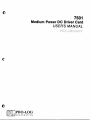
7501
Medium Power
DC Driver Card
USER'S MANUAL
o
•
NOTICE
The information in this document is provided for reference only. Pro-Log does not assume any liability arising
out of the application or use of the information or products described herein.
This document may contain or reference information and products protected by copyrights or patents and
does not convey any license under the patent rights of Pro-Log, nor the rights of others.
Printed in U.S.A. Copyright© 1981 by Pro-Log Corporation, Monterey, CA 93940. All rights reserved. However,
any part of this document may be reproduced with Pro-Log Corporation cited as the source.
•
o
7501
Medium Power DC Driver Card
USER'S MANUAL
o
(O~Dd) ~o~~:~~~
FORWARD
This manual explains how to use Pro-Log's 7501 Medium Power DC Driver Card. It is structured to reflect the
answers to basic questions that you, the user, might ask yourself about the 7501. We welcome your suggestions
on how we can improve our instructions.
0
The 7501 is part of Pro-Log's Series 7000 STD BUS hardware. Our products are modular, and they are designed
and built with second-sourced parts that are industry standards. They provide the industrial manager with the
means of utilizing his own people to control the design, production, and maintenance of the company's
products that use STD BUS hardware.
Pro-Log supports its products with thorough and complete documentation. Also, to provide maximum
assistance to the user, we teach courses on how to design with, and to use microprocessors and the STD BUS
products.
You may find the following Pro-Log documents useful in your work: Microprocessor User's Guide and the
Series 7000 STO BUS Technical Manual. If you would like a copy of these documents, please submit your
request on your company letterhead.
o
o
ii
o
7501 MEDIUM POWER DC DRIVER CARD
TAB LEO F
CON TEN T S
SECTION
Data Sheet
SECTION 2
'Funct i ona 1 Descr i pt ion
SECTION 3
Mapping
SECTION 4
Electrical and Environmental Specifications
SECTION 5
Mechanical
SECTION 6
Operating Subroutines
SECTION 7
Assembly drawing
~nd
Schematic
()
iii
o
o
o
iv
o
7501
u@@@
~u[Q)[IDlliJ~
MEDIUM POWER DC DRIVER CARD
The 7501 provides sixteen independent DC output
circuits for the 7000 Series STD BUS, Each open
col/ector output circuit is capable of sinking up to
+225mA of current in the on-state and can withstand a +50V output level in the off-state, Diode
clamping is included to limit the output voltage
when driving inductive loads, Separate usersupplied clamp voltage inputs are provided for each
group of four outputs, Sixteen LEOs provide a visual
indication of the state of each output.
FEATURES
•
•
•
•
•
•
•
•
16 Independent DC Output Circuits
+22SmA Current Sink Rate
+SOV Output Rating
Diode Clamp for Driving Inductive Loads
Ground Return for each Output Circuit
LED Indicator for each Output Circuit
Standard 40-pin Flat Cable Connector
Clear Plastic Safety Shields
()
r
I
07-011 ~'<---+--I
I
-
- - - - -
STATl); - - - - - -,
INDICATORS
¥
I
I
20
A7-Ae
0----1
IOREa' ...,---.---'UO
WR'
SYSRESET'
o---a
CIRCUITS 4-15
O-_+_--------------.J
DC OUTPUT
7501
'INDICATES ACTIVE LOW LOGIC
1
o
SECTION 2
FUNCTIONAL
Operation
The 7501 converts TTL level stgnals supplied by the STD BUS to latched, negative
true, open-collector DC drtve signals. ThIs conversion process begins by strobing
eight bits of data into one of two fully decoded write""only output port latches.
These latches are cleared at power on by the SYSRESET;', signal ~ A medlum power
logic driver, as shown in the accompanying figures, converts the si'xteen latched
output signals to an inverted, open collector signal, The driverls outputs
are then brought to a 40-pin flat cable connector at the user interface card
edge. Alternating ground and output wires minimize crosstalk on the flat cable.
When driving inductive loads, a diode clamp protects each medium power logic
driver output from high voltage breakdown. This diode is connected between
the user-supp..]ied clamp voltage (+50V or less) and the output signal lj"ne . When
the logic driver is switched off (no current sink), the inductive current surge
raises the collector output voltage above normal levels. When the output
voltage exceeds the clamp voltage, the clamp diode will limit the collector
voltage to approximately the clamp voltage. A separate clamp voltage input is
provided for each group of four outputs (16 outputs, 4 groups) at the user rnter~
face connector. The clamp voltage must be greater than or equal to the off~
state output voltage for each output, but less than +50V. All output signals
are monitored for the low (active) state by LEOs. A diode protects each LED
from reverse voltage breakdown.
.Vee
~
Lb4re4Xc..
r
lN4t41S
l1i4Go'Z..
Jlz'L-
PORi
nATA
l
4
1Itc..1
i\6r :
'IL-
flltN
0
£
7V,cJICA.- 750/ CU7rtt7 S7Afd:?
~
I
I
I
~
..
utSGl?
LOIti:::>
)..
0
2
o
1IlX-
/
po~r
MrA cd
~
VturotJ
II-
\
0----1
-----~------.-L CLAr14P
J),()I)I:::S--
CVJ~jNQ
UNTIL.. !..CAD Cf../ReEv'7
bL- .ssJP't?et::> ~
3
_ _. . . . . .I#tGYOl&JAMllW1&£&4Wi#.&AiAi=r:"'.",U<& ;;,
;;#
,.
,.
MWAI#¥#%M 4k¥H
I
.##4
-'I.
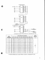
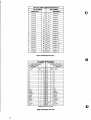
SECTION 3
MAPPING
o
The 7501 consists of two B.-bit output ports that may\ be placed anywh.ere i'n the
I/O address space of OO-FF. These ports occupy two consectui've address locattons~
The 7501 is shipped with hexadecimal port address 40 (port 0 address) and port
address 41 (port 1 address). These port addresses are selected by Jumper w{re~,
To remap the 7501 to another address set, the user connects one jumper w1re on
each of SX, SY, SZA and SZB as shown in the Card Address Selection diagram.
The I/O address mapping and jumper selection table for 2 addresses per card
shows where to place jumper straps to obtain any two sequential port addresses
in the hexadecimal range OO-FF. Using the lowest of the 2-digft hexadecimal
addresses desired, find the most significant hexadecimal address digit along
this vertical axis, and the least significant hex digit on the horizontal
axis. For example, port addresses 40 and 41 are obtained by connecting Jumpers
at X2, YO, 10 and ll.
The only restriction that applies in address selection for the 7501 is the
lower of the two port addresses (40 as shipped) must occur only at every
second possible address. For example, the sequence 41 and 42 i's not allowed
by the decoder.
The pad matrices adjacent to U4, US and u6 are on 0.10 inch (O,25cm) centers,
The jumper wires may be conveniently replaced by wirewrap post if frequent
address selection changes are anticipated.
o
o
4
CARD 5ELECT DECODER5
0
IOEXP-
12
@----~C'
D
74L542
13
15
14
15
.q
9
56
7
X6
6
X5
55
C
X7
57
X4
54
53
B
X3
4
X2
52
X1
51
A
XO
50
5X
12
Y7
9
57
D
Y6
74L542
13
~
14
Z~
. 'C:J
15
l.
C
B
Y2
52
Y1
51
A
YO
50
5Y
5Y
PORT 5ELECT DECODER
lORa12
WR"
13
0
14
2.
15
2.<1
57
D
74L542 56
55
C
54
PORT
STRo-al:
B
52
Z1
51
A
•
Z2
50
pO~t
ZO
0
SrRO~e. ..
1/0 Address Decoder And Schematic For 2 Addresses Per Card
MOST
SIGNIFICANT
HEX ADDRESS
0
1
2
3
4
5
6
7
8
9
A
B
C
D
E
F
B
C
1 DIE 1 F
JUMPER
SELECTION
X, V & Z
I Z1 I Z2 I Z3
ZO
I Z1 LZ2 I Z3
-z
LEAST SIGNIFICANT HEX ADDRESS
o 11 1
ZO
2
13
I Z1 I Z2 I Z3
XO
XO
X1
X1
X2
X2
X3
X3
X4
X4
X5
X5
X6
X6
X7
X7
VO
V4
VO
Y4
YO
V4
VO
Y4
VO
Y4
YO
Y4
VO
V4
VO
Y4
4151617
ZO
I Z1 I Z2 I Z3
XO
XO
X1
X1
X2
X2
X3
X3
X4
X4
X5
X5
X6
X6
X7
X7
V1
V5
Y1
Y5
Y1
V5
V1
Y5
Y1
Y5
Y1
Y5
Y1
Y5
Y1
Y5
8
ZO
1
9
XO
XO
X1
X1
X2
X2
X3
X3
X4
X4
X5
X5
X6
X6
X7
X7
1
A
V2
V6
V2
Y6
Y2
V6
V2
V6
Y2
V6
Y2
V6
Y2
Y6
Y2
Y6
I
XO
XO
X1
X1
X2
X2
X3
X3
X4
X4
X5
X5
X6
X6
X7
X7
1\
V3
V7
V3
Y7
Y3
V7
Y3
V7
Y3
Y7
Y3
Y7
V3
Y7
Y3
Y7
X
AND
V
V
1/0 Address Mapping and Jumper Selection Table for 2 Addresses Per Card.
5
all
--=wwa:&=_U14MiOii4MiiIC#ierM4AiM4P#diQ_
'i"
_01#
i, "
4T\WW¥## 4iP#/f¥4
o
ADDRESS DECODER OPERATION
Refer to the shcematic, Document #105194
The 7501 uses three cascaded 74LS42 decoders (U4, U5 and u6) to decode address
lines AO-A7. These decoders are enabled only when 10RQ* and fOEXP* is active.
The WR* signal is used to gate the select strobes from u6 that control the
output ports.
I
1
CHANGING THE 7501 PORT ADDRESS
Refer to the assembly diagram, Document #105195
Locate deocders U4,
Each decoder device
matrices. Make one
to u4 and U5. Make
U5 and u6 (74LS42) adjacent to the STD BUS edge connenctor.
has a dual row of pads which form decoder output select
(and only one) connection to each of the matrices adjacent
two connections to the matrices adjacent to u6.
The decoder jumper pad numbering figure shows the numbering of the pads
adjacent to the decoder chips on the 7501. Also shown are the jumpers (at
X2, V), SZA and SZB) which produce hexadecimal port addresses 40 and 41,
the selections made when the card is shipped.
0
u4
SX
.,
9
0
0
0
Sy
I
%
0
0
I~ ~
0
0
0
0
0
0
0
0
t.
S
4
5
0
0
0
0
0
0
0
0
"
S
b
'T
0
0
0
., .,
US
0
SZA
~
,
0
0
1-
0
0
3
u6
e
0
0
1-
0
SZB
a
DECODER JUMPER PAD NUMBERING
0
6
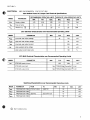
SECTION 4
ELECTRICAL
AND ENVIRONMENTAL SPlCIFICATIONS
7501 Medium Power DC Output Card Electrical Specifications
RECOMMENDED OPERATING LIMITS
MNEM.
PARAMETER
ABSOLUTE NON-OPERATING LIMITS
MIN.
TYP.
MAX.
MIN.
MAX.
UNIT
Vee
Supply voltage
4.75
5.00
5.25
0.0
7.00
Volt
TA
Free air temp.
0
25
55
-40
75
°C
RH
Humi d i ty
95
0
95
%RH
CD
5
User Electrical Characteristics over Recommended Operating Limits
MNEM.
PARAMETER
MIN.
TYP.
MAX.
UNIT
.45
0.8
volt
VOL
Low level user output voltage
V OH
High level user output voltage
50
volt
IOL
Low level user output current
225
rnA
User-supplied clamp voltage
50
volt
User output current duty cycle
100
%
---Yc
STD BUS Electrical Characteristics over Recommended Operating Limits
o
PARAMETER
MNEM.
lee
MIN.
STD BUS supply current
TYP.
MAX.
UNIT
600
1000
rnA
STD BUS input load
See STD BUS Edge Connector Pin List
STD BUS output drive
See
1
1
STD BUS Edge Connector P~'List
I
1
In
I
Switching Characteristics over Recommended Operating Limits
MNEM.
o
PARAMETER
FROM
TO
TpHL
PROPAGATION TIME
TpLH
STD DATA BUS
.,
USER IFC
.,
110
PROPAGATION TIME
110
nsee.
TpHL.
PROPAGATION TIME
USER IFC
STD DATA BUS
110
,usee.
PROPAGATION TIME
H
TpLH
.,
110
,usee.
Q)
MIN.
TYP.
MAX.
UNIT
nsee .
Non-condens i ng
7
AiQiQiiA&AMWA&&t4Mll&WMMQM'ANMa;,;;4AM .,=-4M4=,#4;; , UM;
1#
STO/7501 USER CONNECTOR PIN LIST
PIN NUMBER
PIN NUMBER
MNEMONIC
MNEMONIC
Ground
2
1
Clamp 0-3
Ground
4
3
Output 0"
Ground
6
5
Output 1"
Ground
8
7
Output 2"
Ground
10
9
Output 3"
Ground
12
11
Clamp 4-7
Ground
14
13
Output 4"
Ground
16
15
Output 5"
Ground
18
17
Output 6"
Ground
20
19
Output 7*
Ground
22
21
Clamp 8-11
Ground
24
23
Output 8*
Ground
26
25
Output 9*
Ground
28
27
Output 10*
Output 11 *
Ground
30
29
Ground
32
31
Clamp 12-15
Ground
34
33
Output 12*
Ground
36
35
Output 13"
Ground
38
37
Output 14*
Ground
40
39
Output 15*
o
User Connector Pin List
o
STD/7501 EDGE CONNECTOR PIN LIST
PIN NUMBER
PIN NUMBER
OUTPUT (LSTTL DRIVE)
INPUT (LSTTL LOADS)
MNEMONIC
vee .:, VOL TS
GNO GROUND
OUTPUT (LSTTL DRIVE)
INPUT (LSTTL LOADS)
MNEMONIC
,') VOL TS
vee
2
1
GROUND
4
'3
6
')
7
1
03
1
02
t-------- --
GNO
·5V
07
1
·5\1
06
1
8
10
05
1
12
9
11
1
01
04
A15
1
14
13
1
16
1
A14
18
15
17
DO
A7
1
A6
A13
20
19
1
AS
Al:r-
22
21
1
A4
All
24
23
1
A3
Al0
26
28
25
27
1
1
A2
30
29
1
A9
A8
A1
RO'
32
31
1
MEMRO'
34
33
1
IORO'
MEMEX'
36
35
1
IOEXP'
MCSYNC'
38
37
REFRESH'
STATUS 0'
39
41
STATUS l'
BUSRO'
40
42
INTRO'
44
43
NMIRO'
46
PBRESET'
48
45
47
CNTRl'
50
49
CLOCK'
52
51 OUT
PCO
54
53
AUX GNO
56
55
AUX
PCI
IN
AUX GNO
AUX
-v
BUSAK'
INTAK'
WAITRO'
1
SYSRESET'
Edge Connector Pin List
8
---
AO
WR'
-v
o
~
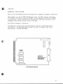
SECTION 5
MECHANICAL SPECIFICATIONS
Refer to the Card Address Selection diagram for component placement information,
When placed in a Series 7000 STO BUS card rack, the 7501 requires clearances
of 0.150" on the circuit side and 0.600" on the component side of the printed
circuit board. These clearances are required for the safety shields on the
component side and the circuit side of the 7501.
User Mating Connector Information
The 7501 uses a 40-pin male PC board header connector (3M PN 3432-130 or
equivalent). The matching female socket for use in standard flat cable
applications is 3M PN 3417-6040.
LED
()
l-
a:
2
I-
..
0
;;
im
ADDRESS
SELECT
S
x 090000000
SY
SZA
000000000
CONNECTOR
40 PIN FLAT
CABLE CONNECTOR
3M PN 3432-1002
OR EQUIVALENT
900000000
600000000
990000000
660000000
SZB
Card Address Selection
•
9
.W_-,--
o
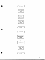
SECTION 6
7501 OPERATING SUBROUTtNE MODULES
This section provides flow diagrams and suhroutines to oper~te your 7501
card. These may be used intact, or used as models to construct subroutines
for a specific application.
The subroutines are written in 8080-fami1y assembly code and will execute
on 8080, 8085, and z80 processors. The memory addresses selected are
compatible with Pro"'Log's 7801 (8085A) and 7803 (z80) processor cards,
The 7501 port addresses used are the address jumper selections made when
the 7501 is sh i pped.
To use these subroutines in systems other than those described aboye~
the memory and/or I/O port addresses may requlre change for compatlb~ll'ty~
The I/O routines provided must be duplicated for the two ports on the 7561,
The correct port address must be inserted in each routine~
The flow diagrams presented can be easily translated into the assembly code
used by any microprocessor since they show the steps required to achieve
7501 operation without reference to a particular microprocessor.
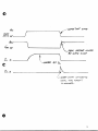
The (Set Bit) routine can set a bit or bits on an output port. To use the
routine, load the accumulator with the hits that should be changed and set
the HL pointer to a place in memory where the port status is stored. Setting
a bit will cause the corresponding output driver to sink (conduct) current
p
0
The (Clear Bit) routine can clear a bit or bits on an output port. To use
the routine, load the accumulator with the bits that should be changed and
set the HL pointer to a place in memory where the port status is stored.
Clearing a bit will cause the corresponding output dirver to turn-off (not
conduct current).
o
10
•
SET BITS
INPUT PRESENT
STATUS
"OR II IN
NEW BITS
OUTPUT NEW
STATUS
o
CLEAR BITS
)
"
INPUT PRESENT
STATUS
"
MASK OFF
UNWANTED BITS
OUTPUT NEW
STATUS
•
"
RETURN
11
&&A
NGiilWWilMIiiW.=_...4i4liWUQU';W'=#II@
Ie
i
Z
;
o
PRO-LOG CORPORATION
HEXADECIMAL
LINE
PAGE
INSTR.
ADR
ADR
PROGRAM ASSEMBLY FORM
MNEMONIC
LABEL
INSTR.
TITLE
L1)A-:t
-
2
lJ)~I
'/..X
\tL
3
-
'1...'1...
4
-
XX
(ser ~\TS)
6
4'1
7£
7
~o
LDA
ORA
8
'-'1
STA~
9
l>~
CRt\
A
"!..~
B
Cq
.Lt>~
-
DATE
COMMENTS
LOAl) A WIT~ ~r'(s.")
0
1
5
'156\
MODIFIER
• SET
A
.... 9.A-JE.
M(~L)
.-6e:-r
~
'?Ol~"I£R
MEMCN...'I
~\ TO;
l ~
Pe.£6£N"T
-0
"'aRT
~A--n)5
N law -:B.l T,s
4-0R t N
(\\-LJ
"-STDRE.
~EW
PDQ.;:L
N~ W ~ ArTA.
+~£~\D
')()(.
T{) ~ <;.£\
r
I~
!:>TA,.OS
\ h PDQ...' \
RTS
C
D
~~
E
F
0
LbA-I
1
L"D-P:r.
2
-
3
4
-
7
1£
LDA
8
f\o
A-I\) A
.~
(\-\L)
rMA
LD&
9
rot '1
A
1)'3
51PtN
OPA
B
'J...'1..
-
C
(lq
1'O_'OE ~Ef)
- SET MF:MhQ..'1
PD\"-l\'BR
-
~l'<"
'/....x
6
((I-,~o.Q ~ r\S)
A W\-n.\ '""&lTcS)
r
"'-'1..
.:u:
4-1
5
LO~
)(~
CoM{)LE'M..eJT
A.,..)D
PI)\
IN "&
A
M (t-+L)
..... bE:T
PP.k~I=A.)'
... ~AS\O(
.... ~::iTt)2..E
f
5B:)O
{>()Q.., S-fA\US
"BlTS
NEw %Q..\ ~T~\I)S
"TO ~D~T
~EW "lJf:\.\A
dE
X-'f...
A..\5
D
E
F
100001 2m
o
12
•
0
0
C/)
t:'l1
("')
t-j
8
7
5
6
4
3
H
2
0
2:
~
-...J
~
DI
ID
~ ~ ~
5KEQ.
~~'~.~
~~O
3REQ
CI
It
U2
74LS273
I~~ ~=:l
JI~
o-oom-o
C>-{iffi}-o
o-OOID-o
<>-{Hlli-o
~
o-OO!}-o
~
~
C
~
~"6600
I:::
~~
I~
Dl3612
o-{8]W-Q
o-{8]ffi-o.
--J
o-{8]iD-o
o-OOm-o
~
o-ooID-<l
~
~
B
n
('D
1/9
I/K,CF/I<f.W,5¥o
I
[IB
I
I
470JL.
NEn~1
s
III
rt
IV,2.)3)4
.....
RS'" 7 8
n
033, ..34,.35,3u.
Z REa
&-
APPLY LOCXTlTE.
& - INtI/CArts
£ro
LAd£LS
AI
&,- PO~T
It:, -[NOI{ATE.S
I
NOTES:
~
-L
(...)
8
-Foe
IIIH/>El>
PIN OF LLD
ON 81JTH
IN4148
I
DI7-D5e
f!rp)
cotrJr
f ClA.C.
SIDe~
Of: PIAlI3
AS SU()WN
TO ADDJ:J.55 4/
TO
,STANOARD
OTHE~1I15£
I
1/1 I
AO{)KES~
A
40
PIN N/J.I OF SOUETS (rr,)
AS5E"'~U
UNLEt;S
PlA:~C
I 1.5 JUI1PCI>
I1::.-PO~T 0 IS
1/4
TO ALL SCfi:Ew5
CATHaDf.
BE
\
Bt:€Q
"S:'YREv.LnTERU~INGRUI>I>ER:;T"MP.
IDENTIFY WiTH
/
!.H. ASIQ0.4.
SPE.lJFI£D
7
6
5
4
3
C/)
::r'
171
B&
III
;:J
~
&,-
III
;:J
O'Q
00
00
00
00
00
00
00
00
00
00
00
00
00
00
00
00
00
00
00
00
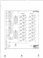
~~
o-OOiD-o
'"1
~
.....
~~ ~-n
o-OOID-<>
rJ
I--'
~
o-!iID-<> o-OOID-o
0-{8!!}-0
('D
S
'<
~~ ~-J
BI
~
/~'"
/
~
>.-
(J)
(J)
.....
~
':"pq'S
BU,Fe::
'------1'174~~244
D7
,\-----
9
OIl?
006
1
1
1
PORT I OUTPUT (I RCUIT
PeU r;J OUTPUT CIRCUIT
1&
S~
.
1>1
17-4>-!>
} - - - - - - - ; I : : ' (TYPl
.~v
t5V
~~OO2. .n
+5V
OD3
..EQrrJL
'7
~'
~~~QV7
iOE)(Q*~
_
_
~
_
'T
A7:
A617
1+
,,~~ S~
S4!5
8
4
'
D
"
'.
~c~-~
50
I
loPO-s~~ 1
7D!>~IZ
A5~9
IS A
e~+~+
a~612_
'XO
(o,OP'-7-'
~-.
I~
~
•
I-
I1
I
~
e61-r,\
(70PO-Sil
(2.5
I
IOPI-;;
I
--<~
lUI::'):> -
DPI-oj.
•
(a9
L-(IO
A+(~I
55-'~
'·C
A~:
!:~:~:
I·IK
::3
SJ~
- - T
I
~
Ai:@
~'... "0-'
+5V
L_
~
5Y
I
~
-05
u,
~
~II
tI
m
+5V
OPO-~
r,H- ~--t
rA
O~H
I
I
~I
3J---.:..-1 Z
5
~DPO-3 U~b
I
':I+ei'i+'l.'O"'.
01'1-5"1
",'i'··i'i+'lT<UL.
L
I DPI-3
I ~
D~~12
IS
OPO·2~
~"
OP/~Z
~..
I
I_
I
H
- 0,6-2
~ H-:i rI'"
-LO+b4
•
DPI-I
~A
AO@
PCO
PC 1
®---,
@-------l
,
~...
74L532
r
(l90PO.,,"
OPI-O
ao
....ll
T5V~
+5V 2
:::~
I
+
lat5V
1:1
II.Ol'
F
sov
1
+
~Z.3..4.S
0
.2.L
ASSEMBLY
105135
PARTS LIST
I051~6
PRO- LOG CORPORATION
"
.1'"
50V
[.<,
1Ml~
o
o
o
•
o
•
o
o
USER'S MANUAL
2411 Garden Road
Monterey, California 93940
Telephone: (408) 372-4593
TWX: 910-360-7082
o
Telex: 171829
1066918
300
11/81