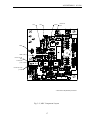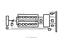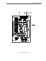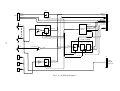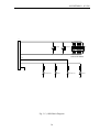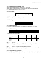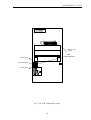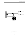
1
Aperture Card Scanner
Technical Service Manual
ACS 4600
ASG/TSM/001 (1.0)
Part Number 6699D107
1
DOCUMENT REVISION RECORD
2
LIST OF DOCUMENTS
3
ASG MAINTENANCE MANUAL
ACS 4600
4
5
6
7
8
9
10
SPARE PARTS AND SERVICE ACCESSORIES
ACS 4600
TECHNICAL SERVICE BULLETINS
ASG/TSM/001
Document Revision Record
REV.
DATE
CHANGED
BY
PAGES
AFFECTED
BRIEF DESCRIPTION OF CHANGE
1.0
031128
BN/LM
All
Original issue of document
DRR
ASG/TSM/001 031128
List of Documents:
ASG/MTM/001 (1.0)
ASG Maintenance Manual
ACS 4600
AOG /PLS/002 (1.1)
Spare Parts and Service Accessories
ACS 4600
TITLE:
AGS MAINTENANCE MANUAL
ACS 4600
DOC.NO.:
ASG/MTM/001
PREPARED BY:
BN/LM
AUTHORIZED:
JR
DISTRIBUTION:
Tegningsarkiv, Svendborg
PT, Svendborg
DD
ISSUE REVISION:
DATE:
(1)
(1)
(1)
1.0
2003-11-28
This document is the property of Contex A/S. The data contained herein, in whole or in part,
may not be duplicated, used or disclosed outside the Recipient for any purpose other than to
conduct technical evaluation. This restriction does not limit the Recipients right to use
information contained in the data if it is obtained from another source without restriction
ASG/MTM/001
Document Revision Record
REV.
DATE
CHANGED
BY
PAGES
AFFECTED
BRIEF DESCRIPTION OF CHANGE
1.0
031128
BN/LM
All
Original Issue of Document
3
DRR
ASG/MTM/001 031128
Table of Contents
LIST OF FIGURES .......................................................................................................................... 6
1.
INTRODUCTION ................................................................................................................................. 7
2.
GENERAL DESCRIPTION................................................................................................................. 8
ACS APERTURE CARD SCANNER MODELS .......................................................................................... 8
2.1
3.
ELECTRICAL CHECK AND ADJUSTMENTS ............................................................................. 11
3.1
3.2
3.2.1
3.3
3.3.1
3.3.2
3.3.3
3.3.4
3.3.5
3.3.6
3.3.7
3.4
3.4.1
3.4.2
3.4.3
3.4.4
3.4.5
3.4.6
3.5
3.5.1
3.5.2
3.5.3
3.5.4
3.5.5
3.5.6
3.6
3.6.1
3.6.2
3.6.3
3.6.4
3.6.5
3.6.6
3.6.7
3.6.8
3.7
3.7.1
3.7.2
3.7.3
3.7.4
3.7.5
3.7.6
3.8
MARKING CODES FOR CIRCUIT BOARDS AND PROGRAMMED DEVICES ............................................. 11
DOWNLOADING SCANNER FIRMWARE ............................................................................................... 11
Erase and Restore Parameter Blocks .......................................................................................... 12
CHECK AND ADJUSTMENT OF THE SWITCH MODE POWER SUPPLY, SMPS........................................ 13
AC Voltages ................................................................................................................................. 13
DC Voltages................................................................................................................................. 13
Adjustments.................................................................................................................................. 13
Fuses............................................................................................................................................ 13
Markings...................................................................................................................................... 13
Jumper Settings............................................................................................................................ 13
Hints............................................................................................................................................. 14
CHECK AND ADJUSTMENT OF MOTOR DRIVER BOARD, MSC ........................................................... 16
DC Voltages................................................................................................................................. 16
Stepper Motor Reference Voltages .............................................................................................. 16
Functional Test ............................................................................................................................ 16
Markings...................................................................................................................................... 16
Jumper Settings............................................................................................................................ 16
Hints............................................................................................................................................. 16
CHECK AND ADJUSTMENT OF CAMERA BOARD, CBG....................................................................... 19
DC Voltages................................................................................................................................. 19
Adjustments.................................................................................................................................. 19
Functional Test ............................................................................................................................ 19
Markings...................................................................................................................................... 19
Jumper Settings............................................................................................................................ 19
Hints............................................................................................................................................. 19
CHECK OF CONTROLLER BOARD, SUC.............................................................................................. 22
DC Voltages................................................................................................................................. 22
Adjustments.................................................................................................................................. 22
Functional Test ............................................................................................................................ 22
Markings...................................................................................................................................... 22
Switch Settings (Download Control Switches)............................................................................. 22
Jumper Settings............................................................................................................................ 22
Signal LEDs on the SUC-Board .................................................................................................. 22
Hints............................................................................................................................................. 22
CHECK OF INTERFACE MODULE, IMC............................................................................................... 26
DC Voltages................................................................................................................................. 26
Adjustments.................................................................................................................................. 26
Functional Test ............................................................................................................................ 26
Markings...................................................................................................................................... 26
Jumper Settings............................................................................................................................ 26
Hints............................................................................................................................................. 26
CHECK OF PUNCHED CARD READER BOARD, PCR............................................................................ 29
3
ASG/MTM/001 031128
3.8.1
DC Voltages................................................................................................................................. 29
3.8.2
Check Phototransistor Outputs.................................................................................................... 29
3.8.3
Functional Test ............................................................................................................................ 29
3.8.4
Markings...................................................................................................................................... 29
3.9
CHECK OF OPERATOR PANEL, OPB................................................................................................... 32
3.9.1
DC Voltages................................................................................................................................. 32
3.9.2
Functional Test ............................................................................................................................ 32
3.9.3
Markings...................................................................................................................................... 32
3.9.4
Switch Setting .............................................................................................................................. 32
3.10
CHECK OF SMART CARD READER, SCR ............................................................................................ 35
3.10.1
DC Voltages ............................................................................................................................ 35
3.10.2
Functional Test ....................................................................................................................... 35
3.10.3
Markings ................................................................................................................................. 35
3.10.4
DIP Switch Setting .................................................................................................................. 35
3.10.5
Signal LED on the SCR-Board ............................................................................................... 35
3.11
CHECK OF OPTOINTERRUPTER BOARD, OIBA................................................................................... 38
3.11.1
Functional Test ....................................................................................................................... 38
3.11.2
Markings ................................................................................................................................. 38
3.12
CHECK AND ADJUSTMENT OF CARD SENSORS ................................................................................... 40
3.12.1
Check and Adjustment of Input Sensor ................................................................................... 40
3.12.2
Check of Feeder Sensor .......................................................................................................... 42
3.12.3
Check of Edge Detector .......................................................................................................... 42
3.13
CHECK AND ADJUSTMENT OF REJECT BIN SENSORS.......................................................................... 42
3.13.1
Check and Adjustment of Bin Full Sensor............................................................................... 42
3.13.2
Check and Adjustment of Reject Tray Sensor ......................................................................... 45
4.
ACS OPTICAL SYSTEM .................................................................................................................. 47
4.1
DESCRIPTION OF ACS OPTICAL SYSTEM ........................................................................................... 47
4.2
CCD-CAMERA CHECK AND ADJUSTMENT......................................................................................... 50
4.2.1
Check of Light Profiles ................................................................................................................ 50
4.2.2
Check and Adjustment of Focus................................................................................................... 53
4.2.3
Check and Adjustment of Scan Width .......................................................................................... 54
4.2.4
Check and Adjustment of CCD-Centering ................................................................................... 57
4.2.5
Check and Adjustment of CCD-Tilt ............................................................................................. 58
5.
GENERAL MAINTENANCE............................................................................................................ 63
6.
TROUBLESHOOTING...................................................................................................................... 64
6.1
6.2
6.3
6.3.1
6.3.2
6.4
6.5
7.
7.1
7.2
7.3
7.4
7.5
8.
8.1
8.2
8.3
8.4
8.5
POWER-ON SELF-TEST ...................................................................................................................... 64
LED INDICATORS ON OPERATOR PANEL ........................................................................................... 64
ERROR CODES ................................................................................................................................... 65
Error Codes displayed on the Operator Panel ............................................................................ 65
Error Codes displayed on the PC Screen .................................................................................... 65
TROUBLESHOOTING HINTS ................................................................................................................ 69
HOLLERITH CODE READING PROBLEMS ............................................................................................ 71
DISASSEMBLY AND ASSEMBLY.................................................................................................. 72
SCANNER CABINET ............................................................................................................................ 72
FRONT-END BASE COVER ................................................................................................................. 72
BOTTOM PLATE ................................................................................................................................. 72
FRONT-END COVER ........................................................................................................................... 73
POWER SUPPLY ASSEMBLY ............................................................................................................... 73
REPLACEMENT OF PARTS ........................................................................................................... 74
PRINTED CIRCUIT BOARDS ................................................................................................................ 74
PCR-BOARD ..................................................................................................................................... 74
PCR APERTURE PLATE ..................................................................................................................... 75
TEFLON TAPE ON SCANNING PLATEN ................................................................................................ 77
CARD SENSORS ................................................................................................................................. 79
4
ASG/MTM/001 031128
8.6
8.7
8.8
8.9
8.10
8.11
8.12
8.13
8.14
8.15
9.
REJECT BIN SENSORS ........................................................................................................................ 82
SAFETY INTERLOCK SWITCH ............................................................................................................. 83
FEEDER SOLENOID ............................................................................................................................ 83
GEAR SOLENOID ................................................................................................................................ 84
STEPPER MOTOR ............................................................................................................................... 85
GEAR CARRIAGE ............................................................................................................................... 86
DRIVING BELT AND ROLLERS ............................................................................................................ 88
SEPARATOR UNIT AND FRICTION PAD ............................................................................................... 88
CARD TRAYS ..................................................................................................................................... 90
LAMP AND LAMP-SOCKET ................................................................................................................. 90
SCANTEST 6....................................................................................................................................... 95
9.1
DESCRIPTION OF SCANTEST 6 .......................................................................................................... 96
9.1.1
Test 1, Scanner Information ....................................................................................................... 96
9.1.2
Test 2, LED Test ......................................................................................................................... 96
9.1.3
Test 3, Key Test........................................................................................................................... 96
9.1.4
Test 4, Original-Sensor Test ....................................................................................................... 96
9.1.5
Test 5, Lamp Test........................................................................................................................ 97
9.1.6
Test 6, Motor Test ....................................................................................................................... 97
9.1.7
Test 9, Camera Adjustment......................................................................................................... 97
9.1.8
Test 13, Switch Scanner to Test Mode ........................................................................................ 98
9.1.9
Test 21, SCANdump .................................................................................................................... 98
10.
WIRING DIAGRAMS ................................................................................................................... 99
11.
SPECIAL SERVICE TOOLS...................................................................................................... 102
5
ASG/MTM/001 031128
List of Figures
FIG. 2-1 ACS 4600 BLOCK DIAGRAM.................................................................................................... 10
FIG. 3-1 SMPS TEST POINTS................................................................................................................... 15
FIG. 3-2 MSC COMPONENT LAYOUT ................................................................................................... 17
FIG. 3-3 MSC BLOCK DIAGRAM ............................................................................................................ 18
FIG. 3-4 CBG COMPONENT LAYOUT ................................................................................................... 20
FIG. 3-5 CBG BLOCK DIAGRAM ............................................................................................................ 21
FIG. 3-6 SUC COMPONENT LAYOUT.................................................................................................... 24
FIG. 3-7 SUC BLOCK DIAGRAM............................................................................................................. 25
FIG. 3-8 IMC COMPONENT LAYOUT .................................................................................................... 27
FIG. 3-9 IMC BLOCK DIAGRAM............................................................................................................. 28
FIG. 3-10 PCR COMPONENT LAYOUT .................................................................................................. 30
FIG. 3-11 PCR BLOCK DIAGRAM........................................................................................................... 31
FIG. 3-12 OPB COMPONENT LAYOUT.................................................................................................. 33
FIG. 3-13 OPB BLOCK DIAGRAM........................................................................................................... 34
FIG. 3-14 SCR COMPONENT LAYOUT .................................................................................................. 36
FIG. 3-15 SCR BLOCK DIAGRAM........................................................................................................... 37
FIG. 3-16 OIBA COMPONENT LAYOUT................................................................................................ 39
FIG. 3-17 ADJUSTMENT OF THE INPUT SENSOR................................................................................ 41
FIG. 3-18 ADJUSTMENT OF THE BIN FULL SENSOR.......................................................................... 44
FIG. 3-19 ADJUSTMENT OF THE REJECT TRAY SENSOR.................................................................. 46
FIG. 4-1 ACS OPTICAL SYSTEM ............................................................................................................ 48
FIG. 4-2 CCD-CAMERA ............................................................................................................................. 49
FIG. 4-3 ACS 4600, LIGHT PROFILE UNCORRECTED.......................................................................... 52
FIG. 4-4 ASC 4600, LIGHT PROFILE CORRECTED ............................................................................... 52
FIG. 4-5 ACS 4600, FOCUS SIGNAL AND SCAN-WIDTH ..................................................................... 56
FIG. 4-6 ACS 4600, CCD-CENTERING AND CCD-TILT ........................................................................ 60
FIG. 4-7 CAMERA ADJUSTMENT CARD................................................................................................ 61
FIG. 4-8 DETAILS OF ADJUSTMENT PATTERNS................................................................................. 62
FIG. 8-1 PCR APERTURE PLATE ............................................................................................................. 76
FIG. 8-2 SCANNING PLATEN................................................................................................................... 78
FIG. 8-3 INPUT SENSOR ASSEMBLY...................................................................................................... 80
FIG. 8-4 OIB-BOARD WITH BRACKET................................................................................................... 81
FIG. 8-5 STEPPER-MOTOR AND GEAR ASSEMBLY ............................................................................ 87
FIG. 8-6 PRESSURE ARM WITH FRICTION PAD .................................................................................. 89
FIG. 8-7 ACS FRONT-END, TOP-VIEW .................................................................................................. 92
FIG. 8-8 ACS FRONT-END, BOTTOM-VIEW ......................................................................................... 93
FIG. 8-9 ACS REAR-END, TOP-VIEW..................................................................................................... 94
FIG. 10-1 ACS 4600 PRIMARY-WIRING DIAGRAM ............................................................................ 100
FIG. 10-2 ACS 4600 SECONDARY-WIRING DIAGRAM...................................................................... 101
6
ASG/MTM/001 031128
1. Introduction
The scope of this Maintenance Manual (MTM) is to provide technical information to support
board-level troubleshooting and maintenance of the Aperture Card Scanner (ACS) model:
GA66D (ACS 4600)
Chapter 2 contains a general technical description based on block diagrams.
Chapter 3 describes Electrical Check and Adjustments including jumper and switch settings.
Chapter 4 contains a general description of the Optical System and the CCD-Camera
Adjustments.
Chapter 5 describes General Maintenance.
Chapter 6 contains a list of Error Codes and gives some hints on troubleshooting.
Chapter 7 describes Disassembly and Assembly procedures.
Chapter 8 provides guide for replacement of parts for which the procedure is not obvious.
Chapter 9 describes the scanner test program, SCANtest 6.
Chapter 10 contains Wiring Diagram.
Chapter 11 contains a list of Special Service Tools.
7
ASG/MTM/001 031128
2. General Description
The ACS Aperture Card Scanner model:
GA66D (ACS 4600, ACS 4600 PLUS)
is described at block-diagram level in Section 2.1.
2.1 ACS Aperture Card Scanner Models
Block Diagram is shown in: Fig. 2-1 ACS 4600 Block Diagram, page 10.
The ACS 4600 scanner range consists of:
Model:
Trade name:
No. of cameras:
Computer interface:
Max. resolution (on
scanned image)
Optical resolution
(on Aperture Card):
Scan speed (A1 at
200 dpi)
SmartCard:
GA66D
ACS 4600
ACS 4600 PLUS
1
1
IEEE 1394 / USB
IEEE 1394 / USB
200 dpi
2400 dpi
6300 dpi
6300 dpi
20 sec
7 sec
BASIC
PLUS
The basic versions of the scanner (ACS 4600) may be field upgraded to the enhanced version
(ACS 4600 PLUS) by replacing the BASIC Smart Card with a PLUS Smart Card.
The scan-area is back-illuminated by a halogen lamp.
The CCD-Camera in the scanner contains one 7.926 pixel (B/W) CCD. The output signal
from the CCD is Light Profile Corrected at pixel level.
All scanning and image processing functions are contained on only two boards, the Camera
Board (CBGA) and the Controller Board (SUCE).
The Aperture Card Scanner has a Punched Card Reader (PCRA) allowing Hollerith coded
information on the cards to be used for automatic setting of the WIDEimage parameters: Auto
Paper Size and Auto Filenaming.
The card-feeder mechanism is - via a reduction gear - driven by a stepper motor. The gear
ratio, which is selected by the Gear Solenoid, is 1:1 for card feeding and 9:1 for scanning.
The number of steps per scanline depends on the image resolution and the drawing reduction
ratio and is controlled by the microcontroller on the SUC-Board.
The Safety Interlock Switch for the Front-End Cover disables the Stepper Motor driver circuit
(MSCA) and turns the Lamp OFF (via SUCE), and signals the Cover Open condition to the
SUC-Board when the Front-End Cover is open.
The computer Interface Module (IMCA) contains:
8
ASG/MTM/001 031128
IEEE 1394 Controller (FireWire)
USB Controller
for IEEE 1394 interface respectively USB interface.
9
CBGA
PCRA
OPBB
OIBA
OPERATOR
PANEL
LAMP
INT ER LOCK
SWITCH
GEAR SOLENOIDS
REJECT BIN SENSORS
STEPPER MOTOR
FEEDER SOL ENOID
10
IMCA
FAN
MSCA
SWITCH MODE
POWER SUPPLY
STEPPER MOTOR
CON TROL BOARD
SUCE
IEEE 139 4
AUX.
SCANNER CON TROL BOARD
RFI
PRIMARY
SECONDARY
Fig. 2-1, ACS 4600 Block Diagram
SMART
CARD
USB
INTERFACE
BOARD
100 - 240 VAC
SCRA
IEEE 139 4
ASG/MTM/001 031128
SMPS
ASG/MTM/001 031128
3. Electrical Check and Adjustments
Required Test Equipment:
Multimeter, Ri > 10 Mohm.
PC with SCANtest 6 and Scanner Maintenance installed and USB and IEEE 1394
interface.
SCANtest 6 is described in Chapter 9, page 95.
3.1 Marking Codes for Circuit Boards and Programmed Devices
All circuit boards are identified by a 4-letter code, where the fourth letter is designating a
specific variant of the board. A board revision number follows the board identification code.
The marking of all newer printed circuit boards may be exemplified by the marking of the
SUC-Board:
SUCE01
which designates SUC-Board, variant E, revision 1.
The marking code of the older OIBA- and OSBC- Boards are a little different, for example:
OIBA-1.0
which designates OIB-Board, variant A, revision 1.0.
The revision number is updated only if the functionality of the board has been changed.
Updated boards will always be backwards compatible.
Programmed components, like CPLDs, Flash Memory, etc., are marked with a 3- or 4-letter
identification code, depending on whether the component is basic or variant specific. For
example, the component marking:
SUC.003-2
identifies the Interface Controller used on all variants of the SUC-Board. 003 is a component
specific number and 2 is the firmware revision number.
The variant designation (and part number) of the circuit boards used for a particular scanner
model can be found in the Spare Part List included in the Technical Service Manual.
3.2 Downloading Scanner Firmware
The scanner firmware is stored in Flash Memory on the SUC-Board.
Scanner firmware is available on:
http://www.contex.com/
11
ASG/MTM/001 031128
Firmware is downloaded to the scanner through the IEEE 1394 or USB interface, please see
readme.txt on the firmware disk for download instructions.
The download program:
CtxPrgm.exe
is started by double-clicking the self extracting firmware.exe file.
The download program reads the Download Control Switches, SW1 and SW2, on the SUCBoard to check if the actual firmware and the SUC hardware are compatible.
The Download Control Switches are factory set, and the setting must not be changed.
If the scanner does not go into Boot Mode when the download program is started, the scanner
can be forced into Boot Mode by turning it OFF, setting SW7 on the SCSI ID-Switch to ON
(see page 35), and turn the scanner back ON. The scanner will now be in Boot Mode and new
firmware can be downloaded as described above. When the new firmware has been
successfully downloaded, turn the scanner OFF, set SW7 back to OFF, and turn the scanner
ON for normal operation.
3.2.1 Erase and Restore Parameter Blocks
The following two options may be found on the pull-down menu by right-clicking at the
CtxPrgm icon in the title bar of the CtxPrgm window:
•
•
Erase Parameter Blocks
Restore Parameter Blocks
‘Erase Parameter Blocks’ erases the Parameter Blocks (Basic Calibration) in Flash Memory
on the SUC-Board and save these in the file ‘backup.pmb’ located in the directory pointed to
by the SET TEMP environment variable.
The file, backup.pmb, may be useful for diagnostic purposes.
‘Restore Parameter Blocks’ restores the Parameter Blocks from backup.pmb.
Note:
Always run Scanner Maintenance after Erase Parameter Blocks.
12
ASG/MTM/001 031128
3.3 Check and Adjustment of the Switch Mode Power Supply, SMPS
All test points referred to below are shown in Fig. 3-1, page 15.
All DC voltages are measured relative to CN3, pin 1, 2, 3, 4, 5 (GND).
3.3.1 AC Voltages
CAUTION:
The connector CN1 is connected directly to the line voltage and constitute a risk of
electric shock, or injury to persons.
3.3.2 DC Voltages
Ref. on Fig. 3-1
CN3,pin 6,7,8
CN3,pin 1,2,3,4,5
CN2,pin 3,4,5
CN2,pin 2
CN2,pin 1
Ref. on SMPS
3.3V
G
5V
V3
V4
DC Voltage
+3.3 V ± 0.1 V
GND
+5.3 V +0/-0.1 V
+12 V + 1/-0 V
+24 V ± 1 V
3.3.3 Adjustments
CAUTION:
The output voltages of the SMPS are all factory set and should normally not be
adjusted.
The (5V) output voltage should be no more than 5.3 V measured between GND and CN2, pin
3,4,5 (5V) on the SMPS, and no less than 5.1 V measured between GND and C45, left on the
CBG-Board.
If the voltage is not within these limits, it may be adjusted by potentiometer SVR1 on the
SMPS, see Fig. 3-1, page 15.
3.3.4 Fuses
The type and rating of the fuse on the SMPS is:
F1:
F4A
type IEC 127-2/2, UL R/C
CAUTION:
For continued protection against risk of fire, replace only with same type and rating of fuse.
3.3.5 Markings
No marking.
3.3.6 Jumper Settings
No jumpers.
13
ASG/MTM/001 031128
3.3.7 Hints
+3.3 V is used as supply for the SUC-, CBG-, IMC-, and OPB-Boards.
+5.3 V is used as supply for MSC-, CBG, SUC-, and IMC-Boards.
+12 V is used as supply for the MSC- and CBG-Board, and on the MSC-Board for the
Fan and Lamp drivers.
+24 V is used on the MSC-Board for the Stepper Motor and Solenoid drivers.
14
SVR2
+3.3V Adjust
SVR2
CN3
3.3 V
CN3, pin 6-8
3.3 V
+3.3V±0.1
3.3 V
G
G
CN3, pin 1-5
G
GND
G
G
15
5V
CN2, pin 3-5
5V
+5.3V +0/-0.1
5V
CN2, pin 2
V3
-12V±0.5
V4
CN2
AC/N
SVR1
CN1
SVR1, see 3.3.3
Mains Input
Connector
Fuse, see 3.3.4
+5.3V Adjust
Fig. 3-1, SMPS Test Points
+24V±1
ASG/MTM/001 031128
AC/L
CN2, pin 1
ASG/MTM/001 031128
3.4 Check and Adjustment of Motor Driver Board, MSC
All test points referred to below are shown in Fig. 3-2, page 17.
All DC voltages are measured relative to Test Point GND.
MSC Block Diagram is shown in Fig. 3-3, page 18.
3.4.1 DC Voltages
Ref. on Fig. 3-2
J2, pin1 and pin2
J2, pin3 and pin4
J2, pin5
J2, pin6
TP1
DC Voltage
0 V (GND)
+5.3 V +0/-0.2 V
+12.0 V + 1/-0 V
+24.0 V ± 1 V
-5.0 V ± 0.5 V
3.4.2 Stepper Motor Reference Voltages
The stepper motor must be stopped for adjustment of the reference voltages.
Adjust P3 until the voltage on TP6 reads:
10 mV ± 10 mV
Adjust P4 until the voltage on TP4 reads:
10 mV ± 10 mV
3.4.3 Functional Test
SCANtest 6: Test 5, Lamp Test
Test 6, Motor Test
3.4.4 Markings
MSCAdd
ACS 4600
where dd = board revision number.
3.4.5 Jumper Settings
No jumpers.
3.4.6 Hints
Control signals on J9:
pin 2: Lamp ON/OFF, LOW = ON
pin 8: Feed-Motor Step Pulse
pin 11: Feed-Motor Direction, LOW = REVERSE
pin 15: Gear Solenoid, LOW = OFF
pin 16: Feeder Solenoid, LOW = ON
16
ASG/MTM/001 031128
P3*
P4*
TP4*
-5V±0.5V
TP1
TP6*
GND
+12V +1/-0V
J2,5
+24V±1V
J2,6
+5.3V+0/-0.2V
J2,3/4
* See text for adjustment procedure
Fig. 3-2, MSC Component Layout
17
J7
SOLENOID
(GEAR)
SOLENOID
J8
(FEE DER)
J2
PSU
(SMPS)
1
2
3
SOLENOID
DRIVER
+24 V
2
1
J4
2
1
J6
BLEEDER
DRIVER
2
1
J3
FAN
DRIVER
2
1
J5
LAMP
DRIVER
+12 V
1
2
3
4
1
2
3
4
5
6
SOLENOID
DRIVER
+24 V
S ENSOR I NP UT
(NOT US ED)
+12V TO -5 V
CONVERTER
+12 V
TP1
N.C.
N.C.
-5 V
+12 V
+5 V
+12 V
+24 V
FAN
18
J9
16
+12 V
FAN3_OFF
2
LAMPON
15
FAN4_ON
P3
SUCE
3, 4,7
CTRL(2:0)
8
STEP
EPROM
DI R
1,6
I1,I2
STEPPER
MOTOR
DRIVER
P4
COUNTER
11
J1
TP6
DAC
EPROM
DAC
TP4
CIRCUIT
Fig. 3-3, MSC Block Diagram
1
2
STEPPER
MOTOR
3
4
2
1
J10
INTERLOCK
SWITCH
ASG/MTM/001 031128
CONTROL
5
I0
9,10 ,12,13 ,14
LAMP
ASG/MTM/001 031128
3.5 Check and Adjustment of Camera Board, CBG
All test points referred to are shown in Fig. 3-4, page 20.
All voltages are measured relative to GND (TP4 and TP5).
CBG Block Diagram is shown in Fig. 3-5, page 21.
3.5.1 DC Voltages
Note: The test points are not accessible when the CBG Board is mounted on the camera.
Ref. on Fig. 3-6
C45, left
C124, right
C14, right
C32, top
DC Voltage
+5.3 V +0/-0.2 V
+4.85 V +0.1/-0.2 V
+12.0 V +1/-0 V
+3.3 V ± 0.1 V
Remarks
From SUC / SMPS
Derived from +5.3V on CBG
From SUC / SMPS
From SUC / SMPS
3.5.2 Adjustments
The gain and offset of the CBG-Board are adjusted automatically by running Scanner
Maintenance.
3.5.3 Functional Test
SCANtesr 6, Test 9, Camera Adjustment (Light Profiles)
3.5.4 Markings
CBGAdd
ACS 4600
where dd = board revision number.
3.5.5 Jumper Settings
No jumpers.
3.5.6 Hints
+3.3 V, +5.3 V, and +12 V is supplied from the SMPS via the SUC-Board.
After replacement of CBG-Board, do:
• CCD-Centering, Section 4.2.4, page 57.
• CCD-Tilt, Section 4.2.5, page 58.
• Check Scan-Width, if it is within the limits given in Section 4.2.3, page 54, Focus will also
be OK, and no further adjustments are required.
• Run Scanner Maintenance.
These adjustments can be made without loosening the Backpiece Fixing Screws and
without loosening the Focus Lock Screw.
19
ASG/MTM/001 031128
GNDA
(TP4)
GND
(TP5)
+4.85V +0.1/-0.2V
C124,right
+3.3V ±0.1V
C14,top
+5.3V +0/-0.2V
C45,left
+12V +1/-0V
C14,right
Fig. 3-4, CBG Component Layout
20
J1
POWER SUPPLY
4.8V
Wolfson Scanner Controller
SAMPLING
CCD
ILX508A
7926
PIXELS
GAIN
OFFSET
MUX
ADC
LP
CORR.
ODD PIXELS
REG
5.3V
IMAGE DATA
CTRL. SIGNALS
DIFF. AMP.
AMP
RAM
21
Wolfson Scanner Controller
FPGA
LINE
RAM
CTRL. SIGNALS
(CDS)
DAC
SAMPLING
GAIN
OFFSET
MUX
ADC
LP
CORR.
EVEN PIXELS
CONTROL SIGNALS
40 MHz
BUFFER
CLOCK
MULT IPLIER.
10 MHz
DC OFFSET
CLOCK SIGNALS
TP
ANALOG_OUT
ASG/MTM/001 031128
Fig. 3-5, CBG Block Diagram
DAC
ASG/MTM/001 031128
3.6 Check of Controller Board, SUC
All test points referred to below are shown in Fig. 3-6, page 24.
All voltages are measured relative to test point GND2.
SUC Block Diagram is shown in Fig. 3-7, page 25.
3.6.1 DC Voltages
Ref. on Fig. 3-6
12V_CAM
5V_CAM
+3
+5V
APEX_SUP
APEX_PLL
DC Voltage
+12 V + 1/-0V
+5.3 V +0/-0.2 V
+3.3 V ± 0.1 V
+5.1 V +0.1/-0.2 V
+1.8 V ± 0.1 V
+1.8 V ± 0.05 V
Remarks
Supply for Camera Board
Supply for Camera Board
Derived from 5.3V on SUC
3.6.2 Adjustments
No adjustments.
3.6.3 Functional Test
SCANtest 6: Test 1, Scanner Information
3.6.4 Markings
SUCEdd
ACS 4600
where dd = board revision number.
3.6.5 Switch Settings (Download Control Switches)
The download program reads the Download Control Switches, SW1 and SW2, on the SUCBoard to check if the actual firmware and the SUC hardware are compatible.
The Download Control Switches are factory set, and the setting must not be changed.
3.6.6 Jumper Settings
No jumpers.
3.6.7 Signal LEDs on the SUC-Board
The three signal LEDs on the SUC-Board are for debugging purposes only. The ON/OFF
pattern displayed by these LEDs is not intended for troubleshooting.
3.6.8 Hints
After replacement of SUC-Board:
As all scanner parameters are stored in the Flash Memory on the SUC-Board, the following
steps should be carried out after replacement of the SUC-Board:
• Download Firmware
• Run Scanner Maintenance
22
ASG/MTM/001 031128
• Enter Serial Number of scanner into Flash Memory (SCANtest 6, Test 1). The serial
number of the scanner is found on the marking label on back of the scanner.
23
24
"+3"
+5.1V+0.1/-0.2V
"+5"
+5.3V+0/-0.2V
"5V_CAM"
+1.8 ±0.1V
"APEX_SUP"
+12V+1/-0V
+1.8V±0.05V
"APEX_PLL"
"12V_CAM"
GND
"GND2"
Fig. 3-6, SUC Component Layout
ASG/MTM/001 031128
+3.3V±0.1V
CAMERA DATA ACQUISITION MODULE
CONNECTORS
2x
Optical
Res.
RESAMPLING.
STITCHING
COLOR*
LINEARITY
RAM
COLOR
SPACE
CONVER.
GAMMA
RAM
INDEX
RAM
VERTICAL
INTERPOL.
(B/W)
SHARPENING
ADAP.THR
e.t.c.
DOUBLE
BUFFER
CONTROL
RAM
SWITCH
MODULE
DMA1
DMA0
IMC
ADDR / DATA BUS
25
KEYBORD,
SCR, AND
SENSOR
INTERFACE
FLASH
RAM
SENSORS
SCR
OPB
PCR
STEPPER
MOTOR
MSC
CONTROL
SERIAL
MODULE
386 EX
ENSHFT
PAR. BLOCK
BOOT
POSITION
COUNTER
ADDR/DATA BUS
MODULE
Fig. 3-7, SUC Block Diagram
ASG/MTM/001 031128
INTERFACE
PROCESSOR
MODULE
ASG/MTM/001 031128
3.7 Check of Interface Module, IMC
All test points referred to below are shown in Fig. 3-8, page 27.
All voltages are measured relative to test points GND_T1.
IMC Block Diagram is shown in Fig. 3-9, page 28.
3.7.1 DC Voltages
Ref. on Fig. 3-8
D1, bottom (anode)
+5
+3
DC Voltage
+5.3 V +0/-0.2 V
+5.2 V +0/-0.2 V
+3.3 V ± 0.1 V
3.7.2 Adjustments
No adjustments.
3.7.3 Functional Test
Connect the computer to each separate port in turn and start SCANtest 6 or WIDEimage to
check if the scanner is connecting on all ports available.
3.7.4 Markings
IMCAdd
ACS 4600
where dd = board revision number.
3.7.5 Jumper Settings
No jumpers.
3.7.6 Hints
None.
26
ASG/MTM/001 031128
GND
(GND_T1)
+5.3V+0/-0.2V
D1,bottom
+3.3V±0.1V
"+3"
+5.2V+0/-0.2V
"+5"
Fig. 3-8, IMC Component Layout
27
ASG/MTM/001 031128
OSC.
IEEE 1394
DMA0
IEEE 1394
CONTROLLER
IEEE 1394
40 MHz
DMA1
SUC
USB 1.1
ADR/DATA BUS
CTRL
CONTROLLER
USB
CONTROL
MODULE
CTRL
AUX
Fig. 3-9, IMC Block Diagram
28
ASG/MTM/001 031128
3.8 Check of Punched Card Reader Board, PCR
All Test Points referred to below are shown in Fig. 3-10, page 30.
All voltages are measured relative to GND, J6, pin14.
PCR Block Diagram is shown in Fig. 3-11, page 31.
3.8.1 DC Voltages
Ref. on Fig. 3-8
IC1, pin 20
DC Voltage
+5.3 V +0/-0.2 V
3.8.2 Check Phototransistor Outputs
The outputs of the phototransistors are connected to J6, pins 1 through 13 (see PCR Block
Diagram, Fig. 3-11, page 31):
PT1, PT2, PT3, ..., PT13
correspond to J6, pin 1, pin 2, ..., pin 13
where pin 13 is the output of the Edge Detector and pin14 is GND.
The outputs levels of the phototransistors should be:
VPTx < 250 mV
Lamp ON, no card inserted.
VPTx > 2.5 V
Lamp ON, all apertures of the
phototransistors are covered by
an aperture card.
when measured with a high impedance (Ri ≥ 10 MOhm) oscilloscope or multimeter.
3.8.3 Functional Test
SCANtest 6: Test 4, Original Sensor Test
The Edge Detector turns the Diagnostic LED ON / OFF
3.8.4 Markings
PCRAdd
ACS 4600
where dd = board revision number.
29
ASG/MTM/001 031128
Fig. 3-10, PCR Component Layout
30
'2 45
J3
KBIN(4:0)
OPB
KBDIN(5:0)
KB DON(3:0)
L_EDGE
OE
KBDOUT (6:0)
J1
+5V
RD_SKD
KB DON(3:0)
SUC
KBDOUT (6:0)
CP_CNT
PT1
KBDON3
'5 74
PT(12:1 )
KBDOUT (6:0)
CONTROL
LOGIC
CARD DATA
REF
CNT7
CP_CNT
CNT7
OE
RD_PCD
L A_PCD
PT12
CNT7
31
PT13
EDGE DETECTOR
PRGM. COUNTER
'2 45
'1 61
OE
LD
'5 74
CNT(7:0)
L_EDGE
KBDON3
REF
RD_CNT
CP_CNT
J3
LC_CNT
SENS3
J6
J4
SENSORS
SENS2
OE
J5
RD_SENS
SENS1
Fig. 3-11, PCR Block Diagram
CARD
READER
OUTPUTS
ASG/MTM/001 031128
'2 45
ASG/MTM/001 031128
3.9 Check of Operator Panel, OPB
All test points referred to are shown in Fig. 3-12, page 33.
All voltages are measured relative to PCB Ground Plane.
OPB Block Diagram is shown in Fig. 3-13, page 34.
3.9.1 DC Voltages
Ref. on Fig. 3-12
J1, pin14,15,20,21
J1, pin19
DC Voltage
GND
+5.1 V +0.1/-0.2 V
3.9.2 Functional Test
SCANtest 6: Test 1, Scanner ID Switch
Test 2, LED test
Test 3, Key test
3.9.3 Markings
OPBBdd
ACS 4600
where dd = board revision number.
3.9.4 Switch Setting
Scanner ID Switch Setting:
ACS 4600
SW1
SW2
SW3
SW4
SW5
SW6
SW7
SW8
HEX
OFF
OFF
OFF
ON
ON
OFF
ON
OFF
0x1A
An undefined switch setting may cause the ‘Invalid Scanner ID’ Error Code to be displayed on
the Operator Panel, see Section 6.3.1, page 65.
CAUTION:
The Scanner ID Switch setting is stored in the Flash Memory on the SUC-Board. Every time
the scanner is switched ON, it reads the switch setting and if it is different from the stored
value, the new setting will be stored and all other stored scanner parameters (Basic
Calibration) will be cleared to default values.
This means that the scanner must be calibrated using Scanner Maintenance afterwards to
restore the actual values.
32
ASG/MTM/001 031128
Fig. 3-12, OPB Component Layout
33
ASG/MTM/001 031128
J1
ON
REVER SE
FORWARD
SW1
1
2
3
4
5
6
7
8
Scanner ID Switch
+5 V
DIAGNOSTIC
WAIT
Fig. 3-13, OPB Block Diagram
34
POWER ON
READY
ASG/MTM/001 031128
3.10 Check of Smart Card Reader, SCR
All test points referred to below are shown in Fig. 3-14, page 36.
All DC voltages are measured relative to test point GND (DIP Switch, right-side pins).
SCR Block Diagram is shown in Fig. 3-15, page 37.
3.10.1 DC Voltages
Ref. on Fig. 3-14
R2, top
DC Voltage
+5.1 V +0.1/-0.2 V
3.10.2 Functional Test
SCANtest 6: Test 1, Scanner Model (Smart Card)
3.10.3 Markings
SCRAdd
ACS 4600
where dd = board revision number.
3.10.4 DIP Switch Setting
SCSI related switch settings (SW No. 1, 2, 3, 4, and 5) do not apply for ACS 4600)
Default DIP Switch Setting:
Switch No:
SCSI ID 2
1
ON
2
ON
3
ON
4
ON
5
ON
6
ON
7
OFF
8
OFF
2
3
4
5
6
7
8
Troubleshooting and Test Switches:
Switch No:
Boot start-up
Forced:
Normal:
Factory testing
Self-test:
Normal:
1
ON
OFF
ON
OFF
SW1-6:
Not used.
SW7:
If download fails, try to set SW7 to ON. For normal operation SW7 must be set
to OFF.
SW8:
Reserved for factory testing and must be set to OFF.
NB! The switches are read at power-on only, and the scanner must be switched OFF and
back ON for a changed switch setting to become effective.
3.10.5 Signal LED on the SCR-Board
The signal LED on the SCR-Board turns ON when the Smart Card is inserted. It only signals,
that a Smart Card has been inserted, it does not show whether the card is valid or not.
35
ASG/MTM/001 031128
+5.1V+0.1/-0.2V
R2,top
GND
S1,right pins
Switch no. 1
SCSI ID Switch
Switch no. 8
Fig. 3-14, SCR Component Layout
36
ASG/MTM/001 031128
J2
J1
+5 V
LED1
ON
S1
1
2
3
4
5
6
7
SCSI ID Switch
8
Fig. 3-15, SCR Block Diagram
37
ASG/MTM/001 031128
3.11 Check of Optointerrupter Board, OIBA
The OIB Component Layout is shown in Fig. 3-16, page 39.
3.11.1 Functional Test
SCANtest 6: Test 4, Original-Sensor Test
The Reject Tray must be closed for the test to work
OIBA activates Wait LED (Input Sensor)
3.11.2 Markings
OIBA-d.d
ACS 4600
where dd = board revision number.
38
ASG/MTM/001 031128
Fig. 3-16, OIBA Component Layout
39
ASG/MTM/001 031128
3.12 Check and Adjustment of Card Sensors
3.12.1 Check and Adjustment of Input Sensor
The parts of the Input Sensor are:
Optointerrupter Board, OIB.
Sensor Shutter below chassis.
Sensor Arm above chassis.
are shown in Fig. 3-17, page 41, see also Fig. 8-3, page 80.
The Sensor Shutter and the Sensor Arm are mounted on a shaft going through a hole in the
chassis. When a card in the Input Hopper pushes the Sensor Arm it turns the shaft and moves
the Sensor Shutter out of the optointerrupter (OIB).
To adjust the switch point of the Input Sensor:
Loosen the lock screw of the Input Sensor Shutter.
Press the Sensor Shutter against the Stop Bracket on the OIB-Board (below chassis),
and turn the Sensor Shaft until the tip of the Input Sensor Arm (above chassis)
protrudes approx. 0.5 mm from the Card Pressure Plate.
Tighten the lock screw of the Sensor Shutter.
Functional Test of the Input Sensor
SCANtest 6, Test 4, Original Sensor Test
The Reject Tray must be closed for the test to work.
The Wait LED (yellow) on the Operator Panel turns ON when an aperture card is
inserted, observe that the Wait LED turns OFF as the card moves on and leaves the
Input Sensor.
40
ASG/MTM/001 031128
Parts below
Chassis :
Parts above
Chassis :
Ap
OIB-Board
pro
x. 0
.5
mm
Sensor Arm
Stop Bracket
Card Pressure
Plate
Sensor Shutter
Spring
Lock Screw
for Sensor
Shutter
Fig. 3-17, Adjustment of the Input Sensor
41
ASG/MTM/001 031128
3.12.2 Check of Feeder Sensor
The Feeder Sensor consists of an optointerrupter placed above the path of the card just before
the Scanning Platen. The optointerrupter is directly activated by the upper edge of the aperture
card.
The Feeder Sensor cannot be adjusted.
Functional Test of the Feeder Sensor
SCANtest 6: Test 4, Original Sensor Test
The Reject Tray must be closed for the test to work
The Ready LED (green) on the Operator Panel turns ON when the aperture card
enters to the Feeder Sensor and it turns OFF when the card leaves the Feeder Sensor.
3.12.3 Check of Edge Detector
The Edge Detector consists of Phototransistor PT13 of the PCR-Board. The Edge Detector is
activated by the aperture card covering the aperture of PT13.
The Edge Detector cannot be adjusted.
Functional Test of the Edge Detector
SCANtest 6: Test 4, Original Sensor Test
The Reject Tray must be closed for the test to work.
The Diagnostic LED (red) on the Operator Panel turns ON when the aperture card
covers the aperture of PT13 and that it turns OFF when the card no longer covers
PT13.
3.13 Check and Adjustment of Reject Bin Sensors
The Reject Bin Sensors were not mounted in early versions of the ACS 4600 (scanners with
serial numbers lower than GA66D3C001Q).
3.13.1 Check and Adjustment of Bin Full Sensor
The parts of the Bin Full Sensor are:
Micro Switch
Actuator
are shown in Fig. 3-18, page 44.
The Bin Full Sensor consists of a micro switch and an actuator mounted on either side of the
left wall of the Reject Bin. When the Reject Bin is filled up with rejected aperture cards the
actuator is moved towards the left wall of the bin and the switch is activated.
To adjust the Bin Full Sensor:
42
ASG/MTM/001 031128
Remove the Top Cover.
Remove the MCA-Board.
Loosen the fixing screws of the micro switch.
With the actuator in the not-activated position, move the micro switch to the lever
just touches the actuator.
Check that the switch is activated (an audible click is heard) when the actuator is
goes from released to fully activated position as well as from fully activated back to
released position.
Functional Test of the Bin Full Sensor
SCANtest 6, Test 4, Original Sensor Test
Reject Tray must be open for the test to work.
Bin Full activator released:
Bin Full activator activated:
All LEDs ON.
Wait, Ready, and Diagnostic LEDs OFF.
43
ASG/MTM/001 031128
Reject Bin Full
Switch
Fixing Screws
Cover Plate
Fig. 3-18, Adjustment of the Bin Full Sensor
44
ASG/MTM/001 031128
3.13.2 Check and Adjustment of Reject Tray Sensor
The Reject Tray Sensor is shown in Fig. 3-19, page 46.
The Reject Tray Sensor consists of a micro switch mounted below the bottom of the Reject
Bin. The Reject Bin Tray activates the micro switch when it is opened fully.
To adjust the Reject Tray Sensor:
Remove the Top Cover.
Remove the Front-End Base Cover.
Remove the “L-shaped” cover plate on the right side of the Reject Bin (2 pcs. 4 mm,
3 pcs. 2.5 mm, and 1 pcs. 3 mm screws), see Fig. 3-18, page 44.
Loosen the fixing screws of the micro switch.
Open the Reject Tray fully.
Move the micro switch towards the tray to the lever is pressed in.
Check that the switch is activated (an audible click is heard) when the Reject Tray is
closed as well as opened.
Functional Test of the Reject Tray Sensor
SCANtest 6, Test 4, Original Sensor Test
Bin Full Sensor must be released for the test to work.
Reject Tray fully open:
Reject Tray not fully open:
All LEDs ON.
Wait, Ready, and Diagnostic LEDs OFF.
45
ASG/MTM/001 031128
Reject Tray
Switch
Fixing Screws
Fig. 3-19, Adjustment of the Reject Tray Sensor
46
ASG/MTM/001 031128
4. ACS Optical System
The adjustment procedures presented in this chapter cover all adjustments needed for
replacing the complete CCD-camera.
It will hardly ever be necessary to replace mechanical parts such as Lens, Backpiece, etc., and
in most cases, the only adjustments necessary after replacement of the CBG-Board are:
• CCD-Centering, Section 4.2.4, page 57.
• CCD-Tilt, Section 4.2.5, page 58.
• Check Scan-Width, if it is within the limits given in Section 4.2.3, page 54, Focus
will also be OK, and no further adjustments are required.
• Run Scanner Maintenance.
These adjustments can be made without loosening the Backpiece Fixing Screws and
without loosening the Focus Lock Screw.
4.1 Description of ACS Optical System
See Fig. 4-1, page 48.
The optical system of the Aperture Card Scanner consists of
Halogen Lamp
Green Glass Filter (BG18, heat tempered)
Scanning Platen with:
Integrated Condensing Lens for image illumination
Shaped Opal Filter for Light Profile Correction
Condensing lens for Punched Card Reader
Camera Compartment with:
Lens
Lens Mounting
Camera Backpiece
Camera Board (CBG-Board)
The aperture card is kept in position in front of the Camera by the Scanning Platen.
The distance between the Scanning Platen and the Camera Compartment is fixed. Focus and
Scan Width are adjusted by turning the Lens and sliding the Camera Backpiece back and
forth.
47
ASG/MTM/001 031128
Camera Board
Camera Backpiece
Lens
Camera Compartment
PCR Board
PCR Aperture Plate
Scanning Platen
Opal filter for
image illumination
Condensing Lens for
image illumination
Condensing Lens for
Punched Card Reader
IR Filter
Lamp
Fig. 4-1, ACS Optical System
48
ASG/MTM/001 031128
Lens mounting
Lens Adapter
Lens
Camera Compartment
CCD-Tilt
Focus
Alignment
CCD-Centering
Through-holes for Backpiece
fixing screws inside
camera compartment
Backpiece fixing screw
Fixing Screws
Camera Backpiece
CCD-Camera Board
Fig. 4-2, CCD-Camera
49
ASG/MTM/001 031128
4.2 CCD-Camera Check and Adjustment
To get access to the lens for adjustment:
Remove the Scanner Cabinet.
Remove the lid of the Camera Compartment.
Notes:
During adjustment use the lid to cover for stray light that might affect the Light Profile
(White-Signal Level).
It may be convenient to override the Safety Switch to keep the Lamp ON with open Front
Cover.
Equipment needed:
•
PC with SCANtest 6 and Scammer Maintenance installed, and with interface for
IEEE1394 or USB.
•
Key to override Safety Switch:
p/n 6699A201
•
Camera Adjustment Card:
p/n 6699A111
The Camera Adjustment Card is shown in Fig. 4-7, page 61, and the Detailed Adjustment
Patterns:
Focus Pattern
Scan-Width Pattern
CCD-Tilt Pattern
are shown in Fig. 4-8, page 62.
Because the magnification of the CCD Camera is relatively small (approx. 55:32), the
interaction between Focus adjustment and Scan Width adjustment is very strong, and it is
necessary alternately to adjust Focus and Scan Width until they both are correct.
4.2.1 Check of Light Profiles
Images of the Light Profiles are shown in:
Fig. 4-3 ACS 4600, Light Profile Uncorrected, page 52.
Fig. 4-4 ASC 4600, Light Profile Corrected, page 52.
Procedure for check of Light Profiles
Start
SCANtest 6
Select
Test 9
Select
Uncorrected or Corrected Light Profile
50
ASG/MTM/001 031128
Press
Execute
Select
Detail View: Light Profile
Compare the image of the Software Oscilloscope with the relevant sample image listed above.
If the signal levels of the uncorrected Light Profiles differ much from the sample images, the
scanner might need to be calibrated by Scanner Maintenance.
Hints
If the Light Profile is sloping much from one end of the scanline to the other, it may be
possible to reduce the sloping by turning the lamp 180° in its socket.
CAUTION: Turn the lamp OFF (use the Safety Switch) before opening the Lamp Cover. Be
aware that the lamp may be very hot and may cause skin injury if touched with the bare hand.
51
ASG/MTM/001 031128
Fig. 4-3 ACS 4600, Light Profile Uncorrected
Fig. 4-4 ACS 4600, Light Profile Corrected
52
ASG/MTM/001 031128
4.2.2 Check and Adjustment of Focus
Images of the Focus adjustments are shown in:
Fig. 4-5 ACS 4600, Focus Signal and Scan-Width, page 56.
Adjustment Procedure
Always perform the Focus adjustment before adjusting the Scan-Width, see “Interaction”
below.
Open the Reject Tray and pull out the card stop.
Start
SCANtest 6
Select
Test 9
Select
Corrected Light Profile*)
Press
Execute
Insert
Camera Adjustment Card
Press
Camera Adjustment **)
Select
Detail View: Light Profile
*
) If the camera is completely out of adjustment it may not be possible to run Test 9 in
‘Corrected’ mode. In that case, select ‘Uncorrected’.
**
) If necessary, the position of the card may be adjusted by pressing either the
Forward or the Reverse / Stop key.
Loosen the Focus Lock Screw, the CCD Focus Alignment Lever, the Camera Backpiece
fixing screws, and the CBG-Board fixing screws just enough to allow the Camera Backpiece
and the board to be moved.
Turn the Lens Adapter to get maximum amplitude of the Focus signal.
The amplitude of the Focus signal (Corrected) should be as even as possible across the full
Scan Width, and at the least with:
Min/Max > 0.7
If the amplitude of the Focus signal varies asymmetrically when focusing the lens, the Focus
Alignment lever should be adjusted to equalize the change of the signal amplitude at the start
and the end of the focus image.
53
ASG/MTM/001 031128
If the dot on the Lens does not point in upwards direction after focusing (indicating the ‘best
position’ of the Lens):
Mark the upward direction on the Lens Adapter
Loosen the Focus Lock Screw
Turn the Lens Adapter and loosen the Lens Fixing Screws
Rotate the lens to align the dot with the upward mark on the Lens Adapter
Tighten the Lens Fixing Screws (do not over-tighten)
Turn the Lens Adapter to readjust the Focus and tighten the Focus Lock Screw to secure the
Focus setting.
Interaction
The Focus adjustment has a big influence on the Scan-Width adjustment. Therefore the ScanWidth must be checked and readjusted if necessary when the Focus adjustment has been
changed.
When all camera adjustments have been completed, run Scanner Maintenance.
4.2.3 Check and Adjustment of Scan Width
Images of Scan-Width adjustments are shown in:
Fig. 4-5 ACS 4600, Focus Signal and Scan-Width, page 56.
The aim of this adjustment is to obtain a Scan-Width of 31.9637 mm.
The Scan Width is correct if the total sum of Scan-Width Units (SWU) at the start and the end
of the scanline is 14 (1 SWU is either 1 Black Line or 1 White Space of the Scan-Width
Pattern on the Camera Adjustment Card).
Adjustment Procedure
Always perform the Focus adjustment before adjusting the Scan-Width, see “Interaction”
below.
Open the Reject Tray and pull out the card stop.
Start
SCANtest 6
Select
Test 9
Select
Corrected Light Profile
Press
Execute
54
ASG/MTM/001 031128
Insert
Camera Adjustment Card
Press
Camera Adjustment *)
Select
Detail View: Scan Width
*
) If necessary, the position of the card may be adjusted by pressing either the
Forward or the Reverse / Stop key.
Loosen the Focus Lock Screw, the CCD Focus Alignment Lever, the Camera Backpiece
fixing screws, and the CBG-Board fixing screws just enough to allow the Camera Backpiece
and the board to be moved.
Slide the Camera Backpiece back and forth to get total sum of
14 Scan-Width Units +/- 0.5 Scan-Width Unit
at the start and the end of the scanline.
The tolerance corresponds to a scaling error of approximately +/- 0.1 %.
Because of the interaction, Focus must be readjusted every time the Camera Backpiece has
been moved.
Tighten the fixing screws.
Interaction
Check Focus, CCD-Centering, and CCD-Tilt and readjust if necessary.
When all camera adjustments have been completed, run Scanner Maintenance.
Note: The scanning accuracy in the direction of the scanline is determined by the distance
between the CCD and the Scanning Platen (the microfilm).
Scaling errors may be corrected by adjusting the position of the Backpiece (and readjusting
the Focus) as follows:
If the scanned image is too small:
Move the Camera Backpiece away from the Lens (decreasing the number of Black
Lines of the Scan-Width Pattern)
If the scanned image is too big:
Move the Camera Backpiece towards the Lens (increasing the number of Black Lines
of the Scan-Width Pattern)
The Camera Backpiece should be displaced approx. 0.7 mm per 1% error.
55
ASG/MTM/001 031128
Fig. 4-5 ACS 4600, Focus Signal and Scan-Width
56
ASG/MTM/001 031128
4.2.4 Check and Adjustment of CCD-Centering
Images of the CCD-Centering are shown in:
Fig. 4-6 ACS 4600, CCD-Centering and CCD-Tilt, page 60.
The aim of this adjustment is to position the field of vision of the CCD symmetrically with
respect to the microfilm image.
The field of vision is positioned correctly with respect to the microfilm image, if the Black
Lines and White Spaces of the Scan-Width Pattern are distributed symmetrically with 7 Units
(4 Black Lines and 3 White Spaces) at either end of the scanline.
Adjustment Procedure
Open the Reject Tray and pull out the card stop.
Start
SCANtest 6
Select
Test 9
Select
Corrected Light Profile
Press
Execute
Insert
Camera Adjustment Card
Press
Camera Adjustment *)
Select
Detail View: Scan Width
*
) If necessary, the position of the card may be adjusted by pressing either the
Forward or the Reverse / Stop key.
Loosen the CBG-Board fixing screws just enough to allow the board to be moved.
Adjust the CCD-Centering Lever to distribute the Black Lines and White Spaces
symmetrically with 7 Scan-Width Units (4 Black Lines and 3 White Spaces) at either end of
the scanline.
The distribution of Black Lines depends on how accurately the card is guided when it is being
moved forward to the scanning position as well as on tolerances on the Adjustment Card
itself. Some variation is therefore to be expected, if the scanning is repeated using either the
same or another Adjustment Card. In any case, at least
6 Scan-Width Units (3 Black Lines + 3 White Space)
should be shown at the end of the scanline with the fewest Black Lines (corresponding to an
offset of less than 0.2 mm).
Tighten the fixing screws.
57
ASG/MTM/001 031128
Interaction
Check Scan-Width and CCD-Tilt, readjust if necessary.
Note: The ‘Media Offsets’ option of WIDEimage can be used to compensate for offsets of
up to 1.27 mm.
4.2.5 Check and Adjustment of CCD-Tilt
Images of the CCD-Tilt are shown in:
Fig. 4-6 ACS 4600, CCD-Centering and CCD-Tilt, page 60.
The aim of this adjustment is to align the scanline to be perpendicular to the direction in
which the card moves during scanning.
The alignment is based on the number of Black Lines shown on the oscilloscope when
scanning the CCD-Tilt Pattern of the Camera Adjustment Card.
The step height of the CCD-Tilt Pattern is 30 um, giving a total distance from the first step to
the last step of the staircase of 15 x 30 / 1000 = 0.45 mm.
Adjustment Procedure
Open the Reject Tray and pull out the card stop.
Start
SCANtest 6
Select
Test 9
Select
Corrected Light Profile
Press
Execute
Insert
Camera Adjustment Card
Press
CCD-Tilt *)
Select
Detail View: CCD-Tilt
*
) This positioning often displays 16 Black Line, the position of the card may be
adjusted to get about 8 Black Lines at the left side of the image by pressing the
Reverse / Stop key.
Loosen the CBG-Board fixing screws just enough to allow the board to be moved.
Adjust the CCD-Tilt Lever to get the same number of Black Lines of the CCD-Tilt Pattern at
either end of the scanline.
Adjustment Tolerance:
Max. 2 Black Lines in difference between the start
and the end of the scanline.
58
ASG/MTM/001 031128
Tighten the fixing screws.
Interaction
Check Scan-Width and CCD-Centering, readjust if necessary.
59
ASG/MTM/001 031128
Fig. 4-6 ACS 4600, CCD-Centering and CCD-Tilt
60
61
INSERT THIS END
FOR ADJUSTMENT
Marker for Focus Pattern
Marker for CCD-Tilt Pattern
CAMERA ADJUSTMENT CARD
P/N 6699A111
THIS EDGE DOWNWARDS FOR ADJUSTMENT
Focus Pattern
CCD-Tilt Pattern
Scan Width Pattern
DSP Test Pattern
Fig. 4-7, Camera Adjustment Card
ASG/MTM/001 031128
View: Emulsion side of film
70 um, opaque
70 um, transparent
A
210 um, opaque
40 um, transparent
140 um, opaque
850 um
B
280 um, transparent
31.9637
31.9637
65•
70 um, transparent
Focus Pattern
62
Detail B
C
12.7 um, opaque
15 x 30 um
12.7 um, transparent
Scan Width Pattern
CCD-Tilt Pattern
DSP Test Pattern
(Not used with ACS 4600)
Fig. 4-8, Details of Adjustment Patterns
ASG/MTM/001 031128
Detail A
Detail C
ASG/MTM/001 031128
5. General Maintenance
General Maintenance consists of the following steps:
• Check the condition of the Teflon Tape on the Scanning Platen, replace if necessary.
• Check if the color in the center of the green glass filter has faded, replace if necessary.
• Check Camera Adjustments.
• Clean the Scanning Platen and the Aperture Plate for the Punched Card Reader. Use a soft,
damp cloth and a mild detergent for cleaning of the Scanning Platen.
Note: Alcohol, solvents, or other cleansers must not be used for cleaning of the Scanning
Platen.
• Check the output-level of the phototransistors on the PCR-Board, Section 3.8, page 29.
• Run Scanner Maintenance (Basic Calibration).
• Functional Tests:
SCANtest 6: Test 4, Original Sensor Test
•
Run a batch of aperture cards with Hollerith Code and:
Use the ‘batch.log’ facility of WIDEimage to record and to check reading of the
Hollerith coded information of the cards.
Evaluate the general quality of the scanned image.
For special service tools for General Maintenance, please refer to Chapter 11, page 102.
63
ASG/MTM/001 031128
6. Troubleshooting
If contacting Contex for support always supply the following information:
Scanner Model
Serial Number
Firmware revision
Description of the problem
ScanDump of Light Profiles
6.1 Power-On Self-Test
The following operations are executed when the scanner is switched ON:
Operation
Check Scanner ID
Hardware Self-Test
Start stepper motor
Wait
Light Profile Correction
Description
Checks if the setting of the DIP switch on the
Operator Panel is valid.
Check if Smart Card is valid for the scanner type.
All Indicators are ON.
Checks SUC-, IMC-, and CBG-Boards.
All Indicators are ON.
Ejects card from scan path to clear light path.
Power and Wait Indicators are ON.
Normally the Warm-Up time is app. 3 minutes.
Power and Wait Indicators are ON.
The Light Profile is Corrected at power-on, Power
and Wait Indicators are ON.
Thereafter the Light Profile is Corrected whenever
the scanner is idle.
6.2 LED Indicators on Operator Panel
Power LED (Green)
Directly connected to + 5V
Always Green
Diagnostic LED (Red)
Booting and Power-On-Self-Test
Wait
Normal Operation
Low Power mode (Sleep mode)
Scanner in Test mode (SCANtest 6)
Error Condition, see Section 6.3.1 below
Red
OFF
OFF
OFF
Red
Blinking
Wait LED (Yellow)
Booting and Power-On-Self-Test
Wait
Normal Operation:
Low Power mode (Sleep mode)
Yellow
Yellow
OFF
Blinking
64
Error Code
Error 8
Error 40
Error 50
Error 60
Error 30
ASG/MTM/001 031128
Wait LED (Yellow)
Automatic update of Light Profile Correction has been
suspended for a period exceeding the built-in updatetimer or the scanner has been switched ON with the
Original Guide Plate set for Extended Thickness.
Error Condition, Diagnostic is blinking, see Section
6.3.1 below.
Blinking
Hint: May also occur during intensive scanning in
batch mode or if a card is left in the card path during
power on.
Blinking
Ready LED (Green)
Booting and Power-On-Self-Test
Wait
No media
Media inserted
Scanning
Error Condition: Diagnostic is blinking, see Section
6.3.1 below.
Green
OFF
OFF
Green
Blinking
Blinking
6.3 Error Codes
6.3.1 Error Codes displayed on the Operator Panel
A blinking Diagnostic Indicator indicates an error condition. The error may be identified by an
Error Code Number being displayed on the screen and/or by the following combinations of
blinking (F) indicators on the Operator Panel:
Diagnostic
Wait
Ready
Error Description
B
1xB
OFF
Correction of Camera A failed
B
OFF
1xB
Error on SUC-Board
B
OFF
2xB
Error on CBG-Board
B
OFF
3xB
Invalid Scanner ID setting
B
OFF
4xB
Error on IMC-Board
B
OFF
5xB
Invalid Smart Card
B
B
B
B
OFF
OFF
Scanner is in Boot Mode
Refer to the Section below
1 x B, 2 x B, ... means that the Wait and/or the Ready Indicator blinks 1, 2, ... times every time
the Diagnostic Indicator is turned ON.
B, B, B means that all three indicators are blinking simultaneously.
6.3.2 Error Codes displayed on the PC Screen
The Safety Interlock Switch must be activated in order to run the Test Programs as well as to
operate the Aperture Card Scanner with the Front-End Cover open.
A special service tool,
Key for Safety Switch, p/n 6699A201
to override the Safety Switch is available.
65
ASG/MTM/001 031128
If SCANtest 6 is started when the scanner is in Error condition it will display the Error Code
Number and a short description of the error.
The following error messages may be displayed:
Error Code and Description
Refer to page:
ERROR 08-147: Invalid Scanner ID Switch setting
ERROR 08-149: Invalid Smart Card for this scanner type
ERROR 08-208: Keyboard check failed
69
ERROR 30-240: Correction of Camera A failed
69
ERROR 40-35:
ERROR 40-39:
ERROR 40-43:
ERROR 40-47:
70
CBx, Camera A not found
CBx, Camera A AMP RAM error
CBx, Camera A EVEN LINE RAM error
CBx, Camera A ODD LINE RAM error
ERROR 40-75: CBx, FPGA CB status error
ERROR 40-76: CBx, FPGA CB done error
ERROR 40-84: CBx, Camera cables misplaced
ERROR 40-134: Unable to Basic Calibrate
ERROR 40-135: Unable to calibrate analog offset
ERROR 40-136: Unable to calibrate analog gain
ERROR 40-137: Unable to Calibrate Pixel Offset
ERROR 40-138: Timed-out on calibrating analog part
ERROR 40-139: An IT8 white patch was 0
ERROR 40-170: Camera A, Unable to calibrate analog offset
ERROR 40-174: Camera A, Unable to calibrate analog gain
ERROR 40-178: Camera A, Unable to calibrate pixel offset
ERROR 40-182: Camera A, Time-out, calibrating analog part
ERROR 40-186: Camera A, Unable to calibrate ext. DAC
ERROR 50-17: SUx,
ERROR 50-18: SUx,
ERROR 50-19: SUx,
ERROR 50-20: SUx,
ERROR 50-21: SUx,
ERROR 50-22: SUx,
ERROR 50-23: SUx,
ERROR 50-24: SUx,
ERROR 50-25: SUx,
ERROR 50-26: SUx,
ERROR 50-27: SUx,
ERROR 50-28: SUx,
Register 1 error
Register 2 error
Register 3 error
Register 6 error
Register 8 error
FPGA01 register error
FPGA03 register error
FPGA04 register error
FPGA05 register error
FPGA06 register error
FPGA07 register error
FPGA08 register error
ERROR 50-51: SUx, DB 0 reset error
ERROR 50-52: SUx, DB 0 count error
ERROR 50-53: SUx, DB 0 data error
ERROR 50-54: SUx, DB 1 reset error
ERROR 50-55: SUx, DB 1 count error
70
70
66
ASG/MTM/001 031128
Error Code and Description
Refer to page:
ERROR 50-56: SUx, DB 1 data error
ERROR 50-57: SUx, CNTL RAM error
ERROR 50-58: SUx, LIN RAM error
ERROR 50-59: SUx, GAMMA RAM error
ERROR 50-60: SUx, INDEX RAM error
ERROR 50-61: SUx, LUT ATBS error
ERROR 50-62: SUx, LUT A error
ERROR 50-63: SUx, LUT B error
ERROR 50-64: SUx, LUT C error
ERROR 50-65: SUx, Color space converter data error
ERROR 50-66: SUx, Color space converter coefficient error
ERROR 50-67: SUx, Position counter reset error
ERROR 50-68: SUx, Position counter count error
ERROR 50-69: SUx, Data path error
ERROR 50-70: SUx, Data path length error
ERROR 50-71: SUx, FPGA 8k status error
ERROR 50-72: SUx, FPGA 8k done error
ERROR 50-73: SUx, FPGA 10k status error
ERROR 50-74: SUx, FPGA 10k done error
ERROR 50-77: SUx, FPGA 6k status error
ERROR 50-78: SUx, FPGA 6k done error
ERROR 50-79: SUx, FPGA 20k status error
ERROR 50-80: SUx, FPGA 20k done error
ERROR 50-81: SUx, FPGA03 function error
ERROR 50-90: SUx, Sector in write able area of Flash is locked
ERROR 50-91: SUx, Parameter block erasure failed
ERROR 50-92: SUx, Parameter block write failed
ERROR 50-93: SUx, Profile block erasure failed
ERROR 50-94: SUx, Profile block write failed
ERROR 50-95: SUx, Flash block erasure failed
ERROR 50-96: SUx, Flash block write failed
ERROR 50-99: SUx, unknown Flash device type
70
ERROR 50-100: pad task creation failed
ERROR 50-101: pcd task creation failed
ERROR 50-102: pbl task creation failed
ERROR 50-103: err task creation failed
ERROR 50-104: pio task creation failed
ERROR 50-105: pop task creation failed
ERROR 50-106: psn task creation failed
ERROR 50-107: psc task creation failed
ERROR 50-108: psi task creation failed
ERROR 50-109: psp task creation failed
ERROR 50-110: pts task creation failed
ERROR 50-111: pto task creation failed
ERROR 50-112: mbPad creation failed
ERROR 50-113: mbPbl creation failed
ERROR 50-114: mbPcd creation failed
ERROR 50-115: mbPio creation failed
ERROR 50-116: mbPsi creation failed
ERROR 50-117: mbPsp creation failed
ERROR 50-118: mbPts creation failed
ERROR 50-119: mbPio pending
70
67
ASG/MTM/001 031128
Error Code and Description
Refer to page:
ERROR 50-120: hmm out of memory
ERROR 50-121: hmm un-allocated memory block
ERROR 50-122: pop request failed, position unknown
ERROR 50-123: pop request failed, invalid command
ERROR 50-124: pio event
ERROR 50-125: psi event
ERROR 50-126: pcd event
ERROR 50-127: psc event
ERROR 50-128: psi message event
ERROR 50-130: semPsp posted more than once
ERROR 50-131: psp received unknown mail
ERROR 50-132: mrsErrorTbl missing entry
ERROR 50-133: unknown reboot command
70
ERROR 50-190: pbl received invalid mail
ERROR 50-191: mbPss creation failed
ERROR 50-192: pss task creation failed
ERROR 50-193: mbPss pending
ERROR 50-194: pss event
ERROR 50-195: stitch write failed
ERROR 50-196: pmb validation failed
ERROR 50-197: pointer out of range
ERROR 50-198: unknown camera board
ERROR 50-199: unknown SUx/CCD combination
ERROR 50-200: invalid timeout task
ERROR 50-201: invalid data length
ERROR 50-202: semPsp already owned by this SCSI unit
ERROR 50-203: semPsp not released
ERROR 50-204: new failed, out of memory
ERROR 50-206: Light profile flash space overrun
ERROR 50-207: pkb task creation failed
70
ERROR 50-209: ppw task creation failed
ERROR 50-210: mbPpw creation failed
ERROR 50-211: pus task creation failed
ERROR 50-212: mbPus creation failed
ERROR 50-213: pus event
ERROR 50-214: psp task delete failed
ERROR 50-215: pfi task creation failed
ERROR 50-216: mbPfi task creation failed
ERROR 50-217: pfi event
70
ERROR 60-82: IMx, USB chip error
ERROR 60-83: IMx, wrong board version installed
ERROR 60-85: IMx, 1394 chip error
68
ASG/MTM/001 031128
6.4 Troubleshooting Hints
The scanner does not power-up
•
•
•
•
Check the power supply connections.
Check that all cable connectors are properly inserted into their sockets.
Check voltages on the SMPS.
Check the supply voltages on the MSC-, SUC-, CBG-, and IMC-Boards.
Error 08-147, ‘Invalid Scanner ID’
•
•
Error 08-147 indicates that the DIP Switch (pos. 4, 5, 6, 7, and 8) on the Operator
Panel is set to an undefined scanner type or inconsistency between the detected
scanner hardware and the Scanner ID switch setting, see Section 3.9.4, page 32.
Error 08-147 may also indicate a bad connection between the SUC-Board and the
Operator Panel.
Error 08-149, Invalid Smart Card
•
•
The Smart Card is not valid for this scanner type.
Error 08-149 may also indicate a bad connection between the SUC-Board and the
Smart Card Reader.
Error 08-208, Keyboard check failed
•
•
Check cable to Operator Panel.
Replace Operator Panel.
Error 30-240 Light Profile Correction Failed
Error 30 is displayed if more than 200 consecutive pixels or a total of 1500 pixels cannot be
adjusted up to the required White-Signal Level.
•
Use SCANtest 6, Test 9 to check the Light Profiles, see Section 4.2.1, page 50.
If the Light Profile is distorted, the cause may be:
•
•
•
•
Some object inside the scanner shades the Scan Area.
Lamp does not turn ON.
Lamp is not properly aligned in its socket.
Corrupted Basic Calibration.
Try to Erase Parameter Blocks, see Section 3.2.1, page 12. Remember to run Scanner
Maintenance after Erase Parameter Blocks.
• Defective CBG-Board.
It is possible to override Error 30 from WIDEimage and go through with the scanning.
Whether the result will be useful or not depends on the actual cause of Error 30.
69
ASG/MTM/001 031128
Error 40-35, 40-39, 40-43, 40-47 and 40-75, 40-76 CBG-Board Errors
•
•
•
•
Check that the Lamp is lit.
Check that all cable connectors are properly seated into their sockets.
Check the supply voltages on the boards.
Replace CBG-Board.
Error 40-134 to 40-138, 40-170, 40-174, 40-182, 40-186 CBG-Board Errors
•
•
•
•
•
•
•
Check that all cable connectors are properly seated into their sockets.
Check the supply voltages on the boards.
Check Light Profiles with SCANtest 6, Test 9, see Section 4.2.1, page 50.
Erase Parameter Blocks, see Section 3.2.1, page 12.
Run Scanner Maintenance.
Replace Lamp.
Replace CBG-Board.
Error 50-17 to 50-28, 50-51 to 50-81 and 50-90 to 50-99, SUC-Board Errors
•
•
•
•
Check that all cable connectors are properly seated into their sockets.
Check the supply voltages on the SUC-Board.
Replace SUC-Board.
Run Scanner Maintenance.
Error 50-100 to 50-214, Firmware related errors
•
•
•
Upgrade firmware.
Erase Parameter Blocks, see Section 3.2.1, page 12.
Run Scanner Maintenance.
Error 60-2 to 60-34, 60-82,60-83, IMC-Board Errors
• Check the supply voltages on the IMC-Board.
• Replace IMC-Board.
Original Feed Problems
If the Stepper Motor does not run:
• Check supply voltage on the SMPS and MSC-Board, Section 3.3, page 13 and Section
3.4, page 16.
• Replace MSC-Board.
• Remove the Stepper Motor cable connector from J1 on the MSC-Board and check the
resistance of the two windings of the Stepper Motor:
Winding 1: Green – Green, striped
Winding 2: Red – Red, striped
The resistance should be approximately 5 ohms.
• Replace Motor.
70
ASG/MTM/001 031128
If the Stepper Motor is overloaded (high noise level, original feed problems):
• Check supply voltage and the Stepper Motor Reference Voltages on the MSC-Board,
Section 3.4, page 16.
• Replace MSC-Board.
If the motor runs without feeding the card or if the image is distorted (too long):
• Check that the lock screws of the toothed wheels on the motor and in the Gear
Assembly are all tightened.
• Check that the toothed wheels in the Gear Assembly engage properly.
Mis-feeds in batch mode:
• There is a small difference in the diameter of the upper roller and the lower roller on the
feed-roller shaft. The Card Pressure Plate of the Input Hopper should be parallel with
the shaft of the feed-rollers. Check if there is a small gap between the upper ‘finger’ of
the Card Pressure Plate and the upper roller when the lower ‘finger’ rests on the lower
roller. If there is no gap, try to bend the ‘fingers’ a little to create a gap of approx. 0.4
mm.
• Check the Friction Pad of the Separator.
If the solenoids do not work:
• Check supply voltages on the MSC-Board, Section 3.4, page 16.
• Remove the Solenoid cable from its connector on the MSC-Board and check the
resistance of the coils:
Feeder Solenoid (below chassis), J8, pos.1 and pos. 2:
approximately 164 ohms
Gear Solenoid (above chassis), J7, pos.1 and pos. 3:
approximately 82 ohms
• Original Sensor Faults:
• Check with: SCANtest 6, Test 4, Original Sensor Test.
6.5 Hollerith Code Reading Problems
• Check the output-level of the phototransistors on the PCR-Board,
see Section 3.8, page 29.
• Clean the Aperture Plate of the Punched Card Reader.
• Clean the Condensing Lens for the Punched Card Reader.
71
ASG/MTM/001 031128
7. Disassembly and Assembly
CAUTION:
• Before removing the covers, set the power switch to OFF and disconnect the power cord.
• If the scanner is laid on one of its sides, it should be placed on either a support plate or at
the edge of the working table, so that the scanner does not rest on the Front-End Cover.
• When replacing the Scanner Cabinet, be careful not to bend or damage the EMC contact
springs that protrude from the Bottom Plate
Also make sure that the Scanner Cabinet does not hit any cable connectors that protrude
from the circuit boards and that no wires are caught by the Scanner Cabinet.
7.1 Scanner Cabinet
To remove Scanner Cabinet:
• Open the Front-End Cover.
• Remove six fixing screws from the Front-End of the Scanner Cabinet.
• Remove two fixing screws from the rear-end of the Scanner Cabinet.
• Slide the Scanner Cabinet backwards until it is separated from the scanner chassis.
To replace the Scanner Cabinet, reverse the order of removal.
7.2 Front-End Base Cover
To remove Front-End Base Cover:
• Open the Front-End Cover.
• Remove six countersunk fixing screws along the front edge of the scanner chassis.
• Slide off the Front-End Base Cover.
To replace the Front-End Base Cover, reverse the order of removal.
7.3 Bottom Plate
To remove Bottom Plate:
• Remove the Scanner Cabinet.
• Remove the Front-End Base Cover.
• Lay the scanner on the swing-out chassis side.
• Remove the fixing screws and lift off the Bottom Plate.
72
ASG/MTM/001 031128
To replace the Bottom Plate, reverse the order of removal.
7.4 Front-End Cover
To remove Front-End Cover:
• Remove Front-End Base Cover.
• Remove the two fitted screws used as pivots for the Front-End Cover.
Note that on both of the pivot screws, there are two washers placed inside the hinge-plates
of the Front-End Cover.
To replace the Front-End Cover, reverse the order of removal.
7.5 Power Supply Assembly
See Fig. 8-9, page 94.
The Power Supply Assembly consists of:
Power Inlet
RFI Filter
SMPS
MSC-Board
Fan
To get access to RFI-Filter and power inlet:
• Remove the Scanner Cabinet.
• Remove the Front-End Base Cover.
• Remove the Bottom Plate.
• Remove the five fixing screw for Power Supply Assembly from top-side.
• Remove the five fixing screw for Power Supply Assembly from bottom-side.
• Disconnect all cables except those from RFI Filter and fan.
• Note cable positions for correct reinstallation.
• Carefully slide the Power Supply Assembly backwards until it is off the scanner chassis.
To replace the Power Supply Assembly, reverse the order of removal.
73
ASG/MTM/001 031128
8. Replacement of Parts
CAUTION:
• Before removing the covers, set the power switch to OFF and disconnect the power cord.
• If the scanner is laid on one of its sides, it should be placed on either a support plate or at
the edge of the working table, so that the scanner does not rest on the Front-End Cover.
• When replacing the Scanner Cabinet, be careful not to bend or damage the EMC contact
springs that protrude from the Bottom Plate.
• Also make sure that the Scanner Cabinet does not hit any cable connectors that protrude
from the circuit boards and that no wires are caught by the Scanner Cabinet.
8.1 Printed Circuit Boards
The locations of the printed circuit boards are shown in Fig. 8-9, page 94.
When removing printed circuit boards note wire colours and position for correct reinstallation.
When replacing a defective printed circuit board check that the revision no. of the replacement
board is the same or higher than the revision no. of the defective board, see Section 3.1, page
11.
After replacement of a printed circuit board, always check and adjust the board as described in
Chapter 3, page 11.
8.2 PCR-Board
See Fig. 4-1, page 48 and Fig. 8-1, page 76.
To remove the PCR-Board:
Remove the Scanner Cabinet.
Remove the Front-End Base Cover.
Remove the Bottom Plate.
Remove the Scanning Platen.
Lay the scanner on the swing-out chassis side.
Remove the Belt Tightener.
When replacing, the belt tension should allow the belt to be moved approx. 10 mm when
pressed moderately by hand (approx. 500 g), see Fig. 8-8, page 93.
Remove the fixing screw and the fitted screw (below chassis) for the Aperture Plate.
Remove the fitted screw for the Phototransistor Block.
74
ASG/MTM/001 031128
When replacing the fitted screws they should be reinstalled before the fixing screws. Be
careful not to over-tighten either the fitted screws or the fixing screws.
Remove the five bottom-side fixing screws for the Power Supply Assembly.
Place the scanner in normal standing position.
Remove the five top-side fixing screws for the Power Supply Assembly.
Slide the Power Supply Assembly 3 to 5 cm backwards.
Disconnect all cable connectors from the PCR-Board.
When replacing, the flat cable from the Operator Panel must be connected to J2 (the lower
connector) and the flat cable from the SUC-Board to J1 (the upper connector) on the PCRBoard.
Remove the fixing screw and the fitted screw (above chassis) for the Aperture Plate.
Remove the two fitted screws for the Phototransistor Block.
Remove the two fixing nuts for the PCR-Board.
When replacing, the fixing nuts should not be tightened until after the fitted screws have been
reinstalled. Do not over-tighten the fitted screws.
Pull out the PCR-Board (the Aperture Plate should remain in the place).
To replace the PCR-Board, reverse the order of removal.
8.3 PCR Aperture Plate
See Fig. 8-1, page 76.
To remove the PCR Aperture Plate:
Remove the PCR-Board
Push the flaps on the left side of the Aperture Plate into the scanner.
Push the Aperture Plate into the scanner and remove it.
To replace the Aperture Plate, reverse the order of removal.
Reinstall the PCR-Board.
75
ASG/MTM/001 031128
Fitted Screws
Fitted Screw
Fixture Screw
Flap
Fitted Screw
Fixture Screw
Fitted Screw
Fig. 8-1, PCR Aperture Plate
76
ASG/MTM/001 031128
8.4 Teflon Tape on Scanning Platen
See Fig. 8-2, page 78.
To replace the Teflon Tape on the Scanning Platen:
Remove the Scanning Platen.
Pull off the old tape.
Use a damp soft cloth and a mild detergent for cleaning of the Scanning Platen.
Apply the new tape and place it as shown on Fig. 8-2, page 78.
Note: Alcohol, solvents, or other cleansers must not be used for cleaning of the Scanning
Platen.
77
ASG/MTM/001 031128
0.3±0.2
Note:
Use a damp soft cloth and
a mild detergent for cleaning.
Alcohol, solvents, or other
cleansers must not be used !
Teflon Tape
0.8
73
.9
±
0.
25
1±
57.4
±0.2
5
Fig. 8-2, Scanning Platen
78
ASG/MTM/001 031128
8.5 Card Sensors
Input Sensor
The Input Sensor is shown in Fig. 8-3, page 80, and consists of:
Optointerrupter Board, OIB.
Sensor Shutter below chassis.
Sensor Arm above chassis.
To remove the OIB-Board:
Remove the Scanner Cabinet.
Remove the Front-End Base Cover.
Remove the Bottom Plate.
Lay the scanner on the swing-out chassis side.
Disconnect the cable from the OIB-Board.
Remove the spring from the Sensor Shutter.
Remove the two fixing screws holding the mounting bracket for the OIB-Board.
Pull out the mounting bracket and remove the OIB-Board.
Remove the OIB-Board from the bracket.
When replacing the OIB-Board, see Fig. 8-4, page 81 for correct placement on the bracket.
To replace the OIB-Board with mounting bracket, reverse the order of removal.
To get access to the lock screw of the Sensor Arm, the shaft with Sensor Arm has to be
dismounted, see Fig. 8-3:
Remove the top plate of the Input Hopper.
Remove the upper right Card Guide of the Input Hopper.
Remove the two stays.
Loosen the lock screw of the Sensor Shutter and pull off the Sensor Shutter (use 0.9 mm Allen
Key).
Pull out the shaft with the Sensor Arm.
To reinstall the shaft with Sensor Arm, reverse the order of removal.
79
ASG/MTM/001 031128
Upper Right Card Guide
Top-Plate for Input Hopper
Special Stay
Stay
Lower Right Card Guide
Sensor Arm
Lock Screw
Sensor Shutter
Spring
OIB-Board
Fig. 8-3, Input Sensor Assembly
80
ASG/MTM/001 031128
16.8±0.2
Fig. 8-4, OIB-Board with Bracket
81
ASG/MTM/001 031128
Feeder Sensor
See Fig. 8-7, page 92.
The Feeder Sensor consists of an optointerrupter mounted on a plastic block. The Feeder
Sensor is placed in the path of the card just before the Scanning Platen.
To remove the optointerrupter:
Remove the Scanner Cabinet.
Remove the two screws holding the plastic block.
Do not over-tighten the screws when reinstalling.
Pull out the plastic block and the optointerrupter.
Remove the optointerrupter from the plastic block.
To replace the optointerrupter, reverse the order of removal.
8.6 Reject Bin Sensors
Bin Full Sensor
The parts of the Bin Full Sensor are:
Micro Switch
Actuator
are shown in Fig. 3-18, page 44.
The Bin Full Sensor consists of a micro switch and an actuator mounted on either side of the
left wall of the Reject Bin. As the Reject Bin is filled up with rejected aperture cards, the
actuator is moved towards the left wall of the bin and eventually activates the switch.
To remove the Bin Full Sensor:
Remove the Top Cover.
Remove the MCA-Board.
Disconnect the cable.
Remove the fixing screws and the fish plate (mind the washers on the screws).
To replace the micro switch, reverse the order of removal.
After replacement, the sensor should be adjusted according to Sec. 3.13.1, page 42.
Reject Tray Sensor
82
ASG/MTM/001 031128
The Reject Tray Sensor is shown in Fig. 3-19, page 46.
The Reject Tray Sensor consists of a micro switch mounted below the bottom of the Reject
Bin. When the Reject Bin Tray is fully opened it activates the micro switch.
To remove the Reject Tray Sensor:
Remove the Top Cover.
Remove the Front-End Base Cover.
Remove the “L-shaped” cover plate on the right side of the Reject Bin (2 pcs. 4 mm, 3 pcs.
2.5 mm, and 1 pcs. 3 mm screws), see Fig. 3-18, page 44.
Remove the fixing screws and the fish plate (mind the washers on the screws).
To replace the micro switch, reverse the order of removal.
After replacement, the sensor should be adjusted according to Sec. 3.13.2, page 45.
8.7 Safety Interlock Switch
See Fig. 8-7, page 92.
To remove the Safety Interlock Switch:
Remove the Scanner Cabinet.
Remove the Front-End Base Cover.
Remove the Bottom Plate.
Lay the scanner on the swing-out chassis side.
Remove the two fixing screws for the mounting case of the Safety Interlock Switch.
Disconnect the cable from the switch, note wire colour and position for correct reinstallation.
Pull out the mounting case of the Safety Interlock Switch.
Open the mounting case and remove the Safety Interlock Switch.
To replace the Safety Interlock Switch, reverse the order of removal.
8.8 Feeder Solenoid
See Fig. 8-8, page 93.
To remove the Feeder Solenoid:
83
ASG/MTM/001 031128
Remove the Scanner Cabinet.
Remove the Front-End Base Cover.
Remove the Bottom Plate.
Remove the Scanning Platen.
Lay the scanner on the swing-out chassis side.
Remove the Cable Fixture Sheet.
Remove the left Card Guides of the Exit Guide.
Remove the two fixing screws for the Feeder Solenoid.
Remove the solenoid, the plunger should remain connected to the Clutch Assembly.
To replace the Feeder Solenoid, reverse the order of removal.
8.9 Gear Solenoid
See Fig. 8-7, page 92.
To remove the Gear Solenoid:
Remove the Scanner Cabinet.
Remove the Front-End Base Cover.
Remove the Bottom Plate.
Remove the Scanning Platen.
Remove the Pressure Arm for Scanning Platen.
Lay the scanner on the swing-out chassis side.
Remove the Cable Fixture Sheet.
Remove the two bottom-side fixing screws for the Gear Solenoid (one is partly covered by a
toothed wheel).
Remove the two top-side fixing screws for the Gear Solenoid, note that the top-side fixing
screws are shorter than the bottom-side fixing screws.
When replacing, the short screws must be used on the top-side of the Gear Solenoid, the
longer screws will damage the coil of the upper solenoid.
Remove the bracket with the two solenoids,
84
ASG/MTM/001 031128
Remove the solenoids, the two plungers should remain connected to the Gear Carriage.
To replace the Gear Solenoids, reverse the order of removal.
After replacement, check that the Gear Carriage is free to move.
8.10 Stepper Motor
See Fig. 8-5, page 87.
To ensure that the gear functions correctly, the upper toothed wheels of the Gear Carriage
must always engage with the toothed wheels of the motor before the lower toothed wheels of
the Gear Carriage engage with the toothed wheel on the Gear Exit Shaft.
Because the height of the teeth on of the upper toothed wheel on the Gear Exit Shaft is slightly
less than standard size (the teeth of all the other toothed wheels are standard size) this
requirement is fulfilled by aligning the shaft of the stepper motor with the Gear Exit Shaft.
The alignment is obtained by mating a guide-pin at the upper end of the Gear Exit Shaft with
an alignment bushing at the center of the toothed wheel on the motor shaft.
To remove the Stepper Motor:
Remove the Scanner Cabinet.
Remove the Front-End Base Cover.
Remove the Bottom Plate.
Remove the Scanning Platen.
To make the access to the motor fixing screws and later, the removal of the motor easier, the
upper right Card Guide of the Input Hopper should be removed:
See Fig. 8-3, page 80.
Remove the top plate of the Input Hopper.
Remove the upper right Card Guide of the Input Hopper.
Remove the four motor fixing screws/nuts.
Lay the scanner on the swing-out chassis side.
Remove the Cable Fixture Sheet.
Pull out the motor and motor-cable.
To replace the Stepper Motor, reverse the order of removal.
85
ASG/MTM/001 031128
8.11 Gear Carriage
To remove the Gear Carriage:
Remove the Stepper Motor.
Remove the Gear Solenoid.
Remove the circlips and washers that are mounted on three of the four motor stays, note
sequence of removal for correct reinstallation.
Loosen the lock screw of the toothed wheel on the Gear Exit Shaft (below chassis).
Pull off the toothed wheel.
Lift up the Gear Carriage, be aware of the spring mounted on the left side of the Gear
Carriage.
To replace the Gear Carriage, reverse the order of removal.
86
ASG/MTM/001 031128
Alignment Bushing
Gear Exit Shaft
with Guide Pin
Gear Solenoids
Stepper-Motor
Rubber Bushings
Gear Carriage
Gear Carriage
Feeding
Scanning
Fig. 8-5, Stepper-Motor and Gear Assembly
87
ASG/MTM/001 031128
8.12 Driving Belt and Rollers
See Fig. 8-8, page 93.
To replace the driving belt, it is necessary to remove and reinstall:
•
•
•
•
Seven roller shafts
Seven sets of roller bearings
Feeder Clutch Assembly
Two Toothed Wheels (Feeder Clutch)
This task requires skilled service personnel, trained to work with complex mechanical
constructions, and it is not considered to be a normal service task.
Generally, it is recommended to send the scanner to Contex for replacement of Belts and
Rollers, please contact Contex Support to get a RMA number.
8.13 Separator Unit and Friction Pad
See Fig. 8-7, page 92.
To remove the Separator Unit:
Remove the Scanner Cabinet.
Remove the four fixing screws for the Separator Unit, see Fig. 8-7, page 92.
Pull out the Separator Unit.
To replace the Friction Pad:
Remove the old Friction Pad from the Pressure Arm.
Clean the surface of the Pressure Arm thoroughly.
Remove the protection film from the self adhesive surface of the Friction Pad.
Place the Friction Pad on the Pressure Arm exactly as shown in Fig. 8-6, page 89.
To replace the Separator Unit, reverse the order of removal.
88
ASG/MTM/001 031128
0.2
+0
-0. 4
The surface of the Friction Pad
should flush with or be above
this edge of the Presure Arm
The surface of the Friction Pad
should flush with or be below
this edge of the Presure Arm
Friction Pad
Pressure Arm
Fig. 8-6, Pressure Arm with Friction Pad
89
ASG/MTM/001 031128
8.14 Card Trays
Input Tray
Remove the top-plate of Input Hopper.
Remove the upper right Card Guide.
Loosen the two stays and remove the stay closest to the Input Tray.
Remove the Input Tray.
To replace the Input Tray, reverse the order of removal.
Exit Tray
Remove the upper right Exit Card-Guide.
Loosen the two stays.
Remove the stay closest to the Exit Tray.
Remove the Exit Tray.
To replace the Exit Tray, reverse the order of removal.
Reject Tray
Loosen the fixing screw of the left, lower Card Guide (3 mm, hexagonal head screw at bottom
plate).
Turn the Card Guide to release the Reject Tray.
To replace the Reject Tray, reverse the order of removal.
8.15 Lamp and Lamp-Socket
Lamp
Open the Lamp Cover.
Pull out the Lamp, when replacing be careful not to touch the reflecting surface of the Lamp.
CAUTION: Turn the lamp OFF (use the Safety Switch) before opening the Lamp
Compartment. Be aware that the lamp may be very hot and may cause skin injury if touched
with the bare hand.
Note: Replace only with original lamps.
Interaction
After replacement of the Lamp, run Scanner Maintenance.
90
ASG/MTM/001 031128
To remove the Lamp Socket:
Remove the Scanner Cabinet.
Remove the Front-End Base Cover.
Remove the Bottom Plate.
Open the Lamp Cover and remove the Lamp.
Remove the Lamp Socket.
Lay the scanner on the swing-out chassis side.
Remove the Cable Fixture Sheet.
Pull out the cable and remove the Lamp Socket.
To replace the Lamp Socket, reverse the order of removal.
91
Reject Roller
Scanning Platen
Scanning Rollers
Feeder Sensor
Gear Solenoid
Eject Roller
REJECT TRAY
Safety Interlock Switch
4 Fixing Screws for
Separator Unit
92
Separator Unit
Separator Roller
Feed Roller
Input Hopper Top Plate
Upper Left Card Guide
Upper Right Card Guide
INPUT
TRAY
EXIT
TRAY
Fig. 8-7, ACS Front-End, Top-View
ASG/MTM/001 031128
Upper Right Card Guide
Upper Left Card Guide
Belt Tightener
Scanning Rollers
Belt Tension
10mm, 500g
Exit Roller
OIB Board
Feeder Solenoid
93
Clutch Assembly
Fig. 8-8, ACS Front-End, Bottom-View
ASG/MTM/001 031128
Cable Fixture Sheet
ASG/MTM/001 031128
SMPS
FAN
Inlet
RFI Filter
CBG Board
SCR Board
IMC Board
SUC Board
MSC Board
PCR Board
OIB Board (below chassis)
Fig. 8-9, ACS Rear-End, Top-View
94
ASG/MTM/001 031128
9. SCANtest 6
The purpose of the scanner test program, SCANtest 6, is to support troubleshooting and
adjustment of Contex Wide Format Scanners.
SCANtest 6 for Win98/2000/Me/NT4.0 is available from the Contex web-site:
www.contex.com
When SCANtest 6 has been started, the scanner is switched into Test Mode, and the
Diagnostic LED Indicator on the Operator Panel is turned ON.
Scanner Test Program Menu
Test 1:
Test 2:
Test 3:
Test 4:
Test 5:
Test 6:
Test 9:
Test 13:
Test 21:
Scanner Information
LED Test
Key Test
Original-Sensor Test
Lamp Test
Motor Test
Camera Adjustment
Switch Scanner to Test Mode
Scan Dump
If SCANtest 6 is started when the scanner is in Error Mode, the Error Code Number and a
short description of the error will be displayed on the screen.
95
ASG/MTM/001 031128
9.1 Description of SCANtest 6
9.1.1 Test 1, Scanner Information
Purpose: To display scanner data and to enter or change the serial number of the scanner. The
serial number is stored in Flash memory on the SUC-Board.
The following is displayed:
Scanner Model:
Firmware Release:
Firmware Release Date:
Firmware Build:
FPGA Revision:
FPGA Release Date:
Boot Code Revision:
Boot Code Release Date:
Scanner ID Switch:
SCSI ID:
Serial Number:
Lamp Light On: *)
*
) Password to reset counter is “xetnoc”
9.1.2 Test 2, LED Test
Purpose: To test the LED Indicators on the Operator Panel.
Description:
All LEDs are sequentially switched ON/OFF until Test 2 is terminated.
9.1.3 Test 3, Key Test
Purpose: To test the Keys on the Operator Panel.
Description
Each key on the Operator Panel will turn a LED ON when pressed.
Key
Forward
Reverse / Stop
LED
Ready (Green)
Wait (Yellow)
9.1.4 Test 4, Original-Sensor Test
Purpose:
1) To check the Card Sensors (Reject Tray must be closed)
2) To check the Reject Bin Sensors
Description:
96
ASG/MTM/001 031128
1) Card Sensors:
Close the Reject Tray and insert an aperture card. Press the Forward Key to feed the card
through the card path, and as it activates the Card Sensors the following LED indicators on the
Operators Panel are turn ON / OFF:
Actuator
Input Sensor
Feeder Sensor
Edge Detector
LED
Wait (Yellow)
Ready (Green)
Diagnostic (Red)
2) Reject Bin Sensors:
The Reject Tray Sensor turns the Wait, Ready, and Diagnostic LED ON when it is fully
opened.
When activated, the Bin Full Sensor turns the Wait, Ready, and Diagnostic LEDs (that were
all turned ON by the Reject Tray Sensor) OFF.
9.1.5 Test 5, Lamp Test
Purpose: To test the Lamp and associated electronics.
Description: A message on the screen will inform whether the Lamp is turned ON or OFF
(Lamp power is turned ON/OFF) and whether the Light is ON/OFF (Light is detected or not).
The Lamp is delayed approx. 2 seconds when switched ON.
Note: The cooling fan is turned ON/OFF with the Lamp.
9.1.6 Test 6, Motor Test
Purpose: To test the Stepper Motor and associated electronics.
Description: From the menu the motor speed and the direction of rotation can be selected and
the Gear and Feeder Solenoids may be activated by marking the respective check boxes.
Check box
Gear
Checked Feeder Solenoid activated
Feed and Separator Roller
turns
Gear Solenoids activated
Scanning Rollers turn fast
Both
All solenoids activated
All rollers turn fast.
Feeder
Not checked Feeder Solenoid not activated
Feed and Separator Roller
stopped
Gear Solenoids not activated
Scanning and Reject rollers
turn slowly
Solenoids not activated
Scanning and Reject rollers
turn slowly
9.1.7 Test 9, Camera Adjustment
Purpose: To support CCD-Camera adjustments.
Description: Test 9 contains a “Software Oscilloscope” for check and adjustment of the
cameras. The following functions can be selected:
97
ASG/MTM/001 031128
•
•
•
•
•
•
•
•
•
Positioning Adjustment Card for Camera Adjustment *)
Positioning Adjustment Card for adjustment of CCD-Tilt *)
Uncorrected or Corrected Light Profile
Special Detail Views for Light Profile, Scan Width, and Vertical Positioning **)
Load Card
Unoad Card
Save screen images
Print screen images
Load saved images
*
) If necessary, the position of the card may be adjusted by pressing either the Forward or the
Reverse / Stop key.
**
) The content of Detail Views is marked on the upper overview window by red vertical lines.
The continuous lines refer to the left Detail View and the dashed lines to the right Detail
View.
Note: Open Reject Tray before inserting the Adjustment Card
9.1.8 Test 13, Switch Scanner to Test Mode
Purpose: To switch the scanner back to Test Mode. Useful if the scanner gets out of Test
Mode, e.g. if it has to be turned OFF/ON during troubleshooting.
9.1.9 Test 21, SCANdump
Purpose: To create a file, SCANdump.con, which contains Light Profiles and other scanner
data for diagnostics purposes.
Description: The file SCANdump.con will be placed in the directory pointed to by the SET
TEMP environment variable.
The files contained in SCANdump.con may be unpacked by SCANview 6 by double clicking
on SCANdump.con.
The unpacked Light Profiles may be viewed by SCANview 6. If other files are included use an
appropriate reader or viewer.
98
ASG/MTM/001 031128
10. Wiring Diagrams
ACS 4600 Primary Wiring Diagram
Fig. 10-1, page100
ACS 4600 Secondary Wiring Diagram
Fig. 10-2, page 101
99
WHITE
WHITE
L
SMPS
N
100
WHITE
ASG/MTM/001 031128
Fig. 10-1, ACS 4600 Primary-Wiring Diagram
INTERLOCK
SWITCH
SUC
IMC
FEEDER
SOLENOID
REJECT BIN
SWITCHES
OPB
SCR
101
TRANSMISSION
SOLENOID
CBG
PCR
MSC
Fig. 10-2, ACS 4600 Secondary-Wiring Diagram
INPUT
HOPPER
SENSOR
OIB
ASG/MTM/001 031128
SMPS
FEED
SENSOR
ASG/MTM/001 031128
11. Special Service Tools
Special Tools:
Camera Adjustment Card
p/n 6699A111
Key for Safety Switch
p/n 6699A201
Standard Tools with specific requirements to one or more dimensions:
Allen Key 0.9 mm, for the lock screws of Input Sensor Arm and Input Sensor Shutter.
Pozidriv no.2, long blade (200 mm) for the inside fixing screws of the Camera
Backpiece.
For cleaning of the Scanning Platen and the Aperture Plate for the Punched Card Reader:
Use a damp soft cloth and a mild detergent for cleaning of the Scanning Platen.
Note: Alcohol, solvents, or other cleansers must not be used for cleaning of the
Scanning Platen.
For cleaning of the CCD use:
A soft lint-free cloth and ethyl alcohol be careful not to scratch the glass.
102
TITLE:
SPARE PARTS AND SERVICE ACCESSORIES,
ACS 4600
DOC. NO.:
AOG/PLS/002
PREPARED BY:
BN
AUTHORIZED:
JR
DISTRIBUTION:
Tegningsarkiv, Svendborg
PT, Svendborg
DD
ISSUE REVISION:
DATE:
(1)
(1)
(1)
1.1
2003-11-20
This document is the property of Contex A/S. The data contained herein, in whole or in
part, may not be duplicated, used or disclosed outside the Recipient for any purpose other
than to conduct technical evaluation. This restriction does not limit the Recipients right to
use information contained in the data if it is obtained from another source without
restriction.
AOG/PLS/002
Document Revision Record
REV.
DATE
CHANGED
BY
PAGES
AFFECTED
BRIEF DESCRIPTION OF CHANGE
1.0
031001
BN
All
Original Issue of Document
1.1
031120
BN
All
Correction of description:
6634D001 à MSCA, …
6633D112 à Gear-Solenoid
0007E182 à Bin Full Switch
0007E183 à Reject Tray Switch
2
DRR
AOG/PLS/002 031120
Table of Contents
1.
2
3.
Introduction
Spare Parts List
Service Accessories
________________________________________________________________________
1.
Introduction
This document contains the Spare Parts and Service Accessories for the Aperture Card
Scanner model:
GA66D (ACS 4600, ACS 4600 PLUS)
Note:
The columns marked “ACS 4100” and “ACS 4200” have been included for your
convenience to show which parts are common for the new ACS 4600 and the old ACS
4100 / ACS 4200.
The original part list, MCO/PLS003, still applies for ACS 4100 and ACS 4200
3
ACS 4200
Part Number
ACS 4100
Description
ACS 4600
AOG/PLS/002 031120
2. Spare Parts List
PCBs
MSCA, Step Motor Controller
OIBA, Optical Interrupter Board
CBGA, CCD Camera Board (incl. ILX508)
SUCE, Scanner Control Board
PCRA, Punched Card Reader Board
OPBB, Operator Panel Board
IMCA, Interface Module
SCR, Smart Card Reader, assembly
Switch Mode Power Supply, adjusted
6634D001
6336A001
6630D001
6732D005
6632A001
6636A002
6631D001
6653D102
0080A058R01
x
x
x
x
x
x
x
x
x
Electrical Parts
Lamp Socket w. wires and mounting screws
Halogen Lamp, 12V, 20W
Stepper Motor with gear-wheel
Rubber Bushing for Stepper Motor
Collar Bushing for 6629A264
Cooling Fan
Feeder-Solenoid Assembly
Gear-Solenoid (Dual) Assembly
PVC Cable Fixture Sheet
Self-locking 3M Nut for 6653A207
Cable Ties
Self-Adhesive Cable Clips, 6 mm
Self-Adhesive Cable Clips, 9 mm
Safety Interlock Switch
Bin Full Switch
Reject Tray Switch
Input and Feeder Sensor (Optointerrupter)
CCD-Sensor (ILX508)
Spacer for CCD-Sensor
Insulation for SMPS
Power Entry Module
RFI-Filter
6633D111
0075D014
6663D101
6629A264
6629A266
6633D119
6633D115
6633D112
6653A207
3029A238
0002E009
0002E032
0002E026
0007E172
0007E182
0007E183
0075A024
0075A023
6635A201
6738A201
6738A122
0077E038
x
x
x
x
x
x
x
x
x
x
x
x
x
x
x
x
x
x
x
x
x
x
Fuses
SMPS
F4A, IEC 127-2/2, UL Rec., 5x20 mm
0177A030402
x
Mechanical Parts
Front-End Cover, ACS4600
Pivot Screw for Front-End Cover
Front-End Base Cover, ACS4600
Scanner Cabinet, ACS4600
Bottom Plate
Pozidriv Screws for Covers (M4x5)
6602D102
6602A207
6602D702
6602D701
6602A206
0002S524
x
x
x
x
x
x
Input Hopper and Separator
Separator Unit
6608A103
x
4
x
x
x
x
x
x
x
x
x
x
x
x
x
x
x
x
x
x
x
x
x
x
x
x
x
x
x
x
x
x
x
x
Self-Adhesive Friction Pad for Separator
Input and Exit Card-Tray, ACS4600
Lower, Left Card Guide (Input)
Lower, Right Card Guide (Input)
Lower, Left Card Guide (Exit)
Right Card Guide (Exit), ACS4600
Left Reject Bottom Guide
Right Reject Guide
Card Reject Tray with Brace
Torsion Spring, Input Pressure Plate
Torsion Spring, Output Pressure Plate
6608A224
6608D703
6608A113
6608A114
6608A115
6608D101
6611D105
6611D104
6611D103
6608A257
6608A258
x
x
x
x
x
x
x
x
x
x
x
Card Feeding System
Feed Roller
Separator Roller
Scanning Roller
Eject Roller (Hard Rubber)
Eject Roller (Foam Rubber)
General Bronze Bearings for Rollers
Bronze Bearing for Eject Roller (Foam Rubber)
Top Guide on Separator Roller
Spring for 6611A218
Scanning Top Guide (1. plastic block)
Scanning Top Guide (2. plastic block)
Guide Plate (Shield) for Eject Roller
Base Plate for Motor and Gear Assembly
Gear Carriage, Assembly
Gear Exit Shaft with Guide Pin
Feeder-Clutch Assembly, ACS4200, 4600
Belt Tightener
Driving Belt for Rollers
Belt Wheel with flange
Belt Wheel for Transport Roller
Belt Wheel for Eject Roller
General Tooth Wheel, 75 teeth
6629A112
6629A111
6629A102
6629A107
6629A101
0004L101
6629A258
6611A218
6611A225
6611A213
6611A219
6611A221
6629A123
6629A118
6629A121
6629A109
6629A119
6629A253
6629A104
6629A233
6629A234
6629A236
Optical System
Scanning Platen
Teflon Tape (Roll, 30 m)
Pressure Arm (Assembly) for Scanning Platen
Lamp House w/o Lamp, Filter, and Socket
Green Glass Filter, BG18
Lens 1:5.6, 58.3 mm (Fixed Diaphragm Aperture)
Mounting for 6675A215
Adapter for 6675A215
PRC Aperture Plate
Scanner Accessories
USB Cable, 3 m
IEEE 1394 Controller Board (FireWire)
IEEE 1394 Cable with Ferrite
5
ACS 4200
Part Number
ACS 4600
Description
ACS 4100
AOG/PLS/002 031120
x
x
x
x
x
x
x
x
x
x
x
x
x
x
x
x
x
x
x
x
x
x
x
x
x
x
x
x
x
x
x
x
x
x
x
x
x
x
x
x
x
x
x
x
x
x
x
x
x
x
x
x
x
x
x
x
x
x
6665A101
KT832495
6665A102
6665A103
6665A224
6675A215
6675A701
6675A214
6611A209
x
x
x
x
x
x
x
x
x
x
x
x
x
x
x
x
x
x
x
x
x
x
x
x
x
x
x
0090B051
0090B056
6799D140
x
x
x
x
x
x
x
x
x
x
x
x
3. Service Accessories
Camera Adjustment Card
Key for Safety Switch
6699A111
6699A201
6
ACS 4200
Part Number
ACS 4100
Description
ACS 4600
AOG/PLS/002 031120
x
x
x
x
x
x