1
IUNION SWITCH & SIGNAL!~
A member of ANSALDO Group
5800 Cor£orate Drive, Pittsbur;h, PA 15237
j; j
:
j
j
: j
SERVICE MANUAL 6591
Ji
:j
:
INSTALLATION, OPERATION and MAINTENANCE
DIRECT DIGITAL
CARSPACE SYSTEM
~~~~~·~m*illl~m*illl~~~~m*illl~
March, 1994
A-3/94-3026
COPYRIGHT 1994, UNION SWITCH & SIGNAL INC.
PRINTED IN U.S.A.
TABLE OF CONTENTS
Page
Section
CAR SPACE SYSTEM
1.1 PURPOSE
1.2 GENERAL DESCRIPTION
1.2.1 Wayside Signal Input Circuitry
1.2.2 Tower Equipment
1.3 SPECIFICATIONS
1.3.1 Wayside Equipment
1.3.2 Tower Equipment
11 CONTROLS AND INDICATORS
2.1 CAR SPACE RACK
2 .. 1.2 CSPI MODE OPERATION
111 THEORY OF OPERATION
3.1 GENERAL THEORY
3.1.1 Car Space Measurement
3.1.2 Car Space System
1-1
1-1
1-1
1-1
1-1
1-1
1-4
1-4
2-1
2-1
2-1
3-1
3-1
3-1
3-1
3.2 DETAILED THEORY
3-1
3.2.1 Wayside Circuitry
3.2.2 Car Space Rack
3-1
3-3
3.3 SUBSYSTEM DETAILED THEORY
3.3.1
3.3.2
3.3.3
3.3.4
3.3.5
Operation of the Phase Detector P.C.B.
Operation of Address P.C.B.
Operation of the Driver P.C.B.
Operation of the Wayside Circuitry
Operation of Dual Power Supply
IV INSTALLATION
4.1 INSTALLATION CHECKOUT PROCEDURES
3-4
3-4
3-4
3-4
3-9
3-11
4-1
4-1
TABLE OF CONTENTS (continued)
Page
Section
5-1
V CALIBRATION AND TEST PROCEDURES
VI
VII
5.1 GENERAL
5-1
5.2 POWER SUPPLIES
5.2.1 Power Supply Adjustments
5-1
5-1
5.3 CARSPACE SYSTEM CALIBRATION
5.3.1 Data Terminal Set-up Procedure.
5.3.2 System Calibration Procedure
5-1
5-1
5-1
MAINTENANCE
6-1
6.1 GENERAL
6-1
6.2 BASIC TROUBLESHOOTING TECHNIQUES
6-1
6.3 FIELD MAINTENANCE PROCEDURES
6.3.1 Flow Chart Support
6-2
6-5
6.4 SUB-SYSTEM TROUBLE ANALYSIS
6.4.1 General
6.4.2 Wayside Circuitry
6.4.3 Phase Detector P.C.B.
6.4.4 Address Board P.C.B.
6.4.5 Driver Board P.C.B.
6-6
6-6
6-6
6-7
6-8
6-8
6.5 DETAILED CIRCUIT AND COMPONENT TESTING
6.5.1 General
6.5.2 Soldering Techniques
6.5.3 Circuit Board Replacement
6-8
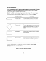
6.6 SCHEMATIC DIAGRAMS
6-12
6-9
6-10
6-11
7-1
PARTS LIST
7-1
7-2
7.1 GENERAL
7.2 PARTS LIST ILLUSTRATIONS
ii
SECTION I
CAR SPACE SYSTEM
1.1 PURPOSE
The Car Space System is intended for application in classification yards as a car space, data
logging and signal conversion device. The Car Space System is a data acquisition system that
supplies analog track fullness information to the remote 1/0 ATP data interface for conversion to
digital data to be interpreted by the Host CPU that is controlling the Hump Yard.
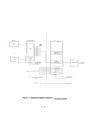
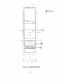
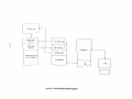
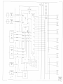
1.2 GENERAL DESCRIPTION (Refer to Figure 1-1 for the simplified equipment diagram)
The car space system is subdivided into two sections: the trackside signal input circuitry, and the
tower equipment.
1.2.1 Trackside Signal Input Circuitry
The Trackside Signal Input Circuitry consists of: a 30/1 track transformer, a 2/1 signal reference
transformer, a 600 ohm resistor and a surge suppressor per each track. Eight signal transformers
and eight surge suppressors are packaged in an assembly referred to as the wayside
transformer. Each wayside transformer can be used to service a maximum of eight tracks.
1.2.2 Tower Equipment
The Tower Equipment consists of the Car Space Rack (Figure 1-2). This is the signal processing
center for the total system and is interfaced with the wayside signal input circuitry, and the ATP
AJD gate card. The rack contains an analog electronics cardfile, consisting of Phase Detector
PCB's, an address board, a driver board. In addition, the rack contains a Lambda power supply
assembly. Track signal data is received from the wayside circuitry and translated to an
appropriate analog signal level to be sent to the external ATP A/0 converter. The digital output
of the AJD is then sent to the host computer for interpretation.
1.3 SPECIFICATIONS
A. Track Coupling Transformer US&S P/N N451154-0101 (Figure 7-4)
Electrical: 50 V.A.@ 60 Hz
Physical Size: 17-1/2" x 6" x 4-1/2
Ratio: 30/1
1-1
lAACKS I
I
·et
TRACK l
"''"
CASE NTO t::QUIPMENT
I
CARSPACE RACX
OROU'
ov ERALL
sH[aD
0
WATS JOE
""'
·---- --
0
0
I.
l
CARSPACE PO'wER
SUPPLY I SPACE 4 l
ISOLATION
TRA\;K B
);fHA
XHIR
I
I
CABLES
ro
I
I
l20Vo
se
CARSl'ACE
HZ
OTHER OROUPS fCASES){
TO t,CSf CPU
CARO="ILE <SPACE 31
ZW! \iATTS CAPAC[TY
===± =-
RTP A/D INTERFACE
CONN;CTCfl PAIEL
---+--L--~----'
'/--,lilJH::, DASHE:O Llk£S IN'JICAIE Fufllf<i GRO\o'TH
CAf'f.u!LlfY.
ilA'l'SIDE f.llU[Pl-'ENT
II
L _________
I
I
I ----------------+
1201/, Se1 HZ
2il8 \tMTS CAf'AClfY
TO\IER EOUIPMENi
Figure 1-1: Simplified Equipment Diagram of Carspace System
l- 2
-
.: :Si
U•MBOA ?OWER SUPPI_V
~
@i
"
o,ns
: ·"
i """'
011~
'i
.i
.,.__
;:'RQNT
__ :i:5 :cic:--c:s
22
:1 '.5
-
:NC:-E:S
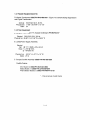
Figure 1-2: Carspace System Rack
1- 3
1.3.1 Wayside Equipment(cont'd)
B. Wayside Transformer US&S P/N N451492-0101 (Figure 7-5) contains 8 Surge Suppressors
and 8 Signal Transformers
Electrical:
Physical Size:
Ratio:
500 W @ 120 V, 60 HZ.
7-5/8" x 9-37/64" x 10-1/8"
2/1
1.3.2 Tower Equipment
A. Car Space Rack (Figure 7-6, Equipto Challenger) PIN 192Y01A17
Electrical: 200 W@ 120 V, 60 Hz.
Physical Size: 85.80" H x 21.06" W x 36.00" D
B. Lambda Power Supply Assembly
Electrical:
Input: @ 117 V RMS +10%, 60 HZ.
Output: 1) +15V @ 0-3A.
2) -15V@ 0-3A.
Physical Size: 5-3/16" H x 21" D x 19" W
Weight: 27 lb
C. Carspace Cardfile Assembly US&S P/N N451056-5501
Cardfile Contains;
Driver Board (1) US&S P/N N451441-8902
Address Board (1) US&S P/N UJ793100-0019
Phase Detector Boards(*) US&S P/N N451441-3101
* - One per group of eight tracks
1-4
SECTION II
CONTROLS AND INDICATORS
2.1
CAR SPACE RACK (Refer to Figure 1-2}
When operating from any of the system data terminals within the yard control system
software operating system, it is possible to monitor the activity of the carspace system by typing
in various commands at the system prompt.
2.1.1
CSPI MODE OPERATION
CSPI is the name of the routine which reads and displays carspace track information
on a continuous basis. This routine is selected from within the 010 1/0 interface
test program.
(1) To run 010, Log in on the system terminal, and type "DIO" at the system prompt.
(2} A menu will appear on the screen with several utility program options. Select menu
option "Car Space Input" by typing "CSPI" next to the ">>>" prompt* followed by <RTN>.
This will access the carspace test program that allows the verification of all signal
interfaces between the Carspace Rack and the Host Computer/ATP.
(3) You will be prompted for a track range. Type "1,8" (for P1; "9, 16" for P2, etc .. )
followed by <RTN>. For a single track number, just enter number.
(4) You will be prompted to select repeat mode. Type "y" followed by <RTN>.
(5) The Driver output voltage, raw value (binary AID output), and converted value (feet)
will be displayed until another key is hit.
(6) When verification of tracks 1-8 is complete, hit <ESC> to return to menu.
'2-1
SECTION Ill
THEORY OF OPERATION
3.1 GENERAL THEORY (Refer to Figure 3-1 for the General System Block Diagram)
3.1.1 car Space Measurement
The car space measurement equipment measures the distance on a storage track from a
given reference point (usually clearance point) to the point of last standing shunt on that track (as
produced by the last car on the track). The operation of the car space circuits utilizes the effect
of electrical phase relationship reflected from the rails of a track. An alternating current applied
to the rails of a track will encounter an impedance composed of resistive and inductive
components. This current lags in time when compared to the voltage across a series resistor in
the circuit. The inductance of the track varies directly with its length, so that the shunt produced
by the last standing car determines how much inductance is offered by the track as a circuit
component.
When the track is full, the inductive effect will be almost non-existent, and a comparison
of these circuit currents with the voltage drop across the circuit's series resistor will be found to
be very close to zero degrees of phase shift. Similarly when the track is empty, there is a
relatively large amount of inductance in the circuit and the track current will lag the system
voltage. Circuits are provided which will measure the amount of phase shift occurring between
the two input signals from the track, and therefore, phase shift is the variable used to measure
track length.
3.1.2 Car Space System
The Car Space System is a data acquisition system designed to provide "track fullness"
information, (as a derived function of externally developed track associated phase angle
measurements) for a maximum of 72 tracks, to any or all three independent requesting stations.
The system utilizes separate and continuously energized phase detector circuits which are
multiplexed in a cascaded fashion for identification of a given track in a given group. The
selected analog information from the phase detector is sent to an external AID converter. The
AID converter output is sent to the Yard system Host CPU. The Host CPU controls the scanning
of the phase detectors, stores the digital data, and outputs the data upon request to any of the
the yard system stations.
3.2 DETAILED THEORY (Refer to Figure 3-2 and 3-3 for the Detailed System Block Diagrams)
3.2.1 Wayside Circuitry
By proper connection of the Wayside Circuitry, the phase angle signals are made to be
direct indications of the available car spaces on a track. For any given track at a given location,
a range of Oto 3,069 feet (of available distance to last standing car, or shunt, on the track) has
its own particular corresponding range of phase angle degrees, (0 degrees to some particular
value). The phase angle pairs are terminated in the Car Space Rack Phase Detector, processed
by the external RTP AID Converter, run through the pre-programmed Host computer, and used
to calculate as track fullness data.
.3 - 1
FAILOVEfl LOGIC
ADOOESS BOARD
SLOT 11
~
-.--f-
TTL OUTPUT DRIVER
v'
I
f'l
DRIVER BOAHD
SLOT 0
I
I
-
INPUT AID GATE HUX
VAX-4000 CPU
,;
IIA TCHDOG Tl HER
PHASE DETECTOR BOARDS
SLOTS I THiDUGH 4
,
110 CDNTR(1-LER
-
IOBC
VT-420
I
Figure 3-1: General System Block Diagram
I
3.2.2 Carspace Rack
The Car Space Rack is wired to accomodate a phase detector for each track -- with eight
successive tracks defining a "group". Each group has its own Phase Detector PCB. A maximum
of nine groups can be wired into the rack. Depending on the number of tracks used in the
yard, one rack could contain one Phase Detector PCB as a minimum, to nine Phase Detector
PCB's as a maximum
In each phase detector circuit on this PCB, the phase angle information is coupled
between the phase comparator and the low-pass filter by an optical coupler. This optical
isolation scheme eliminates any direct connection between the rack's filtered analog voltages
and outside interference. In addition, separate power supplies are provided on both sides of the
opto-coupler to prevent coupling of noise by a common power supply.
Each Phase Detector PCB has a multiplexer (referred to as the "track mux") to channel
the analog phase angle information to the driver PCB. Each Phase Detector PCB has like
channels addressed simultaneously by the 4 bit address PCB output. The track mux selects the
specific phase detector circuit on the Phase Detector PCB. The output of the track Mux is
forwarded to the driver board for amplification. The resultant DC analog signal is then sent to
the RTP AID converter for digital conversion. This is a 12 bit binary equivalent(+/- 1/2 LSB) of
the input analog phase angle information.
This parallel 12 bit binary phase angle information is routed to the Host CPU and is
converted to a digital value of "available car spaces" for the corresponding addressed track.
The "available car space" data for each of the tracks is stored and then updated by the Host
Computer once a second. In this way, any or all of the requesting stations can retrieve the most
up-to-date track fullness information.
The Host Computer Completes a full scan of the yard once every second. The scan
begins with the selection of the address of the first phase detector circuit (track number one) The
driver board output voltages (One for each Phase Detector PCB) are then sent to the RTP A/D
Converter. The analog voltages are then converted to binary and stored to memory . The Host
CPU then goes back and repeats the phase detector multiplexer and conversion routine for the
next channel.
This repetition continues until all eight of the tracks on each board are read. After all of
the phase detector channels are read, the Host CPU scans the two reference voltages (full scale
and half scale) on each Phase Detector PCB to verify validity of data. These references are
compared to the programmed voltage references and if a discrepancy occurs, the fail bit for that
board is set. After one second the scan is reinitiated and the sequence is repeated.
3-
3
3.3 SUBSYSTEM DETAILED THEORY
3.3.1 Operation of the Phase Detector P.C.B. (Refer to Section VI Figure 6-7)
The Phase Detector PCB #UN451441-3101 uses an LM319 dual highspeed comparator
to compare the phase difference between the two incoming signals. RC filtering and diode
limiting are provided on the inputs of the comparator to provide for transient protection and noise
reduction. One of the RC filters contains a potentiometer for varying the phase of its
input signal and hence provides a zero set for the comparator. The comparator's open collector
output drives the Hewlett Packard 5082-4351 highspeed optical coupler directly. The
output of the optical coupler is wired through a resistor to an LM309, 5 volt referenced source.
The output of the optical coupler is a fixed pulse amplitude with a 60 Hz repetition rate
which varies in width with a phase change.
The filter is a 1 Hz. low-pass, two pole Butterworth type using one half of a 747 dual opamp (operational amplifier) for its active element. Pulses from the optical coupler are fed into the
filter and its narrow bandwidth removes everything except the DC component of the pulses. The
second half of the 747 is an amplifier with a gain potentiometer to adjust the full scale reading of
the filter output. An offset potentiometer connected to the non-inverting input of the filter op-amp
is used to compensate for the saturation voltage of the optical isolator transistor and to null out
the combined offset voltages of the filter and amplifier op-amps.
The eight channels of phase detectors and filter amplifiers are fed into a Burr Brown
MPC168 sixteen channel C/MOS analog multiplexer. The multiplexer has a four bit BCD digital
input code which is used to select the desired channel. Channels one through eight of the
multiplexer are used for the phase detector signals, channel nine is connected to the five volt
reference source, channel ten is connected through a two to one voltage divider to the five volt
reference, and channels eleven through sixteen are not used and are tied to ground.
3.3.2 Operation Of The Address P.C.B.
The Carspace address board is an interface to isolate a four-bit address of an output of
the external main yard(dual) computer or dual digital 1/0 subsystem from the Carspace system.
Isolation is accomplished using opto-isolators and separate input and output power supplies.
The circuitry required to switch the address data from CPU A to CPU Bis included. Control of
the switching is via external input.
The secondary purpose of the Address PCB is to fuse and route the Carspace system
clean Power "A" supply, (plus and minus 15 volt) power feeds to the remainder of the Carspace
cardfile.
3.3.3 Operation Of The Driver P.B.C.
The driver board contains 16 independently connected LM 759 Op amp circuits. Each
one of these is designed to amplify the low-level analog output current of the phase detector
board. Each Op_Amp is capable of producing as much as 325 ma of drive current to an
externally connected load. This non-inverting follower configuration of the OP Amp circuit
causes the output signal to remain very stable under a variety of loading conditions. Because of
the feedback design used for this configuration, it is a unity voltage gain circuit. There is one
LM759 Op Amp circuit used for each Phase detector P.C.B.
'3 - 4
r------------------------
COM'UTER
ROOM
,--------,
,----,
I ----------
I
I
I
I
RTP A
CARSPACE
ELECTRONICS CABINET
1
I
I
I
DATA FROM
I
I
I
GROUP
I
t------------------·-··--------------------------:1
P /0 MTB
I
SIGNAL Cll.13LE
CARSPACE RACK
pI
PI
I
ADDRESS TO
I
<ANALOG)
I
I
I
I
I
I
I
I
I
I,____cA_R_sP_Ac_E_R_Ac_K_ _ _ I
i
I
I
I
I
I
I
ADDRESS SWITCHING
CONTROL I CPU A I
I--
l ___"~---J
,-----RTP B
I
,1-1
I
I
I
FAILOVER
:
L~~~c
-i IJ__
I
,_
I
I
I
rI
-
__?~ -
-
-
I
I
I
I
I
I
COtHROLI CPU
I
I
I
P3
ADDRESS TO
DATA FROM
(ARSPAC[ RAU<
1
<~ROI.IP 3
SIGNAL
CA81[
,---------------------··--··-------J
I
I
I
I
I
I
I
I
I
I
I
I
I
I
I
I
I
I
I
I
I
I
I
I
I
I
I_ _ _ _ _ -[
r
:
I
1===-----I
II
I
I ________
SIGNALS
FROM
GP2 TRACKS
_,
I
_J
GROUP 4
SIGllAL CABLE
-
-
-
-
-
-
-
-
I
I
I
I
( ARSPACE
['lll I PI.CNT
P 10 CS CASE
I
I
-
1--------l
,
----~~-----_
_-
=········.·· ·::
SI GtJAL $
fROM
GP3 !RAUS
r
I
I
I
I
1---
GROUP 4 CABLE
, _____
-
---------,
:: =~
I
,_ -
I
I
I
I
GROUP 3 CABLE
,
I
SlGtlALS
rPOM
'----·
pI
I
I
I-------I _________
1------1--------
P 10 MTB
I
I
I
I
I
I
1
,------I
I
I
I
CARSPACE RACK
PIO cs CASE
~~~u~w\~A!~~ - :
, _____ J
I
I
B'
I
I
I
I
I
I
I
I
I
i
I
~
2
GROUP
SJ GNAL CAOLE
CARSPACE
EQUIPMENT
I
I
ADDRESS SW! TCH l!JG
I
I
-
I
•I
I
:
I
I
I
-
A/8 SELECT
i
I
I
I
I
I
rzl------------------------1 r2
I
I
I
I
I
I
I
I
I
I
I
l ~_'.'_~--l
I
I
I
I
I
I
I
,--------1
GROUP I CABLE
....----~,=AN~ALO~G-,---1
I
I
F !ELD
EOUIPMctH
L_ ~~_4_ ___I
I
I
I
I
I
I
I
I
I
J
I _________ J
-1
SI GtJ!il S
GP4 TRACKS
r
CAR SPACE LA\OUT
Dlf<ECT DIGITAL
4-GROUF'S
---------------
---------------- -------------·
-··
--~~"--·--------------
----
--flz-;-:;-~~--~
3· 5 /(
------------COMPUTER
ROOM
,
C Al
RTP RACK CA I
ANALOG
GATE
Ml.IX A
Al{)
-
-
)
8 CH
II
- - - - - - - - - - - - - - - - - - - - - - - - -I
CAR SPACE
I
ELECTROIJICS CABINET
I
------------------1
I
- - "" "'"
I
I
CARDFILE
I
I
PHASE
I
I
I
I
~CP:i,U'2_A~At~lA~L£(
OG~S_l__'.IG~N~AL':_:S~I
I ~_::_:___·:______ _:---;~
1---------,I >-
CAR SPACE CASE
FIELD
EOUIPl.£NT
I
<<
1
A CONNECTOR
ORI VER
PCB
)~
SLOT O
DETECTOR
PCB I N~UT
EDIG[
EDGE
' fiPIJT
C~I_Jl_~~~~~-'---~;;;;;«
B COWIECTOR
>-
,__::
2
L_____________
EDGE
INPUI
v
I t~PUT
PCB
I
L----0>--__<:_~~~---------~~<<E----,
B CONNECTOR
4
ecs,
OPTO
.--- ~~>--- EDGE
RYI
___AO_ _EDGE
<(
IIJPUT
\
)>-------4 \ - -
---1-----------,
/
I -------~-----i--~
l' >"-----0>-----l
r»------';)-------i-
f
">
I
\
--)>
-------------;,------------1
--------!-
-----------1:-------------1--
(
I
·1' >.'·------ -_.-_____________L_I _________ , - - - - - - - , - -
J>>----' .
----- -
I
\ )\-----}>-------1-----
I
- - -----
_
-
ATP RACK IAI
WATCH DOG
CPU A
/
TI M:R A
RlP RACK CB I
WATCH DOG
I
I
I
I
I
CPU B
>>---------
'vL~
8 ----
£ OGE
D
l~L.-
-
,- r~-j
I
I
v~_J
-
-
~
---------
- - - - ---
------------- - -
y
~
------ -POWE.11 SUPP! y AS':,EMBL y
---==~=-------- -~=_!l_
_J
-+ 1 'lV
'----
-~
_______________________ _ J
l H.£R B
CPU SELECT I Otl
RTP DIG ltO
---=-=----~=v-
j
-
SLOT 11
_JJ
,____,_____
'
L-----'~ >---S_!'._l~~:____-------~-z;;;;;;tcu;-R-------- -------
L_
Ii
!--------
--<?-------_ ___c::_~:..__::!:__________- - A- COflt<EClOR
I
L__ _
~
I
--------<~
A COIJIIECTOR
SLOTS f "'TO 4
I
I
I
I
I
I
I
,_____ - - - - - - - - - ·- - - ~
---
---------.,-------------,--
A COtHJECTOR
L------'7)---~~___:_:.;_______
I
-~ >------1------I
_____<:_~~~--------~;:;;;;<L-......_._..~,
>--
i----------1-----,--,
I
\,_·>----
8
1------1---=X
,
( >>---+:--
6
IIIPLIT
PACKAGE
>----~ >----- ---,- -
J>;-------
7
_____2[
CASE
TRANSFORMER
J>>-----+ >---------,-------~-----,---
ltiPUT
IIIPUT
__E!~------~BB-;c;o;;;;,,,11:'cToR
aI
•
\
L---7 >---E'.'Ll_!l_
I
"
I
·1 >>--~>------!
ADDRESSING
I
v
I
I
J>>--------,.>------,
I
l
------<(
I
I
:~---'
F" A 11 OVER
COtHROL
/
/
j
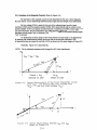
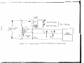
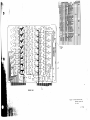
3.3.4 Operation of the Wayside Circuitry (Refer to Figure 3-4)
The operation of the wayside circuitry is best described by the use of vector diagrams.
By using vectors, a true relationship between phase angle and track length can be determined.
The line voltage (EOA) is equal to the sum of the voltage drops across the track
transformer (EBA) and the wayside resistor (EOB). EBA varies directly with the number of car
spaces available. As the car spaces increase the track impedance and EBA increase, and as the
car spaces decrease, the track impedance and EBA decrease. When EBA increases, EOB
decreases causing angle "one" to increase. When EBA decreases EOB increases causing angle
"one" to decrease.
The relationship of phase angle to the measurement of track length can be determined
by observing the instantaneous polarity and turns ratio of the wayside transformer. EBC
is opposite in phase and equal to one half of EOA as shown by the vector diagram of Figure 3-6 .
Vectoriallly, Figure 3-4 is described by:
NOTE: Z ' is the reflected impeqence felt through the 30/1 track transformer.
jw
A
!
a
IR.wysd = Eoa
WAYSIDE IR DROP
;igure 3-5.
a
IR' TIC.
TRACX IR LOSS
Vector Relationshi? of the T=ack Transor:ner Voltage
Droc (E
) , the Wayside Resis~or Voltage Drc9
(Ea~l, BA and the Line Voltage (E 0 Al.
jw
I
!
!X'
I
I
I
Eos
~-~~.....;_..;:i;.,._ _ _ _ _. . , , . _ ----
3
?igure 3-6.
J. ----~>,..
IR.'
'lee-tor Rela tionshi? 3et·..-een .::. 0 A and E3 c
Added to Figure 3-5.
3-9
!
~ · I ~ ... ":.
-~·~
~r_- ~::-··-~~-r
,..-......
1,:'",i_.__ . _ . . , . , ....... '!'" .M;
A
--a
~2;1
:-0
v>
.!..
c,
,
I
1~Line
=
ffP.i!?Mi
.lffll. . .!Ff'J~
Wf.\118*.
':X;P,t!!::',,,...(i,-~.'~-~_,,,..~-l"~ .....a.,0445 -?MVAA.¥4
NU.4¢
$
.... ,- .. - -
-
"TRACK
XFMR"
+ r, ~~ ~31011~ s
~
XTK=f(TK Lgth)
?
2TK = RTK +X TK
: RTK=g ('rK Lgth)
E
=l20V (RMS)OA
@60Hz
;;;z
p
o{lllrs'
+
(L
B
WAYSIDE
XFMR
I
i
Eoc
Rwvso
4
I
EBC
EOB
+
i
I
PHASE
COMPARATOR
0
Figure 3-4.
Typical Wayside Circuit Diagram for a Single Track
On the Vector diagram, transferring vector EBC to Point "B" produces:
------31::W-•
I
c
Figure 3-7
Vector Relationship Between Phase Angle and Car Spaces Available. Added to Figure 3-6
Vector EOG is equal to the sum of EOB and EBC. Angle "two" represents the phase shift
between EOB and EOG, which is the car space data sensed by the phase detector. By
considering the extremes of track length for a minimum and a maximum value, note that angle
"two" varies directly with angle "one" and EBA, and inversely with EOB . Hence, phase angle and
track length (car spaces availabl-e) are directly related to each other.
3.3.5 Operation of Dual Power Supply
Refer to Lambda Service Manual.
SECTION IV
INSTALLATION
4.1
INSTALLATION CHECKOUT PROCEDURES
Upon completion of the wayside and tower equipment installation, perform the following
procedures for making the Car Space System operationally acceptable.
(I) Inspect and test the integrity of insulated joints, "far end" shunts and rail bonds (if used) of
each track. Also at this time, check that undesired track shunting paths do not exist.
(2) Verify that the proper track connections are made (the circuitry for track #1 indeed connects
to track #1 and not to track #2 or #3, etc).
(3)Verify that the proper track transformer polarity connections are made (adjacent rails of
adjacent tracks are in phase for similar track shunting conditions).
(4)Perform the calibration procedures of Section V, "Calibration of the Car Space System".
6053, p. 4-1
SECTIONV
CALIBRATION AND TEST PROCEDURES
5.1
GENERAL (REFER TO FIGURE 5-1)
Calibration of this system is determined by comparing observed output readings with respect
to controlled input signals. For proper calibration of this system, the power supplies must be
properly adjusted, each of the Phase Detector PCB's must be properly zero and gain adjusted,
and then the total system checked and adjusted. The carspace system performance will vary
with changes in climate, therefore, seasonal re-calibration of the system is suggested.
The following procedure should be followed whenever attempting to calibrate the carspace
system. This procedure will cause a false "distance to go" reading to be sent to
the yard computer. It is suggested that the track be empty or, at a minimum, open to
approximately 950 feet. The track should be blocked and the switch ahead of the track
transformer should be spiked. Calibration and trouble analysis of the equipment used in this
system necessitates that maintenance personnel have a working background in electronics
including theory and fundamental troubleshooting procedures. Failure to obtain the correct
readings from previous steps will require troubleshooting not covered in this write-up.
5.2
POWER SUPPLIES
5.2.1 Power Supply Adjustments
Apply power to Carspace Rack. Turn Lambda Power Supply on. Verify +15V +/- .15V on the
following extender card pins: A22, AZ, 81, BA. Verify-15V +/- .15Von A18, AV, 85 and BE.
Verify Common on AG, AF, 83, and BC. Adjust Power Supply outputs as necessary per Lambda
Product Manual. Maintain per Lambda Product Manual.
5.3 CARSPACE SYSTEM CALIBRATION
NOTE: Refer to Section VI, General, for the recommended test equipment needed to
perform the following procedures.
5.3.1 Data Terminal Set-up Procedure
following the procedure described in Section II of this manual, set up the data terminal
to display carspace information on the screen. This will be required while performing the system
calibration procedure.
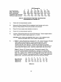
5.3.2 System Calibration Procedure
This procedure is for calibration purposes only and is not intended as a troubleshooting
guide. It is therefore assumed that the carspace system has been working correctly and all
wiring and components have been previously verified. For total system calibration, start with
tracks #(1-8) Phase Detector PCB and check from track #1 to track #32 sequentially. Refer to
Figure 6-7, Phase Detector Troubleshooting Guide. The following stepwise procedure is written
for calibrating any one channel on any one Phase detector PCB. Specific pin number
information is provided in Table 1 below.
5-1
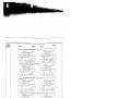
PCB Channel No.
2
1
Zero Potentiometer
Offset Potentiometer
Gain Potentiometer
Comparator output test point
PCB board output test point
3
4
R1
R7
R13
R19
R98 R99 R100
R97
R105 R106 R107 R108
TP1
TP2 TP3
TP4
TP18 TP19 TP20 TP21
5
6
7
R25
R101
R109
TP5
TP22
R31
R102
R110
TP6
TP23
R37
R103
R111
TP7
TP24
8
R43
R104
R112
TP8
TP25
Table 5-1: Phase Detector PCB Output Test Points And
Potentiometers for Channels 1-8.
1.)
"Power Off' the instrumentation card file.
2.)
Remove the Phase Detector PCB to be adjusted, insert Extender card, and reinsert the Phase Detector PCB into the extender card connector.
3.)
"Power On" the car space cases (breakers on fuses in).
4.)
"Power On" the Instrumentation Card File.
5.)
Connect a DVM positive lead to pin A 16 of PCB under test. Connect negative lead to
TP26. Adjust R147 until the meter reads 5.00 V +/- 0.02 V.
CAUTION: STEP 6 INVOLVES WORKING WITH 120 V. ANY CONNECTIONS
SHOULD BE MADE WITH 120 V POWER TURNED OFF.
6.)
a.) Option 1: Unplug Wayside input connectors (P1 - P8). Connect Carspace Simulator
output cable to input connector (P1-P8) for channel under test. Jumper
input pin B to input Pin C with the common wire on Signal Pin Ref. for
channel under test. (See Table 5-2). Confirm two sine waves are in phase
with a dual trace scope on Pin 821 (Channel 1 scope probe) and 822 (Channel 2
scope probe) with respect to 820. Disconnect scope probes and common lead.
Option 2: Remove 120 V power from case. Disconnect the signal C (Sig
C) wire at the case transformer N451492-0101, Terminal C (C1-C8) for track
under test. Place this wire in parallel with Signal B (Sig B) at Terminal B (81-88) .
Apply 120 V power to case. Confirm two sine waves are in phase with a dual trace
scope on Pin 821 (Channel 1 scope probe) and 822 ( Channel 2 scope probe) with
respect to 820. Disconnect scope probes and common lead when finished.
Signal Pin Ref.
Signal Pin B
Signal Pin C
1
820
821
822
2
817
818
819
3
4
814 811
815 812
816 813
TABLES-2
5-2
5
6
BX BU
BY BV
BZ BW
7
BR
BS
BT
8
BM
BN
BP
b.) Connect the Positive scope lead to the comparator output for the track under
calibration (See Table 5-1). Place the negative scope lead at TP17. Observe the 15
Volt (approx.) pulse. Adjust Zero Potentiometer (bottom row of pots) until the pulse
width decreases to the point where it disappears.
c.) Return The Sig. C wire back to its original position on the case transformer as
required.
8.)
a.) Adjust the gain potentiometer for this track (top most row of pots) 5 turns clockwise
from its most counter-clockwise setting.
b.) Connect a DVM positive lead to the PCB output Test pin for this track (See Table
5-1) negative lead should be connected to TP 26 for all measurements.
c.) Place a good shunt across the rails at the connections to the track transformer for the
track under calibration. Make sure connections are clean and tight.
d.) Adjust offset pot for this track (middle row of pots) so that the DVM reads 0.000 VDC.
Make sure data terminal display reads O Feet. Adjust as necessary to zero display.
e.) Disconnect the shunt from the track.
9.)
a.) Measure the rail and permanently mark it with paint at 900 feet from the track
transformer leads. Place the shunt tightly at this point.
b.) Adjust the gain potentiometer for the track under test (top most row of pots) such
that the data terminal display reads 900 feet. Note: Normal drift about this number
is typically within +/- 5 feet. The measured pulse width at the comparator output for
this track (See table 5-1) is typically between .9 and 1 millisecond. Typical voltage is
1.5 volts.
10.)
a.) Measure the rail and permantly mark it with paint at 600 feet from the track
transformer leads. Place the shunt tightly at this point.
b.) The data terminal display should read 600 feet+!- 55 feet (1 standard car length)
Note: The display will normally drift within +/- 5 feet over time. The carspace system
accuracy is contingent upon the quality of cable, cable connections, rail, rail shunts,
and especially rail bonds. The carspace accuracy is relatively linear to to the
calibration point of 900 feet, then increasing in error to the end shunt. This is normal.
c.) Remove test shunt from 600 ft. point. Verify that the data display reads the distance
to go to the last car, or if empty, the end of track length to the double end shunts.
11 .)
Repeat steps 7 -1 O on the next channel of the Phase Detector PCB.
12.)
Repeat steps 1 - 11 on the next Phase Detector Board.
5-3
SECTION VI
MAINTENANCE
6.1 GENERAL
Trouble analysis of the equipment used in this system necessitates that maintenance personnel
have a working back-ground in electronics including theory and fundamental troubleshooting
procedures.
The following test equipment, or equivalent, is recommended for equipment troubleshooting:
Multimeter
Simpson
260
Digital Voltmeter
Fluke
Fairchild
8000A
7000
Oscilloscope
with two 10:1
Divider Probes
Tektronix
465
Two Extender Cards
US&S
UN451441-1101
Two Rail Shunts - 7 ft. long with heavy rail clamps (.06 ohm or less)
6.2 BASIC TROUBLESHOOTING TECHNIQUES
The troubleshooting procedures for the total system are arranged in an order that checks the
simple possibilities before proceeding with extensive troubleshooting. The first few checks below
assure proper connection, operation and calibration. If the trouble is not located by these checks.
the remaining Field Maintenance or Sub-System Trouble Analysis procedures for locating the
defective sub-system or PCB can be used. When the defective part is located, it should be replaced following the replacement procedures given under Corrective Maintenance.
(a)
Check Control Settings
Incorrect control settings can indicate a trouble that does not exist. Make sure that all of
the system controls are set properly. For example: Is all of the power being supplied to
the Car Space Rack, wayside circuits, displays?
(b)
Check Associated Equipment
Before proceeding with the troubleshooting of the Car Space Rack, check that the
equipment used in conjunction with this rack is operating correctly. Check that the
signal lines are properly connected and that the inter-connecting cables are not
defective.
(c)
Visual Check
Visually check all of the car space sub-systems. Many troubles can be located by visual
indications such as unsofdered connections, broken wires, a damaged circuit
board, damaged components, etc. Make sure that all of the cable cards and connectors
are coupled and fully seated.
6-1
(d)
Isolate the Trouble to a Circuit
To isolate the trouble to a circuit, note the trouble symptom. The symptom often
identifies the circuit in which the trouble is located.
(e)
Check Power Supplies
If all of the circuits are operating incorrectly, the trouble may be in the power supply.
However, a defective component elsewhere in the unit can appear as a power
supply failure and may also affect the operation of other circuits. The Lambda Service
Manual lists the tolerances of the LND-W-152 power supplies in this system.
If the power supply voltage is within the listed tolerance, the supply is considered
working correctly. If the power supply voltage is outside the listed tolerance, the supply
is either misadjusted or operating incorrectly.
6.3 FIELD MAINTENANCE PROCEDURES
The possible trouble symptoms can be generalized into two categories:
(I)
A failure in the "front end" of the system which would be indicated by
faulty data to an entire group(s).
(2)
One of the tracks displays the wrong car space data as compared to the
actual known car space availability reported by the others.
Using this generality, the commort failure symptoms of the Car Space System can be identified
as follows:
(1)
Bad Data being sent to Terminal Display (Refer to Figure 6-1)
(2)
Routine Calibration Indicates Faulty Readings. (Refer to Figure 6-2).
Troubleshooting flow charts for locating and correcting a problem, have been developed for each
of the symptoms listed above. The symbol functions used in the flow charts are standard and
are defined in Table 6-1.
NOTE
Before applying the flow charts for trouble analysis, check the basic
troubleshooting techniques of this section .
CAUTION
120V, 60HZ, AC EXISTS ON THE INPUT PAIR TO THE FRONT END OF
THE PHASE DETECTOR PCB'S.
6-2
NO
APPLY POYER TO
ALL ASSEMBLIES
I
YES
'
c
NO
S CORRECT VOL TAG£
PRESENf AT ORJVEA
BOARD OUTPUT?
S CORRECT Vil.TAG:
P!l£SENT AT PHASE
IUEClCJI PCB OUTPUT
PIN AA?
YES
POSSJBLE FAUL TY
OR J\/ER BOARD
1
YES
•o
POSSIBLE FAULTY RTP
A/0 INTEFACE
ARE FIELD INPuT
NO
CONNECT CABLES
CABLES PROPERL 'f
CONNECTED TO RACK?
ARE OTHER
SE VEN CHANNEL
OUTPUTS
CORRECT?
/
JS .:I.LL loiAYSICE
2"CUIP,..ENT ANO
::RCUl :'~'!' •CAKING
.~ACP~RL r?
PROPERLY
CHECK AOORESS BOARD &.
NO
FIELD E:GU!P~ENT
CONNECi IONS/CPEAAT l ON
PEA SEC. 6.-4 ANO 6.5
.,a
-!
~ - S E ? . - I RO-ER
~~gr~~~ ~F4
CARSP4CE ."4ANL.:AL.
'
· ~
Figure 6-1: Bad Data Sent To Terminal Display
'7-3
I
~~~~~~~'
'
I
1----i
I
I!
ROUTINE CAI.IBRAT!ON
INOICATES FAULTY REAOINGISI
SUPP!.. Y SIGNAL OF
KNOWN PHASE SHIFT
TO PHASE DET. INPUT
CHANNEL I SI
j
c
IS THIS PHASE
SHIFT REFLECTED
IN PHASE DET.
OUTPUT VOLTAGE?
NO
REPLACE PHASE OETECTOR
ANO CAL! BRA TE NEW ONE
YES
B
DOES CORREC~
VOLTAGE APPEAR AT
CR I VER BOARD
OUTPUT?
NO
REPLACE CR I VER BOARD
YES
I
'
A
I
:S RT? .0/D
!NTERFACE CONNECTED
4NQ ~ORKINO
NO
RE?•IR RTP
AID INTERFACE
?RCPERL 'f?
::csSiSLE: :-.:ic:... ~v
<iA'fSZ:::: ::~u:.=>.1E\-:'
c:-i:C:< ?::,::i: SECT: :~1
:::i.--' .;,',Q
·I
I
o. 5
Figure 6-2: System Calibration Indicates Faulty Readings
I
,
:
6.3.1 Flow Chart Support
Ref. A - It is possible that the RTP rack(s) may not be powered up, or that one of the ND cards is
not plugged in. The gate card is located at word 91, and the ND card is located at word 88.
Also, make sure that host computer is up and running.
Ref. B - Use a DMM to read analog voltage at output of driver board. This voltage should be
between 1 and 4 volts depending on the distance to the last standing car on the track. Refer to
attached Driver board schematic (N451441-89E) for output pin assignment information
____
SYMBOL
)
(
D
Il
STANDARD DEF.
COMMENTS
"Terminal Box"
Used For Starting and finishing a Flowchart
"Decision Box"
The next logical question in the troubleshooting
procedure is asked here and in such a way that
either a "yes" or a "no" is the only possible
answer.
"Process Box"
Describes the next logical process or operation
to be perfromed.
"Subroutine Box"
Tells the Maintenance Personnel to perform one
of the referenced trouble-shooting procedures.
*ALL OF THE BLOCKS IN THE FLOW CHART ARE REFERENCED WITH LETTERED
DESIGNATIONS, WHICH ARE DEFINED IN THIS SECTION UNDER FLOW CHART
SUPPORT.
Table 6-1. Flow Chart Symbol Functions
6-5
Ref. C - Use a DMM to read analog voltage at output the Phase detector board. This voltage
should be between 1 and 4 volts depending on the distance to the last standing car on the track.
Refer to attached Phase detectorboard schematic (N451441-3101) for output pin assignment
information, and Section 6.4.3 of this manual for troubleshooting guidelines.
Ref. D- Does all of the wayside equipment and circuitry prove good? By performing the steps
included in the Wayside Circuitry Troubleshooting Guide of this section, the equipment and
circuitry for the wayside can be checked.
Ref. E - Calibrate the Phase Detector PCB. Perform the procedures of Section V, Phase
Detector Calibration. If board still does not work properly, repair and test per US&S spec. EU6346
6.4 SUB-SYSTEM TROUBLE ANALYSIS
NOTE
The schematics for all of the sub-systems
and their interconnections are included
at the end of this section.
6.4.1 General
Once the problem is traced to a particular sub-system, one of the following steps can be
performed:
(I)
Replace the defective sub-system with a known good spare.
(2)
Repair the defective sub-system as per the following procedures.
WARNING
MAKE SURE POWER IS OFF BEFORE REMOVING
ANY SUB-SYSTEM, OR DAMAGED COMPONENTS
MAY RESULT.
6.4.2 Wayside Circuitry (Refer to Section Ill, Operation of the Wayside Circuitry)
(I)
Determine that all of the lightning arrestors and surge suppressors are not leaky,
and the fuses are not blown.
(2)
Make certain that the following voltages agree: (Refer to Figure 3-4)
(a)
(b)
(c)
EOA = 120V rms ("E Line" of the Wayside Transformer Primary)
EBC = 60v rms ("E Secondary" of the Wayside Transformer is equal to
one-half of EOA). If not, the wayside transformer or its connections are
faulty and should be repaired or replaced.
Remove one secondary lead from the track connection of the track
transformer
6-6
Esec =..EAB
30
The secondary voltage of the track transformer should be equal to 1/30
of the primary voltage. If not, the track transformer or its connections
are faulty and should be repaired or replaced.
(3)
Check the value of the 600 ohm resistor and verify circuit continuity between the
main terminal board and the track transformer.
(4)
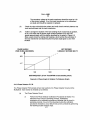
If able to change the location of the last standing shunt on the track in question,
do so, and check that the phase angle variation between EOC and EOB
agrees approximately with the relation described by the graph of Figure 6-6.
Make a quick check by making and breaking a shunt across the secondary of
the track transformer and observing that the phase angle goes to zero when
shunted.
PHASE ANGLE
(TIME IN MILLISECONDS)
NOT DEFINED
LINEARLY BEYOND IOOO FT.
/
.833
i--~~~~~~~~~~~--,./
.417
500
1000
DISTANCE(FEET) (From TrackXFMR to last standing shunt)
Figure 6-3. Phase Angle In Relation To Distance Graph
6.4.3 Phase Detector P.C.B.
The Phase Detector PCB consists of two main sections: the Phase Detector Circuit and the
Multiplexer. Each section is checked out as follows:
(a)
The Phase Detector Circuit
(I)
Perform the Phase Detector Calibration Procedures of Section V to
determine if the circuit is operating correctly. Satisfactory
completion of the calibration procedures indicates that the circuit is
operating correctly. Any error that develops during the calibration
procedures indicates a circuit failure that can be corrected by performing
the following trouble analysis steps.
6-7
6.4.3 Phase Detector P.C.B.(cont'd)
(b)
(2)
Refer to Rgure 6-4, and with an oscilloscope make a point to point
comparison of the specified points.
(3)
Determine which components are faulty and replace them. Repair any
loose or damaged connections.
The Multiplexer
If the Multiplexer is suspected of being the problem, compare the output signal
to the input signal of the multiplexer by addressing the proper channel
and monitoring the output. If the output does not correspond to the addressed
input, the multiplexer chip (IC25), or its connections are faulty.
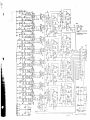
6.4.4 Address board P.C.B.
If the Address Board P.C.B. is suspected of being faulty, refer to US&S Test Spec. EU7995 sheets 8-1 O for detailed testing instructions.
6.4.5 Driver Board P.C.B.
If the Driver Board P.C.B. is suspected of being faulty, refer to Section V of US&S Test
Spec EU-7782 for detailed testing instructions.
6.5 DETAILED CIRCUIT AND COMPONENT TESTING
6.5.1 General
A)
Check Voltage and Waveforms
Often the defective component can be located by checking for the correct voltage or waveform
in the circuit. Typical voltages and waveforms are presented through out this manual.
NOTE
Voltages and waveforms given in this manual
are not absolute and may vary slightly
between units.
B)
Check Individual Components
The following procedures describe methods of checking the individual components in the Car
Space Sub-System. Components which are soldered in place are best checked by disconnecting
one end. This isolates the measurement from the effects of the surrounding circuitry.
6-8
(I)
Transistors
The best check of transistor operation is actual performance under operating conditions. If a
transistor is suspected of being defective, it can best be checked by substituting a new
component or one which has been checked previously. However, be sure that circuit conditions
are not such that a replacement transistor might also be damaged. If substitute transistors are
not available, use a dynamic tester (such as Tektronix Type 575). Static-type testers are not
recommended since they do not check operation under simulated operating conditions.
(2)
Diodes
A diode can be checked for an open or shorted condition by measuring the resistance between
terminals. With an ohmmeter scale having an internal source of between 800 millivolts and
3 volts, the resistance should be very high in one direction and very low when the leads are
reversed.
CAUTION
DO NOT USE AN OHMMETER SCALE THAT HAS A
HIGH INTERNAL CURRENT. HIGH CURRENTS MAY
DAMAGE THE DIODE. DO NOT MEASURE SCHOTTKY
DIODES WITH AN OHMMETER: USE A SUBSTITUTE
DIODE.
(3)
Resistors
Check the resistors with an ohmmeter. Check the Electrical Parts List for the tolerance of the
resistors used in this instrument. Resistors normally do not need to be replaced unless the
measured value varies widely from the specified value.
(4)
Transformers
Check for open transformers by checking continuity with an ohmmeter. Shorted or partially
shorted transformers can usually be found by checking the waveform responses when
high-frequency signals are passed through the circuit. Partial shorting often reduces highfrequency response (roll-off).
(5)
Capacitors
A leaky or shorted capacitor can best be detected by checking resistance with an ohmmeter on
the highest scale. Do not exceed the voltage rating of the capacitor. The resistance reading
should be high after the initial charge of the capacitor. An open capacitor can best be detected
with a capacitance meter or by checking whether the capacitor passes AC signals.
C)
Repair and Readjust the Circuit
If any defective parts are located, follow the replacement procedures given in this section. Be
sure to check the performance of any circuit that has been repaired or that has had any electrical
components replaced.
6-9
6.5.2 Soldering Techniques
WARNING
DISCONNECT THE UNIT FROM THE POWER SOURCE
BEFORE SOLDERING
Circuit Boards
Use ordinary 60/40 rosin core solder and a 35 to 40 watt grounded pencil type soldering iron on
the circuit boards. The tip of the iron should be clean and properly tinned for best heat transfer to
the solder joint. A higher wattage soldering iron may separate the wiring from the base material.
The following techniques should be used to replace a component on a circuit board. Most of the
components can be replaced without removing the boards from the unit.
1.
Grip the component lead with long-nose pliers. Touch the soldering iron to the lead at the
solder connection. Do not lay the iron directly on the board.
2.
When the solder begins to melt, pull the lead out gently. This should leave a clean hole
in the board. If not, the hole can be cleaned by reheating the solder and placing a sharp
object such as a toothpick into the hole to clean it out. A vacuum-type desoldering tool
can also be used for this purpose.
3.
Bend the leads of the new component to fit the holes in the board. If the component is
replaced while the board is mounted in the unit, cut the leads so they will just protrude
through the board. Insert the leads into the holes in the board so the component is firmly
seated against the board (or as positioned originally). If it does not seat properly, heat
the solder and gently press the component into place.
4.
Touch the iron to the connection and apply a small amount of solder to make a firm
solder joint. Do not apply too much between the component body and the solder
joint with a pair of long nose pliers or other heat sink.
5.
Clip the excess leads that protrude through the board.
6.
Clean the area around the solder connection with a flux-remover solvent. Be careful not
to remove information printed on the board.
6-10
6.5.3 Circuit Board Replacement
If the circuit board is damaged beyond repair, the entire assembly including all soldered-on
components, can be replaced. Part numbers are given In the Mechanical Parts List for the
completely wired board. Observe the soldering precautions given in the soldering techniques of
this section. If the bottom side of the board must be reached or if the board must be moved to
gain access to other areas of the unit, only the mounting screws need to be removed. The interconnecting wires on the PCB can quickly be disconnected to allow the board to be removed.
WARNING
MAKE SURE THAT THE POWER IS TURNED OFF BEFORE
REMOVING OR INSERTING A PCB. THIS PROCEDURE
WILL PREVENT FURTHER CIRCUIT DAMAGE.
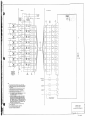
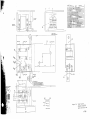
6.6 SCHEMATIC DIAGRAMS
Application Drawings and PCB schematics for the Car Space System are provided to aid the
maintenance personnel in system troubleshooting.
6-i i
f:''i:,__·.;- - - - - - - - - - - - - - - - - - ,
:l> •
!:t:?'\i.
!:·~·
i:
t·.j,·~·;
,~·
l
!,,,
w.osrot CASE
r-,
w--
I- - - - - ,
I
I
__
I"'
-I - '"
I
o_ -
wus1or Slt?UL
xr~ PkO
UN4S1•9l-OIOI
tSU NOTE 1'
------...,_ -
-cs"
-.-
~
.
~
"r,,Jl[2P
::511c·p
Ir,
~
1130
J::~'
,r
PHAY /COlf'UT[R noolJ
!5
"
"
__J_-{
~
'
2P
IP
9 • 120~ - - - ~ ·
1S01..At1ou
,:rm
'?!OOW RA1'UIO
ISEE N01'E 6f
A
....
2,1
.-=~-~-----•--GNO •9
.,v
...
,. ltt'
• FIG• )•2
><vs
-,
I
111.r
1101~
1-'
.
••
nucr.
82
w
C2
t1k
f/;=r==~~-~-~
T W_
SIGUALS
2P
'"""
'"c.s. cnour o"
.
U
~,--«
I
L___
S<t
HOf[ 3
SHOWN $0 TM.-T .tOJAC[NT RAtlS OF AOJ.lC[Nf TRAC•S Wfll
T••c•
].
et '"
rnou
··c.s.
CROUP"!
··c.s.
CROUP"!
r»AS[ fOR Slt.fll,t,R
CONOlflONS.
AT mt SE MINIS APPllCUION or llGHflHG PROT[CllON I SP(C IFIC•ll Y TO
M
St.met lRRt.sTOftS US[O IN
fH[
..
s,c•ot
e,o ·UI'
1,m .. PACUC[t IS •DYIS.t8lt.
4.
ltf,1£ rno ft('SISTOft tAtft 10 flt goo~.... llow.11.
If U SUCC[SftO '""' lll
THtsC •ts1sro•s 8£ "OUHl!O ON A ~- AlUUIN\IM HtlT $1 ...
$.
••
!HIS W[UHCR Pnoor c•el[ UJH ft[ • DtDIClltD t•et[ CONSISTIHC or '
PIIA - fPntr[PIBlTt •1'4 CONOUCTOR - ' ' " ' BUT OVt.Alll sn1no;
lll'SO SuPPUEO e, CUSfOUER.t
g,
AF'PtT t lFUNSF'OfU(.11 r(R CROUP OF' NO WR£ TH.l.N 9 fRACkS I ruts xr111 ro 8E
S[lECT[O
rnoJ[CT [NCI
T,
IPJ:°ll I fRINSfOR~ff PlCUC[ 1'£111 CAOUt" ti" HO u,n[ fMIN I UU,CtS.
THIS t•BLE TO 8( su••UED 1111) IIISflll[O e, EIIGINE[RINC.
SEE ,1cun( C-IT roi, SIGllll PIN-OUT INrllf' ..... f!Qlt.
!.
snn.~
------,..
r
~__.
LCI
--
[_.J~
r[
n
'-C
-------·-l-~>-+--------1 ·· I
"C.S.
r.nour"J
~
:
_,
:
--
TWIST!D
B. VIA r![lD WIRING TH[ S[OU[NC[ or IRACk NU~E•s IN Jiit u•o WST BE UIO[
TO AG•Et WITH TH[ NIM!ERIIIC S[MNCE ot rN•SE OCIECfOII CIOCUITS WIIHIN
IH[ CAR SPACE RACk. 11,[. Tiit r!RSf I SEOUENJ!Al PHIS[ DEl[CTllf' CHAIJ!ll:LS
••E OtDICAT[O TO TII[ Ft•ST I Ull1)-TRICk-!IIMl[OS-SIUll•Rlr roo !HE S[CD"'l
I (TC. rl)IITH[Ol.l()II[ tr TOACkS 4. 5, IC IN T•ts rtOST CRO\IP 00 NOT PHYSICALLY
(Jf~T - eEUUst 'TM[f AR( ,uruRt ,,u.c•s - T»EN F'NASt D[T[CfOA CfUNNtlS •. ,.
IC C.HNOf BE USED AIIO THEN TRA<k •T'S INl'tlf PAIR GET$ CON!l{CltD 10 PHAIE
Otl[Cton CHlfmtl n INrUf-StUILlntY ro,r •It (TC. I
TO
EfT(PfUl
(Of-lH'!Ol
_.:[•__.
N(H[S1
St[ rtG. ,_,, rOQ "'" ASSl!';'1lUITS.
fO MINlt.llU: "Cft05$ Ul', [HtCf", Tttt tnACk tRaNSfoP~J:IS Sw.,utO BE (Of-lN(CJ(O AS
'/011t
14
- - - ---·---l--)>-1--------
mtst Clflt[S TO et SUPPl.ttO "' CUSTOUE.ft.
··-
---'-- --·--"~!~-----
xnn
H: SICNAt.S
,.
2.
II
I
r-- -
14
sun ct
lnA[SfOA
I
I
__e_r
11
:Rrl.RS TO TAICt
I
U)
~
SU: NOfE 21
1
L« I
--~--_J--<~ I
I •I
--i.- - -•--)>-- -- es
-"."-I-<< I
"~ . - -7_- -- - • - ) ) '- - - -- cs
'
- ---".~_,-<< I
,o
I I
- i ; - -- --··--1;,--- -- ~2--1-- - -'-I;~ I
_z - · - - ) > - - _ .c.o ____z__ ·-· _o~t--« I
I I
-y- __ -•·---;(-- _ .e_r_[__ o 1_;; I
_L --·--~>-- t!___L ___
I
I
I
I
"--------- - _._I_« I
I " I
I I
~>---1-« I
Sr.£
~
COUV'l"IG
I
'
--1--"
i-I
"
I
UN4'1154-0IOI
""" C(... l{CIION or
•
- [ - - · ~ > - - - J ! ~ - - -"-1-« I
-----~·>--- -- .!:.'_J__ - _e'-1-<~ I
IP
nuc•
I
"i,"~:1:~·l
I
I· '
I -----~;--- ,---1-<}
------·--~>-------1-<<
8J
G
I
-[-- -·-);--- ---«
-- ---~>-- -- ~---L- _!l~~-<;
IP
:2P
1
S((
•tr
2P
=i4~r
~
::1 ,.!l~
~
CAii 1">t( U(I
UN•\1411-41101
CArACl ll
• IIE" c·~i,,o
uort
2P
"
100W GAOUf'
er I
111.r
n
r,o uz surr·t,
IIL_o;;E-.~==
IP
~
---}
NXll.O.,___ _ _ ~ - - -
1--»-I - - --
\___
r
L.'
.'
9~
rutunf cmu,m c,..r~nlt I rt
SHOwtl
e,
0.1.Sll£0 llUL
...
::,
e,
C/\RSP/\CE SYSTEM
PHYS IOL LAYOUT
/\NO /\PPL.I CAT I ON I UFORM/\ Tl OIJ
."
~
~
i
Fi ~-4-~·-~---~~-ir
)
l«lTtS:
1c1-ic,'
ICt -1c1t
IC 11 ... 1c1
ICU
•
ICU
'"
LI
_j"ffl)__
- -----'~L_
f""''.
__1l7
01 S
·~•001
014
•110
- .. l
IOK
....l, .
...
·~~:=J
,, .
Cfwm.)
-i. c.,
ltU
·I!>
T: _.:, ·~"
u
011
1~4001
-~I
l+
Cit
•
T
I' I
('r' -·p sv
flV
~
-
----
Al II
_.~
1,ci
ti 4
L.
C
14 · l,HI
--~ ____
II
Alf
lJ>
""
OOK
'V'-- - Rl~I
1K
""
JK
--fl.J
~
·1 Oc1_1 ---'
.·\I
I
..
•1vV
I
v
V
-
_"'"
1,~1~' A
U? A ' ~
l~
---~---- --
- - -
.
----
Fi (JII ro. 6·-
5
-c;.,,
~l
NO'l'E:
l
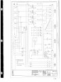
'l'ypical Phase Detector Channel wi lh waveforms
corresponding to c1 GO llz signal input having
a F.S. phase shift.
.i
e PIN
-~
0
5
0
ePIN
...
r
0
16.67
ms
-t
f. s.
ms
1
-tJ5_::u...----u
+s.oov_____
.
0-------
.I
_,..I .... tr.. s.
· to
+ 1--"-~~--'.._~~J.
0
t
f. s.
"",.,
"\
1
o.o 'T
'~Olf
~_J ......
rf1
....
co
--ii
t.011
••
+sv sovrc.e
1110
~~
'Ji.i: r'~I
..~.:m
I'
-
Lr
o.u~
L
1
i'
F11~ure 6-
lo
l'hnse l)(!tector
Trouhleshootlnr: <:ulde
?.
\fc,/17
I
II
10
I
12
15
16
II
18
[
fROUT
BOTTOJ-4
I <J
21
23
24
25
lB
31
}O
a2t-----w ,-.--- - - - - - - - - - -
2
2. 7K I t2W
--~
TP Cl
<170i
---- __t __
_·, ; , ' •
2
2
821
a,
::t
§
~
-_.
.
---- -
- - - - - - 9!--ffi_____ _
822
II
~418
R,
~lf~~g)_5
s
---- -~~ nf',C ~ =1-1
-- -
2
4
~
u
I
0
n
s
823
------
'
82418
N
RI<
2,____ _ _
~ - - - - - - - . - 2--,o-o_R_E5-5---~:
-- --,~llfl:@i.:::i~
J-
_________,..
--l---------''"'J:_:_•:::DD:;_R=E-=-55'--
lP G~p2
~-------~
>
"
0
I
I
I
R26
'---l---l---+---l-~-
I
Ill
@------i--A20
Al
f
,,
I
_____ , _
'1-vcc
GUO
1
---
-
_c~u
9241 l
., µr
AL
lP
~e
AM
'--------------~
AH
... NALOG
TEST POINTS
FROM
PHASE DETECTOR
PCB 1 S
'-------·--------~
u
I
I
';; I
AR
LED •2 \ \
AS
- _____________'p_;_•s_v___
~
-
Rl6
-----1__:2
J
_.c;A • ISV
8
,:"'
AZ
---,-4~r-
6
=----'~
___c:_A
B
I
AO
RI
-- - ~ - - - - - - - - - - - - - - - - - - - - - - -
I
I
VIA
CARDF ILLE
wJ RING
~
\\
~ I
; I
! I
I
I
I
I
I
I
I
I
I
I
I
~ I
~ I
; I
'? I
8
ANALOG COl.4-KJII
n,
~ I
)1
A SUPPLY
tlSVOC OUI
10
PHASE DETECTOR
PCB'S
VIA
CAROF'ILE
ltJRING
jl
~ l
ii
,s I
----e-w--e------------------1~
ZERO OHW
I
I
.&.20
A2J
u
I
I
RI
824 I l
;;
c
_,
A22
~
8
110
--~ L-[>-------J
A21
._
lP
TEST SLOT
l~~o"l
?>-----r------:;--~\--
('"'--
__1}------l>--i
6241 A
~
-!
,so
150
.-. _
t________4
t ___________ ~
t_______________
LEOAI\\
ll
{"--.__12
Rl2
REOt.:;\
\'.'v---------1-----//'-'-1----'I.N'-----~-
FRONT
TOP
AH() COHN,
•2
TP
GP' 1
1.'
Z£RO OHM
A
,so
:•
t____________7
GP' 6
lED AO
8-- !j----t;>o----1-'-~0--
N
<O
~·
_______
IP
f»---!?~0--
@----_!_I-
85
4
7~\~- - -,
l'JRINC
L
GP 5
"'
r· --
PCB'S
VIA
(AROf IL£
r,~r, crf~J-f~~~~~~--::
TP
824
PHASE 0£HCTOR
- :.,
GPT,
I
0
~------------1-P-------tE
___
- ,pL,,-----
::
84
0
,,
~
ADDRESS
OUT TO
-_-_-_1_--'
___VV'-----~ J_________
- - _ JJ__
IF '.!!.'_~ no_·
-- ______________e_____
TP CJ
~
TP A2
W
6 ---~
A
AC
R,4
'_'_o_• _ _ _ _ _ _ _ _ _ _ _ _-_
BJ
4
...
TPIC2
54
~------4--------_::•::•__:::AD:,DcR:.::_E5:::5:__~
TP Al
w
~
53
52
8.&CI( TOP
EDGE COHN.
AO ADDRESS
RJ
@----~
26c~~
82418
51
50
I
lP AO
r_(&;f~--:----_-J_-::::J.
_________L ~ - __J___
82
49
48
42
41
2'
r~- - ~.~,-:--r~17
----
<10
)6
r - ~I
'"'j' ----------!______,___-jii'~ f[C
s
~c_<,_,16'------1--
JS
H
R2
v::;f
IP CO
R9
Bl
ll
a
>()VI
1dfil-,------------------------- - - ~
8370 CONfi.
20
f--"-'-'-'------4----l------~<'>---'\N'----&-- - - - - - -
••
~
ZERO OUM
I
I
0
E
I
I
I
I
I
I
I
I
I
I
I
I
I
R25
' - - - - - - - - e ~ - - - - ---
I
Z£Ro OtlM
F
_
c
AS
I
I
I
"
J
•
I
I
I
ll
...•
NF
I
I
I
I
I
I
I
I
L
I
I
I
I
'
pp
00
R6
A SUPPLY
_
tl5VOC IN
FROU
CAR SPACE
POWER SUPPLIES
ZERO OHM
VIA
CAROF llE
WIRING
A •l!>V
-------------------·-------~---------------------------------. -NOTE.Sr 1 •
I
~v
OENOl£S
co ..u::m roR
MIHUS 15 VOLT
"A" SUPPLY PLUS ANO
ANO FOR PLUS S VOLT SUPPLY
TP f241
2, •
ll[ POIIH
l. 0
TUARE T
82-41
4.R[LAY I PIH I IS COIL PLUS. PIN 16 IS COIL MltlUS
5. All RESISTORS 'AW 51 CARBOH
ura (SS
OlHEAWJS[ UOH.O,
TP
IAMI-'
N211
f
241
82-41
--·------•-'I,•----------·--·----·-----------------·-----------------------------------~~------------>
BL
lP v-418
82418 IAMP
624 IB
--------------•·L------·----- ---------·--·---------------~---------------- -----------------4-------=-"--""'-----l'
89
TP y41A
82-41A IAMP
FROM
INTERFACE
POWER SUPPl l[S
VIA
CAROf ll[
WIRING
8241A
·---···----~-------------------------------------------------._-----"'=-=----~
BK
-------·----------------•L,•-----~-- ------·--
I
I
I
CAR SPACE A00/1:ESSING PCB
«
111 r~,.,.11
1,c l'fltll1.rn • ,...,i.11A11t,o111- 11,c.
lt<JIOllwllUu<.. ,1.-n..io i , '""',. 11'1 ,t1t.lMlll,(-III-· .. Piton ..
\Hllllf, f• NI.Ht! II t~I\ ""''""'•' ""'IU too•ll'!a JI II.Cl. •l,otl IN ..... II . .
"'" e,o1..,..trt -
hC ............ H ,...,_ .,II
--~f .
IU (111,11"11 .... -
II fl( 1'10 •
!NOH
t• .., - · UU•<Ull1•1 ..., ... I • Pl"'O Ill' ICII .... IIOI II N <""Ill.
-~111((,;((0, tr,., ... , too, ..... Dfl . , _ . Clf l•fl.tl •II•'"' HUN •lllh
:~:'R9-';"'-,-o-,-_-.-..-,--'
fl£F£fl£NCES
::~..·~-ttH~
lft•ctD
GTR
.. -26-93
UJl93100-00J9
Aolo<.,ess P.cB.
m
I
SCHfMA..'OC
:c:
1·
!!!C,.co._ PJJ..=_[=z:~:..9ii31--------------------4------L.---~
t41
"'.
4"'
t
"'IC.111'1.-CIIC' ... ll""WII W:11 ..111*" .. ,1 .....1,C llffP .. >'I .... ll.. l(l, 1,C
""""'' ,.., hC , ....... 111 " " ' " " .. u ..
,.,_,
,.,, u...: ..1111
u, Clf•uul l,UIIH•
,t,
• ,.,., ...11111
•MC•-•
MhHt t r l h l l ... , !UT
IUl
,oiu- ...
o
1,
••
,., .,.,..,
2-25-93
---
UNION SWITCH
8 SIGNAL INC,
Pl ITIBURGII, PA 15111
~
I
I
8
gl
i'
.: I
I
~------------------------------------------------I
...
I
'::
g
::: "'"' g
~
~
~
!
'f
•
""
"
REVISIONS
I
EOGE CONNECTOR:
I
'1,
JP2
'1,
'1,
'1,
I
TP
O
TP
,.15V
O OHM
TP
O
+15V
I
I
27
R56 OHM
1
~ . . ":
I
BO
I
.
I
I
lP
I
2~
•9
I
l;;
815
I
II
:fi
I
-o
I
ljl
~
ce,
ca2
I caoi } c1a lie,,
I
I
e<•
a:-i ~ ~ IOOPFJ.
IOOP•J. ,J;,OOIUF -,ioo,urJ_· '"'
,J;,OOIUF-15t001UFJ.·'"'
:
I
JP)
17
v
lv7 7
2-25-93
AS INSTALLED
.
n
n
~
~
_. .. PtN
37 PIN D STYLE
44 PIN
EDGE CONNECTOR
GTR-
,~
TP
23
,v.h i-
AJ
An~ /t
0
C42
C-40
C38
--------------1
CHANN£L
I:
.,s
I
I
TP
26
O
TP
OHM
22
,.l!,V
j
= =
•
•ii :£
I '7"
;l:
C39 o,
.
;;;
C37
1QOP< T T-001ur -1svT.oo,ur T. ,u,
l:1
v
-& 7
R"40 ~..
TP
':
I
w
-&
TP
• I 5V
':
I
I:
CHANNEL AZ
BO
I~ " '=
A32
JPS
""
~
:,
IOOPFT
V
V
V
V
V
•1i5v
~...
s.
--..tv
j
I
V
JP5
VV'
vvo OHM
CHANNEi. "~
45
1ooP'" j
lvvv
A9
vv
A2
i:
c
O
j
JPG
'
w
0
I
~
Iv
I
I·
2
'
C20
v
I
1T 1I '
·1
1
1c•
i
6
,
.•
~
n
c,s
vv
..e
r •
i
•i
R27 3. 32K
I
~l
•:l "
4C'
J
r-1_
_ _ ,_ _
Mi·
~
~
-
v,
c,.
rI I
0
-
0 ·
-
Ah:
;
lvv
r-II
I
I
I
I
I
,
.0
:~
I
· ~ 2'
co
~
b 1;.
.
r.o
1<
1~c~
C9
iIi;
C5
C3
I:
l01
999
I
I
50 ....
, N"400S
F
~ I
I ;! ~~~
.
1'l,48010RJVER.UF
~
'
A20
AX
I
'
!02
,2
I
l
T
I
C3..
.OOIUF
.... C32
L2
1N•OOS
50 lot<
l
r ,oou,
T .OOIUF'
C33
r
.._
C31
IOOUF'
!
TO ALL CIRCUJTS •15V
TP
·.;
20
lP
•
'
~
I
~7
2
~
:
I
>---"---<;----
'hI
1IC14
1;;;
'Bil
;
J
~s3o
m
c10"' - css
/
T.oo,ur -15v1.oo,u, T.,u,
3 •
;
v-&vl
TP
CHANNEL e3
1
z
N
I
0
6
1Cl3
3•
~-~
«!
;;
•i5'Y
~
Rt09 J.32K
~1
-
::
,
:;;
I;;;
ria•
f
~
020
= c11 I _ c••"' - c61
j
IOOPr T
j-OOIUF -15V,.OOIUF'
JUF 1
v'¢"
vvvl
en
I
O
OtHr,t
R88
r,
TP
R92
3,l2K
I ~
•••
;.;2,
1
37
'
vv
~l~ ~~!
.. ! 5,V
TP
35
I
2
'
1'
cs, _
T
IOOPF'
CHANNEL 84
3
~
11_ci~
C62
v7
I
I
6
v, f
•L,
j.OOIUF'
I
i
r--;j
I
O
,
•
s1
I
it
c•o ,
1 1
-1svT.001ur
r C~B
.IUF'
l,----,s2•
j
;;c
I
7vvl
TP
I .
~i
~
,
·
Bri :!
R93
ea·1
-
-
.
~-
.,-
0
3.32K
0
:-&
!
i
I
6
m
4
;;;
cs."'
100Pr,J.
r
~
I
1c&, I
csr
ioo,u,-,sioo,urJ/"'
3
cs3
t
CHANN£L BS
~
I 2 !Cl I
3-32K
R91
•15V
3:
65
;;:;
s24
t:
;:
:
-----------------,I
TP
33
O
OHM
R72
TP
2'3
,
I I
!
.,.
CHANNEL BG
;:::=::=4
~
I
I
~
W
j
•
::
83
~
~
822
f vT v v vT. I
-----------------,
I
I
I
m~
t ;
17'¢'7
j £
TP
3e2
.
B•I
.
6~
•
3, 32K
~
~
+15V
l ~~I ""'"l I'c:2 • cso~ . I:
R76
C54
(,0
O
R69 WOHM
R75
3.32K
JO
R7T
3.32K
~f
~-
0-
l7vv
I
l
C53
100P, T
~
w
IUF
~
!
CHJ.HNEL 87
i
6
I'
11~'
-
;.
-1svT.001uF
TP
2!8
TP
i!\I
-,
r-OOIUF
IO()Pr
i
C51
fl
;::;
~ a20
"';;;
~
C'9"'
;:;
Bl
!
C41
T,001ur-,s+oo1u, T.,u,
7v
I
~
v-&vl
------------------,
NOTES1
I. JC PINS
I. 5, 8 8 NOT USED,
2, JC REQUIRES PRESS ON HEA.T SINK.
3. THIS PCB HAS 4 CONNEC:TORS1
J
PSC
;;;
I
CMANNEL B2
~o
RBS ../V~M
Al
~
r
1
T
3.32K
TP
B~
420
I
1• 1
O
TP
3'9
\_,
JP•
8J'
I •
-----------------,
J:
I
l3
AZZ
I
v-&
Rio~"'
~
$
j : i : j
lvvv
CHANNEL AT
C1
•
LI
I
-
I
O OHM
+15V
I
1
1
6'
!
1.5 Jul>
.,
-.
C6 :;!
C8
-
Fl
~
~- :J:
IT
t
I
~-----------------,
I
I
I
(
r---------------
"'>
• lJ
!1,igl
-:0 I
r-l I
-0'
1
N
-
j
1'i/1
31
RII 3.32K
-
JPI
•15V
j
~
Rl3 3.32K-
~,
c1,
100Pr
RIOT
r
I
,-------.t
T"
-~~
W
lvvv
O OMM
CHANNEL •6
I 1,v,hI =-f;;;
·n
~ ~ t IOOPF T j.001ur-15Vi-001ur T .,u,
lv7v
-&v
'¢"v
44
A5
.l2,4
-&
.,sv
!
. 1lV•h
1
~·
3
~1~
=:_.,,_
... i ~
:~~
;~~
-&
R5 g,.M
~
f
'/
Cl3
roOPrJ. _J;,oo,ur -•sioo•u•.J;•ur
lP
d
I
I
Cl O
~
RI0;-"3.32K
..
TP
Al4 3.32K
-~;
,
- - - --
1
•
•a'
I -
w
il
CIS
-&v
O TP
!PR80MMz
I
!;;;
;
Ii
,b.i
----
Cl7
~
813
'¢'~vi
TP
.. ,
RIIO 3.321\
<!)
100P• T T-001u, -1svT.001ur T. ,u,
:;!
lP
1
3
Cl9
Iv'¢" v
I •
lP
36
_L___J
)
I l.;,~~r _,q_~,9u: T .c,':, I
O
OMM
RICM
BK.
JP7
:
vv
I
s,
vvvl
l 1· i;,,;h
••
""
~~
TP
c
n
~
1 1
I
AZ•
T ,IUF'
j.001ur:-1svf.001ur
O OHM
•
i
r, - - - - - - - - - - - - - - - - ,
~
I
I
O OHM
·r'"
l
10~;
lvvv
)
~ ;;;
'r
c,e
IOOPf"
CHANNEL. U
I ~I
r
~
I
j
• I 5V
R28 3.32K
'VV'
R3o 3.32,
'
f
·,~ 1~1 ~~I~
j,,4
TP
!
~ ~-1
s;
! ~
vv71
TP
8@!
R:Z::M
I
0
',.
I I
I
8
;;
~;;;
-
TP
45
¥
r
•
----------------,
sc'
r--------------~
TP
~I
TP
I
C23 j
T-ooiur -1svi.001ur T .,ur I
C29
CHJ.HNEL BI
~~-
I
-
··.:'"1 l' en'1-i c,;=~"'~-
'! : '
~I ~=~!!;t m=~ljl
TP
F,
··~
A[
1
!
~
J
--'VV
·1' •'1
'
=
'=
~ g-~ :g-~
a~
I °' I « I
----=i
'1
•15V
4.6
l v v -&
63. '
I
-----------=i
T;
I
R37
;i .
O OM..i
I
I
I
SN
R46 3. 32K
J
~i
r
I
I
'¢"
r--I
3.32K
R44
r
:~
f
I
I I
TP
O
Rl23 3.32K
TP
48
Al)
-----:::i
r---------------
TP
TP
~OHM
R59 3.32K
0
-
l. 1,i;,,;h .
i I
-----------------,I
O OHM
CHANNEL Al
---•-----1----~
.I
R61 3.32K
AH
•
B•1
WI'-'
i
-:n:i
1~;
I
lP
24
R53
S
RIZ6 3.l2K
,\)4
r-------------I
I
I
...
CONNECTOR B
CHANNEL AO
TP
I
I
37 PIN O STYLE
CONNECTOR A
r-------------I
I
I
-
TO ALL CJACUlTS PSC.
:no
M.At.E CONNECTOR A. TOP FRON'T
370 MALE CONNECTOR B BOTTOM FRONT
4.:1 PIN EOGE COHH(CTOR A. TOP REAR
ANALOG COl,NJN OR
POWER SUPPLY COlt,l,()N
44 PIN £OGE CONNECTOR 8 BOTTOM REAR
;
I
I
!
;
I
I
;:;
I
"'
0
10 ALI. CJACUJTS -15V
:::;
t:
I-----------------------------------c1\dgn\a1.sfhd•\1.J,486\dt-1Y9r •• ~f
20-JUL-1993 131 I~
~
':'A.ROS / GTR
---------------------------------------------------------
SECTION VII
PARTS LIST
7.1
GENERAL
When it becomes necessary to replace components during unit maintenance, the following
procedures should be followed in obtaining replacement parts:
a)
Standard Parts
II electrical and mechanical part replacements for this unit can be obtained
through your US&S local Field Office or Representative. However, many of
the standard electronic components can be obtained locally in less time than
required to order them from US&S . Before purchasing or ordering replacement parts, check the parts lists for the value, tolerance, rating and description.
NOTE
When selecting replacement parts, it is important to remember
that the physical size and shape of a component may affect
its performance in the instrument, particularly at high frequencies.
All replacement parts should be direct replacements unless it is known
that a different component will not adversely affect system performance.
b)
Special Parts
In addition to the standard electronic-components, some special components
may be used in this unit. These components are manufactured or selected by
US&S to meet specific performance requirements or are manufactured for
US&S in accordance with our specifications. These special components are
indicated in the Electrical Parts List by an asterisk preceding the part number.
Most of the mechanical parts used in this instrument have been manufactured
by US&S. Order all special parts directly from your local US&S Field Office or
Representative.
c)
Ordering Parts
When ordering replacement parts from US&S include the following information:
1. Unit nomenclature.
2. Unit serial number.
3. A description of the part.
4. US&S Part Number (Uxxxxxx-xxxx)
p. 7-1
7.2 PARTS LIST ILLUSTRATIONS
The following parts lists are provided in the order listed.
Figure
Description
Page
Phase Detector PCB Component Layout and
Parts List
7-3/4
7-2
Driver PCB Component Layout and Parts List
7-5/6
7-3
Address P.C.B. Assembly
Component Layout and Parts List
7-7/8
Track Transformer Assembly Component Layout
and Parts List
7-9/10
7-1
7-4
7-5
Wayside Transformer Assembly Component
Layout and Parts List
7-11/12
7-6
Car Space Rack Assembly Component Layout
and Parts List
7-13/14
p. 7-2
0
[
(:
c
c;
c
c
II
"
..
"
J
J
uC
" c
Ill
Ill
J
J
(
"c
" .
...
"'
"'c
c
uC •
J
J
c;"'
[
''j
~ ::J
...
[
llt
IIJ
J
Ill
me
"'
t' '
0 \ .,,/
IU
'"
·-
!Cit
,_ _,
ICII
c
c
1n
::1
J ,. ,
~=!...
'c,,
r :J
'hJ
c"'::J
'-r,,
t':,
... , (l
I' '\
\.
CJI
/lJ
c:
::J
C:J
r1 .,-__!
'"'
CH
"' t
"' c
'"c
0 \ /
"" ,,,
.,,
,,,.. r
~ ~ t' ''-r,r'
c3
...
_. ,';?, ~ ..{ G,r1
......
"'
.. ,
""
~
3
s.~
._ _. " ' o ,I' ',, '-r,,
c jJ
.....
·;~: " "
C:J
::J
mt
."', c
...
[
J u•c
J o/:- t
"'
c
::J
[' :J
"'
r'!:i
t__
' / lJ
t__
r;, ,...~,---...
'"\
,,,
~..~ rl
,. '\ '
, /ll
"'
11
1111
~
t_
C:::J
""
..,
~~
t' "' - . ~
111
111
c
::J
1111
"" '\
rl
111:
'" . -
·~
..,.
...c :Jr ,
0 \
L_
\.
/ll
----
J -
~u
~
u
0
c -,•
" "1
..T\-
..
_\I
L
I
iT
-n
:JIJt"
c :i,,.
Ill~
~-1
:J
C :I
I
Q,r11
=u l J,,.
Mn
••
111JIJI"
c:
fl
;
"'0'
<
rl O
=ul Jm
tpU
., ----- - - •c":i.,,
' J ;[
j !fu11... ,,r l O '"'
i c
,..
1
J ·u~l
-
l'1:'i
j
j ~[
L-,
___J
"l~
tu
J ;(
L_
if-(.
~UJ)ut
=ut Jm
;f1' l Q
i c
___
c :J::i.,, =ul Jcu
... - - - - -
...
:J
c 1,.
"" ,n( ,,t
--!'--------..
------.. . ,. '"
·.,A
•
•[
l
~.~ ;"\llm ,'.'.'.) ,
r! :::J
~
_ _....
~
'--
,?,, \ / la,? \. / l J
c'!J ,,., "'
t'!J
ICU
...
r-
•
~
)",rJ. 11
1
. . "'o r ''-r,r
~.--41
"" ' ,, G,r1 ' /lJ .
r
.....
''"
.,:·
C::J
,_ ......
lllff
I' '\
c, \. /lJ
"l=i ·t
tH
11 1
,_ ..,
"''
..
L_
ltt
Ill
) ..
.. ____:----r-"Tl1T---:------;:-,
UI
lllf
(
r-L_r , ~
Ill
/'11i1-...,
mJ C :J
(l
~ ,11,,~n Q,rn
i c :.1.,,=ul lco : m~O
-l~
....
,?., ' ., G.r1 ' / lJ
C::J
C :J
C::J
rlen'
r:• J
,- • .,
t' ' '-r,r"
UI
[
( ,~ c "' . "'tic [
c J t' 'c::
.
·~
IC I
"ti[ c
""
eC1
)
i
(l
t1Ju1:;n
0""
c: ::> =ulJ.,.
1
1 - - c ::i
1111 " '
• c :i
l"'
)i
lfi,il.., :;n
r
,.,
::,0
<
O .,,.
c: :> =ul J ·--c ::i.,.
["1
",'
ii,feu :nf
_
-~r,?,
, •
o
::, '~
lb:) r?\\_~!.:..\)
,.Ut,)
IPJI
11
,u,
:=n n
=u
~
1 ----:....-__._ _
-
AA
COMPONENT SIDE
Figure 7-1.
Phase Detector PCB
Component Layout and
Parts List
p.
7-3/4·
....
\'
•
,
I ..
,-$ _'
)
L
',(/ /~]ff:~~
1Mn,1nt\
.... !:,
;oJ f=tl ~)\~[} ffe!N.
or '-'""ct
--
(!f,) l\,:1-
-~~.~
rfL, _:
----+------::~~~~~~~~~~-=~l
.--- -__1-::_-..._-_-_-_-_-_-_-_-_-_-_.'
1010-vSIISvMn
. ...-
d]V'HJOJSNV~l
_1__ l)N\ldn08 >\:)Vtll
Vl(W 8, \H(IWIU~
tMl\O\SCt) NOM[Utl .... Tune
.. ,m:.t:
\!\
PUS,(M
;l 01• uou, \ncr I
-- --- - -- --- - - - -
\
\
I
r{tlY-;-;{,.-------, r®---,
r. ==::
,r_-_---_1
I
I
-
\ 1
11
'
'
,1
t,
1,. _ _ _ _ _ _ _ _ _
I
I
I
I
~-=-=::-;, --- .; - - -- - ii---- -:. :-~
S:,~------ -:<-__
~ · ·0·'I
/·~·
·r;\
~'/(I,
~I i I l ,, ':('
·....--r--~-,("~'-tJ
•S ~ ,(.... /
'1
I
I
I
~
' ( ;;;..,·-,
1
j
::
~·
Lt::::::;i:==::~:::=:..:-::.~.::~::::~t=:!=I
1
-r-
/1 t.lM.
rl-,-- ) ,
'\t}rr · ·
'
;1'11~~-=--------= 'f~===i
I
I
s
I
1
I
~ ~
J
, _ _ _ _ _ _ JL
·1
I
r-- -j
L---,
I
.
l,
~t
r=,=~-==--l..
N
I
l--~ '. j~__J
_____ ,~'-·--------~ ---
:
t~'-·-
:-±1======:~=:3.-\-----L------------------------------------
l} "'"·
,-,~
_,
_ _, _______]
-
J·is]
E•s-l
111 IJ JJJ IIIJJ
rfTJ"JffTfrl fff
4
IP
ti'
- - - - - - - - - ft~
~~t~r·-------------~I
0- ST.,AT
(
lf"-0
rlH1,11 lt>-D
)-------
Figure 7-4.
Track 1'ransforroer
Assembly Component
Layout and Parts List
t,
'!.
-----------·-------J-------------
r- -------------- -- ---- --- - --- --- - ---- - - - - -- -
,,
I
IIIM
-Ill
~·
I
I
1~ ~~
I
'
'
"'
.
,o,
I
J 01184\
°8ol'IR.D Tl!.A011r~AL
!. 2
Ill\
T!.PMIN "L
Tviiiii, IOI HIIIICIIIO'I
lit.TtToTt I •u" nr rr.rm
.I .
ot~ 1l~09!!
.,
4
,.__
"
I
I
I
: .-®
:.----'
I
J 075510
7
I
a
I
9
I
I
J 01615,IO 1~6 Tll<l~l"JtlT ,w,u:i. Ct
I
O Tl'l•-YHIT f'Y1"-G C4'J 015•10
J
IH TM, -wm IY'll<..G. 1)4-
//
/Z.
/J
I
I
I
I
I
I
I
I
~
i~
/l,
I
I
+--+---1---l--~~~-4~+----1·~-l.-__..(:__-L_
I
I
/4
,.__
_.._.u._..__.,,_.,____ I
I-'--
17
___!_-f~-
I
I
'--- -- - - - - - - -- - - - - -- - - - - - - - - - - - - - - - - - - - - - - - - - - - - - - - - - - - J
23
Pitt- c or
~
UN.f.!Jlo•S--4101
rl-z
(5ef'. W1R1..ii;; Dtf\GAl'lm)
c t> ,.Hll: c:to n.
vmu.J qr_qurRr.n
0
}'Jo.
TOr r.DC.f. 01"
Pltl. CKT. '801'RD&
T1'1C. -WHT Mi<.a. .. 5
c,
J 07-'1'10 IOl,7f Tl'oa.•W1.n "1"-G. J3
J 07~.IIO IU,7 TIICI -WHT f'11(t. C5
*'
.J 01,. JO
..
ll'\G, •WITT r,,iu., •t-Jt>
-t.0
-
J C17JJIO ~ TI\ Q - YI HT
J 01•110 110J Tl\6 -WttT
C6
n
I
I
I
23
I
24
101
-'lulo
.14
••
J4
II
t1
11
t,
l
lid
trll(..6
h'\llA.
C.1
J 07!JfJO IU>,f, ll\G, •W.fl ~
J 01u10 11.07 TP\G.•Wlif ,.,....., CI
J 047118
J b4n7.s
WSHR• PLATll.
-
MOlllOI
"'
o·i.111
ML
WSHll • 1/4 LOCK ~TL
t-JIJT-1'1NDIIJC1o
NI.IT - c.LA,..,,.
Co,114 le. TOil, T••Mul ...
N 11ou1
CoHa.l~.Tll...,.,I~
M 0411.ltO
N 41514tJ 0)01 Ct(l'\11.t ..
J 0!'1100
ac:a- '/4 •toJ< .!\', "L !n.
W,Hll• 1/4- ~L PLKTL
J 041&01
N 4!'to•a 4701 re•· ~-1•10. '"'"""·
3o
I
31
....____
n
"
!1
t
'4
35
"
J051.U
~1.-ll>•)tlt 1.t<, lD tl'T\.
i,
J 415071
W,HII • 10 "1'L .. Ll'l'TL
3(,.
8
J i(>4'1UJ
:n
I
&
W~Hll•IO ~L LKloC.
M 4>1411
J O!Hl.44
eoo,
J
-
.~ ----- -l!..!...~!.
--%
47'-43
73
4
•
I 'Z.
I
J 030011
..,
,
1. ~ t, IID
In..
Te .. t<'II Nl\l • I llS. r,.., Tt»
11. Hu,,..,.
5c .__ 1/~ ·10 1- 1
A 04!1.!!U IIOOJ YJ1a • • IC. 'P'IC.
W!-4tT l
J 015510 IOI ;s TAI. -WHT MKG 2A
1
,
P\.l'ITl.,t,IAML
ac.a- 1
J 075510 ~!fO
J O?!S.510 0111
I
:!_ 075510_
-4G,
I
J 015!>10 lot•J
....
J 01!>!)10 cnu
I
48
J 01~!>10
4!>
J 07~!510 ()4.0)
I
--·
1
J iO 7.5 !'> I_Q__ ~·JO
~ - ,_
.5 I
I
J 07551Q__ ~
J 01!>.5JO O~l
.2:__
I
J',3
I
J 015510
54
J 015~10 ~tu.
I
j Q1~f!J..Q_ lom
~E_
J 07.5~ PtJ7
!,(o
I
J
51
1
,_
- - - - ~.:?.~?.-!.~ !OHi.
:,o
J 70330l
.5 8
4i
4.5
Vrf'!!.,,,," c-c
C,
'Jl7
41
a:ap:~~~=======n!L..._~_317nbt=i=
""
J 07J&IO t:)otJ T111a.-w1n r,rn. .:.
J 01/1#,10 1101 Tl\ft -WtlT ,..,.._.,.
40
/
01,.,0
J 07,!JIO
J 0711'10 JJ.oJ Tl\6-WlfT r,,~
--
lEST r,. IN~l"ECT r'En 5f"EC. EU-C,,l=,B.
,o,
I
u
Ft>P WlflltJG fHJD c,nctln 'DlnGR(\r{)
5E.1'•.D4514£l3 -511. 04.
c-a
1()4. Tl'IQ-WllT "1"-C.
J 0"16510
I
-Sol. t>IHl
""'-Gi
iOOLS -r "' c. - w wr
1t11
J 075~10 lolU Tl'IG-W~T M"~ IA
J 015510 iOoO 1 Tl'IC.•NHT M...C. A
II
11
Ill
....___
'I
11t.\114
1M
I
/0
I
I
I
ccv.c.e
(..
)
I
I
DIICfttrllOH
Po I.'T, TIUl.ffll ..ti!\\115'10"
J 015.510 0014 "TAa.-win MIC.C. i,1
s
l" ~7f
'"-·-
oo,
2
..._
/ ' J } D,o lr\,/,u
--·-.·
,,o111..
-- --
.~
--
'°'°1.
--
,
·Fiqure 7-5 .
01••
·-
1AG
-wm
MK'- <HlD-1
TIH!t·'NH1 MKO.
31\
TAii -NHT r<1Ki 411
lAO.-WH1 "11<.G 5A
11"() ·Will 1<11<.o.
......
TAe-v-nn """-"'
TIIG-W~\l t<lKG
01
TAG-Wttl t,1KG,
I !I
Ol
TACI-WIIT M~C. 1B
Tr.C.-WflT "11(..G l b
TA<. -y-.lHT t,111.,s, 4 ?I
TAC. -WUT fY1 K6
!'> !I
Tl'\G -Wl~T 1,1 .:.•
"ll
'TIIG.·\"JHT h'":•
.., .._
11\G - W>I T MY.A.
OB
TIE 1 Cl'l'5L ':-______
I
Uayside Transformer
l\ssernt:,ly Component
Layout and Parts Lisi
e.7-11/,2..
-------------------1
II
ll
IJ
11
15
16
17
IB
25
PART•
2G
21
iO
2'1
30
JI
32
33
31
35
36
30
37
3~
10
11
12
13
11
15
16
11
w
I
I
I
I
I
I
I
I
I
I
I
I
I
I
I
I
I
I
I
I
I
I
I
I
I
I
I
I
I
I
I
I
I
I
I
I
I
I
I
I
..J
([
MANUFACTURER
D!STR!OUTOR
o
MANUFACTURER
H
4
w
0:
us
J709004
N451056·5501
8,
s
us &s
5
217
CR92Y04002
CR92Y04002
LAMBDA
6
2CJ9
C NUMBER NEEDED
SPECIAL ORDER
lt'!EDMULLER
7
317
8
316
CJ
SPECIAL
2
ORDER
NIA
337
20
10
338
3
FT.
CR91Y012297
II
264
4
N308947 ·001
NIA
SPECIAL
onorn
24 SLOT CAR!lF !LE II !TII BUSS BAHS.
PCBS CALLEO our SEPARATELY
ENGR.
DEPT.
12
339
20
NIA
800102-05
CGP-2
23N365CJ
us
&s
EOU!PTO
CR9IY012105
ee
340
22
ENGR.
DEPT.
CHALLENGER fOUlf'HENT RACK.
36 IN. DEEP WI PLEX DOOR
ENGR.
DEPT.
RACK NAME TI\G (CUSTOMIZED PER RACK AS llEOlJ!llEOl 9 CIIAllACTER
ENGR.
DEPT.
MAR·Pll!JOF SCREW (EOUIPlOl 10BX5IB IN.
ENGA.
DEPT.
14
341
22
80-0401 -03
EOUIPTO
J475121 ·0111
US!,S
ENGR.
DEPT.
SPEED NUT
NUTS FOR 108 SCHEii
J48021 I -0108
EE
342
FF
OG
,.,
22
(l'.
w
:J
o a
w
u
(l'.
(l'.
>
H
w
w
J475120·0112
N
~,I
BULK
j
1'I
iil
ii
iI
II
BULK
------------·--------!
US!,S
1/4-20 NUT
lJS!,S
BULK
--------------·------------------------------1--- -- ----+----114 PLATE WASHER
BULK
·t--t---1----'---l---l.--:l---l---'1---------L------ - - - - - - - - - - - - - - - - - - - - · ~ - - - - - - - - - - - - - - - - - - - - - - - - - - - - - - - - - t - - - - -
16
343
22
J50013G·0112
US1"S
BULK
l/4·20Xll2 IN. SCREWS
---------------~-----!----}----
---lc--+--+--l--+-+---+-+--+-+-------11------1-------
17
121
N451441·3101
18
122
N451441 ·8'102
US1"S
PIIASE llEfEC!OR f'CBS
ENGR.
DEPT.
US8,S
CARSPACE DRIVEll PCB
DEPT.
-!-------·
u
UJ793100·0019
US1"S
ENGR.
------------------·------------------·----------!
ENGH.
DEPT.
CAHSPACE AO[lflESS PCB
-----~-------------------------·----! - - ! - - . - - - + - - - -
·t---+---t--+---l--l----lf---1-----11----1-------1------ - - - - - - - -
20
124
N451441·1101
US!.S
ENGR.
DUAL EX TENDlfl PCB
DEPT.
_..__...,.____,__..,_____,'----'-----'----'---'--------l-------'---·--·----- - - - - - · - - - - - - - - - - - - - - - - - - - - - - - - - · - - - - - - - - ' - - - - ' - - - ' - - - - - ~ - - - - -
APPTAB-CARSPACE SYSTEM
00
l'lf; ~ I t 1t• ....ua WIIOt • \1"""- 1111:.
!tVU-ft.11 ..... _ 1 . .13 II 1'I, . . M JU1•1oa _ u , .... , IQ IIRUI ..
i.,1, tll;UCJ<I -
lft Dllo,U,lt d
•K01U••aonll'Ol"ll111t_,,1,1111ca."111t1tU1'~at,.lfllllll-lhll
'"' ........,., "...., ..,,._,., • 1nm.1i.reH1. ...-nlll'I or•1t11
tt•
lo!- - 1 1 l>OlielUUl -HotN ,,a.11WIICIII- . . 111110. II.FU'••
•7"D,,(.d.11SJlll#lt01>U111t1111-aUl't&lrt•1no11Cr11,. .. 11Tlll
"'-IOl"kJIC.111Qf,CC11n,HlllfMIIOllntltW.•!1•v,flll:"•«-ftll. llt'
u,on,u -
If•""'' ....,.
Ml . - u 1 _ .... Ill' . .16f ..... CIMVtr
Cll(UOIIJIO.Ulli:.lt. . ~ 1 1 b l
111 .... 11'1: lll'lMIUIU ftll
ft.HUI ..
©•·····~··-... ,. _ ·DO.If---·--
-------
llfJ-tnENCES
o.o.
CEIICHD
rm~
_MT[__
ITALIAN STATE AMLVAY
CERVIGNANO YARD
CLASSl~rn~i:~~ YARD
I
I
I
I
---
JJ
pp
a
<[
w
-------------·-----
114 LOCK WASHER
--l---t--+--l----+--l--+--1--1---1--------lc--------l--------
15
:J
0
I
I
I
I
I
I
I
I
I
I
I
iI
~I
iI
!I
ENGA.
.015' l ( 100 FT. ROLL MIN. PURCHASE) DEPT.
CABLE SUPPORT TIE BAR
FOR 19' RACK, 18.25' IIOLE CENTER TO IIOLE CENTrn
C(
00
w
w en
,_
w
1-
·---------------1---1----+-----
GROMMET
CONTINUOUS GllOMMET ROLL FDrl 19 · 12 GUAGE (. 03 7'
SPC TECH
NEIIAflK
US!,S
~-----13
,-en
I
e1
ENGR.
DEPT.
TEflMINAL BLOCK ASSEMBLY
--t---l--t---·l--+-+---+-+--+-+--------4------1-------- M
e3
ENGA.
DEPT·
ENGR.
DEPT.
LAMBDA POWEH SUPPLY ASSEMBLY
DUAL •I- 15V SUPPLY, 3A
EOU!PTO
ENGR.
DEPT.
36 PIN CONNECTOfl.
---,f---+---1--+--+-+--+--+---+-+---------<f-------t-------~---
u
e2
!------------------·-----------------+---+---!---+-----
N451056·5501
125
01
w
w
w }::J m
a
TERMINAL PANEL WIHI T\10 80Al1flS PER GllOUP
UN377777
UN377777
321
us "' s
SEE ORAIIING F80094 Sil 5 FOR DETAILS
---<--+--+--•-->--+-->--+--~-+-------'------~I------~---.~=-~------------------1
CJ -IIAY 36 P1t1 CONNECTOR PANEL.
M451075·5701
M451075-5701
us 8, s
SEE DWG. 451075 Sii. 57
4
ea
0
0
(J)
D!SlR!BtJTOR
IH
1-
PART •
l-
11
ORDERED
DESCRIPTION
Vl:NOOR
0
us &s
1e
5H
K 7002
::~_~_::_-l-.~~-fB~~Lt-1:l:ON::.:.:.::S_V_IT-CH~~~-J...::::::::'.'.:::lt=::::::~
~
,PIHS!UIGII,
SIONAL PAINC.
T 14 96
"",,.,.,
15237
I
I
I
I
I
I
I
I
I
I
I
I
I
I
I
I
I
I
I
I
\
. ..f .
,·, ~·
L----------------------------------------------------------~
~--------------------------------------------------------~-----------------------·-------
--------------
77-13/14
)