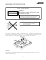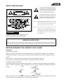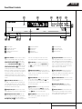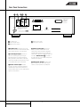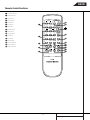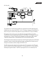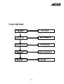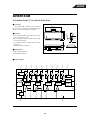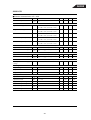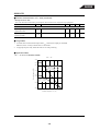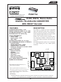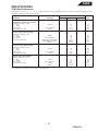
1
harman/kardon Model FL8380 5 Disc Compact Disc Changer SERVICE MANUAL CONTENTS LASER BEAM SAFETY PRECAUTIONS ……...2 OTHER PRECAUTIONS …...................…....… 3 SPECIFICATIONS .........................….….......... 4 FRONT PANEL CONTROLS……….. ... .…...... 6 REAR PANEL CONNECTIONS...........……...... 7 REMOTE CONTROL FUNCTIONS……….…….8 INSTALLATION/CONNECTIONS……………...10 OPERATION......................……………............ 11 BASIC TROUBLESHOOTING ..........……. ….. 13 TEST PROCEDURE…................…..……....… 14 CIRCUIT DESCRIPTION……….. ... ……........ 17 BLOCK DIAGRAM …………………….………...21 GENERAL UNIT EXPLODED VIEW I, II .….. ..22 TECH TIP HKTT2003-06 ……………………… 26 DETAILED TROUBLESHOOTING …………… 27 SEMICONDUCTOR IDENTIFICATION..……... 33 PRINTED ClRCUlT BOARDS .....……… …..... 59 ELECTRICAL PARTS LIST .......…………….... 61 MECHANICAL PARTS LIST .......…..……….... 63 SCHEMATIC DIAGRAMS..................….…...... 68 PACKAGE …………………………………..……72 harman/kardon, Inc. 250 Crossways Park Dr. Woodbury, New York 11797 Rev1 11/2003 FL8380 LASER BEAM SAFETY PRECAUTIONS CLASS 1 LASER PRODUCT CAUTION Invisible laser radiation when the unit is open. Do not stare into beam. CAUTION: USE OF ANY CONTROLS, ADJUSTMENT, OR PROCEDURES OTHER THAN THOSE SPECIFIED HEREIN MAY RESULT IN HAZARDOUS RADIATION EXPOSURE. Do not look directly at the laser beam coming from the pickup or allow it to strike against your skin. This compact disc player uses a pickup that emits a laser beam. The laser beam is emitted from the location shown in the figure. When checking the laser diode, be sure to keep your eyes at least 1 foot away from the pickup lens when the diode is turned on. Do not look directly at the laser beam. CAUTION: Using controls and adjustment, or doing procedures other than those specified herein, may result in hazardous radiation exposure. 2 FL8380 SAFETY PRECAUTIONS This symbol is intended to alert the user to the presence of uninsulated "dangerous voltage" within the product's enclosure that may be of sufficient magnitude to constitute a risk of electric shock to persons. This symbol is intended to alert the user to the presence of important operating and maintenance (servicing) instructions in the literature accompanying the appliance. Caution: To prevent electric shock do not use this (polarized) plug with an extension cord, receptacle or other outlet unless the blades can be fully inserted to prevent blade exposure. Attention: Pour prevenir les chocs electriques ne pas utiliser cetre fiche polarisee avec un prolongateur, une prise de courant ou une autre sortie de courant, sauf si les lames prevent etre inserees a fond-sans en laisser aucune partie a decouvert. WARNING To prevent fire or shock hazard, do not expose the unit to rain or moisture. HANDLING LASER PICKUP The laser diode in the optical system of this player can be damaged by electrostatic discharge from your clothes or your body. Proper electrostatic grounding for service personal is required during servicing. BEFORE REPAIRING THE COMPACT DISC PLAYER Preparation Human Body Grounding: Many of the components used in this compact disc player, including the laser pickup, are sensitive to electrostatic discharge. Service personal should be grounded with an electrostatic armband (1 Mohm). Caution: Static charge on clothing does not escape through a body grounding wrist band. Be careful not to contact the pickup or electrical components with your clothing. Workbench and Tool Grounding: A properly-grounded electroconductive plate (1Mohm) or metal sheet should be fitted to the workbench surface. Tools and instruments (such as soldering irons and scopes) should be grounded to prevent AC leakage. Note: Laser diodes are so susceptible to damage from static electricity that, even if a static discharge does not ruin a diode, it can shorten its life or cause it to work improperly. 3 FL8380 Technical Specifications Signal Format Sampling Frequency 44.1kHz HDCD Processing Burr-Brown PCM1732 D/A Conversion Dual 18-Bit Oversampling 8 Times Discrete Analog Output Section Error Correction CIRC System Frequency Response 20Hz – 20kHz +0, –1dB Total Harmonic Distortion (THD) <0.02% @1kHz Dynamic Range >97dB Signal-to-Noise Ratio >97dB Channel Separation 80dB Line-Level Output 1.0V RMS Digital Output Coax General Power Requirement 120V/60Hz Power Consumption 20 Watts Dimensions Height Width Depth Weight 5.1" (129mm) 17.3" (440mm) 15.2" (386mm) 16.7 lbs (7.6kg) Depth measurement includes knobs and buttons. Height measurement includes feet and chassis. All features and specifications are subject to change without notice. Harman Kardon is a registered trademark, and Power for the digital revolution is a trademark, of Harman Kardon, Inc. , HDCD®, High Definition Compatible Digital® and Pacific Microsonics™ are either registered trademarks or trademarks of Pacific Microsonics, Inc., in the United States and/or other countries. HDCD system manufactured under license from Pacific Microsonics, Inc. This product is covered by one or more of the following: In the USA: 5,479,168; 5,638,074; 5,640,161; 5,808,574; 5,838,274; 5,854,600; 5,864,311; 5,872,531; and in Australia: 669114. Other patents pending. 4 FL8380 GENERAL INFORMATION 1. Power Consumption 2. Power Super 3. Dimensions 4. Product Outlook 5. Remote Unit 6. Compliance Requirement 7. Disc Changer Mechanism Operating <18W; Standby <5W 230V AC 50Hz or 120V AC60Hz 440 x 130 x 386mm Refer to attached diagram harman/kardon remote code i EMC EN55013, EN61000-3-2, EN61000-3-3, EN55022 ii. CE (LVD EN60065) iii. NRTL/C iv. HDCD 5 disc carousel; Play 1 change 4 8. Sound Processor 9. CD Servo System HDCD Digital Servo, Auto Alignment AUDIO SPECIFICATION Output Level 1KHz 0dB (no HDCD) Output Level 1KHz 0dB (HDCD output) Frequency Response 20Hz~20KHz reference THD 1KHz 0dB (30KHz Filter) THD 1KHz 0dB (no any filter) THD 20Hz~20KHz 0dB (30KHz Filter) S/N 1KHz 0dB A-weighted (A Filter) Dynamic Range Channel Separation 1KHz 0dB(30KHz Filter) Channel Balance De-emphasis (5KHz,16KHz) Typical 1.0 Vrms 2.0Vrms +0-1dB 0.01% 0.03% 0.04% 97dB 95dB 85dB +-0.5dB +-0.5dB Limit +-1dB +- 2dB +0.5-1.5dB 0.05% 0.08% 0.05% 93dB 90dB 80dB +-1.5dB +-1.5dB Headphone output specification under 32 ohm load Maximum Headphone Output Level 1KHz 0dB Frequency Response (20~20KHz) THD 20~20KHz 0dB (30KHz Filter) 5 1.5Vp-p +-1dB 0.1% +-0.2V +-1.5dB 0.2% FL8380 Front Panel Controls # $ FL 8380 Power 1 2 Phones ! ) @ 1 2 3 4 5 DISK SKIP 9 PLAY/PAUSE ‹‹ SEARCH ›› STOP Í‹‹ SKIP ››Í 8 7 Phones Level 3 4 5 6 1 Power Switch 2 Status Mode Indicator 3 Headphones Jack 4 Headphones Level Control 5 CD Drawer 6 Open/Close Button 7 Search Button 8 Skip Button 9 Stop Button ) Play/Pause Button ! Disc Skip Button @ Disc Select Button # Information Display $ Remote Sensor 1 Power Switch: Press this switch to apply power to the FL 8380. When the FL 8380 is first turned on by pressing this switch, the Status Mode Indicator 2 will turn green, and the Information Display # will light. Press the switch again to turn the unit off; the Status Mode Indicator 2 will turn amber, indicating that the unit is in a Standby mode. When the FL 8380 is connected to a switched AC outlet, such as those found on the back of many audio products, it will return to the Standby mode when power is applied to the switched outlet without any further press of the switch. level will not change the sound level for the unit’s main output, as that remains constant. 5 CD Drawer: This drawer holds the discs that will be played. Press the Open/Close button 6 to open the drawer so that discs may be inserted. ) Play/Pause Button: Press this button to start the playback of a CD. If the CD drawer is open, pressing this button will automatically close the drawer. Press this button once during play to momentarily pause a disc. When the button is pressed again, the disc will resume play at the point it was paused. 6 Open/Close Button: Press this button to open or close the disc drawer. DO NOT push the drawer to close it or damage to the transport mechanism may result. ! Disc Skip Button: Press this button to change to the next disc. If a disc position is empty, the FL 8380 will automatically search for the next position that contains a disc. 7 Search Button: Press one side of this button to search forward — or the other side of the button to search backwards ‚ through a disc to locate a particular portion of the disc being played. @ Disc Select Buttons: Press one of these buttons to select the disc in a specific position in the CD drawer. 2 Status Mode Indicator: When the FL 8380 is in the On mode, this indicator will glow green. When the unit is off, the indicator will glow amber, indicating that the unit is still connected to the AC main supply. 3 Headphones Jack: Connect a set of standard headphones to this jack for private listening. 4 Headphones Level Control: Turn this knob to increase or decrease the volume level for headphones connected to the FL 8380’s Headphones Jack 3. Note that changing this 8 Skip Button: Press one side of this button to move to the next track —Í or the other side of the button to move back to the previous track Ífifi on the disc being played. 9 Stop Button: Press this button to stop the disc currently being played. (See page 11 for more information.) 6 # Information Display: This display provides details about the operation of the FL 8380. $ Remote Sensor: The sensor behind this window receives commands from the remote control. Keep this area clear if you wish to use the FL 8380 with a remote control. FL8380 Rear Panel Connections £ ¢ ∞ ¡ ™ LEFT OUT CAUTION IN RISK OF ELECTRIC SHOCK DO NOT OPEN RIGHT DIGITAL OUTPUT REMOTE CLASS 1 LASER PRODUCT SHOCK HAZARD: DO NOT OPEN AVIS: RISQUE DE CHOC ELECTRIQUE - NE PAS OUVRIR MADE IN CHINA AUDIO OUTPUT SERIAL NO. AC INPUT AC 117V / 60Hz 20W This device complies with part 1.5 of the FCC Rules. Operation is subject to the following two conditions: (1) This device may not cause harmful interference, and, (2) this device must accept any interference received, including interference that may cause undesired operation. ® ® HDCD® and High Definition Compatible Digital® are registered trademarks of Pacific Microsonics, Inc. WARNING: TO REDUCE THE RISK OF FIRE OR ELECTRIC SHOCK, DO NOT EXPOSE THIS APPLIANCE TO RAIN OR MOISTURE. LR46800 CAN/CSA-C22.2 No. 1-98 UL 1270 PRODUCT COMPLIES WITH DHHS RULES 21 CFR SUBCHAPTER J. APPLICABLE AT DATE MANUFACTURED: ¡ AC Power Cord ™ Coaxial Digital Output £ Remote Control Output ¢ Remote Control Input ∞ Analog Audio Outputs ¡ AC Power Cord: Connect this plug to an AC outlet. If the outlet is switch-controlled, make certain that the switch is in the ON position. ¢ Remote Control Input: Connect the output of a remote infrared sensor or the remote control output of another compatible Harman Kardon product. This will enable the remote control system to operate even when the front panel Remote Sensor $ is blocked. It will also allow use of the FL 8380 with optional, external control systems. ™ Coaxial Digital Output: Connect this jack to the coaxial-digital input of a digital audio/video receiver or an external digital-toanalog converter for direct access to the digital signals of the FL 8380. DO NOT connect this jack to the standard audio inputs of any device. £ Remote Control Output: Connect this jack to the input of another compatible Harman Kardon remote controlled device to have the remote sensor on the FL 8380 provide signals to other products. ∞ Analog Audio Outputs: Connect these jacks to the analog CD audio inputs of your receiver, surround processor or preamplifier. 7 MODEL NO.: FL 8380 HARMAN KARDON NORTHRIDGE CALIFORNIA, U.S.A. FL8380 Remote Control Functions a Disc-Select Buttons b Numeric Buttons c Clear Button d Search Buttons DISC NO. 1 e Skip Buttons f Stop Button a POWER 2 ON OFF 3 4 5 + 1 TRACK NO. 2 3 DISC SKIP 4 5 6 REPEAT p o g Play Button h Random Button i Pause Button – j Program Button k Time Button m b 7 l Intro Button o Power On Button p Power Off Button 8 9 INTRO l m Repeat Button n Disc Skip Buttons n CLEAR 0 c SEARCH d PROGRAM RANDOM SKIP e FL 8380 8 TIME k j i h g f FL8380 Remote Control Functions a Disc-Select Buttons: Press one of these buttons to select the disc in a specific position in the CD drawer. b Numeric Buttons: Press these buttons to select a specific track on a disc. The FL 8380 will immediately go to the track and begin to play it. These buttons are also used to enter track numbers into the memory for preprogrammed-play lists. (See page 13 for complete information on programming the FL 8380.) c Clear Button: Press this button to remove tracks from a programmed sequence. Each press of the button will remove one track, starting with the last track programmed to play. (See page 13 for complete information on programming the FL 8380.) d Search Buttons: Press these buttons to search forward — or backwards ‚ through a disc to locate a particular portion of the selection being played. e Skip Buttons: Press one of these buttons to move to the next track —Í or to move back to the previous track Í‚ on the disc being played. f Stop Button: Press this button to stop the disc currently being played. g Play Button: Press this button to start the playback of a CD. If the CD drawer is open, pressing this button will automatically close the drawer. h Random Button: Press this button to play all of the tracks on a disc in a random order. (See page 11 for more information.) i Pause Button: Press this button once to momentarily pause a disc. When the button is pressed again, the disc will resume play from the point at which it was paused. j Program Button: This button is used to program the playback of a disc in a particular order. (See page 13 for complete instructions on programming the FL 8380.) k Time Button: In normal operation, the display will show the running time of the track being played. Press the button once to check the time remaining for the track in play. Press the button again to view the total play time remaining for the disc in play. l Intro Button: Press this button to put the FL 8380 into the Intro Scan mode. When you press this button, the unit will play the first 10 seconds of each track on the disc, and then move to the next track. Press the button again to defeat the function and continue full play of the current track. (See page 12 for more information.) m Repeat Button: Press this button once to continuously repeat the track currently being played. Press it a second time to repeat the entire disc. (See page 13 for more information.) n Disc Skip Buttons: Press these buttons to change to the next disc. If a disc position is empty, the FL 8380 will automatically search for the next position that contains a disc. o Power On Button: When the FL 8380 is plugged into an active AC outlet, press this button to turn the unit on. The Status Mode Indicator 2 will turn green. If the unit is plugged into a switched outlet, power must be applied to the switched outlet in order for the Power On button o to be effective. p Power Off Button: Press this button to turn the unit off; the Status Mode Indicator 2 will turn amber, indicating that the unit is in a Standby mode. 9 FL8380 Installation and Connections To prevent possible damage to your speakers and other components in your audio system, it is important that ALL components, including the FL 8380 and your receiver or preamp and amplifiers, are turned off and unplugged from their AC power source when installing any new component. NOTE: When replacing batteries, it is always a good idea to replace both at the same time. When the unit will not be used for an extended period of time, it is also a good idea to remove the batteries so that the potential for corrosion or damage is avoided. If the FL 8380 is installed behind a cabinet or other obstruction that may block the path between the front panel Remote Sensor $ and the location of the remote, an optional external IR sensor may be used. Connect the sensor to the remote IR-In jack ¢ on the rear panel. This jack may also be connected to the IR-Output jack of another compatible Harman Kardon component or a compatible IRsystem-remote product. Connecting the FL 8380 to your audio system is simple. Using standard RCA-to-RCA interconnect cords, connect the left and right Audio Output jacks ∞ on the rear panel to the CD input jacks on your receiver, surround processor or preamplifier. If your system includes an optional external digital-to-analog converter, or if you are using a receiver or other processor that has the capability to decode PCM digital input signals, connect the Coaxial Digital Output jack ™ to the Coaxial Digital input on the decoder. Make certain to use a coaxial-style interconnect cable, as standard audio cables will not perform as well. ➞ Install the two AA batteries supplied with the FL 8380’s remote by turning the remote over so that you are holding the bottom side up. Press lightly on the embossed arrow on the cover and gently slide the cover towards you in the direction of the arrow. Insert the batteries inside the compartment, being careful to follow the + and – polarity indications at the bottom of the compartment. Replace the cover by placing it on the remote and sliding it back towards the top of the remote. You may also use the IR Sensor in the FL 8380 to send commands to other compatible remote controlled products. Connect the remote IR-Out jack £ to the input of the other product or system. Connect the power to a nonswitched AC wall outlet or to the accessory outlet on the rear of another audio device in your system and you are ready to go! NOTE: When using the accessory outlet on another product to power the FL 8380, make certain that it has the compatibility to power a device that draws at least 20 watts of current in addition to being able to handle the requirements of the other devices that may be plugged into the accessory outlets. If you use a “switched” outlet, it is important to remember that the host product must be turned on in order for the FL 8380 to operate. 1 0 FL8380 Operation Loading Discs To load a disc, first turn the FL 8380 on, using the Power Switch 1 or the Power On o button on the remote. Note that the Status Mode Indicator 2 will turn green and the Information Display # will light. The word disc will flash in the Information Display, and the disc tray will automatically turn clockwise so that the FL 8380 can sense which, if any, of the disc positions already have a disc. To load a disc, first press the Open/Close button 6, taking care that the space in front of the drawer is not obstructed. Note that if the drawer is blocked when you attempt to open it, it will automatically close within five seconds to protect the mechanism. Load discs in the tray with the printed (label) side facing up toward you. Make certain that the disc is centered in the tray. Either 5" (12cm) or 3" (8cm) discs may be used. When a 3" (8cm) disc is played, it should be carefully centered within the smaller ridges on the tray. Only one CD can be placed in any position at a time. When a 3" (8cm) disc is played, DO NOT place a standard 5" (12cm) disc over the smaller disc. Labeled surface Recorded surface Note that each disc position has a number embossed in the plastic tray. This corresponds to the position this disc will occupy for playback and programming. To make it easier to identify each disc’s position, the disc position number for the holder space that is in the center of the disc tray will also appear in the Information Display when the disc drawer is open. To rotate the disc tray to another position, press the Disc Skip button !n. The tray will revolve to the next slot and the Information Display will indicate the position number for the slot in the middle of the tray. To close the disc drawer, press the Open/ Close button 6. When the drawer closes, the disc that was last in the center position on the tray will be readied for play. Its number will appear in the Information Display and a red icon will flash to the right of the disc number. The icons for all other tray positions that have a disc will be a blue line. If the center disc position is empty when the drawer is closed, the unit will search for the next position with a loaded disc and place it in the Ready mode. The drawer may also be closed and the FL 8380 put into play by pressing the Play/Pause button )g. This will put the disc in the center position into the Play mode. To close the drawer and play a specific disc, press the Disc Select button @ a corresponding to the tray position number for the disc you wish to play. When the disc drawer closes, the Information Display will briefly display the disc number, the total number of tracks on the disc and the disc’s total running time. After five seconds, the display will indicate the disc number that is in the play position, both by a flashing red icon to the right of the disc number and the wording in the display, such as disc 5. The total number 11 of tracks on the disc will light at the far right side of the display. To remove a disc from the player, press the Open/Close button 6. The drawer will open, allowing the disc to be removed. Press the Disc Skip button !n to rotate the disc carousel tray to reach discs that may be covered. When a disc does not occupy a numbered tray, and the sensor detects no disc present, the disc number will drop from the display. Upon placing a disc in the unoccupied tray, the disc number will reappear when detected by the sensor mechanism. Disc-Handling Notes When loading or unloading discs, it is best to hold them by the edges. While compact discs are very reliable, rough handling may damage them. Avoid scratching the bottom (nonprinted) side of discs, and any handling that will leave fingerprints. To avoid damage to the disc and player, always seat discs so that they are centered in the tray. Do not lift the player while the disc tray is opening or closing, as this may cause the discs to unseat from the tray and possibly jam. Note: Always remember to remove all discs from the player before moving or repacking it. FL8380 Operation Normal Play The FL 8380 provides a variety of ways to select discs for playback. To play all of the tracks on each disc in order, starting with the first track on the disc currently in the play position, and proceeding through each disc that has been loaded, press the Play/Pause button ) on the front panel, or the Play g button on the remote. To start play on a specific disc, press the Disc Select button @ a that corresponds to the desired disc’s position in the disc tray. If no disc is found in the selected position, the unit will search for the next disc. When a disc is in play, the Information Display will show a play indicator fl. The track being played will show both as a large number in the middle of the display, and as a smaller, flashing number at the right side of the display. The elapsed time of the track being played will appear in the display. As the disc plays, the track numbers will change, and the time will reset to at the start of each new track. To momentarily pause the play of a disc, press the Play/Pause button ) on the front panel, or the Pause i button on the remote. Note that a Pause indication ± will appear in the display to remind you that the disc is paused. Press either the Play button (Play/Pause on front panel) )g or the Pause button i to resume normal play. You may also select a track on any disc in play by entering the desired track number directly using the Numeric buttons b. Note that two buttons must always be pressed when entering a track number. Thus, when entering track numbers 1 through 9, press the “0” button first and then the number for the desired track. In all cases, the two buttons must be entered within three seconds of each other. To stop the disc, press the Stop button 9f. When the stop button is pressed, the display will again show the total number of tracks and total running time of the last disc played. Random Play The FL 8380 includes three Random Play modes that enable you to let the machine select the tracks to be played in a random order. The Random modes may be started at any time by pressing the Random button h on the remote when the unit is already in Play mode. Random 1: To play all the tracks on a disc in random order, press the Random button h ONCE so that the R A N D O M indicator lights. The FL 8380 will play the tracks on the disc in an order selected by the unit’s microprocessor and stop play when all of the tracks have been played once. Random, All, Sequential: When the Random button h is pressed TWICE, the R A N D O M and S E Q U E N T I A L indicators will light. In this mode, all tracks on the current disc will be played in random order, and then the unit will advance to the next disc in order and play all tracks on that disc randomly. When each disc is finished, the next disc will play its tracks in random order until all discs have been played. After the last disc plays, the unit will stop. Random, All Tracks/Discs: When the Random button h is pressed THREE times, the R A N D O M , A L L and D I S C indicators will light. In this mode, the FL 8380 will select two tracks from the disc in use and play them randomly. After these two tracks play, another disc will be randomly selected and two tracks will play from that disc. This pattern of a randomly selected disc, and the play of two random tracks from each disc, will continue until all tracks on all discs have been played. At that point the unit will stop. HDCD HDCD, which stands for High Definition Compatible Digital®, is a sophisticated process that enables the FL 8380 to deliver outstanding digital-to-analog decoding, no matter what type of CD is played. When a disc with the HDCD logo is played, the FL 8380 is able to take advantage of the special recording process that is used in the creation of HDCD discs. Although HDCD discs are playable on any CD player, when they are used in a unit such as the FL 8380, the special circuitry delivers audio with extraordinary fidelity, stunning resolution and the highest possible overall quality. The HDCD process effectively cancels the additive and subtractive distortions that are present in other recordings. No special adjustment is required to play an HDCD disc. Simply play the disc as you would any other CD, and the FL 8380 will automatically sense that it is an HDCD recording. The indicator will light in the Information Display # on the front panel to remind you that an HDCD disc is playing. It is important to note that the HDCD process is completely compatible with standard recordings. 12 Its high-quality digital-to-analog circuitry provides enhanced playback from all standard CD audio discs. Play Exchange The FL 8380’s Play Exchange feature allows you to change discs while the machine is playing. Using this feature, you can have uninterrupted play of an unlimited number of discs, since the drawer may be opened and discs changed while another disc is playing. To use the Play Exchange function, simply press the Open/Close button 6 at any time while the unit is in the Play mode. The disc drawer will open and two discs will be available for change. Replace either disc, or both, as desired. To reach the other two discs, press the Disc Skip button !n. You may now remove and change either of these two discs. When you have finished making any disc changes, press the Open/Close button 6. The drawer will close and play will continue with normal functions. Time Display The FL 8380’s time display is capable of showing a wide range of information about a CD. In normal operation, the display will show the total running time of the CD that is currently being played. Each time the track changes, the time display will reset to and begin to increase again as the disc plays. To view the time remaining on an individual track, press the Time button k on the remote control ONCE. The display will now show the time left in the track currently playing. To view the total playing time remaining on a disc, press the Time button k on the remote control TWICE. In this Time Display mode the T R A C K indicator will show the tracks remaining, differing from the usual display of the track being played. Headphone Listening You may listen to the output of the FL 8380 through headphones by plugging any headphones with a 1⁄4" headphone plug or adapter into the front-panel Headphones Jack 3. The volume of the headphone output can be adjusted with the Headphones Level Control 4. Note that changing the headphone level will not change the volume for the main audio output. This is a fixed output and it is changed using the volume control on your receiver, preamplifier or surround processor. FL8380 Troubleshooting Guide SYMPTOM POSSIBLE CAUSE SOLUTION No lights on front panel • No AC power • Make certain that the AC power cord is plugged into a live outlet Remote does not appear to operate • Main Power Switch turned off • Weak batteries • Blocked sensor • Turn on Main Power Switch • Install fresh batteries, observing polarity indications • Remove obstructions from the front panel sensor, or connect a remote sensor to the Remote-In jack on the rear panel Front panel lights but CD does not play • Disc upside down • Moisture inside unit • Turn CD over so that label side faces up • Leave the unit turned ON for 30 minutes to allow moisture to evaporate Play indicator lights but no sound is heard • Receiver or preamp and amp not turned on • Poor connections • Wrong source selected • Turn on all necessary equipment • Make certain connections are secure and made to the correct (e.g., CD) input • Select CD source on receiver or preamp Sound skips or stutters during play • Disc may be damaged • Surface vibrations • Try another disc • Isolate the unit from vibration by placing it on a firm surface or move it further away from speakers Sound is continually distorted • Incorrect input • Make certain that the FL 8380 is connected to a line-level audio input, NOT a digital audio or phono input 13 FL8380 Audio Characteristics Test Procedure Test Equipment 1. 3346 CD Player Evaluating Filter x 2 (NF Electronic Instrument) 2. VP7722 Panasonic Audio Analyzer 3. Sony YEDS18 Test CD disc Procedure Equipment Setup 1. The audio output of the CD player under test is connected to the CD filter L & R inputs. 2. The outputs from the filter are connected to the Audio Analyzer. Check the output Voltage 1. Set the mode of the filter to ‘ THRU’ 2. Set the mode of Audio Analyzer to ‘ LEVEL’ mode 3. Select track 2 of the test disc and play the CD disc 4. The output voltage and gain of the R & L channels are taken by pressing the respective buttons on the control board of Audio Analyzer. Frequency Response 1. Set the mode of the filter to reference level mode. 2. Select the track 3, 4, 5, and 6 of the test disc and run it under ‘ Play’ mode. 3. Check the output of the R & L Channels Total Harmonic Distortion 1. Set the mode of the filter to ‘ DIST/CH-SP’ mode 2. Set the audio analyzer to ‘ DIST’ mode. 3. Set the unit of the audio analyzer to ‘ %’ mode 4. Select the track 2, 4, and 5 on the test disc and run them under ‘ PLAY’ mode 5. Check the % of each R & L channels 14 FL8380 Signal to Noise Ratio 1. Set the mode of the filter to ‘ S/N’ mode 2. 3. 4. 5. 6. Play track 2 of the test disc The unit of the audio analyzer is set to dB mode Press the S/N key on the control panel of the audio analyzer Play track 7 Measure the data of S/N ratio Dynamic Range 1. Set the mode of the filter to ‘ D-Range’ mode 2. 3. 4. 5. Set the audio analyzer to ‘ DIST’ Mode Set the unit of the audio analyzer to ‘ dB’ mode Play track 17of the test disc The dynamic range should be |A| + 60dB Channel Separation 1. Set the mode of the filter to ‘ DIST/CH-SP’ mode 2. Set the audio analyzer to ‘ LEVEL’ mode 3. Play the tracks 8, 9, 10 & 11 4. The measured results is the difference between L & R channel De-emphasis 1. Press the ‘ THRU’ button of the CD filter 2. Play the track 2 of the test disc 3. Press the ‘ Relative Level’ and make it ‘ ON’ 4. Select the track 12 and 13 and measure the L & R channels value 15 FL8380 FL8380 Preliminary Production Specification Test Disc Specification Black Dot TCD 725B Interruption MCD-131 Finger print Vertical Deviation MCD-151 Eccentricity TCD 712 8cm test disc TCD 783 Access Time 1st to last track YEDS18 16 Typical 1000um 900um 75um 0.92mm 140um Last Track Limit 600um 600um 65um 0.92mm 140um Last Track 4 sec 10 sec FL8380 FUNCTION DESCRIPTION Tracking System To Focus System VREF1 R15 VREF2 32 Subtraction GCTRL TBAL R14 31 E A B C D TEN 28 C15 VGCTRL F 23 21 30 25 R10 C5 24 C2 R5 VTBAL C8 TEOUT PDIC The tracking error output of E and F is given to Pin 25 (TEOUT). C8 is required for oscillation-proof. R10 is chosen such that TEOUT of Pin 25 become 1.4Vp-p. During alignment procedure, the DSP IC (MN662790) will adjust the tracking balance voltage VTBAL from Pin 31. VTBAL varies with reference to the center voltage VREF2 (=1.65 V) within ±0.5 V. The tracking gain will change according to the type of disc. For normal disc or CDR disc, VGCTRL is set to VREF2; for CDRW disc VGCTRL is set to VREF2 - 0.75 V. At the same time, the focus gain is changed too. 17 FL8380 C47 Focus System R27 R21 R20 C35 3 5 36 E 35 A B C D Subtraction GCTRL FBAL 34 F 33 FEN 28 29 C3 VGCTRL 27 R7 26 C2 R6 PDIC VFBAL C4 FEOUT The focus error output of A, B, C and D are given to Pin 27. C4 is required for oscillationproof. R7 is set such that FEOUT of Pin 27 becomes 1.46 Vp-p. During alignment procedure, the DSP IC (MN662790) will adjust the focus balance voltage VFBAL from Pin 30. VFBAL varies with reference to the center voltage VREF2 (=1.65 V) within ±0.5 V. The focus gain will change according to the type of disc. For normal disc or CDR disc, VGCTRL is set to VREF2; for CDRW disc VGCTRL is set to VREF2 - 0.75 V. At the same time, the tracking gain is changed too. 18 FL8380 RF, EQ, AGC C47 R27 VCC1 R21 R20 C35 RFOUT 3 5 6 EQ ARF NRFDET VCC1 ENV C29 C39 C28 8 9 C38 10 AGC 17 11 12 ENV DETECTION RF DETECTION 36 35 C2 28 GCTRL 34 VGCTRL 33 The signals A, B, C and D input from PDIC are composed into the RF signal by the RF Addition Amp, then output from RFOUT of Pin 5. This Amp is designed so that RFOUT is about 0.5 Vp-p for normal CD disc (about 0.4 Vp-p for CDR and 0.12 Vp-p for CDRW). RF signal from Pin 5 is then input to the AGC block through the EQ block (the EQ characteristic is fixed for single speed operation in this design). It is then gain-controlled and output to Pin 10 ARF. The AGC block maintains the output level of ARF to about 1.0Vp-p for all types of disc. C38 connected to Pin 9 is for the AGC loop filter. The RF Detection block detects the amplitude of the RF signal inputted from the EQ block. Inputted RF signal is detected after passing through a high-pass filter. Detection level is changed in accrodance with the voltage of GCTRL Pin 28. The ENV detection block detects the fluctuation of the 3T-composition in the RF signal which is needed for focus balance adjustment. C39 connected to Pin 11 forms a filter for detecting the signal fluctuation. The ENV output signal from Pin 12 is filtered by C29. 19 FL8380 APC 19 LDON VCC1 C33 R18 2 Q1 LD LASER UNIT 170mV 1 PD The laser diode has large negative temperature characteristic in its optical output when driven with a constant current on laser diode. Therefore, the output on processing monitor photo diode, must be a controlled current for getting regular output power, thus the APC (Auto Power Control) circuit is composed. Reference Power Supply VCC1 VCC2 R R 20 VREF1 R 22 VREF2 R R/2 R/2 A reference power supply for servo is built-in. The current capacity of the reference supply is about 3 mA. VREF1 = 1/2 VCC1 = 2.5 V VREF2 = 1/2 VCC2 = 1.65 V where VCC1 = 5 V and VCC2 = 3.3 V 20 FL8380 21 FL8380 22 FL8380 5-CD MECHANISM 9600-505007-001 23 FL8380 24 FL8380 5-CD MECHANISM 9600-505007-001 25 TECH TIPS harman/kardon Troubleshooting tips and solutions to common service problems For models: FL8350/FL8550/FL8380 TIP# HKTT2003-06 Complaint: Unit Will Not Play or Recognize a Disc, “Skipping”. Possible Problem: Misalignment of the top cover and rear panel. To test, attempt to play the unit with the top cover OFF. If symptoms persist, troubleshoot further. If the unit will play with the cover OFF, the problem is caused by a misalignment of the top cover and the rear panel. When the screws are tightened on the top cover, at the rear of the unit, the CD mechanism may “warp” upward in the area of the clamper arm, which causes a “Will not Play” symptom, which shows up as an unusual delay, with the word “Disc” in the display, after the “Play” button is pressed. Solutions: Washers can be added to the top rear screws to fill the gap between the top cover “lip” and rear panel. Alternately, a spacer can be constructed of fish paper, plastic sheet, or similar material, that will fit between the Disc Clamper and the inside of the rear panel. Choose thickness as necessary. 26 FL8380 27 FL8380 28 FL8380 29 FL8380 30 FL8380 31 FL8380 32 FL8380 MN662790RSA1 Signal Processing LSI for CD Players Overview The MN662790RSA is a CD signal processing LSI that, on a single chip, combines optics servos for the CD player (focus, tracking, and traverse servos), digital signal processing (EFM demodulation and error correction), digital servo processing for the spindle motor, digital filter, and D/A converter, so thus covers all signal processing functions from the head's RF amplifier onward. Features (Optics servo) Focus, tracking, and traverse servos Automatic adjustment functions for FO/TR gain, FO/TR offset, and FO/TR balance Built-in D/A converter for drive voltage output Built-in dropout countermeasures Anti-shock functions Built-in track cross counter Traverse speed detection function (Audio circuits) Digital filter using 8-fold oversampling Built-in D/A converter (1-bit D/A converter) Built-in differential operational amplifier (secondary low pass filter) (Other) Built-in playback pitch control function (normal speed only) (±13%) Support for quadruple-speed playback (digital servo and signal processing block only) Built-in support for jitter-free disc rotation synchronization playback Oscillator shutdown mode Power management mode Operating voltage 3.3 V for internal circuit; 5 V for Digital input pins Applications (Digital Signal Processing) Built-in DSL and PLL Frame synchronization detection, holding, and insertion Subcode data processing Subcode Q data CRC check Built-in subcode Q data register CIRC error detection and correction C1 decoder: duplex error correction C2 decoder: triplex error correction Built-in 16-K bits of RAM for use in deinterleaving Audio data interpolation Averaging or retention of previous values Digital attenuation (–12 dB) Audio data peak level detection function Digital audio interface (EIAJ format) Audio data serial interface for input and output (Spindle Motor Servo) CLV digital servo Switchable servo gain 33 FL8380 MN662790RAS1 60 59 58 57 56 55 54 53 52 51 50 49 48 47 46 45 44 43 42 41 VDD X2 X1 VSS SBCK SUBC VCOF2 PCK EFM AVSS2 AVDD2 VCOF PLLF DSLF DRF IREF ARF WVEL PLAY PLLF2 Pin Assignment 40 39 38 37 36 35 34 33 32 31 30 29 28 27 26 25 24 23 22 21 1 2 3 4 5 6 7 8 9 10 11 12 13 14 15 16 17 18 19 20 61 62 63 64 65 66 67 68 69 70 71 72 73 74 75 76 77 78 79 80 BCLK LRCK SRDATA DVDD1 DVSS1 TX MCLK MDATA MLD SENSE FLOCK TLOCK BLKCK SQCK SUBQ DMUTE STAT RST SMCK PMCK BYTCK/TVSTOP CLDCK FCLK IPFLAG FLAG CLVS CRC DEMPH FLAG6/RESY IOSEL TEST AVDD1 OUTL AVSS1 OUTR RSEL CSEL PSEL MSEL SSEL (TOP VIEW) QFS080-P-1414 34 LDON BDO RFDET TRCRS OFT VDET RFENV TE FE TBAL FBAL VREF FOD TRD KICK ECS ECM PC TVD TRV FL8380 MN662790RAS1 Block Diagram PWM (R) 1 BIT DAC LOGICS PWM (L) 74 AVSS1 72 AVDD1 DIGITAL AUDIO INTERFACE CLV SERVO 6 24 INTERPOLATION SOFT MUTING DIGITAL ATTENUATION PEAK DETECT AUTO CUE CIRC ERROR CORRECTION 16K SRAM DEINTERLEAVE EFM DEMODULATION SYNC INTERPOLATION SUBCODE DEMODULATION SUBCODE BUFFER VCO 53 52 48 41 47 45 46 44 76 78 2 23 3 1 16 D/A CONVERTER OUTPUT PORT SERVO CPU MICROCOMPUTER INTERFACE TIMING GENERATOR PITCH CONTROL 35 36 OFT 38 SERVO TIMING GENERATOR RFDET 39 BDO 35 VDET 37 INPUT PORT TRCRS 32 FE 33 TE 34 RFENV A/D CONVERTER 21 26 29 61 25 22 27 28 31 30 12 11 42 40 TX ECM PC LRCK SRDATA BCLK DMUTE TRV KICK VREF BYTCK/TRVSTOP ECS TVD TRD FOD TBAL FBAL TLOCK FLOCK PLAY LDON 43 WVEL 10 SENSE 17 60 57 4 5 18 71 STAT 19 63 20 77 79 59 58 VDD VSS DVDD1 DVSS1 RST TEST SMCK FCLK PMCK CSEL MSEL X2 X1 VCO 9 MLD 7 MCLK 8 MDATA CK384/EFM 54 VCOF2 49 VCOF OUTL 65 FLAG 64 IPFLAG DSL•PLL 80 SSEL 14 SQCK 15 SUBQ PCK EFM PLLF PLLF2 DSLF IREF DRF ARF RSEL PSEL 8 TIMES OVER SAMPLING DIGITAL FILTER DIGITAL DEEMPHASIS 66 67 13 62 56 55 68 69 + CLVS CRC BLKCK CLDCK SBCK SUBC DEMPH FLAG6/RESY 70 73 – IOSEL OUTR + LRCKIN/MSEL BCLKIN/SSEL SRDATEIN/PSEL 75 – 51 AVSS2 50 AVDD2 FL8380 MN662790RAS1 Pin Descriptions Pin No. 1 Symbol BCLK I/O O Function Description SRDATA bit clock output. 2 LRCK O Left/right channel discrimination signal output. 3 SRDATA O Serial data output. 4 DV DD1 I Power supply for digital circuits. 5 DVSS1 I Ground for digital circuits. 6 TX O Digital audio interface output signal. 7 MCLK I Microcomputer command clock input. (Data is latched at rising edge.) 8 MDATA I Microcomputer command data input. 9 MLD I Microcomputer command load signal input. 10 SENSE O Sense signal output. (OFT, FESL, NACEND, NAJEND, SFG, and NWTEND) 11 FLOCK O During default operation, focus servo convergence signal. "L" level: load. "L" level: convergence. During command execution, direction detection output for external track counter. 12 TLOCK O During default operation, tracking servo convergence signal. "L" level: convergence. During command execution, traverse speed control output. 13 BLKCK O Subcode block clock signal (f BLKCK=75 Hz) 14 SQCK I External clock input for subcode Q register 15 SUBQ O Subcode Q data output 16 DMUTE I Muting input. (Effective only for an output bit rate of 64 fs) "H" level: muting. 17 STAT O Status signal. (CRC, CLVS, TTSTOP, JCLVS, SQOK, FLAG6, SENSE, FLOCK, TLOCK, rpm data, and FCLV) 18 RST I 19 SMCK O Reset input. "L" level: reset. If MSEL is "H" level, 8.4672 MHz clock signal output. If MSEL is "L" level, 4.2336 MHz clock signal output 20 CSEL O Oscillation frequency selection: "H" is 33.8688MHz; "L" is 16.9344MHz. 21 TRV O Traverse forced feed output. 22 TVD O Traverse drive output. 23 PC O Spindle motor ON signal. 24 ECM O Spindle motor drive signal (forced mode output). (tristate) 25 ECS O Spindle motor drive signal (servo error signal output). (tristate) 26 KICK O Kick pulse output. (tristate) 27 TRD O Tracking drive output. 28 FOD O Focus drive output. 29 VREF I Reference voltage for DA output (TVD, ECS, TRD, FOD, FBAL, and 30 FBAL O Focus balance adjustment output. 31 TBAL O Tracking balance adjustment output. 32 FE I Focus error signal input. (analog input) (tristate) "L" level: ON (default). TBAL). 36 FL8380 MN662790RAS1 Pin Descriptions (continued) Pin No. 33 Symbol TE I/O I Function Description Tracking error signal input. (analog input) 34 RFENV I RF envelope signal input. (analog input) 35 VDET I Vibration detection signal input. "H" level: vibration detected. 36 OFT I Offtrack signal input. "H" level: offtrack. 37 TRCRS I Track cross signal input. (analog input) 38 RFDET I RF detection signal input. "L" level: detected. 39 BDO I Dropout signal input. "H" level: dropout. 40 41 LDON PLLF2 O I/O Laser ON signal output. PLL loop filter characteristic selection pin. "H" level: ON. 42 TOFS O 43 WVEL O Double-speed status signal output. 44 ARF I RF signal input. 45 IREF I Reference current input pin. 46 DRF I DSL bias pin. 47 DSLF I/O DSL loop filter pin. 48 PLLF I/O PLL loop filter pin. 49 VCOF I/O 50 AV DD2 I Power supply for analog circuits (DSL, PLL, D/A converter output, and A/D 51 AV SS2 I Ground for analog circuits (DSL, PLL, D/A converter output, and A/D 52 EFM O EFM signal output. EFM output when IOSEL is "H" level. Tracking offset adjustment or DSL balance output(D/A output). "H" level: double-speed. VCO loop filter pin. converter). converter). •Crystal oscillator 16.9344-MHz clock output when I or CK384 •OSEL is "L" level. •384 f s output from signal processing block. (During variable-pitch operation, this is the VCO clock.) Commands permit switching among the above three outputs. O PLL derived clock or DSL balance output. fPCK =4.3218 MHz. 53 PCK 54 VCOF2 I/O VCO loop filter pin. 55 SUBC O Subcode serial output. 56 SBCK I Serial clock input for subcode serial output. 57 VSS I Ground for oscillator circuit. 58 X1 I Crystal oscillator circuit input/output pins. f=16.9344 MHz, 33.8688 MHz. 59 X2 O Crystal oscillator circuit output/output pins. f=16.9344 MHz, 33.8688 MHz. 60 VDD I Oscillator circuit power supply. or DSLB 61 BYTCK or TRVSTOP O When IOSEL is "H" level, byte clock signal output. When IOSEL is "L" level, traverse stop signal output. "H" level: stop mode. 62 CLDCK O Subcode frame clock signal output pin. (f CLDCK=7.35 kHz) 63 FCLK O Crystal frame clock signal output. (fFCLK=7.35 kHz) 64 IPFLAG O Interpolation flag signal output. "H" level: interpolation. 65 FLAG O Flag signal output. 37 FL8380 MN662790RAS1 Pin Descriptions (continued) Pin No. 66 Symbol CLVS I/O O Function Description Spindle servo phase synchronization signal output. "H" level: CLV. "L" level: rough servo. 67 CRC O During default operation, subcode CRC check result output. "H" level: OK. "L" level: no good. During command execution, pulse output for external track counter. 68 DEMPH O De-emphasis detection signal output. "H" level: ON. 69 FLAG6 or O When IOSEL is "L" level, FLAG6 output, signal for resetting address of RESY RAM for error correction de-interleave. "L" level: address reset. When IOSEL is "H" level, RESY output, frame resynchronization signal. "H" level: synchronized. "L" level: out of sync. 70 IOSEL I Mode selection pin 71 TEST I Test pin. 72 AV DD1 I Power supply for analog circuits. (common use for left and right channel Keep this at "H" level. audio outputs.) 73 OUTL O Left channel audio output. 74 AVSS1 I Ground for analog circuits. (common use for left and right channel audio 75 OUTR O Right channel audio output. 76 RSEL I RF signal polarity selection pin. outputs.) "H" level: bright level is "H." "L" level: bright level is "L." 77 VCC5V I 78 PSEL I 5-V power supply applied to pins for 5-V input. When IOSEL is "H" level, test pin. Keep this at "L" level. When IOSEL is "L" level, SRDATA input. 79 MSEL I When IOSEL is "H" level, frequency selection pin for SMCK pin output. "H" level: SMCK=8.4672 MHz When IOSEL is "L" level, LRCK input. "H" level: left channel data. "L" level: right channel data. SMCK output fixed at 4.2336 MHz. 80 SSEL I When IOSEL is "H" level, SUBQ pin output mode selection pin. "H" level: buffered subcode Q mode. "L" level: CLDCK synchronization mode. When IOSEL is "L" level, BCKL input. Buffered subcode Q mode. 38 FL8380 AN8849SB Head amplifier IC for CD-ROM drive (for 24 times speed or more) ■ Overview Unit: mm The AN8849SB is a head amplifier IC for digital servo. It can configure an efficient CD-ROM system in combination with the MN662752, and allows a full-automatic adjustment of tracking balance-gain-offset and focus balance-gain-offset with fewer external parts. Built-in functions are a variable equalizer, wide band RF amp. and AGC which meet CAV playback with 24 times speed or more. 0.2 +0.10 –0.05 19 1 18 0.5 8.4±0.3 36 11.93±0.3 15.2±0.3 1.30±0.25 • Variable equalizer which meets CAV playback with 24 times speed or more CAV playback. • Wide band RF amp. and AGC (fC = 20 MHz or more (−3 dB)) • Balance adjustment function built-in Focus error amp./tracking error amp. • CD-RW playback compatible. Variable gain Focus error amp./tracking error amp. (to +16.9 dB) • OFTR/BDO detection • APC amp. 0.3±0.11 0.8 Seating plane 0.1±0.1 2.85±0.2 ■ Features SSOP036-P-0450A ■ Applications • CD/CD-ROM drive 39 1.30±0.25 40 31 3 Amp. Amp. ADD amp. GCA GCA 5 32 RFN 33 RFOUT 6 34 EQSW BCA GCA BCA BCA BCA GCA 8 ADD amp. RFC 35 CAGC 9 36 ARF Amp. 17 Comp. ENV detection Amp. OFTR BDO 12 RFDET AC NRFDET 11 RF AGC CEA EQ 3TOUT ADD amp. 1 2 20 PD LD VREF1 15 COFTR 16 OFTR 26 FEN 27 FEOUT 22 VREF2 13 CBDO 14 BDO FL8380 AN8849SB ■ Block Diagram 19 28 29 21 23 24 25 30 7 4 18 LDON GCTRL FBAL CROSS CCRS 10 TEN TEOUT TBAL VCC2 VCC1 GND FL8380 AN8849SB ■ Pin Descriptions Pin No. Description Pin No. Description 1 APC amp. input pin 18 GND pin 2 APC amp. output pin 19 APC & masking control pin 3 RF addition amp. inverted input pin 20 VREF1 output pin 4 Power supply pin 1 21 CROSS output pin 5 RF addition amp. output pin 22 VREF2 output pin 6 EQ characteristics control pin 23 Capacitor connection pin for CROSS 7 Power supply pin 2 24 TE amp. inverted input pin 8 Capacitor connection pin for HPF of AGC input 25 TE amp. output pin 9 AGC loop filter connection pin 26 FE amp. inverted input pin 10 AGC output pin 27 FE amp. output pin 11 Capacitor connection pin for HPF amp. 28 GCTRL pin 12 3TENV output pin 29 FBAL control pin 13 Capacitor connection pin for RF dark-side 30 TBAL control pin envelope detection 31 Tracking signal input pin 1 14 BDO output pin 32 Tracking signal input pin 2 15 Capacitor connection pin for RF right-side 33 Focus signal input pin 4 envelope detection 34 Focus signal input pin 2 16 OFTR output pin 35 Focus signal input pin 3 17 NRFDET output pin 36 Focus signal input pin 1 ■ Absolute Maximum Ratings Parameter Symbol Rating Unit Supply voltage 1 *1 VCC1 5.8 V Supply voltage 2 *1 VCC2 5.8 V Supply current 1 *1 ICC1 55 mA Supply current 2 *1 ICC2 2.5 mA PD 333.5 mW Topr −20 to +75 °C Tstg −55 to +125 °C Power dissipation *1, *2 Operating ambient temperature Storage temperature *1 *1 Note) *1: Except for the power dissipation, operating ambient temperature and storage temperature, all ratings are for Ta = 25°C. *2: PD = VCC1 · ICC1 + VCC2 · ICC2 ■ Recommended Operating Range Parameter Symbol Range Unit Supply voltage 1 VCC1 4.5 to 5.5 V Supply voltage 2 VCC2 3.0 to 5.5 V Note) Apply voltage to satisfy V CC2 − VCC1 < 0.3 V. 41 FL8380 AN8849SB ■ Electrical Characteristics at Ta = 25°C Parameter Symbol Conditions Min Typ Max Unit Current consumption with no load 1 ITOTAL1 VCC1 = 5 V, VCC2 = 3.3 V VEQSW = VREF2 +0.75 V 28.4 40.6 52.8 mA Current consumption with no load 2 ITOTAL2 VCC1 = 5 V, VCC2 = 3.3 V 1.20 1.72 2.24 mA VREF1 output voltage VREF1 VCC1 = 5 V, VCC2 = 3.3 V 2.27 2.50 2.73 V VREF2 output voltage VREF2 VCC1 = 5 V, VCC2 = 3.3 V 1.50 1.65 1.80 V Focus error amp. output offset voltage VFO−OF VCC1 = 5 V, VCC2 = 3.3 V −90 0 90 mV Focus error offset balance crosstalk amount VFO−OFB VCC1 = 5 V, VCC2 = 3.3 V VFB = VREF2 ±0.5 V −150 0 150 mV GFO VCC1 = 5 V, VCC2 = 3.3 V VGC = VREF2 − 0.75 V 12.3 14.4 16.5 dB Focus error amp. V-V conversion relative gain ∆GFO VCC1 = 5 V, VCC2 = 3.3 V VGC = VREF2 − 0.75 V −1.5 0 1.5 dB Focus error amp. balance output 1−H BFO1−H VCC1 = 5 V, VCC2 = 3.3 V VFB = VREF2 +0.5 V 1.08 1.35 1.62 Focus error amp. balance output 1−L BFO1−L VCC1 = 5 V, VCC2 = 3.3 V VFB = VREF2 − 0.5 V 0.45 0.65 0.85 6.35 Focus error amp. Focus error amp. V-V conversion gain Focus error amp. balance relative output 2−H BFOH VCC1 = 5 V, VCC2 = 3.3 V VFB = VREF2 +0.5 V 4.35 8.35 dB Focus error amp. balance relative output 2−L BFOL VCC1 = 5 V, VCC2 = 3.3 V VFB = VREF2 − 0.5 V −8.35 −6.35 −4.35 dB Focus error amp. frequency characteristics GFOF VCC1 = 5 V, VCC2 = 3.3 V f = 3 kHz, 60 kHz −4.5 −3.0 −1.5 dB Focus error amp. GCTRL gain ratio × 4 BFO4 VCC1 = 5 V, VCC2 = 3.3 V VGC = VREF2 3.3 4.3 5.3 Tracking error amp. output offset voltage VTR−OF VCC1 = 5 V, VCC2 = 3.3 V −60 0 60 mV Tracking error offset balance crosstalk amount VTR−OFB VCC1 = 5 V, VCC2 = 3.3 V VTB = VREF2 ±0.5 V −200 0 200 mV GTR VCC1 = 5 V, VCC2 = 3.3 V VGC = VREF2 − 0.75 V 12.2 14.3 16.4 dB Tracking error amp. V−V conversion relative gain ∆GTR VCC1 = 5 V, VCC2 = 3.3 V VGC = VREF2 − 0.75 V −1.5 0 1.5 dB Tracking error amp. balance output 1−H BTR1−H VCC1 = 5 V, VCC2 = 3.3 V VTB = VREF2 +0.5 V 0.45 0.65 0.85 Tracking error amp. balance output 1−L BTR1−L VCC1 = 5 V, VCC2 = 3.3 V VTB = VREF2 − 0.5 V 1.08 1.35 1.62 Tracking error amp. Tracking error amp. V−V conversion gain 42 FL8380 AN8849SB ■ Electrical Characteristics at Ta = 25°C (continude) Parameter Symbol Conditions Min Typ Max Unit Tracking error amp. (continued) Tracking error amp. balance relative output 2−H BTRH VCC1 = 5 V, VCC2 = 3.3 V VTB = VREF2 +0.5 V −8.35 −6.35 −4.35 dB Tracking error amp. balance relative output 2−L BTRL VCC1 = 5 V, VCC2 = 3.3 V VTB = VREF2 − 0.5 V 4.35 6.35 8.35 dB Tracking error amp. frequency characteristics GTRF VCC1 = 5 V, VCC2 = 3.3 V f = 30 kHz, 500 kHz −4.5 0 dB Tracking error amp. GCTRL gain ratio × 4 BTR4 VCC1 = 5 V, VCC2 = 3.3 V VGC = VREF2 3.3 4.3 5.3 CROSS high-level output VCR-H VCC1 = 5 V, VCC2 = 3.3 V, f = 10 kHz 4.2 V CROSS low-level output VCR-L VCC1 = 5 V, VCC2 = 3.3 V, f = 10 kHz 0.8 V RF addition amp. output offset voltage VRAOF VCC1 = 5 V, VCC2 = 3.3 V −200 0 200 mV RF addition amp. addition gain GRAD VCC1 = 5 V, VCC2 = 3.3 V −2.1 0 2.1 dB RF addition amp. addition relative gain 1 ∆GRAD1 VCC1 = 5 V, VCC2 = 3.3 V −1.0 0 1.0 dB RF addition amp. addition relative gain 2 ∆GRAD2 VCC1 = 5 V, VCC2 = 3.3 V −1.0 0 1.0 dB RF addition amp. addition relative gain 3 ∆GRAD3 VCC1 = 5 V, VCC2 = 3.3 V −1.0 0 1.0 dB RF addition amp. full-addition gain GRADA VCC1 = 5 V, VCC2 = 3.3 V 9.9 12.0 14.1 dB RF addition amp. full-addition frequency characteristics * GRADDF VCC1 = 5 V, VCC2 = 3.3 V f = 500 kHz, 30 MHz −3.1 −1.6 1.4 dB EQ characteristics × 1−1 * GEQ1−1 f = 100 kHz EQSW = VREF2 − 0.5 V −1.5 0 1.5 dB EQ characteristics × 1−3 * GEQ1−3 f = 500 kHz EQSW = VREF2 − 0.5 V 0.5 2.0 3.5 dB EQ characteristics × 20−1 * GEQ20−1 EQSW = VREF2 +0.5 V f = 2 MHz −1.5 0 1.5 dB EQ characteristics × 20−3 * GEQ20−3 EQSW = VREF2 +0.5 V f = 13 MHz −1.3 0.2 1.7 dB GMAGC f = 500 kHz, VIN = 20 mV[p-p] 20.3 23.3 26.3 dB 3.0 6.0 9.0 dB −1.20 1.30 3.80 dB −4.5 −3.0 0 dB CROSS detection RF addition amp. Variable EQ characteristics AGC AGC max. gain AGC operating gain GAGC f = 500 kHz, VIN = 500 mV[p-p] AGC compression factor ∆GAGC f = 500 kHz, VIN = 125 mV[p-p] AGC frequency characteristics GFAGC f = 30 MHz, VIN = 20 mV[p-p] Note) *: The values mentioned above are subject to change according to the state of a printed circuit board, a socket, etc. 43 FL8380 AN8849SB ■ Electrical Characteristics at Ta = 25°C (continued) Parameter Symbol Conditions Min Typ Max Unit NRF detection NRF det. detection level VRDA1 f = 500 kHz, VGC = VREF2 − 0.75 V 73 105 137 mV[p-p] NRF det. high-level output voltage VRDAH f = 500 kHz, VGC = VREF2 − 0.75 V 4.2 V NRF det. low-level output voltage VRDAL f = 500 kHz, VGC = VREF2 − 0.75 V 0.8 V NRF det. detection level ratio BRDA f = 500 kHz, VGC = VREF2 2.9 3.9 4.9 CBDO detection current IBDO VCC1 = 5 V, VCC2 = 3.3 V EQSW = VREF2 − 0.5 V 0.98 1.40 1.82 µA CBDO detection current ratio BIBD4 VCC1 = 5 V, VCC2 = 3.3 V EQSW = VREF2 3.0 3.8 4.6 BDO high-level output voltage VBDOH VCC1 = 5 V, VCC2 = 3.3 V f = 5 kHz, rectangular wave 4.2 V BDO low-level output voltage VBDOL VCC1 = 5 V, VCC2 = 3.3 V f = 5 kHz, rectangular wave 0.8 V IOFTR VCC1 = 5 V, VCC2 = 3.3 V EQSW = VREF2 − 0.5 V 0.98 1.40 1.82 µA BIOFTR4 VCC1 = 5 V, VCC2 = 3.3 V EQSW = VREF2 3.0 3.8 4.6 OFTR high-level output voltage VOFTRH VCC1 = 5 V, VCC2 = 3.3 V f = 5 kHz, rectangular wave 4.2 V OFTR low-level output voltage VOFTRL VCC1 = 5 V, VCC2 = 3.3 V f = 5 kHz, rectangular wave 0.8 V Masking operating voltage 1 VMASK1 f = 40 kHz, VIN = 100 mV[p-p] 0.35 V Masking operating voltage 2 VMASK2 f = 40 kHz, VIN = 100 mV[p-p] 0.65 V GCEA−ENV VCC1 = 5 V, VCC2 = 3.3 V 20.0 23.0 26.0 dB BDO OFTR COFTR detection current COFTR detection current ratio 3TENV CEA to ENV transfer characteristics CEA input impedance ZCEA VCC1 = 5 V, VCC2 = 3.3 V 6.8 8.8 10.8 kΩ ENV amp. output impedance ZENV VCC1 = 5 V, VCC2 = 3.3 V 6.4 8.4 10.4 kΩ −100 0 100 mV ENV amp. offset voltage ENV amp. operation VENVOF VCC1 = 5 V, VCC2 = 3.3 V VENV VCC1 = 5 V, VCC2 = 3.3 V f = 800 kHz, AM modulation 270 540 810 mV[p-p] VLD VCC1 = 5 V, VCC2 = 3.3 V 135 170 205 mV VLDON VCC1 = 5 V, VCC2 = 3.3 V − 0.35 V LD APC LD operating reference voltage LDON operating voltage 44 FL8380 AN8814SB 4-channel driver IC for optical disk drive ■ Overview Unit: mm 18.4±0.2 (5.15) (4.8) The AN8814SB is a BTL system 4-channel driver and is encapsulated in the SMD package which excels in heat radiation characteristic. 28 22 15 21 +0.10 • Wide output dynamic range regardless of reference voltage of the system • Driver I/O gain setting is possible with an additional external resistor • 3.3 V supply voltage is available due to an external PNP-tr. • Additional OP-amp. built-in 0.30–0.05 8.3±0.2 10.93±0.30 (1.315) ■ Features 0° to 10° 1 7 8 14 0.8 ■ Applications 0.35+0.10 –0.05 (6.4) (1.2) Seating plane 0.1±0.1 2.7±0.2 0.65±0.20 HSOP042-P-0400 • MD, CD/CD-ROM drive • DVD/DVD-ROM drive PVCC2 9 VO4− 11 VO4+ 12 13 VO3− 14 VO3+ 15 VO2− 16 VO2+ 17 VO1− 18 VO1+ 20 PV CC1 ■ Block Diagram 21 1 PVCC 2 1 PV CC 2 6 VCC 7 V CC detector Thermal protection Fin GND circuit 4 Direction detector Direction detector Direction detector 1 45 10 PGND2 28 IN4 27 IN3 26 PC2 25 IN2 24 PC1 IN1 23 3.3 V reg. 19 2 22 PGND1 VCC Direction detector 5 8 VREF FL8380 AN8814SB ■ Pin Descriptions Pin No. Description Pin No. Description 1 Base control pin for an external transistor 15 Motor driver-2 reverse rotation output pin of 3.3 V regulator 16 Motor driver-2 forward rotation output pin 2 3.3 V regulator output monitor pin 17 Motor driver-1 reverse rotation output pin 3 N.C. pin 18 Motor driver-1 forward rotation output pin 4 Op-amp. output pin 19 Driver GND pin 1 5 Op-amp. inverted input pin 20 Driver power supply pin 1 6 Op-amp. non-inverted input pin 21 1/2 PVCC output pin 1 7 Power supply pin 22 VREF input pin 8 1/2 PVCC output pin 2 23 Motor driver-1 input pin 9 Driver power supply pin 2 24 PC (power cut) input pin 1 10 Driver GND pin 2 25 Motor driver-2 input pin 11 Motor driver-4 reverse rotation output pin 26 PC (power cut) input pin 2 12 Motor driver-4 forward rotation output pin 27 Motor driver-3 input pin 13 Motor driver-3 reverse rotation output pin 28 Motor driver-4 input pin 14 Motor driver-3 forward rotation output pin Fin GND pin ■ Absolute Maximum Ratings Parameter Symbol Rating Unit Supply voltage SVCC 17 V Supply current ICC mA Power dissipation *2 PD 542 mW Operating ambient temperature *1 Topr −30 to +85 °C Storage temperature *1 Tstg −55 to +150 °C Note) *1: Except for the operating ambient temperature and storage temperature, all ratings are for Ta = 25°C. *2: Ta = 85°C. Referring to "■ Application Circuit Example", following the allowable power dissipation characteristic curve of "■ Application Notes". ■ Recommended Operating Range Parameter Supply voltage Symbol Range Unit SVCC , PVCC1 , PVCC2 4.0 to 14 V 46 FL8380 AN8814SB ■ Electrical Characteristics at Ta = 25°C Parameter Symbol Conditions Min Typ Max Unit Current consumption with no load ITOT VCC = 5 V 5 10 15 mA Input offset voltage VIOF VCC = 5 V, VPC1 = VPC2 = 0 V, RL1 to RL4 = 8 kΩ, R1 to R4 = 10 kΩ −10 0 10 mV Output offset voltage VOOF VCC = 5 V, VPC1 = VPC2 = 0 V, RL1 to RL4 = 8 kΩ, R1 to R4 = 10 kΩ −50 0 50 mV G VCC = 5 V, VPC1 = VPC2 = 0 V, RL1 to RL4 = 8 kΩ, R1 to R4 = 10 kΩ 18.0 20.0 22.0 dB Maximum output amplitude (+) VL+ VCC = 5 V, VPC1 = VPC2 = 0 V, RL1 to RL4 = 8 kΩ, R1 to R4 = 10 kΩ 2.4 2.7 V Maximum output amplitude (−) VL− VCC = 5 V, VPC1 = VPC2 = 0 V, RL1 to RL4 = 8 kΩ, R1 to R4 = 10 kΩ −2.7 −2.4 V High-level threshold voltage VPCH1 VCC = 5 V, RL1 = 8 Ω, R1 = 10 kΩ 2.0 V Low-level threshold voltage VPCL1 VCC = 5 V, RL1 = 8 Ω, R1 = 10 kΩ 0.5 V High-level threshold voltage VPCH2 VCC = 5 V, RL2 = 8 Ω, R2 = 10 kΩ 2.0 V Low-level threshold voltage VPCL2 VCC = 5 V, RL2 = 8 Ω, R2 = 10 kΩ 0.5 V VRST IIN = 10 µA, R1 to R 4 = 10 kΩ 2.1 2.3 2.5 V Output voltage VREG VCC = 5 V 3.1 3.3 3.5 V Output load fluctuation ∆VR VCC = 5 V −50 0 50 mV Supply voltage fluctuation ∆VV VCC = 5 V/12 V −5 0 5 mV Input offset voltage VOF VCC = 5 V −10 0 10 mV Input bias current IBOP VCC = 5 V 150 500 nA High-level output voltage VOH VCC = 5 V 4.0 V Low-level output voltage VOL VCC = 5 V 1.5 V Output driving current sink ISIN VCC = 5 V 2.0 mA Output driving current source ISOU VCC = 5 V 2.0 mA Motor driver 1 to motor driver 4 Gain Motor driver 1 Motor driver 2 Reset circuit Reset operation release supply voltage 3.3 V regulator Op-amp. 47 FL8380 AN8814SB ■ Electrical Characteristics at Ta = 25°C (continued) • Design reference data Note) The characteristics listed below are theoretical values based on the IC design and are not guaranteed. Parameter Symbol Conditions Min Typ Max Unit Thermal protection circuit Operating temperature equilibrium value TTHD 180 °C Operating temperature hysteresis width ∆TTHD 45 °C ■ Usage Notes 1. Avoid the short-circuits between output and VCC , and between output pin and GND. Otherwise, the IC is likely to break down or emit smoke. 2. An appropriate prior study should be done for use of dip soldering. ■ Application Notes • PD Ta curves of HSOP042-P-0400 PD T a 2.500 2.240 Power dissipation PD (W) 2.000 Mounted on standard board (glass epoxy: 75 mm × 75 mm × t1.6 mm) Rth(j-a) = 55.8°C/W 1.500 1.042 1.000 Independent IC without a heat sink Rth(j-a) = 119.9°C/W 0.500 0.000 0 25 50 75 100 Ambient temperature Ta (°C) 48 125 150 FL8380 ® 49% FPO ® ® PCM1732 For most current data sheet and other product information, visit www.burr-brown.com 24-Bit, 96kHz, Stereo Audio DIGITAL-TO-ANALOG CONVERTER With HDCD® Decoder TM FEATURES ● ● PCM1732 uses a newly-developed “enhanced, multilevel delta-sigma modulator” architecture that improves audio dynamic performance and reduces jitter sensitivity. The internal digital filter operates at 8x oversampling at a 96kHz sampling rate, with –120dB stopband attenuation. PCM1732 HDCD 8x Oversampling Digital Filter ML/I2S MD/FSS HDCD Amplitude Decoding HDCD Hidden Code Recovery MC/DEM NOTE: An HDCD license from Pacific Microsonics, Inc. is required to purchase the PCM1732. Mode Control I/F CS/IWO MODE MUTE VCC2R AGND2R ● The PCM1732 is designed for mid- to high-grade digital audio applications which achieve 96kHz sampling rates with 24-bit audio data, such as High Definition Compatible Digital (HDCD) CD players, DVD players, mini-disc players and AV receivers. VCC2L ● ● ENHANCED MULTI-LEVEL ∆Σ DAC INPUT AUDIO DATA WORD: 16-, 20-, 24-Bit SAMPLING FREQUENCY (fs): 16kHz - 96kHz SYSTEM CLOCK: 256, 384, 512, 768fS HIGH PERFORMANCE: THD+N: –96dB Dynamic Range: 104dB SNR: 104dB AUDIO OUTPUT LEVEL: 0.57 x VCC (Vp-p) 8x OVERSAMPLING DIGITAL FILTER WITH HDCD DECODER: Stopband Attenuation: –120dB Passband Ripple: ±0.00001dB HDCD Filter Optimized for 44.1kHz to 48kHz and 88.2kHz to 96kHz MULTI-FUNCTIONS: Digital De-emphasis Soft Mute BCKIN Serial Digital Attenuation Input LRCIN I/F Zero Detect DIN Digital Gain Scaling Reversible Output Phase +5V SINGLE-SUPPLY OPERATION SMALL SO-28 PACKAGE AGND2L ● ● ● ● ● DESCRIPTION DAC Low-Pass Filter DAC Low-Pass Filter Enhanced Multi-Level ∆Σ Modulator Power-On Reset Open Drain RST HDCD® is a registered trademark of Pacific Microsonics, Inc. Crystal/OSC HDCD® technology is provided under license from Pacific Microsonics Inc. The PCM1732’s design is covered by the following patents: In the USA: 45,479,168, 5,638,074, 5,640,161, 5,808,574, 5,838,274 5,854,600, 5,864,311, 5,872,531. In Australia: 669,114. Other patents pending. XTI XTO Power Supply CLKO VCC1 AGND1 VDD DGND International Airport Industrial Park • Mailing Address: PO Box 11400, Tucson, AZ 85734 • Street Address: 6730 S. Tucson Blvd., Tucson, AZ 85706 • Tel: (520) 746-1111 Twx: 910-952-1111 • Internet: http://www.burr-brown.com/ • Cable: BBRCORP • Telex: 066-6491 • FAX: (520) 889-1510 • Immediate Product Info: (800) 548-6132 © 1999 Burr-Brown Corporation 49 EXTL VOUTR EXTR ZERO BPZ Control SCK VOUTL FL8380 SPECIFICATIONS 24-Bit Data Performance All specifications at +25°C, +VCC = +VDD = +5V, fS = 44.1kHz, and SYSCLK = 384fS, unless otherwise noted. PCM1732 PARAMETER CONDITIONS MIN TYP MAX RESOLUTION 24 DATA FORMAT Audio Data Interface Format Data Bit Length Audio Data Format Sampling Frequency (fS) System Clock Frequency(1) System Clock Duty Cycle Standard/I2S 16/20/24 Selectable MSB-First, Binary Two’s Complement 16 96 256/384/512/768fS 40 60 DIGITAL INPUT/OUTPUT LOGIC LEVEL Input Logic Level (except XTI): VIH VIL Output Logic Level (CLKO): VOH VOL CLKO PERFORMANCE(2) Output Rise Time Output Fall Time Output Duty Cycle DYNAMIC PERFORMANCE(3, 4) THD+N VO = 0dB VO = –60dB Dynamic Range Signal-to-Noise Ratio(5) Channel Separation DC ACCURACY Gain Error Gain Mismatch Channel-to-Channel Bipolar Zero Error ANALOG OUTPUT Output Voltage(6) Center Voltage Load Impedance DIGITAL FILTER PERFORMANCE Filter Characteristics 1 (fS = 44.1kHz/48kHz optimal) Passband Stopband Passband Ripple Stopband Attenuation Delay Time Filter Characteristics 2 (fS = 88.2kHz/96kHz optimal) Passband Stopband Passband Ripple Stopband Attenuation Delay Time De-Emphasis Error INTERNAL ANALOG FILTER –3dB Bandwidth Passband Response POWER SUPPLY REQUIREMENTS Voltage Range Supply Current: ICC + IDD Power Dissipation Bits 2.0 IOH = 2mA IOL = 4mA 0.8 4.5 0.5 20 ~ 80% VDD, 10pF 80 ~ 20% VDD, 10pF 10pF Load 5.5 4 30 fS = 44.1kHz fS = 96kHz fS = 44.1kHz –96 –94 –42 f S = 44.1kHz, EIAJ A-weighted fS = 96kHz, A-weighted f S = 44.1kHz, EIAJ A-weighted fS = 96kHz, A-weighted fS = 44.1kHz fS = 96kHz 98 98 96 Full Scale (0dB) AC Load 5 ±0.002dB –3dB –90 ±3.0 ±3.0 ±60 ±0.0001 VDD, VCC fS = 44.1kHz fS = 96kHz fS = 44.1kHz fS = 96kHz 4.5 TEMPERATURE RANGE Operating Storage Thermal Resistance, θJA –25 –55 dB dB dB sec ±0.0001 31/fS ±0.1 100 –0.16 f = 20kHz % of FSR % of FSR mV 0.395fS 0.441fS 0.538fS –132 dB dB dB Vp-p V kΩ 81/fS < 0.341fS Stopband = 0.538fS V V V V 0.471fS 0.487fS –109 –123 ±0.005dB –3dB % dB dB dB dB dB dB 0.57 VCC 0.5 VCC 0.515fS < 0.453fS Stopband = 0.515fS Stopband = 0.520fS kHz ns ns % 104 103 104 103 104 101 ±1.0 ±1.0 ±30 VO = 0.5VCC at Bipolar Zero UNITS 5 35 93 425 465 67 dB dB sec dB kHz dB 5.5 105 525 +70 +100 VDC mA mA mW mW °C °C °C/W NOTES: (1) Refer to the System Clock section of this data sheet. (2) An external buffer is recommended. (3) Dynamic performance specifications are tested with 20kHz low-pass filter and THD+N specifications are tested with 30kHz LPF, 400Hz HPF, Average Mode. (4) Dynamic performance specifications are tested with HDCD gain scaling set to analog gain scaling. (5) SNR is tested with infinite zero detection off. (6) Output level is for sine wave. DAC outputs 0.64 VCC (peak-to-peak) due to filter response as transient. 50 PCM1732 FL8380 SPECIFICATIONS 16-Bit Data Performance All specifications at +25°C, +VDD = +VCC = +5V, fS = 44.1kHz, and SYSCLK = 384fS, unless otherwise noted. For discussion of HDCD scaling options, see the Applications Considerations section of this data sheet. PCM1732U PARAMETER DYNAMIC ANALOG PERFORMANCE, STANDARD CD, ANALOG HDCD SCALING(1) Total Harmonic Distortion + Noise VO = 0dB VO = –60dB Dynamic Range Output Voltage, Sine Wave DYNAMIC ANALOG PERFORMANCE, HDCD CD, ANALOG HDCD SCALING(3) Total Harmonic Distortion + Noise VO = 0dB VO = –60dB Dynamic Range Output Voltage, Sine Wave DYNAMIC ANALOG PERFORMANCE, Standard CD, Digital HDCD SCALING(1) Total Harmonic Distortion + Noise VO = 0dB VO = –60dB Dynamic Range Output Voltage, Sine Wave DYNAMIC ANALOG PERFORMANCE HDCD CD, Digital HDCD SCALING(2) Total Harmonic Distortion + Noise VO = 0dB VO = –60dB Dynamic Range Output Voltage, Sine Wave CONDITIONS 0dBFS EIAJ A-Weighted 0dBFS(2) 0dBFS EIAJ A-Weighted(4) 0dBFS, Without Peak Extend(2) 0dBFS, With Peak Extend(5) +6dBFS(5, 6) 0dBFS EIAJ A-Weighted 0dBFS 0dBFS EIAJ A-Weighted(4) 0dBFS +6dBFS(5) MIN TYP MAX UNITS –95 –37 99 0.57VCC dB dB dB Vp-p –94 –38 104 0.57VCC 0.285VCC 0.57VCC dB dB dB Vp-p Vp-p Vp-p –92 –33 96 0.285VCC dB dB dB Vp-p –91 –34 104 0.285VCC 0.57VCC dB dB dB Vp-p Vp-p NOTES: (1) Without dither. (2) Gain pin is LOW. (3) With the rectangular PDF dither. (4) Including Peak Extend to +6dBFS. (5) Gain pin is HIGH. (6) +6dBFS is the full Peak Extend, while dynamic range numbers are with Peak Extend. 51 PCM1732 FL8380 PIN CONFIGURATION PIN ASSIGNMENTS Top View SO-28 LRCIN 1 28 ML/I2S DIN 2 27 MC/DEEM BCKIN 3 26 MD/FSS CLKO 4 25 MUTE XTI 5 24 MODE XTO 6 23 CS/IWO DGND 7 22 RST 21 ZERO PCM1732U VDD 8 HDCD 9 20 GAIN VCC2R 10 19 VCC2L AGND2R 11 18 AGND2L EXTR 12 17 EXTL VOUTR 13 16 VOUTL AGND1 14 15 VCC1 ABSOLUTE MAXIMUM RATINGS Power Supply Voltage ...................................................................... +6.5V +VCC to +VDD Difference ................................................................... ±0.1V Input Logic Voltage .................................................. –0.3V to (VDD + 0.3V) Input Current (except power supply) ............................................... ±10mA Power Dissipation .......................................................................... 750mW Operating Temperature Range ......................................... –25°C to +70°C Storage Temperature ...................................................... –55°C to +125°C Lead Temperature (soldering, 5s) ................................................. +260°C (reflow, 10s) .................................................... +235°C PIN NAME I/O DESCRIPTION 1 LRCIN IN Left and Right Clock Input. This clock is equal to the sampling rate, fS.(1) 2 DIN IN Serial Audio Data Input(1) 3 BCKIN IN 4 CLKO OUT 5 XTI IN 6 XTO OUT 7 DGND — Digital Ground Digital Power +5V Bit Clock Input for Serial Audio Data(1) Buffered System Clock Output. Oscillator Input/External Clock Input(2) Oscillator Output 8 VDD — 9 HDCD OUT 10 VCC2R — 11 AGND2R — Analog Ground, Rch 12 EXTR — Common Mode Voltage for Analog Output Amp, Rch 13 VOUTR OUT 14 AGND1 — Analog Ground 15 VCC1 — Analog Power +5V 16 VOUTL OUT 17 EXTL — 18 AGND2L OUT 19 VCC2L — 20 GAIN OUT 21 ZERO OUT 22 RST IN Reset. When this pin is LOW, the digital filter and modulators are held in reset.(3) 23 CS/IW0 IN Chip Select/Input Format Selection. When this pin is LOW, the Mode Control interface is enabled.(4) 24 MODE IN Mode Control Select: H = Software; L = Hardware(3) 25 MUTE IN Mute Control(3) 26 MD/FSS IN Mode Data/Sampling Rate Range Select(3) 27 MC/DEM IN Mode Clock/De-Emphasis Select(3) 28 ML/I2S IN Mode Latch/Input Format Select(3) HDCD Encoded Data Detect Analog Power +5V, Rch Analog Voltage Output, Rch Analog Voltage Output, Lch Common Mode Voltage for Analog Output Amp, Lch Analog Ground, Lch Analog Power +5V, Lch External (analog) Gain Scaling Zero Data Flag NOTES: (1) Schmitt Trigger input. (2) CMOS logic level input. (3) Schmitt Trigger input with pull-up resister. (4) Schmitt Trigger input with pull-down resistor. PACKAGE/ORDERING INFORMATION PRODUCT PACKAGE PACKAGE DRAWING NUMBER(1) PCM1732U SO-28 217 " " " SPECIFIED TEMPERATURE RANGE PACKAGE MARKING ORDERING NUMBER(2) TRANSPORT MEDIA –25°C to +70°C PCM1732U PCM1732U PCM1732U/1K Rails Tape and Reel " " NOTES: (1) For detailed drawing and dimension table, please see end of data sheet, or Appendix C of Burr-Brown IC Data Book. (2) Models with a slash (/) are available only in Tape and Reel in the quantities indicated (e.g., /1K indicates 1000 devices per reel). Ordering 1000 pieces of “PCM1732U/1K” will get a single 1000-piece Tape and Reel. For detailed Tape and Reel mechanical information, refer to Appendix B of Burr-Brown IC Data Book. ELECTROSTATIC DISCHARGE SENSITIVITY This integrated circuit can be damaged by ESD. Burr-Brown recommends that all integrated circuits be handled with appropriate precautions. Failure to observe proper handling and installation procedures can cause damage. ESD damage can range from subtle performance degradation to complete device failure. Precision integrated circuits may be more susceptible to damage because very small parametric changes could cause the device not to meet its published specifications. PCM1732 52 FL8380 Motor driver ICs Reversible motor driver BA6209 / BA6209N The BA6209 and BA6209N are reversible-motor drivers suitable for brush motors. Two logic inputs allow three output modes : forward, reverse, and braking. The motor revolving speed can be set arbitrarily by controlling the voltage applied to the motor with the control pin voltage VR. Applications VCRs and cassette tape recorders Features 1) Power transistors can handle a large current (1.6A maximally). 2) Brake is applied when stopping the motor. 3) Built-in function to absorb rush currents generated by reversing and braking. 4) Motor speed controlling pin. 5) Small standby current. (VCC = 12V, IO = 5.5mA typically) 6) Stable operation during mode changes either from forward to reverse or vice versa. 7) Interface with CMOS devices. Block diagram 53 FL8380 Motor driver IC BA6209 / BA6209N Measurement circuit 54 FL8380 MCU Pin Arrangement and Functions P86 AMUTE HDCD RL- RL+ TRSW DSNS POWER DACRST DAC.DATA DAC.CLK DAC.LD VCC 43 42 41 40 39 38 37 36 35 34 33 46 44 P87 47 45 P21 P20 48 Pin Arrangement P22 49 32 P57 VFD.DO 50 31 MCLK VFD.DI 51 30 MDATA VFD.CLK 52 29 MLD VFD.LAT 53 28 SENSE P1 4 54 27 FLOCK P1 5 55 26 TLOCK P16 56 25 SQCK REMOTE 57 24 SUBQ 12 13 14 15 16 S2 DN UP S0S1 PB1/AN1 S1 P60 11 17 10 64 S0 PB2/AN2 RES P61 9 18 OSC2 63 8 PB3/AN3 7 CDRW VSS PUSW 19 OSC1 20 62 6 61 PB4/AN4 X1 PB5/AN5 5 XRST 4 21 X2 60 TEST PB6/AN6 3 STAT AVSS DMUTE 22 2 23 59 1 58 PB0/AN0 AVCC PB7/AN7 Figure 1.2 Pin Arrangement 55 FL8380 Internal Block Diagram Timer B1 SCI3 Port 8 SCI1 Port 7 Timer A P77 P76/TMOV P75/TMCIV P74/TMRIV P73 Port 6 P30/SCK1 P31/SI1 P32/SO1 RAM P67 P66 P65 P64 P63 P62 P61 P60 Port 5 Port 1 P20/SCK3 P21/RXD P22/TXD ROM P87 P86/FTID P85/FTIC P84/FTIB P83/FTIA P82/FTOB P81/FTOA P80/FTCI P57/INT7 P56/INT6/TMIB P55/INT5/ADTRG P54/INT4 P53/INT3 P52/INT2 P51/INT1 P50/INT0 Port 3 P10/TMOW P14/PWM P15/IRQ1 P16/IRQ2 P17/IRQ3/TRGV Port 2 Data bus (lower) Data bus (upper) CPU H8/300L Address bus VSS VCC RES IRQ0 TEST X1 X2 Subclock generator System clock generator OSC1 OSC2 Figure 1.1 shows a block diagram. Timer X Watchdog timer 14-bit PWM A/D converter PB0/AN0 PB1/AN1 PB2/AN2 PB3/AN3 PB4/AN4 PB5/AN5 PB6/AN6 PB7/AN7 Port B AVCC AVSS P90/FVPP* P91 P92 P93 P94 Port 9 Timer V Figure 1.1 Block Diagram 56 CMOS largecurrent port IOL= 10 mA @VOL= 1V FL8380 Pin Functions Pin 1 2 3 4 5 6 7 8 9 10 11 12 13 14 15 16 17 18 19 20 21 22 23 24 25 26 27 28 29 30 31 32 33 34 35 36 37 38 39 40 41 42 43 44 45 Name PB1 PB0 AVSS TEST X2 X1 VSS OSC1 OSC2 RES S0 S1 S2 DN UP S0S1 P60 P61 CDRW PUSW XRST STAT DMUTE SUBQ SQCK TLOCK FLOCK SENSE MLD MDATA MCLK P57 VCC DAC.LD DAC.CLK DAC.DATA DACRST POWER DSNS TRSW RL+ RLHDCD AMUTE P86 Description No connection No connection Connected 0V Connected 0V No connection Connected 5V MCU ground line; connected to 0V 10MHz crystal input 10MHz crystal input MCU reset line; 0V = reset; 5V = normal operation CD Changer Mechanism door position switch CD Changer Mechanism door position switch CD Changer Mechanism door position switch CD Changer Mechanism door motor control line CD Changer Mechanism door motor control line CD DSP SUBQ ready input; high pulse for SUBQ ready No connection No connection CDRW RF gain control; 0V=CDRW Laser pickup inner switch; 5V=pickup at inner position CD DSP reset line; 0V = DSP reset CD DSP internal status output CD DSP mute control; 5V = mute on SUBQ output SUBQ output serial clock No connection No connection No connection CD DSP command latch CD DSP serial command data CD DSP serial command clock No connection MCU power supply; connected to 5V PCM1732 serial command latch PCM1732 serial command clock PCM1732 serial command data PCM1732 reset pin; 0V = reset Servo power on/off control; 5V = power on Disc detection optical sensor output; 0V = disc present Carousel position detection optical sensor output Carousel motor line Carousel motor line HDCD decoding status from PCM1732; 5V = HDCD System mute control; 0V = mute No connection 57 FL8380 46 47 48 49 50 51 52 53 54 55 56 57 58 59 60 61 62 63 64 P87 P20 P21 P22 VFD.DO VFD.DI VFD.CLK VFD.LAT P14 P15 P16 REMOTE AVCC PB7 PB6 PB5 PB4 PB3 PB2 No connection No connection No connection No connection Display driver status serial data Display driver command serial data Display driver command serial clock Display driver command serial latch No connection No connection CD DSP internal status for auto-adjustment IR remote signal input Connected to 5V No connection No connection No connection No connection No connection No connection 58 FL8380 59 FL8380 60 FL8380 FL8380 Electrical Parts List MAIN BOARD ASSY Reference RESISTOR R13, R64 R72 R18 R4, R79, R118 R41, R60, R61, R62, R76, R77 R1, R2, R3, R20, R21, R27, R46, R59, R65, R66, R119, R120, R121, R122, R123, R124, R125, R126, R127, R133 R28, R42, R43, R44, R45, R69, R71, R75, R114, R132 R6, R29, R68, R82 R130 R31 R23 R17 R48 R8, R53 R9 R25 R40, R52 R55 R35 R14, R15, R50, R104, R105, R106, R109 R7 R51 R5 R10 R107, R110 R22 R11, R12, R129 R32, R33, R38 R116 R36 R56, R57 R67 R73 R83 R34 R24, R70, R131 R16 R49 R100, R101 R84, R85, R88, R93, R94, R95, R96, R97, R98, R99 R30 R90, R91 R102, R103 R108, R111 R89, R92 CAPACITOR C136, C137, C140, C141 C51, C61 C62, C154 C2, C3, C5, C7, C9, C14, C15, C18, C20, C23, C24, C27, C28, C34, C42, C48, C53, C54, C55, C57, C59, C63, C65, C73, C74, C76, C77, C79, C80, C81, C83, C85, C86, C88, C90, C95, C96, C97, C98, C99, C102, C103, C106, C107, C108, C109, C113, C115, C117, C119, C120, C122, C124, C126, C127, C143, C146, C147, C150, C151, C160, C164, C166 C35 C10, C30, C31, C50 C25 C49 C8, C58 C16, C17, C36, C37 C12, C13 Part number 1001-000312-000 1001-000314-020 1001-000316-020 1001-000320-000 1001-001316-020 1001-002316-020 CARBON FILM RESISTOR 10 OHM 1/2W +-5% CARBON FILM RESISTOR 10 OHM 1/4W +-5% AXIAL TAPE CARBON FILM RESISTOR 10 OHM 1/6W +-5% AXIAL TAPE CARBON FILM RESISTOR 10 OHM 2W +-5% CARBON FILM RESISTOR 100 OHM 1/6W +-5% AXIAL TAPE CARBON FILM RESISTOR 1K OHM 1/6W +-5% TP52 2 1 1 3 6 20 1001-003316-020 CARBON FILM RESISTOR 10K OHM 1/6W +-5% TP52 10 1001-004316-020 1001-005316-020 1001-006316-020 1001-200316-020 1001-201316-020 1001-502316-020 1001-803316-020 1002-003316-020 1002-201316-020 1002-202316-020 1002-203316-020 1002-204316-020 1002-702316-020 CARBON FILM RESISTOR 100K OHM 1/6W +-5% TP52 CARBON FILM RESISTOR 1M OHM 1/6W +-5% TP52 CARBON FILM RESISTOR 10M OHM 1/6W +-5% AXIAL TAPE CARBON FILM RESISTOR 12 OHM 1/6W +-5% AXIAL TAPE CARBON FILM RESISTOR 120 OHM 1/6 W +-5% AXIAL TAPE CARBON FILM RESISTOR 1.5K OHM 1/6W +-5% AXIAL TAPE CARBON FILM RESISTOR 18K OHM 1/6W +-5% TP52 CARBON FILM RESISTOR 20K OHM 1/6W +-5% AXIAL TAPE CARBON FILM RESISTOR 220 OHM 1/6 W +-5% AXIAL TAPE CARBON FILM RESISTOR 2.2K OHM 1/6W +-5% TP52 CARBON FILM RESISTOR 22K OHM 1/6W +-5% TP52 CARBON FILM RESISTOR 220K OHM 1/6W +-5% AXIAL TAPE CARBON FILM RESISTOR 2.7K OHM 1/6W +-5% AXIAL TAPE 4 1 1 1 1 1 2 1 1 2 1 1 7 1003-003316-020 1003-302316-020 1003-304316-020 1003-903316-020 1004-700316-020 1004-701316-020 1004-702316-020 1004-703316-020 1005-100316-020 1005-102316-020 1005-602316-020 1005-603316-020 1006-802316-020 1007-501316-020 1007-502316-020 1009-100316-020 1009-101316-020 1009-102316-020 1011-001018-020 1011-002018-020 CARBON FILM RESISTOR 30K OHM 1/6W +-5% AXIAL TAPE CARBON FILM RESISTOR 3.3K OHM 1/6W +-5% TP52 CARBON FILM RESISTOR 330K OHM 1/6W +-5% AXIAL TAPE CARBON FILM RESISTOR 39K OHM 1/6W +-5% AXIAL TAPE CARBON FILM RESISTOR 47 OHM 1/6W +-5% TP52 CARBON FILM RESISTOR 470 OHM 1/6 W +-5% AXIAL TAPE CARBON FILM RESISTOR 4.7K OHM 1/6W +-5% TP52 CARBON FILM RESISTOR 47K OHM 1/6W +-5% TP52 CARBON FILM RESISTOR 51 OHM 1/6W +-5% AXIAL TAPE CARBON FILM RESISTOR 5.1K OHM 1/6W +-5% AXIAL TAPE CARBON FILM RESISTOR 5.6K OHM 1/6W +-5% TP52 CARBON FILM RESISTOR 56K OHM 1/6W +-5% TP52 CARBON FILM RESISTOR 6.8K OHM 1/6W +-5% AXIAL TAPE CARBON FILM RESISTOR 750 OHM 1/6W +-5% AXIAL TAPE CARBON FILM RESISTOR 7.5K OHM 1/6W +-5% AXIAL TAPE CARBON FILM RESISTOR 91 OHM 1/6W +-5% AXIAL TAPE CARBON FILM RESISTOR 910 OHM 1/6W AXIAL TAPE CARBON FILM RESISTOR 9.1K OHM 1/6W +-5% AXIAL TAPE METAL FILM RESISTOR 100 OHM 1/8W +-1% AXIAL TAPE METAL FILM RESISTOR 1K OHM 1/8W +-1% AXIAL TAPE 1 1 1 1 2 1 3 3 1 1 2 1 1 1 1 3 1 1 2 10 1011-204018-020 1012-202018-020 1012-203018-020 1013-902018-020 1016-802018-020 METAL FILM RESISTOR 120K OHM 1/8W +-1% AXIAL TYPE METAL FILM RESISTOR 2.2K OHM 1/8W +-1% AXIAL TAPE METAL FILM RESISTOR 22K OHM 1/8W +-1% AXIAL TAPE METAL FILM RESISTOR 3.9K OHM 1/8W +-1% AXIAL TAPE METAL FILM RESISTOR 6.8K 1/8W +-1% AXIAL TAPE 1100-101042-001 1100-102043-000 1100-103043-000 1100-104044-000 CERAMIC CAP. 100PF/50V +-5% NPO CERAMIC CAP. 1000PF/50V +-10% CERAMIC CAP. 0.01uF/50V +-10% CERAMIC CAP. 0.1uF/50V +-20% 1100-150043-000 1100-220043-000 1100-331043-000 1100-333043-000 1100-471043-000 1100-473043-000 1100-680043-000 CERAMIC CAP. 15PF +-10% CERAMIC CAP. 22pF/50V +- 10% CERAMIC CAP. 330PF/50V +-10% CERAMIC CAP. 0.033UF/50V +-10% CERAMIC CAP. 470PF/50V +-10% CERAMIC CAP. 0.047uF/50V +-10% CERAMIC CAP. 68pF/50V +-10% 61 1 2 2 2 2 4 2 2 63 1 4 1 1 2 4 2 FL8380 FL8380 Electrical Parts List (Cont'd) C67, C70 C71 C40, C133, C135 C29, C39 C128, C129 C41 C114, C116, C118, C121, C123, C125, C144, C145, C152, C153 C43, C56, C64, C78, C82, C91, C161 C92, C93, C100, C104 C89 C32, C52 C21, C60, C68 C112 C19, C22, C26, C66, C75, C165 C87 C84 C33, C130, C131 C138, C139 C94, C101, C105, C110, C111, C142 C149 C38 C69 C46 C44 C47 C4, C132, C134 TRANSISTOR Q2, Q8, Q9 Q3, Q6, Q7, Q12, Q13 Q11 Q1 Q4 Q5 DIODE, ZENER, BRIDGE IC7, IC8 D10, D11 D2, D3, D4, D5 D1, D6, D9, D12, D13 D7 D8 Z1 Z2 INDUCTOR, COIL L6, L13, L22 L20 L3, L4, L5, L8, L9, L10, L11, L21, L23, L24, L25 T1 CRYSTAL X2 X1 CONNECTOR, CABLE CN10 CN8 CN3, CN5, CN6 CN7 CN2 CN12 CN2 CN11 CN1 CN10 CN9 GNDA FUSE F2 F3 F1 F1 RELAY RL2 RL1 IC IC14 U1, U2 1101-102062-000 1101-103062-000 1101-222062-000 1101-273062-000 1101-332062-000 1101-562062-000 1102-100024-000 POLYESTER/MYLAR CAP. 0.001UF/100V +-5% POLYESTER/MYLAR CAP. 0.01UF/100V +-5% POLYESTER/MYLAR CAP. 2200PF/100V +-5% POLYSTER CAP. 0.027UF/100V +-5% POLYESTER/MYLAR CAP. 0.0033UF/100V +-5% POLYESTER/MYLAR CAP. 5600PF/100V +-5% ELECT. CAP. 10UF/25V +-20% 1102-101014-000 ELECT. CAP. 100uF/16V +-20% 7 1102-101024-000 1102-101034-000 1102-102024-000 1102-220014-000 1102-221014-000 1102-221014-000 1102-221034-000 1102-222024-000 1102-470014-000 1102-470024-000 1102-471014-000 ELECT. CAP. 100UF/25V +-20% ELECT.CAP. 100UF/35V +-20% ELECT. CAP. 1000UF/25V +-20% ELECT. CAP. 22uF/16V +-20% ELECT. CAP. 220UF/16V +-20% ELECT. CAP. 220UF/16V +-20% ELECT. CAP. 220UF/35V +-20% ELECT. CAP. 2200UF/25V +-20% ELECT. CAP. 47uF/16V +-20% ELECT. CAP. 47UF/25V +-20% ELECT. CAP. 470uF/16V +-20% 8X12MM 4 1 2 3 1 6 1 1 3 2 6 1106-105044-000 1106-155043-000 1106-224043-000 1106-334043-000 1106-474043-000 1181-121042-000 1181-221042-000 MONO CAP. 1UF/50V +-20% MONO CAP. 1.5UF/50V +-10% MONO. CAP. 0.22uF/50V +-10% MONO CAP. 0.33UF/50V +-10% MONO CAP. 0.47UF/50V +-10% CERAMIC CAP. 120PF/50V +-5% NPO CERAMIC CAP. 220PF/50V +-5% NPO 1 1 1 1 1 1 3 1300-114000-100 1300-174000-101 1301-124000-400 1301-564000-100 1301-855000-100 1301-928000-100 XTOR DTC114E/S NPN TO-92 TRANSISTOR 2SC1740Q NPN TO-92 TRANSISTOR DTA124ESA PNP SC-72 ROHM TRANSISTOR PNP KSB564A-Y (SAMSUNG) TRANSISTOR PNP SS8550C TO-92 (SAMSUNG) TRANSISTOR PNP KSA928A TO-92 SAMSUNG 3 5 1 1 1 1 1401-101000-000 1401-113300-000 1401-140040-000 1401-141480-000 1402-240001-200 1402-471201-200 1402-620001-200 1402-620001-200 BRIDGE RECTIFIER DB101 50V 1A UL DIODE 1SS133, ROHM DIODE RECTIFIER 1N4004 DIODE 1N4148 ZENER DIODE DZ24V ZENER DIODE 4.7V 1/2W ZENER DIODE 6.2V 1/2W ZENER DIODE 6.2V 1/2W 2 2 4 5 1 1 1 1 1500-650400-000 1503-353400-100 1504-100300-100 INDUCTOR COIL 65UH + -20% FERRITE COILS B3534 AXIAL INDUCTOR 10UH +-10% 3299-838000-000 DIGITAL OUTPUT COIL FOR FL8380 1 1600-100003-000 1600-169343-000 CRYSTAL 10MHz +-30PPM 49U TYPE CRYSTAL 16.9344 +- 30 PPM 49U3H TYPE 1 1 2300-003000-001 2300-003100-000 2300-006000-000 2300-006100-000 2301-016901-000 2501-103601-140 2503-162509-090 2510-026001-060 2510-043501-060 2511-034701-160 2511-066501-150 2600-101254-200 STRAIGHT CONN WAFER 3PIN 2MMP JST STRAIGHT CONN. WAFER 3 PINS 2.5mmP STRAIGHT CONN. WAFER 6 PINS 2mmP STRAIGHT CONN. WAFER 6PINS 2.5mmP 16PIN FILM TYPE CABLE STRAIGHT CONN 10PIN 360MM 2CONN CABLE #26 2MMP JST (1 BOARD IN) 16PIN 250MM FLAT FLEXIBLE CABLE 2PIN 600MM 1CONN SHIELD CABLE AWG#30 2MMP 4PIN 350MM 1CONN SHIELD CABLEX2 AWG#30 2MMP 3PIN 470MM 2CONN SHIELD CABLE JST #30 2MMP (SHS) 6PIN 650MM 2CONN 3WIRE S CABLEX2 #28 2MMP(1 BD IN) 125MM JUMPER WIRE AWG#26 UL1007 RED 1 1 3 1 1 1 1 1 1 1 1 1 4030-100000-001 4030-100000-001 4030-160000-512 4031-004000-000 SLOW BLOW MICRO FUSE 1A SLOW BLOW MICRO FUSE 1A FUSE 1.6A 250V GLASS TUBE SLOW BLOW (BELL 5TT1.6) FUSE CLIP FOR 5X20MM HF-004/P 1 1 1 2 4050-000005-002 4050-212000-003 RELAY ME-2-5 DC 5V GS-SH-205T RELAY 12V 5A MI-SH-212L(GOOD SKY) 1 1 4117-320104-600 4145-600001-600 PCM1732 VOLTAGE OUTPUT DELTA-SIGMA DAC BURR-BROWN I.C. NJM4560L 8PINS SIL (NJRC) 1 2 62 2 1 3 2 2 1 10 3 1 11 FL8380 FL8380 Electrical Parts List (Cont'd) IC3 IC6 IC2 U3 IC9 IC11, IC16 IC10 IC12 IC13 IC5 IC1 IC4 PCB, HEATSINK, MISC 4162-090002-300 4162-090002-301 4166-279122-000 4174-040102-910 4178-050310-000 4178-050334-700 4178-080302-600 4178-080310-000 4179-080311-600 4188-140102-000 4188-490102-000 4201-838000-600 I.C. BA6209 SIL MOTOR DRIVER (ROHM) IC BA6209N SIL MOTOR DRIVER WITHOUT HEAT SINK ROHM I.C. MN662790RSA1 QFP TYPE 80PIN DSP (PANASONIC) I.C. SN74HCU04 SOP (T.I.) I.C. LM78L05 TO92 I.C. L7805CV TO220 THOMSON I.C. L7808CV TO-220 (SGS-THOMSON) I.C. 78L08 TO92 (MIRCO) I.C. 79L08 TO92 (NJRC) I.C. AN8814SB SMT 28PIN MOTOR DRIVER (PANASONIC) I.C. AN8849SB SMT TYPE 36PIN ASP (PANASONIC) I.C. 5 DISC MCU 8380-2 HD6433643RB63H HITACHI 1 1 1 1 1 2 1 1 1 1 1 1 IC10, IC11, IC16 6501-010001-000 6600-070003-000 6600-120030-001 7003-008010-111 7103-207004-000 HEAT SINK CD90R05 RUBBER PAD,LEG NUT M3 HEX M3X5.5X2.4MM SCREW M3X8 B/H BLACK FIBRE WASHER M3.2X7X0.4MM 3 1 3 3 1 Part number 1001-001316-000 1001-002316-000 1001-004316-000 1001-202316-000 1004-704316-000 1065-003500-130 CARBON FILM RESISTOR 100 OHM 1/6 W +-5% CARBON FILM RESISTOR 1K OHM 1/6 W +-5% CARBON FILM RESISTOR 100K OHM 1/6 W +-5% CARBON FILM RESISTOR 1.2K OHM 1/6 W +-5% CARBON FILM RESISTOR 470K OHM 1/6 W +-5% VAR. RESISTOR 50k 1/4W +-20% ROTARY B-TYPE 2 2 2 2 2 1 1100-102044-000 1100-103044-000 1101-473062-000 1102-101024-000 1102-471014-000 CERAMIC CAP. 1000PF/50V +-20% CERAMIC CAP. 0.01UF/50V +-20% POLYESTER/MYLAR CAP. 0.047UF/100V +-5% ELECT. CAP. 100UF/25V +-20% ELECT. CAP. 470uF/16V +-20% 8X12MM 2 2 2 2 1 2300-006000-000 2320-009911-003 STRAIGHT CONN. WAFER 6 PINS 2mmP 6.4MM HEADPHONE JACK (JY-6303-02-030)GOLD PLATED 1 1 4145-600001-600 I.C. NJM4560L 8PINS SIL (NJRC) 1 6600-070003-000 CD90R05 RUBBER PAD,LEG 2 Part number 1001-001316-000 CARBON FILM RESISTOR 100 OHM 1/6 W +-5% 9 1001-003316-000 1003-301316-000 1005-103316-000 1007-500316-000 CARBON FILM RESISTOR 10K OHM 1/6 W +-5% CARBON FILM RESISTOR 330 OHM 1/6W +-5% CARBON FILM RESISTOR 51K OHM 1/6W +-5% CARBON FILM RESISTOR 75 OHM 1/6W +-5% 5 2 1 1 1100-104044-000 1102-100014-000 CERAMIC CAP. 0.1uF/50V +-20% ELECT. CAP. 10UF/16V +-20% 1 2 1300-114000-100 XTOR DTC114E/S NPN TO-92 2 1401-141480-000 DIODE 1N4148 4 2300-005010-000 2300-010001-900 2400-020200-000 RIGHT ANGLE CONN WAFER 5PIN 2mmP 10PIN STRAIGHT CONN WAFER 2MMP SMT SM-TYPE TACT SW 2P2T KPT-1105A (5MM) 1 1 13 3001-120430-001 3100-000330-003 INFRARED SENSOR PIC-12043TM LED 3MM GREEN COLOUR 1 18 3105-630900-000 VFD 6-BT-309GNK FUTABA 1 4116-311121-500 IC PTC PIC16311 QFP (VFP DRIVER) 1 HEADPHONE BOARD ASSY Reference R403, R404 R409, R410 R405, R406 R411, R412 R407, R408 VR401 CAPACITOR C413, C414 C410, C412 C407, C408 C409, C411 C401 CONNECTOR CN401 JK401 IC IC401 VFD BOARD ASSY Reference R411, R412, R413, R414, R415, R416, R417, R418, R419 R406, R407, R408, R409, R410 R403, R404 R401 L1 CAPACITOR C401 E401, E402 TRANSISTOR Q1, Q2 DIODE D402, D403, D404, D405 CONNECTOR, SWITCH W403 W401 S401, S402, S403, S404, S405, S406, S407, S408, S409, S410, S411, S413, S415 IR, LED, VFD U402 D411, D412, D413, D414, D415, D416, D417, D418, D419, D420, D421, D422, D423, D424, D425, D426, D427, D428 U403 IC U401 63 FL8380 FL8380 Electrical/Mechanical Parts List (Cont'd) POWER CONTROL BOARD ASSY Reference Part number S841 2400-020200-000 W841 2500-051201-050 LED D841 3100-204000-001 OUTPUT BOARD ASSY Reference R751 R753 R750 R754, R755 R752 CAPACITOR C755, C762 C751, C752 E750 TRANSISTOR Q750 DIODE D1, D2 CONNECTOR W753 W751 W752 U754, U755 U753 RCA 1 IC U750 TACT SW 2P2T KPT-1105A (5MM) 5PIN 120MM 1CONN CABLE AWG#28 UL1571 2MMP 1 1 LED 5MM BI- COLOR A/G #BL-BAG204 1 Part number 1001-001316-000 1002-701316-000 1003-902316-000 1004-700316-000 1004-703316-000 CARBON FILM RESISTOR 100 OHM 1/6 W +-5% CARBON FILM RESISTOR 270 OHM 1/6W +-5% CARBON FILM RESISTOR 3.9K OHM 1/6 W +-5% CARBON FILM RESISTOR 47 OHM 1/6W +-5% CARBON FILM RESISTOR 47K OHM 1/6 W +-5% 1 1 1 2 1 1100-102043-000 1100-151044-000 1102-101014-000 CERAMIC CAP. 1000PF/50V +-10% CERAMIC CAP. 150PF/50V +-20% ELECT. CAP. 100uF/16V +-20% 2 2 1 1301-200300-100 TRANSISTOR PNP KSR2003 (SAMSUNG) 1 1401-141480-000 DIODE 1N4148 2 2300-002000-001 2300-003000-001 2300-004000-002 2321-003911-002 2330-002901-000 2330-003901-304 STRAIGHT CONN WAFER 2PIN 2MMP JST STRAIGHT CONN WAFER 3PIN 2MMP JST STRAIGHT CONN WAFER 4PINS 2MMP JST MIC JACK 3.5MM JY-3510-01-010 RCA JACK RJ-1081-020-000 RCA JACK WITH SHIELD PLATE RCA-213D 1 1 1 2 1 1 4181-700010-000 I.C. LTV817B LITON 1 FL8380 MAIN UNIT MECHANICAL PART LIST 5110-362000-000 LASER PICK UP LABEL 6029-010012-001-01 PLASTIC FOOT (HOT STAMPING) 6083-510011-000 STAND, FRONT-5CD 6083-510012-000 STAND, REAR-5CD 6083-510013-001 BRACKET, 5CD-SIDE 1 6083-510014-001 BRACKET, 5CD-SIDE 2 6083-510016-000 BRACKET, WIRE 6083-810002-000-01 HARMAN/KARDON FL8380 CD TRAY DOOR (W SILKSCREEN) 6083-810003-001-01 HARMAN/KARDON FL8380 DISPLAY LENS W SILKSCREEN 6083-810010-000 DIFFUSER 6583-510001-006 BOTTOM CABINET 6583-510003-003-05 HARMAN/KARDON FL8380 (117V)REAR PANEL W SILKSCREEN 6583-510010-000 COVER PLATE 6583-810001-002-01 TOP CABINET W/BLACK PAINTED 6583-810002-000 BRACLCET, FP LEFT (1.0 SECC) 6583-810003-000 BRACLCET, FP RIGHT (1.0 SECC) 6583-810004-000 HARMAN KARDON LOGO BADGE 6600-070003-000 CD90R05 RUBBER PAD,LEG 6600-120040-000 SCREW NUT M4X7X3 7003-006001-001 SCREW M3x6 S.T.P BW/H (BLACK) 7003-006001-111 SCREW M3X6 S.T.P. B/H (BLACK) 7003-006001-112 SCREW M3X6 S.T.P. B/H 7003-006002-112 SCREW M3X6 P.T.P. B/H 7003-008001-111 SCREW M3X8 S.T.P. B/H BLK 7003-008002-111 SCREW M3X8 P.T.P. B/H (BLACK) 7003-008002-111 SCREW M3X8 P.T.P. B/H (BLACK) 7003-008002-112 SCREW M3X8 P.T.P. B/H 7003-016002-112 SCREW M3X16 PTP B/H ZN 7004-010010-112 SCREW M4X10 B/H 7104-010010-022 WASHER M4X10X1MM 7104-010010-022 WASHER M4X10X1MM 7104-010010-022 WASHER M4X10X1MM 8583-801010-301 6083-810001-000-01 FL8380 FRONT PANEL (HARMAN KARDON FL8380) REV A HARMAN KARDON FL8380 FRONT PANEL (W SILKSCREEN) 64 1 4 1 1 1 1 1 1 1 1 1 1 1 1 1 1 1 4 2 4 39 1 3 2 2 4 12 2 2 1 1 2 1 FL8380 Mechanical Parts List (Cont'd) FL8380 6083-810004-000-01 6083-810006-000-01 6083-810007-000-01 6083-810009-000-01 6083-810011-000 6083-810013-000-01 6083-810014-000-01 6083-810015-000 6583-510006-000 6600-210035-000 6600-210060-000 7003-006002-112 7003-008002-112 BUTTON DISC W PAINTED OPEN/CLOSE KNOB W/PAINTED BUTTON PLAY, PAINTED HK-FP105.1 PAINTED CAP BUTTON DIMMER FOR FL8380 FILTER, FL (PVC 0.5t) KNOB, VR, PAINTED BUTTON STANDBY, PAINTED INDICATOR, STANDBY SAN(MILKY) BRACKET, PHONES (MIC) PADCOCK 10X10X7MM PADCOCK 70X12X6t SCREW M3X6 P.T.P. B/H SCREW M3X8 P.T.P. B/H 1 1 1 1 1 1 1 1 1 1 1 1 12 2610-218300-002 3200-480150-400 6600-180007-000 6600-240003-001 AC POWER CORD NON-INTEGRAL SPT-2 UL/CSA TRANSFORMER EI48 117V UL #4801Y52T AC CORD BUSHING (PG5RF-5B) CLOSE END CONNECTOR (CE-1) 1 1 1 2 9400-501001-131 Part number 1004-701316-000 1007-501316-000 CARBON FILM RESISTOR 470 OHM 1/6 W +-5% CARBON FILM RESISTOR 750 OHM 1/6W +-5% 1 1 2300-002010-000 2300-006010-000 2500-021201-050 2506-062501-150 RIGHT ANGLE CONN WAFER 2PIN 2MMP HORIZONTAL CONN. WAFER 6 PINS 2mmP 2PIN 120MM 1CONN CABLE AWG#28 2MMP 6PIN 250MM 2CONN RIBBON CABLE AWG#28 2MMP 1 1 1 1 3001-820000-000 3004-206000-000 3100-800000-000 INFRARED SENSOR ST-8LR2 OPTO-SENSOR PHOTO COUPLER SG206 OPTO-SENSOR EMITTING DIODE EL-8L OPTO-SENSOR 1 1 1 4841-010130-003 6005-050029-001 6005-050032-000 5CD SENSOR BD REV C HOLDER SENSOR COVER, HOLDER, SENSOR 1 1 1 5 DISC CHANGER MECHANISM 5CD SENSOR BOARD ASSY Reference R2 R1 CONNECTOR, CABLE CN1 CN2 CN1 CN2 OPTICAL DEVICE D2 D1 D3 PCB, MISC 5CD CHANGER MECHANICAL ASSY 2501-062801-150 6PIN 280MM 2CONN RIBBON CABLE AWG#28 2MMP 6505-050002-001 CABINET HOLDER A 7003-008002-112 SCREW M3X8 P.T.P. B/H 1 4 4 8500-055080-300 6005-050002-011 6005-050004-003 6005-050005-001 6005-050026-002 6005-050027-000 6005-050028-000 6005-050051-000 6600-010212-002 6600-010213-000 6600-010290-001 6600-020203-000 6600-020297-000 6600-080001-000 6600-170056-000 7002-608002-002 7002-620002-062 7003-008002-112 7003-012002-062 7103-012010-022 7103-207004-000 CABINET TOP ASSY CABINET TOP GEAR BLOCK GEAR BLOCK ARM LEVER LOCK, T.T. BUSH, ROLLER WASHER, BUSH TRUNTABLE 5CD SPRING, GEAR BLOCK 5CD SPRING, GEAR BLOCK ARM SPRING LEVER LOCK 5CD SHAFT, T.T. ROLLER PIN, ROLLER LOCK YN21R D03/04 PINCH ROLLER RUBBER RING 3.2X5.2X2 SCREW M2.6X8 P.T.P W/H D6.5 SCREW M2.6X20 P TYPE W/H ZN SCREW M3X8 P.T.P. B/H SCREW M3X12 P.T.P. W/H WASHER M3X12X1MM FIBRE WASHER M3.2X7X0.4MM 1 1 1 1 1 1 1 1 1 1 5 1 5 1 2 1 5 1 1 5 8500-055040-301 6005-050019-000 6005-050020-000 6005-050021-000 6005-050022-000 6600-020268-000 6600-090052-000 7002-003010-111 7103-006005-130 MOTOR BRACKET ASSY SHAFT BUSHING PULLEY ROTARY GEAR ROTARY GEAR WORM SHAFT DIA. 2X34MM 5CD BELT ROTARY SCREW M2X3 B/H (BLACK) WASHER 3X6X0.5MM CUT 2 1 1 1 1 1 2 1 8500-055010-300 MOTOR ASSY 65 FL8380 Mechanical Parts List (Cont'd) FL8380 2500-021301-050 6005-050018-000 FF130SH11340-2684A 2PIN 130MM 1CONN CABLE AWG#28 UL1571 2mmP MOTOR PULLEY MOTOR FF-130SH-11340-02684A (MABUCHI) 1 1 1 8500-055040-100 6505-050004-004 6600-020201-001 MOTOR BRACKET SUB-ASSY MOTOR BRACKET 5CD SHAFT, GEAR ROTARY 1 1 8500-055050-100 6005-050017-000 6505-050005-001 6600-020202-000 BRACKET ROLLER ASSY ROLLER BRACKET ROLLER 5CD PIN, ROLLER 1 1 1 8500-055230-101 6005-050006-004 6005-050007-000 6005-050008-001 6005-050009-000 6005-050011-000 6005-050014-004 6005-050015-000 6005-050033-000 6005-050034-001 6005-050035-000 6005-050050-007 6091-060006-000 6591-060007-000 6600-010210-001 6600-010211-000 6600-090062-000 6600-140001-000 6600-150006-001 6600-170021-000 7002-006001-022 7003-006002-112 7003-008002-062 7003-008002-112 7003-008003-112 7003-012002-062 7103-207004-000 7103-209008-022 7103-210012-022 7103-314010-022 7105-010005-030 7106-212505-022 BASE 5CD ASSY REV A CONTROL CAM GEAR, CABINET TOP CONTROL CAM INTERMEDIATE GEAR IDLER GEAR LEVER LOCK, OUTER LEVER LOCK SUPPORT BRACKET DRIVEN PULLEY 80T DRIVEN PULLEY PLATE 80T BASE, 5CD CHUCKING PULLEY CHUCKING METAL PLATE SPRING LEVER LOCK 5CD SPRING, LEVER LOCK, OUTER TIMING BELT, S2M180 90T CD90F01 CHUCKING METAL PLATE FELT RING CHUCKING MAGNET 5CD CUSHION RING SCREW M2*6 S.T.P. P/H SCREW M3X6 P.T.P. B/H SCREWM3X8 P TYPE W/H ZN SCREW M3X8 P.T.P. B/H SCREW M3X8 B TYPE B/H ZN SCREW M3X12 P.T.P. W/H FIBRE WASHER M3.2X7X0.4MM WASHER M3.2X9X0.8 PLAN WASHER 3.2X10X1.2t ZN WASHER M3.3X14X1MM ST/ZN WASHER LOCK 5X10X0.5MM PLAN WASHER 6.2X12.5X0.5t 1 1 1 1 1 1 1 1 1 1 1 1 1 1 1 1 1 1 2 2 2 1 8 1 1 1 3 2 1 3 3 8500-055010-100 6505-050008-001 6600-020196-002 6600-020197-001 6600-020198-000 BRACKET GEAR ASSY BRACKET, GEAR, SUB PIN, CAM CABINET PIN CABINET TOP 5CD PIN, CONTROL CAM 1 1 1 1 8500-055030-301 6005-050023-001 6005-050024-000 MOTOR ASSY PULLEY MOTOR PULLEY DISC 1 1 9400-501000-171 2300-003000-001 6005-050025-002 6505-050007-001 6600-020270-004 5CD SWITCH BOARD ASSY REV A STRAIGHT CONN WAFER 3PIN 2MMP JST SWITCH COVER CONTACT PLATE BUSH, SWITCH COVER 1 1 1 1 9400-501000-211 2300-003000-001 4800-310210-001 5CD LOADER BOARD ASSY REV A STRAIGHT CONN WAFER 3PIN 2MMP JST 5CD LOADER BOARD REVA 1 1 RF-500TB-14415 DC MOTOR MABUCHI RF-500TB-14415 (DC002VT00003) 1 8500-055220-100 3009-213000-000 6005-050030-001 6600-020199-001 6600-020200-002 6600-170076-000 6600-170077-000 7002-608002-022 7102-712706-022 7106-212505-022 BRACKET, CD MECHA ASSY CD MECHANISM 213CCM BRACKET, CD MECHA PIN, LOCK PIN, ROUND CUSHION 5CD, 30 DEG. BLACK IIR CUSHION 5CD 40 DEG. GREY IIR SCREW M2.6X8 P.T.P. P/H WASHER DIA2.7XDIA12.7X0.6mm ST/ZN PLAN WASHER 6.2X12.5X0.5t 1 1 1 1 2 2 4 4 4 66 FL8380 FL8380 Mechanical Parts List (Cont'd) 9400-501000-701 2300-002000-001 2300-006000-000 2501-062801-150 4841-010700-006 5CD TURN TABLE BOARD ASSY REV A STRAIGHT CONN WAFER 2PIN 2MMP JST STRAIGHT CONN. WAFER 6 PINS 2mmP 6PIN 280MM 2CONN RIBBON CABLE AWG#28 2MMP 5CD TURN TABLE REV F 67 1 1 1 1 68 FL8380 69 FL8380 70 FL8380 71 FL8380 FL8380 Ref# 1 2 3 4 5 6 7 8 9 72 Part Number Description 5013-835001-001-10 5000-835001-001 FL 8380 9805-020000-071 2617-210004-001 2611-310009-000 Outer Carton End Packing Foam FL8380 Unit FL8380 Remote Control Cable RCA Cable Warranty Sheet Instruction Sheet Owner’s Manual 5100-838000-000 Qty 1 2 1 1 1 1 1 1 1