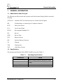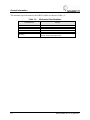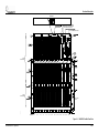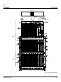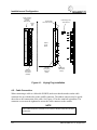
1
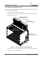
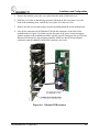
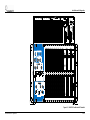
1000 Technology Drive, Pittsburgh, PA 15219 645 Russell Street, Batesburg, SC 29006 SM-1D2.0009 MICROLOK® II HB2X Cardfile ASTS USA Part Nos. N18005201 N18005301 Installation Operation © Copyright 2011 Ansaldo STS USA, Inc. SM-1D2.0009, Rev. 2 August 2011 Notices Proprietary Notice This document and its contents are the property of Ansaldo STS USA, Inc. (formerly known as Union Switch & Signal Inc., and hereinafter referred to as "ASTS USA"). This document is furnished to you on the following conditions: 1.) That no proprietary or intellectual property right or interest of ASTS USA is given or waived in supplying this document and its contents to you; and, 2.) That this document and its contents are not to be used or treated in any manner inconsistent with the rights of ASTS USA, or to its detriment, and are not to be copied, reproduced, disclosed or transferred to others, or improperly disposed of without the prior written consent of ASTS USA. Important Notice ASTS USA constantly strives to improve our products and keep our customers apprised of changes in technology. Following the recommendations contained in the attached service manual will provide our customers with optimum operational reliability. The data contained herein purports solely to describe the product, and does not create any warranties. Within the scope of the attached manual, it is impossible to take into account every eventuality that may arise with technical equipment in service. Please consult an ASTS USA local sales representative in the event of any irregularities with our product. ASTS USA expressly disclaims liability resulting from any improper handling or use of our equipment, even if these instructions contain no specific indication in this respect. We strongly recommend that only approved ASTS USA spare parts are used as replacements. SM-1D2.0009, Rev. 2, August 2011 i Revision History Revision History REV. ii DATE 1 April 2010 2 August 2011 NATURE OF REVISION Initial release Added information for LCP PCB: Section 3.3, Figure 3-6, Figure 3-7, Section 4.4, and Figure 4-5. SM-1D2.0009, Rev. 2, August 2011 Table of Contents Table of Contents 1. 2. 3. 4. 5. GENERAL INFORMATION ............................................................................................................... 1-1 1.1. 8BAbbreviations and Acronyms .................................................................................................... 1-1 1.2. Specifications ............................................................................................................................ 1-1 GENERAL DESCRIPTION ................................................................................................................ 2-1 2.1. Product Functions ..................................................................................................................... 2-1 FUNCTIONAL DESCRIPTION .......................................................................................................... 3-1 3.1. WAGO Connectors ................................................................................................................... 3-9 3.2. Communications Ports ............................................................................................................ 3-11 3.2.1. Communication Port 1 ................................................................................................ 3-11 3.2.2. Communication Port 2 ................................................................................................ 3-11 3.2.3. Communication Port 3 ................................................................................................ 3-11 3.2.4. Communication Port 4 ................................................................................................ 3-11 3.2.5. Optional Ethernet PCB ............................................................................................... 3-12 3.3. Optional Local Control Panel PCB ......................................................................................... 3-13 INSTALLATION AND CONFIGURATION ........................................................................................ 4-1 4.1. Keying ....................................................................................................................................... 4-1 4.2. Cable Connection ..................................................................................................................... 4-2 4.3. Installation of optional Ethernet PCB ........................................................................................ 4-4 4.4. Installation of optional Local Control panel PCB ...................................................................... 4-6 RAIL TEAM AND TECHNICAL SUPPORT ...................................................................................... 5-1 SM-1D2.0009, Rev. 2, August 2011 iii Table of Contents List of Figures Figure 3-1. N18005201 Cardfile Front View ....................................................................................... 3-3 Figure 3-2. N18005301 Cardfile Front View ....................................................................................... 3-5 Figure 3-3. N18005201 Cardfile with Power Supply and CPUs Installed .......................................... 3-7 Figure 3-4. Upper Motherboard WAGO Connector Wiring ................................................................ 3-9 Figure 3-5. Lower Motherboard WAGO Connector Wiring .............................................................. 3-10 Figure 3-6. LCP PCB with Toggle Switches ..................................................................................... 3-14 Figure 3-7. LCP PCB with Pushbuttons ........................................................................................... 3-15 Figure 4-1. Keying Plug Installation .................................................................................................... 4-2 Figure 4-2. Cable Connection............................................................................................................. 4-3 Figure 4-3. Location of Rear Cover Retaining Screws ....................................................................... 4-4 Figure 4-4. Ethernet PCB Location .................................................................................................... 4-5 Figure 4-5. N18005301 Cardfile with LCP Installed ........................................................................... 4-7 List of Tables Table 1-1. Operating Specifications .................................................................................................. 1-1 Table 1-2. Mechanical Specifications ................................................................................................ 1-2 Table 3-1. Pinout of Serial Link Com Ports 3 .................................................................................. 3-12 Table 3-2. Pinout of Serial Link Com Port 4 (Front of Motherboard) .............................................. 3-13 Table 3-3. Pinout of Serial Link Com Port 4 (Rear of Motherboard) ............................................... 3-13 iv SM-1D2.0009, Rev. 2, August 2011 General Information 1. GENERAL INFORMATION 1.1. Abbreviations and Acronyms 8B The following are abbreviations and acronyms used in this manual along with their associated meanings. ASTS USA Ansaldso STS USA (formerly known as Union Switch & Signal) DB D-subminiature (a common type of computer connector) DCD Data Carrier Detect LCP Local Control Panel RS-232 Recommended Standard 232 RX Receive RXD Receive Data RTS Request to Send SEC Serial-to-Ethernet Converter TX Transmit TXD Transmit data VDC Volts Direct Current 1.2. Specifications The operating specifications for the HB2X Cardfile are given in Table 1-1. X Table 1-1. PARAMETER System Power Source Voltage Power Connection Temperature Range Humidity SM-1D2.0009, Rev. 2, August 2011 Operating Specifications VALUE +9.8 to +16.2VDC, Fuse Protected (10A) Minimum voltage required for system start is 11.2VDC. Six position WAGO connector on upper right panel of cardfile -40° C to +70°C 0% to 95% non-condensing 1-1 General Information The mechanical specifications for the HB2X Cardfile are shown in Table 1-2. X Table 1-2. PARAMETER Height Width Depth Material Weight Mounting 1-2 Mechanical Specifications VALUE 17.19 in. (43.7 cm) 19.0 in. (48.26 cm) 11.0 in. (27.9 cm) Stainless steel 22.25 lb. (10.09 kg) for the assembled unit. Wall or Shelf Mount, cardfile is equipped with mounting ears on the rear and bottom sides. SM-1D2.0009, Rev. 2, August 2011 General Description 2. GENERAL DESCRIPTION The MICROLOK II® HB2X is a cardfile that can be configured as a multi-purpose vital and/or nonvital monitoring and control system for railroad and rail mass transit wayside interlocking equipment. The MICROLOK II HB2X cardfile has twenty slots (fourteen configurable) and can be wall or shelf mounted. Two PCB motherboards interconnect the MICROLOK II CPUs, Power Supply, and up to fourteen I/O PCBs to the I/O field connectors at the top of the cardfile motherboard. The cardfile is available in two versions. Part number N18005201 contains 48-pin upper connectors in all slots. Part number N18005301 contains 96-pin upper connectors in slots 1 thru 3 (to accommodate the 32 I/O boards) and 48-pin connectors in slots 4 thru 14. 2.1. Product Functions Basic applications and uses of the MICROLOK II HB2X include: Direct control of wayside signals (color light signal lamps, LED signal, and searchlight signal mechanisms) Switch machine control and switch point position monitoring Switch lock position monitoring Monitoring of mainline track circuits for track occupancy indications and track circuit problems such as faulty insulated joint or broken rail (Microtrax or Ecode) Through-the-rails communications to adjacent wayside control systems: Microtrax or Ecode. Monitors interlocking OS track circuits Cab signal carrier/code generation Line wire communications interface Local manual control of wayside signals and switch machines for maintenance and contingency operations Vital serial communications to other compatible interlocking control and coded track circuit systems. Protocol is a function of the CPU software Non-vital controller logic Non-vital (code line) communications to remote office PTC signal and switch status MICROLOK is a registered trademark of Ansaldo STS USA, Inc. SM-1D2.0009, Rev. 2, August 2011 2-1 General Description The MICROLOK II HB2X implements these functions in any combination, from basic to complex through the use of application-specific hardware configurations. The modular design of the MICROLOK II system enables each customer to configure a system that will meet the specific control and interface requirements for their application. The operational configuration of the MICROLOK II system is primarily defined within the Application logic software, which is custom-developed using the MICROLOK II programming tools. 2-2 SM-1D2.0009, Rev. 2, August 2011 Functional Description 3. FUNCTIONAL DESCRIPTION The MICROLOK II HB2X cardfile accommodates standard MICROLOK II plug-in PCBs (see Figure 3-1 and Figure 3-2). The cardfile is twenty slots wide. Three double-width PCB slots are reserved for the Power Supply PCB in Slots 15 and 16, the vital CPU PCB (MICROLOK II) in Slots 17 and 18, and the non vital CPU PCB (Genisys II) in Slots 19 and 20. The remaining fourteen slots can accommodate any standard MICROLOK II I/O PCBs. The 32 I/O PCB can only be installed in slots 1, 2, and 3 of cardfile part number N18005301. The cardfile has an upper and a lower motherboard. The cable connectors for external cables are mounted on the front of the upper motherboard. The lower motherboard contains keying strips for the lower connectors to prevent insertion of an improper board type. The motherboard uses nominal 12 volt battery power (9.8V to 16.2V) as the system operating power. SM-1D2.0009, Rev. 2, August 2011 3-1 Functional Description 3-2 SM-1D2.0009, Rev. 2, August 2011 Functional Description TOP VIEW OPTIONAL ETHERNET CONNECTOR VITAL COMMUNICATION PORTS NON-VITAL COMMUNICATION PORTS J29 I/O SLOT 1 I/O SLOT 2 I/O SLOT 3 I/O SLOT 4 I/O SLOT 5 I/O SLOT 6 I/O SLOT 7 I/O SLOT 8 I/O SLOT 9 I/O SLOT 10 I/O SLOT 11 I/O SLOT 12 I/O SLOT 13 J33 J30 I/O SLOT 14 _ + BAT (+) 1 2 3 1 2 3 4 FUSE 10A BAT (-) POWER ON VCOR (+) VCOR (-) SHUT DOWN BAT(-) 4 5 6 TRANSZORB 5KP16A OFF COM2 J35 6 25 13 J39 J37 14 6 1 6 COM4 1 14 1 1 J36 J38 9 9 5 5 25 1 COM3 6 J34 NON-VITAL COM PORTS 13 COM3 1 VITAL COM PORTS 9 9 5 5 COM2 COM4 UPPER MOTHERBOARD J2 J4 J6 J8 J10 J12 J16 J18 J20 J22 J24 J26 J28 J40 J41 J42 J18 GND +5V +12V LOWER MOTHERBOARD GND GND +5V +5V -12V +12V AUXILIARY POWER CONNECTOR 1A1.0184.00 GND +5V +12V PCB SLOT 1 2 3 4 5 6 7 8 9 10 11 12 13 14 15 16 17 18 19 20 Figure 3-1. N18005201 Cardfile Front View SM-1D2.0009, Rev. 2, August 2011 3-3/3-4 Functional Description TOP VIEW OPTIONAL ETHERNET CONNECTOR VITAL COMMUNICATION PORTS NON-VITAL COMMUNICATION PORTS J29 I/O SLOT 1 I/O SLOT 2 I/O SLOT 3 I/O SLOT 4 I/O SLOT 5 I/O SLOT 6 I/O SLOT 7 I/O SLOT 8 I/O SLOT 9 I/O SLOT 10 I/O SLOT 11 I/O SLOT 12 I/O SLOT 13 J33 J30 I/O SLOT 14 _ + BAT (+) 1 2 3 1 2 3 4 FUSE 10A BAT (-) POWER ON VCOR (+) VCOR (-) SHUT DOWN BAT(-) 4 5 6 TRANSZORB 5KP16A OFF COM2 13 J35 6 1 25 6 COM3 J39 J37 14 6 1 6 COM4 1 14 1 1 J36 J38 9 9 5 5 25 13 1 COM3 NON-VITAL COM PORTS J34 VITAL COM PORTS 9 9 5 5 COM2 COM4 UPPER MOTHERBOARD J2 J4 J6 J8 J10 J12 J16 J18 J20 J22 J24 J26 J28 J40 J41 J42 PCB CONNECTORS J18 GND +5V +12V LOWER MOTHERBOARD GND GND +5V +5V -12V +12V AUXILIARY POWER CONNECTOR 1A1.0186.00 GND +5V +12V PCB SLOT 1 2 3 4 5 6 7 8 9 10 11 12 13 14 15 16 17 18 19 20 Figure 3-2. N18005301 Cardfile Front View SM-1D2.0009, Rev. 2, August 2011 3-5/3-6 J29 I/O SLOT 1 I/O SLOT 2 I/O SLOT 3 I/O SLOT 4 I/O SLOT 5 I/O SLOT 6 I/O SLOT 7 I/O SLOT 8 I/O SLOT 9 I/O SLOT 10 I/O SLOT 11 I/O SLOT 12 I/O SLOT 13 J33 J30 I/O SLOT 14 _ + BAT (+) 1 2 3 1 2 3 4 FUSE 10A BAT (-) POWER ON VCOR (+) VCOR (-) SHUT DOWN BAT(-) 4 5 6 TRANSZORB 5KP16A OFF COM2 J4 J6 J8 J10 J12 J16 J18 J20 J22 J24 J26 J28 J40 J41 13 J35 6 1 9 5 J39 J37 14 6 1 6 1 COM4 COM4 J42 J18 J2 14 1 1 J36 J38 9 25 5 25 6 J34 COM3 13 COM3 NON-VITAL COM PORTS 1 VITAL COM PORTS 9 9 5 5 COM2 GND GND +5V 1A1.0190.00 +5V -12V +12V Figure 3-3. N18005201 Cardfile with Power Supply and CPUs Installed SM-1D2.0009, Rev. 2, August 2011 3-7/3-8 Functional Description 3.1. WAGO Connectors A six-connection, removable WAGO power connector (J33) is mounted on the front of the upper motherboard (see Figure 3-1). This connector is used for the battery input and VCOR coil wiring. The pinout for the connector is as follows: Pin 1 B12 input Pin 2 N12 input Pin 3 VCOR positive terminal (1A) connection Pin 4 VCOR negative terminal (1C) connection Pin 5 Shutdown Pin 6 N12 input Pins 2, 3, & 6 of J33 are connected internally to bring N12 to the VCOR relay coil as well as the negative return of the shutdown. Pin 5 of J33 is connected internally to the shutdown function of the Power Supply PCB. The shutdown function allows the user to shut down the system using an external power supply. Figure 3-4 shows the connector wiring. POWER / VCOR CONNECTOR J 16 BATTERY INPUT + _ 9.8V – 16.2V 1A - + VCOR 1C EXTERNAL RELAY 1 BAT(+) 2 BAT (-) 3 VCOR (+) 4 VCOR (-) 5 SHUTDOWN 6 BAT (-) PINS 2, 3 AND 6 ARE CONNECTED INTERNALLY TO MOTHERBOARD 1 + 2 - 3 + 4 - 5 VCOR RELAY COIL SHUTDOWN - 6 1A1.0185.00 BATTERY INPUT 9.8V - 16.2V BATTERY WAGO CONNECTOR Figure 3-4. Upper Motherboard WAGO Connector Wiring SM-1D2.0009, Rev. 2, August 2011 3-9 Functional Description Input Battery power (12V) from the WAGO connector is routed through the power switch and a 10 amp fuse to the power supply PCB. Surge protection across the battery is provided by a 5 watt, 16 volt, transzorb (Vishay-General Semi part number 5KP16A-E3/4 5KP16A) mounted on screw terminals. The transzorb assembly with ring terminals (Ansaldo STS USA part number N50770002) is field replaceable. The lower motherboard is equipped with a 6-pin WAGO connector to provide auxiliary (external power supply) power to the MICROLOK II HB2X in lieu of the MICROLOK II Power Supply PCB. Pins 1 and 2 are for common, pins 3 and 4 are for +5 volts, pin 5 is for -12 volts, and pin 6 is for +12 volts. Figure 3-5 shows the connector wiring. The connector is located at the lower right of the motherboard and can be accessed by removing the two screws and panel on the side of the cardfile. AUXILIARY POWER CONNECTOR 1A1.0191.00 J18 1 COMMON 2 COMMON 3 +5V 4 +5V 5 -12V 6 +12V 1 COMMON 2 COMMON 3 +5V 4 +5V 5 -12V 6 +12V WAGO CONNECTOR Figure 3-5. Lower Motherboard WAGO Connector Wiring When using auxiliary power, the Conditional Power Supply PCB (N4519107501) is used in place of the nominal Power Supply PCB (N16660301 or N16661203). The lower motherboard transfers the required voltage (+12V, +5V, & GND) to the upper motherboard Slot 15 connector to satisfy the voltage requirements of the Conditional Power Supply. In this configuration, J33 must be used in conjunction with the auxiliary power so that there is a connection to the VCOR and shutdown function. An external fuse and surge protection are recommended when using auxiliary power. The values of the protection will depend on the auxiliary power source. 3-10 SM-1D2.0009, Rev. 2, August 2011 Functional Description 3.2. Communications Ports The MICROLOK II HB2X cardfile contains three vital and/or three non-vital communications ports for external communications. An additional port is used for internal communications between the non-vital and vital CPU PCBs. 3.2.1. Communication Port 1 The upper motherboard contains RS-485 serial ports that are connected internally from com port 1 of the vital CPU board to com port 1 of the non-vital CPU. 3.2.2. Communication Port 2 Communication Port 2 incorporates two RS-485 serial ports that use standard DB-9 male connectors, DIP switches, and terminating resistors (see Figure 3-1). The connectors are labeled "J34, COM 2" and "J35, COM 2" on the motherboard. The ports are connected internally to com port 2 on the vital and non-vital CPU PCBs. The DIP switches switch the terminating resistors in or out. DIP switch SW1 connects terminating resistors to the non-vital com port 2. DIP switch SW2 connects terminating resistors to the vital com port 2. When the DIP switches are in the closed position, the terminating resistors are connected into the circuit. Terminating resistors are used to reduce reflections on a multi-drop line. Terminating resistors should be implemented if the cardfile is at the two furthest ends of the line. NOTE The four switches of SW1 or SW2 must be set to the same position, either all open or all closed. 3.2.3. Communication Port 3 The upper motherboard contains two RS-232 serial ports that use standard DB-25 connectors (J36 & J37). J36 is connected to com port 3 of the vital CPU. J37 is connected to com port 3 of the non-vital CPU. 3.2.4. Communication Port 4 The upper motherboard contains two RS-232 serial ports (J38 & J39) using standard DB-9 connectors. These connectors are connected internally to the com Port 4 of the CPU boards (vital and non-vital). The signals associated with the connector J38 are shared with the rear mounted DB-9 connector with sockets (J29) for the Serial to Ethernet Converter (SEC) board. DIP switch SW3 transfers the TXD, RXD, RTS, and DCD signals from the vital CPU board between the two connectors J29 and J38. Switch SW3 ensures that only one connector of com port 4 is active at a given time. When all four switches of SW3 are set to the "FRONT" position, the signals are routed to connector J38. When all four switches of SW3 are set to the "REAR" position, the signals are routed to connector J29. SM-1D2.0009, Rev. 2, August 2011 3-11 Functional Description NOTE All four switches of SW3 must be set to the same position, either all FRONT or all REAR. 3.2.5. Optional Ethernet PCB An Ethernet PCB (ASTS USA part number N17006202) can be plugged onto the rear of the upper motherboard. The Ethernet port is on top of the cardfile when the Ethernet PCB is installed. The 12 volt power for the Ethernet PCB comes through connector J30 (on the rear of the cardfile) and the serial communications signals come through connector J29, "COM 4". See Section 4.3 for installation instructions. Refer to SM-6800O, for configuration of the Ethernet PCB. Service Manual SM-6800O describes the Serial to Ethernet Converter (SEC). The SEC (ASTS USA part number N16920401) is different in physical appearance from the optional Ethernet PCB. However, the configuration procedures are the same for both units. When using the optional Ethernet PCB, Switch SW3 must be set to the "REAR" position. The signals and pin numbers for the com ports are shown in Table 3-1 through Table 3-3. Table 3-1. Pinout of Serial Link Com Ports 3 PIN NUMBER 1 2 3 4 5 6 7 8 9 10 11 12 13 14 15 16 17 18 19 20 21 22 23 24 25 3-12 SIGNAL COM 3 Not Connected TXD (Transmit Data) RXD (Receive Data) RTS (Request to Send) CTS (Clear to Send) Not Connected COMMON (N12) DCD (Data Carrier Detect) Not Connected Not Connected Not Connected Not Connected Not Connected Not Connected TXCLK (Transmit Clock) Not Connected RXCLK (Receive Clock) -12V Not Connected Not Connected +12V Not Connected Not Connected Not Connected Not Connected SM-1D2.0009, Rev. 2, August 2011 Functional Description Table 3-2. Pinout of Serial Link Com Port 4 (Front of Motherboard) PIN NUMBER 1 2 3 4 5 6 7 8 9 Table 3-3. SIGNAL COM 4 FRONT DCD (Data Carrier Detect) RXD (Receive Data) TXD (Transmit Data) Not Connected COMMON (N12) Not Connected RTS (Request to Send) Not Connected Not Connected Pinout of Serial Link Com Port 4 (Rear of Motherboard) PIN NUMBER 1 2 3 4 5 6 7 8 9 SIGNAL COM 4 REAR COMMON (N12) Not Connected RXD (Receive Data) TXD (Transmit Data) DCD (Data Carrier Detect) Not Connected Not Connected RTS (Request to Send) Not Connected 3.3. Optional Local Control Panel PCB A Local Control Panel (LCP) PCB can be plugged into the front of the 96-pin cardfile (part number N18005301). The LCP is available with toggle switches or with pushbuttons installed in the uppermost row of controls. Figure 3-6 shows the front panel of the LCP PCB with toggle switches (part number N16926001). Figure 3-7 shows the front panel of the LCP with pushbuttons (part number N16926002). A relay driver PCB (part number N4518104801) is also required when using the LCP PCB. See Section 4.4 for the installation instructions. SM-1D2.0009, Rev. 2, August 2011 3-13 1A1.0246.00 Functional Description Figure 3-6. LCP PCB with Toggle Switches 3-14 SM-1D2.0009, Rev. 2, August 2011 1A1.0245.00 Functional Description Figure 3-7. LCP PCB with Pushbuttons SM-1D2.0009, Rev. 2, August 2011 3-15 Functional Description 3-16 SM-1D2.0009, Rev. 2, August 2011 Installation and Configuration 4. INSTALLATION AND CONFIGURATION The cardfile can be either wall or shelf mounted. One inch flanges are located along each side with four slotted mounting holes for wall mounting. One inch flanges are located along the bottom sides with five holes in each side for shelf mounting. Screws or bolts can be used to secure the cardfile to the wall or shelf. WARNING When replacing a power supply PCB, make certain of the board type. An old model PCB (N16660301) can be replaced with a new model PCB (N16661203), but not a new with an old (due to current rating). A power supply PCB cannot be interchanged with a CPS only PCB. 4.1. Keying The lower motherboard contains keying guides for the lower connectors to prevent accidental insertion of a printed circuit board into the wrong cardfile slot. Keying plugs are inserted by the customer (during installation) into the motherboard connector keying guide (see Figure 4-1). This guide mates with the keying strip mounted alongside the PCB's lower 96-Pin connector. The PCB's keying strip is equipped with twelve male keying tabs from which six tabs are removed at the factory in a specific pattern for the board part number. Each PCB type has a unique six tab arrangement to distinguish it from other boards. Prior to installing a board, insert keying plugs (Part Number J709146-0473) into the corresponding cardfile motherboard keying guide (next to the connector). Plugs are installed in all cavities not corresponding to a keying tab location. If it becomes necessary to change the type of board installed in a given slot, the previously installed keying plugs can be removed using a knife or a pair of needle nose pliers. SM-1D2.0009, Rev. 2, August 2011 4-1 Installation and Configuration 96-pin (Female) Connector on Cardfile Motherboard Keying Plug No. 96-pin (Male) Connector on PCB Insert Keying Plug J709146-0473 1 2 3 4 5 6 7 Printed Circuit Board 8 9 10 11 12 Adjacent Keying Plug Connector (Male) Adjacent Keying Plug Connector (Female) PCB Keying Tabs Set at Factory Figure 4-1. Keying Plug Installation 4.2. Cable Connection When connecting a cable to a Microlok II HB2X, make sure that the notches on the cable connector line up with the tabs on the cardfile connector. The address jumpers may be upside down due to the construction of the cable. See Figure 4-2 for the connector orientation. The connector screws must be tightened to secure the cable connector to the cardfile. NOTE The cables must be secured six to twelve inches from the cardfile connector. 4-2 SM-1D2.0009, Rev. 2, August 2011 Installation and Configuration Figure 4-2. Cable Connection SM-1D2.0009, Rev. 2, August 2011 4-3 Installation and Configuration 4.3. Installation of optional Ethernet PCB Proceed as follows to install the Ethernet PCB (Ansaldso STS USA part number N17006202) on the rear of the cardfile motherboard: 1. Remove the HB2X cardfile from the wall or shelf. 2. Remove the three screws that are located on each side of the cardfile toward the back of the cardfile (see Figure 4-3). REAR COVER RETAINING SCREWS COVER PLATE REAR COVER RETAINING SCREWS 1A1.0187.00 REAR COVER RETAINING SCREWS Figure 4-3. Location of Rear Cover Retaining Screws 3. Remove the five screws from the cardfile that are located at the top of the motherboard. 4. Remove the rear cover from the cardfile. 4-4 SM-1D2.0009, Rev. 2, August 2011 Installation and Configuration 5. Remove the nut that secures the cover plate from the inside of the back cover. 6. Slide the cover plate so that the large portion of the hole in the cover plate is over the head of the mounting screw, and lift the cover plate off of the rear cover. 7. Remove the four screws and washers from the mounting standoffs on the motherboard. 8. Line up the connectors on the Ethernet PCB with the connectors on the back of the motherboard (see Figure 4-4). Make sure the four pins of the power connector engage with the sockets on the motherboard. Make sure the 9-pin D connectors line up. Press the Ethernet PCB down onto the mounting standoffs. Make sure that PCB is positioned completely onto the standoffs and that the connectors are secure. Figure 4-4. Ethernet PCB Location SM-1D2.0009, Rev. 2, August 2011 4-5 Installation and Configuration 9. Install the four screws and washers through the Ethernet PCB into the standoffs. 10. Place the back cover on the cardfile. The tabs on the top of the rear cover must be behind the motherboard. 11. Install the six screws into the sides of the cardfile and rear cover that were removed in Step 2. 12. Install the five screws at the top of the motherboard that were removed in Step 3. 13. Set Switch SW3 to the REAR position. 14. Installation of the Ethernet PCB is complete. 15. Proceed to SM6800O to configure the Ethernet PCB. 4.4. Installation of optional Local Control panel PCB Figure 4-5 shows the LCP PCB with pushbuttons installed in the HB2X cardfile. Proceed as follows to install the LCP PCB (part number N16926001 or N16926002) on the front of 96-pin cardfile (N18005301): 1. Remove power from the HB2X cardfile. 2. Remove any existing PCBs that are installed in slots 1 through 5. 3. Line up the connectors on the Relay Driver PCB with the connectors on the back of the LCP PCB. 4. Press the Relay Driver PCB into the LCP PCB. Make sure that the PCBs are securely connected. 5. Align the Relay Driver PCB's edges with the cardfile slot's channels. 6. Slide the LCP and Relay Driver PCB assembly into the cardfile channels and into the motherboard connectors. Make sure that the PCB assembly is securely connected to the motherboard. 7. Tighten the four screws on the front of the LCB PCB. 8. Apply power to the HB2X cardfile. 9. Installation of the LCP PCB is complete. 4-6 SM-1D2.0009, Rev. 2, August 2011 Installation and Configuration J29 I/O SLOT 1 I/O SLOT 2 I/O SLOT 3 I/O SLOT 4 I/O SLOT 5 I/O SLOT 6 I/O SLOT 7 I/O SLOT 8 I/O SLOT 9 I/O SLOT 10 I/O SLOT 11 I/O SLOT 12 I/O SLOT 13 J33 J30 I/O SLOT 14 3 4 1 2 _ + 1 2 BAT (+) 3 VCOR (+) VCOR (-) SHUT DOWN BAT(-) FUSE 10A BAT (-) 4 5 6 TRANSZORB 5KP16A POWER ON OFF COM2 J2 J4 J6 J8 J10 J12 J16 J18 J20 J22 J24 J26 J28 J40 J41 13 J35 6 1 9 5 J39 J37 14 6 1 6 COM4 1 14 1 1 J36 J38 9 25 5 25 6 J34 COM3 13 COM3 NON-VITAL COM PORTS 1 VITAL COM PORTS 9 9 5 5 COM2 COM4 J42 J18 GND +5V +12V GND GND +5V +5V -12V +12V 1A1.0244.00 GND +5V +12V Figure 4-5. N18005301 Cardfile with LCP Installed SM-1D2.0009, Rev. 2, August 2011 4-7/4-8 RAIL Team and Technical Support 5. RAIL TEAM AND TECHNICAL SUPPORT The Rapid Action Information Link Team (RAIL Team) is a group of experienced product and application engineers ready to assist you to resolve any technical issues concerning this product. Contact the RAIL Team in the United States at 1-800-652-7276 or by e-mail at [email protected]. H SM-1D2.0009, Rev. 2, August 2011 5-1 RAIL Team and Technical Support End of Manual 5-2 SM-1D2.0009, Rev. 2, August 2011