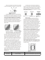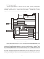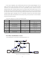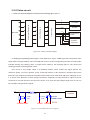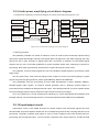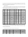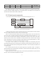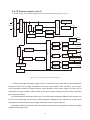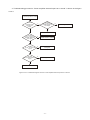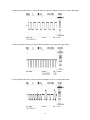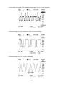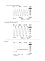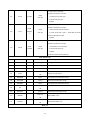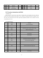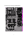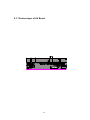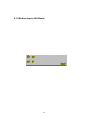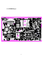
1
DK1910SI & DK1930SI
DK1810SI & DK1830SI
& DK1840SI
service manual
Catalog
Chapter One About Maintenance
1.1 Safety precautions
1
1
1.1.1 Power supply
1
1.1.2 Precautions for antistatic
1
1.1.3 Precautions for laser head
1
1.1.4 About placement position
2
1.2 Maintenance method
2
1.2.1 Visualized method
2
1.2.2 Electric resistance method
2
1.2.3 Voltage method
2
1.2.4 Current method
2
1.2.5 Cutting method
2
1.2.6 Element substitution method
3
1.2.7 Comparison method
3
1.3 Required device for maintenance
Chapter Two Functions and Operation Instructions
3
4
2.1 Features
4
2.2 Controls and functions
5
2.2.1 Front Panel controls
5
2.2.2 Rear panel connections
5
2.2.3 VFD display general view
6
2.2.4 Remote control general view
6
2.3 FUNCTION SETTINGS
8
2.3.1 Function selection and change
8
2.3.2 Language settings
8
2.3.3 Image settings menu
8
2.3.4 Sound settings menu
9
2.3.5 Playback settings
10
2.3.6 Karaoke settings menu
10
2.3.7 Preference settings
11
2.3.8 Parental Control
11
2.3.9 Initial setup menu
11
2.3.10 reset to defaults
11
2.3.11 Exit settings menu
11
2.3.12 Channel delay set-up
11
2.4 Technical characteristics
Chapter Three Principle and Servicing
13
15
Section One Principle of the Player
15
3.1.1 Function and features
15
3.1.2 Block diagram of the player
15
3.1.3 Introduction to IC used in this player
17
Section Two Unit Circuit Principle
18
3.2.1 Introduction to laser head
18
3.2.2 Servo circuit
20
3.2.3 Main axis braking control circuit
23
3.2.4 Disc identification circuit
24
3.2.5 Disc in/out circuit
25
3.2.6 Reset circuit
26
3.2.7 Mute circuit
27
3.2.8 Video circuit
28
3.2.9 Audio power amplifying circuit block diagram
29
3.2.10 Input/output circuit
29
3.2.11 Control panel components
31
3.2.12 Power supply circuit
32
Section Three Servicing Cases
35
3.3.1 Servicing cases
35
3.3.2 Troubleshooting flow chart
38
Section Four Waveform diagram
44
Section Five Function Introduction to IC
49
3.5.1 function introduction to MT1389HD
49
3.5.2 function introduction to AT24C02
65
3.5.3 function introduction to 74HCU04
66
3.5.4 function introduction to Lm1117
66
3.5.5 function introduction to 29LV160BE
67
3.5.6 function introduction to HY57V641620HGT -7
68
3.5.7 function introduction to D5954
69
3.5.8 function introduction to 4558
70
3.5.9 function introduction to SN74LVC
71
3.5.10 function introduction to 74HCT125
71
3.5.11 function introduction to Cd4052
72
3.5.12 function introduction to SAA6588
73
3.5.13 function introduction to 5340
75
3.5.14 function introduction to TLV272
76
3.5.15 function introduction to Lm4880
77
3.5.16 function introduction to TAS5508PAG
78
3.5.17 function introduction to TAS5112DFD
80
3.5.18 function introduction to Ad7312
83
3.5.19 function introduction to VIPer22ADIP
85
3.5.20 function introduction to Hs817
85
3.5.21 function introduction to TL431A
86
3.5.22 function introduction to KA1M0880BTU
86
Chapter Four Disassembly and Assembly Process
88
Chapter Cinque PCB board & Circuit diagram
89
Section One PCB board
89
Section Two circuit diagram
98
Chapter six BOM List
104
Chapter One About Maintenance
1.1 Safety precautions
1.1.1 Power supply
When maintenance personnel are repairing DVD players, he should pay special attention to
the
power board with 220V AC and 330V DC which will cause hurt and damage to persons!
1.1.2 Precautions for antistatic
Movement and friction will both bring static electricity which causes serious damages to integrated
IC. Though static charge is little, when a limited quantity of electric charge is added to largescaleintegrated IC, as the capacitance is very small in the meantime, now the integrated IC is very much
easy to be struck through by static electricity or the performance will decrease. Thus static electricity
prevention is of extraordinary importance. The following are several measures to prevent static
electricity:
1. Use a piece of electric conduction metal with the length of about 2 metres to insert into the earth,
and Fetch the lead wire from the top of the surplus metal and connect to the required static electricity
device. The length and depth of the metal embedded under the earth should be determined according to
the wettability of the local soil. For humid places, it may be shorter, and longer and deeper for dry places.
If possible, it can be distributed and layed in terms of “#” shape.
2. On operating table-board, the antistatic table cushion should be covered and grounded.
3. All devices and equipments should be placed on the antistatic table cushion and grounded.
4. Maintenance personnel should wear antistatic wrist ring which should be grounded.
5. Places around the operating position should also be covered with electric conduction cushion or
Painted with antistatic paint.
1.1.3 Precautions for laser head
1. Do not stare at laser head directly, for laser emission will occur when laser head is working, which
will Hurt your eyes!
2. Do not use wiping water or alcohol to clean laser head, and you may use cotton swab.
-1-
1.1.4 About placement position
1. Never place DVD player in positions with high temperature and humidity.
2. Avoid placing near high magnetic fields, such as loudspeaker or magnet.
3. Positions for placement should be stable and secure.
1.2 Maintenance method
1.2.1 Visualized method
Directly view whether abnormalities of collision, lack of element, joint welding, shedding welding,
rosin joint, copper foil turning up, lead wire disconnection and elements burning up among pins of
elements appear. Check power supply of the machine and then use hands to touch the casing of part of
elements and check whether they are hot to judge the trouble spot. You should pay more attention when
using this method to check in high voltage parts.
1.2.2 Electric resistance method
Set the multimeter in resistance position and test whether the numerical value of resistance of each
point in the circuit has difference from the normal value to judge the trouble spot. But in the circuit the
tested numerical value of resistance is not accurate, and the tested numerical value of integrated IC's
pins can only be used for reference, so the elements should be broken down for test.
1.2.3 Voltage method
Voltage method is relatively convenient, quick and accurate. Set the multimeter in voltage position
and test power supply voltage of the player and voltage of a certain point to judge the trouble spot
according to the tested voltage variation.
1.2.4 Current method
Set the multimeter in current position and test current of the player of a certain point to judge the
trouble spot. But when testing in current method, the multimeter should be series connected in the
circuit, which makes this method too trivial and troublesome, so it is less frequently used in reality.
1.2.5 Cutting method
Cutting method should be combined with electric resistance method and voltage method to use.
This method is mainly used in phenomena of short circuit and current leakage of the circuit. When
cutting the input terminal voltage of a certain level, if voltage of the player rises again, it means that the
trouble lies in this level.
-2-
1.2.6 Element substitution method
When some elements cannot be judged good or bad, substitution method may de adopted directly.
1.2.7 Comparison method
A same good PC board is usually used to test the correct voltage and waveform. Compared these
data with those tested through fault PC board, the cause of troubles may be found.
Through the above maintenance method, theoretical knowledge and maintenance experience, all
difficulties and troubles will be readily solved.
1.3 Required device for maintenance
Digital oscillograph ( 100MHE)
TV set
SMD rework station
Multimeter
Soldering iron
Pointed-month pincers
Cutting nippers
Forceps
Electric screw driver
Terminals connecting cord
Headphone
Microphone
-3-
Chapter Two
Functions and Operation Instructions
2.1 Features
Formats:
#Digital video playback of DVD-Video, Super VCD and VCD formats
#MPEG-4 compatibility: playback of DivX 3.11, DivX 4, DivX 5, DivX Pro and XviD formats
#Playback of music discs in DVD-Audio format
#Playback of musical compositions in CD-DA and HDCD formats
#Playback of compressed musical files in Mp3 and CD+G formats
#Playback of Karaoke-discs in DVD, VCD and CD+G formats
#Playback of photo albums, recorded in Kodak Picture CD and JPEG digital formats
Audio:
#192 kHz/12 bit audio D/A converter
#Coaxial and optical audio outputs, providing digital sound playback in Dolby Digital/DTS/LPC formats
#Coaxial and optical audio inputs, providing connection of external digital signal sources
#Stereophonic audio output for connection to TV and amplifier
#Integrated digital multi-channel sound decoders, providing playback of Dolby Digital and DTS audio
tracks
#Integrated Dolby Pro Logic ll decoder, providing transformation of stereophonic signal to multi-channel
one
#Microphone input providing karaoke functions
#Headphones output
Video:
#108kHz/12 bit video D/A converter
#Progressive scan(Y Pb Pr)video signal output, securing high resolution and absence of image flicker
#Composite and component(Y Cb Cr), S-Video and RGB/SCART video outputs, providing advanced
switching capabilities
#NTSC/PAL transcoder
#Support of many camera angels, dubbed languages and subtitles
#Sharpness, Gamma, Brightness, Contrast, Hue and Saturation adjustment.
Miscellaneous:
#Support of CD-R/CD-RW, DVD-R/DVD-RW, DVD+R/DVD+RW
#FM/AM tuner with RDS support
#USB port, providing playback of files of supported formats from external flash-memory devices
#KARAOKE+, providing extended karaoke features
#Easy to use on-screen menu in Russian
#Support of Russian file names, Id3 tags and CD-text
#”Memory” function which can load the last disc position on stop
-4-
#”Capture” function, auto loading selected bookmarked image as the wallpaper
#Q-Play function that will bring you to the main movie title and skip unskippable commercials
#Virtual control panel function makes your control of the device much easier when playing the movie
#Browser function displays information about playback modes
#Auto protection of TV screen
#Child lock, parental control(protection against playing undesirable discs)
2.2 Controls and functions
2.2.1 Front panel controls
1
8
STANDBY/POWER button
SOURCE button
Press to switch the device on/into standby
Press to switch between DVD-receiver/Audio
2
Disc tray
input/Tuner/Digital audio input
3
Open/close button
9
Press to open/close the disc tray
4
Press to playback/pause
PREV button
10
Press to playback from the previous bookmark
5
6
7
PLAY/PAUSE button
STOP button
Press to stop the playback
NEXT button
11
Microphone input
Press to playback from the next bookmark
12
VOLUME adjuster
PEW button
Press to adjust volume
Press to fast reverse/radio station tuning
13
VFD display window
Forward button
14
Headphones input
Press to fast forward/radio station tuning
15
USB port
4
Right front speaker input(output from the build-
2.2.2 Rear panel connections
1
AM Antenna input
2
FM Antenna input
3
Left front speaker input(output from the build-in
i n amplifier)
5
amplifier)
Center speaker input(output from the build-in
amplifier
-5-
Subwoofer input(output from the build-in
11
Component video output Y Cb(Pb)Cr(Pr)
amplifier)
12
Composite video output
Left Surround speaker input(output from the
13
S-Video output
build-in amplifier)
14
SCART-type V connector
Right Surround speaker input(output from the
15
Coaxial digital audio output
build-in amplifier)
16
Optical digital audio output
9
Audio input
17
Optical digital audio input
10
Stereophonic audio output
18
Coaxial digital audio input
6
7
8
2.2.3 VFD display general view
1
MP3-disc
2
CD-, VCD- or SVCD-disc
9
Dolby Digital
3
DVD-disc
10
Programmed radio station
4
Repeat
11
Friquency
5
AM/FM
12
Playback time
6
Radio tuning mode
13
Chapters or tracks
7
Tuner mode
14
Playback or pause
8
Stereo
15
PBC
4
DISP button
2.2.4 Remote control general view
1
EJECT button
Press to open/close the disc tray
2
Press to display the disc information
DVD button
5
Press to switch to DVD mode
3
LANG button
Press to change the language
AUDIO button
6
Press to display the disc information
SLEEP button
Press to turn the sleep mode on
-6-
7
Q-PLAY button
Press to turn the Q-Play mode on.
8
EQ button
Press to adjust the equalizer
9
BASS +/- button
Press to adjust subwoofer
10
BOOST button
Press to bass boosting
11
BROWSER button
Press to turn on/off the browser function
12
JOG DIAL wheel
Functions are set manually. Default function: ZOOM
13
SETUP button
Press to switch to setup mode
14
Button
Press to capture and bookmark image for the wallpaper
15
Buttons
Press to start reverse or forward scanning.
16
SKIP/PRESET +/Press to switch between files on disc/tuned radio stations.
17
Press to repeat the selected portion
27 OK button
Press OK for confirmation or use it like
18
19
20
21
22
23
24
25
previously memorized point.
Button
Press to trun on/off the virtual control panel
Press to memorize the point where
playback was stopped/playback from the
STOP button
Press to stop the playback
the microphone.
34 MEM button
PLAY/PAUSE button
Press to Play/pause the playback
33 ECHO button
Press to adjust the echo function of
SLOW button
Press to switch to slow down the playback
32 Treble +/- button
Press to adjust the tone
VOLUME +/- button
Press to adjust the volume
31 ST/5.1 button
Press to switch between STEREO/5.1CH
MUTE button
Press to turn on/off the sound
Press to playback from the target place.
30 Numeric buttons
CH +/CH - button
Press to change the acoustic channel
DVD-disc menu/PBC function
29 GOTO button
REPEAT button
Press to repeat playback
joystick during navigating in MENU.
28 MENU button
A-B buttons
26
CANCEL button
Press to go one level back/cancel current operation
-7-
35
4.Press SETUP to exit setup menu.
HDMI button
Press to switch to HDMI mode
36
SUBT button
Press to change the subtitles language
37
ANGLE button
Press to change the camera angel
38
RADIO button
Press to switch to radio mode
39
2.3.2 Language settings
KARAOKE button
1.Menu: interface language setup
#Options: Russian, English, Ukrainian
#Default option: English
Press to set the karaode functions
40
USB button
Press to switch to USB mode
41
Button
Press to switch the device on/into standby
2.3 FUNCTION SETTINGS
2.DVD-menu: selection of disc menu language
3.Soundtrack: selection of translation language
#Options: Russian, English, Estonian,
Lithuanian, Kazakh, Romanian, Belarusian,
Ukrainian, Chinese.
#Default: English
#Selection of other languages: select the
OTHERS item using the jog Dial and press OK.
Enter the language code using the numeric
buttons and press OK.
#If the language you selected is not recorded on
the DVD disc, another available language will
be used.
4.Subtitles: selection of subtitles language
#Options: Off, Russian, English, Estonian,
Lithuanian, Kazakh, Romanian, Belarusian,
Ukrainian, and Chinese.
#Default option: Off.
#Selection of other languages: select the
OTHERS item using the jog Dial and press OK.
Enter the language code using numeric
buttons and press OK.
#If the language you selected is not recorded on
the DVD disc, another available language will
be displayed.
2.3.1 Function selection and
change
Press the SETUP key to show the setup
menu. You will the following image on the screen,
as shown on the figure:
1.For example, if you wish to change the change
the image settings, you have to select the
image item and press the OK or RIGHT key of
the cursor joystick.
2.3.3 Image settings menu
1.TV system: TV system selection
#Options: Auto, PAL, NTSC
#Default option: PAL
2.TV scan mode: scan mode selection
#Options: progressive, interlaced
#Default option; Interlaced
#Progressive scan is transferred only via a
component video output.
2.Using the jog Dial, select the desired item and
press OK or RIGHT key of the cursor joystick.
For example, select the Sharpness item.
Settings will appear on the screen. Then select
the desired sharpness level and press OK for
confirmation.
3.Press LEFT key of the cursor joystick for exit to
previous menu level.
-8-
#Before switching to progressive scan, make
sure that your TV set supports this operation
mode.
b)Stereo mix: playback set-up while playing the
disc with two independent audio channels
#Options: L+R, L, R
#Default options: L+R
c)Surr.mix: set-up of surround options while
playing the stereo disc.
#Options: Off, Sum. L+R,Virt.Surr.
#Default options: Off
d)Low band: distribution of low frequencies
through channels
#Options: Front F, Center C, Surround Sr,
Subwoofer SW
#Default options: Front F, Subwoofer SW.
#If you want the low-frequency component of the
sound signal enter only the subwoofer channel,
select and confirm the parameter Subwoofer
SW.
3.TV Format: image ratio settings
#Options: 4:3 pan&scan, 4:3 letterbox and 16:9
TV.
#Default option: 4:3 letterbox.
#Some discs are recorded with support of only
one ratio. The selected ratio must comply with
the TV screen.
4.Video output: selection of video signal
#Options: S-Video(only for DK14**SI Series),
Comp, SCART.
#Default option: Comp
5.Sharpness: image sharpness adjustment
#Options: High, Medium, Low
#Default option: Medium
6.Gamma: adjustment of image color
temperature
#Options: High, Medium Low, Off
#Default option: Off
7.Brightness: adjustment of image brightness
8.Contrast: adjustment of image contrast
9.Hues: adjustment of image hues
10.Saturation: adjustment of image saturation
Adjustment of image brightness, contrast, hues
and saturation:
#Select the desired item of the image adjustment
section using the jog Dial. Press OK or RIGHT
key to start adjusting the relevant option
#Change the option value using the jog Dial.
#Upon completion press the LEFT key of the
cursor joystick to return to image setup menu.
e)Channel settings: separate adjusting of
volume by channels.(only for DK14**SI Series)
#Select the channel you want.
#Adjust the sound volume of each channel using
the wheel.
#Press the OK to return to sound settings menu.
2.3.4 Sound settings menu
1.Mixer
a)Configuragion: setting of the mode conversion
of the 5-channel signal to stereo signal
#Options: Stereo, 5.1
#Default option:5.1
#5.1 mode must be supported by the disc.
Number of music accompaniment channels
depends on the specific disc.
#Adjustment of th4e central speaker and
surround speakers is available only if the
Configuration option is set to 5.1 position.
f)Delay of the channel: set-up of signal delay in
speaker channels(central, rear and subwoofer)
#Using the jog Dial, select the channel for which
you want to set up the delay, and press OK for
confirmation.
#Using the jog Dial set up the desired distance
from the listener to each speaker(detailed
description of this operation see on page 32).
-9-
#Press LEFT key of the cursor joystick to return
to speaker configuration menu.
#Adjust the tone balance level using the jog Dial
#Press the LEFT key of the cursor joystick to
return to sound correction setup menu.
2.3.5 Playback settings
1.DVD
Advertisment skip: skip the unskippable
block while playing a DVD disc.
#Options; Yes, No
#Default option: Number
#Press LEFT key of the cursor joystick to return to
speaker configuration menu.
g)PRO Logic ll: function of stereo sound
conversion to 5-channel sound
#Options: On, Off, Auto
#Default option: Off
#In Auto position, the DVD receiver determines
itself, when to use the PRO Logic ll decoder.
Some discs do not support this function.
2.Digital audio output
a)SPDIF format: set-up of digital audio output
options
#Options; RAW, PCM
#Default options; RAW
# When you select the RAW option, the not
decoded signal is transferred to the DVD
receiver’s digital outputs, the decoded signal is
transferred to analog outputs. Decoding is
performed by the built-in decoder of the DVD
receiver. This feature is meant to ensure that
signal decoding at digital outputs is performed
by an external device(e.g.an amplifier).
#If you select the PCM option, a PCM coded
signal will be transferred to the DVD receiver’s
digital outputs.
b)LPCM: set-up of digital audio output options to
comply with different amplifiers an d receivers
#Options: 48kHz 16 bit, 96 kHz 24 bit .
#Default option: 48kHz 16 bit.
3.Sound correction
a)Max volume: max volume limiting(only for
DK14**SI Series)
#Using the jog Dial, adjust the max volume level.
#Press the LEFT key of the cursor joystick to
sound correction setup menu.
b)Equalizer: equalizer modes
#Options: Rock, Pop, Live, Dance, Techno,
Classic, Soft.
#Default option: Off.
c)Echo; echo effects
#Options: Off, Concert, Living room, Hall
Bathroom Cave, Arena, Church
#Default option: Off
d)Tone balance: adjustment of tone balance
level.
2.VCD/SVCD
PBS menu: PBC menu on/off
#Options: On, Off
#Default option: On
#If On option is set, while erproducing discs, a
menu will appear, in which you can select the
order of playing the disc content. If the Off
option is set, the reproducing of content is
performed in the order, in which it is recorded
on the disc.
3.Files: selection of reproduced files on the disc
#Options: Audio, Pictures, Video All types.
#Default option: All types
4.Repeat: file repeat mode
#Options: Off, Single, All
#Default option: Off
5.Load effect: type of transition from one JPEG
file to another
#Options: Off, from top, from bottom
#Default option: Off.
2.3.6 Karaoke settings menu
1.Microphone: microphone on/off
#Options: On, Off
#Default option: Off
2.Kar.help: karaoke-disc playback mode
#Options: L Channel, R Channel, No ast, No voc
#Default option: No vocal mode
3.Volume:
Microphone: microphone sound volume
level
#Using the jog Dial adjust the microphone
volume level.
- 10 -
#Press LEFT key of the cursor joystick to return
to karaoke settings menu.
2.Set password: setup of a four-digit password to
change the level of age restrictions
#Default option: 7890
4.Echo: echo level while playing the karaokedisc
#Adjust the echo level Using the jog Dial
#Press LEFT key of the cursor joystick to return
to karaoke settings menu.
2.3.9 Initial setup menu
#Press the RIGHT key of the cursor joystick to
enter the initial setup menu, then select the
desired item using the jog Dial and press OK
key for confirmation.
2.3.7 Preference settings
1.Backlight: Selection of open/colse button LED
#Options: On, Off.
#Default option: On
2.Gr.Equalizer: spectrum analyzer
#Options: On, Off
#Default option: Off
2.3.10 reset to defaults
Resetting all settings and restoring default
options, except age restrictions level and
password
3.Background: selection of an image as TV
screen wallpaper
#Options: Standard, Saved
#Default option: Standard
4.Screensaver: screen saver on/off
#Options; On, Off
#Default option: On
2.3.11 Exit settings menu
#Select the exit item using the jog Dial and press
the OK to exit the menu.
5.Jog Dial
#Options: Zoom, Step, Fast, Skip, Volume
#Default: Zoom
2.3.12 Channel delay set-up
Set-up of time delay in the surround
channel
Usually, time delay in the Dolby digital
decoding system is preset to ensure best effect
while installing the Home Theater. However, in
case you wish to adjust your system more
precisely, please consult instructions given in
this manual.
2.3.8 Parental Control
1.Category: setup of age restrictions to prevent
children from seeing undesirable discs
#Options: Any, Kid, G, PG, PG-13, PGR, R, CN17
#Default option: Any
- 11 -
Set up of tie delay for this device is possible
in both Dolby Digital and Dolby Pro Logic modes..
It makes sense to locate the speakers in
one line, as shown in Fig.3 with the delay value
of the central channel to be set at “0”. Finally, if it
will be necessary to install the central speaker
behind the left and right front speakers, the delay
value shall be set at “0”.
To set the desired delay you have to know
the distance from the place where you are, to the
front speakers and Surround speakers as shown
in Fig.1. Consult Fig.2(Dolby Pro Logic mode)
and 3(Dolby Digital mode)in order to determine
the distance to Surround speakers(axis Y in the
figure)and the distance to the front speakers
(axis X in the figure). Crossing point of those two
lines on the chart will give the recommended
delay value.
“Night” mode
The Dolby Digital system provides an
extremely broad dynamic range of playback
sound-from gentle to roaring. It creates the
presence effect, especially while seeing motion
pictures. However, at night a powerful sound
with a broad dynamic range may give pleasure to
you, but disturb and annoy your family and
neighbors. If you just decrease the volume, you
will immediately notice that you ceased to hear,
e.g., Dialogues as clear as you do at normal
volume, and such sound effects as rustle,
whisper etc have merely disappeared. To avoid
this, you just have to decrease the volume of
“loud”sounds by simultaneously increasing the
volume of “soft”sounds with the volume of
“average”sounds left unchanged, i.e.just
decrease the dynamic range of sound
accompaniment. Only Dolby Digital system
provides for such a method of sound control. It
uses the principle of compressing the acoustic
signal’s dynamic range while recording;
therefore, while playing an inverse
transformation(volume expansion)takes place.
This is called”night”mode. The regulation limits
are restricted, however, to avoid distortions of
resultant signal.
Set-up of time delay in the central channel
Sometimes several people are listening to
the music, and the space is limited. In this case,
you can install three speakers(two front ones
and a central one)as shown in Fig.1 with the
distance to the listener being approximately the
same. The central channel delay is to be set at
“0”.
Should the central speaker be in close
proximity to left and right front speakers as
shown in Fig.2, or the central speaker be nearer
to listeners when compared with front speakers’
location, or the central speaker be nearer to the
listener by 1 foot, in all these cases you may set
the delay value for the central channel at 1 ms.
For instance, as shown in Fig.2, if the line C
is by 1 foot shorter than the lines R and L, the
delay value is to be set at 1 ms. If your sofa is
broad enough, and there are several listeners
sittings on it.
Rear channel
Dolby Digital
Dolby Pro Logic s urround
Stereo 20 Hz-20khz
Mono channel w ith limited friquenc y range( 100 Hz-7khz)
- 12 -
Low-frequency
channel(subwoofer)
Available, 20-120Hz
N/a
multivar iate
From left to r ight, from right to left, f rom front to r ear,
fr om rear to fr ont
Sound field distribution
6 Independent channels, each
reproducing its own signal at a time
Sound field distribution
4 segmented channels. Only one
channel is decoded at a time.
Creates an optimum sound field
with illusion of an equal distance
from listener to each speaker.
Miscellaneous
The most cost-efficient way to ensure
high-quality surround effect.
Allows adjusting the decompression
degree of an equal distance
from listener to ecach speaker.
Surround sound may be received
from any signal source.
Possilility of programmable control of the
decoder to transfer basses into
low-frequency channel in systems
equipped with broad-band speakers
and a subwoofer.
Compatible with existing and future
two-channel(stereo)formats.
Undoubted progress in sound recording
technology, especially important for
program directors, film directors, sound
engineers and actors.
Big progress in comparison with conventional
stereo, the world's most popular surround format.
2.4 Technical characteristics
Playback disc s
DVD-V ide o, Super V CD, V CD, DivX 4, DivX 5, DivX Pro, Xv iD,
CD-DA , CD+G, HDCD, MP3, WMA, Kodak Picture CD, JPEG
Input
2 MIC jacks
FM antenna input
AM antenna input
Stereo audio input(AUX)
Output
Audio output
Video char acteris tics
Video amplitude:
S-Video amplitde:
Component video amplitude:
DVD receiver
Analog audio output: Stereo
Digital audio output: Coaxial, Optical
1.0Vp-p(75Ù)
Y:0.7vP-P(75Ù)
C:0.286vP-P(75Ù)
1.0vP-P(75Ù)
DVD receiver
Audio char acteris tics
Frequency r esponse
Signal-to-noise ratio
THD
Operating voltage
Power consumption
~220V,50/60 Hz
250W
FM Tuner
Frequency r ange
Channel separation
87.5-108 MHz
>35dB
AM Tuner
Frequency r ange
522-1611kHz
- 13 -
20- 20000Hz(±1 Db)
>90(dB)
<1%
Speaker sys tem
Output pow er RMS, 10% THD, 1 kHz
Subw oofer (40Hz)
Front channel
Rear channel
Center channel
DK1110SI
25
12
12
Maximum power
Subw oofer
Front channel
Rear channel
Center channel
Operating
temperature
5-35
Operating humidity
15-75%(no c ondensation)
Dimensions of DVDreceiv er
60×380×350mm
Weight of DVDreceiv er
3.4kg
Dimensions of
speakers
Subw oofer
Front channel
Rear channel
Center channel
40
20
20
DK1110SI
325×310×200
80×101×165
80×101×165
80×
- 14 -
DK1112SI
25
12
50
20
20
DK1112SI
325×310×200
80×101×165
80×101×165
DK1114SI
25
12
50
20
20
DK1114SI
325×310×200
150×90×86
150×90×86
ChapterThreePrincipleandServicing
SectionOnePrincipleofthePlayer
3.1.1 Function and features
# Progressive scanning output to produce steadier and clearer pictures without flickering.
# Composite video, S-video, component video output.
# Digital picture adjustment to the sharpness, brightness, contrast, chroma and saturation of
pictures, gamma correction.
# Built-in Dolby digital decoder. Karaoke function.
# Hi-Fi stereo headphone output. 5.1CH output.
# Power amplifier adopts high performance large power IC with complete protection function and
perfect sound quality.
# Compatible with DIVX, MPEG4 format disc.
# Subwoofer adopts large diameter bass unit matched with large capacity speaker body.
3.1.2 Block diagram of the player
Its internal structure is mainly composed of decode & servo board, power amplifier board,
input/otuput board, panel, headphone board, tuner, power board and loader. The principle block diagram
is shown as the figure 3.1.2.1. All other signal flow is shown in figure except power board. The function
of loader is to read disc information and transmit it to Mt1389, which performs servo function through
D5954 on decode board and other supplementary circuit, and ensues the normal working of loader.
FLASH on decode board is to store system program, SDRAM is to store program and sound/image
information read from disc when the player is working to ensure their smooth output. The main function
of power amplifier board is to perform audio D/A conversion, amplify analog signal and output 5.1CH to
ensure the normal working of external speakers. The main function of AV board is to output various
audio signals. This player is also with headphone and microphone to meet customers’ demand. Further
more, it also has external sound input, which may amplify power by use of power amplifier board of this
player to output to speaker. Tuner in this player makes it have tuning function. It is also equipped with
SAA6558 chip to realize RDS function of Europe and RBDS function of US.
- 15 -
L
R
Y
SCART
Cr/Cb
Pr/Pb
Optial
Coaxial
VEDIOC VIDEOY
VV
VY
VU
Front Front
Rear Rear
L
R Woofer Center
L
R
S-video
VIDEO COMP
LOUTX
ROUTX
Filtering
CD4052
N14
TAS5112
Amplifying circuit
N8, N9 (TLV272)
L
R
AUXL
TUL
Tuner
TUR
MIC 1
OK
N11
LM4880
Amplifying circuit
N1
N12 TAS5508
MIC 2
SDA AD
DAVNIN
HL
HR
SDATA0
SDATA1
SDATA2
N6
SAA6558
ADC DAT
D5954
XS301
Y1
U201
Y2
Y3
URST#
HDET
Headphone
VFD screen
Loader
N101
AD7312
Button
IR
N102
REMOT
IR receiver
Y5
Y6
SPDIF
MT1389HD
CLK
STB
SDA
CS5340
Y4
U214
FLASH
U211
SDRAM
MIC
4558
Reset circuit
PDS MPX
External
audio
input
- 16 -
AUXR
Figure 3.1.2.1 Block diagram of the player
Filtering
FROUT
FLOUT
CEN
SW+ SW-
SROUT
SLOUT
N13
TAS5112
Video
3.1.3 Introduction to IC used in this player
Introduction to IC used in DK1910SI is shown in the following table:
PCB sem i-finishe d
product name
IC model
Locat ion
Function
MT1389HD
U201
Decode chip
24C02
U202
EEPROM
RT9701
U203
HCU04
U205
Phase inverter
LM1117
U209
Precision voltage stabilizer
HY57V641620HGT-7
U211
64M SDRAM
29LV160BE
U214
16M FLASH
D5954
U302
Servo drive
4558
N1
Audio amplifying
SN74LVC
N2
Phase inverter
74HCT125
N3,N4
Buffe r
CD4052
N5
Audio mixing
SAA6588
N6
Tuning IC
CS5340
N7
A/D conversion
TLV272
N8,N9
Operational amplifier
LM4880
N11
Audio amplifying
TAS5508PAG
N12
Pulse width adjuster
TAS5112DFD
N13,N14
Digital power amplifier
PT2597
N15
AD7312
N101
Panel control IC
REMOT
N102
Remote control receiver
VIPER22
U501
Power switch IC
HS817
U502,U506
Photoelectric coupler
TL431
U503,U507
Precision voltage stabilizer
LM7805
U504
Voltage stabilizing tube
KA1M0880BTU
U505
Power switch IC
decode board
Power a mplifie r
board
Main pa nel
Powe r boar d
- 17 -
Section Two Unit Circuit Principle
3.2.1 Introduction to laser head
1. Function introduction to laser head flat cable is shown as the following table:
Pin
Name
Signal flow
direction
DVD disc
CD disc
No disc
1
F-
Input loader
2.52
2.34
0.46
2
F+
Input loader
2.49
2.49
0.93
3
T+
Input loader
2.53
2.51
0.94
4
T-
Input loader
2.58
2.51
0.93
5
C
Input MT1389
2.2
2.25
2.04
Disc data signal
6
D
Input MT1389
2.2
3.2
2.04
Disc data signal
7
IOA
Input MT1389
0.01
3.2
3.21
Disc identification signal, CD is 3.3V, DVD
is 0V
8
RF
Input MT1389
2.21
2.53
1.28
The sum of disc data signal
9
A
Input MT1389
2.17
2.22
2.04
Disc data signal
10
B
Input MT1389
2.19
2.27
2.04
Disc data signal
11
F
Input MT1389
2.07
2.44
2.03
Supplementary signal us ed in trace
12
GND
Ground
0.01
0.01
0
Grounding
13
V20
Input loader
2.04
2.06
2.03
Reference voltage
14
Vcc
Input loader
5.04
5.04
5.02
Supply voltage for loader
15
E
Input MT1389
2.06
2.45
2.03
Disc data signal
16
Blanking
haning in air
0.01
0
0
unused
- 18 -
Function description
Focus error signal is added to two sides of
pick-up focus coil
Trace error signal is added to two sides of
pick-up trace coil
17
VR-CD
Input loader
0.21
0.01
0
Through the handling inside loader, make
sure MD11 is 180mV when reading CD
18
VR-DVD
Input loader
0.01
0.2
0
Through the handling inside loader, make
sure MD11 is 180mV when reading DVD
19
LD-CD
Input loader
0.09
2.1
0
CD laser power control signal
20
MDII
Input MT1389
0.21
0.2
0
CD and DVD laser power monitoring
signal
21
HFM
Input loader
5.04
5.04
5.02
High frequency overlapping signal
produces laser with different wave length
inside loader
22
Blanking
unused
0.01
0.1
0
23
LD-DVD
Input loader
2.21
0.1
0
DVD laser power control signal
24
GND
unused
0.01
0.01
0
Grounding
Note: 1. When reading DVD, there are only A, B, C, D signals.
2. When reading CD, there are A, B, C, D, E, F signals.
3. RFO=A+B+C+D.
4. Focus error signal=(A+C)-(B+D) Trace error signal=E-F.
2. Working principle
(1) Laser tube: wave length of loader DVD laser diode is 650nm, wave length of CD laser diode is
790nm, the wave length which is within 370nm and 750nm is visible light, the laser in the course of
reading DVD disc is visible light, and that when reading CD disc is infrared light.
(2) Principle about laser head picks up signal: laser beam projects onto disc, when laser beam focus
projects onto disc vertically, laser beam will produce reflection, reach on light sensor through reflection
loop and converse into electronic signal through photoelectric cell. For the reflection loop produced in
non pit information area and pit information area in disc has difference and reflects into different position
of light sensor, photoelectric diode in different positions on light sensor will produce different signals to
process all signals on light sensor and then produce digital signals.
(3) Focus, trace coil: when laser head is reading signals normally, information side should be in the
focus of laser beam, because of factors of disc error, high speed rotation and machine error, it is
unavoidable that laser beam focus deviates from information face to produce phenomena of orbit boas
and refocusing. Focus , trace coil is added on loader to adjust laser beam to make it correctly focus in
information area.
(4) Formation of RF signal: when disc reading is normal, light sensor will have 160MV, vague and
eye pattern waveform which is added on A, B, C, D respectively, and output RF signal from FRO pin after
being overlapped by adder inside light sensor, the frequency when reading DVD disc is much higher
than that when reading CD disc, output amplitude is about 1.4V.
- 19 -
3.2.2 Servo circuit
1. DK1910S adopts SANYO 62 decoder and MTK decode solution (MT1389+FLASH
(16M)+SDRAM (64M)). The servo circuit is mainly composed of front signal processing, digital servo
processing, signal processing IC T1389 and drive circuit D5954, in which MT1389 is the main
component of decode circuit at the same time, shown as the figure 3.2.3.1:
Disc in/out circuit
Disc in/out electric
machine and
detecting switch
DVD laser power control
VCD laser power control
Loader
Disc identification circuit
18
23
21
22
Feed electric
machine on loader
Main axis
braking circuit
Main axis electric
machine on loader
Integration circuit
Integration circuit
Integration circuit
Integration circuit
Figure 3.2.2.1 Servo circuit diagram
2. Working principle: after powering on or disc in, according to IOA signal, disc identification circuit
decides through which path of variable resistor the laser detecting diode gets path to the ground,
meanwhile MT1389 decides whether DVD laser or VCD laser is emitted according to IOA signal, which
can be fulfilled through laser power control circuit. When IOA is high level (3.3V), Mt1389 pulls LOD1 of
V302 base electrode in laser tube power control connected to VCD down to about 2.2V to make V302 on
and to make VCD laser tube emit beam; then decides whether to pull up or pull down LOD1 according to
voltage after the feedback from MDI1 to control the power of light emission diode. Similarly, when IOA is
low level (0V), MT1389 pulls LOD2 of V301 base electrode in laser tube power control connected to
- 20 -
DVD down to about 2.2V to make V301 on and to make DVD laser tube emit beam; then decides
whether to pull up or down LOD2 according to the voltage after the feedback from MDIAfter loader
reading disc information, A, B, C, D, E, F signals are sent out to Mt1389 (DVD only has A, B, C, D
signals), and then inputted from pin 2~11, 18, 19 of MT1389. After being amplified and processed by the
pre-amplifier inside MT1389, now signals are separated to two part s for processing inside Mt1389.
After being processed by digital servo signal circuit inside MT1389, one part
of signal form
corresponding servo control signals and output FOO, TRO, DMO, FMO digital servo control signals from
pin 42, pin 41, pin 37, pin 38 of Mt1389 respectively, then change into analog servo control signal FOSO,
TRSO, DMSO, FMSO through integration circuit composed by resistor capacitor, and send to driver
circuit BA5954 for amplification to bring along focus coil, trace coil, main axis electric machine and feed
electric machine after drive amplification. Among these, focus and trace servo are used to correct
objective position accurately; feed servo is used to bring along laser head to make radial large-scale
move which belongs to the preliminary adjustment to pick-up position;and main axis servo is used to
control main axis electric machine to make it read signals in means of constant linear velocity and bring
along disc to rotate.
After processing of amplification by VGA voltage control amplifier and equalization frequency
compensation inside MT1389, another part of signals are changed into digital signals through internal
A/D converter. When loader is reading CD/VCD signals, these signals are conducted EFM demodulation
inside MT1389, and then outputted to latter stage for AV decoding after finishing CIRC (CrossInterleaved Reed-Solomon Code) error correction inside. When loader is readingDVD signals, these
signals are conducted ESM demodulation inside MT1389, and then sent to latter stage for decoding
after finishing RSPC error correction inside.
The other part of servo is open/close disc tray circuit. After panel or remote controller emits
open/close disc tray signal toMT1389, in usual conditions, TROPEN and TRCLOSE sent out by pin 39,
51 of Mt1389 are both low level, when signal of “open” comes, after Mt1389 makes disc stop rotating
through main axis braking circuit, TRCLOSE is set high to make open/close electric machine on loader
frame run to bring along dist tray to eject. After disc tray ejecting to proper Signal of opening to proper
position (TR_OUT) is set high level (0V) through the detecting switch on loader frame, MT1389 pulls
down TRCLOSE and open/close electric machine stop running. When MT1389 receiving “close” signal,
TROPEN is set high level by MT1389, open/clode electric machine tuns conversely to bring along disc
tray to close. After disc tray closing to proper position, signal of closing to proper position (TR_IN) is set
low level through the detecting switch on loader frame, MT1389 pulls down TROPEN and electric
machine stops running to finish “close” process.
3. Explanation to servo terms
FOO: when rotating, disc may probably move upwards or downwards slightly to make the focus of
laser emitted by pick-up cannot justly fall on data pit of disc, so pick-up is required to move upwards or
- 21 -
Downwards to make focus aim at data pit justly. When pick-up is moving upwards or downwards, it
means that pick-up is making focus acts.
TRO: data information is save in disc in form of tracks. The process when pick-up moves from one
track to another one to read data is trace. In this process, it is objective, but the entire pick-up, that
moves forwards or backwards, and the moving range is very small.
FMO: similar to acts of trace, the acts of feed are larger than those of trace. Feed conducts a large
scale movement firstly, and then trace moves slightly in this range. Feed moves for a while, and does not
move for another while; but Trace moves all the time. Feed is rough adjustment and trace is fine.
DMO: it is the top that holds up disc. Its rotation speed decides that of disc. Its rotation is generated
by an individual DC electric machine, in which rotation speed of DVD is twice over that of CD.
Hint: In order to observe these processes, you may take down upper cover of the machine, and then the
loader cover board. When power on with no disc in or disc in after disc out, you may observe that pick-up
returns to inner ring firstly and then springs back for a little distance, which is feed process. Then pick-up
will emit light and you may notice the objective moves upwards and downwards, which is focus process.
In face, in the same time of focus, the objective also moves upwards and backwards to make trace acts.
Because the range is small, it is not easy to observe, and meanwhile DEMO disc tray also rotates
slightly, which is DEMO acts.
4. Voltage of key point is shown as follows:
Name
When reading
disc nor mally
When disc out
When disc in
When no disc
in
TROPEN
0
There is about 1 sec ond 3.3V pulse
w hen at the moment of dis c out
0
0
TRCLOSE
0
0V
There is about 1 sec ond 3.3V pulse w hen
at the moment of dis c out
0
TROUT
3.41V
TRIN
0
OPO
2.61V
2.75V
2.64V
2.61V
ADIN
2.61V
2.76V
2.61V
2.61V
OP+
1.66V
1.81V
1.27V
1.81V
OP-
1.85V
2.12V
1.47V
2.04V
3.3V
0V
0V
0V
3.3V
3.3V
- 22 -
3.3V
0V
3.3V
0
3.2.3 Main axis braking control circuit
1. Main axis braking control circuit is shown as the following figure 3.2.3.1:
Figure 3.2.3.1 Main axis braking control circuit diagram
The equivalent circuit is shown as the following figure 3.2.3.2:
50
Internal
processing
Figure 3.2.3.2 Main axis braking control equivalent circuit diagram
2. Working principle: To prolong the service life of electric machine and decrease the influence of
start-up concussion current to the machine, when there is disc in, the development personnel design the
main axis electric machine in running state always. Even though “STOP” button is pressed, disc will not
stop running immediately. Thus when pressing “OPEN” button, a braking signal is required to make the
main axis electric machine stop running to fulfill the completion of opening disc tray in a short period.
- 23 -
In the course of playback, press “OPEN" button and main axis drive signal disappears. For the
reason of inertia, the main axis electric machine is still in running state, and now the induced voltage
achieved by the induced electromotive force which is generated by electric machine's running on
sampling resistor R321 and R340 outputs from pin 34 through resistor R319, R320 and pin 35, 36 of
MT1389 after being processed inside MT1389 and magnified, then sends to pin 50 of MT1389 through
R13; after A/D conversion and the corresponding processing inside MT1389, an instant electric machine
reversal braking signal is outputted from pin 37 of MT1389 to make the main axis electric machine
decrease speed. When MT1389 detects the disc stops running, disc tray will open to ensure that disc
will not run when disc tray opens.
3. Key point voltage (unit: V), shown as the following table:
Key point
Position
Normal w orking voltage (V)
Voltage change w hen disc out ( V)
SP+
Pin 11 of D5954, pin 5 of XS303
3.79
3.79 0.70 1.80
SP-
Pin 12 of D5954, pin 6 of XS303
1.38
1.38 3.40 1.80
OP+
Pin 36 of MT1389/B
1.38
1.38 3.10 1.80
OP-
Pin 35 of MT1389/A
1.53
1.53 3.08 1.98
OPO
Pin 34 of MT1389/C
2.44
2.44 0.40 2.50
ADIN
Pin 47 of MT1389/D
2.44
2.41 0.41 2.44
DMSO
Pin 5 of D5954
1.42
1.42
VIP4
Pin 30 of MT1389
1.41
1.41
3.2.4 Disc identification circuit
1. Disc identification circuit is shown as the following figure 3.2.4.1:
Loader
Figure 3.2.4.1 Disc identification circuit diagram
- 24 -
2. Working principle: the function of disc identification circuit is to identify the disc inserted to loader
and judge whether the disc is VCD or DVD to perform the corresponding control acts. When disc is
inserted in, decode servo control IC MT1389 defaults disc to DVD. Pin 112 of MT1389 outputs a low
voltage signal, V305 and V304 are cut off, V303 is on, laser receiver tube inside loader selects DVD
channel, now IOA is low level input loader to make loader in the state of reading DVD, through detecting
laser power feedback signal, MT1389 analyses whether the preliminary judgment is correct (disc is
defaulted DVD). When detecting correct preliminary judgment, loader runs in the state of reading DVD;
when detecting incorrect preliminary judgment, MT1389 outputs a high voltage signal from its pin 112,
V305 and V304 are on, V303 is cut off, laser receiver tube inside loader selects VCD channel, now IOA
is high level input loader to make loader in the state of reading VCD. Whether the preliminarily defaulted
disc is VCD or DVD is set by MT1389 internal software.
Note: V303 and V304 are MOS tube.
3.2.5 Disc in/out circuit
1. Disc in/out circuit is shown as the following figure 3.2.5.1:
VCC
R324
1.5K
TC308
47uF/16V
R323
1.5K
LOAD(TRCLOSE1) R325
TROPEN 470R
TC309
47uF/16V
V309
8550
V306
8550
V307
8050
V308
8050
R326
LOAD+
R327
470R
V310
9014-S
2.2R\1/4W
(TROPEN1)
TRCLOSE
R339
(TRCLOSE1)
TROPEN
10K
Figure 3.2.5.1 Disc in/out circuit diagram
2. Electric current when disc in/out
Open disc tray: VCC
electrode on R326
V306CE electrode on
LOAD+
Electric machine
LOAD-
V308CE
Ground
When not opening disc tray, pin 54 and 39 of MT1389 are low level. When opening disc tray, pin 54
of MT1389 sends a high level; V308 is on; V308 collector electrode changes into low level; LOADchanges into low level; V306 base electrode changes into low level; V306 is on. V306 collector electrode
changes into high level and LOAD+ changes into high level.
Close disc tray: VCC
electrode on R326
V309CE electrode on
Ground
- 25 -
LOAD-
Electric machine
LOAD+
V307CE
When closing disc tray, pin 39 of MT1389 sends a high level; V307 is on; collector electrode
changes into low level; LOAD+ is low level; base electrode through R324 and V309 is low level; V309 is
on; V309 collector electrode changes into high level; LOAD- changes into high level.
The function of V310 is interlock TRCLOSE and TROPEN signal to ensure the two are not high level
at the same time. When the two are high level input, base electrode of V308 is made to low level through
V310 on to ensure the normal working of disc in/out circuit. The function of electrolytic capacitor TC309
and Tc308 is to avoid the sudden change of the voltage on two ends of disc in/out electric machine to
make disc in/out acts smooth.
3.2.6 Reset circuit
1. Reset circuit is shown as the following figure 3.2.6.1:
DV33
A
R252
75K
VD201
1N4148
R236
B 1K
Q204
9015
C
R253
0R(DNS)
R254
TC217
47uF/16V 47K
5
6
C278
225
U205C
HCU04
R256
33R
URST#
D
Figure 3.2.6.1 Reset circuit diagram
2. Working principle: The two ends voltage of capacitor T217 cannot change suddenly, anode of the
capacitor begins charging from 0V and now triode Q204 is on. Pin 5 of phase inverterU205 (HCU04)
output port is high voltage and pin 6 of it is low voltage to reset chip MT1389 FLASH, TAS5508 and
Cs5340. When charge of the capacitor is close to 3.3V, triode Q204 cut off; pin 5 of phase inverter input
port is low level; phase inverter outputs high voltage from pin 6 and MT1389 reset finishes. After reset of
MT1389, reset signal is also given to sound D/A conversion chip CS4360 and sound A/D conversion
chip CS5340V for their resetting. In the course of system working, pin 214 of MT1389 outputs reset
signal to reset TAS5508 and CS5340 on power amplifier board.
3. Key point voltage is shown as the following table:
Key point
Position
Voltage
Remark
DV33 (point A)
Diode VD201 cathode
3.3V
TC217 may sends out c urrent f rom this point
after pow er f ailure
- 26 -
Point B
Diode VD201 anode
3.3V af ter res et finishes
Af ter res et finishes , voltage increas es f rom
0V to 3.3V
Point C
Pin 5 of r everter
0V af ter res et finishes
Af ter res et finishes , voltage decr eases f rom
3.3V to 0V
URST# (point D)
Connection place of R256 and R253
3.3V af ter res et finishes
Af ter res et finishes , voltage increas es f rom
0V to 3.3V
3.2.7 Mute circuit
As shown in the figure 3.2.7.1, this model dose not set special mute circuit and SCMUTE signal
outputted from pin 176 o f Mt1389 changes into MUTE signal through flat cable X207 to control As5508.
In normal times, it is kept in high level, but after pressing MUTE button, MUTE signal changes to low
level to control TAS5508 and make it not output sound.
Figure 3.2.7.1 MT1389 SCMUTE signal block diagram
The other factor that causes mute in this model is that after inserting headphone, power amplifier
board has no output. As shown in figure 3.2.7.2, this player has two HDET signals, in which one is
outputted from headphone terminal and sent to Mt1389, and the other is sent to TAS5508 after Mt1389
receives HDET signal outputted from headphone. When headphone is not inserted, HDET signal
outputted from headphone keeps in high level, after headphone being inserted, it changes into 0V and
transmits to pin 184 of U201 (MT1389). Pin 174 of MT1389 also outputs RDSID signal, and signal name
changes into HDET through flat cable XS201. In normal times, it is also high level, after U201 (MT1389)
receives HDET outputted from headphone, it changes into low level, and HDET signal outputted from
headphone also changes from high level into low level to inform N12 (TAS5508) of mute. MUTE, HDET
signal change is shown as the following figure:
Headphone
Figure 3.2.7.2 Headphone mute block diagram
Note: when inserting headphone, only mixed left/right channel on AV board have output, and audio
signal on power amplifier board has no output; when in mute state, all have no output.
- 27 -
3.2.8 Video circuit
1. Video circuit block diagram is shown as the following figure 3.2.8.1:
Y
C
Filter circuit
Catching circuit
Matching filter circuit
MT1389
V-OUT
S-VIDEO
V-OUT
Y1
Pb
Pr
Component
video
SCART
terminal
Figure 3.2.8.1 Video circuit block diagram
2. Working principle:Brightness signal, colour difference signal, CVBS signal and component video
signal after being decoded by U201 (MT1389) are sent out to the corresponding terminal for output after
lowpass filtering and clipping. Take Y1 signal as an instance, the following figure 3.2.8.2 shows the
working principle of filtering limiter circuit.
This circuit is very simple. R261 is a matched resistor, which makes the signal achieve the
maximum power on load. Capacitor C106, C108 and inductor L106 compose a lowpass filter which
filters the high frequency interference signals beside useful ones; dual diode VD102 is clamping circuit.
It is known from features of diode that the maximum amplitude of colour difference signal Y cannot
exceed 5.7V and the minimum one cannot be under -0.7V, thus the high voltage signal from TV set can
be avoided burning down the player.
Y1
VIDEO_Y
S-VIDEO
L106 1.8uH
R105
75R
C106
47P
VGNDVGND
C108
47P
VGND VGND
VD102
MMBD4148SE
D+5V
Figure 3.2.8.2 S-VIDEO output circuit diagram
- 28 -
3.2.9 Audio power amplifying circuit block diagram
1. Audio power amplifying circuit block diagram is shown as the following figure 3.2.9.1:
AU R
AINR
AU L
N5
MIC signal input
AINL
N7
CS5340
OK
SDA
CD4052
External audio input
N12
SDA AD
N4
TUL
74HCT125
TUR
OK
Decode board
SDATAO,ADATA1,ADATA2
TAS5508PAG
External audio input
N13
TAS5112
Surround left/right channel
on power amplifier board,
subwoofer channel output
N14
TAS5112
Front left/right channel on
power amplifier board,
centre channel output
N8
TLV272
N9
TLV272
LD
AV board
left/right
channel
output
RO
N3
74HCT125
N11
4580
H-R
H-L
Headphone
output
Figure 3.2.9.1 Audio power amplifying circuit block diaghram
2. Working principle:
N5 (CD4052): CD4052 is a switch for selection, which is used to select externally inputted tuning
signal, MIC signal and left/right channel audio signal. When the player is in the state of playing disc, MIC
signal may be on. MIC changes to digital signal after conversion of CS5340, and this digital signal
outputs from pin 227 of MT1389 (ASDATO) to power amplifier board after outputting to decode for
processing. Note: MIC signal through Cs5340 does not pass through N4 (74HCT125).
N7 (CS5340): converse analog signal sent out from CD4052 to digital signal for processing by back
stage circuit.
N3, N4 (74HCT125): 74HCT125 is a gating IC with 4 paths in it, which can perform gating to 4 paths
signals. N3 performs gating to MCLK, audio signal SDATA0, SDATA1 and SDATA2.
N12 (TAS5508): after the processing of pulse width demodulation to SDA, SDATA0, SDATA1,
SDATA2 digital audio signals, 10 channel outputs generate, that is, left/right channel output on
input/output board, headphone left/right channel output, front left/right channel on power amplifier board,
surround left/right channel output, subwoofer channel and centre channel output.
N13, N14 (TAS5112): is a high performance amplifying IC, which demodulates and amplifies front
left/right channel, surround left/right channel, centre and subwoofer after PWM of N12 (TAS5508).
3.2.10 Input/output circuit
Input/output circuit is also called AV board. AV board outputs video and audio signals sent from
decode board and power amplifier board from the corresponding terminal after coupling and filter circuit
processing. Externally inputted audio signal is sent to power amplifier board and decode board for
processing also through AV board. Circuit includes composite video output terminal, S-video terminal
- 29 -
And component video output terminal; audio circuit includes mixed left/right channel output terminal,
digital and optical output terminal, coaxial cable output terminal, SCART terminal, and also one path
input terminal, that is left/right channel input terminal.
1. SCART terminal
SCART is a terminal that integrates video and audio together, which can transmit video and audio
signals at the same time and operation is very convenient. It has 21 pins in all and lies in the middle part
at rear side of the player. Pin function is shown as the following table:
Pin
Name
Signal
direction
Function descr iption
Pin
Name
Signal
direction
1
A(B)OUT
I
Audio right
channel input
12
NC
Netw ork communication
data line 2
2
A(B)IN
O
Audio right
channel output
13
RETURN
Pr signal ground
3
A(A)OUT
I
Audio left
channel input
14
RETURN
Blanking
signal ground
4
A-COM
Audio signal ground
15
RED I/O
I/O
Pr signal I/O interfac e
5
RETURN
Pb signal ground
16
BLK I/O
I/O
Blanking signal
I/O interf ace
6
A(A)IN
O
Audio left
channel output
17
RETURN
Blanking
signal ground
7
BLUE I/O
I/O
Pb signal I/O interfac e
18
TRTURN
Composite
video signal ground
8
FUNCSW
I
Function
selection interf ace
19
V-OUT
I
Composite
video signal input
9
RETURN
Y1 s ignal ground
20
V-IN
O
Composite
video signal output
10
CONT
I/O
Netw ork communication
data line 2
21
GND
11
GREEN I/O
I/O
Y1 s ignal I/O interfac e
Function descr iption
Commo n
Note: Blanking signal of pin 16 is used to select RGB or CVBS mode. I means inout, O means
output and I/O means input/output.
2. SCART terminal function selection is shown as the following figure:
PDATO
PDAT1
PDAT2
pin 8 of SCART terminal
Function
0
___
0
10V
AV4:3()
0
___
1
7.5V
AV16:9
1
___
0
0.90V
TV
1
___
1
0.85V
TV
- 30 -
___
0
___
___
CVBS
MODE
___
1
___
___
RGB
MODE
Note: PDAT0 and PDAT2 are used to control the input voltage on pin 8 of SCART terminal. PDAT1
is used to control the voltage change on pin 16 of SCART terminal. The voltage on pin 16 controls and
decides SCART selects whether RGB or CVBS mode.
3.2.11 Control panel components
1. Control panel components block diagram is shown as the following figure 3.2.11.1:
Remote
controller
IR receiver
CLK, STB, SDA
Button
VFD screen
Decode board
Digital
potentiometer
Drive light emission diode
VD105, VD106, VD107, VD108
Figure 3.2.11.1 Control panel components block diagram
2. Working principle: panel is mainly composed of VFD screen, drive chip Ad7312, remote controller
IR receiver, digital potentiometer, MIC jack, button and indicator light.
VFD is a vacuum fluorescence display screen and the working principle is the same with that of
CRT TV set, that is, emit light and display through electron bombarding fluorescent powder. Pin 1, 2, 34
and 35 of VFD are filament power supply pin, GRID1GRID8 is segment control equal to grid, which
speeds up electro emission and is responsible for display selection within reticular scope in display
screen. SEG1SEG16 is bit control connected to single character with fluorescent powder on it. When
electro is bombarding it, it emits light and displays character or strokes.
The function of N101 (Ad7312) is to drive display to display the corresponding state after
processing data signal sent from decode board, meanwhile scan panel buttons matrix and sends it to
CPU in digital signal means after processing button information to control the player and perform the
corresponding acts.
Pin 3 of remote control IR receiver is 5V power supply pin, pin 2 grounds, and pin 1 is output pin.
After processing remote controller buttons information, remote control receiver outputs from pin 1 and
then sends to decode board directly.
Digital potentiometer is used to adjust volume, which uses the phase difference of pulse send out
from pin 1 and 3 of it to realize the adjustment of volume.
- 31 -
3.2.12 Power supply circuit
1. Power supply circuit block diagram is shown as the following figure 3.2.12.1:
Bridge rectifier filter circuit
Start circuit
Transformer
Electromagnetic disturbance filter circuit
220V
Rectification diode
Absorption
loop
Filtering
Switch module
Filter circuit
P+28V
Rectification
diode
Feedback circuit
5V voltage
regulator
Filtering
Transformer
Start circuit
Absorption loop
Rectification
circuit
Filter circuit
Rectification
circuit
Filter circuit
A+5V
A+12V
D+5V
Voltage regulator A-12V
diode
Rectification
circuit
Filter circuit
Rectification diode
-21V
Voltage regulator diode
FL+
Rectification
circuit
Filter circuit
Rectification
circuit
Filter circuit
FL-
Switch module
D+3V3
Feedback loop
Figure 3.2.12.1 Power supply circuit block diagram
2. Working principle: this power supply circuit is composed of two parts that use electromagnetic
disturbance filter circuit, bridge rectification circuit and other module circuit commonly. The first part
circuit generates P+28V DC voltage used for power amplifier circuit power supply; the other part is
responsible for power supply of other module circuit of this player. Working principle of each composed
part is shown as follows:
(1) Electromagnetic disturbance filter circuit: for various electromagnetic radiation exist outside, the
input AC will be affected. The function of electromagnetic disturbance filter capacitor is to filter these
disturbance to make those that enter bridge rectification circuit are pure 220V AC.
(2) Bridge rectification and filter circuit: the function of this circuit is to generate a 310V DC to supply
usage for back stage circuit.
- 32 -
(3) Start circuit: when power on and transformer has not started to work, start circuit provides a
power supply voltage for switch module to make it work. When transformer begins to work, the voltage
provided by power supply circuit for switch module is used to maintenance the working of switch module.
(4) Absorption loop: switch module performs on/off action in a very high frequency, so a very strong
self induction voltage in the preliminary coil of transformer, which may probably cause the damage of
switching module. The function of absorption is to form a loop for this self induction to ensure the normal
working of circuit.
5) Switch module: the input from transformer is 310V DC. To make transformer work, AC shape
voltage must be presented. The function of switch module is to control this 310V DC to make it on for a
while and off for another while to make the input terminal of transformer generate high and low change,
thus the transformer can work.
(6) Power supply circuit: provides a power supply voltage for switch module.
(7) Rectification diode: the voltage outputted from transformer just now is pulse DC. The function of
rectification diode is to change pulse DC into DC together with the back filter circuit.
(8) Feedback loop: the time length of “on” and “off” inside switch module 5L0380R is decided bu
feedback loop. Feedback loop samples +3.3V output voltage; when output voltage is too high, voltage
sampled is on high side, through feedback loop, the space occupation ration of pin 5 of 5L0380R is
changed, “on” time decreases and output voltage begins to reduce; when output voltage is too low,
voltage sampled is on low side, through feedback loop, the space occupation ratio of 5L0380R increases,
and output voltage increases, through the function of feedback loop, power board outputs stable voltage.
LM431 used in this power is a 2.5V comparator; compare sampling voltage with this 2.5V voltage, when
sampling voltage is over 2.5V (that is output voltage is high), LM431 is on, light emission diode in
photoelectric coupler begins to emit light to make the other end of photoelectric coupler begin to be on;
the light emission is stronger, the degree of “on” is stronger, “on” time of switch module 5L0380R
decreases, output voltage begins to decrease; when sampling voltage is less than 2.5V (that is, output
voltage is low), LM431 cuts off, “on” time of VEPR22 increases, output voltage increases, thus, through
the auto control function of feedback loop, power board outputs stable voltage.
(9) Filter circuit: the function of it is to generate a stable and small ripple DC voltage. “
" filter is
mostly used in filter circuit. The feature of capacitor filtering is that when load resistance is high and
current is small, the filtering is obvious; for inductor filtering, when load resistance is small and current is
big, filtering is obvious. Form capacitor to “
“ filter and it can exert better filtering effect.
3. Main function of each output voltage of power board:
(1) FL+, FL-: supply power for filament of panel display screen.
(2) D+5V: supply power for N101, servo drive chip U302 (D5954) and open/close door circuit.
(3) P+28V: supply power for audio power amplifying chip N13, N14 (TAS5112).
- 33 -
(4) A-10V, A+10V: supply power for audio power amplifying chip N1 (F4558) on power amplifier
board. A+12V: supply power for tuning data processing chip N6 (SAA6558) and tuner.
(5) D+3V3: supply power for U201 (MT1389), U214 (FLASH), U211 (SDRAM) and U205 (74HCU04).
(6) A+5V (XP203 pin 5): supply power for loader.
(7) A+5V (XS504 pin 1): supply power for power amplifier board A/D conversion chip N7 (CS5340),
digital audio pulse width modulating chip N12 (TAS5508), power amplifier board data selection chip N5
(CD4052), audio power amplifying chip N8 and N9 (TLV272).
- 34 -
Section Three Service Cases
3.3.1 Servicing cases
Example 1 Symptom: power not on
Description: connect with power, power indicator light is not on and the player cannot be switched
on.
Analysis and troubleshooting: test power board 5V, 3.3V voltage and they are both normal, check
decode board 1389 chip power supply and it is 3.3V, 1.8V, which is normal; then use oscillograph to
check the crystal oscillator that provides 1389 chip with 27MHZ clock frequency; check oscillation
frequency and this frequency is on lower side, so we doubt that the crystal oscillator has trouble; after
changing it, trouble is removed.
Example 2 Symptom: not read DVD disc
Description: laser head focus, feed, main axis and trace are all normal, but no light emission
Analysis and troubleshooting: disconnect power supply, use multimeter to check triode Q301 and it
is not damaged; LD02 and 1389HD communication is normal; power on and check working of V301 and
find that V301 emitter electrode has no 3.3V power; check 3.3V power of the player and it is normal;
seeing from circuit diagram, 3.3V is added to V301 emitter electrode through R301, so we doubt that the
trouble is caused by R301; use resistance level (2K) of multimeter to test and find that resistance value
is infinite; after changing it, V301 emitter electrode is 3.3V, which is normal, laser head emits DVD laser
light normally, and trouble is removed.
Example 3 Symptom: front power amplifier has no sound output
Description: mixed sound output of DVD AV board is normal, front power amplifier has no sound
output.
Analysis and troubleshooting: use multimeter to test voltage of pin 1 of power board XS101 and it is
28V, which is normal; then test pin 1 voltage of CON4 on power amplifier board and it is also +28V, so we
may judge that IC power supply is normal; use oscillograph to test whether vertical screen-shielded
filtering inductor L2, L3 have waveform and find there is no waveform output, so we judge that power
amplifier IC N14 may be invalid; after changing N14, trouble is removed.
- 35 -
Example 4 Symptom: waveform is small
Description: left and right output waveform of mixed audio terminal are both small
Analysis and troubleshooting: left and right output waveform of mixed audio terminal are both small,
when this situation appears, the possibility for the element commonly used by two branch terminals is
large. Firstly check whether the flat cable between AV board and power amplifier board is well connected
or disconnected, after removing the above factor, check power supply on IC with location number N8, N9
on power amplifier board and they are both +5V, N12 power supply is 3.3V, which is normal; check flat
cable between power amplifier board and decode board and it is also normal; check audio signal AD
conversion voltage ADACVDD3 and it is 2.4V, which is slightly small, which should be 3.3V in normal
conditions; check and find that resistance on two ends of C235, C231 are infinite, so seeing from this,
L207 has damaged; after changing it, trouble is removed.
Example 5 Symptom: headphone has no sound
Description: after inserting headphone, two sides of headphone have no sound
Analysis and troubleshooting: after inserting headphone, test voltage of pin 8 on pow amplifier
board X104 and it is 0, which is normal; test pin 8 voltage of N11, N8, N9 and it is +5V, which is also
normal; then check pin 36 of N12 and voltage is 0, this pin is IC power supply pin and it should be 3.3V
in normal conditions; use multimeter to test R113 resistance and it is infinite, this resistor has trouble;
after changing it, trouble is removed.
Example 6 Symptom: tuning has no sound
Description: when tuning, connect left channel of power amplifier and there is no sound output.
Analysis and troubleshooting: adjust in tuning state firstly, use probe of oscillograph to test pin 3, 13
of N15 and find that there is audio signals; then test pin 4 of N7 and there is no audio signals; but test pin
10, 12 and there is audio signals. Observe and find that N7 is invalid; after changing N7, trouble is
removed.
Example7 Symptom: the player not power on
Description: connect with power, blue power indicator light is on, red standby indicator light also
emits light; press POWER button on the panel and the player cannot start up, red indicator light will not
flash and is in standby state all the time.
Analysis and troubleshooting: check STBY signal at the moment of power on according to symptom
and there will be a pulse without abnormality; seeing from this, tis trouble should lie in standby control
circuit of panel; check CPU5V power voltage and it is normal; when pressing POWER button to switch
on the player, check STBY signal from decode board to power board and there is no change; check
power light touch switch and it is not damaged; test pin 39 of panel IC6317, after pressing POWER
button, there is no 5V voltage, so we confirm that trouble should be caused by panel IC; after changing
panel IC6312, trouble is removed.
- 36 -
Example 8 Symptom: no MIC
Description: when speaking after inserting microphone, there is no audio output.
Analysis and troubleshooting: insert microphone and speak, use probe of oscillograph to test pin 7
of power amplifier board N1 and there is signal output; test pin 3, 13 of N5 and there is also signals; test
pin 4 of N7 and there is signals; check flat cable pin 28 between power amplifier board and decode
board and there is also signal; but test pin 215 of MT1389 and there is no signal; judging from this, R268
is disconnected, after changing it, trouble is removed.
Example 9 Symptom: remote control has no function
Description: when pressing remote controller, there is not any function.
Analysis and troubleshooting: insert probe of oscillograph into pin 12 of decode board XP900; when
pressing remote controller, there is not any response on oscillograph, which means remote control
signals are not received; check L233, R230 and find that there is no disconnection and joint welding;
contact probe with pin 1 of N102 receiver on main panel, press remote controller and there is signal
skipping, which means receiver has no trouble; then connect to pin 2 of N101, press remote controller
and there is no signal skipping on oscillograph; carefully observe and find that R110 has rosin joint; after
welding again, trouble is removed.
Example 10 Symptom: power amplifier has no sound
Description: line output sound is normal, when switching to tuning state, there is no sound output;
after power on of this player, switch on power amplifier volume, power amplifier output has small noise.
Analysis and troubleshooting: the symptom has indicated that trouble lies in the common channel
around power amplifier; check SD signal of power amplifier IC and it is 0V all the time, now power
amplifier IC has been in over-current or over-heat protection state; use multimeter to test voltage to
ground of each lead wire of power amplifier output end and find that voltage to ground of subwoofer
channel are 9V and 5V (14.5V in normal conditions); take down L10 of this channel and test, sound
restores to be normal, so we confirm that trouble is caused by L10, after changing it, trouble is removed.
Example 11
Symptom: no OSD
Description: connect with power, panel indicator light emits light normally, press POWER button and
the player starts up normally, video signal output is normal, but there is no OSD.
Analysis and troubleshooting: check display screen filament and it has ben lighted with red light
emission, but without function display; use multimeter to test panel IC power supply and voltage around
and they are normal; test CLK, STB, SDA signal from decode board to main panel and they are normal;
test pin of main panel IC 6317 and there is no SDA signal; check main panel R112 and there is no
abnormality; test resistance to ground of pin 5, 6 of panel IC 6317 and it is 1.5-ohm; after changing 6317,
trouble is removed.
- 37 -
3.3.2 Troubleshooting flow chart
1. Troubleshooting process for “Power not on” is shown in the figure 3.3.2.1:
Power not on
Whether
power board +5V
power supply is
normal
N
Y
N
Check 1.8V path
N
N
Change L506, D615
Y
Whether
decode board 1.8V
power supply is
normal
Whether
TC509 and TC510
are normal
N
Change TC509, TC510
Y
Y
Check 1.8V path
Whether
L506, D615 has been
connected
Whether
decode board 3.3V
power supply is
normal
N
Whether U501 is
normal
Change U501
Y
Y
Change firmware
Whether
rectifying circuit is
normal
N
Change rectifying diode
Y
Whether
F501 has open
circuit
N
Y
Weld F501 again
Figure 3.3.2.1 Troubleshooting flow chart for “Power not on”
- 38 -
Change F501
2. Troubleshooting process for “Power amplifier has no output” is shown in the figure 3.3.2.2:
Power amplifier has
no output
Check power branch
N
Whether
power amplifier IC
28V power supply is
normal
N
Y
Y
Check over-current
protection circuit
Y
Whether
pin 2, 3, 4 of
power amplifier board
XS108 has signal
output
Whether
PWM signal from
5508 to power amplifier
IC is normal
N
Check 5508 peripheral
circuit
Y
Change N3, N4
N
Check decode board
circuit
Y
Whether
pin 25~31 signal
of N12 is
normal
Whether
pin 25~31 signal
of N12 is
normal
N
N
Whether
there is output when
in tuning state or testing
microphone
N
Check N3, N4 peripheral
circuit
Y
Whether
PWM signal
between 5508 and power
amplifier IC is
normal
Whether
N3, N4 are normal
N
Check 5508 peripheral
circuit
Y
Y
Whether
VALID signals
and SD signals of power
amplifier IC
are normal
Check decode board circuit
N
Change 5508
Y
Change power amplifier IC
Figure 3.3.2.2 Troubleshooting flow chart for “Power amplifier has no output”
- 39 -
3. Troubleshooting process for “Headphone has no sound output” is shown in the figure 3.3.2.3:
Headphone had no sound
output
Whether
pin 1, 7 of N1 has
output
Y
Whether
R170, R171 are
short-circuited to
ground
N
Check flat cable between
headphone and power amplifier
Y
N
Weld R170, R171 again
Whether
+5V power supply is
normal
N
Check +5V power supplier
branch
Y
Whether
pin 7 of N8, N9 has
audio signal
N
Change N1
Y
pin 44
Whether
47 of N12 has
signal
N
Change N8, N9
Y
pin 29
Whether
31 of N12 has
signal
N
Change N12
Y
Check MT1389 and power
amplifier path
Figure 3.3.2.3 Troubleshooting flow chart for “Headphone has no sound output”
- 40 -
4. Troubleshooting process for “Power amplifier external input has no sound” is shown in the figure
3.3.2.4:
External input had no sound
Whether
AV board mixed
terminal has
output
Y
Whether
pin 34, 38 of power
amplifier board N14
has output
N
N
Change N14
Y
Normal
Whether
pin 2, 15 of power
amplifier board N5
has signal
N
Check flat cable from power
amplifier board to AV board
Y
Whether
pin 10, 12 of N7 has
signal
N
Change N5
Y
Whether
pin 215 of MT1389 has
signal
N
Change MT1389
Y
Normal
Figure 3.3.2.4 Troubleshooting flow chart for “Power amplifier external input has no sound”
- 41 -
5. Troubleshooting process for “Not read disc” is shown in the figure 3.3.2.5:
Not read disc
Change laser head
N
Whether
laser head emits
light normally
Y
N
Y
Check power supply
N
Whether
laser head +5V
power supply is
normal
Whether
pin 52 voltage of
1389 is 0V
Y
Check disc type circuit
N
Whether
laser head has action
after closing door to
proper
position
Y
Check loader 5P flat cable
N
Whether
1389 servo signal is
normal
Whether
pin 41 signal of 1389
is normal
Y
N
Check 1389 power supply
Y
Change 1389
Whether
5954 power supply
voltage is
normal
N
Check power circuit
Y
Whether
drive voltage of 5954
is normal
N
Y
Change laser head
Figure 3.3.2.5 Troubleshooting flow chart for “Not read disc”
- 42 -
Change 5954
6. Troubleshooting process for “Power not on for the player” is shown in the figure 3.3.2.6:
Power not on for the player
Whether
panel indicator light
is lighted
Whether
power board +5V is
normal
N
N
Check power circuit
Y
Y
Change panel light emission
diode
Whether
standby red indicator
light is on
Whether
main panel STBY
signal is
normal
N
N
Check main panel circuit
Y
Y
After
pressing POWER
button, whether panel
red indicator light
is off
N
A
Whether
each voltage of
power board has
instantaneous
output
N
Check power board standby
control circuit
Y
Y
Check decode board circuit
Whether
panel display is
normal
N
Check panel circuit
Y
Whether
POWER button is
normal
A
N
Change buttons with trouble
Y
Whether
video has signal
output
Troubleshooting
Y
Whether
main panel PT6317
control signal is
normal
N
Whether
182, 183, 185, 187
of 1389 have
signals
N
Change 1389
N
Change PT6317
Y
Whether
CN102 socket STB,
CLK are
normal
Y
Check flat cable from decode
board to AV board
N
Check flat cable and socket
Y
Check decode circuit
Figure 3.3.2.6 Troubleshooting flow chart for “Power not on for the player”
- 43 -
Section Four Waveform diagram
This section collects signal waveform diagram of audio, video and each unit circuit with the purpose
to help servicing personnel to judge where trouble lies in accurately and quickly to improve servicing
skills. For the difference of oscillograph's type, model and tuner, a certain difference may exist, so the
servicing personnel are expected to pay more attention to check in daily operation.
1. RFO signal waveform diagram of pin 17 of Xs301
2. A signal waveform diagram of pin 16 of XS301(B C
- 44 -
D
E F
3. DMO signal (when there is main axis rotation) waveform diagram of pin 37 of U201 (MT1389)
4. FMO signal (when there is feed) waveform diagram of pin 38 of U201 (MT1389)
5. TRO signal (when there is trace) waveform diagram of pin 41 of U201 (MT1389)
- 45 -
6. FOO signal (when there is focus) waveform diagram of pin 42 of U201 (MT1389)
7. Waveform diagram of pin 29 (when no disc in) of U214 (FLASH)
8. Waveform diagram of pin 38of U211 (SDRAM)
- 46 -
9. 27M clock signal waveform diagram
10. 1KHZ signal waveform diagram. It is suggested to use test disc, if not, the tested waveform will
change at any time to affect judgment.
11. Waveform diagram of the comparison between reset signal (channel 1) and 3.3V voltage
(channel 2)
- 47 -
12. Waveform diagram of the comparison between LRSWM signal (channel 2) and +12 power
(channel 1) when power on. When power on, increase of LRSWM signal goes through 2 steps: the first is
0.6V with duration time 6.5 S; the second one is 16V with duration time 13.5 S.
13. Waveform diagram of the comparison between LRSWM signal (channel 1) and LRSWMUT
signal (channel 2). When turning on mute, 1389 sends out low level signal LRSWMUT more than 310ms
to make LRSWM signal level pull down and output mute. 1389 is muted from inside to make all channels
have no output. Mute means of centre/surround channel is the same with that of main channel.
- 48 -
Section Five Function Introduction to IC
3.5.1 Function introduction to MT1389HD
1. Description
MT1389HD (U201) is a cost-effective DVD system-on-chip (SOC) which incorporates advanced features
like MPEG-4 video decoder, high quality TV encoder and state-of-art de-interlace processing.
Based on MediaTek’
s world-leading DVD player SOC architecture, the MT1389E is the 3rd generation of
the DVD player SOC. It integrates the MediaTek 2nd generation front-end analog RF amplifier and the
Servo/MPEG AV decoder.
To enrich the feature of DVD player, the MT1389 equips a simplified MPEG-4 advanced simple profile
(ASP) video decoder to fully support the DivX1 Home Theater profile. It makes the MT1389-based DVD
player be capable of playback MPEG-4 content which become more and more popular.
The progressive scan of the MT1389HD utilized advanced motion-adaptive de-interlace algorithm to
achieve the best movie/video playback. It also supports a 3:2 pull down algorithm to give the best film effect.
The 108MHz/12-bit video DAC provides users a whole new viewing experience.
2. General Feature lists
(1)Integration DVD player single chip
High performance analog RF amplifier
Servo controller and data channel processing
MPEG-1/MPEG-2/JPEG video
Dolby AC-3/DTS Decoder
Unified memory architecture
Versatile video scaling & quality enhancement
OSD & Sub-picture
Built-in clock generator
Built-in high quality TV encoder
Built-in progressive video processor
Audio effect post-processor
Built-in 5.1-ch Audio DAC
- 49 -
(2)High Performance A nalog RF Amplifier
Programmable fc
Dual automatic laser power control
Defect and blank detection
RF level signal generator
(3)Speed Performance on Servo/Channel Decoding
DVD-ROM up to 4XS
CD-ROM up to 24XS
(4)Channel Data Processor
Digital data slicer for small jitter capability
Built-in high performance data PLL for channel data demodulation
EFM/EFM+ data demodulation
Enhanced channel data frame sync protection & DVD-ROM sector sync protection
(5)Servo Control and Spindle Motor Control
Programmable frequency error gain and phase error gain of spindle PLL to control spindle motor on CLV
and CAV mode
Built-in ADCs and DACs for digital servo control
Provide 2 general PWM
Tray control can be PWM output or digital output
(6)Embedded Micro controller
Built-in 8032 micro controller
Built-in internal 373 and 8-bit programmable lower address port
1024-bytes on-chip RAM
Up to 2M bytes FLASH-programming interface
Supports 5/3.3-Volt. FLASH interface
Supports power-down mode
Supports additional serial port
(7)DVD-ROM/CD-ROM Decoding Logic
High-speed ECC logic capable of correcting one error per each P-codeword or Q-codeword
Automatic sector Mode and Form detection
Automatic sector Header verification
Decoder Error Notification Interrupt that signals various decoder errors
Provide error correction acceleration
(8)Buffer Memory Controller
Supports 16Mb/32Mb/64Mb SDRAM
Supports 16-bit SDRAM data bus
Provides the self-refresh mode SDRAM
- 50 -
Block-based sector addressing
(9)Video Decode
Decodes MPEG1 video and MPEG2 main level, main profile video (720/480 and 720x576)Decodes
MPEG-4 Advanced Simple Profile
Support DivX 3.11/4.x/5.x Home Theater Profile
Support Nero-Digital
Smooth digest view function with I, P and B picture decoding
Baseline, extended-sequential and progressive JPEG image decoding
Support CD-G titles
(10)Video/OSD/SPU/HLI Processor
Arbitrary ratio vertical/horizontal scaling of video, from 0.25X to 256X
65535/256/16/4/2-color bitmap format OSD,
256/16 color RLC format OSD
Automatic scrolling of OSD image
(11)Audio Effect Processing
Dolby Digital (AC-3)/EX decoding
DTS/DTS -ES decoding
MPEG-1 layer 1/layer 2 audio decoding
MPEG-2 layer1/layer2 2-channel audio
High Definition Compatible Digital (HDCD)
Windows Media Audio (WMA)
Dolby ProLogic II
Concurrent multi-channel and downmix out
IEC 60958/61937 output
PCM / bit stream / mute mode
Custom IEC latency up to 2 frames
Pink noise and white noise generator
Karaoke functions
Microphone echo
Microphone tone control
Vocal mute/vocal assistant
Key shift up to +/- 8 keys
Chorus/Flanger/Harmony/Reverb
Channel equalizer
3D surround processing include virtual surround and speaker separation
(12)TV Encoder
Four 108MHz/12bit DACs
- 51 -
Support NTSC, PAL-BDGHINM, PAL-60
Support 525p, 625p progressive TV format
Automatically turn off unconnected channels
Support PC monitor (VGA)
Support Macrovision 7.1 L1, Macrovision 525P and 625P
CGMS-A/WSS
Closed Caption
(13)Progressive Scan Video
Automatic detect film or video source
3:2 pull down source detection
Advanced Motion adaptive de-interlace
Minimum external memory requirement
(14)Outline
216-pin LQFP package
3.3/1.8-Volt. Dual operating voltages
3. Pin Definitions
PIN
Main
Alt
Type
Description
RF interface (26)
231
RFGND18
Ground
Analog ground
132
RFVDD 18
Power
Analog power 1.8V
252
OSP
Analog output
RF Offset cancellation capacitor connecting
253
OSN
Analog output
RF Offset cancellation capacitor connecting
254
RFGC
Analog output
RF AGC loop capacitor connecting for DVD-ROM
255
IREF
Analog input
Current reference input. It generates reference current for RF
path. Connect an external 15K resistor to this pin and AVSS
256
AVDD3
Power
Analog power 3.3V
1
AGND
Ground
Analog ground
2
DVDA
Analog input
AC couple input path A
3
DVDB
Analog input
AC couple input path B
4
DVDC
Analog input
AC couple input path C
5
DVDD
Analog input
AC couple input path D
6
DVDRFIP
Analog input
AC coupled DVD RF signal input RFIP
7
DVDRFIN
Analog input
AC coupled DVD RF signal input RFIN
8
MA
Analog input
DC coupled main beam RF signal input A
- 52 -
9
MB
Analog input
DC coupled main beam RF signal input B
10
MC
Analog input
DC coupled main beam RF signal input C
11
MD
Analog input
DC coupled main beam RF signal input D
12
SA
Analog input
DC coupled sub-beam RF signal output A
13
SB
Analog input
DC coupled sub-beam RF signal output B
14
SC
Analog input
DC coupled sub-beam RF signal output C
15
SD
Analog input
DC coupled sub-beam RF signal output D
16
CDFON
Analog input
CD focusing error negative input
17
CDFOP
Analog input
CD focusing error positive input
18
TNI
Analog input
3 beam satellite PD signal negative input
19
TPI
Analog input
3 beam satellite PD signal positive input
ALPC (4)
20
MIDI1
Analog input
Laser power monitor input
21
MIDI2
Analog input
Laser power monitor input
22
LDO2
Analog output
Laser driver output
23
LDO1
Analog output
Laser driver output
ADC Power ( 2 )
244
ADCVDD3
Power
Analog 3.3V Power for ADC
245
ADCVSS
Ground
Analog ground for ADC
VPLL (3)
43
VPLLVSS
Ground
Analog ground for VPLL
44
CAPPAD
Analog Inout
45
VPLLVDD3
Power
VPLL External Capacitance connection
Analog 3.3V Power for VPLL
Reference voltage (3)
28
V2REFO
Analog output
Reference voltage 2.8V
29
V20
Analog output
Reference voltage 2.0V
30
VREFO
Analog output
Reference voltage 1.4V
Analog monitor output (7)
24
SVDD3
25
CSO
Power
Analog power 3.3V
1)
RFOP
2)
26
27
RFLVL
SGND
RFON
Central servo
Analog output
Positive main beam summing output
1)
RFRP low pass, or
2)
Negative main beam summing output
Analog output
Ground
Analog ground
- 53 -
31
FEO
Analog output
Focus error monitor output
32
TEO
Analog output
Tracking error monitor output
33
TEZISLV
Analog output
TE slicing Level
Analog monitor output (6)
246
RFVDD3
Analog output
Analog Power
247
RFRPDC
Analog Input
248
RFRPAC
Analog output
RF ripple detect input(through AC-coupling)
249
HRFZC
Analog output
High frequency RF ripple zero crossing
250
CRTPLP
Analog output
Defect level filter capacitor connecting
251
RFGND
Ground
RF ripple detect output
Analog Power
RF Data PLL Interface (9)
235
JITFO
Analog output
Output terminal of RF jitter meter
236
JITFN
Analog Input
237
PLLVSS
Ground
238
IDACEXLP
Analog output
239
PLLVDD3
Power
240
LPFON
Analog Output
241
LPFIP
Analog input
Positive input terminal of loop filter amplifier
242
LPFIN
Analog input
Negative input terminal of loop filter amplifier
243
LPFOP
Analog output
Input terminal of RF jitter meter
Ground pin for data PLL and related analog circuitry
Data PLL DAC Low-pass filter
Power pin for data PLL and related analog circuitry
Negative output of loop filter amplifier
Positive output of loop filter amplifier
Motor and Actuator Driver Interface (10)
34
OP_OUT
Analog output
Op amp output
35
OP_INN
Analog input
Op amp negative input
36
OP_INP
Analog input
Op amp positive input
37
DMO
Analog output
Disk motor control output. PWM output
38
FMO
Analog output
Feed motor control. PWM output
Analog output
Tray PWM output/Tray open output
TROPENPW
39
M
ADIN0
40
PWMOUT1
1) 1st General PWM output
Analog output
2) AD input 0
Tracking servo output. PDM output of tracking servo
41
TRO
Analog output
compensator
Focus servo output. PDM output of focus servo
42
FOO
Analog output
compensator
- 54 -
LVTTL3.3 Input,
FG
ADIN1
Schmitt input, pull up,
(Digital pin)
GPIO
with analog input path
50
1)
Monitor hall sensor input
2)
AD input 1
3)
GPIO
for ADIN1
General Power/Ground (18)
55
93
142
DVDD18
Power
1.8V power pin for internal digital circuitry
DVSS
Ground
1.8V ground pin for internal digital circuitry
DVDD3
Power
3.3V power pin for internal digital circuitry
DVSS
Ground
3.3V ground pin for internal digital circuitry
160
174
213
81
178
65
96
118
131
145
156
170
208
90
148
Micro Controller and Flash Interface (48)
62
HIGHA0
InOut 4~16mA,SRPU
Microcontroller address 8
74
HIGHA1
InOut 4~16mA,SRPU
Microcontroller address 9
73
HIGHA2
InOut 4~16mA,SRPU
Microcontroller address 10
72
HIGHA3
InOut 4~16mA,SRPU
Microcontroller address 11
71
HIGHA4
InOut 4~16mA,SRPU
Microcontroller address 12
70
HIGHA5
InOut 4~16mA,SRPU
Microcontroller address 13
69
HIGHA6
InOut 4~16mA,SRPU
Microcontroller address 14
68
HIGHA7
InOut 4~16mA,SRPU
Microcontroller address 15
89
AD7
InOut 4~16mA,SRPU
Microcontroller address/data 7
86
AD6
InOut 4~16mA,SRPU
Microcontroller address/data 6
85
AD5
InOut 4~16mA,SRPU
Microcontroller address/data 5
- 55 -
84
AD4
InOut 4~16mA,SRPU
Microcontroller address/data 4
83
AD3
InOut 4~16mA,SRPU
Microcontroller address/data 3
82
AD2
InOut 4~16mA,SRPU
Microcontroller address/data 2
80
AD1
InOut 4~16mA,SRPU
Microcontroller address/data 1
79
AD0
InOut 4~16mA,SRPU
Microcontroller address/data 0
92
IOA 0
InOut 4~16mA,SRPU
Microcontroller address
77
IOA 1
InOut 4~16mA,SRPU
Microcontroller address 1/ IO
56
IOA 2
InOut 4~16mA,SRPU
Microcontroller address 2/ IO
57
IOA 3
InOut 4~16mA,SRPU
Microcontroller address 3/ IO
58
IOA 4
InOut 4~16mA,SRPU
Microcontroller address 4/ IO
59
IOA 5
InOut 4~16mA,SRPU
Microcontroller address 5/ IO
60
IOA 6
InOut 4~16mA,SRPU
Microcontroller address 6/ IO
61
IOA 7
InOut 4~16mA,SRPU
Microcontroller address 7/ IO
67
A16
InOut 4~16mA,SRPU
Flash address 16
91
A17
InOut 4~16mA,SRPU
Flash address 17
63
A18
InOut 4~16mA,
Flash address 18 /IO
SRPD,SMT
InOut 4~16mA,
64
A19
Flash address 19 /IO
SRPD,SMT
5) Flash address 20 /IO
YUV0
75
InOut 4~16mA,
A20
6) While External Flash size <= 1MB:
SRPD,SMT
I) Alternate digital video YUV output 0
YUV7
7) Flash address 21 /IO
InOut 4~16mA,
87
A21
GPIO
8) While External Flash size <= 2MB:
SRPD,SMT
I) Digital video YUV output 7 II) GPIO
InOut 4~16mA,
88
ALE
Microcontroller address latch enable
SRPD,SMT
InOut 4~16mA,
78
IOOE#
Flash output enable, active low / IO
SRPD,SMT
InOut 4~16mA,
66
IOWR#
Flash write enable, active low / IO
SRPD,SMT
InOut 4~16mA,
76
IOCS#
Flash chip select, active low / IO
SRPD,SMT
InOut 4~16mA,
94
UWR#
Microcontroller write strobe, active low
SRPD,SMT
- 56 -
InOut 4mA,
95
URD#
Microcontroller read strobe, active low
SRPD,SMT
InOut 4~16mA,
97
UP1_2
Microcontroller port 1-2
SRPD,SMT
InOut 4mA,
98
UP1_3
Microcontroller port 1-3
SRPD,SMT
InOut 4mA,
99
UP1_4
Microcontroller port 1-4
SRPD,SMT
InOut 4mA,
100
UP1_5
Microcontroller port 1-5
SRPD,SMT
101
102
103
104
UP1_6
UP1_7
UP3_0
UP3_1
InOut 4mA,
1) Microcontroller port 1-6
SRPD,SMT
2) I2C clock pin
InOut 4mA,
1) Microcontroller port 1-7
SRPD,SMT
1) I2C data pin
InOut 4mA,
1) Microcontroller port 3-0
SRPD,SMT
2) 8032 RS232 RxD
InOut 4mA,
1) Microcontroller port 3-1
SRPD,SMT
2) 8032 RS232 TxD
SCL
SDA
RXD
TXD
1) Microcontroller port 3-4
105
RXD
InOut 4mA,
SCL
SRPD,SMT
UP3_4
2) Hardwired RD232 RxD
3) I2C clock pin
1) Microcontroller port 3-5
106
RXD
InOut 4~16mA,
SDA
SRPD,SMT
UP3_5
2) Hardwired RD232 TxD
3) I2C data pin
109
IR
110
INT0#
Input SMT
IR control signal input
InOut 4~16mA,
Microcontroller external interrupt 0, active low
SRPD,SMT
Audio interface ( 28 )
1) Audio DAC master clock of SPDIF input
2) While SPDIF input is not used:
204
SPMCLK
SCLK0
Inout
I) Serial interface port 0 clock pin
II) GPIO
1) Audio data of SPDIF input
2) While SPDIF input is not used:
205
SPDATA
SDIN0
Inout
I) Serial interface port 0 data-in
II) GPIO
- 57 -
1) Audio left/right channel clock of SPDIF input
206
SPLRCK
SDO0
Inout
2) While SPDIF input is not used:
I) Serial interface port 0 data-out
II) GPIO
1) Audio bit clock of SPDIF input
SDCS0
207
SPBCK
ASDATA
2) While SPDIF input is not used:
Inout
I) Serial interface port 0 chip select
5
II) Audio serial data 5 part I : DSD data sub-woofer
Channel or Microphone output III) GPIO
1)
InOut 4mA,
209
Audio left/right channel clock
2) Trap value in power-on reset:
ALRCK
PD,SMT
I) 1: use external 373
II) 0: use internal 373
InOut 4mA,
210
ABCK
1) Audio bit clock
Fs64
SMT
2) Phase de-modulation
InOut 4mA,
211
ACLK
Audio DAC master clock
SMT
1)
Audio serial data 0 (Front-Left/Front-Right)
2) DSD data left channel
InOut 4mA,
197
3) Trap value in power-on reset:
ASDATA0
PD,SMT
I) 1: manufactory test mode
II) 0: normal operation
4) While using external channels:
2)
) GPO_2
Audio serial data 0 (Front-Left/Front-Right)
2) DSD data right channel
3) Trap value in power-on reset:
InOut 4mA,
202
ASDATA1
I) 1: manufactory test mode
PD,SMT
II) 0: normal operation
4) While using external channels:
I) GPO_2
1) Audio serial data 1 (Left-Surround/Right-Surround)
2) DSD data left surround channel
3) Trap value in power-on reset:
InOut 4mA,
203
ASDATA2
I) 1: manufactory test mode
PD,SMT
II) 0: normal operation
4) While using external channels:
I) GPO_1
- 58 -
1) Audio serial data 2 (Center/LFE)
2) DSD data right surround channel
3) Trap value in power-on reset:
InOut 4mA,
212
ASDATA3
I) 1: manufactory test mode
PD,SMT
II) 0: normal operation
4) While only 2 channels output:
I) GPO_0
1) Audio serial data 3 (Center-back/
Center-left-back/Center-right-back, in 6.1 or 7.1 mode)
INT1#
214
InOut 4mA,
2) DSD data center channel
ASDATA4
PD,SMT
18) While only 2 channels output:
I) Digital video YUV output 6
II) GPIO
1) Microphone serial input
INT2#
215
InOut 2mA,
2) While not support Microphone:
MC_DATA
PD,SMT
I) Microcontroller external interrupt 2
II) GPIO
Output
216
SPDIF
4~16mA,
S/PDIF output
SR: ON/OFF
217
APLLVDD3
Power
3.3V Power pin for audio clock circuitry
218
APLLCAP
Analog inout
APLL External Capacitance connection
219
APLLVSS
Ground
Ground pin for audio clock circuitry
220
ADACVSS2
Ground
Ground pin for AUDIO DAC circuitry
221
ADACVSS1
Ground
Ground pin for AUDIO DAC circuitry
222
ARF
Output
1) AUDIO DAC Sub-woofer channel output
2) While internal AUDIO DAC not used: GPIO
1) AUDIO DAC Right Surround channel output
2) While internal AUDIO DAC not used:
223
ARS
GPIO
Output
a. SDATA3
b. GPIO
1) AUDIO DAC Right channel output
2) While internal AUDIO DAC not used:
224
AR
GPIO
Output
a. SDATA1
b. GPIO
225
AVCM
Analog
AUDIO DAC reference voltage
- 59 -
1) AUDIO DAC Left Surround channel output
2) While internal AUDIO DAC not used:
226
AL
GPIO
Output
a. SDATA2
b. GPIO
1) AUDIO DAC Left Surround channel output
2) While internal AUDIO DAC not used:
227
ALS
GPIO
Output
a.SDATA0
b. GPIO
1) AUDIO DAC Center channel output
228
ALF
GPIO
Output
2) While internal AUDIO DAC not used: GPIO
229
ADACVDD1
Power
3.3V power pin for AUDIO DAC circuitry
230
ADACVDD2
Power
3.3V power pin for AUDIO DAC circuitry
Video Interface ( 18 )
196
DACVDDC
Power
3.3V power pin for VIDEO DAC circuitry
195
VREF
Analog
Bandgap reference voltage
194
FS
Analog
Full scale adjustment
Output
1) Video data output bit 0
193
YUV0
192
DACVSSC
191
YUV1
CIN
4MA, SR
2) Compensation capacitor
Ground
Ground pin for VIDEO DAC circuitry
Output
1) Video data output bit 1
Y
4MA, SR
190
DACVDDB
189
YUV2
188
DACVSSB
187
YUV3
2) Analog Y output
Power
3.3V power pin for VIDEO DAC circuitry
Output
1) Video data output bit 2
4MA, SR
2) Analog chroma output
Ground
Ground pin for VIDEO DAC circuitry
Output
1) Video data output bit 3
C
CVBS
4MA, SR
186
DACVDDA
185
YUV4
184
DACVSSA
183
YUV 5
2) Analog composite output
Power
3.3V power pin for VIDEO DAC circuitry
Output
1) Video data output bit 4
Y/G
4MA, SR
2) Green or Y
Ground
Ground pin for VIDEO DAC circuitry
Output
1) Video data output bit 5
B/Cb/Pb
4MA, SR
2) Blue or CB
Output
182
YUV 6
1) Video data output bit 6
R/Cr/Pr
4MA, SR
2) Red or CR
- 60 -
1) Vertical sync input/output
2) While no External TV-encoder:
Output
181
VSYN
V_ADIN1
I) Vertical sync for video-input
4MA, SR
II) Version AD input port 1
III) GPIO
1) Video data output bit 7
2) While no External TV-encoder:
INT3#
Output
180
YUV 7
I) Microcontroller external interrupt 3
ASDATA
4MA, SR
II) Audio serial data 5 part II : DSD data sub-woofer
5
channel or Microphone output
III) GPIO
1) Horizontal sync input/output
2) While no External TV-encoder:
179
INT4#
Output
I) Horizontal sync for video-input
V_ADIN2
4MA, SR
HSYN
II) Version AD input port 2
III) GPIO
IV) Microcontroller external interrupt 4
Video Interface (12)
160
DACVDDC
Power
3.3V power pin for video DAC circuitry
161
VREF
Analog
Bandgap reference voltage
162
FS
Analog
Full scale adjustment
163
DACVSSC
Ground
Ground pin for video DAC circuitry
164
CVBS
InOut 4mA,
Analog composite output
SR
165
DACVDDB
Power
3.3V power pin for video DAC circuitry
166
DACVSSB
Ground
Ground pin for video DAC circuitry
167
DACVDDA
Power
3.3V power pin for video DAC circuitry
168
Y/G
InOut 4mA,
Green, Y, SY, or CVBS
SR
169
DACVSSA
170
B/CB/PB
Ground
Ground pin for video DAC circuitry
InOut 4mA,
Blue, CB/PB, or SC
SR
InOut 4mA,
171
R/CR/PR
Red, CR/PR, CVBS, or SY
SR
MISC (12)
- 61 -
InOut
108
PRST#
Power on reset input, active low
PD,SMT
107
ICE
InOut PD,SMT
Microcontroller ICE mode enable
233
XTALO
Output
234
XTALI
Input
46
USB_VSS
USB Ground
USB ground pin
47
USBP
Analog Inout
USB port DPLUS analog pin
48
USBM
Analog Inout
USB port DMINUS analog pin
49
USB_VDD3
Analog Inout
USB Power pin 3.3V
201
GPIO3
InOut Pull-Down
GPIO
200
GPIO4
InOut Pull-Down
GPIO
199
RCLKB
GPIO5
InOut Pull-Down
GPIO
198
RVREF
GPIO6
InOut Pull-Down
GPIO
27MHz crystal output
27MHz crystal input
Dram Interface (58) (Sorted by position)
IO_0(RD1
176
C_0
1) Digital Video output C bit 0
InOut Non-pull
6)
2) GPIO
IO_1(RD1
175
C_1
1) Digital Video output C bit 1
InOut Non-pull
7)
2) GPIO
IO_2(RD1
173
C_2
1) Digital Video output C bit 2
InOut Non-pull
8)
2) GPIO
IO_3(RD1
172
C_3
1) Digital Video output C bit 3
InOut Non-pull
9)
2) GPIO
IO_4(RD2
171
C_4
1) Digital Video output C bit 4
InOut Non-pull
0)
2) GPIO
IO_5(RD2
169
C_5
1) Digital Video output C bit 5
InOut Non-pull
1)
2) GPIO
IO_6(RD2
168
C_6
1) Digital Video output C bit 6
InOut Non-pull
2)
2) GPIO
IO_7(RD2
167
C_7
1) Digital Video output C bit 7
InOut Non-pull
3)
177
IO_17
166
YUVCLK
(DQM2)
2) GPIO
InOut Pull- Up
IO_8(DQ
1) Digital Video output Clock
InOut Pull- Up
M3)
2) GPIO
IO_9(RD2
165
GPIO
Y_0
1) Digital Video output Y bit 0
InOut Non-pull
4)
2) GPIO
- 62 -
IO_10(RD
164
Y_1
1) Digital Video output Y bit 1
InOut Non-pull
25)
2) GPIO
IO_11(RD
163
Y_2
1) Digital Video output Y bit 2
InOut Non-pull
26)
2) GPIO
IO_12(RD
162
Y_3
1) Digital Video output Y bit 3
InOut Non-pull
27)
2) GPIO
IO_13(RD
161
Y_4
1) Digital Video output Y bit 4
InOut Non-pull
28)
2) GPIO
IO_14(RD
159
Y_5
1) Digital Video output Y bit 5
InOut Non-pull
29)
2) GPIO
IO_15(RD
158
Y_6
1) Digital Video output Y bit 6
InOut Non-pull
30)
2) GPIO
IO_16(RD
157
Y_7
1) Digital Video output Y bit 7
InOut Non-pull
31)
2) GPIO
155
RA4
InOut
DRAM address 4
154
RA5
InOut
DRAM address 5
153
RA6
InOut
DRAM address 6
152
RA7
InOut
DRAM address 7
151
RA8
InOut
DRAM address 8
150
RA9
InOut
DRAM address 9
149
RA11
InOut
DRAM address bit 11
147
CKE
InOut Pull-Down
146
RCLK
InOut
Dram clock
144
RA3
InOut
DRAM address 3
143
RA2
InOut
DRAM address 2
141
RA1
InOut
DRAM address 1
140
RA0
InOut
DRAM address 0
139
RA10
InOut
DRAM address 10
138
BA1
InOut
DRAM bank address 1
137
BA0
InOut
DRAM bank address 0
136
RCS#
output
DRAM chip select, active low
135
RAS#
output
DRAM row address strobe, active low
134
CAS#
output
DRAM column address strobe, active low
133
RWE#
output
DRAM Write enable, active low
- 63 -
DRAM clock enable
132
DQM1
InOut
130
IO_18
129
RD8
InOut
DRAM data 8
128
RD9
InOut
DRAM data 9
127
RD10
InOut
DRAM data 10
126
RD11
InOut
DRAM data 11
125
RD12
InOut
DRAM data 12
124
RD13
InOut
DRAM data 13
123
RD14
InOut
DRAM data 14
125
RD15
InOut
DRAM data 15
121
RD0
InOut
DRAM data 0
120
RD1
InOut
DRAM data 1
119
RD2
InOut
DRAM data 2
117
RD3
InOut
DRAM data 3
116
RD4
InOut
DRAM data 4
115
RD5
InOut
DRAM data 5
114
RD6
InOut
DRAM data 6
113
RD7
InOut
DRAM data 7
112
IO_19
InOut
GPIO
111
DQM0
(DQS1)
(DQS0)
Data mask 1
InOut Non-pull
InOut Non-pull
GIPIO
Data mask 0
JTAG Interface( 4 )
1) Serial interface port 3 data-out
51
TDI
V_ADIN4
InOut Non-pull
2) Version AD input port 4
3) GPIO
1) Serial interface port 3 data-out
52
TMS
V_ADIN5
InOut Non-pull
2) Version AD input port 5
3) GPIO
1) Serial interface port 3 data-out
53
TCK
V_ADIN6
InOut Non-pull
2) Version AD input port 6
3) GPIO
1) Serial interface port 3 data-out
54
TDO
V_ADIN7
InOut Non-pull
2) Version AD input port 7
3) GPIO
- 64 -
3.5.2 function introduction to AT24C02
1. Description
The AT24C02 (U202) provides 2048 bits of serial electrically erasable and programmable read-only
memory (EEPROM) organized as 256 words of 8 bits each. The device is optimized for use in many industrial
and commercial applications where low-power and low-voltage operation are essential. The AT24C02 is
available in space-saving 8-lead PDIP,
8-lead MAP, 8 lead TSSOP and 8-ball dBGA2 packages and is accessed via a 2-wire serial interface. In
addition, the entire family is available in 2.7V (2.7V to 5.5V) and 1.8V (1.8V to 5.5V) versions.
2. Features
◆ Low-voltage and Standard-voltage Operation
– 2.7 (VCC = 2.7V to 5.5V)
– 1.8 (VCC = 1.8V to 5.5V)
◆ Internally Organized, 256 x 8 (2K),
◆ 2-wire Serial Interface
◆ Schmitt Trigger, Filtered Inputs for Noise Suppression
◆ Bi-directional Data Transfer Protocol
◆ 100 kHz (1.8V) and 400 kHz (2.5V, 2.7V, 5V) Compatibility
◆ Write Protect Pin for Hardware Data Protection
◆ 8-byte Page (1K, 2K), Write Modes
◆ Partial Page Writes are Allowed
◆ Self-timed Write Cycle (5 ms max)
◆ High-reliability
◆ – Endurance: 1 Million Write Cycles
◆ – Data Retention: 100 Years
◆ Automotive Grade, Extended Temperature and Lead-Free Devices Available
◆ 8-lead PDIP, 8-lead JEDEC SOIC, 8-lead MAP, 5-lead SOT23,
◆ 8-lead TSSOP and 8-ball dBGA2™ Packages
3. PIN DESCRIPTION
PIN No.
Symbol
I/O
1
A0
I
To Ground
2
A1
I
To Ground
3
A2
I
To Ground
4
VSS
I
To Ground
5
SDA
I/O
Serial Data input
- 65 -
Description
6
SCL
I/O
Serial SCL input
7
TEST
I/O
Test port
8
VDD
I
Positive Power Supply
3.5.3 function introduction to 74HCU04
1. Description
The 74HCU04(U205) is a high-speed Si-gate CMOS device and is pin compatible with low power
Schottky TTL (LSTTL). It is specified in compliance with JEDEC standard no. 7A.
The 74HCU04 is a general purpose hex inverter. Each of the six inverters is a single stage
2. Features
◆ Output capability: standard
◆ ICC category: SSI
3. PIN CONFIGURATION
PIN NO.
SYMBOL
I/O
Description
1, 3, 5, 9, 11, 13
1A to 6A
I
data inputs
2, 4, 6, 8, 10, 12
1Y to 6Y
O
data outputs
7
GND
ground (0 V)
14
VCC
positive supply voltage
3.5.4 function introduction to LM1117
1. Description
The LM1117(U209) series of adjustable and fixed voltage regulators are designed to provide 1A output
current and to operate down to 1V input-to-output differential. The dropout voltage of the device is guaranteed
maximum 1.3V at maximum output current, decreasing at lower load currents.
On-chip trimming adjusts the reference voltage to within 1% accuray. Current limit is also trimmed,
minimizing the stress under overload conditions on both the regulator and power source circuitry.
The BM1117 devices are pin compatible with other three-terminal SCSI regulators and are offered in the low
profile surface mount SOT-223 package and in the TO-252 (DPAK) plastic package.
2. Features
Three Terminal Adjustable or Fixed Voltages 1.5V, 1.8V, 2.5V, 2.85V, 3.3V and 5.0V
Output Current of 1A
- 66 -
Operates Down to 1V Dropout
Line Regulation: 0.2% Max.
Load Regulation: 0.4% Max.
SOT-223 and TO-252 package available
3. PIN DESCRIPTION
PIN No.
Symbol
I/O
Description
1
GND/adjust
I
Ground (fixed)/adjust (adjustable)
2
Vout
O
Voltage output
3
Vin
I
Voltage input
3.5.5 Function introduction to 29LV160BE
29LV160BE (U214) is a 16Mbit FLASH memorizer, and the damage of U214 may cause troubles, such as
power not on, no disc reading and power on picture mosaic. Pin function is shown as the following table:
Pin
Name
Function
Voltage (when no disc)
1-9、16-25、48
AO-A19
20 bit address bus
11
WE
Write enable signal, low level is effective
3.23V
I
12
RESET
Reset, low level is effective
3.23V
I
10、13、14
NC
Blank pin
15
RY/BY
Ready/system busy
3.23V
O
26
CE
Chip enable, low level effective
0V
I
27、46
VSS
Ground
28
OE
Output enable signal , low level is effective
29-3、6、38-44
DQ0-DQ14
15 bit data bus
37
VCC
5V power supply
45
DQ15/A-1
Data direction
I
0V
I
O
+5V
I/O
I
Take word extend mode as data line, and bit extend
mode as address line
Select 8-bit or 16-bit output mode. High level is 16-bit
47
BYTE
output and low level is 8-bit output
- 67 -
3.5.6 Function introduction to HY57V641620HGT-7
64M 16-bit memorizer SDRAM (U211) with the player and the working clock frequency is 166/143MHZ.
The function of 16SDRAM in DVD players is to memorizer the program of AML3298 taken out from FLASH
and information of image and sound taken out from disc to form buffer, add the stability of information output
and add anti-shaking effect of player. Pin function introduction is shown as the following table:
Pin
Name
Function
1
VDD
3.3V power supply
2
DQ0
3
Signal flow
Pin
Name
Function
Signal flow
28
VSS
Ground
Data bus
I/O
29
MA4
Address bus
I
VDDQ
3.3V power supply
I/O
30
MA5
Address bus
I
4
DQ1
Data bus
I/O
31
MA6
Address bus
I
5
DQ2
Data bus
I/O
32
MA7
Address bus
I
6
VSSQ
Ground
33
MA8
Address bus
I
7
DQ3
Data bus
I/O
34
MA9
Address bus
I
8
DQ4
Data bus
I/O
35
MA11
Address bus
I
9
VDDQ
3.3V power supply
36
NC
Blank
10
DQ5
Data bus
I/O
37
CKE
Clock enable signal
I
11
DQ6
Data bus
I/O
38
CLK
System clock input
I
12
VSSQ
Ground
39
UDQM
Data input/output
I
screen-shielded signal
13
DQ7
Data bus
I/O
40
NC
Blank
14
VDD
3.3V power supply
41
VSS
Ground
15
LDQM
I
42
DQ8
Data bus
I/O
Data input/output screen-shielded
signal
16
WE
Write control signal
I
43
VDDQ
3.3V power supply
17
CAS
Line address gating signal
I
44
DQ9
Data bus
I/O
18
RAS
Row address gating signal
I
45
DQ10
Data bus
I/O
19
CS
Chip selection signal
I
46
VSSQ
Ground
20
SD-BS0
Segmanr address 0 gating signal
I
47
DQ11
Data bus
I/O
21
SD-BS1
Segmanr address 1 gating signal
I
48
DQ12
Data bus
I/O
22
MA10
Address bus
I
49
VDDQ
3.3V power supply
23
MA0
Address bus
I
50
DQ13
Data bus
I/O
24
MA1
Address bus
I
51
DQ14
Data bus
I/O
- 68 -
25
MA2
Address bus
I
52
VSSQ
Ground
26
MA3
Address bus
I
53
DQ15
Data bus
I/O
27
VDD
3.3V power supply
54
VSS
Ground
3.5.7 Function introduction to D5954
1. DESCRIPTION
D5954 (U302) is a servo drive IC with built-in 4-channel drive circuit. Digital focus, trace, feed and
mainaxis drive signal outputted by MT1389E is sent to D5954 for amplifying through RC integration circuit.
The focus, trace, feed and main axis drive signal being amplified by D5954 is sent to loader to fulfil the
corresponding servo work.
2. PIN DESCRIPTION
PIN
Symbol
I/O
Description
1
VINFC
I
Focus control signal input
2
CF1
I
External feedback loop
3
CF2
I
External feedback loop
4
VINSL+
I
Forward control input, connected to reference voltage
5
VINSL-
I
Main axis control signal input
6
VOSL
O
External feedback resistor
7
VINFFC
I
Focus feedback signal input
8
VCC
I
5V power supply
9
PVCC1
I
5V power supply
10
PGND
I
Ground
11
VOSL-
O
Main axis drive reverse voltage output
12
VO2+
O
Main axis drive forward direction voltage output
13
VOFC-
O
Focus drive reverse voltage output
14
VOSC+
O
Focus drive forward voltage output
15
VOTK+
O
Trace drive forward direction voltage output
16
VOTK-
O
Trace drive reverse voltage output
17
VOLD+
O
Feed drive forward direction voltage output
18
VOLD-
O
Feed drive reverse voltage output
19
PGND
I
Ground
20
VINFTK
I
Trace feedback signal input
21
PVCC2
I
5V power supply
- 69 -
22
PREGND
I
Ground
23
VINLD
I
Feed control signal input
24
CTK2
I
External feedback loop
25
CTK1
I
External feedback loop
26
VINTK
I
Trace control signal input
27
BIAS
I
1.4V reference voltage input
28
STBY
I
Enable control signal
3.5.8 function introduction to 4558
1. Description
The RC4558 and RM4558 devices (N1) are dual general-purpose operational amplifiers with each half
electrically similar to the ? A741 except that offset null capability is not provided.
The high common-mode input voltage range and the absence of latch-up make these amplifiers ideal for
voltage-follower applications. The devices are short-circuit protected and the internal frequency compensation
ensures stability without external components.
The RC4558 is characterized for operation from 0? C to 70? C, and the RM4558 is characterized for
operation over the full military temperature range of –55 C to 125 C.
2.
FEATURES
◆ Continuous-Short-Circuit Protection
◆ Wide Common-Mode and Differential
◆ Voltage Ranges
◆ No Frequency Compensation Required
◆ Low Power Consumption
◆ No Latch-Up
◆ Unity-Gain Bandwidth . . . 3 MHz Typ
◆ Gain and Phase Match Between Amplifiers
◆ Low Noise . . . 8 nV?
Hz Typ at 1 kHz
◆ Designed To Be Interchangeable With
◆ Raytheon RC4558 and RM4558 Devices
3.
PIN CONFIGURATION
PIN No
Symbol
I/O
Description
1
1OUT
O
Output 1
2
1IN–
I
Inverting Input Pin 1
- 70 -
3
1IN+
I
Non-Inverting Input Pin 1
4
VCC–
I
Negative Power Supply
5
2IN+
I
Non-Inverting Input Pin 2
6
2IN–
I
Inverting Input Pin 2
7
2OUT
O
Output 2
3.5.9 function introduction to SN74LVC
1. Description
The SN74LVC16373A (N2) is particularly suitable for implementing buffer registers, I/O ports,
bidirectional bus drivers, and working registers.
The device can be used as two 8-bit latches or one 16-bit latch. When the latch-enable (LE) input is high,
the Q outputs follow the data (D) inputs. When LE is taken low, the Q outputs are latched at the levels set up
at the D inputs.
2. FEATURES
◆ Operates From 1.65 V to 3.6 V
◆ Inputs Accept Voltages to 5.5 V
◆ Max tpd of 4.2 ns at 3.3 V
◆ Typical VOLP (Output Ground Bounce)
<0.8 V at VCC = 3.3 V, TA = 25°C
◆ Typical VOHV (Output VOH Undershoot)
>2 V at VCC = 3.3 V, TA = 25°C
◆ Ioff Supports Partial-Power-Down Mode Operation
◆ Supports Mixed-Mode Signal Operation
(5-V Input and Output Voltages With 3.3-V VCC )
◆ Latch-Up Performance Exceeds 100 mA Per JESD 78, Class II
◆ ESD Protection Exceeds JESD 22
◆ 2000-V Human-Body Model (A114-A )
◆ 1000-V Charged-Device Model (C101)
3.5.10 function introduction to 74HCT125
1. Description
The Harris CD74HC125 and CD74HCT125 contain 4 independent three-state buffers, each having its
own output enable input, which when “HIGH”puts the output in the high impedance state.
- 71 -
2. FEATURES
◆ Three-State Outputs
◆ Separate Output Enable Inputs
◆ Fanout (Over Temperature Range)
Standard Outputs : 10 LSTTL Loads
Bus Driver Outputs: 15 LSTTL Loads
◆ Wide Operating Temperature Range . . . -55oC to 125oC
◆ Balanced Propagation Delay and Transition Times
◆ Significant Power Reduction Compared to LSTTL Logic ICs
◆ HC Types
2V to 6V Operation
High Noise Immunity: NIL = 30%, NIH = 30% of VCC at VCC = 5V
◆ HCT Types
4.5V to 5.5V Operation
Direct LSTTL Input Logic Compatibility, VIL= 0.8V (Max), VIH = 2V (Min)
CMOS Input Compatibility, Il £ 1mA at VOL, VOH
3.5.11 function introduction to CD4052
1. Description
The CD4052B (N5) analog multiplexers is digitally-controlled analog switches having low ON impedance
and very low OFF leakage current. Control of analog signals up to 20VP-P can be achieved by digital signal
amplitudes of 4.5V to 20V (if VDD-VSS = 3V, a V DD-VEE of up to 13V can be controlled; for VDD-VEE level
differences above 13V, a VDD-VSS of at least 4.5V is required). For example, if VDD = +4.5V, VSS = 0V, and
VEE = -13.5V, analog signals from -13.5V to +4.5V can be controlled by digital inputs of 0V to 5V. These
multiplexer circuits dissipate extremely low quiescent power over the full VDD-VSS and VDD-VEE
supply-voltage ranges, independent of the logic state of the control signals. When a logic “1”is present at the
inhibit input terminal, all channels are off.
The CD4052B is a differential 4-Channel multiplexer having two binary control inputs, A and B, and an
inhibit input. The two binary input signals select 1 of 4 pairs of channels to be turned on and connect the
analog inputs to the outputs.
2. FEATURES
◆ Wide Range of Digital and Analog Signal Levels
Digital : 3V to 20V
Analog: ≤20VP-P
◆ Low ON Resistance, 125W (Typ) Over 15VP-P Signal Input Range for VDD -VEE = 18V
- 72 -
◆ High OFF Resistance, Channel Leakage of ±100pA (Typ) at VDD -VEE = 18V
◆ Logic-Level Conversion for Digital Addressing Signals of 3V to 20V (V DD -VSS = 3V to 20V) to Switch
Analog Signals to 20VP -P (V DD -VEE = 20V)
◆ Matched Switch Characteristics, rON = 5W (Typ) for VDD -VEE = 15V
◆ Very Low Quiescent Power Dissipation Under All Digital-Control Input and Supply Conditions, 0.2mW
(Typ) at VDD -VSS = VDD -VEE = 10V
◆ Binary Address Decoding on Chip
◆ 5V, 10V and 15V Parametric Ratings
◆ 10% Tested for Quiescent Current at 20V
◆ Maximum Input Current of 1mA at 18V Over Full Package Temperature Range, 100nA at 18V and 25
℃
◆ Break-Before-Make Switching Eliminates Channel Overlap
3.5.12 function introduction to SAA6588
1. DESCRIPTION
Today most FM radio stations in Europe and meanwhile also many FM/AM radio broadcasting stations in
the USA transmit the inaudible European RDS (Radio Data System) or the USA RBDS (Radio Broadcast
Data System) informations respectively. Likewise nowadays receivers, most car radios and also some home
and portable radios on the market include at least some of the RDS features.
The RDS/RBDS system offers a large range of applications by its many functions to be implemented. For
car radios the most important are:
◆ Program Service (PS) name
◆ Traffic Program (TP) identification
◆ Traffic Announcement (TA) signal
◆ Alternative Frequency (AF) list
◆ Program Identification (PI)
◆ Enhanced Other Networks (EON) information.
The RDS/RBDS pre-processor is a CMOS device that integrates all RDS/RBDS relevant functions in one
chip. The IC contains filtering and demodulation of the RDS/RBDS signal, symbol decoding, block
synchronization, error detection, error correction and additional detectors for multi-path, signal quality and
audio signal pauses. The pre-processed RDS/RBDS information is available via the I2C-bus.
The RDS/RBDS pre-processor replaces a number of Ics and peripheral components used nowadays in
car radio concepts with RDS or RBDS features. The integration of the relevant RDS/RBDS data processing
functions provides, in an economic manner, high performance of RDS/RBDS processing and reduces the
real-time requirements for the main radio microcontroller considerably. In addition it simplifies the
development of the RDS specific software for the main controller of the radio set.
- 73 -
Compared with standard radio systems, RDS/RBDS controlled radio systems additionally require an
RDS/RBDS demodulator with a 57 kHz band-pass filter, information about the current reception situation
(reception quality, multi-path disturbance etc.), and additional microcontroller power for RDS/RBDS data
processing, decoding and radio control.
The new RDS/RBDS pre-processor includes all these specific functions and meets all requirements of a
high end RDS/RBDS radio. Moreover the timing requirements of the set controller, regarding RDS/RBDS data
processing are reduced due to the integration of decoder functions, so that the development of radio control
software can be concentrated specifically on radio set features.
2. FEATURES
◆ Integrated switched capacitor filters
◆ Demodulation of the European Radio Data System (RDS) or the USA Radio Broadcast Data System
(RBDS) signal
◆ RDS and RBDS block detection
◆ Error detection and correction
◆ Fast block synchronization
◆ Synchronization control (flywheel)
◆ Mode control for RDS/RBDS processing
◆ Different RDS/RBDS block information output modes (e.g. A-block output mode)
◆ Fast I2C-bus interface
◆ Multi-path detector
◆ Signal quality detector with sensitivity adjustment
◆ Pause detector with pause level and time adjustment
◆ Alternatively oscillator frequency: n ´4.332 MHz (n = 1 to 4)
◆ UART compatible with 17.328 MHz (n = 4)
◆ CMOS device
◆ Single supply voltage
◆ Extended temperature range (-40 to +85 °C).
3. PIN DESCRIPTION
PIN No.
Symbol
I/O
Description
1
MRO
O
multi-path rectifier output
2
MPTH
O
multi-path detector output
3
TCON
I
test control input pin
4
OSCO
O
oscillator output
5
OSCI
I
oscillator input
- 74 -
6
VSSD
I
digital ground (0 V)
7
VDDD
I
digital supply voltage (5 V)
8
DAVN
O
data available output (active LOW)
9
SDA
I/O
I2C-bus serial data I/O
10
SCL
I
I2C-bus serial clock input
11
PSWN
O
pause switch output (active LOW)
12
MAD
I
slave address (LSB) input
13
AFIN
I
audio signal input
14
VDDA
I
analog supply voltage (5 V)
15
VSSA
I
analog ground (0 V)
16
MPX
I
multiplex input signal
17
Vref
O
reference voltage output
18
SCOUT
O
band-pass filter output
19
CIN
I
comparator input
20
LVIN
I
level input
3.5.13 function introduction to 5340
1. DESCRIPTION
The CS5340 (N7) is complete analog-to-digital converter for digital audio systems. It performs sampling,
analog-to-digital conversion and anti-alias littering, generating 24-bit values for both left and right inputs in
serial form at sample rates up to 200 kHz per channel.
The CS5340 uses a 5th-order,multi-bit delta-sigma modulator followed by digital filtering and decimation,
which removes the need for an external anti-alias filter.
The CS5340 is ideal for audio systems requiring wide dynamic range, negligible distortion and low noise,
such as set-top boxes, DVD-karaoke players, DVD recorders, A/V receivers, and automotive applications.
2. FEATURES
◆ Advanced multi-bit Delta-Sigma architecture
◆ 24-bit conversion.
◆ Supports all audio sample rates including 192kHz.
◆ 101dB Dynamic Range at 5V.
◆ -94 dB THD+N.
◆ High pass filter to remove DC offsets.
◆ Analog/digital core supplies from 3.3V to 5V..
- 75 -
◆ Linear phase digital anti-alias filtering.
◆ Auto-mode selection.
3. PIN DESCRIPTION
PIN No.
Symbol
I/O
Description
1
M0
I
Mode selection 0
2
MCLK
I
Master clock
3
VL
I
Logic power
4
SDOUT
O
Serial audio data output
5
GND
I
GND
6
VD
I
Digital power
7
SCLK
I
Serial clock
8
LRCK
I
Left right clock
9
/RST
I
Reset
10
AINL
I
Analog input L
11
VQ
O
Quiescent voltage
12
AINR
I
Analog input R
13
VA
I
Analog power
14
REF_GND
I
GND
15
FILT+
I
Positive voltage reference
16
M1
I
Mode selection 1
3.5.14 function introduction to TLV272
1. DESCRIPTION
The TLV27x (N8, N9) takes the minimum operating supply voltage down to 2.7 V over the extended
industrial temperature range while adding the rail-to-rail output swing feature. This makes it an ideal
alternative to the TLC27x family for applications where rail-to-rail output swings are essential. The TLV27x
also provides 3-MHz bandwidth from only 550µA.
Like the TLC27x, the TLV27x is fully specified for 5-V and ±5-V supplies. The maximum recommended
supply voltage is 16 V, which allows the devices to be operated from a variety of rechargeable cells (±8 V
supplies down to ±1.35 V).
The CMOS inputs enable use in high-impedance sensor interfaces, with the lower voltage operation
making an attractive alternative for the TLC27x in battery -powered applications.
All members are available in PDIP and SOIC with the singles in the small SOT-23 package, duals in the
- 76 -
MSOP, and quads in the TSSOP package.
The 2.7-V operation makes it compatible with Li-Ion powered systems and the operating supply voltage
range of many micro power microcontrollers available today including TI’
s MSP430.
2. FEATURES
◆ Rail-To-Rail Output
◆ Wide Bandwidth . . . 3 MHz
◆ High Slew Rate . . . 2 .4 V/µs
◆ Supply Voltage Range . . . 2.7 V to 16 V
◆ Supply Current . . . 550 µA/Channel
◆ Input Noise Voltage . . . 39 nV/vHz
◆ Input Bias Current . . . 1 pA
◆ Specified Temperature Range
0°C to 70°C . . . Commercial Grade
-40°C to 125°C . . . Industrial Grade
◆ Ultrasmall Packaging
8 Pin MSOP (TLV272)
3.5.15 function introduction to LM4880
1. DESCRIPTION
The LM4880 (N11) is a dual audio power amplifier capable of delivering typically 250mW per channel of
continuous average power to an 8O load with 0.1% THD+N using a 5V power supply.
Boomer audio power amplifiers were designed specifically to provide high quality output power with a
minimal amount of external components using surface mount packaging. Since the LM4880 does not require
bootstrap capacitors or snubber networks, it is optimally suited for low-power portable systems.
The LM4880 features an externally controlled, low-power consumption shutdown mode, as well as an
internal thermal shutdown protection mechanism.
The unity-gain stable LM4880 can be configured by external gain-setting resistors.
2. FEATURES
◆ No bootstrap capacitors or snubber circuits are necessary
◆ Small Outline (SO) and DIP packaging
◆ Unity-gain stable
◆ External gain configuration capability
- 77 -
3.5.16 function introduction to TAS5508PAG
1. DESCRIPTION
The TAS5508 (N12) is an eight channel digital pulse width modulator (PWM) that provides both
advanced performance and a high level of system integration. The TAS5508 is designed to interface
seamlessly with most audio digital signal processors. In crystal mode, the TAS5508 automatically adjusts
control configurations in response to clock and data rate changes and idle conditions. This enables the
TAS5508 to provide an easy to use control interface with relaxed timing requirements.
The TAS5508 can drive eight channels of H-bridge power stages. Texas Instruments H-bridge parts
TAS5111, TAS5112, or TAS5182 + FETs are designed to work seamlessly with the TAS5508. The TAS5508
supports both single-ended or bridge tied load configurations. The TAS5508 also provides a high
performance differential output to drive an external differential input analog headphone amplifier (such as the
TPA112).
The TAS5508’
s uses an AD modulation operating at a 384-kHz switching rate for 48-, 96-, and 192-kHz
data. The 8x over sampling combined with the 5th order noise shaper provides a broad flat noise floor and
excellent dynamic range from 20 Hz to 20 kHz.
The TAS5508 is clock slave only device. The TAS5508 receives MCLK, SCLK and LRCLK from other
system components. The TAS5508 accepts master clock rates of 64, 128, 192, 256, 384, 512, and 768 Fs.
The TAS5508 accepts a 64-Fs bit clock.
The TAS5508 allows for extending the dynamic range by providing a power supply volume control (PSVC)
output signal.
2. FEATURES
◆ Automated Operation With an Easy to Use Control Interface
◆ I2C Serial Control Slave Interface
◆ Integrated AM Interference Avoidance Circuitry
◆ Single 3.3-V Power Supply
◆ 64-Pin TQFP Package
◆ 5-V Tolerant Inputs
◆ Supports Two PLL Input Modes:
◆ Crystal Mode
◆ No-Crystal Mode
3. PIN DESCRIPTION
PIN
Symbol
1
VRA_PLL
2
PLL_FLT_RET
I/O
Description
Voltage reference for PLL analog supply 1.8 V
AO
PLL external filter return
- 78 -
3
PLL_FLTM
AO
PLL negative input
4
PLL_FLTP
AI
PLL positive input
5
AVSS
P
Analog ground
6
AVSS
P
Analog ground
7
VRD_PLL
P
Voltage reference for PLL digital supply 1.8 V
8
AVSS_PLL
P
Analog ground for PLL
9
AVDD_PLL
P
3.3-V analog power supply for PLL
10
VBGAP
P
Band gap voltage reference
11
RESET
DI
System reset input
12
HP_SEL
DI
Headphone in/out
13
PDN
DI
Power down
14
MUTE
DI
Soft mute of outputs
15
DVDD
P
Digital power 3.3-V supply for digital core
16
DVSS
P
Digital ground for digital core
17
VR_DPLL
P
Voltage reference for digital PLL supply 1.8 V
18
OSC_CAP
AO
Oscillator capacitor in crystal mode
19
XTL_OUT
AO
1.8-V output drive to the crystal
20
XTL_IN
AI
1.8-V input port for the oscillator circuit
21
RESERVED
Connect to digital ground
22
TBASE_SEL
Connect to digital ground in crystal mode
23
RESERVED
Connect to digital ground
24
SDA
DIO
I2C serial control data interface input / output
25
SCL
DI
I2C serial control clock input output
26
LRCLK
DI
Serial audio data left / right clock
27
SCLK
DI
Serial audio data clock
28
SDIN4
DI
Serial audio data 4 input
29
SDIN3
DI
Serial audio data 3 input
30
SDIN2
DI
Serial audio data 2 input
31
SDIN1
DI
Serial audio data 1 input
32
PSVC
O
Power supply volume control PWM output
33
VR_DIG
P
Voltage reference for digital core supply 1.8 V
34
DVSS
P
Digital ground
35
DVSS
P
Digital ground
- 79 -
36
DVDD
P
3.3-V digital power supply
37
/BKND_ERR
DI
38
DVSS
P
Digital ground
39
VALID
DO
Output indicating validity of PWM outputs
40
PWM_M_1
DO
PWM 1 output (differential -)
41
PWM_P_1
DO
PWM 1 output (differential +)
42
PWM_M_2
DO
PWM 2 output (differential -)
43
PWM_P_2
DO
PWM 2 output (differential +)
44
PWM_M_3
DO
PWM 3 output (differential -)
45
PWM_P_3
DO
PWM 3 output (differential +)
46
PWM_M_4
DO
PWM 4 output (differential -)
47
PWM_P_4
DO
PWM 4 output (differential +)
48
VR_PWM
P
Voltage reference for digital PWM core supply
49
PWM_M_7
DO
PWM 7 (Line out L) output (differential -)
50
PWM_P_7
DO
PWM 7 (Line out L) output (differential +)
51
PWM_M_8
DO
PWM 8 (Line out R) output (differential -)
52
PWM_P_8
DO
PWM 8 (Line out R) output (differential +)
53
DVSS_PWM
P
Digital ground for PWM
54
DVDD_PWM
P
3.3-V digital power supply for PWM
55
PWM_M_5
DO
PWM 5 output (differential -)
56
PWM_P_5
DO
PWM 5 output (differential +)
57
PWM_M_6
DO
PWM 6 output differential -)
58
PWM_P_6
DO
PWM 6 output (differential +)
59
PWM_HPML
DO
PWM left channel headphone (differential -)
60
PWM_HPPL
DO
PWM left channel headphone (differential +)
61
PWM_HPMR
DO
PWM right channel headphone (differential -)
62
PWM_HPPR
DO
PWM right channel headphone (differential +)
63
MCLK
DI
MCLK is a 3.3-V clock master clock input
64
RESERVED
Connect to digital ground
3.5.17 function introduction to TAS5112DFD
1. DESCRIPTION
The TAS5112 (N13, N14) is a high-performance, integrated stereo Digital Amplifier Power Stage
- 80 -
designed to drive 6_ speakers at up to 50W per channel. The device incorporates TI’
s equibit™ technology
and is used in conjunction with a Digital Audio PWM processor (TAS50XX) and a simple passive
demodulation filter to deliver high-quality, high efficiency True Digital Audio Amplification.
The efficiency of this digital amplifier is typically 88%, reducing the size of both the power supplies and heat
sinks needed. Heat sink should have thermal resistance of at least 3.5 C/W and mass of 140 grams. When running
both channels full power continuously, adequate thermal design is required. Over-Current Protection,
Over-Temperature Protection and Under-Voltage Protection are built into the TAS5112, safeguarding the
device and speakers against fault conditions that could damage the system.
2. FEATURES
◆ 2x50W (BTL) into 6O
◆ 95 dB SNR (TDAA system with TAS5026)
◆ < 0.06% THD+N (TDAA system - 1W RMS into 6O)
◆ < 0.2% THD+N (TDAA system - 50W RMS into 6 O)
◆ Power efficiency typical 88% @ 6Oload
◆ Self-protection design (including under voltage, over temperature and short condition) with error
reports
◆ 56-pin DFD PowerPad
TM
package
◆ 3.3 V Digital Interface
◆ Internal Gate Drive Supply voltage Regulator
◆ EMI compliant when used with recommended system design
◆ Four matched DMOS power transistors
3. PIN DESCRIPTION
PIN
Symbol
I/O
Description
28
GND
27
GND
P
Power ground
26
GREG
P
Gate drive voltage regulator decoupling pin
25
DVDD
P
I/O refernece supply input (3.3V)
24
GND
23
DGND
22
GND
21
PWM AP
I
Input signal (positive), Half-bridge A
20
PWM AM
I
Input signal (negative), Half-bridge A
19
/RESET AB
I
Reset signal, active low
Power ground
Power ground
P
Digital I/O reference ground
I/O reference ground
- 81 -
18
PWM BM
I
Input signal (negative), Half-bridge B
17
PWM BP
I
Input signal (positive), Half-bridge B
16
DREG
P
Digital supply voltage regulator decoupling pin
15
M1
I
Mode selection pin
14
M2
I
Mode selection pin
13
M3
I
Mode selection pin
12
DREG RTN
P
Digital supply voltage regulator decoupling return pin
11
PWM CP
I
Input signal (positive), Half-bridge C
10
PWM CM
I
Input signal (negative), Half-bridge C
9
/RESET CD
I
Reset signal, active low
8
PWM DM
I
Input signal (negative), Half-bridge D
7
PWM DP
I
Input signal (positive), Half-bridge D
6
/SD AB
O
Shutdown signal for half-bridge A and B
5
/SD CD
O
Shutdown signal for half-bridge C and D
4
/OTW
O
Over temperature warning output
3
GREG
P
Gate drive voltage regulator decoupling pin
2
GND
P
Power ground
1
GND
Power ground
56
GND
Power ground
55
GVDD
P
Voltage supply
54
BST D
P
HS bootstrap supply (BST)
53
PVDD D
P
Power supply input for half-bridge D
52
PVDD D
P
Power supply input for half-bridge D
51
OUT D
O
Output, half-bridge D
50
OUT D
O
Output, half-bridge D
49
GND
P
Power ground
48
GND
P
Power ground
47
OUT C
O
Output, half-bridge C
46
OUT C
O
Output, half-bridge C
45
PVDD C
P
Power supply input for half-bridge C
44
PVDD C
P
Power supply input for half-bridge C
43
BST C
P
HS bootstrap supply (BST)
42
BST B
P
HS bootstrap supply (BST)
- 82 -
41
PVDD B
P
Power supply input for half-bridge B
40
PVDD B
P
Power supply input for half-bridge B
39
OUT B
O
Output, half-bridge B
38
OUT B
O
Output, half-bridge B
37
GND
P
Power ground
36
GND
P
Power ground
35
OUT A
O
Output, half-bridge A
34
OUT A
O
Output, half-bridge A
33
PVDD A
P
Power supply input for half-bridge A
32
PVDD A
P
Power supply input for half-bridge A
31
BST A
P
HS bootstrap supply (BST)
30
GVDD
P
Voltage supply
29
GND
Power ground
3.5.18 Function introduction to AD7312
1. DESCRIPTION
The AD7312 (N101) is a VFD (Vacuum Fluorescent Display) controller/driver with STANDBY controller. It
is driven on a 1/4 to 1/11 duty factor (include key scan). It consists of 5 segment output lines, 6 segment/key
scan output lines, 6 grid output lines, 5 segment/grid output drive lines, 2 LED output ports, a display memory,
a control circuit, and a key scan circuit. In addition, it includes 2 input ports, RMIN and SKEY, RMIN receives
the signal form the STANDBY-KEY of remote sensor, SEKY can be controlled by an external switch. Both of
them and STANBY SCAN-KEY can control the output level (High) of PSV port to realize the STANDBY
function. To leave the standby mode, we can use the 2 remote WAKE_UP -KEY, 3 WAKE_UP SCAN-KEY,
remote STANDBY-KEY, STANDBY-KEY and STANDBY SCAN-KEY to control the output level (Low) of PSV
port to realize the Wake Up function. Serial data is input to the AD7312 through a four-line serial interface.
2. FEATURES
◆ Serial interface (CLK, STB, DIN, DOUT)
◆ Key scanning (6× 4 matrices)
◆ Programming display modes (11-digit & 11-segment to 6-digit & 16-segment)
◆ Programming dimming step
◆ High-voltage output (V DD -35V max).
◆ LED ports (2 channels., 20 mA max).
◆ 2-pin General-purpose input port
- 83 -
◆ Built-in oscillator
◆ No external resistor necessary for driver outputs (provides PMOS open-drain and pull-low resistor output)
◆ Remote signal input port
◆ Remote signal output port
◆ 3 STANDBY master output ports (controlled by remote STANDBY-KEY, STANDBY-KEY and
STANDBY SCAN-KEY)
◆ 8 WAKE UP master output ports (controlled by 2 remote WAKE_UP -KEY, 3 WAKE_UP SCANKEY,
remote STANDBY-KEY, STANDBY-KEY and STANDBY SCAN-KEY)
◆ NEC 6121/6122 infrared protocol support
3. PIN DESCRIPTION
PIN
Symbol
I/O
Description
6
DIN
I
Data input
5
DOUT
O
Data output
9
STB
O
Strobe
8
CLK
I
Clock input
44
OSC
Oscillator pin
21 to 25
Seg7 to Seg11
O
High-voltage output (Segment)
15 to 20
Seg1/KS1 to Seg6/KS6
O
High-voltage output
32 to 37
Grid1 to Grid6
O
High-voltage output (Grid)
Seg12/Grid11 to Seg16/Grid7
O
High-voltage output (Segment/grid)
LED1 and LED4
O
LED output
40
RMBUF
I
Remote Control Buffer
41
PSV
O
Power Saving Output
KEY1 to KEY4
I
Key data input
14, 38
VDD
I
Logic power
7, 43
VSS
I
Logic ground
27
VEE
I
Pull-down level
SW1 and SW4
I
Switch input
2
RMIN
I
Remote Control Input
3
SKEY
I
Standby Key Input
26, 28 to 31
39 and 42
10 to 13
1 and 4
- 84 -
3.5.19 function introduction to VIPer22ADIP
1. DESCRIPTION
The VIPer22A (U501) combines a dedicated current mode PWM controller with a high voltage Power
MOSFET on the same silicon chip. Typical applications cover off line power supplies for battery charger
adapters, standby power supplies for TV or monitors, auxiliary supplies for motor control, etc. The internal
control circuit offers the following benefits:
Large input voltage range on the VDD pin accommodates changes in auxiliary supply voltage. This
feature is well adapted to battery charger adapter configurations.
Automatic burst mode in low load condition.
Over voltage protection in hiccup mode.
2. FEATURES
◆ FIXED 60 KHZ SWITCHING FREQUENCY
◆ 9V TO 38V WIDE RANGE VDD VOLTAGE
◆ CURRENT MODE CONTROL
◆ AUXILIARY UNDERVOLTAGE LOCKOUT WITH HYSTERESIS
◆ HIGH VOLTAGE START UP CURRENT SOURCE
◆ OVERTEMPERATURE, OVERCURRENT AND OVERVOLTAGE PROTECTION WITH
AUTORESTART
3. PIN DESCRIPTION
PIN
Symbol
I/O
Description
1
SOURCE
O
Power MOSFET source and circuit ground reference.
2
SOURCE
O
Power MOSFET source and circuit ground reference.
3
FB
I
Feedback input.
4
VDD
I
Power supply of the control circuits.
5
DRAIN
I
Pow er MOSFET drain.
6
DRAIN
I
Power MOSFET drain.
7
DRAIN
I
Power MOSFET drain.
8
DRAIN
I
Power MOSFET drain.
3.5.20 Function introduction to HS817
HS817 (U502, U506) is a photoelectric coupler, shown as the figure 3.5.20.1. The right side is a light
emitting diode, which sends out light of different intensity according to the strength of voltage inputted from the
right side, generates photocurrent of different intensity on the left side according to light of different intensity,
- 85 -
and outputs from position D. The higher of the voltage inputted from the right side, the stronger of the light
emitted from light emitting diode and the larger of the photocurrent produced from position D. The lower of the
voltage inputted from the right side of photoelectric coupler, the weaker of the light emitted from light emitting
diode and the weaker of the current outputted from position D.
Figure 3.5.20.1 2501 outside drawing
3.5.21 Function introduction to TL431A
TL431A (U503, U507) is a 2.5V comparator, shown as the figure 3.5.21.1. Compared the inputted voltage of
R end with 2.5V, when voltage of R end is more than 2.5V, KA end is on and photoelectric coupler starts to send
out photocurrent; when voltage of R end is less than 2.5V, KA end is cutoff and photoelectric coupler does not
send out photocurrent. CPU+3.3V in power board circuit must be kept in 3.3V, for the function of comparator. No
matter more than or less than 3.3V, through on and off status of comparator, it will control the on state of the
output end of photoelectric coupler LM431A to adjust the output space occupation ratio of switch module to
control the output voltage of transformer and masthead the power.
K
R
A
Figure 3.5.21.1 LM431A outside drawing
3.5.22 function introduction to KA1M0880BTU
1. DESCRIPTION
The Fairchild Power Switch(FPS) product family is specially designed for an off-line SMPS with minimal
external components. The Fairchild Power Switch(FPS) consist of high voltage power SenseFET and current
mode PWM IC. Included PWM controller features integrated fixed frequency oscillator, under voltage lock-out,
leading edge blanking, optimized gate turn-on/turn-off driver, thermal shutdown protection, over voltage
- 86 -
protection, and temperature compensated precision current sources for loopcompensation and fault
protection circuitry. Compared to discrete MOSFET and PWM controller or RCC solution, a Fairchild Power
Switch(FPS) can reduce total component count, design size, weight and at the same time increase efficiency,
productivity, and system reliability. It has a basic platform well suited for cost effective design in either a
flyback converter or a forward converter.
2. FEATURES
◆ Precision fixed operating frequency (100/67/50kHz),
KA1M0880BTU (70Hz)
◆ Low start -up current(typ. 100uA)
◆ Pulse by pulse current limiting
◆ Over current protection
◆ Over voltage protecton (Min. 25V), KA1M0880BTU (Min. 23V)
◆ Internal thermal shutdown function
◆ Under voltage lockout
◆ Internal high voltage sense FET
◆ Auto-restart mode
3. PIN DESCRIPTION
PIN
Symbol
I/O
Description
1
GND
I
ground
2
Drain
O
Voltage output
3
Vcc
I
Voltage input
4
FB
I
Feed back
- 87 -
Chapter Four
Disassembly and Assembly Process
DVD players manufactured in BBK are largely identical but with minor differences and are mainly
composed of loader components, control panel components, decode and servo board components,
power board components, power amplifier board components, MIC board components and AV board
components. In order to speed up the compilation of “Service Manual”, we shall not give repeat
explanation to model with minor differences in chapter four “Disassembly and Assembly Process” for the
later compiled service manuals. For disassembly and assembly process in this chapter, please refer to
chapter 4 of “DK1005S Service Manual” or “DK1020S Service” .
The pictures of this model are shown as follows:
- 88 -
Chapter Cinque
PCB board & Circuit diagram
Section One PCB board
S104
S105
S106
C110
C 111
2006 04 14
- 89 -
VD105
R120
6DK1910S-0
R122
VD106
R121
R123
V101
V10235
DS101
S101
VD107
S103
RP101
S102
V103
C113
R124
R134
R 135
R132
R106
R137
R139
C107
C109
C108
R102
R100
R105
R103
S109
R133
C101
R114
R108
R107
R138
R136
C112
R131
C102
VD103
VD102
VD101
VD104
1
R101
O
R111
R104
R110
C103
R113
VD109
R125
R112
C106
R126 R128
VD108
S108
S107
S111
N102
V
G
R118
R115
R116
R127
C104
R129R117
R130R119
S110
C105
R109
5.1.1 Surface layer of KEY SCAN Board
5.1.2 Bottom layer of KEY SCAN Board
XS106
N101
- 90 -
XP102
5.1.3 Surface layer of DECODE&SERVO Board
28
XS202
XP207
2DK1910S-0
U203
L216
2006 04 14
C347
4
1
27
U211
R261
U202
TC210
R230
C263
L232
C264
R232
R264
R263
TC217
28
C282
TC201
L231
C265
L230
Q204
U201
X201
R251
R2159
R248
R244
L204
TC248
TC247
TC309
R306
R307
R315
R314
R316
C306
V309
R207
R208
R209
R210
R211
C209
C205 C310
R322
C211
C212
TC204
- 91 -
SP-
GND
SP+
LIMIT
SL+
SL-
R319
R320
R340
R321
L322
XS301
XS303
R329 C344 C309
R313
C303
C302
R312
C304
C305
L305
C343 R328 C346
C204
C201
L317
TC308
TC302
VCC
GND
DV33
GND
AVCC
L209
L223
R324
R323
LO-
8
L222
C208
L307
L301
L314
L320
L310
L312
L316
G
V308
V306
TC304
I
XP203
V310
R339 R327
R325
TC205
U302
L319
C270
1
1
30
TC
O
U208
V303 V305
C202
C203
I O
TC208 TC207
R206
L302
V307
C228
R223
R297
R308
TC213
TC303
C271
3
L250
7
VD202VD203 U209
R2140
R240
R241
R238
R239
R326
TC206
R301
R201
R202
R302
R203
R204
C227
L205 L206
TC211
TC209
TC237
C223
C224
C225
TC
20
2
L236
TC203
G
R255
6
C238
C240
R227
C233
R233
R250 R253
R246
28
U205
C349
C267
C279
U214
R298
R299
VD201
R252 R236
C274 R254
C348
R348
C266
L233
54
R341
R342
R343
R344
R345
C234
R234
R235
R249
C281
XP900
XP206
R346
R347
R292
C260
R294
R295
R296
R291
R293
R260
C261
R259
GNDTXDRXDDV33
LO+
TRO
GND
TRI
XS302
5.1.4 Bottom layer of DECODE&SERVO Board
C278
C276
L238
C231
C275
C273
C272 L227
C241
L251
C301
L303
L306
L308
L311
L321
C311
R309
L318
C242
L323
L324
R305
R304
R303
C236
V301 V302
R311
R310
C217
C216
R214
R317
C307
R318
C213
V304
L309
C210
C243
- 92 -
R228
R2165
R2166
C207
C255
C214
L201
C254
C345
L228
C222
R224
C229
C237
L304
C312
C2174
C246
C258
C244
C251
C2175
C206
C2160
C259
R231
R265
C247
R266
R267
C248
R2162 C257
C250
C235
C230
R270
L203
R243
R242
C308
R205
L226
C2170
C2168
C256
L207
L208
R257
L234
R256
C249
L249
C2158
C239
R213
R268
C221
C2167
C245
R331
C218
C219
C220
R258
C2162
C2171
C2173
C2163
L235
5.1.5 Surface layer of audio power amplifying Board
L-
C117
C81
R53
R49
SL-
L+
C+
Y2
R224
C127
R85
R84
C128
2
R223 L5
C126
R137
R86
R50
R184 R48
R183
N6
R92
C85
R187
C182
C46
C187
R196
R194
R193
R51 R42
R43 R46
R89
C142
C143 R144
R176
R197
R192
R195
R191
R145
R93
R90
R39
R38
C44
C93
R44
R47 R52
R45
C188
C174
R180
R172
1
R178
C89
C88
SL+
R177
RDS_MPXAGND
TU_R TU+9V
TU_L
GND
DIS DO1 DIS CL1
DIS DI1 DIS CE1
C47
C178
C170
R181
R126
R125
R124
R123
C224
N15
C125
C-
C220
C118
C124
R133
VD3
R+
C225
RSW+
C223
R174
R173
SWSR+
8
SRR182
7
XC100
R138
3
V9
R244
R111
N9
R218
R169
C39
L9
C156
R158
C197 C106 R16 C101 R157
R161
C198
C150 R254 R154
R17
C132
R18
L2
C165
L11
L3
L4
L10
C205
C179
C8
N13
N14
R20
C59
C145
R10
L16 R225
N4
C20
N2
R12 R58 R8
C200
VD7
R175
R3
C175
C113R68
N7
N11
C2
C82
C83
R206
R207
C116
R122
C60
C166
C6
R1
R2
C91
R88
N5
C87
R87
L12
L6 L7
C92
R201
C49
C105
C79
C57
N12
C109
C110
C111
R115
5
C72
C190
C189
C112
+9V
A+5V
AGND
-9V
HGND
H-R
C19
VD10 L8
H-L
DIS CL
4
Y3
XS114
XS104
MIC1GND MIC2
VD9
L13
4DVR979-5
L15
A9
2006 03 15
- 93 -
C1
R80
R81
C77
C76
R83
R82
C61
C74
R78
R79
R77
R76
C86
C58
C52 C55
C67
C167
C84
C80
Y1
R113
R5
C201
C204
R170
R4
C78
C50
R64
C53
R66
N3
VD6
R67
C21
C56
C51
C211
C54
R219 R164 R168
C158 C162 C164
C206
C153
C199 R171
VD5
C48
R65
R11
C95 R104 C96
R94
R95
R96
C191
R97
C192
R98
C193
R99
C194
C195
R100
C196
R101
C99
28
C144
R222
R62
R59
R56
R29
R69
R63
R221
C114
R204
C202 R205
R202
R203
R116
C115
R230
VD1
R210
R211
C22
R212
R213
R27
C24
C25
R139
R24
C23
R208
R209
R25
R55
R57
C254
N1
R21
R54
R118
V4
R160
VD12
C26
L14
R30
R242
R33
R130
C119
R199
C120 R134
R241
C129
C27
C28
C137
R34
R185
C34
C130
C32
R131
C33
1
XS108
R32
R141 C138
R186
C123
R132
C35
R35
C30
C62
V2
C131
R135
C122
C29
R31
GND
M1HDET
M0 SDA
C183
R36
DAVNIN
R220 C161
C157 R163
C149
R72
R140
R190
R189
C148
C75 R112
R41
XP112
R110
C104
C41
C38
C154 C155
R19 R162
R136C121
R37
C135
C107 R166
R200
L1
R188
C103 N8
C108
C31
C40
C136
+28V
R114
C45
C134
C37
C36
GND
RST
SDA_LR
SDA_SLSR
SDA_CSW
GND
MCLK
GND
SCLK
LRCK
AUIN_SL0
AUIN_SL1
SCL
SDA
MUTE
STBY
DTS DO
DTS CL
DTS D1
DTS CE
TUNER_ON
C98 C97
C100
R106
R102 R103 R107
R105 R156 C102
R108
6
C141 C139
C133
R40
VD8
R15 R109
C63
C90
V8
V7
C43
C42
C184
R198
XS101
C168
C180
R243 R9
C185
C140
R217
R143 R142
C176 C172
VD2
R245
R167 AUXLAGNDAUXRL O GNDRO +9V
C163
R7
C94
C160
C159
R165
C14
R14
XS113
A11
R91
C169
R6
C181
C186
V5
V6
11
1
C177 C173
A10
A8
5.1.6 Bottom layer of audio power amplifying Board
C10
R117
C13
C70
R119
C71
C66
C12
R120
R121
C65
C11
C69
C68
C9
C64
C146
C147
C151
C152
C207
C208
C209
C210
C213
C212
C17
L17
C18
C214
C171 C217 C73
C216 C215
C218
- 94 -
R13
5.1.7 Surface layer of AV Board
- 95 -
5.1.8 Bottom layer of AV Board
- 96 -
D505
C506
R510
1 T502
16
TC518
R528
R529
D517
W5
U504
TC517
C520
R520
R519
- 97 -
A+ A D+ D D+
5V G 3V G 5V
ST CP -21 FL FL D
BY U5 V - + G
H-D H
ET -L
W3
H-D
ET
W16
W6
C512
TC515
H- H- PG A-1 AG A+5 A+10
V V
0V
L R
XS103
R535
ZD501
L507
TC512
TC513
TC508
R521
R525
W11
W14
W4
C516
W21
ZD502
W12
O
U508
TC520
D514
C519
PG HR
R534
I
R538
C528
W8
L506C511
TC510
XS102
R539
D515
W7
C514
C509
R515
V503
TC506
W10
C522
W9
R518
1R517
U502
R516
R522
C518
TC514
D513
W13
C517
V501
@5DVR979N-7 UL
2006 02 22
TC516
W20
W19
W15
C515
D512
U503
R507
TC507
D511
C521
XS100
D510
ZD504
R501
C502
C503
RV501
T3.15A/250V
C513
XC501
L505
TC509
C508
L504
R536
R514
TC511
D507
D509
C510
D519
W17
D508
TC505
W18
V504
R523
C507
Q501
R513
W22
R540
L503
D503
D504
R506
R505
V502
T501
R524
R537
G
R503
1
U507
R512
D502
U501
R504
R511
D506
TC502
F501
L508
R527
9
YC503
R502
L501
D516
W23
C504
W1
8
D501 R508
C501
L502
U506
XS105
W2
TC503
R509
YC502
C526
C524
TC504
XC502
YC501
GDN502
XS101
C527
R531
RT
501
D522
D521
D523
D520
1
P+28V PGND
R532
R533
C523 D518
R530
R526
U505
ZD503
C525
TC501
C505
GDN501
5.1.9 POWER Board
XS104
24P0.5mm
C312
104
R305
1R
C302
104
C303
104
GND TC304
FMSO 47uF/16V
R312
20K
C304
151
C305
104
22
23
24
25
26
27
28
TRSO
V1P4
STBY
R313
10K
PREGND
VINLD
CTK2
CTK1
VINTK
BIAS
STBY
VINFFC
VOSL
VINSLVINSL+
CF2
CF1
VINFC
R317
2200pF
680K
R320
150K
C308
DNS
OPO
0R
R318
R322
680K
ADIN
OPOP+
C310
2200pF
R3211R
R340
VOFC+
VOFCVO2+
VOSLPGND
PVCC1
VCC
U302
BA5954
C307
R319
150K
VOTK+
VOTKVOLD+
VOLDPGND
VNFTK
PVCC2
V1P4
SP-
DV33
R324
1.5K
TC308
47uF/16V
R323
1.5K
V306
8550
TC309
47uF/16V
L235
FB
L236 FB
C244
104
C245 C246
104
104
AVDD3
C247
104
C248
104
C249
104
C250
104
C251
104
TC248
47uF/16V
V309
8550
R326
2.2R\1/4W
V307
8050
V308
8050
V310
9014-S
R327
470R
(TROPEN1)
TRCLOSE
R339
10K
(TRCLOSE1)
TROPEN
V18
R213
1K
C2167
104
C254
104
C2174
104
100pF JITFN
750K
L203
DACVDD3 FB DV33
FS
RDCL
QUAL
ASPDIF
R268 33R ADC_DAT
AUDIO_RST
V18
AMUTE
ACLK
ABCK
ALRCK
89V33
SPBCLK
SPLRCLK
SPDATA
SPMCLK
10uF/16V
TC207
100uF/16V
C221
104
ASDAT1
ASDAT0
ASDAT2
TC208
LOAD+
LOADR325
(TRCLOSE1)
470R
TROPEN
U201
89V33
1R
VCC
DACVSSC
YUV1/Y
DACVDDB
YUV2/C
DACVSSB
YUV3/CVBS
DACVDDA
YUV4/G
DACVSSA
YUV5/B
YUV6/R
VSYNC/V_ADIN1
YUV7
HSYNC/V_ADIN2
DVSS
IO_17
C0/IO_0
C1/IO_1
DVDD18
C2/IO_2
C3/IO_3
C4/IO_4
DVDD3
C5/IO_5
C6/IO_6
C7/IO_7
YUVCLK/IO_8
Y0/IO_9
Y1/IO_10
Y2/IO_11
Y3/IO_12
Y4/IO_13
DVDD18
Y5/IO_14
Y6/IO_15
Y7/IO_16
DVDD3
RA4
RA5
RA6
RA7
RA8
RA9
RA11
DVSS
CKE
RCLK
DVDD3
RA3
RA2
DVDD18
RA1
RA0
RA10
BA1
BA0
RCS
RAS
CAS
RWE
DQM1
DVDD3
IO_18
RD8
MT1389HD
A17
A0
V18
15
16
17
18
19
20
21
PWR#
A16
A15
A14
A13
A12
A11
A10
A9
A20
PCE#
A1
PRD#
AD0
AD1
- 98 -
SL+
SLMO_VCC
R214
510R
65
66
67
68
69
70
71
72
73
74
75
76
77
78
79
80
81
82
83
84
85
86
87
88
89
90
91
92
93
94
95
96
97
98
99
100
101
102
103
104
105
106
107
108
109
110
111
112
113
114
115
116
117
118
119
120
121
122
123
124
125
126
127
128
R304
1R
GND
GND
29
30
C311
104
R227
C216
C256
104
C257
104
C258
104
PWR#
PCE#
PRD#
R297
R298
R299
0R
0R
0R
DWR#
DCE#
DRD#
DQ2
DQ1
DQ0
DQ15
DQ14
DQ13
DQ12
DQ11
DQ10
DQ9
F
B
A
RFO
IOA
D
C
AGND
DVDA
DVDB
DVDC
DVDD
DVDRFIP
DVDRFIN
MA
MB
MC
MD
SA
SB
SC
SD
CDFON
CDFOP
TNI
TPI
MDI1
MDI2
LDO2
LDO1
SVDD3
CSO/RFOP
RFLVL/RFON
SGND
V2REFO
V20
VREFO
FEO
TEO
TEZISLV
OP_OUT
OP_INN
OP_INP
DMO
FMO
TROPENPWM
PWMOUT1/V_ADIN9
TRO
FOO
VPLLVSS
CAPPAD
VPLLVDD3
USB_VSS
USBP
USBM
USB_VDD3
FG/V_ADIN8
TDI/V_ADIN4
TMS/V_ADIN5
TCK/V_ADIN6
TDO/V_ADIN7
DVDD18
IOA2
IOA3
IOA4
IOA5
IOA6
IOA7
HIGHA0
IOA18
IOA19
DQM0
IOA
DQ7
DQ6
DQ5
DQ4
DQ3
0R
FBSMT
FBSMT
FBSMT
FBSMT
FBSMT
10uH
FBSMT
FBSMT
FBSMT
10uH
FBSMT
R303
L311
L310
L316
L308
L307
L306
L305
L304
L322
L303
L301
1uF
L234
RFV18
FB
URST#
IR
V20
L309
LDO-AV33 FB
VFDCK
VFDAT
VFDST
SCL
SDA
DAVNIN
LRSWMUTE
RXD
TXD
E
1uF
B C202
AD7
FBSMT
FBSMT
C C201
1
DV33 V18
A C203 1uF
2
3
D C204 1uF
4
TC302
RFO
C230
5
47uF/16V
104
LDO2
C206
C205 DNS
6
V301
120p
7
2SB1132-S
C
R201
0R
8
B
R202
0R
9
0R
R331
DQS0
A
R203
0R
10
D
R204
0R
11
12
V302
13
2SB1132-S LDO1
14
15
TC303
16
47uF/16V
17
E
18
R302
C241
TC206
F
19
LDO-AV33
104
10R
47uF/16V
R228 0R MDI1
20
MDI2
21
LDO2
22
C242
TC205
23
LDO1
MO_VCC
VCC 104
47uF/16V
RFSVDD3
24
R21650R RFOP
25
RFON
26
C243
TC204
27
104
V2P8
47uF/16V
28
L302
FB
V20
29
V1P4
V1P4
30
R21660R FEO
31
R306 R307
TEO
C208
32
1R
1R
C207 104
TEZISLV
33
14
C209
OPO
34
13
ADIN
35
OP12
SP36
OP+
R208 10K
11
SP+
DMSO
37
DMO
DMSO
FMSO
10
FMO
38
9
TROPEN
39
R209 15K
R315
8
40
20K
TRSO
R210
18K TRO
41
7
FOSO
R211
20K FOO
42
6
C210C211C212C213
43
153p 104 330p 330p
5
44
C2175
V1P4
4
VPLLV33
45
R316 20K
104
3
V1P4
TC247
46
2
DV33
89V33
47uF/16V
USBP
47
C306
1
FOSO
USBM
48
FB
L201
151
USBVDD
49
R328 R329
ADIN
50
C214
10K
10K
TROUT
TDI
51
104
R349
VPLLV33
TRIN
TMS
52
10K
STBY
TCK
53
L204
TRCLOSE TDO
54
FBSMT
C255
V18
55
C309
XS303
1
SL+
XS302
104
A2
56
104
5
LOAD2
SLA3
57
4
LOAD+
3
LIMIT
A4
58
3
TROUT
4
A5
59
2
5
SP+
A6
60
1
TRIN
6
A7
61
C345 C346
XS05
C343C344
A8
62
XS06
A18
63
104 104 104 104
A19
64
R301
10R
JITFO C233
AVDD3
C229
104
AD2
AD3
AD4
AD5
AD6
A21
L314
L312
MDI1
C237
104
C239
104
R205
FBSMT
FBSMT
FBSMT
FBSMT
FBSMT
TC301
220uF/16V
C240
1uF
R207
C301
104
L250
FB
10K
L321
L320
L319
L318
L317
C236
104
RFSVDD3
L208
FB
100K
AVCC
FBSMT
FBSMT
L324
L323
C238
104
C235
104
RFVDD3
ADCVDD3
TC211
220uF/16V
C231
104
R314
XS301
1
2
3
4
5
6
7
8
9
10
11
12
13
14
15
16
17
18
19
20
21
22
23
24
V304
2SK3018-S
L207 FB
C218
TC202
10uF/16V 0.47uF
C223
102
JITFN
JITFO
XI
XO
RFV18
L238
FB
R310
V303
2SK3018-S
L205
FB
RFV33
C222
20pF
RFVDD3
C220
0.047uF
C219
0.047uF
PLLVDD3
DV33
R223
15K
VREFP
100K
V1P4
IOA
10K
C228
104
C227
104
C225
0.033uF
C224
104 R224
4.7R
R206
V305
3904-S
PLLVDD3
C234
TC203
104
47uF/16V VREFN
ADCVDD3
256
255
254
253
252
251
250
249
248
247
246
245
244
243
242
241
240
239
238
237
236
235
234
233
232
231
230
229
228
227
226
225
224
223
222
221
220
219
218
217
216
215
214
213
212
211
210
209
208
207
206
205
204
203
202
201
200
199
198
197
196
195
194
193
10K
R311
L206
AVDD3
IREF
RFGC
OSN
OSP
RFGND
CRTPLP
HRFZC
RFRPAC
RFRPDC
RFVDD3
ADCVSS
ADCVDD3
LPFOP
LPFIN
LPFIP
LPFON
PLLVDD3
IDACEXLP
PLLVSS
JITFN
JITFO
XTALI
XTALO
RFVDD18
RFGND18
ADACVDD2
ADACVDD1
ALF(CTR)
ALS/SDATA0
AL/SDATA2
AVCM
AR/SDATA1
ARS/SDATA3
ARF(SW)
ADACVSS1
ADACVSS2
APLLVSS
APLLCAP
APLLVDD3
SPDIF
MC_DATA
ASDATA4
DVD18
ASDATA3
ACLK
ABCK
ALRCK
DVDD3
SPBCK
SPLRCK
SPDATA
SPMCLK
ASDATA2/GPO_0
ASDATA1/GPO_1
GPIO_3
GPIO_4
RCLKB/GPIO_5
RVREF/GPIO_6
ASDATA0/GPO_2
DACVDDC
VREF
FS
YUV0/CIN
100K
AVCC
DVDD3
IOWR
A16
HIGHA7
HIGHA6
HIGHA5
HIGHA4
HIGHA3
HIGHA2
HIGHA1
IOA20
IOCS
IOA1
IOCE
AD0
AD1
DVSS
AD2
AD3
AD4
AD5
AD6
IOA21
ALE
AD7
DVSS
A17
IOA0
DVDD18
UWR
URD
DVDD3
UP1_2
UP1_3
UP1_4
UP1_5
UP1_6
UP1_7
UP3_0
UP3_1
UP3_4
UP3_5
ICE
PRST
IR
INT0
DQM0
IO_19
RD7
RD6
RD5
RD4
RD3
DVDD3
RD2
RD1
RD0
RD15
RD14
RD13
RD12
RD11
RD10
RD9
R309
TC201
10uF/16V
C217
104
89V33V18
192
191
190
189
188
187
186
185
184
183
182
181
180
179
178
177
176
175
174
173
172
171
170
169
168
167
166
165
164
163
162
161
160
159
158
157
156
155
154
153
152
151
150
149
148
147
146
145
144
143
142
141
140
139
138
137
136
135
134
133
132
131
130
129
Y1
Y2
Y3
Y4
Y5
Y6
VSYNC#
HSYNC#
VDATA3
DTS_DO
DTS_CL
DTS_DI
DTS_CE
R261 33R
VOICE_DET
TUNER_ON
CLK
RDS_DATA
POWER_ON_RST
RDSSYNC
SCMUTE
RDSID
RDSCE
AUIN_SL0
AUIN_SL1
J3
J4
DMA4
DMA5
DMA6
DMA7
DMA8
DMA9
DMA11
DCKE
DCLK
DMA3
DMA2
DMA1
DMA0
DMA10
BA1
BA0
CS#
RAS#
CAS#
WE#
DQM1
LIMIT
DQ8
Section Two circuit diagram
R308
L209
4.7uH
5.2.1 DECODE&SERVO Board
89V33
U211
C281
104
TC210
47uF/16V
C2162
104
C2163
104
C2168
104
C2170
104
C2171
104
DMA11
SD33
FB
L226
BA1
DV33
C2173
104
R231
33R
XP900
XS202
1
2
3
4
DV33
RXD
TXD
GND
C267
104
XS04(DNS)
DV33
1
2
3
4
5
6
7
8
9
10
11
12
USBP
USBM
USB_VBUS
DV33
U202
AT24C16X4050
1
2
3
4
J4
J3
FBSMT
FBSMT
FBSMT
FBSMT
L230
L231
L232
L233
R259
680R
8
7
6
5
DC/NC
VCC
RST_/NC RST/WP
WP/RST_
SCL
VSS
SDA
VFDAT
VFDST
VFDCK
IR
R260
680R
C259
104
C263
47pF
C265
47pF
C261
102(DNS)
U214
0R
0R
4.7K
R258
R257
4.7K
R240
FB
TC213
220uF/16V
R238
R239
FB
L209
A16
A15
A14
A13
A12
A11
A10
A9
AA20
AA21
DWR#
URST#
VP
DV33A
R2140
DV33
C272
104
L223
AVCC
C270
C271
A19
A18
A8
A7
A6
A5
A4
A3
A2
R241
4.7K(DNS)
XS05
104
104
TC208
220uF/16V
TC207
220uF/16V
- 99 -
1
2
3
4
5
6
7
8
9
10
11
12
13
14
15
16
17
18
19
20
21
22
23
24
1
2
3
DCS#
DRAS#
DCAS#
DWE#
19
18
17
16
DQM0
DQM1
15
39
8M_FLASH(TSOP)
A15
A14
A13
A12
A11
A10
A9
A8
A19
NC
WE
RESET
NC
NC
RY/BY
A18
A17
A7
A6
A5
A4
A3
A2
A1
IN
GND
OUT
U208
BA033FP(DNS)
VCC
38
37
54
41
28
L227
FB
FB
33R
33R
33R
33R
23
24
25
26
29
30
31
32
33
34
22
35
20
21
36
40
4.7K
4.7K
VCC
L222
R265
R266
R267
R2162
SDCLK
SDCKE
C266
47pF
VCC
A21
A20
C264
47pF
VD
1
2
3
4
5
CS#
RAS#
CAS#
WE#
R230
4.7K
CON12
XP203
33R
33R
DCLK R263
DCKE R264
SCL
SDA
C260
102(DNS)
DMA0
DMA1
DMA2
DMA3
DMA4
DMA5
DMA6
DMA7
R232 DMA8
33R DMA9
DMA10
MA11
BA0
#BA1
DQ0
DQ1
DQ2
DQ3
DQ4
DQ5
DQ6
DQ7
DQ8
DQ9
DQ10
DQ11
DQ12
DQ13
DQ14
DQ15
CLK
CKE
2
4
5
7
8
10
11
13
42
44
45
47
48
50
51
53
DQ0
DQ1
DQ2
DQ3
DQ4
DQ5
DQ6
DQ7
DQ8
DQ9
DQ10
DQ11
DQ12
DQ13
DQ14
DQ15
VCC
VCC
VCC
R235
4.7K
1
14
27
VCC
R249
4.7K
SD33
DQML
DQMH
VCCQ
VCCQ
VCCQ
VCCQ
NC
NC
VSSQ
VSSQ
VSSQ
VSSQ
VSS
VSS
VSS
3
9
43
49
C2160
104
6
12
46
52
Y1
Y2
Y3
A17
GND
A0
AD7
VGND
AD6
AD5
AD4
VD
C282
AD3
104
SPDATA R341
SPLRCLK R342
SPBCLK R343
SPMCLK R344
AD2
VOICE_DET R345
AD1
VCC
AD0
DRD#
GND
DCE#
A1
SCL
SDA
DGND
XO
DV33
R250
0R(DNS)
VD202
1N4004(DNS)
R246 100K
DV33
R234
4.7K
SD33
/CS
/RAS
/CAS
/WE
DV33 C274
0R
SACLK
SBCLK
SLRCK
SDATA0
SDATA1
SDATA2
14
R251
IEC958
10
11
12
0R
DV33
R2159
13
U205F
HCU04
HCU04
C2158
27pF(DNS)
104
ASPDIF
U209
LM1117MP-1.8
0R
VCC
1
2
3
33R
33R
33R
33R
33R
33R
L249
2.7uH(DNS)
U205E
C276
27pF
C347
104
R347
10K
DV33
VD
R252
75K
V18
VD201
1N4148
R236
Q204
1K
9015
0R
L204
C279
104
R253
R255
5
DV33
CLK R346
VCC
R254
47K
C278
225
TC237
FB(DNS)
47uF/16V
6
U205C
HCU04
3
4
vin
ce
vout
330
0R(DNS)
TC217
47uF/16V
L216
FB
R256
33R
URST#
L228
FB
C273
104
U203
RT9701
GND
R291
R292
R293
R294
R295
R296
0R
C275 X201
27pF 27MHz
2
ACLK
ABCK
ALRCK
ASDAT0
ASDAT1
ASDAT2
XO
VD203
1N4004(DNS)
DV33
GND
OUT
IN
R248
7
R244
XI
vout
AUDIO_RST
SDATA0
SDATA1
SDATA2
GND
SACLK
GND
SBCLK
SLRCK
AUIN_SL0
AUIN_SL1
SCL
SDA
SCMUTE
LRSWMUTE
DTS_DO
DTS_CL
DTS_DI
DTS_CE
TUNER_ON
DAVNIN
GND
RDSSYNC
RDSID
RDSCE
RDCL
QUAL
ADC_DAT
VCC
SDRAM 64M
48
47
46
45
44
43
42
41
40
39
38
37
36
35
34
33
32
31
30
29
28
27
26
25
A16
BYTE
Vss
DQ15/A-1
DQ7
DQ14
DQ6
DQ13
DQ5
DQ12
DQ4
Vcc
DQ11
DQ3
DQ10
DQ2
DQ9
DQ1
DQ8
DQ0
OE
Vss
CE
A0
A0
A1
A2
A3
A4
A5
A6
A7
A8
A9
A10/AP
A11
BA0/A13
BA1/A12
1
USB_VBUS
5
C348
C349
104
225
R348
10R(DNS)
R242
3.3K
TC209
220uF/16V
R243
1.2K
Y4
Y5
Y6
HSYNC#
VSYNC#
VDATA3
75R
IEC958 R233
DGND
33R
SPDAT
33R SPLRCK
33R
SPBCK
DGND
33R SPMCK
AUDIO_RST
33R
INT
DVCC
L251 FB
XP207
1
2
3
4
5
6
7
8
9
10
11
12
13
14
15
16
17
18
19
20
21
22
23
24
25
26
27
28
XS28
XP206
1
2
3
4
5
6
7
8
9
10
11
12
13
14
15
16
17
18
19
20
21
22
23
24
25
26
27
28
XS28
A+5V
V2
8050
+5V
1
1
1
0
1
OUTPUT
3.3V
VDD
MIC(1)
AUX(2)
TUNER(3)
N5
R76 4.7K
A+5V
3
2
1
R23K
N1B
4558
6
R77 4.7K
A+5V
C8
AUIN_SL1
9
AUIN_SL0
10
B
A
7
CON3
C210u/16V
7
VEE
MCLK
R784.7K
CD4052
5
AVSS
C49
104
MCLK
-9V
R794.7K
10u/16V
R64
200
RST
RST
C48
104
XP112
RO
C50
103
R66
200
C52
104
C53
103
C67
104
C55
104
C113
4.7u/16V
+9V
-9V
4
+9V
RO
AGND
LO
AUXR
AGND
AUXL
1
2
3
4
5
6
7
LO
C199
104
N1A
4558
2
1
100
1
C224
4.7u/16V
16
QUAL RDCL
DAVNIN 2
RDDA
3
VREF
OSC2
14 OSCO
MUXL
4
MUX
OSC1
13 OSC1
VDDA
5
C223
104
AVSS
VDDD
C220
104
11
DVSS
C117 561
10
TEST
9
SCOUT MODE
2
8
9
10
11
13
20
18
19
1
5
16
14
7
17
3
MPTH MPXIN
DAVN VDDA
SDA
VDDD
SCL
Vref
PSWN TCON
AFIN
LVIN
SCOUT MAD
CIN
VSSD
MRO
VSSA
OSC1
OSCO
C85
470u/16V
C81
331
C88
104
C89
102
R92
10K
DGND
3.3V
C125
C126
4.7u/16V 104
R133
1K
48
47
46
45
44
43
42
41
40
39
38
37
36
35
34
33
PWM_SR+
PWM_SRPWM_SL+
PWM_SLPWM_FR+
PWM_FRPWM_FL+
PWM_FLVALID
PWM_SR+
PWM_SRPWM_SL+
PWM_SLPWM_FR+
PWM_FRPWM_FL+
PWM_FLVALID
SD
D3.3V
C109
104
C105
104
C110
R113
1
10u/16V
R5 47
C201
104
SD
V D 1 1N4148
R230
4.7K
VD7
1N4148
XS101
+28.5V
3.3V
3.3V
DGND
R54
10K
R104
100k
R55
10K
C99104
Y1
13.5M
R3
1K
CON4
VD8
5.1V
PGND
R139
4.7K
R94
R95
R96
R97
R98
R99
R100
R101
SDA
SCL
LRCK
SCLK
SDA_CSW
SDA_AD
SDA_SLSR
SDA_LR
SDA
SCL
LRCK
SCLK
SDA_CSW
SDA_AD
SDA_SLSR
SDA_LR
R138 4.7K
V6
9014
47
47
47
47
47
47
47
47
+9V
+28.5V
C191
101
C192
101
C193
101
C194
101
C195 C196
101
101
R44
3K
C124
15p
Y 24.332MHz
R47
5.1K
R198
1K/3W
XC100C
L4 10uH
PGND
R8 100k
N2B S N 7 4 L V C 2 G 0 4 D B V R
N2A
1
6
3
4
L16
R10
FB
1k
R45
2K
R11
C145
100p
C144
100p
PWM_SL+
C17
100p
Y 312.288MHz
PWM_SL-
C18
100p
R2947
- 100 -
FROM MAIN BOARD
1
2
3
4
5
6
7
8
9
10
11
12
13
14
15
16
17
18
19
20
21
22
23
24
25
26
27
28
N3B S D A _ L R
74HCT125
硬件复位信号
RST
R5647
RST
FB
220
C23105
C60
C21
C204
C59 104C20 102
104
102
104
C211
220p
SDA_LR
C61 104
VALID
N4B SCLK
74HCT125
R6947
N4C LRCK
74HCT125
R225 47
VALID
R25 10
C19 47u/16V
C57 47u/16V
PWM_SRPWM_SR+
R210 0R
PWM_SR-
R211 0R
PWM_SR+
N4D S D A _ A D
74HCT125
L12
FB
SCLK
R24 10
LRCK
L6 FB
SDA_AD
R83
4.7K
3.3V
R81
4.7K
PWM_SW+
R212 0R
PWM_SW-
L7 FB
1
2
3
4
5
6
7
8
R22110K
3.3V
R22210K
3.3V
RDCL
QUAL
C24 104
PWM_SW+
R885.1
C78
104
N7 CS5340
SCLK
LRCK
R87 10K
CON28
SD
N4A
74HCT125
R6347
M1
HMUT
M0
M0
MCLK
VL
SDA
GND
VD
SCLK
LRCK
16
15
14
13
12
11
10
9
M1
FILT+
RGND
VA
AINR
VQ
AINL
RST
C79
47u/16V
C83
104
R27 51
PWM_SW-
C22
104
R213 0R
C86
10u/16V
C25
105
PGND
PGND
C82
104
C87
C84
4.7u/16V 4.7u/16V
R82
2.2K
C77
101
VALID
C102101
R1034.7K
R107 27K
R202 0R
PWM_CEN-
PGND
C97
681
AGND
RDS_MPX
0R
TU_R
TU+9V
TU_L
DGND
R224
DTS_DO1
DTS_CL1
DTS_DI1
DTS_CE1
R1024.7K
XS113
0R
1
2
3
4
5
6
7
8
9
10
11
1
R1668.2K
R16522K
N8B
TLV272
6
R6
7
C159
152
+5V
R106 27K
R109 18K
5
V7
R9
R175 10
R114
47K
2N5401
PWM_FR-
PWM_FRC116 104
R206 0R
PWM_FR+
4.7K
C160
105
LGND
PWM_FR+
R207 0R
R244
4.7K
LGND
R122 51
LGND
R243
1K
PGND
C101101
LGND
R1054.7K
R1812K
LGND
R157 27K
PWM_RR-
C132 82p
R1564.7K
N9A
TLV272
1
C155
681
R16 8.2K
R1722K
N9B
TLV272
6
3
R158 27K
R162 18K
+5V
C197
105
+5V
C63
47u/16V
A+5V
10u/16V
LGND
LGND
A+5V
R219
10K
C206
10u/16V
R164 10K
C158
471
C162
47p
C121 104 R136 1.5
PGND
C133
680u/35V
C130 333 R132 1
+28.5V
LGND
+28.5V
R183
20K
C180
470u/35V
R184
20K
C181
470u/35V
LGND
PGND
GND
GND
GREG
/OTW
/SD_CD
/SD_AB
PWM_DP
PWM_DM
/RESET_CD
PWM_CM
PWM_CP
DREG_RTN
M3
M2
M1
DREG
PWM_BP
PWM_BM
/RESET_AB
PWM_AM
PWM_AP
GND
DGND
GND
DVDD
GREG
GND
GND
56
55
54
53
52
51
50
49
48
47
46
45
44
43
42
41
40
39
38
37
36
35
34
33
32
31
30
29
GND
GVDD
BST_D
PVDD_D
PVDD_D
OUT_D
OUT_D
GND
GND
OUT_C
OUT_C
PVDD_C
PVDD_C
BST_C
BST_B
PVDD_B
PVDD_B
OUT_B
OUT_B
GND
GND
OUT_A
OUT_A
PVDD_A
PVDD_A
BST_A
GVDD
GND
PGND
C135
102
R142
10K
R140
3.3
R172
20K
C168
470u/35V
R187
1
R173
20K
C169
470u/35V
+28.5V
R176
20K
C172
470u/35V
R177
20K
C173
470u/35V
FR-
C182
103
PGND
10u/16V
1 IN1 IN+
2 IN2 IN+
1 OUT
2 OUT
+V
V-
N11LM4880
C153
10u/16V
1
7
8
4
H-R
H-L
A+5V
C167330u/10V
HGND
R170
10K
R171
10K
PGND
C140
0.1u
C139
0.47u
R144
1
C66
103
XC100E
SW+
PGND
PGND
C142
103
R143
10K
C141
0.1u
SW-
WP12
R145
1
C71
103
R191
3K
R195
5.1K
XC100B
L11 10uH
C119
104
CEN+
VCC28B
R192
2K
C183 333 R1851
C184
0.47u
R197
1
PGND
C123 104 R186 1.5
C188
103
PGND
C68
103
C11
CEN104
WP12
PGND
+28.5V
C138
103
C122104 R135 1.5
C134
680u/35V
PGND
C131 333 R130 1
C136
102
PGND
R42
3K
PGND
PGND
C30 104 R351.5
PGND
+28.5V
R141
3.3
C34 333 R301
R46
5.1K
XC100A
L3 10uH
PGND
FLOUT
+28.5V
C41
103
C31 104 R371.5
C37
680u/35V
PGND
C35 333 R331
C39
102
R43
2K
C42
0.47u
R41
3.3
R51
1
C46
103
C69
103
C12
FL-
104
WP12
PGND
VCC28B
PGND
C179
104
PGND
+28.5V
R180
20K
C176
470u/35V
PGND
+28.5V
R50
5.1K
XC100F
FROUT
C45
0.47u
R181
20K
C177
470u/35V
SL-
C185
470u/35V
R174
1
R178
1
R194
20K
C186
470u/35V
SR-
R182
1
PGND
R188
47/0.5W
+28.5V
CEN-
R196
1
R190
10
C170
103
C174
103
C178
103
C187
103
H-R
C189
220u/16V
C171
104
PGND
PGND
PGND
GND
PGND
GND
PGND
PGND
PGND
PGND
PGND
GND
HGND
PGND
C190
220u/16V
C73
104
H-L
HGND
R2010R
R2000R
R199
0R
-9V
C164221
HGND
LGND
R53
1
C47
103
+28.5V
R193
20K
R16810K
HGND
HGND
WP12
L10 10uH
+9V
HGND
SR104
C143
103
PGND
C166330u/10V
2
3
6
5
C10
PGND PGND
+28.5V
FL-
+5V
0(dns)
V4
9014
C62
PGND
VCC28A
C26
104
R16710K
10K
LO1
L9 10uH
+28.5V
C137
103
PGND
C107
104
47p C161
HMUTR72
C65
103
PGND
PGND
C120 104 R134 1.5
PGND
R189
10
R254
C163221
R154
10K
R163 10K
C157
471
R40
3.3
R93
1
C93
103
PGND
VCC28B
C205
XC100D
SROUT
C129 333 R131 1
VCC28A
47K
C90
0.47u
R49
2K
R169
47K
+5V
C106
104
47u/16V
R118
R160
10K
R90
2K
C254
HGND
10K
PGND
C33 333 R321
C38
102
RO
LGND
HGND HGND
R220
C36
680u/35V
R218510
RO1
LGND
LGND
RO1
C29 104 R361.5
510
R19 220K
C156
101
R39
5.1K
R48
3K
R7
5
C198
152
+5V
R38
3K
L1 10uH
+28.5V
C40
103
L2 10uH
C165 10u/16V
7
PWM_RR+
PGND
C28 104 R34 1.5
PGND
LGND
LGND
2
LGND
C32 333 R311
V8
8050
R16118K
C154
681
C175
105
C114
104
C103
104
CON11
LGND LGND
LO
V9
8050
LGND
+5V
C104
10u/16V
R204 0R
PWM_FL-
R217510
LO1
510
R15 220K
C100
101
PWM_FL+
R205 0R
C108 10u/16V
3
R111
4.7K
R110
4.7K
PWM_FL+
PWM_FL-
N8A
TLV272
PWM_RL+
+5V
R116 10
LINE_M
R223
VALID
R1412K
LGND
2
C98
681
C115 105
SD
R10818K
C1482p
LGND
1
2
3
4
5
6
7
8
9
10
11
12
13
14
15
16
17
18
19
20
21
22
23
24
25
26
27
28
PWM_CEN+
R203 0R
PWM_RL-
PGND
+28.5V
PGND PGND
N14
TAS5112DFD
SD
10K
10K
10K
10K
WP12
VCC28A
PGND PGND
R80
2.2K
TU+5V
R117
R119
R120
R121
PGND
PGND
C27
104
SL-
104
PGND
+28.5V
C92 4.7u/16V
C76
101
PWM_CEN-
220
220
220
220
56
55
54
53
52
51
50
49
48
47
46
45
44
43
42
41
40
39
38
37
36
35
34
33
32
31
30
29
GND
GVDD
BST_D
PVDD_D
PVDD_D
OUT_D
OUT_D
GND
GND
OUT_C
OUT_C
PVDD_C
PVDD_C
BST_C
BST_B
PVDD_B
PVDD_B
OUT_B
OUT_B
GND
GND
OUT_A
OUT_A
PVDD_A
PVDD_A
BST_A
GVDD
GND
C9
RST
PWM_CEN+
R126
R125
R124
R123
GND
GND
GREG
/OTW
/SD_CD
/SD_AB
PWM_DP
PWM_DM
/RESET_CD
PWM_CM
PWM_CP
DREG_RTN
M3
M2
M1
DREG
PWM_BP
PWM_BM
/RESET_AB
PWM_AM
PWM_AP
GND
DGND
GND
DVDD
GREG
GND
GND
SLOUT
C64
103
C91 4.7u/16V
C80
104
C213 C212
100p 100p
DTS_CE1
DTS_DI1
DTS_CL1
DTS_DO1
1
2
3
4
5
6
7
8
9
10
11
12
13
14
15
16
17
18
19
20
21
22
23
24
25
26
27
28
R209 0R
PWM_SL-
PGND
SD
MCLK
N 3 DS D A _ C S W
SDA_CSW
74HCT125
R6247
SCL
SDA
MUTE
HDET
R13
N 3 CS D A _ S L S R
SDA_SLSR
74HCT125
R5947
AUIN_SL0
AUIN_SL1
SCL
SDA
MUTE
HDET
DTS DO
DTS CL
DTS DI
DTS CE
TUNER_ON
DAVNIN
L17
R208 0R
PWM_SL+
R52
1
C44
103
PGND PGND
N13
TAS5112DFD
A+5V
3.3V
N3A
74HCT125
XS108
C43
0.47u
47
R12
3k
S N 7 4 L V C 2 G 0 4 D B VR58
R
1k
1
2
3
4
PGND
PGND
C95 15p
PT2579
C118
15p
+28.5V
C96 15p
VD3
5.1V
C127 C128
104 47u/16V
64
63
62
61
60
59
58
57
56
55
54
53
52
51
50
49
3.3V
TU+5V
R137 10
12
6
15
4
D+3.3V
3.3V
R89 10
VDDA
VDDD
C51
104
C72
104
VR_PWM
PWM_P_4
PWM_M_4
PWM_P_3
PWM_M_3
PWM_P_2
PWM_M_2
PWM_P_1
PWM_M_1
VALID
DVSS
/BKND_ERR
DVDD
DVSS
DVSS
VR_DIG
N12
TAS5508PAG
R115 22
C112
10u/16V
C111
224
L8 FB
D+3.3V
R91
220/0.5W
R65 1
C54
10u/16V
C202 R57
104 10K
C94
470u/16V
VRA_PLL
PLL_FLT_RET
PLL_FLTM
PLL_FLTP
AVSS
AVSS_GR
VRD_PLL
AVSS_PLL
AVDD_PLL
VBGAP
/RESET
/HP_SEL
/PDA
/MUTE
DVDD
DVSS
OSCO
CIN
8
N6 S A A 6 5 8 8
DAVNIN
SDA
SCL
OSC1
7
C225
561
12
AVDD DVDD
6
R86
10K
RDCL
15
T57
R85
10K
MUXL
8
L5 FB
RDS_MPX
N15
QUAL
+9V
V 5S8550
TU+9V
-9V
R84
10K
DVDD
3.3V
TU+5V
CON8
+9V
MUTE
MUTE
R245
C200
104
3
O
1
2
3
4
5
6
7
8
9
10
11
12
13
14
15
16
3.3V
AVSS
R67 3.3
A+5V
C75
104
C74
104
8
VSS
C56
104
C58
10u/16V
16
VDD
PWM_3.3V
R68 2.2
RESERVED
MCLK
PWM_HPPR
PWM_HPMR
PWM_HPPL
PWM_HPML
PWM_P_6
PWM_M_6
PWM_P_5
PWM_M_5
DVDD_PWM
DVSS_PWM
PWM_P_8
PWM_M_8
PWM_P_7
PWM_M_7
AUXL
TU_L
VD6
1N4148
Y0
Y1
Y2
Y3
INH
VR_DPLL
OSD_CAP
XTL_OUT
XTL_IN
RESERVED
RESEVRED
RESERVED
SDA
SCL
LRCK
SCLK
SDIN4
SDIN3
SDIN2
SDIN1
PSVC
VD5
1N4148
1
5
2
4
6
AVDD
3.3V
3
Y
17
18
19
20
21
22
23
24
25
26
27
28
29
30
31
32
MIC2
GND
MIC1
R4 51K
13
X
C207
104
C208
104
C209
104
C210
104
C151
104
C152
104
C146
104
C147
104
PGND PGND PGND PGND PGND PGND PGND PGND
C70
103
C13
FR104
PGND
11
R13K
C110u/16V
XS114
X0
X1
X2
X3
12
R21
1K
C6 101
12
14
15
11
OK
AUXR
TU_R
1
R201K
C218
104
2
C216
104
3
C215
104
4
C217 C214
104
104
PWM_H_PR
PWM_H_MR
PWM_H_PL
PWM_H_ML
PWM_RR+
PWM_RRPWM_RL+
PWM_RLPWM_SW+
PWM_SWPWM_CEN+
PWM_CEN-
9
HDET
0
0
10
VD12
5.6V
C148
47U/16V
AUIN_SL0
0
7
H-R
H-L
AUIN_SL1
C150
104
47U/16V
8
270
PWM_H_PR
PWM_H_MR
PWM_H_PL
PWM_H_ML
PWM_RR+
PWM_RRPWM_RL+
PWM_RLPWM_SW+
PWM_SWPWM_CEN+
PWM_CEN-
VCC
C149
R242
WP12
5.2.2 audio power amplifying Board
CON8
XS104
R241
47/0.25W
100uH
D+3.3V
VD9 VD10
1N4004 1N4004 -9V
HGND
5
L14
+9V
L13
100uH A G N D
6
L15 FB
1
2
3
4
5
6
7
8
1
2
3
4
5
6
7
XS111
+9V
R1
AGND
+9V
MIX-OUT
LO
4
3
L122 RH354708
Y1
Y2
L
C119
102
2
C118
102
1
R
XC103A
AUX-IN
L
L121 RH354708
Y3
Y3
V-COMP
V-COMP
L110 1.8uH
Y4
Y5
Y6
VSYNC
R107
75R
HSYNC
VDATA3
VGND VGND
C110
47P
L120 RH354708
C111
47P
C101
20P
VD100
MMBD4148SE
7
6
5
4
3
2
1
VGND
VIDEO_C
VGND
VGNDD+5V
L119 RH354708
C122
20P
VGND
SPDIF
Y2
SDOUT
OLRCK
OSCLK
VGND
VIDEO_C
R106
75R
C107
47P
20P
VIDEO_Y
C109
47P
VD101
MMBD4148SE
L118 RH354708
VIDIO Y1
VGND VGND
INT
VGND
VY
VGNDD+5V
C124
20P
C125
20P
L103 RH354708
C104
104
D+5V
VGND
SCL
Y1
VIDEO_Y
SDA
VIDIO U
L106 1.8uH
R105
75R
OMCK
D3.3V
C106
47P
R124 47R
R123 47R
R122 47R
R121 47R
R120 47R
R101 47R
R117 47R
R102 47R
VGND VGND
C108
47P
VD102
MMBD4148SE
VIDIO V
R118
10K
C132
104
C133
104
FILT
DG
C127
10u/16V
VGND
Y5
R
Cb/Pb(Blue)
VV
6
R
Cr/Pr(Red)
5
VD103
MMBD4148SE
+9V
D+5V
VGNDD+5V
R111
R104
R116
4.7K
330R
75R
VIDIO U
R109
75R
C113
47P
VGND VGND
C115
47P
VD104
MMBD4148SE
R112
2.2K
R114
33R
R115
1K
VGND
C188 20P
C186 20P
VU
Y6
C185 20P
VY
V102
8050
VGNDD+5V
V100
8050
C136
472
4
1
2
3
4
5
6
7
8
9
10
11
12
13
14
15
16
17
18
19
20
21
C187 20P
A+9V
L114 1.8uH
22
R119
1.2K
C137
104
C135 104
C114
47P
8
EMPH
AD0
AD1
H/S
3
2
27
24
N101
CS8415A
26
25
15
14
13
12
4
5
AG
C112
47P
VGND VGND
C134
104
RXP6
RXP5
RXP4
RXP3
RXP2
RXP1
RXP0
RXN0
7
3
C126
20P
VGND
VGNDD+5V
D+5V
23
C130
104
XC104A
AV4
XC104B
AV4
L
V-COMP(Yellow)
L111 1.8uH
R108
75R
L109
FB
VD
Y(Green)
VU
VC
1
28
RERR
INT
SDA
SCL
11
19
20
10
U
RMCK
RST
VA
9
18
17
16
21
SDOUT
OLRCK
OSCLK
OMCK
- 101 -
6
L
2
VIDIO Y1
D3.3V
L101
RH354708
VGND
Y4
D+5V
1
L104 RH354708
L105 RH354708
CON28
XC105
DASW-02
C123
L107 1.8uH
RMCK
RST
C128
10u/16V
XC103B
L100 RH354708
L1
AUXR
AGND
AUXL
CON7
1
2
3
4
5
6
7
8
9
10
11
12
13
14
15
16
17
18
19
20
21
22
23
24
25
26
27
28
R
5
C103
102
XS112
6
C184 20P
V101
8050
VV
VIDIO V
L116 1.8uH
VGND
R110
C116
C117
75R
47P
47P
VD105
VGND
R113
MMBD4148SE
C183 20P
C129
104
VC
2.2K
XC107
CS-111
D3.3V
VGND VGND
XC106B
AVG-2 I
VGND
VGNDD+5V
VGND VGND
R126 220R
R125
75R
HSYNC
C121
101
R127 100K
XC102B
AVG-2 O
VDATA3
C120
104
VSYNC
1
XC106A
AVG-2 I
VCC
GND
3
C131
104 2
C138 104
R103 68R
SPDIF
L108 47uH
C141
47u/16V
D+5V
R128
75R
C139
20P
D+5V
3
2
C105
224
1
VCC
GND
XC102A
AVG-2 O
5.2.3 AV IN\ OUT Board
RO
C102
102
L102 RH354708
+5V
R129 0R
VD108
Blue LED
F2
F2
8G
7G
6G
5G
4G
3G
2G
1G
P1
P2
P3
P4
P5
P6
P7
P8
P9
P10
P11
P12
P13
P14
P15
P16
F1
F1
HNV-08SS56
R126 150R
XP102
STBY
34
35
25
26
27
28
29
30
31
32
4
5
6
7
8
9
10
11
12
13
14
15
16
17
18
19
Vee
1
2
DGND
FL+
FLVee
1
2
3
4
5
6
R130 0R
R128 15K
Vee
+5V
VD109
1N4148
C104
47u/16V
C101
C105
47u/16V
R101
4.7K
104
VD102
1N4148
G1
G2
G3
G4
G5
G6
G7
G8
CON6
VD101
1N4148(DNS)
VD103
1N4148
VD104
1N4148
S101 EJECT
S102 PLAY
S103 FUNC
R100 10K
S104 STOP
S105 MEM
S106 BAND
R102 10K
S107 NEXT
S108 REV
S109 FWD
R103 10K
S110
S111 PREV
改为10K
+5V
V102
2N5401
R120
330R
R122
120R
R105
VD105
LED-BK
R121
330R
10K
VD106
Vee
G8
G7
G6
G5
R123
120R
R124
150R
LED-BK
C112
10u/50V
+5V
+5V
0R(DNS)
R135
0R
R106
10K(DNS)
R136
10K
R131
+5V
4.7K
改为2.2K
V103
8050
R132
10K
C113
104
R109
100R
R115 4.7K
R111
100R
R116 4.7K
R112
100R
R118 4.7K
+5V
10K(DNS)
+5V
R107
10K
C107
221
R108
+5V
R110
R138
C108
221
C109
221
XS106
更改为
IR
CLK
STB
SDA
J3
J4
R137
0R
R139
0R(DNS)
0R
100R
N102 REMOT
3
0R(DNS)
R134
R104 10K
VD110
1N4148
N101
AD7312
VD107 Blue LED
R133
POWER
R113 100R
C102
104
G4
G3
G2
G1
V101
2N5401
+5V
11
10
9
8
7
6
5
4
3
2
1
Key2
Key1
STB
CLK
Vss
Din
Dout
SCL
SDA
IR-IN
SW1
34
35
36
37
38
39
40
41
42
43
44
+5V
Seg9
Seg10
Seg11
Seg12/Grid11
Vee
Seg13/Grid10
Seg14/Grid9
Seg15/Grid8
Seg16/Grid7
Grid6
Grid5
Grid4
Grid3
Grid2
Grid1
Vdd
PWCTL
LED3
LED2
LED1
Vss
OSC
- 102 -
23
24
25
26
27
28
29
30
31
32
33
Seg8
Seg7
Seg6/KS6
Seg5/KS5
Seg4/KS4
Seg3/KS3
Seg2/KS2
Seg1/KS1
Vdd
Key4
Key3
22
21
20
19
18
17
16
15
14
13
12
+5V
R114
33K
+5V
C103
R125
47R
C106 47u/16V
+5V
104
2
VS
OUT
GND
RP101 RVP
1
R127
10K
+5V
R117 4.7K
1
2
3
1
2
3
4
5
6
CON6
+5V
R119 4.7K
+5V
C110
102
C111
102
5.2.4 KEY SCAN Board
DS101
5.2.5 PWOER Board
!
T502
14
33R/1W
3
D512
HER207
D514
BYW29E200
6
11
R522
R520
H-GND
8
33R/1W
10
47R/0.25W
HER105
C521
101/50V
HER105
C504
3
10
5
9
6
8
7
XS502
~220V
TC509
1000uF/10V
D506
HER105
R512
R528
1.5K/0.25W
R527
10K/0.25W
R524
24K/0.25W
510R/3W
C514
472/50V
101/50V
1
2
3
4
5
6
7
8
220R/0.25W
1
2
3
4
5
XS505
D GND
FL+
FL-21V
CPU5V
STBY
D-gnd
FL+
FL-21V
CPU5V
STBY
1
2
3
4
5
6
XS501
H-R
H-R
H GND H gnd
H-L
H-L
HDET
HDET
R511
330R/0.5W
A-10V
TC513
470uF/25V
U503
HA17431
C510
102/50V
D510
1N4148
BZX79-C5V1
!
R509
TC512
220uF/35V
-21V
1.5K/0.25W
101/50V
D+5V
D-gnd
D+3V3
A-gnd
A+5V
FL+
TC511
220uF/10V
ZD502
C507
D+5V
D GND
D+3V3
A GND
A+5V
10R/0.5W
R507
47K/0.25W
TC510
1000uF/10V
R514
33/1W
D507
HER105
H-GND
A+5V
A+10V
A-gnd
A-10V
H-gnd
H-R
H-L
HDET
XP203
D+3V3
10uH/2A
4.7K/0.25W
!
CPU5V
A+5V
A+10V
A GND
A-10V
H GND
H-R
H-L
HDET
L505
R510
2
1
!
C513
472/50V
FL-
H-GND
U502
HS817
TC508
1000uF/10V
D509
SR160
1
2
3
4
XS504
A GND
R513
33/1W
XS503
P+28V
P +28V
P +28V P+28V
P-gnd
P GND P-gnd
P GND
C515
472/50V
D+5V
1K/0.25W
R501
680K/1W
TC506
470uF/10V
10uH/1A
101/50V
H-GND
F501
T3.15A/250V
!
C512
333/50V
A+5V
L504
R508
XC501
104X2
RV501
07D471
TC505
470uF/25V
3
Vout
D GND
C506
ZD501
BZX79-C20V
3
!
H-GND
Vin
10uH/1A
TC504
1000uF/25V
C509
104/50V
1
104/50V
1
330R/0.25W
L501
JBL2004 20mH
!
C505
!
TC503
2.2uF/160V
L503
R505
2
1
C502
9.1K/0.25W
4
R503
P-GND
TC502
S
S
FB
100uF/35V
VDD
4
A+10V
D GND
D505
SR560
BCK-28-0287
D502
1N4148
V501
2N5551
D
D
D
D
3
2
U501
VIPER22A
R504
8
7
6
5
3
STBY
1K/0.25W
U504
LM7805
TC507
1000uF/10V
11
R516
V503
2SC9014
1K/0.25W
H-GND
YC501 YC502
102Y1 102Y1
!
!
2
H-GND
L502
JBL2004 20mH
1
!
D504
SR560
12
C517
104/50V
D GND
1K/0.25W
101/50V
14
T501
D501
HER107
101/50V
4
!
R515
GND
!
4
2
TC515
470uF/25V
2
C503
13
XC502
104X2
CPU5V
V502
2SC8550
220uF/50V
R506
C501
103/1KV
D503
SR560
1
!
TC514
C516
101/50V
H-GND
H-GND
TC521
100uF/25V
R529
1.2K/0.5W
TC517
47uF/50v
C508
104/50V
75K/2W
V+
!
R502
TC501
330uF/400V
3
AC
U506
PC817
P GND
YC503
102Y1
V-
- 103 -
AC
U507
TL431
R525
2.2K/0.25W
TC520
470uF/50V
47K/2W
1
R517
RT501
2
C524
104/50V
C511
333/50V
68K/2W
R518
DCVPP
H-GND
C525
473/50V
47K/0.25W
BCK-40-0244
D508
C519
104/50V
!
ZD503
BZX79-C10V1
D511
NTC103
BD501
KBL04
TC518
2200uF/50V
TC516
1uF/50V
4
P +28V
R526
C522
473/50V
D513
BYW29E200
13
D515
1N4148
C523
102/50V
C520
101/50V
TC519
2200uF/50V
2
R521
R523
L506
R519
FB
VCC
GND
DRAIN
SYNC
C518
103/1KV
4
3
2
1
5
!
47K/2W
U505
KAIM0880BTU TO-3P-5L
10uH/5A
YC504
102Y1
DGND
1
2
3
4
Chapter six BOM List
MATERIAL
CODE
MATERIAL NAME
SPECIFICATIONS
LOCATION
DK1910SI(RU)SILVER WHITE
MICROPHONE HOLDER BOARD
5446645
1980030
MICROPHONE SOCKET
CK3-6.35-19
MIC1,MIC2
0000140
CARBON FILM RESISTOR
1/6W22K±5% SHAPED 7.5
R100,R101
0200174
PORCELAIN CAPACITOR
50V 103±10% 2.5mm
C101
2110329
LEAD
22# 70mm BLACK,WITH WELD PIECE
2120534
FLAT CABLE
3P80 2.5 2 SOCKET WITH NEEDLE
1563711
PCB
91070-0
XP114
DK1910SI(RU)SILVER WHITE
AMPLIFIER BOARD:
5448507
0000466
CARBON FILM RESISTOR
1/2W220O±5% SHAPED 12.5
R91
0000274
CARBON FILM RESISTOR
1/4W47O±5% SHAPED 10
R241
0000679
CARBON FILM RESISTOR
1/6W270O±5% SHAPED 7.5
R242
0010233
METAL OXIDE FILM RESISTOR
1/2W47O±5% SHAPED 12.5
R188
0210145
METAL POLYESTER FILM
CAPACITOR
CL21X 100V 104K C5
C140,C141
0210165
METAL POLYESTER FILM
CAPACITOR
CL23X 63V 474±5% 5
C42,C43,C45,C90,C139,C184
0010282
METAL OXIDE FILM RESISTOR
3W1K±5% SHAPED R 20×8
R198
0260127
CD
CD11 16V4.7U±20%5×11 2
C84,C87,C91,C92,C113,C224
0260019
CD
CD11 16V10U±20%5×11 2
C1,C2,C8,C54,C58,C62,C86,C104,C108,C
110,C112,C165,C153,C205,C206
0260025
CD
CD11 16V47U±20%5×11 2
C19,C57,C63,C79,C128,C148,C149,C254
0260028
CD
CD11 16V220U±20%6×12 2.5
C189,C190
0260618
CD
CD11 10V330U±20%6.3×11 2.5
C166,C167
0260029
CD
CD11 16V470U±20%8×123.5
C94,C85
0260048
CD
CD11 35V470U±20%10×20 5
C168,C169,C172,C173,C176,C177,C180,
C181,C185,C186
0260491
CD
CD11K 35V680U±20% 13×20 5
C36,C37,C133,C134
0390057
MAGNETIC BEADS INDUCTOR
RH354708
L5,L8,L15
0410176
VERTICAL SCREEN SHIELD
FILTERING INDUCTOR
10uH±10% 4A 5mm
L1~L4,L9~L11
0570004
DIODE
1N4004
VD9,VD10,R245
05800069 VOLTAGE REGULATOR DIODE
5.1V±5% 1/2W BELT
VD8,VD3
05800339 VOLTAGE REGULATOR DIODE
5.6V±5% 1/2W BELT
VD12
- 104 -
MATERIAL
CODE
MATERIAL NAME
SPECIFICATIONS
LOCATION
0780032
TRIODE
9014C
V4
0780025
TRIODE
2N5401
V7
0780138
TRIODE
8050D
V2,V8,V9
0960226
CMETAL OXIDE FILM
RESISTORSTAL OSCILLATOR
4.332MHz 49-s
Y2
0960182
CMETAL OXIDE FILM
RESISTORSTAL OSCILLATOR
12.288MHz 49-S
Y3
0960171
CMETAL OXIDE FILM
RESISTORSTAL OSCILLATOR
13.50MHZ 49-S
Y1
0881743
IC
F4558 DIP
N1 ①
0880445
IC
4558C DIP
N1 ①
0882161
IC
AZ4558 DIP
N1 ①
0880124
IC
NJM4558D DIP
N1 ①
0881393
IC
IL4558N DIP
N1 ①
0881429
IC
CD4052BE DIP
N5 ②
0880443
IC
CD4052BCN DIP
N5 ②
1940003
SOCKET
4P 2.5mm
XS101
2150191
FLAT CABLE
7P200 2.5 T2 2×2P SHIELD,WITH
NEEDLE,TOGETHER DIRECTION
XP112
1940009
SOCKET
8P 2.5mm
XS104
1940140
CABLE SOCKET
14P 1.0mm DUAL RANK STRAIGHT
INSERT
XS108
1940033
CABLE SOCKET
11P 1.25mm DUAL RANK STRAIGHT
INSERT
XS113
1990025
EXTERNAL SOURCES SOCKET 6PZ-7
XC100
0390168
INDUCTOR
100UH±10% 0410 SHAPED 12.5mm
L13,L14
1940002
SOCKET
3P 2.5mm
XS114
3580186
RADIATOR
78×49×30 DVR938 NOT OXIDATION
5230707
SOFT SPONGE SPACER
10×10×2 SINGLE-FACED,HARD
4490001
SPRING PAD
F3
4450012
BOLT PAD
F 3×7.2×0.5
5230147
INSULATED PAD
F 8×3×0.8 WITHOUT GLUE IN REAR
SIDE
4210005
MACHINE-TAPPING SCREW
PM 3×8 BLACK
5233174
RUBBER SPACER
9×9×1 SINGLE-FACED WITH GLUE IN
REAR SIDE,CENTER HOLE f 3
DK1910SI(RU)SILVER WHITE
AMPLIFIER BOARD-SMD:
0090001
SMD RESISTOR
4DVR979-5
VER2.1
1/16W 0O±5% 0603
- 105 -
R199~R213,R223,R254
MATERIAL
CODE
MATERIAL NAME
SPECIFICATIONS
LOCATION
0090272
SMD RESISTOR
1/16W 1O±5% 0603
R51~R53,R65,R93,R113,R144,R145,R174
,R178,R182,R187,R196,R197
0090540
SMD RESISTOR
1/16W1.5O±5% 0603
R34~R37,R134~R136,R186
0090002
SMD RESISTOR
1/16W 2.2O ±5% 0603
R68
0090616
SMD RESISTOR
1/16W 3.3O±5% 0603
R40,R41,R67,R140,R141
0090314
SMD RESISTOR
1/16W 5.1O±5% 0603
R88
0090003
SMD RESISTOR
1/16W 10O±5% 0603
R24,R25,R89,R116,R137,R175
0090004
SMD RESISTOR
1/16W 22O±5% 0603
R115
0090230
SMD RESISTOR
1/16W 47O±5% 0603
R10,R13,R29,R56,R59,R62,R63,R69,R11,
R94~R101,R225,R5
0090220
SMD RESISTOR
1/16W 51O±5% 0603
R27,R122
0090017
SMD RESISTOR
1/16W 2.2K±5% 0603
R80,R82
0090239
SMD RESISTOR
1/16W 200O±5% 0603
R64,R66
0090008
SMD RESISTOR
1/16W 220O±5% 0603
R123~R126
0090014
SMD RESISTOR
1/16W 1K±5% 0603
R3,R20,R21,R133,R243,R58
0090249
SMD RESISTOR
1/16W 510O±5% 0603
R6,R7,R217,R218
0090223
SMD RESISTOR
1/16W 2K±5%
R43,R45,R49,R90,R192
0090183
SMD RESISTOR
1/16W 3K±5% 0603
R38,R42,R44,R48,R191,R1,R2
0090019
SMD RESISTOR
1/16W 4.7K±5% 0603
R76~R79,R81,R83,R102,R103,R105,R110
,R111,R138,R139,R156,R230,R244
0090016
SMD RESISTOR
1/16W 1.5K±5% 0603
R9
0090020
SMD RESISTOR
1/16W 5.1K±5% 0603
R39,R46,R47,R50,R195
0090022
SMD RESISTOR
1/16W 8.2K±5%
R166,R16
0090023
SMD RESISTOR
1/16W 10K±5% 0603
R54,R55,R57,R84~R87,R92,R117,R119~
R121,R142,R143,R163,R164,R167,R168,
R170,R171,R154,R72
0090187
SMD RESISTOR
1/16W 12K±5% 0603
R14,R18
0090188
SMD RESISTOR
1/16W 18K±5% 0603
R108,R109,R161,R162
0090025
SMD RESISTOR
1/16W 20K±5% 0603
R172,R176,R180,R183,R193,R173,R177,
R181,R184,R194
0090026
SMD RESISTOR
1/16W 22K±5% 0603
R17,R165
0090027
SMD RESISTOR
1/16W 27K±5% 0603
R106,R107,R157,R158
0090192
SMD RESISTOR
1/16W 51K±5% 0603
R4
0090029
SMD RESISTOR
1/16W 47K±5% 0603
R114,R169,R160,R118
0090201
SMD RESISTOR
1/16W 220K±5% 0603
R15,R19
0090034
SMD RESISTOR
1/16W 100K±5% 0603
R8,R104
0090147
SMD RESISTOR
1/10W 1O±5% 0805
R30,R31,R32,R33,R130,R131,R132,R185
- 106 -
MATERIAL
CODE
MATERIAL NAME
SPECIFICATIONS
LOCATION
0090039
SMD RESISTOR
1/10W 10O±5% 0805
R189,R190
0310046
SMD CAPACITOR
50V 82P±5% NPO 0603
C14,C132
0310042
SMD CAPACITOR
50V 15P±5% NPO 0603
C95,C96,C118,C124
0310045
SMD CAPACITOR
50V 47P±5% NPO 0603
C144,C145,C211
0310047
SMD CAPACITOR
50V 101±5% NPO 0603
C6,C76,C77,C100~C102,C156,C191~C19
6,C17,C18,C212,C213
0310051
SMD CAPACITOR
50V 331±5% NPO 0603
C81
0310196
SMD CAPACITOR
50V 471±10% 0603
C157,C158
0310471
SMD CAPACITOR
50V 561±5% NPO 0603
C225
0310054
SMD CAPACITOR
50V 681±5% NPO 0603
C97,C98,C154,C155
0310066
SMD CAPACITOR
50V 102±10% X7R 0603
C20,C21,C38,C39,C89,C135,C136
0310067
SMD CAPACITOR
50V 152±10% X7R 0603
C159,C198
0310072
SMD CAPACITOR
50V 103±10% X7R 0603
C40,C41,C44,C46,C47,C50,C53,C64~C66
,C68~C71,C93,C137,C138,C142,C143,C1
70,C174,C178,C182,C187,C188
50V 104 ±20% X7R 0603
C9~C13,C22,C24,C26~C31,C48,C49,C51,
C52,C55,C56,C59~C61,C67,C72~C75,C7
8,C80,C82,C83,C88,C99,C103,C105~C10
7,C109,C114,C116,C119~C123,C223,C12
7,C179,C199,C200~C202,C204,C150,C17
1 ③
0310207
SMD CAPACITOR
0310543
SMD CAPACITOR
50V 104±10% X7R 0603
C9~C13,C22,C24,C26~C31,C48,C49,C51,
C52,C55,C56,C59~C61,C67,C72~C75,C7
8,C80,C82,C83,C88,C99,C103,C105~C10
7,C109,C114,C116,C119~C123,C223,C12
7,C179,C199,C200~C202,C204,C150,C17
1 ③
0310112
SMD CAPACITOR
16V 224±10% 0603
C111
0310234
SMD CAPACITOR
16V 105 +80%-20% Y5V 0603
C160,C197
0310673
SMD CAPACITOR
50V 333±5% X7R 0603
C32~C35,C129,C130,C131,C183
0310368
SMD CAPACITOR
25V 105 +80%-20% Y5V 0805
C23,C25,C115,C175
0390355
SMD INDUCTOR
4.7UH±10% 1608
R219,R220
0390095
SMD MAGNETIC BEADS
FCM1608K-221T05
L6,L12,L16,L17
0700007
SMD DIODE
1N4148
VD1,VD5,VD6,VD7
0882353
IC
CS5340 TSSOP
N7
0882946
IC
PT2579-SN SOP
N15
0882349
IC
TAS5112 TSSOP
N13,N14
0882350
IC
TAS5508 TQFP
N12
0882352
IC
TLV272 SOP
N8,N9
- 107 -
MATERIAL
CODE
MATERIAL NAME
SPECIFICATIONS
LOCATION
0882920
IC
SN74LVC125APWR TSSOP
N3,N4
0882373
IC
SN74LVC2G04DBVR SOT-23
N2
0882398
IC
LM4880M SOP
N11
1633181
PCB
4DVR979-5
DK1910SI(RU)SILVER WHITE
DECODE BOARD:2DK1910S-1
0000375
Ver2.5
CARBON FILM RESISTOR
1/4W2.2O±5%
R326
02604379 CD
CD11 16V10U±20%5×11C5 BELT
TC202
02600019 CD
CD11 16V22U±20%5×11 C5 BELT
TC217
02601819 CD
CD11 16V220U±20%6×12 C5 BELT
TC207~TC209,TC213
0260028
CD11 16V220U±20%6×12 2.5
TC211,TC301
02600029 CD
CD11 16V47U±20%5×11 C5 BELT
TC205,TC203,TC204,TC247,TC248,TC23
7,TC304,TC308,TC309
0260200
CD
CD11C 16V47U±20%5×7 2
TC302,TC303,TC206,TC201,TC210
0390057
MAGNETIC BEADS INDUCTOR
RH354708
L209,L222,L223,L302,L250
07801389 TRIODE
8050D BELT
V307,V308 ④
07800299 TRIODE
C8050 BELT
V307,V308 ④
07801519 TRIODE
8550D BELT
V306,V309 ⑤
07800309 TRIODE
8550C BELT
V306,V309 ⑤
07800339 TRIODE
9015C(200-600) TO-92 BELT
Q204
CD
0960020
CMETAL OXIDE FILM
RESISTORSTAL OSCILLATOR
27.00MHz 49-S
X201
1940140
CABLE SOCKET
14P 1.0mm DUAL RANK STRAIGHT
INSERT
XP206
1940261
CABLE SOCKET
14P 1.0mm DUAL RANK TOUCH
POINT,DUAL RANK FLEX INSERT
XP207
2121685
FLAT CABLE
5P230 2.5/2.0 2 PIN,WITH L
NEEDLE,TOGETHER DIRECTION
XP203
2121686
SOFT FLAT CABLE
6P240 2.0 2 PIN,WITH L
NEEDLE,REVERSE
XS303
2121687
SOFT FLAT CABLE
5P300 2.0 2 PIN,WITH L
NEEDLE,TOGETHER DIRECTION
XS302
2122001
FLAT CABLE
12P280 2.0 2 PIN,WITH L
NEEDLE,TOGETHER DIRECTION
XP900
DK1910SI(RU)SILVER WHITE
DECODE BOARD-SMD:
2DK1910S-1
Ver2.5
0090001
SMD RESISTOR
1/16W 0O±5% 0603
R201~R204,R244,R248,R251,R255,R297,
R298,R299,R331,R228,R303,R318,R2165,
R2166,R257,R258,R2159
0090006
SMD RESISTOR
1/16W 75O±5% 0603
R233
- 108 -
MATERIAL
CODE
MATERIAL NAME
SPECIFICATIONS
LOCATION
0090272
SMD RESISTOR
1/16W 1O±5% 0603
R304~R307,R321,R340
0090003
SMD RESISTOR
1/16W 10O±5% 0603
R301,R302
0090005
SMD RESISTOR
1/16W 33O±5% 0603
R232,R256,R261,R263,R264,R268,R292~
R296,R231,R265~R267,R2162,R341~R34
4
0090181
SMD RESISTOR
1/16W 100O±5% 0603
R291
0090011
SMD RESISTOR
1/16W 470O±5% 0603
R325,R327
0090014
SMD RESISTOR
1/16W 1K±5% 0603
R213,R236
0090029
SMD RESISTOR
1/16W 47K±5% 0603
R254
0090016
SMD RESISTOR
1/16W 1.5K±5% 0603
R323,R324,R243
0090249
SMD RESISTOR
1/16W 510O±5% 0603
R214
0090018
SMD RESISTOR
1/16W 3.3K±5% 0603
R242
0090019
SMD RESISTOR
1/16W 4.7K±5% 0603
R238~R240,R234,R235,R249,R230,R2140
0090023
SMD RESISTOR
1/16W 10K±5% 0603
R208,R309,R311,R313,R314,R339,R328,
R329,R259,R260,R349,R347
0090030
SMD RESISTOR
1/16W 56K±5% 0603
R252
0090024
SMD RESISTOR
1/16W 15K±5% 0603
R209,R223
0090025
SMD RESISTOR
1/16W 20K±5% 0603
R211,R312,R315,R316
0090188
SMD RESISTOR
1/16W 18K±5% 0603
R210
0090197
SMD RESISTOR
1/16W 150K±5% 0603
R319,R320
0090231
PRECISION SMD RESISTOR
1/16W 680K±1% 0603
R317,R322
0090319
PRECISION SMD RESISTOR
1/16W 750K±1% 0603
R227
0090034
SMD RESISTOR
1/16W 100K±5% 0603
R224,R308,R310,R246
0090111
SMD RESISTOR
1/10W 4.7O±5% 0805
L206
0310085
SMD CAPACITOR
50V 20P±5% NPO 0603
C222
0310190
SMD CAPACITOR
50V 27P±5% NPO 0603
C275,C276
0310045
SMD CAPACITOR
50V 47P±5% NPO 0603
C263~C266
0310051
SMD CAPACITOR
50V 331±5% NPO 0603
C212,C213
0310048
SMD CAPACITOR
50V 151±5% NPO 0603
C304,C306
25V 104±20% X7R 0603
C207,C211,C214,C216,C217,C224,C227~
C231,C234~C239,C241~C251,C254,C256
~C259,C267,C270~C274,C279,C281,C30
1~C303,C305,C309,C311,C312,C2160,C2
162,C2163,C2167,C2168,C2170,C2171,C
2173~C2175,C343~C345,C347,C348
⑥
0310222
SMD CAPACITOR
- 109 -
MATERIAL
CODE
0310207
MATERIAL NAME
SMD CAPACITOR
SPECIFICATIONS
LOCATION
50V 104 ±20% X7R 0603
C207,C211,C214,C216,C217,C224,C227~
C231,C234~C239,C241~C251,C254,C256
~C259,C267,C270~C274,C279,C281,C30
1~C303,C305,C309,C311,C312,C2160,C2
162,C2163,C2167,C2168,C2170,C2171,C
2173~C2175,C343~C345,C347,C348
⑥
0310543
SMD CAPACITOR
50V 104±10% X7R 0603
C207,C211,C214,C216,C217,C224,C227~
C231,C234~C239,C241~C251,C254,C256
~C259,C267,C270~C274,C279,C281,C30
1~C303,C305,C309,C311,C312,C2160,C2
162,C2163,C2167,C2168,C2170,C2171,C
2173~C2175,C343~C345,C347,C348
⑥
0310234
SMD CAPACITOR
16V 105 +80%-20% Y5V 0603
C201~C204,C221,C240
0310066
SMD CAPACITOR
50V 102±10% X7R 0603
C223
0310566
SMD CAPACITOR
10V 225 +80%-20% Y5V 0603
C278,C349
0310068
SMD CAPACITOR
50V 222±10% X7R 0603
C307,C310
0310201
SMD CAPACITOR
50V 153±10% X7R 0603
C210
0310047
SMD CAPACITOR
50V 101±5% NPO 0603
C233,C282
0310055
SMD CAPACITOR
16V 333±10% X7R 0603
C225
0310056
SMD CAPACITOR
16V 473±10% X7R 0603
C219,C220
0310362
SMD CAPACITOR
16V474 +80%-20% Y5V 0603
C218
0310245
SMD CAPACITOR
50V 121±10% X7R 0603
C206
0390163
SMD INDUCTOR
3.3uH±10% 1608
L249
0390087
SMD MAGNETIC BEADS
FCM2012V-221T07
L201,L203,L205,L207,L208,L226,L227,L23
4,L235,L238
0390095
SMD MAGNETIC BEADS
FCM1608K-221T05
L309,L228,L236,L230~L233,L301,L305,L3
07,L310,L312,L314,L316,L317,L320,L304,
L308,L318,L322,L324,L311,L321,L251,L30
3,L306,L216
0390170
SMD INDUCTOR
10UH±10% 1608
L319,L323
0700007
SMD DIODE
1N4148
VD201 ⑦
0700001
SMD DIODE
LS4148
VD201 ⑦
0700002
SMD DIODE
LL4148
VD201 ⑦
0780062
SMD TRIODE
9014C
V310
0780040
SMD TRIODE
3904(100-300) SOT-23
V305
0780193
SMD TRIODE
2SK3018
V303,V304
0780115
SMD TRIODE
2SB1132
V301,V302
0880165
IC
74HCU04D SOP
U205 ⑧
0880322
IC
MM74HCU04M SOP
U205 ⑧
- 110 -
MATERIAL
CODE
MATERIAL NAME
SPECIFICATIONS
LOCATION
0880513
IC
HCU04 SOP
U205 ⑧
0881157
IC
HY57V641620HGT-H TSOP
U211 ⑨
0881661
IC
IC42S16400-7T TSOP
U211 ⑨
0881969
IC
IP1117-ADJ SOT-223
U209 ⑩
0881182
IC
LM1117MP-ADJ SOT-223
U209 ⑩
0881079
IC
AT24C04 SOP
U202
0882644
IC
MT1389FE/H(HD) QFP
U201
0881459
IC
D5954 SOP
U302 ⑾
0881378
IC
BA5954FP HSOP
U302 ⑾
0881914
IC
RT9701CB SOT25
U203
1940228
CABLE SOCKET
24P 0.5mm SMD,NEXT MEET WITH
CLASP
XS301
1633380
PCB
2DK1910S-1
DK1910SI(RU)SILVER WHITE
EARPHONE BOARD:
5448508
0090237
SMD RESISTOR
1/16W 39O±5% 0603
R17,R18
0090028
SMD RESISTOR
1/16W 33K±5% 0603
R19,R20
0310543
SMD CAPACITOR
50V 104±10% X7R 0603
C10 ⑿
0310222
SMD CAPACITOR
25V 104±20% X7R 0603
C10 ⑿
0310207
SMD CAPACITOR
50V 104 ±20% X7R 0603
C10 ⑿
0390095
SMD MAGNETIC BEADS
FCM1608K-221T05
L1,L2,L5
2120535
FLAT CABLE
4P60 2.5 2 SOCKET WITH NEEDLE
XP103
2120463
FLAT CABLE
6P80 2.5 2 SOCKET WITH NEEDLE
XP106
1940175
SOCKET
12P 2.0mm STRAIGHT INSERT
XS1
1860135
USB SOCKET
3DHM04S-30N-C
JK1
1980061
EARPHONE SOCKET
CKX-3.5-01K
CK1
1633546
PCB
C1910-3
0090001
SMD RESISTOR
1/16W 0O±5% 0603
R21
DK1910SI(RU)SILVER WHITE
INPUT OUTPUT BOARD
5446095
0390057
MAGNETIC BEADS INDUCTOR
RH354708
L100~L105,L118~L122
0390147
INDUCTOR
47UH±5% 0410 SHAPED 10mm
L108
0260019
CD
CD11 16V10U±20%5×11 2
C127,C128
- 111 -
MATERIAL
CODE
MATERIAL NAME
SPECIFICATIONS
LOCATION
0260025
CD
CD11 16V47U±20%5×11 2
C141
1910158
TERMINAL SOCKET
AV4-8.4-13
XC103
1910194
TERMINAL SOCKET
AV4-8.4-13/PB-08B
XC104
1860059
SCART SOCKET
CS-111
XC107
1910159
TERMINAL SOCKET
CS TERMINAL DASW-02
XC105
1910195
TERMINAL SOCKET
AVG-2-07 BLACK
XC102,XC106
1090071
OPTIC-ELECTRO CONVERTOR RX179AT
XC106
1090077
ELECTRO-OPTIC
TRANSFORMER
TX179AT-2
XC102
1940007
SOCKET
7P 2.5mm
XS112
1940140
CABLE SOCKET
14P 1.0mm DUAL RANK STRAIGHT
INSERT
XS111
5446090
PCB SEMI-FINISHED PRODUCT 7979-0-SMD DK1050S(RU)
DK1910SI(RU)SILVER WHITE
INPUT OUTPUT BOARD-SMD
5446090
0090005
SMD RESISTOR
1/16W 33O±5% 0603
R114
0090230
SMD RESISTOR
1/16W 47O±5% 0603
R101,R102,R117,R120~R124
0090238
SMD RESISTOR
1/16W 68O±5% 0603
R103
0090006
SMD RESISTOR
1/16W 75O±5% 0603
R105~R110,R116,R125,R128
0090008
SMD RESISTOR
1/16W 220O±5% 0603
R126
0090009
SMD RESISTOR
1/16W 330O±5% 0603
R104
0090014
SMD RESISTOR
1/16W 1K±5% 0603
R115
0090015
SMD RESISTOR
1/16W 1.2K±5% 0603
R119
0090017
SMD RESISTOR
1/16W 2.2K±5% 0603
R112,R113
0090019
SMD RESISTOR
1/16W 4.7K±5% 0603
R111
0090023
SMD RESISTOR
1/16W 10K±5% 0603
R118
0090034
SMD RESISTOR
1/16W 100K±5% 0603
R127
0310085
SMD CAPACITOR
50V 20P±5% NPO 0603
C101,C122~C126,C139,C183~C188
0310045
SMD CAPACITOR
50V 47P±5% NPO 0603
C106~C117
0310066
SMD CAPACITOR
50V 102±10% X7R 0603
C102,C103,C118,C119
0310198
SMD CAPACITOR
50V 472±10% X7R 0603
C136
0310543
SMD CAPACITOR
50V 104±10% X7R 0603
C104,C120,C129~C135,C137,C138
0310723
SMD CAPACITOR
16V 224±10% X7R 0603
C105
0390095
SMD MAGNETIC BEADS
FCM1608K-221T05
L109
- 112 -
MATERIAL
CODE
MATERIAL NAME
SPECIFICATIONS
LOCATION
0390096
SMD INDUCTOR
1.8UH±10% 1608
L106,L107,L110,L111,L114,L116
0700056
SMD DOUBLE DIODE
MMBD4148SE SOT-23
VD100~VD105
0780085
SMD TRIODE
8050D
V100~V102
0882413
IC
CS8415A TSSOP
N101
1632105
PCB
7979-1
DK1910SI(RU)SILVER WHITE
POWER BOARD:
5448506
2100003
LEAD
F 0.6 SHAPED 7.5mm
W1,W2,W9,W10,W16,W17,W22
2100004
LEAD
F 0.6 SHAPED 10mm
W4,W7,W11,W12,W14,W18,W21
2100006
LEAD
F 0.6 SHAPED 12.5mm
W5,W6
2100007
LEAD
F 0.6 SHAPEN 15mm
W3,W15,W19,W20
2100016
LEAD
F 0.6 SHAPEN 18mm
W8,W13
2100017
LEAD
F 0.6 SHAPED 20mm
W23
0000274
CARBON FILM RESISTOR
1/4W47O±5% SHAPED 10
R511
0000431
CARBON FILM RESISTOR
1/4W75O±5% SHAPED 10
R503
0000432
CARBON FILM RESISTOR
1/4W150O±5% SHAPED 10
R517
0000362
CARBON FILM RESISTOR
1/4W220O±5% SHAPED 10
R521
0000277
CARBON FILM RESISTOR
1/4W300O±5% SHAPED 10
R505
0000278
CARBON FILM RESISTOR
1/4W330O±5% SHAPED 10
R523
0000283
CARBON FILM RESISTOR
1/4W1K±5% SHAPED 10
R518
0000361
CARBON FILM RESISTOR
1/4W1.2K±5% SHAPED 10
R514
0000284
CARBON FILM RESISTOR
1/4W1.5K±5% SHAPED 10
R506,R533
0000460
CARBON FILM RESISTOR
1/4W3K±5% SHAPED 10
R540
0000289
CARBON FILM RESISTOR
1/4W4.7K±5% SHAPED 10
R522
0000294
CARBON FILM RESISTOR
1/4W10K±5% SHAPED 10
R515,R524,R532,R537,R536
0000299
CARBON FILM RESISTOR
1/4W22K±5% SHAPED 10
R513
0000423
CARBON FILM RESISTOR
1/4W30K±5% SHAPED 10
R504
0000301
CARBON FILM RESISTOR
1/4W47K±5% SHAPED 10
R531
0010270
METAL FILM RESISTOR
1/4W1.8K±1% SHAPED 10
R519
0010140
METAL FILM RESISTOR
1/4W3K±1% SHAPED 10
R520
0010062
METAL FILM RESISTOR
1/4W2.2K±1% SHAPED 10
R529
0010273
METAL FILM RESISTOR
1/4W24K±1% SHAPED 10
R530
- 113 -
MATERIAL
CODE
MATERIAL NAME
SPECIFICATIONS
LOCATION
0010138
METAL OXIDE FILM RESISTOR
1W330O±5% SHAPED FLAT 15×9
R525
0010294
METAL OXIDE FILM RESISTOR
1W750K±5% FLAT 12.5×7
R512
0010259
METAL OXIDE FILM RESISTOR
1W0.47O±5% FLAT 12.5×7
R534,R535
0010165
METAL OXIDE FILM RESISTOR
1W1O±5%SHAPED FLAT 15×7
R507,R516
0010191
METAL OXIDE FILM RESISTOR
1W33O±5%SHAPED FLAT 15×8
R526,R527
0010279
METAL OXIDE FILM RESISTOR
1W680K±5% SHAPED 15
R501
0010295
METAL OXIDE FILM RESISTOR
2W10O±5% SHAPED VERTICAL 7.5
R539
0010219
METAL OXIDE FILM RESISTOR
2W10O±5% SHAPED FLAT 15×7
R538
0010147
METAL OXIDE FILM RESISTOR
2W47K±5% SHAPED FLAT 15×7
R508,R510
0010157
METAL OXIDE FILM RESISTOR
2W68K±5%SHAPED FLAT 15×7
R509
0010263
METAL OXIDE FILM RESISTOR
2W75K±5% SHAPED FLAT 15×7
R502
0010282
METAL OXIDE FILM RESISTOR
3W1K±5% SHAPED R 20×8
R528
0200105
PORCELAIN CAPACITOR
50V 100P±10% 5mm
C507,C510,C513,C515,C517,C518,C523,
C524
0200123
PORCELAIN CAPACITOR
50V 102±10% 5mm
C527,C503
0200138
PORCELAIN CAPACITOR
50V 104±20% 5mm
C504,C508,C519,C520,C521,C526
0200223
PORCELAIN CAPACITOR
1000V 101 +80%-20% 7.5mm
C502
0200224
PORCELAIN CAPACITOR
1000V 103 +80%-20% 7.5mm
C501,C505
0210148
TERYLENE CAPACITOR
100V 473±10% SHAPED 5mm
C509,C511,C512,C514,C516,C522,C525,
C528,C506
0210116
ANTI-JAMMING CAPACITOR
MKP61 X2 275VAC 104±20%15
XC501,XC502
0200343
CERAMIC CAPACITOR
Y1 400VAC 102±10% 10mm
YC501,YC502,YC503
0260749
CD
EZ 400V220U±20% 30×30 10
TC501
0260655
CD
CD288H 16V220U±20% 8×12 3.5
TC513
0260656
CD
CD288H 16V470U±20% 10×12 5
TC508,TC520
0260657
CD
CD288H 16V1000U±20% 10×20 5
TC507,TC510,TC512
0260661
CD
CD288H 16V2200U±20%13×20 5
TC506,TC509,TC511
0260662
CD
CD288H 25V470U±20%10×16 5
TC515
0260659
CD
CD288H 35V220U±20%10×12 5
TC514
0260660
CD
CD288H 50V1U±20%5×11 2
TC503
0260672
CD
CD288H 50V47U±20%6.3×11 2.5
TC502,TC504,TC505
0260673
CD
CD288H 50V470U±20%13×20 5
TC518
0260751
CD
CD11K 50V1000U±20%16×25 7.5
TC516,TC517
0390340
VERTICAL INDUCTOR
10uH±10% 5A 12.5×26.5 10mm
L508
- 114 -
MATERIAL
CODE
MATERIAL NAME
SPECIFICATIONS
LOCATION
0390154
MAGNETIC BEADS INDUCTOR
RH-357508
L503
0410010
CHOKE COIL
VERTICAL 10UH 1A 5mm
L504,L505,L506
0410011
CHOKE COIL
VERTICAL 10UH 2A 5mm
L507
1000038
FILTER OF POWER NET
SE1989 20mH +∞-0%
L501,L502
BCK-28-0598
T501 ⒀
SE2017
T501 ⒀
BCK-40-0244
T502 ⒁
BCK-40-0726
T502 ⒁
0460481
0460482
0460454
0460441
SWITCH POWER
TRANSFORMER
SWITCH POWER
TRANSFORMER
SWITCH POWER
TRANSFORMER
SWITCH POWER
TRANSFORMER
0680026
SCHOTTKY DIODE
SR160
D515
0680065
SCHOTTKY DIODE
SR560 DO-27 SHAPED 20mm
D510,D511
0680078
SCHOTTKY DIODE
SR3A0 DO-27 SHAPED 17.5
D509
0570006
DIODE
1N4148
D508,D514
0570013
DIODE
HER105
D503,D504,D506,D507,D512,D513
0570014
DIODE
HER107
D501,D502
0570042
DIODE
HER207 SHAPED 12.5mm
D505
0570045
DIODE
BYW29E-200 TO-220
D516,D517 ⒂
0570047
DIODE
ER802 GOLD SEALED TO-220
D516,D517 ⒂
05800069 VOLTAGE REGULATOR DIODE
5.1V 1/2W BELT
ZD501
0580072
VOLTAGE REGULATOR DIODE
9.1V±5% 1W SHAPED 10mm
ZD502
0570032
DIODE
1N5408
D520,D521,D522,D523
0790061
SMD FIELD EFFECT
TRANSISTOR
IRFBC20 PLASTIC SEALED TO-220
V501
0780026
TRIODE
2N5551
V502,V503,V504
0690001
CONTROLLABLE SILICON
MCR100-6
Q501
0880379
IC
LM7805 GOLD SEALED TO-220
U508 ⒃
0880247
IC
MC7805CT GOLD SEALED TO-220
U508 ⒃
0880499
IC
L7805CV GOLD SEALED TO-220
U508 ⒃
0880553
IC
LM431ACZ TO-92
U503,U506 ⒄
0882089
IC
TL431 TO-92
U503,U506 ⒄
0882462
IC
AZ431AZ-A TO-92
U503,U506 ⒄
0882041
IC
MIK431C TO-92
U503,U506 ⒄
0881480
IC
NCP1200P60 DIP
U501
0881500
IC
KA1M0880BTU TO-3P-5L
U504
- 115 -
MATERIAL
CODE
MATERIAL NAME
SPECIFICATIONS
LOCATION
1030007
PRESS SENSITIVITY RESISTOR 7D 471±10% 5mm
RV501
1050002
HEAT SENSITIVITY RESISTOR
NTC SCK-104MS±20%
RT501
1080011
PHOTOELECTRIC COUPLER
HS817
U502,U505,U507
1570182
PCB
@5DVR979N-8 UL
1940003
SOCKET
4P 2.5mm
XS101,XS103
1940004
SOCKET
5P 2.5mm
XS105
1940006
SOCKET
6P 2.5mm
XS102
1940009
SOCKET
8P 2.5mm
XS104
1940074
SOCKET
2P 7.92mm
XS100
2300004
FUSE
T3.15AL 250V
F501
3020402
FUSE HOLDER
BLX-2
F501
3580086
HEAT RADIATION BOARD
11×15×25 BLACK SINGLE HOLE
D516,D517,V501
3580091
HEAT RADIATION BOARD
11×15×31 LFDR9905
U508
3580156
HEAT RADIATION BOARD
40×20×35 DVR938-2
U504
3870115
GROUND CHIP OF POWER
BOARD
AB903
GND501,GND502
4000453
SELF-TAPPING SCREW
BT 3×8H WHITE NICKEL
V501,U508,D516,D517
4000564
SELF-TAPPING SCREW
PWT 3×12×7H WHITE NICKEL
U504
4000627
SELF-TAPPING SCREW
PWT 2.6×6×5H BLACK ZINC
DK1910SI(RU)SILVER WHITE
REMOTE CONTROL
5471746
0310222
SMD CAPACITOR
25V 104±20% X7R 0603
C3 ,C5
0310191
SMD CAPACITOR
50V 30P±5% NPO 0603
C1, C2
0090029
SMD RESISTOR
1/16W 47K±5% 0603
R2
0090233
SMD RESISTOR
1/16W 4.7MO±5% 0603
R3, R4
0090002
SMD RESISTOR
1/16W 2.2O ±5% 0603
R5
0700007
SMD DIODE
1N4148
VD2
0970008
CERAMIC RESONATOR
2.0MHz
G1
0090008
SMD RESISTOR
1/16W 220O±5% 0603
R6
0260008
CD
CD11C 10V47U±20%4×7 1.5
TC1
0630003
EMISSION PIPE
TSAL6200
LED1
0160217
DIGITAL POTENTIOMETER
EC30P16
RP1
1340190
LIGHT TOUCH SWITCH(FIVE
DIRECTION)
SKQUCAA010
RP2
- 116 -
MATERIAL
CODE
MATERIAL NAME
SPECIFICATIONS
0780085
SMD TRIODE
8050D
1564473
PCB
81910SI-2
2100003
LEAD
F 0.6 SHAPED 7.5mm
3031855
SURFACE CASING OF REMOTE
RC-073 BLACK
CONTROL
3041406
BOTTOM CASING OF REMOTE
CONTROL
RC-073 BLACK
3051348
BATTERY CASE DOOR OF
REMOTE CONTROL
RC-073 BLACK
3051349
GLASS OF REMOTE CONTROL RC-073 MING PURPLE
3850124
ANODE SPRING
RC026
3850125
CATHODE SPRING
RC026
3850126
ANODE/CATHODE SPRING
RC026
3072572
5-DIRECTION BUTTON
RC-073 GREEN
3072570
VOLUME KNOB
RC-073 BLACK
4000179
SELF-TAPPING SCREW
PB 2×8 BLACK
0890292
PROGRAM CPU
CPURC073RU-0
4631058
CONDUCT GLUE OF REMOTE
CONTROL(UPPER)
RC-073
4631059
5071274
CONDUCT GLUE OF REMOTE
CONTROL(LOWER)
GLUE BAG FOR
ENVIRONMENTAL
PROTEETION(WITHOUT
HOLE)
LOCATION
V1
W1
RC-073
85×290×0.05 PE
DK1910SI(RU)SILVER WHITE
SURFACE CONTROL BOARD:
5448509
0000619
CARBON FILM RESISTOR
1/6W120O±5% SHAPED 7.5
R122,R123
0000452
CARBON FILM RESISTOR
1/6W150O±5% SHAPED 7.5
R124,R126
0000123
CARBON FILM RESISTOR
1/6W330O±5% SHAPED 7.5
R120,R121
0260075
CD
CD11 50V10U±20%5×11 2
C112
0260025
CD
CD11 16V47U±20%5×11 2
C104,C105,C106
0620040
RADIATION DIODE
3B 4SC WHITE ISSUE BLUE
VD107,VD108
0620078
DUAL COLOR RADIATION
DIODE
3RB9SW03 RED BLUE
VD105,VD106
0881944
PCB
AD7312 QFP
N101
KFC-A06-2WB L3.8
S102,S104~S111
HORIZONTAL 6×6×1
S101,S103
EC12P24L25F12
RP101
1340064
1340003
0160201
LIGHT TOUCH RESTORE
SWITCH
LIGHT TOUCH RESTORE
SWITCH
DIGITAL POTENTIOMETER
- 117 -
MATERIAL
CODE
MATERIAL NAME
SPECIFICATIONS
LOCATION
2360021
IR SENSOR
AT138BV3
N102
1200653
DISPLAY SCREEN
HL-D593
DS101 ⒅
1200532
DISPLAY SCREEN
HNV-08SS56
DS101 ⒅
1200531
ISPLAY SCREEN
VFD16-0801
DS101 ⒅
2121688
FLAT CABLE
6P100 2.5 2 PIN,WITH
NEEDLE,TOGETHER DIRECTION
XP102
1940006
SOCKET
6P 2.5mm
XS106
5233341
SOFT SPONGE SPACER
10×10×8 DOUBLE-FACED,HARD(35
DEGREE)
DK1910SI(RU)SILVER WHITE
SURFACE CONTROL BOARD-SMD:
6DK1910S-2
VER 2.3
0090001
SMD RESISTOR
1/16W 0O±5% 0603
R129,R135,R138,R139
0090230
SMD RESISTOR
1/16W 47O±5% 0603
R125
0090181
SMD RESISTOR
1/16W 100O±5% 0603
R109~R112
0090019
SMD RESISTOR
1/16W 4.7K±5% 0603
R115~R119
0090017
SMD RESISTOR
1/16W 2.2K±5% 0603
R131
0090023
SMD RESISTOR
1/16W 10K±5% 0603
R100,R102~R105,R108,R127,R132,R136,
R140
0090192
SMD RESISTOR
1/16W 51K±5% 0603
R114
0310195
SMD CAPACITOR
50V 221±10% X7R 0603
C107,C108,C109
0310066
SMD CAPACITOR
50V 102±10% X7R 0603
C110,C111
0310543
SMD CAPACITOR
50V 104±10% X7R 0603
C101,C102,C103,C113
0700007
SMD DIODE
1N4148
VD102~VD104,VD109,VD110
0780271
SMD TRIODE
2N5401 SOT-23
V101,V102
0780085
SMD TRIODE
8050D
V103
1633467
PCB
6DK1910S-2
0090021
SMD RESISTOR
1/16W 6.8K±5% 0603
R101
DK1910SI(RU)SILVER WHITE
PROGRAM FLASH ROMDK1910SIRU-0A(16M)
0911715
0881998
IC
AT49BV162A 70TI TSOP
U214 ⒆
0881754
IC
29LV160BE-70NC TSOP
U214 ⒆
DK1910SI(RU)SILVER WHITE
PROGRAM CPURCO73RU-0
0890292
0883034
IC
M37544G2AGP LQFP
5156608
SIGN STICKER
CPURC073RU-0
- 118 -
N1