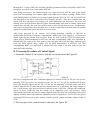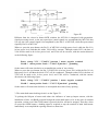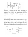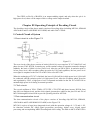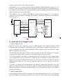
1
Principle and Maintenance of ABS535T
CONTENTS
Chapter I Overview of ABS535T
1、Description of Functions
2、Block Diagram of Player
3、Composition of IC for Player
Chapter II Operating Principle of Servo Circuit
1、Processing Procedure of Digital Signal
2、Processing Procedure of Control Signal
Chapter III Operating Principle of Decoding Circuit
1、Control Circuit of System
2、Audio and Video Output Circuit
Chapter IV Operating Principle of Power Board
1、Block Diagram
2、Operating Principle of Circuits
Chapter V Operating Principle of Panel
1. Operating Principle
Chapter VI Troubleshooting
Appendix: Functions of IC Pins
Important prompt:
This type player employs two kinds of decks, SF-HD62 and SF-HD60, and
corresponding software of these two types of decks are different, therefore please
pay special attention during deck changing in the maintenance. Corresponding decks
should be changed with the same type of original ones, otherwise the player will be
out of order. Identification of decks is shown as figures:
SF-HD62
SF-HD60
Operating Principle Analysis of ABS535T
Chapter I Overview of ABS535T
ABS535T is a medium- low-grade model integrating with video disc
and power amplifier, with the following major features:
1. The layer adopts “Sanyo loader+MT1389”solution;
2. The power amplifier adopts the digital power amplification circuit,
with the power IC of TAS5112DFD; it has low distortion level;
3. The audio process adopts TAS5508 , with high integration and high
performance and price ratio;
4. It has the function of radio reception, and the tuner adopts Sanzhenxing
DTS-44K(CE)module;
5. The power supply adopts the switching power, with compactness, high
efficiency and stable performance;
6. Equipped with SCART(CVBS/RGB)port;
7. Accessory channel input/output function;
8. Headphone output function;
9. Karaoke and automatic accompaniment function
10. “RDS”function;
II. Block Diagram of ABS535T Complete Player and IC Function Table :
Radio reception head
composite
29LV160BE
S terminal
16M ROM
MT1389
Sany
Power
Audio D/A,power
Refor
load drive
SDRAM
Figure 1
Y/Cb/Cr
6-way
HCU04
fiber,
Progressive
load
MPEG decoder
feed
main
Digital signal
track
BA5954
Servo
drive
focus
4340,7265
Digital servo
deck
status
AV output circuit
AT24C02
Panel
Y/Pb/Pr
VGA
III. Function Table of ICs for ABS535T
Circuit
Board
Deck
Main
Board
Panel
Power
Board
Amplifier
board
No
Name
Function
Sanyo
U201
MT1389
U202
AT24C02
Pick- up of disc signal
RF signal processing, digital signal
processing, servo processing, MPEG
decoding, line scan, system control
Series EEPROM, status memory
U205
HCU04
Hex inverter
U209
U211
LM1117MP-1.8
AE45164016
1.8v voltage-regulated power supply
64Mbit SDRAM
U214
29LV160BE
16Mbit FLASH ROM
U302
N102
D5954
SD16311
4-channel servo driver circuit
Panel control, VFD display drive
N103
REMOT
Remote receptor
U501
0380
Switching power circuit
U502
HS817
Photo-electric coupler
U503
HA17431
U11
LM7805
U505
0880
2.5V reference voltage comparator
5V 3-terminal voltage-regulated
power supply
Switching power circuit
U506
U507
HS817
LM431
Photo-electric coupler
2.5V reference voltage comparator
N12
5508
Digital signal processing
N13/14
N8/9
N10/11
5112
TLV272
RC4580
Power amplification
Operational amplification
Digital signal amplification
Chapter II Operating Principle of Servo Circuit
I. Digital Signal Processing Procedure
ABS535T adopts Sanyo double beam super error correction deck and MTK decoding solution,
and its servo circuit mainly consists of preposition signal processing, digital servo processing,
digital signal processing IC MT1389 and driver circuit BA5954. MT1389 is also a main part of the
decoding circuit.
The A, B, C, D, E, F, SA, SB and RFO signal transmitted from the deck are mainly inputted
through the 2-13 pins of MT1389, and after amplifying treatment of built- in amplifier of MT 1389,
the signals are treated in two parts within MT1389:
After being processed by the internal digital servo signal circuit of MT1389, part of the signal
forms into corresponding servo control signal, and output focus (FOSO), tracking (TRSO), main
shaft (DMSO) and feed (FMSO) servo control signal from the P42, P41, P37 and P38 of MT1389
and send them to the driver circuit BA5954 to amplify the drive. After drive amplification, the
signals will drive the focus coil, tracking coil, main shaft motor and feed motor. The focus and
tracking servos will be used to adjust the object lens and enable laser beam to identify signal from
compact disc correctly; the feed servo will be used to drive the laser head to move longitudinally,
and scan the compact disc; the main shaft servo is used to control the main shaft motor to read the
signals in constant linear speed and drive the disc to rotate.
After being processed by the internal VGA voltage-controlled amplifier of MT1389 in
amplification and balance frequency compensation; another part of the signals is converted into
digital signal by the internal A/D converter. When the deck reads the CD/VCD signals, these
signals will be EFM demodulated in MT1389, and after accomplishing CIRC error regulation in
internal MT1389, output to the next grade to carry out audio and video decoding; when the deck
reads the DVD signals, these signals will be ESM demodulated in MT1389, and after
accomplishing RSPC error regulation in internal MT1389, output to the next grade to carry out
audio and video decoding.
II. Processing Procedure of Control Signal
1. Automatic control of laser power, with the circuit shown as the Figure II:
Figure II
MT1389 is integrated with APC (automatic light power control) circuit. Its Pin 20 is the pin for
inputting VCD laser power rate detection signal, the Pin 21 is the pin for inputting DVD laser
power rate detection signal, and the Pin 23 is the pin for outputting VCD laser power rate drive
control. When the Pin 23 finds that the laser output power rate is too strong, the output voltage on
Pin 23 will increase after the processing of internal circuit of MT1389, and then the conduction
degree of V302 (2SB1132) and the voltage on its integration polar will decrease, which
consequently lead to the decrease of voltage supplied to the laser tube, the weakening of laser head
lighting, and thus achieve the automatic adjustment on laser output power. The Pin 22 is the pin for
outputting DVD laser power drive control, with the specific control procedure similar to that of
VCD.
2. The tray open/close control circuit is shown as the Figure III:
Figure III
Different from the circuit in former MTK solution, the MT1389 is integrated with preposition
signal processing circuit, so the tray open/close control signals are accomplished by MT1389, that
is to say, the close control signal is accomplished by the Pin 51 of MT1389, while the open control
signal by Pin 39 of MT1389.
When we press the open button, the Pin 51 of MT1389 is in high power level, while the Pin 39 is
in low power level, and then the triode V308 will be on-state. Through resistor R323, the base of
V306 will be made to be in low power level, and V306 will be on-state, with the current direction
as the following figure:
Power voltage VCC ? V306E-C junction ? motor negative terminal
LOAD- ? motor positive Load +? V308 C-E junction ? grounding
So the motor will rotate clockwise to accomplish the action of tray closing.
When we press the open button, the Pin 51 of MT1389 is in low power level, while the Pin 39 is in
high power level, and then the triode V307 will be conducted. Through resistor R324, the base of
V309 will be made to be in low power level, and V309 will be conducted, with the current
direction as the following figure:
Power voltage VCC ? V309E-C junction ? motor negative terminal
LOAD- ? motor positive Load +? V307 C-E junction? grounding
So the motor will rotate anti-clockwise to accomplish the action of tray opening.
3. The main shaft motor braking circuit is as the Figure IV:
To prolong the lifespan of motor and reduce the influence of start- up impact current, with the
installation of disc, our R&D personnel design the main shaft motor to be in the state of constant
operation, so that even if the STOP button is pressed, the disc will not be stopped. Therefore, when
we press the OPEN button, a braking signal is required to stop the rotation of main shaft motor
immediately to accomplish the opening action in a short time.
Figure IV
During playing, if we press the OPEN button, the main shaft drive signal will disappear, and
because of inertia, the main shaft motor is still in operation. As the electromotive force generated
in the operation of motor receives the induction voltage on sampling resistors R321 and R340,
which, through the resistor R319 and R320, is added to the Pin 36 and Pin 35 of MT1389, and
outputted from the Pin 34 after internal processing for amplification in MT1389, and delivered to
Pin 47 of MT1389 through R318. After the internal A/D conversion and corresponding processing,
an instant motor reversal braking signal will be outputted from the Pin 37 of MT1389 to stop the
rotation of main shaft motor immediately, so as to ensure the standstill of the disc when opening
the player.
III. Servo drive circuit
The servo drive of the playe r is accomplished through a piece of 4-channel dedicated drive circuit
BA5954, with the circuit as Figure V:
The 4 servo control signals generated in digital servo circuit processing of MT1389, i.e. focusing
control FOSO, tracking control TRSO, feed control FMSO and main shaft control DMSO signals,
are added to the pins 1, 26, 23 and 5 of BA5954 respectively, and after drive amplification of
BA5954, the focusing and tracking drive signals will be outputted from the pins 13 and 14 and
pins 15 and 16 of BA5954 respectively, and added to the focusing and tracking coils to drive the
light head to accomplish the actions of focusing and tracking.
The feed and main shaft drive signals will be outputted from the pins 17 and 18 and pins 11 and 12
of BA5954 respectively, and added to the feed motor and main shaft motor to drive the light head
to move longitudinally and enable the disc to rotate in constant linear speed.
The STBY on Pin 28 of BA5954 is an output-enabling signal, and only when the pin is in
high power level, there will be output of drive voltage on the output terminal.
Chapter III Operating Principle of Decoding Circuit
The decoding circuit of the player mainly consists of decoding chips (including MT1389, SDRAM
AE45164016 and FLASH ROM 29LV160BE) and audio DAC CS4360.
I. Control Circuit of System
1. Reset circuit is as the Figure VI:
Figure VI
The reset circuit of the player consists of triode Q204 9014, reset capacitor TC217 100uF/16V and
phase inverter U205 HCU04. In starting up, as the terminal voltage of capacitor cannot be changed
suddenly, the basic of Q204 is in low power level. After the cut-off of Q204, its emission polar is
in low power level, after secondary phase inversion by U205 and regulation, the low power level
reset signal is outputted to the Pin 110 of MT1389 to reset MT 1389.
When the recharging of TC217 is finished, the base of Q204 will be in high power level, Q204 will
be conducted, and the emission polar is in high power level. After the secondary phase inversion
and regulation by U205, a high power level is outputted and added to the Pin 110 of MT1389 to
maintain high power level during its normal operation.
2. Clock circuit
The crystal oscillator of X201 27MHz, C275/27PF, C276/27PF and phase inverter HCU04 form
into clock oscillation circuit, and the clock signals generated are added to the pins 229 and 228 of
MT1389 through R244 and 4248 to provide operating clock for MT1389.
3. Data communication circuit
The data communication circuit of the player consis ts of decoding chip MT1389, SDRAM,
AE45164016 and FLASH ROM 29LV160BE, as the Figure VII:
MT1389 is a piece of super large integrated circuit, with the operation voltage of +3.3V and +1.8V.
Its functions include: RF small signal preposition processing, digital servo, digital signal
processing and accomplishing MPEG decoding and video coding. The built- in MCU of MT1389 is
also the system control circuit of the whole player.
AE45164016 is a piece of 4M*16bit large capacity SDRAM, with the operation voltage of +3.3 V.
In DV971, the 6ns module is adopted, with high speed and the maximum operation frequency up
to 166MHz. Its main function is for operation buffer storage of decoding chip MT1389 to store the
audio and video data stream in decoding.
29LV160BE is a piece of 16Mbit FLASH ROM, with the operation voltage of +3.3V, mainly for
storing the user’
s information including OSD character information, operational microcode and
LOGO in start- up.
VD
DMA0—DMA11
A0—A21
MT1389
RY/BY
DQ0—DQ15
AD0—AD7
15
29LV160BE
26
28
11
DCE
DRD
DWR
77
79
66
47
BYTE
113
137
156
157
140
139
142
138
145
143
AE45164016
15
39
38
37
18
17
19
16
20
21
DQML
DQMH
CLK
CKE
RAS
CAS
CS
WE
BA1
BA0
GND
Figure VII
II. Audio and Video Output Circuit
1. Video output circuit
ABS535T can not only output three types of alternating- line video signal (including CVBS
composite video, S terminal Y-C signal and Y/Cb/Cr color difference signal), but also output two
types of progressive line video signal (including Y/Pb/Pr progressive line color difference signal
and VGA progressive line signal).
The decoding chip MT1389 has built- in video encoding circuit for direct output of analogue
composite video signal CVBS, S terminal, color difference signal and VGA signal.
The CVBS composite video signal is outputted from the Pin 198 of MT1389, the S terminal signal
Y-C is outputted from the pins 194 and 196 of MT1389, the color difference signal and the R-B-G
signal of VGA port is outputted from the pins 203, 202 and 200 of MT1389, the row and field
synchronization signals of VGA port are outputted from the pins 207 and 205 of MT1389
respectively.
To mention specifically, the alternating- line color difference signal, the progressive line color
difference signal and progressive line R-B-G signal are outputted from the same pin, therefore the
signal output shall be selected according to the ports of TV, otherwise there will be only sound but
without picture display.
2. Audio output circuit
Audio signals processed by MT1389 output 5-track data signals through pin 217, pin 218 and pin
219 and 5-channel clock signals through pin 214 and pin 215. These signals after passing through
IC 74HCT125 are transmitted to audio signal processing IC TAS5508 to be processed (specific IC
data please refer to Attachment), then 10 groups of PWM signals are output, six of which are
transmitted to power amplifying parts, two of which to headphone output and two of which to
auxiliary channel output.
Six groups of signals transmitted to power amplifying IC are processed by surrounding and super
DBB sharing an N13 IC TAS5508, and by main sound channel and center sharing an N14 IC
TAS5508. Signals are amplified here, for they are digital high frequency signals, they have high
efficiency; meanwhile power IC has low colorific value. Amplified signals are still digital signals,
in order that they can be output through loudspeaker, amplified digital signals still have to be
processed before outputting.
For PWM signals containing audio signals, since high frequency signals have high frequency and
are beyond audibility range of human ears, we can ignore impacts of high frequency signals and
reduce low frequency audio signals only during processing.
TAS5508 is an 8-channel pulse width modulated high performance IC, and applicable in
processing most digital audio signals. Between 20Hz and 20KHz, it has excellent noise factor and
dynamic range. It has following features:
1、
2、
3、
4、
Automatically control clock speed and digital sampling speed;
8 groups of audio input channels;
8 groups of PWM output can be changed into 6-channel stereo line output or 8-channel
line output;
Line output is a different input open loop amplifier driven by a group of PWM signals.
IC TAS5112 is a high performance audio power amplifier. Bridging with 6O loading, each channel
can output 50W. It has 95DB dynamic range, low distortion degree and low rate of heat generation
with power efficiency up to 90%. It also has functions of low-voltage protection, high-temperature
protection, overflow protection, etc. At the same time, it has built- in driving power adjustment gate
circuit. It is applicable in family video, DVD receiver, mini music center, etc. Detailed IC
introduction see Attachment.
When in normal disc reading, digital signals and clock signals from 1389 are transmitted to pin 26
to pin 31 of IC TAS5508 through IC 74HCT125 gating. If no headphone is inserted, PH-SEL is of
high level, as well as when MUTE is normal. And pin 37 of TAS5508 is also of high level. All data
lines and clock lines can be detected by oscilloscope. One group of signals from 5508 is
transmitted to N8 and N9, then output through auxiliary channel. Another group is transmitted to
headphone; other PWM signals are transmitted to amplifying parts of amplifier.
When headphone is inserted, PH-SEL signal is forcibly shorted to earth, and turns to low level,
meanwhile amplifier is muted.
This amplifier has functions of radio reception, auxiliary channel output and karaoke. All external
inputs after N3 CD4052 gating and N7 CS5340 analog-to-digital conversion are transmitted to
MT1389. Rear processing and output is the same as the signal output flow in normal disc reading.
When in disc reading, system defaults to gate karaoke input, therefore you can open karaoke when
playing disc. This amplifier also has automatic accompaniment function, when playing VCD,
system detects external input and automatically screen to human sound signal in the disc, while
only saves sound accompaniment.
ABS535T has the function of radio reception, and can also receive RDS signal. The radio head
control lines CE, DI, CL and DO are controlled by 28 array lines connecting to MT1389 control.
When any of the controlling lines is in abnormality, the radio reception will be in malfunction. The
RDS signal received by radio head will be delivered to the dedicated IC SAA6588 for processing.
Chapter IV Operating Principle of Power Board
I. Block Diagram
This amplifier has two groups of power supply; one is of low voltage for decoding board and low
power ICS, the other is of higher voltage for power amplifying IC. But their design principles, we
only draw one functional block diagram of them:
II. Introduction of Circuit Principle
220V alternating current is loaded on D501-D504 integrated bridging rectification circuit through
power plug, fuse tube, voltage dependent resistor R501 and common mode rejection BC501 and
L501. Diode adopts IN4007 which ahs better PPR and higher withstand voltage value than IN4001.
Output 311V direct current after being bridging rectified is loaded on two transformers through
TC501 filtering and transmitted to DRAIN control pins of switch modules U501 and U502.
Service voltage of power on IC after being directly rectified and filtered is divided by resistors to
serve IC. Diode D508, capacitor C516 and resistor R516 form absorption circuit to provide
discharge circuit of reverse electromotive force for 1-4 coils of transformers. Pin FB controlling IC
is feedback control pin, so you should decide on/off time of pulse width according to current
intensity on it to ensure stability of output voltage.
There are 5 branch circuits coupled to sub-grade through transformer.
1. Voltage output from pin 11 and pin 13 of transformer T501 outputs a group of +28V voltage
for power amplifying IC after being rectified and filtered.
2. Voltage output from pin 16 of transformer T501 outputs a group of +12V voltage after being
rectified and filtered. +12V voltage is stabilized into a group of +5V voltage by IC LM7805.
3. Voltage output from pin 14 of transformer T501 outputs +5V voltage and provide voltage for
one end of photo-electric coupler U502 after being rectified and filtered.
4. Voltage output from pin 12 of transformer T501 outputs +3.3V voltage and provide a group of
stable voltage for CPU after being rectified and filtered.
5. Voltage output from pin 9 of transformer T501 outputs a group of 21V voltage for displaying
driving IC after being rectified and filtered. Clamp ZD501 of -21V provide heater voltage for
panel display screen. Grounding direct voltage of FL+ and FL- is about -16V.
Operating principles of two groups of switch power are the same, therefore we will only analyze
the group providing +3.3V voltage for CPU here:
Feedback sampling of this group comes from 3.3V and supplies for photocupler HS817 through
D516 and R506. At the same time, it is divided through R508 and R509 for reference voltage pin R
of 2.5V comparator. When 3.3V becomes higher, pin KA of comparator is on; and the voltage is
transmitted to pin 4 of switch IC 5L0380R after photoelectric coupling through HS817 to reduce
on time of internal switch tube. And thus it reduces transformer coupling and decreases output of
3.3V voltage to achieve automatic adjustment and control, and vice verse.
It has to be noted that in this switching power reference voltage comparator IC of two groups of
switching power are different. For voltage of the group supplying power for amplifier is higher, it
adopts LM431 which has better performance and higher withstand voltage. And voltage of the
group supplying power for 3.3V is lower, it adopts 17431. For two ICs are different, you should
pay special attention to distinguish them from each other. They cannot be used mixing.
Chapter 5: Panel control and VFD display circuit
The panel mainly consists of VFD screen, driver ICD16311, remote receptor HS0038A2 and
button and indicator display circuit, mainly for accomplishing man-player dialogue and display of
operation status.
The structural drawing is as follows:
Keystroke
control
VFD
U401
display
IC D16311
VFDST
U201
VFDCK
VFDAT MT1389
Panel indicator control
Remote
receiving
Figure XI
MT1389 will control the U401 IC D16311 to display the operation status of the player through the
VFDST status, VFDCK clock and VFDAT data, under the control of CPU built in MT1389,
receive the user control commands sent by D16311, and control the controlled circuit of the player
to limit the player to operate in specified status.
When the user operates the panel buttons, the control command is sent to the IC D16311 through
keyboard-scanning circuit, and through internal decoding drive, the IC D16311 outputs the control
data from the pins 5 and 6 (VFDAT) to the built- in CPU of MT1389, which will realize the control
on the controlled circuit, and control the VFD through IC D16311.
VFD401 is a vacuum fluorescence screen, and its biggest feature is its high brightness.
Its operation principle is similar to the kinescope of TV. The pins 1, 2, 34 and 35 are for filament
power supply; the pins 27-32 are GRID poles, each GRID has 16 different characters of display;
the pins 4-19 are SEG poles, and the CPU control the SEG poles through its control on IC D16311,
and display the characters of corresponding operation status on the screen.
The remote reception circuit mainly consists of remote receptors HS0038A2, of which the pin 1 is
for grounding, the pin 2 for power supply, the pin 3 for output of reception signal, and they are all
connected directly to the CPU in MT1389 to control the corresponding circuit.
This player has headphone output function. A pin in the headphone directly connects to TAS5508. When the
headphone is inserted, detection line H-DET grounds and turns into low level. When pin 12 of TAS5508 turns
into low level, parts of output of amplifier are muted. When in normal condition, this detection pin is of high
level around 3.3V.
Troubleshooting
I. Voltage on key points of ABS535T
Demoding circuit:
Reset:
1. U205 (HC U04): 8 pins, around 5V;
2. MT1389: 110 pins, around 5V;
3. FLAHS ROM: 12 pins, around 5V
Clock:
27MHZ crystal oscillator two ends: Around 0.77V.
I2 C bus SDA: 3.3V
I2 C bus SCL 3.3V
Servo circuit:
LD01: 3.3V;LD02:3.3V
V301 and V302 electron collector LD voltage: 2.3V
BA5954 pin 4 base voltage: 1.4V
BA5954 pins 15 and 16 tracking drive output: Around 2.5V
BA5954 pins 17 and 18 feed drive output: Around 2.5V
BA5954 pins 13 and 14 focus drive signal output: Around 2.5V
BA5954 pins 11 and 12 main shaft drive output: Around 2.5V
BA5954 pin 1 focus control signal input: 1.4V
BA5954 pin 5 main shaft control signal input: 1.4V
BA5954 pin 26 tracking control signal input: 1.4V
BA5954 pin 23 feed control signal input: 1.4V
Amplifier circuit:
TAS5508 pin 9 power supply pin 3.3V
TAS5112
32、33、40、41、44、45、52、53, 28V。\
II. Troubleshooting of main troubles
No picture, no sound, no VFD
display
Check if power supply of MT1389
3.3V, 1.8V is right?
NO
Check the voltage of power board,
and check if the decoding board is
short circuit to the grounding.
YES
If the clock signal output XO
and XI is right?
Check if clock oscillating circuit
27M crystal oscillator, C275,
C276, R224, R248 are damaged?
NO
YES
Check if reset signal URST# is
in 5V high level?
YES
Check if I2C bus, SDA, SCL 3.3V
voltage is right?
Check if SDRAM CLK, CS, RAS, CAS,
WE communication signals are right?
NO
Check if the reset circuit which is
comprised by HCU04 and Q204 etc.
is in working order?
Check if the AT24C16, CS4360,
MT1389 SDA and SCL are short
circuit to grounding, if R259 and R260
are in working order?
Check if FLASH ROM, URST, DCE,
DRD, DWR signals are right?
Check if the connection between
MT1389, FLASH, SDRAM is right?
Check if the MT1389, SDRAM and
FLASH are damaged?
Do not read disc
Check if the feed control
input of BA5954 Pin 23 is
1.4V?
laser
head has feed action.
Check
if
the
Check if the
connection from
BA5954 to MT1389
is open circuit?
NO
YES
Check if BA5954 pin 17,18
have 2.5V voltage output?
Check feed motor
and its connection.
YES
YES
NO
Check if BA5854 and the power
supply 5V are in working order?
Check if BA5954 pin 1
Check if laser head
has focus action?
has
focus
control
voltage input of 1.4V.
NO
Check if the
connection from
BA5954 to MT1389
is open circuit?
YES
Check if the voltage output of
BA5954 pin 13 and 14 are
2.5V?
YES
NO
Check if BA5854 and 5V power
supply are in working order?
Check focus coil and its
YES
connection.
Check if there is
laser coming out
from laser head?
Check if the signal
voltage of LD01, LD02
is 3.2V?
NO
Check MT1389 and its
connection.
YES
YES
Check if the
main shaft
rotates?
Check if V301 and V302
electron collector voltage is
2.3V?
Check if the control
voltage of BA5954 pin 5
main shaft is 1.4V?
YES
Check if the laser head
and its array line are
right?
NO
Check if the connection from
BA5954 to MT1389 is open
circuit?
YES
Check if BA5954 pin 11
and 12 output is 2.5V?
YES
YES
NO
Check if MT1389
and its peripheral
circuit is right?
Check if BA5854 and 5V power
supply are in working order?
Check if BA5954 or main shaft
motor is damaged?
Attachment :Brief Introduction to IC Pins
I. MT1389
MT1389 adopts the LQFP 256 pin packaging and 3.3V/1.8V double voltage operation mode. It is a
piece of large-scale CD-ROM and DVD-ROM preposition processing CMOS integrated circuit
with excellent performance, and a single chip dedicated to CD/VCD/DVD player. It contains
focusing servo error amplification, tracking servo error amplification and RF level output servo
control, including the following main functions:
RF small signal preposition processing, mainly for carrying our corresponding processing and
amplification on the RF signals transmitted from the light head part, adjusting the laser output
power automatically, and identifying the VCD disc and DVD disc.
Digital servo processing can generate focusing, tracking, feed and main shaft servo control signals;
digital signal processing, accomplishing the EFM/EFM + demodulating of RF signals.
MPEG-1/MPEG-2/MPEG4/JPEG Video decoding chip, which can not only realize the decoding of
VCD and DVD, but also realize MPEG 4 network video decoding, being compatible to “network
movie”disc, and decipher JPED pictures to realize the function of digital photo album play.
On audio aspect, it can not only realize AC-3/DTS double decoding, decipher MP3, and is
also compatible to DVD-Audio decoding to achieve high- resolution sound restoration in 1000
times higher than CD.
By utilizing the 8032 microprocessor with built- in chip, MT1369E can also realize the system
control function of player, which simplifies the circuit design substantially.
The pin functions of MT1389 are as the following table:
Pin
Name
Function
1
AGND
Analogue grounding
2
DVDA
DVD-RF high- frequency AC coupling
signal A
3
DVDB
DVD-RF high- frequency AC coupling
signal B
4
DVDC
DVD-RF high- frequency AC coupling
signal C
5
DVDD
DVD-RF high- frequency AC coupling
signal D
6
DVDRFIP
DVD-RF high- frequency AC coupling
signal RFIP input
7
DVDRFIN
DVD-RF high- frequency AC coupling
signal RFIN input
8
MA
DVD-RAM main light beam RF DC
signal input A
9
MB
DVD-RAM main light beam RF DC
signal input B
10
MC
DVD-RAM main light beam RF DC
signal input C
11
MD
DVD-RAM main light beam RF DC
signal input D
12
SA
DVD-RAM auxiliary light beam RF DC
signal input A
13
SB
DVD-RAM auxiliary light beam RF DC
signal input B
14
SC
DVD-RAM auxiliary light beam RF DC
signal input C
15
SD
DVD-RAM auxiliary light beam RF DC
signal input D
16
CDFON
CD focusing error phase inversion input
17
CDFOP
CD focusing error phase input
18
TNI
3 light beam auxiliary PD signal phase
inversion input
19
TPI
4 light beam auxiliary PD signal phase
input
20
MDI1
Laser power monitoring input 1
21
MDI2
Laser power monitoring input 2
22
LDO2
Laser power monitoring output 2
23
LDO1
Laser power monitoring output 1
24
SVDD3
Servo 3.3V power supply
25
CSO/RFOP
Main servo signal output/RF phase
output
26
RFLVL/RFON
RF level output/RF phase inversion
output
27
SGND
Servo grounding
28
V2REFO
Reference voltage 2.8V
29
V20
Reference voltage 2.0V
30
VREFO
Reference voltage 1.4V
31
FEO
Focusing error signal output
32
TEO
Tracking error signal output
33
TEZISLV
Tracking zero crossover error input
34
OP_OUT
Sensing signal amplification output
35
OP_INN
Sensing signal phase inversion input
36
OP_INP
Sensing signal non- inverting input
37
DMO
Main shaft control signal output
38
FMO
Feed control signal output
39
TROPEN PWM
Tray Open signal output
40
PWMOUT1/ADIN9
First-route pulse width demodulating
signal output/AD universal input
41
TRO
Tracking control signal output
42
FOO
Focusing control signal output
43
USB_VSS
USB grounding
44
USBP
USB data
45
USBM
USB data
46
USB_VDD3
USB 3.3V power supply
47
FG/ADIN8
Motor sensing signal input/AD universal
input
48
TDI/ADIN4
Open position detecting signal input/AD
universal input
49
TMS/ADIN5
Close position detecting signal input/AD
universal input
50
TCK/ADIN6
BA5954 enabling signal output/AD
universal output
51
TDO/ADIN7
Tray close signal output/AD universal
input
52、97、122、
152、173、221
DVDD18
Digital 1.8V power supply
53-58
IOA2-7
Micro-controller address bit 2-7
59
HIGHA0
Micro-controller address bit 0
60、61
IOA18-19
Micro-controller address 18-19
62、85、94、116、
119、134、144、
148、161、163、
175、216、223
DVSS
Digital grounding
63
APLLCAP
Analogue phase lock loop external
capacitor
capacitor
64
APLLVSS
Analogue phase lock loop grounding
65
APLLVDD3
Analogue phase lock 3.3V power supply
66
IOWR
FLASH read control signal
67-72
HIGHA3-7
Micro-controller address bit 3-7
73、80、108、
127、141、155、
167、182、204、
212
DVDD3
Digital 3.3V power supply
74、75
HIGHA1-2
Micro-controller address bit 1-2
76
IOA20
Micro-controller address bit 20
77
IOCS
FLASH chip selection
78
IOA1
Micro-controller address bit 1
79
IOOE
FLASH output enabling
81-84
AD0-3
Micro-controller address/data bit 0-3
86-88
AD4-6
Micro-controller address/data bit 4-6
89
IOA21/ADIN0
Micro-controller address bit 21/AD
universal input
90
ALE
Micro-controller address enabling
91
AD7
Micro-controller address/data bit 7
92
A17
FLASH address bit 17
93
IOA0
Micro-controller address bit 0
95
UWR
Micro-processor reading operation
96
URD
Micro-processor reading operation
98
UP1_2-1_7
Micro-processor port
104
UP3_0
Micro-processor port
105
UP3_1
Micro-processor port
106
UP3_4
Micro-processor port
107
UP3_5
Micro-processor port
109
ICE
Micro-processor correction mode
enabling
110
PRST
Reset input
111
IR
Remote control signal input
112
INT0
Micro-processor interruption 0
113
DQM0
DRAM input output shielding signal
114
DQS0
DRAM input output shielding signal
115
RD7
DRAM data
117-118
RD5-6
DRAM data
120-121
RD3-4
DRAM data
123-125
RD0-2
DRAM data
126
RD15
DRAM data
128-133
RD9-14
DRAM data
135
RD8
DRAM data
136
DQS1
DRAM input output shielding signal
137
DQM1
DRAM input output shielding signal
138
RWE
DRAM writing enabling
139
CAS
DRAM column address selection
140
RAS
DRAM row address selection
142
RCS
DRAM chip selection
143
BA0
DRAM section address 0
145
BA1
DRAM section address 1
146
RA10
DRAM address
147
RA0
DRAM address
149
RA1-3
DRAM address
153
RVREF/ADIN3
Reference voltage/AD universal input
154
RCLKB
DRAM clock
156
RCLK
DRAM clock
157
CKE
DRAM clock enabling
158
RA11
DRAM address
159-160
RA8-9
DRAM address
162
RA7
DRAM address
164
RA4-6
DRAM address
168
RD13/ASDATA5
DRAM data/audio series data
169
RD27-30
DRAM data
174
RD26
DRAM data
176-177
RD24-25
DRAM data
178-179
DQM2-3
DRAM I/O shielding signal
180-181
RD22-23
DRAM data
183-188
RD16-21
DRAM data
189
DACVDDC
D/A conversion 3.3V power supply
190
VREF
Reference voltage
191
FS
192
YUV0/CIN
193
DACVSSC
D/A conversion grounding
194
YUV1/Y
Video signal YUV1 output/Y signal
output
195
DACVDDB
D/A conversion 3.3V power supply
196
YUV2/C
Video signal YUV2 output/C signal
output
197
DACVSSB
D/A conversion grounding
198
YUV3/CVBS
Video signal YUV3 output/CVBS signal
output
199
DACVDDA
D/A conversion 3.3V power supply
200
YUV4/G
Video signal YUV4 output/G signal
output
201
DACVSSA
D/A conversion grounding
202
TUV5/B
Video signal YUV5 output/B signal
output
203
YUV6/R
Video signal YUV6 output/R signal
output
205
VSYNC/ADIN1
Field synchronization signal output/AD
universal input
206
YUV7/ASDATA5
Video signal YUV7 output/audio series
data
207
HSYNC/ADIN2
Row synchronization output/AD
universal input
208
SPMCLK
209
SPDATA
210
SPLRCK
211
SPBCK/ASDATA5
213
ALRCK
Audio left and right sound channel clock
214
ABCK
Audio bit clock
215
ACLK
Audio DAC external clock
217-220
ASDATA0-3
Audio series data
222
ASDATA4
Audio series data
224
MC_DATA
Microphone digital audio input
225
SPDIF
Digital audio signal output
226
RFGND18
RF signal grounding
227
RFVDD18
RF signal 1.8V power supply
228
XTALO
Clock output
229
XTALI
Clock input
230
JITFO
RF small signal output
231
JITFN
RF small signal phase inversion and
amplification input
232
PLLVSS
Phase lock loop grounding
233
IDACEXLP
234
PLLVDD3
Phase lock loop 3.3V power supply
235
LPFON
Amplifier loop wave filtration output
236
LPFIP
Amplifier loop wave filtration input
237
LPFIN
Amplifier loop wave filtration input
238
LPFOP
Amplifier loop wave filtration output
239
ADCVDD3
A/D conversion 3.3V power supply
240
S_VCM
241
ADCVSS
242
S_VREFP
243
S_VREFN
244
RFVDD3
RF 3.3V power supply
245
RFRPDC
DC RF error signal input
246
RFRPAC
AC RF error signal input
247
HRFZC
High- frequency RF signal zero
crossover checking
A/D conversion grounding
crossover checking
248
CRTPLP
249
RFGND
250
CEQP
251
CEQN
252
OSP
253
OSN
254
RFGC
255
IREF
Reference current
256
AVDD3
Analogue 3.3V power supply
RF grounding
Ⅱ.BA5954
BA5954 is a piece of servo drive single-piece integrated circuit, with built- in 4-channel BTL drive
circuit. It can receive directly the PWM control signal output by digital servo IC, and with internal
wave filter and drive amplifier, it pushes the execution part in the servo mechanism to accomplish
the focusing, tracking, feed and main shaft drives. BA5954 adopts the packaging of 28 pins.
Note: The 28 pins of BA5954 are for outputting effective control signal, which is provided by the
50 pins of MT1389. When the signal is in high power level, BA5954 output is in validity, while the
signal is in low power level, BA5954 will not be activated, and its output ports are in the state of
cutoff.
The functions of pins of BA5954 are as the following table:
Pin
Name
Function
1
VINFC
Focusing control signal input
2
CF1
External feedback loop
3
CF2
External feedback loop
4
VINSL+
Forward control input, connected to the reference voltage
5
VINSL-
Main shaft control signal input
6
VOSL
External feedback resistance
7
VINFFC
Focusing feedback signal input
8
VCC
5V power supply
9
PVCC1
5V power supply
10
PGND
Grounding
11
VOSL-
Main shaft drive inverse voltage output
12
VO2+
Main shaft forward voltage output
13
VOFC-
Focusing drive inverse voltage output
14
VOSC+
Focusing drive forward voltage output
15
VOTK+
Tracking drive forward voltage output
16
VOTK-
Tracking drive inverse voltage output
17
VOLD+
Feed drive forward voltage output
18
VOLD-
Feed drive inverse voltage output
19
PGND
Grounding
20
VINFTK
Tracking feedback signal input
21
PVCC2
5V voltage
22
PREGND
Grounding
23
VINLD
Feed control signal input
24
CTK2
External feedback loop
25
CTK1
External feedback loop
26
VINTK
Tracking control signal input
27
BIAS
1.4 reference voltage input
28
STBY
Enabling control signal
III. 29LV160BE
29LV160BE is a type of 16Mbit FLASH memory manufactured via 0.23um technology, with 16
byte width DQ0-DQ15, memory capacity of 16M bit, operation voltage of 3.3V, and packaging
method of 48 pins TSOP. The specific operation mode is as the following table:
DQ8~DQ15
Operation
status
CE
OE
WE RESET A0~A19 DQ0~QD7
BYTE:high
BYTE: Low
level
level
Read
L
L
H
H
Ain
Dout
Dout
High resistance
Write
L
H
L
H
Ain
Din
Din
High resistance
Waiting
H
×
×
H
×
high
high resistance high resistance
resistance
Output
forbidden
L
H
H
H
×
High
High resistance High resistance
resistance
Reset
×
×
×
L
×
High
High resistance High resistance
resistance
The functions of pins of 29LV160BE are as the following table:
Pin
Name
Function
15
RY/BY
Ready/system is busy
1~9、16~25 、48
A0~A19
20-byte address bus
26
CE
Chip enabling
27、46
VSS
Grounding
28
OE
Output enabling
29~36、38~44
DQ0~DQ14
15-byte data bus
37
VCC
5V power supply
45
DQ15/A-1
Character extension mode as the data line; byte expansion
mode as the address line
47
BYTE
Adopting 8-byte (in low level) or 16-byte output mode (in
high level)
11
WE
Write enabling
12
RESET
Reset, valid in low level
NC
10、13、14
Neutral pin
IV. AE45164016
AE45164016 is a type of 64Mb (4Banks×1M×16bit) CMOS synchronization DRAM, featured
with large memory and high speed. Its operation power voltage is 3.0V~3.6V, and it is packaged in
54-pin TSOP.
The functions of pins of AE45164016 are as the following table:
Pin
Name
Function
1、14、27
VDD
+3.3V power supply
2、4、5、7、8、10、11、
13、42、44、45、47、48、
50、51、53
DQ[0~15]
16-byte data bus
3、9、43、49
VDDQ
+3.3V power supply
6、12、46、52
VSSQ
Grounding
28、41、54
VSS
Grounding
15
LDQM
Data I/O shielding signal
16
WE
Write control signal
17
CAS
Column address gate signal
18
RAS
Row address gate signal
19
CS
Chip selection signal
20
SD-BS0
Section address 0 gate signal
21
SD-BS1
Section address 1 gate signal
22~26、29~35
MA[0~11]
12-byte address bus
36、40
NC
Neutral pin
37
CKE
Clock enabling signal
38
CLK
System clock input
39
UDQM
Data I/O shielding signal
V. Pin Functions of TAS5508
TAS5508 is a high performance audio signal processing IC provided by TI. It has 8-channel PWM
processing function, perfect protective functions, low distortion degree and excellent dynamic
characteristics.
1
2
VRA_PLL
PLL_FLT_RET
Provide 1.8V reference voltage for PLL
PLL external filtering circuit
3
4
PLL_FLTM
PLL_FLTP
PLL inverted input pin
PLL non-inverted output pin
5
6
AVSS
AVSS
Analog grounding
Analog grounding
7
8
VRD_PLL
AVSS_PLL
Provide 1.8V reference voltage for PLL
PLL analog grounding
9
10
11
AVDD_PLL
VBGAP
RESET
PLL provides 3.3V voltage
Provide 1.2 V reference voltage
System reset signal, valid in low level
12
13
HP_SEL
PDN
Microphone input/output selection
Switch-off voltage, valid in low level
14
MUTE
15
DVDD
Software muting control, valid in low
level
3.3V digital power supply
16
17
DVSS
VR_DPLL
Digital grounding pin
Provide 1.8V reference voltage for PLL
18
19
20
OSC_CAP
XTL_OUT
XTL_IN
Oscillation capacitance
Crystal oscillation output pin
Crystal oscillation input pin
21
22
RESERVED
TBASE_SEL
Connect to digital grounding
Connect to digital grounding
23
RESERVED
Connect to digital grounding
24
25
SDA
SCL
Digital signal
Clock signal
26
27
LRCLK
SCLK
RF channel clock signal
Audio clock signal
28
29
SDIN4
SDIN3
Audio data input pin
Audio data input pin
30
31
SDIN2
SDIN1
Audio data input pin
Audio data input pin
32
33
34
PSVC
VR_DIG
DVSS
Control PWM signal output
1.8V reference voltage of digital core
Digital grounding
35
36
DVSS
DVDD
Digital grounding
3.3Vdigital service voltage
37
BKND_ERR
38
DVSS
Logic error control pin, valid in low
level
Digital grounding
39
VALID
Output PWM signal is displayed normally,
valid in high level
40
41
PWM_M_1
PWM_P_1
PWM signal output 1
PWM signal output 1
42
43
PWM_M_2
PWM_P_2
PWM signal output 2
PWM signal output 2
44
45
PWM_M_3
PWM_P_3
PWM signal output 3
PWM signal output 3
46
47
PWM_M_4
PWM_P_4
PWM signal output 4
PWM signal output 4
48
49
VR_PWM
PWM_M_7
1.8V reference voltage of PWM core
PWM signal output 7
50
51
52
PWM_P_7
PWM_M_8
PWM_P_8
PWM signal output 7
PWM signal output 8
PWM signal output 8
53
54
DVSS_PWM
DVDD_PWM
Digital grounding for PWM signal
3.3V voltage for PWM signal
55
56
PWM_M_5
PWM_P_5
PWM signal output 5
PWM signal output 5
57
58
PWM_M_6
PWM_P_6
PWM signal output 6
PWM signal output 6
59
60
PWM_HPML
PWM_HPPL
Headphone output PWM left channel
Headphone output PWM left channel
61
62
PWM_HPMR
PWM_HPPR
Headphone output PWM right channel
Headphone output PWM right channel
63
64
MCLK
RESERVED
3.3V clock input
Connect to digital grounding
IV. IC TAS5112
IC TAS5112 is an audio power amplifier of high performance made by TI. Bridging with 6O
loading, each channel can output 50W. It has 95DB dynamic range, low distortion degree and low
rate of heat generation with power efficiency up to 90%. It also has functions of low-voltage
protection, high-temperature protection, overflow protection, etc. At the same time, it has built- in
driving power adjustment gate circuit. Basic functions of its pins are as shown in the following
table:
Pin
31
Name
BST_A
Function
Auxiliary power
42
43
BST_B
BST_C
Auxiliary power
Auxiliary power
54
23
BST_D
DGND
Auxiliary power
Digital input output reference
16
DREG
Digital service voltage adjustment
circuit
12
DREG_RTN
Digital service voltage adjustment
circuit
Input output reference
25
DVDD
1,2,22,24,28, GND
29,27,36,37,
48,49,56
Grounding
3,26
GREG
Driving voltage adjustment of gate
circuit
30,55
15
GVDD
M1(TST0)
Digital voltage adjustment
Mode selection
14
13
M2
M2
Mode selection
Mode selection
4
OTW
34,35
38,39
OUT_A
OUT_B
Protective pin in the high
temperature
Output pin A
Output pin B
46,47
50,51
OUT_C
OUT_D
Output pin C
Output pin D
32,33
40,41
PVDD_A
PVDD_B
Service voltage of half bridge A
Service voltage of half bridge B
44,45
52,53
PVDD_C
PVDD_D
Service voltage of half bridge C
Service voltage of half bridge D
20
21
PWM_AM
PWM_AP
Inverted input pin
Non-inverted input pin
18
17
PWM_BM
PWM_BP
Inverted input pin
Non-inverted input pin
10
11
PWM_CM
PWM_CP
Inverted input pin
Non-inverted input pin
8
7
PWM_DM
PWM_DP
Inverted input pin
Non-inverted input pin
19
RESET_AB
Reset signal , valid in low level
9
6
RESET_CD
SD_AB
Reset signal , valid in low level
Signal switch off control
5
SD_CD
Signal switch off control
IIV. IC SE5532
IC SE5532 is an amplified IC with dual channels and low noise. Compared to most other amplified
ICs, it has lower noise, better output performance and power bandwidth. Its main features are:
small-signal bandwidth; its direct voltage gain can be up to 50000 and alternating voltage gain can
be up to 2200 under 10KHz; its power bandwidth can be up to 140KHz; relatively larger power
supply range; fast slewing rate. Basic functions of its pins are as shown in the following table:
Pin
Name
Function description
1
2
OUTPUT-A
INVERTING INPUT-A
Output channel A
Inverted input A
3
4
NON-INVERTING INPUT-A
V-
Non-inverted input A
Negative power supply
5
6
NON-INVERTING INPUT-B
INVERTING INPUT-B
Non-inverted input B
Inverted input B
7
8
OUTPUT-B
V+
Output channel B
Positive power supply
IIIV、CS 5340
CS 5340 is an IC of analog/digital conversion; it can be applied to sample, analog-to-digital
conversion and filter. During continuous input, its sampling frequency can be up to 200KHz. Its
main features are as follows:
24 bytes conversion; supported audio frequency can be up to 192KHz; under power of 5V, its
dynamic range can be up to 101DB; it has high pass filter to filter direct current. Functions of its
pins are as follows:
Pins
Name
1
M0
Function description
Mode selection
16
2
M1
MCLK
Mode selection
Master clock signal
3
4
5,14
VL
SDOUT
Logic voltage power supply
Audio data output
6
7
GND
VD
SCLK
Grounding
Digital power
DRAM clock signal
8
9
LRCK
RST
RF clock signal
Reset signal
10
12
AINL
AINR
Analog input
Analog input
11
13
VQ
VA
Quiescent voltage
Analog power
15
FILT+
Reference voltage
F
B
A
RFO
IOA
D
C
V302
2SB1132-S
LDO-AV33
C241
104
MO_VCC
VCC
22
23
24
25
26
27
28
20K
151
TRSO
V1P4
STBY
R313
10K
R319
150K
PREGND
VINLD
CTK2
CTK1
VINTK
BIAS
STBY
VINFFC
VOSL
VINSLVINSL+
CF2
CF1
VINFC
C307
2200pF
R317
680K
R320
150K
R340
C242
104
TC205
47uF/16V
C243
104
TC204
47uF/16V
14
13
12
11
10
9
8
7
6
5
4
3
2
1
R307
1R
C209
C308
DNS
0R
MDI1
MDI2
V1P4
DV33
C306
151
FOSO
0R
R318
R322
680K
ADIN
OPOP+
C310
2200pF
XS303
1
2
3
4
5
6
XS302
1
2
3
4
5
SL+
SLLIMIT
SP+
XS05
XS06
C309
104
TRIN
C345 C346
104 104 104 104
R212
0R
89V33
FB
L236 FB
TC309
47uF/16V
TC248
47uF/16V
V309
8550
C244
104
C245 C246
104
104
AVDD3
R326
2.2R\1/4W
C215
1500pF
C247
104
C248
104
C249
104
C250
104
C251
104
V310
9014-S
R327
470R
(TROPEN1)
TRCLOSE
R339
C252
104
Y1
Y2
Y3
Y4
Y6
Y5
ACLK
ABCK
ALRCK
89V33
SPBCK
SPLRCK
SPDATA
V18
AMUTE
ASDAT2
ASDAT1
ASDAT0
ASPDIF
R268
ADC_DAT
AUDIO_RST
0.47uF
100K
MT1389
L202
FB
A
192
191
190
189
188
187
186
185
184
183
182
181
180
179
178
177
176
175
174
173
172
171
170
169
168
167
166
165
164
163
162
161
160
159
158
157
156
155
154
153
152
151
150
149
148
147
146
145
144
143
142
141
140
139
138
137
136
135
134
133
132
131
130
129
TC201
10uF/16V
V18
R214
FS
C216
510R
DTS_DO
DTS_CL
DTS_DI
DTS_CE
R261 33R J4
TUNER_ON
B
J3
RDS_DATA
VDATA3
POWER_ON_RST
RDSSYNC
MUTE
RDSID
RDSCE
AUIN_SL0
AUIN_SL1
J1
J2
DMA4
DMA5
DMA6
C
DMA7
DMA8
DMA9
DMA11
DCKE
DCLK
DMA3
DMA2
DMA1
DMA0
DMA10
BA1
D
BA0
CS#
RAS#
CAS#
WE#
DQM1
LIMIT
DQ8
DQ9
DQ10
DQ11
DQ12
DQ13
E
R2164
10K
DV33
LOAD+
V308
8050
YUV0/CIN
FS
VREF
DACVDDC
RD16
RD17
RD18
RD19
RD20
RD21
DVDD3
RD22
RD23
DQM2
DQM3
RD24
RD25
DVSS
RD26
DVDD18
RD27
RD28
RD29
RD30
RD31/ASDATA5
DVDD3
RA4
RA5
RA6
DVSS
RA7
DVSS
RA8
RA9
RA11
CKE
RCLK
DVDD3
RCLKB
RVREF/V_ADIN3
DVDD18
RA3
RA2
RA1
DVSS
RA0
RA10
BA1
DVSS
BA0
RCS
DVDD3
RAS
CAS
RWE
DQM1
DQS1
RD8
DVSS
RD9
RD10
RD11
DR12
RD13
U201
DV33A
LOADR325
470R
C214
104
TDI
TMS
TCK
TDO
AGND
DVDA
DVDB
DVDC
DVDD
DVDRFIP
DVDRFIN
MA
MB
MC
MD
SA
SB
SC
SD
CDFON
CDFOP
TNI
TPI
MDI1
MDI2
LDO2
LDO1
SVDD3
CSO/RFOP
RFLVL/RFON
SGND
V2REFO
V20
VREFO
FEO
TEO
TEZISLV
OP_OUT
OP_INN
OP_INP
DMO
FMO
TROPENPWM
PWMOUT1/V_ADIN9
TRO
FOO
USB_VSS
USBP
USBM
USB_VDD3
FG/V_ADIN8
TDI/V_ADIN4
TMS/V_ADIN5
TCK/V_ADIN6
TDO/V_ADIN7
DVDD18
IOA2
IOA3
IOA4
IOA5
IOA6
IOA7
HIGHA0
IOA18
IOA19
DVSS
APLLCAP
APLLVSS
L235
R324
1.5K
V307
8050
USBVDD
ADIN
TROUT
TRIN
STBY
TRCLOSE
V18
A2
A3
A4
A5
A6
A7
A8
A18
A19
C212
330pF
L201
FB
C343 C344
DV33
V306
8550
R329
10K
LOADLOAD+
TROUT
TRO
FOO
C213
330pF
C211
89V33 104
R328
10K
18K
20K
R210
R211
C210
153pF
V1P4
R316 20K
0R
FEO
0R TEO
TEZISLV
OPO
104
OPOP+
10K DMO
15K FMO
TROPEN
DMSO R208
FMSO R209
TRSO
FOSO
V1P4
SP-
R323
1.5K
V2P8
V20
V1P4
R2165
OPO
TC308
47uF/16V
1
0R
0R
0R
0R
R228
C207
R206
R315
20K
VCC
F
DNS
1
2
3
4
5
6
7
8
9
10
11
12
13
14
15
16
17
18
19
20
21
22
23
24
25
26
27
28
29
30
31
32
33
34
35
36
37
38
39
40
41
42
43
44
45
46
47
48
49
50
51
52
53
54
55
56
57
58
59
60
61
62
63
64
LDO2
LDO1
RFSVDD3
ADIN
SPSP+
DMSO
1R
(TRCLOSE1)
TROPEN
C205
R201
R202
R203
R204
R2166
C208
U302
BA5954
R321 1R
E
1uF
E
F
TC206
47uF/16V
750K
L203
DACVDD3 FB
DV33
65
66
67
68
69
70
71
72
73
74
75
76
77
78
79
80
81
82
83
84
85
86
87
88
89
90
91
92
93
94
95
96
97
98
99
100
101
102
103
104
105
106
107
108
109
110
111
112
113
114
115
116
117
118
119
120
121
122
123
124
125
126
127
128
C304
C303
104
VOFC+
VOFCVO2+
VOSLPGND
PVCC1
VCC
10K
C302
104
VOTK+
VOTKVOLD+
VOLDPGND
VNFTK
PVCC2
R306
1R
R314
15
16
17
18
19
20
21
GND
GND
R305
1R
C305
104
1uF
C204
C206
120p
V1P4
29
30
D
C203
D
RFOP
RFON
L302
FB
GND TC304
FMSO 47uF/16V
R312
A
LDO1
10R
C
SL+
SLMO_VCC
1uF
TC303
47uF/16V
R302
C312
104
R304
1R
1uF
C202
C
B
A
D
DQS0
100pF JITFN
C217
104
89V33
C253
104
TC247
C2175
47uF/16V
104
DQ14
R331 0R
C201
B
RFO
V301
2SB1132-S
V20
C311
104
C230
104
C
DQ2
DQ1
DQ0
DQ15
0R
FBSMT
FBSMT
FBSMT
FBSMT
FBSMT
FBSMT
FBSMT
FBSMT
FBSMT
FBSMT
FBSMT
TC302
47uF/16V
LDO2
E
RFV18
R227
HSYNC#
ADC_DAT
VSYNC#
SPMCK
DQ4
DQ3
R303
L312
L314
L316
L317
L318
L319
L320
L321
L322
L323
L324
L234
FB
DV33 V18
JITFO C233
DQ6
DQ5
FBSMT
FBSMT
L309
FB
LDO-AV33
(DNS)
(DNS)
(DNS)
(DNS)
1K
DQM0
DQS0
DQ7
L310
L311
R301
10R
MDI1
C237
104
FB
URST#
IR
FBSMT
FBSMT
10uH
FBSMT
FBSMT
TC301
220uF/16V
AD7
A17
A0
L304
L305
L306
L307
L308
C301
104
R220
(DNS)
6
R219
R218
R217
R216
R215
AVDD3
C229
104
AD4
AD5
AD6
A21
FBSMT
10uH
L250
R205
B
L301
L303
C236
104
RFSVDD3
L208
FB
100K
AVCC
R207
24
23
22
21
20
19
18
17
16
15
14
13
12
11
10
9
8
7
6
5
4
3
2
1
V304
2SK3018-S
C239
104
C240
1uF
AD0
AD1
AD2
AD3
V303
2SK3018-S
C238
104
C235
104
RFVDD3
33R
TC211
220uF/16V
5
R269
0R
V18
OPT1
VFDCK
VFDAT
VFDST
SCL
SDA
DAVNIN
LRSWMUTE
RXD
TXD
FB
R310
XS301
24P0.5mm
L207 FB
C231
104
JITFN C218
JITFO
XI
XO
RFV18
RFV33
L238
TC202
10uF/16V
C221 1uF
ADCVDD3
C220
0.047uF
C219
0.047uF
PLLVDD3
DV33
10K
RFVDD3
VREFN
VREFP
IOA
TC203
104 104
47uF/16V VREFN
ADCVDD3
URST#
V1P4 C222
C223 20pF
1000pF
A10
A9
A20
PCE#
A1
PRD#
A
R223
15K
VREFP
4.7R C277 C234
L205
FB
PWR#
A16
A15
A14
A13
A12
A11
V305
3904-S
4
PLLVDD3
C228
104
C227
104
C226
104
C225
0.033uF
C224
104
10K
R311
L206
256
255
254
253
252
251
250
249
248
247
246
245
244
243
242
241
240
239
238
237
236
235
234
233
232
231
230
229
228
227
226
225
224
223
222
221
220
219
218
217
216
215
214
213
212
211
210
209
208
207
206
205
204
203
202
201
200
199
198
197
196
195
194
193
100K
3
AVCC
AVDD3
IREF
RFGC
OSN
OSP
CEQN
CEQP
RFGND
CRTPLP
HRFZC
RFRPAC
RFRPDC
RFVDD3
S_VREFN
S_VREFP
ADCVSS
S_VCM
ADCVDD3
LPFOP
LPFIN
LPFIP
LPFON
PLLVDD3
IDACEXLP
PLLVSS
JITFN
JITFO
XTALI
XTALO
RFVDD18
RFGND18
SPDIF
MC_DATA
DVSS
ASDATA4
DVDD18
ASDATA3
ASDATA2
ASDATA1
ASDATA0
DVSS
ACLK
ABCK
ALRCK
DVDD3
SPBCK/ASDATA5
SPLRCK
SPDATA
SPMCLK
HSYNC/V_ADIN2
YUV7/ASDATA5
VSYNC/V_ADIN1
DVDD3
YUV6/R
YUV5/B
DACVSSA
YUV4/G
DACVDDA
YUV3/CVBS
DACVSSB
YUV2/C
DACVDDB
YUV1/Y
DACVSSC
R309
R224
2
R308
APLLVDD3
IOWR
A16
HIGHA7
HIGHA6
HIGHA5
HIGHA4
HIGHA3
DVDD3
HIGHA2
HIGHA1
IOA20
IOCS
IOA1
IOOE
DVDD3
AD0
AD1
AD2
AD3
DVSS
AD4
AD5
AD6
IOA21/V_ADIN0
ALE
AD7
A17
IOA0
DVSS
UWR
URD
DVDD18
UP1_2
UP1_3
UP1_4
UP1_5
UP1_6
UP1_7
UP3_0
UP3_1
UP3_4
UP3_5
DVDD3
ICE
PRST
IR
INT0
DQM0
DQS0
RD7
DVSS
RD6
RD5
DVSS
RD4
RD3
DVDD18
RD2
RD1
RD0
RD15
DVDD3
RD14
1
R213
1K
V18
C2167
104
(TRCLOSE1)
TROPEN
C254
104
C2174
104
C256
104
C257
104
C258
104
10K
2
3
PWR#
PCE#
PRD#
R297
R298
R299
0R
0R
0R
DWR#
DCE#
DRD#
更改 数量 更改单号
设 计
审 核
标准化
批 准
4
签 名
日期
ABS535T(1389+SANYO)
解码&伺服电原理图
板号:通用
5
BBK
比例
第 1 张
质量
共 3 张
数量
版次: 1.0
广东步步高电子工业有限公司AV厂
6
F
A
B
C
D
E
F
更 改
设
A+9V
R109
计
1
数 量
审
VGND
CVBS
1
2
3
4
5
6
7
8
9
10
V101
VDATA3
8050
XS101
R111 330
33R
VGND
AUXL
AUXR
AGND
LINE L
AGND
LIN R
SWO
R112
4.7K
R101
HSYNC#
V102
8050
2.2K
CON10
7
6
5
4
3
2
1
签
名
10U/16V
VCC
R113
日
批
SPDIF
SPDIF
1
104
2
68
102
102
L109
AGND
L
AGNDL110
LINE_L
L
102
GND
AGND
VCC
XC101B
FR
4
L
5
L116
LINE_R
AGND
FL
L
6
R
3
AV4
C123 C124
AVG-2 O
期
准
V100
VSYNC#
R
AV4
SWO
XC102A
C113
3
L
C120 C122
C121
TC100
L115
AUX_R
CON6
R102
75R
L
2
VGND
VCC
1
L
R110
VCC
XC101A
L114
AUX_L
+12V
8050
C120
R121 220R
104
R122 100K
2
2
标 准 化
更改单号
核
FL
B/U
A+9V
G/Y
R/V
2.2K
1
1K
R100
XS111
FR
102
XC102B
AVG-2 O
102
AGND
3
3
C100
104
Y4
L100
Y4
R103
75
1.8uH
C101
47P
VGND VGND
0
C102
47P
VGND
R106
75
L106
R114
VD100
D2
L
G/Y
3
C114
2
20P
VGND VGND
XC100A
AV4
VGND
Y1
Y5
Y5
R104
75
1.8uH
C103
47P
第
0
C104
47P
VGND
L
VD101
D2
共
R105
75
1.8uH
C105
47P
C115
L104
Y1
VGND
L
X101
VGND
VCC
VGND
L112
R119
L
0
C111
47P
SV_Y
1
2
3
4
5
6
7
C118
VD105
D2
20P
VGND
DASW-02
VGND
VCC
R
Y2
R108
75
1.8uH
C109
47P
L113
R120
SV_C
L
0
C112
47P
VD106
D2
C119
20P
L
AV4
R/V
L105
Y2
VGND
VGND VGND
C116
VGND
VGND
VCC
VGND
VGND
20P
VD103
D2
VGND
VCC
VGND
VGND
R117 0
VGND
6
6
张 版次:
VGND VGND
0
C106
47P
1.8uH
C108
47P
XC100B
6
VGND
L108
R116
20P
VD104
D2
5
L102
VGND
VGND VGND
4
Y6
C117
B/U
5
Y6
CVBS
L
0
C110
47P
20P
VGND
VCC
BBK
张
5
广东步步高电子工业有限公司
VGND VGND
L107
R115
L111
R118
L
R107
75
L101
1.8uH
C107
47P
R
SWO 1
VGND
VCC
L103
Y3
4
4
ABS535T 解 码 板 原 理 图
Y3
VGND
A
B
C
D
E
F
A
B
C
D
E
F
1
更
设
1
改
计
数
C517
103/1KV
R521 C520
T502
BCK-40-0726
4
13
D511
BYW29E200
R527
1.5K
C522
!
102
U506
R526
R522 C519 101
H-GND
8
10
D509
H-GND
104
TC517
2200uF/50V
TC516
2200uF/50V
U507 HS817
TL431
R525
2.2K
H-GND
R520
H-GND
TC515
HER105
47uF/50V
C518
104
C524
472
47K
33R/1W
TC514
1uF/50V
R518
68K/2W
P+28V
R524
24K
C521
473
C523
11
FB
SYNC
GND
3
HER207
BYW29E200
6
4
5
VCC
2
3
D-IN
D508
D510
R523
1K/3W
2
更改单号
签 名
标 准 化
核
2
1
14
L506
2
U505
KAIM0880
TC518
470uF/50V
101
33R/1W
10uH/5A
量
审
!
R519
47K/2W
47R
R507(DNS)
10R/1W
A+12V
TC505
470uF/16V
ZD502(DNS)
H-GND
C506
472
批
R517
47K/2W
D503
HER105
L503 10uH/2A
TC504
1
NTC103
2
V+
KBL04
TC501
330uF/400V
期
准
BD501
AC
3
R504
75K/2W
R502
68K/2W
101
470uF/25V
C508
D501
HER107
4
L502
XC502
104X2
2
14
3
15
13
6
12
11
D502 7
10
FB RH357508
R505
L501
JBL2822 30mH
L504 10uH/2A
TC507
2200uF/16V
C510
TC508
1000uF/16V
C509
472
!
L505 10uH/1A
9
D+3V3
1N4148
TC509
2200uF/16V
T501
SE2135
TC510
1000uF/16V
C512
4.7R/1W
FL+
TC511
220uF/16V
GND
1
C503
223
C513
101
R511
10K
TC513
220uF/35V
!
U502
D+5V
DGND
D+3V3
AGND
A+5V
A+9V
R513
3.3K
FL+
FL-27V
DGND
D+5V
ZD501
5.1V/0.5W
D+5V
D-gnd
D+3V3
A-gnd
A+5V
A+9V
1
2
3
4
5
6
XS108
-27V
R516
270R
H-GND
XS107
~220V
1
2
3
4
5
6
FL+
FL-27V
D-gnd
D+5V
C515
102
1
2
3
4
5
5
BBK
第
5
R512
张
47K
HS817
共
!
YC501
~400V /102
C516
104
R514
10K
R515
5.6K
U503
TL431
DCVPP
张
6
版次:
6
东莞市步步高视听电子工业有限公司
U501
5L0380R
D507
HER105
4
D+5V
D-gnd
A+5V
A-12V
A-gnd
A+12V
XP109
FL-
FB
!
2
1
101
D+5V
DGND
A+5V
A-12V
AGND
A+12V
C511
472
D506
HER105
H-GND
A-12V
C514
472
R510
330R/1W
2
3
H-GND
D
680K/1W
TC502
47uF/50V
TC512
470uF/16V
101
D505
SR560
1
2
3
4
XP102
ZD503
C12V
R509
VCC
R501
C502 R506
104 1M
XC501
104X2
RV501
07D471
F501
T3.15A/250V
!
XP100
P+28V
P+28V
P+28V
P+28V
Pgnd
PGND
Pgnd
PGND
820R
D+5V
D504
SR560
75R
4
!
C507
472
R508
101
4
H-GND
2
A+5V
TC506
470uF/16V
333
3
!
3
Vout
GND
2
16
R503
75K/2W
1
C504
Vin
15
C505
!
H-GND
!
C501
103/1KV
TC503
1000uF/25V
U504
LM7805
1
4
4
ABS535T电源板原理图
V-
AC
R528
3
日
3
DCVPP
C9V1/1W
!
RT501
A
B
C
D
E
F
1
2
3
4
5
6
7
8
9
10
11
12
N5
AUX(2)
TUNER(3)
TU_L
XS104
R 7 74 . 7 K
OK
AUIN_SL0
A+5V
-9V
9
B
PWM_H_PL
VSS
VEE
10
8
C75
104
C74
7
104
A
PWM_H_ML
PWM_H_ML
PWM_RR+
P W M _ R R - PWM_RR+
A+5V
PWM_RL+
PWM_RLPWM_SW+
CD4052
-9V
+9V
PWM_CEN-
R 7 94 . 7 K
AVDD
3.3V
CON5
+9V
+5V
C58
1N4148
TU+5V
V5S8050
TU+9V
L 5 F B+ 9 V
R42
4.7K
C199
104
RDS_MPX
C200
104
R84
R85
R86
10K
10K
10K
C85
C88
220u/16V104
2
8
9
10
11
13
20
18
19
C 1 1 75 6 1 1
5
DAVNIN
SDA
SCL
C62
R91
R 8 91 0
16
14
7
17
3
MPTH MPXIN
DAVN VDDA
SDA
VDDD
SCL
Vref
PSWN TCON
AFIN
LVIN
SCOUT MAD
CIN
VSSD
MRO V S S A
OSC1 OSCO
AVSS
47u/16V 10V
150/0.5W
3.3V
TU+5V
R139
4.7K
R 1 3 71 0
12
6
15
4
C125 C126
4 . 7 u / 1 61V0 4
VD3
5.1V
C 1 2 7C 1 2 8
10447u/16V
C48
104
R585.1K
R134
8.7K
V6
9014
R64
200
RST
RST
3.3V
C50
103
R66
200
C52
104
C53
103
C113
4.7u/16V
PH_SEL
HDET
R133
C202 R57
104
10K
C124
15p
R61
10K
R54
R55
10K
10K
R104
1M
R9
A+5V
120/0.5W
3.3V
RST
FROM MAIN BOARD
C
R 5 64 7
R 5 94 7
74HCT125
MUTE
STBY
DTS DO
R 6 94 7
SCL
SDA
MUTE
5.1V
R224
57
SCLK
N4C LRCK
74HCT125
LRCK
SDA
SCL
LRCK
SCLK
SDA_CSW
SDA_AD
SDA_SLSR
SDA_LR
R94
R95
47
47
R96
R97
47
47
R98
R99
R100
47
47
47
R101
47
L 6F B
R83
4.7K
3.3V
1
2
3
4
5
6
7
8
3.3V
3.3V
SCLK
LRCK
3.3V
R8710K
+28.5V
R81
4.7K
PWM_SL-
R 2 0 90 R
PWM_SL-
PGND
M0
MCLK
VL
SDA
GND
VD
SCLK
LRCK
16
15
14
13
12
11
10
9
M1
FILT+
RGND
VA
AINR
VQ
AINL
RST
C79 C83
4 7 u / 1 6 V1 0 4
SD
C86
10u/16V
VALID
SD
VALID
R2510
C 9 14 . 7 u / 1 6 V
PWM_SRPWM_SR+
RST
C 9 24 . 7 u / 1 6 V
C82
104
C87
C84
4 . 7 u / 1 64V. 7 u / 1 6 V
C76
101
R82
2.2K
C77
101
R 2 1 00 R
PWM_SR-
R 2 1 10 R
PWM_SR+
R80
2.2K
R 2 41 0
PWM_FL+
PWM_FL+
C 2 41 0 4
R 2 1 20 R
TU+5V
PWM_FL-
XS106
10K
10K
10K
10K
0R
R20 27K
R4
681
101
R 1 31 2 K
PGND
R2
4.7K
TLV272
1
R11 10K
R7
22K
N1B
TLV272
6
3
MUTE1
LGND
R12 220
K
R 1 5 21 K
C5
105
LGND
V4
8050
R 1 0 72 7 K
SD
N8A
TLV272
1
R 1 6 61 0 K
R 1 6 52 2 K
R111
4.7K
C160
105
LGND
R114
47K
PWM_FR+
PWM_FR-
LGND LGND
1
2
3
4
5
6
7
R 1 81 2 K
R 1 5 72 7 K
1
R16 10K
R 1 72 2 K
N9B
TLV272
6
3
C198
102
R141
7K
V8
8050
R19 220
LGND
K
C156
101
C197
105
LGND
R 2 0 70 R
SWO
RO
AGND
LO
AGND
R 1 2 25 1
SWO
RO
PGND
LGND
R92
5 4 0 1 MUTE1
R149
1K
5401
M5V
R 1 6 31 0 K
+28.5V
R169
R153
LO
LGND
R176
20K
MUTE
C38
C36
102
1000u/35V
PGND
C 3 33 3 3 R 3 21
XC100D
SROUT
R40
3.3
220
R90
5.1K
C90
R93
0.47u
1
PGND
PGND
C65
103
C10
WP12
C93
103
C 1 2 93 3 3R 1 3 11
PGND
PGND
C 1 2 01 0 4R 1 3 41 . 5
PGND
L9 10uH
+28.5V
R144
C137
103
C 1 2 11 0 4R 1 3 61 . 5
C133
PGND
C 1 3 03 3 3R 1 3 21
C135
102
1000u/35V
R142
10K
C140
0.1u
C66
1
103
XC100A
C143
R140
3.3
VCC28A
C139
103
0.47u
C142
C26
104
FL+
PGND
R143
10K
FL-
103
C141
0.1u R145
WP12
C71
1
103
L 1 01 0 u H
R191
4.7K
PGND PGND
1
2
3
4
5
6
7
8
9
10
11
12
13
14
15
16
17
18
19
20
21
22
23
24
25
26
27
28
GND
GND
GREG
/OTW
/SD_CD
/SD_AB
PWM_DP
PWM_DM
/RESET_CD
PWM_CM
PWM_CP
DREG_RTN
M3
M2
M1
DREG
PWM_BP
PWM_BM
/RESET_AB
PWM_AM
PWM_AP
GND
DGND
GND
DVDD
GREG
GND
GND
GND
GVDD
BST_D
PVDD_D
PVDD_D
OUT_D
OUT_D
GND
GND
OUT_C
OUT_C
PVDD_C
PVDD_C
BST_C
BST_B
PVDD_B
PVDD_B
OUT_B
OUT_B
GND
GND
OUT_A
OUT_A
PVDD_A
PVDD_A
BST_A
GVDD
GND
R195
DNS
XC100B
L 1 11 0 u H
C119
104
56
55
54
53
52
51
50
49
48
47
46
45
44
43
42
41
40
39
38
37
36
35
34
33
32
31
30
29
CEN+
VCC28B
R192
5.1K
C 1 8 33 3 3R 1 8 1
5
C184 R197
0.47u 1
C68
103
CEN-
104
PGND
C 1 2 31 0 4R 1 8 61 . 5
C11
WP12
C188
103
PGND
+28.5V
C138
PGND
B
PGND
103
C121
2 0 4R 1 3 51 . 5
C136
C134
102
1000u/35V
PGND
C 1 3 13 3 3R 1 3 01
R141
3.3
C 3 43 3 3 R 3 01
PGND
PGND
C 3 01 0 4 R 3 51 . 5
PGND
L3 10uH
FR+
+28.5V
C41
103
C 3 11 0 4 R 3 71 . 5
C39
C37
1 0 0 0 u / 3 5 V1 0 2
PGND
C 3 53 3 3 R 3 31
R43
10K
C42
0.1u
R41
3.3
R51
1
C12
103
C46
103
XC100F
VCC28B
C179
104
C69
0.47u
PGND
PGND
C47
103
PGND PGND
C45
0.1u
WP12
R53
1
C70
103
FR-
R180
20K
+28.5V
C176
470u/35V
R193
20K
+28.5V
C173
R178
470u/35V 1
SR-
R181
20K
C177
R182
470u/35V 1
C185
470u/35V
R188
47/0.5W
CEN-
R194
20K
C178
103
C186
R196
470u/35V 1
R190
10
C187
103
R189
10
PGND
C162
47p
PGND
PGND
PGND
PGND
PGND
C 1 6 63 3 0 u / 1 0 V
2
3
6
5
R 1 6 41 0 K
C158
471
SR-
104
R161
70K
47p
10K
1 IN1 IN+
2 IN2 IN+
1 OUT
2 OUT
+V
V-
1
7
8
4
A
H-R
+9V
-9V
N 1 1R C 4 5 8 0
HGND
C189
C171
10u/16V221
H-L
C 1 6 73 3 0 u / 1 0 V
R170
R171
10K
10K
HGND
HGND
C190
C73
10u/16V221
R 2 0 10 R
0R
-9V
HGND
R 2 0 00 R
R199
R161
80K
C146
100U
LGND
C 2 91 0 4 R 3 61 . 5
PGND PGND
PGND
+28.5V
C172
470u/35V
C174
103
+9V
R 1 5 98 . 2 K
R39
DNS
L1 10uH
47K
C161
22K
R148
PGND
SL-
HGND
R150
10K
4.7K
+28.5V
C40
103
VCC28B
R 1 6 08 . 2 K
471
V2
R38
PGND
VCC28A
RO
C157
V3
PGND
C 2 81 0 4 R 3 4 1 . 5
R49
10K
LGND
A
R1510K
+28.5V
C 3 23 3 3 R 3 11
AUXR
AUXL
R177
20K
5401
C175
105
C114
104
LO
C162
321
V1
C
RO
5
MUTE1
R 1 5 82 7 K
R 1 6 22 7 K
WP12
C161
50u/16V
R211
8K
7
681
+5V
LGND
104
L2 10uH
N9A
TLV272
2
C155
SL-
PGND
LGND
PWM_RR+
+5V
C64
1 0 3 C9
R52
1
VCC28A
CON7
C138
22p
R 1 5 64 . 7 K
C43
0.47u
C44
103
PGND
C27
104
56
55
54
53
52
51
50
49
48
47
46
45
44
43
42
41
40
39
38
37
36
35
34
33
32
31
30
29
R 1 6 12 7 K
LGND
C107
104
C 1 1 61 0 4
PWM_FR-
XP101
LGND
C 1 0 11 0 1
R 1 0 54 . 7 K
PWM_FR+
R 2 0 60 R
C104
C103
10u/16V 104
C154
681
LGND
V7
R141
6K
8050
PWM_RR-
LGND
R 1 7 51 0
MUTE1
C100
101
+5V
VALID
LO
LGND
R15 220
K
XS102
CON6
C106
104
SD
C101
80u/16V
R211
7K
7
5
C159
102
+5V
1N4004 1N4004
DGND
+5V
N8B
TLV272
6
3
R 1 0 92 7 K
C63
47u/16V
C 1 1 51 0 5
R 1 1 61 0
R 1 0 62 7 K
+5V
+5V
PGND
R 1 41 2 K
681
PWM_RL+
LGND
R 2 0 20 R
PWM_CEN-
LGND
2
C98
R 1 0 24 . 7 K
LGND LGND
PWM_CEN+
C 1 48 2 p
LGND
R110
4.7K
GND
GVDD
BST_D
PVDD_D
PVDD_D
OUT_D
OUT_D
GND
GND
OUT_C
OUT_C
PVDD_C
PVDD_C
BST_C
BST_B
PVDD_B
PVDD_B
OUT_B
OUT_B
GND
GND
OUT_A
OUT_A
PVDD_A
PVDD_A
BST_A
GVDD
GND
PGND
R 1 0 82 7 K
C97
681
+5V
PGND
R 2 0 30 R
LGND
C 1 0 21 0 1
R 1 0 34 . 7 K
DGND
+5V
-9V
AGND
+9V
XC100C
SLOUT
TAS5112DFD
PWM_CEN-
LGND LGND
PWM_RL-
+9V
GND
GND
GREG
/OTW
/SD_CD
/SD_AB
PWM_DP
PWM_DM
/RESET_CD
PWM_CM
PWM_CP
DREG_RTN
M3
M2
M1
DREG
PWM_BP
PWM_BM
/RESET_AB
PWM_AM
PWM_AP
GND
DGND
GND
DVDD
GREG
GND
GND
R48
47K
VALID
+5V
-9V
AGND
C25
105
1
2
3
4
5
6
7
8
9
10
11
12
13
14
15
16
17
18
19
20
21
22
23
24
25
26
27
28
N14
B
D+3.3V
R47
DNS
SWO
PWM_CEN+
D+3.3V
C194C195 C196
101
101
101
C1310u/16V
R501K
7
5
C4
473
+5V
C3
101
VD10
C193
101
+28.5V
N1A
2
C2
681
R21 27K
VD9
C22
104
27K
R10 27K
L 1 31 0 0 u H
PWM_FL-
C7 8 2 2
PWM_SW+
1
2
3
4
5
6
101
LGND
LGND
RDS_MPX
AGND
CON11
D+5V
DGND
A5V
-9V
AGND
+9V
C192
101
PGND
4.7K
C1
L 1 41 0 0 u H
R2751
R 2 1 30 R
C6
R1
PWM_SW-
TU+9V
TU_R
R223
C191
PGND PGND
N13
TAS5112DFD
R 2 0 80 R
PWM_SL+
C 2 31 0 5
C78
104
C80
104
CON28
R119
R120
R121
CON4
PGND
R44
4.7K
R 8 85 . 1
R221
20K
R117
PGND
VD8
5.6V
L4 10uH
PWM_SL+
R6 10K
1
2
3
4
PGND
+9V
FB
R2210K
220
220
220
XS100
+28.5V
1K/3W
3.3V
L12
N4B SCLK
74HCT125
N4D SDA_AD
SDA_AD
74HCT125
HDET
220
+28.5V
M5V
3.3V
R45
5.1K
N7CS5340
R126
DTS_CE1
DTS_DI1
R125
DTS_CL1
R124
R123
DTS_DO1
R224
0 R DGND
TU_L
R230
4.7K
VD7
1N4148
C5747u/16V
C 1 94 7 u / 1 6 V
DTS CE
TUNER_ON
DAVNIN
11
10
9
8
7
6
5
4
3
2
1
SD
VD11 N 4 1 4 8
C201
104
SDA_CSW
L 7F B
M0
R5 4 7
C110 R113
10u/16V 1
C61104
VD2
DTS CL
DTS DI
M1
PH_SEL
SD
D3.3V
C109
104
C105
104
N4A
74HCT125
R 6 34 7
AUIN_SL1
SCL
SDA
PWM_SR+
PWM_SRPWM_SL+
PWM_SLPWM_FR+
PWM_FRPWM_FL+
PWM_FLVALID
N 3 DS D A _ C S W
R 6 24 7
AUIN_SL0
C 5 9 1 0 4 C 2 0 1 0 2 C 6 0 1 0 4 C 2 11 0 2C 2 0 41 0 4
N 3 CS D A _ S L S R
SDA_SLSR
74HCT125
RST
PWM_FL+
PWM_FLVALID
11
硬件复位信号
1
2
3
4
5
6
7
8
9
10
11
12
13
14
15
16
17
18
19
20
21
22
23
24
25
26
27
28
PWM_SLPWM_FR+
PWM_FR-
R3
1K
74HCT125
XS103
PWM_SRPWM_SL+
C 9 91 0 4
Y1
13.5M
N3A
SDA_LR
PWM_SR+
C 9 61 5 p
15p
N 3 BS D A _ L R
74HCT125
48
47
46
45
44
43
42
41
40
39
38
37
36
35
34
33
17
18
19
20
21
22
23
24
25
26
27
28
29
30
31
32
DGND
SDA
SCL
LRCK
SCLK
SDA_CSW
SDA_AD
SDA_SLSR
SDA_LR
C18
R 2 94 7
C72
104
VR_PWM
PWM_P_4
PWM_M_4
PWM_P_3
PWM_M_3
PWM_P_2
PWM_M_2
PWM_P_1
PWM_M_1
VALID
DVSS
/BKND_ERR
DVDD
DVSS
DVSS
VR_DIG
N12
TAS5508PAG
10u/16V
R198
4
+9V
Y 31 2 . 2 8 8 M H z
224
C 9 51 5 p
MCLK
15p
C51
104
3.3V
DGND
R8 1 M
C17
VRA_PLL
PLL_FLT_RET
PLL_FLTM
PLL_FLTP
AVSS
AVSS_GR
VRD_PLL
AVSS_PLL
AVDD_PLL
VBGAP
/RESET
/HP_SEL
/PDA
/MUTE
DVDD
DVSS
D
R112
52
C112
C111
L 8 FB
N 2 AS N 7 4 L V C 2 G 0 4 D BNV2RBS N 7 4 L V C 2 G 0 4 D B V R
3
R651
C54
10u/16V
C203
104
D+3.3V
6
DVDD
3.3V
1K
Y24.332MHz
R60
10K
3.3V
MUTE
MUTE
C118
15p
C67
104
C55
104
O
1
2
3
4
5
6
7
8
9
10
11
12
13
14
15
16
C49
104
R 7 04 7
MCLK
MCLK
3.3V
AVSS
C56
104
R673.3
100u/16V
DNS
VD4
10u/16V
C94
R46
C89
102
C81
331
N6 SAA6588
-9V
1
PWM_3.3V
R682.2
VD5
HGND
PWM_RRPWM_RL+
PWM_RLPWM_SW+
P W M _ S W - PWM_SWPWM_CEN+
P W M _ C E N - PWM_CEN+
R 7 84 . 7 K
12
H-L
AUIN_SL1
16
3
H-R
D
R 7 64 . 7 K
A+5V
C8 10u/16V
5
OK_A 4
-9V
3
AGND 2
+9V 1
P W M _ H _ P RPWM_H_PR
PWM_H_MR
P W M _ H _ P LPWM_H_MR
3
VDD
4
CON4
AUXL
MIC(1)
Y
64
63
62
61
60
59
58
57
56
55
54
53
52
51
50
49
0
1
13
X
Y0
Y1
Y2
Y3
INH
1
1
1
X0
X1
X2
X3
1
5
2
4
6
2
OUTPUT
7
AUIN_SL0
0
1
8
AUIN_SL1
0
0
5
H-L
H-R
H-DET
4
3
2
1
6
HGND
12
14
15
11
RESERVED
MCLK
PWM_HPPR
PWM_HPMR
PWM_HPPL
PWM_HPML
PWM_P_6
PWM_M_6
PWM_P_5
PWM_M_5
DVDD_PWM
DVSS_PWM
PWM_P_8
PWM_M_8
PWM_P_7
PWM_M_7
AUXR
TU_R
VR_DPLL
OSD_CAP
XTL_OUT
XTL_IN
RESERVED
RESEVRED
RESERVED
SDA
SCL
LRCK
SCLK
SDIN4
SDIN3
SDIN2
SDIN1
PSVC
OK
XS105
C162
421
LGND
GND
PGND
GND
LGND
GND
GND
HGND
LGND
BBK
HGND
更改
设 计
数量
更改单号 签 名 日 期
审 核
标 准 化
批 准
ABS535T功放板电原理图
第 1张
共 1张
版次:
东莞市步步高视听电子有限公司
11-Mar-2006
1
2
3
4
5
6
7
8
9
10
11
12
1
2
3
4
5
6
U211
C281
104
A
TC210
47uF/16V
C2162
104
C2163
104
C2168
104
C2170
104
C2171
104
C2173
104
R231
33R
DV33
XS110
XS202
1
2
3
4
DV33
RXD
TXD
GND
C267
104
XS04(DNS)
J4
J3
J2
J1
GND
VFDDA
VFDCK
VFDST
GND
IR
B
U202
AT24C16X4050
J4
J3
J2
J1
10
9
8
7
6
5
4
3
2
1
L230
L232
L231
FBSMT
FBSMT
FBSMT
L233
FBSMT
1
2
3
4
VFDAT
VFDST
VFDCK
R259
680R
8
7
6
5
DC/NC
VCC
RST_/NC RST/WP
WP/RST_
SCL
VSS
SDA
R260
680R
C259
104
DCLK R263
DCKE R264
SCL
SDA
C260
102(DNS)
IR
CS#
RAS#
CAS#
WE#
C261
102(DNS)
33R
33R
R265
R266
R267
R2162
33R
33R
33R
33R
R230
4.7K
CON10
C263 C264 C265
C266
47pF
47pF 47pF 47pF
DCS#
DRAS#
DCAS#
DWE#
19
18
17
16
DQM0
DQM1
15
39
1
2
3
4
5
6
L222
FB
L223
FB
L209
FB
0R
0R
4.7K
4.7K
A16
A15
A14
A13
A12
A11
A10
A9
AA20
AA21
DWR#
URST#
VP
AVCC
C270
104
CON6
+9V
C271
VD119
D
A19
A18
A8
A7
A6
A5
A4
A3
A2
R241
4.7K(DNS)
104
TC208
TC207
220uF/16V
220uF/16V
1
2
3
4
5
6
7
8
9
10
11
12
13
14
15
16
17
18
19
20
21
22
23
24
A15
A14
A13
A12
A11
A10
A9
A8
A19
NC
WE
RESET
NC
NC
RY/BY
A18
A17
A7
A6
A5
A4
A3
A2
A1
8M_FLASH(TSOP)
48
A16
47
BYTE
46
Vss
45
DQ15/A-1
44
DQ7
43
DQ14
42
DQ6
41
DQ13
40
DQ5
39
DQ12
38
DQ4
37
Vcc
36
DQ11
35
DQ3
34
DQ10
33
DQ2
32
DQ9
31
DQ1
30
DQ8
29
DQ0
28
OE
27
Vss
26
CE
25
A0
DQ0
DQ1
DQ2
DQ3
DQ4
DQ5
DQ6
DQ7
DQ8
DQ9
DQ10
DQ11
DQ12
DQ13
DQ14
DQ15
DQML
DQMH
NC
NC
1
14
27
VCC
VCC
VCC
SD33
3
9
43
49
VCCQ
VCCQ
VCCQ
VCCQ
VSS
VSS
VSS
C2160
104
6
12
46
52
VSSQ
VSSQ
VSSQ
VSSQ
ADC_DAT
Y1
Y2
A17
Y3
GND
A0
AD7
Y4
Y5
Y6
HSYNC#
VSYNC#
VDATA3
AD6
AD5
IEC958
AD4
VD
XS207
1
2
3
4
5
6
7
8
9
10
11
12
13
14
15
16
17
18
19
20
21
22
23
24
25
26
27
28
XS28
A
B
Y1
Y2
SDRAM 64M
Y3
Y4
Y5
Y6
HSYNC#
VSYNC#
VDATD3
VGND
SPDIF
SPDIF
R233
C
75R
R250
0R(DNS)
VGND
AD3
DV33 C274
AD2
AD1
U205E
AD0
DRD#
GND
DCE#
A1
R251
IEC958
10
11
0R
HCU04
12
104
13
U205F
HCU04
R2159
ASPDIF
0R
VD202
VD203
1N4004(DNS) 1N4004(DNS)
DV33
1N4148
VD200 BT
1N6263
AUDIO_RST
SDATA0
SDATA1
SDATA2
GND
SACLK
GND
SBCLK
SLRCK
AUIN_SL0
AUIN_SL1
VCC
SCL
R234
SDA
4.7K
MUTE
LRSWMUTE
DTS_DO
R235
DTS_CL
4.7K
DTS_DI
VCC
DTS_CE
TUNER_ON
R249
DAVNIN
GND
4.7K
RDSSYNC
RDSID
RDSCE
POWER_ON_RST
OPT1
0
R225
0
R226(dns)
14
XS203
R258
R257
TC213
220uF/16V
R238
R239
C
C272
104
R2140
4.7K
4.7K
DV33A
L227
FB
R240
DV33
U214
2
4
5
7
8
10
11
13
42
44
45
47
48
50
51
53
DQ0
DQ1
DQ2
DQ3
DQ4
DQ5
DQ6
DQ7
DQ8
DQ9
DQ10
DQ11
DQ12
DQ13
DQ14
DQ15
SD33
/CS
/RAS
/CAS
/WE
54
41
28
A21
A20
IN
GND
OUT
1
2
3
VCC
CLK
CKE
36
40
VCC
VD
DV33
A0
A1
A2
A3
A4
A5
A6
A7
A8
A9
A10/AP
A11
BA0/A13
BA1/A12
SDCLK 38
SDCKE 37
U208
BA033FP(DNS)
VCC
23
24
25
26
29
30
31
32
33
34
22
35
20
21
7
SD33
FB
DMA11
L226
BA1
DV33
DMA0
DMA1
DMA2
DMA3
DMA4
DMA5
DMA6
DMA7
R232 DMA8
33R DMA9
DMA10
MA11
BA0
#BA1
VCC
D
N106
1
2
3
4
BT1
G101
32.768K
VCC
SQW
SCL
SDA
8
7
6
5
R193 4.7K
SCL
SDA
U209
LM1117MP-1.8
DV33
VD
C186
C187
20P
20P
R252
10K
VD201
1N4148
Q204
9016
0R
L204
C279
104
R253
R246 100K
R255
5
GND
OUT
IN
M41T81
DV33
VCC
1
2
3
C191
DNS
BATTERY
X1
X2
INT
GND
L228
V18
TC237
FB(DNS)
47uF/16V
6
C273
104
0R(DNS)
E
XI
ACLK
ABCK
ALRCK
ASDAT0
ASDAT1
ASDAT2
R291
R292
R293
R294
R295
R296
33R
33R
33R
33R
33R
33R
R244
R248
0R
0R
L249
2.7uH(DNS)
SACLK
SBCLK
SLRCK
SDATA0
SDATA1
SDATA2
C275 X201
27pF 27MHz
TC217
100uF/16V
R254
1K
C278
102
U205C
HCU04
R256
33R
R242
3.3K
E
TC209
220uF/16V
C276
27pF
R243
1.2K
URST#
C2158
27pF(DNS)
F
1
XO
FB
2
3
更改 数量 更改单号
设 计
审 核
标准化
批 准
4
签 名
ABS535T
日期
解码&伺服电原理图
板号:2535-0
5
BBK
比例
第 2 张
质量
共 3 张
数量
版次: 1.0
广东步步高电子工业有限公司AV厂
6
F
A
B
C
D
E
F
更
设
改
计
1
1
-27V
CPU+5V
C1
104
GRID10
GRID9
GRID8
GRID7
GRID6
C2
104
SEG12
SEG11
SEG10
SEG9
SEG8
SEG7
SEG6
SEG5
SEG4
SEG3
SEG2
SEG1
VDD
SEG13
SEG14
SEG15
SEG16
SEG17
SEG18
VDD
VEE
SEG19
SEG20
G8
G7
G6
33K
33K
33K
33K
R1
R2
R3
R4
R5
33K
LED4
LED3
LED2
LED1
GRID5
GRID4
GRID3
GRID2
GRID1
FB1
FB
FB2
FB
FIL-
R6
33K
R7
33K
R8
33K
R26
XS1
10P2.0
100
IR
220
220
220
R32
R33
R34
1
2
3
4
5
6
7
8
9
10
VSTB
VSCK
VSDA
J11
J12
J21
J22
R13
R14
R15
CPU+5V
R11
51K
CPU+5V
KEY4
KEY3
KEY2
KEY1
FIL+
10K
10K
10K
C5
C6
open open
C7
open
3
C4
100uF/16V
FILR10
D4
1N4148
LED11
LED
blue
K5
K7
K11
K2
K6
K8
K12
R17
10K
VR1
RVP
D5
1N4148
B
KEY1
R18
10K
R20
10K
R21
10K
C
1
2
VOL1-
VOL2-
VOL1+
VOL2+
1
2
3
3
C8
104
C9
104
C10
104
K9
K4
K10
A
B
C
C11
104
KEY2
K3
VR2
RVP
A
DVCC
K1
CPU+5V
LED12
LED
blue
1
red
1
LED10
LED
red
2
2
2
2
D3
1N4148
LED9
LED
CPU+5V
4
4
ABS530T 面控板原理图
D2
1N4148
R9
330R
R36 330R
330
R37
330
1
C15
104
VFD1
HNVC10SM25
1
期
准
3
C3
104
2
1
SEG1
13
12
11
10
9
8
7
6
5
4
3
2
1
KEY4
KEY3
KEY2
KEY1
STB
CLK
IC
DI
DO
SW4
SW3
SW2
SW1
40
41
42
43
44
45
46
47
48
49
50
51
52
C16
47uF/50V
SEG4
日
批
SEG1
SEG2
SEG3
SEG4
SEG5
SEG6
SEG7
SEG8
SEG9
SEG10
SEG11
SEG12
SEG13
SEG14
SEG15
SEG16
27
28
29
30
31
32
33
34
35
36
37
38
39
1
2
3
4
5
-27V
G5
G4
G3
G2
G1
VDD
LED5
LED4
LED3
LED2
LED1
VSS
OSV
SEG13
SEG14
SEG15
SEG16
XS2
5P2.0
CPU+5V
U1
16311
26
25
24
23
22
21
20
19
18
17
16
15
14
GRID1
GRID2
GRID3
GRID4
GRID5
GRID6
GRID7
GRID8
GRID9
GRID10
CPU+5V
SEG12
SEG11
SEG10
SEG9
SEG8
SEG7
SEG6
SEG5
SEG4
SEG3
SEG2
SEG1
C14
104
2
更 改 单 号
签 名
核
标 准 化
2
FF-
35
34
33
32
31
30
29
28
27
26
25
24
23
22
21
20
19
18
17
16
15
14
13
12
11
10
9
8
7
6
5
FIL+
SEG3
数
量
审
1G
2G
3G
4G
5G
6G
7G
8G
9G
10G
NC
NC
NC
NC
NC
P16
P15
P14
P13
P12
P11
P10
P9
P8
P7
P6
P5
P4
P3
P2
P1
39
38
SEG2
F+
F+
K13
KEY3
KEY4
CPU+5V
CPU+5V
CPU+5V
U2
IR
IR
第
XS3
1
PHONE_L
2
PHONE_R
4
PHONE_SW
5
R22
LED3
R24
V1
8550
3.3K
LED4
R35
10K
IR
V2
8550
3.3K
+
C12
47u
1
VDD
GND
C13
104
AGND
共
R16
330 7.5MM
C17
104
AGND
2
10R
R23
4P2.0
PHONE
3
5
1
2
3
4
3
张
R19
330 7.5MM
R25
330 7.5MM
R27
330 7.5MM
R29
330 7.5MM
R30
330 7.5MM
R31
330 7.5MM
R28
330 7.5MM
CPU+5V
1
1
LED8
LED
2
2
2
LED7
LED
2
1
1
LED6
LED
LED5
LED
2
LED4
LED
6
6
版次:
2
LED3
LED
2
张
LED2
LED
LED1
LED
1
1
1
1
AGND
2
5
东莞市步步高视听电子有限公司
BBK
JK1
A
B
C
D
E
F
2535-1
2005 08 08
BT1
1
C186
N106
G101
XS203
R193
24
XS303
LIMIT
C208
TC308
C346
C309
L302
R339
R327
R325
C187
1
XS301
V310
V309
L204
X201
R298
R299
TC237
R226
R225
R261
C281
U211
C266
R257
TC247
R326
GN TX RX DV
D D D 33
1
C267
R241
R240
R239
R238 R255
R258
V306
R323
R297
R328
C344
C343
R329
TC309
C279
R312
C304
C305
R313
C274
SP-
R306
R307
R315
R314
R316
C306
R208
R209
R210
R206R211
R207C209
TC210
R234
R292
R235
R249
28
GND
SP+
L323
TC204
C206R331 C212
R232
R264
R263
R214
R295
R296
R291
R293
XS207
SL-
TC301
L226
C216
TC201
R259
C260
R294
R260
C261
A1
A6
R117
C112
R120
SL+
R309R308
C303
C302
TC304
TC303
C204
C201
X101
C310
L317C205 R322C308
C211
R201
R202
R203
R204
TC206
R319
R320
R340
R321
OP1
C202
C203
TC302
V305
C224
C226
C227
L228
TC213
TC248
C259
L322
VD203
C240
U202
V303
TC209
R246 R250R253
R269
R268
R111R252
R216
R217
R2159 U201
R248
R244
L305
L307
L310
L312
L314
L316
L319
L320
C223
C238 R227
C233
R102
L114
L115
L110
L116
L109
L102 L101L100 L103 L104 L105
C105C103C101C107C108C109
R105R104R103R106R107R108
C100
R101
R112
L301
TC202
L250
TC207
R251
U205
L223
L208
L207
R233
L209
TC208
VD201TC217
TC205
VD119
L203
R254
L222
G
C234
TC203 C278
C280
R256
XC100
V100
+9V
TC211
V101
GND
AVCC
U209
G
L206
L205
L236
VD106VD105VD104
V102
DV33
VD200
R121
VD202
R109
R110
GND
R122
U208
L111
L108
L107
L106
R114
C104
R115
C106
R116
VCC
TC100
I
C191
R113 C125
L112
L113
C102
28
VD100 VD101VD103
C111
R119
C110
R118
54
XC101
27
XS101
1
R100
I O
XS111
O
C113
Surface layer of MPEG&SERVO Board
XS202
R230
C265
L233
L232
C264
L231
C263
L230
GND
J1
Q204
U214
XS110
J3
J4
J2
R2140
V308
V307
R324
U302
XS302
Bottom layer of MPEG&SERVO Board
C121
C115
C307
R228
R317
C2175
L201
L202
C251 C254
C237
C231
R242
C118
C119
C117
C270
V301
L303
V304
C273
V302
R243
L309
C271
R301
L318
L324
C345
C242
L306
L308
L321
R302
R311
R310
C239
C225
R223
C228
C241
C210
C243
C2158
L227
C272
C213
R205
C276
C275
L238
C215
C219
C220
C221
C222
R224
C229
L249
C114
R2165
C312
C301
L304
L311
C311
R303
C116
R2166
R220
C277 C235C236
L234
C252 R318
C207
C217
C218
R219
C249
C230
R304
R305
C123
C246
C2174
C247
C258
C248
C250
C244
L235
C245
R215
R218
C2167
C256
C214
R212
C124
C2160
C2170
C2168
R213 C253
C122
C120
R231
R265
R266
R267
R2162
C2162
C2171
C2173
C2163
R2164
C257
Surface layer of audio power amplifying Board
XC100
SRC178
R-
SW-
R182
SR+
SW+
R+
R181
C46
C188
C187
C186
C172
C173
C124
R133
C118
C126
R137
R86
R85
C157
C161
R160
C73
C116
R122
VD6
V5
R170
V2
C15
C77
R80
N5
C8
C175
C86
Y3
N7
C79
R76 R77
R79
VD2
XS103
SOL
AUIN_SL1
AUIN_SL0
DAVNIN
2005 08 08
TUNER_ON
DTS CE
DIS DI
DTS CL
DIS DO
SCLK
MUTE
SCA
SCL
R69
R139
R57
R55
R54
R6
R222
R61
R221
C21
R81
R82 R78
R83 R9
C76
C74
C61
RST
C18
C91
C87
C92
C57
N4
4535-1
C203
C144
L12
C82
C83
M0
PH_SEL
M1
GND
C96 R104 C95
R98
C192
R97
C191
R96
R95
R94
N3
R88
C80
L7
L6
N2
R63
C99
C54
R8 C17
R56
R59
R62
C67
C113
R65
C56
R68 C58
C60
R201
C20
R29
C109
C1
N1 11
2
R67
Y1
C195
C194
R99
C193
C51
C202
V3
C55 C52
R60
C197 C106 N9 R16
C198
R17
C132
R18
C101R161
C156
R158
R157
C50
C201
R113
R101
C196
R100
C105
C155
C49
R58
R162
N1
C13
C84
R175
R206
R207
R116
C114
C115
R202
R203
VD1
R230
R5
VD7
R24
C22
R212
R213
R27
C24
C25
R70
C104
R66
C53
R64
C154
R153
R150
R149
R151
V7
R147R146
C165 R218
R169
R19
R22
R25
R210
R211
C110
C63
R111
R110
C103
R200
N14
R2
R21 C2
R10 C1
C3 R20
R4 R1
C6
R12
C112
R115
C98 C97
R102 R103
R105 R156
C107 R166
C5
C199 C200
C179
C59
R15
C4
R11
R7
R13
C7
R48
R50
C78 R87
C145 R225
C48
1
N8
R217 R114
XS104
C75
C119
C34
C131
R30
C35
C183
C130
V4
R35
C33
R33
2
C7
C100
R106
R107
C102
R108
C19
R109
V8
R185
R130
C166
C28 C120 R134
C137
C23
R208
R209
C204 R3
VD10
RO
SWO
C160
C159
R165
C14
R14
C123
R132
C26
L8
LGND
C108
C32
VD8
XS102
XP101
LO
R131
R34
N13
L13
LGND
R32
R141 C138
R186
C27
VD9
AUXR
C30
C129
C29
R31
R140
R190
+5V
L14
-9V
AUXL
R135
C122
C190
R152
R92
C146 R148
28
R189
L10
XS105
C167
R171
C163
R163
L3
C89
R159
N11 C158
V1
C39
C41
C38
R136
C121
V6
C31
R188
L2
L11
R36
C85
C62
C88
C189
L9
AGND
R91
R138
R199
C171
R167
L4
D+3.3V
C128
1
R37
C135
R41
L1
GND
N6
VD4
C134
R40
+9V
VD3
R84
VD5
C94
C164 R164
C40
C136
C37
C36
C133
+28V
C45
C139
L5
GND
C140
C141
C90
C42
C184
C69
XS106
11
C43
C117
C81
C127
R89
C185
R142
R143
XS100
R223 R224
R121 R123
R120 R124
R119 R125
R117 R126
C125
C162 R168
R198
C176
Y2
R42
C177
R196
R194
R193
R51
R43
R46
C44
C93
R93
R90
R39
R38
R49
R53
C47
R197
R192
R195
R191
1
R44 R52
R47 R45
C143R144
C142
R145
R176
R180
LL+
C+
C174
R178
C-
SL-
SL+
R177
Bottom layer of audio power amplifying Board
C10
C70
C12
C71
C65
C11
C66
C68
C9
C64
T502
TC517
1
16
L506
R521
C520
R519
R517
R518
TC501
D508
C517
Power Board
W2
C521
R528 TC505
D504
XC502
XP100
U504
O
TC509
C507
C510
TC507
1
C501
D501
G
C508
C506
L503
L501
R504
W13
1
W18
W12
W20
D506
W5
R513
R514
2005 08 08
U503
1
C515
FL FL -27 DGN D5
+ - V D V
C514
W14
W15
ZD503
C509
C516
XP109
TC508
R512
R511
@5535-1 UL
TC513
R510
D507
TC510
R516 W16
R509
ZD501
C503
D502
R505
L502
R506
U501
~220V
L505
U502
C513
TC502 C502
L504
R508
1
XS107
C511
W17
R501
R503
F501
RV501
T3.15A/250V
XC501
XP102
W9
TC506
C512
R502
D505
D
A A
D5 GND A+5 A-9 GN +9V
V
V V D
D503
A
D
D5 GN D3.3 GND A5V A9
V
V D V
R507
ZD502
YC501
1
R527
C504
T501
+28V PGND
C505
W19
W7
W3
W4
D509
-
R524
I
~
R520
~
U506
R525
C522
C523
TC504 R526
R522
TC503
C524
RT501
+
BD501
9
U507
8
C519
W1
R523
TC515
C518
TC514
TC516
D511
U505
W6
D510
TC518
R515
TC512
TC511 XS108
C104
C100C103
R103
R108
R101
R102 VD100
XP104
R106
C101
R105
C105
N100
R107
R100
V100
2004 09 11
9530-2
C102
VD101
R104
R109 VD102
MIC100
BOM list
MATERIAL
CODE
MATERIAL NAME
SPECIFICATIONS
LOCATION
DECODE BOARD
0000375 CARBON FILM RESISTOR
1/4W2.2O±5%
R326
0260196
CD
CD11C 16V10U±20%4×7 1.5
TC202,TC100
0260613
CD
CD11C 16V220U±20% 8×7 3.5
TC207~TC209,TC211,TC213,TC301
0260200 CD
CD11C 16V47U±20%5×7 2
TC201,TC302,TC303,TC205,TC206,TC203
~TC204,TC210,TC247,TC248,TC237,TC30
4,TC308,TC309
0260201 CD
CD11C 16V100U±20%6×7 2.5
TC217
0390057 MAGNETIC BEADS INDUCTOR
RH354708
L209,L222,L223,L302,L250,L106~L116
0960020 CRYSTAL OSCILLATOR
27.00MHz 49-S
X201
1940140 CABLE SOCKET
14P 1.0mm STRAIGHT DUAL LINE PLUG
XS207
0680062 SCHOTTKY DIODE
1N6263
VD200
1480017 FASTENER BATTERY
CR2032A
3630281
BATTEMETAL OXIDE FILM
RESISTOR HOLDER
1403G7-GBK4B
BT1
0960017 CRYSTAL OSCILLATOR
32.768KHz 3×9
G101
1940046 SOCKET
10P 2.0mm
XS111,XS110
1940160
5P 2.0mm STRAIGHT FLEX
XS302
1940005 SOCKET
6P 2.0mm
XS303
1940007 SOCKET
7P 2.5mm
XS101
1910225 TERMINAL SOCKET
AV4-8.4-13/PB-1
XC101
1910176 TERMINAL SOCKET
AV4-8.4-13/PB-23
XC100
1910159 TERMINAL SOCKET
CS TERMINAL DASW-02
X101
TX179AT-2
OP1
1910195 TERMINAL SOCKET
AVG-2-07 BLACK
OP1
2121903 FLAT CABLE
6P 360 2.0/2.5 2 PIN,WITH NEEDLE,THE
SAME DIRECTION
XS203
5446913 PCB SEMI-FINISHED PRODUCT
2535-0-SMD ABS535T
1090077
SOCKET
ELECTRO-OPTIC
TRANSFORMER
DECODE BOARD-SMD
0090001 SMD RESISTOR
1/16W 0O ±5% 0603
R201~R204,R244,R248,R251,R255,R297,
R298,R299,R331,R212,R228,R303,R318,
R2165,R2166,R226,R257,R258,R2159,R1
14~R116,R118~R120
0090006 SMD RESISTOR
1/16W 75O ±5% 0603
R233,R102~R108
0090272 SMD RESISTOR
1/16W1O±5% 0603
R304~R307,R321,R340
0090003 SMD RESISTOR
1/16W 10O ±5% 0603
R301,R302
MATERIAL
CODE
MATERIAL NAME
SPECIFICATIONS
LOCATION
0090005 SMD RESISTOR
1/16W 33O ±5% 0603
R232,R256,R261,R263,R264,R268,R292~
R296,R231,R265~R267,R2162,R111,R22
0
0090238 SMD RESISTOR
1/16W 68O ±5% 0603
R113
0090181 SMD RESISTOR
1/16W 100O ±5% 0603
R291
0090008 SMD RESISTOR
1/16W 220O ±5%
R121
0090009 SMD RESISTOR
1/16W 330O ±5% 0603
R110
0090011 SMD RESISTOR
1/16W 470O ±5% 0603
R325,R327
0090014 SMD RESISTOR
1/16W 1K ±5% 0603
R213,R215,R254,R109
0090016 SMD RESISTOR
1/16W 1.5K ±5% 0603
R323,R324,R243
0090123 SMD RESISTOR
1/10W 33O ±5% 0805
L202
0090249 SMD RESISTOR
1/16W 510O ±5% 0603
R214
0090017 SMD RESISTOR
1/16W 2.2K ±5% 0603
R100,R101
0090018 SMD RESISTOR
1/16W 3.3K ±5% 0603
R242
0090019 SMD RESISTOR
1/16W 4.7K ±5% 0603
R238~R240,R234,R249,R230,R2140,R11
2,R193
0090023 SMD RESISTOR
1/16W 10K ±5% 0603
R208,R252,R309,R311,R313,R314,R339,
R2164 ,R328,R329,R259,R260
0090024 SMD RESISTOR
1/16W 15K ±5% 0603
R209,R223
0090025 SMD RESISTOR
1/16W 20K ±5% 0603
R211,R312,R315,R316
0090188 SMD RESISTOR
1/16W 18K ±5% 0603
R210
0090197 SMD RESISTOR
1/16W 150K ±5% 0603
R319,R320
0090231 PRECISION SMD RESISTOR
1/16W 680K ±1% 0603
R317,R322
0090319 PRECISION SMD RESISTOR
1/16W 750K ±1% 0603
R227
0090034 SMD RESISTOR
1/16W 100K ±5% 0603
R224,R308,R310,R246,R122
0090111 SMD RESISTOR
1/10W 4.7O ±5% 0805
L206
0310085 SMD CAPACITOR
50V 20P ±5% NPO 0603
C222,C114~C119,C186,C187
0310190 SMD CAPACITOR
50V 27P ±5% NPO 0603
C275,C276
0310045 SMD CAPACITOR
50V 47P ±5% NPO 0603
C263~C266,C101~C112
0310051 SMD CAPACITOR
50V 331 ±5% NPO 0603
C212,C213
0310048 SMD CAPACITOR
50V 151 ±5% NPO 0603
C304,C306
50V 104 +80%-20% 0603
C207,C211,C214,C216,C217,C224,C226~
C231,C234~C239,C241~C254,C256~C25
9,C267,C270~C274,C279,C281,C301~C3
03,C305,C309,C311,C312,C2160,C2162,
C2163,C2167,C2168,C2170,C2171,C2173
~C2175,C277,C343~C345,C280,C100,C1
13,C125
0310084 SMD CAPACITOR
MATERIAL
CODE
MATERIAL NAME
SPECIFICATIONS
LOCATION
0310058 SMD CAPACITOR
25V 104 +80%-20% 0603
C207,C211,C214,C216,C217,C224,C226~
C231,C234~C239,C241~C254,C256~C25
9,C267,C270~C274,C279,C281,C301~C3
03,C305,C309,C311,C312,C2160,C2162,
C2163,C2167,C2168,C2170,C2171,C2173
~C2175,C277,C343~C345,C280,C100,C1
13,C125
0310234 SMD CAPACITOR
16V 105 +80%-20% 0603
C201~C204,C221,C240
0310066 SMD CAPACITOR
50V 102 ±10% 0603
C278,C223,C120~C124
0310067 SMD CAPACITOR
50V 152 ±10% 0603
C215
0310068 SMD CAPACITOR
50V 222 ±10% 0603
C307,C310
0310201 SMD CAPACITOR
50V 153 ±10% 0603
C210
0310047 SMD CAPACITOR
50V 101 ±5% NPO 0603
C233
0310055 SMD CAPACITOR
16V 333 ±10% 0603
C225
0310056 SMD CAPACITOR
16V 473 ±10% 0603
C219,C220
0310362 SMD CAPACITOR
16V474 +80%-20% 0603
C218
0390044 SMD INDUCTOR
10UH ±10% 2012
L303,L306
0310245 SMD CAPACITOR
50V 121 ±10% X7R 0603
C206
0390163 SMD INDUCTOR
3.3uH ±10% 1608
L249
0390096 SMD INDUCTOR
1.8UH ±10% 1608
L100~L105
L309,L228,L236,L230~L233,L301,L305,L
307,L310,L312,L314,L316,L317,L319,L32
0,L304,L308,L318,L322,L324,L311,L321,
L323
L201,L203,L205,L207,L208,L226,L227,L2
34,L235、L238
0390095 SMD MAGNETIC BEADS
FCM1608K-221T05
0390087 SMD MAGNETIC BEADS
FCM2012V-221T07
0700007 SMD DIODE
1N4148
VD201,VD119
0700001 SMD DIODE
LS4148
VD201
0700002 SMD DIODE
LL4148
VD201
0780062 SMD TRIODE
9014C
V310
0780040 SMD TRIODE
3904(100-300) SOT-23
V305
0780193 SMD TRIODE
2SK3018
V303,V304
0780115 SMD TRIODE
2SB1132
V301,V302
0780085 SMD TRIODE
8050D
V100~V102,V307,V308
0780063 SMD TRIODE
9015C
Q204
0780129 SMD TRIODE
8550D
V306,V309
0700056 SMD DOUBLE DIODE
MMBD4148SE SOT-23
VD100,VD101,VD103~VD106
0880165
74HCU04D SOP
U205
0880322 IC
MM74HCU04M SOP
U205
0880513 IC
HCU04 SOP
U205
IC
MATERIAL
CODE
MATERIAL NAME
SPECIFICATIONS
LOCATION
0881157
IC
HY57V641620HGT-H TSOP
U211
0881661
IC
IC42S16400-7T TSOP
U211
0881969
IC
IP1117-ADJ SOT-223
U209
0881182 IC
LM1117MP-ADJ SOT-223
U209
0881031 IC
24C02N SOP
U202
0881990
MT1389FE/B(B)QFP
U201
0881897 IC
MT1389EE QFP
U201
0881459
D5954 SOP
U302
0881378 IC
BA5954FP HSOP
U302
0881968
M41T81 SOP
N106
1940094 CABLE SOCKET
24P 0.5mm SMD WITH CLASP
XS301
1632563 PCB
2535-1
IC
IC
IC
INPUT BOARD
0200167 PORCELAIN CAPACITOR
50V 20P ±10% NPO 2.5mm
C100~C105
1860064
SC107
XC100
2121601 SOFT FLAT CABLE
10P160 2.0/2.5 2 PIN,WITH NEEDLE,THE
SAME DIRECTION
XP101
1563412
1530-1
SCART SOCKET
PCB
POWER BOARD
2100003 CONNECTED CORDS
F0.6 SHAPED 7.5mm
W1,W2,W3,W4,W5,W6,W14,W20
2100004 CONNECTED CORDS
F0.6 SHAPED 10mm
W7,W15,W18,W19,W12,W17
2100006 CONNECTION CORDS
F0.6 SHAPED 12.5mm
R507,W9
2100007 CONNECTION CORDS
F0.6 SHAPEN 15mm
W16,W13
0000274 CARBON FILM RESISTOR
1/4W47O±5% SHAPED 10
R520
0000431 CARBON FILM RESISTOR
1/4W75O±5% SHAPED 10
R505
0000433 CARBON FILM RESISTOR
1/4W270O±5% SHAPED 10
R516
0000282 CARBON FILM RESISTOR
1/4W820O±5% SHAPED 10
R508
0000284 CARBON FILM RESISTOR
1/4W1.5K±5% SHAPED 10
R527
0000291 CARBON FILM RESISTOR
1/4W5.6K±5% SHAPED 10
R515
0000294 CARBON FILM RESISTOR
1/4W10K±5% SHAPED 10
R511
0000301 CARBON FILM RESISTOR
1/4W47K±5% SHAPED 10
R512,R526
0000310 CARBON FILM RESISTOR
1/4W1MO±5% SHAPED 10
R506
0010134 METAL OXIDE FILM RESISTOR
1W330O±5%SHAPED R 15×8
R510
0000615 CARBON FILM RESISTOR
1W15O±5% SHAPED VERTICAL 5
R528
0010062 METAL FILM RESISTOR
1/4W2.2K±1% SHAPED 10
R525
MATERIAL
CODE
MATERIAL NAME
SPECIFICATIONS
LOCATION
0010063 METAL FILM RESISTOR
1/4W4.7K±1% SHAPED 10
R513
0010101 METAL FILM RESISTOR
1/4W12K±1% SHAPED 10
R514
0010273 METAL FILM RESISTOR
1/4W24K±1% SHAPED 10
R524
0010306 METAL OXIDE FILM RESISTOR
@1W680K±5% SHAPED 15 UL
R501
0010274 METAL FILM RESISTOR
1W10O±1% SHAPED 12.5
R509
0010275 METAL OXIDE FILM RESISTOR
1W33O±5% SHAPED VERTICAL 7.5
R521,R522
0010147 METAL OXIDE FILM RESISTOR
2W47K±5% SHAPED FLAT 15×7
R517,R519
0010157 METAL OXIDE FILM RESISTOR
2W68K±5%SHAPED FLAT 15×7
R502,R518
0010263 METAL OXIDE FILM RESISTOR
2W75K±5% SHAPED FLAT 15×7
R503,R504
0010281 METAL OXIDE FILM RESISTOR
3W1K±5% SHAPED VERTICAL 7.5
R523
0200105 PORCELAIN CAPACITOR
50V 100P ±10% 5mm
C504,C508,C510,C512,C513,C519,C520
0200123 PORCELAIN CAPACITOR
50V 102 ±10% 5mm
C515,C522
0200134 PORCELAIN CAPACITOR
50V 223 ±20% 5mm
C503
0200138 PORCELAIN CAPACITOR
50V 104 ±20% 5mm
C502,C516,C518,C523
0200224 PORCELAIN CAPACITOR
1000V 103 +80%-20% 7.5mm
C501,C517
0210158 TERYLENE CAPACITOR
100V 472±10% SHAPED 5mm
C506,C507,C509,C511,C514
0210024 TERYLENE CAPACITOR
100V 333 ±10% 5mm
C505
0210148 TERYLENE CAPACITOR
100V 473 ±10% SHAPED 5mm
C521,C524
0210204 ANTI-JAMMING CAPACITOR
@MKP61 X2 275VAC 104M 15 UL
XC501,XC502
0200353 CERAMIC CAPACITOR
@Y1 400VAC 102±10% 10mm UL
YC501
0260614
CD
EZ 400V330U±20% 35×35 10
TC501
0260664
CD
CD11K 16V220U±20% 6.3×11 2.5
TC511
0260653
CD
CD11K 16V470U±20%8×14 3.5
TC505,TC506,TC512
0260661
CD
CD288H 16V2200U±20%13×20 5
TC507,TC509
0260597
CD
CD11 105℃ 16V1000U±20%10×20 5
TC508,TC510
0260558 CD
CD11T 25V470u±20%10×16 5
TC504
0260665
CD
CD11K 25V1000U±20% 13×20 5
TC503
0260667
CD
CD11K 50V1U±20% 5×11 2
TC514
0260663
CD
CD11K 35V220U±20% 8×12 3.5
TC513
0260666
CD
CD11K 50V47U±20% 6.3×11 2.5
TC515
0260601
CD
CD11C 105℃ 50V22U±20%6×7 2.5
TC502
0260668
CD
CD11K 50V470U±20% 13×20 5
TC518
0260677
CD
CD11K 50V2200U±20% 16×30 7.5
TC516,TC517
RH-357508
L502
0390154 MAGNETIC BEADS INDUCTOR
MATERIAL
CODE
MATERIAL NAME
SPECIFICATIONS
LOCATION
0390340 VERTICAL INDUCTOR
10uH ±10% 5A 12.5×26.5 10mm
L506
0410010 CHOKE COIL
VERTICAL 10UH 1A 5mm
L505
0410011 CHOKE COIL
VERTICAL 10UH 2A 5mm
L503,L504
@SE2135 UL
T501
BCK-40-0726
T502
0680065 SCHOTTKY DIODE
SR560 DO-27 SHAPED 20mm
D504,D505
0570006 DIODE
1N4148
D502
0570013 DIODE
HER105
D503,D506,D507,D509
0570014 DIODE
HER107
D501
0570042 DIODE
HER207 SHAPED 12.5mm
D508
0570045 DIODE
BYW29E-200 TO-220
D510,D511
05800069 VOLTAGE REGULATOR DIODE
5.1V ±5% 1/2W BELT
ZD501
0580022 VOLTAGE REGULATOR DIODE
12V ±5% 1W
ZD503
0670013
KBL04
BD501
SWITCH POWER
TRANSFORMER
SWITCH POWER
0460441
TRANSFORMER
0460533
SILICON BRIDGE
1570146 PCB
@5535-1 UL
0880379 IC
LM7805 GOLD SEALED TO-220
U504
0880247
IC
MC7805CT GOLD SEALED TO-220
U504
0880499
IC
L7805CV GOLD SEALED TO-220
U504
0880863
IC
HA17431VP TO-92
U503
0882462
IC
AZ431AZ-A TO-92
U503
0880553 IC
LM431ACZ TO-92
U507
0882462
AZ431AZ-A TO-92
U507
0880765 IC
5L0380R YDTU
U501
0881500
KA1M0880BTU TO-3P-5L
U505
1030007 PRESS SENSITIVITY RESISTOR
7D 471 ±10% 5mm
RV501
1050002 HEAT SENSITIVITY RESISTOR
NTC SCK-104MS±20%
RT501
1080032 PHOTOELECTRIC COUPLER
@HS817 VDE
U502,U506
1000010 POWER GRID FILTER
JBL2822 30mH±20%
L501
2121574 FLAT CABLE
4P150 2.5 2 PIN,WITH NEEDLE,THE SAME
DIRECTION 22# CORD
XP100
1940004 SOCKET
5P 2.5mm
XS108
1940006 SOCKET
6P 2.5mm
XP109
1940074 SOCKET
2P 7.92mm
XS107
2120886 FLAT CABLE
6P120 2.5 2 PIN,WITH NEEDLE,THE SAME
DIRECTION
XP102
IC
IC
MATERIAL
CODE
MATERIAL NAME
SPECIFICATIONS
LOCATION
2300033 FUSE
@T3.15AL 250V VDE
F501
3020402 FUSE HOLDER
BLX-2
F501
3580086 HEAT RADIATION BOARD
11×15×25 BLACK SINGLE HOLE
D510,D511
3580091 HEAT RADIATION BOARD
11×15×31 LFDR9905
U504
3580156 HEAT RADIATION BOARD
40×20×35 DVR938-2
U505
4000453 SELF-TAPPING SCREW
BT 3×8H WHITE NICKEL
D510,D511,U504
4000564 SELF-TAPPING SCREW
PWT 3×12×7H WHITE NICKEL
U505
4000627 SELF-TAPPING SCREW
PWT 2.6×6×5H BLACK ZINC
U505
POWER SUPPLY SWITCH BOARD
1780019 SWITCH DOWN-LEAD
2P 390mm
XP106
0200230 CERAMIC CAPACITOR
400VAC 102 ±10% 10mm
C100
1563413
A530-1
PCB
AMPLIFIER BOARD
2100006 CONNECTION CORDS
F0.6 SHAPED 12.5mm
R42
0000540 CARBON FILM RESISTOR
1/2W150O±5% SHAPED 12.5
R91,R9
0010233 METAL OXIDE FILM RESISTOR
1/2W47O±5% SHAPED 12.5
R188,R46
0210145
METAL POLYESTER FILM
CAPACITOR
CL21X 100V 104K C5
C140,C141,C42,C45
0210165
METAL POLYESTER FILM
CAPACITOR
CL23X 63V 474 ±5% 5
C43,C90,C139,C184,C69
0010282 METAL OXIDE FILM RESISTOR
3W1K±5% SHAPED R 20×8
R198
0260127 CD
CD11 16V4.7U±20%5×11 2
C84,C87,C91,C92,C113,C125
0260019 CD
CD11 16V10U±20%5×11 2
C8,C13,C54,C58,C86,C104,C108,C110,C1
12,C165
0260025 CD
CD11 16V47U±20%5×11 2
C19,C57,C63,C79,C128,C62
0260028 CD
CD11 16V220U±20%6×12 2.5
C189,C190,C94,C85,C146,C15
0260618
CD
CD11 10V330U±20%6.3×11 2.5
C166,C167
0260048
CD
CD11 35V470U±20%10×20 5
C172,C173,C176,C177,C185,C186
0260491
CD
CD11K 35V680U±20% 13×20 5
C36,C37,C133,C134
0390057 MAGNETIC BEADS INDUCTOR
RH354708
L5
0390168 INDUCTOR
100UH±10% 0410 SHAPED 12.5mm
L14
10uH ±10% 4A 5mm
L1~L4,L9~L11
0570004 DIODE
1N4004
VD9,VD10
0570006 DIODE
1N4148
VD6
05800069 VOLTAGE REGULATOR DIODE
5.1V ±5% 1/2W BELT
VD3,VD2
00580009 VOLTAGE REGULATOR DIODE
9.1V ±5% 1/2W
VD8,VD4
0410176
VERTICAL SCREEN SHIELD
FILTERING INDUCTOR
MATERIAL
CODE
MATERIAL NAME
SPECIFICATIONS
LOCATION
0780032 TRIODE
9014C
V6
0780029 TRIODE
C8050
V4,V5,V7,V8
0780138 TRIODE
8050D
V4,V5,V7,V8
0780025 TRIODE
2N5401
V1~V3
0960226 CRYSTAL OSCILLATOR
4.332MHz 49-s
Y2
0960182 CRYSTAL OSCILLATOR
12.288MHz 49-S
Y3
0960171 CRYSTAL OSCILLATOR
13.50MHZ 49-S
Y1
0881429
IC
CD4052BE DIP
N5
0880443
IC
CD4052BCN DIP
N5
0882375
IC
RC4580 DIP
N11
0881743
IC
F4558 DIP
N11
0882351
IC
NE4580 DIP
N11
1940003 SOCKET
4P 2.5mm
XS100,XS105
2150246 FLAT CABLE
7P290 2.5 T2 2/3P SHIELD,WITH
NEEDLE,THE SAME DIRECTION
XP101
1940140 CABLE SOCKET
14P 1.0mm STRAIGHT DUAL LINE PLUG
XS103
1940033 CABLE SOCKET
11P 1.25mm STRAIGHT DUAL LINE PLUG
XS106
1940006 SOCKET
6P 2.5mm
XS102
1990038
5PZ-7A
XC100
1940004 SOCKET
5P 2.5mm
XS104
3580186 RADIATOR
78×49×30 DVR938 NOT OXIDATION
5230707 SOFT SPONGE SPACER
10×10×2 SINGLE-FACED,HARD
4490001 SPRING PAD
F3
4450012
F3×7.2×0.5
OUTER CONNECTION SOCKET
BOLT PAD
4210005 MACHINE-TAPPING SCREW
PM 3×8 BLACK
5233174
9×9×1 SINGLE-FACED WITH GLUE IN REAR
SIDE,CENTER HOLE f 3
RUBBER SPACER
5446915 PCB SEMI-FINISHED PRODUCT
4535-0-SMD
AMPLIFIER BOARD-SMD
R199,R200,R202,R203,R206~R213,R223,
R224
R51~R53,R65,R93,R113,R144,R145,R178
,R182,R196,R197
0090001 SMD RESISTOR
1/16W 0O ±5% 0603
0090272 SMD RESISTOR
1/16W1O±5% 0603
0090540 SMD RESISTOR
1/16W1.5O±5% 0603
R34~R37,R134~R136,R186
0090002 SMD RESISTOR
1/16W 2.2O ±5%
R68
0090616 SMD RESISTOR
1/16W 3.3O±5% 0603
R40,R41,R67,R140,R141
0090314 SMD RESISTOR
1/16W 5.1O ±5% 0603
R88
MATERIAL
CODE
MATERIAL NAME
SPECIFICATIONS
LOCATION
0090003 SMD RESISTOR
1/16W 10O ±5% 0603
R24,R25,R89,R116,R137,R175
0090004 SMD RESISTOR
1/16W 22O ±5% 0603
R115
0090230 SMD RESISTOR
1/16W 47O ±5% 0603
R29,R56,R59,R62,R63,R69,R70,R94~R10
1,R225,R5
0090220 SMD RESISTOR
1/16W 51O ±5% 0603
R27,R122
0090239 SMD RESISTOR
1/16W 200O ±5% 0603
R64,R66
0090008 SMD RESISTOR
1/16W 220O ±5%
R123~R126,R148
0090014 SMD RESISTOR
1/16W 1K ±5% 0603
0090019 SMD RESISTOR
1/16W 4.7K ±5% 0603
0090020 SMD RESISTOR
1/16W 5.1K ±5% 0603
R58,R45,R90,R192
0090225 SMD RESISTOR
1/16W 5.6K ±5% 0603
R78
0090022 SMD RESISTOR
1/16W 8.2K ±5%
R79
0090023 SMD RESISTOR
1/16W 10K ±5% 0603
R6,R11,R16,R43,R49,R54,R55,R57,R60,R
61,
0090187 SMD RESISTOR
1/16W 12K ±5%
R13,R14,R18
0090025 SMD RESISTOR
1/16W 20K ±5% 0603
R176,R180,R193,R177,R181,R194
0090026 SMD RESISTOR
1/16W 22K ±5% 0603
R7,R17,R165,R92
0090027 SMD RESISTOR
1/16W 27K ±5% 0603
R106~R108,R157,R158,R161,R4, R10,
R20,R21
0090028 SMD RESISTOR
1/16W 33K ±5% 0603
R109,R162
0090029 SMD RESISTOR
1/16W 47K ±5% 0603
R114,R169,R48
0090030 SMD RESISTOR
1/16W 56K ±5% 0603
R22
0090201 SMD RESISTOR
1/16W 220K ±5% 0603
R15,R19,R12
0090109 SMD RESISTOR
1/16W 1MO ±5% 0603
R8,R104
0090147 SMD RESISTOR
1/10W 1O ±5% 0805
R30,R31,R32,R33,R130,R131,R132,R185
0090039 SMD RESISTOR
1/10W 10O ±5% 0805
R189,R190
0310046 SMD CAPACITOR
50V 82P ±5% NPO 0603
C14,C132
0310045 SMD CAPACITOR
50V 47P ±5% NPO 0603
C161,C162
0310042 SMD CAPACITOR
50V 15P ±5% NPO 0603
C17,C18,C95,C96,C118,C124
0310047 SMD CAPACITOR
50V 101 ±5% NPO 0603
C3,C6,C76,C77,C100~C102,C156,C191~C
196
0310049 SMD CAPACITOR
50V 221 ±5% NPO 0603
C73,C163,C164,C171
0310051 SMD CAPACITOR
50V 331 ±5% NPO 0603
C81
0310196 SMD CAPACITOR
50V 471 ±10% 0603
0310471 SMD CAPACITOR
50V 561±5% NPO 0603
C117
0310054 SMD CAPACITOR
50V 681 ±5% NPO 0603
C1,C2C97,C98,C154,C155
0310066 SMD CAPACITOR
50V 102 ±10% 0603
C20,C21,C38,C39,C89,C135,C136,
R3,R50,R133,R217,R218,R146,R147,R14
9, R150~R152
R76~R77,R80,R82,R102,R103,R105,R110
,R111,R139,R156,R230,R1,R2,R38,R44,R
191
MATERIAL
CODE
MATERIAL NAME
SPECIFICATIONS
LOCATION
0310067 SMD CAPACITOR
50V 152 ±10% 0603
C159,C198
0310072 SMD CAPACITOR
50V 103 ±10% 0603
C40,C41,C44,C46,C47,C50,C53,C64~C66,
C68,C70~C71,C93,C137,C138,C142,C143
,C174,C178,C187,C188,C12
0310084 SMD CAPACITOR
50V 104 +80%-20% 0603
C9~C11,C22,C24,C26~C31,C48,C49,C51,
C52,C55,C56,C59~C61,C67,C72,C74,C75,
C78,C80,C82,C83,C88,C99,C103,C105~C
107,C109,C114,C116,C119~C123,C126,C
127,C179,C199,C200,C201,C202,C203,C
204,C144,C145,R201
0310112 SMD CAPACITOR
16V 224 ±10% 0603
C111
0310234 SMD CAPACITOR
16V 105 +80%-20% 0603
C160,C197,C5
0310673 SMD CAPACITOR
50V 333 ±5% X7R 0603
C32~C35,C129,C130,C131,C183
0310368 SMD CAPACITOR
25V 105 +80%-20% Y5V 0805
C23,C25,C115,C175
0310056 SMD CAPACITOR
16V 473 ±10% 0603
C4
0310201 SMD CAPACITOR
50V 153 ±10% 0603
C7
0390095 SMD MAGNETIC BEADS
FCM1608K-221T05
L6,L8,L12,R160,R159
0700007 SMD DIODE
1N4148
VD1,VD7
0882353
IC
CS5340 TSSOP
N7
0881456
IC
SAA6588 SO20
N6
0882349
IC
TAS5112 TSSOP
N13,N14
0882350
IC
TAS5508 TQFP
N12
0882352
IC
TLV272 SOP
N8,N9,N1
0882372
IC
74HCT125 TSSOP
N3,N4
0882373
IC
SN74LVC2G04DBVR SOT-23
N2
1632564 PCB
4535-1
MICROPHONE HOLDER BOARD
0000133 CARBON FILM RESISTOR
1/6W4.7K±5% SHAPED 7.5
R104,R103,R109
0000148 CARBON FILM RESISTOR
1/6W200K±5% SHAPED 7.5
R101
0000379 CARBON FILM RESISTOR
1/6W2K±5% SHAPED 7.5
R100
0000589 CARBON FILM RESISTOR
1/6W82K±5% BELT
R107
0000146 CARBON FILM RESISTOR
1/6W100K±5% SHAPED 7.5
R108
0200305
POLYPROPYLENE CAPACITOR 50V 22P±10% SHAPED 5mm
C103
0200308
POLYPROPYLENE CAPACITOR 50V 221±10% SHAPED 5mm
C102
0260057
CD
CD11 50V0.47U±20%5×11 2
C100
0260200 CD
CD11C 16V47U±20%5×7 2
C105,C104
0570006 DIODE
1N4148
VD101,VD102
0881227
RC4558P DIP
N100
IC
MATERIAL
CODE
MATERIAL NAME
SPECIFICATIONS
LOCATION
0880445
IC
4558C DIP
N100
0881743
IC
F4558 DIP
N100
1980030 MICROPHONE SOCKET
CK3-6.35-19
MIC100
2150259 FLAT CABLE
5P280 2.5 2 PIN 3P SHIELD,WITH L
NEEDLE,THE SAME DIRECTION
XP104
1563411
9530-2
PCB
SURFACE CONTROL BOARD
2100003 CONNECTED CORDS
F0.6 SHAPED 7.5mm
J5,J6,J7
2100004 CONNECTED CORDS
F0.6 SHAPED 10mm
J8,J9,J10,J14,J16,J17,J18,J19,J20,J22
2100006 CONNECTION CORDS
F0.6 SHAPED 12.5mm
J1,J2,J3,J4
0000122 CARBON FILM RESISTOR
1/6W100O±5% SHAPED 7.5
R32~R34,R12
0000123 CARBON FILM RESISTOR
1/6W330O±5% SHAPED 7.5
R9,R10,R16,R19,R25,R27,R28,R29,R30,R
31,R36,R37
0000137 CARBON FILM RESISTOR
1/6W10K±5% SHAPED 7.5
R35
0000270 CARBON FILM RESISTOR
1/4W10O±5% SHAPED 10
R22
0000287 CARBON FILM RESISTOR
1/4W3.3K±5% SHAPED 10
R23,R24
0000294 CARBON FILM RESISTOR
1/4W10K±5% SHAPED 10
R13,R14,R15,R17,R18,R20,R21,R26
0000300 CARBON FILM RESISTOR
1/4W33K±5% SHAPED 10
R1,R2,R3,R4,R5,R6,R7,R8
0000302 CARBON FILM RESISTOR
1/4W51K±5% SHAPED 10
R11
0200138 PORCELAIN CAPACITOR
50V 104 ±20% 5mm
C1~C4,C8,C9,C10,C11,C13,C14,C15,C17
0200307
POLYPROPYLENE CAPACITOR 50V 101±10% SHAPED 5mm
C5~C7
0260025 CD
CD11 16V47U±20%5×11 2
TC12
0260027 CD
CD11 16V100U±20%6×12 2.5
TC4
0260163 CD
CD11 50V47U±20%6×12 2.5
TC16
0390057 MAGNETIC BEADS INDUCTOR
RH354708
FB1,FB2
0570006 DIODE
1N4148
D2,D3,D4,D5
0620040 RADIATION DIODE
3B 4SC WHITE ISSUE BLUE
LED1,LED2,LED3,LED4,LED5,LED6,LED7,
LED8,LED11,LED12
0620092 RADIATION DIODE
3R 2HD RED
LED9,LED10
0780030 TRIODE
8550C
V1,V2
0780151 TRIODE
8550D
V1,V2
0880251
IC
D16311GC QFP
U1
0881563
IC
S0791GC QFP
U1
HNVC10SM25
VFD1
AB903
VG2,VG3
HORIZONTAL 6×6×1
K1~K13
1200356 DISPLAY SCREEN
GROUND CHIP OF POWER
BOARD
LIGHT TOUCH RESTORE
1340003
SWITCH
3870115
MATERIAL
CODE
1980028
MATERIAL NAME
EARPHONE SOCKET
2121979 FLAT CABLE
2121980 FLAT CABLE
2150266 FLAT CABLE
SPECIFICATIONS
CKX-3.5-241
HS0038A2
5230143
10×10×6
1563896 PCB
JK1
10P210 2.0 2 PIN,WITH L NEEDLE,THE SAME
XP103
DIRECTION
5P205 2.5/2.0 2 PIN,WITH L
XP101
NEEDLE,REVERSE
4P220 2.0/2.5 T2 2P SHIELD,WITH L
XP102
NEEDLE,THE SAME DIRECTION
2360011 IR SENSOR
VFD SPONGE SPACER
LOCATION
U2
6530-4
REMOTE CONEROLLER
0090272 SMD RESISTOR
1/16W1O±5% 0603
R801
0310048 SMD CAPACITOR
50V 151 ±5% NPO 0603
C802,C803
0630009 EMISSION PIPE
TSAL4400
LED801
0700007 SMD DIODE
1N4148
D801~D803
0700001 SMD DIODE
LS4148
D801~D803
0700002 SMD DIODE
LL4148
D801~D803
0780130 SMD TRIODE
STC3265
Q801
0880220
PT2222 SOP
U801
0970003 CERAMIC RESONATOR
455E
X801
1563233
8965-4
IC
PCB
SURFACE CASING OF REMOTE
RC019-01 GREY
CONTROL
REMOTE CONTROL BOTTOM
3040813
RC019-01 GREY
CASING
BATTEMETAL OXIDE FILM
3050701
RC019-01 GREY
RESISTOR CASE DOOR OF
3031118
3850063
ANODE SPRING
RC019-01 3#
3850064
CATHODE SPRING
RC019-01 3#
3850065
ANODE CATHODE SPRING
RC019-01 3#
CONDUCT GLUE OF REMOTE
ABS535T(RU)
CONTROL
GLUE BAG FOR
5070809
70×230×0.05 PE
ENVIRONMENTAL PROTECTION
SURFACE STICKER OF REMOTE
5155307
ABS535T(RU)
CONTROL
4630900
5154411
BOTTOM CASING LABEL
ABS530T(RU)
MATERIAL CODE
MATERIAL NAME
SPECIFICATIONS
PANEL UNITS
0160188
DIGITAL POTENTIOMETER
EC12P24L15F
3001915
PANEL
HF830 SILVER WHITE,SPRAY PAINT
3025708
POWER BUTTON GUIDING LIGHE LOOP
HF830 TRANSPARENCE
3025709
BIG KNOB GUIDING LIGHT RING
HF830 TRANSPARENCE
3025711
LEFT DECORATIVE STRIP
HF830 SILVER WHITE,PLATING
3025712
RIGHT DECORATIVE STRIP
HF830 SILVER WHITE,PLATING
3025713
EJECT BUTTON
HF830 SILVER WHITE,PLATING
3025714
5-DIRECTION BUTTON
HF830 SILVER WHITE,PLATING
3025715
LEFT 3-DIRECTION BUTTON
HF830 SILVER WHITE,PLATING
3025716
RIGHT 3-DIRECTION BUTTON
HF830 SILVER WHITE,PLATING
3029379
POWER BUTTON
ABS530T SILVER WHITE,PLATING
3025721
KNOB
HF830 SILVER WHITE, PLATING
3110481
ALUMINUM ALLOY PANEL
ABS535T(RU) SILVER WHITE
3070711
UPPER GLASS
ABS535T(RU) LENS COVER
3070710
LOWER GLASS
ABS535T(RU) LENS COVER
3025725
DISPLAY WINDOW GLASS
HF830 GRAMAMETAL OXIDE FILM RESISTOR LENS
4000048
SELF-TAPPING SCREW
PB 3×8 COLOR ZINC
4000120
SELF-TAPPING SCREW
PB 3×10 COLOR ZINC
3871118
MICROPHONE PRESSING PIECE
ABS530T SILVER GREY
3810070
GROUNDING SPRING
F8×7 F0.3
2110552
LEAD
22# 140/140mm BLACK,WITH F3.2 WELD PIECE
2110553
LEAD
22# 140/170mm BLACK,WITH F3.2 WELD PIECE
5446917
PCB SEMI-FINISHED PRODUCT
9530-2 ABS535T
5447378
PCB SEMI-FINISHED PRODUCT
6530-3 ABS535T
NET COVER
4650214
NET CLOTH
RC-801K31
ASSEMBLY
2250190
FLAT CABLE CORD
11P 110mm 1.25mm THE SAME DIRECTION
1020037
DIGITAL RECEIVE TUNER
TAF-11MFR
2250177
FLAT CABLE CORD
28P 150mm 1.0mm REVERSE
1350066
POWER SUPPLY SWITCH
PS8-11-C-048B/BH
1710038
MAGNETISM RING
L361 UH16×28×9 WITH CLASP
1870041
8 GRAPHEMIC POWER SUPPLY SOCKET
RF-180-BB
MATERIAL CODE
MATERIAL NAME
SPECIFICATIONS
2121324
SOFT FLAT CABLE
6P180 2.0 2 PIN,THE SAME DIRECTION
2121668
FLAT CABLE
5P140 2.0 2 PIN,THE SAME DIRECTION
5233636
PVC PIECE
55×55×0.25 SILVER GREY,SINGLE-FACED WITH GLUE IN
REAR SIDE
2140116
POWER CORD
2P 1.5m 2.5A RVVB CIRCLE HEAD(VD)
2250144
FLAT CABLE CORD
24P 230mm 0.5mm REVERSE
2380245
DVD LOADER
COSMIC DV342S
2380245
DVD LOADER
COSMIC DV342S
3022336
PLASTIC BRACKET
10mm WITH CLASP
3025710
FOOT
HF830 SILVER WHITE,OIL-SPRAYED
3025718
DOOR(SANYO)
HF830 SILVER WHITE,SPRAY PAINT
3070712
GLASS OF GATE
ABS535T(RU) LENS COVER
3029130
PROTECT COVER OF POWER
ABS530T BLACK
3060222
DVD LOADER
ASA8110(WITHOUT SERVO /PICKUP)
3060240
SANYO LOADER BRACKET (LEFT)
HF830
3060241
SANYO LOADER BRACKET (RIGHT)
HF830
3101945
UPPER COVER
ABS535T(RU) SILVER WHITE
3100792
LOWER COVER
HF830 GREY
3871507
REAR BOARD
ABS535T(RU)
3870610
MIDDLE BRACKET
HF830 GREY
3871532
LEFT BRACKET
ABS535T(RU)
3871533
RIGHT BRACKET
ABS535T(RU)
5234130
PVC PIECE
@156×115.1×0.3 UL
4000515
SELF-TAPPING SCREW
PWT 3×16×7H WHITE NICKEL,TOOTH LONGTH 9
4000452
SELF-TAPPING SCREW
PWT 3×6×7H WHITE NICKEL
4000453
SELF-TAPPING SCREW
BT 3×8H WHITE NICKEL
4000462
SELF-TAPPING SCREW
BT 3×6H WHITE NICKEL
4000463
SELF-TAPPING SCREW
CB 3×6H WHITE NICKEL
4000618
SELF-TAPPING SCREW
PB 3×12 BLACK
4040051
SELF-TAPPING SCREW
FB 3×6H BLACK
4210169
MACHINE-TAPPING SCREW
PWM3×8×7 BLACK
4330026
SELF-TAPPING SCREW
HA3×6 WHITE NICKEL
5233093
NYLON BANDAGE
120mm
5233125
FOOT SPACER(BEHIND)
f 15.5×3 SPONGE(RIGIDITY 65)
5233126
FOOT SPACER(FRONT)
f 20.5×3 SPONGE(RIGIDITY 65)
MATERIAL CODE
MATERIAL NAME
SPECIFICATIONS
5446912
PCB SEMI-FINISHED PRODUCT
2535-0 ABS535T
5446919
PCB SEMI-FINISHED PRODUCT
A530-0 ABS535T
5446918
PCB SEMI-FINISHED PRODUCT
5535-0 ABS535T
5445586
PCB SEMI-FINISHED PRODUCT
1530-0 ABS530T
5446914
PCB SEMI-FINISHED PRODUCT
4535-0 ABS535T
5462014
PANEL UNITS
ABS535T SILVER WHITE
SPEAKER BODY-L
5233946
PVC PEEL
SF00859-HLPC
5233951
PVC PEEL
P21010-01
5233947
RUBBER FEMALE CLASP
DK-009 BLACK
4660086
INVERTED TUBE
DJ-214 WITH 150mm INSIDE BLACK PAPER DUCT AND
NET CLOTH
SPEAKER BODY-R
5233946
PVC PEEL
SF00859-HLPC
5233951
PVC PEEL
P21010-01
5233947
RUBBER FEMALE CLASP
DK-009 BLACK
4660086
INVERTED TUBE
DJ-214 WITH 150mm INSIDE BLACK PAPER DUCT AND
NET CLOTH
PACKAGE MATERIAL
1440002
BATTERY
7# AAA
2160136
AV CORD
1.2M AUDIO
2160017
AV CORD
1m AUDIO,DUAL-HEAD WITH F3.5 EARPHONE PLUG
2160130
SPEAKER CORD
f 0.15/17 2M TRANSPARENCE,WITH LINE NIP
2160131
SPEAKER CORD
f 0.15/17 5M TRANSPARENCE,WITH LINE NIP
2170021
AV CORD
1.2M VIDEO
2180029
FM ANTENNA
1.5m WITH CATV FEMALE SLUG 2#
2180030
AM ANTENNA
FRAME WITH BRACKET 15uH±20%
5013086
GIFT BOX
ABS535T
5180014
SEALING STICKER OF CARTON BOX
0
5040923
FOAM
FM-015303 2#
5040924
FOAM
FM-025303 2#
5070443
HANDLED DRAW
32.5×85.5×8 WHITE
5070320
PLASTIC BAG FOR ENVIRONMENTAL PROTECTION
(WITH WARNING WORDS)
195×260 ×0.023 PO
5070322
SELF-SEALED GLUE BAG(WORNING)
230×335
5071113
PEARL COTTON BAG FOR ENVIRONMENTAL
PROTECTION (WITH HOLE)
390×530×0.5 PE
MATERIAL CODE
MATERIAL NAME
SPECIFICATIONS
5071032
GLUE BAG FOR ENVIRONMENTAL PROTECTION
(WITH HOLE)
1100×740×0.05 PE ENGLISH
5142076
SN LABEL
CURRENCY FOR RUSSIA
5180181
STICKER
BBK ENGLISH 25×10 2#
5193737
USER MANUAL
ABS535T(RU) ENGLISH/RUSSIA
5210336
WARRANTY CARD
CURRENCY FOR RUSSIA 3#
5231504
MICROPHONE SPONGE
226×90×56
5455905
SATELLITE SPEAKER INDIVIDUAL 1
ABS535T SILVER WHITE
5455906
SATELLITE SPEAKER INDIVIDUAL 2
ABS535T SILVER WHITE
5471389
REMOTE CONTROL
ABS535T(RU)
5680228
PACKED DVD DISC(RU)
BBK 3#
2160174
MICROPHONE CORD
2.5m WITHOUT SHIELD(P0.08×12)
5456123
UNPACKED MICROPHONE
DM-998(WITHOUT DOWN-LEAD)
5500407
UNPACKED SPEAKER
ABS535T SILVER GREY
5231424
FOOT SPACER
f 15×2 SPONGE
SOFEWARE PROGRAM
0881998
IC
AT49BV162A 70TI TSOP
0881754
IC
29LV160BE-70NC TSOP
SUPPLEMENT MODULE
2100002
CONNECTION CORDS
F0.6
5110002
ELECTRO WELDING WIRE
F1.0
5110003
ELECTRO WELDING WIRE
5110004
ADHESIVE TAPE
5110018
ELECTRO WELDING WIRE
5120001
THINNER
5120004
SOLDERING FLUX
5120011
WIPING WATER
5120012
RED GLUEWATER
5120013
YELLOW GLUEWATER
5120067
GLUEWATER
5120096
PEANUT OIL
5120209
PVC GLUE
5120332
SILICONE GREASE HEAT CONDUCT OIL
GB-304
5180452
QA ENVELOP CASE STICKER
QA PASS 110×45
5230021
SCOTCH TAPE
12mm
f 2.0
502
MATERIAL CODE
MATERIAL NAME
SPECIFICATIONS
5230022
SEALING PAPER
COLORLESS
5230452
FIBRE ADHESIVE TAPE
18mm
5231454
HIGH TEMPERATURE MASKING PAPER
LENGTH:15 YARD
WIDTH:6mm
5231455
HIGH TEMPERATURE MASKING PAPER
LENGTH:15 YARD
WIDTH:12mm
5231456
HIGH TEMPERATURE MASKING PAPER
LENGTH:15 YARD
WIDTH:24mm
5231514
HIGH TEMPERATURE MASKING PAPER
LENGTH:15 YARD WIDTH:20mm