1
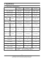
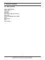
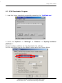
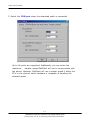
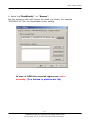
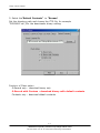
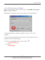
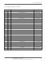
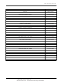
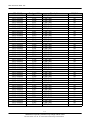
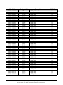
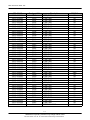
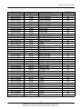
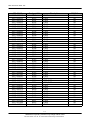
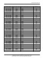
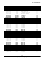
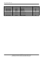
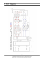
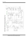
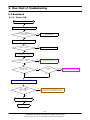
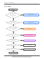
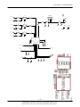
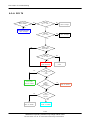
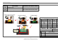
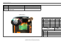
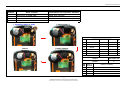
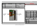
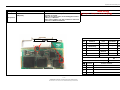
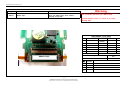
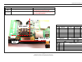
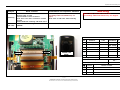
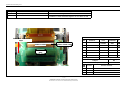
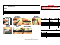
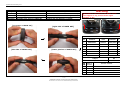
GSM TELEPHONE
SGH-D520
GSM TELEPHONE
CONTENTS
1. Safety Precautions
2. Specification
3. Product Function
4. Array course control
5. Exploded View and Parts list
6. MAIN Electrical Parts List
7. Block Diagrams
8. PCB Diagrams
9. Flow Chart of Troubleshooting
10. Reference data
11. Exploded and assembling View
This Service Manual is a property of Samsung Electronics Co.,Ltd.
Any unauthorized use of Manual can be punished under applicable
International and/or domestic law.
ⓒ Samsung Electronics Co.,Ltd.
Code No.: GH68-10734A
2006. 04. Rev.1.0
목 차
1. Safety Precautions
1-1. Repair Precaution ...........................................................................1-1
1-2. ESD(Electrostatically Sensitive Devices) Precaution ...........................1-2
2. Specification
2-1. GSM General Specification ..............................................................2-1
2-2. GSM TX power Level ......................................................................2-2
3. Product Function
4. Array course control
4-1. Downloading Binary Files .............................................................4-2
4-2. Pre-requsite for Downloading .......................................................4-2
4-3. S/W Downloader Program ...........................................................4-3
5. Exploded View and Parts list
5-1. Cellular phone Exploded View ......................................................5-1
5-2. Cellular phone Parts list ..............................................................5-2
6. MAIN Electrical Parts List
7. Block Diagrams
8. PCB Diagrams
9. Flow Chart of Troubleshooting
9-1. Baseband ..................................................................................9-1
9-1-1. Power ON .............................................................................9-1
9-1-2. Initial ...................................................................................9-4
9-1-3. SIM Part ...............................................................................9-6
9-1-4. Microphone Part ....................................................................9-7
9-1-5. Speaker Part_1(MP3, SPEAKER PHONE) ...................................9-8
9-1-6. Speaker Part_2(RECEIVER) ...................................................9-10
9-1-7. Charging Part ......................................................................9-11
목 차
9-2. RF ..........................................................................................9-13
9-2-1. EGSM RX ............................................................................9-13
9-2-2. DCS RX ..............................................................................9-15
9-2-3. PCS RX ...............................................................................9-16
9-2-4. EGSM TX ............................................................................9-17
9-2-5. DCS TX ..............................................................................9-18
9-2-6. PCS TX ...............................................................................9-19
10. Reference data
11. Exploded and assembling View
11-1. Cellular phone Exploded View ...................................................11-1
11-2. Cellular phone assembling ........................................................11-2
11-3. Slide FPCB KIT assembling .....................................................11-29
1. Safety Precautions
1-1. Repair Precaution
● Repair in Shield Box, during detailed tuning.
Take specially care of tuning or test,
because specipicty of cellular phone is sensitive for surrounding interference(RF noise).
● Be careful to use a kind of magnetic object or tool,
because performance of parts is damaged by the influence of manetic force.
● Surely use a standard screwdriver when you disassemble this product,
otherwise screw will be worn away.
● Use a thicken twisted wire when you measure level.
A thicken twisted wire has low resistance, therefore error of measurement is few.
● Repair after separate Test Pack and Set because for short danger (for example an
overcurrent and furious flames of parts etc) when you repair board in condition of
connecting Test Pack and tuning on.
● Take specially care of soldering, because Land of PCB is small and weak in heat.
● Surely tune on/off while using AC power plug, because a repair of battery charger is
dangerous when tuning ON/OFF PBA and Connector after disassembing charger.
● Don't use as you pleases after change other material than replacement registered on SEC
System.
Otherwise engineer in charge isn't charged with problem that you don't keep this rules.
1-1
SAMSUNG Proprietary-Contents may change without notice
This Document can not be used without Samsung's authorization
Safety Precautions
1-2. ESD(Electrostatically Sensitive Devices)
Precaution
Several semiconductor may be damaged easilly by static electricity. Such parts are called by
ESD(Electrostatically Sensitive Devices), for example IC,BGA chip etc. Read Precaution below.
You can prevent from ESD damage by static electricity.
● Remove static electricity remained your body before you touch semiconductor or parts with
semiconductor. There are ways that you touch an earthed place or wear static electricity
prevention string on wrist.
● Use earthed soldering steel when you connect or disconnect ESD.
● Use soldering removing tool to break static electricity. , otherwise ESD will be damaged by
static electricity.
● Don't unpack until you set up ESD on product. Because most of ESD are packed by box
and aluminum plate to have conductive power,they are prevented from static electricity.
● You must maintain electric contact between ESD and place due to be set up until ESD is
connected completely to the proper place or a circuit board.
1-2
SAMSUNG Proprietary-Contents may change without notice
This Document can not be used without Samsung's authorization
2. Specification
2-1. GSM General Specification
E- GSM
DCS1800
P C S 19 00
Freq. Ban d [M Hz ]
Upl in k/Downl in k
88 0~9 15
92 5~9 60
1 71 0~ 1 78 5
1 80 5~ 1 88 0
1 85 0~ 1 91 0
1 93 0~ 1 99 0
A RF C N ra n g e
97 5~ 10 23
0~12 4
51 2~8 85
51 2~8 10
Tx/R x sp aci ng
45 MHz
95 MHz
80 MHz
27 0. 83 3 K b ps
3.692 us
27 0. 83 3 K b ps
3.692 us
27 0. 83 3 K b ps
3.692 us
Ti me S lot P eri od /F rame
Peri od
576.9 us
4. 61 5 ms
576.9 us
4. 61 5 ms
576.9 us
4. 61 5 ms
M od ul a ti on
G P RS
0. 3 GM SK
0. 3 G M SK
0. 3 GM SK
MS P ow er
GP RS
3 3 d Bm~5 d Bm
3 0 d Bm~0 d Bm
3 0 d Bm~0 d Bm
Power Level
GP RS
5~1 9( cl as s4 )
0~15(class1)
0~15(class1)
Sensitivity
-102 d Bm
-100 dBm
-102 d Bm
TDM A Mu x
8
8
8
Cell Radiu s
35 K m
2 Km
2 Km
Operating Temperature
-20 ℃ ~ 45 ℃
-20 ℃ ~ 45 ℃
-20 ℃ ~ 45 ℃
Supply Voltage
3.7 V
3.7 V
3.7 V
M od . B i t
rate/
Bi t P eri od
GPRS
Size and Weight
Dimention : 97(H) × 52(W) × 14.9(D) mm
Weight
: 96 g (with standard battery)
2-2
SAMSUNG Proprietary-Contents may change without notice
This Document can not be used without Samsung's authorization
Specification
2-2. GSM TX Power Level
TX Power
control level
E-GSM
TX Power
control level
DCS1800
TX Power
control level
PCS1900
5
33±2 dBm
0
30±3 dBm
0
30±3 dBm
6
31±2 dBm
1
28±3 dBm
1
28±3 dBm
7
29±2 dBm
2
26±3 dBm
2
26±3 dBm
8
27±2 dBm
3
24±3 dBm
3
24±3 dBm
9
25±2 dBm
4
22±3 dBm
4
22±3 dBm
10
23±2 dBm
5
20±3 dBm
5
20±3 dBm
11
21±2 dBm
6
18±3 dBm
6
18±3 dBm
12
19±2 dBm
7
16±3 dBm
7
16±3 dBm
13
17±2 dBm
8
14±3 dBm
8
14±3 dBm
14
15±2 dBm
9
12±4 dBm
9
12±4 dBm
15
13±2 dBm
10
10±4 dBm
10
10±4 dBm
16
11±2 dBm
11
8±4 dBm
11
8±4 dBm
17
9±2d Bm
12
6±4 dBm
12
6±4 dBm
18
7±2d Bm
13
4±4 dBm
13
4±4 dBm
19
5±2d Bm
14
2±5 dBm
14
2±5 dBm
15
0±5 dBm
15
0±5 dBm
2-2
SAMSUNG Proprietary-Contents may change without notice
This Document can not be used without Samsung's authorization
3. Product Function
3-1. Main Function
-Camera and camcorder
-Image editor
-File viewer
-Bluetooth
-Get personal with photo caller ID
-Name card
-Multimedia Message Service (MMS)
-Email
-Web browser
-Java
-Voice recorder
3-1
SAMSUNG Proprietary-Contents may change without notice
This Document can not be used without Samsung's authorization
4. Array course control
Test Jig (GH80-03307A)
Test Cable (GH39-00127A)
RF Test Cable (GH39-00283A)
4-1
SAMSUNG Proprietary-Contents may change without notice
This Document can not be used without Samsung's authorization
Array course control
Software Downloading
4-1. Downloading Binary Files
• Two binary files for downloading D520.
– D520XXYY.s3 : Main source code binary.
– D520XXYY.cts : Default Contents binary.
4-2. Pre-requsite for Downloading
• Downloader Program(OptiFlash.exe)
• D520 Mobile Phone
• Data Cable
• Binary files
• CTS files
4-2
SAMSUNG Proprietary-Contents may change without notice
This Document can not be used without Samsung's authorization
1.
Array course control
4-3. S/W Downloader Program
1. Load the binary download programby executing the “OptiFlash.exe”
2. Select the “Options” -> “Settings” -> “Generic” -> “Specify hardware
platform”.
Choose hardware platform for the downloader file setting.
Set the everything else as the default values which are shown below
4-3
SAMSUNG Proprietary-Contents may change without notice
This Document can not be used without Samsung's authorization
Array course control
3. Select the COM port when the download cable is connected
Up to 64 ports are supported. Additionally you can select the
maximum
transfer speed OptiFlash will use to communicate with
the phone. However, OptiFlash will use a slower speed if either the
PC’s or the phone’s serial hardware is incapable of handling the
selected speed
4-4
SAMSUNG Proprietary-Contents may change without notice
This Document can not be used without Samsung's authorization
Array course control
4. Select the“Flash&Verify” -> “Browse”
Set the directory path and choose the latest s/w binary, for example
“D520XXYY.s3”,for the downloader binary setting.
In case of D520 the reserved regions are not a
necessity. (It is defined in platform.def file)
4-5
SAMSUNG Proprietary-Contents may change without notice
This Document can not be used without Samsung's authorization
Array course control
5. Select the“Default Contents” -> “Browse”
Set the directory path and choose the CTS file, for example
“D520XXYY.cts”,for the downloader binary setting.
Function of Flash option
S-Record only : download binary only
S-Record with Contens : download binary with default contents
Contents only : download default contents
4-6
SAMSUNG Proprietary-Contents may change without notice
This Document can not be used without Samsung's authorization
Array course control
6. Click “OK” button then press “Flash”.
(Before pressing ‘Flash’ button, push the button ‘*’and ‘END’ at the same
time. Then press ‘Flash’.)
Downloader will upload the binary file as below for the downloading.
7. When downloading is finished successfully, there is a “All is well”
message. 8. After finishing downloading, Certain memory resets should be done to
guarantee the normal performance.
9. Confirm the downloaded version name and etc. :
*#5002*8376263#
Full Reset : *2767*3855#
4-7
SAMSUNG Proprietary-Contents may change without notice
This Document can not be used without Samsung's authorization
5 . E x p lo d e d V ie w a n d P a r ts L is t
5 - 1 . C e llu la r p h o n e E x p lo d e d V ie w
QFU01
QFR04
QKP01
QMI03
QCA01
QME01
QSP01
QKP02
QFR01
QCK01
QLC01
QMO01
QCR32
QVO01
QCR47
QME02
QCA02
QCR32
QPC01
QHI01
QVK01
QFL02
QCR05
QFL01
QMP01
QAN02
QSH01
QRE01
QCA05
QIF01
QBA01
QRF01
QBA00
5-1
SAMSUNG Proprietary-Contents may change without notice
This Docum ent can not be used w ithout Sam sung's authorization
QCR12
Main Electrical Parts List
5 - 2 . C e llu la r p h o n e P a r ts lis t
Design LOC Discription
QAN02
QBA00
QBA01
SEC CODE
IN TEN NA-SGHD520
G H42-00740A
ASSY-CO VER-BATT
G H98-00721B
INNER BATTERY PACK-800M AH,BLK,
G H43-01850A
QCA01
UN IT-CAM ERA
G H59-02860A
QCA02
UNIT-CAMERA KEY
G H59-02799A
QCA05
MEC-SUB FLASH DECO
G H75-08862A
QCK01
MEC-CAM KEY
G H75-08866A
QCR05
SCREW -M ACHIN E
6001-001478
QCR05
SCREW -M ACHIN E
6001-001478
QCR12
SCREW -M ACHIN E
6001-001530
QCR32
SCREW -M ACHIN E
6001-001700
Q FR01
MEC-SUA FRONT COVER
G H75-08863B
Q FR04
PMO -FRONT CO VER BUSH
G H72-27856A
QKP01
MEC-KEYPAD M AIN
G H75-08864B
QKP02
M EC-KEYPAD SUB
G H75-08861B
QLC01
ELA UN IT-SGHD520 LCD
G H96-02099A
Q ME01
UN IT-KEY PAD
G H59-02716A
Q ME02
UN IT-NAVI KEY
G H59-02717A
QMO01
MOTOR DC-SPHV8400
G H31-00187A
QMP01
PBA MAIN-SGHD520
G H92-02481A
QPC01
MEA-SLIDE FPCB KIT
G H97-05579A
Q RF01
PMO-COVER RF
G H72-29405B
QSH01
NDC-SHIELD CAN
G H71-05961A
QSP01
SPEAKER
3001-001906
QVK01
UNIT-VOLUME KEY
G H59-02798A
QVO01
MEC-KEY VOLUM E
G H75-08277A
QRE01
M EC-SUA REAR COVER
G H75-08865B
QIF01
PMO-IF COVER
G H72-27858B
QFL01
M EC-SUA SLIDE LOW HINGE
G H75-08859B
QCR32
SCREW -M ACHIN E
6001-001700
QCR47
SCREW -M ACHIN E
6001-001695
QFL02
MEC-SLIDE LOW ER
G H75-08860B
QHI01
MEC-HIN GE
G H75-09414A
QFU01
M EC-SUA SLIDE UPPER
G H75-08857B
Q MI03
RMO-M IC HOLDER
G H73-05704A
5-2
SAMSUNG Proprietary-Contents may change without notice
This Docum ent can not be used w ithout Sam sung's authorization
Main Electrical Parts List
Discription
SEC CODE
BAG PE
6902-000297
CBF INTERFACE-DATA LIN K CABLE
GH39-00444A
ADAPTOR-SGHD800 TA(EU)
GH44-01060A
S/W CD-SAM SUNGPCSTUDIO 3.0
GH46-00215A
EARPHONE-STEREO HEADSET
GH59-02499A
LABEL(P)-IMEI
GH68-01335D
LABEL(P)-W ATER SOAK
GH68-02026A
LABEL(P)-W ATER SOAK
GH68-02026A
MANUAL-SFC CARD
GH68-07937A
MAN UAL USERS-EU FRENCH
GH68-09205A
LABEL(P)-MAIN (EU)
GH68-09251A
MAN UAL USERS-EU DUTCH
GH68-09509A
CUSHION-CASE TA2 MA2
GH69-03632A
BOX(P)-UNIT M AIN (EU)
GH69-03635A
MPR-BOHO VIN YL LCD CONN
GH74-15350A
MPR-TAPE REM OVE LCD
GH74-18286A
MPR-VINYL BOHO MAIN
GH74-19951A
MPR-TAPE GASKET MAIN FPC
GH74-21361A
MPR-TAPE NAVI CONN BTM
GH74-21362A
MPR-TAPE CAMERA CONN
GH74-21364A
MPR-TAPE LCD CONN C
GH74-21365A
M PR-TAPE NAVI KEY CONN
GH74-21366A
MPR-TAPE MAIN CO NN C
GH74-21367A
M PR-TAPE M AIN CONN A
GH74-21368A
MPR-TAPE LCD CONN D
GH74-21369A
M PR-CUSHION NAVI KEY
GH74-21626A
MPR-CUSHION LCD BACK
GH74-21627A
MPR-VINYL BOHO SUB KEY
GH74-22225A
5-3
SAMSUNG Proprietary-Contents may change without notice
This Docum ent can not be used w ithout Sam sung's authorization
6. MAIN Electrical Parts List
SEC CODE
4202-001095
4302-001201
3711-006025
2203-006194
2203-006194
2203-006423
2203-006423
2203-006324
2203-006562
2203-006562
2203-006562
2203-006562
2203-006562
2203-006562
2203-006562
2203-005736
2203-006648
2203-006194
2203-001405
2203-006562
2203-006423
2203-006121
2203-006423
2203-005682
2203-005682
2203-005729
2203-006257
2203-006562
2203-006423
2203-006562
2203-006562
2203-006825
2203-006562
2203-006825
2203-006562
2203-006423
2203-006348
2203-006324
2203-006194
2203-006194
2203-006423
2203-006423
Design LOC
ANT602
BAT100
BTC502
C100
C101
C102
C103
C104
C105
C106
C107
C108
C109
C110
C111
C112
C113
C114
C115
C116
C117
C118
C119
C120
C121
C122
C124
C125
C126
C128
C129
C130
C131
C132
C135
C136
C137
C138
C200
C201
C202
C203
Discription
ANTENNA-CHIP
BATTERY-LI(2ND)
HEADER-BATTERY
C-CER,CHIP
C-CER,CHIP
C-CER,CHIP
C-CER,CHIP
C-CER,CHIP
C-CER,CHIP
C-CER,CHIP
C-CER,CHIP
C-CER,CHIP
C-CER,CHIP
C-CER,CHIP
C-CER,CHIP
C-CER,CHIP
C-CER,CHIP
C-CER,CHIP
C-CER,CHIP
C-CER,CHIP
C-CER,CHIP
C-CER,CHIP
C-CER,CHIP
C-CER,CHIP
C-CER,CHIP
C-CER,CHIP
C-CER,CHIP
C-CER,CHIP
C-CER,CHIP
C-CER,CHIP
C-CER,CHIP
C-CER,CHIP
C-CER,CHIP
C-CER,CHIP
C-CER,CHIP
C-CER,CHIP
C-CER,CHIP
C-CER,CHIP
C-CER,CHIP
C-CER,CHIP
C-CER,CHIP
C-CER,CHIP
6-1
SAMSUNG Proprietary-Contents may change without notice
This Document can not be used without Samsung's authorization
STATUS
SA
SA
SA
SA
SA
SA
SA
SA
SA
SA
SA
SA
SA
SA
SA
SA
SA
SA
SA
SA
SA
SA
SA
SA
SA
SA
SA
SA
SA
SA
SA
SA
SA
SA
SA
SA
SA
SA
SA
SA
SA
SA
Main Electrical Parts List
SEC CODE
2203-006423
2203-006194
2203-006423
2203-006194
2203-006423
2203-005727
2203-005727
2203-000254
2203-005806
2203-005806
2203-006423
2203-006194
2203-006194
2203-006423
2203-006562
2203-006562
2203-006423
2203-006562
2203-006423
2203-006305
2203-006305
2203-006562
2203-006423
2203-006324
2203-006423
2203-006379
2203-006423
2203-006562
2203-006648
2203-005806
2203-006423
2203-000654
2203-006423
2203-006423
2203-006423
2203-002709
2203-006423
2203-006423
2203-006668
2203-006423
2203-006423
2203-006562
Design LOC
C204
C205
C206
C207
C208
C209
C210
C211
C212
C213
C215
C216
C217
C218
C300
C301
C302
C303
C304
C305
C306
C309
C312
C313
C314
C315
C316
C317
C318
C319
C320
C321
C322
C326
C327
C328
C330
C331
C332
C333
C342
C343
Discription
C-CER,CHIP
C-CER,CHIP
C-CER,CHIP
C-CER,CHIP
C-CER,CHIP
C-CER,CHIP
C-CER,CHIP
C-CER,CHIP
C-CER,CHIP
C-CER,CHIP
C-CER,CHIP
C-CER,CHIP
C-CER,CHIP
C-CER,CHIP
C-CER,CHIP
C-CER,CHIP
C-CER,CHIP
C-CER,CHIP
C-CER,CHIP
C-CER,CHIP
C-CER,CHIP
C-CER,CHIP
C-CER,CHIP
C-CER,CHIP
C-CER,CHIP
C-CER,CHIP
C-CER,CHIP
C-CER,CHIP
C-CER,CHIP
C-CER,CHIP
C-CER,CHIP
C-CER,CHIP
C-CER,CHIP
C-CER,CHIP
C-CER,CHIP
C-CER,CHIP
C-CER,CHIP
C-CER,CHIP
C-CER,CHIP
C-CER,CHIP
C-CER,CHIP
C-CER,CHIP
6-2
SAMSUNG Proprietary-Contents may change without notice
This Document can not be used without Samsung's authorization
STATUS
SA
SA
SA
SA
SA
SA
SA
SA
SA
SA
SA
SA
SA
SA
SA
SA
SA
SA
SA
SA
SA
SA
SA
SA
SA
SA
SA
SA
SA
SA
SA
SA
SA
SA
SA
SA
SA
SA
SA
SA
SA
SA
Main Electrical Parts List
SEC CODE
2203-006562
2203-006260
2203-006260
2203-006348
2203-006423
2203-000854
2203-000854
2203-006562
2203-006423
2203-005682
2203-005682
2203-005682
2203-005682
2203-006257
2203-005682
2203-006626
2203-005682
2203-005683
2203-006348
2203-005682
2203-006626
2203-005682
2203-006348
2203-005682
2203-006260
2203-006260
2203-005682
2203-006825
2203-006825
2203-005736
2203-006048
2203-006562
2203-006257
2007-008055
2203-005682
2203-006423
2203-006423
2203-006423
2203-006423
2203-005736
2203-005736
2203-006648
Design LOC
C344
C347
C348
C400
C401
C403
C404
C406
C407
C408
C409
C410
C411
C413
C414
C415
C416
C417
C418
C419
C420
C421
C422
C423
C424
C426
C429
C432
C433
C500
C502
C503
C505
C506
C507
C508
C509
C510
C511
C512
C513
C542
Discription
C-CER,CHIP
C-CER,CHIP
C-CER,CHIP
C-CER,CHIP
C-CER,CHIP
C-CER,CHIP
C-CER,CHIP
C-CER,CHIP
C-CER,CHIP
C-CER,CHIP
C-CER,CHIP
C-CER,CHIP
C-CER,CHIP
C-CER,CHIP
C-CER,CHIP
C-CER,CHIP
C-CER,CHIP
C-CER,CHIP
C-CER,CHIP
C-CER,CHIP
C-CER,CHIP
C-CER,CHIP
C-CER,CHIP
C-CER,CHIP
C-CER,CHIP
C-CER,CHIP
C-CER,CHIP
C-CER,CHIP
C-CER,CHIP
C-CER,CHIP
C-CER,CHIP
C-CER,CHIP
C-CER,CHIP
R-CHIP
C-CER,CHIP
C-CER,CHIP
C-CER,CHIP
C-CER,CHIP
C-CER,CHIP
C-CER,CHIP
C-CER,CHIP
C-CER,CHIP
6-3
SAMSUNG Proprietary-Contents may change without notice
This Document can not be used without Samsung's authorization
STATUS
SA
SA
SA
SA
SA
SA
SA
SA
SA
SA
SA
SA
SA
SA
SA
SA
SA
SA
SA
SA
SA
SA
SA
SA
SA
SA
SA
SA
SA
SA
SA
SA
SA
SA
SA
SA
SA
SA
SA
SA
SA
SA
Main Electrical Parts List
SEC CODE
2203-006194
2203-005682
2203-005736
2203-006194
2203-005806
2203-006556
2203-005682
2203-006423
2203-006648
2203-006423
2203-006194
2203-005792
2203-005792
2203-006318
2203-006318
2203-006318
2203-006318
2203-005736
2203-005736
2203-005736
2203-006556
2203-006318
2203-006423
2203-006194
2203-006423
2203-005682
2203-006620
2203-005682
2203-005682
2203-005682
2203-006194
2203-006423
2203-006324
2203-005682
2203-005682
2203-006324
2203-006305
2203-005725
2203-006562
2203-006562
2203-005158
2901-001256
Design LOC
C543
C600
C601
C602
C603
C604
C605
C606
C607
C608
C609
C610
C611
C612
C613
C614
C615
C616
C617
C618
C619
C620
C622
C623
C625
C626
C627
C628
C629
C630
C631
C632
C633
C635
C636
C637
C638
C639
C640
C641
C642
F101
Discription
C-CER,CHIP
C-CER,CHIP
C-CER,CHIP
C-CER,CHIP
C-CER,CHIP
C-CER,CHIP
C-CER,CHIP
C-CER,CHIP
C-CER,CHIP
C-CER,CHIP
C-CER,CHIP
C-CER,CHIP
C-CER,CHIP
C-CER,CHIP
C-CER,CHIP
C-CER,CHIP
C-CER,CHIP
C-CER,CHIP
C-CER,CHIP
C-CER,CHIP
C-CER,CHIP
C-CER,CHIP
C-CER,CHIP
C-CER,CHIP
C-CER,CHIP
C-CER,CHIP
C-CER,CHIP
C-CER,CHIP
C-CER,CHIP
C-CER,CHIP
C-CER,CHIP
C-CER,CHIP
C-CER,CHIP
C-CER,CHIP
C-CER,CHIP
C-CER,CHIP
C-CER,CHIP
C-CER,CHIP
C-CER,CHIP
C-CER,CHIP
C-CER,CHIP
FILTER-EMI SMD
6-4
SAMSUNG Proprietary-Contents may change without notice
This Document can not be used without Samsung's authorization
STATUS
SA
SA
SA
SA
SA
SA
SA
SA
SA
SA
SA
SA
SA
SA
SA
SA
SA
SA
SA
SA
SA
SA
SA
SA
SA
SA
SNA
SA
SA
SA
SA
SA
SA
SA
SA
SA
SA
SA
SA
SA
SA
SA
Main Electrical Parts List
SEC CODE
2901-001337
2901-001337
2901-001337
2901-001337
2901-001337
2901-001337
2901-001337
2904-001592
2904-001599
2904-001601
3711-006109
3710-002306
2703-002749
2703-002734
2007-000171
2007-000171
3301-001729
2703-002485
2703-002544
2703-002608
2703-002917
2703-002917
2703-002558
2703-002313
2801-004466
2801-004225
2801-004455
2801-004426
1201-002278
0504-000168
2007-008588
2007-009166
2007-008419
2007-008055
2007-000142
2007-008483
2007-008052
2007-009167
2007-008516
2007-008483
2007-008478
2007-009115
Design LOC
F500
F501
F502
F503
F504
F505
F506
F600
F601
F602
HDC500
IFC503
L100
L101
L300
L301
L302
L600
L601
L602
L603
L604
L605
L607
OSC200
OSC300
OSC600
OSC601
PAM601
Q100
R100
R101
R102
R103
R104
R105
R106
R107
R108
R109
R110
R111
Discription
FILTER-EMI/ESD
FILTER-EMI/ESD
FILTER-EMI/ESD
FILTER-EMI/ESD
FILTER-EMI/ESD
FILTER-EMI/ESD
FILTER-EMI/ESD
FILTER-SAW
FILTER-SAW
FILTER-SAW
HEADER-BOARD TO BOARD
SOCKET-INTERFACE
INDUCTOR-SMD
INDUCTOR-SMD
R-CHIP
R-CHIP
BEAD-SMD
INDUCTOR-SMD
INDUCTOR-SMD
INDUCTOR-SMD
INDUCTOR-SMD
INDUCTOR-SMD
INDUCTOR-SMD
INDUCTOR-SMD
CRYSTAL-SMD
CRYSTAL-SMD
CRYSTAL-SMD
CRYSTAL-SMD
IC-POWER AMP
TR-DIGITAL
R-CHIP
R-CHIP
R-CHIP
R-CHIP
R-CHIP
R-CHIP
R-CHIP
R-CHIP
R-CHIP
R-CHIP
R-CHIP
R-CHIP
6-5
SAMSUNG Proprietary-Contents may change without notice
This Document can not be used without Samsung's authorization
STATUS
SA
SA
SA
SA
SA
SA
SA
SA
SA
SA
SNA
SA
SA
SA
SA
SA
SA
SA
SA
SA
SA
SA
SA
SA
SA
SA
SA
SA
SA
SA
SA
SA
SA
SA
SA
SA
SA
SA
SA
SA
SA
SA
Main Electrical Parts List
SEC CODE
2007-009115
2007-009212
2007-000172
2007-008531
2007-008806
2007-000162
2007-008055
2007-008483
2007-008531
2007-008055
2007-000171
2007-009084
2007-000157
2007-000171
2007-008542
2007-008531
2007-008483
2007-008516
2007-008483
2007-008051
2007-009166
2007-008055
2007-009166
2007-000138
2007-009084
2007-009169
2007-009169
2007-007310
2007-008210
2007-008210
2203-006091
2203-006091
2007-009084
2007-009084
2007-000171
2007-001292
2007-001292
2007-008420
2007-008420
2007-001119
2007-007528
2007-007528
Design LOC
R112
R115
R201
R202
R203
R204
R205
R206
R207
R208
R210
R300
R301
R302
R304
R308
R309
R312
R313
R314
R315
R316
R317
R319
R320
R321
R322
R323
R326
R327
R328
R329
R330
R331
R400
R403
R406
R409
R410
R411
R412
R413
Discription
R-CHIP
R-CHIP
R-CHIP
R-CHIP
R-CHIP
R-CHIP
R-CHIP
R-CHIP
R-CHIP
R-CHIP
R-CHIP
R-CHIP
R-CHIP
R-CHIP
R-CHIP
R-CHIP
R-CHIP
R-CHIP
R-CHIP
R-CHIP
R-CHIP
R-CHIP
R-CHIP
R-CHIP
R-CHIP
R-CHIP
R-CHIP
R-CHIP
R-CHIP
R-CHIP
C-CER,CHIP
C-CER,CHIP
R-CHIP
R-CHIP
R-CHIP
R-CHIP
R-CHIP
R-CHIP
R-CHIP
R-CHIP
R-CHIP
R-CHIP
6-6
SAMSUNG Proprietary-Contents may change without notice
This Document can not be used without Samsung's authorization
STATUS
SA
SA
SA
SA
SA
SA
SA
SA
SA
SA
SA
SA
SA
SA
SA
SA
SA
SA
SA
SA
SA
SA
SA
SA
SA
SA
SA
SA
SA
SA
SA
SA
SA
SA
SA
SA
SA
SA
SA
SA
SA
SA
Main Electrical Parts List
SEC CODE
2007-007590
2007-007142
2007-007590
2007-007142
2007-007107
2007-007107
2007-007142
2007-007142
2007-007798
2007-007798
2007-007528
2007-007588
2007-001119
2007-008542
2007-008055
2007-008055
2007-000171
2007-000171
2007-000171
2007-000171
2007-008055
2007-008419
2007-008419
2007-008419
2007-008055
2007-008419
2007-008786
2007-008786
2007-008806
2007-008806
2007-008806
2007-008806
2007-008806
2007-008806
2007-008806
2007-008806
2007-008806
2007-008806
2007-008806
2007-008542
2007-008419
2007-008419
Design LOC
R414
R415
R416
R417
R418
R419
R420
R421
R426
R427
R428
R429
R430
R431
R432
R433
R434
R435
R436
R437
R500
R501
R502
R503
R504
R505
R506
R507
R508
R509
R510
R511
R512
R513
R514
R515
R516
R517
R518
R519
R522
R523
Discription
R-CHIP
R-CHIP
R-CHIP
R-CHIP
R-CHIP
R-CHIP
R-CHIP
R-CHIP
R-CHIP
R-CHIP
R-CHIP
R-CHIP
R-CHIP
R-CHIP
R-CHIP
R-CHIP
R-CHIP
R-CHIP
R-CHIP
R-CHIP
R-CHIP
R-CHIP
R-CHIP
R-CHIP
R-CHIP
R-CHIP
R-CHIP
R-CHIP
R-CHIP
R-CHIP
R-CHIP
R-CHIP
R-CHIP
R-CHIP
R-CHIP
R-CHIP
R-CHIP
R-CHIP
R-CHIP
R-CHIP
R-CHIP
R-CHIP
6-7
SAMSUNG Proprietary-Contents may change without notice
This Document can not be used without Samsung's authorization
STATUS
SA
SA
SA
SA
SA
SA
SA
SA
SA
SA
SA
SA
SA
SA
SA
SA
SA
SA
SA
SA
SA
SA
SA
SA
SA
SA
SA
SA
SA
SA
SA
SA
SA
SA
SA
SA
SA
SA
SA
SA
SA
SA
Main Electrical Parts List
SEC CODE
2007-008045
2007-008806
2007-008483
2007-008548
2007-008587
2007-008045
2007-008516
2007-008516
2007-008542
2007-000171
3705-001358
3709-001421
3708-002170
2404-001381
2404-001339
2404-001381
2404-001375
2404-001225
2404-001353
2404-001353
2404-001339
2404-001381
2404-001381
2404-001240
2404-001240
2404-001225
2404-001225
2404-001352
2404-001377
2404-001411
2404-001411
2404-001374
1404-001165
0504-001049
1203-003920
0801-002529
1203-003109
1205-002272
1203-003523
1203-003428
1203-003434
1203-003523
Design LOC
R524
R525
R526
R600
R601
R602
R603
R605
R606
R634
RFS600
SIM100
SLC504
TA100
TA101
TA103
TA200
TA300
TA301
TA302
TA303
TA304
TA305
TA400
TA401
TA402
TA403
TA404
TA405
TA500
TA503
TA600
TH100
TR300
U100
U101
U102
U103
U104
U105
U106
U107
Discription
R-CHIP
R-CHIP
R-CHIP
R-CHIP
R-CHIP
R-CHIP
R-CHIP
R-CHIP
R-CHIP
R-CHIP
CONNECTOR-COAXIAL
CONNECTOR-CARD EDGE
CONNECTOR-FPC/FFC/PIC
C-TA,CHIP
C-TA,CHIP
C-TA,CHIP
C-TA,CHIP
C-TA,CHIP
C-TA,CHIP
C-TA,CHIP
C-TA,CHIP
C-TA,CHIP
C-TA,CHIP
C-TA,CHIP
C-TA,CHIP
C-TA,CHIP
C-TA,CHIP
C-TA,CHIP
C-TA,CHIP
C-TA,CHIP
C-TA,CHIP
C-TA,CHIP
THERMISTOR-NTC
TR-DIGITAL
IC-POWER SUPERVISOR
IC-CMOS LOGIC
IC-BATTERY
IC-TRANSCEIVER
IC-POSI.FIXED REG.
IC-DC/DC CONVERTER
IC-DC/DC CONVERTER
IC-POSI.FIXED REG.
6-8
SAMSUNG Proprietary-Contents may change without notice
This Document can not be used without Samsung's authorization
STATUS
SA
SA
SA
SA
SA
SA
SA
SA
SA
SA
SA
SA
SA
SA
SA
SA
SA
SA
SA
SA
SA
SA
SA
SA
SA
SA
SA
SA
SA
SA
SA
SA
SA
SA
SA
SA
SA
SA
SA
SA
SA
SA
Main Electrical Parts List
SEC CODE
1205-002612
1201-002233
1001-001261
1001-001306
1205-002683
4709-001368
1203-003432
1204-002309
1205-002681
GH09-00040A
1108-000024
1405-001082
1405-001082
1405-001082
1405-001082
1405-001082
1405-001082
1405-001082
1405-001082
1405-001082
1405-001082
1405-001082
1405-001082
1405-001082
1405-001082
1405-001082
1405-001082
1405-001082
1405-001082
1405-001082
1405-001082
1405-001082
1405-001082
1405-001121
1405-001121
1405-001121
1405-001082
1405-001082
1405-001082
1405-001082
1405-001082
1405-001082
Design LOC
U300
U303
U400
U401
U600
U602
U603
UCD301
UCD302
UCP200
UME201
V400
VR200
VR401
VR402
VR403
VR404
VR500
VR501
VR502
VR503
VR504
VR505
VR506
VR507
VR508
VR509
VR510
VR511
VR512
VR513
VR514
VR515
VR516
VR517
VR518
VR519
VR520
VR521
VR522
VR523
VR524
Discription
IC-CODEC
IC-AUDIO AMP
IC-ANALOG SWITCH
IC-ANALOG MULTIPLEX
IC-TRANSCEIVER
BLUETOOTH MODULE
IC-POSI.FIXED REG.
IC-MELODY
IC-CODEC
IC MICOM
IC-MCP
VARISTOR
VARISTOR
VARISTOR
VARISTOR
VARISTOR
VARISTOR
VARISTOR
VARISTOR
VARISTOR
VARISTOR
VARISTOR
VARISTOR
VARISTOR
VARISTOR
VARISTOR
VARISTOR
VARISTOR
VARISTOR
VARISTOR
VARISTOR
VARISTOR
VARISTOR
VARISTOR
VARISTOR
VARISTOR
VARISTOR
VARISTOR
VARISTOR
VARISTOR
VARISTOR
VARISTOR
6-9
SAMSUNG Proprietary-Contents may change without notice
This Document can not be used without Samsung's authorization
STATUS
SA
SA
SA
SA
SA
SA
SA
SA
SA
SA
SA
SA
SA
SA
SA
SA
SA
SA
SA
SA
SA
SA
SA
SA
SA
SA
SA
SA
SA
SA
SA
SA
SA
SA
SA
SA
SA
SA
SA
SA
SA
SA
Main Electrical Parts List
SEC CODE
1405-001082
1405-001121
1405-001082
0406-001190
0406-001190
0403-001547
0403-001411
0403-001427
Design LOC
VR525
VR526
VR527
ZD500
ZD501
ZD502
ZD503
ZD504
Discription
VARISTOR
VARISTOR
VARISTOR
DIODE-TVS
DIODE-TVS
DIODE-ZENER
DIODE-ZENER
DIODE-ZENER
6-10
SAMSUNG Proprietary-Contents may change without notice
This Document can not be used without Samsung's authorization
STATUS
SA
SA
SA
SA
SA
SA
SA
SA
7. Block Diagrams
7-1
SAMSUNG Proprietary-Contents may change without notice
This Document can not be used without Samsung's authorization
Block Diagrams
7-2
SAMSUNG Proprietary-Contents may change without notice
This Document can not be used without Samsung's authorization
8. PCB Diagrams
ANT601 ANT600
U604
G4
TA600
VR508
U600
F601F600
RFS600
VR507
F602
PAM601
U602
TA404
V400
A N T6 0 2
TA501
U107
U401
BAT100
SIM100
VR513
ZD503
U603
TA100
TA500
VR523
BTC502
VR521
VR525
VR520
VR522
ZD504
G1
OSC601
U102
ZD500
ZD502
VR510
VR511
VR512
VR505
U1 0 1
TA405
Z D 501
IFC503
VR514
TA402
U4 0 0
TA403
HDC500
OSC600
G2
TA302 TA301
VR506
VR509
G3
VR515
TP207 TP204
TP214TP213TP210TP211 TP212
8-1
TP209
UCD301
UCP200
U100
U300
VR200
OSC300
UME201
TA200
VR524
VR504
VR403VR526VR527
VR503
VR501
VR502
SLC504
VR500
F504 F505 F503 F501 F502 F500 F506
VR516VR518
U303
VR517
TA305
TA304
TR300
VR519
VK500
CK500
VR402
8-2
U1 0 4
TA300
TA401
TA101TH100
TA400
VR404
VR401
U103
UCD302
F101
TA303
OSC200
TA103
U105
U106
PCB Diagrams
9. Flow Chart of Troubleshooting
9-1.Baseband
9-1-1. Power ON
'Power On' does not work
Check the current consumption
Yes
Current consumption
>= 100mA
No
Download again
Yes
Check the Vbat Voltage
Voltage >=3.3V
No
Charge the Battery
Yes
Check the pin of U100
Pin#J12 >= 2.8V
No
Check U100 and C110
Yes
Pin#A13 and
pin#A14 =2.8V
No
pin#G11 =
1.5V
No
Check U100, U105 and U106
Yes
Yes
Check the clock signal at C601
Freq = 26MHz
Vrms >=300mV
Vpp≒ 900mV
No
Check the clock generation circuit
(related to 3pin of OSC600, C602, R601)
Yes
Check the initial operation
END
9-1
SAMSUNG Proprietary-Contents may change without notice
This Document can not be used without Samsung's authorization
SERLE
SERDAT
SERCLK
XOENA
VMOD_EN
RF_EN
TX_EN
SVC_LED
DSP_IO
DSP_RWN
FLASH_RESET
OCTL0
OCTL1
OCTL2
OCTL3
OCTL4
OCTL5
OCTL6
OCTL7
B1 SERLE1
A2 SERLE2
C1 SERDA
C2 SERCK
E6
C5
F5
E5
A4
G6
B3
A3
DB15
DB14
DB13
DB12
DB11
DB10
DB9
DB8
DB7
DB6
DB5
DB4
DB3
DB2
DB1
DB0
AB8
AB7
AB6
AB5
AB4
AB3
AB2
AB1
AB0
I|O
RWN
RESETN_CSP
D9 A FC
E7 TXP
DSP_AB(0:8)
DSP_DB(15) D2
DSP_DB(14) D3
DSP_DB(13) E3
DSP_DB(12) E2
DSP_DB(11) F3
DSP_DB(10) F2
DSP_DB(9) F1
DSP_DB(8) F4
DSP_DB(7) G4
DSP_DB(6) G3
DSP_DB(5) H5
DSP_DB(4) J6
DSP_DB(3) J5
DSP_DB(2) K3
DSP_DB(1) K2
DSP_DB(0) K1
DSP_AB(8)
K5
DSP_AB(7)
K7
DSP_AB(6)
M1
DSP_AB(5)
M2
DSP_AB(4)
N2
DSP_AB(3)
N1
DSP_AB(2)
L5
DSP_AB(1)
P1
DSP_AB(0)
K6
L3
L2
R3
RA REF2
RA REF1
RXTXIP
RXTXIN
RXTXQP
RXTXQN
RTXIP
RTXIN
RTXQP
RTXQN
C101
U100
A OUTA P
A OUTA N
A OUTB P
A OUTB N
MICINP
MICINN
MICOUTP
MICOUTN
A UXINP
A UXINN
A UXOUTP
A UXOUTN
VXVCM
VREGP
VREGN
DA ICK
DA IRN
DA IDI
DA IDO
P11
N12
R12
P12
N14
M1 4
N15
P15
M1 5
L 14
K 13
L 13
R13
M1 3
R14
R4
P4
L6
M6
C116
A OUTA P
A OUTA N
A OUTB P
A OUTB N
MICINP
MICINN
MICOUTP
MICOUTN
A UXINP
A UXINN
A UXOUTP
A UXOUTN
B5
B6
D7
D6
C7
C6
C117
A FC
TX_PWR
C102
P5
CL K 32K
XOENA Q
CL K 13M_MC
C103
K12
H11
G12
G13
F13
F15
C12
A14
C9
D10
B10
B11
A12
B12
A13
J12
G11
F14
VSIM
VRTC
LED2_DRV
LED1_DRV
RING_DRV
VIB_DRV
VLDO_7
VLDO_6
VL5S_B
VL5S_A
VLDO_5
VL4S_B
VL4S_A
VLDO_4
VLDO_3
VLDO_2
VLDO_1
VACC
E14
E13
E11
F12
D14
D15
E10
A10
E9
RTC_ALMN H10
C113
ADC_AUX2
ADC_AUX1
VREF
CREF
VEXT
VBAT
CH_BDRV
CH_ISEN
CH_RES
CSN_PSC K8
SCLK_PSC L8
SDO_PSC N7
SDI_PSC M7
N9
R10
P10
J11
K11
K14
VDD34 C11
VDD12 J13
C104
BAND_SEL2
BAND_SEL1
KEY_BL1
UP_CS
UP_SCLK
UP_SDO
UP_SDI
VIB_EN
INTRQ
PWR_KEEP
RST
R106
MOT
U605
VSIM
SIMCLK
SIMRST
SIMDATA
SIM_IO
SIM_RST
SIM_CLK
VBAT
VBAT
UP_CLK
UP_RST
UP_IO
SIM_IO
SIM_RST
SIM_CLK
VIB _ RNG_EN
DSP_DB(0:15)
C100
VCCD_1.8V VCCD_2.9V
DSP_INT
A DC_A UX4
2
1
K 10
J 10
J9
J8
J7
H9
H8
H7
H6
G10
G9
G8
G7
F10
F9
F8
F7
D13
P3 DINTR
NC6
NC5
GNDS17
GNDS16
GNDS15
GNDS14
GNDS13
GNDS12
GNDS11
GNDS10
GNDS9
GNDS8
GNDS7
GNDS6
GNDS5
GNDS4
GNDS3
GNDS2
GNDS1
A UX_A DC3
N4 RTC_CL K
D1 XOENA Q
R 6 MC
B4
C4
P13
L 11
F6
A6
M 10
N11
P6
R2
K4
G5
J4
N5
N6
M3
J3
F11
K 15
B 15
E8
B 13
C10
GND_OCTL
VDD_OCTL
GNDV
VDDV
GNDB
VDDB
GNDD
VDDD
VSS4
VSS3
VSS2
VSS1
VDD_IO2
VDD_IO1
VDD3
VDD2
VDD1
GND_HCUR
GND_PSC2
GND_PSC1
GNDQ
VDD67
VDD5
PWR_SW2
PWR_SW1N
PSW1_B UF
RESET_O
MODE
PWR_K EEP
INTRQ
C14
C15
L7
K9
N10
M9
L 10
L9
J IG_ON
PWR_ON
PSW1_B UF
ICHRG
VBAT
VCCB_2.9V
C105
VLDO7_1.8V
C106
RTCALARM
C107
VCCA_2.9V
C108
R107
R101
C111
C112
C115
VCCB_2.9V
VLDO1_1.5V
TH100
C110
VCCD_2.9V
C109
C114
VRF_2.9V
BAT100
R100
VRTC_1.5V
1
2
VCCD_2.9V VCCA_2.9V
Flow Chart of Troubleshooting
9-2
This Document can not be used without Samsung's authorization
SAMSUNG Proprietary-Contents may change without notice
Flow Chart of Troubleshooting
VCCD_2.9V VRF_2.9V
C604
GSM_PAM_IN
DPCS_PAM_IN
R600
C605
RF_EN
15
RFOL
VDD
GND
VIO
14
16
RFIPP
RFIPN
6 BIN
RTXQP
RFIDP
U600
5 BQP
RTXQN
RFIDN
4 BQN
SERLE
SERCLK
3 SDIO
RFIEN
2 _SEN
RFIAP
35 34 33
32
31
30
PCS_LNA_IN_P
17
PCS_LNA_IN_N
18
DCS_LNA_IN_P
19
DCS_LNA_IN_N
20
GSM_LNA_IN_P
21
GSM_LNA_IN_N
22
23
29
28
A FC
VDD
RFIAN
VDD
XTA L 2
XTA L 1
NC
NC
1 SCLK
27
XDIV
SERDAT
RFIEP
XMODE
RTXIN
R602
13
7 BIP
GND
CLK13M_YMU
XOUT
12
RFOH
8
RTXIP
C603
11
_RESET
C601
_PDN
C602
R601
CLK13M_MC
10
VDD
9
XEN
C600
CLK13M_TR
26
24
25
R603
AFC
XOENA
C609
C606
3
4
2
1
C607
C608
VBAT
3
2
F101
1
OSC600
VLDO7_1.8V
R108
VCCD_1.8V
HP_CORE_1.57V
U105
1 VIN
U106
SW 5
L100
1 VIN
2 GND
3 EN
TA103
SW 5
L101
2 GND
FB 4
3 EN
C132
D100
FB 4
C130
C131
9-3
SAMSUNG Proprietary-Contents may change without notice
This Document can not be used without Samsung's authorization
VLDO1_1.5V
Flow Chart of Troubleshooting
9-1-2. Initial
Initial Failure
Yes
The pin #C12 of U100 =
1.8V and
No
the pin #J12 of U100 =
Check the U100
(if it has some problem, it is to be replaced.)
2.8V ?
Yes
Is the pin #K9 of U100
No
"Low → High" ?
Check the U100
(if it has some problem, it is to be replaced.)
Yes
There is 32.768kHz wave
No
forms at the C209 and
Check the U200
C210
Yes
Is the pin #3 of U105 &
No
Check the U105 & U106
U106 "High"?
Yes
The voltage is "High" at
No
Check the U100
the C111,C106
Yes
No
LCD display is O.K?
Check the LCD part
Yes
No
Sound is O.K?
Check the Audio part
Yes
END
9-4
SAMSUNG Proprietary-Contents may change without notice
This Document can not be used without Samsung's authorization
Flow Chart of Troubleshooting
HP_CORE_1.57V VLDO1_1.5V
HP_CORE_1.57V
R210
C200
C217
VCCD_1.8V
VRTC_1.5V
R209
C201
C202
C204
C203
C205
C206
C207
C208
C218
CLK13M_TR
TR_RST
A(0)
A(1)
A(2)
A(3)
A(4)
A(5)
A(6)
A(7)
A(8)
A(9)
A(10)
A(11)
A(12)
A(13)
A(14)
A(15)
A(16)
A(17)
A(18)
A(19)
A(20)
A(21)
A(22)
A(23)
A(24)
D(0)
D(1)
D(2)
D(3)
D(4)
D(5)
D(6)
D(7)
D(8)
D(9)
D(10)
D(11)
D(12)
D(13)
D(14)
D(15)
CP_WEN
CP_OEN
FLASH_RESET
ROM1_CS
ONENAND_CS
RAM_CS
F1 8
F1 7
R11
T1 1
M12
M11
M10
M9
M8
L8
L7
K8
J 12
H12
H11
H10
H9
H8
G9
G8
A 18
A2
V1 3
V7
N18
M2
H18
G2
B 13
B8
W18
W8
U12
U5
U1
T18
P1
L 16
L4
F1
D18
D9
C14
C1
B 16
B 12
B6
B4
G18
W12
G15
W14
R12
TDO
TDI
TCK
CKO_IACK
IOBIT1_PIO06
IOBIT0_PIO05
SPFS1_PIO15
SPTXD1_I2SD_PIO16
SPRXD1_PIO17
SPCLK1_PIO18
INT0
IO
RWN
D_D15
D_D14
D_D13
D_D12
D_D11
D_D10
D_D9
D_D8
D_D7
D_D6
D_D5
D_D4
D_D3
D_D2
D_D1
D_D0
D_A8
D_A7
D_A6
D_A5
D_A4
D_A3
D_A2
D_A1
D_A0
TEST3
TEST2
TEST1
CPTSTSTOP_CKO
ATDO_PWM2
ATDI_RTS1
ATCK_CTS1
ATMS_PIO45
PIO31_IRQ6
PIO00_IRQ5
IRQ4
IRQ3
IRQ2
IRQ1
PIO47
PIO34
PIO33
UCP200
T12
V14
U14
N12
N11
V12
N15
N16
M17
M18
T15
W6
V6
P11
N10
N9
N8
P9
P8
R9
T9
T8
U8
V8
R8
T7
R7
T6
U6
R6
N6
V4
T5
U4
V3
W3
W2
V1
V16
T14
U15
T17
T13
L5
M4
K12
P12
P16
DSP_TMS
DSP_TDO
DSP_TDI
DSP_TCK
FLASH_EN1
SPK_SEL
PCM_SYNC
PCM_IN
PCM_OUT
PCM_CLK
DSP_DB(15)
DSP_DB(14)
DSP_DB(13)
DSP_DB(12)
DSP_DB(11)
DSP_DB(10)
DSP_DB(9)
DSP_DB(8)
DSP_DB(7)
DSP_DB(6)
DSP_DB(5)
DSP_DB(4)
DSP_DB(3)
DSP_DB(2)
DSP_DB(1)
DSP_DB(0)
CP_TDO
CP_TDI
CP_TCK
CP_TMS
SIMCLK
SIMDATA
SIMRST
CHG_OFF
EAR_SWITCH
CHG_DET
EAR_SEL
AMP_EN
BT_WAKE
BRIGHTNESS
USB_SUSP
USB_DET
CF
USB_VPO
USB_VMO
USB_OEN
USB_DATA
UP_SCLK
UP_SDO
UP_SDI
UP_CS
XOENAQ
PWR_KEEP
CLK32K
RTCALARM
OSC200
BT_CTS
BT_RXD
BT_TXD
BT_RTS
HOST_WAKE
C210
C209
SDS_TXD
SDS_RXD
KEY_COL(0:4)
KEY_COL(0)
KEY_COL(1)
KEY_COL(2)
KEY_COL(3)
KEY_COL(4)
PSW1_BUF
KEY_ROW(0:5)
DSP_INT
DSP_IO
DSP_RWN
KEY_ROW(0)
KEY_ROW(1)
KEY_ROW(2)
KEY_ROW(3)
KEY_ROW(4)
KEY_ROW(5)
9-5
SAMSUNG Proprietary-Contents may change without notice
This Document can not be used without Samsung's authorization
DSP_DB(0:15)
DSP_AB(0:8)
DSP_AB(8)
DSP_AB(7)
DSP_AB(6)
DSP_AB(5)
DSP_AB(4)
DSP_AB(3)
DSP_AB(2)
DSP_AB(1)
DSP_AB(0)
TP209
TP210
TP211
TP212
NAND_INT
HALL_SENSOR
LCDC_INT
YMU_IRQ
JACK_IN
INTRQ
M_HOLD
USB_CON
LED_DATA
P18
P17
M19
M16
J16
R14
U18
P4
T2
P5
B 19
C19
C18
D17
E16
F16
E17
R3
R4
U2
T3
P3
P2
N4
N2
M3
M1
M6
N5
R16
R17
K7
L6
J7
J6
J5
J4
J8
H6
H4
H1
H3
G6
G4
H2
J 15
J 13
K 13
L 12
L 13
L 15
L 14
M14
N14
H19
F19
H17
G16
P15
P19
G5
V17
V19
U16
U19
W17
R13
LCDC_CS
YMU_CS
LOWER_BYTE
UPPER_BYTE
A_A0
A_A1
A_A2
A_A3
A_A4
A_A5
A_A6
A_A7
A_A8
A_A9
A_A10
A_A11
A_A12
A_A13
A_A14
A_A15
A_A16
A_A17
A_A18
A_A19
A_A20
A_A21
A_A22
A_A23
A_A24
PIO35_A_A25_BOOTSEL
A_D0
A_D1
A_D2
A_D3
A_D4
A_D5
A_D6
A_D7
A_D8
A_D9
A_D10
A_D11
A_D12
A_D13
A_D14
A_D15
A_WEN
A_OEN
PIO30_WAITN
FLASHRSTN
A_CS0N
A_CS1N
A_CS2N
A_CS3N
A_CS4N
A_CS5N
A_CS6N
A_CS7N
A_BE0N
A_BE1N
A UDIO_OUT_SEL
D(0:15)
B7
C8
D8
A6
C6
C5
D7
E7
C4
C2
A3
B3
B1
D6
D5
D3
E8
F8
E6
D2
E4
E3
F5
F4
F3
F2
A8
E9
F9
G10
G11
F11
E11
G12
D11
E12
C12
A12
F12
D12
E13
D13
D14
B14
E14
H14
A14
C15
G14
J14
D15
C16
F15
B17
H16
A17
SIMCL K
SIMIO
PIO14_SIMRST
PIO07_USB _SUSP
PIO09_USB _VPI
PIO11_USB _VMI
PIO12_USB _VPO
PIO13_USB _VMO
PIO36_USB _OEN
PIO37_USB _DA TA
SPCL K 0
SPRXD0
SPTXD0_I2SD
SPFS0
RIO_PIO01
DSR0_PIO02
DTR0_PIO03
RTS0_PIO04
T X0
RX0_IRQ28
CTS0_PIO29
DCD0_PIO44
PIO41_IRDA TX
PIO42_IRDA RX
T X1
RX1_IRQ28
K EYB RD0
K EYB RD1
K EYB RD2
K EYB RD3
K EYB RD4
K EYB RD5_PSW1_B UF
K EYB RD6
K EYB RD7
K EYB RD8
K EYB RD9
K EYB RD10
K EYB RD11
PIO38_MCI_CL K
PIO08_MCI_CMD
PIO21_MCI_DA T0
PIO22_MCI_DA T1
PIO23_MCI_DA T2
PIO24_MCI_DA T3
PIO39_MCI_CMD_EN
PIO40_MCI_DA T_EN
PIO43_MCI_DA T0_EN
X1RTC
X2RTC
RTCA L A RMN
OSC32OUT
PIO19_PWRK EEP
PIO20_SYSCL K REQ
PWM1_PIO46
PIO10
PIO25
PIO26
PIO27
PIO28
PIO32
A(0:24)
VSSA _U
VDDA _U
VSSA _D
VDDA _D
VSS18
VSS17
VSS16
VSS15
VSS14
VSS13
VSS12
VSS11
VSS10
VSS9
VSS8
VSS7
VSS6
VSS5
VSS4
VSS3
VSS2
VSS1
VDD_CORE8
VDD_CORE7
VDD_CORE6
VDD_CORE5
VDD_CORE4
VDD_CORE3
VDD_CORE2
VDD_CORE1
VDD_IO_1P8_18
VDD_IO_1P8_17
VDD_IO_1P8_16
VDD_IO_1P8_15
VDD_IO_1P8_14
VDD_IO_1P8_13
VDD_IO_1P8_12
VDD_IO_1P8_11
VDD_IO_1P8_10
VDD_IO_1P8_9
VDD_IO_1P8_8
VDD_IO_1P8_7
VDD_IO_1P8_6
VDD_IO_1P8_5
VDD_IO_1P8_4
VDD_IO_1P8_3
VDD_IO_1P8_2
VDD_IO_1P8_1
VRTC
CK I
RESTN
TMS
TRSTN
NC2 2
NC1 1
TP213
R204
Flow Chart of Troubleshooting
9-1-3. Sim Part
"Insert SIM is displayed on the LCD
Yes
Check the SIM
connector's (SIM111)
connection to SIM card
No
Resolder or change SIM111
Yes
Check the voltage at
pin#1 of CN111 >=
2.8V ?
No
Check the U100
Yes
Is there any signals
pin#2,#3,#6 of CN111 ?
No
Check the UCP200
Yes
Check the SIM Card
END
9-6
SAMSUNG Proprietary-Contents may change without notice
This Document can not be used without Samsung's authorization
Flow Chart of Troubleshooting
9-1-4. Microphone Part
Microphone does not work
Yes
No
Is the assembled status
of microphone O.K?
Reassembled the microphone
Yes
Check the reference voltage on mic path
Yes
Resolder or change
No
C101 ≒ 2.8V ?
R411,R413,R414,R415,R416,R417,
C414,C415
Yes
No
Check U100
Is microphone ok?
Yes
END
VCCA_2.9V
R411
V400
TA404
C413
AK_MIC+
C418
R412
R413
VR401
MICINP
MICOUTP
C414
R414
R415
C415
C416
MAIN_MIC_P
C417
MAIN_MIC_N
R417
C420
MICINN
MICOUTN
C419
VR402
R416
VR403
C421
AK_MIC-
C422
VR404
9-7
SAMSUNG Proprietary-Contents may change without notice
This Document can not be used without Samsung's authorization
Flow Chart of Troubleshooting
9-1-5. Speaker Part_1(MP3, SPEAKER PHONE)
There is no sound from the Speaker
Yes
Are there any signals at
the terminal of Speaker?
Replace the Speaker
No
Yes
Are there any signals at
the L300, L301
Yes
Yes
Are there any signals at
the R321, R322
No
The pin#10 of
U401 is "High"?
Check UCP200
Check U401
Check U303
No
MP3
SPEAKER PHONE
What is the type of
sound from the
Speaker
MELODY
No
Is there any
signals at the
C432, C433?
Is there any
signals at the
C434, C435?
Check
UCD302
Is there any
signals at the
C436, C437?
No
Check
Yes
Yes
Check U100
Yes
UCD301
The pin #2 of
U401 is
"High"?
No
No
Check UCP200
Yes
Check U401
END
9-8
SAMSUNG Proprietary-Contents may change without notice
This Document can not be used without Samsung's authorization
Flow Chart of Troubleshooting
VBAT
C434
YMU+
C432
R431
MP3_SPK+
C407
AMP_IN+
C406
R410
AOUTAN
C433
3
MP3_SPK-
4
AMP_IN-
V+
D1
1S2
4S1
U401
1-2IN
3-4IN
2S1
3S2
D2
5
6
7
12
SPK-
11
MELODY-
10
AUDIO_OUT_SEL
R409
9
AOUTAP
C409
D3
2
SPK_SEL
3S 1
YMU-
D4
GND
1
AOUTBP
NC
NC
2S 2
C435
C408
15 14 13
4S2
21
22
C436
16
1S1
GND
17
8
AOUTBN
C437
SPK+
C410
C411
MELODY+
VBAT
L302
C342
TA304
U303
R322
AMP_IN-
A2
VDD
VSS
A1
VIP
C1
VIM
R329
AMP_EN
L300
VOM A3
PVSS B3
VOP C3
MELODYL301
MELODY+
NC
AMP_IN+
R321
B1
C2 EN
B2
PVDD
NC
R328
1 2
R319
R320
C335
TA305
C343
R330
R331
9-9
SAMSUNG Proprietary-Contents may change without notice
This Document can not be used without Samsung's authorization
C334
Flow Chart of Troubleshooting
9-1-6. Speaker Part_2(RECEIVER)
There is no sound from the Speaker
Is the terminal of Speaker
O.K ?
No
Replace the Speaker
Yes
Are there any signals at
the PIN#8, #12 of U401
No
Check U401
Yes
Are there any signals at
the PIN#9, #13 of U401
No
Check U100
END
9-10
SAMSUNG Proprietary-Contents may change without notice
This Document can not be used without Samsung's authorization
Flow Chart of Troubleshooting
9-1-7. Charging Part
Abnormal charging part
What is the type
of Charging
TA Charging
No
Check
IFC503
No
The pin #1 of
U102 is
TA_VEXT 뵃 5V?
Yes
The pin #5 of
U102 is
"LOW"?
Check
UCP200
Yes
No
Check U102
Charging Current
is 350mA~650mA?
Yes
Check The Battery
END
9-11
SAMSUNG Proprietary-Contents may change without notice
This Document can not be used without Samsung's authorization
Flow Chart of Troubleshooting
VBAT
TA_VEXT
USB_5V
VCCD_1.8V
IFC503
R500
1
2
3
4
5
6
7
8
9
10
11
12
EAR_MIC_P
EAR_MIC_N
IF_EAR_R
IF_EAR_L
EAR_SWITCH
JACK_IN
SDS_TXD
SDS_RXD
R501
JIG_ON_IF
USB_D+
USB_D-
R503
5
13
14
15
16
17
18
19
20
21
22
23
24
4
6
4
5
6
R502
3
8
2
1
ZD503
ZD502
ZD501
VR514
C542
7
8
3
2
7
1
ZD500
TA501
R526
C543
ZD504
VBAT
U102
TA_VEXT
ICHRG
1 VL
_CHG 8
2 IN
BATT 7
3 GND
_ACOK 6
4 ISET
_EN 5
CHG_OFF
GG G G
910 11 12
C136
TA100
R104
C124
R105
9-12
SAMSUNG Proprietary-Contents may change without notice
This Document can not be used without Samsung's authorization
1
2
3
4
5
6
7
8
9
10
11
12
13
14
15
16
17
18
19
20
NC
NC
NC
NC
NC
NC
NC
NC
25
26
27
28
Flow Chart of Troubleshooting
9-2. RF
9-2-1. EGSM RX
NORMAL CONDITION
catch the channel?
No
CHECK
ANT600, R604 contact?
Yes
PAM601 Check
Pin12 ≥ -65dBm ?
No
RFS600,L603,L604,C619
resolder or change
Yes
PAM601 Check
Pin16 ≥ -65dBm ?
No
PAM601
resolder or change
Yes
U600 Check
Pin21,22 ≥ -65dBm ?
No
C610, C611, C619, F600
resolder or change
Yes
U600 Check
Pin11,12,13,28,29 : 2.9V ?
No
U100 pin #A13, C109,#C4 ,C100
resolder or change
Yes
U600 Check
Pin30,31 : 26Mhz?
Vp-p : 950mV?
No
OSC600
resolder or change
Yes
U600 Check
Pin4, 5, 6, 7
Vp-p : 120mV?
No
U600
resolder or change
Yes
U100 CHECK!!
9-13
SAMSUNG Proprietary-Contents may change without notice
This Document can not be used without Samsung's authorization
Flow Chart of Troubleshooting
3
4
OUT
OUT
G
5
GSM_LNA_IN_P
L600
27NH
IN
C616
1
GND C
4
3
G
L603
F601
C612
3
4
C620
IN
R604
C621
L607
C614
4
2
C615
OUT
IN
OUT
G
G
5
2
TP
ANT601
C618
1
3
10
L605
2
RX4 14
A N T 12
GSM850|900TXIN
V1
C623
C622
11
VB S1
VB S2
5
4
9
VMOD_EN
VCC1
V RA M P
VTX
13
VCC2
PAM601
VB A TT
GND2
GND1
6
GND3
1 DCS|PCSIN
GND4
8
GND5
17
15
7
21
19
RX3 16
RX1
RX2 18
20
PCS_LNA_IN_P
DPCS_PAM_IN
GSM_PAM_IN
VBAT
TA600
L606
TP
G
F602
3
ANT
C617
1
C613
PCS_LNA_IN_N
L602
ANT600
L604
C619
OUT
OUT
G
5
L601
8.2NH
A GND
2
1
2
C611
DCS_LNA_IN_N
DCS_LNA_IN_P
RFS600
F600
C610
GSM_LNA_IN_N
C625
VMOD_EN
BAND_SEL2
BAND_SEL1
R605
TX_PWR
TX_EN
C627
C628
C629
C630
C626
9-14
SAMSUNG Proprietary-Contents may change without notice
This Document can not be used without Samsung's authorization
U604
Flow Chart of Troubleshooting
9-2-2. DCS RX
NORMAL CONDITION
catch the channel?
No
CHECK
ANT600, R604contact?
Yes
PAM601 Check
Pin1 ≥ -65dBm ?
No
RFS600,L603,L604,C619
resolder or change
Yes
PAM601 Check
Pin16 ≥ -65dBm ?
No
PAM601
resolder or change
Yes
U600 Check
Pin19,20 ≥ -65dBm ?
No
C612, C613, C617, F601
resolder or change
Yes
U600 Check
Pin11,12,13,28,29 : 2.9V ?
No
U100 pin #A13, C109,#C4 ,C100
resolder or change
Yes
U600 Check
Pin30,31 : 26Mhz?
Vp-p : 950mV?
No
OSC600
resolder or change
Yes
U600 Check
Pin4, 5, 6, 7
Vp-p : 120mV?
No
U600
resolder or change
Yes
U100 CHECK!!
9-15
SAMSUNG Proprietary-Contents may change without notice
This Document can not be used without Samsung's authorization
Flow Chart of Troubleshooting
9-2-3. PCS RX
NORMAL CONDITION
catch the channel?
No
CHECK
ANT600, R604contact?
Yes
PAM601 Check
Pin1 ≥ -65dBm ?
No
RFS600,L603,L604,C619
resolder or change
Yes
PAM601 Check
Pin20 ≥ -65dBm ?
No
PAM601
resolder or change
Yes
U600 Check
Pin17,18 ≥ -65dBm ?
No
C614, C615, C618, F602
resolder or change
Yes
U600 Check
Pin11,12,13,28,29 : 2.9V ?
No
U100 pin #A13, C109,#C4 ,C100
resolder or change
Yes
U600 Check
Pin30,31 : 26Mhz?
Vp-p : 950mV?
No
OSC600
resolder or change
Yes
U600 Check
Pin4, 5, 6, 7
Vp-p : 120mV?
No
U600
resolder or change
Yes
U100 CHECK!!
9-16
SAMSUNG Proprietary-Contents may change without notice
This Document can not be used without Samsung's authorization
Flow Chart of Troubleshooting
9-2-4. EGSM TX
No
PAM601 pin 12 :
about 32dBm?
PAM601
pin 6 : 2.6V ?
No
U100
check & change
Yes
Yes
ANT600,R604,C619
RFS600,L603,L604,
check & change
PAM601
pin7: 3.7V?
No
BATTERY
check & change
Yes
No
PAM601 pin11
about 5dBm ?
Yes
PAM601
pin 8 : 2.8V ?
No
Yes
PAM601
check & change
No
U100
check
U600
pin9,11.12,13,28,
29
: 2.9V ?
Yes
U100 pin
A13,J12,B3
check or resolder
U600
pin30,31 :
26MHz ?
Vp-p : 950mV ?
No
OSC600
check or resolder
Yes
No
U600
pin4,5,6,7
100mV ?
Yes
U100
check or resolder
U600
check or resolder
9-17
SAMSUNG Proprietary-Contents may change without notice
This Document can not be used without Samsung's authorization
Flow Chart of Troubleshooting
9-2-5. DCS TX
No
PAM601 pin 12 :
about 30dBm?
PAM601
pin 6 : 2.6V ?
No
U100
check & change
Yes
Yes
ANT600,R604,C619
RFS600,L603,L604,
check & change
PAM601
pin7: 3.7V?
No
BATTERY
check & change
Yes
No
PAM601 pin1
about 5dBm ?
Yes
PAM601
pin 8 : 2.8V ?
No
Yes
PAM601
check & change
No
U100 pin
A13,J12,B3
check or resolder
U100
check
U600
pin9,11.12,13,28,
29
: 2.9V ?
U600
pin30,31 :
26MHz ?
Vp-p : 950mV ?
No
OSC600
check or resolder
Yes
No
U600
pin4,5,6,7
100mV ?
Yes
U100
check or resolder
U600
check or resolder
9-18
SAMSUNG Proprietary-Contents may change without notice
This Document can not be used without Samsung's authorization
Flow Chart of Troubleshooting
9-2-6. PCS TX
No
PAM601 pin 12 :
about 30dBm?
PAM601
pin 6 : 2.6V ?
No
U100
check & change
Yes
Yes
ANT600,R604,C619
RFS600,L603,L604,
check & change
PAM601
pin7: 3.7V?
No
BATTERY
check & change
Yes
No
PAM601 pin1
about 5dBm ?
Yes
PAM601
pin 8 : 2.8V ?
No
Yes
PAM601
check & change
No
U100
check
U600
pin9,11.12,13,28,
29
: 2.9V ?
Yes
U100 pin
A13,J12,B3
check or resolder
U600
pin30,31 :
26MHz ?
Vp-p : 950mV ?
No
OSC600
check or resolder
Yes
No
U600
pin4,5,6,7
100mV ?
Yes
U100
check or resolder
U600
check or resolder
9-19
SAMSUNG Proprietary-Contents may change without notice
This Document can not be used without Samsung's authorization
10. Reference data
10-1. Reference Abbreviate
AAC: Advanced Audio Coding.
AVC : Advanced Video Coding.
BER : Bit Error Rate
BPSK: Binary Phase Shift Keying
CA : Conditional Access
CDM : Code Division Multiplexing
C/I : Carrier to Interference
DMB : Digital Multimedia Broadcasting
EN : European Standard
ES : Elementary Stream
ETSI: European Telecommunications Standards Institute
MPEG: Moving Picture Experts Group
PN : Pseudo-random Noise
PS : Pilot Symbol
QPSK: Quadrature Phase Shift Keying
RS : Reed-Solomon
SI : Service Information
TDM : Time Division Multiplexing
TS : Transport Stream
10-1
SAMSUNG Proprietary-Contents may change without notice
This Document can not be used without Samsung's authorization
11. Exploded and assembling View
11-1. Cellular phone Exploded View
WARNING
■ Put on straps and gloves to remove electricity
[disassemble lower part of SET]
[disassembe
SET]
[disassemble left
part of SET]
INSTRUMENTS TO BE USED
NO
[final check]
[remove MAIN FPCB
connector]
[disassemble right
part of SET]
MATERIAL
CODE
STANDARD
Qua
n
1
2
3
4
5
6
Application
Subject
Work
Descriction NO
DISASSEMBLY OF MAIN SET
25
ED
1
2
3
11-1
SAMSUNG Proprietary-Contents may change without notice
This Document can not be used without Samsung's authorization
S G H - D 5 2 0 / D 5 2 8
when to
modufy
what to modify
Exploded and assembling View
11-2. Cellular phone assembling
Subject
Description
inspection
-Inspect the exterior of speaker
-check broken wires and exterior of speaker
inspection
-Inspect the exterior of motor
-check
-Solder the speaker on board
-take care polarity and solder that(look at
soldering
soldering
glue
Warning
Confirmation and inspection standard
broken wires of motor
■ take care polarity of PAD when you solder
speaker and receiver
picture)
-Solder the motor on board
-take care polarity and solder that(look at
picture)
-apply the glue on part to solder
INSTRUMENTS TO BE USED
NO
MATERIAL
CODE
STANDARD
Qua
n
1
speaker
3001001906
8ohm,88+2dB,800Hz
1EA
2
motor
GH3100187A
90mA,10~5
5Hz,1EA
,2.5~3.5V/
90~150mA
3
soldering ion
-
350도~380
도
4
solder
-
SR-34
1EA
(PA TYPE)
5
JIG for sodering
-
D520/D528 1EA
6
strap
-
-
-
7
gloves
-
-
-
1EA
8
Application
Subject
Work
Description NO
soldering of motor and speaker
1
ED
1
2
3
4
11-2
SAMSUNG Proprietary-Contents may change without notice
This Document can not be used without Samsung's authorization
SGH-D520/D528
date of
revision
Revision contents
Exploded and assembling View
Subject
remove
tape
connect
Work contents
Confirmation and inspection standard
-adhere tape on camera FPCB and remove
the paper on tape
-camera connects with LCD connector.
-insert Silt line of camera FPCB and Silt line
camera
under connector that occupy space equally
adhere tape -adhere tape on upper side of connector
[adhere tape and remove
the paper on tape]
[ connect camera]
[ adhere tape]]
INSTRUMENTS TO BE USED
[enlargement]
NO
MATERIAL
CODE
STANDARD
Qua
n
1
CAMERA MODULE
GH5902860A
1.5V/2.8V,
50mA
1
2
TAPE
GH7421364A
17X9X0.085
T
1
3
TAPE
GH7421362A
7X2X0.35T
1
4
5
6
Application
adhere tape
and make
right angle
ED
1
2
3
4
11-3
SAMSUNG Proprietary-Contents may change without notice
This Document can not be used without Samsung's authorization
SGH-D520/D528
Subject
Work
Description NO
Connection of camera
2
date of
revision
Revision contents
Exploded and assembling View
Subject
Work contents
remove
connect
FPCB
adhere
tape
adhere
tape
Sponge
-adhere tape and remove paper on tape
-insert navi KEY into LCD connector
-close black acuator
-adhere tape(like picture)
-Insert white silk and LCD connector
that becomes to position equally
-adhere sponge on left upper side of
LCD
-adhere sponge(like picture)
-Attach via sticking page lower column
department silk.
-Attach to the top portion via red.
Warning
Confirmation and inspection
[ adhere tape and remove the paper on tape ]
■Do to do sticking progress from sticking standard
at TAPE sticking.
[ connect navi key ]
INSTRUMENTS TO BE USED
connec
t
NO
MATERIAL
CODE
STANDARD
Qua
n
1
Navi KEY_FPCB
GH5902717A
DC15V,1mA
1
2
TAPE
GH7421362A
7X2X0.35T
1
3
LCD SPONGE
GH7421627A
31.5*48*0.
55t
1
4
TAPE
GH7421362A
7X2X0.35T
1
5
FPCB SPONGE
GH7421366A
18.8X14.5X
0.085T
1
6
[ Attach TAPE
Application
]
adhere
sponge
ED
adhere
sponge
along silk line
along red
line
11-4
SAMSUNG Proprietary-Contents may change without notice
This Document can not be used without Samsung's authorization
1
2
3
4
SGH-D520/D528
Subject
Work
Description NO
connection of navi key
3
date of
revision
Revision contents
Exploded and assembling View
Subject
Inspection
Insertion
ReInspection
Work contents
Confirmation and inspection standard
-Inspect the dust in MAIN WINDOW
-Hndle by badness if you find dust
-Insert LCD to UPPER CASE.
-RE-inspect MAIN WINDOW after removing
-Hndle by badness if you find dust
half part of tape
[Insert LCD ]
INSTRUMENTS TO BE USED
NO
MATERIAL
CODE
STANDARD
Qua
n
1
LCD
-
D520
1EA
2
CAMERA
-
D520
1EA
3
Air-gun
-
-
-
4
Tweezers
-
-
1EA
5
6
Application
Subject
Work
Description NO
Assembly UPPER CASE and LCD
4
ED
1
2
3
4
11-5
SAMSUNG Proprietary-Contents may change without notice
This Document can not be used without Samsung's authorization
SGH-D520/D528
date of
revision
Revision contents
Exploded and assembling View
Subject
Inspection
Work contents
Confirmation and inspection standard
-Inspect the dust in MAIN WINDOW
-Hndle by badness if you find dust
Insertion
-Insert motor to UPPER CASE
-Handle wires cautiously
Insertion
-Insert camera to UPPER CASE
-Handle camera FPCB crack
Insertion
-Insert speaker to UPPER CASE
-Handle wires cautiously
[ Insertion state of LCD]
[ insert motor ]
INSTUMENTS TO BE USED
[insert
speaker]
[ insert camera
]
NO
MATERIAL
CODE
STANDRAD
Qua
n
1
Hand strap
-
-
1
2
Tweezers
-
-
1
3
Gloves
-
-
1
4
5
6
Application
Subject
Work
Description NO
Insertion of motor, camera and
speaker
5
ED
1
2
3
4
11-6
SAMSUNG Proprietary-Contents may change without notice
This Document can not be used without Samsung's authorization
SGH-D520/D528
Date of
revision
Revision contents
Exploded and assembling View
Subject
Inspection
Work contents
Confirmation and inspection standard
-Inspect exterior of Unit
-scratch and printing badness
Insertion
-Insert Navi KEY to UPPER CASE
-Look at picture
Assembly
-Fix Navi KEY PBA along fixing lever
INSTUMENTS TO BE USED
NO
MATERIAL
CODE
STANDRAD
Qua
n
1
NAVI KEY
GH7508861A
D520
1
2
3
4
5
6
Application
Insert KEY
PAD
Assemble
Navi KEY
ED
1
2
3
4
11-7
SAMSUNG Proprietary-Contents may change without notice
This Document can not be used without Samsung's authorization
SGH-D520/D528
Subject
Work Description
NO
Assembly of Navi KEY PAD
6
Date of
revision
Revision contents
Exploded and assembling View
Subject
TAPE
REMOVE
Work contents
Confirmation and inspection standard
-Adhere tape
-Remove paper on tape that is attached to
LCD
Insertion of -Insert FPCB and make connector and FPCB
MAIN FPCB silk parallel
INSTUMENTS TO BE USED
Insert FPCB and make
connector and FPCB
silk parallel
NO
MATERIAL
CODE
STANDRAD
Qua
n
1
MAIN FPCB
GH4101066A
18.33X61.0
0mm
1
2
TAPE
GH7421365A
21X12.5X0.
085T
1
3
4
5
LCD
CONNECTOR
6
Application
ED
1
2
3
4
11-8
SAMSUNG Proprietary-Contents may change without notice
This Document can not be used without Samsung's authorization
SGH-D520/D528
Subject
Work Description
NO
MAIN FPCB Connection
7
Date of
revision
Revision contents
Exploded and assembling View
Subject
Work contents
Adhere gold -Adhere gold tape along white silk line
Confirmation and inspection standard
-Look at left picture
TAPE
Adhere
-Adhere tape along white silk line
-Look at right picture
TAPE
INSTUMENTS TO BE USED
Adhere tape along white silk
line
Adhere tape along white silk line
NO
MATERIAL
CODE
STANDRAD
Qua
n
1
TAPE
GH7421369A
19X3X0.35T
1
2
LCD Gasket TAPE
GH7421361A
17X2X0.3T
1
3
4
5
6
Application
ED
1
2
3
4
11-9
SAMSUNG Proprietary-Contents may change without notice
This Document can not be used without Samsung's authorization
SGH-D520/D528
Subject
Work Description
NO
ADHERE TAPE
8
Date of
revision
Revision contents
Exploded and assembling View
Subject
Inspection
Work contents
- Inspect exterior of mic-holder
Confirmation and inspection standard
-confirm whether there is small hole(look at
picture)
Insertion
- Insert mic-holder with mic
-look at picture
INSTUMENTS TO BE USED
Be Caution
direction
NO
MATERIAL
1
MIC-HOLDER
2
AIR-GUN
3
Tweezers
STANDRAD
Qua
n
D520
1EA
-
-
-
-
-
1EA
CODE
4
5
6
Application
Confirm whether there is
small hole under micholder(like left picture)
ED
1
2
3
4
11-10
SAMSUNG Proprietary-Contents may change without notice
This Document can not be used without Samsung's authorization
SGH-D520/D528
Subject
Work Description
NO
Insertion of mic-holder
9
Date of
revision
Revision contents
Exploded and assembling View
Subject
Inspection
Work contents
-Confirm tape specification attaching
CASE
-Look at right picture
basically to LOWER CASE
Assembly of -Fold soldering part of FPCB(2 points)
LOWER
Confirmation and inspection standard
-Look at pictures
-Insert FPCB to LOWER CASE
-First of all, assemble top portion of HOOK
-Assemble lower portion of HOOK
[Assembly flowchart]
Fold soldering
part of FPCB
Insert FPCB to
LOWER CASE
Insert FPCB to
LOWER CASE
INSTUMENTS TO BE USED
NO
MATERIAL
CODE
STANDRAD
Qua
n
1
LOWER CASE
GH7508859A
D520
1
2
3
4
5
Assemble lower
portion of HOOK
First of all,
assemble top
portion of HOOK
6
Application
SGH-D520/D528
Work Description
NO
Subject
LOWER CASE Assembly
ED
1
2
3
4
11-11
SAMSUNG Proprietary-Contents may change without notice
This Document can not be used without Samsung's authorization
Date of
revision
Revision contents
10
Exploded and assembling View
Warning
■ Torque of Electric motor when you assemble
LOWER CASE and UPPER CASE
=> SPEC : 1.1kgf/m±0.1
SCREW
INSTUMENTS TO BE USED
operation
of hinge
tension
STANDRAD Qu
an
NO
MATERIAL
CODE
1
SCREW
6001001530
M1.4,L2.5
1
2
Electric motor
-
-
1
3
JIG for
assembly
-
-
1
4
Hand strap
-
-
1
5
6
Application
ED
1
2
3
4
11-12
SAMSUNG Proprietary-Contents may change without notice
This Document can not be used without Samsung's authorization
SGH-D520/D528
Subject
Work
Description
NO
SCREW
11
Date of
revision
Revision contents
Exploded and assembling View
Subject
Work contents
-Inspect exterior of Main Front
-Confirm damage
-Confirm whether or not magnet work.
Inspection
Warning
Confirmation and inspection standard
■ If it produces only one time that is creased to
FPCB, don't reuse
-Handle by badness at bonding excess to
magnet
Assembly of -Assemble Main Front and hole of slide hinge -Confirm whether LCD and Main Front are
Main Front
twisted or not after assembly
INSTUMENTS TO BE USED
Assemble Main Front and
hole of slide hinge(like this
picture)
Assemble Main Front
and hole of slide
hinge
NO
MATERIAL
CODE
STANDRAD
Qua
n
1
FRONT
GH7508863A
D520
1
2
3
4
5
6
Application
Subject
Work Description
NO
Assembly and inspection of Main
Front
12
ED
1
2
3
4
11-13
SAMSUNG Proprietary-Contents may change without notice
This Document can not be used without Samsung's authorization
SGH-D520/D528
Date of
revision
Revision contents
Exploded and assembling View
Subject
SCREW
Confirmation and inspection
standard
Work contents
-Check the screw size
-Place Front on JIG
-Screw
Warning
■ Torque of Electric motor when you assemble
LOWER CASE and UPPER CASE
=> SPEC : 0.9kgf/m ~ 1.1kgf/m
[ SCREW ]
INSTUMENTS TO BE USED
SCREW
NO
MATERIAL
CODE
STANDRAD
Qua
n
1
SCREW
6001001700
M1.4,L2
1
2
Electric motor
-
-
1
3
JIG for screw
-
-
1
4
5
6
Application
ED
1
2
3
4
11-14
SAMSUNG Proprietary-Contents may change without notice
This Document can not be used without Samsung's authorization
SGH-D520/D528
Subject
Work Description
NO
Front SCREW
13
Date of
revision
Revision contents
Exploded and assembling View
Subject
Adhere
black tape
Work contents
Confirmation and inspection standard
-Atach black tape via red dotted line like
picture.
Base line
INSTUMENTS TO BE USED
Adhere
tape in
this
portion
NO
MATERIAL
CODE
STANDRAD
Qua
n
1
TAPE
GH7423218A
32.6x34.35
x0.1,bk
1
2
3
4
5
6
Application
ED
1
2
3
4
11-15
SAMSUNG Proprietary-Contents may change without notice
This Document can not be used without Samsung's authorization
SGH-D520/D528
Subject
Work Description
NO
Adhere tape
14
Date of
revision
Revision contents
Exploded and assembling View
Subject
Adhere
Work contents
-Ahhere MAIN FPCB Gasket TAPE in
appointment position
Confirmation and inspection
standard
-Adhere FPCB TAPE FPCB In top portion
of FPCB silk
[Goodnees]
[Badness]
Adhere FPCB
tape
11-16
SAMSUNG Proprietary-Contents may change without notice
This Document can not be used without Samsung's authorization
Exploded and assembling View
Subject
Inspection
Inspection
Soldering
Work contents
-Inspect camera KEY FPCB
Warning
Confirmation and inspection standard
-Damaged camera FPCB PAD/torn FPCB
=> Badnees
-Inspect soldering parts of camera key in
-Damaged camera KEY PAD, Separated PAD,
board
Short => Badness
-Solder camera KEY FPCB on board
-Solder between Guide Holes
■ Take care so that CHIP and SHORT may not
happen after soldering of camera KEY FPCB
■ Temperature of Soldering iron : 350°~380°
■ Do to drop power after use of soldering iron
complete
-Don't happen short
INSTUMENTS TO BE USED
Set FPCB
with Guide
hole
BE cautious
when you
solder
NO
MATERIAL
CODE
STANDRAD
Qua
n
1
Camera Key
FPCB
-
D520
1EA
2
JIG for soldering
of Camera Key
-
D520
1EA
3
Soldering iron
-
350°~380°
1EA
4
Lead
-
SR-34
1EA
(PA TYPE)
5
Hand-strap
-
Application
ED
1
2
3
4
11-17
SAMSUNG Proprietary-Contents may change without notice
This Document can not be used without Samsung's authorization
-
1EA
SGH-D520/D528
Subject
Work Description
NO
Soldering of camera KEY FPCB
16
Date of
revision
Revision contents
Exploded and assembling View
Subject
Inspection
Inspection
Soldering
Work contents
-Inspect SIDE KEY FPCB
Confirmation and inspection
standard
-Damaged SIDE FPCB PAD/torn FPCB
Warning
■ Temperature of Soldering iron : 350°~380°
=> Badness
-Inspect soldering parts of side key in board
-Damaged SIDE KEY PAD, Separated PAD,
Short => Badness
-Solder between Guide Holes
Solder SIDE KEY FPCB on board
-Don't happen short
INSTUMENTS TO BE USED
BE cautious
when you
solder
Set FPCB
with Guide
hole
NO
MATERIAL
CODE
STANDRAD
Qua
n
1
SIDE KEY FPCB
-
D520
1EA
2
JIG for soldering
of Side Key
-
D520
1EA
3
Soldering iron
-
350°~380°
1EA
4
Lead
-
SR-34
1EA
(PA TYPE)
5
Air
-
-
-
6
Hand-strap
-
-
1EA
7
Gloves
-
-
1EA
Application
ED
1
2
3
4
11-18
SAMSUNG Proprietary-Contents may change without notice
This Document can not be used without Samsung's authorization
SGH-D520/D528
Subject
Work Description
NO
Soldering of SIDE KEY FPCB
17
Date of
revision
Revision contents
Exploded and assembling View
Subject
Inspection
Soldering
Work contents
Inspect exterior of antenna
Confirmation and inspection
standard
Check Flexure of Metal plate ,Damage
and Dust
Warning
■ Temperature of Soldering iron : 350°~380°
-Place board and antenna on JIG
-Solder antenna
INSTUMENTS TO BE USED
Solder
antenna
Check state of metal
plate
NO
MATERIAL
CODE
STANDRAD
Qua
n
1
Antenna
-
이터트로닉스
1EA
2
Soldering iron
-
350°~380°
1EA
3
Lead
-
SR-34
(PA TYPE) 1EA
4
Air
-
-
-
5
Hand-strap
-
-
1EA
6
Gloves
-
-
1EA
7
Application
ED
1
2
3
4
11-19
SAMSUNG Proprietary-Contents may change without notice
This Document can not be used without Samsung's authorization
SGH-D520/D528
Subject
Work Description
NO
Soldering of antenna
18
Date of
revision
Revision contents
Exploded and assembling View
Subject
Work contents
-Inspect the exterior of SHIELD
CAN(Metal)
Inspection
Warning
Confirmation and inspection standard
-Check whether there is part that come out
bounding on inside.
-There is part that come out bounding(Occurrence
of Short) =>Badness
-Silver part of WALL part has bounded to side and
come out =>Badness badness
■ Torque : Torque : 1 ± 0.1 Kgf/㎠
INSTUMENTS TO BE USED
SCREW
NO
MATERIAL
CODE
STANDRAD
Qua
n
1
Gloves
-
-
1EA
2
Hand-strap
-
-
1EA
3
+ screwdriver
-
-
1EA
4
screw
6001001478
M1.4 * L3
2EA
5
JIG for screw
-
-
1EA
Application
ED
1
2
3
4
11-20
SAMSUNG Proprietary-Contents may change without notice
This Document can not be used without Samsung's authorization
SGH-D520/D528
Subject
Work Description
NO
RF Shied CAN Assembly
S19
Date of
revision
Revision contents
Exploded and assembling View
Subject
Adhere
Work contents
Warning
Confirmation and inspection standard
-Use alcohol to remove a stitch of tape
-Adhere TAPE along base line.
-Adhere tape
-when you adhere tape, don't contact
■ Take care so that SHORT may not happen with
slide connector pin when you adhere tape
soldering of Key PAD
■ Check whether there is a stitch or not after
adhering tape
INSTUMENTS TO BE USED
NO
MATERIAL
CODE
STANDRAD
Quan
1
Tape
GH7421367A
19×4.5×0.3t
1EA
2
Hand-strap
-
-
1EA
3
Gloves
-
-
1EA
4
Tweezers
-
-
1EA
5
6
Application
Adhere tape
ED
1
2
3
4
11-21
SAMSUNG Proprietary-Contents may change without notice
This Document can not be used without Samsung's authorization
SGH-D520/D528
Subject
Work Description
NO
Adhere tape
20
Date of
revision
Revision contents
Exploded and assembling View
Subject
Glue
Work contents
-Glue on upper side of Bluetooth antenna
Confirmation and inspection standard
-Glue avoids that invade to SIM SOKET.
-Glue avoids that is spread end of PBA
-Confirm whether glue invaded in SIM SOKET
Confirmation
-Blue invaded to SIM SOKEY => Badness
(You can't assemble MAIN SET and it does not
become SIM CARD realization )
INSTUMENTS TO BE USED
SIM SOKET
NO
MATERIAL
CODE
STANDRAD
Qua
n
1
Hand-strap
-
-
1EA
2
Gloves
-
-
1EA
3
Glue
-
-
1EA
4
Glue bulk
-
-
1EA
5
6
end of
PBA
Application
Glue at this
portion
ED
1
2
3
4
11-22
SAMSUNG Proprietary-Contents may change without notice
This Document can not be used without Samsung's authorization
Date of
revision
SGH-D520/D528
Subject
Work Description
NO
Glue
21
Revision contents
Exploded and assembling View
Subject
Adhere
SIM CARD
Sticker
Work contents
-Adhere black TAPE in rihgt position like
Confirmation and inspection standard
-Adhere via end of PBA (Red dotted line)
picture
-Adhere SIM CARD insertion direction sticker
like picture
INSTUMENTS TO BE USED
Adhere
tape
Attach
SIM CARD
insertion
direction
sticker
NO
MATERIAL
CODE
STANDRAD
Quan
1
TAPE
GH7423217A
33.85x14.3x
0.1,bk
1
2
SIM CARD
Sticker
GH6801920A
-
1
3
4
5
6
Application
ED
1
2
3
4
11-23
SAMSUNG Proprietary-Contents may change without notice
This Document can not be used without Samsung's authorization
SGH-D520/D528
Subject
Work Description
NO
Adhere tape
22
Date of
revision
Revision contents
Exploded and assembling View
Subject
Soldering
Work contents
Warning
Confirmation and inspection standard
-Place JIG on JIG
-When solder, that take care so that
-Remove paper on tape
surroundings CHIP and SHORT may not
-Connect FPCB to board connector.
happen
-Press down once after connection of FPCB
-Check state of PAD after FPCB soldering
■When solder, that take care so that
surroundings CHIP and SHORT may not happen
and tape
-Solder FPCB both soldering PAD with board
-Attach PN label attaching for board to MAIN
PN Label
WINDOW
INSTUMENTS TO BE USED
NO
MATERIAL
CODE
STANDRAD
Qua
n
1
Soldering iron
-
350°~380°
1EA
2
Lead
-
SR-34
1EA
(PA TYPE)
3
JIG for soldering
-
D520/D528
1대
4
Solder
Solder
Attach PN
Label
5
6
Application
Subject
Work Description
NO
Conncet and Solder MAIN FPCB
23
ED
1
2
3
11-24
SAMSUNG Proprietary-Contents may change without notice
This Document can not be used without Samsung's authorization
SGH-D520/D528
Date of
revision
Revision contents
Exploded and assembling View
Subject
Adhere
Confirmation
Work contents
Confirmation and inspection standard
-Adhere tape
-Adhere via TAPE sticking.
-Confirm state of FPCB TAPE
- Confirm whether attached via silk.
=>Badness of slide connection happen if do not attach via silk
INSTUMENTS TO BE USED
base line to adhere
tape
adhere FPCB
base line to
adhere FPCB tape
NO
MATERIAL
CODE
STANDRAD
Qua
n
1
TAPE
GH7421368A
30X15.5X0.
085T
1장
2
JIG for soldering
-
D520/D528
1대
3
Adhere
tape
4
5
6
Application
ED
1
2
3
11-25
SAMSUNG Proprietary-Contents may change without notice
This Document can not be used without Samsung's authorization
SGH-D520/D528
Subject
Work Description
NO
Adhere tape
24
Date of
revision
Revision contents
Exploded and assembling View
Subject
Board
Assembly
Work contents
-Place board on Front
-Assembles from antenna and assembles the
-Be cautious occurrence of loose antenna
top portion
Confirmatio -Confirm state of antenna and HOOK
Warning
Confirmation and inspection standard
■ Confirm the direction when you assemble
SIDE KEY, camera KEY => if you consider the
direction, badness happen.
-Be cautious occurrence of loose antenna
n
Assembly
Connect
-Assemble SET lower portion
-Connect MAIN KEY connector to board
Insertion
-Insert camera KEY in Front.
Insertion
-Insert Side KEY in Front.
[Place board]
[Assembly of
upper portion]
[Assembly of
lower portion]
[Confirm state
of antenna]
INSTUMENTS TO BE USED
STANDRAD
Qua
n
NO
MATERIAL
CODE
1
Camera KEY
GH7508866A
D520/D528 1EA
2
Side KEY
GH7508277A
D520/D528 1EA
3
4
5
[Connect
connector]
[Insert camera
Key ]
6
[Insert Side Key
7
Application
Subject
Work Description
NO
Assembly of Camera key and Side
key
25
ED
1
2
3
4
11-26
SAMSUNG Proprietary-Contents may change without notice
This Document can not be used without Samsung's authorization
SGH-D520/D528
Date of
revision
Revision contents
Exploded and assembling View
Subject
Work contents
Assembly
-Assemble top portion of the MAIN SET
-Confirm GAP and White screen after assembly
Assembly
-Assemble right side of MAIN SET
-Confirm GAP and difference of height
Assembly
-Assemble left side of MAIN SET left side.
-Confirm GAP and difference of height
Assembly
-Assemble lower portion of MAIN SET
-Confirm GAP and difference of height
[top portion of MAIN SET]
Warning
Confirmation and inspection standard
■ Assemble so that Flexure and White screen
don't happen at top portion HOOK region
assembly of SET.
[tension Test]
[right side of MAIN SET]
INSTUMENTS TO BE USED
NO
MATERIAL
CODE
1
REAR ASS'Y
GH9705191A
STANDRAD
Qua
n
D520/D528 1EA
2
3
[left side of MAIN SET]
[lower portion of MAIN SET]
4
5
6
Application
Subject
Work Description
NO
REAR Assembly and tesion test
26
ED
1
2
3
4
11-27
SAMSUNG Proprietary-Contents may change without notice
This Document can not be used without Samsung's authorization
SGH-D520/D528
Date of
revision
Revision contents
Exploded and assembling View
Warning
Subject
SCREW
Work contents
Confirmation and inspection standard
■ Screw TORGUE : 1.6kgf/m
-SCREW(4POINTS)
INSTUMENTS TO BE USED
NO
MATERIAL
CODE
STANDRAD
Qua
n
1
SCREW
6001001478
M1.4,L3
1EA
2
BLACK TAPE
GH7419614A
32.2X49.5X
1EA
0.1T
3
SCREW
4
5
Application
ED
1
2
3
4
11-28
SAMSUNG Proprietary-Contents may change without notice
This Document can not be used without Samsung's authorization
Date of
revision
SGH-D520/D528
Subject
Work Description
NO
SCREW
27
Revision contents
Exploded and assembling View
11-3. Slide FPCB KIT assembling
Warning
■ Take care so that CHIP and SHORT may not
happen
■ Put on strap and gloves to remove electricity
[ Remove the paper
on tape]
[Insert MAIN FPCB]
[Connect the Acuator]
insert
FPCB
Instruments to be used
[Adhere the tape]
[Solder the PCB]
NO
MATERIAL
CODE
STANDARD
Qua
n
1
Soldering ion
-
350°~380°
1EA
2
Solder
-
SR-34
(PA TYPE) 1EA
3
JIG for solder
-
D520/D528 1EA
4
base line to adhere tape
Adhere FPCB
tape
base line
to adhere
FPCB tape
solde
r this
part
solder
this
part
5
6
Application
Adhere
tape
Subject
Work Description
NO
connection and soldering of MAIN
FPCB
24
ED
1
2
3
11-29
SAMSUNG Proprietary-Contents may change without notice
This Document can not be used without Samsung's authorization
S G H - D 5 2 0 / D 5 2 8
when to
modify
what to modify


![PathoDx Herpes Typing Kit [FR]](http://vs1.manualzilla.com/store/data/006441679_1-9ffcc47a7f13fe52f3c55f72a743d5da-150x150.png)