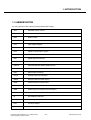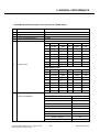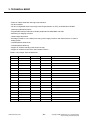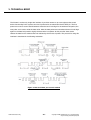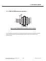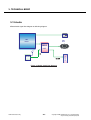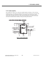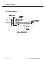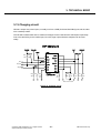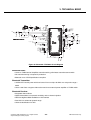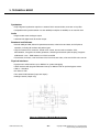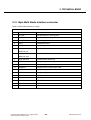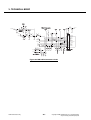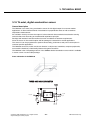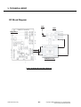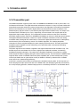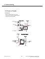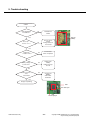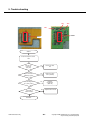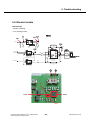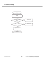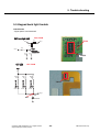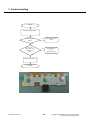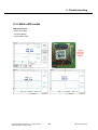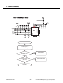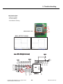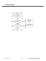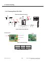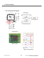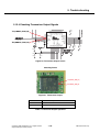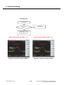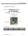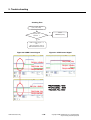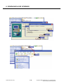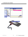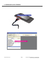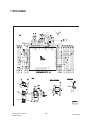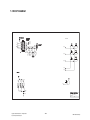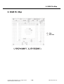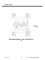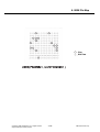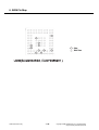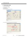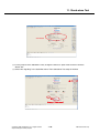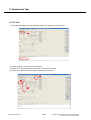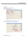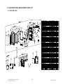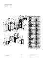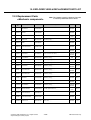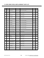
1
Service Manual
Internal Use Only
Service Manual
KP500
Model : KP500
Date: October, 2008 / Issue 1.0
REVISED HISTORY
Editor
Date
Issue
S.J.CHOI
4/10
0.1
Contents of Changes
S/W Version
* The information in this manual is subject to change without notice and should not be construed as a
commitment by LGE Inc. Furthermore, LGE Inc. reserves the right, without notice, to make changes to
equipment design as advances in engineering and manufacturing methods warrant.
* This manual provides the information necessary to install, program, operate and maintain the KP500.
Copyright © 2008 LG Electronics. Inc. All right reserved.
Only for training and service purposes
-3-
LGE Internal Use Only
LGE Internal Use Only
-4-
Copyright © 2008 LG Electronics. Inc. All right reserved.
Only for training and service purposes
Table Of Contents
1. INTRODUCTION .....................................7
1.1 Purpose .......................................................... 7
1.2 Regulatory Information.................................... 7
1.3 ABBREVIATION.............................................. 9
2. PERFORMANCE ...................................11
5.10 SIM & uSD trouble .......................................87
5.11 Touch pad trouble ........................................91
5.12 RTC trouble..................................................93
5.13 Tri-axial, digital acceleration sensor trouble.94
5.14 Trouble shooting of Receiver part ................95
5.15 Trouble Shooting of Transmitter Part .........101
2.1 H/W Features .................................................11
2.2 Technical specification ...................................12
6. DOWNLOAD & S/W UPGRADE.............109
3. TECHNICAL BRIEF ..............................19
7. CIRCUIT DIAGRAM ............................121
3.1 KP500 Functional Block diagram ...................19
3.2 Baseband Processor (BBP) Introduction .......20
3.3 Power management IC ..................................32
3.4 Power ON/OFF ..............................................37
3.5 SIM & uSD interface.......................................39
3.6 Memory ..........................................................41
3.7 LCD Display ...................................................42
3.8 Keypad Switching & Scanning .......................43
3.9 Keypad back-light illumination........................44
3.10 LCD back-light illumination...........................45
3.11 JTAG & ETM interface connector ................47
3.12 Audio ............................................................48
3.13 Charging circuit ............................................51
3.14 FM radio & BLUETOOTH.............................52
3.15 18pin Multi Media Interface connector .........55
3.16 Tri-axial, digital acceleration sensor..............57
3.17 General Description .....................................59
3.18 Receiver part................................................61
3.19 Transmitter part............................................62
3.20 RF synthesizer .............................................63
3.21 VCTCXO ......................................................63
3.22 Front End Module control.............................64
3.23 Power Amplifier Module ...............................65
3.24 PAM Schematic............................................66
8. BGM PIN MAP.....................................129
9. PCB LAYOUT......................................135
10. RF Calibration ..................................139
10.1 Test Equipment Setup................................139
10.2 Calibration Step..........................................139
11. Stand-alone Test ..............................144
11.1 Test Program Setting .................................144
11.2 Tx Test .......................................................146
11.3 Rx Test.......................................................147
12. EXPLODED VIEW & REPLACEMENT
PART LIST.........................................149
12.1 Exploded View ...........................................149
12.2 Replacement Parts.....................................151
12.3 Accessory.................................................. 169
4. PCB layout............................................67
4.1 Main PCB component placement...................67
5. Trouble shooting..................................69
5.1 Trouble shooting test setup............................69
5.2 Power on Trouble...........................................70
5.3 Charging trouble.............................................73
5.4 LCD display trouble........................................75
5.5 Camera Trouble .............................................77
5.6 Receiver & Speaker trouble ...........................79
5.7 Microphone trouble ........................................81
5.8 Vibrator trouble...............................................83
5.9 Keypad back light trouble...............................85
Copyright © 2008 LG Electronics. Inc. All right reserved.
Only for training and service purposes
-5-
LGE Internal Use Only
LGE Internal Use Only
-6-
Copyright © 2008 LG Electronics. Inc. All right reserved.
Only for training and service purposes
1. INTRODUCTION
1. INTRODUCTION
1.1 Purpose
This manual provides the information necessary to repair, calibration, description and download the
features of the KP500.
1.2 Regulatory Information
A. Security
Toll fraud, the unauthorized use of telecommunications system by an unauthorized part (for example,
persons other than your company’s employees, agents, subcontractors, or person working on your
company’s behalf) can result in substantial additional charges you’re your telecommunications
services. System users are responsible for the security of own system.
There are may be risks of toll fraud associated with your telecommunications system. System users
are responsible for programming and configuring the equipment to prevent unauthorized use. LGE
does not warrant that this product is immune from the above case but will prevent unauthorized use of
common-carrier telecommunication service of facilities accessed through or connected to it. LGE will
not be responsible for any charges that result from such unauthorized use.
B. Incidence of Harm
If a telephone company determines that the equipment provided to customer is faulty and possibly
causing harm or interruption in service to the telephone network, it should disconnect telephone
service until repair can be done. A telephone company may temporarily disconnect service as long as
repair is not done.
C. Changes in Service
A local telephone company may make changes in its communications facilities or procedure.
If these changes could reasonably be expected to affect the use of the KF600 or compatibility with the
network, the telephone company is required to give advanced written notice to the user, allowing the
user to take appropriate steps to maintain telephone service.
D. Maintenance Limitations
Maintenance limitations on the KP500 must be performed only at the LGE or its authorized agents.
The user may not make any changes and/or repairs expect as specifically noted in this manual.
Therefore, note that unauthorized alternations or repair may affect the regulatory status of the system
and may void any remaining warranty.
Copyright © 2008 LG Electronics. Inc. All right reserved.
Only for training and service purposes
-7-
LGE Internal Use Only
1. INTRODUCTION
E. Notice of Radiated Emissions
The KP500 complies with rules regarding radiation and radio frequency emission as defined by local
regulatory agencies. In accordance with these agencies, you may be required to provide information
such as the following to the end user.
F. Pictures
The pictures in this manual are for illustrative purposes only; your actual hardware may look slightly
different.
G. Interference and Attenuation
An KP500 may interfere with sensitive laboratory equipment, medical equipment, etc.
Interference from unsuppressed engines or electric motors may cause problems.
H. Electrostatic Sensitive Devices
ATTENTION
Boards, which contains Electrostatic Sensitive Device(ESD), are indicated by the sign.
Following information is ESD handling: Service personnel should ground themselves by using a wrist
strap when exchange system boards.
When repairs are made to a system board, they should spread the floor with anti-static mat which is
also grounded. Use a suitable, grounded soldering iron. Keep sensitive parts in these protective
packages until these are used. When returning system boards or parts such as EEPROM to the
factory, use the protective package as described.
LGE Internal Use Only
-8-
Copyright © 2008 LG Electronics. Inc. All right reserved.
Only for training and service purposes
1. INTRODUCTION
1.3 ABBREVIATION
For the purposes of this manual, following abbreviations apply:
APC
Automatic Power Control
BB
Baseband
BER
Bit Error Ratio
CC-CV
Constant Current - Constant Voltage
CLA
Cigar Lighter Adapter
DAC
Digital to Analog Converter
DCS
Digital Communication System
dBm
dB relative to 1 milli-watt
DSP
Digital Signal Processing
EEPROM
Electrical Erasable Programmable Read-Only Memory
EGPRS
Enhanced General Packet Radio Service
EL
Electroluminescence
ESD
Electrostatic Discharge
FPCB
Flexible Printed Circuit Board
GMSK
Gaussian Minimum Shift Keying
GPIB
General Purpose Interface Bus
GPRS
General Packet Radio Service
GSM
Global System for Mobile Communications
IPUI
International Portable User Identity
IF
Intermediate Frequency
LCD
Liquid Crystal Display
LDO
Low Drop Output
LED
Light Emitting Diode
Copyright © 2008 LG Electronics. Inc. All right reserved.
Only for training and service purposes
-9-
LGE Internal Use Only
1. INTRODUCTION
LGE
LG Electronics
OPLL
Offset Phase Locked Loop
PAM
Power Amplifier Module
PCB
Printed Circuit Board
PGA
Programmable Gain Amplifier
PLL
Phase Locked Loop
PSTN
Public Switched Telephone Network
RF
Radio Frequency
RLR
Receiving Loudness Rating
RMS
Root Mean Square
RTC
Real Time Clock
SAW
Surface Acoustic Wave
SIM
Subscriber Identity Module
SLR
Sending Loudness Rating
SRAM
Static Random Access Memory
STMR
Side Tone Masking Rating
TA
Travel Adapter
TDD
Time Division Duplex
TDMA
Time Division Multiple Access
UART
Universal Asynchronous Receiver/Transmitter
VCO
Voltage Controlled Oscillator
VCTCXO
Voltage Control Temperature Compensated Crystal Oscillator
WAP
Wireless Application Protocol
8PSK
8 Phase Shift Keying
LGE Internal Use Only
- 10 -
Copyright © 2008 LG Electronics. Inc. All right reserved.
Only for training and service purposes
2. GENERAL PERFORMANCE
2. GENERAL PERFORMANCE
2.1 H/W Feature
Item
Standard Battery
Feature
Comment
Li-ion, 900mAh
AVG TCVR Current
270mA typ
@PL5
Standby Current
2.3 mA typ
@PP9
Talk time
3 hours (GSM TX Level 7)
Standby time
Over 250 hours (Paging Period:9, RSSI: -85dBm)
Charging time
Under 3 hours
RX Sensitivity
EGSM/GSM850:-105dBm↓, DCS/PCS:-105dBm↓
TX output power
EGSM/GSM850 : 33dBm (@PL 5)
DCS/PCS: 30dBm (@PL 0)
GPRS compatibility
Class 10
SIM card type
3V Small
Display
Status Indicator
Main 240 x 400 pixels, 3” WQVGA, 262K color
Send Key, Shortcut Key, Volume Up/Down Key,
PWR Key, Camera Key, Lock Key
ANT
EAR Phone Jack
PC Synchronization
Speech coding
Built in antenna
18pin multi port Headset jack
Yes
HR/EFR/FR/AMR
Data and Fax
Yes
Vibrator
Yes
Buzzer
No
Voice Recoding
Yes
C-Mic
Yes
Receiver
Yes
Travel Adapter
Yes
Options
Bluetooth hands-free kit, Data Kit
Copyright © 2008 LG Electronics. Inc. All right reserved.
Only for training and service purposes
- 11 -
LGE Internal Use Only
2. GENERAL PERFORMANCE
2.2 Technical specification
Item
Description
Specification
GSM900
TX: 890 + 0.2 x n MHz
RX: 935 + 0.2 x n MHz ( n = 1 ~ 124 )
EGSM
TX: 890 + 0.2 x (n-1024) MHz
1
Frequency Band
RX: 935 + 0.2 x (n-1024) MHz ( n = 975 ~ 1023 )
DCS1800
TX: 1710 + ( n-511 ) x 0.2 MHz (n = 512 ~ 885)
RX: TX + 95 MHz
PCS1900
TX: 1850.2 + ( n-512 ) x 0.2 MHz (n = 512 ~ 810)
RX: TX + 80MHz
2
Phase Error
3
Frequency Error
RMS < 5 degrees
Peak < 20 degrees
< 0.1ppm
GSM900/EGSM
4
Power Level
LGE Internal Use Only
Level
Power
5
33 dBm
6
Toler.
Level
Power
Toler.
2dB
13
17 dBm
3dB
31 dBm
3dB
14
15 dBm
3dB
7
29 dBm
3dB
15
13 dBm
3dB
8
27 dBm
3dB
16
11 dBm
5dB
9
25 dBm
3dB
17
9 dBm
5dB
10
23 dBm
3dB
18
7 dBm
5dB
11
21 dBm
3dB
19
5 dBm
5dB
12
19 dBm
3dB
Level
Power
Toler.
DCS1800/PCS1900
Level
Power
0
30 dBm
2dB
8
14 dBm
3dB
1
28 dBm
3dB
9
12 dBm
4dB
2
26 dBm
3dB
10
10 dBm
4dB
3
24 dBm
3dB
11
8 dBm
4dB
4
22 dBm
3dB
12
6 dBm
4dB
5
20 dBm
3dB
13
4 dBm
4dB
6
18 dBm
3dB
14
2 dBm
5dB
7
16 dBm
3dB
15
0 dBm
5dB
- 12 -
Toler.
Copyright © 2008 LG Electronics. Inc. All right reserved.
Only for training and service purposes
2. GENERAL PERFORMANCE
Item
Description
Specification
GSM900/EGSM
5
Offset from Carrier (kHz).
Max. dBc
100
+0.5
200
-30
250
-33
400
-60
600 ~ 1,200
-60
1,200 ~ 1,800
-60
1,800 ~ 3,000
-63
3,000 ~ 6,000
-65
6,000
-71
Output RF Spectrum
(due to modulation)
DCS1800/PCS1900
Offset from Carrier (kHz).
Max. dBc
100
+0.5
200
-30
250
-33
400
-60
600 ~ 1,200
-60
1,200 ~ 1,800
-60
1,800 ~ 3,000
-65
3,000 ~ 6,000
-65
6,000
-73
GSM900/EGSM
6
Offset from Carrier (kHz)
Max. (dBm)
Output RF Spectrum
400
-19
(due to switching transient)
600
-21
1,200
-21
1,800
-24
Copyright © 2008 LG Electronics. Inc. All right reserved.
Only for training and service purposes
- 13 -
LGE Internal Use Only
2. GENERAL PERFORMANCE
Item
Description
Specification
DCS1800/PCS1900
6
7
8
Offset from Carrier (kHz).
Max. (dBm)
Output RF Spectrum
400
-22
(due to switching transient)
600
-24
1,200
-24
1,800
-27
Spurious Emissions
Bit Error Ratio
Conduction, Emission Status
EGSM
BER (Class II) < 2.439% @-102dBm
DCS1800/PCS1900
BER (Class II) < 2.439% @-100dBm
9
Rx Level Report accuracy
10
SLR
11
12
13
8
3 dB
Frequency (Hz)
Max.(dB)
Min.(dB)
100
-12
-
200
0
-
300
0
-12
1,000
0
-6
2,000
4
-6
3,000
4
-6
3,400
4
-9
4,000
0
-
Frequency (Hz)
Max.(dB)
Min.(dB)
100
-12
-
200
0
-
300
2
-7
500
*
-5
1,000
0
-5
3,000
2
-5
3,400
2
-10
4,000
2
Sending Response
RLR
2 3 dB
Receiving Response
* Mean that Adopt a straight line in between 300 Hz
and 1,000 Hz to be Max. level in the range.
LGE Internal Use Only
- 14 -
Copyright © 2008 LG Electronics. Inc. All right reserved.
Only for training and service purposes
2. GENERAL PERFORMANCE
Item
Description
Specification
14
STMR
13 5 dB
15
Stability Margin
> 6 dB
16
dB to ARL (dB)
Level Ratio (dB)
-35
17.5
-30
22.5
-20
30.7
-10
33.3
0
33.7
7
31.7
10
25.5
Distortion
17
Side Tone Distortion
Three stage distortion < 10%
18
System frequency
(26 MHz) tolerance
2.5ppm
19
32.768KHz tolerance
30ppm
20
Power consumption
21
Talk Time
22
Standby Time
23
Ringer Volume
24
Charge Current
Standby
- Normal
3 mA(@PP9)
EGSM/Lvl 7 (Battery Capacity 800mA):180 min
EGSM/Lvl12(Battery Capacity 800 mA):320min
Under conditions, at least 300 hours:
1. Brand new and full 800mAh battery
2. Full charge, no receive/send and keep GSM in idle mode.
3. Broadcast set off.
4. Signal strength display set at 3 level above.
5. Backlight of phone set off.
At least 65 dB under below conditions:
1. Ringer set as ringer.
2. Test distance set as 50 cm
Fast Charge : < 400 mA
Slow Charge: < 120 mA
Antenna Bar Number
25
Antenna Display
Copyright © 2008 LG Electronics. Inc. All right reserved.
Only for training and service purposes
- 15 -
Power
7
>-92 dBm ~
5
-97dBm ~ -93dBm
4
-100dBm ~ -98dBm
2
-103dBm ~ -101dBm
1
-105dBm ~ -104dBm
0
< -106 dBm
Off
No Service
LGE Internal Use Only
2. GENERAL PERFORMANCE
Item
26
Description
Specification
Battery Bar Number
Voltage( 0.05V)
3
3.69V ~ 4.2V
2
3.53V ~ 3.69V
1
3.43V ~ 3.53V
0
3.30V ~ 3.43V
Battery Indicator
3.53V↓
0.05V (Call)
3.43V ↓
0.05V (Standby)
27
Low Voltage Warning
28
Forced shut down Voltage
3.3
Battery Type
Li-ion Battery
Standard Voltage = 3.7 V
Battery full charge voltage = 4.2 V
Capacity: 800mAh
Travel Charger
Switching-mode charger
Input: 150 ~ 240 V, 50/60Hz
Out put: 5.6, 0.4A
29
30
LGE Internal Use Only
0.05 V
- 16 -
Copyright © 2008 LG Electronics. Inc. All right reserved.
Only for training and service purposes
2. GENERAL PERFORMANCE
* EDGE RF Specification (Option: is not serviced for “EDGE mode”)
Item
1
2
3
4
Description
RMS EVM
Peak EVM
95th Percentile EVM
Origin Offset Suppression
Specification
≥
9%
30%
15%
30dB
GSM900/EGSM
5
Power Level
Level
Power
Toler.
Level
Power
Toler.
5
27dBm
3dB
13
17dBm
3dB
6
27dBm
3dB
14
15dBm
3dB
7
27dBm
3dB
15
13dBm
3dB
8
27dBm
3dB
16
11dBm
5dB
9
25dBm
3dB
17
9dBm
5dB
10
23dBm
3dB
18
7dBm
5dB
11
21dBm
3dB
19
5dBm
5dB
12
19dBm
3dB
Level
Power
Toler.
DCS1800/PCS1900
6
Output RF Spectrum
(due to modulation)
Copyright © 2008 LG Electronics. Inc. All right reserved.
Only for training and service purposes
Level
Power
Toler.
0
26/25dBm
3dB
8
14 dBm
3dB
1
26/25dBm
3dB
9
12 dBm
4dB
2
26/25dBm
3dB
10
10 dBm
4dB
3
24 dBm
3dB
11
8 dBm
4dB
4
22 dBm
3dB
12
6 dBm
4dB
5
20 dBm
3dB
13
4 dBm
4dB
6
18 dBm
3dB
14
2 dBm
5dB
7
16 dBm
3dB
15
0 dBm
5dB
GSM900/EGSM
Offset from carrier(kHz)
Max. dBc
100
+0.5
200
-30
250
-33
400
-54
600 ~ <1,200
-60
1,200 ~ <1,800
-60
1,800 ~ <3,000
-63
3,000 ~ <6,000
-65
6,000
-71
- 17 -
LGE Internal Use Only
2. GENERAL PERFORMANCE
Item
6
Description
Output RF Spectrum
(due to modulation)
7
Output RF Spectrum
(due to switching transient)
Specification
DCS1800/PCS1900
Offset from carrier(kHz)
Max. dBc
100
+0.5
200
-30
250
-33
400
-54
600 ~ <1,200
-60
1,200 ~ <1,800
-60
1,800 ~ <3,000
-63
3,000 ~ <6,000
-65
6,000
-71
GSM900/EGSM
Offset from carrier(kHz)
Max. dBm
400
-23
600
-26
1,200
-27
1,800
--30
DCS1800/PCS1900
LGE Internal Use Only
Offset from carrier(kHz)
Max. dBm
400
-23
600
-26
1,200
-27
1,800
-30
- 18 -
Copyright © 2008 LG Electronics. Inc. All right reserved.
Only for training and service purposes
3. TECHNICAL BRIEF
3. TECHNICAL BRIEF
3.1 KP500 Functional Block diagram
The functional component arrangement is mentioned below diagram.
KP500 Block Diagram
ANT
FEM
PAM(SKY77340)
BB IC(PMB8877)
Memory
FM_ANT
DCS/PCS
PA_LEVEL
Match
ADD(0:29)
PA_LEVEL
/
Match
DGM1110M014
TXON_PA
TXON_PA
PA_BAND
PA_BAND
PA_MODE
PA_MODE
DATA(0:15)
/
Controller
(2G NAND +
1G DDR SDRAM)
GSM850/900
FE1 FE2
Match
Pin.03
Pin.04
Touch Window
/
H/S_RIGHT
Match
Pin.05
I2C
I2C1
KEY_COL
GPIO
I/I_/Q/Q_
/
PMB6272
GPIO
/
LED Matrix Module
USB_M
KEY PAD
ROW
KEY_EN
26M_MCLK
RF INTERFACE
RF_DA
Pin.07
JACK_DETECT
VBAT
KEY Back Light
Pin.09
Pin.10
VIB_EN
Vibrator
CAM_I2C CAM_I2C
Pin.08
VBAT.
RPWRON
RF_EN
RF_CLK
Pin.06
USB_P
COL
Pin.11
VCHG
I/O CONNECTOR
KEY_ROW
TRANSCEIVER
Pin.02
H/S_LEFT
I 2C
I 2C
Pin.01
H/S MIC & HOOK_DET
Pin.12
3-Axis Accelerometer
Pin.13
MMC I/F
MMC I/F
/
DSR
-SD + SIM Socket
Pin14
VBUS_USB
VCHG
T_IN1
CHG_EN
Charging IC
UART_TX
VUSB_USB
Pin.15
Pin.16
UART_RX
Pin.17
Pin.18
Battery
CAM_ I2C
AFC
CIF
I2C
26M_TCXO
BT ANT
3M CAM
/
/
I2C1
BT_CLK
(LED CTRL : 5 ea)
BPF
FM ANT
UART
UART
/
BT IC
BCM2048SB0
DIF
DIF
I2S
/
LCD, 3.0"
262K TFT WQVGA
Charge Pump
(SC654ULTRT)
I2S
/
AUIDO AMP(MAX9877)
VBAT
FM
RADIO
HPL
VAUDIOa(2.5V)
VIO(2.62V)
VAUDIOb(2.5V)
SD2(1.8V)
VSIM(2.9V)
VRF1(2.85V)
VPLL(1.35V)
VMME (2.9V)
VRF2(1.53V)
VRTC(2.0V)
VUMTS(2.85V)
VRF3(2.70V)
VVIB(2.8V)
VUSB(3.1V)
VLED (2.9V)
INA2
EPPA21
I2C
END_KEY
I2C
/
I2C1
I2C1
2V11_RTC
2V11_RTC
MIXER
VAUX (2.9V)
PRE-AMP
INA1
EPPA11
SD2(1.8V)
HEADSET RECEIVER
HPR
VBAT
SD1 (1.35V)
BYPASS
EPP11
32kHz
PMB6821(PM IC)
RXINRXIN+
EPN11
OUT-
FM
RADIO
MAIN SPEAKER
OUT+
/
INB1/2
VMICP/N
MIC1(P/N)
MIC2(P/N)
MAIN MIC
HEADSET MIC
B/UP BAT.
Figure 1 KP500 Functional block diagram
Copyright © 2008 LG Electronics. Inc. All right reserved.
Only for training and service purposes
- 19 -
LGE Internal Use Only
3. TECHNICAL BRIEF
3.2 Baseband Processor (BBP) Introduction
Figure 3 Top level block diagram of the S-GOLD3™ (PMB8877)
3.2.1 General Description
S-GOLD3™ is a GSM/EDGE single chip mixed signal Baseband IC containing all analog and digital
functionality of a cellular radio. Additionally S-GOLD3™ Provides multimedia extensions such as
camera, software MIDI, MP3 sound. It is designed as a single chip solution, integrating the digital and
mixed signal portions of the base band in 0.09um, 1.2V technology.
The chip will fully support the FR, EFR, HR and AMR-NB vocoding.
S-GOLD3™ support multi-slot operation modes HSCSD (up to class 10), GPRS for high speed data
application (up to class 12) and EGPRS (up to class 12) without additional external hardware.
LGE Internal Use Only
- 20 -
Copyright © 2008 LG Electronics. Inc. All right reserved.
Only for training and service purposes
3. TECHNICAL BRIEF
3.2.2 Block Description
• Processing core
ARM926EJ-S 32 bit processor core for controller functions. The ARM926EJ-S includes an MMU,
and the Jazelle Java extension for Java acceleration.
- TEAKLite DSP core
• ARM-Memory
- 32k Byte Boot ROM on the AHB
- 96k Byte SRAM on the AHB, flexibly usable as program or data RAM
- 16k Byte Cache for Program (internal)
- 8k Byte tightly coupled memory for Program(internal)
- 8k Byte Cache for Data(internal)
- 8k Byte tightly coupled memory for Data(internal)
• DSP-Memory
- 104K x 16bit Program ROM
- 8k x 16bit Program RAM
- 60k x 16bit Data ROM
- 37k x 16bit Data RAM
- Incremental Redundancy(IR) Memory of 35904 words of 16bit
• Shared Memory Block
1.5K x 32bit Shared RAM(dual ported) between controller system and TEAKLite.
• Controller Bus system
The processor cores and their peripherals are connected by powerful buses.
Multi-layer AHB for connecting the ARM and the other master capable building blocks with the
internal and external memories and with the peripheral buses.
• Clock system
The clock system allows widely independent selection of frequencies for the essential parts of the
S-GOLD3. Thus power consumption and performance can be optimized for each application.
• Functional Hardware block
- CPU and DSP Timers
- MOVE coprocessor performing motion estimation for video encoding algorithms (H.263, MPEG-4)
- Programmable PLL with additional phase shifters for system clock generation
- GSM Timer Module that off-loads the CPU from radio channel timing
- GMSK / 8-PSK Modulator according to GSM-standard 05.04 (5/2000)
- GMSK Modulator: gauss-filter with B*T=0.3
- EDGE Modulator: 8PSK-modulation with linearized GMSK-Pulse-Filter
- Hardware accelerators for equalizer and channel decoding.
- Incremental Redundancy memory for EDGE class 12 support
- A5/1, A5/2, A5/3 Cipher unit
- GEA1, GEA2, GEA3 Cipher Unit to support GPRS data transmission
- Advanced static and dynamic power management features including TDMA-Frame synchronous
low power mode and enhanced CPU modes(idle and sleep modes)
Copyright © 2008 LG Electronics. Inc. All right reserved.
Only for training and service purposes
- 21 -
LGE Internal Use Only
3. TECHNICAL BRIEF
- Pulse Number Modulation output for Automatic Frequency Correction(AFC)
- Serial RF Control interface: support of direct conversion RF
- A Universal Serial Interface(USIF) enabling asynchronous (UART) of synchronous (SPI) serial
data transmission
- 1 Serial Synchronous SPI compatible interfaces in the controller domain
- 1 Serial Synchronous SPI compatible interface in the TEAKLite domain
- 2 USART with autobaud detection, hardware flow control and integrated IrDA controller
supporting IrDA’s SIR standard (up to 115.2Kbps)
- A dedicated Fas IfDA Controller supporting IrDA’s SIR,MIR and FIR standards (up to 4Mbps)
- I2C-bus interface (e.g. connection to S/M power)
- A fast display interface supporting serial and parallel interconnection
- An ITU-R BT.656 compatible Camera interface.
- Programmable clock output for a camera
- An multimedia/Secure Digital Card Interface (MMCI/SD: SDIO capable)
3.2.3 External Devices connected to memory interface
Table 1. Memory interface
Device
Name
Maker
Remark
FLASH
K5E1G12ACA-D075
Samsung
Synchronous / A synchronous
DDR
K5E1G12ACA-D075
Samsung
Synchronous 133MHz
LCD
IM200DST2A
LGIT
8bit access 2 times transmission
Melody IC
Not Used
S/W
Infineon Software CODEC
3.2.4 RF Interface (T_OUT)
S-Gold3 uses this interface to control RF IC and Peripherals. 13 signals are provided switch on/off RF
ICs Periodically each TDMA frame.
Table 2. RF Interface Spec.
T_OUT
Resource
Interconnection
Description
T_OUT0
TXON_PA
PAM Power on
T_OUT1
Other function
-
T_OUT2
PA_BAND
TX RF band select
T_OUT3
ANT_SW1
FEM control
T_OUT4
ANT_SW2
FEM control
T_OUT5
ANT_SW3
FEM control
T_OUT6
MODE
PAM Mode select
LGE Internal Use Only
- 22 -
Copyright © 2008 LG Electronics. Inc. All right reserved.
Only for training and service purposes
3. TECHNICAL BRIEF
3.2.5 USIF Interface
KF350 have three USIF Drivers as follow :
- USIF1 : Hardware Flow Control / SW upgrade / Calibration
- USIF2 : MON used Rx, Tx and CTS, RTS use BT Interface
- USIF3 : BT Interface
Table 3. USIF Interface Spec.
Resource
USIF1
USIF1_TXD
USIF1_RXD
USIF1_CTS
USIF1_RTS
USIF2
USIF2_TXD
USIF2_RXD
USIF2_CTS
USIF2_RTS
USIF3
USIF3_TXD
USIF3_RXD
Name
Remark
UART_TX
UART_RX
USB_DP
USB_DM
Transmit Data
Receive Data
NC
NC
BT_CTS
BT_RTS.
NC
NC
BT_TX
BT_RX
BT Transmit tx
BT Receive rx
3.2.6 ADC channel
BBP ADC block is composed of 10 external ADC channel. This block operates charging process and
other related process by reading battery voltage and other analog values.
Table 4. S-Gold3 ADC channel usage
ADC channel
Resource
M0
M1
M2
M3
M4
M5
M6
M7
M8
M9
M10
Interconnection
BAT_ID
RF_TEMP
N.C
JACK_TYPE
N.C
H/W VERSION
N.C
ICLD
VSUPPLY
N.C
N.C
Copyright © 2008 LG Electronics. Inc. All right reserved.
Only for training and service purposes
Description
Battery temperature measure
RF block temperature measure
Accessory type detect
S-Gold3 H/W version detect
Battery supply voltage measure
- 23 -
LGE Internal Use Only
3. TECHNICAL BRIEF
3.2.7 GPIO map
Over a hundred allowable resources, KF350 is using as follows except dedicated to SIM and Memory.
KF350 GPIO(General Purpose Input/Output) Map, describing application, I/O state, and enable level,
is shown in below table
Table 5 S-Gold3 GPIO pin Map
Port Function
KEY MATRIX
KP_IN0
KP_IN1
KP_IN2
KP_IN3
KP_IN4
KP_IN5
KP_OUT5
KP_OUT0
KP_OUT1
KP_OUT2
KP_OUT3
USIF1
USIF1_RXD
USIF1_TXD
USIF1_RTS_N
USIF1_CTS_N
USIF2
USIF2 _RXD
USIF2 _TXD
USIF2_RTS_N
USIF2_CTS_N
USIF3
USIF3 _RXD
USIF3 _TXD
GPIO_21
MMCI2
MMCI2_CMD
MMCI2_DAT[0]
MMCI2_CLK
CAMERA I/F
CIF_D0
CIF_D1
LGE Internal Use Only
Net Name
Description
N/A
N/A
N/A
KP_IN3
N/A
KP_IN5
KP_IN6
KP_OUT0
LIN_INVERT
KP_OUT2
KP_OUT3
UART_RX
UART_TX
USB_DAT_VP
USB_SE0_VM
UART, RS232 Data
UART, RS232 Data
USB Data
USB Data
ACCEL_INT
N/A
UART_BT_RTS
UART_BT_CTS
Not used
Bluetooth RTS
Bluetooth CTS
UART_BT_RX
UART_BT_TX
N/A
Bluetooth RX
Bluetooth TX
PCB_VER1
PCB_VER2
PCB Version1
PCB Version2
VIB_EN
Vibrator LDO Enable
CIF_D(0)
CIF_D(1)
Camera DATA[0]
Camera DATA[1]
- 24 -
Copyright © 2008 LG Electronics. Inc. All right reserved.
Only for training and service purposes
3. TECHNICAL BRIEF
CIF_D2
CIF_D3
CIF_D4
CIF_D5
CIF_D6
CIF_D7
CIF_PCLK
CIF_HSYNC
CIF_VSYNC
CLKOUT
CIF_PD
CIF_DATA2
CIF_DATA3
CIF_DATA4
CIF_DATA5
CIF_DATA6
CIF_DATA7
CIF_PCLK
CIF_HSYNC
CIF_VSYNC
CIF_MCLK
CIF_PD
Camera DATA[2]
Camera DATA[3]
Camera DATA[4]
Camera DATA[5]
Camera DATA[6]
Camera DATA[7]
Camera pixel clock
Camera H sync
Camera V sync
Camera main clock
Camera power down(active high)
CIF_RESET
LCD I/F
DIF_D0
DIF_D1
DIF_D2
DIF_D3
DIF_D4
DIF_D5
DIF_D6
DIF_D7
DIF_D8
DIF_CS1
DIF_CS2
DIF_CD
DIF_WR
CIF_RESET
Camera reset
DIF_D0
DIF_D1
DIF_D2
DIF_D3
DIF_D4
DIF_D5
DIF_D6
DIF_D7
CAM_LDO_EN
DIF_MAIN_CS
IF_MODE
DIF_CD
DIF_WR
LCD data[0]
LCD data[1]
LCD data[2]
LCD data[3]
LCD data[4]
LCD data[5]
LCD data[6]
LCD data[7]
Camera LDO Enable
MAIN LCD chip select
Interface mode
Command Data switch
LCD Write
DIF_RD
HOOK_DETECT
DIF_VSYNC
DIF_RESET
TOUCH_INT
LCD Read
Ear-Mic hook detection
LCD Sync
LCD Reset
Touch Sensor INT
I2C_SCL
I2C_SDA
UART_BT_RTS
UART_BT_CTS
For Touch LDO/PMIC/Audio Amp
For Touch LDO/PMIC/Audio Amp
Bluetooth RTS
Bluetooth CTS
UART_BT_RX
UART_BT_TX
N/A
Bluetooth RX
Bluetooth TX
DIF_RD
EINT7
GPIO_100
GPIO_27 _
EINT5
#I2C1
I2C_SCL
I2C_SDA
USIF2_RTS_N
USIF2_CTS_N
USIF3
USIF3 _RXD
USIF3 _TXD
GPIO_21
MMCI2
Copyright © 2008 LG Electronics. Inc. All right reserved.
Only for training and service purposes
- 25 -
LGE Internal Use Only
3. TECHNICAL BRIEF
MMCI2_CMD
MMCI2_DAT[0]
MMCI2_CLK
CAMERA I/F
CIF_D0
CIF_D1
CIF_D2
CIF_D3
CIF_D4
CIF_D5
CIF_D6
PCB_VER1
PCB_VER2
VIB_EN
PCB Version1
PCB Version2
Vibrator LDO Enable
CIF_DATA0
CIF_DATA1
CIF_DATA2
CIF_DATA3
CIF_DATA4
CIF_DATA5
CIF_DATA6
Camera DATA[0]
Camera DATA[1]
Camera DATA[2]
Camera DATA[3]
Camera DATA[4]
Camera DATA[5]
Camera DATA[6]
CIF_D7
CIF_PCLK
CIF_HSYNC
CIF_VSYNC
CLKOUT
CIF_PD
CIF_RESET
LCD I/F
DIF_D0
DIF_D1
DIF_D2
DIF_D3
DIF_D4
DIF_D5
DIF_D6
CIF_DATA7
CIF_PCLK
CIF_HSYNC
CIF_VSYNC
CIF_MCLK
CIF_PD
CIF_RESET
Camera DATA[7]
Camera pixel clock
Camera H sync
Camera V sync
Camera main clock
Camera power down(active high)
Camera reset
DIF_D0
DIF_D1
DIF_D2
DIF_D3
DIF_D4
DIF_D5
DIF_D6
LCD data[0]
LCD data[1]
LCD data[2]
LCD data[3]
LCD data[4]
LCD data[5]
LCD data[6]
DIF_D7
DIF_D8
DIF_CS1
DIF_CS2
DIF_CD
DIF_WR
DIF_RD
EINT7
GPIO_100
GPIO_27
EINT5
#I2C1
I2C_SCL
I2C_SDA
PM_INT (EINT)
DIF_D7
CAM_LDO_EN
DIF_MAIN_CS MAIN
IF_MODE
DIF_CD
DIF_WR
DIF_RD
HOOK_DETECT
DIF_VSYNC
_DIF_RESET
TOUCH_INT
LCD data[7]
Camera LDO Enable
LCD chip select
Interface mode
Command Data switch
LCD Write
LCD Read
Ear-Mic hook detection
LCD Sync
LCD Reset
Touch Sensor INT
I2C_SCL
I2C_SDA
PM_INT
For Touch LDO/PMIC/Audio Amp
For Touch LDO/PMIC/Audio Amp
LGE Internal Use Only
- 26 -
Copyright © 2008 LG Electronics. Inc. All right reserved.
Only for training and service purposes
3. TECHNICAL BRIEF
#I2C2
I2C2_SCL
I2C2_SDA
SIM I/F
CC_IO
CC_CLK
CC_RST
IrDA
USB_OEn
EINT3
External Memory
CIF_SCL
CIF_SDA
For Camera
For Camera
SIM_IO
SIM_CLK
SIM_RST
SIM CARD I/O
SIM CARD CLOCK
SIM CARD RESET
USB_OEn
N/A
MMCI_CMD
MMCI_DAT[0]
MMCI_CLK
MMCI1_DAT[1]
MMCI1_DAT[2]
MMCI1_DAT[3]
I2S1
I2S2_CLK0
GPIO_102
I2S2_RX
I2S2_TX
I2S2_WA0
I2S2
EINT4
GPIO_102
MMC_CMD
MMC_D0
MMC_CLK
MMC_D1
MMC_D2
MMC_D3
T-flash
T-flash
T-flash
T-flash
T-flash
T-flash
I2S1_CLK
MMC_DETECT
I2S1_RX
I2S1_TX
2S1_WA0
Bluetooth Clock
T-flash Detect
Bluetooth PCM RX
Bluetooth PCM TX
Bluetooth Clock
CHG_EOC
LCD_ID
Charger
LCD ID
CC0CC1IO
CC0CC7IO
CC0CC3IO
GPIO_103
Audio I/F
EPN1
EPP1
EPPA1
EPREF
EPPA2
MICN1
MICP1
MICN2
MICP2
VMICP
_PPR
BT_INT
N/A
KEY_EN
Charger
Bluetooth INT
EAR_N
EAR_P
BB_SND_L
Reference
BB_SND_R
MAIN_MIC_N
MAIN_MIC_P
HS_MIC_N
HS_MIC_P
VMIC_P
For Receiver
For Receiver
For Speaker
Copyright © 2008 LG Electronics. Inc. All right reserved.
Only for training and service purposes
For Speaker
For Mic
For Mic
For Headset Mic
For Headset Mic
Power for MIC
- 27 -
LGE Internal Use Only
3. TECHNICAL BRIEF
VMICN
#I/Q-Signale
PAOUT1
BB_I
BB_IX
BB_Q
BB_QX
ADC
M0
M1
M2
M3
M7
M8
M9
M10
Reference
VREFP
IREF
JTAG I/F
TDO
TDI
TMS
TCK
TRST_n
RTCK
#Debug
TRIG_IN
MON1
MON2
TRACESYNC
TRACECLK
PIPESTAT[2]
PIPESTAT[1]
PIPESTAT[0]
TRACEPKT[0]
TRACEPKT[1]
TRACEPKT[2]
TRACEPKT[3]
TRACEPKT[4]
TRACEPKT[5]
LGE Internal Use Only
VMIC_N
Power for MIC
PA_LEVEL
I
IX
Q
QX
BAT_ID
RF_TEMP
PCB_VER
Battery temperature measure
RF block temperature measure
LOAD
N.C
Current consumption measure
VREFN
TDO
TDI
TMS
TCK
TRSTn
RTCK
JTAG
JTAG
JTAG
JTAG
JTAG
JTAG
TRIG_IN
2V62_VIO
ETM (Embedded Trace Macro Cell)
ETM
TRACESYNC
TRACECLK
PIPESTAT[2]
PIPESTAT[1]
PIPESTAT[0]
TRACEPKT[0]
TRACEPKT[1]
TRACEPKT[2]
TRACEPKT[3]
TRACEPKT[4]
TRACEPKT[5]
ETM
ETM
ETM
ETM
ETM
ETM
ETM
ETM
ETM
ETM
ETM
- 28 -
Copyright © 2008 LG Electronics. Inc. All right reserved.
Only for training and service purposes
3. TECHNICAL BRIEF
TRACEPKT[6]
TRACEPKT[7]
Memory
MEM_ADV_n
MEM_RDN
MEM_AD[0]
MEM _AD[1]
MEM _AD[2]
MEM _AD[3]
MEM _AD[4]
MEM _AD[5]
TRACEPKT[6]
TRACEPKT[7]
BA1
_RD
DATA0
DATA1
DATA2
DATA3
DATA4
DATA5
MEM _AD[6]
MEM _AD[7]
MEM _AD[8]
MEM _AD[9]
MEM _AD[10]
MEM _AD[11]
MEM _AD[12]
MEM _AD[13]
MEM _AD[14]
MEM _AD[15]
MEM_CS0_n
MEM_CS1_n
MEM_WRN
MEM_A[16]
MEM_A[17]
DATA6
DATA7
DATA8
DATA9
DATA10
DATA11
DATA12
DATA13
DATA14
DATA15
_NAND_CS
_RAM_CS
_WR
ADD[16]
ADD[17]
MEM_A[18]
MEM_A[19]
MEM_A[20]
MEM_A[21]
MEM_A[22]
MEM_A[23]
MEM_A[24]
MEM_A[25]
MEM_A[26]
MEM_CSA0_n
MEM_CSA1_n
MEM_CSA2_n
MEM_CSA3_n
MEM_BFCLKO1
MEM_BFCLKO2
ADD[18]
ADD[19]
ADD[20]
ADD[21]
ADD[22]
ADD[23]
ADD[24]
ADD[25]
ADD[26]
ADD[27]
ADD[28]
ADD[29]
BA0
ETM
ETM
Read
SDCLKI
Copyright © 2008 LG Electronics. Inc. All right reserved.
Only for training and service purposes
- 29 -
LGE Internal Use Only
3. TECHNICAL BRIEF
MEM_SDCLKO
MEM_BC0_n
MEM_BC1_n
MEM_BC2_n
MEM_BC3_n
MEM _A[0]
MEM _A[1]
MEM _A[2]
MEM _A[3]
MEM _A[4]
MEM _A[5]
SDCLKO
_BC0
_BC1
LDQS
UDQS
ADD[0]
ADD[1]
ADD[2]
ADD[3]
ADD[4]
ADD[5]
MEM _A[6]
MEM _A[7]
MEM _A[8]
MEM _A[9]
MEM _A[10]
MEM _A[11]
MEM _A[12]
MEM _A[13]
MEM _A[14]
MEM _A[15]
MEM_RAS_n
MEM_CAS_n
MEM_CKE
FCDP_RBn
FWP
ADD[6]
ADD[7]
ADD[8]
ADD[9]
ADD[10]
ADD[11]
ADD[12]
ADD[13]
ADD[14]
ADD[15]
_RAS
_CAS
CKE
FCDP
_WP
T_OUT0
T_OUT1
T_OUT2
T_OUT3
GPIO_47
GPIO_48
T_OUT6
GPIO_50
GPIO_51
GPIO_52
CC1CC7IO
GPIO_54
#SPCU
SPCU_RQ_IN0
GPIO_118
TXON_PA
FE2
PA_BAND
FE1
BT_WAKEUP
VBUS_OVP
PA_MODE
For
DSR
LCD_BACKLIGHT_EN
JACK_DETECT
BT_LDO_EN
Vibrator
UART DSR
LCD Backlight Enable
Jack Detect
Bluetooth LDO Enable
BT_RESETn
Bluetooth Reset
LGE Internal Use Only
Bluetooth wakeup
- 30 -
Copyright © 2008 LG Electronics. Inc. All right reserved.
Only for training and service purposes
3. TECHNICAL BRIEF
SPCU_RC_OUT0
SPCU_RQ_IN2
#RF Control Unit
RF_STR0
RF_STR1
RF_DATA
RF_CLK
other
AFC
GPIO_58
F26M
VCXO_EN
RESOURCE_CTRL
F32K
OSC32K
RESET_n
RTC_OUT
#Extra I/Os
CLK32K
DSPOUT1
F32K
OSC32K
_RESET
RTC_OUT
RF_EN
LIN_PWM_MAG
RF_DA
RF_CLK
RPWRON
26MHZ_MCLK
CLK32K
WDOG
Copyright © 2008 LG Electronics. Inc. All right reserved.
Only for training and service purposes
VCXO Enable
For Vibrator
26MHz Clock
For FM Radio, BT CLK32K
- 31 -
LGE Internal Use Only
3. TECHNICAL BRIEF
3.3 Power management IC
3.3.1 General Description
SM-POWER is a highly integrated Power and Battery Management IC for mobile handsets. It has
been specially designed for usage with S-Gold3. Although optimized for usage with the Infineon SGOLD baseband device it is suitable for the S-GOLDlite and the E-GOLD+ baseband devices as well.
It also supports the cellular RF devices like SMARTi-DC, SMARTi-DC+, SMARTi-SD and the
Bluemoon Single, Infineon s single chip solution for Bluetooth. If used with S-GOLD3 it provides all
power supply functions (except for the RF PA) for a complete advanced GSM Edge smart phone
minimizing external device count.
Block Description
• Highly efficient step-down converter for main digital baseband supply including Core, DSP and
memory interface (External Bus Unit).
• Support of S-GOLD standby power-down concept
• Low-drop-out (LDO) regulators for Flash and mobile RAM memory devices
• Voltage independent switching of two SIM cards
• LDO regulators for baseband I/O supply
• LDO regulator for analog mixed-signal section of S-GOLD
• Low-noise LDO regulators for RF devices
• Supply for Bluemoon Single, Infineon s single chip solution for Bluetooth
• Audio amplifier 8 Ohms for handsfree operation and ringing
• Charge Control for charging Li-Ion/Polymer batteries under software control
• Pre-charge current generator with selectable current level
• RTC regulator with ultra-low quiescent current
• USB interface support for peripheral and mini-host mode
• Backlight LEDs driver with current selection and PWM dimming function
• Two single LED driver outputs for signaling
• Vibrator driver with adjustable voltage
• Fully controlable by software via I2C - Bus
• Temperature and battery voltage sensors
• Interrupt channels for peripherals
• System debug mode
• VQFN 48 package with heat sink and non-protruding leads
• Compatible with the Infineon E-GOLD+ V2 and V3
LGE Internal Use Only
- 32 -
Copyright © 2008 LG Electronics. Inc. All right reserved.
Only for training and service purposes
3. TECHNICAL BRIEF
SM-POWER is a further step on the successful E-Power product line with enhanced and optimized
functionality.
SM-POWER features a baseband supply concept with a DC/DC step-down converter cascaded by two
linear regulators
- SM-POWER’s DC/DC converter makes up to 40 % reduction of battery current for smart phone
functions (e.g. organizer functions, games, MP3 decoding) possible.
- SDBB has high efficiency up to 95% and also a power save mode.
- Memory Interface is directly supported by the SDBB
- SDBB can also act as main supply voltage for E-GOLD+ or S-GOLDlite baseband devices.
- For S-GOLD two linear regulators for DSP and Core are cascaded after the SDBB.
SM-POWER supports the standby power-down concept of S-GOLD by temporarily switching off the
linear regulator for the DSP during mobile standby whenever this subsystem is not used. In this phase
the ARM controller and most peripherals including parts of the on-chip SRAM are kept powered-up
withpower being supplied by the other linear regulator.
SM-POWER includes a fully differential audio amplifier able to drive loads down to a nominal value of
8 Ohm for usage in hands-free phones and for ringing
- 450 mW maximum output power
- adjustable gain
- mute switch SM-POWER also integrates a charging function for Li-Ion, Li-Polymer batteries
- click and pop -protection SM-POWER also integrates a charging function for Li-Ion, Li-Polymer
batteries
- Precharge current source with two current levels
- Constant current / constant voltage charging with 3 different termination voltages
- Programable charge current limitation for use with different batteries
- Freely programable pulse charging to reduce the thermal power dissipation in the constant voltage
charging phase
- Top-off charge current sensing SM-POWER completes the USB interface of S-GOLD
- Regulated voltage for S-GOLD USB interface including reverse current and overvoltage protection
- Switch to supply USB pull-up resistor
- Mini-host pull down resistor functionality
- Charge pump with internal switching capacitor for USB host VBUS supply voltage SM-POWER fully
supports LED and Vibra Motor functionality
- no external components needed
- driver for backlight LEDs adjustable in steps up to 140mA and with soft turn on and off by PWM
dimming
- two driver outputs for single LEDs for precharge indication and signaling with i.e. change of colour
- driver for Vibra Motor with adjustable voltages, soft startup / shutdown and current limitation SMPOWER offers several control functions
Copyright © 2008 LG Electronics. Inc. All right reserved.
Only for training and service purposes
- 33 -
LGE Internal Use Only
3. TECHNICAL BRIEF
- Power-on Reset Generator with logic state machine
- I2C bus interface
- I2C bus configurable mode control logic with ON (push-button or RTC), VCXOEN and LRF3EN
(wake-up by Bluetooth) inputs
- Programable interrupt channels to handle peripherals like SIM, MMC and USB
- Monitoring of charging functions
- Undervoltage Shut-Down
- Errorflags (volatile or non-volatile) from many power-supply functions and thermal sensor in order to
debug system
- Overtemperature Shut-Down
- Overtemperature Warning
- Support of S-GOLD standby power-down concept
- Support of S-GOLD Power-Down Pad Tristate Function
Table 6. LDO Output Table of SM-Power
LDO
Net name
Output Voltage Output Current
Usage
SD1
1V35_Core
1.35V
600mA
Core & for LDO
SD2
1V8_SD
1.8V
300mA
Memory
VAUX
2V85_VAF
2.85V
100mA
Cam Auto Focus
VIO
2V62_VIO
2.62V
100mA
Peripherals
VSIM
2V9_SIM
2.9V
70mA
SIM card
VMME
2V8_VMME
2.9V
150mA
u-SD
VUMTS
2V85_AMP
2.85V
110mA
Headset AMP
VUSB
VUSB
3.1V
40mA
Not used
VLED
VLED
2.9V
10mA
Not used
VAUDIOa
2V5_VAUDA
2.5V
200mA
Stereo headset, Mono earpiece
VAUDIOb
2V5_VAUDB
2.5V
50mA
Analog parts of S-Gold
VRF1
2V85_VRF
2.85V
150mA
2.85 V supply for SMARTi-PM RF transceiver
VRF2
1V5_VRF
1.53V
100mA
1.5 V supply for SMARTi-PM RF transceiver
VRF3
2V65_VBT
2.7V
150mA
Bluetooth
VPLL
1V35_VPLL
1.35V
30mA
S-GOLD3 PLL
VRTC
2V11_RTC
2.11V
4mA
Real Time Clock
VAFC
VAFC
2.65V
5mA
Not used
VVIB
2V8_CAM_A
2.8V
140mA
LCD
LGE Internal Use Only
- 34 -
Copyright © 2008 LG Electronics. Inc. All right reserved.
Only for training and service purposes
WDOG
PWRON
ON_OFF2
PMIC
VIO_2V62
VBAT
VBAT
VBAT
PMRSTn
VCXO_EN
BT_VCXO_EN
4.7K
4.7K
4.7K
D3 0 2
1u
KDR331V
2. 2u
C310
L11
L7
K8
L8
K9
L9
K10
J9
A8
VSD1
CH_CNTRL
CH_SOURCE
CHARGE_UC
VDD_CHARGE
SENSE_IN1
SENSE_IN2
VDD_REF
VLED
L6
BL1_PWM K7
BL2_PWM J8
BL3_PWM
K5
I2C_INT K6
I2C_DAT J7
I2C_CLK
L1
B11
B4
A1
J4
K3
L3
K4
L4
L5
J5
VSD2
PUMS3
PUMS2
PUMS1
OUTPORT
POWER_ON
WDOG
ON_OFF1
ON_OFF2
ON_OFF_OUT
RESOURCE_CRTL
A11
VIO
A10
VPLL
B9
VDDPLLIO
A9
FLASH_SHINK C9
FLASH_ON B10
TXONPA
B8
RREF
C8
VREF
B6
C5
B7
A5
A7
C7
A6
A4
VUSB
B5
VDD_USB
L300
VMME
VSIM
C323
C324
2. 2u
0. 1u
2. 2u
VRF_1V5
VMME_2V9
C11
C10
VRTC
G10
H1 1
H1 0
FB301
K11
VDDSD1
J1 0
SD1_FB
L10
SD1_FBL
C314
C315
C316
H8
VSS_SD1
H4
VSS_SD2
C322
10u
SD_1V8
VBT_2V65
VRF_2V85
H9
VDDUMTS
J1 1
VUMTS
VSS1
VSS2
VSS3
VSS4
VSS5
VSS6
VSS7
VSS8
VSS9
VSS10
VSS11
VSS12
VSS13
VSS14
VSS15
VSS16
VSS17
VSS18
VSS19
VSS20
VSS21
VSS22
VSS23
VSS24
VSS25
VSS26
VSS27
VSS28
VSS29
VSS30
C318
2. 2u
VSIM_2V9
RTC_2V11
F10
VRF1
F11
VVIB
G11
VDDSIMVIB
C6
D4
D5
D6
D7
D8
E4
E5
E6
E7
E8
E9
F3
F4
F5
F6
F7
F8
F9
G3
G4
G5
G6
G7
G8
G9
H5
H6
H7
J6
C321
22u
CAM_A_2V8
CAM_2V85
D1 0
VDDRF2
D1 1
VRF2
VAFC
0. 1u
C320
CORE_1V35
VBAT
KDS160E
E10
VRF3
E11
VDDRF13_AFC
K1
VDDSD2
K2
SD2_FB
L2
SD2_FBL
C317
D3 0 1
10uH
VDDMME
J1
SU1_GATE
J2
SU1_GND
H3
SU1_FB
J3
SU1_ISENSE
L301
10uH
VBUS_OVP
C308
C307
H2
VAUX
H1
VDDAUX
KDS160E
VCHG_OVP
1
R305 4.7K
R306 4.7K
DNI
SP_INT
C304 2.2u
R302
R303
R304
1u
TP300
VSS_VREF
1u
2
D9
2. 2u
D3 0 0
3
U300
PMB6821
EUSY0323901
G2
VDDAUDIOB
G1
VAUDIOB
2. 2u
VBAT
E3
RESET_N
D1
RESET2_N
E2
SLEEP1_N
E1
SLEEP2_N
F2
VAUDIOA
F1
VDDAUDIOA
C313
VIO_2V62
C319
10u
10u
10u
FB300
PMRSTn
MONO_INP
MONO_INN
VDD_MONO
VREFEX_M
MONO_OUTP
VSS_MONO
MONO_OUTN
B2
A2
C3
B3
A3
C4
B1
RCV
C2
VPIN
D3
VMIN
C1
D+
D2
D-
U_RCV
U_PMIN
U_VMIN
USB_DP
USB_DM
C312
DNI
0. 1u
VBAT
VFM_2V9
C311
ON_OFF2
27K
R301
TXON_PA
VBAT
VAUDB_2V5
VAUDA_2V5
SE0_VM
DAT_VP
ACAC+
SUSPEND
OE_N
SD_1V8
1u
USB_OEn
USB_DAT_VP
USB_SE0_VM
R307 100K
100K
RTC_OUT
VBAT
C309
2. 2u
C306 0.1u
R323
TP301
0. 1u
C305
C303 2.2u
KEY_BL
KEY_EN
C300
2. 2u
C302
C301
R300
SPOWER_INT
I2C_SDA
I2C_SCL
VPLL_1V35
LIN_PWM_MAG
VBAT
R322
VUSB
RESOURCE_CTRL
3. TECHNICAL BRIEF
10u
C325
C326
C327
C328
C329
C330
C331
C332
C333
C334
2. 2u
1u
1u
1u
2. 2u
2. 2u
2. 2u
2. 2u
2. 2u
2. 2u
ECCH0005604
Figure 3. SM-Power Circuit Diagram of KP500
Battery Connector & Current Monitor
VSUPPLY
OVP Charging IC
VBAT
VIO_2V62
VBUS_USB
VBAT
VCHG
C413
C414
C415
100p
2. 2u
100p
R427
R426
100K
100K
1
2
TP400
_PPR
47m o hm
D1
1
2
3
R414
D2
HSBC- 3P30- 18
ENZY0019401
U400
R412
CN402
BAT_ID
1K
R415
C419
DNI
100p
1
LOAD NC
2
GND
3
4
VIN IOUT
3
4
CHG_EOC
5
ZXCT1010E5TA
EUSY0286901
U401
TP401
CHG_EN
5
6
PGND
VDC
VDC_BYP
VUSB
BAT
_PPR
USB_BYP
_CHG
IVDC
_EN
GND
IMIN
LOAD
IUSB
C417
R416
R430
C439
R431
1u
2. 2K
100K
1u
5. 6K
( 1%)
VBUS_OVP
VCHG_OVP
ISL9221
EUSY0351601
13
12
11
10
9
8
7
R433
R434
R432
C440
C441
C442
20K
( 1%)
DNI
15K
0. 1uF
0. 1uF
0. 1uF
R432 15K o hm : 450mA
Figure 4 SM-Power Circuit Diagram with charging part
Copyright © 2008 LG Electronics. Inc. All right reserved.
Only for training and service purposes
- 35 -
LGE Internal Use Only
3. TECHNICAL BRIEF
3.3.2 Charging
SM-POWER provides together with an external p-channel FET Siliconix Si3455 an external ACadapter a complete charge control function for charging of Li-Ion or Li-Ion-Polymer batteries. Either a
1-cell Li-Ion or Li-Ion-Polymer battery with 4.1, 4.2 or 4.4 Volts may be used.
4.2V~3.69V
3.69V~3.53V
3.53V~3.43V
3.43V~3.35V
Figure 5 Battery Block Indication
1. Charging method : CC-CV
2. Charger detect voltage : 4.0 V
3. Charging time : 2h 40m
4. Charging current : 380 mA
5. CV voltage : 4.2 V
6. Cutoff current : 110 mA
7. Full charge indication current (icon stop current) : 110 mA
8. Recharge voltage : 4.16 V
9. Low battery alarm
a. Idle : 3.43 V ~ 3.3 V
b. Dedicated : 3.53 V ~ 3.3 V
10. Low battery alarm interval
a. Idle : 3 min
b. Dedicated : 1 min
11. Switch-off voltage : 3.3 V
12. Charging temperature adc range
a. ~ -5°C : low charging voltage operation (3.6 V ~ 3.9 V) .
b. -5°C ~ 50°C : standard charging (up to 4.2 V)
c. 50°C ~ : low charging voltage operation (3.6V ~ 3.9V)
LGE Internal Use Only
- 36 -
Copyright © 2008 LG Electronics. Inc. All right reserved.
Only for training and service purposes
3. TECHNICAL BRIEF
3.4 Power ON/OFF
KP500 Power State : Defined 3cases as follow
] Power-ON : Power key detect (SM-Power’s ON port)
] Power-ON-charging : Charger detect.
Figure 6 Power on application.
Input ON is a power-on input for SM-POWER with 2 active high levels (see Figure 6). It might be
triggered by a push button or by the RTCOUT output of the S-GOLD device as well. To detect if the
push-button is pressed during system operation the logical level at pin ON or its change (if Bit 1 EION
in INTCTRL2 is asserted) is recorded in bit LON of the ISF register. If the high level of voltage at pin
ON does not reach VIHdet (Vbat-0.8 ~ Vbat-0.3) the above-mentioned bit won t be set.
To support Remote power on function for factory mass production, applied an analog switch as
following figure. As monitoring the RPWRON and Key matrix KP_OUT(2) & KP_IN (0), KF350 system
recognize whether remote power on or End-key pushed
Copyright © 2008 LG Electronics. Inc. All right reserved.
Only for training and service purposes
- 37 -
LGE Internal Use Only
3. TECHNICAL BRIEF
Power On
RPWRON_EN
R215
R213
2K
330K
R220
C231
R217
100K
10u
3. 3M
R214
2K
RPWRON
END_KEY_IN
wer On
U203
EMX18
N0013701
RTC_2V11
PWRON
U203
EMX18
EQBN0013701
1
2
3
6
5
4
RTC_2V11
END_KEY_IN
KP_IN( 6)
R218
Q200
KTC4075E
END
1
2
3
10K
R219
KP_OUT( 2)
100K
6
5
4
Figure 7 Remote power on and End-key power on circuit
LGE Internal Use Only
- 38 -
Copyright © 2008 LG Electronics. Inc. All right reserved.
Only for training and service purposes
3. TECHNICAL BRIEF
3.5 SIM & uSD interface
KP500 supports 1.8V & 2.9V plug in SIM, SIM interface scheme is shown in (Figure 8).
SIM_IO, SIM_CLK, SIM_RST ports are used to communicate with BBP(S-Gold3) and the SIM power
supply enabled by PMIC.
SIM Interface
SIM_CLK : SIM card reference clock
SIM_RST : SIM card Async /sync reset
SIM_IO : SIM card bidirectional reset
micro SD & SIM(Hybrid Socket)
VSIM_2V9
R204
10K
VMME_2V9
SIM_IO
SIM_CLK
SIM_RST
VIO_2V62
R208
47K
R209
47K
R210
47K
R211
47K
1
2
3
4
5
6
7
8
MMC_D2
MMC_D3
MMC_CMD
MMC_CLK
R212
C7
C3
C6
C2
C5
C1
R207
47K
47
MMC_D0
MMC_D1
MMC_DETECT
C229
C230
DNI
1u
1
2
3
4
5
6
7
8
9
SWB
10
SWA
C226
C227
C228
0. 1u
22p
150p
C7
C3
C6
C2
C5
C1
R206
100K
U202
GND1
GND2
GND3
GND4
GND5
GND6
16
15
14
13
12
11
1743733- 2
ENSY0017901
Figure 8 SIM & Micro SD Circuit
Copyright © 2008 LG Electronics. Inc. All right reserved.
Only for training and service purposes
- 39 -
LGE Internal Use Only
3. TECHNICAL BRIEF
The MicroSD Memory Module has eight exposed contacts on one side. The S-Gold3 is connected
to the module using a dedicated eight-pin connector
Micro SD Memory Card Detection Scheme
Table 7 Micro SD memory pad assign.
SD mode
Pin No.
Name
Type
Description
1
DAT2
I/O
Data bit [2]
2
CD/DAT3
I/O
Data bit [3]
3
CMD
I/O
Command response
4
VDD
Power
Power supply
5
CLK
I
Clock
6
VSS
Ground
Power ground
7
DAT0
I/O
Data bit [0]
8
DAT1
I/O
Data bit [1]
LGE Internal Use Only
- 40 -
Copyright © 2008 LG Electronics. Inc. All right reserved.
Only for training and service purposes
3. TECHNICAL BRIEF
3.6 Memory
2Gbit NAND & 1Gbit DDRSDRAM employed on KF500 with 8 & 16 bit parallel data bus thru ADD(0) ~
ADD(29). The 1Gbit Nand Flash memory with DDRAM stacked device family offers multiple high-
VCCN1
VSS1
VSS2
VSS3
VSS4
VSS5
VSS6
VSSQ
10K
3.3K
TP200
TP201
TP202
_NAND_CS
_WR
_RD
ADD( 16)
ADD( 17)
R202
R203
G3
M3
F3
L3
K3
E3
N3
SD_1V8
FCDP
_WP
H2
SD_1V8
C5
C9
G2
H10
P7
P9
C214 0.1u
C215 0.01u
_CE
_WEN
_RE
ALE
CLE
R__B
_WP
DATA( 0: 15)
DATA( 0)
DATA( 1)
DATA( 2)
DATA( 3)
DATA( 4)
DATA( 5)
DATA( 6)
DATA( 7)
DATA( 8)
DATA( 9)
DATA( 10)
DATA( 11)
DATA( 12)
DATA( 13)
DATA( 14)
DATA( 15)
P10
N10
M10
L10
F10
E10
D10
C10
N11
M11
L11
K11
G11
F11
E11
D11
P5
SD_1V8
C4
VDD1
C8
VDD2
P6
VDD3
C224 0.1u
C225 0.01u
C222 0.1u
C223 0.01u
P4
VDDQ1
P8
VDDQ2
C220 0.1u
C221 0.01u
TP205
U201
H8BCS0SI0MAP_56M
EUSY0347503
I_O0
I_O1
I_O2
I_O3
I_O4
I_O5
I_O6
I_O7
I_O8
I_O9
I_O10
I_O11
I_O12
I_O13
I_O14
I_O15
C218 0.1u
C219 0.01u
TP203
TP204
A0
A1
A2
A3
A4
A5
A6
A7
A8
A9
A10
A11
A12
A13
DQ0
DQ1
DQ2
DQ3
DQ4
DQ5
DQ6
DQ7
DQ8
DQ9
DQ10
DQ11
DQ12
DQ13
DQ14
DQ15
LDQM
UDQM
LDQS
UDQS
_CLK
CLK
CKE
BA0
BA1
_RAS
_CAS
_WED
_CS
J3
J4
J5
J6
J7
J8
J9
J10
J11
K2
K4
K5
K8
K9
K10
L2
M2
N2
P1
P2
P3
P11
P12
Q1
Q2
Q3
Q10
Q11
Q12
T1
T2
T3
T10
T11
T12
_BC0
_BC1
LDQS
UDQS
SDCLKI
SDCLKO
CKE
BA0
BA1
_RAS
_CAS
_WR
_RAM_CS
D4
E4
F4
G4
G8
F8
E8
D8
D9
G7
G5
F7
E7
E9
L4
M4
N4
L5
M5
N5
M6
N6
M7
N7
L8
M8
N8
L9
M9
N9
K6
K7
L6
L7
C6
C7
D7
E5
F5
F6
E6
D6
D5
C216 0.1u
C217 0.01u
ADD( 0: 15)
ADD( 16)
ADD( 17)
ADD( 18)
ADD( 19)
ADD( 20)
ADD( 21)
ADD( 22)
ADD( 23)
ADD( 24)
ADD( 25)
ADD( 26)
ADD( 27)
ADD( 28)
ADD( 29)
ADD( 0)
ADD( 1)
ADD( 2)
ADD( 3)
ADD( 4)
ADD( 5)
ADD( 6)
ADD( 7)
ADD( 8)
ADD( 9)
ADD( 10)
ADD( 11)
ADD( 12)
ADD( 13)
ADD( 14)
ADD( 15)
NC36
NC37
NC38
NC39
NC40
NC41
NC42
NC43
NC44
NC45
NC46
NC47
NC48
NC49
NC50
NC51
NC52
NC53
NC54
NC55
NC56
NC57
NC58
NC59
NC60
NC61
NC62
NC63
NC64
NC65
NC66
NC67
NC68
NC69
NC70
ADD( 16: 29)
NC1
NC2
NC3
NC4
NC5
NC6
NC7
NC8
NC9
NC10
NC11
NC12
NC13
NC14
NC15
NC16
NC17
NC18
NC19
NC20
NC21
NC22
NC23
NC24
NC25
NC26
NC27
NC28
NC29
NC30
NC31
NC32
NC33
NC34
NC35
A1
A2
A3
A10
A11
A12
B1
B2
B3
B10
B11
B12
C1
C2
C3
C11
C12
D1
D2
D3
E2
H11
F2
F9
G6
G9
G10
H3
H4
H5
H6
H7
H8
H9
J2
performance solutions.
Figure 9 Flash memory & DDR RAM MCP circuit diagram
Copyright © 2008 LG Electronics. Inc. All right reserved.
Only for training and service purposes
- 41 -
LGE Internal Use Only
3. TECHNICAL BRIEF
3.7 LCD Display
LCD module include:
- Main LCD: 3.0” 240x400 WQVGA, 262K color TFT
- Backlight : 5 piece of white LED
LCD FPC Interface Spec:
Table 9 LCD FPC Interface Spec.
LGE Internal Use Only
- 42 -
Copyright © 2008 LG Electronics. Inc. All right reserved.
Only for training and service purposes
3. TECHNICAL BRIEF
3.8 Keypad Switching & Scanning
The keypad interface is a peripheral which can be used for scanning keypads up to 3 rows (outputs
from Port Control Logic) and 2columns (inputs to PCL). The number of rows and columns depend on
settings of the PCL.
KEY PAD
CAM
HOLD
KP_OUT( 0)
UP
CLR
DN
SEND
KP_OUT( 2)
KP_OUT( 3)
VBAT
END
KP_IN( 3)
KP_IN( 5)
END
Figure 10 Key pad part key matrix
Copyright © 2008 LG Electronics. Inc. All right reserved.
Only for training and service purposes
- 43 -
LGE Internal Use Only
3. TECHNICAL BRIEF
3.9 Keypad back-light illumination
There are 2 snow white color LEDs on Key FPCB for keypad illumination. Keypad Back-light is
controlled by SM-Power Flash LED port which has constant current control function. The whole
configuration of the SM-POWER Flash LED drivers is shown in below Figure11.
Figure 11 Keypad Back-light LEDs
LGE Internal Use Only
- 44 -
Copyright © 2008 LG Electronics. Inc. All right reserved.
Only for training and service purposes
3. TECHNICAL BRIEF
KEY LED
VBAT
R106
120
R108
120
TWH104- HS
LD101
TWH104- HS
TWH104- HS
R107
120
LD102
LD103
LED_R
VA105
EVL5M02200
Figure 11 Keypad Back-light LEDs
3.10 LCD back-light illumination
The SC654 is a high efficiency charge pump LED driver using Semtech s proprietary charge pump
technology. Performance is optimized for use in single-cell Li-ion battery applications.
LCD Backlight
VBAT
C503
4
1u
5
9
3
LCD_BACKLIGHT_EN
C500
R504
1u
100K
U500
C1+
C1-
C2+
C2OUTCP
IN
EN_SET
10
GND
15
PGND
D1
D2
D3
D4
D5
D6
7
C504
8
6
1u
MLED
11
12
13
14
1
2
AAT3169IFO- T1
EUSY0336502
MLED1
MLED2
MLED3
MLED4
MLED5
C502
1u
Figure 12 LCD Back light unit and Flash LED charge pump IC
Copyright © 2008 LG Electronics. Inc. All right reserved.
Only for training and service purposes
- 45 -
LGE Internal Use Only
3. TECHNICAL BRIEF
The SC654 is a write-only single wire interface. It provides access to up to 32 registers that control
device functionality.In this system, two sets of pulse trains are transmitted via the SPIF pin. The first
pulse set is used to set the desired address. After the bus is held high for the address hold period, the
next pulse set is used to write the data value. After the data pulses are transmitted the bus is held high
again for the data hold period to signify the data write is complete. At this point the slave device
latches the data into the address that was selected by the first set of pulses. The protocol for using this
interface is described in the following subsection.
Figure 13 I2C Serial data port control method
LGE Internal Use Only
- 46 -
Copyright © 2008 LG Electronics. Inc. All right reserved.
Only for training and service purposes
3. TECHNICAL BRIEF
3.11 JTAG & ETM interface connector
SD_1V8
VIO_2V62
CN100
G1
TRSTn
TDI
TMS
TCK
RTCK
TDO
EXTRSTn
TRIG_IN
G2
1
2
3
4
5
6
7
8
9
10
11
12
13
14
15
30
29
28
27
26
25
24
23
22
21
20
19
18
17
16
G3
TRACECLK
TRACEPKT7
TRACEPKT6
TRACEPKT5
TRACEPKT4
TRACEPKT3
TRACEPKT2
TRACEPKT1
TRACEPKT0
PIPESTAT2
PIPESTAT1
PIPESTAT0
TRACESYNC
G4
AXT430124
ENBY0029001
Figure 15 JTAG & ETM(Embedded Trace Module) interface connector
In case of KP500 mass production, the JTAG & ETM interface connector will not be mount on board.
That is only for developing and software debugging purpose.( It will not be mounted on mass
production PCB)
Copyright © 2008 LG Electronics. Inc. All right reserved.
Only for training and service purposes
- 47 -
LGE Internal Use Only
3. TECHNICAL BRIEF
3.12 Audio
KP500 Audio signal flow diagram as following diagram.
MIC
BBP
SPK
RCV
PMB8877
MAX
9877
FM
EarMIC
18pin/ IO
BT+FM
Figure 16 Audio signal flow diagram
LGE Internal Use Only
- 48 -
Copyright © 2008 LG Electronics. Inc. All right reserved.
Only for training and service purposes
3. TECHNICAL BRIEF
3.12.1 Audio amplifier
Audio amplifier sub system IC is an audio power amplifier capable of delivering 1.2 W of continuous
average power into a mono 8Ω load, 50mW per channel of continuous average power into stereo 32Ω
single-ended (SE) loads. The MAX9877 features a 32-step digital volume control and ten distinct
output modes. The digital volume control, output modes (mono/SE/OCL) are programmed through a
two-wire I2C interface that allows flexibility in routing and mixing audio channels.
AUDIO AMP SUB SYSTEM & SIGNAL DISTRIBUTOR
VBAT
A5
C1P
C206
C207
1u
1u
D1
INA2
D2
INA1
C208
C209
1u
1u
C1
INB2
C2
INB1
2. 2u
PVDD
1u
C1N
VDD
A4
B2
HPR
HPL
A1
HSO_R
A2
HSO_L
U200
MAX9877AEWP_TG45
EUSY0360201
OUT+
OUT-
BIAS
D5
C210
DNI
D4
RXIN+
B4
RXIN-
C211
SPK_RCV_N
PGND
8. 2
8. 2
C4
R200
R201
SPK_RCV_P
B5
B3
SDA
C3
SCL
I2C_SDA
I2C_SCL
EAR_P
EAR_N
B1
A3
C203
C5
C202
VSS
1u
GND
FM_SND_R
FM_SND_L
C201
D3
BB_SND_R
BB_SND_L
C200
2. 2u
VBAT
1u
C212
C213
27p
27p
Figure 17 Audio amplifier PMIC
Copyright © 2008 LG Electronics. Inc. All right reserved.
Only for training and service purposes
- 49 -
LGE Internal Use Only
3. TECHNICAL BRIEF
3.12.2 Microphone circuit
20 Pin Connector
VBAT
END
LED_R
KP_IN( 3)
KP_IN( 5)
Pin15
Pin14
Pin13
Pin12
CN101
1
2
3
4
5
6
7
8
9
10
:
:
:
:
MAIN_MIC_N
MAIN_MIC_P
VMIC_P
VMIC_N
20
19
18
17
16
15
14
13
12
11
KP_OUT( 0)
KP_OUT( 2)
KP_OUT( 3)
AXK820145WG
ENBY0020101
MIC101
1
O
2
G1
3
G2
4
P
C101
C102
C106
27p
27p
1u
VA101
VA102
SPM0204HE5- PB- 3
SUMY0010603
R109
DNI
SEVY0003901
EVL5M02200
Figure 18 Microphone circuit
LGE Internal Use Only
- 50 -
Copyright © 2008 LG Electronics. Inc. All right reserved.
Only for training and service purposes
3. TECHNICAL BRIEF
3.13 Charging circuit
ISL9221 accepts two power inputs, normally one from a USB (Universal Serial Bus) port and the other
from a desktop cradle.
The ISL9221 features 28V and 7V maximum voltages for the cradle and the USB inputs respectively.
Due to the 28V rating for the cradle input, low-cost, large output tolerance adapters can be used
safely.
OVP Charging IC
VIO_2V62
VBUS_USB
VBAT
VCHG
R427
R426
100K
100K
U401
1
2
TP400
_PPR
3
4
CHG_EOC
TP401
CHG_EN
5
6
VCHG_OVP
PGND
VDC
VDC_BYP
VUSB
BAT
_PPR
USB_BYP
_CHG
IVDC
_EN
GND
IMIN
IUSB
R430
C439
R431
100K
1u
5. 6K
( 1%)
VBUS_OVP
ISL9221
EUSY0351601
13
12
11
10
9
8
7
R433
R434
R432
C440
C441
C442
20K
( 1%)
DNI
15K
0. 1uF
0. 1uF
0. 1uF
R432 15K o hm : 450mA
Figure 19 Charging circuit
Copyright © 2008 LG Electronics. Inc. All right reserved.
Only for training and service purposes
- 51 -
LGE Internal Use Only
3. TECHNICAL BRIEF
3.14 FM radio & BLUETOOTH
FM radio
Simultaneous operation with Bluetooth
• Support of US/Europe (87.5 to 108 MHz) and Japanese (76 to 90 MHz) FM band
• Wide dynamic range AGC
• Soft mute and stereo blend
• Adjustment-free stereo decoder and AFC
• Autonomous search tuning function (up/down) with programmability (threshold setting)
• RDS demodulator
• Audio output available over Bluetooth audio interface or dedicated audio output
• Control of FM via Bluetooth HCI or I2C
• Adaptive filter to suppress narrow band interference in the FM channel
Bluetooth
General Features
• Small outline by LTCC substrate built-in RF function and Resin mold
• Integrated top BPF for Bluetooth and FM radio
• Integrated RDS/RBDS demodulator and decoder
• Bluetooth® 2.1+EDR conformity
• Secure Simple Pairing (SSP)
• Encryption Pause Resume (EPR)
• Enhance Inquiry Response (EIR)
• Link Supervision Time Out (LSTO)
• Sniff Sub Rating (SSR)
• Erroneous Data (ED)
• Packet Boundary Flag (PBF)
• WLAN coexistence including 802.15.2 three-wire coexistence support
• UART Interface
• PCM Interface
• I2S Interface
• I2C Interface
LGE Internal Use Only
- 52 -
Copyright © 2008 LG Electronics. Inc. All right reserved.
Only for training and service purposes
3. TECHNICAL BRIEF
(1%)
R417
ANT400
FL400
R418
FEED
AMAN802012LG13
SNMF0036201
IN
0
R420
DNI
GND1
R421
DNI
OUT
GND2
LFB212G45SG8A166
SFCY0000901
H2
F1
G1
C422 10p
C423
FM_ANT
L407
1000p
100nH
C424
C425
DNI
DNI
L408
C426
C427
47p
47p
FM_SND_R
FM_SND_L
C430
C431
DNI
DNI
FM Radio & Bluetooth
26M_BT
CLK32K
C428
C429
0. 1u
0. 1u
C432
1000p
C434
0. 1u
C435
BT_INT
BT_WAKEUP
I2S1_TX
I2S1_RX
I2S1_WA0
I2S1_CLK
D4
D1
C1
56 nH A3
A2
A1
K6
K5
J5
K2
K3
B4
D10
B8
G6
E6
G9
F10
H9
H10
E7
B7
K9
E9
A10
B10
C10
B9
BT_VCXO_EN
DNI
VIO_2V62
150K
TP402
TP403
TP404
TP405
TP406
TP407
D6
BT_RESETn
NC
FMRF_INP
FMRF_INN
FMVCO_LP
FMVCO_LN
FM_CVAR
AUDIOR
AUDIOL
AUDIOGND
U402
BCM2048SB0
EUSY0365201
RST_N
C446
VREG_CTL
VREG_BT
VREGFM_DAC
VDDR5V
VDDR3V
VDDO18_1
VDDO18_2
VDDO18_3
VDDC1
VDDC2
VDDC3
VDDC4
VDDC5
VDDTF
VDDRF
VDDPLL
VDDXO
VDDLO
VDDFM1
VDDFM2
VDDFM3
VDDFM4
VDDFM5
VDDO33_1
VDDO33_2
VDDO33_3
D5
B5
A5
A6
B6
K8
A8
F9
G5
D9
G7
A7
J10
E1
E2
K1
J3
J1
A4
B1
B3
J4
K4
A9
E10
J8
VBAT
VIO_2V62
TP412
BT_LDO_EN
C433
FB406
R429
FB405
1u
VBT_2V65
C436
C437
C438
1u
0. 1u
1u
DNI
C443
C444
C445
1u
1u
1. 8p
B2
C2
D2
D7
E4
E5
F2
F4
F5
G2
G4
G10
H1
J2
DNI
UART_BT_RTS
UART_BT_CTS
UART_BT_TX
UART_BT_RX
J6
TM3
F6
TM2
J7
TM1
K7
TM0
XTALP
XTALN
LPOIN
GPIO7
GPIO6
GPIO5
GPIO4
GPIO3
GPIO2
GPIO1
GPIO0
A_GPIO7
A_GPIO6
A_GPIO5
A_GPIO4
A_GPIO3
A_GPIO2
A_GPIO1
A_GPIO0
TP408
TP409
TP410
TP411
F7
UART_CTS_N
C9
UART_RTS_N
J9
UART_RXD
K10
UART_TXD
RES
RFIOP
RFION
VSS1
VSS2
VSS3
VSS4
VSS5
VSS6
VSS7
VSS8
VSS9
VSS10
VSS11
VSS12
VSS13
VSS14
GND1
GND2
C447
0. 1u
C448
C449
0. 1u
1u
Figure 20. Bluetooth / FM Radio Circuit Diagram
Bluetooth Radio
• Common TX/RX teminal simplifies external matching, eliminates external antenna switch
• No external trimming is required In production
• Bluetooth v2.0 + EDR Specification compliant
Bluetooth Transmitter
• +6 dBm RF Transmit power with level control from on-chip 6-bit DAC over a dynamic range >
30dB
• Class 2 and Class 3 support without the need for an external power amplifier or TX/RX switch.
Bluetooth Receiver
• Integrated channel filters
• Digital demodulator for improved sensitivity and co-channel rejection
• Real time digitized RSSI available on HCI interface
• Fast AGC for enhanced dynamic range
• Channel classification for AFH
Copyright © 2008 LG Electronics. Inc. All right reserved.
Only for training and service purposes
- 53 -
LGE Internal Use Only
3. TECHNICAL BRIEF
Synthesiser
• Fully integrated synthesizer requires no external VCO varactor diode, resonator or loop filter
• Compatible with crystals between 7.5 and 40MHz(in multiples of 250KHz) or an external clock
Audio
• Single-ended stereo analogue output
• 16-bit 48 kHz digital audio bit stream output
Baseband and Software
• Internal 48Kbyte RAM, allows full speed data transfer, mixed voice and data, and full piconet
operation, including all medium rate packet types
• Logic for forward error correction, header error control, access code correlation. CRC,
demodulation, encryption bit stream generation, whitening and transmit pulse shaping. Supports
all Bluetooth v 2.0 + EDR features incl. ESCO and AFH
• Transcoders for A-law, u-law and linear voice from host and A-law, u-law and CVSD voice over air
Physical Interfaces
• Synchronous serial interface up to 4Mbits/s for system debugging
• UART interface with programmable baud rate up to 4Mbits/s with an optional bypass mode
• USB v1.1 interface
• I2C slave for FM
• Two audio PCM interfaces (input and output)
• Analogue stereo (output only)
Figure 21. Bluetooth / FM Radio Block Diagram
LGE Internal Use Only
- 54 -
Copyright © 2008 LG Electronics. Inc. All right reserved.
Only for training and service purposes
3. TECHNICAL BRIEF
3.15 18pin Multi Media Interface connector
Table 8. Multi media interface pin assign
KM380 series MMI
Pin Function
Description
1
FM_ANT
FM radio antenna / Audio ground
2
HS_MIC
Headset microphone signal
3
JACK_TYPE
Accessory type detect
4
HSO_L
Headset left sound
5
HSO_R
Headset Right sound
6
UART_TX/USB_DP/
UART / USB/ Remote control interrupt
REMOTE_INT
7
UART_RX/USB_DM/
UART / USB/ Remote control Key ADC
REMOTE_ADC
8
JACK_DETECT
Headset detect (active low)
9
VSUPPLY
Battery voltage
10
VSUPPLY
Battery voltage
11
RPWRON
Remote power on (active high. 2.8V)
12
VCHG
Charger voltage
13
VCHG
Charger voltage
14
DSR
N.C.
15
VBUS_USB
USB VBUS
16
TX
UART TX data
17
RX
UART RX data
18
GND
Power GND
Copyright © 2008 LG Electronics. Inc. All right reserved.
Only for training and service purposes
- 55 -
LGE Internal Use Only
3. TECHNICAL BRIEF
VIO_2V62
R400
1M
U403
R401
47
HOOK_DETECT
5
4
1
VCC
OUT
GND
C402
2
120p
NCS2200SQ2T2G
EUSY0250501
3
VSUPPLY
VCHG
VIO_2V62
VAUDA_2V5
HS_MIC_P
100nH
C406
0. 1u
C408
0. 1u
2. 2K
C407
24p
R407
R404
R436
R405
4. 7K
10K
DNI
100K
C411
C409
C412
19
27p
10u
100p
R408
R409
R410
USB_DP
USB_DM
JACK_DETECT
FB400
FB401
36
36
47
RPWRON_EN
R435
DSR
UART_TX
UART_RX
R411
R413
47
47
VA405
VA406
VA407
VA408
1
2
3
4
5
6
7
8
9
10
11
12
13
14
15
16
17
18
1 : FM Rad io ANT
2 : Head set MIC
4:
5:
6:
7:
8:
Head set _L
Head set _R
USB+
USBJACK_Det ec t
9, 10 : BATT
11 : Remo t e Po wer ON
12, 13 : Charg ing
14 :
15 :
16 :
17 :
DSR
VUSB
UART_TX
UART_RX
20
C416
100nH
24p
HSO_R
VA409
L406
VA404
VA410
C421
ICVS0505500FR
C420
VA403
24p
HSO_L
L405
47
FB404
VA402
C418
FB402
FB403
1u
ICVS0505500FR
27p
24p
CN401
R406
L404 100nH
C410
C400
L402
VUSB
R402
1. 5K
HS_MIC_N
FM_ANT
100nH
VBUS_USB
VIN+
R403
220K
L401
18Pin IO Connector
VIN-
HSEJ- 18S04- 25PC
ENRY0006501
100nH
1u
Close to 18Pin Conn.
Figure 22. MMI 18Pin Connector circuit
LGE Internal Use Only
- 56 -
Copyright © 2008 LG Electronics. Inc. All right reserved.
Only for training and service purposes
3. TECHNICAL BRIEF
3.16 Tri-axial, digital acceleration sensor
General description
The BMA150 is a tri-axial, low-g acceleration sensor IC with digital output for consumer market
applications. It allows measurements of acceleration in perpendicular axes as well as absolute
temperature measurement.
An evaluation circuitry converts the output of a three-channel micromechanical acceleration sensing
structure that works according to the differential capacitance principle.
Package and interface have been defined to match a multitude of hardware requirements.
Since the sensor IC has small footprint and flat package it is attractive for mobile applications.
The sensor IC can be programmed to optimize functionality, performance and power consumption in
customer specific applications.
The BMA150 senses tilt, motion and shock vibration in cell phones, handhelds, computer peripherals,
man-machine interfaces, virtual reality features and game controllers.
The BMA150 is the LGA package version of the SMB380 triaxial acceleration sensor which is available
in a 3mm x 3mm x 0.9mm QFN package.
Axes orientation of the BMA150
THREE- AXIS ACCELEROMETER
VIO_2V62
R317
C339
390
22n
ACCEL_INT
Copyright © 2008 LG Electronics. Inc. All right reserved.
Only for training and service purposes
U302
NC1
VDD
GND
INT
CSB
11
NOT1
12
NOT2
1
2
3
4
5
NC2
VDDIO
SDI
SDO
SCK
BMA150
EUSY0345201
- 57 -
10
9
8
7
6
CIF_SDA
CIF_SCL
C340
0. 1u
LGE Internal Use Only
3. TECHNICAL BRIEF
RF Block Diagram
ANT
FEM
Mobile Switch
PAM(SKY77340)
Figure 23 KF500 RF part Block Diagram
LGE Internal Use Only
- 58 -
Copyright © 2008 LG Electronics. Inc. All right reserved.
Only for training and service purposes
3. TECHNICAL BRIEF
3.17 General Description
The RF transceiver (PMB 6272 SMARTi-PM) is an integrated single chip, quad-band transceiver for
GSM850/GSM900/GSM1800/GSM1900 designed for voice and data transfer applications.
The transceiver provides an analog I/Q baseband interface and consists of a direct conversion
receiver and a quad-band polar transmitter for GSM and EDGE with integrated PGA functionality.
Further on a completely integrated SD-synthesizer with HSCSD and GPRS/EDGE capability, a
digitally controlled reference oscillator with three outputs, a fully integrated quad-band RF oscillator
and a three wire bus interface with all necessary control circuits complete the transceiver.
Figure 24 RF transceiver PMB6272 SMARTi-PM functional block diagram
Copyright © 2008 LG Electronics. Inc. All right reserved.
Only for training and service purposes
- 59 -
LGE Internal Use Only
G
3. TECHNICAL BRIEF
VRF_1V5
VRF_2V85
VRF_2V85
C615
C616
C617
C618
C643
C644
C645
C646
5. 6p
5. 6p
3. 9p
3. 9p
3. 3p
3. 3p
3. 9p
3. 9p
L611
L612
L613
18nH
18nH
5. 1nH
5. 1nH
GSM850
GSM900
DCS1800
L610
C629
0. 1u
C630
4. 7n
PCS1900
VRF_2V85
VRF_1V5
FE1
C639
220n
R606
10
41
VRF_1V5
VRF_2V85
GND4
U601
PMB6272
EUSY0274801
VDDRX2V8
VDDRX1V5
VCO_RC
VDDVCO2V8
EN
VDDXO2V8
FSYS1
GND1
A
AX
B
BX
VDDDIG2V8
DA
CLK
VDDDIG1V5
FSYS3
FSYS2
XO
XOX
LBAND_PAM_IN
HBAND_PAM_IN
FE2
VBIAS
VDDTX1V5
TX1
TX2
VDDTX2V8
VDDMIX2V8
GND3
R608
C641
C642
220n
0. 1u
C637
0. 1u
C636
0. 1u
RF_EN
C638
X600
TSX- 3225
GND2
1 HOT1
HOT2 3
GND1 2
4
10
C635
0. 1u
20
19
18
17
16
15
14
13
1
2
3
4
5
6
7
8
9
10
11
12
33
34
35
36
37
38
39
40
VDDBIAS2V8
RX1X
RX1
RX2X
RX2
GND2
RX3X
RX3
RX4X
RX4
VDDLNA1V5
32
31
30
29
28
27
26
25
24
23
22
21
C634
0. 1u
VRF_2V85
R607
C640
820
47n
1000p
26MHZ_MCLK
26MHz
26M_BT
RF_CLK
RF_DA
QX
Q
IX
I
Figure 25 RF transceiver PMB6272 SMARTi-PM schematic
LGE Internal Use Only
- 60 -
Copyright © 2008 LG Electronics. Inc. All right reserved.
Only for training and service purposes
3. TECHNICAL BRIEF
3.18 Receiver part
Figure 26 Receiver part block diagram
The constant gain direct conversion receiver contains all active circuits for a complete receiver chain
for GSM/GPRS/EDGE (see Figure 39). The GSM850/900/DCS1800/ PCS1900 LNAs with balanced
inputs are fully integrated. No inter-stage filtering is needed. The orthogonal LO signals are generated
by a divider-by-four for GSM850/900 band and a divider-by-two for the DCS1800/PCS1900 band.
Down conversion to baseband domain is performed by low/high band quadrature direct down
conversion mixers. The baseband chain contains a LNB (low noise buffer), channel filter, output buffer
and DC-offset compensation. The 3rd order low pass filter is fully integrated and provides sufficient
suppression of blocking signals as well as adjacent channel interferers and avoids anti-aliasing
through the baseband ADC. The receive path is fully differential to suppress on-chip interferences.
Several gain steps are implemented to cope with the dynamic range of the input signals. Depending
on the baseband ADC dynamic range, single- or multiple gain step switching schemes are applicable.
Furthermore an automatic DC-offset compensation can be used (depending on the gain setting) to
reduce the DC-offset at baseband-output. A programmable gain correction can be applied to correct
for front end- and receiver gain tolerances.
Copyright © 2008 LG Electronics. Inc. All right reserved.
Only for training and service purposes
- 61 -
LGE Internal Use Only
3. TECHNICAL BRIEF
3.19 Transmitter part
The GMSK transmitter supports power class 4 for GSM850 and GSM900 as well as power class 1 for
DCS1800 and PCS1900. The digital transmitter architecture is based on a very low power fractional-N
Sigma-Delta synthesizer without any external components (see Figure39). The analog I/Q modulation
data from the baseband is converted to digital, filtered and transformed to polar coordinates. The
phase/frequency signal is further on processed by the Sigma-Delta modulation loop. The output of its
associated VCO is divided by four or two, respectively, and connected via an output buffer to the
appropriate single ended output pin. This configuration ensures minimum noise level. The 8PSK
transmitter supports power class E2 for GSM850 and GSM900 as well as for DCS1800 and PCS1900.
The digital transmitter architecture is based on a polar modulation architecture, where the analog
modulation data (rectangular I/Q coordinates) is converted to digital data stream and is subsequently
transformed to polar coordinates by means of a CORDIC algorithm. The resulting amplitude
information is fed into a digital multiplier for power ramping and level control. The ready processed
amplitude signal is applied to a DAC followed by a low pass filter which reconstructs the analog
amplitude information.
The phase signal from the CORDIC is applied to the Sigma-Delta fractional-N modulation loop. The
divided output of its associated VCO is fed to a highly linear amplitude modulator, recombining
amplitude and phase information. The output of the amplitude modulator is connected to a single
ended output RF PGA for digitally setting the wanted transmit power. The PA interface of SMARTi-PM
supports direct control of standard dual mode power amplifiers (PA s) which usually have a power
control input VAPC and an optional bias control pin VBIAS for efficiency enhancement. In GMSK
mode, the PA is in saturated high efficiency
mode and is controlled via its VAPC pin directly by the baseband ramping DAC. In this way both up- /
down-ramping and output power level are set. In 8PSK mode, the ramping functionality is assured by
an on-chip ramping generator, whereas output power is controlled by the PGA s as described above.
Figure 27 Transmitter part block diagram
LGE Internal Use Only
- 62 -
Copyright © 2008 LG Electronics. Inc. All right reserved.
Only for training and service purposes
3. TECHNICAL BRIEF
3.20 RF synthesizer
The transceiver contains a fractional-N sigma-delta synthesizer for the frequency synthesis in the RX
operation mode. For TX operation mode the fractional-N sigma-delta synthesizer is used as SigmaDelta modulation loop to process the phase/frequency signal. The 26MHz reference signal is provided
by the internal crystal oscillator. This frequency serves as comparison frequency of the phase detector
and as clock frequency for all digital circuitry.The divider in the feedback path of the synthesizer is
carried out as a multi-modulus divider (MMD). The loop filter is fully integrated and the loop bandwidth
is about 100 kHz to allow the transfer of the phase modulation. The loop bandwidth is automatically
adjusted prior to each slot (OLGA2). To overcome the statistical spread of the loop filter element values
an automatic loop filter adjustment (ALFA) is performed before each synthesizer startup. The fully
integrated quad-band VCO is designed for the four GSM bands (850, 900, 1800, 1900 MHz) and
operates at double or four times transmit or receive frequency. To cover the wide frequency range the
VCO is automatically aligned by a binary automatic band selection (BABS) before each synthesizer
startup.
3.21 VCTCXO
The SMARTiPM contains a fully integrated 26MHz digitally controlled crystal oscillator (DCXO) with
three outputs for the system clock, one output for the GSM baseband and two additional for other
U601 etc.).The only external part of the oscillator is the crystal itself. The
subsystems (GPS, Bluetooth,
PMB6272along the selected subrange by programming the frequency control
frequency tuning is performed
EUSY0274801
word (XO_TUNE) via the three wire bus (“3Wbus”)
VRF_2V85
GND4
A
AX
B
BX
VDDDIG2V8
DA
CLK
VDDDIG1V5
FSYS3
FSYS2
XO
XOX
41
6
VDDXO2V8
15
FSYS1
14
GND1
13
R607
820
1
2
3
4
5
6
7
8
9
10
11
12
39
GND3
40
X600
TSX- 3225
GND2
HOT2 3
GND1 2
4
1 HOT1
26MHz
642
1u
Figure 28 DCXO Schematic
Copyright © 2008 LG Electronics. Inc. All right reserved.
Only for training and service purposes
- 63 -
LGE Internal Use Only
3. TECHNICAL BRIEF
3.22 Front End Module control
Implemented in the S-Gold3 (FL600) are two outputs which are FE1, FE2 for direct control of front end
modules with two logic input pins to select RX and TX mode as well as low and high band operation.
FEM need 2V85_VRF supply.
Table 12 FEM Control Logic
MODE
Tx 1GHz
Tx 2GHz
Rx 1GHz
Rx 2GHz
VDD
ON
ON
ON
ON
VC1
OFF
ON
OFF
ON
VC2
ON
ON
OFF
OFF
RF
VRF_2V85
C600
R609
GND600
GND601
0
C602
C603
1u
39p
12nH
C609
DNI
C606
G2
G1
RF
180p
17
C604
C605
47p
47p
FL600
DGM1110M014
SFAY0011101
10
GSM1800_1900_TX
15
GSM850_900_TX
2. 2nH
0
L601
GRS302- 2S- H22- E3000
ENWY000 6301
ANT
ANT
SW600
GSM850_RX1
GSM850_RX2
GSM900_RX1
GSM900_RX2
GSM1800_RX1
GSM1800_RX2
GSM1900_RX1
GSM1900_RX2
L603
1
2
3
4
5
6
7
8
R611
9
11
16
18
19
20
FE1
FE2
12
DNI
VDD
0
14
VC1
13
VC2
C601
GND1
GND2
GND3
GND4
GND5
GND6
DNI
R610
L
1
C611
DNI
C61
Figure 29 FEM schematic
LGE Internal Use Only
- 64 -
Copyright © 2008 LG Electronics. Inc. All right reserved.
Only for training and service purposes
3. TECHNICAL BRIEF
3.23 Power Amplifier Module
The SKY77340 Power Amplifier Module(PAM) is designed in a compact from fact for quad-band
cellular handsets comprising GSM850/900,DCS1800,PCS1900,supporting GMSK and linear EDGE
modulation.
Class12 General Packet Radio Service(GPRS) multi-slot operation is also supported.
The module consists of a GSM850/900 PA block and a DCS1800/PCS1900 PA block,impedance
matching circuitry for 50ohm input and output impedances, and a Multi-function Power Amplifier
Control(MFC) block. A custom CMOS integrated circuit provides the internal MFC function and
interface circuitry.
Two separate Heterojunction Bipolar Transistor(HBT) PA blocks are fabricated onto InGaP die; one
supports the GSM850/900 bands, the other supports the DCS1800 and PCS1900 bands. Both PA
blocks share common power supply pins to distribute current. The InGaP die, the silicon die, nad the
passive components are mounted on a multi layer laminate substrate. The assembly is encapsulated
with plastic overmold.
RF input and output ports are internally matched to 50ohm to reduce the number of external
components Extremely low leakage current(2.5uA) maximizes handset standby time. Band select(BS)
circuitry select GSM transmit frequency band(logic0) and DCS/PCS transmit frequency(logic1). MODE
circuitry selects GMSK modulation (logic0) or EDGE modulation(logic1). VRAMP controls the output
power for GMSK modulation and provides bias optimization for EDGE modulation depending on the
state of MODE control.
The integrated multi-function(MFC) provides envelope amplitude control in GMSK mode, reducing
sensitivity to input drive, temp, power supply, and process variation. In EDGE mode, the MFC
configures the PA for fixed gain, and provides the ability to optimize the PA bias operation at different
power levels, This circuitry regulates PA bias conditions, reducing sensitivity to temp., power supply,
and process variation. The Enable input signal(pin8) provides a standby state to minimize battery
drain.
Table 13 PAM pin description
Pin
Mame
1
MODE
2
DCS/PCS_IN
3
BS
Description
GMSK/EDGE Power control mode. L=GMSK, H=EDGE
RF input(DCS/PCS) DC Blocked
Band Select
4
VBIAS
Analog PA Bias Control(All Bands, EDGE Mode)
5
VBATT
DC Supply
6
VRAMP
Analog Output Power Control(All Bands, GMSK Mode)
7
GSM_IN
RF input(CEL/EGSM) DC Blocked
8
EN
9
GSM_OUT
*12
REVD2
*10,11,13-15
GND
Transmit Enable/Disable. Low=Disable
RF Output(CEL/EGSM) DC Blocked
Reserved
Ground
*16
DCS/PCS_OUT
RF Output(DCS/PCS) DC Blocked
Pad
GND PAD GRID
Ground pad grid is device underside.
Copyright © 2008 LG Electronics. Inc. All right reserved.
Only for training and service purposes
- 65 -
LGE Internal Use Only
3. TECHNICAL BRIEF
3.24 PAM Schematic
VSUPPLY
U600
27
28
29
30
31
32
33
34
35
36
L604
1nH
C611
C612
DNI
DNI
C614
68p
C627
DNI
L609
22nH
9
10
11
12
13
14
15
16
GND15
GND14
GND13
GND12
GND11
GND10
GND9
GND8
GND7
GND6
GND25
GND24
GND23
GND22
GND21
GND20
GND19
GND18
GND17
GND16
EN
GSM_IN
VRAMP
VBATT
RSVD1
BS
DCS_PCS_IN
MODE
GSM_OUT
GND5
GND4
RSVD2
GND3
GND2
GND1
DCS_PCS_OUT
26
25
24
23
22
21
20
19
18
17
R600
22K
R601
10K
RF_TEMP
R602
47
R603
47
R604
47
C610
8
7
6
5
4
3
2
1
TXON_PA
LBAND_PAM_IN
PA_LEVEL
100p
C613
R605
SKY77340
SMPY0012301
C631
C628
C632
C633
1u
33 uF
39p
27p
PA_BAND
HBAND_PAM_IN
PA_MODE
100p
47
C619
C620
C621
C622
C623
C624
C625
C626
39p
39p
39p
39p
DNI
DNI
DNI
DNI
Figure 30 PAM schematic
LGE Internal Use Only
- 66 -
Copyright © 2008 LG Electronics. Inc. All right reserved.
Only for training and service purposes
4. PCB layout
4. PCB layout
4.1 Main PCB component placement
Main PCB Top placement
Copyright © 2008 LG Electronics. Inc. All right reserved.
Only for training and service purposes
- 67 -
LGE Internal Use Only
4. PCB layout
Main PCB bottom placement
LGE Internal Use Only
- 68 -
Copyright © 2008 LG Electronics. Inc. All right reserved.
Only for training and service purposes
5. Trouble shooting
5. Trouble shooting
5.1 Trouble shooting test setup
Equipment setup
Power on all of test equipment
- Connect PIF-UNION JIG or dummy battery to the DUT for power up.
- Connect mobile switch cable between Communication test set and DUT when you need to make a
phone call.
- Follow trouble shooting procedure
Copyright © 2008 LG Electronics. Inc. All right reserved.
Only for training and service purposes
- 69 -
LGE Internal Use Only
5. Trouble shooting
5.2 Power on Trouble
Check Points
- Battery Voltage( Need to over 3.35V)
- Power-On Key detection (PWRON signal)
- Outputs of LDOs from PMIC
Power On
RTC_2V11
RPWRON_EN
R215
R213
2K
330K
R220
C231
R217
100K
10u
3. 3M
TP1
R214
2K
RPWRON
PWRON
U203
EMX18
EQBN0013701
END_KEY_IN
VIO_2V62
1
2
3
6
5
4
External Reset
RTC_2V11
R216
100K
U204
7
6
5
4
EXTRSTn
SPOWER_INT
_RESET
TP2
LGE Internal Use Only
A1
B1
Y2
GND
VCC
Y1
B2
A2
NC7WZ08L8X
EUSY0102802
- 70 -
8
1
2
3
PM_INT
PMRSTn
C232
0. 1u
Copyright © 2008 LG Electronics. Inc. All right reserved.
Only for training and service purposes
VBAT
WDOG
PWRON
ON_OFF2
PMIC
VIO_2V62
VBAT
VBAT
2. 2u
1u
4.7K
4.7K
4.7K
R305 4.7K
R306 4.7K
DNI
R322
C304 2.2u
R302
R303
R304
TP301
1u
TP300
1u
2. 2u
10uH
2. 2u
VSS_VREF
C324
0. 1u
L11
VSD1
L7
K8
L8
K9
L9
K10
J9
A8
CH_CNTRL
CH_SOURCE
CHARGE_UC
VDD_CHARGE
SENSE_IN1
SENSE_IN2
VDD_REF
VLED
L6
BL1_PWM K7
BL2_PWM J8
BL3_PWM
L1
B11
B4
A1
J4
K3
L3
K4
L4
L5
J5
VSD2
PUMS3
PUMS2
PUMS1
OUTPORT
POWER_ON
WDOG
ON_OFF1
ON_OFF2
ON_OFF_OUT
RESOURCE_CRTL
A11
VIO
A10
VPLL
B9
VDDPLLIO
A9
FLASH_SHINK C9
FLASH_ON B10
TXONPA
B8
RREF
C8
VREF
B6
C5
B7
A5
A7
C7
A6
A4
VUSB
B5
VDD_USB
K5
I2C_INT K6
I2C_DAT J7
I2C_CLK
VSIM
D9
C323
2. 2u
CAM_A_2V8
VSIM_2V9
RTC_2V11
CAM_2V85
SD_1V8
VBT_2V65
VRF_2V85
VRF_1V5
VMME_2V9
C11
C10
F10
VRF1
F11
VVIB
G11
VDDSIMVIB
G10
H1 1
H1 0
FB301
K11
VDDSD1
J1 0
SD1_FB
L10
SD1_FBL
H8
VSS_SD1
H4
VSS_SD2
C322
10u
CORE_1V35
VBAT
KDS160E
H9
VDDUMTS
J1 1
VUMTS
VSS1
VSS2
VSS3
VSS4
VSS5
VSS6
VSS7
VSS8
VSS9
VSS10
VSS11
VSS12
VSS13
VSS14
VSS15
VSS16
VSS17
VSS18
VSS19
VSS20
VSS21
VSS22
VSS23
VSS24
VSS25
VSS26
VSS27
VSS28
VSS29
VSS30
C318
2. 2u
VMME
VDDMME
VAFC
C6
D4
D5
D6
D7
D8
E4
E5
E6
E7
E8
E9
F3
F4
F5
F6
F7
F8
F9
G3
G4
G5
G6
G7
G8
G9
H5
H6
H7
J6
C317
0. 1u
C321
10uH
VRTC
VDDSD2
SD2_FB
L2
SD2_FBL
22u
D3 0 1
E10
VRF3
E11
VDDRF13_AFC
U300
PMB6821
EUSY0323901
K1
K2
C320
L300
D1 0
VDDRF2
D1 1
VRF2
J1
SU1_GATE
J2
SU1_GND
H3
SU1_FB
J3
SU1_ISENSE
L301
KDS160E
VBUS_OVP
C310
H2
VAUX
H1
VDDAUX
D3 0 2
VCHG_OVP
1
KDR331V
C314
C315
C316
VCXO_EN
BT_VCXO_EN
G2
VDDAUDIOB
G1
VAUDIOB
2. 2u
2
3
C308
C307
E3
RESET_N
D1
RESET2_N
E2
SLEEP1_N
E1
SLEEP2_N
PMRSTn
F2
VAUDIOA
F1
VDDAUDIOA
C313
VBAT
C319
10u
10u
10u
10u
FB300
PMRSTn
MONO_INP
MONO_INN
VDD_MONO
VREFEX_M
MONO_OUTP
VSS_MONO
MONO_OUTN
B2
A2
C3
B3
A3
C4
B1
RCV
C2
VPIN
D3
VMIN
C1
D+
D2
D-
U_RCV
U_PMIN
U_VMIN
USB_DP
USB_DM
C312
VIO_2V62
0. 1u
VBAT
VFM_2V9
C311
DNI
TXON_PA
VBAT
VAUDB_2V5
VAUDA_2V5
SE0_VM
DAT_VP
ACAC+
SUSPEND
OE_N
SD_1V8
R307 100K
USB_OEn
USB_DAT_VP
USB_SE0_VM
ON_OFF2
27K
R301
D3 0 0
C309
100K
2. 2u
C306 0.1u
R323
RTC_OUT
VBAT
1u
0. 1u
C305
C303 2.2u
KEY_BL
KEY_EN
C300
2. 2u
C302
C301
R300
SPOWER_INT
I2C_SDA
I2C_SCL
VPLL_1V35
LIN_PWM_MAG
VBAT
SP_INT
VUSB
RESOURCE_CTRL
5. Trouble shooting
C325
C326
C327
C328
C329
C330
C331
C332
C333
C334
2. 2u
1u
1u
1u
2. 2u
2. 2u
2. 2u
2. 2u
2. 2u
2. 2u
ECCH0005604
LDO
Net name
Output Voltage
Output Current
Usage
SD1
CORE_1V35
1.35V
600mA
Core & for LDO
SD2
SD_1V8
1.8V
300mA
Memory
VAUX
VFM_2V9
2.9V
100mA
Touch, LCD
VIO
VIO_2V62
2.62V
100mA
Peripherals
VSIM
VSIM_2V9
2.9V
70mA
SIM card
VMME
VMME_2V9
2.9V
150mA
u-SD
VUMTS
CAM_2V85
2.85V
110mA
Camera
VUSB
VUSB
3.1V
40mA
USB
VLED
VLED
2.9V
10mA
Not used
2.5V
200mA
Stereo headset, Mono earpiece
VAUDIOa
VAUDIOb
VAUDB_2V5
2.5V
50mA
Analog parts of S-Gold
VRF1
VRF_2V85
2.85V
150mA
2.85 V supply for SMARTi-PM
RF transceiver
VRF2
VRF_1V5
1,53V 1
00mA
1.5 V supply for SMARTi-PM
RF transceiver
VRF3
VBT_2V65
2.7V
150mA
BT/FM Radio
VPLL
VPLL_1V35
1.35V
30mA
S-GOLD3 PLL
VRTC
VRTC_2V11
2.11V
4mA
Real Time Clock
VAFC
VAFC
2.65V
5mA
Not used
VVIB
CAM_A_2V8
2.8V
140mA
Camera
Copyright © 2008 LG Electronics. Inc. All right reserved.
Only for training and service purposes
- 71 -
LGE Internal Use Only
5. Trouble shooting
START
TP1
Connect power
supply to the DUT
Vbat = over 3.35V
U203
Yes
ìPWRONî signal
Check 3 pin of U203
(High
Low)
No
Check the
RPWRON,
replace U203
U204
Yes
TP2
ì_RESETî signal
Check 5 pin of U204
No
Check solder
U204 or replace it
No
Check solder
U300 or replace it
U300
Yes
Check the all LDOís
output
Is it correct?
Yes
Is the 26MHz
clock From X600
signal correct?
No
Check solder X600
or replace it
Check 1 pin of X600
Or Check C638 of U601
Yes
Replace main PCB
C638 of U601
U601
1 Pin X600
LGE Internal Use Only
- 72 -
Copyright © 2008 LG Electronics. Inc. All right reserved.
Only for training and service purposes
5. Trouble shooting
5.3 Charging trouble
Check Points
- Connection of TA (check TA voltage 5.1V)
- Charging Current Path component voltage drop
- Battery voltage
1 Charging method : CC-CV
2 Charger detect voltage : 4.0 V
3 Charging time : 2h 20m
4 Charging current : 550 mA
5 CV voltage : 4.2 V
6 Cutoff current : 110 mA
7 Full charge indication current (icon stop current) : 110 mA
8 Recharge voltage : 4.16 V
4.2V~3.71V
3.70V~3.55V
3.54V~3.46V
3.45V~3.31V
OVP Charging IC
VIO_2V62
TP1
VBUS_USB
VCHG
R427
R426
100K
100K
U401
1
2
TP400
_PPR
3
4
CHG_EOC
TP401
CHG_EN
VBAT
5
6
VCHG_OVP
PGND
VDC
VDC_BYP
VUSB
BAT
_PPR
USB_BYP
_CHG
IVDC
_EN
GND
IMIN
IUSB
R430
C439
R431
100K
1u
5. 6K
( 1%)
VBUS_OVP
TP2
ISL9221
EUSY0351601
13
12
11
10
9
8
7
R433
R434
R432
C440
C441
C442
20K
( 1%)
DNI
15K
0. 1uF
0. 1uF
0. 1uF
R432 15K o hm : 450mA
Copyright © 2008 LG Electronics. Inc. All right reserved.
Only for training and service purposes
- 73 -
LGE Internal Use Only
5. Trouble shooting
START
18pin IO(CN401)
Is soldered ?
No
Resolder the
CN401
18pin IO
(CN401)
Yes
Source pin
of U401 = 5.1V ?
No
The TA can be
broken
Change other TA
then retest
Yes
Output pin
of U401 =4.2V?
No
Check solder
U401 or replace it
Yes
Battery voltage
is over 3.4V?
No
Waiting until
battery
Voltage goes up
to 3.4V
Yes
Battery thermistor
value
is about 68K?
No
Change the
Battery
After check
thermistor
Yes
Charge is operating
U401
TP1: Source pin
U401
TP2: Output pin
LGE Internal Use Only
- 74 -
Copyright © 2008 LG Electronics. Inc. All right reserved.
Only for training and service purposes
5. Trouble shooting
5.4 LCD display trouble
Check Points
- LCD assembly status ( LCD FPCB, Connector on FPCB)
- EMI filter soldering
- Connector combination
LCD Connector
Pin2 : LCD_VSYNC_I
Pin3 : MAKER_ID
Pin11 : IF_MODE( IF1)
Pin18 : OPEN( OTP)
Pin19 : IF_MODE( IF0)
VFM_2V9
VFM_2V9
R516
VFM_2V9
10K
CN502
DIF_D0
DIF_D1
DIF_D2
DIF_D3
INOUT_A4
4
INOUT_A3
3
INOUT_A2
2
INOUT_A1
1
EVRC14S03Q030100R
TP501
TP502
TP503
TP504
TP505
TP506
TP507
TP509
5
G1
10
G2
FL503
INOUT_B4
6
INOUT_B3
7
INOUT_B2
8
INOUT_B1
9
DIF_D4
DIF_D5
DIF_D6
DIF_D7
INOUT_A4
4
INOUT_A3
3
INOUT_A2
2
INOUT_A1
1
FL505
INOUT_B4
6
INOUT_B3
7
INOUT_B2
8
INOUT_B1
9
EVRC14S03Q030100R
1
2
3
4
5
6
7
8
9
10
11
12
13
14
15
16
17
18
19
20
C518
1u
R517
R512
DNI
IF_MODE
R518
DNI
FL504
_DIF_RESET
DIF_VSYNC
TP508
VA508
GB042- 40S- H10- E3000
ENBY0036001
DNI
LCD_ID
MLED
MLED1
MLED2
MLED3
MLED4
MLED5
EVLC14S02050
G2
10
G1
5
5
G1
10
G2
40
39
38
37
36
35
34
33
32
31
30
29
28
27
26
25
24
23
22
21
INOUT_B4
6
INOUT_B3
7
INOUT_B2
8
INOUT_B1
9
INOUT_A4
4
INOUT_A3
3
INOUT_A2
2
INOUT_A1
1
DIF_CD
DIF_MAIN_CS
DIF_RD
_DIF_WR
EVRC14S03Q030100R
LCD Interf ac e Mo d e
Maker
SHARP
LGIT
IF1
H
L
Maker ID
L
H
- Check the connection LCD FPCB
Connector(CN502)
- Check signal flow via EMI filter
(FL503, FL504, FL505)
FL505
FL504
FL503
FL504
Charge Pump(U500)
Copyright © 2008 LG Electronics. Inc. All right reserved.
Only for training and service purposes
- 75 -
LGE Internal Use Only
5. Trouble shooting
START
Check LCD connector
combination then LCD test
with New LCD
No
Is LCD FPCB
normal?
Replace LCD FPCB
Yes
No
Signal is normal on
DIF Signal
FL503, FL504, FL505
Check solder and
repair
Damaged filter
Yes
Assemble
LGE Internal Use Only
- 76 -
Copyright © 2008 LG Electronics. Inc. All right reserved.
Only for training and service purposes
5. Trouble shooting
5.5 Camera Trouble
Check Points
- Connectors combination
- FPCB status
CMA_A_2V8
(FB500)
3M F/ F Camera Connector
FL500
CN500
FL502
1
INOUT_A1
2
INOUT_A2
3
INOUT_A3
4
INOUT_A4
ICVE10184E070R101FR
9
INOUT_B1
8
INOUT_B2
7
INOUT_B3
6
INOUT_B4
5
G1
10
G2
CIF_D3
CIF_D2
CIF_D1
CIF_D0
CAM_2V85
VCAM_CORE_1V8
1
2
3
4
5
6
7
8
9
10
11
12
24
23
22
21
20
19
18
17
16
15
14
13
CIF_SCL
CIF_SDA
FL501
1
INOUT_A1
2
INOUT_A2
3
INOUT_A3
4
INOUT_A4
9
INOUT_B1
8
INOUT_B2
7
INOUT_B3
6
INOUT_B4
5
G1
10
G2
ICVE10184E070R101FR
CAM_A_2V8
9
INOUT_B1
8
INOUT_B2
7
INOUT_B3
6
INOUT_B4
FB500
1
INOUT_A1
2
INOUT_A2
3
INOUT_A3
4
INOUT_A4
5
G1
10
G2
CIF_D7
CIF_D6
CIF_D5
CIF_D4
R501
R502
CIF_VSYNC
CIF_HSYNC
CIF_MCLK
CIF_PCLK
0
0
ICVE10184E070R101FR
SFEY0011401
4 Pin U501
C501
CIF_RESET
CIF_PD
VA500
EVLC5S02100
VCAM_CORE_1V8
U501
C505
DNI
VBAT
DNI
ENBY0034201
GB042- 24S- H10- E3000
5
1
STBY
NC
2
6
GND BGND
4
3
VIN
VOUT
CAM_LDO_EN
C506
C507
C508
C509
C510
C511
56p
0. 1u
56p
0. 1u
56p
0. 1u
R505
C512
100K
1u
BH18LB1WHFV
EUSY0223006
C513
1u
- Check the connector combination(CN500)
CN500
4 Pin U501
CMA_A_2V8
(FB500)
Copyright © 2008 LG Electronics. Inc. All right reserved.
Only for training and service purposes
- 77 -
LGE Internal Use Only
5. Trouble shooting
START
Check camera connector,
24pin main PCB connector
combination then Camera test
with equipped camera module
Yes
Replace New
Camera module
Working properly?
No
Replace
Main
PCB
Yes
Replace Camera module
Yes
Assemble
LGE Internal Use Only
- 78 -
Copyright © 2008 LG Electronics. Inc. All right reserved.
Only for training and service purposes
5. Trouble shooting
5.6 Receiver & Speaker trouble
Check Points
- Speaker soldering status
- Audio amp & Analog switch soldering status
AUDIO AMP SUB SYSTEM & SIGNAL DISTRIBUTOR
VBAT
BB_SND_R
BB_SND_L
FM_SND_R
FM_SND_L
1u
A5
1u
1u
D1
INA2
D2
INA1
C208
C209
1u
1u
C1
INB2
C2
INB1
B1
2. 2u
HPR
HPL
A1
HSO_R
A2
HSO_L
U200
MAX9877AEWP_TG45
EUSY0360201
OUT+
OUT-
BIAS
TP3
D5
C210
DNI
SPK_RCV_N
TP4
D4
RXIN+
B4
RXIN-
D3
C211
PGND
8. 2
8. 2
C4
R200
R201
SPK_RCV_P
B5
B3
SDA
C3
SCL
I2C_SDA
I2C_SCL
EAR_P
EAR_N
C1P
C206
C207
B2
TP2
C1N
PVDD
A4
VDD
C203
C5
C202
A3
1u
VSS
C201
GND
TP1
C200
2. 2u
VBAT
1u
C212
C213
27p
27p
Receiver & Speaker
L400
CN400
SPK_RCV_N
100nH
C401
2
39p
L403
1
SPK_RCV_P
C404
C405
22p
22p
VA400
VA401
100nH
24- 8000- 002- 000- 829
ENEY0003801
TP1
U200
TP2
TP3
TP4
Copyright © 2008 LG Electronics. Inc. All right reserved.
Only for training and service purposes
- 79 -
LGE Internal Use Only
5. Trouble shooting
Speaker contact
L403
L400
START
Check Speaker ís
Contacts are clear.
No
Resolder/Replace
Speaker
Yes
Input Signal is
High(TP1 C206,
TP2 C207) ?
No
Replace Main Board
Yes
Output Signal is
High(TP3 C212,
TP4 C213)?
No
Replace Audio
AMP(U200).
Yes
Signal is
High(L400,
L403)?
No
Replace L400 , L403
Yes
Assemble
LGE Internal Use Only
- 80 -
Copyright © 2008 LG Electronics. Inc. All right reserved.
Only for training and service purposes
5. Trouble shooting
5.7 Microphone trouble
Check Points
- Microphone hole
- Mic. Bias & signal line
VBAT
02
C521
1u
CN501
1
20
2
19
R506
680
3
18
R507
680
4
17
R508
680
5
16
6
15
C514
22n
14
C515
22n
8
13
9
12
L500
11
100nH
10
VA503
VA504
VA505
VA506
VA507
VBAT
KP_IN( 3)
KP_IN( 5)
FB501
MAIN_MIC_N
FB502
MAIN_MIC_P
TP2
VMIC_P
C517
2. 2u
27p
TP3
VMIC_N
Pin15
Pin14
Pin13
Pin12
CN101
1
2
3
4
5
6
7
8
9
10
TP1
C516
AXK720147G
ENBY0019501
20 Pin Connector
LED_R
KP_OUT( 2)
KP_OUT( 3)
7
ICVL0505101V150FR
ICVL0505101V150FR
END
KP_OUT( 0)
:
:
:
:
MAIN_MIC_N
MAIN_MIC_P
VMIC_P
VMIC_N
20
19
18
17
16
15
14
13
12
11
AXK820145WG
ENBY0020101
KP_OUT( 0)
KP_OUT( 2)
KP_OUT( 3)
MIC101
1
O
2
G1
3
G2
4
P
C101
C102
C106
27p
27p
1u
VA101
VA102
SPM0204HE5- PB- 3
SUMY0010603
R109
DNI
SEVY0003901
EVL5M02200
MIC101
Copyright © 2008 LG Electronics. Inc. All right reserved.
Only for training and service purposes
- 81 -
LGE Internal Use Only
5. Trouble shooting
TP1
TP2
TP3
CN501
CN101
START
Check microphone sound
hole
Mic bias ON
(2.5V)when
call? (TP3)
No
Check mic. Bias
line
No
Repair the 44pin
conn. (CN501)
No
Replace
microphone
(MIC101)
Yes
44pin connector
(CN501)is good?
Yes
Check Signal
TP1, TP2 (2.5V)?
Yes
Check All of
CN101 solder?
No
Replace KEY FPCB
Yes
Assemble
LGE Internal Use Only
- 82 -
Copyright © 2008 LG Electronics. Inc. All right reserved.
Only for training and service purposes
5. Trouble shooting
5.8 Vibrator trouble
Check Points
- Vibrator soldering
- IC is working correct
Vibrator
3V0_VMOT
VBAT
TP2
TP1
R308
C336
100K
1u
5
4
VDD
3
CE_NC
VIB_EN
PGND
U301
1
VOUT
2
GND
C335
RP104K301D
EUSY0353901
1u
C337
2200p
R310
100K
3V0_VMOT
C338
U304
TPA6205A1ZQVR
3V0_VMOT
U303
LIN_INVERT
LIN_PWM_FRQ
1
2 IN_B
3 IN_A
GND
VCC
OUT_Y
C3
5
R316
4
TC7SZ86FU
EUSY0140901
C2
120K
B1
VIB_EN
C1
IN-
VDD
IN+
VO+
_SHUTDOWN
VO-
BYPASS
GND
1u
A3
B3
CLOSE TO
CONNECTOR
L302
100nH
CN300
L303
100nH
24- 8000- 002- 000- 829
ENEY0003801
A1
B2
2
C341
0. 01u
U305
LIN_PWM_MAG
1
2 IN_B
3 IN_A
GND
VCC
OUT_Y
TC7SZ86FU
EUSY0140901
1
EUSY0349001
5
4
R320
120K
-
R321
100K
C342
2200p
+
TP1
U301
U304
TP2
Copyright © 2008 LG Electronics. Inc. All right reserved.
Only for training and service purposes
- 83 -
LGE Internal Use Only
5. Trouble shooting
START
Check Vibrator contacts are
clear
TP1(VIB_EN) is
high?
No
Replace U100
No
Replace U301
Yes
TP2 is 3.0V?
Yes
Replace Vibrator
Assemble
LGE Internal Use Only
- 84 -
Copyright © 2008 LG Electronics. Inc. All right reserved.
Only for training and service purposes
5. Trouble shooting
5.9 Keypad back light trouble
Check Points
- Signal path is connected well
Main FPCB
KEY Backlight LED
TP500
R324
LED_R
KEY_BL
0
R325
DNI
3
R309
KEY_EN
2
DNI
1
R313
R312
100K
10
KEY LED
Q300
KTC4075E
EQBN0007601
CN501
KEY FPCB
R106
120
R107
120
R108
120
TWH104- HS
TWH104- HS
TWH104- HS
VBAT
LD102
LD103
LD101
CN101
LED_R
VA105
TP1
EVL5M02200
Copyright © 2008 LG Electronics. Inc. All right reserved.
Only for training and service purposes
- 85 -
LGE Internal Use Only
5. Trouble shooting
START
Check All of LEDs solder
Check TP500 is
2.62V?
No
Check Q300 of main
board
No
Replace 20pin
conn.
(CN501, CN101)
Yes
20pin connector
(Main CN501, KEY
FPCBCN101) is
good?
Yes
Replace KEY FPCB
Assemble
TP1
LGE Internal Use Only
- 86 -
Copyright © 2008 LG Electronics. Inc. All right reserved.
Only for training and service purposes
5. Trouble shooting
5.10 SIM & uSD trouble
SIM Check Points
- Power is working
- Socket soldering
- Proper SIM is used
Copyright © 2008 LG Electronics. Inc. All right reserved.
Only for training and service purposes
- 87 -
LGE Internal Use Only
5. Trouble shooting
micro SD & SIM(Hybrid Socket)
VSIM_2V9
R204
10K
VMME_2V9
SIM_IO
SIM_CLK
SIM_RST
VIO_2V62
R209
47K
R208
47K
R210
47K
R211
47K
C7
C3
C6
C2
C5
C1
R207
47K
1
2
3
4
5
6
7
8
MMC_D2
MMC_D3
MMC_CMD
MMC_CLK
R212
47
MMC_D0
MMC_D1
C230
DNI
1u
U202
9
SWB
10
SWA
MMC_DETECT
C229
1
2
3
4
5
6
7
8
C226
C227
C228
0. 1u
22p
150p
C7
C3
C6
C2
C5
C1
R206
100K
GND1
GND2
GND3
GND4
GND5
GND6
16
15
14
13
12
11
1743733- 2
ENSY0017901
START
Check All of SIM card voltage
KP500 support
2.9V SIM only
No
6 pins are
soldered well?
Resolder pin
Yes
Yes
Check Proper
SIM Card
Replace Main Board
Assemble
LGE Internal Use Only
- 88 -
Copyright © 2008 LG Electronics. Inc. All right reserved.
Only for training and service purposes
5. Trouble shooting
uSD Check Points
- Power is working
- Socket soldering
- Card detect is working
TP3
TP4
TP1
MMC-DETECT PIN
TP2
MMC_DETECT SIGNAL
Card insert
Card Deject
micro SD & SIM(Hybrid Socket)
VSIM_2V9
R204
10K
VMME_2V9
SIM_IO
SIM_CLK
SIM_RST
VIO_2V62
R208
47K
R209
47K
R210
47K
R211
47K
C7
C3
C6
C2
C5
C1
R207
47K
MMC_D2
MMC_D3
MMC_CMD
MMC_CLK
R212
47
TP4
MMC_D0
MMC_D1
TP3
MMC_DETECT
TP1C229
TP2
DNI
Copyright © 2008 LG Electronics. Inc. All right reserved.
Only for training and service purposes
C230
1
2
3
4
5
6
7
8
1
2
3
4
5
6
7
8
9
SWB
10
SWA
C226
C227
C228
0. 1u
22p
150p
C7
C3
C6
C2
C5
C1
R206
100K
U202
GND1
GND2
GND3
GND4
GND5
GND6
16
15
14
13
12
11
1743733- 2
ENSY0017901
1u
- 89 -
LGE Internal Use Only
5. Trouble shooting
START
Check Micro SD card voltage
(VMME_2V9)
No
TF socket pins
are well soldered
Resolder it
(check data line
TP 1~4 is 2.9V
Signal)
Yes
Yes
Check proper
uSD?
Replace Main Board
Assemble
LGE Internal Use Only
- 90 -
Copyright © 2008 LG Electronics. Inc. All right reserved.
Only for training and service purposes
5. Trouble shooting
5.11 Touch pad trouble
SIM Check Points
- Touch driver IC soldering`
- Touch FPCB Crack
TOUCH SCREEN DRIVER IC
VFM_2V9
C519
1u
C520
R515
0. 1u
DNI
CN503
G1
YX-
10
9
8
7
6
G3
A1
A2
A3
B1
B2
B3
G2
1
2
3
4
5
X+
TOUCH_INT
Y+
G4
AXK7L10227G
ENBY0018601
TSC2007IYZGR
EUSY0337101
AUX
VDD_REF
X+
PENIRQA0
Y+
SDA
A1
XSCL
GND
Y-
C1
C2
C3
D1
D2
D3
I2C_SDA
I2C_SCL
X+
Y+
XYVA509
EVLC14S02050
Copyright © 2008 LG Electronics. Inc. All right reserved.
Only for training and service purposes
U502
- 91 -
VA510
VA511
EVLC14S02050
EVLC14S02050
VA512
EVLC14S02050
LGE Internal Use Only
5. Trouble shooting
START
PinA2 of Touch driver
IC(U502) is high(2.9v)?
No
Check the PMIC
U300(PMB6821)
CN503 (touch connector)
Yes
PinA3 of U502 is
high?
No
Check the
U502(touch IC)
solderin g
No
Check the Touch
window FPCB
connection
Yes
FPCB is Crack?
Yes
Replace Touch window with
Front Case
U502 (touch driver IC)
LGE Internal Use Only
- 92 -
Copyright © 2008 LG Electronics. Inc. All right reserved.
Only for training and service purposes
5. Trouble shooting
5.12 RTC trouble
BACKUP BATTERY
2V 0.5mAh
R500
RTC_2V11
R500
TP1
4. 7K
BAT500
NBL414R- F9J
SBCL0 00170 1| batt_n bl414r_f9j
TP1
RTC_2V11
RTC_2V11
BAT500
START
Check All of BAT500 solder
Check TP1 is
high (1.0V)?
No
Change BAT500
No
Change R500 or
Change U300,
Change Main PCB
Yes
Check RTC_2V11
is high?(2.0v)
Yes
Assemble
Copyright © 2008 LG Electronics. Inc. All right reserved.
Only for training and service purposes
- 93 -
LGE Internal Use Only
5. Trouble shooting
5.13 Tri-axial, digital acceleration sensor trouble
THREE- AXIS ACCELEROMETER
VIO_2V62
1
2
3
4
5
390
22n
ACCEL_INT
U302
NC1
VDD
GND
INT
CSB
11
NOT1
12
NOT2
TP1
TP2
NC2
VDDIO
SDI
SDO
SCK
BMA150
EUSY0345201
R317
C339
U302
10
9
8
7
6
CIF_SDA
CIF_SCL
C340
0. 1u
TP1
TP2
START
Check All of U302 solder
Check TP1 is
high (2.6V)?
No
Change U300 or
Change Main PCB
Yes
Acceleration
sensor operated
Check TP2 is
high?(2.6v)
No
Change R500
Yes
Assemble
LGE Internal Use Only
- 94 -
Copyright © 2008 LG Electronics. Inc. All right reserved.
Only for training and service purposes
5. Trouble shooting
5.14 Trouble shooting of Receiver part
Checking Flow
START
Setup Test Equipment
Cell Power : ñ74dBm
EGSM CH30
DCS CH699
Checking Points
Figure 1.
Main PCB
Check point
DCXO
Check point
PLL Control
Check point
Mobile SW & FEM
Check point
RX I/Q Signal
Re-Download S/W & CAL
Copyright © 2008 LG Electronics. Inc. All right reserved.
Only for training and service purposes
- 95 -
LGE Internal Use Only
5. Trouble shooting
5.14.1 Checking DCXO Circuit
Checking Points
Checking Flow
No
Is the waveform
of TP1(C638) similar to Fig.4?
Replace X600
X600
Yes
DCXO Circuit is OK.
See next page to check
PLL Circuit.
TP1(C638) : 26MHz
Figure2. DCXO
Waveform
DCXO Circuit Diagram
VCO_RC
VDDVCO2V8
EN
VDDXO2V8
FSYS1
GND1
18
17
16
15
14
13
RF_EN
C638
6
7
8
9
10
11
12
DA
CLK
VDDDIG1V5
FSYS3
FSYS2
XO
XOX
U601
PMB6272
EUSY0274801
X600
TSX- 3225
GND2
1 HOT1
HOT2 3
GND1 2
4
R607
C640
820
47n
1000p
26MHZ_MCLK
TP1
TP1 (C638)
26MHz
Figure
3. DCXO Cicuit
2 6 M BT
Figure 4. DCXO Waveform
LGE Internal Use Only
- 96 -
Copyright © 2008 LG Electronics. Inc. All right reserved.
Only for training and service purposes
5. Trouble shooting
5.14.2 Checking PLL Control signals
Checking Points
TP1 (RF_EN)
Checking Flow
TP3 (RF_CLK)
No
Check U601
EN Signal(TP1) is OK ?
Yes
TP2 (RF_DATA)
No
Check U601
No
Check U601
DA(Data,TP2) is Normal ?
?
Yes
U601
CLK(Clock,TP3) is Normal ?
?
Figure 5. Transceiver
Yes
Control Signal is OK.
See next page to check
Mobile SW & FEM.
RF Transceiver Circuit Diagram
FE1
VRF_2V85
GND4
U601
PMB6272
EUSY0274801
VDDRX2V8
VDDRX1V5
VCO_RC
VDDVCO2V8
EN
VDDXO2V8
FSYS1
GND1
A
AX
B
BX
VDDDIG2V8
DA
CLK
VDDDIG1V5
FSYS3
FSYS2
XO
XOX
41
FE2
VBIAS
VDDTX1V5
TX1
TX2
VDDTX2V8
VDDMIX2V8
GND3
C642
C636
0. 1u
C637
0. 1u
RF_DATA(TP3)
RF_EN
C638
X600
TSX- 3225
GND2
1 HOT1
HOT2 3
GND1 2
4
C635
0. 1u
20
19
18
17
16
15
14
13
1
2
3
4
5
6
7
8
9
10
11
12
33
34
35
36
37
38
39
40
VDDBIAS2V8
RX1X
RX1
RX2X
RX2
GND2
RX3X
RX3
RX4X
RX4
VDDLNA1V5
32
31
30
29
28
27
26
25
24
23
22
21
C634
0. 1u
Waveform
R607
C640
820
47n
1000p
26MHZ_MCLK
RF_CLK(TP2)
RF_EN(TP1)
26MHz
0. 1u
26M_BT
RF_CLK
RF_DA
QX
Q
IX
I
Figure 6. Transceiver Circuit
Copyright © 2008 LG Electronics. Inc. All right reserved.
Only for training and service purposes
Figure 7. PLL Control Waveform
- 97 -
LGE Internal Use Only
5. Trouble shooting
5.14.3 Checking Mobile SW & FEM
Mobile SW & FEM Circuit Diagram
RF
TP4
VRF_2V85
C600
TP3
R609
GND600
VC1
PIN 14
VC2
PIN 13
L
H
H
H
GSM850_EGSM RX
L
L
DCS_PCS RX
H
L
GND601
0
39p
DCS_PCS TX
SW600
2. 2nH
0
L601
C609
DNI
GRS302- 2S- H22- E3000
ENWY000 6301
ANT
C606
G2
G1
12
VDD
FL600
DGM1110M014
SFAY0011101
17
RF
180p
C604
C605
47p
47p
U600
10
GSM1800_1900_TX
15
GSM850_900_TX
L603
1
2
3
4
5
6
7
8
R611
TP2
9
11
16
18
19
20
FE1
FE2
TP1
12nH
1u
GND1
GND2
GND3
GND4
GND5
GND6
DNI
GSM850_EGSM TX
14
VC1
13
VC2
C601
0
C603
ANT
R610
C602
GSM850_RX1
GSM850_RX2
GSM900_RX1
GSM900_RX2
GSM1800_RX1
GSM1800_RX2
GSM1900_RX1
GSM1900_RX2
DNI
27
28
29
30
31
32
33
34
35
36
L604
1nH
C611
C612
DNI
DNI
C614
9
10
11
12
13
14
15
GND25
GND24
GND23
GND22
GND21
GND20
GND19
GND18
GND17
GND16
GSM_OUT
GND5
GND4
RSVD2
GND3
GND2
GND1
Figure 8. Mobile SW & FEM Circuit
Checking Points
TP1
TP4_C605 (FE2)
TP5 ~ 8
TP3_C604 (FE1)
FL600
TP2
Figure 9. Mobile SW & FEM
EGSM/GSM850
DCS/PCS
FE1
OFF
ON
FE2
OFF
OFF
Table 2. FEM RX Control Logic
LGE Internal Use Only
- 98 -
Copyright © 2008 LG Electronics. Inc. All right reserved.
Only for training and service purposes
5. Trouble shooting
Checking Flow
Check TP1 of SW600
with RF Cable and TP2 of C606
No
TP1 Signal same
as TP2?
Repl ace Mobil e SW
(SW600)
Yes
Check TP3, TP4 of FL600
Yes
Control Signal is
OK
No
Replace BB CHIP (U100)
Yes
TP5 Sig nal is
OK ?
No
Replace FEM (FL600)
Yes
Mobil e SW & FEM is OK.
Check Antenna.
EGSM TX
TP2(ANT SW2)
TP1(ANT SW1)
Figure 30 Mobile SW
Copyright © 2008 LG Electronics. Inc. All right reserved.
Only for training and service purposes
Figure 31 FEM Control Signals
- 99 -
LGE Internal Use Only
5. Trouble shooting
5.14.4 Checking RX I/Q Signals
Checking Flow
41
FE2
VBIAS
VDDTX1V5
TX1
TX2
VDDTX2V8
VDDMIX2V8
GND3
GND4
U601
PMB6272
EUSY0274801
VDDRX2V8
VDDRX1V5
VCO_RC
VDDVCO2V8
EN
VDDXO2V8
FSYS1
GND1
20
19
18
17
16
15
14
13
X600
TSX- 3225
GND2
HOT2 3
GND1 2
4
1 HOT1
C642
0. 1u
Signals are
Normal?
1
2
3
4
5
6
7
8
9
10
11
12
VRF_2V85
Check RX I/Q signals(TP1~TP4)
A
AX
B
BX
VDDDIG2V8
DA
CLK
VDDDIG1V5
FSYS3
FSYS2
XO
XOX
33
34
35
36
37
38
39
40
VDDBIAS2V8
RX1X
RX1
RX2X
RX2
GND2
RX3X
RX3
RX4X
RX4
VDDLNA1V5
FE1
32
31
30
29
28
27
26
25
24
23
22
21
C634
0. 1u
TP1(I)
R607
C64
820
47
Replace
Transceiver
PMB6272(U601)
Yes
RX Part is OK.
Check Base Band Circuit
or
Re-Download S/W and Cal
TP4(QX) 26MHz
TP3(Q)
TP2(IX)
No
26M_BT
RF_CLK
RF_DA
QX
Q
IX
I
Figure 12. RX I/Q Circuit
Checking Points
I
Q
TP4
TP3
TP2
TP1
I
RX
Figure 13. RX I/Q
Q
Figure 14. RX I/Q Waveform
LGE Internal Use Only
- 100 -
Copyright © 2008 LG Electronics. Inc. All right reserved.
Only for training and service purposes
5. Trouble shooting
5.15 Trouble Shooting of Transmitter Part
Checking Flow
Checking Points
Figure 15. Main PCB
Figure 16. Main PCB
5.15.1. Checking VCTCXO Circuit
See RX Part “1. Checking DCXO Circuit”
5.15.2. Checking PLL Control Signal
See RX Part “2. Checking PLL Control Signal”
Copyright © 2008 LG Electronics. Inc. All right reserved.
Only for training and service purposes
- 101 -
LGE Internal Use Only
5. Trouble shooting
5.15.3. Checking TX I/Q Signals
Checking Flow
FE1
41
FE2
VBIAS
VDDTX1V5
TX1
TX2
VDDTX2V8
VDDMIX2V8
GND3
GND4
Check TX I/Q Signals(TP1~TP4)
VDDRX2V8
VDDRX1V5
VCO_RC
VDDVCO2V8
EN
VDDXO2V8
FSYS1
GND1
Signals are
Normal ?
X600
TSX- 3225
GND2
1 HOT1
HOT2 3
GND1 2
4
C642
0. 1u
20
19
18
17
16
15
14
13
1
2
3
4
5
6
7
8
9
10
11
12
VRF_2V85
U601
PMB6272
EUSY0274801
A
AX
B
BX
VDDDIG2V8
DA
CLK
VDDDIG1V5
FSYS3
FSYS2
XO
XOX
33
34
35
36
37
38
39
40
VDDBIAS2V8
RX1X
RX1
RX2X
RX2
GND2
RX3X
RX3
RX4X
RX4
VDDLNA1V5
32
31
30
29
28
27
26
25
24
23
22
21
C634
0. 1u
TP1(I)
TP4(QX)
TP3(Q)
TP2(IX)
R607
C64
820
47
No
Replace
Transceiver
PMB6272(U401)
Yes
TX Part is OK.
Check Base Band Circuit
or
Re-Download S/W and Cal
26MHz
26M_BT
RF_CLK
RF_DA
QX
Q
IX
I
Figure 17. TX I/Q
Checking Points
Checking Points
I
Q
TP4
TP3
TP2
TP1
TX
I
Figure 18. TX I/Q
Q
Figure 19. TX I/Q Waveform
LGE Internal Use Only
- 102 -
Copyright © 2008 LG Electronics. Inc. All right reserved.
Only for training and service purposes
G
5. Trouble shooting
VRF_1V5
5.15.4 Checking Transceiver Output Signals
32
31
30
29
28
27
26
25
24
23
22
21
FE1
R606
10
C639
220n
41
FE2
VBIAS
VDDTX1V5
TX1
TX2
VDDTX2V8
VDDMIX2V8
GND3
GND4
VRF_1V5
VDDRX2V8
VDDRX1V5
VCO_RC
VDDVCO2V8
EN
VDDXO2V8
FSYS1
GND1
R608
X600
TSX- 3225
GND2
1 HOT1
HOT2 3
GND1 2
4
10
C641
C642
220n
0. 1u
20
19
18
17
16
15
14
13
1
2
3
4
5
6
7
8
9
10
11
12
VRF_2V85
U601
PMB6272
EUSY0274801
A
AX
B
BX
VDDDIG2V8
DA
CLK
VDDDIG1V5
FSYS3
FSYS2
XO
XOX
33
34
35
36
37
38
39
40
LBAND_PAM_IN
HBAND_PAM_IN
TP2(HBNAD_PAM_IN)
C634
0. 1u
VDDBIAS2V8
RX1X
RX1
RX2X
RX2
GND2
RX3X
RX3
RX4X
RX4
VDDLNA1V5
TP1(LBNAD_PAM_IN)
VRF_2V85
R607
C640
820
47n
26MHz
Figure 20. Transceiver Output Circuit
Checking Points
TP1(LBNAD_PAM_IN)
TP2(HBNAD_PAM_IN)
Figure 21. Transceiver Output
MODE
Transceiver Output
GSMK
Fixed
8PSK
Ramp Burst Control
Table 3. Transceiver Output Operation
Copyright © 2008 LG Electronics. Inc. All right reserved.
Only for training and service purposes
- 103 -
LGE Internal Use Only
VRF_2V85
5. Trouble shooting
Checking Flow
Chec k Output Signal
(TP1, TP2)
No
Signals are
Norm al ?
Replace
PMB6272(U601)
Yes
Transce iver is OK.
See next page to check
PAM Con tr ol Circ ui t.
LBAND_PAM_IN (MODE: GMSK) : TP1
LBAND_PAM_IN (MODE: 8PSK) : TP1
Figure 22. Transceiver Output (GMSK)
Figure 23. Transceiver Output (8PSK)
LGE Internal Use Only
- 104 -
Copyright © 2008 LG Electronics. Inc. All right reserved.
Only for training and service purposes
5. Trouble shooting
5.15.5 Checking PAM Control Signals
SM_IN
VRAMP
VBATT
RSVD1
BS
PCS_IN
MODE
8
7
6
5
4
3
2
1
R602
47
R603
47
R604
47
C610
TP2(TXON PA)
TXON_PA
LBAND_PAM_IN
PA_LEVEL
100p
C613
R605
TP3(PA_MODE)
PA_BAND
HBAND_PAM_IN
PA_MODE
100p
47
C622
C623
C624
C625
C626
39p
DNI
DNI
DNI
DNI
TP1(PA LEVEL)
Figure 24. PAM Control Signals
Checking Points
TP3(PA MODE)
TP2(TXON PA)
TP1(PA LEVEL )
Figure 25. Transceiver Output
Table 4. PAM Mode Operation
MODE
MODE
PA_LEVEL
TXON_PA
MODE
MODE
PA_LEVEL
TXON_PA
GMSK
LOW
Ramp Burst Control
HIGH
8PSK
HIGH
Control Amp bias
HIGH
Copyright © 2008 LG Electronics. Inc. All right reserved.
Only for training and service purposes
- 105 -
LGE Internal Use Only
5. Trouble shooting
Checking Flow
Check Cont rol Signals
(TP1, TP2, TP3)
No
Signal s are
Normal ?
Check
PMB8877(U100)
Yes
PAM Control Signal is
OK.
See next page to chec k
FEM & Mobile SW Circuit.
Figure 26. GSMK Control Signal
Figure 27. 8PSK Control Signal
TP1(PA LEVEL)
TP2(TXON PA)
TP3(PA MODE)
TP1(PA LEVEL)
TP2(TXON PA)
TP1(PA LEVEL)
TP3(PA MODE)
TP3(PA MODE) : R605
TP1(PA_LEVEL) : R403
TP3(PA
MODE) : R605
TP2(TXON_PA)
: R602
TP1(PA_LEVEL) : R403
TP2(TXON_PA) : R602
TP2(TXON PA)
TP3(PA MODE)
LGE Internal Use Only
- 106 -
Copyright © 2008 LG Electronics. Inc. All right reserved.
Only for training and service purposes
5. Trouble shooting
5.15.6 Checking FEM & Mobile SW
Mobile SW & FEM Circuit Diagram
RF
VRF_2V85
C600
TP3
R609
GND600
GND601
DNI
TP5
0
C601
R610
C602
C603
1u
39p
12nH
C609
DNI
G2
G1
17
RF
180p
9
11
16
18
19
20
12
C605
47p
47p
GND1
GND2
GND3
GND4
GND5
GND6
C604
FL600
DGM1110M014
SFAY0011101
TP4
H
H
H
GSM850_EGSM RX
L
L
DCS_PCS RX
H
L
U600
10
GSM1800_1900_TX
15
GSM850_900_TX
0
L601
GRS302- 2S- H22- E3000
ENWY000 6301
ANT
2. 2nH
C606
ANT
SW600
GSM850_RX1
GSM850_RX2
GSM900_RX1
GSM900_RX2
GSM1800_RX1
GSM1800_RX2
GSM1900_RX1
GSM1900_RX2
L603
1
2
3
4
5
6
7
8
R611
VDD
14
VC1
13
VC2
TP2
TP1
VC2
PIN 13
L
DCS_PCS TX
FE1
FE2
DNI
0
VC1
PIN 14
GSM850_EGSM TX
27
28
29
30
31
32
33
34
35
36
L604
9
10
11
12
13
14
15
1nH
C611
C612
DNI
DNI
C614
GND25
GND24
GND23
GND22
GND21
GND20
GND19
GND18
GND17
GND16
GSM_OUT
GND5
GND4
RSVD2
GND3
GND2
GND1
Figure 28. Mobile SW & FEM Circuit
Checking Points
TP4_R605 (FE2)
SW600
TP3_R604 (FE1)
FL600
TP1
TP5
TP2
Figure 29 Mobile SW & FEM
EGSM/GSM850
DCS/PCS
FE1
OFF
ON
FE2
ON
ON
Table 5. FEM TX Control Logic
Copyright © 2008 LG Electronics. Inc. All right reserved.
Only for training and service purposes
- 107 -
LGE Internal Use Only
5. Trouble shooting
Checking Flow
Check TP1 of SW600
with RF Cable and TP2 of C606
No
TP1 Signal same
as TP2?
Repl ace Mobil e SW
(SW600)
Yes
Check TP3, TP4 of FL600
Yes
Control Signal is
OK
No
Replace BB CHIP (U100)
Yes
TP5 Sig nal is
OK ?
No
Replace FEM (FL600)
Yes
Mobil e SW & FEM is OK.
Check Antenna.
EGSM TX
TP2(ANT SW2)
TP1(ANT SW1)
Figure 30 Mobile SW
LGE Internal Use Only
Figure 31 FEM Control Signals
- 108 -
Copyright © 2008 LG Electronics. Inc. All right reserved.
Only for training and service purposes
6. DOWNLOAD & S/W UPGRADE
6. DOWNLOAD & S/W UPGRADE
KP500
KP500
KP500
Copyright © 2008 LG Electronics. Inc. All right reserved.
Only for training and service purposes
- 109 -
LGE Internal Use Only
6. DOWNLOAD & S/W UPGRADE
KP500
KP500
KP500
LGE Internal Use Only
- 110 -
Copyright © 2008 LG Electronics. Inc. All right reserved.
Only for training and service purposes
6. DOWNLOAD & S/W UPGRADE
Copyright © 2008 LG Electronics. Inc. All right reserved.
Only for training and service purposes
- 111 -
LGE Internal Use Only
6. DOWNLOAD & S/W UPGRADE
LGE Internal Use Only
- 112 -
Copyright © 2008 LG Electronics. Inc. All right reserved.
Only for training and service purposes
6. DOWNLOAD & S/W UPGRADE
Copyright © 2008 LG Electronics. Inc. All right reserved.
Only for training and service purposes
- 113 -
LGE Internal Use Only
6. DOWNLOAD & S/W UPGRADE
LGE Internal Use Only
- 114 -
Copyright © 2008 LG Electronics. Inc. All right reserved.
Only for training and service purposes
6. DOWNLOAD & S/W UPGRADE
Copyright © 2008 LG Electronics. Inc. All right reserved.
Only for training and service purposes
- 115 -
LGE Internal Use Only
6. DOWNLOAD & S/W UPGRADE
KP500
KP500
KP500
KP500
KP500
KP500
KP500
LGE Internal Use Only
- 116 -
Copyright © 2008 LG Electronics. Inc. All right reserved.
Only for training and service purposes
6. DOWNLOAD & S/W UPGRADE
KP500
KP500
KP500
Copyright © 2008 LG Electronics. Inc. All right reserved.
Only for training and service purposes
KP500
- 117 -
LGE Internal Use Only
6. DOWNLOAD & S/W UPGRADE
KP500
KP500
LGE Internal Use Only
- 118 -
Copyright © 2008 LG Electronics. Inc. All right reserved.
Only for training and service purposes
6. DOWNLOAD & S/W UPGRADE
KP500
KP500
Copyright © 2008 LG Electronics. Inc. All right reserved.
Only for training and service purposes
- 119 -
LGE Internal Use Only
LGE Internal Use Only
- 120 -
Copyright © 2008 LG Electronics. Inc. All right reserved.
Only for training and service purposes
7. CIRCUIT DIAGRAM
VMME_2V9
CORE_1V35
SD_1V8
SD_1V8
RTC_2V11
VSIM_2V9
VIO_2V62
VAUDB_2V5
VAUDA_2V5
VPLL_1V35
TRACEPKT0
TRACEPKT1
TRACEPKT2
TRACEPKT3
TRACEPKT4
TRACEPKT5
TRACEPKT6
TRACEPKT7
C122 0.1u
C123 1u
VREFN
C119 0.1u
C120 1u
C121 0.1u
C118 0.1u
1
R100
0.1u
C116
C117 0.1u
C115 0.1u
C112 0.1u
C113 0.1u
C114 0.1u
C109 0.1u
C110 0.1u
C111 0.1u
C104
C106 1u
C107 0.1u
C108 0.1u
1u
0.1u
C103
0.01u
0.01u
C101
C102
C105
1u
0.1u
C100
BASE BAND PROCESSOR
ON BOARD ARM9 JTAG & ETM INTERFACE
LOAD
R104
100K
K16
M12
N15
M15
M16
K15
PA_LEVEL
I
IX
Q
QX
E13
B14
F11
A15
E11
F12
B13
C1 1
E12
C1 2
B12
B15
C1 3
TXON_PA
FE2
PA_BAND
FE1
_
BT WAKEUP
LIN_PWM_MAG
PA_MODE
LIN_PWM_FRQ
DSR
LCD_BACKLIGHT_EN
JACK_DETECT
BT_LDO_EN
CHG_EN
AA8
Y10
AA12
AA11
AA9
Y15
Y11
Y12
AA10
AA3
AA6
Y1
P1
U1
V2
W1
W10
F17
A5
A16
C17
B2
A7
H2
J17
H1
B10
A13
K19
AA13
AA14
W13
T12
L2
P15
L15
T16
T14
U13
W15
T13
U14
P16
N16
J15
T17
R17
W19
U17
N18
N17
TRACEPKT0
TRACEPKT1
TRACEPKT2
TRACEPKT3
TRACEPKT4
TRACEPKT5
TRACEPKT6
TRACEPKT7
VDDA_BB
VSSA_BB
VDDA_D
VSSA_D
VDDA_M
VSSA_M
VDDA_BG
VSSA_BG
VREFN
AGND
GUARD
VDDA_VBR1
VSSA_VBR1
VDDA_VBR2
VSSA_VBR2
VDDA_VBT
VSSA_VBT
VSS_MAIN1
VSS_MAIN2
VSS_MAIN3
VSS_MAIN4
VSS_MAIN5
VSS_MAIN6
VSS_MAIN7
VSS_MAIN8
VSS_MAIN9
K12
K11
K10
K9
K8
M11
M10
M9
M8
J11
J10
J9
L12
L11
L10
L9
L8
N10
N9
N11
PAOUT11
PAOUT12
BB_I
BB_IX
BB_Q
BB_QX
T_OUT0
T_OUT1
T_OUT2
T_OUT3
T_OUT4
T_OUT5
T_OUT6
T_OUT7
T_OUT8
T_OUT9
T_OUT10
T_IN0
T_IN1
MEM_AD0
MEM_AD1
MEM_AD2
MEM_AD3
MEM_AD4
MEM_AD5
MEM_AD6
MEM_AD7
MEM_AD8
MEM_AD9
MEM_AD10
MEM_AD11
MEM_AD12
MEM_AD13
MEM_AD14
MEM_AD15
VBUS_OVP
10K
RPWRON
26MHZ_MCLK
10K
TRACESYNC
TRACECLK
PIPESTAT2
PIPESTAT1
PIPESTAT0
F7
C6
B5
E7
A3
A2
B3
B4
C2
C1
E5
C5
C3
B1
C4
D1
F8
C7
TRACE32(14 Pin)
C1 2 6
CHG_EOC
LCD_ID
_PPR
BT_INT
BB_SND_R
EAR_P
BB_SND_L
EAR_N
KP_IN(3)
KP_IN(5)
KP_IN(6)
KP_OUT(0)
LIN_INVERT
KP_OUT(2)
KP_OUT(3)
CIF_D0
CIF_D1
CIF_D2
CIF_D3
CIF_D4
CIF_D5
CIF_D6
CIF_D7
CIF_PCLK
CIF_HSYNC
CIF_VSYNC
CIF_MCLK
CIF_PD
CIF_RESET
I2S1_CLK
MMC_DETECT
I2S1_RX
I2S1_TX
I2S1_WA0
TRACE32(20 Pin)
DIF_D0
DIF_D1
DIF_D2
DIF_D3
DIF_D4
DIF_D5
DIF_D6
DIF_D7
CAM_LDO_EN
DIF_MAIN_CS
IF_MODE
DIF_CD
_DIF_WR
DIF_RD
HOOK_DETECT
DIF_VSYNC
_DIF_RESET
TOUCH_INT
0. 1u
VIO_2V62
VIO_2V62
30
29
28
27
26
25
24
23
22
21
20
19
18
17
16
G3
TRACECLK
TRACEPKT7
TRACEPKT6
TRACEPKT5
TRACEPKT4
TRACEPKT3
TRACEPKT2
TRACEPKT1
TRACEPKT0
PIPESTAT2
PIPESTAT1
PIPESTAT0
TRACESYNC
G4
AXT430124
ENBY0029001
DATA( 0: 15)
_NAND_CS
_RAM_CS
TP100
ADD( 27)
ADD( 28)
ADD( 29)
BA0
T11
FCDP
BA1
_RD
_WR
W3
Y3
Y2
AA2
V3
U5
Y4
SDCLKI
SDCLKO
_BC0
_BC1
LDQS
UDQS
_RAS
_CAS
CKE
AA16
AA15
W14
H1 8
Y14
R16 C124
R15
32. 768KHz
2
1
_RESET
220n
RTC_OUT
VREFN
C1 2 5
15p
X100
C1 3 2
15p
R111
J18
SPCU_RQ_IN0
J19
SPCU_RQ_IN1
H1 7
SPCU_RC_OUT0
G18
SPCU_RQ_IN2
22K
TP103
R110
UART_BT_RTS
UART_BT_CTS
UART_BT_RX
UART_BT_TX
DNI
TRIG_IN
MON1
MON2
TRACESYNC
TRACECLK
PIPESTAT2
PIPESTAT1
PIPESTAT0
USIF1_RXD_MRST
USIF1_TXD_MTSR
USIF1_RTS_N
R109
E14
B16
C1 0
AA7
U11
Y9
T10
Y8
USIF1_CTS_N
USIF2_RXD_MRST
USIF2_TXD_MTSR
USIF2_RTS_N
USIF2_CTS_N
USIF3_RXD_MRST
USIF3_TXD_MTSR
USIF3_SCLK
TRIG_IN
F32K
OSC32K
RESET_N
RSTOUT_N
RTC_OUT
VREFP
IREF
F5
F3
E1
F4
H19
J16
G16
F14
E3
E2
E4
1K
UART_RX
UART_TX
USB_DAT_VP
USB_SE0_VM
ACCEL_INT
R108
1K
C14
I2C1_SCL
A17
I2C1_SDA
Y13
PM_INT
R107
TRSTn
TDI
TMS
TCK
RTCK
TDO
EXTRSTn
TRIG_IN
Y7
MEM_RAS_N
W8
MEM_CAS_N
U10
MEM_CKE
TDO
TDI
TMS
TCK
TRST_N
RTCK
C19
I2C2_SCL
F15
I2C2_SDA
Larg e Blo c k
Small Blo c k
TRIG_IN
P/ U 1K
P/ D 10K
F2
IRDA_TX
G2
IRDA_RX
A18
B18
C1 5
C1 6
F13
F16
PM_INT
* Bo o t Mo d e
TDO
TDI
TMS
TCK
TRSTn
RTCK
TP102
TP101
USB_OEn
VIO_2V62
KEY_EN
10K
I2S2_CLK0
I2S2_CLK1
I2S2_RX
I2S2_TX
I2S2_WA0
I2S2_WA1
DNI
G19
G15
F18
E19
F19
G17
V 1. 2
VIB_EN
_WP
I2S1_CLK0
I2S1_CLK1
I2S1_RX
I2S1_TX
I2S1_WA0
L
R121
E16
D19
E18
E17
B19
L
R120
MEM_BFCLKO1
MEM_BFCLKO2
MEM_SDCLKO
MEM_BC0_N
MEM_BC1_N
MEM_BC2_N
MEM_BC3_N
EPN11
EPN12
EPP11
EPP12
EPPA11
EPPA12
EPREF1
EPREF2
EPPA21
EPPA22
MICN1
MICP1
MICN2
MICP2
AUXN1
AUXP1
AUXN2
AUXP2
AUXGND
VMICP
VMICN
Rev. B
DNI
P17
P18
R18
R19
T18
T19
U18
U19
V18
V19
N19
P19
M18
M17
L17
M19
L19
L18
L16
T15
U16
H
R119
KP_IN0
KP_IN1
KP_IN2
KP_IN3
KP_IN4
KP_IN5
KP_IN6
KP_OUT0
KP_OUT1
KP_OUT2
KP_OUT3
L
R118
100K
G1
J5
H3
H5
J2
J1
K3
G4
G3
F1
G5
V 1. 0
CIF_D0
CIF_D1
CIF_D2
CIF_D3
CIF_D4
CIF_D5
CIF_D6
CIF_D7
CIF_PCLK
CIF_HSYNC
CIF_VSYNC
CLKOUT2
CIF_PD
CIF_RESET
V 1. 1
L
R2
P3
N3
N4
U3
U4
T6
T5
K2
M1
L1
MEM_RDN
R3
MEM_WRN
F9
A11
A9
C8
B8
B9
A8
E8
B7
E9
A4
B6
A6
A10
Versio n
H
FCDP_RBN
DATA( 0)
DATA( 1)
DATA( 2)
DATA( 3)
DATA( 4)
DATA( 5)
DATA( 6)
DATA( 7)
DATA( 8)
DATA( 9)
DATA( 10)
DATA( 11)
DATA( 12)
DATA( 13)
DATA( 14)
DATA( 15)
MEM_WAITN
MEM_ADVN
MMCI1_CMD
MMCI1_CLK
MMCI1_DAT0
MMCI1_DAT1
MMCI1_DAT2
MMCI1_DAT3
MMCI2_CMD
MMCI2_DAT0
MMCI2_CLK
FWP
DIF_D0
DIF_D1
DIF_D2
DIF_D3
DIF_D4
DIF_D5
DIF_D6
DIF_D7
DIF_D8
DIF_CS1
DIF_CS2
DIF_CD
DIF_WR
DIF_RD
DIF_HD
DIF_VD
DIF_RESET1
DIF_RESET2
D3
H
H
E10
A12
B11
C9
F10
A14
D3
D2
F6
W11
MMC_CMD
MMC_CLK
MMC_D0
MMC_D1
MMC_D2
MMC_D3
* PCB Versio n
D2
H16
CC_IO
K18
CC_CLK
K17
CC_RST
SIM_IO
SIM_CLK
SIM_RST
SD_1V8
MEM_CS0_N
MEM_CS1_N
MEM_CS2_N
MEM_CS3_N
MEM_CSA0_N
MEM_CSA1_N
MEM_CSA2_N
MEM_CSA3_N
C1 8
AFC
W12
CLKOUT0
U12
F26M
H15
SWIF_TXRX
G2
1
2
3
4
5
6
7
8
9
10
11
12
13
14
15
ADD( 0: 26)
H4
DSPIN0
K1
DSPIN1
E6
DSPOUT1
RF_EN
RF_DA
RF_CLK
R106
U100
PMB8877
EUSY0322801
D17
RF_STR0
D18
RF_STR1
E15
RF_DATA
B17
RF_CLK
CLK32K
R105
9. 1K
M2
L3
J3
L5
M3
N1
P2
N2
J4
K4
K5
L4
R1
M5
M4
P4
HOLE
TP104
390K
ADD( 0)
ADD( 1)
ADD( 2)
ADD( 3)
ADD( 4)
ADD( 5)
ADD( 6)
ADD( 7)
ADD( 8)
ADD( 9)
ADD( 10)
ADD( 11)
ADD( 12)
ADD( 13)
ADD( 14)
ADD( 15)
ADD( 16)
ADD( 17)
ADD( 18)
ADD( 19)
ADD( 20)
ADD( 21)
ADD( 22)
ADD( 23)
ADD( 24)
ADD( 25)
ADD( 26)
BT_RESETn
R102
R103
100K
U8
W4
T8
U6
W5
AA4
T7
U7
Y5
AA5
W6
T9
W7
Y6
U9
W9
V1
N5
U2
W2
R5
T1
R4
T2
P5
T3
T4
RESOURCE_CTRL
VCXO_EN
390K
* M2 : PCB Versio n
M_0
M_1
M_2
M_3
M_4
M_5
M_6
M_7
M_8
M_9
M_10
CN100
G1
MEM_A0
MEM_A1
MEM_A2
MEM_A3
MEM_A4
MEM_A5
MEM_A6
MEM_A7
MEM_A8
MEM_A9
MEM_A10
MEM_A11
MEM_A12
MEM_A13
MEM_A14
MEM_A15
MEM_A16
MEM_A17
MEM_A18
MEM_A19
MEM_A20
MEM_A21
MEM_A22
MEM_A23
MEM_A24
MEM_A25
MEM_A26
WDOG
W18
V17
Y19
Y18
W17
AA18
Y17
W16
AA17
Y16
U15
BAT_ID
RF_TEMP
VDDP_MEM_ETM1
VDDP_MEM_ETM2
VDDP_MEM_ETM3
VDDP_MEM_ETM4
VDDP_MEM_ETM5
VSSP_MEM_ETM1
VSSP_MEM_ETM2
VSSP_MEM_ETM3
VSSP_MEM_ETM4
VDDP_DIGA
VDDP_DIGB
VDDP_DIGC1
VDDP_DIGC2
VDDP_DIGD
VSSP_DIG2
VSSP_DIG1
VSSP_DIG3
VDDP_DIGE
VSSP_DIG4
VDDP_MMC
VDDP_SIM
VDD_RTC
VSS_RTC
VDD_PLL
VSS_PLL
VDD_FUSE_FS
R101
VDD_MAIN1
VDD_MAIN2
VDD_MAIN3
VDD_MAIN4
VDD_MAIN5
VDD_MAIN6
VDD_MAIN7
VDD_MAIN8
VDD_MAIN9
VDD_MAIN10
VBAT
VBAT
NC
A1
CORNER_A1 A19
CORNER_A2 AA1
CORNER_AA1 AA19
CORNER_AA2
SD_1V8
VIO_2V62
UART1
3G
2.5G
1
GND
GND
2
RX
RX
3
TX
TX
4
NC1
VCHAR
5
ON_SW ON_SW
6
VBAT
VBAT
7
NC2
PWR
8
NC3
URXD
9
NC4
UTXD
10
DSR
11
RTS
12
CTS
VCHG
VBUS_USB
VSUPPLY
J- TAG
TP_RX
TP_TX
UART_RX
UART_TX
TP_RPON
RPWRON_EN
TP_VSUPPLY
TP_GND
USB_DM
USB_DP
DSR
R115
R116
1.5K
1.5K
2.2K
2.2K
R112
R113
0
R114
C1 3 1
C1 3 0
CIF_SCL
CIF_SDA
I2C_SCL
I2C_SDA
39p
39p
VMIC_P
VMIC_N
39p
HS_MIC_N
HS_MIC_P
C1 2 9
39p
MAIN_MIC_N
MAIN_MIC_P
C1 2 8
C127
1000p
UART_TP
KP500- MAIN- V1.0
DBB& ABB
Sheet/ Sheets
Copyright © 2008 LG Electronics. Inc. All right reserved.
Only for training and service purposes
- 121 -
1/ 6
LGE Internal Use Only
7. CIRCUIT DIAGRAM
Large Block Memory
(2048Mbit NAND / 1024 Mbit DDR SDRAM, 1.8V I/ O)
AUDIO AMP SUB SYSTEM & SIGNAL DISTRIBUTOR
VCCN1
VSS1
VSS2
VSS3
VSS4
VSS5
VSS6
VSSQ
1u
1u
D1
INA2
D2
INA1
C208
C209
1u
1u
C1
INB2
C2
INB1
B1
C5
HPR
HPL
A1
HSO_R
A2
HSO_L
U200
MAX9877AEWP_TG45
EUSY0360201
OUT+
OUT-
BIAS
D5
SPK_RCV_P
C210
B5
DNI
SPK_RCV_N
C211
PGND
D4
RXIN+
B4
RXIN-
C4
8. 2
8. 2
GND
B3
SDA
C3
SCL
R200
R201
D3
_NAND_CS
_WR
_RD
ADD( 16)
ADD( 17)
C1P
C206
C207
I2C_SDA
I2C_SCL
EAR_P
EAR_N
C1N
2. 2u
PVDD
A3
A5
VSS
A4
1u
VDD
C203
B2
SD_1V8
VBAT
C202
10K
3.3K
TP200
TP201
TP202
1u
C212
C213
27p
27p
R202
R203
G3
M3
F3
L3
K3
E3
N3
1u
FM_SND_R
FM_SND_L
FCDP
_WP
H2
SD_1V8
C5
C9
G2
H10
P7
P9
C214 0.1u
C215 0.01u
_CE
_WEN
_RE
ALE
CLE
R__B
_WP
P5
SD_1V8
C4
VDD1
C8
VDD2
P6
VDD3
C224 0.1u
C225 0.01u
P4
VDDQ1
P8
VDDQ2
J3
J4
J5
J6
J7
J8
J9
J10
J11
K2
K4
K5
K8
K9
K10
L2
M2
N2
P1
P2
P3
P11
P12
Q1
Q2
Q3
Q10
Q11
Q12
T1
T2
T3
T10
T11
T12
TP205
U201
H8BCS0SI0MAP_56M
EUSY0347503
C201
2. 2u
BB_SND_R
BB_SND_L
C222 0.1u
C223 0.01u
TP203
TP204
I_O0
I_O1
I_O2
I_O3
I_O4
I_O5
I_O6
I_O7
I_O8
I_O9
I_O10
I_O11
I_O12
I_O13
I_O14
I_O15
C200
DATA( 0: 15)
DATA( 0)
DATA( 1)
DATA( 2)
DATA( 3)
DATA( 4)
DATA( 5)
DATA( 6)
DATA( 7)
DATA( 8)
DATA( 9)
DATA( 10)
DATA( 11)
DATA( 12)
DATA( 13)
DATA( 14)
DATA( 15)
P10
N10
M10
L10
F10
E10
D10
C10
N11
M11
L11
K11
G11
F11
E11
D11
C220 0.1u
C221 0.01u
_BC0
_BC1
LDQS
UDQS
SDCLKI
SDCLKO
CKE
BA0
BA1
_RAS
_CAS
_WR
_RAM_CS
A0
A1
A2
A3
A4
A5
A6
A7
A8
A9
A10
A11
A12
A13
DQ0
DQ1
DQ2
DQ3
DQ4
DQ5
DQ6
DQ7
DQ8
DQ9
DQ10
DQ11
DQ12
DQ13
DQ14
DQ15
LDQM
UDQM
LDQS
UDQS
_CLK
CLK
CKE
BA0
BA1
_RAS
_CAS
_WED
_CS
C218 0.1u
C219 0.01u
ADD( 0: 15)
D4
E4
F4
G4
G8
F8
E8
D8
D9
G7
G5
F7
E7
E9
L4
M4
N4
L5
M5
N5
M6
N6
M7
N7
L8
M8
N8
L9
M9
N9
K6
K7
L6
L7
C6
C7
D7
E5
F5
F6
E6
D6
D5
C216 0.1u
C217 0.01u
ADD( 16)
ADD( 17)
ADD( 18)
ADD( 19)
ADD( 20)
ADD( 21)
ADD( 22)
ADD( 23)
ADD( 24)
ADD( 25)
ADD( 26)
ADD( 27)
ADD( 28)
ADD( 29)
ADD( 0)
ADD( 1)
ADD( 2)
ADD( 3)
ADD( 4)
ADD( 5)
ADD( 6)
ADD( 7)
ADD( 8)
ADD( 9)
ADD( 10)
ADD( 11)
ADD( 12)
ADD( 13)
ADD( 14)
ADD( 15)
NC36
NC37
NC38
NC39
NC40
NC41
NC42
NC43
NC44
NC45
NC46
NC47
NC48
NC49
NC50
NC51
NC52
NC53
NC54
NC55
NC56
NC57
NC58
NC59
NC60
NC61
NC62
NC63
NC64
NC65
NC66
NC67
NC68
NC69
NC70
ADD( 16: 29)
NC1
NC2
NC3
NC4
NC5
NC6
NC7
NC8
NC9
NC10
NC11
NC12
NC13
NC14
NC15
NC16
NC17
NC18
NC19
NC20
NC21
NC22
NC23
NC24
NC25
NC26
NC27
NC28
NC29
NC30
NC31
NC32
NC33
NC34
NC35
A1
A2
A3
A10
A11
A12
B1
B2
B3
B10
B11
B12
C1
C2
C3
C11
C12
D1
D2
D3
E2
H11
F2
F9
G6
G9
G10
H3
H4
H5
H6
H7
H8
H9
J2
VBAT
micro SD & SIM(Hybrid Socket)
VSIM_2V9
R204
10K
VMME_2V9
SIM_IO
SIM_CLK
SIM_RST
VIO_2V62
R208
47K
R209
47K
R210
47K
R211
47K
1
2
3
4
5
6
7
8
MMC_D2
MMC_D3
MMC_CMD
MMC_CLK
Power On
VIO_2V62
External Reset
R215
R213
2K
330K
R214
KP_IN( 6)
2K
RPWRON
U204
EXTRSTn
SPOWER_INT
_RESET
MMC_DETECT
END_KEY_IN
100K
7
6
5
4
A1
B1
Y2
GND
VCC
Y1
B2
A2
NC7WZ08L8X
EUSY0102802
8
1
2
3
47
MMC_D0
MMC_D1
RTC_2V11
RPWRON_EN
RTC_2V11
R216
R212
R218
R220
C231
R217
100K
10u
3. 3M
PWRON
1
2
C229
C230
DNI
1u
1
2
3
4
5
6
7
8
9
SWB
10
SWA
C226
C227
C228
0. 1u
22p
150p
U202
GND1
GND2
GND3
GND4
GND5
GND6
16
15
14
13
12
11
1743733- 2
ENSY0017901
Q200
KTC4075E
END
10K
3
C7
C3
C6
C2
C5
C1
R207
47K
C7
C3
C6
C2
C5
C1
R206
100K
R219
KP_OUT( 2)
100K
PM_INT
PMRSTn
C232
0. 1u
END_KEY_IN
U203
EMX18
EQBN0013701
6
5
4
KP500- MAIN- V1.0
Aud io AMP, Memo ry, SIM & T- Flash
Sheet / Sheet s
LGE Internal Use Only
- 122 -
2/ 6
Copyright © 2008 LG Electronics. Inc. All right reserved.
Only for training and service purposes
WDOG
PWRON
ON_OFF2
PMIC
VIO_2V62
VBAT
VBAT
VCXO_EN
BT_VCXO_EN
4.7K
4.7K
4.7K
DNI
R305 4.7K
R306 4.7K
1u
C304 2.2u
L11
VSD1
L7
K8
L8
K9
L9
K10
J9
A8
CH_CNTRL
CH_SOURCE
CHARGE_UC
VDD_CHARGE
SENSE_IN1
SENSE_IN2
VDD_REF
VLED
L6
BL1_PWM K7
BL2_PWM J8
BL3_PWM
K5
I2C_INT K6
I2C_DAT J7
I2C_CLK
L1
B11
B4
A1
J4
K3
L3
K4
L4
L5
J5
A11
VIO
VSD2
PUMS3
PUMS2
PUMS1
OUTPORT
POWER_ON
WDOG
ON_OFF1
ON_OFF2
ON_OFF_OUT
RESOURCE_CRTL
VMME
VDDMME
10uH
VSIM
VAFC
VRTC
VSS1
VSS2
VSS3
VSS4
VSS5
VSS6
VSS7
VSS8
VSS9
VSS10
VSS11
VSS12
VSS13
VSS14
VSS15
VSS16
VSS17
VSS18
VSS19
VSS20
VSS21
VSS22
VSS23
VSS24
VSS25
VSS26
VSS27
VSS28
VSS29
VSS30
C321
C318
C322
C323
C324
22u
2. 2u
10u
2. 2u
0. 1u
2. 2u
C6
D4
D5
D6
D7
D8
E4
E5
E6
E7
E8
E9
F3
F4
F5
F6
F7
F8
F9
G3
G4
G5
G6
G7
G8
G9
H5
H6
H7
J6
0. 1u
C320
CAM_A_2V8
CAM_2V85
VSIM_2V9
RTC_2V11
SD_1V8
VBT_2V65
VRF_1V5
VRF_2V85
VMME_2V9
KDS160E
C11
C10
G10
H1 1
H1 0
H9
VDDUMTS
J1 1
VUMTS
K1
VDDSD2
K2
SD2_FB
L2
SD2_FBL
C317
CORE_1V35
VBAT
F10
VRF1
F11
VVIB
G11
VDDSIMVIB
J1
SU1_GATE
J2
SU1_GND
H3
SU1_FB
J3
SU1_ISENSE
L301
KDS160E
D3 0 1
10uH
H2
VAUX
H1
VDDAUX
D3 0 2
VBUS_OVP
KDR331V
FB301
K11
VDDSD1
J1 0
SD1_FB
L10
SD1_FBL
C314
C315
C316
1u
L300
H8
VSS_SD1
H4
VSS_SD2
2. 2u
A10
VPLL
B9
VDDPLLIO
A9
FLASH_SHINK C9
FLASH_ON B10
TXONPA
B6
C5
B7
A5
A7
C7
A6
U300
PMB6821
EUSY0323901
VSS_VREF
2. 2u
2. 2u
D1 0
VDDRF2
D1 1
VRF2
D9
C313
1u
E10
VRF3
E11
VDDRF13_AFC
G2
VDDAUDIOB
G1
VAUDIOB
C312
C308
C310
E3
RESET_N
D1
RESET2_N
E2
SLEEP1_N
E1
SLEEP2_N
PMRSTn
F2
VAUDIOA
F1
VDDAUDIOA
C311
1
C307
C319
10u
10u
10u
PMRSTn
RCV
VPIN
VMIN
D+
D-
B8
RREF
C8
VREF
B1
C2
D3
C1
D2
U_RCV
U_PMIN
U_VMIN
USB_DP
USB_DM
MONO_INP
MONO_INN
VDD_MONO
VREFEX_M
MONO_OUTP
VSS_MONO
MONO_OUTN
B2
A2
C3
B3
A3
C4
VFM_2V9
FB300
TP300
VCHG_OVP
3
0. 1u
VBAT
VAUDA_2V5
VBAT
TXON_PA
VBAT
A4
VUSB
B5
VDD_USB
VAUDB_2V5
SE0_VM
DAT_VP
ACAC+
SUSPEND
OE_N
SD_1V8
DNI
VIO_2V62
2
R322
USB_OEn
USB_DAT_VP
USB_SE0_VM
ON_OFF2
27K
R301
D3 0 0
R302
R303
R304
100K
C303 2.2u
C306 0.1u
2. 2u
RTC_OUT
VBAT
C302
R323
R307 100K
C305
TP301
0. 1u
1u
C300
2. 2u
C309
C301
KEY_BL
KEY_EN
VBAT
LIN_PWM_MAG
VPLL_1V35
R300
SPOWER_INT
I2C_SDA
I2C_SCL
VBAT
SP_INT
VUSB
RESOURCE_CTRL
7. CIRCUIT DIAGRAM
10u
C325
C326
C327
C328
C329
C330
C331
C332
C333
C334
2. 2u
1u
1u
1u
2. 2u
2. 2u
2. 2u
2. 2u
2. 2u
2. 2u
ECCH0005604
Vibrator
THREE- AXIS ACCELEROMETER
U301
1u
VIO_2V62
1
VOUT
2
GND
DNI
1u
C337
2200p
R310
100K
3V0_VMOT
1
2
3
4
5
VCC
OUT_Y
R316
4
TC7SZ86FU
EUSY0140901
C2
120K
B1
VIB_EN
C1
IN-
VDD
IN+
VO+
_SHUTDOWN
VO-
BYPASS
GND
C341
0. 01u
U305
LIN_PWM_MAG
1
2 IN_B
3 IN_A
GND
VCC
OUT_Y
A3
B3
L302
100nH
A1
B2
ACCEL_INT
CLOSE TO
CONNECTOR
390
22n
LIN_INVERT
LIN_PWM_FRQ
C3
5
1u
CN300
1
R317
C339
U303
3
R309
C338
U304
TPA6205A1ZQVR
3V0_VMOT
1
2 IN_B
3 IN_A
GND
KEY_BL
0
R325
C335
RP104K301D
EUSY0353901
2
L303
100nH
KEY_EN
U302
NC1
VDD
GND
INT
CSB
11
NOT1
12
NOT2
C336
100K
PGND
R308
R324
LED_R
5
4
VDD
3
CE_NC
VIB_EN
KEY Backlight LED
3V0_VMOT
VBAT
NC2
VDDIO
SDI
SDO
SCK
BMA150
EUSY0345201
2
DNI
10
9
8
7
6
CIF_SDA
1
R313
R312
100K
10
Q300
KTC4075E
EQBN0007601
CIF_SCL
C340
0. 1u
24- 8000- 002- 000- 829
ENEY0003801
EUSY0349001
5
4
TC7SZ86FU
EUSY0140901
R320
120K
R321
100K
C342
2200p
KP500- MAIN- V1.0
PMIC, Vib rat o r, Key LED
Sheet / Sheet s
Copyright © 2008 LG Electronics. Inc. All right reserved.
Only for training and service purposes
- 123 -
3/ 6
LGE Internal Use Only
7. CIRCUIT DIAGRAM
VIO_2V62
Receiver & Speaker
L400
CN400
SPK_RCV_N
100nH
C401
39p
L403
C404
C405
22p
22p
VA400
100nH
VA401
5
R401
47
HOOK_DETECT
1
SPK_RCV_P
R400
1M
U403
2
24- 8000- 002- 000- 829
ENEY0003801
1
VCC
OUT
GND
C402
2
120p
NCS2200SQ2T2G
EUSY0250501
4
VIN-
3
VIN+
L401
18Pin IO Connector
VBUS_USB
100nH
HS_MIC_P
Battery Connector & Current Monitor
VSUPPLY
27p
VBAT
C413
C414
C415
100p
2. 2u
100p
C406
0. 1u
C408
0. 1u
CN401
R406
C407
2. 2K
24p
R407
R404
R436
R405
4. 7K
10K
DNI
100K
19
C411
C409
C412
27p
10u
100p
R408
R409
R410
USB_DP
USB_DM
JACK_DETECT
FB400
FB401
36
36
47
RPWRON_EN
4
R414
D2
HSBC- 3P30- 18
ENZY0019401
R415
C419
DNI
100p
VIN
UART_TX
UART_RX
R411
R413
FB404
47
47
LOAD
ZXCT1010E5TA
EUSY0286901
BAT_ID
1K
1
NC
2
GND
3
IOUT
47
C417
R416
1u
2. 2K
VA402
C418
VA403
VA404
VA405
VA406
L405
100nH
24p
HSO_R
VA409
L406
(1%)
R417
FL400
R418
FEED
AMAN802012LG13
SNMF0036201
IN
R420
0
DNI
GND1
R421
DNI
OUT
C423
100nH
C424
C425
DNI
DNI
L408
C426
C427
47p
47p
C428
C429
FM_SND_R
FM_SND_L
C430
C431
DNI
DNI
FM Radio & Bluetooth
26M_BT
CLK32K
0. 1u
0. 1u
C432
1000p
C434
0. 1u
DSR
VUSB
UART_TX
UART_RX
20
VA408
VA410
1u
C421
HSEJ- 18S04- 25PC
ENRY0006501
1u
VIO_2V62
C435
BT_INT
BT_WAKEUP
I2S1_TX
I2S1_RX
I2S1_WA0
I2S1_CLK
H2
F1
G1
D4
D1
C1
56 nH A3
A2
A1
K6
K5
J5
K2
K3
B4
D10
B8
G6
E6
G9
F10
H9
H10
E7
B7
K9
E9
A10
B10
C10
B9
BT_VCXO_EN
DNI
11 : Remo t e Po wer ON
12, 13 : Charg ing
14 :
15 :
16 :
17 :
GND2
LFB212G45SG8A166
SFCY0000901
L407
1000p
9, 10 : BATT
150K
C422 10p
FM_ANT
Head set _L
Head set _R
USB+
USBJACK_Det ec t
TP402
TP403
TP404
TP405
TP406
TP407
D6
BT_RESETn
C446
UART_BT_RTS
UART_BT_CTS
UART_BT_TX
UART_BT_RX
J6
TM3
F6
TM2
J7
TM1
K7
TM0
XTALP
XTALN
LPOIN
U402
BCM2048SB0
EUSY0365201
RST_N
VREG_CTL
VREG_BT
VREGFM_DAC
VDDR5V
VDDR3V
VDDO18_1
VDDO18_2
VDDO18_3
VDDC1
VDDC2
VDDC3
VDDC4
VDDC5
VDDTF
VDDRF
VDDPLL
VDDXO
VDDLO
VDDFM1
VDDFM2
VDDFM3
VDDFM4
VDDFM5
VDDO33_1
VDDO33_2
VDDO33_3
D5
B5
A5
A6
B6
K8
A8
F9
G5
D9
G7
A7
J10
E1
E2
K1
J3
J1
A4
B1
B3
J4
K4
A9
E10
J8
OVP Charging IC
VBAT
VIO_2V62
VBUS_USB
TP412
BT_LDO_EN
C433
1u
VBT_2V65
VBAT
VCHG
VIO_2V62
FB405
R427
R426
100K
100K
U401
1
2
TP400
_PPR
FB406
C436
C437
C438
1u
0. 1u
1u
3
4
CHG_EOC
TP401
CHG_EN
5
6
R429
DNI
C443
C444
C445
1u
1u
1. 8p
VCHG_OVP
PGND
VDC
VDC_BYP
VUSB
BAT
_PPR
USB_BYP
_CHG
IVDC
_EN
GND
IMIN
IUSB
R430
C439
R431
100K
1u
5. 6K
( 1%)
VBUS_OVP
ISL9221
EUSY0351601
13
12
11
10
9
8
7
R433
R434
R432
C440
C441
C442
20K
( 1%)
DNI
15K
0. 1uF
0. 1uF
0. 1uF
R432 15K o hm : 450mA
B2
C2
D2
D7
E4
E5
F2
F4
F5
G2
G4
G10
H1
J2
DNI
NC
FMRF_INP
FMRF_INN
FMVCO_LP
FMVCO_LN
FM_CVAR
AUDIOR
AUDIOL
AUDIOGND
GPIO7
GPIO6
GPIO5
GPIO4
GPIO3
GPIO2
GPIO1
GPIO0
A_GPIO7
A_GPIO6
A_GPIO5
A_GPIO4
A_GPIO3
A_GPIO2
A_GPIO1
A_GPIO0
TP408
TP409
TP410
TP411
F7
UART_CTS_N
C9
UART_RTS_N
J9
UART_RXD
K10
UART_TXD
RES
RFIOP
RFION
VSS1
VSS2
VSS3
VSS4
VSS5
VSS6
VSS7
VSS8
VSS9
VSS10
VSS11
VSS12
VSS13
VSS14
GND1
GND2
4:
5:
6:
7:
8:
100nH
Close to 18Pin Conn.
ANT400
1 : FM Rad io ANT
2 : Head set MIC
C416
HSO_L
C420
VA407
24p
ICVS050550 0FR
1
2
3
LOAD
FB402
FB403
ICVS050550 0FR
5
47m o hm
D1
R435
DSR
U400
R412
CN402
1
2
3
4
5
6
7
8
9
10
11
12
13
14
15
16
17
18
L404 100nH
C410
24p
VUSB
R402
1. 5K
HS_MIC_N
C400
L402
VSUPPLY
VCHG
VIO_2V62
VAUDA_2V5
R403
220K
FM_ANT
100nH
C447
0. 1u
C448
C449
0. 1u
1u
KP500- MAIN- V1.0
I/ O, Bluet o o t h, Charg ing
Sheet / Sheet s
LGE Internal Use Only
- 124 -
4/ 6
Copyright © 2008 LG Electronics. Inc. All right reserved.
Only for training and service purposes
7. CIRCUIT DIAGRAM
3M F/ F Camera Connector
FL500
CAM_A_2V8
CN500
1
2
3
4
5
6
7
8
9
10
11
12
9
INOUT_B1
8
INOUT_B2
7
INOUT_B3
6
INOUT_B4
5
G1
10
G2
1
INOUT_A1
2
INOUT_A2
3
INOUT_A3
4
INOUT_A4
CIF_D3
CIF_D2
CIF_D1
CIF_D0
ICVE10184E070R101FR
24
23
22
21
20
19
18
17
16
15
14
13
CIF_SCL
CIF_SDA
RTC_2V11
FL501
1
INOUT_A1
2
INOUT_A2
3
INOUT_A3
4
INOUT_A4
9
INOUT_B1
8
INOUT_B2
7
INOUT_B3
6
INOUT_B4
5
G1
10
G2
FL502
BACKUP BATTERY
2V 0.5mAh
FB500
ICVE10184E070R101FR
CAM_2V85
VCAM_CORE_1V8
R501
R502
CIF_VSYNC
CIF_HSYNC
CIF_MCLK
CIF_PCLK
0
0
R500
4. 7K
ICVE10184E070R101FR
SFEY0011401
BAT500
NBL414R- F9J
C501
CIF_RESET
CIF_PD
VBAT
DNI
ENBY0034201
GB042- 24S- H10- E3000
VA500
C506
C507
C508
C509
C510
C511
56p
0. 1u
56p
0. 1u
56p
0. 1u
R505
C512
100K
1u
BH18LB1WHFV
EUSY0223006
C503
4
1u
5
9
3
LCD_BACKLIGHT_EN
C500
R504
1u
100K
5
1
STBY
NC
6
2
GND BGND
4
3
VIN
VOUT
CAM_LDO_EN
DNI
VBAT
U501
C505
EVLC5S02100
VCAM_CORE_1V8
LCD Backlight
SBCL0001701| batt_nbl414 r_f9j
9
INOUT_B1
8
INOUT_B2
7
INOUT_B3
6
INOUT_B4
5
G1
10
G2
1
INOUT_A1
2
INOUT_A2
3
INOUT_A3
4
INOUT_A4
CIF_D7
CIF_D6
CIF_D5
CIF_D4
U500
7
C1+
C2+
C1-
8
C26
OUTCP
IN
D1
D2
D3
D4
D5
D6
EN_SET
10
GND
15
PGND
C504
1u
MLED
11
12
13
14
1
2
MLED1
MLED2
MLED3
MLED4
MLED5
C502
AAT3169IFO- T1
EUSY0336502
1u
C513
1u
KEY FPCB Connector
- Vo lume Up / DN
- SEND, CLR, END
- Sleep , CAM
VBAT
CN501
20
2
19
R506
680
3
18
R507
680
R508
680
END
TP500
LED_R
KP_IN( 3)
KP_IN( 5)
17
5
16
6
15
14
R509
680
7
R510
680
8
13
9
12
10
11
VA501
VA502
C521
1u
LCD Connector
KP_OUT( 3)
C514
22n
C515
22n
Pin2 : LCD_VSYNC_I
Pin3 : MAKER_ID
Pin11 : IF_MODE( IF1)
Pin18 : OPEN( OTP)
Pin19 : IF_MODE( IF0)
FB501
MAIN_MIC_N
FB502
MAIN_MIC_P
VFM_2V9
VA503
VA504
VA505
VA506
VA507
AXK720147G
ENBY0019501
C517
2. 2u
27p
VMIC_N
ICVL0505101V150FR
ICVL0505101V150FR
DIF_D0
DIF_D1
DIF_D2
DIF_D3
INOUT_A4
4
INOUT_A3
3
INOUT_A2
2
INOUT_A1
1
DIF_D4
DIF_D5
DIF_D6
DIF_D7
VFM_2V9
INOUT_A4
4
INOUT_A3
3
INOUT_A2
2
INOUT_A1
1
FL505
C519
1u
C520
R515
0. 1u
DNI
CN503
G1
YX-
10
9
8
7
6
G3
G4
AXK7L10227G
ENBY0018601
X+
TOUCH_INT
Y+
EVRC14S03Q030100R
INOUT_B4
6
INOUT_B3
7
INOUT_B2
8
INOUT_B1
9
EVRC14S03Q030100R
TP501
TP502
TP503
TP504
TP505
TP506
TP507
TP509
U502
TSC2007IYZGR
EUSY0337101
AUX
VDD_REF
X+
PENIRQA0
Y+
SDA
A1
XSCL
GND
Y-
C1
C2
C3
D1
D2
D3
10K
1
2
3
4
5
6
7
8
9
10
11
12
13
14
15
16
17
18
19
20
C518
1u
A1
A2
A3
B1
B2
B3
G2
1
2
3
4
5
40
39
38
37
36
35
34
33
32
31
30
29
28
27
26
25
24
23
22
21
INOUT_B4
6
INOUT_B3
7
INOUT_B2
8
INOUT_B1
9
5
G1
10
G2
FL503
TOUCH SCREEN DRIVER IC
R516
CN502
VMIC_P
100nH
C516
VFM_2V9
VFM_2V9
L500
5
G1
10
G2
4
KP_OUT( 0)
KP_OUT( 2)
R517
DNI
R512
LCD_ID
MLED
MLED1
MLED2
MLED3
MLED4
MLED5
_DIF_RESET
DIF_VSYNC
TP508
VA508
GB042- 40S- H10- E3000
ENBY0036001
EVLC14S02050
DNI
IF_MODE
R518
DNI
FL504
G2
10
G1
5
1
INOUT_B4
6
INOUT_B3
7
INOUT_B2
8
INOUT_B1
9
INOUT_A4
4
INOUT_A3
3
INOUT_A2
2
INOUT_A1
1
DIF_CD
DIF_MAIN_CS
DIF_RD
_DIF_WR
EVRC14S03Q030100R
LCD Interf ac e Mo d e
Maker
SHARP
LGIT
IF1
H
L
Maker ID
L
H
I2C_SDA
I2C_SCL
X+
Y+
XYVA509
EVLC14S02050
VA510
VA511
EVLC14S02050
EVLC14S02050
VA512
KP500- MAIN- V1.0
EVLC14S02050
Camera, LCD, To uc h
Sheet / Sheet s
Copyright © 2008 LG Electronics. Inc. All right reserved.
Only for training and service purposes
- 125 -
5/ 6
LGE Internal Use Only
7. CIRCUIT DIAGRAM
RF
VRF_2V85
C600
VC1
PIN 14
VC2
PIN 13
L
H
H
H
GSM850_EGSM RX
L
L
DCS_PCS RX
H
L
R609
GND600
GND601
0
39p
DCS_PCS TX
FE1
FE2
0
L601
12nH
C609
DNI
C606
G2
G1
17
RF
VDD
GSM850_RX1
GSM850_RX2
GSM900_RX1
GSM900_RX2
GSM1800_RX1
GSM1800_RX2
GSM1900_RX1
GSM1900_RX2
GRS302- 2S- H22- E3000
ENWY000 6301
ANT
ANT
SW600
L603
2. 2nH
FL600
DGM1110M014
SFAY0011101
180p
1
2
3
4
5
6
7
8
R611
C604
C605
47p
47p
VSUPPLY
U600
10
GSM1800_1900_TX
15
GSM850_900_TX
DNI
C603
1u
9
11
16
18
19
20
0
C602
12
C601
14
VC1
13
VC2
R610
GSM850_EGSM TX
GND1
GND2
GND3
GND4
GND5
GND6
DNI
27
28
29
30
31
32
33
34
35
36
L604
1nH
C611
C612
DNI
DNI
C614
VRF_1V5
VRF_2V85
VRF_2V85
C616
C615
5. 6p
5. 6p
L610
C630
4. 7n
C629
0. 1u
C617
3. 9p
C618
C644
C643
3. 9p
3. 3p
L611
3. 3p
C645
68p
C646
3. 9p
3. 9p
DNI
L613
L612
18nH
18nH
5. 1nH
GSM850
GSM900
DCS1800
5. 1nH
PCS1900
VRF_2V85
VRF_1V5
32
31
30
29
28
27
26
25
24
23
22
21
R606
10
41
VRF_1V5
VRF_2V85
R608
GND4
VDDBIAS2V8
RX1X
RX1
RX2X
RX2
GND2
RX3X
RX3
RX4X
RX4
VDDLNA1V5
FE1
C639
220n
U601
PMB6272
EUSY0274801
VDDRX2V8
VDDRX1V5
VCO_RC
VDDVCO2V8
EN
VDDXO2V8
FSYS1
GND1
A
AX
B
BX
VDDDIG2V8
DA
CLK
VDDDIG1V5
FSYS3
FSYS2
XO
XOX
LBAND_PAM_IN
HBAND_PAM_IN
FE2
VBIAS
VDDTX1V5
TX1
TX2
VDDTX2V8
VDDMIX2V8
GND3
10
C642
220n
0. 1u
20
19
18
17
16
15
14
13
EN
GSM_IN
VRAMP
VBATT
RSVD1
BS
DCS_PCS_IN
MODE
GSM_OUT
GND5
GND4
RSVD2
GND3
GND2
GND1
DCS_PCS_OUT
26
25
24
23
22
21
20
19
18
17
R600
22K
R601
10K
RF_TEMP
R602
47
R603
47
R604
47
C610
8
7
6
5
4
3
2
1
TXON_PA
LBAND_PAM_IN
PA_LEVEL
100p
C613
R605
SKY77340
SMPY0012301
C631
C628
C632
C633
1u
33 uF
39p
27p
PA_BAND
HBAND_PAM_IN
PA_MODE
100p
47
C619
C620
C621
C622
C623
C624
C625
C626
39p
39p
39p
39p
DNI
DNI
DNI
DNI
VRF_2V85
C636
0. 1u
C637
0. 1u
RF_EN
C638
X600
TSX- 3225
GND2
1 HOT1
HOT2 3
GND1 2
4
C641
C635
0. 1u
C634
0. 1u
1
2
3
4
5
6
7
8
9
10
11
12
33
34
35
36
37
38
39
40
L609
22nH
C627
9
10
11
12
13
14
15
16
GND15
GND14
GND13
GND12
GND11
GND10
GND9
GND8
GND7
GND6
GND25
GND24
GND23
GND22
GND21
GND20
GND19
GND18
GND17
GND16
R607
C640
820
47n
1000p
26MHZ_MCLK
26MHz
26M_BT
RF_CLK
RF_DA
QX
Q
IX
I
SC600
1
2
3
4
8
7
6
5
KP500- MAIN- V1.0
MFEA0023001
MFEA0023001
RF
Sheet / Sheet s
LGE Internal Use Only
- 126 -
6/ 6
Copyright © 2008 LG Electronics. Inc. All right reserved.
Only for training and service purposes
7. CIRCUIT DIAGRAM
20 Pin Connector
VBAT
Pin15
Pin14
Pin13
Pin12
CN101
1
2
3
4
5
6
7
8
9
10
END
LED_R
KP_IN( 3)
KP_IN( 5)
:
:
:
:
MAIN_MIC_N
MAIN_MIC_P
VMIC_P
VMIC_N
20
19
18
17
16
15
14
13
12
11
KEY PAD
KP_OUT( 0)
KP_OUT( 2)
KP_OUT( 3)
AXK820145WG
ENBY0020101
MIC101
1
O
2
G1
3
G2
4
P
C101
C102
C106
27p
27p
1u
VA101
VA102
CAM
SPM0204HE5- PB- 3
SUMY0010603
HOLD
KP_OUT( 0)
UP
CLR
DN
SEND
R109
DNI
KP_OUT( 2)
SEVY0003901
EVL5M02200
KP_OUT( 3)
KP_IN( 3)
KP_IN( 5)
KEY LED
VBAT
R106
120
R107
120
R108
120
TWH104- HS
TWH104- HS
TWH104- HS
VBAT
LD102
LD103
LD101
END
END
LED_R
VA105
KP500- F- KEY- V1.0
EVL5M02200
KEY, Key LED, MIC
Sheet/ Sheets
Copyright © 2008 LG Electronics. Inc. All right reserved.
Only for training and service purposes
- 127 -
1/ 1
LGE Internal Use Only
LGE Internal Use Only
- 128 -
Copyright © 2008 LG Electronics. Inc. All right reserved.
Only for training and service purposes
8. BGM Pin Map
8. BGM Pin Map
Use
Not Use
Copyright © 2008 LG Electronics. Inc. All right reserved.
Only for training and service purposes
- 129 -
LGE Internal Use Only
8. BGM Pin Map
Use
Not Use
LGE Internal Use Only
- 130 -
Copyright © 2008 LG Electronics. Inc. All right reserved.
Only for training and service purposes
8. BGM Pin Map
Use
Not Use
Copyright © 2008 LG Electronics. Inc. All right reserved.
Only for training and service purposes
- 131 -
LGE Internal Use Only
8. BGM Pin Map
Use
Not Use
LGE Internal Use Only
- 132 -
Copyright © 2008 LG Electronics. Inc. All right reserved.
Only for training and service purposes
8. BGM Pin Map
: Use
: Not Use
U600(SKY77340, SMPY0012301 )
Copyright © 2008 LG Electronics. Inc. All right reserved.
Only for training and service purposes
- 133 -
LGE Internal Use Only
8. BGM Pin Map
Use
Not Use
LGE Internal Use Only
- 134 -
Copyright © 2008 LG Electronics. Inc. All right reserved.
Only for training and service purposes
9. PCB LAYOUT
FL600 : FEM
-no service
-RF Sensitivity & TX Power
U601 : Transceiver
-no service
-RF Sensitivity & TX Power
U600 : PAM
-no service
-RF Sensitivity & TX Power
U600 : PAM
-no service
-RF Sensitivity & TX Power
CN401 : I/O conn.
-no Headset sound
-no Charging
-no USB Connection
-no Serial Connection
U300 : PMIC
-no booting
-no Power On
-no Charging
-no service
U204 : RESET
-no booting
U200 : Audio AMP
-no Speaker sound
-no Receiver sound
CN501 : KEY FPCB conn.
-no booting
-no Power On
-no KEY LED On
U100 : ABB+DBB
-no Power on
-no Service
-Reset
U201 : Memory
-no booting
CN402 : Battery conn.
-no Power On
Copyright © 2008 LG Electronics. Inc. All right reserved.
Only for training and service purposes
- 135 -
LGE Internal Use Only
9. PCB LAYOUT
U502 : Touch IC
-no Touch Sensing
CN400 : Speaker & Receiver conn.
-no Speaker sound
-no Receiver sound
ANT400 : Bluetooth ANT
-no BT connection
CN 300 : Vibrator conn.
-no Vibrator
CN500 : 3M Camera conn.
-no Camera
SW600 : Mobile Switch
-RF Sensitivity & TX Power
-no service
CN503 : Touch conn.
-no Touch Sensing
U501 : Camera LDO
-no Camera
U401 : Charging IC
-no Over Voltage
Protection
-no Charging
U202 : SIM & T-Flash
Socket
-no SIM
-no T-Flash memory
U402 : Bluetooth +
FM Radio Module
-no BT connection
-no FM Radio service
U203 : Power On
-no Power On
U302 : Three-Axis
Accelerometer IC
-no Three-Axis
Accelerometer
BAT500 : Backup battery
-RTC Reset
CN502 : LCD conn.
-no Display
U500 : Chargepump
-no Display
-no LCD Backlight LED On
LGE Internal Use Only
- 136 -
Copyright © 2008 LG Electronics. Inc. All right reserved.
Only for training and service purposes
9. PCB LAYOUT
END : Power On
-no Power On
MIC101 : MIC
-no Sound(MIC)
Copyright © 2008 LG Electronics. Inc. All right reserved.
Only for training and service purposes
- 137 -
LGE Internal Use Only
9. PCB LAYOUT
CN101 : KEY FPCB conn.
-no booting
-no Power On
-no KEY LED On
-no Side Key
-no Multi Key
LGE Internal Use Only
- 138 -
Copyright © 2008 LG Electronics. Inc. All right reserved.
Only for training and service purposes
10. RF Calibration
10. RF Calibration
10.1 Test Equipment Setup
4.00 V 0.000 A
10.2 Calibration Step
10.2.1 Turn on the Phone
10.2.2 Execute “HK_34.exe”
Copyright © 2008 LG Electronics. Inc. All right reserved.
Only for training and service purposes
- 139 -
LGE Internal Use Only
10. RF Calibration
10.2.3 Click “SETTING” Menu
10.2.4 Setup “Ezlooks” menu such as the following figure
LGE Internal Use Only
- 140 -
Copyright © 2008 LG Electronics. Inc. All right reserved.
Only for training and service purposes
10. RF Calibration
10.2.5 Setup “Line System” menu such as the following figure
Adjust number of times
10.2.6 Setup Logic operation such as the following figure
Setup UART port
Operation Mode
1. By-Pass: not control by GPIB
2. Normal: control by GPIB
PWR: Power supply
CELL: Call Test Equipment
Copyright © 2008 LG Electronics. Inc. All right reserved.
Only for training and service purposes
- 141 -
LGE Internal Use Only
10. RF Calibration
10.2.7 Select “MODEL”
10.2.8 Click “START” for RF calibration
10.2.9 RF Calibration finishes.
LGE Internal Use Only
- 142 -
Copyright © 2008 LG Electronics. Inc. All right reserved.
Only for training and service purposes
10. RF Calibration
10.2.10 Calibration data will be saved to the following folder
Saving Format:
Year/month/day_pass or fail
Notices:
1. The state of Phone is “test mode” during the CALIBRATION.
2. Calibration program automatically changes either “normal mode” or “ptest mode”.
3. RF Calibration steps as follow:
TX Channel compensation: EGSM → GSM850 → DCS → PCS → EDGE EGSM → EDGE
GSM850 → EDGE DCS → EDGE PCS
RX Channel compensation: EGSM → GSM850 → DCS → PCS
4. Phone Operation Mode
< Normal Mode >
Copyright © 2008 LG Electronics. Inc. All right reserved.
Only for training and service purposes
< Ptest Mode>
- 143 -
LGE Internal Use Only
11. Stand-alone Test
11. Stand-alone Test
11.1 Test Program Setting
1 Set COM Port.
2 Check PC Baud rate.
3 Confirm EEPROM & Delta file prefix name.
4 Click “Update Info” for communicating Phone and Test-Program.
Not Connected
LGE Internal Use Only
- 144 -
Copyright © 2008 LG Electronics. Inc. All right reserved.
Only for training and service purposes
11. Stand-alone Test
Connected
5 For the purpose of the Standalone Test, Change the Phone to “ptest mode” and then Click the
“Reset” bar.
6 Select “Non signaling” in the Quick Bar menu. Then Standalone Test setup is finished.
Change " p test mood"
Copyright © 2008 LG Electronics. Inc. All right reserved.
Only for training and service purposes
- 145 -
LGE Internal Use Only
11. Stand-alone Test
Change ptest mood
11.2 Tx Test
1 Click “Non signaling mode” bar and then confirm “OK” text in the command line.
2 Put the number of TX Channel in the ARFCN.
3 Select “Tx” in the RF mode menu and “PCL” in the PA Level menu.
4 Finally, Click “Write All” bar and try the efficiency test of Phone.
LGE Internal Use Only
- 146 -
Copyright © 2008 LG Electronics. Inc. All right reserved.
Only for training and service purposes
11. Stand-alone Test
11.3 Rx Test
1 Put the number of RX Channel in the ARFCN.
2 Select “Rx” in the RF mode menu.
3 Finally, Click “Write All” bar and try the efficiency test of Phone.
4 The Phone must be changed “normal mode” after finishing Test.
5 Change the Phone to “normal mode” and then Click the “Reset” bar.
Change "normal mode "
Copyright © 2008 LG Electronics. Inc. All right reserved.
Only for training and service purposes
- 147 -
LGE Internal Use Only
LGE Internal Use Only
- 148 -
Copyright © 2008 LG Electronics. Inc. All right reserved.
Only for training and service purposes
12. EXPLODED VIEW & REPLACEMENT PART LIST
12.1 EXPLODED VIEW
19
3
5
4
6
7
20
21
22
32
31
24 30
23
33
10
8
34
18
25
2
26
35
17
1
27
8
36
16
28
29
15
9
38
37
11
12 13
14
59
58
43
44 45
42
46 47
57
53 55
50 51 52 54
56
48 49
41
39 40
36
Copyright © 2008 LG Electronics. Inc. All right reserved.
Only for training and service purposes
- 149 -
LGE Internal Use Only
ASS'Y EXPLODED VIEW
21 27
20
13 14
5
4
6
8
7
28 29
33
26
10
3
22
2
30
15
1
23
16
31
17
25
18
24
19
32
9
39 40
38
41
42
43 44
11
45 46
12
48 50
47 49
52
51
37
36
31
LGE Internal Use Only
- 150 -
34
35
A52
A51
A50
A49
A48
A47
A46
A45
A44
A43
A42
A41
A40
A39
A38
A37
A36
A35
A34
A33
A32
A31
A30
A29
A28
A27
A26
A25
A24
A23
A22
A21
A20
A19
A18
A17
A16
A15
A14
A13
A12
A11
A10
A9
A8
A7
A6
A5
A4
A3
A2
A1
Copyright © 2008 LG Electronics. Inc. All right reserved.
Only for training and service purposes
12. EXPLODED VIEW & REPLACEMENT PART LIST
12.2 Replacement Parts
<Mechanic component>
Level
Location
No.
1
Description
Note: This Chapter is used for reference, Part order
is ordered by SBOM standard on GCSC
Part Number
Spec
Color
GSM,BAR/FILP
TGSM0066301
VANDYKE
BROWN
ADDITION
AAAY0344603
VANDYKE
BROWN
COVER,BATTERY
MCJA0070801
MOLD, PC LUPOY SC-1004A, , , , ,
PRINTING, (empty), , , , ,
Remark
2
AAAY00
3
MCJA
3
MPHY00
PROTECTOR
MPHY0015501
2
APEY00
PHONE
APEY0664401
VANDYKE
BROWN
3
ACGM00
COVER ASSY,REAR
ACGM0117901
VANDYKE
BROWN
4
MCCF00
CAP,MOBILE SWITCH
MCCF0054001
MOLD, PC LUPOY SC-1004A, , , , ,
VANDYKE
BROWN
A45, 50
4
MCJN00
COVER,REAR
MCJN0089701
MOLD, PC LUPOY SC-1004A, , , , ,
VANDYKE
BROWN
A44, 49
4
MDAD00
DECO,CAMERA
MDAD0041604
COMPLEX, (empty), , , , ,
Gold
A47, 52
4
MPBL00
PAD,MSM
MPBL0007301
COMPLEX, (empty), , , , ,
Black
57
4
MPBL01
PAD,MSM
MPBL0007302
COMPLEX, (empty), , , , ,
Black
56
4
MPBT00
PAD,CAMERA
MPBT0062901
COMPLEX, (empty), , , , ,
VANDYKE
BROWN
A43, 48
4
MPBU01
PAD,CONNECTOR
MPBU0037701
COMPLEX, (empty), , , , ,
VANDYKE
BROWN
A41, 46
4
MPBU02
PAD,CONNECTOR
MPBU0037801
COMPLEX, (empty), , , , ,
VANDYKE
BROWN
A42, 47
4
MTAA01
TAPE,DECO
MTAA0166201
COMPLEX, (empty), , , , ,
VANDYKE
BROWN
A46, 51
4
MTAB00
TAPE,PROTECTION
MTAB0254801
COMPLEX, (empty), , , , ,
VANDYKE
BROWN
A50, 55
4
MTAD00
TAPE,WINDOW
MTAD0092101
COMPLEX, (empty), , , , ,
VANDYKE
BROWN
A48, 53
4
MWAE00
WINDOW,CAMERA
MWAE0039001
CUTTING, Quartz Glass, 0.6, , , ,
Without
Color
A49, 54
3
ACGV00
COVER ASSY,BAR
ACGV0001701
VANDYKE
BROWN
4
ACGK00
COVER ASSY,FRONT
ACGK0119401
VANDYKE
BROWN
5
MBFF00
BRACKET,LCD
MBFF0021001
Copyright © 2008 LG Electronics. Inc. All right reserved.
Only for training and service purposes
PRESS, STS, , , , ,
- 151 -
Without
Color
A52, 59
Transparent
VANDYKE
BROWN
A6, 5
LGE Internal Use Only
12. EXPLODED VIEW & REPLACEMENT PART LIST
Level
Location
No.
5
MCJK00
COVER,FRONT
MCJK0092401
MOLD, PC LUPOY SC-1004A, , , , ,
5
MICC00
INSERT,FRONT(UPPER)
MICC0010001
D2.2 L2.0 KURL 45
5
MPBG00
PAD,LCD
MPBG0082101
COMPLEX, (empty), , , , ,
VANDYKE
BROWN
A7, 6
5
MPBN00
PAD,SPEAKER
MPBN0060301
COMPLEX, (empty), , , , ,
VANDYKE
BROWN
A8, 7
5
MTAD00
TAPE,WINDOW
MTAD0092001
COMPLEX, (empty), , , , ,
VANDYKE
BROWN
A3, 3
4
AFBZ00
FRAME ASSY
AFBZ0008901
5
MBJL00
BUTTON,SIDE
MBJL0066001
MOLD, PC LUPOY SC-1004A, , , , ,
VANDYKE
BROWN
A23, 27
5
MBJL01
BUTTON,SIDE
MBJL0065701
MOLD, PC LUPOY SC-1004A, , , , ,
VANDYKE
BROWN
A16, 17
5
MBJL02
BUTTON,SIDE
MBJL0065901
MOLD, PC LUPOY SC-1004A, , , , ,
VANDYKE
BROWN
A24, 29
5
MCCC00
CAP,EARPHONE JACK
MCCC0058501
MOLD, PC LUPOY SC-1004A, , , , ,
VANDYKE
BROWN
A14, 20
5
MCCG00
CAP,MULTIMEDIA CARD
MCCG0015501
MOLD, PC LUPOY SC-1004A, , , , ,
VANDYKE
BROWN
A22, 25
5
MDAG00
DECO,FRONT
MDAG0040401
MOLD, PC LUPOY SC-1004A, , , , ,
VANDYKE
BROWN
A20, 21
5
MGAD01
GASKET,SHIELD FORM
MGAD0175201
COMPLEX, (empty), , , , ,
Gold
A13, 38
5
MHCY00
HANGER
MHCY0002901
MOLD, Urethane Rubber S195A, , , , ,
Black
A19, 15
5
MICC00
INSERT,FRONT(UPPER)
MICC0010001
D2.2 L2.0 KURL 45
Gold
8
5
MLAB00
LABEL,A/S
MLAB0001102
C2000 USASV DIA 4.0
White
A17, 16
5
MPBJ00
PAD,MOTOR
MPBJ0056801
COMPLEX, (empty), , , , ,
VANDYKE
BROWN
23
5
MPBU00
PAD,CONNECTOR
MPBU0037601
COMPLEX, (empty), , , , ,
VANDYKE
BROWN
A26, 22
5
MPBU01
PAD,CONNECTOR
MPBU0046701
COMPLEX, (empty), , , , ,
Black
A30, 26
5
MTAB00
TAPE,PROTECTION
MTAB0254501
COMPLEX, (empty), , , , ,
VANDYKE
BROWN
A25, 18
5
MTAB01
TAPE,PROTECTION
MTAB0254401
COMPLEX, (empty), , , , ,
VANDYKE
BROWN
A15, 28
5
MTAK00
TAPE,CAMERA
MTAK0015701
COMPLEX, (empty), , , , ,
VANDYKE
BROWN
A27, 24
4
APKA00
PEN ASSY,STYLUS
APKA0000401
VANDYKE
BROWN
A32, 37
4
GMEY01
SCREW MACHINE,BIND
GMEY0009301
Black
A35, 33
Description
LGE Internal Use Only
Part Number
Spec
Color
Remark
VANDYKE
BROWN
A5, 4
Gold
VANDYKE
BROWN
1.4 mm,5.0 mm,MSWR3(BK) ,B ,+ ,head=2.7
- 152 -
Copyright © 2008 LG Electronics. Inc. All right reserved.
Only for training and service purposes
12. EXPLODED VIEW & REPLACEMENT PART LIST
Level
Location
No.
4
GMZZ00
SCREW MACHINE
GMZZ0019005
3.5 mm,1.5 mm,MSWR3 ,N ,+ ,- ,NYLOK Coating , , , , , ,
,,,
4
MBJC00
BUTTON,FUNCTION
MBJC0028001
4
MGAD00
GASKET,SHIELD FORM
4
MGAD02
4
Description
Part Number
Spec
Color
Remark
Without
Color
A31
COMPLEX, (empty), , , , ,
VANDYKE
BROWN
A9
MGAD0173601
COMPLEX, (empty), , , , ,
VANDYKE
BROWN
A39, 44
GASKET,SHIELD FORM
MGAD0178701
COMPLEX, (empty), , , , ,
Gold
A40, 45
MGAD03
GASKET,SHIELD FORM
MGAD0175301
COMPLEX, (empty), , , , ,
Gold
A18, 13
4
MLAZ00
LABEL
MLAZ0038303
PRINTING, (empty), , , , ,
White
4
MPBU00
PAD,CONNECTOR
MPBU0050201
COMPLEX, (empty), , , , ,
VANDYKE
BROWN
35
4
MTAB00
TAPE,PROTECTION
MTAB0254701
COMPLEX, (empty), , , , ,
Without
Color
A1, 1
4
MWAC00 WINDOW,LCD
MWAC0105901
CUTTING, PMMA MR 200, , , , ,
Without
Color
A2, 2
6
ADCA00
DOME ASSY,METAL
ADCA0092001
3 button
Without
Color
12
6
MGAD00
GASKET,SHIELD FORM
MGAD0179401
COMPLEX, (empty), , , , ,
VANDYKE
BROWN
6
MPBH00
PAD,MIKE
MPBH0040501
COMPLEX, (empty), , , , ,
VANDYKE
BROWN
6
MTAJ00
TAPE,FLEXIBLE PCB
MTAJ0013601
COMPLEX, (empty), , , , ,
Without
Color
6
MTAJ01
TAPE,FLEXIBLE PCB
MTAJ0013602
COMPLEX, (empty), , , , ,
Without
Color
3
GMZZ00
SCREW MACHINE
GMZZ0019005
3.5 mm,1.5 mm,MSWR3 ,N ,+ ,- ,NYLOK Coating , , , , , ,
,,,
Without
Color
3
MLAK00
LABEL,MODEL
MLAK0018616
PRINTING, (empty), , , , ,
Without
Color
5
ACKA00
CAN ASSY,SHIELD
ACKA0010101
6
MCBA00
CAN,SHIELD
MCBA0036901
6
MIDZ00
INSULATOR
6
MPBU00
5
MLAZ00
6
SC600
7
7
A11, 11
36
Without
Color
A36
PRESS, STS, 0.3, , , ,
Silver
40
MIDZ0184101
COMPLEX, (empty), , , , ,
Black
41
PAD,CONNECTOR
MPBU0042001
COMPLEX, (empty), , , , ,
Black
39
LABEL
MLAZ0038301
PID Label 4 Array
Without
Color
CAN ASSY,SHIELD
ACKA0010102
SMT TYPE
Without
Color
MCBA00
CAN,SHIELD
MCBA0036801
PRESS, STS, 0.15, , , ,
MFEA00
FRAME,SHIELD
MFEA0023001
COMPLEX, (empty), , , , ,
Copyright © 2008 LG Electronics. Inc. All right reserved.
Only for training and service purposes
- 153 -
A38, 43
VANDYKE
BROWN
Without
Color
LGE Internal Use Only
12. EXPLODED VIEW & REPLACEMENT PART LIST
<Main component>
Level
Location
No.
4
SACY00
5
SACB
5
Description
Note: This Chapter is used for reference, Part order
is ordered by SBOM standard on GCSC
Part Number
Spec
Color
Remark
PCB ASSY,FLEXIBLE
SACY0078602
PCB ASSY,
FLEXIBLE,INSERT
SACB0050402
SACE00
PCB ASSY,FLEXIBLE,SMT
SACE0076102
6
SACC
PCB ASSY,FLEXIBLE,SMT
BOTTOM
SACC0051002
7
CN101
CONNECTOR,BOARD TO
BOARD
ENBY0020101
6
SACD
PCB ASSY,FLEXIBLE,SMT
TOP
SACD0062202
7
C101
CAP,CHIP,MAKER
ECZH0000826
27 pF,50V ,J ,NP0 ,TC ,1005 ,R/TP
7
C102
CAP,CHIP,MAKER
ECZH0000826
27 pF,50V ,J ,NP0 ,TC ,1005 ,R/TP
7
C106
CAP,CERAMIC,CHIP
ECCH0004904
1 uF,6.3V ,K ,X5R ,TC ,1005 ,R/TP
7
LD101
DIODE,LED,CHIP
EDLH0012504
Snow White ,1608 ,R/TP ,color concept
7
LD102
DIODE,LED,CHIP
EDLH0012504
Snow White ,1608 ,R/TP ,color concept
7
LD103
DIODE,LED,CHIP
EDLH0012504
Snow White ,1608 ,R/TP ,color concept
7
MIC101
MICROPHONE
SUMY0010605
UNIT ,-42 dB,4.72*3.76*1.25 ,Top mems ,; , , ,OMNI
,[empty] , ,SMD
7
R106
RES,CHIP,MAKER
ERHZ0000411
120 ohm,1/16W ,J ,1005 ,R/TP
7
R107
RES,CHIP,MAKER
ERHZ0000411
120 ohm,1/16W ,J ,1005 ,R/TP
7
R108
RES,CHIP,MAKER
ERHZ0000411
120 ohm,1/16W ,J ,1005 ,R/TP
7
VA101
VARISTOR
SEVY0003901
5.5 V, ,SMD ,Vdc 5.5, Vb 8, Cp 420, 1.0*0.5*0.6 , ,5.5 ,
,480 ,1.0*0.5*0.6 ,[empty] ,SMD ,R/TP
7
VA102
VARISTOR
SEVY0003901
5.5 V, ,SMD ,Vdc 5.5, Vb 8, Cp 420, 1.0*0.5*0.6 , ,5.5 ,
,480 ,1.0*0.5*0.6 ,[empty] ,SMD ,R/TP
7
VA105
VARISTOR
SEVY0003901
5.5 V, ,SMD ,Vdc 5.5, Vb 8, Cp 420, 1.0*0.5*0.6 , ,5.5 ,
,480 ,1.0*0.5*0.6 ,[empty] ,SMD ,R/TP
6
SPCY
PCB,FLEXIBLE
SPCY0150801
POLYI ,0.15 mm,DOUBLE , ,; , , , , , , , , ,
4
SJMY00
VIBRATOR,MOTOR
SJMY0008506
2.0 V,0.1 A,10*3.6 ,17mm elco8000 ,; ,3V , , , , , , ,
A28, 30
4
SNGF00
ANTENNA,GSM,FIXED
SNGF0040801
3.0 ,-5 dBd,, ,internal, GSM850/900/1800/1900 ,; ,QUAD
,-5.0 ,50 ,3.0
A33, 32
4
SUSY00
SPEAKER
SUSY0028005
ASSY ,8 ohm,90 dB,1810 mm,3.0T 20mm elco8000 ,; , , ,
, , , ,CONNECTOR
A29, 31
4
SVCY00
CAMERA
SVCY0018201
CMOS ,MEGA ,3M FF SS-LSI(1/4"), 8.5x8.5x4.9,FPCB
A34, 34
LGE Internal Use Only
A12, 14
20 PIN,0.4 mm,ETC , ,H=1.5, Header
- 154 -
Copyright © 2008 LG Electronics. Inc. All right reserved.
Only for training and service purposes
12. EXPLODED VIEW & REPLACEMENT PART LIST
Level
Location
No.
4
SVLM00
LCD MODULE
SVLM0030201
3
SAFY00
PCB ASSY,MAIN
SAFY0268405
4
SAFB00
PCB ASSY,MAIN,INSERT
SAFB0081102
4
SAFF
PCB ASSY,MAIN,SMT
SAFF0170325
5
SAFC00
PCB ASSY,MAIN,SMT
BOTTOM
SAFC0106205
6
C100
CAP,CERAMIC,CHIP
ECCH0004904
1 uF,6.3V ,K ,X5R ,TC ,1005 ,R/TP
6
C101
CAP,CERAMIC,CHIP
ECCH0000182
0.1 uF,10V ,K ,X5R ,HD ,1005 ,R/TP
6
C102
CAP,CERAMIC,CHIP
ECCH0000155
10 nF,16V,K,X7R,HD,1005,R/TP
6
C103
CAP,CERAMIC,CHIP
ECCH0004904
1 uF,6.3V ,K ,X5R ,TC ,1005 ,R/TP
6
C104
CAP,CERAMIC,CHIP
ECCH0000182
0.1 uF,10V ,K ,X5R ,HD ,1005 ,R/TP
6
C105
CAP,CERAMIC,CHIP
ECCH0000155
10 nF,16V,K,X7R,HD,1005,R/TP
6
C106
CAP,CERAMIC,CHIP
ECCH0004904
1 uF,6.3V ,K ,X5R ,TC ,1005 ,R/TP
6
C107
CAP,CHIP,MAKER
ECZH0003103
0.1 uF,10V ,K ,X7R ,HD ,1005 ,R/TP
6
C108
CAP,CERAMIC,CHIP
ECCH0000182
0.1 uF,10V ,K ,X5R ,HD ,1005 ,R/TP
6
C109
CAP,CHIP,MAKER
ECZH0003103
0.1 uF,10V ,K ,X7R ,HD ,1005 ,R/TP
6
C110
CAP,CHIP,MAKER
ECZH0003103
0.1 uF,10V ,K ,X7R ,HD ,1005 ,R/TP
6
C111
CAP,CERAMIC,CHIP
ECCH0000182
0.1 uF,10V ,K ,X5R ,HD ,1005 ,R/TP
6
C112
CAP,CHIP,MAKER
ECZH0003103
0.1 uF,10V ,K ,X7R ,HD ,1005 ,R/TP
6
C113
CAP,CHIP,MAKER
ECZH0003103
0.1 uF,10V ,K ,X7R ,HD ,1005 ,R/TP
6
C114
CAP,CHIP,MAKER
ECZH0003103
0.1 uF,10V ,K ,X7R ,HD ,1005 ,R/TP
6
C115
CAP,CHIP,MAKER
ECZH0003103
0.1 uF,10V ,K ,X7R ,HD ,1005 ,R/TP
6
C116
CAP,CERAMIC,CHIP
ECCH0000182
0.1 uF,10V ,K ,X5R ,HD ,1005 ,R/TP
6
C117
CAP,CHIP,MAKER
ECZH0003103
0.1 uF,10V ,K ,X7R ,HD ,1005 ,R/TP
6
C118
CAP,CHIP,MAKER
ECZH0003103
0.1 uF,10V ,K ,X7R ,HD ,1005 ,R/TP
6
C119
CAP,CHIP,MAKER
ECZH0003103
0.1 uF,10V ,K ,X7R ,HD ,1005 ,R/TP
6
C120
CAP,CERAMIC,CHIP
ECCH0004904
1 uF,6.3V ,K ,X5R ,TC ,1005 ,R/TP
6
C121
CAP,CHIP,MAKER
ECZH0003103
0.1 uF,10V ,K ,X7R ,HD ,1005 ,R/TP
6
C122
CAP,CERAMIC,CHIP
ECCH0000182
0.1 uF,10V ,K ,X5R ,HD ,1005 ,R/TP
6
C123
CAP,CERAMIC,CHIP
ECCH0004904
1 uF,6.3V ,K ,X5R ,TC ,1005 ,R/TP
6
C124
CAP,CHIP,MAKER
ECZH0001216
220 nF,10V ,K ,X5R ,TC ,1005 ,R/TP
6
C125
CAP,CERAMIC,CHIP
ECCH0000112
15 pF,50V,J,NP0,TC,1005,R/TP
Description
Part Number
Copyright © 2008 LG Electronics. Inc. All right reserved.
Only for training and service purposes
Spec
Color
MAIN ,240*400 ,44.88*74.9*2.0 ,262k ,TFT ,TM
,D54E4PA7551 ,
Remark
A10, 10
A37, 42
Black
- 155 -
LGE Internal Use Only
12. EXPLODED VIEW & REPLACEMENT PART LIST
Level
Location
No.
6
C126
CAP,CHIP,MAKER
ECZH0003103
0.1 uF,10V ,K ,X7R ,HD ,1005 ,R/TP
6
C127
CAP,CERAMIC,CHIP
ECCH0000143
1 nF,50V,K,X7R,HD,1005,R/TP
6
C128
CAP,CERAMIC,CHIP
ECCH0000120
39 pF,50V,J,NP0,TC,1005,R/TP
6
C129
CAP,CERAMIC,CHIP
ECCH0000120
39 pF,50V,J,NP0,TC,1005,R/TP
6
C130
CAP,CERAMIC,CHIP
ECCH0000120
39 pF,50V,J,NP0,TC,1005,R/TP
6
C131
CAP,CERAMIC,CHIP
ECCH0000120
39 pF,50V,J,NP0,TC,1005,R/TP
6
C132
CAP,CERAMIC,CHIP
ECCH0000112
15 pF,50V,J,NP0,TC,1005,R/TP
6
C200
CAP,CERAMIC,CHIP
ECCH0005603
2.2 uF,10V ,K ,X5R ,TC ,1608 ,R/TP
6
C201
CAP,CERAMIC,CHIP
ECCH0004904
1 uF,6.3V ,K ,X5R ,TC ,1005 ,R/TP
6
C202
CAP,CERAMIC,CHIP
ECCH0005603
2.2 uF,10V ,K ,X5R ,TC ,1608 ,R/TP
6
C203
CAP,CHIP,MAKER
ECZH0001215
1 uF,10V ,K ,X5R ,TC ,1005 ,R/TP
6
C206
CAP,CERAMIC,CHIP
ECCH0004904
1 uF,6.3V ,K ,X5R ,TC ,1005 ,R/TP
6
C207
CAP,CERAMIC,CHIP
ECCH0004904
1 uF,6.3V ,K ,X5R ,TC ,1005 ,R/TP
6
C208
CAP,CERAMIC,CHIP
ECCH0004904
1 uF,6.3V ,K ,X5R ,TC ,1005 ,R/TP
6
C209
CAP,CERAMIC,CHIP
ECCH0004904
1 uF,6.3V ,K ,X5R ,TC ,1005 ,R/TP
6
C211
CAP,CERAMIC,CHIP
ECCH0004904
1 uF,6.3V ,K ,X5R ,TC ,1005 ,R/TP
6
C212
CAP,CERAMIC,CHIP
ECCH0000117
27 pF,50V,J,NP0,TC,1005,R/TP
6
C213
CAP,CERAMIC,CHIP
ECCH0000117
27 pF,50V,J,NP0,TC,1005,R/TP
6
C214
CAP,CHIP,MAKER
ECZH0003103
0.1 uF,10V ,K ,X7R ,HD ,1005 ,R/TP
6
C215
CAP,CERAMIC,CHIP
ECCH0000155
10 nF,16V,K,X7R,HD,1005,R/TP
6
C216
CAP,CHIP,MAKER
ECZH0003103
0.1 uF,10V ,K ,X7R ,HD ,1005 ,R/TP
6
C217
CAP,CERAMIC,CHIP
ECCH0000155
10 nF,16V,K,X7R,HD,1005,R/TP
6
C218
CAP,CHIP,MAKER
ECZH0003103
0.1 uF,10V ,K ,X7R ,HD ,1005 ,R/TP
6
C219
CAP,CERAMIC,CHIP
ECCH0000155
10 nF,16V,K,X7R,HD,1005,R/TP
6
C220
CAP,CHIP,MAKER
ECZH0003103
0.1 uF,10V ,K ,X7R ,HD ,1005 ,R/TP
6
C221
CAP,CERAMIC,CHIP
ECCH0000155
10 nF,16V,K,X7R,HD,1005,R/TP
6
C222
CAP,CHIP,MAKER
ECZH0003103
0.1 uF,10V ,K ,X7R ,HD ,1005 ,R/TP
6
C223
CAP,CERAMIC,CHIP
ECCH0000155
10 nF,16V,K,X7R,HD,1005,R/TP
6
C224
CAP,CHIP,MAKER
ECZH0003103
0.1 uF,10V ,K ,X7R ,HD ,1005 ,R/TP
6
C225
CAP,CERAMIC,CHIP
ECCH0000155
10 nF,16V,K,X7R,HD,1005,R/TP
6
C232
CAP,CERAMIC,CHIP
ECCH0000182
0.1 uF,10V ,K ,X5R ,HD ,1005 ,R/TP
6
C300
CAP,CERAMIC,CHIP
ECCH0000182
0.1 uF,10V ,K ,X5R ,HD ,1005 ,R/TP
Description
LGE Internal Use Only
Part Number
Spec
- 156 -
Color
Remark
Copyright © 2008 LG Electronics. Inc. All right reserved.
Only for training and service purposes
12. EXPLODED VIEW & REPLACEMENT PART LIST
Level
Location
No.
6
C301
CAP,CERAMIC,CHIP
ECCH0005603
2.2 uF,10V ,K ,X5R ,TC ,1608 ,R/TP
6
C302
CAP,CERAMIC,CHIP
ECCH0004904
1 uF,6.3V ,K ,X5R ,TC ,1005 ,R/TP
6
C303
CAP,CERAMIC,CHIP
ECCH0000198
2.2 uF,6.3V ,M ,X5R ,TC ,1005 ,R/TP
6
C304
CAP,CERAMIC,CHIP
ECCH0000198
2.2 uF,6.3V ,M ,X5R ,TC ,1005 ,R/TP
6
C305
CAP,CERAMIC,CHIP
ECCH0005603
2.2 uF,10V ,K ,X5R ,TC ,1608 ,R/TP
6
C306
CAP,CERAMIC,CHIP
ECCH0000182
0.1 uF,10V ,K ,X5R ,HD ,1005 ,R/TP
6
C307
CAP,CHIP,MAKER
ECZH0001215
1 uF,10V ,K ,X5R ,TC ,1005 ,R/TP
6
C308
CAP,CERAMIC,CHIP
ECCH0000198
2.2 uF,6.3V ,M ,X5R ,TC ,1005 ,R/TP
6
C309
CAP,CERAMIC,CHIP
ECCH0004904
1 uF,6.3V ,K ,X5R ,TC ,1005 ,R/TP
6
C310
CAP,CERAMIC,CHIP
ECCH0000182
0.1 uF,10V ,K ,X5R ,HD ,1005 ,R/TP
6
C311
CAP,CERAMIC,CHIP
ECCH0000198
2.2 uF,6.3V ,M ,X5R ,TC ,1005 ,R/TP
6
C312
CAP,CERAMIC,CHIP
ECCH0000198
2.2 uF,6.3V ,M ,X5R ,TC ,1005 ,R/TP
6
C313
CAP,CERAMIC,CHIP
ECCH0004904
1 uF,6.3V ,K ,X5R ,TC ,1005 ,R/TP
6
C314
CAP,CERAMIC,CHIP
ECCH0005604
10000000 pF,6.3V ,M ,X5R ,TC ,1608 ,R/TP , , ,[empty]
,[empty] ,[empty] ,[empty] ,[empty] ,[empty] ,0.8 mm
6
C315
CAP,CERAMIC,CHIP
ECCH0005604
10000000 pF,6.3V ,M ,X5R ,TC ,1608 ,R/TP , , ,[empty]
,[empty] ,[empty] ,[empty] ,[empty] ,[empty] ,0.8 mm
6
C316
CAP,CERAMIC,CHIP
ECCH0005604
10000000 pF,6.3V ,M ,X5R ,TC ,1608 ,R/TP , , ,[empty]
,[empty] ,[empty] ,[empty] ,[empty] ,[empty] ,0.8 mm
6
C317
CAP,CERAMIC,CHIP
ECCH0000182
0.1 uF,10V ,K ,X5R ,HD ,1005 ,R/TP
6
C318
CAP,CERAMIC,CHIP
ECCH0005604
10000000 pF,6.3V ,M ,X5R ,TC ,1608 ,R/TP , , ,[empty]
,[empty] ,[empty] ,[empty] ,[empty] ,[empty] ,0.8 mm
6
C319
CAP,CERAMIC,CHIP
ECCH0005604
10000000 pF,6.3V ,M ,X5R ,TC ,1608 ,R/TP , , ,[empty]
,[empty] ,[empty] ,[empty] ,[empty] ,[empty] ,0.8 mm
6
C320
CAP,CERAMIC,CHIP
ECCH0000393
22000000 pF,6.3V ,M ,X5R ,HD ,2012 ,R/TP , , ,[empty]
,[empty] ,[empty] ,[empty] ,[empty] ,[empty] ,1.25 mm
6
C321
CAP,CERAMIC,CHIP
ECCH0000198
2.2 uF,6.3V ,M ,X5R ,TC ,1005 ,R/TP
6
C322
CAP,CERAMIC,CHIP
ECCH0005603
2.2 uF,10V ,K ,X5R ,TC ,1608 ,R/TP
6
C323
CAP,CHIP,MAKER
ECZH0003103
0.1 uF,10V ,K ,X7R ,HD ,1005 ,R/TP
6
C324
CAP,CERAMIC,CHIP
ECCH0005603
2.2 uF,10V ,K ,X5R ,TC ,1608 ,R/TP
6
C325
CAP,CERAMIC,CHIP
ECCH0000198
2.2 uF,6.3V ,M ,X5R ,TC ,1005 ,R/TP
6
C326
CAP,CERAMIC,CHIP
ECCH0004904
1 uF,6.3V ,K ,X5R ,TC ,1005 ,R/TP
6
C327
CAP,CERAMIC,CHIP
ECCH0004904
1 uF,6.3V ,K ,X5R ,TC ,1005 ,R/TP
6
C328
CAP,CERAMIC,CHIP
ECCH0004904
1 uF,6.3V ,K ,X5R ,TC ,1005 ,R/TP
6
C329
CAP,CERAMIC,CHIP
ECCH0000198
2.2 uF,6.3V ,M ,X5R ,TC ,1005 ,R/TP
Description
Part Number
Copyright © 2008 LG Electronics. Inc. All right reserved.
Only for training and service purposes
Spec
- 157 -
Color
Remark
LGE Internal Use Only
12. EXPLODED VIEW & REPLACEMENT PART LIST
Level
Location
No.
6
C330
CAP,CERAMIC,CHIP
ECCH0000198
2.2 uF,6.3V ,M ,X5R ,TC ,1005 ,R/TP
6
C331
CAP,CERAMIC,CHIP
ECCH0000198
2.2 uF,6.3V ,M ,X5R ,TC ,1005 ,R/TP
6
C332
CAP,CERAMIC,CHIP
ECCH0000198
2.2 uF,6.3V ,M ,X5R ,TC ,1005 ,R/TP
6
C333
CAP,CERAMIC,CHIP
ECCH0000198
2.2 uF,6.3V ,M ,X5R ,TC ,1005 ,R/TP
6
C334
CAP,CERAMIC,CHIP
ECCH0000198
2.2 uF,6.3V ,M ,X5R ,TC ,1005 ,R/TP
6
C400
CAP,CHIP,MAKER
ECZH0000901
24 pF,50V ,J ,NP0 ,TC ,1005 ,R/TP
6
C416
CAP,CHIP,MAKER
ECZH0003503
1 uF,25V ,K ,X5R ,HD ,1608 ,R/TP
6
C418
CAP,CHIP,MAKER
ECZH0000901
24 pF,50V ,J ,NP0 ,TC ,1005 ,R/TP
6
C420
CAP,CHIP,MAKER
ECZH0000901
24 pF,50V ,J ,NP0 ,TC ,1005 ,R/TP
6
C421
CAP,CHIP,MAKER
ECZH0003503
1 uF,25V ,K ,X5R ,HD ,1608 ,R/TP
6
C514
CAP,CERAMIC,CHIP
ECCH0000179
22 nF,16V ,K ,X5R ,HD ,1005 ,R/TP
6
C515
CAP,CERAMIC,CHIP
ECCH0000179
22 nF,16V ,K ,X5R ,HD ,1005 ,R/TP
6
C516
CAP,CERAMIC,CHIP
ECCH0000198
2.2 uF,6.3V ,M ,X5R ,TC ,1005 ,R/TP
6
C517
CAP,CERAMIC,CHIP
ECCH0000117
27 pF,50V,J,NP0,TC,1005,R/TP
6
C521
CAP,CHIP,MAKER
ECZH0001215
1 uF,10V ,K ,X5R ,TC ,1005 ,R/TP
6
C602
CAP,CERAMIC,CHIP
ECCH0004904
1 uF,6.3V ,K ,X5R ,TC ,1005 ,R/TP
6
C603
CAP,CERAMIC,CHIP
ECCH0000120
39 pF,50V,J,NP0,TC,1005,R/TP
6
C604
CAP,CERAMIC,CHIP
ECCH0000122
47 pF,50V,J,NP0,TC,1005,R/TP
6
C605
CAP,CERAMIC,CHIP
ECCH0000122
47 pF,50V,J,NP0,TC,1005,R/TP
6
C606
CAP,CERAMIC,CHIP
ECCH0001002
180 pF,50V ,J ,NP0 ,TC ,1005 ,R/TP
6
C610
CAP,CHIP,MAKER
ECZH0000813
100 pF,50V ,J ,NP0 ,TC ,1005 ,R/TP
6
C613
CAP,CHIP,MAKER
ECZH0000813
100 pF,50V ,J ,NP0 ,TC ,1005 ,R/TP
6
C614
CAP,CHIP,MAKER
ECZH0000844
68 pF,50V ,J ,NP0 ,TC ,1005 ,R/TP
6
C615
CAP,CERAMIC,CHIP
ECCH0000185
5.6 pF,50V ,C ,NP0 ,TC ,1005 ,R/TP
6
C616
CAP,CERAMIC,CHIP
ECCH0000185
5.6 pF,50V ,C ,NP0 ,TC ,1005 ,R/TP
6
C617
CAP,CERAMIC,CHIP
ECCH0000195
3.9 pF,50V ,C ,NP0 ,TC ,1005 ,R/TP
6
C618
CAP,CERAMIC,CHIP
ECCH0000195
3.9 pF,50V ,C ,NP0 ,TC ,1005 ,R/TP
6
C619
CAP,CERAMIC,CHIP
ECCH0000120
39 pF,50V,J,NP0,TC,1005,R/TP
6
C620
CAP,CERAMIC,CHIP
ECCH0000120
39 pF,50V,J,NP0,TC,1005,R/TP
6
C621
CAP,CERAMIC,CHIP
ECCH0000120
39 pF,50V,J,NP0,TC,1005,R/TP
6
C622
CAP,CERAMIC,CHIP
ECCH0000120
39 pF,50V,J,NP0,TC,1005,R/TP
6
C628
CAP,TANTAL,CHIP
ECTH0004804
33 uF,10V ,M ,L_ESR ,3216 ,R/TP
Description
LGE Internal Use Only
Part Number
Spec
- 158 -
Color
Remark
Copyright © 2008 LG Electronics. Inc. All right reserved.
Only for training and service purposes
12. EXPLODED VIEW & REPLACEMENT PART LIST
Level
Location
No.
6
C629
CAP,CERAMIC,CHIP
ECCH0000182
0.1 uF,10V ,K ,X5R ,HD ,1005 ,R/TP
6
C630
CAP,CERAMIC,CHIP
ECCH0000151
4.7 nF,25V,K,X7R,HD,1005,R/TP
6
C631
CAP,CHIP,MAKER
ECZH0001215
1 uF,10V ,K ,X5R ,TC ,1005 ,R/TP
6
C632
CAP,CERAMIC,CHIP
ECCH0000120
39 pF,50V,J,NP0,TC,1005,R/TP
6
C633
CAP,CERAMIC,CHIP
ECCH0000117
27 pF,50V,J,NP0,TC,1005,R/TP
6
C634
CAP,CERAMIC,CHIP
ECCH0000182
0.1 uF,10V ,K ,X5R ,HD ,1005 ,R/TP
6
C635
CAP,CERAMIC,CHIP
ECCH0000182
0.1 uF,10V ,K ,X5R ,HD ,1005 ,R/TP
6
C636
CAP,CERAMIC,CHIP
ECCH0000182
0.1 uF,10V ,K ,X5R ,HD ,1005 ,R/TP
6
C637
CAP,CERAMIC,CHIP
ECCH0000182
0.1 uF,10V ,K ,X5R ,HD ,1005 ,R/TP
6
C638
CAP,CERAMIC,CHIP
ECCH0000143
1 nF,50V,K,X7R,HD,1005,R/TP
6
C639
CAP,CHIP,MAKER
ECZH0001216
220 nF,10V ,K ,X5R ,TC ,1005 ,R/TP
6
C640
CAP,CERAMIC,CHIP
ECCH0000163
47 nF,10V,K,X5R,HD,1005,R/TP
6
C641
CAP,CHIP,MAKER
ECZH0001216
220 nF,10V ,K ,X5R ,TC ,1005 ,R/TP
6
C642
CAP,CERAMIC,CHIP
ECCH0000182
0.1 uF,10V ,K ,X5R ,HD ,1005 ,R/TP
6
C643
CAP,CERAMIC,CHIP
ECCH0000180
3.3 pF,50V ,C ,NP0 ,TC ,1005 ,R/TP
6
C644
CAP,CERAMIC,CHIP
ECCH0000180
3.3 pF,50V ,C ,NP0 ,TC ,1005 ,R/TP
6
C645
CAP,CERAMIC,CHIP
ECCH0000195
3.9 pF,50V ,C ,NP0 ,TC ,1005 ,R/TP
6
C646
CAP,CERAMIC,CHIP
ECCH0000195
3.9 pF,50V ,C ,NP0 ,TC ,1005 ,R/TP
6
CN401
CONNECTOR,I/O
ENRY0006501
18 PIN,0.4 mm,ETC , ,1.2 Offset
6
CN402
CONNECTOR,ETC
ENZY0019401
3 PIN,3.0 mm,ETC , ,H=5.3
6
CN501
CONNECTOR,BOARD TO
BOARD
ENBY0019501
20 PIN,.4 mm,ETC , ,H=1.5, Socket
6
D300
DIODE,SWITCHING
EDSY0017301
VSM ,15 V,100 mA,R/TP ,PB-FREE
6
D301
DIODE,SWITCHING
EDSY0009901
ESC ,80 V,300 A,R/TP ,1.6*0.8*0.6(t)
6
D302
DIODE,SWITCHING
EDSY0009901
ESC ,80 V,300 A,R/TP ,1.6*0.8*0.6(t)
6
FB300
FILTER,BEAD,CHIP
SFBH0001003
220 ohm,2012 ,
6
FB301
FILTER,BEAD,CHIP
SFBH0001003
220 ohm,2012 ,
6
FB400
FILTER,BEAD,CHIP
SFBH0008105
1800 ohm,1005 ,Chip bead ,; ,1800ohm ,; ,[empty] ,R/TP
6
FB401
FILTER,BEAD,CHIP
SFBH0008105
1800 ohm,1005 ,Chip bead ,; ,1800ohm ,; ,[empty] ,R/TP
6
FB402
FILTER,BEAD,CHIP
SFBH0000903
600 ohm,1005 ,
6
FB403
FILTER,BEAD,CHIP
SFBH0000903
600 ohm,1005 ,
6
FB404
FILTER,BEAD,CHIP
SFBH0007102
10 ohm,1005 ,Ferrite Bead
Description
Part Number
Copyright © 2008 LG Electronics. Inc. All right reserved.
Only for training and service purposes
Spec
- 159 -
Color
Remark
LGE Internal Use Only
12. EXPLODED VIEW & REPLACEMENT PART LIST
Level
Location
No.
6
Description
Part Number
FB501
FILTER,BEAD,CHIP
SFBH0007101
120 ohm,1005 ,Ferrite Bead
6
FB502
FILTER,BEAD,CHIP
SFBH0007101
120 ohm,1005 ,Ferrite Bead
6
FL600
FILTER,SEPERATOR
SFAY0011101
850.900 ,1800.1900 ,3.8 dB,4.1 dB, dB, dB,4532
,4.5X3.2 Size Quad Band FEM
6
L300
INDUCTOR,SMD,POWER
ELCP0006703
10 uH,M ,3.2*2.6*1.0 ,R/TP ,
6
L301
INDUCTOR,SMD,POWER
ELCP0005104
10 uH,M ,3.8*3.8*1.8 ,R/TP ,power inductor/ 850mA
6
L401
INDUCTOR,CHIP
ELCH0004727
100 nH,J ,1005 ,R/TP ,
6
L402
INDUCTOR,CHIP
ELCH0004727
100 nH,J ,1005 ,R/TP ,
6
L405
INDUCTOR,CHIP
ELCH0005009
100 nH,J ,1005 ,R/TP ,
6
L406
INDUCTOR,CHIP
ELCH0005009
100 nH,J ,1005 ,R/TP ,
6
L500
INDUCTOR,CHIP
ELCH0003842
100 nH,J ,1005 ,R/TP ,MLCI
6
L604
INDUCTOR,CHIP
ELCH0001403
1 nH,S ,1005 ,R/TP ,PBFREE
6
L609
INDUCTOR,CHIP
ELCH0001413
22 nH,J ,1005 ,R/TP ,PBFREE
6
L610
INDUCTOR,CHIP
ELCH0009105
18 nH,J ,1005 ,R/TP ,COIL
6
L611
INDUCTOR,CHIP
ELCH0009105
18 nH,J ,1005 ,R/TP ,COIL
6
L612
INDUCTOR,CHIP
ELCH0009110
5.1 nH,J ,1005 ,R/TP ,chip coil
6
L613
INDUCTOR,CHIP
ELCH0009110
5.1 nH,J ,1005 ,R/TP ,chip coil
6
Q200
TR,BJT,NPN
EQBN0007601
SOT-23 ,0.15 W,R/TP ,EMT3
6
R100
RES,CHIP,MAKER
ERHZ0000434
1 ohm,1/16W ,J ,1005 ,R/TP
6
R101
RES,CHIP
ERHY0000166
390 Kohm,1/16W ,F ,1005 ,R/TP
6
R102
RES,CHIP
ERHY0000166
390 Kohm,1/16W ,F ,1005 ,R/TP
6
R103
RES,CHIP,MAKER
ERHZ0000406
100 Kohm,1/16W ,J ,1005 ,R/TP
6
R104
RES,CHIP,MAKER
ERHZ0000204
100 Kohm,1/16W ,F ,1005 ,R/TP
6
R105
RES,CHIP,MAKER
ERHZ0000519
9100 ohm,1/16W ,J ,1005 ,R/TP
6
R106
RES,CHIP,MAKER
ERHZ0000203
10 Kohm,1/16W ,F ,1005 ,R/TP
6
R107
RES,CHIP,MAKER
ERHZ0000404
1 Kohm,1/16W ,J ,1005 ,R/TP
6
R108
RES,CHIP,MAKER
ERHZ0000404
1 Kohm,1/16W ,J ,1005 ,R/TP
6
R110
RES,CHIP,MAKER
ERHZ0000203
10 Kohm,1/16W ,F ,1005 ,R/TP
6
R111
RES,CHIP,MAKER
ERHZ0000244
22 Kohm,1/16W ,F ,1005 ,R/TP
6
R112
RES,CHIP,MAKER
ERHZ0000529
1.5 Kohm,1/16W ,J ,1005 ,R/TP
6
R113
RES,CHIP,MAKER
ERHZ0000529
1.5 Kohm,1/16W ,J ,1005 ,R/TP
6
R114
PCB ASSY,MAIN,PAD
SHORT
SAFP0000501
LGE Internal Use Only
Spec
- 160 -
Color
Remark
Copyright © 2008 LG Electronics. Inc. All right reserved.
Only for training and service purposes
12. EXPLODED VIEW & REPLACEMENT PART LIST
Level
Location
No.
6
R115
6
Description
Part Number
Spec
RES,CHIP,MAKER
ERHZ0000443
2200 ohm,1/16W ,J ,1005 ,R/TP
R116
RES,CHIP,MAKER
ERHZ0000443
2200 ohm,1/16W ,J ,1005 ,R/TP
6
R118
RES,CHIP,MAKER
ERHZ0000204
100 Kohm,1/16W ,F ,1005 ,R/TP
6
R121
RES,CHIP,MAKER
ERHZ0000203
10 Kohm,1/16W ,F ,1005 ,R/TP
6
R200
RES,CHIP,MAKER
ERHZ0000534
8.2 ohm,1/16W ,J ,1005 ,R/TP
6
R201
RES,CHIP,MAKER
ERHZ0000534
8.2 ohm,1/16W ,J ,1005 ,R/TP
6
R202
RES,CHIP,MAKER
ERHZ0000405
10 Kohm,1/16W ,J ,1005 ,R/TP
6
R203
RES,CHIP,MAKER
ERHZ0000267
3300 ohm,1/16W ,F ,1005 ,R/TP
6
R216
RES,CHIP,MAKER
ERHZ0000406
100 Kohm,1/16W ,J ,1005 ,R/TP
6
R218
RES,CHIP,MAKER
ERHZ0000405
10 Kohm,1/16W ,J ,1005 ,R/TP
6
R219
RES,CHIP,MAKER
ERHZ0000406
100 Kohm,1/16W ,J ,1005 ,R/TP
6
R300
RES,CHIP,MAKER
ERHZ0000454
27 Kohm,1/16W ,J ,1005 ,R/TP
6
R302
RES,CHIP
ERHY0000254
4.7K ohm,1/16W,J,1005,R/TP
6
R303
RES,CHIP
ERHY0000254
4.7K ohm,1/16W,J,1005,R/TP
6
R304
RES,CHIP
ERHY0000254
4.7K ohm,1/16W,J,1005,R/TP
6
R305
RES,CHIP,MAKER
ERHZ0000485
4700 ohm,1/16W ,J ,1005 ,R/TP
6
R306
RES,CHIP,MAKER
ERHZ0000485
4700 ohm,1/16W ,J ,1005 ,R/TP
6
R307
RES,CHIP,MAKER
ERHZ0000204
100 Kohm,1/16W ,F ,1005 ,R/TP
6
R323
RES,CHIP,MAKER
ERHZ0000406
100 Kohm,1/16W ,J ,1005 ,R/TP
6
R324
PCB ASSY,MAIN,PAD
SHORT
SAFP0000501
6
R325
PCB ASSY,MAIN,PAD
OPEN
SAFO0000501
0OHM_1005_DNI
6
R404
RES,CHIP,MAKER
ERHZ0000405
10 Kohm,1/16W ,J ,1005 ,R/TP
6
R405
RES,CHIP,MAKER
ERHZ0000406
100 Kohm,1/16W ,J ,1005 ,R/TP
6
R407
RES,CHIP,MAKER
ERHZ0000485
4700 ohm,1/16W ,J ,1005 ,R/TP
6
R408
RES,CHIP,MAKER
ERHZ0000469
36 ohm,1/16W ,J ,1005 ,R/TP
6
R409
RES,CHIP,MAKER
ERHZ0000469
36 ohm,1/16W ,J ,1005 ,R/TP
6
R410
RES,CHIP,MAKER
ERHZ0000483
47 ohm,1/16W ,J ,1005 ,R/TP
6
R411
RES,CHIP,MAKER
ERHZ0000483
47 ohm,1/16W ,J ,1005 ,R/TP
6
R413
RES,CHIP,MAKER
ERHZ0000483
47 ohm,1/16W ,J ,1005 ,R/TP
6
R506
RES,CHIP,MAKER
ERHZ0000505
680 ohm,1/16W ,J ,1005 ,R/TP
6
R507
RES,CHIP,MAKER
ERHZ0000505
680 ohm,1/16W ,J ,1005 ,R/TP
Copyright © 2008 LG Electronics. Inc. All right reserved.
Only for training and service purposes
- 161 -
Color
Remark
LGE Internal Use Only
12. EXPLODED VIEW & REPLACEMENT PART LIST
Level
Location
No.
6
R508
RES,CHIP,MAKER
ERHZ0000505
680 ohm,1/16W ,J ,1005 ,R/TP
6
R509
RES,CHIP,MAKER
ERHZ0000505
680 ohm,1/16W ,J ,1005 ,R/TP
6
R510
RES,CHIP,MAKER
ERHZ0000505
680 ohm,1/16W ,J ,1005 ,R/TP
6
R600
RES,CHIP
ERHY0000132
22K ohm,1/16W,F,1005,R/TP
6
R601
THERMISTOR
SETY0006301
NTC ,10000 ohm,SMD ,1005, 3350~3399k, J, R/T,
PBFREE
6
R602
RES,CHIP,MAKER
ERHZ0000483
47 ohm,1/16W ,J ,1005 ,R/TP
6
R603
RES,CHIP,MAKER
ERHZ0000483
47 ohm,1/16W ,J ,1005 ,R/TP
6
R604
RES,CHIP,MAKER
ERHZ0000483
47 ohm,1/16W ,J ,1005 ,R/TP
6
R605
RES,CHIP,MAKER
ERHZ0000483
47 ohm,1/16W ,J ,1005 ,R/TP
6
R606
RES,CHIP,MAKER
ERHZ0000206
10 ohm,1/16W ,F ,1005 ,R/TP
6
R607
RES,CHIP
ERHY0000185
820 ohm,1/16W ,F ,1005 ,R/TP
6
R608
RES,CHIP,MAKER
ERHZ0000206
10 ohm,1/16W ,F ,1005 ,R/TP
6
R609
PCB ASSY,MAIN,PAD
SHORT
SAFP0000501
6
R610
PCB ASSY,MAIN,PAD
SHORT
SAFP0000501
6
U100
IC
EUSY0322801
BGA ,293 PIN,R/TP ,Multimedia Extension EDGE BB
6
U200
IC
EUSY0360201
CSP ,20 ,R/TP ,Class D(mono) + Capless HP + A/S ,;
,IC,Audio Sub System
6
U201
IC
EUSY0347503
FBGA ,149 PIN,ETC ,FULLY 1.8V 2G(LB/128Mx16)
NAND+1G(DDR/16Mx4x16) SDRAM ,; ,IC,MCP
6
U204
IC
EUSY0102802
Micropak ,8 PIN,R/TP ,Daul 2 input AND gate,
6
U300
IC
EUSY0323901
BGA PG-WFSGA ,121 PIN,R/TP ,SMPOWER3
6
U600
PAM
SMPY0012301
dBm, %, A, dBc, dB, ,SMD ,
6
U601
IC
EUSY0274801
VQFN ,40 PIN,R/TP ,GPRS, EDGE TRANSCEIVER
6
VA402
VARISTOR
SEVY0005402
5.6 V, ,SMD ,1005 Siez , 50pF
6
VA403
VARISTOR
SEVY0005402
5.6 V, ,SMD ,1005 Siez , 50pF
6
VA404
VARISTOR
SEVY0005402
5.6 V, ,SMD ,1005 Siez , 50pF
6
VA405
VARISTOR
SEVY0005402
5.6 V, ,SMD ,1005 Siez , 50pF
6
VA406
VARISTOR
SEVY0005402
5.6 V, ,SMD ,1005 Siez , 50pF
6
VA407
VARISTOR
SEVY0005402
5.6 V, ,SMD ,1005 Siez , 50pF
6
VA408
VARISTOR
SEVY0005402
5.6 V, ,SMD ,1005 Siez , 50pF
6
VA409
VARISTOR
SEVY0005402
5.6 V, ,SMD ,1005 Siez , 50pF
6
VA410
VARISTOR
SEVY0005402
5.6 V, ,SMD ,1005 Siez , 50pF
Description
LGE Internal Use Only
Part Number
Spec
- 162 -
Color
Remark
Copyright © 2008 LG Electronics. Inc. All right reserved.
Only for training and service purposes
12. EXPLODED VIEW & REPLACEMENT PART LIST
Level
Location
No.
6
VA501
VARISTOR
SEVY0005201
5.5 V, ,SMD ,1005, 50pF
6
VA502
VARISTOR
SEVY0005201
5.5 V, ,SMD ,1005, 50pF
6
VA503
VARISTOR
SEVY0005201
5.5 V, ,SMD ,1005, 50pF
6
VA504
VARISTOR
SEVY0005201
5.5 V, ,SMD ,1005, 50pF
6
VA505
VARISTOR
SEVY0005201
5.5 V, ,SMD ,1005, 50pF
6
VA506
VARISTOR
SEVY0003601
5.6 V, ,SMD ,100pF, 1005
6
VA507
VARISTOR
SEVY0003601
5.6 V, ,SMD ,100pF, 1005
6
X100
X-TAL
EXXY0024301
32.768 KHz,20 PPM,12.5 pF,70 Kohm,SMD ,3.2*1.5*0.9
,-40'C ~ +85'C, C0 1.05pF, C1 fF ,; ,32.768 ,20PPM ,12.5
, , ,SMD ,R/TP
6
X600
X-TAL
EXXY0025701
26 MHz,10 PPM,8 pF,40 ohm,SMD ,32X25X0.6 ,X-Tal
(Infinion chip), Pb-Free ,; , ,10PPM , , , ,SMD ,R/TP
5
SAFD00
PCB ASSY,MAIN,SMT TOP
SAFD0104705
6
ANT400
ANTENNA,MOBILE,FIXED
SNMF0036201
3:1 ,-4 dB,Pb-free_Chip_BT Class1 ,; ,SINGLE ,-4 ,50
,3:1
6
BAT500
BATTERY,CELL,LITHIUM
SBCL0001701
2 V,0.5 mAh,CYLINDER ,Reflow type BB, Max T 1.67, phi
4.8, Pb-Free
6
C226
CAP,CHIP,MAKER
ECZH0003103
0.1 uF,10V ,K ,X7R ,HD ,1005 ,R/TP
6
C227
CAP,CERAMIC,CHIP
ECCH0000115
22 pF,50V,J,NP0,TC,1005,R/TP
6
C228
CAP,CERAMIC,CHIP
ECCH0000187
150 pF,50V ,J ,NP0 ,TC ,1005 ,R/TP
6
C230
CAP,CERAMIC,CHIP
ECCH0004904
1 uF,6.3V ,K ,X5R ,TC ,1005 ,R/TP
6
C231
CAP,CERAMIC,CHIP
ECCH0005604
10000000 pF,6.3V ,M ,X5R ,TC ,1608 ,R/TP , , ,[empty]
,[empty] ,[empty] ,[empty] ,[empty] ,[empty] ,0.8 mm
6
C335
CAP,CERAMIC,CHIP
ECCH0004904
1 uF,6.3V ,K ,X5R ,TC ,1005 ,R/TP
6
C336
CAP,CHIP,MAKER
ECZH0001215
1 uF,10V ,K ,X5R ,TC ,1005 ,R/TP
6
C337
CAP,CERAMIC,CHIP
ECCH0000147
2.2 nF,50V,K,X7R,HD,1005,R/TP
6
C338
CAP,CERAMIC,CHIP
ECCH0004904
1 uF,6.3V ,K ,X5R ,TC ,1005 ,R/TP
6
C339
CAP,CERAMIC,CHIP
ECCH0000179
22 nF,16V ,K ,X5R ,HD ,1005 ,R/TP
6
C340
CAP,CHIP,MAKER
ECZH0003103
0.1 uF,10V ,K ,X7R ,HD ,1005 ,R/TP
6
C341
CAP,CERAMIC,CHIP
ECCH0000155
10 nF,16V,K,X7R,HD,1005,R/TP
6
C342
CAP,CERAMIC,CHIP
ECCH0000147
2.2 nF,50V,K,X7R,HD,1005,R/TP
6
C401
CAP,CERAMIC,CHIP
ECCH0000120
39 pF,50V,J,NP0,TC,1005,R/TP
6
C402
CAP,CERAMIC,CHIP
ECCH0000129
120 pF,50V,J,NP0,TC,1005,R/TP
6
C404
CAP,CERAMIC,CHIP
ECCH0000115
22 pF,50V,J,NP0,TC,1005,R/TP
6
C405
CAP,CERAMIC,CHIP
ECCH0000115
22 pF,50V,J,NP0,TC,1005,R/TP
Description
Part Number
Copyright © 2008 LG Electronics. Inc. All right reserved.
Only for training and service purposes
Spec
- 163 -
Color
Remark
LGE Internal Use Only
12. EXPLODED VIEW & REPLACEMENT PART LIST
Level
Location
No.
6
C406
CAP,CHIP,MAKER
ECZH0003103
0.1 uF,10V ,K ,X7R ,HD ,1005 ,R/TP
6
C407
CAP,CHIP,MAKER
ECZH0000901
24 pF,50V ,J ,NP0 ,TC ,1005 ,R/TP
6
C408
CAP,CHIP,MAKER
ECZH0003103
0.1 uF,10V ,K ,X7R ,HD ,1005 ,R/TP
6
C409
CAP,TANTAL,CHIP
ECTH0004807
10 uF,10V ,M ,STD ,1608 ,R/TP ,; , ,[empty] ,[empty] , ,55TO+125C , ,[empty] ,[empty] ,[empty] ,[empty]
6
C410
CAP,CERAMIC,CHIP
ECCH0000117
27 pF,50V,J,NP0,TC,1005,R/TP
6
C411
CAP,CERAMIC,CHIP
ECCH0000117
27 pF,50V,J,NP0,TC,1005,R/TP
6
C412
CAP,CHIP,MAKER
ECZH0000813
100 pF,50V ,J ,NP0 ,TC ,1005 ,R/TP
6
C413
CAP,CHIP,MAKER
ECZH0000813
100 pF,50V ,J ,NP0 ,TC ,1005 ,R/TP
6
C414
CAP,CERAMIC,CHIP
ECCH0005603
2.2 uF,10V ,K ,X5R ,TC ,1608 ,R/TP
6
C415
CAP,CHIP,MAKER
ECZH0000813
100 pF,50V ,J ,NP0 ,TC ,1005 ,R/TP
6
C417
CAP,CERAMIC,CHIP
ECCH0004904
1 uF,6.3V ,K ,X5R ,TC ,1005 ,R/TP
6
C419
CAP,CHIP,MAKER
ECZH0000813
100 pF,50V ,J ,NP0 ,TC ,1005 ,R/TP
6
C422
CAP,CERAMIC,CHIP
ECCH0000110
10 pF,50V,D,NP0,TC,1005,R/TP
6
C423
CAP,CERAMIC,CHIP
ECCH0000143
1 nF,50V,K,X7R,HD,1005,R/TP
6
C426
CAP,CERAMIC,CHIP
ECCH0000122
47 pF,50V,J,NP0,TC,1005,R/TP
6
C427
CAP,CERAMIC,CHIP
ECCH0000122
47 pF,50V,J,NP0,TC,1005,R/TP
6
C428
CAP,CHIP,MAKER
ECZH0003103
0.1 uF,10V ,K ,X7R ,HD ,1005 ,R/TP
6
C429
CAP,CHIP,MAKER
ECZH0003103
0.1 uF,10V ,K ,X7R ,HD ,1005 ,R/TP
6
C432
CAP,CERAMIC,CHIP
ECCH0000143
1 nF,50V,K,X7R,HD,1005,R/TP
6
C433
CAP,CERAMIC,CHIP
ECCH0004904
1 uF,6.3V ,K ,X5R ,TC ,1005 ,R/TP
6
C434
CAP,CHIP,MAKER
ECZH0003103
0.1 uF,10V ,K ,X7R ,HD ,1005 ,R/TP
6
C436
CAP,CERAMIC,CHIP
ECCH0004904
1 uF,6.3V ,K ,X5R ,TC ,1005 ,R/TP
6
C437
CAP,CHIP,MAKER
ECZH0003103
0.1 uF,10V ,K ,X7R ,HD ,1005 ,R/TP
6
C438
CAP,CERAMIC,CHIP
ECCH0004904
1 uF,6.3V ,K ,X5R ,TC ,1005 ,R/TP
6
C439
CAP,CHIP,MAKER
ECZH0003503
1 uF,25V ,K ,X5R ,HD ,1608 ,R/TP
6
C440
CAP,CHIP,MAKER
ECZH0004402
100000 pF,16V ,Z ,X7R ,TC ,1005 ,R/TP , , ,[empty]
,[empty] ,[empty] ,[empty] ,[empty] ,[empty]
6
C441
CAP,CHIP,MAKER
ECZH0004402
100000 pF,16V ,Z ,X7R ,TC ,1005 ,R/TP , , ,[empty]
,[empty] ,[empty] ,[empty] ,[empty] ,[empty]
6
C442
CAP,CHIP,MAKER
ECZH0004402
100000 pF,16V ,Z ,X7R ,TC ,1005 ,R/TP , , ,[empty]
,[empty] ,[empty] ,[empty] ,[empty] ,[empty]
6
C443
CAP,CERAMIC,CHIP
ECCH0004904
1 uF,6.3V ,K ,X5R ,TC ,1005 ,R/TP
6
C444
CAP,CERAMIC,CHIP
ECCH0004904
1 uF,6.3V ,K ,X5R ,TC ,1005 ,R/TP
Description
LGE Internal Use Only
Part Number
Spec
- 164 -
Color
Remark
Copyright © 2008 LG Electronics. Inc. All right reserved.
Only for training and service purposes
12. EXPLODED VIEW & REPLACEMENT PART LIST
Level
Location
No.
6
C445
CAP,CERAMIC,CHIP
ECCH0000183
1.8 pF,50V ,C ,NP0 ,TC ,1005 ,R/TP
6
C447
CAP,CHIP,MAKER
ECZH0003103
0.1 uF,10V ,K ,X7R ,HD ,1005 ,R/TP
6
C448
CAP,CHIP,MAKER
ECZH0003103
0.1 uF,10V ,K ,X7R ,HD ,1005 ,R/TP
6
C449
CAP,CERAMIC,CHIP
ECCH0004904
1 uF,6.3V ,K ,X5R ,TC ,1005 ,R/TP
6
C500
CAP,CHIP,MAKER
ECZH0001215
1 uF,10V ,K ,X5R ,TC ,1005 ,R/TP
6
C502
CAP,CERAMIC,CHIP
ECCH0004904
1 uF,6.3V ,K ,X5R ,TC ,1005 ,R/TP
6
C503
CAP,CERAMIC,CHIP
ECCH0004904
1 uF,6.3V ,K ,X5R ,TC ,1005 ,R/TP
6
C504
CAP,CERAMIC,CHIP
ECCH0004904
1 uF,6.3V ,K ,X5R ,TC ,1005 ,R/TP
6
C506
CAP,CHIP,MAKER
ECZH0000841
56 pF,50V ,J ,NP0 ,TC ,1005 ,R/TP
6
C507
CAP,CHIP,MAKER
ECZH0003103
0.1 uF,10V ,K ,X7R ,HD ,1005 ,R/TP
6
C508
CAP,CHIP,MAKER
ECZH0000841
56 pF,50V ,J ,NP0 ,TC ,1005 ,R/TP
6
C509
CAP,CHIP,MAKER
ECZH0003103
0.1 uF,10V ,K ,X7R ,HD ,1005 ,R/TP
6
C510
CAP,CHIP,MAKER
ECZH0000841
56 pF,50V ,J ,NP0 ,TC ,1005 ,R/TP
6
C511
CAP,CHIP,MAKER
ECZH0003103
0.1 uF,10V ,K ,X7R ,HD ,1005 ,R/TP
6
C512
CAP,CHIP,MAKER
ECZH0001215
1 uF,10V ,K ,X5R ,TC ,1005 ,R/TP
6
C513
CAP,CHIP,MAKER
ECZH0001215
1 uF,10V ,K ,X5R ,TC ,1005 ,R/TP
6
C518
CAP,CHIP,MAKER
ECZH0001215
1 uF,10V ,K ,X5R ,TC ,1005 ,R/TP
6
C519
CAP,CERAMIC,CHIP
ECCH0004904
1 uF,6.3V ,K ,X5R ,TC ,1005 ,R/TP
6
C520
CAP,CHIP,MAKER
ECZH0003103
0.1 uF,10V ,K ,X7R ,HD ,1005 ,R/TP
6
CN300
CONN,RECEPTACLE
ENEY0003801
2 PIN, , ,
6
CN400
CONN,RECEPTACLE
ENEY0003801
2 PIN, , ,
6
CN500
CONNECTOR,BOARD TO
BOARD
ENBY0034201
24 PIN,0.4 mm,ETC , ,GB042 H=1.0, Socket
6
CN502
CONNECTOR,BOARD TO
BOARD
ENBY0036001
40 PIN,0.4 mm,ETC , ,H=1.0, Socket
6
CN503
CONNECTOR,BOARD TO
BOARD
ENBY0018601
10 PIN,.4 mm,STRAIGHT , ,H=0.9, SOCKET
6
FB405
FILTER,BEAD,CHIP
SFBH0000903
600 ohm,1005 ,
6
FB406
FILTER,BEAD,CHIP
SFBH0000903
600 ohm,1005 ,
6
FB500
FILTER,BEAD,CHIP
SFBH0007102
10 ohm,1005 ,Ferrite Bead
6
FL400
FILTER,CERAMIC
SFCY0000901
2450 MHz,2.00*1.25*0.95 ,SMD ,Bluetooth Band Pass
Filter
6
FL500
FILTER,EMI/POWER
SFEY0011401
SMD ,SMD, 18V, 4ch, EMI_ESD Filter (100 Ohm, 7.5pF)
6
FL501
FILTER,EMI/POWER
SFEY0011401
SMD ,SMD, 18V, 4ch, EMI_ESD Filter (100 Ohm, 7.5pF)
Description
Part Number
Copyright © 2008 LG Electronics. Inc. All right reserved.
Only for training and service purposes
Spec
- 165 -
Color
Remark
LGE Internal Use Only
12. EXPLODED VIEW & REPLACEMENT PART LIST
Level
Location
No.
6
FL502
FILTER,EMI/POWER
SFEY0011401
SMD ,SMD, 18V, 4ch, EMI_ESD Filter (100 Ohm, 7.5pF)
6
FL503
FILTER,EMI/POWER
SFEY0013201
SMD ,1608 ,EMI-ESD Filter, 4ch, 14V, 15pF, 100ohm
6
FL504
FILTER,EMI/POWER
SFEY0013201
SMD ,1608 ,EMI-ESD Filter, 4ch, 14V, 15pF, 100ohm
6
FL505
FILTER,EMI/POWER
SFEY0013201
SMD ,1608 ,EMI-ESD Filter, 4ch, 14V, 15pF, 100ohm
6
L302
INDUCTOR,CHIP
ELCH0005009
100 nH,J ,1005 ,R/TP ,
6
L303
INDUCTOR,CHIP
ELCH0005009
100 nH,J ,1005 ,R/TP ,
6
L400
INDUCTOR,CHIP
ELCH0010302
100 nH,J ,1608 ,R/TP ,chip coil
6
L403
INDUCTOR,CHIP
ELCH0010302
100 nH,J ,1608 ,R/TP ,chip coil
6
L404
INDUCTOR,CHIP
ELCH0005009
100 nH,J ,1005 ,R/TP ,
6
L407
INDUCTOR,CHIP
ELCH0003842
100 nH,J ,1005 ,R/TP ,MLCI
6
L408
INDUCTOR,CHIP
ELCH0012503
56 nH,J ,1005 ,R/TP ,1005,Coil-type,J
6
L601
INDUCTOR,CHIP
ELCH0003819
12 nH,J ,1005 ,R/TP ,
6
L603
INDUCTOR,CHIP
ELCH0005001
2.2 nH,S ,1005 ,R/TP ,
6
PCB
PCB,MAIN
SPFY0189301
FR-4 ,.8 mm,STAGGERED-10 , ,; , , , , , , , , ,
6
R204
RES,CHIP,MAKER
ERHZ0000405
10 Kohm,1/16W ,J ,1005 ,R/TP
6
R206
RES,CHIP
ERHY0000280
100K ohm,1/16W,J,1005,R/TP
6
R207
RES,CHIP,MAKER
ERHZ0000486
47 Kohm,1/16W ,J ,1005 ,R/TP
6
R208
RES,CHIP,MAKER
ERHZ0000486
47 Kohm,1/16W ,J ,1005 ,R/TP
6
R209
RES,CHIP,MAKER
ERHZ0000486
47 Kohm,1/16W ,J ,1005 ,R/TP
6
R210
RES,CHIP,MAKER
ERHZ0000486
47 Kohm,1/16W ,J ,1005 ,R/TP
6
R211
RES,CHIP,MAKER
ERHZ0000486
47 Kohm,1/16W ,J ,1005 ,R/TP
6
R212
RES,CHIP,MAKER
ERHZ0000483
47 ohm,1/16W ,J ,1005 ,R/TP
6
R213
RES,CHIP,MAKER
ERHZ0000467
330 Kohm,1/16W ,J ,1005 ,R/TP
6
R214
RES,CHIP,MAKER
ERHZ0000437
2 Kohm,1/16W ,J ,1005 ,R/TP
6
R215
RES,CHIP,MAKER
ERHZ0000437
2 Kohm,1/16W ,J ,1005 ,R/TP
6
R217
RES,CHIP
ERHY0000298
3.3M ohm,1/16W,J,1005,R/TP
6
R220
RES,CHIP,MAKER
ERHZ0000406
100 Kohm,1/16W ,J ,1005 ,R/TP
6
R308
RES,CHIP,MAKER
ERHZ0000406
100 Kohm,1/16W ,J ,1005 ,R/TP
6
R310
RES,CHIP,MAKER
ERHZ0000406
100 Kohm,1/16W ,J ,1005 ,R/TP
6
R316
RES,CHIP,MAKER
ERHZ0000414
120 Kohm,1/16W ,J ,1005 ,R/TP
6
R317
RES,CHIP,MAKER
ERHZ0000474
390 ohm,1/16W ,J ,1005 ,R/TP
6
R320
RES,CHIP,MAKER
ERHZ0000414
120 Kohm,1/16W ,J ,1005 ,R/TP
Description
LGE Internal Use Only
Part Number
Spec
- 166 -
Color
Remark
Copyright © 2008 LG Electronics. Inc. All right reserved.
Only for training and service purposes
12. EXPLODED VIEW & REPLACEMENT PART LIST
Level
Location
No.
6
R321
6
Description
Part Number
Spec
RES,CHIP,MAKER
ERHZ0000406
100 Kohm,1/16W ,J ,1005 ,R/TP
R322
PCB ASSY,MAIN,PAD
OPEN
SAFO0000501
0OHM_1005_DNI
6
R400
RES,CHIP,MAKER
ERHZ0000407
1000 Kohm,1/16W ,J ,1005 ,R/TP
6
R401
RES,CHIP,MAKER
ERHZ0000483
47 ohm,1/16W ,J ,1005 ,R/TP
6
R402
RES,CHIP,MAKER
ERHZ0000529
1.5 Kohm,1/16W ,J ,1005 ,R/TP
6
R403
RES,CHIP,MAKER
ERHZ0000445
220 Kohm,1/16W ,J ,1005 ,R/TP
6
R406
RES,CHIP,MAKER
ERHZ0000443
2200 ohm,1/16W ,J ,1005 ,R/TP
6
R412
RES,CHIP
ERHY0011901
47 mohm,1/4W ,F ,2012 ,R/TP
6
R414
RES,CHIP
ERHY0003201
1000 ohm,1/16W ,F ,1005 ,R/TP
6
R415
PCB ASSY,MAIN,PAD
OPEN
SAFO0000501
0OHM_1005_DNI
6
R416
RES,CHIP,MAKER
ERHZ0000443
2200 ohm,1/16W ,J ,1005 ,R/TP
6
R417
RES,CHIP,MAKER
ERHZ0000222
150 Kohm,1/16W ,F ,1005 ,R/TP
6
R418
PCB ASSY,MAIN,PAD
SHORT
SAFP0000501
6
R426
RES,CHIP,MAKER
ERHZ0000406
100 Kohm,1/16W ,J ,1005 ,R/TP
6
R427
RES,CHIP,MAKER
ERHZ0000406
100 Kohm,1/16W ,J ,1005 ,R/TP
6
R430
RES,CHIP,MAKER
ERHZ0000406
100 Kohm,1/16W ,J ,1005 ,R/TP
6
R431
RES,CHIP,MAKER
ERHZ0000499
5600 ohm,1/16W ,J ,1005 ,R/TP
6
R432
RES,CHIP,MAKER
ERHZ0000212
12 Kohm,1/16W ,F ,1005 ,R/TP
6
R433
RES,CHIP,MAKER
ERHZ0000237
20 Kohm,1/16W ,F ,1005 ,R/TP
6
R435
RES,CHIP,MAKER
ERHZ0000483
47 ohm,1/16W ,J ,1005 ,R/TP
6
R500
RES,CHIP
ERHY0000254
4.7K ohm,1/16W,J,1005,R/TP
6
R501
PCB ASSY,MAIN,PAD
SHORT
SAFP0000501
6
R502
PCB ASSY,MAIN,PAD
SHORT
SAFP0000501
6
R504
RES,CHIP,MAKER
ERHZ0000406
100 Kohm,1/16W ,J ,1005 ,R/TP
6
R505
RES,CHIP,MAKER
ERHZ0000406
100 Kohm,1/16W ,J ,1005 ,R/TP
6
R517
PCB ASSY,MAIN,PAD
OPEN
SAFO0000501
0OHM_1005_DNI
6
R611
PCB ASSY,MAIN,PAD
SHORT
SAFP0000501
6
SW600
CONN,RF SWITCH
ENWY0006301
Copyright © 2008 LG Electronics. Inc. All right reserved.
Only for training and service purposes
Color
Remark
,SMD ,0.8 dB, ,; ,0.40MM ,STRAIGHT ,SOCKET ,SMD
,[empty] ,[empty] , ,
- 167 -
LGE Internal Use Only
12. EXPLODED VIEW & REPLACEMENT PART LIST
Level
Location
No.
6
U202
CONN,SOCKET
ENSY0017901
14 PIN,ETC , ,2.54 mm,Micro-SD, UIM Dupli Socket
6
U203
TR,BJT,NPN
EQBN0013701
EMT6 ,150 mW,R/TP ,DUAL TRANSISTORS
6
U301
IC
EUSY0353901
PLP1010-4 ,4 PIN,R/TP ,1x1 LDO, 3.0V , 150mA ,;
,IC,LDO Voltage Regulator
6
U302
IC
EUSY0345201
3*3 QFN ,10 PIN,R/TP ,3xis Accelerometer ,; ,IC,A/D
Converter
6
U303
IC
EUSY0140901
SSOP5-P-0.65 ,5 PIN,R/TP ,XOR GATE, Pb Free
6
U304
IC
EUSY0349001
BGA ,8 PIN,R/TP ,Class AB SPK AMP ,; ,IC,Audio
Amplifier
6
U305
IC
EUSY0140901
SSOP5-P-0.65 ,5 PIN,R/TP ,XOR GATE, Pb Free
6
U400
IC
EUSY0286901
SOT23-5 ,5 PIN,R/TP ,2.5V Sense voltage(max), current
monitor
6
U401
IC
EUSY0351601
DFN ,12 PIN,R/TP ,Dual Charger IC (Bypass) ,;
,IC,Charger
6
U402
IC
EUSY0365201
WFBGA ,80 ,R/TP ,BT2.1+ EDR, FM Rx(5.5*5.5*0.6) ,;
,IC,Bluetooth
6
U403
IC
EUSY0250501
SC70 ,5 PIN,R/TP ,Comparator, pin compatible to
EUSY0077701
6
U500
IC
EUSY0336502
, PIN,R/TP , ,; ,IC,Charge Pump
6
U501
IC
EUSY0223006
HVSOF5 ,5 PIN,R/TP ,1.8V ,150mA LDO
6
U502
IC
EUSY0337101
CSP ,12 PIN,R/TP ,Touchscreen Controller IC , ,IC,A/D
Converter
6
VA400
VARISTOR
SEVY0005201
5.5 V, ,SMD ,1005, 50pF
6
VA401
VARISTOR
SEVY0005201
5.5 V, ,SMD ,1005, 50pF
6
VA500
VARISTOR
SEVY0005202
5.5 V,+-30 ,SMD ,1005, 100 pF, Pb free
6
VA508
VARISTOR
SEVY0001001
14 V, ,SMD ,50pF, 1005
6
VA509
VARISTOR
SEVY0001001
14 V, ,SMD ,50pF, 1005
6
VA510
VARISTOR
SEVY0001001
14 V, ,SMD ,50pF, 1005
6
VA511
VARISTOR
SEVY0001001
14 V, ,SMD ,50pF, 1005
6
VA512
VARISTOR
SEVY0001001
14 V, ,SMD ,50pF, 1005
Description
LGE Internal Use Only
Part Number
Spec
- 168 -
Color
Remark
Copyright © 2008 LG Electronics. Inc. All right reserved.
Only for training and service purposes
12. EXPLODED VIEW & REPLACEMENT PART LIST
12.3 Accessory
Level
3
Location
No.
SBPL00
Description
Note: This Chapter is used for reference, Part order
is ordered by SBOM standard on GCSC
Part Number
Spec
BATTERY PACK,LI-ION
SBPL0097501
3.7 V,900 mAh,1 CELL,PRISMATIC
,553443,INNERPACK,WW ,; ,3.7 ,900 ,180 ,PRISMATIC
,5.5X34X43 ,6.1X44X37.5 ,BLACK ,INNERPACK ,WW
LABEL
BATTERY PACK,LI-ION
SBPL0097701
3.7 V,900 mAh,1 CELL,PRISMATIC ,553443, Worldwide
label ,; , , , ,PRISMATIC , , ,BLACK , ,
3
SGDY00
DATA CABLE
SGDY0014401
; ,[empty] ,[empty] ,1.2M , ,BLACK ,4, 18Pin Plug USB
Datacable ,N
3
SGEY00
EAR PHONE/EAR MIKE
SET
SGEY0003721
; ,RMS 20mW(0.56V,RMS) ,16Ohm+/-2.4Ohm 1KHZ
,116dB+/-3dB 1KHZ,3mW ,116dB 1KHZ ,96dB 100HZ
,[empty] ,BLACK ,18P MMI CONNECTOR ,
,Earphone,Stereo
3
SSAD00
ADAPTOR,AC-DC
SSAD0025001
100-240V ,5060 Hz,5.1 V,.7 A,CE ,AC-DC ADAPTOR ,;
,85Vac~264Vac ,5.1V, +0.15V, -0.2V ,700mA ,5060 ,
,WALL 2P ,I/O CONNECTOR ,
ADAPTOR,AC-DC
SSAD0025002
100-240V ,5060 Hz,5.1 V,.7 A,CE ,AC-DC ADAPTOR ,;
,85Vac~264Vac ,5.1V +0.15V, -0.2V ,700mA ,5060 ,
,WALL 2P ,I/O CONNECTOR ,
Copyright © 2008 LG Electronics. Inc. All right reserved.
Only for training and service purposes
- 169 -
Color
Remark
Black
58
Black
LGE Internal Use Only
Note
Note