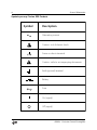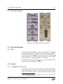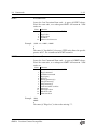
1
Operation and Service Manual
Precision Current Preamplifier
SIM918
Stanford Research Systems
Revision 1.8 • December 13, 2006
Certification
Stanford Research Systems certifies that this product met its published specifications at the time
of shipment.
Warranty
This Stanford Research Systems product is warranted against defects in materials and workmanship for a period of one (1) year from the date of shipment.
Service
For warranty service or repair, this product must be returned to a Stanford Research Systems
authorized service facility. Contact Stanford Research Systems or an authorized representative
before returning this product for repair.
Information in this document is subject to change without notice.
c Stanford Research Systems, Inc., 2006. All rights reserved.
Copyright Stanford Research Systems, Inc.
1290–D Reamwood Avenue
Sunnyvale, CA 94089 USA
Phone: (408) 744-9040 • Fax: (408) 744-9049
www.thinkSRS.com • e-mail: [email protected]
Printed in U.S.A.
Document number 9-01592-903
SIM918
Precision Current Preamplifier
Contents
General Information
Safety and Preparation for Use
Symbols . . . . . . . . . . . . .
Notation . . . . . . . . . . . . .
Specifications . . . . . . . . . .
1
2
3
4
.
.
.
.
.
.
.
.
.
.
.
.
.
.
.
.
.
.
.
.
.
.
.
.
Getting Started
1.1 Introduction to the Instrument . . .
1.2 Front-Panel Operation . . . . . . . .
1.3 Connections . . . . . . . . . . . . . .
1.4 Power-On . . . . . . . . . . . . . . .
1.5 Restoring the Default Configuration
1.6 SIM Interface . . . . . . . . . . . . . .
Description of Operation
2.1 About Transimpedance Amplifiers
2.2 Bias and Ground . . . . . . . . . .
2.3 Output . . . . . . . . . . . . . . . .
2.4 Autozero Trim . . . . . . . . . . . .
2.5 Phase-Locked Loop . . . . . . . . .
2.6 Autocalibration . . . . . . . . . . .
2.7 Clock Stopping . . . . . . . . . . .
2.8 Quiescent Operation . . . . . . . .
Remote Operation
3.1 Index of Common Commands .
3.2 Alphabetic List of Commands .
3.3 Introduction . . . . . . . . . . .
3.4 Commands . . . . . . . . . . . .
3.5 Status Model . . . . . . . . . . .
.
.
.
.
.
.
.
.
.
.
.
.
.
.
.
.
.
.
.
.
.
.
.
.
.
.
.
.
.
.
.
.
.
.
.
.
.
.
.
.
.
.
.
.
.
.
.
.
.
.
.
.
.
.
.
.
.
.
.
.
.
.
.
.
.
.
.
.
.
.
.
.
.
.
.
.
.
.
.
.
.
.
.
.
.
.
.
.
.
.
.
.
.
.
.
.
.
.
.
.
.
.
.
.
.
.
.
.
.
.
.
.
.
.
.
.
.
.
.
.
.
.
.
.
.
.
.
.
.
.
.
.
.
.
.
.
.
.
.
.
.
.
.
.
.
.
.
.
.
.
.
.
.
.
.
.
.
.
.
.
.
.
.
.
.
.
.
.
.
.
.
.
.
.
.
.
.
.
.
.
.
.
.
.
.
.
.
.
.
.
.
.
.
.
.
.
.
.
.
.
.
.
.
.
.
.
.
iii
iii
vi
vii
vii
.
.
.
.
.
.
.
.
.
.
.
.
.
.
1–1
. 1–2
. 1–5
. 1–8
. 1–9
. 1–9
. 1 – 10
.
.
.
.
.
.
.
.
2–1
. 2–2
. 2–4
. 2–5
. 2–5
. 2–6
. 2–6
. 2–7
. 2–8
.
.
.
.
.
3–1
. 3–2
. 3–4
. 3–6
. 3–7
. 3 – 24
Circuit Description
4–1
4.1 Schematic Diagrams . . . . . . . . . . . . . . . . . . . 4 – 2
A Index
A–1
i
ii
Contents
SIM918
Precision Current Preamplifier
General Information
The SIM918 Precision Current Preamplifier, part of Stanford Research
Systems’ Small Instrumentation Modules family, converts an input
electric current into a proportional voltage output while maintaining zero potential difference between the input terminal and a bias
terminal.
The main amplifier stage presents a transimpedance RF , equal to
the current gain of the preamplifier, to an input current iin . The bias
voltage Vbias is subtracted from the output of the stage, so that the
voltage at the output of the instrument is
Vout = (Vbias − iin × RF ) − Vbias = −iin × RF .
Safety and Preparation for Use
Connections
No dangerous voltages are generated by the module. However,
the outer shield of the front-panel Input coaxial (BNC) connector
in the SIM918 can be switched to the rear-panel Program input. If
a dangerous voltage is applied to the Program terminal, it may be
present on the outer shell of the Input connector, and may cause
injury or death.
WARNING
Do not exceed ±60 volts to the Earth at the center terminal of the rear-panel
Shield Program Voltage BNC connector.
CAUTION
Do not exceed ±15 volts to the Earth at the center terminal of the front-panel
Input and Bias BNC connectors, or at the center terminal of the rear-panel
Ref Clock Sync BNC connector.
Biomedical applications
WARNING
Under certain conditions, the SIM918 may prove to be unsafe for
applications involving human subjects. Incorrect grounding, component failure, and excessive common-mode input voltages are examples of conditions in which the instrument may expose the subject
iii
iv
General Information
to large input currents. Therefore, Stanford Research Systems does
not recommend the SIM918 for such applications.
Caution regarding use with photomultipliers
CAUTION
The front-end amplifier of this instrument is easily damaged if a
photomultiplier is used improperly with the preamplifier. When left
completely unterminated, a cable connected to a PMT can charge
to several hundred volts in a relatively short time. If this cable is
connected to the curent input of the SIM918, the stored charge may
damage the front-end JFET. To avoid this problem, provide a leakage
path of about 100 kΩ to ground inside the base of the PMT to prevent
charge accumulation.
Service
Do not install substitute parts or perform unauthorized modifications
to this instrument.
Preparation for use
The SIM918 is a single-wide module designed to be used inside the
SIM900 Mainframe. Do not turn on the power to the mainframe or
apply voltage or current inputs to the module until the module is
completely inserted into the mainframe and locked in place.
SIM918
Precision Current Preamplifier
General Information
SIM918
Precision Current Preamplifier
v
vi
General Information
Symbols you may Find on SRS Products
Symbol
Description
Alternating current
Caution - risk of electric shock
Frame or chassis terminal
Caution - refer to accompanying documents
Earth (ground) terminal
Battery
Fuse
On (supply)
Off (supply)
SIM918 Precision Current Preamplifier
General Information
vii
Notation
The following notation will be used throughout this manual:
WARNING
A warning means that injury or death is possible if the instructions
are not obeyed.
CAUTION
A caution means that damage to the instrument or other equipment
is possible.
Typesetting conventions used in this manual are:
• Front-panel buttons are set as [GAIN ];
[GAIN
] is shorthand for “[GAIN ] & [GAIN ]”.
• Front-panel indicators are set as OVLD.
• Signal names are set as ¬STATUS.
• Signal levels are set as HIGH.
• Remote command names are set as *IDN? .
• Literal text other than command names is set as OFF.
• Special ASCII characters are set as hCRi.
Remote command examples will all be set in monospaced font. In
these examples, data sent by the host computer to the SIM918 are set
as straight teletype font, while responses received by the host
computer from the SIM918 are set as slanted teletype font.
SIM918
Precision Current Preamplifier
viii
General Information
Specifications
Performance characteristics
Min
Gain
Selection
Accuracy, 106 V/A
107 V/A
108 V/A
Stability, 106 V/A
107 V/A
108 V/A
Current input
Selection
Offset voltage [1–3]
Resistance
Capacitance
Bias current, DC [3]
AC [1, 4]
Current noise at 1 kHz [5], 106 V/A
107 V/A
108 V/A
Voltage noise [1, 4]
−3 dB bandwidth [5], 106 V/A
107 V/A
108 V/A
Terminals
BNC shield
Bias input
Selection
Voltage [7]
Resistance
−3 dB bandwidth
Terminals
BNC shield
Program input
Voltage
Resistance
Terminals
Reference clock sync
Selection
Interface
Input frequency [10]
Output frequency
SIM918
Typ
Max
106 , 107 , 108
±0.1
±0.1
±1
±10
±50
±100
Units
V/A
%
%
%
ppm/◦ C
ppm/◦ C
ppm/◦ C
On, open
±10 µV
1
Ω
18
pF
0.5
2.0 pA
3.5
pA rms
√
130
fA/ Hz
√
42
fA/ Hz
√
15
fA/ Hz
25
µV rms
22
kHz
12
kHz
4
kHz
Isolated BNC [6]
Ground, bias, program /open
On, ground
−5.0
+5.0 V
10
MΩ
0.2
Hz
Isolated BNC [6]
Ground, float
−60
+60 V
3
GΩ
Grounded BNC [8], rear
Input, output
Rear BNC [8], TTL [9]
0.90
1.10 Hz
1.0
Hz
Precision Current Preamplifier
General Information
ix
Min
Autozero
Selection
Source
Switching frequency
Output
Voltage [7]
Maximum current
Short circuit duration
Resistance
Offset voltage [2]
Common-mode rejection, DC
Terminals
Operating
Temperature [11]
Power
Supply current, +5 V
±15 V
Typ
Max Units
On, hold
Internal, external reference clock
0.50
Hz
+10.0
−10.0
±100
80
V
mA
Indefinite
100
Ω
±50 µV
dB
Grounded BNC [6]
0
40
+5, ±15
100
150
◦C
V DC
mA
mA
Conditions:
[1] With autozero on.
[2] Following an autocalibration at (23 ± 5) ◦ C within 24 hours.
[3] 100 s average.
[4] 0.1 Hz to 10 Hz.
[5] For a 100 pF source capacitance and an infinite source resistance.
Higher values of source capacitance or a finite source resistance will
degrade these specifications.
[6] Amphenol 31–10–4052 or similar.
[7] An overload will be detected and the instrument is not guaranteed
to perform properly if these limits are exceeded, or if |Vbias − iin × RF |
exceeds the limits. Continuous application of a bias voltage Vbias in
excess of ±15 V will damage the instrument.
[8] Tyco 227169–4 or similar.
[9] Rising-edge sensitive.
[10] External reference clock capture range. The instrument is not guaranteed to perform properly if these limits are exceeded.
[11] Non-condensing.
General characteristics
Interface
Connectors
Weight
Dimensions
SIM918
Precision Current Preamplifier
Serial (RS–232) through SIM interface
BNC (3 front [4], 2 rear [6]); DB–15 (male) SIM interface
1.7 lbs
1.500 W × 3.600 H × 7.000 D
x
General Information
SIM918
Precision Current Preamplifier
1
Getting Started
This chapter gives you the necessary information to get started
quickly with your SIM918 Precision Current Preamplifier.
In This Chapter
1.1
1.2
1.3
1.4
1.5
1.6
Introduction to the Instrument . . . . .
1.1.1 Current amplifiers and autozero
1.1.2 Clocks . . . . . . . . . . . . . . .
1.1.3 Cabling and grounding . . . . .
1.1.4 Autocalibration . . . . . . . . . .
1.1.5 Remote interface and status . . .
1.1.6 Block diagram . . . . . . . . . . .
1.1.7 Front and rear panels . . . . . . .
Front-Panel Operation . . . . . . . . . .
1.2.1 Gain . . . . . . . . . . . . . . . .
1.2.2 Autozero . . . . . . . . . . . . . .
1.2.3 Input . . . . . . . . . . . . . . . .
1.2.4 Bias . . . . . . . . . . . . . . . . .
1.2.5 Output overload . . . . . . . . .
Connections . . . . . . . . . . . . . . . .
Power-On . . . . . . . . . . . . . . . . .
Restoring the Default Configuration .
SIM Interface . . . . . . . . . . . . . . .
1.6.1 SIM interface connector . . . . .
1.6.2 Direct interfacing . . . . . . . . .
.
.
.
.
.
.
.
.
.
.
.
.
.
.
.
.
.
.
.
.
.
.
.
.
.
.
.
.
.
.
.
.
.
.
.
.
.
.
.
.
.
.
.
.
.
.
.
.
.
.
.
.
.
.
.
.
.
.
.
.
.
.
.
.
.
.
.
.
.
.
.
.
.
.
.
.
.
.
.
.
.
.
.
.
.
.
.
.
.
.
.
.
.
.
.
.
.
.
.
.
.
.
.
.
.
.
.
.
.
.
.
.
.
.
.
.
.
.
.
.
.
.
.
.
.
.
.
.
.
.
.
.
.
.
.
.
.
.
.
.
.
.
.
.
.
.
.
.
.
.
.
.
.
.
.
.
.
.
.
.
1–2
1–2
1–2
1–3
1–3
1–3
1–4
1–5
1–5
1–5
1–5
1–7
1–7
1–8
1–8
1–9
1–9
1 – 10
1 – 10
1 – 10
1–1
1–2
1.1
1.1.1
Getting Started
Introduction to the Instrument
Current amplifiers and autozero
A current, or transimpedance, amplifier converts electric current into
a proportional output voltage. Unlike a simple resistor, the amplifier presents a low-impedance terminal to the input current. In
the SIM918 Precision Current Preamplifier, the electric potential of
the input terminal, Vin , is accurately made equal to the user-provided
offset voltage potential at the bias terminal, Vbias , or to ground. The absolute magnitude of the resulting input offset voltage is nearly zero:
Vofs = Vin − Vbias ,
|Vofs | < 10 µV.
In all transimpedance amplifiers, the input potential is kept near
that of the bias through the action of negative feedback. When the
bias voltage is at ground, the input terminal is often said to present
virtual ground a virtual ground, or a virtual null. Without autozeroing, this virtual ground drifts, in some cases by many millivolts. This error in
the electric potential of the input terminal may be unacceptable in
precision measurements.
In the SIM918, an autozero circuit measures Vofs every 2 seconds and
makes the adjustment necessary to keep the offset voltage at zero.
The autozero feature can be engaged or inhibited remotely or from
the front panel, giving the user flexibility in sensitive applications.
With autozero inhibited, the preamplifier retains microvolt input
accuracy for many hours. When engaged, it takes the autozero only
a few cycles of a reference clock to restore the offset to within its
specified limits.
The gain, or transimpedance, of the preamplifier can be set to
RF = 106 , 107 , or 108 V/A, remotely and from the front panel. Along
with voltage accuracy, the SIM918 offers a low input bias current1
and a current noise that is close to the lower limit imposed by the
Johnson noise of the transimpedance.
1.1.2
Clocks
The autozero circuit switches between measuring the input offset
voltage, and the offset voltage of the zeroing amplifier itself, at one
reference clock half the frequency of an internal or external reference clock. The inone pps ternal clock signal (typically 1.0 pulse per second, pps, i.e. 1.0 Hz)
can be selected, remotely or from the front panel, to be output on
1
In the unfortunate but established terminology of electronics, the word bias conveys different meanings. The bias current is the input current present in the
instrument in the absence of a current from an external source.
SIM918
Precision Current Preamplifier
1.1
Introduction to the Instrument
1–3
a rear-panel connector. Alternatively, the same connector can be
used to input a clock signal at (1.0 ± 10%) pps (i.e. 1.10 Hz–0.90 Hz),
synchronizing the switching to an external source.
The reference clock in the SIM918 operates independently of the oscillator used to clock the digital control circuitry. The latter is designed
with a special clock-stopping architecture. The microcontroller is
turned on only in the following cases: when the settings are being
changed; autozero is turned on or off; and during autocalibration, remote communications, or when an overload condition or an external
reference clock event occurs. This guarantees that no digital noise
contaminates low-level analog signals.
With autozero off and in the absense of an external clock input,
the preamplifier enters a completely quiescent state: no reference
clock transitions are present that can disturb the measurement of a
low-level electric current.
1.1.3
Cabling and grounding
The SIM918 provides maximum flexibility for cabling and grounding. The input connection can be opened, and the bias voltage can
be connected to signal ground.
The shield of the Input BNC can be switched between signal ground,
the bias voltage, or the rear-panel Program input (which can be left
floating, if desired). With the Program input, a user can supply
an excitation potential to an experiment via the shield conductor of
the input cable, while the excited current flows through the center
conductor to the SIM918. The shield of the Bias BNC can be independently grounded or floated.
The input and bias selections, and those of their shields, can be made
via the push of a front-panel button or remotely.
1.1.4
Autocalibration
A user-commanded autocalibration procedure allows one to eliminate the effects of thermal drifts in the autozero circuit, and to reduce
output offset voltage.
1.1.5
Remote interface and status
remote interface A remote computer can access the module through the SIM900 Main-
frame, using RS–232 or GPIB. All instrument settings can be queried
via the remote interface. The SIM918 can be operated outside the
SIM900 Mainframe by powering it with its required DC voltages.
SIM918
Precision Current Preamplifier
1–4
Getting Started
If the maximum bias voltage is exceeded, or the chosen gain setting
causes the output voltage to exceed its maximum, the appropriate
overload LED turns on. If the module cannot lock to an external
reference clock signal, an LED indicates an unlocked state. If armed,
the module also generates a status signal to alert the user of the
overload or unlocked condition.
1.1.6
Block diagram
The output of the main amplifier (transimpedance stage) is referenced to the bias voltage. A difference amplifier subtracts the bias
voltage, so the output of the instrument is directly proportional to
the input current iin and the gain RF :
Vout = (Vbias − iin × RF ) − Vbias = −iin × RF .
(1.1)
A block diagram of the preamplifier is shown below in Figure 1.1.
RF
INPUT
−
BIAS
+
Main
amp
offset
adj
+
−
−
+
OUTPUT
Difference
amp
LPF
Zeroing
amp
(±1)
0.5 Hz
Figure 1.1: The SIM918 block diagram.
SIM918
Precision Current Preamplifier
1.2
Front-Panel Operation
1.1.7
1–5
Front and rear panels
Figure 1.2: The SIM918 front and rear panels.
1.2
Front-Panel Operation
1.2.1
Gain
The gain RF of the preamplifier, in volts per microampere, is indicated
on the front panel of the instrument via a green annunciator LED.2
Press one of the [GAIN
] buttons to change the gain. If [GAIN ]
is pressed when RF = 1 V/µA, the press has no effect. If [GAIN ] is
pressed when RF = 100 V/µA, the press has no effect.
A simultaneous press of [GAIN
] has a special meaning. This
press initiates autocalibration (Section 2.6).
1.2.2
Autozero
1.2.2.1
Engaging the autozero circuit
The autozero circuit is turned ON by the press of a front-panel button.
There will be a pause of up to 3.3 seconds (a wait for a positive-going
edge of the reference clock). At the end of the pause, the green
2
SIM918
Note the minus sign in Eq. (1.1); the output voltage is positive for a current that
flows out of the input terminal.
Precision Current Preamplifier
1–6
Getting Started
annunciator LED will turn on and the zeroing circuit will become
active.
The same button turns autozeroing off. There will be a less than 1 s
pause in order for the present control output of the autozero circuit
to be sampled and stored. At the end of the pause, the LED indicator
will turn off and all switching inside the SIM918 will cease. The sampled control output (trim) will remain applied to the transimpedancestage amplifier, zeroing it to the best of precision available at the time
the autozero circuitry is inhibited.
1.2.2.2
Reference clock detection
The autozero circuit switches at one half the frequency of an internal
or external reference clock. If a periodic TTL-level signal is applied
to the rear-panel Ref Clock Sync connector, and the connector is
not selected for output (see the next section), the preamplifier will
recognize the external clock and attempt to lock to the signal. The
green External LED will illuminate for the duration of the external
clock input.
capture range If the frequency of the external clock is stable and is between 0.90 Hz
lock acquisition time and 1.10 Hz, the module will successfully lock to the signal. It typically takes 250 s (just over 4 minutes) to acquire a lock. The yellow Unlocked LED is illuminated whenever the SIM918 is not in a
locked state. For further discussion of locking, see Chapter 2.5.
For the duration of an unlocked state, the switches in the autozero
circuit are not guaranteed to have correct duty cycles. Therefore, the
specified input offset accuracy is not guaranteed while Unlocked.
The internal reference clock is used when an external clock signal
is not present. In this state, neither the External LED nor the Unlocked LED is illuminated.
1.2.2.3
Output 1 pps sync
The rear-panel Ref Clock Sync connector can be used to output the
internal reference clock. The signal at the output is TTL, typically
at 1.0 Hz (1.0 pps). The [Output 1 pps sync] button toggles the direction of the signal at the rear-panel connector. The output direction is
indicated by a green LED. An inactive Output 1 pps sync indicates
that the connector may be used to input an external clock.
If [Output 1 pps sync] is pressed while an external reference clock
signal is present at the connector, clock output will fail and a DeviceDependent Error (Section 3.5.3) will be issued. If an external signal is
applied to the Ref Clock Sync terminal while the connector is selected
for output, the external signal will not be recognized.
SIM918
Precision Current Preamplifier
1.2
Front-Panel Operation
1.2.3
1–7
Input
The [INPUT Open] button opens and closes a relay in the path of the
input current. A green LED indicates a disconnected input terminal.
The input capacitance of the SIM918 is at its lowest with input open,
and is specified in the table on Page viii.
1.2.3.1
Input shield
Successive presses of the [INPUT Shield] button connect the outer
shell of the Input BNC to the rear-panel Shield Program Voltage
terminal, a buffered copy of the bias voltage, and to signal ground.
The state of the input shield connection is indicated by one of three
LEDs: the yellow INPUT Shield Prog, the yellow INPUT Shield Bias,
or the green INPUT Shield GND.
To float the shield of the Input connector, leave the Shield Program Voltage BNC open and select INPUT Shield Prog.
1.2.4
Bias
The [BIAS GND] button toggles the source of the bias between
the voltage at the center terminal of the Bias BNC and the signal
ground of the instrument. If the bias source is set to ground, the
green BIAS GND light is on.
With Bias grounded, the difference amplifier (Figure 1.1) is switched
out and the output of the instrument is taken directly from the transimpedance stage. With this configuration, there is no common-mode
error and the output-offset error is reduced.
When Bias is connected to a user voltage, the voltage is buffered
internally before being distributed to other parts of the preamplifier.
The offset error of the bias buffer is included in the input offset
accuracy specifications in the table on Page viii.
1.2.4.1
Bias overload
An overload condition is recognized and the BIAS OVLD LED is
activated if the absolute value of the voltage applied to the Bias
bias overload limits input exceeds certain limits. These limits are typically ±5.0 V, and
are between
−5.2 V ≤ Vmin ≤ −4.9 V,
4.9 V ≤ Vmax ≤ 5.2 V.
The overload LED stays on for a minimum of 50 ms; after this time it
turns off if the overload condition has ceased.
SIM918
Precision Current Preamplifier
1–8
Getting Started
1.2.4.2
Bias shield
Successive presses of the [BIAS Shield] button float the outer
shell of the Bias BNC and connect it to ground. The state of the
bias shield connection is indicated by one of two LEDs: the yellow BIAS Shield Float or the green BIAS Shield GND.
Note that it is the electric potential at the Bias terminal, not the potential difference across the Bias connector, that the autozero circuit
uses as the reference for the input voltage.
1.2.5
Output overload
An overload condition is recognized and the OUTPUT OVLD LED
is activated if the absolute value |iin ×RF | exceeds certain limits. These
output overload limits limits are typically ±10.0 V, and are between
−10.4 V ≤ Vmin ≤ −9.9 V,
9.9 V ≤ Vmax ≤ 10.4 V.
The overloaded state is also recognized, and OUTPUT OVLD activated, if the raw output of the transimpedance stage, |Vbias − iin × RF |,
exceeds these limits. To distinguish between the two output overload possibilities, use the OVLD? query. The overload LED stays on
for a minimum of 50 ms; after this time it turns off if the overload
condition has ceased.
1.3
Connections
There are five BNC connectors in the SIM918, three on the front panel
and two at the rear.
Panel
BNC
Front
Input
Terminal
Bias
Output
Rear
Shield Program Voltage
Ref Clock Sync
Signal
Direction
Center
Input current
Input
Shield
Shield program voltage,
bias voltage, signal ground
Output
Center
Bias voltage
Input
Shield
Float, power ground
Center
Output voltage
Output
Shield
Signal ground
Output
Center
Shield program voltage
Input
Shield
Chassis ground
Center
Reference clock
Input, output
Shield
Chassis ground
Input, output
Table 1.1: BNC connections in the SIM918.
For a further discussion of grounding, see Section 2.2.1. The SIM
interface connector is discussed in Section 1.6.1.
SIM918 Precision Current Preamplifier
1.4
1.4
Power-On
1–9
Power-On
The instrument retains the following settings in non-volatile memory:
1. The power line frequency (FPLC): 60 Hz or 50 Hz.3
2. The gain.
3. Autozero on/off.
4. Input selection (on, open).
5. Input shield selection (program, bias, ground.)
6. Bias selection (on, ground).
7. Bias shield selection (float, ground.)
8. Whether or not the phase-locked loop (Section 2.5) stays active
when autozero is off.
9. Calibration values.
The power-on configuration of the remote interface is detailed in
Section 3.3.1.
1.5
Restoring the Default Configuration
The default configuration of the SIM918 is:
1. Gain 106 V/A.
2. Autozero on.
3. Input connected.
4. Input shield at ground.
5. Bias at ground.
6. Bias shield at ground.
7. Reference clock direction is input.
8. The phase-locked loop (Section 2.5) is inactive when autozero
is off.
To reset the module into this configuration, turn the SIM900 Mainframe power on while holding a front-panel button of the SIM918
for at least 2.0 seconds. The same configuration can also be reached
from the remote interface by issuing the *RST command.
3
SIM918
FPLC equals the principal rejection frequency of an internal analog-to-digital
converter used to measure the input offset trim. See the command OFST.
Precision Current Preamplifier
1 – 10
1.6
Getting Started
SIM Interface
The primary connection to the SIM918 Precision Current Preamplifier is the rear-panel DB–15 SIM interface connector. Typically, the
SIM918 is mated to a SIM900 Mainframe via this connection, either
through one of the internal mainframe slots or the remote cable interface.
It is also possible to operate the SIM918 directly, without using the
SIM900 Mainframe. This section provides details on the interface.
1.6.1
SIM interface connector
The DB–15 SIM interface connector carries all the power and communication lines to the instrument. The connector signals are specified
in Table 1.2.
Pin
1
2
3
4
5
6
7
8
9
10
11
12
13
14
15
Direction
Src ⇒ Dest
Signal
SIGNAL GND
¬STATUS
RTS
CTS
¬REF 10MHZ
−5V
−15V
PS RTN
CHASSIS GND
TXD
RXD
REF 10MHZ
+5V
+15V
+24V
MF ⇒ SIM
SIM ⇒ MF
MF ⇒ SIM
SIM ⇒ MF
MF ⇒ SIM
MF ⇒ SIM
MF ⇒ SIM
MF ⇒ SIM
MF ⇒ SIM
SIM ⇒ MF
MF ⇒ SIM
MF ⇒ SIM
MF ⇒ SIM
MF ⇒ SIM
Description
Signal ground
Status/service request (GND = asserted, +5 V= idle)
HW handshake (unused in SIM918)
HW handshake (unused in SIM918)
10 MHz reference (no connection in SIM918)
Power supply (no connection in SIM918)
Power supply
Power ground
Chassis ground
Async data (start bit = “0”= +5 V; “1” = GND)
Async data (start bit = “0”= +5 V; “1” = GND)
10 MHz reference (no connection in SIM918)
Power supply
Power supply
Power supply (no connection in SIM918)
Table 1.2: SIM interface connector pin assignments, DB–15.
1.6.2
Direct interfacing
The SIM918 is intended for operation in the SIM900 Mainframe, but
users may wish to directly interface the module to their own systems
without the use of additional hardware.
The mating connector needed is a standard DB–15 receptacle, such
as Tyco part number 747909–2 (or equivalent). Clean, well-regulated
supply voltages of ±15.0 V DC, +5.0 V DC must be provided, following the pinout specified in Table 1.2 and the minimum currents in
the table on Page ix. Ground must be provided on Pins 1 and 8, with
chassis ground on Pin 9. The ¬STATUS signal may be monitored
SIM918 Precision Current Preamplifier
1.6
SIM Interface
1 – 11
on Pin 2 for a low-going TTL-compatible output indicating a status
message. See Section 3.5 for the description of status messages.
CAUTION
1.6.2.1
The SIM918 has no internal protection against reverse polarity, missing
supply, or overvoltage on the +5 V and the ±15 V power-supply pins. Supply voltages above 5.5 V on Pin 13, above +16 V on Pin 14, or below −16 V
on Pin 7 are likely to damage the instrument. SRS recommends using the
SIM918 together with the SIM900 Mainframe for most applications.
Direct interface cabling
If the user intends to directly wire the SIM918 independent of the
SIM900 Mainframe, communication is usually possible by directly
connecting the appropriate interface lines from the SIM918 DB–15
plug to the RS–232 serial port of a personal computer.4 Connect RXD
from the SIM918 directly to RxD on the PC, TXD directly to TxD. In
other words, a null-modem-style cable is not needed.
To interface directly to the DB–9 male (DTE) RS–232 port typically
found on contemporary personal computers, a cable must be made
with a female DB–15 socket to mate with the SIM918, and a female
DB–9 socket to mate with the PC’s serial port. Separate leads from
the DB–15 need to go to the power supply, making what is sometimes
know as a “hydra” cable. The pin connections are given in Table 1.3.
DB–15/F to SIM918
Name
DB–9/F
10 ←→ 3
11 ←→ 2
5
TxD
RxD
Computer Ground
to Power Supply
7 ←→
13 ←→
14 ←→
1 ←→
8 ←→
9 ←→
−15 V DC
+5 V DC
+15 V DC
Signal Ground (separate wire to Ground)
Power Ground (separate wire to Ground)
Chassis Ground (separate wire to Ground)
Table 1.3: SIM918 direct interface cable pin assignments.
note about grounds The distinct Signal Ground and Power Ground, and the chassis
ground, are not directly connected within the SIM918. The power
4
SIM918
Although the serial interface lines on the DB–15 do not satisfy the minimum
voltage levels of the RS–232 standard, these lines are typically compatible with
desktop personal computers.
Precision Current Preamplifier
1 – 12
Getting Started
ground carries the return currents of digital control signals, powerintensive analog amplifiers, and the power supplies, whereas the
output voltage references to a stable signal ground (Section 2.2.1).
When operating in the SIM900, the three grounds are tied together
in the SIM900 Mainframe. Signal Ground and Power Ground are
connected through back-to-back Schottky diodes, so they cannot be
more than ∼ ±0.35 V apart. The three ground lines should be separately wired to a single, low-impedance ground source at the power
supply.
1.6.2.2
Serial settings
The initial serial port settings at power-on are: baud rate 9600, 8 bits,
no parity, 1 stop bit, and no flow control. The baud rate of the SIM918
cannot be changed. Flow control is not implemented in the SIM918.
The parity may be changed with the PARI command.
SIM918
Precision Current Preamplifier
2
Description of Operation
This chapter provides a number of additional details of the operation
of the SIM918.
In This Chapter
2.1
2.2
2.3
2.4
2.5
2.6
2.7
2.8
About Transimpedance Amplifiers .
2.1.1 Input capacitance and stability
2.1.2 Choosing the right gain . . . .
Bias and Ground . . . . . . . . . . . .
2.2.1 Grounds . . . . . . . . . . . . .
2.2.2 Bias . . . . . . . . . . . . . . . .
Output . . . . . . . . . . . . . . . . . .
Autozero Trim . . . . . . . . . . . . . .
Phase-Locked Loop . . . . . . . . . . .
Autocalibration . . . . . . . . . . . . .
Clock Stopping . . . . . . . . . . . . .
Quiescent Operation . . . . . . . . . .
.
.
.
.
.
.
.
.
.
.
.
.
.
.
.
.
.
.
.
.
.
.
.
.
.
.
.
.
.
.
.
.
.
.
.
.
.
.
.
.
.
.
.
.
.
.
.
.
.
.
.
.
.
.
.
.
.
.
.
.
.
.
.
.
.
.
.
.
.
.
.
.
.
.
.
.
.
.
.
.
.
.
.
.
.
.
.
.
.
.
.
.
.
.
.
.
.
.
.
.
.
.
.
.
.
.
.
.
2–2
2–2
2–3
2–4
2–4
2–4
2–5
2–5
2–6
2–6
2–7
2–8
2–1
2–2
2.1
Description of Operation
About Transimpedance Amplifiers
transimpedance amplifier
A transimpedance amplifier is an operational amplifier with a resistor
in the feedback path. More generally, the feedback impedance ZF always has a resistive and a reactive component. The two inputs to the
operational amplifier have a very high impedance; and the feedback
in the amplifier acts to keep the two inputs at the same electric potential. Therefore, the input current iin is forced through the feedback
impedance, and the amplifier produces an output voltage
Vout, TA = Vbias − iin × ZF .
The amplifier acts to translate the input current into a proportional
output voltage, with the feedback impedance being the coefficient of
proportionality. Hence the term transimpedance.
The main amplifier of the SIM918 Precision Current Preamplifier is a
transimpedance amplifier based on a composite, JFET-input design.
2.1.1
Input capacitance and stability
The input impedance of JFET devices is extremely large. However,
the impedance experienced, as a whole, by a current input to the
feedback amplifier (i.e. the change in the input voltage1 divided by
the input current) has two other, much more significant contributions
in parallel. The first one is the effect of the output on the input
via feedback due to finite open-loop voltage gain of the operational
amplifier, and the second one is input capacitance.
CF
RF
Input BNC
i in
Vout, TA
C in
Op-amp
(F)
Z in
Bias
Bias
Figure 2.1: A transimpedance amplifier.
The first term equals the feedback impedance divided by the openloop gain of the operational amplifier2 :
(F)
Zin = ZF /AOL
1
2
(2.1)
Without the action of the autozero circuit.
Within the current bandwidth of the transimpedance amplifier.
SIM918 Precision Current Preamplifier
2.1
About Transimpedance Amplifiers
2–3
and is below 1 Ω at DC. The open-loop gain is very high at DC, and
typically decreases as inverse frequency with a corresponding 90◦
phase lag:
AOL = −j fT / f
where fT is the gain-bandwidth product of the operational amplifier
(∼ 10 MHz in the SIM918). Substituting into Equation (2.1), observe
(F)
Zin = j
ZF
f.
fT
If the feedback element is purely resistive, the term due to ZF behaves exactly as if a large inductor were connected between the input and the bias terminals. This contribution to the input impedance
increases linearly with frequency, with a corresponding 90◦ phase
lead.3
The input terminal always has some amount of parasitic capacitance
to the bias terminal, and to ground. The input capacitance specification in the table on Page viii applies for no cable connected to the
Input BNC. A coaxial cable adds ∼ 100 pF/m of capacitance. Even
one meter of coax will dramatically increase the input capacitance.
The input capacitance, in parallel with the effective inductance, can
form a resonant tank circuit if the capacitance is large enough that
the resulting resonant frequency lies within the bandwidth of the
transimpedance amplifier. The SIM918 has adequate compensation
(feedback capacitance) to prevent oscillation for up to 100 pF of additional input capacitance.4 To avoid a feedback oscillation, follow
these steps:
1. Place the preamplifier as close as possible to the signal being
measured, and use the shortest cable length necessary to connect them.
2. Reduce all stray capacitance to bias or ground at the output of
the experiment under measurement.
3. Use a lower gain setting, which reduces the effective input
inductance.
Other detrimental effects of excess input capacitance include reduced
current bandwidth, poor step response (overshoot and ringing), and
increased output noise.
2.1.2
Choosing the right gain
It is important to consider the output resistance (in general, impedance) of the current source being measured. The transimpedance
3
4
SIM918
The input voltage leads the input current.
Longer cable lengths are tolerated at lower gain settings.
Precision Current Preamplifier
2–4
Description of Operation
stage amplifies its input voltage noise by the factor5 of (1+RF /Rsource ),
where Rsource is the source resistance. This noise adds in quadrature
with the current noise of the stage.To prevent the voltage noise term
from dominating the overall output noise, set the current gain to
RF . Rsource .
2.2
2.2.1
Bias and Ground
Grounds
The output of the SIM918 is referenced to ground. To maintain
the DC accuracy of the instrument, there are two separate ground
references. Power Ground (Pin 8 of the SIM interface connector)
provides a current return path for digital control signals, powerintensive analog amplifiers, and the power supplies. Signal Ground
(Pin 1 of the interface connector) serves as the reference point for
analog voltages. The outer shell of the Output BNC connector is tied
to Signal Ground. The output current of the preamplifier returns
to the power supply through Signal Ground. When INPUT Shield
GND is selected, the shell of the Input BNC is also tied to Signal Ground.
The outer shells of the rear-panel Shield Program Voltage and
Ref Clock Sync BNCs are connected to chassis ground, Pin 9 of the
DB–15 SIM interface connector. The separate power, signal, and
chassis grounds are not directly connected within the preamplifier.
When operating in the SIM900 Mainframe, the three grounds are
tied together inside the mainframe, and through the mainframe
to the Earth. The signal and power grounds are connected inside
the SIM918 through back-to-back Schottky diodes, so they cannot be
more than ∼ ±0.35 V apart.
2.2.2
Bias
The bias potential is received by an ultralow-offset voltage buffer. It
is this buffered voltage that appears on the shield of the Input BNC
when INPUT Shield Bias is selected.
The shield of the Bias connector is not used as a reference for the
bias voltage. When Bias Shield GND is selected, the shield is at
Signal Ground. The limits on the bias voltage in Section 1.2.4.1
are relative to this ground. A voltage exceeding these limits by
more than 1 V will be clamped , through diodes, to ±5.5 V relative to
Power Ground. The 10 MΩ input resistor is connected between Bias
and Signal Ground.
5
At frequencies low enough that the resistive components of the two impedances
are dominant.
SIM918
Precision Current Preamplifier
2.3
Output
2–5
To reduce output noise of the SIM918, the Bias input is limited to a
bandwidth specified in the table on Page viii. Beyond this frequency,
the transimpedance stage cannot follow variations in the bias voltage,
but the output difference amplifier (discussed in the next section)
does. Hence the common-mode rejection of the instrument is greatly
reduced at frequencies above DC.
The bias sensing circuitry is always active, and will signal BIAS
OVLD when the applied input exceeds the voltage limits in Section 1.2.4.1, even if Bias is set to GND.
2.3
Output
When Bias is switched to GND, the output of the instrument is taken
directly from the transimpedance stage; otherwise, from a difference
amplifier (Figure 1.1) that subtracts the bias voltage from the output
of the transimpedance stage. Both outputs have equal drive capacity.
The output impedance of the SIM918 Precision Current Preamplifier
is 100 Ω. The preamplifier can drive load impedances from ∞ to 0 Ω
for the full ±10 V range of output voltage. When driving a 50 Ω load,
the gain will be one third of that displayed on the front panel.
The output signal is filtered by a passive LRC, with f−3 dB = 25 kHz.
The filter eliminates broad-spectrum noise, while adding a negligible amount of overshoot in the step response. The R in the filter
contributes to the output resistance.
The output difference amplifier, when engaged (Bias not at [GND]),
introduces an offset error that can be greater than the maximum input
offset error of the preamplifier. The error is reduced by autocalibration (Section 2.6). The output offset can also be trimmed from the
remote interface by using the command OFST 1.
2.4
Autozero Trim
The autozero control loop is fully analog.6 Its settling time, to
within the maximum input offset voltage specification in the table on
Page viii, is 40 s. Two adjustments can be made to loop parameters
via the remote command OFST. The first one to consider, OFST 3,
adjusts the zero point of the loop itself, i.e. the voltage to which the
control loop drives the input offset when autozero is ON.
The command OFST 2 sets the code in a digital-to-analog converter,
the output of which adds together with the output of the loop to
form the overall control output of the autozero circuit. When autozero is engaged, the control loop will compensate for changes made
6
SIM918
With discrete time steps.
Precision Current Preamplifier
2–6
Description of Operation
via OFST 2, driving the input offset voltage back to a value determined by OFST 3. With autozero off, OFST 3 has no effect and
OFST 2 changes the input offset directly.
The best value for OFST 2 is readjusted each time autozero is turned
from on to off. If the preamplifier is to be operated under conditions that tolerate absolutely no clock transitions, the recommended
course of action is to turn autozero on, let the control loop drive the
output to zero and settle, and turn autozero off for the duration of
the experiment (Section 2.8).
The value for OFST 3 is reestablished by autocalibration (Section 2.6).
2.5
Phase-Locked Loop
The switches in the autozero circuit receive a clock signal from an
internal phase-locked loop. If an external reference clock is available
at the rear-panel Ref Clock Sync connector, autozero is on, and the
connector is not selected for output, the PLL will attempt to lock to
the clock signal. The synchronization will be successful for external
clock frequencies between 0.90 Hz and 1.10 Hz.
In the internal reference clock mode, the PLL oscillator runs freely,
generating a 1.0 Hz square wave with rising edges at the beginning
of each autozero half-cycle. The voltage-controlled oscillator in the
loop operates at 240 Hz for 60 Hz power line frequency (FPLC), and
at 200 Hz for FPLC = 50 Hz.
The PLL can be automatically inhibited, and the voltage-controlled
oscillator turned off, when the reference clock is External and autozero is off. The behavior is set by the remote command APLL. With
APLL OFF, the oscillator turns off. In this mode, under external reference clock, the instrument will undergo the full capture and lock
transient after autozero is switched on. To avoid the 4 minute capture
delay, set APLL ON. The module restores the last known APLL mode
upon power-on.
When autozero is on, the PLL oscillator is always running, regardless
of the reference clock source. If the reference clock is internal and
autozero is off, the PLL oscillator is off. There is no capture delay
under internal clock.
2.6
Autocalibration
To ensure the specified offset accuracy, the preamplifier must be selfcalibrated within the 24 hours preceding a measurement. A valid autocalibration must take place at (23 ± 5) ◦ C with the module warmed
up for at least 2 hours at (23±5) ◦ C. If the module is being used inside
SIM918
Precision Current Preamplifier
2.7
Clock Stopping
2–7
the SIM900 Mainframe, the autocalibration must also be inside the
mainframe. Otherwise, perform the autocalibration with the same
connection to an independent supply as you use for the operation.
Disconnect all inputs and outputs to the SIM918 while performing the
autocalibration. Connect the center and shield terminals of the Bias BNC
together externally, e.g. with a grounding cap. To calibrate, issue the command ACAL, or press both [GAIN
] at the same time. Depending
on the firmware revision, the calibration may take up to 20 minutes to
complete. During the autocalibration, all LEDs are lit. At the end of
the calibration, the module returns to its pre-ACAL settings, except
the reference clock direction is reset to input.
If autocalibration is unsuccessful, for example because an external
current is applied to Input, the calibration constants revert to their
original values and the command LDDE? will return Code 2. If an
external reference clock is detected, the autocalibration terminates
immediately with LDDE? 2.
Autocalibration does not affect gain accuracy.
2.7
Clock Stopping
The microprocessor clock of the SIM918 stops if the module is idle,
“freezing” the digital circuitry. The following actions “wake up” the
clock:
1. A power-on.
2. A press of a front-panel button.
3. Activity (send or receive) at the remote interface.
4. An overload.
5. A change in external reference clock status: several rising edges
at the rear-panel connector while in internal clock mode, or
cessation of clocking while in external mode.
6. Loss of PLL lock.
The clock runs for as long as is necessary to complete a change
of settings requested from the front panel, or to communicate the
output of a query through the remote interface. However, the clock
will remain active for as long as the overload or unlocked condition
exists, and for the full duration of an autocalibration.
This default behavior can be modified with the remote command AWAK. Setting AWAK ON will prevent the clock from stopping.
The module returns to AWAK OFF upon power-on.
SIM918
Precision Current Preamplifier
2–8
Description of Operation
Note that the operation of the PLL oscillator is completely independent of the microprocessor clock.
2.8
Quiescent Operation
Follow these steps to operate the SIM918 Precision Current Preamplifier in sensitive measurements that can tolerate absolutely no module
clock transitions:
1. Reset the preamplifier (Section 1.5).
2. Set Input to Open.
3. Wait for at least 40 s.
4. Turn autozero off.
5. Select the desired gain.
6. Close the input.
7. Perform the measurement.
After this sequence is complete, the control output of the autozero
circuit holds at a value that initially drives the input offset within its
specification. Without active autozeroing, the input offset may drift
as time progresses, so Steps 1–6 may need to be repeated.
SIM918
Precision Current Preamplifier
3
Remote Operation
This chapter describes operating the SIM918 over the serial interface.
In This Chapter
3.1
3.2
3.3
3.4
3.5
Index of Common Commands . . . . . . . . . . . .
Alphabetic List of Commands . . . . . . . . . . . .
Introduction . . . . . . . . . . . . . . . . . . . . . . .
3.3.1 Power-on configuration . . . . . . . . . . . .
3.3.2 Buffers . . . . . . . . . . . . . . . . . . . . . .
3.3.3 Device Clear . . . . . . . . . . . . . . . . . . .
Commands . . . . . . . . . . . . . . . . . . . . . . .
3.4.1 Command syntax . . . . . . . . . . . . . . . .
3.4.2 Notation . . . . . . . . . . . . . . . . . . . . .
3.4.3 Examples . . . . . . . . . . . . . . . . . . . .
3.4.4 General commands . . . . . . . . . . . . . . .
3.4.5 Configuration commands . . . . . . . . . . .
3.4.6 Calibration commands . . . . . . . . . . . . .
3.4.7 Status commands . . . . . . . . . . . . . . . .
3.4.8 Interface commands . . . . . . . . . . . . . .
3.4.9 Serial communication commands . . . . . .
Status Model . . . . . . . . . . . . . . . . . . . . . .
3.5.1 Status Byte (SB) . . . . . . . . . . . . . . . . .
3.5.2 Service Request Enable (SRE) . . . . . . . . .
3.5.3 Standard Event Status (ESR) . . . . . . . . .
3.5.4 Standard Event Status Enable (ESE) . . . . .
3.5.5 Communication Error Status (CESR) . . . . .
3.5.6 Communication Error Status Enable (CESE)
3.5.7 Overload Status (OLSR) . . . . . . . . . . . .
3.5.8 Overload Status Enable (OLSE) . . . . . . . .
3.5.9 Reference Clock Status (RCSR) . . . . . . . .
3.5.10 Reference Clock Status Enable (RCSE) . . . .
.
.
.
.
.
.
.
.
.
.
.
.
.
.
.
.
.
.
.
.
.
.
.
.
.
.
.
3–2
3–4
3–6
3–6
3–6
3–7
3–7
3–7
3–9
3–9
3 – 10
3 – 11
3 – 14
3 – 16
3 – 19
3 – 22
3 – 24
3 – 25
3 – 25
3 – 26
3 – 26
3 – 26
3 – 27
3 – 27
3 – 28
3 – 28
3 – 29
3–1
3–2
3.1
Remote Operation
Index of Common Commands
Symbol
Definition
i
j
m
y, z
Bit number (0–7)
Unsigned integer (0–65535)
Unsigned integer (1–3)
Literal token
(?)
var
{var}
[var]
Required for queries; illegal for set commands
Parameter always required
Required parameter for set commands; illegal for queries
Optional parameter for both set and query forms
General
HELP(?)
AWAK(?) {z}
3 – 10 Instrument Help
3 – 11 Keep Clock Awake
Configuration
FPLC(?) {j}
GAIN(?) {m}
INPT(?) {z}
BIAS(?) {z}
SHLD(?) y {, z}
CHOP(?) {z}
SYNC(?) {z}
FREQ?
PHAS?
APLL(?) {z}
3 – 12
3 – 12
3 – 12
3 – 12
3 – 13
3 – 13
3 – 13
3 – 13
3 – 14
3 – 14
Calibration
ACAL
READ? m
OFST(?) m {, j}
3 – 14 Autocalibration
3 – 15 Read Microvoltmeter
3 – 15 Offset Trim
Status
*CLS
*STB? [i]
*SRE(?) [i,] {j}
*ESR? [i]
*ESE(?) [i,] {j}
CESR? [i]
CESE(?) [i,] {j}
OLSR? [i]
OLSE(?) [i,] {j}
3 – 16
3 – 16
3 – 16
3 – 16
3 – 16
3 – 17
3 – 17
3 – 17
3 – 17
Power Line Cycle Frequency
Gain
Input
Bias
Shield
Autozero
Reference Clock Direction
Reference Clock Frequency
Autozero Phase
Keep PLL Active
Clear Status
Status Byte
Service Request Enable
Standard Event Status
Standard Event Status Enable
Communication Error Status
Communication Error Status Enable
Overload Status
Overload Status Enable
SIM918
Precision Current Preamplifier
3.1
Index of Common Commands
3–3
RCSR? [i]
RCSE(?) [i,] {j}
PSTA(?) {z}
LBTN?
OVLD?
RCLK?
3 – 17
3 – 17
3 – 18
3 – 18
3 – 18
3 – 19
Reference Clock Status
Reference Clock Status Enable
Pulse ¬STATUS Mode
Last Button
Overload
Reference Clock State
Interface
*RST
*IDN?
*TST?
*OPC(?)
CONS(?) {z}
LEXE?
LCME?
LDDE?
TOKN(?) {z}
TERM(?) {z}
3 – 19
3 – 20
3 – 20
3 – 20
3 – 20
3 – 21
3 – 21
3 – 22
3 – 22
3 – 22
Reset
Identify
Self Test
Operation Complete
Console Mode
Execution Error
Command Error
Device Error
Token Mode
Response Termination
Serial Communications
PARI(?) {z}
3 – 23 Parity
SIM918
Precision Current Preamplifier
3–4
3.2
Remote Operation
Alphabetic List of Commands
?
*CLS
*ESE(?) [i,] {j}
*ESR? [i]
*IDN?
*OPC(?)
*RST
*SRE(?) [i,] {j}
*STB? [i]
*TST?
3 – 16
3 – 16
3 – 16
3 – 20
3 – 20
3 – 19
3 – 16
3 – 16
3 – 20
Clear Status
Standard Event Status Enable
Standard Event Status
Identify
Operation Complete
Reset
Service Request Enable
Status Byte
Self Test
A
ACAL
APLL(?) {z}
AWAK(?) {z}
3 – 14 Autocalibration
3 – 14 Keep PLL Active
3 – 11 Keep Clock Awake
B
BIAS(?) {z}
3 – 12 Bias
C
CESE(?) [i,] {j}
CESR? [i]
CHOP(?) {z}
CONS(?) {z}
3 – 17
3 – 17
3 – 13
3 – 20
Communication Error Status Enable
Communication Error Status
Autozero
Console Mode
F
FPLC(?) {j}
FREQ?
3 – 12 Power Line Cycle Frequency
3 – 13 Reference Clock Frequency
G
GAIN(?) {m}
3 – 12 Gain
H
HELP(?)
3 – 10 Instrument Help
I
INPT(?) {z}
3 – 12 Input
L
LBTN?
LCME?
3 – 18 Last Button
3 – 21 Command Error
SIM918
Precision Current Preamplifier
3.2
Alphabetic List of Commands
LDDE?
LEXE?
3–5
3 – 22 Device Error
3 – 21 Execution Error
O
OFST(?) m {, j}
OLSE(?) [i,] {j}
OLSR? [i]
OVLD?
3 – 15
3 – 17
3 – 17
3 – 18
Offset Trim
Overload Status Enable
Overload Status
Overload
P
PARI(?) {z}
PHAS?
PSTA(?) {z}
3 – 23 Parity
3 – 14 Autozero Phase
3 – 18 Pulse ¬STATUS Mode
R
RCLK?
RCSE(?) [i,] {j}
RCSR? [i]
READ? m
3 – 19
3 – 17
3 – 17
3 – 15
Reference Clock State
Reference Clock Status Enable
Reference Clock Status
Read Microvoltmeter
S
SHLD(?) y {, z}
SYNC(?) {z}
3 – 13 Shield
3 – 13 Reference Clock Direction
T
TERM(?) {z}
TOKN(?) {z}
SIM918
Precision Current Preamplifier
3 – 22 Response Termination
3 – 22 Token Mode
3–6
3.3
Remote Operation
Introduction
Remote operation of the SIM918 is through a simple command language documented in this chapter. Both set and query forms of most
commands are supported, allowing the user complete control of the
amplifier from a remote computer, either through the SIM900 Mainframe or directly via RS–232 (see Section 1.6.2.1).
See Table 1.2 for the specification of the DB–15 SIM Interface Connector.
3.3.1
Power-on configuration
The initial settings for the remote interface are 9600 baud with no
parity and no flow control, and with local echo disabled (CONS OFF).
The following values are retained in non-volatile memory:
1. The power line frequency (FPLC).
2. The gain.
3. Autozero on/off.
4. Input selection (on, open).
5. Input shield selection (program, bias, ground.)
6. Bias selection (on, ground).
7. Bias shield selection (float, ground.)
8. Whether or not the phase-locked loop stays active when autozero is off.
9. Calibration values.
Upon power-on, those settings are restored to their values before the
power was turned off.
Where appropriate, the default or power-on value for parameters is
listed in boldface in the command descriptions.
3.3.2
Buffers
The SIM918 stores incoming bytes from the host interface in a 64byte input buffer. Characters accumulate in the input buffer until
a command terminator (either hCRi or hLFi) is received, at which
point the message is parsed and executed. Query responses from
the SIM918 are buffered in a 64-byte output queue.
SIM918
Precision Current Preamplifier
3.4
Commands
3–7
If the input buffer overflows, then all data in both the input buffer
and the output queue are discarded, and an error is recorded in the
CESR and ESR status registers.
3.3.3
Device Clear
The SIM918 host interface can be asynchronously reset to its poweron configuration by sending an RS–232-style hbreaki signal. From the
SIM900 Mainframe, this is accomplished with the SRST command;
if directly interfacing via RS–232, then use a serial break signal. After
receiving the Device Clear, the CONS mode is turned OFF. Note that
this only resets the communication interface; the basic function of
the SIM918 is left unchanged; to reset the preamplifier, use *RST.
The Device Clear signal will also terminate the output of the HELP?
command from the SIM918.
3.4
Commands
This section provides syntax and operational descriptions for remote
commands.
3.4.1
Command syntax
The four letter mnemonic (shown in CAPS) in each command sequence specifies the command. The rest of the sequence consists of
parameters.
Commands may take either set or query form, depending on whether
the “?” character follows the mnemonic. Set only commands are
listed without the “?”, query only commands show the “?” after the
mnemonic, and optionally query commands are marked with a “(?)”.
Parameters shown in { } and [ ] are not always required. Parameters
in { } are required to set a value, and should be omitted for queries.
Parameters in [ ] are optional in both set and query commands. Parameters listed without surrounding characters are always required.
Do not send ( ) or { } or [ ] as part of the command.
Multiple parameters are separated by commas. Multiple commands
may be sent on one command line by separating them with semicolons (;) so long as the input buffer does not overflow. Commands
are terminated by either hCRi or hLFi characters. Null commands
and whitespaces are ignored. Execution of the command does not
begin until the command terminator is received.
tokens Token parameters (generically shown as y and z in the command
descriptions) can be specified either as a keyword or as an integer
SIM918
Precision Current Preamplifier
3–8
Remote Operation
value. Command descriptions list the valid keyword options, with
each keyword followed by its corresponding integer value. For example, to set the response termination sequence to hCRi+hLFi, the
following two commands are equivalent:
TERM CRLF
—or—
TERM 3
For queries that return token values, the return format (keyword or
integer) is specified with the TOKN command.
SIM918
Precision Current Preamplifier
3.4
3.4.2
Commands
3–9
Notation
The following table summarizes the notation used in the command
descriptions:
3.4.3
Symbol
Definition
i
j
m
y, z
Bit number (0–7)
Unsigned integer (0–65535)
Unsigned integer (1–3)
Literal token
(?)
var
{var}
[var]
Required for queries; illegal for set commands
Parameter always required
Required parameter for set commands; illegal for queries
Optional parameter for both set and query forms
Examples
Each command is provided with a simple example illustrating its
usage. In these examples, all data sent by the host computer to
the SIM918 are set as straight teletype font, while responses
received by the host computer from the SIM918 are set as slanted
teletype font.
The usage examples vary with respect to set/query, optional parameters, and token formats. These examples are not exhaustive, and are
intended to provide a convenient starting point for user programming.
SIM918
Precision Current Preamplifier
3 – 10
3.4.4
Remote Operation
General commands
HELP(?)
Instrument Help
Outputs a condensed version of Section 3.4 to the remote interface.
HELP may be used with or without the query sign, with the same
effects.
Example: HELP?
Notation:
i is bit number (0..7);
j is a 16-bit unsigned integer (0..65535);
m is a small unsigned integer (1..3);
y, z are tokens
(?) question required for queries, illegal for set commands;
[] = parameter is optional for both set and query forms;
{} = parameter is required to set, illegal for queries;
parameter without brackets is always required;
the brackets themselves should not be sent.
General commands:
HELP?
- Send this text.
AWAK(?) {z}
- Keep the module clock awake.
Configuration commands:
FPLC(?) {j}
- Power line rejection frequency (50, 60).
GAIN(?) {m}
- Set/query gain.
INPT(?) {z}
- Input (OPEN, CLOSE).
BIAS(?) {z}
- Bias (GND, ON).
SHLD(?) y {,z}
- Shield (INPUT, BIAS)
(GND, BIAS, FLOAT, PROG).
CHOP(?) {z}
- Autozero OFF/ON.
SYNC(?) {z}
- Reference clock IN/OUT.
FREQ?
- Reference clock frequency (Hz).
PHAS?
- Switch position (Zero Amp, Zero Zero).
APLL(?) {z}
- Keep PLL active when autozero is off.
Calibration commands:
ACAL
- One-time autocalibration.
READ? m
- Check intermediate/output voltage (uV).
OFST(?) m {,j}
- Set/query offset trim.
Status commands:
*CLS
- Clear Status.
*STB?
[i]
- Query the Status Byte.
*SRE(?) [i,] {j} - Service Request Enable.
SIM918
Precision Current Preamplifier
3.4
Commands
3 – 11
*ESR?
*ESE(?)
CESR?
CESE(?)
OLSR?
OLSE(?)
RCSR?
RCSE(?)
PSTA(?)
LBTN?
OVLD?
RCLK?
[i]
[i,]
[i]
[i,]
[i]
[i,]
[i]
[i,]
{z}
{j} {j} {j} {j} -
Query Standard Event Status register.
Standard Event Status Enable.
Query the Communications Error Status.
Communications Error Status Enable.
Query Overload Status register.
Overload Status Enable.
Query Reference Clock Status register.
Reference Clock Status Enable.
Pulse Status or change its level.
Which button last pressed?
Bias, intermediate, or output overloaded?
Reference clock int./ext., locked?
Interface commands:
*RST
- Reset to known state.
*IDN?
- Identify.
*TST?
- Does nothing.
*OPC(?)
- Operation complete.
CONS(?) {z}
- Console OFF/ON.
LEXE?
- Last Execution Error.
LCME?
- Last Communications Error.
LDDE?
- Last Device Error.
TOKN(?) {z}
- Turn token mode OFF/ON.
TERM(?) {z}
- Cmd line end (NONE, CR, LF, CRLF, LFCR).
Serial interface command (baud rate is always 9600):
PARI(?) {z}
- Parity (NONE, EVEN, ODD, MARK, SPACE).
AWAK(?) {z}
Keep Clock Awake
Set (query) the SIM918 keep-awake mode {to z = (OFF 0, ON 1)}.
Ordinarily, the clock oscillator for the SIM918 microcontroller is held
in a stopped state, and only enabled during processing of events
(Section 2.7). Setting AWAK ON forces the clock to stay running, and
is useful only for diagnostic purposes.
Example: AWAK ON
3.4.5
Configuration commands
SIM918
Precision Current Preamplifier
3 – 12
FPLC(?) {j}
Remote Operation
Power Line Cycle Frequency
Set (query) the power-line rejection frequency {to j = (50, 60)}, in Hz.
The FPLC value is retained in non-volatile memory, and is not modified by a power-on reset.
Example: FPLC 60
GAIN(?) {m}
Gain
Set (query) the preamplifier gain {to m}.
Value
0
1
2
3
Gain, V/A
2.0 × 10⁴
1.000 × 10⁶
1.000 × 10⁷
1.00 × 10⁸
A special case m = 0 connects the input terminal to the output of the
transimpedance stage through RF = 20 kΩ. This state is indicated
by all GAIN LEDs switched off. With BIAS GND, the configuration
reproduces the input offset voltage at the output of the instrument.
This voltage may be measured with READ? 3.
The configuration m = 0 is volatile, and is reset to m = 1 upon
power-on.
Example: GAIN?
2
INPT(?) {z}
Input
Set (query) the preamplifier input connection {to z = (OPEN 0,
CLOSE 1)}.
Example: INPT CLOSE
BIAS(?) {z}
Bias
Set (query) the preamplifier bias connection {to z = (GND 0, ON 1)}.
Example: BIAS?
ON
SIM918
Precision Current Preamplifier
3.4
Commands
SHLD(?) y {, z}
3 – 13
Shield
Set (query) the preamplifier BNC shield connection for y = (INPUT 0,
BIAS 1) {to z = (GND 0, BIAS 1, FLOAT 2, PROG 3)}.
The following combinations are valid:
BNC y
INPUT
BIAS
Shield z
GND
BIAS
PROG
GND
FLOAT
Example: SHLD INPUT,BIAS
SHLD BIAS,FLOAT
CHOP(?) {z}
Autozero
Set (query) the preamplifier autozero selection {to z = (OFF 0, ON 1)}.
There will be a wait before the chosen regime takes effect (Section 1.2.2.1).
Example: CHOP?
ON
SYNC(?) {z}
Reference Clock Direction
Set (query) the direction of the signal at the SIM918 rear-panel
Ref Clock Sync connector {to z = (IN 0, OUT 1)}. The direction is
reset to IN upon power-on.
Example: SYNC 1
FREQ?
Reference Clock Frequency
Query the reference clock frequency of the preamplifier, in hertz.
The nominal frequency of the internal reference clock is 1.0 Hz. The
command can also be used to measure the frequency of an external
reference clock.
If autozero is off and the reference clock is internal, or if autozero is
off and APLL is set to OFF under external reference clock, there are no
reference clock transitions inside the SIM918 and FREQ? will time
out with Execution Error 16.
Example: FREQ?
1.023
SIM918
Precision Current Preamplifier
3 – 14
Remote Operation
PHAS?
Autozero Phase
Query the autozero switch position in the preamplifier. The responses are ZA 0 (while zeroing the input voltage of the main amplifier itself) and ZZ 1 (while zeroing the offset volage of the zeroing
amplifier). These responses alternate with every cycle of the reference clock.
The switches are parked in the ZA state when autozero is off.
Example: TOKN ON; PHAS?
ZZ
APLL(?) {z}
Keep PLL Active
Set (query) the “keep PLL active when autozero is off” mode of
the preamplifier {to z = (OFF 0, ON 1)}.
This setting only applies to the external reference clock direction.
When APLL is OFF, turning off the autozero function (CHOP OFF)
will fully halt the PLL oscillator (Section 2.5), ensuring that no digital
clock transitions occur. One consequence of APLL OFF is that the
oscillator will require up to 250 s to reestablish the lock to an external
reference when returning to CHOP ON.
Conversely, with APLL ON the internal oscillator will continue to track
an external 1 pps reference clock during CHOP OFF periods. In this
case, there is no re-lock time needed when returning to CHOP ON.
The PLL oscillator always turns off with CHOP OFF in the internal
reference clock mode.
The APLL setting is retained in non-volatile memory, and is not modified by a power-on reset.
Example: APLL 1
3.4.6
ACAL
Calibration commands
Autocalibration
Perform a self-calibration (Section 2.6). Make sure to disconnect all
inputs and outputs to the SIM918. Remote commands are not processed
until ACAL is complete.
Example: ACAL
LDDE?
0
checks for success of an autocalibration.
SIM918
Precision Current Preamplifier
3.4
Commands
READ? m
3 – 15
Read Microvoltmeter
Query instrument voltage m, in microvolts. READ? 1 queries the
voltage at the overall Output terminal, and READ? 3, the voltage
at the output of the transimpedance stage. These diagnostics are
useful in manually adjusting the output and input offsets with the
commands OFST 1 and OFST 2/OFST 3, respectively.
The command READ? 2 measures the control output of an internal
digital-to-analog converter. This output adds together with the output of the autozero control loop to form the overall control output of
the autozero circuit, and is adjusted with OFST 2.
Disconnect all inputs and outputs to the SIM918 before issuing READ? .
Connect the center and shield terminals of the Bias BNC together externally,
e.g. with a grounding cap. There will be a wait of several seconds for the
command to execute while internal switches are configured and the
voltages are sampled and averaged. Autozero is ON while READ?
executes, and the reference clock is used during the measurement.
The results of READ? will be unpredictable if the reference clock
is external and Unlocked. Remote commands are not processed
until READ? is complete.
Example: READ? 1
-12
OFST(?) m {, j}
Offset Trim
Set (query) offset trim m {to j}. The trims are established by autocalibration. If needed, the offsets in the SIM918 (Section 2.4) may be
adjusted manually as follows:
Trim m
1
2
3
Range of j
Adjusts offset
When
By
-128– +126
-32768– +32767
-128– +126
Output
Input
Input
BIAS ON
CHOP OFF
CHOP ON
3.9 µV/count
0.45 µV/count
0.45 µV/count
A greater value of OFST 1 will make the output voltage more positive. A greater value of OFST 2 or OFST 3 will make the input
offset more positive, i.e. will make the input voltage exceed the bias
voltage by more microvolts.
Example: OFST? 3
-13
READ? 3
14
OFST 3,-42
SIM918
Precision Current Preamplifier
3 – 16
3.4.7
Remote Operation
Status commands
The Status commands query and configure registers associated with
status reporting of the SIM918. See Section 3.5 for the status model.
*CLS
Clear Status
*CLS immediately clears the ESR, CESR, RCSR, and OLSR status
registers.
Example: *CLS
*STB? [i]
Status Byte
Query the Status Byte register [Bit i].
Execution of the *STB? query (without the optional Bit i) always
causes the ¬STATUS signal to be deasserted. Note that *STB? i will
not clear ¬STATUS, even if Bit i is the only bit presently causing the
¬STATUS signal.
Example: *STB?
16
*SRE(?) [i,] {j}
Service Request Enable
Set (query) the Service Request Enable register [Bit i] {to j}.
Example: *SRE 0,1
*ESR? [i]
Standard Event Status
Query the Standard Event Status Register [Bit i].
Upon execution of *ESR? , the returned bit(s) of the ESR register are
cleared.
Example: *ESR?
64
*ESE(?) [i,] {j}
Standard Event Status Enable
Set (query) the Standard Event Status Enable register [Bit i] {to j}.
Example: *ESE 6,1
ESE?
64
SIM918
Precision Current Preamplifier
3.4
Commands
CESR? [i]
3 – 17
Communication Error Status
Query the Communication Error Status Register [Bit i].
Upon executing a CESR? query, the returned bit(s) of the CESR register are cleared.
Example: CESR?
0
CESE(?) [i,] {j}
Communication Error Status Enable
Set (query) the Communication Error Status Enable register [Bit i]
{to j}.
Example: CESE?
2
OLSR? [i]
Overload Status
Query the Overload Status Register [Bit i].
Upon executing an OLSR? query, the returned bit(s) of the OLSR register are cleared.
Example: OLSR?
3
OLSE(?) [i,] {j}
Overload Status Enable
Set (query) the Overload Status Enable register [Bit i] {to j}.
Example: OLSE 4
RCSR? [i]
Reference Clock Status
Query the Reference Clock Status Register [Bit i].
Upon executing an RCSR? query, the returned bit(s) of the RCSR register are cleared.
Example: RCSR?
7
RCSE(?) [i,] {j}
Reference Clock Status Enable
Set (query) the Reference Clock Status Enable register [Bit i] {to j}.
Example: RCSE 3,1
SIM918
Precision Current Preamplifier
3 – 18
PSTA(?) {z}
Remote Operation
Pulse ¬STATUS Mode
Set (query) the Pulse ¬STATUS mode {to z = (OFF 0, ON 1)}.
When PSTA ON is set, all new service requests will only pulse the
¬STATUS signal LOW (for a minimum of 1 µs). The default behavior
is to latch ¬STATUS LOW until a *STB? query is received.
A reset does not alter PSTA. The value in boldface above is the
power-on value.
Example: PSTA OFF
LBTN?
Last Button
Query the number of the last button pressed. The response is
LBTN?
1
2
3
4
5
6
7
8
9
10
Last button
[GAIN ]
[GAIN ]
[AUTOZERO]
[Output 1 pps sync]
[INPUT Open]
[INPUT Shield]
[BIAS GND]
[BIAS Shield]
Both [GAIN ] and [GAIN ] (autocalibrate)
A button held upon power-on (reset)
The value 0 is returned if no button was pressed since the last LBTN? .
A query of LBTN? always clears the button code, so a subsequent LBTN? will return 0.
Example: LBTN?
5
OVLD?
Overload
Query the current overload condition. The response is
OVLD?
1
2
4
Overloaded
Bias
Output
Bias + Output
Combination overloads are reported by summing the values of the individual overload flags. This command complements the OLSR status register described in Section 3.5.7, and the three overload flags
correspond one-to-one with bits in OLSR. However, once cleared
SIM918
Precision Current Preamplifier
3.4
Commands
3 – 19
by OLSR? or *CLS, the overload status bits will stay cleared even
though the overload condition may persist and remain reported
by OVLD? .
Example: OVLD?
6
implies that the bias is not overloaded; the transimpedance stage
(Vbias − iin × RF ) is overloaded; and the output is overloaded.
Reference Clock State
RCLK?
Query the current source and lock state of the reference clock
of the preamplifier. The responses are INTERNAL 0, EXTERNAL 1,
and UNLOCKED 3.
This command complements the RCSR status register described in
Section 3.5.9, but there is no one-to-one correspondence between
the response of RCLK? and bits in RCSR. Once cleared by RCSR?
or *CLS, the reference clock status bits will stay cleared even though
the reference clock state may persist and remain reported by RCLK? .
Example: RCLK?
UNLOCKED
3.4.8
Interface commands
The Interface commands provide control over the interface between
the SIM918 and the host computer.
*RST
Reset
Reset the SIM918 to its default configuration.
*RST sets the following:
1. Gain to 106 V/A.
2. Autozero on.
3. Input connected.
4. Input shield to ground.
5. Bias to ground.
6. Bias shield to ground.
7. Reference clock direction to input.
8. The phase-locked loop to inactive when autozero is off (APLL
OFF).
9. Clock oscillator to stop during idle time (AWAK OFF).
SIM918
Precision Current Preamplifier
3 – 20
Remote Operation
10. The token mode to OFF.
*RST does not affect PSTA, CONS, TERM, and all service-enable
registers (*SRE, *ESE, CESE, RCSE, or OLSE).
Example: *RST
CONS?
1
*IDN?
Identify
Query the device identification string.
The identification string is formatted as:
Stanford Research Systems,SIM918,s/n******,ver#.###
where SIM918 is the model number, ****** is a 6-digit serial number,
and #.### is the firmware revision level.
Example: *IDN?
Stanford Research Systems,SIM918,s/n005432,ver2.1
*TST?
Self Test
There is no internal self-test in the SIM918 after the power-on, so this
query always returns 0.
Example: *TST?
0
*OPC(?)
Operation Complete
Sets the OPC flag in the ESR register.
The query form *OPC? writes a 1 into the output queue when complete, but does not affect the ESR register.
Example: *OPC?
1
CONS(?) {z}
Console Mode
Set (query) the console mode {to z = (OFF 0, ON 1)}.
CONS causes each character received at the input buffer to be copied
to the output queue.
A reset does not alter CONS. The value in boldface above is the
power-on value. CONS is set to OFF upon Device Clear.
Example: CONS ON
SIM918
Precision Current Preamplifier
3.4
Commands
LEXE?
3 – 21
Execution Error
Query the Last Execution Error code. A query of LEXE? always
clears the error code, so a subsequent LEXE? will return 0. Valid
codes are:
Value
0
1
2
3
16
Definition
No execution error since last LEXE?
Illegal value
Wrong token
Invalid bit
Reference clock inactive
Example: *STB? 12; LEXE?; LEXE?
3
0
The error (3, ”Invalid bit”) is because *STB? only allows bit-specific
queries of 0–7. The second read of LEXE? returns 0.
LCME?
Command Error
Query the Last Command Error code. A query of LCME? always
clears the error code, so a subsequent LCME? will return 0. Valid
codes are:
Value
0
1
2
3
4
5
6
7
8
10
11
12
14
Definition
No command error since last LCME?
Illegal command
Undefined command
Illegal query
Illegal set
Missing parameter(s)
Extra parameter(s)
Null parameter(s)
Parameter buffer overflow
Bad integer
Bad integer token
Bad token value
Unknown token
Example: *IDN
LCME?
4
The error (4, ”Illegal set”) is due to the missing “?”.
SIM918
Precision Current Preamplifier
3 – 22
Remote Operation
Device Error
LDDE?
Query the Last Device-Dependent Error code. A query of LDDE?
always clears the error code, so a subsequent LDDE? will return 0.
Valid codes are:
Value
0
1
2
Definition
No execution error since last LEXE?
Reference clock conflict
Unable to autocalibrate
Example: ACAL
LDDE?
0
indicates a successful autocalibration.
TOKN(?) {z}
Token Mode
Set (query) the token query mode {to z = (OFF 0, ON 1)}.
If TOKN ON is set, then queries to the SIM918 that return tokens will
return a text keyword; otherwise they return a decimal integer value.
Thus, the only possible responses to the TOKN? query are ON and 0.
Example: TOKN OFF
TERM(?) {z}
Response Termination
Set (query) the htermi sequence {to z = (NONE 0, CR 1, LF 2, CRLF 3,
or LFCR 4)}.
The htermi sequence is appended to all query responses sent by
the module, and is constructed of ASCII character(s) 13 (carriage
return) and 10 (line feed). The token mnemonic gives the sequence
of characters.
A reset does not alter TERM. The value in boldface above is the
power-on value.
Example: TOKN ON; TERM?
CRLF
3.4.9
Serial communication commands
Note that the SIM918 can only support a single baud rate of 9600,
and does not support flow control. A reset does not change the serial
interface settings; use Device Clear.
SIM918
Precision Current Preamplifier
3.4
Commands
PARI(?) {z}
3 – 23
Parity
Set (query) the parity {to z = (NONE 0, ODD 1, EVEN 2, MARK 3,
SPACE 4)}. The value in boldface is the power-on value.
Example: TOKN ON; PARI?
EVEN
SIM918
Precision Current Preamplifier
3 – 24
3.5
Remote Operation
Status Model
status registers The SIM918 status registers follow the hierarchical IEEE–488.2 for-
mat. A block diagram of the status register array is given in Figure 3.1.
Communication Error Status
DCAS: Device Clear 7
CTSH: CTS Halted 6
7
RTSH: RTS Halted 5
OVR: Input Buffer Overrun 4
5
HWOVRN: Hardware Input Overrun 3
NOISE: Noise Error 2
3
FRAME: Framing Error 1
PARITY: Parity Error 0
1
CESR
6
4
2
0
CESE
Reference Clock Status
undef X
undef X
X
undef X
undef X
X
Lock 3
Unlock 2
3
Arrive 1
Leave 0
1
RCSR
Standard Event Status
PON: Power On 7
URQ: User Request 6
CME: Command Error 5
7
EXE: Execution Error 4
DDE: Device Error 3
4
7
7 CESB
3
6
X MSS
QYE: Query Error 2
INP: Input Buffer Error 1
2
5
5 ESB
1
4
4 IDLE
OPC: Operation Complete 0
0
3
3 undef
ESE
2
2 undef
1
1 RCSB
0
SB
0 OLSB
SRE
ESR
6
5
X
X
2
0
RCSE
Overload Status
undef X
undef X
X
undef X
undef X
X
undef X
Bias + Output 2
X
Output 1
Bias 0
1
OLSR
Status Byte
-STATUS
X
X
2
0
OLSE
Figure 3.1: Status register model for the SIM918 Precision Current Preamplifier.
There are two categories of registers in the SIM918 status model:
Event Registers : These read-only registers record the occurrence of defined
events. If the event occurs, the corresponding bit is set to 1.
Upon querying an event register, all set bits within it are
cleared. These are sometimes known as “sticky bits,” since
once set, a bit can only be cleared by reading its value. Event
register names end with SR.
Enable Registers : These read/write registers define a bitwise mask for their corresponding event register. If a bit position is set in an event
register while the same bit position is also set in the enable
register, then the corresponding summary bit message is set.
Enable register names end with SE.
SIM918 Precision Current Preamplifier
3.5
Status Model
3 – 25
At power-on, all status registers are cleared.
3.5.1
Status Byte (SB)
The Status Byte is the top-level summary of the SIM918 status model.
When masked by the Service Request Enable register, a bit set in the
Status Byte causes the ¬STATUS signal to be asserted on the rearpanel SIM interface connector.
Weight
Bit
1
2
4
8
16
32
64
128
0
1
2
3
4
5
6
7
Flag
OLSB
RCSB
undef (0)
undef (0)
IDLE
ESB
MSS
CESB
OLSB : Overload Summary Bit. Indicates whether one or more of the
enabled flags in the Overload Status Register has become true.
RCSB : Reference Clock Summary Bit. Indicates whether one or more
of the enabled flags in the Reference Clock Status Register has
become true.
IDLE : Indicates that the input buffer is empty and the command
parser is idle. Can be used to help synchronize SIM918 query
responses.
ESB : Event Status Bit. Indicates whether one or more of the enabled
events in the Standard Event Status Register is true.
MSS : Master Summary Status. Indicates whether one or more of the
enabled status messages in the Status Byte register is true.
CESB : Communication Error Summary Bit. Indicates whether one or
more of the enabled flags in the Communication Error Status
Register has become true.
3.5.2
Service Request Enable (SRE)
Each bit in the SRE corresponds one-to-one with a bit in the SB register, and acts as a bitwise AND of the SB flags to generate MSS. Bit 6 of
the SRE is undefined—setting it has no effect, and reading it always
returns 0. This register is set and queried with the *SRE(?) command.
At power-on, this register is cleared.
SIM918
Precision Current Preamplifier
3 – 26
3.5.3
Remote Operation
Standard Event Status (ESR)
The Standard Event Status Register consists of 8 event flags. These
event flags are all “sticky bits” that are set by the corresponding
events, and cleared only by reading or with the *CLS command.
Reading a single bit (with the *ESR? i query) clears only Bit i.
Weight
Bit
1
2
4
8
16
32
64
128
0
1
2
3
4
5
6
7
Flag
OPC
INP
QYE
DDE
EXE
CME
URQ
PON
OPC : Operation Complete. Set by the *OPC command.
INP : Input buffer error. Indicates data has been discarded from the
input buffer.
QYE : Query Error. Indicates data in the output queue has been lost.
DDE : Device-Dependent Error. Indicates a failed autocalibration or
a reference clock conflict.
EXE : Execution Error. Indicates the error in a command that was
successfully parsed. Out-of-range parameters are an example.
CME : Command Error. Indicates a command parser-detected error.
URQ : User Request. Indicates that a front-panel button was pressed.
PON : Power On. Indicates that an off-to-on transition has occurred.
3.5.4
Standard Event Status Enable (ESE)
The ESE acts as a bitwise AND with the ESR register to produce the
single-bit ESB message in the Status Byte Register (SB). The register
can be set and queried with the *ESE(?) command.
At power-on, this register is cleared.
3.5.5
Communication Error Status (CESR)
The Communication Error Status Register consists of 8 event flags;
each of the flags is set by the corresponding event, and cleared only
by reading the register or with the *CLS command. Reading a single
bit (with the CESR? i query) clears only Bit i.
SIM918
Precision Current Preamplifier
3.5
Status Model
3 – 27
Weight
Bit
1
2
4
8
16
32
64
128
0
1
2
3
4
5
6
7
Flag
PARITY
FRAME
NOISE
HWOVRN
OVR
RTSH
CTSH
DCAS
PARITY : Parity error. Set by serial parity mismatch on the incoming data
byte.
FRAME : Framing error. Set when an incoming serial data byte is missing
the STOP bit.
NOISE : Noise error. Set when an incoming serial data byte does not
present a steady logic level during each asynchronous bitperiod window.
HWOVRN : Hardware Overrun. Set when an incoming serial data byte is
lost due to internal processor latency. Causes the input buffer
to be flushed, and resets the command parser.
OVR : Input buffer Overrun. Set when the input buffer is overrun by
the incoming data. Causes the input buffer to be flushed, and
resets the command parser.
RTSH : RTS Holdoff Event. Unused in the SIM918.
CTSH : CTS Holdoff Event. Unused in the SIM918.
DCAS : Device Clear. Indicates that the SIM918 received the Device
Clear signal (an RS–232 hbreaki). Clears the input buffer and
the output queue, and resets the command parser.
3.5.6
Communication Error Status Enable (CESE)
The CESE acts as a bitwise AND with the CESR register to produce
the single-bit CESB message in the Status Byte Register (SB). The
register can be set and queried with the CESE(?) command.
At power-on, this register is cleared.
3.5.7
Overload Status (OLSR)
The Overload Status Register consists of 3 event flags; each of the
flags is set by the corresponding overload, and cleared only by reading the register or with the *CLS command. Reading a single bit
(with the OLSR? i query) clears only Bit i.
SIM918
Precision Current Preamplifier
3 – 28
Remote Operation
Weight
Bit
1
2
4
8
16
32
64
128
0
1
2
3
4
5
6
7
Flag
Bias
Output
Bias + Output
undef (0)
undef (0)
undef (0)
undef (0)
undef (0)
Bias : Bias overload.
tion 1.2.4.1).
Indicates that |Vbias | > 5.0 V (see also Sec-
Output : Output overload. Indicates that |Vout | > 10.0 V (see also Section 1.2.5).
Bias + Output : Transimpedance stage
|Vbias − iin × RF | > 10.0 V.
overload.
Indicates
that
Reading this register (with the OLSR? query) clears all overload bits
that are set. If the overload condition persists, the bits will remain
cleared until the overload condition ceases and reoccurs. Use OVLD?
to query the current state of the overload.
3.5.8
Overload Status Enable (OLSE)
The OLSE acts as a bitwise AND with the OLSR register to produce
the single-bit OLSB message in the Status Byte Register (SB). The
register can be set and queried with the OLSE(?) command.
At power-on, this register is cleared.
3.5.9
Reference Clock Status (RCSR)
The Reference Clock Status Register consists of 4 event flags; each of
the flags is set by the corresponding clock event, and cleared only by
reading the register or with the *CLS command. Reading a single bit
(with the RCSR? i query) clears only Bit i.
Weight
Bit
1
2
4
8
16
32
64
128
0
1
2
3
4
5
6
7
Flag
Leave
Arrive
Unlock
Lock
undef (0)
undef (0)
undef (0)
undef (0)
Leave : Reference clock stop detect. Indicates that the external reference clock signal has ceased.
SIM918
Precision Current Preamplifier
3.5
Status Model
3 – 29
Arrive : Reference clock start detect. Indicates that several periodic clock edges have been newly present at the rear-panel
Ref Clock Sync connector.
Unlock : Unlock detect. Indicates that the reference clock PLL (Section 2.5) has transitioned from locked or idle to unlocked.
Lock : Lock detect. Indicates that the reference clock PLL has transitioned from unlocked to locked.
Reading this register (with the RCSR? query) clears all event bits
that are set. If the clock state persists (e.g. the clock remains unlocked), the bits will remain cleared until the state ceases and reoccurs. Use RCLK? to query the current state of the reference clock.
3.5.10
Reference Clock Status Enable (RCSE)
The RCSE acts as a bitwise AND with the RCSR register to produce
the single-bit RCSB message in the Status Byte Register (SB). The
register can be set and queried with the RCSE(?) command.
At power-on, this register is cleared.
SIM918
Precision Current Preamplifier
3 – 30
Remote Operation
SIM918
Precision Current Preamplifier
4
Circuit Description
In This Chapter
4.1
Schematic Diagrams . . . . . . . . . . . . . . . . . . . 4 – 2
4–1
4–2
4.1
Circuit Description
Schematic Diagrams
Circuit schematic diagrams follow this page.
SIM918
Precision Current Preamplifier
Appendix A
Index
¬STATUS signal, 1 – 3, 1 – 10, 3 – 16, 17, 3 – 25
hbreaki signal, see Device Clear
Accuracy
gain, see Gain, accuracy
offset, 2 – 6
Autocalibration, 1 – 3, 2 – 6, 7, 3 – 14, 15, 3 –
18, 3 – 22, 3 – 26
Autozero, ix, 1 – 2, 3, 1 – 5, 2 – 6, 2 – 8, 3 – 14,
15
button, see Button, [AUTOZERO]
clock source, see Reference clock, source
LED, see LED, AUTOZERO
phase, 3 – 14
selecting, ix, 1 – 2, 3, 1 – 9, 2 – 6, 3 – 6, 3 –
13, 14, 3 – 19
switching frequency, ix, 1 – 2, 1 – 6
Autozero circuit, 1 – 3, 1 – 5, 6, 1 – 8, 2 – 2, 2 –
5, 6, 2 – 8, 3 – 15
settling time, 2 – 5, 2 – 8
Bandwidth
bias, viii, 2 – 4
current, viii, 2 – 2, 3
Baud rate, 1 – 12, 3 – 6
Bias, iii, 2 – 4
bandwidth, see Bandwidth, bias
button, see Button, [BIAS GND]
connector, iii, viii, 1 – 7, 8, 2 – 7, 3 – 15
shield, viii, 1 – 3, 1 – 7–9, 2 – 4, 3 – 6, 3
– 12, 3 – 19
input resistance, viii, 2 – 4
LED, see LED, BIAS GND
overload, see Overload, bias
selecting, viii, 1 – 3, 1 – 7, 1 – 9, 2 – 5, 3 –
6, 3 – 12, 3 – 19
shield
button, see Button, [BIAS Shield]
LED, see LED, BIAS Shield
voltage, iii, 1 – 2–4, 1 – 7, 8, 2 – 4, 5, 3 – 15
limits, viii, ix, 1 – 7, 2 – 4, 5
voltage buffer, 1 – 7, 2 – 4
offset voltage, 1 – 7, 2 – 4
Block diagram, 1 – 4
BNC, iii, viii, ix, 1 – 3, 1 – 7, 8, 2 – 3, 4, 2 – 7, 3
– 12, 3 – 15
Buffer
bias, see Bias, voltage buffer
input, 3 – 6, 3 – 25–27
overflow, 3 – 6, 7, 3 – 27
output, see Output queue
voltage, see Output, voltage buffer
Button, 1 – 9, 3 – 18, 3 – 26
[AUTOZERO], 1 – 5, 3 – 18
[BIAS GND], 1 – 7, 2 – 5, 3 – 18
[BIAS Shield], 1 – 7, 3 – 18
[GAIN], 1 – 5, 2 – 7, 3 – 18
[INPUT Open], 1 – 6, 3 – 18
[INPUT Shield], 1 – 7, 3 – 18
[Output 1 pps sync], 1 – 6, 3 – 18
Circuit schematics, see Schematic diagrams
Clock stopping, 1 – 3, 2 – 7, 3 – 11, 3 – 19
Command
error, 3 – 21, 3 – 26
parameters, 3 – 7, 3 – 21
separator, 3 – 7
terminator, 3 – 6, 7, 3 – 20, 3 – 22
Common-mode rejection (CMRR), ix, 1 – 7, 2
–4
Compensation, 2 – 3
Console mode, 3 – 6, 7, 3 – 20
Current gain, see Gain
Current input, see Input
DB–15, 1 – 10, 11, 2 – 4
DB–9
female, 1 – 11
male, 1 – 11
Default configuration, see Reset
Device Clear, 3 – 7, 3 – 20, 3 – 22, 3 – 27
Device error, 1 – 6, 3 – 21, 3 – 26
A–1
A–2
Difference amplifier, 1 – 4, 1 – 7, 2 – 4, 5
Dimensions, ix
Error
command, see Command, error
Execution error, 3 – 13, 3 – 21, 3 – 26
Firmware revision, 2 – 7, 3 – 20
Flow control, 1 – 12, 3 – 6, 3 – 22
FPLC, 1 – 9, 2 – 6, 3 – 6, 3 – 11
Front panel, 1 – 5, 1 – 8, 2 – 7
operation, 1 – 5
Full duplex, see Console mode
Gain, iii, viii, 1 – 2, 1 – 4, 5, 1 – 9, 2 – 3, 2 – 5, 3
– 6, 3 – 12, 3 – 19
accuracy, viii, 2 – 7, 3 – 12
button, see Button, [GAIN]
LED, see LED, GAIN
selecting, 2 – 8
stability, viii
General information, iii
Ground, iii, 1 – 2, 1 – 10, 2 – 4
chassis, 1 – 8, 1 – 10, 11, 2 – 4
Earth, 2 – 4
power, 1 – 7, 8, 1 – 10, 11, 2 – 4
signal, 1 – 3, 1 – 7, 8, 1 – 10, 11, 2 – 4
virtual, 1 – 2
Help, 3 – 10
Input, iii, iv, 2 – 3, 2 – 7, 3 – 12
bias, see Bias
bias current, 1 – 2
AC, viii
DC, viii
button, see Button, [INPUT Open]
capacitance, viii, 1 – 6, 2 – 2
connector, iii, viii, 1 – 8
shield, iii, viii, 1 – 3, 1 – 7–9, 2 – 4, 3 –
6, 3 – 12, 3 – 19; see also Shield program voltage
current, iii, 1 – 2, 1 – 4–6, 1 – 8, 2 – 2
impedance, viii, 1 – 2, 2 – 2
LED, see LED, INPUT Open
maximum cable length, 2 – 3
Index
offset voltage, iii, viii, 1 – 2, 1 – 6, 7, 2 – 5,
2 – 8, 3 – 12, 3 – 15
adjusting, see Trim, input offset
drift, 2 – 8
measuring, 3 – 12, 3 – 15
zeroing, 3 – 14
program, see Shield program voltage
resistance, see Input, impedance
selecting, viii, 1 – 3, 1 – 6, 1 – 9, 3 – 6, 3 –
12, 3 – 19
shield
button, see Button, [INPUT Shield]
float, 1 – 3, 1 – 7
LED, see LED, INPUT Shield
voltage, iii, 1 – 2, 1 – 8, 2 – 2, 3 – 15
Interface
direct, 1 – 10
cable, 1 – 11
remote, see Remote interface
SIM, see SIM interface
JFET, iv, 2 – 2
LED
AUTOZERO, 1 – 5, 2 – 5
BIAS GND, 1 – 7, 2 – 5, 3 – 12
BIAS OVLD, 1 – 3, 1 – 7, 2 – 5
BIAS Shield
Float, 1 – 7
GND, 1 – 7, 2 – 4
External, 1 – 6, 2 – 6
GAIN, 1 – 5, 3 – 12
INPUT Open, 1 – 6
INPUT Shield
Bias, 1 – 7, 2 – 4
GND, 1 – 7, 2 – 4
Prog, 1 – 7
OUTPUT OVLD, 1 – 3, 1 – 8
Output 1 pps sync, 1 – 6
Unlocked, 1 – 3, 1 – 6, 3 – 15
all on, 2 – 7
Main amplifier, see Transimpedance stage
Mainframe, see SIM900
Noise, 2 – 3–5
current, viii, 1 – 2, 2 – 3
SIM918
Precision Current Preamplifier
Index
A–3
Johnson, 1 – 2
overall, 2 – 3
voltage, viii, 2 – 3
Non-volatile settings, 1 – 9, 3 – 6, 3 – 11, 12, 3
– 14
Notation, vii, 3 – 6, 3 – 9
Null modem, 1 – 11
Offset
input, see Input, offset voltage
output, see Output, offset voltage
Output, 2 – 5
connector, ix, 1 – 8
shield, 1 – 8, 2 – 4
current, ix, 2 – 4
filter, 2 – 5
maximum load, 2 – 5
offset voltage, ix, 1 – 3, 1 – 7, 2 – 5, 3 – 15
adjusting, see Trim, output offset
measuring, 3 – 15
overload, see Overload, output
resistance, ix, 2 – 5
voltage, iii, 1 – 2–5, 1 – 7, 8, 1 – 11, 3 – 12,
3 – 15
limits, ix, 1 – 8, 2 – 5
Output queue, 3 – 6, 3 – 20, 3 – 26, 27
Output 1 pps sync
button, see Button, [Output 1 pps sync]
Overload, 1 – 3, 2 – 7, 3 – 18
bias, ix, 1 – 3, 1 – 7, 2 – 5, 3 – 18, 3 – 28
OVLD indicator, see LED, BIAS OVLD
bias plus output, ix, 1 – 8, 3 – 18, 3 – 28
output, ix, 1 – 3, 1 – 8, 3 – 18, 3 – 28
OVLD indicator, see LED, OUTPUT
OVLD
Parity, 1 – 12, 3 – 6, 3 – 22, 3 – 27
Phase-locked loop (PLL), 2 – 6, 7, 3 – 29
keep active, 1 – 9, 2 – 6, 3 – 6, 3 – 13, 14, 3
– 19
oscillator, 2 – 6, 7, 3 – 14
Photomultiplier (PMT), iv
Power
ground, see Ground, power
requirements, ix, 1 – 10, 11
SIM918
Precision Current Preamplifier
Power-on, 1 – 9, 2 – 6, 7, 3 – 6, 7, 3 – 11–14, 3 –
18, 3 – 20, 3 – 22, 3 – 25–29
Power line frequency, see FPLC
Preparation for use, iv
Program, see Shield program voltage
Query command, 3 – 7, 3 – 21, 3 – 25
Quiescent operation, 1 – 3, 2 – 6, 2 – 8, 3 – 14
Rear panel, 1 – 5, 1 – 8
Reference clock, viii, 1 – 2, 3, 1 – 5, 1 – 8, 3 –
14, 15, 3 – 19, 3 – 21
capture time, 1 – 6, 2 – 6, 3 – 14
capture range, see input, frequency limits
connector, iii, viii, 1 – 2, 1 – 6, 1 – 8, 2 – 4,
2 – 6, 7, 3 – 13, 3 – 28
direction, 1 – 8, 2 – 7
conflict, 1 – 6, 3 – 22, 3 – 26
selecting, viii, 1 – 6, 1 – 9, 3 – 13, 3 – 19
external, ix, 1 – 2, 3, 1 – 6, 2 – 6, 7, 3 – 13,
14, 3 – 19, 3 – 28
Unlocked indicator, see LED, Unlocked
LED indicator, see LED, External
unlocked, 1 – 3, 1 – 6, 2 – 7, 3 – 14, 15, 3
– 19, 3 – 29
input, 1 – 2, 1 – 6
frequency, 3 – 13
frequency limits, viii, ix, 1 – 6, 2 – 6
internal, ix, 1 – 2, 1 – 6, 2 – 6, 7, 3 – 13, 14,
3 – 19
frequency, viii, 1 – 6, 2 – 6, 3 – 13
levels, viii, 1 – 6
lock acquisition time, see capture time
output, 1 – 2, 1 – 6, 2 – 6
frequency, see internal, frequency
source, ix, 1 – 2, 1 – 6, 2 – 6
Registers, see Status, registers
Remote interface, ix, 1 – 3, 1 – 9, 2 – 7, 3 – 1, 3
– 7, 3 – 10, 3 – 19
data format, 3 – 13
Reset, 1 – 9, 2 – 8, 3 – 18–20, 3 – 22
power-on button hold, 1 – 9, 3 – 18
RS–232, 1 – 3, 1 – 11, 3 – 6, 7, 3 – 22, 3 – 27
settings, 1 – 12, 3 – 22
Safety, iii
biomedical applications, iii
A–4
Schematic diagrams, 4 – 2
Self-test, 3 – 20
Serial interface, see RS–232
Serial number, 3 – 20
Service, iv
Set command, 3 – 7, 3 – 21
Shield
bias, see Bias, connector, shield
input, see Input, connector, shield
Shield program voltage, iii, 1 – 3, 1 – 7, 8
connector, iii, viii, 1 – 7, 8, 2 – 4
input resistance, viii
limits, viii
SIM900, iv, 1 – 3, 1 – 9–11, 2 – 4, 2 – 6, 3 – 6, 7
SIM interface, ix, 1 – 10, 3 – 25
connector, 1 – 10, 2 – 4
Source resistance, 2 – 3
Specifications, viii
Stability
from oscillation, 2 – 2
gain, see Gain, stability
Status, 3 – 15, 3 – 24
registers, 3 – 16, 3 – 24
CESE, 3 – 17, 3 – 27
CESR, 3 – 6, 3 – 16, 3 – 25–27
ESE, 3 – 16, 3 – 20, 3 – 26
ESR, 3 – 6, 3 – 16, 3 – 20, 3 – 25
OLSE, 3 – 17, 3 – 20, 3 – 28
OLSR, 3 – 17, 18, 3 – 25, 3 – 27, 28
RCSE, 3 – 17, 3 – 29
RCSR, 3 – 17, 3 – 19, 3 – 25, 3 – 28, 29
SB, 3 – 16, 3 – 25–29
SRE, 3 – 16, 3 – 20, 3 – 25
Sticky bits, 3 – 24, 25
Index
input offset, 1 – 6, 1 – 9, 2 – 5, 3 – 15
output offset, 2 – 5, 3 – 15
Warmup, 2 – 6
Weight, ix
Zeroing amplifier
input offset voltage, 1 – 2
zeroing, 3 – 14
Temperature, ix, 2 – 6
Token, 3 – 7, 8, 3 – 21
mode, 3 – 19, 3 – 22
Transimpedance, iii, 1 – 2, 2 – 2
amplifier, 1 – 2, 2 – 2, 3
Transimpedance stage, iii, 1 – 4, 1 – 7, 2 – 2–5,
3 – 12, 3 – 19, 3 – 28
front-end amplifier, iv, 1 – 6
output voltage, 1 – 8, 2 – 2, 2 – 5, 3 – 15
Trim
autozero control loop, 2 – 5, 3 – 15
SIM918
Precision Current Preamplifier