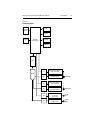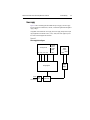
1
Model 2520 Pulsed Laser Diode Test System
Service Manual
A GREATER MEASURE OF CONFIDENCE
WARRANTY
Keithley Instruments, Inc. warrants this product to be free from defects in material and workmanship for a
period of 1 year from date of shipment.
Keithley Instruments, Inc. warrants the following items for 90 days from the date of shipment: probes, cables,
rechargeable batteries, diskettes, and documentation.
During the warranty period, we will, at our option, either repair or replace any product that proves to be
defective.
To exercise this warranty, write or call your local Keithley representative, or contact Keithley headquarters in
Cleveland, Ohio. You will be given prompt assistance and return instructions. Send the product, transportation
prepaid, to the indicated service facility. Repairs will be made and the product returned, transportation prepaid.
Repaired or replaced products are warranted for the balance of the original warranty period, or at least 90 days.
LIMITATION OF WARRANTY
This warranty does not apply to defects resulting from product modification without Keithley’s express written
consent, or misuse of any product or part. This warranty also does not apply to fuses, software, nonrechargeable batteries, damage from battery leakage, or problems arising from normal wear or failure to follow
instructions.
THIS WARRANTY IS IN LIEU OF ALL OTHER WARRANTIES, EXPRESSED OR IMPLIED, INCLUDING ANY IMPLIED WARRANTY OF MERCHANTABILITY OR FITNESS FOR A PARTICULAR USE.
THE REMEDIES PROVIDED HEREIN ARE BUYER’S SOLE AND EXCLUSIVE REMEDIES.
NEITHER KEITHLEY INSTRUMENTS, INC. NOR ANY OF ITS EMPLOYEES SHALL BE LIABLE FOR
ANY DIRECT, INDIRECT, SPECIAL, INCIDENTAL OR CONSEQUENTIAL DAMAGES ARISING OUT OF
THE USE OF ITS INSTRUMENTS AND SOFTWARE EVEN IF KEITHLEY INSTRUMENTS, INC., HAS
BEEN ADVISED IN ADVANCE OF THE POSSIBILITY OF SUCH DAMAGES. SUCH EXCLUDED DAMAGES SHALL INCLUDE, BUT ARE NOT LIMITED TO: COSTS OF REMOVAL AND INSTALLATION,
LOSSES SUSTAINED AS THE RESULT OF INJURY TO ANY PERSON, OR DAMAGE TO PROPERTY.
Keithley Instruments, Inc. • 28775 Aurora Road • Cleveland, OH 44139 • 440-248-0400 • Fax: 440-248-6168 • http://www.keithley.com
BELGIUM:
CHINA:
FRANCE:
GERMANY:
GREAT BRITAIN:
INDIA:
ITALY:
NETHERLANDS:
SWITZERLAND:
TAIWAN:
Keithley Instruments B.V.
Keithley Instruments China
Keithley Instruments Sarl
Keithley Instruments GmbH
Keithley Instruments Ltd
Keithley Instruments GmbH
Keithley Instruments s.r.l.
Keithley Instruments B.V.
Keithley Instruments SA
Keithley Instruments Taiwan
Bergensesteenweg 709 • B-1600 Sint-Pieters-Leeuw • 02/363 00 40 • Fax: 02/363 00 64
Yuan Chen Xin Building, Room 705 • 12 Yumin Road, Dewai, Madian • Beijing 100029 • 8610-62022886 • Fax: 8610-62022892
3, allée des Garays • 91127 Palaiseau Cedex • 01-64 53 20 20 • Fax: 01-60 11 77 26
Landsberger Strasse 65 • 82110 Germering • 089/84 93 07-40 • Fax: 089/84 93 07-34
Unit 2 Commerce Park, Brunel Road • Theale • Reading • Berkshire RG7 4AB • 0118 929 7500 • Fax: 0118 929 7519
Flat 2B, WILOCRISSA • 14, Rest House Crescent • Bangalore 560 001 • 91-80-509-1320/21 • Fax: 91-80-509-1322
Viale S. Gimignano, 38 • 20146 Milano • 02-48 39 16 01 • Fax: 02-48 30 22 74
Postbus 559 • 4200 AN Gorinchem • 0183-635333 • Fax: 0183-630821
Kriesbachstrasse 4 • 8600 Dübendorf • 01-821 94 44 • Fax: 01-820 30 81
1 Fl. 85 Po Ai Street • Hsinchu, Taiwan, R.O.C. • 886-3572-9077 • Fax: 886-3572-903
4/01
Model 2520
Pulsed Laser Diode Test System
Service Manual
©2001, Keithley Instruments, Inc.
All rights reserved.
Cleveland, Ohio, U.S.A.
First Printing, September 2001
Document Number: 2520-902-01 Rev. A
Manual Print History
The print history shown below lists the printing dates of all Revisions and Addenda created
for this manual. The Revision Level letter increases alphabetically as the manual undergoes
subsequent updates. Addenda, which are released between Revisions, contain important change
information that the user should incorporate immediately into the manual. Addenda are
numbered sequentially. When a new Revision is created, all Addenda associated with the
previous Revision of the manual are incorporated into the new Revision of the manual. Each new
Revision includes a revised copy of this print history page.
Revision A (Document Number 2520-902-01) ..................................................... September 2001
All Keithley product names are trademarks or registered trademarks of Keithley Instruments, Inc.
Other brand names are trademarks or registered trademarks of their respective holders.
Safety Precautions
The following safety precautions should be observed before using this product and any associated instrumentation. Although some instruments and accessories would normally be used with non-hazardous
voltages, there are situations where hazardous conditions may be present.
This product is intended for use by qualified personnel who recognize shock hazards and are familiar
with the safety precautions required to avoid possible injury. Read the operating information carefully
before using the product.
The types of product users are:
Responsible body is the individual or group responsible for the use and maintenance of equipment, for
ensuring that the equipment is operated within its specifications and operating limits, and for ensuring
that operators are adequately trained.
Operators use the product for its intended function. They must be trained in electrical safety procedures
and proper use of the instrument. They must be protected from electric shock and contact with hazardous
live circuits.
Maintenance personnel perform routine procedures on the product to keep it operating, for example,
setting the line voltage or replacing consumable materials. Maintenance procedures are described in the
manual. The procedures explicitly state if the operator may perform them. Otherwise, they should be
performed only by service personnel.
Service personnel are trained to work on live circuits, and perform safe installations and repairs of products. Only properly trained service personnel may perform installation and service procedures.
Keithley products are designed for use with electrical signals that are rated Installation Category I and
Installation Category II, as described in the International Electrotechnical Commission (IEC) Standard
IEC 60664. Most measurement, control, and data I/O signals are Installation Category I and must not
be directly connected to mains voltage or to voltage sources with high transient over-voltages. Installation Category II connections require protection for high transient over-voltages often associated with local AC mains connections. The user should assume all measurement, control, and data I/O connections
are for connection to Category I sources unless otherwise marked or described in the Manual.
Exercise extreme caution when a shock hazard is present. Lethal voltage may be present on cable connector jacks or test fixtures. The American National Standards Institute (ANSI) states that a shock hazard exists when voltage levels greater than 30V RMS, 42.4V peak, or 60VDC are present. A good safety
practice is to expect that hazardous voltage is present in any unknown circuit before measuring.
Users of this product must be protected from electric shock at all times. The responsible body must ensure that users are prevented access and/or insulated from every connection point. In some cases, connections must be exposed to potential human contact. Product users in these circumstances must be
trained to protect themselves from the risk of electric shock. If the circuit is capable of operating at or
above 1000 volts, no conductive part of the circuit may be exposed.
Do not connect switching cards directly to unlimited power circuits. They are intended to be used with
impedance limited sources. NEVER connect switching cards directly to AC mains. When connecting
sources to switching cards, install protective devices to limit fault current and voltage to the card.
Before operating an instrument, make sure the line cord is connected to a properly grounded power receptacle. Inspect the connecting cables, test leads, and jumpers for possible wear, cracks, or breaks before each use.
When installing equipment where access to the main power cord is restricted, such as rack mounting, a
separate main input power disconnect device must be provided, in close proximity to the equipment and
within easy reach of the operator.
For maximum safety, do not touch the product, test cables, or any other instruments while power is applied to
the circuit under test. ALWAYS remove power from the entire test system and discharge any capacitors before:
connecting or disconnecting cables or jumpers, installing or removing switching cards, or making internal
changes, such as installing or removing jumpers.
Do not touch any object that could provide a current path to the common side of the circuit under test or power
line (earth) ground. Always make measurements with dry hands while standing on a dry, insulated surface capable of withstanding the voltage being measured.
The instrument and accessories must be used in accordance with its specifications and operating instructions
or the safety of the equipment may be impaired.
Do not exceed the maximum signal levels of the instruments and accessories, as defined in the specifications
and operating information, and as shown on the instrument or test fixture panels, or switching card.
When fuses are used in a product, replace with same type and rating for continued protection against fire hazard.
Chassis connections must only be used as shield connections for measuring circuits, NOT as safety earth
ground connections.
If you are using a test fixture, keep the lid closed while power is applied to the device under test. Safe operation
requires the use of a lid interlock.
If a
screw is present, connect it to safety earth ground using the wire recommended in the user documentation.
The ! symbol on an instrument indicates that the user should refer to the operating instructions located in
the manual.
The
symbol on an instrument shows that it can source or measure 1000 volts or more, including the combined effect of normal and common mode voltages. Use standard safety precautions to avoid personal contact
with these voltages.
The WARNING heading in a manual explains dangers that might result in personal injury or death. Always
read the associated information very carefully before performing the indicated procedure.
The CAUTION heading in a manual explains hazards that could damage the instrument. Such damage may
invalidate the warranty.
Instrumentation and accessories shall not be connected to humans.
Before performing any maintenance, disconnect the line cord and all test cables.
To maintain protection from electric shock and fire, replacement components in mains circuits, including the
power transformer, test leads, and input jacks, must be purchased from Keithley Instruments. Standard fuses,
with applicable national safety approvals, may be used if the rating and type are the same. Other components
that are not safety related may be purchased from other suppliers as long as they are equivalent to the original
component. (Note that selected parts should be purchased only through Keithley Instruments to maintain accuracy and functionality of the product.) If you are unsure about the applicability of a replacement component,
call a Keithley Instruments office for information.
To clean an instrument, use a damp cloth or mild, water based cleaner. Clean the exterior of the instrument
only. Do not apply cleaner directly to the instrument or allow liquids to enter or spill on the instrument. Products that consist of a circuit board with no case or chassis (e.g., data acquisition board for installation into a
computer) should never require cleaning if handled according to instructions. If the board becomes contaminated and operation is affected, the board should be returned to the factory for proper cleaning/servicing.
Rev. 2/01
Table of Contents
1
Performance Verification
Introduction ................................................................................ 1-2
Verification test requirements ..................................................... 1-4
Environmental conditions ................................................... 1-4
Warm-up period .................................................................. 1-4
Line power .......................................................................... 1-4
Recommended test equipment ................................................... 1-5
Resistor characterization ..................................................... 1-5
Verification limits ....................................................................... 1-6
Example limits calculation .................................................. 1-6
Restoring factory defaults .......................................................... 1-6
Performing the verification test procedures ............................... 1-7
Test summary ...................................................................... 1-7
Test considerations .............................................................. 1-7
Testhead connections ................................................................. 1-8
Voltage measurement accuracy .................................................. 1-9
Current source accuracy ........................................................... 1-10
Current measurement accuracy ................................................ 1-11
Voltage bias source accuracy .................................................... 1-13
2
Calibration
Introduction ................................................................................
Environmental conditions ..........................................................
Temperature and relative humidity .....................................
Warm-up period ..................................................................
Line power ..........................................................................
Calibration considerations ..........................................................
Calibration cycle .................................................................
Recommended calibration equipment .................................
Resistor characterization .....................................................
Calibration menus ......................................................................
Unlocking calibration .................................................................
Unlocking calibration from the front panel ........................
Unlocking calibration by remote ........................................
Changing the password ..............................................................
Changing the password from the front panel ......................
Changing the password by remote ......................................
2-2
2-4
2-4
2-4
2-4
2-4
2-5
2-5
2-5
2-6
2-7
2-7
2-7
2-8
2-8
2-8
Resetting the calibration password ............................................. 2-8
Viewing calibration dates and calibration count ......................... 2-9
Calibration errors ........................................................................ 2-9
Front panel error reporting .................................................. 2-9
Remote error reporting ........................................................ 2-9
Aborting calibration steps ........................................................... 2-9
Testhead connections ................................................................ 2-10
Front panel calibration .............................................................. 2-10
Remote calibration .................................................................... 2-22
Remote calibration command summary ............................ 2-22
Remote calibration procedure ........................................... 2-23
3
Routine Maintenance
Introduction ................................................................................ 3-2
Line fuse replacement ................................................................. 3-2
4
Troubleshooting
Introduction ................................................................................ 4-2
Safety considerations .................................................................. 4-2
Repair considerations ................................................................. 4-2
Power-on self-test ....................................................................... 4-2
Front panel tests .......................................................................... 4-3
KEYS test ............................................................................ 4-3
DISPLAY PATTERNS test ................................................. 4-3
CHAR SET test ................................................................... 4-4
Principles of operation ................................................................ 4-4
Overall block diagram ......................................................... 4-4
Analog circuits .................................................................... 4-6
Power supply ....................................................................... 4-9
Digital circuitry ................................................................. 4-10
Troubleshooting ........................................................................ 4-12
Display board checks ........................................................ 4-12
Power supply checks ......................................................... 4-13
Digital circuitry checks ..................................................... 4-14
Analog circuitry checks ..................................................... 4-15
No comm link error .................................................................. 4-16
5
Disassembly
Introduction ................................................................................
Handling and cleaning ...............................................................
Handling PC boards ............................................................
Solder repairs ......................................................................
Static sensitive devices ...............................................................
Assembly drawings ....................................................................
Case cover removal ....................................................................
Motherboard removal .................................................................
Front panel disassembly .............................................................
Removing power components ....................................................
Power supply module removal ............................................
Power module removal .......................................................
Instrument re-assembly ..............................................................
Testhead disassembly .................................................................
Case disassembly ................................................................
Output board removal .........................................................
Input board removal ............................................................
Testhead re-assembly .................................................................
6
Replaceable Parts
Introduction ................................................................................
Parts lists ....................................................................................
Ordering information .................................................................
Factory service ...........................................................................
Component layouts ....................................................................
A
5-2
5-2
5-2
5-2
5-3
5-3
5-4
5-4
5-5
5-6
5-6
5-6
5-6
5-7
5-7
5-7
5-7
5-7
Specifications
6-2
6-2
6-2
6-2
6-2
B
Calibration Reference
Introduction ............................................................................... B-2
Command summary ................................................................... B-2
Miscellaneous commands .......................................................... B-3
Measurement commands ........................................................... B-6
Current source commands ......................................................... B-7
Voltage bias source commands .................................................. B-8
Detecting calibration errors ....................................................... B-9
Reading the error queue ..................................................... B-9
Error summary .................................................................... B-9
Status byte EAV (Error Available) bit .............................. B-10
Generating an SRQ on error ............................................. B-10
Detecting calibration step completion ..................................... B-10
Using the *OPC? query .................................................... B-10
Using the *OPC command ............................................... B-11
Generating an SRQ on calibration complete .................... B-11
List of Illustrations
1
Performance Verification
Figure 1-1
Figure 1-2
Figure 1-3
Figure 1-4
Testhead connections ............................................................. 1-8
Connections for voltage measurement verification tests ....... 1-9
Connections for current source verification tests ................. 1-10
Connections for DETECTOR 1 current measurement
verification tests ............................................................. 1-11
Connections for DETECTOR 2 current measurement
verification tests ............................................................. 1-13
Connections for DETECTOR 1 voltage bias source
verification tests ............................................................ 1-13
Connections for DETECTOR 2 voltage bias source
verification tests ............................................................. 1-14
Figure 1-5
Figure 1-6
Figure 1-7
2
Calibration
Figure 2-1
Figure 2-2
Figure 2-3
Figure 2-4
Figure 2-5
Figure 2-6
Figure 2-7
Figure 2-8
Figure 2-9
Testhead connections ...........................................................
Voltage measurement calibration connections .....................
Current source calibration connections ................................
Pulse low calibration connections ........................................
Detector 1 voltage bias source calibration connections .......
Detector 2 voltage bias source calibration connections .......
Detector 1 current measurement calibration connections ....
Detector 2 current measurement calibration connections ....
Compliance calibration connections ....................................
2-10
2-12
2-13
2-15
2-16
2-17
2-18
2-19
2-20
3
Routine Maintenance
Figure 3-1
Model 2520 rear panel ........................................................... 3-2
4
Troubleshooting
Figure 4-1
Figure 4-2
Figure 4-3
Figure 4-4
Overall block diagram ........................................................... 4-5
Analog circuitry block diagram ............................................. 4-7
Power supply block diagram .................................................. 4-9
Digital circuitry block diagram ............................................ 4-11
List of Tables
1
Performance Verification
Table 1-1
Table 1-2
Table 1-3
Table 1-4
Recommended verification equipment .................................. 1-5
Voltage measurement accuracy limits .................................... 1-9
Current source verification limits ........................................ 1-11
Current measurement verification limits .............................. 1-12
2
Calibration
Table 2-1
Table 2-2
Table 2-3
Table 2-4
Table 2-5
Table 2-6
Table 2-7
Table 2-8
Table 2-9
Table 2-10
Table 2-11
Table 2-12
Table 2-13
Table 2-14
Recommended calibration equipment ................................... 2-5
Calibration menu ................................................................... 2-6
Calibration execution menu ................................................... 2-6
Voltage measurement calibration values .............................. 2-11
Current source calibration values ......................................... 2-13
Pulse low calibration values ................................................. 2-14
Current measurement calibration values .............................. 2-18
Remote calibration command summary .............................. 2-22
Voltage measurement calibration voltages and commands . 2-25
Remote current source calibration summary ....................... 2-27
Remote pulse low calibration summary ............................... 2-29
Remote voltage bias source calibration summary ............... 2-31
Remote current measurement calibration
currents and commands .................................................. 2-33
Remote compliance calibration summary ............................ 2-36
3
Routine Maintenance
Table 3-1
Power line fuse ....................................................................... 3-3
4
Troubleshooting
Table 4-1
Table 4-2
Table 4-3
Table 4-4
Display board checks ...........................................................
Power supply checks ............................................................
Digital circuitry checks ........................................................
Analog circuitry checks .......................................................
4-12
4-13
4-14
4-15
6
Replaceable Parts
Table 6-1
Table 6-2
Table 6-3
Table 6-4
Table 6-5
Mainframe digital board parts list .......................................... 6-3
Mainframe display board parts list ......................................... 6-9
Test head board parts list ...................................................... 6-10
Pulse board parts list ............................................................ 6-13
Miscellaneous parts list ........................................................ 6-16
B
Calibration Reference
Table B-1
Table B-2
Calibration commands .......................................................... B-2
Calibration errors .................................................................. B-9
1
Performance Verification
1-2
Performance Verification
Model 2520 Pulsed Laser Diode Test System Service Manual
Introduction
Use the procedures in this section to verify that Model 2520 Pulsed Laser Diode Test
System accuracy is within the limits stated in the instrument’s one-year accuracy
specifications. You can perform these verification procedures:
•
•
•
•
When you first receive the instrument to make sure that it was not damaged during
shipment.
To verify that the unit meets factory specifications.
To determine if calibration is required.
Following calibration to make sure it was performed properly.
Model 2520 Pulsed Laser Diode Test System Service Manual
WARNING
NOTE
Performance Verification
1-3
While the Model 2520 does not incorporate a laser, it is designed to
operate (power) laser diode devices. Read all safety precautions listed
at the beginning of the Model 2520 User’s Manual. The following safety
practices must be used to protect operators and other users of this
product from potential exposure to laser radiation:
•
Operators must be protected from radiation and electrical hazards
at all times.
•
The installer must comply with all applicable laws and regulations
on laser safety. This requirement includes warning signs and operator training.
•
The interlock is required for safe operation. The test fixtures must
ensure that the interlock circuit is disabled (source outputs inhibited) so that an operator is not exposed to any radiation. The test
fixture interlock must not be defeated.
•
The testhead key control must be used to prevent operation unless
authorized by the responsible body. This requirement must be part
of the facilities administrative controls for laser safety. Outputs
cannot be turned on with the key removed.
•
When servicing the test system, any required personnel protection
equipment (e.g. laser safety goggles) must be provided by the customer’s responsible body.
•
The customer’s laser safety officer (LSO) must review and approve
all installations before they are put into operation. Any safety concerns must be immediately reported to the customer’s LSO.
•
If at any time, the indicators provided on the testhead for INTERLOCK STATUS or LASER POWER ON should fail to light or
properly indicate status, immediately contact a Keithley service
representative for repair. Failure to do so may expose the user to
hazards without proper warnings. See “Interlock status indicator
test sequence” in Section 9 of the User’s manual for details on testing the indicator lights.
•
Maximum isolation from earth ground is 10V. Exceeding this
value may result in a shock hazard.
•
When making connections, do not leave any exposed connections.
Ensure that all external circuits are properly insulated.
If the instrument is still under warranty and its performance is outside specified
limits, contact your Keithley representative or the factory to determine the correct course of action.
1-4
Performance Verification
Model 2520 Pulsed Laser Diode Test System Service Manual
Verification test requirements
Be sure that you perform the verification tests:
•
•
•
•
•
Under the proper environmental conditions.
After the specified warm-up period.
Using the correct line voltage.
Using the proper test equipment.
Using the specified output signals and reading limits.
Environmental conditions
Conduct your performance verification procedures in a test environment with:
•
•
An ambient temperature of 18-28°C (65-82°F).
A relative humidity of less than 70% unless otherwise noted.
Warm-up period
Allow the Model 2520 to warm up for a minimum of one hour before conducting the verification procedures.
If the instrument has been subjected to temperature extremes (those outside the ranges
stated above), allow additional time for the instrument’s internal temperature to stabilize.
Typically, allow one extra hour to stabilize a unit that is 10°C (18°F) outside the specified
temperature range.
Also, allow the test equipment to warm up for the minimum time specified by the
manufacturer.
Line power
The Model 2520 requires a line voltage of 100V to 240V and a line frequency of 50 or
60 Hz. Verification tests must be performed within this range.
Model 2520 Pulsed Laser Diode Test System Service Manual
Performance Verification
1-5
Recommended test equipment
Table 1-1 summarizes recommended verification equipment and pertinent specifications.
You can use alternate equipment as long as that equipment has specifications at least as
good as those listed in Table 1-1. Keep in mind, however, that test equipment uncertainty
will add to the uncertainty of each measurement. Generally, test equipment uncertainty
should be at least four times better than corresponding Model 2520 specifications.
Table 1-1
Recommended verification equipment
Description
Manufacturer/Model Specifications
Calibrator
Fluke 5700A1
DC Voltage:
5V:
10V:
±5ppm
±5ppm
Digital
Multimeter
Keithley 20012
DC Voltage:
20V:
±22ppm
Resistance:
20Ω
200Ω
2kΩ
±59ppm
±43ppm
±37ppm
Precision
Resistors3
1.
2.
3.
4.
1.2 to 1.6Ω, 5W, ±5%4
10 to 15Ω, 5W, ±5%4
200Ω, 2W, ±1%
400Ω, 1W, ±1%
1kΩ, 0.5W, ±1%
2kΩ, 0.25W, ±1%
Temperature
coefficient =
20ppm/°C for
all resistors
90-day accuracy specifications of lowest usable range for specified output.
90-day full-range accuracy specifications.
Characterize resistors to within ±100ppm using 4-wire ohms function of digital multimeter before use.
Use only non-inductive metal film or bulk metal resistors.
Resistor characterization
The precision resistors listed in Table 1-1 should be characterized to within ±100ppm
using the 4-wire ohms function of the digital multimeter before use. Use the characterized
values when performing the verification procedure.
1-6
Performance Verification
Model 2520 Pulsed Laser Diode Test System Service Manual
Verification limits
The verification limits listed in this section have been calculated using only the
Model 2520 one-year accuracy specifications; they do not include test equipment
uncertainty. If a particular measurement falls outside the allowable range, recalculate new
limits based on Model 2520 specifications and corresponding test equipment
specifications.
Example limits calculation
As an example of how verification limits are calculated, assume you are testing the 10mA
measurement range with a 10mA input current. Using the Model 2520 one-year accuracy
specification of ±(0.3% of reading + 20µA offset), the calculated reading limits are:
Limits = 10mA ± [(10mA × 0.3%) + 20µA]
Limits = 10mA ± (30µA + 20µA)
Limits = 10mA ± 50µA
Limits = 9.95mA to 10.05mA
Restoring factory defaults
Before performing the verification procedures, restore the instrument to its factory front
panel (BENCH) defaults as follows:
1.
Press the SETUP key. The instrument will display the following prompt:
SAVESETUP MENU
SAVE RESTORE POWERON RESET
2.
Select RESET, then press ENTER. The unit displays:
RESET ORIGINAL DFLTS
BENCH GPIB
3.
Select BENCH, then press ENTER to restore BENCH defaults.
Model 2520 Pulsed Laser Diode Test System Service Manual
Performance Verification
1-7
Performing the verification test procedures
Test summary
•
•
•
•
Detector current measurement accuracy
Laser diode voltage measurement accuracy
Laser diode current source accuracy
Detector voltage bias source accuracy
If the Model 2520 is not within specifications and not under warranty, see the calibration
procedures in Section 2, Calibration, for information on calibrating the unit.
Test considerations
When performing the verification procedures:
•
•
•
•
Restore factory front panel defaults as previously outlined.
Ensure test equipment is fully warmed up and properly connected to the correct
Model 2520 terminals as required.
Allow signals to settle before making a measurement.
Do not connect test equipment to the Model 2520 through a scanner, multiplexer,
or other switching equipment.
WARNING
The maximum common-mode voltage (voltage between LO and
chassis ground) is ±10V DC. Exceeding this value may cause a shock
hazard.
1-8
Performance Verification
Model 2520 Pulsed Laser Diode Test System Service Manual
Testhead connections
The Model 2520 mainframe must be connected to the testhead in order to perform the verification procedures. Using Figure 1-1 as a guide, make testhead connections as follows:
CAUTION
•
•
•
Make sure power is turned off before making connections.
Connect mainframe TESTHEAD CONN 1 to testhead MAINFRAME CONN 1.
Connect mainframe TESTHEAD CONN 2 to testhead MAINFRAME CONN 2.
Short pins 1 and 9 of the REMOTE INTERLOCK connector. Insert the key in the
KEY INTERLOCK and rotate to the ENABLED position to enable operation.
WARNING
NOTE
Shorting the interlock connector will disable the interlocks. Use caution when performing verification tests.
Both interlocks must be enabled to perform the verification tests.
Figure 1-1
Testhead connections
Model 2520 Mainframe
WARNING:
Model 2520 Testhead
NO INTERNAL OPERATOR SERVICABLE PARTS, SERVICE BY QUALIFIED PERSONNEL ONLY.
! BOTH INTERLOCKS MUST BE ENABLED TO OPERATE
IEEE-488
(CHANGE IEEE ADDRESS
WITH FRONT PANEL MENU)
CAT I
MADE IN
U.S.A.
PULSE
SYNC
OUT
KEY
INTERLOCK
REMOTE
INTERLOCK
DIGITAL I/O
!
ENABLED
DISABLED
1
RS-232
TRIGGER LINK
9
ENABLED
GREEN=ENABLED
RED=DISABLED
TESTHEAD
CONN 1
INTERLOCK
STATUS
!
!
TESTHEAD
CONN 2
CAUTION:
DISABLED
(PULL TO
REMOVE)
LINE FUSE
SLOWBLOW
1.6A, 250V
LINE RATING
100-240VAC
50, 60Hz
140VA MAX.
MAINFRAME
CONN 2
MAINFRAME
CONN 1
FOR CONTINUED PROTECTION AGAINST FIRE HAZARD, REPLACE FUSE WITH SAME TYPE AND RATING.
CONN 2 Cable
CONN 1 Cable
LASER
POWER
ON
Model 2520 Pulsed Laser Diode Test System Service Manual
Performance Verification
1-9
Voltage measurement accuracy
Follow the steps below to verify that Model 2520 laser diode voltage measurement accuracy is within specified limits. This test involves applying accurate voltages from a DC
calibrator, and verifying that the Model 2520 voltage readings are within specified limits.
1.
2.
3.
4.
5.
6.
7.
With the power off, connect the voltage calibrator to the testhead VOLTAGE
SENSE jacks, as shown in Figure 1-2.
Turn on the Model 2520 and calibrator, and allow them to warm up for a minimum
of one hour.
Restore BENCH defaults as covered previously in Restoring factory defaults.
Press the LASER VL key, then select the Model 2520 5V range with the RANGE
key.
Set the calibrator source voltage to +5.0000V, and turn on the output.
Press the TRIG key, then verify the Model 2520 voltage reading is within the limits
for the 5V range shown in Table 1-2.
Repeat steps 4 through 6 for the 10V range with a 10V input voltage, as covered in
Table 1-2.
Table 1-2
Voltage measurement accuracy limits
Model 2520 Calibrator
range
voltage
Voltage reading limits
(1 year, 18˚C to 28˚C)
05V
05.0000V
4.9785 to 5.0215V
10V
10.000V
9.962 to 10.038V
Figure 1-2
Connections for voltage measurement verification tests
Calibrator (Output DC Voltage)
Model 2520 Testhead
Output HI
HI CURRENT LO
OUTPUT
CURRENT
INPUT
BIAS
!
CAT I
DETECTOR 1
DETECTOR 2
!
HI
VOLTAGE
SENSE LO
ISOLATION FROM EARTH: 10V MAX.
VOLTAGE
SENSE HI
VOLTAGE
SENSE LO
BNC Cables
Output LO
1-10
Performance Verification
Model 2520 Pulsed Laser Diode Test System Service Manual
Current source accuracy
Follow the steps below to verify that Model 2520 current source accuracy is within specified limits. This test involves setting the output current to a specific value and measuring
the current with a digital multimeter.
1.
2.
3.
4.
5.
6.
7.
8.
With the power off, connect the digital multimeter and characterized 10Ω to 15Ω
resistor to the testhead CURRENT OUTPUT jacks, as shown in Figure 1-3.
Turn on the Model 2520 and DMM, and allow them to warm up for a minimum of
one hour.
Restore front panel (BENCH) defaults as outlined previously in Restoring factory
defaults.
Select the DC mode as follows:
a. Press CONFIG then LASER IL.
b. Select SHAPE, then press ENTER.
c. Select DC, then press ENTER.
d. Press EXIT to return to normal display.
Press the LASER IL key, then the EDIT key, and select the Model 2520 500mA
source range with the RANGE key.
Select the DMM DC voltage function, and enable auto-range.
Press the EDIT key to enter the EDIT mode. Using the EDIT and or numeric
keys, set the Model 2520 current source output to 500.00mA, then turn on the outputs by pressing the ON/OFF OUTPUT key.
Note the DMM voltage reading, then turn off the output by pressing the ON/OFF
OUTPUT key.
Figure 1-3
Connections for current source verification tests
Model 2001 DMM
Model 2520 Testhead
Input HI
SENSE
Ω 4 WIRE
INPUT
HI
350V
PEAK
1100V
PEAK
!
HI CURRENT LO
OUTPUT
2001 MULTIMETER
LO
PREV
DCV
ACV
DCI
ACI
Ω2
Ω4
FREQ
TEMP
EXIT
ENTER
RANGE
DISPLAY
NEXT
REL
TRIG
STORE RECALL
INFO
LOCAL
CHAN
AUTO
FILTER MATH
CONFIG MENU
F
CURRENT
INPUT
BIAS
R
!
CAT I
FRONT/REAR
DETECTOR 1
2A 250V
RANGE
POWER
SCAN
500V
PEAK
INPUTS
CAL
DETECTOR 2
AMPS
!
VOLTAGE
HI SENSE LO
ISOLATION FROM EARTH: 10V MAX.
Input LO
10 to 15Ω Resistor
(500mA Range)
1.2 to 1.6Ω Resistor
(5A Range)
CURRENT
OUTPUT HI
CURRENT
OUTPUT LO
Model 2520 Pulsed Laser Diode Test System Service Manual
9.
Performance Verification
1-11
Calculate the current using the voltage value and characterized resistance value:
I = V/R. Recalculate reading limits from these values, then verify that the current is
within those limits.
Replace the 10Ω to 15Ω resistor with the characterized 1.2Ω to 1.6Ω resistor.
Repeat steps 5 through 9 for the 5A range using the 1A value shown in Table 1-3.
10.
11.
Table 1-3
Current source verification limits
Model 2520
range
Test resistance
Output current
Output current limits*
(1 year, 18˚C to 28˚C)
500mA
10 to 15Ω
500.000mA
498.55mA to 501.45mA
005A
1.2 to 1.6Ω
001.0000A
0.9935 to 1.0065A
* Nominal values. Recalculate limits from characterized resistance and measured voltage: I = V/R.
Current measurement accuracy
Follow the steps below to verify that Model 2520 detector current measurement accuracy
is within specified limits. This test involves applying currents and verifying that
Model 2520 current readings are within required limits.
1.
2.
3.
With the power off, connect the 2kΩ resistor and DMM to the testhead DETECTOR 1 jack, as shown in Figure 1-4.
Turn on the Model 2520 and DMM, and allow them to warm up for a minimum of
one hour.
Select the DMM DC volts function, and enable auto-range.
Figure 1-4
Connections for DETECTOR 1 current measurement verification tests
Input HI
Center
Conductor
Model 2520 Testhead
Model 2001 DMM
SENSE
Ω 4 WIRE
INPUT
HI
350V
PEAK
1100V
PEAK
!
HI CURRENT LO
OUTPUT
2001 MULTIMETER
LO
PREV
DCV
ACV
DCI
ACI
Ω2
Ω4
FREQ
TEMP
EXIT
ENTER
RANGE
DISPLAY
NEXT
REL
TRIG
STORE RECALL
INFO
LOCAL
CHAN
AUTO
FILTER MATH
SCAN
CONFIG MENU
F
R
!
CAT I
FRONT/REAR
2A 250V
RANGE
POWER
CURRENT
INPUT
BIAS
500V
PEAK
INPUTS
CAL
AMPS
Input LO
Inner
Shield
Resistor
(See Text)
DETECTOR 1
DETECTOR 2
!
HI
ISOLATION FROM EARTH: 10V MAX.
DETECTOR 1
VOLTAGE
SENSE LO
1-12
Performance Verification
4.
5.
6.
7.
8.
9.
10.
11.
12.
Model 2520 Pulsed Laser Diode Test System Service Manual
Restore front panel (BENCH) defaults as outlined previously in Restoring factory
defaults.
Press the DETECTOR 1 IPD key, then select the Model 2520 10mA range with the
RANGE key.
Press the DETECTOR 1 VB key, then press the EDIT key, and set the voltage bias
source value to +20.000V.
Turn on the Model 2520 outputs by pressing the ON/OFF OUTPUT key.
Press the TRIG key. Note the DMM voltage reading, then turn off the outputs by
pressing the ON/OFF OUTPUT key.
Calculate the current from the DMM voltage reading and characterized resistance
value: I = V/R.
Calculate reading limits based on the current and Model 2520 specifications, then
verify that the Model 2520 DETECTOR 1 current reading is within the limits.
Repeat steps 5 through 10 for the 20mA, 50mA, and 100mA ranges. Be sure to use
the correct test resistor for each range.
After verifying all ranges for DETECTOR 1, repeat the entire procedure for
DETECTOR 2. (Connect the calibrator to the TESTHEAD DETECTOR 2 jack,
and select that channel by pressing DETECTOR 2 IPD. See Figure 1-5 for
connections.)
Table 1-4
Current measurement verification limits
Model 2520
range
Test resistor
Reading limits*
(1 year, 18˚C to 28˚C)
010mA
002kΩ
09.950 to 10.050mA
020mA
001kΩ
19.875 to 20.125mA
050mA
400Ω
49.760 to 50.240mA
100mA
200Ω
99.53 to 100.47mA
*Nominal values. Recalculate limits from characterized resistance and
measured voltage: I = V/R.
Model 2520 Pulsed Laser Diode Test System Service Manual
Performance Verification
1-13
Figure 1-5
Connections for DETECTOR 2 current measurement verification tests
Center
Conductor
Input HI
Model 2520 Testhead
Model 2001 DMM
SENSE
Ω 4 WIRE
INPUT
HI
350V
PEAK
1100V
PEAK
!
HI CURRENT LO
OUTPUT
2001 MULTIMETER
LO
PREV
DCV
ACV
DCI
ACI
Ω2
Ω4
FREQ
TEMP
EXIT
ENTER
RANGE
DISPLAY
NEXT
REL
TRIG
STORE RECALL
INFO
LOCAL
CHAN
AUTO
FILTER MATH
F
R
SCAN
CONFIG MENU
!
CAT I
FRONT/REAR
2A 250V
RANGE
POWER
CURRENT
INPUT
BIAS
500V
PEAK
INPUTS
Inner
Shield
AMPS
CAL
DETECTOR 1
DETECTOR 2
!
HI
Resistor
(See Text)
Input LO
VOLTAGE
SENSE LO
ISOLATION FROM EARTH: 10V MAX.
DETECTOR 2
Voltage bias source accuracy
Follow the steps below to verify that Model 2520 detector voltage bias source accuracy is
within specified limits. This test involves setting the bias voltages to specific values and
measuring the voltages with a DMM.
1.
2.
3.
4.
With the power off, connect the digital multimeter to the Model 2520 testhead
DETECTOR 1 jack, as shown in Figure 1-6.
Turn on the Model 2520 and DMM, and allow them to warm up for a minimum of
one hour.
Restore BENCH defaults as covered previously in Restoring factory defaults.
Select the DMM DC volts measuring function, and choose auto-range.
Figure 1-6
Connections for DETECTOR 1 voltage bias source verification tests
Input HI
Model 2001 DMM
SENSE
Ω 4 WIRE
Model 2520 Testhead
Inner Shield
INPUT
HI
350V
PEAK
1100V
PEAK
!
2001 MULTIMETER
LO
PREV
DCV
ACV
DCI
ACI
Ω2
Ω4
FREQ
TEMP
EXIT
ENTER
RANGE
DISPLAY
NEXT
REL
TRIG
STORE RECALL
INFO
LOCAL
CHAN
AUTO
FILTER MATH
SCAN
CONFIG MENU
F
R
FRONT/REAR
2A 250V
RANGE
POWER
CAL
Triax Cable
HI CURRENT LO
OUTPUT
AMPS
CURRENT
INPUT
BIAS
500V
PEAK
INPUTS
Center
Conductor
!
CAT I
DETECTOR 1
DETECTOR 2
!
HI
Input LO
ISOLATION FROM EARTH: 10V MAX.
DETECTOR 1
VOLTAGE
SENSE LO
1-14
Performance Verification
5.
6.
7.
8.
9.
Model 2520 Pulsed Laser Diode Test System Service Manual
Press the DETECTOR 1 VB key, press EDIT, then set the source voltage to
+20.000V using the EDIT and or numeric keys.
Press the ON/OFF OUTPUT key to turn on the outputs, then press TRIG.
Verify the DMM reading is within the following limits: 19.75 to 20.25V.
Press the ON/OFF OUTPUT key to turn off the outputs.
Repeats steps 5 through 8 for the DETECTOR 2 bias source (make connections to
the testhead DETECTOR 2 jack as shown in Figure 1-7, and use the DETECTOR
2 VB key to set the output voltage).
Figure 1-7
Connections for DETECTOR 2 voltage bias source verification tests
Model 2001 DMM
Input HI
SENSE
Ω 4 WIRE
Inner Shield
Model 2520 Testhead
INPUT
HI
350V
PEAK
1100V
PEAK
!
2001 MULTIMETER
LO
PREV
DCV
ACV
DCI
ACI
Ω2
Ω4
FREQ
TEMP
EXIT
ENTER
RANGE
DISPLAY
NEXT
REL
TRIG
STORE RECALL
INFO
LOCAL
CHAN
AUTO
FILTER MATH
SCAN
CONFIG MENU
F
HI CURRENT LO
OUTPUT
CURRENT
INPUT
BIAS
R
FRONT/REAR
2A 250V
RANGE
POWER
Triax Cable
500V
PEAK
INPUTS
CAL
AMPS
Center
Conductor
Input LO
!
CAT I
DETECTOR 1
DETECTOR 2
!
HI
ISOLATION FROM EARTH: 10V MAX.
DETECTOR 2
VOLTAGE
SENSE LO
2
Calibration
2-2
Calibration
Model 2520 Pulsed Laser Diode Test System Service Manual
Introduction
Use the procedures in this section to calibrate the Model 2520 Pulsed Laser Diode Test
System. These procedures require accurate test equipment to supply and measure precise
DC currents and voltages. Calibration can be performed either from the front panel or by
sending SCPI calibration commands over the IEEE-488 bus or RS-232 port with the aid of
a computer.
Model 2520 Pulsed Laser Diode Test System Service Manual
WARNING
Calibration
2-3
While the Model 2520 does not incorporate a laser, it is designed to
operate (power) laser diode devices. Read all safety precautions listed
at the beginning of the Model 2520 User’s Manual. The following safety
practices must be used to protect operators and other users of this
product from potential exposure to laser radiation:
•
Operators must be protected from radiation and electrical hazards
at all times.
•
The installer must comply with all applicable laws and regulations
on laser safety. This requirement includes warning signs and operator training.
•
The interlock is required for safe operation. The test fixtures must
ensure that the interlock circuit is disabled (source outputs inhibited) so that an operator is not exposed to any radiation. The test
fixture interlock must not be defeated.
•
The testhead key control must be used to prevent operation unless
authorized by the responsible body. This requirement must be part
of the facilities administrative controls for laser safety. Outputs
cannot be turned on with the key removed.
•
When servicing the test system, any required personnel protection
equipment (e.g. laser safety goggles) must be provided by the customer’s responsible body.
•
The customer’s laser safety officer (LSO) must review and approve
all installations before they are put into operation. Any safety concerns must be immediately reported to the customer’s LSO.
•
If at any time, the indicators provided on the testhead for INTERLOCK STATUS or LASER POWER ON should fail to light or
properly indicate status, immediately contact a Keithley service
representative for repair. Failure to do so may expose the user to
hazards without proper warnings. See “Interlock status indicator
test sequence” in Section 9 of the User’s manual for details on testing the indicator lights.
•
Maximum isolation from earth ground is 10V. Exceeding this
value may result in a shock hazard.
•
When making connections, do not leave any exposed connections.
Ensure that all external circuits are properly insulated.
2-4
Calibration
Model 2520 Pulsed Laser Diode Test System Service Manual
Environmental conditions
Temperature and relative humidity
Conduct the calibration procedures at an ambient temperature of 18-28°C (65-82°F) with
relative humidity of less than 70% unless otherwise noted.
Warm-up period
Allow the Model 2520 to warm up for a minimum of one hour before performing
calibration.
If the instrument has been subjected to temperature extremes (those outside the ranges
stated above), allow additional time for the instrument’s internal temperature to stabilize.
Typically, allow one extra hour to stabilize a unit that is 10°C (18°F) outside the specified
temperature range.
Also, allow the test equipment to warm up for the minimum time specified by the
manufacturer.
Line power
The Model 2520 requires a line voltage of 100V to 240V at line frequency of 50 or 60Hz.
The instrument must be calibrated while operating from a line voltage within this range.
Calibration considerations
When performing the calibration procedures:
•
•
•
•
Make sure that the test equipment is properly warmed up and connected to the
Model 2520 input or output terminals as required.
Allow signals to settle before calibrating each point.
Do not connect test equipment to the Model 2520 through a scanner or other
switching equipment.
If an error occurs during calibration, the Model 2520 will generate an appropriate
error message. See Appendix B for more information.
WARNING
The maximum common-mode voltage (voltage between LO and
chassis ground) is ±10V DC. Exceeding this value may cause a shock
hazard.
Model 2520 Pulsed Laser Diode Test System Service Manual
Calibration
2-5
Calibration cycle
Perform calibration at least once a year to ensure the unit meets or exceeds its
specifications.
Recommended calibration equipment
Table 2-1 lists the recommended equipment for the calibration procedures. You can use
alternate equipment as long that equipment has specifications at least as good as those
listed in the table. For optimum calibration accuracy, test equipment specifications should
be at least four times better than corresponding Model 2520 specifications.
Table 2-1
Recommended calibration equipment
Description
Manufacturer/Model
5700A1
Calibrator
Fluke
Digital
Multimeter
Keithley 20012
Resistors3
Specifications
DC Voltage:
5V:
10V:
±5ppm
±5ppm
DC Voltage:
20V:
±22ppm
DC Current:
2mA
20mA
200mA
±320ppm
±320ppm
±320ppm
Resistance:
20Ω
200Ω
2kΩ
±59ppm
±43ppm
±37ppm
1.2 to 1.6Ω, 2W, ±5%4
10 to 15Ω, 2W, ±5%4
10Ω, 0.5W, ±1%
100Ω, 0.5W, ±1%
200Ω, 2W, ±1%
400Ω, 1W, ±1%
1kΩ, 0.5W, ±1%
2kΩ, 0.25W, ±1%
Temperature
coefficient =
20ppm/°C for
all resistors.
1. 90-day accuracy specifications of lowest usable range for specified output.
2. 90-day full-range accuracy specifications.
3. Characterize resistors to within ±100ppm using 4-wire ohms function of digital multimeter before use.
4. Use only non-inductive metal film or bulk metal resistors.
Resistor characterization
The precision resistors listed in Table 2-1 should be characterized to within ±100ppm
using the 4-wire ohms function of the digital multimeter before use. Use the characterized
values when performing the calibration procedure.
2-6
Calibration
Model 2520 Pulsed Laser Diode Test System Service Manual
Calibration menus
Table 2-2 summarizes the main calibration menu selections. To enter the calibration menu,
press the MENU key, select CAL, then press ENTER. Use the EDIT keys to move the cursor and scroll through menu selections. Press ENTER to select a MENU item.
Table 2-2
Calibration menu
Menu selection
Description
UNLOCK
EXECUTE
VIEW-DATES
SAVE
LOCK
CHANGE-PASSWORD
Unlock calibration using password (default: 002520).
Execute calibration steps for present range.
View calibration dates.
Save calibration constants.
Lock out calibration.
Change calibration password.
Table 2-3 summarizes the calibration execute menu. Each of these functions is covered in
detail below.
Table 2-3
Calibration execution menu
Menu selection
Function calibrated
VL
IL
COMPLIANCE
PULS_LOW
Ipd1
Vb1
Ipd2
Vb2
Laser voltage measure
Laser current source
Laser source compliance
Laser source pulse low
Detector 1 current measure
Detector 1 voltage bias source
Detector 2 current measure
Detector 2 voltage bias source
Model 2520 Pulsed Laser Diode Test System Service Manual
Calibration
2-7
Unlocking calibration
Before performing calibration, you must first unlock calibration by entering or sending the
calibration password as explained in the following paragraphs.
Unlocking calibration from the front panel
1.
Press the MENU key, then choose CAL, and press ENTER. The instrument will
display the following:
CALIBRATION
UNLOCK EXECUTE VIEW-DATES SAVE LOCK CHANGE-PASSWORD
2.
Select UNLOCK, then press ENTER. The instrument will display the following:
PASSWORD:
Use , , , , ENTER or EXIT.
3.
4.
Use the EDIT and keys to select the letter or number, and use the EDIT and
arrow keys to choose the position. (Press for letters; for numbers.) Enter
the present password on the display. (Front panel default: 002520.)
Once the correct password is displayed, press the ENTER key. You can then proceed with the calibration procedure.
Unlocking calibration by remote
To unlock calibration via remote, send the following command:
:CAL:PROT:CODE '<password>'
For example, the following command uses the default password:
:CAL:PROT:CODE 'KI002520'
2-8
Calibration
Model 2520 Pulsed Laser Diode Test System Service Manual
Changing the password
The default password (002520) may be changed from the front panel or via remote, as
discussed below.
Changing the password from the front panel
Follow the steps below to change the password from the front panel:
1.
Press the MENU key, choose CAL, and press ENTER. The instrument will display
the following:
CALIBRATION
UNLOCK EXECUTE VIEW-DATES SAVE LOCK CHANGE-PASSWORD
2.
3.
Select UNLOCK, then enter the password. (Default: 002520.)
Select CHANGE-PASSWORD, and then press ENTER. The instrument will display the following:
New Pwd: 002520
Use , , , , ENTER or EXIT.
4.
5.
Using the EDIT keys, enter the new password on the display.
Once the desired password is displayed, press the ENTER key to store the new
password.
Changing the password by remote
To change the calibration password by remote, first send the present password, and then
send the new password. For example, the following command sequence changes the password from the 'KI002520' remote default to 'KICAL':
:CAL:PROT:CODE 'KI002520'
:CAL:PROT:CODE 'KICAL'
You can use any combination of letters and numbers up to a maximum of eight characters.
NOTE
If you change the first two characters of the password to something other than
“KI”, you will not be able to unlock calibration from the front panel.
Resetting the calibration password
If you lose the calibration password, you can unlock calibration by shorting together the
CAL pads, which are located on the display board. Doing so will also reset the password
to the factory default (002520, front panel; KI002520, remote).
See Section 5 for details on disassembling the unit to access the CAL pads. Refer to the
display board component layout drawing at the end of Section 6 for the location of the
CAL pads.
Model 2520 Pulsed Laser Diode Test System Service Manual
Calibration
2-9
Viewing calibration dates and calibration count
When calibration is locked, only the UNLOCK and VIEW-DATES selections will be
accessible in the calibration menu. To view calibration dates and calibration count at any
time:
1.
From normal display, press MENU, select CAL, and then press ENTER. The unit
will display the following:
CALIBRATION
UNLOCK EXECUTE VIEW-DATES 2.
Select VIEW-DATES, and then press ENTER. The Model 2520 will display the
next and last calibration dates and the calibration count as in the following
example:
NEXT CAL: 07/15/2002
Last cal: 07/15/2001 Count: 0001
Calibration errors
The Model 2520 checks for errors after each calibration step, minimizing the possibility
that improper calibration may occur due to operator error.
Front panel error reporting
If an error is detected during calibration, the instrument will display an appropriate error
message (see Appendix B). The unit will then prompt you to repeat the calibration step
that caused the error.
Remote error reporting
You can detect errors while in remote by testing the state of EAV (Error Available) bit
(bit 2) in the status byte. (Use the *STB? query to request the status byte.) Query the
instrument for the type of error by using the :SYST:ERR? query. The Model 2520 will
respond with the error number and a text message describing the nature of the error. See
Appendix B for details.
Aborting calibration steps
To abort a calibration step from the front panel, press the EXIT key. To abort a calibration
step via remote, send the :ABORt command.
2-10
Calibration
Model 2520 Pulsed Laser Diode Test System Service Manual
Testhead connections
The Model 2520 mainframe must be connected to the testhead in order to perform calibration. Using Figure 2-1 as a guide, make testhead connections as follows:
CAUTION
•
•
•
Connect mainframe TESTHEAD CONN 1 to testhead MAINFRAME CONN 1.
Connect mainframe TESTHEAD CONN 2 to testhead MAINFRAME CONN 2.
Short pins 1 and 9 of the REMOTE INTERLOCK connector. Insert the key in the
KEY INTERLOCK and rotate to the ENABLED position to enable operation.
WARNING
NOTE
Make sure power is turned off before making connections.
Shorting interlock connectors will disable the interlock. Use caution to
avoid live contacts when performing calibration.
Both interlocks must be enabled to perform calibration.
Figure 2-1
Testhead connections
Model 2520 Testhead
Model 2520 Mainframe
WARNING:
NO INTERNAL OPERATOR SERVICABLE PARTS, SERVICE BY QUALIFIED PERSONNEL ONLY.
! BOTH INTERLOCKS MUST BE ENABLED TO OPERATE
IEEE-488
(CHANGE IEEE ADDRESS
WITH FRONT PANEL MENU)
CAT I
MADE IN
U.S.A.
PULSE
SYNC
OUT
KEY
INTERLOCK
REMOTE
INTERLOCK
DIGITAL I/O
!
ENABLED
DISABLED
1
RS-232
TRIGGER LINK
9
ENABLED
GREEN=ENABLED
RED=DISABLED
TESTHEAD
CONN 1
INTERLOCK
STATUS
!
!
TESTHEAD
CONN 2
CAUTION:
DISABLED
(PULL TO
REMOVE)
LINE FUSE
SLOWBLOW
1.6A, 250V
LINE RATING
100-240VAC
50, 60Hz
140VA MAX.
LASER
POWER
ON
MAINFRAME
CONN 2
MAINFRAME
CONN 1
FOR CONTINUED PROTECTION AGAINST FIRE HAZARD, REPLACE FUSE WITH SAME TYPE AND RATING.
CONN 2 Cable
CONN 1 Cable
Front panel calibration
The front panel calibration procedure described below calibrates all functions. Note that
each function and range is separately calibrated, and the procedure must be performed in
the order shown.
Model 2520 Pulsed Laser Diode Test System Service Manual
Calibration
2-11
Step 1: Prepare the Model 2520 for calibration
1.
2.
Turn on the Model 2520 and the calibration equipment, and allow them to warm up
for a minimum of one hour before performing calibration.
Press the MENU key, choose CAL, and press ENTER. Select UNLOCK, and then
press ENTER. The instrument will display the following:
PASSWORD:
Use , , , , ENTER or EXIT.
3.
4.
5.
Use the EDIT and keys to select the letter or number, and use the and arrow keys to choose the position. (Press EDIT for letters; for numbers.)
Enter the present password on the display. (Front panel default: 002520.)
Press ENTER to complete the process.
Press EXIT to return to normal display.
Step 2: Voltage measurement calibration
Follow the steps below to calibrate both voltage measurement ranges. Table 2-4 summarizes calibration ranges and voltages.
1.
2.
3.
4.
From normal display, press the Model 2520 LASER VL key, then select the 10V
range using the RANGE key.
Press the MENU key, select CAL, then press ENTER.
Select EXECUTE, then press ENTER to enter the CAL EXECUTION menu.
Select VL, then press ENTER. The unit displays the following:
VL-CAL
Remove all inputs
5.
Make sure all signal cables are disconnected from the testhead, then press ENTER.
The instrument will display:
VL-CAL
Connect Calibrator HI to V-sense LO and set it to -10.000V
Table 2-4
Voltage measurement calibration values
Voltage range
Calibration voltage
5V
10V
-5.0000V
-10.0000V
2-12
Calibration
Model 2520 Pulsed Laser Diode Test System Service Manual
6.
7.
Connect the calibrator to the Model 2520 testhead VOLTAGE SENSE jacks, as
shown in Figure 2-2. (Connect calibrator HI to VOLTAGE SENSE LO; connect
calibrator LO to VOLTAGE SENSE HI.)
Turn on the calibrator output, set the calibrator voltage to -10.000V, then press
ENTER. The unit will prompt you as follows:
VL-CAL
Switch HI and LO connections
8.
9.
10.
11.
12.
Switch the HI and LO calibrator connections, then press ENTER.
Press EXIT to return to normal display.
Press the LASER VL key to make sure the laser volts mode is selected.
Press the RANGE key to select the 5V range.
Repeat steps 2 through 9 for the 5V range. Be sure to set the calibrator output to
-5.000V as shown in Table 2-4.
Figure 2-2
Voltage measurement calibration connections
Calibrator (Output DC Voltage)
Model 2520 Testhead
Output
HI
HI CURRENT LO
OUTPUT
CURRENT
INPUT
BIAS
!
CAT I
DETECTOR 1
DETECTOR 2
!
HI
VOLTAGE
SENSE LO
BNC Cables
ISOLATION FROM EARTH: 10V MAX.
VOLTAGE
SENSE HI
VOLTAGE
SENSE LO
Output LO
Step 3: Current source calibration
Follow the steps below to calibrate the current source. Table 2-5 summarizes calibration
resistors.
1.
2.
3.
4.
From normal display, press the Model 2520 LASER VL key, then set the range to
10V range using the RANGE key.
Press the LASER IL key, press the EDIT key, then set the source to the 500mA
range using the RANGE key.
Press the MENU key, select CAL, then press ENTER.
Select EXECUTE, then press ENTER to enter the calibration menu.
Model 2520 Pulsed Laser Diode Test System Service Manual
5.
Calibration
2-13
Select IL, then press ENTER. The instrument will prompt for the resistor:
RES VALUE: +15.000
Use , , , , ENTER or EXIT.
Table 2-5
Current source calibration values
Current source range
Calibration resistor
500mA
5A
10 to 15Ω
1.2 to 1.6Ω
6.
Enter the measured value of the 10 to 15Ω resistor, then press ENTER. The unit
displays the following:
IL-CAL
Connect Calibration Resistor to Pulse Sense and Pulse Source
7.
8.
9.
10.
11.
12.
13.
Connect the 10 to 15Ω resistor to the Model 2520 testhead VOLTAGE SENSE and
CURRENT OUTPUT jacks, as shown in Figure 2-3.
Press ENTER to complete calibration of the present range.
Press EXIT to return to normal display.
Press LASER IL, then EDIT, then use the RANGE key to select the 5A current
range.
Press LASER VL, then use the RANGE key to make sure the 10V range is
selected.
Disconnect the 10 to 15Ω resistor, then connect the 1.2 to 1.6Ω resistor in its place
(Figure 2-3).
Repeat steps 3 to 9 for the 5A range using the 1.2 to 1.6Ω resistor instead of the
10 to 15Ω resistor.
Figure 2-3
Current source calibration connections
Model 2520 Testhead
10 to 15Ω Resistor
(500mA Range)
1.2 to 1.6Ω Resistor
(5A Range)
HI CURRENT LO
OUTPUT
CURRENT
INPUT
BIAS
!
CAT I
DETECTOR 1
DETECTOR 2
!
HI
ISOLATION FROM EARTH: 10V MAX.
VOLTAGE
SENSE LO
CURRENT OUTPUT LO
CURRENT OUTPUT HI
VOLTAGE VOLTAGE
SENSE HI SENSE LO
2-14
Calibration
Model 2520 Pulsed Laser Diode Test System Service Manual
Step 4: Pulse low calibration
Follow the steps below to calibrate current source pulse low. Table 2-6 summarizes calibration currents and test resistance values.
1.
2.
3.
4.
5.
6.
Connect DMM and 100Ω resistor to the Model 2520 testhead CURRENT
OUTPUT jacks, as shown in Figure 2-4.
Select the DMM DC volts function, and enable auto-range.
Press the LASER IL key, press the EDIT key, then set the source to the 500mA
range using the RANGE key.
Press the MENU key, select CAL, then press ENTER.
Select EXECUTE, then press ENTER to enter the calibration menu.
Select PULS_LOW, then press ENTER. The unit displays:
Pulse Low CAL
Press ENTER to Output +15.000mA
7.
Press ENTER. The unit displays:
DMM RDG: +15.000mA
Use , , , , ENTER or EXIT.
8.
9.
Note the DMM voltage reading, then calculate the current from the voltage and
actual resistance value: I = V/R.
Adjust the display to agree with the calculated current, then press ENTER. The unit
displays:
Pulse Low CAL
Press ENTER to Output +01.500mA
10.
Press ENTER. The unit displays:
DMM RDG: +01.500mA
Use , , , , ENTER or EXIT.
11.
Again, note the DMM voltage reading, then calculate the current from the voltage
and actual resistance value: I = V/R.
Table 2-6
Pulse low calibration values
Current source range
Calibration values
Calibration resistance
500mA
5A
15mA, 1.5mA
150mA, 15mA
100Ω
10Ω
Model 2520 Pulsed Laser Diode Test System Service Manual
12.
Calibration
2-15
Adjust the display to agree with the calculated, then press ENTER. The unit displays the following:
Pulse Low CAL
Press ENTER to Output +15.000mA
13.
Press ENTER. The unit displays:
DMM RDG: +15.000mA
Use , , , , ENTER or EXIT.
14.
15.
Note the DMM voltage reading, then calculate the current from the voltage and
actual resistance value: I = V/R.
Adjust the display to agree with the calculated, then press ENTER. The unit
displays:
Pulse Low CAL
Press ENTER to Output +01.500mA
16.
Press ENTER. The unit displays:
DMM RDG: +01.500mA
Use , , , , ENTER or EXIT.
17.
18.
19.
20.
21.
22.
Note the DMM voltage reading, then calculate the current from the voltage and
actual resistance value: I = V/R.
Adjust the display to agree with the calculated, then press ENTER.
Press EXIT to return to normal display.
Disconnect the 100Ω resistor, and connect the 10Ω resistor in its place
(Figure 2-4).
Press LASER IL, then EDIT, then use the RANGE key to select the 5A current
range.
Repeat steps 5 through 19 for the 5A range.
Figure 2-4
Pulse low calibration connections
Input HI
Model 2001 DMM
SENSE
Ω 4 WIRE
10Ω or 100Ω
Resistor
(See Text)
Model 2520 Testhead
INPUT
HI
350V
PEAK
1100V
PEAK
!
HI CURRENT LO
OUTPUT
2001 MULTIMETER
LO
PREV
DCV
ACV
DCI
ACI
Ω2
Ω4
FREQ
TEMP
EXIT
ENTER
RANGE
DISPLAY
NEXT
REL
TRIG
STORE RECALL
INFO
LOCAL
CHAN
AUTO
FILTER MATH
SCAN
CONFIG MENU
F
R
!
CAT I
FRONT/REAR
DETECTOR 1
2A 250V
RANGE
POWER
CURRENT
INPUT
BIAS
500V
PEAK
INPUTS
CAL
DETECTOR 2
AMPS
!
VOLTAGE
HI SENSE LO
ISOLATION FROM EARTH: 10V MAX.
Input LO
CURRENT
CURRENT
OUTPUT HI OUTPUT LO
2-16
Calibration
Model 2520 Pulsed Laser Diode Test System Service Manual
Step 5: Voltage bias source calibration
Follow the steps below to calibrate both bias voltage sources.
1.
2.
3.
4.
5.
6.
Connect the DMM to the Model 2520 testhead DETECTOR 1 and VOLTAGE
SENSE HI jacks, as shown in Figure 2-5. (Be sure to connect DMM LO to the
inner shield of the DETECTOR triax cable.)
Select the DMM DC volts function, and enable auto-range.
Press the MENU key, select CAL, then press ENTER.
Select EXECUTE, then press ENTER to enter the CAL EXECUTION menu.
Select Vb1, then press ENTER.
The instrument will prompt for -20V calibration:
Vbias 1 CAL
Press ENTER to Output -20.000 V
7.
Press ENTER. The instrument will display the following message:
DMM RDG: -20.00000 V
Use , , , , ENTER or EXIT.
8.
Note the DMM voltage reading, then use the EDIT keys to adjust the Model 2520
display value to agree with that reading.
Figure 2-5
Detector 1 voltage bias source calibration connections
Input HI
Model 2001 DMM
SENSE
Ω 4 WIRE
Model 2520 Testhead
INPUT
HI
350V
PEAK
1100V
PEAK
!
2001 MULTIMETER
LO
PREV
DCV
ACV
DCI
ACI
Ω2
Ω4
FREQ
TEMP
EXIT
ENTER
RANGE
DISPLAY
NEXT
REL
TRIG
STORE RECALL
INFO
LOCAL
CHAN
AUTO
FILTER MATH
CONFIG MENU
F
Triax Cable
Inner Shield
HI CURRENT LO
OUTPUT
CURRENT
INPUT
BIAS
R
!
CAT I
FRONT/REAR
2A 250V
RANGE
POWER
SCAN
500V
PEAK
INPUTS
CAL
AMPS
Input LO
DETECTOR 1
DETECTOR 2
!
HI
VOLTAGE
SENSE LO
ISOLATION FROM EARTH: 10V MAX.
DETECTOR 1
VOLTAGE
SENSE HI
Model 2520 Pulsed Laser Diode Test System Service Manual
9.
Calibration
2-17
Press ENTER. The unit will prompt for the 0V calibration point:
Vbias 1 CAL
Press ENTER to Output +00.000 V
10.
Press ENTER. The instrument will display the following message:
DMM RDG: +00.00000 V
Use , , , , ENTER or EXIT.
11.
12.
Note the DMM voltage reading, then use the EDIT keys to adjust the Model 2520
display value to agree with the reading.
Press ENTER. The unit will display the prompt for the +20V calibration point:
Vbias 1 CAL
Press ENTER to Output +20.000 V
13.
Press ENTER. The instrument will display the following message:
DMM RDG: +20.00000 V
Use , , , , ENTER or EXIT.
14.
15.
16.
Note the DMM voltage reading, then use the EDIT keys to adjust the Model 2520
display value to agree with the reading, and press ENTER.
Press EXIT to return to normal display.
Repeat steps 4 through 15 for the DETECTOR 2 bias voltage source. Make your
connections to the testhead DETECTOR 2 jack (Figure 2-6), and select Vb2 for
calibration.
Figure 2-6
Detector 2 voltage bias source calibration connections
Input HI
Model 2520 Testhead
Model 2001 DMM
SENSE
Ω 4 WIRE
INPUT
HI
350V
PEAK
1100V
PEAK
!
2001 MULTIMETER
LO
PREV
DCV
ACV
DCI
ACI
Ω2
Ω4
FREQ
TEMP
EXIT
ENTER
RANGE
DISPLAY
NEXT
REL
TRIG
STORE RECALL
INFO
LOCAL
CHAN
AUTO
FILTER MATH
CONFIG MENU
F
R
FRONT/REAR
2A 250V
RANGE
POWER
SCAN
500V
PEAK
INPUTS
CAL
AMPS
Triax Cable
Inner Shield
Input LO
HI CURRENT LO
OUTPUT
CURRENT
INPUT
BIAS
!
CAT I
DETECTOR 1
DETECTOR 2
!
VOLTAGE
HI SENSE LO
ISOLATION FROM EARTH: 10V MAX.
DETECTOR 2
VOLTAGE
SENSE HI
2-18
Calibration
Model 2520 Pulsed Laser Diode Test System Service Manual
Step 6: Current measurement calibration
Follow the steps below to calibrate all photodiode current measurement ranges. Table 2-7
summarizes calibration ranges and resistors.
Table 2-7
Current measurement calibration values
Current range
Calibration resistor*
10mA
20mA
50mA
100mA
2kΩ
1kΩ
400Ω
200Ω
* Nominal values. Use measured values for procedure.
1.
2.
3.
4.
5.
6.
Select the DMM DC volts function, and enable auto-range. Temporarily short the
ends of the DMM test leads together, then enable REL to null offsets.
Connect the 2kΩ resistor and the DMM to the Model 2520 testhead DETECTOR 1
jack, as shown in Figure 2-7.
From normal display, press the Model 2520 DETECTOR 1 IPD key, then select the
10mA current range using the RANGE key.
Press the MENU key, select CAL, then press ENTER.
Select EXECUTE, then press ENTER to enter the CAL EXECUTION menu.
Select Ipd1, then press ENTER. The instrument will prompt for the resistor value:
RES VALUE: +2000.00
Use , , , , ENTER or EXIT.
Figure 2-7
Detector 1 current measurement calibration connections
Input HI
Model 2001 DMM
SENSE
Ω 4 WIRE
Center
Conductor
Model 2520 Testhead
INPUT
HI
350V
PEAK
1100V
PEAK
!
HI CURRENT LO
OUTPUT
2001 MULTIMETER
LO
PREV
DCV
ACV
DCI
ACI
Ω2
Ω4
FREQ
TEMP
EXIT
ENTER
RANGE
DISPLAY
NEXT
REL
TRIG
STORE RECALL
INFO
LOCAL
CHAN
AUTO
FILTER MATH
SCAN
CONFIG MENU
F
R
FRONT/REAR
2A 250V
RANGE
POWER
CURRENT
INPUT
BIAS
500V
PEAK
INPUTS
CAL
AMPS
Input LO
Inner
Shield
Resistor
(See Text)
!
CAT I
DETECTOR 1
DETECTOR 2
!
HI
ISOLATION FROM EARTH: 10V MAX.
DETECTOR 1
VOLTAGE
SENSE LO
Model 2520 Pulsed Laser Diode Test System Service Manual
7.
Calibration
2-19
Press ENTER. The instrument will prompt for calibration with -20V:
Ipd 1 CAL
Press ENTER to Output -20.000 V
8.
Press ENTER. The unit will display:
DMM RDG: -20.000 V
Use , , , , ENTER or EXIT.
9.
10.
Use the EDIT keys to adjust the Model 2520 display value to agree with the DMM
voltage reading.
Press ENTER. The instrument will prompt for 0V calibration:
Ipd 1 CAL
Press ENTER to Output +00.000 V
11.
Press ENTER. The unit will display:
DMM RDG: +00.000 V
Use , , , , ENTER or EXIT.
12.
13.
Use the EDIT keys to adjust the Model 2520 display value to agree with the DMM
reading.
Press ENTER. The instrument will prompt for calibration with +20V:
Ipd 1 CAL
Press ENTER to Output +20.000 V
14.
Press ENTER. The unit will display:
DMM RDG: +20.000 V
Use , , , , ENTER or EXIT.
15.
16.
17.
18.
Use the EDIT keys to adjust the Model 2520 display value to agree with the DMM
reading, then press ENTER.
Press EXIT to return to normal display.
Repeat steps 3 through 16 for the 20mA, 50mA, and 100mA ranges, using
Table 2-7 as a guide. Be sure to set the Model 2520 to the correct range using the
RANGE and keys, and use the correct resistor for each range.
Repeat steps 3 through 17 for the DETECTOR 2 measurement channel. Make calibrator connections to the testhead DETECTOR 2 jack (see Figure 2-8).
Figure 2-8
Detector 2 current measurement calibration connections
Input
Center
HI
Conductor
Model 2001 DMM
SENSE
Ω 4 WIRE
Model 2520 Testhead
INPUT
HI
350V
PEAK
1100V
PEAK
!
HI CURRENT LO
OUTPUT
2001 MULTIMETER
LO
PREV
DCV
ACV
DCI
ACI
Ω2
Ω4
FREQ
TEMP
EXIT
ENTER
RANGE
DISPLAY
NEXT
REL
TRIG
STORE RECALL
INFO
LOCAL
CHAN
AUTO
FILTER MATH
SCAN
CONFIG MENU
F
R
FRONT/REAR
2A 250V
RANGE
POWER
CAL
AMPS
Resistor
(See Text)
Input LO
CURRENT
INPUT
BIAS
500V
PEAK
INPUTS
Inner
Shield
!
CAT I
DETECTOR 1
DETECTOR 2
!
HI
ISOLATION FROM EARTH: 10V MAX.
DETECTOR 2
VOLTAGE
SENSE LO
2-20
Calibration
Model 2520 Pulsed Laser Diode Test System Service Manual
Step 7: Compliance calibration
Follow the steps below to calibrate compliance:
1.
2.
3.
4.
5.
6.
7.
8.
Connect the DMM to the CURRENT OUTPUT jacks, as shown in Figure 2-9.
Select the DC volts function, and enable auto-range.
From normal display, press LASER IL, then press the EDIT key.
Press the EDIT : key.
Select the 500mA key with the RANGE key.
Using the EDIT and : keys and EDIT and keys, set the current source to
100.00mA.
Press the MENU key, select CAL, then press ENTER.
Select EXECUTE, then press ENTER to enter the CAL EXECUTION menu.
Select COMPLIANCE, then press ENTER. The unit displays the following:
Compliance CAL
Press ENTER to Output +10.500V
9.
Press ENTER. The instrument will display:
DMM RDG: +10.500 V
Use , , , , ENTER or EXIT.
10.
11.
Note the DMM reading, then adjust the Model 2520 display to agree with that
value.
Press ENTER. The instrument will display:
DMM RDG: +03.000 V
Use , , , , ENTER or EXIT.
12.
Note the DMM reading, then adjust the Model 2520 display to agree with that
value. Press ENTER to complete compliance calibration.
Figure 2-9
Compliance calibration connections
Model 2001 DMM
Input HI
SENSE
Ω 4 WIRE
Model 2520 Testhead
INPUT
HI
350V
PEAK
1100V
PEAK
!
HI CURRENT LO
OUTPUT
2001 MULTIMETER
LO
PREV
DCV
ACV
DCI
ACI
Ω2
Ω4
FREQ
TEMP
EXIT
ENTER
RANGE
DISPLAY
NEXT
REL
TRIG
STORE RECALL
INFO
LOCAL
CHAN
AUTO
FILTER MATH
SCAN
CONFIG MENU
F
R
!
CAT I
FRONT/REAR
DETECTOR 1
2A 250V
RANGE
POWER
CURRENT
INPUT
BIAS
500V
PEAK
INPUTS
CAL
AMPS
Input LO
DETECTOR 2
!
VOLTAGE
HI SENSE LO
ISOLATION FROM EARTH: 10V MAX.
CURRENT
CURRENT
OUTPUT HI OUTPUT LO
Model 2520 Pulsed Laser Diode Test System Service Manual
Calibration
2-21
Step 8: Enter calibration dates and save calibration
NOTE
1.
For temporary calibration without saving new calibration constants, proceed to
Step 9: Lock out calibration.
From the CALIBRATION menu, select SAVE, and then press ENTER. The unit
will prompt you for the calibration date:
CAL DATE: 08/15/2001
Use , , , , ENTER or EXIT.
2.
3.
Using the EDIT keys, change the displayed date to today's date, and then press the
ENTER key. Press ENTER again to confirm the date.
The unit will then prompt for the calibration due date:
NEXT CAL: 08/15/2002
Use , , , , ENTER or EXIT.
4.
5.
Set the calibration due date to the desired value, and then press ENTER. Press
ENTER again to confirm the date.
Once the calibration dates are entered, calibration is complete, and the following
message will be displayed:
CALIBRATION COMPLETE
Press ENTER to save; EXIT to abort
6.
Press ENTER to save the calibration data (or press EXIT to abort without saving
calibration data.)
Step 9: Lock out calibration
From the CAL EXECUTION menu, select LOCK, and then press ENTER to lock out calibration. Press EXIT to return to normal display.
2-22
Calibration
Model 2520 Pulsed Laser Diode Test System Service Manual
Remote calibration
Use the following procedure to perform remote calibration by sending SCPI commands
over the IEEE-488 bus or RS-232 port. The remote commands and appropriate parameters
are separately summarized for each step.
Remote calibration command summary
Table 2-8 summarizes only those remote calibration commands used in this section.
NOTE
For a detailed description of all calibration commands and queries, refer to
Appendix B.
Table 2-8
Remote calibration command summary
Command
Description
:CALibration
:PROTected
:CODE '<password>'
:CODE?
:SENSe[1] <NRf>
:SENSe2 <NRf>
:SENSe3 <NRf>
:SOURce[1] <NRf>
:PROTection <NRf>
:LOW <NRf>
:SOURce2 <NRf>
:SOURce3 <NRf>
:DATE <yyyy>,<mm>,<dd>
:NDUE <yyyy>,<mm>,<dd>
:SAVE
:LOCK
:DIAGnostic
:KEIThley
:FCON
:HI <b>
Calibration subsystem.
Calibration commands protected by password.
Unlock calibration. (Default password: KI002520.)
Query password (if calibration is unlocked).
Calibrate active range of voltage measurement.
Calibrate active range of detector 1 current measurement.
Calibrate active range of detector 2 current measurement.
Calibrate active range of current source.
Calibrate voltage compliance.
Calibrate current source pulse low output level.
Calibrate detector 1 voltage bias source.
Calibrate detector 2 voltage bias source.
Program calibration year, month, day.
Program calibration due year, month, day.
Save calibration constants in EEPROM.
Lock out calibration.
Diagnostic subsystem.
:LO <b>
Internally connect VOLTAGE SENSE HI input to floating
ground.
Internally connect VOLTAGE SENSE LO input to floating
ground.
Model 2520 Pulsed Laser Diode Test System Service Manual
Calibration
2-23
Remote calibration procedure
Step 1: Prepare the Model 2520 for calibration
1.
2.
3.
4.
With the power off, connect the Model 2520 to the controller IEEE-488 interface or
RS-232 port using a shielded interface cable.
Turn on the Model 2520 and the test equipment, and allow them to warm up for a
minimum of one hour before performing calibration.
If you are using the IEEE-488 interface, make sure the primary address of the
Model 2520 is the same as the address specified in the program you will be using to
send commands. (Use the COMM key to access the IEEE-488 address.)
Send the following command to unlock calibration:
:CAL:PROT:CODE
‘KI002520’
2-24
Calibration
Model 2520 Pulsed Laser Diode Test System Service Manual
Step 2: Voltage measurement calibration
Follow these steps to calibrate voltage measurements. Table 2-9 summarizes calibration
voltages and commands.
1.
Put the unit into the DC mode with this command:
:SOUR1:FUNC:SHAP DC
2.
Send the following command to select the 10V range:
:SENS1:VOLT:RANG 10
3.
4.
Disconnect all signal cables from the testhead.
Send the following commands in order:
:DIAG:KEIT:FCON:HI ON
:DIAG:KEIT:FCON:LO ON
:SENS1:VOLT:POL NEG
:CAL:PROT:SENS1 0
:SENS1:VOLT:POL POS
:CAL:PROT:SENS1 0
:DIAG:KEIT:FCON:LO OFF
5.
6.
7.
Connect the calibrator to the Model 2520 testhead VOLTAGE SENSE jacks, as
shown in Figure 2-2.
Set the calibrator voltage output to -10.000V, and turn on its output.
Send the following command to calibrate the +10V point:
:CAL:PROT:SENS1 10
8.
9.
Reverse the calibrator HI and LO connections.
Send the following commands to calibrate the negative full-range voltage point:
:DIAG:KEIT:FCON:HI OFF
:DIAG:KEIT:FCON:LO ON
:SENS1:VOLT:POL NEG
:CAL:PROT:SENS1 -10
:DIAG:KEIT:FCON:LO OFF
10.
Repeat steps 2 through 9 for the 5V range using Table 2-9 as a guide. Be sure to:
• Select the 5V range using the :SENS1:VOLT:RANG 5 command.
• Send the appropriate calibration voltage values with the :CAL:PROT:SENS1
<Voltage> command.
Model 2520 Pulsed Laser Diode Test System Service Manual
Calibration
Table 2-9
Voltage measurement calibration voltages and commands
Voltage range
Calibration voltages*
5V
0
-5.00000V
+5.00000V
10V
0
-10.0000V
+10.0000V
Calibration commands
:SOURI:FUNC:SHAP DC
:SENS1:VOLT:RANG 5
:DIAG:KEIT:FCON:HI ON
:DIAG:KEIT:FCON:LO ON
:SENS1:VOLT:POL NEG
:CAL:PROT:SENS1 0
:SENS1:VOLT:POL POS
:CAL:PROT:SENS1 0
:DIAG:KEIT:FCON:LO OFF
:CAL:PROT:SENS1 5
:DIAG:KEIT:FCON:HI OFF
:DIAG:KEIT:FCON:LO ON
:SENS1:VOLT:POL NEG
:CAL:PROT:SENS1 -5
:DIAG:KEIT:FCON:LO OFF
:SOURI:FUNC:SHAP DC
:SENS1:VOLT:RANG 10
:DIAG:KEIT:FCON:HI ON
:DIAG:KEIT:FCON:LO ON
:SENS1:VOLT:POL NEG
:CAL:PROT:SENS1 0
:SENS1:VOLT:POL POS
:CAL:PROT:SENS1 0
:DIAG:KEIT:FCON:LO OFF
:CAL:PROT:SENS1 10
:DIAG:KEIT:FCON:HI OFF
:DIAG:KEIT:FCON:LO ON
:SENS1:VOLT:POL NEG
:CAL:PROT:SENS1 -10
:DIAG:KEIT:FCON:LO OFF
* Polarity reversed by switching calibrator connections. See procedure.
2-25
2-26
Calibration
Model 2520 Pulsed Laser Diode Test System Service Manual
Step 3: Current source calibration
Follow these steps to calibrate the current source. Table 2-10 summarizes current source
calibration resistances and commands.
1.
Send the following command to select the pulse mode:
:SOUR1:FUNC:SHAP PULS
2.
Send the following commands to set source and measure polarities:
:SENS1:VOLT:POL POS
:SOUR1:CURR:POL POS
3.
4.
Connect the 10 to 15Ω resistor to the Model 2520 testhead VOLTAGE SENSE and
CURRENT OUTPUT jacks, as shown in Figure 2-3.
Set the pulse transition to fast:
:SOUR1:PULS:TRAN:STAT OFF
5.
Set ranges with these commands:
:SENS1:VOLT:RANG 10
:SOUR1:CURR:RANG 0.5
6.
Send this command to turn on the source output:
:OUTP1 ON
7.
Set the compliance DAC to full scale so that it does not affect the measurement:
:DIAG:KEIT:BITS:VDAC1 4095
8.
Source 10% of full scale:
:SOUR1:CURR 0.05
9.
Trigger a pulse:
:INIT
10.
Send the following query to request the Model 2520 voltage measurement:
:SENS1:DATA?
11.
12.
Note the voltage reading returned by the Model 2520 in step 10, then calculate the
actual sourced current as follows: I = V/R. Here, I is the actual sourced current, V is
the returned Model 2520 voltage reading, and R is the actual resistance value.
Send the following calibration command using the current calculated in step 11:
:CAL:PROT:SOUR1 <Calculated_Current>
For example, if the resistance value is 14.02Ω, and the returned voltage reading
from step 10 is 0.6732V, the actual current is: I = 0.6732V/14.02Ω = 0.048017A.
In this example, the calibration command is:
:CAL:PROT:SOUR1 0.048017
13.
Send this command to source 90% of full scale current:
:SOUR1:CURR 0.45
14.
15.
Repeat steps 9 through 12.
Send this command to select the slow transition pulse:
:SOUR1:PULS:TRAN:STAT ON
Model 2520 Pulsed Laser Diode Test System Service Manual
Calibration
2-27
Table 2-10
Remote current source calibration summary
Current
range
Calibration resistance1
N/A
500mA
10 to 15Ω
5A
1.2 to 1.6Ω
Calibration commands
:SOUR1:FUNC:SHAP PULS
:SENS1:VOLT:POL POS
:SOUR1:CURR:POL POS
:SOUR1:PULS:TRAN:STAT ON | OFF2
:SENS1:VOLT:RANG 10
:SOUR1:CURR:RANG 0.5
:OUTP1 ON
:DIAG:KEIT:BITS:VDAC1 4095
:SOUR1:CURR 0.05
:INIT
:SENS1:DATA?
:CAL:PROT:SOUR1 <Calculated_Current>3
:SOUR1:CURR 0.45
:INIT
:SENS1:DATA?
:CAL:PROT:SOUR1 <Calculated_Current>3
:OUTP1 OFF
:SOUR1:PULS:TRAN:STAT ON | OFF2
:SENS1:VOLT:RANG 10
:SOUR1:CURR:RANG 5
:OUTP1 ON
:DIAG:KEIT:BITS:VDAC1 4095
:SOUR1:CURR 0.5
:INIT
:SENS1:DATA?
:CAL:PROT:SOUR1 <Calculated_Current>3
:SOUR1:CURR 4.5
:INIT
:SENS1:DATA?
:CAL:PROT:SOUR1 <Calculated_Current>3
:OUTP1 OFF
1. Use characterized resistance values.
2. Repeat steps for both fast and slow pulse transition. See procedure.
3. Calculate current from voltage measurement and actual resistance: I = V/R.
2-28
Calibration
Model 2520 Pulsed Laser Diode Test System Service Manual
16.
17.
Repeat steps 5 through 14 to calibrate the slow transition pulse.
Repeat steps 3 through 16 for the 5A range with the following exceptions:
• Use the 1.2 to 1.6Ω resistor.
• Select the 5A source range with this command:
:SOUR1:CURR:RANG 5
•
Set the appropriate 10% (0.5) and 90% (4.5) of range values using this
command:
:SOUR1:CURR <Current>
18.
Send this command to turn off the output:
:OUTP1 OFF
Step 4: Pulse low calibration
Follow these steps to calibrate current source pulse low. Table 2-11 summarizes calibration resistances and commands.
1.
2.
3.
Connect the 100Ω resistor and DMM to the Model 2520 testhead CURRENT
OUTPUT jacks, as shown in Figure 2-4.
Select the DMM DC volts function, and enable auto-range.
Put the unit into the pulse mode:
:SOUR1:FUNC:SHAP PULS
4.
Send this command to turn on the source output:
:OUTP1 ON
5.
Enable fast transition pulses:
:SOUR1:PULS:TRAN:STAT OFF
6.
Send the following command to select the 500mA current range:
:SOUR1:CURR:RANG 0.5
7.
Send this command to set the current to 15mA:
:SOUR1:CURR:LOW 15e-3
8.
9.
Note the DMM reading, then calculate the current from the voltage and actual
resistance, adding a slight offset value: I = V/R + 90µA.
Send the calculated current value as the parameter for the following command:
:CAL:PROT:SOUR1:LOW <Calculated_current>
For example, if the current is 14.5mA, the correct command is:
:CAL:PROT:SOUR1:LOW 14.59e-3
10.
Send this command to set the current to 1.5mA:
:SOUR1:CURR:LOW 1.5e-3
11.
12.
Note the DMM reading, then calculate the current from the voltage and actual
resistance, subtracting a slight offset value: I = V/R -75µA.
Send the calculated current value as the parameter for the following command:
:CAL:PROT:SOUR1:LOW <Calculated_current>
Model 2520 Pulsed Laser Diode Test System Service Manual
13.
Calibration
Enable slow pulses:
:SOUR1:PULS:TRAN:STAT ON
14.
15.
Repeat steps 5 through 12.
Send this command to turn off the output:
:OUTP1 OFF
16.
17.
Disconnect the 100Ω resistor, then connect the 10Ω resistor in its place.
Repeat steps 3 through 15 for the 5A range with the following changes:
• Select the 5A range:
:SOUR1:CURR:RANG 5
•
Use these commands to set the two low current values:
:SOUR1:CURR:LOW 0.15
:SOUR1:CURR:LOW 0.015
•
Use 900µA and 750µA respectively as the offsets when calculating the
:CAL:PROT:SOUR1:LOW parameter.
Table 2-11
Remote pulse low calibration summary
Current range
Calibration resistance1
N/A
Calibration commands
:SOUR1:FUNC:SHAP PULS
500mA
100Ω
5A
10Ω
1. Use actual resistance values when calculating currents.
2. Repeat steps for both fast and slow pulses. See procedure.
:OUTP1 ON
:SOUR1:PULS:TRAN:STAT OFF | ON2
:SOUR1:CURR:RANG 0.5
:SOUR1:CURR:LOW 15e-3
:CAL:PROT:SOUR1:LOW <Current + 90µA>
:SOUR1:CURR:LOW 1.5e-3
:CAL:PROT:SOUR1:LOW <Current - 75µA>
:OUTP1 OFF
:OUTP1 ON
:SOUR1:PULS:TRAN:STAT OFF | ON2
:SOUR1:CURR:RANG 5
:SOUR1:CURR:LOW 150e-3
:CAL:PROT:SOUR1:LOW <Current + 900µA>
:SOUR1:CURR:LOW 15e-3
:CAL:PROT:SOUR1:LOW <Current - 750µA>
:OUTP1 OFF
2-29
2-30
Calibration
Model 2520 Pulsed Laser Diode Test System Service Manual
Step 5: Voltage bias source calibration
Follow these steps to calibrate the two voltage bias sources. Table 2-12 summarizes calibration voltages and commands.
1.
2.
3.
Connect the DMM to the Model 2520 testhead DETECTOR 1 and VOLTAGE
SENSE HI jacks, as shown in Figure 2-5.
Select the DMM DC voltage function, and enable auto-range.
Connect the VOLTAGE SENSE HI terminal to internal ground:
:DIAG:KEIT:FCON:HI ON
4.
Send this command to turn on the output:
:OUTP1 ON
5.
Send the following command to output +20V:
:SOUR2:VOLT 20
6.
Note and record the DMM reading, and then send the negative of that value as the
parameter for the following command:
:CAL:PROT:SOUR2 -<DMM_Reading>
7.
Send the following command to output 0V:
:SOUR2:VOLT 0
8.
Note and record the DMM reading, and then send the negative of that value as the
parameter for the following command:
:CAL:PROT:SOUR2 -<DMM_Reading>
9.
Send the following command to output -20V:
:SOUR2:VOLT -20
10.
Note and record the DMM reading, and then send the negative of that value as the
parameter for the following command:
:CAL:PROT:SOUR2 -<DMM_Reading>
11.
Send this command to turn off the outputs:
:OUTP1 OFF
12.
Disconnect VOLTAGE SENSE HI from ground:
:DIAG:KEIT:FCON:HI OFF
13.
Repeat steps 3 through 12 for detector 2 using Table 2-12 as a guide. Be sure to:
• Connect the DMM to the testhead DETECTOR 2 and VOLTAGE SENSE HI
jacks (Figure 2-6).
• Send source values using the :SOUR3:VOLT command where appropriate.
• Calibrate each point using the :CAL:PROT:SOUR3 command.
Model 2520 Pulsed Laser Diode Test System Service Manual
Calibration
2-31
Table 2-12
Remote voltage bias source calibration summary
Voltage bias channel
Calibration voltages
Detector 1
+20V
0V
-20V
Detector 2
+20V
0V
-20V
Calibration commands*
:DIAG:KEIT:FCON:HI ON
:OUTP1 ON
:SOUR2:VOLT 20
:CAL:PROT:SOUR2 -<DMM_Reading>
:SOUR2:VOLT 0
:CAL:PROT:SOUR2 -<DMM_Reading>
:SOUR2:VOLT -20
:CAL:PROT:SOUR2 -<DMM_Reading>
:OUTP1 OFF
:DIAG:KEIT:FCON:HI OFF
:DIAG:KEIT:FCON:HI ON
:OUTP1 ON
:SOUR3:VOLT 20
:CAL:PROT:SOUR3 -<DMM_Reading>
:SOUR3:VOLT 0
:CAL:PROT:SOUR3 -<DMM_Reading>
:SOUR3:VOLT -20
:CAL:PROT:SOUR3 -<DMM_Reading>
:OUTP1 OFF
:DIAG:KEIT:FCON:HI OFF
*Command parameter values are negative of the displayed DMM reading.
Step 6: Current measurement calibration
Follow these steps to calibrate current measurements for both photodiode detector channels. Table 2-13 summarizes calibration currents and commands.
1.
2.
3.
4.
Select the DMM DC voltage function, and enable auto-range.
Temporarily short the ends of the DMM test leads together, and enable the REL
mode to null offsets.
Connect the DMM and 2kΩ resistor to the Model 2520 testhead DETECTOR 1
jack, as shown in Figure 2-7.
Send the following command to select the 10mA range:
:SENS2:CURR:RANG 10e-3
5.
Put the unit into the DC mode:
:SOUR1:FUNC:SHAP DC
6.
Select positive current measurement polarity:
:SENSE2:CURR:POL POS
2-32
Calibration
Model 2520 Pulsed Laser Diode Test System Service Manual
7.
Send this command to turn on the outputs:
:OUTP1 ON
8.
Send the following command to output -20V:
:SOUR2:VOLT -20
9.
10.
Note the DMM voltage reading, then calculate the current from the characterized
resistance value and DMM voltage reading: I = V/R
Send the following command to calibrate the negative full-range current point:
:CAL:PROT:SENS2 <Calculated_current>
11.
Send the following command to output 0V:
:SOUR2:VOLT 0
12.
13.
Note the DMM voltage reading, then calculate the current from the characterized
resistance value and DMM voltage reading: I = V/R
Send the following command to calibrate the zero range current point:
:CAL:PROT:SENS2 <Calculated_current>
14.
Switch current measurement polarity to negative:
:SENSE2:CURR:POL NEG
15.
Calibrate the negative zero range current point:
:CAL:PROT:SENS2 <Calculated_current>
16.
Send the following command to output +20V:
:SOUR1:VOLT 20
17.
18.
Note the DMM voltage reading, then calculate the current from the characterized
resistance value and DMM voltage reading: I = V/R
Send the following command to calibrate the positive full-range current point:
:CAL:PROT:SENS2 <Calculated_current>
19.
20.
Note that if the measured voltage is negative, the current will be negative.
Repeat steps 4 through 18 for the 20mA, 50mA, and 100mA ranges using
Table 2-13 as a guide. Be sure to:
• Select the appropriate range using the :SENS2:CURR:RANG <Range>
command.
• Send the appropriate calibration current values with the :CAL:PROT:SENS2
<Current> command.
Turn off the outputs by sending:
:OUTP1 OFF
21.
Repeat steps 3 through 20 for the other photodiode current measurement channel.
Be sure to:
• Connect the DMM and resistor to the testhead DETECTOR 2 jack
(Figure 2-8).
• Use the :SOUR3:CURR:RANG command to select the correct range.
• Use the :CAL:PROT:SOUR3 command for each calibration point.
Model 2520 Pulsed Laser Diode Test System Service Manual
Calibration
2-33
Table 2-13
Remote current measurement calibration currents and commands
Channel
Current range
Test resistor*
Detector 1
10mA
2kΩ
Calibration
currents*
-10mA
0mA
0mA
+10mA
20mA
1kΩ
-20mA
0mA
0mA
+20mA
50mA
400Ω
-50mA
0mA
0mA
+50mA
Calibration commands*
:OUTP1 ON
:SENS2:CURR:RANG 10e-3
:SOUR1:FUNC:SHAP DC
:SENSE2:CURR:POL POS
:SOUR2:VOLT -20
:CAL:PROT:SENS2 <Current>
:SOUR2:VOLT 0
:CAL:PROT:SENS2 <Current>
:SENSE2:CURR:POL NEG
:CAL:PROT:SENS2 <Current>
:SOUR2:VOLT 20
:CAL:PROT:SENS2 <Current>
:SENS2:CURR:RANG 20e-3
:SOUR1:FUNC:SHAP DC
:SENSE2:CURR:POL POS
:SOUR2:VOLT -20
:CAL:PROT:SENS2 <Current>
:SOUR2:VOLT 0
:CAL:PROT:SENS2 <Current>
:SENSE2:CURR:POL NEG
:CAL:PROT:SENS2 <Current>
:SOUR2:VOLT 20
:CAL:PROT:SENS2 <Current>
:SENS2:CURR:RANG 50e-3
:SOUR1:FUNC:SHAP DC
:SENSE2:CURR:POL POS
:SOUR2:VOLT -20
:CAL:PROT:SENS2 <Current>
:SOUR2:VOLT 0
:CAL:PROT:SENS2 <Current>
:SENSE2:CURR:POL NEG
:CAL:PROT:SENS2 <Current>
:SOUR2:VOLT 20
:CAL:PROT:SENS2 <Current>
* Nominal values shown. Calculate actual current from characterized resistance and DMM voltage reading: I = V/R.
2-34
Calibration
Model 2520 Pulsed Laser Diode Test System Service Manual
Table 2-13 (continued)
Remote current measurement calibration currents and commands
Channel
Current range
Test resistor*
Detector 1
100mA
200Ω
Calibration
currents*
-100mA
0mA
0mA
+100mA
Detector 2
10mA
2kΩ
-10mA
0mA
0mA
+10mA
20mA
1kΩ
-20mA
0mA
0mA
+20mA
Calibration commands*
:SENS2:CURR:RANG 100e-3
:SOUR1:FUNC:SHAP DC
:SENSE2:CURR:POL POS
:SOUR2:VOLT -20
:CAL:PROT:SENS2 <Current>
:SOUR2:VOLT 0
:CAL:PROT:SENS2 <Current>
:SENSE2:CURR:POL NEG
:CAL:PROT:SENS2 <Current>
:SOUR2:VOLT 20
:CAL:PROT:SENS2 <Current>
:OUTP1 OFF
:OUTP1 ON
:SENS3:CURR:RANG 10e-3
:SOUR1:FUNC:SHAP DC
:SENSE3:CURR:POL POS
:SOUR3:VOLT -20
:CAL:PROT:SENS3 <Current>
:SOUR3:VOLT 0
:CAL:PROT:SENS3 <Current>
:SENSE3:CURR:POL NEG
:CAL:PROT:SENS3 <Current>
:SOUR3:VOLT 20
:CAL:PROT:SENS3 <Current>
:SENS3:CURR:RANG 20e-3
:SOUR1:FUNC:SHAP DC
:SENSE3:CURR:POL POS
:SOUR3:VOLT -20
:CAL:PROT:SENS3 <Current>
:SOUR3:VOLT 0
:CAL:PROT:SENS3 <Current>
:SENSE3:CURR:POL NEG
:CAL:PROT:SENS3 <Current>
:SOUR3:VOLT 20
:CAL:PROT:SENS3 <Current>
* Nominal values shown. Calculate actual current from characterized resistance and DMM voltage reading: I = V/R.
Model 2520 Pulsed Laser Diode Test System Service Manual
Calibration
2-35
Table 2-13 (continued)
Remote current measurement calibration currents and commands
Channel
Current range
Test resistor*
Detector 2
50mA
400Ω
Calibration
currents*
-50mA
0mA
0mA
+50mA
100mA
200Ω
-100mA
0mA
0mA
+100mA
Calibration commands*
:SENS3:CURR:RANG 50e-3
:SOUR1:FUNC:SHAP DC
:SENSE3:CURR:POL POS
:SOUR3:VOLT -20
:CAL:PROT:SENS3 <Current>
:SOUR3:VOLT 0
:CAL:PROT:SENS3 <Current>
:SENSE3:CURR:POL NEG
:CAL:PROT:SENS3 <Current>
:SOUR3:VOLT 20
:CAL:PROT:SENS3 <Current>
:SENS3:CURR:RANG 100e-3
:SOUR1:FUNC:SHAP DC
:SENSE3:CURR:POL POS
:SOUR3:VOLT -20
:CAL:PROT:SENS3 <Current>
:SOUR3:VOLT 0
:CAL:PROT:SENS3 <Current>
:SENSE3:CURR:POL NEG
:CAL:PROT:SENS3 <Current>
:SOUR3:VOLT 20
:CAL:PROT:SENS3 <Current>
:OUTP1 OFF
* Nominal values shown. Calculate actual current from characterized resistance and DMM voltage reading: I = V/R.
2-36
Calibration
Model 2520 Pulsed Laser Diode Test System Service Manual
Step 7: Compliance calibration
Follow the steps below to calibrate compliance. Table 2-14 summarizes calibration steps.
1.
2.
3.
Connect the DMM to the Model 2520 testhead CURRENT OUTPUT jacks, as
shown in Figure 2-9.
Select the DMM DC volts function, and enable auto-range.
Put the unit into the DC mode:
:SOUR1:FUNC:SHAP DC
4.
Send this command to turn on the source output:
:OUTP1 ON
5.
Send the following command to set the current to 100mA:
:SOUR1:CURR 0.1
6.
Set the voltage compliance to 10.5V:
:SOUR1:VOLT:PROT 10.5
7.
Note the DMM voltage reading, then send the value as the parameter for the following command:
:CAL:PROT:SOUR1:PROT <DMM_Reading>
For example, if the voltage is 10.45V, the correct command is:
:CAL:PROT:SOUR1:PROT 10.45
8.
Set the voltage compliance to 3V:
:SOUR1:VOLT:PROT 3
9.
Note the DMM voltage reading, then send the value as the parameter for the following command:
:CAL:PROT:SOUR1:PROT <Voltage>
10.
Send this command to turn off the output:
:OUTP1 OFF
Table 2-14
Remote compliance calibration summary
Command
Description
:SOUR1:FUNC:SHAP DC
:OUTP1 ON
:SOUR1:CURR 0.1
:SOUR1:VOLT:PROT 10.5
:CAL:PROT:SOUR1:PROT <DMM_Reading>
:SOUR1:VOLT:PROT 3
:CAL:PROT:SOUR1:PROT <DMM_Reading>
:OUTP1 OFF
Select DC source mode.
Turn output on.
Source 100mA.
Set compliance to 10.5V.
Calibrate 10.5V compliance.
Set compliance to 3V.
Calibrate 3V compliance.
Turn output off.
Model 2520 Pulsed Laser Diode Test System Service Manual
Calibration
2-37
Step 8: Program calibration dates
Use the following commands to set the calibration date and calibration due date:
:CAL:PROT:DATE
:CAL:PROT:NDUE
<yyyy>, <mm>, <dd>
<yyyy>, <mm>, <dd>
(Calibration date)
(Next calibration due date)
Note that the year, month, and date must be separated by commas.
Step 9: Save calibration constants
Calibration is now complete. You can store the calibration constants in EEROM by sending the following command:
:CAL:PROT:SAVE
NOTE
Calibration will be temporary unless you send the SAVE command.
Step 10: Lock out calibration
To lock out further calibration, send the following command after completing the calibration procedure:
:CAL:PROT:LOCK
3
Routine Maintenance
3-2
Routine Maintenance
Model 2520 Pulsed Laser Diode Test System Service Manual
Introduction
The information in this section deals with routine type maintenance that can be performed
by the operator and includes information on line fuse replacement.
Line fuse replacement
WARNING
Disconnect the line cord at the rear panel, and remove all test leads
connected to the instrument before replacing the line fuse.
The power line fuse is accessible from the rear panel and is integral with the AC power
module (see Figure 3-1).
Figure 3-1
Model 2520 rear panel
WARNING:
NO INTERNAL OPERATOR SERVICABLE PARTS, SERVICE BY QUALIFIED PERSONNEL ONLY.
IEEE-488
(CHANGE IEEE ADDRESS
WITH FRONT PANEL MENU)
CAT I
MADE IN
U.S.A.
PULSE
SYNC
OUT
DIGITAL I/O
!
RS-232
TRIGGER LINK
TESTHEAD
CONN 1
!
!
TESTHEAD
CONN 2
CAUTION:
LINE FUSE
SLOWBLOW
1.6A, 250V
LINE RATING
100-240VAC
50, 60Hz
140VA MAX.
FOR CONTINUED PROTECTION AGAINST FIRE HAZARD, REPLACE FUSE WITH SAME TYPE AND RATING.
Line Fuse
Model 2520 Pulsed Laser Diode Test System Service Manual
Routine Maintenance
3-3
Perform the following steps to replace the line fuse:
1.
2.
Using a small flat-blade screwdriver, carefully release the locking tab that secures
the fuse carrier to the power module.
Pull out the fuse carrier, and replace the fuse with the type specified in Table 3-1.
CAUTION
3.
NOTE
To prevent instrument damage, use only the fuse rating and type specified in Table 3-1.
Re-install the fuse carrier, pushing it in firmly until it locks into place.
If the power line fuse continues to blow, a circuit malfunction exists and must be
corrected. Refer to the troubleshooting information in Section 4 of this manual
for additional information.
Table 3-1
Power line fuse
Line voltage
Fuse rating
Keithley part no.
100-240V
1.6A slow blow, 250V, 5 × 20mm
FU-106-1.6
4
Troubleshooting
4-2
Troubleshooting
Model 2520 Pulsed Laser Diode Test System Service Manual
Introduction
This section of the manual will assist you in troubleshooting and repairing the Model 2520
Pulsed Laser Diode Test System. Included are self-tests, test procedures, troubleshooting
tables, and circuit descriptions. Note that disassembly instructions are located in Section 5,
and component layout drawings are at the end of Section 6.
Safety considerations
WARNING
The information in this section is intended for qualified service personnel only. Do not perform these procedures unless you are qualified to
do so. Some of these procedures may expose you to hazardous voltages
that could cause personal injury or death. Use caution when working
with hazardous voltages.
Repair considerations
Before making any repairs to the Model 2520, be sure to read the following
considerations.
CAUTION
•
•
•
•
•
The PC-boards are built using surface mount techniques and require
specialized equipment and skills for repair. If you are not equipped
and/or qualified, it is strongly recommended that you send the unit
back to the factory for repairs or limit repairs to the PC-board replacement level. Without proper equipment and training, you could damage
a PC-board beyond repair.
Repairs will require various degrees of disassembly. However, it is recommended
that the Front Panel Tests be performed prior to any disassembly. The disassembly
instructions for the Model 2520 are contained in Section 5 of this manual.
Do not make repairs to surface mount PC-boards unless equipped and qualified to
do so (see previous CAUTION).
When working inside the unit and replacing parts, be sure to adhere to the handling
precautions and cleaning procedures explained in Section 5.
Many CMOS devices are installed in the Model 2520. These static-sensitive
devices require special handling as explained in Section 5.
Whenever a circuit board is removed or a component is replaced, the Model 2520
must be recalibrated. See Section 2 for details on calibrating the unit.
Power-on self-test
During the power-on sequence, the Model 2520 will perform a checksum test on its
EPROM and test its RAM. If one of these tests fails, the instrument will lock up.
Model 2520 Pulsed Laser Diode Test System Service Manual
Troubleshooting
4-3
Front panel tests
There are three front panel tests: one to test the functionality of the front panel keys and
two to test the display. In the event of a test failure, refer to Display board checks for
details on troubleshooting the display board.
KEYS test
The KEYS test lets you check the functionality of each front panel key. Perform the following steps to run the KEYS test.
1.
2.
3.
Display the MAIN MENU by pressing the MENU key.
Using the EDIT keys, select TEST, and press ENTER to display the SELF-TEST
MENU.
Select DISPLAY-TESTS, and press ENTER to display the following menu:
FRONT PANEL TESTS
KEYS DISPLAY-PATTERNS CHAR-SET
4.
5.
Select KEYS, and press ENTER to start the test. When a key is pressed, the label
name for that key will be displayed to indicate that it is functioning properly. When
the key is released, the message “No keys pressed” is displayed.
Pressing EXIT tests the EXIT key. However, the second consecutive press of EXIT
aborts the test and returns the instrument to the SELF-TEST MENU. Continue
pressing EXIT to back out of the menu structure.
DISPLAY PATTERNS test
The display test lets you verify that each pixel and annunciator in the vacuum fluorescent
display is working properly. Perform the following steps to run the display test:
1. Display the MAIN MENU by pressing the MENU key.
2. Select TEST, and press ENTER to display the SELF-TEST MENU.
3. Select DISPLAY-TESTS, and press ENTER to display the following menu:
FRONT PANEL TESTS
KEYS DISPLAY-PATTERNS CHAR-SET
4.
Select DISPLAY-PATTERNS, and press ENTER to start the display test. There are
five parts to the display test. Each time a front panel key (except EXIT) is pressed,
the next part of the test sequence is selected. The five parts of the test sequence are
as follows:
• Checkerboard pattern (alternate pixels on) and all annunciators.
• Checkerboard pattern and the annunciators that are on during normal
operation.
• Horizontal lines (pixels) of the first digit are sequenced.
• Vertical lines (pixels) of the first digit are sequenced.
• Each digit (and adjacent annunciator) is sequenced. All the pixels of the
selected digit are on.
4-4
Troubleshooting
5.
Model 2520 Pulsed Laser Diode Test System Service Manual
When finished, abort the display test by pressing EXIT. The instrument returns to
the FRONT PANEL TESTS MENU. Continue pressing EXIT to back out of the
menu structure.
CHAR SET test
The character set test lets you display all characters. Perform the following steps to run the
character set test:
1.
2.
3.
Display the MAIN MENU by pressing the MENU key.
Select TEST, and press ENTER to display the SELF-TEST MENU.
Select DISPLAY-TESTS, and press ENTER to display the following menu:
FRONT PANEL TESTS
KEYS DISPLAY-PATTERNS CHAR-SET
4.
5.
Select CHAR-SET, and press ENTER to start the character set test. Press any key
except EXIT to cycle through all displayable characters.
When finished, abort the character set test by pressing EXIT. The instrument
returns to the FRONT PANEL TESTS MENU. Continue pressing EXIT to back
out of the menu structure.
Principles of operation
The following information is provided to support the troubleshooting tests and procedures
covered in this section of the manual. Refer to the following drawings:
Figure 4-1 — Overall block diagram
Figure 4-2 — Analog circuitry block diagram
Figure 4-3 — Power supply block diagram
Figure 4-4 — Digital circuitry block diagram
Overall block diagram
Figure 4-1 shows an overall block diagram of the Model 2520. Circuitry may be divided
into two general areas:
•
•
Analog circuits — includes measurement circuits for voltage, and I-V converter for
current, A/D converters, and voltage bias and current source circuits.
Digital circuits — includes the microcomputer that controls the analog section,
front panel, and GPIB and RS-232 ports, the DSP (digital signal processor), and
associated interfacing and data storage circuits.
Model 2520 Pulsed Laser Diode Test System Service Manual
Troubleshooting
4-5
Figure 4-1
Overall block diagram
GPIB
Front Panel
Keypad
RS-232
2 Line VFD
MC68332
Microprocessor
Digital I/O
Trigger Link
DSP
SRAM
Detector 1
D/A
Voltage Source Detector 1
±20V, 100mA Max
10MHz
A/D
I/V Converter Detector 1
(4 Current Ranges)
Detector 2
D/A
Voltage Source Detector 2
±20V,100mA Max
10MHz
A/D
I/V Converter Detector 2
(4 Current Ranges)
Laser
D/A
Laser Diode Current Source
1A, 10V DC
5A, 9V Pulse
PULSED
OUT
10MHz
A/D
Voltage Measurement
(2 Voltage Ranges)
PULSED
SENSE
DETECTOR 1
DETECTOR 2
4-6
Troubleshooting
Model 2520 Pulsed Laser Diode Test System Service Manual
Analog circuits
Figure 4-2 shows a simplified block diagram of the analog circuits.
Measurement circuits
Voltage measurement circuits
The laser diode voltage measurement circuits consist of U12, U13, and associated circuitry. The two sections of U12 provide buffering for the HI and LO sense lines, while
U13 controls ranging with appropriate feedback elements.
Current measurement circuits
Signal conditioning for the detector input currents are provided by I-V converters, which
convert the input signal currents to voltages that can be used by the A/D converters. U7,
U8, Q10, and Q11 form a compound op amp for detector #1 I-V conversion, while U10,
U17, Q15, and Q16 make up an identical op amp for detector #2 I-V conversion. Current
ranging is provided by selecting various feedback resistors for the corresponding current
ranges (10mA, 20mA, 50mA, and 100mA).
A/D converters
Each of the three measurement channels has its own 10MHz, 14-bit A/D converter. U31
provides A/D conversion for laser diode voltage measurements, while U43 and U53
perform A/D conversion for detector 1 and detector 2 current measurements, respectively.
A/D digital data is stored in high-speed FIFO (first-in, first-out) SRAM circuits (U27,
U29, U38-U42, and U49) for use by the DSP section (described below).
Model 2520 Pulsed Laser Diode Test System Service Manual
Troubleshooting
Figure 4-2
Analog circuitry block diagram
Voltage
Clamp
Laser Diode Current Source
Control Data
From MPU
High
DAC
U54
Low
DAC
U1
Pulse
High/Low
Switch
U5
U4, U6
U16,Q9
Current
Amplifiers
Output
Stage
U8, U18
Q10-Q12
PULSED OUT
Terminals
Detector 1 Voltage Bias Source
Control Data
From MPU
DAC
U1
Amplifier
and
Current
Drive
DETECTOR 1
Bias Terminal
U20
Detector 2 Voltage Bias Source
Control Data
From MPU
DAC
U2
Amplifier
and
Current
Drive
DETECTOR 2
Bias Terminal
U3
Laser Diode Voltage Measurement
Sample Data
to SRAM
and DSP
A/D
Converter
Buffer
and
Ranging
U31
U12,U13
PULSED SENSE
Terminals
Detector 1 Current Measurement
Sample Data
to SRAM
and DSP
A/D
Converter
U43
I-V
Converter
and
Ranging
U7,U8
Q10,Q11
DETECTOR 1
Current Input
Terminal
Detector 2 Current Measurement
Sample Data
to SRAM
and DSP
A/D
Converter
U53
I-V
Converter
and
Ranging
U10,U17
Q15,Q16
DETECTOR 2
Current Input
Terminal
4-7
4-8
Troubleshooting
Model 2520 Pulsed Laser Diode Test System Service Manual
Source circuits
Voltage bias source circuits
Each Model 2520 voltage bias source is a digitally controlled source that can source up to
±20V @ 100mA. Digital control information from the MPU is converted by a DAC into
an equivalent analog signal. U1 converts the detector 1 source data, while U2 converts
detector 2 source data. Gain and 100mA drive capability for detector 1 and detector 2
sources, respectively, are provided by U20 and U3 to provide the full ±20V, 100mA output
capability for each source.
Current pulse source circuits
The Model 2520 current source can output a maximum current of 1A DC @10V (10W) or
5A @ 9V (45W) current pulses.
DC and pulse high current source data from the MPU is converted into an analog signal by
a 16-bit DAC made up of U54 and associated components. Pulse low data is converted by
DAC U1, and U5 performs pulse high/low switching. The signal from U5 is amplified by
the current amplifiers, U8 and U18, and applied to the output stage (Q10 - Q12), which
provides the current drive capability for the current source.
The voltage clamp circuit made up of U4, U6, U16, and Q9 maintains the output voltage at
the programmed compliance value regardless of load, while the compliance detection circuit made up of U9 and U19 provides feedback to the MPU for an over-compliance condition. Over temperature detection for the current source is performed by RT1, R46, U15,
and associated components.
Model 2520 Pulsed Laser Diode Test System Service Manual
Troubleshooting
4-9
Power supply
Figure 4-3 shows a block diagram of the Model 2520 power supply system. The supply
has two separate power transformers, T1 and T2, as well as both regulated and unregulated
supply voltages.
Unregulated circuits include the -8VF1 supply and -25VF1 supply that powers the output
stage. Regulated circuits include ±5VFA, ±12VF, +12VD, and ±25VF supplies to power
the various circuits throughout the instrument.
Figure 4-3
Power supply block diagram
Analog Circuits
±5V ±8V ±12V ±25V
Analog Supplies
Line In
100-240V AC
Line
Filter
Power
Transformers
Current
Source
Output
Stage
±25V
Digital
Circuits
+5VD +12VD
Digital
Supply
4-10
Troubleshooting
Model 2520 Pulsed Laser Diode Test System Service Manual
Digital circuitry
Refer to Figure 4-4 for the following discussion on digital circuitry.
Microcontroller
The core digital circuitry uses a Motorola 68332 microcontroller (U15) running at
16.78MHz. The memory configuration includes a flash EEPROM (U3 and U4) and a
RAM U2 and U17). Flash ROM support allows internal firmware upgrades using either
the serial or GPIB port for downloading new firmware. All calibration constants and the
saved setups are stored in a separate serial EEPROM (U13).
I/O circuits
External communication is provided via GPIB and serial interfaces. A 9914 GPIB
IEEE-488 standard interface IC is used for the GPIB (U5), and an IC (U20) provides the
voltage conversion for the RS-232 port. U35 provides interfacing for the Digital I/O port,
while U46 and Q6-Q11 provide Trigger Link I/O interfacing.
Digital signal processor
U47 is the DSP IC that processes raw voltage and current samples into final readings.
Voltage and current data for the DSP is read from the high-speed FIFO (first-in, first-out)
SRAM circuits (U27, U29, U38-U42, and U49) after being stored there by the A/D
converters.
Display board circuits
The display board includes a microcontroller (U902) that controls the VFD (vacuum fluorescent display) and interprets key data. The microcontroller has four peripheral I/O ports
that are used for the various control and read functions.
The VFD (vacuum fluorescent display) module (DS901) can display up to 49 characters.
Each character is organized as a 5 × 7 matrix of dots or pixels and includes a long underbar segment to act as a cursor. The display uses a common multiplexing scheme with each
character refreshed in sequence. Circuitry includes the grid drivers and dot drivers.
Model 2520 Pulsed Laser Diode Test System Service Manual
Troubleshooting
4-11
Figure 4-4
Digital circuitry block diagram
ROM
RAM
U3, U4
U2, U17
Serial
Interface
U20
Reset
RS-232 Interface
E 2 PROM
U13
GPIB
Microprocessor
U15
DSP
U5, U6
U19
U47
Data From A/D
Converters
IEEE-488 Interface
To Display
Board Controller
16.78MHz
SRAM
U27, U29
U38-U42,
U49
To Current and Voltage
Source Control DACs
Trigger
U46,
Q6-Q11
Digital I/O
U35
Trigger
Link
Digital
I/O
4-12
Troubleshooting
Model 2520 Pulsed Laser Diode Test System Service Manual
Troubleshooting
Troubleshooting information for the various circuits is summarized below. Refer to the
component layout drawings at the end of Section 6 for component locations.
Display board checks
If the front panel display tests indicate that there is a problem on the display board, use
Table 4-1. See Principles of operation for display circuit theory.
Table 4-1
Display board checks
Step
1
2
3
4
5
6
Item/
component
Required condition
Front panel test Verify that all segments operate.
J1033
+5V, ±5%
U902, pin 1
Goes low briefly on power up, and
then goes high.
U902, pin 43
4MHz square wave.
U902, pin32
Pulse train every 1 ms.
Brief pulse train when front panel key
U902, pin 33
is pressed.
Remarks
Use front panel display test.
Digital +5V supply.
Microcontroller RESET.
Controller 4MHz clock.
Control from main processor.
Key down data sent to main processor.
Model 2520 Pulsed Laser Diode Test System Service Manual
Troubleshooting
4-13
Power supply checks
Power supply problems can be checked out using Table 4-2. See Principles of operation
for circuit theory on the power supply.
Table 4-2
Power supply checks
Step
Item/
component*
Required condition
Remarks
1
2
3
4
5
6
7
8
9
10
11
12
Line fuse
Line power
TP1
TP2
TP14
TP15
TP16
TP20
TP21
TP22
TP23
TP32
Check continuity.
Plugged into live receptacle, power on.
+25V, ±10%
-25V, ±10%
+25V, ±5%
+12V, ±5%
+5V, ±5%
+5V, ±5%
-5V, ±5%
+12V, ±5%
-12V, ±5%
+3.3V, ±5%
Remove to check.
Check for correct power-up sequence.
Referenced to jumper W3.
Referenced to jumper W3.
Referenced to jumper W3.
Referenced to jumper W3.
Referenced to jumper W3.
Referenced to jumper W3.
Referenced to jumper W3.
Referenced to jumper W3.
Referenced to jumper W3.
Referenced to jumper W3.
* Test points (TP) are marked on circuit boards.
4-14
Troubleshooting
Model 2520 Pulsed Laser Diode Test System Service Manual
Digital circuitry checks
Digital circuit problems can be checked out using Table 4-3. See Principles of operation
for a digital circuit description.
Table 4-3
Digital circuitry checks
Step
Item/
component
Required condition
Remarks
1
2
3
4
5
6
7
8
9
10
11
12
13
14
15
16
17
Power-on test
Clip W2
U15 pin 7
U15 pin 68
U15, A0-A18
U15, D0-D15
U15 pin 66
U20 pin 7
U20 pin 8
U5 pins 34-42
U5 pins 26-31
U5 pin 24
U5 pin 25
U15 pin 43
U15 pin 44
U15 pin 45
U15 pin 47
RAM OK, ROM OK.
Digital common.
+5V
Low on power-up, then goes high.
Check for stuck bits.
Check for stuck bits.
16.78MHz.
Pulse train during RS-232 I/O.
Pulse train during RS-232 I/O.
Pulse train during IEEE-488 I/O.
Pulses during IEEE-488 I/O.
Low with remote enabled.
Low during interface clear.
Pulse train.
Pulse train.
Pulse train.
Pulse train.
Verify that RAM and ROM are functional.
All signals referenced to digital common.
Digital logic supply.
MPU RESET line.
MPU address bus.
MPU data bus.
MPU clock.
RS-232 TX line.
RS-232 RX line.
IEEE-488 data bus.
IEEE-488 command lines.
IEEE-488 REN line.
IEEE-488 IFC line.
D_RETURN_DATA
D_SPI_DATA
D_SPI_CLK
D_SPI_STB
Model 2520 Pulsed Laser Diode Test System Service Manual
Troubleshooting
Analog circuitry checks
Table 4-4 summarizes analog circuitry checks.
Table 4-4
Analog circuitry checks
Step
Item/component
Required condition
Remarks
1
2
3
4
5
6
7
8
9
10
11
12
13
14
15
16
17
18
DETECTOR 1 jack
TP3
TP4
DETECTOR 2 jack
TP17
TP18
PULSED SENSE jacks
LASER VL range
TP5
TP6
Bias source 1
U20, pin 6
Bias source 2
U3, pin 6
LASER IL source
LASER IL source
TP40
TP7
Apply +20mA
+2.5V*
-2.5V*
Apply +20mA
+2.5V*
-2.5V*
Apply +10V
Select 10V range
-2.5V*
+2.5V*
Set to +20V
+20V*
Set to +20V
+20V*
500mA range
500mA output
+10V**
+1.4V*
Select detector 1 20mA range.
Detector 1 I-V converter high output.
Detector 1 I-V converter low output.
Select detector 2 20mA range.
Detector 2 I-V converter high output.
Detector 2 I-V converter low output.
Input 10V to V measure circuit.
**Referenced to TP6, OUTPUT ON.
**Referenced to M20, OUTPUT ON.
V measure high output.
V measure low output.
Output +20V bias value.
Bias source #1 output.
Output +20V bias value.
Bias source #2 output.
Set to 500mA range, DC mode.
Output 500mA.
I source pulse high DAC output.
Current amplifier input.
4-15
4-16
Troubleshooting
Model 2520 Pulsed Laser Diode Test System Service Manual
No comm link error
A “No Comm Link” error indicates that the front panel display processor has stopped
communicating with the main processor, which is located on the motherboard. This error
indicates that the main processor ROMs (U3 and U4) may require re-seating in their sockets. The ROMs may be reseated as follows:
1.
2.
3.
4.
Turn off the power, and disconnect the line cord and all other test leads and cables
from the instrument.
Remove the case cover as outlined in Section 5.
Locate the firmware ROMs, U3 and U4, located on the motherboard. These ROMs
are the only IC installed in a socket. (Refer to the component layout drawing at the
end of Section 6 for exact location.)
Carefully push down on the ROM ICs to make sure it is properly seated in its
socket.
CAUTION
5.
Be careful not to push down excessively. The motherboard could crack.
Connect the line cord, and turn on the power. If the problem persists, additional
troubleshooting will be required.
5
Disassembly
5-2
Disassembly
Model 2520 Pulsed Laser Diode Test System Service Manual
Introduction
This section explains how to handle, clean, and disassemble the Model 2520 Pulsed Laser
Diode Test System. Disassembly drawings are located at the end of this section.
Handling and cleaning
To avoid contaminating PC board traces with body oil or other foreign matter, avoid
touching the PC board traces while you are repairing the instrument. Certain board areas
have high-impedance devices or sensitive circuitry where contamination could cause
degraded performance.
Handling PC boards
Observe the following precautions when handling PC boards:
•
•
•
•
•
Wear cotton gloves.
Only handle PC boards by the edges and shields.
Do not touch any board traces or components not associated with repair.
Do not touch areas adjacent to electrical contacts.
Use dry nitrogen gas to clean dust off PC boards.
Solder repairs
Observe the following precautions when you must solder a circuit board:
•
•
•
•
Use an OA-based (organic activated) flux, and take care not to spread the flux to
other areas of the circuit board.
Remove the flux from the work area when you have finished the repair by using
pure water with clean, foam-tipped swabs or a clean soft brush.
Once you have removed the flux, swab only the repair area with methanol, then
blow-dry the board with dry nitrogen gas.
After cleaning, allow the board to dry in a 50°C, low-humidity environment for
several hours.
Model 2520 Pulsed Laser Diode Test System Service Manual
Disassembly
5-3
Static sensitive devices
CMOS devices operate at very high impedance levels. Therefore, any static that builds up
on you or your clothing may be sufficient to destroy these devices if they are not handled
properly. Use the following precautions to avoid damaging them:
CAUTION
•
•
•
•
•
•
•
Many CMOS devices are installed in the Model 2520. Handle all semiconductor devices as being static sensitive.
Transport and handle ICs only in containers specially designed to prevent static
build-up. Typically, you will receive these parts in anti-static containers made of
plastic or foam. Keep these devices in their original containers until ready for
installation.
Remove the devices from their protective containers only at a properly grounded
work station. Also, ground yourself with a suitable wrist strap.
Handle the devices only by the body; do not touch the pins.
Ground any printed circuit board, into which a semiconductor device is to be
inserted, to the bench or table.
Use only anti-static type desoldering tools.
Use only grounded-tip solder irons.
Once the device is installed in the PC board, it is normally adequately protected,
and you can handle the boards normally.
Assembly drawings
Use the assembly drawings located at the end of this section to assist you as you disassemble and re-assemble the Model 2520. Also, refer to these drawings for information about
the Keithley part numbers of most mechanical parts in the unit.
5-4
Disassembly
Model 2520 Pulsed Laser Diode Test System Service Manual
Case cover removal
Follow the steps below to remove the case cover to gain access to internal parts.
WARNING
1.
2.
NOTE
3.
4.
5.
Before removing the case cover, disconnect the line cord and any test
leads from the instrument.
Remove handle — The handle serves as an adjustable tilt-bail. Adjust its position
by gently pulling it away from the sides of the instrument case and swinging it up
or down. To remove the handle, swing the handle below the bottom surface of the
case and back until the orientation arrows on the handles line up with the orientation arrows on the mounting ears. With the arrows lined up, pull the ends of the
handle away from the case.
Remove mounting ears — Remove the screw that secures each mounting ear. Pull
down and out on each mounting ear.
When re-installing the mounting ears, make sure to mount the right ear to the
right side of the chassis, and the left ear to the left side of the chassis. Each ear
is marked “RIGHT” or “LEFT” on its inside surface.
Remove rear bezel — To remove the rear bezel, loosen the two screws that secure
the rear bezel to the chassis, then pull the bezel away from the case.
Remove bottom screws — Remove the six screws that secure the case to the chassis. They are located on the bottom of the case.
Remove chassis — To remove the case, grasp the front bezel of the instrument,
and carefully slide the chassis forward. Slide the chassis out of the metal case.
Motherboard removal
Perform the following steps to remove the motherboard. This procedure assumes that the
case cover is already removed.
1.
2.
Remove the IEEE-488, DIGITAL I/O, RS-232, and TESTHEAD CONN 1 fasteners. The IEEE-488, DIGITAL I/O, RS-232, and TESTHEAD CONN 1 connectors
each have two screws that secure the connectors to the rear panel. Remove these
screws.
Remove the motherboard mounting screws. Remove the five mounting screws that
secure the motherboard to the chassis.
Model 2520 Pulsed Laser Diode Test System Service Manual
3.
4.
Disassembly
5-5
Unplug cables:
• Unplug the ribbon cables from J1007 and J1033.
• Unplug the cable going to the power supply module from J1011.
• Unplug the cable going to the OUTPUT indicator from J1034.
• Unplug the wires going to the rear panel PULSE SYNC OUT jack from
J1006.
Remove the motherboard. Slide the motherboard forward slightly until the rear
panel connectors clear the holes in the rear panel, then remove the board.
During re-assembly, replace the motherboard, and start the IEEE-488,
DIGITAL I/O, RS-232, and TESTHEAD CONN1 connector screws and the board
mounting screws. Tighten all the fasteners once they are all in place and the board
is correctly aligned. Be sure to plug in all cables.
Front panel disassembly
Use the following procedure to remove the display board and/or the push-button switch
pad.
1.
2.
3.
4.
Remove the front panel assembly. This assembly has four retaining clips that snap
onto the chassis over four pem nut studs. Two retaining clips are located on each
side of the front panel. Pull the retaining clips outward and, at the same time, pull
the front panel assembly forward until it separates from the chassis.
Unplug the display board ribbon cables.
Using a thin-bladed screwdriver, pry the plastic PC board stop (located at the bottom of the display board) until the bar separates from the casing. Pull the display
board from the front panel.
Remove the switch pad by pulling it from the front panel.
5-6
Disassembly
Model 2520 Pulsed Laser Diode Test System Service Manual
Removing power components
The following procedures to remove the power supply and/or power module require that
the case cover and motherboard be removed, as previously explained.
Power supply module removal
Perform the following steps to remove the power supply module:
1.
2.
Disconnect the wires that connect the power supply module on the bottom of the
chassis to the rear panel power module.
Remove the screws that secure the power supply to the chassis bottom, then
remove the module.
Power module removal
Perform the following steps to remove the rear panel power module:
1.
2.
Disconnect the power module's ground wire. This green and yellow wire connects
to a threaded stud on the chassis with a kep nut.
Squeeze the latches on either side of the power module while pushing the module
from the access hole.
Instrument re-assembly
Re-assemble the instrument by reversing the previous disassembly procedures. Make sure
that all parts are properly seated and secured, and that all connections are properly made.
WARNING
To ensure continued protection against electrical shock, verify that
power line ground (green and yellow wire attached to the power module) is connected to the chassis. Also make sure the ground wires are
attached to the power transformer mounting screws.
Also ensure the six bottom case screws are properly installed to secure
and ground the case cover to the chassis.
Model 2520 Pulsed Laser Diode Test System Service Manual
Disassembly
5-7
Testhead disassembly
Follow the procedures below in the following order to disassemble the testhead.
Case disassembly
1.
2.
3.
Remove the eight screws that secure the case top to the case bottom.
Remove the nuts and washers that secure the four BNC PULSED and two triax
DETECTOR jacks to the front panel.
Slide the case top forward until it clears the BNC and triax jacks, then continue
sliding the case top forward away from the case bottom.
Output board removal
1.
2.
3.
4.
5.
Remove the two screws that secure the REMOTE INTERLOCK connector to the
rear panel.
Remove the nut that secures the KEY INTERLOCK to the rear panel.
Unplug the ribbon cable from J4.
Remove the three screws that secure the output board to the standoffs.
Pull the output board forward until the KEY INTERLOCK and REMOTE INTERLOCK connector clear the rear panel, then remove the output board.
Input board removal
1.
2.
3.
4.
5.
Remove the two screws that secure the MAINFRAME CONN 1 connector to the
front panel.
Unplug the MAINFRAME CONN 2 ribbon cables from the input board.
Unplug the INTERLOCK STATUS and POWER ON indicator light cables from J5
and J6.
Remove the screws and standoffs that secure the input board to the case bottom.
Pull the input board forward until the MAINFRAME CONN 1 connector clears the
rear panel, then carefully remove the input board from the case bottom.
Testhead re-assembly
Re-assemble the testhead by reversing the above procedure. Be sure that all cables are
connected, and that all screws, standoffs, and nuts are installed and properly secured.
6
Replaceable Parts
6-2
Replaceable Parts
Model 2520 Pulsed Laser Diode Test System Service Manual
Introduction
This section contains replacement parts information and component layout drawings for
the Model 2520 Pulsed Laser Diode Test System.
Parts lists
The electrical parts lists for the Model 2520 are shown in tables at the end of this section.
For part numbers to the various mechanical parts and assemblies, use the Miscellaneous
parts list and the assembly drawings provided at the end of Section 5.
Ordering information
To place an order, or to obtain information concerning replacement parts, contact your
Keithley representative or the factory (see inside front cover for addresses). When ordering parts, be sure to include the following information:
•
•
•
•
•
Instrument model number (Model 2520)
Instrument serial number
Part description
Component designation (if applicable)
Keithley part number
Factory service
If the instrument is to be returned to Keithley Instruments for repair, perform the
following:
•
•
•
•
Call the Repair Department at 1-800-552-1115 for a Return Material Authorization
(RMA) number.
Complete the service form at the back of this manual, and include it with the
instrument.
Carefully pack the instrument in the original packing carton.
Write ATTENTION REPAIR DEPARTMENT and the RMA number on the
shipping label.
Component layouts
The component layouts for the circuit boards are provided on the following pages.
Model 2520 Pulsed Laser Diode Test System Service Manual
Replaceable Parts
6-3
Table 6-1
Mainframe digital board parts list
Circuit designation
Description
Keithley part no.
C10
C105,C106,C146,C147,C186,C187
C108
C111
C116
C128-C132,C136,C137,C1,
C17,C22, C28,C30
C13,C15,C83-C85
C133-C135,C60,C63-C65,C67,
C72,C76, C82
C14
C140,C141,C169-C171,C178,C179,
C182,C183
C142-C145,C159,C166-C168,
C173-C177,C184
C148-C153
C158
C16,C46-C49,C101,C102,C104,
C138,C139
C172
C180,C181
C185,C103,C107,C110,C112,C113,
C120-C127
C189
C190,C87,C93-C96,C100,C109,
C117-C119
C19-C21,C42-C45,C154,C160,
C163-C165,C188
C202-C205,C207,C210-C214
C206,C208,C309,C310.C311
C216,C217,C219,C220,C222,
C224-C226,C228
C218,C221,C223,C279,C281,
C283-C286
C227,C229,C230,C292-C294
C232-C236,C191,C192,C194,
C196,C199
CAP, .33UF, 20%, 50V, CERAMIC
CAP, 22P, 5%, 100V, CERAMIC
CAP, 1UF, 20%, 35V, TANTALUM
CAP, .1UF, 20%,100V, CERAMIC
CAP, 10U, 20%, 16V, TANTALUM
CAP, 22U, 20%, 25V, ALUM ELEC
C-237-.33
C-465-22P
C-494-1
C-436-.1
C-546-10
C-609-22
CAP, 220PF, 10%, 100V, CERAMIC
CAP, .1UF, 20%, 50V, CERAMIC
C-451-220P
C-418-.1
CAP, 2200P, 1%, 50V, CERAMIC
CAP, 22U, 20%, 25V, ALUM ELEC
C-532-2200P
C-609-22
CAP, .1UF, 20%, 50V, CERAMIC
C-418-.1
CAP, 1000P, 10%, 100V, CERAMIC
CAP, 100U, 20%, 16V, ALUM ELEC
CAP, 100PF, 5%, 100V, CERAMIC
C-451-1000P
C-547-100
C-465-100P
CAP, 33PF, 5%, 100V, CERAMIC
CAP, 100PF, 5%, 100V, CERAMIC
CAP, .1UF, 20%, 50V, CERAMIC
C-465-33P
C-465-100P
C-418-.1
CAP, .01uF, 20%, 50V, CERAMIC
CAP, 22U, 20%, 25V, ALUM ELEC
C-418-.01
C-609-22
CAP, .01uF, 20%, 50V, CERAMIC
C-418-.01
CAP, .1UF, 20%, 50V, CERAMIC
CAP, .01uF, 20%, 50V, CERAMIC
CAP, .1UF, 20%, 50V, CERAMIC
C-418-.1
C-418-.01
C-418-.1
CAP, .01uF, 20%, 50V, CERAMIC
C-418-.01
CAP, 100P, 10%, 100V, CERAMIC
CAP, .1UF, 20%, 50V, CERAMIC
C-451-100P
C-418-.1
6-4
Replaceable Parts
Model 2520 Pulsed Laser Diode Test System Service Manual
Table 6-1 (continued)
Mainframe digital board parts list
Circuit designation
Description
Keithley part no.
C237
C239,C263,C287
C240-C245,C250,C253-C262,
C264-C278,C282
C246,C247,C249,C251,C252
C25,C41
C26,C114,C155,C157
C27
C280
C288-C291,C295-C300,C307,
C308,C238
C301-C306,C193,C195,C197,C198,
C200,C201
C31,C66,C68,C70,C74,C77-C81
C32,C37,C38,C40,C50-C54,C59,
C312-C320
C33,C35,C36,C57,C58,C61,C62,
C71,C75
C34
C39
C4,C9,C24
C55,C56
C6
C69,C73
C8,C115,C156,C161,C162
C86,C88-C92,C97-C99,C11,
C12,C18, C23,C29
CR1,CR2
CR13,CR14,CR17,CR18,
CR25-CR30
CR15,CR16
CR19-CR23
CAP, 1000P, 10%, 100V, CERAMIC
CAP, 47P, 5%, 100V, CERAMIC
CAP, .1UF, 20%, 50V, CERAMIC
C-451-1000P
C-465-47P
C-418-.1
CAP, 220PF, 10%, 100V, CERAMIC
CAP, 15P, 1%, 100V, CERAMIC
CAP, 470U, 20%, 25V, ALUM ELEC
CAP, 100P, 10%, 100V, CERAMIC
CAP, 47PF, 10%, 100V, CERAMIC
CAP, .1UF, 20%, 50V, CERAMIC
C-451-220P
C-512-15P
C-478-470
C-451-100P
C-451-47P
C-418-.1
CAP, .01uF, 20%, 50V, CERAMIC
C-418-.01
CAP, 22U, 20%, 25V, ALUM ELEC
CAP, .1UF, 20%, 50V, CERAMIC
C-609-22
C-418-.1
CAP, 47U, 20%, 50V, ALUM
C-579-47
CAP, 470U, 20%, 50V, ALUM ELEC
CAP, 47PF, 10%, 100V, CERAMIC
CAP, 22UF, 20%, 25V, TANTALUM
CAP, 1000PF, 10%, 50V, MONO CERAMIC
CAP, 470U, 20%, 25V, ALUM ELEC
CAPACITOR
CAP, .1UF, 10%, 25V, CERAMIC
CAP, .1UF, 20%, 50V, CERAMIC
C-570-470
C-451-47P
C-440-22
C-452-1000P
C-557-470
C-606-470
C-495-.1
C-418-.1
DIODE, SWITCHING, MMBD914
DIODE, DUAL SWITCHING, BAV99L
RF-83
RF-82
DIODE, SCHOTTKY BARRIER, 50V, BAS86
DIODE, DUAL COMMON ANODE,
BAW56LT2
DIODE, MBR5130LT3
ULTRAFAST POWER RECTIFIER
ULTRAFAST POWER RECTIFIER
RF-129
RF-98
CR24
CR3,CR4,CR8-CR11
CR5,CR6
RF-115
RF-105
RF-107
Model 2520 Pulsed Laser Diode Test System Service Manual
Replaceable Parts
6-5
Table 6-1 (continued)
Mainframe digital board parts list
Circuit designation
Description
Keithley part no.
CR7,CR12
ULTRA FAST BRIDGE RECTIFIER,
EDF1BM
POLYSWITCH, SMD030-2
4-40X5/16 PHILLIPS PAN HD
HEAT SINK
CONN, MINI-D RIBBON, 26 PINS
CONN, CIRCULAR DIN
CONN, D-SUB DUAL STACK M-F
LATCHING HEADER, FRICTON, SGL ROW
CONN, HEADER, 36 PINS
CONN, RIGHT ANGLE, 24 PIN
CONN, HEADER, STRAIGHT SOLDER PIN
CONN, DUAL, 7-PIN-BERG
CONN, MALE, 4 PIN
CONN, BERG
CONN, HEADER, STRAIGHT SOLDER PIN
FERRITE BEAD
FERRITE CHIP, 600 OHM, BLM32A07
INDUCTOR
INDUCTOR
FERRITE CHIP, 600 OHM, BLM32A07
RF-123
FERRITE BEAD
TRANS, N CHANNEL MOSFET, BUZ11
TRANS, NPN, MMBT3904
TRANS, N-MOSFET, VN0605T
RES, 10K, 1%, 100MW, THICK FILM
CH-91
TG-211
TG-238
TG-243
R-418-10K
RES, 100, 1%, 100MW, THICK FILM
RES, 4.75K, 1%, 100MW, THICK FILM
RES, 100, 1%, 100MW, THICK FILM
RES, 15k, 1%, 100MW, THICK FILM
RES, 499, 1%, 100MW, THICK FILM
RES, 2.21K, 1%, 100MW, THICK FILM
RES, 475, 1%, 100MW, THICK FILM
R-418-100
R-418-4.75K
R-418-100
R-418-15K
R-418-499
R-418-2.21K
R-418-475
F1
FOR CS-501
HS1,HS2,HS21-HS26
J1003
J1004
J1005
J1006,J1034
J1007
J1008
J1009
J1010
J1011
J1012
J1033
L1,L3,L16-L18,L20,L21
L2,L4-L15,L19,L22-L28,L30,L32
L29
L31
L33,L34,L36-L39,L42-L44,
L47-L52, L55-L57
L35
Q1,Q2
Q3,Q5
Q4,Q6-Q11
R1,R2,R13,R14,R34-R37,R59-R61,
R68,R73
R111-R113
R117,R122,R146
R118,R119,R126-R129,R139
R120
R123
R125
R130,R132,R147
FU-103
4-40X5/16PPH
HS-55
CS-1105-26
CS-762
CS-1072-1
CS-724-3
CS-368-36
CS-501
CS-368-10
CS-389-5
CS-288-4
CS-339
CS-368-16
CH-91
CH-62
CH-105-1
CH-89-1
CH-62
6-6
Replaceable Parts
Model 2520 Pulsed Laser Diode Test System Service Manual
Table 6-1 (continued)
Mainframe digital board parts list
Circuit designation
Description
Keithley part no.
R131
R133,R136,R138,R163-R165,R175
R134
R135,R137
R140,R167,R169
R15,R16,R38-R40
R152,R154,R155
R158,R159,R160,R161
R162,R166
R168,R170,R200,R202-R206,R219,
R220,R233
R17,R18,R19,R20,R32
R176-R179,R207-R210,R221-R224
R180,R181,R211,R212,R225,R226
R182-R184,R213-R215,R227-R229
R185,R218,R235
R189-R192,R195,R196
R216,R217,R230
R23,R26,R28
R231,R193,R194,R197-R199,R201
R232,R236,R171-R174,R186-R188
R234,R121,R141-R145,R148-R151,
R153,R157
R237-R242
R24,R25,R27,R33
R29,R49-R54,R56,R75-R80,R104
R3,R46,R48
R30
R31
R4
R41,R43
R42,R44
R45,R47
R5
R57
RES, 24.3, 1%, 100MW, THICK FILM
RES, 1K, 1%, 100MW, THICK FILM
RES, 30.1K, 1%, 100MW, THICK FILM
RES, 200, 1%, 100MW, THICK FILM
RES, 100, 1%, 100MW, THICK FILM
THICK FILM SMT
RES, 475, 1%, 1/4W, METAL FILM
RES, 226, .1%, 1W, THICK FILM
RES, 10K, 1%, 100MW, THICK FILM
RES, 10K, 1%, 100MW, THICK FILM
R-418-24.3
R-418-1K
R-418-30.1K
R-418-200
R-418-100
TF-278-100
R-391-475
R-418-226
R-418-10K
R-418-10K
RES, 475, 1%, 1/4W, METAL FILM
RES, 909, 1%, .1W, THIN FILM
RES, 71.5, 1%, 100MW, THICK FILM
RES, 604, 1%, .1W, THIN FILM
RES, 2K, 1%, 100MW, THICK FILM
RES, 5.11K, 1%, 100MW, THICK FILM
RES, 715, 1%, 100MW, THIN FILM
RES, 100, 1%, 1/4W, METAL FILM
RES, 49.9, 1%, 100MW, THICK FILM
RES, 100, 1%, 100MW, THICK FILM
RES, 10K, 1%, 100MW, THICK FILM
R-391-475
R-438-909
R-418-71.5
R-438-604
R-418-2K
R-418-5.11K
R-438-715
R-391-100
R-418-49.9
R-418-100
R-418-10K
RES, 49.9, 1%, 1/4W, METAL FILM
RES, 226, .1%, 1W, THICK FILM
RES, 100, 1%, 100MW, THICK FILM
RES, 2K, 1%, 100MW, THICK FILM
RES, 332, 10%, 1/4W, METAL FILM
RES, 150, 1%, 100MW, THICK FILM
RES, 332K,1%, 100MW, THICK FILM
RES, 4.75K, 1%, 100MW, THICK FILM
RES, 249,1%, 100MW, THICK FILM
RES, 221, 1%, 100MW, THICK FILM
RES, 10M, 1%, 125MW, THICK FILM
RES, 33, 5%, 250mW, METAL FILM
R-391-49.9
R-418-226
R-418-100
R-418-2K
R-391-332
R-418-150
R-418-332K
R-418-4.75K
R-418-249
R-418-221
R-418-10M
R-376-33
Model 2520 Pulsed Laser Diode Test System Service Manual
Replaceable Parts
6-7
Table 6-1 (continued)
Mainframe digital board parts list
Circuit designation
Description
Keithley part no.
R58
R62
R67,R87
R6-R11,R55,R63-R66,R69-R72,
R110
R74,R89-R92,R94-R103,R114
R81-R86,R105,R106,R115,R116
R88,R93,R107,R108,R109
SO37,SO3,SO4
T1
T2
TP13
U1
U13
U15
U16
RES, 20, 1%, 100MW, THICK FILM
RES, 100, 5%, 250MW, METAL FILM
RES, .0499, 1%, 100MW, THICK FILM
RES, 1K, 1%, 100MW, THICK FILM
R-418-20
R-376-100
R-418-.0499
R-418-1K
RES, 10K, 1%, 100MW, THICK FILM
RES, 49.9, 1%, 100MW, THICK FILM
RES, 10, 10%, 100MW, THICK FILM
SOCKET, PLCC-032-T-A
TRANSFORMER
TRANSFORMER
SURFACE MOUNT PCB TEST POINT
IC, HIGH SPEED PWN CONTROLLER
IC, SERIAL EPROM 24LC16B
IC, MICROCONTROLLER MC68332-FC
IC, 2 INPUT EXCLUSIVE OR GATE,
NC7SZ86
IC, OCTAL INTER BUS TRANS, 75161
IC, 256K X 16 BIT CMOS RAM, 17NS
IC, +5V RS-232 TRANSCEIVER, MAX202
IC, VOLTAGE REGULATOR, LM317T
IC, VOLTAGE REGULATOR, LM337MP
IC, +5V VOLTAGE REGULATOR,
LM2940CT
IC, -5V LOW DROPOUT REGULATOR
LARGE SCALE IC SMT
IC, HEX SCHMITT INVERTER
IC, 16 BIT BIDIRECTIONAL TRANSCEIV
PROGRAMMED ROM
IC, 14 BIT MSPS A/D CONVERTOR
IC, CMOS ANAL SWITCH, DG444DY
IC, HIGH SPEED OP AMP DUAL
IC, PROTECTED QUAD POWER DRIVERS
IC, STEP-DOWN VOLTAGE REGULATOR
PROGRAMMED ROM
R-418-10K
R-418-49.9
R-418-10
SO-143-32
TR-351A
TR-350A
CS-1026
IC-1120
LSI-153
LSI-161
IC-1180
U19
U2,U17
U20
U21,U23
U22,U24
U25
U26
U27,U39,U40
U28,U30
U29,U41,U42
U3
U31,U43,U53
U32,U44,U56
U33,U45,U57
U35
U36
U37
IC-647
LSI-249-1
IC-952
IC-317
IC-309
IC-576
IC-1370
LSI-239-1
IC-1368
LSI-265
2520-800B01
LSI-264
IC-866
IC-1429
IC-1212
IC-1369
2520-801B01
6-8
Replaceable Parts
Model 2520 Pulsed Laser Diode Test System Service Manual
Table 6-1 (continued)
Mainframe digital board parts list
Circuit designation
Description
Keithley part no.
U38,U49
U4
U47
U48
U5
U50
U51,U52
U54
U55
U58
U59
U6
U60
U7,U9,U11,U12,U14
U8,U10,U18,U34,U46
VR1
W1-W4
Y1
Y2
32 BIT BUS SWITCH, HOTSWITCH
PROGRAMMED ROM
LARGE SCALE IC SMT
IC, QUAD 2 INPUT OR GATES
IC, GPIB ADAPTER, 9914A
IC, QUAD 2 INPUT NOR GATES
IC, HEX INVERTER
IC, 16 BIT MULTIPLYING DAC
IC, DUAL FET OP AMP
IC, 8 STAGE SHIFT, C074HC409AM
IC, HEX INVERTER
IC, OCTAL INTERFACE BUS, 75160
IC, HIGH PRECISION 10V REFERENCE
IC, HCPL0631, PACK
IC, POS NAND GATES/INVERT, 74HCT14
DIODE, ZENER 30V, BZX84C30
JUMPER
CRYSTAL, FSM327
OSCILLATOR, 30M
LSI-260
2520-802B01
LSI-244
IC-1365
LSI-123
IC-1363
IC-1366
IC-1359
IC-1128
IC-1026
IC-1367
IC-646
IC-1121
IC-1153
IC-656
DZ-106-30
J-24-1
CR-41
CR-56-4
Model 2520 Pulsed Laser Diode Test System Service Manual
Replaceable Parts
6-9
Table 6-2
Mainframe display board parts list
Circuit designation
Description
Keithley part no.
C901
C902,C904,C907,C908,C910
C903,C905,C906,C909,C911
C912
C913,C914
C915,C916
CR901,CR902,CR903,CR904
CR905,CR906
DS901
J1032
J1033
Q901,Q902
R901
R902
R903,R904
R905
R906
R907
R908
T901
U901,U904,U905
U902
U903
VR901
Y901
CAP, 22UF, 20%, 6.3, TANTALUM
CAP, .1UF, 20%,100V, CERAMIC
CAP, .1UF, 20%, 50V, CERAMIC
CAP, 2.2UF, 20%,100V, ALUM ELEC
CAP, 100UF, 20%, 16V, TANTALUM
CAP, 33PF, 10%, 100V, CERAMIC
DIODE, SWITCHING, 250MA, BAV103
DIODE, SWITCHING, MMBD914
VACUUM FLUORESCENT DISPLAY
CONN, BERG
CONN, HEADER, STRAIGHT SOLDER PIN
TRANS, NPN GEN PURPOSE, BC868
RES NET, 15K, 2%, 1.875W
RES, 13K, 5%, 125MW, METAL FILM
RES, 4.7K, 5%, 250MW, METAL FILM
RES, 1M, 5%, 125MW, METAL FILM
RES, 1K, 5%, 250MW, METAL FILM
RES, 240, 5%, 250MW, METAL FILM
RES, 10M, 5%, 125MW, METAL FILM
TRANSFORMER, TDK, ER14.5 SERIES
IC, LATCHED DRIVERS, UCN-5812EPF-1
PROGRAMMED ROM
IC, 32-BIT, SERIAL UCN5818EPF-1
DIODE, ZENER, 8.2V, MMBZ5237
CRYSTAL, 4MHZ
C-417-22
C-436-.1
C-418-.1
C-503-2.2
C-504-100
C-451-33P
RF-89
RF-83
DD-51C
CS-339
CS-368-16
TG-293
TF-219-15K
R-375-13K
R-376-4.7K
R-375-1M
R-376-1K
R-376-240
R-375-10M
TR-300
IC-732
7001-800A02
IC-830
DZ-92
CR-36-4M
6-10
Replaceable Parts
Model 2520 Pulsed Laser Diode Test System Service Manual
Table 6-3
Test head board parts list
Circuit designation
Description
Keithley part no.
C1,C52,C53,C59,C60,C2
C11,C13,C17,C18,C29,C30,C33,
C34,C46-C49
C12,C22
C15,C32
C19
C20,C206-C209,C210,C211,
C215-C217,C27
C212
C23,C40
C231,C252
C24,C41
C25,C42
C254,C255
C257,C259
C26,C43
C28
C3,C36,C37,C4,C44,C45,C50,C51,
C56,C57
C5,C54,C55,C58,C6,C61-C63,
C69,C70
C64,C67,C68,C7,C71,C72,C8,C256,
C258
C65,C66
C9,C10
CR1,CR2,CR4,CR5
CR13,CR15,CR17,CR19,CR22
CR21,CR23,CR29,CR9,CR30,C31,
C14,C24
CR3,CR6-CR8,CR10-CR12,CR16,
CR18,CR20
CR32,CR33
HS22
HS3,HS20
J1,J10
J2,J3
CAP, 470UF, 20%, 63V, ALUM ELEC
CAP, 22U, 20%, 25V, ALUM ELEC
C-477-470
C-609-22
CAP, 68PF, 10%, 100V, CERAMIC
CAP, 22PF, 10%, 100V, CERAMIC
CAP, .1UF, 20%, 50V, CERAMIC
CAP, .1UF, 20%, 50V, CERAMIC
C-451-68P
C-451-22P
C-418-.1
C-418-.1
CAP, .1UF, 10%, 25V, CERAMIC
CAP, 470P, 10%, 100V, CERAMIC
CAP, 1U, 10%, 50V, CERAMIC
CAP, 220PF, 10%, 100V, CERAMIC
CAP, 100P, 10%, 100V, CERAMIC
CAP, 33PF, 10%, 100V, CERAMIC
CAP, 1UF, 20%, 50V, CERAMIC
CAP, 47PF, 10%, 100V, CERAMIC
CAP, .1UF, 20%, 50V, CERAMIC
CAP, .1UF, 20%, 50V, CERAMIC
C-495-.1
C-451-470P
C-564-1
C-451-220P
C-451-100P
C-451-33P
C-237-1
C-451-47P
C-418-.1
C-418-.1
CAP, 22U, 20%, 25V, ALUM ELEC
C-609-22
CAP, .1UF, 20%, 50V, CERAMIC
C-418-.1
CAPACITOR
CAP, 33U, 20%, 6.3V, TANTALUM
ULTRAFAST POWER RECTIFIER
DIODE, DUAL SWITCHING, BAV99L
DIODE, SWITCHING, MMBD914
C-606-470
C-561-33
RF-105
RF-82
RF-83
DIODE, SWITCHING, MMBD914
RF-83
SCHOTTKY DIODE
HEAT SINK
HEAT SINK
CONN, BNC
TRIAX RECEPTACLE, PCB MOUNT
RF-125
HS-55
HS-43
CS-547
CS-995
Model 2520 Pulsed Laser Diode Test System Service Manual
Replaceable Parts
6-11
Table 6-3 (continued)
Test head board parts list
Circuit designation
Description
Keithley part no.
J4
J5
J6
J8,J9
K1,K2,K5-K10
K3,K4,K11,K12
L1,L2,L3,L4
L6-L8,L11-L15,L9,L16-L18
Q10,Q15
Q11,Q16
Q21
Q38,Q39,Q40,Q41
Q5,Q6
Q7-Q9,Q12-Q14,Q17-Q19,Q28,
Q36,Q37,Q20
R1,R103
R10,R12,R265,R266
R100
R102,R104
R11,R7
R14,R45
R15,R39,R46,R69
R16,R47
R18,R9
R2,R3,R92-R96,R101,R221,
R244-R247,R90
R222,R223
R238,R239
R24,R250,R260,R54
R248,R249
R252-R255,R258,R259,R36,
R37,R66,R67
R256,R257
R262,R263
R26-R35,R56-R65
CONN, .05 MINI-D RIBBION, 26 PINS
CONN, HEADER, 36 PINS
CONN, HEADER, STRAIGHT SOLDER PIN
LATCHING HEADER, FRICTON, SGL ROW
NON LATCHING RELAY
RELAY
FERRITE BEAD
FERRITE CHIP, 600 OHM, BLM32A07
TRANS, NPN SILICON, 2N3904
TRANS, PNP SILICON, 2N3906
TRANS, N-MOSFET, VN0605T
IC, POWER VOLT REF, LT1004CZ 2.5
TRANS, P-CHAN, MOSFET, TP0610T
TRANS, N-MOSFET, VN0605T
CS-1118-1
CS-368-36
CS-368-26
CS-724-3
RL-242
RL-185
CH-91
CH-62
TG-47
TG-84
TG-243
IC-929
TG-259
TG-243
RES, 121, 1%, 100MW, THICK FILM
RES, 15, 1%, .1W, THICK FILM
RES, 715, 1%, 100MW, THICK FILM
RES, 402, 1%, 100MW, THICK FILM
RES, 121K, 1%,100MW, THICK FILM
RES, 1, 1%, 100MW, THICK FILM
RES, .0499, 1%, 100MW, THICK FILM
RES, 49.9, 1%, 100MW, THICK FILM
RES, 200K, .1%, 1/10W, METAL FILM
RES, 1K, 1%, 100MW, THICK FILM
R-418-121
R-418-15
R-418-715
R-418-402
R-418-121K
R-418-1
R-418-.0499
R-418-49.9
R-263-200K
R-418-1K
RES, 10K, 1%, 100MW, THICK FILM
RES, 59K, 1%, 100MW, THICK FILM
RES, 200, 1%, 100MW, THICK FILM
RES, 499, 1%, 100MW, THICK FILM
RES, 24.3, 1%, 100MW, THICK FILM
R-418-10K
R-418-59K
R-418-200
R-418-499
R-418-24.3
RES, 24.3, 1%, 100MW, THICK FILM
RES, 1M, 1%, 100MW, THICK FILM
RES, 249, 1%, .1W, THIN FILM
R-418-24.3
R-418-1M
R-438-249
6-12
Replaceable Parts
Model 2520 Pulsed Laser Diode Test System Service Manual
Table 6-3 (continued)
Test head board parts list
Circuit designation
Description
Keithley part no.
R4,R6
R40,R41,R70,R71
R42,R43,R72,R73,R88,R89
R5,R8
R76-R79
R80-R83
R84,R85,R86,R87
R91,R224
R97,R98,R99
TP1,TP2,TP10,TP12,TP20-TP23
TP6,TP25-TP27
U1,U2
U10,U12,U13,U8
U11
U20,U3
U21
U22
RES, 8.98K, .1%, .125W, THIN FILM
RES, 1.1K, .1%, .125W, THIN FILM
RES, 49.9, 1%, 1/4W, METAL FILM
RES, 10K, .1%, .125W, THIN FILM
RES, 402, 1%, 125W, THIN FILM
RES, 80.6, 1%, 125W, THIN FILM
RES, 121, .1%, .125W, THIN FILM
RES, 249, 1%, 100MW, THICK FILM
RES, 100, 1%, 100MW, THICK FILM
SURFACE MOUNT PCB TEST POINT
CONN, TESTPOINT
IC, +5V, 12 BIT DAC
IC, HIGH SPEED OP AMP DUAL
IC, POS NAND GATES/INVERT, 74HCT14
IC, HIGH VOLTAGE OP-AMP
IC, 3 TO 8 LINE DECODER
IC, +5V VOLTAGE REGULATOR,
LM2940CT
IC, -5V, LOW DROPOUT REGULATOR
IC, 8 STAGE SHIFT, C074HC409AM
IC, HCPL0631, PACK
RES, 499, 1%, 1/4W, METAL FILM
TRANS, CURR REG, CDLL5313
R-456-8.98K
R-456-1.1K
R-391-49.9
R-456-10K
R-456-402
R-456-80.6
R-456-121
R-418-249
R-418-100
CS-1026
CS-985
IC-1329
IC-1429
IC-656
IC-1414
IC-1378
IC-576
U23
U4,U5,U6
U9
IC-1370
IC-1026
IC-1153
R-391-499
TG-321
Model 2520 Pulsed Laser Diode Test System Service Manual
Replaceable Parts
6-13
Table 6-4
Pulse board parts list
Circuit designation
Description
Keithley part no.
C1
C10,C11,C12,C13
C14
C16,C19,C22,C24,C27,C29
C26,C28,C2,C31,C32,C39,C40,C44,
C45,C47
C3,C4,C6-C9,C15,C17,C18,
C20,C21,C23,C25
C33
C34
C35,C36
C37
C38
C41
C42
C46
C5
CR1
CR2,CR3,CR4,CR5,CR6,CR7
DS1,DS2
HS11,HS12
J1,J2
J3
J4
J5
K1,K2,K3
L1,L2
L3
Q1
Q10,Q11,Q12
Q13,Q14,Q16,Q19,Q24
Q18,Q21,Q22
Q2,Q3,Q4
Q25,Q26,Q27
CAP, .1UF, 10%, 25V, CERAMIC
CAP, 680U, 20%, 50V, ALUM ELEC
CAP, 10U, 20%, 35V, TANTALUM
CAP, 22U, 20%, 25V, ALUM ELEC
CAP, .1UF, 20%, 50V, CERAMIC
C-495-.1
C-578-680
C-551-10
C-609-22
C-418-.1
CAP, .1UF, 20%, 50V, CERAMIC
C-418-.1
CAP, 2200P, 1%, 50V, CERAMIC
CAP, 150PF, 5%, 100V,CERAMIC
CAP, 270PF, 5%, 100V, CERAMIC
CAP, 33PF, 5%, 100V, CERAMIC
CAP, 47P, 5%, 100V, CERAMIC
CAP, 470U, 20%, 25V, ALUM ELEC
CAP, 2200P, 1%, 50V, CERAMIC
CAP, .1UF, 20%, 50V, CERAMIC
CAP, 10PF, 5%, 50V, MONO CERAMIC
SCHOTTKY DIODE
DIODE, SWITCHING, MMBD914
LED, GRN LGT679-C0
HEAT SINK
CONN, BNC RIGHT ANGLE PLASTIC
CONN, D-SUB MALE, BOARDLOCK TYPE
CONN, HEADER, STRAIGHT SOLDER PIN
LATCHING HEADER, FRICTON, SGL ROW
FORM 2A2B POLARIZED RELAY, S28B-5V
FERRITE CHIP, 600 OHM, BLM32A07
FERRITE CHIP, 600 OHM, BLM32A07
TRANS, P-CHAN, MMBFJ175
HEXFET POWER MOSFET, N
TRANS, CURR REG, CDLL5313
TRANS, NPN, MMBT3904
TRANS, N-MOSFET, VN0605T
TRANS, PNP COMP SILICON AMP,
MPS8599
C-532-2200P
C-465-150P
C-465-270P
C-465-33P
C-465-47P
C-478-470
C-532-2200P
C-418-.1
C-452-10P
RF-121
RF-83
PL-107-1
HS-51
CS-506
CS-848-9
CS-368-26
CS-724-3
RL-207
CH-62
CH-62
TG-311
TG-409
TG-321
TG-238
TG-243
TG-158
6-14
Replaceable Parts
Model 2520 Pulsed Laser Diode Test System Service Manual
Table 6-4 (continued)
Pulse board parts list
Circuit designation
Description
Keithley part no.
Q5,Q6,Q7,Q8,Q17,Q20,Q23
Q9
R1
R10
R11,R9,R51
R12,R20
R15
R16,R21,R14
R2
R22,R13
R24
R25
R26
R27
R28,R30
R29,R53-R59,R63
R3,R6,R7,R17-R19,R48,R67,R68
R33,R35
R34,R36,R32
R37,R40,R31
R38,R39,R41,R42
R4
R43,R49
R44
R45
R46
R47
R5,R23
R50
R52
R60
R64,R66
R65
R69,R70
R71
TRANS, PNP, MMBT3906L
TRANS, HEXFET POWER MOSFET
RES, 2.5, .1%, 1.5W, METAL FOIL
RES, 22.1K, 1%, 100MW, THICK FILM
RES, 10K, 1%, 100MW, THICK FILM
RES, 475, 1%, 100MW, THICK FILM
RES, 24.9, 1%, 100MW, THICK FILM
RES, 324, 1%, 100MW, THIN FILM
RES, 215, 1%, 100MW, THICK FILM
RES, 38.3K, 1%, 100MW, THIN FILM
RES, 11.8K, 1%, 100MW, THIN FILM
RES, 43.2, 1%, 100MW, THICK FILM
RES, 2K, 1%, 100MW, THICK FILM
RES, 24.9, 1%, 100MW, THICK FILM
RES, 200, 1%, 100MW, THICK FILM
RES, 2.2, 5%, 1W, THICK FILM
RES, 1K, 1%, 100MW, THICK FILM
RES, 33, 5%, 250MW, METAL FILM
RES, 33, 5%, 250MW, METAL FILM
RES, 20, 1%, 100MW, THICK FILM
RESISTOR
RES, 100K, 1%, 100MW, THICK FILM
RES, 499, 1%, 100MW, THICK FILM
RES, 2M, 1%, 100MW, THICK FILM
RES, 39.2K, 1%, 100MW, THICK FILM
NTC THERMISTOR
RES, 1.74K, 1%, 100MW, THICK FILM
RES, 2.21K, 1%,100MW, THIN FILM
RES, 100, 1%, 100MW, THICK FILM
RES, 100, 1%, 100MW, THICK FILM
RES, 1K, 1%, 100MW, THICK FILM
RES, 49.9, 1%, 100MW, THICK FILM
RES, 10K, 1%, 100MW, THICK FILM
RES, 10M, 1%, 125MW, THICK FILM
RES, 3.32K, 1%, 100MW, THICK FILM
TG-244
TG-304
R-501-2.5
R-418-22.1K
R-418-10K
R-418-475
R-418-24.9
R-438-324
R-418-215
R-438-38.3K
R-438-11.8K
R-418-43.2
R-418-2K
R-418-24.9
R-418-200
R-500-2.2
R-418-1K
R-376-33
R-376-33
R-418-20
R-509-2.2
R-418-100K
R-418-499
R-418-2M
R-418-39.2K
RT-24
R-418-1.74K
R-438-2.21K
R-418-100
R-418-100
R-418-1K
R-418-49.9
R-418-10K
R-418-10M
R-418-3.32K
Model 2520 Pulsed Laser Diode Test System Service Manual
Replaceable Parts
6-15
Table 6-4 (continued)
Pulse board parts list
Circuit designation
Description
Keithley part no.
R72
R76
R77-R81
R8
R82,R83,R84
RT1
RES, 332, 1%, 100MW, THICK FILM
RES, 249, 1%, .1W, THIN FILM
RES, 100, 1%, 100MW, THIN FILM
RES, 8.87K, 1%, .1W, THIN FILM
RES, 2.21, 1%, 100MW, THICK FILM
THERMISTOR, PD=7MW/DEG C, 1500V,
613.74K
CONN, TESTPOINT
IC, 12-BIT VOLTAGE OUTPUT DAC
IC, 8 STAGE SHIFT, C074HC409AM
IC, POS VOLTAGE REG +15V, 500MA,
78M15
IC, +5V VOLTAGE REGULATOR,
LM2940CT
IC, HCPL0631, PACK
IC, -5V VOLTAGE REGULATOR
IC, VOLT. COMPARATOR, LM311M
IC, TINYLOGIC CMOS INVERTER
IC, +5V REFERENCE SOIC8
IC, 1000V OPAMP, LT1363CS8
IC, VOLTAGE REFERENCE SOIC8
IC, DUAL FET OPAMP
IC, SWITCHED INPUT OPAMP
IC, QUAD SPST CMOS SWITCH,
MAX4545CWP
IC, DUAL D-TYPE F/F, 74HC74
R-418-332
R-438-249
R-438-100
R-438-8.87K
R-418-2.21
RT-8
TP8,TP10
U1,U6
U10,U2
U11
U12
U13
U14,U25
U15,U19
U16,U3
U17
U18,U8
U21
U4,U20
U5
U7
U9
CS-985
IC-1130
IC-1026
IC-194
IC-576
IC-1153
IC-184
IC-776
IC-1282
IC-1050
IC-1279
IC-1065
IC-1128
IC-1439
IC-1285
IC-773
6-16
Replaceable Parts
Model 2520 Pulsed Laser Diode Test System Service Manual
Table 6-5
Miscellaneous parts list
Qty
Description
Keithley part no.
1
1
4
1
1
1
1
2
4
10
6
1
1
2
1
1
1
1
1
1
2
1
4
2
2
1
1
1
1
1
1
1
1
1
1
1
1
1
1
1
1
AC ON/OFF LINE SWITCH
BEZEL, REAR
CABLE ASSEMBLY, BNC
CHASSIS
CHASSIS ASSEMBLY
CONDUCTIVE RUBBER SWITCH
CONN, FEMALE, 3 PIN, SHAPELESS
CONN, FEMALE, 4 PIN, SHAPELESS
CONNECTOR
CONNECTOR
CONNECTOR
CONNECTOR, FEMALE
CONNECTOR, HARDWARE KIT
CONNECTOR, HOUSING
CONNECTOR, HOUSING
COVER
COVER TOP
COVER, BOTTOM
DISPLAY ASSEMBLY
DISPLAY LENS
FOOT
FOOT, BLACK MOLDED POLY
FOOT, BLACK MOLDED POLY
FOOT, EXTRUDED
FOOT, RUBBER
FRONT PANEL, MODIFIED
FUSE
FUSE HOLDER
HANDLE
LED, BLUE
LED, HIGH POWER, BLUE
LED, RED/GREEN
LENS, LED
LINE CORD
MEMBRANE SWITCH, FRONT PANEL
MOUNTING EAR, LEFT
MOUNTING EAR, RIGHT
PCB SUPPORT
POWER SUPPLY
PRINTED FRONT PANEL
PRINTED FRONT PANEL
PM-6-1
428-303D
CA-290-1B
2520-301B
2520-302B
2520-315A
CS-287-3
CS-287-4
CS-236
CS-276
CS-236
CS-938
CS-713
CS-638-3
CS-638-3
2306-307A
2520-324A
2520-326C
P-2400-110D
2520-311A
428-319A
FE-12
FE-10
FE-22A
FE-6
2520-305A
FU-106-1.6
FH-39
428-329F
PL-112-3
PL-118-1
PL-112-2
6517-309B
CO-7
6430-313A
428-338B
428-328E
2520-329A
PS-41C
2520-306A
V-2520-306A
Model 2520 Pulsed Laser Diode Test System Service Manual
Replaceable Parts
6-17
Table 6-5 (continued)
Miscellaneous parts list
Qty
1
1
1
1
2
Description
Keithley part no.
REAR PANEL
SAFETY COVER, MODIFIED
SWITCH
SWITCH
TRIAX CABLE
2520-303A
2520-330A
SW-513A
SW-513A
CA-289-1A
A
Specifications
A-2
Specs and Accessories
LASER DIODE PULSE OR DC CURRENT SOURCE SPECIFICATIONS
DRIVE CURRENT
SOURCE
PROGRAMMING
RANGE
RESOLUTION
0–500 mA
10 µA
0–1.00 A DC
100 µA
0–5.00 A Pulse
APPROX.
ELECTRICAL
RESOLUTION
8 µA
80 µA
ACCURACY1, 6
±(% rdg. + mA)2, 3
0.2 + 0.45
0.2 + 4.5
APPROX.
ELECTRICAL
RESOLUTION
7 nA typ.
70 nA typ.
ACCURACY1
±(% rdg. + mA)
0.2 + 0.45
0.2 + 4.5
RMS NOISE
(typical)
(1kHz–20MHz)5
70 µA
800 µA
OFF CURRENT4
PROGRAMMING
RESOLUTION
1 µA
10 µA
RANGE
0–15 mA
0–150 mA
TEMPERATURE COEFFICIENT (0°–18°C & 28°–50°C): ±(0.15 × accuracy specification)/°C.
PULSE ON TIME: 500ns to 5ms, 100ns programming resolution.
PULSE OFF TIME: 20µs to 500ms, 10µs programming resolution; valid only in sweep mode.
PULSE DUTY CYCLE: 0 to 100% for I ≤ 1.0A; 0 to 4% for I > 1.0A.
VOLTAGE COMPLIANCE: 3V to 10V, 10mV programming resolution5.
POLARITY: 1 quadrant source, polarity reversal available through internal relay inversion.
OUTPUT OFF: < 200mΩ short across laser diode; measured at Remote Test Head connector.
SETTING
AND RANGE
500 mA
500 mA
5.00 A
5.00 A
LOAD
10 Ω ¼ Watt
10 Ω ¼ Watt
1.5 Ω 1 Watt
1.5 Ω 1 Watt
7
PULSE
RISE/FALL
PULSE OVERSHOOT
TIME 6, 8, 9, 10
6,
8,
9
MODE
MAX.
TYPICAL MAX.
Fast
1.0%
55 ns
80 ns
Slow
0.1%
1 µs
1.3 µs
Fast
1.0%
100 ns
130 ns
Slow
0.1%
1 µs
1.3 µs
LASER DIODE VOLTAGE MEASURE SPECIFICATIONS
RANGE
5.000 V
10.00 V
MINIMUM
RESOLUTION14
0.33 mV
0.66 mV
ACCURACY
±(% rdg. + volts)1, 12
0.3% + 6.5 mV
0.3% + 8 mV
RMS NOISE (typical)13
60 µV
120 µV
TEMPERATURE COEFFICIENT (0°–18°C & 28°–50°C): ±(0.15 × accuracy specification)/°C.
MAX. LEAD RESISTANCE: 100Ω for rated accuracy.
INPUT IMPEDANCE: 2MΩ differential, 1MΩ from each input to common. Input bias current ±7.5µA max.
PHOTODIODE VOLTAGE BIAS SOURCE SPECIFICATIONS (each channel)
RANGE: 0 to ±20VDC.
PROGRAMMING RESOLUTION: 10mV.
ACCURACY: ±(1% + 50mV).
CURRENT: 160mA max. with V-Bias shorted to I-Measure.
RMS NOISE (1kHz to 5MHz): 1mV typical.
Specs and Accessories
A-3
PHOTODIODE CURRENT MEASURE SPECIFICATIONS (each channel)
RANGE
10.00 mA
20.00 mA
50.00 mA
100.0 mA
MINIMUM
RESOLUTION4
0.7 µA
1.4 µA
3.4 µA
6.8 µA
DC INPUT
IMPEDANCE
< 10 Ω
<6Ω
<3Ω
< 2.5 Ω
ACCURACY
±(% rdg. + current)1, 2 RMS NOISE (typical)3
0.3% + 20 µA
90 nA
0.3% + 65 µA
180 nA
0.3% + 90 µA
420 nA
0.3% + 175 µA
840 nA
TEMPERATURE COEFFICIENT (0°–18°C & 28°–50°C): ±(0.15 × accuracy specification)/°C.
INPUT PROTECTION: The input is protected against input shorting to the associated channel’s internal bias supply. The input is protected for
shorts to external supplies up to 20V for up to 1 second with no damage, although calibration may be affected.
SYSTEM SPEEDS
Reading Rates (ms)15, 16
Number of
Source Points17
To Memory
To GPIB
1
10 18
100 18
1000 18
5.3
9.5
48
431
6.8
18
120
1170
GENERAL
DC FLOATING VOLTAGE: User may float common ground up to ±10VDC from chassis ground.
COMMON MODE ISOLATION: >109Ω.
OVERRANGE: 105% of range on all measurements and voltage compliance.
SOURCE OUTPUT MODES:
Fixed DC Level
Fixed Pulse Level
DC Sweep (linear, log and list)
Pulse Sweep (linear, log and list)
PROGRAMMABILITY: IEEE-488 (SCPI-1995.0), RS-232, 5 user-definable power-up states plus factory default and *RST.
DIGITAL INTERFACE:
Safety Interlock: External mechanical contact connector and removable key switch.
Aux. Supply: +5V @ 300mA supply.
Digital I/O: 2 trigger input, 4 TTL/Relay Drive outputs (33V @ 500mA max., diode clamped).
Tlink: 6 programmable trigger input/outputs.
Pulse Trigger Out BNC: +5V, 50Ω output impedance, output trigger corresponding to current source pulse; pulse to trigger delay <100ns. See
Figure 3.
MAINS INPUT: 100V to 240V rms, 50–60Hz, 140VA.
WARRANTY: 1 year.
EMC: Complies to European Union Directive 89/336/EEC (EN61326-1).
SAFETY: Conforms to European Union Directive 73/23/EEC EN61010-1, CAT 1.
VIBRATION: MIL-PRF-28800F Class 3, Random.
WARM-UP: 1 hour to rated accuracy.
DIMENSIONS, WEIGHT:
Main Chassis, bench configuration (with handle & feet): 105mm high × 238mm wide × 416mm deep (41⁄8 in × 93⁄8 in × 163⁄8 in). 2.67kg (5.90 lbs).
Remote Test Head: 95mm high × 178mm deep (with interlock key installed) × 216mm wide (3½ in × 7 in × 8½ in). 1.23kg (2.70lbs).
Cable Length, From Main Unit to Remote Test Head: 2.1m (83 in).
ENVIRONMENT:
Operating: 0°–50°C, 70% R.H. up to 35°C. Derate 3% R.H./°C, 35°–50°C.
Storage: –25° to 65°C.
A-4
Specs and Accessories
Notes
1
2
1 year, 23°C ±5°C.
If Duty Cycle · I exceeds 0.2, accuracy specifications must be derated with an additional error term as follows:
500mA Range: ±0.1% rdg. ·
D ·I·K
5A Range:
±0.3% rdg. · D · I · K
where: I = current setting
D = duty cycle
K = 0.5 for time < 5 minutes
1 for time > 5 minutes.
This derating must also be applied for a period equal to the time that D · I was ≥ 0.2.
3 Not including overshoot and settling time.
4 Pulse mode only.
5 Output: 500mA DC on 500mA range and 1A DC on 5A range.
6 See Figure 4 for test configuration.
7 Figures 1 and 2 are typical pulse outputs into resistive loads.
8 Typical.
9 Per ANSI/IEEE Std 181-1977.
10 Per ANSI/IEEE Std 181-1977 10% to 90%.
11 DC accuracy ±700mV @ output terminal. 0.2Ω typical output impedance.
12 At DC, 10µs measurement pulse width, Filter off.
13 Standard deviation of 10,000 readings with 10µs pulse width, filter off, with I source set to 0 amps DC.
14 The A/D converter has 14 bit resolution. The useful resolution is improved by reading averaging. The useful resolution is:
Useful Resolution =
15
16
17
18
Range
·
214
1
Pulse Width (ns) – 400ns
· Averaging Filter Setting
100ns
Excluding total programmed (Pulse ON time + Pulse OFF time).
Front panel off, calc off, filter off, duty cycle < 10%, binary communications.
Returning 1 voltage and 2 current measurements for each source point.
Sweep mode.
Specifications are subject to change without notice.
Specifications
A-5
Pulse Output/Trigger Output Relationship
Pulse Waveform Flatness - 500mA Into 20 Ohms
6
0.6
0.515
Full Pulse
Trigger
5
0.5
0.51
0.4
Current
0.3
(A)
4
0.505
Expanded Pulse Top
Current
(A)
0.5
3
Volts
0.2
0.495
2
0.1
0.49
1
0.485
25
0
0
5
10
15
Time (µs)
20
0
Pulse
-1
-2
-1.00E-06
Figure 1
-5.00E-07
0.00E+00
5.00E-07
Time
Figure 3
Pulse Waveform Flatness - 5A into 2 ohms
6
5.06
Full Pulse
5.04
5
4
Expanded Pulse Top
Current
3
(A)
5.02
5
2
4.98
1
4.96
0
0
5
10
15
Time (µs)
20
Current
(A)
4.94
25
Figure 2
Figure 4
1.00E-06
1.50E-06
A-6
Specifications
Model 2520 Pulsed Laser Diode Test System Service Manual
Accuracy calculations
The information below discusses how to calculate accuracy for both measurement and
source specifications.
Measurement accuracy
Measurement accuracy specifications are stated as follows:
Accuracy = ±(% of reading + offset)
As an example of how to calculate the actual limits, assume an input current of 10mA on
the 20mA range. You can compute the limits from one-year current measurement accuracy
specifications as follows:
Accuracy =
±(% of reading + offset)
±[(0.3% × 10mA) + 65µA]
±(30µA + 65µA)
±95µA
Thus, the reading limits are: 10mA± 95µA, or from 9.905mA to 10.095mA.
Source accuracy
Source accuracy specifications are stated as follows:
Accuracy = ±(% of setting + offset)
For example, assume a DC source current of 200mA on the 500mA range. Limits are calculated from one-year current source accuracy specifications as follows:
Accuracy =
±(% of setting + offset)
±[(0.2% × 200mA) + 0.45mA]
±(0.4mA+ 0.45mA)
±0.85mA
Thus, the actual source current range is: 200mA± 0.85mA, or from 199.15mA to
200.85mA.
B
Calibration Reference
B-2
Calibration Reference
Model 2520 Pulsed Laser Diode Test System Service Manual
Introduction
This appendix contains detailed information on the various Model 2520 remote calibration
commands, calibration error messages, and methods to detect the end of each calibration
step.
Section 2 of this manual covers detailed calibration procedures.
Command summary
Table B-1 summarizes Model 2520 calibration commands. These commands are covered
in detail in the following paragraphs.
Table B-1
Calibration commands
Command
Description
:CALibration
:PROTected
:CODE '<password>'
:CODE?
:SENSe[1] <NRf>
:DATA?
:SENSe2 <NRf>
:DATA?
:SENSe3 <NRf>
:DATA?
:SOURce[1] <NRf>
:DATA?
:PROTection
:DATA?
:LOW
:DATA?
:SOURce2 <NRf>
:DATA?
:SOURce3 <NRf>
:DATA?
:DATE <yyyy>,<mm>,<dd>
:DATE?
:NDUE <yyyy>,<mm>,<dd>
:NDUE?
:SAVE
:LOCK
:LOCK?
:COUNt?
Calibration subsystem.
Calibration commands protected by password.
Unlock calibration. (Default password: KI002520.)
Query calibration code/password.
Calibrate active voltage measurement range.
Query voltage measurement calibration constants.
Calibrate active detector 1 current measurement range.
Query detector 1 current measurement calibration constants.
Calibrate active detector 2 current measurement range.
Query detector 2 current measurement calibration constants.
Calibrate active current source range.
Query current source calibration constants.
Calibrate voltage compliance DAC.
Query voltage compliance DAC calibration constants.
Calibrate low current output level DAC.
Query low current output level DAC calibration constants.
Calibrate detector 1 voltage bias source.
Query detector 1 voltage bias source calibration constants.
Calibrate detector 2 voltage bias source.
Query detector 2 voltage bias source calibration constants.
Program calibration year, month, day.
Query calibration date.
Program calibration due year, month, day.
Query calibration due date.
Save calibration data in EEPROM.
Lock out calibration.
Query if calibration is locked. (1 = locked; 0 = unlocked).
Query number of times Model 2520 has been calibrated.
Model 2520 Pulsed Laser Diode Test System Service Manual
Calibration Reference
B-3
Miscellaneous commands
Miscellaneous commands are those commands that perform such functions as unlocking
calibration, saving calibration constants, locking out calibration, and programming date
parameters.
:CODE
(:CALibration:PROTected:CODE)
Purpose
To unlock calibration enabling you to perform the calibration procedures.
Format
:cal:prot:code '<password>'
Parameter
Up to an 8-character string including letters and numbers.
Description
The :CODE command sends the password/code and enables calibration
when performing these procedures via remote. The correct password
must be sent to the unit before sending any other calibration command.
The default remote password is KI002520.
Note
• The :CODE command should be sent only once before performing
calibration. Do not send :CODE before each calibration step.
• To change the code, first send the present code, then send the new
code.
• The password parameter must be enclosed in single quotes.
• If you change the first two characters of the password to something
other than "KI", you will not be able to unlock calibration from the
front panel.
Example
:CAL:PROT:CODE 'KI002520'
Send default code of KI002520.
:COUNT?
(:CALibration:PROTected:COUNT?)
Purpose
To request the number of times the Model 2520 has been calibrated.
Format
:cal:prot:count?
Response
Number of times calibrated.
Description
The :COUNT? query may be used to determine the total number of
times the Model 2520 has been calibrated.
Example
:CAL:PROT:COUNT?
Request calibration count.
B-4
Calibration Reference
Model 2520 Pulsed Laser Diode Test System Service Manual
:LOCK
(:CALibration:PROTected:LOCK)
Purpose
To lock out calibration.
Format
:cal:prot:lock
Query
:cal:prot:lock?
Response
0
1
Description
The :LOCK command allows you to lock out calibration after completing the procedure. Thus, :LOCK performs the opposite of sending the
password with the :CODE command. The :LOCK? query returns calibration lock status.
Note
To unlock calibration, send the :CODE command with the appropriate
password.
Example
:CAL:PROT:LOCK
Calibration unlocked
Calibration locked
Lock out calibration.
:SAVE
(:CALibration:PROTected:SAVE)
Purpose
To save calibration constants in EEROM after the calibration procedure.
Format
:cal:prot:save
Description
The :SAVE command stores internally calculated calibration constants
derived during comprehensive in EEROM. EEROM is non-volatile
memory, and calibration constants will be retained indefinitely once
saved. Generally, :SAVE is sent after all other calibration steps (except
for :LOCK).
Note
Calibration will be only temporary unless the :SAVE command is sent to
permanently store calibration constants. Calibration data will not be
saved if calibration was not unlocked by sending the :CODE command
or if invalid calibration data exists.
Example
:CAL:PROT:SAVE
Save calibration constants.
Model 2520 Pulsed Laser Diode Test System Service Manual
Calibration Reference
B-5
:DATE
(:CALibration:PROTected:DATE)
Purpose
To program the calibration date.
Format
:cal:prot:date <yyyy>, <mm>, <dd>
Parameters
<yyyy> = 2000 to 2099
<mm> = 1 to 12
<dd> = 1 to 31
Query
:cal:prot:date?
Response
<year>, <month>, <day>
Description
The :DATE command allows you to store the calibration date in instrument EEROM for future reference. You can read back the date from the
instrument by using the :DATE? query, or by using the front panel CAL
menu.
Note
The year, month, and day parameters must be delimited by commas.
Example
:CAL:PROT:DATE 2001,8,20
Send cal date (8/20/2001).
:NDUE
(:CALibration:PROTected:NDUE)
Purpose
To send the next calibration due date to the instrument.
Format
:cal:prot:ndue <yyyy>, <mm>, <dd>
Parameters
<yyyy> = 2000 to 2099
<mm> = 1 to 12
<dd> = 1 to 31
Query
:cal:prot:ndue?
Response
<year>, <month>, <day>
Description
The :NDUE command allows you to store the date, when calibration is
next due, in instrument memory. You can read back the next due date by
using the :NDUE? query, or by using the front panel CAL menu.
Note
The next due date parameters must be delimited by commas.
Example
:CAL:PROT:NDUE 2002,8,20
Send due date (8/20/2002).
B-6
Calibration Reference
Model 2520 Pulsed Laser Diode Test System Service Manual
Measurement commands
:SENSe
(:CALibration:PROTected:SENSe[1])
(:CALibration:PROTected:SENSe2)
(:CALibration:PROTected:SENSe3)
Purpose
To calibrate the active voltage or current measurement range.
Format
:cal:prot:sens1 <Cal_voltage>
:cal:prot:sens2 <Cal_current>
:cal:prot:sens3 <Cal_current>
Parameters
<Cal_current> =
Within ±10% of positive full-range value
<Cal_voltage> =
0 ±0.1% of full-range value
Within ±10% of negative full-range value
Description
The :CAL:PROT:SENS1 command calibrates the active voltage measurement range, while the CAL:PROT:SENS2 and :CAL:PROT:SENS3
commands calibrate the active detector 1 or detector 2 current measurement range respectively. During the calibration process, each command
is sent three times for each range, once each with parameters of positive
full range, 0, and negative full range. The appropriate calibration voltage
or current must be applied to the appropriate input terminals.
Example
:CAL:PROT:SENS2 20e-3
Calibrate detector 1 20mA range.
:DATA
(:CALibration:PROTected:SENSe[1]:DATA?)
(:CALibration:PROTected:SENSe2:DATA?)
(:CALibration:PROTected:SENSe3:DATA?)
Purpose
To query measurement calibration constants.
Query
:cal:prot:sens1:data?
:cal:prot:sens2:data?
:cal:prot:sens3:data?
Description
The :CAL:PROT:SENS1:DATA? query requests voltage calibration
constants, while the :CAL:PROT:SENS2:DATA? and
:CAL:PROT:SENS3:DATA? queries request calibration current constants for detector 1 and detector 2 respectively. Returned values are in
ASCII format separated by commas.
Example
:CAL:PROT:SENS1:DATA?
Query voltage constants.
Model 2520 Pulsed Laser Diode Test System Service Manual
Calibration Reference
B-7
Current source commands
:SOURce[1]
(:CALibration:PROTected:SOURce[1])
Purpose
To calibrate the current source.
Format
:cal:prot:sour1 <Resistance>
Parameters
<Resistance> =
Description
The :CAL:PROT:SOUR1 command calibrates the current source. During the calibration process, this command is sent with the appropriate
resistance connected to the testhead (see Section 2).
Example
:CAL:PROT:SOUR1 10
10 to 15Ω (500mA range)
1.2 to 1.6Ω (5A range)
Calibrate 500mA range.
:DATA?
(:CALibration:PROTected:SOURce[1]:DATA?)
Purpose
To query current source calibration constants.
Query
:cal:prot:sour1:data?
Description
The :CAL:PROT:SOUR1:DATA? query requests current source calibration constants. Returned constants are in ASCII format separated by
commas.
Example
:CAL:PROT:SOUR1:DATA?
Query current source constants.
:PROTection
(:CALibration:PROTected:SOURce[1]:PROTection)
(:CALibration:PROTected:SOURce[1]:PROTection:DATA?)
Purpose
To calibrate the voltage compliance DAC.
Format
:cal:prot:sour1:prot
Query
:cal:prot:sour1:prot:data?
Description
The :CAL:PROT:SOUR1:PROT command calibrates the current source
voltage compliance DAC. The :CAL:PROT:SOUR1:PROT:DATA?
query requests voltage compliance DAC calibration constants. Returned
constants are in ASCII format separated by commas.
Example
:CAL:PROT:SOUR1:PROT
Calibrate voltage compliance DAC.
B-8
Calibration Reference
Model 2520 Pulsed Laser Diode Test System Service Manual
:LOW
(:CALibration:PROTected:SOURce[1]:LOW)
(:CALibration:PROTected:SOURce[1]:LOW:DATA?)
Purpose
To calibrate the low output level DAC.
Format
:cal:prot:sour1:low
Query
:cal:prot:sour1:low:data?
Description
The :CAL:PROT:SOUR1:LOW command calibrates the current source
low output level DAC. The :CAL:PROT:SOUR1:LOW:DATA? query
requests low output level DAC calibration constants. Returned constants
are in ASCII format separated by commas.
Example
:CAL:PROT:SOUR1:LOW
Calibrate low output level DAC.
Voltage bias source commands
:SOURce
(:CALibration:PROTected:SOURce2)
(:CALibration:PROTected:SOURce3)
Purpose
To calibrate the detector 1 or detector 2 voltage bias source.
Format
:cal:prot:sour2 <DMM_reading>
:cal:prot:sour3 <DMM_reading>
Parameters
<DMM_reading> =
Description
The :CAL:PROT:SOUR2 and :CAL:PROT:SOUR3 commands calibrate
the detector 1 or detector 2 voltage bias source respectively. During the
calibration process, this command is sent three times, once each with
parameters of approximately +20V, 0V, and -20V. The voltage parameters are determined from a DMM reading.
Example
:CAL:PROT:SOUR2 20
+18 to +22V
-0.5 to +0.5
-18 to -22V
Calibrate detector 1 bias source.
Model 2520 Pulsed Laser Diode Test System Service Manual
Calibration Reference
B-9
:DATA?
(:CALibration:PROTected:SOURce2:DATA?)
(:CALibration:PROTected:SOURce3:DATA?)
Purpose
To query detector 1 or detector 2 voltage bias calibration constants.
Query
:cal:prot:sour2:data?
:cal:prot:sour3:data?
Description
The :CAL:PROT:SOUR2:DATA? and :CAL:PROT:SOUR3:DATA?
queries request detector 1 and detector 2 calibration constants. Returned
constants are in ASCII format separated by commas
Example
:CAL:PROT:SOUR2:DATA?
Query detector 2 constants.
Detecting calibration errors
If an error occurs during any calibration step, the Model 2520 will generate an appropriate
error message. Several methods to detect calibration errors are discussed below.
Reading the error queue
As with other Model 2520 errors, any calibration errors will be reported in the error queue.
(You can read the error queue by using the :SYST:ERR? query.)
Error summary
Table B-2 summarizes calibration errors.
Table B-2
Calibration errors
Error
number
Error message
+500
+501
+502
+509
+510
+520
+521
+522
+523
+524
+525
"Date of calibration not set"
"Next date of calibration not set"
"Calibration data invalid"
"Not permitted with cal locked"
"Not permitted with cal un-locked"
"Source + gain data invalid"
"Source + offset data invalid"
"Source - gain data invalid"
"Source - offset data invalid"
"Source DAC Overflow"
"Source DAC Underflow"
B-10
Calibration Reference
Model 2520 Pulsed Laser Diode Test System Service Manual
Status byte EAV (Error Available) bit
Whenever an error is available in the error queue, the EAV (Error Available) bit (bit 2) of
the status byte will be set. Use the *STB? query to obtain the status byte, then test bit 2 to
see if it is set. If the EAV bit is set, an error has occurred, and you can use the appropriate
error query to read the error and at the same time clear the EAV bit in the status byte.
Generating an SRQ on error
To program the instrument to generate an IEEE-488 bus SRQ (Service Request) when an
error occurs, send the following command: *SRE 4. This command will enable SRQ when
the EAV bit is set. You can then read the status byte and error queue as outlined above to
check for errors and to determine the exact nature of the error.
Detecting calibration step completion
When sending remote calibration commands, you must wait until the instrument completes the current operation before sending another command. You can use either *OPC?
or *OPC to help determine when each calibration step is completed.
Using the *OPC? query
With the *OPC? (operation complete) query, the instrument will place an ASCII 1 in the
output queue when it has completed each step. To determine when the OPC response is
ready, do the following:
1.
2.
3.
Repeatedly test the MAV (Message Available) bit (bit 4) in the status byte and wait
until it is set. (You can request the status byte by using the *STB? query.)
When MAV is set, a message is available in the output queue, and you can read the
output queue and test for an ASCII 1.
After reading the output queue, repeatedly test MAV again until it clears. At this
point, the calibration step is completed.
Model 2520 Pulsed Laser Diode Test System Service Manual
Calibration Reference
B-11
Using the *OPC command
The *OPC (operation complete) command can also be used to detect the completion of
each calibration step. In order to use *OPC to detect the end of each calibration step, do
the following:
1.
2.
Enable operation complete by sending *ESE 1. This command sets the OPC (operation complete bit) in the standard event enable register, allowing operation complete status from the standard event status register to set the ESB (event summary
bit) in the status byte when operation complete is detected.
Send the *OPC command immediately following each calibration command. For
example:
:CAL:PROT:SOUR2 20;*OPC
3.
4.
Note that you must include the semicolon (;) to separate the two commands, and
that the *OPC command must appear on the same line as the calibration command.
After sending a calibration command, repeatedly test the ESB (Event Summary)
bit (bit 5) in the status byte until it is set. (Use *STB? to request the status byte.)
Once operation complete has been detected, clear OPC status using one of two
methods: (1) use the *ESR? query, then read the response to clear the standard
event status register, or (2) send the *CLS command to clear the status registers.
Note that sending *CLS will also clear the error queue and operation complete
status.
Generating an SRQ on calibration complete
An IEEE-488 bus SRQ (service request) can be used to detect operation complete instead
of repeatedly polling the Model 2520. To use this method, send both *ESE 1 and *SRE 32
to the instrument, then include the *OPC command at the end of each calibration command line, as covered above. Clear the SRQ by querying the ESR (using the *ESR? query)
to clear OPC status, then request the status byte with the *STB? query.
Refer to your controller's documentation for information on detecting and servicing SRQs.
Index
E
Environmental conditions 2-4
Line power 2-4
Temperature and relative humidity 2-4
Warm-up period 2-4
A
Aborting calibration steps 2-9
Assembly drawings 5-3
F
Factory service 6-2
Front panel calibration 2-10
Front panel disassembly 5-5
Front panel tests 4-3
CHAR SET test 4-4
DISPLAY PATTERNS test 4-3
KEYS test 4-3
C
Calibration 2-1
Calibration commands B-2
Calibration considerations 2-4
Calibration cycle 2-5
Recommended calibration equipment 2-5
Resistor characterization 2-5
Calibration errors 2-9, B-9
Front panel error reporting 2-9
Remote error reporting 2-9
Calibration menus 2-6
Calibration Reference B-1
Case cover removal 5-4
Changing the password 2-8
by remote 2-8
from the front panel 2-8
Command summary B-2
Component layouts 6-2
Current measurement accuracy 1-11
Current source accuracy 1-10
Current source commands B-7
:DATA? B-7
:LOW B-8
:PROTection B-7
:SOURce B-7
H
Handling and cleaning 5-2
Handling PC boards 5-2
Solder repairs 5-2
I
Instrument re-assembly 5-6
L
Line fuse replacement 3-2
M
Measurement commands B-6
:DATA B-6
:SENSe B-6
Miscellaneous commands B-3
:CODE B-3
:COUNT? B-3
:DATE B-5
:LOCK B-4
:NDUE B-5
:SAVE B-4
Model 2520 rear panel 3-2
Motherboard removal 5-4
D
Detecting calibration errors B-9
Error summary B-9
Generating an SRQ on error B-10
Reading the error queue B-9
Status byte EAV (Error Available)
bit B-10
Detecting calibration step completion B-10
Generating an SRQ on calibration
complete B-11
Using the *OPC command B-11
Using the *OPC? query B-10
Disassembly 5-1
N
No comm link error 4-16
O
Ordering information 6-2
P
S
Parts lists 6-2
Mainframe digital board 6-3
Mainframe display board 6-9
Miscellaneous 6-16
Pulse board 6-13
Test head board 6-10
Performance Verification 1-1
Performing the verification test procedures 1-7
Test considerations 1-7
Test summary 1-7
Power line fuse 3-3
Power-on self-test 4-2
Principles of operation 4-4
Analog circuits 4-6
A/D converters 4-6
Measurement circuits 4-6
Source circuits 4-8
Digital circuitry 4-10
Digital signal processor 4-10
Display board circuits 4-10
I/O circuits 4-10
Microcontroller 4-10
Overall block diagram 4-4
Power supply 4-9
R
Recommended test equipment 1-5
Resistor characterization 1-5
Remote calibration 2-22
command summary 2-22
procedure 2-23
Removing power components 5-6
Power module removal 5-6
Power supply module removal 5-6
Repair considerations 4-2
Resetting the calibration password 2-8
Restoring factory defaults 1-6
Routine Maintenance 3-1
Safety considerations 4-2
Specifications A-1
Static sensitive devices 5-3
T
Testhead connections 1-8, 2-10
Testhead disassembly 5-7
Case disassembly 5-7
Input board removal 5-7
Output board removal 5-7
Testhead re-assembly 5-7
Troubleshooting 4-1, 4-12
Analog circuitry checks 4-15
Digital circuitry checks 4-14
Display board checks 4-12
Power supply checks 4-13
U
Unlocking calibration 2-7
by remote 2-7
from the front panel 2-7
V
Verification limits 1-6
Example limits calculation 1-6
Verification test requirements 1-4
Environmental conditions 1-4
Line power 1-4
Warm-up period 1-4
Viewing calibration dates and calibration count
2-9
Voltage bias source accuracy 1-13
Voltage bias source commands B-8
:DATA? B-9
:SOURce B-8
Voltage measurement accuracy 1-9
Service Form
Model No. ______________ Serial No.___________________Date________________
Name and Telephone No. _________________________________________________
Company ______________________________________________________________
List all control settings, describe problem and check boxes that apply to problem. _________________________
__________________________________________________________________________________________
__________________________________________________________________________________________
❑ Intermittent
❑ Analog output follows display
❑ Particular range or function bad; specify
_______________________________
❑ IEEE failure
❑ Obvious problem on power-up
❑ Front panel operational ❑ All ranges or functions are bad
❑ Batteries and fuses are OK
❑ Checked all cables
Display or output (check one)
❑ Drifts
❑ Overload
❑ Unable to zero
❑ Will not read applied input
❑ Calibration only
❑ Certificate of calibration required
(attach any additional sheets as necessary)
❑ Unstable
❑ Data required
Show a block diagram of your measurement including all instruments connected (whether power is turned on or
not). Also, describe signal source.
Where is the measurement being performed? (factory, controlled laboratory, out-of-doors, etc.)_______________
__________________________________________________________________________________________
What power line voltage is used? ___________________ Ambient temperature? ________________________ °F
Relative humidity? ___________________________________________Other?___________________________
Any additional information. (If special modifications have been made by the user, please describe.)
__________________________________________________________________________________________
__________________________________________________________________________________________
Be sure to include your name and phone number on this service form.
Specifications are subject to change without notice.
All Keithley trademarks and trade names are the property of Keithley Instruments, Inc. All other trademarks and
trade names are the property of their respective companies.
Keithley Instruments, Inc.
28775 Aurora Road • Cleveland, Ohio 44139 • 440-248-0400 • Fax: 440-248-6168
1-888-KEITHLEY (534-8453) www.keithley.com
BELGIUM:
CHINA:
FRANCE:
GERMANY:
GREAT BRITAIN:
INDIA:
ITALY:
KOREA:
NETHERLANDS:
SWITZERLAND:
TAIWAN:
Bergensesteenweg 709 • B-1600 Sint-Pieters-Leeuw • 02/363 00 40 • Fax: 02/363 00 64
Yuan Chen Xin Building, Room 705 • 12 Yumin Road, Dewai, Madian • Beijing 100029 • 8610-6202-2886 • Fax: 8610-6202-2892
3, allée des Garays • 91127 Palaiseau Cédex • 01 64 53 20 20 • Fax: 01 60 11 77 26
Landsberger Strasse 65 • D-82110 Germering • 089/84 93 07-40 • Fax: 089/84 93 07-34
Unit 2 Commerce Park, Brunel Road • Theale • Reading • Berkshire RG7 4AB • 0118 929 7500 • Fax: 0118 929 7519
Flat 2B, WILLOCRISSA • 14, Rest House Crescent • Bangalore 560 001 • 91-80-509-1320/21 • Fax: 91-80-509-1322
Viale San Gimignano, 38 • 20146 Milano • 02-48 39 16 01 • Fax: 02-48 30 22 74
2FL., URI Building • 2-14 Yangjae-Dong • Seocho-Gu, Seoul 137-130 • 82-2-574-7778 • Fax: 82-2-574-7838
Postbus 559 • NL-4200 AN Gorinchem • 0183-635333 • Fax: 0183-630821
Kriesbachstrasse 4 • 8600 Dübendorf • 01-821 94 44 • Fax: 01-820 30 81
1FL., 85 Po Ai Street • Hsinchu, Taiwan, R.O.C. • 886-3-572-9077• Fax: 886-3-572-9031
Keithley Instruments B.V.
Keithley Instruments China
Keithley Instruments Sarl
Keithley Instruments GmbH
Keithley Instruments Ltd.
Keithley Instruments GmbH
Keithley Instruments s.r.l.
Keithley Instruments Korea
Keithley Instruments B.V.
Keithley Instruments SA
Keithley Instruments Taiwan
© Copyright 2000 Keithley Instruments, Inc.
Printed in the U.S.A.
No. 2193
4/2001