1
Service Guide
Publication Number 54855-97008
October 2003
For Safety information, Warranties, and Regulatory
information, see the pages at the back of this book.
Copyright Agilent Technologies 2003
All Rights Reserved.
Agilent Model 54853A, 54854A, and
54855A Infiniium Oscilloscopes
The Agilent Technologies Infiniium Oscilloscope Model 54853/4/5A at a Glance
Ease of use with high performance
The Agilent Technologies Infiniium oscilloscopes
combine unprecedented ease-of-use with highperformance digitizing oscilloscope functionality
to simplify your design and analysis measurement
tasks.
• Traditional oscilloscope front-panel interface
provides direct access to the controls needed
for most troubleshooting tasks
• Graphical user interface with menus,
windows, dialogs, and toolbars provides easy
access to dozens of configuration and
analysis tools, ensuring you can set up and
make the most complex measurements
• Agilent 54853A offers 4 channels, 20 GSa/s
sampling rate on all four channels, 2.5 GHz
bandwidth
• Agilent 54854A offers 4 channels, 20 GSa/s
sampling rate on all four channels, 4 GHz
bandwidth
• Agilent 54855A offers 4 channels, 20 GSa/s
sampling rate on all four channels, 6 GHz
bandwidth
Display shows waveforms and graphical user
interface
• Graphical interface allows direct interaction
with waveforms, including drag-and-drop
positioning and instant waveform zoom
• Waveforms displayed in color, making
correlation easy
• Current configuration parameters displayed
near the waveform display and are colorcoded to make identification easy
• Graphical interface menus and toolbars
simplify complex measurement setups
Horizontal controls set sweep speed and position
• Main sweep speeds from 5 ps/div to 20 s/div
(54855A/54854A) or 10 ps/div to 20 s/div
(54853A)
• Delayed sweep speeds from 1 ps/div to main
time base setting
• Intensified waveforms on main sweep
window make it easy to see what will appear
in delayed sweep window
ii
Acquisition and general controls start and stop
the scope and do basic setup
• Run and stop controls for continuous or
single-shot acquisitions
• Clear display before one or more acquisitions
• Default setup and Autoscale set initial
configuration
Hard disk drive and floppy disk drive for saving
and restoring setups and measurement results
• Store measurement displays for inclusion in
reports and test setup guides
• Store oscilloscope setups to repeat tests
another time
• Hard disk stores oscilloscope operating
system
Trigger setup controls set mode and basic
parameters
• Select Edge, Glitch, or Advanced Modes
• Choose input source and slope
• Use graphical user interface to simplify
configuration of pattern, state, delay, and
violation
• Use auxiliary trigger to increase triggering
flexibility
Vertical controls set attenuation, and position
• Input attenuation adjustable from 1 mV/div to
1 V/div
• Color-coded knobs make it easy to find the
controls that affect each waveform
Marker and quick measurements help measure
waveform parameters
• Waveform markers A and B to check voltage
or ∆−time at any point on the displayed
waveform
• Quick Meas executes up to four predefined
measurements instantly
Service Policy
The service policy of this instrument requires
replacing defective assemblies. Some
assemblies can be replaced on an exchange
basis.
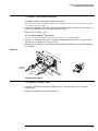
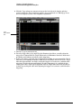
Front panel
Display and
Graphical
Interface
Horizontal
controls
Acquisition and
general controls
Floppy Disk Drive
H
Vertical
Inputs
Marker and Quick
Measurements
Power
Vertical
Controls
Auxiliary
Trigger Input
Trigger
Setup
AutoProbe
Interface
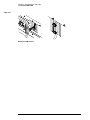
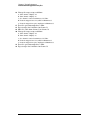
Rear panel without option 017
Rear
foot
Mouse and
Keyboard
Interface
Parallel
Printer Port
RS232
COM
Port
LAN
and
USB
Ports
Secondary
monitor
CD-RW
drive
Sound In
Sound Out
Microphone
VGA
Interface
GPIB Interface
Trig
Out
AC Power
Input
10 MHz
Ref Out
iii
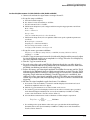
Rear panel with option 017
Removable hard drive
iv
In This Book
This book provides the service documentation for the Agilent Technologies 54853A, 54854A, and
54855A oscilloscopes. It is divided into seven chapters.
Chapter 1 provides general information and specifications.
Chapter 2 shows you how to prepare the oscilloscope for use.
Chapter 3 gives performance tests.
Chapter 4 covers calibration procedures, how to do them, and how often they need to be done.
Chapter 5 gives the procedures and techniques for replacing assemblies and other parts.
Chapter 6 includes a list of exchange assemblies and other replaceable parts, part ordering
information, and shipping information.
Chapter 7 briefly covers the internal operation of the oscilloscope.
At the back of the book you will find safety notice information.
v
vi
Contents
1
General Information
Instruments covered by this service guide 1-2
Accessories supplied 1-3
Options available 1-3
Accessories available 1-3
Specifications and Characteristics 1-5
Dimensions 1-11
Recommended test equipment 1-12
2
Setting Up the Oscilloscope
To connect power 2-3
To connect the mouse or other pointing device 2-5
To connect the keyboard 2-6
To connect to the LAN card 2-7
To connect oscilloscope probes 2-8
To connect SMA Cables 2-10
To connect a printer 2-11
To connect an external monitor 2-13
To connect a GPIB cable 2-13
To tilt the oscilloscope upward for easier viewing 2-15
To turn on the oscilloscope 2-16
To turn off the oscilloscope 2-16
To verify basic oscilloscope operation 2-17
Installing application programs on Infiniium 2-18
Changing Windows System Settings 2-18
To clean the oscilloscope 2-19
3
Testing Performance
Performance Test Interval 3-2
Performance Test Record 3-2
Test Order 3-2
Test Equipment 3-2
Before Performing Performance Verification Testing 3-3
Vertical Performance Verification 3-4
Offset Performance Test 3-5
DC Measurement Accuracy (Single Cursor) Test 3-11
Analog Bandwidth - Maximum Frequency Check 3-16
Horizontal Performance Verification 3-23
Time Base Accuracy Test 3-24
Delta-time Measurement Accuracy Test 3-28
Trigger Performance Verification 3-31
Internal Channel Trigger Sensitivity Test 3-32
Trigger Jitter Test 3-43
Agilent 54853A/54A/55A Performance Test Record 3-47
Contents–1
Contents
4
Calibration
Equipment Required 4-2
Self Calibration Interval and Hardware Adjustments 4-2
Mainframe Cal Factor Memory Error 4-2
Operating Hints 4-3
Loading Default Oscilloscope Settings 4-3
Loading New Software 4-3
Calibration Procedures 4-3
To check the flat panel display (FPD) 4-4
To run the self calibration 4-7
5
Troubleshooting
Safety 5-2
Tools Required 5-2
ESD Precautions 5-2
Keystroke Conventions 5-2
Default Setup 5-3
To install the fan safety shield 5-3
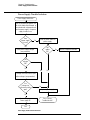
To troubleshoot the instrument 5-4
Primary Trouble Isolation 5-6
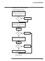
No Display Trouble Isolation 5-10
Front Panel Display Debug 5-11
Motherboard Verification 5-13
To configure the motherboard jumpers and setup BIOS 5-16
POST Code Listing 5-19
Front Panel Debug 5-21
Power Supply Trouble Isolation 5-22
Power Board Trouble Isolation 5-24
AutoProbe Board Trouble Isolation 5-25
To check the keyboard; Troubleshooting Procedure 5-26
To check the LEDs 5-27
To troubleshoot the acquisition system 5-28
Software Revisions 5-29
To check probe power outputs 5-30
To check the SVGA display board video signals 5-31
To check the backlight inverter voltages 5-32
6
Replacing Assemblies
ESD Precautions 6-2
Tools Required 6-2
To return the oscilloscope to Agilent Technologies for service 6-3
To remove and replace the covers 6-4
To disconnect and connect Mylar flex cables 6-6
To remove and replace the AutoProbe assembly 6-7
To remove and replace the probe power and control board 6-9
To remove and replace the backlight inverter board 6-11
To remove and replace the front panel assembly 6-13
To remove and replace the keyboard and flat-panel display assemblies 6-16
To remove and replace the acquisition board assembly 6-19
Contents–2
Contents
To remove and replace the power regulator distribution board 6-22
To remove and replace the GPIB interface board 6-23
To remove and replace the PCI bridge board. 6-24
To remove and replace the scope interface board and SVGA display board 6-25
To remove and replace the floppy disk drive 6-26
To remove and replace the internal hard disk drive 6-27
To remove and replace the CD-ROM drive 6-29
To remove and replace the motherboard 6-31
To remove and replace the power supply 6-33
To remove and replace the fans 6-37
7
Replaceable Parts
Ordering Replaceable Parts 7-2
Power Cables and Plug Configurations 7-3
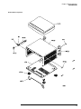
Exploded Views 7-5
Replaceable Parts List 7-10
8
Theory of Operation
Block-Level Theory 8-3
Acquisition Theory 8-5
Contents–3
Contents-4
1
Instruments covered by this service guide 1-2
Accessories supplied 1-3
Options available 1-3
Accessories available 1-3
Specifications and Characteristics 1-5
Recommended test equipment 1-12
General Information
General Information
This chapter of the Agilent Technologies Infiniium Oscilloscope Service Guide gives
you general information about the instrument. The following topics are covered in this
chapter.
•
•
•
•
•
Instrument identification
Options
Accessories
Specifications and characteristics
Test equipment requirements
Instruments covered by this service guide
The oscilloscope can be identified by the product number (54853A, 54854A, or 54855A) on
the back panel.
On the rear panel of the instrument is a serial number label and a VIN # XXX. The serial number
is composed of two parts. The first part contains two letters and two numbers that signify the
instrument’s county of origin and year date code. The second part, or the last six digits from the
right, contains a rolling number that is different for each Infiniium. This manual applies to “B”
model Infiniinums at release date. This manual may not reflect changes made to the oscilloscope
after the release data listed on the title page.
An oscilloscope manufactured after the printing of this manual may have a newer serial number.
This newer serial prefix indicates that the oscilloscope may be different from those described in
this manual. The manual for this oscilloscope will be revised as needed. If you have an oscilloscope
with a newer serial number, please refer to the Agilent Technologies website and download a
newer manual edition in Adobe Acrobat (pdf) format. The Agilent Technologies URL is:
“www.agilent.com”. It will be necessary to search for the 54853A, 54854A, or 54855A product
page, then click on “Manuals, Guides, & Notifications” link in the Library section of the product
page.
For additional information on configuration differences see the following sections in this service
guide:
• Chapter 6, “Replaceable Parts”.
This section contains exploded views for the different motherboard configurations, cabling
schemes, and outside hardware versions. The Replaceable Parts List also contains the
assembly part numbers for the different oscilloscope configurations.
1–2
Chapter 1: General Information
Accessories supplied
Accessories supplied
The following accessories are supplied.
• Mouse, Agilent part number 1150-7913
• Keyboard, Agilent part number 1150-7809
• Accessory Pouch, Agilent part number 54810-68701
• Front-panel cover, Agilent part number 54810-42201
• Calibration cable assembly (54855A only), Agilent part number 54855-61620
• Probe De-skew and Performance Verification Kit, Agilent E2655A
• Precision 3.5 mm adapters (qty 2), Agilent part number 54855-67604 (54854A & 54855A only)
• BNC shorting cap, Agilent part number 1250-0929
• Power cord (see chapter 6, “Replaceable Parts,” for available power cords)
• Recovery CD Kit 54855-68821
• User's Quick Start Guide
Options available
The following options are available for the oscilloscope.
Table 1-1
Infiniium Oscilloscope Options
Option
Description
001
1 MB Memory Upgrade
1CM
Add 1 Rackmount kit (E2609B)
A6J
ANSI Z-540 compliant calibration
R1280A
Return-to-Agilent - warranty and service plan
R-51B
Return-to-Agilent - warranty and service plan (months)
R1282A
Return-to-Agilent - calibration plan
You can order multiple options with the oscilloscope. Also, all model numbers shown in table 1-1 may
also be ordered separately, using the model number. Some accessories that will enhance your work
with the oscilloscope are listed in table 1-2.
Accessories available
The following accessories are available for use with the oscilloscope.
Table 1-2
Accessories for the Infiniium Oscilloscopes
Agilent Model Number
Description
54855-67604
18 GHz BNC-compatible to APC 3.5 mm adaptor
10833A
GPIB cable, 1 m
10833B
GPIB cable, 2 m
10833C
GPIB cable, 4 m
10833D
GPIB cable, 0.5 m
11094B
75 Ω Feedthrough Termination
1131A
3.5 GHz InfiniiMax Active Probe
1–3
Chapter 1: General Information
Accessories available
Agilent Model Number
Description
1132A
5 GHz InfiniiMax Active Probe
1134A
7 GHz InfiniiMax Active Probe
1144A
800 MHz Active Probe
1145A
750 MHz Active Probe
1156A
1.5 GHz Active Probe
1157A
2.5 GHz Active Probe
1158A
4 GHz Active Probe
1181B
Testmobile with tilt tray
1184A
Testmobile with keyboard and mouse tray and drawer for accessories
34398A
RS-232-C Printer Cable
34399A
RS-232-C Adapter kit
54006A
6 GHz probe, 10:1 (500 Ω) or 20:1 (1 k Ω), .25 pf
C2950A
Parallel printer cable, 2 m
C2951A
Parallel printer cable, 3 m
E2609B
Rackmount kit
E2621A
75 Ω terminator
E2622A
100/110/120 Ω differential terminator
E2654A
EZ-Probe® Positioner
E2655A
Additional probe deskew and performance verification kit
E2669A
Differential connectivity kit
E2668A
Single-ended connectivity kit
E2675A
Differential browser and accessories
E2676A
Single-ended browser and accessories
E2677A
Differential solder-in probe head
E2678A
Single-ended/differential socketed probe
E2679A
Single-ended solder-in probe head
E2680A
1 MB Memory upgrade
E2681A
Jitter Analysis Software for the 54850A Series Infiniium oscilloscope
E2683A
USB Test Option
E2688A
Serial Bus Mask Test Option
E5850A
Time-correlation fixture, integrates Infiniium oscilloscope and 16700
logic analyzer
N1022A
Adapter 113X & 115X probes to 86100 infiniium DCA
1–4
Chapter 1: General Information
Specifications and Characteristics
Specifications and Characteristics
The following table lists the specifications and characteristics for the Agilent Technologies
54853A, 54854A, and 54855A Infiniium Oscilloscopes. Asterisks (*) denotes warranted
specifications, all others are typical. Specifications are valid after a 30 minute warm-up period,
and within ± 5 °C from the self-calibration temperature.
Vertical
Input channels
4
Analog bandwidth (-3 dB)*
54855A: 6 GHz
54854A: 4 GHz
54853A: 2.5 GHz
Rise time (10% to 90%)
54855A: 70 ps
54854A: 105 ps
54853A: 155 ps
Input impedance
50 Ω ±2.5%
Sensitivity1
1 mV/div to 1 V/div
Input coupling
Vertical resolution
DC
8 bits, ≥12 bits with averaging
2
Channel to channel isolation
DC to 100 MHz: 40 dB
(any two channels with equal V/div settings) 100 MHz to 1 GHz: 28 dB
>1 GHz to 6 GHz: 24dB
!
DC gain accuracy*1
±1% of full scale at full resolution channel scale
Maximum input voltage*
5 Vrms, CAT I
Offset range
> ±12 div or ±4 Volts, whichever is smallest
Offset accuracy*1
± (2% of channel offset +1% of full scale)
Dynamic range
± 4 div from center screen
DC voltage measurement accuracy*1
Dual cursor
Single cursor
± [(DC gain accuracy)+(resolution)]
± [(DC gain accuracy)+(offset accuracy)+(resolution/2)]
Horizontal
Main sweep time scale range
54855A: 5 ps/div to 20 s/div
54854A: 5 ps/div to 20 s/div
54853A: 10 ps/div to 20 s/div
Main sweep time delay range
-200 s to 200 s
Delayed sweep time scale range
1 ps/div to current main time scale setting
Channel deskew range
-50 µs to 150 µs
Time scale accuracy3
±1 ppm pk
6,7
Delta-time measurement accuracy
≥256 Averages: 70 fs rms, ± [ (0.5 ps) + (1 x 10⁻⁶ x |reading|) ] peak
Averaging disabled: 2.0 ps rms, ± [ (7.0 ps) + (1 x 10⁻⁶ x |reading|) ] peak
Jitter measurement floor6
Time interval error:
Period jitter:
N-cycle, cycle-cycle jitter:
54855A: 1.4 ps rms
54855A: 2.0 ps rms
54855A: 2.4 ps rms
54854A: 1.8 ps rms
54854A: 2.5 ps rms
54854A: 3.8 ps rms
54853A: 2.0 ps rms
54853A: 3.0 ps rms
54853A: 4.5 ps rms
1–5
Chapter 1: General Information
Specifications and Characteristics
Acquisition
Real time sample rate per channel
Memory depth per channel
Standard
Option 001
Sampling modes
Real time
Real time with averaging
Real time with peak detect
Filters
Sin(x)/x Interpolation
20 GSa/s
262,144 at all sample rates
1,025,000 at all sample rates
32,800,000 ≤2 GSa/s sample rate
Successive single-shot acquisitions
Selectable from 2 to 4096
2 GSa/s peak detect, for less than 2 GSa/s sample rates (option 001 only)
On/off selectable FIR digital filter. Digital signal processing adds points
between acquired data points to enhance measurement accuracy and
waveform display quality.
Trigger
Sensitivity1
Internal Low1
54855A: 0.5 div p-p 0 to 2 GHz, 1.0 div p-p 2 to 4 GHz, <2.5 div @ 5 GHz
54854A: 0.5 div p-p 0 to 2 GHz, 1.0 div p-p 2 to 4 GHz
54853A: 0.5 div p-p 0 to 2 GHz, 1.0 div p-p 2 to 2.5 GHz
Internal High1
54855A: 0.2 div p-p 0 to 6 GHz
54854A: 0.2 div p-p 0 to 4 GHz
54853A: 0.2 div p-p 0 to 2.5 GHz
Auxiliary
DC to 500 MHz: 500 mV p-p CATI
Level range
Internal
Auxiliary
±8 div from center screen
±5 V
Sweep modes
Auto, triggered, single
Trigger jitter6,8
54855A: 1.0 ps rms
54854A: 1.3 ps rms
54853A: 1.7 ps rms
Trigger holdoff range
80 ns to 320 ms
Trigger actions
Specify an action to occur and the frequency of the action when a trigger
condition occurs. Actions include e-mail on trigger and QuickMeas+.
1–6
Chapter 1: General Information
Specifications and Characteristics
Trigger modes
Edge
Glitch
Line
Pattern
State
Delay by time
Delay by events
Violation triggers
Pulse width
Setup/hold
Transition
Triggers on a specified slope and voltage level on any channel or auxiliary
trigger.
Triggers on glitches narrower than the other pulses in your waveform by
specifying a width less than your narrowest pulse and a polarity.
Triggers on glitches as narrow as 500 ps. Glitch range settings: < 1.5 ns to
< 160 ms.
Triggers on the line voltage powering the oscilloscope.
Triggers when a specified logical combination of the channels is entered,
exited, present for a specified period of time or is within a specified time
range. Each channel can have a value of High (H), Low (L) or Don’t care
(X). Triggers on patterns as narrow as 500 ps.
Pattern trigger clocked by the rising or falling edge of one channel.
Logic type: AND or NAND.
The trigger is qualified by an edge. After a specified time delay between
30 ns to 160 ms, a rising or falling edge on any one selected input will
generate the trigger.
The trigger is qualified by an edge. After a specified delay between 1 to
16,000,000 rising or falling edges, another rising or falling edge on any one
selected input will generate the trigger.
Trigger on a pulse that is wider or narrower than the other pulses in your
waveform by specifying a pulse width and a polarity. Triggers on pulse
widths as narrow as 500 ps. Pulse width range settings: 1.5 ns to 160 ms.
Triggers on setup, hold or setup and hold violations in your circuit.
Requires a clock and data signal on any two input channels as trigger
sources. High and low thresholds and setup and/or hold time must then
be specified.
Trigger on pulse rising or falling edges that do not cross two voltage levels
in > or < the amount of time specified.
Measurements and math
Waveform measurements
Voltage
Time
Frequency Domain
Peak to peak, minimum, maximum, average, RMS, amplitude, base, top,
overshoot, preshoot, upper, middle, lower, area.
Period, frequency, positive width, negative width, duty cycle, delta time,
rise time, fall time, Tmin, Tmax, channel-to-channel phase.
FFT frequency, FFT magnitude, FFT delta frequency, FFT delta magnitude,
FFT phase.
Statistics
Displays the mean, standard deviation, minimum, maximum and number
of measurements value for the displayed automatic measurements.
Histograms
Vertical (for timing and jitter measurements) or horizontal (noise and
amplitude change) modes, regions are defined using waveform markers.
Measurements included: mean, standard deviation, peak-to-peak value,
median, min, max, total hits, peak (area of most hits), and mean ± 1, 2, and
3 sigma.
Eye-diagram measurements
Eye-diagram measurements include eye height, eye width, eye jitter,
crossing percentage, Q factor, and duty-cycle distortion.
Jitter measurements
(E2681A software package)
Cycle-cycle jitter, N-cycle jitter, cycle-cycle + width, cycle-cycle - width,
cycle-cycle duty cycle, data rate, unit interval, time interval error data,
time interval error clock, setup time, hold time, phase, period, frequency,
+ width, - width, duty cycle, rise time, fall time.
Mask testing
Allows pass/fail testing to user-defined or Agilent-supplied waveform
templates. AutoMask lets you create a mask template from a captured
waveform and define a tolerance range in time/voltage or percentage.
Test modes include test forever, test to specified time or event limit, and
stop on failure. Communications Mask Test Kit option provides a set of
ITU-T G.703, ANSI T1.102, and IEEE 802.3 industry-standard masks for
compliance testing.
1–7
Chapter 1: General Information
Specifications and Characteristics
Waveform math
FFT
Frequency range4
Frequency resolution
Best resolution at maximum sample rate
Frequency accuracy
Signal-to-noise ratio5
Window modes
Measurement modes
Automatic measurements
QuickMeas
Drag-and-drop measurement toolbar
Marker modes
Four functions, select from add, average, differentiate, divide, FFT
magnitude, FFT phase, integrate, invert, magnify, min, max, multiply,
subtract, versus, common mode, smoothing.
4 DC to 10 GHz.
Sample rate/memory depth = Resolution.
20 GSa/1 Mpts = 20 kHz.
(1/2 frequency resolution)+(1 x 10⁻⁶)(signal frequency).
60 dB at 32k memory depth.
Hanning, flattop, rectangular.
Measure menu access to all measurements, five measurements can be
displayed simultaneously.
Front-panel button activates five pre-selected or five user-defined
automatic measurements.
Measurement toolbar with common measurement icons that can be
dragged and dropped onto the displayed waveforms.
Manual markers, track waveform data, track measurements.
Display
Display
Display
Resolution
Annotation
Grids
Waveform style
8.4 inch diagonal color TFT-LCD.
640 pixels horizontally x 480 pixels vertically.
Up to 12 labels, with up to 100 characters each, can be inserted into the
waveform area.
Can display 1, 2 or 4 waveform grids.
Connected dots, dots, persistence (minimum, variable, infinite),
color-graded infinite persistence.
Computer system and peripherals, I/O ports
Computer system and peripherals
Operating system
CPU
PC system memory
Drives
Peripherals
File types
Waveforms
Images
1–8
Windows® XP Pro.
Intel® Pentium® III 1 GHz microprocessor.
512 MB.
≥10 GB internal hard drive, CD-RW drive on rear panel, standard 3.5 inch
1.44 MB floppy drive.
Logitech optical USB mouse and compact keyboard supplied. All Infiniium
models support any Windows-compatible input device with a serial, PS/2
or USB interface.
Compressed internal format, comma and tab separated X and Y pairs or
voltage values.
BMP, PCX, TIFF, GIF or JPEG.
Chapter 1: General Information
Specifications and Characteristics
I/O ports
LAN
GPIB
RS-232 (serial)
Parallel
PS/2
USB
Video output
Dual-monitor video output
Auxiliary output
Trigger output
Time base reference output
RJ-45 connector, supports 10Base-T and 100Base-T. Enables
Web-enabled remote control, e-mail on trigger or demand, data/file
transfers and network printing.
IEEE 488.2, fully programmable.
COM1, printer and pointing device support.
Centronics printer port.
2 ports. Supports PS/2 pointing and input devices.
2 ports. Allows connection of USB peripherals and pointing devices while
the oscilloscope is on.
15 pin VGA, full color output of scope waveform display.
15 pin XGA, full color output for using third-party applications.
DC (±2.4 V); square wave (~715 Hz and 456 MHz); trigger output
(255 mV p-p into 50Ω).
5 V 50 Ω back-terminated.
10 MHz, 5 V 50 Ω back-terminated.
1–9
Chapter 1: General Information
Specifications and Characteristics
General characteristics
Temperature
Operating: 0° C to +40° C.
Non-operating: -40° C to +70° C.
Humidity
Operating: Up to 95% relative humidity (non-condensing) at +40°C.
Non-operating: Up to 90% relative humidity at +65°C.
Altitude
Operating: Up to 4,600 meters (15,000 feet).
Non-operating: Up to 15,300 meters (50,000 feet).
Vibration
Operating: Random vibration 5-500 Hz, 10 minutes per axis, 0.3 g(rms).
Non-operating: Random vibration 5-500 Hz, 10 minutes per axis, 2.41
g(rms); resonant search 5-500 Hz, swept sine, 1 octave/minute sweep rate,
(0.75g), 5 minute resonant dwell at 4 resonances per axis.
Power
100-240 VAC, ± 10%, Cat II, 47 to 440 Hz; max power dissipated: 475 W.
Weight
Net: 13 kg (28.5 lbs.).
Shipping: 16 kg (35.2 lbs.).
Dimensions (excluding handle)
Height: 216 mm (8.5 in).
Width: 437 mm (17.19 in).
Depth: 440 mm (17.34 in).
Safety
Meets IEC 61010-1 +A2, CSA certified to C22.2 No.1010.1, self-certified to
UL 3111.
*
1.
2.
3.
4.
5.
6.
7.
8.
Denotes warranted specifications, all others are typical. Specifications are valid after a 30-minute warm-up period, and ±5°C from
annual calibration temperature.
Full scale is defined as 8 vertical divisions. Vertical divisions are defined by the major scale settings above non-major scale settings.
The major scale settings are 10 mV, 20 mV, 50 mV, 100 mV, 200 mV, 500 mV, 1 V.
Vertical resolution for 8 bits = 0.4% of full scale, for 12 bits = 0.024% of full scale.
Within one year of previous calibration.
FFT amplitude readings are affected by input amplifier roll-off.
54855A: (-3 dB at 6 GHz, with amplitude decreasing as frequency increases above 6 GHz).
54854A: (-3 dB at 4 GHz, with amplitude decreasing as frequency increases above 4 GHz).
54853A: (-3 dB at 2.5 GHz, with amplitude decreasing as frequency increases above 2.5 GHz).
The noise floor varies with memory depth and averaging.
Signal peak-to-peak amplitude ≥5 divisions, vertical scale ≥10 mV/div, signal rise time 155 ps (54853A), ≤225 ps (54854A), 150 ps
(54855A), sample rate = 20 Gsa/s, sin(x)/x interpolation enabled, measurement threshold = fixed voltage at 50% level.
Between two edges on a single channel. Rms value refers to the standard deviation of 256 consecutive measurements performed
using an individual instrument.
Internal trigger. Trigger level contained within full scale display range of trigger channel.
CAT I and CAT II Definitions
Installation category (overvoltage category) I: Signal level, special equipment or parts of
equipment, telecommunication, electronic, etc., with smaller transient overvoltages than
installation category (overvoltage category) II.
Installation category (overvoltage category) II: Local level, appliances, portable equipment etc.,
with smaller transient overvoltages than installation category (overvoltage category) III.
1–10
Chapter 1: General Information
Dimensions
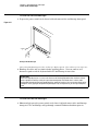
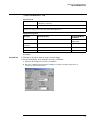
Dimensions
The following pictures shows the dimensions of the frame.
1–11
Chapter 1: General Information
Recommended test equipment
Recommended test equipment
The following table is a list of the test equipment required to test performance, calibrate and
adjust, and troubleshoot this instrument. The table indicates the critical specification of the test
equipment and for which procedure the equipment is necessary. Equipment other than the
recommended model may be used if it satisfies the critical specification listed in the table.
Recommended Test Equipment
Equipment Required
Critical Specifications
Recommended Model
Use
Digital Multimeter
DC voltage measurement accuracy better than
±0.1% of reading
Agilent 34401A or Agilent
3458A
P
Microwave CW
Generator
Maximum Frequency ≥ 6 GHz
Power range: -20 dBm to +16 dBm into 50 Ω
Output resistance = 50 Ω
10 MHz Reference Signal Output
Agilent E8247C with
Opt 520 or Agilent 82712B
with Opt 1E5 or Agilent
8665B with Opt 004
P
Power Splitter
2 Resistor Power Splitter
Max Frequency ≥ 18 GHz
Agilent 11667B
P
Power Meter
Agilent E-series power sensor compatibility
Agilent E4418B or E4419B
P
Power Sensor
Maximum Frequency ≥ 6 GHz
Power range: -24 dBm to +16 dBm
Agilent E4413A
P
Microwave Cable
Assembly
50 Ω characteristic impedance
3.5 mm (m) or SMA (m) connectors
Max Frequency ≥ 18 GHz
Agilent 8120-4948 or
Agilent 11500E or
Gore EKD01D010480
P
Cable Assembly
(2 required)
50 Ω characteristic impedance
BNC (m) connectors
Agilent 8120-1840
P
Adapter
BNC Tee (m)(f)(f)
Agilent 1250-0781
P
Adapter
BNC (f) to dual banana
Agilent 1251-2277
P
Adapter
3.5 mm (f) to Precision BNC
Agilent 54855-67604
P
Shorting Cap
BNC (m)
Agilent 1250-0929
A
Cable Assembly
(Cal Cable for 54853A
and 54854A)
50 Ω characteristic impedance
BNC (m) connectors
<= 12 Inch Length
Agilent 8120-1838
or Agilent 10502A
A
Cable Assembly
(Cal Cable for 54855A)
NO Substitute
Agilent 54855-61620
A
10 MHz Signal Source
Frequency accuracy better than 0.4 ppm
Agilent 53131A with
Opt. 010 *
or Agilent 5071A or
Symmetricom 58503B **
A
* Requires time base calibration once every 6 months
** Requires link to GPS
Alternate Power Splitter/Power Sensor Equipment - List 1
Equipment Required
Critical Specifications
Recommended Model
Use
Power Splitter
2 Resistor Power Splitter
Max Frequency ≥ 18 GHz
Agilent 11667A
P
Power Sensor
Maximum Frequency ≥ 6 GHz
Power range: -24 dBm to +16 dBm
Agilent E4412A
P
Adapters
3.5 mm (f) to Precision BNC
Type N (m) to 3.5 mm (f)
Type N (m) to 3.5 mm (m)
Agilent 54855-67604
Agilent 1250-1744
Agilent 1250-1743
P
1–12
Chapter 1: General Information
Recommended test equipment
Alternate Power Splitter/Power Sensor Equipment - List 2
Equipment Required
Critical Specifications
Recommended Model
Use
Power Splitter
2 Resistor Power Splitter
Max Frequency ≥ 18 GHz
Agilent 11667A
P
Power Sensor
Maximum Frequency ≥ 6 GHz
Power range: -24 dBm to +16 dBm
Agilent E4412A
P
Adapters
3.5 mm (f) to Precision BNC
3.5 mm (f) to 3.5 mm (m)
Type N (m) to 3.5 mm (m)
Agilent 54855-67604
Agilent 1250-1748
Agilent 1250-1750
P
1–13
1–14
2
To connect power 2-3
To connect the mouse or other pointing device 2-5
To connect the keyboard 2-6
To connect to the LAN card 2-7
To connect oscilloscope probes 2-8
To connect SMA Cables 2-10
To connect a printer 2-11
To connect an external monitor 2-13
To connect a GPIB cable 2-13
To tilt the oscilloscope upward for easier viewing 2-15
To turn on the oscilloscope 2-16
To turn off the oscilloscope 2-16
To verify basic oscilloscope operation 2-17
Installing application programs on Infiniium 2-18
Changing Windows System Settings 2-18
To clean the oscilloscope 2-19
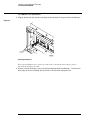
Setting Up the Oscilloscope
Setting Up the Oscilloscope
This chapter shows you how to set up your Infiniium oscilloscope, connect power and
accessories, and verify general operation.
2–2
Chapter 2: Setting Up the Oscilloscope
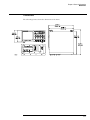
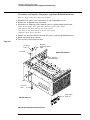
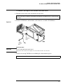
To connect power
To connect power
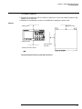
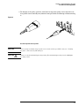
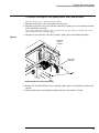
1 Position the oscilloscope where it will have sufficient clearance for airflow around the top,
bottom, back, and sides.
2 Position the oscilloscope so that it is not difficult to unplug the power cord.
Figure 2-1
Minimum 39 mm
Minimum 0 mm
Minimum 22 mm
Minimum 85 mm
both sides
Airflow requirements 250 cfm
Positioning the Infiniium Oscilloscope with Sufficient Clearance
2–3
Chapter 2: Setting Up the Oscilloscope
To connect power
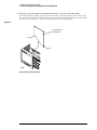
3 Connect the power cord to the rear of the oscilloscope, then to a suitable ac voltage source
(120-240 VAC ±10%, 47 to 440 Hz, max power dissipation 475 W).
Figure 2-2
Infiniium Oscilloscope Power Cord Connection
The oscilloscope power supply automatically adjusts for line input voltages in the range 120 to 240
VAC. Therefore, you do not need to adjust an input line voltage setting. The line cord provided is
matched by Agilent Technologies to the country of origin of the order. A full list of power cables
and plug configurations is shown in chapter 6, "Replaceable Parts".
2–4
Chapter 2: Setting Up the Oscilloscope
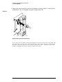
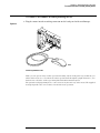
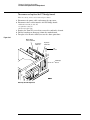
To connect the mouse or other pointing device
To connect the mouse or other pointing device
1 Plug the mouse into the matching connector on the back panel of the oscilloscope.
Figure 2-3
Connecting the Mouse Cable
While you can operate many oscilloscope functions using only the front-panel keys and knobs, you
will need the mouse to access advanced oscilloscope functions through the graphical interface, or to
find out more about the oscilloscope through the built-in information system.
The optional touchpad pointing device connects in exactly the same way as the mouse. The supplied
mousepad provides the correct surface for smooth mouse operation.
2–5
Chapter 2: Setting Up the Oscilloscope
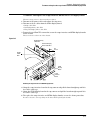
To connect the keyboard
To connect the keyboard
1 Plug the keyboard cable into the matching connector on the back panel of the oscilloscope.
Figure 2-4
Connecting the Keyboard
The keyboard simplifies some oscilloscope tasks, such as entering file names when you store
waveforms and setups to the disk.
2 If you need more desk space, place the keyboard on top of the oscilloscope. Do not stack
other objects on the keyboard; this will cause self-test failures on power on.
2–6
Chapter 2: Setting Up the Oscilloscope
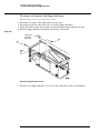
To connect to the LAN card
To connect to the LAN card
1 Connect your LAN cable to the RJ-45 connector on the LAN card. Make sure the
connection is secure.
Figure 2-5
RJ-45
Connection
Connecting to the LAN Card
2 After you have connected to the LAN card, you must set up the network. See your system
administrator for assistance in setting up the network.
2–7
Chapter 2: Setting Up the Oscilloscope
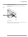
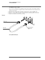
To connect oscilloscope probes
To connect oscilloscope probes
1 Attach the probe connector to the desired oscilloscope channel or trigger input. Push it
straight on until it latches into place.
Figure 2-6
Attaching the Probe Connector
2 Connect the probe to the circuit of interest using the browser or other probing accessories.
Figure 2-7
Probing the Circuit
2–8
Chapter 2: Setting Up the Oscilloscope
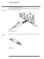
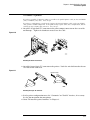
To connect oscilloscope probes
3 To disconnect the probe, push the small latch on top of the probe connector to the left,
then pull the connector body away from the front panel of the oscilloscope without twisting
it.
Figure 2-8
Disconnecting the Oscilloscope Probe
CA UT IO N
CA UT IO N
Do not attempt to twist the snap-on probes on or off the oscilloscope’s BNC connector. Twisting
the probe connector body will damage it.
!
Do not exceed the maximum input voltage rating. The maximum input voltage for the 50 Ω inputs
is 5 Vrms, CAT I.
2–9
Chapter 2: Setting Up the Oscilloscope
To connect SMA Cables
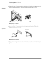
To connect SMA Cables
You can connect an SMA cable to the Infiniium oscilloscopes by using 3.5 mm to BNC compatible
adaptors. Precision adapters are supplied with the 54854A and 54855A. Precision adapters are not
required for the 54853A.
1 Attach the two 3.5 mm to BNC compatible adaptors to the ends of an SMA cable.
2 Push the 3.5 mm to BNC compatible adaptors onto the oscilloscope BNC connectors.
3 Tighten the thumbscrews until they are snug.
Figure 2-9
Thumb screw
Precision 3.5 mm to
BNC compatible
adaptor
SMA cable
Connecting SMA to BNC Adaptors
2–10
Chapter 2: Setting Up the Oscilloscope
To connect a printer
To connect a printer
If you have a parallel (Centronics) printer, you will need a parallel printer cable, such as an C2950A
(2 m) or C2951A (3 m) cable. Go to step 1.
If you have a serial printer, you will need a 9-pin to 25-pin serial printer cable, such as an 34398A
cable, plus the 34399A adapter kit. Some printers may require other cable configurations, but the
oscilloscope has a 9-pin serial connector. Go to step 5.
1 Attach the 25-pin small “D” connector to the printer output connector on the rear of the
oscilloscope. Tighten the thumbscrews to secure the cable.
Figure 2-10
Attaching the Small “D” Connector
2 Attach the larger 36-pin “D” connector to the printer. Latch the wire bails into the tabs on
each side of the connector.
Figure 2-11
Port on Printer
Attaching the Larger “D” Connector
3 Set the printer configuration to use the “Centronics” or “Parallel” interface, if necessary.
See the documentation for your printer.
4 Go to “To install the printer software” in Chapter 3.
2–11
Chapter 2: Setting Up the Oscilloscope
To connect a printer
5 Connect the 9-pin “D” connector of the serial printer cable to the serial output port on the
rear panel of the oscilloscope. Tighten the thumbscrews to secure the cable.
Figure 2-12
Attaching the 9-pin “D” Connector
6 Attach the 25-pin “D” connector to the serial input port of the printer. Tighten the
thumbscrews to secure the cable.
Figure 2-13
Port on Printer
Attaching the 25-pin “D” Connector
7 Set the printer configuration to use the serial interface. See the documentation for your
printer.
2–12
Chapter 2: Setting Up the Oscilloscope
To connect an external monitor
To connect an external monitor
To display a larger view of the oscilloscope screen
You can connect a VGA-compatible monitor to the Infiniium oscilloscope to provide a larger viewing
area of the oscilloscope display.
1 Connect the monitor cable to the display board video connector marked VGA at the rear
panel of the oscilloscope as shown in the figure below.
2 Tighten the retaining screws.
To extend the Windows XP desktop
You can extend the Windows XP desktop by connecting a secondary monitor.
1 Connect the monitor cable to the secondary monitor connector at the rear panel of the
oscilloscope as shown in the figure below.
2 Tighten the retaining screws then go into the Windows control panel to setup and configure
the monitor.
Figure 2-14
Secondary
Monitor
Oscilloscope
Display
Connecting External Monitors
To connect a GPIB cable
1 Attach the GPIB connector to the GPIB interface card connector at the rear of the
oscilloscope.
2 Tighten the thumbscrews on the connector.
2–13
Chapter 2: Setting Up the Oscilloscope
To connect a GPIB cable
Figure 2-15
Attaching the GPIB Connector
2–14
Chapter 2: Setting Up the Oscilloscope
To tilt the oscilloscope upward for easier viewing
To tilt the oscilloscope upward for easier viewing
1 Lift up the front of the oscilloscope, grasp the wire bail near the center, and pull it down
and forward until it latches into place.
Figure 2-16
Latching the Oscilloscope Front Feet
2–15
Chapter 2: Setting Up the Oscilloscope
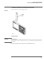
To turn on the oscilloscope
To turn on the oscilloscope
1 Depress the power switch in the lower left-hand corner of the oscilloscope front panel.
Figure 2-17
Turning on the Oscilloscope
After a short initialization period, the oscilloscope display appears. The oscilloscope is ready to use.
2 Hook up all cables and accessories before applying power. You can connect and
disconnect probes and the keyboard while the oscilloscope is turned on.
Screen Saver
The oscilloscope display has a screen saver that turns off the backlight when there has been no front
panel or graphical interface activity for a pre-determined period. The default time is 8 hours and is
configurable through the Display Setup dialog in the graphical interface. You can turn the display on by
moving the mouse, typing on the optional keyboard, pressing a front panel key, or turning a front panel
knob.
To turn off the oscilloscope
1 Momentarily depress the power switch at the lower left-hand corner of the oscilloscope
front panel. The oscilloscope will go through a normal Windows shutdown process.
2–16
Chapter 2: Setting Up the Oscilloscope
To verify basic oscilloscope operation
To verify basic oscilloscope operation
1 Connect an oscilloscope probe to channel 1.
2 Attach the probe to the calibration output on the front panel of the oscilloscope.
Use a probe grabber tip so you do not need to hold the probe and make sure you connect the ground
wire. The calibration output is marked with a square wave symbol.
Figure 2-18
Calibration
Output
Verifying Basic Oscilloscope Operation
3 Press the Default Setup key on the front panel.
The display will pause momentarily while the oscilloscope is configured to its default settings.
4 Press the Autoscale key on the front panel.
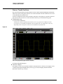
The display will pause momentarily while the oscilloscope adjusts the sweep speed and vertical scale.
You should then see a square wave with peak-to-peak amplitude of approximately 5 divisions and a
period of almost 3 divisions. If you do not see the waveform, ensure your power source is adequate,
the oscilloscope is properly powered-on, and the probe is connected securely to the front-panel
channel input BNC and to the probe calibration output.
5 Move the mouse around and verify that the pointer follows on the screen.
If the pointer does not move, ensure that the mouse is properly connected, that you have clicked the
correct button to enable the graphical interface.
2–17
Chapter 2: Setting Up the Oscilloscope
Installing application programs on Infiniium
Installing application programs on Infiniium
Infiniium is an open Windows system. This allows you to install your own application software. Agilent
has verified that the following applications are compatible with the Infiniium oscilloscope application.
• Microsoft Office 2000
• MathWorks MATLAB
• Mathsoft MathCad 2001i
• McAfee VirusScan
• Symantec Norton AntiVirus
Before installing any software, you should exit the oscilloscope application.
If you install an application other than those which Agilent has tested, it is possible that it could break
the oscilloscope application. This would require you to reinstall the oscilloscope application using
the recovery disks.
Changing Windows System Settings
Before changing any Windows System settings outside of the oscilloscope application you should Exit
the oscilloscope application.
There are several Windows System settings that can be changed to suit your own personal
preferences. However, there are some system settings that you should avoid changing because it will
interfere with the proper operation of the oscilloscope.
•
•
•
•
•
•
Do not change the Power Options.
Do not change the System Properties Hardware Tab settings.
Do not change the System Properties Advanced Tab settings.
Do not change the Regional and Language Options Advanced Tab settings.
Do not remove Fonts.
Display Settings
• Do not turn off the screen saver. The screen saver turns off the display’s backlights extending their
life.
• Do not change the screen resolution from 640 by 480 pixels or the color quality from High (24 bit).
• Do not use the Windows XP Theme.
• Do not change “Windows and buttons” from the “Windows Classic Style”.
• Do not change the Font size to Extra Large.
• Do not use a Menu font size greater than 12 points.
• Do not modify “1. Digital Flat Panel (640x480) on Chips and Technologies (Asiliant) 65550”.
• Do not set “Intel ® 82815 Graphics Controller” to “Use this device as the primary monitor”.
• Do not use the Administrative Tools to enable or disable Internet Information Services
(Web Server). Use the Infiniium Web Control dialog box to enable or disable the Web
Server.
• Do not delete or modify the InfiniiumAdmin user account.
2–18
Chapter 2: Setting Up the Oscilloscope
To clean the oscilloscope
To clean the oscilloscope
• Clean the oscilloscope with a soft cloth dampened with a mild soap and water solution.
CA UT IO N
Do not use too much liquid in cleaning the oscilloscope. Water can enter the Infiniium front panel,
damaging sensitive electronic components.
2–19
2–20
3
Performance Test Interval 3-2
Performance Test Record 3-2
Test Order 3-2
Test Equipment 3-2
Before Performing Performance Verification Testing 3-3
Vertical Performance Verification 3-4
Offset Performance Test 3-5
DC Measurement Accuracy (Single Cursor) Test 3-11
Analog Bandwidth - Maximum Frequency Check 3-16
Horizontal Performance Verification 3-23
Time Base Accuracy Test 3-24
Delta-time Measurement Accuracy Test 3-28
Trigger Performance Verification 3-31
Internal Channel Trigger Sensitivity Test 3-32
Trigger Jitter Test 3-43
Agilent 54853A/54A/55A Performance Test Record 3-47
Testing Performance
Testing Performance
This section documents performance test procedures. Performance verification for the
products covered by this manual consists of three main steps:
• Performing the internal product self-tests to ensure that the measurement system is
functioning properly
• Calibrating the product
• Testing the product to ensure that it is performing to specification
Performance Test Interval
The procedures in this section may be performed for incoming inspection and should be
performed periodically to verify that the instrument is operating within specification. The
recommended test interval is once per year or after 2000 hours of operation. Performance
should also be tested after repairs or major upgrades.
Performance Test Record
A test record form is provided at the end of this section. This record lists performance tests,
test limits and provides space to record test results.
Test Order
The tests in this section may be performed in any order desired. However, it is recommended
to conduct the tests in the order presented in this manual as this represents an incremental
approach to performance verification. This may be useful if you are attempting to
troubleshoot a suspected problem.
Test Equipment
Lists of equipment needed to conduct each test are provided for each test procedure. The
procedures are written to minimize the number and types of instruments and accessories
required. The instruments in these lists are ones that are currently available for sale by
Agilent at the time of writing this document. In some cases, the test procedures use features
specific to the instruments in the recommended equipment list. However, with some
modification to the test procedures, instruments, cables and accessories that satisfy the
critical specifications in these lists may be substituted for the recommended models with
some modification to the test procedures.
Contact Agilent Technologies for more information about the Agilent products in these lists.
3–2
Chapter 3: Testing Performance
Before Performing Performance Verification Testing
Let the instrument warm up before testing
The oscilloscope under test must be warmed up (with the oscilloscope application running) for at least 30
minutes prior to the start of any performance test.
1 Perform self tests
While the oscilloscope is warming up, run the self-test to ensure that the hardware is functioning
properly. To run the self-test:
a Pull down the Utilities menu and select SelfTest.
b Select Scope SelfTest from the SelfTest list.
c Click on Start SelfTest to start the self test procedure.
If any of the self-tests fail, ensure that the failure is diagnosed and repaired before
calibrating and testing performance.
2 Performance calibration.
After the warm up period, calibrate the oscilloscope.
a Pull down the Utilities menu and select Calibration.
b Uncheck to Cal Memory Protect box to allow calibration.
c Click on Start to start the calibration procedure.
Follow the on-screen instructions as calibration proceeds.
3–3
Vertical Performance Verification
This section contains the following vertical performance verification:
• Offset Performance Test
• Zero Error Test
• Offset Gain Test
• DC Measurement Accuracy (Single Cursor) Test
• Analog Bandwidth (Maximum Frequency Check)
3–4
Chapter 3: Testing Performance
Offset Performance Test
Offset Performance Test
Specifications
Offset Accuracy
= ±(2% of channel offset + 1% of full scale)
= ±(Offset Gain + Zero Error)
Offset Range
> ±12 div, or ±4 V, whichever is smallest
Full scale is defined as 8 vertical divisions. Vertical divisions are defined by the major scale settings above non-major scale settings.
The major scale settings are 10 mV, 20 mV, 50 mV, 100 mV, 200 mV, 500 mV and 1 V.
Equipment Required
Description
Critical Specifications
Recommended Model/
Part Numbers
Digital Multimeter
DC voltage measurement accuracy better than ±0.1% of reading Agilent 34401A or
Agilent 3458A
Cable Assembly
(2 required)
50Ω characteristic impedance, BNC (m) connectors
Agilent 8120-1840
Adapter
BNC Tee (m)(f)(f)
Agilent 1250-0781
Adapter
BNC (f) to dual banana
Agilent 1251-2277
Procedure
Zero Error Test
1 Disconnect all cables from the scope channel inputs.
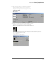
2 Press Default Setup, then configure the scope as follows:
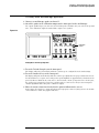
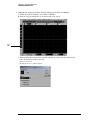
a Pull down the Setup menu and select Acquisition.
b When the Acquisition Setup window is displayed, enable averaging and set the # of
averages to 256 as shown below.
3–5
Chapter 3: Testing Performance
Offset Performance Test
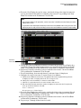
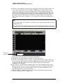
3 Configure the scope to measure Average voltage on channel 1 as follows:
a Change the vertical sensitivity of channel 1 to 10mV/div.
b Click the V avg measurement icon on the left side of the screen.
V avg
icon
c When the Enter Measurement Info window is displayed, ensure that the V avg function
is set up as follows and then click OK:
Source = Channel 1
Measurement Area = Entire Display
3–6
Chapter 3: Testing Performance
Offset Performance Test
4 Press the Clear Display key on the scope, wait for the #Avgs value (top left corner of
screen) to return to 256 and then record the scope’s mean V avg reading in the Zero
Error Test section of the Performance Test Record.
Notes
• For all scope readings in this procedure, use the mean value in the Measurements display area at the
bottom of the screen.
• If a question mark is displayed in front of any of the values at the bottom of the screen, press the Clear
Display key on the scope, wait for the #Avgs value to return to 256 and then record the scope reading.
Record the
mean reading
5 Change the vertical sensitivity of channel 1 to 20 mV/div, press the Clear Display key,
wait for the #Avgs value (top left corner of screen) to return to 256 and then record the
scope V avg reading in the Zero Error Test section of the Performance Test Record.
6 Repeat step 5 for the remaining vertical sensitivities for channel 1 in the Zero Error
Test section of the Performance Test Record.
7 Press Default Setup, then turn off channel 1 and turn channel 2 display on.
8 Configure the scope to measure V avg on Channel 2 as follows:
a Pull down the Utilities menu and select Acquisition. When the Acquisition Setup window
is displayed, enable averaging and set the # of averages to 256.
b Change the vertical sensitivity of channel 2 to 10 mV/div.
c Click the V avg measurement icon on the left side of the screen.
d When the Enter Measurement Info window is displayed, ensure that the Vavg function
is set up as follows and then click OK:
Source = Channel 2
Measurement area = Entire Display
9 Press the Clear Display key on the scope, wait for the #Avgs value to return to 256 and
then record the DMM voltage reading and the scope V avg reading in the Zero Error
Test section of the Performance Test Record.
10 Repeat step 9 for the remaining vertical sensitivities for channel 2 in the Zero Error
section of the Performance Test Record.
11 Repeat steps 7 through 10 for channels 3 and 4.
3–7
Chapter 3: Testing Performance
Offset Performance Test
Offset Gain Test
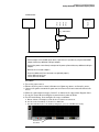
12 Make the connections to scope channel 1 as shown below.
Connections
Digital Multimeter
5485x Scope Under Test
Aux Out
Chan 3 IN
Chan 4 IN
Chan 2 IN
Chan 1 IN
Input
BNC Tee
connected directly to
scope channel input
Notes:
• Where it is used, it is important to connect the BNC Tee adapter directly to the scope channel input to
minimize ground potential differences between the scope and the test instruments and to ensure that
the DMM measures the input voltage to the scope channel as accurately as possible. Differences in
ground potential can be a significant source of measurement error, particularly at high scope
sensitivities.
• It also helps to reduce ground potential differences if the scope and the external test instruments are
connected to the same AC supply circuit.
• A fairly large number of averages are used in the scope measurements of this section to reduce
measurement noise and to reduce the measurement error due to resolution.
13 Set up the DMM to perform DC voltage measurements.
14 Configure the scope to measure V avg on Channel 1 as follows:
a Press Default Setup.
b Pull down the Utilities menu and select Acquisition. When the Acquisition Setup window
is displayed, enable averaging and set the # of averages to 256.
c Change the vertical sensitivity of channel 1 to 10 mV/div.
d Click the V avg measurement icon on the left side of the screen.
e When the Enter Measurement Info window is displayed, ensure that the V avg function
is set up as follows and then click OK:
Source = Channel 1
Measurement area = Entire Display
3–8
Chapter 3: Testing Performance
Offset Performance Test
15 Set the channel 1 offset value to 120 mV. This can be done either using the front panel
control or:
a Pull down the Setup menu and select Channel 1 or click the Channel 1 setup icon.
b Click the Offset control arrows to change the offset value or click on the offset value
and enter 120 mV in the dialog box.
c Enter 120 mV in the Enter Offset dialog box.
Channel 1
setup icon
16 Set the Aux Out voltage (VAux Out) to +120 mV as follows:
a Pull down the Utilities menu and select Calibration.
b Change the Aux Output function to DC (top left corner).
c Set the Level to 120 mV.
d Click on Close.
17 Press the Clear Display key on the scope, wait for the #Avgs value (top left corner of
screen) to return to 256 and then record the DMM voltage reading as VDMM+ and the
scope Vavg reading as VScope+ in the Offset Gain Test section of the Performance Test
Record.
3–9
Chapter 3: Testing Performance
Offset Performance Test
18 Change the channel 1 offset value to -120 mV.
19 Set the Aux Out voltage to -120 mV.
20 Press the Clear Display key on the scope, wait for the #Avgs value (top left corner of
screen) to return to 256 and then record the DMM voltage reading as VDMM- and the
scope Vavg reading as VScope- in the Offset Gain Test section of the Performance Test
Record.
21 Calculate the offset gain using the following expression and record this value in the
Offset Gain Test section of the Performance Test Record:
∆V out V scope+ – V scopeOffset Gain = -------------- = -------------------------------------------∆V in
V DMM+ – V DMM22 Repeat steps 15 to 21 for the remaining channel 1 vertical sensitivities in the Offset
Gain Test section of the Performance Test Record. For each measurement, set both
the Aux Out voltage (VAux Out) and the Channel offset voltage to the positive VAux Out
value and then to the negative VAux Out value in the "VAux Out Setting" column of the
Offset Gain Test table in the Performance Test Record for each of the vertical
sensitivities.
23 Move the Tee connector to the next channel input and repeat steps 14 to 22 for the
channels 2 to 4.
3–10
Chapter 3: Testing Performance
DC Measurement Accuracy (Single Cursor) Test
DC Measurement Accuracy (Single Cursor) Test
Specifications
DC Gain Accuracy
±1% of full scale at full resolution channel scale
Offset Accuracy
±(2% of channel offset + 1% of full scale)
Vertical Resolution
8 bits, ≥12 bits with averaging
DC Voltage Measurement Accuracy
Single Cursor
±[(DC gain accuracy) + (offset accuracy) + (resolution/2)]
Dual Cursor
±[(DC gain accuracy) + (resolution)]
Full scale is defined as 8 vertical divisions. Vertical divisions are defined by the major scale settings above non-major scale
settings. The major scale settings are 10 mV, 20 mV, 50 mV, 100 mV, 200 mV, 500 mV and 1 V.
Vertical resolution for 8 bits = 0.4% of full scale, for 12 bits = 0.024% of full scale
Example: Single cursor measurement 70 mV input @ 20 mV/div, 0 V channel offset with no averaging:
expected measurement error < ±[(1%(160 mV)) + (1%(160 mV) + (0.4%(160 mV)/2)] = ±3.52 mV.
Equipment Required
Description
Critical Specifications
Recommended Model/
Part Numbers
Digital Multimeter
DC voltage measurement accuracy better than ±0.1% of reading Agilent 34401A or
Agilent 3458A
Cable Assembly
(2 required)
50Ω characteristic impedance, BNC (m) connectors
Agilent 8120-1840
Adapter
BNC Tee (m)(f)(f)
Agilent 1250-0781
Adapter
BNC (f) to dual banana
Agilent 1251-2277
Connections
Digital Multimeter
5485x Scope Under Test
Aux Out
Chan 3 IN
Chan 4 IN
Chan 2 IN
Chan 1 IN
Input
BNC Tee
connected directly to
scope channel input
3–11
Chapter 3: Testing Performance
DC Measurement Accuracy (Single Cursor) Test
Notes
• It is important to connect the BNC Tee adapter directly to the scope channel input to minimize ground
potential differences between the scope and the test instruments and to ensure that the DMM measures
the input voltage to the scope channel as accurately as possible. Differences in ground potential can be
a significant source of measurement error, particularly at high scope sensitivities.
• It also helps to reduce ground potential differences if the scope and the external test instruments are
connected to the same AC supply circuit.
• A fairly large number of averages are used in the scope measurements of this section to reduce
measurement noise and to reduce the measurement error due to resolution to a negligible value.
• Only single cursor measurements are made in this procedure since this measurement covers all of the
accuracy terms in this product's dc vertical accuracy specification and makes the procedure more
efficient.
Procedure
1 Make the connections to scope channel 1 as shown in the connection diagram on the
previous page.
2 Set up the DMM to perform DC voltage measurements.
3 Press Default Setup, then configure the scope as follows:
a Pull down the Utilities Menu and select Acquisition.
b When the Acquisition Setup window is displayed, enable averaging and set the # of
averages to 256 as shown below.
3–12
Chapter 3: Testing Performance
DC Measurement Accuracy (Single Cursor) Test
4 Set the Aux output voltage to +30 mV DC as follows:
a Pull down the Utilities menu and select Calibration.
b Change the Aux Output function to DC (top left corner).
c Set the Level to 30 mV.
d Click on Close.
5 Configure the scope to measure Average voltage as follows:
a Change the vertical sensitivity of channel 1 to 10 mV/div.
b Click the V avg measurement icon on the left side of the screen.
c When the Enter Measurement Info window is displayed, ensure that the V avg function
is set up as follows and then click OK:
Source = Channel 1
Measurement area = Entire Display
3–13
Chapter 3: Testing Performance
DC Measurement Accuracy (Single Cursor) Test
6 Press the Clear Display key on the scope, wait for the #Avgs value (top left corner of
screen) to return to 256 and then record the DMM voltage reading (VDMM) and the
scope Vavg reading (VScope) in the DC Measurement Accuracy (Single Cursor) Test
section of the Performance Test Record. For all scope readings in this procedure, use
the mean value in the Measurements display area at the bottom of the screen. Calculate
the upper and lower limits for this test using the VDMM reading and the Max Scope
Error (VERR) value in the results table. VScope must be between these two limits to pass
this test.
Notes
• For all scope readings in this procedure, use the mean value in the Measurements display area at the
bottom of the screen.
• If a question mark is displayed in front of any of the values at the bottom of the screen, press the Clear
Display key on the scope, wait for the #Avgs value to return to 256 and then record the scope reading.
Record the
mean reading
7 Change the vertical sensitivity of channel 1 to 20 mV/div.
8 Change the Aux output voltage to +60 mV DC as in step 4 above.
9 Press the Clear Display key on the scope, wait for the #Avgs value (top left corner of
screen) to return to 256 and then record the DMM voltage reading and the scope V avg
reading in the DC Measurement Accuracy (Single Cursor) Test section of the
Performance Test Record.
10 Repeat steps 7, 8 and 9 for the remaining channel 1 vertical sensitivities in the table.
For each measurement, set the Aux Out voltage to the "VAux Out Setting" column in the
DC Measurement Accuracy (Single Cursor) Test section of the Performance Test
Record for each of the vertical sensitivities.
11 Move the BNC Tee adapter to scope channel 2. Press Default Setup, then turn off
channel 1 and turn channel 2 display on.
3–14
Chapter 3: Testing Performance
DC Measurement Accuracy (Single Cursor) Test
12 Configure the scope to measure V avg on Channel 2 as follows:
a Change the vertical sensitivity of channel 2 to 10 mV/div.
b Click the V avg measurement icon on the left side of the screen.
c When the Enter Measurement Info window is displayed, ensure that the V avg function
is set up as follows and then click OK:
Source = Channel 2
Measurement area = Entire Display
13 Press the Clear Display key on the scope, wait for the #Avgs value to return to 256 and
then record the DMM voltage reading and the scope V avg reading in the DC
Measurement Accuracy (Single Cursor) Test section of the Performance Test Record.
14 Repeat steps 12 and 13 for the remaining channel 2 vertical sensitivities in the table.
For each measurement, set the Aux Out voltage to the "VAux Out Setting" column in the
DC Measurement Accuracy (Single Cursor) Test section of the Performance Test
Record for each of the vertical sensitivities.
15 Repeat steps 11 to 14 for the remaining channels and sensitivities of the table in the
DC Measurement Accuracy (Single Cursor) Test section of the Performance Test
Record.
3–15
Chapter 3: Testing Performance
Analog Bandwidth - Maximum Frequency Check
Analog Bandwidth - Maximum Frequency Check
Specification
Analog Bandwidth (-3 dB)
54855A
6.0 GHz
54854A
4.0 GHz
54853A
2.5 GHz
Equipment Required
Description
Critical Specifications
Recommended Model/
Part Numbers
Microwave CW
Generator
Maximum Frequency ≥6 GHz
Power range: -20 dBm to +16 dBm into 50Ω
Output resistance = 50Ω
Agilent E8247C with Opt 520 or
Agilent 82712B with Opt 1E5 or
Agilent 8665B with Opt 004
Power Splitter
2 Resistor Power Splitter
Max Frequency ≥18 GHz
Agilent 11667B
Power Meter
Agilent E-series power sensor compatibility
Agilent E4418B or E4419B
Power Sensor
Maximum Frequency ≥6 GHz
Power range: -24 dBm to +16 dBm
Agilent E4413A
Microwave Cable
Assembly
50Ω Characteristic Impedance
3.5 mm (m) or SMA (m) connectors
Max Frequency ≥18 GHz
Agilent 8120-4948 or
Agilent 11500E or
Gore EKD01D010480
Adapters
3.5 mm (f) to Precision BNC
Agilent 54855-67604
Alternate Power Splitter/Power Sensor Equipment List 1
Description
Critical Specifications
Recommended Model/
Part Numbers
Power Splitter
2 Resistor Power Splitter
Max Frequency ≥18 GHz
Agilent 11667A
Power Sensor
Maximum Frequency ≥6 GHz
Power range: -24 dBm to +16 dBm
Agilent E4412A
Adapters
3.5 mm (f) to Precision BNC
Type N (m) to 3.5 mm (f)
Type N (m) to 3.5 mm (m)
Agilent 54855-67604
Agilent 1250-1744
Agilent 1250-1743
Alternate Power Splitter/Power Sensor Equipment List 2
Description
Critical Specifications
Recommended Model/
Part Numbers
Power Splitter
2 Resistor Power Splitter
Max Frequency ≥18 GHz
Agilent 11667B
Power Sensor
Maximum Frequency ≥6GHz
Power range: -24 dBm to +16 dBm
Agilent E4412A
Adapters
3.5 mm (f) to Precision BNC
3.5mm (m) to 3.5 mm (m)
Type N (f) to 3.5 mm (m)
Agilent 54855-67604
Agilent 1250-1748
Agilent 1250-1750
3–16
Chapter 3: Testing Performance
Analog Bandwidth - Maximum Frequency Check
Connections
Power Meter
5485x Scope Under Test
Microwave
Generator
RF Out
Chan 4
Chan 3
Chan 2
Chan 1
54855-67604
11667B
E4413A
Notes
• Connect output 1 of the 11667B splitter to the scope Channel n input directly using the 54855-67604
adapter, without any additional cabling or adapters.
• Connect the power sensor directly to output 2 of the power splitter without any additional cabling or
adapters.
• Minimize the use of other adapters.
• Ensure that SMA and 3.5 mm connectors are tightened properly:
8 in-lbs (90 N-cm) for 3.5 mm
5 in-lbs (56 N-cm) for SMA
Procedure
1 Preset the power meter.
2 Ensure that the power sensor is disconnected from any source and zero the meter.
3 Connect the power sensor to the power meter’s Power Ref connector and calibrate the
meter.
4 Make the connections to scope channel 1 as shown in the connection diagram above.
5 Set up the Power Meter to display measurements in units of Watts.
6 Press Default Setup, then configure the scope as follows:
a Ensure Channel 1 is displayed and all other channels are turned off.
b Set the vertical sensitivity of channel 1 to 10mV/div.
c Set the horizontal scale to 16 ns/div (to display 8 cycles of a 50 MHz waveform).
Click here and
enter 16E-9
3–17
Chapter 3: Testing Performance
Analog Bandwidth - Maximum Frequency Check
d Pull down the Setup menu, select Acquisition and then set up the acquisition parameters
as follows:
Memory Depth = Automatic
Sampling rate = Maximum (20 GSa/s)
Sin(x)/x Interpolation filter enabled
Averaging enabled with # of Averages = 16
e Pull down the Measure menu, select Voltage and then select V rms.
f When the RMS voltage measurement setup window is displayed, configure this
measurement as follows:
Source = Channel 1
Measurement Area = Entire Display
RMS Type = AC
3–18
Chapter 3: Testing Performance
Analog Bandwidth - Maximum Frequency Check
7 Set the generator to apply a 50 MHz sine wave with a peak-to-peak amplitude of about
4 divisions.
• Use the following table to determine the approximate required signal amplitude.
The amplitude values in the table below are not absolutely required. If your generator is
unable to produce the recommended amplitude, then set the generator to the highest
value that does not produce a vertically clipped signal on the scope.
Table 3-1. Nominal Generator Amplitude Settings
Scope
Vertical Sensitivity
Generator Signal
Amplitude (Vp-p)
Generator Signal
Amplitude (dBm)
10 mV/div
0.08
-18
20 mV/div
0.16
-12
50 mV/div
0.4
-4
100 mV/div
0.8
+2
200 mV/div
1.6
+8
500 mV/div
4
+16
1 V/div
8
+22
8 Measure the input power to the scope channel and convert this measurement to Volts
RMS using the expression:
V in =
P meas × 50Ω
For example, if the power meter reading is 4.0 µW, then Vin = (4.0*10-6 * 50Ω)1/2 = 14.1 mVrms.
Record the RMS voltage in the Analog Bandwidth - Maximum Frequency Check section of the
Performance Test Record (Vin @ 50 MHz).
3–19
Chapter 3: Testing Performance
Analog Bandwidth - Maximum Frequency Check
9 Press the Clear Display key on the scope, wait for the #Avgs value (top left corner of
screen) to return to 16 and then record the scope V rms reading in the Analog
Bandwidth - Maximum Frequency Check section of the Performance Test Record (Vout
@ 50 MHz). For all scope readings in this procedure, use the mean value in the
Measurements display area at the bottom of the screen.
Notes
• For all scope readings in this procedure, use the mean value in the Measurements display area at the
bottom of the screen.
• If a question mark is displayed in front of any of the values at the bottom of the screen, press the Clear
Display key on the scope, wait for the #Avgs value to return to 16 and then record the scope reading.
Record the
mean reading
10 Calculate the reference gain as follows:
V out @50 MHz
Gain 50 MHz = --------------------------------V in @50 MHz
Record this value in the Calculated Gain @50 MHz column in the Analog Bandwidth - Maximum
Frequency Check section of the Performance Test Record.
3–20
Chapter 3: Testing Performance
Analog Bandwidth - Maximum Frequency Check
11 Change the generator frequency to the maximum value for the model being tested as
shown in the table below. It is not necessary to adjust the signal amplitude at this point
in the procedure.
Setting
Model
54853A
54854A
54855A
Maximum Frequency
2.5 GHz
4.0 GHz
6.0 GHz
Scope Time Base Setting
320 ps/div
200 ps/div
133 ps/div
12 Change the scope time base to the value for the model under test in the table above.
Click here and enter time
base value from table
13 Measure the input power to the scope channel at the maximum frequency and convert
this measurement to Volts RMS using the expression:
V in =
P meas × 50Ω
For example, if the power meter reading is 4.0 µW, then Vin = (4.0*10-6 * 50Ω)1/2 = 14.1 mVrms.
Record the RMS voltage in the Analog Bandwidth - Maximum Frequency Check section of the
Performance Test Record (Vin @ Max Freq).
14 Press the Clear Display key on the scope, wait for the #Avgs value (top left corner of
screen) to return to 16 and then record the scope V rms reading in the Analog
Bandwidth - Maximum Frequency Check section of the Performance Test Record (Vout
@ Max Freq).
15 Calculate the gain at the maximum frequency using the expression:
Gain Max Freq = 20 log 10
( V out Max Freq ) ⁄ ( V in Max Freq )
-----------------------------------------------------------------------------------Gain 50 MHz
For example, if (Vout @ Max Frequency) = 13.825 mV, (Vin @ Max Frequency) = 13.461 mV and
Gain @ 50MHz = 1.0023, then:
13.825 mV ⁄ 13.461 mV
Gain Max Freq = 20 log 10 ------------------------------------------------------------- = 0.212 dB
1.0023
Record this value in the Calculated Gain @Max Freq column in the Analog Bandwidth - Maximum
Frequency Check section of the Performance Test Record. To pass this test, this value must be
greater than -3.0 dB.
3–21
Chapter 3: Testing Performance
Analog Bandwidth - Maximum Frequency Check
16 Change the scope set up as follows:
a Change the channel vertical sensitivity to 20 mV/div.
b Reset the horizontal scale to 16 ns/div (to display 8 cycles of a 50 MHz waveform).
17 Change the generator output as follows:
a Reset the generator frequency to 50 MHz.
b Change the amplitude to the value suggested for this sensitivity in Table 3-1.
18 Repeat steps 8, 9, and 10 to measure the reference gain at 50 MHz for this sensitivity.
19 Repeat steps 11, 12, 13, and 14 to measure the gain at maximum frequency for this
sensitivity.
20 Repeat steps 15 to 19 to complete measuring gains for remaining sensitivities for
channel 1 in the Analog Bandwidth - Maximum Frequency Check section of the
Performance Test Record.
21 Move the splitter to channel 2 and change the scope configuration as follows:
•
•
•
•
Ensure Channel 2 is displayed and all other channels are turned off.
Set the vertical sensitivity of channel 2 to 10 mV/div.
Set the horizontal scale to 16 ns/div (to display 8 cycles of a 50MHz waveform).
Right click on the V rms measurement at the bottom of the screen. When the RMS voltage
measurement setup window is displayed, change the source from Channel 1 to Channel 2.
22 Repeat steps 7 to 20 to complete measuring gains for channel 2.
23 Move the splitter to channel 3 and change the scope configuration as follows:
a Ensure Channel 3 is displayed and all other channels are turned off.
b Set the vertical sensitivity of channel 3 to 10 mV/div.
c Set the horizontal scale to 16 ns/div (to display 8 cycles of a 50 MHz waveform).
d Click on the V rms measurement at the bottom of the screen and select Customize. When
the V rms setup window is displayed, change the source from Channel 2 to Channel 3.
24 Repeat steps 7 to 20 to complete measuring gains for channel 3.
25 Move the splitter to channel 4 and change the scope configuration as follows.
a Ensure Channel 4 is displayed and all other channels are turned off.
b Set the vertical sensitivity of channel 4 to 10 mV/div.
c Set the horizontal scale to 16 ns/div (to display 8 cycles of a 50 MHz waveform).
d Click on the V rms measurement at the bottom of the screen. When the V rms setup
window is displayed, change the source from Channel 3 to Channel 4.
26 Repeat steps 7 to 20 to complete measuring gains for channel 4.
3–22
Horizontal Performance Verification
This section contains the follow horizontal performance verification:
• Time Base Accuracy Test
• Delta-time Measurement Accuracy Test
3–23
Chapter 3: Testing Performance
Time Base Accuracy Test
Time Base Accuracy Test
Specification
Time Scale Accuracy
±1 ppm peak
Equipment Required
Description
Critical Specifications
Recommended Model/Part
Numbers
10 MHz Signal Source
Sine Wave with Amplitude ≤6 Vp-p into 50Ω
Frequency Accuracy better than 0.4 ppm
Output resistance = 50Ω
Agilent E8247C with Opt 520 or
Agilent 82712B with Opt 1E5 or
Agilent 8665B with Opt 004
Microwave Cable Assembly 50Ω Characteristic Impedance
3.5 mm (m) or SMA (m) connectors
Max Frequency ≥18 GHz
Agilent 8120-4948 or
Agilent 11500E or
Gore EKD01D010480
Adapters
Agilent 54855-67604
3.5mm (f) to Precision BNC
Connections
10 MHz
Signal
Source
Channel 1
Scope
Under
Test
Procedure
1 Connect the 10 MHz signal source to scope channel 1 as shown in the connection
diagram above.
2 Set up the scope as follows:
a Press Default Setup.
b Press Auto-scale.
c Change the timebase setting to 1 ms/div.
3–24
Chapter 3: Testing Performance
Time Base Accuracy Test
3 Set up the scope to measure frequency as follows:
a Click the Frequency measurement icon on the left side of the screen, or
b Pull down the Measure menu, select Time and then select Frequency.
Frequency
measurement
icon
c If the time base is calibrated, the displayed waveform will be un-aliased at this time base
setting and will appear like the one on the screen image shown below.
The question marks in the frequency measurement area at the bottom of the screen
indicate that the frequency is not measurable at this time scale.
d If the time base is NOT calibrated, an aliased waveform with a frequency in the range of
about 30 Hz to 140 Hz will be displayed.
3–25
Chapter 3: Testing Performance
Time Base Accuracy Test
4 Increase the time base setting to 2 ms/div and then press the Clear Display key.
a If at least 1 complete cycle is displayed and NO question marks are displayed in the
frequency measurement area at the bottom of the screen, record the max frequency in
the Aliased Frequency Measurement field in the Time Base Accuracy Test section of the
Performance Test Record.
b If less than one cycle is displayed or if question marks appear in the frequency
measurement area, continue to increase the time base setting and then press the Clear
Display key until at least 1 complete cycle is displayed and NO question marks are
displayed in the frequency measurement area at the bottom of the screen.
c In most cases, it will be necessary to repeat this procedure until the time base setting is
about 100 ms/div to 500 ms/div. A typical aliased waveform will look like the one shown
below.
Wait until the # of meas field shows 15 or more measurements and then record the max
reading in the Aliased Frequency Measurement field in the Time Base Accuracy Test
section of the Performance Test Record.
To meet specification, the aliased frequency must be less than or equal to 10 Hz.
If the scope was just calibrated, the aliased frequency must be less than or equal to 5 Hz
to account for an aging rate of 0.5 ppm per year.
Record the
max reading
3–26
Chapter 3: Testing Performance
Time Base Accuracy Test
d In some cases, the time base clock will be too close in frequency to the input signal used
in this test. If this is the case, a waveform like the one shown below will be displayed.
If this case, it will be impossible to capture a full cycle of the aliased waveform. If this
occurs with the timebase set to 200 ms/div or higher, and if the frequency accuracy of the
source is 0.4 ppm or better, then the scope under test passes this test.
3–27
Chapter 3: Testing Performance
Delta-time Measurement Accuracy Test
Delta-time Measurement Accuracy Test
Specification
≥256 Averages
RMS: 70 fs
Peak: ±[(0.5 ps) + (1x10⁻⁶ * |reading|)]
Averaging disabled
RMS: 2.0 ps
Peak: ±[(7.0 ps) + (1x10⁻⁶ * |reading|)]
Signal peak-to-peak amplitude ≥5 divisions, vertical scale ≥10mV/div, signal rise time 155ps (54853A) ≤225 ps (54854A) 150 ps
(54855A), sample rate = 20 GSa/s, sinx/x interpolation enabled, measurement threshold = fixed voltage at 50% level.
Measurement is between two edges on a single channel.
RMS value refers to the standard deviation of 256 consecutive measurements performed using an individual instrument.
Equipment Required
Description
Critical Specifications
Recommended Model/Part
Numbers
Microwave CW Generator
Maximum Frequency ≥6 GHz
Power range: -20 dBm to +16 dBm into 50Ω
Frequency Accuracy better than 0.4 ppm
Output resistance = 50Ω
Agilent E8247C with Opt 520 or
Agilent 82712B with Opt 1E5 or
Agilent 8665B with Opt 004
Microwave Cable Assembly 50Ω Characteristic Impedance
3.5 mm (m) or SMA (m) connectors
Max Frequency ≥18 GHz
Agilent 8120-4948 or
Agilent 11500E or
Gore EKD01D010480
Adapter
Agilent 54855-67604
3.5 mm (f) to Precision BNC
Connections
Microwave
Signal
Source
50 Ohm
RF Output
Channel 1
Scope
Under
Test
Procedure
1 Connect the microwave signal source to scope channel 1 as shown in the connection
diagram above.
2 Set up the scope as follows:
a Press Default Setup.
b Set channel 1 vertical sensitivity to 100 mV/div.
c Set the horizontal scale to 48 ps/div (54855A and 54854A) or 76 ps/div (54853A).
Click here and enter
48E-12 or 76E-12
3–28
Chapter 3: Testing Performance
Delta-time Measurement Accuracy Test
d Pull down the Setup menu, select Acquisition and then set up the acquisition parameters
as follows:
Memory Depth = Automatic
Sampling rate = Automatic or maximum (20 GSa/s)
Sin(x)/x filter enabled
Averaging enabled with # of Averages = 256
3 Set up the signal source to operate as follows:
Frequency = 4 GHz (54855A and 54854A) or 2.5 GHz (54853A)
Amplitude = ~7 divisions peak to peak (~+2.5 dBm)
4 Set up the scope to measure period as follows:
a Click the Period measurement icon on the left side of the screen, or
b Pull down the Measure menu, select Time and then select Period.
Period
measurement
icon
3–29
Chapter 3: Testing Performance
Delta-time Measurement Accuracy Test
5 Scroll down the measurement bar at the bottom of the screen so the min, max, std dev
and # of meas fields are visible as shown below.
6 Press the Clear Display key, then allow the # of meas field to increment to at least 256
and then press the Stop key.
7 Record the min, max and std dev values in the Delta-time Results with Averaging
Enabled section of the Performance Test Record.
Record the min,
max, and std dev
readings
8 Pull down the Setup menu, select Acquisition and then disable Averaging.
9 Press the Clear Display key, then allow the # of meas field to increment to at least 256
and then press the Stop key.
10 Record the min, max and std dev values in the Delta-time Results with Averaging
Disabled section of the Performance Test Record.
3–30
Trigger Performance Verification
This section contains the follow trigger performance verification:
• Internal Channel Trigger Accuracy Test
• Low Sensitivity Measurements @ 1 GHz
• Low Sensitivity Measurements @ 2.5 GHz (54853A) or 4 GHz (54854A and 54855A)
• High Sensitivity Measurements @ Maximum Frequency: 2.5 GHz (54853A) or 4 GHz (54854A)
or 6 GHz (54855A)
• Trigger Jitter Test
3–31
Chapter 3: Testing Performance
Internal Channel Trigger Sensitivity Test
Internal Channel Trigger Sensitivity Test
Specification
Low sensitivity mode:
54855A: 0.5 div p-p 0 to 2 GHz, 1.0 div p-p 2 to 4 GHz, <2.5 div @ 5 GHz
54854A: 0.5 div p-p 0 to 2 GHz, 1.0 div p-p 2 to 4 GHz
54853A: 0.5 div p-p 0 to 2 GHz, 1.0 div p-p 2 to 2.5 GHz
High sensitivity mode:
54855A: 0.2 div p-p 0 to 6 GHz
54855A: 0.2 div p-p 0 to 4 GHz
54855A: 0.2 div p-p 0 to 2.5 GHz
Equipment Required
Description
Critical Specifications
Recommended Model/
Part Numbers
Microwave CW Generator
Maximum Frequency ≥6 GHz
Power range: -20 dBm to +16 dBm into 50Ω
Output resistance = 50Ω
Agilent E8247C with Opt 520 or
Agilent 82712B with Opt 1E5 or
Agilent 8665B with Opt 004
Microwave Cable Assembly 50Ω Characteristic Impedance
3.5 mm (m) or SMA (m) connectors
Max Frequency ≥18 GHz
Agilent 8120-4948 or
Agilent 11500E or
Gore EKD01D010480
Adapters
Agilent 54855-67604
3.5 mm (f) to Precision BNC
Connections
Microwave
Signal
Source
50 Ohm
RF Output
Channel 1
Scope
Under
Test
Procedure
Low Sensitivity Measurements @ 2 GHz
1 Connect the microwave signal source to scope channel 1 as shown in the connection
diagram above.
2 Set up the scope as follows:
a Press Default Setup.
b Set channel 1 vertical sensitivity to 1.0 V/div.
c Set the horizontal scale to 2 ns/div.
3–32
Chapter 3: Testing Performance
Internal Channel Trigger Sensitivity Test
d Pull down the Setup menu, select trigger and then set up the trigger parameter as follows:
Mode = Edge
Source = Channel 1
Sweep = Auto
Click on Conditioning and select Low Sensitivity.
e Pull down the Setup menu, select Acquisition and then set up the acquisition parameters
as follows:
Memory Depth = Automatic
Sampling rate = Maximum 20 GSa/s
Sin(x)/x Interpolation filter enabled
Averaging enabled with # of Averages = 16
3 Set up the source generator as follows:
Frequency = 2 GHz
Amplitude = -5.0 dBm
3–33
Chapter 3: Testing Performance
Internal Channel Trigger Sensitivity Test
4 Click the V p-p voltage measurement icon on the left side of the display and then
coarsely adjust the signal amplitude until the mean amplitude is ≥ 500 mVp-p. Press
the Clear Display key after each amplitude adjustment.
V p-p
measurement
icon
5 Turn the V p-p measurement off.
6 Press the trigger Sweep key until Trig’d is illuminated and then carefully adjust the
trigger Level control until the Trig’d indicator by the Horizontal timebase knob turns
on solidly (not blinking) to indicate stable triggering.
7 Reduce the source generator signal amplitude in 0.2 dBm decrements until the Trig’d
indicator by the Horizontal timebase knob starts to blink on and off. When the Trig’d
indicator starts to blink, carefully re-adjust the trigger level to try to re-establish stable
triggering (Trig’d indicator not blinking.) If stable triggering is re-established, then
continue to reduce input signal amplitude until the Trig’d indicator starts to blink on
and off. Repeat this procedure until adjusting the trigger level cannot re-establish stable
triggering.
3–34
Chapter 3: Testing Performance
Internal Channel Trigger Sensitivity Test
8 Measure the signal amplitude applied to channel 1 as follows:
a Increase the vertical sensitivity of channel 1 until the displayed waveform is at least 4
divisions in amplitude and is not clipped.
b Click the V p-p measurement icon on the left side of the screen.
c Record the mean V p-p value displayed at the bottom of the screen in the space provided
in the Internal Trigger Sensitivity Test section (Low Sensitivity @ 2 GHz) of the
Performance Test Record for channel 1.
V p-p
measurement
icon
Record the
mean reading
d Convert this measurement into units of divisions at 1 V/div using the expression:
Measured V p-p
Trig Sens = ------------------------------------------- = ______ divisions
1 V/div
e Record this peak-to-peak division value in the space provided in the Internal Trigger
Sensitivity Test section (Low Sensitivity @ 2 GHz) section of the Performance Test
Record for channel 1.
9 Turn off the V p-p measurement.
10 Move the cable from channel 1 to channel 2.
11 Change the scope setup as follows
a Turn channel 1 display off.
b Turn channel 2 display on.
c Set channel 2 vertical sensitivity to 1.0 V/div.
d Press the trigger Source key until 2 is illuminated.
e Press the trigger Sweep key until Auto is illuminated.
12
13
14
15
Reset the source generator output to -5 dBm.
Repeat steps 4 to 8 inclusive for channel 2.
Turn off the V p-p measurement.
Move the cable from channel 2 to channel 3.
3–35
Chapter 3: Testing Performance
Internal Channel Trigger Sensitivity Test
16 Change the scope setup as follows:
a Turn channel 2 display off.
b Turn channel 3 display on.
c Set channel 3 vertical sensitivity to 1.0 V/div.
d Press the trigger Source key until 3 is illuminated.
e Press the trigger Sweep key until Auto is illuminated.
17
18
19
20
Reset the generator output to -5 dBm.
Repeat steps 4 to 8 inclusive for channel 3.
Move the cable from channel 3 to channel 4.
Change the scope setup as follows:
a
b
c
d
e
Turn channel 3 display off.
Turn channel 4 display on.
Set channel 4 vertical sensitivity to 1.0 V/div.
Press the trigger Source key until 4 is illuminated.
Press the trigger Sweep key until Auto is illuminated.
21 Reset the generator output to -5 dBm.
22 Repeat steps 4 to 8 inclusive for channel 4.
3–36
Chapter 3: Testing Performance
Internal Channel Trigger Sensitivity Test
Low Sensitivity Measurements @ 2.5 GHz (54853A) or 4 GHz (54854A and 54855A)
1 Connect the microwave signal source to scope channel 1.
2 Set up the scope as follows:
a Press the Default Setup key.
b Set channel 1 vertical sensitivity to 1.0 V/div.
c Set the horizontal scale to 2 ns/div.
d Pull down the Setup menu, select trigger and then set up the trigger parameter as follows:
Mode = Edge
Source = Channel 1
Sweep = Auto
Click on Conditioning and select Low Sensitivity.
e Pull down the Setup menu, select Acquisition and then set up the acquisition parameters
as follows:
Memory Depth = Automatic
Sampling rate = Maximum 20 GSa/s
Sin(x)/x Interpolation filter enabled
Averaging enabled with # of Averages = 16
3 Set up the source generator as follows:
Frequency = 2.5 GHz (if testing 54853A) or 4.0 GHz (if testing 54854A or 54855A)
Amplitude = -1.5 dBm
4 Click the V p-p measurement icon on the left side of the display and then coarsely adjust
5
6
7
8
the signal amplitude until the mean amplitude is ≥1.0 Vp-p. Press the Clear Display key
after each amplitude adjustment.
Turn the V p-p measurement off.
Press the trigger Sweep key until Trig’d is illuminated and then carefully adjust the
trigger Level control until the Trig’d indicator by the Horizontal timebase knob turns
on solidly (not blinking) to indicate stable triggering.
Reduce the source generator signal amplitude in 0.2 dBm decrements until the Trig’d
indicator by the Horizontal timebase knob starts to blink on and off. When the Trig’d
indicator starts to blink, carefully re-adjust the trigger level to try to re-establish stable
triggering (Trig’d indicator not blinking.) If stable triggering is re-established, then
continue to reduce input signal amplitude until the Trig’d indicator starts to blink on
and off. Repeat this procedure until adjusting the trigger level cannot re-establish stable
triggering.
Measure the signal amplitude applied to channel 1 as follows:
a Increase the vertical sensitivity of channel 1 until the displayed waveform is at least 4
divisions in amplitude and is not clipped.
b Click the V p-p measurement icon on the left side of the screen.
c Record the V p-p mean value displayed at the bottom of the screen in the space provided
in the Internal Trigger Sensitivity Test section (Low Sensitivity @ 4 GHz or 2.5 GHz)
section of the Performance Test Record for channel 1.
d Convert this measurement into units of divisions at 1V/div using the expression:
V pp
Trig Sens = ------------------- = ______ divisions
1 V/div
e Record this peak-to-peak division value in the space provided in the Internal Trigger
Sensitivity Test section (Low Sensitivity @ 4 GHz or 2.5 GHz) section of the Performance
Test Record for channel 1.
3–37
Chapter 3: Testing Performance
Internal Channel Trigger Sensitivity Test
9 Turn off the V p-p measurement.
10 Move the cable from channel 1 to channel 2.
11 Change the scope setup as follows:
a Turn channel 1 display off.
b Turn channel 2 display on.
c Set channel 2 vertical sensitivity to 1.0 V/div.
d Press the trigger Source key until 2 is illuminated.
e Press the trigger Sweep key until Auto is illuminated.
12
13
14
15
16
Reset the source generator output amplitude to -1.5 dBm.
Repeat steps 4 to 8 inclusive for channel 2.
Turn off the V p-p measurement.
Move the cable from channel 2 to channel 3
Change the scope setup as follows:
a
b
c
d
e
17
18
19
20
Turn channel 2 display off.
Turn channel 3 display on.
Set channel 3 vertical sensitivity to 1.0 V/div.
Press the trigger Source key until 3 is illuminated.
Press the trigger Sweep key until Auto is illuminated.
Reset the source generator output amplitude to -1.5 dBm.
Repeat steps 4 to 8 inclusive for channel 3.
Move the cable from channel 3 to channel 4
Change the scope setup as follows:
a
b
c
d
e
Turn channel 3 display off.
Turn channel 4 display on.
Set channel 4 vertical sensitivity to 1.0 V/div.
Press the trigger Source key until 4 is illuminated.
Press the trigger Sweep key until Auto is illuminated.
21 Reset the source generator output amplitude to -1.5 dBm.
22 Repeat steps 4 to 8 inclusive for channel 4.
3–38
Chapter 3: Testing Performance
Internal Channel Trigger Sensitivity Test
Low Sensitivity Measurements @ 5 GHz (54855A only)
1 Connect the microwave signal source to scope channel 1.
2 Set up the scope as follows:
a Press the Default Setup key.
b Set channel 1 vertical sensitivity to 1.0 V/div.
c Set the horizontal scale to 2 ns/div.
d Pull down the Setup menu, select trigger and then set up the trigger parameter as follows:
Mode = Edge
Source = Channel 1
Sweep = Auto
Click on Conditioning and select Low Sensitivity.
e Pull down the Setup menu, select Acquisition and then set up the acquisition parameters
as follows:
Memory Depth = Automatic
Sampling rate = Maximum 20 GSa/s
Sin(x)/x Interpolation filter enabled
Averaging enabled with # of Averages = 16
3 Set up the source generator as follows:
Frequency = 5 GHz
Amplitude = -1.5 dBm
4 Click the V p-p measurement icon on the left side of the display and then coarsely adjust
5
6
7
8
the signal amplitude until the mean amplitude is ≥2.5 Vp-p. Press the Clear Display key
after each amplitude adjustment.
Turn the V p-p measurement off.
Press the trigger Sweep key until Trig’d is illuminated and then carefully adjust the
trigger Level control until the Trig’d indicator by the Horizontal timebase knob turns
on solidly (not blinking) to indicate stable triggering.
Reduce the source generator signal amplitude in 0.2 dBm decrements until the Trig’d
indicator by the Horizontal timebase knob starts to blink on and off. When the Trig’d
indicator starts to blink, carefully re-adjust the trigger level to try to re-establish stable
triggering (Trig’d indicator not blinking.) If stable triggering is re-established, then
continue to reduce input signal amplitude until the Trig’d indicator starts to blink on
and off. Repeat this procedure until adjusting the trigger level cannot re-establish stable
triggering.
Measure the signal amplitude applied to channel 1 as follows:
a Increase the vertical sensitivity of channel 1 until the displayed waveform is at least 4
divisions in amplitude and is not clipped.
b Click the V p-p measurement icon on the left side of the screen.
c Record the V p-p mean value displayed at the bottom of the screen in the space provided
in the Internal Trigger Sensitivity Test section (Low Sensitivity @ 5 GHz) section of the
Performance Test Record for channel 1.
d Convert this measurement into units of divisions at 1V/div using the expression:
V pp
Trig Sens = ------------------- = ______ divisions
1 V/div
e Record this peak-to-peak division value in the space provided in the Internal Trigger
Sensitivity Test section (Low Sensitivity @ 5 GHz) section of the Performance Test
Record for channel 1.
3–39
Chapter 3: Testing Performance
Internal Channel Trigger Sensitivity Test
9 Turn off the V p-p measurement.
10 Move the cable from channel 1 to channel 2.
11 Change the scope setup as follows:
a Turn channel 1 display off.
b Turn channel 2 display on.
c Set channel 2 vertical sensitivity to 1.0 V/div.
d Press the trigger Source key until 2 is illuminated.
e Press the trigger Sweep key until Auto is illuminated.
12
13
14
15
16
Reset the source generator output amplitude to -1.5 dBm.
Repeat steps 4 to 8 inclusive for channel 2.
Turn off the V p-p measurement.
Move the cable from channel 2 to channel 3
Change the scope setup as follows:
a
b
c
d
e
17
18
19
20
Turn channel 2 display off.
Turn channel 3 display on.
Set channel 3 vertical sensitivity to 1.0 V/div.
Press the trigger Source key until 3 is illuminated.
Press the trigger Sweep key until Auto is illuminated.
Reset the source generator output amplitude to -1.5 dBm.
Repeat steps 4 to 8 inclusive for channel 3.
Move the cable from channel 3 to channel 4
Change the scope setup as follows:
a
b
c
d
e
Turn channel 3 display off.
Turn channel 4 display on.
Set channel 4 vertical sensitivity to 1.0 V/div.
Press the trigger Source key until 4 is illuminated.
Press the trigger Sweep key until Auto is illuminated.
21 Reset the source generator output amplitude to -1.5 dBm.
22 Repeat steps 4 to 8 inclusive for channel 4.
3–40
Chapter 3: Testing Performance
Internal Channel Trigger Sensitivity Test
High Sensitivity Measurements @ Maximum Frequency: 2.5 GHz (54853A) or 4 GHz (54854A) or 6 GHz (54855A)
1 Connect the microwave signal source to scope channel 1.
2 Set up the scope as follows:
a Press Default Setup.
b Set channel 1 vertical sensitivity to 1.0 V/div.
c Set the horizontal scale to 2 ns/div.
d Pull down the Setup menu, select trigger and then set up the trigger parameter as follows:
Mode = Edge
Source = Channel 1
Sweep = Auto
Click on Conditioning and select High Sensitivity.
e Pull down the Setup menu, select Acquisition and then set up the acquisition parameters
as follows:
Memory Depth = Automatic
Sampling rate = Maximum 20 GSa/s
Sin(x)/x Interpolation filter enabled
Averaging enabled with # of Averages = 16
3 Set up the source generator as follows:
Frequency = 2.5 GHz (if testing 54853A), 4.0 GHz (if testing 54854A), or 6.0 GHz (if testing 54855A)
Amplitude = -10.0 dBm
4 Click the V p-p measurement icon on the left side of the display and then coarsely adjust
5
6
7
8
the signal amplitude until the mean amplitude is ≥200 mVp-p. Press the Clear Display
key after each amplitude adjustment.
Turn the V p-p measurement off.
Press the trigger Sweep key until Trig’d is illuminated and then carefully adjust the
trigger Level control until the Trig’d indicator by the Horizontal timebase knob turns
on solidly (not blinking) to indicate stable triggering.
Reduce the source generator signal amplitude in 0.2 dBm decrements until the Trig’d
indicator by the Horizontal timebase knob starts to blink on and off. When the Trig’d
indicator starts to blink, carefully re-adjust the trigger level to try to re-establish stable
triggering (Trig’d indicator not blinking.) If stable triggering is re-established, then
continue to reduce input signal amplitude until the Trig’d indicator starts to blink on
and off. Repeat this procedure until adjusting the trigger level cannot re-establish stable
triggering.
Measure the signal amplitude applied to channel 1 as follows:
a Increase the vertical sensitivity of channel 1 until the displayed waveform is at least 4
divisions in amplitude and is not clipped.
b Click the V p-p measurement icon on the left side of the screen.
c Record the mean V p-p value displayed at the bottom of the screen in the space provided
in the Internal Trigger Sensitivity Test section (High Sensitivity @ Max Frequency)
section of the Performance Test Record for channel 1.
d Convert this measurement into units of divisions at 1V/div using the expression:
V pp
Trig Sens = ------------------- = ______ divisions
1 V/div
e Record this peak-to-peak division value in the space provided in the Internal Trigger
Sensitivity Test section (High Sensitivity @ Max Frequency) section of the Performance
Test Record for channel 1.
3–41
Chapter 3: Testing Performance
Internal Channel Trigger Sensitivity Test
9 Turn off the V p-p measurement.
10 Move the cable from channel 1 to channel 2.
11 Change the scope setup as follows:
a Turn channel 1 display off.
b Turn channel 2 display on.
c Set channel 2 vertical sensitivity to 1.0 V/div.
d Press the trigger Source key until 2 is illuminated.
e Press the trigger Sweep key until Auto is illuminated.
12
13
14
15
16
Reset the source generator output amplitude to -10.0 dBm.
Repeat steps 4 to 8 inclusive for channel 2.
Turn off the V p-p measurement.
Move the cable from channel 2 to channel 3.
Change the scope setup as follows:
a
b
c
d
e
17
18
19
20
Turn channel 2 display off.
Turn channel 3 display on.
Set channel 3 vertical sensitivity to 1.0 V/div.
Press the trigger Source key until 3 is illuminated.
Press the trigger Sweep key until Auto is illuminated.
Reset the source generator output amplitude to -10.0 dBm.
Repeat steps 4 to 8 inclusive for channel 3.
Move the cable from channel 3 to channel 4.
Change the scope setup as follows:
a
b
c
d
e
Turn channel 3 display off.
Turn channel 4 display on.
Set channel 4 vertical sensitivity to 1.0 V/div.
Press the trigger Source key until 4 is illuminated.
Press the trigger Sweep key until Auto is illuminated.
21 Reset the source generator output amplitude to -10.0 dBm.
22 Repeat steps 4 to 8 inclusive for channel 4.
3–42
Chapter 3: Testing Performance
Trigger Jitter Test
Trigger Jitter Test
Specification
54855A
1.0 ps rms
54854A
1.3 ps rms
54853A
1.7 ps rms
Signal peak-to-peak amplitude ≥5 divisions, vertical scale ≥10mV/div, signal rise time 155 ps (54853) ≤ 225 ps (54854) 150ps (54855),
sample rate = 20 GSa/s, sinx/x interpolation enabled, measurement threshold = fixed voltage at 50% level.
Internal trigger: Trigger level contained within full scale display range of trigger channel.
Equipment Required
Description
Critical Specifications
Recommended Model/
Part Numbers
Microwave CW
Generator
Maximum Frequency ≥6 GHz
Power range: -20 dBm to +16 dBm into 50Ω
Frequency Accuracy better than 0.4 ppm
Output resistance = 50Ω
Agilent E8247C with Opt 520 or
Agilent 82712B with Opt 1E5 or
Agilent 8665B with Opt 004
Microwave Cable
Assembly
50Ω Characteristic Impedance
3.5 mm (m) or SMA (m) connectors
Max Frequency ≥18 GHz
Agilent 8120-4948 or
Agilent 11500E or
Gore EKD01D010480
Adapter
3.5 mm (f) to Precision BNC
Agilent 54855-67604
Connections
Microwave
Signal
Source
50 Ohm
RF Output
Channel 1
Scope
Under
Test
Procedure
1 Connect the microwave signal source to scope channel 1 as shown in the connection
diagram above.
2 Set up the source to operate as follows:
Frequency = 4 GHz (54855A and 54854A) or 2.5 GHz (54853A)
Amplitude = +10 dBm
3–43
Chapter 3: Testing Performance
Trigger Jitter Test
3 Set up the scope as follows:
a Press Default Setup.
b Set channel 1 vertical sensitivity to 200 mV/div.
c Set the horizontal scale to 10 ps/div.
d Trigger Mode: Edge triggered, Rising edge.
e Trigger Source = Channel 1.
4 Configure the scope to measure jitter as follows:
a Pull down the Setup menu and select Display.
b Enable Color Grade.
3–44
Chapter 3: Testing Performance
Trigger Jitter Test
c Pull down the Analyze menu and select Histogram.
d Set up the histogram parameters as shown below:
Orientation = Horizontal
Scale Source = Channel 1
Top Limit (By) = 0.0 V
Bottom Limit (Ay) = 0.0 V
Left Limit (Ax) = -10 ps
Right Limit (Bx) = 10 ps
Histogram is enabled
Click here and enter
limits from step d
5 Press the Clear Display key, allow the hits counter to increment to at least 512 and then
record the std dev value in the Trigger Jitter Test section of the Performance Test
Record for channel 1.
Record the
std dev reading
hits
counter
3–45
Chapter 3: Testing Performance
Trigger Jitter Test
6 Move the cable from channel 1 to channel 2. Turn the channel 1 display off and turn
channel 2 display on.
a Set channel 2 vertical sensitivity to 200 mV/div.
b Change the trigger source to channel 2.
7 Pull down the Analyze menu and select Histogram. When the histogram menu is
displayed, change the scale source from channel 1 to channel 2.
8 Press the Clear Display key, allow the hits counter to increment to at least 512 and then
record the std dev value in the Trigger Jitter Test section of the Performance Test
Record for channel 2.
9 Repeat steps 6 to 8 for channels 3 and 4.
3–46
Chapter 3: Testing Performance
Agilent 54853A/54A/55A Performance Test Record
Agilent 54853A/54A/55A Performance Test Record
Offset Performance Test
Zero Error Test
Vertical Sensitivity
10 mV/div
20 mV/div
50 mV/div
100 mV/div
200 mV/div
500 mV/div
1 V/div
Test Limits
-0.8 mV to +0.8 mV
-1.6 mV to +1.6 mV
-4.0 mV to +4.0 mV
-8.0 mV to +8.0 mV
-16.0 mV to +16.0 mV
-40.0 mV to +40.0 mV
-80.0 mV to +80.0 mV
Channel 1
Channel 2
VDMM-
VScope+
Channel 3
Channel 4
Offset Gain Test
Vertical Sensitivity VAux Out
Setting
Channel 1
10 mV/div
±120 mV
20 mV/div
±240 mV
50 mV/div
±600 mV
100 mV/div
±1.2 V
200 mV/div
±2.4 V
500 mV/div
±2.4 V
1 V/div
±2.4 V
Channel 2
10 mV/div
±120 mV
20 mV/div
±240 mV
50 mV/div
±600 mV
100 mV/div
±1.2 V
200 mV/div
±2.4 V
500 mV/div
±2.4 V
1 V/div
±2.4 V
Channel 3
10 mV/div
±120 mV
20 mV/div
±240 mV
50 mV/div
±600 mV
100 mV/div
±1.2 V
200 mV/div
±2.4 V
500 mV/div
±2.4 V
1 V/div
±2.4 V
Channel 4
10 mV/div
±120 mV
20 mV/div
±240 mV
50 mV/div
±600 mV
100 mV/div
±1.2 V
200 mV/div
±2.4 V
500 mV/div
±2.4 V
1 V/div
±2.4 V
VDMM+
VScope-
Calculated
Offset Gain
Offset Gain
Test Limits
+0.98 to +1.02
+0.98 to +1.02
+0.98 to +1.02
+0.98 to +1.02
+0.98 to +1.02
+0.98 to +1.02
+0.98 to +1.02
+0.98 to +1.02
+0.98 to +1.02
+0.98 to +1.02
+0.98 to +1.02
+0.98 to +1.02
+0.98 to +1.02
+0.98 to +1.02
+0.98 to +1.02
+0.98 to +1.02
+0.98 to +1.02
+0.98 to +1.02
+0.98 to +1.02
+0.98 to +1.02
+0.98 to +1.02
+0.98 to +1.02
+0.98 to +1.02
+0.98 to +1.02
+0.98 to +1.02
+0.98 to +1.02
+0.98 to +1.02
+0.98 to +1.02
3–47
Chapter 3: Testing Performance
Agilent 54853A/54A/55A Performance Test Record
DC Measurement Accuracy (Single Cursor) Test
Vertical Sensitivity VAux Out
Setting
Channel 1
10 mV/div
20 mV/div
50 mV/div
100 mV/div
200 mV/div
500 mV/div
1 V/div
Channel 2
10 mV/div
20 mV/div
50 mV/div
100 mV/div
200 mV/div
500 mV/div
1 V/div
Channel 3
10 mV/div
20 mV/div
50 mV/div
100 mV/div
200 mV/div
500 mV/div
1 V/div
Channel 4
10 mV/div
20 mV/div
50 mV/div
100 mV/div
200 mV/div
500 mV/div
1 V/div
VDMM
VScope
Max Scope
Error (VERR)
+30 mV
+60 mV
+150 mV
+300 mV
+600 mV
+1.5 V
+2.4 V
1.6 mV
3.2 mV
8.0 mV
16.0 mV
32.0 mV
80.0 mV
160 mV
+30 mV
+60 mV
+150 mV
+300 mV
+600 mV
+1.5 V
+2.4 V
1.6 mV
3.2 mV
8.0 mV
16.0 mV
32.0 mV
80.0 mV
160 mV
+30 mV
+60 mV
+150 mV
+300 mV
+600 mV
+1.5 V
+2.4 V
1.6 mV
3.2 mV
8.0 mV
16.0 mV
32.0 mV
80.0 mV
160 mV
+30 mV
+60 mV
+150 mV
+300 mV
+600 mV
+1.5 V
+2.4 V
1.6 mV
3.2 mV
8.0 mV
16.0 mV
32.0 mV
80.0 mV
160 mV
3–48
Calculated
Vscope
Lower Limit
(VDMM – VERR)
Calculated
Vscope
Upper Limit
(VDMM + VERR)
Chapter 3: Testing Performance
Agilent 54853A/54A/55A Performance Test Record
Analog Bandwidth - Maximum Frequency Check
Max frequency: 54853A = 2.5 GHz, 54854A = 4.0 GHz, 54855A = 6.0 GHz
Vertical Sensitivity
Vin @ 50 MHz
Vout @ 50 MHz
Measurement
Calculated
Vin @ Max Freq
Gain @ 50 MHz
(Test Limit =
greater than -3 dB)
Vout @ Max Freq
Calculated
Gain @ Max Freq
(Test Limit =
greater than -3 dB)
Channel 1
10 mV/div
20 mV/div
50 mV/div
100 mV/div
200 mV/div
500 mV/div
1 V/div
Channel 2
10 mV/div
20 mV/div
50 mV/div
100 mV/div
200 mV/div
500 mV/div
1 V/div
Channel 3
10 mV/div
20 mV/div
50 mV/div
100 mV/div
200 mV/div
500 mV/div
1 V/div
Channel 4
10 mV/div
20 mV/div
50 mV/div
100 mV/div
200 mV/div
500 mV/div
1 V/div
Time Base Accuracy Test
Aliased Frequency Measurement
Test Limits
≤ 10 Hz to meet specification
≤ 5 Hz if timebase just calibrated
3–49
Chapter 3: Testing Performance
Agilent 54853A/54A/55A Performance Test Record
Delta-time Measurement Accuracy Test
Result Name
Measured Value
Delta-time Results with Averaging Enabled
Min
Max
Std dev
Delta-time Results with Averaging Disabled
Min
Max
Std dev
Test Limit
249.5 ps
250.5 ps
70 fs
242.5 ps
257.5 ps
2.0 ps
Internal Channel Trigger Sensitivity Test
Channel
Peak to Peak Voltage
Peak to Peak Divisions Test Limit
Low Sensitivity Measurements and Results @ 2 GHz
1
0.5 division
2
0.5 division
3
0.5 division
4
0.5 division
Low Sensitivity Measurements and Results @ 4 GHz (54855A &54854A) or 2.5 GHz (54853A)
1
1.0 division
2
1.0 division
3
1.0 division
4
1.0 division
Low Sensitivity Measurements and Results @ 5 GHz (54855A only)
1
<2.5 division
2
<2.5 division
3
<2.5 division
4
<2.5 division
High Sensitivity Measurements and Results @ Max Frequency
1
0.2 division
2
0.2 division
3
0.2 division
4
0.2 division
Trigger Jitter Test
Channel
1
2
3
4
Measured Value (Std Dev) Test Limits
54855A: 1.0 ps
54854A: 1.3 ps
54853A: 1.7 ps
54855A: 1.0 ps
54854A: 1.3 ps
54853A: 1.7 ps
54855A: 1.0 ps
54854A: 1.3 ps
54853A:
54855A: 1.0 ps
54854A: 1.3 ps
54853A: 1.7 ps
3–50
4
Equipment Required 4-2
Self Calibration Interval and Hardware Adjustments 4-2
Mainframe Cal Factor Memory Error 4-2
Operating Hints 4-3
Loading Default Oscilloscope Settings 4-3
Loading New Software 4-3
Calibration Procedures 4-3
To check the flat panel display (FPD) 4-4
To run the self calibration 4-7
Calibration
Calibration
This chapter provides firmware (self calibration) procedures for the Agilent
Technologies 54853A/54A/55A oscilloscope.
•
•
•
•
Power Supply Check
Oscillator Check
Flat-Panel Display Check
Self calibration
Equipment Required
Equipment required for adjustments is listed in the Recommended Test Equipment
table in chapter 1 of this manual. Any equipment that satisfies the critical specification
listed in the table may be substituted for the recommended model. Equipment for
individual procedures is listed at the procedure.
Self Calibration Interval and Hardware Adjustments
The firmware calibration is the self cal (self calibration). Self calibration should be done
every year, or every 2,000 hours of operation, whichever comes first. The hardware
adjustment consists of checking the power supply and flat-panel display. These
adjustments only need to be done under circumstances set by certain needs, which are
explained in other areas of this guide.
The self calibration uses signals generated in the oscilloscope to calibrate channel
sensitivity, offsets, and trigger parameters. You should run the self calibration
•
•
•
•
•
yearly, or according to your periodic needs,
when you adjust or replace the acquisition assembly or acquisition hybrids,
when you replace the hard drive or any other assembly,
when the delta temperature is more than ±5 °C different than the last calibration, or
after performing incoming performance verification and before performing outgoing
performance verification.
The need for self calibration will also depend on your experience and on the environment
in which you use the oscilloscope.
Mainframe Cal Factor Memory Error
If power is applied to the oscilloscope and the message “Mainframe cal factor memory
error: Please perform calibration” is displayed, you must calibrate the oscilloscope. See
“To run the self calibration” in this chapter.
If the oscilloscope does not pass the self calibration, repair is necessary.
4–2
Chapter 4: Calibration
Operating Hints
Some knowledge of operating the Agilent Technologies 54853A/54A/55A oscilloscope is
helpful. However, procedures are written so that little experience is necessary. The
following hints will speed progress of the procedures.
When using many averages, it often takes awhile for a waveform display to stabilize after
a change. When a front panel control on the oscilloscope is changed, averaging
automatically restarts. When the input signal or an adjustment is changed, the
oscilloscope averages new data with the old, so it takes longer for the waveform to
stabilize to the new value. Press the Clear Display key while changing input signals or
adjustments. Clearing the display restarts averaging, which gives a quicker indication
of the result of the change.
Loading Default Oscilloscope Settings
To reset the oscilloscope to default conditions, press the Default Setup key.
Loading New Software
This oscilloscope stores its operating system code on a hard disk drive. New code is
loaded into the oscilloscope by using the CD-ROM. It is rarely necessary to reload the
code. If your system is not working correctly you may need to update to newer code or
re-image the disk. Find the latest software at www.agilent.com/find/infiniium_software.
To load new code, enable the graphical interface, then select Upgrade Software from
the Utilities menu. You can then follow the instructions on the screen.
Calibration Procedures
The procedures start with the next paragraphs. Unless specified elsewhere, procedures
must be followed in the order given. Display checks are optional and independent of
other procedures.
Let the Oscilloscope Warm Up Before Adjusting
Warm up the oscilloscope for 30 minutes before starting adjustment procedures. Failure to allow warmup may result in inaccurate calibration.
4–3
Chapter 4: Calibration
To check the flat panel display (FPD)
To check the flat panel display (FPD)
No equipment is required for this procedure. Specifications for flat-panel displays used in the
Infiniium oscilloscope are shown in the following table.
Flat-Panel Display Specifications
Defect Type
Polarizer
Dot Defect
(A dot is defined as 1, 2, or 3 stuck
subpixels touching horizontally.
Subpixels are horizontal red, green,
blue triads, so these may show up as
one of 8 colors or black.)
Limit
Scratch
Width ≤ 0.05 mm
Length ≤ 10 mm
Dent
φ ≤ 0. 4mm
Bright dot
N≤5
Dark dot
N≤7
Total dot
N ≤ 12
Two adjacent dots
Bright dot
Dark dot
≤ 2 pairs
≤ 2 pairs
Three or more adjacent dots
Not allowed
Distance between defects
Bright dot
Dark dot
≥ 10 mm
≥ 10 mm
Line Defect
Not allowed
Non-uniformity
Check other specifications
Luminance
(The measurement is perpendicular
to the screen surface in both axes.)
Minimum
Typical
160 cd/m2
200 cd/m2
When to Use this Procedure
This procedure should not be performed as a part of routine maintenance. Perform the procedure only
when there appears to be a problem with the display.
1
2
3
4
Enable the graphical interface.
Select Self Test from the Utilities menu.
Click the Service Extensions box in the Self Test dialog.
Select Screen from the Interactive Test Group drop-down list box.
See figure 4-1.
4–4
Chapter 4: Calibration
To check the flat panel display (FPD)
Figure 4-1
Click to start the
test
Select Screen to do
the flat-panel
display test
Starting the Screen Test
5 Click Start Self Test.
A new dialog appears with a series of radio buttons that allow selection of different background
colors. See figure 4-2.
Figure 4-2
Click one of these buttons
to select the background
color to check
Screen Test
4–5
Chapter 4: Calibration
To check the flat panel display (FPD)
6 Select a color by clicking the radio button for that color.
7 Carefully check the colored region for pixels colored differently than the current
selection.
These pixels are either inactive or stuck. If black (when a color or white is selected), they are
inactive; if another color than the current selection, but not black, then they are stuck. If the
display does not meet the specification given on the previous page, replace it. See chapter 5 for
removal and replacement procedures.
8 Repeat steps 6 and 7 for all colors.
4–6
Chapter 4: Calibration
To run the self calibration
To run the self calibration
The self calibration uses signals generated in the oscilloscope to calibrate channel sensitivity,
offsets, and trigger parameters. You should run the self calibration
• yearly, or according to your periodic needs,
• when you adjust or replace the acquisition assembly or acquisition hybrids,
• when you replace the hard drive or any other assembly,
• when the delta temperature is more than ±5 °C different than the last calibration, or
• after performing incoming performance verification and before performing outgoing
performance verification.
Equipment Required
Equipment
Critical Specifications
Recommended Model/Part
Adapter (supplied with 54854A & 54855A - 2
required for 54855A calibration)
3.5 mm (f) to precision BNC No substitute
Agilent 54855-67604
Shorting Cap (supplied with all 3 models)
BNC (m)
Agilent 1250-0929
Cable Assembly
50 Ω characteristic impedanceBNC (m)
connectors <= 12 inch length
Agilent 10502A or Agilent 8120-1838
Cable Assembly (cal cable supplied with 54855A)
No substitute
Agilent 54855-61620
10 MHz Signal Source (required for time scale
calibration)
Frequency accuracy better than 0.4ppm
Agilent 53131A with Opt. 010* or Agilent 5071A
or Symmetricom 58503B **
* Requires time base calibration once every 6 months. Should not be powered off for more than 24 hours after time base calibration.
** Requires link to GPS
Self calibration
Calibration time
It will take approximately 20 minutes to run the self calibration on the oscilloscope, including the time
required to change cables from channel to channel.
1 Let the Oscilloscope Warm Up Before Running the Self Calibration.
The self calibration should only be done after the oscilloscope has run for 30 minutes at ambient
temperature with the cover installed. Calibration of an oscilloscope that has not warmed up may
result in an inaccurate calibration.
2 Pull down the Utilities menu and Select Calibration.
3 Click the check box to clear the Cal Memory Protect condition.
You cannot run self calibration if this box is checked. See figure 4-3.
4–7
Chapter 4: Calibration
To run the self calibration
Figure 4-3
Clear this check
box before starting
calibration
Click here to start
calibration
Calibration Dialog
4 Click Start, then follow the instructions on the screen.
The routine will ask you to do the following things in sequence:
a Disconnect everything from all inputs and Aux Out.
b Connect the shorting cap to each of the channel inputs, in turn.
c Connect the cal cable from Aux Out to channel 1.
You must use the recommended calibration cable for this procedure. Refer to the
Recommended Equipment table for the correct cable type. In particular, when calibrating
the 54855A, you must use the 54855-61620 cable assembly with two 54855-67604
adapters. Failure to use the appropriate cal cable will result in an inaccurate calibration.
d Decide if you wish to perform the Time Scale Calibration. Your choices are:
• Calibrate - Performs the time scale calibration. This option requires you to connect a 10
MHz reference signal to channel 1 that meets the following specifications. Failure to use
a reference signal that meets this specification will result in an inaccurate calibration.
Frequency: 10MHz ±0.4ppm = 10MHz ±4Hz
Amplitude: 0.2Vpeak-to-peak to 5.0Vpeak-to-peak
Wave shape: Sine or Square
• Skip - Time scale calibration will not be performed. Time scale calibration factors from
the previous time scale calibration will be used and the 10 MHz reference signal will not
be required. The remaining calibration procedure will continue.
• Default - Factory time scale calibration factors will be used. The 10 MHz reference signal
will not be required. The remaining calibration procedure will continue.
e Connect the cal cable from Aux Out to each of the channel inputs and Aux Trig In, in turn.
f A Passed/Failed indication is displayed for each calibration section. If any section fails,
repeat the self-calibration procedure.
5 After the calibration procedure is completed, click Close.
4–8
5
Safety 5-2
Tools Required 5-2
ESD Precautions 5-2
Keystroke Conventions 5-2
Default Setup 5-3
To install the fan safety shield 5-3
To troubleshoot the instrument 5-4
Primary Trouble Isolation 5-6
No Display Trouble Isolation 5-10
POST Code Listing 5-19
Power Supply Trouble Isolation 5-22
To check the keyboard; Troubleshooting Procedure 5-26
To check the LEDs 5-27
Software Revisions 5-29
To check probe power outputs 5-30
To check the SVGA display board video signals 5-31
To check the backlight inverter voltages 5-32
Troubleshooting
Troubleshooting
This section provides troubleshooting information for the Agilent Technologies
54853A/54A/55A oscilloscope. The service strategy of this instrument is replacement of
defective assemblies.
Safety
Read the Safety Summary at the front of this manual before servicing the instrument.
Before performing any procedure, review it for cautions and warnings.
WAR N IN G
SHOCK HAZARD!
Maintenance should be performed by trained service personnel aware of the hazards involved
(for example, fire and electric shock). Lack of training and awareness of the hazards could result
in electrical shock. When maintenance can be performed without power applied, the power cord
should be removed from the instrument.
WAR N IN G
INJURY CAN RESULT!
Use caution when working around the cooling fan with the cover removed from the instrument.
The cooling fan blades are exposed on one side and can be hazardous. Install the optional fan
safety shield (Agilent Technologies P/N 54810-00601) to protect your fingers from the fan blades.
Tools Required
You will need basic electronic troubleshooting tools, including a digital multimeter,
external Atx supply or loopback connector, external monitor, and a 100-MHz
oscilloscope. Performance verification tests have more stringent requirements. See
chapter 1 for the list of recommended test equipment.
If you need to remove and replace assemblies, you will need some of the hand tools listed
in chapter 6, “Replacing Assemblies.”
ESD Precautions
When using any of the procedures in this chapter, you should use proper ESD
precautions. As a minimum, you should place the instrument on a properly grounded
ESD mat and wear a properly grounded ESD wrist strap.
Keystroke Conventions
To guide you while setting up the oscilloscope, the following conventions are used to
represent keystrokes and other interactions with the instrument:
• When you need to issue a command through the graphical interface, the command
will be phrased like this: “Select <command> from the <menu name> menu.”
• When you need to click on an object on the graphical interface, the instructions will
be phrased something like this: “Click the OK button.”
• When you need to press a key, the instructions will be phrased something like this:
“Press the Run key.”
5–2
Chapter 5: Troubleshooting
To install the fan safety shield
Default Setup
A Default Setup is provided to assure the instrument setup is in a known default state.
The default setup prevents previous setups from interfering with the next test. It also
simplifies the instrument setup procedure. Use the default setup when a procedure
requires it.
• Press the Default Setup key to set the instrument to the default state.
To install the fan safety shield
1 Disconnect the instrument power cord and remove the cover.
,IQHFHVVDU\UHIHUWRWKHSURFHGXUHVLQFKDSWHU5HSODFLQJ$VVHPEOLHV
2 Clip the fan safety shield over the outside of the instrument chassis next to the fans.
6HHILJXUH
Figure 5-1
Installing the Fan Safety Shield
5–3
Chapter 5: Troubleshooting
To troubleshoot the instrument
To troubleshoot the instrument
7KHWURXEOHVKRRWLQJSURFHGXUHLVXVHGWRLVRODWHSUREOHPVWRDIDXOW\DVVHPEO\:KHQ\RX
ILQGWKHIDXOW\DVVHPEO\XVHWKHGLVDVVHPEO\DQGDVVHPEO\SURFHGXUHVLQFKDSWHUWR
UHSODFHWKHDVVHPEO\
7KHSULPDU\SURFHGXUDOWRROLQWKLVVHFWLRQLVWKHIORZFKDUW7KHIORZFKDUWFRQWDLQVWKH
HQWLUHWURXEOHVKRRWLQJSDWKIURPDIDLOHGLQVWUXPHQWWRDZRUNLQJRQHDQGZLOOGLUHFW\RX
LQDQRUGHUO\PDQQHUWKURXJKWKHSRVVLEOHIDLOXUHV\PSWRPV5HIHUHQFHOHWWHUVRQWKH
IORZFKDUWVSRLQWWRSURFHGXUDOVWHSVWKDWH[SODLQWKHEULHILQVWUXFWLRQVLQWKHFKDUW'RQRW
WU\WRWURXEOHVKRRWE\IROORZLQJRQO\WKHUHIHUHQFHWH[WEHFDXVHWKHWH[WLVQRWLQWKHFRUUHFW
RUGHUIRUWURXEOHVKRRWLQJ,QVWHDGVLPSO\IROORZWKHIORZFKDUW
,I\RXDUHXQIDPLOLDUZLWKWKLVLQVWUXPHQWVWDUWZLWKWKH3ULPDU\7URXEOH,VRODWLRQ
)ORZFKDUWRQWKHQH[WSDJH
5–4
Chapter 5: Troubleshooting
To troubleshoot the instrument
Primary Trouble Isolation Flowchart
Primary Trouble Isolation
A
B
Go to ’No Display
Debug’
Yes
Perform power-up
Check display
On
screen display
problems
?
F
No
C
Replace
motherboard.
No
Check processor
temperature?
Check front panel
response.
Do
knob and key test
OK?
Is
temperature
OK?
No
Go to ’Keyboard
Troubleshooting’
No
Go to ’Acquisition
Troubleshooting’
Yes
Yes
D
Replace fan.
Yes
Check for fan fail
message.
Does
fan fail?
Yes
Yes
G
No
E
Go to Acquisition
Troubleshooting
No
Check Self Calibration
Does
self calibration test
pass?
Run scope self tests.
Does
self test
pass?
Does
LED test
OK?
H
Yes
System works; do
performance tests
End
54830F01
5–5
Chapter 5: Troubleshooting
Primary Trouble Isolation
Primary Trouble Isolation
7KHDFWLRQVLQWKH3ULPDU\7URXEOH,VRODWLRQDUHGRQHZLWKRXWGLVDVVHPEOLQJWKHLQVWUXPHQW
,QWHUDFWLRQRIWKHIURQWSDQHOZLWKWKHUHVWRIWKHLQVWUXPHQWDQGRWKHULQGLFDWRUVDUHXVHG
WRKHOSLGHQWLI\WKHSUREOHPDUHD
$OHWWHULVDVVLJQHGWRER[HVLQWKHIORZFKDUW7KHOHWWHUFRUUHVSRQGVWRDVSHFLILFVHFWLRQLQ
WKHUHIHUHQFHWH[W%HVXUHWRXVHWKHIORZFKDUWLWVHOIIRU\RXUWURXEOHVKRRWLQJSDWK
A Perform power-up.
1 Power-on the instrument.
A short time after the instrument is turned on, the scope graticule is displayed on the
screen. The screen should look similar to the next figure. The exact appearance may vary
depending on the setup selected before the instrument was turned off.
Figure 5-2
Power-on Display Default (Graphical Interface Disabled)
2 Press the Default Setup key.
B Check the display.
7KHGLVSOD\RQWKHVFUHHQVKRXOGEHVLPLODUWRWKHILJXUHDERYH,IWKHUHLVQRGLVSOD\RQWKH
RVFLOORVFRSHIODWSDQHOGLVSOD\DIWHUSRZHUXSJRWRWKH1R'LVSOD\7URXEOH,VRODWLRQ
)ORZFKDUWRWKHUZLVHJRWRVWHS&
5–6
Chapter 5: Troubleshooting
Primary Trouble Isolation
C Check the processor temperature. If the processor temperature is over 70 °C, the
motherboard will turn on an audible alarm. If the alarm can be heard:
1 Reboot the oscilloscope.
2 Press del key when the splash screen is seen.
3 Scroll down to PC Health Status and press the Enter key.
4 Check that the Current CPU Temperature is around 45 °C.
,IWKHSURFHVVRUWHPSHUDWXUHLVKRWFKHFNWKHIROORZLQJ
1 Check that the processor’s heatsink is properly attached.
2 Check that the heatsink fan cable is connected to the motherboard.
,IWKHDERYHVWHSVGRQRWVROYHWKHSUREOHPWKHQUHSODFHWKHPRWKHUERDUGDVVHPEO\
D Check for the fan failure message. When the oscilloscope application loads, it will
check that the fans are running. If a fan is not running, a fan failure message will appear.
If more than one fan has failed, the oscilloscope will shut down.
E Run oscilloscope self-tests.
1 Enable the graphical interface. Refer to section 2 “Preparing for use” for instructions.
2 Select Self Test from the Utilities menu.
3 Select Scope Self Tests from the Self Test drop down list box.
4 Click the Start Test button and follow the instructions on the screen.
,IDQ\RIWKHVHOIWHVWVIDLOJRWRWKH$FTXLVLWLRQ7URXEOH,VRODWLRQWURXEOHVKRRWLQJIORZFKDUW
ODWHULQWKLVFKDSWHUIRUIXUWKHUWURXEOHVKRRWLQJ2WKHUZLVHJRWRVWHS)
F Check the front panel response by running the knob, key, and LED self tests.
8VHWKLVSURFHGXUHWRYHULI\FRUUHFWNH\ERDUGRSHUDWLRQ
1 Enable the graphical interface.
2 Select Self Test from the Utilities menu.
3 Select Knob and Key from the Self Test drop down list box, then click Start.
$QHZZLQGRZDSSHDUVZLWKDV\PEROLFUHSUHVHQWDWLRQRIWKHNH\ERDUG6HHILJXUH
5–7
Chapter 5: Troubleshooting
Primary Trouble Isolation
Figure 5-3
When you push a key
or turn a knob in both
directions, the
corresponding symbol
on this screen turns
green.
Knob and Key Self Test Screen
4 Push each key on the keyboard until you have pushed all keys.
:KHQ\RXSXVKDNH\WKHFRUUHVSRQGLQJNH\V\PERORQWKHGLVSOD\VKRXOGFKDQJHIURPUHG
WRJUHHQ
5 Turn each knob in both directions until you have turned all knobs.
:KHQ\RXWXUQDNQRELQRQHGLUHFWLRQWKHFRUUHVSRQGLQJNQREV\PERORQWKHGLVSOD\VKRXOG
FKDQJHIURPUHGWR\HOORZ:KHQ\RXWKHQWXUQWKHNQRELQWKHRWKHUGLUHFWLRQWKHNQRE
V\PEROVKRXOGFKDQJHIURP\HOORZWRJUHHQ
6 When you are finished, click Close.
,IDQ\RIWKHNQREVRUNH\VGRQRWZRUNJRWR7RFKHFNWKHNH\ERDUG7URXEOHVKRRWLQJ
3URFHGXUH
5–8
Chapter 5: Troubleshooting
Primary Trouble Isolation
8VHWKHIROORZLQJSURFHGXUHWRWHVWWKHIURQWSDQHO/('OLJKWHPLWWLQJGLRGHLQGLFDWRUV
1 Enable the graphical interface.
2 Select Self Test from the Utilities menu.
3 Select LED from the Self Test drop-down list box, then click Start Test.
7KH/('WHVWVFUHHQDSSHDUVZKLFKVKRZVDV\PEROLFUHSUHVHQWDWLRQRIDOOIURQWSDQHO/('
LQGLFDWRUV6HHILJXUH
Figure 5-4
LED Test Screen
4 Push the Marker A left and right arrow keys to highlight each LED symbol in the test
screen. Verify that the corresponding LEDs on the front panel are the only ones
illuminated.
Test by Rows
You can use the Marker B arrow keys to test LEDs by row; however, in the event that two LED indicators
are shorted together, there is a small chance that the test will not reveal the failure.
5 When you are finished, click Close.
If any of the LEDS do not work, go to “To check the LEDs” later in this chapter.
6 If both tests pass, go to step E.
G Self Calibration
1 Complete a self Calibration by following the procedures in chapter 3, “Testing
Performance.”
2 If the calibration test fails, replace the acquisition assembly. If the calibration test passes,
go to step F.
H The system is operational. Performance test the oscilloscope using the procedures in
chapter 3 of this service manual.
5–9
Chapter 5: Troubleshooting
No Display Trouble Isolation
No Display Trouble Isolation
No Display Debug
Remove acquisition board.
Plug unit in and turn it on.
Do fans
turn on & does
motherboard beep
(@10 sec)?
Remove the probe interface
board cable from the power
board.
Yes
Go to ’Front Panel
Display Debug’
No
Is
power board
OK?
Unplug unit. Remove cover.
Disconnect cables to power
board and motherboard from
the power supply.
No
Check the motherboard using
the ’Motherboard Verification’
flowchart in this chapter.
No
Yes
Remove AC power. Plug all
cables back into boards
Turn on unit.
Does
unit turn on
?
No
Replace power supply.
Go to ’Primary
Trouble Isolation’.
Does
unit turn on
?
Replace motherboard.
Yes
Go to ’Primary
Trouble Isolation’.
Replace acquisition
board.
Go to ’Primary
Trouble Isolation’
Plug probe interface board
cable back into power board.
Turn unit on.
No trouble found.
Loose connectors were
probably reseated.
End
5–10
Go to ’Primary
Trouble Isolation’.
Yes
Yes
No Display Trouble Isolation Flowchart
Replace power board.
Reinstall acquisition board.
Check the power supply using
the ’Power Supply Verification’
flowchart in this chapter.
Is
motherboard
OK?
No
Yes
Plug in AC power.
Is
power supply
OK?
Check the power board using
the ’Power Board Verification’
flowchart in this chapter.
No
Go to ’AutoProbe
Board Power Problem’
Chapter 5: Troubleshooting
Front Panel Display Debug
Front Panel Display Debug
Front Panel Display Debug
Turn unit on. Connect external monitor to VGA port.
Does
display appear
on monitor
?
Connect external
monitor to secondary
display port.
No
Yes
Check ffc display
cable connection to
SVGA card and LCD
No
Does
display appear
on monitor
?
Is
front Panel
black?
Yes
Does
front panel
display
work?
Check inverter board
control cable.
No
Check voltage on
Cap C2 of SVGA
card. Should be 12V.
Yes
No
Try a golden SVGA
card to verify failure
Does
display work
with golden
card?
Yes
Yes
Try a golden SVGA
card to verify failure
Yes
Does
display work
with golden
card?
Replace LCD.
No
Replace
LCD.
Replace
SVGA card
No
Is cable
and voltage
OK?
Does
front panel
display
work?
No
Yes
Replace
inverter.
Replace
SVGA card.
No
Replace
motherboard.
Yes
Go to ’Primary Trouble Isolation’.
5–11
Chapter 5: Troubleshooting
Front Panel Display Debug
WAR N IN G
SHOCK HAZARD!
The backlight inverter assembly, which is mounted at the front corner of the instrument near
the flat-panel display, operates at 1.3 kV at turn on. DO NOT handle this assembly while it is in
operation.
WAR N IN G
INJURY CAN RESULT!
Once the cover is removed, the fan blades are exposed both inside and outside the chassis.
Disconnect the power cable before working around the fan. Use extreme caution in working with
the instrument when the cover is removed. Install the fan safety shield (Agilent Technologies
P/N 54810-00601) on the side of the chassis over the fan. Failure to observe these precautions
may result in injury.
)RULQIRUPDWLRQRQKRZWRUHSODFHWKHGLVSOD\SDUWVVHHFKDSWHU
5–12
Chapter 5: Troubleshooting
Motherboard Verification
Motherboard Verification
7KHPRWKHUERDUGYHULILFDWLRQUHTXLUHVWKHXVHRIHLWKHUD:DWWRUJUHDWHU$7;3&SRZHU
VXSSO\RUDWHVWIL[WXUHWKDWFDQEHEXLOWDVIROORZV
8VLQJDQ$03FRQQHFWRU7\FR(OHFWURQLFVSDUWQXPEHURU$JLOHQWSDUWQXPEHU
VROGHUZLUHVEHWZHHQWKHSLQVDVVKRZQLQWKH)LJXUH
Figure 5-5
5–13
Chapter 5: Troubleshooting
Motherboard Verification
Motherboard Verification
Obtain a 300 Watt or greater ATX PC power
supply, or build a test fixture per instructions
Disconnect ac power.
Plug motherboard
connector of ATX
supply into
motherboard power
connector.
Yes
Using
ATX power
supply?
Plug test fixture into sense line of
power harness.
No
Plug ac power into power
supply being used.
Plug motherboard connector of
power harness into motherboard.
Push power button on front of
instrument.
Do fans
turn on & does
motherboard beep
(@10 sec)?
Go to
No
A
Yes
Hit delete at splash
screen. Enter bios setup.
Is power board,
54855-66502, in
instrument?
Yes
Yes
Motherboard OK.
5–14
No
Set bios up
correctly note
wrong setting.
Go to ’Primary
Trouble Isolation’.
No
Setup bios per
setting instructions.
Is
’Power on After
Power Fail’ set
to off?
Chapter 5: Troubleshooting
Motherboard Verification
A
No
Check that the motherboard switch cable
is seated properly.
Is
cable
OK?
No
Motherboard verification
Pull cable from PCI bridge board. Use
tweezers to short two pins together.
Do fans
turn on & does
motherboard beep
(@10 sec)?
Yes
Go to ’Front Panel
Button Debug’.
No
Remove all PCI cards and disconnect
hard drive, CD drive and floppy drive
from the motherboard.
Use tweezers and motherboard switch
cable to try and get the motherboard to
boot.
Do fans
turn on & does
motherboard beep
(@10 sec)?
No
Replace motherboard if
all components removed
& motherboard still does
not boot.
Go to ’Primary
Trouble Isolation’.
Yes
Start adding components back in one at
a time. Remove all cables from cards and
add them back on one at a time also
5–15
Chapter 5: Troubleshooting
To configure the motherboard jumpers and setup BIOS
To configure the motherboard jumpers and setup BIOS
,IWKH%,26VHWWLQJVEHFRPHFRUUXSWHGWKH,QILQLLXPRVFLOORVFRSH3&PRWKHUERDUGZLOOQRW
UHFRJQL]HWKHKDUGGULYHDQGWKHXQLWZLOOQRWERRW7RGHWHUPLQHWKHFRUUHFW%,26VHWXS
SURFHGXUHIRU\RXUFRQILJXUDWLRQGHWHUPLQHWKHIROORZLQJLQIRUPDWLRQ
• BIOS release number
• RAM size shown on screen at power-up
)URPWKLVLQIRUPDWLRQGHWHUPLQHWKHFRUUHFW:,1%,26VHWXSSURFHGXUHLQRUGHUWRHQWHU
WKHFRUUHFW%,26VHWWLQJ
Configure the MOT series VP-22 1 GHz CPU, floppy drive, and CD-ROM.
7KLVFRQILJXUDWLRQLVODEHOHGq9,1rRQWKHLQVWUXPHQWUHDUSDQHO,QILQLLXPRVFLOORVFRSHV
RIWKLVFRQILJXUDWLRQDUHHTXLSSHGZLWWKH0276HULHV93PRWKHUERDUGDQGWKH,QWHO
*+]SURFHVVRU7KHPRWKHUERDUGpVYROWDJHVHOHFWLVDXWRPDWLFIRUWKHFRUUHFWSURFHVVRU
YROWDJH
7KLVPRWKHUERDUGFRQILJXUDWLRQOLVWVWKHIROORZLQJPHVVDJHRUVLPLODUDWWXUQRQ
Award Modular BIOS v.6.0PG
Copyright
VP22
Main Processor: Intel Pentium III 1 GHz
Memory Test: 262144K OK
6HHq&RQILJXUHWKH027VHULHV930RWKHUERDUG%,26SDUDPHWHUVrIRUWKHDSSURSULDWH
%,26VHWXSSURFHGXUH
7KLVFRQILJXUDWLRQYLQWDJHLQFRUSRUDWHVPHFKDQLFDOFKDQJHVWRWKHLQVWUXPHQWFKDVVLVDQG
FDEOLQJWRPDWFKWKHFKDQJHLQIRUPIDFWRURIWKLVPRWKHUERDUG6HH5HSODFHDEOH3DUWV
FKDSWHUIRUQHZSDUWQXPEHUV
7KHPRWKHUERDUGMXPSHULQIRUPDWLRQDQG%,26VHWXSVSURFHGXUHVDUHSUHVHQWHGLQWKH
IROORZLQJSDJHV
5–16
Chapter 5: Troubleshooting
To configure the motherboard jumpers and setup BIOS
Configure the MOT series VP-22 Motherboard BIOS parameters.
8VHWKLVSURFHGXUHWRVHWWKH02793PRWKHUERDUG%,26
1 Connect the power cable to the Infiniium oscilloscope.
2 Connect the external keyboard to the rear panel.
3 Press the delete key when you see the following prompt on the bottom of the screen
Press TAB to Show POST screen, DEL to enter SETUP, F12 to select boot device.
1RWH,I\RXDUHQRWVHHLQJWKHSURPSWRUWKHRVFLOORVFRSHGRHVQRWDSSHDUWREHIXQFWLRQLQJ
FKHFNWKHPRWKHUERDUGMXPSHUVHWWLQJDQGWKHULEERQFDEOHFRQQHFWRUV2WKHUZLVHFRQWLQXH
ZLWKWKHQH[WVWHS
5–17
Chapter 5: Troubleshooting
To configure the motherboard jumpers and setup BIOS
BIOS Setup Procedure
1 Go to Load Setting 2 Defaults and press Enter key. Select Y to load the defaults of
BIOS Setting 2 and press the Enter key.
2 If you have a power board part number 54855-66502 then perform the following steps.
3
4
5
6
7
Otherwise, go to step 7.
Go to Power Management Setup and press the Enter key.
Select the PWORN After PWR-Fail setting and press the Enter key.
Select the Off option and press the Enter key.
Return to the CMOS Setup Utility by pressing the Esc key.
Press F10 to save and exit the setup. Type “Y” to save changes.
5–18
Chapter 5: Troubleshooting
POST Code Listing
POST Code Listing
8VHWKHIROORZLQJOLVWLQJWRWURXEOHVKRRWWKHPRWKHUERDUG<RXZLOOQHHGD32673RZHU2Q
6HOI7HVWFDUGLQVWDOOHGLQDQ3&,VORWWRXVHWKLVOLVWLQJ
POST Code Listing
Checkpoint
Code
DEscription
CF
Test CMOS read/write functionality
C0
Early Chipset Initialization. Disable Shadow RAM; Program basic chipset registers.
C1
Memory Detect.
C3
Expand the compressed BIOS code to DRAM.
C5
Use chipset hook to copy BIOS back to shadow RAM in E000 & F000.
01
Expand the Xgroup codes located in physical address 1000:0.
03
Initialize Superio_Early_Init switch
05
Blank out the screen and clear CMOs error flag.
07
Clear 8042 interface and Initialize 8042 self-test.
08
Test keyboard controller for Winbond 977 series Super I/O chips and enable keyboard interface.
0A
Disable PS/2 mouse interface (optional). Auto detect mouse and keyboard ports. Reset Keyboard
for Winbond 977 series Super I/O chips.
0E
Test F000 segment shadow to see if it is R/W-able or not. If test fails the speaker will keep beeping.
10
Auto detect flash type to load appropriate flash R/W codes into the runtime area in F000 for EscD
& DMI support.
12
Use walking 1’s algorithm to check out the interface in CMOS circuitry. Set real time clock power
status, and then check for override.
14
Program chipset default values into chipset. Chipset default values are MODBINable by OEM
customers.
16
Initialize Early_Init_onboard_generator switch.
18
Detect CPU information.
1B
Initialize interrupts vector table.
1D
Initialize Early_PM_Init switch.
1F
Load keyboard matrix (notebook only).
21
Initialize HPM (notebooks only).
23
Check validity of RTC value. Load CMOS setting into BIOS stack. If CMOS checksum fails use
default values. Prepare BIOS resource map for PCI and PnP use. Onboard clock generator
initialized. Early PCI initialization.
27
Initialize Int 09 buffer.
29
Program CPU internal MTRR for 0-640K memory address. Initialize the APIC for pentium class CPU.
Measure CPU speed. Invoke video BIOS.
2D
Initialize multi language. Put information on screen display, including Award title, CPU type and
speed.
33
Reset keyboard except Winbond 977 series Super I/O chips.
3C
Test 8254.
5–19
Chapter 5: Troubleshooting
POST Code Listing
3E
Test 8259 interrupt mask bits for channel 1.
40
Test 8259 interrupt mask bits for channel 2.
43
Test 8259 functionality.
47
Initialize EISA slot.
49
Calculate total memory by testing the last double word of each 64K page.
4E
Program MTRR of M1 CPU. Initialize APIC for P6 class CPU.
50
Initialize USB.
52
Test all memory and clear all extended memory to 0.
55
Display number of processors for multi processor platforms.
57
Display PnP logo. Early ISA PnP initialization.
59
Initialize the combined Trend Anti-Virus code.
5B
Show message for entering awardflash.exe.
5D
Initialize Init_Onboard_Super_IO switch. Init_Onboard_AUDIO switch
60
Okay to enter setup utility.
65
Initialize PS/2 mouse.
67
Prepare memory size information for function call: INT 15hex ax=E820hex.
69
Turn on L2 Cache.
6B
Program Chipset registers according to items dEscribed in setup & Auto configuration table.
6D
Assign resources to all ISA PnP devices. Auto assign ports to COM ports if setup is on Auto.
6F
Initialize floppy controller. Set up floppy related fields in 40:hardware.
73
Enter AWARDFLASH.EXE if found if floppy drive.
75
Detect and install all IDE devices. Example: hard drive, LS120, CDROM.
77
Detect serial ports and parallel ports.
7A
Detect and install co-processor.
7F
Switch back to text mode if full screen is supported.
82
Call chipset power management hook. Recover the text found used by EPA logo. If password is
set, ask for password.
83
Save all data in stack back to CMOS.
84
Initialize ISA PnP boot devices.
85
USB final initialization. Net PC. Switch screen back to text mode. Set up APCI table at of memory.
Invoke ISA adapter ROMs. Assign IRQs to PCI devices. Initialize APM. Clear noise of IRQs.
93
Read HDD book sector information for trend Anti-Virus code.
94
Enable L2 Cache. Program boot up speed. Chipset final initialization. Power management final
initialization. Clear screen & display summary table. Program K write allocation. Program P6 class
write combining.
95
Program Daylight Savings. Update Keyboard LED an typematic rate.
96
Build MP table. build and updated EscD. Set CMOS century to 20 Hex or 19Hex. Load CMOS time
into DOS timer tick. Build MSIRQ routing table.
FF
Boot Attempt (INT 19 Hex).
5–20
Chapter 5: Troubleshooting
Front Panel Debug
Front Panel Debug
Front Panel Debug
Follow the keyboard
troubleshooting guide for
just the power button.
Go to ’Primary Trouble
Isolation’.
5–21
Chapter 5: Troubleshooting
Power Supply Trouble Isolation
Power Supply Trouble Isolation
Power Supply Verification
With the ac power plugged in and
with all the cables disconnected to
the motherboard and power board
from the power supply, the power
supply should turn on.
Does
power supply
fan turn?
No
Check ac power cables to
power supply
Yes
Are
cables
OK?
Check power supply voltages
(see procedure).
Are
voltages
ON?
Yes
No
Yes
If voltages are ON but out of spec
adjust voltages (see procedure).
Can
voltages be
adjusted to within
spec?
No
Replace power supply.
Yes
Remove ac power.
Power supply OK.
End
Power Supply Trouble Isolation Flowchart
5–22
Go to ’Primary
Trouble Isolation’.
No
Reseat or replace bad cable.
Chapter 5: Troubleshooting
Power Supply Trouble Isolation
7KHVHWURXEOHLVRODWLRQLQVWUXFWLRQVKHOSLVRODWHWKHSUREOHPWRWKHDVVHPEO\OHYHOZKHQWKH
SRZHUVXSSO\LVQRWRSHUDWLQJ%HFDXVHRIDGYDQFHGSRZHUVXSSO\SURWHFWLRQIHDWXUHVWKH
SUREOHPPD\QRWEHZLWKWKHVXSSO\LWVHOIDQGWKHUHIRUH\RXZLOOQHHGWRZRUNWKURXJKWKH
SURFHGXUHV\VWHPDWLFDOO\WRGHWHUPLQHWKHVRXUFHRIWKHIDXOW
1 Check the power supply voltages on the power supply. See Figure 5-6 for the location
of these test points. Table 5-1 shows the allowable range of power supply voltages.
Figure 5-6
+3.3 V
Module adjustment screws
+3.3 V
+5.1 V
+12.25 V
-12.25 V
Power Supply Voltage Test Locations
Table 5-1
Power Supply Voltage Limits
Supply Voltage Specification
Limits
+5.1 V ± 0.4%
+5.08 V to +5.12 V
+3.3 V ± 0.4%
+3.33 V to +3.36 V
+12.25 V ± 0.4%
+12.2 V to +12.3 V
-12.25 V ± 10%V
-11.03 V to -13.48 V
Power supply adjustment procedure
WAR N IN G
SHOCK HAZARD!
The maintenance described in this section is performed with power supplied to the oscilloscope
and with the protective covers removed. Only trained service personnel who are aware of the
hazards involved should perform the maintenance Read the safety summary at the back of this
book before proceeding. Failure to observe safety precautions may result in electric shock.
2 Use a volt meter to monitor each of the supply’s output voltages. Use a long
screwdriver, being careful not to touch any other components, to turn the adjustment
screw for each supply voltage until it is within the specified limits.
5–23
Chapter 5: Troubleshooting
Power Board Trouble Isolation
Power Board Trouble Isolation
Power Board Verification
Ensure unit is configured as follows:
Power supply connected to power
board. Acquisition board removed.
Probe interface board, A9,
disconnected from the power board.
Connect ac power.
Verify voltages on power
board.
Are
voltages within
spec?
No
Replace power
board.
Go to ’Primary
Trouble Isolation’.
Yes
Power board OK.
Power Board Check
Connector
Test Point
Specification
Range
J4
AVDD4F
AVDD34
+1.62 V ± 1%
+1.60 V ± 3%
+1.60 V to +1.64 V
+1.55 V to +1.65 V
J5
AVDD3F
+2.0 V
-1.4 V
+1.62 V ± 1%
+2.0 V ± 0.4%
-1.4 V ± 0.3%
+1.60 V to +1.64 V
+1.992 V to +2.008 V
-1.3958 to -1.4042 V
J6
+3.3 V
-5.2 V
+3.35 V ± 0.4%
-5.2 V ± 0.4%
+3.3366 V to +3.3634 V
-5.1792 V to -5.2208 V
J7
+ 5VF
-2 V
-3.3 V
AVDD2F
+5.0 V ± 0.4%
-2.0 V ± 0.4%
-3.3 V ± 0.4%
+1.62 V ± 1%
+4.98 V to +5.02 V
-1.992 V to -2.008 V
-3.2868 V to -3.3132 V
+1.6038 V to +1.6362 V
J8
AVDD12
AVDD1F
+1.60 V ± 3%
+1.62 V ± 1%
+1.552 V to +1.648 V
+1.6038 V to +1.6362 V
J9
+2.5 V
-12 VF
+12 VF
+2.5 V ± 0.4%
-12 V± 10%
+12 V ± 0.4%
2.49 V to +2.51
-10.8 V to -13.2 V
+11.952 V to +12.048 V
5–24
Chapter 5: Troubleshooting
AutoProbe Board Trouble Isolation
AutoProbe Board Trouble Isolation
AutoProbe Board Power Problem
Inspect ffc cables between probe
interface board and power board, W17
and the probe interface board and
AutoProbe board, W8.
Cables
OK?
No
Replace bad cable.
Yes
Ensure cable, W17 is connected into
the power board and the probe
interface board correctly. Disconnect
other cable
from probe interface board, W8.
Turn unit on.
Does
unit turn
ON?
No
Replace probe
interface board.
Yes
Make sure connections between probe
interface board and AutoProbe board
are correct.
Turn unit on.
Does
unit turn
ON?
No
Replace AutoProbe
board.
Yes
Bad connection must have been fixed
in cable changes.
Go to ’Primary
Trouble Isolation.
5–25
Chapter 5: Troubleshooting
To check the keyboard; Troubleshooting Procedure
To check the keyboard; Troubleshooting Procedure
8VHWKLVSURFHGXUHRQO\LI\RXHQFRXQWHUNH\IDLOXUHVLQWKHNH\ERDUGWHVWSURFHGXUH,IDQ\
NQREVIDLOUHSODFHWKHNH\ERDUGDVVHPEO\
1 Disconnect the power cord and remove the cover.
2 Remove the front panel assembly.
6HHFKDSWHUIRULQVWUXFWLRQV
3 Remove the keyboard assembly and the cursor keyboard assembly from the front panel
assembly. Partially re-assemble the front panel assembly, including the flat-panel
display and lens, but omitting the keyboard and cursor keyboard. Re-attach the partial
assembly to the chassis.
%HVXUHWRUHFRQQHFWWKHGLVSOD\YLGHRFDEOHDQGWKHEDFNOLJKWLQYHUWHUFDEOHV6HHFKDSWHU
IRULQVWUXFWLRQVRQUHPRYLQJDQGGLVDVVHPEOLQJWKHIURQWSDQHO
4 Separate the elastomeric keypads from the cursor keyboard and keyboard assemblies.
CA UT IO N
CONTAMINATION CAN CAUSE INTERMITTENT OPERATION!
Be careful not to contaminate the key side of the PC board or the keypads. Dust and fingerprints
on these parts may cause intermittent key operation.
5 Set the cursor keyboard and keyboard assembly on an antistatic electrical insulated
surface.
6 Connect the cursor keyboard cable to the keyboard assembly. Connect the keyboard
cable to the scope interface board in the chassis.
<RXPD\QHHGWRVHWWKHFKDVVLVRQLWVVLGHWRDOORZSURSHUURXWLQJRIWKHFDEOHVZLWKRXW
VWUDLQLQJWKHP
7 Reconnect the power cable and apply power.
8 Enable the graphical interface, then start the keyboard test as described in the previous
procedure.
9 Carefully short the PC board trace, with a paper clip or screwdriver, at each
nonoperating key (as determined by keyboard test), and look for an appropriate
response on the display.
• If the display responds as though a key were pressed, replace the elastomeric keypad.
• If the display does not respond as though a key were pressed, replace the keyboard.
10 Re-assemble the instrument.
5–26
Chapter 5: Troubleshooting
To check the LEDs
To check the LEDs
,I\RXVHHDIDLOXUHZLWKWKH$XWRRU7ULJ
G/('VFKHFNWKHYROWDJHDWSLQRI:ZLWK:
GLVFRQQHFWHGIURPWKHNH\ERDUG7KHYROWDJHVKRXOGEHDVIROORZV
• 0 V ±0.5 V when both LEDs are supposed to be off.
• 2.5 V ±0.5 V when Trig'd is supposed to be on and Auto is supposed to be off.
• 5.0 V ±0.5 V when both LEDs are supposed to be on.
,IWKHYROWDJHVDUHQRWFRUUHFWWKHSUREOHPPD\EHZLWKNH\ERDUGFDEOH:3&,EULGJHERDUG
$DFTXLVLWLRQFDEOH:RUDFTXLVLWLRQERDUG$7U\WURXEOHVKRRWLQJWKHDFTXLVLWLRQ
V\VWHPILUVWWRYHULI\FRUUHFWEHKDYLRUEHIRUHUHSODFLQJDQ\DVVHPEOLHV,IWKHYROWDJHVDUH
FRUUHFWEXWWKH/('VGRQRWOLJKWFRUUHFWO\UHSODFHWKHNH\ERDUGDVVHPEO\
,I\RXILQGDSUREOHPZLWKWKH$UPHG/('FKHFNSLQRI:ZLWKWKHFDEOHGLVFRQQHFWHG
IURPWKHNH\ERDUG7KHYROWDJHVKRXOGEHDVIROORZV
• 5.0 V ±0.5 V when Armed is supposed to be on.
• < 3.6 V ±0.5 V when Armed is supposed to be on.
,VRODWLRQLVWKHVDPHDVIRUWKH7ULJ
GDQG$XWR/('V
,I\RXILQGDQ\RWKHUIDLOXUHVUHSODFHWKHNH\ERDUGDVVHPEO\,IWKHIURQWSDQHOSRZHU
LQGLFDWRU/('GRHVQRWOLJKWUHSODFHWKHFXUVRUNH\ERDUGDVVHPEO\
5–27
Chapter 5: Troubleshooting
To troubleshoot the acquisition system
To troubleshoot the acquisition system
Acquisition Trouble Isolation
Does
vertical test
group pass?
No
Does
acquisition interface
test group
pass?
Yes
Does
trigger test group
pass?
No
Replace the interface board, A10. If
that does not work, replace the
display board.
Yes
No
Does
misc. scope
test group
pass?
No
Does
temp sense
pass?
Yes
Yes
Does
TimeBase test
group pass?
Does
fan status
pass?
No
No
Replace
acquisition
board.
No
Check fans
Replace fans
that are not
turning, if
none are
turning
replace
power board
No
Replace
interface
card.
Yes
Yes
Does
ADC test group
pass?
No
Yes
Yes
Does
acquisition memory
test group
pass?
Go to ’Primary
Trouble Isolation’.
No
Replace
acquisition
board.
Go to ’Primary
Trouble Isolation’.
5–28
Yes
Does
NVram tests
pass?
Chapter 5: Troubleshooting
Software Revisions
Software Revisions
• Select About Infiniium... from the Help Menu.
Enable the Graphical Interface
The graphical interface must be enabled to select this command.
$GLDORJER[DSSHDUVVKRZLQJWKHFXUUHQWYHUVLRQQXPEHUIRUWKHVFRSHVRIWZDUHDQGRQ
OLQHLQIRUPDWLRQV\VWHPVRIWZDUH7KLVLQIRUPDWLRQPD\EHXVHIXOZKHQFRQWDFWLQJ$JLOHQW
7HFKQRORJLHVIRUIXUWKHUVHUYLFHLQIRUPDWLRQ6HHILJXUH
Figure 5-7
About Infiniium... Information
5–29
Chapter 5: Troubleshooting
To check probe power outputs
To check probe power outputs
3UREHSRZHURXWSXWVDUHRQWKHIURQWSDQHOVXUURXQGLQJHDFK%1&LQSXW
Use the table and figure to the right
to check the power output at the
connectors.
Pin
Supply
1
+3V
The +12 V and –12 V supplies
come from ripple regulator on
the power board, and the +3 V
and –3 V supplies are
developed in three-terminal
regulators on the probe power
& control assembly.
2
–3V
3
Offset
4
Data
5&
ring
Probe ID
6
Clk
Measure the voltages with respect
to the ground terminal on the front
panel, located near the Aux Out
BNC.
7
Rp
8
–12 V
9
+12 V
Do not attempt to measure voltages
at pins 3 through 7.
$Q\IDLOXUHPD\EHDSUREOHPZLWKWKHSUREHSRZHUDQGFRQWURODVVHPEO\WKH$XWR3UREH
IOH[FDEOH:WKHSUREHSRZHUDQGFRQWUROFDEOH:RUWKHSRZHUERDUG
5–30
Chapter 5: Troubleshooting
To check the SVGA display board video signals
To check the SVGA display board video signals
7KHYLGHRVLJQDOVDUHFKHFNHGRQWKHSLQFRQQHFWRU-RQWKH69*$GLVSOD\ERDUG$
8VHD0+]JHQHUDOSXUSRVHRVFLOORVFRSHVXFKDVWKH$JLOHQW7HFKQRORJLHV%WR
YHULI\WKHVLJQDOV(YHQQXPEHUHGSLQVDUHRQWKHWRSVLGHRIWKHFRQQHFWRU7KHYLGHRVLJQDOV
DUHSUHVHQWGXULQJWKHV\VWHPERRWSURFHVVEHIRUHWKHEDFNOLJKWVFRPHRQ,IWKHVLJQDOVDUH
QRWSUHVHQWVXVSHFWWKHGLVSOD\FDUG,IWKHVLJQDOVDUHSUHVHQWDQGWKHEDFNOLJKWVDUHRQ
VXVSHFWWKHIODWSDQHOGLVSOD\DVWKHSUREOHP
Table 5-2
Video Signals
Pin Number
Signal
1-2
+3.3 V
3, 5-6
NC
4, 7-9, 11, 15, 19, 23, 27, 31, 35, 38, 40
Ground
12-14, 16-18
Blue video
20-22, 24-26
Green video
28-30, 32-34
Red video
10
Panel enable
36
Panel HSync
37
Panel VSync
39
Panel Clk
Figure 5-8
Video Signals
5–31
Chapter 5: Troubleshooting
To check the backlight inverter voltages
To check the backlight inverter voltages
WAR N IN G
SHOCK HAZARD!
The backlight inverter assembly, which is mounted at the front corner of the oscilloscope near the
flat-panel display, can operate at a voltage as high as 1.3 kV acrms. DO NOT handle this assembly
while it is in operation.
7KHEDFNOLJKWLQYHUWHUERDUG$LVORFDWHGLQWKHIURQWOHIWFRUQHURIWKHRVFLOORVFRSHDV\RX
IDFHWKHIURQWSDQHO
• There is one input connector on the side of the board.
• There are two output connectors, one at each end of the board (top and bottom), which power
the two backlights inserted into the flat panel display.
7KHRXWSXWYROWDJHLVDSSUR[LPDWHO\9UPVN+]PHDVXUHGGLIIHUHQWLDOO\EHWZHHQ
WKHWZRZLUHVZKHQWKHEDFNOLJKWLVLOOXPLQDWHG7KHYROWDJHLVDSSUR[LPDWHO\N9EHIRUH
WKHEDFNOLJKWWXEHLVLOOXPLQDWHG
7KHRXWSXWVDUHFRQWUROOHGE\WKHLQSXW1RWLFHWKDWLQSXWSLQJRHVORZWRHQDEOHWKHRXWSXW
YROWDJH7KHVHSLQVFDQEHUHDFKHGDW-RQWKH69*$GLVSOD\ERDUG$
Table 5-3
Backlight Inverter Board Input Voltages
Input Pin #
7
6
5
4
3
2
1
Backlight OFF
0V
0V
12 V
0V
0V
12 V
12 V
Backlight ON
0V
0V
0V
0V
0V
12 V
12 V
5–32
6
ESD Precautions 6-2
Tools Required 6-2
To return the oscilloscope to Agilent Technologies for service 6-3
To remove and replace the covers 6-4
To disconnect and connect Mylar flex cables 6-6
To remove and replace the AutoProbe assembly 6-7
To remove and replace the probe power and control board 6-9
To remove and replace the backlight inverter board 6-11
To remove and replace the front panel assembly 6-13
To remove and replace the keyboard and flat-panel display assemblies 6-16
To remove and replace the acquisition board assembly 6-19
To remove and replace the power regulator distribution board 6-22
To remove and replace the GPIB interface board 6-23
To remove and replace the PCI bridge board. 6-24
To remove and replace the scope interface board and SVGA display board 6-25
To remove and replace the floppy disk drive 6-26
To remove and replace the internal hard disk drive 6-27
To remove and replace the CD-ROM drive 6-29
To remove and replace the motherboard 6-31
To remove and replace the power supply 6-33
To remove and replace the fans 6-37
Replacing Assemblies
Replacing Assemblies
Use the procedures in this chapter when removing and replacing assemblies and parts
in the Agilent Technologies 54853/54/55A oscilloscopes.
In general, the procedures that follow are placed in the order to be used to remove a
particular assembly. The procedures listed first are for assemblies that must be removed
first.
ESD Precautions
When using any of the procedures in this chapter you must use proper ESD precautions.
As a minimum you must place the oscilloscope on a properly grounded ESD mat and
wear a properly grounded ESD wrist strap.
CA UT IO N
AVOID DAMAGE TO THE oscilloscope!
Failure to implement proper antistatic measures may result in damage to the oscilloscope.
Tools Required
The following tools are required for these procedures.
•
•
•
•
•
•
Torx drivers: T6, T8, T10, T15, T20
Socket wrench: 5/8 inch
Medium size (3/16-in) flat-blade screwdriver
Nut Drivers: 3/16-in, 9/32-in, 5/16-in, 5/8-in
Torque driver, 0.34 Nm (3 in-lbs), 5 mm or 3/16-in hex drive
Torque driver, 0.34 Nm (3 in-lbs), Torx T6 drive
CA UT IO N
REMOVE POWER BEFORE REMOVING OR REPLACING ASSEMBLIES!
Do not remove or replace any circuit board assemblies in this oscilloscope while power is applied.
The assemblies contain components which may be damaged if the assembly is removed or replaced
while power is connected to the oscilloscope.
WAR N IN G
SHOCK HAZARD!
To avoid electrical shock, adhere closely to the following procedures. Also, after disconnecting the
power cable, wait at least three minutes for the capacitors on the power supply to discharge before
servicing this oscilloscope. Hazardous voltages exist on the inverter for the display monitor.
WAR N IN G
SHOCK HAZARD!
Read the Safety information at the back of this guide before performing the following procedures.
Failure to observe safety precautions may result in electrical shock.
WAR N IN G
INJURY CAN RESULT!
Install the fan safety shield (included in the Service Kit) if you remove the oscilloscope cover.
Without this shield, the oscilloscope fan blades are exposed and can cause injury.
6–2
Chapter 6: Replacing Assemblies
To return the oscilloscope to Agilent Technologies for service
To return the oscilloscope to Agilent Technologies for service
Before shipping the oscilloscope to Agilent Technologies, contact your nearest Agilent Technologies
oscilloscope Support Center (or Agilent Technologies Service Center if outside the United States)
for additional details.
1 Write the following information on a tag and attach it to the oscilloscope.
• Name and address of owner
• oscilloscope model numbers
• oscilloscope serial numbers
• Description of the service required or failure indications
2 Remove all accessories from the oscilloscope.
Accessories include all cables. Do not include accessories unless they are associated with the failure
symptoms.
3 Protect the oscilloscope by wrapping it in plastic or heavy paper.
4 Pack the oscilloscope in foam or other shock absorbing material and place it in a strong
shipping container.
You can use the original shipping materials or order materials from an Agilent Technologies Sales
Office. If neither are available, place 8 to 10 cm (3 to 4 inches) of shock-absorbing material around
the oscilloscope and place it in a box that does not allow movement during shipping.
5 Seal the shipping container securely.
6 Mark the shipping container as FRAGILE.
In any correspondence, refer to oscilloscope by model number and full serial number.
6–3
Chapter 6: Replacing Assemblies
To remove and replace the covers
To remove and replace the covers
When necessary, refer to other removal procedures.
Disconnect the power cable.
Disconnect all scope probes and BNC input cables from the front panel.
Disconnect any other cables, such as mouse, keyboard, printer, or GPIB cables.
Remove the two Torx T15 screws securing the side handle.
Remove the four Torx T20 screws that secure the rear feet (two in each foot).
Remove the four Torx T20 screws that secure the top cover to the rear of the chassis.
Place the unit so the bottom is facing up.
Remove the eight Torx T10 screws that secure the top and bottom covers to the chassis.
Place the unit so the top is facing up.
Carefully slide the top cover off of the frame by pulling the front panel and the top cover
away from each other.
11 Place the unit so the bottom is facing up.
1
2
3
4
5
6
7
8
9
10
Figure 5-1
Torx
T10
Torx
T10
2 Handle
Screws
(Torx T15)
Torx
T20
Torx
T20
Fasteners to remove handle, rear feet, top cover
6–4
Torx
T20
Chapter 6: Replacing Assemblies
To remove and replace the covers
12 Remove the four Torx T20 screws that secure the bottom cover to the rear of the chassis.
13 Pull the bottom cover out and away from the rear of the chassis. Be careful not to catch
the feet on the chassis.
14 To replace the covers, reverse the above procedure.
Be sure to keep ribbon cables out of the way when replacing the covers, particularly the flex cable
and connector for the AutoProbe assembly at the bottom front of the oscilloscope.
CA UT IO N
PROPERLY TIGHTEN HANDLE AND SCREWS!
Tighten the side handle screws to 2.4 Nm (21 in-lbs) and rear feet screws to 2 Nm (18 in-lbs).
Figure 5-2
Torx
T20
Bottom cover fasteners
6–5
Chapter 6: Replacing Assemblies
To disconnect and connect Mylar flex cables
To disconnect and connect Mylar flex cables
CA UT IO N
The mylar flex cables and their connectors are fragile; mishandling may damage the cable or
connector.
To disconnect the cable
1 Pry up the retainer slightly at either end of the connector using a small flat-blade
screwdriver. Do not force the retainer; it should remain attached to the body of the socket.
2 Gently pull the flex cable out of the connector.
Figure 5-3
Disconnecting a Mylar Ribbon Cable
To reconnect the cable
1 Ensure that the cable retainer is up, then insert the ribbon cable into the socket, making
sure to observe polarity of the cable with respect to the connector.
2 Push the ends of the retainer down onto the connector body, using a small flat-bladed
screwdriver. The retainer should be flush with the connector body when you are finished.
Figure 5-4
Connecting Mylar Ribbon Cables
6–6
Chapter 6: Replacing Assemblies
To remove and replace the AutoProbe assembly
To remove and replace the AutoProbe assembly
When necessary, refer to other removal procedures.
Figure 5-5
AutoProbe
Assembly
A16
AutoProbe Assembly
1 Disconnect the power cable and remove the top and bottom covers.
2 Remove the AutoProbe assembly, the subpanel, and the probe connector assembly that
fits around the front-panel BNC connectors, by doing the following:
a Place the unit so the bottom is facing up.
b Locate the access hole on the inside of the front-panel assembly which is below and
almost between channel 2 and channel 3 BNC connectors.
c From the back of the front panel, put a small screw driver or other slender pointed object
through the access hole to push the AutoProbe assembly faceplate away from the front
panel assembly.
Figure 5-6
Access Hole
CA UT IO N
AVOID DAMAGE TO THE RIBBON CABLE AND FACEPLATE!
Do not pry around the edge of the assembly. Doing so may damage the ribbon cable or faceplate.
6–7
Chapter 6: Replacing Assemblies
To remove and replace the AutoProbe assembly
d Disconnect the mylar flex cable W8 from the AutoProbe board.
See “To disconnect and connect Mylar flex cables” in this chapter.
Figure 5-7
Disconnect mylar
flex cable W8 here
Pushing Out the AutoProbe Faceplate
3 To replace the AutoProbe assembly, reverse the above procedure.
6–8
Chapter 6: Replacing Assemblies
To remove and replace the probe power and control board
To remove and replace the probe power and control board
When necessary, refer to other removal procedures.
1 Disconnect the power cable and remove the top cover.
2 Disconnect the mylar flex cable W8 that connects the probe power and control assembly
to the AutoProbe assembly.
The connector must be unlocked before you can remove the flex cable. See “To disconnect and
connect Mylar flex cables” in this chapter.
3 Disconnect the mylar flex cable W17 from the probe power and control assembly.
Figure 5-8
AutoProbe
Interface
Cable W8
Probe Power
Cable W17
Torx
T10
Remove the Probe Power and Control Assembly
4 Remove the two Torx T10 screws securing the probe power and control assembly to the
chassis.
5 Lift the probe power and control assembly out and away from the chassis.
6–9
Chapter 6: Replacing Assemblies
To remove and replace the probe power and control board
6 To replace the probe power and control assembly, reverse the above procedure.
When inserting the assembly, be sure the two tabs on the circuit board engage the two slots in the
sheet metal. Also, be sure to carefully lock in the connector for the mylar flex cable when reattaching
the cable. See “To disconnect and reconnect mylar flex cables” in this chapter.
Figure 5-9
Probe Power and
Control Board
Tab
Tab
Probe Power and Control Assembly
6–10
Chapter 6: Replacing Assemblies
To remove and replace the backlight inverter board
To remove and replace the backlight inverter board
When necessary, refer to other removal procedures.
Figure 5-10
Backlight
Inverter
Board
Backlight Inverter Board
WAR N IN G
SHOCK HAZARD!
The backlight inverter assembly, which is mounted at the front corner of the oscilloscope near the
flat-panel display, operates at a high voltageof 1.3 kV acrms. DO NOT handle this assembly while it is
in operation.
1 Disconnect the power cable and remove the top and bottom covers.
6–11
Chapter 6: Replacing Assemblies
To remove and replace the backlight inverter board
2 Disconnect the two backlight cables from the top and bottom of the backlight inverter
board.
You can either stand the chassis on end or turn it over to gain access to both cables.
3 Disconnect the backlight primary cable W21 from the side of the backlight inverter board.
4 Remove the two Torx T10 screws that secure the backlight inverter board to the chassis.
Avoid Interference
You may need to use a Torx key or stubby Torx driver to avoid interference with other parts in the chassis.
Figure 5-11
Top edge of
front panel
Top
Backlight
Cable
Bottom
Backlight
Cable
Torx
T10
Torx
T10
Backlight Power
Cable W21
Removing the Backlight Inverter Board
5 Lift the backlight inverter board out through the top of the chassis.
6 To replace the backlight inverter board, reverse the assembly procedure.
6–12
Bottom edge
of front panel
Chapter 6: Replacing Assemblies
To remove and replace the front panel assembly
To remove and replace the front panel assembly
When necessary, refer to other removal procedures.
1 Disconnect the power cable and remove the top and bottom covers.
2 Remove the Auto-Probe assembly A16 and Mylar flex cable W8.
3 Using a 5/8” nut driver, remove the hex nuts that secure the BNC connectors to the front
panel.
Figure 5-12
Removing the BNC Nuts
4 Remove the power supply spring cover from the left side of the chassis.
5 Using a 5/16” open-end wrench, disconnect the Aux Out semi-rigid cable from the rear of
the front panel.
6 Disconnect the probe comp wire from the acquisition board. If necessary, use pliers to
remove the probe comp wire.
7 Remove the Torx T10 screw that secures the front frame to the chassis.
Figure 5-13
Torx
T10
Front frame back plate
Acquisition board
Aux Trig In SMB Cable
Probe comp wire
Aux Out cable
Power supply
spring cover
Removing Aux Out Cable W9, Probe Comp Wire W10, and Back Plate Screw
6–13
Chapter 6: Replacing Assemblies
To remove and replace the front panel assembly
8 Disconnect the backlight primary cable W21, flat-panel display driver cable W11, and
keyboard cable W12.
Figure 5-14
Top edge
front panel
Backlight primary
cable W21
Keyboard
cable W12
Flat-panel display
driver cable W11
Disconnecting W21 Backlight Primary Cable, W11 Display Driver Cable, and W12 Keyboard Cable
9 Remove the four Torx T15 screws that secure the chassis sides to the front panel assembly.
Figure 5-15
Power supply
support bracket
Pull front panel
away from chassis
T15
screws
Front Panel Side Screws
6–14
T10
screws
T15
screws
Chapter 6: Replacing Assemblies
To remove and replace the front panel assembly
10 Remove the two Torx T10 screws that secure the power supply support bracket to the front
panel assembly.
11 Pull the front panel assembly away from the chassis, being careful to feed the ribbon cables
W16 and W20 out through the slot in the front of the chassis and not to damage the backlight
invertor board.
12 To replace the front panel assembly, reverse the above procedure.
Ensure that you observe polarity designations when reconnecting the ribbon cables.
Replacing the BNC hex nuts
When assembling the hex nuts to secure the BNC connectors to the front panel, put the conical side of
the nut toward the front-panel casting.
6–15
Chapter 6: Replacing Assemblies
To remove and replace the keyboard and flat-panel display assemblies
To remove and replace the keyboard and flat-panel display assemblies
Where necessary, refer to other removal procedures.
1 Disconnect the power cable and remove the cover.
2 Remove the front panel assembly from the chassis.
3 Remove the ten Torx T10 screws that secure the front panel cover plate to the front casting.
Figure 5-16
Keyboard
Cable W12
Display
Cable W11
Backlight
Cable
Probe Comp
Wire
Backlight
Inverter
Board
T10
Screws
(10)
Backlight
Cable
Front Panel Cover Plate Screws
4 Carefully feed the front-panel keyboard cable W12 and the flat-panel display driver cable
W11 through the cable access hole while separating the front panel cover plate from the
front casting.
Keep Long Screws Separate for Re-assembly
The four screws that fasten the keyboard to the front panel plate are longer than those around the perimeter
of the plate. Keep them separate for re-assembly.
6–16
Chapter 6: Replacing Assemblies
To remove and replace the keyboard and flat-panel display assemblies
5 To remove the main keyboard, disconnect the cursor keyboard cable W13, pull off the
knobs, and lift out the keyboard.
Figure 5-17
Main Keyboard Knobs and Cable
6 To remove the flat-panel display from the front-panel cover plate:
a Disconnect the two backlight cables from the backlight inverter board (see previous
figure).
b Remove the three Torx T10 screws securing the display to the cover plate.
7 To remove the cursor keyboard and flat lens:
a Remove the display spring. Note orientation of spring for reassembly.
b Remove the four Torx T10 screws that secure the corners of the lens bracket.
c Carefully remove the lens.
You can lift the cursor keyboard directly out of the front casting.
Figure 5-18
Lens
Gasket
Torx
T10
Display
Spring
Front
Casing
Flat-panel
Display
Cursor
Keyboard
Flat
Lens
Torx
T10
Front-panel
Cover Plate
Removing the Cursor Keyboard
6–17
Chapter 6: Replacing Assemblies
To remove and replace the keyboard and flat-panel display assemblies
8 To re-assemble the front panel assembly, reverse the above procedure.
The cursor keyboard has holes that fit over locating pins in the front panel casting.
CA UT IO N
PREVENT GLASS BREAKAGE!
Use care when handling the Lens Glass and the FPD monitor to prevent glass breakage. Make sure
lens gasket is positioned correctly.
Inspect the inside surfaces of the Lens Glass and the Display Monitor closely for dust, smudges, and
finger prints. Viewing these with line-of-sight 45 degrees to the surface is the best method for seeing
subtle faults. Clean the inside surfaces with glass cleaner and lint-free lens paper before re-assembly.
Clean the front of the FPD monitor by applying the glass cleaner to the lint-free lens paper or soft
lens cloth. Do not apply glass cleaner directly to the FPD monitor. This will prevent cleaner from
corroding FPD connections.
6–18
Chapter 6: Replacing Assemblies
To remove and replace the acquisition board assembly
To remove and replace the acquisition board assembly
When necessary, refer to other removal procedures.
1 Disconnect the power cable and remove the top and bottom covers.
2 Remove the AutoProbe assembly.
3 Using a 5/8” nut driver, remove the hex nuts that secure the BNC connectors to the front
panel.
Figure 5-19
Removing the BNC Nuts
4 Remove the power supply spring cover.
5 Using 1/4” and 5/16” open-end wrenches, disconnect the semi-rigid Aux Out cable between
the bottom of the acquisition board and the main part of the cable.
Hold the 1/4” wrench stationary while turning the 5/16” wrench.
6 Disconnect the following cables from the acquisition board:
• Line sync cable W5
• Acquisition cable W3
• 10 MHz Ref SMB cable
• Trig Out SMB cable
• Aux Trig In SMB cable
• Probe Comp wire
7 Remove the six Torx T10 screws that secure the acquisition board to the chassis.
8 Remove the sixteen Torx T8 screws from the A/D converter heat sinks.
6–19
Chapter 6: Replacing Assemblies
To remove and replace the acquisition board assembly
Figure 5-20
Torx
T10 (4)
Torx T10
(16 in heat
sinks)
Line
Sync Cable
W5
10 MHz Ref
SMB Cable
Aux Trig In
SMB Cable
Acquisition
Cable W3
Torx
T10 (4)
Probe
Comp
Wire
Aux Out
Cable
Power
Distribution
Board
Acquisition
Board
Removing Cables and Screws
6–20
Power
Supply
Spring
Cover
Trig Out
SMB Cable
Chapter 6: Replacing Assemblies
To remove and replace the acquisition board assembly
9 Carefully lift the back of the board to separate the acquisition board connectors from the
power distribution board.
10 Lift the board back from the front panel until the BNC connectors clear the front panel,
then lift the board away from the chassis.
Figure 5-21
Connectors
Separate Acquisition Board from Power Distribution Board
11 To re-install the acquisition board assembly, reverse the above procedure.
Replacing the heat sink screws
When replacing the heat sink screws start all screws but do not torque them. For each heat sink torque 2
diagonally opposed screws first, and then torque the other 2 screws to 5 in-lb.
Replacing the BNC hex nuts
When assembling the hex nuts to secure the BNC connectors to the front panel, put the conical side of
the nut toward the front-panel casting.
6–21
Chapter 6: Replacing Assemblies
To remove and replace the power regulator distribution board
To remove and replace the power regulator distribution board
When necessary, refer to other removal procedures.
1 Disconnect the power cable and remove the top and bottom covers.
2 Remove the Acquisition board assembly.
3 Disconnect the following cables from the power regulator distribution board:
• Three power supply cables (part of W4) from the top side of the chassis
• Fan harness cable W19 on the top side of the chassis
• Fan harness cable W19 on the bottom side of the chassis
• Mylar flex probe power cable W17
4 Remove the four Torx T10 screws from the power regulator distribution board.
5 Lift the board out of the chassis.
6 To re-install, reverse this procedure.
Figure 5-22
Fan Harness
Cable
Mylar Flex
AutoProbe Interface
Cable
Torx T10 (4)
Bottom Side of Chassis
Power Regulator
Distribution Board
Fan Harness
Cable
Top Side of Chassis
Removing the Power Regulator Distribution Board
6–22
Power Supply
Cables (3)
Chapter 6: Replacing Assemblies
To remove and replace the GPIB interface board
To remove and replace the GPIB interface board
When necessary, refer to other removal procedures.
1 Disconnect the power cable and remove the top cover.
2 Remove the Torx T15 screw that secures the GPIB board to the rear of the chassis.
3 Pull the board up to disengage it from the motherboard, then lift up and out of the chassis.
CA UT IO N
BE CAREFUL NOT TO SNAG THE DISPLAY CABLE W11.
4 To replace the board, reverse the removal procedure.
Figure 5-23
Display Cable W11
T15
screw
GPIB
Board
Removing the GPIB Interface Board
6–23
Chapter 6: Replacing Assemblies
To remove and replace the PCI bridge board.
To remove and replace the PCI bridge board.
When necessary, refer to other removal procedures.
1 Disconnect the power cable and remove the top cover.
2 Disconnect these cables from the A21 PCI bridge board:
• Motherboard switch cable W7
• Acquisition cable W3
• Keyboard cable W12
3 Remove the Torx T15 screw that secures the cord to the chassis.
4 Pull the board up to disengage it from the motherboard.
5 To replace the interface board, reverse the above procedure.
Figure 5-24
Motherboard
Switch Cable W7
Acquisition
Cable W3
Keyboard
Cable W12
T15
Screw
PCI Bridge
Board
Removing the PCI Bridge Board.
6–24
Chapter 6: Replacing Assemblies
To remove and replace the scope interface board and SVGA display board
To remove and replace the scope interface board and SVGA display board
When necessary, refer to other removal procedures.
1 Disconnect the power cable and remove the top cover.
2 Disconnect these cables from the SVGA display board:
• Bridge cable W22
• Backlight primary cable W21
• Flat panel display driver cable W11
3 Remove the two Torx T15 screws that secure the scope interface and SVGA display boards
to the chassis.
These screws are at the rear of the chassis.
Figure 5-25
Backlight Primary
Cable W21
Flat Panel Display
Driver Cable W11
T15
Screws
Bridge
Cable
W22
SVGA
Display
Board
Scope
Interface
Board
Removing the Scope Interface and SVGA Display Boards
4 Grasp the scope interface board at the top corners and pull the board straight up until it is
free of the card cage.
5 Grasp the SVGA display board at the top corners and pull the board straight up until it is
free of the card cage.
6 To replace the scope interface and SVGA display boards, reverse the above procedure.
Be sure to observe correct polarity on all cables when replacing the boards.
6–25
Chapter 6: Replacing Assemblies
To remove and replace the floppy disk drive
To remove and replace the floppy disk drive
When necessary, refer to other removal procedures.
1
2
3
4
Disconnect the power cable and remove the top cover.
Disconnect mylar flex cable W23 at the rear of the floppy disk drive.
Using a T8 driver remove the two side screws holding the floppy disk drive in place.
Slide the floppy disk drive through the front frame and remove.
Figure 5-26
Floppy Drive
Mylar Flex
Cable W23
Torx
T8
Torx
T8
Floppy
DIsk
Drive
Removing the Floppy Disk Drive Screws
5 To replace the floppy disk drive, reverse the above procedure with a new disk drive.
6–26
Chapter 6: Replacing Assemblies
To remove and replace the internal hard disk drive
To remove and replace the internal hard disk drive
1 IDisconnect the power cable and remove the top cover.
If the oscilloscope has option 017 (removeable hard disk drive) installed then there is no internal hard
disk drive.
2 Remove the IDE cable and hard drive cable from the rear of the CD-ROM drive.
Figure 5-27
Hard Drive
Cable
CD-ROM
Drive
IDE
Cable
Removing the Cables
CA UT IO N
DO NOT LET THE DISK DRIVE FALL!
Support the drive while removing the screws so that the drive does not fall.
3 Remove the two top T20 Torx screws holding the shock mount in place.
You may need to use a Torx key to loosen the screws.
6–27
Chapter 6: Replacing Assemblies
To remove and replace the internal hard disk drive
Figure 5-28
T10
Screw
T20
Screws
Shock
Mount
Plate
Ground
Cable
Hard Disk
Drive
Removing the Internal Hard Disk Drive
4 Lift the disk drive assembly enough to clear the lower shock mounts, then move assembly
toward fans enough to clear the chassis bracket under the floppy disk drive, then lift the
disk drive out of the chassis.
Some cables may need to be removed to allow removal of the disk drive.
5 Remove the four T10 Torx screws holding the disk drive onto the shock mount.
6 To replace the hard disk reverse, the above procedure with a new hard drive.
CA UT IO N
DO NOT OVER TIGHTEN THE SCREWS!
Do not overtighten the T10 screws that secure the Internal Hard Disk Drive to the bracket. Torque
to 3 in-lbs.
Reinstalling the internal hard drive
1. Make sure the assembly is inserted into the center slots of the lower shock mounts.
2. Be sure to reconnect the hard drive ground cable to the upper-right shock mount screw.
3. Tighten the upper shock mount screws to 18 in-lbs.
6–28
Chapter 6: Replacing Assemblies
To remove and replace the CD-ROM drive
To remove and replace the CD-ROM drive
When necessary, refer to other removal procedures.
1 Disconnect the power cable and remove the top cover.
2 Remove the following cables from the back of the CD-ROM drive:
• IDE cable W15 - remove connector retainer clip first.
• Hard drive cable W13 if option 017 (removable hard drive) is not installed.
• CD-ROM Power cable W4 - push in on plastic tab to release
• Audio cable W16 - push in on plastic tab to release
3 Remove the Torx T10 screw securing the block to the CD-ROM support rail.
4 Remove the Torx T20 screw securing the CD-ROM support bracket to the rear chassis.
5 Slide the CD-ROM assembly inwards towards the front frame, then lift up and remove.
Figure 5-29
Torx
T10
Torx
T6
IDE Cable
W15
Block
Retainer
Clip
Support
Rail
Torx
T6
Hard Drive
Cable W13
Support
bracket
CD Power
Cable W4
Torx T6
CD
drive
Adapter
board
Audio
Cable W16
Torx
T6
Torx
T20
Removing the CD-ROM Drive
6 Remove the two Torx T6 screws securing the CD-ROM drive to the support rail and one
screw securing the CD-ROM drive to the support bracket.
7 Remove the two Torx T6 screws securing the CD-ROM Adapter Board to the rear of the
CD-ROM drive.
6–29
Chapter 6: Replacing Assemblies
To remove and replace the CD-ROM drive
8 Remove the CD-ROM Adapter Board from the rear of the CD-ROM drive.
9 To replace the CD-ROM drive, reverse the above procedure with a new drive.
6–30
Chapter 6: Replacing Assemblies
To remove and replace the motherboard
To remove and replace the motherboard
When necessary, refer to other removal procedures.
CA UT IO N
REPLACE MOTHERBOARD WITH THE SAME TYPE!
Be sure to order the correct motherboard, and replace the motherboard with the same type.
1 Disconnect the power cable and remove the top and bottom covers.
2 Remove the CD-ROM drive.
3 Disconnect the following cables. See Figure 5-30.
• Mylar flex cable W23 from floppy disk drive
• Motherboard power supply cable W4
• Motherboard switch cable W7
• Display ribbon cable W11
• Keyboard cable W12
• Acquisition cable W3
• Backlight primary cable W21
Figure 5-30
Motherboard
Power Supply
Cable W4
Floppy Disk
Mylar Flex Cable
W23
Backlight
Primary Cable
W21
Motherboard
Switch Cable W7
Acquisition
Cable W3
Display Ribbon
Cable W11
Keyboard
Cable W12
Removing the Cables
6–31
Chapter 6: Replacing Assemblies
To remove and replace the motherboard
4 Remove the cable that goes to the mother board connector IDE1 at the motherboard endo
5
6
7
8
of the cable.
If option 017 (removable hard drive) is installed, remove the CDROM cable that goes to
the motherboard connector IDE2 at the motherboard end of the cable. See Figure 5-31.
Remove all PCI cards from the motherboard.
Remove the 8 T10 screws holding the motherboard to the chassis.
Remove the 6 port lock screws holding the port connectors to the chassis.
Figure 5-31
T10 screws
(8)
Port lock
screws (6)
PCI cards
IDE2
IDE1
Removing the Motherboard Screws, IDE Cable, and PCI Cards
9 To replace the motherboard assembly, reverse the above procedure.
10 BIOS settings.
11 Run the self-test to verify the oscilloscope is operating properly. Select Self Test from the
Utilities menu and then Start in theSelf Test window.
6–32
Chapter 6: Replacing Assemblies
To remove and replace the power supply
To remove and replace the power supply
When necessary, refer to other removal procedures.
WAR N IN G
SHOCK HAZARD!
If the power supply is defective it could have a dangerous charge on some capacitors. This charge
could remain for many days after removing power from the supply.
1
2
3
4
5
Disconnect the power cable and remove the top cover.
Remove the floppy disk drive.
Remove the motherboard subassembly.
Remove the power supply spring cover.
Disconnect the cables from the front of the supply.
Figure 5-32
Red wire
Jumper cable
Yellow wire
Green wire
Brown wire
Power supply
spring cover
Disconnecting Power Supply Cables
6–33
Chapter 6: Replacing Assemblies
To remove and replace the power supply
6 Remove the Torx T15 screw that secures the power supply support bracket to the power
supply.
7 Remove the two Torx T10 screws that secure the support bracket to the front chassis.
8 If you do not have option 017 (removeable hard disk drive), follow the instructions for
removing the hard disk drive found earlier in this chapter.
If you have option 017 installed, remove the four T15 screws in the side of the power supply.
See Figure 5-33.
9 Separate the main power input cable from the power supply cable to the power supply.
6–34
Chapter 6: Replacing Assemblies
To remove and replace the power supply
Figure 5-33
Without option 017
T15
screw
T10
screws
Support
bracket
Power
supply
cable
Power
supply
Main power
input cable
Press
retaining
latches to
release
Mounting
bracket
Hard disk
drive
T15
screws
With option 017
T15 screws (4)
Removing Hard Disk, Support Bracket, and Power Supply
6–35
Chapter 6: Replacing Assemblies
To remove and replace the power supply
10 Lift the supply up and out of the chassis.
11 To replace the supply, reverse the installation procedure.
6–36
Chapter 6: Replacing Assemblies
To remove and replace the fans
To remove and replace the fans
WAR N IN G
AVOID INJURY!
The fan blades are exposed both inside and outside the chassis. Disconnect the power cable before
working around the fan. Use extreme caution in working with the oscilloscope. Failure to observe
these precautions may result in injury.
When necessary, refer to other removal procedures.
1 Disconnect the power cable and remove the top and bottom covers.
2 Disconnect the two fan harness cables from the power regulator distribution board.
One cable is on the top of the chassis and one cable is on the bottom of the chassis.
3 Remove the fan bracket securing the fan to the chassis.
Use service kit tool
The ATX Service Kit (Agilent Technologies part number 54845-68803) has instructions and a tool to assist
with fan bracket removal.
Figure 5-34
Fan
Fan
bracket
Top of Chassis
Fan
harness
cables
Removing Fan Fasteners
CA UT IO N
AVOID OVERHEATING THE oscilloscope!
When replacing the fan, be sure the direction of the fan air flow is coming from the inside to the
outside of the oscilloscope. Check the flow arrows on the fan and check for proper flow once power
is applied to the oscilloscope. Improper air flow can overheat the oscilloscope.
4 To install the fan, reverse this procedure.
6–37
6–38
7
Ordering Replaceable Parts 7-2
Listed Parts 7-2
Unlisted Parts 7-2
Direct Mail Order System 7-2
Exchange Assemblies 7-2
Power Cables and Plug Configurations 7-3
Exploded Views 7-5
Replaceable Parts List 7-10
Replaceable Parts
Replaceable Parts
This chapter of the Agilent Technologies Infiniium Oscilloscope Service Guide
includes information for ordering parts. Service support for this instrument is
replacement of parts to the assembly level. The replaceable parts include assemblies
and chassis parts.
Ordering Replaceable Parts
Listed Parts
To order a part in the parts list, quote the Agilent Technologies part number, indicate the quantity
desired, and address the order to the nearest Agilent Technologies Sales Office.
Unlisted Parts
To order a part not listed in the parts list, include the instrument part number, instrument serial
number, a description of the part (including its function), and the number of parts required.
Address the order to the nearest Agilent Technologies Sales Office.
Direct Mail Order System
Within the USA, Agilent Technologies can supply parts through a direct mail order system. There
are several advantages to this system:
• Direct ordering and shipping from the Agilent Technologies parts center in California, USA.
• No maximum or minimum on any mail order. (There is a minimum amount for parts ordered
through a local Agilent Technologies Sales Office when the orders require billing and
invoicing.)
• Prepaid transportation. (There is a small handling charge for each order.)
• No invoices.
In order for Agilent Technologies to provide these advantages, please send a check or money
order with each order.
Mail order forms and specific ordering information are available through your local Agilent
Technologies Sales Office. Addresses and telephone numbers are located in a separate document
shipped with the manuals.
Exchange Assemblies
Some parts used in this instrument have been set up for an exchange program. This program
allows the customer to exchange a faulty assembly with one that has been repaired, calibrated,
and performance-verified by the factory. The cost is significantly less than that of a new part.
The exchange parts have a part number in the form XXXXX-695XX.
After receiving the repaired exchange part from Agilent Technologies, a United States customer
has 30 days to return the faulty assembly. For orders not originating in the United States, contact
the local Agilent Technologies service organization. If the faulty assembly is not returned within
the warranty time limit, the customer will be charged an additional amount. The additional
amount will be the difference in price between a new assembly and that of an exchange assembly.
7–2
Chapter 7: Replaceable Parts
Power Cables and Plug Configurations
Power Cables and Plug Configurations
This instrument is equipped with a three-wire power cable. The type of power cable plug shipped
with the instrument depends on the country of destination. The following figure shows option
numbers of available power cables and plug configurations.
Power Cables and Plug Configurations
Plug Type
Cable
Part No.
Plug Description
Length
(in/cm)
Color
Country
Opt 900
250V
8120-1703
90°
90/228
Mint Gray
United Kingdom, Cyprus, Nigeria,
Zimbabwe, Singapore
Opt 901
250V
8120-0696
90°
87/221
Mint Gray
Australia, New Zealand
Opt
902
250V
8120-1692
90°
79/200
Mint Gray
East and West Europe, Saudi
Arabia, So. Africa, India
(unpolarized in many nations)
Opt
903**
125V
8120-1521
90°
90/228
Jade Gray
United States, Canada, Mexico,
Philippines, Taiwan
Opt
919
250V
8120-6799
90°
90/228
Opt
920
250 V
8120-6871
90°
Opt
906
250V
8120-2296
1959-24507
Type 12 90°
79/200
Mint Gray
Switzerland
Opt 912
220V
8120-2957
90°
79/200
Mint Gray
Denmark
Opt 917
250V
8120-4600
90°
79/200
Israel
Argentina
Republic of South Africa
India
7–3
Chapter 7: Replaceable Parts
Power Cables and Plug Configurations
Plug Type
Cable
Part No.
Plug Description
Length
(in/cm)
Opt
918
100V
8120-4754
90°
90/230
Opt
921
8120-6979
90°
Opt
922
8120-8377
90°
Opt
927
8120-8871
90°
Color
Country
Japan
Chile
Thailand
* Part number shown for plug is industry identifier for plug only. Number shown for cable is Agilent Technologies part number for complete cable including plug.
** These cords are included in the CSA certification approval of the equipment.
E = Earth Ground
L = Line
N = Neutral
7–4
Chapter 7: Replaceable Parts
Exploded Views
Exploded Views
Front Frame and Front Panel
7–5
Chapter 7: Replaceable Parts
Exploded Views
Fan and Acquisition Assembly
7–6
Chapter 7: Replaceable Parts
Exploded Views
Power Supply and PC Motherboard without option 017
7–7
Chapter 7: Replaceable Parts
Exploded Views
Power Supply and PC Motherboard with option 017
7–8
Chapter 7: Replaceable Parts
Exploded Views
Sleeve and Accessory Pouch
7–9
Chapter 7: Replaceable Parts
Replaceable Parts List
Replaceable Parts List
The following table is a list of replaceable parts and is organized as follows:
• Exchange assemblies in alphanumeric order by reference designation.
• External chassis parts in alphanumeric order by reference designation. These parts are
generally those that take the physical wear and tear of use.
• Internal parts in several categories. Each category is in alphanumeric order by reference
designation. Replacing these parts generally requires opening the cabinet.
The information given for each part consists of the following:
• Reference designation.
• Agilent Technologies part number.
• Total quantity (QTY) in instrument or on assembly. The total quantity is given once and at the
first appearance of the part number in the list.
• Description of the part.
7–10
Chapter 7: Replaceable Parts
Replaceable Parts List
Replaceable Parts
Ref.
Des.
Agilent Part
Number
QTY
Description
Exchange Assemblies
A1
54853-69501
or
54853-69503
1
4-CH ACQUISITION ASSEMBLY (Agilent Model 54853A)
or
4-CH ACQUISITION ASSEMBLY (Agilent Model 54853A) for use with
software versions V.A.03.10 or higher
A1
54854-69501
or
54854-69504
1
4-CH ACQUISITION ASSEMBLY (Agilent Model 54854A)
or
4-CH ACQUISITION ASSEMBLY (Agilent Model 54854A) for use with
software versions V.A.03.10 or higher
A1
54855-69501
or
54855-69513
1
4-CH ACQUISITION ASSEMBLY (Agilent Model 54855A)
or
4-CH ACQUISITION ASSEMBLY (Agilent Model 54855A) for use with
software versions V.A.03.10 or higher
External Chassis Parts
MP13
54801-47403
1
KNOB 24 MM GRAY
MP14
54801-47408
1
KNOB 18 MM YELLOW
MP15
54801-47404
1
KNOB 12 MM YELLOW
MP16
54801-47409
1
KNOB 18 MM GREEN
MP17
54801-47405
1
KNOB 12 MM GREEN
MP18
54801-47410
1
KNOB 18 MM PURPLE
MP19
54801-47406
1
KNOB 12 MM PURPLE
MP 20
54801-47411
1
KNOB 18 MM PINK
MP21
54801-47407
1
KNOB 12 MM PINK
MP22
54801-47401
2
KNOB 12 MM GRAY
MP24
54855-94303
1
AUTO PROBE LABEL
MP26
54855-94302
1
FRONT PANEL 4CH LABEL
MP28
54853-94301
1
LOGO LABEL/54853A (Infiniium 2.5 GHz 20GSa/s)
MP28
54854-94301
1
LOGO LABEL/54854A (Infiniium 4 GHz 20GSa/s)
MP28
54855-94301
1
LOGO LABEL/54855A (Infiniium 6 GHz 20GSa/s)
MP31
54810-68701
1
ACCESSORY POUCH
MP32
5042-1798
2
REAR FEET
MP34
54810-44901
1
MOLD OVER HANDLE
MP35
54810-45001
2
END CAP HANDLE
MP36
54810-61001
4
BOTTOM FEET w/INSERT
MP37
54810-03702
1
TILT STAND
MP38
01680-41002
4
SIDE FOOT
W18
8120-1521
1
CABLE-POWER (standard 125V USA)
W18
8120-1703
1
CABLE-POWER (Option 900-UK)
W18
8120-0696
1
CABLE-POWER (Option 901-AUSTL)
W18
8120-1692
1
CABLE-POWER (Option 902-EUR)
W18
8120-2296
1
CABLE-POWER (Option 906-SWIT)
W18
8120-2957
1
CABLE-POWER (Option 912-DEN)
W18
8120-4600
1
CABLE-POWER (Option 917-AFRICA)
W18
8120-4754
1
CABLE-POWER (Option 918-JAPAN)
W18
8120-6799
1
CABLE-POWER (Option 919-ISRAEL)
W18
8120-6871
1
CABLE-POWER (Option 920-ARGENTINA)
W18
8120-6979
1
CABLE-POWER (Option 921-CHILE)
W18
8120-8377
1
CABLE-POWER (Option 922)
W18
8120-8871
1
CABLE-POWER (Option 927-THAILAND)
7–11
Chapter 7: Replaceable Parts
Replaceable Parts List
Replaceable Parts
Ref.
Des.
Agilent Part
Number
QTY
Description
Electrical Assemblies
A2
0950-4369
1
POWER SUPPLY
A5
0950-3235
1
INVERTER BOARD
A13
2090-0396
1
LCD DISPLAY
PC Motherboard (Motorola Motherboard w/1.44 MByte Floppy Drive and CD ROM Drive)
A4
86100-66517
54810-66541
1
1
CDROM ADAPTER BOARD (NOT ON OPTION 017)
CDROM ADAPTER BOARD (WITH OPTION 017)
A6
0950-4411
1
CD ROM R/W
A7
0950-4362
1
3.5 INCH FLOPPY DRIVE
A8
0950-4166
1
HARD DRIVE (NOT ON OPTION 017)
A8
54855-83501
1
HARD DRIVE w/SOFTWARE (NOT ON OPTION 017)
A19
0960-2176
1
MOTHERBOARD SUBASSEMBLY (DOES NOT INCLUDE DIMM)
H22
0624-0847
3
SELF TAPPING SCREWS
W13
54801-61643
1
HARD DRIVE MINI IDE CABLE (NOT ON OPTION 017)
W14
54810-61615
1
HARD DRIVE GROUND CABLE (NOT ON OPTION 017)
W15
54810-61611
2
IDE HARD DRIVE CABLE
W16
54810-61616
1
CDROM AUDIO CABLE
All Configurations
A9
54810-66506
1
PROBE INTERFACE BOARD
A10
54810-66529
1
WAVEFORM DISPLAY BOARD
A11
54810-66525
1
DISPLAY BOARD
A12
82350BI
1
PCI GPIB BOARD
A15
54810-66511
1
AUTO PROBE I/F
A17
54810-66507
1
KEYBOARD - CURSOR
A18
54855-66506
1
KEYBOARD - 4CH
A21
54855-66510
1
PCI BRIDGE BOARD
3160-4134
6
12 V FAN
Fans
B1
Internal Chassis Parts
H1
0515-2219
3
MACHINE SCREW 5 MM
H2
54503-25701
5
HEX NUT BNC
H3
0515-1025
4
PAN HEAD SCREW 26 MM
H4
0515-1410
6
PAN HEAD SCREW 20 MM
H5
0515-0430
11
PAN HEAD SCREW 6 MM
H6
0515-0372
21
PAN HEAD SCREW 8 MM
H7
0515-1246
2
PATCH LOCK SCREW 6 MM
H8
5021-4302
2
M4x0.7 20MM-LG PANHD PATCHLOCK BLACK
H9
54801-24702
2
RETAINER STRAP HANDLE
H10
0515-2195
8
PAN HANDLE SCREW 40 MM
H11
0515-1103
10
FLAT HEAD SCREW
H12
0515-0380
18
PAN HEAD SCREW
H13
0515-1403
4
M4X0.7 6 MM 90DEG FLATHD T15
H14
0515-0436
4
MS M4x0.7 18 MM LG SCREW (NOT ON OPTION 017)
7–12
Chapter 7: Replaceable Parts
Replaceable Parts List
Replaceable Parts
Ref.
Des.
Agilent Part
Number
QTY
H15
0515-0375
3
MS MSx0.5 16 MM LG
H16
0515-0365
5
SCR MACHINE
Description
H18
0515-2691
2
MS M2.6X0.45 6 MM PAN HEAD
H19
54542-26101
1
GROUND LUG
H20
2190-0027
1
WIL.256 .478 .02
H21
2950-0072
1
NUTH 1/4-32 .062
H25
0515-0666
10
M3 SCREW
H26
0515-0368
16
M2.5x12MM SCREW
H27
2190-0068
2
WASHER
H28
2950-0054
2
NUT
H29
0515-0433
4
M4X0.7 8MM SCREW; TORX T20
MP1
54810-01212
6
FAN CLIP
MP2
54855-00501
1
SLEEVE BOTTOM
MP3
54855-60101
1
CHASSIS ASSEMBLY
MP4
54855-60102
1
ATX TRAY
MP5
54810-01211
1
HARD DRIVE BRACKET (NOT ON OPTION 017)
MP6
54810-03701
1
CDROM SUPPORT RAIL
MP7
54810-01214
1
CDROM MOUNT BRACKET
MP8
54810-04103
1
FRONT FRAME BACK PLATE
MP9
54801-40502
1
FRONT FRAME
MP10
54810-01213
1
POWER SUPPLY SUPPORT BRACKET
MP11
54801-88001
1
LENS GLASS
MP12
54801-01205
2
LENS BRACKET
MP23
54801-24701
1
BRACKET STIFFENER
MP25
54801-09101
1
SPRING STEEL
MP27
54855-41901
1
KEYPAD 4CH
MP29
54810-41902
1
CURSOR KEYPAD
MP30
54801-01206
1
CAL BNC BRACKET
MP33
54810-04104
1
SLEEVE TOP
MP39
1520-0238
4
GROMET (NOT ON OPTION 017)
MP41
54810-03703
1
CD-SUPPORT RAIL STOP
MP42
1400-3242
1
CABLE CLAMP
MP43
54832-09102
1
DISPLAY SPRING
MP44
54832-09103
1
POWER SUPPLY SPRING COVER
MP45
54810-42203
4
GROMMET 9x38
MP46
54810-42204
1
GROMMET 9x64
MP47
54810-42202
1
GROMMET 20x50
MP48
54855-61101
4
HEAT SINK
MP49
54857-60201
1
REMOVEABLE HARD DRIVE COVER PLATE (NOT ON OPTION 017)
MP50
54857-01216
1
REMOVEABLE HARD DRIVE BRACKET (NOT ON OPTION 017)
W3
54826-61606
1
ACQUISITION SIGNAL CABLE
W4
54855-61604
1
POWER HARNESS CABLE
W5
54855-68803
1
POWER INPUT/LINE SINC
W6
54810-61613
1
CABLE ASSEMBLY POWER SUPPLY
W7
54810-61609
1
MOTHERBOARD SWITCH CABLE
W8
54810-61606
1
AUTO PROBE INTERFACE CABLE
W9
54855-61617
1
SEMI-RIGID CAL CABLE
W10
54801-61634
1
PROBE COMP CABLE
W11
54810-61610
1
DISPLAY CABLE
Cables
7–13
Chapter 7: Replaceable Parts
Replaceable Parts List
Replaceable Parts
Ref.
Des.
Agilent Part
Number
QTY
W12
54855-61602
1
KEYBOARD CABLE
W17
54855-61608
1
PROBE POWER CABLE
W19
54855-61606
1
FAN CABLE
W20
54801-61626
1
KEYBOARD INTERCONNECT
W21
54810-61605
1
BACKLIGHT POWER CABLE
W22
54801-61624
1
DISPLAY JUMPER CABLE
W23
54855-61610
1
FLOPPY DRIVE CABLE
W24
54855-61618
2
AUX TRIG OUT CABLE
W25
01680-61625
1
IDE HARD DISK DRIVE CABLE
W26
54855-61622
1
REMOVABLE HARD DISK POWER CABLE
7–14
Description
8
Block-Level Theory 8-3
Acquisition Theory 8-5
Theory of Operation
Chapter 8: Theory of Operation
GPIB
ATX
Motherboard
Backlight
Driver
Display
Board
Scope
Interface
Flat Panel
Display
PCI BUS
on/off
switch
Acquisition
PCI Bridge
Main
Keyboard
Cursor
Keyboard
on/off
switch
Autoprobe
I/F
Power
Supply
Acquisition Board
Power Board
Carefree
Probe
Board
6 Fans
4 chan
analog in
54855A System Block Diagram
8–2
external
trig in
trig
out
aux
out
probe
comp
Theory of Operation
Theory of operation is included only as supplemental information.
Block-Level Theory
The Agilent Technologies 54853A/54A/55A Oscilloscopes have four channels which are
individually sampled up to 20 GSa/s. Each channel stores up to 256 Kbytes of memory.
The bandwidths are:
54853A 2.5 GHz
54854A 4 GHz
54855A 6 GHz
The front panel provides:
• Dedicated knobs and pushbuttons for major oscilloscope functions.
• An 8.4-inch (diagonal) color flat panel display for waveform, measurement, and graphical
interface display.
• A 3 1/2-inch flexible disk drive.
• BNC connectors for channel input signals, auxiliary trigger input, and auxiliary output.
• AutoProbe interface for probe power and probe control.
• A connection for probe compensation.
The rear panel provides several connections:
• The line power input.
• An GPIB connector, for connection to an instrument controller.
• An RS-232 connection.
• A parallel printer connection.
• VGA monitor connection.
• Mouse and keyboard connections.
8–3
Chapter 8: Theory of Operation
Block-Level Theory
CH4
Calibrator
Preamp
20 Gs/s
ADC
Data
Management
ASIC
32MB
SDRAM
Preamp
20 Gs/s
ADC
Data
Management
ASIC
32MB
SDRAM
Preamp
20 Gs/s
ADC
Data
Management
ASIC
32MB
SDRAM
Preamp
20 Gs/s
ADC
Data
Management
ASIC
32MB
SDRAM
Aux out
CH3
External
Trigger
Logic
Trigger
PCI BUS
Trig in
Trigger
Chip
CH2
CH1
256Kb
NVRAM
Interpolator
Clocks
PCI
Bridge
FPGA
PCI BUS
Ribbon Connector
Acquisition Block Diagram
8–4
ADC
&
Temps
Chapter 8: Theory of Operation
Acquisition Theory
Acquisition Theory
The acquisition board is part of a PC system complete with a computer motherboard, power
supply, and LCD display. It is essentially a device on the PCI bus connected with an 80-pin ribbon
cable through the PCI-bridge board.
Power is delivered to the acquisition board from the Power Board. The power board is common
to all three oscilloscope models and is responsible for regulating the bulk supply to the various
voltages needed by the acquisition board. The power board mates to the acquisition board with
six 51-pin board-to-board connectors.
8–5
8–6
Safety
Notices
This apparatus has been
designed and tested in accordance with IEC Publication 1010,
Safety Requirements for Measuring Apparatus, and has been
supplied in a safe condition.
This is a Safety Class I instrument (provided with terminal for
protective earthing). Before
applying power, verify that the
correct safety precautions are
taken (see the following warnings). In addition, note the external markings on the instrument
that are described under "Safety
Symbols."
Warnings
• Before turning on the instrument, you must connect the protective earth terminal of the
instrument to the protective conductor of the (mains) power
cord. The mains plug shall only
be inserted in a socket outlet
provided with a protective earth
contact. You must not negate the
protective action by using an
extension cord (power cable)
without a protective conductor
(grounding). Grounding one conductor of a two-conductor outlet
is not sufficient protection.
• Only fuses with the required
rated current, voltage, and specified type (normal blow, time
delay, etc.) should be used. Do
not use repaired fuses or shortcircuited fuseholders. To do so
could cause a shock or fire hazard.
• If you energize this instrument
by an auto transformer (for voltage reduction or mains isolation), the common terminal must
be connected to the earth terminal of the power source.
• Whenever it is likely that the
ground protection is impaired,
you must make the instrument
inoperative and secure it against
any unintended operation.
• Service instructions are for
trained service personnel. To
avoid dangerous electric shock,
do not perform any service
unless qualified to do so. Do not
attempt internal service or
adjustment unless another person, capable of rendering first
aid and resuscitation, is present.
• Do not install substitute parts
or perform any unauthorized
modification to the instrument.
Agilent Technologies
P.O. Box 2197
1900 Garden of the Gods Road
Colorado Springs, CO 80901
• Capacitors inside the instrument may retain a charge even if
the instrument is disconnected
from its source of supply.
Safety Symbols
• Do not operate the instrument
in the presence of flammable
gasses or fumes. Operation of
any electrical instrument in such
an environment constitutes a
definite safety hazard.
Instruction manual symbol: the
product is marked with this symbol when it is necessary for you
to refer to the instruction manual in order to protect against
damage to the product..
• Do not use the instrument in a
manner not specified by the
manufacturer.
To clean the instrument
If the instrument requires cleaning: (1) Remove power from the
instrument. (2) Clean the external surfaces of the instrument
with a soft cloth dampened with
a mixture of mild detergent and
water. (3) Make sure that the
instrument is completely dry
before reconnecting it to a
power source.
!
Hazardous voltage symbol.
Earth terminal symbol: Used to
indicate a circuit common connected to grounded chassis.
Notices
© Agilent Technologies, Inc. 2003
No part of this manual may be
reproduced in any form or by any
means (including electronic
storage and retrieval or translation
into a foreign language) without
prior agreement and written
consent from Agilent
Technologies, Inc. as governed by
United States and international
copyright laws.
Manual Part Number
54855-97008, October 2003
Print History
54855-97008, October 2003
54855-97007, August 2003
54855-97002, April 2003
Agilent Technologies, Inc.
1900 Garden of the Gods Road
Colorado Springs, CO 80907 USA
Restricted Rights Legend
If software is for use in the performance of a U.S. Government
prime contract or subcontract,
Software is delivered and
licensed as “Commercial computer software” as defined in
DFAR 252.227-7014 (June 1995),
or as a “commercial item” as
defined in FAR 2.101(a) or as
“Restricted computer software”
as defined in FAR 52.227-19
(June 1987) or any equivalent
agency regulation or contract
clause. Use, duplication or disclosure of Software is subject to
Agilent Technologies’ standard
commercial license terms, and
non-DOD Departments and
Agencies of the U.S. Government will receive no greater than
Restricted Rights as defined in
FAR 52.227-19(c)(1-2) (June
1987). U.S. Government users
will receive no greater than Limited Rights as defined in FAR
52.227-14 (June 1987) or DFAR
252.227-7015 (b)(2) (November
1995), as applicable in any technical data.
Document Warranty
The material contained in
this document is provided
“as is,” and is subject to
being changed, without
notice, in future editions.
Further, to the maximum
extent permitted by applicable law, Agilent disclaims
all warranties, either
express or implied, with
regard to this manual and
any information contained
herein, including but not limited to the implied warranties of merchantability and
fitness for a particular purpose. Agilent shall not be
liable for errors or for incidental or consequential
damages in connection with
the furnishing, use, or performance of this document or of
any information contained
herein. Should Agilent and
the user have a separate
written agreement with warranty terms covering the
material in this document
that conflict with these
terms, the warranty terms in
the separate agreement
shall control.
Technology Licenses
The hardware and/or software
described in this document are
furnished under a license and
may be used or copied only in
accordance with the terms of
such license.
WARNING
A WARNING notice
denotes a hazard. It calls
attention to an operating
procedure, practice, or
the like that, if not
correctly performed or
adhered to, could result
in personal injury or
death. Do not proceed
beyond a WARNING
notice until the indicated
conditions are fully
understood and met.
CAUTION
A CAUTION notice
denotes a hazard. It calls
attention to an operating
procedure, practice, or
the like that, if not
correctly performed or
adhered to, could result in
damage to the product or
loss of important data. Do
not proceed beyond a
CAUTION notice until the
indicated conditions are
fully understood and met.