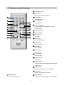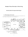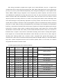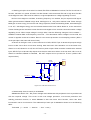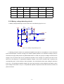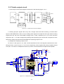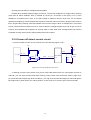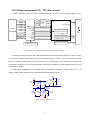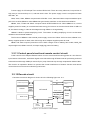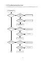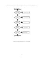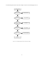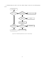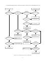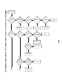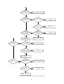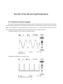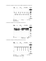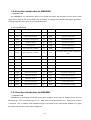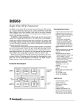
1
DL370D
service manual
Catalog
Chapter One About Maintenance
1.1 Safety precautions
1
1
1.1.1 Power supply
1
1.1.2 Precautions for antistatic
1
1.1.3 Precautions for laser head
1
1.1.4 About placement position
2
1.2 Maintenance method
2
1.2.1 Visualized method
2
1.2.2 Electric resistance method
2
1.2.3 Voltage method
2
1.2.4 Current method
2
1.2.5 Cutting method
2
1.2.6 Element substitution method
3
1.2.7 Comparison method
3
1.3 Required device for maintenance
Chapter Two Functions and Operation Instructions
3
4
2.1 Features
4
2.2 Control Button Locations and Explanations
4
2.3 Remote Control Illustration
6
2.4 Accessories
7
2.5 FUNCTION SETUP
7
2.5.1 Function Setup
7
2.5.2 General Settings
7
2.5.3 Audio Setup
8
2.5.4 Initial Setup
8
2.5.5 Useful notes
9
2.6 Specifications
9
Chapter Three Principle or Servicing
Section One Principle of the Player
10
10
3.1.1 Block diagramof the player
10
3.1.2 PCB composition block diagramof the player
11
3.1.3 Function introduction to IC of the player
11
Section Two Unit Circuit Principle
13
3.2.1 Servo processing circuit
13
3.2.2 CD/DVD switch circuit
15
3.2.3 Laser power control circuit
16
3.2.4 Main axis control circuit
17
3.2.5 DC-DC switch circuit
17
3.2.6 Battery voltage detecting circuit
19
3.2.7 Audio output circuit
20
3.2.8 Screen off detect control circuit
21
3.2.9 Video coding and LCD TFT drive circuit
22
3.2.10 Charge circuit and protection circuit
25
3.2.11 Control panel circuit and remote control circuit
26
3.2.12 Decode circuit
26
3.2.13 Reset circuit
28
3.2.14 Mute circuit
29
Section Servicing Cases
30
3.3.1 Servicing instances
30
3.3.2 Troubleshooting flow chart
34
Section Four Servicing Parameters
44
3.4.1 Signal waveformdiagram
44
Section Five Function Introduction to IC
51
3.5.1 function introduction to MT1389E
51
3.5.2 function introduction to AM5898N
62
3.5.3 function introduction to HWD4863
62
3.5.4 function introduction to S3C9454
63
3.5.5 function introduction to T102
65
Chapter Four Disassembly and Assembly Process
70
Chapter Cinque PCB board & Circuit diagram
76
Section One PCB board
76
Section Two circuit diagram
85
Chapter six BOM List
94
6.1 upgrade board unit
94
6.2 battery board
94
6.3 battery case
94
6.4 battery charge board
95
6.5 battery connecting board
96
6.6 battery protect board
96
6.7 decode board
97
6.8 drive board
101
6.9 main panel
102
6.10power socket board
103
Chapter One About Maintenance
1.1 Safety precautions
1.1.1 Power supply
When maintenance personnel are repairing DVD players, he should pay special attention to
the
power board with 220V AC and 330V DC which will cause hurt and damage to persons!
1.1.2 Precautions for antistatic
Movement and friction will both bring static electricity which causes serious damages to integrated
IC. Though static charge is little, when a limited quantity of electric charge is added to largescaleintegrated IC, as the capacitance is very small in the meantime, now the integrated IC is very much
easy to be struck through by static electricity or the performance will decrease. Thus static electricity
prevention is of extraordinary importance. The following are several measures to prevent static
electricity:
1. Use a piece of electric conduction metal with the length of about 2 metres to insert into the earth,
and Fetch the lead wire from the top of the surplus metal and connect to the required static electricity
device. The length and depth of the metal embedded under the earth should be determined according to
the wettability of the local soil. For humid places, it may be shorter, and longer and deeper for dry places.
If possible, it can be distributed and layed in terms of “#” shape.
2. On operating table-board, the antistatic table cushion should be covered and grounded.
3. All devices and equipments should be placed on the antistatic table cushion and grounded.
4. Maintenance personnel should wear antistatic wrist ring which should be grounded.
5. Places around the operating position should also be covered with electric conduction cushion or
Painted with antistatic paint.
1.1.3 Precautions for laser head
1. Do not stare at laser head directly, for laser emission will occur when laser head is working, which
will Hurt your eyes!
2. Do not use wiping water or alcohol to clean laser head, and you may use cotton swab.
-1-
1.1.4 About placement position
1. Never place DVD player in positions with high temperature and humidity.
2. Avoid placing near high magnetic fields, such as loudspeaker or magnet.
3. Positions for placement should be stable and secure.
1.2 Maintenance method
1.2.1 Visualized method
Directly view whether abnormalities of collision, lack of element, joint welding, shedding welding,
rosin joint, copper foil turning up, lead wire disconnection and elements burning up among pins of
elements appear. Check power supply of the machine and then use hands to touch the casing of part of
elements and check whether they are hot to judge the trouble spot. You should pay more attention when
using this method to check in high voltage parts.
1.2.2 Electric resistance method
Set the multimeter in resistance position and test whether the numerical value of resistance of each
point in the circuit has difference from the normal value to judge the trouble spot. But in the circuit the
tested numerical value of resistance is not accurate, and the tested numerical value of integrated IC's
pins can only be used for reference, so the elements should be broken down for test.
1.2.3 Voltage method
Voltage method is relatively convenient, quick and accurate. Set the multimeter in voltage position
and test power supply voltage of the player and voltage of a certain point to judge the trouble spot
according to the tested voltage variation.
1.2.4 Current method
Set the multimeter in current position and test current of the player of a certain point to judge the
trouble spot. But when testing in current method, the multimeter should be series connected in the
circuit, which makes this method too trivial and troublesome, so it is less frequently used in reality.
1.2.5 Cutting method
Cutting method should be combined with electric resistance method and voltage method to use.
This method is mainly used in phenomena of short circuit and current leakage of the circuit. When
cutting the input terminal voltage of a certain level, if voltage of the player rises again, it means that the
trouble lies in this level.
-2-
1.2.6 Element substitution method
When some elements cannot be judged good or bad, substitution method may de adopted directly.
1.2.7 Comparison method
A same good PC board is usually used to test the correct voltage and waveform. Compared these
data with those tested through fault PC board, the cause of troubles may be found.
Through the above maintenance method, theoretical knowledge and maintenance experience, all
difficulties and troubles will be readily solved.
1.3 Required device for maintenance
Digital oscillograph ( 100MHE)
TV set
SMD rework station
Multimeter
Soldering iron
Pointed-month pincers
Cutting nippers
Forceps
Electric screw driver
Terminals connecting cord
Headphone
Microphone
-3-
Chapter Two
Functions and Operation Instructions
2.1 Features
This player utilizes color TFT LCD and new generation DVD decoding chip with built-in Dolby Digital
decoders which can bring you to a brand-new AV entertainment world. The 2-laser super error correction
mechanism supports CD-R
Brand-new AV Effects.
1.7”color TFT LCD.
2.Compatible with MPEG4 discs to produce wonderful pictures.
3.Built-in Dolby Digital decoder.
4.Built-in stereo speakers.
5.Hi-Fi stereo headphone output.
High Quality Digital Audio
1.Built-in Dolby Digital and DTS digital surround decoder
Numerous Convenient Functions
1.Screen saver function cautiously protects your LCD and TV.
2.Large capacity solid Li-Ion battery, electronic anti-shock circuits, convenient for you towatchmovies
outdoors.
3.Easy-to-use brand-new GUI and virtual keyboard.
4.Multi-angle playback functionmakes it possible for you to view a scene from different camera angles.
5.Direct entry to desired scenes (title/chapter/time/track search).
6.Multiple aspect ratios to fit various TV sets.
7.Parental control function to protect children from watching inappropriate discs.
8.Multiple dubbing languages and subtitle languages keep you in thebestentertaining status anytime.
Supports SVCD, VCD, CD, MP3, HDCD, KODAK PICTURE CD, DVD-R/RW.
NOTE:Some discs labelled with MPEG4 on the market actually are*.rm/*.ram/*.rmm/*.ra and others
which are imcompatible. Please take care when buying discs.
2.2 Control Button Locations and Explanations
1
2
3
19
4
5
6
18
7
17
8
16
9
15
10
14
13
11
12
-4-
1
Color TFT LCD
11
Power indicator
2
Speakers
12
IR sensor
3
PICTURE Button
13
STOP Button
4
DVD/AUX IN Button
14
Keyboard/SWITCH Button
5
SETUP Button
15
REW Button/ DOWN direction arrow
6
FWD Button/UP direction arrow
16
NEXT/RIGHT Button
7
PREV/LEFT Button
17
MENU Button
8
OPEN/CLOSE Button
18
TITLE Button
9
PLAY / SELECT button
19
Q-PLAY Button
10
PAUSE button
1
2
3
4
5
6
7
1
Video In jack
5
Power switch
2
HeadPhones jack
6
Speaker volume knob
3
Audio In jack
7
DC 9V In
4
DC 5V Out
-5-
2.3 Remote Control Illustration
1
NUMBER Buttons
2
GOTO button
Play from the desired location.
1
3
PLAY Button
Normal playback.
2
4
19
Stop playback.
3
18
5
4
17
5
display modes.
15
7
6
CURSOR Buttons
7
SELECT Button
8
TITLE button
14
8
13
9
12
10
11
SUBTITLE Button
Change subtitle languages/Switch JPEG
16
6
STOP Button
DVD titles.
9
REW Button
Fast backward play.
10
FWD Button
Fast forward play.
11
PREV Button
Skip backward.
12
NEXT Button
Skip forward.
13
SETUP Button
Function setup.
14
REPEAT Button
Repeat play.
15
ANGLE Button
Change camera angles, MP3/JPEG playback
modes switch.
16
MENU Button
Display DVD menu or open/close PBC.
17
OSD Button
Display or hide disc information.
19
PAUSE Button
18
AUDIO Button
Change the audio language or audio channel.
Pause frame by frame.
-6-
4. Press UP/DOWN arrow to select the desired
value. Press SELECT to confirm it.
For example: Press UP/DOWN arrow to select
"LT/RT", than press SELECT, the TV screen
Display:
2.4 Accessories
1PCS
1PCS
2PCS
1PCS
1PCS
1PCS
1PCS
AV Cords
Remote Control
AAA Size Batteries
Instruction Manual
Battery Pack
Power Adapter
Warranty Card
— — Audio Setup Page — —
2.5 FUNCTION SETUP
2.5.1 Function Setup
Audio Mode
LT/RT
EQ Type
Stereo
Sound Field
V SURR
Tone
00
Dolby Digital Setup
1. Press SETUP button, The TV set screen
displays:
5. Press SETUP to exit the setup menu.
CURSOR
SETUP
— — General Setup Page — —
TV Display
SELECT
Wide
OSD Lang
English
Screen Saver
On
Spectrum
Off
2.5.2 General Settings
2. Press LEFT/RIGHT arrow to select the
desired channel to be changed.
For example, if you want to set this player's
Audio, please press LEFT/RIGHT arrows to
select AUDIO SETUP PAGE. Press SELECT for
verification. The audio setup page displays
On the screen.
— — General Setup Page — —
TV Display
LT/RT
EQ Type
Stereo
Sound Field
V SURR
Tone
Dolby Digital Setup
3. Press UP/DOWN arrow to select the desired
item you want to set and press SELECT.
For example, press UP/DOWN arrows to
select AUDIO MODE and press SELECT. The
AUDIO MODE appears on the screen.
— — Audio Setup Page — —
Audio Mode
LT/RT
EQ Type
Stereo
Sound Field
V SURR
English
Screen Saver
On
Spectrum
Off
1. TV Display: To set the aspect ratio of this
player's output image.
◆Optional settings: NORMAL/PANSCAN,
NORAM/LETTER BOX, WIDE.
◆Default: WIDE.
NOTES
◆The playing effects are contingent upon the
disc's recording aspect ratio. Some discs may
not be played according to your selected
aspect ratio.
◆16:9 is only applicable to the 16:9 TV.
◆Please select the aspect ration in accordance
with that of your TV.
◆The LCD screen is utilizing 16 by 9 aspect
ratio only.
2. OSD Lang: This item is used to set the
prompts language on the screen.
◆Optional settings: English, Russian.
◆Default: English.
3. Screen saver: Open or close the screen saver
Function.
◆Optional settings: OFF, ON
— — Audio Setup Page — —
Audio Mode
Wide
OSD Lang
Tone
Dolby Digital Setup
-7-
◆Default: ON
4.Spectrum:This item is used to set whether the
Dynamic Spetrum is allowed.
◆Selectable value:ON,OFF.
◆Default:OFF
2.5.4 Initial Setup
— — Preference Page — —
PBC
Audio
Subtitle
Disc Menu
Parental
Password
Default
2.5.3 Audio Setup
— — Audio Setup Page — —
Audio Mode
Stereo
EQ Type
Off
Sound Field
Off
Tone
00
On
English
Off
English
Off
1. PBC: To set the PBC status.
◆When playing SVCD or VCD2.0 discs, if the
PBC is ON, the menu image displays on the
screen and this player enter the PBC mode; if
the PBC is OFF, this player plays the disc by
its sequence.
◆Optional settings: On, Off.
◆Default: On.
2. AUDIO: To set the preference audio language
when playing.
3. SUBTITLE: To set the preference subtitle
language when playing.
◆Optional subtitle languages: English, French,
Spanish, Chinese,Japanese, korean, Russian,
Thai, others, Off.
◆subtitle language default: Off
4. DISC MENU LANGUAGE: To set the
preference disc menu language when playing.
◆Optional audio/disc menu languages: English,
French, Spanish, Chinese, Japanese, korean,
Russian, Thai, others.
◆Audio/disc menu language default: English.
NOTES
◆Audio/subtitle/disc menu languages are
effective to DVD only.
◆If the disc does not record your desired
language, the player will select the discspecifiedlanguages to play.
◆Selecting other languages: Press UP/DOWN
ARROW to move the cursor to OTHER item,
press SELECT. Press NUMBER buttons to
enter your desired language codes,then press
SELECT.
5. Parental : To set the parental control ratings to
prevent children from watching the restricted
contents. (In case the disc supports this
function.)
◆Optional settings: KID, G, PG, PG-13, PGR, R,
NC17, ADULT, OFF.
◆Default: OFF.
NOTE
Dolby Digital Setup
1. Audio output mode: To set the audio output
mode to make the multi-channel audio into
two-channel outputs.
◆Optional settings: LT/RT, STEREO, V SURR.
◆Default: STEREO
2. EQ type: To set EQ modes.
◆Optional settings:Off,ROCK,Pop, Live,Dance,
Techno, Classic, Soft.
◆Default: Off
3. Sound Field:To set different sound field effects.
◆Optional settings: Off, Concert, Living room,
Hall, Bathroom, Cave, Arena, Church.
◆Default: Off.
4. TONE control: This item is used to set the tone
level to match your diapason when you are
singing.
◆Method to adjust tone:
A. Press UP/DOWN cursor button to select
TONE item in AUDIO SETUP PAGE, and then
press SELECT button to enter the adjust menu
B. Press LEFT/RIGHT cursor button to adjust the
setting value.
C. Press SELECT button to return to AUDIO
SETUP PAGE after adjustment are well done.
5. Dolby Digital setup:
A. L+R: To set the output means of the left or
right audio when playing a Dolby disc with
separate two-channel audio
◆Optional settings: Stereo, L-Mono,R-Mono,
Mix-Mono.
◆Default: Stereo.
B. Dynamic compression: To set the linear
compression ratio to get different compression
result.
◆Optional settings: OFF、1/8、1/4、3/8、1/2、
5/8、3/4、7/8、FULL。
◆Default: OFF.
-8-
◆When changing the parental control ratings, a password is needed. Refer to the following password
item for detailed settings.
6. PASSWORD: To set a four digit password to enable you to change the parental control ratings.
◆Default: 7890.
OLD PASSWORD
NEW PASSWORD
CONFIRM PWD
OK
7. DEFAULT: To restore all settings to the default value except for the parental control and password
settings.
2.5.5 Useful notes
◆In order to prolong the service life of your player, it is recommended to wait at least 30 seconds before
you turn it on again after switching it off.
◆Turn off power after operation.
◆Only use the power supply of the nominal voltage, otherwise the player will not be operational or even
be damaged.
◆Some functions of the player may not be applicable to some discs.
◆In case of occasional player halt, please turn it off and turn it on again.
◆This player cannot play some SVCD discs with the CVD format.
◆When to use the Audio Output of this unit, please minimize the phone volume first.
2.6 Specifications
Disc Types
DVD VIDEO
SVCD,MPEG4
VCD1.0,1.1,2.0
CD-DA
MP3
Analog audio output
Stereo output,
Headphone output
Output
Video Output
Video
Characteristics
Video Amplitude
1.0Vp-p(75Ω)
Audio
Characteristics
Frequency
Signal-to-noise Ratio
Total harmonic distortion
20Hz~20kHz(±1dB)
>90dB
<0.01%
General
Specifications
Power Supply DC 9V 2A
Power Consumption 12W
Dimensions 205mmX149mmX39.5mm
Mass 735g
Operating
Temperature
Operating
Humidity
5℃~35℃
15%~75%(no condensation)
◆Specifications are subject to change without notice.
◆We do not grarantee that all discs can be played smoothly due to the disc quality,disc recording quality
and recording format.
-9-
Chapter Three Principle or Servicing
Section One Principle of the Player
3.1.1 Block diagram of the player
DL370D is composed of decode circuit, servo circuit, audio circuit, video circuit and power circuit.
The block diagram of the player is shown as in the following figure 3.1.1.1:
Sw601
Screen off
detect control
circuit
U204
AT24C02
BL_CLT
Boost board
Ht6222
Buttons control
BL_CLT#
STBT
VSAD
27MHz
IR
Disc switch and
APC circuit
LCD drive
T102
ALIN
Loader
AL
MT1389 E
Focus,
trace
drive
AR
Servo drive
signal input
Feed,
main axis
drive
+9VIN
ARIN
Audio filtering/
amplifying
Headphone/
speaker
amplifying
LM4863
LOUT
ROUT
LSOUT
RSOUT
VCC
DC-DC
conversion circuit
Dv33
FLASH (16M)
Reset circuit
+9VIN
SDRAM( 64M )
Battery
components
Charge control circuit
Figure 3.1.1.1 Block diagram of the player
- 10 -
CVBS1
3.1.2 PCB composition block diagram of the player
PCB composition diagram of the player is shown as in the following figure 3.1.2.1:
Battery
components
VOUT+
Main panel
TEMP COUT9VIN
Jk602
PGND
GND
V33
Loudspeaker
TFT
LCD
VSDA
Xs501
GND
STV1
STV2
Charge board BATTY_LED
CKV
U/D
Jk603
CHECK Jk101
OEV
VCOMO
COVER_SW
GND
OEH
VIN+9V
GND
STH2
DC socket board
STH1
Xs101
GND
A/B/C/D/E/F CPH1
SPGND
VR
SP+
Loader
VG
SL+
VB
Xs102
SLGND
LIMIT
Xs801
Jp2
Jp1
Drive board
Xs701
Jp3
BLGND
BLCLT
BL+9V
Jp6
+5V
+5V
BL BL
GND
BL9V
CTL GND
SRSR+
SLBoost board
SL-
GND
5VA
VGL
VGH
STV1
STV2
CKV
U/D
OEV
VCOM
VCOM
L/R
STH2
STH1
CPH1
CPH1
CPH1
5VA
GND
VR
VG
VB
VDD2
GND
Figure 3.1.2.1 PCB composition figure of the player
3.1.3 Function introduction to IC of the player
Function introduction to IC of the player is shown as in the following figure:
PCB board
Location
IC model
Function
Main panel
U401
PT2222A
U1
NJM3414AM
U2
G5105TBU
QB1
S8232
U601
S3F9454
U602
TL431
Three-end adjustable distributary reference
source
U603
LM358
Operational amplifier
IC1
MP1026
U301
C4558
Audio amplifying (operational amplifier)
U803
AZ1117
Voltage regulating IC
U202
HY57V641620ET
U801
T102
Buttons coding control
VCOM signal amplifying
Drive board
Protection board
Charge board
Boost board
DC-DC conversion
Battery charge protection
8-bit single chip, charge control
Boost control
Decode board
- 11 -
64M SDRAM
Video coding, LCD drive
U204
24C02
U201
MT1389FE/E
U901
AM5898
U502
LM393
U701
HWD4863
Headphone amplifying
U206,U802
LM1117H
Voltage regulating IC (U206 1.8V/U802 2.5V)
U501
HS0038B3V
Receiver
U203
29LV160BE
16M FLASH
Decode board
- 12 -
EEPROM
Decode chip
Servo drive, DC-DC control
Battery electrical charge detect (operational
amplifier)
Section Two Unit Circuit Principle
3.2.1 Servo processing circuit
1. DL370D adopts SANYO 62 loader and MTK decode solution (MT1389E+FLASH (16M)+SDRAM
(64M)). The servo circuit is composed of front end signal processing, digital signal processing IC
MT1389E and drive circuit Am5898, in which MT1389E is also the main composition of decode circuit.
Switch circuit
IOA
MD11
LDO2
LDO2
APC circuit
A B C D E F RFO
XS101
FOSO
TKTK+
FMSO
FC+
TRSO
FC-
DMSO
SL+
Feed electric machine
SL-
MT1389
D5898
SPMain axis electric machine
SP+
Main axis control
detect circuit
Figure 3.2.2.1 Servo processing circuit block diagram
2. Working principle: after power on or turning off door (door detect switch SW601/SW602 on
charge board shouts off), loader laser head begins to reset, focus and main axis begin to rotate, laser
head begins to identify disc information to judge the disc is CD or DVD to facilitate to make the
corresponding acts. At the same time, Mt1389 also adjusts laser output power through laser power
control circuit. When loader reads disc information, after photoelectric conversion, A, B, C, D, E, F
signals are formed to give to Mt1389 (DVD has A, B, C, D signals only) and Th erefore signal and the
input from pin 2~11, 18, 19 of MT1389. After MT1389 internal pre-amplifying processing, now signal are
divided into two parts inside MT1389:
- 13 -
After being processed by digital servo signal circuit inside MT1389, one part
of signal form
corresponding servo control signals and output FOO, TRO, DMO, FMO digital servo control signals from
pin 42, pin 41, pin 37, pin 38 of Mt1389 respectively, then change into analog servo control signal FOSO,
TRSO, DMSO, FMSO through integration circuit composed by resistor capacitor, and send to driver
circuit BA5954 for amplification to bring along focus coil, trace coil, main axis electric machine and feed
electric machine after drive amplification. Among these, focus and trace servo are used to correct
objective position accurately; feed servo is used to bring along laser head to make radial large-scale
move which belongs to the preliminary adjustment to pick-up position; and main axis servo is used to
control main axis electric machine to make it read signals in means of constant linear velocity and bring
along disc to rotate. After processing of amplification by VGA voltage control amplifier and equalization
frequency compensation inside MT1389, another part of signals are changed into digital signals through
internal A/D converter. When loader is reading CD/VCD signals, these signals are conducted EFM
demodulation inside MT1389, after CIRC (Cross-Interleaved Reed-Solomon Code) error correction is
finished inside, it outputs to rear state for audio/video decoding; when loader is reading DVD signals,
these signals are conducted ESM demodulation inside MT1389, and then sent to latter stage for
decoding after finishing RSPC error correction inside. Compared with general DVD players, this
machine has no disc in/out circuit and manual opening method is adopted. When pin 148 of MT1389E is
high level, system recognises that the door has been opened, when it is low level, the machine
recognizes that the door has been closed.
3. Loader signals introduction is shown as follows:
Pin
Name
Signal flow
direction
DVD disc
CD disc
No disc
Function description
1
F-
Input loader
2.52
2.34
0.46
2
F+
Input loader
2.49
2.49
0.93
Focus error signal is added to two sides of
pick-up focus coil
3
T+
Input loader
2.53
2.51
0.94
4
T-
Input loader
2.58
2.51
0.93
5
C
Input MT1389
2.2
2.25
2.04
Disc data signal
6
D
Input MT1389
2.2
3.2
2.04
Disc data signal
7
IOA
Input MT1389
0.01
3.2
3.21
Disc identification signal, CD is 3.3V, DVD
is 0V
8
RF
Input MT1389
2.21
2.53
1.28
The sum of disc data signal
9
A
Input MT1389
2.17
2.22
2.04
Disc data signal
10
B
Input MT1389
2.19
2.27
2.04
Disc data signal
11
F
Input MT1389
2.07
2.44
2.03
Supplementary signal used in trace
12
GND
Ground
0.01
0.01
0
Grounding
13
V20
Input loader
2.04
2.06
2.03
Reference voltage
- 14 -
Trace error signal is added to two sides of
pick-up trace coil
14
Vcc
Input loader
5.04
5.04
5.02
Supply voltage for loader
15
E
Input MT1389
2.06
2.45
2.03
Disc data signal
16
Blanking
haning in air
0.01
0
0
unused
17
VR-CD
Input loader
0.21
0.01
0
Through the handling inside loader, make
sure MD11 is 180mV when reading CD
18
VR-DVD
Input loader
0.01
0.2
0
Through the handling inside loader, make
sure MD11 is 180mV when reading DVD
19
LD-CD
Input loader
0.09
2.1
0
CD laser power control signal
20
MDII
Input MT1389
0.21
0.2
0
CD and DVD laser power monitoring signal
21
HFM
Input loader
5.04
5.04
5.02
High frequency overlapping signal produces
laser with different wave length inside
loader
22
Blanking
unused
0.01
0.1
0
23
LD-DVD
Input loader
2.21
0.1
0
DVD laser power control signal
24
GND
unused
0.01
0.01
0
Grounding
Note: 1. When reading DVD, there are only A, B, C, D signals.
2. When reading CD, there are A, B, C, D, E, F signals.
3. RFO=A+B+C+D.
4. Focus error signal=(A+C)-(B+D) Trace error signal=E-F.
3.2.2 CD/DVD switch circuit
1. CD/DVD switch circuit is shown as in the following figure 3.2.2.1:
AVCC
R102
R103
100K
10K
R104
V101
Xs101
VD101
10K
3904-S
R105
2SK3018-S
100K
VD102
2SK3018-S
17
18
Figure 3.2.2.1 CD/DVD switch circuit
- 15 -
IOA
MT1389E
2. Working principle: after disc is loaded in machine, IOA port is defaulted high level to make Vd102
saturation on and form loop with CD laser power control circuit on loader, at the same time IOA also
reaches loader PD IC for switch, disc begins to rotate; when servo processing system recognises that
the disc inside machine is not CD, IQA pin outputs low level to make Vd102 cut off, Vd101 on and form
loop with DVD laser power control circuit on loader to carry out the action of reading DVD disc. After
door is opened, IOA still keeps the state before door is opened. If machine cannot recognises which the
disc is , IQA pin will switch always until no disc is read out or judged by system.
Note: V303, V304 are MOS pipes (pressure drop is small when saturation on).
3.2.3 Laser power control circuit
1. Laser power control circuit is shown as in the following figure 3.2.3.1:
LDO-AV33
R106
4.7R
L104
601
DV33
C106
106
LDO2
23 DVD
22
VD103
2SB1132-S
20/21
XS101
MT1389
19 CD
VD104
2SB1132-S LDO1
23
C107
106
LDO-AV33
R107 4.7R
Figure 3.2.3.1 Laser power control circuit diagram
2. Working principle: pin 20/21 of MT1389 is laser power detect signal input pin, pin 21 is DVD laser
power strong/weak detect signal input pin, pin 23 is VCD laser power drive control output pin, pin 22 is
DVD laser power drive control output pin.
When reading VCD disc, laser power becomes weak, voltage of MDII pin decreases; when voltage
of MT1389 decreases, voltage of pin 19 of XS101 increases to reach the function of boost laser power;
when laser power is too strong, voltage of MDI pin increases to make voltage of MT1389 increase and
voltage of pin 19 of XS101 decrease to reach the purpose of lowering laser power to form a automatic
power control circuit. When reading DVD disc, pin 21 is detect signal input pin, pin 22 is drive control
output pin and the working principle is the same with that when playing VCD disc.
- 16 -
3.2.4 Main axis control circuit
1. Main axis control circuit is shown as in the following figure 3.2.4.1:
C113
222
104/DNS
C114
ADIN
OPO
R108
680K
R109
0R
OPOP+
MT1389E
R113
150K
R110
150K
C115
222
R111
DNS
SPSP+
SL+
SL-
R114
680K
V1P4
R112
1R
XS102
6
5
4
3
2
1
LIMIT
PH-6
Figure 3.2.4.1 Main axis control circuit diagram
2. Working principle: MT1389E has a comparator composed of operational amplifier inside. When
door is opened, disc is always rotating, so a braking signal is required to make main axis electric
machine stop rotating immediately to realize the purpose that disc can stop rotating during a short
period after door is opened. In the course of playing, if “OPEN”button is pressed, main axis drive signal
disappears, but main axis electric machine is still in rotating state because of inertia function. The
induced voltage achieved by induced electromotive force produced by electric machine running on
sampling resistor R321, R340, after sampling through resistor R112/R110/R113, input to pin 35, 36 of
MT1389,and output from pin 34 after Mt1389 amplifying processing inside, after D/A conversion and
relevant processing inside Mt1389, an instant electric machine reverse braking signal is outputted to
make main axis electric machine speed down. This machine is manual open/close means, so disc is still
rotating after door is opened but it will stop very soon.
3.2.5 DC-DC switch circuit
1. DC-DC switch circuit is shown as in the following figure 3.2.5.1:
EN
CT2
C906 COMP2
68pF SW2
IPK2
+9VIN
PGND
F+
+9VIN
FVCC
FOSO
R905 FMSO
10K
SL+
SLR906
10K
T-
1
2
3
4
5
6
7
8
9
10
11
12
13
14
15
16
17
35
EN2
CT2
COMP2
SW2
IPK2
PVCC1
PVCC2
VOFC+
VOFCVCC1
VINFC
VINSL
MGND
VOSL+
VOSLMGND
VOTK+
MGND
AM5898N
BIAS
MUTE
EN1
CT1
COMP1
SW1
IPK1
PGND2
PGND1
PGND
VCC2
VINTK
VINSP
VOSPVOSP+
MGND
VOTKMGND
34
33
32
31
30
29
28
27
26
25
24
23
22
21
20
19
18
36
SBIAS
SELECT
R912
0.1
COMP1
SW1
IPK1
C907
68pF
SW2
VCC
TRSO
SPSP+
PGND
DMSO
R1
TC907
100uF/16V
R910
0R
R913
680k
10K
R916
R914
T+
1.2K
R915
10K
SGND
Figure 3.2.5.1 DC-DC switch circuit diagram
- 17 -
VCC
C909
D904
MBRS340 104
PGND
PGND
PGND
C908
102
R911
750
QB902
AO3419 L902 47uH
1
2
COMP2
3.6K
2. Working principle: when switch is closed, EN1 EN2 of AM5898 is low level, DC-DC circuit has no
function, machine is in power off state, but after Sw901 is disconnected, EN end is high level, DC-DC
circuit begins to work. Take VCC for instance, we give explanation to voltage regulating of circuit:
DC-DC circuit begins to oscillate, its working frequency is in 240khz, Sw pin outputs on/off signal.
When grid electrode of QB902 is high level, MOS pipe is on, +9V power reaches L902 TC907 through
MOS pipe to save energy for inductor and charge capacitor, D904 freewheeling diode, when MOS pipe
is cut off, L discharges energy and its induced electromotive force makes diode on, at the same time
TC907 discharges the load with current direction unchanged to form a series connection switch voltage
regulating circuit. When output voltage is on high side, it has the following changes: VCC increases ―
COMP2 increases SW2 on/off frequency turns low ― VCC decreases. When voltage is on low side, the
course is opposite to that of increase. R912 is over-current protection circuit sampling resistor. (DV3.3
circuit principle is the same with that of VCC)
As shown in the figure 3.2.5.2, when machine is in DVD, SELECT pin of decode chip outputs a high
level to make servo drive circuit enter working state and reach Vd1 saturation on at the same time,
VD901 is cut off, Qb904 is cut off, DC OUT has no power output. When machine is switched to external
input, SELECT pin of decode chip outputs a low level to make servo driver circuit not work, VD1 is cut off,
VD901 is saturated, QB904 is saturated, DC OUT outputs VCC to provide for TV box. (CON3 is DC
output socket)
JK901
QB904
AO3419
VCC
R902
10K
R3
100R
SELECT
R904
1K
VD1
3904
1
2
3
TC905
106
CON3
R903
0R
VD901
3904
GND
Figure 3.2.5.2 DC OUT control circuit
3. Relationship of each control pin of AM5898
AM5898 has built-in DC- DC power manager and collaborate with peripheral circuit to provide load
with the required voltage. This circuit is with over-voltage protection, over-current protection and
stability protection function, in which AM5898 is also with servo drive function, which has been
introduced in servo circuit section. The relationship of each pin of AM5898 is shown as in the following
table:
Truth table ( ○ : active × : inactive - : don’t care )
- 18 -
MUTE
EN1
EN2
MOTOR CHANNEL
DC-DCCTRL1
DC-DCCTRL2
H
—
—
○
—
—
—
H
—
—
○
—
—
—
H
—
—
○
L
L
L
×
×
×
3.2.6 Battery voltage detecting circuit
1. Battery voltage detecting circuit is shown as in the following figure 3.2.6.1:
+9VIN
106
TC501
VCC
L503
DV33
10UH
R504
27K
R507
47K
GND 2
R509
4.7K
POWER_OFF
1
3
R511
33R
U502A
LM393
GND
R505
1.2k
6
R510
4.7K
U502B
R512
33R
LM393
R506
18k
LOW_BAT
7
5
R508
47K
Figure 3.2.6.1 Battery voltage detecting circuit
2. Working principle: U502 is an operational amplifier and used as a comparator in circuit. Reverse
input terminal inputs a VCC5V, through two resistors partial pressure, the reference voltage (2.5V) is
achieved; through partial pressure by R504 R505 R506 of +9VIN, two groups of voltage are achieved to
supply for the in-phase input end of operational amplifier; when voltage of in-phase input end is less
than 2.5V, the output pin of operational amplifier outputs a low level to decode chip to perform the
corresponding acts. In this machine, after calculation, we conclude that when input voltage is less than
6.5V, pin 7 of operational amplifier outputs low level and machine screen displays low battery; when
input voltage is less than 6.1V, pin 1 of operational amplifier outputs low level and machines carries out
power-off action.
- 19 -
3.2.7 Audio output circuit
1. Audio output circuit block diagram is shown as in the following figure 3.2.7.1:
HP_L
5
AL
186
LOUT
7
6
JK701
HP_R
16
6
RSOUTU201
MT1389E
184
U301
4558
AR
U701
LM4863
1
2
LSOUT-
ROUT
3
15
18
ALIN
Drive
board
LSOUT+
JP3
RSOUT+
ARIN
AUDIO_IN Jk301
Figure 3.2.7.1 Audio output circuit block diagram
2. Working principle: signal read out by disc, through audio and video decoding, converse audio
signal in MT1389E built-in DAC circuit to analog audio signal and output left and right channel analog
signals from pin 186, 184 of MT1389E, through Tc301, Tc302, coupled to pin 6, 2 of U301 and then
output from pin 1, 7 of U301 through being filtering and amplifying by the active filter composed of U301
and send to audio output terminal and headphone amplifying output circuit.
(1) Headphone amplifying output circuit
As shown in the figure 3.2.7.2, after volume adjustment of the audio signals outputted from U301
through VR701, input from pin 6, 15 of U701 respectively; audio signals after being amplified output
from pin 5, 16 of U701 to headphone socket for perform converse between headphone and speaker.
SP5V
L701 10UH VCC
C706 C707
R712 104 104
1K
TC701
100U/16V
SPGND
TC703
R70536K
R701
20K
R707
1K
R703
DNS SPGND
LM4863MTE
U701
TC704
SPGND
100uF/16V
0R
HPR R710
C701 105
ROUT
50K*2
C702
105
R702
20K
GND
100uF/16V
0R
HPLR709
VR701
LOUT
TC702
100U/16V
HP-L
HP-R
4 JK701HP
3
2
1
SP5V
C705
R704 225
DNS
SPGND
SPGND
R711
100K
HP-V1
R706
36K
R713 100K
Figure 3.2.7.2 Headphone amplifying output circuit diagram
- 20 -
D701
1N4148
(2) Output mode switch in headphone and speaker
LM4863 drive speaker adopts bridge connection. That drives headphone is single ending working
mode and its switch between them is fulfilled by HP-IN pin. As shown in the figure 3.2.7.2, when
headphone is inserted into a jack, a 4V~VDD voltage is added to HP-IN, which may cut off internal
operational amplifying module Amp2A and Amp2B to make the load connected by bridge invalid. Now IC
lies in single ending working mode and speaker has no sound output. When no headphone is connected
to jack, partial pressure resistance of R711, R707 makes the voltage supplied to pin HP-IN (pin 16) close
to 50mV, drive Amp2A and Amp2B are in working state to make 4863 work in bridge mode and transmit
to speaker through drive board to make speaker has sound output.
3.2.8 Screen off detect control circuit
1. Screen off detect control circuit is shown as in the following figure 3.2.8.1:
VCC
VCC
升压板
R601
1K
R604
1K
R603
1K
STBT
45
BL_CTL
SW601
SW2
MT1389E
VD601
8050
8050 VD602
R605
BL_CTL#
158
1K
GND
R602
10K
GND
Figure 3.2.8.1 Screen off detect control circuit
2. Working principle: when switch is off, pin 45 of MT1389 detects level, pin 158 outputs low level to
make BL_CTL low level, boost board stops working; when switch is disconnected, STBT is high level,
pin 158 of MT1389 outputs high level to make BL_CTL high level, boost board begins to work and lighten
back light board ( when switch is in panel position, screen close is off, screen open is disconnected).
- 21 -
3.2.9 Video coding and LCD-TFT drive circuit
1. Video coding and LCD-TFT drive circuit block diagram is shown as in the following figure 3.2.9.1:
U201
MT1389E
YUV0
IOR
YUV1
YUV2
YUV3
YUV4
YUV5
YUV6
YUV7
IOG
T102_RESET
MT1389_CLK
SDA/SCL
IOB
VR
RGB signal
amplifying
circuit
Jp2
VG
Jp1
VB
Drive board
STV1
U801 STV2
T102 CKV
U/D
VCOM
OEV
L/R
OEH
STH1
STH2
CPH1
VCOM signal amplifying
-10V
DC-DC conversion VGH
Voltage doubling
rectification circuit VGL
+15V
-10V
Boost board components
External video input
Figure 3.2.9.1 Video coding and LCD-TFT drive circuit block diagram
2. Working principle: decode chip outputs digital video signal and directly inputs to T102 for coding
in the means of data in parallel (8 bit), and restore digital signal to 3 base colour signal through internal
DAC circuit and are outputted by pin 62, 65, 68 and sent to a amplifying circuit composed of single triode.
Shown as in the figure 3.2.9.2, converse small current signal of RGB into voltage output means to drive
LCD screen to display.
VCOM signal amplifying circuit: VCOM, after U1 (NJM2414) amplifying, outputs from pin 6, 7 to
display screen and is used as the colourful filtering plate of display screen.
BIAS
+5VA
C845
104
R843
10K
R837
430
C842
106
R831
39K
GND
C841
1
IOR
VD801
2N3904
106
R828
150
R834
10K
R840
100
C844
100pF
GND
Figure 3.2.9.2 Amplifying circuit
- 22 -
C843
104
GND
VR
3. Voltage doubling circuit
Working of display drive circuit requires high voltage, so +5V voltage is voltage doubled, shown as
in the following figure 3.2.9.3:
D1
BAT54S
LX
Q1
8050
2
L5 560R
VGH
3
C16
474
1
C17
R11
5.1K
R15
10K
2
3
474
D2
BAT54S
1VOUT1
C18
104
C19 C20
C21
105 105
105
D5
BZT52C16V
C22
106
C23
104
GND
Figure 3.2.9.3 Voltage doubling rectification circuit
+5V power, through DC-DC conversion conducted by U2, is transmitted to the two groups of voltage
doubling rectification circuit composed of D1-D4 to perform rectification to power sent from pin 1 of U2.
When LX input is negative half circle, about -14V voltage is formed in collector electrode of Q2, -10 VGL
voltage outputted after D6 voltage regulating is provided to VCOM signal amplifying circuit and display
screen. When LX input is positive half circle, the voltage doubling rectification circuit composed by D1,
D2, C19 cannot be up to voltage required by VGH, so 7V DC current achieved after D7 rectification is
overlapped in pin 1 of to voltage regulating circuit Q1, D5 for voltage regulating and then output +15V
DC power to provide for display screen. +15V is outputted by JP1 to display screen through socket JP2
to drive board. In which JP3 on drive board
mainly transmit the signal and power required by
loudspeaker and boost board.
4. Boost board (if this PCB board is damaged, it will not be serviced but change it directly): how to judge the
boost board: 1) Make detecting head of oscillograph close to high voltage output line (pay attention not to touch the
line), a sine wave with about 60K will be viewed from oscillograph, which means that boost board has AC output.
The main fault of boost board is that there is no back light or back light is dark.
5. Function introduction to display screen pin is shown as in the following table:
Pin
Symbol
I/O
description
1
GND
-
Ground
2
VCC
P
Power line for logic
3
VGL
P
Gate driver negative voltage
4
VGH
P
Gate driver positive voltage
5
STV1
I/O
Gate driver START PULSE 1
6
STV2
I/O
Gate driver START PULSE 2
- 23 -
7
CKV
I
Gate driver scanning clock
8
U/D
I
Up/Down scanning change
9
OEV
I
Gate driver output enable
10
Vcom
I
HORIZONTAL SYNCHRONIZATION SIGNAL(Voltage applied to color filter
substrate)
11
Vcom
I
Voltage applied to color filter substrate
12
L/R
I
Right / Left scanning change
13
MOD
I
Sampling mode change (H: Simultaneous, L: Sequential)
14
OEH
I
LATCH PULSE FOR COLUMN DRIVER
15
STH2
I/O
Source scanning start signal 2
16
STH1
I/O
Source scanning start signal 1
17
CPH1
I
INPUT DATA CLOCK
18
CPH1
I
INPUT DATA CLOCK
19
CPH1
I
INPUT DATA CLOCK
20
Vcc
P
Power line for logic
21
GND
P
Ground
22
VR
I
Red video signal
23
VG
I
Green video signal
24
VB
I
Blue video signal
25
AVdd
P
Power
26
AVss
P
Ground
6. Scanning mode selection is shown as in the following table:
Start up pulse I/O state
Scan control input setup
Scan mode
U/D
L/R
STVR
STVL
STHR
STHL
GND
Vcc
O
I
O
I
Up→down Left→right
Vcc
GND
I
O
I
O
Down→up Right→left
GND
GND
O
I
I
O
Up→down Right→left
Vcc
Vcc
I
O
O
I
Up→down Left→right
- 24 -
3.2.10 Charge circuit and protection circuit
1. Battery: Lithium-ion polymer chargeable battery always follows the method of constant current
firstly and then constant voltage, and then charge in constant voltage state.
2. Lithium battery protection part (this PCB board will not be serviced inside battery components) is
divided into three types: A) Over-voltage protection, that is charge protection; B) Under voltage
protection, that is discharge protection; C) Current protection (short circuit protection included). The
protection delay and delay time of the above 3 items are different, from 1 second to 0.1 second and to
10ms with delay adjustable. Two lithium batteries protection, no matte over voltage protection or under
voltage protection, they are the relationship of “or”. Only one of the two cores has the condition, the
protection is available, which requires that the two cores of a group of battery are balanced on the whole,
or else the whole capacity will be severely damaged (when in over voltage protection, the core of high
voltage causes over voltage protection firstly; when in under voltage protection, the core of low voltage
causes protection firstly).
3. Charge part (charge board is a individual PCB inside main unit): core of charge part is single chip
that adopts A/D conversion with 10-bit. 8-bit single chip (S3F9454)) of PWM (12bits) SAMSUNG
company has the following features:
(1) Single chip is with 10-bit A/D conversion itself, the precision of A/D conversion is 1/1024, the
negative voltage of general NI-MH is 3-6mv (6mv/1500mv=1/250), which can meet the demands greatly.
The precision of lithium battery may be up to 5mv. Considering the test error, it may be up to ±20mv,
that is 4.2V+/-0.02v. The high precision and strong point are obvious.
(2) Use PWM (pulse width modulator) of single chip itself to directly control DC/DC conversion. The
control method is provided by software to achieve different constant current and constant voltage curve
(different charge means may be designed according to clients’requirements), so the whole line is simple,
with low cost, high reliability, high efficiency power conversion and less heat radiation.
(3) May charge NI-MH, NI-CD, LI-ION battery well. How to judge whether it is fully charged: A) max
voltage; B) max temperature increase; C) negative voltage; D) longest charge time. It can be tested
quickly after battery is fully charged and loaded again (within 15 minutes) and stop charging (this point is
very important to NIMH and NICD, which can prevent over charge to damage battery), when battery
voltage is low, use small current to charge to resume the damaged battery.
4. Working principle: when external power adapter is adopted to supply power, power arrives at VIN
pin through socket board and is divided into two ways: A) arrive at decode board (VOUT+) directly
through VD602; B) provided for charge circuit. After voltage regulating, the voltage regulating circuit
composed by V601, U602 provides working voltage for U601. U601 is charge management control
single chip.
- 25 -
Power supply of CPU adopts Tl431 and an NPN triode. There are many elements, but precision is
high, easy to correct and up to 1%, and test work is less. The power supply circuit is composed of U602
and V601, etc.
V605, V604, V603, QB602 compose switch DC/DC circuit; V603 and V604 compose standard push
pull circuit to drive QB602 to make QB602 has good switch waveform to decrease heat radiation.
QB602, L601, TC603 and VD601 compose classic STEP DOWN circuit. When QB602 is on, current
supplies power for battery on one hand and save energy for inductor on the other hand. When is QB1 cut
off, the electric energy in inductor discharges through VD601 to charge battery.
LM358 is classic in-phase amplifying circuit. The reason of adding amplifying circuit is to decrease
resistance test and heat radiation.
The function of QB603 is the external power supply control end. When VIN is low level, QB603 is on,
battery supplies power for load; when VIN is high level, adapter supplies power for load.
QB601 and V602 compose protection circuit. When charge circuit or battery has trouble, MOS_SW
outputs high level, QB601 cuts off, 9V stops supplying power for battery.
3.2.11 Control panel circuit and remote control circuit
Panel control circuit adopts HT6222 control circuit to control and its working power is 3.3V. After we
input buttons information, serial data signal are achieved through HT6222 internal processing and sent
to decode board through VSDA pin and to IR pin (102) of decode chip through a separation diode Vd201.
The function of separation diode is to prevent the mutual interference of buttons function and remote
control function and incorrect order being carried out.
3.2.12 Decode circuit
1. Decode circuit block diagram is shown as in the following figure 3.2.12.1:
186
Loader components
184
AM5898
FOSO
FMSO
TRSO
DMSO
AL
AR
27M
MT1389 E
YUV0~YUV7
T102_RESET
Reset circuit
Audio amplifying
U301
URST#
MT1389_CLK
101
93/94
T102
U801
SDA/SCL
U204
24C02
U203
FLASH
U202
SDRAM
Figure 3.2.12.1 Decode circuit block diagram
- 26 -
2. Working principle:
(1) Power: MT1389 is with two groups of power supply: one group achieves 1.8V voltage after
LM1117MP-1.8(U216) voltage regulating to supply for the logic circuit inside IC; the other group
achieves 3.3V voltage after DC-DC conversion and QB903 voltage regulating. At the same time, FLASH
and SDRAM must also meet the requirements of power.
(2) System clock: clock signal is an important factor of machine’
s working, that whether there is
clock signal or whether it is normal will affect the normal working of the player. This machine adopts
external clock (27M) that inputs to pin 194 of MT1389, clock is produced byT102 and its peripheral
circuit.
(3) Data communication
1) Communication of Mt1389 and SDRAM: the communication of MT1389 and SDRAM is mainly to
temporarily save the large quantities of data after MT1389 decoding to prepare for saving at any time.
Shown as in the figure, DMA0DMA10 is address signal, DQ0DQ15 is data signal, DCLK is synchronous
clock, DCKE is enabled end, CS is chip selection signal, WE is write enabled signal, RAS and CAS are
row and line gating signals.
DMA0—DMA10
DQ0—DQ15
MA11
35
158
#BA1
145
MT1389
DCLK
136
DCKE
138
21
38
37
127
CS#
19
126
RAS#
18
125
CAS#
17
WE#
16
124
123/1 04
DQM0 、 DQM1
SDRAM
15、 39
Figure 3.2.12.2 Communication block diagram of MT1389 and SDRAM
2) Communication of MT1389 and FLASH
The communication of Mt1389 and FLASH is mainly to call the program and working directions
saved inside FLASH when power on. Shown as in the figure, A0A19 is address line, A20 and 21 are
address line, AD0AD14 is data line, DWR# is read-write control, DCE# is chip selection and DRD# is red
operation.
- 27 -
A0— A19
AA20、 21
AD0 — AD14
FLASH
MT1389
DWR#
57
11
DCE#
68
26
DRD#
28
70
Figure 3.2.12.3 Communication block diagram of Mt1389 and FLASH
3. Audio, video output
(1) Video: MT1389 integrates video encoder inside, so analog video signals can output from
Mt1389 inside directly; but DL370D only need to output digital signal, and its digital signal output is as
follows:
Pin 152~157 and pin 79/99 of MT1389E output MYUV0~MYUV7 8-bit digital video signal separately.
(2) Audio: Mt1389 integrates D/A conversion inside, so analog audio signal output from MT1389
inside directly, and digital signal may also output directly and be conversed by the externally connected
D/A conversion IC, which is also with optical output function. DL370D adopts analog audio output and
the output signals are as follows:
◆ P187: ASL
◆ P186: AL
◆ P184: AR
◆ P183: ASR
◆ P182: ASUBW
◆ P188: ACENTER
◆ P159: DPDIF#
This machine only uses two channels of AL and AR and no other channels.
3.2.13 Reset circuit
1. Reset circuit is shown as in the following figure 3.2.13.1:
Dv33
D201
In4148
R211
10K
R212
K10
Tc207
106
URST#
MT1389E
+
Figure 3.2.13.1 Reset circuit diagram
- 28 -
T102
2. Working principle: after power on, DV33 charges TC207 through R211. Voltage on two ends of
capacitor cannot change suddenly, so positive voltage of TC207 increases gradually and its increase
time is related with R211/TC207. When machine is working normally, this voltage is the same with power
voltage on the whole. After this circuit performs reset to decode chip, pin 95 of decode chip outputs a
reset signal to pin 28 of T102 to perform reset to T102. After machine power off, the electric charge
saved in TC207 discharges through D201 to ensure the reliable reset after power on next time.
3.2.14 Mute circuit
1. Mute circuit is shown as in the following figure 3.2.14.1:
HP-L
+9VIN
R323
1K
V303
8550
R714
MUTE
560R
0
MT1389E
D301
1N4148
MUTE_DAC
V701
2SC1815-Y
SPGND
R715
D302
1N4148
R321
1k
560R
1
V702
2SC1815-Y
HP-R
V304
8050
R322
10K
R320
AGND
560R
LOUT
V301
2SC1815-Y
AGND
AGND
MUTE
R319
560R
V302
2SC1815-Y
ROUT
Figure 3.2.14.1 Mute circuit diagram
2. Working principle: after power on, +9V arrives at the base electrode of
V301, V302, V701,
V702 through CE of V303 to make triode saturated on, audio signal output and headphone output are
short circuited to ground to remove noise that produces when power on. After machine resets and
begins to read disc, pin 151 of Mt1389 outputs a high level to make pin MUTE change from high level to
low level, V301, V302, V701, V702 are cut off because the base electrode is low level , audio signal can
output normally.
- 29 -
Section Servicing Cases
3.3.1 Servicing instances
[ Example1 ] Symptom: not read disc
Description: not read any disc
Analysis and troubleshooting: firstly, press down detect switch of door and check whether loader
laser head can restore to the most inner circle and it is normal after observing. Then check whether laser
head has infrared light radiation, the intensity of light radiation (pay attention not to stare at laser light
with eyes vertically, which is harmful to eyes, and look at it at a certain angle) is basically normal, then
load disc and observe the rotation speed of disc, the beginning of rotation is basically normal, and finally
rotation speeds up obviously and the laser head also moves all the way, which means that it cannot find
the disc information, firstly you may consider that laser head focus has trouble and cannot find the
beginning information, change loader components and trouble is removed.
[ Example 2 ] Symptom: no OSD
Description: machine cannot read disc, there is no image
Analysis and troubleshooting: firstly check power supply of each channel, 9V, 3.3V, 1.8V, 5V which
are all normal, check 5V of control line BL_CTL of boost board and back light voltage 9V of boost board
and boost board output, which are normal; check whether detect switch is stuck or whether detect switch
is invalid, which are normal; check CVBS0 signal on L801 and find that there is no; check power supply
of MT1389, U202 (SDRAM), U203 (FLASH), U204 (EEPROM), which is normal; check pin 1, 24, 25, 48
of FLASH address line (FLASH pin is dense, this 4 pins are at the edge, so it is easy to measure) and
find that there are two pins without waveform, another two pins have waveform but it is incorrect; after
changing FLASH, trouble is removed.
[ Example 3 ] Symptom: colour distortion
Description: colour loss leads to the distortion of played picture
Analysis and troubleshooting: play colourful bar signal and find that green signal is missing; colour
loss is not display screen trouble generally, so firstly check display drive circuit, directly check amplifying
circuit of R, G, B, there is IOG signal but there is no output signal VG; check triode Vd802 and find that
R835 is missed stuck, after sticking it again and trouble is removed.
[ Example 4 ] Symptom: white screen
Description: disc reading is normal, sound is normal, display screen cannot display image and white
screen appears.
- 30 -
Analysis and troubleshooting: white screen means that boost board working is normal, so it is
preliminarily judged that display drive has trouble, check voltage of 3.3V, 2.5V of U801 and they are both
normal; check input/output signal CVBS0, SDL, SCL, YUV, STH, VCOM0 and find that there is no
VCOM0 signal; after changing U801, the trouble is removed.
[ Example 5 ] Symptom: headphone has no output
Description: loudspeaker and headphone both have no output.
Analysis and troubleshooting: use oscillograph to test whether there is sound signal that outputs to
headphone terminal, and there is no; test whether left and right of TC703, TC704 electrolytic capacitor
have waveform output and there is no; check whether mute circuit is normal, MUTE signal is low level,
normal; check pin 15, 16 of U701 (LM4863 headphone/loudspeaker drive), and there is sound signal
input; after changing U701, trouble is removed.
[ Example 6 ] Symptom: power not on
Description: machine has no response after power on
Analysis and troubleshooting: check whether 9V voltage comes through charge board and it is
normal; check QB902, QB903, and there is 5V, 3.3V conversion, which is normal; check power supply of
each channel and find that L216 has no 1.8V output, so it is doubted that U206 has trouble; after
changing U206, trouble is removed.
[ Example 7 ] Symptom: after installing battery, unplug power adapter, screen will be dark for 1-2S and
then become normal.
Description: use battery to supply power, unplug power adapter, screen will be dark for 1-2S and
then become normal.
Analysis and troubleshooting: firstly compare defective machine with good one, good one will flash
once, but it flashes slightly and shortly, and you will not be aware if you do not observe carefully;
because the brightness and darkness of screen has closely relation to boost board, firstly check boost
board; according to experiences, if the R9 rosin joint on boost board will lead to dark screen, use
multimeter to test and there is no rosin joint, use oscillograph to touch HV, LV signal, and unplug power
adapter at the same time, trouble does not appear again, use man-made simulating method to insert
and unplug quickly and trouble appears again, sine wave on oscillograph disappears for 1-2s, check
BL_9V power supply and find that during trouble period BL_9V voltage will have distortion (it is a little
similar to distortion sine wave, but much more complicated), take down IC and distortion still exists,
which means that it is not IC fault, check element connected with BL_9V, when testing to pin 11 of IC, we
find that during the fault period of 9V voltage, there is distortion waveform, after changing C7, trouble is
removed.
[ Example 8 ] Symptom: not read disc
Description: not read any disc
Analysis and troubleshooting: firstly press down open detecting switch and observe laser head
focus and heat radiation, which are normal; after changing laser head, trouble still exists; load disc and
- 31 -
Read it, when laser head begins to focus, laser head cannot be searched and slides back and forth, use
oscillograph to check focus and trace signal and they are all noisy wave, check the digital signal at front
end of integration, it is still noisy wave; check A, B, C, D, Therefore signal and they are also noisy wave,
check the path between them and there is no problem, each capacitor has no rosin joint and joint
welding; when checking whether flat cable holder XS101 has rosin joint, tin seems to be connected
between pin 8, 9; use multimeter to test and there is actually short circuit, after removing welding tin,
trouble is removed.
[ Example 9 ] Symptom: noise exists when playing
Description: there is noise when playing not any discs, loudspeaker and headphone both have
noise.
Analysis and troubleshooting: firstly make clear that it is loudspeaker trouble or other circuit trouble,
use headphone to listen to Jk701 and check whether it has noise, if it has, it is confirmed that circuit has
trouble, then play 1KHZ standard signal disc, it is easy to test waveform, use oscillograph to check pin 3
and 18 waveform of U701, it should be sine wave, but there is noisy wave to appear consequently, then
check pin 5 and 15 of U701, input pin of left/right channel, and there is still noisy weave to appear, go on
checking to the front stage, check C701, C702 waveform and there is still noisy wave to appear; directly
test pin 1 and 7 of U301, and there is still noisy wave, then check pin 2 and 6 of U301, and waveform is
normal consequently, test power supply of U301, it is also normal; after changing U301, trouble is
removed.
[ Example 10 ] Symptom: black screen
Description: screen of machine has no display after power on
Analysis and troubleshooting: firstly check whether power indicator light emits light to judge whether
power starts up; if indicator light is normal, load disc and check whether disc reading can continue and
whether disc reading is normal; listen loudspeaker and check whether its sound is normal, if it is normal,
the power is judged to be normal preliminarily. Then press screen display detect switch to check whether
screen display has light flashing, if there is no, check 5V of detect signal control line BL_CTL of boost
board and back light voltage 9V of boost board and boost board output and they are all normal; then test
whether high voltage has output. Use detecting head of oscillograph to close up high voltage line of
input display screen and there should be sine wave. Finally change display screen and trouble is
removed.
[ Example 11 ] Symptom: no output
Description: machine screen has no display after power on, cannot read disc.
Analysis and troubleshooting: firstly test 3.3V, 1.8V voltage after DC-DC conversion, voltage output
is normal, then test whether crystal oscillator Y801 has oscillation, and it is normal, and frequency
27.00MHZ is also normal, then test URST# reset voltage 3.0V and it is also normal basically, then test
software data 128M and it also normal, then test U202 DCLK,DCKE and it has response, and only
address line has no response, so we begin to doubt that SDRAM has trouble, change it and there is still
- 32 -
No output, finally we doubt that chip Mt1389 has trouble; after changing MT1389, trouble is removed.
[ Example 12 ] Symptom: noise appears when playing CD
Description: it is normal when playing other discs, but noise appears when playing CD disc
Analysis and troubleshooting: firstly make clear whether other discs have noise, play Dvd disc and
test that there is no noise, then listen to headphone and check whether it has noise to confirm whether it
is loudspeaker trouble or headphone trouble, and they both has noise consequently; now we analyse
that DVD is normal, which means that DAC audio decode and operational amplifier are basically normal,
then process audio decode and data has trouble, which is mainly caused by SDRAM and decode chip,
change SDRAM and it is invalid, then change decode chip MT1389 and trouble is removed.
[ Example 13 ] Symptom: not read CD disc
Description: DVD disc reading is normal, Cd and VCD disc reading are not available
Analysis and troubleshooting: DVD disc reading is normal, so it is judged that focus and trace is
normal basically; firstly we doubt whether detecting has error, test IOA voltage of pin 44 of MT1389, and
the voltage at that time is about3.1 which is obviously incorrect, when reading DVD disc, it is high level,
now VCD disc is being read and it is also high level, triode V102 will not be on at all, of course loader
laser head CD laser pipe will not be lightened; directly change MT1389 and trouble is removed.
[ Example 14 ] Symptom: not read disc
Description: not read any disc
Analysis and troubleshooting: laser head is in middle and cannot return to the most inner circle after
power on, firstly measure T+, T- voltage and it is about 2.5V, which is basically normal, then test feed
inner resistance on loader components, it is about 8 ohm, which is also normal, finally carefully observe
Xs102 flat cable holder and find that there is one flat cable of the 6 loader flat cable that falls off, after
pressing tightly, trouble is removed (this loader always has this trouble, which shows that main axis
electric machine does not rotate sometimes and also pay attention to observe this plug).
[ Example 15 ] Symptom: white screen
Description: TFT screen appears white screen, no normal image output
Analysis and troubleshooting: boost board is normal and it is preliminarily judged that display drive
part has trouble, check each voltage 3.3V, 2.5V of U801 and they are both normal; test oscillation of
Y801 and it is normal; test tricolour and it is normal; test 8-bit data and it is normal, which means that
U801 working is normal, change display screen and trouble still exists. Then we doubt that it is the
display screen flat cable holder that has trouble, observe carefully and find that 3.3V power supply pin of
flat cable holder DV33 3.3V has false welding; after welding again and trouble is removed.
- 33 -
3.3.2 Troubleshooting flow chart
1. Troubleshooting flow chart for “Not read disc”is shown as in the following figure 3.3.2.1:
Not read disc
Whether
laser head has resets
N
Y
Whether
pin 12 of AM5898 has
feed signal
input
N
Check MT1389 and C231
Y
Check
whether voltage
on two ends of electric
machine is
equal
N
Check electric machine
Y
Check AM5898
Whether
there is focus action
N
Whether
pin 11 of AM5898
has focus signal
input
N
Check MT1389 and C233
Y
Y
Check
whether voltage of
pin 8, 9 of Am5898 is
normal
N
Check AM5898
Y
Check the line between
pin 1, 2 of XS101 and coil
Whether
main axis electric
machine rotates
Y
N
Whether
pin 22 of Am5898 has
signal input
Check MT1389 and C230
Y
Check
whether voltage of
pin 21, 22 of AM5898
is normal
Y
A
N
Check electric machine
- 34 -
N
Check AM5898
A
Whether
laser head emits light
N
Check
whether APC circuit
provides voltage for
laser head
N
N
Check
power supply circuit
Y
Y
Y
Y
Check
whether LDO_DV33
is normal
Change loader
Check MT1389
Check
whether LD01 is normal
Y
Check
V104, V103 and socket
XS101
N
Y
Change 24P flat cable
Whether
rotation speed of disc is
normal
Y
N
N
Whether
there is RF signal
Change loader
Y
Whether
there are ABCDEF
signal
N
Check XS101 and flat cable
Y
Change loader
Check MT1389 and peripheral
Figure 3.3.2.1 Troubleshooting flow chart for “Not read disc”
- 35 -
Change
2. Troubleshooting flow chart for “Player has no output”is shown as in the following figure 3.3.2.2:
Player has no output
N
Whether reset is normal
Check reset capacitor
Y
Whether
there is 27M clock
N
Check T102 and crystal
oscillator
Y
Whether
1.8V power supply is
normal
Check
whether pin 3
of U206 has 3.3V
power supply
N
Y
N
Y
Whether
pin 2 of U206 has
1.8V output
N
Whether
V18 is short
circuited to ground
N
Change U206
Y
Y
Check MT1.89 and 1.8V
filtering capacitor
Check the line from L216
to decode IC
Check
whether power
supply of decode chip,
FLASH, DRAM
is normal
Service according to
troubleshooting process
for “No 3.3V”
N
Check power supply circuit
Change SDRAM or MT1389
Y
N
Check
whether clock
of pin 38 of SDRAM
is normal
N
N
Whether DCLK is 27M
Y
Check
whether SDRAM
is rosin joint
Y
Y
Weld again
Check
whether FLASH is
normal
Change FLASH
Y
B
Y
Weld again
N
Check
whether MT1389 is
rosin joint
N
Change MT1389
- 36 -
N
Check
whether decode
chip is rosin joint
Y
Weld again
B
Check
whether FLASH
has data output
N
Y
Check
whether FLASH,
Mt1389 has rosin
joint
N
Change FLASH or MT1389
Y
Weld again
Check
whether SDRAM
data line has
signal
N
Y
Check
whether FLASH,
Mt1389 has rosin
joint
N
Change FLASH or MT1389
Y
Weld again
Check
whether U204 is
normal
N
Change U204
Y
Check the line between
decode chip and FLASH/DRAM
Figure 3.3.2.2 Troubleshooting flow chart for “Player has no output”
- 37 -
3. Troubleshooting flow chart for “No VCC voltage”is shown as in the following figure 3.3.2.3:
No VCC voltage
Check
whether resistance
of VCC pin to ground
is normal
N
Check load circuit
Y
Check
whether R910 has 4V
voltage
N
Change AM5898N
Y
Check
whether the
end connected to QB902
of R912 has 9V
voltage
N
Check R912
Y
Check
whether cathode
of D904 has 5V
voltage
N
Change QB902
Y
Check
whether L902
has open circuit
N
Check whether TC907 has
electricity leakage
Y
Change
Figure 3.3.2.3 Troubleshooting flow chart for “No VCC voltage”
- 38 -
4. Troubleshooting flow chart for “No DV33V voltage”is shown as in the following figure 3.3.2.4:
No DV33V voltage
Check
whether resistance
to ground of Dv33 is
normal
N
Check load circuit
Y
Check
whether R917
has 5.5V voltage
N
Change AM5898N
Y
Check
whether the
end connected to QB903
of R917 has 9V
voltage
N
Check R912
Y
Check
whether cathode
of D904 has 5V
voltage
N
Change QB902
Y
Check
whether L903
has open circuit
N
Check whether TC909
has electricity leakage
Y
Change
Figure 3.3.2.4 Troubleshooting flow chart for “No DV33V voltage”
- 39 -
5. Troubleshooting flow chart for “No VCC, DV33V voltage”is shown as in the following figure
3.3.2.5:
No VCC, DV33
Whether
+9VIN is normal
N
Check
whether power
adapter of charge board
is normal
N
Power adapter troubleshooting
Y
Y
Whether
+9V Dc socket is
normal
N
Change
Y
Check +9V filtering capacitor
and power supply line
Whether
pin 1 ofAM5898
is high level
Y
ChangeAM5898
N
Whether
SW901 is in OFF
position
N
Change SW901
Y
Set switch in OFF position
Figure 3.3.2.5 Troubleshooting flow chart for “No VCC, DV33V voltage”
- 40 -
6. Troubleshooting flow chart for “Audio has no output”is shown as in the following figure 3.3.2.6:
Change MT1389
Audio has no output
N
Whether
headphone has sound
N
Check
whether MUTE is low
level
Check
whether MUTE_DAC
is high level
N
Y
Y
Check
whether there is mute
N
Y
Y
Cancel mute
Check
whether V304 is
normal
N
Check
whether V303 is normal
N
Change V304
Change V303
Y
Check R714/R715
Check
whether pin 6,
15 of U701 has signal
input
Check
whether potentiometer
has signal
input
N
Y
Check
whether U301 has
signal output
N
Y
Y
Check the line from U301
to potentiometer
Change U701
Whether
pin 20 of U701 is 4V
N
Check
whether potentiometer
is normal
Headphone socket is
not good
N
Change potentiometer
Y
Y
Check
whether loudspeaker is
normal
Check element from
potentiometer to U701
Check
whether U301
has signal input
N
N
Change MT1389
Change loudspeaker
Y
Y
Change U701
Check A9V power supply
circuit
N
Check
whether power
supply of U301 is
normal
Y
Check U301
Figure 3.3.2.6 Troubleshooting flow chart for “No audio output”
- 41 -
N
LCDdisplay trouble
Whether
LCD has back light
output
N
Check
whether boost
board has high voltage
output
N
Y
Y
N
Check
whether YUV
has signal input
N
Check
whether 27M clock is
normal
Check
whether VD602 is 0.7V
N
Y
Change boost board
Y
Y
N
Y
Check whether display
screen is normal
Whether
there is image output
Check
whether pin 2 of Jp6
is high level
Y
Change MT1389
Check VD602/VD601
N
Check
27M crystal
oscillation and matched
capacitor
N
Y
Y
Check T102 power supply
Check
whether decode board
works normally
N
Decode circuit troubleshooting
Y
Change MT1389
Check
whether IOG,
IOB, IOR has signal
output
Y
C1
C2
N
Check
whether reset
and power supply of
T102 is normal
Y
Change T102
N
Remove one by one
Check
whether STBT is high
level
Change
N
Change SW601
C2
Check
whether VG,
VR, VB has signal
output
N
Check RGB amplifying circuit
Y
Check
whether drive
board VR, VG, VB has
signal
N
Y
Check
XS801 and flat cable
N
Whether
picture output is
normal
Check display screen
socket and display screen
N
Check
whether VCOM signal
is normal
Check
whether LX
waveform of DC-DC
circuit is
normal
N
Weld again
N
Y
Y
C1
Change
Y
Check
whether there is rosin
joint
Check
whether VGH,
VGL, +5V voltage on
drive board is
normal
N
Check voltage regulating
circuit
N
Check U1 and its peripheral
Y
Y
Check
whether other
display drive signal
is normal
N
Change T102
Y
Check signal pathway and
display screen
Whether
colour is normal
N
Check
whether 27M clock is
normal
N
Check crystal oscillator and
externally connected capacitor
Y
Check
whether T102 is
normal
N
Change
Y
Check whether MT1389 is
normal
Figure 3.3.2.7 Troubleshooting flow chart for “LCD display trouble”
- 43 -
Change U2
Section Four Servicing Parameters
3.4.1 Signal waveform diagram
This section collects signal waveform diagram of audio, video and each unit circuit with the purpose
to help servicing personnel to judge where trouble lies in accurately and quickly to improve servicing
skills. For the difference of oscillograph's type, model and tuner, a certain difference may exist, so the
servicing personnel are expected to pay more attention to check in daily operation.
1. Waveform diagram of pin 2 8M of charge board U601
2. Waveform diagram of pin 4 CKV of JP2
- 44 -
3. Waveform diagram of main axis drive DMO outputted by decode chip
4. Waveform diagram of FO outputted by decode chip
5. Waveform diagram of FM outputted by decode chip
- 45 -
6. Waveform diagram of TR outputted by decode chip
7. Waveform diagram of LX signal of pin 1 of G5105
8. Waveform diagram of CLK of pin 194 of MT1389
- 46 -
9. Waveform diagram of OEH of pin 11 of JP2
10. Waveform diagram of STH1, STH2 of pin 12, 13 of JP2
11. Waveform diagram of pin 5, 6 STV1, STV2 of JP2
- 47 -
12. Waveform diagram of pin 29 SW1 of AM5898
13. Waveform diagram of pin 4 SW2 of AM5898
14. Waveform diagram of pin 13 of U601
- 48 -
15. Waveform diagram of pin 7 VCOMO of JP2
16. Waveform diagram of pin 17 VR of JP2
17. Waveform diagram of pin 81~88 YUV of T102
- 49 -
18. Waveform diagram of black light drive voltage
Note: back light drive voltage is high, when testing, detecting head of oscillograph cannot be
contacted with output terminal directly, only close to output terminal and waveform can be tested.
19. URST waveform diagram
20. Waveform diagram of pin 6 U1 VCOM
- 50 -
Section Five Function Introduction to IC
3.5.1 function introduction to MT1389E
1. DESCRIPTION
MT1389E is a cost-effective DVD system-on-chip (SOC) which incorporates advanced features like
MPEG-4 video decoder, high quality TV encoder and state-of-art de-interlace processing.
Based on MediaTek’
s world-leading DVD player SOC architecture, the MT1389E is the 3rd generation of
the DVD player SOC. It integrates the MediaTek 2nd generation front-end analog RF amplifier and the
Servo/MPEG AV decoder.
To enrich the feature of DVD player, the MT1389 equips a simplified MPEG-4 advanced simple profile
(ASP) video decoder to fully support the DivX1 Home Theater profile. It makes the MT1389-based DVD
player be capable of playback MPEG-4 content which become more and more popular.
The progressive scan of the MT1389E utilized advanced motion-adaptive de-interlace algorithm to
achieve the best movie/video playback. It also supports a 3:2 pull down algorithm to give the best film effect.
The 108MHz/12-bit video DAC provides users a whole new viewing experience.
2. Key Features
RF/Servo/MPEG Integration
Embedded 6ch Audio DAC
Embedded 2ch Audio ADC for Karaoke
High Performance Audio Processor
High Performance Progressive Video Processor
Support Nero-Digital
High Quality 108MHz/12-bit, 4 CH TV Encoder
3. General Feature lists
(1)Integration DVD player single chip
High performance analog RF amplifier
Servo controller and data channel processing
MPEG-1/MPEG-2/JPEG video
Dolby AC-3/DTS Decoder
Unified memory architecture
- 51 -
Versatile video scaling & quality enhancement
OSD & Sub-picture
Built-in clock generator
Built-in high quality TV encoder
Built-in progressive video processor
Audio effect post-processor
Built-in 5.1-ch Audio DAC
Built-in 2-ch Audio ADC for Karaoke
(2)High Performance Analog RF Amplifier
Programmable fc
Dual automatic laser power control
Defect and blank detection
RF level signal generator
(3)Speed Performance on Servo/Channel Decoding
DVD-ROM up to 4XS
CD-ROM up to 24XS
(4)Channel Data Processor
Digital data slicer for small jitter capability
Built-in high performance data PLL for channel data demodulation
EFM/EFM+ data demodulation
Enhanced channel data frame sync protection & DVD-ROM sector sync protection
(5)Servo Control and Spindle Motor Control
Programmable frequency error gain and phase error gain of spindle PLL to control spindle motor on CLV
and CAV mode
Built-in ADCs and DACs for digital servo control
Provide 2 general PWM
Tray control can be PWM output or digital output
(6)Embedded Micro controller
Built-in 8032 micro controller
Built-in internal 373 and 8-bit programmable lower address port
1024-bytes on-chip RAM
Up to 2M bytes FLASH-programming interface
- 52 -
Supports 5/3.3-Volt. FLASH interface
Supports power-down mode
Supports additional serial port
(7)DVD-ROM/CD-ROM Decoding Logic
High-speed ECC logic capable of correcting one error per each P-codeword or Q-codeword
Automatic sector Mode and Form detection
Automatic sector Header verification
Decoder Error Notification Interrupt that signals various decoder errors
Provide error correction acceleration
(8)Buffer Memory Controller
Supports 16Mb/32Mb/64Mb SDRAM
Supports 16-bit SDRAM data bus
Provides the self-refresh mode SDRAM
Block-based sector addressing
(9)Video Decode
Decodes MPEG1 video and MPEG2 main level, main profile video (720/480 and 720x576)
Decodes MPEG-4 Advanced Simple Profile
Support DivX 3.11/4.x/5.x Home Theater Profile
Support Nero-Digital
Smooth digest view function with I, P and B picture decoding
Baseline, extended-sequential and progressive JPEG image decoding
Support CD-G titles
(10)Video/OSD/SPU/HLI Processor
Arbitrary ratio vertical/horizontal scaling of video, from 0.25X to 256X
65535/256/16/4/2-color bitmap format OSD,
256/16 color RLC format OSD
Automatic scrolling of OSD image
(11)Audio Effect Processing
Dolby Digital (AC-3)/EX decoding
DTS/DTS-ES decoding
MPEG-1 layer 1/layer 2 audio decoding
MPEG-2 layer1/layer2 2-channel audio
- 53 -
High Definition Compatible Digital (HDCD)
Windows Media Audio (WMA)
Dolby ProLogic II
Concurrent multi-channel and downmix out
IEC 60958/61937 output
PCM / bit stream / mute mode
Custom IEC latency up to 2 frames
Pink noise and white noise generator
Karaoke functions
Microphone echo
Microphone tone control
Vocal mute/vocal assistant
Key shift up to +/- 8 keys
Chorus/Flanger/Harmony/Reverb
Channel equalizer
3D surround processing include virtual surround and speaker separation
(12)TV Encoder
Four 108MHz/12bit DACs
Support NTSC, PAL-BDGHINM, PAL-60
Support 525p, 625p progressive TV format
Automatically turn off unconnected channels
Support PC monitor (VGA)
Support Macrovision 7.1 L1, Macrovision 525P and 625P
CGMS-A/WSS
Closed Caption
(13)Progressive Scan Video
Automatic detect film or video source
3:2 pull down source detection
Advanced Motion adaptive de-interlace
Minimum external memory requirement
(14)Outline
216-pin LQFP package
3.3/1.8-Volt. Dual operating voltages
- 54 -
4. PIN DESCRIPTION
S.N.
Pin Name
Definition
Description
1
AGND
Ground
2
DVDA
Analog Input
AC coupled input path A
3
DVDB
Analog Input
AC coupled input path B
4
DVDC
Analog Input
AC coupled input path C
5
DVDD
Analog Input
AC coupled input path D
6
DVDRFIP
Analog Input
AC coupled DVD RF signal input RFIP
7
DVDRFIN
Analog Input
AC coupled DVD RF signal input RFIN
8
MA
Analog Input
DC coupled main-beam RF signal input A
9
MB
Analog Input
DC coupled main-beam RF signal input B
10
MC
Analog Input
DC coupled main-beam RF signal input C
11
MD
Analog Input
DC coupled main-beam RF signal input D
12
SA
Analog Input
DC coupled sub-beam RF signal input A
13
SB
Analog Input
DC coupled sub-beam RF signal input B
14
SC
Analog Input
DC coupled sub-beam RF signal input C
15
SD
Analog Input
DC coupled sub-beam RF signal input D
16
CDFON
Analog Input
CD focusing error negative input
17
CDFOP
Analog Input
CD focusing error positive input
18
TNI
Analog Input
3 beam satellite PD signal negative input
19
TPI
Analog Input
3 beam satellite PD signal positive input
20
MDI1
Analog Input
Laser power monitor input
21
MDI2
Analog Input
Laser power monitor input
22
LDO2
Analog Output
Laser driver output
23
LDO1
Analog Output
Laser driver output
24
SVDD3
RFSVDD
Analog power 3.3V
25
CSO/RFOP
Analog output
Analog ground
1) Central servo
2) Positive main beam summing output
1) RFRP low pass, or
26
RFLVL/RFON
Analog output
2) Negative main beam summing output
27
SGND
Ground
28
V2REFO
Analog output
Analog ground
Reference voltage 2.8V
- 55 -
29
V20
Analog output
Reference voltage 2.0V
30
VREFO
Analog output
Reference voltage 1.4V
31
FEO
Analog output
Focus error monitor output
32
TEO
Analog output
Tracking error monitor output
33
TEZISLV
Analog output
TE Slicing Level
34
OP_OUT
Analog output
Op amp output.
35
OP_INN
Analog input
Op amp negative input
36
OP_INP
Analog input
Op amp positive input
37
DMO
Analog Output
Disk motor control output. PWM output.
38
FMO
Analog Output
Feed motor control. PWM output.
39
TROPENPWM
NC
Tray PWM output / Tray open output.
40
PWMOUT1
NC
1) 1st General PWM output, or
41
TRO
Analog Output
Tracking servo output. PDM output of tracking servo compensator.
42
FOO
Analog Output
Focus servo output. PDM output of focus servo compensator
43
FG/ADIN
INPUT
44
IOA
OUTPUT
45
STBT
INPUT
46
STBY
NC
47
A2
INOUT
Flash address
48
DVDD18
INPUT
1.8V power
49
A3
INOUT
Flash address
50
A4
INOUT
Flash address
51
A5
INOUT
Flash address
52
A6
INOUT
Flash address
53
A7
INOUT
Flash address
54
A8
INOUT
Flash address
55
A18
INOUT
Flash address
56
A19
INOUT
Flash address
57
PWR#
INOUT
FLASH read/write control
58
A16
INOUT
Flash address
59
A15
INOUT
Flash address
60
DVDD3
DV33INPUT
1) Motor Hall sensor input
Control CD/DVD switch circuit
Screen off detect
Unused
3.3V power
- 56 -
61
A14
INOUT
Flash address
62
A13
INOUT
Flash address
63
A12
INOUT
Flash address
64
A11
INOUT
Flash address
65
A10
INOUT
Flash address
66
A9
INOUT
Flash address
67
A20
INOUT
Flash address
68
PCE#
INOUT
Chip selection
69
A1
INOUT
Flash address
70
PRD#
INOUT
Read operation control
71
AD0
INOUT
FLASH DATA
72
AD1
INOUT
FLASH DATA
73
AD2
INOUT
FLASH DATA
74
DVSS
Ground
Ground
75
AD3
INOUT
FLASH DATA
76
AD4
INOUT
FLASH DATA
77
AD5
INOUT
FLASH DATA
78
AD6
INOUT
FLASH DATA
79
MYUV7
OUTPUT
80
ALE
NC
81
AD7
INOUT
FLASH DATA
82
A17
INOUT
Flash address
83
A0
INOUT
Flash address
84
DVDD18
Power
1.8V power
85
UWR#
Output
NC
86
URD#
Output
NC
87
DVDD3
Power
3.3V power
88
UP1_2
NC
89
NOUSE
NC
NC
90
YUV_CLK
INPUT
YUV signal clock
91
LOW_BAT
INPUT
Lower battery detect pin
92
POWER_OFF
INPUT
Lower battery power-off detect pin
YUV signal digital output
NC
- 57 -
93
SCL
INOUT
I2C clock pin
94
SDA
INOUT
I2C data pin
95
Reset output
OUTPUT
96
KEY2
NC
97
RXD
INOUT
8032 RS232 RXD
98
TXD
INOUT
8032 RS232 TXD
99
MYUV3
OUTOUT
100
ICE
Input
101
PRST#
INPUT
Power on reset input, active low
102
IR
INPUT
IR control signal input
103
INTO#
INPUT
NC
104
DQMO
Inout
Data mask 0
105
RD7
Inout
DRAM data 7
106
RD6
Inout
DRAM data 6
107
RD5
Inout
DRAM data 5
108
DVDD3
DV33INPUT
109
RD4
Inout
DRAM data 4
110
RD3
Inout
DRAM data 3
111
RD2
Inout
DRAM data 2
112
RD1
Inout
DRAM data 1
113
RD0
Inout
DRAM data 0
114
RD15
Inout
DRAM data 15
115
RD14
Inout
DRAM data 14
116
RD13
Inout
DRAM data 13
117
RD12
Inout
DRAM data 12
118
RD11
Inout
DRAM data 11
119
RD10
Inout
DRAM data 10
120
DVSS
IN
121
RD9
Inout
DRAM data 9
122
RD8
Inout
DRAM data 8
123
DQM1
Inout
Data mask 1
124
WE#
output
DRAM Write enable, active low
T102_RESET
NC
YUV signal digital output
unused
3.3V power
3.3V power
- 58 -
125
CAS#
output
DRAM column address strobe, active low
126
RAS#
output
DRAM row address strobe, active low
127
CS#
output
DRAM chip select, active low
128
BA0
Inout
DRAM bank address 0
129
BA1
Inout
DRAM bank address 1
129
DMA10
Inout
DRAM address 10
131
DMA0
Inout
DRAM address 0
132
DVDD18
INPUT
133
DMA1
Inout
DRAM address 1
134
DMA2
Inout
DRAM address 2
135
DMA3
Inout
DRAM address 3
136
DCLK
Inout
Dram clock
137
DV33
INPUT
3.3V power
138
DCKE
output
DRAM clock enable
139
DMA11
Inout Pull-Down
140
DMA9
Inout
DRAM address 9
141
DMA8
Inout
DRAM address 8
142
DMA7
Inout
DRAM address 7
143
DMA6
Inout
DRAM address 6
144
DMA5
Inout
DRAM address 5
145
DMA4
Inout
DRAM address 4
146
DVDD18
INPUT
147
LIMIT
Input
Feed electric machine to position detect
148
cover_sw
Input
Door detect switch signal input
149
GND
150
SELECT
1.8V power
DRAM address bit 11
1.8V power
GND
Drive IC control pin (high level when reading disc, low level when in
OUTPUT
external input)
Mute signal output, low level when power on, high level when reading
151
MUTE_DAC
OUTPUT
disc
152
MYUV0
OUTPUT
YUV signal digital output
153
MYUV1
OUTPUT
YUV signal digital output
154
MYUV2
OUTPUT
YUV signal digital output
- 59 -
155
MYUV4
OUTPUT
YUV signal digital output
156
MYUV5
OUTPUT
YUV signal digital output
157
MYUV6
OUTPUT
YUV signal digital output
158
BL_CTL#
OUTPUT
Screen off control output
159
SPDIF
OUTPUT
unused
160
DACVDDC
Power
3.3V power pin for VIDEO DAC circuitry
161
VREF
Analog
Bandgap reference voltage
162
FS
Analog
Full scale adjustment
163
DACVSSC
Ground
Ground pin for VIDEO DAC circuitry
164
CVBS
Output
Analog composite output (unused)
165
DACVDDC
Power
3.3V power pin for VIDEO DAC circuitry
166
DACVSSC
Ground
Ground pin for VIDEO DAC circuitry
167
DACVDDC
Power
3.3V power pin for VIDEO DAC circuitry
168
CVBS2
Output
Analog composite output (unused)
169
DACVSSC
Ground
Ground pin for VIDEO DAC circuitry
170
S/C
Output
Chroma signal output
171
S/Y
Output
Brightness signal output
172
DACVSSC
Ground
Ground pin for VIDEO DAC circuitry
173
AKIN2
INPUT
Karaoke input 2
174
ADVCM
175
AKIN1
INPUT
Karaoke input 1
176
AADVDD3
Power
AD conversion 3.3V power input
177
APLLVDD3
Power
PLL power input
178
APLLCAP
179
DACVSSC
Ground
Ground pin for DAC circuitry
180
DACVSSA
Ground
Ground pin for DAC circuitry
181
DACVSSC
Ground
Ground pin for DAC circuitry
182
SW
Output
ASUBW OUTPUT
183
ARS
Output
Surround right output
184
AR
Output
AUDIO DAC right channel output
185
AVCM
186
AL
AUDIO ADC reference voltage
Externally connected capacitor
AUDIO DAC reference voltage
Output
AUDIO DAC left channel output
- 60 -
187
ALS
Output
Surround left output
188
ACENTER
Output
Center output
189
ADCCVDD1
POWER
ADC power input
190
ADCCVDD1
POWER
ADC power input
191
RFGND18
Ground
Analog ground
192
RFVDD18
Power
Analog power 1.8V
193
XTALO
Output
27M crystal out
194
XTALI
Input
27M crystal in
195
JITFO
Analog output
The output terminal of RF jitter meter.
196
JITFN
Analog Input
The input terminal of RF jitter meter.
197
PLLVSS
Ground
198
IDACEXLP
Analog output
199
PLLVDD3
Power
200
LPFON
Analog Output
201
LPFIP
Analog Input
The positive input terminal of loop filter amplifier.
202
LPFIN
Analog Input
The negative input terminal of loop filter amplifier.
203
LPFOP
Analog Output
204
ADCVDD3
Power
Analog 3.3V Power for ADC
205
ADCVSS
Ground
Analog ground for ADC
206
RFVDD3
Power
Analog Power
207
RFRPDC
Analog output
RF ripple detect output
208
RFRPAC
Analog Input
RF ripple detect input(through AC-coupling)
209
HRFZC
Analog Input
High frequency RF ripple zero crossing
210
CRTPLP
Analog output
Defect level filter capacitor connecting
211
RFGND
Ground
212
OSP
Analog output
RF Offset cancellation capacitor connecting
213
OSN
Analog output
RF Offset cancellation capacitor connecting
214
RFGC
Analog output
RF AGC loop capacitor connecting for DVD-ROM
215
IREF
Analog Input
Ground pin for data PLL and related analog circuitry.
Data PLL DAC Low-pass filter
Power pin for data PLL and related analog circuitry.
The negative output of loop filter amplifier
The positive output of loop filter amplifier
Analog Power
Current reference input. It generates reference current for RF path.
Connect an external 15K resistor to this pin and AVSS.
216
AVDD3
Power
Analog Power
- 61 -
3.5.2 function introduction to AM5898N
1. DESCRIPTION
The AM5898N is a 4-channel BTL driver IC for driving the motors and actuators such as used in DVD
player and consists of two DC-DC Step Down Converters. It is pretty fit for portable DVD player application.
Package material is Pb Free for environmental protection.
2. PIN DESCRIPTION
PIN No
Pin Name
Function
PIN No
Pin Name
Function
1
EN2
Enable pin for buck converter 2
18
VOTK-
Tracking driver output (-)
2
CT2
Timing capacitor input 2
19
MGND
Ground for motor driver
3
COMP2
Comparator inverting input 2
20
VOSP+
Spindle driver output (+)
4
SW2
Switching output 2
21
VOSP-
Spindle driver output (-)
5
IPK2
Current sense 2
22
VINSP
Input for spindle driver
6
PVcc1
Vcc for step down converter 1
23
VINTK
Input for tracking driver
7
PVcc2
Vcc for step down converter 2
24
Vcc2
Vcc for power block of spindle , tracking and
focus
8
VOFC+
Focus driver output (+)
25
PGND
Ground for analog ground
9
VOFC-
Focus driver output (-)
26
PGND1
Ground for step down converter 1
10
Vcc1
Vcc for power block of sled
27
PGND2
Ground for step down converter 2
11
VINFC
Input for focus driver
28
IPK1
Current sense 1
12
VINSL+
Input for the sled driver
29
SW1
Switching output 1
13
MGND
Ground for motor driver
30
COMP1
Comparator inverting input 1
14
VOSL+
Sled driver output (+)
31
CT1
Timing capacitor input 1
15
VOSL-
Sled driver output (-)
32
EN1
Enable pin for buck converter 1
16
MGND
Ground for motor driver
33
MUTE
Input for mute control
17
VOTK+
Tracking driver output (+)
34
BIAS
Input for reference voltage
3.5.3 function introduction to HWD4863
1. DESCRIPTION
HWD4863 is a dual-bridge connecting audio power amplifier, which uses 5V voltage source and can
transmit 2.2W
even continuous power to a 4Ω load (note1) or transmit 2.5W to a 3Ω load (note 2), THD+N
is less than 1.0%. In addition, when headphone plug is connected to jack, audio power amplifier is in signal
final end working mode to drive stereo headphone.
- 62 -
HWD4863 audio power amplifier is designed to provide high quality power output. It adopts surface
casing technology with minimum external components. To simplify audio system design, 4863 bridge
connecting speaker amplifying mode and single final end stereo headphone amplifying mode can be realized
by the same chip.
4863 adopts externally controlled low power cut off mode, stereo headphone amplifying mode and
internal thermal cut protection system, also utilizes features of circuit to decrease noise (click sound and
crepitating sound) and distortion degree.
2. PIN DESCRIPTION
Pin
Name
Type
Explanation
1
SHUTDOWN
INPUT
Cut off port
2
GND
POWER
Ground wire
3
+OUTA
OUTPUT
Positive direction output end A
4
VDD
POWER
Power
5
-OUTA
OUTPUT
Reverse output end A
6
-INA
INPUT
Reverse input end A
7
GND
POWER
Ground wire
8
+INA
INPUT
Positive direction input end A
9
NC
Ground wire
10
NC
Ground wire
11
NC
Ground wire
12
NC
Ground wire
13
+INB
INPUT
Positive direction input end B
14
BYPASS
INPUT
15
-INB
INPUT
Reverse input end B
16
-OUTB
OUTPUT
Reverse output end B
17
VDD
POWER
Power
18
+OUTB
OUTPUT
Positive direction output end B
19
GND
POWER
Ground wire
20
HP-IN
INPUT
Headphone/stereo mode selection
3.5.4 function introduction to S3C9454
1. DESCRIPTION
S3C9454 is core part of charge part and a single chip. This single chip adopts 10-bit A/D conversion,
- 63 -
PWM (12bits). Scheme of single chip (S3F9454)) has the following features:
(1) Single chip is with 10-bit A/D conversion with the precision 1/1024, the general negative voltage of
NI-MH is 3-6mv (6mv/1500mv=1/250) which can satisfy your requirements. Lithium battery precision may be
up to 5mv, and may be up to +/-20mv, that is 4.2V+/-0.02v when demodulation error is considered, and high
precision degree is obvious.
(2) Utilize PWM (Pulse width demodulator) of single chip itself to directly control DC/DC conversion.
Control method is provided by software to get different constant current and constant voltage curve (different
charge means may be designed according to client’
s requirements), so the whole line is simple with low cost
and high security, power conversion efficiency is high and heat radiation is less.
(3) May well charge NI-MH, NI-CD, LI-ION battery. The way to judge whether it is fully charged: a. Max
voltage; b. max temperature increase; c. Negative voltage; d. Longest charge time. After battery is fully
charged and put again (within 15 minutes), it can be tested very quickly and stop charging (this is very
important to NIMH and NICD, which can prevent over charging and battery damage), may also use small
current to charge to recover the damaged battery when voltage is very low.
2. PIN DESCRIPTION
Function
Working voltage
Pin
Description
1
VSS
Ground wire
2
XIN
Oscillation input pin
2.5
3
XOUT
Oscillation output pin
2.5
4
REST
Reset
5
I/O
0
5
Discharge output pin, it is low when in normal condition and high
0
when in discharge
6
I/O
Unused
5
Bad battery or trouble control pin; when externally connected
7
I/O
battery has trouble or in short circuit, output high level control
5
QB601, V602 make QB601 cut off, charge stops.
8
I/O
Unused
0
9
I/O
Unused
0
10
I/O
Charge indication
11
A/D
Unused
5
12
A/D
Check
5
0, 5 change
Pulse modulating output pin (PWM), this pin outputs wav with
13
A/D
different pulse width to control power-amplifying circuit to achieve
different charge voltage current.
- 64 -
3
14
A/D
15
A/D
A/D input pin, which may be used as judge pin of battery category.
5
Battery voltage input pin, which may input through proper resistor
4.5
partial pressure.
16
A/D
17
A/D
Temperature protection
2.4
Charge current input pin, which input through externally connected
0.33
detect resistor (such as 0.5 ohm) and low pass filtering.
Charge battery category input pin, when VDD is pulled up, NIMH,
18
A/D
NICD is charged; when VSS is connected, Lithium battery is
0
charged.
Test mode input pin, which is connected to VDD when in normal
19
A/D
5
conditions.
20
VDD
Power
5
3.5.5 function introduction to T102
1. DESCRIPTION
The T102 in a highly integrated All-in-one Visual Processor that provides major cost saving solution for
the portable applications. T102 has built-in Double high performance ADCs, TCON, Triple DACs, Scaling
Machine
with
sophisticated
upscaling
and
downscaling
algorithms.
The
Innovative
integrated
“Frame-Buffer0Less”De-interlacer can significantly reduce system cost. The T102 also integrates On Screen
Display engine with 1K-word of SRAM. The device can interface to an external micro-controller through 2-wire
serial bus interface.
2. FEATURES
Cost Effective Integrated Double ADC OSD + ITU656/01 Decoder +2D Video Decoder +OSD + Scaler +
TCON + DAC
-Integrates 9-bit Double Analog to Digital Converters (ADC)& Phase Locked Loop (PLL)
-Scaler supports 2-D adaptive intra-field de-interlace and non=linear 16:9 aspect ration.
-Requires no external Frame Buffer Memory for deinterlacer
-ITU656/601 Decoder with digital input ports for standard ITU656/601 input data
-Advanced On Screen Display (OSD) function
-Programmable Timing Controller (Tcon) for Car TV applications
-Multi-standard color decoder with 2D adaptive comb filter
-Innovative and flexible design to reduce total system cost
# Double 9-bit Analog to digital Converters (ADC)
# 80MSPS Conversion Date
- 65 -
-built-in Pre-amp, mid-level & ground clamp circuit
-Automatic Clamp Control for CVBS, Y and C
-Programmable Static Gain Control or Automatic Gain Control for CVBS or Y/C
-Max input configuration up to 6xCVBS, 3xS-video
# Digital Video Enhancement
# Chroma Enhancer
-C supports DCTI, Saturation and Hue adjustment.
# Advanced Scaling Engine
# FIR Based Scaler
-Coefficient based sharpness filters
-independent vertical and horizontal scaling ratio
-16:9 Non-linear Aspect ratio
# LCD Interface
-Provides Gamma correction for panel compensation
-Supports image pan functions
-Programmable Timing Controller
-RGB Triple output
# Color Management
-RGB Gamma Correction
# Built-in On Screen Display Engine
-1k-word OSD SRAM memory
-Supports text or bitmap modes
-Supports character blinking and overlay functions
-Fully programmable character mapping
-Supports alpha blending & Zoom-in/Zoom-out function
-Optional fonts can be stored in off-ship serial EEPROM
# Crystal Oscillator Circuit
-Direct interface to a (27.0MHz) Crystal
-Also provide a buffered clock output for external Micro-controller
# Digital Test Pattern Generator
-Programmable standard & special panel burn-in test patterns
-Supports special border frame blocking mode
# Independent Display Phase Lock Loop
-Generates pixel clock output to panel
-Supports free run OSD mode
# Serial Bus Interface
-Supports 2-wire (normal speed) or 4-wire (high speed) mode
- 66 -
# Pulse Width Modulation Outputs
# General Purpose Input Output (GPIO)
# Design For Testability
-Scan chain insertion
-Separated analog & digital test modes
# Power Supple: +2.5V & +3.3V
# Package: 100-pin LQFP
3. PIN DESCRIPTION
symbol
Pin#
Type
Description
Power Supplies
VDD25
27,46,57,78,89,96
PWR
+2.5V digital core power supply
VD33
26,35,47,56,80,91
PWR
+3.3V digital output power supply
AVDDB
1,7
PWR
+3.3V analog power supply for ADC channel 2
AVDDG
9,15
PWR
+3.3V analog power supply for ADC channel 1
GND
25,37,48,51,55,58,79,94,95
GND
Digital ground
AGNDB
2,8
GND
Analog ground for ADC channel 2
AGNDG
10,16
GND
Analog ground for ADC channel 1
AVD33R
69
PWR
+3.3V anaolg power supply for DAC channel R
AVD33G
66
PWR
+3.3V anaolg power supply for DAC channel G
AVD33B
63
PWR
+3.3V anaolg power supply for DAC channel B
AVDD
75
PWR
+2.5V Analog Power Supply for DAC
DVDD
60
PWR
+2.5V Digital Power Supply for DAC
AVD33D
77
PWR
+3.3V Analog Power Supply for DAC I/O pads
AVSS3R
70
GND
Analog ground for DAC channel R
AVSS3G
67
GND
Analog ground for DAC channel G
AVSS3B
64
GND
Analog ground for DAC channel B
AVSS
76
GND
Analog ground for DAC
DVSS
61
GND
Digital ground for DAC
AVSSD
59
GND
Analog Ground for DAC I/O pads
Output Interface Signals
IOR
68
AO
Channel R current output
IOG
65
AO
Channel G current output
- 67 -
IOB
62
AO
Channel B current output
LLCK1
52
DO
Output Data Clock
LLCK2
53
DO
Output Data Clock
LLCK3
54
DO
Output Data Clock
VSO
49
DO
Vertical Synchronization Output Control Signal
HSO
45
DO
Horizontal Synchronization Output Control Signal
Timing Controller Interface Signals
STH2
50
DO
Source Driver start pulse
LP
44
DO
Latch pulse for column driver
GCLK
43
DO
Gate driver clock
GOE
42
DO
Gate driver outut enable
STV1
40
DO
Gate Driver start pulse
STV2
40
DO
Gate Driver start pulse
UD
39
DO
Panel UP/DOWN Control
PL
38
DO
Panel Right/Left Control
P1H
32
DO
Panel Polarity Control
2-wire serial bus Interface Signals
SCL
30
DI
2-wire serial bus clock.Power down does not affect SCL
SDA
29
I/O
2-wire serial bus data.Power Down does not affect SDA
Configuration interface Signals
CPUINT
31
I/O
Internal Interrupt
RSTB
28
DI
Field flag
Test Pins
F1B1
99
AO
ADC test pin
FILED
33
DO
Field flag
ADC Interface
ACB2
4
AI
Analog input 2 of channel 2
ACB1
5
AI
Analog input 1 of channel 2
ACB0
6
AI
Analog input 0 of channel 2
AY2
12
AI
Analog input 2 of channel 1
AY1
13
AI
Analog input 1 of channel 1
AY0
14
AI
Analog input 0 of channel 1
- 68 -
Video-In Interface
VCLK
90
DI/O
ITU-656 video clock
VDTO
81
DI/O
ITU-656 video port
VDT1
82
DI/O
ITU-656 video port
VDT2
83
DI/O
ITU-656 video port
VDT3
84
DI/O
ITU-656 video port
VDT4
85
DI/O
ITU-656 video port
VDT5
86
DI/O
ITU-656 video port
VDT6
87
DI/O
ITU-656 video port
VDT7
88
DI/O
ITU-656 video port
LHREF
97
DI
ITU-601 video port
LODD
98
DI
ITU-601 video port
PLL Reference Clock
XTALI
92
DI
Output PLL reference clock input
XTALO
93
DO
Output PLL reference clock output
XCLK2MC
36
DO
Buffered XTALI for external microprocessor
Power Management Interface Signals
PWM
34
DO
Pulse Width Modulation for backlight control
General Purpose Input Output Signals
GPIO0
81
DI/O
GPIO port 0
GPIO1
82
DI/O
GPIO port 1
GPIO2
83
DI/O
GPIO port 2
GPIO3
84
DI/O
GPIO port 3
- 69 -
Chapter Four Disassembly and Assembly Process
In order to know the structure of DVD player DK1005S easily, visibly and quickly, now each key
link of the disassembly and assembly process of the player is presented in means of pictures to
prevent users from incorrect operating and damaging elements. This player is divided into: the unit,
loader, loader components, control panel components, decode control components, power board
components, AV board components, MIC board components and remote controller. You are suggested
to operate according to illustrations strictly.
The assembly and disassembly process is as follows:
1. Open battery case cover and use electric
screwdriver to take out screws.
2. Take out all screws.
3. Take apart bottom board: loader flat cable is stuck
on bottom board, so when taking apart bottom board,
you should separate loader flat cable from bottom
board and then you may take the bottom board (pay
attention not to pull flat cable by force).
- 70 -
4. Take apart bottom cover.
5. Change loader: take out 24P loader flat cable and
pay attention to the clasp on flat cable socket.
6. Remove the red glue on socket and take out feed
electric machine flat cable.
7. Take out loader and change new loader. The
assembly process is opposite to disassembly
process. After assembly is ok, open the protection
point on laser head.
8. Take down decode board: pull out the flat cable
connected charge board and decode board.
Use electric screwdriver to unfix screws of
decode board.
9. Remove the red glue from drive board to decode
board and pull out flat cable (when removing
display screen components, this two flat cable
may not be removed).
10. Take out panel flat cable and then you may take
out decode board.
- 71 -
11. Take down display screen components: firstly take
down decode board with the method the same as
above. The two flat cable of drive board may not be
removed, but should be loosed. Take out PVC plate.
12. Panel servicing: you may take down panel directly
for servicing.
14. Take out rotary axis bracket.
13. Take down display components: open the
display screen.
15. Take out screws in rotary axis.
16. Separate display screen components from machine.
- 72 -
17. Use electric screwdriver to unfix screws at the
powerpart of display screen components.
18. Take out screws.
20. The assembly process of display screen
components is adverse to that of disassembly
process.
19. Exert strength on upper display cover backwards
and take out the upper display cover.
21. PVC plate must be added to decode board
assembly to prevent short circuit of the decode
board.
22. Insert panel flat cable. Pay attention that the
switch is pointed to the position and forcible
assembly is avoided.
- 73 -
23. Fix decode board screws.
24. Well weld flat cable to prevent the misplaced
welding.
25. Well arrange flat cable inside machine to prevent
them locking the loader.
26. Assemble power switch and cover the bottom
cover.Pay attention that the bottom cover must
be well assorted with panel.
27. Use electric screwdriver to fix screws. Pay
attention the length of screws before fixing.
28. Check whether the machine is fully and properly
assembled with all elements.
- 74 -
29. Open the door of the machine and you may see
the double-faced adhesive tape. Use hand to press
the flat cable on bottom board to prevent it falling off.
- 75 -
30. Power on, test and assembly finishes.
Chapter Cinque
PCB board & Circuit diagram
Section One PCB board
5.1.1 Bottom layer of Battery charge Board
- 76 -
5.1.2 Surface layer of Battery charge Board
- 77 -
5.1.3 Surface layer of DECODE Board
- 78 -
5.1.4 Bottom layer of DECODE Board
- 79 -
5.1.5 Surface layer of KEY SCAN Board
- 80 -
5.1.6 Bottom layer of KEY SCAN Board
- 81 -
5.1.7 Surface layer of Drive Board
- 82 -
5.1.8 Bottom layer of Drive Board
- 83 -
5.1.9 Battery protection Board
- 84 -
3
R4
75R
C3
47PF
C2
47PF
STBT
BL_CTL#
VCC
+9VIN
GND
A9V
VGND
VD401
MMBD4148SE
VGND
视频信号
VCC
VGND
XS10
VCC
+9VIN
GND
A9V
ALIN
JK301
102BED AUDIO-IN
4
3
L302 102BED
2
1
VD302
MMBD4148SE
L301
VD301
MMBD4148SE
3
BL_CTL#
XS701
1
2
3
4
5
6
7
8
9
10
2
GND
BL_CTL
9VIN
VCC
VCC
GND
RSOUTRSOUT+
LSOUTLSOUT+
CVBS
1.8uH
3
STBT
L1
CVBS1
1
CVBS0
AL
AR
MUTE_DAC
JK401
VIDEO-IN
ARIN
2
1
VCC
L701 10UH
C706 C707
R712
104
VCC
TC701
100U/16V
104
HP-L
TC702
100U/16V
R704
DNS
SHDN
LSOUT+
LSOUT-
10
9
8
7
6
5
4
3
2
1
C705
225
V701
2SC1815-Y
0R
HPL R709
R323
1K
SPGND
V702
2SC1815-Y
R715
MUTE
100uF/16V
560R
HP-L
TC704
100uF/16V SPGND
0R
HPR R710
R109 1
HP-R
MUTE
HP-R
D301
1N4148
LM4863MTE
U701
V303
8550
0
R707
1K
11
12
13
14
15
16
17
18
19
20
D302
1N4148
R321
1k
MUTE_DAC
JK701 HP
4
3
2
1
1
V304
8050
SP5V
AGND
R322
10K
SPGND
静音电路
R711
100K
SPGND
AGND
HP-V1
ALIN
RSOUT+
TC307
106
R317
56K
R307
100K
R713
D701
1N4148
82P
8
C305
TC301
106
AL
36K
A9V
R301
R303
R305
6.8K
4.7K
4.7K
VCC
TC303
7
5
C303
122
C301
102
VCC
6
U301B
4580
R309
LOUT
330R
106
R320
V301
2SC1815-Y
4
R706
36K
RSOUT-
R603
1K
ARIN
R604
1K
TC306
106
AGND
R318 56K
R308
C306
36K
AGND
V302
R312
2SC1815-Y
100K
R319
MUTE
82P
8
STBT
SW601
SW2
BL_CTL
TC302
AR
R602
10K
GND
R311
100K
560R
R601
1K
VD601
VD602 R605
8050
8050
1K
R302
6.8K
R304
4.7K
R306
4.7K
A9V
560R
2
TC304
1
BL_CTL#
106
C302
102
C304
122
3
U301A
4580
106
R310
R315
AGND
GND
R316
47K
39K
TC305
106
AGND
AGND
ROUT
330R
A9V
4
C702
105
R702
20K
DNS
50K*2
GND
TC703
R708 1K
105
AGND
R714
+9VIN
SPGND
GND
GND
GND
GND
+INB
+INA
BYPASS GND
-INB
-INA
-OUB
-OUA
VDD
VDD
+OUB +OUA
GND
GND
HP-IN SHDN
C701
SPGND
ROUT
C704
- 85 -
VR701
LOUT
R703
DNS
C703
DNS
R701
20K
AGND
560R
1K
R705 36K
2
1
VCC AGND
SP5V
Section Two circuit diagram
CVBS0
AL
AR
MUTE_DAC
CVBS_OUT 4
3
C401
2
20pF 1
5.2.1 DECODE Board 1
L401 102BED
CVBS0
3
11
G_MID
R847
R848
SDA
C804
104
C805
104
SCL
33
33
29
30
IICA3/SDA
SCANB/SCL
R24 1M
C806
22PF
C809
GND
C867
+
GND
104
T102_RESET
106
34
C811
99
104
17
18
19
20
GND
VREFIN
VREFOUT
VREF
PWM
FIB1
NC
NC
NC
NC
NC
NC
NC
NC
NC
NC
R849
C810
+
106
VDD33
R803 4.7K
90
38
39
40
41
42
43
44
45
49
50
52
53
54
32
71
72
1
2
3
4
YUV0
YUV1
YUV2
YUV3
YUV4
YUV5
YUV6
YUV7
8
7
6
5
560R
33R
8
7
6
5RN802
62
65
68
GND
C841
IOR
104
104
R834
R840
C844
150
10K
100
100pF
R821
R822
R823
+5VA
STV1
33
1
2
3
4
R844
STV2
8 OEV
7 CKV
6 OEH
5 VCOMO
C846
104
CPH1
IOG
C857
COMP
C858
27P
27P
39K
430
1
R835
R841
C850
150
10K
100
100pF
GND
AVDD33
GND
820R
IOR
C821 C822 C823
C824 C825 C826 C827 C828
104
104
104
104
VDD33
104
104
R845
C851
GND
VDD33
L803
FB( 600R )
C833 C834
104
104
104
C838
106
GND
C839
106
GND
104
104
R826
47K
VDD25
R850
47K
GND
R852
200
C835
106
B_MID
R827
11K
GND
R853
150
GND
GND
C855
104
G_MID
R851
11K
TC2
100U/16V
CON20
GND
3
430
VB
C853
106
R836
R842
C854
10K
100
100pF
AVDD33
1
2
3
C830 C831 C832
10K
1
2
3
4
5
6
7
8
9
- 10
11
12
13
14
15
16
17
18
19
20
C852
106
R830
150
AVDD33
C829
104
R839
VD803
2N3904
1
+
IOB
U802
LM1117MP-1.8
104
GND
OUT
IN
104
BIAS
+5VA
L802
33UH
DV33
D801 1N5819(DNS)
1
C837
106
104
VG
C848
106
2N3904
XS801
GND
STV1
STV2
CKV
U/D
OEV
VCOMO
GND
L/R
GND
OEH
STH2
STH1
GND
CPH1
GND
VR
VG
VB
GND
104
GND
C820
GND
C847
106
R829
25
37
48
51
55
58
79
94
61
59
64
67
76
70
95
33
2
8
10
16
2
C849
104
10K
R39
104
IOG
R838
VD802
STH2
RSET
R832
GND
STH1
33R
33
200R
L806 102BED
IOB
BIAS
GND
U/D
GND
DV33
104 104
104
VR
2
104
AVDD33
104
2N3904
GND
C817 C818 C819
C843
10K
GND
106
R828
39K
C814 C815 C816
R843
C842
VD801 106
1
GND
VDD25
104
430
R833
C808
106
GND
C813
39K
L/R
C856
IOB
IOG
IOR
R837
YUV_CLK
R812 33R
RN801
1
2
3
4
R831
3
81
82
83
84
85
86
87
88
RN805 560R
8
7
6
5RN806
1
2
3
4
0R
21
22
23
24
97
98
- 86 -
73
74
100
C807
22PF
RSTB
CPUINT/SCANST
GND
GND
GND
GND
GND
GND
GND
GND
DVSS
28
31
C845
104
RL
UD
STV1
STV2
GOE
GCLK
LP/OEH
POL/VCOM/HSO
STH1/HSO
STH2/DE
CPH1/LLCK1
CPH2/LLCK2
CPH3/LLCK3
Q1H
RSET
COMP
XTALI
XTALO
XCLK2MC
AVSSD
AVSS33B
AVSS33G
AVSS
AVSS33R
DPLLGND
92
93
36
FIELD/XbusWR
AGNDB
AGNDB
AGNDG
AGNDG
33R
33R
MT1389_CLK
GNDR801
R802
GND
VCLK
TERAWINS T102
GND
Y801
27MHZ
DVDD
AVDD
DPLLVC25
CBMID
CGMID
BIAS
2
GND
B_MID
GND
106
106
C840
106
+5VA
VDT0
VDT1
VDT2
VDT3
VDT4
VDT5
VDT6
VDT7
CVBS0/AY0
CVBS1/AY1
CVBS2/AY2
C868
+
C861
+
3
GND
VDD25
VDD25
VDD25
VDD25
VDD25
14
13
12
VDD33
VDD33
VDD33
VDD33
VD33
VD33
AY0
AY1
AY2
R846
56R
AC0/ACB0
AC1/ACB1
AC2/ACB2
AVDD33B
AVDD33G
AVDD33R
AVDD33
6
5
4
C860
104
TC1
100U/16V GND
2
18R
AC0
C803
105AC2
AVDDB
AVDDB
AVDDG
AVDDG
R2
C802
331
+
C859
104
U801
C869
106
VDD25
+
C801
331
10uH
VDD25
L804 601
GND
CVBS0
VDD33
+
AVDD33
60
75
96
104
27
46
57
78
89
C866
104
26
35
47
56
80
91
C865
104
63
66
69
77
C864
104
1
7
9
15
C863
104
BIAS
R825 10K
AY2
AY1
AY0
AC2
AC0
C862
L801 2.7uH
+5VA +5VA
R82410K
L805
5.2.2 DECODE Board 2
VCC
GND
R.G.B CIRCUIT
CVBS0
MT1389_CLK
SCL
SDA
YUV0
YUV1
YUV2
YUV3
YUV4
YUV5
YUV6
YUV7
YUV_CLK
DV33
VCC
GND
T102_RESET
CVBS0
MT1389_CLK
SCL
SDA
YUV0
YUV1
YUV2
YUV3
YUV4
YUV5
YUV6
YUV7
YUV_CLK
DV33
VCC
GND
T102_RESET
L216 120 BED
V18
TC215
106
R238
1.8K
+9VIN
R239
1K
+9VIN
FMSO
FOSO
DMSO
TRSO
SELECT
F+
FT+
TSL+
SLSP+
SP-
VCC
TC3
SW901
SW SPDT
CON3
R903
0R
VD1
3904
1K
VD901
3904
GND
SBIAS
R912
QB902
AO3419 1
47uH 2
L902
0.1
C905
104
C904 TC910
100UF/16V
104
C903
104
R906
10K
R904
TC904
100uF/16V
C902
104
10uF/16V
TC905
106
R3
100R
SELECT
FMSO
FOSO
DMSO
TRSO
F+
FT+
TSL+
SLSP+
SP-
R905
10K
R902
10K
1
2
3
V18
GND
SELECT
DV33
VCC
IPK2
AGND
QB904
AO3419
+9VIN
PGND
GND
OUT
IN
TC901
100uF/16V
CON2
+9VIN
VCC
DV33
A9V
V18
GND
1
2
3
2
1
U206
LM1117MP-1.8
L303 33UH
9VIN
5.2.3 DECODE Board 3
A9V
J1
JK901
+9VIN
VCC
DV33
A9V
C908
102
R911
750
VCC
C909
TC907
D904
MBRS340 104
100uF/16V
SGND
R910
SW2
PGND
PGND
PGND
+9VIN
EN
0R
AM5898N
C906
68pF
VCC
27K
VD903
3906
CT2
CT2
COMP2
SW2
IPK2
+9VIN
PGND
R907
R908
F+
FVCC
FOSO
FMSO
43K
6.8K
SL+
SL-
VD902
3904
PGND
T-
1
2
3
4
5
6
7
8
9
10
11
12
13
14
15
16
17
35
EN2
CT2
COMP2
SW2
IPK2
PVCC1
PVCC2
VOFC+
VOFCVCC1
VINFC
VINSL
MGND
VOSL+
VOSLMGND
VOTK+
MGND
BIAS
MUTE
EN1
CT1
COMP1
SW1
IPK1
PGND2
PGND1
PGND
VCC2
VINTK
VINSP
VOSPVOSP+
MGND
VOTKMGND
34
33
32
31
30
29
28
27
26
25
24
23
22
21
20
19
18
36
SBIAS
SELECT
R913
680k
R916
R914
COMP1
SW1
IPK1
C907
68pF
PGND
R915
1.2K
VCC
TRSO
SPSP+
COMP2
3.6K
10K
R919
PGND
R1
DMSO
IPK1
R909
+9VIN
- 87 -
PGND
QB903
AO3419 1
L903
47uH 2
DV33
0.1
R918 C910
10K
750
D905
C911
MBRS340
104
102
T+
R917
SW1
PGND
0R
SGND
R920
680k
R921
1.2K
PGND
R922
2K
R923
0R
COMP1
TC909
100uF/16V
C253
474
MT1389_CLK
TC211
C251
152
106
104
SDA
SCL
SDA
SCL
STBT
CVBS1
CVBS2
SC
SY
AKIN2
ADVCM
AKIN1
AADVDD3
APLLVDD3
ASUBW
ARS
AR
AL
RFV18
L213
601BED
C211
104
A
GND
D
GND
DV33
C222
C223
C224
E
104
104
104
104
104
F
MDI1
GND
V18
RFSVDD3
LDO2
LDO1
C225
C226
C227
C228
104
104
104
104
RFOP
RFON
V2P8
V20
10K
15K
27K
27K
R201
R202
R203
R204
DMSO
FMSO
TRSO
FOSO
DMO
V1P4
FMO
FEO
TRO
TEO
FOO
TEZISLV
C234
C230 C231 C232 C233
OP+
153 104 331 331 V1P4
DMO
GND
FMO
C235
DNS
V1P4
DNS
R205
TRO
FOO
TC205
ADIN
C236
104
OPO
OP-
104
V20
IOA
STBT
106
V18
STBY
A2
GND
XS04(DNS)
DV33
A3
A4
A5
TC206
RXD
TXD
A6
C237
A7
104
106
A8
IOA18
IOA19
IOWR#
A16
HIGHA7
DVDD3
HIGHA6
HIGHA5
HIGHA4
HIGHA3
HIGHA2
HIGHA1
IOA20
IOCS#
IOA1
IOOE#
AD0
AD1
AD2
DVSS
AD3
AD4
AD5
AD6
IOA21
ALE
AD7
A17
IOA0
DVDD18
UWR#
URD#
DVDD3
UP1_2
UP1_3
GPIO6
UP1_4
UP1_5
UP1_6
UP1_7
UP3_0
UP3_1
UP3_4
UP3_5
GPIO7
ICE
PRST#
IR
INT0#
DQM0#
RD7
RD6
RD5
DVDD3
XS201
1
2
3
4
V1P4
GND
GND
33R DWR#
33R DCE#
33R DRD#
A18
55
56
57
58
A16
59
A15
60
61
A14
62
A13
63
A12
64
A11
65
A10
66
A9
67
A20
68
PCE#
69
A1
70
PRD#
71
AD0
72
AD1
73
AD2
74
75
AD3
76
AD4
77
AD5
78
AD6
79
MYUV7
80
81
AD7
82
A17
83
A0
84
85
86
87
88
NO USE
89
YUV_CLK
90
LOW_BAT
91
POWER_OFF
92
93
SCL
94
SDA
T102_RESET 95
KEY2
96
97
RXD
98
TXD
MYUV3
99
100
ICE
101
URST#
102
103
INT0#
104
DQM0
105
DQ7
106
DQ6
107
DQ5
108
PWR# R206
PCE# R207
PRD# R208
A19
DV33
YUV0
YUV1
YUV2
YUV3
YUV4
YUV5
YUV6
YUV7
YUV_CLK
LOE_BAT
POWER_OFF
YUV0
YUV1
YUV2
YUV3
YUV4
YUV5
YUV6
YUV7
YUV_CLK
LOW_BAT
POWER_OFF
V18
PWR#
- 88 -
GND
Pin Assignment v1.4
GND
RN803 33R
MYUV0
MYUV1
MYUV2
MYUV3
1
2
3
4
R209
RN804 33R
8
7
6
5
YUV0
YUV1
YUV2
YUV3
MYUV4
MYUV5
MYUV6
MYUV7
1
2
3
4
330R
R210
DV33
8
7
6
5
10K
YUV4
YUV5
YUV6
YUV7
VD201
IR
VSDA
MMBD4148CA
C221
1
C220
MT1389E
3
TC204
106
U201
MT1389E
R228 560R
FS
23
24
25
26
29
30
31
32
33
34
22
35
20
21
LDO2
LDO1
OPO
OPOP+
A0
A1
A2
A3
A4
A5
A6
A7
A8
A9
A10/AP
A11
BA0/A13
BA1/A12
VREF
C247
SPDIF#
R225
MYUV6
MYUV5
MYUV4
MYUV2
MYUV1
MYUV0
R224
R223
104
GND
33R
BL_CTL#
DCLK R227
DCKE R226
RN201
4
3
2
1
33R COVER_SW
LIMIT
DMA5
DMA6
R221
10K
DV33
DMA7
DMA8
DMA9
DMA11
DCKE
DCLK
DMA3
DMA2
5
6
7
8
DV33
DCS#
DRAS#
DCAS#
DWE#
DQM0
DQM1
33R
33R MUTE_DAC
33R SELECT
R222
DMA4
33R SDCLK 38
33R SDCKE 37
CS#
RAS#
CAS#
WE#
SDCLK
C210 C
DNS B
162
161
160
159
158
157
156
155
154
153
152
151
150
149
148
147
146
145
144
143
142
141
140
139
138
137
136
135
134
133
132
131
130
129
128
127
126
125
124
123
122
121
120
119
118
117
116
115
114
113
112
111
110
109
GND
DV33
L212
102BED
3
9
43
49
VCCQ
VCCQ
VCCQ
VCCQ
NC
NC
6
12
46
52
VSSQ
VSSQ
VSSQ
VSSQ
VSS
VSS
VSS
GND
1
14
27
VCC
VCC
VCC
DQML
DQMH
54
41
28
DQ0
DQ1
DQ2
DQ3
DQ4
DQ5
DQ6
DQ7
DQ8
DQ9
DQ10
DQ11
DQ12
DQ13
DQ14
DQ15
SD33
/CS
/RAS
/CAS
/WE
15
39
2
4
5
7
8
10
11
13
42
44
45
47
48
50
51
53
DQ0
DQ1
DQ2
DQ3
DQ4
DQ5
DQ6
DQ7
DQ8
DQ9
DQ10
DQ11
DQ12
DQ13
DQ14
DQ15
CLK
CKE
19
18
17
16
36
40
C246
10pf
DV33
R220 DNS
105
FS
VREF
DACVDDC
SPDIF
MC_DATA
ASDATA3
ASDATA2
ASDATA1
ASDATA0
ALRCK
ACLK
ABCK
GPIO5
DVSS
GPIO4
GPIO3
DVDD18
RA4
RA5
RA6
RA7
RA8
RA9
RA11
CKE
DVDD3
RCLK
RA3
RA2
RA1
DVDD18
RA0
RA10
BA1
BA0
RCS#
RAS#
CAS#
RWE#
DQM1
RD8
RD9
DVSS
RD10
RD11
RD12
RD13
RD14
RD15
RD0
RD1
RD2
RD3
RD4
GND
SDRAM 64M
SD33
C239 C240
104
104
C241 C242 C243
104
104
104
C244
C245
104
104
TC209
106
DMA1
DMA0
VD
DMA10
U203
A16
A15
A14
A13
A12
A11
A10
A9
A20
AA21
DWR#
BA1
BA0
CS#
10K
10K
10K
10k
10k
C216
105
GND
AGND
DVDA
DVDB
DVDC
DVDD
DVDRFIP
DVDRFIN
MA
MB
MC
MD
SA
SB
SC
SD
CDFON
CDFOP
TNI
TPI
MDI1
MDI2
LDO2
LDO1
SVDD3
CSO/RFOP
RFLVL/RFON
SGND
V2REFO
V20
VREFO
FEO
TEO
TEZISLV
OP_OUT
OP_INN
OP_INP
DMO
FMO
TROPENPWM
PWMOUT1/ADIN0
TRO
FOO
FG/ADIN1
GPIO0/VSYNC#
GPIO1/HSYNC#
GPIO2
IOA2
DVDD18
IOA3
IOA4
IOA5
IOA6
IOA7
HIGHA0
V18
RAS#
CAS#
WE#
DQM1
DQ8
DQ9
R214
R213
R215
R217
R216
105
106
R219 560R
105
C214
104
BL_CTL#
C215
D
RFO
V2P8
C212
105
A
DMA0
DMA1
DMA2
DMA3
DMA4
DMA5
DMA6
DMA7
DMA8
DMA9
DMA10
DMA11
BA0
BA1
SELECT
C213
B
C202
104
1
2
3
4
5
6
7
8
9
10
11
12
13
14
15
16
17
18
19
20
21
22
23
24
25
26
27
28
29
30
31
32
33
34
35
36
37
38
39
40
41
42
43
44
45
46
47
48
49
50
51
52
53
54
LDO2
LDO1
OPO
OPOP+
GND
MUTE_DAC R218 DNS
C
TC203
100u/16V
104
216
215
214
213
212
211
210
209
208
207
206
205
204
203
202
201
200
199
198
197
196
195
194
193
192
191
190
189
188
187
186
185
184
183
182
181
180
179
178
177
176
175
174
173
172
171
170
169
168
167
166
165
164
163
GND
SELECT
SELECT
MUTE_DAC
MUTE_DAC
BL_CTL#
BL_CTL#
T102_RESET
T102_RESET
A
B
C
D
E
F
V1P4
RFO
V20
U202
2
L209
100uH
ADACVDD3
JITFN
R232 750K
C208
104
L202
601BED
391
A
B
C
D
E
F
V1P4
RFO
V20
C250 C248 C249 TC210
AVDD3
IREF
RFGC
OSN
OSP
RFGND
CRTPLP
HRFZC
RFRPAC
RFRPDC
RFVDD3
ADCVSS
ADCVDD3
LPFOP
LPFIN
LPFIP
LPFON
PLLVDD3
IDACEXLP
PLLVSS
JITFN
JITFO
XTALI
XTALO
RFVDD18
RFGND18
ADACVDD2
ADACVDD1
ALF(CTR)
ALS/SDATA0
AL/SDATA2
AVCM
AR/SDATA1
ARS
ARF(SW)
ADACVSS2
ADACVSS1
APLLVSS
APLLCAP
APLLVDD
AADVDD
AKIN1
ADVCM
AKIN2
AADVSS
R/Cr/CVBS/SY
B/Cb/SC
DACVSSA
G/Y/SY/CVBS
DACVDDA
DACVSSB
DACVDDB
CVBS
DACVSSC
JITFO C217
DMSO
FMSO
TRSO
FOSO
ADIN
IOA
STBY
LIMIT
MDI1
COVER_SW
DACVDD3
104
C207
104
AVDD3
L208 601BED
STBT
DV33
RFV18
R229 33R
C252
106
DMSO
FMSO
TRSO
FOSO
ADIN
IOA
STBY
LIMIT
MDI1
COVER_SW
DV33
GND
V18
IR
VSDA
ADACVDD3
JITFO
JITFN
TC212
AL
AR
XO
473
PLLVDD3
473
ADCVDD3
RFVDD3
C256
XI
GND
GND
ALS
106
ACENTER
20pF
103 GND
102
C258
R230 100K
AL
AR
TC213
C260
104
C206
104
ADCVDD3
L207 601BED
102
DV33
GND
V18
IR
VSDA
MT1389_CLK
C254
C257
C209
333
L210
102BED RFV18
V18
C205
104
APLLVDD3
L206 601BED
GND
C229
104
GND
104
AADVDD3
L205 601BED
C263
33pF(DNS)
C219
C204
104
GND
MT1389_CLK
C255
C259
C264
33pF(DNS)
XO
0R(DNS)
X201
27MHz(DNS)
104
R242
C203
104
R231 15K
L204 601BEDRFSVDD3
R240 100K(DNS)
106
C218
TC201
106
GND
104
AVDD3
RFVDD3
L203 601BED
XI
5.2.4 DECODE Board 4
DV33
R241
0R(DNS)
TC202
C201
V1P4
PLLVDD3
L201 10R
DQ10
DQ11
DQ12
DQ13
DQ14
A19
A18
A8
A7
A6
A5
A4
A3
A2
DQ15
DQ0
DQ1
DQ2
DQ3
DQ4
DV33
R211
10K
D201
1N4148
R212
LQFP216/SMD
A15
A14
A13
A12
A11
A10
A9
A8
A19
NC
WE
RESET
NC
NC
RY/BY
A18
A17
A7
A6
A5
A4
A3
A2
A1
DV33
URST#
10K
TC207
106
GND
1
2
3
4
5
6
7
8
9
10
11
12
13
14
15
16
17
18
19
20
21
22
23
24
复位电路
8M_FLASH(TSOP)
48
A16
47
BYTE
46
Vss
45
DQ15/A-1
44
DQ7
43
DQ14
42
DQ6
41
DQ13
40
DQ5
39
DQ12
38
DQ4
37
Vcc
36
DQ11
35
DQ3
34
DQ10
33
DQ2
32
DQ9
31
DQ1
30
DQ8
29
DQ0
28
OE
27
Vss
26
CE
25
A0
A17
GND
A0
AD7
AD14
AD6
AD13
AD5
AD12
AD4
VD
AD11
AD3
AD10
AD2
AD9
AD1
AD8
AD0
DRD#
GND
DCE#
A1
VD
L211 102BED
C238
TC208
104
106
GND
AVCC
L101
Very Important
to reduce Noise
601
C109
104
E1
V101
3904-S
2SK3018
3 D
2G
TC101
100uF/16V
S 1
1
2
3
3
VD102
2SK3018-S
TC216 C261
U204
AT24C02X4050
IOA
10K
1
2
3
4
C104
106
1
2
VD101
2SK3018-S
DV33
L215
R105
DC/NC
VCC
RST_/NC RST/WP
WP/RST_
SCL
VSS
SDA
106
104
XS501
R236
680R
8
7
6
5
R237
680R
DV33
SCL
SDA
LDO-AV33
MDI1
10uH
R106
4.7R
601
L502
VSDA
VD501
MMBD4148SE
C505
CON10
10uH
601
L501
10
9
8
7
6
5
4
3
2
1
EEPROM
100K
47pF
DV33
L104
601
C106
106
E
C105
106
LDO2
V20
VD103
2SB1132-S
F
B
A
RFO
IOA
D
C
TT+
F+
F-
C110
104
R101
0R
DV33
4
3
2
1
VD104
2SB1132-S LDO1
BATTY_LED
DV33
R501
JK101
IR
R115
1K
U501
HS0038B
4.7K(DNS)
R502
10R
C501
47pF(DNS)
VCC
COVER_SW
1
1 2 3
2SB1132
SOT89
C502
R107
GND
VCC
103
遥控IR输入电路
C107
106
LDO-AV33
C111
225
OUT
2
3
CON4
TC502
106
GND
DV33
4.7R
R503
100
VCC
R108
680K
R110
150K
R109
0R
R113
150K
R111
DNS
C115
222
ADIN
OPOP+
R114
680K
V1P4
LIMIT
R112
1R
6
5
4
3
2
1
XS102
PH-6
RFO
A
B
C
D
E
F
LIMIT
OPO
RFO
A
B
C
D
E
F
LIMIT
OPO
TC501
106
DV33
10UH
8
R507
47K
R509
4.7K
GND
2
VCC
1
R511
33R
POWER_OFF
33R
LOW_BAT
3
R513
470R
R514
470R
LED501
R-G LED
绿
SPSP+
SL+
SL-
R504
27K
C503
104
C504
104
GND
U502A
LM393
LOW_BAT
POWER_OFF
IR
VSDA
COVER_SW
SCL
SDA
VCC
GND
DV33
+9VIN
LOW_BAT
POWER_OFF
IR
VSDA
COVER_SW
SCL
SDA
GND
R505
1.2k
R510
4.7K
U502B
6
7
5
LM393
R506
18k
VCC
GND
DV33
+9VIN
8 4
C114
104/DNS
OPO
V1P4
OP+
OPADIN
FF+
TT+
V20
IOA
MDI1
SP+
SPSL+
SLLDO1
LDO2
L503
R508
47K
4
C113
222
BATTY_LED
+9VIN
V1P4
OP+
OPADIN
FF+
TT+
V20
IOA
MDI1
SP+
SPSL+
SLLDO1
LDO2
G
- 89 -
C108
225
C102
104
C101
106
10K
R104
1
XS101
SMT24P0.5mm
24
23
L102
22
21
20
19
L103
18
17
16
15
14
13
12
11
10
9
8
7
6
5
4
3
2
1
100K
3
VCC
R103
2
2 B
R102
R512
5.2.5 DECODE Board 5
AVCC
3904/3906
3 C
RED
B+
Note: Voltage detecting
2
RB3
1K
BT1
BATTERY
RB4
1K
FB1
125V/3A
1
1
3
TP2
4
3
2
1
RB1 1K
- 90 Note: Temperature detecting
VC
CO
ICT
VMS8232G
VSS
8
CB4
104
RB5
7
B
B
WHITE
1K
6
5
UB1
S8232G
TP6
CB6
225/25V
4
TP3
TP4
TP5
DO
RB2 4.7M
JKB1502
BA-CON
SENS VCC
2
TP1
BT2
BATTERY
104
CB1
104
CB5
RP1
NTC
QB1A
UPA1870
VOUTCB2
104
CB3
QB1B
UPA1870
104
B-
BBLACK
5.2.6 Battery protection Board
B+
5.2.7 Drive Board
C12 102
+5V
GND
106
1
2
3
4
5
6
7
8
9
10
11
12
13
14
15
16
17
18
19
20
VGL
VGH
5VA
C33
STV1
C34
STV2
104
R13
0
104
CKV
U/D
GND
OEV
VCOM
VCOM
MOD
L/R
MOD
R14
OEH
STH2
(DNS)
STH1
CPH1
CPH1
GND
L1
CPH1
601BED
5VA
C2
C1
C15
VG
VB
L2
GND
+5V
VDD2
601BED
GND
C3
104
JP6
C9
106
R8
3.3K
R20
10K
R10
56K
U2
G5105
GND
Q1
8050
2
L5
560R
VGH
3
LX
C16
474
For Innolux 7"
1
C17
3
2
474
1 VOUT1
C18
104
D2
BAT54S
R11
5.1K
R15
10K
C19 C20
C21
105 105
105
C22
106
D5
BZT52C16V
C23
104
R6
D3
BAT54S
5
6
7
8
U1
NJM3414AM
C24
474
3
R16
+I/P B
-I/P A
+I/P A
GND
C5
106
2
106
C26
C31
C25
474
3
R17
Lx
4
20K
L7
R7
15K
R5
R4
18K
C28
105
D6
BZT52C11V
GND
10K
GND
GND
C29
106
C27
105
D4
BAT54S
601BED
15K
VCOM CIRCUIT
105
2
VGL
R3
1
GND
R2
10K
L6
R12
5.1K
15K
106
3
2
R1
10K
Q2
8550
1
C8
-I/P B
O/P A
1
2
CON2
C14
106
5
COMP
C11
103
18K
VCOMO
3
D1
BAT54S
C7
104
106
1
2
C13
47pF
GND
C6
JP4
SR+
SR-
R9
270K
SHDN
JP3
CON2
JP5
D7
MBRS140
FB
C10
104
XS10
SL+
SL-
1
6
4
106
O/P B
1
2
3
4
5
6
7
8
9
10
V+
BLGND
BLCTL
BL+9V
+5V
+5V
GND
SRSR+
SLSL+
C4
R18
100K
GND
CON3
1
- 91 -
L3
601BED
1
2
3
GND
VR
104 104
106
CON20
BLGND
BLCTL
BL9V
1
2
3
4
5
6
7
8
9
10
11
12
13
14
15
16
17
18
19
20
21
22
23
24
25
26
5VA
BLGND
VOUT1
601BED
JP1
GND
GND
STV1
STV2
CKV
U/D
OEV
VCOMO
GND
L/R
GND
OEH
STH2
STH1
GND
CPH1
GND
VR
VG
VB
GND
10UH
4.7uH
2
C32
JP2
L4
L8
SW
BL9V
L9
VCC
BL+9V
Lx
VCOM
C30
104
100R
VGL
R19
82K
T10
T11
T12
L601
QB603
AO3419
2
QB602
IR7416
QB601
AO3419
VIN
VOUT+
R607
8050
V602
U602
TL431
1
R604
10K_1%
10K_1%
T9
4.7K
- 92 -
CHECK
COVER_SW
BATTY_LED
CVDD
CON4
9
8
T3
T4
R615
220K
MOS_SW
7
6
T5
5
4
JK601
2
1
CON2
VIN
C606
104
XOUT
3
XIN
2
1
T6
TC605
100uF/25V
CVDD
R617
10K
P2.5
P2.4
P0.7/AD7
P2.3
P0.6/AD6
P2.2
P0.5/AD5
P2.1
P0.4/AD4
P2.0
P0.3/AD3
/RE/P1.2
P0.2/AD2
XOUT/P1.1
P0.1/AD1
XIN/P1.0
P0.0/AD0
VSS
R611
R618
10K
470R1206
R631
22K 1%
R614
10K
VD602
MBRS340
1
R629
*
TC604
330uF/16V(AL)
R612
3K
10K
R620
12
TEMP
10K
R623
16
TEMP
T7
VOUT-
U603
3K
17
20
R616
2.2K
SW602
XOUT
XIN
R639
100K
X601
8MHz
C608
10pF
JK602
1
2
3
4
VOUT-
T2
TVS(DNS)
15
VDD
R621
4.7K
R622
14
19
T1
TVS(DNS)
10K
13
18
CHECK
R624
470R
R625
1
2
3
4
R626
470R
8
7
6
5
R633
0.27R
47K
LM358M
T8
R634
0.27R
R635
0.27R
R636
0.27R
R637
100R1206
R642
0.27R
R630
*
R632
C615
104
22K 1%
CVDD
C609
C610
104
T47uF/10V
R627
C611
104
22K
C612
104
R628
1.5K_1%
仓门开关检测
C607
10pF
224
R619
11
P2.6/AD8
S3C9454
GND
SW601
C604
104
V605
8050
U601
10
JK603
BATTY_LED
C605
CVDD
T47uF/10V
TC606
4
3
2
1
C602
102
TC603
330uF/16V(AL)
V604
8550
10K
R608
R603
MOS_SW
R610
10R
VD601
MBRS340
VIN
C601
104
2
R606
4.7K
2
A
R613
10R
V603
8050
A K
10K
V601
8050
Ref K
3
TC602
100uF/16V AL
R609
1K1206
1
R605
TC601
R601 100uF/25V
10K
A K
33uH
R602
1K
CVDD
C613 C614
104
T47uF/10V
V606
8050
R638
100R1206
CON4
5.2.8 Battery charge Board
VIN
5.2.9 Boost Board
R11
0R
L1
15uH CDRH4D28(DNS)
R12
100K
IC1
R2
1K
R3
1K
1
2
R13
100K
3
4
R1
10K
CN1
1
2
3
5
6
BL_9V
BL_CTL
BL_GND
7
C4
105/16V
8
CON3
C5
9
CR2
103
10
ABRT
IL
BOS
DBRT
EN
AGND
ISFB
VLFB
FT
COMP
VDD
VDD
BATT
BATT
OUTL
OUTR
PGND
PGND
BTL
- 93 -
IN4148
BTR
R9
300K
20
R10
1K
C12
105/16V
C13
DNS
T1
2
7
C14
10PF/3KV
19
18
17
16
4
6
R8
100K
15
CN2
HV
LV
14
13
105/16V
12
11
C6 CR3
103
IN4148
MP1026
CR1
R4 C3
C17
106/16V
C1
106/16V
5.1V
C2
105/10V
105
100K
R5
3.3K
R6
270R
R7
DNS
(3.1mA)
1
2
CON2
C8
C7
105/10V
C10
C9
103
C11
105/10V103
C15
332
C16
681
Chapter six BOM List
MATERIAL
CODE
MATERIAL NAME
SPECIFICATIONS
LOCATION
DL370D(RU)SUKVER[1389E]
UPGRADE BOARD UNIT
5462199
0090001 SMD RESISTOR
1/16W 0O±5% 0603
R11
0090014 SMD RESISTOR
1/16W 1K±5% 0603
R2,R3,R10
0090018 SMD RESISTOR
1/16W 3.3K±5% 0603
R5
0090227 SMD RESISTOR
1/16W 270O±5%
R6
0090023 SMD RESISTOR
1/16W 10K±5% 0603
R1
0090034 SMD RESISTOR
1/16W 100K±5% 0603
R4,R8,R12,R13
0090204 SMD RESISTOR
1/16W 300K±5% 0603
R9
0310070 SMD CAPACITOR
50V 332±10% X7R 0603
C15
0310065 SMD CAPACITOR
50V 681±10% X7R 0603
C16
0310072 SMD CAPACITOR
50V 103±10% 0603
C5,C6,C9,C11
0310658 SMD CAPACITOR
25V 105±10% X7R 0805
C4,C8,C12
0310483 SMD CAPACITOR
10V 105±10% X5R 0603
C3,C2,C7,C10
0310549 SMD CERAMICCAPACITOR
25V 106+80%-20% 1210
C1,C17
0310778 SMDCERAMICCAPACITOR
3000V 10P±5% NPO 1808
C14
1940227 SOCKET
3P 1.25mm SMD
CN1
1940280 SOCKET
SM02B-BHSS-1-TB
CN2
0700154 SMD TRIODE
1N4148WS SOD-323
CR2,CR3
5.1V±5% 0.2W SOD-323
CR1
MP1026EF TSSOP
IC1
002P502
T1
0700163
SMD VOLTAGE REGULATOR
DIODE
0882914 IC
0460571
SWITCH
POWERTRANSFORMER
1632843 PCB
A375K-0
DL370D(RU)SUKVER[1389E]
BATTERY BOARD PCB SEMI-FINISHED PRODUCT
1632077 PCB
3630280
5446634
E371-3
BATTEMETAL OXIDE FILM
DL371 GILD
RESISTOR POLARITY LABELL
DL370D(RU)SUKVER[1389E]
BATTERY CASE
5471684
5233441 INSULATION PLATISC BAND
PZ-281 LENGTH:60m WIDTH:23mm DEEP
YELLOW
- 94-
MATERIAL
CODE
3072235
MATERIAL NAME
TOP COVER OF
BATTERYCASE
SPECIFICATIONS
LOCATION
DL370D(RU) DEEP GREY
BOTTOM COVER OF
3070167 BATTEMETAL OXIDE FILM
RESISTORCASE
DL371 DEEP GREY
5142620 SN LABELL
PORFABLE DVD BATTEMETAL OXIDE FILM
RESISTOR WITH BAR CODE NUMBER
1510201 RECHARGEABLE BATTERY
2750MAH 7.2V LITHIUM 102×68×4.6
PCB SEMI-FINISHED
PRODUCT
PCB SEMI-FINISHED
5448114
PRODUCT
5446634
E371-3 DL371D(RU)
D375K-2 DL370D(RU)
DL370D(RU)SUKVER[1389E]
BATTERY CHARGE BOARD PCB SEMI-FINISHED PRODUCT
5448113
0090536 SMD RESISTOR
1/8W 0.27O±5% 1206
R633,R634,R635,R636,R642
0090003 SMD RESISTOR
1/16W 10O±5% 0603
R610,R613
0090171 SMD RESISTOR
1/8W 1K±5% 1206
R609
0090135 SMD RESISTOR
1/8W 100O±5% 1206
R637,R638
0090011 SMD RESISTOR
1/16W 470O±5% 0603
R624,R626
0090488 SMD RESISTOR
1/8W 470O±5% 1206
R611
0090014 SMD RESISTOR
1/16W 1K±5% 0603
R602
0090016 SMD RESISTOR
1/16W 1.5K±5% 0603
R628
0090017 SMD RESISTOR
1/16W 2.2K±5% 0603
R616
0090549 PRECISION SMD RESISTOR
1/16W 3k±1% 0603
R612,R623
0090304 PRECISION SMD RESISTOR
1/16W 10K±1% 0603
R601,R603,R604,R605,R607,R614,R6
17~R620,R622
0090019 SMD RESISTOR
1/16W 4.7K±5% 0603
R606,R608,R621
0090029 SMD RESISTOR
1/16W 47K±5% 0603
R625
0090490 PRECISION SMD RESISTOR
1/16W 22K±1% 0603
R627,R631,R632
0090201 SMD RESISTOR
1/16W 220K±5% 0603
R615
0090034 SMD RESISTOR
1/16W 100K±5% 0603
R639
0310066 SMD CAPACITOR
50V 102 ±10% 0603
C602
0310207 SMD CAPACITOR
50V104 ±20% 0603
C601,C605,C606,C609,C611,C612,C6
14,C615
0310112 SMD CAPACITOR
16V 224 ±10% 0603
C604
0260008 CD
CD11C 10V47U±20%4×7 1.5
TC606,C610,C613
0260451 CD
CD11C 25V100U±20% 8×7 3.5
TC601,TC602,TC605
0260214 CD
CD11 16V330U±20%8×12 3.5
TC603
- 95 -
MATERIAL
CODE
MATERIAL NAME
SPECIFICATIONS
LOCATION
0780085 SMD TRIODE
8050D
V602,V603,V605,V606
0780138 TRIODE
8050D
V601
0780129 SMD TRIODE
8550D
V604
0680028 SMD SCHOTTKY DIODE
MBRS340
VD601,VD602
0790097 FIELD EFFECT TRANSISTOR
AO4419 SO8
QB602
AO3409 SOT-23
QB601,QB603
0882887 IC
S3F9454 SOP(375KR)
U601
0880176 IC
LM358M SOP
U603
0882089 IC
TL431 TO-92
U602
0960245 SMD CRYSTAL OSCILLATOR
8.00MHz ±20ppm 49-S
X601
0310188 SMD CAPACITOR
50V 10P ±5% NPO 0603
C607,C608
0410139 CHOKE COIL
VERTICAL 30UH 3A 15mm
L601
1940295 CABLE SOCKET
4P 1.0mm DUAL RANK TOUCH
POINT,SMD,HORIZONTAL
JK603
1350053 TESTING SWITCH
SPVE110600
SW601,SW602
1632919 PCB
B375K-2
0790095
SMDFIELD EFFECT
TRANSISTOR
DL370D(RU)SUKVER[1389E]
BATTERY CONNECTING BOARD PCB SEMI-FINISHED PRODUCT
1860063
BATTEMETAL OXIDE FILM
RESISTOR LINKER
4p 2.5mm DC-001-040-100
2121557 FLAT CABLE
4P 120mm 22# CORD RED BLACK BLACK
RED
1631736 PCB
G371-0
1030028
SMD PRESS SENSITIVITY
RESISTOR
V1608A18NR(18V) 0603
5445368
CN1
PARALLEL CONNECTION TO
GROUND OF BATTERY POWER
OUTPUT PORT
DL370D(RU)SUKVER[1389E]
BATTERY PROTECT BOARD PCB SEMI-FINISHED PRODUCT
5448114
0090014 SMD RESISTOR
1/16W 1K±5% 0603
RB1,RB3,RB4,RB5
0090233 SMD RESISTOR
1/16W 4.7MO±5% 0603
RB2
0310594 SMD CAPACITOR
25V 104 ±10% 0603
CB1,CB2,CB3,CB4,CB5
0310219 SMD CAPACITOR
16V 106 +80%-20% 1206
CB6
0790040 FIELD EFFECT TRANSISTOR
UPA1870 SSOP
QB1
0881941 IC
S8232AUFT TSSOP
QB1
0881535 IC
S8232 SOP
UB1
2300023
T3AL 125V
FB1
SMD FUSE
- 96 -
MATERIAL
CODE
MATERIAL NAME
1632920 PCB
SPECIFICATIONS
LOCATION
D375K-2
DL370D(RU)SUKVER[1389E]
DECODE BOARD PCB SEMI-FINISHED PRODUCT
2375K-3
0090001 SMD RESISTOR
1/16W 0O±5% 0603
R101,R109,R903,R849,R910,R917,R9
23,R1,R812
0090735 SMD RESISTOR
1/4W 0.1O±5% 1206
R912,R919
0090272 SMD RESISTOR
1/16W 1O±5% 0603
R112
0090106 SMD RESISTOR
1/16W 4.7O±5% 0603
R106,R107
0090003 SMD RESISTOR
1/16W 10O±5% 0603
L201,R502
0090296 SMD RESISTOR
1/16W 18O±5% 0603
R2
0090005 SMD RESISTOR
1/16W 33O±5% 0603
R206~R208,R222~R227,R511,R512,R
801,R802,R821,R822,R847,R848
0090291 SMD RESISTOR
1/16W 56O±5% 0603
R846
0090232 SMD RESISTOR
1/16W 150O±5% 0603
R828,R829,R830,R709,R710,R853
0090181 SMD RESISTOR
1/16W 100O±5% 0603
R503,R840,R841,R842,R3
0090239 SMD RESISTOR
1/16W 200O±5% 0603
R823,R852
0090009 SMD RESISTOR
1/16W 330O±5% 0603
R210,R309,R310
0090248 SMD RESISTOR
1/16W 430O±5% 0603
R837,R838,R839
0090011 SMD RESISTOR
1/16W 470O±5% 0603
R513,R514
0090012 SMD RESISTOR
1/16W 560O±5% 0603
R219,R228,R319,R320,R714,R715
0780197 SMD TRIODE
C1815
V301,V302,V701,V702
0090013 SMD RESISTOR
1/16W 680O±5% 0603
R236,R237
0090182 SMD RESISTOR
1/16W 750O±5% 0603
R911,R918
0090014 SMD RESISTOR
1/16W 1K±5% 0603
R239,R601,R603,R604,R605,R707,R7
08,R712,R904,R115
0090235 SMD RESISTOR
1/16W 820O±5% 0603
R39
0090015 SMD RESISTOR
1/16W 1.2K±5% 0603
R505,R921
0090541 PRECISION SMD RESISTOR
1/16W 2.2K±1% 0603
R914
0090236 SMD RESISTOR
1/16W 1.8K±5% 0603
R238
0090223 SMD RESISTOR
1/16W 2K±5%
R922
0090526 PRECISION SMD RESISTOR
1/16W 6.8K±1% 0603
R916
0090019 SMD RESISTOR
1/16W 4.7K±5% 0603
R303,R304,R305,R306,R509,R510,R8
03
0090021 SMD RESISTOR
1/16W 6.8K±5% 0603
R301,R302,R908
- 97 -
MATERIAL
CODE
MATERIAL NAME
SPECIFICATIONS
LOCATION
0090023 SMD RESISTOR
1/16W 10K±5% 0603
R103,R104,R209,R211~R217,R221,R6
02,R824,R825,R834,R835,R836,R843,
R844,R845,R902,R905,R906,R915,R5,
R322,R323
0090502 PRECISION SMD RESISTOR
1/16W 11K±1% 0603
R827,R851
0090024 SMD RESISTOR
1/16W 15K±5% 0603
R231
0090028 SMD RESISTOR
1/16W 33K±5% 0603
R202
0090017 SMD RESISTOR
1/16W 2.2K±5% 0603
R201
0090188 SMD RESISTOR
1/16W 18K±5% 0603
R506
0090025 SMD RESISTOR
1/16W 20K±5% 0603
R701,R702,R321
0090027 SMD RESISTOR
1/16W 27K±5% 0603
R203,R204,R504,R909,R317,R318
0090190 SMD RESISTOR
1/16W 36K±5% 0603
R307,R308
0090255 SMD RESISTOR
1/16W 24K±5% 0603
R705,R706
0090191 SMD RESISTOR
1/16W 39K±5% 0603
R315,R831~R833
0090029 SMD RESISTOR
1/16W 47K±5% 0603
R316,R507,R508,R826,R850
0090030 SMD RESISTOR
1/16W 56K±5% 0603
R907
0090006 SMD RESISTOR
1/16W 75O±5% 0603
R4,R229
0090034 SMD RESISTOR
1/16W 100K±5% 0603
R102,R105,R230,R311,R312,R711,R7
13
0090197 SMD RESISTOR
1/16W 150K±5% 0603
R110,R113
0090211 SMD RESISTOR
1/16W 680K±5% 0603
R108,R114,R913,R920
0090212 SMD RESISTOR
1/16W 750K±5% 0603
R232
0090109 SMD RESISTOR
1/16W 1MO±5% 0603
R24
0100019 SMD RESISTOR NETWORKS
1/16W 33O±5% 8P
RN201,RN801,RN802
0090623 SMD RESISTOR NETWORK
1/16W 75O±5% 0603×4 8P
RN803,RN804
0160157 ROTATED POTENTIOMETER
WHE101GB-2A-B50K-16
VR701
0260455 CD
CD11E 6.3V220U±20% 6.3×5 2.5
TC2
0260568 CD
CD11E 16V100U±20%6.3×5 2.5
TC1,TC101,TC203,TC701~TC704,TC9
01,TC904,TC907,TC909,TC910
0310389 SMD CAPACITOR
10V 106 +80%-20% Y5V 0805
C101,C104~C107,C808,C810,C835,C8
39,C840,C841,C842,C847,C848,C852,
C853,C861,C867,C868,C869,TC201,T
C202,TC204~TC213,TC215,TC216,TC
301~TC307,TC501,TC502,TC905,TC3
~TC5
0310188 SMD CAPACITOR
50V 10P ±5% NPO 0603
C246
0310647 SMD CAPACITOR
25V 20P ±5% NPO 0603
C258,C401
- 98 -
MATERIAL
CODE
MATERIAL NAME
SPECIFICATIONS
LOCATION
0310043 SMD CAPACITOR
50V 22P ±5% NPO 0603
C806,C807
0310190 SMD CAPACITOR
50V 27P ±5% NPO 0603
C857,C858
0310045 SMD CAPACITOR
50V 47P ±5% NPO 0603
C505,C2,C3
0390096 SMD INDUCTOR
1.8UH ±10% 1608
L1
0310193 SMD CAPACITOR
50V 68P ±5% NPO 0603
C906,C907
0310046 SMD CAPACITOR
50V 82P ±5% NPO 0603
C305,C306
0310047 SMD CAPACITOR
50V 101 ±5% NPO 0603
C844,C850,C854
0310051 SMD CAPACITOR
50V 331 ±5% NPO 0603
C232,C233,C801,C802
0310064 SMD CAPACITOR
50V 391 ±10% 0603
C217
0310066 SMD CAPACITOR
50V 102 ±10% 0603
C255,C259,C301,C302,C908,C910
0310231 SMD CAPACITOR
50V 122 ±10% 0603
C303,C304
0310067 SMD CAPACITOR
50V 152 ±10% 0603
C252
0310117 SMD CAPACITOR
50V 222 ±5% X7R 0603
C113,C115
0310072 SMD CAPACITOR
50V 103 ±10% 0603
C254,C502
0310324 SMD CAPACITOR
16V 393 ±10% X7R 0603
C230
0310055 SMD CAPACITOR
16V 333 ±10% 0603
C229
0310056 SMD CAPACITOR
16V 473 ±10% 0603
C256,C257
0310594 SMD CAPACITOR
25V 104 ±10% 0603
C102,C109,C110,C201~C209,C211,C2
18~C228,C234,C236~C245,C247~C25
1,C260,C261,C503,C504,C706,C707,C
804,C805,C809,C811,C813~C827,C82
9~C834,C843,C845,C846,C849,C851,
C855,C856,C859,C860,C862~C866,C9
02~C905,C909,C911
0310257 SMD CAPACITOR
16V 683 ±10% X7R 0603
C231
0310542 SMD CAPACITOR
16V 474±10% 0603
C253
0310234 SMD CAPACITOR
16V 105 +80%-20% 0603
C212~C216,C701,C702,C803
0310672 SMD CAPACITOR
25V 225 +80%-20% Y5V 0805
C108,C111,C705
0390189 SMD INDUCTOR
2.7UH ±10% 1608
L801
0390044 SMD INDUCTOR
10UH ±10% 2012
L102,L103,L503,L701
0390215 SMD RESISTOR
33uH±10% 3225
L303,L802
0390433 VERTICAL INDUCTOR
47uH±10% 8×5 5mm
L902,L903
100uH ±10% 3225
L209,L805
0390302 SMDMAGNETIC BEADS
MGHB1608S102
L210,L211,L212,L301,L302,L401,L806
0390259 SMDMAGNETIC BEADS
FCM2012-120T2A
L216
0390279
SMD COIL THREAD
INDUCTOR
- 99 -
MATERIAL
CODE
MATERIAL NAME
SPECIFICATIONS
LOCATION
0390142 SMDMAGNETIC BEADS
FCM1608-601T02
L104,L202~L208,L215,L501,L502,L804
0390025 SMDMAGNETIC BEADS
BGH2012B601L
L101,L213
0700007 SMD DIODE
1N4148
D201,D701,D1,D2,D301,D302
①
0700001 SMD DIODE
LS4148
D201,D701,D1,D2,D301,D302
①
0700002 SMD DIODE
LL4148
D201,D701,D1,D2,D301,D302
①
0700056 SMD DOUBLE DIODE
MMBD4148SE SOT-23
VD301,VD302,VD401,VD501
0700063 SMD DUAL DIODE
MMBD4148CA SOT-23
VD201
0680050 SMD SCHOTTKY DIODE
MBRS140
D904,D905
0620086
2RG59PC RED AND GREEN 2
2.5RG59HW-A×5 RED AND GREEN
×4.5×4
LED501
0780085 SMD TRIODE
8050D
V304,VD601,VD602,VD1
0780129 SMD TRIODE
8550D
V303
0780193 SMD TRIODE
2SK3018
VD101,VD102
0780115 SMD TRIODE
2SB1132
VD103,VD104
0780040 SMD TRIODE
3904(100-300) SOT-23
V101,VD801~VD803,VD901,VD902
0780041 SMD TRIODE
3906(100-300) SOT-23
VD903
AO3409 SOT-23
QB902~QB904
0880768 IC
C4558 SOP
U301
0882485 IC
AZ1117H-3.3 SOT-223
U803
0882262 IC
K4S641632H-TC60 TSOP
U202 ②
0882559 IC
HY57V641620ET-7 TSOP
U202 ②
0882892 IC
T102 LQFP
U801
0882150 IC
24CC02A SOP
U204 ③
0881947 IC
A21SC SOP
U204 ③
0882749 IC
FM24C02 SOP
U204 ③
0882643 IC
MT1389FE/E(E) QFP
U201
0882886 IC
AM5898N HSOP
U901
0882105 IC
LM393 SO8
U502
0882942 IC
HWD4863MTE TSSOP
U701
0882461 IC
AZ1117H-ADJ SOT-223
U206,U802 ④
0881182 IC
LM1117MP-ADJ SOT-223
U206,U802 ④
2360016 IR SENSOR
HS0038B3V
U501
0790095
SMDFIELD EFFECT
TRANSISTOR
- 100 -
MATERIAL
CODE
MATERIAL NAME
SPECIFICATIONS
LOCATION
0960020 CRYSTAL OSCILLATOR
27.00MHz 49-S
Y801
1940294 CABLE SOCKET
10P 1.0mm DUAL RANK TOUCH
POINT,SMD,HORIZONTAL
XS501
1940295 CABLE SOCKET
4P 1.0mm DUAL RANK TOUCH
POINT,SMD,HORIZONTAL
JK101
1940237 SOCKET
20P 0.8mm SMD
XS801
1940220 SOCKET
6P 1.25mm SMD
XS102
1940322 SOCKET
10P 1.25mm SMD HORIZONTAL
XS701
1940094 CABLE SOCKET
24P 0.5mm SMD WITH CLASP
XS101
1350065 TESTING SWITCH
SPVE0010
SW601
1310083 STIR SWITCH
SK-12D06-D2
SW901
1870024 POWER SUPPLY SOCKET
DS-341-113
JK901
1910101 AV SOCKET
PJ-327 BLACK
JK301,JK701
1910104 AV SOCKET
PJ-327 YELLOW
JK401
1632988 PCB
2375K-3
DL370D(RU)SUKVER[1389E]
DRIVE BOARD PCB SEMI-FINISHED PRODUCT
5448111
0090001 SMD RESISTOR
1/16W 0O±5% 0603
R13,R6
0090018 SMD RESISTOR
1/16W 3.3K±5% 0603
R8
0090014 SMD RESISTOR
1/16W 1K±5% 0603
R11,R12
0090023 SMD RESISTOR
1/16W 10K±5% 0603
R1,R15,R2,R5,R20,R7
0090192 SMD RESISTOR
1/16W 51K±5% 0603
R4
0090189 SMD RESISTOR
1/16W 30K±5% 0603
R16
0390044 SMD INDUCTOR
10UH ±10% 2012
L5,L6
0090024 SMD RESISTOR
1/16W 15K±5% 0603
R3
0090254 SMD RESISTOR
1/16W 9.1K±5% 0603
R17
0090030 SMD RESISTOR
1/16W 56K±5% 0603
R10
0090193 SMD RESISTOR
1/16W 82K±5% 0603
R19
0090034 SMD RESISTOR
1/16W 100K±5% 0603
R18
0090203 SMD RESISTOR
1/16W 270K±5% 0603
R9
0310389 SMD CAPACITOR
10V 106 +80%-20% Y5V 0805
C1,C4,C5,C6,C8,C9,C14,C31,C32
⑤
0310701 SMD CAPACITOR
10V 106±20% Y5V 0805
C1,C4,C5,C6,C8,C9,C14,C31,C32
⑤
0310654 SMD CERAMICCAPACITOR
25V 106 +80%-20% Y5V 1206
C22,C29
- 101 -
MATERIAL
CODE
MATERIAL NAME
SPECIFICATIONS
LOCATION
0310066 SMD CAPACITOR
50V 102 ±10% 0603
C12
0310072 SMD CAPACITOR
50V 103 ±10% 0603
C11
0310594 SMD CAPACITOR
25V 104 ±10% 0603
C10,C15,C18,C2,C23,C3,C30,C33,C34
,C7
0310542 SMD CAPACITOR
16V 474±10% 0603
C16,C17,C24,C25
0310658 SMD CAPACITOR
25V 105 ±10% X7R 0805
C19,C20,C21,C26,C27,C28
0390435 SMD INDUCTOR
10uH ±20% 4532
L9,L4
0390142 SMDMAGNETIC BEADS
FCM1608-601T02
L1,L2,L3,L7
0390025 SMDMAGNETIC BEADS
BGH2012B601L
L8
0680042 SMD SCHOTTKY DIODE
BAT54S SOT-23
D1,D2,D3,D4
0700136
SMD VOLTAGE REGULATOR
DIODE
16V ±5% 1/2W MINIMELF
D5
0700137
SMD VOLTAGE REGULATOR
DIODE
11V ±5% 1/2W MINIMELF
D6
0680050 SMD SCHOTTKY DIODE
MBRS140
D7
0780085 SMD TRIODE
8050D
Q1
0780129 SMD TRIODE
8550D
Q2
0881539 IC
NJM3414AM SOP
U1
0882891 IC
G5105TBU SOT-23
U2
1940194 CABLE SOCKET
26P 0.5mm SMD,SUBMIT MEET WITH CLASP JP1
1940237 SOCKET
20P 0.8mm SMD
JP2
1940322 SOCKET
10P 1.25mm SMD HORIZONTAL
JP3
1633048 PCB
C375K-2
DL370D(RU)SUKVER[1389E]
MAIN PANEL PCB SEMI-FINISHED PRODUCT
5448110
0090003 SMD RESISTOR
1/16W 10O±5% 0603
R403
0310048 SMD CAPACITOR
50V 151 ±5% NPO 0603
C402,C403
0310389 SMD CAPACITOR
10V 106 +80%-20% Y5V 0805
TC401
0700002 SMD DIODE
LL4148
VD401,VD402,VD403 ⑥
0700001 SMD DIODE
LS4148
VD401,VD402,VD403 ⑥
0700007 SMD DIODE
1N4148
VD401,VD402,VD403 ⑥
0970003 CERAMIC RESONATOR
455E
X401
0881587 IC
PT2222A SOP
U401
1940294 CABLE SOCKET
10P 1.0mm DUAL RANK TOUCH
POINT,SMD,HORIZONTAL
XS401
- 102 -
MATERIAL
CODE
MATERIAL NAME
SPECIFICATIONS
LOCATION
0700056 SMD DOUBLE DIODE
MMBD4148SE SOT-23
Q401~Q409
0310207 SMD CAPACITOR
50V104 ±20% 0603
C401 ⑦
0310543 SMD CAPACITOR
50V 104 ±10% X7R 0603
C401 ⑦
1632989 PCB
4375K-2
DL370D(RU)SUKVER[1389E]
POWER SOCKET BOARD PCB SEMI-FINISHED PRODUCT
1870021 POWER SUPPLY SOCKET
DC-023
1570158 PCB
F375K-0
5448112
JK102
DL370D(RU)SUKVER[1389E]
PROGRAM FLASH
0881650 IC
29LV160BE-70PFTN TSOP
- 103 -
U203