1
IT
S T E R E OA M P L I F I E R
sA-7cIa
(1)rrloNEER.
:.)
(=*\
ELECTFIG'NIC
CG'FIPG'FIATIGIN
153' Japan
4-1' Mesuro 1-chome' Mesuro-ku' Tokvo
Ij#lEi:=iËgft:lËËgilml*iç*gl;*'+;àÉ?"jâe.Ë#"È
PIoNEEFI
< AFfi-3É7O)
sA-7clE|
lndicatorAssembly(AWV-004)
VolumeAssembly(GWG-1
30)
CAPACITORS
Part No.
Part No,
Symbol & Description
C E A N L O R 1M 5 0
c E A 1 0 1 P1 6
c F A R 4 7 P5 0
coMA 332K 50
C K D Y F4 7 3 2 5 0
C4
C5, C6
c7-c9
RESISTORS
When ordering resls/ors,cont,ert the
resistancevalue inta code form, and
then rewrite the part no as before
Part No.
Symbol& Description
N ote:
RD%PMFÛtln J
RD%PM -I]t] J
ACP.O78
ACV-181
VR1
RD%PM 1O4J
R D % P M1 2 3 J
ccDsl 271K50
coMA 473J 50
ASK-158
R 11 1 ,R 1 1 2
R113,R114
c101, c102
c103,c104
55
L e v e rs w i t c h ( L O U D N E S S )
R1
R2-R4
VR1.VR2
V a r i a b l er e s i s t o r
(VOLUME}
,.<a2
/
SEMICONDUCTORS
Part No.
Symbol & Description
.y'f
ii,---
Symbol & Description
o1
02, 03
TA7318P.A
H412010
OTHERS
Part No.
Symbol & Description
AAV.OO4
V1
T1
I nrr-sru
Fluorescent indicator tube
Heater transformer
1O. PACKING
Key No.
1
2
Part No.
Description
AHA.187
ARB.328
Side pad
O p e r a t i n gi n s t r u c t i o n s
( E N GL I S H )
P a c k i n gc a s e
AHD.698
1 1. SUPPLEMENTSFOR HA TYPE
Model SA'708/HA is the sameas the SA-708/HR with exception of descriptionin this supplements.
Contrast of MiscellaneousParts
Part No.
Symbol
Description
HR type
,A
A C s o c k e t( A C O U T L E T S )
O p e r a t i n gi n s t r u c t i o n s
( GE R M A N / F R E N C H )
HA type
AKP-026
ARD.I37
Remarks
MODELSA.7O8COMESIN FOURVERSIONSDISTINGUISHED
AS FOLLOWS:
Tvpe
Remarks
Voltage
HR
22OV and 240V (Selectable)
U . K . a n d O c e a n i am o d e l
HA
22OV and 240V (Selectable)
Êurope model
s
11 O V , 1 2 O V , 2 2 O V , o n d 2 4 0 V ( S w i t c h a b l e l
G e n e r a le x p o r t m o d e l
S/G
11 O V , 1 2 O V , 2 2 Q V , a n d 2 4 0 V ( S w i t c h a b l e l
U.S. Military model
o This servicemanualis applicableto the HR and HA types.Whenrepairingthe S and S/G types,
pleaseseethe additionalservicemanual(ART-368).
CONTENTS
1. SPEC|F|CATTONS
2 . F R O N TP A N E LF A C I L I T I E S
3 . B L O C KD I A G R A M
3
4
6
4 . C I R C U I TD E S C R I P T I O N S
10
12
13
6 . P A R T SL O C A T I O N
7. ADJUSTMENTS.
8. EXPLODED
VIEW
9 . S C H E M A T I CD I A G R A M ,P . C .B O A R D
P A T T E R N SA N D P A R T SL I S T
4.1 PhonoCircuit.....
6
4.2
Tone Controls . . .
6
9.1
Miscellanea
4.3
PowerAmplifier . . .
6
9.2
SchematicDiagram
16
19
23
4.4
IndicatorCircuit
7
9.3
P.C.BoardConnectionDiagram
4.5
ProtectionCircuit
8
9.4
PartsList of P.C.BoardAssemblies.
.
5 . D I S A S S E M B L Y. .
I
15
10.PACK|NG....
25
11.SUPPLEMENTSFORHATYPE.
25
t
LINE VOLTAGE SELECTION
HR type; Line voltage is factory adjusted at 24OY.
HA type; Line voltage is factory adjusted at 220Y.
Line voltage can be changedwith following steps.
1. Disconnectthe power cord.
2. Remove the top cover (refer to page 9).
3. Reset the fuse (2.5A) on the Fuse assemblyto
the comect place (seeFig. 1).
4. Stick the line voltage label on the rear panel.
Part No.
AAX.193
AAX-192
t
Description
22OV label
24OV label
F i g .1
sA-7ClEt
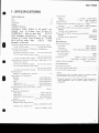
1. SPECIFICATIONS
Semiconductors
lCs
FETs .
Transistors
Diodes
J
2
41
31
Ampfifier Section
C o n t i n u oPuosw eO
r u t p uot f G 5 w a t t s -p e r
c h a n n em
l , i n . ,a t 8 o h m sf r o m2 0 H e r t zt o
2 0 , 0 0H
0 e r t z w i t hn om o r e
t h a n 0 . 0 2%
t o t a lh a r m o ndi ics t o r t i o n
r 6 5 w a t t sp e r
c h a n naetl 4 o h m sf r o m2 0 H e r ttzo 2 0 , 0 0 0
H e r tw
z i t hn o m o r et h a n 0 . 0 3 % t o t a l
h a r m o ndi ci s t o r t i o n .
C o n t i n u o u sP o w e rO u t p u t a t l k H z ( b o t hc h a n n e lds r i v e n )
T . H . D .0 . 0 2 y " , 8o h m s
. . 7 0 w a t t so e r c h a n n e l
T o r a l H a r m o n i cD i s r o r t i o n( 2 O H e r t zt o 2 0 , 0 0 0 H e r t z ,
8 o h m s ,f r o m A U X )
c o n t i n u o u rsa t e dp o w e ro u t p u t . . N o m o r et h a n0 . 0 2 %
3 2 . 5w a t t sp e rc h a n n epl o w e ro u t p u t
. . . . N o m o r et h a n0 . 0 2 %
'f
watt per channelpoweroutput . No more thanO.O2o/o
I n t e r m o d u l a t i oDni s t o r t i o n( 5 0 H e r t z :7 , 0 0 0 H e r t z= 4 : 1 ,
8 o h m s ,f r o m A U X )
continuousratedpoweroutput . . No more than0.02o/o
3 2 . 5w a t t sp e rc h a n n epl o w e ro u t p u t
. . . . . No more thano.}2o/o
1 watt per channelpoweroutput . No more thanO.O2o/o
DampingF actor
(20 Hertzto 20,000Hertz,8 ohms) .
35
I n p u t ( S e n s i t itvyi / l m p e d a n c e )
. . 2.5mV/5Okilohms
PHONO
. .l50mV/5Okilohms
TUNER
..150mV/50kilohms
AUX.
.....150mV/50kilohms
TAPEPLAYl,2 ..
T A P EP L A Y 2 ( D l N c o n n e c t o r ). . . 1 5 0 m V / 5 0 k i l o h m s
P h o n oO v e r l o a dL e v e l( T . H . D .0 . 0 1 % ,l k H z )
PHoNo
. " 2oomV
l pedance)
O u t p u t ( L e v e l /m
.1i?mYl1kilohm
TAPERECl...,
. ls0mV/lkilohm
:
T A P E R E C 2. . . . . . . . .
3OmV/8Okilohms
T A P E R E C2 ( D l N c o n n e c t o r )
. A, B, A+B (4 - 16ohms)
Speaker
FrequencyResponse
P H O N O( R I A A E q u a l i z a t i o n )
2 0 H zt o 2 0 , 0 0 0 H 2j 0 . 2 d B
TUNERA
, U X .T A P EP L A Y
1 0 H zt o 5 0 . 0 0 0 H 2 l . l d B
T o n eC o n t r o l
BASS.
... +7.5d8,-7.5d8(t00Hz)
TREBLE
+ 7 . 5 d 8 -, 7 . 5 d 8 ( 1 0 , 0 0 0 H 2 )
S u b s o n i cF i l t e r.
l5Hz (-6dB/oct)
L o u d n e sC
s o n t o u r( V o l u m ec o n t r o ls e ta t - 4 0 d 8
position)
. . . . + 6 d B( 1 0 0 H 2 ) , + 3 d B ( 1 0 , 0 0 0 H 2
H u m a n d N o i s e( l H F , s h o r t - c i r c u i t eAd ,n e t w o r k )
PHONO
....86d8
T U N E R ,A U X , T A P EP L A Y .
. IOOdB
H u m a n d N o i s e( D l N c o n t i n u o u p
sower/5OmW)
PHONO
TodB/6odB
T U N E R ,A U X , T A P EP L A Y .
86dB/61d8
Muting
-20d8
Miscellaneous
P o w e rR e q u i r e m e n t s
HAmodel
..220V,50/60H2
HR model
. ..240V,50160H2
S, SiG models
1 l0V/1 20V 1220v1240V,50/60H2
P o w e rC o n s u m o t i o n
HA,HRmodels
....600W
S,S/Gmodels
l90W
Dimensions
. . . . 4 2 0 ( W ) x 1 5 0 ( H )x 3 3 7 ( D )m m
1 6 - e l 1 6 ( wx) s - 7 l 8 ( H )x t 3 - 1 l 4 ( D )i n
W e i g h (t w i t h o u tp a c k a g e )
. . . . 9 . 7 k g( 2 1 t b . 6 o z )
Furnished Parts
O p e r a t i n gi n s t r u c t i o n s
F u s e2 . 5 A ( S ,S / G m o d e l so n l y )
F u s e5 A ( S ,S / G m o d e l so n l y ) .
1
1
I
NOTE:
Specificationsand the designsubject to possiblemodificationswithout notice due to improuements.
* Measuredpursuant to the FederanlTrade Commision's
Trade Regulation rule on Power Output Claims for
Amplifiers.
3. BLOCK DIAGRAM
MUTITIG
f275dBi
l ( f : 1 r H zI,
BALANCE
I
I
voLutiE
MODE I;I
S P E A K E RA
SPEAKER
B
[] exor,res
1UNER
FL TUEE
aux
TAPEOUPLICATE
rREC
TAPE I
L pllv
IB
FUNCT'ON
rREC
TAPE2
Lpr-lY
PHOr{O
SPEAKER
A
R CHANNEL(SAME AS L
CHANNEL)
TUNER
AUX
lREC
TAPEI
LPLAY
S P E A K E R8
R E C TFI I E R
POWER AI'P
RECTIFIER
INOICATOR DRIVE, FUNCTION IIiIDICATOR
POWER AMP
lREC
T A P E2
LP LAY
V OL T A G E
R E G UL A T O R
R E C T IF I E R
VO LIAGE
RE G U LAÎOR
AMP
TONE AMP
FL HEATER
4. CIRCUIT DESCRIPTIONS
4 . 1 P H O N OC I R C U I T
RF InterferenceFilter
Since the phono input circuit is extremely sensitive, it is adversely affected by radio frequency
interference. This interference is reduced by inserting a resistor in serieswith the phono input circuit
by setting the PHONO INTERFERENCE FILTER
switch on the rear panel to the ON position.
EqualizerAmplifier
The equalizer amplifier is a B-stage directcoupled amplifier with emitter-to-emitter feedback. An S-N ratio of SGdB (at 2.bmV input,
IHF-A, PHONO INTERFERENCE FILTER switch
OFF) has been achieved by using a ultra-low-noise
PNP transistor (2SAST8) at the first stage, and
reducing the signal source resistance and equalizer
element impedance.
The 2nd stage load has been reduced, a large
6
output voltage obtained, and the output impedance lowered by using an emitter follower at the
output stage.
Metal film resistors having a tolerance of. llTo
and polypropylene film capacitors having a toler_
ance of !2Vo are used on the NFB circuit to obtain
an equalizer deviation of within r0.2dB over the
2OHz to 2OOOOHz
range. The maximum allowable
input of this circuit is 20OmV (at 7kHz, THD
o.otTo).
4.2 TONE CONTROLS
The tone amplifier is a B-stage direct-coupled
amplifier with emitter-to-emitter feedback.
Tone control (BASS, TREBLE) is accomplished
_
by providing the tone amplifier NFB circuit with a
frequency characteristic. The NFB circuit is
changed to a flat frequency characteristic when
the TONE switch is in the OFF position.
sA-7clE|
O
BASS AND TREBLE CONTROLS
and the
Use these controls to adjust the bass
ON and turn
treble. If you set the tone switch to
position'
the bass control to right from its center
ômphasize tlne sound in the
Vo" *iff be able to
range' Conversely'turning the bass
io*-Tr"q.r"ncy
'to
you
the left from the center position'
"o"t-f
will attenuate the sound'
the
yor,
use the treble control to adjust
""n
sound in the high-frequency range'
@ TONE SWITCH
the bassand
Set this switch to ON when adjqsting
the tone contÀf" controls. When set to OFF'
and frequency
trol circuits are disengaged
is convenient for
,"rpot *" is flat' This function
phono cartridge and speaker tone
"tË"n"g
quality and listening room acoustlcs'
O
BALANCE CONTROL
of the left
Use this control to balancethe volume
the mode
however'-set
and right channels' First,
sound
the
that
so
adjust
,"f""to-t to MONO, and
beexactly
somewhere
appears to come from
to
appears
so.un$
the
lf
tween the two speakers'
that the volume
L"-foua"t on the right, it means
the balance
Turn
high"t'
it
oi tfr" right chann"l
adjust'
control to the left and
to be Iouder on
éî.ru"tt"fv, if th; sound-appears
volume of the left
the left, it means that tùô
the balance
is higher' Therefore' turn
After adjusting'
"iu"""f
control to the right and adigst'
ST'
iJutn the mode selectorto
SWITCH
@ SUBSONIC FILTER
to Xhe LSHz position-'-the
set
is
When this switch
frequency of 15Hz is
cut-off
a
wittr
subsonictitter
servesto attenuate
actuated. The subsonic filter
in a 6dB/oct slope'
îi"qr'r".r"i"t lower than 15Hz
suppressingultra-lowIt is therefore effective in
generated by record
frequency ,toi'!- *f i"h is
-a You cannot actually hear
*"ô *d other causes'
factor in th-e generation of
this noise Uut iils
and it may damage
intermodulation distortion
syitlh to the 15Hz
your speak"' 'V't"-' Set this
'p..itl""
best effect'
during'iecord play for the
@ MODE SELECTOR
the performances'
Use this selector for selecting
normal stereo refor
Set to this position
ST:
Production
right channel signalsand
MONO: rnri*"'îii'and
'"P'od''""t them monoPhonicallY'
@ FIJNCTION SELECTOR
Use this selectorto selectthe progtam source'
meter
When set, the function indicator above the
func'
the
of
position
the
to
p"""i
""it"sponding
uP'
light
tion selector will
broadcasts
iUNBn, Set here when listening to
jacks'
TUNER
the
to
connected
on a tuner
(The TUNER function indicator lights up')
on a
PHONô: Set here when playing records jacks'
turntable connected to the PHONO
(The PHONO function indicator lights up')
program source
AUX: Èet here when listening to a
jacks'
which is connected to the AUX
up';
lights
(The AUX function indicator
SWITCH
@ TAPEDUPLICATE
tape decks
Use this switch when employing two
This
tapes'
edit
or
to duplicate recorded tapes
position'
OFF
switch is otherwise kept at the
on a deck conltC: when playing back the tape
jacks
and recording
1
nected to thl TAPE
to the
connected
deck
a
(duplicating) on
jacks'
TAPE 2
duplicating'
OFF: Set to this position when not
a deck conon
tape
the
back
it1, wr,"n ptaying
jacks
recording
and
2
TAPE
th*e
nected to
to the
connected
deck
a
on
(duplicating)
TAPE l jacks'
@ TAPE MONITOR SWITCH
source which is
Use this to select the program
being reProduced'
,
or a tape
Set here to monitor a recording
1:
which is
tape.deck
being ptayed back on a
jacks'
1
connected to the TAPE
you are not playing back
OFF: Set t'"'" *nàtt"ver
(i'e' when
a tape or Àonitoring a recording
to
selector
function
the
you have set
alteran
for
i'ttOUO or TUNER' or AUX
source)'
native Program
or a tape
Set here tl monitor a recording
2;
which is
Ueing ptayàd Lack ol3 !".p"'deck
jacxs'
connectedto the TAPE 2
2. FRONT PANEL FACILITIES
E Po\ryER
SwITcH
@ LOUDNESSSWITCH
@ SPEAKER
sELEcToR
Use this selector to select the speaker
systems.
OFF: Sound not obtained from,pàJ"i.
A:
Sound obtained from spe'akers
ïonnectea
to the A speakerterminals.
Sound obtained from speakersconnected
to the B speakerterminals.
A+B: Sound obtained from speakers
connected
to both A and B speakerierminas.------'
@ PowERMETER
This meter allows you to read
out the rated
power level on the fluorescent
dispiay tube when
speakerswith a nominal i-puau""â
oï g ohms are
connected to the amplifier's speaker
terminals.
@ FIJNCTION INDICATORS
The TUNER, PHONO. AUX function
indicators
light up in accordance with
the position of the
function selector.
The function indicator wi|
not go off when the tape
monitor switch is set to position ,,î,,
or',',2J.'-""
@ VOLUME CONTROL
Usethis control t9 adjustthe output
tevelto the
speakersand headphones.Tum
it clocku,iseto
increasethe output tevel. No ;;"";
iuitt U" heard
if you setit to ,,b',
@ MUTING SWITCH
@ HEADPHONEJACK
Plug the headphonesinto
this jack when you
want to Iistenthroughyour stereo-fràaOphones.
NOTE:
t^3::!:r:i:r.rer
setector to oFF when tistening
ontvwith
siA-7cl8
4 . 3 P O W E RA M P L I F I E R
The first stage is a differential amplifier formed
by twin transistor, while the load circuit forms a
current mirror circuit. The current mirror serves
to make this stage operate in push-pull mode,
thereby eliminating the even numbered harmonics,
and doubling the gain.
The predriver stage is a Darlington connection,
while the load circuit forms a constant-current
source, thereby obtaining a high voltage gain.
The povver stage is a Darlington connection
pure-complementar5r SEPP circuit, employing an
high speed transistor. The high speed transistor
is a kind of IC consisting of a number of
small transistor being connected in parallel via an
emitter resistor. This provides excellent high
frequency characteristics comparable to those of
a small-signal transistor. Furthermore, because
there is no time constant in the NFB circuit in the
low-frequency region, amplification is possible
down to DC (DC inputs will be cut off, however,
by the input coupling capacitor of the power
amplifier.).
The circuit features described above provide an
extremely wide power frequency range (65W +
65W, 20Hz to 2OkHz,THD O.O2%,8s, ).
4 . 4 I N D I C A T O RC I R C U I T
The SA-708 output power and function indicators feature fluorescentindicator tube (FL tube).
In this tube. thermionic emissions from the cathode are acceleratedinto the fluorescent substance
of the segmentalanodes, resulting in the emission
of light. This tube is used to indicate numerals,
letters, and other symbols.
t c ( T A 7 3 1 8P )
s t G Na L l N
D El E C T O R
An outline of the FL tube drive circuit is shown
in Fig. 4-1. The output circuit signal is applied to
pin no.6 (4) of the IC (TA7318P-A).The IC contains a detector circuit, compressor (40dB), and
peak hold circuit for both left and right channels.
The dynamic range of the signal is thus contracted
by 40dB to obtain a "peak held" DC voltage.
The output power indicator segmentsof the FL
tube are driven by the HA12010 ICs (one for each
channel) equipped with 12 pairs of differential
amplifiers. These amplifiers are biasedat increasing
levels, so each amplifier will commence to operate
separately as the input level increases.And since
these amplifiers apply the voltages to the output
power indicator segments,each successivesegment
will light up in tum as the input level rises.
The function indicators are lit up as a result of
a voltage being applied to the corresponding function indicator segment according to the selected
positions of the FUNCTION switch.
4 . 5 P R O T E C T I O NC I R C U I T
The purpose of this circuit is to protect the
speakersand the power amplifier. The relay in the
output circuit is automatically opened in any of
the following cases;
1. During the "transient operations" when the
pov/er supply is tumed on and off.
2. Upon detection of an overload caused by a
short circuit in the load.
3. Upon detection of a DC voltage in the output
causedby component failure or accident.
t/2
COMPRESSOR
140 dB )
tc (HA t20ro)
oFFS€r COMPENSATOR
FLTJORESCENT
+1 5 V
FUNCT ION
INOICATOR
TU BE
FILAM E N T
Fig.4-1
I n d i c a t o rc i r c u i t
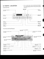
6. PARTS LOCATION
.
The L marh found on some component parts indicates
' the importance of the safety factor of the part' Therefore, when replacing, be sure to use parts of identical
designation
Front PanelView
Leverknob
AAD.183
Knob
AAB-2O2
Leverknob
AAD.183
O
Leverknobfr
AAD183
Leverknob
AAD-183
Knob
AAB-204
Knob
AAB.2O3
Leverknob
AAD.183
Leverknob
Knob
AAD-183
AAB.2O4
Front View with PanelRemoved
Leverswitch (LOUDNESS)
ASK.158
Variableresistor( V O L U M E }
ACV-181
indicatortube
Fluorescent
AAV.OO4
Rotaryswitch (SPEAKE
ASD-104
t;
Leverswitch (MUTING)
ASK.158
Leverswitch (POWER)
ASK.s15
Phoneiack (PHONES)
AKN.O23
Variableresistor(BASS,TREBLE
ACT-I17
Leverswitch (TONE
ASK.158
Variableresistor(BALANCE)
ACT-118
Leverswitch (TAPE)
ASK-160
Rotary switch (FUNCTION)
ASD.I18
Leverswitch (MODE)
ASK-158
Leverswitch (SUBSONIC)
ASK-158
I
Muting Operation When Power Supply is Turned
On and Off
With reference to Fig. 4-2 when the power supply is turned on, Qz tums off due to +Br and +Bz.
If there is no input (DC) on Qc and Qr, they will
be off, and the timing capacitor C, charges up
through R3 and D3 and thus Qr tums on. \[hen
Q3 conducts, the relay operates, and the output
muting on the power amplifier will be removed.
When the power supply is tumed off, +3, yill
abruptly decay, and Q, will conduct owing to the
residual component of +Br . As a result, Cz will
rapidly discharge,Qr will ceaseto conduct, whereupon the relay will become de-energized and
restore muting.
Overload Detector
The overload detector circuit incorporates the
load (RL) in one side of a Wheatstone bridge (see
Fig. 4-3). The baseand emitter of a sensingtransistor (Q, ) are connected to the opposite comers of
the bridge, so if RL decreases,Qr will become
forward biased. If RL falls below a prescribed
value, Qr will turn on, thereby pasdinga current
through R3 and Dr. Due to the voltage difference
generated across R:, Q, will become forward
biased, and consequently tum on. C, will rapidly
discharge.As consequence,Q3 will tum on and the
relay will become de-energized, thus causing the
output circuit to open.
DC Voltage Detector
The output circuit is connected to the Q5 emitter and Q+ base via a low-pass filter (Ro, C, ).
Any DC voltages appearingat the output circuit of
the power amplifier, will be applied to the e5
emitter and the Qa base. If the voltage is negative,
Q, turns on. Due to the voltage difference generared across Rr, Q, will become forward biased, and
consequently turn on. C, will rapidly discharge.
If the voltage is positive, Qc and e2 tums on. C,
will rapidly discharge. As consequence, e3 wiù
tum on and the relay will become de-energized,
thus causingthe output circuit to open.
RELAY
DRIVE
l:t e j
tQ4
i!4
î
@Overloaddetector
@PowerOFF detector
@DC voltagedetector
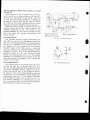
F i s . 4 - 2 Protectioncircuit
Fig. 4-3 Overload detector
sA-7ClE|
5. DISASSEMBLY
Top Cover
Removethe two screws(A) on eachside of the
top cover.
Bottom Plate
Remove the seven screu/s(B) and the rivet (C)
to detach the bottom plate.
Front Panel
Remove the all control knobs. Remove the four
nuts (D).
\@tnt
Front panel
N
sA-7clE|
Top View
Tape terminal assemblY
GWX-333
Terminalassembly
GWX-334
AF assembly
GWK-130
/r1Fuse(2.5
lj-\ AEK403
Switchassembly
GWS-194
FuseassemblY
GWX-337
SP switch
GWX-335
rl
Control âssembly
GWG-129
Mutingassembly
GWS.192
Volumeassembly
GWG-130
Rear Panel View
T e r m i n a l( I N P U T
AKB.O55
T e r m i n a (l S P E A K E B S )
AKE.O38
Slide switch-( P H O N OI N T E R F E R E N C E )
ASH-015
Terminal(TAPE
AKB-054
T e r m i n a l( T A P E2 l
AKB-054
Connectorsocket
AKP-O24
rll
4l
,,ô
Key No.
1.
A z.
A s.
4.
Part No.
Description
A8A-069
ATT-603
AEK-4o3
GWX-337
Screw 4xB
Power transformer
F u s e( 2 . 5 4 )
F u s ea s s e m b l Y
Wire saddle
5.
6.
7.
8.
9.
10.
11.
'12.
13.
14.
15.
AEC-446
A8A-069
P.C. Board holder
Screw 3x4
Frame
Foot assemblY
Screw 4xB
ABA-048
AWV-Oo4
GWX-336
GWG-I29
Angle
Screw 3x6
Indicator assemblY
Headphone assemblY
Control assemblY
ABA-025
16.
A rz.
18.
19.
20.
21.
22.
23.
24.
ASK.515
GWX.335
ABN-050
ABN-049
ABN-O3l
L e v e rs w i t c h ( P O W E R )
Cushion
SP switch assembly
Panel stay
Union nut
Union nut
Nut M7
Heat sink
Part No.
Description
25.
AEC-488
I n s u l a t o rs p a c e r
26.
27.
28.
29.
30.
2SC2525lAl-G
2SA1075lAl-G
ABA-208
Transistor
Transistor
Screw 3x 12
Frame
AF assembly
Key No.
GWK-I30
Volume assembly
Switch assembly
Frame
Rearpanel
R e c e s s e dp l u s ( A C I N L E T )
31.
32.
33.
34.
A ss.
GWG-130
GWS-I94
36.
37.
38.
39.
40.
AKE-038
GWX-334
GWX-333
ABA-228
ABA-057
T e r m i n a l ( S P E A K ER S )
Terminal assemblY
Tape terminal assembly
41.
42.
43.
44.
45.
ABA-157
ABA-115
ABA-116
ABE-005
Screw 3x8
Screw 3x10
Screw 3x6
Washer
T e r m i n a l( G N D )
AKP-oog
Screw 3x6
Screw 3x8
siA-7cla
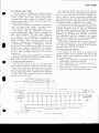
8. EXPLODEDVIEW
NOTE:
o Partswithout part number cannot be supplied'
o
of the
marh found on some component parts indicotes the importance
The A
parts
of
use
to
sure
be
replacing'
when
Therefore,
safety
factor of the pdrt
ide n t ical designa lion -
Part No.
Description
1.
2.
ABA-079
ANE-235
Screw 4x8
Top cover
3.
ANB-747
4.
5.
M4$086
871-O04
FrontPanelassembly
Washer
Key No.
AAD.183
Nut M9
Lever knob
Part No.
Description
7.
8.
9.
10.
AAB-204
AAB-202
AAB-203
Knob
Knob
Knob
Bottom Plate
11.
12.
ABA-048
AEC-525
Screw 3x6
Rivet
13.
822-017
Washer
Key No.
7. ADJUSTMENTS
I
ld le Current Adjustment
1. Tum the VOLUME control down to minimum
level, turn the power on, and wait about 10
minutes.
2. Connect a DC voltmeter to the TP terminals
(L ch; TP4 O and TP3 O, R ch; TPl @ and
TPz o) of the cWK-130.
3. Check that the voltage between Tp4 and Tp3
(L ch) lies within the DV DC 4mV- b0mV
range. Then make a similar check for the R ch
(between TP3 and TP4). If the voltage is less
than 4.4mV, cut jumper A (L ch), and jumper
B (R ch). If the voltage exceeds bOmV. check
for circuit failure-
I
B
Fis.7.1
Output Indicator Adjustment
Indicatorassembly
@-vR,
S-vn,
4. Adjust the VOLUME control so that
the volt199 on_the output terminals (SPEAKERS) read
ev (AC).
5. Adjust VRl (L ch) and VR2 (R
ch) of the
indicator assembly so that the output
power
indicator read 10 watts.
Panelstay
Fig.t.Z
10
i-
iAss'y (cWX-337)
II
l s,, PowER
I
20V /240V
50/6OHz
SPSWITCHAss'y(GWX-335)
J_
HEAD PHONEAss,y
(GWX-336)
NDICATORAss'y(AWV-004)
o
12
4
-Ji
îr':i:'-
I
3
J
gscHEMAT|cD|AGRAMS'P.c.BoARDPATTERNS
AND PARTS LIST
NOTES;
oWhenorderingresist-ors,firstconuertresistanceUaluesintocodeformosshoulntn
the following exam2tes
Lrtfrom 0)' such as 560 ohm
t
Ex.t When there are 2
ohm(tole
and47h
unlr:tt
t^ttri
o 5e
Is)
a
i,iritââltt
)'/'PSAaar
'/2HOBtrl i(
; 1 PO E O K
oRs
OIO
ich precision metal film resrcEx 2 When there are 3
tors).
R N t / t s RE ) G t r t r r
t
5. A
6 2e 1
5 i6l 2 .x. 1, not'
s ains
the importance of the
mdicates
parts
some component
o The A marh found on
"'i"'ï
sure to use parts of
be
*in''- 'l"placing'
ii"it"'"'
safetv factor tf ;;
identical designatton
9.1 MISCHELLANEA
MiscellanousParts
List of ChangedPartsfor Factory Modification
CAPACITORS
Part No.
CKDYF 473250
qvmhnl
& Descriptlon
c1-c4
SEMICONDUCTORS
Part No.
25A1075/A/-G
2SC2525lAl'G
Symbol & DescriPtion
01, 04
02, 03
OTHERS
Part No.
A arr-oos
l\ ner-aos
A nsr-sts
Symbol & Description
T1
FU1
sl 1
Powertransformer
Fuse (2 5A)
L e v e rs w i t c h ( P O W E R )
P.C.BOARD ASSEMBLIES
Part No.
Description
GWK-130
GWX-335
GWX.336
GWX.337
GWX.334
AF assembly
SP switch assembly
H e a d p h o n ea s s e m b l Y
F u s ea s s e m b l Y
Terminal assemblY
GWX-333
GWs-194
GW$193
GWS-192
GWG-130
Tape terminal assemblY
Switch assemblY
Mode assemblY
Muting assemblY
Volume assembly
GWG-129
AWV.OO4
Control assemblY
Indicator assemblY
f u r n i s h e dw h e n L i s t o f c h a n g e dp a r t s i n f o r m a t i o n w i l l b e
t
o amend parts
y
o
u
r
e
q
u
e
s
t
e
d
are
e v e r n e c e s s a r ya n d
n u m b e r i n t h i s P a r t sl i s t '
DIAGRAM
9.2 SCHEMATIC
NOTE:
The indicated semiconductorsare representatiueones
only. Other alternatiuesemiconductorsmay be usedand
are listed in the Partslist.
fl
r A P € T E R M I N À LÀ 3 ! t
I
I
cwx- 333
ÊFEc
6-
L.5
rt-----i
I:]o., ,r"r^* o,,u
I
ll-
Gwx-334
-1
I
o a o r- 5 0 4
AA
0507,50€ roE?
o50l 5@
2sc945A-Q
o509
POWEi
FoR
SUPPLY CIRCUIT
EURæE
MoÉL
^
o{r-404
rs20?6
Dal6
Mr-240
SA-7OE|
7
External Appearanceof
Transistorsand lCs
2SA968
2SC223A
2SD313
Type No
2SA733A
2SC94sA
hre
Type No
258507
:
(
2SA904A
2SC1914A
Suffrx-
254798
t
Type No
Lot No
Type No
hre
Type No
d
258682
2sD712
TA7318P
-Type
No
2SC1384
I/4q
t
(r) |
5\
r1.
(r F)/volraqe
voltage
volràqe
r.
r
foubd
rs
on
65î
nô
Dc
+
The.efô!e,
uhen
of
to
:ÀTE
65w
hre
HA12010
2SA949
Lot No
ùnr€ss
3
oùÈpùÈ(1kH2)
sighàI
thê
àt
2SC1400
porer
lated
parès
safety
2SA107slA/
2SC2525lA/
fàcto!
replàcin9/
idenÈrcèI
schenaÈrc
Cuê
role!ènce
except
component
of
ic
50v
votrage
some
Ior
(v)
inpur
rnportance
ârts
y
a!
)
is
àt
(v)
tâgé
ùnless
(x) ,
{c) ;:2i.
capàc!ry
thôut
toreràncê
be
desrqnation
diagrah,
rmproweûênts
but
Èhe
rn
dcsrqh
actùàl
æc2æ1
Tvpê
rr2-SOURCE-2,1
-20d8
ofF-
STEREO-MONO
2S4978
2SA1100
2SC1919
2s,C2575
TUNER-PHONO.ÀUX
orF-À-B-À+B
indicaÈes
the
seitch
posirion
7
I
td
9 SCHEMATICDIAGRAMS,P.C. BOARD PATTERNS
AND PARTS LIST
.
'
NOlES:
o When ordering resistors, first conuert resistanceualues into code form as shown in
the following examples.
Ex 1 When there are 2 effective digits (any dieit apart from 0), such as 560 ohm
and 47h ohm (tolerance is shown by J = 57", and K: l0o/o).
561......
. RDI/IPSE6AJ
56xlot
560st
473
. . R D % P SE i l E B J
47ha
47 x 103
jRs
RN2H @BE r
0.50
olo
....
RS/PEIIIOK
Js)
Ex 2 When there are 3 effectiue digits (such as in high precision metal film resis'
tors).
RNZas-R
s62 x t0'
s621, .
s.62kç
EEEEF
. The A marh found on some component parts indicates the importance of the
safety factor of the part. Therefore, when replacing, be sure to use parts of
ide nt ical designation.
9.1 MISCHELLANEA
Parts
Miscellanous
List of ChangedParts for Factory Modification
CAPACITORS
Part No.
CKDYF 473250
Symbol & Description
C1-C4
SEMICONDUCTORS
Part No.
2SA1075lAt-G
2SC2525lAl-G
Symbol & Description
01, 04
02, 03
OTHERS
Part No.
Symbol & Description
I err-eoa
A eex-qos
A nsr-srs
T1
FUl
sl 1
Power transformer
Fuse{2.5A)
Leverswitch (POWER)
P.C.BOARD ASSEMBLIES
Part No.
Description
GWK-130
GWX.335
GWX.336
GWX.337
GWX.334
AF assembly
SP switch assembly
Headphone assembly
Fuse assembly
Terminal assembly
GWX-333
GWS-I94
GWS-r93
GWS-I92
GWG-130
Tape terminal assembly
Switch assembly
Mode assembly
Muting assembly
Volume assembly
GWG-129
AWV.OO4
Control assembly
Indicator assemblY
List of changed parts information will be furnished whenever necessary and you are requested to amend parts
n u m b e r i n t h i s p a r t sl i s t .
10
i A s s ' y( G W X - 3 3 7 )
SPSWITCHAss'y(GWX-3351
12
H
HEAD PHONEAss'y
(GWX-336)
SPEAKERS
AB
NDICATORAss'y(AWV-004)
10
'12
T A P ET E R M I N A LA s s ' y( c W X3 3 3 )
Rrcr 100(
V O L U M E A s s ' y( G W G 1 3 0 )
MUTINGAss'y
TCUDNESS
Fh"r-
1
l.l-
I
l.|.JL'-"
i""
ffi1,.r"
[H
tï
*ifi t i*r
C O N T R O LA s s ' y ( G W S - 1 2 9 )
1S
T E R M I N A LA s s ' y
(GWX-334)
I
e2l
a
I
SWITCH
Ass'y
(GWS -1 e4)
I
) l
I
I
Se't,,
59'.
6
ï
â.+
li
l'n"
il
c(
.'_-
/
)É
Ae. t,
2w-
.,@o@
li
l+
^- .qOWER Tr
o@@_
tl
I
A F A s s ' y( c W K - 1 3 0 )
.
siA-7clEt
9 . 4 P A R T SL I S TO F P . C .B O A R DA S S E M B L I E S
AF Assembly(GWK-I30)
SEMICONDUCTORS
CAPACITORS
I
Part No.
Symbol & Description
Part No.
Symbol & Description
A ACH-212
A ACG-004
ccDsl 050D 50
ccDSL 270K 50
c c D S L 4 7 0 K5 0
c503, c504
c502, c505, c506
c 3 1 1 , C 3 1 2C
, 4 0 9 ,C 4 1 0
c413, C414
c401, c402
2SAg78
2SC1
9 19
(2SC1
400)
2S4949
2SA798_c
ccDSL 680K 50
ccDSL 221K 500
C K D Y B4 7 1K 5 0
coMA 473J 50
coMA 473J 250
c c D S L 1 0 0 K5 0
c405, c406, c407, c408
c 4 15 - C 4 1 8
c30s, c306, c319, c320
c421, C322
c411, C412
c425, C426
25C2291
2SA726S
25C2229
* 2SA968-Yor O
* 2SC2238-Y
or O
cosA 271J50
cosA 122G 50
coPA 183G50
coPA 683G 50
C E A N L3 R 3 M5 0
c301, c302, c509, c510
c315, C316
c 3 1 3 ,C 3 1 4
c 3 1 7 ,C 3 1 8
c303, c304, c403, C404
2SK34
25D112
( 2 5 D 3 13 )
2S8682
( 2 S 8 5 0 7)
CEANLNP 4R7M 50
CEANL 470M 16
CEANL 470M 35
cEA 010P 50
c E A 2 R 2 P3 5
C321,C322
C307,C308
C325
C517
C 5 11 . C 5 12
2SC945A
(25C2515)
0505. 0507, 0508
2SA733A
(2SA1100)
0506
2SA904A
o509
C E A R 4 7 P5 0
c E A 1 0 0 P1 6
c E A 1 0 0 P6 3
c E A 1 0 1 P1 6
c E A 1 0 1 P2 5
c419, C420
c 5 13
c 5 16
c 5 15
c424
2 S C 13 8 4
0 5 10
15 2 0 7 6
Irbt555'
1S 15 5 5
D401- D404,D411 -D41 4
c E A 1 0 1P 3 5
cEA 331P 63
c E A 4 7 1P 6
c E A 1 0 2 P5 0
c323, C324
c507, c508
c 3 0 9 ,c 3 1 0 ,c 5 1 4
c423
STV3H.Y
D 4 0 9 ,D 4 1 0
D 4 1 5 ,D 5 0 5 - D 5 0 8
RESISTORS
When ordering resistors, conuert the
resistance ualue into code form, and
then reutrite the part no. as before.
PartNo,
Symbol& Description
Note:
0301, 0302
0303, 0304
0305, 0306, 0409, 0410
o 4 0 1 ,0 4 0 2
0403, 0404
o405, 0406
0 4 0 7 ,0 4 0 8 , 0 4 1 5 , 0 4 1 6
4411,4412
o 4 1 3 ,o 4 1 4
* h f e o f o l 1 1 - O 4 1 4 s h o u l d h a v et h e s a m ev a l u e
A roez
( s r B o-l0 2 )
MZ-240
lwz-2401
A snsnu-a
0501, 0502
0503, o51 1
o504
D405- D408
D 4 16
MZ-177
D501-D504
D509
{wz-1771
MZ-150
D 5 10
(wz-150)
RD%PM trtrtr J
R303-R316, R325-R334. R337.
R 4 0 1- R 4 0 4 , R 4 0 7 - R 4 1 8 , F . 4 2 3 - R 4 2 6
R429-R436, R443-R446, R451-R454
R503-R510
R 5 12 - R 5 1 4
F.419-R422
RD%PM DlC J
RD%PM !!tr
I
J
A nozpu rrr L
RN7"SODO't]
RSlP OC! J
F
A Rozplvrrr.r
R D % P SC l O J
A ncN-oso
R S 2 Pt r l D J
:i_ Rozpsr rra
I
R317-R322
R 3 2 3 , R 3 2 4 , R 4 4 7 - R 4 5 0 , R 5 11
R335, R336
R42t.R428. R501, R502
R439-R442
R515, R516
R437, R43B
A rszazr
MZ440
D 5 11- D 5 1 4
D 5 15
(wz-140)
OTHERS
Part No.
ASD.l 18
ASR.O23
Symbol & Description
S9
RL1
R o t a r y s w r t c h( F U N C T I O N )
Relay
SPSwitchAssembly(GWX'335)
(GWG-I29)
control AssemblY
Note:
CAPACITORS
Symbol & DescriPtion
Part No.
Part No.
When ordering resistors,conuert the
resistance ualue into code form, and
then rewrite the part no. as before.
Symbol & DescriPtion
ccDsL 100D50
ccDSL 270K 50
CKDYB681K 50
coMA 392J 50
c205, C206
c 2 1 5 ,c 2 1 6
c 2 1 1 ,c 2 1 2
c219.C220
coMA 223J 50
coMA 104J50
c E A 1 0 0 P1 6
oEA220P 25
c E A 1 0 1 P1 0
c221, C222,C225, c226
c227, C22A
c209, C210
c233
c207, C208
c E A 1 0 1 P3 5
C E A N L N PO l O M5 0
CEANL 2R2M25
C E A N L3 R 3 M2 5
C E A N L3 R 3 M5 0
c231, c232
c229, C230
c217, C218
c223, C224
c201, C202
FuseAssembly(GWX-337)
C E A N L4 R 7 M5 0
c213, C214
Part No.
Symbol & DescriPtion
I ncc-oor
c501
Part No.
Symbol& DescriPtion
A R o z p un n r l
A C T - 11 7
ACT-118
R201-R207,R213,R214,R219-R236,
F.241-R243
R208-R212. R215, R216, R239, R240
R217.R218
R237, R238
V R 2 ,V R 3
VR4
V a r i a b l e( B A S ST, R E B L E )
(BALANCEI
Variable
2S4978
2SC1919
(2SC14001
2SA949
(2SA9051
RD%PM222J
ASH-O15
AKB-055
Symbol & Description
0201,4202
0203, 0204
0205, 0206
Symbol & Description
R301, R302
Slide switch
58
( P H O N EI N T E R F E R E N C E }
T e r m i n a l( I N P U T )
TapeTerminalAssembly(GWX-333)
Part No.
SEMICONDUCTORS
Part No.
P h o n ej a c k ( P H O N E S I
TerminalAssembly(GWX-334)
Pert No.
RDTAVS
CtrD J
RSl P trtrtr J
Symbol & Description
AKN-023
RESfSTORS
RD%PMlDtr J
R601.R602
R603. R604
R605, R606
R o t a r ys w i t c h( S P E A K E R S I
SlO
Assembly(GWX'336)
Headphone
Part No.
When ordering resistors, conuert the
resistance value into code form, and
then rewrite the part no as before.
Note:
RS2Ptrtrtr J
RD%PMtrtrtr J
RSlP trtrtrJ
ASD-104
RD%PM 394J
RD7.PM 1O4J
AKB-O54
AKP-024
Svmbol & Description
R 1 0 1R
, 102
Rl03, R104
Terminal {TAPEI
Connector socket
SwitchAssembly(GWS-I94)
Part No.
SYmbol & Description
SWITCH
Part No.
Symbol & Oescription
s6,s7
(GWS-I
93)
Mode Assembly
ASK-158
Part No.
RDy.PM 332J
A S K - 15 8
ASK-160
ASK-160
S1
S2
Leverswilch(DUPLICATEI
Leverswitch(TAPEMONITOR)
Lever (TONE, SUBSONIC)
Symbol & Description
R 1 0 9R
, 110
Leverswitch(MODEI
54
e
Muting Assembly (GWS-192)
Part No.
RD%PM 562J
RD%PM 473J
ASK-158
Symbol & Description
R 1 0 7 .R 1 0 8
R105,8106
Leverswitch(MUTING)
53
I