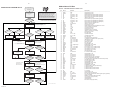
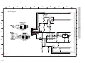
1
Compact Disc Player
CD753
/00 /01 /14
HIGHLIGHT SHUFFLE
OPEN
CLOSE
FADE
PLAY
CD TEXT
STOP
SCROLL
POWER ON / STANDBY
PROGRAM
DIGITAL OUTPUT
CD REWRITEA
BLE PLAYBACK
EDIT
PEAK
PREV.
PAUSE
NEXT
TIME
PHONES
COMPACT DISC
COMPACT
DISC
VOLUME
PLAYER CD
PLAYER
CD 753
753
Table of Contents
Technical Specification...................................................1-1
Location of Printed Circuit Boards ..................................1-2
Safety Instructions ..........................................................2-1
Instruction for use (excerpt)............................................3-1
Mechanical Instructions ..................................................4-1
Service Tools..................................................................5-1
Service Test Program.....................................................5-2
Blockdiagram..................................................................5-3
Wiring Diagram...............................................................6-1
HEADPHONE BOARD
Circuit Diagram .........................................................7-6
Component Layout....................................................7-6
CD BOARD
Circuit Diagram .........................................................7-7
Component Layout....................................................7-8
Fault Finding Tree CD...............................................7-9
EXPLODED VIEW
AF BOARD
Circuit Diagram Supply Part......................................7-1
Component Layout....................................................7-2
Circuit Diagram DAC Part .........................................7-3
Component Layout....................................................7-4
Set............................................................................10-1
CD Short Loader ......................................................10-2
Electrical Partslist ..........................................................10-3
FRONT BOARD
Circuit Diagram .........................................................7-5
Component Layout....................................................7-6
Safety regulations require that the set be restored to its original
condition and that parts which are identical with those specified
be used.
© Copyright
CLASS 1
LASER PRODUCT
1997 Philips Consumer Electronics B.V. Eindhoven, The Netherlands
All rights reserved. No part of this publication may be reproduced, stored in a retrieval
system or transmitted, in any form or by any means, electronic, mechanical, photocopying,
or otherwise without the prior permission of Philips.
Published by HB 9823 Service Audio
CS 53 132
Printed in The Netherlands
Subject to modification
© 4822 725 26026
1-1
TECHNICAL SPECIFICATION
General
Headphone output
Dimensions (WxHxD)
Weight
: 435 x 86 x 265mm
: 2,9kg
Accessories
Instruction for use
: 4822 736 16255 for /00
: 4822 736 16256 for /01
: 4822 736 16257 for /14
Remote control
: 4822 219 10538
: ≥5VRMS
: ≤1,2dB
: 120Ω
: 32Ω - 600Ω
: 25mW at 32Ω
: 52mW at 120Ω
: 29mW at 600Ω
Output level (1kHz, 0dB)
Unbalance left-right
Output impedance
Load impedance
Output power
Laser
Output power
Wavelength
: <5mW (3mW typ.)
: 780nm
Mains voltage
/00
/01
/14
: 220-230V(±10%) 50Hz
: 120/230V(±15%) 50/60Hz
: 220-230V(±10%) 50Hz
Measurement setup
Use Audio Signal disc SBC429 4822 397 30184
L
Power consumption
R
: ≤5W
: approx. 8W
stand by
operating
S/N and distortion meter
e.g. Sound Technology ST1700B
Audio performance
Number of channels
Output voltage (Line out)
Unbalance left-right
Frequency response
Signal to noise ratio
Dynamic range
THD
Channel separation
:2
: 2VRMS ±3dB
: ≤1dB
: 20Hz-20kHz ≤0,4dB
: 108 dB typ.
: 105dB typ. at 1kHz
: ≤0,0063% at 1kHz
: 98dB typ. at 1kHz
LEVEL METER
e.g. Sennheiser UPM550
with FF-filter
RC 5 Commands
System code = 20
Command
Code
Command
Code
Command
Code
KEY "0"
0
DISPLAY SCROLL
15
SHUFFLE
28
KEY "1"
1
PLAY
53
HIGHLIGHT
43
KEY "2"
2
STOP
54
REPEAT
29
KEY "3"
3
PAUSE
48
FADE
120
KEY "4"
4
TIME
11
VOLUME UP
16
KEY "5"
5
PREVIOUS
33
VOLUME DOWN
17
KEY "6"
6
REVIEW
50
STAND BY
12
KEY "7"
7
CUE
52
CD TEXT
88
KEY "8"
8
PROGRAM
36
NEXT
32
KEY "9"
9
REPEAT A/B
59
CS 53 133
1-2
LOCATION OF PRINTED CIRCUIT BOARDS
CS 53 134
2-1
©
ESD
WARNING
All ICs and many other semiconductors are susceptible to
electrostatic discharges (ESD). Careless handling during
repair can reduce life drastically.
When repairing, make sure that you are connected with the
same potential as the mass of the set via a wristband with
resistance. Keep components and tools at this potential.
f
ATTENTION
Tous les IC et beaucoup d´autres semi-conducteurs sont
sensibles aux décharges statiques (ESD). Leur longévite
pourrait être considérablement écourtée par le fait qu´aucune
précaution nést prise à leur manipulation.
Lors de réparations, s´assurer de bien être relié au même
potentiel que la masse de l´appareil et enfileer le bracelet
serti d´une résistance de sécurité.
Veiller à ce que les composants ainsi que les outils que l´on
utilise soient également à ce potentiel.
©
ñ
WAARSCHUWING
Alle IC´s en vele andere halfgeleiders zijn gevoelig voor
electrostatische ontladingen (ESD).
Onzorgvuldig behandelen tijdens reparatie kan de levensduur
drastisch doen vermindern. Zorg ervoor dat u tijdens reparatie
via een polsband met weerstand verbonden bent met hetzelfde
potentiaal als de massa van het apparaat.
Houd componenten en hulpmiddelen ook op ditzelfde potentiaal.
d
i
WARNUNG
Alle ICs und viele andere Halbleiter sind empfindlich
gegenüber elektrostatischen Entladungen (ESD).
Unsorgfältige Behandlung im Reparaturfall kann die
Lebensdauer drastisch reduzieren.
Sorgen Sie dafür, daß sie im Reparaturfall über ein Pulsarmband mit Widerstand mit dem Massepotential des
Gerätes verbunden sind.
Halten Sie Bauteile und Hilfsmittel ebenfalls auf diesem
Potential.
AVVERTIMENTO
Tutti IC e parecchi semi-conduttori sono sensibili alle scariche
statiche (ESD).
La loro longevità potrebbe essere fortemente ridatta in caso di
non osservazione della più grande cauzione alla loro
manipolazione. Durante le riparationi occorre quindi essere
collegato allo stesso potenziale che quello della massa
delápparecchio tramite un braccialetto a resistenza.
Assicurarsi che i componenti e anche gli utensili con quali si
lavora siano anche a questo potenziale.
AVAILABLE ESD PROTECTION EQUIPMENT :
anti-static table mat
large 1200x650x1.25mm
small 600x650x1.25mm
4822 466 10953
4822 466 10958
anti-static wristband
4822 395 10223
connection box (3 press stud connections, 1MΩ)
4822 320 11307
extendible cable (2m, 2MΩ, to connect wristband to connection box) 4822 320 11305
connecting cable (3m, 2MΩ, to connect table mat to connection box) 4822 320 11306
earth cable (1MΩ, to connect any product to mat or to connection box) 4822 320 11308
KIT ESD3 (combining all 6 prior products - small table mat)
4822 310 10671
wristband tester
4822 344 13999
SAFETY
©
ñ
Safety regulations require that the set be restored to its
original condition and that parts which are identical with
those specified be used.
Safety components are marked by the symbol
Veiligheidsbepalingen vereisen, dat het apparaat in zijn
oorspronkeliijke toestand wordt teruggebracht en dat
onderdelen, identiek aan de gespecificeerde, worden toegepast.
De Veiligheidsonderdelen zijn aangeduid met het symbool
f
i
Les normes de sécurité exigent que l`appareil soit remis
à l`état d`origine et que soient utilisées les pièces de
rechange identiques à celles spécifiées.
Les composants de sécurité sont marqués
Le norme di sicurezza estigono che l´apparecchio venga
rimesso nelle condizioni originali e che siano utilizzati i
pezzi di ricambiago identici a quelli specificati.
Componenty di sicurezza sono marcati con
©
DANGER: Invisible laser radiation when open.
AVOID DIRECT EXPOSURE TO BEAM.
d
Bei jeder Reparatur sind die geltenden Sicherheitsvorschriften zu beachten. Der Originalzustand des Gerätes
darf nicht verändert werden. Für Reparaturen sind Originalersatzteile zu verwenden.
Sicherheitsbauteile sind durch das Symbol
markiert.
CLASS 1
LASER PRODUCT
s Varning !
∂ Advarsel !
ß Varoitus !
Osynlig laserstrålning när apparaten är öppnad och
spärren är urkopplad. Betrakta ej strålen.
Usynlig laserstråling ved åbning når sikkerhedsafbrydere
er ude af funktion. Undgå udsaettelse for stråling.
Avatussa laitteessa ja suojalukituksen ohitettaessa olet alttiina
näkymättömälle laserisäteilylle. Älä katso säteeseen !
©
f
After servicing and before returning the set to customer
perform a leakage current measurement test from all
exposed metal parts to earth ground, to assure no
shock hazard exists.
The leakage current must not exceed 0.5mA.
"Pour votre sécurite, ces documents doivent être utilisés par
des spécialistes agréés, seuls habilités à réparer votre
appareil en panne".
CS 53 135
4
GENERAL INFORMATION
Maintenance ................................................................4
Technical data ..............................................................4
CONTROLS AND CONNECTIONS
Controls on the front....................................................5
Connections at the back ..............................................5
At the bottom...............................................................5
INSTALLATION AND REMOTE CONTROL
Accessoires ..................................................................6
Connections
Usual connection, LINE OUT ....................................6
Digital connection, DIGITAL OUT.............................6
Mains ...........................................................................6
Remote control.............................................................6
Batteries ...................................................................6
PLAYBACK
CD Text .........................................................................7
Playing a CD.................................................................7
ADDITIONAL FUNCTIONS
Selecting a track and searching
Selecting a track during CD play .............................8
Selecting a track when CD play is stopped.............8
Searching for a passage during CD play .................8
Random order playing (SHUFFLE) ................................8
Repeating a CD, a track or a program.........................8
Repeating a part of the CD..........................................8
Programming track numbers........................................9
Clearing the program ...................................................9
Loudest passage searching .........................................9
Time display .................................................................9
Fading out and in .......................................................10
Volume adjustment ....................................................10
Locking the volume ....................................................10
Headphone listening ..................................................10
Scanning the CD ........................................................10
Recording setup .........................................................11
Environmental information.........................................11
TROUBLESHOOTING
Warning......................................................................12
Troubleshooting..........................................................12
Table of contents
GENERAL INFORMATION
Maintenance
Standby power consumption .............................................< 5W
Frequency range ....................................................20–20,000Hz
Amplitude linearity ..................................< 0.5dB (1kHz, -90dB)
Dynamic range.......................................................100dB (1kHz)
Signal-to-noise ratio.........................108dB (1kHz, A-weighted)
Channel separation..................................................98dB (1kHz)
Total harmonic distortion.........................0.004%, -88dB (1kHz)
Audio output ...............................................2V RMS ±3dB, 1kΩ
Digital coaxial output.....................................75Ω acc. IEC 958
Impedance headphones .......30–600Ω (5V e. m. f. from 120Ω)
Dimensions ..................................................435 × 86 × 265mm
Weight................................................................................2.9kg
Subject to modification without notice.
Technical data
To clean a CD, wipe it in a straight
line from the center toward the edge
using a soft, lint-free cloth. A
cleaning agent may damage the disc!
Never write on a CD or attach a
sticker to it.
The lens may cloud over when the CD player is suddenly
moved from cold to warm surroundings. Playing a CD is not
possible then. Leave the CD player in a warm environment
until the moisture evaporates.
If the CD player cannot read CDs correctly use a commonly
available cleaning CD to clean the lens before taking the CD
player to repair. Other cleaning methods may destroy the lens.
Always keep the tray closed to avoid dust on the lens.
This CD player can play all kinds of Audio Discs such as
CD-Recordables, CD-Rewriteables and CD-Text CDs. Do not
try to play a CD-ROM, CD-I, CDV or computer CD.
Do not expose the CD player,
batteries or CDs to humidity, rain,
sand or excessive heat (caused by
heating equipment or direct sunlight).
Clean the CD player with a soft,
slightly dampened lint-free cloth. Do
not use any cleaning agents as they
may have a corrosive effect.
POWER ON / STANDBY
CD REWRITEAB
LE PLAYBACK
OPEN
CLOSE
4
5 6 7
PROGRAM
HIGHLIGHT
9
24
20 19
TIME
SCROLL
CD TEXT
8
EDIT
SHUFFLE
18
PEAK
FADE
17
PREV.
PLAY
VOLUME
NEXT
STOP
13
23
14 15
22
21
At the bottom
≤ VOLTAGE SELECTOR.........(Not on all versions.)
Disconnect the mains lead
first, if this selector must be
reset.
5
Connections at the back
¡ DIGITAL OUT......................to connect the digital input of
a digital audio device
™ LINE OUT L R .....................to connect the audio input of
an amplifier
£ Mains lead ...........................After all other connections
have been made, connect this
mains lead to the wall socket.
^ VOLUME .............................decreases or increases the
volume level of the
headphones
& PHONES..............................6.3mm headphone socket
* PEAK ...................................searches the loudest passage
of a CD
( EDIT.....................................changes the settings for
recording on tape or
CD-Recordable
) PROGRAM..........................programs track numbers
110
16
PHONES
PAUSE
10 11 12
Controls on the front
1 POWER ON / STANDBY...switches the CD player on and
to standby
2 OPEN·CLOSE......................opens and closes the CD tray
3 Sensor for the infrared remote control
4 Display
5 TIME ....................................switches through the different
time information
6 SCROLL ...............................scrolls CD-Text information
7 CD TEXT..............................switches through the different
CD-Text information
8 HIGHLIGHT.........................plays the beginning of each
track or – if a CD-Text disc
contains highlights – the
highlights of a CD
9 SHUFFLE .............................plays a CD or a program in
random order
0 FADE....................................fades CD play out and in
! PREV. ∞ .............................selects the beginning of the
current or a previous track,
and searches backward
@ PLAY 2................................starts CD play
# PAUSE ;..............................interrupts CD play
$ STOP 9 ...............................stops CD play and clears a
program
% NEXT §..............................selects the beginning of a
subsequent track, and
searches forward
1
2
3
CONTROLS AND CONNECTIONS
3-1
INSTRUCTION FOR USE
English
CS 53 136
English
CS 53 137
English
6
Note: To disconnect the CD player from the mains completely,
remove the mains plug from the wall socket.
2 Connect the mains cable to the wall socket. This switches
on the mains supply.
1 If your set is equipped with a VOLTAGE selector (at the
bottom), set this selector to your local mains voltage if
necessary. Position 120V includes 110V–127V. Position
230V includes 220V–240V.
The type plate is located on the back of the CD player.
Mains
2 Insert the other side of the cable into the digital input of
your digital device (e. g. CD Recorder).
PE
AT
A/B
ST
OP
NE
+
XT
T
A
PE
RE
1 Insert an optional coaxial cable into DIGITAL OUT.
RE
PA
US
E
0
Digital connection, DIGITAL OUT
Never connect this socket to a non-digital input – such as
AUX, CD, PHONO, TAPE – of an amplifier. This output supplies
a digital signal and can therefore only be connected to a
digital input.
LL
PRO
GRA
M
6
You may also use the TUNER or TAPE, but never the PHONO
input of your amplifier!
RO
ME
8
Important!
SC
VO
LU
1
9
AY
4
E
FAD
ER
TIM
3
2 Insert the other side of the cable into the corresponding
sockets of the CD or AUX input of your amplifier.
XT
PL
7
y
E
FL
UF
SH
TIME......................switches through the different time
informations
y ............................switches the CD player to standby
PROGRAM............programs track numbers
FADE......................fades CD play out and in
SHUFFLE ...............plays a CD or a program in random order
Digits 1–0...............selects a track by number
HIGHLIGHT...........plays the beginning of each track or – if a
CD-Text disc contains highlights – the
highlights of a CD
REPEAT .................repeats a track, a program or the entire
CD
VOLUME – ............decreases the volume level
VOLUME + ............increases the volume level
PLAY 2..................starts CD play
PREV. J..................selects the beginning of the current or a
previous track
NEXT K ..................selects the beginning of a subsequent
track
STOP 9 .................stops CD play and clears a program
5...........................searches backward
PAUSE ;................interrupts CD play
6...........................searches forward
CD TEXT................switches through the different CD-Text
information
SCROLL .................scrolls CD-Text information
REPEAT A/B .........repeats a selected part of the CD
Batteries contain chemical substances, so they should
be disposed of properly.
Remove batteries if they are flat or the remote control is not
going to be used for a long time.
Batteries
• Open the battery compartment of the remote control and
insert 2 alkaline batteries, type AAA (R03, UM-4).
TE
EV
.
SCA
N
2
Usual connection, LINE OUT
1 Insert the red plug of the supplied connection cable into R
and the other plug into L.
CD
PR
–
Remote control
5
Connections
This CD player is supplied including:
– a remote control
– 2 batteries for the remote control
– a connection cable
– this instruction booklet
Accessories
INSTALLATION AND REMOTE CONTROL
EDIT
PEAK
FADE
PREV.
PLAY
PAUSE
PHONES
VOLUME
NEXT
STOP
5 CD-Text information is scrolled every 30 seconds. Press
SCROLL to scroll the text through the display any time.
4 At the beginning of a new track the track title is scrolled
once. Then the first 12 digits of the track title are
displayed.
3 Press CD TEXT during CD play to switch between album
title, performing artist(s) and track title if available.
2 Press CD TEXT before playing a CD to switch between
album title and performing artist(s) if available.
1 When inserting a disc with CD-Text the display shows
CD TEXT and performing artist or group. In case there are
various artists the album title is shown.
Note: Playback will also stop if the end of the CD is reached.
5 Press STOP 9 to stop CD play.
• You can interrupt CD play by pressing PAUSE ;.
y
The display shows
and the track number and time
where playback was stopped.
• Continue CD play by pressing PAUSE ; again.
7
4 Press PLAY 2 to start CD play.
y
The display shows , TRACK, TIME, and the number and
time of the actual track. If the disc contains CD-Text the
display shows CD-Text information.
3 Insert an audio CD (printed side up) and press OPEN·CLOSE
to close the CD compartment.
y
READING appears on the display. Then the number of
tracks and the playing time is shown. If the disc
contains CD-Text the display shows CD TEXT and
CD-Text information (see “CD-Text”).
2 Press OPEN·CLOSE to open the CD tray.
y
OPEN appears on the display.
Playing a CD
PROGRAM
SHUFFLE
1 Use POWER ON / STANDBY to switch on the CD player.
TIME
HIGHLIGHT
CD-Text
CD REWRITEA
BLE PLAYBACK
CD TEXT
SCROLL
This CD player can show information which is stored on CDText discs. It will only reproduce the text which is recorded on
the disc.
POWER ON / STANDBY
OPEN
CLOSE
PLAYBACK
3-2
INSTRUCTION FOR USE
English
PROGRAM
HIGHLIGHT
EDIT
SHUFFLE
PEAK
FADE
PREV.
PLAY
PAUSE
PHONES
VOLUME
NEXT
STOP
8
Note: In the shuffle and repeat mode and when playing a
program, searching is only possible within the
particular track.
2 Release the button when you have reached the desired
passage.
Searching for a passage during CD play
1 Hold down PREV. ∞ or NEXT § (5 or 6 on the remote
control) to find a particular passage in a backward or
forward direction.
y
CD play continues at a low volume.
2 Press PLAY 2 to start CD play.
y
Playback starts with the selected track.
Selecting a track when CD play is stopped
1 Briefly press PREV. ∞ or NEXT § (PREV. J or NEXT K on
the remote control) once or several times.
or
• Use the digits 1–0 on the remote control to key in the
number of a track.
Selecting a track during CD play
• Briefly press PREV. ∞ or NEXT § (PREV. J or NEXT K on
the remote control) once or several times to skip to the
beginning of the current, previous or subsequent track(s).
or
• Use the digits 1–0 on the remote control to key in the
number of a track.
y
CD play continues with the selected track.
Selecting a track and searching
TIME
SCROLL
CD TEXT
ADDITIONAL FUNCTIONS
Random order playing (SHUFFLE)
4 Press PLAY 2 to return to normal CD play.
3 Press REPEAT A/B on the remote control to mark the end of
the passage to be repeated.
y
REPEAT A-B is shown in the display. The part of the CD
between the marked points is played repeatedly.
2 Press REPEAT A/B on the remote control to mark the
beginning of the passage to be repeated.
y
REPEAT is shown and A- is flashing in the display.
1 Press PLAY 2 to start CD play.
Repeating a part of the CD
Note: It is possible to activate the different playing modes at
the same time, e. g. you can repeatedly play the entire
CD or program in random order (PROGRAM REPEAT SHUFFLE).
2 Press REPEAT until the display indication disappears to
return to normal CD play.
1 Press repeatedly REPEAT on the remote control during CD
play.
y
The display shows the different repeating modes.
REPEAT 1: the current track is played repeatedly.
REPEAT: the entire CD or program (if available) is played
repeatedly.
Repeating the CD, a track or a program
2 Press SHUFFLE again to return to normal CD play.
1 Press SHUFFLE before or during CD play to start shuffle
play.
y
SHUFFLE is shown in the display. All the tracks of the CD
(or program if available) will now be played in random
order.
PROGRAM
HIGHLIGHT
EDIT
SHUFFLE
PEAK
FADE
PREV.
PLAY
PA
Note: If you try to store more than 30 tracks
PROGRAM FULL scrolls through the display.
6 Press PLAY 2 to start program play.
• It is possible to review the program using the PREV. ∞ or
NEXT § (PREV. J or NEXT K on the remote control). You
can add more tracks by pressing PROGRAM like you have
done before.
5 Press STOP 9 to end programming.
y
PROGRAM lights permamently.
4 Repeat steps 2 and 3 for all tracks to be programmed.
3 Press PROGRAM to store the track number.
y
TRACK, TOTAL TIME, and the number of the programmed
track is displayed. The number of programmed tracks is
increased and the time of the track is added to the total
time of the program.
2 Press PREV. ∞ or NEXT § (PREV. J or NEXT K on the
remote control) to select the desired track.
or
• Key in the number of a track with the digits 1–0 on the
remote control.
Note: If you press PROGRAM while playing a CD, the actual
track will be added to the program.
1 Press PROGRAM to start programming.
y
PROGRAM flashes.
You can select a number of tracks and store these in the
memory in the desired sequence. You can store any track
more than once. At most, 30 tracks can be stored in the
memory.
Programming track numbers
TIME
SCROLL
CD TEXT
Note: If you press TIME when the CD is not playing you may
only display the total time of the CD.
9
• Press TIME several times to display:
y
If the disc contains CD-Text, the number and elapsed
time of the actual track, and TIME are displayed first.
y
The number and remaining time of the actual track, and
REM TIME.
y
The number of the actual track, the total elapsed time
of the CD, and TOTAL TIME.
y
The number of the actual track, the total remaining time
of the CD, and TOTAL REM TIME.
While playing a CD or a program the number and elapsed
time of the actual track, and TIME are displayed. If the disc
contains CD-Text the display shows CD-Text information (see
“CD-Text”).
You can display time information which is stored on the CD.
Time display
3 Press STOP 9 to stop playing.
or
• Press PLAY 2 to start CD play.
• You can interrupt peak play by pressing PAUSE ;. Continue
peak play by pressing PAUSE ; again.
2 Press PEAK to start searching.
y
PEAK starts flashing. Searching may need a few
minutes. Then 4 seconds of the loudest passage are
played repeatedly.
1 If necessary press STOP 9 to stop CD play.
You can search for the loudest passage of a CD or program.
This will help you in adjusting your recording device if
required.
Loudest passage searching
Note: The program will also be cleared if you open the tray.
2 Press STOP 9 to clear the program.
y
PROGRAM CLEARED scrolls through the display,
PROGRAM disappears and your program is cleared.
1 If necessary press STOP 9 to stop program playing.
Clearing the program
ADDITIONAL FUNCTIONS
3-3
INSTRUCTION FOR USE
English
CS 53 138
English
CS 53 139
English
PROGRAM
HIGHLIGHT
EDIT
SHUFFLE
PEAK
FADE
PREV.
PLAY
PAUSE
PHONES
VOLUME
NEXT
STOP
Locking the volume
10
Note: If you press VOLUME –/+ and the volume is locked the
display shows VOLUME FIXED.
• Keep EDIT pressed for more than 2 seconds.
If the voulme was unlocked:
y
The display shows VOLUME FIXED and the volume
is locked.
If the voulme was locked:
y
The display shows VOLUME MAX and the volume is
unlocked.
It is possible to lock the output volume to its maximum. This
affects the DIGITAL OUT output as well. Locking the volume
can be usefull when recording from the CD-player.
Note: If you press HIGHLIGHT while SHUFFLE is active,
shuffle will be stopped before scanning.
3 Press STOP 9 to stop scanning.
or
• Press PLAY 2 to start CD play with the actual track.
Important!
VOLUME –/+ is altering the signal of the output. Before
recording set the volume to VOLUME MAX and do not
change during recording.
• You can interrupt scan by pressing PAUSE ;. Continue scan
by pressing PAUSE ; again.
2 As soon as the desired scan mode is displayed do not press
the button again.
y
After 1 second scanning starts. The number and
remaining time of the actual track, and REM TIME are
displayed.
1 Press HIGHLIGHT repeatedly to switch through the different
scan modes.
y
HIGHLIGHT, SCAN 10, SCAN 20, SCAN 30,
SCAN OFF… (SCAN OFF aborts the scan function).
It is possible to listen to the beginning of each track of a CD
or program. You can choose whether to play 10, 20 or 30
seconds of each track. If a disc contains CD-Text highlights
this part of the tracks is scanned and HIGHLIGHT is
displayed.
Scanning the CD
The volume of the headphones is in line with the volume of the
output. Therefore do not use VOLUME –/+ during recording.
Important!
Note: The maximum volume on the headphones is set through
VOLUME –/+ on the remote control.
2 Use VOLUME to adjust the volume of the headphones.
1 Connect your headphones to the 6.3mm PHONES socket.
Headphone listening
• Press VOLUME – or VOLUME + on the remote control.
y
The volume of the CD player is lowered or raised. The
display shows the actual value between
VOLUME MIN and VOLUME MAX.
The volume of the CD player can be adjusted. This affects the
DIGITAL OUT output as well.
Volume adjustment
Note: You may use FADE anytime when CD play is paused to
fade in.
2 Press FADE again to fade in.
y
The display shows
in steps. CD play starts and the
volume is raised continuously to its previous level.
1 Press FADE during CD play to fade out.
y
The display shows
in steps. The volume is lowered
continuously until CD play is paused.
You can fade out and in CD play, e. g. to stop and start a
recording softly.
Fading out and in
TIME
SCROLL
CD TEXT
ADDITIONAL FUNCTIONS
PROGRAM
EDIT
SHUFFLE
PEAK
FADE
PREV.
PLAY
PA
All redundant packing material has been omitted. We have
done our utmost to make the packaging easily separable
into three mono materials: cardboard (box), polystyrene foam
(buffer) and polyethylene (bags, protective foam sheet).
Environmental information
4 As soon as the desired edit mode is displayed press EDIT.
y
The display shows C 90.
➢
3 Press PREV. ∞ or NEXT § (PREV. J or NEXT K on the
remote control) to switch through the different scan modes.
y
NORMAL, OPTIMAL, STOP… (STOP aborts the edit
function).
2 Press EDIT to start the setup.
y
The display shows EDIT and NORMAL.
1 Insert a CD and, if desired, program track numbers.
If you use NORMAL the recording stops after the last track
that fits on one side of your recording media. Notice that CDRecordables are single-sided only! If you use OPTIMAL
some tracks will be skipped to minimise the unused space on
your recording media. The sequence of the tracks stays as the
original.
It is possible to set up the CD player in a way that it will
calculate which tracks will fit on your recording media. It is
only possible to use the edit function if a disc has not more
than 29 tracks.
Recording setup
TIME
SCROLL
CD TEXT
HIGHLIGHT
Your set consists of materials which can be recycled if
disassembled by a specialized company. Please observe the
local regulations regarding the disposal of packing
materials, exhausted batteries and old equipment.
11
Note: It is possible to switch between A and B by using
PREV. ∞ or NEXT § (PREV. J or NEXT K on the remote
control).
9 Press PLAY 2 to start CD play again.
y
B, the number of tracks and the playing time are
displayed. The remaining tracks for side B are played.
8 If required switch tape sides.
7 Start your recording and press PLAY 2 to start CD play.
y
If cassette (C) was selected the CD player pauses after
playing the calculated tracks for side A. If CDRecordable (CDR) was selected the CD player stops.
6 As soon as the desired recording time and media is
displayed press EDIT.
y
A, the number of tracks and the playing time are
displayed.
Note: C is for cassette, CDR is for CD-Recordable and
CD-Rewriteable and therefore for single-sided
recording only.
5 Press PREV. ∞ or NEXT § (PREV. J or NEXT K on the
remote control) to switch through the different recording
times and media.
y
C 100, C 120, CDR 21, CDR 60, CDR 74,
C 30, C 45, C 60, C 90…
ADDITIONAL FUNCTIONS
3-4
INSTRUCTION FOR USE
English
4-1
MECHANICAL INSTRUCTIONS
Dismantling Top Cover
1) Loosen 7x screw as shown in picture 1.
picture 1
2) Lift top cover as shown in picture 2.
3) Remove top cover.
picture 2
CS 53 140
4-2
MECHANICAL INSTRUCTIONS
Dismantling Front
1) Loosen 2x screw as shown in picture 3.
Bottom view
picture 3
2) Release 2x snap on bottom (see picture 3).
3) Release 2x snap on side (see picture 4).
4) Remove front.
Side view
picture 4
CS 53 141
4-3
Dismantling hints CD Short Loader
Dismantling the tray
a) Press open/close button to open the tray. If the tray
doesn´t work, use a small screwdriver as shown in Fig.1
step 1 to move the tray outside. After the first centimetre
it is possible to pull the tray out by hand.
b) Release two snaps and remove tray.
Fig. 1
CS 53 142
4-4
Assembly of gear
a) Use a pin (e.g. a paperclip) to align the cam wheel (a)
with the gear wheel (b). See Fig. 2.
b) Fix the wheels with the small plastic washers.
Fig. 2
CS 53 143
4-5
c) Mount idle wheel 2 (c) and idle wheel 1 (d) in any
position. See Fig. 3.
d) Fix the idle wheel 1 (d) with the small plastic washer.
e) Mount the driving belt.
Fig. 3
f) Mount the pinion guiding assy and the cover as shown in
Fig. 4.
g) Turn the gear wheel (b) counter clockwise to
endposition.
Fig. 4
h) Mount the CD Mechanism as shown in Fig. 5.
i) Mount the tray (Align the tray to the chassis and push it
inside).
Check if tray mechanism works correctly!
1) Turn the gear wheel (b) clockwise to its endposition
(Use a small screwdriver as shown in Fig. 1 step 1).
The tray has to move to inner position first and then the
CD mechanism has to move to its upper position.
2) Turn the gear wheel (b) counter clockwise to its
endposition.
Fig. 5
The CD Mechanism has to move to its lower position first
and then the tray has to move outside.
CS 53 144
5-1
HANDLING CHIP COMPONENTS
SERVICE TOOLS
TORX T10 screwdriver with shaftlength 150mm ......................................4822 395 50423
TORX screwdriver set T6 - T20 SBC 163...............................................4822 395 50145
Audio signal disc SBC 429......................................................................4822 397 30184
Playability test disc SBC444/444A..........................................................4822 397 30245
Test disc 444 (disc without errors) +
Test disc 444A (disc with dropout errors, black spots and fingerprints)
Burn in test disc SBC442 ........................................................................4822 397 30155
(65 min. 1kHz signal at -30dB level without "pause")
CS 53 145
5-2
5-2
To start service test
program hold
PLAY & PAUSE depressed
while plugging in
the mains cord
SERVICE TEST PROGRAM
Display shows number of
ROM version
"S Vzz"
S
stands for Service Testprogram
V stands for Software Version
zz version number counted from 01 upwards
KEY
TEST
DISPLAY
TEST
N
SHUFFLE
Button pressed?
QUARTZ
TEST
TIME
Button pressed?
N
PROGRAM
Button pressed?
Y
Y
Display shows "--"
Display shows Fig. 1
any key pressed?
TIME
Button pressed?
N
CD
TEST
N
CD PLAY
TEST
NEXT
Button pressed?
Y
N
Y
Display shows
8M
Output at
pin80 of 7800=1953,125Hz
FOR CD TEST
see next page
STOP
Button pressed?
Y
In case of failures error codes
according table 2 will be
displayed.
Y
TIME
Button pressed?
The CD PLAY Test is intended
to be used for continuously playing
a disc in order to detect intermittend
or not reproducible failures.
The error code indicates where the
failure can be found.
N
KEY TEST
CD PLAY TEST
Key
Number
Next
1
Key
Number
Key
Number
7
Fade
13
Shuffle
Previous
2
Scan
8
Time
14
Play
3
Program
9
CD-Text
15
Stop
EXIT
Peak search
10
Scroll
16
Open/Close
5
Repeat
11
Stand by
17
Edit
6
Pause
12
any RC button
RC
Error number
Type
W
Focus error
Triggered when the focus could not be found within a certain time when starting up the CD or
when the focus is lost for a certain time during playing the CD.
1001
W
Radial error
Triggered when the radial servo is not on track for a certain time during playing the CD.
1002
W
Slide in error
Generated when the slide did not reach its inner position (innerswitch is closed) before 6 seconds
have passed by. Innerswitch or slide motor problem.
1003
W
Slide out error
Generated when the slide did not come out of its inner position (innerswitch is open) before 250ms
have passed by. Innerswitch or slide motor problem.
1005
W
Jump error
Generated when the jump destination could not be found within a certain time.
1006
W
Subcode error
No valid subcode for a certain time.
1007
W
PLL error
The Phase -Lock-Loop could not lock within a certain time.
1008
W
Turntable motor error
Generated when the CD could not reach 75% of speed during starting up within a certain time.
Disc motor problem
1020
F
Focus search error
Focus point has not been found within a certain time.
DISPLAY TEST
PROGRAM SHUFFLE REPEAT 1A-B SCAN TRACK
TOTAL REM TRACK TIME
CD TEXT
1
2
3
4
5
6
7
8
9
10 11 12 13 14 15 16 17 18 19 +
Fig. 1
CD TEXT
Description
1000
Table 1
PEAK
Display becomes dark
Set is in stand by
Display shows Fig. 2
N
STOP
Button pressed?
Y
Set works as in normal Mode.
N
Y
Display shows
corresponding key number
(see table 1)
N
N
Y
Y
PLAY
Button pressed?
Table 2
PEAK
3
4
7
10
Fig. 2
13
16
19 +
W = Warning
Error number remains on display till next warning/error
F = Fatal error
Set stops playing → Error number remains on display
Service Test Program CD713/CD723 (980429)
CS 53 146
5-3
5-3
Abbreviations CD Part
SERVICE TEST PROGRAM CD-Part
To start service test
program hold
PLAY & PAUSE depressed
while plugging in
the mains cord
SAA7372 – DECODER AND DIGITAL SERVO IC CD7
Pin
Since the CD-RW reflects much less light than an ordinary
CD-A, the gain of the HF-amplifier stage and the sensitivity
of the ADC inside the signal processor must be increased.
The gain is switched via the HG line (pin41 of CD7), the
ADC-sensitivity is switched via software (µP → CD7).
During start-up the correct mode is choosen automatically;
in the service test program it can be switched manually in
order to allow individual measurements in both conditions.
Display shows number of
ROM version
"S Vzz"
NEXT
Button pressed?
N
NOTE: If sensitivity is switched to high
the set will not work with normal Audio CDs!
Y
Motor Test
Display shows
CD
STOP button pressed in any step returns
to begin of Service Testprogram.
Disc Motor
SHUFFLE
Button pressed?
N
Slide Motor
PROGRAM
Button pressed?
Y
N
Y
Disc Motor turns CCW
Display shows
Disc Motor turns CW
Display shows
CCW
CW
N
NEXT
Button pressed?
PLAY
Button pressed?
Y
Y
Slide moves inside
Slide moves outside
Y
PREV
Button pressed?
Focus Servo Test
Sensitivity can be toggled
via EDIT Button.
Display shows
FOC XXX
CD RW resp. CD NORM is displayed
FOC ERR = Focus not found
FOC OK = Focus found
for two seconds.
N
STOP
Button pressed?
FOCUS found?
Y
Y
Display shows
Display shows
FOC ERR
FOC OK
N
N
PLAY
Button pressed?
STOP
Button pressed?
Y
N
Y
Disc Servo Test
Disc speeds up
Display shows
It is possible to control the
slide motor with the
NEXT & PREV button
DISC
N
PLAY
Button pressed?
In case of focus lost FOC ERR
will be displayed and
Focus Servo Test is entered again
STOP
Button pressed?
N
Y
Y
Radial Servo Test
Display shows
RDL
N
PLAY
Button pressed?
Y
STOP
Button pressed?
N
Y
STP-CD Part CD713/CD723 (980429)
CS 53 147
Name
Direction
Description
–––––––––––––––––––––––––––––––––––––––––––––––––––––––––––––––––––––––––––––––––––––––––––––––––––––––––––
1 VSSA1
GND
supply (analog) of CD7
2 VDDA1
+4V
supply (analog) of CD7
3 D1
HF-preamp → CD7
unipolar current input (central diode signal input)
4 D2
HF-preamp → CD7
unipolar current input (central diode signal input)
5 D3
HF-preamp → CD7
unipolar current input (central diode signal input)
6 VRL
GND
reference input for ADC
7 D4
HF-preamp → CD7
unipolar current input (central diode signal input)
8 R1
HF-preamp → CD7
unipolar current input (satellite diode signal input)
9 R2
HF-preamp → CD7
unipolar current input (satellite diode signal input)
10 IREFT
→ CD7
current reference for calibration ADC
11 VRH
not connected
reference output from ADC
12 VSSA2
GND
supply (analog) of CD7
13 SELPLL
+4V
selects whether internal clock multiplier PLL is used
14 ISLICE
CD7 →
current feedback from data slicer
15 HFIN
→ CD7
comparator signal input
16 VSSA3
GND
supply (analog) of CD7
17 HFREF
→ CD7
comparator common mode input
18 IREF
→ CD7
reference current pin (nom. VDD/2)
19 VDDA2
+4V
supply (analog) of CD7
20 TEST1
GND
test control input
21 CRIN
X-Tal → CD7
crystal/resonator input
22 CDOUT
X-Tal → CD7
crystal/resonator output
23 TEST2
GND
test control input
24 CL16
not connected
16.9344MHz system clock output
25 CL11
not connected
11.2896MHz or 5.6448MHz clock output (3-state)
26 RA
CD7 → servo driver
radial actuator output
27 FO
CD7 → servo driver
focus actuator output
28 SL
CD7 → servo driver
slide actuator output
29 TEST3
GND
test control input
30 VDD1P
+4V
supply (digital) of CD7
31 DOBM
CD7 → digital output
bi-phase mark output (3-state)
32 VSS1
GND
supply (digital) of CD7
33 MOTO1
CD7 → servo driver
motor output1 of CD7; versatile (3-state)
34 MOTO2
CD7 → servo driver
motor output2 of CD7; versatile (3-state)
35 SBSY
not connected
subcode block sync (3-state)
36 SFSY
not connected
subcode frame sync (3-state)
37 RCK
GND
subcode clock input
38 SUB
not connected
P to W subcode bits (3-state)
39 VSS2
GND
supply (digital) of CD7
40 V5
not connected
versatile output pin of CD7
41 V4
not connected
versatile output pin of CD7
42 V3
not connected
versatile output pin of CD7 (open drain)
43 KILL
CD7 →
kill output; programmable (open drain)
44 MISC
not connected
C2 error flag; output only defined in CD-ROM modes (3-state)
45 DATA
CD7 → DAC
serial data output (3-state)
46 WCLK
CD7 → DAC
word clock output (3-state)
47 VDD2P
+4V
supply (digital) of CD7
48 BCLK
CD7 → DAC
serial bit clock output (3-state)
49 VSS3
GND
supply (digital) of CD7
50 CL4
not connected
4.2336MHz µP clock output
51 SDA
µP → CD7
µP interface data I/O line (open drain output)
52 SCL
µP → CD7
µP interface clock line
53 RAB
µP → CD7
µP interface R/W and load control line
54 SILD
µP → CD7
µP interface R/W and load control line
55 NC
no connection
56 VSS4
GND
supply (digital) of CD7
57 RESET
µP → CD7
power-on reset input (active low)
58 STATUS
not connected
servo interrupt request line/CD7 status register output (open drain)
59 VDD3C
+4V
supply core (digital)
60 C2FAIL
not connected
indication of correction failure (open drain)
61 CFLG
not connected
correction flag output (open drain)
62 V1
→ CD7
versatile input pin
63 V2
→ CD7
versatile input pin
64 LDON
CD7 → 7820
laser drive on output (open drain)
5-4
5-4
BLOCKDIAGRAM
ECO SHORT LOADER
for details see next page
4
3
2
1
µP CLK
AF BOARD
+5V
GND
1802
SRDT
KILL
DOSY
SDA
BCLK
1
1
KILL
2
2
SDA
3
3
BCLK
4
5
5
TRAY-
6
6
TRAY+
7
7
1804
+5V
2
+10V
-10V
SDA
BCLK
WCLK
+10V
3
1506
7505
1251
4
WCLK
1
HEADPHONE BOARD
KILL
WCLK
SERIAL DATA
INTERFACE
1720
D/A
Left out
MUTE
D/A
Right out
162
1
1
2
2
3
3
4
4
5
5
+10V
7670
-10V
1600
HEADPHONE SOCKET
MUTE
+5V (switched)
VOLUME
DAC
+10V
BUFFER
AMPLIFIER
TRAY_SW
4
1504
CD_PORE
5
CD_DATA
MUTE
6
LINE OUT
CD_SILD
7
GND
Mute control
Standby circuit
8
CD_SICL
+5V
STBY
(COMMAND FROM µP)
MUTE
KILLP
POWERED
KILLI
(COMMAND FROM µP)
MAINS PLUG
1250
F1
F1,F2
-VKK
+10V
-10V
+5V
FRONT BOARD
Filament for FTD (FRONT BOARD)
Supply for FTD (FRONT BOARD)
+Supply for buffer and headphone amplifier
-Supply for buffer and headphone amplifier
Stabilized 5V supply for DAC and µP
F2
-VKK
+10V
-10V
+5V
1
2
3
4
110V
5
VOLTAGE
SELECTOR
(/01 only)
6
220V
PROGRAM SHUFFLE REPEAT 1A-B SCAN TRACK
TOTAL REM TRACK TIME
CD TEXT
PEAK
1
2
3
4
5
6
7
8
9
P7
10 11 12 13 14 15 16 17 18 19 +
P9
P8
KEY MATRIX
VKK
181
1
TRAY-
2
TRAY+
P6
DISPLAY-DRIVERS
4
P4
CD_PORE
5
CD_DATA
6
CD_SILD
7
GND
8
CD_SICL
8BIT CPU
VDD
ROM
RAM
P5
P0
VSS
1810
CLOCK
P3
TEST
TRAY_SW
4
RESET
3
P2
A/D
Converter
P1
4
182
POWERED 1
1252
1
POWERED
2
KILLI
STBY 3
3
STBY
-VKK 4
4
-VKK
KILLI 2
1
µP CLK
2
GND
3
SRDT
F2 5
5
F2
4
DOSY
F1 6
6
F1
GND 7
7
+5V 8
8
7810
+5V
IR EYE
RC5
+5V
STBY
CD753 Blockdiagram 19980604
CS 53 148
5-5
5-5
BLOCKDIAGRAM ECO SHORTLOADER Mk3
7855
TDA7072A
1803
+
M
eye-pattern signal
DISC
TRAY
> 800 mVpp
1804
1
,,,,,,,,
,,,,,,,,
,,,,,,,,
,,,,,,,,
TRAY
TRACK
SERVO
DATA
HF-PREAMPLIFIER
DOBM
MOTO1 MOTO2
16.93MHz
GAIN SELECTION H=CD-R/W, L=normal CD
LDON
7860
1
SICL
HFIN
ALPC
Vref
Laser
tab
urn l
e
FRONT END
EBU
INTERFACE
DIGITAL PLL
ERROR
CORRECT.
MOTOR
CONTROL
SUBCODE
PROCESS.
SRAM
RAM
ADDRESS.
PEAK
DET.
D1
D1
TIMING
L.P.F.
D3
D3
L.P.F.
slide motor
pick up
unit
D4
D4
L.P.F.
PHOTO DIODE
ARRAY
R1
R1
A/D-CONVERTER
Inner switch
EFM
DEMOD.
D2
D2
P
INTERFACE
CONTROL PART
R1
CD - Drive
VAM1201
R2
PRE-PROC.
L.P.F.
FUNCTION
CONTROL
AUDIO
PROCESS.
SERIAL
INTERFACE
OUTPUT
STAGES
KILL
VERSATILE
INTERFACE
FLEX PCB
TDA1302T
DALAS
D3
WFCK
MCK
R2
R2
D2
SBSQ
SAA7372
CD7
BCLK
WCLK
SDA
XMODE
+4V
VDD
32kx8
RAM
SCOR
L.P.F.
D1
7821
EXCK
L.P.F.
+5V
SILD
CPU
Interface
SLIDE
SERVO
7819
Timing & Sync
Protection
7802
TRAY_SW
RESET
RESET
FOCUS
SERVO
t
TRAY +
TB=0.5 s
CRC
Check
DQSY
DQSY
SRDT
SRDT
SCLK
uP_CLK
LC89170M
1720
CD-TEXT INTERFACE
Laser
on/off
CONTROL INTERFACE
TRAY -
Automatic Laser Power Control
TURNTABLE
MOTOR
MOTOR
CD TEXT (optional)
RA FO SL
7851
SERVO DRIVER
BCLK
WCLK
WCLK
SDA
SDA
TRACK ServoTRACK
RA (PWM signal)
4
L.P.F.
CD7 → DAC
TRACK Servo+
2,5V
during focus search
FOCUS Servo-
TB=0.1s
FO (PWM signal)
FOCUS
6
0
+5
TRANSFER OF AUDIO SAMPLES VIA SERIAL INTERFACE OF CD7
3
+A
BCLK
L.P.F.
FOCUS Servo+
WCLK
left channel
right channel
LSB
MSB
SDA
LSB
TDA7073A
MSB
-2,5V
7852
MOTOR DRIVER
SLIDE MotorSLIDE
SL (PWM signal)
2
+5ESDV
L.P.F.
SLIDE Motor+
+5V
DISC Motor-
7877
DISC MOTOR
DISC Motor+
ECO SL Mk3 Blockdiagram (IIs) 19980601
CS 53 149
TDA7073A
5
MOTO1
(from CD7)
MOTO2
(from CD7)
STABILIZER
+4V
+A
SUPPLY & AUDIO
INTERFACE
1802
BCLK
6-1
6-1
WIRING DIAGRAM
TRANSFORMER /00 /14
1506
Line out
1504
GND
DOBM
SHIELD
Digital out
1503
1
1
+10V
-10V
LEFT
AGND
RIGHT
5
Mains plug
Thermal fuse
130¡C
Mains plug
TRANSFORMER /01
1250
1502
220 - 230V
blue
white
green
white
red
red
8003
AF - BOARD
Thermal fuse
125¡C
blue
white
green
white
red
red
6
Voltage selector
black
red 220 - 230V
blue 110 - 127V
KILL
DATA
BCK
WS
+5V
GND
+10V
POWERED
KILLI
STDBY
-VKK
F2
F1
GND
+5V
1
1
1252
1
8
8001
8006
7
181
CD MODULE
1
ECO SL Mk3
8007
1804
8
1 SICL
GND
SILD
DATA
RESET
TRAY_SW
TRAY+
TRAY-
8
8005
1
3
1880
182
GND
DOBM
SHIELD
8001
7
1810
1
1
1
184
connect cover
8010
1802
+A(+10V)
GND
+5V
WS
BCK
DATA
1 KILL
FRONT - BOARD
8006
connect cover
8
P CLK 1720
GND
SRDT 1
DOSY
8002
4
HEADPHONE
8004
2
STAND BY
8001
1
161
1600
188
1
162
1
+10V
-10V
LEFT
AGND
RIGHT
8007
TRAYTRAY+
TRAY_SW
RESET
DATA
SILD
GND
SICL
P CLK
GND
SRDT
DOSY
1251
3
POWERED
KILLI
STDBY
-VKK
F2
F1
GND
+5V
8005
not for CD713
connect cover
phones
Wiring diagram CD753 (980430)
CS 53 150
7-1
1
2
7-1
3
4
5
6
7
8
AF Board / Supply part
5V~
F1
470R
3252
A
470R
3251
F2
A
BZX55-C4V7
22K
3253
6251
7250
-31,4VBC327-40
-27,8V
-27,8V
-VKK
6250
2253
22n
10,2V 1
100n
2255
6260
4m7
D
-10V
2258
3m3
BZX79-C3V9
3,9V
3257
KILLI
-8,3V
D
4K7
3258
4K7
E
D
F567
KILLP
POWERED
...DC voltages measured
in Play mode
CD713/CD723/CD753 AF Board Supply part 19980512
1
CS 53 151
+5V
A
F568
V EVM
5,6V
A
A
7252
6259
220u
1N4003
22n
2254
1N4003
6258
1N4003
6257
3
2
3
4
5
C
3,4V BC558C
1K
2259
VOUT
-11,7V
3256
D2
VIN
0,6V 2
A
E
L7805CV
5R6
T630mA
D
7251
3260
2257
22n
6255
2256
1256
+10V
TO/FROM AF BOARD / DAC PART
2K2
3255
3254
EH-B
1N4003GP 1N4003GP
F565 9,5V~
10,7V
T630mA
A
6254
F564 9,5V~
6256
6
D2
D2
1N4003GP 1N4003GP
5
B
1255
F563
22n
4
C
F562
6253
3
6
F561 5V~
2252
2
F560
-28,5V
2251
1
220u
1250
6R8
3557
1N4003
4K7
B
F566
BZX79-C27
6252
470n
2250
D
6
7
8
1250 B4
1255 C5
1256 D5
2250 B6
2251 B5
2252 C6
2253 C6
2254 D7
2255 D8
2256 D6
2257 D6
2258 D7
2259 E5
3251 A5
3252 A5
3253 A5
3254 B6
3255 B6
3256 E6
3257 E7
3258 E7
3260 C7
3557 B4
6250 C6
6251 A6
6252 B5
6253 C6
6254 C6
6255 D6
6256 D6
6257 D5
6258 D5
6259 E6
6260 D8
7250 A6
7251 C8
7252 E6
F560 C4
F561 C4
F562 C4
F563 C4
F564 C4
F565 C4
F566 B5
F567 E6
F568 E6
7-2
1250
1251
1252
1255
1256
1502
1503
1504
1505
A1
A4
A1
A1
A1
A4
B4
B1
B4
1506
2250
2251
2252
2253
2254
2255
2256
2257
B1
A1
A2
A1
A1
A2
A3
A1
A1
2258
2259
2501
2502
2503
2504
2505
2506
2507
A2
A2
A3
A3
A4
A3
A4
A4
A3
2508
2511
2512
2513
2514
2515
2516
2521
2522
B3
B2
B2
B2
B1
A3
A4
B2
B3
2523
2524
2527
2540
2541
2543
2544
2545
3251
7-2
A3
A4
B4
B4
A4
B4
A4
B4
A1
3252
3253
3254
3255
3256
3257
3258
3260
3500
A1
A1
A2
A1
A2
A2
A2
A3
A3
3501
3502
3503
3504
3505
3506
3507
3508
3509
A2
A4
A4
A4
A3
A3
B2
B2
B3
3510
3511
3512
3513
3514
3515
3527
3532
3533
B3
B2
B2
B2
B2
A3
A2
A2
B4
3534
3535
3537
3538
3539
3540
3541
3542
3543
A3
A3
B2
B3
B2
B1
B2
B2
B1
3544
3545
3547
3548
3550
3552
3553
3556
3557
B2
B1
B1
A2
A4
A4
A4
B4
A1
5801
5803
6250
6251
6252
6253
6254
6255
6256
B4
B4
A1
A1
A1
A1
A2
A1
A1
6257
6258
6259
6260
6500
7250
7251
7252
7500
A2
A1
A2
A3
A2
A1
A3
A2
A3
7501
7504
7505
7507
7508
7509
7510
7511
9253
A2
A2
B2
B1
B1
B1
B1
B4
A1
9254
9256
9257
9258
9262
9263
9264
9265
9266
A2
A2
A2
A2
A3
A3
A3
A3
B3
9267
9269
9270
9272
9274
B1
A2
A3
A4
B4
AF Board Componentside view
This assembly drawing shows a summary of all possible versions.
For components used in a specific version
see schematic diagram respectively partslist.
AF Board stage .4 19980513
CS 53 152
7-3
1
2
3
4
5
3553 G4
3556 G4
5801 G3
5803 F6
6500 F11
3545 C12
3547 E12
3548 E3
3550 F4
3552 F4
3540 C12
3541 D12
3542 E12
3543 B12
3544 D12
3534 C10
3535 D2
3537 A8
3538 F8
3539 B12
3514 E10
3515 D4
3527 C10
3532 D10
3533 F5
3509 B8
3510 E8
3511 C9
3512 D9
3513 B10
3504 C3
3505 C4
3506 D4
3507 B8
3508 E8
2545 H3
3500 D2
3501 D2
3502 B3
3503 B3
2527 F6
2540 F2
2541 G3
2543 H4
2544 B2
2516 E4
2521 A9
2522 F9
2523 C2
2524 D7
2511 B10
2512 E10
2513 D13
2514 E13
2515 E4
2504 D4
2505 D7
2506 D5
2507 B8
2508 E7
1505 F7
1506 B14
2501 C4
2502 D4
2503 C4
1251 B1
1252 F14
1502 G2
1503 G4
1504 D14
7-3
6
7
8
F524 E7
F525 B14
F526 B14
F527 C14
F528 C14
F519 C5
F520 D5
F521 B8
F522 E7
F523 B8
F514 C1
F515 C1
F516 C1
F517 D2
F518 C4
7511-F F4
F510 B1
F511 B1
F512 B1
F513 B1
7505-B B9
7507 B13
7508 C13
7509 D13
7510 E13
7500 C2
7501 E2
7502 C7
7504 C10
7505-A E9
9
10
F529 C14
F530 D14
F531 D14
F532 D14
F540 G2
F546 F7
F550 F14
F551 G14
F552 G14
F553 G14
F541 G2
F542 G2
F543 G4
F544 G4
F545 F7
11
F554 G14
F555 G14
F556 G14
F557 G14
12
13
14
AF Board / DAC part
3537
+10V
2521
CLOCK
5V
4.23MHz
A
220u
A
220R
TRANSFER OF AUDIO SAMPLES VIA SERIAL INTERFACE
WORD SELECT
5V
left channel
176.4kHz
right channel
LSB
LSB
MSB
MSB
A
TB 0.5 s/Div
DATA
5V
11,2V
470p
A
7 VOR
13
2,5V
3515
TEST
NOISE SHAPERS
FILTCL 5
NC
OUTPUT SWITCHES
2505
PLAY=1,4V
Stand by=5,5V
E
3541
1K
2524
-10V
47u
F524
1
NJM4560D
2
47u
3542
2512
1K
0V
4
0V
7
4K7
A
-8,3V
1K
7510
BC337-40
A
47u
3538
F546 1
12
DRIVER
220u
220R
2522
-10V
3553
KILLP
F
6500
1N4148
A
F552 3
STDBY
F553 4
-VKK
2
F541
DOBM
F542
EBU/GND
1
2541
1u
5801
3
F543 2
3556
2
F554 5
F2
F555 6
F1
DIGITAL OUT
F544 1
10R
6
7
3 1503
8
G
F556 7
D
1
PH-B
4
+5V
F557 8
EH-B
100n
3
YKC21-3564
1252
F551 2
KILLI
GND
1502
2543
from ECO_SL
G
F550 1
POWERED
22K
SHIELD
to headphone
E
3
F540
4
A
A
1505
2 GP1F32T
GND
13
10K
2
1504
A
OPTICAL OUT
preliminary
2540
22u
14
3552
D
0V
3547
-11,2V
3508
F
BC337-40
F545
2527
100R
3550
7511-F
74HCU04N
1K
7509
A
A
4U7
220K
-8,3V
7505-A
0V
2508
5803
3544
A
F522
33R
3532
3
F531
1
F532
0V
2K7
3
3533
A
3512
A
DIGITAL / OPTICAL OUT
LINE OUT
470p
A
A
-8,3V
F530 YKC21-3418
10n
2516
47u
2515
2K2
C
A
7504
2,5V
STDBY
D
1K
EH-B
7508
BC337-40
D
VREF 8
DAC
-8,3V
5,4V
BC557B
VOL 4
CURRENT SINKS/
SOURCES
5,4V
10K
3
OVERSAMPLING
100R
3548
BC558C
7501
3513
3534
KILL
BCK 2
+5V
F517
3545
2K2
WS 1
F529 5
0V
to/from FRONT
VSSO
1K
3527
DATA ENCODERS
5K6
A
9
VDDO
6 FILTCR
10n
2502
10K
3501
5K6
100R
2506
+5V
PLAY=4,9V
Stand by=5,6V
F520
A
1 3506 2
+5V
VSSA
A
470p
10
CONTROL
AND
TIMING
F528 4
3540
DATA 16
FIR
FILTER
F527 3
470p
A
5,0V
5,6V
3535
12
D
VDDA
F526 2
-10V
2513
7500
BC327-40
3500
PLAY=5,3V
Stand by=0V
D
11
VSSD
STANDBY
5,1V F519
1506
+10V
7507
BC337-40
A
7502
TDA1549T
14 15
D
VDDD
A
10n
A
F525 1
2514
100R
10n
D
4,5V
47u
F516
+10V
4K7
F518
3505
-8,3V
1K
2K7
A
+5V
B
0V
A
3511
DATA
100R
1K
+5V
2523
3539
47u
47K
3504
F515
EH-B
3509
100R
+5
2511
3543
WORD SELECT
2503
C
100R
2504
7
3503
WS
2501
6
BCK
7505-B
NJM4560D
7
0V
3514
F514
6
4K7
5
0V
8
A
CLOCK
3507
F513
3502
D
4K7
F512
4
F521
3510
3
DATA
5
47u
F511
KILL
22n
2
2544
F510
47u
to/from ECO_SL
B
1
0V
47u
KILL
1251
F523
47K
2507
2545
10n
H
GND
H
A
A
...DC voltages measured
V EVM
in Play mode
CD753 AF Board DAC part 19980527
1
CS 53 153
2
3
4
5
6
7
8
9
10
11
12
13
14
7-4
1250
1251
1252
1255
1256
1502
1503
1504
1505
A1
A4
A1
A1
A1
A4
B4
B1
B4
1506
2250
2251
2252
2253
2254
2255
2256
2257
B1
A1
A2
A1
A1
A2
A3
A1
A1
2258
2259
2501
2502
2503
2504
2505
2506
2507
A2
A2
A3
A3
A4
A3
A4
A4
A3
2508
2511
2512
2513
2514
2515
2516
2521
2522
B3
B2
B2
B2
B1
A3
A4
B2
B3
2523
2524
2527
2540
2541
2543
2544
2545
3251
7-4
A3
A4
B4
B4
A4
B4
A4
B4
A1
3252
3253
3254
3255
3256
3257
3258
3260
3500
A1
A1
A2
A1
A2
A2
A2
A3
A3
3501
3502
3503
3504
3505
3506
3507
3508
3509
A2
A4
A4
A4
A3
A3
B2
B2
B3
3510
3511
3512
3513
3514
3515
3527
3532
3533
B3
B2
B2
B2
B2
A3
A2
A2
B4
3534
3535
3537
3538
3539
3540
3541
3542
3543
A3
A3
B2
B3
B2
B1
B2
B2
B1
3544
3545
3547
3548
3550
3552
3553
3556
3557
B2
B1
B1
A2
A4
A4
A4
B4
A1
5801
5803
6250
6251
6252
6253
6254
6255
6256
B4
B4
A1
A1
A1
A1
A2
A1
A1
6257
6258
6259
6260
6500
7250
7251
7252
7500
A2
A1
A2
A3
A2
A1
A3
A2
A3
7501
7504
7505
7507
7508
7509
7510
7511
9253
A2
A2
B2
B1
B1
B1
B1
B4
A1
9254
9256
9257
9258
9262
9263
9264
9265
9266
A2
A2
A2
A2
A3
A3
A3
A3
B3
9267
9269
9270
9272
9274
B1
A2
A3
A4
B4
AF Board Componentside view
This assembly drawing shows a summary of all possible versions.
For components used in a specific version
see schematic diagram respectively partslist.
AF Board stage .4 19980513
CS 53 154
7-5
1
2
3
7-5
4
5
6
7
8
9
10
11
12
13
FRONT BOARD
P15
P16
P14
P13
P12
P11
P10
P09
P08
P07
P06
P05
P04
P03
P02
P01
G01
G02
G03
G04
G05
G06
G07
G08
G09
G10
G11
G12
G13
A
G14
A
24 23 22 21 20 19 18 17 16 15 14 13 12 11 10
9
3848
F2
3849
F1
4R7
10u
B
2801
1
F11
2
F12
5
NC1
6
NC2
NC4
7
NC3
8
P16
P15
P14
P13
P12
P11
P10
P9
P8
P7
P6
P5
P4
P3
P2
P1
G1
G2
G3
G4
G5
G6
G7
G8
G9
G10
G11
G12
G13
G14
NC5
VC
41 40 39 38 37 36 35 34 33 32 31 30 29 28 27
F21
45 44
F22
B
2800
10u
10R
VC
1800
14-BT-54GK
F826
C
C
D
100n
4,9V
1K
1K
3833
26
F804
3834
1K
25
5
F805
1K
3835
6
F806
3844
1K
22n
8
DIPMATE
VSS
CLOCK
P3
P15
P14
P13
P12
P16
+5V
77
1K
1K
78
80
D
5
4
3
2
F817
D
F818 F819
D
F820
D
1
1K
F824
7811
F823
4,8V
2
1810
2
3
4
D
D
D
1824
1826
1830
PRGM
EDIT
PEAK
STOP
1828
1829
1831
1832
PREV
PAUSE
NEXT
CD TEXT
1833
1834
G
SCROLL
H
TIME
OUT
1
4,8V
GND
D
D
4
I
D
FFC
1
1822
CD753 Front Board 19980512
1
CS 53 155
2
3
4
5
6
7
F
7810
3
I
PLAY
VSUP
10n
2810
3809
2803
22n
0V
100K
6820
9
F843
+5V
F842
D 1N4003
F841
F1
7 F814
4,8V
F825
100u
F2
6 F813
BC547B
2813
-VKK
5 F812
100n
3842
FADE
+5V
POWERED
3808
47R
+5V
+5V
2807
STDBY
1K
3806
KILLI
3805
1K
1K
3838
3841
3804
1K
3 F810
1K
2 F809
D
3807
D
POWERED
SHUFFLE
HLIGHT
+5V
KILLI
CST
1K
1827
+5V
D
10n
2811
STDBY
1825
+5V
22K
6
7
1823
1821
3818
8
24 23 22 21 20 19 18 17 16 15 14 13 12 11 10 9
F840
to/from AF
1K
3815
79
P1
3846
DIPMATE
182
1 F808
8 F815
3814
76
F822
1K
F807
4 F811
P11
P2
1844
H
P10
P09
P08
P07
P06
P05
P04
P03
P02
P01
G01
G02
G03
G04
G05
G06
G07
P5
A/D
Converter
3845
D
3813
22K
2808
1K
3819
CD_SICL
F803
7
P0
27
4
1K
74
22K
G
D
3811
3820
DGND
RAM
ROM
29
3
3812
75
30
28
1K
1K
73
3821
CD_SILD
3832
72
9800
preliminary
CD_DATA
F802
8BIT CPU
VDD
E
3810
71
31
3823
D
70
F821
CD_PORE
2
P4
47K
TRAY_SW
1K
69
3837
TRAY+
1
68
34
33
3822
VC
220n
67
DISPLAY-DRIVERS
TEST
to/from ECO_SL
TRAY-
P6
32
F800
F801
VKK
100R
2815
-18V
22K
36
66
3817
37
G14
P9
P8
1K
G13
P7
-VKK
3816
38
1K
F
G08
6802
G12
D
1820
181
G09
G03
1N4148
39
3847
65
1K
22K
3836
22K
G11
VC
2u2
OPEN/CLOSE
GND
40
5802
+5V
2
D
G10
35
47u
2812
1840
F816
2814
E
1
3830
STAND BY 188
22K
3829
184
D
7800
TMP87CP71F 41 42 43 44 45 46 47 48 49 50 51 52 53 54 55 56 57 58 59 60 61 62 63 64
+5V
RESET
D
6801
1N4148
G04
D
8
9
10
11
12
13
181 F1
182 H1
184 E1
1800 C10
1810 I6
1820 F1
1821 F11
1822 F11
1823 F12
1824 F12
1825 F12
1826 F12
1827 F13
1828 G11
1829 G12
1830 F13
1831 G12
1832 G13
1833 H11
1834 H12
1844 G7
2800 B5
2801 B11
2803 I7
2807 I8
2808 G2
2810 I8
2811 G8
2812 E3
2813 H8
2814 E3
2815 D10
3804 H7
3805 H7
3806 H6
3807 H8
3808 H8
3809 I7
3810 E10
3811 E11
3812 E10
3813 F11
3814 F10
3815 F10
3816 F10
3817 F11
3818 G11
3819 G11
3820 H11
3821 G10
3822 E5
3823 F6
3829 E2
3830 E2
3832 F3
3833 F3
3834 F3
3835 F3
3836 E2
3837 G9
3838 H2
3841 H2
3842 H2
3844 G3
3845 G3
3846 G3
3847 D10
3848 B4
3849 B11
5802 E3
6801 D5
6802 D6
6820 I2
7800 D6
7810 H9
7811 H8
9800 G10
2814
2815
3804
3805
3806
3807
B3
A3
B4
B4
B3
B4
3808
3809
3810
3811
3812
3813
B2
B5
A5
A5
A5
B5
3814
3815
3816
3817
3818
3819
B5
B5
B5
B5
B5
B5
3820
3821
3822
3823
3829
3830
B4
A4
B3
B2
B4
B2
3832
3833
3834
3835
3836
3837
B1
B1
B1
B1
B2
B4
3838
3841
3842
3844
3845
3846
B1
B1
B2
B1
B1
B1
3847
3848
3849
5802
6801
6802
B2
A1
A3
B3
A2
A2
6820
7810
7811
9800
9801
9802
B2
B3
B5
B4
A3
A3
9803
9804
9805
9806
9807
9808
A5
A4
A5
A6
A6
A7
9809
9810
9811
9812
9813
9814
A7
B2
B2
B2
B2
B4
9815
9816
9817
9818
9819
9820
7800
B3
B4
B4
B5
B1
A1
B3
1
2
3
4
Headphone Board
VCC
VCC
3611
10,8V
*
5
0V
A
7670-B
8
NJM4560D
7
+10V
10R
220u
B2
B1
B5
B4
B3
B4
A
0V
VSS
6
0V
Front Board Componentside view
4
AGND
Right
4 F604
5 F605
DIPMATE
3602
3605
3 F603
Left
*
VSS
3603
3604
15K
120R
F608
6.3mm
F607
B
2
3607
3608
15K
120R
1 HLJ1540
1600
3609
VSS
1
0V
3
0V
-10V
F606 1
161
2
C
100n
10R
2610
4
0V
220u
2
7800
*
-11,7V
2602
3601
10K
*
C
161 C4
162 B1
1600 B4
2601 A3
2602 C3
2603 A2
2604 B3
2605 B3
2610 C4
3600-A B1
3600-B B1
3601 C2
3602 B2
3603 B3
3604 B3
3605 B2
3606 B2
3607 B3
3611 A4
3608 B3
3609 C3
7670-A C3
7670-B A3
3
3606
B
2 F602 -10V
3600-A
10K
-10V
1 F601 +10V
3600-B
10K
+10V
10K
-11,7V
162
1n
2807
2808
2810
2811
2812
2813
1n
A4
B4
B4
A1
A4
B1
2601
1833
1834
1844
2800
2801
2803
2605
A7
B7
B7
A8
B8
A4
2604
1827
1828
1829
1830
1831
1832
10K
A5
B5
A5
B5
A6
B6
10K
1821
1822
1823
1824
1825
1826
7-6
22n
181 B1
182 B2
184 B3
1800 A3
1810 B1
1820 A1
7-6
2603
7-6
NJM4560D
7670-A
8
10,8V
VCC
* preliminary
CD753 Headphone Board 1998 05 11
1
2
3
4
Headphone Board Copperside view
Front Board Copperside view
7800
This assembly drawing shows a summary of all possible versions.
For components used in a specific version
see schematic diagram respectively partslist.
161
162
1600
2601
2602
2603
2604
2605
2610
3600
3601
3602
3603
3604
3605
3606
3607
3608
3609
3611
7670
9600
9601
9602
9603
9604
B4
B2
D2
B2
C3
B3
D3
D1
B4
D4
B4
B4
C2
B2
D2
D3
B3
C1
B3
B1
B3
C4
C4
C4
C4
D4
CD753 Front Board stage .4 19980520
CS 53 156
7-7
3
4
5
6
7
8
9
10
11
12
13
14
15
16
17
18
19
+4V
+4V
A
20
21
22
R2
9
CONTROL
-
11
+
10
-
5
7
0.3V
8
+
47p
3880
10k
2766
10n
2761
input+
2 2.4V
input-
3 2.4V
outGND
6
MOTO2
17
2
1820
1
TRAY
SWITCH
1
Leaf Switch
1807
+4V
LC89170M
2722
7821
34
29
30
31
4V
D
33
1
3721
470
2 SBSQ
EXCK
3722
470
3
3723
470
4 WFCK
3724
470
5
RAM
SCOR
+4V
3726
470
11
3727
470
4
SRDT
3
2
SCLK
D
1
uP_CLK
D
32
MCK
SW2 10
EBU
JST FE hor
CRC
Check
6
#
3875
100
12
1720
DQSY
face
100n
#
SRDT
Inter-
only if not CD-TEXT
2V
D
3725
470
DQSY 13
CPU
2869
3862
1M
5860
8.46MHz
D
VDD 14
32kx8
XMODE
7 GND
1n
2V
MOTO1
3720
470
I
K
Timing & Sync
Protection
TEST 8
L
+4V
D
D
D
D
Break-Away PB OPT OUT
D
4V
0V
0V
0V
2
Item
#
0V
0V
COAX
OUT
OPT
OUT
4V
2890
150p
47p
0V
3894
no
10R
3896
270
220
3897
180R
no
9890
yes
no
D
1
EBU
EBU
EBU
5
TURNTABLE
3
SHIELD
+5V
1881
3
DOBM
DOBM (TTL)
EBU_GND
GROUND
JST PH
EBU
920927-152B
5890
2
1
2892
3
1u
2
4
1
1890
1895
YKC21
3899
10
2
GP1F32T
7896
3898
22
3
1
Driver
IC
1
6
3
MT
JST PH
Do not split cables!
for coax out: 3875 = 22R
SHARP TOSLINK
JST PH
N
for COAXIAL OUT version only
for OPTICAL OUT version only
...DC voltages measured
in Play mode
O
# ... for provision only
CD-SL Mk3 (CD R/W & IIs) 19980416
CS 53 157
3
4
5
6
7
8
9
M
2
47u
4V
1880
3894
10
30cm
2859
brake
length
10n
SLIDE
play
for Optical:
2891
during speed up
for Coaxial:
V EVM
2
J
SW1 9
O
1
H
47p
28
2V
VDD1P
27
2V
11.29MHz
D
3860
100
26
1.8V
TEST3
25
SL
24
1.8V
FO
23
RA
CL11
22
1.8V
#
JST EH
2
1810
3730
4k7
D
2720
D
CL16
20 0V 21
1.7V
CROUT
19
4V
F
TRAY_SW
VSS3
35
6
SUPPLY & AUDIO INTERFACE
7877
BC547B
22p
2767
22p
2765
2764
47p
2845
CL4
SUBCODE
OUTPUT
TEST2
18
2V
HF
100n
3845
39k
3844
1k
9
INNERSWITCH
(to versatile pin 63 of decoder IC)
SBSY
8
4.8V
for coax. out: 33R
3843
39k
0.5V
INNERSWITCH
1
3851
27k
10V
6
36
5
[7]
3846
1k
2
L
2V
2843
3
VDD
HF
2
FOCUS
4
4
12
3838
22k
3
3850
1k
-
SFSY
[6]
10V
G
3891
1k
3890
1k
+5V
0.47u
13
37
GND
E
for FLAP version only
47u/16V
2849
3
5
2V
RCK
4
D
3852
1k
2853
SLEDGE
1
2
10n
+
38
[5]
+A
3853
6k8
2851
-
14
39
SUB
out+
4.8V
TRAY
3896
15
1806
VSS2
9802
+Vp
MOTOR
STAGES
+A_TRAY
7852
TDA7073A
+
4
CONTROL
22p
2860
3840
6k8
1 SEC
6
47p
2857
2V
10V
MOTOR-DRIVER
16
47n
2858
2V
7
8
+
17
2V
4u7
10
6
10V
2850
+
-
5
PLL
TIMING
3857
100k
3848
1k
-
4V
during focus search
2856
5n6
HF
3849
3R3
M
HF
4
VDD
11
9
VSSA3
PDM
10n
6
L
ISLICE
HFIN
2V
3839
1k2
2839
12
-
MOTOR
SELPLL
2V 14
2V 15
TRACK
DIGITAL
2861
3
13
2V
2
3836
1k2
2836
+
14
1
47u/16V
2847
-
15
40
3
+5V 5.6V
TO 1804
TRAY_SW
+A_TRAY
ADDR.
VSSA2
16
3835
27k
SRAM
DEMOD.
4.2V 13
NFR: +A = 8 ... 13.5V
3837
6k8
560p
CD DRIVE
VAM 1201
+
2837
16
V5
10V
7855
1 TDA7072A
5
1
2721
VRH
3856
22k
+A
PTC: +A = 6 ... 13.5V(only for battery powered versions)
PTC 4R6
3841
3R3
1n8
100n
2819
2818
100n
L
42
2
TRAY- TRAY+
CD TEXT
12
DA
3847
+5ESD
Vref
CRIN
DA
3
L
#
43
to 3881
41 0V
[4]
1802
JST EH
+A_TRAY
#
5802
100u AL04
1803
V4
RAM
EFM
22p
3854
390k
220p
2830
220p
2829
220p
2828
220p
2827
220p
2826
220p
2825
560p
DA
7851
TDA7073A
KILL
PEAK
0.7V
SERVO-DRIVER
for TRAY Version only
Loader
DETECT
11
+4V
3820
1k
V3
2
WS
INT.
IREFT
TEST1
LASER
ON/OFF
FLAGS
CORRECTION
3833
1k
L
44
EBU
ERROR
R2
L
DALAS
L
4
1
O4
MISC
1
[3]
+4V
2865
1u/16V
PROC.
10
1n5
I4
3764
220R
[2]
BCLK
+A
R1
for R/W: 270k
2898
LD-
24
2868
3870
10k
FUNCTION
2862
2
45
KILL
PRE-
FRONT END
O6
DATA
SDA
CD-TEXT INTERFACE
3825
10k
I6
3762
220R
[1]
3729
47
8
23
46
KILL
3728
10k
R1
3
WCLK
3864
100
V1...VV5
7
3826
10k
O3
SDA
SCL
RAB
PINS
VRL
4
I3
47 4V
6
D4
5
22
DATA
SICL
SILD
VERSATILE
CONTROL PART
IREF
O1
SCLK
VDD2P
3876
180
4.9V
3763
220R
48 2V
D3
VDDA2
I1
3751
220
3752
220
3753
220
SILD
NC
V1
D2
3827
10k
2820
+5ESD
1
M
7860
SAA7378
D1
3879
560
2890
6
49
47n
5
100n
2V
50
51
3893
1k8
D3
3.3V
52
5810
10u AL02
5.6V
6888
3828
10k
53
+A
BZX79F2V4
4
0V
+5V
3892
33k
D2
54
4.2V
+5ESD
#
3895
33k
3829
10k
0.2V
55
MICROPROCESSOR
INTERFACE
3
L
2823
7822
BC337/40
0V
J
M
3.3V
D
56
M
L
D1
9803
5804
1u AL02
9804
7
DD1
2
DISC
10n
57
VDDA1
3830
10k
7
L
N
4V
58
VSSA1
3861
100
DD2
5
K
D
59
VSS4
1
4u7/16V
21
I
Focus
O5
4V
60
22n
9
6
Track
2831
8
VSS1
9 1V
2840
comm.cath
I5
61
3865
220
3863
220
2844
HFREF
DD3
8
D1
O2
0V
62
D4
10
100n
D2
I2
20
DD5
[6]
BCLK
PROCESSOR
LDon
Vdd
19
L
SICL
C
2838
2
1801
L
7
SDA
DOBM
Vdd
4.6V 18
6
[5]
D
RESET
VDDA1
4u7/16V
8 5.4V
MI
4V
CFLG
DA
from 7860/Pin 41
63
V2
3881
4k7
V4
(H = CD-R/W)
47n
L
[4]
JST EH
INTERFACE
47n
4u7
2870
2899
3.8V 17
SILD
GND
3771
470
KILL
D
PROCESSOR
3817
4k7
T730
5
1804
2842
0.8V
64
D
SERIAL DATA
Vrfe
2863
4.1V
LD_ON
Vrf
Lo
3871
10
3832
33
INNERSWITCH
16
3883
100
D3
32
WS
AUDIO
GNDL
L
+5ESD
[3]
+4V
3.8V
5.4V
11
0.4V
HG
Vg
D
10
D4
31
D
LDON
Adj
15
H
30
2n2
(H = Laser On)
12
LS
+4V
ADC
F
7802
C
+4V
3815
1k
3882
4k7
E
TDA1302T
A
+4V
HF
HF
2814
2
1.3V
SVDDA1
3858
100
+5ESD
1
3859
220
1
1.3V
47n
0V
10n
3818
14
120k 1.3V
4
DATA
#
10k
3842
18p
SICL
"L"=dig out, "H"= no dig out
1
7819
PC74HCU04D
3803
10k
2809
11
29
B
9801
HF PRE-AMPLIFIER
D
TB=0,5 us/DIV
3804
33k
2810 #
3819
10k
3806 #
15k
D
13
[2]
HF
HF
2848
BC547C
RESET
HF
3
RESET
7878
SILD
47u/16V
HF
12
F
[1]
22p
1
13
2
TRAY_SW
9890
10
E
#
STATUS
HF
1
11
3872
100
9800 #
DATA
VDD3C
8
D
for BLER measurement
eye-pattern
1
1
9
+4V
C2FAIL
6
C
3807
560
2.7V
1850
1
5
HF
DD4
28
1
TRAY+
CFLG output (open drain)
SUPPLY FOR 7819
7819
PC74HCU04D
7819
PC74HCU04D
2
4
B
7819
PC74HCU04D
100n
7819
PC74HCU04D
2802
7819
PC74HCU04D
1
TRAY_SW
FROM 1810
RESET
CD R/W Front End
12
27
470p
B
D5
26
A
CONTROL INTERFACE
3873
10k
3867
10k
3866
10k
3868
10k
3869
10k
TRAYTRAY-
G
25
not for flap
TRAY+
3
24
resistor for flap version only
CD-BOARD (ECO-SL Mk3)
C
23
+5V
3897
180
2
7-7
3874
10k
1
7-7
10
11
12
13
14
15
16
17
18
19
20
21
22
23
24
25
26
27
28
29
30
31
32
1720 J32
1801 G2
1802 F32
1803 G26
1804 D21
1806 M2
1807 H31
1810 H30
1820 H32
1850 C16
1880 M23
1881 M27
1890 M30
1895 M29
2720 L27
2721 L27
2722 I30
2761 F28
2764 E24
2765 E24
2766 C26
2767 E25
2802 C10
2809 D8
2810 D9
2814 D11
2818 J3
2819 J4
2820 I9
2823 I9
2825 I11
2826 I11
2827 I11
2828 I12
2829 I12
2830 I12
2831 G7
2836 K10
2837 K9
2838 E20
2839 L10
2840 L9
2842 E17
2843 N9
2844 F14
2845 E19
2847 J9
2848 F5
2849 M9
2850 N14
2851 N9
2853 N10
2856 K14
2857 L15
2858 K14
2859 M31
2860 L15
2861 L17
2862 L16
2863 E17
2865 H26
2868 D19
2869 K19
2870 G4
2890 N21
2891 N29
2892 M28
2898 I4
2899 G4
3720 I27
3721 J27
3722 J27
3723 K27
3724 K27
3725 J30
3726 J30
3727 K30
3728 J31
3729 I31
3730 I29
3751 E19
3752 E19
3753 E18
3762 F22
3763 F22
3764 G22
3771 C26
3803 D9
3804 C10
3806 D9
3807 C11
3815 D12
3817 G4
3818 F5
3819 D15
3820 J3
3825 H10
3826 H10
3827 G10
3828 G10
3829 G10
3830 G10
3832 E14
3833 K16
3835 K10
3836 K10
3837 K9
3838 L10
3839 L10
3840 L9
3841 J10
3842 E15
3843 N10
3844 O9
3845 O10
3846 O9
3847 J10
3848 M14
3849 M10
3850 N14
3851 M10
3852 N10
3853 M9
3854 I14
3856 J14
3857 K15
3858 E7
3859 E16
3860 K17
3861 L16
3862 K16
3863 E17
3864 F21
3865 E18
3866 A18
3867 A18
3868 A18
3869 A18
3870 D19
3871 E16
3872 C20
3873 A19
3874 A20
3875 L19
3876 F28
3879 F27
3880 B22
3881 F11
3882 E8
3883 G3
3890 H29
3891 G29
3892 G29
3893 G29
3894 M22
3895 G28
3896 M22
3897 N22
3898 M31
3899 M29
5802 G27
5804 E26
5810 E29
5860 L16
5890 M28
6888 H30
7802 E7
7819 C3
7819 C4
7819 C5
7819 C6
7819 C7
7819 D10
7821 I28
7822 I5
7851 J8
7852 M8
7855 G28
7860 F15
7877 E28
7878 C19
7896 M32
9800 C19
9801 D15
9802 G27
9803 E28
9804 J20
9890 N22
6
ECO SL Mk3 (R/W&IIs) Layout stage .2 (19980330)
6
5
4
3
2
1
7855
7896
2859
1890
7896
2859
3898
C
2891
B
1807
OPTIONAL
FOR FLAP LOADERS
Copperside view
2
1
1820
17
9842
3
1
DQSY
5802
2
COAXIAL OUT
9802
6888
9702
2892
1881
3899
µP CLK
GND
SRDT
1
1
Componentside view
2892
1881
1
8
SLIDESLIDE+
DISCDISC+
GND
INNERSWITCH
5890
1806
TRAY MOTOR DRIVER
3893
2720
2722
2765
2767
2764
6
1895
3729
3730
CD-TEXT
9823
2721
3720
2836
2839
2853
3851
COAXIAL OUT
3899
3727
3728
3726
3725
3891
3892
3895
3890
9805
3898
1
1890
7852
2891
9822
9704
B
FOR SETS WITH COAXIAL OUT
Copperside view
1895
2850
3850
3848
2899
3833
5860
3862
2861
2862
3724
9821
D
3846
9830
3844
9839
9705
9808
2851
9831
3838
9804
3722
3723
3721
9701
3835
OPTIONAL
9
5890
1801
3826
2823
3843
3845
3841
2849
9824
9819
1
SLIDE & DISC
MOTOR DRIVER
3825
2820
2843
2857
3861
3860
2890
9703
2869
2847
2840
2837
9814
9809
3840
FOCUS & TRACK
SERVO DRIVER
9851
2870
7802
3818
2848
3817
9807
9815
1720
3830
HF-AMPLIFIER2831
2809
3829
2856
7851
7819
2802
3815
9811
3856
3854
7822
3804
2810
2814
9803
7877
2827
2858
3839
12
3896
9892
9825
E
1
3853
3852
3857
9817
C
3847
3836 3849
9850
3864
3875
+A
GND
+5V
WS
BCLK
SDA
KILL
3803
2761
3876
3879
7878
3882
2830
2829
2828
9806
2826
2825
2863
7860
SIGNAL
PROCESSOR
9847
OPTICAL OUT
3837
1810
4
A
A
This assembly drawing shows a summary
of all possible versions.
For components used in a specific version
see schematic diagram respectively partslist.
DISC MOTOR CONNECTION
(break away part)
5
BC...
ECO SL Mk3 (R/W&IIs) Layout stage .2 (19980330)
6
5
Componentside view
1
2849
2847
BC...
1880
2844
2842
3883
Componentside view
4
3
2
2
1
F
3753
3751
2845
9816
3858
OPTICAL OUT
1820
17
5810
7852
SLIDE & DISC
MOTOR DRIVER
2851
3841
2837
3840
FOCUS & TRACK
SERVO DRIVER
7851
2840
7822
2818
2898
2819
9800
28
65
2843
1801
9851
2809
2831
3818
2848
3817
2810
3804
7819
3806
3803
2802
9814
9809
7802
2870
HF PRE-AMPLIFIER
DALAS
3830
2856
3829
3815
9811
2814
9803
1806
3730
CD-TEXT
3729
2850
3850
3848
2899
3833
2857
3861
2858
3856
3854
3807
7877
7855
TRAY MOTOR
DRIVER
7821
2721
2720
2722
3720
5860
3862
2861
2862
2836
2839
2853
3724
9821
3860
3882
2830
2829
2828
9806
2826
2825
2827
3820
3847
SCREENING
FOIL
2761
3876
3879
HF-AMPLIFIER
2838
7878
3858
E
3871
3828
3827
3820
65
28
9800
3883
8820
1850
3837
9
1
9841
1
3836 3849
GND
DOBM
+5V/SHIELD
3832
3806
F
2
5804
3827
3828
9825
D
3897
3842
3819
3869
3752
3865
3863
9840
3880
3807
2819
2898
2818
FOR SETS WITH OPTICAL OUT
Copperside view
1
3832
3852
3853
3839
SICL
GND
SILD
DATA
RESET
TRAY_SW
TRAY MOTOR+
-
9820
9801
OPTIONAL
5810
5804
2838
9805
9804
3722
3723
3721
2890
9703
9890
1804
2863
9816
9815
9807
9850
E
6
1
2.7933 303 3013
3819
3842
9819
9824
D
9
3873
3866
3867
3859
3868
9810
1
3872
3874
2844
9831
1
2820
3825
9847
3871
9801
9820
3870
2868
1807
9842
1810
2766
1802
3894
3763
3762
3764
3771
3881
SIGNAL PROCESSOR
2842
2823
3826
2860
1
9810
3868
3859
3867
3866
3873
F
12
2845
3751
3753
3863
3865
3752
3869
3844
9830
3846
9839
3872
2868
3870
1
1
9840
1
TRAY MOTOR+
TRAY_SW
RESET
DATA
SILD
GND
SICL
3835
3857
7860
3880
E
2869
6
9822
3864
3897
1
D
3838
9823
C
3874
2
1
3875
+5V/SHIELD
DOBM
GND
3851
3843
3725
3726
3728
3727
INNERSWITCH
GND
DISC+
DISCSLIDE+
SLIDE-
9841
3
1
9817
1
F
1
3896
DQSY
SRDT
GND
µP CLK
8
3893
3845
1720
Componentside view
1
9701
9802
1
9705
1
3890
3895
3892
3891
4
HF-AMPLIFIER
5802
9704
C
1880
1
1
+5V
GND
+A
B
6888
2764
2767
2765
9808
KILL
SDA
BCLK
WS
2
2
9702
3103 303 3397.2
B
9892
3
5
SCREENING
FOIL
4
6
9
A
A
D2
C4
D2
E2
D3
E2
D3
C3
E2
E2
E4
E4
D4
E3
E5
D4
D4
D4
E5
D5
E5
E5
E5
E5
E5
F5
E5
F5
F5
F6
C5
F5
F5
D6
D5
F5
E3
B2
C2
C2
C2
D6
B2
C5
D6
opt.
opt.
B2
F5
F4
D4
opt.
B2
E4
F4
F3
F2
D1
C2
D5
F5
F5
opt.
C5
B5
D5
B5
C5
F5
E5
B2
F4
C4
B4
F5
E2
B5
E3
E5
E4
E2
D2
E4
C6
D2
E5
C4
C2
C3
D2
E3
D2
D2
D2
D5
F5
B4
D4
D3
F3
D6
B6
8820
5
3844
3845
3846
3847
3848
3849
3850
3851
3852
3853
3854
3856
3857
3858
3859
3860
3861
3862
3863
3864
3865
3866
3867
3868
3869
3870
3871
3872
3873
3874
3875
3876
3879
3880
3881
3882
3883
3890
3891
3892
3893
3894
3895
3896
3897
3898
3899
5802
5804
5810
5860
5890
6888
7802
7819
7822
7851
7852
7855
7860
7877
7878
7896
9701
9702
9703
9704
9705
9800
9801
9802
9803
9804
9805
9806
9807
9808
9809
9810
9811
9814
9815
9816
9817
9819
9820
9821
9822
9823
9824
9825
9830
9831
9839
9840
9841
9842
9847
9850
9851
9890
9892
1
DISC MOTOR CONNECTION
(break away part)
opt.
C1
D3
C6
E6
C1
B2
B5
B3
F6
D6
opt.
opt.
opt.
C3
C3
C2
F5
B5
B5
B5
B5
F4
E4
F3
F4
F3
F3
D4
D4
E4
E4
E4
F5
F5
F5
E3
D3
E2
D5
D3
F2
E5
D2
E5
D5
F1
E3
E1
D2
E2
D3
E4
D4
D4
opt.
D4
D4
D4
E5
A1
F5
D5
E3
D5
opt.
opt.
F3
D3
C3
C5
C5
C5
C4
C2
C2
C2
C2
C2
C2
D5
E5
E5
D5
D6
D5
D5
F4
F4
F4
F4
E4
E3
E3
E5
F3
D4
D4
E4
E4
E4
E4
E5
D4
D3
E2
E2
C3
E2
F2
E2
E5
C4
2766
ECO Short Loader Mk3
Copperside view
17
1720
1801
1802
1804
1806
1807
1810
1820
1850
1880
1881
1890
1895
2720
2721
2722
2761
2764
2765
2766
2767
2802
2809
2810
2814
2818
2819
2820
2823
2825
2826
2827
2828
2829
2830
2831
2836
2837
2838
2839
2840
2842
2843
2844
2845
2847
2848
2849
2850
2851
2853
2856
2857
2858
2859
2860
2861
2862
2863
2865
2868
2869
2870
2890
2891
2892
2898
2899
3720
3721
3722
3723
3724
3725
3726
3727
3728
3729
3730
3751
3752
3753
3762
3763
3764
3771
3803
3804
3806
3807
3815
3817
3818
3819
3820
3825
3826
3827
3828
3829
3830
3832
3833
3835
3836
3837
3838
3839
3840
3841
3842
3843
1850
1
3763
3762
3764
3771
3881
2
9890
3
1802
4
1804
5
7-8
3894
6
7-8
2860
7-8
1
CS 53 158
7-9
7-9
WARNING
7-9
BEGIN
A
Press Open/Close
CHARGED CAPACITORS ON THE CD BOARD MAY DAMAGE THE CD-ELECTRONICS WHEN
CONNECTING A NEW CD DRIVE. THAT´S WHY, BESIDES THE SAFETY MEASURES LIKE
• SWITCH OFF POWER SUPPLY
• ESD PROTECTION
ADDITIONAL ACTIONS MUST BE TAKEN BY THE REPAIR TECHNICIAN.
Tray opened ?
N
Check: Supply voltages +A, +5V
Communication lines to µP of apparatus.
Motordriver 7855, Safety resistor 3849.
Tray mechanism, wiring, tray switch
Audio signal ?
N
Y
Y
The following steps have to be done when replacing the CDM mechanism:
1. Disconnect old CD drive flexfoil from printed board
2. Connect paperclip to CD drive flexfoil to short-circuit flexfoil (fig.1)
3. Short-circuit printed board with brass-sheet (4822 321 11197) plugged into the flexfoil connector (fig.2)
4. Remove old CD drive
5. Position new CD drive in its studs
6. Remove short-circuit from printed board connector
7. Remove short-circuit from flexfoil of new CD drive
8. Connect new flexfoil to print connector (fig.3)
Load disc
press play
only one channel ?
N
Y
TOC on display ?
Enter Service Test Program
"CD Servo Test"
remove disc
N
Check: DAC (not part of the ECO Shortloader)
Y
Slide motor ok ?
N
Check: Communication lines of signal processor 7860 -DAC
Connector 1802
DAC (not part of the ECO Shortloader)
Check: Wiring of CD Mechanism
Power supply of Signal processor (7860)
Reference voltage R3850 - GND
OPAMP 7852
Y
Enter Step 1
Focus Search
Digital out ?
(optional)
4822 321 11197
Laser light ?
N
Check: Signal processor (7860) Pin 64
TS 7822
CD Mechanism
N
Y
Check: Connector 1880
Signal Processor 7860 - pin 31
Y
Load disc
Focus ok ?
fig.1
fig.2
fig.3
N
Check: Signal processor (7860) Pin 27
Power supply 7851
Motordriver 7851
CD Mechanism
Y
Intermit. failurs ?
N
Y
Enter Step 2
Disc Test
Enter Service Testprogram
"CD PLAY TEST"
See error table
Remarks
Disc turns ?
N
Check: Eye Pattern on MP1
Signal Processor 7860 Pin 32,33
Motordriver 7852
CD Mechanism
Y
Set OK
Enter Step 3
Radial servo
END
Radial Servo ok ?
N
Check: Signal processor (7860) Pin 26
Motordriver 7851
CD Mechanism
Y
Leave Service Test Program
press play
TOC on display ?
N
Enter Service Testprogram
"CD PLAY TEST"
See error table
Y
A
CS 53 159
Faultfinding tree CDSL Mk3(IIs), 060698
10-1
10-1
EXPLODED VIEW of SET
501
401
413
402
FRONT BOARD
403
408
409
414
404
406
ECO SHORT LOADER
AF-BOARD
MAINS TRANSFORMER
5001
HEADPHONE
BOARD
418
407
502 (3x)
503
504 (Bottom)
MECHANICAL PARTSLIST SET
401
402
403
404
407
4822 410 11906
4822 410 11905
4822 459 05032
4822 459 10887
4822 450 10553
BUTTON OPEN-CLOSE
KNOB POWER
CABINET FRONT
WORDMARK "PHILIPS"
WINDOW DISPLAY
408
409
411
412
413
4822 410 11907
4822 410 11911
4822 492 51374
4822 410 11909
4822 442 01467
BUTTON SET PROGRAM
BUTTON SET CD
SPRING KNOB CLAMP
KNOB LEVEL
COVER DOOR CD
414
416
417
418
4822 410 11904
4822 462 72095
4822 462 42159
4822 532 60948
BUTTON SET PLAY-PAUSE
FOOT BLACK
FOOT SILVER
CABLE BUSH
5001 4822 146 11031
5001 4822 146 11032
4822 219 10538
4822 321 22832
TRANSFORMER MAINS not for /01
TRANSFORMER MAINS for /01 only
RC07105/01 (Remote Control)
CINCH-CABLE
416
417
ADHESIVE TAPE (3x)
CD7x3 Exploded view (980430)
CS 53 160
10-2
10-2
Exploded view CD Short Loader
207
208
201
Torx 3x6 Plastite
(2x)
212
(3x)
202
501
209
203
(3x)
204
213
206
502
211
(2x)
214
1800
1802
219
MECHANICAL PARTSLIST CD Short Loader
201
202
203
204
206
4822 532 51061
4822 522 33464
4822 535 93466
4822 522 33465
4822 464 51031
WASHER (PLASTIC)
GEAR WHEEL DRAWER
SPINDLE
CAM WHEEL
CHASSIS
207
208
209
211
212
4822 358 31301
4822 528 70851
4822 528 70852
4822 502 12162
4822 401 11709
DRIVING BELT
IDLE WHEEL 1
IDLE WHEEL 2
SCREW M2 X 3 (MOTOR)
CLAMPER ASSY
213
214
216
217
218
4822 532 52573
4822 402 50312
4822 444 40727
4822 502 13886
4822 535 93486
PINION GUIDING ASSY
LEVER SWITCH
DRAWER
SCREW PLASTITE 2X6
PIN FRAME
219
221
1800
1802
4822 325 50215
4822 464 51032
4822 691 10615
4822 361 21708
4822 502 30735
SUSPENSION
FRAME
CD Drive VAM1201
MOTOR ASSY
SCREW 3 X 6 PLASTITE
CS 53 161
(4x)
216
P
Boa rinted C
rd
ircui
t
221
503
218
Torx 2x6 Plastite
504
Torx 2x6 Plastite
217
10-3
ELECTRICAL
PARTSLIST CD BOARD
––––––––––––––––––––––––––––––––––––––––––––––––––––––––––––––––––––––––––––––––––––––––––––––––––––––––––––––––––
MISCELLANEOUS
–––––––––––––––––––––––––––––––––––––––––––––––––––––
1720
4822 265 11183 CON. FLEX FOIL 4 PIN SIDE ENTRY
1800
4822 691 10645 CD DRIVE VAM1201
1801
4822 267 51453 CON. FLEX FOIL 12 PIN SIDE ENTRY
1810
4822 276 13503 TRAY SWITCH
8002
4822 320 12385 FLEX FOIL 4P 100mm (CD Text)
CAPACITORS
–––––––––––––––––––––––––––––––––––––––––––––––––––––
2720
4822 122 33197
1nF 10%
50V
2722
4822 126 12785
47nF 10%
50V
2761
4822 121 51387
10nF 20%
16V
2764
4822 122 33191
22pF
5%
50V
2765
4822 122 33191
22pF
5%
50V
2766
2767
2802
2809
2814
4822 126 12878
4822 122 33191
4822 126 12882
4822 126 12785
4822 126 12339
1,5nF
22pF
100nF
47nF
2,2nF
10%
5%
20%
10%
10%
16V
50V
50V
50V
16V
2818
2819
2820
2823
2825
4822 126 12882
4822 126 12882
4822 122 10459
4822 126 12878
4822 122 10466
100nF
100nF
560pF
1,5nF
220pF
20%
20%
10%
10%
10%
50V
50V
50V
16V
50V
2826
2827
2828
2829
2830
4822 122 10466
4822 122 10466
4822 122 10466
4822 122 10466
4822 122 10466
220pF
220pF
220pF
220pF
220pF
10%
10%
10%
10%
10%
50V
50V
50V
50V
50V
2831
2836
2837
2838
2839
4822 126 12785
4822 126 13098
4822 122 10459
4822 126 12882
4822 121 51387
47nF
5,6nF
560pF
100nF
10nF
10%
20%
10%
20%
20%
50V
16V
50V
50V
16V
2840
2842
2843
2844
2845
4822 122 10576
4822 121 51387
5322 124 41948
4822 124 22726
4822 122 33848
1,8nF
10nF
0,47µF
4,7µF
47pF
10%
20%
20%
20%
5%
16V
16V
50V
35V
50V
2847
2848
2849
2850
2851
4822 124 40433
4822 121 51387
4822 124 40433
4822 124 22726
4822 121 51387
47µF
10nF
47µF
4,7µF
10nF
20%
20%
20%
20%
20%
25V
16V
25V
35V
16V
2853
2856
2857
2858
2860
4822 126 12882
4822 121 70619
4822 126 11585
4822 122 33848
4822 124 22726
100nF
22nF
22nF
47pF
4,7µF
20%
10%
20%
5%
20%
50V
50V
50V
50V
35V
2861
2862
2863
2869
2870
4822 122 33191
4822 122 33191
4822 124 81286
4822 126 12882
4822 126 12785
22pF
22pF
47µF
100nF
47nF
5%
5%
20%
20%
10%
50V
50V
16V
50V
50V
2890
2898
2899
4822 122 33849
4822 126 12882
4822 124 22726
150pF
100nF
4,7µF
10%
20%
20%
50V
50V
35V
RESISTORS
–––––––––––––––––––––––––––––––––––––––––––––––––––––
3720
4822 116 83883
470Ω
5% 0,16W
3721
4822 116 83883
470Ω
5% 0,16W
3722
4822 116 83883
470Ω
5% 0,16W
3723
4822 116 83883
470Ω
5% 0,16W
3724
4822 116 83883
470Ω
5% 0,16W
3725
3726
3727
3728
4822 116 83883
4822 116 83883
4822 116 83883
4822 116 83864
470Ω
470Ω
470Ω
10kΩ
5%
5%
5%
5%
0,16W
0,16W
0,16W
0,5W
3729
3730
3751
3752
3753
4822 116 52195
4822 116 52283
4822 116 83872
4822 116 83872
4822 116 83872
47Ω
4,7kΩ
220Ω
220Ω
220Ω
5%
5%
5%
5%
5%
0,5W
0,5W
0,5W
0,5W
0,5W
3762
3763
3764
3771
3803
4822 116 83872
4822 116 83872
4822 116 83872
4822 116 83883
4822 116 83864
220Ω
220Ω
220Ω
470Ω
10kΩ
5%
5%
5%
5%
5%
0,5W
0,5W
0,5W
0,16W
0,5W
3804
3807
3815
3817
3818
4822 116 52257
4822 116 52226
4822 050 11002
4822 116 52283
4822 116 52239
22kΩ
560Ω
1kΩ
4,7kΩ
120kΩ
5%
5%
5%
5%
5%
0,5W
0,5W
0,2W
0,5W
0,5W
3820
3825
3826
3827
3828
4822 050 11002
4822 116 83864
4822 116 83864
4822 116 83864
4822 116 83864
1kΩ
10kΩ
10kΩ
10kΩ
10kΩ
5%
5%
5%
5%
5%
0,2W
0,5W
0,5W
0,5W
0,5W
3829
3830
3832
3833
3835
4822 116 83864
4822 116 83864
4822 116 52191
4822 050 11002
4822 116 52264
10kΩ
10kΩ
33Ω
1kΩ
27kΩ
5%
5%
5%
5%
5%
0,5W
0,5W
0,5W
0,2W
0,5W
3836
3837
3838
3839
3840
4822 116 52207
4822 116 83961
4822 116 52257
4822 116 52207
4822 116 83961
1,2kΩ
6,8kΩ
22kΩ
1,2kΩ
6,8kΩ
5%
5%
5%
5%
5%
0,5W
0,16W
0,5W
0,5W
0,16W
3841 !
3842
3843
3844
3845
4822 052 10338
4822 116 83864
4822 116 83882
4822 050 11002
4822 116 83882
3,3Ω
10kΩ
39kΩ
1kΩ
39kΩ
5%
5%
5%
5%
NFR25
0,5W
0,5W
0,2W
0,5W
3846
3848
3849 !
3850
3851
4822 050 11002
4822 050 11002
4822 052 10338
4822 050 11002
4822 116 52264
1kΩ
1kΩ
3,3Ω
1kΩ
27kΩ
5%
5%
0,2W
0,2W
NFR25
0,2W
0,5W
3852
3853
3854
3856
3857
4822 050 11002
4822 116 83961
4822 116 83878
4822 116 52257
4822 116 52234
1kΩ
6,8kΩ
270kΩ
22kΩ
100kΩ
5%
5%
5%
5%
5%
0,2W
0,16W
0,5W
0,5W
0,5W
3858
3859
3860
3861
3862
4822 116 52175
4822 116 83872
4822 116 52175
4822 116 52175
4822 116 52235
100Ω
220Ω
100Ω
100Ω
1MΩ
5%
5%
5%
5%
5%
0,5W
0,5W
0,5W
0,5W
0,5W
5%
5%
CS 53 162
10-4
ELECTRICAL
PARTSLIST CD BOARD
––––––––––––––––––––––––––––––––––––––––––––––––––––––––––––––––––––––––––––––––––––––––––––––––––––––––––––––––––
RESISTORS
–––––––––––––––––––––––––––––––––––––––––––––––––––––
3863
4822 116 83872
220Ω
5%
0,5W
3864
4822 116 52175
100Ω
5%
0,5W
3865
4822 116 83872
220Ω
5%
0,5W
3866
4822 116 83864
10kΩ
5%
0,5W
3867
4822 116 83864
10kΩ
5%
0,5W
3868
3869
3870
3871
3872
4822 116 83864
4822 116 83864
4822 116 83864
4822 116 52176
4822 116 52175
10kΩ
10kΩ
10kΩ
10Ω
100Ω
5%
5%
5%
5%
5%
0,5W
0,5W
0,5W
0,5W
0,5W
3873
3874
3875
3876
4822 116 83864
4822 116 83864
4822 116 52191
4822 116 52213
10kΩ
10kΩ
33Ω
180Ω
5%
5%
5%
5%
0,5W
0,5W
0,5W
0,5W
3879
3881
3882
3883
3890
4822 116 52226
4822 116 52283
4822 116 52283
4822 116 52175
4822 050 11002
560Ω
4,7kΩ
4,7kΩ
100Ω
1kΩ
5%
5%
5%
5%
5%
0,5W
0,5W
0,5W
0,5W
0,2W
3891
3892
3893
3895
3896
4822 050 11002
4822 116 52271
4822 116 52249
4822 116 52271
4822 116 83876
1kΩ
33kΩ
1,8kΩ
33kΩ
270Ω
5%
5%
5%
5%
5%
0,2W
0,16W
0,16W
0,16W
0.16W
3897
4822 116 52213
180Ω
5%
0,5W
COILS
–––––––––––––––––––––––––––––––––––––––––––––––––––––
5804
4822 157 53302 1µH
5810
4822 157 11517 10µH
5860
4822 242 10566 CRYSTAL 8.4672MHz
DIODES
–––––––––––––––––––––––––––––––––––––––––––––––––––––
6888
4822 130 80655 BZX79-F2V4
TRANSISTORS
–––––––––––––––––––––––––––––––––––––––––––––––––––––
7822
4822 130 41344 BC337-40
7877
4822 130 40959 BC547B
7878
4822 130 44503 BC547C
INTEGRATED CIRCUITS
–––––––––––––––––––––––––––––––––––––––––––––––––––––
7802 © 4822 209 12636 TDA1302T/N1 HF PRE AMPLIFIER
7819 © 5322 209 11517 PC74HCU04T HF AMPLIFIER
7821
4822 209 16143 LC89170M
CD TEXT
7851
4822 209 32852 TDA7073A/N2 SERVO DRIVER
7852
4822 209 32852 TDA7073A/N2 MOTOR DRIVER
7855 © 4822 209 31519
7860 © 4822 209 12752
TDA7072A
SAA7378GP
TRAY MOTOR DRIVER
SIGNAL PROCESSOR
ELECTRICAL
PARTSLIST HEADPHONE BOARD
––––––––––––––––––––––––––––––––––––––––––––––––––––––
ELECTRICAL
PARTSLIST SET
––––––––––––––––––––––––––––––––––––––––––––––––––––––
MISCELLANEOUS
–––––––––––––––––––––––––––––––––––––––––––––––––––––
1600
4822 267 31453 HEADPHONE SOCKET 6,3mm
MISCELLANEOUS
–––––––––––––––––––––––––––––––––––––––––––––––––––––
5001 ! 4822 146 11031 TRANSFORMER MAINS not for /01
5001 ! 4822 146 11032 TRANSFORMER MAINS for /01 only
4822 219 10538 RC07105/01 (Remote Control)
4822 321 22832 CINCH-CABLE
CAPACITORS
–––––––––––––––––––––––––––––––––––––––––––––––––––––
2603
4822 126 11585
22nF 20%
50V
2604
4822 122 33197
1nF 10%
50V
2605
4822 122 33197
1nF 10%
50V
2610
4822 126 12882
100nF 20%
50V
RESISTORS
–––––––––––––––––––––––––––––––––––––––––––––––––––––
3600
4822 101 21199
POTMETER 2x10KΩ
3603
4822 116 52244
15kΩ
5%
0,5W
3604
4822 116 52206
120Ω
5%
0,5W
3605
3606
3607
3608
3609
3611 !
4822 116 83864
4822 116 83864
4822 116 52244
4822 116 52206
4822 052 10109
4822 052 10109
10kΩ
10kΩ
15kΩ
120Ω
10Ω
10Ω
5%
5%
5%
5%
5%
5%
0,5W
0,5W
0,5W
0,5W
NFR
NFR
INTEGRATED CIRCUITS
–––––––––––––––––––––––––––––––––––––––––––––––––––––
7670
4822 209 83274 NJM4560D
CS 53 163
10-5
ELECTRICAL
PARTSLIST AF BOARD
––––––––––––––––––––––––––––––––––––––––––––––––––––––––––––––––––––––––––––––––––––––––––––––––––––––––––––––––––
MISCELLANEOUS
–––––––––––––––––––––––––––––––––––––––––––––––––––––
1255 ! 4822 071 56301 FUSE T 630mA/250V
1256 ! 4822 071 56301 FUSE T 630mA/250V
1503
4822 267 31996 CINCH SOCKET DIGITAL OUT
1504
4822 265 20553 CINCH SOCKET LINE OUT
CAPACITORS
–––––––––––––––––––––––––––––––––––––––––––––––––––––
2250
4822 124 41407 0,47µF 20%
63V
2251
4822 124 11769
220µF 20%
50V
2252
4822 126 11585
22nF 20%
50V
2253
4822 126 11585
22nF 20%
50V
2254
4822 124 11878 4700µF 20%
16V
2255
2256
2257
2258
2259
4822 126 12882
4822 126 11585
4822 126 11585
4822 124 40784
4822 124 40849
100nF
22nF
22nF
3300µF
330µF
20%
20%
20%
20%
20%
50V
50V
50V
16V
16V
2500
2501
2502
2503
2504
4822 126 11585
4822 124 40433
4822 124 40433
4822 121 51387
4822 121 51387
22nF
47µF
47µF
10nF
10nF
20%
20%
20%
20%
20%
50V
25V
25V
16V
16V
2505
2506
2507
2508
2511
4822 122 33519
4822 122 33519
4822 124 40433
4822 124 40433
4822 124 40433
470pF
470pF
47µF
47µF
47µF
10%
10%
20%
20%
20%
50V
50V
25V
25V
25V
2512
2513
2514
2515
2516
4822 124 40433
4822 122 33519
4822 122 33519
4822 124 40433
4822 121 51387
47µF
470pF
470pF
47µF
10nF
20%
10%
10%
20%
20%
25V
50V
50V
25V
16V
2521
2522
2523
2524
2541
4822 124 22263
4822 124 22263
4822 121 51387
4822 124 40433
4822 124 40242
220µF
220µF
10nF
47µF
1µF
20%
20%
20%
20%
20%
25V
25V
16V
25V
63V
2543
2544
2545
4822 126 12882
4822 126 11585
4822 121 51387
100nF
22nF
10nF
20%
20%
20%
50V
50V
16V
RESISTORS
–––––––––––––––––––––––––––––––––––––––––––––––––––––
3251 ! 4822 053 10471
470Ω
5%
1W
3252 ! 4822 053 10471
470Ω
5%
1W
3253
4822 116 52257
22kΩ
5%
0,5W
3254
4822 116 52283
4,7kΩ
5%
0,5W
3255
4822 116 52256
2,2kΩ
5% 0,16W
3256
3257 !
3258
3260 !
3500
4822 050 11002
4822 116 52283
4822 116 52283
4822 052 10568
4822 116 52289
1kΩ
4,7kΩ
4,7kΩ
5,6Ω
5,6kΩ
5%
5%
5%
5%
5%
0,2W
0,5W
0,5W
0,33W
0,16W
3501
3502
3503
3504
3505
4822 116 83864
4822 116 52175
4822 116 52175
4822 116 52175
4822 116 52175
10kΩ
100Ω
100Ω
100Ω
100Ω
5%
5%
5%
5%
5%
0,5W
0,5W
0,5W
0,5W
0,5W
3506
3507
3508
3509
3510
4822 116 52175
4822 116 52283
4822 116 52283
4822 116 52283
4822 116 52283
100Ω
4,7kΩ
4,7kΩ
4,7kΩ
4,7kΩ
5%
5%
5%
5%
5%
0,5W
0,5W
0,5W
0,5W
0,5W
RESISTORS
–––––––––––––––––––––––––––––––––––––––––––––––––––––
3511
4822 116 52256
2,2kΩ
5% 0,16W
3512
4822 116 52256
2,2kΩ
5% 0,16W
3513
4822 116 83884
47kΩ
5% 0,16W
3514
4822 116 83884
47kΩ
5% 0,16W
3515
4822 116 52175
100Ω
5%
0,5W
3527
3532
3534
3535
3537
4822 116 52256
4822 116 83874
4822 116 83864
4822 116 52289
4822 116 83872
2,2kΩ
220kΩ
10kΩ
5,6kΩ
220Ω
5%
5%
5%
5%
5%
0,16W
0,5W
0,5W
0,16W
0,5W
3538
3539
3540
3541
3542
4822 116 83872
4822 050 11002
4822 050 11002
4822 050 11002
4822 050 11002
220Ω
1kΩ
1kΩ
1kΩ
1kΩ
5%
5%
5%
5%
5%
0,5W
0,2W
0,2W
0,2W
0,2W
3543
3544
3545
3547
3548
4822 050 11002
4822 050 11002
4822 050 11002
4822 050 11002
4822 116 52256
1kΩ
1kΩ
1kΩ
1kΩ
2,2kΩ
5%
5%
5%
5%
5%
0,2W
0,2W
0,2W
0,2W
0,16W
3556
3557
3557
4822 116 52176
4822 052 10688
4822 052 10688
10Ω
6,8Ω
6,8Ω
5%
5%
5%
0,5W
0,33W
0,33W
DIODES
–––––––––––––––––––––––––––––––––––––––––––––––––––––
6250
4822 130 34379 BZX79-C27
6251
4822 130 34174 BZX79-B4V7
6252
4822 130 31878 1N4003G
6253
4822 130 31878 1N4003G
6254
4822 130 31878 1N4003G
6255
6256
6257
6258
6259
4822 130 31878
4822 130 31878
4822 130 31878
4822 130 31878
4822 130 31981
1N4003G
1N4003G
1N4003G
1N4003G
BZX79-C3V9
6260
6500
4822 130 31878
4822 130 30621
1N4003G
1N4148
TRANSISTORS
–––––––––––––––––––––––––––––––––––––––––––––––––––––
7250
7252
7500
7501
7504
4822 130 41327
5322 130 60068
4822 130 41327
5322 130 60068
4822 130 44568
BC327-40
BC558C
BC327-40
BC558C
BC557B
7507
7508
7509
7510
4822 130 41344
4822 130 41344
4822 130 41344
4822 130 41344
BC337-40
BC337-40
BC337-40
BC337-40
INTEGRATED CIRCUITS
–––––––––––––––––––––––––––––––––––––––––––––––––––––
7251 ! 4822 209 80817 L7805CV
5V REGULATOR
7502
4822 209 33252 TDA1549T/N1 DAC
7505
4822 209 83274 NJM4560D
DUAL OP. AMP
CS 53 164
10-6
ELECTRICAL
PARTSLIST FRONT BOARD
––––––––––––––––––––––––––––––––––––––––––––––––––––––––––––––––––––––––––––––––––––––––––––––––––––––––––––––––––
MISCELLANEOUS
–––––––––––––––––––––––––––––––––––––––––––––––––––––
1800
4822 135 00234 DISPLAY
1810
4822 265 11183 CON. FLEX FOIL 4PIN SIDE ENTRY
1820
4822 276 13114 TACT SWITCH
1821
4822 276 13114 TACT SWITCH
1822
4822 276 13114 TACT SWITCH
RESISTORS
–––––––––––––––––––––––––––––––––––––––––––––––––––––
3835
4822 050 11002
1kΩ
5%
0,2W
3836
4822 116 52257
22kΩ
5%
0,5W
3837
4822 116 83884
47kΩ
5% 0,16W
3838
4822 050 11002
1kΩ
5%
0,2W
3841
4822 050 11002
1kΩ
5%
0,2W
1823
1824
1825
1826
1827
4822 276 13114
4822 276 13114
4822 276 13114
4822 276 13114
4822 276 13114
TACT SWITCH
TACT SWITCH
TACT SWITCH
TACT SWITCH
TACT SWITCH
3842
3844
3845
3846
3847
4822 050 11002
4822 050 11002
4822 050 11002
4822 050 11002
4822 116 52175
1kΩ
1kΩ
1kΩ
1kΩ
100Ω
5%
5%
5%
5%
5%
0,2W
0,2W
0,2W
0,2W
0,5W
1828
1829
1830
1831
1832
4822 276 13114
4822 276 13114
4822 276 13114
4822 276 13114
4822 276 13114
TACT SWITCH
TACT SWITCH
TACT SWITCH
TACT SWITCH
TACT SWITCH
3848
3849
4822 116 52176
4822 050 24708
10Ω
4,7Ω
5%
1%
0,5W
0,6W
1840
7810
8002
4822 276 13114
4822 130 10165
4822 320 12385
TACT SWITCH
GP1U28XP, IR EYE
FLEX FOIL 4P 100mm (CD Text)
CAPACITORS
–––––––––––––––––––––––––––––––––––––––––––––––––––––
2800
4822 124 22726
4,7µF 20%
35V
2801
4822 124 22726
4,7µF 20%
35V
2803
4822 126 11585
22nF 20%
50V
2807
4822 124 81029
100µF 20%
25V
2808
4822 126 11585
22nF 20%
50V
2810
2811
2812
2813
2814
4822 121 51387
4822 121 51387
4822 126 12882
4822 126 12882
4822 124 40433
10nF
10nF
100nF
100nF
47µF
20%
20%
20%
20%
20%
16V
16V
50V
50V
25V
2815
4822 121 42408
220nF
5%
63V
RESISTORS
–––––––––––––––––––––––––––––––––––––––––––––––––––––
3804
4822 050 11002
1kΩ
5%
0,2W
3805
4822 050 11002
1kΩ
5%
0,2W
3806
4822 050 11002
1kΩ
5%
0,2W
3807
4822 050 11002
1kΩ
5%
0,2W
3808
4822 116 52195
47Ω
5%
0,5W
3809
3810
3811
3812
3813
4822 116 52234
4822 050 11002
4822 050 11002
4822 050 11002
4822 050 11002
100kΩ
1kΩ
1kΩ
1kΩ
1kΩ
5%
5%
5%
5%
5%
0,5W
0,2W
0,2W
0,2W
0,2W
3814
3815
3816
3817
3818
4822 050 11002
4822 050 11002
4822 050 11002
4822 116 52257
4822 116 52257
1kΩ
1kΩ
1kΩ
22kΩ
22kΩ
5%
5%
5%
5%
5%
0,2W
0,2W
0,2W
0,5W
0,5W
3819
3820
3821
3822
3823
4822 116 52257
4822 116 52257
4822 050 11002
4822 050 11002
4822 050 11002
22kΩ
22kΩ
1kΩ
1kΩ
1kΩ
5%
5%
5%
5%
5%
0,5W
0,5W
0,2W
0,2W
0,2W
3829
3830
3832
3833
3834
4822 116 52257
4822 116 52257
4822 050 11002
4822 050 11002
4822 050 11002
22kΩ
22kΩ
1kΩ
1kΩ
1kΩ
5%
5%
5%
5%
5%
0,5W
0,5W
0,2W
0,2W
0,2W
CS 53 165
COILS
–––––––––––––––––––––––––––––––––––––––––––––––––––––
1844
4822 242 72066 CERAMIC FILTER 8,0MHz
5801
4822 156 31058 FILTER DIGITAL OUT
5802
4822 156 21721 2,2µH
DIODES
–––––––––––––––––––––––––––––––––––––––––––––––––––––
6801
4822 130 30621 1N4148
6802
4822 130 30621 1N4148
6820
4822 130 31878 1N4003G
TRANSISTORS
–––––––––––––––––––––––––––––––––––––––––––––––––––––
7811
4822 130 40959 BC547B
INTEGRATED CIRCUITS
–––––––––––––––––––––––––––––––––––––––––––––––––––––
7800 © 4822 209 16739 TMP87CP71-83780 MICROPROCESSOR