1
Model 418A
Universal Coincidence
Operating and Service Manual
Printed in U.S.A.
ORTEC® Part No. 733170
Manual Revision B
1202
Advanced Measurement Technology, Inc.
a/k/a/ ORTEC®, a subsidiary of AMETEK®, Inc.
WARRANTY
ORTEC* warrants that the items will be delivered free from defects in material or workmanship. ORTEC makes
no other warranties, express or implied, and specifically NO WARRANTY OF MERCHANTABILITY OR
FITNESS FOR A PARTICULAR PURPOSE.
ORTEC’s exclusive liability is limited to repairing or replacing at ORTEC’s option, items found by ORTEC to
be defective in workmanship or materials within one year from the date of delivery. ORTEC’s liability on any
claim of any kind, including negligence, loss, or damages arising out of, connected with, or from the performance
or breach thereof, or from the manufacture, sale, delivery, resale, repair, or use of any item or services covered
by this agreement or purchase order, shall in no case exceed the price allocable to the item or service furnished
or any part thereof that gives rise to the claim. In the event ORTEC fails to manufacture or deliver items called
for in this agreement or purchase order, ORTEC’s exclusive liability and buyer’s exclusive remedy shall be release
of the buyer from the obligation to pay the purchase price. In no event shall ORTEC be liable for special or
consequential damages.
Quality Control
Before being approved for shipment, each ORTEC instrument must pass a stringent set of quality control tests
designed to expose any flaws in materials or workmanship. Permanent records of these tests are maintained for
use in warranty repair and as a source of statistical information for design improvements.
Repair Service
If it becomes necessary to return this instrument for repair, it is essential that Customer Services be contacted in
advance of its return so that a Return Authorization Number can be assigned to the unit. Also, ORTEC must be
informed, either in writing, by telephone [(865) 482-4411] or by facsimile transmission [(865) 483-2133], of the
nature of the fault of the instrument being returned and of the model, serial, and revision ("Rev" on rear panel)
numbers. Failure to do so may cause unnecessary delays in getting the unit repaired. The ORTEC standard
procedure requires that instruments returned for repair pass the same quality control tests that are used for
new-production instruments. Instruments that are returned should be packed so that they will withstand normal
transit handling and must be shipped PREPAID via Air Parcel Post or United Parcel Service to the designated
ORTEC repair center. The address label and the package should include the Return Authorization Number
assigned. Instruments being returned that are damaged in transit due to inadequate packing will be repaired at the
sender's expense, and it will be the sender's responsibility to make claim with the shipper. Instruments not in
warranty should follow the same procedure and ORTEC will provide a quotation.
Damage in Transit
Shipments should be examined immediately upon receipt for evidence of external or concealed damage. The carrier
making delivery should be notified immediately of any such damage, since the carrier is normally liable for damage
in shipment. Packing materials, waybills, and other such documentation should be preserved in order to establish
claims. After such notification to the carrier, please notify ORTEC of the circumstances so that assistance can be
provided in making damage claims and in providing replacement equipment, if necessary.
Copyright © 2002, Advanced Measurement Technology, Inc. All rights reserved.
*ORTEC® is a registered trademark of Advanced Measurement Technology, Inc. All other trademarks used
herein are the property of their respective owners.
iii
CONTENTS
WARRANTY . . . . . . . . . . . . . . . . . . . . . . . . . . . . . . . . . . . . . . . . . . . . . . . . . . . . . . . . . . . . . . . . . . . . . . . ii
SAFETY INSTRUCTIONS AND SYMBOLS . . . . . . . . . . . . . . . . . . . . . . . . . . . . . . . . . . . . . . . . . . . . . . . v
SAFETY WARNINGS AND CLEANING INSTRUCTIONS . . . . . . . . . . . . . . . . . . . . . . . . . . . . . . . . . . . . . vi
1. DESCRIPTION . . . . . . . . . . . . . . . . . . . . . . . . . . . . . . . . . . . . . . . . . . . . . . . . . . . . . . . . . . . . . . . . . . . 1
1.1. GENERAL . . . . . . . . . . . . . . . . . . . . . . . . . . . . . . . . . . . . . . . . . . . . . . . . . . . . . . . . . . . . . . . . 1
1.2. BASIC FUNCTION . . . . . . . . . . . . . . . . . . . . . . . . . . . . . . . . . . . . . . . . . . . . . . . . . . . . . . . . . . 1
2. SPECIFICATIONS . . . . . . . . . . . . . . . . . . . . . . . . . . . . . . . . . . . . . . . . . . . . . . . . . . . . . . . . . . . . . . . . 1
3. INSTALLATION . . . . . . . . . . . . . . . . . . . . . . . . . . . . . . . . . . . . . . . . . . . . . . . . . . . . . . . . . . . . . . . . . .
3.1. GENERAL . . . . . . . . . . . . . . . . . . . . . . . . . . . . . . . . . . . . . . . . . . . . . . . . . . . . . . . . . . . . . . . .
3.2. CONNECTION TO POWER . . . . . . . . . . . . . . . . . . . . . . . . . . . . . . . . . . . . . . . . . . . . . . . . . . .
3.3. LOGIC INPUTS TO THE COINCIDENCE UNIT . . . . . . . . . . . . . . . . . . . . . . . . . . . . . . . . . . . .
2
2
2
2
4. OPERATING INSTRUCTIONS . . . . . . . . . . . . . . . . . . . . . . . . . . . . . . . . . . . . . . . . . . . . . . . . . . . . . . .
4.1. FRONT PANEL CONTROLS . . . . . . . . . . . . . . . . . . . . . . . . . . . . . . . . . . . . . . . . . . . . . . . . . .
4.2. CONNECTOR DATA . . . . . . . . . . . . . . . . . . . . . . . . . . . . . . . . . . . . . . . . . . . . . . . . . . . . . . . .
4.3. INITIAL TESTING AND OBSERVATION OF PULSE WAVEFORMS . . . . . . . . . . . . . . . . . . . .
4.4. TYPICAL OPERATING CONSIDERATIONS . . . . . . . . . . . . . . . . . . . . . . . . . . . . . . . . . . . . . .
3
3
3
3
3
5. CIRCUIT DESCRIPTION . . . . . . . . . . . . . . . . . . . . . . . . . . . . . . . . . . . . . . . . . . . . . . . . . . . . . . . . . . . 4
5.1. INPUT A . . . . . . . . . . . . . . . . . . . . . . . . . . . . . . . . . . . . . . . . . . . . . . . . . . . . . . . . . . . . . . . . . 5
5.2. INPUTS B,C,D, and E . . . . . . . . . . . . . . . . . . . . . . . . . . . . . . . . . . . . . . . . . . . . . . . . . . . . . . . . 5
6. CALIBRATION AND MAINTENANCE . . . . . . . . . . . . . . . . . . . . . . . . . . . . . . . . . . . . . . . . . . . . . . . . . .
6.1. TESTING PERFORMANCE OF SLOW COINCIDENCE . . . . . . . . . . . . . . . . . . . . . . . . . . . . . .
6.2. SUGGESTIONS FOR TROUBLESHOOTING . . . . . . . . . . . . . . . . . . . . . . . . . . . . . . . . . . . . . .
6.3. TABULATED TEST POINT VOLTAGES ON ETCHED BOARD . . . . . . . . . . . . . . . . . . . . . . . .
6
6
8
8
iv
v
SAFETY INSTRUCTIONS AND SYMBOLS
This manual contains up to three levels of safety instructions that must be observed in order to avoid
personal injury and/or damage to equipment or other property. These are:
DANGER
Indicates a hazard that could result in death or serious bodily harm if the safety instruction
is not observed.
WARNING
Indicates a hazard that could result in bodily harm if the safety instruction is not observed.
CAUTION
Indicates a hazard that could result in property damage if the safety instruction is not
observed.
Please read all safety instructions carefully and make sure you understand them fully before attempting to
use this product.
In addition, the following symbol may appear on the product:
ATTENTION–Refer to Manual
DANGER–High Voltage
Please read all safety instructions carefully and make sure you understand them fully before attempting to
use this product.
vi
SAFETY WARNINGS AND CLEANING INSTRUCTIONS
DANGER
Opening the cover of this instrument is likely to expose dangerous voltages. Disconnect the
instrument from all voltage sources while it is being opened.
WARNING Using this instrument in a manner not specified by the manufacturer may impair the
protection provided by the instrument.
Cleaning Instructions
To clean the instrument exterior:
! Unplug the instrument from the ac power supply.
! Remove loose dust on the outside of the instrument with a lint-free cloth.
! Remove remaining dirt with a lint-free cloth dampened in a general-purpose detergent and water
solution. Do not use abrasive cleaners.
CAUTION To prevent moisture inside of the instrument during external cleaning, use only enough liquid
to dampen the cloth or applicator.
!
Allow the instrument to dry completely before reconnecting it to the power source.
1
ORTEC MODEL 418A
UNIVERSAL COINCIDENCE
1. DESCRIPTION
These current pulses are fed into an AND circuit
which produces an output when an overlap occurs.
1.1. GENERAL
The ORTEC 418A is a coincidence unit with five
inputs. Each input has a three-position switch
associated with it to select the COINCIDENCE,
ANTICOINCIDENCE, or OFF mode. The resolving
time of Input A is controlled by a front-panel
potentiometer and is continuously variable from 100
ns to 2 :s. The remaining four inputs are dccoupled and their resolving times are determined by
their input pulse widths. By means of a front-panel
switch 1,2,3,4, or 5 coincident pulses may be
required for an output and all five inputs are used in
the coincident mode, an output pulse will be
obtained when a coincident occurs between any two
inputs.
Input A is particularly useful for
anticoincidence and coincidence strobe operations
because of its variable resolving time; e.g., this
input can be used in the anticoincidence mode to
block two 500-ns-wide input pulses without
additional external pulse-shaping equipment. Two
positive output pulses are provided on BNC
connectors, one front panel and one rear panel.
These pulses are normally 500 ns wide but their
width can be altered as desired by changing a
capacitor.
1.2. BASIC FUNCTION
The 418A employs an “overlap” type of coincidence
circuit. Each input pulse is regenerated into a
current pulse which has a fast rise and fall time.
The width of the current pulse from Input A is
controlled by a front-panel potentiometer and can
be varied from 100 ns to 2 :s. The current pulses
from the remaining inputs are the same width as
their associated input pulses at the 1.8-V level.
Since these inputs are dc-coupled, their current
pulses can be made infinitely long by the
application of a dc voltage to the input.
The routing of the individual current is controlled by
front-panel toggle switches. They can be routed to
the COINCIDENCE or AND circuit, ground (OFF
position), or the ANTICOINCIDENCE circuit. The
front-panel COINCIDENCE REQUIREMENTS
switch alters the AND circuits so that 1,2,3,4, or 5
coincident current pulses are required to produce an
output; therefore the number of INPUT CONTROL
toggle switches in the COINCIDENCE position must
be equal to or greater than the number selected by
the COINCIDENCE REQUIREMENTS switch in
order for the unit to produce an output. A current
pulse routed to the anticoincidence circuit blocks all
pulses routed to the coincidence circuit for the
duration of the anticoincidence pulse.
When the coincidence requirements are met, a
500-ns-wide output pulse is generated. The width
of this pulse can be changed as desired by
changing the value of capacitor C9.
2. SPECIFICATIONS
The 418A is housed in a Nuclear Standard Module.
It is one module wide and weighs 1.5 lb. It contains
no internal power supply and must therefore obtain
the necessary operating power from the Nuclear
Standard Bin and Power Supply, ORTEC
4001A/4002A. All signals in and out of the module
are on front-panel BNC connectors, and an
additional output BNC is on the rear panel.
PERFORMANCE
RESOLVING TIME (J).
INPUT A
100 ns to 2 :s controlled by 20-turn
potentiometer.
INPUTS B,C,D,E, Controlled by input pulse width.
2
COINCIDENCE REQUIREMENTS Selectable by
front-panel switch; i.e., 1, 2, 3, 4, or 5 coincident
pulses may be required to yield an output. For
example, if the COINCIDENCE REQUIREMENTS
switch is set to 3 and all five INPUT CONTROL
switches are set to COINCIDENCE, an output will
be obtained when a coincidence occurs between
any three inputs.
INPUTS
POLARITY
Positive 2 V minimum, 30 V
maximum.
PULSE WIDTH 50 ns to dc.
IMPEDANCE
>1.5kS, dc-coupled
OUTPUTS
TEMPERATURE STABILITY Change in INPUT
A resolving time (J) is less than 0.1%/°C; change in
INPUTS B, C, D, and E resolving time (J) is less
than 0.5%/°C; J = 500 ns.
Two each, dc-coupled, positive 5 V, 500 ns wide;
impedance <10S.
OPERATING TEMPERATURE 0 to 50°C.
MECHANICAL One module wide and designed to
meet the recommended interchangeability
standards set forth in DOE Report TID-20893
(Rev.); 1.35 in. Wide, 8.714 in. High, and 9.75 in.
Long.
CONTROLS (INPUTS)
Each input has a three-position locking toggle
switch associated with it which permits any input to
be
used
in
the
COINCIDENCE,
ANTICOINCIDENCE, or OFF mode. When the
OFF mode is selected, the respective input is
disabled.
MECHANICAL AND ELECTRICAL
POWER REQUIREMENTS +24 V, 105 mA; +12
V, 50 mA; -24 V, 90 mA; -12 V, 30 mA.
3. INSTALLATION
3.1. GENERAL
The 418A, used in conjunction with a 4001A/4002A
Bin and Power Supply, is intended for rack
mounting; therefore any vacuum tube equipment
operating in the same rack must be sufficiently
cooled with circulating air to prevent any localized
heating of the all-transistor circuitry used throughout
the 418A. The temperature of the equipment
mounted in racks can easily exceed the
recommended maximum of 120°F (50°C) unless
precautions are taken.
3.2. CONNECTION TO POWER
Because the 418A contains no internal power
supply, it must obtain operating power from the
Nuclear Standard Bin and Power Supply such as
ORTEC 4001A/4002A. It is recommended that the
bin power supply be turned off when modules are
inserted or removed. The ORTEC NIM modules
are designed so that it is not possible to overload
the NIM power supply with a full complement of
modules in the bin. Since, however, this may not
be true when the bin contains modules other than
those of ORTEC design, power supply voltages
should be checked after the modules are inserted.
ORTEC 4001A/4002A has test points on the power
supply control panel to monitor the dc voltages.
3.3. LOGIC INPUTS TO THE
COINCIDENCE UNIT
The input pulses to the 418A may come from any
source of logic pulses. The input impedance is
approximately 2000S, and some care must be
given to ensure that reflections do not occur in the
driving transmission cable.
Reflections can
probably best be avoided by terminating the driving
cable at the inputs with the characteristic
impedance of the driving cable. The amplitude and
width of the input signals are specified in Section
2.2.
3
4. OPERATING INSTRUCTIONS
4.1. FRONT PANEL CONTROLS
INPUT A RESOLVING TIME CONTROL
Each input pulse is regenerated into a current pulse
with fast rise and fall times. The width of the
current pulse from INPUT A is continuously variable
from 100 ns to 2 :. The current pulses from the
remaining inputs are the same width of these
current pulses at the 1.8-V level. The width of
these current pulses determines the resolving time
of the unit. INPUT A RESOLVING TIME control is
especially useful when INPUT A is used in the
anticoincidence mode; e.g., this input can be used
to block two 500-ns-wide pulses without additional
external pulse shaping equipment.
COINCIDENCE REQUIREMENTS
The position of this switch determines the number
of coincidence pulses required to produce an output
pulse; e.g., if this switch is in the 2 position and all
input control switches are in the COINCIDENCE
position, an output pulse will be produced when any
two input pulses are in coincidence. In order to
obtain an output pulse, the number of input control
switches in the COINCIDENCE position must
always be equal to or greater than the number of
selected by the COINCIDENCE REQUIREMENTS
switch.
INPUT CONTROLS
Each of the five three-position locking toggle
switches determines the routing of the signal
applied to its associated input connector. The three
positions of each switch and their function are:
1. COINCIDENCE – Input signal is routed to the
coincidence portion of the circuit.
2. OUT – Input signal is routed to ground; therefore
it does not affect the coincidence or anticoincidence
portion of the circuit and is completely out of the
system.
3. ANTICOINCIDENCE – Input signal is routed to
the anticoincidence portion of the circuit and will
block all coincidence signals for the duration of the
anticoinicdence signal, except for INPUT A, for
which the blocking time is a function of the frontpanel RESOLVING TIME control.
Any combination of switch positions may be used;
however, an output pulse can be obtained only
when the number of input controls in the
COINCIDENCE positions is equal to or exceeds the
number selected by the COINCIDENCE
REQUIREMENTS switch.
4.2. CONNECTOR DATA
INPUT A is a front-panel BNC connector dccoupled to the internal circuitry and has an
impedance to ground greater than 1.5 kS. To
minimize reflections when driving from a lowimpedance source into this connector, a terminator
equal to the characteristics impedance of the
driving cable should be shunted to ground. A
positive 2-V signal with a minimum width of 50 ns
is required to trigger the input circuit. The resolving
time of INPUT A can be varied from 100 ns to 2 :
by the INPUT A RESOLVING TIME control.
INPUTS B,C,D,E - Same as INPUT A, except that
the resolving time is set by the input pulse width.
OUTPUTS Two separate, buffered, dc-coupled
coincidence outputs are provided on BNC
connectors. The output pulses are 5 V in amplitude
and 500 ns wide. The output pulse width can be
altered as desired by changing capacitor C9. The
amplitude can be increased by increasing the value
of R75.
TEST POINT An oscilloscope test point is provided
for monitoring the output signals. The test point has
a 470S resistor connecting it to the associated BNC
output connector on the front panel.
4.3. INITIAL TESTING AND OBSERVATION
OF PULSE WAVEFORMS
Refer to Section 6 for information on testing
performance and observing waveforms.
4.4. TYPICAL OPERATING
CONSIDERATIONS
The coincidence circuit is an overlap type or it can
be described as an AND circuit. The 2J resolving
time of INPUT A is determined by the INPUT A
RESOLVING TIME control. See timing diagrams in
Figs. 4.1 through 4.5.
4
If the coincidence requirements are met by the
input pulses, two standard output pulses 500 ns
wide and 5 V in amplitude are produced regardless
of the overlap time of the coincident pulses. The
width of the output pulses may be changed by
changing the value of C9.
Careful attention should be given the 418A frontpanel controls when using it. The input control
toggle switches determine the routing of each input
pulse. The COINCIDENCE REQUIREMENTS
switch determines the number of coincident pulses
required to yield an output pulse. This means that
the number of input control switches in the
COINCIDENCE position must be equal to or greater
than the number selected by the COINCIDENCE
REQUIREMENTS switch (see Fig. 4.5).
5. CIRCUIT DESCRIPTION
The 418A has five dc-coupled inputs which may be
used in the coincidence or anticoincidence mode.
Each input is protected by a diode limiter. INPUT A
has a variable resolving time, while INPUTS B
through E have a resolving time determined by their
input pulse widths. The input controls route the
signals from these inputs to the coincidence (CR29)
or anticoincidence (Q25) stage. The number of
coincident pulses required to trigger the coincidence
stage (tunnel diode CR29) is determined by the
amount of reverse current flowing in CR29. The
5
quiescent current flowing in CR29 is controlled by
the COINCIDENCE REQUIREMENTS switch and
Q26. If CR29 is triggered to its high state, a one
shot (Q27-Q29) is triggered which produces a 5-V
500-ns-wide pulse. This pulse is passed through two
emitter followers to the output connectors.
5.1. INPUT A
INPUT A is fed to a current switch (Ql and Q3)
through a diode limiter consisting of CR1, CR2, R1,
R2, R3, and R4. The limiting action is accomplished
when a positive voltage, large enough to switch the
constant current that normally flows through CR1
and RI to the limiter load, R3 and R4, is applied to
the input. This causes the Ql base voltage to
exceed ground potential and turn Ql on. Emitter
follower Q2 drives the base of Q6 negative through
the timing capacitor, C2, with the pulse from the
collector of Ql. The resolving time of INPUT A, Ja,
is determined by the length of time that Q6 is off.
The constant current generator, Q4, controls the off
time of Q6, Ja by discharging capacitor C2 back
from its negative value toward ground. When the
voltage at the base of Q6 exceeds ground potential,
Q6 is turned on again. Q8 converts the voltage
pulse at Q6 collector to a current pulse to drive the
coincidence stage. Q5 is used as a feedback
element to ensure that the pulse from the input
current switch, Ql collector, has a minimum
duration of Ja regardless of the input pulse width.
5.2. INPUTS B,C,D, and E
These four inputs are identical, so only INPUT B
will be explained. A diode limiter similar to that of
INPUT A is provided. This limiter is followed by a
dc Schmitt trigger circuit, Q9, Q10, Q11. In the
quiescent state the base of Q9 is at ground
potential and the base of QIO is 1.8 V. The Q10
base potential is maintained by the current from
Q11 and R25. When a pulse is applied to the input
and raises the base of Q9 above the potential at the
base of QIO, Q9 turns on and Q10 and Q11I turn
off. Due to the loss of the current supplied by Q11,
the base of Q10 is now set at 0.9 V. The circuit will
be reset to its quiescent state when the input
voltage drops below 0.9 V. The hysteresis and
threshold of the circuit can be altered by changing
the value of R22 and R25. Q12 converts the
voltage pulse at the collector of Q10 to a current
pulse.
The current pulse from each input circuit is
connected to a three-position toggle switch (input
controls) which routes the pulse to the coincidence
stage, ground (OUT position), or the
anticoincidence stage.
The anticoincidence stage is composed of Q25,
which is biased off in the quiescent condition. An
anticoincidence pulse saturates Q25 for the
duration of the pulse. When Q25 saturates, it short
circuits the coincidence line to ground, thereby
preventing coincidence signals from reaching the
coincidence stage for the duration of the
anticoincidence pulse.
The coincidence stage is composed of CR29 and
Q26. When tunnel diode CR29 is set to its high
state by the coincidence current pulses, the 418A
produces an output pulse. The number of coincident
current pulses required to set CR29 to its high state
is determined by its quiescent current. The bias
current in CR29 is equal to the collector current of
Q26. This current is controlled by the Q26 emitter
resistor which is selected by the COINCIDENCE
REQUIREMENTS switch. The voltage pulse
produced when CR29 is set to its high state turns
Q27 and Q29 off. The period of time that Q29 stays
off is equal to the output pulse width and is
controlled by C9 and R74. If a different output pulse
width is desired, the value of C9 should be
changed. The pulse at the collector of Q29 is dccoupled to the output connectors through two
emitter followers (Q30 and Q31). In the quiescent
condition, the bases of these transistors are at zero
volts, and they do not conduct. The amplitude of
the output pulses is determined by the ratio of R72
and R75. R75 should be increased in value to
increase the output pulse amplitude. An output
pulse amplitude of approximately 10 V can be
obtained by removing R75 from the circuit.
6
6. CALIBRATION AND MAINTENANCE
6.1. TESTING PERFORMANCE OF SLOW
COINCIDENCE
INTRODUCTION
3. Set the 416A and 416B controls as follows:
1.0-11
DELAY RANGE switch
DELAY control
500
Minimum
WIDTH control
AMPLITUDE control
4V
The following paragraphs are intended as aids in
the installation and checkout of the 418A. These
instructions present information on front-panel
controls and waveforms at test points and output
connectors.
TEST EQUIPMENT
The following or equivalent test equipment is
needed:
ORTEC 419 or 480 Pulse Generator
ORTEC 410, 435A, 440A, 450, or 451 Amplifier
Two ORTEC 416 Gate and Delay Generators
Tektronix Model 580 Oscilloscope
100S BNC terminators
PRELIMINARY PROCEDURES
1. Visually check module for possible damage due
to shipment.
2. Connect ac power to nuclear standard bin,
ORTEC 4001A/4002A.
3. Plug module into bin and check for proper
mechanical alignment.
4. Switch on ac power and check the dc power
supply voltage at the test points on the 4001A
Power Supply control panel.
COINCIDENCE TESTING
1. Connect the above test equipment as shown in
Fig. 6.1. The ORTEC 416's will be referred to as
416A and 416B for clarity.
2. Adjust the 419 and 410 for a 6-V output pulse
from the 410.
Fig. 6.1. ORTEC 418A Test Circuit
4. Set the 418A controls as follows:
INPUT A RESOLVING TIME Control
Maximum
COINCIDENCE REQUIREMENTS Control 2
INPUT Controls
A
COIN
B
COIN
C
OFF
D
OFF
E
OFF
5. Monitor the 416A and 416B outputs with the
oscilloscope. Adjust the 416B DELAY control until
the leading edges of the two pulses are in
coincidence.
6. Monitor the 416B and 418A outputs with the
oscilloscope. An output pulse should be present at
the 418A test point. Increase the 416B DELAY
control until the 418A output pulse disappears.
7. Check the 416A and 416B outputs with the
oscilloscope again. The leading edges of these two
pulses should be 2 :s apart.
7
8. Repeat steps 4 through 7 except for the following
changes:
Set INPUT A RESOLVING TIME Control to
Minimum. Step 7 The leading edges of the
two pulses from the 416A and 416B should be
less than 100 ns apart.
9. Place 418A input control switches to OFF,
INPUT A RESOLVING TIME to 0.1 :s, and
COINCIDENCE REQUIREMENTS to 1.
10. Sequentially place each INPUT-CONTROL
switch to COINCIDENCE and then to OFF. An
output pulse should appear on the oscilloscope
each time a switch is placed to the COINCIDENCE
position and should disappear when the switch is
returned to OFF position.
II. Place the COINCIDENCE REQUIREMENTS
switch to 2. Place switch A to the COINCIDENCE
position and all others to the OFF position. An
output pulse should not be present. Place switch B
to the COINCIDENCE position and an output pulse
should appear.
12. Place the COINCIDENCE REQUIREMENTS
switch to 3 and the output pulse should disappear.
Place switch C to the COINCIDENCE position and
an output pulse should appear.
13. Place the COINCIDENCE REQUIREMENTS
switch to 4 and the output pulse should disappear.
Place switch D to the COINCIDENCE position and
an output pulse should appear.
14. Place the COINCIDENCE REQUIREMENTS
switch to 5 and the output pulse should disappear.
Place switch E to the COINCIDENCE position and
an output pulse should appear.
15. Reduce the 416A and 416B output pulses to 2.0
V and ensure that a pulse still appears at the 418A
output. Reset the 416A and 416B output pulses to
5 V.
16. Load both 418A outputs with 100S. The 418A
output pulses should be a minimum of 5 V in
amplitude and 500 ns wide.
17. Set instrument controls as follows:
416A
DELAY RANGE
DELAY
WIDTH
AMPLITUDE
1.0-11
400
4 :s
5V
416B
DELAY RANGE
DELAY
WIDTH
AMPLITUDE
1.0-11
500
0.4 :s
5V
418A
INPUT A RESOLVING TIME CONTROL
COINCIDENCE REQUIREMENTS
2:s
1
INPUT CONTROLS
A and D
OFF
B, C, and E COINCIDENCE
18. Monitor the 418A output with the oscilloscope.
An output pulse should be present. Sequentially
place switches A and D to the ANTICOINCIDENCE
mode and ensure that the output pulse disappears.
19. Change the instrument controls as follows:
416A
DELAY
WIDTH
500
0.4, :s
416B
DELAY
WIDTH
400
4 :s
418A
INPUT A RESOLVING TIME Control 0.1 :s
INPUT CONTROLS
A and D
COINCIDENCE
B. C, and E
OFF
20. Monitor the 418A Output with the oscilloscope.
Ensure that the 418A output pulse disappears as
switches B, C, and E are sequentially switched to
the ANTICOINCIDENCE position.
8
6.2. SUGGESTIONS FOR
TROUBLESHOOTING
Recheck front-panel control settings. Ensure that
the number of INPUT CONTROL switches in the
COINCIDENCE position is equal to or exceeds the
number selected by the COINCIDENCE
REQUIREMENTS switch. If the 418A is still
suspected of malfunctioning, it is essential to verify
such malfunctioning in terms of simple pulse
generator impulse at the input and output. In
consideration of this, the 418A must be
disconnected from its position in the system, and
routine diagnostic analysis performed with a test
pulse generator and oscilloscope. It is imperative
that testing not be performed with a source and
detector until the logic inputs to the coincidence unit
perform satisfactorily with the test pulse generator.
The testing instructions in Section 6.1 Of this
manual and the circuit description in Section 5
should provide assistance in locating the region of
trouble and remedying the malfunctioning. The
guide plate and shield cover can be completely
removed from the module to enable oscilloscope
and voltmeter observations with a minimal chance
of accidentally short-circuiting portions of etched
board.
The 418A may be returned to ORTEC for repair
service at nominal cost. Our standardized
procedure requires that each repaired instrument
receive the same extensive quality control tests
that a new instrument receives.
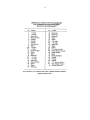
6.3. TABULATED TEST POINT
VOLTAGES ON ETCHED BOARD
The following dc voltages are intended to indicate
the typical voltages measured on the etched circuit
board. The voltages given here should not be
considered as absolute values, but should be used
as an aid in troubleshooting. All voltages were
measured from ground with a DVM having an input
impedance of 10 MS or greater. Voltages are dc
values with no input pulses. Set INPUT A
RESOLVING TIME Control to 0.1 :s (min). Set
COINCIDENCE REQUIREMENTS switch to 1.
Test Point
Q1c
Q4b
Q6b
Q6c
Q7c
Q9b
Q10b
Q10c
Q13b
Q14b
Q14c
Q17b
Voltage
11.5
14.5
0.7
10.0
11.9
0
1.8
10.8
0
1.8
10.8
0
Test Point
Q18b
Q18c
Q21b
Q22b
Q22c
Q25b
Q26b
Q26c
Q27b
Q29b
Q29c
Voltage
1.8
10.8
0
1.8
10.8
- 0.6
- 2.9
0
- 12.0
- 11.7
- 0.3
9
Pins marked (*) are installed and wired in ORTEC 4001A and 4001C
Modular System Bins.
10