1
.
inn
mam
© Copr. 1949-1998 Hewlett-Packard Co.
Microprocessor-Controlled Harmonic
Heterodyne Microwave Counter also
Measures Amplitudes
The new harmonic heterodyne frequency measuring
technique provides wide F M tolerance, high sensitivity,
and automatic amplitude discrimination. Simultaneous
measurement of input amplitude is optional.
by Ali Bologlu and Vernon A. Barber
AUTOMATIC MICROWAVE FREQUENCY mea
surements to 18 GHz and beyond have generally
been done using one of two frequency down-conver
sion techniques, the transfer oscillator or the hetero
dyne converter (see box, page 5). In a new micro
wave counter, Model 5342 A (Fig. 1), a new downconversion technique, called harmonic heterodyne
conversion, provides many of the advantages of both
traditional methods while significantly reducing
cost. Among these advantages are wide FM tolerance,
high input sensitivity, and automatic amplitude dis
crimination.
The new technique requires only one microwave
component, a sampler, and relies on a microprocessor
to perform the required computations, thereby
eliminating a good deal of digital hardware and its
associated expense. The microprocessor also adds to
the counter's power and versatility by making it pos
sible to manipulate the measured data. An easy-to-use
keyboard permits the operator to define frequency
offsets or measure frequency deviations. An
amplitude measurement option provides simultane
ous measurements of input signal level and input
frequency for the first time in a microwave counter.
Model 5342A measures frequency from 10 Hz to 18
GHz with a resolution of 1 Hz. It has an 11-digit
display. With the amplitude measurement option, the
user can see input level displayed in dBm with 0.1-dB
resolution and ±1.5-dB accuracy, and frequency can
be displayed simultaneously with 1-MHz resolution.
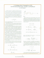
Harmonic Heterodyne Conversion
Fig. 2 is a simplified block diagram of the harmonic
heterodyne technique. All of the harmonics of an
internal oscillator are simultaneously mixed with the
unknown signal by the sampler. The output of the
sampler consists of sum and difference frequencies
produced by each harmonic of the internal oscillator
mixing with the unknown. The internal oscillator, a
programmable frequency synthesizer locked to the
counter's time base, is incremented in frequency until
one of the outputs of the sampler is in the counting
range of the low-frequency counter. The IF detector
detects when the IF (intermediate frequency) is in the
range of the low-frequency counter and sends a signal
that causes the synthesizer control to stop increment
ing the frequency of the synthesizer. The IF is then
counted by the low-frequency counter. The unknown
frequency can be determined from the relation:
fx = Nf, ± f,IKl
Cover: An easy-to-use key
board puts the micropro
cessor-based Model 5342A
Microwave Frequency Count
er through its paces. This
new counter measures fre
quencies and (optionally)
amplitudes, with or without
offsets, up to 18 GHz, and
has extensive built-in self-test facilities.
In this Issue:
Microprocessor-Controlled Harmonic
Heterodyne Microwave Counter also
Measures Amplitudes, by Ali Bologlu
and Vernon A. Barber
page 2
A Technique that Is Insensitive to FM for Deter
mining Harmonic Number and Sideband, by
Luiz Peregrino, page 13.
Generating High-Speed CRT Displays
from Digital Data, by Arnot L Ellsworth
and Kunio Hasebe .
L a b o r a t o r y
N o t e b o o k
page 17
page 24
Swept-Frequency Measurements of High
Levels of Attenuation at Microwave Frequencies
©Hewlett-Packard Company. 1978
Printed in U.S.A.
© Copr. 1949-1998 Hewlett-Packard Co.
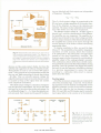
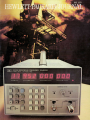
Fig. 1. Model 5342 A Microwave
Frequency Counter measures fre
quencies from 10 Hz to 18 GHz.
With its amplitude measurement
option, it can simultaneously mea
sure and display frequency and
amplitude. Keyboard control and
microprocessor architecture pro
vide ease of operation and data
manipulation features.
where fx = unknown frequency
N = harmonic of frequency synthesizer
fj = programmed frequency of synthe
sizer
fIFl = IF produced by Nf: mixing with fx.
The frequency fa of the programmable synthesizer is
known, since it is known where the indexing of the
Input
IF
Detector
Sampler
Driver
Programmable
Frequency
Synthesizer
synthesizer was stopped. fIFl is known, since it is
counted by the low-frequency counter. Still to be de
termined are N and the sign ( ±) of the IF. This is done
by making one more IF measurement with the syn
thesizer frequency offset from its previous value by
a known amount Af. Thus f2 = fj-Af. This produces
an IF, fIF2, that is counted by the low-frequency
counter. The offset Af is much smaller than the IF, so
if fx is less than Nf1( then fIFl produced by mixing
Nfj with fx will be greater than fIF2. Conversely, if
fx is greater than Nfj then fIF1 will be less than f]F2.
This is shown in Fig. 3. N is then determined as
follows:
- fx (Nf^fJ
fIF1 =
= Nf2-fx (Nf2>fx)
MF2
N=
Synthesizer
Control
or, if fx is greater than Nf1(
Fig. 2. Simplified block diagram of the harmonic heterodyne
frequency conversion technique used in the 5342 A Counter.
All harmonics of a frequency synthesizer are simultaneously
mixed with the unknown in a sampler. The synthesizer fre
quency is incremented until one of the sampler outputs is in the
range of the low-frequency counter. The system measures this
output, determines which synthesizer harmonic produced it,
and adds the measured value to the known harmonic fre
quency. A microprocessor controls the synthesizer and does
the computations.
Nf, (Nf,<fx
fIF1
IF2 = fx - Nf2 (Nf2<fx
N=
MFl
The unknown frequency is then computed as
follows:
© Copr. 1949-1998 Hewlett-Packard Co.
fx = Nfj - fIFl (f,F2 < f,F1)
fx = Nfa
IF1
(fIIF2
Input
f,IFlJ
Since the frequency of the synthesizer is known to the
accuracy of the counter's time base and the IF is mea
sured to the accuracy of the counter's time base the
accuracy of the microwave measurement is deter
mined by the time base error and the ±l-count error
inherent in any counter.
Multiplexer
Automatic Amplitude Discrimination
The bandwidth and gain characteristics of the IF
provide automatic amplitude discrimination. This
means that the counter will measure the frequency of
the highest-level signal in the presence of a multitude
of signals at different frequencies, provided that the
desired signal is larger than any other by a certain
minimum number of dB. The specified minimum
separation for the 5342Ais 6 dB for signals within 500
MHz of the desired signal and 20 dB for signals
farther away. Typical values are lower.
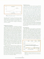
Frequency
Synthesizers
Main
Fig. 4. The harmonic heterodyne technique is implemented in
the 5342A Counter with two synthesizers and two counters, as
shown here, to prevent frequency modulation on the unknown
signal from causing an incorrect computation of the harmonic
number N. A pseudorandom sequence generator switches
between the two synthesizers and the two counters.
Pseudorandom switching avoids any coherence between the
switching rate and the modulation rate of the FM on the un
known.
FM Considerations
The discussion up to now has dealt with the ideal
case in which the counter is measuring input signals
with little or no FM. However, many signals in the
microwave region, particularly those from micro
wave radios, have significant modulation on them.
To prevent this modulation from causing incorrect
computation of the harmonic number N, the har
monic heterodyne technique is implemented as
shown in Fig. 4. There are two synthesizers offset
by precisely 500 kHz, two counters, and a pseudo
random sequence generator that controls a multi
plexer and the two counters synchronously.
Nf,
rf
f x
N f ,
N f ,
f
Fig. 3. To determine the number, N, of the synthesizer har
monic that produced the sampler output at intermediate fre
quency f¡F1, the counter makes a second measurement with
the synthesizer frequency f-, changed to f2 = f-, -Af, where
&f«fIF1. If fx<Nf-! then 1,F2<1,Fi, and if fx>Nf1 then
fiF2>fiFi> as shown here. Then N = \fIF1 —fiF2\ -=-Af.
The operating algorithm is as follows. With the
multiplexer having selected the main oscillator out
put, the main oscillator frequency fl is swept from
350 MHz to 300 MHz in 100-kHz steps. The offset
oscillator frequency f2 is maintained at ft - 500 kHz
by a phase-locked loop. When the IF detector indi
cates the presence of an IF signal in the range of
50 MHz to 100 MHz, the synthesizer stops its sweep
and the counter starts the harmonic number (N) deter
mination. The pseudorandom sequence output
switches between the main oscillator and the offset
oscillator and between counter A and counter B so
that counter A accumulates fIF1 (produced by Nfa
mixing with fx) and counter B accumulates fiF2 (pro
duced by Nf2 mixing with fx). The pseudorandom
switching prevents any coherence between the
switching rate of the multiplexer and the modulation
rate of the FM that might produce an incorrect com
putation of N. N and the sign of the IF are computed
as previously described, since counter A accumulates
f¡F1) and counter B accumulates fjF2. The pseudoran
dom sequence is then disabled, the main oscillator
is selected, and the frequency of fIFl is measured in
counter A to the selected resolution.
The counter's FM tolerance is related to the length
of the pseudorandom sequence. As shown in the box
on page 13, the maximum error in the determina-
© Copr. 1949-1998 Hewlett-Packard Co.
Down-Conversion Techniques for
Microwave Frequency Measurements
A frequency counter is limited in its direct-counting frequency
range by the speed of its logic circuitry. Today the state of the art
in high-speed logic allows the construction of counters with a
frequency range of around 500 MHz. Continuing advances in 1C
technology should extend this range beyond 1 GHz in the nottoo-distant future.
The designer of an automatic microwave counter must look to
some form of down-conversion to extend frequency measure
ment beyond 500 MHz. Four techniques are available today to
provide this down-conversion:1
• Prescaling, or simply dividing the input frequency, with a
range of only about 1.5 GHz;
• Heterodyne converter, allowing measurements as high as 20
GHz;
• Transfer oscillator, used in counters with ranges to 23 GHz;
• Harmonic heterodyne converter, a new technique that can
provide measurements to 40 GHz, and is used in the new
Model 5342A Microwave Frequency Counter to measure up
to 18 GHz.
Heterodyne Converter
In a heterodyne converter, the incoming microwave signal is
mixed with a high-stability local oscillator signal of known fre
quency, resulting in a difference frequency within the range of a
conventional counter (see Fig. 1). The high-stability local oscil
lator signal is generated by first digitally multiplying the fre
quency of the instrument's time base to a convenient fundamen
tal frequency, fin, typically 1 00 to 500 MHz. This fin is directed to
a harmonic generator that produces a comb line of frequencies
spaced at fin extending to the full frequency range of the
counter. One line of this comb, Kfin, is then selected by a mi
crowave filter and directed to the mixer. Emerging from the
mixer is an intermediate frequency equal to fx-Kfin. This fre
quency is amplified and sent to the counter. The display con
tains the sum of the intermediate frequency and Kfin.
In practice, the system begins with K=1 and steps the mi
crowave filter through the comb line until a detector indicates
that an intermediate frequency in the proper range is present.
The microwave filter may be a YIG filter or an array of thin-film
filters that are selected by PIN diode switches.
•4 —
Local
Oscillator
Harmonic
Generator
Fig. 2. Transfer oscillator.
harmonic member N. The counter then measures ft, multiplies
by N (usually by extending its gate time) and displays the result.
Harmonic Heterodyne Converter
The harmonic heterodyne converter, as its name implies, is a
hybrid of the previous two techniques. Fig. 2 on page 3 is a
simplified diagram of a counter that uses harmonic heterodyne
conversion. The input fx is directed to a sampler, with the result
ing down-converted video signal f,F=fx-Nf1 amplified and
sent to the counter. The sampling frequency ^ is created by a
processor-controlled synthesizer.
The acquisition routine for this down-converter consists of tun
ing the a frequency f-, until the signal detector finds a
video by f!F of the appropriate frequency range (defined by
the bandpass filter). Next, the harmonic number N must be deter
mined, as in the transfer oscillator. One method of finding N is to
use a second sampler loop or similar technique. A second
method is to step the synthesizer back and forth between two
closely-spaced frequencies and observe the differences in
counter readings; it is then a simple task for the processor to
calculate N.
A frequency measurement is accomplished by the proces
sor's multiplying the known synthesizer frequency fj by N, add
ing the result to the frequency f!F measured by the counter,
and displaying the answer: fx=Nf1+f|F.
The harmonic heterodyne converter has the potential to be
constructed at a lower cost than the previous two techniques
because it can be designed with just one microwave compo
nent, the sampler, and the control, decisions, and calculations
can be performed by a low-cost microprocessor.
Comparison
The table below compares the three major down-conversion
techniques.
Multiplier
Fig. 1. Heterodyne converter.
Transfer Oscillator
The transfer oscillator (Fig. 2) uses the technique of phase
locking a low-frequency voltage-controlled oscillator (VCO) to
the microwave input signal. The VCO frequency f-| can then be
measured in a conventional counter, and all that remains is to
determine the harmonic relationship between that frequency
and the input. A second VCO is often used to help determine the
Reference
1 . "Fundamentals of Microwave Frequency Counters," HP Application Note 200-1 .
© Copr. 1949-1998 Hewlett-Packard Co.
tion of the harmonic number N is
Allowed Range of
IF Frequencies
25 MHz 50 MHz
100MHz 125MHz
Fig. 5. 5342A Counter's FM tolerance is determined by the IF
bandwidth, which is 25 to 125 MHz. The IF detector stops the
sweep when the IF is between 50 and 100 MHz. Thus the
allowable FM is 50 MHz peak to peak.
where P is the length of the pseudorandom sequence
in clock periods, Afx is the peak frequency deviation
of the unknown, and Af is the frequency offset be
tween the two synthesizers. For example, if P = 215-1,
Afx = 5 MHz, and Af = 500 kHz, emax <0.2209. As
long as emax <0.5, N is correctly determined.
The length of the pseudorandom sequence also
affects the counter's measurement time, which con-
Data Bus and
Address Bus
10 Hz-500 MHz
Time Base
Buffer
Assembly
Mixer/
Search Control
Assembly
Fig. sampler, This block diagram. Only one microwave component, the sampler, is needed. This
helps reduce cost.
© Copr. 1949-1998 Hewlett-Packard Co.
sists of three components: sweep time, N determina
tion time, and gate time. The sweep time is 150 milli
seconds or less and the gate time for 1-Hz resolution
is one second. In normal operation the pseudoran
dom sequence length is 360 milliseconds, so the
total measurement time is about IVi seconds. Under
these conditions the counter can tolerate 20 MHz
peak-to-peak frequency deviation on the unknown.
This corresponds to the bandwidth of most tele
communications channels.
The counter's maximum FM tolerance is deter
mined by the bandwidth of the IF amplifier. As Fig. 5
shows, the allowable range of intermediate frequen
cies is 25 to 125 MHz. The IF detector is adjusted to
stop the sweep when the IF is in the range 50 to 100
MHz. Therefore, a maximum of 50 MHz peak-topeak frequency deviation on the unknown can be
tolerated. A switch on the rear panel of the 5342A
selects either the 20-MHz or the 50-MHz FM mode.
In the wide FM mode the pseudorandom sequence
length is 2096 milliseconds, so the acquisition time
is significantly increased over the normal mode.
T
RF Input
V
100
IF Output
N
+«-
1.8 pF
1.8 pFI
100
Counter Design
The overall 5342A block diagram is shown in Fig.
6. The product design not only decreases assem
bly costs but also yields significant RFI performance
improvements. As can be seen in Fig. 7, the entire
counter is built into one die casting. The boards that
constitute the individual assemblies plug into one
multilayer motherboard, thereby eliminating all
IF Amplifiers
and Signal-Present
Detectors
100
IF Output
100
Microstrip
/ Balun
Pulse
Input
50
150
Gate Time and
PRS Generation Board
Counter
Board
\\\\\Y
flffH
1
Processor
Board
100
Main Synthesizer
and Offset Loop
Fig. 8. Sampler is a thin-film hybrid circuit. The sampling
pulse couples to the slotted line through a balun that gener
ates two opposite-polarity pulses to drive the Schottky diodes.
Direct
Input
Amplifier
Power
Supply
Amplitude
Option
HP-IB Board
Option
Board
Time Base
Buffer
RF Multiplexer
JF Preamplifier
Fig. 7. Product design minimizes assembly costs and im
proves RFI performance. A single casting houses all as
semblies, which plug into a single multilayer motherboard.
wiring except for the rear-panel power connections.
The power supply is of the switching regulator
type. The power supply boards are also inside the
casting, but in a separate compartment, so the switch
ing spikes are contained and are not permitted to in
terfere with the rest of the circuitry. On the front
panel a fine metallic mesh covers the LED display and
attenuates emissions from this area. These pre
cautions have resulted in improved RFI performance
with respect to past instruments.
The casting is also the main structural element of
the instrument. The side rails of the box are attached
to it, and the front and rear panel assemblies are
© Copr. 1949-1998 Hewlett-Packard Co.
Signature Analysis in the 5342A
Incorporating microprocessor control into the 5342A Mi
crowave Frequency Counter made it possible to develop a
powerful measuring instrument at a substantial reduction in
cost. Besides providing many operational benefits, such as
keyboard entry of frequency and amplitude offsets, resolution
selection, and offset recall, microprocessor control enhances
the serviceability of the 5342A by providing powerful diagnostic
routines, also selectable from the front-panel keyboard , that aid
the service person in fault isolation and instrument verification
(see Fig. 1). Other microprocessor routines, exercised every
time the instrument is turned on, check the health of ROMs and
RAM and display error codes if all is not well.
Despite the diagnostic aids provided by the microprocessor,
placing a microcomputer inside a sophisticated measuring in
strument also introduces some serviceability problems. After
the first prototype was constructed, we discovered it was im
possible to isolate certain failures to a particular assembly using
traditional troubleshooting equipment and techniques.
Failures involving the microprocessor assembly and the indi
vidual assemblies that interface to the microprocessor assem
bly were extremely difficult to troubleshoot. Even after hours of
troubleshooting, it was uncertain whether the fault was a control
failure originating on the microprocessor assembly, an interface
failure originating on an assembly's interface with the micro
processor, or a failure in some other part of the instrument,
causing the measurement algorithm to hang up or branch to an
incorrect program segment. We needed a quick way to verify
proper operation of the microprocessor control assembly.
Fortunately, there was a solution which, even though the
instrument had advanced to the prototype stage, was inexpen
sive to implement and permitted microprocessor verification
and fault isolation to the component level. This technique, called
signature analysis, relies on a relatively inexpensive trou
bleshooting instrument — the 5004A Signature Analyzer.1
Signature Analysis
Signature analysis, as implemented in the 5004A Signature
Analyzer, employs a data compression technique to reduce
long, complex data streams at circuit nodes to four-digit
hexadecimal signatures. By taking the signature of a suspected
circuit node and comparing it to the correct signature, which is
empirically determined and documented in the operating and
service manual, proper circuit operation is quickly verified. By
probing designated nodes, observing good and bad signa
tures, and then tracing back along the signal flow from outputs
to inputs, the cause of an incorrect signature may be discovered
and corrected.
In operation, four signals must be supplied to the signature
analyzer. A START signal initiates the measurement window. Dur
ing this time window, DATA from a circuit node is clocked into the
signature analyzer. A CLOCK signal synchronizes the data. A STOP
signal terminates the measurement window.
There are two ways to implement signature analysis and meet
the requirements just mentioned in a microprocessor-based
product: free running and software driven. In the free running
method, the microprocessor is forced into an operating mode in
which it cycles continuously through its entire address field.
START/STOP signals are derived from the address bus lines. In
software driven signature analysis, a stimulus program is stored
in ROM. The stimulus program generates START/STOP signals and
can also write repeatable DATA streams onto the data bus for
testing other assemblies connected to the microprocessor. Free
running signature analysis has the advantage of not requiring
Ã
gsa,yyy
y¼a
yy
y
SAMPLE RATE
QffgyyÃy
y
¼P
Fig. 1. Nine diagnostic modes are available with the counter
in AUTO mode. The SET key is pushed twice and is followed by
the appropriate digit key.
SET, SET, 0: Indicates that the main synthesizer is sweeping
(SP) and that the signal has been placed in the IF (23)
and finally that the harmonic determination has been
made (Hd). This display is shown in the photograph.
SET, SET, 1: Displays the main synthesizer frequency, the
location of the harmonic comb line (e.g., if -, harmonic
is below fx so must add IF result), and the harmonic
number N.
SET, SET, 2: Displays results of counter A accumulation dur
ing acquisition.
SET, SET, 3: Displays results of counter B accumulation dur
ing acquisition.
SET, SET, 4: Displays intermediate frequency being counted.
SET, SET, 5: If Option 002, amplitude measurement, is instal
led, a single corrected amplitude measurement is
made and held.
SET, SET, 6: If Option 002, amplitude measurement is instal
led, a continuous measure of uncorrected amplitude is
displayed.
SET, SET, 7: When the signal is removed from the microwave
port, the main synthesizer sweeps over its full range in
100-kHz steps.
SET, SET, 8: This mode is a keyboard check.
any ROM space for storing the stimulus program. Software
driven signature analysis has the advantage of being able to
exercise a greater portion of the instrument's circuitry. For
thorough testing, both techniques could be implemented in the
same instrument.
In the 5342A, lack of ROM space ruled out the software driven
implementation. To implement the free running approach in the
5342A, all that was required was the addition of some switches
and pull-up resistors to the microprocessor assembly. Fig. 9 on
page 9 shows a block diagram of the 5342A microprocessor
assembly. The shaded area contains the components added to
the assembly to implement free running signature analysis.
To check out the microprocessor assembly, the micro
processor is forced into a free run mode by opening the data
bus switches S1 (this prevents data out of the ROMs from
altering the forced free run instruction) and grounding the free
© Copr. 1949-1998 Hewlett-Packard Co.
run switch S2. When S2 is grounded, a clear B instruction is
presented to the microprocessor data input (clear B was chosen
to minimize the number of diodes needed). This causes the B
accumulator to be cleared and the address to be incremented
by 1 . Consequently, the address lines from the microprocessor
repeatedly cycle over the entire address field of the micro
processor from 0000 to FFFF. By using the most significant
address line as both START and STOP for the 5004A, and one
phase of the microprocessor clock as the 5004A CLOCK input,
repeatable, stable signatures are obtained for the microproces
sor address lines, ROM outputs, device select outputs, and
most circuit nodes on the microprocessor assembly. By check
bolted onto the side rails.
The only microwave component required to make
the frequency measurements is the sampler, Fig. 8.
This consists of a thin-film hybrid mounted in an
aluminum package that is manufactured by a hobbing
die. This technique is similar to coin minting and
results in relatively low piece costs.
Operation of the sampler is similar to that of
ing the assembly's outputs for correct signatures (documented
in the manual), it is possible to verify with a high degree of
confidence that the assembly is functioning properly. If a signa
ture is incorrect, then signatures are checked back along the
signal flow paths, from outputs to inputs. When a device is found
where the output signature is bad but the input signatures are
good; that device is replaced.
Reference
1 . A.Y. Complex "Easy-to-Use Signature Analyzer Accurately Troubleshoots Complex
Logic Circuits," Hewlett-Packard Journal, May 1977.
-Martin Neil
samplers used in previous HP microwave counters.1
On the hybrid are two Schottky diodes placed across
a slotted line. The sampling pulse couples to the
slotted line through a stripline balun that generates
two opposite-polarity pulses to drive the diodes. The
down-converted signal is taken from two isolated
resistors to the preamplifier. Resistors across the slot
are used to absorb secondary reflections introduced
To Rear-Panel
Connector
Fig. area for microprocessor assembly. Components in the shaded area were added for
troubleshooting by signature analysis. Only a few switches and pull-up resistors were required.
© Copr. 1949-1998 Hewlett-Packard Co.
by the sampling pulse.
and necessary control lines to the rear panel for inter
facing to external devices. During the power-on cycle,
the 6800 first does a RAM exercise by doing a READ/
WRITE for each memory location using four different
patterns. In hexadecimal code the four patterns are
FF, 00, AA, and 55. Should a particular location not
pass, the front-panel display shows all "E"s. After the
RAM test the 6800 goes through a ROM checksum
routine. A defective ROM results in a display of 1, 2,
or 3 on the front panel, indicating the failed ROM.
Successful completion of the above steps causes the
instrument to light up all display segments and
front-panel LEDs, giving the user a visual check. The
instrument then comes on in the auto mode, with
1-Hz resolution and the HP-IB interface cleared.
Keyboard input is connected to the MPU interrupt
line. When a key is pushed the MPU consults a key
table, branches to the proper key sequence routine,
and displays a prompt. If the sequence is not com
pleted, some of the key lights will be kept blinking,
indicating that the routine is waiting for more key
depressions to complete the sequence. If an unex
pected key is pushed it may be ignored or an error
indication may be displayed, depending on the situa-
Microprocessor Architecture
Measurement, control, and system coordination of
the 5342A are implemented by a 6800 microproces
sor. The microprocessing unit (MPU) handles inter
facing to the analog circuits, the power-up routine,
display control, keyboard manipulation and control,
frequency and amplitude measurements, arithmetic
calculations, and diagnostics (Figs. 9, 10, 11). The
MPU consists of one 6800 chip, 128 bytes of RAM
(random-access memory), and three 2K-byte ROMs
(read-only memories) that store the MPU programs.
Decoder/drivers for peripheral circuit interfaces and
diagnostic switches to facilitate signature analysis for
trouble shooting are also located on the processor
board. A ribbon cable transports the address, data,
Start
4
RAM Check
ROM Check
T
Display o
Check
Start
IF Auto Mode
Yes
Decrease
Synthesizer
Frequency 500 kHz
Display
'0"=No Input
No
Add 500 kHz
To Synthesizer
Frequency
IF Manual or Low-Range Mode
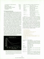
Fig. 10. Simplified 5342A system flow chart.
Fig. 11. 5342/4 sweep flow chart.
10
© Copr. 1949-1998 Hewlett-Packard Co.
-20 -
dBm
-25
-30 -
0
I
2
I
I
4
I
6
I
I I I I
8
1 0
I I
1 2
I
I I I I
1 4
1 6
I
I I ,
1 8
f (GHz)
Fig. 12. Specified and typical 5342A input sensitivity.
lion. Software diagnostic routines are built in as a
service aid, enabling the user to diagnose problems to
the subassembly level. Digital board troubleshooting
can be done to the component level using signature
analysis (see page 8).
Front-Panel Inputs and Controls
The 5342A has two inputs, one going from 10 Hz to
520 MHz, and the other from 500 MHz to 18 GHz.
Sensitivity of the microwave input is shown in Fig.
12. The right-hand side of the front panel deals with
input signal channel selection and sample rate con
trol of the measurement. The left-hand side of the
front panel enables the user to do data manipulation
by keyboard control of the processor. Instructions on
how to do this are on a label (Fig. 13) that is affixed to
the instrument top.
The panel layout is in algebraic notation. Panel
operation closely resembles remote programming via
the HP interface bus (HP-IB). When the machine pow
ers up it is in the auto mode with 1-Hz resolution. As
the user selects other resolutions, insignificant zeros
are truncated. Display digits are in groups of three to
facilitate reading.
In case the user wants to bypass the acquisition
cycle of the algorithm, a manual mode of operation is
available. In this mode, the user should know the
unknown frequency within 50 MHz and enter it via
the keyboard. The counter then acts like a receiver
making frequency measurements.
Offsets can be specified from the front panel. Any
frequency offset can either be subtracted from or
added to the measured frequency. In the auto offset
mode of operation the counter holds the initial mea
surement and then displays all succeeding measure
ments as deviations about the initial reading.
Amplitude Measurements
Equipped with the amplitude measurement option,
the 5342A is alone among microwave counters in its
ability to make simultaneous amplitude and fre
quency measurements. Incoming signal amplitude is
measured to 0.1-dB resolution with a specified accu
racy of ±1.5 dB. Amplitude offsets can be entered
from the front panel in the same way as frequency
offsets.
The most fundamental decision involved in de
signing an amplitude measuring system was what
element to use to sense amplitude. Ideally, we wanted
a system that is RMS-responding from -30 to +20
dBm, makes measurements rapidly, has stable cali
bration, is burnout resistant, and has low input SWR.
One choice might have been to use the counter's sam
pler and measure its output level. Unfortunately, this
IF level is also a function of the input frequency, of the
intermediate frequency, and of the sampler drive
pulse amplitude and frequency, and begins to satu
rate at about —10 dBm. Some sort of switchable at
tenuator ahead of the sampler to increase dynamic
range would have resulted in an input SWR greater
than three at low levels. Among other alternatives,
thermistors are subject to drift and easy burnout, and
while thermocouples do not suffer these problems,
their sensitivity is low, necessitating a narrow video
bandwidth and consequent slow response at low
levels. Point-contact diodes are sensitive, wideband,
and have the low origin resistance necessary for driv
ing an operational amplifier without biasing, but they
are not very rugged, mechanically and electrically,
nor are they stable over long periods. Planar Schottky
diodes have recently been built, however, with low
barrier height, so they are usable without bias. These
5342A KEYBOARD OPERATING INSTRUCTIONS
E KEA SU«e «fi NT S (OPI»
: D. a , """'.«i^a,
iÃ--p«f ss- D . Q . ffl H E . D :
*L- ANALOG CONVÉ H TE B {OPTION t*
: D. D . in»o.n««i ,D
u-»» B.tr-!fmnttB.°ff,
Fig. 13. Instructions for using the front-panel keyboard are
attached to each instrument. Frequency and amplitude offsets
are easily specified.
© Copr. 1949-1998 Hewlett-Packard Co.
tors are identical and their outputs are independent
of frequency. Therefore
VRF = V2 = KV0
Thus V0, the dc output voltage, is proportional to the
RF sine wave voltage regardless of the transfer func
tion of the detectors, as long as the detectors are
matched. The output is also independent of tempera
ture if the diodes are at the same temperature.
The detector output voltage at -30 dBm input is
about 0.5 mV, so the dc characteristics of the differen
tial amplifier are very important. The amplifier is a
hybrid, laser-trimmed for low offset voltage and drift.
The low origin resistance of the detector diodes allows
the amplifier bias current to be drawn through the
reverse direction of the diodes without introducing
appreciable offset.
To display amplitude in dBm, we need the loga
rithm of V. The availability of monolithic integrating
converters of 13-bit accuracy allows this function
to be performed by the instrument's microprocessor
instead of the usual logarithmic amplifier. The
dynamic range is further increased by a switchable dc
amplifier ahead of the analog-to-digital converter.
This combination allows better than 0.03-dB resolu
tion at all levels and avoids the drift problems of a log
amplifier. Once the processor has logged and scaled
the result it uses the frequency information obtained
in a previous measurement to correct the result
according to a calibration table stored in memory
(more about this later).
Fig. 14. Planar Schottky diode detectors are used in the op
tional amplitude measurement system. Two detectors are
used to compensate for temperature variations. The dc out
put voltage V0 is proportional to the RF sine wave voltage as
long as the detectors are matched, and is independent of
temperature as long as the detectors are at the same tempera
ture.
devices are like point-contact diodes, but have the
stability and ruggedness of ordinary Schottky diodes.
These diodes are now in use in several HP applica
tions.2'3 They meet all of our requirements except that
they are not RMS-responding at levels above about
— 20 dBm. Thus we actually measure voltage but
make the instrument read out in units of power, and it
is accurate as long as the signal does not contain
much amplitude modulation.
The diode output voltage is a function of tempera
ture and must be compensated. The circuit that does
this (see Fig. 14] also provides another advantage. For
Av sufficiently large, V3 = V4. Since the detector out
puts are equal, their inputs must be equal if the detec
Thin-Film Hybrid
All of the microwave components are contained in
a thin-film assembly (Figs. 15 and 16). The dc block
ing capacitors and all resistors are integrated on two
sapphire substrates, one for the microwave detector,
CR3, and the other for the low-frequency detector,
CR4. CRl and CR2 are PIN diodes used to route the
input signal either to the counter or to the detector.
Fig. 15. All of the microwave
components of the amplitude
measurement system are con
tained in a thin-film assembly. De
tectors CR3 and CR4 are planar
low-barrier Schottky diodes man
ufactured by HP.
12
© Copr. 1949-1998 Hewlett-Packard Co.
A Technique that Is Insensitive to FM
for Determining Harmonic Number and Sideband
by Luiz Peregrino
The basic principle of a heterodyne microwave counter is
the use of a sampler or harmonic mixer to convert the highfrequency signal to a low intermediate frequency (IF) that can
be counted directly. Before the frequency of the microwave
signal can be computed from the measured IF the harmonic
number and the sideband must somehow be determined.
One way to determine the harmonic and sideband is to use
two microwave receivers with local oscillators offset by Af. The
difference between the two IF frequencies is proportional to
the harmonic number and the sign of the difference determines
the sideband:
N =
gffi
M
-1
Fig. 1.
We will consider only the upper sideband case. The lower
sideband case is identical except for a change in sign. Let fx
represent the unknown frequency and N the harmonic number.
By proper selection of IF amplifier bandwidth and local oscilla
tor frequencies, we can guarantee that the harmonic and side
band that be the same for both oscillator frequencies. With that
in mind, we have:
F2
The main disadvantage with this technique is the cost of the
two high-frequency receivers.
An alternate solution ¡s to vary the local-oscillator frequency,
for instance switching regularly between two values. It can be
shown that this technique would be very sensitive to FM pre
sent in the microwave signal.1'2
Another possibility ¡s to apply random modulation to the local
oscillator and correlate the applied modulation to the resultant
modulation in the IF. If there is crosscorrelation between the
applied modulation and the FM in the microwave signal, there
will but an error in the determination of the harmonic number, but
if this error is less than 0.5, it can be completely eliminated,
because the harmonic number ¡s an integer.
In the new 5342A Microwave Frequency Counter, a pseudo
random signal3'4 is used to change the local oscillator fre
quency between the values f., and f2 and gate the resultant
f,F1 and f|F2 into two low-frequency counters. This reduces the
problem to determining the proper pseudorandom sequence
length to give the desired FM tolerance.
Let g(t) represent a period of the pseudorandom sequence
(see to . 1 ). When g = + 1 the local oscillator frequency ¡s set to
f-, and f,F1 is gated into counter 1. When g = -1 the local os
cillator frequency ¡s changed to f2 and f,F2 ¡s gated into counter
2. At the end of the sequence, t=T, the difference of the num
bers accumulated by both counters is used to determine the
harmonic number.
The number M(t) accumulated by a counter ¡s given by the
integral of the frequency during the time the counter ¡s gated
on.' Let M-|(t) and M2(t) represent the numbers accumulated
by counter 1 and 2, respectively.
f,F1(t) = fx (tJ-Nf,
f,F2(t) = fx (t)-Nf2
|f f xT( t ) d t f- N f TJ d t
J o ' g = + i J o
a=-i
•f
where T1 ¡s the length of time for which g = +1 and T2 is the
length of time for which g = -1. Then
=
r
N =
g(t)fx(t)dt
= Nc+e
T,fi-T2f2
The value of the integral is not available, so the second term
appears as an error in the calculated harmonic number Nc.
For a pseudorandom sequence we have T1-T2=TC, where
Tc is the sequence clock period.3'4 This difference can be
made zero by a small modification of the sequence circuit, or
it can be disregarded if the sequence is long enough. Then we
have:
T, = T2 = T/2
f,F1(t)dt
Mi(t) =
-Nf2 dt
f,Fi(t)dt
/ < 2
r M
f,F2(t)dt+J fIF2(t)dt + ...
â € ¢ 1 ' 3
= /of,F2(t)dt
N =
2(M2-M i ) _ _ 2 _ f T
TAf
TAf J n
g(t)fx(t)dt.
Let us consider the error term as function of time and take the
Fourier transform. Using the shifting theorem we have:
g— 1
13
© Copr. 1949-1998 Hewlett-Packard Co.
where Afx is the peak deviation of the unknown signal.
Thus if we want the counter to tolerate 10 MHz peak FM on
the input signal, and Af = 500 kHz,
Af
\<a
P > 25,600.
Upper-case letters are used to represent Fourier transforms.
The term in brackets can be recognized as the Fourier transform
of the pseudorandom sequence. The term Fx(ja>)/Af can be
considered as the input to a linear system and E(j<a) as the out
put.1 The transfer function of this system is:
H(jco) =
2 1 -eHM'i
T I jo)
Since P = 2m-1 , where m is the number of shift-register stages
in the pseudorandom sequence generator, a 15-stage shift
register would be needed to generate this sequence.
References
1 L. Peregrino and D,W. Ricci, "Phase Noise Measurement Using a High Resolution
Counter with On-Line Data Processing," Proceedings of the 30th Annual Sympo
sium on Frequency Control, 1976, p. 309.
2 R.A. Baugh, "Frequency Modulation Analysis with Hadamard Variance," Pro
ceedings of the Frequency Control Symposium, April 1971, pp. 222-225.
3. S.W. Golomb, "Shift Registers," Holden-Day Inc.
4. S.W. Prentice- et al., "Digital Communications with Space Applications," PrenticeHall, 1964,
JO)
To determine the counter's sensitivity to sine wave modulation
present in fx(t) we only need to know | H(jw) | . This can be easily
found at frequencies that are multiples of f0 = 1/T by taking
the square root of the power spectrum for the repetitive se
quence.4
. IT
sin —
H(jn277f0)
QTT
P
, n>0
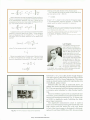
Luiz Peregrino
b Luiz Peregrino received the de^^__ gree Engenheiro de Eletronica
-•& ***&m iB from tne lnstituto Tecnológico da
Aeronáutica in Sao Paolo, Brazil in
1959. In 1960 he joined HP's mar
keting organization for a brief
period, then spent three years with
other companies as a develop
ment engineer and field engineer
before rejoining HP in 1964. Luiz
has been involved in production,
research, -and development for
many HP products. He originated
the random modulation concept
• fvi for harmonic determination used
in the 5342A. He's a member of IEEE. He enjoys skiing and
swimming, and is a home computer enthusiast.
where P is the sequence length in clock periods:
We can use a safety factor of 2 to take care of the actual value
of |H(f)| for frequencies not multiples of f0. The worst case
occurs for frequencies of the order of f0. For large P, we have:
4
A f ,
€max~^p A;
Inductors Ll to L3 act as RF chokes at high frequen
cies and as part of a 500-MHz high-pass filter with the
capacitors Cl to C3 at lower frequencies. This repre
sents an almost lossless method of injecting bias into
a broadband, planar circuit.
Detectors CR3 and CR4, as mentioned above, are
planar, low-barrier Schottky diodes manufactured by
HP. They are mounted with their bypass capacitors on
a common metal substrate for close thermal match
ing.
Since low SWR is important for an amplitude mea
surement, careful attention was paid to parasitic reac
tances and impedance matching. Fig. 17 shows typi
cal SWR in amplitude mode, including the frontpanel input connector.
The amplitude measurement circuit is made to
serve as an attenuator by biasing PIN diode CR2 with
high current and PIN diode CRl with only about
0.4 mA. Most input energy is dissipated in the termi
nation, Rl, and input SWR is low. CRl, however looks
MM
Fig. 16. Thin-film amplitude measurement assembly.
14
© Copr. 1949-1998 Hewlett-Packard Co.
Amplitude Accuracy
Many factors affect the accuracy of an amplitude
measurement in the 5342A. For traceability of our
standards to NBS and their application to individual
instruments in production we allow 0.4 dB. There can
be up to 0.1 dB error in all the digital processes.
Analog errors, such as op amp offset, modulator
linearity, noise, and A-to-D converter accuracy can
add a maximum of 0.3 dB. While drift with tempera
ture is typically less than 0.2 dB from 0° to 50°C, we
allow a maximum of 0.4 dB. The worst-case uncer
tainty for all these variables together is thus ±1.2 dB.
These errors although not random, are independent
and will rarely add to this value. The root-sum-ofthe-squares4 uncertainty, a more realistic value of ex
pected error, is less than 0.6 dB. To this value must be
added mismatch uncertainty, which depends upon
the SWR of both the source and load. Reference 4
contains a good discussion of this.
Low-loss cables are recommended for routing sig
nals to the front panel of the 5342A. Flexible cable
with repeatable insertion loss less than semi-rigid
coax has recently become available5 and is very con
venient to use.
10
Frequency (GHz)
Fig. 17. Model 5342A input SWR in amplitude mode, in
cluding the front-panel connector.
like about 250 ohms and a small amount of energy
(approximately -15 dB) goes to the sampler. This
function is controlled by the converted signal level in
the IF. With this technique, dynamic range is in
creased to +20 dBm with no danger of overloading
the input sampler.
Amplitude Error Correction
A feature of Model 5342 A is its ability to correct for
known errors according to a stored calibration table
before display. Since the microprocessor knows the
frequency and measured amplitude of the input sig
nal, it is possible to correct not only for the frequency
response of the detector and the insertion loss of the
input connector and switch but also for amplitude
related errors such as mistracking between detectors.
Typical errors to be corrected are shown in Fig. 18.
Measurements such as this are made on every unit
before installation and the data is stored in a PROM in
much the same format as shown in Fig. 18. Curve A is
stored to eight-bit resolution in 0.25-GHz increments
and curve B also to eight-bit resolution in 4-dB incre
ments and every 0.5 GHz. The processor uses the
frequency and uncorrected amplitude of the input
signal to look up the values of correction in each table
and to interpolate for intermediate values. Since
Table B is normalized to the level used in Table A, the
correction values are simply added together and
applied to the result.
The system that collects the data to calibrate each
amplitude module consists of two signal sources and
four TWT (traveling wave tube) amplifiers multi
plexed together, with attenuators and an output di
rectional coupler and power meter under the control
of an HP 9825A Desktop Computer via the HP-IB.
This system drives the module under test with all
frequencies and amplitudes in its range, and with low
source SWR and accurately known amplitude. The
error in the response of the module is then measured
and stored in the calibration PROM.
Acknowledgments
Many individuals made significant contributions
to the 5342A. The single-sampler concept was first
suggested by John Dukes. Tom Coates provided mi
croprocessor support software and other user aids
that got the project off to a running start. The sampler
was the result of Jeff Wolfington's ingenious efforts.
The power supply was done by John Gliever. We were
fortunate to have Yoh Narimatsu working on the
synthesizers. Art Bloedorn did the IF preamps and the
direct input channel and also took production en
gineering responsibility for the product. Digital de
sign was initiated by Chuck Howey. When Chuck
5 GHz
1
(A)
10 GHz
1
15 GHz
20 GHz
-1dB-2dBA: Errors at an Input Amplitude of 0 dBm
(B) B: Deviations from Curve A for Different Amplitudes
+ 1dBOdB
2GHz-16
-1dB-
- 8
0
Input Amplitude (dBm)
+ 16 +20
i —
12 GHz
Hz
Fig. 18. Each 5342A amplitude measurement system is cali
brated before installation. Systematic errors are stored in a
PROM and the microprocessor corrects each measurement
before display.
15
© Copr. 1949-1998 Hewlett-Packard Co.
opted for a farming career, John Shing stepped in and
was responsible for digital design and firmware. Spe
cial thanks are due Al Foster who designed an HP-IB
interface to the 6800 processor. For the amplitudemeasurement option, Steve Upshinsky worked on the
low frequency analog circuitry and Art Lange did all
the digital work, including programming of the calib
ration system. Thanks also go to Karl Ishoy for help
with hybrid circuit production. 5342A product de
sign was effectively done by Keith Leslie. Martin Neil,
support engineer, contributed significantly in trou
bleshooting concepts and manual preparation. Prod
uct introduction was by Craig Artherholt. The prod
uct was designed and put into production under the
lab management of Ian Band and Roger Smith. S
References
1. J. Merkelo, "A dc-to-20-GHz Thin-Film Signal Sampler
for Microwave Instrumentation," Hewlett-Packard Journal,
April 1973.
2. P. A. Szente, S. Adam, and R.B. Riley, Low-Bar
rier Schottky Diode Detectors," Microwave Journal,
February 1976.
3. R.E. Pratt, "Very Low-Level Microwave Power Mea
surements," Hewlett-Packard Journal, October 1975.
4. "Fundamentals of RF and Microwave Power Measure
ment," HP Application Note 64-1.
5. D.L. Slothour, "Expanded PTFE Dielectrics for Coaxial
Cables," Plastics Engineering, March 1975.
Vernon A. Barber
Al Barber has been designing HP
I microwave counters for ten years.
- His latest project was the
I amplitude measurement option for
" the 5342A. Al was born in Chicago
and grew up in Fairbanks, Alaska.
He received his BSEE degree from
the University of Washington in
1967 and his MSEE from Stanford
^ University in 1970. He's a member
^ o f I E E E . A l ' s t a s t e s i n r e c r e a t i o n
run to mountain climbing and
classical music. He's climbed in
the Sierra Nevada, the Rocky
Mountains, the Alaska Range, the
Alps, and the Himalaya, and he's now learning piano. He's
married and lives in San Jose, California.
Ali Bologlu
AN Bologlu has been with HP for
fifteen years and has been project
manager for microwave counters
since 1 970. He's contributed to the
design of many HP frequency
synthesizers and microwave
_ I counters, most recently the
I 5342A. Ali received BS and MS
4fe I degrees in electrical enginering in
1 I 1962 and 1963 from Michigan
^k I State University and the degree of
H^ I Electrical Engineer from Stanford
Bk ' University in 1965. Born in IstanIn bul, Turkey, he's married, has
^BK j three children, and now lives in
Mountain View, California. He plays tennis, enjoys water sports,
and coaches a youth soccer team.
SPECIFICATIONS
HP Model 5342A Microwave Frequency Counter
Input Characteristics
INPUT 1 :
FREQUENCY RANGE: 500 MHz to 18 GHz
SENSITIVITY: 500 MHz to 12.4 GHz. -25 dBm
124 GHz 10 18 GHz, -20 dBm
MAXIMUM INPUT: +5 dBm (see Option 002, 003 for higher level)
DYNAMIC RANGE: 500 MHz 1O 12.4 GHz. 30 dB
12.4 GHz to 18 GHz, 25 dB
IMPEDANCE: 50 ohms, nominal
CONNECTOR: Precision Type N témale
DAMAGE LEVEL: +25 dBm
OVERLOAD INDICATION: Displays dashes when input level exceeds ^5 dBm
nominal
COUPLING: do to load, ac to instrument
SWR: <2:1, 500 MHz - 10 GHz
O:1, 10 GHz- 18 GHz
FM TOLERANCE: Switch selectable (rear panel)
FM (wide): 50 MHz p-p worst case
CW (normal): 20 MHz p-p worst case
For modulation rales from dc to 10 MHz
AM TOLERANCE: Any modulation index provided the minimum signal level is
not less than the sensitivity specification
AUTOMATIC AMPLITUDE DISCRIMINATION: Automatically measures the
largest of all signals present, providing that signal is 6 dB above any signal
within 500 MHz: 20 dB above any signal, 500 MHz-18 GHz.
MODES and OPERATION: Automatic: Counter automatically acquires and
displays highest level signal within sensitivity range Manual Center fre
quency entered 10 within ^50 MHz of true value.
ACQUISITION TIME: Automatic mode: normal FM 530 ms worst case: wide
FM 2.4 s worst case. Manual mode: 5 ms after frequency entered.
INPUT 2:
FREQUENCY RANGE: 10 Hz to 520 MHz Direct Count
SENSITIVITY: 50ÃÃ. 10 Hz to 520 MHz, 25 mV rms
1 Mn, 10 Hz to 25 MHz, 50 mV rms
IMPEDANCE: Selectable: 1 Mn. <50 pF or 50!t nominal
COUPLING: ac
CONNECTOR: Type BNC female
MAXIMUM INPUT: 50n, 3.5Vrms (-24 dBm) or 5Vdc fuse protected: 1 Mn.
200 Vdc + 5.0 Vrms
TIME BASE:
CRYSTAL FREQUENCY: 10 MHz
STABILITY- Aging rate: <1 X10~7 per month
Short term: <1 x10~9 for 1 second avg. time
Temperature: <1X10~6 over the range 0;C to 50CC
Line vanatjon: <±1 x 10~7 for 10% change from nominal.
OUTPUT FREQUENCY: 10MHz, 32.4V square wave (TTL compatible]; 1.5V
peak-to-peak ¡nto 50Ià available from rear panel BNC.
EXTERNAL TIME BASE: Requires 10 MHz, 1.5V peak-to-peak sine wave or
square either into 1 k!l via rear-panel BNC connector. Switch selects either
- 1 aw
i mal ¡
DAMAGE LEVEL: +24 dBm
RESOLUTION: 0.1 dB
ACCURACY: ±1.5 dB (excluding mismatch u
SWR: <1.8:1
MEASUREMENT TIME: 100 ms + frequency measurement tim
DISPLAY: Simultaneously displays frequency to 1 MHz r
input level.
Optional Time Base (Option 001)
Option 001 provides an oven -control led crystal oscillator time base, 1054-1A, lhat
results in better accuracy and longer periods between calibration,
CRYSTAL FREQUENCY: 10 MHz
Aging rate: <S x I0~10/day after 24-hour warm-up
Short term: <1 x 10~11 for 1 second avg. time
Temperature: <7 x 10~9 over the range 0°C to 50°C
Line variation: <1 • 10~'^ for 10% change from nominal
Warm-up: <5 x 1D~9 of final value 20 minutes after turn-on, at
25°C
Amplitude Measurement {Option 002)
Option incom provides the capability of measuring the amplitude of the incom
ing sine wave signal, and simultaneously displaying its frequency (MHz)
and level (dBm). The maximum operating level and the top end of the
dynamic range are increased to +20 dBm. Amplitude offset to 0.1 dB resolution
may be selected from front-panel pushbuttons.
INPUT 1:
FREQUENCY RANGE: 500 MHz-18 GHz
DYNAMIC RANGE (FREQUENCY AND LEVEL):
-22 dBm to -20 dBm, 500 MHz !o 12.4 GHz
-15 dBm to +20 dBm, 12.4 GHz to 18 GHz
MAXIMUM OPERATING LEVEL: +20 dBm
DAMAGE LEVEL: +25 dBm
OVERLOAD INDICATION: Displays dashes when input level exceeds *20 dBm
RESOLUTION: 0.1 dB
ACCURACY: ±1.5 dB (excluding mismatch uncertainty)
SWR: < 2:1 (amplitude measurement)
<5:1 (frequency measurement)
MEASUREMENT TIME: 100 ms + frequency measurement time
DISPLAY: Simultaneously displays frequency to 1 MHz resolution and
input level. (Option 011 provides full frequency resolution on HP-IB
output).
INPUT 2: (5011 impedance only)
FREQUENCY RANGE: 10 MHz-520 MHz
DYNAMIC RANGE (FREQUENCY AND LEVEL): -17 dBm to +20 dBm
16
© Copr. 1949-1998 Hewlett-Packard Co.
Extended Dynamic Range (Option 003)
Option range provides an attenuator that automatically extends the dynamic range
of operation tor input 1,
INPUT 1:
FREQUENCY RANGE. 500 MHz to 18 GHz
SENSITIVITY: 500 MHz to 12.4 GHz, -22 dBm
12.4 GHz to 18 GHz, -15 dBm
DYNAMIC RANGE: 500 MHz to 12.4 GHz, 42 dB
12.4 GHz to 18 GHz, 35 dB
DAMAGE LEVEL: +25 dBm
SWR: <5:1
General
ACCURACY: ±1 count ± time base error.
RESOLUTION: Front-panel pushbuttons select 1 Hz to 1 MHz.
RESIDUAL STABILITY: When counter and source use common time base or
counter uses external higher stability time base, <4xlo~11 rms typical.
DISPLAY: 1 t-dlgit LED display, sectionalized to read GHz, MHz, kHz. and Hz.
SELF MHz Selected from front-panel pushbuttons. Measures 75 MHz for
resolution chosen.
FREQUENCY OFFSET: Seiected from front-pane! pushbuttons. Displayed fre
quency is offset by entered value to 1-Hz resolution.
SAMPLE HOLD Variable from less than 20 ms between measurements to HOLD
which holds display indefinitely.
IF OUT: down- panel BNC connector provides 25 MHz to 125 MHz output of downOPERATING TEMPERATURE: 0°C to 50°C
POWER REQUIREMENTS: 100/120/220/240 Vrms, +5%, -10%. 48-66 Hz;
100 VA max.
SIZE: 133 mm H x 213 mm W x498 mm D (51/* x 8 Vi x 19%fe in)
WEIGHT: Net 9.1 kg (20 Ib). Shipping 12.7 kg (28 Ibs).
PRICES $375. U.S.A.: 5342A, S4500 Options' 001. S500. 002, S1000. 003. $375.
MANUFACTURING DIVISION: SANTA CLARA DIVISION
5301 Stevens Creek Boulevard
Santa Clara, California 95050 U.S.A.
Generating High-Speed CRT Displays
from Digital Data
A new graphics translator converts information received from
a digital system by way of the HP interface bus into the
analog signals needed for tracing vectors and characters
on high-resolution CRT displays.
by Arnot L. Ellsworth and Kunio Hasebe
GRAPHICAL DISPLAY of digital data is generally
easier to interpret than long columns of num
bers. Trends, curve shapes, maxima, and minima are
much easier to perceive when data is presented in
graphical form.
X-Y plotters are widely used for converting digital
data to graphics, giving accurate, permanent records
that encompass large amounts of data with fine detail.
There are times, however, when a plotter may be too
slow. In applications that require many plots to be
made in getting to the desired result, such as adjust
ing a circuit for a desired response, not only is a lot of
paper wasted but the time required to make all those
plots may be inordinately long.
Storage CRTs provide a means of presenting
graphical data more quickly than X-Y plotters. They
too can present a great amount of data at one time, the
amount being limited only by the resolution of the
CRT. However, if only part of the stored display needs
to be updated, the entire display must be erased and
all the data retransmitted to the display.
Directed-beam CRT displays, on the other hand,
use a refresh memory, any part of which can be up
dated without erasing data in the rest of the memory.
Hence, updating is fast, enabling a high degree of
operator interaction with the digital system. Fur
thermore, refreshed directed-beam displays are
significantly brighter than storage-tube displays.
Unfortunately, there has been a major stumbling
block to the use of directed-beam displays: the need
for the user to provide interfacing to the digital sys
tem. This can be especially troublesome when design
and production resources needed for the interfacing
are limited.
All that is necessary to implement a display system
with the new graphics translator is to connect its
outputs to a directed-beam display and its input to an
HP-IB interface for the system calculator or computer
(Fig. 3). The display needs to have full-scale deflec
tion factors of one volt and at least 2-MHz response on
the X and Y axes and 10-MHz response on the Z axis.
The system controller may already have an HP-IB
interface since so many instrumentation systems are
now being designed around the HP interface bus.
Programming is straightforward. Vectors are traced
by specifying the coordinates of the vector end points.
Characters are drawn by specifying each character by
a single ASCII code (lower or upper case) and the
starting position of the character string.
Fast Results
The principal advantage of using the new graphics
•Hewlett-Packard's implementation of IEEE standard 488-1975, ANSI Standard MC 1 .1 , and BUS CEI.
A Ready-Made Interface
The new HP Model 1350A Graphics Translator,
Fig. 1, represents a general solution to the interface
problem. It accepts data supplied by way of the HP
interface bus, stores the data, and repetitively gener
ates the analog signals needed for tracing the speci
fied vectors and characters (Fig. 2).
Fig. 1. The new Model 1350 A Graphics Translator converts
outputs from digital systems to analog outputs for driving
high-resolution, directed-beam CRT displays. It will be particu
larly useful for systems involving engineering design, statis
tics, medicine, process control, radar, and any others requir
ing high-resolution graphics display.
17
© Copr. 1949-1998 Hewlett-Packard Co.
Fig. 2. Displays generated by a
digital system using the Model
1350A Graphics Translator. Hew
lett-Packard offers a variety of CRT
displays suitable for use with the
new graphics translator, with
viewing areas ranging from 8 x 10
cm to 30 x 35 cm.
translator and a directed-beam display is the in
creased system throughput rate. Where changes are
being made in the data to be displayed, the effects of
changes are immediately apparent. Curve fitting, for
example, can be done much more quickly than with
other display devices. When the system user has to
make decisions related to scale factors, data limits,
and so on, the interactivity and speed of response of
the graphic display system shorten the time needed to
configure the display parameters so the data is pre
sented in the optimum form. Once the data presenta
tion is optimized, an X-Y plotter connected to the
HP-IB can give a permanent record of the displayed
data.
The internal 2K-word refresh memory of the new
graphics translator can be partitioned into 32 files.
The data displayed from any of these files can be
blanked, unblanked, or erased individually, permit
ting selective erasure, an especially useful feature if
standard data is to be retained for comparison with
later data. Windowing, expansion, highlighting by
blinking selected areas of the display, and the use of
cursors are also possible.
The 50ÃÃ X, Y, and Z analog outputs can drive
several displays in parallel with the same informa
tion. However, four separate blanking outputs are
provided so four different blanking signals can be
obtained. These override the Z-axis signal generated
for the displays. Thus, information intended only for
certain displays in a multiple-display set-up can be
blanked from the others. These blanking signals in
effect "steer" the data to the appropriate displays.
Compared to the less-expensive raster display sys
tems, directed-beam displays have higher resolution
because vectors are traced in any direction with con
tinuous lines and also because the addressing scheme
enables the beam to be positioned with greater preci
sion. For example, the 10-bit addresses used by the
new graphics translator permit the beam to be
positioned to any of the more than one million posi
tions in the 1023 x 1024-point display area. Further
more, updating is faster because only the vector end
points need to be known — the system does not have to
take time to calculate intermediate points. This speed
HP-IB
9 8 2 5 A I 8 1 6 5 A
Desktop I • Programmable
Computer^H Signal Source
3455A
Digital
Voltmeter
1350A
Graphics
Translator
Q
1311A
Large Screen
Display
Fig. 3. Typical of the kind of systems that can use the new
graphics translator advantageously is this automatic system
for measuring filter response in a production environment
(DUT=device under test).
18
© Copr. 1949-1998 Hewlett-Packard Co.
angle so the beam intensity will be uniform
everywhere on the display.
This is difficult to do at the speeds required for a
refreshed, directed-beam display. Consequently the
vector generator approximates the ideal situation by
using one of six tracing times and one of 32 intensity
levels for each vector according to its length. This
gives 6 x 32 = 192 combinations of tracing times and
intensity levels to approximate the ideal constant
tracing rate.
A block diagram of the vector generator is shown in
Fig. 5. To assure long-term stability, digital
techniques are used right up to the line-driver
amplifiers. This has resulted in very good tempera
ture stability, as well as good, demonstrated reliabil
ity.
Operation is as follows. The coordinates for the
next vector endpoints are latched in the NEXT X,Y
latches. When the system finishes tracing the present
vector, the arithmetic units subtract the present X-Y
position coordinates from the next position coordi
nates. The results are the Ax and Ay components of
the next vector.
The Ax component is right-shifted until a com
parator indicates that the five left-most bit positions
are filled with zeros. The number of shifts required is
a gross indication of the length of the Ax component.
The same operation occurs with the Ay component,
and the control circuits then select the larger of the
two shifts as the designator of tracing time. Vector
length determines tracing time as follows:
TTL
Blanking
Ports
Plug-In
IÓ
Module
TT
Interconnect Board
Display Board
Memory Digital Vector
Circuits Generation Circuits
I
Character
Generator
Board
x
To Displays
Fig. 4. Basic block diagram of the Model 1350A Graphics
Translator. The character generator and I/O module are de
signed to be easily replaced if special characters are needed
and/or if the I/O format needs to be modified.
enables simulated motion studies.
How It's Organized
The internal organization of the Model 1350A
Graphics Translator is shown in the block diagram of
Fig. 4. The refresh memory contains the data to be
displayed. It can store up to 2048 vectors and/or
characters and, as mentioned before, can be par
titioned into 32 files of any length, as long as the total
file contents do not exceed the memory.
A separate character generator is included so a
complete character can be generated in response to a
single ASCII code. It is a separate subassembly with
its own control circuitry so it can control the instru
ment to some extent while drawing characters. This
enables it to scale or rotate the characters. It is im
plemented such that the character set can be changed
for special applications.
The I/O module for the input and output of data is
also a separate subassembly, allowing easy modifica
tion of the I/O format. This module was designed
almost completely with TTL technology to allow very
fast data transfer (<2 /us/character or <20/iS/point).
Much of the TTL circuitry could have been replaced
with a less-expensive microprocessor system but this
would have slowed the data transfer rate signifi
cantly.
Vector length
1 > length > 1/2 of full screen
1/2 > length > 1/4
1/4 > length > 1/8
1/8 > length > 1/16
1/16 > length > 1/32
1/32 > length > 0
Tracing
time
«48 /¿s
«24 /AS
= 12 /AS
= 6 /AS
~3 /JLS
=1.5 /is
The upper four bits of Ax and Ay are summed to
obtain a five-bit number for control of the intensity
level. The shifted Ax and Ay components are applied
to rate multipliers that divide down the input clock
rate according to the magnitudes of Ax and Ay. The
divided-down clocks increment or decrement the X
and Y position counters and the D-to-A converters
generate analog signals proportional to the counters'
instantaneous contents, moving the CRT beam
through a series of microsteps to arrive at the next
position (three-pole low-pass filters in the drive
amplifiers smooth the microstep transitions). When
the control circuits determine that the correct number
of clocks have occurred, the rate multipliers
are stopped.
Operation with the character generator is similar
Vector Generation
Among other requirements, there is an important
one that the design of the vector generator had to
meet: the CRT beam should be moved at the same
constant rate for all vectors regardless of length and
19
© Copr. 1949-1998 Hewlett-Packard Co.
From Refresh Memory
or Character Generator
Present X Position
Intensity Control
To Z-Axis Circuits
To/Froml
Controls
Board |
Fig. processing performed block diagram of the vector generator. All processing is performed digitally to
eliminate drift. The coordinates of the instantaneous CRT beam position are held In counters, and
the counter contents are converted to analog signals for driving the X-Y inputs to the CRT display.
except that the arithmetic units act as pass-throughs
since the character generator has already computed
Ax and Ay. Also, switching circuits (not shown) can
modify the arithmetic signs and interchange Ax and
Ay so the characters can be rotated.
The character generator is a conventional ROMcontrolled algorithmic state machine that uses a
look-up table to find the end points of short vectors for
tracing each character. Scaling factors can be applied
to the algorithms so the character size can be mag
nified (xl, X2, x4, x 8). The Ax- Ay coordinate infor
mation for each vector end point is sent to the vector
generator.
Hence, the refresh rate for this data display is well
above the flicker level.
Processing the Data
The data path from the input to the refresh memory
is outlined in Fig. 6. ASCII-coded data written in the
graphics translator machine language is accepted
through the HP-IB interface in the following format:
NN
xxxx,
yyyy;
followed by a colon(:), carriage return (CR), or line
feed (LF). The first two letters (NN) are a mnemonic
for the instruction command (see Table I), and can be
either upper or lower case. The parameters xxxx and
yyyy are four-digit decimal numbers. For example,
the instruction "pa 200, 500 moves the CRT beam
to x = 200, y = 500 on the 1023 x 1024 matrix ("pa" is
the mnemonic for "plot absolute"), xxxx and yyyy
may not be used with some instruction commands.
The system is initialized when the decoder ROM
(see Fig. 6) detects CR, LF, or a colon(:). The instruc
tion counter is then reset to 0, the system is put into
the "listen program" mode, and the BCD data shift
register is cleared. When the system is in this mode,
the next two alphanumerics received through the in
terface buffer are interpreted by the decoder ROM as
an instruction. (If through some error these two al
phanumerics are not one of the instruction com
mands listed in Table I, the system goes into a "sleep"
mode and does nothing until another CR, LF, or : is
received.)
After the instruction counter counts the two al
phanumerics, the system goes into th'e "listen data"
mode and the numeric data is clocked into the BCD
data shift register. When a parameter terminator (","
or " occurs, the register contents are converted to
Refresh Rate
The refresh rate depends upon the number of vec
tors and characters to be drawn and the number of
blanked movements of the CRT beam. Each normalsize character requires 15 /AS to trace. The vector trace
time is according to the list on page 19 and the time
for blanked movements is the same as for vector
movements. As an example, consider a presentation
that has 50 characters, a graticule of 21 vertical and 21
horizontal lines, 40 tick marks on the graticule, 60
blanked movements to trace the graticule and tick
marks, 24 blanked movements to position the charac
ters, and 200 data points joined by short vectors. Total
trace time is then approximately:
50 characters at 15 ¿is
= 750 ¿is
42 lines at 48 ¿us
=2016 ¿is
40 tick marks at 4.5 ¿is
= 180 ¿is
60 short blanked movements at 6 ¿is =360 ¿is
24 blanked movements at 12 ¿is
=288 ¿is
200 data points at 1.5 ¿is
=300 ¿is
=3894 ¿is
1/3894 ¿is = 250 Hz
20
© Copr. 1949-1998 Hewlett-Packard Co.
go into the text mode. The 7-bit ASCII code following
tx is then loaded into the 10-bit Y coordinate register.
Character size and angle of rotation fill out the re
maining three bits. The X coordinate register is filled
with 1's and loaded into memory at the same time as
the informmation in Y. During readout of the mem
ory, the ten 1's in X indicate to the display circuits
that the information in Y is to be sent to the character
generator.
The system remains in the text mode until receipt of
the end-of-text character (binary 3).
Each of the 32-bit words stored in the refresh mem
ory contains the following:
X coordinate (or text-mode code) 10 bits
binary and transferred through the multiplexers to
the register designated by the decoder ROM accord
ing to the instruction command. When the next CR,
LF, or : is detected by the decoder ROM, the data is
loaded into the next address in memory and a new
instruction cycle is initiated.
An exception to the above occurs with the plot
absolute (pa) command, which causes data to be
loaded into memory each time a semicolon ( ap
pears. This allows several coordinates to be transmit
ted in one statement. For example, the single state
ment "pa 100, 100; 350, 900; 600, 100; 100, 100
draws a triangle.
The instruction command "tx" causes the system to
First and Second
Alphanumerics
fr-4
Registers
Fig. 6. Block diagram of the data processing circuits.
21
© Copr. 1949-1998 Hewlett-Packard Co.
Vector
Memory
Address
Vector P C = P e n C o n t r o l
Memory
Address F B C = F i l e
Blanking Control
Y coordinate (or ASCII character) 10 bits
F i l e
n u m b e r
5
b i t s
Monitor select code 4 bits
Pen control (blank or unblank) 1 bit
File blanking control 1 bit
U n a s s i g n e d
1
b i t
Some of the Softcopy Graphics statements are:
pit x,y draw a line to x,y
scl x1; x2, y1( y2 establish the scale range
ofst x,y offset the origin
file x designate a file number
bfile x,x,... blank these files.
vfile x,x,.... view these files.
fish x,y,y... flash this file (x) on these
monitors (y,y,...].
mon x,x, display subsequent data on
these monitors.
bmon x,y,...,y blank these files (y,y,...j from
this monitor (x).
vmon x,y,...,y view these files on this monitor.
Because the cartridge tape on which the Softcopy
Graphics Library is supplied, is written in the Model
9825A's machine language and includes the com
piler, there is no need to use the "call" statement to
execute the graphics command statements.
An example of a program written with Softcopy
Graphics statements is shown below followed by an
explanation of the program steps. This program traces
the display shown in Fig. 7, the result of a radio
receiver test, and illustrates the relative simplicity of
creating graphic displays with the Model 13 50 A
using a Model 9825A Desktop Computer as a control
ler and the Softcopy Graphics Library.
Pre-programmed Subroutines
To simplify the programming of the graphics trans
lator, a number of graphics utility subroutines for use
with several different host computers have been pre
pared. The graphics command statements in the
higher-level languages used with these programs
were selected to be easy to understand and, if possi
ble, to be already familiar to the user. For example,
one of these routines, the 10184A Softcopy Graphics
Library designed to run on the Model 9825A Desktop
Computer, supports the Models 9862A and 9872A
Plotters as well as the graphics translator. This
routine has graphics command statements and
parameter meanings for the translator that for the
most part are identical to the plotter command state
ments. Hence, the user does not have to learn the
graphics translator machine language (GTML).
The "hdcpy" statement in this subroutine indicates
to the desktop computer that the data is to be sent to
the plotter for a hard-copy output. Whenever the user
gives a graphics command statement, the graphics
subroutine first looks for the "hdcpy" flag. If the flag
is clear, the system speaks GTML to the graphics
translator via the HP-IB and the CRT display is up
dated. If the flag is set, it speaks the HP graphics
language (HPGL) to the plotter and the user obtains a
hard copy of the graphics information.
11
pclr;fxd 0;csiz 3
scl -145, -20, -120, 20
yax -127, 10, -100, 1
xax -100, 20, -127, -26
pit -110, 10,1; Ibl "RECEIVER AUDIO TEST"
pit -90, -120,1; Ibl "RF LEVEL DBM"
for Y=-90 to 0 by 10
pit -145,Y-2,l;if Y>=0;lbl " "
Ibl Y, "DB";next Y
for X=-127 to -25 by 20
pit X-7,-110,l;lbl X;next X
l»D;gsb "read data" if F=l;plt X,Y,l;lbl
2*D;qsb "read data" if F=l;plt X,Y;jmp 0
3*D;gsb "read data" if F=l;plt X,Y,l;lbl
'#" ; jmp 0
'*" ; jrop 0
stp
RECEIVER AUDIO TEST
hdcpy l;qtc 0
end
"read data":
Explanation of the program:
Line 0 Clears the picture on the CRT screen,
sets the fixed point format, and estab
lishes the size of characters to be used.
Line 1 Establishes the user's scale range for
the plotting area.
Line 2 Draws the Y-axis.
Line 3 Draws the X-axis.
Lines 4 & 5 Writes titles.
Lines 6-8 Writes labels on the Y-axis tick mark
location.
Lines 9-10 Writes labels on the X-axis tick mark
location.
Lines 11-13 Reads the DVM measured values and
plots data. "F" is a flag that indicates
another reading is to be taken. l-»-D,
2— »D, 3— »D set switches in the test set-
- I 87 - 1 07
RF LEVEL DBM
Fig. 7. Display resulting from the program described in the
text. The bottom trace is the noise level at a receiver's output
as a function of the RF input level. The middle trace is the level
of the combined noise and distortion and the top trace is the
signal plus noise and distortion.
22
© Copr. 1949-1998 Hewlett-Packard Co.
SPECIFICATIONS
HP Model 1350A Graphics Translator
INPUT INTERFACE: HP-IB listener only that conforms to IEEE 488-1975. Data
acceptance rate is 2 /¿s per character.
X, Y, vectors, OUTPUT: -0.2 Vdc to -1.2 Vdc into 50fl, X, Y, analog vectors,
between addressable points. Positive up and to the nght.
2 ANALOG OUTPUT: 0 to 1 V unblanked, -1 V blanked, into 50.Q.
ADDRESSABLE RESOLUTION: 1000 x 1000 points.
MEMORY: 2048 Vectors or characters.
32 ADDRESSABLE FILES: may be of any length that does not exceed memory
size. Files can be erased or blanked.
ADDRESSABLE WRITE POINTER: allows new data to be written from that
address forward.
CHARACTER GENERATOR: 8x12 resolution stroke characters. Modified full
ASCII set (compatible with HP 9825A keyboard). Character strokes are stored
in plug-in ROM's.
4 PROGRAMMABLE SIZES: 1 x, 2x, 4x, 8x, 80 characters per line and 51
lines (not to exceed memory size) at 1 x character size.
2 PROGRAMMABLE ORIENTATIONS: 0° and 90°.
INPUT CONNECTOR: rear panel, conforms to IEEE 488-1975.
OUTPUT CONNECTORS: three rear panel BNC's for X, Y, and Z axes with shields
grounded. Four rear panel BNC auxiliary outputs for TTL blanking of displays.
FRONT PANEL INDICATOR LIGHTS: power interrupt, listen data, listen program,
power on.
OPERATING ENVIRONMENT
TEMPERATURE: (operating) 0°C to +55=C (+32°F to +130°F); (non-operat
ing) -40°C to +70°C (-40°F to + 158°F).
HUMIDITY: to 95% relative humidity at +40=C ( + 104°F).
ALTITUDE: (operating) to 4600 m (15 000 ft); (non-operating) to 7600 m
(25 000 ft).
SHOCK: 30 g level with 1 1 ms duration and 1/2 sine wave shape.
VIBRATION: vibrated in three planes for 15 min. each with 0.25 mm (0.010 in)
excursion, 10 to 55 Hz.
POWER: selectable 100, 120, 220 or 240 Vac, +5%, -10%, 48 Hz to 440 Hz
maximum power 100 VA approximately 80 W). Average power dissipation at
60 Hz and 120 V without any options is approximately 74W.
SIZE: 98 mm H x 426 mm W x 511 mm D (3.875 x 18.937 x 20.125 in).
WEIGHT: 4.5 kg (2 Ib).
PRICE IN U.S.A.: Model 1350A Graphics Translator, $3450.
MANUFACTURING DIVISION: COLORADO SPRINGS DIVISION
1900 Garden of the Gods Road
P.O. Box 2197
Colorado Spring, Colorado 80901 U.S.A.
Fig. 8. Graphics work station uses the Model 1350 'A Graphics
Translator with the Model 9825A Desktop Computer. Vectors
and characters for all the displays shown here are stored in
Model 1350A's files at the same time and directed to individual
displays by Model 1350A's blanking signals.
up to supply the indicated inputs to
the DVM.
Line 14 Stops the program execution.
Line 15 Sets hard copy flag and continues the
program from line 0.
Line 17 Beginning of the subroutine to make
measurements and to set F=0 if the
measurement cycle is complete.
Acknowledgments
Tom Bohley and Bill Mason developed the vector
generator. Bill also contributed to the character
generator and the power supply. Mechanical design
was by Bill Smith. Many thanks are also due Ed
Scholtzhauer of the Loveland Instrument Division
who provided much help in the development of the
Softcopy Graphics Library, and to new-product plan
ning managers Dave Wilson and Bob Bell who helped
define the instrument. &
Kunio Hasebe
Kunio Hasebe joined HP's inter
continental operations in 1 973 as a
staff engineer, a position that in
volved a considerable amount of
travel in the far east. He later be
came the intercontinental
specialist on the HP interface bus,
logic analysis, and digital signal
analysis. Wishing to get involved in
R and D, Kunio transferred to the
1,1 Colorado Springs Division in 1 976,
f'J where he did some of the pro
gramming and I/O design for the
r i 1350A Graphics Translator. Kunio
mJm was born in Japan but when he
was 13 his family moved to Hawaii. There, he obtained both
BSEE and MSEE degrees from the University of Hawaii in 1971
and 1972. Fond of driving, Kunio likes to unwind by winding
around Colorado's mountain roads in his aging BMW.
Arnot L. Ellsworth
Fresh out of the U.S. Navy, Arnie
Ellsworth joined HP's Colorado
Springs Division In 1969 as a
production-line technician. He
also started engineering studies
f
part-time at the University of Col
orado. In 1972, he transferred to
the R and D labs, eventually as
suming project leadership of the
1317A and 1321 A CRT displays
before becoming project leader
on the 1350A. Arnie earned his
BSEE degree at UC in 1974 and
his ME degree in 1977. Work and
school has left little spare time but
weekends are devoted to his family (wife, boy 5, girl 7) and
church work. Arnie's a Corvette buff and he also joins his daugh
ter in learning stunt roller skating.
f
23
© Copr. 1949-1998 Hewlett-Packard Co.
Laboratory Notebook
Swept-Frequency Measurements of High
Levels of Attenuation at Microwave Frequencies
A major difficulty facing anyone measuring high attenuation
levels at microwave frequencies is getting adequate power to the
measuring instrument's detector. One way around this problem is
provided by the setup shown in the diagram.
Microwave power from the sweep oscillator is split off through a
series of couplers and supplied directly to the measuring instru
ment's detector. The remaining power passes through a microwave
amplifier and an amplitude modulator then through the attenuator
under test before being coupled to the direct power path prior to
detection.
The path containing the attenuator under test was made many
wavelengths longer than the direct path so while the frequency is
swept, the microwave power from the two paths at the detector goes
rapidly in and out of phase. The resulting display on the CRT of the
frequency response test set is thus a closely-spaced series of peaks,
as shown in the photo, with the envelope of the peaks delineating
the attenuation-vs-frequency characteristics of the attenuator
under test.
The advantage of this setup is that the power in the direct path
causes the detector to operate as a linear detector, as long as the
signal from the attenuator path is much smaller than the direct
path. This greater measurement sensitivity is thus obtained. This
system, which is used for production-line testing of the Model
8496B/H Step Attenuators, has a dynamic range of 120 dB.
Much helpful advice was provided by Bob Kirkpatrick in the
design of this system.
Robert /acobsen
Stanford Park Division
"See "Economical Precision Step Attenuators for RF and Microwaves," by G.R. Kirkpatrick and D.R.
Veteran, Hewlett-Packard Journal, May 1974.
Frequency
Response
Test Set
Leveling
30-kHz
Square Wave
10-dB
18 GHz
3-dB
Sweep
Ramp
Sweep
Oscillator
20-dB
Microwave
Amplifier
Hewlett-Packard Company, 1501 Page Mill
Road, Palo Alto, California 94304
HEWLETT-PACKARD JOURNAL
Attenuator
Under Test
Bulk Rate
U.S. Postage
Paid
Hewlett-Packard
Company
MAY 1978 Volume 29 • Number 9
Technical information from the Laboratories of
Hewlett-Packard Company
Hewlett-Packard Central Mailing Department
Van Heuven Goedhartlaan 121
Amstelveen-1134 The Netherlands
Yokogawa-Hewlett-Packard Ltd , Shibuya-Ku
Tokyo 151 Japan
Editorial Director . Howard L. Roberts
Managing Editor • Richard P. Dolan
Art Director, Photographer • An/Id A. Danlelson
Illustrator . Susan E. Wright
Administrative Services, Typography • Anne S. LoPrestl
European Production Manager • Dick Leeksma
A r~\ our please p off). O • To Cnan9e y°ur address or delete your name from our mailing list please send us your old address label (it peels off).
l\ I— 1501 i— California li days. . Send changes to Hewlett-Packard Journal, 1501 Page Mill Road, Palo Alto, California 94304 U.S.A. Allow 60 days.
© Copr. 1949-1998 Hewlett-Packard Co.