1
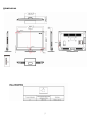
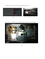
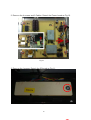
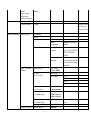
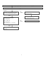
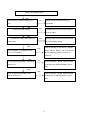
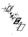
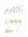
SERVICE MANUAL
LCD COLOR TELEVISION
MODEL:
LC-32LE440U
CONTENTS
SAFETY PRECAUTION
IMPORTANT SERVICE SAFETY PRECAUTION............................................................................. ………………………2
CHAPTER 1. SPECIFICATIONS
[1] SPECIFICATIONS .........................................................................................................................................4
[2] DIMENSIONS .................................................................................................................................................5
CHAPTER 2. REMOVING OF MAJOR PARTS
[1] REMOVING OF MAJOR PARTS ...............................................................................................................6
CHAPTER 3. ADJUSTMENT PROCEDURE
[1] ADJUSTMENT PROCEDURE ................................................................................................................14
[2] SERVICE MODE.....................................................................................................................................19
[3] SOFTWARE UPGRADE PROCEDURE .....................................................................................................20
CHAPTER 4. TROUBLESHOOTING TABLE
[1] TROUBLESHOOTING TABLE......................................................................................................................... 21
CHAPTER 5. MAJOR IC INFORMATIONS
[1] MAJOR IC INFORMATIONS ........................................................................................................................37
CHAPTER 6. BLOCK DIAGRAM/WIRING DIAGRAM
[1] BLOCK DIAGRAM ................................................................................................................................ ….. 41
[2] POWER MANAGEMENT BLOCK DIAGRAM .................................................................................................... 42
[3] WIRING DIAGRAM .......................................................................................................................................... 42
CHAPTER 7. PRINTED WIRING BOARD
[1] MAIN UNIT PRINTED WIRING BOARD .......................................................................................................... 43
[2] POWER UNIT PRINTED WIRING BOARD ....................................................................................................... 45
[3] KEY UNIT PRINTED WIRING BOARD ............................................................................................................. 47
[4] IR UNIT PRINTED WIRING BOARD................................................................................................................. 47
CHAPTER 8. SCHEMATIC DIAGRAM
[1] MAIN SCHEMATIC DIAGRAM ............................................................................................................................... 48
[2] POWER SCHEMATIC DIAGRAM ......................................................................................................................... 58
[3] KEY SCHEMATIC DIAGRAM ................................................................................................................................. 64
[4] IR SCHEMATIC DIAGRAM .................................................................................................................................... 64
CHAPTER 9. Parts Guide
[1]SPARE PARTS LIST .............................................................................................................................................. 65
[1] CABINET PARTS ................................................................................................................................................... 67
[2] SUPPLIED ACCESSORIES ................................................................................................................................... 69
[3] PACKING PARTS................................................................................................................................................... 70
1
2
3
CHAPTER 1. OPERATION MANUAL
[1] SPECIFICATIONS
Item
Model: LC-32LE440U
LCD screen size
32 inches diagonal
Resolution
1366 x 768
TV-standard
TV function
American TV Standard ATSC/NTSC System
VHF/UHF
VHF 2-13ch, UHF 14-69ch
CATV
1-125ch (non-scrambled channel only)
Receiving
Digital
channel
Broadcast (8VSB)
Terrestrial
Digital cable*1
(64/256 QAM)
Audio multiplex
2-69ch
1-135ch (non-scrambled channel only)
BTSC System
Audio out
5W*2
ANT./CABLE
Rear
Terminal
Side
75 Ω Unbalance ,F Type x 1 for Analog (VHF/UHF/CATV) and
Digital(AIR/CABLE)
INPUT2
HDMI in with HDCP
INPUT3
HDMI in with HDCP
Audio PC/HDMI
Audio in (Ø 3.5mm jack)
PC IN
Analog RGB (PC) in (15-pin mini D-sub female connector)
Headphone out
Ø 3.5mm jack (Audio output)
SPDIF
HDMI in with HDCP
RS-232C
D-sub 9 pin for service & Hotel mode using
INPUT1
HDMI in with HDCP
USB
Photo/Music/Video mode, Software update
OSD language
English/French/Spanish
Power Requirement
AC 120V ~60Hz
Power Consumption
≤75W (0.7 W Standby with AC 120 V)
TV + stand
18.7 lbs. /8.5 kg
TV only
16.7 lbs./7.6kg
Dimension
TV + stand
30 25/64 × 218/128× 7 96 /128 inch
(W/H/D)
TV only
30 25/64 × 1918/32× 2 10 /16 inch
Weight
Operating temperature
+32°F to + 104°F (0°C to + 40°C)
Response time
6ms
4
[2]DIMENSIONS
5
CHAPTER 2. Removing of Major Parts
1. Assy/Panel Removal
Notes: Please put your machine on soft material to avoid scrape panel when you
disassemble it.
Front view
Fig.1
Back view
Fig.2
Step1. Remove the Base Assy.
1. Remove the 4 screws as Fig.3 and pull out the base .
Fig.3
6
Step 2. Remove the REAR COVER Assy.
1. Remove the 13 screws, around the REAR COVER as Fig.4.
Fig.4
2. Remove the 4 screws at the IO area as Fig.5.
Fig.5
7
3. Remove the 3 screws to release AC cable as Fig.6 .Fig.7
Fig.6
Fig.7
Step3. Remove the Main, Power, IR board, Key Pad ASSY, and the Speakers.
Fig.8
8
1. Remove the 5 screws and disconnect 4 cables .Detach the Main board ASSY
as Fig.9
Fig.9
9
2. Remove the 4 screws and 2 Cables. Detach the Power board as Fig.10.
Fig.10
3. Remove the 1screws. Detach the IR board as Fig.11.
Fig.11
10
4. Remove the 1screws.Detach the Key Pad ASSY as Fig.12.
Fig.12
5. Detach the Speakers as Fig.13. Fig.14.
Fig.13
Fig.14
11
Step4. Remove BASE SUPPORT.
Remove the 4 screws and 2 cable clamps. Detach the BASE SUPPORT as Fig.15
Fig.15
12
Step5. Remove PANEL module.
1. Remove the 4 screws. Detach the PANEL HOLDER as Fig.16, Fig.17, Fig.18
Fig.16
Fig.17
Fig.18
13
CHAPTER 3. ADJUSTMENT PROCEDURE
[1]ADJUSTMENT PROCEDURE
1. Main Menu (The default value is marked in red)
Level 1
Level 2
Picture Settings AV Mode
Level 3
Level 4
Level 5
Level 6
User/ Standard/
Movie/ Game/ PC/
Dynamic/
Dynamic(Fixed)
OPC
Off/ On
Disable when
Backlight
0~100 (100)
AV mode is
Contrast
0~100 (50)
Dynamic(Fixe
Brightness
0~100 (50)
d).
Color
0~100 (50)
Tint
-50 ~ 50 (0)
Sharpness
0~20 (10)
Advanced
Color Temp.
Color Temp.
User/Cool/
Standard/Warm
R Gain
0~255
G Gain
0~255
B Gain
0~255
Reset
Yes/No
Active Contrast
Off/ On
DI Film Mode
Off/ Auto
Digital Noise Reduction Off/ Low/
Middle/ High/
Auto
Reset
Yes/No
(Only reset
currect AV
mode settings.)
Audio Settings
Treble
0~100 (50)
Disable when
Bass
0~100 (50)
AV mode is
Balance
-50 ~ 50 (0)
Dynamic(Fixe
Surround
Off/ On
d).
14
Reset
Yes/No
(Only reset
currect AV
mode settings.)
Power Control
No Signal Off
Enable/ Disable
Power Saving
Off/ On
Disable when
AV mode is
Dynamic(Fixe
d).
System Options
View Option
View Mode
Freeze
Change Audio
Change CC
MTS
Mono/ Stereo/ SAP
Audio
English/ Spanish/
Language
French
Analog Closed Off/ CC1/ CC2
Caption
/CC3 /CC4/ TEXT1/
TEXT2/ TEXT3/
TEXT4
Digital Closed
Off/ Service1/
Caption
Service2/ Service3/
Service4/ Service5/
Service6
Input Terminal Audio Setup
Off/ Dolby
Setting
Digital/ PCM
PC input
Auto Sync.
(For PC only)
Fine Sync.
H-Pos.
V-Pos.
Clock
Phase
Audio Select
Video/
(For PC only)
Video+Audio
Audio Select
Auto/
(For HDMI only)
HDMI(Digital)/
HDMI+Analog
HDMI Setup
HDMI Mode
(For HDMI only)
Caption setup
Video
Speaker
On/ Off
Caption Style
Default/
15
Auto/ Graphic/
Custom
(For TV & AV
only)
Caption Size
Small/
Standard/
Large
Foreground Color
Black/ White/
Green/ Blue/
Red/ Cyan/
Yellow/
Magenta
Foreground Opacity
Solid/
Translucent/
Transparent
Background Color
Black/ White/
Green/ Blue/
Red/ Cyan/
Yellow/
Magenta
Background Opacity
Solid/
Translucent/
Transparent
Window Color
Black/ White/
Green/ Blue/
Red/ Cyan/
Yellow/
Magenta
Window Opacity
Solid/
Translucent/
Transparent
Initial Setup
EZ Setup
Broadcasting
CH Setup
Air/Cable
Setup
CH Search
(For TV only)
CH Memory
Favorite CH
Air/ Cable
A
B
C
D
All Data Clear
16
Yes/No
Language
English/ Español/
Français
Individaul Setup Secret No.
New Secret No.
(Input Secret
Confirm Secret
No.)
No.
(For TV & AV
Parental CTRL
V-Chip
MPAA
only)
G/ PG/
PG-13/ R/
NC-17/ X/
NONE
TV Guidelines
TV-Y/ TV-Y7/
TV-G/ TV-PG/
TV-14/
TV-MA/
NONE
D, L, S, V, FV
Can.English
E/ C/ C8+/ G/
Ratings
PG/ 14+/ 18+/
NONE
Can.French
E/ G/ 8ans+/
Ratings
13ans+/
16ans+/
18ans+/
NONE
V-Chip(DTV
Only)
Status
Reset
Information
Yes/No
Identification
17
No/ Yes
2. Display adjustment
Only adjust HDMI Mode and copy to all of input source
General set-up:
Equipment Requirements: Minolta CA-210 or Equivalent Color analyzer or
equivalent instrument.
Input Signal Type:
1. Internal full white pattern.
2. Select Picture mode to Standard mode and check the x, y data.
Input Injection Point: HDMI cable
Alignment method:
Initial Set-up:
1. Select source as “INPUT 1” (HDMI 1).
2. Set AV mode as “Standard”.
3. Enter factory mode menu: press MENU + Numeric keys “3481” .
Alignment:
1. Press MENU key enter factory mode page.
2. Set VideoÆWhite Pattern to “Medium”.
3. Enter VideoÆColor Temperature adjust.
Color temperature adjust:
1. Set color temperature to “Cool”
2. Adjust R Gain/G Gain values to meet “Cool” color coordinates.(Keep B Gain set “128”)
3. Adjust R Offset/G Offset values to meet “Cool” color coordinates.(Keep B Offset set “128”)
4. Repeat step 2, 3, 4 twice to meet “Cool” color coordinates specification below.
5. Set color temperature to “Warm”、”Standard” then Repeat 2,3,4 step adjusting.
6. Set color temperature “User” mode then set all values to “128”
Mode
Chromaticity Coordinate
x
y
0.272 ± 0.015
0.277 ± 0.015
STANDARD
0.285 ± 0.015
0.293 ± 0.015
WARM
0.313 ± 0.015
0.323 ± 0.015
COOL
Customer Color
Panel Native Color Temperature
Check the 16 grayscale pattern should be distinguished and color bar is correct
18
Note:
1. Use Minolta CA-210 for color coordinates and luminance check.
2. Before adjusting, all color analyzers (CA-210) should be coordinates with a
same reference TV set.
3. Luminance > =320 cd/m2 in the center of the screen when Brightness control at
100, Contrast control at 100, Backlight control at 100. (Test Color mode:
Standard)
[2] SERVICE MODE
Enter factory mode menu: press MENU + Numeric keys “3481” to enter factory
mode.
You can press “RETURN” key to back to normal main menu.
19
[3] SOFTWARE UPGRADE PROCEDURE
1. Connect to TV USB port to upgrade the software firmware
Please follow the following steps to upgrade the firmware.
I.
Turn on TV.
II.
III.
Press MENU, select InformationÆIdentification to check "Version"
Copy the correct software firmware (*.pkg) to USB disk.
Ex: Version: V2.0, copy NAS2_89.pkg to USB disk.
IV.
Insert the USB disk to TV USB port.
V.
VI.
TV AC power off -> AC power on
TV will upgrade by itself after detect the USB disk condition and the content of the
pkg file.
Note: TV's LED will flash during upgrade process
VII. After finish upgrade process, TV will reboot by itself.
VIII. Remove USB disk from TV.
IX.
X.
Press MENU, select InformationÆIdentification.
Check the software version is correct or not.
20
CHAPTER 4.TROUBLESHOOTING TABLE
[1]TROUBLE SHOOTING TABLE
The sound is not emitted from the speaker though the picture has come out.
No sound output in all models?
TEREMINAL
Is the audio signal output of pin (96)
(AOSDATA0), pin (95) (AOBCK), pin (94)
(AOLRCK) and pin (93) (AOMCLK) of IC
U2102 normal?
NO
Check IC U2102 and its peripheral circuits.
YES
Is audio signal input to pin (6) (AOSDATA0),
pin (7) (AOBCLK), pin (8) (AOLRCK) and
pin (5) (AOMCLK) of IC U6101 (AMP)?
NO
Check the line between IC U2102 and IC
U6101.
YES
Is MUTE circuit [YDA_MUTE] normal ?
NO
Check the PD#. (R6130, Q6101, R6134, etc.)
YES
Is the audio signal output of pin (1, 2) (L-ch)
and pin (3, 4) (R-ch) of CN6101
(AOUDIO-CONNECTOR) normal?
NO
YES
Check Speaker Box (right and left) and wire
harness.
21
Check IC U6101 and its peripheral circuits.
No sound (during the reception of TV broadcasting)
Does not the sound go out though the picture has come out when UHF/VHF is received?
MAIN UNIT:
Is the DIF signal output from pin (10) and pin (11) of
NO
Check the tuner and its peripheral circuits. Replace as
required.
TUNER(TU9101)?
YES
Is the DIF signal sent to pin (58) and pin (59) of IC
NO
U2102?
YES
Refer to “No sound output in all modes”.
22
Check IC U2102 its peripheral circuits.
No sound from external input devices (1)
Does not the sound of the audio signal input to input (Component) go out?
MAIN UNIT:
v
Is the audio signal properly sent to pin (8) and pin
NO
(10) of CN1202?
Check the connection to CN1202 and the external
input device.
YES
Is the audio signal properly sent to pin (68)
(AIN0_R) and pin (70) (AIN0_L) of IC
U2102?
NO
YES
Refer to “No sound output in all modes”.
23
Check the line between CN1202 and IC U2102.
No sound from external input devices (2)
Does not the sound of the audio signal input to VGA go out?
MAIN UNIT:
Is the audio signal properly sent to pin (3) and pin
NO
(2) of CN1102?
Check the connection to CN1102 and the external
input device.
YES
Is the audio signal properly sent to pin (67)
NO
(AIN1_R) and pin (69) (AIN1_L) of IC U2102?
YES
Refer to “No sound output in all modes”.
24
Check the line between CN1102 and IC U2102.
No sound from external input devices (3)
Does not the sound of the audio signal input to USB go out?
YES
Is USB stick audio format correct?
MAIN
NO
Change to correct mp3 format
YES
NO
Is the USB +5V Q7105 sent to pin (1) of CN1104?
Check the connection to Q7105 and the external
input device.
YES
Is the USB con (CN1104) signal properly sent to
NO
pin (233) (USB_DM0) and pin (234) (USB DP0) of
IC U2102?
YES
Refer to “No sound output in all modes”.
25
Check the line between CN1104 and IC2102
The audio signal is not output
No audio signal output from Headphone terminal (CN6201).
Terminal
Is audio signal output from pin (12) (OUTL) and pin
YES
(3) (OUTR) of IC U6201 to Jack (CN6201)?
Check the connection to HPOL(R) OUT and
external devices.
No
Is the audio signal output from IC U2102 pin (74)
YES
Check the line between IC U2102 and IC U6201.
(AL1O) and pin (76) (AR1O) to pin (3) (OUTR) and
pin (12) (OUTL) of IC U6201
No
Check IC U2102 and its peripheral circuits.
.
26
The audio signal is not output
No audio signal output from SPDIF terminal (CN6202).
Terminal
Is input source on HDMI? The SPDIF out not
YES
support HDMI source.
Change input source to others (AV, TV, etc.).
No
Is the audio signal output from IC U2102 pin (92)
YES
Check the line between IC U2102 and CN6202.
(ASPDIF) sent to CN6202?
No
Check IC U2102 and its peripheral circuits.
27
No picture on the display (1)
The picture doesn't appear in all modes.
Main UNIT:
Check LVDS signal output from IC U2102 or not?
32" : (O0N/O0p), (O1N/O1P),(O2N/O2P),(O3N/O3P),(OCKN/OCKP)
42" : (O0N/O0p),(O1N/O1P),(O2N/O2P),(O3N/O3P),(OCKN/OCKP), (E0N/E0p), (E1N/E1P), (E2N/E2P), (E3N/E3P),
(ECKN/ECKP)
Check IC U2102 and its peripheral control
YES
circuits.
Check signal
NO
Check relative components are ok or not.
BL_PWM/BL_ON/PSON/ID_0/1/2/LVDS_Power
_ON/LVDSVDD are normally or not.
YES
NO
Similarly, is the LVDS signal input to
Wire harness is checked.
connector of the panel module?
YES
Check the panel module.
28
No picture on the display (2)
Does not the picture come out when VHF/UHF is received?
Main UNIT:
Check +5V_tuner/VCCK/DDRV/AV33/DV33/+3V3SB
NO
is applied to Tuner and U2102 or not.
Check each power IC and peripheral
components are correct or not.
YES
Is the DIF signal output from pin (10) and pin (11) of
NO
TUNER
Check the tuner and its peripheral circuits.
Replace as required.
(TU9101)?
YES
Is the DIF signal sent to pin (58) and pin (59) of IC
NO
U2102?
Check IC U2102 its peripheral circuits.
YES
Refer to “The picture doesn't appear in all modes.”
29
<External input Input(Side HDMI)>No picture on the display (3)
Does not the picture display when HDMI cable plugged into HDMI1 ?
Terminal
Is the HOT_PLUG detection function of
NO
Check the line between pin (78) of IC
U2102 and CN8103.
pin (19) of HDMI terminal (CN8103)
YES
Check the connection and setup with
Main UNIT:
the external HDMI devices.
Is TMDS signal input into pin
RX3_2/ RX3_2B,
RX3_1 /RX3_1B,
NO
Check the line between IC U2102 and
RX3_0/RX3_0B
RX3_C/RX3_CB of IC U2102?
YES
Refer to “The picture doesn't appear in
all modes.”?
30
<External input Input(Rear_HDMI2)>No picture on the display (4)
Does not the picture display when HDMI cable plugged into HDMI 2 ?
Terminal
Is the HOT_PLUG detection function of
NO
Check the line between pin (7) of IC
U2102 and CN8101
pin (19) of a HDMI terminal (CN8101)
YES
Check the connection and setup with
the external HDMI devices.
Is TMDS signal input into pin
RX1_2/ RX1_2B,
RX1_1 / RX1_1B,
NO
RX1_0/ RX1_0B
RX1_C/ RX1_CB of IC U2102?
YES
Refer to “The picture doesn't appear in
all modes.”?
31
Check the line between IC U2102 and
<External input Input(Rear HDMI3)>No picture on the display (5)
Does not the picture display when HDMI cable plugged into HDMI 3?
Terminal
Is the HOT_PLUG detection function of
NO
Check the line between pin (1) of IC
U2102 and CN8102.
pin (19) of a HDMI terminal (CN8102)
YES
Check the connection and setup with
the external HDMI devices.
Is TMDS signal input into pin
RX2_2/ RX2_2B,
RX2_1 / RX2_1B,
NO
RX2_0/ RX2_0B
RX2_C/ RX2_CB of IC U2102?
YES
Refer to “The picture doesn't appear in
all modes.”?
32
Check the line between IC U2102 and
<External input USB>No picture on the display (6)
Does not the picture display when USB cable plugged into USB port?
Is USB stick video format correct?
Main UNIT:
NO
Change to correct .jpg or .jpeg or .png or
.bmp format.
YES
Is the USB +5V sent to pin (1) of
NO
Check the fuse F1101 and the external
input device.
YES
Is the USB con (CN1104) signal properly
NO
sent to pin (233) (USB_DM0) and pin
(234) (USB_DP0) of IC U2102?
YES
Refer to “The picture doesn't appear in
33
Check the line between CN1104 and IC
<External input Input(Component)>No picture on the display (7)
Does not the picture display when RCA cable plugged into component?
Terminal
Is Component Y/Pb/Pr signal sent to pin
NO
(2)/Y, (4)/Pb, (6)/Pr of CN1202?
Main UNIT:
Check the setting of an external input
device that connects of CN1202
YES
<External input
NO
Input(Component)>No picture on the
YES
Refer to “The picture doesn't appear in
34
Check the line between IC U2102 and
<External input D-SUB>No picture on the display (8)
Does not the picture display when VGA cable plugged into D-SUB ?
Is Video format correct?
Terminal
NO
Set the timing which TV is support
NO
Check the setting of an external input
YES
Is R/G/B/H/V signal sent to pin (1)/RED,
(2)/Green, (3)/BLUE, (14)/H sync#,
device that connects of CN1101
YES
Main UNIT:
Is R/G/B/H/V signal sent to pin
NO
(32)/RED, (30)/Green, (28)/BLUE,
YES
Refer to “The picture doesn't appear in
35
Check the line between IC U2102 and
Power unit operation check
YES
Are the power cord and harness in the
NO
Power cord and harness in the unit
unit
connected
YES
If F101 and F102 normal?
NO
Line filter unit? LX101 ,LX102 or RT101
is out of order?
YES
Does BD101 output 169V when AC
NO
Change a new full-wave rectifier diode to
input 120V?
check the output voltage.
YES
Is the voltage of +12V applied to pin
Does the standby circuit normal?. (QM104,
NO
TM101, ZD102 , DM103 , the circuit around
11,12 ,13 of CN201?
the um102 and protection circuit ect. is
checked)
YES
Is +5V output as for power on/off switch
NO
Does the UM103 , UM108 ,LM101 and the
when is on?
circuit around IC UM103/UM108? Check
them.
YES
Is +24V output as for power on/off
NO
Does the UM104 , QM105 ,LM103 and the
switch when is on?
circuit around IC UM103/UM104? Check
them.
36
CHAPTER5. MAJOR IC INFORMATIONS
[1]MAJOR IC INFORMATIONS
1.1. U2102 (MT5389)
The MediaTek MT5389FUNU family consists of a DTV front-end demodulator, a backend
decoder and a TV controller and offers high integration for advanced applications. It combines a
transport de-multiplexer, a high definition video decoder, an audio decoder, a dual-link LVDS
transmitter, a mini-LVDS transmitter (option), an EPI transmitter (option) and an
NTSC/PAL/SECAM TV decoder with a 3D comb filter (NTSC/PAL). The MT5389FUNU enables
consumer electronics manufactures to build high quality, low cost and feature-rich DTV.
World-Leading Audio/Video Technology: The MT5389FUNU supports Full-HD
MPEG1/2/4/h.264/DiviX/VC1/RM/AVS (option) video decoder standards, and JPEG. The
MT5389FUNU also supports MediaTek MDDiTM de-interlace solution can reach very smooth
picture quality for motions. A 3D comb filter added to the TV decoder recovers great details for
still pictures. The special color processing technology provides natural, deep colors and true
studio quality video. Also, the MT5389FUNU family has built-in high resolution and high-quality
audio codec.
Rich Features for High Value Products: The MT5389FUNU family enables true singlechip
experience. It integrates high-quality HDMI1.4a, high speed VGA ADC, LVDS, mini-LVDS
(option), EPI (option), USB2.0 receiver, TCON (option), panel overdrive (option), and ATSC
demodulators.
WW Common Platform Capability: The MT5389FUNU family supports ATSC
demodulation functions. TV maker can easily port the same UI to worldwide TV models.
Excellent adjacent and co-channel rejection capability grants customers never miss any
wonderful stream. Professional error-concealment provides stable, smooth and mosaic-free
video quality.
Key Features:
1. Worldwide multi-standard analog TV demodulator
2. ATSC demodulators
3. Powerful CPU core
4. A transport de-multiplexer
5. A muti-standard video decoder
6. Rich format audio codec
7. HDMI1.4a receiver
8. Local dimming (LED backlight) (option)
9. TCON (option)
10. Panel overdrive control (option)
37
11. LVDS, mini-LVDS (option), EPI (option)
1.2. U3101 (NT5CB64M16DP)
Description
The 1Gb Double-Data-Rate-3 (DDR3/L) B-die DRAMs is double data rate architecture to achieve
high-speed operation. It is internally configured as an eight bank DRAM.
The 1Gb chip is organized as 16Mbit x 8 I/Os x 8 banks or 8Mbit x 16 I/Os x 8 bank devices. These
synchronous devices achieve high speed double-data-rate transfer rates of up to 1866 Mb/sec/pin
for general applications.
The chip is designed to comply with all key DDR3/L DRAM key features and all of the control and
address inputs are
synchronized with a pair of externally supplied differential clocks. Inputs are latched at the cross
point of differential clocks (CK rising and ___falling). All I/Os are synchronized with a single ended
DQS or differential DQS pair in a source
synchronous fashion. These devices operate with a single 1.5V ± 0.075V &1.35V -0.067/+0.1V
power supply and are available in BGA packages.
The DDR3/L SDRAM D-Die is a high-speed dynamic random access memory internally configured
as an eight-bank
DRAM. The DDR3/L SDRAM uses an 8n prefetch architecture to achieve high speed operation.
The 8n prefetch
architecture is combined with an interface designed to transfer two data words per clock cycle at
the I/O pins. A single read or write operation for the DDR3/L SDRAM consists of a single 8n-bit
wide, four clock data transfer at the internal DRAM core and two corresponding n-bit wide, one-half
clock cycle data transfers at the I/O pins.
Read and write operation to the DDR3/L SDRAM are burst oriented, start at a selected location,
and continue for a burst length of eight or a ‘chopped’ burst of four in a programmed sequence.
Operation begins with the registration of an Active command, which is then followed by a Read or
Write command. The address bits registered coincident with the Active command are used to
select the bank and row to be activated (BA0-BA2 select the bank; A0-A13 select the row). The
address bit registered coincident with the Read or Write command are used to select the starting
column location for the burst operation, determine if the auto precharge command is to be issued
(via A10), and select BC4 or BL8 mode ‘on the fly’ (via A12) if enabled in the mode register.
Prior to normal operation, the DDR3/L SDRAM must be powered up and initialized in a predefined
manner. The following sections provide detailed information covering device reset and initialization,
register definition, command descriptions and device operation.
38
1.3. U6102 (YAMAHA YDA175)
Features
・Supply Voltage Range VDDP 5V*1) to 18V
・Input Digital Audio Interface (Stereo)
Sampling Frequency: 32kHz, 44.1kHz, 48kHz
Left-justified, MSB first, 1-bit delay, Digital Audio Data 24-bits
・Max. Instantaneous Output 15W×2ch (VDDP=15V, RL=8Ω, THD+N=10%)
10W×2ch (VDDP=12V, RL=8Ω, THD+N=10%)
10W×2ch (VDDP=12V, RL=6Ω, THD+N=10%)
・Max. Continuous Output 15W*2)×2ch (VDDP=15V, RL=8Ω, Ta=70 ºC, 4-layer Board)
10W*2)×2ch (VDDP=12V, RL=8Ω, Ta=70 ºC, 4-layer Board)
10W*2)×2ch (VDDP=12V, RL=6Ω, Ta=70 ºC, 4-layer Board) *TBD
・Distortion Ratio (THD+N) 0.05% (VDDP=12V, RL=8Ω, Po=4.5W, 1kHz)
・Residual Noise 50µVrms (VDDP=12V, RL=8Ω, A-Weighted Filter)
・S/N Ratio 105dB (VDDP=12V, RL=8Ω, A-Weighted Filter)
・Efficiency 92% (VDDP=12V, RL=8Ω, Po=10W)
・Channel Separation 80 dB (VDDP=12V, RL=8Ω, 1kHz)
・Power Limit Function (15W, RL=8Ω, min, THD+N=10%)
・Output Mute Function (Quick Mute/Quick Start)
・Sleep Function
・Pop Noise Reduction Function
・Overcurrent Protection Function (OCP)
・Over Temperature Protection Function (OTP)
・Under Voltage Lockout (UVLO)
・DC Detection Function (DCDET)
・Clock Detection Function (CKDET)
・Package Lead-free 32-pin Plastic QFN (Exposed die pad) : YDA175-QZ
*1: When operating below 8V (VDDP), the speaker impedance must be 8Ω or higher.
*2: These values are based on evaluations on a Yamaha's PCB board implementation.
1.4. U1101 (TRS3221ECDBR SSOP16)
FEATURES
· ESD Protection for RS-232 Pins
– ±15-kV Human-Body Model (HBM)
– ±8 kV (IEC 61000-4-2, Contact Discharge)
– ±15 kV (IEC 61000-4-2, Air-Gap Discharge)
· Meets or Exceeds the Requirements of
TIA/EIA-232-F and ITU v.28 Standards
39
· Operates With 3-V to 5.5-V VCC Supply
· Operates up to 250 kbit/s
· One Driver and One Receiver
· Low Standby Current . . . 1 µA Typical
· External Capacitors . . . 4 ´ 0.1 µF
· Accepts 5-V Logic Input With 3.3-V Supply
· Alternative High-Speed Pin-Compatible (1 Mbit/s)
.TRSF3221E
· Auto-Powerdown Feature Automatically
Disables Drivers for Power Savings
Description
The TRS3221E is a single driver, single receiver RS-232 solution operating from a single VCC
supply. The RS-232 pins provide IEC G1000-4-2 ESD protection. The device meets the
requirements of TIA/EIA-232-F and provides the electrical interface between an asynchronous
communication controller and the serial-port connector. The charge pump and four small external
capacitors allow operation from a single 3-V to 5.5-V supply. These devices operate at data
signaling rates up to 250 kbit/s and a maximum of 30-V/µs driver output slew rate.
Flexible control options for power management are available when the serial port is inactive. The
auto-powerdown feature functions when FORCEON is low and FORCEOFF is high. During this
mode of operation, if the device does not sense a valid RS-232 signal on the receiver input, the
driver output is disabled. If FORCEOFF is set low and EN is high, both the driver and receiver are
shut off, and the supply current is reduced to 1 µA. Disconnecting the serial port or turning off the
peripheral drivers causes the auto-powerdown condition to occur. Auto-powerdown can be
disabled when FORCEON and FORCEOFF are high.
With auto-powerdown enabled, the device is activated automatically when a valid signal is applied
to the receiver input. The INVALID output notifies the user if an RS-232 signal is present at the
receiver input. INVALID is high (valid data) if the receiver input voltage is greater than 2.7 V or less
than –2.7 V, or has been between -0.3 V and 0.3 V for less than 30 µs. INVALID is low (invalid data)
if the receiver input voltage is between –0.3 V and 0.3 V for more than 30 µs. Refer to Figure 5 for
receiver input levels.
40
CHAPTER 6.BLOCK DIAGRAM/WIRING DIAGRAM
[1]BLOCK DIAGRAM
TUNER
LVDS OUT
H702F
1Gb DDR3
Side
HDMI1
Rear
HDMI2
Rear
HDMI3
Side
USB
8MB FLASH
MT5389
PC INPUT
I2S
YDA175
AUDIO AMP
SPEAKER
YPbPr+CVBS
ASPDIF
Hotel Mode
Earphone
amp.DRV632
41
SPDIF Output
RS 232
(NAFTA)
(NAFTA)
Earphone
Side
[2]POWER MANAGEMENT BLOCK DIAGRAM
There are 1 part circuits in Power board of this project (fig.1), Power circuits which is a single layer board,
There are 3 output in the power parts, one is interface board including USB and TV tuner et; the other is
inverter board and audio circuit.+24V output is inverter part.the system block diagram as below; the last
is panel Vcc and audio, the power is 12V.
AC
INPUT
EMI
Rectifier
filter
Standby
DC:12V/2.23A output to
Audio
DC:5.3V/2A output to IF BD
DC:24V/1.6A output to Inverter
DC-DC
ACD
ACD
(fig.1)
[3]WIRING DIAGRAM
42
CHAPTER 7.PRINTED WIRING DIAGRAM
[1]MAIN UNIT PRINTED WIRING BOARD (LC-32SV40U&LC-42SV50U&LC-46SV50U)
TOP
43
BOTTOM
44
[2]POWER SCHEMATIC DIAGRAM- POWER BOARD WITH TOP/BOTTOM VIEW
Top Layer
45
Bottom Layer
46
[3]KEY UNIT PRINTED WIRING BOARD
[4] IR UNIT PRINTED WIRING BOARD
47
CHAPTER 8.SCHEMATIC DIAGRAM
[1]MAIN SCHEMATIC DIAGRAM
01 System POWER
48
02 MT5389
49
03 DDR3 DRAM/Flash.
50
04 Peripheral / IR/Keypad /ESD
51
05 HDMI
52
06 VGA/RS-232/USB
53
07 YPbPr
54
08 Audio amp.
55
09 Headphone/ line out /SPDIF
56
10 LVDS
11 Tuner
57
[2]POWER SCHEMATIC DIAGRAM
1) AC Input and EMI Filter:(fig.7)
VZ105
2
RT101
SG104
2
470K
R1206
CY 102
1000p/250V
CAP--CSY -1001000p/250V
CAP--CSY -100
1
2
LX102
CHK-251
IND--LC-2222-1806
CX102
0.33u/275V
CAP--CSX-1809-150
VZ102
RES--RT-WD165-075
1
1000p/250V
CAP--CSY -100
CY 103
BD101
4
3
1
RX102
F101
CHK-251
IND--LC-2222-1806
-
5
CY 101
LX101
VZ101
CX101
470K
RES--RT-WD165-075
R1206
0.33u/275V
CAP--CSX-1809-150
1
NTC 2.5Ω/8A
300V
RES--RT-WD165-075
OTHER--SPARK-GAP-070
3
A3963WR2-5P-A
CON--FOX-HF9905
3
1
470K
R1206
RX101
4
CN101
2
4A/250V
FUSE--250
2
1
RX103
4
RES--RT-WD165-075
6200V
OTHER--SPARK-GAP-070
F102
SG103
2
300V
OTHER--SPARK-GAP-070
3
DP106
FR10-10-LF
DIO--DO41
DP107
FR10-10-LF
DIO--DO41
Fig.7
CN101 is a connector for connecting AC Power. F101&F102 are fuse to protect all the circuit
AC. Input voltage is single 120V. CY101, CY102, CY103 are used high frequency noise of primary
between common GND.LX101,LX102,CX101, CX102 is used to filter low frequency noise. RX101,
RX102 and RX103 are used to discharge CX101 and CX102 remnants voltage
58
KBJ1006G-FC
DIO--WKBJ
2
+
4A/250V
FUSE--250
1
1
1 1
2
SG105
2
2) Standby Control&DC-DC&ACD Circuit:(fig.8)
HS1
Hestsink1
HS-43.5X45.1
1
2
+12V2
+ 1
1
A
FERR BEAD
IND--090
BD+
+ CP110
68u/450V
3
+ CP111
68u/450V
CP113
NC
CAP--CC-050
RM104
68K 2W
RES--2W-150
CM104
222/630V
RM107
20K
R1206
RM106
NC/NC
R1206
RM109
NC/NC
R1206
DIS
ZD102
P6KE200A
1
3
COMP
RM114
CM113
NC/NC
R0805-P 1000p/50V
C0805-P
2
CM114
1000p/50V
C0805-P
3
4
EN/DIS
2
HV
COMP
NC
CS
VDD
GND
GATE
IND--060 LB102
8
7
CM116
0.1u/50V
C0805-P
6
5
RM116
100
R0805-P
RM117
10K
R1206
TRS--WTO220-GDS-210
1
QM104
700V/12A
CM117
100PF/1KV
CAP--CC-050
G
CM115
220p/50V
C0805-P
RM118
270
R1206
RM101
0.24ohm 2W
RES--2W-150
VCC1
DIO--1N4148
DM108
SN4148
1
RM120
2
R1206
DM105
VCC
FR10-10-LF
DIO--DO41
CM123
+
10u/50V
CAP--CE-D050-050
59
+ CM220
680u/25V
CM109
0.1u/50V
C0805-P
CAP--CE-D100-1016R
CAP--CE-D100-1016R
CAP--CE-D100-1016R
+ CM110
680u/25V
CAP--CE-D100-1016R
2
3
4
.
C0805-P
CM111
0.1u/50V
1
RM113
1M
R0805-P
5
6
7
TRS--TO252-GDS
R0805-P
RM105
120K 1%
RM108
20K 1%
R0805-P
R0805-P
RM112
200K
CM112
2.2u/16V
. .
HS2
Hestsink2
HS-30.7X47.9
DIO--1N4148 R0805-P
DM104
RM115
SN4148
47ohm
+ CM108
680u/25V
QM102
P1504EDG4
3
2
PSON
INN801BGS
1
2
+ CM107
680u/25V
DM112
SRF20-150CT
IC--WTO220-GDS
TRF--CC40-7P
TM101
350uH
DM103
FR207G
DIO--DO41
UM102
2
DM102
SRF20-150CT
IC--WTO220-GDS
DIO--DO15
RM111
20K
R1206
RM110
NC/NC
R1206
3
CAP--CP-1007-075
D
BD+
+12V
LM102
1.25uH
IND--H06110015
3
CAP--CE-D125-1250R
1
+12V1
CAP--CE-D125-1250R
LB101
4 -
CAP--CC-050
CM102
2200p/1kV
2
RES--3W
RM102
20ohm 3W
DIO--WKBJ
KBJ1006G-FC
BD101
S
2
Fig.8
QM103
MMBT4401
TRS--SOT23-BEC
CM106
0.1u/50V
C0805-P
RM226
2K 1%
R1206
+12V1
+12V2
COMP
RM133
NC
RM135
20K 1%
R0805-P
R1206
UM105
LTV-817M-C
1
3
2
C0805-P
CM138
0.1u/50V
CM142
3
IC--LTV817M
1
CM135
100p/50V
C0805-P
RM140
NC
RM147
R0805-P
33K 1%
R0805-P
0.01u/50V
C0805-P
RM154
5.1K 1%
R0805-P
RM159
NC
R0805-P
C0805-P
+5V
+12V2
ZD103
5.6V
DIO--ZD-1206
ZD101
15V
DIO--ZD-1206
DM107
OVP
0
OVP
3
RM166
NC
R0805-P
1
2
CM147
NC
C0805-P
RM171
NC
R0805-P
Fig.9
OVP
VCC
UM110
LTV-817M-C
4
RM204
39K 1%
R0805-P
RM203
82K
R0805-P
3
2
1
QM201
PMBT2907A
SN4148
QM202
MMBT4401
2
TRS--SOT23-BEC
1
2
R1206
RM202
10K
R0805-P
RM205
1K
R0805-P
RM201
330 1%
3
3
DIS
1
IC--LTV817M
TRS--SOT23-BEC
DIO--1N4148
DM201
PSON
CM143
NC
UM106
2
AS431
IC--TO92-RAC
QM109
NC
TRS--SOT23-BEC
R0805-P
RM146
NC
QM101
1
NC
TRS--SOT23-BEC
2
4
RM137
5.1K 1%
R0805-P
3
RM132
2K 1%
R1206
CM201
0.01u/50V
C0805-P
60
RM149
NC
R0805-P
RM142
20ohm
R1206
+12V
IND--D140-112
LM103
15uH CHK-145
CAP--CE-D100-1016R
+ CM105
470u/35V
CM126
0.1u/50V
C0805-P
DIO--1N4148
DM106
SN4148
CM130
1u/50V
2
1
C0805-P
CM101
0.01u/50V
3
5
CM134
0.22u/50V
4
CM136 12
1000p/50V
C0805-P
VDC
ISW
COMP
PGND
FB
FSW
PWMI
SS
FAULT
EN
OOVP
14
11
R0805-P
0
RM182
13
RM148
1M
R0805-P
RM151
390K
+24V
8
2
4
RM134
100KR0805-P
CM140
0.1u/50V
C0805-P
R0805-P
RM138
1M
CM137
0.1u/50V
C0805-P
RM139
390K
CM129
0.1u/50V
C0805-P
RM180
4.7K 1%
R1206
RM181
4.7K 1%
R1206
R0805-P
CM131
10P/50V
C0805-P
R0805-P
RM238
100
VDC
10
CM160
0.1u/50V
C0805-P
RM129
0.05 2W 1%
R2512
FaultI
7
PWM
+12V
CM139
100p/50V
C0805-P
R0805-P
R0805-P
RM152
100K 1%
CM144
0.1u/50V
C0805-P
R0805-P
CM145
1000p/50V
C0805-P
RM128
100
CM133 R0805-P
NC
C0805-P
R0805-P
RM130
NC
FB
9
RM141
10K 1%
IC--SOP14 R0805-P
+12V
2
RM125
2 1%
QM105
P1504BDG NIKOS
TRS--TO252-GDS
1
RM126
2.2ohm
R0805-P
RM127
1.6K 1%
R0805-P
6
C0805-P
RM131
10K 1%
R0805-P
DRV
VIN
AG N D
CM132
1u/50V
R0805-P
RM136
56K 1%
RM124
NC
R0805-P
UM104
RT8525
VDC
1
SR506F79-LF
DM101 CAP--CE-D100-1016R CAP--CE-D100-1016R
60V ok.
+ CM127
+ CM128
DIO--DO201AD-200A
470u/35V
470u/35V
3
+12V
CM141
2.2nF/50V
C0805-P
+24V
42'' 32'' (190K)
R0805-P
RM220
NC
R0805-P
RM221
NC
FB R0805-P
RM156
182K 1%
FBI
CM223
NC
C0805-P
RM157
10K 1%
R0805-P
+12V2
CAP--CE-D100-1016R
IC--HSOP8L
UM103
RT8120DZSP
5
CM222
0.1u/50V
C0805-P
6
RM310
10K 1%
R0805-P
BOOT
CM311
0.01u/50V
C0805-P
1
R0805-P
RM123
4.7 1%
C0805-P
CM118
0.01u/50V
2
8
3
4
LGATE/OCSET 3
GND
4
FB
PHASE
CM119
1u/50V
+ CM150
470u/35V
+5V
1
2
COMP/EN UGATE
9
CM310
10P/50V
C0805-P
7
VCC
9
+12V2
TRS--SO8-SSS
UM108
AP4232BGM
S1
D1
G1
D1
S2
D2
G2
D2
8
IND--D140-112
LM101
15uH CHK-145
7
6
5
RM119
56K 1%
R0805-P
RM222
16K 1%
R0805-P
RM224
0
R0805-P
CM124
10P/50V
C0805-P
RM225
10
R0805-P
CM120
150p/50V
C0805-P
61
RM122
10K 1%
R0805-P
CM312
0.1u/50V
C0805-P
+ CM121
+ CM221
1000u/10V
NC
CAP--CE-D100-1016R CAP--CE-D100-1016R
CM122
0.1u/50V
C0805-P
VCC1
+5V
BD+
CM152
1u/50V
CM151
1u/50V
RM160
100K
R0805-P
R0805-P
RM163
1M 1%
R1206
NC/NC
UM107
LTV-817M-C
1
4
R0805-P
RM169
RM168
1M 1%
R1206
RM174
390K 1%
R0805-P
RM165
10K
R0805-P
RM164
DIS
IC--LTV817M
1
RM176
100K
R0805-P
CM148
0.47u/50V
1
QM110
MMBT4401
TRS--SOT23-BEC
CM159
NC
C0805-P
2
3
ZD104
RM175
5.6V
47k
DIO--ZD-1206
ACD
NC/NC
3
3
2
QM111
MMBT4401
TRS--SOT23-BEC
RM172
NC/NC
R0805-P
2
RM170
1M 1%
R1206
RM161
10k
R0805-P
CM158
0.1u/50V
RM173
100K 1%
R0805-P
R0805-P
CN202
14
13
12
11
10
9
8
7
6
5
4
3
2
1
CN201
PWM
FaultI
BLON
FBI
CON--JWT-A2501WV216PT
+24V
14P 2.5mm
CON--JWT-A2501WV214PT
1
2
3
4
5
6
7
8
9
10
11
12
13
14
15
16
ACD
PWM
BLON
PSON
+5V
+12V
16P 2.5mm
BD101 is a rectifier in which there are 4 build-in diodes, inverting AC to DC. CP110,CP111
is used to smooth the wave from rectifier. FR801 is a fuse resistor to protect the following circuit
when inrush current is too large.
UM102 is a current-mode PWM controller with excellent power-saving operation, It features a
high-voltage current source to directly supply the startup current from two half-wave rectifier diodes
further to provide lossless startup circuit. Max start-up current for UM102 is 10mA, When current
flow from two half-wave rectifier diodes through RM107 and RM111 gets to HV pin to start up
UM102, Meanwhile, the VCC supply current is as low as 550uA thus most of the HV current is
utilized to change the VCC capacitor CM123, When Vcc (Pin6) reaches UVLO(on) threshold ,The
UM102 is powered on to start issuing the gate drive signal , the high-voltage current source is then
disabled ,and the Vcc supply current is provided from the auxiliary winding of the transformer PIN3.
UM102 Pin3 is protection PIN.RM101 are sense circuit, UM102 detects the MOSFET current,
from the CS in. When CS pin over 0.73V, the UM102 will enter auto-recovery type protection,
Presenting a hiccup mode. The gate-out will not resume switching until OCP falls below 0.67V.
UM102 Pin1 is OVP protection PIN.It receives ON/OFF signal from secondary scalar
62
controller. If the voltage of EN/DIS pin exceeds the enable threshold voltage 1.2V or EN/DIS pin is
floating, the system will be start-up. However, if the voltage of EN/DIS voltage is below the enable
threshold voltage 0.8V, the system will be shut down completely and consume almost zero power.
For
low
as
small
standby
power
application,
it's important
to
make
current
in
this
path
as possible. The deglitch delay time of the disable function is about 20us. The internal
bias current of EN/DIS is 2uA. For low power consumption, it's a high impedance pin. Therefore,
proper layout is necessary for noise immunity. If capacitor is unavoidable,
should
be
capacitor
value
carefully calculated and not to influence system operation.
UM102 control 12V output , UM103, UM108, LM101 construct buck circuit to output 5V. UM104,
LM103 , QM105 construct buck circuit to output 12V.
ACD circuit is to make the backlight shutdown in time as son as AC input turn off .When
AC input turn on , the ACD signal will output a low voltage, then the main board receive this
low voltage to make backlight work normally. When AC input turn off , the ACD signal will
output a high voltage, then the main board receive this high voltage to make backlight
shutdown.
63
[3]KEY SCHEMATIC DIAGRAM
ME. Top Down Sequence
POWER_KEY
CN901
4P 2.0mm 90° (W/L)
4
3
2
ADC1
ADC0
To IF BD:
ADC1
To IF BD:
ADC0
INPUT
MENU
VOL-
VOL+
CH-
CH+
1
TACT-5
3
2
3
2
SW902
CH+
TACT-5
TACT-5
4
C909
1000p/25V
1
4
C908
1000p/25V
1
4
1
4
C907
1000p/25V
TACT-5
R902
8.2K 1%
SW907
CH-
3
2
2
TACT-5
R903
4.32K 1%
SW906
VOL+
C906
1000p/25V
1
C905
1000p/25V
TACT-5
R905
2.2K 1%
SW904
VOL-
3
C904
1000p/25V
4
1
4
1
C903
1000p/25V
R907
0
SW905
POWER_KEY
2
SW901
INPUT
2
2
SW903
MENU
R906
0
3
R901
4.32K 1%
1
D902
0.055p/24V
4
R904
8.2K 1%
D901
0.055p/24V
3
C902
1000p/25V
3
C901
1000p/25V
TACT-5
[4]IR SCHEMATIC DIAGRAM
新帶Lock CN
R101
47
U101
FM-1038FN-5CN
3
VCC
VOUT
GND
GND
R104
22
C106
0.1u/16V
4
R105
NC/0
R102
10K
2
1
I2C_SCLK
CN101
1
2
3
4
5
6
LED1_ON_OFF
LED2_ON_OFF
IR
C103
1000p/50V
C101
NC/10u/10V
D108
0.055p/24V
SCLK
ADC_SDA
IR
D106
NC/0.055p/24V
C104
NC/1000p/50V
C102
0.1u/16V
8
+5VSB
+5VSB
7
+5VSB
R103
NC/0
C105 6P 1.25mm 90°
10p/50V
D107
NC/0.055p/24V
D105
0.055p/24V
C107
100p/50V
D103
0.055p/24V
+5VSB
6
C108
NC/0.1u/16V
U102
NC/CM3213A3OP
VDD
R108
4
NC/1M 1%
1
SET
GND
INT
SCLK
SDAT
3
5
2
I2C_SCLK
ADC_SDA
+5VSB
+5VSB
R106
1K
1
G
D101
NC/LED SMT R/G
U103
ALS-PDIC17-77C/TR8
For NAFTA
For Others
26/32/42/46
Dual LED
Red Only
R: off
R: off
G: on
D101: NC
D102
1
2
3
D101
D102: NC
1
R112
10K
2
3
Q102
PMBT3904
Q101
1
NC/PMBT3904
2
R110
1K
2
LED2_ON_OFF
3
4
2
D102
LTST-C190KRKT
R
1
3
R107
NC/1K
R111
NC/1K
LED1_ON_OFF
R113
NC/10K
64
VCC VOUT
GND GND
GND GND
6 Light_Sensor_I2C
5
4
R115 0
I2C_SCLK
R114
51K
ADC_SDA
R116
100K
C109
1u/16V
CHAPTER 9.PARTS GUIDE
[1]SPARE PARTS LIST
Recommended Spare Parts List
Material
751202000-600-G
Region
NA
Description
LC-32LE440U
Updated date
2011 年 12 月 15 日
Item Catalog
1
Panel
Component no.
Object description
Usage
9JY76040NG00531G
LCD Module,TFT,TV,V315B5-LE3,
1
9JY0132CTG04100
LC-32LE440U/CTG04,Mother Board
1
9JY0932CTG04000
LC-32LE440U/CTG04,Power Board
1
4
9JY0332CTG05000
LC-32SV40U/CTG05,Keypad Board
1
5
9JY0432CTG05000
LC-32SV40U/CTG05,IR Board
1
FRONT BEZEL ASSY,CTG04
1
2
3
PCBA
6
Cosmetics 9JY01200019577
7
9JY01200019573
BASE ASSY,CTG04
1
8
9JY02500012541
NECK SUPPORT ASSY ,CTG04
1
65
Photo
9
9JY02500012535
10
9JY01200009937
ASSY BACKCOVER,CTG04
1
11
9JY01200019574
FUNCTION KEY,CTG04
1
12
9JY02500012530
IF SHIELDING ,CTL02
1
13
9JY02500012537
PANEL HOLDER,CTG04
4
14
9JY01200019663
AC COVER,VT464D
1
15
9JY35101M80033TG
LCD Cable Assembly,420mm,+/-10mm,G
1
16
9JY35101MC0020UG
LCD Cable Assembly,220mm,+/-5mm,G
1
17
9JY35110FQ0033TG
Cable
18
9JY35101MT0020UG
19
9JY35071BP00600G
20
Speaker 9JY57020Q100975G
22 Accessory 9JY600153G00886G
23
Screw
9JY06000013236
SIDE I/O BRACKET ASSY,CTG04
FFC Cable Assembly,200mm,
+/-3mm,1mm,30,G
LCD Cable Assembly,850mm,
+20/-0mm,G
AC Power Cable,1.6m+0.10m,+/-50mm,
18AWG,5PIN+2PIN,G
Speaker Unit,6ohm,5W,G,
YDT30120N-R001B06
Remote Controller, IR,NEC,
8m,G,RC-LCDTV-520
SCREW,B,CROSS,M5*44.5,Zn-black
[2]CABINET PARTS
66
1
1
1
1
1
1
4
NO
Sharp PN
Description
Q'TY
1 9JY01200019577
FRONT BEZEL ASSY,CTG04
1
2 9JY01200019574
FUNCTION KEY,CTG04
1
3 9JY0332CTG05000
LC-32SV40U/CTG05,Keypad Board
1
4 9JY0432CTG05000
LC-32SV40U/CTG05,IR Board
1
5 9JY57020Q100975G
Speaker Unit,6ohm,5W,G,YDT30120N-R001B06
1
6 9JY76040NG00531G
LCD Module,TFT,TV,V315B5-LE3,
1
7 9JY09000016165
POWER/BD MYLAR,CTG04
1
8 9JY02500012537
PANEL HOLDER,CTG04
7
9 9JY0932CTG04000
LC-32LE440U/CTG04,Power Board
1
10 9JY0132CTG04100
LC-32LE440U/CTG04,Mother Board
1
11 9JY02500012530
IF SHIELDING ,CTL02
1
12 9JY02500012535
SIDE I/O BRACKET ASSY,CTG04
1
13 9JY02500012541
NECK SUPPORT ASSY ,CTG04
1
14 9JY01200009937
ASSY BACKCOVER,CTG04
1
15 9JY01200019663
AC COVER,VT464D
1
16 9JY01200019573
BASE ASSY,CTG04
1
17 9JY06000013236
SCREW,B,CROSS,M5*44.5,Zn-black
18 9JY06000013256
SCREW,B,CROSS,T.T-4*10,BLK ,ROHS
19 9JY06000013257
SCREW,I,CROSS,T.T-3*5,Zn,ROHS
1
20 9JY06000013261
SCREW,P,CROSS,W/WAS,M3*8,BLK-Zn
4
21 9JY06000013251
SCREW,P,CROSS,W/WAS,M3*6,Zn-Cc
22 9JY06000013258
SCREW,P,CROSS,M3*8,Zn
2
23 9JY06000013252
BOLT,#4-40x12.5,Ni ROHS
4
24 9JY06000013259
SCREW,P,CROSS,T.T-3*8,Zn ROHS
4
68
4
26
12
[3]SUPPLIED ACCESSORIES
Item
1
2
Sharp PN
DESCRIPTION
9JY600153G00886G Remote Controller,IR,NEC,8m,G,RC-LCDTV-520
9JY89010330021YG
Primary Battery,1.5V,Zn-Mn
Battery,44.5mm*10.5mm,G,GLR03A
9JY01200019573
BASE ASSY,CTG04
9JY06000013236
SCREW,B,CROSS,M5*44.5,Zn-black
4
9JY08400017274
USER MANUAL NAFTA,CTG04
5
9JY08400017277
REGISTRATION CARD,NAFTA
3
69
[4]PACKING PARTS
70
ASSY,PACK,40H FOR S360,CTG04
Item
Sharp PN
Description
Q'TY
1
9JY08400017525
SLIP SHEET L1140*w915
1
2
9JY08400017528
CARDBOARD COVER,4EARS,L1140xW915xH100,HF
0.0625
9JY08400017529
CORNER PAPER 1050X50X50XT5mm ROHS
0.125
4
9JY08400017527
FILM,PE 500mmx900M ROHS
0.67
5
9JY08400017233
KIT,ACCESSORY NAFTA,CTG04
0.0034
6
9JY01200019573
7
9JY08400017293
8
9JY600153G00886G Remote Controller,IR,NEC,8m,G,RC-LCDTV-520
1
9
9JY08400017520
BAG PE L90*W60MM,VI1906
1
10
9JY06000013236
SCREW,B,CROSS,M5*44.5,Zn-black
4
11
9JY89010330021YG Primary Battery,1.5V,Zn-Mn Battery,44.5mm*10.5mm,G,GLR03A
2
12
9JY08400017316
CUSHION-TL, CTG04
1
13
9JY08400017314
CUSHION-BL, CTG04
1
14
9JY08400017315
CUSHION-TR, CTG04
1
15
9JY08400017313
CUSHION-BR, CTG04
1
16
9JY751202000600G
LC-32LE440U,CTG04
1
17
9JY08400017318
BAG EPE PO L850xW580xT0.5 0.05MM,CTG04
1
18
9JY08400017231
CARTON NAFTA,CTG04
1
19
9JY08400017526
TAPE,WRAPPING TYPE,,914000MMX76MM
0.0022
20
9JY08400017275
LABEL,BLANK,60x15mm
1
21
9JY08401017275
LABEL,BLANK,60x15mm
0.0009
BASE ASSY,CTG04
1
BAG LDPE L400xW250xT0.05MM,CTG04
71
1
72
ASSY,PACK,20&40ST FOR S360,CTG04
Item
Sharp PN
Description
Q'TY
1
9JY08400017525
SLIP SHEET L1140*w915
1
2
9JY08400017528
CARDBOARD COVER,4EARS,L1140xW915xH100,HF
0.0417
3
9JY08400017536
CORNER PAPER 1610x50x50xT5mm LE1506
0.083
4
9JY08400017527
FILM,PE 500mmx900M ROHS
0.17
5
9JY08400017233
KIT,ACCESSORY NAFTA,CTG04
0.0033
6
9JY01200019573
7
9JY08400017293
8
9JY600153G00886G Remote Controller,IR,NEC,8m,G,RC-LCDTV-520
1
9
9JY08400017520
BAG PE L90*W60MM,VI1906
1
10
9JY06000013236
SCREW,B,CROSS,M5*44.5,Zn-black
4
11
9JY89010330021YG Primary Battery,1.5V,Zn-Mn Battery,44.5mm*10.5mm,G,GLR03A
2
12
9JY08400017316
CUSHION-TL, CTG04
1
13
9JY08400017314
CUSHION-BL, CTG04
1
14
9JY08400017315
CUSHION-TR, CTG04
1
15
9JY08400017313
CUSHION-BR, CTG04
1
16
9JY751202000600G
LC-32LE440U,CTG04
1
17
9JY08400017318
BAG EPE PO L850xW580xT0.5 0.05MM,CTG04
1
18
9JY08400017231
CARTON NAFTA,CTG04
1
19
9JY08400017526
TAPE,WRAPPING TYPE,,914000MMX76MM
0.0022
20
9JY08400017275
LABEL,BLANK,60x15mm
1
21
9JY08401017275
LABEL,BLANK,60x15mm
0.0007
BASE ASSY,CTG04
1
BAG LDPE L400xW250xT0.05MM,CTG04
73
1