1
ORDER NO. MKE0406850C1
B2
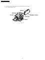
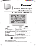
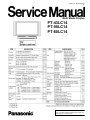
Multi Media Display
PT-43LC14
PT-50LC14
PT-60LC14
© 2004 Matsushita Kotobuki Electronics Industries
LTD. All rights reserved. Unauthorized copying and
distribution is a violation of law.
PT-43LC14 / PT-50LC14 / PT-60LC14
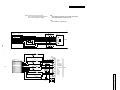
CONTENTS
Page
1 SAFETY PRECAUSIONS
Page
10.7. VOLTAGE CHART
3
1.1. GENERAL GUIDELINES
3
1.2. LEAKAGE CURRENT COLD CHECK
3
1.3. LEAKAGE CURRENT HOT CHECK
3
1.4. UV-PRECAUTION
3
75
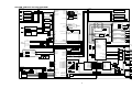
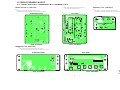
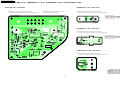
11 CIRCUIT BOARD LAYOUT
11.1. FRONT JACK C.B.A. /
OPERATION C.B.A. /
75
NETWORK C.B.A.
11.2. AUDIO AMP C.B.A. /
THERMISTOR 1 C.B.A. /
THERMISTOR 2 C.B.A. /
2 PREVENTION OF ELECTROSTATIC DISCHARGE (ESD) TO
ELECTROSTATICALLY SENSITIVE (ES) DEVICES
73
11.3. TUNER C.B.A.
4
3 ABOUT LEAD FREE SOLDER (PbF)
5
4 SERVICE NOTES
6
COVER SWITCH C.B.A.
12 EXPLODED VIEWS
76
77
79
12.1. MAIN PARTS SECTION
79
18
12.2. FRONT AND BASE SECTION
80
18
12.3. DISPLAY SECTION
81
6 ADJUSTMENT PROCEDURES 1
45
12.4. SCREEN SECTION
83
7 ADJUSTMENT PROCEDURES 2
48
12.5. PROJECTION SECTION
85
8 TROUBLESHOOTING HINTS FOR BLOCK LEVEL REPAIR
51
12.6. TV AND TUNER SECTION
86
9 BLOCK DIAGRAMS
57
12.7. PACKING PARTS AND ACCESSORIES SECTION
87
67
12.8. OPTIONAL ACCESSORY SECTION
88
5 DISASSEMBLY / ASSEMBLY PROCEDURES
5.1. CABINET SECTION
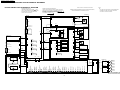
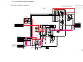
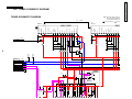
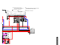
10 SCHEMATIC DIAGRAMS
10.1. SCHEMATIC DIAGRAM AND CIRCUIT BOARD LAYOUT
13 REPLACEMENT PARTS LIST
90
67
13.1. REPLACEMENT NOTES
90
10.2. INTERCONNECTION SCHEMATIC DIAGRAM
68
13.2. MECHANICAL REPLACEMENT PARTS LIST
91
10.3. FRONT JACK SCHEMATIC DIAGRAM
69
13.3. OPTIONAL ACCESSORY REPLACEMENT PARTS LIST
NOTES
10.4. NETWORK /
OPERATION /
THERMISTOR 1 /
92
THERMISTOR 2 /
13.4. ELECTRICAL REPLACEMENT PARTS LIST
COVER SWITCH SCHEMATIC
DIAGRAMS
10.5. AUDIO AMP SCHEMATIC DIAGRAM
71
10.6. TUNER SCHEMATIC DIAGRAM
72
93
14 SCHEMATIC DIAGRAMS FOR PRINTING WITH LETTER SIZE
70
96
2
PT-43LC14 / PT-50LC14 / PT-60LC14
1 SAFETY PRECAUSIONS
1.1.
not exceed 1/2 mA. In case a measurement is outside of
the limits specified, there is a possibility of shock hazard,
and thereceivershouldbe repaired and rechecked before it
is returned to the customer.
GENERAL GUIDELINES
1. For continued safety, no modification of any circuit should
be attempted.
2. Disconnect AC Plug before disassembling this unit.
3. It is advisable to use an isolation transformer in the AC
supply before servicing.
4. When servicing, observe the original lead dress. If a short
circuit is found, replace all parts which have been
overheated or damaged by the short circuit.
5. After servicing, see to it that all the protective devices such
as insulation barriers, insulation papers, shield, and
isolation R-C combinations etc. are properly installed.
6. After servicing, be sure to restore the wires, leads,
insulation barriers, shields, etc.
Figure 1
7. After servicing, make the leakage current checks to prevent
the customer from being exposed to shock hazards.
1.4.
1. Be sure to disconnect the AC Plug when replacing the
lamp.
Caution:
2. Since the lamp reaches a very high temperature during its
operation, wait until it has completely cooled off when
replacing the Lamp Unit.
Use a separate Isolation Transformer for this unit when
servicing.
1.2.
UV-PRECAUTION
3. The lamp emits small amounts of UV-Radiation.
LEAKAGE CURRENT COLD
CHECK
Avoid direct-eye contact by covering the Lamp and wearing
the UV cut protective glass.
4. The high pressure lamp involves a risk of explosion.
1. Unplug the AC cord and connect a jumper between the two
prongs on the plug.
2. For physically operated power switches, turn power on.
Otherwise skip step 2.
3. Measure the resistance value, with an ohmmeter, between
the jumpered AC plug and each exposed metallic cabinet
part on the receiver, such as screwheads, connectors, etc.
When the exposed metallic part has a return path to the
chassis, the readingshouldbebetween 1 MΩ and 12 MΩ.
When the exposed metal does not have a return path to the
chassis, the reading must be infinity.
1.3.
LEAKAGE CURRENT HOT
CHECK
Figure 2
1. Plug the AC cord directly into the AC outlet.
Do not use a isolation transformer for this check.
2. Connect a 1.5 kΩ, 10 W resistor, in parallel with a 0.15 µF
capacitor, between each exposed metallic part on the set
and a good earth ground, as shown in Figure 1.
3. Use an AC voltmeter, with 1 kΩ/V or more sensitivity, to
measure the potential across the resistor.
4. Check each exposed metallic part, and measure the
voltage at each point.
5. Reverse the AC plug in the AC outlet and repeat each of the
above measurements.
6. The potential at any point should not exceed 0.75 V RMS.
A leakage current tester (Simpson Model 229 equivalent)
may be used to make the hot checks. Leakage current must
3
PT-43LC14 / PT-50LC14 / PT-60LC14
2 PREVENTION OF
ELECTROSTATIC
DISCHARGE (ESD) TO
ELECTROSTATICALLY
SENSITIVE (ES) DEVICES
Some semiconductor (solid state) devices can be damaged
easily by static electricity. Such components commonly are
called Electrostatically Sensitive (ES) Devices. Examples of
typical ES devices are integrated circuits and some field-effect
transistorsandsemiconductor"chip" components. The following
techniques should be used to help reduce the incidence of
component damage caused by electro static discharge (ESD).
1. Immediately
before
handling
any
semiconductor
component or semiconductor-equipped assembly, drain off
any ESD on your body by touching a known earth ground.
Alternatively, obtain and wear a commercially available
discharging ESD wrist strap,whichshouldbe removed for
potential shock reasons prior to applying power to the unit
under test.
2. After removing an electrical assembly equipped with ES
devices, place the assembly on a conductive surface such
as aluminum foil, to prevent electrostatic charge buildup or
exposure of the assembly.
3. Use only a grounded-tip soldering iron to solder or unsolder
ES devices.
4. Use only an antistatic solder removal device. Some solder
removal devices not classified as "antistatic (ESD
protected)" can generate electrical charge sufficient to
damage ES devices.
5. Do not use freon-propelled chemicals. These can generate
electrical charges sufficient to damage ES devices.
6. Do not remove a replacement ES device from its protective
package until immediately before you are ready to install it.
(Most replacement ES devices are packaged with leads
electrically shorted together by conductive foam, aluminum
foil or comparableconductivematerial).
7. Immediately before removing the protective material from
the leads of a replacement ES device, touch the protective
material to the chassis or circuit assembly into which the
device will be installed.
CAUTION :
Be sure no power is applied to the chassis or circuit, and
observe all other safety precautions.
8. Minimize bodily motions when handling unpackaged
replacement ES devices. (Otherwise harmless motion such
as the brushing together of your clothes fabric or the lifting
of your foot from a carpeted floor can generate static
electricity (ESD)sufficienttodamage an ES device).
4
PT-43LC14 / PT-50LC14 / PT-60LC14
3 ABOUT LEAD FREE SOLDER (PbF)
5
PT-43LC14 / PT-50LC14 / PT-60LC14
4 SERVICE NOTES
LED INDICATIONS FOR ERROR CONDITION
Each LED indication facilitates finding the cause of the error.
When an error is detected, the Lamp comes off and the LED on the front will flash.
POWER LED
TV/VIDEO
TEMP LED
Error No.
Error Information
LAMP LED
POWER LED
TEMP LED
LAMP LED
1)
Fan1, Fan2 or Fan3 stopped
flashes orange once
every 5 seconds
-
-
2)
Lamp Cover open
flashes orange twice
every 5 seconds
-
-
3)
Temperature Sensor shorted or open
(Thermistor 1 C.B.A.)
-
flashes once
every 5 seconds
-
4)
Abnormal Temperature
(Thermistor 1 C.B.A.)
-
flashes twice
every 5 seconds
-
5)
Ballast Error (abnormal Lamp or Ballast)
-
-
flashes once
every 5 seconds
6)
Ballast Error (abnormal Lamp voltage)
-
-
flashes twice
every 5 seconds
7)
Ballast Error (abnormal temperature)
-
-
flashes 3 times
every 5 seconds
8)
Ballast Error (other causes)
-
-
flashes 4 times
every 5 seconds
9)
Abnormal Voltage on 30 V line
flashes orange 5 times
every 5 seconds
flashes once
every 5 seconds
flashes once
every 5 seconds
10)
Abnormal Voltage on 9 V line
flashes orange 6 times
every 5 seconds
flashes twice
every 5 seconds
flashes twice
every 5 seconds
11)
Abnormal Voltage on 5 V line
flashes orange 7 times
every 5 seconds
flashes 3 times
every 5 seconds
flashes 3 times
every 5 seconds
12)
Abnormal Voltage on 3.3 V line
flashes orange 8 times
every 5 seconds
flashes 4 times
every 5 seconds
flashes 4 times
every 5 seconds
13)
Abnormal Voltage on -5 V line
flashes orange 9 times
every 5 seconds
flashes 5 times
every 5 seconds
flashes 5 times
every 5 seconds
14)
Abnormal Voltage on 6 V line
flashes orange 10 times
every 5 seconds
flashes 6 times
every 5 seconds
flashes 6 times
every 5 seconds
15)
Temperature Sensor shorted or open
(Thermistor 2 C.B.A.)
-
flashes 3 times
every 5 seconds
-
16)
Abnormal Temperature
(Thermistor 2 C.B.A.)
-
flashes 4 times
every 5 seconds
-
17)
Clogged air filter
-
flashes 5 times
every 5 seconds
-
(Note 2)
(Note 3)
OSD
LAMP OFF
Note:
1. When two or more errors have occurred at the same time, the LED will alternate flash patterns as shown above every 5 seconds.
2. Warning OSD appears when the air filter is clogged.
3. LAMP OFF: The LED will flash immediately after the Lamp comes off.
6
PT-43LC14 / PT-50LC14 / PT-60LC14
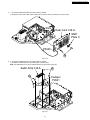
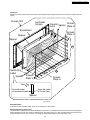
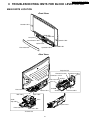
MAIN PARTS LOCATION
<Front View>
Network C.B.A.
TEMP LED
LAMP LED
Lamp Cover
Cover Switch C.B.A.
Network C.B.A.
Optical Cover
Front Cover Unit
Operation C.B.A.
POWER LED
<Rear View>
Projection Unit
Thermal Fuse Unit
Thermistor 1 C.B.A.
Thermistor 2 C.B.A.
Fan 3
Air Filter
Fan Case Unit
(Fan 1)
Front Jack C.B.A.
Main C.B.A.
Ballast C.B.A.
Air Filter
Air Filter
Fan 2
LCD Drive C.B.A.
Tuner C.B.A.
Fan 4
Audio
Amp C.B.A.
Rear Cover
Power C.B.A.
Rear Jack C.B.A.
TV/Tuner Unit
7
PT-43LC14 / PT-50LC14 / PT-60LC14
SERVICE MODE
Service Mode Map
In this mode, the following information can be confirmed on the
screen:
Enter :
VOLUME DOWN button + TV/VIDEO key
(on the front)
(on the remote)
(for more than 5 seconds in power off condition)
Service Mode (1/3)
• Current Lamp elapsed time
• The number of Lamp ON (For reference only)
• BKSV number read-out
Power ON
SERVICE
Service Mode (2/3)
• Key detection check
• Communication check for IIC bus and serial bus on the
Main C.B.A.
• Total Lamp elapsed time
• Communication check for IIC bus on the Main C.B.A.
• EEPROM IC6006 version and build version (For reference only)
• EEPROM IC6306 version and build version (For reference only)
• IC6003 software version and build version (For reference only)
• IC6302 software version and build version (For reference only)
MODE
1/3
LAMP
OPERATION
TIME
CUR
OSD
LON
BKSV
RENT LAMP:
DISPLAY
:
COUNT
:
:
4B 7E 3D
2000
O
15
CA F
h
N
3
B
< Service Mode (1/3) >
CH DOWN key
CH UP key
SERVICE
IC3
5
6
TO
IC7
Service Mode (3/3)
• IC6003 Port information
• IC6302 Port information
5
0
0
T
5
0
0
0
A
0
1
4
5
L
1
IC6003
IC6302
MODE
:1
:1
:1
IR
3502
5103
6006
:
:
:
:
1
1
1
1
MTNR
E
F
V
V
:
:
:
:
:
1
0
0
0
0
1
:1
4
0
4
4
U
3
5
9
2
S
0
0
0
0
N
5
3
0
3
T
5
0
5
5
I
0
0
0
4
N
2
0
2
2
T
4
1
4
5
R
5
0
5
0
2
:
:
:
:
h
:
/3
1
1
1
1
1
0
2
0
< Service Mode (2/3) >
Note:
IC6003: Main Microcontroller on the Main C.B.A.
IC6302: Sub Microcontroller on the Main C.B.A.
CH DOWN key
SE
I
P0
P1
P2
I
P0
P1
P2
P3
P4
R
C
:
:
:
C
:
:
:
:
:
V
6
0
1
1
6
0
0
1
I
0
0
0
1
3
0
0
0
1
C
0
0
0
1
0
1
0
1
CH UP key
E
3
0
0
1
2
0
0
0
1
MODE
PORT
1110
0001
1111
PORT
1111
-1-1
0111
0111
0011
P
P
P
P
P
P
P
P
P
P
P
6
3
4
5
7
8
5
6
7
8
A
:
:
:
:
:
:
:
:
:
:
:
0
0
1
1
1
1
1
1
-
0
0
0
0
0
1
1
1
-
0
0
0
1
0
1
0
0
-
0
0
0
1
1
0
1
0
-
0
0
0
1
0
1
1
1
0
1
0
0
0
0
0
1
0
0
1
1
1
1
0
1
0
0
1
0
0
0
1
1
1
0
0
0
0
1
1
1
0
1
1
3/3
< Service Mode (3/3) >
CH DOWN key
Exit:
Power OFF.
(When turning the power on again after once turning
off, wait for approx. 10 seconds. Or, the unit can not be
released from Service Mode.)
Fig. 1-1
8
PT-43LC14 / PT-50LC14 / PT-60LC14
BEFORE REMOVING THE MAIN C.B.A. OR
THE TV/TUNER UNIT FROM THE UNIT AT
THE USER’S LOCATION
WHEN REINSTALLING THE MAIN C.B.A.
OR THE TV/TUNER UNIT INTO THE UNIT
AT THE USER’S LOCATION
CAUTION:
1. Set CURRENT LAMP value to original value as follows.
1) Select CURRENT LAMP in Service Mode (1/3).
2) Press the VOLUME UP/DOWN key on the remote to
change to the original value (value A) that was noted
before removing the Main C.B.A. or the TV/Tuner Unit
at the user’s location.
Note:
The TV/Tuner Unit includes the Main C.B.A.
CAUTION:
1. Be sure to make a note of the CURRENT LAMP value
(value A) in Service Mode (1/3):
SERVICE
MODE
SERVICE
1/3
LAMP
OPERATION
CUR
OSD
LON
BKSV
RENT LAMP:
DISPLAY
:
COUNT
:
:
4B 7E 3D
TIME
2000
O
15
CA F
h
N
3
B
Value A
(Changeable)
Fig. 2
LAMP
OPERATION
TIME
CUR
OSD
LON
BKSV
RENT LAMP:
DISPLAY
:
COUNT
:
:
B0 3A 59
2000
O
15
CD 6
Value A
(Changeable)
h
N
3
6
Service Mode Map
LAMP OPERATION TIME is stored in EEPROM on the
Main C.B.A. Therefore, before removing the Main C.B.A. or
the TV/Tuner Unit at the user’s location, make a note of the
CURRENT LAMP value (value A) in Service Mode (1/3).
Then, after installing the new Main C.B.A. or the TV/Tuner
Unit at the user’s location, set the CURRENT LAMP value
to the original value (value A) in Service Mode.
Otherwise, OSD and LED Lamp replacement indications
will be displayed at the wrong time.
Enter :
VOLUME DOWN button + TV/VIDEO key
(on the front)
=
(on the remote)
(for more than 5 seconds in power off condition)
Power ON
SERVICE
Note:
In case it is impossible to make a note of the CURRENT
LAMP value because of a defective Main C.B.A., ask the
customer their daily average use and the approximate age
of the current Lamp. Then, calculate the CURRENT LAMP
value as follows and make a note.
Approx. age
(days)
1/3
<Service Mode (1/3)>
Fig. 3
<Service Mode (1/3)>
Daily average use
X
(hours)
MODE
MODE
1/3
LAMP
OPERATION
TIME
CUR
OSD
LON
BKSV
RENT LAMP:
DISPLAY
:
COUNT
:
:
4B 7E 3D
2000
O
15
CA F
h
N
3
B
< Service Mode (1/3) >
CH DOWN key
CURRENT LAMP
(hours)
CH UP key
SERVICE
IC3
5
6
TO
IC7
Note:
The TOTAL value can be set to the original value in Service
Mode (2/3) by similar method:
Before removing the Main C.B.A. at the user’s location,
make a note of the TOTAL value in Service Mode (2/3).
Then, after installing the new Main C.B.A. at the user’s
location, set the TOTAL value to the original value in
Service Mode.
5
0
0
T
5
0
0
0
A
0
1
4
5
L
1
IC6003
IC6302
MODE
:1
:1
:1
IR
3502
5103
6006
:
:
:
:
1
1
1
1
MTNR
E
F
V
V
:
:
:
:
:
1
0
0
0
0
1
:1
4
0
4
4
U
3
5
9
2
S
0
0
0
0
N
5
3
0
3
T
5
0
5
5
I
0
0
0
4
N
2
0
2
2
T
4
1
4
5
R
5
0
5
0
2
:
:
:
:
h
:
/3
1
1
1
1
1
0
2
0
< Service Mode (2/3) >
CH DOWN key
SE
I
P0
P1
P2
I
P0
P1
P2
P3
P4
R
C
:
:
:
C
:
:
:
:
:
V
6
0
1
1
6
0
0
1
I
0
0
0
1
3
0
0
0
1
C
0
0
0
1
0
1
0
1
CH UP key
E
3
0
0
1
2
0
0
0
1
MODE
PORT
1110
0001
1111
PORT
1111
-1-1
0111
0111
0011
P
P
P
P
P
P
P
P
P
P
P
6
3
4
5
7
8
5
6
7
8
A
:
:
:
:
:
:
:
:
:
:
:
0
0
1
1
1
1
1
1
-
0
0
0
0
0
1
1
1
-
0
0
0
1
0
1
0
0
-
0
0
0
1
1
0
1
0
-
0
0
0
1
0
1
1
1
0
1
0
0
0
0
0
1
0
0
1
1
1
1
0
1
0
0
1
0
0
0
1
1
1
0
0
0
0
1
1
1
0
1
1
3/3
< Service Mode (3/3) >
CH DOWN key
Exit:
Power OFF.
(When turning the power on again after once turning
off, wait for approx. 10 seconds. Or, the unit can not be
released from Service Mode.)
9
PT-43LC14 / PT-50LC14 / PT-60LC14
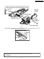
Lamp Replacement Procedure:
REPLACEMENT OF LAMP
1. Press the POWER button on the remote to turn off the
power.
2. Wait for about 1 minute until the cooling fan stops.
Note:
The lamp cooling fan will continue to operate for about 1
minute after the power is turned off. Do not unplug the AC
Cord from the outlet until the fan has stopped. Avoid
interrupting the power by using circuit breakers or switchable
power strips.
3. After the cooling fan has stopped, unplug the AC Cord from
the outlet.
Note:
Please wait more than one hour before replacing the lamp.
[ Forced cooling function ]
If you need to replace the lamp more urgently:
• The Projection display has a forced cooling feature.
After the POWER button is turned OFF, and sometime
during about the first minute of the normal cooling fan
operation, press the VOLUME UP button on the unit
and CH UP key on the remote at the same time for more
than 5 seconds. The cooling fan will operate for about
10 minutes. (LAMP LED will flash 5 times every 5
second and POWER LED will flash red for 10 minutes.)
4. Remove the Front Cover Unit from the latches.
5. Remove the Lamp Cover by loosening the Screw.
Lamp Time Reset Procedure:
Be sure to reset the Lamp time to "0" after replacing the new
Lamp.
1. Plug in the AC Cord, and turn on the power by pressing the
POWER button.
2. Press and hold the VOLUME DOWN button on the unit and
the SPLIT key on the remote together for over 5 seconds in
power on condition.
When the reset is finished, the display as shown in Fig. 51 appears and the LAMP LED goes out.
Fig. 5-1
Note:
1. The unit will detect when the Lamp’s end of life is
approaching and the following message will be
displayed. And the LAMP indicator light will be lit when
the Lamp’s end of life is approaching.
Lamp Cover
Screw
Fig. 5-2
Fig. 5-3
2. Influences of frequent lighting, continuous light use for
over 24 hours, the number of times lit, the length of time
between lightings, etc. may shorten lamp life. (Because
of this, we recommend having a replacement lamp on
hand.)
6. Loosen the Screw on the Lamp. Then, pull the Lamp.
Note:
Because the Lamp may still be hot, use caution when
handling.
Lamp
WARNING:
• The high-pressure lamp could explode if not properly
handled and lamp fragments could cause injury.
• Because the temperature of the lamp unit is elevated
immediately after its use, touching it may cause burns.
Please allow the lamp to cool before handling or replacing
the lamp unit.
• Wear gloves and safety eyeglasses when replacing the
lamp unit.
• If replacement of the lamp unit becomes necessary during
the operation of the TV, follow the procedure to turn off the
power and wait until the lamp unit cools completely.
Screw
Cautions for Lamp Unit Replacement:
• Do not disassemble the Lamp.
• The lamp may be hot. Be careful when handling. Wear
gloves.
• Under no circumstance should you touch the actual bulb.
At this high operating temperature the natural oil on your
finger can cause the glass to weaken where touched and
the bulb can crack or explode.
Fig. 5-4
7. Install the new Lamp, and tighten the Screw.
8. Install the Lamp Cover securely, and tighten the Screw.
9. Install the Front Cover Unit.
Note:
After replacing the Lamp, use caution to reset the Lamp time.
10
PT-43LC14 / PT-50LC14 / PT-60LC14
CLEANING METHOD
THE FILTER ON THE PROJECTION UNIT
THE SCREEN UNIT AND THE MIRROR
•THE SCREEN UNIT (Lenticular Screen, Fresnel Lens)
It is strongly recommended that the Lenticular Screen surface
(outside) and the Fresnel Lens surface (inside) should be
wiped gently with a clean, soft, dry cloth to remove the dirt.
CAUTION:
Operating with torn or damaged Air Filter may cause damage
to the Projection unit.
Remove the Projection Unit from rear. Then, clean the filters on
the Projection Unit. Gently remove any accumulated dust from
filter with a vacuum cleaner.
Note:
1. If the dirt cannot be removed by wiping with a clean, soft, dry
cloth, use a clean, soft, dry cloth moistened with diluted
neutral pH liquid cleanser or a lens cleaner (usually
containing a small amount of ethyl alcohol) and wipe lightly.
Take care not to leave any streaks.
Do not use cleaning materials containing methyl alcohol,
acetone, or dichloromethane.
2. Use an air blower to clean the inner surface of the Lenticular
Screen and the outer surface of the Fresnel Lens (the
surfaces that one another). These surfaces must not be
wiped with a cloth.
Air Filter
Air Filter
Air Filter
•THE MIRROR
Remove any dirt with an air blower or wipe with a clean, soft,
dry cloth. If wiped too forcefully, the surface of the Mirror can
be damaged. If wiping with a clean, dry cloth does not remove
the dirt, the Mirror must be replaced.
Mirror
Screen Unit
<Bottom View>
Fig. 6-3
THE PROJECTION LENS
Use lens cleaning paper and cleaner available at your local
camera shop, etc. Dampen the cleaning paper with cleaner
and gently wipe the surface of the lens from the center outward
to remove dust.
Fresnel Lens surface
(inside)
Lens
Lenticular Screen surface
(outside)
Fig. 6-1
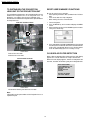
THE LAMP
Gently wipe the surface of the glass of the Lamp with cleaning
paper or soft cloth.
Fig. 6-4
THE POLARIZER UNIT, THE FIELD LENS, THE RELAY
LENS, THE CONDENSER LENS, THE DICHROIC
MIRROR, THE FULL MIRRORS, THE INTEGRATOR AND
THE P/S CONVERTER
Make sure that no dust gets on the optical components such as
the Polarizer Unit, the Field Lens, the Relay Lens, the Condenser
Lens, the Dichroic Mirror, the Full Mirrors, the Integrator and
the P/S Converter. Clean these optical components with
cleaning paper moistened with pure ethyl alcohol or a lens
cleaner which contains no water or oil.
Surface of glass
THE LCD PANEL OF THE LCD/PRISM UNIT
1) Clean the surface of the LCD Panel of the LCD/Prism Unit
with an air blower or wipe with a clean, or soft blush lightly.
2) If any dirt remains, lightly wipe the surface with a cotton
swab moistened with pure ethyl alcohol or a lens cleaner
which contains no water or oil. Use a new swab after each
wiping so that dirt will not be re-deposited on the surface.
Fig. 6-2
11
PT-43LC14 / PT-50LC14 / PT-60LC14
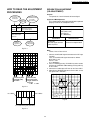
TO DISTINGUISH THE PROJECTION
LENS UNIT OR THE PROJECTION UNIT
RESET USER’S MEMORY FUNCTIONS
Be sure to reset the user’s memory:
• After replacing the Main C.B.A. (included in the TV/Tuner
Unit)
• If the secret code of V-chip is forgotten.
• When moving the unit to a new location.
The only difference between the 43 inch model and the 50 inch
model of the Projection Unit is the Projection Lens. To
distinguish, see marking (Z or A) on the Projection Lens.
And the 60 inch model of the Projection Unit is placed label on
the Projection Lens.
1. Turn on the power.
2. Press the MENU key on the remote to display the MENU
screen.
3. Select LOCK by pressing CH UP/DOWN key on the remote.
Then, press the OK key.
43/50 inch model as shown
X X X A
Z or A
4. Press and hold the VOLUME DOWN button on the unit and
the OK key on the remote for more than 5 seconds while this
LOCK menu is displayed. When reset is finished, power
shuts off automatically (the user’s memory is reset).
<Front View>
CLOGGED AIR FILTER DETECTION
Z with red: for 43 inch model
A with black: for 50 inch model
When a dirty or clogged air filter is detected, the OSD display
appears for 1 minute. And then the Lamp is turned OFF.
When this OSD display appears, remove the Projection Unit
from rear, and clean the air filters gently on the Projection Unit.
60 inch model as shown
AIR FILTER CLEANING
IS RECOMMANDED AT THIS
TIME. FIRST TURN THE
UNIT OFF.
PLEASE CALL FOR
SERVICE.
LSDL0248
UNIT WILL BE TURNED
OFF AFTER 1 MINUTE.
<Front View>
LSDL0248 with Yellowish green label: for 60 inch model
Note:
LSDL0248 is not the part numbers of the Projection Lens as a
replacement part.
12
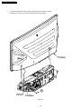
PT-43LC14 / PT-50LC14 / PT-60LC14
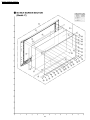
BEFORE REMOVING THE PROJECTION
UNIT FROM THE UNIT AT THE USER’S
LOCATION
DO NOT UNPLUG AC CORD DURING
COOLING OPERATION
The lamp cooling fan will continue to operate for approximately
1 minute after the power is turned off.
At the same time, the POWER LED will flash red.
Do not disconnect the AC Cord from the power outlet and do
not open any circuit breakers while the cooling fan is still
operating.
1. When removing the Projection Unit, remove the Lamp from
the Projection Unit and keep it. Then, reinstall this Lamp
into the new Projection Unit.
2. When removing the Projection Unit, remove the Fan 3 Unit,
the Top Duct 3 Unit and the 20-pin Cable from the Projection
Unit and keep them. Then, reinstall the Fan 3 Unit, the Top
Duct 3 Unit and the 20-pin Cable into the new Projection
Unit.
HOT CIRCUIT
Primary circuit exists on the Audio Amp C.B.A., the Ballast
C.B.A. and the Power C.B.A.
This circuit is identified as "HOT" on the C.B.A. and in the
Service Manual. Use extreme care to prevent accidental shock
when servicing.
21 Projection Unit
Screw
for lamp
Lamp
Clamper
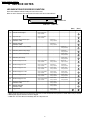
MODEL NO. IDENTIFICATION MARK
Fan 3 Unit
Use Marks shown in the chart below to distinguish the different
models included in this Service Manual.
MODEL
P2904
GND
Wire
PT-43LC14
PT-50LC14
PT-60LC14
NOT USED
402
421
421
402
MARK
A
B
C
PT
Note:
Refer to Item 3 of Schematic Diagram Notes of
Schematic Diagram and Circuit Board Layout Notes,
for mark "PT."
Top Duct 3 Unit
13
PT-43LC14 / PT-50LC14 / PT-60LC14
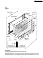
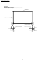
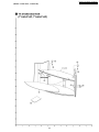
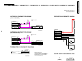
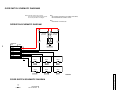
WIRE AND LEAD POSITION DIAGRAM OF THE UNIT
After servicing, make sure that all wires, leads, and clampers are placed in their original position. It is important for the best
operation of the unit.
Note: Use extreme care especially for the following.
Clamper
Clamper
RF Input Terminal
Fan 3
Thermal Fuse Unit
GND Wire
AC Cord
Fig. 9-1
14
PT-43LC14 / PT-50LC14 / PT-60LC14
After servicing, make sure that all wires, leads, and clampers are placed in their original position. It is important for the best
operation of the unit.
Note: Use extreme care especially for the following.
P2303 (From Thermistor 1 C.B.A.)
Thermistor 2
C.B.A.
P2902
(From Fan 1)
Lamp Cable
Lamp Sockets
P2901
(From Main
C.B.A.)
P2501
(From Main
C.B.A.)
P2904
(From
Fan 3)
P2502 (From
Cover Switch
C.B.A.)
Clamper
P2903
(From Fan 2)
Clamper
Fan 4
Ballast C.B.A.
P1306 (From Thermal Fuse Unit)
Fig. 9-2
15
P2304 (From
Thermistor 2
C.B.A.)
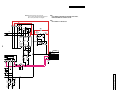
PT-43LC14 / PT-50LC14 / PT-60LC14
After servicing, make sure that all wires, leads, and clampers are placed in their original position. It is important for the best
operation of the unit.
Note: Use extreme care especially for the following.
P6305
(From Operation C.B.A.) No connection
Speaker Connector
Leads
P5501
(From Front
Jack C.B.A.)
P6004
(From Tuner
C.B.A.)
Clampers
P3501
(From Tuner
C.B.A.)
P3502
(From Front
Jack C.B.A.)
P4503
(From Speaker)
P3504
(From Front
Jack C.B.A.)
P4505
(To Tuner
C.B.A.)
P3603
(From Audio
Amp C.B.A.)
P4501
(From Power C.B.A.)
Clamper
P3402
(From LCD
Drive C.B.A.)
P6002
(From Ballast C.B.A.)
P3401
(From Power C.B.A.)
Clamper
GND Plate A
P5302
(From LCD
Drive C.B.A.)
P805
(From Ballast
C.B.A.)
Clamper
20-pin Cable
Connector Cable
Fig. 9-3
16
PT-43LC14 / PT-50LC14 / PT-60LC14
After servicing, make sure that all wires, leads, and clampers are placed in their original position. It is important for the best
operation of the unit.
Note: Use extreme care especially for the following.
P3401
(To Main
C.B.A.)
P1001 (To Ballast C.B.A.)
P805
(To Ballast C.B.A.)
Clamper
P1009
P1010
P1011
P4501
(To Audio
Amp C.B.A.)
P1007
Clamper
P804
P1006
(To Fan 4)
AC Cord
Fig. 9-4
17
PT-43LC14 / PT-50LC14 / PT-60LC14
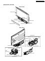
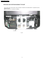
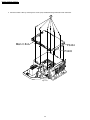
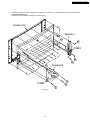
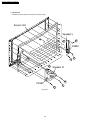
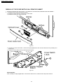
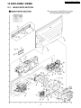
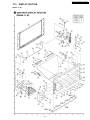
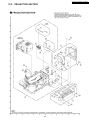
5 DISASSEMBLY / ASSEMBLY PROCEDURES
5.1.
CABINET SECTION
CABINET SECTION
DISASSEMBLY METHOD OF CABINET SECTION
Cabinet section contains following removal procedures:
REMOVAL OF THE BALLAST C.B.A. AND THE TV/TUNER UNIT FROM THE CABINET
REMOVAL OF THE PROJECTION UNIT FROM THE CABINET
REMOVAL OF THE TUNER C.B.A., THE MAIN C.B.A., THE REAR JACK C.B.A., THE AUDIO AMP C.B.A., THE POWER C.B.A. FROM
THE TV/TUNER UNIT
REMOVAL OF THE SCREEN UNIT AND THE SPEAKER FROM THE DISPLAY
REMOVAL OF THE MIRROR FROM THE BACK COVER
REMOVAL OF THE FRONT JACK C.B.A. AND THE OPERATION C.B.A. FROM THE CABINET
REMOVAL OF THE COVER SWITCH C.B.A. FROM THE CABINET
DISASSEMBLY FLOWCHART
This flow chart indicates the disassembly steps of the cabinet parts and the P.C.Boards in order to gain access to item (s) to be
serviced. When reassembling, perform the step (s) in the reverse order. Bend, route and dress the wires as they were originally.
FRONT COVER UNIT SPEAKER
REAR COVER
LAMP COVER
PROJECTION UNIT
SCREEN UNIT
BALLAST C.B.A.
THERMISTOR 2 C.B.A.
OPTICAL COVER NETWORK C.B.A.
FAN 3 UNIT
MIRROR
OPERATION C.B.A.
TV/TUNER UNIT
THERMAL FUSE UNIT
TOP DUCT 3 UNIT
BACK PANEL
(DISPLAY)
TUNER C.B.A.
FRONT JACK C.B.A.
MAIN C.B.A.
AUDIO AMP C.B.A. REAR JACK C.B.A.
POWER C.B.A.
THERMISTOR 1 C.B.A.
(LCD/PRISM UNIT, LIGHT IN POLARIZER, ETC)
COVER SWITCH C.B.A.
Note :
a. Place a cloth or some other soft material under the P.C. Boards or Unit to prevent damage.
b. When reinstalling, ensure that the connectors are connected firmly and electrical components have not been damaged.
c. Do not supply power to the unit during disassembly and reassembly.
18
PT-43LC14 / PT-50LC14 / PT-60LC14
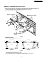
REMOVAL OF THE BALLAST C.B.A. AND THE TV/TUNER UNIT FROM THE CABINET
1. (PT-43LC14/PT-50LC14)
Remove the Rear Cover by removing the 18 Screws (401).
Rear Cover
401
Fig. D1-1-1
1. (PT-60LC14)
Remove the Rear Cover by removing the 20 Screws (401, 464).
Rear Cover
401
Fig. D1-1-2
19
464
PT-43LC14 / PT-50LC14 / PT-60LC14
2. Remove the Rear Support Plate by removing the 4 Screws (401, 452).
Rear Support
Plate
401
401
Fig. D1-2
20
452
PT-43LC14 / PT-50LC14 / PT-60LC14
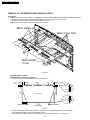
3. 1)
2)
3)
4)
5)
Remove the 5 Screws (402) and remove Clamper-1.
Remove the 2 Screws (451) on the Lamp Socket.
Disconnect the Lamp Connector.
Avoiding the Ballast C.B.A., disconnect Connector P1306 (Thermal Fuse Unit) inside of the Ballast C.B.A.
Remove the Clamper from the Ballast C.B.A.
Clamper-1
Lamp Socket
402
451
Lamp Connector
Note:
Do not remove the
Thermal Fuse Unit.
Clamper
Ballast C.B.A.
Clamper-1
451
P1306
402
Fig. D1-3
Replacement Note of Ballast C.B.A.:
These parts will be necessary when replacing the Ballast C.B.A. Set aside, and keep and re-use.
• The Clamper on Ballast C.B.A.
• The Thermal Fuse Unit
21
PT-43LC14 / PT-50LC14 / PT-60LC14
4. 1) Disconnect Connector P2901 (Connector Cable) and release them from the clamper.
2) Disconnect Connector P2501 (20-pin Cable) and release it from the clamper.
CAUTION: Take extreme care not to damage the 20-pin Cable when disconnecting.
5. 1) Disconnect Connectors P3502, P3504, P5501, P4503, P6305 and release them from the clampers.
2) Remove the Screw (452) on the GND Plate A.
3) Remove the Screw (401) on the TV/Tuner Ass’y.
4) Lift up and slide the TV/Tuner Ass’y by releasing the 7 Guide Tabs.
CAUTION: Do not slide the TV/Tuner Unit before removing the 20-pin Cable.
P2501 P2901
GND Plate A
452
Clamper
P5302
CAUTION:
20-pin Cable
Connector
Cable
P5501
P6305
452
TV/Tuner Ass'y
P4503
P3504
P3502
Clampers
401
Fig. D1-4
Slot
holes
TV/Tuner Ass'y
holes
Guide Tabs (X5)
Guide Tabs (X2)
Rear
<Bottom View of TV/Tuner Ass'y>
Fig. D1-5
Replacement Note of TV/Tuner Unit:
These parts will be necessary when replacing the TV/Tuner Unit. Set aside, and keep and re-use.
• 20-pin Cable
22
PT-43LC14 / PT-50LC14 / PT-60LC14
6. 1) Pull off the TV/Tuner Ass’y with the Ballast C.B.A. while taking care with the cables.
2) Remove the GND Plate A from the TV/Tuner Unit by removing the Screw (452).
3) Remove the SD Door Unit from the TV/Tuner Unit by releasing the 2 Locking Tabs.
Ballast
C.B.A.
holes
Locking Tabs
Slide
SD Door Unit
GND
Plate A
452
TV/Tuner Unit
Fig. D1-7-1
Reassembly Note: When installing the SD Door Unit, install the SD Door Unit with the 2 Locking Tabs from the front of the cabinet
after installing the TV/Tuner Unit into the cabinet.
Reassembly Note:
Locking
Tabs
SD Door Unit
<Front View>
Fig. D1-7-2
Replacement Note of TV/Tuner Unit:
These parts will be necessary when replacing the TV/Tuner Unit. Set aside, and keep and re-use.
• The GND Plate A
• The SD Door Unit
23
PT-43LC14 / PT-50LC14 / PT-60LC14
7. 1) Disconnect Connectors P6002, P805, P1001 and release them from the clampers.
2) Then, remove the Ballast C.B.A.
P6002
Clamper
Ballast C.B.A.
P1001
Clamper
P805
Fig. D1-8
24
PT-43LC14 / PT-50LC14 / PT-60LC14
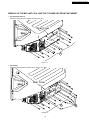
REMOVAL OF THE PROJECTION UNIT FROM THE CABINET
1. Remove the Ballast C.B.A. and the TV/Tuner Unit. Refer to Steps 1~6 in "REMOVAL OF THE BALLAST C.B.A. AND THE TV/
TUNER UNIT FROM THE CABINET."
2. 1) Disconnect Connector P2502. Then, hook the P2502 cable to the pin.
2) Remove the 7 Screws (401) on the Projection Unit.
3) Lift up and slide the Projection Unit by releasing the 5 Guide Tabs.
Tips on removal of the Projection Unit:
First, slide the Projection Unit to the rear (approx. 1.5 inch (4 cm)). Then, lift up the front and the rear portions of the Projection
Unit by both hand to release the Guide Tabs. Then, slide out the Projection Unit.
Or, remove the Fan 3 Unit from the Projection Unit at first. Refer to Fig. D2-3.
CAUTION:
Disconnect Connector P2502
and hook it as follows.
P2502
Pin
Cable
Cover
Switch
C.B.A.
Tips on removal of the Projection Unit
Slide
Boss
4
P2502
1
3
2
Up
Up
<Side View>
1 Lift up and slide the Projection Unit
by approx. 1.5 inch (4 cm).
2
Up
3
Up
401
Fig. D2-1
25
2 Lift up the front portion.
3 Lift up the rear portion.
4 Slide out the Projection Unit.
PT-43LC14 / PT-50LC14 / PT-60LC14
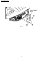
CAUTION:
Disconnect Connector P2502
and hook it as follows.
P2502
Pin
Cable
Guide Tabs (X5)
Cover
Switch
C.B.A.
<Bottom View of Projection Unit>
Rear
Projection Unit
Slide
holes
Fig. D2-2
Reassembly Note:
Before installing the Projection Unit, confirm that the P2502 cable is hooked to the pin. Then, install the Projection Unit to the
cabinet.
26
PT-43LC14 / PT-50LC14 / PT-60LC14
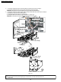
3. 1) Disconnect Connector P2904, and remove the Fan 3 Unit by removing the 2 Screw (402).
2) Remove the Top Duct 3 Unit by removing the 4 Screws (421).
CAUTION:
When removing the Screws (421) on the Top Duct 3 Unit, plastic dust may be produced. Therefore, confirm that there is no dust
on the Top Duct 3 Unit. If there is dust, clean the Top Duct 3 Unit with a brush, etc. Otherwise, dust may adhere to the inside of
the screen.
3) Remove the Lamp from the Projection Unit by loosening the Screw.
21 Projection Unit
Screw
for lamp
Lamp
Clamper
Fan 3 Unit
P2904
GND
Wire
402
421
421
Top Duct 3 Unit
Fig. D2-3
Replacement Note of Projection Unit (Ref. No. 21):
These parts will be necessary when replacing the Projection Unit (Ref.No. 21). Set aside, and keep and re-use.
• Fan 3 Unit
• Top Duct 3 Unit
27
402
PT-43LC14 / PT-50LC14 / PT-60LC14
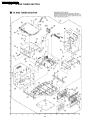
REMOVAL OF THE TUNER C.B.A., THE MAIN C.B.A., THE REAR JACK C.B.A., THE
AUDIO AMP C.B.A., THE POWER C.B.A. FROM THE TV/TUNER UNIT
CAUTION:
1. Be sure to make a note of the CURRENT LAMP value (value A) in Service Mode (1/3):
LAMP OPERATION TIME is stored in EEPROM on the Main C.B.A. Therefore, before removing the Main C.B.A. or the TV/Tuner
Unit at the user’s location, make a note of the CURRENT LAMP value (value A) in Service Mode (1/3).
Then, after installing the new Main C.B.A. or the TV/Tuner Unit at the user’s location, set the CURRENT LAMP value to the original
value (value A) in Service Mode.
Otherwise, OSD and LED Lamp replacement indications will be displayed at the wrong time.
Note:
In case it is impossible to make a note of the CURRENT LAMP value because of a defective Main C.B.A., ask the customer
their daily average use and the approximate age of the current Lamp. Then, calculate the CURRENT LAMP value as follows
and make a note.
Daily average use
Approx. age
CURRENT LAMP
X
=
(hours)
(days)
(hours)
1. Remove the TV/Tuner Unit and the Ballast C.B.A. Refer to Steps 1~7 in "REMOVAL OF THE BALLAST C.B.A. AND THE TV/
TUNER UNIT FROM THE CABINET."
2. 1) Disconnect Connectors P6004, P3501 and release from the clampers.
2) Remove the Tuner C.B.A. by removing the 4 Screws (402).
TV/Tuner Unit
402
Tuner
C.B.A.
P6004
Clampers
P3501
Fig. D3-1
28
PT-43LC14 / PT-50LC14 / PT-60LC14
3. 1)
2)
3)
4)
5)
Disconnect Connector P3401 and release from the clamper.
Disconnect Connector P3402 and remove the Connector Cable.
Remove the Tuner P.C.B. Frame by removing the 6 Screws (402).
Release the AC Cord from the slot of the Rear Jack Holder.
Remove the Rear Jack Holder by removing the 4 Screws (402).
402
Tuner
P.C.B.
Frame
Connector Cable
P3401
P3402
Rear Jack
Holder
402
Slot
Clamper
402
402
Fig. D3-2
29
AC Cord
PT-43LC14 / PT-50LC14 / PT-60LC14
4. Remove the Main C.B.A. by removing the 6 Screws (402) and disconnecting Connector P3403 and P3404.
402
Main C.B.A.
P3404
P3403
Fig. D3-3
30
PT-43LC14 / PT-50LC14 / PT-60LC14
5. 1) Disconnect Connector P3603 and release from the clamper.
2) Remove the Rear Jack C.B.A. and the GND Plate C from the slots by removing the 2 Screws (402).
Slots
Rear Jack C.B.A.
GND
Plate C
P3603
402
Fig. D3-4
6. 1) Disconnect Connector P4501 and release from the clamper.
2) Remove the Audio Amp C.B.A. by removing the 4 Screws (402).
Note: The Audio Amp C.B.A. can be removed from the TV/Tuner Unit at any time.
Audio Amp C.B.A.
402
402
Clamper
P4501
Fig. D3-5
31
PT-43LC14 / PT-50LC14 / PT-60LC14
7. 1)
2)
3)
4)
Disconnect Connector P1006 and release from the clamper.
Remove the Main P.C.B. Frame by removing the 6 Screws (402), and remove the Fan 4 by removing the 2 Screws (435).
Remove the Power C.B.A. by removing the 5 Screws (411).
Disconnect Connector P804 (AC Cord) and release from the clamper.
402
Main P.C.B. Frame
Fan 4
435
Clamper
Air Flow
Name
Plate
402
411
Clampers
Power
C.B.A.
AC Cord
P804
P1006
411
Fig. D3-6
Reassembly Note for Fan 4:
Install the Fan 4 with the 2 Screws (435) so that the name plate (manufacture’s name etc.) face out (visible from the outside).
Note:
After servicing the Power C.B.A., be sure to connect the Connector P1006 on the Power C.B.A. to install the Fan 4.
32
PT-43LC14 / PT-50LC14 / PT-60LC14
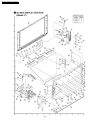
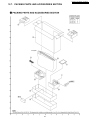
REMOVAL OF THE SCREEN UNIT AND THE SPEAKER FROM THE DISPLAY
1. 1) Remove the Front Cover Unit from the 8 latches.
2) Remove the Optical Cover by removing the 2 Screws (454).
3) Remove the 2 Screws (401) from front side.
latches
Optical Cover
latches
401
454
401
454
Front Cover Unit
Fig. D4-1
2. (PT-43LC14/PT-50LC14)
Remove the Rear Cover by removing the 18 Screws (401), refer to Fig. D1-1-1.
(PT-60LC14)
Remove the Rear Cover by removing the 20 Screws (401, 464), refer to Fig. D1-1-2.
33
PT-43LC14 / PT-50LC14 / PT-60LC14
3. 1) Disconnect Connector P4503 (speaker cables) and release it from the clamper.
2) Remove the 2 Screws (401) from rear side, and remove the Display.
Display
401
401
P4503 Clamper
Fig. D4-3
34
PT-43LC14 / PT-50LC14 / PT-60LC14
4. 1) Remove the Speaker-L and the Speaker-R by removing the 6 Screws (477, 478) and disconnect the connectors P4553.
2) (PT-43LC14/PT-50LC14)
Remove the Screen Unit by removing the 16 Screws (401).
Screen Unit
Speaker L
401
477
P4553
477
478
401
Speaker R
478
477
P4553
477
Fig. D4-4-1
35
PT-43LC14 / PT-50LC14 / PT-60LC14
2) (PT-60LC14)
Remove the Screen Unit by removing the 26 Screws (401).
Screen Unit
Speaker L
477
401
P4553
478
401
Speaker R
478
P4553
477
Fig. D4-4-2
36
477
477
PT-43LC14 / PT-50LC14 / PT-60LC14
5. (PT-43LC14)
Remove the 2 Screen Plate H and 2 Screen Plate V by removing 26 Screws (401), and remove the Fresnel Lens and the Lenticular
Screen.
(PT-50LC14)
Remove the 2 Screen Plate H and 2 Screen Plate V by removing 30 Screws (401), and remove the Fresnel Lens and the Lenticular
Screen.
Screen Unit
Screen
Lenticular
Plate H
Screen
Fresnel
Lens
Screen
Plate V
Escutcheon
401
Serial No.
Label
401
Screen
Plate V
Screen
Plate H
Front
Serial No. Label
of Lenticular Screen
Serial No. Label
of Fresnel Lens
Fig. D4-5-1
Reassembly Note:
Install them so that Serial No. Labels are on the each outside as shown above.
Replacement Note for Screen Unit:
The Screen Unit is supplied as a unit, or the individual parts (Fresnel Lens, Lenticular Screen) in the Screen Unit are also supplied.
When replacing the Fresnel Lens and the Lenticular Screen, take care that dust, etc., does not adhere between the Fresnel Lens
and the Lenticular Screen. Due to this risk, it is strongly recommended to replace the Screen Unit as a unit.
37
PT-43LC14 / PT-50LC14 / PT-60LC14
(PT-50LC14)
Reassembly Note for 4 Spacers:
Wind the string for screen spacer on the Fresnel Lens a shown.
Fresnel Lens
string for screen spacer
Serial No. Label
string for screen spacer
string for screen spacer
hook
hook
knot
hook
hook
38
PT-43LC14 / PT-50LC14 / PT-60LC14
(PT60LC14)
Remove the 2 Screen Plate H and 2 Screen Plate V by removing 40 Screws (465), and remove the Fresnel Lens and the Lenticular
Screen.
Screen Unit
Lenticular
Screen
Screen
Fresnel
Spacer Plate H
Lens
Escutcheon
Screen
Plate V
Spacer
Spacer
465
Serial No.
Label
Spacer
465
Screen
Plate V
Screen
Plate H
Front
Serial No. Label
of Lenticular Screen
Serial No. Label
of Fresnel Lens
Spacer
Fig. D4-5-2
Reassembly Note:
Install them so that Serial No. Labels are on the each outside as shown above.
Replacement Note for Screen Unit:
The Screen Unit is supplied as a unit, or the individual parts (Fresnel Lens, Lenticular Screen) in the Screen Unit are also supplied.
When replacing the Fresnel Lens and the Lenticular Screen, take care that dust, etc., does not adhere between the Fresnel Lens
and the Lenticular Screen. Due to this risk, it is strongly recommended to replace the Screen Unit as a unit.
39
PT-43LC14 / PT-50LC14 / PT-60LC14
(PT-60LC14)
Reassembly Note for 4 Spacers:
Place the 4 Spacers on the Lenticular Screen as shown.
Approx. 1330.5 mm ~ 1332.0 mm
11.0 mm ~ 12.5 mm
18.5 mm ± 2.0 mm
Spacer
2.5 mm ± 1.5 mm
Edge of
Escutcheon
2.5 mm ± 1.5 mm
Lenticular
Screen
11.0 mm ~ 12.5 mm
18.5 mm ± 2.0 mm
Spacer
Lenticular
Screen
Edge of
Escutcheon
Spacer
Spacer
2.5 mm ± 1.5 mm
2.5 mm ± 1.5 mm
Escutcheon
Approx. 725.5 mm ~ 754.0 mm
Lenticular
Screen
Spacer
2.5 mm ± 1.5 mm
Edge of
Escutcheon
Serial No. Label
2.5 mm ± 1.5 mm
Lenticular
Screen
Touch
the bosses
2.5 mm ± 1.5 mm
2.5 mm ± 1.5 mm
Spacer
Spacer
18.5 mm ± 2.0 mm
11.0 mm ~ 12.5 mm
Edge of
Escutcheon
Spacer
18.5 mm ± 2.0 mm
11.0 mm ~ 12.5 mm
Approx. 1330.5 mm ~ 1332.0 mm
40
Spacer
Lenticular
Screen
Touch
the boss
PT-43LC14 / PT-50LC14 / PT-60LC14
REMOVAL OF THE MIRROR FROM THE BACK COVER
(PT-43LC14/PT-50LC14)
1. Remove the Screen Unit. Refer to Steps 1~4 in "REMOVAL OF THE SCREEN UNIT AND THE SPEAKER FROM THE DISPLAY."
2. 1) Remove the 2 Mirror Holder H and the 2 Mirror Holder V Unit by removing the 12 Screws (401).
2) Remove the Mirror from the top by releasing the Back Cover slots.
Note: Be careful that the Mirror does not fall down when removing.
Mirror Holder H
Back Cover slots
401
401
401
401
Mirror Holder
V Unit
Fig. D4-6-1
Reassembly Notes for Mirror:
Install the Mirror as following procedures:
1) Place the 3 sheets on the top and bottom edges of the Mirror.
5 mm
Sheet
3 mm
5 mm
20 mm
<Front View>
Sheet
Mirror surface
5 mm
Sheet
60 mm
20 mm
10 mm ~ 15 mm
Sheet
10 mm
10 mm ~ 15 mm
Mirror surface
60 mm
15 mm ~ 20 mm
0 mm ~ 5 mm
10 mm ~ 15 mm
15 mm ~ 20 mm
10 mm ~ 15 mm
3 mm
Sheet
15 mm ~ 20 mm
Sheet
0 mm ~ 5 mm
(PT-50LC14)
15 mm ~ 20 mm
(PT-43LC14)
Top edge
of Mirror
Sheet
Sheet
Bottom edge
of Mirror
5 mm
<Front View>
Fig. D4-7-1
2) Hold the sheet portions of the Mirror, and insert the Mirror from the top into the Back Cover slots carefully.
When handling the Mirror, do not touch the Mirror surface.
3) Install the 2 Mirror Holder H and the 2 Mirror Holder V on the Mirror and tighten the 12 Screws (401).
41
10 mm
PT-43LC14 / PT-50LC14 / PT-60LC14
REMOVAL OF THE MIRROR FROM THE BACK COVER
(PT-60LC14)
1. Remove the Screen Unit. Refer to Steps 1~4 in "REMOVAL OF THE SCREEN UNIT AND THE SPEAKER FROM THE DISPLAY."
2. 1) Remove the 3 Mirror Holder H and the 2 Mirror Holder V Unit by removing the 15 Screws (401).
2) Remove the Mirror from the top by releasing the Back Cover slots.
Note: Be careful that the Mirror does not fall down when removing.
Mirror Holder H
Back Cover slots
401
Mirror Holder
V Unit
401
Fig. D4-6-2
Reassembly Notes for Mirror:
Install the Mirror as following procedures:
1) Place the 3 sheets on the top and bottom edges of the Mirror.
Sheet
10 mm ~ 20 mm
Mirror surface
Sheet
<Front View>
10 mm ~ 15 mm
10 mm ~ 15 mm
15 mm ~ 20 mm
18 mm ~ 28 mm
Sheet
15 mm ~ 20 mm
Sheet
10 mm ~ 20 mm
Top edge
of Mirror
Sheet
Sheet
Bottom edge
of Mirror
18 mm ~ 28 mm
Fig. D4-7-2
2) Hold the sheet portions of the Mirror, and insert the Mirror from the top into the Back Cover slots carefully.
When handling the Mirror, do not touch the Mirror surface.
3) Install the 3 Mirror Holder H and the 2 Mirror Holder V on the Mirror and tighten the 15 Screws (401).
42
PT-43LC14 / PT-50LC14 / PT-60LC14
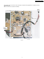
REMOVAL OF THE FRONT JACK C.B.A. AND THE OPERATION C.B.A. FROM THE CABINET
1. 1)
2)
2. 1)
2)
3)
4)
5)
Remove the Rear Cover by removing the 18 Screws or 20 Screws (PT-60LC14).
Disconnect Connector P6305 and release it from the clamper.
Remove the Front Cover Unit from the 8 latches.
Remove the Screw (454).
Slide the Front Side Cover R with the Operation C.B.A. as indicated by the arrow to release the 4 slots.
Pull off the Operation C.B.A. from front side.
Remove the Operation C.B.A. and the Operation Button Unit from the Front Side Cover R by removing the 4 Screws (421).
slots
Operation
Operation
Button Unit C.B.A.
421
P6305
Slide
421
Bosses
Front Cover
Unit
454 Front Side
Clampers
<Rear View>
Cover R
Fig. D5-1
3. 1)
2)
3)
4)
Disconnect Connectors P3502, P3504, P5501 and release them from the clampers.
Remove the 2 Screw (401).
Pull off the Front Jack C.B.A. from front side.
Remove the Front Jack C.B.A. from the Side Jack Holder by removing the 2 Screws (421) and releasing the 2 Locking Tabs.
Front Jack
C.B.A.
P5501
421
Boss
401
Locking
Tabs
Side Jack
Holder
P3504
P3502
Clampers
<Rear View>
Fig. D5-2
43
PT-43LC14 / PT-50LC14 / PT-60LC14
REMOVAL OF THE COVER SWITCH C.B.A. FROM THE CABINET
1. Remove the Projection Unit. Refer to Steps 1~2 in "REMOVAL OF THE PROJECTION UNIT FROM THE CABINET."
2. 1) Remove the Front Cover Unit from the 8 latches.
2) Remove the Optical Cover by removing the 2 Screws (454).
3) Remove the Screw (401) from the front side.
latches
Optical Cover
latches
401
454
454
Front Cover Unit
Fig. D6-1
4) To remove the Cover Switch C.B.A., remove the Display Support Plate L with the Cover Switch C.B.A. by removing the 2
Screws (401).
5) Remove the Cover Switch C.B.A. by removing the Screw (402).
Cover Switch
C.B.A.
Bosses
402
Display Support
Plate L
401
Fig. D6-2
Reassembly Note:
When installing the Display Support Plate L with the Cover Switch C.B.A., install it with the Lamp Cover removed.
44
PT-43LC14 / PT-50LC14 / PT-60LC14
6 ADJUSTMENT PROCEDURES 1
WHEN REINSTALLING THE PROJECTION
UNIT INTO THE UNIT AT THE USER’S
LOCATION:
4. 1) Then, press and hold the VOLUME DOWN button on
the unit and the SWAP key on the remote for more than
1 second. The unit will go into the Factory Adjust Mode.
(FACTORY ADJUST menu will appear.)
The following ADJUSTMENT of the Projection Unit must be
performed.
a. Mechanical Picture Position Adjustment
b. Focus Adjustment
Note:
Perform this adjustment only if necessary. (Normally, it will
not be necessary.)
c. Electrical Picture Position Adjustment
M:
V
S
F
O
P
Preparation of ADJUSTMENT:
1. Install all parts except the Front Cover Unit and the Optical
Cover.
0
I
O
A
T
A
F
4
D
U
N
H
R
A
0
E
N
CTORY ADJUST
1/1
5252 S:04052002
O ADJ
D
ER
TIAL
DEFAULT SET
(SELF CHECK)
<Factory Adjust mode>
Fig. M1-3
2) Then, press the CH UP/DOWN key on the remote to
select "OTHER" on menu and press the OK key.
(OTHER menu will appear.)
Projection
Unit
OTHER
O
O
F
G
P
P
I
C
(With Front Cover Unit and Optical Cover removed)
<Front View>
Fig. M1-1
T H
T V
LTE
:04
POSI
POSI
R DET
0525
1/1
RGB1
0C
06
6B
<Factory Adjust Mode>
(OTHER menu 1/1)
Note:
When the rear cover is disassembled, the screen can be
moved back and forth, which could affect the video display
vertical position. This could also cause the vertical adjust to
be at or near its limit.
Only try the picture position adjustment with the rear cover
assembled!
Fig. M1-4
5. Press the VOLUME UP/DOWN key on the remote.
(Focus screen will appear.)
O P T
O P T
2. Turn the power on.
3. Press and hold the VOLUME DOWN button on the unit and
the RECALL key on the remote for more than 5 seconds in
power on condition. The unit will go into Work Mode.
("WORK MODE" will appear on the screen.)
H P O S I
V P O S I
0 C
0 6
RGB1
<Focus Screen>
To release this mode:
1. After completing the ADJUSTMENT, press the CH UP/
DOWN key on the remote to return to the OTHER menu.
2. Then, press RECALL key twice to return to Work Mode, and
press and hold the VOLUME DOWN button on the unit and
the RECALL key on the remote for more than 5 seconds.
Alternatively, turn off the power.
3. Then, install the Optical Cover with the 2 Screws and the
Front Cover Unit.
C-COR/GAM/W-BAL
PUSH RECALL 5SEC
WORK MODE
<Work Mode>
Fig. M1-2
45
PT-43LC14 / PT-50LC14 / PT-60LC14
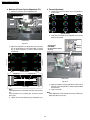
a. Mechanical Picture Position Adjustment (Tilt)
b. Focus Adjustment
1) Loosen the 4 Screws on the Projection Unit.
1) Confirm that each of the pixels in the nine portions is
clearly visible.
Projection Lens
Screw
Screw
Screw
Twist
O P T
O P T
H P O S I
V P O S I
0 C
0 6
Screw
Twist
<Focus Screen>
2) If not, loosen the Knob on the Projection Lens until the
Knob can be moved.
<Front View>
Knob
Fig. M1-5
Tighten
(PT-60LC14)
CAUTION:
Do not turn the screw
and nut.
2) Adjust the Projection Lens by twisting so that the long
line "g" and the long line "h" are within 4 dots. (The long
line "g" and the long line "h" will be almost aligned
horizontally.)
Loosen
Up
O
O P
P T
T
O
O P
P T
T
H
S I
I
H P
P O
O S
V
S I
I
V P
P O
O S
0 C7
0
0 69
0
Down
"G"
long line "g"
<Focus Screen>
"H"
long line "h"
<Front View>
Fig. M1-6
"G"
within 4 dots
3) Adjust the Knob by moving up or down so that each of
the pixels in the nine portions is clearly visible to obtain
the best focus.
4) Tighten the Knob.
"H"
Note:
If the Projection Lens is twisted left, the Focus Screen twists
left.
If the Projection Lens is twisted right, the Focus Screen
twists right.
3) Tighten the 4 Screws while fixing the Projection Lens.
Note:
Focus Adjustment is not normally necessary. Perform this
adjustment only if necessary.
46
PT-43LC14 / PT-50LC14 / PT-60LC14
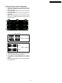
c. Electrical Picture Position Adjustment
1) Adjust OPT HPOSI so that "C" is symmetrical to "D." by
pressing the VOLUME UP/DOWN key on the remote to
change the value.
2) Press the CH UP/DOWN key on the remote to return to
the OTHER menu.
3) Select OPT VPOSI by pressing CH UP/DOWN key on
the remote.
4) Adjust OPT VPOSI so that "A" is symmetrical to “B” by
pressing the VOLUME UP/DOWN key on the remote to
change the value.
"A"
"E"
"F"
"I"
"J"
O P T
O P T
H P O S I
V P O S I
0 C
0 6
"C"
"D"
"K"
"L"
"G"
"B"
"H"
<Focus Screen>
"C"
"D"
width "c" = width "d"
width "c"
width "d"
"A"
width "a"
width "a" = width "b"
width "b"
"B"
5) Confirm that all "A", "B", "C", "D", "E", "F", "G", "H", "I",
"J", "K", "L" are each almost symmetrical.
6) If not, adjust the "OPT HPOSI" and "OPT VPOSI"
(repeat steps 1-6) until the picture is in the correct
position.
7) Press the CH UP/DOWN key on the remote to return to
the OTHER menu.
47
PT-43LC14 / PT-50LC14 / PT-60LC14
7 ADJUSTMENT PROCEDURES 2
INITIAL GUIDELINE
The table below shows which adjustments are necessary according to the unit parts and individual parts to be replaced. Make sure
to perform these adjustments shown below as necessary.
Tuner C.B.A. is included in TV/Tuner Unit
Replacement Parts
Tuner1
(Main Tuner)
Adjustment Item
IC7501
(MTS/SAP Signal Process)
Tuner C.B.A. Separation Adjustment (VR Adjustment)
Adjustment
Section
Note:
: Adjustment Item
Fig. E1-1
Section
Adjustment Item
Tuner C.B.A. Separation Adjustment
Adjustment (VR Adjustment)
Section
Necessary Equipment
·MTS/SAP Signal Generator
·Oscilloscope
·Plastic Tip Driver
Fig. E1-2
TEST EQUIPMENT
To do all of these electrical adjustments, the following equipment is required.
1. Dual-Trace Oscilloscope
Voltage Range: 0.001 V to 50 V/Div.
Frequency Range: DC to 50 MHz
Probes: 10:1, 1:1
2. NTSC Video Pattern Generator
3. Plastic Tip Driver and Non-Metal Driver
4. MTS/SAP Signal Generator
(TV Multi-Channel Sound Modulator (U.S.A.))
48
Input
MTS Signal
(Only L CH, 300Hz, 30% Modulating)
RF
(TV)
PT-43LC14 / PT-50LC14 / PT-60LC14
HOW TO READ THE ADJUSTMENT
PROCEDURES
Connecting Point
(Test Point) of
Oscilloscope
Adjustment
component
TP
ADJ.
TP3602
TP3603
R3662
SEPARATION ADJUSTMENT
(VR ADJUSTMENT)
Purpose:
To separate the L and R Channels of Stereo Signal.
Supply NTSC
COLOR BAR SIGNAL
to the Video
Input Connector
Symptom of Misadjustment:
The L and R Channels of Stereo Signal will not be separated
properly resultin in no stereophonic effect.
INPUT
(Video input Connector)
NTSC Color Bar Signal
EQUIPMENT
TP
ADJ.
TP7501
R7514
INPUT
(RF Input Terminal)
MTS (ONLY L CH)
300 Hz±5 Hz
30 % Modulating
SPECIFICATION
Oscilloscope,
NTSC Video Pattern
Generator
A=0.2 V ± 0.06 V DC
EQUIPMENT
Equipment
required for
adjustment
SPECIFICATION
Oscilloscope
MTS/SAP Signal Generator
Plastic Tip Driver
Specification
for Adjustment
Refer to Description below
Fig. E2-1
Note:
TP7501, R7514: Tuner C.B.A.
CH1
1. Connect the MTS/SAP Signal Generator to the RF Input
Terminal.
Then, set the MTS/SAP Signal Generator as follows.
MTS (ONLY L CH)
300 Hz ± 5 Hz
30 % Modulating
2. Set to TV mode by pressing TV/VIDEO key on the remote
and then set to STEREO audio mode by pressing SAP key
on the remote.
3. Connect the Oscilloscope to TP7501 on the Tuner C.B.A.
4. Adjust R7514 (SEPARATION) on the Tuner C.B.A. so that
the signal level is minimum.
CH2
CH2: TP3602
CH1: TP3603
2V
1
2
10 µs 1
1V
3
1 Connecting Point
3 Volts/DIV (CH2)
5 Time/DIV
6
4 5
2 Volts/DIV (CH1)
4 Connecting Point
6 Trigger Channel of
the Scope
1 : CH1 2 : CH2
Minimum
Fig. E2-2
75 % White
TP7501(R CH)
100 % White
1 ms
20 mV
Fig. E3
75 % Color Bar Signal (Standard)
Fig. E2-3
49
PT-43LC14 / PT-50LC14 / PT-60LC14
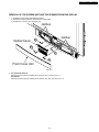
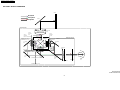
TEST POINTS AND CONTROL LOCATION
Tuner C.B.A.
SEPARATION
R7514
TP7501
(Component Side)
Test Point Information
Test Point with a Test Pin.
Test Point with a jumper wire across a hole in the P.C.B.
Test Point with no Test Pin.
Test Point with a Hook.
50
PT-43LC14 / PT-50LC14 / PT-60LC14
8 TROUBLESHOOTING HINTS FOR BLOCK LEVEL REPAIR
MAIN PARTS LOCATION
<Front View>
Network C.B.A.
TEMP LED
LAMP LED
Lamp Cover
Cover Switch C.B.A.
Network C.B.A.
Optical Cover
Front Cover Unit
Operation C.B.A.
POWER LED
<Rear View>
Projection Unit
Thermal Fuse Unit
Thermistor 1 C.B.A.
Thermistor 2 C.B.A.
Fan 3
Air Filter
Fan Case Unit
(Fan 1)
Front Jack C.B.A.
Main C.B.A.
Ballast C.B.A.
Air Filter
Air Filter
Fan 2
LCD Drive C.B.A.
Tuner C.B.A.
Fan 4
Audio
Amp C.B.A.
Rear Cover
Power C.B.A.
Rear Jack C.B.A.
TV/Tuner Unit
51
PT-43LC14 / PT-50LC14 / PT-60LC14
ERROR INDICATION INFORMATION
Each LED indication facilitates finding the cause of the error.
When an error is detected, the Lamp comes off and the LED on the front will flash.
POWER LED
TV/VIDEO
TEMP LED
Error No.
Error Information
LAMP LED
POWER LED
TEMP LED
LAMP LED
1)
Fan1, Fan2 or Fan3 stopped
flashes orange once
every 5 seconds
-
-
2)
Lamp Cover open
flashes orange twice
every 5 seconds
-
-
3)
Temperature Sensor shorted or open
(Thermistor 1 C.B.A.)
-
flashes once
every 5 seconds
-
4)
Abnormal Temperature
(Thermistor 1 C.B.A.)
-
flashes twice
every 5 seconds
-
5)
Ballast Error (abnormal Lamp or Ballast)
-
-
flashes once
every 5 seconds
6)
Ballast Error (abnormal Lamp voltage)
-
-
flashes twice
every 5 seconds
7)
Ballast Error (abnormal temperature)
-
-
flashes 3 times
every 5 seconds
8)
Ballast Error (other causes)
-
-
flashes 4 times
every 5 seconds
9)
Abnormal Voltage on 30 V line
flashes orange 5 times
every 5 seconds
flashes once
every 5 seconds
flashes once
every 5 seconds
10)
Abnormal Voltage on 9 V line
flashes orange 6 times
every 5 seconds
flashes twice
every 5 seconds
flashes twice
every 5 seconds
11)
Abnormal Voltage on 5 V line
flashes orange 7 times
every 5 seconds
flashes 3 times
every 5 seconds
flashes 3 times
every 5 seconds
12)
Abnormal Voltage on 3.3 V line
flashes orange 8 times
every 5 seconds
flashes 4 times
every 5 seconds
flashes 4 times
every 5 seconds
13)
Abnormal Voltage on -5 V line
flashes orange 9 times
every 5 seconds
flashes 5 times
every 5 seconds
flashes 5 times
every 5 seconds
14)
Abnormal Voltage on 6 V line
flashes orange 10 times
every 5 seconds
flashes 6 times
every 5 seconds
flashes 6 times
every 5 seconds
15)
Temperature Sensor shorted or open
(Thermistor 2 C.B.A.)
-
flashes 3 times
every 5 seconds
-
16)
Abnormal Temperature
(Thermistor 2 C.B.A.)
-
flashes 4 times
every 5 seconds
-
17)
Clogged air filter
-
flashes 5 times
every 5 seconds
-
(Note 2)
(Note 3)
OSD
LAMP OFF
Note:
1. When two or more errors have occurred at the same time, the LED will alternate flash patterns as shown above every 5 seconds.
2. Warning OSD appears when the air filter is clogged.
3. LAMP OFF: The LED will flash immediately after the Lamp comes off.
4.The detected error data will be stored in the EEPROM.
52
PT-43LC14 / PT-50LC14 / PT-60LC14
How to solve the problem indicated by the Error Indication of LED
(All symptom is that Lamp turns off or Lamp does not light up)
Note: Before performing the troubleshooting, confirm that all connector cables in the unit are connected to connectors correctly.
Error No.
1)
Problem
Possible Solution
Cooling Fan (Fan1, Fan2 and/or Fan3) malfunction.
Are the Fan1,
Fan2 and Fan3
operating?
NO
Replace the Power C.B.A.Still NG,
replace the Projection Unit. Still NG,
replace the Main C.B.A.
Only the Fan1 stops.
Replace the Projection Unit.
Only the Fan2 stops.
Only the Fan3 stops.
Replace the Projection Unit.
Replace the Fan3.
2)
Mis-installed the Lamp Cover (the Lamp cover is open).
1. Tighten the screw of the Lamp Cover.
2. If still NG, replace the Cover SW (SW2911) on the Cover Switch C.B.A.
3. If still NG, replace the Main C.B.A.
4. If still NG, replace the Projection Unit.
3)
The temperature sensor (R2811) on the Thermistor 1
C.B.A. on the Fan 1 is short or open.
Remove P2303 connector on the LCD Drive C.B.A. and check if the resistance between pin1 and pin2 of
P2811 on the Thermistor 1 C.B.A. is 5k
200k . If NG, replace the Temperature Sensor (R2811) on the
Thermistor 1 C.B.A. Still NG, replace the Projection Unit. Still NG, replace the Main C.B.A.
4)
It indicates when the temperature detected by the
Temperature Sensor (R2811) on Thermistor 1 C.B.A.
exceeds 55 °C (131 °F).
1. The surrounding temperature of the place of use may
be too high.
2. The vents on the rear may be blocked.
5)
1.
2.
3.
4.
6)
The Lamp is defective (short of the Lamp).
Replace the Lamp.
7)
Thermal fuse (F1302) 117 °C (243 °F) on the Ballast
C.B.A. is open due to abnormal temperature rise.
Replace the Ballast C.B.A.
8)
The Ballast C.B.A. is defective.
If the Lamp does not light up after attempting turning on the power 2 or 3 times, replace the Ballast C.B.A.
9)
+30V line on the Main C.B.A. error.
1. Replace the Power C.B.A.
2. If still NG, replace the Main C.B.A.
3. If still NG, replace the Tuner C.B.A.
10)
+9V line on the Main C.B.A. error.
1. Replace the Power C.B.A.
2. If still NG, replace the Main C.B.A.
3. If still NG, replace the Rear Jack C.B.A.
4. If still NG, replace the Projection Unit.
11)
+5V line on the Main C.B.A. error.
1. Replace the Power C.B.A.
2. If still NG, replace the Main C.B.A.
3. If still NG, replace the Rear Jack C.B.A.
4. If still NG, replace the Tuner C.B.A.
5. If still NG, replace the Projection Unit.
12)
+3.3V line on the Main C.B.A. error.
1. Replace the Power C.B.A.
2. If still NG, replace the Main C.B.A.
13)
-5V line on the Main C.B.A. error.
1. Replace the Power C.B.A.
2. If still NG, replace the Main C.B.A.
14)
+6V line on the Main C.B.A. error.
1. Replace the Power C.B.A.
2. If still NG, replace the Main C.B.A.
15)
The temperature sensor (R2821) on the Thermistor 2
C.B.A. on the Lamp House is short or open.
Remove P2304 connector on the LCD Drive C.B.A. and check if the resistance between pin1 and pin2 of
P2821 on the Thermistor 2 C.B.A. is 5k
1M . If NG, replace the Temperature Sensor (R2821) on the
Thermistor 2 C.B.A. Still NG, replace the Projection Unit. Still NG, replace the Main C.B.A.
16)
It indicates when the temperature detected by the
Temperature Sensor (R2821) on Thermistor 2 C.B.A.
exceeds 85 °C (185 °F).
1. The surrounding temperature of the place of use may
be too high.
2. The vents on the rear may be blocked.
1. Relocate the unit to a proper location.
• Do not place in direct sunlight and other sources of direct heat.
• Do not place the unit in humid or dusty location, or areas exposed to smokeor steam.
(surrounding temperature should be between 0 °C (32 °F) and 40 °C (104 °F) and humidity should be
between 20 % and 80 % (with no condensation).)
• The vents are not blocked.
It is recommended that a gap of at least 10 cm is left all around the unit even when it is placed inside a
cabinet or between shelves.
2. Check if the fans are operating properly.
17)
Clogged air filter of the Fan Case Unit.
1. Cleaning the Air Filter on the Projection Unit.
2. If still NG, replace the Projection Unit.
3. If still NG, replace the Main C.B.A.
Note: The Projection Unit includes LCD Drive C.B.A.
1. Relocate the unit to a proper location.
• Do not place in direct sunlight and other sources of direct heat.
• Do not place the unit in humid or dusty location, or areas exposed to smokeor steam.
(surrounding temperature should be between 0 °C (32 °F) and 40 °C (104 °F) and humidity should be
between 20 % and 80 % (with no condensation).)
• The vents are not blocked.
It is recommended that a gap of at least 10 cm is left all around the unit even when it is placed inside a
cabinet or between shelves.
2. Check if the fans are operating properly.
1. Confirm that the Thermal Fuse Unit (115˚C(239˚F)) on the Lamp House is not open.
The Lamp is not cooled off.
Thermal Fuse Unit (115˚C (239˚F)) is defective (open). 2. Wait until the Lamp is cooled off and try to turn the power back on. If same error LED
The Lamp is defective (crack).
indication continues, remove the Lamp and visually inspect it. If it is cracked, it must be
The Lamp voltage becomes more over 130V or less
replaced. If the Lamp is not cracked, replace the Ballast C.B.A.
than 30V.
3. If still NG, replace the Main C.B.A.
5. The Ballast C.B.A. is defective.
6. The Main C.B.A. is defective.
Note: The Projection Unit includes LCD Drive C.B.A.
53
PT-43LC14 / PT-50LC14 / PT-60LC14
No picture or abnormal picture
ABNORMAL PICTURE:
No Color Picture (Black and White picture)
Abnormal Color Picture
No Synchronisation Picture
Dark Picture
Check that there is no picture or abnormal
picture on the screen from all input
terminals.
(All input are NG.)
Does the OSD appear on the
screen?
NO
Replace the Projection Unit. Still
NG, replace the Main C.B.A.
YES
Replace the Main C.B.A.
(Only Video1 OR 2 input is NG.)
Replace the Rear Jack C.B.A.
(Only Video3 input is NG.)
Replace the Front Jack C.B.A. Still
NG, replace Rear Jack C.B.A.
(Only tuner input is NG.)
Replace the Tuner C.B.A. Still NG,
replace the Rear Jack C.B.A.
(Only RGB 1 input is NG.)
(Only RGB 2 input is NG.)
(Only Component 1, 2, 3 OR 4 input
is NG.)
(Component 1, 2, 3 AND 4 input
is NG.)
(Only HDMI input is NG.)
(Tuner, Component AND Video input
is NG.)
(PC/SD Card input is NG.)
Replace the Main C.B.A.
Replace the Front Jack C.B.A.
Still NG,replace the Main C.B.A.
Replace the Rear Jack C.B.A.
Replace the Main C.B.A. Still NG,
replace the Rear Jack C.B.A.
Replace the Main C.B.A.
Replace the Rear Jack C.B.A.
Replace the Main C.B.A.
54
In the case that one or some input
is NG, it can be judged that the
Projection Unit is OK.
PT-43LC14 / PT-50LC14 / PT-60LC14
No sound from built-in both L-CH and
R-CH Speakers
Check that there is an audio signal to the Audio Out
Terminal from all input terminals.
(All input are NG.)
Replace the Rear Jack C.B.A.
(Only Audio1, 2, Component
1, 2, 3, OR 4 input is NG.)
Replace the Rear Jack C.B.A.
(Only Audio3 input is NG.)
Replace the Front Jack C.B.A. Still
NG, replace the Rear Jack C.B.A.
(Only Tuner input is NG.)
Replace the Tuner C.B.A. Still NG,
replace the Rear Jack C.B.A.
(Only RGB 1 input is NG.)
(Only RGB 2 input is NG.)
(Only HDMI input is NG.)
Replace the Main C.B.A.
Replace the Front Jack C.B.A. Still
NG, replace the Main C.B.A.
Replace the Main C.B.A.
OK
Replace the Audio Amp C.B.A. Still NG, Replace the Rear Jack C.B.A. Still NG, Replace the Power C.B.A.
No sound from built-in L-CH Speaker only
Press "MENU" button on the remote and select
"BALANCE" in MENU screen. Then press "OK."
Does the "BALANCE" becomes center position?
NO
Set to the center position.
YES
Replace the L-CH Speaker.
No sound from built-in R-CH Speaker only
Press "MENU" button on the remote and select
"BALANCE" in MENU screen. Then press "OK."
Does the "BALANCE" becomes center position?
NO
Set to the center position.
YES
Replace the R-CH Speaker.
55
PT-43LC14 / PT-50LC14 / PT-60LC14
56
PT-43LC14 / PT-50LC14 / PT-60LC14
9 BLOCK DIAGRAMS
OVERALL BLOCK DIAGRAM
NETWORK C.B.A. (FOR R-CH)
AUDIO AMP C.B.A.
REAR JACK C.B.A.
IC3502
COMPONENT
AUDIO IN 1 (L/R)
COMPONENT AUDIO IN1(L/R)
COMPONENT
AUDIO IN 2 (L/R)
COMPONENT AUDIO IN2(L/R)
COMPONENT
AUDIO IN 3 (L/R)
COMPONENT AUDIO IN3(L/R)
COMPONENT
AUDIO IN 4 (L/R)
COMPONENT AUDIO IN4(L/R)
AUDIO IN 1(L/R)
AUDIO IN 1 (L/R)
AUDIO IN 2(L/R)
AUDIO IN 2(L/R)
IC3501
P4552
IC4501
P3603
P4503
P4505
P4551
SPEAKER-R
(TWEETER)
NETWORK C.B.A. (FOR L-CH)
P4552
AUDIO
SW
MAIN C.B.A.
P4551
IC5004
SPEAKER-L
(TWEETER)
IC5301
MAIN VIDEO
SIGNAL PROCESS
AUDIO IN 3(L/R)
IC5304
FIFO
I/F
RGB2 AUDIO IN(L/R)
DATA BUS (32bit)
SDRAM
I/F
LCD DRIVE C.B.A.
64M SDRAM
<FOR SCALER(720p CONVERTER)>
RGB1/HDMI/DVI AUDIO IN(L/R)
FPGA
3D Y/C SEPARATION
NTSC DECODER
A/D
AUDIO OUT(L/R)
YUV DATA (10bit)
SW
VIDEO OUT
IC3504
GC3FM
COMPONENT
IN 1(Y/PB/PR)
COMPONENT1 Y/PB/PR
COMPONENT
IN 2(Y/PB/PR)
COMPONENT2 Y/PB/PR
COMPONENT
IN 3(Y/PB/PR)
COMPONENT3 Y/PB/PR
P3601
I/P CONVERTER
R DATA (8bit)
PICTURE CONTROL
MULTI WINDOW
G DATA (8bit)
PICTURE IN PICTURE
SPLIT SCREEN
SEARCH
B DATA (8bit)
SCALER(720p CONVERTER)
VIDEO IN 1
VIDEO IN 1
S-VIDEO IN 1
S-VIDEO IN 1
OSD MIX
D/D CONVERTER
G DATA (8bit)
SIGNAL PROCESS
FOR LCD PANEL
IC2001
TTL PARALLEL TO
LVDS SERIAL
CONVERTER
LVDS DATA/CLOCK
LVDS SERIAL TO
TTL PARALLEL
CONVERTER
R DATA (8bit)
COLOR
CORRECTION
P2001
R DATA (10bit)
SAMPLING
HOLD
D/A
R DATA (12bit)
LCD(R)
B DATA (8bit)
LVDS
TRANSMITTER
P3403
IC2002
P2002
DATA BUS
(32bit)
VIDEO
SW
COLOR
CORRECTION
G DATA (10bit)
SAMPLING
HOLD
D/A
G DATA (12bit)
LCD(G)
LEVEL SHIFTER
IC5306
DATA BUS
(32bit)
Y DATA (8bit)
2D Y/C SEPARATION
NTSC DECODER
A/D
SW
G DATA (8bit)
64M SDRAM
SUB VIDEO
SIGNAL PROCESS
IC5104
SUB Y/V,
PB/C, PR
OSD DATA (0-3)
IC5707
IC5103
64M SDRAM
IC2003
<FOR IP CONVERTER, MULTI WINDOW,
3D Y/C SEPARATION, ETC>
UV DATA (8bit)
S-VIDEO IN 2
S-VIDEO IN 2
P2501
R DATA (8bit)
MAIN Y/V,
PB/C, PR
VIDEO IN 2
VIDEO IN 2
P5302
IC2505
LVDS
RECEIVER
LEVEL SHIFTER
COMPONENT4 Y/PB/PR
COMPONENT
IN 4(Y/PB/PR)
IC2503
IC5705
IC5702
IC5302,5303
VIDEO OUT
SPEAKER-L
(WOOFER)
P4553
TUNER AUDIO(L/R)
AUDIO OUT (L/R)
SPEAKER-R
(WOOFER)
P4553
AUDIO
AMP
SOUND
PROCESSOR
P2003
B DATA (8bit)
GC3I
VIDEO
SIGNAL PROCESS
TUNER VIDEO 1
GC3FS
TUNER VIDEO 2
COLOR
CORRECTION
B DATA (10bit)
SAMPLING
HOLD
D/A
B DATA (12bit)
LCD(B)
NON-UNIFORMITY
COLOR COMPENSATION
GAMMA CORRECTION
WHITE BALANCE
CONTROL
VIDEO IN 3
S-VIDEO IN 3
LEVEL SHIFTER
TUNER C.B.A.
IC7501
RF-IN
RF-OUT
P7002
MTS/SAP AUDIO
SIGNAL PROCESS
AUDIO
TIMING
GENERATOR
P3501
TUNER AUDIO (L/R)
IC9001
VIDEO
128M
SDRAM
U7101 (SUB TUNER)
DATA BUS
(16bit)
VIDEO
RF-IN
SD
CARD
P3502
P9201
IC9207,IC9208
TRANSCEIVER
PC
CARD
VIDEO IN 3
FAN1 SPEED CONTROL
DATA BUS (16bit)
ADJUSTMENT DATA/SETTING DATA
OF EACH IC's FOR LCD DRIVE C.B.A.
SD/PC CARD
SIGNAL
PROCESS
SERIAL DATA/CLOCK
HDMI AUDIO IN2(L/R)
RGB AUDIO IN1(L/R)
DVI AUDIO IN(L/R)
P3404
P3602
P3601
EEPROM
SW
SW
G
SW
B
MAIN MICROCONTROLLER
Q5510-Q5514
RGB-->YUV
CONVERTER
COVER SW
IC2905
OP AMP
THERMISTOR 1 C.B.A.
LAMP ON(H)
LAMP STATUS(ERROR)
P2303
P2811
IC6302
TEMPERATURE
SENSOR
THERMISTOR 2 C.B.A.
SERIAL DATA/CLOCK
THERMO TEMP DATA 3
THERMO TEMP DATA 1
FAN(1,2,3) LOCK (H)
FAN1 SPEED CONTROL
SERIAL DATA/CLOCK
IC5802
HDMI IN
P2912
I2C SERIAL DATA/CLOCK
(PT-50LC14/PT-60LC14)
DVI AUDIO IN(L/R)
(FAN 3)
LAMP COVER OPEN(H)
FILTER ERROR DETECTION
LAMP COVER OPEN(H)
THERMO TEMP DATA 3
R
P2904
DRIVE
COVER SWITCH C.B.A.
IC5501
RGB2 R
RGB1 R
RGB2 G
RGB1 G
RGB2 B
RGB1 B
IC2904
P2502
SERIAL DATA/CLOCK
P5501
RGB AUDIO IN1(L/R)
RGB IN1
FAN3 SPEED CONTROL
FAN1 ON(H)
FAN2 ON(H)
FAN3 ON(H)
I2C SERIAL DATA/CLOCK
SW
RGB IN2
(FAN 2)
FAN2 SPEED CONTROL
IC6003
P3403
P6004
P3901
P2903
SETTING DATA OF EACH
IC's FOR MAIN C.B.A.
USER ADJUSTMENT DATA
PROGRAM
FOR CARD
PROCESSOR
(IC9004)
I2C SERIAL DATA/CLOCK
LCD
MICROCONTROLLER
IC6006
FLASH MEMORY
RGB AUDIO IN2(L/R)
(FAN 1)
DRIVE
EEPROM
LAMP TIME DATA
ADJUSTMENT DATA
IC9007
P3504
IC4002
IC2903
IC2304
IC6005
DATA BUS
(8bit)
AUDIO IN 3 (L/R)
P2902
DRIVE
EEPROM
S-VIDEO IN 3
P3903
IC2902
IC2301
DATA BUS (4bit)
FRONT JACK C.B.A.
P3902
IC9004
P9002
P7003
CARD YUV DATA (8bit)
U7001 (MAIN TUNER)
I2C SERIAL DATA/CLOCK
EEPROM
IC5803
HDMI INFORMATION
DATA
I2C SERIAL DATA/CLOCK
TMDS DATA/CLOCK
HDMI
INTERFACE
+3.3V
HDMI Y DATA (8bit)
TEMP
HDMI UV DATA (8bit)
LAMP
I2C SERIAL DATA/CLOCK
P6701
POWER
HDMI AUDIO IN2(L/R)
P2821
THERMO TEMP DATA 1
SUB MICROCONTROLLER
POWER C.B.A.
BALLAST C.B.A.
P1302
P6305
TEMPERATURE
SENSOR
P805
DRIVE
IC5805
D/A
P2304
REMOTE
SENSOR
OPERATION BUTTON
(KEY MATRIX)
P6002
IC1006
P1305
BALLAST
CIRCUIT
LAMP
AC IN
POWER SUPPLY
CIRCUIT
P1006
(FAN 4)
DRIVE
OVERALL BLOCK DIAGRAM
PT-43LC14/PT-50LC14/PT-60LC14
57
PT-43LC14 / PT-50LC14 / PT-60LC14
POWER SUPPLY BLOCK DIAGRAM
POWER C.B.A.
AUDIO AMP C.B.A.
TP1021
P804-1
P804-2
F801
6.3A 125V/250V L802
AC LINE
FILTER
F1001
5A 125V/250V L1001
AC LINE
FILTER
L803
AC LINE
FILTER
D1002-1005
FULL-WAVE
RETIFIER
10
5
11
VCC OVER VOLTAGE
PROTECTION
DRIVE
CONTROL
Q801
D
S
3
1
12
TP1020
13
TP1009
14
6
RL802
TP1010
TP1006
Q1001-1003
+19V
REGULATOR
PR1001
PR1013
15
7
Q1004-1006
+17V
REGULATOR
8
16
9
17
3
+30V
+3.3V
+6V
-5V
+9V
+5V
IC3402
2
P3402-1
P3402-2
P3402-3
P3402-4
+9V
REG.
4
4
IC6303
+3.3V
REG.
IC6302
11
4
Q6303
REG.
IC6003
56
SUB MICROCONTROLLER
MAIN MICROCONTROLLER
LCD DRIVE C.B.A.
2
IC2901
(+15.5V REGULATOR)
IC1003
(+12V)
5
18
19
20
21
6
VCC
STANDBY POWER CIRCUIT
TP803
OVER CURR.
LIMITER
CONSTANT
VOLTAGE
CONTROL
TP810
(+6V)
11
12
13
14
SWITCHING
T801
D803-806
FULL-WAVE
RETIFIER
+5V
REG.
5
32
77
4
4
P3401-1
P3401-3
P3401-6,7
P3401-5
P3401-8
P3401-4
P3401-2
DC/DC CONVERTER (STEP-DOWN CHOPPER SYSTEM)
TP804
+9V
+5V
1
PR1008
3
2
1
P3602-1, 2
P3602-4, 5
MAIN C.B.A.
P1007-1
P1007-3
P1007-6,7
P1007-5
P1007-8
P1007-4
P1007-2
IC1005
(SHUNT REGULATOR)
IC1006
(FAN4 DRIVE)
6
+30V
+5V
REAR JACK C.B.A.
P3404-1, 2
P3404-4, 5
-16V
2
V-REF(2.495V)
REG.
(+30V)
(+12V)
(+3.3V)
(+6V)
(-5V)
(+9V)
(+17V)
TP1012
FEED BACK
3
P7003-6
P7003-5
IC3401
IC1002
(8V)
P4501-3
PR1003
PR1014
R809
(RUSH CURRENT
PROTECTOR)
TP1013
P1011
TP1008
PR1012
TP1025
P4501-2
TP1007
4
2
TP1022
(17V)
P1010
+16V
TP1003
5
TP1024
P4501-1
PR1011
POWER ON(H)
<FROM IC6302 (72)>
(18.5V)
P1009
TP1005
IC1001
(SWITCHING CONTROL)
RL801
TP1023
P6004-6
P6004-5
PR1010
4
TP1015
TUNER C.B.A.
TP1004
1
P2901-1
P2901-2
P2901-3
P2901-4
(+17V)
(+12V)
(+5V)
(+3.3V)
2
+15.5V
REG.
TP2906
TP2901
SW +15.5V
4
1 5
SW +15.5V CONTROL
<FROM IC2304 (26)>
LCD ON (H)
<FROM IC2304 (51)>
3
2
+5V
IC2902
(FAN1 DRIVE)
32
2
(STBY+9V)
REG.
TP2907
TP2911
FAN 1
(7.75V)
4
P2902-1
P2902-2
P2902-3
IC2905
(OP AMP)
1 5
7
FAN1 SPEED CONTROL
<FROM IC2503(7)>
5
6
FAN1 OH (H)
<FROM IC2304 (53)>
IC2903
(FAN2 DRIVE)
FAN4
P1006-1
P1006-2
2
REG.
TP2908
TP2912
FAN2
(8.75V)
4
P2903-1
P2903-2
P2903-3
1 5
FAN2 SPEED CONTROL
<FROM IC2304 (28)>
FAN2 OH (H)
<FROM IC2304 (55)>
BALLAST C.B.A.
THERMAL FUSE UNIT
F001
115 C (239 F)
TP1301
P1306-1
P1306-2
P805-1
P805-2
P1302
P1303
F1301
5A/250V L1301
AC LINE
FILTER
VOLTAGE MULTIPLYING
RECTIFIER
DC/DC CONVERTER
(STEP-DOWN CHOPPER SYSTEM)
L1303,
C1309-1311
C1305
C1306
IC2904
(FAN3 DRIVE)
DC/AC INVERTER
2
TP1305
Q1304
NOISE
REDUCTION
REG.
TP2909
TP2913
FAN3
(7.75V)
4
P2904-1
P2904-2
P2904-3
1 5
R1321
WATTAGE
D1302
Q1306
Q1308
Q1307
Q1309
FAN3 SPEED CONTROL
<FROM IC2304 (30)>
FAN3 ON (H)
<FROM IC2304 (73)>
TP1302
+17V
+11V
+5V
F1302
THERMAL FUSE
117 C (243 F)
+3.3V
FAN(1,2,3) LOCK (H)
<TO IC6302 (6)>
Q1305
P1001-4
P1001-5
P1001-1
P1001-2
P1301-4
P1301-5
P1301-1
P1301-2
Q1301
(17V)
TP1306
(18.5V)
TP1303
FROM
SYSTEM CONTROL
BLOCK DIAGRAM
STANDBY(L)/POWER ON(H)
LAMP ON(H)
LAMP STATUS(ERROR)
P6002-1
P6002-2
P6002-3
P1305-1
P1305-2
P1305-3
IC1302
OPTICAL
ISOLATOR
ERROR VOLTAGE DET
LAMP GND
ERROR CURRENT DET
IC1304
OPTICAL
ISOLATOR
TP1304
PWM CONTROL
IC1303
OPTICAL
ISOLATOR
THERMISTOR
MAIN C.B.A.
VCC(+17V)
Q1302
VCC(+19V)
AC IN
T1001
LAMP ON(L)
LAMP ERROR PULSE
BALLAST CONTROL
CIRCUIT
U1301(HIC)
4
T1301
3
LAMP
1
INVERTER DRIVE3
INVERTER DRIVE1
2
D1315
INVERTER DRIVE2
INVERTER DRIVE4
Q1310
HV ON(H)
Q1310 TURNS ON WHEN
LAMP STARTS UP.
LAMP STATUS
SIGNAL
LAMP ON
H
LAMP OFF
L
ERROR 1
PULSE (T=128 msec)
ERROR 2
PULSE (T=96 msec)
ERROR 3
PULSE (T=64 msec)
ERROR 4
PULSE (T=32 msec)
(ERROR PULSE)
"2T"
POWER SUPPLY BLOCK DIAGRAM
PT-43LC14/PT-50LC14/PT-60LC14
58
PT-43LC14 / PT-50LC14 / PT-60LC14
VIDEO SIGNAL PATH I BLOCK DIAGRAM (1/2)
REAR JACK C.B.A.
MAIN C.B.A.
IC3504 (VIDEO SW)
IC5004 (MAIN VIDEO SIGNAL PROCESS)
JK3601
COMPONENT
-Y1
21
COMPONENT
-PB1
23
IC5002
COMPONENT
-PR1
25
5
VCC
+3.3V
TP3603
+2.5V
REG.
GC3FM
1,12,23,32,73,90,
105,113,114
3-5,136-143
66,71,79,84
4
VCC
4
VCC
115-122,125-132
IC5003
JK3602
COMPONENT
-Y2
27
COMPONENT
-PB2
29
5
+2.5V
REG.
V-SYNC 109
H-SYNC 110
CLOCK 111
38,40,45,47,52,54,58
TP3602
COMPONENT
-PR2
FR CLOCK1 24
IC5001
8
31
JK3603
+2.5V
REG.
VCC
1
10,21,30,75,88,114,
123,135
TP3601
33
COMPONENT
-PB3
35
MAIN Y/V
COMPONENT
-PR3
37
60
Q3503
MAIN PB/C 59
Q3504
MAIN PR
Q3505
58
B
P3601-6
P3403-6
B
P3601-8
P3403-8
P3601-9
B
Q5002
Q5003
Q5004
P3403-9
B
LPF
B
LPF
B
Q5005
Q5006
Q5007
LPF
B
B
B
Q5008
Q5010
Q5009
Y/V
B
56
B
42
B
PR
49
PB/C
A/D
YUV DATA
3D Y/C SEPARATION
NTSC DECODER
A/D
A/D
JK3604
6 104 7 2
COMPONENT
-Y4
39
COMPONENT
-PB4
41
COMPONENT
-PR4
43
SUB PB/C
SUB PR
JK3501
Y
C
S-VIDEO IN2
56
55
54
Q3506
Q3507
Q3508
B
P3601-11
P3403-11
B
P3601-13
P3403-13
B
P3601-14
P3403-14
Q5103
Q5106
Q5107
Y
C
B
LPF
B
LPF
Q5105
Q5109
Q5110
LPF
B
B
Q5108
B
1
16
9
8
14
11
B
B
(PT-50LC14/PT-60LC14)
TP3604
H
L
Q5111
3
H
L
Q5113
6
H
L
Q5112
5
B
40
B
30
B
35
Y/V
PB/C
PR
A/D
74-76,78-80,83,84
2D Y/C SEPARATION
NTSC DECODER
A/D
85,86,88-93
TP3605
RGB-IN 1
RGB(L)
<FROM IC6003 (11)>
FR CLOCK1 68
FR CLOCK2 70
8,15,53,66,82,95
VCC
VCC
+3.3V
VIDEO IN2
UV DATA (8BIT)
V-SYNC 72
H-SYNC 73
CLOCK 94
12 7 2
R
G
B
H-SYNC
V-SYNC
Y DATA (8BIT)
A/D
+9V
VCC 13
JK5501
VIDEO
INPUT
SELECT
17
77
3
9
15
VIDEO IN1
IC5103 (SUB VIDEO SIGNAL PROCESS)
IC5104 (SW)
SUB Y/V
S-VIDEO IN1
YUV DATA (10BIT)
8,9,13-20
H-SYNC
H-SYNC
V-SYNC
CLOCK
COMPONENT
-Y3
6,12,17,51,62,69,
81,97
TP3606
IC5101
FRONT JACK C.B.A.
S-VIDEO IN3
RGB-IN 2
JK4801
Y
C
VIDEO IN3
P3902-3
P3902-5
P3502-3
P3502-5
P3902-7
P3502-7
IC5501 (SW)
JK3901
1
7
13
R
G
B
H-SYNC
V-SYNC
P3901-1
P3901-3
P3901-5
P3901-7
P3901-9
1
7
P5501-1
P5501-3
P5501-5
P5501-7
P5501-9
3
9
5
11
TUNER C.B.A.
21
H
L
19
H
L
15
H
L
12
13
51
U7001
(MAIN TUNER)
B
Q5504
B
Q5505
B
Q5512
RGB --> Y
CONVERT
+5V
20
Q5516
P7002-1
4
VCC
28,33,38,41
+2.5V
REG.
5
B
GC3FS
19 20
IC5505
(OR GATE)
Q5513,Q5514 Q5517
RGB --> PR
B
CONVERT
1
2
Q5509,
Q5518-Q5520
4
VCC
DELAY
22
IC5502
(INVERTER)
6
IC5105 (SW)
H
L
3
2
2
4
VCC
5
8
+3.3V
+3.3V
H
L
6
5
14
7
VCC 16
RGB1(H)RGB2(L) <FROM IC6003(22)>
+3.3V
1
VCC
RF-IN
VIDEO 17
VCC
Q5510,Q5511 Q5515
RGB --> PB
B
CONVERT
16
TP7001
4
IC5102
Q5503
H
L
H
L
24
23
49,57
+2.5V
REG.
5
FRONT JACK C.B.A.
H-SYNC
V-SYNC
79
5
11
RGB(L)
<FROM IC6003 (11)>
P3501-1
RF-OUT
IC5803 (HDMI INTERFACE)
JK5801
U7101
(SUB TUNER)
TP7101
RF-IN
VIDEO 17
P7002-3
P3501-3
HDMI-IN
8,47,53,57
+9V
VCC
TMDS DATA0(+)
TMDS DATA0(-)
TMDS DATA1(+)
TMDS DATA1(-)
TMDS DATA2(+)
TMDS DATA2(-)
TMDS CLOCK(+)
TMDS CLOCK(-)
I2C SERIAL CLOCK
I2C SERIAL DATA
87
86
92
91
97
96
84
83
XOR
MASK
YUV CONVERTER
COLOR RANGE SCALING
COLOR SPACE CONVERSION
UP/DOWN CONVERSION
MODE
CONTROL
TMDS
DECODER
WF65
Y
HDMI Y DATA (8BIT)
49-55,58
WF66
UV
HDMI UV DATA (8BIT)
36-39,42-44,48
WF67
WF68
WF69
V-SYNC 34
H-SYNC 33
HDMI CLOCK(76MHz) 46
IC5805 (D/A CONVERTER)
IC5804 (OP AMP)
IC5802 (EEPROM)
Q5803
I2C SERIAL CLOCK 6
DRIVE
77
I2C SERIAL CLOCK
AUDIO DATA
DECODER
Q5802
I2C SERIAL DATA 5
DRIVE
76
I2C SERIAL DATA
MAIN CLOCK
GENERATOR
JK3502
VCC 8
+5V
VCC
VIDEO OUT
1,6,11,14,17,,21,40,
47,56,64,67,82,89,
93,95,100
32
30
31
27
2
3
4
26
1
AUDIO
DATA
INTERFACE
D/A
10
3
1
HDMI AUDIO (R)
D/A
11
5
7
HDMI AUDIO (L)
4.4 dB VEE 4
-5V
VCC 8
+5V
TO AUDIO
BLOCK DIAGRAM
23,80
VCC
VCC 14
+5V
IC5801
+3.3V
+5V
5
+3.3V 4
REG.
VIDEO SIGNAL PATH I BLOCK DIAGRAM (1/2)
PT-43LC14/PT-50LC14/PT-60LC14
59
PT-43LC14 / PT-50LC14 / PT-60LC14
VIDEO SIGNAL PATH I BLOCK DIAGRAM (2/2)
MAIN VIDEO SIGNAL
SUB VIDEO SIGNAL
VIDEO SIGNAL(MAIN/SUB)
CARD Y/PB/PR SIGNAL
IC5301 (VIDEO SIGNAL PROCESS)
IC5304 (64M MEMORY)
<FOR SCALER(720p COVERTER)>
E1,E2,E4,
F1-F5,G2-G4
FIFO
INTERFACE
G1,H1-H3,J1-J5,
K1-K5,L1,L5
L2
L3
L4
SDRAM
INTERFACE
DATA BUS(32BIT)
Y22-Y25,AA23-AA26,AB18,AB19,AC22,
AD17,AD18,AD21-AD24,AE17,AE18,
AE21-AE26,AF17,AF18,AF21-AF25
64M
MEMORY
V-SYNC
H-SYNC
CLOCK
1,3,9,15,29,35,41,
43,49,55,75,81
VCC
+3.3V
IC5303 (BUS SW)
10,13
VCC 14
9,12
+5V
8,11
OSD DATA 3
FROM
OSD DATA 2
SYSTEM CONTROL
OSD DATA 1
BLOCK DIAGRAM
OSD DATA 0
OSD BLANKING
IC5302 (BUS SW)
16,18,20-28
+5V
VCC 17
55
YUV DATA (10BIT)
BUS
SW
MAIN SIGNAL PATH
29-37,39,40
IC5702 (FPGA)
IC5705 (LVDS TRANSMITTER)
98 97 96 95 94
B1-B3,C1-C4,D2-D4
CARD(L)
<FROM IC6003 (79)>
CARD YUV DATA(8BIT)
FROM CARD
CARD V-SYNC
SIGNAL PROCESS CARD H-SYNC
BLOCK DIAGRAM
27MHz CLOCK
D1
E5
E3
56
3-7,9-14
BUS
SW
V-SYNC
H-SYNC
CLOCK
FOR MAIN SIGNAL
42-48,50-53
SUB SIGNAL PATH
Y DATA (8BIT)
A6,A7,B6,B7,
C5,C6,D5,E6
UV DATA (8BIT)
A8,A9,B8,C7,
C8,C9,D7,D8
IP CONVERTER
PICTURE CONTROL
MULTI WINDOW
PICTURE IN PICTURE
SPLIT SCREEN
SEARCH
SCALER(720p CONVERTER)
R DATA (8BIT)
G DATA (8BIT)
B DATA (8BIT)
A25,B24-B26,
C24-C26,D24
147-154
V3,W1-W3,
Y2,Y3,Y5
157-164
V24-V26,W26,
Y1,AA1-AA3
166-173
H-SYNC W24
175
V-SYNC W25
176
V-SYNC
H-SYNC FOR SUB SIGNAL
CLOCK
HDMI CLOCK
B4
FR CLOCK2
OSD
MIX
8,10-12,14-16,18
B DATA (8BIT)
134,135,138-143
19,20,22-25,27,28
V-SYNC
H-SYNC
V-SYNC 102
V-SYNC 101
H-SYNC
2-4,6,7,54-56
G DATA (8BIT)
122-124,127-131
47
48
45
46
41
42
37
38
39
40
TTL PARALLEL
TO LVDS SERIAL
CONVERTER
51
52
V-SYNC
CLOCK(76MHz)
178
CLOCK Y26
A5
B5
B9
A2
R DATA (8BIT)
110-112,115-119
D/D CONVERTER
(76MHz ---> 76MHz)
CLOCK(76MHz) 81
1,10,24,36,46,54,68,
76,78,93,100,105,114,
126,137,145,180,201
VCCE
LVDS DATA A(+)
LVDS DATA A(-)
LVDS DATA B(+)
LVDS DATA B(-)
TO VIDEO II
LVDS DATA C(+) SIGNAL PATH
LVDS DATA C(-) BLOCK DIAGRAM
LVDS DATA D(+)
LVDS DATA D(-)
LVDS CLOCK(+)
LVDS CLOCK(-)
PLL
31
CLOCK(76MHz) 92
17,42,61,86,108,
156,174,207
P5302-14
P5302-15
P5302-11
P5302-12
P5302-8
P5302-9
P5302-2
P5302-3
P5302-5
P5302-6
9,26,34,44
VCC
VCCI
X5702
76M
OSC
3-8,11-15,18-22,25-30,32-35,37,39-41,43,44
IC5706
4
+3.3V
REG.
5
+5V
IC5708
+3.3V
8
+1.8V
REG.
1
IC5707 (64M SDRAM)
DATA BUS(32BIT)
64M
MEMORY
1,3,9,15,29,35,41,
43,49,55,75,81
VCC
+3.3V
IC5306 (64M SDRAM)
<FOR IP COVERTER, MULTI WINDOW,
3D Y/C SEPARATION, ETC>
28,33,38,41
DATA BUS(32BIT)
8AB1-AB5,AB8,AC2-AC4,AC8,AD5-AD8,AD11,
AD12,AE4-AE8,AE11,AE12,AF4-AF8,AF10-AF12
64M
MEMORY
AVS(GND)
1,3,9,15,29,35,41,
43,49,55,75,81
P1,P2,ETC
VCC
+3.3V
VSS(GND)
L5307
L5304
+3.3V
P3,P4,ETC
AVD
D23,F23,ETC
VDDE
IC5305
1
+1.8V
REG.
U5,V5,ETC
3
VDDI
GC3I
VIDEO SIGNAL PATH I BLOCK DIAGRAM (2/2)
PT-43LC14/PT-50LC14/PT-60LC14
60
PT-43LC14 / PT-50LC14 / PT-60LC14
VIDEO SIGNAL PATH II BLOCK DIAGRAM (Models: PT-43LC14 / PT-50LC14)
VIDEO SIGNAL(MAIN/SUB)
LCD DRIVE C.B.A.
IC2503 (LVDS RECEIVER)
IC2001 (SAMPLING HOLD)
LVDS DATA A(+)
LVDS DATA A(-)
LVDS DATA B(+)
LVDS DATA B(-)
LVDS DATA C(+)
LVDS DATA C(-)
LVDS DATA D(+)
LVDS DATA D(-)
LVDS CLOCK(+)
LVDS CLOCK(-)
P2501-14
P2501-15
P2501-11
P2501-12
P2501-8
P2501-9
P2501-2
P2501-3
P2501-5
P2501-6
R DATA (8BIT)
30,32-35,
37-39
10
9
12
11
16
15
20
19
18
17
A5-A7,B6-B8,
C7,C8
LVDS SERIAL TO
TTL PARALLEL
CONVERTER
NON UNIFORMITY COLOR COMPENSATION
G DATA (8BIT)
41-43,45-47,
49,50
R DATA (10BIT)
W4-W6,Y1-Y7
S/H CLOCK(R) V2
XFR(R) V1
STSQO(R) W3
FRP U1
GAMMA CORRECTION
A10-A12,B10-B12,
C10,C11
WHITE BALANCE CONTROL
DY M19
B DATA (8BIT)
1-3,5,51,
53-55
DX
ENABLE 4
ENABLE 3
ENABLE 2
ENABLE 1
NRG
A15,A16,B14-B16,
C14-C16
Y10
V9
W9
Y9
W10
M1
CLX W8
CLY M18
H-SYNC 29
E2
H-SYNC
V-SYNC 27
D2
V-SYNC
26
E1
86-95
96
97
98
99
100
24
23
33
37
36
35
34
27
22
38
25
TIMING GENERATOR FOR PANEL DRIVE
PLL
V-REF-H(+7V)
CLOCK(76 MHz)
V-REF-L(+5V)
TP2001
(IC2001 PIN52 LINE)
6
D/A
CONVERTER
INVERTER
AMP
CONTROL
LOGIC
& DAC LATCH
3
5
4
SERIAL
INTERFACE
12
11
10
SCALE
CONTROL
W15-W19,Y16-Y20
S/H CLOCK(G) W13
XFR(G) V13
STSQO(G) Y15
XFRP Y13
+5V
5
+3.3V 4
REG.
13,23,31,40,48,56
86-95
96
97
98
99
100
VCC(A) 15,26,53,57,61,65,69,73,82
+15.5V
VCC(D) 1,50
+3.3V
SCALE
CONTROL
V1
V2
AMP
SW
INVERTER
AMP
CONTROL
LOGIC
& DAC LATCH
ON/OFF
SW
V-REF-H(+7V)
V-REF-L(+5V)
12
11
10
SCALE
CONTROL
VCC(A) 15,26,53,57,61,65,69,73,82
+15.5V
VCC(D) 1,50
+3.3V
SCALE
CONTROL
V1
V2
D/A CONVERTER
IC2003 (SAMPLING HOLD)
D20,E19,E20,F19,F20,
G19,G20,H19,H20,J18
B DATA (10BIT)
S/H CLOCK(B) K20
XFR(B) K18
STSQO(B) J19
<FROM IC2304(52)> RESET(L)
C19
RESET(L)
<FROM IC2304(57)> CORRECT ON(L)
H2
CORRECT ON(L)
86-95
96
97
98
99
100
24
23
33
37
36
35
34
27
22
38
25
V-REF-H(+7V)
V-REF-L(+5V)
AMP
SW
ON/OFF
SW
SCALE
CONTROL
TP2005
V-REF-L(+7V)
LCD(B)
LCDCOM
P2003-1
P2003-2
P2003-3
P2003-4
P2003-5
P2003-6
P2003-(7-18)
P2003-19
P2003-20
P2003-21
P2003-22
P2003-23
P2003-24
P2003-25
P2003-26
P2003-27
P2003-28
P2003-29
P2003-30
P2003-31
P2003-32
P2003-33
P2003-34
P2003-35
P2003-36
TP2006
52,54,56,58,60,62,
64,66,68,70,72,74
VCC(A) 15,26,53,57,61,65,69,73,82
+15.5V
VCC(D) 1,50
+3.3V
19
18
39
43
42
41
40
28
LEVEL
SHIFTER
(3.3V --> 15.5V)
12
11
10
LCD(G)
P2002-1
P2002-2
P2002-3
P2002-4
P2002-5
P2002-6
P2002-36
P2002-(7-18)
P2002-19
P2002-20
P2002-21
P2002-22
P2002-23
P2002-24
P2002-25
P2002-26
P2002-27
P2002-28
P2002-29
P2002-30
P2002-31
P2002-32
P2002-33
P2002-34
P2002-35
P2002-36
V-REF-H(+7.5V)
TP2003
(IC2003 PIN52 LINE)
INVERTER
AMP
CONTROL
LOGIC
& DAC LATCH
SERIAL
INTERFACE
19
18
39
43
42
41
40
28
17
44
45
20
21
81
80
79
77
78
13
6
D/A
CONVERTER
3
5
4
V-REF-L(+7V)
LCDCOM
52,54,56,58,60,62,
64,66,68,70,72,74
LEVEL
SHIFTER
(3.3V --> 15.5V)
SERIAL
INTERFACE
V-REF-H(+7.5V)
TP2002
(IC2002 PIN74 LINE)
D/A
CONVERTER
3
5
4
44
45
20
21
81
80
79
77
78
13
6
VCC
24
23
33
37
36
35
34
27
22
38
25
TP2004
52,54,56,58,60,62,
64,66,68,70,72,74
LEVEL
SHIFTER
(3.3V --> 15.5V)
IC2002 (SAMPLING HOLD)
G DATA (10BIT)
ON/OFF
SW
P2001-1
P2001-2
P2001-3
P2001-4
P2001-5
P2001-6
P2001-(7-18)
P2001-19
P2001-20
P2001-21
P2001-22
P2001-23
P2001-24
P2001-25
P2001-26
P2001-27
P2001-28
P2001-29
P2001-30
P2001-31
P2001-32
P2001-33
P2001-34
P2001-35
P2001-36
19
18
39
43
42
41
40
28
D/A CONVERTER
IC2502
LCD(R)
+15.5V
IC2505 (SIGNAL PROCESS FOR LCD PANEL)
SCALE
CONTROL
V1
V2
D/A CONVERTER
AMP
SW
44
45
20
21
81
80
79
77
78
13
V-REF-H(+7.5V)
V-REF-L(+7V)
LCDCOM
TP2901
Q2003
IC2504 (BUFFER)
XDIR-X <FROM IC2304 (60)>
DIR-X <FROM IC2304 (59)>
DIR-Y <FROM IC2304 (50)>
SERIAL DATA 0 B18
2
18
SERIAL DATA 0
SERIAL CLOCK B20
3
17
SERIAL CLOCK
7
13
IC2001 CS(L)
5
15
IC2002 CS(L)
4
16
IC2003 CS(L)
6
14
IC2505CS(L)
H4,H5,ETC
+3.3V
VDD2(+3.3V)
IC2501
D7,D8,ETC
8
+1.8V
REG.
1
VDD1(+1.8V)
CS(L) B19
FROM
SYSTEM CONTROL
BLOCK DIAGRAM
LEVEL
SHIFTER
VIDEO SIGNAL PATH II BLOCK DIAGRAM
PT-43LC14/PT-50LC14
61
PT-43LC14 / PT-50LC14 / PT-60LC14
VIDEO SIGNAL PATH II BLOCK DIAGRAM (Model: PT-60LC14)
VIDEO SIGNAL(MAIN/SUB)
LCD DRIVE C.B.A.
IC2503 (LVDS RECEIVER)
IC2001 (SAMPLING HOLD)
FROM VIDEO I
SIGNAL PATH
BLOCK DIAGRAM
LVDS DATA A(+)
LVDS DATA A(-)
LVDS DATA B(+)
LVDS DATA B(-)
LVDS DATA C(+)
LVDS DATA C(-)
LVDS DATA D(+)
LVDS DATA D(-)
LVDS CLOCK(+)
LVDS CLOCK(-)
P2501-14
P2501-15
P2501-11
P2501-12
P2501-8
P2501-9
P2501-2
P2501-3
P2501-5
P2501-6
R DATA (8BIT)
30,32-35,
37-39
10
9
12
11
16
15
20
19
18
17
A5-A7,B6-B8,
C7,C8
LVDS SERIAL TO
TTL PARALLEL
CONVERTER
NON UNIFORMITY COLOR COMPENSATION
G DATA (8BIT)
41-43,45-47,
49,50
R DATA (10BIT)
W4-W6,Y1-Y7
S/H CLOCK(R) V2
XFR(R) V1
STSQO(R) W3
FRP U1
GAMMA CORRECTION
A10-A12,B10-B12,
C10,C11
WHITE BALANCE CONTROL
DY
M19
B DATA (8BIT)
DX
ENABLE 4
ENABLE 3
ENABLE 2
ENABLE 1
NRG
Y10
V9
W9
Y9
W10
M1
1-3,5,51,
53-55
A15,A16,B14-B16,
C14-C16
CLX
CLY
W8
M18
H-SYNC
29
E2
H-SYNC
V-SYNC
27
D2
V-SYNC
26
E1
CLOCK(76 MHz)
86-95
96
97
98
99
100
24
23
33
37
36
35
34
27
22
38
25
TIMING GENERATOR FOR PANEL DRIVE
PLL
V-REF-H(+7V)
V-REF-L(+5V)
TP2001
(IC2001 PIN52 LINE)
6
D/A
CONVERTER
INVERTER
AMP
CONTROL
LOGIC
& DAC LATCH
+5V
5
+3.3V
REG.
13,23,31,40,48,56
4
G DATA (10BIT)
SERIAL
INTERFACE
12
11
10
SCALE
CONTROL
SCALE
CONTROL
V1
V2
AMP
SW
INVERTER
AMP
CONTROL
LOGIC
& DAC LATCH
ON/OFF
SW
V-REF-H(+7V)
VCC(A)
15,26,53,57,61,65,69,73,82
V-REF-L(+5V)
LEVEL
SHIFTER
(3.3V --> 15.5V)
12
11
10
SCALE
CONTROL
SCALE
CONTROL
V1
V2
D/A CONVERTER
IC2003 (SAMPLING HOLD)
D20,E19,E20,F19,F20,
G19,G20,H19,H20,J18
S/H CLOCK(B)
XFR(B)
STSQO(B)
<FROM IC2304(52)> RESET(L)
C19
RESET(L)
<FROM IC2304(57)> CORRECT ON(L)
H2
CORRECT ON(L)
B DATA (10BIT)
K20
K18
J19
86-95
96
97
98
99
100
24
23
33
37
36
35
34
27
22
38
25
V-REF-H(+7V)
V-REF-L(+5V)
AMP
SW
INVERTER
AMP
ON/OFF
SW
VCC(A)
19
18
39
43
42
41
40
28
17
44
45
20
21
81
80
79
77
78
13
15,26,53,57,61,65,69,73,82
TP2005
+15.5V
Q2004,Q2007,
Q2010,Q2011,
Q2016,Q2017
V-REF-H(+7.5V)
BUFFER
V-REF-L(+7V)
LCD(B)
LCDCOM
P2003-36
P2003-35
P2003-34
P2003-33
P2003-32
P2003-31
P2003-(19-30)
P2003-18
P2003-17
P2003-16
P2003-15
P2003-14
P2003-13
P2003-12
P2003-11
P2003-10
P2003-9
P2003-8
P2003-7
P2003-6
P2003-5
P2003-4
P2003-3
P2003-2
P2003-1
TP2006
1,50
+15.5V
+3.3V
19
18
39
43
42
41
40
28
LEVEL
SHIFTER
(3.3V --> 15.5V)
SCALE
CONTROL
P2002-36
P2002-35
P2002-34
P2002-33
P2002-32
P2002-31
P2002-36
P2002-(19-30)
P2002-18
P2002-17
P2002-16
P2002-15
P2002-14
P2002-13
P2002-12
P2002-11
P2002-10
P2002-9
P2002-8
P2002-7
P2002-6
P2002-5
P2002-4
P2002-3
P2002-2
P2002-1
52,54,56,58,60,62,
64,66,68,70,72,74
VCC(D)
12
11
10
LCD(G)
LCDCOM
TP2003
(IC2003 PIN52 LINE)
CONTROL
LOGIC
& DAC LATCH
SERIAL
INTERFACE
BUFFER
V-REF-L(+7V)
+3.3V
1,50
6
D/A
CONVERTER
3
5
4
Q2006,Q2009,
Q2014,Q2015,
Q2020,Q2021
V-REF-H(+7.5V)
52,54,56,58,60,62,
64,66,68,70,72,74
VCC(D)
SERIAL
INTERFACE
44
45
20
21
81
80
79
77
78
13
TP2002
(IC2002 PIN74 LINE)
D/A
CONVERTER
3
5
4
+15.5V
+3.3V
1,50
6
VCC
24
23
33
37
36
35
34
27
22
38
25
TP2007
19
18
39
43
42
41
40
28
LEVEL
SHIFTER
(3.3V --> 15.5V)
3
5
4
86-95
96
97
98
99
100
15,26,53,57,61,65,69,73,82
P2001-36
P2001-35
P2001-34
P2001-33
P2001-32
P2001-31
P2001-(19-30)
P2001-18
P2001-17
P2001-16
P2001-15
P2001-14
P2001-13
P2001-12
P2001-11
P2001-10
P2001-9
P2001-8
P2001-7
P2001-6
P2001-5
P2001-4
P2001-3
P2001-2
P2001-1
TP2004
52,54,56,58,60,62,
64,66,68,70,72,74
VCC(D)
IC2002 (SAMPLING HOLD)
W15-W19,Y16-Y20
S/H CLOCK(G) W13
XFR(G) V13
STSQO(G) Y15
XFRP Y13
ON/OFF
SW
VCC(A)
D/A CONVERTER
IC2502
LCD(R)
+15.5V
IC2505 (SIGNAL PROCESS FOR LCD PANEL)
SCALE
CONTROL
V1
V2
D/A CONVERTER
AMP
SW
44
45
20
21
81
80
79
77
78
13
Q2005,Q2008,
Q2012,Q2013,
Q2018,Q2019
V-REF-H(+7.5V)
BUFFER
V-REF-L(+7V)
LCDCOM
TP2901
Q2003
IC2504 (BUFFER)
H4,H5,ETC
+3.3V
XDIR-X <FROM IC2304 (60)>
DIR-X <FROM IC2304 (59)>
DIR-Y <FROM IC2304 (50)>
VDD2(+3.3V)
SERIAL DATA 0
IC2501
D7,D8,ETC
8
+1.8V
REG.
1
SERIAL CLOCK
B18
B20
VDD1(+1.8V)
CS(L)
B19
2
18
+15.5V
SERIAL DATA 0
3
17
SERIAL CLOCK
7
13
IC2001 CS(L)
5
15
IC2002 CS(L)
4
16
IC2003 CS(L)
6
14
IC2505CS(L)
IC2004 (SW)
5
3
2
1
FROM
SYSTEM CONTROL
BLOCK DIAGRAM
L
H
4
L
H
15
9 10
Q2001,Q2002
LEVEL
SHIFTER
VIDEO SIGNAL PATH II BLOCK DIAGRAM
PT-60LC14
62
PT-43LC14 / PT-50LC14 / PT-60LC14
SD/PC CARD SIGNAL PROCESS BLOCK DIAGRAM
CARD Y/PB/PR SIGNAL
MAIN C.B.A.
IC9011 (+3.3V REG.)
IC9004 (SD/PC CARD SIGNAL PROCESS)
+5V
5
+3.3V REG.
P9002
VCC(+3.3V)
4
SD DATA(0-3)
SD DATA(0-3)
160-162,165
SD CLOCK
TO VIDEO I
SIGNAL PATH
BLOCK DIAGRAM
CARD YUV DATA (8BIT) : 480i
CARD YUV DATA
(0-7)
SD CLOCK
SD WRITE PROTECT(L)
SD CARD DETECT(L)
169
106-110,
113-115
CARD V-SYNC
CARD H-SYNC
27MHz CLOCK
118
119
IC9207 (TRANSCEIVER)
CARD V-SYNC
CARD H-SYNC
SD/PC CARD
SIGNAL PROCESS
2
3
4
5
6
7
8
9
1 DIRECTION
19 ENABLE
PC DATA(0-15)
122-128,131-137,
140,141
18
17
16
15
14
13
12
11
VCC
IC9008
+6V
2
+3.5V
REG.
VCC
4
1,18,27,51,59,68,75,92,
99,104,111,130,148,157,
159,164,183,193,201
2
+2.8V
REG.
9,35,44,83,121,139,172
PC ADDRESS(0-9)
PC CARD DETECT1(L)
PC CARD DETECT2(L)
CHIP ENABLE2
CHIP ENABLE1
OUTPUT ENABLE
I/O READ CONTROL
WRITE ENABLE
I/O WRITE CONTROL
VS1
VS2
REG
RESET(L)
20
18
17
16
15
14
13
12
11
VCC
VCC
3
P9201
PC DATA(0-15)
IC9208 (TRANSCEIVER)
2
3
4
5
6
7
8
9
1 DIRECTION
19 ENABLE
IC9002
+3.3V
SD CARD
PC CARD
+5V(PC CARD DETECTED)/0V(NO PC CARD)
20
4
+3.3V
PC ADDRESS 0
PC ADDRESS 1
Q9001
154
155
IC9209 (BUFFER)
IC9205 (D-FLIP/FLOP)
3
4
7
8
13
14
17
18
IC9001 (128M SDRAM)
+3.3V
SDRAM DATA (0-15)
128M SDRAM
F/F
F/F
F/F
F/F
F/F
F/F
F/F
2
3
4
5
6
7
8
9
19 ENABLE
2
5
6
9
12
15
16
19
11
38
102
94.5MHz
VCC
20
IC9211 (BUFFER)
H RESET(L)
145
IC9201 (D-FLIP/FLOP)
+3.3V
+3.3V
16
VCC
11
13
14
F/F
10
12
15
F/F
F/F
20
VCC
2
3
4
5
6
7
8
9
19 ENABLE
1,3,9,14,27,43,49
VCC
18
17
16
15
14
13
12
11
VCC
77-82,85-90,
93-96
TP9001
94.5MHz
20
F/F
18
17
16
15
14
13
12
11
IC9206 (OR GATE)
CARD RESET(L)
LCS1(L)
24
174
1
9
+3.3V
HCS3(L)
153
HRD
150
1
2
4
5
10
9
IC9202 (D-FLIP/FLOP)
1
2
3
4
F/F
10
11
12
13
F/F
3
+6V
+5V REG.
2
4
8
1
VCC
5
TP9202
IC9204 (+5V REG.)
6
14
+3.3V
TP9201
PC CARD ON(H)
9
VCC
14
+3.3V
IC9203 (2 TO 4LINE DECODER)
IC9212 (BUFFER)
16
VCC
IO/MEM
158
IC9003 (INVERTER)
HWR
149
1
2
3
2 TO 4LINE
DECODER
13
14
15
2 TO 4LINE
DECODER
VCC
1
4
2
5
4
5
+3.3V
11
IC9210 (BUFFER)
12
20
VCC
13
12
116
27MHz CLOCK
11
10
117
27MHz CLOCK
9
8
105
27MHz CLOCK
HCS1(L)
152
DATA(8-15)
X9001
IC9007 (FLASH MEMORY)
1
27MHz
OSC
2
IC9010
3
+3.3V
14
4
VCC
1
SPECTRUM
SPLITTER
178-182,185-191,
194-197
DATA(0-15)
DATA(0-7)
FLASH
MEMORY
12
5
5
6
49
PROGRAM FOR
CARD PROCESSOR (IC9004)
+3.3V
37
+3.3V
19
18
17
16
15
14
13
12
11
ENABLE
RESET(L)
27MHz CLOCK
VCC
7
VCC
2
3
4
5
6
7
8
9
CARD RESET(L) <FROM IC6003(43)>
LCS2(L)
CARD SERIAL DATA 1
CARD SERIAL CLOCK
CARD CS(L)
CARD READY(L)
SERIAL DATA 0
SERIAL DATA 1
SERIAL CLOCK
CARD CS(L)
CARD READY(L)
175
142
143
166
167
TO/FROM
SYSTEM CONTROL
BLOCK DIAGRAM
SD/PC CARD SIGNAL PROCESS BLOCK DIAGRAM
PT-43LC14/PT-50LC14/PT-60LC14
63
PT-43LC14 / PT-50LC14 / PT-60LC14
AUDIO SIGNAL PATH BLOCK DIAGRAM
TUNER C.B.A.
IC7501
(MTS/SAP SIGNAL PROCESS)
U7001
(MAIN TUNER)
AUDIO 13
21
R7514
SEPARATION
MTS/SAP
SIGNAL
PROCESS
VCC
R-CH
L-CH
29
30
IC3502 (AUDIO SW)
+16V
IC3501 (SOUND PROCESSOR)
TP7501
Q7501
B
B
Q7502
P7002-7
P3501-7
P7002-5
P3501-5
34
4
2
36
16
14
6
8
10
12
TP7502
19
AUDIO SIGNAL
AUDIO AMP C.B.A.
REAR JACK C.B.A.
+5V
TV
LINE 1
LINE 2
LINE 3
RGB 2
DVI/RGB 1/HDMI
COMPONENT 1
COMPONENT 2
COMPONENT 3
COMPONENT 4
1
IC4503
+12V 3
REG.
IC4501
(AUDIO AMP)
RL4501
NETWORK C.B.A. (FOR R-CH)
AUDIO
INPUT
SELECT
(R-CH)
29
30
SOUND
PROCESS
(R-CH)
23
Q3502
B
P3603-3
P4505-3
11
AUDIO AMP
(R-CH)
2
3
2
P4503-1
P4503-2
P4503-3
P4503-4
P4553-1
P4553-2
P4552-1
P4552-2
SPEAKER
(R-CH)
WOOFER
P4551-1
P4551-2
SPEAKER
(R-CH)
TWEETER
25
JK3501
6
AUDIO IN1 (R)
AUDIO IN1 (L)
1
NETWORK C.B.A. (FOR L-CH)
AUDIO IN2 (R)
AUDIO IN2 (L)
FRONT JACK C.B.A.
JK4801
AUDIO IN3 (R)
P3902-11
AUDIO IN3 (L)
P3902-9
P3502-11
33
3
1
35
15
13
5
7
9
11
TV
LINE 1
LINE 2
LINE 3
RGB 2
DVI/RGB 1/HDMI
COMPONENT 1
COMPONENT 2
COMPONENT 3
COMPONENT 4
P4553-1
P4553-2
AUDIO
INPUT
SELECT
(L-CH)
1
30
SOUND
PROCESS
(L-CH)
8
JK4802
R
P3603-1
P4505-1
P3502-9
7
AUDIO AMP
(L-CH)
-16V
1
6
VEE
VEE
+16V
3
VCC
26
VCC 16
RGB AUDIO IN2
Q3501
B
4
4
5
P4552-1
P4552-2
SPEAKER
(L-CH)
WOOFER
P4551-1
P4551-2
SPEAKER
(L-CH)
TWEETER
Q4504
+9V
5
VCC VCC
P3903-2
P3504-2
P3903-1
P3504-1
31
32
Q4501
L
DRIVE Q4505
+9V
AMP MUTE(L) <FROM IC6003(13)>
MAIN C.B.A.
IC4002 (SW)
(R-CH)
HDMI AUDIO(R)
FROM VIDEO I
BLOCK DIAGRAM
HDMI AUDIO(L)
1
5
4
HDMI
RGB1
DVI
12
14
11
HDMI
RGB1
DVI
3
P3404-12
P3602-12
13
P3404-14
P3602-14
(L-CH)
RGB AUDIO IN1
JK4001
R
SWITCHING
CONTROL
L
JK4003
9
DVI
AUDIO IN (R)
DVI
AUDIO IN (L)
Q4002
VCC 16
+5V
VEE 7
-5V
10
Q4001
<FROM IC6003(62)> AUDIO SW CONTROL 2
<FROM IC6003(64)> AUDIO SW CONTROL 1
JK3601
COMPONENT
AUDIO IN1 (R)
COMPONENT
AUDIO IN1 (L)
JK3602
COMPONENT
AUDIO IN2 (R)
COMPONENT
AUDIO IN2 (L)
JK3603
COMPONENT
AUDIO IN3 (R)
COMPONENT
AUDIO IN3 (L)
JK3604
COMPONENT
AUDIO IN4 (R)
COMPONENT
AUDIO IN4 (L)
JK3502
AUDIO OUT (R)
AUDIO OUT (L)
Q3510
MUTE-ON
Q3512
MUTE-ON
DRIVE
Q3509
LINE OUT MUTE(H) <FROM IC6003(9)>
AUDIO SIGNAL PATH BLOCK DIAGRAM
PT-43LC14/PT-50LC14/PT-60LC14
64
PT-43LC14 / PT-50LC14 / PT-60LC14
SYSTEM CONTROL BLOCK DIAGRAM
REAR JACK C.B.A.
MAIN C.B.A.
TUNER C.B.A.
U7001 (MAIN TUNER)
IC6003 (MAIN MICROCONTROLLER)
IC3501 (SOUND PROCESSOR)
+9V
16
VCC
IC6007 (BUFFER)
I2C SERIAL CLOCK1 14
I2C SERIAL DATA1 13
P3601-2
P3601-3
P3403-2
P3403-3
70
71
73
I2C SERIAL CLOCK1
I2C SERIAL DATA1
RESET(L)
78
80
I2C SERIAL CLOCK0
I2C SERIAL DATA0
IC5803 (HDMI INTERFACE)
IC3504 (VIDEO SW)
+9V
8,47,53,57
I2C SERIAL CLOCK0 74
I2C SERIAL DATA0 75
RESET(L) 72
I2C SERIAL CLOCK1 46
I2C SERIAL DATA1 45
VCC
OSD DATA 0 27
5
6
OSD DATA 0
OSD DATA 1 26
2
3
OSD DATA 1
OSD DATA 2
OSD DATA 2 24
9
8
OSD DATA 3 23
12
11
OSD DATA 3
VCC 14
+3.3V
P6004-3
P6004-4
P7003-3
P7003-4
10
11
I2C SERIAL CLOCK
I2C SERIAL DATA
U7101 (SUB TUNER)
TO VIDEO I
SIGNAL PATH
BLOCK DIAGRAM
10
11
I2C SERIAL CLOCK
I2C SERIAL DATA
IC6008 (BUFFER)
IC3502 (AUDIO SW)
+9V
31,32
VCC
IC5004
(MAIN VIDEO SIGNAL PROCESS)
I2C SERIAL CLOCK1 23
I2C SERIAL DATA1 22
VCC 14
OSD BLANKING 8
12
IC7501 (MTS/SAP SIGNAL PROCESS)
+3.3V
OSD BLANKING
11
27
24
I2C SERIAL CLOCK0 25
I2C SERIAL DATA0 26
RESET(L) 33
Q6004
Q6002
LAMP ON(H)
Q6011
8
3
B20
SERIAL CLOCK
18
2
B18
SERIAL DATA 0
14
6
B19
CS(L)
13
7
15
5
16
4
+3.3V
SETTING DATA OF EACH
IC's FOR MAIN C.B.A.
USER ADJUSTMENT DATA
RESET 1
2
X6001
4 MHz
OSC
+3.3V
Q6010
+3.3V
REG.
CARD CS(L)
VDD2
IC2501
VDD1
VCC 20
5
VCC 14
4
5
13
12
SERIAL CLOCK
RESET(L)
FILTER ERROR DETECTION 65
75
76
2
6
5
1
OSC2
OSC1
32
77
VCC
VCC
41
VCC
SERIAL DATA 1
SERIAL CLOCK
SERIAL DATA 0
CS(L)
ADJUSTMENT DATA/
SETTING DATA OF
VCC 8
EACH IC'S FOR LCD
DRIVE C.B.A.
CARD CS(L)
82
1
81
49
+3.3V
58
69
68
61
62
23
24
22
EEPROM CS(L)
IC2003 CS(L)
IC2002 CS(L)
IC2001 CS(L)
IC2505 CS(L)
SERIAL DATA 1
SERIAL CLOCK
SERIAL DATA 0
9
+3.3V LINE DETECT
(NORMAL(H)/ABNORMAL(L))
5
SERIAL CLOCK
3
SERIAL DATA 0
4
CS(L)
VCC(A) 15,26,53,57,61,65,69,73,82
VCC(D) 1,50
11
+3.3V
IC6303
+3.3V 5
4
REG.
VCC 11
IC5702 (FPGA)
+5V
5
SERIAL CLOCK
3
SERIAL DATA 0
4
CS(L)
VCC(A) 15,26,53,57,61,65,69,73,82
VCC(D) 1,50
VCC 56
RESET(L) 88
VCC
SERIAL DATA 0 205
19
SERIAL DATA 0
SERIAL CLOCK 203
21
SERIAL CLOCK
SERIAL DATA 1 208
20
SERIAL DATA 1
CS(L) 204
76
V-REF 10
VCC 11
VCC 56
5
SERIAL CLOCK
3
SERIAL DATA 0
4
CS(L)
VCC(A) 15,26,53,57,61,65,69,73,82
CS(L)
SERIAL DATA 0
SERIAL CLOCK
SERIAL DATA 1
+17V
48
+17V LINE DETECT
(NORMAL(H)/ABNORMAL(L))
+11V
47
+11V LINE DETECT
(NORMAL(H)/ABNORMAL(L))
VCC(D) 1,50
+15.5V
+3.3V
P2302-7
P2302-8
TXD 39
RXD 40
2
6
RS-232C
+5V
IC2902
FAN1 ON(H) 53
2
5
1
FAN2 SPEED CONTROL 28
FAN2 ON(H) 55
2
5
1
FAN3 SPEED CONTROL 30
FAN3 ON(H) 73
2
5
1
FAN 1
DRIVE 4
P2902-1
P2902-2
P2902-3
IC2903
IC2303
+5V
SCALER CS(L)
RESET
18
RESET (L)
X2301
8 MHz
OSC
12
13
X1
X2
Q6302
7
TXD
RXD
+11V
STBY+9V
33
23
24
22
I2C SERIAL CLOCK 38
I2C SERIAL DATA 36
8
+3.3V
+5V
REG.
IC5701 (INVERTER)
+3.3V
+15.5V
IC2003 (SAMPLING HOLD BLUE)
Q6303
17,42,61,83,86,108,
156,174,207
+3.3V
6
IC6302 (SUB MICROCONTROLLER)
1,10,24,36,46,54,68,
76,78,93,100,105,114,
126,137,145,180,201
+15.5V
IC2002 (SAMPLING HOLD GREEN)
IC2304 (LCD MICROCONTROLLER)
SERIAL DATA 0
+1.8V
+1.8V 8
REG.
+3.3V
IC2301 (EEPROM)
LAMP COVER OPEN(H) 66
SERIAL DATA 1
SERIAL DATA 0
51 CARD READY(L)
SERIAL CLOCK
SUB MICROCONTROLLER CS(L)
IC6001 (BUFFER)
SERIAL DATA 1
VCC
1
IC2001 (SAMPLING HOLD RED)
50
CARD READY(L)
+3.3V
+3.3V
H4,H5,ETC
D7,D8,ETC
IC6002
I2C SERIAL CLOCK1 6
I2C SERIAL DATA1 5
VCC
FROM/TO
SD/PC CARD
SIGNAL PROCESS
BLOCK DIAGRAM
17
+3.3V
IC6006 (EEPROM)
+5V
TO
POWER SUPPLY
BLOCK DIAGRAM
LAMP STATUS
LAMP STATUS 19
I2C SERIAL CLOCK0 A3
I2C SERIAL DATA0 A4
RESET(L) A22
LAMP TIME DATA
ADJUSTMENT DATA
Q6001
LAMP ON(H) 44
IC5301
(VIDEO SIGNAL PROCESS)
I2C SERIAL CLOCK1 6
I2C SERIAL DATA1 5
VCC
STANDBY(L)
/POWER ON(H)
STANDBY(L)/NORMAL(H) 48
Q6003
IC6005 (EEPROM)
+5V
IC2505 (COLOR CORRECTION/TIMING GENERATOR)
IC2504 (BUFFER)
I2C SERIAL CLOCK0 65
I2C SERIAL DATA0 64
RESET(L) 61
8
VCC 19
LCD DRIVE C.B.A.
IC5103
(SUB VIDEO SIGNAL PROCESS)
+5V
I2C SERIAL CLOCK
I2C SERIAL DATA
B
B
1
Q6301
VCC
FAN 2
DRIVE 4
P2903-1
P2903-2
P2903-3
IC2904
FAN 3
DRIVE 4
P2904-1
P2904-2
P2904-3
FAN1 SPEED CONTROL 26
COVER SWITCH C.B.A.
X6302
8 MHz
OSC
X6301
32.768kHz
OSC
U6301
REMOTE
SENSOR
OPERATION C.B.A.
IC6301
12
13
OSC2
OSC1
16
15
XO
XI
32
IR DATA
+3.3V
D6303 TEMP
80
TEMP LED ON(L)
79
LAMP LED ON(L)
D6701 POWER
+5V
RESET(L) 18
+3.3V LINE DETECT
(NORMAL(H)/ABNORMAL(L))
+5V LINE DETECT
(NORMAL(H)/ABNORMAL(L))
+6V LINE DETECT
(NORMAL(H)/ABNORMAL(L))
+30V LINE DETECT
(NORMAL(H)/ABNORMAL(L))
-5V LINE DETECT
(NORMAL(H)/ABNORMAL(L))
+9V LINE DETECT
(NORMAL(H)/ABNORMAL(L))
KEY MATRIX
(OPERATION BUTTON)
+3.3V
IC5705 (LVDS TRANSMITTER)
+3.3V
7
63
+5V
60
+6V
61
+30V
62
-5V
64
+9V
+3.3V
GREEN
Q6702
RESET 2
50
FAN1 SPEED
LVDS DATA A(+)
CONTROL
LVDS DATA A(-)
LVDS DATA B(+)
LVDS DATA B(-)
LVDS DATA C(+)
LVDS DATA C(-)
LVDS DATA D(+)
LVDS DATA D(-)
LVDS CLOCK(+)
LVDS CLOCK(-)
IC2503
47
48
45
46
41
42
37
38
39
40
P5302-14
P5302-15
P5302-11
P5302-12
P5302-8
P5302-9
P5302-2
P5302-3
P5302-5
P5302-6
P2501-14
P2501-15
P2501-11
P2501-12
P2501-8
P2501-9
P2501-2
P2501-3
P2501-5
P2501-6
P6701-6
P6701-7
P6701-3
P6701-4
P6701-5
P6701-1
P6701-2
P6305-6
P6305-7
P6305-3
P6305-4
P6305-5
P6305-1
P6305-2
78
77
46
47
48
42
43
POWER LED-R ON(L)
POWER LED-G ON(L)
SCAN 0
SCAN 1
SCAN 2
KEY DATA 0
KEY DATA 1
10
9
12
11
16
15
20
19
18
17
LVDS DATA A(+)
LVDS DATA A(-) FAN1 SPEED 7
CONTROL
LVDS DATA B(+)
LVDS DATA B(-)
LVDS DATA C(+)
LVDS DATA C(-)
LVDS DATA D(+)
LVDS DATA D(-)
LVDS CLOCK(+)
LVDS CLOCK(-)
SW2911
COVER SW
IC2905
(OP AMP)
5
6
P2502-1
P2502-2
7
P2912-1
P2912-2
THERMISTOR 1 C.B.A.
R2811
TEMPERATURE
SENSOR
IC2905 (OP. AMP)
1
D6304 LAMP
RED
Q6701
1
3
2
P2303-2
P2303-1
P2811-2
P2811-1
(NEAR THE FAN1)
+3.3V
P5302-18
P5302-16
P5302-17
P5302-20
P5302-19
FAN(1,2,3) LOCK(H) 6
TEMPERATURE DATA 3 4
TEMPERATURE DATA 4 5
TEMPERATURE DATA 1 2
TEMPERATURE DATA 2 3
P2501-18
P2501-16
P2501-17
P2501-20
P2501-19
THERMISTOR 2 C.B.A.
R2821
TEMPERATURE
SENSOR
P2304-2
P2304-1
P2821-2
P2821-1
(NEAR THE LAMP)
SYSTEM CONTROL BLOCK DIAGRAM
PT-43LC14/PT-50LC14/PT-60LC14
65
PT-43LC14 / PT-50LC14 / PT-60LC14
OPTICAL BLOCK DIAGRAM
SCREEN
Blue Light Path
Green Light Path
MIRROR
Red Light Path
PROJECTION UNIT
PROJECTION
LENS
LIGHT IN
POLARIZER
BLUE UNIT
LIGHT IN
POLARIZER
BLUE
LCD/PRISM UNIT
DICHROIC
PRISM
RELAY LENS 2
LIGHT OUT
POLARIZER
BLUE
UV CUT FILTER
ND FILTER
OPTICAL BLOCK UNIT
LIGHT OUT
POLARIZER
RED
FIELD LENS RED
FULL MIRROR
RED
LCD RED
LCD BLUE
(PT-60LC14) FIELD LENS BLUE
(PT-43/50LC14) RELAY LENS 1
FULL MIRROR
BLUE
LIGHT IN
POLARIZER
RED UNIT
LCD GREEN
LIGHT OUT
POLARIZER
GREEN
LIGHT IN
POLARIZER GREEN
CONDENSER
LENS
LIGHT IN
POLARIZER
GREEN UNIT
FIELD LENS
GREEN
FULL MIRROR
BLUE
DICHROIC
(PT-60LC14) RELAY LENS 1 MIRROR
GREEN
DICHROIC
MIRROR
RED
INTEGRATOR
LAMP
P/S CONVERTER
(PT-43/50LC14) RELAY LENS 1
OPTICAL BLOCK DIAGRAM
PT-43LC14/PT-50LC14/PT-60LC14
66
PT-43LC14 / PT-50LC14 / PT-60LC14
10 SCHEMATIC DIAGRAMS
10.1. SCHEMATIC DIAGRAM AND CIRCUIT BOARD LAYOUT NOTES
1. Important safety notice
have special
Components identified by the sign
characteristics important for safety. When replacing any
of these components. Use only the specified parts.
3. Parts marked "PT" are not used in any models included
in this service model.
Example:
2. Do not use the part number shown on this drawing for
ordering.
The correct part number and part value is shown in the
parts list, and may be slightly different or amended since
this drawing was prepared.
C6011
100P
PT
C6011
PT
R6097
PT
4. Jumper wires are used for WA10, WA5 etc and these are
not supplied as replacement parts.
3. Use only original replacement parts:
To maintain original function and reliability of repaired
units, use only original replacement parts which are listed
with their part numbers in the parts list section of the
service manual.
Circuit Board Layout Note
4. Parts different in shape or size may be used.
However, only interchangeable parts will be supplied as
service replacement parts.
NOTE:
Circuit Board Layout includes components which are not
used.
Circuit Board Layout shows components installed for
various models.
For proper parts content for the model you are servicing,
please refer to the schematic diagram and parts list.
5. Test point information
: Test point with a jumper wire across a hole in P.C.B.
: Test point with no test pin.
Schematic Diagram Notes
1. Indication for Zener Voltage of Zener Diodes
The Zener Voltage of Zener Diodes are indicated as such
on Schematic Diagrams.
Example:
(6.2V)......Zener Voltage
2. How to identify Connectors
Each connector is labeled with a Connector No. and Pin
No. Indicating what it is connected to,
in other words, its counter part.
Use the interconnection schematic diagram to find the
connection between associated connectors.
Example:
The connections between C.B.A.s are shown below.
Ref. No. of the connection parts such as lead cable,
flexible cable which is supplied as a replacement parts.
POWER SUPPLY
C.B.A.
The Number of pins of the Connector.
MAIN C.B.A.
P3004
P1503
244 (10 Pins)
Connector No.
on Main C.B.A.
SCHEMATIC DIAGRAM AND CIRCUIT BOARD LAYOUT NOTES
PT-43LC14/PT-50LC14/PT-60LC14
67
PT-43LC14 / PT-50LC14 / PT-60LC14
10.2. INTERCONNECTION SCHEMATIC DIAGRAM
INTERCONNECTION SCHEMATIC DIAGRAM
THERMAL FUSE UNIT REPLACEMENT NOTE:
CAUTION: FOR CONTINUED PROTECTION AGAINST FIRE HAZARD,
REPLACE ONLY WITH THE SAME TYPE NUMBER LSJA0464-FE (115
ATTENTION: POUR UNE PROTECTION CONTINUE LES RISQUES
D’ INCENDIE N’ UTILISERQUE DES FUSIBLE DE MÉME
TYPE NUMÉRO LSJA0464-FE (115 )
IMPORTANT SAFETY NOTICE:
COMPONENTS IDENTIFIED BY THE SIGN
HAVE
SPECIAL CHARACTERISTICS IMPORTANT FOR SAFETY.
WHEN REPLACING ANY OF THESE COMPONENTS,
USE ONLY THE SPECIFIED PARTS.
NOTE: For placing a purchase order of the parts,
be sure to use the part number listed in the parts list.
NOTE:
Do not use the part number on this diagram.
FOR SCHEMATIC DIAGRAM AND CIRCUIT BOARD LAYOUT NOTES,
REFER TO BEGINNING OF SCHEMATIC SECTION.
).
NOTE:
FOR SCHEMATIC DIAGRAM AND CIRCUIT BOARD LAYOUT NOTES,
NOTE:REFER TO BEGINNING OF SCHEMATIC SECTION.
THE LAMP UNIT IS NOT SUPPLIED AS A REPLACEMENT PART.
WHEN REPLACING, REPLACE THE LAMP UNIT WHICH IS
NOTE:
SUPPLIED AS A OPTIONAL ACCESSORY.
PARTS MARKED "PT" ARE NOT USED.
TV/TUNER UNIT
MAIN C.B.A.
POWER C.B.A.
P3401
73
P1007
P1007 (14 Pins)
P804
AC CORD FAN 4
P1006
(3 Pins)
HDMI IN
P1009
P1010
P1011
P805
P1001
P1009 (3 Pins)
HDMI AUDIO IN L-CH
HDMI AUDIO IN R-CH
PROJECTION UNIT
BALLAST C.B.A.
P1302
(2 Pins)
P1302
P1303
RGB IN 1
P6002
FAN CASE UNIT
P1301
(5 Pins)
FAN 1
P2902
LAMP
UNIT
P1301
(3 Pins)
P1305
P1305 (4 Pins)
RGB AUDIO IN 1
P1306
PT-50LC14, PT-60LC14
OPERATION C.B.A.
P6701
P6701
(9 Pins)
LCD DRIVE C.B.A.
FRONT JACK C.B.A.
S-VIDEO IN 3
P3901
P3901
(10 Pins)
P5501
P2903
(3 Pins)
AUDIO IN 3 R-CH
LCD / PRISM UNIT
FAN 3
LCD PANEL (RED)
P5302
P2501
14 (20 Pins)
P2001
P2904
(36 Pins)
P6007
(4 Pins)
P6007 USED FOR
ADJUSTMENT AT
FACTORY ONLY
AUDIO IN 3 L-CH
(3 Pins)
LCD PANEL (GREEN)
P2002
COVER SWITCH C.B.A.
(36 Pins)
P2502
P2912
(2 Pins)
P2912
LCD PANEL (BLUE)
P3902
P3902
(12 Pins)
P3903
P3903
(3 Pins)
RGB IN 2
P3402
P6008
(5 Pins)
P6008 USED FOR
ADJUSTMENT AT
FACTORY ONLY
P2901
97 (8 Pins)
P2003
(36 Pins)
THERMISTOR 1 C.B.A.
P6301
(8 Pins)
P6301 USED FOR
ADJUSTMENT AT
FACTORY ONLY
TUNER C.B.A.
P7003
UHF/VHF MAIN TUNER
P7003
(7 Pins)
P2302
(8 Pins)
P2302 USED FOR
ADJUSTMENT OF
LCD DRIVE C.B.A.
THERMISTOR 2 C.B.A.
P2304
P6003
P3403
762 (2 Pins)
P2821
P3404
(14 Pins)
PIN
P2811
P2303
(2 Pins)
RGB AUDIO IN 2
(14 Pins)
AUDIO AMP C.B.A.
REAR JACK C.B.A.
(25 Pins)
P3502
P3601
P4501
P3602
PIN
P3504
758 (1 Pin)
NETWORK C.B.A.
P2901
(4 Pins)
P4553
P4552
(2 Pins)
SPEAKER
(R-CH)
WOOFER
(2 Pins)
SPEAKER
(R-CH)
TWEETER
(2 Pins)
SPEAKER
(L-CH)
WOOFER
(2 Pins)
SPEAKER
(L-CH)
TWEETER
P4505
P4551
AUDIO OUT R-CH
AUDIO OUT L-CH
VIDEO OUT
AUDIO IN 2 R-CH
AUDIO IN 2 L-CH
VIDEO IN 2
S-VIDEO IN 2
AUDIO IN 1 R-CH
AUDIO IN 1 L-CH
VIDEO IN 1
S-VIDEO IN 1
COMPONENT
AUDIO IN 4 R-CH
COMPONENT
AUDIO IN 4 L-CH
NETWORK C.B.A.
PR
PB COMPONENT
IN 4
Y
COMPONENT
AUDIO IN 3 R-CH
COMPONENT
AUDIO IN 3 L-CH
PR
PB COMPONENT
IN 3
Y
COMPONENT
AUDIO IN 2 R-CH
COMPONENT
AUDIO IN 2 L-CH
PR
COMPONENT
IN 2
PB
Y
COMPONENT
AUDIO IN 1 R-CH
COMPONENT
AUDIO IN 1 L-CH
PR
(25 Pins)
PB COMPONENT
IN 1
P7002 (8 Pins)
PIN
PIN
P4505
(6 Pins)
P4503
P3501
P7002
UHF/VHF SUB TUNER
P3603
Y
UHF/VHF
IN
FAN 2
P6305
P6001
(6 Pins)
P6001 USED FOR
ADJUSTMENT AT
FACTORY ONLY
VIDEO IN 3
F001
115
THERMAL
(239 F) FUSE
UNIT
P4553
P4552
P4551
INTERCONNECTION SCHEMATIC DIAGRAM
PT-43LC14/PT-50LC14/PT-60LC14
68
PT-43LC14 / PT-50LC14 / PT-60LC14
10.3. FRONT JACK SCHEMATIC DIAGRAM
FRONT JACK SCHEMATIC DIAGRAM
NOTE: For placing a purchase order of the parts,
be sure to use the part number listed in the parts list.
Do not use the part number on this diagram.
VIDEO SIGNAL(MAIN/SUB)
100
JK4801
K1U412A00006
LSJA0471
PT P4591
7
SW_IN_L
6
SW_OUT_L
5
H/P_IN_L
4
AMP_GND
3
H/P_IN_R
2
SW_IN_R
1
SW_OUT_R
L3903
D3911
PT
D3912
PT
0
7
8
9
L4801
0
L4802
0
VIDEO IN3
JK4590
PT
K2HC103A0017
7
6
1
2
3
4
5
PT
S-VIDEO IN3
PT
R4595
Y
C
75
R3912
0
75
1
2
3
4
5
6
7
8
9
10
11
12
L3902
PT
PT
D4592
75
1
2
3
4
5
6
D4593
0
P3902
R3913
TO REAR JACK
C.B.A. P3502
L3_CPS_NOSIG_L
L3_S_IN_L
LINE3_Y
GND
LINE3_C
GND
LINE3_V
GND
LINE3_L_AUDIO
GND
LINE3_R_AUDIO
GND
R3911
L3901
NOTE:
PARTS MARKED "PT" ARE NOT USED.
AUDIO SIGNAL
PT
C3561
R3914
SUB VIDEO SIGNAL
NOTE:
FOR SCHEMATIC DIAGRAM AND CIRCUIT BOARD LAYOUT NOTES,
REFER TO BEGINNING OF SCHEMATIC SECTION.
HEADPHONE
10
11
AUDIO IN3(L)
12
AUDIO IN3(R)
D4803
PT
D4804
RGB AUDIO IN2
PT
0
1
2
3
4
5
6
7
8
9
10
11
12
13
14
15
75[F]
L3906
L3907
0
L3908
0
0
0
0
0
L4803
L4804
0
R3917
P3903
1
2
3
L3905
0
RGB2_L_AUDIO
RGB2_R_AUDIO
GND
RGB2_R
GND
RGB2_G
GND
RGB2_B
GND
RGB2_H
GND
RGB2_V
GND
JK3901
K1FB115A0015
R3916
TO REAR JACK
C.B.A. P3504
7
6
1
2
3
4
5
P3901
1
2
3
4
5
6
7
8
9
10
0
75[F]
TO MAIN C.B.A.
P5501
JK4802
K2HC103A0017
R3902
R3901
D3913
PT
R3903
D4802
PT
75[F]
L3904
D4801
PT
R3915
13
RED
GREEN
BLUE
NC
CSYNC(MAC2)
RED RETURN
GREEN RETURN
BLUE RETURN
NC
GND
GND
I2C DATA
HSYNC
VSYNC
I2C SCK
RGB IN2
R3918 PT
R3919 PT
D3901
B0BD6R200002
(6.2V)
R3920 PT
LSJB3129
FRONT JACK SCHEMATIC DIAGRAM
PT-43LC14/PT-50LC14/PT-60LC14
69
PT-43LC14 / PT-50LC14 / PT-60LC14
10.4. NETWORK / THERMISTOR 1 / THERMISTOR 2 / OPERATION / COVER SWITCH SCHEMATIC DIAGRAMS
NOTE:
FOR SCHEMATIC DIAGRAM AND CIRCUIT BOARD LAYOUT NOTES,
REFER TO BEGINNING OF SCHEMATIC SECTION.
NOTE: For placing a purchase order of the parts,
be sure to use the part number listed in the parts list.
Do not use the part number on this diagram.
NOTE:
PARTS MARKED "PT" ARE NOT USED.
NETWORK SCHEMATIC DIAGRAM
OPERATION SCHEMATIC DIAGRAM
SP_OUT_L_WF 2
AMP_GND
1
SP_OUT_L
AMP_GND
TO MAIN C.B.A.
P6305
GND
STBY5V
P_LED_G
P_LED_R
SCAN2
SCAN1
SCAN0
KEY_IN1
KEY_IN0
NETWORK SCHEMATIC DIAGRAM
(FOR R-CH SPEAKER)
AUDIO SIGNAL
J4551
WA5
P4551
2
1
SP_OUT_R_TW
AMP_GND
TO R-CH SPEAKER
(WOOFER)
C4551
R4551
3R3/63V
PT
SP_OUT_R_WF 2
AMP_GND
1
2
10K
D6701
B3AGA0000072
POWER LED
P6701
9
8
7
6
5
4
3
2
1
TO AUDIO AMP C.B.A.
P4503
P4553
2
P4503-1
SP_OUT_R
P4503-2
AMP_GND
1
P4552
G
3
1
P4503-3
P4503-4
LSJB3097
TO R-CH SPEAKER
(TWEETER)
R6706
R
TO AUDIO AMP C.B.A.
P4503
10K
P4553
2
1
Q6702
2SB1218A0L
(LED DRIVE)
R6707
P4552
100
PT
180
R6705
3R3/63V
Q6701
2SB1218A0L
(LED DRIVE)
R6704
R4551
10K
TO L-CH SPEAKER
(WOOFER)
C4551
R6703
P4551
SP_OUT_L_TW 2
AMP_GND
1
10K
AUDIO SIGNAL
J4551
WA5
TO L-CH SPEAKER
(TWEETER)
R6702
(FOR L-CH SPEAKER)
SW6701
SW6703
SW6706
EVQ11G05R
EVQ11G05R
VOL_UP
INPUT
SW6702
SW6704
SW6705
EVQ11G05R
EVQ11G05R
EVQ11G05R
EVQ11G05R
CH_UP
LSJB3097
THERMISTOR 1 SCHEMATIC DIAGRAM
R2811
D4CA35030002
TO LCD DRIVE
C.B.A. P2303
P2811
1 THERMO_4
2 THERMO_3
LSJB3136
CH_DOWN
IMPORTANT SAFETY NOTICE:
COMPONENTS IDENTIFIED BY THE SIGN
HAVE
SPECIAL CHARACTERISTICS IMPORTANT FOR SAFETY.
WHEN REPLACING ANY OF THESE COMPONENTS,
USE ONLY THE SPECIFIED PARTS.
POWER
LSJB3128
COVER SWITCH SCHEMATIC DIAGRAM
J2911
PT
THERMISTOR 2 SCHEMATIC DIAGRAM
R2821
D4CE31330001
VOL_DOWN
1
TO LCD DRIVE
P2821
C.B.A. P2304
1 THERMO_2
2 THERMO_1
4
2
TO LCD DRIVE
C.B.A. P2502
P2912
1 COVER SW
2 GND
3
LINK TO VOLTAGE CHART
SW2911
K0L1BA000070
LSJB3098
LAMP COVER SW
LSJB3137
70
NETWORK SCHEMATIC DIAGRAM
THERMISTOR 1 SCHEMATIC DIAGRAM
THERMISTOR 2 SCHEMATIC DIAGRAM
OPERATION SCHEMATIC DIAGRAM
COVER SWITCH SCHEMATIC DIAGRAM
PT-43LC14/PT-50LC14/PT-60LC14
PT-43LC14 / PT-50LC14 / PT-60LC14
10.5. AUDIO AMP SCHEMATIC DIAGRAM
AUDIO AMP SCHEMATIC DIAGRAM
NOTE:
FOR SCHEMATIC DIAGRAM AND CIRCUIT BOARD LAYOUT NOTES,
REFER TO BEGINNING OF SCHEMATIC SECTION.
NOTE: For placing a purchase order of the parts,
be sure to use the part number listed in the parts list.
Do not use the part number on this diagram.
NOTE:
PARTS MARKED "PT" ARE NOT USED.
PT 10K
R4537
PT
J4502
PT
PT 10/16V
PT
PT 2R7
2R7
C4520
C4534
R4520
R4521
PT 0.1[KB]
C4523
C4521
PT 0.1[KB]
PT 2700
PT
R4538
R4542
PT
R4539
R4541
PT 0
R4540
AUDIO SIGNAL
Q4506
PT 2SB710ARS
R4536
C4535 PT100/6.3V
7
6
POWER_G
VCC
IC4503
C0CAAKE00013
(+12V REG.)
3
4
5
C4522 PT
22/6.3V
R4517
PT 47K
PT 47K
2
3
4
5
GND
6
7
8
9
10
11
0.1
C4501
1000/35V
C4502
R4501
4700
(5.1V)
820
Q4505
2SD0601AHL
SWITCHING
AUDIO MUTE-ON
C4527
PT 0
R4518
PT 0
0.068[KB]
470
R4513 C4509
4R7
ERX1SJ4R7P
10/16V[N]
R4505
C4526
4R7/25V
R4526
C4528
Q4504
2SD0601AHL
SWITCHING
AUDIO MUTE-ON
0.1
3
C4505
2
4R7
ERX1SJ4R7P
1
P4503
4
3
2
1
R4504
4
4700
TO NETWORK C.B.A. P4553
(FOR R-CH SPEAKER)
SP_OUT_L
AMP_GND
SP_OUT_R
AMP_GND
5
R4527
TO NETWORK C.B.A. P4553
(FOR L-CH SPEAKER)
6
0.1
D4504
J4505
WA5
C4504
RL4501
K6B2AGA00038
C4508
1K
PT
WA5
0.068[KB]
R4511
1200
R4546 0
J4504
470
R4530
0
3.3V
470
1K
R4543
0
R4512
1200
R4531
J4501
WA7.5
0.047[KB]
R4510
R4528
5V
AMP_MUTE_L
AUDIO_G
AMP_R_AUDIO
AUDIO_G
AMP_L_AUDIO
33K
C4507
10/16V[N]
R4529
33K
C4506
0
1/50V[N]
R4524
PT
10K
0
15K
R4525
R4503
R4545
R4508
15K
Q4501
2SD0601AHL
SWITCHING
AUDIO MUTE-ON
MAC16700E
SW_IN_L
SW_OUT_L
H/P_IN_L
AMP_GND
H/P_IN_R
SW_IN_R
SW_OUT_R
P4502
PT
7
6
5
4
3
2
1
R4506
R4544
6
5
4
3
2
1
TO REAR JACK
C.B.A. P3603
0.047[KB]
R4507 R4509
R4502
15K
C4503
10/16V
1000/35V
D4501
MAZ40510MF
C4511
C4510 1/50V[N]
C4518
1
-+
-Vs
PT
PT 1/50V[N]
0.1
C4513
+Vs
PT
C4519
-Vs
C4532
P4505
PT
+-
C4512
C4533
R4519
(AUDIO AMP)
PT 1/50V[N]
C1AA00000660
PT
C4530
IC4501
C4531
P4501
)
+Vs
1
GND
2
-Vs
3
TO FRONT JACK
C.B.A. P4591
R4516
470
( TO POWER C.B.A.
Q4508
PT 2SD601A
PRE_G
PT1K
POWER
ON_H
1
2
R4534
3
C4516
10/16V
C4514
10/50V
Q4507
PT 2SD601A
PT 10K
PT
IC4502
PT
2
P1009
P1010
P1011
PT 47K
C4536
R4535
+12V
REG.
1
C4529
MUTE_L
8
PT 330
9
R4532
R4533
10
PT 10/16V
PT22
PT 100/6.3V
LINK TO VOLTAGE CHART
LSJB3092
AUDIO AMP SCHEMATIC DIAGRAM
PT-43LC14/PT-50LC14/PT-60LC14
71
PT-43LC14 / PT-50LC14 / PT-60LC14
10.6. TUNER SCHEMATIC DIAGRAM
TUNER SCHEMATIC DIAGRAM
Z7001
LSJA0468
VIDEO SIGNAL(MAIN/SUB)
16
1
17
2
8
9
10
11
12
R7106
VIDEO OUT
BTL
SIF_OUT
NC
AGC_CONT
17
R7105
PT
PT
C7112
Q7101
PT
PT
PT
R7104
22
C7111
PT
C7107
PT
C7110
PT
C7105
PT
C7104
PT
C7109
10U
L7101
Q7002
PT
C7106
100
100
100
R7101
R7102
R7103
R7007
PT
PT
PT
R7004
R7003
R7002
R7001
16
P7002
1
2
3
4
5
6
7
8
P7003
1
2
3
4
5
6
7
SEPARATION
R7514
R7517
D7501
PT
50KB
D7502
PT
TO MAIN C.B.A.
P6004
S_AFC
M_AFC
I2C_SCK_5V
I2C_DATA_5V
5V
30V
GND
33K
R7515
R7516
R7512
PT
50KB
PT
PT
B/B IN
L7501
24
L+R
23
OFFSET
CANCEL
22
75us
DE-EMPH
L-R/SAP
WIDEBAND
EXPAND
OFFSET
CANCEL
IC7501
AN5832SA-E1V
MTS/SAP
SIGNAL PROCESS
SPECTRAL
EXPAND
dbx
DE-EMPH
SPECTRAL
RMS DET
SPECTRAL
FILTER
WIDEBAND
RMS DET
IIC/PARA
6
7
0.022[KB]
5
0.1[KB]
C7508
4
3R3/50V
C7507
3
0.33/50V
C7505
2
C7503
1
8
MODE
9
INPUT
VCA
STEREO
FILTER
18
Vcc
L+R
FILTER
0.33/50V
0.1[KB]
C7520
C7519
0.22[KB]
C7517
19
R7513 3300
0.01
10/16V
C7515
20
OFFSET
CANCEL
17
PLL
PILOT
DET
PILOT
CANCEL
L-R
FILTER
15
16
SIF/BB
SW
NOISE
FILTER
L-R/SAP
SW
SAP OUT
FILTER
WIDEBAND
FILTER
AGC SW
C7513
21
SIF
DEMOD
MUTE
SIF/BB
11
12
SAP
DEMOD
SAP
FILTER
NOISE
DET
SAP
DET
NC
FOMO
10
13
14
2R2/50V
GND
PT
PT
C7511
25
NC
C7512
2R2/50V
26
100U
0.033[KB]
C7518
MATRIX
& MODE SW
C7510
100
100K
C7509
100/6.3V
27
IIC
DECORDER
0.1[KB]
C7516
28
100
100K
R7507
C7506
29
AGC
C7514
30
NC
R7510
R7511
0
31
R7508
R7509
PT
PT 180K
PT
R7503
PT
R7505
32
10/16V
C7504
Q7502
2SB1218A0L
(BUFFER)
R7506 0
TP7502
WA10
R7504
C7502
Q7501
2SB1218A0L
(BUFFER)
2R2/50V
0.01
C7501
2200
TP7501
WA10
2200
GND
15
Q7001
PT
R7501
GND
M_TNR_R_AUDIO
14
PT
C7108
TP7101
WA10
R7502
TO REAL JACK
C.B.A. P3501
M_TNR_VIDEO
GND
S_TNR_VIDEO
GND
M_TNR_L_AUDIO
C7103
R7009
PT
PT
C7012
PT
C7102
1000/6.3V
R7006
TP7001
WA10
C7101
2200P[KB]
22
0
PT
100
100
100
PT
C7008
R7008
0.01[KB]
PT
C7007
C7011
10U
L7001
C7006
C7010
C7009 10/16V
C7002
1000/6.3V
13
0
PT
PT
C7005
PT
C7004
P7001
1
C7003
C7001
2200P[KB]
AUDIO OUT
7
AFT
6
SDA
5
SCK
4
NC(IF OUT)
3
NC(XTAL)
AGC
NC(CH SW)
AGC_VR
NC(AUDIO IN)
VIDEO OUT
NC
AGC_CONT
15
NC(BT)
14
BTL
SIF_OUT
13
NC
11
12
R7005
NC(VIDEO IN)
10
NC(CONTROL)
9
BC
8
AUDIO OUT
7
AFT
6
SDA
NC(BT)
5
SCK
NC
4
NC(IF OUT)
NC(VIDEO IN)
3
NC(XTAL)
AGC
NC(CONTROL)
2
0
ESD GND
NOTE:
PARTS MARKED "PT" ARE NOT USED.
SUB_TUNER
MAIN_TUNER
BC
NC(CH SW)
AGC_VR
NC(AUDIO IN)
AUDIO SIGNAL
U7101
ENG36A08GF
U7001
ENGF6302GF
1
NOTE:
FOR SCHEMATIC DIAGRAM AND CIRCUIT BOARD LAYOUT NOTES,
REFER TO BEGINNING OF SCHEMATIC SECTION.
NOTE: For placing a purchase order of the parts,
be sure to use the part number listed in the parts list.
Do not use the part number on this diagram.
LINK TO VOLTAGE CHART
LSJB3133
TUNER SCHEMATIC DIAGRAM
PT-43LC14/PT-50LC14/PT-60LC14
72
PT-43LC14 / PT-50LC14 / PT-60LC14
10.7. VOLTAGE CHART
AUDIO AMP C.B.A.
TUNER C.B.A.
PIN NO.
IC7501
1
2
3
4
5
6
7
8
9
10
11
12
13
14
15
16
17
18
19
20
21
22
23
24
25
26
27
28
29
30
31
32
Q7501
E
C
B
Q7502
E
C
B
TP7001
TP7101
TP7501
TP7502
VOLTAGE
0
0.3
2.4
0.5
2.4
2.0
4.8
0
2.4
2.4
2.0
0
1.5
2.6
2.5
2.2
3.3
3.3
4.9
0
2.2
1.8
2.1
0
0
1.7
4.8
1.9
2.2
2.2
0
2.2
PIN NO.
VOLTAGE
PIN NO.
VOLTAGE
IC4501
1
-19.2
2
0
3
19.2
4
0
5
15.0
6
-19.2
7
0
8
0
9
0
10
0
11
0
IC4503
1
19.2
2
0
3
12.0
Q4501
E
C
B
Q4504
E
C
B
Q4505
E
C
B
PIN NO.
NOTE:
FOR SCHEMATIC DIAGRAM AND CIRCUIT BOARD LAYOUT NOTES,
REFER TO BEGINNING OF SCHEMATIC SECTION.
OPERATION C.B.A.
VOLTAGE
PIN NO.
Q6701
E
C
B
Q6702
E
C
B
VOLTAGE
PIN NO.
VOLTAGE
PIN NO.
VOLTAGE
PIN NO.
VOLTAGE
PIN NO.
VOLTAGE
PIN NO.
VOLTAGE
PIN NO.
VOLTAGE
PIN NO.
VOLTAGE
3.3
-2.1
3.3
3.3
3.2
2.6
0
15.0
0
0
12.0
0
0
12.0
0
2.9
0
2.3
2.9
0
2.3
2.6
2.8
2.9
2.9
VOLTAGE CHART
PT-43LC14/PT-50LC14/PT-60LC14
73
PT-43LC14 / PT-50LC14 / PT-60LC14
74
PT-43LC14 / PT-50LC14 / PT-60LC14
11 CIRCUIT BOARD LAYOUT
11.1. FRONT JACK C.B.A. / OPERATION C.B.A. / NETWORK C.B.A.
NOTE:
FOR SCHEMATIC DIAGRAM AND CIRCUIT BOARD LAYOUT NOTES,
REFER TO BEGINNING OF SCHEMATIC SECTION.
FRONT JACK C.B.A. LSEP3129A
NETWORK C.B.A. LSEP3097A
NOTE:
CIRCUIT BOARD LAYOUT INCLUDES COMPONENTS WHICH ARE NOT USED.
PLEASE REFER TO THE SCHEMATIC DIAGRAM AND PARTS LIST FOR PROPER PARTS CONTENT.
NOTE:
CIRCUIT BOARD LAYOUT INCLUDES COMPONENTS WHICH ARE NOT USED.
PLEASE REFER TO THE SCHEMATIC DIAGRAM AND PARTS LIST FOR PROPER PARTS CONTENT.
(COMPONENT SIDE)
(FOIL SIDE)
12
L3902
RGB2
JK3901
R3911
L3901
R3920
R3912
R3914
C3561
D3911
C4551
S
L3906
P3902
1
R3919
11
R3915
15
L3904
10
1
5
R3913
V
L3908
R3916
R3903
J4551
D3913
L3907
R3917
R4551
LINE3
JK4801
R3902 R3901
P3901
L3905
1
6
P4552
2 1
P4551
2 1
D3912
2 1
P4553
L3903
D4804
D3901
1
L4803
P3903
3
L4804
D4802
LSJB3097
L4801
R3918
L
AUDIO
JK4802
10
D4803
R
P4591
D4801
1
L4802
R4595
HEAD PHONE
JK4590
D4593
D4592
7
LSJB3129
LSJB3129
(DUAL PATTERNS)
(DUAL PATTERNS)
OPERATION C.B.A. LSEP3128A
NOTE:
CIRCUIT BOARD LAYOUT INCLUDES COMPONENTS WHICH ARE NOT USED.
PLEASE REFER TO THE SCHEMATIC DIAGRAM AND PARTS LIST FOR PROPER PARTS CONTENT.
(FOIL SIDE)
(COMPONENT SIDE)
EB
C
R6703
R6706
R6702
R6705
EB
C
R6707
P6701
1
R6704
Q6701 Q6702
9
POWER LED
D6701
SW6705
VOL.
UP
VOL.
DOWN
CH.UP
POWER
SW6703
SW6704
SW6701
CH.
DOWN
INPUT
SW6702
SW6706
LSJB3128
LSJB3128
(DUAL PATTERNS)
(DUAL PATTERNS)
75
FRONT JACK C.B.A. LSEP3129A
OPERATION C.B.A. LSEP3128A
NETWORK C.B.A. LSEP3097A
PT-43LC14/PT-50LC14/PT-60LC14
PT-43LC14 / PT-50LC14 / PT-60LC14
11.2. AUDIO AMP C.B.A. / THERMISTOR 1 C.B.A. / THERMISTOR 2 C.B.A. / COVER SWITCH C.B.A.
AUDIO AMP C.B.A. LSEP3092A
THERMISTOR 1 C.B.A. LSEP3136A1
NOTE:
FOR SCHEMATIC DIAGRAM AND CIRCUIT BOARD LAYOUT NOTES,
REFER TO BEGINNING OF SCHEMATIC SECTION.
NOTE:
CIRCUIT BOARD LAYOUT INCLUDES COMPONENTS WHICH ARE NOT USED.
PLEASE REFER TO THE SCHEMATIC DIAGRAM AND PARTS LIST FOR PROPER PARTS CONTENT.
IMPORTANT SAFETY NOTICE:
COMPONENTS IDENTIFIED BY THE SIGN
HAVE
SPECIAL CHARACTERISTICS IMPORTANT FOR SAFETY.
WHEN REPLACING ANY OF THESE COMPONENTS,
USE ONLY THE SPECIFIED PARTS.
R2811
2
1
P2811
C4504
C4505
NOTE:
CIRCUIT BOARD LAYOUT INCLUDES COMPONENTS WHICH ARE NOT USED.
PLEASE REFER TO THE SCHEMATIC DIAGRAM AND PARTS LIST FOR PROPER PARTS CONTENT.
Q4508
6
R4528
R4529
D4501
R4525
7
J4505
R4530
R2821
1
2
P2821
R4531
R4546
4
R4548
Q4504
R4526
R4545
P4502
1
C4512
LSJB3137
P4503 1
C4501
C4502
R4543
C
BE
Q4505
C4527
IMPORTANT SAFETY NOTICE:
COMPONENTS IDENTIFIED BY THE SIGN
HAVE
SPECIAL CHARACTERISTICS IMPORTANT FOR SAFETY.
WHEN REPLACING ANY OF THESE COMPONENTS,
USE ONLY THE SPECIFIED PARTS.
R4527
C
BE
C4526
R4501
C4513
RL4501
D4504
C4503
R4502
R4503
Q4501
R4504
2
1
C
BE
NOTE:
CIRCUIT BOARD LAYOUT INCLUDES COMPONENTS WHICH ARE NOT USED.
PLEASE REFER TO THE SCHEMATIC DIAGRAM AND PARTS LIST FOR PROPER PARTS CONTENT.
R4547
P4505
1
COVER SWITCH C.B.A. LSEP3098A
3
P4501
1
NOTE:
CIRCUIT BOARD LAYOUT INCLUDES COMPONENTS WHICH ARE NOT USED.
PLEASE REFER TO THE SCHEMATIC DIAGRAM AND PARTS LIST FOR PROPER PARTS CONTENT.
J4501
C4514
R4534
EB
C
THERMISTOR 2 C.B.A. LSEP3137A
R4506
C4506
11
R4524
C4523
Q4507
R4535
C4530
R4508
IC4501
C4519
C4533
C4529
C
BE
R4519
C4518
R4513 C4508
R4511
10
C4510
R4533
R4517
R4536
C4536
R4532
Q4506
R4518
C
BE
IC4502
10 6
1 5
R4541
R4540
C4522 C4531
R4539
R4544
R4516
C4532
J4502
R4542
R4521
R4520
C4511
R4538
C4521
R4537
C4535
C4509
C4507
J4504
R4507
R4509
C4520
R4512
R4510
C4534
R4505
LSJB3136
IC4503
C4528
3
1
C4516
J2911
LSJB3092
SW2911
LAMP
COVER
2
1
P2912
LSJB3098
76
AUDIO AMP C.B.A. LSEP3092A
THERMISTOR 1 C.B.A. LSEP3136A1
THERMISTOR 2 C.B.A. LSEP3137A
COVER SWITCH C.B.A. LSEP3098A
PT-43LC14/PT-50LC14/PT-60LC14
PT-43LC14 / PT-50LC14 / PT-60LC14
11.3. TUNER C.B.A.
TUNER C.B.A. LSEP3133A
NOTE:
FOR SCHEMATIC DIAGRAM AND CIRCUIT BOARD LAYOUT NOTES,
REFER TO BEGINNING OF SCHEMATIC SECTION.
C7102
P7003
1
NOTE:
CIRCUIT BOARD LAYOUT INCLUDES COMPONENTS WHICH ARE NOT USED.
PLEASE REFER TO THE SCHEMATIC DIAGRAM AND PARTS LIST FOR PROPER PARTS CONTENT.
7
P7002
1
8
L7101
TP7001
R7009 R7008
1
R7105
EB
C
17
C7012
C7011
R7004
R7512
D7502
R7516
R7517
C7519
32
17
IC7501
C7502
1
R7007
R7513
C7513
C7517
C7512
D7501
R7509 R7511
R7503 R7504
EB
C
C7511
C7510
R7508
R7507
C7506
R7505 R7506
R7001
7
6
C7520
16
C7002
U7101
UHF/VHF
TUNER/TV
DEMODULATOR
UNIT
C7507
C7508
C7514
C7503 C7504 C7505
R7006 C7008
C7007
Q7001
C7006
EB
C
C7005
C7004
C7003
C7516
R7005
17
EB
C
C7518
Q7101
C7112
EB
C
C7515
C7111
R7104
Q7502 Q7501
R7510
C7009
R7101
R7102
R7103
C7010
R7003
R7002
C7001
TP7501
C7501
7
L7001
SEPARATION
R7514
R7515
C7509
R7502 R7501
TP7502
6
C7103
C7104
C7105
C7106
C7107
C7108
C7109
C7110
Q7002
L7501
TP7101
R7106
C7101
1
P7001
U7001
UHF/VHF
TUNER/TV
DEMODULATOR
UNIT
LSJB3133
TUNER C.B.A. LSEP3133A
PT-43LC14/PT-50LC14/PT-60LC14
77
PT-43LC14 / PT-50LC14 / PT-60LC14
78
PT-43LC14 / PT-50LC14 / PT-60LC14
12 EXPLODED VIEWS
12.1. MAIN PARTS SECTION
79
PT-43LC14 / PT-50LC14 / PT-60LC14
12.2. FRONT AND BASE SECTION
80
PT-43LC14 / PT-50LC14 / PT-60LC14
12.3. DISPLAY SECTION
(Models: A, B)
81
PT-43LC14 / PT-50LC14 / PT-60LC14
(Model: C)
82
PT-43LC14 / PT-50LC14 / PT-60LC14
12.4. SCREEN SECTION
(Models: A, B)
83
PT-43LC14 / PT-50LC14 / PT-60LC14
(Model: C)
84
PT-43LC14 / PT-50LC14 / PT-60LC14
12.5. PROJECTION SECTION
85
PT-43LC14 / PT-50LC14 / PT-60LC14
12.6. TV AND TUNER SECTION
86
PT-43LC14 / PT-50LC14 / PT-60LC14
12.7. PACKING PARTS AND ACCESSORIES SECTION
87
PT-43LC14 / PT-50LC14 / PT-60LC14
12.8. OPTIONAL ACCESSORY SECTION
(Model: TY-43LC14C)
88
PT-43LC14 / PT-50LC14 / PT-60LC14
(Models: TY-50LC14C, TY-60LC14C)
89
PT-43LC14 / PT-50LC14 / PT-60LC14
13 REPLACEMENT PARTS LIST
13.1.3.
BEFORE REPLACING PARTS, READ THE FOLLOWING:
Electrical Replacement Notes
1. Unless otherwise specified;
13.1. REPLACEMENT NOTES
13.1.1.
All resistors are in Ω, K = 1,000 Ω, M = 1,000 kΩ.
2. Abbreviation
General Notes
RTL:
Retention Time Limited
NR:
MGF CHIP:
C CHIP:
COMPLX CMP:
W FLMPRF:
C.B.A.:
P.C.B.:
E.S.D.:
This indicates that the retention time is
limited for this item. After the
discontinuation of this item in
production, it will no longer be
available.
Non Repairable Board Ass´y
Metal Glaze Film Chip
Ceramic Chip
Complex Component
Wirewound Flameproof
Circuit Board Assembly
Printed Circuit Board
Electrostatically Sensitive Devices
1. Use only original replacement parts:
To maintain original function and reliability of repaired units,
use only original replacement parts which are listed with
their part numbers in the parts list.
2. IMPORTANT SAFETY NOTICE
Components identified by the sign
have special
characteristics important for safety. When replacing any of
these components, use only the specified parts.
3. SPECIAL NOTE
All integrated circuits and many other semiconductor
devices are electrostatically sensitive and therefore require
the special handling techniques described under the
"ELECTROSTATICALLY SENSITIVE (ES) DEVICES"
section of this service manual.
3. When replacing 0 Ω resistor, a wire can be substituted for
it.
4. Parts with no Ref. No. in "EXPLODED VIEWS" are not
supplied. And some Ref. No. will be skipped. Be sure to
make your orders of replacement parts according to the
parts list.
4. Since MAIN TUNER,UHF/VHF and SUB TUNER,UHF/VHF
(Ref. No. 756 and 757) have already been pre-adjusted at
the factory, do not try to adjust them. The replacement parts
for them are available as a complete assembly unit only.
5. Parts different in shape or size may be used. However, only
interchangeable parts will be supplied as service
replacement parts.
6. Definition of Parts supplier:
a. Parts with mark "MKE" in the Remarks column are
supplied from MKE.
b. Parts without mark in the Remarks column are supplied
from MKA.
7. Item numbers with capital letter E (Example: E10, E20,...) in
the Ref. No. column are shown in the exploded views.
8. Parts whose Ref. Nos. are the same are interchangeable as
replacement parts. Any of these parts may be ordered and
used as a replacement part.
13.1.2.
Main Parts Replacement Notes
1. Section No. of parts shown in Exploded Views are indicated
in the Remarks column.
2. Abbreviation
RTL: Retention Time Limited
This indicates that the retention time is limited for this item.
After the discontinuation of this item in production, it will no
longer be available.
3. After replacing the Projection Unit (Ref. No. 21), be sure to
perform "ADJUSTMENT of the Projection Unit." Refer to
"WHEN REINSTALLING THE PROJECTION UNIT INTO
THE UNIT AT THE USER´S LOCATION"; in
ADJUSTMENT PROCEDURES 1.
4. The Infrared Remote Control Unit (Ref. No. 109)
replacement part is available as a complete assembly unit
only. Do not try to disassemble the Infrared Remote Control
Unit.
90
PT-43LC14 / PT-50LC14 / PT-60LC14
13.2. MECHANICAL REPLACEMENT
PARTS LIST
Definition of Parts supplier:
1. Parts with mark "MKE" in the Remarks column are
supplied from MKE.
2. Parts without mark in the Remarks column are supplied
from MKA.
MECHANICAL REPLACEMENT PARTS
Ref.
No.
Part No.
1
1
2
3
4
5
6
7
8
9
10
11
12
13
14
15
16
17
18
19
20
21
LSYK1384
LSYK1406
LSXY0507
LSXA0531
LSQL1662
LSGL0390
LSMA0688
LSMA0697
LSMA0696
LSYK1382
LSKG0043
LSYY0147
LSKF0573
LSYK1383
LSJA0467
LSSC0648
LSMA0686
LSGV0086
STL450-3-1BK
SLCSE2-500-3
LSXA0478
LSXA0571-HB
21
LSXA0572-HB
21
LSXA0573-HB
22
22
22
23
24
25
25
26
31
32
33
34
35
36
38
39
40
LSYK1378
LSYK1403
LSYK1405
TMM14414
FBL12G12L2CS
LSXY0618
LSXY0633
LSGV0073
EASG5PH519A2
EASG10P581A2
LSMF0290
LSGQ0088
LSGQ0089
TMMJ058
LSGQ0109
LSGQ0110
LSMG0147
41
42
44
44
LSKG0045
LSXU0014
LSJH0077
LSJH0066
Part Name & Description
BASE BODY UNIT ( A,B )
BASE BODY UNIT ( C )
EXAUST FAN UNIT
TOP DUCT 3 UNIT
CAUTION LABEL
INFRARED PIECE
LAMP COVER FIX PLATE,STEEL
DISPLAY SUPPORT PLATE R,STEEL
DISPLAY SUPPORT PLATE L,STEEL
FRONT COVER UNIT
FRONT SIDE COVER L
SD DOOR UNIT
OPTICAL COVER
LAMP COVER UNIT
20PIN CABLE
GROUNDING PLATE A,STEEL
REAR SUPORT PLATE,STEEL
REAR COVER
CLAMPER
CLAMPER
CLAMPER UNIT
PROJECTION UNIT ( A )
Remarks
2
2
5
5
1
2
2
2
2
1
2
1
1
2
1
1
1
1
1
1
1
5
MKE
PROJECTION UNIT ( B )
5
MKE
PROJECTION UNIT ( C )
5
MKE
SCREEN UNIT ( A )
3,4
SCREEN UNIT ( B )
3,4
SCREEN UNIT ( C )
3,4
STRIKE
1
FAN3
5
TV/TUNER UNIT ( A )
1,6
TV/TUNER UNIT ( B,C )
1,6
60 REAR COVER ( C )
1
TWEETER
3
WOOFER
3
SPACER
3
SPEAKER BOX FRONT
3
SPEAKER BOX REAR
3
SPEAKER RUBBER
3
SPACER ( C )
4
SPACER ( C )
4
STRING FOR SCREEN SPACER ( B 4
)
FRONT SIDE COVER R
2
OPERATION BUTTON UNIT
2
SIDE JACK HOLDER ( A )
2
SIDE JACK HOLDER ( B,C )
2
RTL
RTL
RTL
RTL
RTL
91
Ref.
No.
51
51
51
52
52
52
53
53
53
54
54
54
55
55
55
56
57
57
57
58
58
58
59
59
60
60
60
61
62
62
63
63
64
64
65
66
66
66
67
68
69
72
73
74
75
76
77
78
79
80
81
83
84
85
95
96
96
97
101
101
101
102
102
102
103
Part No.
LSGY0226
LSGY0230
LSGY0231
LSGP0410
LSGP0365
LSGP0373
LSGP0411
LSGP0431
LSGP0374
LSXA0567
LSXA0548
LSXA0541
LSXA0568
LSXA0549
LSXA0542
TBM2AA0071-1
LSGV0085
LSGV0056
LSGV0091
LSDL0277
LSDL0278
LSDL0247
LSMF0280
LSMF0337
LSMF0320
LSMF0338
LSMF0311
LSGQ0092
LSYF0541
LSYF0543
LSMA0700
LSMA0715
LSMF0347
LSMF0288
LSMF0289
LSJA0535
LSJA0474
LSJA0475
LSMF0291
LSMF0292
TMM77409
LSMA0755
LSJA0531
LSJH0072
LSSC0672
LSMP0440
LSMA0693
LSMA0694
LSMA0695
LSSC0646
LSMA0690
TMM5439-1
TMM7464-1
TMM6425-1
LSMZ0376
LSGH0048
LSGH0049
LSJA0530
LSPG1740
LSPG1765
LSPG1772
LSPG1741
LSPG1548
LSPG1605
LSPN0476
103
LSPN0496
103
LSPN0418
104
LSPN0477
104
LSPN0497
Part Name & Description
ESCUTCHEON ( A )
ESCUTCHEON ( B )
ESCUTCHEON ( C )
LENTICULAR SCREEN ( A )
LENTICULAR SCREEN ( B )
LENTICULAR SCREEN ( C )
FRESNEL LENS ( A )
FRESNEL LENS ( B )
FRESNEL LENS ( C )
SCREEN ANGLE H UNIT ( A )
SCREEN ANGLE H UNIT ( B )
SCREEN PLATE H UNIT ( C )
SCREEN ANGLE V UNIT ( A )
SCREEN ANGLE V UNIT ( B )
SCREEN PLATE V UNIT ( C )
BADGE,ABS RESIN
BACK COVER ( A )
BACK COVER ( B )
BACK COVER ( C )
MIRROR ( A )
MIRROR ( B )
MIRROR ( C )
SPACER ( A,C )
SPACER ( B )
SPACER ( A )
SPACER ( B )
SPACER ( C )
MIRROR HOLDER H
MIRROR HOLDER V UNIT ( A,B )
MIRROR HOLDER V UNIT ( C )
BACK COVER PLATE,STEEL ( B )
BACK COVER PLATE,STEEL ( C )
SPACER ( A )
SPACER ( B,C )
SPACER
CONENCTOR CABLE W/PLUG ( A )
CONENCTOR CABLE W/PLUG ( B )
CONNECTOR CABLE W/PLUG ( C )
SPACER
SPACER
CLAMPER
TNR PCB FRAME
AC CORD W/PLUG
REAR JACK HOLDER
EARTH PLATE C
PCB FRAME
PCB FRAME PLATE LEFT,STEEL
PCB FRAME PLATE RIGHT,STEEL
PCB FRAME PLATE CENTER,STEEL
BOTTOM SHIELD PLATE,STEEL
MAIN PCB FRAME
CLAMPER
CLAMPER
CLAMPER
HDMI SHEET
REAR JACK SHEET ( A )
REAR JACK SHEET ( B,C )
CONNECTOR CABLE W/PLUG
CARTON BOX ( A )
CARTON BOX ( B )
CARTON BOX ( C )
CARTON BOX BOTTOM ( A )
CARTON BOX BOTTOM ( B )
CARTON BOX BOTTOM ( C )
CUSHION TOP LEFT,STYROFORM (
A )
CUSHION TOP LEFT,STYROFORM (
B )
CUSHION TOP LEFT,STYROFORM (
C )
CUSHION TOP RIGHT,STYROFORM (
A )
CUSHION TOP RIGHT,STYROFORM (
B )
Remarks
4
4
4
4
4
4
4
4
4
4
4
4
4
4
4
4
3
3
3
3
3
3
3
3
3
3
3
3
3
3
3
3
3
3
3
3
3
3
3
3
1
6
6
6
6
6
6
6
6
6
6
6
6
6
6
6
6
6
7
7
7
7
7
7
7
7
7
7
7
PT-43LC14 / PT-50LC14 / PT-60LC14
Ref.
No.
104
Part No.
Part Name & Description
LSPN0419
105
LSPN0478
105
LSPN0498
105
LSPN0420
106
LSPN0479
106
LSPN0499
106
LSPN0421
107
107
107
108
108
109
110
111
113
252
LSPG1742
LSPG1549
LSPG1604
LSPF0054
LSPF0111
EUR7627Z20
LSJA0239
LSQF0834
LSPN0430
LSJA0464
CUSHION TOP RIGHT,STYROFORM (
C )
CUSHION BOTTOM LEFT,STYROFORM
( A )
CUSHION BOTTOM LEFT,STYROFORM
( B )
CUSHION BOTTOM LEFT,STYROFORM
( C )
CUSHION
BOTTOM
RIGHT,STYROFORM ( A )
CUSHION
BOTTOM
RIGHT,STYROFORM ( B )
CUSHION
BOTTOM
RIGHT,STYROFORM ( C )
INSIDE CARTON ( A )
INSIDE CARTON ( B )
INSIDE CARTON ( C )
BAG,POLYETHYLENE ( A )
BAG,POLYETHYLENE ( B,C )
INFRARED REMOTE CONTROL UNIT
VGA CABLE W/PLUG
FAN BAG
FRONT CUSHION ( B )
THERMAL FUSE UNIT
253
255
330
331
332
333
401
402
406
411
417
421
435
451
452
454
455
456
464
465
466
477
478
714
751
756
757
758
759
762
E10
E10
E20
E30
E40
E50
E60
E70
E80
E90
E100
E120
LSMP0420
L6FAKCDH0007
LSMF0269
LSMF0270
LSMF0271
LSMF0272
XTV4+16A
XTV3+8J
XTV3+10J
XYE3+FF8
XYN3+K10
XTV3+8G
XTV3+20J
XTW3+8Q
XTV3+8F
XTV4+16AFZ
XTV3+12J
XTV3+6F
XTV4+20A
XTV4+12A
XTV3+10G
LSHD0100
LSHD0099
VMTS0035
J0KA00000044
ENGF6302GF
ENG36A08GF
LSJA0468
LSSC0634
LSJA0533
LSXY0629
LSXY0641
LSEP3130A
LSEB3131A
LSEP3129A
LSXY0620
LSEP3133A
LSEP3092A
LSEP3128A
LSEP3097A
LSEP3098A
LSEP3136A
SENSOR HOLDER
FAN4
TOP DUCT 3 SPONGE 1
TOP DUCT 3 SPONGE 2
TOP DUCT 3 SPONGE 3
TOP DUCT 3 SPONGE 4
TAPPING SCREW,STEEL
TAPPING SCREW,STEEL
TAPPING SCREW,STEEL
SCREW W/WASHER,STEEL
SCREW,STEEL
TAPPING SCREW,STEEL
TAPPING SCREW,STEEL
SCREW,STEEL
TAPPING SCREW,STEEL
TAPPING SCREW,STEEL
SCREW,STEEL
TAPPING SCREW,STEEL
TAPPING SCREW,STEEL ( C )
TAPPING SCREW,STEEL
TAPPING SCREW,STEEL
SCREW,STEEL
SCREW,STEEL
CUSHION,RUBBER
FERRITE CORE
MAIN TUNER,UHF/VHF NR
SUB TUNER,UHF/VHF NR
CONNECTOR CABLE W/PLUG
HEAT SINK
CONNECTOR CABLE W/PLUG
MAIN C.B.A. ( A )
MAIN C.B.A. ( B,C )
POWER C.B.A.
BALLAST C.B.A. NR
FRONT JACK C.B.A.
REAR JACK C.B.A.
TUNER C.B.A.
AUDIO AMP C.B.A.
OPERATION C.B.A.
NETWORK C.B.A.
COVER SWITCH C.B.A.
THERMISTOR 1 C.B.A.
E130
LSEP3137A
THERMISTOR 2 C.B.A.
13.3. OPTIONAL ACCESSORY
REPLACEMENT PARTS LIST
Remarks
7
7
Definition of Parts supplier:
1. All parts are supplied from MKA.
7
7
13.3.1.
7
Ref.
No.
312
313
321
322
323
324
325
460
480
7
7
7
7
7
7
7
7
7
7
7
5
MKE
5 MKE
6
5
5
5
5
1,2,3
1,2,5,6
3
6
6
2,5
6
1
1
1,2
5
5 MKE
1
4
6
3
3
6
2,6
6
6
6
6
5 MKE
6 RTL
6 RTL
6 RTL
1
2 RTL
6 RTL
6 RTL
6 RTL
2 RTL
3 RTL
2 RTL
5
RTL
MKE
5
RTL
MKE
Part No.
LSGP0420
LSGP0421
LSGP0364
LSQT0841-A
LSXA0535
LSXA0536
LSMA0701
XTV4+25AK
LSHD0090
13.3.2.
Ref.
No.
321
322
323
325
480
481
LSGP0417
LSQT0843-A
LSXA0613
LSMA0773
LSHD0090
XSN5+20
Ref.
No.2
320
SIDE PANEL L
SIDE PANEL R
SHELF PANEL
INSTRUCTION BOOK
SHELF ANGLE SIDE
SHELF ANGLE CENTER
CONNECTING ANGLE
TAPPING SCREW,STEEL
SCREW,STEEL
Remarks
8
8
8
8
8
8
8
8
8
Part Name & Description
SHELF PANEL
INSTRUCTION BOOK
SHELF ANGLE SIDE
CONNECTING ANGLE
SCREW,STEEL
SCREW,STEEL
Remarks
8
8
8
8
8
8
TV STAND (TY-60LC14C)
Part No.
LSGP0424
LSQT0843-A
LSXA0613
LSMA0774
LSHD0090
XSN5+20
13.3.4.
Part Name & Description
TV STAND (TY-50LC14C)
Part No.
13.3.3.
Ref.
No.
321
322
323
325
480
481
TV STAND (TY-43LC14C)
Part Name & Description
SHELF PANEL
INSTRUCTION BOOK
SHELF ANGLE SIDE
CONNECTING ANGLE
SCREW,STEEL
SCREW,STEEL
Remarks
8
8
8
8
8
8
LAMP UNIT
Part No.
TY-LA1000
Part Name & Description
LAMP UNIT
Remarks
5 NOTE
NOTE:
The Lamp Unit (TY-LA1000) is not supplied as a
replacement part. It is sold separately. To purchase a
replacement, call the Panasonic accessory department.
92
PT-43LC14 / PT-50LC14 / PT-60LC14
13.4. ELECTRICAL REPLACEMENT
PARTS LIST
Ref.
No.
L4803
L4804
Part No.
ERJ3GEY0R00V
ERJ3GEY0R00V
Part Name & Description
Remarks
MGF CHIP 1/16W 0
MGF CHIP 1/16W 0
PIN HEADERS
Ref.
No.
P3901
P3902
P3903
Part No.
LSJA0526
LSJA0470
LSJA0528
Part Name & Description
Remarks
CONNECTOR CABLE W/PLUG
CONNECTOR CABLE W/PLUG,5V
CONNECTOR CABLE W/PLUG
JACKS
Ref.
No.
JK3901
JK4801
JK4802
Definition of Parts supplier:
1. Parts with mark "MKE" in the Remarks column are
supplied from MKE.
Part No.
K1FB115A0015
K1U412A00008
K2HC103A0017
Part No.
J0KA00000044
13.4.2.
PRINTED CIRCUIT BOARD ASSEMBLY
Part No.
LSXY0629
MAIN C.B.A. ( A )
E10
LSXY0641
MAIN C.B.A. ( B,C )
E20
E30
E40
E50
E60
E70
E80
E90
E100
E120
E130
LSEP3130A
LSEB3131A
LSEP3129A
LSXY0620
LSEP3133A
LSEP3092A
LSEP3128A
LSEP3097A
LSEP3098A
LSEP3136A
LSEP3137A
POWER C.B.A.
BALLAST C.B.A. NR
FRONT JACK C.B.A.
REAR JACK C.B.A.
TUNER C.B.A.
AUDIO AMP C.B.A.
OPERATION C.B.A.
NETWORK C.B.A.
COVER SWITCH C.B.A.
THERMISTOR 1 C.B.A.
THERMISTOR 2 C.B.A.
13.4.1.
Part Name & Description
Ref.
No.
IC7501
E.S.D.
RTL
E.S.D.
RTL
RTL
B0BD6R200002
Part Name & Description
RTL
RTL
RTL
RTL
RTL
RTL
RTL
RTL MKE
RTL MKE
Remarks
DIODE ZENER 6.2V
Part No.
ERJ6ENF75R0V
ERJ6ENF75R0V
ERJ6ENF75R0V
ERJ6GEYJ750V
ERJ6GEYJ750V
ERJ6GEYJ750V
ERJ6GEYJ101V
ERJ3GEY0R00V
ERJ3GEY0R00V
ERJ3GEY0R00V
Part Name & Description
MGF
MGF
MGF
MGF
MGF
MGF
MGF
MGF
MGF
MGF
CHIP
CHIP
CHIP
CHIP
CHIP
CHIP
CHIP
CHIP
CHIP
CHIP
1/10W
1/10W
1/10W
1/10W
1/10W
1/10W
1/10W
1/16W
1/16W
1/16W
Remarks
75
75
75
75
75
75
100
0
0
0
COILS
Ref.
No.
L3901
L3902
L3903
L3904
L3905
L3906
L3907
L3908
L4801
L4802
Part No.
ERJ3GEY0R00V
ERJ3GEY0R00V
ERJ3GEY0R00V
ERJ3GEY0R00V
ERJ3GEY0R00V
ERJ3GEY0R00V
ERJ3GEY0R00V
ERJ3GEY0R00V
ERJ3GEY0R00V
ERJ3GEY0R00V
Part Name & Description
MGF
MGF
MGF
MGF
MGF
MGF
MGF
MGF
MGF
MGF
CHIP
CHIP
CHIP
CHIP
CHIP
CHIP
CHIP
CHIP
CHIP
CHIP
1/16W
1/16W
1/16W
1/16W
1/16W
1/16W
1/16W
1/16W
1/16W
1/16W
Remarks
FERRITE CORE
TUNER C.B.A.
Part No.
AN5832SA-E1V
Part Name & Description
Remarks
IC, LINEAR
Part No.
2SB1218A0L
B1ADCF000063
B1ADCF000075
2SB1218A0L
B1ADCF000063
B1ADCF000075
Part Name & Description
TRANSISTOR
TRANSISTOR
TRANSISTOR
TRANSISTOR
TRANSISTOR
TRANSISTOR
SI
SI
SI
SI
SI
SI
PNP
PNP
PNP
PNP
PNP
PNP
Remarks
CHIP
CHIP
CHIP
CHIP
CHIP
CHIP
RESISTORS
Ref.
No.
R7001
R7002
R7003
R7004
R7005
R7008
R7101
R7102
R7103
R7104
R7106
R7501
R7502
R7504
R7506
R7508
R7509
R7510
R7511
R7513
R7514
R7517
RESISTORS
Ref.
No.
R3901
R3902
R3903
R3911
R3912
R3913
R3914
R3915
R3916
R3917
Part Name & Description
TRANSISTORS
Ref.
No.
Q7501
Q7501
Q7501
Q7502
Q7502
Q7502
FRONT JACK C.B.A.
Part No.
D-SUB MINI JACK SOCKET
S-JACK SOCKET
EARPHONE JACK SOCKET
INTEGRATED CIRCUITS
Remarks
DIODES
Ref.
No.
D3901
Remarks
MISCELLANEOUS
Ref.
No.
751
2. Parts without mark in the Remarks column are supplied
from MKA.
Ref.
No.
E10
Part Name & Description
Part No.
ERJ3GEYJ101V
ERJ3GEYJ101V
ERJ3GEYJ101V
ERJ3GEY0R00V
ERJ3GEY0R00V
ERJ3GEYJ220V
ERJ3GEYJ101V
ERJ3GEYJ101V
ERJ3GEYJ101V
ERJ3GEYJ220V
ERJ3GEY0R00V
ERJ3GEYJ222V
ERJ3GEYJ222V
ERJ3GEY0R00V
ERJ3GEY0R00V
ERJ3GEYJ101V
ERJ3GEYJ104V
ERJ3GEYJ101V
ERJ3GEYJ104V
ERJ3GEYJ332V
EVNCYAA03B54
ERJ3GEYJ333V
Remarks
Part Name & Description
MGF CHIP
MGF CHIP
MGF CHIP
MGF CHIP
MGF CHIP
MGF CHIP
MGF CHIP
MGF CHIP
MGF CHIP
MGF CHIP
MGF CHIP
MGF CHIP
MGF CHIP
MGF CHIP
MGF CHIP
MGF CHIP
MGF CHIP
MGF CHIP
MGF CHIP
MGF CHIP
VARIABLE
MGF CHIP
1/16W
1/16W
1/16W
1/16W
1/16W
1/16W
1/16W
1/16W
1/16W
1/16W
1/16W
1/16W
1/16W
1/16W
1/16W
1/16W
1/16W
1/16W
1/16W
1/16W
50K
1/16W
Remarks
100
100
100
0
0
22
100
100
100
22
0
2.2K
2.2K
0
0
100
100K
100
100K
3.3K
33K
CAPACITORS
Ref.
No.
C7001
C7002
C7009
C7011
C7101
C7102
C7501
C7502
0
0
0
0
0
0
0
0
0
0
93
Part No.
ECJ1VB1H222K
ECA0JM102B
ECEA1CKA100
ECJ1VB1H103K
ECJ1VB1H222K
ECA0JM102B
ECJ1VF1H103Z
ECEA1HKA2R2
Part Name & Description
C CHIP 50V 0.0022UF
ELECTROLYTIC 6.3V 1000UF
ELECTROLYTIC 16V 10UF
C CHIP 50V 0.01UF
C CHIP 50V 0.0022UF
ELECTROLYTIC 6.3V 1000UF
C CHIP 50V 0.01UF
ELECTROLYTIC 50V 2.2UF
Remarks
PT-43LC14 / PT-50LC14 / PT-60LC14
Ref.
No.
C7503
C7504
C7505
C7507
C7508
C7509
C7510
C7513
C7514
C7515
C7516
C7517
C7518
C7519
C7520
Part No.
ECEA1CKA100
ECEA1HKAR33
ECEA1HKA3R3I
ECJ1VB1C104K
ECJ1VB1E223K
ECEA0JKA101
ECEA1HKA2R2
ECEA1CKA100
ECJ1VB1C104K
ECJ1VF1H103Z
ECJ1VB1E333K
ECJ1VB1A224K
ECEA1HKA2R2
ECJ1VB1C104K
ECEA1HKAR33
Part Name & Description
Remarks
Ref.
No.
R4508
R4509
R4510
R4511
R4512
R4513
R4525
R4526
R4527
R4543
R4544
R4545
R4546
ELECTROLYTIC 16V 10UF
ELECTROLYTIC 50V 0.33UF
ELECTROLYTIC 50V 3.3UF
C CHIP 16V 0.1UF
C CHIP 25V 0.022UF
ELECTROLYTIC 6.3V 100UF
ELECTROLYTIC 50V 2.2UF
ELECTROLYTIC 16V 10UF
C CHIP 16V 0.1UF
C CHIP 50V 0.01UF
C CHIP 25V 0.033UF
C CHIP 10V 0.22UF
ELECTROLYTIC 50V 2.2UF
C CHIP 16V 0.1UF
ELECTROLYTIC 50V 0.33UF
Part No.
VLQSAB7D100K
VLQSAB7D100K
ELESN101KA
Part Name & Description
Remarks
COIL 10UH
COIL 10UH
COIL 100UH
PIN HEADERS
Ref.
No.
P7002
P7003
Part No.
LSJA0524
LSJA0525
Part Name & Description
Remarks
CONNECTOR CABLE W/PLUG
CONNECTOR CABLE W/PLUG
MISCELLANEOUS
Ref.
No.
756
757
758
Part No.
ENGF6302GF
ENG36A08GF
LSJA0468
13.4.3.
Part Name & Description
Remarks
MAIN TUNER,UHF/VHF NR
SUB TUNER,UHF/VHF NR
CONNECTOR CABLE W/PLUG
Part No.
C1AA00000660
C0CAAKE00013
Part No.
2SD0601AHL
B1ABCF000011
B1ABCF000106
2SD0601AHL
B1ABCF000011
B1ABCF000106
2SD0601AHL
B1ABCF000011
B1ABCF000106
Part Name & Description
Remarks
IC, LINEAR
IC, LINEAR
SI
SI
SI
SI
SI
SI
SI
SI
SI
NPN
NPN
NPN
NPN
NPN
NPN
NPN
NPN
NPN
Ref.
No.
RL4501
Remarks
CHIP
CHIP
CHIP
CHIP
CHIP
CHIP
CHIP
CHIP
CHIP
Part No.
MAZ40510MF
HZS5C2TD
HZS5C3TD
MA2C16700E
B0AAEL000001
Part Name & Description
DIODE
DIODE
DIODE
DIODE
DIODE
ECA1VM102B
ECA1VM102B
ECEA1CKA100
ECQB1H104KF
ECQB1H104KF
ECJ2VB1E473K
ECJ2VB1E473K
ECJ2VB1E683K
ECJ2VB1E683K
ECEA1HKN010B
ECEA1HKN010B
ECJ2VF1H104Z
ECJ2VF1H104Z
ECA1HM100B
ECEA1CKA100
ECEA1CKN100
ECEA1CKN100
ECEA1EKA4R7
Part No.
ERJ6GEYJ472V
ERJ6GEYJ153V
ERJ6GEYJ103V
ERX1SJ4R7P
ERX1SJ4R7P
ERJ6GEYJ153V
ERJ6GEYJ153V
33K
33K
470
470
470
470
0
820
4.7K
0
0
0
0
Part Name & Description
Remarks
ELECTROLYTIC 35V 1000UF
ELECTROLYTIC 35V 1000UF
ELECTROLYTIC 16V 10UF
POLYESTER 50V 0.1UF
POLYESTER 50V 0.1UF
C CHIP 25V 0.047UF
C CHIP 25V 0.047UF
C CHIP 25V 0.068UF
C CHIP 25V 0.068UF
ELECTROLYTIC 50V 1UF
ELECTROLYTIC 50V 1UF
C CHIP 50V 0.1UF
C CHIP 50V 0.1UF
ELECTROLYTIC 50V 10UF
ELECTROLYTIC 16V 10UF
ELECTROLYTIC 16V 10UF
ELECTROLYTIC 16V 10UF
ELECTROLYTIC 25V 4.7UF
K1KA03A00008
K1KA04A00192
LSJA0473
Part Name & Description
Remarks
CONNECTOR 3P
CONNECTOR 2P
CONNECTOR CABLE W/PLUG
Part Name & Description
Part No.
K6B2AGA00038
Part Name & Description
Remarks
RELAY
Part No.
TMM5439-1
XYN3+K10
XTV3+10G
VMTS0035
LSSC0634
Part Name & Description
Remarks
CLAMPER
SCREW,STEEL
TAPPING SCREW,STEEL
CUSHION,RUBBER
HEAT SINK
OPERATION C.B.A.
TRANSISTORS
ZENER 5.1V
ZENER 5.1V
ZENER 5.1V
SI
SI
MGF CHIP 1/10W
MGF CHIP 1/10W
MGF CHIP 1/10W
METAL OXIDE 1W
METAL OXIDE 1W
MGF CHIP 1/10W
MGF CHIP 1/10W
Part No.
13.4.4.
Remarks
Ref.
No.
Q6701
Q6701
Q6701
Q6702
Q6702
Q6702
RESISTORS
Ref.
No.
R4501
R4502
R4503
R4504
R4505
R4506
R4507
1/10W
1/10W
1/10W
1/10W
1/10W
1/10W
1/10W
1/10W
1/10W
1/10W
1/10W
1/10W
1/10W
MISCELLANEOUS
Ref.
No.
83
417
466
714
759
DIODES
Ref.
No.
D4501
D4501
D4501
D4504
D4504
CHIP
CHIP
CHIP
CHIP
CHIP
CHIP
CHIP
CHIP
CHIP
CHIP
CHIP
CHIP
CHIP
RELAY
Part Name & Description
TRANSISTOR
TRANSISTOR
TRANSISTOR
TRANSISTOR
TRANSISTOR
TRANSISTOR
TRANSISTOR
TRANSISTOR
TRANSISTOR
MGF
MGF
MGF
MGF
MGF
MGF
MGF
MGF
MGF
MGF
MGF
MGF
MGF
Remarks
PIN HEADERS
Ref.
No.
P4501
P4503
P4505
TRANSISTORS
Ref.
No.
Q4501
Q4501
Q4501
Q4504
Q4504
Q4504
Q4505
Q4505
Q4505
Part No.
AUDIO AMP C.B.A.
INTEGRATED CIRCUITS
Ref.
No.
IC4501
IC4503
ERJ6GEYJ333V
ERJ6GEYJ333V
ERJ6GEYJ471V
ERJ6GEYJ471V
ERJ6GEYJ471V
ERJ6GEYJ471V
ERJ6GEY0R00V
ERJ6GEYJ821V
ERJ6GEYJ472V
ERJ6GEY0R00V
ERJ6GEY0R00V
ERJ6GEY0R00V
ERJ6GEY0R00V
Part Name & Description
CAPACITORS
Ref.
No.
C4501
C4502
C4503
C4504
C4505
C4506
C4507
C4508
C4509
C4510
C4511
C4512
C4513
C4514
C4516
C4526
C4527
C4528
COILS
Ref.
No.
L7001
L7101
L7501
Part No.
Remarks
4.7K
15K
10K
4.7
4.7
15K
15K
Part No.
2SB1218A0L
B1ADCF000063
B1ADCF000075
2SB1218A0L
B1ADCF000063
B1ADCF000075
Part Name & Description
TRANSISTOR
TRANSISTOR
TRANSISTOR
TRANSISTOR
TRANSISTOR
TRANSISTOR
SI
SI
SI
SI
SI
SI
PNP
PNP
PNP
PNP
PNP
PNP
Remarks
CHIP
CHIP
CHIP
CHIP
CHIP
CHIP
DIODES
Ref.
No.
D6701
94
Part No.
B3AGA0000072
Part Name & Description
LIGHT EMITTING DIODE GREEN
Remarks
PT-43LC14 / PT-50LC14 / PT-60LC14
RESISTORS
Ref.
No.
R6702
R6703
R6704
R6705
R6706
R6707
Part No.
ERJ6GEYJ103V
ERJ6GEYJ103V
ERJ6GEYJ181V
ERJ6GEYJ101V
ERJ6GEYJ103V
ERJ6GEYJ103V
Part Name & Description
MGF
MGF
MGF
MGF
MGF
MGF
CHIP
CHIP
CHIP
CHIP
CHIP
CHIP
1/10W
1/10W
1/10W
1/10W
1/10W
1/10W
Remarks
10K
10K
180
100
10K
10K
PIN HEADERS
Ref.
No.
P6701
Part No.
LSJA0527
Part Name & Description
Remarks
CONNECTOR CABLE W/PLUG
SWITCHES
Ref.
No.
SW6701
SW6702
SW6703
SW6704
SW6705
SW6706
Part No.
EVQ11G05R
EVQ11G05R
EVQ11G05R
EVQ11G05R
EVQ11G05R
EVQ11G05R
13.4.5.
Part Name & Description
SWITCH
SWITCH
SWITCH
SWITCH
SWITCH
SWITCH
Remarks
PUSH
PUSH
PUSH
PUSH
PUSH
PUSH
NETWORK C.B.A.
CAPACITORS
Ref.
No.
C4551
Part No.
F2J1J3R3A003
Part Name & Description
Remarks
ELECTROLYTIC 63V 3.3UF
PIN HEADERS
Ref.
No.
P4551
P4552
P4553
Part No.
K1KA02A00229
K1KA02A00188
K1KA02A00008
13.4.6.
Part Name & Description
Remarks
CONNECTOR 2P
CONNECTOR 2P
CONNECTOR 2P
COVER SWITCH C.B.A.
PIN HEADERS
Ref.
No.
P2912
Part No.
LSJA0476
Part Name & Description
Remarks
CONNECTOR CABLE W/PLUG
SWITCHES
Ref.
No.
SW2911
Part No.
K0L1BA000070
13.4.7.
Part Name & Description
Remarks
SWITCH PUSH
THERMISTOR 1 C.B.A.
RESISTORS
Ref.
No.
R2811
Part No.
D4CA35030002
Part Name & Description
THERMISTOR
Remarks
MKE
PIN HEADERS
Ref.
No.
P2811
Part No.
K1KA02A00229
13.4.8.
Part Name & Description
CONNECTOR 2P
Remarks
MKE
THERMISTOR 2 C.B.A.
RESISTORS
Ref.
No.
R2821
Part No.
D4CE31330001
Part Name & Description
THERMISTOR
Remarks
MKE
PIN HEADERS
Ref.
No.
P2821
Part No.
K1KA02A00100
Part Name & Description
CONNECTOR 2P
Remarks
MKE
MISCELLANEOUS
Ref.
No.
762
Part No.
LSJA0533
Part Name & Description
CONNECTOR CABLE W/PLUG
Remarks
MKE
95
INTERCONNECTION SCHEMATIC DIAGRAM
THERMAL FUSE UNIT REPLACEMENT NOTE:
CAUTION: FOR CONTINUED PROTECTION AGAINST FIRE HAZARD,
REPLACE ONLY WITH THE SAME TYPE NUMBER LSJA0464-FE (115
ATTENTION: POUR UNE PROTECTION CONTINUE LES RISQUES
D’ INCENDIE N’ UTILISERQUE DES FUSIBLE DE MÉME
TYPE NUMÉRO LSJA0464-FE (115 )
IMPORTANT SAFETY NOTICE:
COMPONENTS IDENTIFIED BY THE SIGN
HAVE
SPECIAL CHARACTERISTICS IMPORTANT FOR SAFETY.
WHEN REPLACING ANY OF THESE COMPONENTS,
USE ONLY THE SPECIFIED PARTS.
).
NOTE: For placing a purchase order of t
be sure to use the part number li
NOTE:
Do not use the part number on th
FOR SCHEMATIC DIAGRAM AND CIRCUIT BOARD LAY
REFER TO BEGINNING OF SCHEMATIC SECTION.
TV/TUNER UNIT
MAIN C.B.A.
POWER C.B.A.
P3401
73
P1007
P1007 (14 Pins)
P804
AC CORD FAN 4
P1006
(3 Pins)
HDMI IN
P1009
P1010
P1011
P805
P1001
P1009 (3 Pins)
HDMI AUDIO IN L-CH
HDMI AUDIO IN R-CH
PROJECTION UNIT
96
P1302
(2 Pins)
RGB IN 1
P6002
FAN CASE UNIT
P1301
(5 Pins)
BALLAST C.B.A.
P1302
P1303
FAN 1
LAMP
UNIT
P1301
P2902
(3 Pins)
P1305
P1305 (4 Pins)
RGB AUDIO IN 1
P1306
OPERATION C.B.A.
P6701
P6701
(9 Pins)
LCD DRIVE C.B.A.
FRONT JACK C.B.A.
S-VIDEO IN 3
P3901
P3901
(10 Pins)
P5501
AUDIO IN 3 L-CH
AUDIO IN 3 R-CH
(3 Pins)
LCD / PRISM UNIT
FAN 3
LCD PANEL (RED)
P5302
14 (20 Pins)
P2501
P2001
P2904
(36 Pins)
(3 Pins)
LCD PANEL (GREEN)
P6007
(4 Pins)
P6007 USED FOR
ADJUSTMENT AT
FACTORY ONLY
P2002
COVER SWITCH C.B.A.
(36 Pins)
P2502
P2912
(2 Pins)
P2912
LCD PANEL (BLUE)
P3902
RGB IN 2
P3903
P3402
P6008
(5 Pins)
P6008 USED FOR
ADJUSTMENT AT
FACTORY ONLY
P3902
(12 Pins)
PIN
P2003
(36 Pins)
THERMISTOR 1 C.B.A.
P7003
(7 Pins)
P2811
(2 Pins)
TUNER C.B.A.
UHF/VHF MAIN TUNER
P2901
P2303
P6301
(8 Pins)
P6301 USED FOR
ADJUSTMENT AT
FACTORY ONLY
P7003
97 (8 Pins)
P3903
(3 Pins)
RGB AUDIO IN 2
UHF/VHF
IN
FAN 2
P2903
P6305
P6001
(6 Pins)
P6001 USED FOR
ADJUSTMENT AT
FACTORY ONLY
VIDEO IN 3
F001
115
THERMAL
(239 F) FUSE
UNIT
P2302
(8 Pins)
P2302 USED FOR
ADJUSTMENT OF
LCD DRIVE C.B.A.
P6003
P3403
P3404
(14 Pins)
REAR JACK C B A
THERMISTOR 2 C.B.A.
P2304
(14 Pins)
762 (2 Pins)
P2821
14 SCHEMATIC DIAGRAMS FOR PRINTING WITH LETTER SIZE
10.2. INTERCONNECTION SCHEMATIC DIAGRAM
PT-43LC14 / PT-50LC14 / PT-60LC14
PT-43LC14 / PT-50LC14 / PT-60LC14
RE HAZARD,
0464-FE (115
RISQUES
).
NOTE: For placing a purchase order of the parts,
be sure to use the part number listed in the parts list.
NOTE:
Do not use the part number on this diagram.
FOR SCHEMATIC DIAGRAM AND CIRCUIT BOARD LAYOUT NOTES,
REFER TO BEGINNING OF SCHEMATIC SECTION.
NOTE:
FOR SCHEMATIC DIAGRAM AND CIRCUIT BOARD LAYOUT NOTES,
NOTE:REFER TO BEGINNING OF SCHEMATIC SECTION.
THE LAMP UNIT IS NOT SUPPLIED AS A REPLACEMENT PART.
WHEN REPLACING, REPLACE THE LAMP UNIT WHICH IS
NOTE:
SUPPLIED AS A OPTIONAL ACCESSORY.
PARTS MARKED "PT" ARE NOT USED.
TV/TUNER UNIT
73
P804
AC CORD FAN 4
P1006
(3 Pins)
P1009
P1010
P1011
P1009 (3 Pins)
PROJECTION UNIT
FAN CASE UNIT
97
FAN 1
LAMP
UNIT
F001
115
THERMAL
(239 F) FUSE
UNIT
P2902
(3 Pins)
FAN 2
P2903
(3 Pins)
LCD / PRISM UNIT
FAN 3
LCD PANEL (RED)
P2904
ns)
(3 Pins)
LCD PANEL (GREEN)
COVER SWITCH C.B.A.
ns)
P2502
P2912
(2 Pins)
P2912
LCD PANEL (BLUE)
ns)
THERMISTOR 1 C.B.A.
(2 Pins)
ED FOR
MENT OF
E C.B.A.
THERMISTOR 2 C.B.A.
P2304
762 (2 Pins)
P2821
AUDIO AMP C B A
PT-43LC14 / PT-50LC14 / PT-60LC14
P2811
P2303
FRONT JACK SCHEMATIC DIAGRAM
NOTE: For placing a purchase order of t
be sure to use the part number li
Do not use the part number on th
VIDEO SIGNAL(MAIN/SUB)
PT
100
0
75
R3912
D3911
PT
D3912
PT
7
8
9
75
R3913
S-VIDEO IN3
L4801
0
L4802
0
VIDEO IN3
LSJA0471
PT P4591
7
SW_IN_L
6
SW_OUT_L
5
H/P_IN_L
4
AMP_GND
3
H/P_IN_R
2
SW_IN_R
1
SW_OUT_R
PT
L3903
Y
C
PT
R4595
0
D4593
L3902
1
2
3
4
5
6
75
0
PT
D4592
JK4801
K1U412A00006
L3901
P3902
1
2
3
4
5
6
7
8
9
10
11
12
AUDIO SIGNAL
10
11
AUDIO IN3(L)
12
TO MAIN C.B.A.
P5501
JK4802
K2HC103A0017
TO REAR JACK
C.B.A. P3504
RGB2_L_AUDIO
RGB2_R_AUDIO
GND
P3903
1
2
3
L4803
L4804
0
0
D4803
PT
D4804
PT
7
6
1
2
3
4
5
RGB AUDIO IN2
RGB2_R
GND
RGB2_G
GND
RGB2_B
GND
RGB2_H
GND
RGB2_V
GND
P3901
1
2
3
4
5
6
7
8
9
10
0
L3905
0
L3906
0
L3907
0
L3908
0
75[F]
L3904
75[F]
D3913
PT
R3901
D4802
PT
R3902
D4801
PT
AUDIO IN3(R)
75[F]
13
R3903
98
TO REAR JACK
C.B.A. P3502
L3_CPS_NOSIG_L
L3_S_IN_L
LINE3_Y
GND
LINE3_C
GND
LINE3_V
GND
LINE3_L_AUDIO
GND
LINE3_R_AUDIO
GND
R3911
C3561
R3914
SUB VIDEO SIGNAL
PT-43LC14 / PT-50LC14 / PT-60LC14
10.3. FRONT JACK SCHEMATIC DIAGRAM
PT-43LC14 / PT-50LC14 / PT-60LC14
NOTE: For placing a purchase order of the parts,
be sure to use the part number listed in the parts list.
Do not use the part number on this diagram.
NOTE:
FOR SCHEMATIC DIAGRAM AND CIRCUIT BOARD LAYOUT NOTES,
REFER TO BEGINNING OF SCHEMATIC SECTION.
NOTE:
PARTS MARKED "PT" ARE NOT USED.
PT
7
6
1
2
3
4
5
PT
PT
R4595
D4593
JK4590
PT
K2HC103A0017
PT
D4592
LSJA0471
PT P4591
7
SW_IN_L
6
SW_OUT_L
5
H/P_IN_L
4
AMP_GND
3
H/P_IN_R
2
SW_IN_R
1
SW_OUT_R
HEADPHONE
99
)
75[F]
0
JK3901
K1FB115A0015
0
L3906
0
0
0
R3917
0
0
L3908
R3916
0
R3915
L3907
R3918 PT
R3919 PT
D3901
B0BD6R200002
(6.2V)
R3920 PT
RED
GREEN
BLUE
NC
CSYNC(MAC2)
RED RETURN
GREEN RETURN
BLUE RETURN
NC
GND
GND
I2C DATA
HSYNC
VSYNC
I2C SCK
RGB IN2
PT-43LC14 / PT-50LC14 / PT-60LC14
1
2
3
4
5
6
7
8
9
10
11
12
13
14
15
75[F]
L3905
75[F]
IO IN2
RGB2_R
GND
RGB2_G
GND
RGB2_B
GND
RGB2_H
GND
RGB2_V
GND
P3901
1
2
3
4
5
6
7
8
9
10
R3903
TO MAIN C.B.A.
P5501
R3902
R3901
L3904
10.4. NETWORK / THERMISTOR 1 / THERMISTOR 2 / OPERATION / COVER SWITCH SCHEMATIC DIAGRAMS
NOTE: For placing a purchase order of t
be sure to use the part number li
Do not use the part number on th
NETWORK SCHEMATIC DIAGRAM
C4551
R4551
3R3/63V
PT
P4552
P4553
2
1
SP_OUT_L_WF 2
AMP_GND
1
R6702
TO AUDIO AMP C.B.A.
P4503
SP_OUT_L
AMP_GND
P4503-3
P4503-4
100
LSJB3097
NETWORK SCHEMATIC DIAGRAM
GND
STBY5V
P_LED_G
P_LED_R
SCAN2
SCAN1
SCAN0
KEY_IN1
KEY_IN0
(FOR R-CH SPEAKER)
AUDIO SIGNAL
TO R-CH SPEAKER
(TWEETER)
J4551
WA5
P4551
2
1
SP_OUT_R_TW
AMP_GND
TO R-CH SPEAKER
(WOOFER)
C4551
R4551
3R3/63V
PT
TO MAIN C.B.A.
P6305
P6701
9
8
7
6
5
4
3
2
1
TO AUDIO AMP C.B.A.
P4553
P4503
2
SP_OUT_R
P4503-1
AMP_GND
P4503-2
1
P4552
SP_OUT_R_WF 2
AMP_GND
1
10K
P4551
SP_OUT_L_TW 2
AMP_GND
1
R6703
TO L-CH SPEAKER
(TWEETER)
TO L-CH SPEAKER
(WOOFER)
AUDIO SIGNAL
J4551
WA5
10K
OPERATION SCHEMATIC DIAGRA
(FOR L-CH SPEAKER)
SW6701
EVQ11G05R
CH_UP
LSJB3097
THERMISTOR 1 SCHEMATIC DIAGRAM
SW6702
EVQ11G05R
R2811
D4CA35030002
TO LCD DRIVE
C.B.A. P2303
P2811
1 THERMO_4
2 THERMO_3
LSJB3136
CH_DOWN
IMPORTANT SAFETY NOTICE:
COMPONENTS IDENTIFIED BY THE SIGN
HAVE
SPECIAL CHARACTERISTICS IMPORTANT FOR SAFETY.
WHEN REPLACING ANY OF THESE COMPONENTS,
USE ONLY THE SPECIFIED PARTS.
COVER SWITCH SCHEMATIC DIAG
J2911
PT
P2912
TO LCD DRIVE
C.B.A. P2502
PT-43LC14 / PT-50LC14 / PT-60LC14
PT-43LC14 / PT-50LC14 / PT-60LC14
OVER SWITCH SCHEMATIC DIAGRAMS
NOTE:
FOR SCHEMATIC DIAGRAM AND CIRCUIT BOARD LAYOUT NOTES,
REFER TO BEGINNING OF SCHEMATIC SECTION.
NOTE: For placing a purchase order of the parts,
be sure to use the part number listed in the parts list.
Do not use the part number on this diagram.
NOTE:
PARTS MARKED "PT" ARE NOT USED.
G
D6701
B3AGA0000072
POWER LED
P6701
9
8
7
6
5
4
3
2
1
SW6701
EVQ11G05R
CH_UP
SW6702
EVQ11G05R
TO LCD DRIVE
C.B.A. P2502
SW6706
EVQ11G05R
EVQ11G05R
VOL_UP
INPUT
SW6704
SW6705
EVQ11G05R
EVQ11G05R
VOL_DOWN
COVER SWITCH SCHEMATIC DIAGRAM
P2912
SW6703
POWER
LSJB3128
PT-43LC14 / PT-50LC14 / PT-60LC14
CH_DOWN
J2911
PT
10K
2
R6707
10K
R6703
101
GND
STBY5V
P_LED_G
P_LED_R
SCAN2
SCAN1
SCAN0
KEY_IN1
KEY_IN0
Q6702
2SB1218A0L
(LED DRIVE)
3
1
TO MAIN C.B.A.
P6305
10K
R6706
R
100
180
R6705
Q6701
2SB1218A0L
(LED DRIVE)
R6704
10K
R6702
OPERATION SCHEMATIC DIAGRAM
AUDIO AMP SCHEMATIC DIAGRAM
NOTE: For placing a purchase order of t
be sure to use the part number li
Do not use the part number on th
J
PT 10/16V
PT
PT 2R7
2R7
C4520
C4534
R4520
R4521
PT 0.1[KB]
C4523
C4521
PT 0.1[KB]
PT
R4538
PT 10K
R4537
PT
PT 2700
R4542
PT
R4539
R4541
PT 0
R4540
AUDIO SIGNAL
Q4506
PT 2SB710ARS
C4535 PT100/6.3V
PT 100/6.3V
3
POWER
ON_H
1
2
C4516
10/16V
3
4
5
C4522 PT
22/6.3V
4
5
GND
6
7
8
9
10
11
0.1
C4501
1000/35V
C4502
R4501
4700
(5.1V)
5
4
0.068[KB]
470
470
C4509
C4508
470
0.068[KB]
R4511
470
R4513
16V[N]
6
C4527
1K
RL4501
K6B2AGA00038
R4505
1200
PT
WA5
R4530
7P
R4546 0
J4504
R4512
1K
R4510
1200
R4531
3.3V
0
C4526
R4528
33K
C4507
0.047[KB]
R4524
PT
4R7
RX1SJ4R7P
R4529
33K
C4506
0
1/50V[N]
16V[N]
0
15K
R4525
10K
R4545
R4508
15K
Q4501
2SD0601AHL
SWITCHING
AUDIO MUTE-ON
R4503
SW_IN_L
SW_OUT_L
H/P_IN_L
AMP_GND
H/P_IN_R
SW_IN_R
SW_OUT_R
P4502
PT
7
6
5
4
3
2
1
R4506
R4544
0.047[KB]
R4507 R4509
R4502
15K
C4503
10/16V
1000/35V
D4501
MAZ40510MF
C4511
C4510 1/50V[N]
0
PT 0
R4518
PT 0
R4543
C4518
3
PT
PT 1/50V[N]
2
-+
-Vs
C4532
PT
C4519
1
+Vs
PT
C4530
-Vs
PT
+-
C4512
C4533
R4519
(AUDIO AMP)
C1AA00000660
C4531
IC4501
0.1
C4513
TO FRONT JACK
C.B.A. P4591
R4516
PT 47K
)
P4501
+Vs
1
GND
2
-Vs
3
PT 1/50V[N]
102
PRE_G
R4517
P1009
P1010
P1011
PT 47
C4536
PT
Q4507
PT 2SD601A
PT 47K
( TO POWER C.B.A.
6
VCC
IC4502
PT
2
C4514
10/50V
7
R4535
+12V
REG.
8
POWER_G
PT 330
IC4503
C0CAAKE00013
(+12V REG.)
1
9
R4532
R4533
10
MUTE_L
PT-43LC14 / PT-50LC14 / PT-60LC14
10.5. AUDIO AMP SCHEMATIC DIAGRAM
PT-43LC14 / PT-50LC14 / PT-60LC14
NOTE:
FOR SCHEMATIC DIAGRAM AND CIRCUIT BOARD LAYOUT NOTES,
REFER TO BEGINNING OF SCHEMATIC SECTION.
NOTE: For placing a purchase order of the parts,
be sure to use the part number listed in the parts list.
Do not use the part number on this diagram.
PT 10K
R4537
PT
J4502
PT
PT 10/16V
PT
PT 2R7
2R7
C4520
C4534
R4520
R4521
PT 0.1[KB]
C4523
C4521
PT 0.1[KB]
PT 2700
PT
R4538
R4542
PT
R4539
R4541
PT 0
R4540
NOTE:
PARTS MARKED "PT" ARE NOT USED.
Q4506
PT 2SB710ARS
R4536
C4535 PT100/6.3V
7
6
POWER_G
VCC
C4529
MUTE_L
8
PT 330
9
R4532
R4533
10
PT 47K
C4536
PT 10/16V
PT22
PT 100/6.3V
3
22/6.3V
R4517
R4516
PT 47K
C4511
R4544
C4510 1/50V[N]
0
C4518
PT 0
PT 1/50V[N]
PT 0
R4518
PT
R4519
11
1/50V[N]
R4508
PT
PT 1/50V[N]
10
C4532
P4505
6
5
4
3
2
1
TO REAR JACK
C.B.A. P3603
5V
AMP_MUTE_L
AUDIO_G
AMP_R_AUDIO
AUDIO_G
AMP_L_AUDIO
J4501
WA7.5
R4543
0
PT
9
PT
C4530
6
8
C4531
7
C4533
C4519
-+
GND
PT 10K
4
5
C4522 PT
PT 47K
+-
Q4508
PT 2SD601A
PT1K
PRE_G
R4534
103
POWER
ON_H
1
2
Q4507
PT 2SD601A
R4535
PT
IC4502
PT
33K
C4506
0.047[KB]
7 R4509
0.068[KB]
470
470
C4509
R4513
/16V[N]
C4527
C4508
470
0.068[KB]
R4511
470
R4512
/16V[N]
C4526
R4510
3.3V
PT-43LC14 / PT-50LC14 / PT-60LC14
33K
C4507
0.047[KB]
10.6. TUNER SCHEMATIC DIAGRAM
TUNER SCHEMATIC DIAGRAM
NOTE: For placing a purchase order of t
be sure to use the part number li
Do not use the part number on th
Z7001
LSJA0468
VIDEO SIGNAL(MAIN/SUB)
16
17
1
2
7
8
9
10
11
12
R7106
1
2
3
4
5
6
7
8
SEPARATION
R7514
R7517
D7501
PT
50KB
D7502
PT
33K
R7515
R7516
R7512
PT
50KB
PT
PT
B/B IN
L7501
31
30
29
28
27
26
23
22
21
20
18
0.33/50V
0.1[KB]
C7520
C7519
0.22[KB]
C7517
19
100U
R7513 3300
10/16V
0.01
C7515
C7513
PT
24
PT
2R2/50V
C7510
C7511
25
C7512
100
100K
R7510
R7511
100
100K
C7509
100/6.3V
R7508
R7509
PT
PT 180K
PT
R7507
C7506
R7506 0
R7503
PT
R7505
0
2R2/50V
C7502
32
R7504
TP7502
WA10
0.01
TP7501
WA10
Q7501
2SB1218A0L
(BUFFER)
PT
C7105
PT
C7104
PT
C7109
10U
L7101
Q7002
PT
17
100
100
100
R7101
R7102
R7103
R7007
PT
PT
R7004
R7003
R7002
R7001
PT
P7002
C7501
GND
PT
C7107
Q7001
PT
2200
GND
M_TNR_R_AUDIO
C7106
PT
C7108
TP7101
WA10
R7501
TO REAL JACK
C.B.A. P3501
M_TNR_VIDEO
GND
S_TNR_VIDEO
GND
M_TNR_L_AUDIO
C7103
C7102
1000/6.3V
22
R7006
TP7001
WA10
C7101
2200P[KB]
R7009
PT
R7008
0.01[KB]
PT
PT
C7012
100
100
PT
104
100
PT
C7008
C7011
PT
C7007
C7010
C7009 10/16V
10U
L7001
C7006
0
C7002
1000/6.3V
0
PT
PT
C7004
P7001
1
C7003
ESD GND
PT
C7005
0
C7001
2200P[KB]
AFT
6
SDA
5
SCK
4
NC(IF OUT)
3
NC(XTAL)
AGC
NC(CH SW)
AGC_VR
NC(AUDIO IN)
VIDEO OUT
NC
AGC_CONT
15
NC(BT)
14
BTL
SIF_OUT
13
NC
11
12
R7005
NC(VIDEO IN)
10
NC(CONTROL)
9
BC
8
AUDIO OUT
7
AFT
6
SDA
NC(BT)
5
SCK
NC
4
NC(IF OUT)
NC(VIDEO IN)
3
NC(XTAL)
AGC
NC(CONTROL)
2
SUB_T
MAIN_TUNER
BC
NC(CH SW)
AGC_VR
NC(AUDIO IN)
1
AUDIO SIG
U7101
ENG36A08GF
U7001
ENGF6302GF
PT-43LC14 / PT-50LC14 / PT-60LC14
PT-43LC14 / PT-50LC14 / PT-60LC14
NOTE:
FOR SCHEMATIC DIAGRAM AND CIRCUIT BOARD LAYOUT NOTES,
REFER TO BEGINNING OF SCHEMATIC SECTION.
NOTE: For placing a purchase order of the parts,
be sure to use the part number listed in the parts list.
Do not use the part number on this diagram.
JA0468
VIDEO SIGNAL(MAIN/SUB)
AUDIO SIGNAL
NOTE:
PARTS MARKED "PT" ARE NOT USED.
U7101
ENG36A08GF
8
9
10
11
12
R7106
13
14
15
16
VIDEO OUT
NC
AGC_CONT
BTL
SIF_OUT
AUDIO OUT
7
AFT
6
SDA
NC(BT)
5
SCK
NC
4
NC(IF OUT)
NC(VIDEO IN)
3
NC(XTAL)
AGC
NC(CONTROL)
2
BC
1
NC(CH SW)
AGC_VR
NC(AUDIO IN)
SUB_TUNER
17
R7105
PT
PT
C7112
Q7101
PT
PT
PT
R7104
22
C7111
PT
C7107
PT
C7110
PT
C7109
10U
C7106
L7101
PT
PT
C7105
C7103
PT
C7102
1000/6.3V
PT
C7104
0
C7101
2200P[KB]
100
100
100
R7102
R7103
PT
P7003
1
2
3
4
5
6
7
SEPARATION
R7514
R7517
50KB
33K
PT
50KB
PT
PT
0.33/50V
0.1[KB]
C7520
C7519
0.22[KB]
C7517
0.01
C7515
100U
R7513 3300
10/16V
PT
L7501
PT-43LC14 / PT-50LC14 / PT-60LC14
B/B IN
C7512
TO MAIN C.B.A.
P6004
S_AFC
M_AFC
I2C_SCK_5V
I2C_DATA_5V
5V
30V
GND
R7515
R7516
R7512
C7513
105
PT
R7101
PT
C7108