1
lIadl8/haeN
•
o
•
•
•
• -
®
Madel I Dauble-Density
Adapter Kit
Catalog Number 26-1143
CUSTOM MANUFACTURED IN U.S.A. FOR RADIO SHACK. A DIVISION OF TANDY CORPORATION
TRS-80® Model I
Double-Density Disk System
1lJanua{
.
© 1982 Tandy Corporation
All Rights Reserved
Reproduction or use, without express written permIssIon
from Tandy Corporation, of any portion of this manual is
prohibited. While reasonable efforts have been taken in the
preparation of this manual to assure its accuracy, Tandy
Corporation assumes no liability resulting from any errors or
omissions in this manual, or from the use of the information
obtained herein.
Model I Double-Density
Service Manual
- - - - - - - - - - - TRS-BO
® -----------
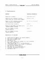
CONTENTS
Introduction.
. . . . . . . . . . .
. . . . . . . . . . .
1/ Functional Specifications • . . . . . .
2/ Block Diagram
3/ Installation
. . ..
. . . . . ..
. . . . . . . ..
4/ Alignment Instructions
...
....
....
7/ Schematic . .
8/ Parts List.
. . . . . . • . .
4
7
9
. . . . . . . . 10
. •.
. . • . . . . . •.
9/ Theory of Operation
3
5
5/ Troubleshooting . . . . . . . . . . . . . . . . . .
6/ Printed Circuit Board . . . . .
. 2
12
.
13
15
- - - - - - - - - - rtadaelbaell----------- 1 -
Model I Double-Density
Service Manual
®
Introduction
The Double-Density Disk System for the TRS-80 Model I allows more
storage on a 5 1/4 inch diskette than is available on a
single-density diskette. An 80% increase in disk-storage
capability is available using 35 tracks and more than double' the
capacity if 40 tracks is used.
To use this capability, you must have a Double-Density operating
system and a hardware modification. The new operating system is
on a diskette and the description of its use is found in the
Double-Density Disk System Owner's Manual (26-1143). The hardware
modification is an Adapter Board that must be installed by a
qualified Radio Shack Service Technician.
This Adapter Board allows the continued use of single-density
diskettes with a single-density operating system as well as the
enhanced double-density system.
Model I with double-density is capable of reading Model III data
diskettes, but this feature is not supported in the Double-Density
Operating System (DDOS). The operating systems are not compatible
because of addressing differences. Therefore, the software does
not support full compatibility. Shugart disk drives will NOT
support a 40 track operation. The disk drives that have a serial
number that is followed by a (-1) are manufactured by Tandon or
Texas Peripherals and are certified for double-density and can be
CONFIGured to 40 tracks.
The design objective was to make the double-density adapter fully
compatible with the Western Digital 1771 socket inside the
Model I expansion interface. This is an easy plug-in installation
without trace cuts or jumpers.
In addition, a side select line is
available on the adapter board for future enhancements. This
modification, however, would require changes to the expansion
interface.
®
-
2 -
Model I Double-Density
Service Manual
- - - - - - - - - - - TRS..BO
® .........................- - - - - - - -
1/ Functional Specifications
The TRS-80 Model I Double-Density Adapter Board is an optional
"add-on" board for the Model I which provides a double-density
controller for the S 1/4 inch floppy disk drives. This board can
support both single and double-density operation.
This modification, along with the software required for operation,
allows the transfer of Model I single-density files to
double-density format.
Write precompensation is provided and is software controlled for
any desired track. System software automatically enables
precompensation for all tracks greater than 21. The amount of
write precompensation is hardware adjustable on the Adapter Board
from Ons to SOOns. The adapter boards are adjusted at the factory
for a nominal rate of 200ns.
The data-clock recovery circuit incorporates a phase-locked loop
system for state-of-the-art reliability.
Upon reset or power-up, the Adapter Board is configured for side
0, no precompensation, and single-density.
If a
single-density operating system is used, the Model I will not
change from that density.
If a double-density operating system is
used, the Model I will reconfigure the Adapter Board to operate in
double-density.
In the double-density operation, data transfers are synchronized
to the CPU by polling the FDe for a data request before the
operation begins.
If good status is not received after a
specified length of time, the operation is aborted and control is
returned to the calling program.
----------lIadlelhaell--------- 3 -
Service Manual
Model I Double-Density
- - - - - - - - - - - TRS-BO
®
2/ Block Diagram
DISK
DRIVES
I
EXPANSION
INTERFACE
DOUBLE
DENSITY
DECODING
LOGIC
SINGLE
DENSITY
_, ENABLE
1771
SINGLE
DEN.
CONT.
DOUBLE
DENSITY
l ' ENABLE
1
1791
DOUBLE
DEN.
CONT.
PRE·COMP
ENABLE
-
II"
DATA
I.....-_W_R_IT_E_D_A_TA
_ _~ SEPARATOR
AND
PRECOMP
READ DATA
LOGIC
RCLOCK
.
VLD
CONTROL
- - - - - - - - - ftadIG/haell---------
4 -
Model I Double-Density
Service Manual
- - - - - - - - - - - TRS·BO
®
3/ Installation
Before installation of the Model I Double-Density Adapter, verify
the proper operation of the Expansion Interface using a memory
test, FORMAT, and BACKUP for single-density. This installation
should only be attempted after the Expansion Interface is proved
to be functioning properly.
1. Remove the Power Supply Cover on the Expansion Interface and
remove and disconnect the power supplies.
2. Turn the E. I. upside down and remove the six screws that hold
the case together. Remove the bottom cover. The screws are of
different lengths (remember which screws went where), and must be
used to reinstall the Bottom Cover.
3. Locate the WD 1771 FDC chip.
It is the only 40 pin chip in
the E. I.
It is Z34 on revisions A and C boards and Z42 on the
revision D board. Carefully remove this chip. After removing the
chip, carefully check and straighten any bent pins, and insert the
chip in the socket for U3 on the new DDA board.
4. The Adapter Board is mounted (installed) in the socket on the
Expansion Interface board where the WD 1771 FDC chip was removed.
There are extension pins below the adapter circuit board for this
purpose. Be certain that the FDC chip is facing the same
direction as it was on the E. I. board ( #1 pin is over #1 pin,
etc). Carefully set the Adapter Board OVER the socket (in the E.
I.) so that the ends marked for pin #1 are aligned and that the
pins will go in the socket. Then press evenly on the board to
firmly seat the pins in the socket.
5. It is unlikely that you will need to bend any capacitors to
seat the adapter board. If you must, be sure to not cause a short
or break any leads.
6. Lay the piece of foam, included with the unit over toe Adapter
Board. Carefully reinstall the Bottom Cover. Then turn the E. I.
back over and reconnect the power supplies and replace the Power
Supply Cover.
7. Apply power to the unit and boot either the single-density or
the double-density version of TRSDOS. Do not try to boot Model
III TRSDOS. If TRSDOS will not boot, first attempt steps 1 and 2
----------lIadlolbaell--------- 5 -
Model I Double-Density
Service Manual
- - - - - - - - - - - TRS..BO
®
of the alignment procedure (see "Alignment") before going on to
the "Troubleshooting" section of this manual.
8.
Go to the "Alignment" section of this manual.
- - - - - - - - - - - ftattl8
-
6 -
aell-----------
Model
I
Double-Density
Service Manual
- - - - - - - - - - - TRS·BO
® -----------
4/ Alignment Instructions
1. TP9 is the Frequency control point for the Voltage Control
Oscillator circuit (U13). It should be adjusted when instructions
are not being executed by the Floppy Disk Controller (idle state).
Adjust R7 so that the level of 1.4 volts is obtained with
reference to ground.
2. The VCO free-running frequency must
idle state and in single-density mode.
should be adjusted as close as possible
side (i.e. 124.99 kHz). The adjustment
also be adjusted in an
The measurement at TP5
to 125 kHz but on the low
is made using Rll.
3. Write precompensation must be adjusted while executing disk
writes and is measured at TP6. Boot TRSDOS (either version) and
format a blank diskette. While it is formatting, adjust R2 so
that the pulse width on TP6 is 2~~ ns in duration.
When a version of Tandy Drive Controller (TDC) is available,
execute continuous track writes. This will be much easier than
trying to catch the pulse during the FORMAT operation.
TEST POINTS
WHAT YOU SHOULD SEE
NAME
1
CLK
1 mhz clock from E. I.
2
DDEN*
~ for double-density
1 for single-density
4
IP*
Index pulse from disk
drive
5
RCLK
125 kHz in idle
condition (Rll)
(drive not running)
6
Precomp
2~~ nsec duration pulse
when enabled and writing
(R2 )
---------ltadI8/haell--------- 7 -
Model I Double-Density
- - - - - - - - - - - TRS-BO
Service Manual
® ------------
7
PREN
~ for No Precomp
1 for Precomp enable
8
Ground
Ground
9
FDC Bias
1.4 VDC in idle position
(R 7)
ADJUSTMENT POTENTIOMETERS
R2
Precomp Adjust (TP6)
R7
Bias Adjust (TP9)
Rll
Free Run Adjust (TPS)
----------lIadlo/haell---------
8 -
Model I Double-Density
Service Manual
- - - - - - - - - - - TRS-BO
® -----------
5/ Troubleshooting
SYMPTOM
POSSIBLE PROBLEM(S)
Powers-On to Ready >
a,b,c,d,e, or f
Powers-On with garbage on Screen
(Drive does not turn-on after RESET)
e,f,h,i, or k
Powers on with garbage on screen
(Drive turns-on after RESET)
a - f, h, j, k, pr 1
All drives stay turned-on
g or k
Starts to boot DDOS, but hangs up at
'LOADING TRSDOS' message
j, 1, or m
will not FORMAT or write
(Single-density)
d or 1
Will not FORMAT or write
(Double-density)
1, m or
0
Explanation of problems
a.
b.
c.
d.
e.
f.
g.
h.
i.
j.
k.
1.
ffi.
Double-Density Adapter not seated properly
Bent pins on header strip
Bent pins on WD1771 (U3)
Bad WD1771 (U3)
E. I. power supply not plugged in or not turned-on
Bad cable (CPU to E. I. )
Cable upside down (E. I. to Disk Drive(s»
If buffered cable, is it plugged in backwards?
Disk Drive(s) turned off?
Bad Operating System diskette
Bad cable (E. I. to Disk Drive(s»
Incorrect adjustments on board
Bad WD1791 (U4)
- - - - - - - - - - ftadI8/haell--------- 9 -
Model I Double-Density
Service Manual
- - - - - - - - - - - TRS-BO
® -----------
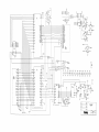
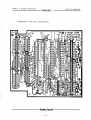
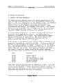
6/ Printed Circuit Board(solder side)
- - - - - - - - -....... ftadl8
- 10 -
aell---.. . . . .- - - - - - -
itiV
RIO
6.8K
C17
...-
-5
::16:-JDIR
....-
.
WD
r----------------------------..::
"1
...---:3B
WG
3O
9WP
...-
U3
1771
3~2
.--
---:1..,4
.--
DAL7
•
...;1-9
2 DAL5·
,.......
....-
~11
DAL4.
1~0
DAL3.
3B~DDIR
...---
flL-< DSTEP
..--
~B~DWD
2Y
,.....!
IY
....-
3Y,~9=--
~5
B
U12
A LS123
AO
Q~
---+---------.,---------r~,R~-
_ _.:.:H:.-'
L---_
18
'
3B ODRa
- - - -
8
II
1
GND_
itiV
1 A
2 B
3 C
DAL5·
DAL6·
DAL7· -
DDEN·
-=DDEN
,
I
N_C_';---;.b..o;:-5.() XTOS·
~O.D
I
SIDE 0
SIDE 1
I
.~INTRa
_
Y5 10
Y4 11
G2A
I
XTDS·~
I~
J
-1<
16
Gl
G2B
I
I
I
iti4+
...L
Al
WE·
Ul1
LS10
--1
~MR.
TEST"\.:2~2---_~+_------+----,------.-----~TEST.
~~2i
~
40 0
30
31 ~
------.- -------:--=::'-0
AO
T""
,-
,
I
I
I
I
lnl
SOCKET
HEADER
~
4.:.j Reo
I
L
SIDESEL
I
,
...l
SIDEO
NC
+...
r<DDEN
~C.:E·r3--t_J-II---::~:j~:
L
MR·
n.:.:
'1--1-
.....
r~'
9
itiV +12V itiV
r - - - - - - - -:1
16
I
DDIA ~ DIR
DIR 0...:.::._1 _ _-'
i
......
DSTEP~ STEP
WP.o.l3B~I----.....+H+++_H+H_+1f-t+_+--_936 wp.
I
U4
1791
I
Ip.
I
1771
SOCKET
I
HEADER
35
TAKO·
I
32 ADY
24 ,
24 CLK
I
DRa~
34
O.J34~..L
! - - - - I - - - + . + H H + - H H - H + + - f - t - - - 9 TRKO.
I
CLK
14
I
14 DAL7.
I
DAL7·
13
I
13 DAL6.
DAL6·
12
I
DAL4.o-'~1-1---l-~--!I--+---.4I,...jH-H+_Hf_t_-t_~11 DAL4·
:
D A L 3 . o - - l ! 1 ° 4 - - + - I - I - H - + - - - - 4 - H + + t - + - - t - -'O
9 DAL3·
I
DAL2.o--.!9..L
1 - + _ H - I - - + - - - -.....H + + - f - t - - t - - ' l 9 DAL2·
I
DALI.
I
DALO.o--.f.7..:.'---++++--1--------4-HH--+-_t_--'-i7 DALO.
81
1
AO
I
RE.
5
41
~E: o-.~.2~J....
••
- - + + + - + - - + - - - - - - + . - + - -......-++--+--=12LW_E_.
DAL5·~
DAL6· +DAL7· ~
Al~
AO~
--
~
+rC4
.I
10ul
--
+5V
+5V
+5V
+5V
IC5
I,lUI
Ice
I,lUI
lC7
Ice
I,'ut
I"UI
-=-
--
I"UI
lca
+5V
+5V
+5V
I·, I·, I
ICll IC12
10ut
UI
I
itiV
lC13
UI
-=-
lC15
1
UI
-=-
+5V
R4
10K
...z WG
U8
WD1691
11
ARD.112~7------+--!I-+--+_il--+-+-I"""";'"
RRD·
VFOE.~---"--"-l--
......J!
+.-
__--.!!! LATE
,----------1-------------:;;;
17 EARLY
2.-- NC
1 WDIN
EAR LYI-!lL7
-=
~.
H_LT..J~23
I
.....
J:
...------UA-,J.J"
FCI=2-+----..---..,
~
STB
01.
02.
03.
04.
U5
WD2143
TP6
+12V
C18
2
3
19
WOO 6
+5V R8
10K
GND
T043 fL<PREN
10 1
C16
lOOpl
-=
'-----
9m
7
A GND
B
R
U12
8
74LSl23 CLA
C
a 11 HI
a
12
5
1
NC
..1.
R7
lOOK
SOpl
11
7
5
3
1
5
4
itiV~
RG F!--NC
GNDI=2::..0
r
R3
2.2K
PRECOMP
ADJUST
VFOE·
15 DDEN •
DDEN.1:l3~7------_---4-----4_+----''''1
RCLK~2~6------+.-----_ _-4_---'~
12 RCLK
LATE j..!1.2,8
16
VCO
13
PU
PO
Xl
01.
02.
OPW~ ~~K
ro.
GND~
04.
BIAS
ADJUST
+5V
-=
itiV
itiV
DRA.FT
DATE
CHECK
O"TE
DESIGN
DATE
APPD
DATE
TITLE
DOUBLE DENSITY
ADAPTER
•E
TP4O---
WE·~
lC19
1
UI
I·
TP9
• PO
CLK~~TPI
+5V
+5V
WO~DWD
WG~DWG
4 RE·
_~ CEo
-=-
lC3
l·lUI
HI
itiV
HLD 1!!.-NC
5 AO
NCo-2L
+5V
MR·1-'1~9-~---~MR·
---<l~+_t_-+---=i6Al
I
41
+12V
TEST" 22
8 DALI.
Al o-.!6.!.1_-I-+-I--I-_--+
DDEN"
INTRO~NC
DAL5·o-~-~-+++-~I---~+H+H+_+-_+_.:.::;'2 DAL5·
I
1
READ·
PIN 27-1771
ICI
IC2
l,lUI l,lUI
T043 .1jL- NC
35 Ip.
RDYo-B '
U9
+12~
STEP o-':.::.5.....
I
I~
2.2K
8
U7
08
3044208
iti 21
itiV
FDCLK
PIN 26-1771
5
~'
Rl (
10K
8
U7
08
10
U9
L
Ul1
LS10
-~PH3
(
I
- 3PM.
I
6
5
4
12
I
I
I
TP5
:
5
4
3
TI343 29
: 29 0 TG43
DINT. 37
1 37 0 DINT"
33
WF.r:' = - - - - - - , - - - - - - - - - - + - - - - - - - - - - - - - - - - . - ; ; : ; . < l W F .
HLD 28
I
OHLD
HLT 23
, 23 OHLT
26
NC --~ FDCLK
FDCLK
.....,
4Y,l-:'::.2
-::!::-'5
I,
1
2
13
itiV
HI
CLR
3
'NTRa~NC
.:.j7 DALO •
.....::.j8
....-
lBf-L--<OWG
Ul1
LS10
MR. 19
8
....---------4
DAL1·
U2
LS157
--2
r=
1
14
10
11
Al---------
FD~~ ~
9
DAL2·
...--------=-i
1 SELECT
...-_ _--'-1
.------1
VCC~
a r!L- NC
ORO ~_______
-"'1
13 DAL6·
....-
4B
40
Re;~: ~ READ·
ROY
--=24;;;CLK
...-
~4A
+12
DAL7·
DAL6·DAL5·
15
~C
-
•
..::34.,TRKO·
....-
L..-_ _...;1..:,1 3A
-::h 1"
iti +12
35=1 Ip·
....-
....l. lA
~2A
loopl
+5~
..:;15"-tSTEP
..::3'"'1
1
...--------
~..!-J
itiV
9
tandq
l"'
'u
8000126
rCALE~I ...n· I
ISIZE
0'
I
+5V
C17
.5 +5 +12
100pl
----"-----.0 T
-: b
...-----------
.
---'=3'11 WD
...---------
-22
...-
~;71
~ ~C ISvCC~
.-------2- B a
1
U12
r- A lS123
+12 40
WG
_ _ _:H.::.I_- - t - - - - - - - " - - - - - - - - - - -
~-_---------- ..----E ROY
...,
-""--1
24 ClK
...--
'4--tDAl7"
...-
..
--:.:13::;DAl6"
...-
--'1=,2 DAL5"
...-
.......;' '
4
...-
- - - + - - - - - - - - - - - - - - - - - - rl --;;3S;;-o ORO
OINP,..37
TP43,29
WF" 33
HlD 28
HlT 23
~WF"
I 28 0 HlO
I 23 OHLT
NC
FDClK
..2
----------8"'"iDAll"
...-;7 DAlO"
3B~DOIR
"B~OSTEP
~Br£--<DWD
lA
~2A
~_ _---,-1.,' ~
1B
IN
...--
f-=!--< CWG
39
~~~
Tl
,
XTOS"
GND 2 0 _
1
_
-L
8"'"i Al
'M'", ~; ~
-= - - --1
VI
GND
I
' - - - - - r,
--
I
...-~ 14
O~NC
lS74
11 CK GNDh
AO-BF
I -:::!::13
MR"
r
12
4
~
0 PRE a 5
DDEN"
~~74
-
+5V
10 . "t'TP7
PRE
~
~CK
DDEN
«
D
O~PREN
U6
-
19 OMR"
22 TEST"
HI
U, li rT----, .
r
"
-=-
::::-
I
29
+5V
12 0
LS74
MR"
li t!-NC
II CK
I 39 ~ INTRa
I
NC~XTOS"
I 20 _ GND
~
GNDh
13
::!::-
I
+54+
-5~
-
SIDE 1>,------,
+12~
r - - - - - - - " '5i AO
4 Re...--'-i
U2
LS157
--
fill
~~
--L..3!..o
FOClK
I 17 OPH3
I
TESP 22
r------------! DAL2"
-
;~-------------__t-------'-------=::::::::::::::::::::::::::::::::::::::::;I
::::~3~7-o0DTGIN43T"
I
FOClK~
~~ 19
DAl4"
...;.10::; DAl3"
0 R;- 3PM"
3S
ORO
Y3
_
i 27
Re;~:~~!!!~-...:--R-EA-D-"---'-------------___i---------_--------I---!.!!..o
341TRKO"
U
~~~3S
ClR
3
35
, . . - - - - - - - - - - - - - - - - - . : :"lIP"
..--_,
Ull
lS10
1~ NC
,...,,-,----,16
'-"- Gl
...-WP~ G2B
Y5~SIDEO
....
r~6:..------~4a~G2A
Y4~SIDE 1
o~_
-L
.;;..36,WP"
+5V
HI
I
r-------..
...-:====================================================================~:::-15""16 ~~:P
+5V
RIO
68K
lnl
2
_r -
SOCKET
HEADER
0
lS74
-L
O~ SIDESEl
U6
.--
3Y1-=9:..-
''-iSElECT
.----2 2V
-,
...-
.. V~I~2-------+___,
~IY
SIDE 0
2, we-<DDEN
-=-'5
L
~C~E:.:".r--r-I-I--~13;j ~l
11
~
ue
04
o
a
mv
r - - - - - - - -.,
DIR o-.;.;:16'-t-,_ _......
STEP 0~_'5_i
......
I
I
WP"
:
IP"
I
~'KET
I
HEADER
I
I
I
_
DDIR~
DIR
DSTEP~
STEP
3S WP"
~3B!!.+-1, --------.l4++-l-++-HH-t+-H-t-i-T--4
35 IP"
~,---- .......H++-I--+++-++1-+-t-t-+--t---4
TRKO· o-:34~IL----+-~~-+-+++-H+H_t__r_r_t--......;:134 TRKO"
~3~2~1- - - - - ! - - - + - t - t + + + H + - H H - t - t - - - , -324 RDV
24 ClK
-~2~"-T, I----+--t--+--+-H-r+-+i-H--rt-r-t----J
ROY 0-:
ClK
14 DAl7"
DAl7"o-l!!4.,.1---~+--I--+-++-H_+t_+nH_-j-__i---'_'i
13 DAlS"
DAl6.o-..!;13~--~_+-f---f---+-++H++-H--t-t_-_r4
U4
1791
3B
INTRa ~NC
TEST" 22
t-lL--_
+5V
WD POWD
DDEN" ~-------t---_-----_.._t---'45
37
I
RClK 26
7 DAlO"
lATE
I
I
I
L
I
5 AO
AOlo--...:s~I-_lH-+_I--+-------l-..----4-+_+-_+-4
4 RE"
RE.o-.::.
.. .:..'---+-+-+--+------if----+--+----..-i--t--;
NCo--!-!-
r--
r---2 CEO
WE"-o-~2.;.1_-4-++_+_-+_----+-+_--T-++_-t-""1 WE·
2
---A
DAlS· oE-DAl6· ~
DAl7· ~
Al~
AO~
I
R4
.2 WG
WG ~DWG
10K
11
RRD" ~----'----+-+--t-,+-->--_t--r___r--j
27
RRD"
.....J!.
_f-
I"uf
IC6 IC7 YC6
I
I:
_1uf
,uf
I"uf
Ice
I-
+5V
1uf
+5V
ICl1 IC12
'Ouf
l uf
+5V
+5V
IC13
1uf
lC15 lCle
1Uf I,1Uf
I- I- I-
I-
-
-
-
________--+
-::::L.
-
+
+
04"r!!!--
7 01"
5 02"
3 03"
---1 04•
~
+5V R8
10K
t
101
71
Cls'_*"I
el
A
B
ClK~~TPl
WE"~
,
.
--
CI8.--'-
6Opf~1c2
R3
2.2K
PRECOMP
ADJUST
81
GND
-=
OPW~>~gK
GND~
-=
~v~
II
~ ""'UN
1
ADJUST
'~+5V
Rl1
50K
+5V
-
WL
_
i
2
FCt--.---.-----,
...... Cl0
U13
47Uf
74lS829
R5
>R7
47K-.
RS
lOOK
47/1.
BIAS
RNG~
_
....
ADJUST
+5V
8
R
U12
100PTtc a 74lS123
T_G4_....
3PL'< PREN
l-.-
+12V
'-;11 Xl
.--
wooS
--;' WDIN
J:\-G_N_D
-
US
WD2143
01" 4
02. 2
03" 3
+5vl--~
RGPi-NC
......
PO~
STB j.:S:..-_ _
DDEN"
-'-'-\'7 EARLY
...-
V~~~1~3 _ _- ;
&-.-2 Fl
~C1
-=1'2
NC
C~R 11
5
1
_ _____'
~=-=--
HI
DRAFT
DATE
CHECK
DATE
DESIGN
DATE
APPD
I DATE
APPD
A E
TITLE
TP4o-l..-
+5V
~
,..-----UA1pJ-
16
VFOE"
...,'8 LATE
EARLY ~1
r--NC
''1
US
WD1691
.._---;2 RClK
'
.!L________-+
GND 20
Yes
TP9
8 DALt"
--l--l--+--.1f---+-------
+rC4'Ouf
1uf
+5V
9 DAL2"
DAL2.o-.::.lI..JI----4-++-+---~-----+_t-++-H---:r-___jI--""i
S Al
Alo-..::..::..--+-H-+---+----....-----+--r-t--t---t--;
I-
HI
-?MR"
I
I
2.2K
IC2 IC3
cl
I~
READ"
PIN 27-1771
HlD ~NC
VFOP 33
7 I
DAlO" ~O-~6~1
l
8
+5V
FOClK
PIN 26-1nl
-
DAl3.o-2': : : . . t - ° - - 1 H - f - t - - _ 1 - - - - - 6 - t + + H H - t - - - r10
4 DAl3"
'"-o-..:8~1!--+-H-+--_1------.....,rt-j--+-t-__t-"i
U7
08
I-lUI I-lUI
I
DAl
"
®--o
V
r
rlL- NC
II
I
I
-
U9
12 DAlS "
DAl5.o-~12~lt___---4t_l_+---lf---+---4_t+i+t-iH+_t-_t-1
11
DAl4" o-'~I-1I--lH-+_1--+---....+_t+t-i___t+___t-___t---'_'_j DAl4"
I
U7
08
10
1
+12 ~
MR"
_ _--+_ _---1
9
r-----+-.-+--++--~-----t
U7
}-'3::..-+-_ _4.,
3
...--+---+-+--1----1
04
4
2
08
+5 21
ORO
2
v
Rl ..
10K
TG43
ClR li ~ NC
JR:
12
3
T1'5
I
>----! CK
tandq
DOUBlE DENSITY
ADAPTER
®_-----------
Model I Double-Density
Service Manual
(Component side and components)
®
- 11 -
Model I Double-Density
Service Manual
- - - - - - - - -...........- - - TRS..BO
® -----------
7/ Schematic
- - - - - - - - - - l I a d l e l h a e l l - - - - - - - - -.. . . .
- 12 -
Model I Double-Density
Service Manual
- - - - - - - - - - - - - TRS-BO
® -------------
8/ Parts List
SYMBOL
DESCRIPTION
MANUFACTURER'S
PART NUMBER
RADIO SHACK
PART NUMBER
RESISTOR/TRIM POT
Rl, R4, and
R8
Resistor,
R2
Trim Pot,
R9, R3
Resistor,
R5
Resistor,
R6
Resistor,
R7
Trim Pot,
RIO
Resistor,
Rll
Trim Pot,
10K ohm, 1/4 watt, 5%
10K ohm, .151 watt
2.2K ohm, 1/4 watt,5%
47K ohm, 1/4 watt, 5%
47 ohm, 1/4 watt, 5%
lOOK ohm, .151 watt
6.8K ohm, 1/4 watt, 5%
50K ohm, .151 watt
820-7310
827-9310
820-7222
820-7347
820-7047
827-9410
820-7268
827-9350
AN028lEEC
AP7l67
AN02l6EEC
AN0340EEC
AN0099EEC
AP0834
AN2262EEC
AN7l68
838-4104
832-6331
835-4475
830-1104
830-0754
ACCl04QJAP
ACC336QDAP
ACC474KLGP
ACClOlQJCP
ACC750QJCP
802-0074
802-0157
AMX3558
AMX3563
802-5771
804-5791
804-0143
802-0008
804-1691
802-0004
802-0138
802-0010
802-0123
802-0629
AXX3014
AMX4472
AMX3698
AMX4471
AMX3552
AMX4583
AMX3898
AMX3803
AMX4663
CAPACITORS
Cl-C3, C5-C9, C12-C15, and
C19
1 mfd, 50 volt, monolithic, radial
C4, Cll 33 mfd, 16 v, electrolytic, radial
CIO
47 mfd, 100 volt, 10% polyester
C16,C17 100 pfd, 50 volt, ceramic disk
C18
75 pfd, 50 volt, ceramic disk
INTEGRATED CIRCUITS
Ul, U6
U2
U3
U4
U5
U7
U8
U9
UIO
Ull
U12
U13
74LS74 Flip Flop
74LS157 MUltiplexer
WD177l (removed from EI to
multiplexer)
WD179lB-02 Floppy Disk Formatter
WD2l43-0l 4-Phase Clock
74LS08 Quad (2 input) And gate
WD169l Floppy support logic
74LS04 Hex Inverter
74LS138 3 to 8 Decoder
74LSIO Triple input Nand gate
74LS123 Multivibrator (one shot)
74LS629 veo
- - - - - - - - - - rtadI8/haell--------- 13 -
Model I Double-Density
Service Manual
- - - - - - - - - - - TRS-BO
SYMBOL
DESCRIPTION
® -----------
MANUFACTURER'S
PART NUMBER
RADIO SHACK
PART NUMBER
MISCELLANEOUS
U3
U4
US
U8
Printed Circuit Board (Rev. B)
Staking Pins
Socket 40-Pin DIP
Socket 20-Pin SIP
Socket 18-pin DIP
Socket 20-Pin DIP
Header 20-Pos SIP with spacer
870-9202
852-9014
850 -90 0 2
850-9013
850-9006
850-9009
851-9132
NST
AHB9682
AJ6580
AJ7125
AJ6701
AJ6760
AJ7126
----------ltadI8Ihaell--------- 14 -
Model I Double-Density
Service Manual
- - - - - - - - - - - TRS-BO
® - - - -...........- - - - - -
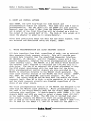
9/ Theory Of Operation
A. CONTROL AND DATA BUFFERING
The Double-Density Adapter Board is a memory mapped device that
uses the same decoding logic as the single-density system on the
Model I. (For more information on the decoding logic, see decoding
logic section of the Expansion Interface Service Manual).
Control lines, such as DDEN* (double-density enable), PREN
(precompensation enable), and SIDESEL (side select), are latched
using a one of 8 decoder, UIO (74LS138), and Ul, U6 (flip flops).
The three high order bits (DAL5* - DAL7*) of the sector write
register (37EEH) are used to control the decoder.
In single-density operation, the WD177l Floppy Disk Controller is
selected (using DDEN as the select). For double-density
operation, the WD1791 FDC is used. The Double-Density Adapter
Board includes both of these FDC's. The single-density FDC
(WD1771) is moved from the Expansion Interface and the
double-density FDC (WD1791) is a new part.
A WR* strobe in the address range 37ECH - 37EFH is decoded on the
expansion interface as a write to the FDC.
Al must be high and
AO must be low to enable the decoder (UIO) at the active low at
G2A. The decoded address is 37EEH.
In addition, if all the data
lines DAL5*-DAL7* are high (this means a zero due to inverted
logic) G2A will not go low. This prevents changing the state of
the control lines on a normal write to the sector register.
The following table illustrates the data used for each function:
DATA
FUNCTION
40-5F
60-7F
80-9F
AO-BF
CO-DF
EO-FF
Select side 0
Select side 1
Set double-density mode
Set single-density mode
Disable precomp
Enable precomp
Note that only one function may be toggled at a time.
(i.e. one
could not enable double-density and precompensation in one write
to the sector register.) After selecting a control function, the
data that was previously in the sector register will have been
destroyed and should be rewritten if necessary.
----------ltadI8
- 15 -
ell----------
Model I Double-Density
Service Manual
- - - - - - - - - - - - TRS·BO
®
B. RESET and CONTROL LATCHES
Upon RESET, the LS74 flip-flops for side select and
precompensation enable are cleared. This mode sets side 0 and no
precompensation. The two LS74's for the DDEN* are also cleared.
However, upon the clock (1 MHz) from the Expansion Interface, the
not Q output of the first flip-flop will be clocked as a high to
the output of the second half of Ul. The high at this output will
cause the 9dapter to power-up in single-density.
Since both controllers share the data bus and other signals, they
are selected and deselected using one signal, DDEN*.
C.
WRITE PRECOMPENSATION and CLOCK RECOVERY CIRCUIT
All data transfers from disk, regardless of mode, use an external
data separater/clock recovery circuit. This will provide more
reliable data transfer than the unmodified Expansion Interface.
U8 (WD169l), U5 (WD2l43), and U13 (74LS629), along with a few
passive components, comprise the write precompensation and read
clock recovery logic. The WD169l is a LSI device which minimizes
the external logic required to interface the 1791 FDC chip to a
disk drive. The use of an external VCO allows adjustment to keep
the RCLK signal synchronous with the read data for the drive.
Write precompensation control signals are also provided by the
WDl691 to interface directly to the WD2l43 clock generator. The
read clock recovery section of the WD169l has five inputs: DDEN*,
VCO, RRD*, WG, and VFOE*/WFi and three outputs: PU, PD*, and
RCLK. The inputs VFOE*/WF and WG when both low enable the clock
recovery logic. When WG is high, a write operation is in progress
and the clock recovery circuits are disabled regardless of the
state of any other inputs.
The write precompensation section of the WD169l was designed to be
used with the WD2l43 clock generator. Write precompensation is
not used in the single-density mode and the signal DDEN* when high
indicates this condition.
In double-density mode (DDEN* = 0), the
signals EARLY and LATE are used to select a phase input (01*-04*)
on the leading edge of WDIN. The STB line is latched high when
this occurs, causing the WD2l43 to start its pulse generation.
02* is used as the write data pulse on nominal (EARLY = LATE = 0),
01* is used for the EARLY = 1, and 03* is used for the LATE = 1.
----------lIadlolhaell---------- 16 -
Model I Double-Density
Service Manual
- - - - - - - - - - - TRS..BO
®
The leading edge of 04* resets the STB line in anticipation of th
next write data pulse. When TG43 = 0 or DDEN* = 1,
precompensation is disabled and any transitions on the WDIN line
will appear on the WDOUT line.
When VFOE*jWF and WG are low, the clock recovery circuits are
enabled. When the RRD* line goes low, the PU or PD* signals will
become active.
If the RRD* line has made its transition in the
beginning of the RCLK window, PU will go from a high impedance
state to a logic 1. This will cause the VCO to increase in
fr.equency.
If the RDD* line has made its transition at the end o~
the RCLK window, PU will remain in the high impedance state while
PD* will go to a logic O. This will' cause the VCO to decre~se in
frequency.
When the leading edge of RRD* occurs in the middle of
the RCLK window, both PU and PD* will remain in the high impedanc€
state, indicating that no adjustment of the VCO frequency is
required. By tying PU and PD* together, an adjustment signal is
created which will be forced low for a decrease in VCO frequency
and forced high for an increase in VCO frequency. To speed up
rise times and stabilize the output voltage, a resistor divider
using R5, R6, and R7 (potentiometer) are used to adjust the
tri-state level to approximately 1.4 s. This adjustment results
in a worst case voltage swing of plus or minus lv, which is
acceptable for the frequency control input of the vco (U13). The
signal derived from the combination of PU and PD* will eventually
correct the VCO input to exactly the same frequency multiple as
the RRD* signal. The leading edge of the RRD* signal will then
occur in the exact center of the RCLK window, an ideal condition
for the WD179l internal recovery circuits.
D.
EXTERNAL DATA SEPARATION IN SINGLE DENSITY
In single-density mode, there is a separate clock bit for every
data bit. This is not true in double-density. Therefore,
external logic is required to interface the WD169l Floppy Support
Logic to the WD177l Floppy Disk Controller. The purpose of this
logic is to separate the clock and data bits in the data stream
into two signals. This is done using one inverter (U9) and two
AND gates (U7). This logic is also enabled using DDEN* and RRD*
to detect single-density mode, and activity on the data line. On
the rising edge of RCLK, the data bit is being decoded, and on the
falling edge the clock pulse is decoded.
Two one-shots (sections of U12, 74LS123) are used to insure that
the read and write data pulses are the necessary duration, from
- - - - - - - - - - - ftadl8 "na'lC~R - - - - - - - - - - - 17 -
Model I Double-Density
Service Manual
® --------------
about 300 to 450 nsec. Also, the VFO enable signal to the WD169l
is held active when in single- density.
E.
FLOPPY DISK CONTROLLERS
The WD177l is a single-density ONLY floppy disk
formatter/controller.
A detailed description of this device is
given in the Expansion Interface Service Manual.
The WD1791 is an MOS LSI device which performs both the functions
of a single and double-density floppy disk formatter/controller in
a single chip. The 1791 is also used on the Model II FOC/Printer
Interface board. The Model II Reference Manual contains a good
presentation of the 1791 FDC chip as well as a discussion on write
precompensation.
Both controllers share a common data bus and control lines,
therefore, they are switched using DDEN. The following RAM
addresses are assigned to the internal registers of the 1771/1791
FDC chips.
RAM ADDRESS
FUNCTION
37ECH
37EDH
37EEH
37EFH
Command/Status Register
Track Register
Sector Register
Data Register
- - - - - - - - - - - I'tadle SnIClek@---------- 18 -
CORPORATION
RADIO SHACK,A
U.S.A.:
CANADA:
02
AUSTRALIA
BELGIUM
280-316 VICTORIA ROAO
RYOAlMERE, N.S.W. 2116
PARe INOUSTAIEl DE NANiNNE
5140 NANiNNE
8149343
BILSTON ROAO WEONESBURY
WEST MIDLANDS WS10 7JN
PRINTED iN USA