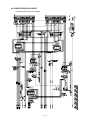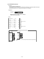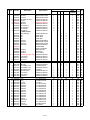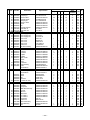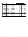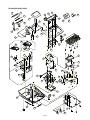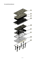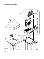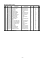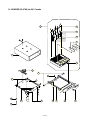
1
SERVICE MANUAL
(without price)
ELECTRONIC CASH REGISTER
TE-2200/2400
(EX-443/544)
AUG. 2005
TE-2400
TE-2200
Ver.2 : Aug. 2009
INDEX
CONTENTS
TE-2200/2400
PAGE
1. SPECIFICATIONS........................................................................................ 1
2. MACHINE INITIALIZATION ......................................................................... 4
3. DISASSEMBLY ............................................................................................ 7
4. CIRCUIT EXPLANATION .......................................................................... 17
5. DIAGNOSTIC OPERATION ....................................................................... 29
6. ERROR CODE LIST................................................................................... 55
7. IC DATA ..................................................................................................... 59
8. PCB LAYOUT ............................................................................................ 66
9. CIRCUIT DIAGRAMS ................................................................................. 68
10. PARTS LIST ............................................................................................... 82
To prevent malfunctions caused by the weak batteries, charge the memory
protection batteries for over 12-hours before installation or after a long-time
vacation (over 30 days).
• Before installation, initialize the terminal and leave it turn on over 12-hours.
• After a long-time vacation, initialize the terminal and restore the program data if
the terminal is in malfunction, and leave it turn on over 12-hours.
• Over 48-hours charging makes the batteries fully charged.
1. SPECIFICATIONS
1-1. Electrical specifications
•Power consumption
In operation
stand-by
Max.
Max.
120 V
0.5 A
0.1 A
220 V
0.25 A
0.05 A
230 V
0.25 A
0.05 A
240 V
0.25 A
0.05 A
•Memory protection
Back-up battery
Except. USA, CANADA Back-up period
Battery life
Recharge time
Vanadium lithium battery
90 days (25 °C)
Replace the battery every 5 years.
48 hours (full charge)
•Memory protection
USA, CANADA
Back-up battery
Back-up period
Battery life
Mangan battery (UM-3 × 3)
1 years (25 °C)
Replace the battery every 1 years.
•Clock & Calendar
Accuracy
Auto calendar
Within ± 30 sec. per month (25 °C)
Effective until 2099 A.D.
1-2. Environmental specifications
• Operating temperature
0 °C ~ 40 °C
• Operating humidity
10 % ~ 95 %
• Storage temperature
-25 °C ~ 65 °C
• Storage humidity
10 % ~ 95 %
• Vibration strength
1.5 G (The machine must be in the carton box)
1-3. Main components
• CPU
Name
Number of control bit
uPD784215AGC279
16 bit
• RAM (US)
Name
Capacity
M68AF128BM70 × 2
1 Mbit
• RAM (EURO)
Name
Capacity
M68AF511AM70
4 Mbit
• Flash ROM
Name
Capacity
MBM29F160BE90TN
16 Mbit
• I/O controller
Name
uPD784215AGC280
• Themal printer
Name
Paper cut
FTP-628MCL518 (receipt)
FTP-628MCL518 (journal)
Thermal dot line printing
Total dot number : 384 dots/dot line
Dot pitch : Length 8 dots/mm
Wide 8 dots/mm
Manual-paper cut
Type
Size
Roll diam
Thickness
Heat-sensitive paper
57.5 ± 0.5 mm
φ 80 or less
0.06 ~ 0.085 mm
Print method
Head specification
• Roll paper
—1—
1-4. Duration of Life
• Printer head
50 Km (anti-abrasion), 1400 Million lines
• LCD
20,000 hours
• Backlight
20,000 hours
1-5. Drawer List
Type
Drawer Name
Specification
M
DL-2429
D-24H2C-B55SRM-9*
M
DL-2797
D-24H2C-B84RM-9*
M
DL-2798
D-24H2C-B84SRM-9*
M
DL-2799
D-24H2C-A84SRM-9*
Note: Country code
B: Europe
D: England
C: U.S.A.
BU: Other countries
L: Canada
—2—
B
D
C
BU
L
1-6. Option List
DEVICE NAME
• Multi drawer kit
• PC cable
• Waterproof cover
• Waterproof cover
• Slip printer
• Slip printer cable
• Remote printer
• Printer cable
• Printer cable
• Slip printer/ AC adaptor
• Handy scnner
• Handy scnner
• Handy scanner
• CF Memory Card
• Modem
• Modem
• Conversion Kit
• Roll paper
MODEL
MDL-12
PRL-CB-2
WT-82
WT-87
SP-1300
PRT-CB-8C
UP-360
PRT-CB-8A
PRT-CB-8B
31AD-U or E
HHS-15
HS1250
Quic Scan 6000
SDCFB-xx-505
NOTE
Connect to Com2
Length 1.5m
Connect to Com2
Length 3m
Length 5m
U: 120V/ E: 230V
Com2 port only
Com2 port only
Com2 port only
56k V92 External
Faxmodem
56k Faxmodem
CVK-S3-M/CVK-L3-M
P-5880T
CAUTION
RISK OF EXPLOSION IF BATTERY IS REPLACED
BY AN INCORRECT TYPE.
DISPOSE OF USED BATTERIES ACCORDING
TO THE INSTRUCTIONS
—3—
Applicable
Common
Common
TE-2200 only
TE-2400 only
Common
Common
Common
Common
Common
Local purchase
Local purchase
Local purchase
Common
Local purchase
Local purchase
Local purchase
Common
Common
2. MACHINE INTIALIZATION
Machine initialization procedure
1. Plug the power cord into an AC outlet.
2. Hold down <JOURNAL FEED>.
RECEIPT
FEED
REG2
REG1
3. Turn the mode switch to PGM position.
OFF
X1
Z1
X2/Z2
RF
PGM
4. Release <JOURNAL FEED>.
You should see “0000000000” on the display.
If 10 zeros are not shown or another character are
shown, immediately set the mode switch to OFF and
restart from the beginning of this procedure.
RECEIPT
FEED
5. Enter 11-digit program code from the worksheet.
6. Press <SUBTOTAL> to register the program code.
(Wait until beep twice.)
7. Press <SUBTOTAL> to register the program code.
—4—
D11D10D9D8 ~ D3D2D1
refer to Worksheet (Initialize)
JOURNAL
FEED
Worksheet (Initialize)
Description
Choice
Print password of PGM mode, when flag clear operation is performed.
Password in PGM3 ~ 7 mode
Messages and descriptors are written in
English = 0, French = 1, Spanish = 2, German = 4
Model for
U.S. or Canada (Date order: month/day/year)
= 2,
Other area (0.00, Date order: day/month/year)
= 1,
Other area (0, Date order: day/month/year)
=3
Fixed value:
TE-2200: 25
TE-2400: 04
Use
1 clerk switch (clerk push switch)/
2 Clerk secret number key *
Initialization pattern:
1 For scanning/2 For check tracking
Yes = 0
No = 4
Significant
numbers
Significant
number
Significant
number
Significant
numbers
a
Program code
D11
D10 D9 D8 D7
D6
D5
D4 D3
1=0
2=1
(a+b)
D2
1
=
0
b
2=2
No = 0
Use Euro only.
D1
Yes = 1
* When you select this option “Use clerk secret code key”, and your register doesn’t have this key on the default
keyboard, be sure to allocate <CLERK-#> (clerk secret number key) just after the initialization.
(Do NOT turn to OFF before allocating this key.)
Note:
Please check the receipt after initialization operation (machine initialization, flag clear operation and init2)
that the machine number is printed properly.
If error codes are printed on it, check the hardware and retry the operation.
P01
C01
03-04-2004
MC#01
11:58
000001
INIT
(C) 2005 by CASIO
COMPUTER CO.,LTD.
All rights reserved.
Mode symbol/date/time
Clerk descriptor/Mc-No./consecutive No.
INIT symbol
Copyright
TE-2200/2400 STD
Model name
VER.
LABEL
ROM version
ROM label
:nnnn
:nnnnnn
VER.
:nnnn
LABEL :nnnnnn
INIT.
:nnnnnnnnnnnnnn
0002-98
:
00
2000
ROM version
ROM label
Initialization code
I/O parameter table record No./error code
—5—
Flag clear operation
1. Plug the power cord into an AC outlet.
2. Hold down <RECEIPT FEED>.
TJOURNAL
FEED
REG2
REG1
X1
Z1
OFF
3. Turn the mode switch to PGM position.
X2/Z2
RF
PGM
4. Release <RECEIPT FEED>.
You should see “FFFFFFFFFF” on the display.
If 10 Fs are not shown or another character are shown,
immediately set the mode switch to OFF and restart from
the beginning of this procedure.
5. Press <SUBTOTAL> to complete.
RECEIPT
FEED
JOURNAL
FEED
After completion of flag clear, receipt is issued.
Note: After flag clear, clerk 1 is assigned automatically. So do not program clerk 1 as not assignable or
not operable in PGM mode.
Init 2 operation
1. Plug the power cord into an AC outlet.
TJOURNAL
FEED
2. Hold down <RECEIPT FEED>.
REG2
REG1
3. Turn the mode switch to PGM position.
OFF
X1
Z1
X2/Z2
RF
PGM
4. Release <RECEIPT FEED>.
You should see “FFFFFFFFFF” on the display.
If 10 Fs are not shown or another character are shown, immediately set the mode switch to OFF and restart from the beginning
of this procedure.
RECEIPT
FEED
JOURNAL
FEED
5. Enter “8888888888” and press <CHECK TEND> to complete.
After completion, receipt is issued.
—6—
3. DISASSEMBLY
■ UPPER COVER
1. Remove the printer cover.
2. Remove two screws.
3. Remove the printer cover.
4. Remove two FPCs.
Hooks
FPC (10pin)
FPC (12pin)
—7—
5. Remove the screw.
6. Remove the upper case by sliding it forward.
7. Remove two connectors. (CN13, CN15)
CN15
8. Remove the UPPER COVER.
—8—
CN13
■ KEY BOARD ASS’Y
9. TE-2200: Remove 10 screws.
TE-2400: Remove eight screws.
10. Remove the FPC.
TE-2200
11. Remove the chassis.
12. Remove the FPC sheet.
13. Remove the spacer.
14. Remove the sheet.
TE-2400
Sheet
Spacer
FPC sheet
Chassis
15. Remove eight screws.
16. Remove the KEY frame.
TE-2200
—9—
TE-2400
■ TACT SW PCB, MODE KEY
17. Remove three screws.
18. Remove the TACT SW PCB (E443-E6 PCB).
E443-E6 PCB
19. Remove the screw.
20. Remove the MODE KEY.
MODE KEY
■ BACKUP BATTERY
21. Remove the connector.
22. Remove the backup battery.
CN14
— 10 —
■ MIAN PCB
23. Remove four connectors.
Connector (CN7)
Connector (CN1)
Connector (CN5)
Connector (CN16)
24. Remove three FPCs.
FPC (CN8)
FPC (CN9)
FPC (CN12)
NOTE; While fixing, be fully care to the direction of the FPC.
Pattern
Pattern
25. Remove eight screws.
— 11 —
■ LCD ASS’Y
26. Remove five screws and then the LCD ASS’Y.
27. Remove three screws and one connector.
■ PRINTER
28. Remove two E272-PR PCBs.
E272-PR PCB
29. Remove four FPCs.
— 12 —
30. Remove four screws.
31. Remove two printer units.
32. Remove the battery cover.
33. Remove four screws.
34. Remove the lower case.
— 13 —
■ DRAWER
35. Remove the case.
36. Remove 10 screws.
37. Remove the DARWER cable.
— 14 —
38. Remove the Bottom plate.
39. Loosen 4 screws.
40. Remove the screw and then fix the drawer case.
— 15 —
■ POWER SUPPLY
28. Remove the two screws.
29. Remove the POWER UPPER CASE.
30. Remove three screws.
31. Remove the POWER UNIT.
— 16 —
4. CIRCUIT EXPLANATION
4-1. HARDWARE DIAGRAM
Main Display
Popup
display
Journal printer
Keyboard
CPU
Drawer
1 i/f
2 i/f
Drawer
Drawer
RS232C
COM1
PRL-CB-2
Drawer
Multi drawer kit MDL-12
Popup
disp.
i/f
MODEM
or
PC
Flash
Memory
RAM
RS232C
COM2
CF card
Slip
printer
Scanner
HHS-15
SP-1300
Power
supply
31AD-U/E
Note: Shadowed device and dot line indicate option devices.
— 17 —
PRT-CB-8A/-8B
Power
supply
PRT-CB-8C
Receipt printer
External
printer
UP-360
Power
supply
— 18 —
Optional Hand
Held Scanner
HHS-15
Optional
MODEM / PC
+5V supply
signal only
COM2
COM1
PWB:E272-PR
PWB:E272-PR
CPU
EURO
CPU
US
Feed Motor
Feed Motor
Journal
Thermal PRN UNIT
Receipt
SRAM
4Mbit
SRAM
1Mbit
optional
CG
16Mbit
DRW I/F
DRAWER UNIT
DRW I/F
(LED BackLight on board)
PWB:E443-LCD
CF card socket
FROM
16Mbit
FROM
16Mbit
LCD UNIT
EURO only
PWB : E443-1
SRAM
1Mbit
Winder Motor
PWB:E443-E22
Optional
PWB:E443-E6
EURO only
LiB Battery
optional
voltage
selector
Transformer
POWER SUPPLY UNIT
TE-2200 (STROKE)
or
TE-2400 (FLAT)
FPC
PWB:E475-E3
MODE KEY
AC120V
or AC220-230V
or AC240V
, 50/60Hz
US_cord : PS204-A
AUS_cord : X-AU10S3
UK_cord : MP5004
EU_cord : M2511
4-2. BLOCK DIAGRAM
4-3. RESET CIRCUIT
The reset circuit is as follows.
4-4. POWER SUPPLY CIRCUIT
The power supply circuit is as follows.
IC32 32pin
— 19 —
4-5. DRAWER I/F CIRCUIT
The drawer open circuit is as follows.
— 20 —
4-6. PRINTER CONTROL CIRCUIT
The printer control circuit is as follows.
— 21 —
4-7. CPU (IC32: uPD784215AGC279-8EUA) / I/O CONTROLLER (IC44: uPD784215AGC280EUA)
P63/A19
P64/RD
P66/WAIT
P65/WR
P67/ASTB
P101/TI6/TO6
P100/TI5/TO5
VDD
P103/TI8/TO8
P102/TI7/TO7
P30/TO0
P33/TI1
P32/TO2
P31/TO1
P35/TI00
P34/TI2
P95
P94
P93
P92
P91
P90
TEST/VPP
P37/EXA
P36/TI01
4-7-1. Pin Assignment
100 99 98 97 96 95 94 93 92 91 90 89 88 87 86 85 84 83 82 81 80 79 78 77 76
P120/RTP0
P121/RTP1
P122/RTP2
1
2
3
P123/RTP3
4
P124/RTP4
P125/RTP5
P126/RTP6
P127/RTP7
VDD
5
6
7
8
20
21
22
23
24
70
P56/A14
69
68
67
P55/A13
P54/A12
P53/A11
P52/A10
P51/A9
55
54
— 22 —
P81/A1
P82/A2
P25/SI0/SDA0
P26/SO0
P27/SCK0/SCL0
P80/A0
P20/RxD1/SI1
P21/TxD1/SO1
P22/ASCK1/SCK1
P23/PCL
P24/BUZ
P71/TxD2/SO2
P72/ASCK2/SCK2
P131/ANO1
AVREF1
P70/RxD2/SI2
25
26 27 28 29 30 31 32 33 34 35 36 37 38 39 40 41 42 43 44 45 46 47 48 49 50
AVSS
P10/ANI0
71
P60/A16
VSS
P57/A15
58
57
56
P130/ANO0
AVDD
AVREF0
P61/A17
73
72
60
59
17
18
19
P17/ANI7
P05/INTP5
P06/INTP6
14
15
16
P14/ANI4
P15/ANI5
P16/ANI6
P02/INTP2/NMI
P03/INTP3
P04/INTP4
P62/A18
74
66
65
64
63
62
61
P13/ANI3
P00/INTP0
P01/INTP1
9
10
11
12
13
P11/ANI1
P12/ANI2
X2
X1
VSS
XT2
XT1
RESET
75
53
52
51
P50/A8
P47/AD7
P46/AD6
P45/AD5
P44/AD4
P43/AD3
P42/AD2
P41/AD1
P40/AD0
P87/A7
P86/A6
P85/A5
P84/A4
P83/A3
4-7-2. Block Diagram
INTP2/NMI
INTP0, INTP1,
INTP3-INTP6
PROGRAMMABLE
INTERRUPT
CONTROLLER
UART/IOE1
BAUD-RATE
GENERATOR
TI00
TI01
TO0
TIMER/COUNTER
(16 BITS)
UART/IOE2
BAUD-RATE
GENERATOR
TI1
TO1
TIMER/COUNTER1
(8 BITS)
CLOCKED
SERIAL
INTERFACE
TI2
TO2
TIMER/COUNTER2
(8 BITS)
TI5/TO5
TIMER/COUNTER5
(8 BITS)
TI6/TO6
TIMER/COUNTER6
(8 BITS)
TI7/TO7
RxD1/SI1
TxD1/SO1
ASCK1/SCK1
RxD2/SI2
TxD2/SO2
ASCK2/SCK2
SI0
SO0
SCK0
AD0-AD7
A0-A7
A8-A15
TI8/TO8
BUS I/F
A16-A19
RD
WR
WAIT
ASTB
TIMER/COUNTER7
(8 BITS)
PORT0
P00-P06
PORT1
P10-P17
TIMER/COUNTER8
(8 BITS)
PORT2
P20-P27
PORT3
P30-P37
PORT4
P40-P47
PORT5
P50-P57
PORT6
P60-P67
PORT7
P70-P72
PORT8
P80-P87
PORT9
P90-P95
PORT10
P100-P103
PORT12
P120-P127
PORT13
P130,P131
WATCH TIMER
78K/IV
CPU CORE
ROM
RAM
WATCHDOG TIMER
RTP0-RTP7
NMI/INTP2
REAL-TIME
OUTPUT PORT
ANO0
ANO1
AVREF1
AVSS
D/A
CONVERTER
ANI0-ANI7
AVREF0
AVDD
AVSS
P03
A/D
CONVERTER
PCL
BUZ
RESET
X1
SYSTEM CONTROL
CLOCK OUTPUT
CONTROL
X2
XT1
XT2
BUZZER OUTPUT
VDD
VSS
— 23 —
4-7-3. Pin Function
PIN NO.
1
2
3
4
5
6
7
8
9
10
11
12
13
14
15
16
17
18
19
20
21
22
23
24
25
26
27
28
29
30
31
32
33
34
35
36
37
38
39
40
41
42
43
44
45
46
47
48
49
50
PIN NAME
P120/RTP0
P121/RTP1
P122/RTP2
P123/RTP3
P124/RTP4
P125/RTP5
P126/RTP6
P127/RTP7
VDD
X2
X1
VSS
XT2
XT1
RESET
P00/INTP0
P01/INTP1
P02/INTP2/NMI
P03/INTP3
P04/INTP4
P05/INTP5
P06/INTP6
AVDD
AVREF0
P10/ANI0
P11/ANI1
P12/ANI2
P13/ANI3
P14/ANI4
P15/ANI5
P16/ANI6
P17/ANI7
AVSS
P130/ANO0
P131/ANO1
AVREF1
P70/RxD2/SI2
P71/TxD2/SO2
P72/ASCK2/SCK2
P20/RxD1/SI1
P21/TxD1/SO1
P22/ASCK1/SCK1
P23/PCL
P24/BUZ
P25/SI0/SDA0
P26/SO0
P27/SCK0/SCL0
P80/A0
P81/A1
P82/A2
I/O
IO
I
I
I
IO
DESCRIPTION
8 bit input/output PORT
Power Supply
Main system Clock
GND
Sub system Clock
Reset
7 bit input/output PORT
-
A/D CONVERTER POWER SUPPLY
Application of Standard Voltage for A/D CONVERTER
I
8 bit input PORT
A/D CONVERTER & D/A CONVERTER GND
IO
2 bit input/output PORT
Application of Standard Voltage for D/A CONVERTER
IO
3 bit input/output PORT
IO
8 bit input/output PORT
IO
8 bit input/output PORT
— 24 —
PIN NO.
51
52
53
54
55
56
57
58
59
60
61
62
63
64
65
66
67
68
69
70
71
72
73
74
75
76
77
78
79
80
81
82
83
84
85
86
87
88
89
90
91
92
93
94
95
96
97
98
99
100
PIN NAME
P83/A3
P84/A4
P85/A5
P86/A6
P87/A7
P40/AD0
P41/AD1
P42/AD2
P43/AD3
P44/AD4
P45/AD5
P46/AD6
P47/AD7
P50/A8
P51/A9
P52/A10
P53/A11
P54/A12
P55/A13
P56/A14
P57/A15
VSS
P60/A16
P61/A17
P62/A18
P63/A19
P64/RD
P65/WR
P66/WAIT
P67/ASTB
VDD
P100/TI5/TO5
P101/TI6/TO6
P102/TI7/TO7
P103/TI8/TO8
P30/TO0
P31/TO1
P32/TO2
P33/TI1
P34/TI2
P35/TI00
P36/TI01
P37/EXA
TEST/VPP
P90
P91
P92
P93
P94
P95
I/O
DESCRIPTION
IO
8 bit input/output PORT
IO
8 bit input/output PORT
IO
8 bit input/output PORT
-
IO
-
GND
8 bit input/output PORT
Power Supply
IO
4 bit input/output PORT
IO
8 bit input/output PORT
-
IO
TEST pin
6 bit input/output PORT
— 25 —
4-8. SRAM (EURO only, IC13: M68AF511AM70MC6U)
4-8-2. Pin Function
4-8-1. Pin Assignment
VCC
19
8
A0-A18
DQ0-DQ7
W
E
A0-A18
Address Inputs
DQ0-DQ7
Data Input/Output
E
Chip Enable
G
Output Enable
W
Write Enable
VCC
Supply Voltage
VSS
Ground
G
VSS
4-8-3. Block Diagram
A18
ROW
DECODER
MEMORY
ARRAY
A8
DQ7
I/O CIRCUITS
COLUMN
DECODER
DQ0
A0
E
W
G
— 26 —
A7
VCC
VSS
4-9. SRAM (US only, IC14, 15: M68AF128BM70MC6U)
4-9-2. Pin Function
4-9-1. Pin Assignment
VCC
17
8
A0-A16
DQ0-DQ7
W
E1
A0-A16
Address Inputs
DQ0-DQ7
Data Input/Output
E1, E2
Chip Enable
G
Output Enable
W
Write Enable
VCC
Supply Voltage
VSS
Ground
E2
G
VSS
4-9-3. Block Diagram
A16
ROW
DECODER
MEMORY
ARRAY
A7
I/O CIRCUITS
DQ7
COLUMN
DECODER
DQ0
E1
E2
A0
W
G
— 27 —
A6
VCC
VSS
4-10. FROM (IC24: MBM29F160BE90TN)
4-10-2. Pin Function
4-10-1. Pin Assignment
A15
1
48
A16
A14
2
47
BYTE
A13
3
46
VSS
A12
4
45
DQ15/A-1
A11
5
44
DQ7
A10
6
43
DQ14
A9
7
42
DQ6
A8
8
41
DQ13
Pin
Function
A-1, A0 to A19
DQ0 to DQ15
CE
Address Inputs
Data Inputs/Outputs
Chip Enable
A19
9
40
DQ5
OE
Output Enable
N.C.
10
39
DQ12
WE
Write Enable
WE
11
38
DQ4
RESET
12
37
VCC
RY/BY
Ready/Busy Output
N.C.
13
36
DQ11
RESET
Hardware Reset Pin/Temporary Sector Unprotection
WP
14
35
DQ3
BYTE
RY/BY
15
34
DQ10
N.C.
No Internal Connection
Selects 8-bit or 16-bit mode
A18
16
33
DQ2
VSS
Device Ground
A17
17
32
DQ9
A7
18
31
DQ1
VCC
Device Power Supply
A6
19
30
DQ8
A5
20
29
DQ0
A4
21
28
OE
A3
22
27
VSS
A2
23
26
CE
A1
24
25
A0
4-10-3. Block Diagram
RY/BY
Buffer
RY/BY
DQ0 to DQ15
VCC
VSS
Erase Voltage
Generator
WE
BYTE
RESET
Input/Output
Buffers
State
Control
Command
Register
Program Voltage
Generator
Chip Enable
Output Enable
Logic
CE
STB
Data Latch
OE
STB
Low VCC Detector
Timer for
Program/Erase
A0 to A18
A-1
— 28 —
Y-Decoder
Address
X-Decoder
Latch
Y-Gating
Cell Matrix
5. DIAGNOSTIC OPERATION
5-1. To start the diagnostic program
To enter the diagnostic program, press ”99990000<ST>” right after reset-and-start, IPL boot or INT
operation. In QA DIAG (factory module also) module, the mode transfers to the diagnostic mode after
INT operation.
* Reset-and-start
1 Press the reset switch while pressing JFEED button.
2 When “INT” appears in the first line of the LCD dot line, press<SUBTOTAL>.
3 When “INT” appears in the second line of the LCD dot line, press”99990000<SUBTOTAL>”.
4 Enter the diagnostic mode.
* INT operation
1 While holding down the JFEED button, align the mode key with “PGM” using the OW key.
2 When “INT” appears in the second line of the LCD dot line, press “99990000<SUBTOTAL>”.
3 Enter the diagnostic mode.
* In the case if “MASK DIAG” is displayed and the counter is activated
A false operation has led to the MASK diagnostic mode. Perform IPL operation again.
5-2. Displaying and printing the version
The version of DIAG and MADK ROM/IOC are printed immediately after entering the DIAG mode.
However, DIAG/IOC version printing function is available only in QA DIA module.
• All test results are printed by the built-in printer receipt.
I o
Ma
D i
Ma
c
Ve
s k Ve
ag Ve
y 25
r
r
r
20
: 4 2 3 3 AANZAC
: 4 2 0 7 AAOAAA
:
05
09 : 54
IOC
MASK ROM
DIAG
5-3. Notes for the DIAG
• All test result are printed by the built-in receipt printer.
• Make sure to test HHS-15 by connecting to COM2.
• To perform the continuous check, follow the direction for each test, and input numbers except 0. Input
numbers 1-9 as the command how many times to perform the test for the operation in each page to
perform continuous check. Note that you can only choose one time check or continuous check.
• When turn off by rotating the key, the display is unlit, and DAIG command is not accepted.
[Others]
• ESC value is printed as follows if the test ended by force. Press the “C” key or turn off the power to end
the test while performing continuous check. The result of ending by force is not printed in each test.
| ESC
|
— 29 —
5-4. Displaying the status of the device
[Function]
The status of the device which has the status information is displayed by 7 segments (Pop-up display)
as well as lit transaction.
The status information and the displayed position are as follows. As for tact switch, the pressed LED
will be lit.
[DISPLAY]
Mode display
1:PGM, 2:RF, 3:REG1, 4:REG2, 5:X 6:Z, 7:XZ2, 8:OFF
Receipt head
Off : Head down On : Head up
Journal head
Off : Head down On : Head up
No receipt paper
Off : Paper available On : No paper
No journal paper
Off : Paper available On : No paper
CF CARD sensor
Off : Not yet inserted On : Inserted
Drawer 1 sensor
Off : CLOSE On : OPEN
Drawer 2 sensor
Off : CLOSE On : OPEN
E-STAMP sensor
Off : Not yet inserted On : Inserted
— 30 —
5-5. Check item
The following test can be checked in the diagnostic test.
No
Device to be checked
1 Batch test 1
Operation
1
2
3
4
5
6
7
8
9
10
11
12
13
14
15
16
17
18
19
20
21
22
23
24
25
2
n011
n111
0n013
0n113
0n213
0n313
x1x20016
n017
212
n021
c0121
221
n321
421
521
cn03d
26
27
28
29
30
31
Batch test 2
RAM WRITE/READ test
RAM READ ONLY test
CF-CARD WRITE/READ test
CF-CARD READ ONLY test
CF-CARD CLEAR test
CF-CARD CLEAR WRITE/READ test
Locale information write
CG READ test
FLASH USER AREA clear test
Display test
Backlight test
Pop-up display test
LCD test
LCD CONTRAST ADJUSTMENT
Display test (repeat)
Internal printer print test
Internal printer graphic print test
Internal printer dot rate test
Internal printer print value test
Internal printer print density test
COM (RS232C) test
COM (RS232C) batch test
Time setting
Time display
Drawer open test
Buzzer test
Consumption current
KEY dipsplay
OBR test
Displaying the battery voltage
Note
Test Device : RAM, Printer, Date,
Time, Buzzer, Drawer
Test Device : Display, Back light
Page
32
x1x2x3x4x5x60a70
32
33
34
34
35
35
36
36
37
37
38
39
39
40
41
42
43
44
45
46
46
47
48
49
70
xn091
n092
193
94
95
96
50
50
51
52
53
54
P1P1P1P2P2P2n13d
pn33d
435
x0235
xn04d
40
— 31 —
5-6. Operation of each test
[ 1 ] Batch test 1
[Function]
RAM test, test print, time setting, buzzer test and drawer open test are performed continuously.
[Operation]
Operation :
[Pop-up display]
1
n
SUBTOTAL
The following tests are performed
automatically.
(1) RAM test: WRITE/READ area test.
(2) Test print
(3) Time setting: Set the following data.
Arranged data: 2005 December
31,23:59’30
(4) Buzzer: Ring once the one shot buzzer.
No print or display in this test.
(5) Drawer open: Drawer 1 opens only.
(6) Receipt issuance
n=0 1 2 3 2 3
[Main display]
D I AG
1
00n
n=0 1 2 3 2 3
[Print]
* Normal print
BA TCH
1
R A M WR
OK
BBBBBBBBBBBBBBBBBBBBBBBB
DATE
05 / 12 / 31
T I ME
23 : 59 - 30
D RW 1
OK
END
1
Print Test
* See “RAM test” if “ERROR” appears while
performing the RAM test.
[ 2 ] Batch test 2
[Function]
Display test and backlight test are performed continuously.
[Pop-up display]
[Operation]
Operation :
2
Refer to each item.
SUBTOTAL
[Main display]
The following tests are performed
automatically.
(1) Display test: Refer to “[12] Display test.”
Press any key to go to the next
test.(Same in the backlight test also)
Press any key to go on to the next test.
(Same in the backlight test also)
(2) Main test: Refer to “[15] LCD test.”
(3) Pop-up display test: Perform Pop-up
display test. See “[14]” for more
information.
(4) Backlight test: Refer to “[13]” for more
information.
Perform the backlight test.
The backlight color changes if any key is
depressed.
Refer to the “Backlight test” for details.
(5) Receipt issuance
— 32 —
Refer to each item.
[Print]
* Normal print
BA TCH
D I SP
D I S P MA I N
D I SP 7 SEG
B ACK L I GH T
END
2
OK
OK
OK
OK
2
[ 3 ] RAM WRITE/READ test
[Function]
This test will check the WRITE/READ test for RAM.
A counter is displayed for the RAM test.
Write and read test is performed in the sequence as following. Write common (system area) and
read write common( other than the system area) and read write each bank read each bank.
Also, the test is not performed for the range to (-400H) by the handler.
[Operation]
Operation :
n
0
1
1
SUBTOTAL
n : 0
= One time check (can be omitted)
not 0 = Continuous check (To stop the test, press “C” key)
[Pop-up display]
A counter is displayed for Pop-up display.
n
n=0 1 2 3 2 3
[Main display]
D I AG
0011
00n
n=0 1 2 3 2 3
[Print]
The result of all area for RAM test is printed as follows.
RAM
R A M WR
END
11
OK
11
* The result is printed as follows if the test ended with an error.
If an error occurs while checking the BANKO address 0x60400 for normal RAM
STD
R A M WR
NG
BANK 0 - 6 0 4 0 0
* The result is printed as follows if the test ended with an error.
Print
RAM WR NG-*****
RAM WR NG BANKO
RAM WR NG BANK1
NG
NG if the COMMON address for RAM is ******* to 1Kbyte.
NG if the BANKO address for RAM is ********to 1Kbyte.
NG if the BANK1 address for AM is *******to 1Kbyte.
— 33 —
[ 4 ] RAM READ ONLY test
[Function]
RAM READ ONLY test is performed.
Perform the WRITE test (n011) right before start of this test.
System area test for COMMON is not performed.
[Operation]
Operation :
n
1
1
1
SUBTOTAL
n : 0
= One time check (can be omitted)
not 0 = Continuous check ( Press the “C” key or turn off the power by rotating the key to
end the test.)
[Pop-up display]
A counter is displayed for Pop-up display.
[Main display]
D I AG
0111
n
00n
n=0 1 2 3
n=0 1 2 3
[Print]
The result for all area test for RAM is printed as follows.
RAM
RAM RD
END
111
OK
111
Address of an error is printed if the test ended with an error.
* Refer to RAM WRITE/READ test when NG is printed.
[ 5 ] CF-CARD WRITE/READ test
[Function]
This test will check the write/read test (connection test) for CF-CARD.
Perform the CF-CARD clear test, before start of this test.
Note that this test does not ensure the data inside the CF-CARD as well as its performance.
[Operation]
Operation :
0
n
0
1
3
SUBTOTAL
n : 0
= One time check( can be omitted)
not 0 = Continuous check (To stop the test, press “C” key or turn off the power by rotating
the key.)
[PRINT]
CF - CARD
CF
WR
END
13
OK
13
NG and the address are printed if WRITE cannot be done
normally.
— 34 —
[ 6 ] CF-CARD READ ONLY test
[Function]
This test will check the read only test for CF-CARD.
Perform the CF-CARD write test, before start of this test.
Note that this test does not ensure the data inside the CF-CARD as well as its performance.
[Operation]
Operation :
0
n
1
1
3
SUBTOTAL
n : 0
= One time check(can be omitted)
not 0 = Continuous check( To stop the test, press ”C” key or turn off the power by rotating
the key.)
[PRINT]
CF - CARD
CF
RD
END
113
OK
113
NG and the address are printed if READ cannot be done
normally.
[ 7 ] CF-CARD CLEAR test
[Function]
This test will check the clear test for CF-CARD.
Note that this test does not ensure the data inside the CF-CARD as well as its performance.
[Operation]
Operation :
0
n
2
1
3
SUBTOTAL
n : 0
= One time check (can be omitted)
not 0 = Continuous check (To stop the test, press “C” key or turn off the power by rotating
the key.)
[PRINT]
CF - CARD
CF
CLR
END
213
OK
213
NG and the address are printed if WRITE cannot be done
normally.
— 35 —
[ 8 ] CF-CARD CLEAR WRITE/READ test
[Function]
This test will check the clear Åïwrite/read test for CF-CARD.
Perform the write/read test (connection check) after clearing all memory.
Note that this test does not ensure the data inside the CF-CARD as well as its performance.
[Operation]
Operation :
0
n
3
1
3
SUBTOTAL
n : 0
= One time check(can be omitted)
not 0 = Continuous check (To stop the test, press “C” key or turn off the power by rotating
the key.)
[PRINT]
CF - CARD
CF
C L R &WR
END
313
OK
313
NG and the address are printed if WRITE cannot be done
normally.
[ 9 ] Locale information write
[Function]
The Locale information is written into FLASH MEMORY.
[Operation]
Operation : x1 x2
0
0
1
6
SUBTOTAL
x1 : xcountry code,
x2: SUB CODE
x1 x2:
10 R Europe, 20 R US, 30 R UK, 40 R Germany,
50 R Canada, 60 R Direct, 61 R Direct (Hebrew)
[PRINT]
The following receipt is not issued when commands other than x1, x2.
L OCA L E
L OCA L E
END
x1x2 0 0 1 6
OK
x1x2 0 0 1 6
The following is printed when an error occurs during writing LOCALE.
| LOCALE
NG
|
The LOCALE can be written 5 times. When no more LOCALE can be written
(writing more than 5 times), the following is printed.
| LOCALE
OVER
|
— 36 —
[ 10 ] CG READ test
[Function]
Perform the READ ONLY test for OG.
[Operation]
Operation :
n
0
1
7
SUBTOTAL
n : 0
= One time check (can be omitted)
not 0 = Continuous check (Press “C” key or turn off the power by rotating the key to stop
this test.)
[PRINT]
The address is not printed when the error occurs.
CG
CG
END
17
OK
17
RD
NG is printed if CHECK SUM value is not normal.
[ 11 ] FLASH USER AREA clear test
[Function]
Clear the area of LOCALE/CONTRAST setting.
[Operation]
Operation :
2
1
2
SUBTOTAL
[PRINT]
R OM
R OM C L R
END
212
OK
212
NG is printed if the test is not done correctly.
— 37 —
[ 12 ] Display test
[Function]
LCD, Pop-up display and transaction display tests are performed (as follows).
[Pop-up display]
[Main display]
Input command
Pattern 1
8.8.8.8.8.8.8.8.
34567890
A B C D E F GH I J K L MNOP
Q R S T U VWX Y Z a b c d e f
1234567890
Press any key
End
[Operation]
Operation :
n
0
2
1
SUBTOTAL
n : 0
= One time check (can be omitted)
not 0 = Continuous check (To stop the test, press “C” key)
* Any key must be pressed to end the test when performing one time check.
[PRINT]
D I SP
D I SP
END
1
8,8,8,8,8,8,8,8,8,8,
Press any key
Pattern 2
D I AG
21
OK
21
— 38 —
[ 13 ] Backlight test
[Function]
This is a test for the LCD backlight.
[Operation]
Operation :
c
0
1
2
1
SUBTOTAL
C : Designating the backlight color
0
= Batch test
The color changes as follows upon the press of keys.
White Green Red
1
= OFF
2
= White
3
= Green
4
= White + Green
[PRINT]
When inputting 0 or without inputting in "C", 121 is printed.
BACK
BACK
END
L I GH T
L I GH T
121
OK
121
When inputting numbers 1 to 4 in "C", the number input on C and 0120 are printed as the figure shown.
BACK
BACK
END
L I GH T
L I GH T
c0121
OK
c0121
[ 14 ] Pop-up display test
[Function]
Pop-up display test is performed.
Press any key to end the test.
[Operation]
Operation :
2
2
1
SUBTOTAL
[Pop-up display]
The following is displayed and cleared after
the test.
34567890
[Main display]
D I AG
221
1234567890
— 39 —
[PRINT]
D I SP
D I SP
END
7 SEG
7 SEG
221
OK
221
[ 15 ] LCD test
[Function]
Perform LCD display pattern test.
Display 4 patterns as follows.
Press “C” key or turn off the power to stop the test while performing one time check.
Turn off the power to stop the test while performing continuous check.
[Pop-up display]
[Main display]
Input command
Pattern 1
34567890
1234567890
Press any key
Pattern 2
A B C D E F GH I J K L MNOP
Q R S T U VWX Y Z a b c d e f
7.6.5.4.3.2.1.0.
A B C D E F GH I J K L MNOP
Q R S T U VWX Y Z a b c d e f
9,8,7,6,5,4,3,2,1,0,
Press any key
Pattern 3
Press any key
Pattern 4
8.8.8.8.8.8.8.8.
D I AG
8,8,8,8,8,8,8,8,8,8,
Press any key
End
One time checkPress the optional key or turn off the power.
Continuous checkturn off the power.
[Operation]
Operation :
n
3
2
1
SUBTOTAL
n : 0
= One time check (can be omitted)
not 0 = Continuous check (To stop the test, press “C” key)
* After the test, pattern 4 is displayed until any key is depressed.
[PRINT]
D I SP
D I S P MA I N
END
1
321
OK
321
— 40 —
[ 16 ] LCD CONTRAST ADJUSTMENT
[Function]
Adjust the contrast for LCD and then write the value into the FLASH.
FLASH can be written 16 times. Error occurs if it’s written more than 16 times. Clear the FLASH for
MASK DIAG and then set the IPL and LOCALE again to write after 16 times.
Contrast value is selected as same as the previous setting (“32” is selected for no setting).
Press “CA/AMT TEND” button to correct writing after adjustment.
[Operation]
Operation :
4
2
1
SUBTOTAL
Press buttons as follows to operate.
“DARK” button
:
contrast +1
“LIGHT” button
:
contrast -1
“CA/AMT TEND” button :
“C” button
Turn off the power
:
:
Contrast determination (Write into Flash)
Contrast adjustment is completed.
Stop adjusting
Stop adjusting
[Pop-up display]
345
XX
XX is the setting value.
[Main display]
A B C D E F GH I J K L MNOP
Q R S T U VWX Y Z a b c d e f
12345
XX is the setting value.
XX
[PRINT]
D I SP
L CD CON T RA S T
END
421
XX
421
XX is the setting value.
L CD
CON T RA S T
NG
It is printed if the error occurs.
L CD
CON T RA S T
OVER
It is printed if the flash is written more than 16 times.
L CD
CON T RA S T
ESC
It is printed if “C” key is depressed.
— 41 —
[ 17 ] Display test (repeat)
[Function]
LCD, Pop-up display and transaction display tests are performed as follows.
[Pop-up display]
[Main display]
Input command
Pattern 1
8.8.8.8.8.8.8.8.
34567890
End
[Operation]
5
2
1
SUBTOTAL
* Press “C” key or turn off the power to stop the test.
[PRINT]
D I SP
D I SP
END
A B C D E F GH I J K L MNOP
Q R S T U VWX Y Z a b c d e f
1234567890
Press any key
Operation :
1
8,8,8,8,8,8,8,8,8,8,
Press any key
Pattern 2
D I AG
521
OK
521
— 42 —
[ 18 ] Internal printer print test
[Function]
This test will check the characters in the receipt/journal of the internal printer.
[Operation]
Operation :
c: 0
1
n: 0
not 0
d: 3
4
5
c
n
0
3
d
SUBTOTAL
=
=
=
=
prints character’ B’
prints all characters
One time check
Continuous check (To stop the test, press “C” key or turn off the power by rotating
the key.)
= prints only receipt
= prints only journal
= prints both receipt/journal (prints alternately)
[Print]
1. prints character’ B’
BBBBBBBBBBBBBBBBBBBBBBBB
2. prints all characters
The printing order is in the order of the character code. The characters from 0x20(SP) to 0xFA(•)
are printed.
A space is printed for a code without the printing character.
A character which cannot be printed is a character within the range of the code 0x00 to 0x1F and
0xFB to 0xFF.
— 43 —
[ 19 ] Internal printer graphic print test
[Function]
This test will check the graphic patterns in the receipt/journal of the internal printer.
[Operation]
Operation :
P1 P1 P1 P2 P2 P2
n
1
3
d
SUBTOTAL
P1 : 0
= Graphic patter 1 (change 8 bit into a decimal number and input it)
P2 : 0
= Graphic patter 2 (change 8 bit into a decimal number and input it)
n : 0
= One time check (can be omitted)
not 0 = Continuous check (To stop the test, press “C” key)
d : 3
= prints only receipt
4
= prints only journal
5
= prints both receipt/journal (prints alternately)
The graphic patterns and the print images are as follows;
Graphic pattern 1
Graphic pattern 2
Graphic pattern 1
Graphic pattern 2
:
: repeat (for 28 Dot line )
* Print patterns and commands
1 Receipt, 25% pattern, continuous
0
8
5
0
0
0
Print pattern image
1
1
3
3
SUBTOTAL
The display unit of the print pattern image in the right is as follows;
Horizontal: dot
Vertical: do line
2 Receipt, 50% pattern, continuous
0
8
5
1
7
0
Print pattern image
1
1
3
3
SUBTOTAL
The display unit of the print pattern image in the right is as follows;
Horizontal: dot
Vertical: do line
3 Receipt, 100% pattern, continuous
2
5
5
2
5
5
Print pattern image
1
1
3
3
SUBTOTAL
The display unit of the print pattern image in the right is as follows;
Horizontal : dot
Vertical : do line
[Print] Refer to “Print patterns and commands”.
— 44 —
[ 20 ] Internal printer dot rate test
[Function]
This test will check the printing of the receipt/journal according to the following specifications.
The printing specification is reflected in 1/2 line and the only specified number of dot lines are printed
in all dots from the 1 dot line.
Note that 1/2 line is printed two times because the printing unit is one line.
[Operation]
Operation :
p : 0
1
2
n : 0
not 0
d : 3
4
5
p
n
3
3
d
SUBTOTAL
=
=
=
=
=
3 dot line
5 dot line
7 dot line
One time check
Continuous check (To stop the test, press “C” key or turn off the power by rotating
the key.)
= prints only receipt
= prints only journal
= prints both receipt/journal (prints alternately)
[Print]
1 3 dot lines
The first 3 dot lines in the 1/2 line ( 14 dot lines) out of one line are printed in all dots.
3 dot lines (printed in all dots)
Printing image of 1/2 line
11 dot lines (no printing)
(14 dot lines)
printing image of 1 line
(28 dot lines)
3 dot lines (printed in all dots)
Printing image of 1/2 line
(14
dot
lines)
11 dot lines (no printing)
2 5 dot lines
The first 3 dot lines in the 1/2 line ( 14 dot lines) out of one line are printed in all dots.
5 dot lines (printed in all dots)
Printing image of 1/2 line
9 dot lines (no printing)
(14 dot lines)
printing image of 1 line
(28 dot lines)
5 dot lines (printed in all dots)
Printing image of 1/2 line
(14 dot lines)
9 dot lines (no printing)
3 7 dot lines
The first 3 dot lines in the 1/2 line ( 14 dot lines) out of one line are printed in all dots.
7 dot lines (printed in all dots)
Printing image of 1/2 line
7 dot lines (no printing)
(14 dot lines)
printing image of 1 line
(28 dot lines)
Printing image of 1/2 line
7 dot lines (printed in all dots)
(14
dot
lines)
7 dot lines (no printing)
— 45 —
[ 21 ] Internal printer print value test
[Function]
Printing is performed to the internal printer receipt/ journal according to the following print format.
This test is performed only once.
[Operation]
Operation :
4
3
5
SUBTOTAL
[Print]
7 dot line black printing
one line feed
0 1 2 3 4 5 6 7 8 9 : ; < = > ? @A B C D E F G
H I J K L MN O P Q R S T U VWX Y Z [ ] ^ _
' a b c d e f g h i j k l mn o p q r s t u v w
Character codes from 0x30 to 0x7c are printed for 3 lines.
Receipt side: cut
Journal side : Feeds to the cut position of the receipt.
[ 22 ] Internal printer print density test
[Function]
This will set the print density of the internal printer.
This setting is kept until the power is off. The setting will return to the default once the power is turned
off.
[Operation]
Operation :
x
0
2
3
5
SUBTOTAL
x: 0 = 1.0 time (default)
1 = 1.1 time
2 = 0.9 time
[LCD]
No display
[Print]
No print
— 46 —
[ 23 ] COM (RS232C) test
[Function]
This is the RS232C test.
The loop back test for RS232C port is performed by making the connection shown in the figure.
Refer to [ 24 ] COM (RS232C) batch test the figure for RS232C port connection.
[Operation]
Operation :
x
n
0
4
d
SUBTOTAL
x :
Baud rate selection
0
= 2400 bps, 1=4800 bps, 2=9600 bps, 3=19.2 kbps
n : 0
= One time check (can be omitted)
not 0 = Continuous check (To stop the test, press “C” key)
d :
Port selection
1
= COM1
2
= COM2
[Print]
x=0, d=1
C OM 1
RTS1
DTR1
DTR1
DTR1
RTS1
DTR1
DTR1
DTR1
TxD
END
=
=
=
=
=
=
=
=
1
1
1
1
0
0
0
0
x=1~3, d=1
–
–
–
–
–
–
–
–
–
–
–
–
–
–
–
–
–
–
>
>
>
>
>
>
>
>
>
4
CTS1 =
DSR1 =
CD 1 =
CI 1=
CTS1 =
DSR1 =
CD 1 =
CI 1=
RxD
4
1
0
0
0
0
0
0
0
0
C OM 1
RTS1
DTR1
DTR1
DTR1
RTS1
DTR1
DTR1
DTR1
TxD
END
OK
OK
OK
OK
OK
OK
OK
OK
OK
1
x=0, d=2
C OM 2
RTS2
DTR2
RTS2
DTR2
TxD
END
=
=
=
=
1
1
0
0
=
=
=
=
=
=
=
=
1
1
1
1
0
0
0
0
–
–
–
–
–
–
–
–
–
–
–
–
–
–
–
–
–
–
>
>
>
>
>
>
>
>
>
x
CTS1 =
DSR1 =
CD 1 =
CI 1=
CTS1 =
DSR1 =
CD 1 =
CI 1=
RxD
x
n041
0
0
0
0
0
0
0
0
x
CTS2 =
DSR2 =
CTS2 =
DSR2 =
RxD
x
n042
0
0
0
0
OK
OK
OK
OK
OK
OK
OK
OK
OK
n041
x=1~3, d=2
–
–
–
–
–
–
–
–
–
–
>
>
>
>
>
4
CTS2 =
DSR2 =
CTS2 =
DSR2 =
RxD
4
2
0
0
0
0
C OM 2
RTS2
DTR2
RTS2
DTR2
TxD
END
OK
OK
OK
OK
OK
2
— 47 —
=
=
=
=
1
1
0
0
–
–
–
–
–
–
–
–
–
–
>
>
>
>
>
n042
OK
OK
OK
OK
OK
[ 24 ] COM (RS232C) batch test
[Function]
This is the RS232C port batch test.
The loop back test for RS232C port is performed by making the connection shown in the figure.
When performing this test, fix loop back connectors to all COM ports.
[Operation]
Operation :
4
0
SUBTOTAL
Baud rate: COM1: 19.2kbps, COM 2 : 9600 bps
Check time: one time (stable)
[Print]
C OM B A T C H
RTS1 = 1 – – >
DTR1 = 1 – – >
DTR1 = 1 – – >
DTR1 = 1 – – >
RTS1 = 0 – – >
DTR1 = 0 – – >
DTR1 = 0 – – >
DTR1 = 0 – – >
TxD
––>
RTS2 = 1 – – >
DTR2 = 1 – – >
RTS2 = 0 – – >
DTR2 = 0 – – >
TxD
––>
END
COM1
4
CTS1 =
DSR1 =
CD 1 =
CI 1=
CTS1 =
DSR1 =
CD 1 =
CI 1=
RxD
CTS2 =
DSR2 =
CTS2 =
DSR2 =
RxD
4
0
0
0
0
0
0
0
0
0
0
0
0
0
OK
OK
OK
OK
OK
OK
OK
OK
OK
OK
OK
OK
OK
OK
COM 1 test result
COM 2 test result
0
Figure : RS232C port connection
COM2
TxD
TxD
RxD
RxD
CTS
CTS
RTS
RTS
DTR
DTR
DSR
DSR
CD
CI
outputs "1" "0" from the output terminal and checks the input terminal.
— 48 —
[ 25 ] Time setting
[Function]
This sets the time and date.
The time and date is displayed without inputting the fixed value.
[Operation]
* Date and time setting
Operation : x1 x2 x3 x4 x5 x6
0
a
7
0
SUBTOTAL
* Date and time display
Operation :
a
7
0
SUBTOTAL
To stop the operation, press “Esc” key or turn off the power by rotating the key. Press any key to
enter the next test.
a : 0
1
:
:
time setting x1/x2: time, x3/x4: minutes, x5/x6: second
time setting x1/x2: year, x3/x4: month, x5/x6: day
The test will be done one time.
[Main display]
Y Y / MM / D D
H H – MM S S
1
[Print]
Date and time setting
DA T E / T I ME
DATE
END
Date and time display
Y Y MM D D 0 1 7 0
Y Y / MM / D D
Y Y MM D D 0 1 7 0
DA T E / T I ME
ESC
END
— 49 —
70
70
[ 26 ] Drawer open test
[Function]
This test will check the drawer open function.
[Operation]
Operation :
x : 0
1
n : 0
not 0
*
x
n
0
9
1
SUBTOTAL
=
=
=
=
All drawers open (can be omitted)
Drawer 1 open
One time check (can be omitted)
Continuous check (To stop the test, press “C” key or turn off the power by rotating
the key.)
Drawer status data is displayed in the transaction status display unit.
Status condition is displayed after all drawers open while performing continuous check.
[Print]
x=0
x=1
D RW
D RW A L L
END
91
OK
91
D RW
D RW 1
END
10091
OK
10091
[ 27 ] Buzzer test
[Function]
This test will check the buzzer function.
Ring the one-shot buzzer.
Ring the 500msec intermittent buzzer while performing continuous check.
Press “C” key or turn off the power to stop the intermittent buzzer.
[Operation]
Operation :
n
0
9
2
SUBTOTAL
n : 0
= One time check (can be omitted)
not 0 = Continuous check (To stop the test, press “C” key or turn off the power by rotating
the key.)
[Print]
BUZ Z
END
92
92
— 50 —
[ 28 ] Consumption current
[Function]
Connect LCD, REAR, DISP, OBR, and DRW then perform the test as follows.
All Pop-up display and Main display turn on. Repeat printing in the internal printer.
[Operation]
Operation :
1
9
3
SUBTOTAL
Press “C” key or turn off the power to stop.
[Pop-up display]
[Print]
Prints only in the receipt of the internal printer
with 50% dot rate.
8.8.8.8.8.8.8.8.
Print pattern image
[Main display]
D I AG
193
8,8,8,8,8,8,8,8,8,8,
— 51 —
[ 29 ] KEY dipsplay
[Function]
The key codes for all keys except “C” key which are pressed down are displayed.
The hard key codes are located as shown in the following figure.
[Operation]
Operation :
9
4
SUBTOTAL
To stop the test, press “C” key or turn off the power by rotating the key.
[Pop-up display]
x.8.8.8.8.8.z z
x
zz
:
:
hard key code (Prints only last number of three in the main display.)
key code type
[Main display]
D I AG
94
xxx
xxx
zz
zz
:
:
hard key code
key code type
[Print]
No printing is done in this test.
[Location of the hard key code]
TE-2200
082
083
084
085
086
088
093
089
094
090
095
RECEIPT
FEED
JOURNAL
FEED
071
C
064
062
060
054
048
042
036
030
024
018
081
076
070
065
063
061
059
053
047
041
035
029
023
017
080
075
069
7
8
9
058
052
046
040
034
028
022
015
079
074
068
4
5
6
057
051
045
039
033
027
014
016
078
073
067
1
2
3
056
050
044
038
032
026
020
021
077
072
066
0
011
012
055
049
043
037
031
025
019
013
— 52 —
TE-2400 for Eu
109
110
112
111
114
113
117
115
118
116
119
RECEIPT JOURNAL
FEED
FEED
038
045
052
059
066
073
080
087
094
101
108
031
029
026
037
044
051
058
065
072
079
086
093
100
107
030
028
025
023
019
036
043
050
057
064
071
078
085
092
099
106
C
027
024
022
018
035
042
049
056
063
070
077
084
091
098
105
7
8
9
021
017
034
041
048
055
062
069
076
083
090
097
104
4
5
6
020
015
033
040
047
054
061
068
075
082
089
096
103
1
2
3
014
016
032
039
046
053
060
067
074
081
088
095
102
0
011
012
013
RECEIPT JOURNAL
FEED
FEED
TE-2400 for US
045
052
059
066
073
080
087
094
101
108
038
036
033
030
044
051
058
065
072
079
086
093
100
107
037
035
032
029
023
019
043
050
057
064
071
078
085
092
099
106
C
027
031
028
022
018
042
049
056
063
070
077
084
091
098
105
7
8
9
027
021
017
041
048
055
062
069
076
083
090
097
104
4
5
6
026
020
015
040
047
054
061
068
075
082
089
096
103
1
2
3
025
014
016
039
046
053
060
067
074
081
088
095
102
0
011
012
024
013
[ 30 ] OBR test
[Function]
This is a scanner test. The test enters the wait mode for the scanner input, and waits only for scanner.
The test determines the result between OK and NG by comparing the fixed data and the read data.
Make sure to connect OBR (HHS-15 or HHS-17) to COM 2.
* The fixed barcode is as follows.
[Operation]
Operation :
9
5
SUBTOTAL
To stop the test, press “C” key or turn off the power by rotating the key.
[Print]
OBR
OBR
OBR
ESC
END
ERR
95
OK
✱✱✱✱✱✱✱✱✱
Normal printing
Prints if the test ended with an error.
95
— 53 —
[ 31 ] Displaying the battery voltage
[Function]
Display the battery voltage. Display with three digits.
Example : “300” indicates “3.00” v.
[Operation]
Operation :
9
6
SUBTOTAL
Press “C” key or turn off the power to stop the test.
[Pop-up display]
x.8.8.8.8 x x x
xxx
:
battery voltage
[Main display]
D I AG
96
xxx
xxx
:
battery voltage
[Print]
No printing in this test.
— 54 —
6. ERROR CODE LIST
Error
code
Message
Meaning
Action
E001 Wrong mode
Mode switch position changed before finalization. Return the mode switch to its original setting and
finalize the operation.
E003 Wrong operator
Clerk button pressed before finalization of a Press the original clerk button and finalize the
registration being performed under another clerk transaction before pressing another clerk button.
Input correct check number or assign the proper
button.
The signed on clerk differs from the clerk clerk number.
performed the tracking check registration.
Initialization or unit lock clear operation in Complete operation.
E004 Error INIT/FC
progress.
E005 Insufficient memory Memory allocation exceeds total memory Reallocate memory or expand memory (if
capacity.
possible).
Registration without entering a clerk number.
Enter a clerk number.
E008 Please sign on
E009 Enter password
Operation without entering the password.
Enter password.
The drawer is left open longer than the program Close the drawer.
E010 Close the drawer
time (drawer open alarm).
Attempt to register while the cash drawer is open. Shut the cash drawer.
E011 Close the drawer
E016 Change back to REG Two consecutive transactions attempted in the Switch to another mode and then back to the RF
refund mode.
mode for the next transaction.
mode
Attempt made to register an item without inputting Input a check number.
E017 Enter CHK/TBL
a check number.
number
E018 Enter Table number Attempt made to register an item without inputting Input a table number.
a table number.
Finalize operation attempted without entering Enter the number of customer.
E019 Enter number of
the number of customer.
customers
E021 No DEPT Link
No department linked PLU is registered.
Correct the program.
Actual stock quantity becomes less than the Perform stock maintenance.
E023 Stock shortage
minimum stock quantity.
Actual stock quantity becomes/is negative.
Perform stock maintenance.
E024 No stock
No condiment/preparation PLU is registered.
Register condiment/preparation PLU.
E026 Enter condiment/
preparation PLU
E029 In the tender
Item registration is prohibited, while partial tender. Finalize the transaction.
operation
E030 Press RATE TAX Finalization of a transaction attempted without Register <RATE TAX>.
registering rate-tax.
key
Finalization of a transaction attempted without Press <SUBTOTAL>.
E031 Press ST key
confirming the subtotal.
Finalization of a transaction attempted without Press <FS/ST>.
E032 Press FSST key
confirming of the food stamp subtotal.
Finalize operation attempted without entering Enter the amount tendered.
E033 Enter tendered
amount tender.
amount
Change amount exceeds preset limit.
E035 Change amount
Input amount tendered again.
exceeds limit
E036 Remove money from Contents of the drawer exceed programmed Perform pick up operation.
limit.
the drawer
High amount lock out/low digit lock out error
E037 Digit or amount
Enter correct amount.
limitation over
E038 Perform money
Read/reset operation without declaring cash in Perform money declaration.
drawer.
declaration
This error appears only when this function is
activated.
E040 Issue guest receipt Attempt to register a new transaction without Issue a guest receipt.
issuing a guest receipt.
Attempt to register a new transaction without Perform validation operation.
E041 Print validation
validation.
Validation paper (slip printer) has run out.
E042 Insert VLD paper
Insert new validation paper.
and retry
— 55 —
Error
code
Message
Meaning
Action
E044 Print Cheque
without Perform check print.
E045
without Perform check endorsement.
E046
E047
E048
E049
Attempt to register a new transaction
printing check.
Attempt to register a new transaction
Print Check
Endorsement
printing check endorsement.
REG buffer full
Registration buffer full.
Print bill
Separate check buffer full.
Insert slip paper
Attempt to register a new transaction
and retry
printing slip.
No paper is inserted or paper is out in
printer.
CHECK memory full Check tracking index memory full.
E050 DETAIL memory full Check tracking detail memory full.
Finalize the transaction.
Allocate sufficient separate check buffer.
without Perform slip printing operation.
Insert slip paper
the slip
Finalize and close the check number currently
used.
Finalize and close the check number currently
used.
Finalize and close the check that is currently
under the number that you want to use or use a
different check number.
Use another check number or close the check at
that terminal.
E051 CHK/TBL No. is Attempt to made use <New Check> to open a
occupied
new check using a number that is already used
for an existing check in check tracking memory.
E052 CHK/TBL No. is busy Attempt to use the same check number whilst the
specified number is being used in the other
terminal.
E053 CHK/TBL No. is not Attempt made to use <Old Check> reopen a new Use the correct check number (if you want to
check using a number that is not used for an reopen a check that already exists in check
opened
existing check in check tracking memory.
tracking memory) or use <New Check> to open
a new check.
Enter correct number.
E054 Out of CHK/TBL No. Check number range over.
range
E055 In the SEP CHK
Normal registration is prohibited during separate Terminate separate check operation.
operation
check operation.
E056 CHK range full
All check number are occupied in range.
Recall the stored data.
E059 Press EAT-IN or
Attempt to finalize a transaction without specifying Press <EAT-IN> or <TAKE-OUT>.
TAKEOUT key
<EAT-IN> or <TAKE-OUT>.
E060 Printer offline
External printer offline
E061 Printer error
External printer went down.
E062 Printer paper end
External printer paper end
Replace new paper.
E064 Print buffer full
Printing buffer full
E066 Print from the
Attempt to print the last separated transaction on Print from the beginning of the transaction
beginning of
slip.
the transaction
E075 Negative balance
Attempt to finalize a transaction when balance is Register item(s) until the balance becomes
cannot be finalized less than or equal to zero.
positive amount.
Data exists in the consolidation file.
Clear the data.
E085 Data exist in
consolidation file
E100 Operate at the Prohibit master operation.
Perform it at master terminal.
master terminal
E101 PLU maintenance Scanning PLU direct maintenance/batch Terminate the maintenance.
file full. Press <#2> maintenance file becomes full.
to exit
E103 PLU Code is not
PLU code is not existed in the file.
Enter proper PLU code.
exist. Input the PLU
Code
E105 PLU file full
Scanning PLU/not found PLU file full
Modify the designated item.
E106 Item exists in the
The designated item has already existed in the
PLU FILE
scanning PLU file.
The journal platen arm is opened.
E112 Close the journal
Close the journal platen arm.
platen arm
— 56 —
Error
code
Message
E114 Close the receipt
platen arm
E139 Negative balance is
not allowed
E146 Arrangement file full
E164 Employee No. is not
Found in the
Employee File
E165 Employee No. is not
Clocking-in.
E166 Employee No. is
Occupied
E176 Time&Attendance
file full
E200 Insert CF card
E201 Illegal Format
E202 File not found
E203 Insufficient memory
E205 File already exist.
Meaning
Action
The receipt platen arm is opened.
Close the receipt platen arm.
Attempt to register <–> or <CPN> when the Enter proper minus/coupon amount.
balance becomes negative.
Arrangement file is full.
Set the arrangement properly.
Attempt to enter a wrong employee number Enter proper employee number.
which is not set to the employee file.
Attempt to clock out the employee who is not Enter proper employee number.
clocked in.
Attempt to clock in the employee who has clocked Enter proper employee number.
in already.
Time and attendance file becomes full.
Delete unused employee number or reallocate
the time and attendance file.
No CF card is set.
Set CF card.
Illegally formatted CF card
Format the CF card.
The designated file is not found in the CF card. Enter proper file name.
Insufficient memory in the CF card.
Use a vacant (formatted) CF card.
Can not write, because designated file has already Check the operation and retry.
been Insert new slip paper.
— 57 —
System error code
Error
code
Error
code
Meaning
File I/O errors
750
File cannot be created.
751
No designated drive
752
FCB area shortage of flash memory
753
No appropriate record number is designated.
754
No partition exists.
755
No vacant record is remained.
756
Changing is not permitted.
757
The designate file cannot be found.
758
The same file has already existed.
759
The same page has already existed.
760
No vacant record is remained.
762
The contents of internal memory and CF card are
different.
763
The contents of scanning PLU file among the master/
satellite terminals are different.
764
Write error
CF card I/O errors
781
CF card device error
783
CF card format error
785
No designated file
788
The file is already existed in the CF card.
Communication errors
2000
Network join error
2001
Inline port open error
2002
Inline synchronize error
2003
Inline command error
2004
Time over
2005
Parameter error
2006
Time out
2007
ID number over error
2008
Packet error
2009
ID
2010
WAK receive error
2011
Packet type error
2012
Sequence error
2013
Packet format error
2014
Time over (5 seconds)
2015
User time out
2016
Other communication error
2017
Not found PLU area error
2018
Online port open error
2019
No response
2020
File not found
2021
File create error
2022
File I/O error
— 58 —
Meaning
2023
Retry error
2024
Receive SYN error
2025
Receive FIN error
2026
FIN is in sending sequence whole recalling n_write()
2027
Illegal format
2028
Illegal command
2029
Busy with response
2030
Communication abortion
2031
Online receiving hardware error
2032
Inline receiving hardware error
2033
Online receiving overrun
2034
Online sending hardware error
2035
Inline sending hardware error
2036
Token is not detected while sending
2037
Time over while detecting DSR ON
Program data send/receive (auto-program) errors
2100
Command code error
2101
Index format error
2102
Machine ID number error
2103
Maximum record number error
Mail box function errors
2300
Mail box full error
2301
Job number error
Other errors
2900
Break operation
2901
Password error
2902
I/O parameter program error
Logic driver initialize common errors
5000
Parameter error (Illegal information of I/O parameter)
5001
No connection (Illegal information of I/O parameter)
5010
Logical driver COM open error
5011
Logical driver COM double open
5012
Logical driver COM not open
5013
Logical driver COM device error
5014
Logical driver COM remain data error
MODEM errors
5300
MODEM initialize error
5301
MODEM open error
5302
Negotiation error
5303
AT command sending error
5304
Control ER error
5305
Receive status error
7. IC DATA
1. BA10393F (IC3, IC11, IC12, IC38)
OUT1 1
–IN1 2
1ch
–
VCC
7
OUT2
6
–IN2
5
+IN2
+
2ch
+IN1 3
8
+
VEE 4
–
2. LB1936V (IC2, IC10)
VS
1
16 P-GND
VCC
2
15 RFG1
IN1 3
14 OUT1
IN2 4
13 OUT2
LB1936V
S-GND 5
12 OUT3
IN3 6
11 OUT4
IN4 7
10 RFG2
VS
9
10
uF
8
(NC)
VCC
VS
30K
OUT1
30K
IN1
OUT2
30K
30K
IN3
30K
IN4
RFG1
VS
Output drive circuit
30K
IN2
Control and logic circuit
30K
OUT3
30K
OUT4
RFG2
S-GND
P-GND
LB1936V
— 59 —
Stepping
Motor
10
uF
3. MAX3243CPW (IC22)
C2+
C2±
V±
RIN1
RIN2
RIN3
RIN4
RIN5
DOUT1
DOUT2
DOUT3
DIN3
DIN2
DIN1
1
28
2
27
3
26
4
25
5
24
6
23
7
22
8
21
9
20
10
19
11
18
12
17
13
16
14
15
DIN1
C1+
V+
VCC
GND
C1±
FORCEON
FORCEOFF
INVALID
ROUT2B
ROUT1
ROUT2
ROUT3
ROUT4
ROUT5
DIN2
DIN3
14
9
13
10
12
11
Auto-powerdown
23
FORCEON
19
ROUT1
ROUT3
ROUT4
ROUT5
FORCEOFF
VALID RIN
RS-232 LEVEL
18
5
17
6
16
7
15
8
OUTPUT
DOUT
DRIVER STATUS
X
L
X
Z
Powered off
L
H
H
X
H
H
H
H
X
L
Normal operation with
auto-powerdown disabled
L
L
H
Yes
H
H
L
H
Yes
L
L
L
H
No
Z
H
L
H
No
Z
Normal operation with
auto-powerdown enabled
Powered off by
y
auto-powerdown feature
H = high level, L = low level, X = irrelevant, Z = high impedance
EACH RECEIVER
OUTPUTS
RIN2
RIN1,
RIN3±RIN5
FORCEOFF
VALID RIN
RS-232 LEVEL
L
X
L
H
X
L
ROUT2B
ROUT
X
L
Z
X
H
Z
H
L
L
H
Yes
L
L
H
H
Yes
L
L
H
L
H
Yes
H
H
H
H
H
Yes
H
L
Open
Open
H
No
L
H
RECEIVER STATUS
Powered off while
ROUT2B is active
operation
Normal o
eration with
auto-powerdown
di bl d
bl d
disabled/enabled
H = high level, L = low level, X = irrelevant, Z = high impedance (off), Open = input disconnected or connected
driver off
— 60 —
INVALID
RIN1
RIN2
RIN3
RIN4
X
INPUTS
21
4
EACH DRIVER
FORCEON
DOUT3
20
ROUT2B
ROUT2
DIN
DOUT2
22
FORCEOFF
INPUTS
DOUT1
RIN5
NC
A18
A17
A7
A6
A5
A4
A3
A2
A1
A0
CE
VSS
OE
D0
D8
D1
D9
D2
D10
D3
D11
2
3
4
5
6
7
8
9
10
11
12
13
14
15
16
17
18
19
20
21
22
MX23C1610
4. MX23C1610MC10GSA01 (IC18)
44
43
42
41
40
39
38
37
36
35
34
33
32
31
30
29
28
27
26
25
24
23
NC
A19
A8
A9
A10
A11
A12
A13
A14
A15
A16
BYTE
VSS
D15/A-1
D7
D14
D6
D13
D5
D12
D4
VCC
MODE SELECTION
CE
OE
Byte
D15/A-1
H
X
X
X
High Z
L
H
X
X
High Z
L
L
H
Output
L
L
L
Input
D0~D7 D8~D15
Mode
Power
High Z
-
Stand-by
High Z
-
Active
D0~D7 D8~D15
Word
Active
D0~D7
Byte
Active
High Z
BLOCK DIAGRAM
A0(A-1)
Address
Buffer
Memory
Array
Page
Decoder
Page
Buffer
Word/
Byte
D0
Output
Buffer
D15/(D7)
A19
CE
BYTE
OE
5. S-80123BNMC-JGIT2G (IC42)
5
4
VDD
Delay circuit
OUT
1
2
3
Oscillation circuit
*1
counter
timer
Function
PIN NO. PIN NAME
1
DS
Delay time ON/OFF switch PIN
2
VSS
GND
3
NC
Not used
4
OUT
OUTPUT POWER SUPPLY DETECTOR
5
VDD
INPUT POWER SUPPLY
*1
VREF
VSS
DS
*1; Parasitic diode
— 61 —
6. SN74AHCT244 (IC31)
SN74LV244 (IC8, IC35, IC39, IC40, IC41)
SN74LVC244 (IC36, IC37)
7. SN74AHCT08 (IC45)
SN74LV08 (IC1, IC5, IC9, IC17)
1G 1
20 VCC
1A
1
14
VCC
1A1 2
19 2G
1B
2
13
4B
2Y4 3
18 1Y1
1Y
3
12
4A
1A2 4
17 2A4
2Y3 5
2A
4
11
4Y
16 1Y2
1A3 6
15 2A3
2B
5
10
3B
2Y2 7
14 1Y3
2Y
6
9
3A
1A4 8
13 2A2
GND
7
8
3Y
2Y1 9
12 1Y4
GND 10
11 2A1
8. SN74LV04 (IC19, IC21)
9. SN74LV11 (IC25)
1A
1
14 VCC
1Y
2
13
2A
1
14
VCC
6A
1A
1B
2
13
1C
3
12 6Y
2A
3
12
1Y
2Y
4
11 5A
2B
4
11
3C
3A
5
10 5Y
2C
5
10
3B
3Y
6
9
4A
2Y
6
9
3A
GND
7
8
4Y
GND
7
8
3Y
10. SN74LV139 (IC24)
1G
1A
1B
1Y0
1Y1
1Y2
1Y3
GND
1
16
2
15
3
14
4
13
5
12
6
11
7
10
8
9
VCC
2G
2A
2B
2Y0
2Y1
2Y2
2Y3
4
1G
1
1Y0
5
1Y1
6
1Y2
2
1A
7
1B
1Y3
3
12
2Y0
INPUTS
OUTPUTS
SELECT
G
15
11
2G
B
A
Y0
H
X
X
H
L
L
L
L
L
L
H
H
L
H
L
L
H
H
Y1
Y2
Y3
H
H
H
H
H
H
L
H
H
H
H
L
H
H
H
H
L
2Y1
10
2Y2
2A
14
13
2B
— 62 —
9
2Y3
11. SN74LV32 (IC20, IC23)
1A
1
14
VCC
1B
2
13
4B
1Y
3
12
4A
2A
4
11
4Y
2B
5
10
3B
2Y
6
9
3A
GND
7
8
3Y
12. SN74LV367 (IC4, IC7)
1OE
1A1
1Y1
1A2
1Y2
1A3
1Y3
GND
1
16
2
15
3
14
4
13
5
12
6
11
7
10
8
9
VCC
2OE
2A2
2Y2
2A1
2Y1
1A4
1Y4
1
EN
1OE
1A1
1A2
1A3
1A4
2
3
4
5
6
7
10
9
15
2A1
OE
A
OUTPUT
Y
L
H
H
L
L
L
H
X
Z
2A2
1OE
1A1
1Y3
1Y4
EN
2OE
INPUTS
1Y1
1Y2
12
11
14
13
1
2OE
2
3
1Y1
2A1
2Y1
2Y2
15
12
11
To Three Other Channels
2Y1
To One Other Channel
13. SN74LV373 (IC34)
Output
Control 1
1Q 2
1D 3
2Q 4
2D 5
3Q 6
3D 7
4Q 8
4D 9
GND 10
20 Vcc
Q
OE
GD
Q
OE
GD
GD
OE
Q
GD
OE
Q
Q
OE
GD
Q
OE
GD
GD
OE
Q
GD
OE
Q
1Q
19 8D
2Q
3Q
4Q
5Q
6Q
7Q
8Q
18 8Q
17 7D
16 7Q
15 6D
Q
DG
Q
DG
Q
DG
Q
DG
Q
DG
Q
DG
Q
DG
Q
DG
14 6Q
13 5D
12 5Q
11 Enable
G
Output 1D
Control
2D
— 63 —
3D
4D
5D
6D
7D
8D
Enable
G
14. SN74LV374 (IC26, IC27, IC33)
OE 1
20 Vcc
1Q 2
19 8D
1D 3
18 8Q
2Q 4
17 7D
2D 5
16 7Q
3Q 6
15 6D
3D 7
14 6Q
4Q 8
13 5D
4D 9
12 5Q
FUNCTION TABLE
INPUTS
OUTPUT
Q
OE CLK D
H
L
H
L
L
L
L
X
L
Q0
X
X
H
Z
OE
CLK
1D
1
11
C1
3
2
1D
11 CLK
GND 10
15. SN74LVC1G08 (IC43)
1A
1
14
VCC
1B
2
13
4B
1Y
3
12
4A
2A
4
11
4Y
2B
5
10
3B
2Y
6
9
3A
GND
7
8
3Y
16. ULN2003ADR (IC29)
9
1B
2B
3B
4B
5B
6B
7B
E
1
16
2
15
3
14
4
13
5
12
6
11
7
10
8
9
1C
2C
3C
4C
5C
6C
7C
COM
1B
2B
3B
4B
5B
6B
7B
— 64 —
1
16
2
15
3
14
4
13
5
12
6
11
7
10
COM
1C
2C
3C
4C
5C
6C
7C
1Q
17. UPD65881MC1065A4 (IC28)
WR
D0
D1
D2
D3
D4
D5
D6
D7
CS2
AMC
ANDI0
ANDI1
ANDO0
GND
1
2
3
4
5
6
7
8
9
10
11
12
13
14
15
30
29
28
27
26
25
24
23
22
21
20
19
18
17
16
VCC
C/D
CS1
RESET
INT
LCD_CS
A0
S0
SCLK
CLK
SMC
ORO0
ORI1
ORI0
TEB
18. XC6206P332PR (IC16)
PIN
PIN NUMBER
FUNCTION
NAME
1
VSS
2
3
VIN
VOUT
1
VSS
Ground
2
3
VIN
Power Input
VOUT
Output
VIN
VOUT
Current
Limit
Voltage
Reference
VSS
— 65 —
8. PCB LAYOUT
MAIN PCB (E466-1 PCB)
(TOP VIEW)
— 66 —
MAIN PCB (E466-1 PCB)
(BOTTOM VIEW)
— 67 —
9. CIRCUIT DIAGRAM
MODEL : TE-2200/2400
(EX-443/544)
CONTENTS
1. MAIN PCB CIRCUIT .................................................................................................................
1-1. MAIN PCB CIRCUIT (1/7) .............................................................................................
1-2. MAIN PCB CIRCUIT (2/7) .............................................................................................
1-3. MAIN PCB CIRCUIT (3/7) .............................................................................................
1-4. MAIN PCB CIRCUIT (4/7) .............................................................................................
1-5. MAIN PCB CIRCUIT (5/7) .............................................................................................
1-6. MAIN PCB CIRCUIT (6/7) .............................................................................................
1-7. MAIN PCB CIRCUIT (7/7) .............................................................................................
69
69
70
71
72
73
74
75
2. TACT SW PCB CIRCUIT .......................................................................................................... 76
3. LCD DISPLAY PCB CIRCUIT .................................................................................................. 77
4. LED DISPLAY PCB CIRCUIT ................................................................................................... 78
4-1. LED DISPLAY PCB CIRCUIT (1/2) ............................................................................... 78
4-2. LED DISPLAY PCB CIRCUIT (2/2) ............................................................................... 79
5. REAR DISPLAY PCB CIRCUIT ................................................................................................ 80
6. KEY SHEET SW PCB CIRCUIT (TE-2200) .............................................................................. 81
7. KEY SHEET SW PCB CIRCUIT (TE-2400) .............................................................................. 82
— 68 —
Model
CASIO COMPUTER CO.,LTD.
— 69 —
TE-2200/2400
(EX-443/544)
Board No.
E443-1
Name
MAIN BOARD [ 1 / 7 ]
Drawing No.
RJE501624D302
Model
CASIO COMPUTER CO.,LTD.
— 70 —
TE-2200/2400
(EX-443/544)
Board No.
E443-1
Name
MAIN BOARD [ 2 / 7 ]
Drawing No.
RJE501624D302
Model
CASIO COMPUTER CO.,LTD.
— 71 —
TE-2200/2400
(EX-443/544)
Board No.
E443-1
Name
MAIN BOARD [ 3 / 7 ]
Drawing No.
RJE501624D302
Model
CASIO COMPUTER CO.,LTD.
— 72 —
TE-2200/2400
(EX-443/544)
Board No.
E443-1
Name
MAIN BOARD [ 4 / 7 ]
Drawing No.
RJE501624D302
Model
CASIO COMPUTER CO.,LTD.
— 73 —
TE-2200/2400
(EX-443/544)
Board No.
E443-1
Name
MAIN BOARD [ 5 / 7 ]
Drawing No.
RJE501624D302
Model
CASIO COMPUTER CO.,LTD.
— 74 —
TE-2200/2400
(EX-443/544)
Board No.
E443-1
Name
MAIN BOARD [ 6 / 7 ]
Drawing No.
RJE501624D302
Model
CASIO COMPUTER CO.,LTD.
— 75 —
TE-2200/2400
(EX-443/544)
Board No.
E443-1
Name
MAIN BOARD [ 7 / 7 ]
Drawing No.
RJE501624D302
Model
CASIO COMPUTER CO.,LTD.
— 76 —
TE-2200/2400
(EX-443/544)
Board No. Name
E443-E6
TACT SW BOARD
Drawing No.
RJE501624D305
Model
CASIO COMPUTER CO.,LTD.
— 77 —
TE-2200/2400
(EX-443/544)
Board No. Name
E433-LCD
LCD DISPLAY BOARD
Drawing No.
RJE501624D303
Model
CASIO COMPUTER CO.,LTD.
— 78 —
TE-2200/2400
(EX-443/544)
Board No. Name
E443-LED
LED DISPLAY BOARD [ 1 / 2 ]
Drawing No.
RJE501624D304
Model
CASIO COMPUTER CO.,LTD.
— 79 —
TE-2200/2400
(EX-443/544)
Board No. Name
E443-LED
LED DISPLAY BOARD [ 2 / 2 ]
Drawing No.
RJE501624D304
Model
CASIO COMPUTER CO.,LTD.
— 80 —
TE-2200/2400
(EX-443/544)
Board No. Name
E443-E22
REAR DISPLAY BOARD
Drawing No.
RJE501624D309
Model
CASIO COMPUTER CO.,LTD.
— 81 —
TE-2200
(EX-443)
Board No. Name
E443-E4
KEY SEET [ STROKE ]
Drawing No.
RJE501624D307
Model
CASIO COMPUTER CO.,LTD.
— 82 —
TE-2400
(EX-544)
Board No. Name
E544-E4
KEY SEET [ FLAT ]
Drawing No.
RJE501624D315
10. PARTS LIST
MODEL : TE-2200/2400
(EX-442/544)
TE-2200
Explode view ............................................................................................................................
1. MAIN PCB Block ..................................................................................................................
2. Main Display Block ..............................................................................................................
3. Rear Display Block ..............................................................................................................
4. Keyboard Block ....................................................................................................................
5. Power supply Block .............................................................................................................
6. Upper Case Block ................................................................................................................
7. Switch Board Block ..............................................................................................................
8. Lower Case Block ................................................................................................................
9. Printer Block ........................................................................................................................
10. Others ................................................................................................................................
84
86
86
87
87
88
88
88
88
89
89
TE-2400
Explode view ............................................................................................................................
1. MAIN PCB Block ..................................................................................................................
2. Main Display Block ..............................................................................................................
3. Rear Display Block ..............................................................................................................
4. Keyboard Block ....................................................................................................................
5. Power supply Block .............................................................................................................
6. Upper case Block .................................................................................................................
7. Switch board Block ..............................................................................................................
8. Lower case Block .................................................................................................................
9. Printer Block ........................................................................................................................
10.Others .................................................................................................................................
90
92
92
93
93
93
94
94
94
94
95
11. DRAWER (DL-2429) for USA ............................................................................................
12. DRAWER (DL-2797) for Other country ..............................................................................
13. DRAWER (DL-2798) for Europe ........................................................................................
14. DRAWER (DL-2799) for UK, Canada ................................................................................
96
98
100
102
NOTES :
1. Price and specifications are subject to change withput prior notice.
2. As for spare parts order and supply, refer to the “GUIDEBOOK for Spare Parts Supply”, published
separately.
3. The numbers in item column corespond to the same numbers in drawing.
4. CASIO does not supply the spare parts without parts code.
5. Remarks
Q'ty : Quantity used per unit
RANK: A = Essential
B = Stock recommended
C = Less recommended
X = No stock recommended
— 83 —
TE-2200 EXPLODED VIEW
14
10
51
11
48
50
73
49
5
4
9
75
74
54
77
12
13
47
53
6
76
55
7
8
4
9
5
1
68
6
2
0
3
00
.
56
67
71
52
66
64
2
8
64
7
3
70
61
70
46
65
69
44
80
62
1
60
45
43
46
71
57
59
58
63
— 84 —
TE-2200 KEYBOARD BLOCK
15
41
16
42
17
9
8
7
6
5
4
3
2
1
.
18
00
0
30
31
32
33
34
35
36
37
38
39
40
— 85 —
29
TE-2200
N Item Code No.
Parts Name
1. MAIN PCB Block
1 10204425 PCB ass'y / E443-1
1 10204427 PCB ass'y / E443-1
1 10204428 PCB ass'y / E443-1
Crystal oscillator
35802371 Connector
30007917 D-SUB connector
10204414 Connector
32402089 BUZZER
30007777 FUSE
10196293 LSI
10214954 LSI
10197486 LSI
10127164 LSI
10204546 LSI
10196925 LSI
10196316 LSI
10204547 Monolithic IC
10204548 IC
10127165 IC/Reset
10146550 IC
21120821 Monolithic IC
21120823 Monolithic IC
10105416 IC/MOS
10120128 IC/CMOS
10120129 IC/CMOS
10005659 IC/CMOS
10120130 IC/CMOS
10005669 IC/CMOS
10207634 IC
10005721 IC/CMOS
10004413 IC/MOS
10089475 IC
10050431 IC/CMOS
10005662 IC
10105407 IC/CMOS
10210709 Switch
10146565 Ceramic Oscillator
10204573 Connector
10204574 Connector
10204575 Connector
Connector
10204576 Connector
10204578 Connector
10204580 Connector
10120086 Connector
2. Main Display Block
for except USA,Canada
2 10216505 LCD unit
3 10204335 E443-LCD assy
10127161 LED
10120089 LED
35012765 Connector
10204339 Connector
10223031 IC
10005659 CMOS IC
21120823 Monolithic IC
Specification
RJE501482*002V01
RJE501482*003V01
RJE501482*004V01
C-002RX-8.3/10-LF
B4P-VH
ID9P33E4GX28
IMSA-9604S-28C
PKM22EPTH2001-B0
230.600MXW
D784215AGC279-8EUA
D784215AGC290-8EUA
MBM29F160BE90TNKE1
M68AF511AM70MC6U
M68AF127BM70MC6U
MX23C1610MC10GSA02
UPD65881MC1065A4-A
LB1936V-TLM-E
XC6206P332PR
S-80123BNMC-JGIT2G
MAX3243CPWR
BA10393F-E2
BA12003BF-E2
SN74AHCT08PWR
SN74AHCT244PWR
SN74LV04APWR
SN74LV08APWR
SN74LV11APWR
SN74LV139APWR
SN74LVC1G08DCKR
SN74LV244APWR
SN74LV32APWR
SN74LV367APWR
SN74LV373APWR
SN74LV374APWR
SN74LVC244APWR
SKQLLDE012
CSTCE12M5G52-R0
53398-0371
53398-1571
B12B-ZR-SM4-TBLFSN
B2B-ZR-SM4-TBLFSN
B3B-PH-SM4-TBLFSN
IMSA-9610S-20Y920
IMSA-9610S-30Y920
FCN-568H050-G/A3
JIC-MSGF8857-07
RJE501486*001V01
NSPW312BS(B1B2-SR)
NSPG320BS(G-ST)
S12B-ZR
IMSA-9610S-20B-TC
LM2611BMF NOPB
SN74LV08APWR
BA12003BF-E2
— 86 —
Q'ty
Europe UK USA Canada
1
1
1
1
2
1
1
1
1
1
1
1
1
1
2
1
1
1
1
1
1
1
1
2
1
1
2
4
1
1
1
2
4
1
1
1
1
2
2
1
3
2
1
2
1
1
1
1
2
1
2
1
1
2
1
1
2
4
1
1
1
2
4
1
1
1
1
2
2
1
3
2
1
2
1
1
1
1
2
1
2
1
1
1
3
2
1
1
1
1
2
1
1
3
2
1
1
1
1
2
1
1
1
2
1
1
1
1
1
1
1
1
1
2
1
1
1
1
1
1
2
2
2
1
1
2
4
2
1
1
2
4
1
1
2
4
1
1
2
4
1
1
1
1
2
1
1
1
1
1
2
1
2
1
2
1
2
1
2
1
1
2
1
2
1
1
2
1
2
1
Price
Other
Code
Countries
1
1
1
2
1
1
1
1
1
1
1
1
1
2
1
1
2
4
1
1
1
2
4
1
1
1
1
2
2
1
3
2
1
2
1
1
1
1
2
1
2
1
1
1
3
2
1
1
1
1
2
R
DV
DU
DU
A
A
A
AB
AK
AC
AG
AL
BN
X
X
X
X
A
B
B
B
B
B
B
B
B
B
B
B
B
B
B
B
B
B
B
B
B
B
B
B
B
B
B
C
C
X
X
X
X
X
X
X
X
CL
CX
BD
BI
AF
AE
AY
AB
AF
A
A
B
B
X
X
B
B
B
AE
AE
BK
BK
BC
BN
AX
AU
AT
AK
AD
AI
AW
AB
AF
AC
AC
AC
AB
AC
AD
AB
AF
AB
AE
AI
AF
AA
AF
AK
AD
AH
AF
N Item Code No.
10204342
10204343
10204344
10211994
10203339
10224742
10104622
10126583
10126584
10207417
10207418
Parts Name
Connector
Connector
Connector
80
LCD cable sub assy
4
DP case
5
DP board
6
RDP bush
LCD cushion V
LCD cushion H
7
LCD stand R
8
LCD stand L
for USA, Canada
10204353 E443-LED assy
10072597 LED
10072598 LED
10136132 LED
10204339 Connector
10204344 Connector
10204343 Connector
10210576 LED holder
10295606 IC
10005662 IC
22501603 Transistor
10120138 Transistor
22592674 Transistor
4,5 10224258 DP board (with DP case)
10224257 Blind sheet C
7 10207415 DP mount R
8 10207416 DP mount L
3. Rear Display Block
10211985 RDP-assy
10211988 RDP-assy
9 10094111 Rear Display case
9 10211989 Rear Display case
10 10072602 Rear display plate
11 10204322 E443-E22 assy
12 10211991 FFC joiner A
13 10211990 FFC joiner B
14 10211992 Cushion R
4. Keyboard Block
15 10207539 S cap
16 10207533 L cap
17 62214346 LLL cap
18 10207558 S button-1
19 10207544 S button-2
20 10207545 S button-3
21 10207546 S button-4
22 10207547 S button-6
23 10207548 S button-7
24 10207549 S button-8
25 10207550 S button-9
26 10207551 S button-0
27 10207552 S button-.
28 10207553 S button-00
29 10207543 S button-5
30 10207532 L Key top
31 62471471 LLL Key top
Specification
IMSA-9632S-16Y917
IMSA-9610S-10Y918
IMSA-9610S-12Y918
RJE501494*001V02
RJE501455-002V01
RJE501547-002V01
RJE500339-001V01
RJE500659-001V01
RJE500659-002V01
RJE501418-001V01
RJE501419-001V01
Q'ty
Europe UK USA Canada
1
1
1
1
1
1
1
2
2
1
1
1
1
1
1
1
1
1
2
2
1
1
RJE501488*001V01
HDSP-521G
HDSP-A22G
HLMP-S501
IMSA-9610S-20B-TC
IMSA-9610S-12Y918
IMSA-9610S-10Y918
RJE501462-002V01
ULN2003ADR
SN74LV374APWR
2SB1182TLQR
2SA2018-TL
DTC114YETL
RJE501524-001V02
RJE501567-001V01
RJE501586-001V01
RJE501587-001V01
1
5
4
9
1
1
1
1
7
7
4
1
5
1
1
1
1
1
5
4
9
1
1
1
1
7
7
4
1
5
1
1
1
1
1
1
1
1
Price
Other
Code
Countries
1
AC
1
AD
1
AD
1
AP
1
BC
1
AX
1
AC
2
AB
2
AB
1
AI
1
AI
RJE501542*002V01
RJE501542*003V01
E140466-001V02
RJE501565-001V01
E140465-1
RJE501484*001V01
RJE501553-001V01
RJE501553-002V01
RJE501554-001V01
1
1
1
1
1
1
1
2
1
1
1
1
1
2
1
1
1
1
2
1
1
1
1
2
1
1
1
1
1
2
E311103-001V02
E210964-001V02
E211131-1
E311792-001V03
E311792-002V03
E311792-003V03
E311792-004V03
E311792-005V03
E311792-006V03
E311792-007V03
E311792-008V03
E311792-009V03
E311792-010V03
E311792-011V03
E311116-004V03
E210963-004V04
E211132B-3
47
1
1
1
1
1
1
1
1
1
1
1
1
1
1
2
1
47
1
1
1
1
1
1
1
1
1
1
1
1
1
1
2
1
50
2
1
1
1
1
1
1
1
1
1
1
1
1
1
1
1
50
2
1
1
1
1
1
1
1
1
1
1
1
1
1
1
1
47
1
1
1
1
1
1
1
1
1
1
1
1
1
1
2
1
— 87 —
1
R
X
X
X
C
X
C
X
C
C
X
X
DB
AN
AX
AC
AE
AD
AD
AC
AF
AF
AC
AC
AA
BA
AB
AG
AG
A
A
A
A
X
X
X
X
B
B
B
B
B
C
X
X
X
BY
AF
AM
AF
BV
AE
AF
AA
X
X
B
A
B
B
C
AA
AB
AC
AH
AH
AH
AH
AH
AH
AH
AH
AH
AH
AH
AH
AB
AB
B
B
B
C
C
C
C
C
C
C
C
C
C
C
C
B
B
N Item Code No.
Parts Name
32 10207538 S Key top
33 10207554 Coil spring A
34 10166869 Contact rubber
35 10224261 Keyboard frame
36 10207555 Coil spring B
37 10203474 Common sheet
38 10203358 Spacer
39 10203356 FPC
40 10207419 Keyboard chassis
41 62461990 Button filler S
42 62471478 Button filler 3S
5. Power supply Block
43 10224256 Power supply unit
43 10224254 Power supply unit
43 10224255 Power supply unit
44 10224253 Power cord
44 10224252 Power cord
44 10225547 Power cord
44 10225548 Power cord
45 30304055 Ferrite core
46 10210667 PW case sub assy
6. Upper Case Block
47 10224160 KB cover
48 10203373 FK board
49 10203345 FK switch
50 10225053 FK plate
50 10225059 FK plate
51 10223217 Paper cutter
10203349 Lens R
10203350 Lens L
52 10207408 E6 chassis
53 10211505 Mode SW assy
54 10210684 Blind J
PCB E443-E6
7. Switch Board Block
55 10204331 E443-E6 assy
PCB E443-E6
10204327 Switch
10204328 Switch
10204329 LED
35022040 Connector
56 10210682 E6 cable sub assy
8. Lower Case Block
57 10203375 Lower case
10210683 L-Chassis
10210658 PCB spacer
10210662 DRW cable sub assy
58 10203347 CF cover
59 10203348 CN cover
60 10207409 CN chassis
61 10210663 FFC cable C
62 10210666 FFC cable D
10211518 PCB spacer
10121158 Ferrite core
10211388 LED FG wire assy
63 10204356 E443-PRN assy
54300207 NUT
Specification
Q'ty
Europe UK USA Canada
E311101-004V03
E411104-001V03
RJE501209-001V01
E140462-001V03
E411104-002V03
RJE501450-001V01
RJE501532-001V01
RJE501449-001V01
RJE501463-001V01
E412129-1
E311197-2
59
3
62
1
6
1
1
1
1
2
5
59
3
62
1
6
1
1
1
1
2
5
PS-272A-2D
PS-272A-U
PS-272A-1D
M2511-LF
MP5004-LF
PS204-A-LF
X-AU10S3-LF
L5T18X6X10
RJE501596*001V01
1
1
1
1
62
2
64
1
6
1
1
1
1
1
5
62
2
64
1
6
1
1
1
1
1
5
1
1
1
1
1
1
1
1
1
1
1
RJE501471-001V02
RJE501456-002V01
RJE501472-001V01
RJE501514-002V02
RJE501514-008V02
RJE501069-001V01
RJE501460-001V01
RJE501461-001V01
RJE501453-001V01
E341052*002V01
RJE501566-001V01
RJE501497D301-1
1
1
11
1
1
1
11
1
1
1
1
1
1
1
1
1
1
1
1
1
1
1
1
1
1
1
1
1
1
1
1
1
1
1
1
1
1
1
1
1
RJE501485*002V01
RJE501497D301-1
SKHHALA010
SKHHDAA010
HLMP1503
53048-1510
RJE501493*001V01
1
1
5
6
7
1
1
1
1
5
6
7
1
1
RJE501454-002V01
RJE501452-001V02
RJE501464-001V01
RJE501492*001V01
RJE501458-001V01
RJE501459-001V01
RJE501473-001V01
RJE501553-003V01
RJE501553-004V01
SPD-3U
FRS31x5x12
RJE501630*001V01
RJE501490*001V01
SB-3001
1
1
6
1
1
1
1
1
2
4
1
1
6
1
1
1
1
1
2
4
1
2
1
2
— 88 —
1
1
6
1
1
1
1
1
2
4
1
1
1
2
1
1
6
1
1
1
1
1
2
4
1
1
1
2
Price
Other
Code
Countries
59
AA
3
AA
62
AE
1
AV
6
AA
1
AP
1
AG
1
AH
1
AL
2
AE
5
AB
R
B
B
B
X
B
A
C
A
X
C
C
CX
DB
CW
AZ
BG
AV
BB
AC
BL
A
A
A
C
C
C
C
X
X
AU
AV
AA
AV
AP
AC
AB
AB
AU
AV
AA
X
X
C
C
C
C
X
X
X
B
X
C
1
1
5
6
7
1
1
AO
A
AA
AA
AA
AD
AS
C
C
C
X
C
1
1
6
1
1
1
1
1
2
4
BS
BL
AA
AI
AQ
AQ
AJ
AZ
AF
AB
AG
AD
AP
AA
X
X
X
C
C
C
X
C
C
X
X
X
B
X
1
1
1
1
1
1
1
11
1
1
1
1
1
1
1
1
2
N Item Code No.
9. Printer Block
64 10212617
10210645
65 10203342
66 10210042
67 10078724
68 10072642
69 10211978
70 10211981
71 10224761
72 10110555
72 10110554
63224499
60006091
60207658
60207666
10211983
10. Others
73 10204698
73 10204699
74 10079266
75 10072547
76 10210643
77 10080665
Parts Name
Specification
Q'ty
Europe UK USA Canada
Thermal printer
Caution plate
PR mount
R/P roller
Platen arm R
Platen arm J
Motor assy
Shaft Journal
Battery ass'y
Battery Cover
Battery cover
Battery spring A-G55
Battery spring G67
Battery spring B-1G513
Battery spring B-2G514
Battery cable sub assy
FTP-628MCL518#65
RJE501570-001V01
RJE501470-001V01
E411696-001V02
E140474-1
E140472-1
RJE501529*001V01
RJE501568-001V01
RJE501528*001V02
RJE500211-002V01
RJE500211-001V01
A42606-1
A43656-1
P408A-1
P409A-1
RJE501491*001V01
2
2
1
2
1
1
1
2
1
1
2
2
1
2
1
1
1
2
1
1
Key set sub ass'y
Key set sub ass'y
Paper spool
Wind Pulley
PR cover ass'y
Journal cover
RJE500074*004V02
RJE500074*005V02
E341312-1
E240814-1
RJE501544*001V01
E341236-1
1
1
1
1
1
1
1
1
1
1
— 89 —
2
2
1
2
1
1
1
2
2
2
1
2
1
1
1
2
1
1
1
1
1
1
1
1
1
1
1
1
1
1
1
1
1
1
1
1
1
1
Price
Other
Code
Countries
R
2
2
1
2
1
1
1
2
1
1
CP
AE
AV
AA
AK
AM
AZ
AK
BP
AB
AC
AA
AA
AB
AA
AB
A
X
X
B
C
C
B
X
A
B
B
C
C
C
C
C
1
AO
AT
AH
AF
BJ
AC
A
A
A
A
C
C
1
1
1
1
TE-2400 EXPLODED VIEW
14
10
32
11
29
31
54
30
5
56
4
9
55
35
58
12
13
28
34
6
57
36
49
37
48
53
33
47
2
45
8
45
7
3
51
42
51
27
46
43
1
50
25
41
26
24
27
52
38
40
39
44
— 90 —
TE-2400 KEYBOARD BLOCK
15
16
17
18
19
20
21
22
23
— 91 —
TE-2400
N Item Code No.
Parts Name
1. MAIN PCB Block
1 10204425 PCB ass'y / E443-1
1 10204427 PCB ass'y / E443-1
1 10204428 PCB ass'y / E443-1
35802371 Connector
30007917 D-SUB connector
10204414 Connector
32402089 BUZZER
10222619 Crystal oscillator
30007777 FUSE
10196293 LSI
10214954 LSI
10197486 LSI
10127164 LSI
10204546 LSI
10196925 LSI
10196316 LSI
10204547 Monolithic IC
10204548 IC
10127165 IC/Reset
10146550 IC
21120821 Monolithic IC
21120823 Monolithic IC
10105416 IC/MOS
10120128 IC/CMOS
10120129 IC/CMOS
10005659 IC/CMOS
10120130 IC/CMOS
10005669 IC/CMOS
10207634 IC
10005721 IC/CMOS
10004413 IC/MOS
10089475 IC
10050431 IC/CMOS
10005662 IC
10105407 IC/CMOS
10210709 Switch
10146565 Ceramic Oscillator
10204573 Connector
10204574 Connector
10204575 Connector
Connector
10204576 Connector
10204578 Connector
10204580 Connector
10120086 Connector
2. Main Display Block
for except USA, Canada
2 10216505 LCD unit
3 10204335 E443-LCD assy
10127161 LED
10120089 LED
35012765 Connector
10204339 Connector
10223031 IC
10005659 CMOS IC
21120823 Monolithic IC
Specification
RJE501482*002V01
RJE501482*003V01
RJE501482*004V01
B4P-VH
ID9P33E4GX28
IMSA-9604S-28C
PKM22EPTH2001-B0
C-002RX-8.3/10-LF
230.600MXW
D784215AGC279-8EUA
D784215AGC290-8EUA
MBM29F160BE90TNKE1
M68AF511AM70MC6U
M68AF127BM70MC6U
MX23C1610MC10GSA02
UPD65881MC1065A4-A
LB1936V-TLM-E
XC6206P332PR
S-80123BNMC-JGIT2G
MAX3243CPWR
BA10393F-E2
BA12003BF-E2
SN74AHCT08PWR
SN74AHCT244PWR
SN74LV04APWR
SN74LV08APWR
SN74LV11APWR
SN74LV139APWR
SN74LVC1G08DCKR
SN74LV244APWR
SN74LV32APWR
SN74LV367APWR
SN74LV373APWR
SN74LV374APWR
SN74LVC244APWR
SKQLLDE012
CSTCE12M5G52-R0
53398-0371
53398-1571
B12B-ZR-SM4-TBLFSN
B2B-ZR-SM4-TBLFSN
B3B-PH-SM4-TBLFSN
IMSA-9610S-20Y920
IMSA-9610S-30Y920
FCN-568H050-G/A3
JIC-MSGF8857-07
RJE501486*001V01
NSPW312BS(B1B2-SR)
NSPG320BS(G-ST)
S12B-ZR
IMSA-9610S-20B-TC
LM2611BMF NOPB
SN74LV08APWR
BA12003BF-E2
— 92 —
Q'ty
Europe UK USA Canada
1
1
1
2
1
1
1
1
1
1
1
1
1
2
1
1
1
1
1
1
1
1
1
2
1
1
2
4
1
1
1
2
4
1
1
1
1
2
2
1
3
2
1
2
1
1
1
1
2
1
2
1
1
2
1
1
2
4
1
1
1
2
4
1
1
1
1
2
2
1
3
2
1
2
1
1
1
1
2
1
2
1
1
1
3
2
1
1
1
1
2
1
1
3
2
1
1
1
1
2
1
1
2
1
1
1
1
1
1
1
1
1
2
1
1
1
1
1
1
1
2
2
2
1
1
2
4
2
1
1
2
4
1
1
2
4
1
1
2
4
1
1
1
1
2
1
1
1
1
1
2
1
2
1
2
1
2
1
2
1
1
2
1
2
1
1
2
1
2
1
Price
Other
Code
Countries
1
1
2
1
1
1
1
1
1
1
1
1
1
2
1
1
2
4
1
1
1
2
4
1
1
1
1
2
2
1
3
2
1
2
1
1
1
1
2
1
2
1
1
1
3
2
1
1
1
1
2
DV
DU
DU
AB
AK
R
AC
AG
AL
BN
A
A
A
X
X
X
X
X
A
B
B
B
B
B
B
B
B
B
B
B
B
B
B
B
B
B
B
B
B
B
B
B
B
B
B
C
C
X
X
X
X
X
X
X
X
CL
CX
BD
BI
AF
AE
AY
AB
AF
A
A
B
B
X
X
B
B
B
AE
AD
AE
BK
BK
BC
BN
AX
AU
AT
AK
AD
AI
AW
AB
AF
AC
AC
AC
AB
AC
AD
AB
AF
AB
AE
AI
AF
AA
AF
AK
AD
AH
AF
N Item Code No.
10204342
10204343
10204344
10211994
10203339
10224742
10104622
10126583
10126584
10207417
10207418
Parts Name
Connector
Connector
Connector
LCD cable sub assy
4
DP case
5
DP board
6
RDP bush
LCD cushion V
LCD cushion H
7
LCD stand R
8
LCD stand L
for USA,Canada
10204353 E443-LED assy
10072597 LED
10072598 LED
10136132 LED
10204339 Connector
10204344 Connector
10204343 Connector
10210576 LED holder
10295606 IC
10005662 IC
22501603 Transistor
10120138 Transistor
22592674 Transistor
4,5 10224258 DP board (with DP case)
10224257 Blind sheet C
7 10207415 DP mount R
8 10207416 DP mount L
3. Rear Display Block
10211985 RDP-assy
10211988 RDP-assy
9 10094111 Rear Display case
9 10211989 Rear Display case
10 10072602 Rear display plate
11 10204322 E443-E22 assy
12 10211991 FFC joiner A
13 10211990 FFC joiner B
14 10211992 Cushion R
4. Keyboard Bloc
15 10224262 Sheet cover
16 10210649 Menu sheet
16 10211506 Menu sheet
17 10207520 No slip sheet
18 10224264 KB Frame
19 10207401 Contact rubber
20 10203355 Common sheet
21 10203353 Spacer
22 10203354 FPC
23 10207413 KB chassis
5. Power supply Block
24 10224256 Power supply unit
24 10224254 Power supply unit
24 10224255 Power supply unit
25 10224253 Power cord
25 10224252 Power cord
25 10225547 Power cord
Specification
IMSA-9632S-16Y917
IMSA-9610S-10Y918
IMSA-9610S-12Y918
RJE501494*001V02
RJE501455-002V01
RJE501547-002V01
RJE500339-001V01
RJE500659-001V01
RJE500659-002V01
RJE501418-001V01
RJE501419-001V01
Q'ty
Europe UK USA Canada
1
1
1
1
1
1
1
2
2
1
1
1
1
1
1
1
1
1
2
2
1
1
RJE501488*001V01
HDSP-521G
HDSP-A22G
HLMP-S501
IMSA-9610S-20B-TC
IMSA-9610S-12Y918
IMSA-9610S-10Y918
RJE501462-002V01
ULN2003ADR
SN74LV374APWR
2SB1182TLQR
2SA2018-TL
DTC114YETL
RJE501524-001V02
RJE501567-001V01
RJE501586-001V01
RJE501587-001V01
RJE501542*002V01
RJE501542*003V01
E140466-001V02
RJE501565-001V01
E140465-1
RJE501484*001V01
RJE501553-001V01
RJE501553-002V01
RJE501554-001V01
RJE501533-001V02
RJE501535-003V01
RJE501535-005V01
RJE501534-001V01
RJE501445-001V03
RJE501480-001V01
RJE501477-001V01
RJE501478-001V01
RJE501476-001V01
RJE501479-001V01
PS-272A-2D
PS-272A-U
PS-272A-1D
M2511-LF
MP5004-LF
PS204-A-LF
— 93 —
1
1
1
1
1
1
1
2
1
1
1
1
1
2
1
1
1
1
1
1
1
1
1
1
1
1
1
1
1
1
1
1
1
1
1
1
1
5
4
9
1
1
1
1
7
7
4
1
5
1
1
1
1
1
5
4
9
1
1
1
1
7
7
4
1
5
1
1
1
1
1
1
1
1
1
1
1
1
2
1
1
1
1
2
1
1
1
1
1
1
1
1
1
1
1
1
1
1
1
1
1
1
1
1
1
1
Price
Other
Code
Countries
1
AC
1
AD
1
AD
1
AP
1
BC
1
AX
1
AC
2
AB
2
AB
1
AI
1
AI
1
1
1
1
1
1
2
1
1
1
1
1
1
1
1
1
1
1
1
R
X
X
X
C
X
C
X
C
C
X
X
DB
AN
AX
AC
AE
AD
AD
AC
AF
AF
AC
AC
AA
BA
AB
AG
AG
A
A
A
A
X
X
X
X
B
B
B
B
B
C
X
X
X
BY
AF
AM
AF
BV
AE
AF
AA
X
X
B
A
B
B
C
BF
AA
AA
BO
AO
BJ
AL
AE
AS
AM
A
X
X
C
X
A
A
C
A
X
CX
DB
CW
AZ
BG
AV
A
A
A
C
C
C
N Item Code No.
Parts Name
25 10225548 Power cord
26 30304055 Ferrite core
27 10210667 PW case sub assy
6. Upper case Block
28 10224160 KB cover
29 10203373 FK board
30 10203345 FK switch
31 10225057 FK plate
31 10225060 FK plate
32 10223217 Paper cutter
10203349 Lens R
10203350 Lens L
33 10207408 E6 chassis
34 10211505 Mode SW assy
35 10210684 Blind J
PWB E443-E6
7. Switch board Block
36 10204331 E443-E6 assy
PCB E443-E6
10204327 Switch
10204328 Switch
10204329 LED
35022040 Connector
37 10210682 E6 cable sub assy
8. Lower case Block
38 10203375 Lower case
10210683 L-Chassis
10210658 PCB spacer
DRW cable sub assy
39 10203347 CF cover
40 10203348 CN cover
41 10207409 CN chassis
42 10210663 FFC cable C
43 10210666 FFC cable D
10211518 PCB spacer
10121158 Ferrite core
10211388 LED FG wire assy
44 10204356 E443-PRN assy
54300207 NUT
9. Printer Block
45 10212617 Thermal printer
10210645 Caution plate
46 10203342 PR mount
47 10210042 R/P roller
48 10078724 Platen arm R
49 10072642 Platen arm J
50 10211978 Motor assy
51 10211981 Shaft Journal
52 10224761 Battery ass'y
53 10110555 Battery Cover
53 10110554 Battery cover
63224499 Battery spring A-G55
60006091 Battery spring G67
60207658 Battery spring B-1G513
60207666 Battery spring B-2G514
10211983 Battery cable sub assy
Specification
X-AU10S3-LF
L5T18X6X10
RJE501596*001V01
Q'ty
Europe UK USA Canada
1
1
1
1
1
1
1
1
RJE501471-001V02
RJE501456-002V01
RJE501472-001V01
RJE501514-006V02
RJE501514-009V02
RJE501069-001V01
RJE501460-001V01
RJE501461-001V01
RJE501453-001V01
E341052*002V01
RJE501566-001V01
RJE501497D301-1
1
1
11
1
1
1
11
1
1
1
1
1
1
1
1
1
1
1
1
1
1
1
1
1
1
1
1
1
1
1
1
1
1
1
1
1
RJE501485*002V01
RJE501497D301-1
SKHHALA010
SKHHDAA010
HLMP1503
53048-1510
RJE501493*001V01
1
1
5
6
7
1
1
1
1
5
6
7
1
1
RJE501454-002V01
RJE501452-001V02
RJE501464-001V01
RJE501492*2
RJE501458-001V01
RJE501459-001V01
RJE501473-001V01
RJE501553-003V01
RJE501553-004V01
SPD-3U
FRS31x5x12
RJE501630*001V01
RJE501490*001V01
SB-3001
1
1
6
1
1
1
1
1
2
4
1
1
6
1
1
1
1
1
2
4
2
2
2
2
FTP-628MCL518#65
RJE501570-001V01
RJE501470-001V01
E411696-001V02
E140474-1
E140472-1
RJE501529*001V01
RJE501568-001V01
RJE501528*001V02
RJE500211-002V01
RJE500211-001V01
A42606-1
A43656-1
P408A-1
P409A-1
RJE501491*001V01
2
2
1
2
1
1
1
2
1
1
2
2
1
2
1
1
1
2
1
1
— 94 —
Price
Other
Code
Countries
1
BB
1
AC
1
BL
1
1
11
1
R
C
X
X
AU
AV
AA
AV
AP
AC
AB
AB
AU
AV
AA
X
X
C
C
C
C
X
X
X
B
X
C
1
1
5
6
7
1
1
AO
A
AA
AA
AA
AD
AS
C
C
C
X
C
BS
BL
AA
AQ
AQ
AJ
AZ
AF
AB
AG
AD
AP
AA
X
X
X
C
C
C
X
C
C
X
X
X
B
X
CP
AE
AV
AA
AK
AM
AZ
AK
BP
AB
AC
AA
AA
AB
AA
AB
A
X
X
B
C
C
B
X
A
B
B
C
C
C
C
C
1
1
1
1
1
1
1
6
1
1
1
1
1
2
4
1
1
2
2
1
1
6
1
1
1
1
1
2
4
1
1
2
2
1
1
6
1
1
1
1
1
2
4
2
2
1
2
1
1
1
2
2
2
1
2
1
1
1
2
1
1
1
1
1
1
1
1
1
1
1
1
2
2
1
2
1
1
1
2
1
1
2
2
N Item Code No.
10.Others
54 10204698
54 10204699
55 10079266
56 10072547
57 10210643
58 10080665
Parts Name
Key set sub ass'y
Key set sub ass'y
Paper spool
Wind Pulley
PR cover ass'y
Journal cover
Specification
RJE500074*004V02
RJE500074*005V02
E341312-1
E240814-1
RJE501544*001V01
E341236-1
— 95 —
Q'ty
Europe UK USA Canada
1
1
1
1
1
1
1
1
1
1
1
1
1
1
1
1
1
1
1
1
Price
Other
Code
Countries
1
1
1
1
1
AO
AT
AH
AF
BJ
AC
R
A
A
A
A
C
C
11. DRAWER (DL-2429) for USA
18
12
17
15
13
14
1
19
16
3
7
11
5
2
20
4
8
5
21
— 96 —
6
10
9
DL-2429 for USA
N
Item
Code No.
1 10203572
10203573
2 10203587
3 10208224
4 55000619
5 10194208
10203607
6 10223071
7 55000619
8 10201065
9 10203374
10 10215645
11 19064150
12 10192854
13 10200509
14 10079063
15 10194233
16 10078757
17 10106267
18 10110335
19 10106268
20 10203171
21 10167366
Parts Name
BOX SUB ASSY
B-CHASSIS ASSY
B-CHASSIS
LOCK ASSY
DELRIN ROLLER
DUMPER RUBBER
DRAWER ASSY
DRAWER SUB ASSY
DELRIN ROLLER
EARTH SPRING
CYLINDER LOCK
FRONT PANEL
RIVET
BILL COIN CASE ASSY
BILL HOLER SUB ASSY
BILL HOLDER SPRING
BILL HOLDER PLATE
BILL CASE
COIN CASE
COIN SEPARATER
BILL SEPARATER
RUBBER LEG CASE
RUBBER LEG
Specification
RJE501440*001V01
RJE501442*003V01
RJE501384-001V01
RJE500567*006V01
DR-19B1
RJE500005-001V02
RJE501441*001V01
E341274*002V04
DR-19B1
E412092-001V02
CL-23
RJE501385-001V02
5X30
RJE501368*003V01
E341290*002V03
E441357-1
E240845-001V02
E140505-1
RJE500284-001V01
RJE500285-001V01
RJE500219-001V01
RJE500667-001V02
RJE501204-001V01
— 97 —
Qty
Price Code
R
1
1
1
1
2
4
1
1
2
1
1
1
1
1
5
5
1
1
1
4
4
4
4
CY
CA
BM
CF
AF
AD
CQ
BQ
AF
AC
AZ
AZ
AA
CH
AC
AA
AK
BM
AH
AA
AA
AD
AD
X
X
X
A
B
X
X
C
B
C
B
C
X
C
A
A
X
X
C
B
B
X
X
12. DRAWER (DL-2797) for Other country
18
18
17
12
15
13
14
19
1
16
3
7
11
5
2
20
4
5
7
21
— 98 —
8
6
10
9
DL-2797 for Other country
N
Item
Code No.
1 10203572
10203574
2 10203587
3 10208223
4 55000619
5 10194208
10203607
6 10223071
7 55000619
8 10201065
9 10203374
10 10215645
11 19064150
12 10200516
13 10200509
14 10079063
15 10194233
16 10195656
17 10195658
18 10195657
19 10195659
20 10203171
21 10167366
Parts Name
BOX SUB ASSY
B-CHASSIS ASSY
B-CHASSIS
LOCK ASSY
DELRIN ROLLER
DUMPER RUBBER
DRAWER ASSY
DRAWER SUB ASSY
DELRIN ROLLER
EARTH SPRING
CYLINDER LOCK
FRONT PANEL
RIVET
BILL COIN CASE ASSY
BILL HOLER SUB ASSY
BILL HOLDER SPRING
BILL HOLDER PLATE
BILL CASE
COIN CASE
COIN SEPARATER
BILL SEPARATER
RUBBER LEG CASE
RUBBER LEG
Specification
RJE501440*001V01
RJE501442*004V01
RJE501384-001V01
RJE500567*005V01
DR-19B1
RJE500005-001V02
RJE501441*001V01
E341274*002V04
DR-19B1
E412092-001V02
CL-23
RJE501385-001V02
5X30
RJE501368*004V01
E341290*002V03
E441357-1
E240845-001V02
E140505-2
RJE500217-002V01
RJE500216-002V01
RJE500219-002V01
RJE500667-001V02
RJE501204-001V01
— 99 —
Qty
Price Code
R
1
1
1
1
2
4
1
1
2
1
1
1
1
1
4
4
1
1
1
6
3
4
4
CY
CA
BM
CF
AF
AD
CQ
BQ
AF
AC
AZ
AZ
AA
BW
AC
AA
AK
BE
AY
AA
AB
AD
AD
X
X
X
A
B
X
X
C
B
C
B
C
X
C
A
A
X
X
C
B
B
X
X
13. DRAWER (DL-2798) for Europe
18
18
17
12
15
13
14
19
1
16
3
7
11
5
2
20
4
5
7
21
— 100 —
8
6
10
9
DL-2798 for Europe
N
Item
Code No.
1 10203572
10203573
2 10203587
3 10208224
4 55000619
5 10194208
10203607
6 10223071
7 55000619
8 10201065
9 10203374
10 10215645
11 19064150
12 10200516
13 10200509
14 10079063
15 10194233
16 10195656
17 10195658
18 10195657
19 10195659
20 10203171
21 10167366
Parts Name
BOX SUB ASSY
B-CHASSIS ASSY
B-CHASSIS
LOCK ASSY
DELRIN ROLLER
DUMPER RUBBER
DRAWER ASSY
DRAWER SUB ASSY
DELRIN ROLLER
EARTH SPRING
CYLINDER LOCK
FRONT PANEL
RIVET
BILL COIN CASE ASSY
BILL HOLER SUB ASSY
BILL HOLDER SPRING
BILL HOLDER PLATE
BILL CASE
COIN CASE
COIN SEPARATER
BILL SEPARATER
RUBBER LEG CASE
RUBBER LEG
Specification
RJE501440*001V01
RJE501442*003V01
RJE501384-001V01
RJE500567*006V01
DR-19B1
RJE500005-001V02
RJE501441*001V01
E341274*002V04
DR-19B1
E412092-001V02
CL-23
RJE501385-001V02
5X30
RJE501368*004V01
E341290*002V03
E441357-1
E240845-001V02
E140505-2
RJE500217-002V01
RJE500216-002V01
RJE500219-002V01
RJE500667-001V02
RJE501204-001V01
— 101 —
Qty
Price Code
R
1
1
1
1
2
4
1
1
2
1
1
1
1
1
4
4
1
1
1
6
3
4
4
CY
CA
BM
CF
AF
AD
CQ
BQ
AF
AC
AZ
AZ
AA
BW
AC
AA
AK
BE
AY
AA
AB
AD
AD
X
X
X
A
B
X
X
C
B
C
B
C
X
C
A
A
X
X
C
B
B
X
X
14. DRAWER (DL-2799) for UK, Canada
12
15
13
14
16
1
17
3
7
11
5
2
18
4
8
5
19
— 102 —
6
10
9
DL-2799 for UK, Canada
N
Item
Code No.
1 10203572
10203573
2 10203587
3 10208224
4 55000619
5 10194208
10203607
6 10223071
7 55000619
8 10201065
9 10203374
10 10215645
11 19064150
12 10225530
13 10200509
14 10079063
15 10194233
16 10195659
17 10225579
18 10203171
19 10167366
Parts Name
BOX SUB ASSY
B-CHASSIS ASSY
B-CHASSIS
LOCK ASSY
DELRIN ROLLER
DUMPER RUBBER
DRAWER ASSY
DRAWER SUB ASSY
DELRIN ROLLER
EARTH SPRING
CYLINDER LOCK
FRONT PANEL
RIVET
BILL COIN CASE ASSY
BILL HOLER SUB ASSY
BILL HOLDER SPRING
BILL HOLDER PLATE
BILL SEPARATER
BILL COIN CASE
RUBBER LEG CASE
RUBBER LEG
Specification
RJE501440*001V01
RJE501442*003V01
RJE501384-001V01
RJE500567*006V01
DR-19B1
RJE500005-001V02
RJE501441*001V01
E341274*002V04
DR-19B1
E412092-001V02
CL-23
RJE501385-001V02
5X30
RJE501368*006V01
E341290*002V03
E441357-1
E240845-001V02
RJE500219-002V01
RJE500367-002V01
RJE500667-001V02
RJE501204-001V01
— 103 —
Qty
Price Code
R
1
1
1
1
2
4
1
1
2
1
1
1
1
1
4
4
1
3
1
4
4
CY
CA
BM
CF
AF
AD
CQ
BQ
AF
AC
AZ
AZ
AA
CH
AC
AA
AK
AB
BJ
AD
AD
X
X
X
A
B
X
X
C
B
C
B
C
X
C
A
A
X
B
B
X
X
Ver.1 : Aug. 2008
• Correction of the PARTS LIST (P87 and P93)
Ver.2 : Aug. 2009
• Correction of the PARTS LIST (P84 and 87)
CASIO COMPUTER CO.,LTD.
Overseas Service Division
6-2, Hon-machi 1-Chome
Shibuya-ku, Tokyo 151-8543, Japan