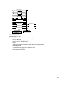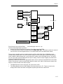
1
MC-12 / MC-12 Balanced
Music and Cinema
Processors
Service
Manual
MC-12 / MC-12 Balanced Service Manual
Precautions
Save these instructions for later use.
Follow all instructions and warnings marked on the unit.
Always use with the correct line voltage. Refer to the manufacturer's operating instructions for power requirements. Be advised that
different operating voltages may require the use of a different line cord and/or attachment plug.
Do not install the unit in an unventilated rack, or directly above heat producing equipment such as power amplifiers. Observe the
maximum ambient operating temperature listed in the product specification.
Slots and openings on the case are provided for ventilation; to ensure reliable operation and prevent it from overheating, these
openings must not be blocked or covered. Never push objects of any kind through any of the ventilation slots. Never spill a liquid of
any kind on the unit.
This product is equipped with a 3-wire grounding type plug. This is a safety feature and should not be defeated.
Never attach audio power amplifier outputs directly to any of the unit’s connectors.
To prevent shock or fire hazard, do not expose the unit to rain or moisture, or operate it where it will be exposed to water.
Do not attempt to operate the unit if it has been dropped, damaged, exposed to liquids, or if it exhibits a distinct change in performance
indicating the need for service.
This unit should only be opened by qualified service personnel. Removing covers will expose you to hazardous voltages.
This triangle, which appears on your component, alerts you to the presence of uninsulated, dangerous voltage inside the
enclosure… voltage that may be sufficient to constitute a risk of shock.
CAUTION
RISK OF ELECTRIC SHOCK
DO NOT OPEN
This triangle, which appears on your component, alerts you to important operating and maintenance Instructions in this
accompanying literature.
Notice
This equipment generates and uses radio frequency energy and if not installed and used properly, that is, in strict accordance with the
manufacturer's instructions, may cause interference to radio and television reception. It has been type tested and found to comply with
the limits for a Class B computing device in accordance with the specifications of Part 15 of FCC Rules, which are designated to
provide reasonable protection against such interference in a residential installation. However, there is no guarantee that interference
will not occur in a particular installation. If this equipment does cause interference to radio or television reception, which can be
determined by turning the equipment OFF and ON, the user is encouraged to try to correct the interference by one or more of the
following measures:
Reorient the receiving antenna
Relocate the computer with respect to the receiver
Move the computer away from the receiver
Plug the computer into a different outlet so that the computer and receiver are on different branch circuits.
If necessary, the user should consult the dealer or an experienced radio/television technician for additional suggestions. The user may
find the following booklet prepared by the Federal Communications Commission helpful:
“How to identify and Resolve Radio/TV Interference Problems"
This booklet is available from the U.S. Government Printing Office, Washington, DC 20402, Stock No. 004-000-00345-4.
Le présent appareil numérique n'émet pas de bruits radioélectriques dépassant les limites applicables aux appareils numériques de Ia
class B prescrites dans le Règlement sur le brouillage radioélectrique édicté par le ministère des Communications du Canada.
Copyright © 2002 Lexicon, Inc.
All Rights Reserved
Lexicon Inc. ● 3 Oak Park ● Bedford, MA 01730-1441 ● Tel (781) 280-0300 ● Customer Service Fax (781) 280-0499
Lexicon Part # 070-14828 Rev 0
Printed in the United States of America
Lexicon
Safety Suggestions
Read Instructions Read all safety and operating
instructions before operating the unit.
Retain Instructions Keep the safety and
operating instructions for future reference.
Heed Warnings Adhere to all warnings on the
unit and in the operating instructions.
Follow Instructions Follow operating and use
instructions.
Heat Keep the unit away from heat sources such
as radiators, heat registers, stoves, etc., including
amplifiers which produce heat.
Ventilation Make sure that the location or
position of the unit does not interfere with its
proper ventilation. For example, the unit should
not be situated on a bed, sofa, rug, or similar
surface that may block the ventilation openings;
or, placed in a cabinet which impedes the flow of
air through the ventilation openings.
Wall or Ceiling Mounting Do not mount the unit
to a wall or ceiling except as recommended by
the manufacturer.
Power Sources Connect the unit only to a power
supply of the type described in the operating
instructions, or as marked on the unit.
Grounding or Polarization* Take precautions
not to defeat the grounding or polarization of the
unit’s power cord.
*Not applicable in Canada.
Power Cord Protection Route power supply
cords so that they are not likely to be walked on
or pinched by items placed on or against them,
paying particular attention to cords at plugs,
convenience receptacles, and the point at which
they exit from the unit.
Nonuse Periods Unplug the power cord of the
unit from the outlet when the unit is to be left
unused for a long period of time.
Water and Moisture Do not use the unit near
water — for example, near a sink, in a wet
basement, near a swimming pool, near an open
window, etc.
Object and Liquid Entry Do not allow objects to
fall or liquids to be spilled into the enclosure
through openings.
Cleaning The unit should be cleaned only as
recommended by the manufacturer.
Servicing Do not attempt any service beyond
that described in the operating instructions. Refer
all other service needs to qualified service
personnel.
Damage Requiring Service The unit should be
serviced by qualified service personnel when:
the power supply cord or the plug has been
damaged; objects have fallen or liquid has been
spilled into the unit; the unit has been exposed to
rain; the unit does not appear to operate normally
or exhibits a marked change in performance; the
unit has been dropped, or the enclosure
damaged.
MC-12/MC-12 Balanced Service Manual
SAFETY SUMMARY
The following general safety precautions must be observed during all phases of operation, service and repair of this instrument. Failure to
comply with these precautions or with specific warnings elsewhere in these instructions violates safety standards of design manufacture and
intended use of the instrument. Lexicon assumes no liability for the customer’s failure to comply with these requirements.
GROUND THE INSTRUMENT
To minimize shock hazard the instrument chassis and cabinet
must be connected to an electrical ground. The instrument is
equipped with a three-conductor AC power cable. The power
cable must either be plugged into an approved three-contact
electrical outlet or used with a three-contact to two-contact
adapter with the grounding wire (green) firmly connected to an
electrical ground (safety ground) at the power outlet. The power
jack and mating plug of the power cable meet International
Electrotechnical Commission (IEC) safety standards.
SAFETY SYMBOLS
General definitions of safety symbols used on equipment or in
manuals.
Instruction manual symbol: the product will be marked
with this symbol when it is necessary for the user to refer to the
instruction manual in order to protect against damage to the
instrument.
DO NOT OPERATE IN AN EXPLOSIVE
ATMOSPHERE
Do not operate the instrument in the presence of flammable gases
or fumes. Operation of any electrical instrument in such an
environment constitutes a definite safety hazard.
Indicates dangerous voltage. (Terminals fed from the
interior by voltage exceeding 1000 volts must be so marked.)
KEEP AWAY FROM LIVE CIRCUITS
Operating personnel must not remove instrument covers.
Component replacement and internal adjustments must be made
by qualified maintenance personnel. Do not replace components
with power cable connected. Under certain conditions, dangerous
voltages may exist even with the power cable removed. To avoid
injuries, always disconnect power and discharge circuits before
touching them.
WARNING
The WARNING sign denotes a hazard. It calls attention to a
procedure, practice, condition or the like which, if not correctly
performed or adhered to, could result in injury or death to
personnel.
CAUTION
DO NOT SERVICE OR ADJUST ALONE
Do not attempt internal service or adjustment unless another
person, capable of rendering first aid and resuscitation, is present.
DO NOT SUBSTITUTE PARTS OR MODIFY
INSTRUMENT
Because of the danger of introducing additional hazards, do not
install substitute parts or perform any unauthorized modification to
the instrument.
DANGEROUS PROCEDURE WARNINGS
Warnings, such as the example below, precede potentially
dangerous procedures throughout this manual. Instructions
contained in the warnings must be followed.
WARNING
The CAUTION sign denotes a hazard. It calls attention to an
operating procedure, practice, condition or the like which, if not
correctly performed or adhered to, could result in damage to or
destruction of part or all of the product.
NOTE:
The NOTE sign denotes important information. It calls attention to
procedure, practice, condition or the like which is essential to
highlight.
CAUTION
Electrostatic Discharge (ESD) Precautions
The following practices minimize possible damage to ICs resulting
from electrostatic discharge or improper insertion.
Dangerous voltages, capable of causing death, are present in this
instrument. Use extreme caution when handling, testing and
adjusting.
•
•
•
•
•
•
•
•
•
•
•
Keep parts in original containers until ready for use.
Avoid having plastic, vinyl or styrofoam in the work area.
Wear an anti—static wrist-strap.
Discharge personal static before handling devices.
Remove and insert boards with care.
When removing boards, handle only by non-conductive
surfaces and never touch open-edge connectors except at a
static-free workstation.*
Minimize handling of ICs.
Handle each IC by its body.
Do not slide ICs or boards over any surface.
Insert ICs with the proper orientation, and watch for bent
pins on ICs.
Use static shielding containers for handling and transport.
‘To make a plastic-laminated workbench anti-static, wash with a
solution of Lux liquid detergent, and allow drying without rinsing.
Lexicon
Table of Contents
Chapter 1 Reference Documents, Required Equipment............................. 1-1
Reference Documents............................................................................................................................. 1-1
Required Equipment................................................................................................................................ 1-1
Tools .................................................................................................................................................... 1-1
Test Equipment.................................................................................................................................... 1-1
Chapter 2 General Information ................................................................... 2-1
Periodic Maintenance .............................................................................................................................. 2-1
Ordering Parts ......................................................................................................................................... 2-1
Returning Units to Lexicon for Service .................................................................................................... 2-1
Chapter 3 Specifications............................................................................. 3-1
Chapter 4 Performance Verification............................................................ 4-1
Functional Tests ...................................................................................................................................... 4-1
Initial inspection ................................................................................................................................... 4-1
Power Supply Test............................................................................................................................... 4-1
Setup.................................................................................................................................................... 4-2
Audio Tests I/O .................................................................................................................................... 4-2
Audio Performance Verification ............................................................................................................. 4-10
Audio Inputs RCA #1 Left and Right to all Left and Right RCA/XLR Outputs Tests .......................... 4-10
All Remaining Audio RCA Inputs Left and Right to Front Left and Right RCA Output Tests ............. 4-11
Audio Inputs RCA #1 Left and Right to Zone 2 Left and Right RCA Fix /Var Outputs and Zone 2 XLR
Outputs Tests..................................................................................................................................... 4-12
Audio Inputs RCA #1 Left and Right to Record Left and Right RCA Fix /Var Outputs Tests ............. 4-13
All Digital Audio Inputs Coax, Optical, AES/EBU to the Left and Right Front RCA Outputs Tests .... 4-13
Video Input / Output Tests..................................................................................................................... 4-14
Composite Inputs to Composite (Main and Record) Outputs Tests ................................................... 4-14
S-Video Inputs to S-Video (Main and Record) Outputs Tests............................................................ 4-15
Component Inputs to Component Output Tests................................................................................. 4-16
Lexicon Audio Precision ATE Summary ............................................................................................ 4-17
Chapter 5 Troubleshooting ......................................................................... 5-1
V1.00 Release Notes............................................................................................................................... 5-1
Diagnostics .............................................................................................................................................. 5-2
Introduction .......................................................................................................................................... 5-2
DiagnosticS Categories ....................................................................................................................... 5-2
Power-on Modes.................................................................................................................................. 5-3
DiagnosticS Reporting ......................................................................................................................... 5-3
Diagnostics Control/Interface ............................................................................................................... 5-7
Power-on Diagnostics .......................................................................................................................... 5-7
Extended DiagnosticS Tests.............................................................................................................. 5-10
Extended Diagnostics Suite ............................................................................................................... 5-11
Service Notes ........................................................................................................................................ 5-17
Removing The Top Cover.................................................................................................................. 5-17
Removing the Video and Analog Boards ........................................................................................... 5-18
Removing the MEMORY Board ......................................................................................................... 5-19
Removing the Power Supply Board ................................................................................................... 5-19
Removing the Front Panel ................................................................................................................. 5-20
Changing Trigger Voltage From 12 Volts to 5 Volts........................................................................... 5-20
Removing the Main Board ................................................................................................................. 5-20
Initialization (Hard Reset) Procedure ................................................................................................. 5-20
Chapter 6 Theory of Operation ................................................................... 6-1
Main Board .............................................................................................................................................. 6-1
Z180 Host Processor ........................................................................................................................... 6-1
MC-12/MC-12 Balanced Service Manual
FPGAs ..................................................................................................................................................6-3
Host Interface to Other Boards .............................................................................................................6-6
Video Board & OSD..............................................................................................................................6-8
Analog Board ........................................................................................................................................6-8
OPTION Boards....................................................................................................................................6-9
DSP ....................................................................................................................................................6-10
Audio Routing .....................................................................................................................................6-14
Encoder ..............................................................................................................................................6-18
VCO Board Overview .........................................................................................................................6-20
PLL Overview .....................................................................................................................................6-21
Analog BOARD ......................................................................................................................................6-22
Overview.............................................................................................................................................6-22
Analog Audio Inputs............................................................................................................................6-23
Mic Inputs and Main A/D Converter ....................................................................................................6-23
Record and Zone 2 A/D Converters....................................................................................................6-24
Record and Zone 2 D/A converters ....................................................................................................6-24
Record and Zone 2 Outputs ...............................................................................................................6-24
Main D/A Converters ..........................................................................................................................6-25
Main Outputs ......................................................................................................................................6-26
Analog FPGA......................................................................................................................................6-26
Control Registers and Main Board Connector ....................................................................................6-28
XLR Board Connector, Power Supply Connections and Regulators ..................................................6-29
xlr board Overview..............................................................................................................................6-29
Main Channels....................................................................................................................................6-29
Zone 2 Variable Channels ..................................................................................................................6-30
OPTO/MIC Input Board ......................................................................................................................6-30
Video BOARD ........................................................................................................................................6-30
Overview.............................................................................................................................................6-30
Composite video inputs ......................................................................................................................6-31
Composite video outputs ....................................................................................................................6-31
S-video inputs .....................................................................................................................................6-31
Monitor Composite / S-video ..............................................................................................................6-31
Record Composite / S-video ...............................................................................................................6-32
Component Video Switcher ................................................................................................................6-32
On-Screen Display Signals .................................................................................................................6-33
Support Logic / FPGA.........................................................................................................................6-34
Sync Stripper / DC Restorer ...............................................................................................................6-34
Video Control Registers......................................................................................................................6-35
Power and Control Interface ...............................................................................................................6-35
Chapter 7 - Parts List.................................................................................. 7-1
MC-12/MC-12 Balanced MAIN BOARD ...................................................................................................7-1
MC-12/MC-12 Balanced OPTO/MIC BOARD ..........................................................................................7-3
MC-12/MC-12 Balanced VIDEO BOARD .................................................................................................7-4
MC-12/MC-12 Balanced VIDEO RCA BOARD ........................................................................................7-6
MC-12/MC-12 Balanced ANALOG I/O BOARD .......................................................................................7-6
MC-12/MC-12 Balanced SWITCH/LED BOARD ....................................................................................7-11
MC-12/MC-12 Balanced IR/ENCODER BOARD....................................................................................7-11
MC-12/MC-12 Balanced STANDBY BOARD .........................................................................................7-12
MC-12/MC-12 Balanced MEMORY BOARD ..........................................................................................7-12
MC-12/MC-12 Balanced VCO ASSEMBLY............................................................................................7-12
MC12 Balanced ONLY ...........................................................................................................................7-12
MC-12B XLR BOARD.........................................................................................................................7-12
MC-12/MC-12 Balanced CHASSIS ASSEMBLY....................................................................................7-13
MC-12/MC-12 Balanced POWER SUPPLY ASSEMBLY.......................................................................7-14
MC-12/MC-12 Balanced FAN ASSEMBLY ............................................................................................7-14
Lexicon
MC-12/MC-12 Balanced FRONT PANEL MECHANICAL ASSEMBLY ................................................. 7-14
MC-12/MC-12 Balanced VIDEO MECHANICAL ASSEMBLY ............................................................... 7-15
MC-12/MC-12 Balanced PACKAGING/MISCELLANOUS..................................................................... 7-15
MC-12/MC-12 Balanced POWER CORD OPTIONS............................................................................. 7-15
MC-12/MC-12 Balanced MOUNTING OPTION..................................................................................... 7-15
MC-12/MC-12 Balanced SPARE ASSEMBLIES ................................................................................... 7-16
Chapter 8 Schematics and Drawings ......................................................... 8-1
Schematics .............................................................................................................................................. 8-1
Drawings.................................................................................................................................................. 8-1
Lexicon
Chapter 1 Refe r ence Documents, Required Equipment
Reference Documents
MC-12/MC-12 Balanced User Guide - Lexicon P/N 070-14773, latest revision
Required Equipment
TOOLS
The following is a minimum suggested technician's tool kit required for performing disassembly, assembly
and repairs:
• Clean, antistatic, well-lit work area with grounding wrist strap
• (1) #1 Phillips tip screwdriver - (Magnetic tip preferred)
• (1) 14mm socket nut driver
• (1) Allen hex head wrench ( 2.5 mm )
• (1) 3/16 hollow nutdriver
• Solder: 63/37 - Tin/Lead Alloy composition, low residue, no-clean solder
• Magnification glasses and lamps
• SMT Soldering/Desoldering bench-top repair station
TEST EQUIPMENT
The following is a minimum suggested equipment list required to perform the proof of performance tests.
• (1) High quality Amplifier with RCA and XLR input connectors
• (1) Pair high quality Speakers with RCA and XLR input connectors
• (1) High quality Video Monitor with RCA, S-Video, and Component (RCA and BNC) input
connections
• (1) CD disc for test audio source
• (1) DVD movie disc for test video source
• Cables: (dependent on your signal source)
• Audio Input Cables with shield and an RCA connector on one end and an appropriate
connector on the opposite end for connection to the Low Distortion Oscillator
• Audio Output Cable with shield and an RCA connector on one end and an appropriate
connector on the opposite end for connection to the Distortion Analyzer
• Audio Output Cable (balanced) with shield and an XLR female plug on one end and an
appropriate connector on the opposite end for connection to the Distortion Analyzer
• (4) Audio Cables shielded with RCA connectors on both ends
• (2) Audio Cables shielded with an XLR male and female connector on either end
• (1) Digital Audio Cable with RCA connectors on both ends
• (1) Digital Audio Cable with Optical connectors on both ends
• (1) AES/EBU Digital cable
• (1) Digital Audio Cable with Standard Optical connector on one end and an OMJ (Optical
Mini Jack) connector on the other
• (2) Video Cables with RCA connectors on both ends
• (2) Video Cables with S-Video connectors on both ends
• (1) Video Cable with 3-wire Component RCA connectors on both ends
• (2) Video Cables with 3-wire Component BNC connectors on both ends
• (1) High end DVD player with RCA Analog Left and Right and Digital Coax and Optical
Audio Outputs
• (1) MC-12 AC power cord
• variable AC power supply 2 amp minimum
• Digital Multimeter (DMM) 3.5 digit 0.5% or better accuracy
1-1
MC-12/MC-12 Balanced Service Manual
•
•
•
•
1-2
(1) Low Distortion Analog oscillator with single-ended or balanced output, < 100 ohms output
impedance, < .005% THD
(1) Analog Distortion Analyzer and Level Meter with single-ended or balanced input, switchable
30Hz high pass filter or audio bandpass (20-20kHz) filter
(1) 100 MHz Oscilloscope
(1) Digital Distortion Analyzer & Digital Function Generator (e.g. Stanford Research Systems
Model DS360 or Audio Precision System 1 with DSP Option/System 2).
Lexicon
Chapter 2 Gene r al Information
Periodic Maintenance
Under normal conditions the MC-12/MC-12 Balanced requires minimal maintenance. Use a soft, lint-free
cloth slightly dampened with warm water and mild detergent to clean the exterior surfaces of the connector
box.
Do not use alcohol, benzene or acetone-based cleaners or any strong commercial cleaners. DO
NOT use abrasive materials such as steel wool or metal polish. If the unit is exposed to a dusty
environment, a vacuum or low-pressure blower may be used to remove dust from the unit's exterior.
Ordering Parts
When ordering parts, identify each part by type, price and Lexicon Part Number. Replacement parts can be
ordered from:
LEXICON, INC.
3 Oak Park
Bedford, MA 01730-1441
Telephone: 781-280-0300; Fax: 781-280-0499; email: [email protected]
ATTN: Customer Service
Returning Units to Lexicon for Service
Before returning a unit for warranty or non-warranty service, consult with Lexicon Customer
Service to determine the extent of the problem and to obtain Return Authorization. No equipment
will be accepted without Return Authorization from Lexicon.
If Lexicon recommends that an MC-12/MC-12 Balanced should be returned for repair and you choose to
return the unit to Lexicon for service, Lexicon assumes no responsibility for the unit in shipment from the
customer to the factory, whether the unit is in or out of warranty. All shipments must be well-packed (using
the original packing materials if possible), properly insured and consigned, prepaid, to a reliable shipping
agent.
When returning a unit for service, please include the following information:
•
•
•
•
•
•
•
•
•
Your Name
Company Name
Street Address
City, State, Zip Code, Country
Telephone number (including area code and country code where applicable)
Serial Number of the unit
Description of the problem
Preferred method of return shipment
Return Authorization #, on both the inside and outside of the package
Please enclose a brief note describing any conversations with Lexicon personnel (indicate the name of the
person at Lexicon) and give the name and daytime telephone number of the person directly responsible for
maintaining the unit.
Do not include accessories such as manuals, audio cables, footswitches, etc. with the unit, unless
specifically requested to do so by Lexicon Customer Service personnel.
2-1
Lexicon
Chapter 3 Spec i fications
Audio Inputs and Outputs
Audio Inputs - 8 stereo pairs (RCA) or 5 stereo pairs and one 5.1-channel analog input
Digital Audio Inputs - 6 coaxial (RCA), 6 optical (5 TosLink, and 1 optical mini jack), 1 AES/EBU; coaxial and
optical inputs conform to IEC-958, S/PDIF standards
Sample Rates: 44.1, 48, 88.2, 96kHz
Accepts: 16-24 bits PCM audio, Dolby Digital, dts and dts-ES discrete data formats
Main Audio Outputs - 12 unbalanced (RCA) and 12 balanced (XLR, MC-12 Balanced only) for Front L/R,
Center, LFE, Subwoofer L/R, Side L/R, Rear L/R, Auxiliary L/R
Zone 2 Audio Outputs - 2 stereo pairs (RCA, one fixed and one variable output level); 2 balanced (XLR) for
L/R variable output (MC-12 Balanced only)
Record Audio Outputs - 2 stereo pairs (RCA, one fixed and one variable output level); 1 coaxial (RCA) and 1
optical (TosLink) S/PDIF output (in parallel)
Performance (Main Zone)
Analog-to-Digital Conversion - 24-bit, 96kHz, dual-bit ∆Σ architecture
Digital-to-Analog Conversion - 24-bit, 44.1 to 192kHz, multi-bit ∆Σ architecture, operating in dual-mono
mode
Frequency Response - 10Hz to 20kHz, +0.1dB/-0.25dB, -0.75dB at 40 kHz, reference 1kHz
THD + Noise - Below 0.003% at 1kHz, maximum output level
Dynamic Range - 108dB minimum, 111dB typical, 22kHz bandwidth
Signal-to-Noise Ratio - 108dB minimum, 111dB typical, 22kHz bandwidth
Input Sensitivity - 200mVrms (2Vrms for maximum output level) at 0dB input gain
Input Impedance - 100kΩ in parallel with 150pF
Output Level - 150mVrms typical, 6Vrms maximum (RCA outputs); 300mVrms typ, 12Vrms maximum (XLR
outputs, MC-12 Balanced only); maximum value with full-scale input signal and volume at +12dB
Output Impedance - 100Ω in parallel with 150pF (RCA outputs); 50Ω in parallel with 150pF (XLR outputs,
MC-12 Balanced only)
Performance (Zone 2 and Record Zone)
Analog-to-Digital Conversion - 24-bit, 44.1 to 96kHz, dual-bit ∆Σ architecture (Record Zone only)
Digital-to-Analog Conversion - 24-bit, 44.1 to 192kHz, multi-bit ∆Σ architecture
Frequency Response - 10Hz to 20kHz, +0.1dB/-0.25dB, -0.75dB at 40kHz, reference 1kHz
THD + Noise Below 0.005% at 1kHz, maximum output level
Dynamic Range - 105dB minimum, 108dB typical, 22kHz bandwidth
Signal-to-Noise Ratio - 105dB minimum, 108dB typical, 22kHz bandwidth
Input Sensitivity - 200mVrms (4Vrms for maximum output level)
Input Impedance - 100 kΩ in parallel with 150pF
Output Level - 200mVrms typical, 4Vrms maximum (RCA outputs); 400mVrms typical, 8Vrms maximum (XLR
outputs, Zone 2 only, MC-12 Balanced only); maximum value with full-scale input signal and volume at 0dB
Output Impedance - 100Ω in parallel with 150pF (RCA outputs); 50Ω in parallel with 150pF (XLR outputs,
Zone 2 only, MC-12 Balanced only)
Video Inputs and Outputs
Video Inputs - 5 composite (RCA), 8 S-video, and 4 component video (3 RCA, 1 BNC)
Video Outputs - 4 composite (RCA, 2 monitor and 2 record), 4 S-video (2 monitor and 2 record), and 1
component (BNC)
Performance (Composite & S-video)
NTSC M, PAL, and SECAM compatible
Switching - Active
Output Level - 1.0V peak-to-peak
Impedance - 75Ω
Input Return Loss - >40dB
Differential Gain - <0.5%
Differential Phase - <0.5°
Bandwidth - >25MHz
K Factor - <0.3%
3-1
MC-12/MC-12 Balanced Service Manual
Gain - ±0.15dB
Signal/Noise Ratio - >70dB
Frequency Response - 10Hz to 10MHz + 0.1/-0.3dB
Performance (Component Video)
3-channel (Y, Pr, Pb), format-independent
Switching - Passive
Impedance - 75Ω
Bandwidth - >300MHz
Insertion Loss - <3dB
Other
Microphone Inputs - 4 3.5mm miniature phone jacks
Input sensitivity: 10mVrms (400mV maximum input level)
Input Impedance: 20kΩ (accepts balanced or unbalanced input signals)
Trigger Outputs - 1 power-on/off trigger, 2 programmable triggers; +12 VDC, 0.5 amps each; detachable
screw terminals
RS-232 Serial Input/Output - 2 9-pin D-sub connectors for system control and software upgrades
Power Requirements - 90-250 VAC, 50-60Hz, 90W (universal line input), detachable power cord
Dimensions MC-12: 17.3"w x 5.2"h x 14.85"d (440 x 132 x 377mm)
MC-12 Balanced: 17.3"w x 6.63"h x 14.85"d (440 x 169 x 377mm)
Weight MC-12: 36lbs (16.4kg)
MC-12 Balanced: 45lbs (20.5kg)
Rack Mounting - Optional brackets are available for mounting either unit in a standard 19" equipment rack
Environment
Operating Temp: 0° to 35°C (32° to 95°F)
Storage Temp: -30° to 75°C (-22° to 167°F)
Relative Humidity: 95% maximum without condensation
Remote Control - Hand-held, battery-powered infrared remote control unit
Batteries: Two AA
3-2
Lexicon
Chapter 4 Perfo r mance Verification
This section describes a quick verification of the operation of the MC-12/MC-12 Balanced and the integrity
of its analog and digital audio signal paths. Tests are included for the MC-12 Balanced version and can be
omitted when testing an MC-12/MC-12 Balanced.
Functional Tests
The following tests cover basic functions making sure the MC-12/MC-12 Balanced responds to button
commands from the remote as well as from its front panel.
INITIAL INSPECTION
1.
2.
3.
4.
5.
6.
7.
Inspect the MC-12/MC-12 Balanced for obvious signs of physical damage.
Verify that all switches operate smoothly.
Remove the MC-12/MC-12 Balanced top cover.
Verify that all socketed ICs are correctly seated.
Verify that all ribbon cables are correctly installed and are secure.
Check for burnt or obviously damaged components.
Using the main power switch on the back of the MC-12/MC-12 Balanced, verify that it runs through its
Diagnostics Test and settles into the last state it was powered down in.
8. Check each of the front panel's switches for smooth mechanical operation, that each LED turns on and
off when depressed, and that the display acknowledges its function.
9. Press all the buttons on the remote and verify that the display is responding to all the remote
commands.
POWER SUPPLY TEST
The main power supply in the MC-12/MC-12 Balanced has an operational range of 100-240 VAC 50-60Hz,
90Watts.
The following test is for North American line voltage of 120VAC.
1.
2.
3.
4.
5.
6.
Set the variable AC supply to 0 volts.
Verify that the MC-12/MC-12 Balanced is powered off at its rear panel power switch.
Connect the power cord between the supply and the MC-12/MC-12 Balanced.
Turn on the MC-12/MC-12 Balanced using the rear panel power switch.
Slowly bring up the voltage to 120VAC.
The current draw will bounce up and down a bit and should not exceed 1.5amps. Once you have
achieved 120VAC the current draw on the Variac should not exceed 0.6amps. If the MC-12/MC-12
Balanced draws an excessive current, turn the MC-12/MC-12 Balanced off and check the power supply
rails for shorts to ground with the DMM meter.
7. Using the DMM measure all the power supply rails as stated by the test points below, being sure to use
the MC-12/MC-12 Balanced chassis as ground
8. Verify that all voltages are within the tolerance range shown.
Main Board
Supply Rail
+5VD
Battery
Tolerance
4.94-5.26
≥ 2.5
Location (facing front panel)
Lower left-hand corner connector J31 Red wires to ground.
Right side to the Left of U69; Measure the top of the battery
to ground
Note: If battery is in need of replacement
CAUTION
“CAUTION Danger of explosion if battery is incorrectly replaced. Replace only with the same or equivalent
type.”
4-1
MC-12/MC-12 Balanced Service Manual
Analog Board
Supply Rail
+5VDC
-5VDC
+15V
-15V
Tolerance
4.75-5.25VDC
4.75-5.25VDC
15.00-16.95
14.25-15.75
Location (facing front panel)
Lower left hand corner connector J26.Red wire to ground
J26 Grey wire to ground
J26 Yellow wire to ground
J26 Blue wire to ground
Video Board
Supply Rail
+5VA
-5VA
Tolerance
4.75-5.26
4.75-5.26
Location (facing front panel)
Lower left hand corner connector J22. Red wire to ground
J22 Grey wire to ground
SETUP
In order to properly test the MC-12/MC-12 Balanced as described in this document, follow this setup
procedure before hand. It will make it much easier to follow along and perform each of the tests to follow.
1. Connect a small color monitor to the Composite output. This will allow you to fully view the diagnostic
menus of the MC-12/MC-12 Balanced.
2. Press and hold down the Zone 2 LD and the Record LD buttons on the front panel while powering up
the MC-12/MC-12 Balanced with the Main Power Switch on the back of the unit.
3. Once the display reads Lexicon, release the buttons on the front panel.
4. The Display on the front panel will read DIAGS MENU FUNCTIONAL TESTS and the monitor will have
a distorted, fractured-looking screen. This will happen on the monitor every time Diagnostics are
loaded.
5. To clear this display, press the Down Menu button (or turn the Volume knob) on the remote until you
see 'VIDEO I/O TESTS' displayed on their front panel.
6. Press the Right Menu Button (or the Mode button on the front panel) to enter the top of the VIDEO I/O
TESTS Menu.
7. Press the Down button (or Modes Down button on the front panel) several times until you see 'LOAD
FONT' displayed on the front panel.
8. Press Right Menu button (or Modes Down button on the front panel) to load the Fonts. The Monitor will
turn to a blue screen and the front panel will read VIDEO I/O TESTS completed.
9. Press the Left Menu button (or the Mode Up button on the front panel) to bring a clear legible menu to
the monitor screen. The monitor will display the VIDEO I/O TESTS menu with LOAD FONT highlighted
with a black bar.
10. Press the Left Menu button (or Mode Up button on the front panel) to bring you to the main DIAGS
MENU. The MC-12/MC-12 Balanced is now set up for monitor display for easier navigation through the
Diagnostic menus.
Note: The tests to follow assume you have entered the Diagnostics Menu as described above. Each test
will not repeat this setup procedure. It will make reference to it in order to set the stage for proper testing of
the MC-12/MC-12 Balanced.
AUDIO TESTS I/O
Analog Input To ALL Analog Outputs Test
In this test we will be verifying the path of the #1 Left and Right RCA paired input to all Analog Outputs both
RCA and XLR of the MC-12/MC-12 Balanced.
1. Connect the oscillator output to the Left and Right audio inputs marked #1 on the rear panel of the MC12/MC-12 Balanced.
2. Connect the RCA Left and Right Front outputs of the MC-12/MC-12 Balanced to the amplifier Left and
Right inputs, and the outputs of the amplifier to a pair of speakers.
4-2
Lexicon
3. If the MC-12/MC-12 Balanced is not in Extended Diagnostics, follow the setup procedure as described
at the beginning of this chapter.
4. In the Diagnostic Menu, select Audio I/O Tests.
5. Highlight Audio Input 1 Test, then press the Right menu button to engage the test. The MC-12/MC-12
Balanced is now set for audio coming into the Left and Right #1 RCA input to the Front Left and Right
RCA output and all the remaining RCA and XLR paired Left and Right audio output connections.
6. Slowly increase the volume on the amplifier to a comfortable listening level from the speakers.
7. Sweep the oscillator from 20Hz to 20kHz. Verify that you hear clean, clear audio coming from the
speakers.
8. Power down the amplifier and move the cables from the Front Left and Right outputs to the Center Left
and Right outputs.
9. Power on the amplifier and repeat the oscillator sweep as described in Step 7.
10. Repeat steps 8 and 9 for the remaining paired RCA outputs up to the Left and Right Aux. The Zone 2
and Record outs will be tested later.
11. To test the XLR paired outputs, power down the amplifier and remove the RCA output cables from the
MC-12/MC-12 Balanced to the amplifier.
12. Connect a pair of XLR cables. Connect the Front Left and Right balanced outputs of the MC-12/MC-12
Balanced to the XLR balanced input of the amplifier.
13. Repeat step 7.
14. Test the remaining XLR Left and Right balanced outputs and Center L/R to AUX L/R by powering down
the amp and repeating step 9.
All Remaining Analog Inputs to Analog Output Test
This test will verify the path of the remaining analog Left and Right inputs #2 to 8 to the Main Front Left and
Right analog outputs pass signal.
1. Connect the oscillator output to the Left and Right audio inputs marked #2 on the rear panel of the MC12/MC-12 Balanced.
2. Connect the RCA Left and Right Front outputs of the MC-12/MC-12 Balanced to the amplifier Left and
Right inputs, and the outputs of the amplifier to a pair of speakers.
3. If the MC-12/MC-12 Balanced is not in Extended Diagnostics, follow the setup procedure as described
at the beginning of this chapter.
4. In the Diagnostic Menu, select Audio I/O Tests.
5. Highlight Audio Input 2 Test, then press the Right menu button to engage the test. The MC-12/MC-12
Balanced is now set for audio coming in to the Left and Right #2 RCA input and out to the Front Left
and Right RCA output.
6. Slowly increase the volume on the amplifier to a comfortable listening level from the speakers.
7. Sweep the oscillator from 20Hz to 20kHz. Verify that you hear clean, clear audio coming from the
speakers.
8. In order to test the remaining Analog inputs you must power down the amplifier and move the input
cables to the next paired audio inputs.
9. Repeat steps 4 & 5 above highlighting the next input to be tested in the Audio I/O Tests Menu and
select it by pressing the Right Menu button.
10. Repeat steps 5 to 7 until all the Audio Inputs have been tested.
Analog Input to Zone 2 Output Test
This test will verify the path of the #1 Left and Right RCA paired input to the Zone 2 Fix and Var outputs.
1. Connect the oscillator output to the Left and Right audio inputs marked #1 on the rear panel of the MC12/MC-12 Balanced.
2. Connect the RCA Left and Right Zone 2 Fix outputs of the MC-12/MC-12 Balanced to the amplifier Left
and Right inputs, and the outputs of the amplifier to a pair of speakers.
3. If the MC-12/MC-12 Balanced is not in Extended Diagnostics, follow the setup procedure as described
at the beginning of this chapter.
4. In the Diagnostic Menu, select Audio I/O Tests.
4-3
MC-12/MC-12 Balanced Service Manual
5. Highlight Audio Input 1 Test, then press the Right menu button to engage the test. The MC-12/MC-12
Balanced is now set for audio coming in to the Left and Right #1 RCA input to the ZONE 2 Left and
Right RCA outputs.
6. Slowly increase the volume on the amplifier to a comfortable listening level from the speakers.
7. Sweep the oscillator from 20Hz to 20kHz. Verify that you hear clean, clear audio coming from the
speakers.
8. Power down the amplifier and move the cables from the Zone 2 Fix Left and Right outputs to the Zone
2 Var Left and Right outputs.
9. Power on the amplifier and repeat the oscillator sweep as described in Step 7.
10. Remove the RCA output cables from the Zone 2 Var Left and Right outputs of the MC-12/MC-12
Balanced to the amplifier.
11. Connect a pair of XLR cables to the Left and Right Zone 2 Fix balanced outputs of the MC-12/MC-12
Balanced to the XLR balanced input of the amplifier.
12. Repeat steps 7 to 9.
All Remaining Analog Inputs to the ZONE 2 Fix Output Test
This test will verify the path of the remaining analog Left and Right inputs #2 to #8 to the Fix Zone 2 Left
and Right analog outputs pass signal.
1. Connect the oscillator output to the Left and Right audio inputs marked #2 on the rear panel of the MC12/MC-12 Balanced.
2. Connect the RCA Left and Right Zone 2 Fix outputs of the MC-12/MC-12 Balanced to the amplifier Left
and Right inputs and the outputs of the amplifier to a pair of speakers.
3. If the MC-12/MC-12 Balanced is not in Extended Diagnostics, follow the setup procedure as described
at the beginning of this chapter.
4. In the Diagnostic Menu, select Audio I/O Tests.
5. Highlight Audio Input 2 Test, then press the Right menu button to engage the test. The MC-12/MC-12
Balanced is now set for audio coming into the Left and Right #2 RCA input to the ZONE 2 Left and
Right RCA outputs.
6. Slowly increase the volume on the amplifier to a comfortable listening level from the speakers.
7. Sweep the oscillator from 20Hz to 20kHz. Verify that you hear clean, clear audio coming from the
speakers.
8. In order to test the remaining Analog inputs to the Zone 2 Fix output, you must power down the
amplifier and move the input cables to the next paired audio inputs. Next, highlight the input being
tested in the Audio I/O Tests Menu and select it by pressing the Right Menu button.
9. Repeat steps 5 to 7 until all the Audio Inputs have been tested.
Analog Input to Record Output Test
This test will verify the path of the #1 Left and Right RCA paired input to the Record Fix and Var outputs.
1. Connect the oscillator output to the Left and Right audio inputs marked #1 on the rear panel of the MC12/MC-12 Balanced.
2. Connect the RCA Left and Right Record Fix outputs of the MC-12/MC-12 Balanced to the amplifier Left
and Right inputs and the outputs of the amplifier to a pair of speakers.
3. If the MC-12/MC-12 Balanced is not in Extended Diagnostics, follow the setup procedure as described
at the beginning of this chapter.
4. In the Diagnostic Menu, select Audio I/O Tests.
5. Highlight Audio Input 1 Test then press the Right menu button to engage the test. The MC-12/MC-12
Balanced is now set for audio coming in to the Left and Right #1 RCA input to the Record Fix Left and
Right outputs.
6. Slowly increase the volume on the amplifier to a comfortable listening level from the speakers.
7. Sweep the oscillator from 20Hz to 20kHz. Verify that you hear clean, clear audio coming from the
speakers.
8. Power down the amplifier and move the cables from the Record Fix Left and Right outputs to the
Record Var Left and Right outputs.
9. Power on the amplifier and repeat the oscillator sweep as described in Step 7.
4-4
Lexicon
All Remaining Analog Inputs to the Record Fix Output Test
This test will verify the path of the remaining analog Left and Right inputs #2 to #8 to the Fix Record Left
and Right analog outputs pass signal.
1. Connect the oscillator output to the Left and Right audio inputs marked #2 on the rear panel of the MC12/MC-12 Balanced.
2. Connect the RCA Left and Right Record Fix outputs of the MC-12/MC-12 Balanced to the amplifier Left
and Right inputs and the outputs of the amplifier to a pair of speakers.
3. If the MC-12/MC-12 Balanced is not in Extended Diagnostics, follow the setup procedure as described
at the beginning of this chapter.
4. In the Diagnostic Menu, select Audio I/O Tests.
5. Highlight Audio Input 2 Test, then press the Right menu button to engage the test. The MC-12/MC-12
Balanced is now set to see audio coming in to the Left and Right #2 RCA input to the Record Fix Left
and Right outputs.
6. Slowly increase the volume on the amplifier to a comfortable listening level from the speakers.
7. Sweep the oscillator from 20Hz to 20kHz. Verify that you hear clean, clear audio coming from the
speakers.
8. In order to test the remaining Analog inputs to the Record Fix output, you must power down the
amplifier move the input cables to the next paired audio inputs. Next, highlight the input being tested in
the Audio I/O Tests Menu and select it by pressing the Right Menu button.
9. Repeat steps 5 to 7 until all the Audio Inputs have been tested.
Digital Input to all Analog Outputs Test
This test will verify the path of the #1 Coax digital input to all of the Main analog outputs, both RCA and XLR
of the MC-12/MC-12 Balanced.
Note: This test requires the use of a DVD player as a source. Therefore, the tests to follow will be run at the
44.1kHz sample rate. To properly test the full sample range of the MC-12/MC-12 Balanced, you will need to
repeat all of the Digital tests with 48, 88.2, and 96kHz sample rate sources.
1. Connect the digital output source DVD Player to the #1 Coax digital input on the rear panel of the MC12/MC-12 Balanced.
2. Connect the RCA Left and Right Front outputs of the MC-12/MC-12 Balanced to the amplifier Left and
Right inputs and the outputs of the amplifier to a pair of speakers.
3. If the MC-12/MC-12 Balanced is not in Extended Diagnostics, follow the setup procedure as described
at the beginning of this chapter.
4. In the Diagnostic Menu, select Audio I/O Tests.
5. Highlight S/PDIF Input CX1 Test, then press the Right menu button to engage the test. The MC-12/MC12 Balanced is now set to see digital audio from the S/PDIF #1 digital input to the Front Left and Right
RCA output and all the remaining RCA and XLR paired Left and Right audio output connections.
6. Press play on the DVD player.
7. Slowly increase the volume on the amplifier to a comfortable listening level from the speakers.
8. Verify that you hear clean, clear audio coming from the speakers.
9. Pause the DVD and power down the amplifier.
10. Move the cables from the Front Left and Right outputs to the Center Left and Right outputs.
11. Power on the amplifier press play on the DVD player and repeat Steps 7 - 8.
12. Repeat steps 7 - 10 for the remaining paired RCA outputs up to the Left and Right Aux. The Zone 2 and
Record outs will be tested later. Remove the RCA output cables from the MC-12/MC-12 Balanced to
the amplifier.
13. With a pair of XLR cables, connect the Left and Right balanced outputs of the MC-12/MC-12 Balanced
to the XLR balanced input of the amplifier.
14. Repeat steps 7 - 10 for the remaining paired XLR balanced outputs up to the Left and Right Aux. As in
the RCA test above the Zone 2 XLR will be tested later.
4-5
MC-12/MC-12 Balanced Service Manual
All Remaining Digital Inputs to Analog Output Test
This test will verify the path of all the remaining Coax and Optical Digital inputs to the Main Front Left and
Right analog output.
Note: In order to test the Optical #6, which is an OMJ (Optical Mini Jack) style connector, you will need an
Optical to OMJ adapter in order to make the proper connection.
1. Connect the digital output source DVD player to the #2 Coax digital input on the rear panel of the MC12/MC-12 Balanced.
2. Connect the RCA Left and Right Front outputs of the MC-12/MC-12 Balanced to the amplifier Left and
Right inputs and the outputs of the amplifier to a pair of speakers.
3. If the MC-12/MC-12 Balanced is not in Extended Diagnostics, follow the setup procedure as described
at the beginning of this chapter.
4. In the Diagnostic Menu, select Audio I/O Tests.
5. Highlight S/PDIF Input CX2 Test then press the Right menu button to engage the test. The MC-12/MC12 Balanced is now set to see digital audio coming in to the S/PDIF #2 digital input to the Front Left and
Right RCA output.
6. Press play on the DVD player.
7. Slowly increase the volume on the amplifier to a comfortable listening level from the speakers.
8. Verify that you hear clean, clear audio coming from the speakers.
9. Pause the DVD and power down the amplifier.
10. In order to test the remaining Digital inputs both RCA and Optical you must move the Digital Input cable
to the next Digital input (RCA or Optical), then highlight the input being tested in the Audio I/O Tests
Menu and select it by pressing the Right Menu button.
11. Repeat steps 6 - 8 until all the remaining Digital Inputs have been tested.
Digital Input to Zone 2 Output Test
This test will verify the path of the #1 Coax Digital input to the Zone 2 Fix and Var Left and Right outputs.
1. Connect the digital output source DVD player to the #1 Coax digital input on the rear panel of the MC12/MC-12 Balanced.
2. Connect the RCA Left and Right Zone 2 Fix outputs of the MC-12/MC-12 Balanced to the amplifier Left
and Right inputs and the outputs of the amplifier to a pair of speakers.
3. If the MC-12/MC-12 Balanced is not in Extended Diagnostics, follow the setup procedure as described
at the beginning of this chapter.
4. In the Diagnostic Menu, select Audio I/O Tests.
5. Highlight S/PDIF Input CX1 Test then press the Right menu button to engage the test. The MC-12/MC12 Balanced is now set to see digital audio from the S/PDIF #1 digital input to the Front Left and Right
RCA output and all the remaining RCA and XLR paired Left and Right audio output connections.
6. Press play on the DVD player.
7. Slowly increase the volume on the amplifier to a comfortable listening level from the speakers.
8. Verify that you hear clean, clear audio coming from the speakers.
9. Pause the DVD and power down the amplifier.
10. Move the cables from the Zone 2 Fix Left and Right outputs to the Zone 2 Var Left and Right outputs.
11. Power on the amplifier press play on the DVD player and repeat step 7 - 8.
12. Pause the DVD and power down the amplifier.
13. Remove the RCA output cables from the Zone 2 Var Left and Right outs of the MC-12/MC-12 Balanced
to the amplifier.
14. With a pair of XLR cables connect the Left and Right Zone 2 Fix balanced outputs of the MC-12/MC-12
Balanced to the XLR balanced input of the amplifier.
15. Power on the amplifier, press play on the DVD player, and repeat Step 7 - 9.
All Remaining Digital Inputs to Zone 2 Output Test
This test will verify the path of all the remaining Digital Coax and Optical Digital inputs to the Zone 2 Fix
Front Left and Right analog output.
4-6
Lexicon
Note: In order to test the Optical #6, which is an OMJ (Optical Mini Jack) style connector, you will need an
Optical to OMJ adapter in order to make the proper connection.
1. Connect the digital output source DVD player to the #2 Coax Digital input on the rear panel of the MC12/MC-12 Balanced.
2. Connect the RCA Left and Right Zone 2 Fix outputs of the MC-12/MC-12 Balanced to the amplifier Left
and Right inputs and the outputs of the amplifier to a pair of speakers.
3. If the MC-12/MC-12 Balanced is not in Extended Diagnostics, follow the setup procedure as described
at the beginning of this chapter.
4. In the Diagnostic Menu, select Audio I/O Tests.
5. Highlight S/PDIF Input CX2 Test, then press the Right menu button to engage the test. The MC-12/MC12 Balanced is now set to see digital audio from the S/PDIF #2 digital input to the Fix Left and Right
RCA output.
6. Press play on the DVD player.
7. Slowly increase the volume on the amplifier to a comfortable listening level from the speakers.
8. Verify that you hear clean, clear audio coming from the speakers.
9. Pause the DVD and power down the amplifier.
10. In order to test the remaining Digital inputs both RCA and Optical you must move the Digital Input cable
to the next Digital input (RCA or Optical), then highlight the input being tested in the Audio I/O Tests
Menu and select it by pressing the Right Menu button.
11. Repeat steps 6 - 9 until all the remaining Digital Inputs have been tested.
Digital Input to Record Output Test
This test will verify the path of the #1 Coax Digital input to the Record Fix and Var Left and Right outputs.
1. Connect the digital output source DVD player to the #1 Coax Digital input on the rear panel of the MC12/MC-12 Balanced.
2. Connect the RCA Left and Right Record Fix outputs of the MC-12/MC-12 Balanced to the amplifier Left
and Right inputs and the outputs of the amplifier to a pair of speakers.
3. If the MC-12/MC-12 Balanced is not in Extended Diagnostics, follow the setup procedure as described
at the beginning of this chapter.
4. In the Diagnostic Menu, select Audio I/O Tests.
5. Highlight S/PDIF Input CX1 Test then press the Right menu button to engage the test. The MC-12/MC12 Balanced is now set to see digital audio from the S/PDIF #1 digital input to the Record Fix Left and
Right RCA outputs.
6. Press play on the DVD player.
7. Slowly increase the volume on the amplifier to a comfortable listening level from the speakers.
8. Verify that you hear clean, clear audio coming from the speakers.
9. Pause the DVD and power down the amplifier.
10. Move the cables from the Record Fix Left and Right outputs to the Record Var Left and Right outputs.
11. Power on the amplifier and press play on the DVD player and repeat Steps 6 - 9.
All Remaining Digital Inputs to Record Output Test
This test will verify the path of all of the remaining Digital Coax and Optical Digital inputs to the Record Fix
Front Left and Right analog outputs in the test to follow.
1. Connect the digital output source DVD player to the #2 Coax Digital input on the rear panel of the MC12/MC-12 Balanced.
2. Connect the RCA Left and Right Record Fix outputs of the MC-12/MC-12 Balanced to the amplifier Left
and Right inputs and the outputs of the amplifier to a pair of speakers.
3. If the MC-12/MC-12 Balanced is not in Extended Diagnostics, follow the setup procedure as described
at the beginning of this chapter.
4. In the Diagnostic Menu, select Audio I/O Tests.
4-7
MC-12/MC-12 Balanced Service Manual
5. Highlight S/PDIF Input CX2 Test, then press the Right menu button to engage the test. The MC-12/MC12 Balanced is now set to see digital audio from the S/PDIF #2 digital input to the Record Fix Left and
Right RCA outputs.
6. Press play on the DVD player.
7. Slowly increase the volume on the amplifier to a comfortable listening level from the speakers.
8. Verify that you hear clean, clear audio coming from the speakers.
9. Pause the DVD and power down the amplifier.
10. In order to test the remaining Digital inputs (both RCA and Optical) you must move the Digital Input
cable to the next Digital input (RCA or Optical), then highlight the input being tested in the Audio I/O
Tests Menu and select it by pressing the Right Menu button.
11. Repeat steps 6 - 9 until all the remaining Digital Inputs have been tested.
Digital Input to Digital Outputs Test
This test will verify the path of the S/PDIF #1 Digital input to the Digital S/PDIF outputs (RCA and Optical) of
the MC-12/MC-12 Balanced.
1. Connect the digital output source DVD player to the #1 Coax Digital input on the rear panel of the MC12/MC-12 Balanced.
2. Connect the Coax S/PDIF output on the back of the MC-12/MC-12 Balanced to the digital input of the
DAT machine.
3. Connect the Left / Right analog outputs of the DAT to the Analog Left and Right inputs of the amplifier
and its outputs to a pair of speakers.
4. If the MC-12/MC-12 Balanced is not in Extended Diagnostics, follow the setup procedure as described
at the beginning of this chapter.
5. In the Diagnostic Menu, select Audio I/O Tests.
6. Highlight S/PDIF Input Test, then press the Right menu button to engage the test. The MC-12/MC-12
Balanced is now set to see digital audio from the S/PDIF digital #1 input to both the RCA and Optical
S/PDIF digital output connections.
7. Press play on the DVD player.
8. Slowly increase the volume on the amplifier to a comfortable listening level from the speakers.
9. Verify that you hear clean, clear audio coming from the speakers.
10. Power down the amplifier and MC-12/MC-12 Balanced move the digital cable from the S/PDIF digital
output to the Optical S/PDIF digital output.
11. Power on the amplifier and repeat Steps 7 - 9.
All Remaining Digital Inputs to Digital Output Test
This test will verify the path of all remaining Digital Coax and Optical Digital inputs to the S/PDIF RCA digital
output.
1. Connect the digital output source DVD player to the #2 Coax Digital input on the rear panel of the MC12/MC-12 Balanced.
2. Connect the Coax S/PDIF output on the back of the MC-12/MC-12 Balanced to the digital input of the
DAT machine.
3. Connect the Left / Right analog outputs of the DAT to the Analog Left and Right inputs of the amplifier
and its outputs to a pair of speakers.
4. If the MC-12/MC-12 Balanced is not in Extended Diagnostics, follow the setup procedure as described
at the beginning of this chapter.
5. In the Diagnostic Menu, select Audio I/O Tests.
6. Highlight S/PDIF Input Test then press the Right menu button to engage the test. The MC-12/MC-12
Balanced is now set to see digital audio from the S/PDIF digital #2 input to the S/PDIF RCA digital
output.
7. Press play on the DVD player.
8. Slowly increase the volume on the amplifier to a comfortable listening level from the speakers.
9. Verify that you hear clean, clear audio coming from the speakers.
10. In order to test the remaining Digital inputs (both RCA and Optical) to the digital S/PDIF output, you
must power down the amplifier and move the Digital Input cable to the next Digital input (RCA or
4-8
Lexicon
Optical). Next, highlight the input being tested in the Audio I/O Tests Menu and select it by pressing the
Right Menu button.
11. Repeat steps 7 - 9 until all the remaining Digital Inputs have been tested.
AES/EBU Digital Input to all Analog Outputs Test
This test will verify the path of the AES/EBU digital Input to all of the Main analog outputs both RCA and
XLR of the MC-12/MC-12 Balanced.
1. Connect the digital output source DVD player to the AES/EBU digital input on the rear panel of the MC12/MC-12 Balanced.
2. Connect the RCA Left and Right Front outputs of the MC-12/MC-12 Balanced to the amplifier Left and
Right inputs and the outputs of the amplifier to a pair of speakers.
3. If the MC-12/MC-12 Balanced is not in Extended Diagnostics, follow the setup procedure as described
at the beginning of this chapter.
4. In the Diagnostic Menu, select Audio I/O Tests.
5. Highlight AES Input Test, then press the Right menu button to engage the test. The MC-12/MC-12
Balanced is now set to see digital audio from the AES digital #1 input to both the RCA and XLR.
6. Press play on the DVD player.
7. Slowly increase the volume on the amplifier to a comfortable listening level from the speakers.
8. Verify that you hear clean, clear audio coming from the speakers.
9. Pause the DVD and power down the amplifier.
10. Move the cables from the Front Left and Right outputs to the Center Left and Right outputs.
11. Power on the amplifier press play on the DVD player and repeat Step 7.
12. Repeat steps 7 - 9 for the remaining paired RCA outputs up to the Left and Right Aux. The Zone 2 and
Record outs will be tested later.
13. Remove the RCA output cables from the MC-12/MC-12 Balanced to the amplifier.
14. With a pair of XLR cables connect the Left and Right balanced outputs of the MC-12/MC-12 Balanced
to the XLR balanced input of the amplifier.
15. Repeat steps 7 - 9 for the remaining paired XLR balanced outputs up to the Left and Right Aux. As in
the RCA test above, the Zone 2 XLR will be tested later.
AES/EBU Digital Input to Zone 2 Output Test
This test will verify the path of the AES/EBU digital input to the Zone 2 Fix and Var RCA and XLR outputs.
1. Connect the digital output source DVD player to the AES/EBU digital input on the rear panel of the MC12/MC-12 Balanced.
2. Connect the RCA Left and Right Zone 2 Fix outputs of the MC-12/MC-12 Balanced to the amplifier Left
and Right inputs, and the outputs of the amplifier to a pair of speakers.
3. If the MC-12/MC-12 Balanced is not in Extended Diagnostics, follow the setup procedure as described
at the beginning of this chapter.
4. In the Diagnostic Menu, select Audio I/O Tests.
5. Highlight AES Input Test, then press the Right menu button to engage the test. The MC-12/MC-12
Balanced is now set to see digital audio from the AES digital #1 input to both the RCA and XLR.
6. Press play on the DVD player.
7. Slowly increase the volume on the amplifier to a comfortable listening level from the speakers.
8. Verify that you hear clean, clear audio coming from the speakers.
9. Pause the DVD and power down the amplifier.
10. Move the cables from the Zone 2 Fix Left and Right outputs to the Zone 2 Var Left and Right outputs.
11. Power on the amplifier, press play on the DVD player, and repeat Steps 7 - 8.
12. Pause the DVD and power down the amplifier.
13. Remove the RCA output cables from the Zone 2 Var Left and Right outputs of the MC-12/MC-12
Balanced to the amplifier.
14. With a pair of XLR cables, connect the Left and Right Zone 2 Fix balanced outputs of the MC-12/MC-12
Balanced to the XLR balanced input of the amplifier.
15. Power on the amplifier, press play on the DVD player, and repeat Step 7 to 9.
4-9
MC-12/MC-12 Balanced Service Manual
AES/EBU Digital Input to Record Output Test
This test will verify path of the AES/EBU digital input to the Record Fix and Var outputs.
1. Connect the digital output source to the AES/EBU digital input on the rear panel of the MC-12/MC-12
Balanced.
2. Connect the RCA Left and Right Record Fix outputs of the MC-12/MC-12 Balanced to the amplifier Left
and Right inputs and the outputs of the amplifier to a pair of speakers.
3. If the MC-12/MC-12 Balanced is not in Extended Diagnostics, follow the setup procedure as described
at the beginning of this chapter.
4. In the Diagnostic Menu, select Audio I/O Tests.
5. Highlight AES Input Test then press the Right menu button to engage the test. The MC-12/MC-12
Balanced is now set to see digital audio from the AES digital #1 input to both the RCA and Fix and Var
outputs.
6. Press play on the DVD player.
7. Slowly increase the volume on the amplifier to a comfortable listening level from the speakers.
8. Verify that you hear clean, clear audio coming from the speakers.
9. Pause the DVD and power down the amplifier.
10. Move the cables from the Record Fix Left and Right outputs to the Record Var Left and Right outputs.
11. Power on the amplifier press play on the DVD player and repeat Steps 7 - 9.
AES/EBU Digital Input to Digital Outputs Test
This test will verify the path of the AES/EBU Digital input to the Digital S/PDIF outputs (RCA and Optical) of
the MC-12/MC-12 Balanced.
1. Connect the digital output source to the AES/EBU digital input on the rear panel of the MC-12/MC-12
Balanced.
2. Connect the Coax S/PDIF output on the back of the MC-12/MC-12 Balanced to the digital input of the
DAT machine.
3. Connect the Left / Right analog outputs of the DAT to the Analog Left and Right inputs of the amplifier
and its outputs to a pair of speakers. If the MC-12/MC-12 Balanced is not in Extended Diagnostics,
follow the setup procedure as described at the beginning of this chapter.
4. In the Diagnostic Menu, select Audio I/O Tests.
5. Highlight AES Input Test, then press the Right menu button to engage the test. The MC-12/MC-12
Balanced is now set to see digital audio from the AES digital #1 input to both the RCA and Fix and Var
digital outputs.
6. Press play on the DVD player.
7. Slowly increase the volume on the amplifier to a comfortable listening level from the speakers.
8. Verify that you hear clean, clear audio coming from the speakers.
9. Power down the amplifier and MC-12/MC-12 Balanced and move the digital cable from the S/PDIF
digital output to the Optical S/PDIF digital output.
10. Power on the amplifier and repeat Steps 6 to 8.
Audio Performance Verification
Performing these tests assures that the audio signal paths in the MC-12/MC-12 Balanced are functional
and that the MC-12/MC-12 Balanced meets published specifications. These tests will verify the
performance of the A/D and D/A circuitry, gain, frequency response, THD+N, and S/N ratio.
AUDIO INPUTS RCA #1 LEFT AND RIGHT TO ALL LEFT AND RIGHT RCA/XLR
OUTPUTS TESTS
This test will verify the specs of the main analog output channels for both RCA and XLRs.
Setup
1. Connect an audio cable between the output of the Low Distortion Oscillator and the MC-12’s Left RCA
#1 audio input.
4-10
Lexicon
2. Connect an audio cable between the Left Front RCA output of the MC-12/MC-12 Balanced and the
input of the Distortion Analyzer.
3. Place the MC-12/MC-12 Balanced into Extended Diagnostics as described at the beginning of this
chapter.
4. In the Diagnostic Menu, select Audio I/O Tests.
5. Highlight Audio Input 1 Test, then press the Right menu button to engage the test. The MC-12/MC-12
Balanced is now set to see audio coming in to the Left #1 RCA input to the Front Left RCA output.
Test
1. Apply a 1kHz signal @ 12dBV (+ 4 Vrms) to the input of the MC-12/MC-12 Balanced.
2. Set the scale on the Distortion Analyzer to measure + 12dBV (+4 Vrms) signal level.
3. Turn all the filters off on the Analyzer.
4. Verify that the output level from the MC-12/MC-12 Balanced is +12dBV (+4 Vrms) + 3.71 to 3.45dBV.
5. Adjust the scale on the Distortion Analyzer to measure 0.005% THD-N and turn on the 30kHz low pass
or audio bandpass filter.
6. Verify that the THD-N measured is less than 0.003%.
7. Set the scale on the Distortion Analyzer to measure +12dBV (+4 Vrms) signal level.
8. Using the output level from Step 4 above, set for a 0dB reference to check Frequency Response for the
MC-12/MC-12 Balanced.
9. Turn the filter on the Analyzer off.
10. Sweep the oscillator frequency from 10Hz to 20kHz.
11. Verify the signal level is within +0.1/-0.25dBV (-0.75dBV @ 40Hz) of the reference level over the entire
sweep.
12. Set the scale on the Distortion Analyzer to measure –100dBr signal level with the filter on.
13. Turn off the oscillator to the MC-12/MC-12 Balanced and verify a noise level measurement <-108dBr.
14. Swap cables from the Left #1 RCA input to the Right #1 RCA input and the Left Front RCA output to the
Right Front RCA output.
15. Repeat Steps 1 to 13 above.
16. To test the remaining Left and Right RCA / XLR outputs for required specifications, you will need to
repeat the above tests using the same RCA #1 Left and Right inputs to the remaining RCA and XLR
Left and Right outputs.
17. Repeat steps 1 - 16 again until all the analog outputs are tested.
ALL REMAINING AUDIO RCA INPUTS LEFT AND RIGHT TO FRONT LEFT AND
RIGHT RCA OUTPUT TESTS
Setup
1. Connect an audio cable between the output of the Low Distortion Oscillator and the MC-12’s Left RCA
#2 audio input.
2. Connect an audio cable between the Center RCA output of the MC-12/MC-12 Balanced and the input
of the Distortion Analyzer.
3. Place the MC-12/MC-12 Balanced into Extended Diagnostics as described at the beginning of this
chapter.
4. In the Diagnostic Menu, select Audio I/O Tests.
5. Highlight Audio Input 2 Test, then press the Right menu button to engage the test. The MC-12/MC-12
Balanced is now set to see audio coming in to the Left and Right #2 RCA input to the Front Left and
Right RCA output and all the remaining RCA and XLR paired Left and Right audio output connections.
Test
1. Apply a 1kHz signal @+12dBV (+4 Vrms) to the input of the MC-12/MC-12 Balanced.
2. Set the scale on the Distortion Analyzer to measure +12dBV (+4 Vrms) signal level.
3. Turn all the filters off on the Analyzer.
4. Verify that the output level from the MC-12/MC-12 Balanced is +12dBV (+4 Vrms) + 3.71 to 3.45dBV.
5. Adjust the scale on the Distortion Analyzer to measure 0.005% THD-N and turn on the 30kHz low pass
or audio bandpass filter.
4-11
MC-12/MC-12 Balanced Service Manual
6. Verify that the THD-N measured is less than 0.003%.
7. Set the scale on the Distortion Analyzer to measure +12 dBV (+4 Vrms) signal level.
8. Using the output level from Step 4 above, set for a 0dB reference to check Frequency Response for the
MC-12/MC-12 Balanced.
9. Turn the filter on the Analyzer off.
10. Sweep the oscillator frequency from 10Hz to 20kHz.
11. Verify the signal level is within +0.1/-0.25dBV (–0.75dBV @ 40Hz) of the of reference level over the
entire sweep.
12. Set the scale on the Distortion Analyzer to measure –100dBr signal level with the filter on.
13. Turn off the oscillator to the MC-12/MC-12 Balanced and verify a noise level measurement <-108dBr.
14. Swap cables from the Left #2 RCA input to the Right #2 RCA input and the Left Front RCA output to the
Right Front RCA output.
15. Repeat Steps 1 - 13 above.
16. To test all the remaining Left and Right RCA inputs for required specifications you will need to repeat
Step 5 in the Setup section and engage the next Audio Input Test in the diagnostic menu.
17. Repeat steps 1 - 14.
AUDIO INPUTS RCA #1 LEFT AND RIGHT TO ZONE 2 LEFT AND RIGHT RCA FIX
/VAR OUTPUTS AND ZONE 2 XLR OUTPUTS TESTS
Setup
1. Connect an audio cable between the output of the Low Distortion Oscillator and the MC-12’s Left RCA
#1 audio input.
2. Connect an audio cable between the Zone 2 Left Fix RCA output of the MC-12/MC-12 Balanced and
the input of the Distortion Analyzer.
3. Place the MC-12/MC-12 Balanced into Extended Diagnostics as described at the beginning of this
chapter.
4. In the Diagnostic Menu, select Audio I/O Tests.
5. Highlight Audio Input 1 Test, then press the Right menu button to engage the test. The MC-12/MC-12
Balanced is now set to see audio coming in to the Left #1 RCA input to the Zone 2 Left Fix RCA output.
Tests
1. Apply a 1kHz signal @+12dBV (+4 Vrms) to the input of the MC-12/MC-12 Balanced.
2. Set the scale on the Distortion Analyzer to measure +12dBV (+4 Vrms) signal level.
3. Turn all the filters off on the Analyzer.
4. Verify that the output level from the MC-12/MC-12 Balanced is +12dBV (+4 Vrms) + 3.71 to 3.45dBV.
5. Adjust the scale on the Distortion Analyzer to measure 0.005% THD-N and turn on the 30kHz low pass
or audio bandpass filter.
6. Verify that the THD-N measured is less than 0.003%.
7. Set the scale on the Distortion Analyzer to measure +12 dBV (+4 Vrms) signal level.
8. Using the output level from Step 4 above, set for a 0dB reference to check Frequency Response for the
MC-12/MC-12 Balanced.
9. Turn the filter on the Analyzer off.
10. Sweep the oscillator frequency from 10Hz to 20kHz.
11. Verify the signal level is within +0.1/-0.25dBV (–0.75dBV @ 40Hz) of the reference level over the entire
sweep.
12. Set the scale on the Distortion Analyzer to measure –100dBr signal level with the filter on.
13. Turn off the oscillator to the MC-12/MC-12 Balanced and verify a noise level measurement <-108dBr.
14. Swap cables from the Left #1 input to the Right #1 input and the Left Fix RCA output to the Right Fix
RCA output.
15. Repeat Steps 1 - 11 above.
16. Test the Zone 2 RCA Var outputs and the XLR Zone 2 outputs using the above test.
4-12
Lexicon
AUDIO INPUTS RCA #1 LEFT AND RIGHT TO RECORD LEFT AND RIGHT RCA FIX
/VAR OUTPUTS TESTS
Setup
1. Connect an audio cable between the output of the Low Distortion Oscillator and the MC-12’s Left RCA
#1 audio input.
2. Connect an audio cable between the Record Left Fix RCA output of the MC-12/MC-12 Balanced and
the input of the Distortion Analyzer.
3. Place the MC-12/MC-12 Balanced into Extended Diagnostics as described at the beginning of this
chapter.
4. In the Diagnostic Menu, select Audio I/O Tests.
5. Highlight Audio Input 1 Test, then press the Right menu button to engage the test. The MC-12/MC-12
Balanced is now set to see audio coming in to the Left #1 RCA input to the Record Left Fix RCA output.
Tests
1. Apply a 1kHz signal @+12dBV (+4 Vrms) to the input of the MC-12/MC-12 Balanced.
2. Set the scale on the Distortion Analyzer to measure +12dBV (+4 Vrms) signal level.
3. Turn all the filters off on the Analyzer.
4. Verify that the output level from the MC-12/MC-12 Balanced is +12dBV (+4 Vrms) +3.71 to 3.45dBV.
5. Adjust the scale on the Distortion Analyzer to measure 0.005% THD-N and turn on the 30kHz low pass
or audio bandpass filter.
6. Verify that the THD-N measured is less than 0.003%.
7. Set the scale on the Distortion Analyzer to measure +12 dBV (+4 Vrms) signal level.
8. Using the output level from Step 4 above set for a 0dB reference to check Frequency Response for the
MC-12/MC-12 Balanced.
9. Turn the filter on the Analyzer off.
10. Sweep the oscillator frequency from 10Hz to 20kHz.
11. Verify the signal level is within +0.1/-0.25dBV (–0.75dBV @ 40Hz) of the reference level over the entire
sweep.
12. Set the scale on the Distortion Analyzer to measure –100dBr signal level with the filter on.
13. Turn off the oscillator to the MC-12/MC-12 Balanced and verify a noise level measurement <-108dBr.
14. Swap cables from the Left #1 input to the Right #1 input and the Left Record Fix output to the Right
Record Fix output.
15. Repeat Steps 1 - 13 above.
16. Repeat the test above for the Left and Right Record Var outputs.
ALL DIGITAL AUDIO INPUTS COAX, OPTICAL, AES/EBU TO THE LEFT AND RIGHT
FRONT RCA OUTPUTS TESTS
Having tested all Analog to Analog specifications in the above tests, it is now only necessary to prove that
all the Digital inputs pass specifications. This test will verify the specifications of all Digital Inputs to the
Front Left and Right RCA outputs.
Setup
1. Connect the digital output source to the #1 Coax digital input on the rear panel of the MC-12/MC-12
Balanced.
2. Connect the RCA Left Front output of the MC-12/MC-12 Balanced to the amplifier Left inputs and the
output of the amplifier to a pair of speakers.
3. Place the MC-12/MC-12 Balanced into Extended Diagnostics as described at the beginning of this
chapter.
4. In the Diagnostic Menu, select Audio I/O Tests.
5. Highlight S/PDIF Input CX1 Test, then press the Right menu button to engage the test. The MC-12/MC12 Balanced is now set to see digital audio from the S/PDIF #1 digital input to the Front Left and Right
RCA output and all the remaining RCA and XLR paired Left and Right audio output connections.
4-13
MC-12/MC-12 Balanced Service Manual
Tests
1. Apply a 1kHz signal @ +0.00dBFS to the input of the MC-12/MC-12 Balanced.
2. Set the scale on the Distortion Analyzer to measure +12dBV (+4 Vrms) signal level.
3. Turn all the filters off on the Analyzer.
4. Verify that the output level from the MC-12/MC-12 Balanced is +12dBV (+4 Vrms) +4.025 to 3.590dBV.
5. Adjust the scale on the Distortion Analyzer to measure 0.005% THD-N and turn on the 30kHz low pass
or audio bandpass filter.
6. Verify that the THD-N measured is less than 0.003%.
7. Set the scale on the Distortion Analyzer to measure +12 dBV (+4 Vrms) signal level.
8. Using the output level from Step 4 above set for a 0dB reference to check Frequency Response for the
MC-12/MC-12 Balanced.
9. Turn the filter on the Analyzer off.
10. Sweep the oscillator frequency from 10hz to 20kHz.
11. Verify the signal level is within +0.1/-0.25dBV (–0.75dBV @ 40Hz) of the reference level over the entire
sweep.
12. Set the scale on the Distortion Analyzer to measure –100dBr signal level with the filter on.
13. Turn off the oscillator to the MC-12/MC-12 Balanced and verify a noise level measurement <-108dBr.
14. Swap cables from the Coax #1 Digital input to the Coax #2 Digital input.
15. To test all the remaining Left and Right RCA inputs for required specifications you will need to repeat
Step 5 in the Setup section and engage the next Audio Input Test in the diagnostic menu.
16. Repeat steps 1 - 13.
Video Input / Output Tests
These tests will verify that all 17 video inputs and 9 outputs pass video. There are 3 different types of video
to be tested in the MC-12/MC-12 Balanced: Composite - 5 Input and 4 Outputs; S-Video - 8 Inputs and 4
Outputs; Component - 4 Inputs and 1 Output. The following tests, will verify that the MC-12/MC-12
Balanced is passing clear, clean video to it source. It is not necessary to enter the Extended Diagnostics as
we did in the Audio tests to perform the Video tests.
COMPOSITE INPUTS TO COMPOSITE (MAIN AND RECORD) OUTPUTS TESTS
This test will set up a simple pass through of Video information in order to verify the Composite video
switching properties of the MC-12/MC-12 Balanced.
Setup
1. Connect the Composite video output from the DVD to the MC-12's #1 Composite video input.
2. Connect the Composite video #1 Main output of the MC-12/MC-12 Balanced to the Monitor's
Composite video Input.
3. Turn on the DVD, Monitor, and MC-12/MC-12 Balanced.
4. The Monitor should have a blue screen display.
5. On the MC-12/MC-12 Balanced remote, press the DVD-1 button to select this as the Input for testing
the video paths.
6. Press the Menu button on the remote. The Main Menu should appear on the screen.
7. With the Down Menu button on the remote, scroll down to SETUP, then select by pressing the Right
Menu button.
8. The SETUP Menu will appear and the INPUTS at the top will be highlighted. At this point press the
Right Menu button again.
9. The INPUT SETUP Menu will appear. At the top will be DVD1. To keep things simple, use this DVD1
Input to test all the video inputs and outputs of the MC-12/MC-12 Balanced.
10. Press the Right Menu button. The MC-12/MC-12 Balanced will now be set to the DVD1 INPUT SETUP
Menu.
11. Using Down button scroll down to the VIDEO IN S-VIDEO-1 and press the Right Menu button.
12. Select any of the 5 Composite or 8 S-Video Inputs of the MC-12/MC-12 Balanced from the DVD1 Video
In Menu.
4-14
Lexicon
13. Scroll to the COMPOSITE-1 Video input and press the Right Menu button. This will assign the
Composite Video input 1 Jack to all composite Video output jacks, both in Main and Record of the MC12/MC-12 Balanced.
14. Press the OSD button on the remote. This will turn off the on-screen video information from the MC12/MC-12 Balanced and allow you to view the video for the DVD. The video path is now set for testing.
Test
1. Load a disc into the DVD player and press play.
2. Verify a clean, undistorted picture appears on the screen.
3. Pause the DVD.
4. Test the remaining Composite outputs by switching the Composite output cable to Main2 and Record 1,
2 and repeating steps 1 - 3 above.
5. Pause the player.
6. To test the remaining Composite video inputs of the MC-12/MC-12 Balanced, leave the Composite
Video output on Record 2 output.
7. Switch from the Composite-1 input to the Composite-2 input.
8. Select the Composite-2 to 5 in the DVD1 VIDEO IN Menu as stated in the Setup section above, then
repeat steps 1 to 3 above.
S-VIDEO INPUTS TO S-VIDEO (MAIN AND RECORD) OUTPUTS TESTS
This test will set up a simple pass through of Video information in order to verify the S-Video switching
properties of the MC-12/MC-12 Balanced.
Setup
1. Connect the S-Video output from the DVD to the MC-12's #1 S-Video input.
2. Connect the S-Video #1 Main output of the MC-12/MC-12 Balanced to the Monitors S-Video Input.
3. Turn on the DVD, Monitor, and MC-12/MC-12 Balanced.
4. The Monitor should have a blue screen display.
5. On the MC-12/MC-12 Balanced remote, press the DVD-1 button to select this as our Input for testing
the video paths.
6. Press the Menu button on the remote. The Main Menu should appear on the screen.
7. With the Down Menu button on the remote, scroll down to SETUP, then select by pressing the Right
Menu button.
8. The SETUP Menu will appear and the INPUTS at the top will be highlighted. At this point press the
Right Menu button again.
9. The INPUT SETUP Menu will appear. At the top will be DVD1. To keep things simple, use this DVD1
Input to test all the video input and outputs of the MC-12/MC-12 Balanced.
10. Press the Right Menu button. The MC-12/MC-12 Balanced will now be set to the DVD1 INPUT SETUP
Menu.
11. Using Down button scroll down to the VIDEO IN S-VIDEO-1 and press the Right Menu button.
12. In the DVD1 VIDEO IN Menu, select any of the 8 S-Video Inputs of the MC-12/MC-12 Balanced to be
tested by scrolling down to it and selecting the video path to be tested by pressing the Right Menu
button.
13. At this time the MC-12/MC-12 Balanced is already set to S-Video-1 input to all the S-video outputs
(Main 1, 2 and Record 1, 2) of the MC-12/MC-12 Balanced.
14. Press the OSD button on the remote. This will turn off the on-screen video information from the MC12/MC-12 Balanced and allow you to view the video for the DVD The video path is now set for testing.
Test
1. Load a disc into the DVD player and press play.
2. Verify a clean, undistorted picture appears on the screen.
3. Pause the player.
4. Test the remaining S-Video outputs by switching the S-Video output cable to Main2 and Record 1, 2
and repeating steps 1 - 3 above.
5. Pause the DVD player.
4-15
MC-12/MC-12 Balanced Service Manual
6. To test the remaining S-Video inputs of the MC-12/MC-12 Balanced, leave the S-Video output on
Record 2 output.
7. Switch from the S-Video-1 input to the S-Video-2 input.
8. You must select the S-Video 2 - 8 in the DVD1 VIDEO IN Menu as stated in the Setup section above,
then repeat steps 1 - 3 above.
COMPONENT INPUTS TO COMPONENT OUTPUT TESTS
This test will set up a simple pass through of Video information in order to verify the Component video
switching properties of the MC-12/MC-12 Balanced.
Setup
1. Connect the 3-wire Component Video output from the DVD to the MC-12's Component Video #1 input.
2. Connect the 3-wire Component BNC video outputs of the MC-12/MC-12 Balanced to the Monitor's BNC
Component Video Inputs.
3. Turn on the DVD, Monitor, and MC-12/MC-12 Balanced.
4. The Monitor should have a blue screen display.
5. On the MC-12/MC-12 Balanced remote, press the DVD-1 button to select this as the Input for testing
the video paths.
6. Press the Menu button on the remote. The Main Menu should appear on the screen.
7. With the Down Menu button on the remote, scroll down to SETUP, then select by pressing the Right
Menu button.
8. The SETUP Menu will appear and the INPUTS at the top will be highlighted. At this point press the
Right Menu button again.
9. The INPUT SETUP Menu will appear. At the top will be DVD1. To keep things simple, use this DVD1
Input to test all the video input and outputs of the MC-12/MC-12 Balanced.
10. Press the Right Menu button. The MC-12/MC-12 Balanced will now be set to the DVD1 INPUT SETUP
Menu.
11. Using Down button scroll down to the COMPONENT IN and press the Right Menu button.
12. In the DVD1 COMPONENT Menu, select any of the 4 COMPONENT Video Inputs of the MC-12/MC-12
Balanced to be tested.
13. At this time the MC-12/MC-12 Balanced is already set to COMPONENT 1 Video input to the
COMPONENT Video output of the MC-12/MC-12 Balanced.
14. Press the OSD button on the remote. This will turn off the on-screen video information from the MC12/MC-12 Balanced and allow you to view the video for the DVD. The video path is now set for testing.
Test
1. Load a disc into the DVD and press play.
2. Verify a clean, undistorted picture appears on the screen.
3. Pause the tape.
4. Test the remaining COMPONENT Video inputs of the MC-12/MC-12 Balanced, switch the
COMPONENT Video input cable to 2, 3, and 4 and repeat steps 1 - 3 above.
5. Pause the player after testing Component Video #3.
6. Remove the 3-wire RCA Component Video cable that connects the video output from the DVD player to
the back of the MC-12/MC-12 Balanced.
7. Using the 3-wire BNC Video cable, connect the Component Video output of the DVD player to the MC12/MC-12 Balanced Component #4 video input.
8. Press play on the DVD player.
9. Verify a clean, undistorted picture appears on the screen.
4-16
Lexicon
LEXICON AUDIO PRECISION ATE SUMMARY
This chart represents a summary of Audio Precision test settings and parameters used by Lexicon in
production testing of all MC-12/MC-12 Balanced products. This is provided as a reference and supplement
to bench test settings found in the proof of performance section in this manual.
4-17
MC-12/MC-12 Balanced Service Manual
4-18
Lexicon
4-19
MC-12/MC-12 Balanced Service Manual
4-20
Lexicon
4-21
MC-12/MC-12 Balanced Service Manual
4-22
Lexicon
Chapter 5 Trou b leshooting
Check the Lexicon web site for the latest software and information:
http://www.lexicon.com
The Lexicon Support Knowledgebase:
http://www.lexicon.com/kbase/index.asp
V1.00 Release Notes
The following are additions and modifications to the MC-12/MC-12 Balanced User Guide (Rev 1) based on
Software
Version 1.0 (note - page numbers refer to the User Guide, not this Service Manual):
1. The Mute LED lights whenever mute is activated either manually or automatically by the unit. For
example, the unit will briefly activate mute when changing input types or listening modes. (Page 2-3)
2. When using an analog input source, the ZONE 2 AUDIO OUTPUTS and RECORD AUDIO OUTPUTS
are approximately 2dB higher than the MAIN AUDIO OUTPUTS labeled FRONT L/R. When using a
digital input source, the ZONE 2 AUDIO OUTPUTS and RECORD AUDIO OUTPUTS are
approximately 8dB higher than the MAIN AUDIO OUTPUTS labeled FRONT L/R. This is to
accommodate THX level requirements. (Page 2-5)
3. When the 2-CH parameter on the INPUT SETUP menu is set to USE LAST, pressing the 2CH button
on the remote control selects the 2-CHANNEL listening mode. However, pressing the 2CH button again
does not select the previous listening mode. To deselect the 2-CHANNEL listening mode, press
another mode family selection button or reselect the input. (Pages 2-14 and 3-10)
4. Zone 2 and the Record Zone will provide a downmix (a 2-channel version of multi-channel digital audio)
only when using the same input that is selected in the Main Zone. (Page 2-16)
5. Audio will mute for up to 2 seconds when: The same input is selected in the Main Zone that is already
selected in Zone 2 or the Record Zone. Likewise, when the input is deselected in the Main Zone. The
same input is selected in Zone 2 or the Record Zone that is already selected in the Main Zone.
Likewise, when the input is deselected in Zone 2 or the Record Zone. (Page 2-16)
6. When a connector is selected for both the DIGITAL IN and ANALOG IN parameters, all INPUT
SELECT parameters will automatically be set to AUTO. The DIGITAL IN and ANALOG IN parameters
are located on the INPUT SETUP menu. The INPUT SELECT parameters are located on the MAIN
ADV, ZONE 2 ADV, and RECORD ADV menus. (Pages 3-5, 3-6, 3-13, 3-15, and 3-16)
7. The level meters on the ANLG IN LVL menu indicate signal levels for the selected input, whether the
input signal is analog or digital. For example, if the input signal is digital only, the level meters will
indicate the digital input signal levels. (Page 3-6)
8. The factory-default setting of the COMPONENT OSD parameter is OFF. When set to ON, the
component on-screen display appears on a full blue-screen background. This includes the two-line
status. The COMPONENT OSD parameter is located on the MAIN ADV menu. (Page 3-14)
9. The ANLG IN LVL parameter on the RECORD ADV menu only affects the digital RECORD AUDIO
OUTPUT labeled S/PDIF. This is used to prevent the internal analog-to-digital converter from
overloading. This can be adjusted while listening to an input source. (Page 3-17)
10. Changing the setting of the DIG OUT RATE parameter will cause the digital RECORD AUDIO OUTPUT
labeled S/PDIF to mute momentarily, even if the DIGITAL BYPASS parameter is set to ON. The DIG
OUT RATE and DIGITAL BYPASS parameters are located on the RECORD ADV menu. (Page 3-17)
11. When the REAR L/R parameter is set to NONE, the unit redirects rear channel signals to the SIDE L/R
outputs. This item refers to the REAR L/R parameter on the CUSTOM SETUP menu. (Page 3-21)
12. Speaker parameters that are set to NONE or OFF on the CUSTOM SETUP menu cannot be adjusted
during the INTERNAL NOISE TEST. These speakers can be adjusted during the EXTERNAL NOISE
TEST or on the SPEAKER DISTANCES menu, but this is not recommended. (Pages 3-18 to 3-23, and
3-26 to 3-27)
13. The INTERNAL NOISE TEST calibration noise will pass briefly through the SUB R output when:
13.1. The SUB L/R parameter on the CUSTOM SETUP or THX SETUP menus is set to MONO. (Pages
3-22 and 3-24)
5-1
MC-12/MC-12 Balanced Service Manual
14.
15.
16.
17.
18.
19.
20.
21.
22.
23.
24.
13.2. During the INTERNAL NOISE TEST, the SUB RIGHT parameter on the SPEAKER LEVELS
ADJUST menu is manually selected. (Page 3-26)
During the INTERNAL NOISE TEST, it is possible to manually select a speaker just as the unit is about
to automatically scroll to the next speaker. This may cause the unit to send the noise signal to both
outputs. If this occurs, reselect the desired speaker. (Page 3-26)
Selecting EXTERNAL NOISE TEST on the LEVELS CALIBRATION menu will mute audio when the unit
is configured for analog bypass. To restore audio, exit the SPEAKER LEVELS ADJUST menu. To
deactivate analog bypass, set the ANALOG BYPASS parameter on the MAIN ADV menu to OFF (page
3-13). (Pages 3-26 and 3-27)
When the SETUP parameter is set to LOCKED, the STATUS parameter on the ON-SCREEN DISPLAY
and FRONT PANEL DISPLAY menus can still be set using the FP, BLUE, and OSD buttons on the
remote control. The SETUP parameter is located on the LOCKED OPTIONS menu. (Page 3-36)
The MONO listening mode includes a SUB L/R parameter. (Page 5-7)
When a THX speaker configuration is selected, the LFE parameter will appear on the OUTPUT
LEVELS menu for the 5.1 THX SURROUND EX or 5.1 THX and dts(-ES) THX listening modes. This
parameter only has an effect when the LFE parameter on the CUSTOM SETUP menu is set to ON
(page 3-23). (Pages 5-10 and 5-14)
The 5.1 MONO, 5.1 MONO LOGIC, and 5.1 MONO SURR listening modes are designed for playback
of Dolby Digital mono sources. Mono material can be found on both Dolby Digital 1.0 and 2.0 input
types. These modes are also available, but not recommended, for 5.1 Dolby Digital sources. The unit
will automatically select 5.1 MONO LOGIC when a 1.0 Dolby Digital input type is present. (Pages 5-12
to 5-13)
It is possible to scroll through STATUS menu parameters with the MENU arrows for front panel display
viewing. STATUS menu parameters are not adjustable. (Page 5-18)
Toggling the setting of the SURROUND EX parameter produces low-level clicks in the front speakers.
Pressing the THX button on the remote control when the SHIFT command bank is active will still toggle
the SURROUND EX parameter setting when the MODES parameter on the LOCK OPTIONS menu is
set to LOCKED (page 3-36). Pressing the 7/5 button on the remote control will not toggle the
SURROUND EX parameter setting when either the REAR L/R or SIDE L/R parameters are set to
NONE. The REAR L/R and SIDE L/R parameters are located on the CUSTOM SETUP and THX
SETUP menus (pages 3-21 and 3-24). (Page 5-24)
The THD + Noise specification for the Main Zone, Zone 2, and the Record Zone is: “Below .008% at
1kHz, maximum output level.” (Page A-2)
The MC-12/MC-12/MC-12 Balanced Balanced does not support MPEG input types.
Some DVD players will produce audio artifacts when switching audio formats.
Diagnostics
INTRODUCTION
This section contains a complete description of the diagnostic tests for the MC-12/MC-12 Balanced. The
diagnostics in the MC-12/MC-12 Balanced are used to verify functionality of the unit and to aid in
troubleshooting defective units.
DIAGNOSTICS CATEGORIES
There are 2 types of diagnostics in the MC-12/MC-12 Balanced, power-on and extended. The extended
diagnostics contain the tests that are used by Lexicon manufacturing personnel to verify functionality and by
repair personnel to aid in troubleshooting. The entire set of power-on diagnostics is executed every time a
unit is powered on using the rear panel power switch. The power-on diagnostic tests can be run individually
in the extended diagnostics. The extended diagnostics also contain additional tests used to verify all the
front panel controls, infrared communications, audio and video performance, etc. The troubleshooting or
repair diagnostics are utilized to troubleshoot an MC-12/MC-12 Balanced if any test fails.
5-2
Lexicon
POWER-ON MODES
There are two power-on modes available via the rear panel power switch or by bringing the MC-12/MC-12
Balanced out of standby mode. The power-on diagnostics are executed every time the rear panel power
switch is switched on. When an MC-12/MC-12 Balanced is operating, if the front panel Standby button is
pressed, the unit goes into a low-power/standby mode. Pressing any front panel button or any remote key
will bring the MC-12/MC-12 Balanced out of low-power/standby mode. No diagnostics are run when the unit
is brought out of standby.
DIAGNOSTICS REPORTING
All diagnostic functionality is reported to the VFD (Vacuum Fluorescent Display), and to the front panel
LEDs. They report on what test is being executed, and if the test passed or failed. The LEDs are utilized to
report diagnostic status in the event that the VFD is not functioning.
Diagnostic status and data is also available on an external PC or a terminal, via the serial debug port
located at the D9 connector labeled RS232 2 on the rear panel of the MC-12/MC-12 Balanced. The D9
connector labeled RS232 1 is used for updating the flash memory. In the event a diagnostic failure occurs,
additional failure information, such as data sent, data received, address location, etc., is listed in the error
log. The error log can be viewed either via the VFD, or it can be sent to the serial debug port.
VFD (Vacuum Fluorescent Display)
The VFD is the primary source of information during diagnostics. The exact display information will depend
on the test or tests being executed. When an individual diagnostic test is executed, the VFD will display the
name of that test. Groups of tests, such as during power-on diagnostics or the burn-in loop, have a generic
message on the top line of the VFD. For example DIAGNOSTIC TESTS is on the VFD while the power-on
diagnostics is being run. Failure messages are displayed by an E followed by a number that indicates which
test failed.
Front Panel LEDs
The top row of the front panel LEDs are also used to display diagnostic status. The LEDs are used in binary
format with the Record LD LED as the LSB and the Main DVD 1 LED as the MSB. Running test number 1
would illuminate the Record LD LED only with all the others off. Running test number 2 would illuminate the
Record DVD 2 LED only with all others off. Running test number 3 would illuminate the Record LD and the
Record DVD 2 LEDs together with all others off, etc. The table below lists the tests run and what front panel
LEDs are used to indicate them. Not all of the tests listed are performed during power-on. Those tests that
are run during power-on are listed in the "In Use" column with a '+'. Those marked with a '-' are not. The
table shows all of the tests available, not just power-on tests.
Test
Num
1
2
3
4
5
6
7
8
9
10
11
12
13
14
Test Name
Trap Opcode
EPROM Chksum Via EPROM
Z180 SRAM
Flash Checksum Via EPROM
VFD Memory
IO FPGA
Digital Audio Receiver FPGA
Audio FPGA
Analog FPGA
Crystal 49326 Boot Test
Crystal 8420 Version Id Test
SHARC Pair 0 PS1 GPIO
SHARC Pair 0 PS2 GPIO
SHARC Pair 1 PS1 GPIO
In
Use
+
+
+
+
+
+
+
+
+
+
+
-
Front Panel LEDs On
Blink Standby LED 1 time/interval
Blink Standby LED 2 times/interval
Blink Standby LED 3 times/interval
Blink Standby LED 4 times/interval
Rec. DVD 1 and Record LD
Rec. DVD 1 and Record DVD 2
Rec. DVD 1 and Rec. DVD 2 and Record LD
Z2 LD
Z2 LD and Rec. LD
Z2 LD and Rec. DVD 2
Z2 LD and DVD 2 and Rec. LD
Z2 LD and Rec. DVD 1
Z2 LD and Rec. DVD 1 and Rec. LD
Z2 LD and Rec. DVD 1 and Rec. DVD2
5-3
MC-12/MC-12 Balanced Service Manual
15
16
20
21
22
23
24
25
26
27
28
29
30
31
SHARC Pair 1 PS2 GPIO
SHARC Pair 0 PS1 SDRAM
Test
SHARC Pair 0 PS2 SDRAM
Test
SHARC Pair 1 PS1 SDRAM
Test
SHARC Pair 1 PS2 SDRAM
Test
SHARC Pair 0 PS1 SRAM Test
SHARC Pair 0 PS2 SRAM Test
SHARC Pair 1 PS1 SRAM Test
SHARC Pair 1 PS2 SRAM Test
SHARC Pair 0 Boot
SHARC Pair 1 Boot
SHARC Pair 2 Boot
SHARC Pair 3 Boot
EPROM Chksum Via Flash
FLASH Chksum Via Flash
RS232 Wrap Test
ID Remote Test
32
33
34
35
36
37
38
39
40
41
42
43
44
45
46
47
VFD Char Test
VFD Block Test
OSD Char Test
Switch Test
LED Test
View ERRORLOG
Clear NON-VOL SRAM
Normal Operation
Manufacturing Tests Start
Pre-Burn Tests Start
Burn-In Tests Start
SHARC Pair 2 PS1 GPIO
SHARC Pair 2 PS2 GPIO
SHARC Pair 3 PS1 GPIO
SHARC Pair 3 PS2 GPIO
SHARC Pair 4 PS1 GPIO
-
48
49
50
51
52
53
54
55
SHARC Pair 4 PS2 GPIO
SHARC Pair 5 PS1 GPIO
SHARC Pair 5 PS2 GPIO
SHARC Pair 6 PS1 GPIO
SHARC Pair 6 PS2GPIO
SHARC Pair 7 PS1 GPIO
SHARC Pair 7 PS2 GPIO
SHARC Pair 2 PS1 SDRAM
-
56
57
58
59
SHARC Pair 2 PS2 SDRAM
SHARC Pair 3 PS1 SDRAM
SHARC Pair 3 PS2 SDRAM
SHARC Pair 4 PS1 SDRAM
-
60
SHARC Pair 4 PS2 SDRAM
-
17
18
19
5-4
+
Z2 LD and Rec. DVD1 and Rec. DVD2 and LD
Z2 DVD1
-
Z2 DVD2 and Rec. LD
+
Z2 DVD2 and Rec. DVD2
-
Z2 DVD2 and Rec. DVD2 and Rec. LD
+
+
-
Z2 DVD2 and Rec. DVD1
Z2 DVD2 and Rec. DVD1 and Rec. LD
Z2 DVD2 and Rec. DVD1and Rec. DVD2
Z2 DVD2 and Rec. DVD1 and Rec. DVD2 and Rec. LD
Z2 DVD2 and Z2 LD
Z2 DVD2 and Z2 LD and Rec. LD
Z2 DVD2 and Z2 LD and Rec. DVD2
Z2 DVD2 and Z2 LD and Rec. DVD2 and Rec. LD
Z2 DVD2 and Z2 LD and Rec. DVD1
Z2 DVD2 and Z2 LD and Rec. DVD1 and Rec. LD
Z2 DVD2 and Z2 LD and Rec. DVD1 and Rec. DVD2
Z2 DVD2 and Z2 LD and Rec. DVD1 and Rec. DVD2
and Rec. LD
Z2 DVD1
Z2 DVD1 and Rec. LD
Z2 DVD1and Rec. DVD2
Z2 DVD1 and Rec. DVD2 and Rec. LD
Z2 DVD1 and Rec. DVD1
Z2 DVD1 and Rec. DVD1 and Rec. LD
Z2 DVD1 and Rec. DVD1 and Rec.DVD2
Z2 DVD1 and Rec. DVD1 and Rec. DVD2 and Rec. LD
Z2 DVD1 and Z2 LD
Z2 DVD1 and Z2 LD and Rec. LD
Z2 DVD1 and Z2 LD and Rec. DVD2
Z2 DVD1 and Z2 LD and Rec. DVD2 and Rec. LD
Z2 DVD1 and Z2 LD and Rec. DVD1
Z2 DVD1 and Z2 LD and Rec. DVD1 and Rec. LD
Z2 DVD1 and Z2 LD and Rec. DVD1 and Rec. DVD2
Z2 DVD1 and Z2 LD and Rec. DVD1 and Rec. DVD2
and Rec. LD
Z2 DVD1 and Z2 DVD2
Z2 DVD1 and Z2 DVD2 and Rec. LD
Z2 DVD1 and Z2 DVD2 and Rec. DVD2
Z2 DVD1 and Z2 DVD2 and Rec. DVD2 and Rec. LD
Z2 DVD1 and Z2 DVD2 and Rec. DVD1
Z2 DVD1 and Z2 DVD2 and Rec. DVD1 and Rec. LD
Z2 DVD1 and Z2 DVD2 and Rec. DVD1 and Rec. DVD2
Z2 DVD1 and Z2 DVD2 and Rec. DVD1 and Rec. DVD1
and Rec. LD
Z2 DVD1 and Z2 DVD2 and Z2 LD
Z2 DVD1 and Z2 DVD2 and Z2 LD and Rec. LD
Z2 DVD1 and Z2 DVD2 and Z2 LD and DVD2
Z2 DVD1 and Z2 DVD2 and Z2 LD and Rec. DVD2 and
Rec. LD
Z2 DVD1 and Z2 DVD2 and Z2 LD and Rec. DVD1
Lexicon
61
SHARC Pair 5 PS1 SDRAM
-
62
SHARC Pair 5 PS2 SDRAM
-
63
SHARC Pair 6 PS1 SDRAM
-
64
65
66
67
68
69
70
71
72
73
74
75
76
77
78
79
SHARC Pair 6 PS2 SDRAM
SHARC Pair 7 PS1 SDRAM
SHARC Pair 7 PS2 SDRAM
SHARC Pair 2 PS1 SRAM
SHARC Pair 2 PS2 SRAM
SHARC Pair 3 PS1 SRAM
SHARC Pair 3 PS2 SRAM
SHARC Pair 4 PS1 SRAM
SHARC Pair 4 PS2 SRAM
SHARC Pair 5 PS1 SRAM
SHARC Pair 5 PS2 SRAM
SHARC Pair 6 PS1 SRAM
SHARC Pair 6 PS2 SRAM
SHARC Pair 7 PS1 SRAM
SHARC Pair 7 PS2 SRAM
SHARC Pair 4 Boot
-
80
81
82
83
84
SHARC Pair 5 Boot
SHARC Pair 6 Boot
SHARC Pair 7 Boot
Pre-burn SRAM
Burn-in Z180 SRAM
-
Z2 DVD1 and Z2 DVD1 and Z2 LD and Rec. DVD1 and
Rec. LD
Z2 DVD1 and Z2 DVD2 and Z2 LD and Rec. DVD1 and
Rec. DVD2
Z2 DVD1 and Z2 DVD2 and Z2 LD and Rec. DVD1 and
Rec. DVD2 and Rec. LD
Main LD
Main LD and Rec. LD
Main LD and Rec. DVD2
Main LD and Rec. DVD2 and Rec. LD
Main LD and Rec. DVD1
Main LD and Rec. DVD1 and Rec. LD
Main LD and Rec. DVD1 and Rec. DVD2
Main LD and Rec. DVD1 and Rec. DVD2 and Rec. LD
Main LD and Z2 LD
Main LD and Z2 LD and Rec. LD
Main LD and Z2 LD and Rec.DVD2
Main LD and Z2 LD and Rec. DVD2 and Rec. LD
Main LD and Z2 LD and Rec. DVD1
Main LD and Z2 LD and Rec. DVD1 and Rec. LD
Main LD and Z2 LD and Rec. DVD1 and Rec. DVD2
Main LD and Z2 LD and Rec. DVD1 and Rec. DVD2 and
Rec. LD
Main LD and Z2 DVD1
Main LD and Z2 DVD1 and Rec. LD
Main LD and Z2 DVD1 and Rec. DVD2
Main LD and Z2 DVD2 and Rec. DVD2 and Rec. LD
Main LD and Z2 DVD2 and Rec. DVD1
If a failure occurs, the MUTE LED is illuminated to indicate the test failure, and the LEDs indicating which
test was running when the failure occurred will also continue to be illuminated. The diagnostics will attempt
to continuously execute the failed test (a test loop) to keep the signal lines active as an aid in debugging the
failure.
Serial Debug Port
The Serial Debug Port is available to provide diagnostic status to be viewed on an external PC from the D9
connector labeled RS232 2. Using a terminal or a PC running a terminal program connected to Remote 2,
the progress of the diagnostics can be monitored and test failure information is reported. Also, the error log
can be dumped to the serial debug port while in extended diagnostics. The serial protocol is 19,200bps, 8,
N, 1, (8 data bits, no parity and 1 stop bit).
Error Log
An error log, or ring buffer, containing a log of the last 20 (13h) failures is available. If the error quantity
exceeds 20, additional error messages are stored at the first location in the buffer (FIFO). The error log is
stored in the non-volatile section of SRAM. Every failure stored in the error log has 6 parts:
#NN E## tXX aYYYYYY
wZZZZZZ rQQQQQQ
#NN: Error Log Number.
The error log location number, in hexadecimal. It goes from 00 to 13. Turning the ENCODER knob
clockwise allows one to scroll through all 20 error log locations.
E##: Failure Number.
5-5
MC-12/MC-12 Balanced Service Manual
The E stands for error & the 2-digit number indicates which test failed.
tXX: Error Code from the following list
NO_ERROR
ADDR_FAILURE
DATA_FAILURE
TIMEOUT_FAILURE
COUNTER_FAILURE
NON_VOL_DATA_FAILURE
OPCODE_FAILURE
IO_FPGA_ID_NO_MATCH
DAR_FPGA_ID_NO_MATCH
AUDIO_FPGA_ID_NO_MATCH
ANALOG_FPGA_ID_NO_MATCH
VFD_TIME_OUT
VFD_RAM_ERROR
SRAM_PREBURNIN_FAILURE
SRAM_BURN_IN_FAILURE
EPROM_CHKSUM_FROM_FLASH
SRAM_FAILURE
FIFO_ERROR_OVERRUN
CS49326_NO_BOOT_START_MESSAGE
CS49326_NO_BOOT_SUCCESS_MESSAGE
CS49326_INIT_ERROR
CS49326_ISC_WR_TIMEOUT
CS49326_ISC_RD_TIMEOUT
CS49326_INTREQ_TIMEOUT
CS49326_AUTO_BOOT_FAILURE
CS8420_INIT_ERROR
CS8420_ISC_WR_TIMEOUT
CS8420_ISC_RD_TIMEOUT
CS8420_WRONG_VERSION
CS8420_WRONG_ID
SHARC_BAD_OPCODE
SHARC_TX_TIMEOUT
SHARC_RX_TIMEOUT
SHARC_GPIO_FAILURE
SHARC_SDRAM_FAILURE
SHARC_SRAM_FAILURE
0
1
2
3
4
5
6
7
8
9
0xA
0xB
0xC
0x13
0x14
0x15
0x16
0x17
0x100
0x101
0x102
0x103
0x104
0x105
0x106
0x200
0x201
0x202
0x203
0x204
0x300
0x301
0x302
0x302
0x304
0x305
aYYYYYY: Failing address location.
The address, in hexadecimal, where the failure occurred.
wZZZZZZ: Value Written.
The target value, in hexadecimal, that was written to the address where the failure occurred.
rQQQQQQ: Value Read.
The actual value, in hexadecimal, that was read from the address where the failure occurred.
The error log is available as a menu item in the extended diagnostics under Repair Tests. In addition, the
error log can be viewed on an external PC or terminal via the D9 connector labeled RS232 2 on the rear
panel of the MC-12/MC-12 Balanced. The error log is sent to RS232 2 when the VIEW ERRORLOG
selection is made.
5-6
Lexicon
DIAGNOSTICS CONTROL/INTERFACE
Various combinations of button pushes are used to control diagnostic activity. During power-on diagnostics
the following options are available:
Entering Diagnostics, RECORD LD & ZONE 2 LD
Pressing and holding the RECORD LD and ZONE 2 LD front panel buttons when powering on a MC12/MC-12 Balanced will put the unit into the extended diagnostics. The extended diagnostics can also be
entered via the serial debug port by first entering the debug program. Typing ‘debug’ when connected to the
serial port accesses the debug program. The debug program is case sensitive. In addition the extended
diagnostics can be entered by sending "ed", for extended diagnostics, to the unit via the serial debug port
during the first 10 seconds after powering on the unit.
Skip Power-on Diagnostics, ZONE 2 AUX& RECORD AUX
Skip the power up diagnostics and go right to the operating system. Immediately after sufficient testing is
performed to verify the system can boot (the Z180 CPU, EPROM, Z80 SRAM, FPGAs loaded, VFD etc.)
after each subsequent test, the diagnostics check to see if the ZONE 2 AUX and RECORD AUX front panel
buttons are being pressed together. If they are, the unit will attempt to skip the rest of the power up
diagnostic tests and jump to the operating system.
Branch to Extended Diagnostics, RECORD OFF & ZONE 2 OFF
Pressing and holding the RECORD OFF and ZONE 2 OFF front panel buttons after a failure occurs will
cause the unit to attempt to jump to the extended diagnostics. After a failure occurs the unit will attempt to
display, on the VFD, and the front panel LEDs, the failed test number and loop on the failing test. If the
Z180 CPU and support circuitry is not working the unit will not attempt to read any front panel switches.
Go to the Next Diagnostic Test, RECORD GAME & ZONE 2 GAME
Assuming the Z180 CPU and support circuitry is working, pressing and holding the RECORD GAME and
ZONE 2 GAME front panel buttons after a failure occurs will cause the MC-12/MC-12 Balanced to attempt
to execute the next power-on diagnostic step. If a failure occurs the MC-12/MC-12 Balanced attempts to
enter a test loop to keep the signal lines active as an aid in debugging the failure. At the end of each
successive loop, the diagnostics will check to see if the RECORD GAME and ZONE 2 GAME buttons are
being held. Depending on the length of the test, the amount of time required to press and hold the buttons
will vary.
POWER-ON DIAGNOSTICS
As described earlier there are two power-on modes in the MC-12/MC-12 Balanced . Power-on via the rear
panel power switch and coming out of standby mode. Power-on diagnostics are executed every time the
rear panel power switch is switched on. Diagnostics are not run when the unit is brought out of Standby.
Power-on diagnostics take approximately 40 seconds to complete. The power-on diagnostics are intended
to verify basic hardware functionality of an MC-12/MC-12 Balanced. Additional diagnostic tests are
available for manufacturing and customer service to completely test the hardware, and for debugging
failures.
Initially, an attempt is made to illuminate the VFD and front panel LEDs for approximately five seconds.
However during the first 6 tests/processes, the VFD will not be considered functional due to it not being
tested. During these tests (Trap Op Code, EPROM, FLASH Checksum, Z80 SRAM, programming of
FPGAs, and VFD RAM) the unit will attempt to use the STANDBY LED to indicate if a failure occurs. As
soon as these are completed the VFD will display:
DIAGNOSTIC TESTS
…
…
5-7
MC-12/MC-12 Balanced Service Manual
The dots increment in number from both sides simultaneously, as the rest of the power-on diagnostic tests
are completed. This informs the user that the unit is still functioning. The audio outputs (digital and analog)
will be muted during this sequence.
The following is a list of test explanations. The front panel display is shown only for the first test that can
use the VFD.
Trap Opcode
The Trap Opcode error occurs if during the initial boot sequence an undefined Opcode is fetched. The
INT/TRAP Control register can be used to determine the starting address of the undefined instruction. If the
trap error occurs an attempt will be made to blink the STANDBY LED using a rate of a single blink per
several seconds, and the test will attempt to enter a loop to exercise signal lines to aid in debugging.
EPROM Checksum Test
The EPROM Checksum test verifies the EPROM has the correct program by adding up all the values in the
EPROM. The test also verifies the 4 separate banks and the bank switching of the MC-12/MC-12 Balanced.
First, the data in each of the 4 banks of the EPROM is added up. The checksum of each bank is reported to
the Serial Debug Port. This performs an addition of the entire EPROM. The test verifies that the calculated
checksum matches the checksum value stored in the EPROM. If an error occurs an attempt will be made to
blink the STANDBY LED using a rate of a two blinks per several seconds, and the test will attempt to enter
a loop to exercise signal lines to aid in debugging.
Z180 SRAM
The SRAM test will perform non-destructive testing on the SRAM.
The non-destructive test first saves the data in the location being tested. Then that location is tested by
writing and reading patterns 0x00, 0xFF, 0x55, 0xAA, 0x01, 0x02, 0x04, 0x08, 0x10, 0x20, 0x40, and 0x80.
The original data is then returned to the SRAM and the next location tested. Once each location in the
SRAM is verified, a counting-memory check is done throughout the SRAM to test buss integrity. First, each
byte in a special 32-byte section is written with a count. Then, starting from the beginning of the block, and
incrementing through it, the count is verified to be correct. If so, this area will be used to store the contents
of the rest of SRAM as it under goes the count check in 32-byte blocks. If an error occurs an attempt will be
made to blink the STANDBY LED using a rate of a three blinks per several seconds, and the test will
attempt to enter a loop to exercise signal lines to aid in debugging.
Flash Checksum Test
The Flash checksum test verifies the data in the flash memory. For all banks the checksum test adds up all
the data in each bank except for the bank and stored checksum locations (stored in the last 3 locations of
each bank.). The added value is then verified against stored values. If an error occurs an attempt will be
made to blink the STANDBY LED using a rate of a four blinks per several seconds and the test will attempt
to enter a loop to exercise signal lines to aid in debugging.
Display for the Remaining Tests
If the following tests fail, the VFD display and LED matrix will display the test and error fault, if one occurs,
as previously discussed. The VFD will display the test number and the error code. In the event that the VFD
is not operable, the same information will be written to the LED matrix. The test number will be read out as
in the top row. The error number can be read out in the second row (Most Significant Byte) and third row
(Least Significant Byte).
VFD Test
The VFD performs a busy test and a memory test. The busy test sends information to the VFD and verifies
that the VFD asserts then de-asserts its busy status. The VFD memory test consists of writing 55h, and
AAh, to the character generator memory and display memory space of the VFD and reading them back.
After the MC-12/MC-12 Balanced has passed the VFD Test, for the rest of the power-on diagnostics, the
VFD displays:
5-8
Lexicon
DIAGNOSTIC TESTS
…
…
The dots increment in number from both sides simultaneously, as the rest of the power-on diagnostic tests
are completed. This keeps the user informed as to the functioning of a MC-12/MC-12 Balanced.
If a failure occurs, the test will attempt to write an entry into the error log and enter a loop to exercise signal
lines to aid in debugging. The error log is stored in the non-volatile section of the SRAM so that it is not
destroyed during the power-on diagnostics. A single error log entry is made each time the MC-12/MC-12
Balanced is powered up, a diagnostic test is executed, and a failure encountered.
IO FPGA
The I/O FPGA test loads and verifies the programming of the part. If a failure occurs, the test will attempt to
write an entry into the error log, write the test number and the error number to the VFD and LED matrix.
Digital Audio Receiver (DAR) FPGA
The DAR FPGA test loads and verifies the programming of the part. If a failure occurs, the test will attempt
to write an entry into the error log, write the test number and the error number to the VFD and LED matrix.
Audio FPGA
The Audio FPGA test loads and verifies the programming of the part. If a failure occurs, the test will attempt
to write an entry into the error log, write the test number and the error number to the VFD and LED matrix.
Analog FPGA
The Analog FPGA test loads and verifies the programming of the part. If a failure occurs, the test will
attempt to write an entry into the error log, write the test number and the error number to the VFD and LED
matrix.
Crystal 43296 Boot Serial Protocol Interface
This test verifies that the Crystal 43296 can communicate with the Host processor. If a failure occurs, the
test will attempt to write an entry into the error log, write the test number and the error number to the VFD
and LED matrix.
Crystal 8420 Boot Memory Test
This test verifies that the Crystal 8420 can communicate with the Host processor. If a failure occurs, the test
will attempt to write an entry into the error log, write the test number and the error number to the VFD and
LED matrix.
SHARC SDRAM Test
This test verifies that the SDRAM for each SHARC that has this test enabled on the Main Board is
operational and can be written to and read from. The SDRAM test is run on Pair 0 Processor A and on Pair
1 Processor C. If a failure occurs, the test will attempt to write an entry into the error log, write the test
number and the error number to the VFD and LED matrix.
The test writes the test patterns of 0x55555555, 0xAAAAAAAA, and 0x00000000 to each location and
reads them back. Once each location is verified, a counting test is applied to verify the address buss.
SHARC SRAM Test
This test verifies that the SRAM for each SHARC that has this test enabled on the Main Board is
operational and can be written to and read from. The SRAM tests is run on Pair 0 Processor B and on Pair
1 Processor D. If a failure occurs, the test will attempt to write an entry into the error log, write the test
number and the error number to the VFD and LED matrix.
5-9
MC-12/MC-12 Balanced Service Manual
The test writes the test patterns of 0x55555555, 0xAAAAAAAA, and 0x00000000 to each location and
reads them back. Once each location is verified, a counting test is applied to verify the address buss.
Power-on Diagnostics Completed
After the power-on diagnostics are completed the VFD will display the appropriate power up message:
MANUFACTURER MODEL
(c) 2001
OPTIONS
VX.XX
At this point the operating system takes over the functioning of the MC-12/MC-12 Balanced.
EXTENDED DIAGNOSTICS TESTS
Entering Extended Diagnostic Tests
The extended diagnostic tests are accessible by pressing and holding the RECORD LD and ZONE 2 LD
front panel buttons when powering on a MC-12/MC-12 Balanced. The audio outputs (analog and digital) are
muted. After entering the diagnostics and the VFD displays LEXICON, the front panel buttons can be
released. After the model banner is briefly displayed on the VFD, the display will indicate:
DIAGS MENU
FUNCTIONAL TESTS
The extended diagnostics can also be entered via the serial debug port by first entering the debug program.
Typing ‘debug’ when connected to the serial port accesses the debug program (the debug program is case
sensitive). In addition the extended diagnostics can be entered by sending ed, for extended diagnostics, to
the unit via the serial debug port during the first 10 seconds after powering on the unit.
After extended diagnostics are entered, the front panel encoder, Mode Up and Mode Down buttons are
used to navigate through the diagnostics. The front panel encoder is rotated to display the desired tests.
The Mode Down button is pressed to move down through the menu selections and to execute the desired
diagnostic test. The Mode Up is used to back up through menu selections similar to an escape button on a
computer keyboard.
Types of Tests
The Extended diagnostic tests fall into two categories. The first category is for tests required to functionally
verify an MC-12/MC-12 Balanced. These will be referred to as manufacturing diagnostic tests. The second
category is for troubleshooting defective units. These tests are only utilized if there is a failure. The
troubleshooting tests can be used to help isolate the source of failures. These tests are referred to as
troubleshooting diagnostics.
Three groups of tests are executed for every MC-12/MC-12 Balanced. These are the Pre Burn-In Tests,
Burn-In Loop, and the Manufacturing Suite. The Pre Burn-In, Burn-In, and Manufacturing suite comprise the
automated sets of tests used to verify proper operation of the unit. Each of the tests in these suites are run
in order unless there is a failure. The failing test will loop to allow the electrical signals to be active for
troubleshooting. The user can optionally continue the suite. The Repair suite allows a technician to run
particular tests for troubleshooting.
User Interface
The user interface consists of a set of menus. The top menu is the "DIAGS MENU" and is shown in the top
line of the VFD display. To view the available menu items turn the encoder knob in either direction and the
menu choices will appear in the second row. When the desired menu item is shown press the Mode Down
button. This selects the menu item. If the item is another menu, the menu's title now appears in the top line
of the VFD and its menu items are in the second row. If a test is selected, the test name will appear in the
top line and the results or information to run the test will be on the second row. Once a test is finished, or to
get out of a menu, press the Mode Up button.
5-10
Lexicon
The group tests are those diagnostics where if a test passes, the diagnostics automatically execute the next
test. Group tests are the Power-On Diagnostics, the Manufacturing Suite, the Pre Burn-In test, and the
Burn-In Loop. If one of the group tests is selected the next test is automatically run if the current test
passes. Upon successful completion of the group tests the VFD will either display "Pass" or "Fail", come out
of the test group to the menu or continuously loop as in the case of the Burn-In Loop test.
If a test fails, the VFD, and front panel LEDs, will attempt to indicate the failed test. The test will attempt to
loop to keep the signal lines active for debugging purposes. If an individual test is selected, it will
continuously run and report if it passes every time it successfully completes the test. If the test fails it will
attempt to loop to keep the signal lines active for debugging purposes. In addition, test progress and failure
information is available via the serial debug port. Specific failure information will depend on the test being
executed. Pressing and holding the Mode Up button returns the user to the top level diagnostic menu.
EXTENDED DIAGNOSTICS SUITE
The Repair Diagnostic Suite allows one to run every diagnostic test on the unit. The Functional Suite uses
the same tests as the Repair Diagnostic Suite, but automates how the tests are run.
The following tests are available in the Functional/Repair Diagnostics:
Extended Diagnostics Test List
Z180 EPROM checksum
Z180 FLASH checksum
Z180 SRAM
I/O FPGA Verify
RS232 Wrap Test
SHARC Tests
SHARC GPIO(x4)
PAIR 0 PROC A
PAIR 0 PROC B
PAIR 1 PROC A
PAIR 2 PROC B
SHARC SRAM (x4)
PAIR 0 PROC A
PAIR 0 PROC B
PAIR 1 PROC A
PAIR 2 PROC B
SHARC SDRAM (x4)
PAIR 0 PROC A
PAIR 0 PROC B
PAIR 1 PROC A
PAIR 2 PROC B
SHARC WCLK(x4)
SEL 44 WORD CLK
SEL 48 WORD CLK
SEL 88 WORD CLK
SEL 96 WORD CLK
SEL 44-48 PLL WCLK
SEL 88-96 PLL WCLK
SEL DRCVR WCLK
PAIR 0 PROC A
PAIR 0 PROC B
PAIR 1 PROC A
PAIR 2 PROC B
5-11
MC-12/MC-12 Balanced Service Manual
SHARC Boot (x2)
PAIR 0
PAIR 1
DAR FPGA Verify
Audio FPGA Verify
CS49326 Boot Test
CS4820 ID Test
Analog FPGA Verify
IR Remote
VFD Memory Test
VFD CHAR Test
VFD BLOCK Test
OSD CHAR Test
SWITCH Test
LED Test
ENCODER Test
VIEW ERRORLOG
Clear NON-VOL SRAM
Set Triggers
Expand Output MUTE
Show Serial NUM
PIC SN Validity
Flash Burn Test
Normal Operation
The diagnostic tests that are the same as in the power-on tests are not described here.
RS232 Wrap Test
This test verifies the RS232 ports are working by comparing the transmitted signal (at pin 2 of J5) to the
received signal (at pin 3s of J5). If the signals are the same, the test passed. In order to test this circuit, (2)
RS232 Wraparound plugs are needed and must be installed at the female D9 connectors (J3 & 4) on the
rear panel of the MC-12/MC-12 Balanced labeled “RS232”. Once these plugs are installed, the test can be
executed.
When the test is selected, the display will read:
EXTENDED DIAGNOSTICS
RS232 Test
All buttons except for the Mode Down will be inactive. The ENCODER is active to select another test.
Pressing the Mode Down button will execute the test and the display will read the following if both ports
pass:
SERIAL PORT A PASSED
SERIAL PORT B PASSED
If Serial Port A Failed, the display will read:
SERIAL PORT A Failed
SERIAL PORT B PASSED
If Serial Port B Failed, the display will read:
SERIAL PORT A PASSED
SERIAL PORT B Failed
5-12
Lexicon
If both Serial Ports Failed, the display will read:
SERIAL PORT A Failed
SERIAL PORT B Failed
To troubleshoot this type of failure, use the front panel Mode Down button. Each time the button is pressed,
a message is sent out the RS232 port at pin2 of J4. Therefore, this will activate the COM0_TX0 signal
coming from the Z180 pin 48. In the situation where the test passes, the COM0_RX signal is present at
Z180 pin 49 as long as the wraparound plug is connected. Another way to test this circuit is to verify the IR
Receiver (green) LED lights briefly when the button is pressed. This approach can be helpful when
troubleshooting intermittent failures.
Note: If the unit is attached to a debugging PC, then serial port A will fail; however, if the PC's terminal
software is showing results and the user is able to type in commands or run debug scripts, then the port is
working.
IR Remote
This test verifies the functionality of the IR Remote by pressing on the remote and verifying that the VFD
displays which IR remote button was pressed. The VFD displays in hexadecimal the code received when a
remote key is pressed. The hex display on the VFD remains unchanged until another remote key is
pressed. While the remote key is being pressed the IR acknowledge LED will flash and the VFD displays
the message "IR", (without the quotes), next to the hex value. When you have successfully exited the test
the VFD will display an arrow on the left side pointing to the word REMOTE.
When the test is selected, the display will read:
IR REMOTE
Remote Test:
All buttons except for Mode Down will be inactive.
When a button is hit (pressed/release) on the remote, the display will read;
IR REMOTE
Remote Test: 0C
When a button is held down on the remote, the display will read;
IR REMOTE
Remote Test: 0CIR
IR is displayed to indicate the remote is currently transmitting a signal.
VFD Character Test
The combination of the Character Test and the Block Test verifies that all display segments are functioning.
The Character Test places the same character on all VFD segments. The ENCODER knob is then used to
change the character. The test has sufficient variation of characters to verify complete functionality of the
display. All characters present in the VFD can be observed.
When the test is selected, the display will read:
AAAAAAAAAAAAAAAAAAAA
AAAAAAAAAAAAAAAAAAAA
5-13
MC-12/MC-12 Balanced Service Manual
The operator will use the ENCODER knob to view other characters.
To exit the test, press the Mode Up button.
VFD Block Test
The Block Test illuminates all pixels on a single segment of the VFD. The ENCODER knob is then used to
move the block to each segment.
Pressing the EFFECT DOWN button will execute the test and the display will read: g
The operator will use the ENCODER knob to view the block and to move the block through all VFD
locations. At the end of the line, the block will wrap to the next line. In the case of second line, the block will
return to the starting point on the first line.
Switch Test
This test will verify all 43 front panel switches are working. Each button on the front panel is pressed and
the VFD will indicate which front panel button has been pressed.
Example: Switch Test: MODE_DN in the second line on the VFD.
If the button has an LED associated with it, the LED will illuminate. When all switches have been tested the
bottom half of the display will indicate completion.
LED Test
The LED test illuminates each LED by the tester turning the ENCODER knob clockwise or counter
clockwise. As the ENCODER knob is turned each individual LED is illuminated.
Encoder
The Encoder Test verifies the operation of the Encoder including direction and the 24 positions. It is
designed so if there was a bad position on the Encoder, the display will never indicate a "Passed" message.
This is achieved by having the accumulator value reset to 0 if a switch position is bad or if the Encoder was
turned in the opposite direction during the test. Therefore, the accumulator never sees the expected value
of 24, so the program isn't able to perform the next task (i.e. instruct the user to perform the counterclockwise test or display "Passed").
When the Encoder is being tested, the bottom right half of the display will indicate the Encoder direction and
position value. The test requires the clockwise direction to be tested first.
When the ENCODER is being turned clockwise the display will read:
EXTENDED DIAGNOSTICS
Encoder Test CW 05
In this example, the Encoder was turned 5 positions clockwise.
After the ENCODER is turned 1 revolution clockwise, covering all 24 positions, the display will read:
EXTENDED DIAGNOSTICS
Encoder Test CCW 24
The bottom half of the display (CCW 24) indicates the counter-clockwise test is ready to be executed.
After the ENCODER is turned 1 revolution counter-clockwise, covering all positions, the display will then
read:
5-14
Lexicon
ENCODER TEST
Encoder test passed
View Error Log
This is not a test but it enables an operator to view the contents of the error log. Turning the encoder allows
the operator to view the log contents.
Clear Non-Volatile RAM
This is not a test, but allows the operator to clear out the error log contents and other areas of RAM that are
not cleared on a power up.
When the user selects this menu item the display will show:
CLEAR NON-VOL SRAM
Confirm - Press MUTE
When the MUTE key is pressed, the second line will display:
Initializing RAM
then it will display:
Test: Pass
Functional Suite
The Functional Suite is available from the top level DIAGS MENU when the FUNCTIONAL TESTS item is
selected.
When the operator selects that menu item, the VFD will display:
FUNCTIONAL TESTS
START ALL TESTS
There is only one menu item in this menu, and selecting it will start the sweep through the whole repair
suite. As long as there are no errors, the test will continue until the tests requiring an operator response are
nd
encountered. If there is a failure, the offending test will cycle and the error code will be displayed on the 2
line. For example, if the analog FPGA verify fails the VFD will show:
ANLG FPGA TEST
Fail E:0A.
If the operator wants to continue, he can hit the Mode Up button.
Some tests require the operator to help with the test. This may be just to hit the Mode Up button or it may
require the operator to turn the encoder to iterate through the test.
Upon completion of all of the tests, the 2
nd
row of the VFD shows Pass or Errors.
LOOP Tests
Entering LOOP Tests
The Loop (burn-in) suite is available from the top level DIAGS MENU when the LOOP TESTS item is
selected.
When the operator selects that menu item, the VFD will display:
LOOP TESTS
NON_VOL RAM SETUP
5-15
MC-12/MC-12 Balanced Service Manual
The NON_VOL RAM setup initializes the non-volatile section of the SRAM with a byte that is verified by the
loop tests. As the unit is in burn-in, this byte is continuously verified ensuring that the register section of the
SRAM continues to hold data.
Rotating the encoder knob will display the following on the VFD:
START ALL TESTS
When the Start All Tests menu option is selected the Loop tests are run continuously. These are the tests
available in the Loop Test Suite:
List of LOOP Tests
Z180 EPROM checksum
Z180 FLASH checksum
Z180 Burn-In SRAM
I/O FPGA Verify ID
SHARC Internal GPIO(x4)
SHARC SRAM (x4)
SHARC SDRAM (x4)
SHARC Boot (x2)
DAR FPGA Verify ID
Audio FPGA Verify ID
Analog FPGA Verify ID
Crystal 49326 Boot
Crystal 4820 Verify ID
There is only one menu item in this menu and selecting it will start the sweep through the whole suite of
loop tests. As long as there are no errors the test will continue to run. If there is a failure, the entire bottom
row of 9 LEDs on the front panel will light. These are the TAPE, TUNER, and AUX LEDs for the Main, Zone
2, and Record sections. Depending upon the failure, the failing test will cycle and the error code will be
displayed on the second line of the VFD. For example, if the analog FPGA verify fails the VFD will show:
ANLG FPGA TEST
Fail E:0A.
If the user wants to continue, press the Mode Up switch.
Upon completion of all of the tests, the second row of the VFD will briefly indicate Pass or Errors.
Loop SRAM test
The Burn-In SRAM Test reads a bit-pattern from a known location by the NON_VOL RAM SETUP
Test.
Audio I/O Tests
The Audio I/O tests contain the following tests:
Audio Input 1 Test
Audio Input 2 Test
Audio Input 3 Test
Audio Input 4 Test
Audio Input 5 Test
Audio Input 6 Test
Audio Input 7 Test
Audio Input 8 Test
S/PDIF Input CX1 Test
S/PDIF Input CX2 Test
5-16
Lexicon
S/PDIF Input CX3 Test
S/PDIF Input CX4 Test
S/PDIF Input CX5 Test
S/PDIF Input CX6 Test
S/PDIF Input OP1 Test
S/PDIF Input OP2 Test
S/PDIF Input OP3 Test
S/PDIF Input OP4 Test
S/PDIF Input OP5 Test
S/PDIF Input OP6 Test
AES/EBU Input Test
These tests put the unit into a state to pass audio through the path that is contained in the test name for
troubleshooting. For instance the Audio Input 1 Test will pass analog audio from analog input 1 to all the
outputs.
Video I/O Tests
The Video I/O tests contain the following tests:
INIT INT SYNC
INIT EXT SYNC
Select PAL
Select SECAM
Load Font
Color Bars
Show CHARS
The video I/O tests initialize the video circuitry to put the unit into a known state for troubleshooting. The
menu items select a few of the basic setups that can be used for troubleshooting. These selections will
instruct the On Screen Display (OSD) IC in the unit to output a video signal that can be used to verify the
video circuit from the OSD to the monitor outputs of the unit.
Service Notes
This section will address some of the descriptions and issues that involve the unit in order to repair and/or
replace boards or components in the MC-12/MC-12 Balanced. Please refer to the Assembly Drawings
found in Chapter 8 and additional drawings/figures that have been included in this section.
CAUTION
Please refer to the Safety Suggestions and Summary Descriptions at the beginning of this manual.
REMOVING THE TOP COVER
1. Remove the 12 screws that hold the top cover of the unit as shown in Figure 1 below.
2. Reverse the above procedure when reinstalling the cover.
5-17
MC-12/MC-12 Balanced Service Manual
Figure 1
REMOVING THE VIDEO AND ANALOG BOARDS
1. First rotate the MC-12/MC-12 Balanced so the rear panel is facing you.
2. Disconnect the following cables using Figure 2 as a guide.
2.A. The ribbon cable connecting the Main Board to the Video Board. Disconnect the cable from its
location J26 on the Main Board by gently rocking the cable from side to side and pulling it away
from the board.
2.B. The ribbon cable connecting the opto/mic board to the analog board. Disconnect the cable from its
location J30 on the analog board. (The opto/mic board is located between the Main Board and the
analog board, directly behind the Microphone Inputs on the rear of the panel.)
2.C. The ribbon cable connecting the analog board to the Main Board. Disconnect the cable from its
location J29 on the Main Board by releasing the locking tabs on the sides of the connector then
pulling the cable away from the board.
2.D. The power supply cable from its location J26 on the analog board. The power supply cable may
require more force to remove than the other cables.
2.E. The power cable connecting the analog board to the Video Board. Disconnect the cable from its
location J25 on the analog board.
5-18
Lexicon
Figure 2
3. Refer to 080-14530 ASSY DWG,CHASSIS in chapter 8 and remove the five rear panel screws that are
connected to the Video Board.
4. Carefully pull the board inward then up and out of the MC-12/MC-12 Balanced. Store it in a static-free
area.
5. Next remove the five rear panel screws that are connected to the analog board.
6. Next, remove the three internal screws connecting the analog board to the chassis. These screws are
black. DO NOT REMOVE THE SILVER SCREWS.
7. As done with the Video Board carefully pull the analog board inward then up and out of the MC-12/MC12 Balanced. Store it in a static-free area.
REMOVING THE MEMORY BOARD
1. With the MC-12/MC-12 Balanced front panel facing you locate the memory board mounted to the inside
chassis on the Right front side of the MC-12/MC-12 Balanced.
2. Remove the screw at the top of the board that holds it to the chassis.
3. Carefully pull the board up and out of its connector J39. Store it in a static-free area.
REMOVING THE POWER SUPPLY BOARD
1. With the MC-12/MC-12 Balanced front panel facing you, locate the power supply module mounted to
the inside chassis on the left hand side of the MC-12/MC-12 Balanced.
2. At the back left corner, locate the wires that are attached to the rear power switch and remove them
from the switch.
3. Hold the supply with one hand and remove the 2 nut screws that hold the supply to the inside chassis.
4. Rotate the far end of the supply up out of the chassis and then disconnect the 2 secondary wire
connections from the other side of the power supply.
5. Store it in a static-free area.
5-19
MC-12/MC-12 Balanced Service Manual
REMOVING THE FRONT PANEL
1. Just behind the front panel you will need to locate 2 ribbon cables J35 and J33. Carefully remove them
from the connectors on the Main Board.
2. Remove the 2 screws from the inside top left and right corners of the front panel.
3. At this time tip the MC-12/MC-12 Balanced carefully on its side and locate and remove the 3 remaining
screws on the bottom that hold the front panel.
4. Remove the front panel and store it in a static-free area.
CHANGING TRIGGER VOLTAGE FROM 12 VOLTS TO 5 VOLTS
1. With the Video and Analog boards removed as described above and the MC-12/MC-12 Balanced front
panel facing you, locate the 6 jumpers to the trigger circuit in the upper rear left hand corner of the Main
board.
2. All the jumpers W 1-6 are jumpered on pins 1 and 2 for 12 volt trigger output. To make them all 5 volt
trigger out, all the jumpers must be moved to pins 2 and 3.
REMOVING THE MAIN BOARD
Removal of the Main Board can only be done after removal of the Video and Analog boards.
1. Locate and remove the 7 screws and 3 standoffs holding the Main Board to the chassis.
2. Using the same diagram locate and remove the 8 screws, 5 dress nuts, 4 nut screws, and the trigger
connector.
3. Carefully remove the Main Board from the chassis and store it in a static-free area.
INITIALIZATION (HARD RESET) PROCEDURE
This is the initialization procedure for the MC-12/MC-12 Balanced.
CAUTION This procedure will clear all custom settings in the MC-12/MC-12 Balanced.
1. Power down the MC-12/MC-12 Balanced main power switch on the back of the MC-12/MC-12
Balanced.
2. Press and hold down 2 buttons on the front panel: the Zone 2 LD button and the Record LD button.
3. While holding down those buttons turn on the Main power switch on the back of the unit.
4. Once the unit shows activity on the front panel, release the buttons.
5. When the front panel reads DIAGS MENU FUNCTIONAL TESTS turn the volume knob on the front
panel so that it reads DIAGNOSTICS MENU REPAIR TESTS.
6. Press the Down Mode button once. The display reads REPAIR TESTS Z180 EPROM CHECKSUM.
7. Turn the Volume knob until the display reads REPAIR TESTS CLEAR NON-VOL SRAM.
8. Press the Down Mode button once. The display reads REPAIR TESTS Confirm - Press MUTE.
9. Press the Mute button on the front panel once. The display will quickly read REPAIR TESTS Initializing
RAM then read REPAIR TESTS Test completed.
10. Press the Up Mode button once. The display will read REPAIR TESTS CLEAR NON-VOL SRAM.
11. Turn the Volume knob until the display reads REPAIR TESTS NORMAL OPERATION.
12. Press the Down Mode button once. The display will flash DIAG Menu Please Wait. It will then go
through a normal power up diagnostic test and drop into normal operation
5-20
Lexicon
Chapter 6 Theo r y of Operation
Main Board
Z180 HOST PROCESSOR
29.491 MHZ
CRYSTAL
RS-232
RCV
RS 232 XMT
INTERRUPTS
ZWAIT/
ZA(7:0)
ZD(7:0)
Z180
HOST
PROCESSOR
SRAM
CONTROL
Z CTRL
Z180
HOST
INTERFACE
MEMORY
BOARD
CONTROL
SRAM
I/O FPGA
PROGRAM
RESETS
STANDBY BUTTON
MEMORY
EPROM
ENCODER INTERFACE
MEMORY CPLD
FLASH
ROM
HOST PROCESSOR
BLOCK
MEMORY
BOARD
Z180
(schematic page1)
The Z180 is responsible for all systems control in the unit. It runs off the 29.491MHz crystal oscillator. It is
reset by the main PWR_RST/ signal. ZCLK is a buffered synchronous clock output that is used to
synchronize signals in the Memory CPLD and the I/O FPGA. One half of a VHCT244 is used to buffer
ZA(3:0) to the DAR FPGA because of the length of signal trace.
Memory CPLD (schematic page1)
The Memory CPLD is programmed at the factory like an EPROM. It can be programmed before or after it is
soldered to the PC board. It provides the following functionality:
• Host data, address and control interface – provides all memory space address decoding, plus a small
section of I/O space that is occupied by the Memory CPLD internal control and status registers
• SRAM read/write signals and bank address bit
• Flash ROM and EPROM control signals and bank address bits, RA(22:15)
• The I/O FPGA programming bits
• Reset lines under host control to the Video Board, Analog Board, I/O FPGA and Front Panel Board
• The Standby LED
•
The Standby Button
•
The Front Panel Encoder interface
6-1
MC-12/MC-12 Balanced Service Manual
Host Processor Memory(schematic page 2 and Memory Board)
There are three devices located in the Z180’s memory space; the SRAM, which is on the Main Board, and
the FLASH ROM and EPROM, which are located on the Memory Board. The 32kx8, 70ns SRAM is
powered by the battery backup, BAT_VCC, so that user and factory default settings are preserved when
the unit is powered down.
The Z180 boots from the 256kx8 70ns EPROM at power up. Once the EPROM, SRAM and FLASH
diagnostics have passed, the Z180 sets a bit in the Memory CPLD that allows the Z180 to run out of the
FLASH ROM. The 2Mx8 FLASH ROM is programmable from the RS-232 serial port.
Host Processor I/O
(schematic page 2 and 3)
All peripheral devices and boards live in the Z180 I/O address space. All address decoding is handled by
the I/O FPGA. Because of the size of the Main Board, the Z180 data bus is buffered through two
74VHCT245s, creating the IODX and IODY data buses. All data and address buses going to other boards
are also buffered.
Z180 ADDRESS
Z180 DATA
IO
DATA
X
BUFFER
IO X DATA
IO
DATA
Y
BUFFER
IO Y DATA
AUDIO
FPGA
Z180 CONTROL
Z180
HOST
INTERFACE
CHIP
SELECTS
DAR
FPGA
FRONT
PANEL
CONTROL/
STATUS
CHIP
SELECTS
AUDIO
FPGA
PROGRAM
ANALOG
BOARD
D BOARD
0
DAR FPGA
PROGRAM
ANLG FPGA
PROGRAM
D BOARD
1
D BOARD
2
DSP CONTROL INTERFACE
I/O FPGA
I/O BLOCK
CONTROL
REGISTERS
STATUS
REGISTERS
RS-232 Serial Interface (schematic pages 1 and 20)
The 29.491MHz crystal oscillator is divided down to provide the 19.2K Serial Baud Rate of the MC-12. The
TX0, RX0, TX1 and RX1 ports on the Z180 are connected to theMax202E Transceiver that drives the two
female DE9 connectors RS-232 1 and 2.
6-2
Lexicon
FPGAS
Host Programming of FPGAs (schematic pages 1 and 2)
The FPGAs are programmed by the Host processor as part of the boot process when the unit is powered
on from the rear panel. The I/O FPGA is programmed by the host through the Memory CPLD. The two
remaining FPGAs, I/O and Audio, are programmed by the host through the I/O FPGA. It is important to
understand that until the FPGAs have been programmed, most of the unit, including the front panel and on
screen display, are in reset. There are LEDs that light to indicate when the programming for each FPGA is
complete.
Z180 ADDRESS
Z180 DATA
Z180
HOST
INTERFACE
Z180
HOST
INTERFACE
I/O FPGA
PROGRAM
MEMORY CPLD
PROGRAM
PINS
AUDIO
FPGA
PROGRAM
AUDIO
FPGA
DAR FPGA
PROGRAM
DAR
FPGA
ANLG FPGA
PROGRAM
ANALOG
FPGA
I/O FPGA
FPGA PROGRAMMING
I/O FPGA
(schematic page 2)
The I/O FPGA has only a four-bit wide data path for the host interface. It provides the following
functions:
• Handles the entire I/O space memory map for the system.
• Generates the chip selects for all peripheral devices that the host communicates with over the
I/O data bus.
• Automatically generates wait states to the Host for devices that require longer access times.
• Outputs the bits that are used to program the other FPGAs in the system.
• Provides the host side of the Host-DSP communication interface.
6-3
MC-12/MC-12 Balanced Service Manual
Z180
HOST
INTERFACE
HOST
WAIT
STATES
CHIP
SELECTS
CONTROL/
STATUS
CHIP
SELECTS
AUDIO
FPGA
PROGRAM
DAR FPGA
PROGRAM
ANLG FPGA
PROGRAM
DSP CONTROL INTERFACE
I/O FPGA
Audio FPGA
(schematic page 4)
The Audio FPGA is the central audio routing block for the system. It performs the following functions:
• Generates word and bit clocks for each zone from the master clocks and distributes them to all audio
devices and interfaces on the Main Board.
2
• Routes all I S audio data in the system.
2
• Packs and unpacks I S audio into octal streams for the SHARC DSPs.
• Provides interrupts to the SHARC and Crystal DSPs and the Z180 Host processor.
• Provides the DSP side of the Host-DSP communication interface.
6-4
Lexicon
HOST
INTERFACE
DSP
INTERRUPTS
HOST
INTERRUPTS
SHARC DSP A/B
CLOCKS & AUDIO DATA
SHARC DSP C/D
CLOCKS & AUDIO DATA
HOST-DSP INTERFACE
text
MAIN AUDIO CLOCKS
& DATA
RECORD AUDIO CLOCKS &
DATA
ZONE 2 AUDIO CLOCKS & DATA
CRYSTAL DECODER CS49326
AUDIO CLOCKS & DATA
OPTION BOARD
AUDIO I/O, AUDIO CLOCKS
& SPARES
SPARES
AUDIO FPGA BLOCK
DAR FPGA
(schematic page 16)
This FPGA provides the following functionality:
• Allows the host to select which digital audio connector is connected to the Main, Record and Zone 2
Digital Receivers.
• Allows the host to choose between the crystal oscillators for analog audio, the master clock output of
the Digital Receivers or the output of the Phase Lock Loop as the master clock source for each zone.
• Digital control signals for the Phase Lock Loop
• Control bits and sample-rate detection clocks to the Main, Record and Zone 2 Digital Receivers.
• Host Serial Control Interface to the Crystal 49326 DSP Audio Decoder. Consists of the chip select,
serial clock and data. The FPGA converts the host parallel data to a serial data stream. It also
converts the serial output of the Crystal chip to parallel for the host to read.
• Host Serial Control Interface to the Video Board and On Screen Display. Consists of the chip select,
serial clock and data. The FPGA converts the host parallel data to a serial data stream.
• Host Serial Control Interface to the Record Digital Transmitter. Consists of the chip select, serial clock
and data. The FPGA converts the host parallel data to a serial data stream. It also converts the serial
output of the Crystal chip to parallel for the host to read.
• The 1MHz clock signal used by the 16C54 PIC IR Receiver.
6-5
MC-12/MC-12 Balanced Service Manual
HOST
INTERFACE
MAIN
DRCVR
CONTROL
& NRZ
AUDIO DATA
S/PDIF
COAX/OPTO
INPUTS
RECORD
DRCVR
CONTROL
& NRZ
AUDIO DATA
ZONE
DRCVR
CONTROL
& NRZ
AUDIO DATA
XTAL OSC
AUDIO
MASTER
CLOCKS
MAIN MASTER CLOCK I/O
text
RECORD MASTER CLOCK I/O
ZONE MASTER CLOCK I/O
PLL I/O & CONTROL
CRYSTAL DECODER CS49326
SERIAL CONTROL INTERFACE
VIDEO BOARD & OSD
SERIAL CONTROL INTERFACE
RECORD DIGITAL XMTR
SERIAL CONTROL INTERFACE
SPARES
DAR FPGA BLOCK
HOST INTERFACE TO OTHER BOARDS
Switch/LED, IR/Encoder, and VFD
(schematic page 21)
The interface to the all of the front panel boards (with the exception of the standby board) is a single ribbon
connector. All signals are connected to the Switch/LED Board. It then passes signals as required to the
IR/Encoder Board and the VF Display.
The Signals used by the Switch/LED Board are as follows:
• FP_RST – This prevents the LEDs from lighting when the unit is first powered up, until the host is
initialized.
• SWRD_LEDWR/ - When this signal is high, the MUX generates the enable for reading the Switch
Buffer. When it is low, it generates write strobes to the LED Registers and the Switch Column register.
In order to read the switches; the host must first select a column.
• Front Panel data – bi-directional
• Front Panel address – used by the MUX
Signals used by the VF Display are as follows:
• VFD_EN_BUF – chip select to the display
• Data – byte-wide
• Address – two address bits. Address determines whether an access is a read or a write.
Signals used by the IR/Encoder Board are as follows:
• IR auxiliary data from the rear panel connector. This is optically coupled with the incoming IR signal at
the IR receiver.
• The IR acknowledge LED bit. This comes from the PIC and is used to indicate that the unit is detecting
an infrared signal.
• System_On and Overload LED bits.
• Encoder 0:1 – these are the output of the Front Panel Encoder knob. They are read and interpreted on
the Main Board.
6-6
Lexicon
VFD ENABLE
HOST IO DATA
BUFFER
HOST ADDRESS
BUFFER
VFD ENABLE
FRONT
PANEL DATA
DATA
VFD DATA
FRONT
PANEL ADDR
ADDR
ADDR (0:1)
MUX
SWITCH READ/LED WRITE
RESET
VFD
BUT
TON
REG
DISPLAY
LED
REG
LED'S
IR AUX DATA
IR AUX DATA
IR ACK LED
IR ACK LED
IR DATA
IR
RECEIVER
IR DATA
ENCODER (0:1)
ENCODER (0:1)
FRONT PANEL
CONNECTOR
FRONT PANEL,
I/R ENCODER & OSD
SWITCH/LED BOARD
ENCODER
IR ENCODER
BOARD
6-7
MC-12/MC-12 Balanced Service Manual
VIDEO BOARD & OSD
(schematic page 21)
The control interface to the Video Board consists of:
• Serial control data
• The serial control bit clock
• OSD chip select – enables the serial control port of the On Screen Display chip
• Video Register chip select – enables the serial to parallel registers that generate the control bits used
on the Video Board.
• The video reset line
VFD ENABLE
HOST IO DATA
BUFFER
HOST ADDRESS
BUFFER
VFD ENABLE
FRONT
PANEL DATA
DATA
VFD DATA
FRONT
PANEL ADDR
ADDR
ADDR (0:1)
MUX
SWITCH READ/LED WRITE
RESET
VFD
BUT
TON
REG
DISPLAY
LED
REG
LED'S
IR AUX DATA
IR AUX DATA
IR ACK LED
IR ACK LED
IR DATA
IR
RECEIVER
IR DATA
ENCODER (0:1)
ENCODER (0:1)
FRONT PANEL
CONNECTOR
SWITCH/LED BOARD
FRONT PANEL,
I/R ENCODER & OSD
ANALOG BOARD
(schematic page 12)
The analog board has the following interface:
• FPGA programming bits
• Host I/O data bus
• Host I/O address bus
• Host I/O control – RD, WR and CS
• Reset
• 4 MHz clock used on the analog board to derive serial control clocks
• Main audio clocks and data
• Record audio clocks and data
• Zone 2 audio clocks and data
6-8
ENCODER
IR ENCODER
BOARD
Lexicon
FPGA PROGRAM
HOST IO DATA
BUFFER
HOST ADDRESS
DBA DATA
DBA ADDR
BUFFER
IO_RD
IO_WR
RD
WR
ANALOG CHIP SELECT
4 MHZ SERIAL CONTROL CLK
MAIN AUDIO CLOCKS
MAIN DAC DATA
MAIN ADC DATA
ZONE AUDIO CLOCKS
ZONE DAC DATA
ZONE ADC DATA
RECORD AUDIO CLOCKS
RECORD DAC DATA
RECORD ADC DATA
RESET
ANALOG BOARD
INTERFACE
ANALOG BOARD
CONNECTOR
OPTION BOARDS
(schematic pages 13-15)
The option board connectors have the following interface:
• Host I/O data bus
• Host I/O address bus
• Host I/O control – RD, WR and CS
• Reset
• 4 MHz clock used on the analog board to derive serial control clocks
• Main audio clocks
• 3 audio input lines, may be 2- channel or octal
• 3 audio output lines, may be 2- channel or octal
• spare lines to/from FPGAs
6-9
MC-12/MC-12 Balanced Service Manual
HOST IO DATA
BUFFER
HOST ADDRESS
DBA DATA
DBA ADDR
BUFFER
IO_RD
IO_WR
RD
WR
OPTION BOARD CHIP SELECT
4 MHZ SERIAL CONTROL CLK
AUDIO CLOCKS
AUDIO DATA IN x 3
AUDIO DATA OUT
X3
RESET
SPARE LINES
OPTION BOARD
INTERFACE
OPTION BOARD
CONNECTOR
DSP
Crystal 49326 DSP Audio Decoder
(schematic page 5)
The Crystal DSP is responsible for detecting and decoding all compressed audio data formats, Dolby Digital
and DTS. It is a 2.5-Volt part. Its master clock, DEC_24MHZ, is derived from the audio crystal oscillator.
To boot the chip, the Host processor sets the DEC_ABOOT/IRQ pin low and sets the DECODER_RST/ pin
high. The chip then boots from the external EPROM. During run time, the host communicates with the
Crystal Decoder through a serial control interface that consists of:
• DECODER_DATA_IN – host serial control data generated in the DAR FPGA
• DECODER_DATA_OUT – Crystal Decoder status data output to the host.
• DECODER_SCLK – serial data bit clock
• DECODER/ - serial port chip select
• DEC_ABOOT/IRQ/ - Crystal Decoder interrupt to the host
The Main zone input, analog or digital is always routed through the Crystal decoder. The serial audio
interface consists of:
• DECODER_SDI – 2 channel PCM audio stream from either the Main Digital Receiver or the Main
Analog ADC
• DECODER_SDO(3:0) – four 2-channel PCM audio streams going to the Audio FPGA
• DECODER_FSI – word clock audio framing signal, 1 x sample rate
• DECODER_SCKI – audio bit clock, 64 x sample rate
6-10
Lexicon
EPROM DATA
DATA
ADDRESS
LATCHES
ADDRESSES
EPROM
HOST SERIAL
CONTROL CLOCKS
HOST SERIAL
CONTROL DATA
AUDIO DATA
& CLOCKS IN
CRYSTAL
49326
4x2 CHANNEL PCM AUDIO DATA OUT
CRYSTAL DSP BLOCK
6-11
MC-12/MC-12 Balanced Service Manual
SHARC DSPs (schematic pages 6 – 11)
The principle DSP in the system consists of two pairs of Analog Devices 21065 SHARC DSP engines.
Each pair shares four 128kx8 12ns SRAMs and one 2Mx32 SDRAM. The SHARCs communicate with this
external memory and each other over a 32-bit wide data bus. All necessary chip selects are generated by
the SHARCs, including the clocking required for the Synchronous DRAM. The SHARCs master clock is
provided by a 30 MHz crystal oscillator that is distributed through a 74LCX14 inverter used as a buffer.
30
MHZ
SHARC A
HOST
DATA
DSP
COMMAND
REGISTER
SRAM
X4
SHARC C
SHARC
DSP
A/B
SHARC B
ADDRESS & DATA
SDRAM
ADDRESS & DATA
DSP
STATUS
REGISTER
HOST
DATA
SHARC D
SHARC
DSP
BLOCK
HOST
DATA
6-12
DSP
COMMAND
REGISTER
SRAM
X4
SDRAM
DSP
STATUS
REGISTER
SHARC
DSP
C/D
HOST
DATA
Lexicon
Host Communication with the SHARC DSPs
(schematic pages 2,4,6 –11)
The lowest byte of the external data bus is also connected to the Host-to-DSP Command Register, a
VHC574, and the DSP-to-Host Status Register, an HCT574. There are three modes of communication
between the Host and the DSPs.
The first occurs at boot time. When it comes out of reset the A or C SHARC asserts DSP_BMS/ and
DSP_RD/. These are combined by the Audio FPGA to create DSP_CMD_RD/. This signal goes to the I/O
FPGA where it is used to generate the DSP_WAIT/ signal. DSP_WAIT/ is then returned to the Audio FPGA
where it is re-clocked by the DSP_30MHZ to synchronize it to the SHARCs. It is then sent to the SHARC
as DSP_AB_ACK where it keeps the SHARC in a wait state until the Z180 has written the data to the Hostto-DSP Command Register.
DSP_ACK/
DSP_WAIT/
SHARC
DSP'S
A/B
HOST
DATA
DSP
CMD
REG
DSP_BMS/
DSP_RD/
DSP_ACK/
AUDIO
FPGA
DSP_CMD_RD/
DSP_WAIT/
I/O
FPGA
DSP
DATA
CMD REG FULL
TO
HOST
DSP_COMMAND_WR/
DSP_C0MMAND_RD/
DSP_COMMAND_WR/
Host Writes Data to a SHARC DSP
(schematic pages 2,4,6 –11)
This is how the host transmits data to the SHARCS during run-time. The Host writes a byte to the Host-toDSP Command Register. The write strobe, DSP_COMMAND_WR/ also interrupts the SHARC to let it
know that a byte is waiting. The SHARC then retrieves the byte by asserting DSP_HOST_CS/ and
DSP_RD/. This also clears a status bit in the I/O FPGA letting the host know that the command register is
empty and can be written to again.
DSP_COMMAND_WR/
HOST
DATA
DSP
CMD
REG
SHARC
DSP'S
A/B
DSP_HOST_CS/
DSP_RD/
AUDIO
FPGA
DSP_CMD_RD/
I/O
FPGA
CMD REG FULL
TO
HOST
DSP_COMMAND_WR/
DSP
DATA
DSP_C0MMAND_RD/
DSP_COMMAND_WR/
HOST WRITES DATA TO SHARC
SHARC DSP writes Data to the Host
(schematic pages 2,4,6 –11)
The SHARC writes a byte into the DSP to Host Status Register by asserting DSP_HOST_CS/ and
DSP_WR/. This sets a bit in the I/O FPGA that lets the host know that that register is full and waiting to be
6-13
MC-12/MC-12 Balanced Service Manual
read. When the host reads the byte, the DSP_STATUS_FULL line to the SHARC is cleared so the SHARC
knows that the register is empty and can be written to again.
DSP_STATUS_FULL
AUDIO
FPGA
DSP_HOST_CS/
DSP_STATUS_WR/
DSP_STATUS_FULL
DSP_WR/
I/O
FPGA
SHARC
DSP'S
A/B
STATUS REG
FULL
TO
HOST
DSP_STATUS_RD/
DSP
DATA
DSP
STATUS
REG
HOST
DATA
DSP_STATUS_RD/
HOST-DSP
COMUNICATIONS
BLOCK
DSP_STATUS_WR/
SHARC DSP WRITES DATA TO HOST
AUDIO ROUTING
Digital Audio Input Path (schematic pages 4, 16 and17)
Digital Audio can be either PCM 2-channel data or one of the compressed data formats. It enters the unit
on one of the digital input connectors that are connected to the DAR FPGA. The FPGA functions as a mux
and routes the output NRZ (Non Return to Zero) data of the connector selected by the user to the three
Digital Receivers, Main, Record and Zone. These receivers lock to the incoming signal and extract a 2channel PCM audio signal that is sent to the Audio FPGA.
COAX
x6
COAX 1:6
OPTO
x6
OPTO 1:6
AES
XLR
XLR
DAR
FPGA
DIGITAL AUDIO INPUT PATH
6-14
MAIN_DRCVR_NRZI
MAIN DRCVR
MAIN_DRCVR_SDO
REC_DRCVR_NRZI
RECORD
DRCVR
REC_DRCVR_SDO
ZONE_DRCVR_NRZI
ZONE
DRCVR
ZONE_DRCVR_SDO
AUDIO
FPGA
Lexicon
Main Audio Data Path (schematic pages 4, 5, 6 – 11, and 17)
The Main Audio Data Path is as follows:
1. Output of the Main Digital Receiver and the Main ADC to the Audio FPGA
2. Output of the Audio FPGA to the Crystal 49326 Decoder
3. 4 2-channel outputs from the Crystal 49326 Decoder back to the Audio FPGA
4. The 4 2-channel streams are packed into a single octal data stream in the Audio FPGA
5. The output of the octal packer is sent to SHARC A
6. The octal output of SHARC B is sent back to the Audio FPGA
7. The octal output of the Audio FPGA is sent to SHARC C
8. Two octal outputs of SHARC D are sent back to the Audio FPGA
9. The two octal outputs of SHARC D (not all slots are used) are unpacked into 6 2-channel PCM streams
in the Audio FPGA
10. These 6 2-channel streams are sent to the Analog board as MAIN_DAC(0:5)_SDI
MAIN_DRCVR_SDO
MAIN_ADC_SDO
DECODER_SDO(0:3)
DSPB_1A_SDO
DECODER_SDI
CRYSTAL
49326
DECODER
SHARC DSP A/B CLOCKS & AUDIO
DATA I/O
DSPA_OA_SDI
SHARC
DSP
C/D
SHARC DSP C/D CLOCKS & AUDIO
DATA I/O
DSPC_OA_SDI
SHARC
DSP
C/D
CRYSTAL DECOER CS49326
AUDIO CLOCKS & DATA
4 STEREO IN TO 1 OCTAL OUT
DSPD_1A_SDO
1 OCTAL IN TO 4 STEREO OUT
MAIN AUDIO PATH
AUDIO FPGA BLOCK
MAIN_DAC(0:5)_SDI
TO
ANALOG
BOARD
Main Audio Clock Path (schematic pages 4, 16, 17 and 18)
There are three possible sources of master clock for the Main Audio Path. The 22.5792MHz crystal
oscillator that provides either a 44.1kHz or 88.2kHz sample rate, the 24.576 oscillator that provides either a
48kHz or 96kHz sample rate, or the master clock output of the main digital receiver. In practice, the unit
runs off the crystal at 96kHz when the input is analog. When the input is digital, the master clock output of
the digital receiver is used. This master clock is de-jittered by the Phase Lock Loop that is controlled by the
DAR FPGA using signals derived from MAIN_DRCVR_MCKO.
Depending on the input selected, the appropriate master clock is routed from the DAR FPGA to the Audio
FPGA. Here it drives a clock tree that divides down the master clock, which is 256 times the sample rate,
256FS, to create the other clock rates required.
• The SHARC DSPs receive a word clock, or framing signal, FS and a bit clock of 256FS
• The Digital Receiver uses a word clock, FS, and bit clock, 64FS
6-15
MC-12/MC-12 Balanced Service Manual
•
The Analog Board and Option Boards receive a 256FS Master Clock and a word clock, FS. These are
used on each individual board to derive the audio clock signals required by that particular board.
PLL_MCKO
22.5792 MHZ
24.576 MHZ
MAIN DRCVR
4488_MCK
PLL
CONTROL
4896_MCK
PLL
PLLMCKO
MAIN_DRCVR_MCKO
DAR FPGA
MAIN_MCKO
DSP
DSP_FSI
DSP_SCKI
DSP_IRQ
MAIN
DRCVR
MAIN_DRCVR_FSI
MAIN_DRCVR_SCKI
MAIN
ANALOG
MAIN_ANLG_FSI
MAIN_ANLG_MCKI
DAUGHTER
BOARDS
0,1,2
MAIN AUDIO CLOCKS
Record Audio Clock and Data Paths
DBx_FSI
DBx_SCKI
AUDIO FPGA
(schematic pages 4 and 16 – 19)
The Record Audio Data Path is as follows:
1. Output of the Record Digital Receiver and the Record ADC to the Audio FPGA
2. A 2-channel stream is sent to the Analog board as REC_DAC_SDI and to the Record Digital
Transmitter as REC_DXMTR_SDI. This stream is either the output of the Record ADC, the Record
Digital Receiver or a 2-channel down-mix of the Main Audio content.
There are three possible sources of master clock for the Record Audio Path. The 22.5792MHz crystal
oscillator that provides either a 44.1kHz or 88.2kHz sample rate, the 24.576MHz oscillator that provides
either a 48kHz or 96kHz sample rate, or the master clock output of the Record digital receiver. In practice,
the unit runs off the crystal at 96kHz when the input is analog. When the input is digital, the master clock
output of the digital receiver is used.
Depending on the input selected, the appropriate master clock is routed from the DAR FPGA to the Audio
FPGA. Here it drives a clock tree that divides down the master clock, which is 256 times the sample rate,
256FS, to create the other clock rates required.
•
•
•
The Digital Receiver uses a word clock, FS, and bit clock, 64FS.
The Analog Board receives a 256FS Master Clock and a word clock, FS. These are used on the
analog board to derive the audio clock signals required by the devices on that board.
The Record Digital Transmitter requires an input master clock at 256FS, a bit clock at 64FS and an FS
word clock. A separate output master clock is required by the sample rate converter section of the
transmitter, which uses it to drive the output bitstream when the output sample rate is different from the
input sample rate.
6-16
Lexicon
22.5792 MHZ
4488_MCK
24.576 MHZ
4896_MCK
RECORD
DRCVR
REC_DRCVR_MCKO
DAR FPGA
REC_DRCVR_SDO
REC_DXMTR_MCKO
RECORD_MCKO
FROM
ANALOG
BOARD
REC_ADC_SDO
RECORD
DIGITAL
XMITTER
CLOCKS
& DATA
RECORD
DRCVR
CLOCK &
DATA
RECORD
ANALOG
CLOCKS &
DATA
RECORD AUDIO
CLOCKS & DATA PATH
REC_DXMTR_FSI
REC_DXMTR_SCKI
REC_DXMTR_MCKI
REC_DXMTR_SDI
REC_DRCVR_FSI
REC_DRCVR_SCKI
REC_ANLG_FSI
REC_ANLG_MCKI
REC_DAC_SDI
RECORD
DIGITAL
XMITTER
TO
DIGITAL
RCVR
TO
ANALOG
BOARD
AUDIO FPGA
Zone 2 Audio Clock and Data Paths
(schematic pages 4 and 16 – 18)
The Zone Audio Data Path is as follows:
1. Output of the Zone Digital Receiver and the Zone ADC to the Audio FPGA
2. A 2-channel stream is sent to the Analog board as ZONE_DAC_SDI. This stream is either the output of
the Zone ADC, the Zone Digital Receiver or a 2-channel down-mix of the Main Audio content.
There are three possible sources of master clock for the Zone Audio Path. The 22.5792MHz crystal
oscillator that provides either a 44.1kHz or 88.2kHz sample rate, the 24.576MHz oscillator that provides
either a 48kHz or 96kHz sample rate, or the master clock output of the Zone digital receiver. In practice,
the unit runs off the crystal at 96kHz when the input is analog. When the input is digital, the master clock
output of the digital receiver is used.
Depending on the input selected, the appropriate master clock is routed from the DAR FPGA to the Audio
FPGA. Here it drives a clock tree that divides down the master clock, which is 256 times the sample rate,
256FS, to create the other clock rates required.
•
•
The Digital Receiver uses a word clock, FS, and bit clock, 64FS.
The Analog Board receives a 256FS Master Clock and a word clock, FS. These are used on the
analog board to derive the audio clock signals required by the devices on that board.
6-17
MC-12/MC-12 Balanced Service Manual
22.5792 MHZ
4488_MCK
24.576 MHZ
4896_MCK
ZONE
DRCVR
ZONE_DRCVR_MCKO
DAR FPGA
ZONE_DRCVR_SDO
ZONE_MCKO
FROM
ANALOG
BOARD
ZONE_ADC_SDO
ZONE
DRCVR
CLOCK &
DATA
ZONE
ANALOG
CLOCKS &
DATA
ZONE AUDIO
CLOCKS & DATA PATH
ZONE_DRCVR_FSI
ZONE_DRCVR_SCKI
ZONE_ANLG_FSI
ZONE_ANLG_MCKI
ZONE_DAC_SDI
TO
DIGITAL
RCVR
TO
ANALOG
BOARD
AUDIO FPGA
ENCODER
Encoder Processing (main board schematic sheet 1)
The two encoder signals ENCODER_A, ENCODER_B connect to inputs on the mem cpld U79. When
either one is asserted low, the TRIGGER/ output is asserted, which discharges the CHARGE/ voltage on
C243 through D42. TRIGGER/ remains asserted until CHARGE/ is sensed to have reached the low logic
threshold of the cpld input. This guarantees that even brief signals from the encoder will discharge C243
sufficiently. When CHARGE/ drops below about 4V, the emitter of Q6 becomes reverse-biased, which
asserts T_RUN/ low. When both encoder phases return high, C243 is allowed to charge through R263,
delaying the rise of CHARGE/. If either encoder phase returns low before CHARGE/ reaches around 4V,
another TRIGGER/ event is initiated, and the sequence restarts. When CHARGE/ finally is allowed to reach
4V, the emitter of Q6 becomes forward-biased and T_RUN/ returns high, ending the detection sequence. At
that point, logic within U79 updates the internal 2-bit position reguster. Each complete T_RUN/ cycle
corresponds to a single transition between detents, and direction is determined by whether ENCODER_A
or ENCODER_B was the first phase asserted at the start of the cycle.
The timing circuit acts as a retriggerable one-shot multivibrator whose interval begins when both encoder
phases have returned high. The time is chosen to be longer than the duration of expected sliding-contact
dropouts. If both encoder phases are at a high level, that state could either represent a brief dropout or it
could represent a legitimate detent state. Discriminating between the two is based on time. The time must
not be too long, however, because legitimate transitions occur close together when the encoder is rotated
rapidly. The time chosen for the MC-12 encoder is around 1msec and represents a good compromise
between rejecting noise and accepting legitimate transitions.
The following figures illustrate the operation of the circuit.
6-18
Lexicon
Figure 1. Normal Encoder
Figure 1 illustrates the operation of a new, well-behaved encoder. T_RUN can be seen to end at the
delayed trailing edge of CHARGE/, which begins rising when ENCODER_B returns high. With opposite
direction of rotatation, B would precede A.
Figure 2. Noisy Encoder, Detail
6-19
MC-12/MC-12 Balanced Service Manual
Figure 3. Defective Encoder
Figure 3 illustrates defective encoder operation. Dropout time exceeds 2msec (the manufacturer’s spec),
and two T_RUN cycles are seen during a single detent transition.
VCO BOARD OVERVIEW
The MC-12 VCO board (schematic 060-14849) is an isolated Voltage-Controlled Oscillator module that
forms part of an overall Phase-Locked Loop (PLL) for generating master clocks for digital audio in the MC12 system.
The board is housed in a shielded enclosure and mounts to the Main Board through a 5-pin in-line header
J1, which carries control-voltage input, oscillator output, and 5-volt power and ground.
The VCO assembly is soldered to the MC-12 Main Board (schematic 060-13659), which incorporates the
phase-detector and error amplifier to form the complete PLL.
VCO Circuit (VCO board schematic sheet 1)
U1 oscillates at a frequency determined by L1, C3, and the capacitance of varactor diode D1. L1 is a
permeable-core inductor having high Q, necessary for oscillator purity. The tuning slug is factory set for a
nominal 1uH inductance, and the operating range of the circuit is wide enough that no adjustment is
necessary. A positive voltage on VCO_V of about 2VDC produces oscillation at about 17MHz, and 13VDC
produces about 33MHz. A larger positive voltage increases the reverse bias of D1, lowering its capacitance
and raising the resonant LC frequency. The cathode of D1 is effectively grounded for AC through bypasscapacitor C5. Series bead FB1 helps isolate the control point from spurious external influences. If VCO_V is
much below 2V, D1 will become forward-biased; oscillation will stop and there will be no output.
The oscillator output is about 700mV p-p biased at around 3.5VDC, coupled through series-resistor R1 to
help isolate the oscillator from load influences. External signal conditioning is necessary to convert the
output OSC to a logic level that is compatible with downstream logic devices.
The VCO module is intended to be operated at 22.579MHz or 24.576MHz, with control voltage in the 5- to
6-Volt range.
6-20
Lexicon
VCO Signal Conditioning (main board schematic sheet 18)
The 700-mVpp OSC output of the VCO is ac-coupled and amplified to a 5V logic level by U44, which is selfbiased near the middle of its inverting characteristic. The VCO module and associated sensitive circuitry is
supplied from a dedicated 5V regulator (U32).
PLL OVERVIEW
The purpose of the PLL is to develop a pure, stable clock that matches the average properties of a
potentially jittery, unstable reference. The elements of a PLL are frequency/phase detector, error
amplifier/filter, and controllable oscillator.
PLL Phase Detector (main board schematic sheet 16)
PLL_MCKO from the VCO is fed to the DAR FPGA U19, for use as a 512FS master clock at 44/48kHz and
a 256FS master clock at 88/96kHz. Within the FPGA, the VCO frequency is divided by 512, to 44 or 48kHz,
and the result is frequency/phase-compared with a corresponding frequency derived from a selected
reference (e.g. quartz crystal, digital audio receiver). When the frequency of the VCO is too low relative to
the reference, a train of active-high pulses occurs on PLL_PUMP_UP. When the VCO frequency is too high
relative to the reference, a train of active-low pulses occurs on PLL_PUMP_DOWN/.
PLL Error Amplifier / Filter (main board schematic sheet 18)
The non-inverting input of op-amp U45 is biased at 2.5V by a voltage divider from the regulated +5VA. The
pump pulses from U19 are buffered by U33 and connect to schottky diodes D12,D13. When no pulses are
asserted, the diodes are reverse-biased and no current is injected into the summing node of U45. When the
VCO frequency is too low, D12 will be forward-biased by UP/ pulses asserted low by U33. The resulting
current through R122 gets integrated by feedback capacitors C172 and C171 to produce progressively
higher voltage at VCOV, which raises the VCO frequency. Conversely, DOWN pulses asserted high
produce progressively lower voltage, lowering the VCO frequency. R125 damps the transient response of
the loop. The integrator is the dominant element of the loop filter. The tendency of the closed loop is to
adjust VCOV to synchronize the VCO frequency with the reference.
PLL Behavior in Lock (main board schematic sheet 18)
In lock, both of the pump pulses are inactive, and other circuitry determines the behavior of the loop. The
loop enters a special state that produces high purity oscillation.
In lock, PLL_LOCK_DOWN/ delivers a train of low-going pulses at 44.1 or 48kHz whose average duty-cycle
is designed to be about 1/128, independent of frequency. Instability or jitter in the reference will appear as
variations in pulse width, but the instantaneous variation gets averaged by the action of the loop filter. The
result is a steady control voltage that produces a high-stability VCO oscillation based on the average
frequency of the reference.
The pulse duty-cycle is adjusted automatically by an additional branch in the feedback loop. When a pulse
forward-biases D11, current flows through R120 and gets integrated by C167. R119 supplies a constant
current of opposite polarity which also gets integrated. The two integrals oppose each other, and when the
net current into the summing node is 0, the voltage at U45-1 remains effectively constant (DC). If the dutycycle of the pulse is too small, the voltage is driven progressively lower, and vice-versa. The resulting
voltage is applied to R121, which sinks current from the summing node of the loop integrator, which tends
to raise VCOV. This tendency gets counteracted by current pulses through D14 and R124. When the
integral of these two currents balance, VCOV remains constant, so OSC is a constant frequency, and the
loop is locked.
D16 prevents VCOV from going much below 2V, to ensure that the VCO is never driven into a nonoscillating state. D15 prevents the duty-cycle integrator from being driven to the wrong polarity when the
loop is out of lock.
6-21
MC-12/MC-12 Balanced Service Manual
The gain of the loop is such that the PLL_PUMP_UP and PLL_PUMP_DOWN/ pulses will cause the VCO
frequency to change quickly when the loop is trying to achieve lock, based on R122, R123. When the phase
comparator detects that the duty-cycle is < 1/64, the loop is considered to be in lock, and special gating
logic within U19 disables the PLL_PUMP_DOWN/ pulse, so only PLL_LOCK_DOWN/ remains active. This
greatly reduces the gain of the loop, based on R124. The reduced loop gain in lock means that the VCO
frequency remains relatively insensitive to phase fluctuations (jitter) of the reference, yet when out of lock it
can slew rapidly to track abrupt reference frequency changes, as when switching to a different sample rate.
When the PLL circuitry is not operating closed-loop, U45-1 drops to around –13V, and VCOV eventually
rises to around +13V. Under these circumstances, the VCO oscillates at a poorly-controlled high frequency
of 30MHz or higher.
Analog BOARD
OVERVIEW
The MC-12 Analog Board encompasses all of the analog audio inputs and outputs, level controls and A/D
and D/A converters. This board is separate from and is located immediately above the MC-12 Main Board.
All of the Digital Audio I/O connectors, transmitters and receivers are found on the Main board.
The MC-12 can be described as a complex audio switch matrix. There are three separate signal paths:
Main, Record and Zone 2. Each of the 8 analog stereo inputs or 13 digital inputs can be routed to any or all
of the three paths. The Main path digitizes the analog signal (if selected) and passes it to the DSP.
(Please refer to the Main Audio Path 2-Channel Input block diagram below). The DSP can create as many
as 12 different output signals from the 2-channel input. Individual stereo D/A converter ICs operate in mono
mode to convert each of the 12 signals from the DSP to analog. The signals pass through level controls
and output drivers to their respective RCA connectors. A direct analog path is also provided which passes a
2-channel analog input signal directly to the Left and Right Front outputs via the level controls, bypassing
the DSP and converters.
Error! Not a valid link.
The MC-12 Balanced version offers additional Balanced Main and Zone 2 analog outputs using XLR
connectors. In this version, an internal 34 pin ribbon cable routes the post level control signals from the
Analog Board to the XLR Board. The XLR Board incorporates active balanced output drivers for each of
the 14 outputs.
In addition a 5.1 channel source can be selected for the Main audio path. There are four possible methods
of getting a 5.1 source into the box. (Please refer to the Main Audio Path 5.1-Channel Input block diagram
below).
1. An S/PDIF signal may be encoded in Dolby Digital or DTS format and passed through a decoder that
outputs the 5.1 channels. These channels are then passed along to the DSP.
2. Three separate analog input pairs can be routed directly to the outputs, bypassing the DSP and
converters. This mode is available for DVD-Audio and multi-channel SACD players with 5.1 analog
outputs. In this case, Input 6 would pass to the Left and Right Front outputs, Input 7 would pass to the
Center and Mono Subwoofer as well as the Left and Right Subwoofer outputs. Input 8 would pass to
the Left and Right Side and Rear outputs. In this case, Record and Zone 2 functionality is not
restricted.
3. Three separate analog input pairs can be routed to the DSP by using the Record and Zone 2 input
muxes and A/D converters. While this is engaged, the Record and Zone 2 paths cannot source analog
inputs. This allows 5.1 analog inputs to be processed by the MC-12.
6-22
Lexicon
4. Three separate digital audio inputs with the same sample rate can be routed to the DSP by using the
Record and Zone 2 input muxes and S/PDIF receivers. While this is engaged, the Record and Zone 2
paths cannot source digital audio inputs.
Error! Not a valid link.
Any of the 8 analog or 13 digital audio inputs can be selected as the source for the Record Audio Path.
(Please refer to the Record & Zone 2 Audio Paths block diagram below). An analog source can be passed
directly to the analog outputs or be digitized and come out as an S/PDIF data stream. Likewise, a digital
source can be sample-rate converted or passed directly to the digital outputs and be routed to a D/A
converter for the analog outputs. In addition, a 5.1 Dolby Digital or DTS encoded 5.1 digital source may
also be selected and passed through a decoder which will output a 2-channel downmix for the Record
outputs. Two separate analog output pairs are provided, one with a fixed output level and the other with a
rd
variable output level for use as a 3 Zone output. Two S/PDIF output ports are also available, one RCA
(coax) and one Toslink (optical).
The Zone 2 Audio Path is similar to the Record Audio Path but does not have the S/PDIF outputs. A third
stereo A/D converter and input level control have been designed in to permit selection of a 5.1-channel
analog audio source for the Main Audio Path. Note this A/D section is not used for Zone 2 functionality and
is not shown in the diagram.
Error! Not a valid link.
ANALOG AUDIO INPUTS
(schematic sheets 1 & 2)
Sheets 1 and 2 are identical. The Left input jacks and associated circuitry are on sheet 1, while sheet 2
includes the Right input jacks and circuitry. Each input pair is buffered by a dual TL072 op amp followed by
a resistive divider that reduces the signal by 6 dB. Each buffer connects to three DG408 8x1 CMOS
switches. There are separate switches for the Main, Record and Zone 2 analog source selection with
independent switches for left and right channels, for a total of six DG408s.
The outputs of the Main source selectors feed the Main Input Level control on sheet 3, and two dual op
amps on sheets 1 and 2. These op amps are used for the direct analog path to the Front L/R outputs. The
first op amp is a unity gain voltage follower. The second amplifier inverts the signal and has 1.9 dB of gain.
At the bottom right-hand corner of each sheet are two op amps. These amplifiers are used when routing a
5.1 analog source. One routes the Center and Subwoofer signals from Input 7 while the other routes the
Surround L/R signals from Input 8. Each inverting amplifier reduces the signal level by 4.4 dB.
MIC INPUTS AND MAIN A/D CONVERTER
(schematic sheet 3)
Up to four microphone inputs are provided on the MC-12 rear panel for future calibration features. A 10-pin
connector provides the interface to a separate small board that holds the 1/8” microphone connectors and
preamplifiers. (This board is described later in this chapter.) A DG411 analog switch can select either Mic
inputs 1&2 (when MIC_SEL0 is high) or Mic inputs 3&4 (when MIC_SEL1 is high) to be passed to the Main
Input level control and A/D converter. When a Mic input is selected, the Analog inputs are disabled by
bringing MAIN_ANLG_EN low on sheets 1 and 2.
The Main Input level control is the CS3310, which has a range from +31.5 to –95.5 dB in 0.5 dB steps. The
CS3310 operates on ±5 volt rails and cannot handle signal levels greater than 7.5 Vpp. Two dual op amps
provide the left and right differential audio signals to the A/D converter. The op amp circuits bias the signals
at 2.5 V and attenuate it by 7 dB. This means a 2 Vrms signal at the output of the level control will be
equivalent to 0 dBFS after the A/D conversion.
6-23
MC-12/MC-12 Balanced Service Manual
The AK5383 stereo A/D converter incorporates a dual-bit delta-sigma architecture. It outputs 24 bits at a
96kHz sample rate under normal operation. The serial audio data from the A/D converter goes directly to
the Main board. The A/D also provides a signal to mute the Main analog inputs (MAININ_VC_MUTE/)
when it is going through calibration during power up or sample rate changes. Control signals are used for
reset (MAIN_AD_RST/) and to place the converter in 88.2k or 96k sample rate mode (MAIN_AD_96K_EN).
The Analog FPGA (sheet 17) provides three clocks: MAIN_AD_MCLK/, which is 256xFS for 44.1k and 48k
sample rates, 128xFS for 88.2k and 96k sample rates; MAIN_AD_SCLK/, which is 64xFS; and
MAIN_AD_LRCK/ which is 1xFS (where FS = sample rate).
RECORD AND ZONE 2 A/D CONVERTERS
(schematic sheet 4)
The Record and Zone 2 Input level controls and A/D converter circuits are identical to what is used by the
Main inputs, which are described in the Main A/D Converter section. The selected analog source gets
routed to the CS3310 level control. Dual op amps condition the signal for the A/D converters with 2.5 V of
bias and 7 dB of attenuation. Again, a 2 Vrms signal at the output of the level control will be equivalent to 0
dBFS after the A/D conversion.
Note that the Zone 2 Input level control and A/D converter are not required for the Zone 2 path because
there is no associated digital output. The Zone 2 A/D converter and level control is only used when an
analog 5.1 channel source needs to be processed.
RECORD AND ZONE 2 D/A CONVERTERS
(schematic sheets 5 & 6)
Sheets 5 and 6 are identical with one minor difference on the Zone 2 output at the lower right hand corner.
The Record path is on sheet 5 and Zone 2 path on sheet 6.
The AK4395 24-bit delta-sigma stereo D/A converter operates up to 192 kHz. Each DAC is configured
through its serial control port (pins 8,10,11) with a separate Reset pin.
rd
The output of the DAC passes through a 3 order low pass filter with its –3 dB frequency at 100 kHz. The
filter topology is a compromise between the flat passband Butterworth filter and the Bessel filter with its
superb transient response. The filter is pretty much flat out to 20 kHz. It has an overall gain of 1.4 dB when
measured at the test points. This means a 0 dBFS signal at the D/A converter will be 2 Vrms going into the
analog switches.
DG411 analog switches select either the output of the respective DAC or the analog input source directly
for the Record or Zone 2 outputs. The selected signal goes off to sheet 7 to the fixed-level outputs and to
the on-page CS3310 output level control. Both Record and Zone 2 have two sets of analog outputs. One
set is labeled “Fixed” and has a maximum output level of 4 Vrms that cannot be varied. The other set is
labeled “Variable” and has an associated level control to vary the output level. The “Fixed” outputs provide
a unity gain path through the MC-12 for Record and Zone 2 analog inputs.
After the signal passes through the CS3310, it is boosted by 6 dB by a non-inverting op amp and then goes
off to sheet 7. The one schematic difference is the muting relay for the variable output is shown on sheet 6
for Zone 2; the respective relay for the Record variable output is shown on sheet 7.
RECORD AND ZONE 2 OUTPUTS
(schematic sheet 7)
The Record outputs are located in the upper half of sheet 7; Zone 2 outputs in the lower half.
The Record variable-level outputs from sheet 5 come in on the left hand side of the schematic and pass
through a muting relay before going to the output jacks. The fixed-level outputs come into non-inverting
stages with 6 dB of gain to insure unity gain for analog input sources. These signals also pass through a
6-24
Lexicon
muting relay on the way to the output jacks. The relays for both the fixed and variable-level outputs operate
in parallel and are controlled by the RECOUT_MUTE/ signal.
The Zone 2 variable-level outputs from sheet 6 come in on the left hand side of the schematic and go
directly to the output jacks. As in the Record path, the fixed-level outputs come into non-inverting stages
with 6 dB of gain to insure unity gain for analog input sources. These signals pass through a muting relay
on the way to the output jacks. The relays for both the fixed and variable-level outputs operate in parallel
and are controlled by the ZON2OUT_MUTE/ signal on sheet 6.
MAIN D/A CONVERTERS
(schematic sheets 8-13)
There are 12 outputs for the Main Audio Path. The D/A circuitry is shown for two outputs on each sheet.
The circuitry is identical for all twelve outputs.
The AD1853 is a stereo multi-bit delta-sigma 24-bit D/A converter that operates at sample rates up to 192
kHz. Each D/A IC is configured in mono mode. This means there are two D/A converters being used to
provide each of the MC-12’s twelve outputs. By doing so, this topology insures the best performance in
terms of high-level THD and dynamic range.
The Analog FPGA (sheet 17) is the source for the clocks and data for the D/A converters. The data is
manipulated in the FPGA to create an inverted copy of the DAC’s left channel data for its right channel,
necessary to operate the DACs in mono mode.
The MCLK, SCLK and LRCK clocks are distributed from the Analog FPGA (sheet 17). The MCLK is at
256x the sample rate (FS) and is inverted and distributed independently for each DAC pair. The SCLK
(64xFS) and LRCK (1xFS) are distributed to three sets of four DACs via separate source resistors. All of
2
the D/A converters operate in I S mode.
The AD1853 DACs are configured through their serial ports (pins 3,4,5). FRONT_DAC_RST/ puts the
Front L/R pair of DACs into reset, while all other DACs share the same reset line (MAIN_DAC_RST/).
The AD1853 has current outputs. The combined currents OUTL+ and OUTR- are fed to one summing
node of a dual op amp which acts as a current-to-voltage (I/V) converter. Similarly, OUTL- and OUTR+ are
fed to the other summing node. The non-inverting inputs are biased at about 2.7V by the FILTR pin of the
AD1853.
The I/V converter produces a differential voltage from the combined D/A current outputs. Each
current-output pin sinks a bias of 1mA, and delivers full-scale signal current of +/-0.75mA around that bias
point (0.25 to 1.75 mA). The output voltage at the I/V converter is determined by its feedback resistor
(6.49k). For example, the full-scale AC signal voltage developed due to OUTL+ would be +/(0.75mA*6.49k) = +/-4.9V; it becomes +/-9.8V when the equal contribution of OUTR- is added.
A separate DC feedback scheme is used to eliminate DC bias from the outputs of the I/V converters. The
feedback loop is formed by 2N3904 and 2N3906 transistors and their associated passive components. The
2N3906 supplies bias currents into the summing nodes via two resistors, while the 2N3904 senses the sum
of the I/V converters outputs. The objective of this circuit is to maximize the voltage range available for the
audio signal, thus improving the signal-to-noise ratio. By eliminating DC bias in the output of the I/V
converters, their full-scale AC signal voltage is +/-9.8V.
The current outputs from the DACs have substantial components at frequencies well above the audio band,
and the combination of series ferrite beads, across-the-line capacitor, and feedback caps in the I/V
converters are important for reducing this high-frequency content.
6-25
MC-12/MC-12 Balanced Service Manual
rd
The DAC’s I/V converters are followed by a 3 order low pass filter. The filter topology is a compromise
between the flat passband Butterworth filter and the Bessel filter with its superb transient response, with the
–3 dB point at 90 kHz and the passband flat to 20 kHz. The filter attenuates the 17Vpp differential signal to
6.8Vpp (2.4Vrms) and converts it to single-ended for the level controls. Note these values assume a 0
dBFS digital input signal to the DAC.
In all of the output channels except for Aux, DG411 analog switches are used to select either the DAC
output or analog input for the respective output. These direct analog signal paths have been designed in to
support two modes:
1. 2-channel analog direct or bypass mode. Any analog input can be routed directly to the L/R
Front outputs.
2. 5.1-channel analog direct or bypass mode. When this mode is enabled, specific analog input
signals are routed to specific analog outputs according to the table below:
Analog Input
#6, left channel
#6, right channel
#7, left channel
#7, right channel
#8, left channel
#8, right channel
Analog Output(s)
Left Front
Right Front
Center
Mono Sub, Left & Right Subs
Left Side and Left Rear
Right Side and Right Rear
Two different pairs of control bits are used to select the DSP/DAC signals or analog input signals for the
Main outputs. FRONT_DACOUT_SEL/ selects the Front L/R DAC outputs for the Left and Right Front
outputs when low. FRONT_DIRECT_SEL/ selects the analog input for the Front outputs.
MAIN_DACOUT_SEL/ selects the respective DAC outputs for all of the other Main outputs (Center, Mono
Sub, L/R Sub, L/R Side, L/R Rear) whereas MAIN_DIRECT_SEL/ selects the 5.1 analog inputs directly.
MAIN OUTPUTS
(schematic sheets 14-16)
Sheets 14, 15 and 16 are identical, with each sheet including four of the twelve Main output circuits. One of
the circuits is described below.
The output from the analog switch goes to a CS3310 output level control. This level control operates from
+/-5V rails with a gain range from +31.5 to –95.5 dB in 0.5 dB steps. Each CS3310 controls a signal pair.
The outputs from the level control feed a dual op amp. Each op amp is configured as an inverting amplifier
with 10.4 dB of gain. The output signals pass through DC-blocking caps and relays before going to the
RCA connectors. The relays mute the Main outputs during a power cycle and whenever the unit is in
Standby or Off. Three separate 2N4401 transistors are used to drive four relays each to minimize the
stress on the transistor.
The CS3310 outputs also go to a 34-pin connector on sheet 19. This connector is used for routing the
audio to the XLR board in MC-12 Balanced models.
ANALOG FPGA
(schematic sheet 17)
A Xilinx 144-pin FPGA is the “brains” behind the analog board. Its purpose in life includes:
• 3 internal clock trees for the Main, Record and Zone 2 A/D and D/A converters
• Provides independent outputs for A/D and D/A converter clocks
• Realigns and buffers the audio data for all D/A converters
• Serial state machine that allows the Z180 to control the DACs and level controls serially
• Provides the chip selects for 7 control registers
6-26
Lexicon
The Z180 on the Main board communicates to the FPGA via an 8-bit data (DBA_D[7:0]) and 5-bit address
(DBA_A[4:0]) bus. Appropriate Read (DBA_RD/), Write (DBA_WR/) and Chip select (DBA_CS/) signals are
active during communication.
The Main clock tree comes into the FPGA with a Master clock (MAIN_ANLG_MCK) and word clock
2
(MAIN_ANLG_FS). Data for the Main DACs (MAIN_DAC_SD[5:0]) comes into the FPGA in I S format
relative to the word clock input. The FPGA reclocks the data internally and reformats it to support the
“mono mode” operation of the Main DACs. Each DAC receives its own data serially from the FPGA.
Separate clocks are provided for the Main A/D converter and Main D/A converters. The following tables
provide a description of the Main clock and data I/O:
Main Inputs
MAIN_ANLG_MCK
MAIN_ANLG_FS
MAIN_DAC_SD0
MAIN_DAC_SD1
MAIN_DAC_SD2
MAIN_DAC_SD3
MAIN_DAC_SD4
MAIN_DAC_SD5
Description
Master clock input (256FS)
Word clock input (FS)
2
Front L/R DAC I S data
2
Center/LFE DAC I S data
2
Sub L/R DAC I S data
2
Side L/R DAC I S data
2
Rear L/R DAC I S data
2
Aux L/R DAC I S data
Analog FPGA – Main Clock and Data Inputs
Main A/D & D/A Outputs
MAIN_AD_MCLK/
MAIN_AD_SCLK/
MAIN_AD_LRCK/
MAIN_DAC_ MCLK/
MAIN_DAC_ SCLK/
MAIN_DAC_ LRCK/
Description
A/D Master clock (128FS@96k)
A/D Serial data clock (64FS)
A/D Word clock (FS)
D/A Master clock (256FS)
D/A Serial data clock (64FS)
D/A Word clock (FS)
Analog FPGA – Main A/D & D/A Clock Outputs
Likewise, the Record and Zone 2 converters have independent clock trees so they can each run at different
sample rates than the Main channels. The data for the D/A converters is reclocked inside the FPGA. The
following tables provide a description of the Record and Zone clock and data I/O:
Record Inputs
REC_ANLG_MCK
REC _ANLG_FS
REC _ANLG_SDI
Description
Master clock input (256FS)
Word clock input (64FS)
2
Record DAC I S data
Analog FPGA – Record Clock and Data Inputs
Record Outputs
REC _AD_MCLK/
REC _AD_SCLK/
REC _AD_LRCK/
REC _DAC_ MCLK/
REC _DAC_ SCLK/
Description
A/D Master clock (128FS@96k)
A/D Serial data clock (64FS)
A/D Word clock (FS)
D/A Master clock (256FS)
D/A Serial data clock (64FS)
6-27
MC-12/MC-12 Balanced Service Manual
REC _DAC_ LRCK/
REC _DAC_ DATA
D/A Word clock (FS)
2
D/A I S data
Analog FPGA – Record Clock and Data Outputs
Record Inputs
ZON2_ANLG_MCK
ZON2 _ANLG_FS
ZON2 _ANLG_SDI
Description
Master clock input (256FS)
Word clock input (64FS)
2
Zone 2 DAC I S data
Analog FPGA – Zone 2 Clock and Data Inputs
Record Outputs
ZON2 _AD_MCLK/
ZON2 _AD_SCLK/
ZON2 _AD_LRCK/
ZON2 _DAC_ MCLK/
ZON2 _DAC_ SCLK/
ZON2 _DAC_ LRCK/
ZON2 _DAC_ DATA
Description
A/D Master clock (128FS@96k)
A/D Serial data clock (64FS)
A/D Word clock (FS)
D/A Master clock (256FS)
D/A Serial data clock (64FS)
D/A Word clock (FS)
2
D/A I S data
Analog FPGA – Zone 2 Clock and Data Outputs
CONTROL REGISTERS AND MAIN BOARD CONNECTOR
(schematic sheet 18)
Seven discrete 74HC273 control registers are located on the board. The Z180 writes to them via the 8-bit
data bus (DBA_D[7:0]). The decoding for the chip selects resides in the Analog FPGA.
Control Register 0 provides the following:
• Mute relay control for the Main RCA outputs (MAINOUTS_MUTE/)
• Mute relay control for the Main XLR outputs (EXPOUTS_MUTE/)
• Mute relay control for the Record fixed and variable RCA outputs (RECOUT_MUTE/)
• Mute relay control for the Zone fixed and variable RCA & XLR outputs (ZON2OUT_MUTE/)
Control Register 1 provides the following:
• Analog source selection for the Main audio path (MAIN_ANLG_SEL[2:0]; MAIN_ANLG_EN)
• Main A/D calibration and 96kHz sample-rate enable (MAIN_AD_RST/; MAIN_AD_96K_EN)
Control Register 2 provides the following:
• Analog source selection for the Record audio path (REC_ANLG_SEL[2:0]; REC_ANLG_EN)
• Record A/D calibration and 96kHz sample-rate enable (REC_AD_RST/; REC_AD_96K_EN)
Control Register 3 provides the following:
• Analog source selection for the Zone 2 audio path (ZON2_ANLG_SEL[2:0]; ZON2_ANLG_EN)
• Zone 2 A/D calibration and 96kHz sample-rate enable (ZON2_AD_RST/; ZON2_AD_96K_EN)
Control Register 4 provides the following:
• Independent Zero crossing enable for each Main output level control (FRONT_VC_ZCEN, etc.)
• Zero crossing enable for the Record output level control (RECOUT_VC_ZCEN)
• Zero crossing enable for the Zone 2 output level control (ZON2OUT_VC_ZCEN)
6-28
Lexicon
Control Register 5 provides the following:
• Record DAC reset control (REC_DAC_RST/)
• Record output selection – DSP or analog direct path (REC_DACOUT_SEL/; REC_DIRECT_SEL/)
• Mute for Record output level control (RECOUT_VC_MUTE/)
• Zone 2 DAC reset control (ZON2_DAC_RST/)
• Zone 2 output selection – DSP or analog direct path (ZON2_DACOUT_SEL/; ZON2_DIRECT_SEL/)
• Mute for Zone 2 output level control (ZON2OUT_VC_MUTE/)
Control Register 6 provides the following:
• Main DACs reset control (MAIN_DAC_RST/)
• Main outputs selection – DSP or analog direct path (MAIN_DACOUT_SEL/; MAIN_DIRECT_SEL/)
• Mute for Main output level controls (MAINOUT_VC_MUTE/)
• Front Main DACs reset control (FRONT_DAC_RST/)
• Front Main output selection – DSP or analog direct path (FRONT_DACOUT_SEL/;
FRONT_DIRECT_SEL/)
• Mute for Front Main output level control (FRONT_VC_MUTE/)
Also shown on sheet 18 is a 60-pin dual row ribbon connector, the interface to the Main board.
XLR BOARD CONNECTOR, POWER SUPPLY CONNECTIONS AND REGULATORS
(schematic sheet 19)
A 26-pin dual row ribbon connector routes the audio signals to the XLR board for MC-12 Balanced models.
There are two separate feeds from the 90W switching power supply to the Main and Analog boards. The
Video board gets its power from the analog board. The Analog board has a 6-pin connector that accepts
±15 volts, ±5 volts and two ground connections to the supply. A 4-pin connector supplies the Video Board
with +5VD, +5VA and –5VA.
A 7805 voltage regulator creates the +5VA supply from the +15V rail. Heat is dissipated by a heatsink and
a 10 ohm, 5W power resistor. +5VA is an alternative “clean” 5 volt supply used by the A/D and D/A
converters and other sensitive circuitry.
XLR BOARD OVERVIEW
The MC-12 Balanced XLR output board (schematic 060-14469) provides balanced versions of the 12 main
audio outputs and the two variable Zone 2 audio outputs. Input signals and power are connected through a
34-pin ribbon cable to the Analog I/O board. The XLR board is housed in its own chassis, which attaches to
the basic MC-12 chassis to form the complete MC-12 Balanced.
MAIN CHANNELS
(XLR board schematic sheets 1,2).
Specific references are to the left front channel; other main channels are similar. LFRONT+ is the
unbalanced audio driven by volume control chip U37 on the Analog I/O board, fed through a series 100ohm resistor and the ribbon cable, connecting to the XLR Board at J15-4. FRONTRTN connects through
the cable to the signal ground near the driving point. Op-amp U21 and associated circuitry amplify the
difference between LFRONT+ and FRONTRTN with a gain of 3. The combination of R62 and the 100-ohm
resistor at the driven end matches the value of R60, preserving differential symmetry and giving high
common-mode rejection. FRONTRTN is a ground-sense line dedicated to the front channel pair. The
differential stage with remote ground-sensing rejects common-mode ground differences that arise between
boards due to ir drops in the common ground connections.
U14 is a balanced audio line-driver with nominal open-circuit gain of 6.7dB and low output impedance,
capable of driving 600-ohm loads. It also has high output common-mode rejection, so its differential output
6-29
MC-12/MC-12 Balanced Service Manual
tends to be independent of any imbalance in output loading. Its outputs are AC-coupled through non-polar
electrolytic capacitors C109,C110. With a 600-ohm load, the AC-coupling gives a lower, -3dB frequency of
around 10Hz.
Relay RY14 mutes the left front output through its normally-closed contacts in un-powered and uncontrolled situations. Q2 energizes the relay and un-mutes when EXPOUTS_MUTE/ is set high by
software.
The XLR Board has an overall inverting characteristic. When LFRONT+ is negative-going, pin 2 of J14 is
positive-going. This matches the inversion occurring in the final unbalanced output stage on the Analog I/O
Board, so the RCA and XLR outputs are in-phase. The overall gain is such that the open-circuit level at
each balanced main output is approximately twice that of its unbalanced counterpart.
ZONE 2 VARIABLE CHANNELS
(XLR board schematic sheet 3).
The description of the main channels applies to the zone-2 channels, with the following exceptions.
The differential stage, U15, has a gain of 2. The final unbalanced output stage on the analog i/o board is
non-inverting, so the zone-2 RCA and XLR outputs will be seen to be out-of-phase. The overall gain is such
that the open-circuit level at each balanced zone-2 output is approximately 2.16 times that of its unbalanced
counterpart. The driver transistor for the zone-2 mute relays RY1, RY2
OPTO/MIC INPUT BOARD
This is a small helper board which has low-level microphone preamplifiers and optical inputs. The outputs
from the microphone preamps are sent to the Analog Board via a ribbon cable and eventually to the A/Ds
on that board. The optical inputs are sent via another ribbon cable to the Main Board.
Microphone Preamplifiers
The circuitry here supplies power (9 volts) to an external microphone capsule, and performs balanced to
unbalanced conversion and amplification. The input op-amp is protected from the common-mode phantom
power by 10uF input capacitors and an inductor capacitor RFI filter network. The op-amp has unity gain to
a differential signal from the microphone while rejecting common-mode noise. The output of the op-amp is
amplified by nineteen by the next op-amp. A 270 ohm resistor isolates the output from reactive loads.
Microphone “Phantom” Power Supply
Power is pulled from the +15 supply and regulated down to 9 volts by a voltage regulator. Diode D1
prevents back-biasing the regulator when +15 is removed. An RC filter is created by 330 ohms and 10uF.
The 2.2K resistors provide current limiting and define the input impedance that the microphone sees at the
input of the amplifier.
Optical Inputs
This part of the board serves as a riser board for three optical S/PDIF inputs. Power is supplied by the
Main Board via a separate cable.
Video BOARD
OVERVIEW
The MC-12 video section consists of two major functional blocks: video switcher and on-screen display
generator (OSD).
6-30
Lexicon
The video assembly consists of two boards, the Video RCA Board, schematic 060-13609, and the Video
Board, schematic 060-13679.
The two boards are interconnected with a flexible 32-pin ribbon connector, with most of the active circuitry
contained on the Video Board. Video input and output connectors are mounted directly on the boards,
which attach to the rear panel of the MC-12. Separate cables supply power and control signals to the video
assembly. Control from the Main Board is implemented via a serial interface.
COMPOSITE VIDEO INPUTS
(Video RCA board schematic sheet 1)
Specific references are to input 1; other inputs are similar. Standard video levels applied to RCA jack J18
develop 1Vp-p across 75-ohm termination resistor R17. Emitter-follower Q7 is located close to the
connector and buffers the input with a gain slightly less than unity. Transistor bias is supplied through R16
only when the channel is selected by control lines MVID_SEL or RVID_SEL which operate CMOS switches
U1 and U2. DC power from the -5V rail is applied to the emitter resistor through the on-resistance of the
switch, which is only a few tens of ohms. Buffers without bias are effectively disabled, so an on-board video
transmission path is subject to crosstalk from at most one other simultaneously active (hostile) composite
video input. Buffered video is fed to pin 27 of ribbon cable J22 through low-value series resistor R15, which
reduces high-frequency peaking in the transmission path to the Video Board.
COMPOSITE VIDEO OUTPUTS
(Video RCA board schematic sheet 1)
Composite video outputs originating on the Video Board are fed through individual pins of J22 to the
corresponding output RCA jacks. The on-board traces are controlled-impedance and form part of a 75-ohm
wideband transmission system, and output level is 1Vp-p when terminated in 75 ohms (2Vp-p open-circuit).
S-VIDEO INPUTS
(Video board schematic sheet 1)
Specific references are to input 1; other inputs are similar. S-video luminance inputs (pin 4 of the mini-DIN
jacks) are terminated and buffered the same as composite inputs. AC-coupling is applied after buffering;
C59 couples S-video input 1, C167 couples composite input 1. Chrominance input 1 (pin 3 of mini-DIN jack
J18) is first ac-coupled by C22, and then buffered by emitter follower Q20. The DC-level at the chroma input
pin is direct-coupled to subsequent sense circuitry through R54. Bias to the luma/chroma emitter-follower
pairs is controlled by U6/U7.
MONITOR COMPOSITE / S-VIDEO
(Video board schematic sheet 2)
Composite and S-video luminance connect to multiplexers U9, U25, and S-video chrominance connects to
U10. The monitor-channel multiplexers are addressed by the MVID-SELn bits. When MCVID_EN/ is
asserted low, U25 is enabled and the multiplexer selects one composite source. The opposite sense
enables U9 and U10 for selecting one S-video source. Q24 is a simple inverter. The composite/luminance
(MY) signal from U9/U25 is amplified by non-inverting stage U23. R156 makes the gain be slightly greater
than the desired factor of two in order to make up for slight losses in other stages. The signal from U23-1 is
fed through R155 to the sync-stripper and DC-restorer (sheet 7). The DC-correction signal BPCOR returns
through R158 to close the DC-feedback loop and maintain the video back-porch near 0VDC. The signal
OSD_Y_IN is distributed to output amplifiers U15, U14, U39, U38, and also feeds the on-screen display
(sheet 5).
Chroma selected by U10 (MC) is ac-coupled by C102 and amplified by U23, also with gain slightly greater
than two. With a composite source selected, U10 is disabled, no signal is selected, and the chroma channel
is turned off. D6 is used to enhance chroma on/off switching. With U10 disabled, D6 is forward-biased by
R152, shunting the un-driven node with a low impedance to ground. When U10 is enabled, the DC level at
6-31
MC-12/MC-12 Balanced Service Manual
U10-3 is negative due to the operating point of the selected emitter-follower, D6 is reverse-biased and is
effectively an open circuit. The signal OSD_C_IN is distributed to output amplifiers U22, U14, U39, U38,
and also feeds the on-screen display (sheet 5).
The DC-level on the chroma channel of the selected source is fed to the base of Q22 through multiplexer
U8 and the associated 100k series resistor. R95 raises the threshold for sensing a high level. The DCamplifier formed by Q22 and Q21 is disabled when MORPHEN/ is high. When enabled, a high DC-level on
the chroma input will drive base current into Q22. Q22 saturates and turns on Q21, which applies a high
DC-level to the filter formed by R92 and C49. With low DC-level input, both transistors remain off, and no
DC is fed to the filter. This circuit discriminates a low or high DC voltage on the selected chroma input and
forms a 0 or 5V level accordingly. Sensing threshold is around 3V.
For both composite video and S-video, there are two monitor outputs available. The On-Screen Display
(OSD) feature is available on the MONITOR 1 outputs, but is absent from the MONITOR 2 outputs.
Monitor 1 S-video at J4 is driven by gain-of-one amplifiers U15 (luma) and U22 (chroma). Internal
multiplexers in these amplifiers determine whether the video is taken from the OSD path (MTHRU/=hi) or
straight through from the input amplifiers (MTHRU/=low). Amplifier outputs are fed through 75-ohm series
resistors (R121, R148), forming a matched transmission-line driver system. R120 and R147 compensate for
slight impedance errors due to the resistance of the on-board connecting traces. The chroma output is ACcoupled by C76, with a DC-level introduced through R2. When MORPHEN1/ is asserted low, switch U21
permits the Monitor 1 chroma output to follow the DC-sensing circuit.
Monitor 2 S-video at J3 is driven by gain-of-one amplifiers in U14, which are always driven from the input
amplifiers. R119 and R116 are required by the current-amplifier topology of U14. Output impedance and
coupling is structured as with Monitor 1. When MORPHEN/=low, the chroma DC-level of the selected input
is sensed and replicated on the Monitor 2 chroma output through R1.
Monitor 1 composite video CVID_MON1 is driven by U39. Luma and chroma from the input amplifiers are
summed by R199 and R200, scaled by 1/2. The result is amplified by U39, which has a gain of slightly more
than two. With composite input, there is no chroma, and the result is simply the composite video. With Svideo input, the result is the composite version of the S-video, the sum of Y+C. As with the S-video monitor
1 path, the internal U39 multiplexer selects whether the OSD is in the path or whether the input is fed
straight through, controlled by MTHRU/. Output impedance is structured as with the Monitor 1 luma output.
Monitor 2 composite video CVID_MON2 is driven by U38 and is always taken directly from the input
amplifiers, bypassing the OSD. Summing, gain, and output are as described for Monitor 1.
Standard 1Vp-p video input levels produce 1Vp-p output on the composite and luminance channels when
terminated in 75 ohms, or 2Vp-p open circuit. The composite monitor outputs are fed to RCA jacks on the
Video RCA Board via ribbon cable J25.
RECORD COMPOSITE / S-VIDEO
(Video board schematic sheet 3)
Record video circuitry is structured similarly to monitor video, but without OSD capability. Refer to the
previous section for additional description. Multiplexers U16, U24, and U17 are addressed by the
RVID_SELn bits to select an independent record source, but otherwise operate like their counterparts in the
monitor path. There is no DC-restorer in the record path, so back-porch DC-level varies with average
picure level due to input ac-coupling. The two sets of record outputs are driven by common output
amplifiers through separate series-terminating resistor paths. The multiplexer internal to U27 allows the
record S-video luminance to be shut off when a composite source is in use. The record monitor outputs are
fed to RCA jacks on the Video RCA board via ribbon cable J25.
COMPONENT VIDEO SWITCHER
(Video RCA board schematic sheet 2, Video board schematic sheet 3)
6-32
Lexicon
Component video switching is performed by high-bandwidth relays to maximize signal fidelity and format
compatibility. There is no active circuitry in the component video path.
Three sets of component input RCA jacks (component inputs 1,2,3) are mounted on the video RCA board
and feed a 3-wide, two-tier tree of DPDT relays. The tree selects one of the input sets to be transmitted to
the Main Board via 75-ohm coaxial jumpers J19,20,21. One transistor driver is associated with each set of 3
relays. Relays are actuated when the associated PSELn bit is asserted high, switching from the normallyclosed to the normally-open circuits.
One set of component input BNC jacks (component input 4) is mounted on the Video
Board. A set of 3
relays (RY3,4,7) forms another tier of the relay tree and selects either input 4 or the set fed from the RCA
board via J19,20,21. RY6 permits the selected luminance to be routed through the OSD via buffer Q4. The
final tier of the tree (RY1,2,5) connects the output BNC jacks either to the selected component source or to
the OSD. Relays are actuated through their driver transistors when the associated PSELn bit is asserted
high.
Note: component video overlays are not implemented in current operating system software.
Component OSD luminance (Y) is taken from the normal analog luminance output of the OSD chip. Colordifference signals (Pr, Pb) are derived from logic-level signals from the RGB port of the chip. U19 buffers
the logic levels and provides inverted versions of R and B. A resistor array forms a weighted sum of the
RGB levels along with appropriate DC-offset and scaling to implement the standard color-difference matrix:
Y=.587G+.299R+.114B
Pr = .713 (R-Y)
Pb =.564 (B-Y).
U11 serves as buffer/filter/output driver for the Pr and Pb and drives the outputs through series-terminating
resistors R101, R105.
The signals generated by the MC-12 OSD are compatible only with the 480i component format. When
incompatible formats are in use, the component OSD is inapplicable, and is not accessed by the operating
system software.
ON-SCREEN DISPLAY SIGNALS
(Video board schematic sheet 5)
OSD chip U34 produces a character-based video display that can be overlaid on program video or that can
occupy a full-screen, based on an independent internal video generator. OSD modes and parameters are
controlled by an extensive set of internal registers, accessed via serial interface.
The character strings to be displayed are loaded serially into the screen memory within the chip. The
bitmapped patterns that define the shapes of individual characters are stored in external font memory,
interfaced through the A[18:0] and D[7:0] buses (see below). Character dot-clock is fixed at about 15 MHz,
based on the external LC circuit formed by L18/C140/C139. A crystal clock is supplied by oscillator U35
(PAL) or U36 (NTSC). The active oscillator is determined by a high level on either NTSC_EN or PAL_EN,
enabling the respective oscillator.
In overlay mode, composite or S-video luminance from the input amplifier is applied to YIN, and similarly, Svideo chrominance (if applicable) is applied to CIN. The video applied to YIN is shifted to have a back-porch
DC-level of about 1.57VDC by U13 and associated circuitry. C97/C75 passively couple the ac-content of
the luminance signal, with the op-amp providing the DC response. The chroma channel is biased to the
same 1.57V level by R201/R202. The OSD video is related to program video by the separate H and V
syncs (GMHSYN/, VSYNC/) derived by the sync stripper (sheet 7).
The full-screen mode is independent of video and sync inputs. Raster generation is based on the
appropriate crystal clock.
6-33
MC-12/MC-12 Balanced Service Manual
The OSD luminance output is DC-shifted back to 0V back-porch level by U13 and associated circuitry.
C141/C142 passively couple the AC-content, with the op-amp providing the DC response. Chroma is simply
ac-coupled by C149/C150. The shifted OSD video is buffered and filtered by U37 to produce
OSD_SY_OUT and OSD_SC_OUT. OSD_PY_OUT is buffered separately by U38 to drive the component
OSD luminance output. Switch U21 permits the S-video luminance to be turned off when MSVID_OFF is
asserted high. OSD_Y+C_OUT is formed as half the sum of the buffer outputs. These OSD output signals
feed the output amplifiers as described earlier.
In order to produce usable overlays in the SECAM system, the OSD switching action is bypassed at high
frequency through U21 and R144, preserving an attenuated version of the FM color carriers.
SUPPORT LOGIC / FPGA
(Video board schematic sheet 6)
When power is applied, the video FPGA receives its configuration program from SROM U29. Once
configured, the FPGA interfaces the Main Board serial control port to the Video Board.
There are 3 possible destinations for control data on the Video Board: OSD, control registers, and character
font SRAM. Data are conveyed in multiple 8-bit packets on VIDEO_DATA, accompanied by VIDEO_SCLK,
operating at 1 MHz.
Data and clock connect directly to the OSD chip U34, and when chip-select OSD/ is asserted from the Main
Board, the FPGA asserts OSD_CS/ to implement the interface to the chip. Each logical transfer to the OSD
chip consists of a pair of single-byte transfers.
VIDEO_REG/ acts as a multi-purpose chip-select that supports data transfer to other subsystems of the
Video Board.
To access the video control registers (sheet 8), VIDEO_REG/ is asserted and 3 bytes of data are sent while
VIDEO_REG/ remains low. VREG_DATA is clocked into the shift stages of U3,4,5 by the rising edge of
VREG_SCLK. When VIDEO_REG returns high, logic within the FPGA generates a special strobe,
VREG_RCLK, to transfer data from the internal stages to the output latches of the chips. The FPGA
synchronizes VREG_RCLK with VSYNC/ so that latching occurs during vertical blanking. In the absence of
sync, the strobe will occur by default after a several tens of milliseconds, using the 15kHz clock as a
timebase. If VIDEO_REG/ returns high after only one byte of serial data, the byte gets latched into a
register implemented within the FPGA, and no external strobe gets generated.
The FPGA recognizes one register bit as a command to enter a special mode for initializing the character
font SRAM (U31,32,33). In this mode, the host keeps VIDEO_REG/ asserted while it sends the font pattern
bytes to fill the SRAMs. Logic within the FPGA converts the received serial bytes to parallel, drives the
A[18:0] and D[7:0] buses, and asserts WR/, generating write cycles to transfer data to the SRAMs. It takes
over over a second to complete the transfer, and during this time the OSD A and D buses are tri-stated with
OSD_TSC/ asserted low. Once loaded, the OSD chip accesses the SRAMs and fetches 3 bytes of pattern
data for each character, for a total of 3x24 reads on every active horizontal scan line.
SYNC STRIPPER / DC RESTORER
(Video board schematic sheet 7)
Video from input amplifier U23 is fed through R155 to the series LC chroma trap formed by L17 and
associated capacitors. With NTSC_EN asserted, U12 connects directly to C91, disconnecting C90 and
making the LC trap frequency about 3.6MHz. With the switches in the other position, the effective
capacitance is the series combination of C90 and C91, and the resulting lower capacitance raises the trap
frequency to about 4.4MHz, suitable for PAL. Trapping the chroma enhances the accuracy of back-porch
DC-restoring. U20 buffers the chroma trap output and drives sync stripper U1 and the DC-restorer formed
by switch U12 and op amp U20.
6-34
Lexicon
Sync stripper U1 accepts analog video and extracts vertical and horizontal sync, producing logic level
VSYNC-OUT and AFC-OUT pulses respectively. A phase-locked loop based on ceramic resonator Y1
provides robust horizontal sync extraction even from noisy video sources. Pull-down resistors on the
outputs improve the pulse waveshapes. Sections of U2 buffer and shape the pulses from U1. AFC-OUT is
stretched by R69/C1 before buffering in order to meet the minimum width necessary for the OSD chip.
Sections of U2 and the network formed by R71,R72,D1 and C36 form pulses that are aligned with video
back porch. These pulses switch U12, which in combination with integrator U20 forms a sample-and-hold
circuit that closes the feedback loop around the input video amplifier during back-porch time. This acts to
maintain the back-porch level at 0V. D5 limits the negative-going output of U20 in order to minimize the
undesirable effects of unusual sync patterns inherent in the macrovision video copy-protection scheme.
Additional logic within U1 detects the presence of a valid video input. SYNC_DETECT is fed to the Main
Board for use in OSD management.
With video input absent, AFC_OUT free-runs at around 15kHz, and is used as a general purpose clock to
govern some default timing of state machines within the FPGA.
VIDEO CONTROL REGISTERS
(Video board schematic sheet 8)
U3,4, and 5 are 8-bit shift registers which are cascaded to receive a 24-bit word. Each chip contains internal
shift stages plus a set of output latches. The shift clock and data are arbitrated by the FPGA, as described
earlier. Data that has been accumulated in the shift stages gets transferred simultaneously to all 24 output
latches when the FPGA strobes the VREG_RCLK. All control bits are initialized to 0 at power-up.
VIDEO_RST/ is asserted to clear the internal shift stages. When reset is removed, the FPGA generates a
special VREG_CLK to transfer the internal zeros to the output latches. This occurs after a default interval
based on the 15kHz clock.
POWER AND CONTROL INTERFACE
(Video board schematic sheet 9)
J24 is the control and status interface to the host. J22 supplies power from a connector on the analog
board. The main video +5-volt rail is +5VV, a filtered version of system +5VD, which also supplies relay
coils through FB2. The negative rail is -5VV, derived from the analog board -5VA. The sync stripper U1 is
specially-powered from a well-regulated rail, +5VAS, derived from the Analog Board +5VA.
6-35
Lexicon
Chapter 7 - Pa r ts List
MC-12/MC-12 Balanced MAIN BOARD
PART NO
202-09794
DESCRIPTION
RESSM,RO,0 OHM,0805
QTY
11.00
202-09795
RESSM,RO,5%,1/10W,2.2K OHM
8.00
202-09871
RESSM,RO,5%,1/10W,1K OHM
7.00
202-09873
RESSM,RO,5%,1/10W,10K OHM
34.00
202-09874
202-09894
202-09897
202-10557
RESSM,RO,5%,1/10W,2.2M OHM
RESSM,RO,5%,1/10W,1M OHM
RESSM,RO,5%,1/10W,470 0HM
RESSM,RO,5%,1/10W,4.7K OHM
2.00
1.00
4.00
17.00
202-10558
RESSM,RO,5%,1/10W,47K OHM
9.00
202-10559
202-10571
202-10836
202-10890
RESSM,RO,5%,1/10W,100 OHM
RESSM,RO,5%,1/10W,100K OHM
RESSM,RO,5%,1/4W,1K OHM
RESSM,RO,5%,1/10W,220 OHM
3.00
1.00
6.00
24.00
202-10944
202-10946
202-10949
202-11071
202-11496
RESSM,RO,5%,1/10W,33K OHM
RESSM,RO,5%,1/10W,3.3K OHM
RESSM,RO,5%,1/10W,1.2K OHM
RESSM,RO,5%,1/4W,75 OHM
RESSM,RO,0 OHM,1206
1.00
1.00
3.00
7.00
31.00
202-12365
202-14792
RESSM,RO,5%,1/4W,110 OHM
RESSM,RO,5%,1/10W,56 OHM
203-10424
203-10896
203-11733
203-11741
203-12167
203-12363
203-12722
203-13131
240-09786
RESSM,RO,1%,1/10W,4.99K OHM
RESSM,RO,1%,1/10W,1.00K OHM
RESSM,RO,1%,1/10W,3.57K OHM
RESSM,RO,1%,1/10W,18.2K OHM
RESSM,RO,1%,1/10W,374 OHM
RESSM,RO,1%,1/10W,90.9 OHM
RESSM,THIN,1%,1/10W,49.9K OHM
RESSM,RO,1%,1/10W,8.45K OHM
CAP,ELEC,100UF,25V,RAD,LOW ESR
1.00
110.00
2.00
4.00
3.00
1.00
1.00
1.00
1.00
3.00
2.00
EFFECTIVE■INACTIVE
REFERENCE
R81-84,90-93,109
R157,282
R1,16,18,20,22,24
R26,246
R2,241,242,247,263
R283,287
R28,29,56,111,137
R138,140,141,144-151
R175,232,244,248,255
R267-274,278,279,286
R296,297
R119,121
R152
R31,76,80,280
R3-6,65,133,135,136
R139,142,143,195,238
R243,249,256,257
R15,17,19,21,23,25
R117,118,245
R128,295,298
R251
R32,33,38,39,43,44
R112-115,129-132
R252-254,284,285
R288-294,300-303
R134
R299
R122,123,125
R7-12,36
R48,49,54,55,59,61
R77,78,89,98,176
R207,208,212,218,229
R233-237,239,240
R258-262,264-266
R27
R13,14,30,50,51,57
R58,60,62,64,66-75
R79,85-88,94-97
R101-107,110,116
R153-156,158-174
R177-194
R196-206,209-211
R213-217,219-228
R230,231,275,277
R126,127
R37,42,47,250
R34,40,45
R120
R53
R52
R124
R35,41,46
C257,264
7-1
MC-12/MC-12 Balanced Service Manual
PART NO
240-10758
240-12330
240-13216
240-13217
240-13803
241-09798
241-11799
DESCRIPTION
QTY EFFECTIVE■INACTIVE
CAPSM,ELEC,1UF,50V,20%,5.5MMH
2.00
CAPSM,ELEC,2.2UF,35V,20%
2.00
CAPSM,ELEC,22UF,16V,20%
3.00
CAPSM,ELEC,47UF,16V,20%
3.00
CAP,ELEC,560UF,35V,RAD,LOW ESR 1.00
06/11/01■
CAPSM,TANT,10UF,10V,20%
3.00
CAPSM,TANT,4.7UF,6.3V,20%
7.00
244-10423
244-11589
245-09105
245-09291
245-09876
CAP,MYL,.22UF,50V,RAD,5%,BOX
CAP,MYL,.068UF,63V,RAD,5%,BOX
CAPSM,CER,.027UF,50V,X7R,10%
CAPSM,CER,470PF,50V,COG,5%
CAPSM,CER,.01UF,50V,Z5U,20%
2.00
3.00
48.00
2.00
9.00
245-10562
245-10588
CAPSM,CER,150PF,50V,COG,10%
CAPSM,CER,33PF,50V,COG,10%
9.00
11.00
245-11595
245-11645
245-12485
CAPSM,CER,.01UF,50V,COG,5%
CAPSM,CER,.47UF,50V,Z5U,20%
CAPSM,CER,.1UF,25V,Z5U,20%
270-11545
270-13802
300-10509
300-10563
300-10564
300-11599
310-10510
310-10565
310-10566
330-09241
330-09889
330-10523
330-12452
FERRITESM,CHIP,600 OHM,0805
15.00
INDUCTORSM,24UH,20%,2.74A
1.00
DIODESM,1N914,SOT23
5.00
DIODESM,DUAL,SERIES,GP,SOT23
8.00
DIODESM,SCHOTTKY,LOW VF,SOT23 5.00
DIODESM,GP,1N4002,MELF
5.00
TRANSISTORSM,2N3904,SOT23
2.00
TRANSISTORSM,2N3906,SOT23
3.00
TRANSISTORSM,2N4401,SOT23
1.00
ICSM,DIGITAL,74HCT574,SOIC
2.00
ICSM,DIGITAL,74ACT04,SOIC
1.00
ICSM,DIGITAL,74HCU04,SOIC
5.00
ICSM,DIGITAL,74VHCT244,SOIC
9.00
330-13865
330-13866
330-13868
330-13876
330-13882
330-14247
330-14534
340-09244
340-10567
340-11597
340-13137
340-13883
340-14535
345-12038
345-13138
345-13139
345-13140
350-12456
350-13676
350-13854
ICSM,DIGITAL,74VHC04,SOIC
ICSM,DIGITAL,74VHC244,SOIC
ICSM,DIGITAL,74VHC574,SOIC
ICSM,DIGITAL,74VHC273,SOIC
ICSM,DIGITAL,74LCX14,SOIC
ICSM,DIGITAL,74VHCT245,SOIC
ICSM,DIGITAL,74VHCT541,SOIC
ICSM,LINEAR,78LS05,5V REG,SOIC
ICSM,LIN,MC34164,+5V MON,SOIC
ICSM,LIN,TL072,DUAL OPAMP,SOIC
IC,LINEAR,LM2941CT,ADJ,TO-220
ICSM,LIN,LM2937,2.5V REG,TO263
IC,LIN,1585A,3.3V REG,TO220
ICSM,INTER,75ALS180,DR/RC,SOIC
ICSM,INTER,CS8414,RCVR,SOIC
ICSM,INTER,CS8420,ASRC,SOIC
ICSM,INTER,RS232 XCVR,+5V,SOIC
ICSM,SRAM,128KX8,12NS,3.3V,SOJ
ICSM,CPLD,MC12,MEM,V1.00
ICSM,FPGA,XCS05XL-4,10X10,VQFP
7-2
1.00
3.00
152.00
2.00
1.00
4.00
4.00
1.00
7.00
5.00
1.00
1.00
1.00
3.00
1.00
1.00
1.00
3.00
1.00
1.00
8.00
1.00
2.00
06/11/01■
REFERENCE
C171,243
C185,241
C45,47,49
C170,172,181
C267
C123,163,256
C43,75,90,179,184
C187,189
C252,253
C41,73,88
C92-115,125-148
C183,240
C13,16,17,20,21
C24,27,261,262
C3-9,251,254
C2,14,15,18,19,22,23
C25,26,191,192
C182
C46,48,50
C1,10-12,28-40,42,44
C51-72,74,76-87,89
C91,116-122,124
C149-154,157-162
C164-169,173-178,180
C186,188,190,193-239
C242,244-250,255
C258-260,263
FB1-13,15,16
L1
D15,16,27,31,42
D1-8
D11-14,26
D9,10,21,28,29
Q2,3
Q1,4,6
Q5
U42,48
U33
U2-4,44,52
U55,62-64,68,70-72
U86
U26,49
U51
U41,47,56,57
U40,46,53,83
U38
U59-61,69,73-75
U9,21,28,54,84
U32
U77
U45
U10-12
U43
U82
U5
U8,20,27
U17
U1
U13-16,22-25
U79
U19,67
Lexicon
PART NO
350-13863
350-13879
350-14540
350-14784
365-13860
365-13861
365-13862
365-14683
390-13864
390-13885
390-13886
390-14543
390-14544
430-10419
430-10420
430-10421
DESCRIPTION
ICSM,SRAM,32KX8,70NS,SOIC,20UA
ICSM,SDRAM,512KX32X4,3.3V,TSOP
ICSM,FPGA,XCS20XL-4,20X20,PQFP
IC,ROM,27C020,MC12,MAIN,V1.00
ICSM,UPROC,ADSP21065,60MHZ,PQF
ICSM,UPROC,Z8S180,33MHZ,PQFP
ICSM,UPROC,CS49326,DD/DTS,PLCC
ICSM,UPROC,PIC16C54,MC12,V1.00
RESONATOR,CER,4.00MHZ,.5%,5MM
CRYSTAL OSCSM,29.491MHZ,TRI
CRYSTAL OSCSM,30.0MHZ,TRI,3.3V
CRYSTAL OSCSM,22.5792MHZ,TRI3V
CRYSTAL OSCSM,24.576MHZ,TRI,3V
LEDSM,INNER LENS,RED
LEDSM,INNER LENS,YEL
LEDSM,INNER LENS,GRN
QTY EFFECTIVE■INACTIVE
1.00
2.00
1.00
1.00
4.00
1.00
1.00
1.00
1.00
1.00
1.00
1.00
1.00
6.00
6.00
11.00
460-04598
470-12913
490-02356
500-03620
500-13643
510-02899
510-03550
510-03922
510-03989
510-10546
510-10595
510-10745
510-12999
510-13145
510-13148
510-13538
510-13840
510-13873
510-13887
510-14079
510-14796
510-14833
510-14835
520-04999
635-14671
640-01701
BATTERY,LITH,3V@160MAH,HORIZ
XFORMER,PULSE,AES,1:1,.2X.4SP
CONN,JUMPER,.1X025,2FCG
CONN,EURO,C,ROW A+C,FEM
CONN,EURO,C,48P,ABC,RECP,VERT
CONN,POST,100X025,HDR,3MC
CONN,DSUB,9FC,PCRA,4-40THD INS
CONN,POST,100X025,HDR,6MCG
CONN,POST,156X045,HDR,2MCG,LOK
CONN,POST,079,HDR,4MC
PHONE JACK,3.5MM,PCRA,3C,STER
CONN,POST,100X025,HDR,2MC,POL
CONN,POST,.100,HDR,2X30MCG,LK
CONN,POST,.100,HDR,2X7MCG,LP
CONN,RCA,PCRA,1FCGX2V,BLK,GND
CONN,RCA,PCRA,1FCG,BLK,GND
CONN,OPTO,PCRA,TORX173,6MBPS
CONN,HDR,.200,6MC,PCRA
CONN,POST,.100,HDR,2X13MCG,POL
CONN,POST,156X045,HDR,4MC,LOK
CONN,XLR,3FC,PCRA,LATCH,METSHL
CONN,OPTO,PCRA,XMTR,13.2MBPS
CONN,OPTO,PCRA,RCVR,OMJ,8MBPS
IC SCKT,32 PIN,MACH,TIN
SPCR,PCB,4-40X5/8,.219RD,STEEL
SCRW,4-40X1/4,PNH,PH,ZN
1.00
1.00
6.00
3.00
1.00
6.00
2.00
1.00
1.00
1.00
1.00
1.00
1.00
1.00
3.00
1.00
2.00
1.00
1.00
1.00
1.00
1.00
1.00
1.00
2.00
2.00
701-09640
704-06165
704-14452
BRACKET,KEYSTONE,621,4-40X2
HEATSINK,TO220,.75X.5X.5,TAB
HEATSINK,TO220,MTTAB,NUT,1.45H
1.00
3.00
1.00
REFERENCE
U76
U31,36
U66
U58
U29,30,34,35
U80
U50
U85
Y1
U81
U39
U6
U7
D18,20,23,25,43,45
D30,33,35,37,39,41
D17,19,22,24,32,34
D36,38,40,44,46
BAT1
TX1
W1-6 PINS 1&2
J23-25
J39
W1-6
J3,4
J36
J32
J33
J1
J30
J29
J26
J6-8
J2
CP3,4
J5
J35
J31
J9
CP1
CP2
U58
OPTO/MIC
LUG1(DSUB CONN GND);
U82 REG TO H/S
LUG1 (DSUB CONN GND)
U10-12
U82
MC-12/MC-12 Balanced OPTO/MIC BOARD
PART NO
202-09795
DESCRIPTION
RESSM,RO,5%,1/10W,2.2K OHM
202-09871
202-09899
202-10598
202-11073
203-11077
203-11980
RESSM,RO,5%,1/10W,1K OHM
RESSM,RO,5%,1/10W,47 OHM
RESSM,RO,5%,1/10W,330 OHM
RESSM,RO,5%,1/4W,270 OHM
RESSM,RO,1%,1/10W,237 OHM
RESSM,THIN,1%,1/10W,10.0K OHM
QTY
8.00
1.00
3.00
4.00
4.00
1.00
16.00
EFFECTIVE■INACTIVE
REFERENCE
R11,12,21,22,31,32
R38,39
R44
R1-3
R13,23,33,40
R8,18,28,42
R45
R4-7,14-17,24-27
7-3
MC-12/MC-12 Balanced Service Manual
PART NO
DESCRIPTION
QTY
203-12481
203-12719
203-12723
240-11827
RESSM,RO,1%,1/10W,1.5K OHM
RESSM,THIN,1%,1/10W,2.00K OHM
RESSM,THIN,1%,1/10W,102 OHM
CAPSM,ELEC,10UF,16V,20%
1.00
4.00
4.00
13.00
240-13216
245-10562
CAPSM,ELEC,22UF,16V,20%
CAPSM,CER,150PF,50V,COG,10%
1.00
8.00
245-10976
CAPSM,CER,47PF,50V,COG,5%
12.00
245-12485
CAPSM,CER,.1UF,25V,Z5U,20%
13.00
270-11545
300-11599
340-10552
340-11559
510-10595
510-13840
680-14081
680-14170
FERRITESM,CHIP,600 OHM,0805
DIODESM,GP,1N4002,MELF
ICSM,LIN,MC33078,DU OPAMP,SOIC
ICSM,LIN,LM317M,+ADJ REG,DPAK
PHONE JACK,3.5MM,PCRA,3C,STER
CONN,OPTO,PCRA,TORX173,6MBPS
CABLE,100,PLUG/SCKT,2X5C,12"L
CABLE,RIB,24-26AWG,6CX.1,3"L
EFFECTIVE■INACTIVE
REFERENCE
R34-37
R46
R9,19,29,41
R10,20,30,43
C3,10-12,20-22
C30-32,40-42
C46
C13,14,23,24,33
C34,43,44
C5,6,9,15,16,19,25
C26,29,35,36,39
C1,2,4,7,8,17,18
C27,28,37,38,45,47
FB1-8
D1,2
U1-4
U5
J2-5
CP1,2,3A
OPTO (J6) TO ANLG BD
OPTO (J1) TO MAIN BD
EFFECTIVE■INACTIVE
REFERENCE
R7,8,14,15,21,22,28
R29,35,36,42,43,49
R50,56,57,69,73-75
R77,92,143
R1,2,61,64,67,72,93
R94,176,179
R142
R80,82-84,96-98,114
R118,120,147,173,175
R198,206
R5,12,19,26,33,40,47
R54,66,126,127,131
R146,151,152,158,187
R76,85-91,99,122,145
R207-211
R60,68,70
R95,212-215
R62
R59
R63
R160,161,163,166
R124,129,149,156
R6,9,13,16,20,23,27
R30,34,37,41,44,48
R51,55,58,78
R3,4,10,11,17,18,24
R25,31,32,38,39,45
R46,52,53,79,101
R105,115,117,121,148
R159,162,164,165,172
R174,191,197,205
R132,135,136,139
R71,116,119,144,155
R169,192
R102,103,123,125,128
R130,150,153,154,157
8.00
2.00
4.00
1.00
4.00
3.00
1.00
1.00
MC-12/MC-12 Balanced VIDEO BOARD
PART NO
202-09871
DESCRIPTION
RESSM,RO,5%,1/10W,1K OHM
QTY
23.00
202-09873
RESSM,RO,5%,1/10W,10K OHM
10.00
202-09874
202-10426
RESSM,RO,5%,1/10W,2.2M OHM
RESSM,RO,5%,1/10W,15K OHM
1.00
15.00
202-10571
RESSM,RO,5%,1/10W,100K OHM
17.00
202-10573
RESSM,RO,5%,1/10W,470K OHM
16.00
202-10943
202-10944
202-10945
202-10947
202-10948
202-11042
202-12369
202-13579
RESSM,RO,5%,1/10W,22K OHM
RESSM,RO,5%,1/10W,33K OHM
RESSM,RO,5%,1/10W,1.5K OHM
RESSM,RO,5%,1/10W,680K OHM
RESSM,RO,5%,1/10W,390 OHM
RESSM,RO,5%,1/10W,6.8K OHM
RESSM,RO,5%,1/10W,36K OHM
RESSM,RO,5%,1/10W,22 OHM
3.00
5.00
1.00
1.00
1.00
4.00
4.00
17.00
203-10560
RESSM,RO,1%,1/10W,75.0 OHM
32.00
203-10583
203-10837
RESSM,RO,1%,1/10W,10.0K OHM
RESSM,RO,1%,1/10W,475 OHM
203-10840
RESSM,RO,1%,1/10W,750 OHM
7-4
4.00
7.00
16.00
Lexicon
PART NO
DESCRIPTION
QTY
203-10895
203-11080
RESSM,RO,1%,1/10W,681 OHM
RESSM,RO,1%,1/10W,1.15K OHM
2.00
10.00
203-11082
203-11723
203-11726
203-11730
203-12198
203-12298
203-12838
203-12897
203-14789
203-14790
240-09786
240-10758
240-11111
240-11827
RESSM,RO,1%,1/10W,15.0K OHM
1.00
RESSM,RO,1%,1/10W,4.75K OHM
5.00
RESSM,RO,1%,1/10W,301 OHM
2.00
RESSM,RO,1%,1/10W,1.37K OHM
2.00
RESSM,RO,1%,1/10W,2.15K OHM
5.00
RESSM,RO,1%,1/10W,30.1K OHM
1.00
RESSM,RO,1%,1/10W,29.4K OHM
1.00
RESSM,RO,1%,1/10W,976 OHM
4.00
RESSM,RO,1%,1/10W,61.9K OHM
1.00
RESSM,RO,1%,1/10W,11.8K OHM
1.00
CAP,ELEC,100UF,25V,RAD,LOW ESR 3.00
CAPSM,ELEC,1UF,50V,20%,5.5MMH
1.00
CAPSM,ELEC,47UF,6V,NONPOL,20% 15.00
CAPSM,ELEC,10UF,16V,20%
8.00
240-13217
245-09291
245-09876
245-09895
245-10416
245-10544
245-10561
245-10972
245-10975
245-10976
245-10977
245-11625
245-12070
245-12485
CAPSM,ELEC,47UF,16V,20%
CAPSM,CER,470PF,50V,COG,5%
CAPSM,CER,.01UF,50V,Z5U,20%
CAPSM,CER,10PF,50V,COG,10%
CAPSM,CER,1000PF,50V,COG,5%
CAPSM,CER,220PF,50V,COG,5%
CAPSM,CER,100PF,50V,COG,5%
CAPSM,CER,.068UF,50V,X7R,20%
CAPSM,CER,3300PF,50V,X7R,10%
CAPSM,CER,47PF,50V,COG,5%
CAPSM,CER,330PF,50V,COG,5%
CAPSM,CER,33PF,50V,COG,5%
CAPSM,CER,15PF,50V,COG,10%
CAPSM,CER,.1UF,25V,Z5U,20%
245-12524
245-14762
245-14763
245-14764
245-14765
270-00779
270-11289
300-10509
300-10563
300-10564
300-11599
310-10510
310-10565
310-10566
330-09797
330-10505
330-10506
340-10502
CAPSM,CER,68PF,50V,COG,5%
1.00
CAPSM,CER,6.8PF,50V,COG,5%
1.00
CAPSM,CER,12PF,50V,COG,5%
4.00
CAPSM,CER,82PF,50V,COG,5%
1.00
CAPSM,CER,180PF,50V,COG,5%
1.00
FERRITE,BEAD
4.00
INDUCTORSM,10UH,10%
2.00
DIODESM,1N914,SOT23
2.00
DIODESM,DUAL,SERIES,GP,SOT23
1.00
DIODESM,SCHOTTKY,LOW VF,SOT23 1.00
DIODESM,GP,1N4002,MELF
3.00
TRANSISTORSM,2N3904,SOT23
20.00
TRANSISTORSM,2N3906,SOT23
1.00
TRANSISTORSM,2N4401,SOT23
3.00
ICSM,DIGITAL,74AC04,SOIC
1.00
ICSM,DIGITAL,74HC02,SOIC
1.00
ICSM,DIGITAL,74HC595,SOIC
3.00
ICSM,LIN,LF353,DUAL OPAMP,SOIC
2.00
3.00
1.00
1.00
1.00
3.00
2.00
2.00
1.00
1.00
3.00
1.00
1.00
1.00
110.00
EFFECTIVE■INACTIVE
REFERENCE
R170,171,183,186,195
R196
R180,188
R167,168,182,184,185
R190,193,194,199,200
R137
R106,108,111,113,201
R203,204
R133,134
R107,109,110,112,202
R65
R140
R100,104,181,189
R141
R138
C115,116,120
C25
C40,51-59,163-167
C31,104,117-119,142
C150,160
C88,97,114
C90
C72
C139
C32,33,102
C28,36
C26,94
C29
C30
C64,69,146
C35
C155
C140
C1-24,27,34,37-39
C41-50,60-63,66,67
C70,71,73-87,89,92
C93,95,96,98-101,103
C105-113,121-138,141
C143,144,149,151
C152,156-159,161
C148
C153
C65,68,145,147
C154
C91
FB1-4
L17,18
D1,7
D5
D6
D2-4
Q4-20,22-24
Q21
Q1-3
U19
U2
U3-5
U13,20
7-5
MC-12/MC-12 Balanced Service Manual
PART NO
340-11495
DESCRIPTION
ICSM,LIN,LT1229,VID OPAMP,SOIC
340-13856
340-14791
345-10503
346-10507
346-10508
350-13921
350-14248
350-14785
365-13288
390-10516
390-13857
390-13858
410-13859
510-13128
510-13891
510-14079
520-00941
620-14766
680-14855
ICSM,LIN,EL4421C,VIDAMP,W/MUX
ICSM,LIN,EL4422C,VIDAMP,W/MUX
ICSM,INTER,NJM2229,SYNSEP,SOIC
ISCM,SS SWITCH,74HC4051,SOIC
ICSM,SS SWITCH,74HC4053,SOIC
ICSM,FPGA,XCS05-3,10X10,PLCC
ICSM,SRAM,128KX8,70NS,SOIC
IC,SPROM,MC12,VIDEO,V1.00
ICSM,UPROC,MB90092,OSDC,PQFP
RESONATOR,CER,503KHZ
CRYSTAL,OSCSM,14.31818MHZ,TRI
CRYSTAL,OSCSM,17.73448MHZ,TRI
RELAY,1P2T,5V,DIP,MINI,RF
CONN,MINIDIN,4FC,PCRA,GND
CONN,BNC,1FCG,PCRA,75 OHM
CONN,POST,156X045,HDR,4MC,LOK
IC SCKT,8 PIN,LO-PRO
LUG,SOLDER,.52IDX.66ODX.33H,TB
CABLE,100,PLUG/SCKT,2X7C,6"L
QTY
7.00
EFFECTIVE■INACTIVE
3.00
1.00
1.00
9.00
2.00
1.00
3.00
1.00
1.00
1.00
1.00
1.00
7.00
12.00
6.00
1.00
1.00
6.00
1.00
REFERENCE
U11,14,18,23,26
U37,38
U15,22,27
U39
U1
U6-10,16,17,24,25
U12,21
U30
U31-33
U29
U34
Y1
U36
U35
RY1-7
J1-4,11-18
J5-10
J22
U29
J5-10
VIDEO(J24)TO MAIN BD
MC-12/MC-12 Balanced VIDEO RCA BOARD
PART NO
202-09871
202-13579
203-10560
240-11827
240-13217
245-12485
300-11599
310-10510
310-10566
346-10507
410-13859
510-13147
510-14545
510-14546
510-14547
680-14856
680-14857
DESCRIPTION
RESSM,RO,5%,1/10W,1K OHM
RESSM,RO,5%,1/10W,22 OHM
RESSM,RO,1%,1/10W,75.0 OHM
CAPSM,ELEC,10UF,16V,20%
CAPSM,ELEC,47UF,16V,20%
CAPSM,CER,.1UF,25V,Z5U,20%
DIODESM,GP,1N4002,MELF
TRANSISTORSM,2N3904,SOT23
TRANSISTORSM,2N4401,SOT23
ISCM,SS SWITCH,74HC4051,SOIC
RELAY,1P2T,5V,DIP,MINI,RF
CONN,RCA,PCRA,1FCG,YEL,GND
CONN,RCA,PCRA,1FCG,RED,GND
CONN,RCA,PCRA,1FCG,GRN,GND
CONN,RCA,PCRA,1FCG,BLU,GND
CABLE,COAX,TERMINAL,4"L
CABLE,FFC,32CX.1,CRMP,ST/RA,3"
QTY EFFECTIVE■INACTIVE
7.00
5.00
5.00
2.00
1.00
14.00
2.00
5.00
2.00
2.00
6.00
9.00
3.00
3.00
3.00
3.00
1.00
REFERENCE
R1,2,4,7,10,13,16
R3,6,9,12,15
R5,8,11,14,17
C12,13
C1
C2-11,14-17
D1,2
Q3-7
Q1,2
U1,2
RY1-6
J1-4,14-18
J6,9,12
J7,10,13
J5,8,11
J19-21
J22 (TO VIDEO BD)
MC-12/MC-12 Balanced ANALOG I/O BOARD
PART NO
202-09794
DESCRIPTION
RESSM,RO,0 OHM,0805
QTY
32.00
202-09872
RESSM,RO,5%,1/10W,33 OHM
21.00
202-09873
RESSM,RO,5%,1/10W,10K OHM
20.00
202-09899
202-10426
202-10557
RESSM,RO,5%,1/10W,47 OHM
RESSM,RO,5%,1/10W,15K OHM
RESSM,RO,5%,1/10W,4.7K OHM
3.00
4.00
8.00
7-6
EFFECTIVE■INACTIVE
REFERENCE
R157,159,163,164,179
R180,191,192,198,199
R205,206,212,213,219
R220,226,227,236,237
R243,244,250,251,326
R335,411,415,419,572
R574,575
R546-558,562-565,567
R569-571
R3,4,7,8,11,12,15,16
R19,20,23,24,27,28
R31,32,35,36,39,40
R412,416,420
R542-545
R559-561,566,568
R573,576,577
Lexicon
PART NO
202-10558
DESCRIPTION
RESSM,RO,5%,1/10W,47K OHM
QTY
23.00
202-10559
RESSM,RO,5%,1/10W,100 OHM
14.00
202-10569
RESSM,RO,5%,1/10W,10 OHM
11.00
202-10571
RESSM,RO,5%,1/10W,100K OHM
16.00
202-10585
RESSM,RO,5%,1/4W,51 OHM
12.00
202-10586
RESSM,RO,5%,1/4W,100 OHM
36.00
202-10598
202-10890
202-10948
202-11041
203-10583
RESSM,RO,5%,1/10W,330 OHM
RESSM,RO,5%,1/10W,220 OHM
RESSM,RO,5%,1/10W,390 OHM
RESSM,RO,5%,1/10W,680 OHM
RESSM,RO,1%,1/10W,10.0K OHM
1.00
1.00
1.00
2.00
6.00
203-11743
RESSM,RO,1%,1/10W,100K OHM
36.00
203-11980
RESSM,THIN,1%,1/10W,10.0K OHM
36.00
203-12371
RESSM,THIN,1%,1/10W,2.74K OHM
36.00
203-12372
RESSM,THIN,1%,1/10W,4.99K OHM
68.00
EFFECTIVE■INACTIVE
03/28/01■
REFERENCE
R149,150,155,156,167
R168,184,185,232,233
R256-265,413,417,421
R175,176,186,187,193
R194,200,201,207,208
R214,215,221,222
R166,182,190,197
R204,211,218,225
R238,245,252
R43,44,51,52,59,60
R67,68,75,76,83,84
R91,92,99,100
R288,291,294,297,300
R303,306,309,312,315
R318,321
R1,2,5,6,9,10,13,14
R17,18,21,22,25,26
R29,30,33,34,37,38
R41,42,49,50,57,58
R65,66,73,74,81,82
R89,90,97,98
R579
R578
R183
R165,181
R239,240,246,247
R253,254
R422-424,432-434
R442-444,452-454
R462-464,472-474
R482-484,492-494
R502-504,512-514
R522-524,532-534
R121,122,125,126,129
R130,133,134,137,138
R141,142,425,428,435
R438,445,448,455,458
R465,468,475,478,485
R488,495,498,505,508
R515,518,525,528,535
R538
R274,277,282,283,342
R345,350,351,356,359
R364,365,370,373,378
R379,384,387,392,393
R398,401,406,407,431
R441,451,461,471,481
R491,501,511,521
R531,541
R105-120,145,146
R151,152,278-280,285
R346-348,353,360,361
R363,366,374,375,377
R380,388,389,391,394
R402,403,405,408,427
R430,437,440,447,450
R457,460,467,470,477
R480,487,490,497,500
7-7
MC-12/MC-12 Balanced Service Manual
PART NO
DESCRIPTION
QTY
203-12719
RESSM,THIN,1%,1/10W,2.00K OHM
203-12969
RESSM,THIN,1%,1/10W,316 OHM
8.00
203-12970
RESSM,THIN,1%,1/10W,590 OHM
48.00
203-13132
RESSM,THIN,1%,1/10W,3.01K OHM
24.00
203-13134
RESSM,THIN,1%,1/10W,1.00K OHM
24.00
203-13537
RESSM,THIN,1%,1/10W,5.62K OHM
6.00
203-13638
RESSM,THIN,1%,1/10W,2.49K OHM
16.00
203-14296
RESSM,THIN,1%,1/10W,6.49K OHM
24.00
204-14794
240-09367
RES,WW,1%,5W,10 OHM,FP
1.00
CAPSM,ELEC,10UF,25V,NONPOL,20% 20.00
240-09786
240-11111
CAP,ELEC,100UF,25V,RAD,LOW ESR 4.00
CAPSM,ELEC,47UF,6V,NONPOL,20% 22.00
240-12330
CAPSM,ELEC,2.2UF,35V,20%
12.00
240-13217
CAPSM,ELEC,47UF,16V,20%
6.00
240-13642
CAP,ELEC,47UF,25V,RAD,NPOL,6D
20.00
241-09798
CAPSM,TANT,10UF,10V,20%
26.00
241-11799
CAPSM,TANT,4.7UF,6.3V,20%
79.00
7-8
14.00
EFFECTIVE■INACTIVE
REFERENCE
R507,510,517,520,527
R530,537,540
R228,229,286,287,295
R296,298,299,307,308
R310,311,319,320
R171,174,268,271,322
R325,331,334
R45-48,53-56,61-64
R69-72,77-80,85-88
R93-96,101-104,169
R172,266,269,272,275
R340,343,354,357,368
R371,382,385,396,399
R123,124,127,128,131
R132,135,136,139,140
R143,144,147,148
R153,154,170,173
R267,270,323,324
R332,333
R273,276,281,284,341
R344,349,352,355,358
R362,367,369,372,376
R381,383,386,390,395
R397,400,404,409
R289,292,301,304
R313,316
R230,231,290,293,302
R305,314,317,327-330
R336-339
R426,429,436,439,446
R449,456,459,466,469
R476,479,486,489,496
R499,506,509,516,519
R526,529,536,539
R255
C43,44,47,48,51,52
C55,56,59,60,63,64
C67,68,71,72,494-497
C329,330,333,336
C95,96,99,100,151
C152,183,186,189,192
C195,198,241,244,251
C254,261,264,271,274
C281,284
C347,359,371,383,395
C407,419,434,446,458
C470,482
C157,158,167,168
C177,178
C3,4,7,8,11,12,15,16
C19,20,23,24,27,28
C31,32,35,36,39,40
C101,104,107,110,113
C116,119,122,125,128
C131,134,137,140,143
C146,153,156,159,163
C166,169,173,176
C179,431
C106,112,117,123,129
C135,141,147,161,171
C181,221,224,225,228
Lexicon
PART NO
DESCRIPTION
QTY
244-10423
CAP,MYL,.22UF,50V,RAD,5%,BOX
8.00
244-10592
CAP,MYL,2200PF,100V,RAD,5%
26.00
245-09291
CAPSM,CER,470PF,50V,COG,5%
32.00
245-10416
CAPSM,CER,1000PF,50V,COG,5%
12.00
245-10544
CAPSM,CER,220PF,50V,COG,5%
12.00
245-10561
245-10562
CAPSM,CER,100PF,50V,COG,5%
CAPSM,CER,150PF,50V,COG,10%
12.00
68.00
245-10587
245-12485
CAPSM,CER,18PF,50V,COG,10%
CAPSM,CER,.1UF,25V,Z5U,20%
26.00
262.00
EFFECTIVE■INACTIVE
REFERENCE
C233,236,237,240,292
C295,299,302,304,307
C311,314,316,319,323
C326,350,352,355,357
C362,364,367,369,374
C376,379,381,386,388
C391,393,398,400,403
C405,410,412,415,417
C422,424,427,429,437
C439,442,444,449,451
C454,456,461,463,466
C468,473,475,478,480
C485,487,490,492
C327,331,334,337,340
C342,344,346
C184,185,190,191,196
C197,217,218,229,230
C242,243,252,253,262
C263,272,273,282,283
C291,297,303,309
C315,321
C187,188,193,194,199
C200,202,203,219,220
C231,232,245,246,249
C250,255,256,259,260
C265,266,269,270,275
C276,279,280,285,286
C289,290
C201,204,247,248
C257,258,267,268
C277,278,287,288
C351,363,375,387
C399,411,423,438
C450,462,474,486
C205-216
C1,2,5,6,9,10,13,14
C17,18,21,22,25,26
C29,30,33,34,37,38
C41,42,45,46,49,50
C53,54,57,58,61,62
C65,66,69,70,328,332
C335,338,339,341,343
C345,348,349,360,361
C372,373,384,385,396
C397,408,409,420,421
C435,436,447,448,459
C460,471,472,483,484
C73-94,97,98,149,150
+/-BC1-27
+BC29A,B;-BC29
+BC31A,B;-BC31
+/-BC38,42
+BC43-47A,B;-BC43-47
+/-BC48-55,58-62
BC63,65
+/-BC68-74
BC75,76,85,86
+/-BC87-91
7-9
MC-12/MC-12 Balanced Service Manual
PART NO
DESCRIPTION
QTY
270-00779
270-06671
270-09799
FERRITE,BEAD
FERRITE CHOKE,2.5 TURN
FERRITESM,CHIP,600 OHM,1206
20.00
4.00
29.00
270-11545
FERRITESM,CHIP,600 OHM,0805
24.00
300-01030
300-10563
300-11599
300-11599
300-14286
310-10510
DIODE,1N4004 AND 4005
DIODESM,DUAL,SERIES,GP,SOT23
DIODESM,GP,1N4002,MELF
DIODESM,GP,1N4002,MELF
DIODESM,SCHOTTKY,1A,SMB
TRANSISTORSM,2N3904,SOT23
1.00
16.00
5.00
6.00
2.00
13.00
310-10565
TRANSISTORSM,2N3906,SOT23
12.00
310-10566
330-10522
330-10536
TRANSISTORSM,2N4401,SOT23
ICSM,DIGITAL,74HC04,SOIC
ICSM,DIGITAL,74HC273,SOIC
3.00
2.00
7.00
340-00742
340-10550
340-10552
IC,LINEAR,7805 (LM 340 T-5)
ICSM,LIN,CS3310,VOL CTL,SOIC
ICSM,LIN,MC33078,DU OPAMP,SOIC
340-11597
340-12367
340-12936
346-10549
346-14451
346-14583
350-13855
355-13829
ICSM,LIN,TL072,DUAL OPAMP,SOIC
9.00
ICSM,LIN,OP275,DU OP AMP,SOIC
8.00
ICSM,LIN,OPA2134,DU OP AMP,SO8 12.00
ICSM,SS SWITCH,DG408,SOIC
6.00
ICSM,SS SW,DG411QUAD,1P1T,SOIC 8.00
ICSM,SS SW,ADG451QUAD,1P1T,SOI 8.00
ICSM,FPGA,XCS10-3,14X14,TQFP
1.00
ICSM,ADC,AKM5383,24B,96KHZ,SOP
3.00
7-10
EFFECTIVE■INACTIVE
■06/01/01
■06/01/01
06/01/01■
1.00
11.00
19.00
■08/29/01
08/29/01■
REFERENCE
BC92
+BC93A,B;-BC93
BC94;BC95A-H
BC101,102
C102,103,105,108,109
C111,114,115,118,120
C121,124,126,127,130
C132,133,136,138,139
C142,144,145,148,154
C155,160,162,164,165
C170,172,174,175,180
C182,222,223,226,227
C234,235,238,239,293
C294,296,298,300,301
C305,306,308,310,312
C313,317,318,320,322
C324,325,353,354,356
C358,365,366,368,370
C377,378,380,382,389
C390,392,394,401,402
C404,406,413,414,416
C418,425,426,428,430
C432,433,440,441,443
C445,452,453,455,457
C464,465,467,469,476
C477,479,481,488,489
C491,493
FB1-20
FB26-29
FB21-25,30,33,36,39
FB42,45,48,51-58
FB61,64,67,70,73-77
FB31,32,34,35,37,38
FB40,41,43,44,46,47
FB49,50,59,60,62,63
FB65,66,68,69,71,72
D26
D1-16
D17-21
D17-21,26
D24,25
Q4,6,8,10,12,14,16
Q18,20,22,24,26,28
Q5,7,9,11,13,15,17
Q19,21,23,25,27
Q1-3
U65,94
U63,75,76,85,86
U92,101
U77
U28,30,32-37,39-41
U10,12,19,20,38,42
U48-55,58-62
U1-8,21
U9,11,13-18
U68-74,87-91
U22-27
U29,31,43-47,93
U29,31,43-47,93
U95
U64,66,67
Lexicon
PART NO
355-13987
355-14761
410-11639
430-10419
430-10421
510-03961
510-13149
510-13877
510-13941
510-14079
510-14080
520-00941
640-01701
641-13116
680-12320
701-14088
704-14452
DESCRIPTION
QTY EFFECTIVE■INACTIVE
ICSM,DAC,AD1853,24BIT,SSOP
12.00
ICSM,DAC,AK4395,24BIT,VSOP
2.00
RELAY,2P2T,DIP,5V,HI SENS
10.00
LEDSM,INNER LENS,RED
1.00
03/28/01■
LEDSM,INNER LENS,GRN
1.00
CONN,POST,100X025,HDR,2MCG
1.00
CONN,RCA,PCRA,1FCGX2V,WH/RED,G18.00
CONN,POST,.100,HDR,2X5MCG,LP
1.00
CONN,POST,.100,HDR,2X17MCG,LP
1.00
CONN,POST,156X045,HDR,4MC,LOK
1.00
CONN,POST,156X045,HDR,6MC,LOK
1.00
IC SCKT,8 PIN,LO-PRO
1.00
SCRW,4-40X1/4,PNH,PH,ZN
1.00
SCRW,TAP,AB,4X3/8,FH,PH,BZ
18.00
CABLE,100,PLUG/SCKT,2X30C,1.5"
1.00
BRACKET,ANALOG BD,MC12
1.00
HEATSINK,TO220,MTTAB,NUT,1.45H
1.00
REFERENCE
U78-84,96-100
U56,57
RY1-10
D23
D22
W1
J1-18
J30
J33
J25
J26
U102
U77 (H/S)
J1-18 (RCAS TO BRKT)
J32 (ANLG TO MN BD)
U77
MC-12/MC-12 Balanced SWITCH/LED BOARD
PART NO
202-09795
202-10597
202-10599
202-10945
202-10948
240-09786
245-12485
300-10509
310-10510
330-10372
330-10537
330-14244
430-13639
430-13888
430-14527
453-13899
510-13145
680-14083
DESCRIPTION
RESSM,RO,5%,1/10W,2.2K OHM
RESSM,RO,5%,1/10W,180 OHM
RESSM,RO,5%,1/10W,3K OHM
RESSM,RO,5%,1/10W,1.5K OHM
RESSM,RO,5%,1/10W,390 OHM
CAP,ELEC,100UF,25V,RAD,LOW ESR
CAPSM,CER,.1UF,25V,Z5U,20%
DIODESM,1N914,SOT23
TRANSISTORSM,2N3904,SOT23
ICSM,DIGITAL,74HC574,SOIC
ICSM,DIGITAL,74HC541,SOIC
ICSM,DIGITAL,74VHCT138,SOIC
LEDSM,BLU,30MCB,AX,ZBEND,2.5MM
LEDSM,RED,60MCD,AX,ZBEND,2.5MM
LEDSM,SYEL,250MCD,AX,ZBEND,2.5
SWSM,PBM,1P1T,6.2MMSQ,200GF
CONN,POST,.100,HDR,2X7MCG,LP
CABLE,100,PLUG/SCKT,2X13C,2"L
QTY EFFECTIVE■INACTIVE
8.00
15.00
2.00
13.00
12.00
1.00
9.00
6.00
1.00
7.00
1.00
1.00
12.00
15.00
13.00
42.00
2.00
1.00
REFERENCE
R39-46
R1-12,47-49
R37,38
R13-24,50
R25-36
C10
C1-9
D37,38,43-46
Q1
U1-7
U8
U9
D25-36
D1-12,39-41
D13-24,42
SW1-42
J1,2
SW/LED TO MAIN BD
MC-12/MC-12 Balanced IR/ENCODER BOARD
PART NO
202-00528
202-00530
202-00531
245-03609
345-14780
430-10594
430-14487
DESCRIPTION
RES,CF,5%,1/4W,820 OHM
RES,CF,5%,1/4W,1.2K OHM
RES,CF,5%,1/4W,1.5K OHM
CAP,CER,.1UF,50V,Z5U,AX,80/20%
IC,INTER,GP1U28,38KHZ,IR DET
LED,T1-3/4,IR
LED,T1,BLU,430NM
QTY EFFECTIVE■INACTIVE
1.00
1.00
1.00
2.00
1.00
1.00
1.00
430-14787
LED,T1,RED,700NM
1.00
430-14788
LED,T1,YEL,585NM
1.00
452-13640
630-14778
680-14082
SW,RTY,ENC,24POS,INC B,25L,VRT
SPCR,LED,T1,.375"H
CABLE,100,PLUG/SCKT,2X7C,3"L
1.00
3.00
1.00
REFERENCE
R1
R2
R3
C1,2
U1B
D1
SYSTEM ON
D4
OVERLOAD
D2
IR ACK
D3
SW1
D2-4
IR/ENC BD
(J1) TO SW/LED BD
7-11
MC-12/MC-12 Balanced Service Manual
MC-12/MC-12 Balanced STANDBY BOARD
PART NO
430-13888
453-13899
510-10546
DESCRIPTION
LEDSM,RED,60MCD,AX,ZBEND,2.5MM
SWSM,PBM,1P1T,6.2MMSQ,200GF
CONN,POST,079,HDR,4MC
QTY
1.00
1.00
1.00
EFFECTIVE■INACTIVE
REFERENCE
D1
SW1
J1
EFFECTIVE■INACTIVE
REFERENCE
R1
C5;
C1,2 (IF U1 POP);
C3,4 (IF U2 POP)
U1 (TSOP PKG) OR
REFERENCE
U2 (SOIC PKG)
U3
J1
U3
MC-12/MC-12 Balanced MEMORY BOARD
PART NO
202-09873
245-12485
DESCRIPTION
RESSM,RO,5%,1/10W,10K OHM
CAPSM,CER,.1UF,25V,Z5U,20%
QTY
1.00
3.00
350-14466
PART NO
ICSM,FLASH,16M,MC12,V1.01
DESCRIPTION
1.00
QTY
350-14786
500-13644
520-04999
IC,ROM,27C020,MC12,MEM,V1.00
CONN,EURO,C,48P,ABC,PLUG,RA
IC SCKT,32 PIN,MACH,TIN
1.00
1.00
1.00
EFFECTIVE■INACTIVE
MC-12/MC-12 Balanced VCO ASSEMBLY
PART NO
202-09899
245-09895
245-12485
270-11545
270-14359
300-13881
340-14528
510-14836
700-14838
700-14839
DESCRIPTION
RESSM,RO,5%,1/10W,47 OHM
CAPSM,CER,10PF,50V,COG,10%
CAPSM,CER,.1UF,25V,Z5U,20%
FERRITESM,CHIP,600 OHM,0805
COILSM,VAR,1UH,5%,5.6X6.2X6MM
DIODESM,VARACTOR,BB132
ICSM,LIN,MC100EL1648,VCO,SOIC
CONN,POST,100X025,HDR,5MC,RA
HOUSING,VCO,MC12
COVER,VCO,MC12
QTY EFFECTIVE■INACTIVE
1.00
1.00
4.00
1.00
1.00
1.00
1.00
1.00
1.00
1.00
REFERENCE
R1
C3
C1,2,4,5
FB1
L1
D1
U1
J1
MC12 Balanced ONLY
MC-12B XLR BOARD
PART NO
202-10943
202-10948
203-12720
DESCRIPTION
RESSM,RO,5%,1/10W,22K OHM
RESSM,RO,5%,1/10W,390 OHM
RESSM,THIN,1%,1/10W,2.94K OHM
QTY
28.00
2.00
14.00
203-13132
RESSM,THIN,1%,1/10W,3.01K OHM
14.00
203-14874
203-14891
RESSM,THIN,1%,1/10W,6.04K OHM
RESSM,THIN,1%,1/10W,9.09K OHM
4.00
24.00
240-13642
CAP,ELEC,47UF,25V,RAD,NPOL,6D
28.00
240-13803
241-14676
CAP,ELEC,560UF,35V,RAD,LOW ESR 2.00
CAPSM,TANT,1UF,25V,20%
28.00
7-12
EFFECTIVE■INACTIVE
REFERENCE
R3-30
R1,2
R33,38,41,46,49,54
R57,62,65,70,73,78
R81,86
R31,36,39,44,47,52
R55,60,63,68,71,76
R79,84
R32,34,35,37
R40,42,43,45,48,50
R51,53,56,58,59,61
R64,66,67,69,72,74
R75,77,80,82,83,85
C43,44,49,50,53,54
C59,60,63,64,69,70
C73,74,79,80,83,84
C89,90,93,94,99,100
C103,104,109,110
C156,157
C45,46,51,52,55,56
C61,62,65,66,71,72
C75,76,81,82,85,86
Lexicon
PART NO
DESCRIPTION
QTY
245-10562
CAPSM,CER,150PF,50V,COG,10%
28.00
245-10587
CAPSM,CER,18PF,50V,COG,10%
24.00
245-10588
245-12485
CAPSM,CER,33PF,50V,COG,10%
CAPSM,CER,.1UF,25V,Z5U,20%
4.00
14.00
270-00779
270-06671
300-11599
310-10566
340-10552
340-13911
410-11639
510-10881
510-14890
620-12428
FERRITE,BEAD
FERRITE CHOKE,2.5 TURN
DIODESM,GP,1N4002,MELF
TRANSISTORSM,2N4401,SOT23
ICSM,LIN,MC33078,DU OPAMP,SOIC
ICSM,LIN,DRV134,BAL LINE DRVR
RELAY,2P2T,DIP,5V,HI SENS
CONN,XLR,3MC,PCRA,PLASTIC CMPT
CONN,POST,.100,HDR,2X17MCG,LK
LUG,#4,INT STAR,XLR GND
28.00
2.00
2.00
2.00
7.00
14.00
14.00
14.00
1.00
14.00
EFFECTIVE■INACTIVE
REFERENCE
C91,92,95,96,101,102
C105,106,111,112
C1,3,4,6,7,9,10,12
C13,15,16,18,19,21
C22,24,25,27,28,30
C31,33,34,36,37,39
C40,42
C119,120,123-126
C129-132,135,136
C138,139,142-145
C148-151,154,155
C113,114,117,118
C115,116,121,122
C127,128,133,134
C140,141,146,147
C152,153
FB1-28
FB29,30
D1,2
Q1,2
U15-21
U1-14
RY1-14
J1-14
J15
J1-14
MC-12/MC-12 Balanced CHASSIS ASSEMBLY
Note: * items are on MC12 only; ^ items are on MC12B only.
PART NO
DESCRIPTION
QTY
120-09621 ADHESIVE,THRD LOCK,LOCTITE#242 0.00
490-13872 CONN,PLUG,.200,6FC,RA,12-30G
1.00
527-12974 CONN,DSUB,JSCKT,4-40,.187X.25
4.00
540-02472^ PLUG,HOLE,3/8",BLK
4.00
541-13631* FOOT,2.0X.5H,ALUM,BLK
4.00
630-15011 SPCR,#6CLX3/16,1/4RD,NYL
2.00
635-13637 SPCR,M3X34MM,M/F,6MM HEX
3.00
635-14779 SPCR,M3X14MM,6MM HEX
1.00
640-02377 SCRW,4-40X1/4,PNH,PH,BLK
3.00
640-10467
SCRW,M3X6MM,FH,PH,BZ
3.00
640-10495
640-10496
640-10496*
640-10496^
SCRW,M3X12MM,PNH,PH,ZN
SCRW,4X10MM,PNH,PH,ZN
SCRW,4X10MM,PNH,PH,ZN
SCRW,4X10MM,PNH,PH,ZN
2.00
2.00
4.00
7.00
640-10498
SCRW,M3X6MM,PNH,PH,BZ
640-10498^ SCRW,M3X6MM,PNH,PH,BZ
640-13645 SCRW,M4X10MM,FH,SCKT,BZ
641-01703* SCRW,TAP,AB,4X1/4,PNH,PH,ZN
29.00
2.00
12.00
2.00
EFFECTIVE■INACTIVE
REFERENCE
DSUB JSCKT
REAR PANEL
DCONN TO R.PANEL
CHASSIS
ANLG SHLD TO ANLG BD
ANLG BD TO MAIN BD
MEM BD TO CHASSIS
OPTO TO MAIN BD(2);
MAIN BD TO R.PNL(1)
PS SPT TO CHAS(2);
MEM BD TO CHAS(1)
ANLG SHLD TO ANLG BD
F.PANEL TO CHAS
FEET TO CHAS
12B FP TO 1U CHAS(3);
1U CHAS TO 3U CHAS(4)
PS SPT TO CHAS(3);
MAIN BD TO CHAS(7);
F.PANEL TO CHAS(3);
OPT PNL TO REAR(2);
ANLG BD TO R.PNL(5);
ANLG ASSY TO MNBD(3);
VIDEO BDS TO R.PNL(5);
MEM BD TO CHAS(1)
XLR BD TO 1U CHASSIS
COVER TO CHASSIS
ACCESS PANEL TO CHAS
7-13
MC-12/MC-12 Balanced Service Manual
PART NO
641-10989
641-11466
DESCRIPTION
SCRW,TAP,AB,4X3/8,PNH,PH,BZ
SCRW,TAP,#4X3/8,PNH,PH,BZ,TRI
QTY
6.00
5.00
641-14672
641-14776^
643-10491
680-14494^
SCRW,TAP,M2.5X8MM,PNH,PH,BZ,TR 2.00
SCRW,TAP,#4X3/8,FH,PH,ZN,TRI
28.00
NUT,M3X.5MM,KEP,ZN
2.00
CABLE,.10,SCKTX2-180,2X17C,6"
1.00
680-14539
CABLE,HSG/HSG,4C,4"
700-14084
700-14085
700-14677^
701-15010
702-14094
702-14097
702-14454^
702-14495*
720-13632
CHASSIS,3U,MC12
1.00
COVER,3U,MC12
1.00
CHASSIS,1U,MC12B
1.00
SHIELD,ANLG BD,MC-12/MC-12 Balanced1.00
PANEL,REAR,MC12
1.00
PANEL,OPTION,BLANK,MC12
1.00
PANEL,FRONT,1U,MC12B
1.00
PANEL,ACCESS,MC12
1.00
PAD,FOOT,1.438DIA
4.00
720-14749
740-09538
740-14888
TAPE,FOAM,SGL-STK,1/4THX1"W
LABEL,S/N,CHASSIS,PRINTED
LABEL,DOLBY/THX/EX/DTS-ES/WARN
EFFECTIVE■INACTIVE
1.00
REFERENCE
R.PANEL TO CHASSIS
OPTO CONN TO R.PNL(1);
RCA CONN TO R.PNL(4)
XLR CONN TO R.PNL
XLR BD TO 1U CHASSIS
ANLG SHLD TO ANLG BD
XLR BD (J15) TO
ANLG BD (J33)
ANLG BD (J25) TO
VIDEO BD (J22)
REAR PANEL
CHASSIS BOTTOM
MC12: 3U CHAS BTM
MC12B: 1U CHAS BTM
3.00
1.00
1.00
REAR PANEL
CHASSIS BOTTOM
MC-12/MC-12 Balanced POWER SUPPLY ASSEMBLY
PART NO
454-13850
490-11462
530-02488
DESCRIPTION
SW,ROCKER,2P1T,5A/80A@250,TV5
CONN,AC,3MC,SNAP,04TH,IEC,10A
TIE,CABLE,NYL,.14"X5 5/8"
QTY
1.00
1.00
2.00
640-10467
640-12534
640-13622
643-10492
644-01740
644-10494
680-11461
680-14536
680-14537
680-14538
SCRW,M3X6MM,FH,PH,BZ
SCRW,M3X20MM,PNH,PH,BZ
SCRW,6-32X1/4,HWH,SL,ZN
NUT,M4X.7MM,KEP,ZN
WSHR,LOCK,SPLIT,#6
WSHR,FL,M4CLX9ODX.8MM THK
WIRE,18G,G/Y,2.5",187QDC/LUG#8
CABLE,PWR,.187/.110QDC,SLV,4.5
CABLE,PWR,HSG/.110QDC,2C,5"
CABLE,HSG/HSG,10C,SLV,16/13"
2.00
4.00
2.00
1.00
2.00
1.00
1.00
1.00
1.00
1.00
700-14086
720-14852
740-08556
740-14798
750-14532
SUPPORT,PS,MC12
GASKET,FAN,1.5D/1.7SQ,BLK
LABEL,GROUND SYMBOL,0.5"DIA
LABEL,FUSE,CAUTION,F1,4A/250V
PWR SUP,+-5V/+-15V,90W
1.00
1.00
1.00
1.00
1.00
EFFECTIVE■INACTIVE
REFERENCE
FERRITE SLEEVE TO
PS SUPPORT
PWR SW TO PS SPT
FAN TO PS SPT
PS TO PS SPT
CHASSIS GND
PS TO PS SPT
CHASSIS GND
AC CONN TO CHAS GND
AC CONN TO PWR SW
PWR SW TO PWR SUP
PWR SUP TO MAIN(J31)
AND ANLG(J26) BDS
FAN TO PS SPT
PS SUPPORT
PS SUPPORT
MC-12/MC-12 Balanced FAN ASSEMBLY
PART NO
410-14851
525-12536
527-12537
DESCRIPTION
FAN,40X40X10MM,12VDC,3.43CFM
CONN,CONT,CRIMP,22-26AWG,AMP
CONN,HSG,CRIMP,.100X2,POL,LK
QTY EFFECTIVE■INACTIVE
1.00
2.00
1.00
REFERENCE
MC-12/MC-12 Balanced FRONT PANEL MECHANICAL ASSEMBLY
PART NO
430-13143
550-13633
550-13634
550-14090
7-14
DESCRIPTION
QTY EFFECTIVE■INACTIVE
DISPLAY,VF,20X2 CHAR,5X8DOT
1.00
BUTTON,.276X.572,BLK
2.00
BUTTON,.276X.572,BLK,W/LTPIPE
41.00
KNOB,2.00X.95H,6MM,ALUM,PEWTER 1.00
REFERENCE
ENCODER
Lexicon
PART NO
635-14526
640-01841
640-10495
640-10496
640-10498
DESCRIPTION
SPCR,M3CLX6MM,6MMRD
SCRW,2-56X1/4,PNH,PH,ZN
SCRW,M3X12MM,PNH,PH,ZN
SCRW,4X10MM,PNH,PH,ZN
SCRW,M3X6MM,PNH,PH,BZ
680-14693
680-14854
701-13630
701-14496
701-14858
702-14091
703-14098
CABLE,100,PLUG/SCKT,2X7C,11.5"
CABLE,079,SCKT/SCKT,4C,4",CMP
BRACKET,SUPPORT,COVER,MC12
BRACKET,OPT BD,MC12
SHIELD,6.7X1.8X.4"H
PANEL,FRONT,MC12
LENS,6.36X1.55,MC12
QTY
1.00
4.00
1.00
2.00
22.00
EFFECTIVE■INACTIVE
1.00
1.00
1.00
1.00
1.00
1.00
1.00
REFERENCE
IR/ENC BD
DISPLAY TO FP
IR/ENC BD
SPT BRKT TO FP
OPT BD BRKT(2);
SHIELD TO FP(10);
SW/LED BD TO FP(8);
STANDBY BD TO FP(2)
DSPLY TO SW/LED BD.
STANDBY TO MAIN BD
MC-12/MC-12 Balanced VIDEO MECHANICAL ASSEMBLY
PART NO
640-10498
641-13116
643-04942
644-04943
701-14087
DESCRIPTION
SCRW,M3X6MM,PNH,PH,BZ
SCRW,TAP,AB,4X3/8,FH,PH,BZ
NUT,1/2-28,HEX,SMALL,BRASS/NI
WSHR,INT STAR,1/2CLX5/8ODX.022
BRACKET,VIDEO BD,MC12
QTY EFFECTIVE■INACTIVE
6.00
18.00
6.00
6.00
1.00
REFERENCE
VIDEO BD TO BRKT
VIDEO BD TO BRKT
BNC TO VIDEO BRKT
BNC TO VIDEO BRKT
MC-12/MC-12 Balanced PACKAGING/MISCELLANOUS
PART NO
070-14710
070-14773
460-08345
730-14767
730-14769
730-14770
730-14771
730-14772
750-14521
DESCRIPTION
NOTES,ERRATA,MC12/B
GUIDE,USER,MC12/B
BAT,ALK,AA
BOX,21-3/4X19X12,LEXICON
BOX,22-1/2X19-3/4X13-1/4,BLANK
INSERT,CORR/FOAM,ACCESS,MC12/B
INSERT,FOAM,BASE,3&4UX15
INSERT,FOAM,TOP,3&4UX15
REMOTE CONTROL,MC12
QTY EFFECTIVE■INACTIVE
1.00
1.00
2.00
1.00
1.00
1.00
1.00
2.00
1.00
REFERENCE
INNER BOX
OUTER BOX
MC-12/MC-12 Balanced POWER CORD OPTIONS
PART NO
680-09149
680-08830
680-10093
680-10096
680-10097
680-10094
680-10095
DESCRIPTION
QTY EFFECTIVE■INACTIVE
CORD,POWER,IEC,10A,2M,NA,SVT
1.00
CORD,POWER,IEC,6A,2M,EURO
1.00
CORD,POWER,IEC,5A,2M,UK
1.00
CORD,POWER,IEC,6A,2M,AUSTRALIA 1.00
CORD,POWER,IEC,6A,2M,JAPAN
1.00
CORD,POWER,IEC,6A,2M,ITALY
1.00
CORD,POWER,IEC,6A,2M,SWISS
1.00
REFERENCE
N.AMER.
MC-12/MC-12 Balanced MOUNTING OPTION
PART NO
630-08670
640-08671
640-14680
701-13635
DESCRIPTION
WSHR,FIN,#10,NYL,BLK
SCRW,10-32X3/4,FH,PH,BLK
SCRW,M4X14MM,FH,SCKT,SS
BRACKET,MTG,RACK,3U,MC12
QTY
4.00
4.00
4.00
2.00
EFFECTIVE■INACTIVE
REFERENCE
7-15
MC-12/MC-12 Balanced Service Manual
MC-12/MC-12 Balanced SPARE ASSEMBLIES
Available by special order
PART NO
021-14570
021-14571
021-14572
021-14573
021-14574
021-14575
021-14576
021-14577
7-16
DESCRIPTION
PL,MAIN BD ASSY,MC12/B,TESTED
PL,OPTO/MIC ASSY,MC12/B,TESTED
PL,VIDEO ASSY,MC12/B,TESTED
PL,ANLG BD ASSY,MC12/B,TESTED
PL,SW/LED ASSY,MC12/B,TESTED
PL,IR/ENC ASSY,MC12/B,TESTED
PL,MEM BD ASSY,MC12/B,TESTED
PL,XLR BD ASSY,MC12B,TESTED
Lexicon
Chapter 8 Sche m atics and Drawings
Schematics
060- 13609
060- 13619
060- 13629
060- 13659
060- 13669
060- 13679
060- 13689
060- 13699
060- 14469
060- 14479
060- 14849
060- 15009
SCHEM,VIDEO RCA BD
SCHEM,MAIN OPTO/MIC BD
SCHEM,STANDBY BD
SCHEM,MAIN BD
SCHEM,ANLG I/O BD
SCHEM,VIDEO BD
SCHEM,SW/LED BD
SCHEM,IR/ENC BD
SCHEM,XLR BD
SCHEM,MEMORY BD
SCHEM,VCO BD
SCHEM,PS FILTER BD
Drawings
080-14529
080-14530
080-14531
080-14533
080-14681
080-14834
080-14853
080-14895
MAIN BD, COMPONENT LAYOUT
OPTO/MIX BD, COMPONENT LAYOUT
VIDEO BD, COMPONENT LAYOUT
VIDEO RCA BD, COMPONENT LAYOUT
ANALOG BD, COMPONENT LAYOUT
SW/LED BD, COMPONENT LAYOUT
IR/ENC BD, COMPONENT LAYOUT
STANDBY BD, COMPONENT LAYOUT
MEMORY BD, COMPONENT LAYOUT
XLR BD, MC-12 BALANCED, COMPONENT LAYOUT
ASSY DWG,SHIPMENT
ASSY DWG,CHASSIS
ASSY DWG, MECH, VIDEO
ASSY DWG, MECH, FP
ASSY DWG, ACCESS KIT
ASSY DWG, MECH, VCO
ASSY DWG, FAN
ASSY DWG, SHIPMENT
8-1
MC-12/MC-12 Balanced Service Manual
Your Notes:
8-2
A
B
C
D
8
5
4
3
2
1
CVID
1
1
1
1
1
2 YEL RCA
J14
2 YEL RCA
J15
2 YEL RCA
J16
2 YEL RCA
J17
2 YEL RCA
J18
COMPOSITE VIDEO INPUTS
*L1
*
L2
*L3
*L4
*L5
7
75.0
1%
R5
75.0
1%
R8
75.0
1%
R11
75.0
1%
R14
75.0
1%
R17
7
C11
.1/25
C2
.1/25
C3
.1/25
C4
.1/25
C5
.1/25
C6
.1/25
C7
.1/25
C8
.1/25
C9
.1/25
C10
.1/25
CSEL1
CSEL2
CSEL3
CSEL4
1K
R4
Q3
CSEL5
2N3904
+5VV
1K
R7
Q4
2N3904
+5VV
1K
R10
Q5
2N3904
+5VV
1K
R13
Q6
2N3904
+5VV
1K
R16
Q7
2N3904
+5VV
22
R3
22
R6
22
R9
22
6
R12
22
R15
6
CVID5
CVID4
CVID3
CVID2
CVID1
CSEL[5:1]
CVID[5:1]
5
5
CSEL3
CSEL5
CSEL1
CSEL4
CSEL2
CSEL3
CSEL5
CSEL1
CSEL4
CSEL2
CVID1
CVID2
CVID3
CVID4
CVID5
[2/A5]
[2/A3]
PSEL0
PSEL2
MVID_SEL0
MVID_SEL1
MVID_SEL2
NC
NC
NC
RVID_SEL0
RVID_SEL1
RVID_SEL2
NC
NC
NC
RVID_SEL2
RVID_SEL1
RVID_SEL0
MVID_SEL2
MVID_SEL1
MVID_SEL0
7
7
8
3
U2
-5VV
VEE
INH
VSS
4
6
-5VV
-5VV
74HC4051
OUT/IN
VCC
16
3
U1
-5VV
+5VV
VEE
8
Y0
Y1
Y2
Y3
Y4
Y5
Y6
Y7
-5VV
+5VV
74HC4051
OUT/IN
VCC
16
+5VV
+5VR
INH
VSS
11
A
10
B
9
C
13
14
15
12
1
5
2
4
6
1
2
3
4
5
6
7
8
9
10
11
12
13
14
15
16
17
18
19
20
21
22
23
24
25
26
27
28
29
30
31
32
J22
Y0
Y1
Y2
Y3
Y4
Y5
Y6
Y7
11
A
10
B
9
C
13
14
15
12
1
5
2
4
4
CVID_REC2
CVID_REC1
CVID_MON2
CVID_MON1
3
3
2
RECORD
COMPOSITE
VIDEO
OUT
1
BYPASS
2
MONITOR
COMPOSITE
VIDEO
OUT
OSD
1
-5VV
10/16
C12
10/16
C13
+5VV
.1/25
C14
.1/25
C15
.1/25
C16
.1/25
C17
BYPASS CAPACITORS
YEL RCA 2
1
J1
YEL RCA 2
1
J2
YEL RCA 2
1
J3
YEL RCA 2
1
J4
2
REVISIONS
NOTES
CHANGED PER DCR 001222-01
CHANGED PER DCR 000814-01
DESCRIPTION
1
DRAFTER
CHECKER
CW
9/28/00
ECM
9/28/00
RWH
12/28/00
ECM
1/15/01
DIGITAL
GROUND
ANALOG
GROUND
CHASSIS
GROUND
POWER
GROUND
Q.C.
AUTH.
RWH
10/2/00
KAB
10/2/00
CW
1/16/00
KB
1/16/01
C
D
2
ISSUED
Q.C.
CHECKED
KB
CW
AF
RWH
ARE NOT INSTALLED.
DATE
1/17/00
1/14/00
1/13/00
11/29/99
01730
CODE
1
SHEET
2
REV
1 OF 2
060-13609
NUMBER
13609-2.1
FILE NAME
B
SIZE
SCHEM,VIDEO RCA BD,MC12
RCA BUFFER AND BOARD CONN
TITLE
3 OAK PARK
BEDFORD, MA
TITLE
RCA BUFFER AND BOARD CONN
INPUTS, COMPONENT VIDEO/ RCA
exicon
REVISION NUMBER
2
2
© 2001 Lexicon, Inc.
CONTRACT
NO.
APPROVALS
DRAWN
*
DOCUMENT CONTROL BLOCK: #060-13609
COMPONENTS MARKED WITH
SHEET NUMBER
1 OF 2
2 OF 2
7
A
B
6 LAST REFERENCE DESIGNATORS USED: C17, D2, J22, L5, Q7, R17, RY6, U2
5 [XX/XX] DENOTES [SHEET NUMBER/SECTOR]
4
3 UNLESS OTHERWISE INDICATED, CAPACITORS ARE UF/V
2 UNLESS OTHERWISE INDICATED, RESISTORS ARE 5%
1 UNLESS OTHERWISE INDICATED, RESISTORS ARE 1/10W
2
1
REV
1-16-2001_13:09
8
Lexicon
8-3
MC-12/MC-12 Balanced Service Manual
Your Notes:
8-4
A
B
C
D
INPUT 3
INPUT 2
INPUT 1
8
PB
PR
Y
PB
PR
Y
PB
PR
Y
J5
J6
J7
J8
J9
J10
J11
J12
J13
2 BLU RCA
1
2 RED RCA
1
2 GRN RCA
1
2 BLU RCA
1
2 RED RCA
1
2 GRN RCA
1
2 BLU RCA
1
2 RED RCA
1
2 GRN RCA
1
COMPONENT VIDEO INPUTS
PB_IN3
PR_IN3
Y_IN3
PB_IN2
PR_IN2
Y_IN2
PB_IN1
PR_IN1
Y_IN1
7
7
+5VR
+5VR
+5VR
1N4002
Q2
2N4401
+
RY1
+
RY2
+
RY3
6
+5VR
D2
1
7
14
8
1
7
14
8
1
7
14
8
6
11
11
11
1K
R2
PB_IN3/2
PR_IN3/2
Y_IN3/2
PSEL0
5
[1/D5]
5
47/16
C1
+5VR
+5VR
+5VR
+5VR
4
Q1
2N4401
+
RY4
+
RY5
+
RY6
+5VR
1N4002
D1
1
7
14
8
1
7
14
8
1
7
14
8
4
11
11
11
1K
R1
3
3
PSEL2
PB_IN
PR_IN
Y_IN
3 2
J19
3 2
J20
3 2
J21
[1/D5]
COAX
1
COAX
1
COAX
1
2
CHECKED
2
ISSUED
KB
CW
AF
RWH
DATE
1/17/00
1/14/00
1/13/00
11/29/99
1
3 OAK PARK
BEDFORD, MA
DRAFTER
CHECKER
CW
9/28/00
ECM
9/28/00
RWH
12/28/00
ECM
1/15/01
01730
Q.C.
AUTH.
RWH
10/2/00
KAB
10/2/00
CW
1/16/00
KB
1/16/01
CODE
1
SHEET
2
REV
2 OF 2
060-13609
NUMBER
13609-2.2
FILE NAME
B
SIZE
SCHEM,VIDEO RCA BD,MC12
INPUTS, COMPONENT VIDEO/ RCA
TITLE
exicon
CHANGED PER DCR 001222-01
APPROVALS
DRAWN
Q.C.
REVISIONS
DESCRIPTION
CHANGED PER DCR 000814-01
CONTRACT
NO.
2
1
REV
A
B
C
D
1-16-2001_11:23
8
Lexicon
8-5
MC-12/MC-12 Balanced Service Manual
Your Notes:
8-6
A
B
C
D
8
MIC IN 4
MIC IN 3
MIC IN 2
MIC IN 1
J5
J4
J3
J2
1
3
2
1
3
2
1
3
2
1
3
2
7
7
MIC_IN_4-
FB7
150PF
C43
150PF
C44
FB8
MIC_IN_4+
MIC_IN_3-
FB5
150PF
C33
150PF
C34
FB6
MIC_IN_3+
MIC_IN_2-
FB3
150PF
C23
150PF
C24
FB4
MIC_IN_2+
MIC_IN_1-
FB1
150PF
C13
150PF
C14
FB2
MIC_IN_1+
[2/C5]
[2/C5]
[2/C5]
[2/C5]
[2/C5]
[2/D5]
[2/D5]
[2/D5]
C11
R7
10.0K
1%
10/16
6
R34
10.0K
1%
10/16
C40
R36
10.0K
1%
10/16
C41
R24
10.0K
1%
10/16
C30
R26
C31
R14
10.0K
1%
C20
10.0K
1%
10/16
10/16
R17
10.0K
1%
10/16
C21
R4
10.0K
1%
C10
10/16
6
2
3
2
3
2
3
2
3
R6
4
8
1
R16
4
1
R27
4
1
R37
4
R35
5
10.0K
1%
47PF
C35
U4
1
MC33078
-15VA
-
+
8
+15VA
47PF
10.0K
C36
1%
47PF
C25
U3
10.0K
1%
R25
47PF
MC33078
-15VA
-
+
8
+15VA
10.0K
C26
1%
47PF
C15
U2
10.0K
1%
R15
47PF
MC33078
-15VA
-
+
8
+15VA
10.0K
C16
1%
47PF
C5
U1
10.0K
1%
R5
47PF
C6
MC33078
-15VA
-
+
+15VA
10.0K
1%
5
4
4
1%
102
4
8
R41
47PF
2.00K
1%
C39
U4
7
MC33078
47PF
-15VA
-
R43
6
5
R29
2.00K
1%
C29
U3
7
MC33078
+15VA
+
102
1%
4
-15VA
-
+
8
47PF
2.00K
1%
R19
C19
U2
7
MC33078
+15VA
R30
6
5
1%
102
4
8
47PF
-15VA
-
R20
6
5
R9
2.00K
1%
C9
U1
7
MC33078
+15VA
+
102
1%
4
8
-15VA
-
+
R10
6
5
+15VA
R8
270
1/4W
R42
270
1/4W
R28
270
1/4W
R18
270
1/4W
3
3
MIC_OUT4
MIC_OUT3
MIC_OUT2
MIC_OUT1
1
2
3
4
5
6
7
8
9
10
J6
-15VA
+15VA
2
REVISIONS
NOTES
CHANGED PER DCR 001221-00
CHANGED PER DCR 001027-00
CHANGED PER DCR 000327-00
DESCRIPTION
1
DRAFTER
CHECKER
RWH
3/28/00
KB
4/10/00
RWH
10/31/00
JV
11/6/00
RWH
12/22/00
JV
12/22/00
DIGITAL
GROUND
ANALOG
GROUND
CHASSIS
GROUND
POWER
GROUND
Q.C.
AUTH.
CW
4/28/00
KB
4/10/00
CW
11/7/00
KB
11/7/00
CW
12/22/00
KB
1/2/01
C
D
2
ISSUED
Q.C.
CHECKED
KB
CW
KB
KB
APPROVALS
DRAWN
*
ARE NOT ON BOM.
DATE
3/21/00
10/26/99
10/26/99
10/26/99
3 OAK PARK
BEDFORD, MA
01730
TITLE
MIC INPUTS
MIC BIAS & OPTO INPUTS
CODE
13619-31
.
FILE NAME
B
SIZE
1
SHEET
1 OF
060-13619
NUMBER
2
3
REV
SCHEM,MAIN OPTO/MIC BD,MC12
MIC INPUTS
TITLE
exicon
REVISION
3
3
DOCUMENT CONTROL BLOCK: #060-13619
© 2001 Lexicon, Inc.
CONTRACT
NO.
SHEET NUMBER
1 OF 2
2 OF 2
7 COMPONENTS MARKED WITH
A
B
6 LAST REFERENCE DESIGNATORS USED: C49, CP3, D2, FB8, J6, R46, U5.
5 [XX/XX] DENOTES [SHEET NUMBER/SECTOR]
4
3 UNLESS OTHERWISE INDICATED, CAPACITORS ARE UF/V
2 UNLESS OTHERWISE INDICATED, RESISTORS ARE 5%
1 UNLESS OTHERWISE INDICATED, RESISTORS ARE 1/10W
3
2
1
REV
1-4-2001_13:47
8
Lexicon
8-7
MC-12/MC-12 Balanced Service Manual
Your Notes:
8-8
A
B
C
D
8
.1/25
C47
+15VA
3
VOUT
1%
1.50K
R46
ADJ
1
LM317M
VIN
CASE=VOUT
1N4002
D1
U5
2
D2
1K
R44
22/16
C46
C17
C27
C37
C18
C28
C38
.1/25 .1/25 .1/25 .1/25
C7
BYPASS CAPACITORS
1N4002
7
.1/25 .1/25 .1/25 .1/25
C8
-15VA
237
1%
R45
MICROPHONE BIAS VOLTAGE SUPPLY
7
22/16
*C48
22/16
*C49
+15VA
.1/25
C45
9V
6
6
R12
10/16
2.2K
R38
R39
2.2K
330
2.2K
R40
C42
10/16
R31
R32
2.2K
330
C32
R33
2.2K
R21
2.2K
10/16
330
2.2K
R11
2.2K
R22
C22
10/16
C12
R23
330
R13
.1/25
5
C4
10/16
+5VD
.1/25
C2
+5VD
.1/25
C1
+5VD
MIC_IN_4-
MIC_IN_4+
MIC_IN_3-
MIC_IN_3+
MIC_IN_2-
MIC_IN_2+
MIC_IN_1-
MIC_IN_1+
C3
5
AGND
1
3
6
5
4
2
8
7
*
CP3B
NC
NC
NC
NC
NC
NC
CP3A
1
CP2
1
CP1
1
47
R2
47
R1
OPTO3
4
SEE NOTE 1
OPTO3
OPTO2
OPTO1
OPTICAL RECORD INPUTS
VCC 7
GND
G:2,4
+5:3
TORX173
G:2,4
+5:3
TORX173
G:2,4
+5:3
TORX173
[1/A6]
[1/B6]
[1/B6]
[1/B6]
[1/C6]
[1/C6]
[1/C6]
[1/D6]
4
47
R3
DGND
-15VA
-15VA
TEST POINTS
+5VD
+5VD
1
2
3
4
5
6
3
J1
+15VA +5VD
+15VA
3
2
REVISIONS
NOTES
CHANGED PER DCR 001221-00
CHANGED PER DCR 001027-00
CHANGED PER DCR 000327-00
DESCRIPTION
1
DRAFTER
CHECKER
RWH
3/28/00
KB
4/10/00
RWH
10/31/00
JV
11/6/00
RWH
12/22/00
JV
12/22/00
Q.C.
AUTH.
CW
4/28/00
KB
4/10/00
CW
11/7/00
KB
11/7/00
CW
12/22/00
KB
1/2/01
2
ISSUED
Q.C.
CHECKED
KB
KB
CW
KB
APPROVALS
DRAWN
CONTRACT
NO.
DATE
3/21/00
10/26/99
10/26/99
10/26/99
3 OAK PARK
BEDFORD, MA
01730
CODE
13619-32
.
FILE NAME
B
SIZE
1
SHEET
2 OF
060-13619
NUMBER
2
3
REV
SCHEM,MAIN OPTO/MIC BD,MC12
MIC BIAS & OPTO INPUTS
TITLE
exicon
1 DUAL LAYOUT: INSTALL OPTO CONNECTOR IN LOCATION CP3A OR CP3B.
3
2
1
REV
A
B
C
D
1-3-2001_15:48
8
Lexicon
8-9
MC-12/MC-12 Balanced Service Manual
Your Notes:
8-10
A
B
8
7
RED
STANDBY LED
6
1
2
3
4
D1
5
1
2
4
3
SW1
4
3
3
2
REVISIONS
NOTES
ANALOG
GROUND
2
ISSUED
Q.C.
CHECKED
KB
RWH
KB
CW
APPROVALS
DRAWN
DATE
10/27/99
10/27/99
10/27/99
10/27/99
1
3 OAK PARK
BEDFORD, MA
D1, J1, SW1
CHASSIS
GROUND
DRAFTER
CHECKER
RWH
3/27/00
KB
4/10/00
RWH
12/5/00
KB
12/5/00
B
SIZE
CODE
13629-2.1
FILE NAME
1
SHEET
1 OF
060-13629
NUMBER
1
2
REV
01730
POWER
GROUND
Q.C.
AUTH.
CW
4/28/00
KB
4/10/00
CW
12/7/00
KB
12/5/00
SCHEM,STANDBY BD, MC12
TITLE
exicon
© 2000 Lexicon, Inc.
CONTRACT
NO.
2 LAST REFERENCE DESIGNATORS USED:
DIGITAL
GROUND
CHANGED TITLE PER DCR 000926-00
2
1
CHANGED PER DCR 000327-00
DESCRIPTION
1
REV
A
B
12-7-2000_16:03
J1
4
C
5
C
6
D
7
D
8
Lexicon
8-11
MC-12/MC-12 Balanced Service Manual
Your Notes:
8-12
A
B
C
D
IN
4
VDD
BUSREQ/
STANDBY_SWITCH/
PWR_RST/
BSY/RDY
8
10K
7
10K
10K
R270
R267
R269
10K
10K
10K
TEST
TXS
TXA1
RTS0
TXA0
TEND1
MREQ
IORQ
RD
WR
M1
ST
RFSH
BUSACK
HALT
E
NC
53
U80
NC
56
COM1_TX
NC
52
COM0_TX
45
NC
NC
NC
NC
NC
NC
ZWR/
ZMREQ/
ZA0
ZA1
ZA2
ZA3
ZA4
ZA5
ZA6
ZA7
ZA8
ZA9
ZA10
ZA11
ZA12
ZA13
ZA14
ZA15
NC
NC
NC
NC
6
56
R275
48
60
67
66
65
70
69
68
7
64
78
61
8
9
10
11
13
15
16
17
18
19
20
21
24
25
26
27
28
29
31
33
71
NOTE: XC9572 I/O HAS INTERNAL 10K PULLUPS
DURING POWER UP AND PROGRAMMING
GND GND GND GND
12 34 72 73
57
RXS ,CTS1/
58
CKS
RXS
CKS
R268
54
RXA1
55
CKA1 ,TEND0/
COM1_RX
CKA1
DREQ1
RST
COM1_RX
59
DREQ1/
WAIT
PHI
A0
A1
A2
A3
A4
A5
A6
A7
A8
A9
A10
A11
A12
A13
A14
A15
A16
A17
TOUT, A18
A19
33MHZ
49
RXA0
50
CKA0 ,DREQ0/
47
DCD0
46
CTS0
80
77
PWR_RST/
VCC
Z8S180-33
BUSREQ
NC1
NC2
NC3
NC4
NC5
NC6
NC7
NC8
NC9
NC10
NC11
NC12
D0
D1
D2
D3
D4
D5
D6
D7
4
INT0
5
INT1
6
INT2
1
NMI
79
2
3
14
22
23
30
42
43
51
62
63
75
35
36
37
38
39
40
41
44
76
EXTAL
74
XTAL
32
COM0_RX
CKA0
DCD0/
CTS0/
R272
10K
R278
NC
NC
NC
NC
NC
NC
NC
NC
NC
NC
NC
NC
NC
6
+5VD
COM0_RX
R271
R274
+5VD
56
R276
*
10K
*
R273
10/10
.1/25
10K
C266
*
C265
ZXTAL
ZD0
ZD1
ZD2
ZD3
ZD4
ZD5
ZD6
ZD7
ZWAIT/
*
U87
5
56
R277
ZWAIT/
3
GND
W181-01
CLK_OUT
VDD
6
*
FB17
+5VD
ZINT0/
ZINT1/
ZINT2/
NMI/
4 SS%
7 FS1
8 FS2
1
CLK_IN
NC 2
NC
R304
R305
ENCODER_A
[1/C1,21/B2]
ENCODER_B
[1/C1,21/B2]
[21/C3]
[22/A3]
[2/A3]
[20/A4]
[20/A4]
[2/D3]
3
U81
7
ZINT0/
ZINT1/
ZINT2/
*
*
2
GND
OUT
29.491MHZ
[4/A4]
[4/A4]
[4/A4]
.1/25
C250
10K
1
R279
+5VD
+5VD
[20/A7]
[20/B7]
5
84
65
33
77
55
45
76
15
39
56
14
37
ZA15
ZA14
ZA13
ZA12
ZA7
ZA6
ZA5
ZA4
ZA3
ZA2
ZA1
ZA0
S_SW
57
62
6
GND GND GND GND GND GND
8 16 27 42 49 60
TEST_LED0
TEST_LED1
TEST_LED2
TEST_LED3
4
U79
26
36
43
40
48
S_LED
61
S_SW_RD
4
E0
1
E1
21
TRIGGER
MEM_IO
MEM_AUDIO
MEM_DAR
32
VIDEO_RST
31
DBA_RST
35
FP_RST
19
IO_RST
25
IO_PROGRAM
47
IO_CCLK
17
IO_DIN
41
63
69
82
46
34
20
83
SA_14
50
SRAM_RD
66
SRAM_WR
68
RA22
70
RA21
81
RA20
80
RA19
79
RA18
75
RA17
72
RA16
71
RA15
220
1
2
3
4
D46
D44
220
GRN
D45
GRN
RED
D43
*
R265
R264
R261
*
J38
1
2
3
J37
R302
R301 220 R303
RED
220
R300
ZD5
ZD6
ZD7
R260
R262
R258
ZD4
RA22
RA21
RA20
RA19
RA18
RA17
RA16
RA15
+5VD
64
VCCIO
22
VCCIO
78
VCC
4
DAR_A0
DAR_A1
DAR_A2
DAR_A3
U55
MEM_RD
EPROM
FLASH0
MEM_SPARE
FLASH_WR
FLASH_RST
BSY/RDY_RD
XC9572
44
ENC_A
53
ENC_B
51
CHARGE
24
T_RUN
58
30
TCK
59
TDO
28
TDI
29
TMS
73
VCC
MEM CPLD
BSY/RDY
A15
A14
A13
A12
A7
A6
A5
A4
A3
A2
A1
A0
D0
D1
D2
D3
D4
D5
D6
D7
ZCLK
38
VCC
9
Y1
7
Y2
5
Y3
3
Y4
74VHCT244
11
A1
13
A2
15
A3
17
A4
19
G
MEMORY CPLD
ZA0
ZA1
ZA2
ZA3
23
ZMREQ
12
ZIORQ
67
ZRD
54
ZWR
74
RESET
10
52
7
2
3
11
5
13
18
ZCLK 9
ZD0
ZD1
ZD2
ZD3
ZD4
ZD5
ZD6
ZD7
ZMREQ/
ZIORQ/
ZRD/
ZWR/
PWR_RST/
CHARGE/
T_RUN/
1
2
3
4
5
6
J36
5
3
3
D42
1N914
TRIGGER
STANDBY_LED
MEM_IO
MEM_AUDIO
MEM_DAR
VIDEO_RST/
DBA_RST/
FP_RST
IO_RST/
IO_PROGRAM/
IO_CCLK
IO_DIN
MEM_RD/
EPROM/
FLASH0/
MEM_SPARE
FLASH_WR/
FLASH_RST/
RA[22:15]
SA_14
SRAM_RD/
SRAM_WR/
ZM1/
ZIORQ/
ZRD/
DAR_A[3:0]
ZA[15:0]
ZCLK
ZD[7:0]
2
2
REVISIONS
CHANGED PER DCR 000927-00
CHANGED PER DCR 000511-00
DESCRIPTION
R255
10K
1/50
4.7K
C243
R256
1K
+5VD
R263
+5VD
[21/C5]
[2/B3]
[4/A4]
[16/B5]
4.7K
R257
T_RUN/
CHARGE/
2N3906
Q6
[21/D5]
[12/B7]
[21/B6]
[2/C5,3/A8,4/C7,16/C5]
[2/D6]
[2/D4]
[2/D4]
[2/B8]
[2/C8]
[2/B8]
[2/B8]
[2/B8]
[2/C8]
[2/B7]
[2/C8]
[2/C8]
[2/C8]
[1/C1,2/C5]
[1/C1,2/C5]
[1/C1,2/C5]
[16/C5]
NOTES
ZINT0/
ZINT1/
ZINT2/
ENCODER_A
ENCODER_B
ZCLK
ZMREQ/
ZIORQ/
ZRD/
ZWR/
ZM1/
TEST POINTS
ZINT0/
ZINT1/
ZINT2/
ENC_A
ENC_B
ZCLK
ZMREQ/
ZIORQ/
ZRD/
ZWR/
ZM1/
CHANGED SHT 22 PER ECO 010605-00
CHANGED SHT 12 PER ECO 010405-00
1
DRAFTER
CHECKER
RWH
5/19/00
KB
6/2/00
RWH
11/9/00
KB
12/13/00
RWH
1/10/01
KB
2/9/01
RWH
4/6/01
ECM
4/6/01
RWH
6/6/01
ECM
6/7/01
DIGITAL
GROUND
ANALOG
GROUND
CHASSIS
GROUND
POWER
GROUND
Q.C.
AUTH.
CW
6/1/00
KB
6/2/00
CW
12/27/00
KB
12/13/00
CW
2/12/01
KB
2/12/01
CW
4/6/01
KB
4/6/01
CW
6/7/01
KB
6/7/01
C
D
2
ISSUED
Q.C.
CHECKED
KB
CW
AF
RWH
ARE NOT INSTALLED.
DATE
7/26/99
7/28/99
7/27/99
7/26/99
3 OAK PARK
BEDFORD, MA
CODE
13659-5.1
FILE NAME
B
SIZE
1
SHEET
060-13659
NUMBER
SCHEM,MAIN BD,MC12
HOST & MEMORY CPLD
TITLE
exicon
TITLE
HOST & MEMORY CPLD
MEMORY CONN, RAM, I/O CPLD
STATUS & CTL REGISTERS, IR RCVR
AUDIO FPGA
AC3/DTS DECODER
DSP A
DSP B
DSPAB EXT MEM & HOST INTERFACE
DSP C
DSP D
DSPCD EXT MEM & HOST INTERFACE
ANALOG BOARD CONNECTOR
OPTION BD 0 CONNECTOR
OPTION BD 1 CONNECTOR
OPTION BD 2 CONNECTOR
AES&S/PDIF IN, DIG AUDIO RCVR FPGA
DIGITAL AUDIO RECEIVERS
PLL & AUDIO OSCILLATORS
DIG AUDIO SRC & XMTR
REMOTE POWER & RS232 PORTS
FRONT PANEL,STANDBY,VIDEO CONN
PWR SUPPLY, RESET & BATTERY B/U
BYPASS CAPACITORS
© 2001 Lexicon, Inc.
CONTRACT
NO.
SHEET
REVISION
1 OF 23
5
3
2 OF 23
3
3 OF 23
3
4 OF 23
3
5 OF 23
3
6 OF 23
3
7 OF 23
3
8 OF 23
3
9 OF 23
3
10 OF 23
3
11 OF 23
4
12 OF 23
3
13 OF 23
3
14 OF 23
3
15 OF 23
3
16 OF 23
3
17 OF 23
3
18 OF 23
3
19 OF 23
3
20 OF 23
3
21 OF 23
22 OF 23
4
3
23 OF 23
APPROVALS
DRAWN
*
DOCUMENT CONTROL BLOCK: #060-13659
7 COMPONENTS MARKED WITH
J39, L1,Q6, R305, TX1, U87, W9, Y1.
1 OF 23
5
REV
01730
A
B
6 LAST REFERENCE DESIGNATORS USED: BAT1, C267, CP4, D46, E7, FB17
5 [XX/XX] DENOTES [SHEET NUMBER/SECTOR]
4
3 UNLESS OTHERWISE INDICATED, CAPACITORS ARE UF/V
2 UNLESS OTHERWISE INDICATED, RESISTORS ARE 5%
1 UNLESS OTHERWISE INDICATED, RESISTORS ARE 1/10W
5
4
3
CHANGED PER DCR 001227-01
[2/D6,4/D7,12/C7,13/C7,14/B7,15/B7,21/A7]
[1/C1,2/D5]
1
[2/D6,3/D7,12/B7,13/A7,14/A7,15/A7,21/A7]
REV
6-8-2001_12:57
8
Lexicon
8-13
MC-12/MC-12 Balanced Service Manual
Your Notes:
8-14
A
B
C
D
ZD[7:0]
[1/B3]
[1/B3]
[1/B3]
[1/B3]
[1/B3]
[1/B3]
[1/B3]
SRAM_WR/
SRAM_EN/
SRAM_RD/
SA_14
BAT_VCC
8
RA[22:15]
EPROM/
FLASH_RST/
FLASH_WR/
FLASH0/
MEM_SPARE
MEM_RD/
[1/C3]
[22/A3]
[1/C3]
[1/C3]
[22/B3]
ZA[15:0]
ZA0
ZA1
ZA2
ZA3
ZA4
ZA5
ZA0
ZA1
ZA2
ZA3
ZA4
ZA5
ZA6
ZA7
ZA8
ZA9
ZA10
ZA11
ZA12
ZA13
C1
C2
C3
C4
C5
C6
C7
C8
C9
C10
C11
C12
C13
C14
C15
C16
7
ZD0
ZD1
ZD2
ZD3
ZD0
ZD1
ZD2
ZD3
ZD4
ZD5
ZD6
ZD7
32KX8
70NS
11
12
13
15
16
17
18
19
28
U76
J39
EURO48-F
D0
D1
D2
D3
D4
D5
D6
D7
VCC
43256
A0
A1
A2
A3
A4
A5
A6
A7
A8
A9
A10
A11
A12
A13
A14
27
WE
20
CE
22
OE
14
GND
10
9
8
7
6
5
4
3
25
24
21
23
2
26
1
[1/D4,4/D7,12/C7,13/C7,14/B7,15/B7,21/A7]
7
J39
ZD4
ZD5
ZD6
ZD7
MEMORY BOARD CONNECTOR
ZA6
ZA7
ZA8
ZA9
ZA10
ZA11
RA15
RA16
RA17
RA18
RA19
B1
B2
B3
B4
B5
B6
B7
B8
B9
B10
B11
B12
B13
B14
B15
B16
EURO48-F
6
6
[1/B3]
E7
ZA7
ZA6
ZA5
ZA4
ZA3
ZA2
ZA1
ZA0
+3.3VD
5
60
DSPCD_CMD_RD
61
DSPCD_STAT_WR
J39
+5VD
RESET
DSPCD_COMMAND_RD/
[2/C1,4/C4,11/B8]
DSPCD_STATUS_WR/
[2/C1,4/C4,11/A8]
A1
A2
A3
A4
A5
A6
A7
A8
A9
A10
A11
A12
A13
A14
A15
A16
92
4
VCC
GND
DSPCD_WAIT
DSPCD_STAT_FULL
DSPCD_CMD_WR
DSPCD_STAT_RD
DSPAB_WAIT
DSPAB_STAT_FULL
DSPAB_CMD_WR
DSPAB_STAT_RD
IO_SP0
IO_SP1
IO_SP2
IO_SP3
IO_SP4
IO_SP5
4
1
2
3
U67
3
BSY/RDY
DSPCD_WAIT/
DSPCD_STATUS_FULL
DSPCD_COMMAND_WR/
DSPCD_STATUS_RD/
*
62
65
66
67
J27
1
2
3
J28
MEM_IO
IO_AUDIO
IO_DAR
DB0_SP4
DB1_SP4
DB2_SP4
ANLG_PROGRAM/
ANLG_CCLK
ANLG_DIN
DAR_PROGRAM/
DAR_CCLK
DAR_DIN
R237
R236
R240
STATUS_[4:0]/
CONTROL_[3:0]/
VFD_EN
SWRD_LEDWR/
FRONT_PANEL/
AUDIO_FPGA/
DAR_FPGA/
PIC_CONFIG
IODX_EN/
IODY_EN/
ANALOG_CS/
DB0_CS/
DB1_CS/
DB2_CS/
AUDIO_PROGRAM/
AUDIO_CCLK
AUDIO_DIN
R234
R212
R54
[21/C7]
[1/B8]
[2/C1,4/C7]
[2/C1,9/B8,10/B8]
[2/C1,9/D8,11/B8]
[2/C1,11/A8]
[2/C1,4/C7]
[2/C1,6/B8,7/B8]
[2/C1,6/D8,8/B8]
[2/C1,8/A8]
[1/B3]
[4/A4]
[16/B5]
[13/B3]
[14/B3]
[15/B3]
[12/C7]
[12/C7]
[12/C7]
[16/D5]
[16/D4]
[16/D4]
[4/D7]
[4/D4]
[4/D4]
[3/D7]
[3/D6]
[21/C7]
[21/B6]
[21/A7]
[4/D7]
[16/C5]
[3/A8]
[3/D8]
[3/C8]
[12/B6]
[13/B5]
[14/B5]
[15/B5]
2
REVISIONS
CD_WAIT/
STATCD_RD/
STATCD_WR/
CMDCD_WR/
CMDCD_RD/
CD_FULL
AB_WAIT/
STATAB_RD/
STATAB_WR/
CMDAB_WR/
CMDAB_RD/
AB_FULL
ZWAIT/
IO_RD/
IO_WR/
RD/WR
M1,M0 = 1,0 MASTER SERIAL MODE
M1,M0 = 1,1 SLAVE SERIAL MODE
NOTES
DSPCD_WAIT/
DSPCD_STATUS_RD/
DSPCD_STATUS_WR/
DSPCD_COMMAND_WR/
DSPCD_COMMAND_RD/
DSPCD_STATUS_FULL
2
ISSUED
Q.C.
CHECKED
KB
CW
AF
RWH
APPROVALS
DRAWN
DATE
7/26/99
7/28/99
7/27/99
7/26/99
3 OAK PARK
BEDFORD, MA
B
SIZE
CODE
13659-3.2
FILE NAME
1
SHEET
060-13659
NUMBER
2 OF 23
3
REV
01730
Q.C.
AUTH.
CW
6/1/00
KB
6/2/00
CW
12/27/00
KB
12/13/00
CW
2/12/01
KB
2/12/01
SCHEM,MAIN BD,MC12
MEMORY CONN, RAM, I/O CPLD
TITLE
exicon
2 JUMPER W9 TO GND TO USE CONFIGURATION ROM.
CONTRACT
NO.
1
DRAFTER
CHECKER
RWH
5/19/00
KB
6/2/00
RWH
11/9/00
KB
12/13/00
RWH
1/10/01
KB
2/9/01
DSPAB_WAIT/
DSPAB_STATUS_RD/
DSPAB_STATUS_WR/
DSPAB_COMMAND_WR/
DSPAB_COMMAND_RD/
DSPAB_STATUS_FULL
ZWAIT/
IO_RD/
IO_WR/
RD/WR
TEST POINTS
CHANGED PER DCR 001227-01
CHANGED PER DCR 000927-00
CHANGED PER DCR 000511-00
DESCRIPTION
1 M1,M0 HAVE WEAK PULLUPS
3
2
1
REV
[1/C8,2/D1]
[2/D1,4/D7,12/B7,13/B7,14/B7,15/B7,16/C5]
[2/D1,4/D7,12/B7,13/B7,14/B7,15/B7,16/C5]
[2/D1,3/D8,3/C8,12/B7,13/A7,14/A7,15/A7,21/A7]
U78
1
6 NC
R235
R233
R239
*
GND
CE
OE DATA
CLK CEO
*
5
7
8
+3.3VD
DSPAB_WAIT/
DSPAB_STATUS_FULL
DSPAB_COMMAND_WR/
DSPAB_STATUS_RD/
STATUS_0/
STATUS_1/
STATUS_2/
STATUS_3/
STATUS_4/
ZWAIT/
IO_RD/
IO_WR/
RD/WR
E6
4
3
2
VPP
VCC
XC17S05XL
IO_DONE
3
56
57
58
59
47
48
53
69
70
71
85
DB0_SP4
83
DB1_SP4
81
DB2_SP4
45
AUDIO_PROGRAM
76
AUDIO_CCLK
6
TMS_AUDIO_DIN
42
DAR_PROGRAM
43
DAR_CCLK
5
TCK_DAR_DIN
39
ANLG_PROGRAM
40
ANLG_CCLK
4
TDI_ANLG_DIN
31
STATUS0
32
STATUS1
33
STATUS2
34
STATUS3
35
STATUS4
28
CTRL0
30
CTRL1
79
CTRL2
78
CTRL3
91
90
87
46
44
86
93
68
41
84
82
80
97
ZWAIT
96
IORD
95
IOWR
94
RD/WR
*
W9
4.7K
R238
+3.3VD
CONTROL_0/
CONTROL_1/
CONTROL_2/
CONTROL_3/
SEE NOTES
1 & 2
24
M0
50
DONE
36
INIT
74
CCLK
72
IO_DIN
73
IO_DOUT
[1/B3]
[1/B3]
IO_CCLK
IO_DIN
VFD_EN
SWRD_LEDWR/
FRONT_PANEL
AUDIO_FPGA
DAR_FPGA
PIC_CONFIG
IODX_EN
IODY_EN
ANLG_CS
DB0_CS
DB1_CS
DB2_CS
IO FPGA
XCS05-VQ100
54
DSPAB_CMD_RD
55
DSPAB_STAT_WR
ZA12
ZA13
ZA14
RA20
RA21
RA22
EURO48-F
IO_RST/
[1/B3,3/A8,4/C7,16/C5]
A7
A6
A5
A4
A3
A2
A1
A0
99
Z1ORQ
98
ZRD
3
ZM1
16
17
18
19
20
21
27
29
13
A15
14
A14
15
A13
ZA15
ZA14
ZA13
ZCLK
7
D0
8
D1
9
D2
10
D3
2
NC 22
M1
NC 26
NC2
52
PROGRAM
ZD0
ZD1
ZD2
ZD3
ZCLK
ZIORQ/
[1/C3,1/C1]
ZRD/
[1/B5,1/C1]
ZM1/
[1/C3,1/C1]
[1/C1,1/D3]
R259
+3.3VD
DSPAB_COMMAND_RD/
[2/C1,4/C4,8/B8]
DSPAB_STATUS_WR/
[2/C1,4/C4,8/A8]
IO_PROGRAM/
10K
R232
+3.3VD
5
88
77
64
49
38
23
11
1
8
89
100
12
25
37
51
63
75
A
B
C
D
2-12-2001_15:07
[1/D3,3/D7,12/B7,13/A7,14/A7,15/A7,21/A7]
Lexicon
8-15
MC-12/MC-12 Balanced Service Manual
Your Notes:
8-16
A
B
C
D
ZD[7:0]
IODY[7:0]
IODX[7:0]
PIC_CONFIG
IR_DATA
1MHZ
PIC_RST/
ZONE_C0/
ZONE_CA
ZONE_CB
ZONE_CC
ZONE_CD
ZONE_CE
ZONE_ERF
REC_C0/
REC_CA
REC_CB
REC_CC
REC_CD
REC_CE
REC_ERF
MAIN_C0/
MAIN_CA
MAIN_CB
MAIN_CC
MAIN_CD
MAIN_CE
MAIN_ERF
8
1K
11
TIMER INT
U26
10
74VHC04-5V
R287
1N914
D31
NC
NC
15
16
4
17
18
1
2
3
5
7
OS2
OS1
MCLR
RA0
RA1
RA2
RA3
RTCC
VSS
VDD
RB0
RB1
RB2
RB3
RB4
RB5
RB6
RB7
16C54
U85
14
6
7
8
9
10
11
12
13
IR RECEIVER
+3.3VD
STATUS_[4:0]/
+3.3VD
MAIN_SVID_DETECT
REC_SVID_DETECT
COMPONENT_DETECT
SYNC_DETECT
DSPA_OUT1
DSPB_OUT1
DSPC_OUT1
DSPD_OUT1
IODY_EN/
RD/WR
IODX_EN/
RD/WR
IO_RST/
[1/B3,2/C5,4/C7,16/C5]
[2/C3]
[21/B2]
[16/B2]
[3/C3]
[17/A4]
[17/A4]
[17/A4]
[17/A4]
[17/A4]
[17/A4]
[17/A4]
[17/C4]
[17/C4]
[17/C4]
[17/C4]
[17/B4]
[17/B4]
[17/B4]
[17/D4]
[17/D4]
[17/D4]
[17/D4]
[17/D4]
[17/D4]
[17/D4]
[21/D3]
[21/D3]
[21/D3]
[21/D3]
[6/A3]
[7/A3]
[9/A3]
[10/A3]
[2/C3]
[2/C3]
[2/C3]
[2/C3]
[2/C3]
7
CONTROL_[3:0]/
[1/D3,2/D6,12/B7,13/A7,14/A7,15/A7,21/A7]
[4/D7,11/B7]
[8/B7,16/D5]
[2/C3]
10K
R286
+3.3VD
STATUS_4/
STATUS_3/
IO_RST
STATUS_2/
IO_RST
STATUS_1/
IO_RST
STATUS_0/
IO_RST
2
3
4
5
6
7
8
9
19
1
ZD0
ZD1
ZD2
ZD3
ZD4
ZD5
ZD6
ZD7
A1
A2
A3
A4
A5
A6
A7
A8
G
DIR
B1
B2
B3
B4
B5
B6
B7
B8
B1
B2
B3
B4
B5
B6
B7
B8
Y1
Y2
Y3
Y4
Y5
Y6
Y7
Y8
Y1
Y2
Y3
Y4
Y5
Y6
Y7
Y8
Y1
Y2
Y3
Y4
Y5
Y6
Y7
Y8
Y1
Y2
Y3
Y4
Y5
Y6
Y7
Y8
6
A1
A2
A3
A4
A5
A6
A7
A8
1G
2G
Y1
Y2
Y3
Y4
Y5
Y6
Y7
Y8
U84
18
17
16
15
14
13
12
11
U28
18
17
16
15
14
13
12
11
U9
18
17
16
15
14
13
12
11
U21
18
17
16
15
14
13
12
11
U54
18
17
16
15
14
13
12
11
U73
18
17
16
15
14
13
12
11
U75
18
17
16
15
14
13
12
11
74VHCT541
A1
A2
A3
A4
A5
A6
A7
A8
1G
2G
74VHCT541
A1
A2
A3
A4
A5
A6
A7
A8
1G
2G
74VHCT541
A1
A2
A3
A4
A5
A6
A7
A8
1G
2G
74VHCT541
A1
A2
A3
A4
A5
A6
A7
A8
1G
2G
74VHCT541
A1
A2
A3
A4
A5
A6
A7
A8
G
DIR
74VHCT245
2
3
4
5
6
7
8
9
1
19
2
3
4
5
6
7
8
9
1
19
2
3
4
5
6
7
8
9
1
19
2
3
4
5
6
7
8
9
1
19
2
3
4
5
6
7
8
9
1
19
2
3
4
5
6
7
8
9
19
1
ZD0
ZD1
ZD2
ZD3
ZD4
ZD5
ZD6
ZD7
74VHCT245
6
IODY0
IODY1
IODY2
IODY3
IODY4
IODY5
IODY6
IODY7
IODX0
IODX1
IODX2
IODX3
IODX4
IODX5
IODX6
IODX7
IODX0
IODX1
IODX2
IODX3
IODX4
IODX5
IODX6
IODX7
IODX0
IODX1
IODX2
IODX3
IODX4
IODX5
IODX6
IODX7
IODY0
IODY1
IODY2
IODY3
IODY4
IODY5
IODY6
IODY7
IODY0
IODY1
IODY2
IODY3
IODY4
IODY5
IODY6
IODY7
IODX0
IODX1
IODX2
IODX3
IODX4
IODX5
IODX6
IODX7
5
5
IODY0
IODY1
IODY2
IODY3
IODY4
IODY5
IODY6
IODY7
CONTROL_3/
IODY0
IODY1
IODY2
IODY3
IODY4
IODY5
IODY6
IODY7
CONTROL_2/
IODY0
IODY1
IODY2
IODY3
IODY4
IODY5
IODY6
IODY7
CONTROL_1/
IODX0
IODX1
IODX2
IODX3
IODX4
IODX5
IODX6
IODX7
CONTROL_0/
1D
2D
3D
4D
5D
6D
7D
8D
CLK
CLR
1Q
2Q
3Q
4Q
5Q
6Q
7Q
8Q
U40
2
5
6
9
12
15
16
19
1D
2D
3D
4D
5D
6D
7D
8D
CLK
CLR
1Q
2Q
3Q
4Q
5Q
6Q
7Q
8Q
U46
2
5
6
9
12
15
16
19
1D
2D
3D
4D
5D
6D
7D
8D
CLK
CLR
1Q
2Q
3Q
4Q
5Q
6Q
7Q
8Q
U53
2
5
6
9
12
15
16
19
3
4
7
8
13
14
17
18
11
1
1D
2D
3D
4D
5D
6D
7D
8D
CLK
CLR
4
1Q
2Q
3Q
4Q
5Q
6Q
7Q
8Q
U83
2
5
6
9
12
15
16
19
74VHC273-3.3V
3
4
7
8
13
14
17
18
11
1
74VHC273-3.3V
3
4
7
8
13
14
17
18
11
1
74VHC273-3.3V
3
4
7
8
13
14
17
18
11
1
74VHC273-3.3V
4
NC
NC
NC
NC
NC
3
YEL
D35
220
R291
YEL
D36
220
GRN
R292
D37
220
R293
YEL
D38
220
GRN
R294
[20/C7]
[20/D7]
[20/D7]
[13/A7]
[14/B5]
[15/B5]
[3/A8]
R289
R288
J34
IR_ACK_PIC
D32
D33
GRN
220
GRN
YEL
220
1
2
3
4
5
6
7
8
9
[21/A7]
DEBUG HEADER
D34
220
R290
[9/C8,10/D8]
[9/B8]
[9/B8]
[10/B8]
[10/B8]
[22/B4]
[19/B7]
[6/C8,7/D8]
[6/B8]
[6/B8]
[7/B8]
[7/B8]
D30
220
R285
REMOTE_PWREN0/
REMOTE_PWREN1/
REMOTE_PWREN2/
DB0_RST/
DB1_RST/
DB2_RST/
PIC_RST/
DSPCD_RST/
DSPC0_IN
DSPC1_IN
DSPD0_IN
DSPD1_IN
FAN_ON
REC_DXMTR_RST/
DSPAB_RST/
DSPA0_IN
DSPA1_IN
DSPB0_IN
DSPB1_IN
3
2
CHECKED
RWH
2
ISSUED
KB
CW
AF
4
U26
NC
6
U26
U26
2
NC
NC
8
U26
NC
U26
12 NC
DATE
7/26/99
7/28/99
7/27/99
7/26/99
1
3 OAK PARK
BEDFORD, MA
DRAFTER
CHECKER
RWH
5/19/00
KB
6/2/00
RWH
11/9/00
KB
12/13/00
RWH
1/10/01
KB
2/9/01
01730
Q.C.
AUTH.
CW
6/1/00
KB
6/2/00
CW
12/27/00
KB
12/13/00
CW
2/12/01
KB
2/12/01
CODE
13659-3.3
FILE NAME
B
SIZE
1
SHEET
060-13659
NUMBER
3 OF 23
3
REV
SCHEM,MAIN BD,MC12
STATUS & CTL REGISTERS, IR RCVR
TITLE
exicon
13
74VHC04-5V
9
74VHC04-5V
1
74VHC04-5V
5
74VHC04-5V
3
74VHC04-5V
+5VD
SPARES
CHANGED PER DCR 001227-01
CHANGED PER DCR 000927-00
APPROVALS
DRAWN
Q.C.
REVISIONS
DESCRIPTION
CHANGED PER DCR 000511-00
CONTRACT
NO.
3
2
1
REV
A
B
C
D
2-12-2001_15:07
8
Lexicon
8-17
MC-12/MC-12 Balanced Service Manual
Your Notes:
8-18
A
B
8
DSPAB_WR
DSPAB_RD
DSPAB_BMS
DSPAB_HOST_CS
DSPAB_WAIT
DSPCD_WR
DSPCD_RD
DSPCD_BMS
DSPCD_HOST_CS
DSPCD_WAIT
DSP_CLOCK
DSPB_0A_SDO
DSPB_0B_SDO
DSPB_1A_SDO
DSPB_1B_SDO
DSPD_0A_SDO
DSPD_0B_SDO
DSPD_1A_SDO
DSPD_1B_SDO
[6/A3]
[7/A3]
[9/A3]
[10/A3]
[4/C1,19/B5]
[15/C3]
[15/C3]
[15/C3]
[15/B3]
[15/B3]
[15/B3]
[14/C3]
[14/C3]
[14/C3]
[14/B3]
[14/B3]
[14/B3]
[13/C3]
[13/C3]
[13/C3]
[13/B3]
[13/B3]
[13/B3]
141
142
145
146
147
148
70
DSPA_OUT0
72
DSPB_OUT0
127
DSPC_OUT0
128
DSPD_OUT0
190
REC_DXMTR_INT
16
SP0_TMS
125
SP1
126
SP2
191
SP3
44
SP4
DB2_SDO0
DB2_SDO1
DB2_SDO2
DB2_SP1
DB2_SP2
DB2_SP3
DSPA_OUT0
DSPB_OUT0
DSPC_OUT0
DSPD_OUT0
REC_DXMTR_INT/
6
5
R195
56
56
56
56
56
56
56
56
56
56
56
56
56
56
56
56
56
56
56
56
56
56
56
56
56
56
56
56
56
56
56
56
R228
R217
R227
R225
R215
R222
R224
R214
R223
R226
R213
R216
R219
R231
R220
R221
R230
R209
R205
R210
R206
R211
R164
R173
R165
R174
R204
R170
R162
R171
R163
R172
27
28
29
40
42
47
43
46
45
35
48
37
9
4
6
3
7
166
167
168
169
171
149
150
151
152
157
135
136
137
138
139
5
U66
179
SP5
180
SP6
189
SP7
22
ANLG_SP0
23
ANLG_SP1
R207
R266
R208
R229
R218
56
56
56
56
56
56
56
56
56
56
R197
R184
R185
R201
R188
R200
R187
R199
R186
R198
67
68
64
56
58
59
60
61
62
63
4
AUDIO_DAR
MEM_AUDIO
IO_AUDIO
ANLG_SP0
ANLG_SP1
ZINT0/
ZINT1/
ZINT2/
DEC_ABOOT/IRQ
DB2_FSI/O
DB2_MCKI
DB2_SDI0
DB2_SDI1
DB2_SDI2
DB1_FSI
DB1_MCKI
DB1_SDI0
DB1_SDI1
DB1_SDI2
DB0_FSI
DB0_MCKI
DB0_SDI0
DB0_SDI1
DB0_SDI2
ZONE_DRCVR_FSI
ZONE_DRCVR_SCKI
ZONE_ANLG_FSI
ZONE_ANLG_MCKI
ZONE_DAC_SDI
REC_DRCVR_FSI
REC_DRCVR_SCKI
REC_DXMTR_MCKI
REC_DXMTR_FSI
REC_DXMTR_SCKI
REC_DXMTR_SDI
REC_ANLG_FSI
REC_ANLG_MCKI
REC_DAC_SDI
DECODER_FSI
DECODER_SCKI
DECODER_SDI
MAIN_DRCVR_FSI
MAIN_DRCVR_SCKI
MAIN_ANLG_FSI
MAIN_ANLG_MCKI
MAIN_DAC0_SDI
MAIN_DAC1_SDI
MAIN_DAC2_SDI
MAIN_DAC3_SDI
MAIN_DAC4_SDI
MAIN_DAC5_SDI
DSPCD_COMMAND_RD/
DSPCD_STATUS_WR/
DSPCD_ACK
[16/B5]
[1/B3]
[2/B3]
[12/C3]
[12/C3]
[1/C1,1/C8]
[1/C1,1/C8]
[1/C1,1/C8]
[5/C1,5/B7]
[15/D7]
[15/D7]
[15/C7]
[15/C7]
[15/C7]
[14/C7]
[14/D7]
[14/C7]
[14/C7]
[14/C7]
[13/D7]
[13/D7]
[13/D7]
[13/C7]
[13/C7]
[4/B1,17/A7]
[4/B1,17/A7]
[12/C7]
[12/C7]
[4/B1,12/C7]
[4/C1,17/C7]
[4/C1,17/C7]
[4/C1,19/B7]
[4/C1,19/B7]
[4/C1,19/C7]
[4/C1,19/C7]
[12/C7]
[12/D7]
[4/C1,12/C7]
[5/D1,5/B8]
[5/D1,5/B8]
[5/D1,5/B8]
[4/D1,17/D7]
[4/D1,17/D7]
[12/D7]
[12/D7]
[4/C1,12/D7]
[4/C1,12/D7]
[4/C1,12/D7]
[4/C1,12/D7]
[4/C1,12/D7]
[12/D7]
[2/C1,2/A5,11/B8]
[2/C1,2/A5,11/A8]
[9/B1,9/C6,10/D8]
[2/C1,2/A5,8/B8]
[2/C1,2/A5,8/A8]
[6/D8,6/B1,7/D8]
[9/B1,9/C8]
[9/B1,9/C8]
[9/B1,10/C8]
[9/B1,10/C8]
[9/C1,9/C8,10/C8]
[9/C1,9/C8,10/C8]
[9/C1,9/C8,10/C8]
[9/C1,9/C8,10/C8]
[9/C1,9/C8]
[9/C1,9/C8]
[9/C1,9/C8]
[9/B1,9/C8]
[6/B1,6/C8]
[6/B1,6/C8]
[6/B1,7/D8]
[6/B1,7/D8]
[6/C8,6/C1,7/C8]
[6/C8,6/C1,7/C8]
[6/C1,6/C8,7/C8]
[6/C1,6/C8,7/C8]
[6/C8,6/C1]
[6/C1,6/C8]
[6/C1,6/C8]
[6/C1,6/C8]
AUDIO_CCLK
[2/C3]
AUDIO_DIN
[2/B3]
185
184
109
DSPC_IRQ0/
DSPC_IRQ1/
DSPD_IRQ0/
DSPD_IRQ1/
DSPCD0_FSI
DSPCD0_SCKI
DSPCD1_FSI
DSPCD1_SCKI
DSPC_0A_SDI
DSPC_0B_SDI
DSPC_1A_SDI
DSPC_1B_SDI
DSPA_IRQ0/
DSPA_IRQ1/
DSPB_IRQ0/
DSPB_IRQ1/
DSPAB0_FSI
DSPAB0_SCKI
DSPAB1_FSI
DSPAB1_SCKI
DSPA_0A_SDI
DSPA_0B_SDI
DSPA_1A_SDI
DSPA_1B_SDI
4.7K
4
DSPAB_COMMAND_RD/
DSPAB_STATUS_WR/
DSPAB_ACK
*
W8
+3.3VD
188
187
107
56
56
56
56
56
56
56
56
56
56
56
56
R168
R160
R169
R161
R178
R192
R203
R190
R177
R191
R202
R189
129
132
133
134
89
90
97
98
93
94
99
100
196
ZINT0
194
ZINT1
193
ZINT2
24
DEC_ABOOT_IRQ
DB2_FSI/O
DB2_MCKI
DB2_SDI0
DB2_SDI1
DB2_SDI2
DB1_FSI
DB1_MCKI
DB1_SDI0
DB1_SDI1
TDO_DB1_SDI2
DB0_FSI
DB0_MCKI
DB0_SDI0
DB0_SDI1
DB0_SDI2
ZONE_DRCVR_FSI
ZONE_DRCVR_SCKI
TDI_ZONE_ANLG_FSI
ZONE_ANLG_MCKI
TCK_ZONE_DAC_SDI
REC_DRCVR_FSI
REC_DRCVR_SCKI
REC_DXMTR_MCKI
REC_DXMTR_FSI
REC_DXMTR_SCKI
REC_DXMTR_SDI
REC_ANLG_FSI
REC_ANLG_MCKI
REC_DAC_SDI
DECODER_RCV_FSI
DECODER_RCV_SCKI
DECODER_SDI
MAIN_DRCVR_FSI
MAIN_DRCVR_SCKI
MAIN_ANLG_FSI
MAIN_ANLG_MCKI
MAIN_DAC0_SDI
MAIN_DAC1_SDI
MAIN_DAC2_SDI
MAIN_DAC3_SDI
MAIN_DAC4_SDI
MAIN_DAC5_SDI
DSPCD_CMD_RD
DSPCD_STATUS_WR
DSPCD_ACK
DSPAB_CMD_RD
DSPAB_STATUS_WR
DSPAB_ACK
DSPC_IRQ0
DSPC_IRQ1
DSPD_IRQ0
DSPD_IRQ1
DSPCD0_FSI
DSPCD0_SCKI
DSPCD1_FSI
DSPCD1_SCKI
DSPC_0A_SDI
DSPC_0B_SDI
DSPC_1A_SDI
DSPC_1B_SDI
56
56
56
56
56
56
56
56
56
56
56
56
E5
R166
R167
R158
R159
R183
R182
R180
R194
R196
R181
R179
R193
NC
SEE NOTES
1 & 2
120
122
123
124
73
74
82
83
75
76
84
85
52
M0
50
M1
104
DONE
77
IO_INIT
155
CCLK
153
IO_DIN
154
IO_DOUT
DSPA_IRQ0
DSPA_IRQ1
DSPB_IRQ0
DSPB_IRQ1
DSPAB0_FSI
DSPAB0_SCKI
DSPAB1_FSI
DSPAB1_SCKI
DSPA_0A_SDI
DSPA_0B_SDI
DSPA_1A_SDI
DSPA_1B_SDI
NC
NC
AUDIO FPGA
XCS20XL-4PQ208
VCC
GND
DB2_SDO0
DB2_SDO1
DB2_SDO2
DB2_SP1
DB2_SP2
DB2_SP3
DB1_SDO0
DB1_SDO1
DB1_SDO2
DB1_SP1
DB1_SP2
DB1_SP3
159
160
161
162
163
164
DB1_SDO0
DB1_SDO1
DB1_SDO2
DB1_SP1
DB1_SP2
DB1_SP3
DB0_SDO0
DB0_SDO1
DB0_SDO2
DB0_SP1
DB0_SP2
DB0_SP3
172
174
175
176
177
178
2
ZONE_MCKO
8
ZONE_ADC_SDO
5
ZONE_DRCVR_SDO
DB0_SDO0
DB0_SDO1
DB0_SDO2
DB0_SP1
DB0_SP2
DB0_SP3
ZONE_MCKO
[4/B1,16/C2]
ZONE_ADC_SDO
[4/B1,12/C3]
ZONE_DRCVR_SDO
[4/B1,17/A4]
49
REC_MCKO
36
REC_ADC_SDO
41
REC_DRCVR_SDO
55
MAIN_MCKO
57
MAIN_ADC_SDO
69
MAIN_DRCVR_SDO
110
112
113
114
186
115
116
117
119
181
108
80
81
87
88
95
96
101
102
REC_MCKO
[4/C1,16/C2]
REC_ADC_SDO
[4/C1,12/C3]
REC_DRCVR_SDO
[4/C1,17/C4]
7
A0
A1
A2
A3
A4
30
DECODER_SDO0
31
DECODER_SDO1
32
DECODER_SDO2
34
DECODER_SDO3
S0
S1
S2
S3
S4
PROG
D0
D1
D2
D3
D4
D5
D6
D7
206
RD
207
WR
205
CS
204
RESET
201
200
199
198
197
10
11
14
15
17
19
20
21
106
DECODER_SDO0
[5/B3]
DECODER_SDO1
[5/C1,5/B3]
DECODER_SDO2
[5/B3]
DECODER_SDO3
[5/B3]
MAIN_MCKO
[4/D1,16/C2]
MAIN_ADC_SDO
[12/D3]
MAIN_DRCVR_SDO
[4/D1,17/D4]
ZA0
ZA1
ZA2
ZA3
ZA4
IODY0
IODY1
IODY2
IODY3
IODY4
IODY5
IODY6
IODY7
1
13
25
38
51
66
79
91
103
118
131
143
158
170
182
195
C
DSPB_0A_SDO
DSPB_0B_SDO
DSPB_1A_SDO
DSPB_1B_SDO
DSPD_0A_SDO
DSPD_0B_SDO
DSPD_1A_SDO
DSPD_1B_SDO
DSPAB_WR/
[6/D1,6/C3,7/D3,8/B4]
DSPAB_RD/
[6/D1,6/C3,7/D3,8/B4]
DSPAB_BMS/
[6/D1,6/C3,7/D3]
DSPAB_HOST_CS/
[6/D1,6/C3,7/D3]
DSPAB_WAIT/
[2/C1,2/A3]
DSPCD_WR/
[9/C3,10/C3]
DSPCD_RD/
[9/D1,9/C3,10/C3,11/B4]
DSPCD_BMS/
[9/D1,9/C3,10/D3]
DSPCD_HOST_CS/
[9/D1,9/C3,10/D3]
DSPCD_WAIT/
[2/C1,2/A3]
DSP_30MHZ
[7/B6]
[7/C8]
[7/C8]
[7/C8]
[7/C8]
[10/C8]
[10/C8]
[10/C8]
[10/C8]
IO_RD/
[2/D1,2/D3,12/B7,13/B7,14/B7,15/B7,16/C5]
IO_WR/
[2/D1,2/D3,12/B7,13/B7,14/B7,15/B7,16/C5]
AUDIO_FPGA/
[2/C3]
IO_RST/
[1/B3,2/C5,3/A8,16/C5]
[1/D4,2/D6,12/C7,13/C7,14/B7,15/B7,21/A7]
ZA[15:0]
IODY[7:0]
AUDIO_PROGRAM/
10K
R175
+3.3VD
NC 144
NC 165
NC 202
NC 203
D
[2/C3]
[3/D6,11/B7]
R176
FPGA_PROG/
6
18
26
33
53
71
78
86
105
121
130
140
156
173
183
192
208
+3.3VD
NC
NC
NC
NC
NC
NC
12
39
54
65
92
111
7
GND
3
VPP
VCC
CE
OE DATA
CLK CEO
*
5
4
3
2
XC17S20
3
NC
U65
1
6
7
8
+3.3VD
AUDIO_DONE
[21/C7]
2
REVISIONS
ZDRX_SDO
ZADC_SDO
ZMCK
ZDRX_FSI
ZDRX_SCKI
ZDAC_SDI
RDAC_SDI
RDTX_MCKO
RDTX_MCK
RDTX_FS
RDTX_SCK
RDTX_SD
RDTX_INT/
RDRX_SDO
RADC_SDO
RMCK
RDRX_FSI
RDRX_SCKI
DAC0_SDI
DAC1_SDI
DAC2_SDI
DAC3_SDI
DAC4_SDI
MDRX_SDO
MADC_SDO
MMCK
MDRX_FSI
MDRX_SCKI
2
ISSUED
Q.C.
CHECKED
RWH
KB
CW
AF
APPROVALS
DRAWN
CONTRACT
NO.
DATE
7/26/99
7/28/99
7/27/99
7/26/99
3 OAK PARK
BEDFORD, MA
CODE
13659-3.4
FILE NAME
B
SIZE
1
SHEET
060-13659
NUMBER
SCHEM,MAIN BD,MC12
AUDIO FPGA
TITLE
exicon
1
DRAFTER
CHECKER
RWH
5/19/00
KB
6/2/00
RWH
11/9/00
KB
12/13/00
RWH
1/10/01
KB
2/9/01
2 JUMPER W8 TO GND TO USE CONFIGURATION ROM.
M1,M0 = 1,0 MASTER SERIAL MODE
M1,M0 = 1,1 SLAVE SERIAL MODE
NOTES
ZONE_DRCVR_SDO
ZONE_ADC_SDO
ZONE_MCKO
ZONE_DRCVR_FSI
ZONE_DRCVR_SCKI
ZONE_DAC_SDI
ZONE PATH
REC_DAC_SDI
REC_DXMTR_MCKO
REC_DXMTR_MCKI
REC_DXMTR_FSI
REC_DXMTR_SCKI
REC_DXMTR_SDI
REC_DXMTR_INT/
REC_DRCVR_SDO
REC_ADC_SDO
REC_MCKO
REC_DRCVR_FSI
REC_DRCVR_SCKI
RECORD PATH
MAIN_DAC0_SDI
MAIN_DAC1_SDI
MAIN_DAC2_SDI
MAIN_DAC3_SDI
MAIN_DAC4_SDI
MAIN_DRCVR_SDO
MAIN_ADC_SDO
MAIN_MCKO
MAIN_DRCVR_FSI
MAIN_DRCVR_SCKI
MAIN PATH
TEST POINTS
CHANGED PER DCR 001227-01
CHANGED PER DCR 000927-00
CHANGED PER DCR 000511-00
DESCRIPTION
1 M1,M0 HAVE WEAK PULLUPS
3
2
1
REV
4 OF 23
3
REV
01730
Q.C.
AUTH.
CW
6/1/00
KB
6/2/00
CW
12/27/00
KB
12/13/00
CW
2/12/01
KB
2/12/01
A
B
C
D
2-12-2001_15:07
8
Lexicon
8-19
MC-12/MC-12 Balanced Service Manual
Your Notes:
8-20
A
B
C
D
DECODER_RST/
DECODER_SCKI
DECODER_FSI
DECODER_SDI
DECODER_DATA_IN
DECODER_SCLK
DECODER/
DEC_24MHZ
R138
10K
R141
10K
10K
R140
10K
R148
8
7
4.7
C189
4.7K
R135
10K
NC
10K
10K
R151
C180
+2.5VD
VDD
EMAD0
EMAD1
EMAD2
EMAD3
EMAD4
EMAD5
EMAD6
EMAD7
36
RESET
28
SCLKN2
29
LRCLKN2
27
SDATAN2
25
SCLKN1
26
LRCLKN1
22
SDATAN1
44
MCLK
43
SCLK
42
LRCLK
DGND
CS49326
6
AGND
FLT1
FLT2
VA
XMT958
AUDATA2
AUDATA1
AUDATA0
R144
R133
4.7K
1Q
2Q
3Q
4Q
5Q
6Q
7Q
8Q
DEC_A8
DEC_A9
DEC_A10
DEC_A11
DEC_A12
DEC_A13
DEC_A14
DEC_A15
U57
19
18
17
16
15
14
13
12
4
A0
A1
A2
A3
A4
A5
A6
A7
A8
A9
A10
A11
A12
A13
A14
A15
A16
A17
16
GND
470PF
U50
35
33
32
34
33K
R134
2.2/35
.01/50
4.7
47/16
4.7K
DEC_ABOOT/IRQ
D0
D1
D2
D3
D4
D5
D6
D7
VCC
27C020
1
VPP
22
CE
24
OE
31
PGM
12
11
10
9
8
7
6
5
27
26
23
25
4
28
29
3
2
30
+5VD
DEC_EXT_MEM/
DEC_EMOE/
DEC_A0
DEC_A1
DEC_A2
DEC_A3
DEC_A4
DEC_A5
DEC_A6
DEC_A7
DEC_A8
DEC_A9
DEC_A10
DEC_A11
DEC_A12
DEC_A13
DEC_A14
DEC_A15
DECODER_SDO3
R139
4.7K
R142
1D
2D
3D
4D
5D
6D
7D
8D
OC
CLK
TO SELECT SPI INTERFACE
AT RISING EDGE OF RESET
WR, PIN 4, LOW
EMOE, PIN5 , HIGH
2
3
4
5
6
7
8
9
1
11
74VHC574-2.5V
3
5
DEC_EXT_MEM/
DEC_EMOE/
DECODER_A16
DECODER_A17
DEC_EMOE/
DEC_A0
DEC_A1
DEC_A2
DEC_A3
DEC_A4
DEC_A5
DEC_A6
DEC_A7
DECODER_DATA_OUT
C182
DEC_A0
DEC_A1
DEC_A2
DEC_A3
DEC_A4
DEC_A5
DEC_A6
DEC_A7
U56
19
18
17
16
15
14
13
12
+2.5VD
1Q
2Q
3Q
4Q
5Q
6Q
7Q
8Q
DECODER_SDO2
DECODER_SDO1
DECODER_SDO0
C181
1D
2D
3D
4D
5D
6D
7D
8D
OC
CLK
DEC_A[15:0]
DEC_AD[7:0]
4
19
C184
2
3
4
5
6
7
8
9
1
11
74VHC574-2.5V
5
39
40
41
C185
DEC_EXT_MEM/
DEC_EMOE/
21
5
4
DEC_AD7
DEC_AD6
DEC_AD5
DEC_AD4
DEC_AD3
DEC_AD2
DEC_AD1
DEC_AD0
DEC_AD0
DEC_AD1
DEC_AD2
DEC_AD3
DEC_AD4
DEC_AD5
DEC_AD6
DEC_AD7
C183
FB16
10K
DEC_AD0
DEC_AD1
DEC_AD2
DEC_AD3
DEC_AD4
DEC_AD5
DEC_AD6
DEC_AD7
17
16
15
14
11
10
9
8
R146
10K
.1/25
.1/25
10K
C186
C198
.1/25
C197
+2.5VD
R149
.1/25
6
EXTMEM
20
EMOE
ABOOT ,INTREQ
6
SCDIN
WR
7
SCCLK
18
SCDOUT
CS
31
CLKSEL
30
CLKIN
38
DC
37
DD
.1/25
C188
R150
R137
4.7K
R136
DEC_ABOOT/IRQ
4.7K
R143
CLKSEL
PULLUP = EXT
PULLDWN = PLL
10K
CS49326 ABOOT/IRQ PIN IS DUAL PURPOSE OPEN DRAIN I/O
WHEN RESET RISES WITH ABOOT LOW - > AUTOBOOT MODE
AT RUN TIME, PIN IS THE IRQ OUTPUT
PIN SHOULD NOT BE DRIVEN EXTERNALLY WHEN CHIP IS IN RUN MODE
[16/C2]
[4/B4]
[4/B4]
[4/B4]
[16/B2]
[16/B2]
[16/B2]
[18/C3]
CS49326 REQUIRES 2.5 VOLT SUPPLY
PINS ARE 3.3 VOLT TOLERANT
DECODER_A16
[16/C2]
DECODER_A17
[16/C2]
R147
10K
4.7
4.7
R145
+2.5VD
C187
C179
1
12
23
2
13
24
7
3
[4/A4,5/C1]
[4/B7,5/C1]
[4/B7,5/C1]
[4/B7,5/C1]
[4/B7,5/D1]
Y4
U51
G
2
A1
4
A2
6
A3
8
A4
1
U51
18
Y1
16
Y2
14
Y3
12
Y4
74VHC244-3.3V
G
9
Y1
7
Y2
5
Y3
3
74VHC244-3.3V
11
A1
13
A2
15
A3
17
A4
19
[16/C1,16/B5]
[5/C1]
[5/C1]
U58
256KX8
100NS
13
14
15
17
18
19
20
21
32
+5VD
3
DEC_AD4
DEC_AD5
DEC_AD6
DEC_AD7
DEC_AD0
DEC_AD1
DEC_AD2
DEC_AD3
2
CHECKED
RWH
2
ISSUED
KB
CW
AF
DATE
7/26/99
7/28/99
7/27/99
7/26/99
3 OAK PARK
BEDFORD, MA
CODE
13659-3.5
FILE NAME
B
SIZE
1
SHEET
060-13659
NUMBER
SCHEM,MAIN BD,MC12
AC3/DTS DECODER
TITLE
1
DRAFTER
CHECKER
RWH
5/19/00
KB
6/2/00
RWH
11/9/00
KB
12/13/00
RWH
1/10/01
KB
2/9/01
DEC_EXT_MEM/
DEC_EMOE/
DEC_ABOOT/IRQ
DECODER_SDO0
DECODER_SDO1
DECODER_SDO2
DECODER_SDO3
DECODER_FSI
DECODER_SCKI
DECODER_SDI
TEST POINTS
exicon
DEC_EMEM/
DEC_EMOE/
DEC_AB/IRQ
DEC_SD0
DEC_SD1
DEC_SD2
DEC_SD3
DEC_FSI
DEC_SCKI
DEC_SDI
CHANGED PER DCR 001227-01
CHANGED PER DCR 000927-00
APPROVALS
DRAWN
Q.C.
REVISIONS
DESCRIPTION
CHANGED PER DCR 000511-00
CONTRACT
NO.
3
2
1
REV
5 OF 23
3
REV
01730
Q.C.
AUTH.
CW
6/1/00
KB
6/2/00
CW
12/27/00
KB
12/13/00
CW
2/12/01
KB
2/12/01
A
B
C
D
2-12-2001_15:07
8
Lexicon
8-21
MC-12/MC-12 Balanced Service Manual
Your Notes:
8-22
A
B
C
D
DSPA_IRQ0/
DSPA_IRQ1/
DSPAB_RST/
DSPA_CLK
DSPAB_COMMAND_WR/
8
R89
[6/D1,7/A6]
[7/B8]
NC
NC
NC
*J11
1
3
5
7
9
11
13
2
4
6
8
10
12
14
R49
7
DSPAB_EMU/
DSPAB_ICE_CLK
DSPAB_TMS
DSPAB_TCK
DSPAB_TRST
DSPAB_TDI
R48
+3.3VD
DSPAB_ICE_CLK
DSPB_TDO
+3.3VD
DEVELOPMENT ONLY:
PIN 7, BTCK, JUMP TO PIN 8
PIN 9, BTRST/, JUMP TO PIN 10
DSPAB_STATUS_FULL
[2/C1,2/A3,7/B8]
DSPA0_IN
[3/D3]
DSPA1_IN
[3/D3]
DSPAB_CPA/
[6/C1,7/B8]
DSPAB_BR1/
[6/C1,7/B8]
DSPAB_BR2/
[6/C1,7/B8]
DSPAB1_FSI
[4/D4,6/C1,7/C8]
DSPAB1_SCKI
[4/D4,6/C1,7/C8]
DSPA_1A_SDI
[4/D4]
DSPA_1B_SDI
[4/D4]
DSPAB0_FSI
[4/D4,6/C1,7/C8]
DSPAB0_SCKI
[4/D4,6/C1,7/C8]
DSPA_0A_SDI
[4/D4]
DSPA_0B_SDI
[4/D4]
[4/D4]
[4/D4]
[3/D3,7/D8]
[7/A6]
[2/A3]
[4/C4,6/B1,7/D8]
DSPAB_ACK
1
2
U49
74VHC04-3.3V
DSPAB_TMS
DSPAB_TCK
DSPAB_TRST
DSPA_TDO
DSPAB_EMU/
1
2
3
[7/B8]
[7/B8]
[7/B8]
[7/B8]
[7/B8]
*J14
*J15
1
2
3
DSPA_IRQ2/
6
GA
RA
6
R82
NC
D18
D17
GRN
220
220
RED
R112
R113
CLKIN
XTAL2
BSEL
RESET
ID0
ID1
ACK
RFS1
RCLK1
DR1A
DR1B
TFS1
TCLK1
DT1A
DT1B
RFS0
RCLK0
DR0A
DR0B
TFS0
TCLK0
DT0A
DT0B
HBR
HBG
CS
REDY
SBTS
102
103
115
142
202
203
NC
NC
NC
NC
NC
NC
NC
145
146
148
151
149
147
NC1
NC2
NC3
NC4
NC5
NC6
FLAG0
FLAG1
FLAG2
FLAG3
FLAG4
FLAG5
FLAG6
FLAG7
FLAG8
FLAG9
FLAG10
FLAG11
EMU
TDO
TDI
TCK
TMS
TRST
65
CPA
27
BR1
28
BR2
40
52
55
63
56
38
DMAR1
39
DMAR2
50
DMAG1
51
DMAG2
26
PWMEVENT0
24
PWMEVENT1
13
15
16
17
18
19
22
23
2
4
5
6
7
8
11
12
205
IRQ0
206
IRQ1
207
IRQ2
30
31
152
157
144
143
69
197
198
199
201
138
137
136
134
80
79
78
76
DSPAB_EMU/
DSPA_TDO
DSPAB_TDI
DSPAB_TCK
DSPAB_TMS
DSPAB_TRST
NC
NC
NC
NC
NC
NC
NC
NC
NC
NC
DSPA_IRQ2/
R81
SLAVE - ID0 LOW, ID1 HIGH
+3.3VD
MASTER - ID0 HIGH, ID1 LOW
5
4
GND
ADSP21065
VCC
NC7
BMSTR
D0
D1
D2
D3
D4
D5
D6
D7
D8
D9
D10
D11
D12
D13
D14
D15
D16
D17
D18
D19
D20
D21
D22
D23
D24
D25
D26
D27
D28
D29
D30
D31
A0
A1
A2
A3
A4
A5
A6
A7
A8
A9
A10
A11
A12
A13
A14
A15
A16
A17
A18
A19
A20
A21
A22
A23
BMS
MS0
MS1
MS2
MS3
SW
WR
RD
RAS
CAS
SDWE
DQM
SDCKE
SDA10
SDCLK0
SDCLK1
1
9
20
21
29
32
36
45
54
61
66
67
77
85
93
95
105
110
120
124
130
131
140
141
156
158
163
172
176
182
191
192
200
5
4
3
10
14
25
33
35
41
49
57
60
62
68
72
73
81
89
94
99
106
114
119
125
129
135
139
150
154
155
159
167
168
177
181
186
187
196
204
7
U29
208
3
DSPA_OUT1
DSPA_OUT0
DSPA_BMSTR
DSPAB_D[31:0]
NC
DSPAB_A[23:0]
DSPAB_D0
DSPAB_D1
DSPAB_D2
DSPAB_D3
DSPAB_D4
DSPAB_D5
DSPAB_D6
DSPAB_D7
DSPAB_D8
DSPAB_D9
DSPAB_D10
DSPAB_D11
DSPAB_D12
DSPAB_D13
DSPAB_D14
DSPAB_D15
DSPAB_D16
DSPAB_D17
DSPAB_D18
DSPAB_D19
DSPAB_D20
DSPAB_D21
DSPAB_D22
DSPAB_D23
DSPAB_D24
DSPAB_D25
DSPAB_D26
DSPAB_D27
DSPAB_D28
DSPAB_D29
DSPAB_D30
DSPAB_D31
82
83
84
86
87
88
90
91
92
96
97
98
100
101
104
107
108
109
111
112
113
116
117
118
121
122
123
126
127
128
132
133
53
DSPAB_WR/
DSPAB_RD/
DSPAB_A0
DSPAB_A1
DSPAB_A2
DSPAB_A3
DSPAB_A4
DSPAB_A5
DSPAB_A6
DSPAB_A7
DSPAB_A8
DSPAB_A9
DSPAB_A10
DSPAB_A11
DSPAB_A12
DSPAB_A13
DSPAB_A14
DSPAB_A15
DSPAB_A16
DSPAB_A17
DSPAB_A18
DSPAB_A19
DSPAB_A20
DSPAB_A21
DSPAB_A22
DSPAB_A23
DSPAB_BMS/
DSPAB_SDRAM_CS/
DSPAB_HOST_CS/
DSPAB_SRAM_CS/
195
194
193
190
189
188
185
184
183
180
179
178
175
174
173
171
170
169
166
165
164
162
161
160
NC
NC
NC
DSPAB_RAS/
DSPAB_CAS/
DSPAB_SDWE/
DSPAB_DQM
DSPAB_SDCKE
DSPAB_SDA10
DSPAB_SDCLK
153
70
71
74
75
64
58
59
42
43
44
46
47
48
37
34
3
[3/C8]
[4/A7]
[6/C1]
[7/B3,8/D7]
[7/C3,8/D6]
[4/C7,6/D1,7/D3,8/B4]
[4/C7,6/D1,7/D3,8/B4]
[4/C7,6/D1]
[6/C1,8/C8]
[4/C7,6/D1]
[6/D1,8/D4]
[6/C1,8/C8]
[6/C1,8/C8]
[6/C1,8/C8]
[6/C1,8/C8]
[6/C1,8/C8]
[6/C1,8/D8]
[6/C1,8/C8]
2
REVISIONS
2
ISSUED
Q.C.
CHECKED
RWH
KB
CW
AF
DATE
7/26/99
7/28/99
7/27/99
7/26/99
CODE
FILE NAME
13659-3.6
B
SIZE
1
SHEET
060-13659
NUMBER
SCHEM,MAIN BD,MC12
DSP A
TITLE
1
DRAFTER
CHECKER
RWH
5/19/00
KB
6/2/00
RWH
11/9/00
KB
12/13/00
RWH
1/10/01
KB
2/9/01
3 OAK PARK
BEDFORD, MA
DSPA_IRQ0/
DSPA_IRQ1/
DSPB_IRQ0/
DSPB_IRQ1/
DSPAB_ACK
DSPAB1_FSI
DSPAB1_SCKI
DSPA_1A_SDI
DSPA_1B_SDI
DSPB_1A_SDO
DSPB_1B_SDO
DSPAB0_FSI
DSPAB0_SCKI
DSPA_0A_SDI
DSPA_0B_SDI
DSPB_0A_SDO
DSPB_0B_SDO
DSPAB_CPA/
DSPAB_BR1/
DSPAB_BR2/
DSPA_BMSTR
DSPB_BMSTR
DSPAB_SDRAM_CS/
DSPAB_RAS/
DSPAB_CAS/
DSPAB_SDWE/
DSPAB_DQM
DSPAB_SDCKE
DSPAB_SDA10
DSPAB_SDCLK
DSPAB_ICE_CLK
DSPAB_WR/
DSPAB_RD/
DSPAB_BMS/
DSPAB_HOST_CS/
DSPAB_SRAM_CS/
exicon
AIRQ0/
AIRQ1/
BIRQ0/
BIRQ1/
ABACK
AB1_FSI
AB1_SCKI
A1A_SDI
A1B_SDI
B1A_SDO
B1B_SDO
AB0_FSI
AB0_SCKI
A0A_SDI
A0B_SDI
B0A_SDO
B0B_SDO
ABCPA/
ABBR1/
ABBR2/
BMSTRA
BMSTRB
ABSDRAM_CS/
ABRAS/
ABCAS/
ABSDWE/
ABDQM
ABSDCKE
ABSDA10
ABSDCLK
APPROVALS
DRAWN
CONTRACT
NO.
CHANGED PER DCR 001227-01
3
TEST POINTS
CHANGED PER DCR 000927-00
2
ABCLK
ABWR/
ABRD/
ABBMS/
ABHOST_CS/
ABSRAM_CS/
CHANGED PER DCR 000511-00
DESCRIPTION
1
REV
6 OF 23
3
REV
01730
Q.C.
AUTH.
CW
6/1/00
KB
6/2/00
CW
12/27/00
KB
12/13/00
CW
2/12/01
KB
2/12/01
A
B
C
D
2-12-2001_15:07
8
Lexicon
8-23
MC-12/MC-12 Balanced Service Manual
Your Notes:
8-24
A
B
C
D
*
R99
*
1
8
4 SS%
7 FS1
8 FS2
3
GND
W181-01
CLK_OUT
VDD
6
*
*
U37
5
FB14
+5VD
2
GND
4
30.000MHZ
VDD
3.3V
OUT
IN
1
CLK_IN
NC 2
NC
10K
.1/25
R100
R111
C158
+3.3VD
*
*
.1/25
C156
U39
3
[2/C1,2/A3,6/B8]
[3/D3]
[3/D3]
[6/A6]
[6/A8]
[6/A6]
[6/A6]
[6/A6]
[6/A6]
[6/C1,6/B8]
[6/C1,6/B8]
[6/C1,6/B8]
[4/D4,6/C1,6/C8]
[4/D4,6/C1,6/C8]
[4/C7,6/C1]
[4/C7,6/C1]
[4/D4,6/C8,6/C1]
[4/D4,6/C8,6/C1]
[4/C7,6/C1]
[4/C7,6/C1]
[4/D4]
[4/D4]
[4/C4,6/D8,6/B1]
[3/D3,6/C8]
[7/A6]
DSP_30MHZ
1
2
3
10/10
*
C155
R108
R109
GB
RB
R115
R114
3
4 R105
5
6 R104
8 R101
U38
10 R102
U38
12 R103
7
74LCX14-3.3V
13
74LCX14-3.3V
11
74LCX14-3.3V
9
U38
74LCX14-3.3V
U38
74LCX14-3.3V
DSPC_CLK
56 DSPCD_ICE_CLK
56 DSPD_CLK
56
56 DSPAB_ICE_CLK
6
[9/A8,9/D1]
[10/D8]
[9/D8]
[6/A8,6/D1]
[7/D8]
[6/D8]
D20
RED
D19
DSPA_CLK
56 DSPB_CLK
56
220
U38
2 R106
220
GRN
U38
[4/C7]
74LCX14-3.3V
1
56
R107
NC
NC
NC
NC
NC
NC
NC
RFS1
RCLK1
DR1A
DR1B
TFS1
TCLK1
DT1A
DT1B
RFS0
RCLK0
DR0A
DR0B
TFS0
TCLK0
DT0A
DT0B
102
103
115
142
202
203
NC1
NC2
NC3
NC4
NC5
NC6
FLAG0
FLAG1
FLAG2
FLAG3
FLAG4
FLAG5
FLAG6
FLAG7
FLAG8
FLAG9
FLAG10
FLAG11
EMU
TDO
TDI
TCK
TMS
TRST
65
CPA
27
BR1
28
BR2
40
HBR
52
HBG
55
CS
63
REDY
56
SBTS
38
DMAR1
39
DMAR2
50
DMAG1
51
DMAG2
26
PWMEVENT0
24
PWMEVENT1
13
15
16
17
18
19
22
23
2
4
5
6
7
8
11
12
197
198
199
201
138
137
136
134
80
79
78
76
*J16
*J17
CLKIN
XTAL2
BSEL
RESET
ID0
ID1
ACK
205
IRQ0
206
IRQ1
207
IRQ2
30
31
152
157
144
143
69
DSPAB_STATUS_FULL
DSPB0_IN
DSPB1_IN
1
2
3
NC
NC
NC
NC
NC
NC
NC
145
146
148
151
149
147
56
56
56
56
56
R84
DSPAB_EMU/
DSPB_TDO
DSPA_TDO
DSPAB_TCK
DSPAB_TMS
DSPAB_TRST
R110
R87
R88
DSPAB1_FSI
DSPAB1_SCKI
DSPB_1A_SDO
DSPB_1B_SDO
DSPAB_CPA/
DSPAB_BR1/
DSPAB_BR2/
R85
R86
DSPAB0_FSI
DSPAB0_SCKI
DSPB_0A_SDO
DSPB_0B_SDO
DSPB_IRQ0/
DSPB_IRQ1/
DSPAB_ACK
DSPAB_RST/
DSPB_CLK
R83
SLAVE - ID0 LOW, ID1 HIGH
+3.3VD
MASTER - ID0 HIGH, ID1 LOW
6
5
4
GND
ADSP21065
VCC
NC7
BMSTR
D0
D1
D2
D3
D4
D5
D6
D7
D8
D9
D10
D11
D12
D13
D14
D15
D16
D17
D18
D19
D20
D21
D22
D23
D24
D25
D26
D27
D28
D29
D30
D31
A0
A1
A2
A3
A4
A5
A6
A7
A8
A9
A10
A11
A12
A13
A14
A15
A16
A17
A18
A19
A20
A21
A22
A23
BMS
MS0
MS1
MS2
MS3
SW
WR
RD
RAS
CAS
SDWE
DQM
SDCKE
SDA10
SDCLK0
SDCLK1
1
9
20
21
29
32
36
45
54
61
66
67
77
85
93
95
105
110
120
124
130
131
140
141
156
158
163
172
176
182
191
192
200
5
4
3
10
14
25
33
35
41
49
57
60
62
68
72
73
81
89
94
99
106
114
119
125
129
135
139
150
154
155
159
167
168
177
181
186
187
196
204
7
NC
U30
208 NC
3
DSPB_OUT1
DSPB_OUT0
DSPB_BMSTR
DSPAB_D[31:0]
DSPAB_D0
DSPAB_D1
DSPAB_D2
DSPAB_D3
DSPAB_D4
DSPAB_D5
DSPAB_D6
DSPAB_D7
DSPAB_D8
DSPAB_D9
DSPAB_D10
DSPAB_D11
DSPAB_D12
DSPAB_D13
DSPAB_D14
DSPAB_D15
DSPAB_D16
DSPAB_D17
DSPAB_D18
DSPAB_D19
DSPAB_D20
DSPAB_D21
DSPAB_D22
DSPAB_D23
DSPAB_D24
DSPAB_D25
DSPAB_D26
DSPAB_D27
DSPAB_D28
DSPAB_D29
DSPAB_D30
DSPAB_D31
82
83
84
86
87
88
90
91
92
96
97
98
100
101
104
107
108
109
111
112
113
116
117
118
121
122
123
126
127
128
132
133
53
DSPAB_A[23:0]
DSPAB_A0
DSPAB_A1
DSPAB_A2
DSPAB_A3
DSPAB_A4
DSPAB_A5
DSPAB_A6
DSPAB_A7
DSPAB_A8
DSPAB_A9
DSPAB_A10
DSPAB_A11
DSPAB_A12
DSPAB_A13
DSPAB_A14
DSPAB_A15
DSPAB_A16
DSPAB_A17
DSPAB_A18
DSPAB_A19
DSPAB_A20
DSPAB_A21
DSPAB_A22
DSPAB_A23
DSPAB_WR/
DSPAB_RD/
DSPAB_BMS/
DSPAB_SDRAM_CS/
DSPAB_HOST_CS/
DSPAB_SRAM_CS/
DSPAB_RAS/
DSPAB_CAS/
DSPAB_SDWE/
DSPAB_DQM
DSPAB_SDCKE
DSPAB_SDA10
DSPAB_SDCLK
195
194
193
190
189
188
185
184
183
180
179
178
175
174
173
171
170
169
166
165
164
162
161
160
153
70
71
74
75 NC
64 NC
58
59
42
43
44
46
47
48
37
34
3
[3/C8]
[4/A7]
[6/C1]
[6/A3,8/D7]
[6/B3,8/D6]
[4/C7,6/D1,6/C3,8/B4]
[4/C7,6/D1,6/C3,8/B4]
[4/C7,6/D1]
[6/C1,8/C8]
[4/C7,6/D1]
[6/D1,8/D4]
[6/C1,8/C8]
[6/C1,8/C8]
[6/C1,8/C8]
[6/C1,8/C8]
[6/C1,8/C8]
[6/C1,8/D8]
[6/C1,8/C8]
2
REVISIONS
2
ISSUED
Q.C.
CHECKED
RWH
KB
CW
AF
APPROVALS
DRAWN
CONTRACT
NO.
DATE
7/26/99
7/28/99
7/27/99
7/26/99
1
3 OAK PARK
BEDFORD, MA
DRAFTER
CHECKER
RWH
5/19/00
KB
6/2/00
RWH
11/9/00
KB
12/13/00
RWH
1/10/01
KB
2/9/01
CODE
13659-3.7
FILE NAME
B
SIZE
1
SHEET
060-13659
NUMBER
SCHEM,MAIN BD,MC12
DSP B
TITLE
exicon
CHANGED PER DCR 001227-01
CHANGED PER DCR 000927-00
2
3
CHANGED PER DCR 000511-00
DESCRIPTION
1
REV
7 OF 23
3
REV
01730
Q.C.
AUTH.
CW
6/1/00
KB
6/2/00
CW
12/27/00
KB
12/13/00
CW
2/12/01
KB
2/12/01
A
B
C
D
2-12-2001_15:08
8
Lexicon
8-25
MC-12/MC-12 Balanced Service Manual
Your Notes:
8-26
A
B
C
D
8
DSPAB_SRAM_CS/
[6/C3,7/D3]
DSPAB_WR/
[4/C7,6/C3,7/D3]
DSPAB_RD/
[4/C7,6/C3,7/D3]
DSP WRITES
DSPAB_STATUS_RD/
[2/A3]
DSPAB_STATUS_WR/
[2/A5,4/C4]
HOST READS
HOST WRITES
DSPAB_COMMAND_RD/
[2/A5,4/C4]
DSPAB_COMMAND_WR/
[2/A3]
IODX[7:0]
73
70
69
57
30
21
14
NC6
NC5
NC4
NC3
NC2
NC1
NC0
67
CKE
68
CLK
DSPAB_SDCKE
DSPAB_SDCLK
NC
NC
NC
NC
NC
NC
NC
19
RAS
18
CAS
17
WE
20
CS
A10
A9
A8
A7
A6
A5
A4
A3
A2
A1
A0
DSPAB_RAS/
DSPAB_CAS/
DSPAB_SDWE/
DSPAB_SDRAM_CS/
24
66
65
64
63
62
61
60
27
26
25
23
BA1
22
BA0
59
DQM3
28
DQM2
71
DQM1
16
DQM0
DSPAB_A9
DSPAB_A8
DSPAB_A7
DSPAB_A6
DSPAB_A5
DSPAB_A4
DSPAB_A3
DSPAB_A2
DSPAB_A1
DSPAB_A0
DSPAB_A13
DSPAB_A12
DSPAB_DQM
DSPAB_SDA10
DSPAB_A[23:0]
DSP READS
[3/D6,16/D5]
[6/D3,7/D3]
[6/D3,7/D3]
[6/D3,7/D3]
[6/D3,7/D3]
[6/D3,7/D3]
[6/C3,7/D3]
[6/D3,7/D3]
[6/D3,7/D3]
[6/B3,7/C3]
7
7
IODX0
IODX1
IODX2
IODX3
IODX4
IODX5
IODX6
IODX7
56
54
53
51
50
48
47
45
42
40
39
37
36
34
33
31
85
83
82
80
79
77
76
74
13
11
10
8
7
5
4
2
U31
DSPAB_D31
DSPAB_D30
DSPAB_D29
DSPAB_D28
DSPAB_D27
DSPAB_D26
DSPAB_D25
DSPAB_D24
DSPAB_D23
DSPAB_D22
DSPAB_D21
DSPAB_D20
DSPAB_D19
DSPAB_D18
DSPAB_D17
DSPAB_D16
DSPAB_D15
DSPAB_D14
DSPAB_D13
DSPAB_D12
DSPAB_D11
DSPAB_D10
DSPAB_D9
DSPAB_D8
DSPAB_D7
DSPAB_D6
DSPAB_D5
DSPAB_D4
DSPAB_D3
DSPAB_D2
DSPAB_D1
DSPAB_D0
6
2
3
4
5
6
7
8
9
1
11
1D
2D
3D
4D
5D
6D
7D
8D
OC
CLK
1Q
2Q
3Q
4Q
5Q
6Q
7Q
8Q
U41
19
18
17
16
15
14
13
12
74VHC574-3.3V
6
DSPAB_D0
DSPAB_D1
DSPAB_D2
DSPAB_D3
DSPAB_D4
DSPAB_D5
DSPAB_D6
DSPAB_D7
HOST TO DSPAB COMMAND REGISTER
VSSQ
2MX32
100MHZ
VDDQ
DQ31
DQ30
DQ29
DQ28
DQ27
DQ26
DQ25
DQ24
DQ23
DQ22
DQ21
DQ20
DQ19
DQ18
DQ17
DQ16
DQ15
DQ14
DQ13
DQ12
DQ11
DQ10
DQ9
DQ8
DQ7
DQ6
DQ5
DQ4
DQ3
DQ2
DQ1
DQ0
+3.3VD
VSS
VDD
1
15
29
43
44
58
72
86
DSPAB_D[31:0]
3
9
35
41
49
55
75
81
6
12
32
38
46
52
78
84
8
DSPAB_D0
DSPAB_D1
DSPAB_D2
DSPAB_D3
DSPAB_D4
DSPAB_D5
DSPAB_D6
DSPAB_D7
2
3
4
5
6
7
8
9
1
11
1D
2D
3D
4D
5D
6D
7D
8D
OC
CLK
1Q
2Q
3Q
4Q
5Q
6Q
7Q
8Q
74HCT574
U42
19
18
17
16
15
14
13
12
IODX0
IODX1
IODX2
IODX3
IODX4
IODX5
IODX6
IODX7
DSPAB TO HOST STATUS REGISTER
5
5
1
2
3
4
13
14
15
16
17
18
19
20
21
29
30
31
32
1
2
3
4
13
14
15
16
17
18
19
20
21
29
30
31
32
1
2
3
4
13
14
15
16
17
18
19
20
21
29
30
31
32
1
2
3
4
13
14
15
16
17
18
19
20
21
29
30
31
32
4
9
25
DSPAB_SRAM_CS/
5
DSPAB_WR/
12
DSPAB_RD/
28
DSPAB_A0
DSPAB_A1
DSPAB_A2
DSPAB_A3
DSPAB_A4
DSPAB_A5
DSPAB_A6
DSPAB_A7
DSPAB_A8
DSPAB_A9
DSPAB_A10
DSPAB_A11
DSPAB_A12
DSPAB_A13
DSPAB_A14
DSPAB_A15
DSPAB_A16
9
25
DSPAB_SRAM_CS/
5
DSPAB_WR/
12
DSPAB_RD/
28
DSPAB_A0
DSPAB_A1
DSPAB_A2
DSPAB_A3
DSPAB_A4
DSPAB_A5
DSPAB_A6
DSPAB_A7
DSPAB_A8
DSPAB_A9
DSPAB_A10
DSPAB_A11
DSPAB_A12
DSPAB_A13
DSPAB_A14
DSPAB_A15
DSPAB_A16
9
25
5
DSPAB_SRAM_CS/
DSPAB_WR/
12
28
DSPAB_RD/
DSPAB_A0
DSPAB_A1
DSPAB_A2
DSPAB_A3
DSPAB_A4
DSPAB_A5
DSPAB_A6
DSPAB_A7
DSPAB_A8
DSPAB_A9
DSPAB_A10
DSPAB_A11
DSPAB_A12
DSPAB_A13
DSPAB_A14
DSPAB_A15
DSPAB_A16
9
25
5
DSPAB_SRAM_CS/
DSPAB_WR/
12
28
DSPAB_RD/
DSPAB_A0
DSPAB_A1
DSPAB_A2
DSPAB_A3
DSPAB_A4
DSPAB_A5
DSPAB_A6
DSPAB_A7
DSPAB_A8
DSPAB_A9
DSPAB_A10
DSPAB_A11
DSPAB_A12
DSPAB_A13
DSPAB_A14
DSPAB_A15
DSPAB_A16
4
E
W
G
U14
VSS1
VSS2
E
W
G
U16
A0 VDD1
A1 VDD2
A2
A3
A4 128KX8
A5 12NS
A6 SRAM
A7
A8
A9
D0
D1
A10
A11
D2
A12
D3
A13
D4
D5
A14
D6
A15
D7
A16
VSS1
VSS2
DSPAB_D0
DSPAB_D1
DSPAB_D2
DSPAB_D3
DSPAB_D4
DSPAB_D5
DSPAB_D6
DSPAB_D7
DSPAB_D16
DSPAB_D17
DSPAB_D18
DSPAB_D19
DSPAB_D20
DSPAB_D21
DSPAB_D22
DSPAB_D23
6
7
10
11
22
23
26
27
8
24
DSPAB_D24
DSPAB_D25
DSPAB_D26
DSPAB_D27
DSPAB_D28
DSPAB_D29
DSPAB_D30
DSPAB_D31
+3.3VD
6
7
10
11
22
23
26
27
8
24
+3.3VD
6
7
10
11
22
23
26
27
8
24
DSPAB_D8
DSPAB_D9
DSPAB_D10
DSPAB_D11
DSPAB_D12
DSPAB_D13
DSPAB_D14
DSPAB_D15
+3.3VD
6
7
10
11
22
23
26
27
8
24
U13
U15
A0 VDD1
A1 VDD2
A2
A3
A4 128KX8
A5 12NS
A6 SRAM
A7
A8
A9
D0
D1
A10
A11
D2
A12
D3
A13
D4
D5
A14
D6
A15
D7
A16
VSS1
VSS2
E
W
G
A0 VDD1
A1 VDD2
A2
A3
A4 128KX8
A5 12NS
A6 SRAM
A7
A8
A9
D0
D1
A10
D2
A11
D3
A12
A13
D4
D5
A14
D6
A15
D7
A16
VSS1
VSS2
E
W
G
A0 VDD1
A1 VDD2
A2
A3
A4 128KX8
A5 12NS
A6 SRAM
A7
A8
A9
D0
D1
A10
A11
D2
A12
D3
A13
D4
D5
A14
D6
A15
D7
A16
+3.3VD
3
3
2
CHECKED
RWH
2
ISSUED
KB
CW
AF
DATE
7/26/99
7/28/99
7/27/99
7/26/99
1
3 OAK PARK
BEDFORD, MA
DRAFTER
CHECKER
RWH
5/19/00
KB
6/2/00
RWH
11/9/00
KB
12/13/00
RWH
1/10/01
KB
2/9/01
01730
Q.C.
AUTH.
CW
6/1/00
KB
6/2/00
CW
12/27/00
KB
12/13/00
CW
2/12/01
KB
2/12/01
CODE
13659-38
.
FILE NAME
B
SIZE
1
SHEET
060-13659
NUMBER
8 OF 23
3
REV
DSPAB EXT MEM & HOST INTERFACE
SCHEM,MAIN BD,MC12
TITLE
exicon
CHANGED PER DCR 001227-01
CHANGED PER DCR 000927-00
APPROVALS
DRAWN
Q.C.
REVISIONS
DESCRIPTION
CHANGED PER DCR 000511-00
CONTRACT
NO.
3
2
1
REV
A
B
C
D
2-12-2001_15:08
[6/A3,7/B3]
Lexicon
8-27
MC-12/MC-12 Balanced Service Manual
Your Notes:
8-28
A
B
C
D
[10/B8]
[7/A6,9/D1]
NC
8
DSPCD_ICE_CLK
DSPD_TDO
+3.3VD
NC
NC
DSPCD_STATUS_FULL
DSPC0_IN
DSPC1_IN
DSPCD_CPA/
DSPCD_BR1/
DSPCD_BR2/
DSPCD1_FSI
DSPCD1_SCKI
DSPC_1A_SDI
DSPC_1B_SDI
DSPCD0_FSI
DSPCD0_SCKI
DSPC_0A_SDI
DSPC_0B_SDI
DSPC_IRQ0/
DSPC_IRQ1/
DSPCD_RST/
DSPC_CLK
DSPCD_COMMAND_WR/
DSPCD_ACK
R98
*J13
1
3
5
7
9
11
13
2
4
6
8
10
12
14
R78
7
DSPCD_EMU/
DSPCD_ICE_CLK
DSPCD_TMS
DSPCD_TCK
DSPCD_TRST
DSPCD_TDI
R77
+3.3VD
DEVELOPMENT ONLY:
PIN 7, BTCK, JUMP TO PIN 8
PIN 9, BTRST/, JUMP TO PIN 10
[2/C1,2/A3,10/B8]
[3/D3]
[3/C3]
[9/C1,10/B8]
[9/C1,10/B8]
[9/C1,10/B8]
[4/C4,9/C1,10/C8]
[4/C4,9/C1,10/C8]
[4/C4]
[4/C4]
[4/C4,9/C1,10/C8]
[4/C4,9/C1,10/C8]
[4/C4]
[4/C4]
[4/C4]
[4/C4]
[3/D3,10/D8]
[7/A6]
[2/A3]
[4/C4,9/B1,10/D8]
13
12
U49
74VHC04-3.3V
DSPCD_TMS
DSPCD_TCK
DSPCD_TRST
DSPC_TDO
DSPCD_EMU/
1
2
3
[10/B8]
[10/B8]
[10/B8]
[10/B8]
6
*J19
[10/B8]
*J18
1
2
3
DSPC_IRQ2/
6
GC
RC
+3.3VD
R91
NC
D23
RED
220
R130
D22
GRN
220
R129
DSPCD_EMU/
DSPC_TDO
DSPCD_TDI
DSPCD_TCK
DSPCD_TMS
DSPCD_TRST
NC
NC
NC
NC
NC
NC
NC
NC
NC
NC
DSPC_IRQ2/
R90
CLKIN
XTAL2
BSEL
RESET
ID0
ID1
ACK
RFS1
RCLK1
DR1A
DR1B
TFS1
TCLK1
DT1A
DT1B
RFS0
RCLK0
DR0A
DR0B
TFS0
TCLK0
DT0A
DT0B
102
103
115
142
202
203
NC
NC
NC
NC
NC
NC
NC
145
146
148
151
149
147
NC1
NC2
NC3
NC4
NC5
NC6
FLAG0
FLAG1
FLAG2
FLAG3
FLAG4
FLAG5
FLAG6
FLAG7
FLAG8
FLAG9
FLAG10
FLAG11
EMU
TDO
TDI
TCK
TMS
TRST
65
CPA
27
BR1
28
BR2
40
HBR
52
HBG
55
CS
63
REDY
56
SBTS
38
DMAR1
39
DMAR2
50
DMAG1
51
DMAG2
26
PWMEVENT0
24
PWMEVENT1
13
15
16
17
18
19
22
23
2
4
5
6
7
8
11
12
205
IRQ0
206
IRQ1
207
IRQ2
30
31
152
157
144
143
69
197
198
199
201
138
137
136
134
80
79
78
76
MASTER - ID0 HIGH, ID1 LOW
SLAVE - ID0 LOW, ID1 HIGH
5
4
GND
ADSP21065
VCC
NC7
BMSTR
D0
D1
D2
D3
D4
D5
D6
D7
D8
D9
D10
D11
D12
D13
D14
D15
D16
D17
D18
D19
D20
D21
D22
D23
D24
D25
D26
D27
D28
D29
D30
D31
A0
A1
A2
A3
A4
A5
A6
A7
A8
A9
A10
A11
A12
A13
A14
A15
A16
A17
A18
A19
A20
A21
A22
A23
BMS
MS0
MS1
MS2
MS3
SW
WR
RD
RAS
CAS
SDWE
DQM
SDCKE
SDA10
SDCLK0
SDCLK1
1
9
20
21
29
32
36
45
54
61
66
67
77
85
93
95
105
110
120
124
130
131
140
141
156
158
163
172
176
182
191
192
200
5
4
3
10
14
25
33
35
41
49
57
60
62
68
72
73
81
89
94
99
106
114
119
125
129
135
139
150
154
155
159
167
168
177
181
186
187
196
204
7
U34
208
NC
3
DSPC_OUT1
DSPC_OUT0
DSPC_BMSTR
2
[9/C1]
[10/A3,11/D7]
[10/C3,11/D5]
REVISIONS
CHANGED PER DCR 001227-01
3
2
ISSUED
Q.C.
CHECKED
RWH
KB
CW
AF
APPROVALS
DRAWN
CONTRACT
NO.
DATE
7/26/99
7/28/99
7/27/99
7/26/99
CODE
FILE NAME
13659-3.9
B
SIZE
1
SHEET
060-13659
NUMBER
SCHEM,MAIN BD,MC12
DSP C
TITLE
3 OAK PARK
BEDFORD, MA
DSPC_IRQ0/
DSPC_IRQ1/
DSPD_IRQ0/
DSPD_IRQ1/
DSPCD_ACK
DSPCD1_FSI
DSPCD1_SCKI
DSPC_1A_SDI
DSPC_1B_SDI
DSPD_1A_SDO
DSPD_1B_SDO
DSPCD0_FSI
DSPCD0_SCKI
DSPC_0A_SDI
DSPC_0B_SDI
DSPD_0A_SDO
DSPD_0B_SDO
DSPCD_CPA/
DSPCD_BR1/
DSPCD_BR2/
DSPC_BMSTR
DSPD_BMSTR
1
DRAFTER
CHECKER
RWH
5/19/00
KB
6/2/00
RWH
11/9/00
KB
12/13/00
RWH
1/10/01
KB
2/9/01
DSPCD_SDRAM_CS/
DSPCD_RAS/
DSPCD_CAS/
DSPCD_SDWE/
DSPCD_DQM
DSPCD_SDCKE
DSPCD_SDA10
DSPCD_SDCLK
exicon
CIRQ0/
CIRQ1/
DIRQ0/
DIRQ1/
CDACK
CD1_FSI
C1A_SCKI
C1A_SDI
C1B_SDI
D1A_SDO
D1B_SDO
CD0_FSI
CD0_SCKI
C0A_SDI
C0B_SDI
D0A_SDO
D0B_SDO
CDCPA/
CDBR1/
CDBR2/
BMSTRC
BMSTRD
CDSDRAM_CS/
CDRAS/
CDCAS/
CDSDWE/
CDDQM
CDDCKE
CDSDA10
CDSDCLK
DSPCD_ICE_CLK
DSPCD_WR/
DSPCD_RD/
DSPCD_BMS/
DSPCD_HOST_CS/
DSPCD_SRAM_CS/
TEST POINTS
CHANGED PER DCR 000927-00
2
CDCLK
CDWR/
CDRD/
CDBMS/
CDHOST_CS/
CDSRAM_CS/
CHANGED PER DCR 000511-00
DESCRIPTION
1
REV
[4/C7,9/D1,10/C3,11/B4]
[4/C7,9/D1,10/C3,11/B4]
[4/C7,9/D1]
[9/C1,11/C8]
[4/C7,9/D1]
[9/C1,11/D4]
[9/C1,11/C8]
[9/C1,11/C8]
[9/C1,11/C8]
[9/C1,11/C8]
[9/C1,11/C8]
[9/C1,11/D8]
[9/C1,11/C8]
[3/C8]
[4/A7]
DSPCD_D[31:0]
53
DSPCD_A[23:0]
DSPCD_D0
DSPCD_D1
DSPCD_D2
DSPCD_D3
DSPCD_D4
DSPCD_D5
DSPCD_D6
DSPCD_D7
DSPCD_D8
DSPCD_D9
DSPCD_D10
DSPCD_D11
DSPCD_D12
DSPCD_D13
DSPCD_D14
DSPCD_D15
DSPCD_D16
DSPCD_D17
DSPCD_D18
DSPCD_D19
DSPCD_D20
DSPCD_D21
DSPCD_D22
DSPCD_D23
DSPCD_D24
DSPCD_D25
DSPCD_D26
DSPCD_D27
DSPCD_D28
DSPCD_D29
DSPCD_D30
DSPCD_D31
82
83
84
86
87
88
90
91
92
96
97
98
100
101
104
107
108
109
111
112
113
116
117
118
121
122
123
126
127
128
132
133
DSPCD_WR/
DSPCD_RD/
DSPCD_BMS/
DSPCD_SDRAM_CS/
DSPCD_HOST_CS/
DSPCD_SRAM_CS/
DSPCD_A0
DSPCD_A1
DSPCD_A2
DSPCD_A3
DSPCD_A4
DSPCD_A5
DSPCD_A6
DSPCD_A7
DSPCD_A8
DSPCD_A9
DSPCD_A10
DSPCD_A11
DSPCD_A12
DSPCD_A13
DSPCD_A14
DSPCD_A15
DSPCD_A16
DSPCD_A17
DSPCD_A18
DSPCD_A19
DSPCD_A20
DSPCD_A21
DSPCD_A22
DSPCD_A23
NC
NC
NC
DSPCD_RAS/
DSPCD_CAS/
DSPCD_SDWE/
DSPCD_DQM
DSPCD_SDCKE
DSPCD_SDA10
DSPCD_SDCLK
195
194
193
190
189
188
185
184
183
180
179
178
175
174
173
171
170
169
166
165
164
162
161
160
153
70
71
74
75
64
58
59
42
43
44
46
47
48
37
34
3
9 OF 23
3
REV
01730
Q.C.
AUTH.
CW
6/1/00
KB
6/2/00
CW
12/27/00
KB
12/13/00
CW
2/12/01
KB
2/12/01
A
B
C
D
2-12-2001_15:08
8
Lexicon
8-29
MC-12/MC-12 Balanced Service Manual
Your Notes:
8-30
A
B
C
D
[7/A6]
8
[2/C1,2/A3,9/B8]
[3/C3]
[3/C3]
[9/A6]
[9/A8]
[9/A6]
[9/A6]
[9/A6]
[9/A6]
[9/C1,9/B8]
[9/C1,9/B8]
[9/C1,9/B8]
[4/C4,9/C1,9/C8]
[4/C4,9/C1,9/C8]
[4/C7,9/B1]
[4/C7,9/B1]
[4/C4,9/C1,9/C8]
[4/C4,9/C1,9/C8]
[4/C7,9/C1]
[4/C7,9/C1]
[4/C4]
[4/C4]
[4/C4,9/B1,9/C6]
[3/D3,9/C8]
GD
RD
R132
D25
RED
220
R131
6
D24
GRN
220
102
103
115
142
202
203
*J21
NC1
NC2
NC3
NC4
NC5
NC6
FLAG0
FLAG1
FLAG2
FLAG3
FLAG4
FLAG5
FLAG6
FLAG7
FLAG8
FLAG9
FLAG10
FLAG11
EMU
TDO
TDI
TCK
TMS
TRST
65
CPA
27
BR1
28
BR2
40
HBR
52
HBG
55
CS
63
REDY
56
SBTS
38
DMAR1
39
DMAR2
50
DMAG1
51
DMAG2
NC
1
2
3
RFS1
RCLK1
DR1A
DR1B
TFS1
TCLK1
DT1A
DT1B
RFS0
RCLK0
DR0A
DR0B
TFS0
TCLK0
DT0A
DT0B
26
PWMEVENT0
24
PWMEVENT1
13
15
16
17
18
19
22
23
2
4
5
6
7
8
11
12
NC
NC
NC
NC
NC
NC
*
1
2
3
J20
CLKIN
XTAL2
BSEL
RESET
ID0
ID1
ACK
205
IRQ0
206
IRQ1
207
IRQ2
30
31
152
157
144
143
69
197
198
199
201
138
137
136
134
80
79
78
76
NC
NC
NC
NC
NC
NC
NC
DSPCD_STATUS_FULL
DSPD0_IN
DSPD1_IN
7
56
56
56
56
R93
145
146
148
151
149
147
R96
R97
R94
R95
R92
DSPCD_EMU/
DSPD_TDO
DSPC_TDO
DSPCD_TCK
DSPCD_TMS
DSPCD_TRST
DSPCD_CPA/
DSPCD_BR1/
DSPCD_BR2/
DSPCD1_FSI
DSPCD1_SCKI
DSPD_1A_SDO
DSPD_1B_SDO
DSPCD0_FSI
DSPCD0_SCKI
DSPD_0A_SDO
DSPD_0B_SDO
DSPD_IRQ0/
DSPD_IRQ1/
DSPCD_ACK
DSPCD_RST/
DSPD_CLK
+3.3VD
SLAVE - ID0 LOW, ID1 HIGH
MASTER - ID0 HIGH, ID1 LOW
6
5
GND
ADSP21065
VCC
4
NC7
BMSTR
D0
D1
D2
D3
D4
D5
D6
D7
D8
D9
D10
D11
D12
D13
D14
D15
D16
D17
D18
D19
D20
D21
D22
D23
D24
D25
D26
D27
D28
D29
D30
D31
A0
A1
A2
A3
A4
A5
A6
A7
A8
A9
A10
A11
A12
A13
A14
A15
A16
A17
A18
A19
A20
A21
A22
A23
BMS
MS0
MS1
MS2
MS3
SW
WR
RD
RAS
CAS
SDWE
DQM
SDCKE
SDA10
SDCLK0
SDCLK1
1
9
20
21
29
32
36
45
54
61
66
67
77
85
93
95
105
110
120
124
130
131
140
141
156
158
163
172
176
182
191
192
200
5
4
3
10
14
25
33
35
41
49
57
60
62
68
72
73
81
89
94
99
106
114
119
125
129
135
139
150
154
155
159
167
168
177
181
186
187
196
204
7
U35
208 NC
3
DSPD_OUT1
DSPD_OUT0
DSPD_BMSTR
DSPCD_D[31:0]
DSPCD_D0
DSPCD_D1
DSPCD_D2
DSPCD_D3
DSPCD_D4
DSPCD_D5
DSPCD_D6
DSPCD_D7
DSPCD_D8
DSPCD_D9
DSPCD_D10
DSPCD_D11
DSPCD_D12
DSPCD_D13
DSPCD_D14
DSPCD_D15
DSPCD_D16
DSPCD_D17
DSPCD_D18
DSPCD_D19
DSPCD_D20
DSPCD_D21
DSPCD_D22
DSPCD_D23
DSPCD_D24
DSPCD_D25
DSPCD_D26
DSPCD_D27
DSPCD_D28
DSPCD_D29
DSPCD_D30
DSPCD_D31
82
83
84
86
87
88
90
91
92
96
97
98
100
101
104
107
108
109
111
112
113
116
117
118
121
122
123
126
127
128
132
133
53
DSPCD_A[23:0]
DSPCD_A0
DSPCD_A1
DSPCD_A2
DSPCD_A3
DSPCD_A4
DSPCD_A5
DSPCD_A6
DSPCD_A7
DSPCD_A8
DSPCD_A9
DSPCD_A10
DSPCD_A11
DSPCD_A12
DSPCD_A13
DSPCD_A14
DSPCD_A15
DSPCD_A16
DSPCD_A17
DSPCD_A18
DSPCD_A19
DSPCD_A20
DSPCD_A21
DSPCD_A22
DSPCD_A23
195
194
193
190
189
188
185
184
183
180
179
178
175
174
173
171
170
169
166
165
164
162
161
160
DSPCD_WR/
DSPCD_RD/
DSPCD_BMS/
DSPCD_SDRAM_CS/
DSPCD_HOST_CS/
DSPCD_SRAM_CS/
153
70
71
74
75 NC
64 NC
58
59
NC
DSPCD_RAS/
DSPCD_CAS/
DSPCD_SDWE/
DSPCD_DQM
DSPCD_SDCKE
DSPCD_SDA10
DSPCD_SDCLK
42
43
44
46
47
48
37
34
3
[3/C8]
[4/A7]
[9/C1]
[9/A3,11/D7]
[9/B3,11/D5]
[4/C7,9/D1,9/C3,11/B4]
[4/C7,9/D1,9/C3,11/B4]
[4/C7,9/D1]
[9/C1,11/C8]
[4/C7,9/D1]
[9/C1,11/D4]
[9/C1,11/C8]
[9/C1,11/C8]
[9/C1,11/C8]
[9/C1,11/C8]
[9/C1,11/C8]
[9/C1,11/D8]
[9/C1,11/C8]
2
REVISIONS
2
ISSUED
Q.C.
CHECKED
KB
CW
AF
APPROVALS
DRAWN
RWH
CHANGED PER DCR 001227-01
3
DATE
7/26/99
7/28/99
7/27/99
7/26/99
1
3 OAK PARK
BEDFORD, MA
DRAFTER
CHECKER
RWH
5/19/00
KB
6/2/00
RWH
11/9/00
KB
12/13/00
RWH
1/10/01
KB
2/9/01
CODE
1
3
REV
01730
Q.C.
AUTH.
CW
6/1/00
KB
6/2/00
CW
12/27/00
KB
12/13/00
CW
2/12/01
KB
2/12/01
10 OF 23
060-13659
NUMBER
13659-3.10 SHEET
FILE NAME
B
SIZE
SCHEM,MAIN BD,MC12
DSP D
TITLE
exicon
CHANGED PER DCR 000927-00
2
CONTRACT
NO.
CHANGED PER DCR 000511-00
DESCRIPTION
1
REV
A
B
C
D
2-12-2001_15:08
8
Lexicon
8-31
MC-12/MC-12 Balanced Service Manual
Your Notes:
8-32
A
B
C
DSPCD_COMMAND_RD/
DSPCD_COMMAND_WR/
IODY[7:0]
DSPCD_SDCKE
DSPCD_SDCLK
8
[9/C3,10/C3]
[9/C3,10/C3]
[4/C7,9/C3,10/C3]
DSPCD_SRAM_CS/
DSPCD_WR/
DSPCD_RD/
DSP WRITES
DSPCD_STATUS_RD/
DSPCD_STATUS_WR/
HOST READS
[2/A3]
[2/A5,4/C4]
7
NC
NC
NC
NC
NC
NC
NC
73
70
69
57
30
21
14
NC6
NC5
NC4
NC3
NC2
NC1
NC0
67
CKE
68
CLK
2MX32
100MHZ
VDDQ
IODY0
IODY1
IODY2
IODY3
IODY4
IODY5
IODY6
IODY7
DQ31
DQ30
DQ29
DQ28
DQ27
DQ26
DQ25
DQ24
DQ23
DQ22
DQ21
DQ20
DQ19
DQ18
DQ17
DQ16
DQ15
DQ14
DQ13
DQ12
DQ11
DQ10
DQ9
DQ8
DQ7
DQ6
DQ5
DQ4
DQ3
DQ2
DQ1
DQ0
56
54
53
51
50
48
47
45
42
40
39
37
36
34
33
31
85
83
82
80
79
77
76
74
13
11
10
8
7
5
4
2
DSPCD_D31
DSPCD_D30
DSPCD_D29
DSPCD_D28
DSPCD_D27
DSPCD_D26
DSPCD_D25
DSPCD_D24
DSPCD_D23
DSPCD_D22
DSPCD_D21
DSPCD_D20
DSPCD_D19
DSPCD_D18
DSPCD_D17
DSPCD_D16
DSPCD_D15
DSPCD_D14
DSPCD_D13
DSPCD_D12
DSPCD_D11
DSPCD_D10
DSPCD_D9
DSPCD_D8
DSPCD_D7
DSPCD_D6
DSPCD_D5
DSPCD_D4
DSPCD_D3
DSPCD_D2
DSPCD_D1
DSPCD_D0
U36
6
2
3
4
5
6
7
8
9
1
11
6
1D
2D
3D
4D
5D
6D
7D
8D
OC
CLK
1Q
2Q
3Q
4Q
5Q
6Q
7Q
8Q
U47
19
18
17
16
15
14
13
12
74VHC574-3.3V
DSPCD_D0
DSPCD_D1
DSPCD_D2
DSPCD_D3
DSPCD_D4
DSPCD_D5
DSPCD_D6
DSPCD_D7
HOST TO DSPCD COMMAND REGISTER
VSSQ
VDD
+3.3VD
VSS
19
RAS
18
CAS
17
WE
20
CS
A10
A9
A8
A7
A6
A5
A4
A3
A2
A1
A0
DSPCD_RAS/
DSPCD_CAS/
DSPCD_SDWE/
DSPCD_SDRAM_CS/
24
66
65
64
63
62
61
60
27
26
25
23
BA1
22
BA0
59
DQM3
28
DQM2
71
DQM1
16
DQM0
DSPCD_A9
DSPCD_A8
DSPCD_A7
DSPCD_A6
DSPCD_A5
DSPCD_A4
DSPCD_A3
DSPCD_A2
DSPCD_A1
DSPCD_A0
DSPCD_A13
DSPCD_A12
DSPCD_DQM
DSPCD_SDA10
DSPCD_A[23:0]
HOST WRITES
[2/A5,4/C4]
[2/A3]
DSP READS
[3/D6,4/D7]
[9/D3,10/D3]
[9/D3,10/D3]
[9/D3,10/D3]
[9/D3,10/D3]
[9/D3,10/D3]
[9/C3,10/D3]
[9/D3,10/D3]
[9/D3,10/D3]
[9/B3,10/C3]
7
1
15
29
43
44
58
72
86
D
DSPCD_D[31:0]
3
9
35
41
49
55
75
81
6
12
32
38
46
52
78
84
8
DSPCD_D0
DSPCD_D1
DSPCD_D2
DSPCD_D3
DSPCD_D4
DSPCD_D5
DSPCD_D6
DSPCD_D7
2
3
4
5
6
7
8
9
1
11
5
1D
2D
3D
4D
5D
6D
7D
8D
OC
CLK
1Q
2Q
3Q
4Q
5Q
6Q
7Q
8Q
74HCT574
U48
19
18
17
16
15
14
13
12
IODY0
IODY1
IODY2
IODY3
IODY4
IODY5
IODY6
IODY7
DSPCD TO HOST STATUS REGISTER
5
4
4
5
12
28
DSPCD_SRAM_CS/
DSPCD_WR/
DSPCD_RD/
5
12
28
DSPCD_SRAM_CS/
DSPCD_WR/
DSPCD_RD/
5
12
28
DSPCD_SRAM_CS/
DSPCD_WR/
DSPCD_RD/
5
12
28
DSPCD_SRAM_CS/
DSPCD_WR/
DSPCD_RD/
9
25
1
2
3
4
13
14
15
16
17
18
19
20
21
29
30
31
32
DSPCD_A0
DSPCD_A1
DSPCD_A2
DSPCD_A3
DSPCD_A4
DSPCD_A5
DSPCD_A6
DSPCD_A7
DSPCD_A8
DSPCD_A9
DSPCD_A10
DSPCD_A11
DSPCD_A12
DSPCD_A13
DSPCD_A14
DSPCD_A15
DSPCD_A16
9
25
1
2
3
4
13
14
15
16
17
18
19
20
21
29
30
31
32
DSPCD_A0
DSPCD_A1
DSPCD_A2
DSPCD_A3
DSPCD_A4
DSPCD_A5
DSPCD_A6
DSPCD_A7
DSPCD_A8
DSPCD_A9
DSPCD_A10
DSPCD_A11
DSPCD_A12
DSPCD_A13
DSPCD_A14
DSPCD_A15
DSPCD_A16
9
25
1
2
3
4
13
14
15
16
17
18
19
20
21
29
30
31
32
DSPCD_A0
DSPCD_A1
DSPCD_A2
DSPCD_A3
DSPCD_A4
DSPCD_A5
DSPCD_A6
DSPCD_A7
DSPCD_A8
DSPCD_A9
DSPCD_A10
DSPCD_A11
DSPCD_A12
DSPCD_A13
DSPCD_A14
DSPCD_A15
DSPCD_A16
9
25
1
2
3
4
13
14
15
16
17
18
19
20
21
29
30
31
32
DSPCD_A0
DSPCD_A1
DSPCD_A2
DSPCD_A3
DSPCD_A4
DSPCD_A5
DSPCD_A6
DSPCD_A7
DSPCD_A8
DSPCD_A9
DSPCD_A10
DSPCD_A11
DSPCD_A12
DSPCD_A13
DSPCD_A14
DSPCD_A15
DSPCD_A16
U23
VSS1
VSS2
E
W
G
U25
A0 VDD1
A1 VDD2
A2
A3
A4 128KX8
A5 12NS
A6 SRAM
A7
A8
A9
D0
D1
A10
D2
A11
D3
A12
A13
D4
D5
A14
A15
D6
A16
D7
VSS1
VSS2
E
W
G
DSPCD_D0
DSPCD_D1
DSPCD_D2
DSPCD_D3
DSPCD_D4
DSPCD_D5
DSPCD_D6
DSPCD_D7
DSPCD_D16
DSPCD_D17
DSPCD_D18
DSPCD_D19
DSPCD_D20
DSPCD_D21
DSPCD_D22
DSPCD_D23
3
6
7
10
11
22
23
26
27
8
24
DSPCD_D24
DSPCD_D25
DSPCD_D26
DSPCD_D27
DSPCD_D28
DSPCD_D29
DSPCD_D30
DSPCD_D31
+3.3VD
6
7
10
11
22
23
26
27
8
24
+3.3VD
6
7
10
11
22
23
26
27
8
24
DSPCD_D8
DSPCD_D9
DSPCD_D10
DSPCD_D11
DSPCD_D12
DSPCD_D13
DSPCD_D14
DSPCD_D15
+3.3VD
6
7
10
11
22
23
26
27
8
24
U22
U24
A0 VDD1
A1 VDD2
A2
A3
A4 128KX8
A5 12NS
A6 SRAM
A7
A8
A9
D0
D1
A10
A11
D2
A12
D3
A13
D4
D5
A14
D6
A15
D7
A16
VSS1
VSS2
E
W
G
A0 VDD1
A1 VDD2
A2
A3
A4 128KX8
A5 12NS
A6 SRAM
A7
A8
A9
D0
D1
A10
A11
D2
A12
D3
A13
D4
D5
A14
D6
A15
D7
A16
VSS1
VSS2
E
W
G
A0 VDD1
A1 VDD2
A2
A3
A4 128KX8
A5 12NS
A6 SRAM
A7
A8
A9
D0
D1
A10
A11
D2
A12
D3
A13
D4
D5
A14
D6
A15
D7
A16
+3.3VD
3
2
CHECKED
RWH
2
ISSUED
KB
CW
AF
DATE
7/26/99
7/28/99
7/27/99
7/26/99
1
3 OAK PARK
BEDFORD, MA
DRAFTER
CHECKER
RWH
5/19/00
KB
6/2/00
RWH
11/9/00
KB
12/13/00
RWH
1/10/01
KB
2/9/01
01730
Q.C.
AUTH.
CW
6/1/00
KB
6/2/00
CW
12/27/00
KB
12/13/00
CW
2/12/01
KB
2/12/01
CODE
1
3
REV
11 OF 23
060-13659
NUMBER
13659-311
SHEET
.
FILE NAME
B
SIZE
SCHEM,MAIN BD,MC12
DSPCD EXT MEM & HOST INTERFACE
TITLE
exicon
CHANGED PER DCR 001227-01
CHANGED PER DCR 000927-00
APPROVALS
DRAWN
Q.C.
REVISIONS
DESCRIPTION
CHANGED PER DCR 000511-00
CONTRACT
NO.
3
2
1
REV
A
B
C
D
2-12-2001_15:08
[9/A3,10/A3]
Lexicon
8-33
MC-12/MC-12 Balanced Service Manual
Your Notes:
8-34
A
B
C
D
8
MAIN_ANLG_MCKI
ZA[15:0]
ANLG_PROGRAM/
ANLG_CCLK
ANLG_DIN
ZONE_DAC_SDI
ZONE_ANLG_FSI
ZD[7:0]
[1/B3]
[2/C3]
[2/C3]
7
DBA_RST/
ZDBA_D0
ZDBA_D1
ZDBA_D2
ZDBA_D3
ZDBA_D4
ZDBA_D5
ZDBA_D6
ZDBA_D7
C191
33PF
33PF
U52
74HCU04
5
6
U52
4.00MHZ
C192
U52
74HCU04
9
8
1M
Y1
74HCU04
11
10
U52
U69
18
17
16
15
14
13
12
11
74HCU04
3
4
B1
B2
B3
B4
B5
B6
B7
B8
U52
A1
A2
A3
A4
A5
A6
A7
A8
G
DIR
74VHCT245
74HCU04
13
12
2
3
4
5
6
7
8
9
19
1
R154
R153
R155
R156
6
6
R157
DBA_A4
NC
ZDBA_RD/
ZDBA_WR/
DBA_A0
DBA_A1
DBA_A2
DBA_A3
U52
R152
ZD0
ZD1
ZD2
ZD3
ZD4
ZD5
ZD6
ZD7
U68
9
Y1
7
Y2
5
Y3
3
Y4
U68
18
Y1
16
Y2
14
Y3
12
Y4
74VHCT244
A1
A2
A3
A4
G
74VHCT244
11
A1
13
A2
15
A3
17
A4
19
G
2
4
6
8
1
74HCU04
1
2
ANALOG_CS/
RD/WR
[1/D3,2/D6,3/D7,13/A7,14/A7,15/A7,21/A7]
ZA4
ZA0
ZA1
ZA2
ZA3
ZONE_ANLG_MCKI
REC_DAC_SDI
REC_ANLG_FSI
REC_ANLG_MCKI
MAIN_ANLG_FSI
MAIN_DAC0_SDI
MAIN_DAC1_SDI
MAIN_DAC2_SDI
MAIN_DAC3_SDI
MAIN_DAC4_SDI
MAIN_DAC5_SDI
IO_RD/
[2/D3,4/D7,16/C5]
IO_WR/
[2/D3,4/D7,16/C5]
[1/D4,2/D6,4/D7]
[2/B3]
[2/B3]
[2/B3]
[4/B4,4/B1]
[4/B4]
[4/B4]
[4/B4,4/C1]
[4/B4]
[4/B4]
[4/C4]
[4/C4,4/C1]
[4/C4,4/C1]
[4/C4,4/C1]
[4/C4,4/C1]
[4/B4,4/C1]
[4/B4]
[4/C4]
7
0
56
56
56
56
HOST_4MHZ
DB2_4MHZ
DB1_4MHZ
DB0_4MHZ
DBA_4MHZ
ZDBA_D[7:0]
DBA_A[4:0]
NC
DBA_RST/
ZDBA_D0
ZDBA_D1
ZDBA_D2
ZDBA_D3
ZDBA_D4
ZDBA_D5
ZDBA_D6
ZDBA_D7
NC
ANALOG_CS/
ZDBA_WR/
ZDBA_RD/
DBA_A0
DBA_A1
DBA_A2
DBA_A3
DBA_A4
DBA_4MHZ
5
[16/B5]
[15/C7]
[14/C7]
[13/C7]
5
1
2
3
4
5
6
7
8
9
10
11
12
13
14
15
16
17
18
19
20
21
22
23
24
25
26
27
28
29
30
31
32
33
34
35
36
37
38
39
40
41
42
43
44
45
46
47
48
49
50
51
52
53
54
55
56
57
58
59
60
J29
-15V
+15V
4
-15
+15
ANALOG BOARD IS THE +/-15V SOURCE
4
ANLG_SP0
ANLG_SP1
3
ZONE_ADC_SDO
REC_ADC_SDO
MAIN_ADC_SDO
3
[4/A4]
[4/A4]
[4/B7,4/B1]
[4/B7,4/C1]
[4/C7,4/C1]
2
2
ISSUED
Q.C.
CHECKED
RWH
KB
CW
AF
APPROVALS
DRAWN
DATE
7/26/99
7/28/99
7/27/99
7/26/99
3 OAK PARK
BEDFORD, MA
CODE
1
4
REV
01730
Q.C.
AUTH.
CW
6/1/00
KB
6/2/00
CW
12/27/00
KB
12/13/00
CW
2/12/01
KB
2/12/01
CW
4/6/01
KB
4/6/01
12 OF 23
060-13659
NUMBER
13659-412
.
SHEET
FILE NAME
B
SIZE
SCHEM,MAIN BD,MC12
ANALOG BOARD CONNECTOR
TITLE
exicon
CHANGED R157 TO 0 OHM PER
CONTRACT
NO.
4
CHANGED PER DCR 001227-01
CHANGED PER DCR 000927-00
2
3
CHANGED PER DCR 000511-00
1
DRAFTER
CHECKER
RWH
5/19/00
KB
6/2/00
RWH
11/9/00
KB
12/13/00
RWH
1/10/01
KB
2/9/01
RWH
ECO 010405-00
4/6/01
ECM
4/6/01
REVISIONS
DESCRIPTION
1
REV
A
B
C
D
4-6-2001_15:59
8
Lexicon
8-35
MC-12/MC-12 Balanced Service Manual
Your Notes:
8-36
A
B
C
D
DB0_MCKI
ZA[15:0]
DB0_4MHZ
DB0_SDI2
DB0_SDI1
DB0_SDI0
DB0_FSI
8
[3/C3]
[2/C3]
[2/C3]
DB0_RST/
DB0_CS/
RD/WR
[1/D3,2/D6,3/D7,12/B7,14/A7,15/A7,21/A7]
ZD[7:0]
IO_WR/
[2/D3,4/D7,16/C5]
IO_RD/
[2/D3,4/D7,16/C5]
[1/D4,2/D6,4/D7]
[12/A5]
[4/B4]
[4/B4]
[4/B4]
[4/B4]
[4/B4]
7
7
ZA13
ZA11
ZA9
ZA7
ZA6
ZA8
ZA10
ZA12
ZA0
ZA2
ZA4
ZA5
ZA3
ZA1
11
13
15
17
19
A1
A2
A3
A4
G
A1
A2
A3
A4
A5
A6
A7
A8
G
DIR
B1
B2
B3
B4
B5
B6
B7
B8
74VHCT245
DB0_A13
DB0_A11
DB0_A9
DB0_A7
DB0_A6
DB0_A8
DB0_A10
DB0_A12
ZDB0_WR/
DB0_A0
DB0_A2
DB0_A4
DB0_A5
DB0_A3
DB0_A1
ZDB0_RD/
2
ZD0
3
ZD1
ZD2
4
ZD3
5
ZD4
6
ZD5
7
ZD6
8
ZD7
9
DB0_CS/ 19
1
U72
9
Y1
7
Y2
5
Y3
3
Y4
74VHCT244
U72
18
Y1
16
Y2
14
Y3
12
Y4
74VHCT244
2
A1
4
A2
6
A3
8
A4
1
G
U64
9
Y1
7
Y2
5
Y3
3
Y4
U64
18
Y1
16
Y2
14
Y3
12
Y4
74VHCT244
A1
A2
A3
A4
G
74VHCT244
11
A1
13
A2
15
A3
17
A4
19
G
2
4
6
8
1
ZDB0_D0
ZDB0_D1
ZDB0_D2
ZDB0_D3
ZDB0_D4
ZDB0_D5
ZDB0_D6
ZDB0_D7
6
U61
18
17
16
15
14
13
12
11
6
ZDB0_D[7:0]
DB0_A[13:0]
5
DB0_RST/
DB0_CS/
ZDB0_D0
ZDB0_D1
ZDB0_D2
ZDB0_D3
ZDB0_D4
ZDB0_D5
ZDB0_D6
ZDB0_D7
ZDB0_WR/
ZDB0_RD/
DB0_A10
DB0_A9
DB0_A8
DB0_A7
DB0_A6
DB0_A5
DB0_A4
DB0_A3
DB0_A2
DB0_A1
DB0_A0
DB0_A11
DB0_A12
DB0_A13
5
EURO64-F
C32
A32
C31
A31
C30
A30
C29
A29
C28
A28
C27
A27
C26
A26
C25
A25
C24
A24
C23
A23
C22
A22
C21
A21
C20
A20
C19
A19
C18
A18
C17
A17
C16
A16
C15
A15
C14
A14
C13
A13
C12
A12
C11
A11
C10
A10
C9
A9
C8
A8
C7
A7
C6
A6
C5
A5
C4
A4
C3
A3
C2
A2
C1
A1
J25
+3.3VD
+5VD
4
4
E4
DB0_SP4
DB0_SP3
DB0_SP2
DB0_SP1
DB0_SP0
DB0_SDO2
DB0_SDO1
DB0_SDO0
3
3
[2/B3]
[4/B7]
[4/B7]
[4/B7]
[16/C5]
[4/B7]
[4/B7]
[4/B7]
2
REVISIONS
2
ISSUED
Q.C.
CHECKED
RWH
KB
CW
AF
APPROVALS
DRAWN
CONTRACT
NO.
DATE
7/26/99
7/28/99
7/27/99
7/26/99
1
3 OAK PARK
BEDFORD, MA
DRAFTER
CHECKER
RWH
5/19/00
KB
6/2/00
RWH
11/9/00
KB
12/13/00
RWH
1/10/01
KB
2/9/01
CODE
1
3
REV
01730
Q.C.
AUTH.
CW
6/1/00
KB
6/2/00
CW
12/27/00
KB
12/13/00
CW
2/12/01
KB
2/12/01
13 OF 23
060-13659
NUMBER
13659-3.13 SHEET
FILE NAME
B
SIZE
SCHEM,MAIN BD,MC12
OPTION BD 0 CONNECTOR
TITLE
exicon
CHANGED PER DCR 001227-01
CHANGED PER DCR 000927-00
2
3
CHANGED PER DCR 000511-00
DESCRIPTION
1
REV
A
B
C
D
2-12-2001_15:09
8
Lexicon
8-37
MC-12/MC-12 Balanced Service Manual
Your Notes:
8-38
A
B
C
D
ZA[15:0]
DB1_4MHZ
DB1_SDI2
DB1_SDI1
DB1_SDI0
DB1_FSI
DB1_MCKI
ZD[7:0]
IO_WR/
IO_RD/
8
[3/C3]
[2/C3]
[2/C3]
DB1_RST/
DB1_CS/
RD/WR
[1/D3,2/D6,3/D7,12/B7,13/A7,15/A7,21/A7]
[2/D3,4/D7,16/C5]
[2/D3,4/D7,16/C5]
[1/D4,2/D6,4/D7]
[12/A5]
[4/A4]
[4/A4]
[4/A4]
[4/A4]
[4/A4]
7
7
ZA13
ZA11
ZA9
ZA7
ZA6
ZA8
ZA10
ZA12
ZA0
ZA2
ZA4
ZA5
ZA3
ZA1
11
13
15
17
19
DB1_A13
DB1_A11
DB1_A9
DB1_A7
DB1_A6
DB1_A8
DB1_A10
DB1_A12
ZDB1_WR/
DB1_A0
DB1_A2
DB1_A4
DB1_A5
DB1_A3
DB1_A1
ZDB1_RD/
A1
A2
A3
A4
A5
A6
A7
A8
G
DIR
B1
B2
B3
B4
B5
B6
B7
B8
74VHCT245
U71
9
Y1
7
Y2
5
Y3
3
Y4
ZD0
2
ZD1
3
ZD2
4
ZD3
5
ZD4
6
ZD5
7
ZD6
8
ZD7
9
DB1_CS/ 19
1
A1
A2
A3
A4
G
U71
18
Y1
16
Y2
14
Y3
12
Y4
74VHCT244
2
A1
4
A2
6
A3
8
A4
1
G
74VHCT244
U63
9
Y1
7
Y2
5
Y3
3
Y4
U63
18
Y1
16
Y2
14
Y3
12
Y4
74VHCT244
A1
A2
A3
A4
G
74VHCT244
11
A1
13
A2
15
A3
17
A4
19
G
2
4
6
8
1
U60
18
17
16
15
14
13
12
11
6
ZDB1_D0
ZDB1_D1
ZDB1_D2
ZDB1_D3
ZDB1_D4
ZDB1_D5
ZDB1_D6
ZDB1_D7
6
ZDB1_D[7:0]
DB1_A[13:0]
5
5
DB1_RST/
DB1_CS/
ZDB1_D0
ZDB1_D1
ZDB1_D2
ZDB1_D3
ZDB1_D4
ZDB1_D5
ZDB1_D6
ZDB1_D7
ZDB1_WR/
ZDB1_RD/
DB1_A10
DB1_A9
DB1_A8
DB1_A7
DB1_A6
DB1_A5
DB1_A4
DB1_A3
DB1_A2
DB1_A1
DB1_A0
DB1_A11
DB1_A12
DB1_A13
EURO64-F
C32
A32
C31
A31
C30
A30
C29
A29
C28
A28
C27
A27
C26
A26
C25
A25
C24
A24
C23
A23
C22
A22
C21
A21
C20
A20
C19
A19
C18
A18
C17
A17
C16
A16
C15
A15
C14
A14
C13
A13
C12
A12
C11
A11
C10
A10
C9
A9
C8
A8
C7
A7
C6
A6
C5
A5
C4
A4
C3
A3
C2
A2
C1
A1
J24
+3.3VD
+5VD
4
4
E3
DB1_SP4
DB1_SP3
DB1_SP2
DB1_SP1
DB1_SP0
DB1_SDO2
DB1_SDO1
DB1_SDO0
3
3
[2/B3]
[4/A7]
[4/A7]
[4/A7]
[16/B5]
[4/B7]
[4/B7]
[4/B7]
2
REVISIONS
2
ISSUED
Q.C.
CHECKED
RWH
KB
CW
AF
APPROVALS
DRAWN
CONTRACT
NO.
DATE
7/26/99
7/28/99
7/27/99
7/26/99
1
3 OAK PARK
BEDFORD, MA
DRAFTER
CHECKER
RWH
5/19/00
KB
6/2/00
RWH
11/9/00
KB
12/13/00
RWH
1/10/01
KB
2/9/01
CODE
1
3
REV
01730
Q.C.
AUTH.
CW
6/1/00
KB
6/2/00
CW
12/27/00
KB
12/13/00
CW
2/12/01
KB
2/12/01
14 OF 23
060-13659
NUMBER
13659-314
.
SHEET
FILE NAME
B
SIZE
SCHEM,MAIN BD,MC12
OPTION BD 1 CONNECTOR
TITLE
exicon
CHANGED PER DCR 001227-01
CHANGED PER DCR 000927-00
2
3
CHANGED PER DCR 000511-00
DESCRIPTION
1
REV
A
B
C
D
2-12-2001_15:09
8
Lexicon
8-39
MC-12/MC-12 Balanced Service Manual
Your Notes:
8-40
A
B
C
D
8
[3/C3]
[2/C3]
[2/C3]
DB2_RST/
DB2_CS/
RD/WR
ZD[7:0]
IO_WR/
IO_RD/
ZA[15:0]
DB2_4MHZ
DB2_SDI2
DB2_SDI1
DB2_SDI0
DB2_FSI/O
DB2_MCKI
[1/D3,2/D6,3/D7,12/B7,13/A7,14/A7,21/A7]
[2/D3,4/D7,16/C5]
[2/D3,4/D7,16/C5]
[1/D4,2/D6,4/D7]
[12/A5]
[4/A4]
[4/A4]
[4/A4]
[4/A4]
[4/A4]
7
ZA13
ZA11
ZA9
ZA7
ZA6
ZA8
ZA10
ZA12
ZA0
ZA2
ZA4
ZA5
ZA3
ZA1
7
A1
A2
A3
A4
A5
A6
A7
A8
G
DIR
B1
B2
B3
B4
B5
B6
B7
B8
74VHCT245
DB2_A13
DB2_A11
DB2_A9
DB2_A7
DB2_A6
DB2_A8
DB2_A10
DB2_A12
ZDB2_WR/
DB2_A0
DB2_A2
DB2_A4
DB2_A5
DB2_A3
DB2_A1
ZDB2_RD/
2
ZD0
3
ZD1
ZD2
4
ZD3
5
ZD4
6
ZD5
7
ZD6
8
ZD7
9
DB2_CS/ 19
1
U70
9
Y1
7
Y2
5
Y3
3
Y4
U70
18
Y1
16
Y2
14
Y3
12
Y4
74VHCT244
A1
A2
A3
A4
G
U62
9
Y1
7
Y2
5
Y3
3
Y4
74VHCT244
A1
A2
A3
A4
G
11
A1
13
A2
15
A3
17
A4
19
G
2
4
6
8
1
11
13
15
17
19
74VHCT244
U62
18
Y1
16
Y2
14
Y3
12
Y4
74VHCT244
2
A1
4
A2
6
A3
8
A4
1
G
U59
18
17
16
15
14
13
12
11
6
ZDB2_D0
ZDB2_D1
ZDB2_D2
ZDB2_D3
ZDB2_D4
ZDB2_D5
ZDB2_D6
ZDB2_D7
6
ZDB2_D[7:0]
DB2_A[13:0]
5
DB2_RST/
DB2_CS/
ZDB2_D0
ZDB2_D1
ZDB2_D2
ZDB2_D3
ZDB2_D4
ZDB2_D5
ZDB2_D6
ZDB2_D7
ZDB2_WR/
ZDB2_RD/
DB2_A10
DB2_A9
DB2_A8
DB2_A7
DB2_A6
DB2_A5
DB2_A4
DB2_A3
DB2_A2
DB2_A1
DB2_A0
DB2_A11
DB2_A12
DB2_A13
5
EURO64-F
C32
A32
C31
A31
C30
A30
C29
A29
C28
A28
C27
A27
C26
A26
C25
A25
C24
A24
C23
A23
C22
A22
C21
A21
C20
A20
C19
A19
C18
A18
C17
A17
C16
A16
C15
A15
C14
A14
C13
A13
C12
A12
C11
A11
C10
A10
C9
A9
C8
A8
C7
A7
C6
A6
C5
A5
C4
A4
C3
A3
C2
A2
C1
A1
J23
+3.3VD
+5VD
4
4
E2
DB2_SP4
DB2_SP3
DB2_SP2
DB2_SP1
DB2_SP0
DB2_SDO2
DB2_SDO1
DB2_SDO0
3
[2/B3]
[4/A7]
[4/A7]
[4/A7]
[16/C5]
[4/A7]
[4/A7]
[4/A7]
3
2
REVISIONS
2
ISSUED
Q.C.
CHECKED
RWH
KB
CW
AF
APPROVALS
DRAWN
CONTRACT
NO.
DATE
7/26/99
7/28/99
7/27/99
7/26/99
1
3 OAK PARK
BEDFORD, MA
DRAFTER
CHECKER
RWH
5/19/00
KB
6/2/00
RWH
11/9/00
KB
12/13/00
RWH
1/10/01
KB
2/9/01
CODE
1
15 OF 23
3
REV
01730
Q.C.
AUTH.
CW
6/1/00
KB
6/2/00
CW
12/27/00
KB
12/13/00
CW
2/12/01
KB
2/12/01
060-13659
NUMBER
13659-3.15 SHEET
FILE NAME
B
SIZE
SCHEM,MAIN BD,MC12
OPTION BD 2 CONNECTOR
TITLE
exicon
CHANGED PER DCR 001227-01
CHANGED PER DCR 000927-00
2
3
CHANGED PER DCR 000511-00
DESCRIPTION
1
REV
A
B
C
D
2-12-2001_15:09
8
Lexicon
8-41
MC-12/MC-12 Balanced Service Manual
Your Notes:
8-42
A
B
C
D
.1/25
C10
+5VD
.1/25
C11
+5VD
.1/25
C12
+5VD
3
3
J6
J6
3
3
J7
J7
3
3
J8
J8
R11
C17
8
33PF
4
5
6A
6B
3
2
GND
8
9
CP2
CP3
1
CP4
1
C15
VCC 7
G:2,4
+5:3
TORX173
G:2,4
+5:3
TORX173
RCA
2
C14
33PF
+5VD
.01/50
C16
OPTO6
OPTO5
OPTO4
75
1/4W
R8
75
1/4W
R7
.01/50
.01/50
C20
.01/50
RCA
75
1/4W
R10
75
1/4W
R9
75
1/4W
R12 .01/50
C13
C19
33PF
C18
33PF
C23
33PF
C24
1
RCA
2
RCA
1
RCA
2
75
1/4W
.01/50
C22
RCA
33PF
C21
1
+5VD
+5VD
+5VD
+5VD
+5VD
47K
7
2.2K
U2
47K
OPTO1
OPTO2
OPTO3
+5VD
U2
74HCU04
13
12
COAX6
COAX3
COAX5
COAX2
COAX4
COAX1
OPTO[6:1]
U2
74HCU04
11
10
2.2K
R18
U2
R17
74HCU04
3
4
2.2K
R16
U3
74HCU04
11
10
74HCU04
1
2
47K
R15
U3
74HCU04
13
12
R22
U3
U3
R21
74HCU04
3
4
2.2K
R20
U4
74HCU04
11
10
2.2K
74HCU04
1
2
47K
R19
U4
74HCU04
13
12
47K
R26
U4
U4
R25
74HCU04
3
4
2.2K
R24
74HCU04
1
2
47K
R23
J10
*
1
2
3
4
5
6
BAV99
D4
BAV99
D3
BAV99
D6
BAV99
D5
BAV99
D8
BAV99
D7
7
[2/B3]
[1/D3]
[3/D6,8/B7]
6
.01/50
C27
4
5
DAR_A[3:0]
IODX[7:0]
DAR_PROGRAM/
R55
XLR
1 3
2
J9
33PF
5
C26
33PF
C25
FEMALE-XLR
*J12
1
2
3
MEM_DAR
AUDIO_DAR
IO_DAR
2
1
R63
R61
R59
*
NC
NC
TX1
4
1:1 3
OPTO1
OPTO2
OPTO3
OPTO4
OPTO5
OPTO6
COAX1
COAX2
COAX3
COAX4
COAX5
COAX6
HOST_4MHZ
[12/A5]
DECODER_DATA_OUT
[5/B3,16/C1]
REC_DXMTR_DATA_OUT
[16/C1,19/B5]
[1/B3]
[4/A4]
[2/B3]
R56
10K
IODX0
IODX1
IODX2
IODX3
IODX4
IODX5
IODX6
IODX7
DAR_A0
DAR_A1
DAR_A2
DAR_A3
E1
+3.3VD
MAIN_DRCVR_MCKO
REC_DRCVR_MCKO
ZONE_DRCVR_MCKO
DB2_SP0
DB0_SP0
DB1_SP0
4488_MCK
[16/C1,18/D3]
4896_MCK
[16/C1,18/C3]
PLL_MCKO
[16/C1,18/A2]
[16/D1,17/D4]
[16/C1,17/C4]
[16/C1,17/B4]
[15/B3]
[13/C3]
[14/B3]
OPTO[6:1]
COAX[6:1]
IO_RD/
[2/D1,2/D3,4/D7,12/B7,13/B7,14/B7,15/B7]
IO_WR/
[2/D1,2/D3,4/D7,12/B7,13/B7,14/B7,15/B7]
DAR_FPGA/
[2/C3]
IO_RST/
[1/B3,2/C5,3/A8,4/C7]
6
DAR FPGA
VCC
1/4W
110
R27
11
12
4
5
3
U18
1
6 NC
7
8
GND
4
U5
2
10
9
XLR
NC
NC
14 75ALS180
RE
GND1 GND2
7
6
3
Z
DE
A
R
B
D
Y
VCC1 VCC2
13
FB8
+5VD
73
69
68
67
U19
56
56
R57
56
R62
R60
56
R64
56
56
56
56
R58
R68
R72
R66
58
98
15
29
97
96
56
56
56
R74
R73
R71
3
13
17
10
28
30
62
OSD
76
TDO_VIDEO_REG
61
VIDEO_SCLK
60
VIDEO_DATA
48
REC_DXMTR
56
REC_DXMTR_SCLK
55
REC_DXMTR_DATA
DOUT_1MHZ
DECODER
DECODER_SCLK
DECODER_DATA
PLL_PUMP_UP
PLL_LOCK_DOWN
DXMT_MCKO
MAIN_MCKO
REC_MCKO
ZONE_MCKO
MAIN_DRCVR_NRZI
REC_DRCVR_NRZI
ZONE_DRCVR_NRZI
DECODER_RST
HDC_DECODER_A16
LDC_DECODER_A17
PLL_PUMP_DOWN/
REC_DXMTR/
REC_DXMTR_SCLK
REC_DXMTR_DATA_IN
OSD/
VIDEO_REG/
VIDEO_SCLK
VIDEO_DATA
1MHZ
DECODER/
DECODER_SCLK
DECODER_DATA_IN
PLL_PUMP_UP
PLL_LOCK_DOWN/
REC_DXMTR_MCKO
MAIN_MCKO
REC_MCKO
ZONE_MCKO
MAIN_DRCVR_NRZI
REC_DRCVR_NRZI
ZONE_DRCVR_NRZI
DECODER_RST/
DECODER_A16
DECODER_A17
ZONE_DRCVR_RST
ZONE_ERR/STATUS
ZONE_CS12/FCK
79
4MHZ
66
DECODER_DATA_OUT
57
REC_DXMTR_DATA_OUT
70
PLL_PUMP_DOWN
65
DAR_SP1
59
DAR_SP2
GND
CE
OE DATA
CLK CEO
VPP
VCC
XC17S05XL
*
5
4
3
2
7
ZONE_DRCVR_RST
6
TMS_ZONE_ERR/STATUS
18
ZONE_CS12/FCK
4.7K
REC_DRCVR_RST
REC_ERR/STATUS
REC_CS12/FCK
*
+3.3VD
8
REC_DRCVR_RST
5
TCK_REC_ERR/STATUS
19
REC_CS12/FCK
W7
R65
+3.3VD
DAR_DONE
MAIN_DRCVR_RST
MAIN_ERR/STATUS
MAIN_CS12/FCK
24
M0
50
DONE
36
INIT
74
CCLK
72
DIN
SEE NOTES
1 & 2
DAR_CCLK
[2/B3]
DAR_DIN
[2/B3]
3
9
MAIN_DRCVR_RST
4
TDI_MAIN_ERR/STATUS
20
MAIN_CS12/FCK
XCS05-VQ100
MAIN_DRCVR_MCKO
REC_DRCVR_MCKO
ZONE_DRCVR_MCKO
DB2_MCKO
IO46
IO_HDC
XLR
OPTO1
OPTO2
OPTO3
OPTO4
OPTO5
OPTO6
COAX1
COAX2
COAX3
COAX4
COAX5
COAX6
D0
D1
D2
D3
D4
D5
D6
D7
A0
A1
A2
A3
IO_RD
IO_WR
CS
RESET
27
4488_MCK
21
4896_MCK
99
PLL_MCKO
2
14
16
54
47
53
31
41
42
43
44
45
46
32
33
34
35
39
40
91
90
87
86
85
84
83
82
81
80
78
71
94
93
95
92
22
M1
26
NC2
52
PROGRAM
+3.3VD
4
88
77
64
49
38
23
11
1
+5VD
89
100
12
25
37
51
63
75
[18/A8]
[16/C1,19/B7]
[16/C1,19/B7]
[16/C1,19/B7]
[16/C1,21/D5]
[16/C1,21/D5]
[16/C1,21/D5]
[16/C1,21/D5]
[3/A8,16/C1]
[5/B8,16/C1]
[5/B8,16/C1]
[5/B8,16/C1]
[18/B8]
[18/A8]
[4/C1,19/B7]
[4/C7,4/D1]
[4/B7,4/C1]
[4/B7,4/B1]
[17/D7]
[17/C7,19/C7]
[17/B7]
[5/A8]
[5/C8]
[5/C8]
[17/A7]
[17/B7]
[17/A7]
[17/B7]
[17/C7]
[17/C7]
[17/D7]
[17/D7]
[17/D7]
[21/C7]
2
REVISIONS
RX/
RXSCLK
RXDIN
RXDOUT
OSD
VREG
VSCLK
VDATA
1MHZ
DEC/
DSCLK
DDIN
DDOUT
4488
4896
PLL_OUT
M_DRX_MCKO
R_DRX_MCKO
Z_DRX_MCKO
SPARES
NC
U2
2
ISSUED
Q.C.
CHECKED
RWH
KB
CW
AF
APPROVALS
DRAWN
CONTRACT
NO.
DATE
7/26/99
7/28/99
7/27/99
7/26/99
3 OAK PARK
BEDFORD, MA
01730
Q.C.
AUTH.
CW
6/1/00
KB
6/2/00
CW
12/27/00
KB
12/13/00
CW
2/12/01
KB
2/12/01
1
3
16 OF 23
060-13659
13659-3.16 SHEET
FILE NAME
B
AES&S/PDIF IN, DIG AUDIO RCVR FPGA
SIZE CODE
NUMBER
REV
SCHEM,MAIN BD,MC12
TITLE
exicon
1
DRAFTER
CHECKER
RWH
5/19/00
KB
6/2/00
RWH
11/9/00
KB
12/13/00
RWH
1/10/01
KB
2/9/01
2 JUMPER W7 TO GND TO USE CONFIGURATION ROM.
M1,M0 = 1,0 MASTER SERIAL MODE
M1,M0 = 1,1 SLAVE SERIAL MODE
NOTES
U2
74HCU04
9
8
NC
NC
U4
74HCU04
5
6
NC
NC
NC
74HCU04
9
8
U4
74HCU04
5
6
U3
74HCU04
9
8
U3
74HCU04
5
6
+5VD
REC_DXMTR/
REC_DXMTR_SCLK
REC_DXMTR_DATA_IN
REC_DXMTR_DATA_OUT
OSD/
VIDEO_REG/
VIDEO_SCLK
VIDEO_DATA
1MHZ
DECODER/
DECODER_SCLK
DECODER_DATA_IN
DECODER_DATA_OUT
4488_MCK
4896_MCK
PLL_MCKO
MAIN_DRCVR_MCKO
REC_DRCVR_MCKO
ZONE_DRCVR_MCKO
TEST POINTS
CHANGED PER DCR 001227-01
CHANGED PER DCR 000927-00
CHANGED PER DCR 000511-00
DESCRIPTION
1 M1,M0 HAVE WEAK PULLUPS
3
2
1
REV
A
B
C
D
2-12-2001_15:09
8
Lexicon
8-43
MC-12/MC-12 Balanced Service Manual
Your Notes:
8-44
A
B
C
D
8
[16/C2]
[16/C2]
[4/B1,4/B4]
[4/B4,4/B1]
[16/C2]
[16/C2]
[16/C2]
[16/C2]
[4/C1,4/B4]
[4/B4,4/C1]
[16/C2,19/C7]
[16/C2]
[16/D2]
[16/C2]
[4/D1,4/C4]
[4/C4,4/D1]
[16/C2]
[16/D2]
7
FB9
7
ZONE_DRCVR_RST
C86
.1/25
6
FB11
13
ZONE_CS12/FCK
NC
NC
NC
12
ZONE_DRCVR_SCKI
C87
23
M0
24
M1
18
M2
17
M3
NC
R80
.068/63
5
C88
470
C90
U27
20
25
28
.1/25
21
FILT
ERF
VERF
AGND
4.7
56
[16/C1,16/C5]
[4/B7,4/C1]
[3/B8]
[3/B8]
[3/B8]
[3/B8]
[3/B8]
[3/B8]
[3/B8]
ZONE_ERF
4
[3/A8]
[3/B8]
[3/B8]
[3/B8]
[3/B8]
[3/B8]
[3/B8]
[16/C1,16/C5]
[4/B7,4/B1]
ZONE DIGITAL AUDIO RECEIVER
ZONE_DRCVR_MCKO
ZONE_DRCVR_SDO
ZONE_CA
ZONE_CB
ZONE_CC
ZONE_CD
ZONE_CE
R79
5
CA/E1
4
CB/E2
3
CC/F0
2
CD/F1
27
CE/F2
19
26
REC_ERF
REC_CA
REC_CB
REC_CC
REC_CD
REC_CE
REC_C0/
REC_DRCVR_MCKO
REC_DRCVR_SDO
ZONE_C0/
VA+
C89
56
[3/B8]
[3/C8]
[3/B8]
[3/B8]
[3/B8]
[3/B8]
[3/C8]
[16/D1,16/C5]
[4/C7,4/D1]
RECORD DIGITAL AUDIO RECEIVER
MAIN_ERF
16
SEL
6
C0/E0
MCK
SDATA
DGND
22
1
C
14
U
15
CBL
4.7
.068/63
470
R31
C41
CS8414
NC
C43
8
U8
20
25
28
5
4
3
2
27
R30
.1/25
.1/25
CS12/FCK
SCK
FSYNC
11
ZONE_DRCVR_FSI
VD+
7
21
22
FILT
ERF
VERF
CA/E1
CB/E2
CC/F0
CD/F1
CE/F2
AGND
C42
19
26
16
SEL
6
C0/E0
MCK
SDATA
VA+
9
RXP
10
RXN
+5VD
23
M0
24
M1
18
M2
17
M3
1
C
14
U
15
CBL
CS12/FCK
SCK
ZONE_DRCVR_NRZI
ZONE_ERR/STATUS
.1/25
13
REC_CS12/FCK
REC_DRCVR_RST
12
REC_DRCVR_SCKI
C40
.1/25
DGND
.068/63
CS8414
C73
4.7
VD+
FSYNC
11
R76
470
C75
U20
20
25
28
.1/25
8
21
7
AGND
FILT
ERF
VERF
4
MAIN DIGITAL AUDIO RECEIVER
MAIN_DRCVR_MCKO
MAIN_DRCVR_SDO
MAIN_CA
MAIN_CB
MAIN_CC
MAIN_CD
MAIN_CE
NC
56
5
CA/E1
4
CB/E2
3
CC/F0
2
CD/F1
27
CE/F2
R75
MAIN_C0/
19
26
CS8414
5
16
SEL
6
C0/E0
MCK
SDATA
VA+
C74
8
DGND
22
9
RXP
10
RXN
NC
NC
NC
23
M0
24
M1
18
M2
17
M3
1
C
14
U
15
CBL
REC_DRCVR_FSI
C39
+5VD
FB10
.1/25
C72
CS12/FCK
SCK
REC_DRCVR_NRZI
REC_ERR/STATUS
.1/25
13
MAIN_CS12/FCK
MAIN_DRCVR_RST
12
MAIN_DRCVR_SCKI
NC
NC
NC
11
MAIN_DRCVR_FSI
7
VD+
FSYNC
9
RXP
10
RXN
C71
6
+5VD
MAIN_DRCVR_NRZI
MAIN_ERR/STATUS
3
3
2
CHECKED
RWH
2
ISSUED
KB
CW
AF
DATE
7/26/99
7/28/99
7/27/99
7/26/99
1
3 OAK PARK
BEDFORD, MA
DRAFTER
CHECKER
RWH
5/19/00
KB
6/2/00
RWH
11/9/00
KB
12/13/00
RWH
1/10/01
KB
2/9/01
B
SIZE
CODE
1
3
17 OF 23
060-13659
NUMBER
13659-317
SHEET
.
FILE NAME
REV
01730
Q.C.
AUTH.
CW
6/1/00
KB
6/2/00
CW
12/27/00
KB
12/13/00
CW
2/12/01
KB
2/12/01
SCHEM,MAIN BD,MC12
DIGITAL AUDIO RECEIVERS
TITLE
exicon
CHANGED PER DCR 001227-01
CHANGED PER DCR 000927-00
APPROVALS
DRAWN
Q.C.
REVISIONS
DESCRIPTION
CHANGED PER DCR 000511-00
CONTRACT
NO.
3
2
1
REV
A
B
C
D
2-12-2001_15:09
8
Lexicon
8-45
MC-12/MC-12 Balanced Service Manual
Your Notes:
8-46
A
B
C
D
[16/B2]
[16/B2]
[16/B2]
U32
1
3
5
PLL_PUMP_DOWN/
PLL_LOCK_DOWN/
8
1
FB12
VOUT
78L05
COMMON
2 3 6 7
VIN
PLL_PUMP_UP
8
+15V
14
7
74ACT04
6
U33
74ACT04
4
U33
74ACT04
2
U33
8
U33
7
3
4
8
TL072
1
U45
-15V
+
-
6
2.2M
+15V .1/25
R121
2
49.9K
1%
R124
1.2K
R123
1.2K
R122
1N914C167
D15
D14
BAR35
D13
BAR35
BAR35
D12
2.2M
+5VA
L_DOWN
P_DOWN
UP/
6
R119
D11 R120
LK_DN
P_DN
P_UP/
10/10
C123
1N4002
D10
+5VA
18.2K
74ACT04 BAR35
1%
9
.1/25
C124
.1/25
C122
D9
1N4002
+5VD
7
D16
5
6
4
R126
4.99K
1%
47/16
4.99K
1%
R127
100
R128
C170
TL072
7
+5VA
47/16
C172
1/50
C171
U45
-15V
+
8
+15V
-
1.2K
R125
1N914
+5VA
.1/25
C173
5
VCOV
5
VCOV
74HCU04
3
4
R117
1
FB13
14
2
VCO
J22
1
2
3
4
5
OSC
OSC
.1/25
47K
R118
U44
47K
.1/25
C164
U44
7
74HCU04
R116
R70
R69
.1/25
4
3
U7
R67
.1/25
C165
2
GND
4
24.576MHZ
VDD
3.3V
IN
OUT
3
U6
C166
VCO MODULE
1
+3.3VD
2
GND
4
22.5792MHZ
VDD
3.3V
1
IN
OUT
+3.3VD
C174
FB15
R29
10K
C37
.1/25
R28
10K
C82
.1/25
4
56
3
56
56
56
3
88.2K AND 96K @ 256 FS
44.1K AND 48K @ 512FS
[16/C1,16/B5]
[5/B8]
[16/C1,16/B5]
[16/C1,16/B5]
PLL_MCKO
DEC_24MHZ
4896_MCK
4488_MCK
2
REVISIONS
2
ISSUED
Q.C.
CHECKED
RWH
KB
CW
AF
APPROVALS
DRAWN
CONTRACT
NO.
NC
DATE
7/26/99
7/28/99
7/27/99
7/26/99
1
3 OAK PARK
BEDFORD, MA
DRAFTER
CHECKER
RWH
5/19/00
KB
6/2/00
RWH
11/9/00
KB
12/13/00
RWH
1/10/01
KB
2/9/01
B
SIZE
CODE
1
3
18 OF 23
060-13659
NUMBER
13659-3.18 SHEET
FILE NAME
REV
01730
Q.C.
AUTH.
CW
6/1/00
KB
6/2/00
CW
12/27/00
KB
12/13/00
CW
2/12/01
KB
2/12/01
SCHEM,MAIN BD,MC12
PLL & AUDIO OSCILLATORS
TITLE
exicon
U44
74HCU04
13
12
U44
U44
NC
NC
74HCU04
5
6
U44
NC
NC
NC
74HCU04
11
10
74ACT04
10
U33
74ACT04
12
U33
SPARES
74HCU04
9
8
11
13
CHANGED PER DCR 001227-01
CHANGED PER DCR 000927-00
2
3
CHANGED PER DCR 000511-00
DESCRIPTION
1
REV
A
B
C
D
2-12-2001_15:09
8
Lexicon
8-47
MC-12/MC-12 Balanced Service Manual
Your Notes:
8-48
A
B
C
D
8
REC_DRCVR_NRZI
[16/B2]
[16/B2]
[16/B2]
[3/D3]
[16/C2]
7
REC_DXMTR_SCLK
REC_DXMTR/
REC_DXMTR_DATA_IN
REC_DXMTR_RST/
REC_DXMTR_MCKO
REC_DXMTR_SDI
[4/B4]
REC_DXMTR_SCKI
[4/C1,4/B4]
REC_DXMTR_FSI
[4/B4,4/C1]
REC_DXMTR_MCKI
[4/C1,4/B4]
[16/C2,17/C7]
7
6
21
OMCK
22
7
AGND
8
1
19
11
3
18
16
17
26
25
U17
FILT
CDOUT
INT
RERR
EMPH
VA+
VD+
4
CS8420
TXP
RXP
5
TXN
RXN
14
SDOUT
SDIN
13
OSCLK
ISCLK
12
OLRCK
ILRCK
10
RMCLK
NC 15
TCBL
NC 20
U
28
CCLK
2
CS
27
CDIN
9
RST
24
H_S/
DGND
NC
23
+5VD
NC
NC
NC
NC
NC
NC
6
6
56
56
374
1%
R53
[16/C1,16/B5]
[4/A7,4/C1]
REC_DXMTR_OPTO
REC_DXMTR_COAX
REC_DXMTR_DATA_OUT
REC_DXMTR_INT/
R50
R51
5
1%
90.9
C60
R52 .1/25
5
C1
.1/25
COAX_S/PDIF_OUT
REC_DXMTR_OPTO
C2
33PF
1
GND
3
2
VCC
+5VD
RCA
4
CP1
1
GP1F55T
2
J2
S/PDIF RECORD OUTPUTS
4
3
COAX RECORD OUT
OPTICAL RECORD OUT
3
2
REVISIONS
2
ISSUED
Q.C.
CHECKED
RWH
KB
CW
AF
APPROVALS
DRAWN
CONTRACT
NO.
DATE
7/26/99
7/28/99
7/27/99
7/26/99
1
3 OAK PARK
BEDFORD, MA
DRAFTER
CHECKER
RWH
5/19/00
KB
6/2/00
RWH
11/9/00
KB
12/13/00
RWH
1/10/01
KB
2/9/01
CODE
1
3
REV
01730
Q.C.
AUTH.
CW
6/1/00
KB
6/2/00
CW
12/27/00
KB
12/13/00
CW
2/12/01
KB
2/12/01
19 OF 23
060-13659
NUMBER
13659-3.19 SHEET
FILE NAME
B
SIZE
DIG AUDIO SRC & XMTR
SCHEM,MAIN BD,MC12
TITLE
exicon
CHANGED PER DCR 001227-01
CHANGED PER DCR 000927-00
2
3
CHANGED PER DCR 000511-00
DESCRIPTION
1
REV
A
B
C
D
2-12-2001_15:10
8
Lexicon
8-49
MC-12/MC-12 Balanced Service Manual
Your Notes:
8-50
A
B
C
D
MUST BE HIGH AT POWER UP
8
FOR +12V TRIGGER VOLTAGE:
CONNECT PINS 1 & 2 ON W1-6
FOR +5V TRIGGER VOLTAGE:
CONNECT PINS 2 & 3 ON W1-6
NOTE:
HIGH = OFF, LOW = ON
7
[1/C5]
[1/C5]
[3/C3]
[3/C3]
[3/C3]
COM1_TX
COM0_TX
+5VD
REMOTE_PWREN0/
+5VD
REMOTE_PWREN1/
+5VD
REMOTE_PWREN2/
+15V
+15V
+15V
W2
3
1
W6
3
1
W4
3
1
2
2
2
5
6
U49
C46
8
U49
6
10
U49
GND
3
.47UF
C50
2 CASE=GND
ON-OFF
5
VOUT
GND
3
R47
R41
8.45K
1%
R46
8.45K
1%
RX1
RX0
9
10
12
11
V-
C2-
U1
8
7
13
14
5
4
3
RXDB
TXDB
RXDA
TXDA
.1/25
6
C2+
C1-
.1/25
GND
VCC
C29
15
16
C28
.1/25
C32
.1/25
1
C30
C1+
C31
V+
MAX202E
5
FB2
FB1
FB4
FB3
W5
3
2
1
3.57K
1%
R45
W3
3
2
1
3.57K
1%
R40
W1
3
2
1
R34
3.57K
1%
R35
8.45K
1%
.1/25
2
5
150PF
C4
22/16
C49
22/16
C47
22/16
C45
150PF
C3
150PF
C6
C7
56
56
R13
4.7K
R4
+5VD
4.7K
R5
+5VD
150PF
C9
150PF
C8
150PF
R14
150PF
C5
R44
1K
1/4W
R43
1K
1/4W
FB7
R39
1K
1/4W
R38
1K
1/4W
FB6
R33
1K
1/4W
R32
FB5
1K
1/4W
REMOTE POWER CONTROL DRIVERS
RS-232 TRANSCEIVER
1.00K
1%
ADJ
1 U12
LM2941CT
VIN
+5VD
4
R42
1.00K
1%
ADJ
1 U11
LM2941CT
2 CASE=GND
ON-OFF
5
VIN
VOUT
74VHC04-3.3V
11
.47UF
C48
4
R37
1.00K
1%
ADJ
1 U10
LM2941CT
GND
3
74VHC04-3.3V
9
.47UF
2 CASE=GND
ON-OFF
4
5
VIN
VOUT
74VHC04-3.3V
6
4
4.7K
R3
4.7K
R6
4
NC
RXD_B
NC
TXD_B
NC
NC
NC
RXD_A
NC
TXD_A
NC
NC
COM0_RX
COM1_RX
J3
J4
1
2
3
4
5
1
2
3
4
5
6
7
8
9
DE9F
6
7
8
9
DE9F
(FEMALE)
RS-232
LUG1
1
2
3
4
5
6
J5
11
11
10
[1/C8]
[1/C8]
10
REMOTE_PWRENx/
7
3
3
2
REVISIONS
2
ISSUED
Q.C.
CHECKED
KB
CW
AF
APPROVALS
DRAWN
RWH
CHANGED PER DCR 001227-01
3
CONTRACT
NO.
CHANGED PER DCR 000927-00
2
3
4
U49
NC
1
DRAFTER
CHECKER
RWH
5/19/00
KB
6/2/00
RWH
11/9/00
KB
12/13/00
RWH
1/10/01
KB
2/9/01
DATE
7/26/99
7/28/99
7/27/99
7/26/99
B
SIZE
CODE
1
3
20 OF 23
060-13659
NUMBER
13659-3.20 SHEET
FILE NAME
REV
01730
Q.C.
AUTH.
CW
6/1/00
KB
6/2/00
CW
12/27/00
KB
12/13/00
CW
2/12/01
KB
2/12/01
SCHEM,MAIN BD,MC12
REMOTE POWER & RS232 PORTS
TITLE
3 OAK PARK
BEDFORD, MA
9...RI
8...CTS
7...RTS
6...DSR
exicon
5...GND
4...DTR
3...TXD
2...RXD
1...DCD
RS-232 PINOUT (MALE)
NOTES
74VHC04-3.3V
+3.3VD
SPARES
CHANGED PER DCR 000511-00
DESCRIPTION
1
REV
A
B
C
D
2-12-2001_15:10
8
Lexicon
8-51
MC-12/MC-12 Balanced Service Manual
Your Notes:
8-52
A
B
C
D
1
3
2
ZA[15:0]
IR_ACK_PIC
ZD[7:0]
[1/D4,2/D6,4/D7]
[3/A2]
8
[2/C3]
[2/C3]
7
FRONT_PANEL/
RD/WR
[1/D3,2/D6,3/D7,12/B7,13/A7,14/A7,15/A7]
J1
REAR PANEL IR INPUT
[4/D2]
[16/D2]
[2/D3]
[2/C3]
AUDIO_DONE
DAR_DONE
IO_DONE
VFD_EN
7
D1
D2
BAV99
BAV99
3.3K
R299
[2/C3]
[1/B3]
2.2K
R1
6
ZA0
ZA1
ZA2
FP_RST
ZD0
ZD1
ZD2
ZD3
ZD4
ZD5
ZD6
ZD7
SWRD_LEDWR/
1K
R2
U86
9
Y1
7
Y2
5
Y3
3
Y4
74VHCT244
11
A1
13
A2
15
A3
17
A4
19
G
6
2
3
4
5
6
7
8
9
19
1
A1
A2
A3
A4
A5
A6
A7
A8
G
DIR
B1
B2
B3
B4
B5
B6
B7
B8
74VHCT245
U74
18
17
16
15
14
13
12
11
U86
18
Y1
16
Y2
14
Y3
12
Y4
74VHCT244
2
A1
4
A2
6
A3
8
A4
1
G
5
D40
D39
FP_D0
FP_D1
FP_D2
FP_D3
FP_D4
FP_D5
FP_D6
FP_D7
GRN
R253
220
YEL
R252
J33
1
2
3
4
STANDBY SWITCH
CONNECTOR
NC
1
2
3
4
5
6
7
8
9
10
11
12
13
14
J26
NC
VFD_EN_BUF
+5VD
4
J35
26
25
24
23
22
21
20
19
18
17
16
15
14
13
12
11
10
9
8
7
6
5
4
3
2
1
MAIN_SVID_DETECT
REC_SVID_DETECT
COMPONENT_DETECT
SYNC_DETECT
1K
3
C261
.01/50
100
R295
10K
C262
100
R298
+5VD
R296
[1/B8]
[3/C8]
[3/C8]
[3/C8]
[3/C8]
3
.01/50
10K
R297
STANDBY_SWITCH/
R283
+5VD
IR_DATA
FRONT PANEL CONNECTOR
220
R284
FP_A0
FP_A1
FP_A2
FP_D1
FP_D0
FP_D3
FP_D2
FP_D5
FP_D4
FP_D7
FP_D6
4
VIDEO BOARD CONNECTOR
IR0_AUXIN
IR0_AUXRET
U55
18
Y1
16
Y2
14
Y3
12
Y4
74VHCT244
2
A1
4
A2
6
A3
8
A4
1
G
FP_D[7:0]
D41
YEL
220
R254
STANDBY_LED
VIDEO_RST/
220
[1/A3]
[1/B3]
[16/B2]
[16/B2]
[16/B2]
[16/B2]
VIDEO_DATA
VIDEO_SCLK
OSD/
VIDEO_REG/
5
IR_DATA
ENCODER_B
ENCODER_A
[3/A8]
[1/C1,1/A8]
[1/C1,1/A8]
2
CHECKED
RWH
2
ISSUED
KB
CW
AF
DATE
7/26/99
7/28/99
7/27/99
7/26/99
1
3 OAK PARK
BEDFORD, MA
DRAFTER
CHECKER
RWH
5/19/00
KB
6/2/00
RWH
11/9/00
KB
12/13/00
RWH
1/10/01
KB
2/9/01
01730
Q.C.
AUTH.
CW
6/1/00
KB
6/2/00
CW
12/27/00
KB
12/13/00
CW
2/12/01
KB
2/12/01
CODE
1
3
REV
21 OF 23
060-13659
NUMBER
13659-3.21 SHEET
FILE NAME
B
SIZE
SCHEM,MAIN BD,MC12
FRONT PANEL,STANDBY,VIDEO CONN
TITLE
exicon
CHANGED PER DCR 001227-01
CHANGED PER DCR 000927-00
APPROVALS
DRAWN
Q.C.
REVISIONS
DESCRIPTION
CHANGED PER DCR 000511-00
CONTRACT
NO.
3
2
1
REV
A
B
C
D
2-12-2001_15:10
8
Lexicon
8-53
MC-12/MC-12 Balanced Service Manual
Your Notes:
8-54
A
B
C
D
NEUTRAL
LINE
RED
RED
BLACK
BLACK
8
2.2/35
C241
100K
R251
+5VD
2N3906
Q4
1N914
D27
7
GND2
IN
GND
4
RESET
MC34164
U77
1
2.2K
6
PWR_RST/
C240
470PF
4.7K
R243
10K
GND7
+3.3VD1
GND8
GND9
GND11
GND3
GND4
GND1
GND10
GND6
GND5
+5VD
R248
10K
R244
+3.3VD
R246
+5VD
6
NEUTRAL
NC
LINE
+5VD
1
2
3
1.00K
1%
2
1
2
3
+5V MONITOR
150PF
C254
150PF
C251
NC
R250
+5VD
RESET / BATTERY BACKUP
.22/50
C257
1
2
RED
BLACK
C253
.22/50
C264
100/25
C252
100/25
1.5 TURNS
SLEEVE
FERRITE
REAR PANEL
POWER SWITCH
J32
+3.3V POWER CONNECTOR
1
2
3
4
J31
+5V POWER CONNECTOR
AC
INPUT
7
R242
Q2
1K
R247
2N3904
1K
1
2N3906
Q1
+5VD
.1/25
C162
1
2
3
4
5
6
7
1
2
3
4
5
6
3
5
47K
R245
4
3V
BAT1
D26
BAR35
2N3904
Q3
10/10
C163
+2.5VD
1K
4.7K
1
2
3
4
5
6
7
1
2
3
4
5
6
NC
NC
NC
4
C239
.1/25
4
10/10
C256
+3.3VD
+2.5VD
CASE=VOUT
2
VIN
VOUT
TO-220
GND
1
U82
R241
U43
3
R249
+5VD
-
+
2
GND
LM2937
VOUT
TERM
VIN
D21
1N4002
1N4002
D29
LMS1585A
2.5V REGULATOR
C267
560/35
24UH
L1
SEE NOTE 2
.1/25
+5VD
GND
GND
+15V
+15V
-15V
GND
-5V
GND
GND
GND
+5V
+5V
+5V
3.3V REGULATOR
C255
+5VD
+5V @ 14A
-5V @ 1A
+15V @ 3.6A
-15V @ 1A
POWER SUPPLY
90W
5
[3/D3]
1
2
3
4
5
6
7
1
2
3
4
5
6
FAN_ON
1.5 TURNS
SLEEVE
FERRITE
+3.3VD2
1
2
3
4
5
6
7
1
2
3
4
5
6
470
R280
RED
3
PWR_RST/
SRAM_EN/
BAT_VCC
2N4401
Q5
+5V
GND
-5V
+15V
GND
-15V
+5V
+5V
GND
GND
[1/B8]
[2/C8]
[2/D8]
J30
1
2
SEE NOTE 1
1N4002
BLACK
D28
R281
+5VD
R282
75
1/4W
R36
+15V
3
1
2
3
4
5
6
1
2
3
4
TO FAN
TO ANALOG
BOARD
J26
TO MAIN
BOARD
J31
2
REVISIONS
1
DRAFTER
CHECKER
RWH
5/19/00
KB
6/2/00
RWH
11/9/00
KB
12/13/00
RWH
1/10/01
KB
2/9/01
RWH
6/6/01
ECM
6/7/01
Q.C.
AUTH.
CW
6/1/00
KB
6/2/00
CW
12/27/00
KB
12/13/00
CW
2/12/01
KB
2/12/01
CW
6/7/01
KB
6/7/01
C
D
2
ISSUED
Q.C.
CHECKED
RWH
KB
CW
AF
APPROVALS
DRAWN
CONTRACT
NO.
DATE
7/26/99
7/28/99
7/27/99
7/26/99
3 OAK PARK
BEDFORD, MA
01730
CODE
1
4
REV
22 OF 23
060-13659
NUMBER
13659-522
SHEET
.
FILE NAME
B
SIZE
SCHEM,MAIN BD,MC12
PWR SUPPLY, RESET & BATTERY B/U
TITLE
exicon
A
B
2 FOR REV 4 AND EARLIER, L1 & C267 ARE MOUNTED ON ANCILLARY BOARD
INSTALL R281 FOR 5V FAN.
NOTES
ADDED L1 & C267 PER ECO 010605-00
CHANGED PER DCR 001227-01
CHANGED PER DCR 000927-00
CHANGED PER DCR 000511-00
DESCRIPTION
1 INSTALL R282 FOR 12V FAN.
4
3
2
1
REV
6-8-2001_12:58
8
Lexicon
8-55
MC-12/MC-12 Balanced Service Manual
Your Notes:
8-56
A
B
C
D
.1/25
C204
.1/25
C249
.1/25
C203
.1/25
C238
.1/25
8
C161
.1/25
.1/25
C244
.1/25
C205
.1/25
C177
.1/25
.1/25
C91
C34
C33
.1/25
C245
.1/25
C231
.1/25
C193
.1/25
C35
7
.1/25
C246
.1/25
C232
.1/25
C195
.1/25
C36
.1/25
C247
.1/25
C233
.1/25
C196
.1/25
C44
.1/25
C248
.1/25
C234
.1/25
C199
.1/25
C59
+5V DIGITAL BYPASS CAPACITORS
7
.1/25
C259
.1/25
C235
.1/25
C200
.1/25
C61
6
.1/25
C263
.1/25
C236
.1/25
C201
.1/25
C76
6
5
.027/50
.1/25
C222
.1/25
C221
.1/25
.1/25
C260
C210
.1/25
.1/25
.1/25
C209
C157
C154
.027/50
C143
C132
C131
C130
.027/50
C53
.1/25
C224
C223
.1/25
.1/25
C212
.1/25
C160
.027/50
C145
.027/50
C133
.1/25
C118
.027/50
C106
.027/50
C94
.1/25
C68
.1/25
.1/25
C211
.1/25
C159
.027/50
C144
.027/50
.1/25
C117
.1/25
C142
-15V
C105
.027/50
C116
.027/50
.1/25
C104
.027/50
.027/50
C93
.027/50
C92
C67
.1/25
.027/50
.1/25
C168
C52
.1/25
.1/25
C66
.1/25
C51
C115
.027/50
C103
.1/25
C84
.1/25
C65
.1/25
C38
C169
+15V
.1/25
C237
.1/25
C202
.1/25
C85
+5VD
5
C54
.1/25
C225
.1/25
C213
.1/25
C175
.027/50
C146
.027/50
C134
.1/25
C119
.027/50
C107
.027/50
C95
.1/25
C69
.1/25
4
.1/25
C226
.1/25
C214
.1/25
C176
.027/50
C147
.027/50
C135
.1/25
C120
.027/50
C108
.027/50
C96
.1/25
C70
.1/25
C55
.1/25
C227
.1/25
C215
.1/25
C178
.027/50
C148
.027/50
C136
.1/25
C121
.027/50
C109
.027/50
C97
.1/25
C77
.1/25
C56
.1/25
C228
.1/25
C216
.1/25
C190
.1/25
C149
.027/50
C137
.027/50
C125
.027/50
C110
.027/50
C98
.1/25
C78
.1/25
C57
3
.1/25
C229
.1/25
C217
.1/25
C194
.1/25
C150
3
.027/50
C138
.027/50
C126
.027/50
C111
.027/50
C99
.1/25
C79
.1/25
C58
+3.3V DIGITAL BYPASS CAPACITORS
4
C62
.1/25
C230
.1/25
C218
.1/25
C206
.1/25
C151
.027/50
C139
.027/50
C127
.027/50
C112
.027/50
C100
.1/25
C80
.1/25
C63
.1/25
C242
.1/25
C219
.1/25
C207
.1/25
C152
.027/50
C140
.027/50
C128
.027/50
C113
.027/50
C101
.1/25
C81
.1/25
.1/25
C258
.1/25
C220
.1/25
C208
.1/25
C153
.027/50
C141
.027/50
C129
.027/50
C114
.027/50
C102
.1/25
C83
.1/25
C64
+3.3VD
2
REVISIONS
2
ISSUED
Q.C.
CHECKED
RWH
KB
CW
AF
APPROVALS
DRAWN
CONTRACT
NO.
DATE
7/26/99
7/28/99
7/27/99
7/26/99
1
3 OAK PARK
BEDFORD, MA
DRAFTER
CHECKER
RWH
5/19/00
KB
6/2/00
RWH
11/9/00
KB
12/13/00
RWH
1/10/01
KB
2/9/01
CODE
1
3
REV
01730
Q.C.
AUTH.
CW
6/1/00
KB
6/2/00
CW
12/27/00
KB
12/13/00
CW
2/12/01
KB
2/12/01
23 OF 23
060-13659
NUMBER
13659-323
SHEET
.
FILE NAME
B
SIZE
SCHEM,MAIN BD,MC12
BYPASS CAPACITORS
TITLE
exicon
CHANGED PER DCR 001227-01
CHANGED PER DCR 000927-00
2
3
CHANGED PER DCR 000511-00
DESCRIPTION
1
REV
A
B
C
D
2-12-2001_15:10
8
Lexicon
8-57
MC-12/MC-12 Balanced Service Manual
Your Notes:
8-58
A
B
C
D
8
8
7
6
5
4
3
2
1
3
3
J11 3
J12 3
J13 3
J14 3
J15 3
J16 3
J17
J18
RCA
1
RCA
1
RCA
1
RCA
1
RCA
1
RCA
1
RCA
1
RCA
1
LEFT ANALOG INPUTS
R97
C67
R65
D3
7
100K
150PF
10/25
R43
-15V
D1
BAV99
C41
100
1/4W
R41
+15V
100K
C43
10/25
150PF
BAV99
R51
-15V
+15V
C45
100
1/4W
R49
R59
100K
C47
10/25
150PF
-15V
D5
BAV99
C49
100
1/4W
R57
+15V
100K
150PF
C51
10/25
C53
-15V
D7
BAV99
R67
100
1/4W
+15V
R75
100K
C55
10/25
150PF
-15V
D9
BAV99
C57
100
1/4W
R73
100K
+15V
150PF
C59
10/25
R83
-15V
D11
BAV99
C61
100
1/4W
R81
+15V
R91
C63
10/25
100K
BAV99
150PF
-15V
+15V
C65
100
1/4W
R89
100K
150PF
D13
C71
10/25
R99
-15V
D15
BAV99
0dBFS=4.0Vrms
C69
100
1/4W
+15V
7
6
5
6
5
6
5
6
5
6
5
6
5
6
5
6
5
4
8
U8
4
U7
4
U6
4
U5
4
U4
4
U3
4
U2
4
U1
7
TL072
-15V
-
+
+15V
8
7
TL072
-15V
-
+
+15V
8
7
TL072
-15V
-
8
+15V
+
7
TL072
-15V
-
8
+15V
+
7
TL072
-15V
-
8
+15V
+
7
TL072
-15V
-
+
+15V
8
7
TL072
-15V
-
+
+15V
8
7
TL072
-15V
-
+
+15V
1%
590
R45
1%
590
R53
1%
590
R61
1%
590
R69
1%
590
R77
1%
590
R85
1%
590
R93
1%
590
R101
-6dB
6
1%
590
R47
1%
590
R55
1%
590
R63
1%
590
R71
1%
590
R79
1%
590
R87
1%
590
R95
1%
590
R103
6
MAIN_ANLG_EN
REC_ANLG_EN
[18/C3]
5
ZON2_ANLG_EN
ZON2_ANLG_SEL0
[18/C3]
ZON2_ANLG_SEL1
[18/C3]
ZON2_ANLG_SEL2
[18/C3]
[18/C3]
REC_ANLG_SEL0
[18/C3]
REC_ANLG_SEL1
[18/C3]
REC_ANLG_SEL2
[18/C3]
[18/D3]
MAIN_ANLG_SEL0
[18/D3]
MAIN_ANLG_SEL1
[18/D3]
MAIN_ANLG_SEL2
[18/D3]
5
3
-15V
DG408
1
16
15
2
U22
V+ GND
VS1
S2
S3
S4
8
D
S5
S6
S7
S8
A0 A1 A2 EN
14
3
DG408
1
16
15
2
U23
4.99K
1%
R151
-4.4dB
4
5
6
7
12
11
10
9
14
3
-15V
1
15
5
6
C97
2
4
8
U20
7
MC33078
-15V
+
-
+15V 18PF
3.01K
1%
R153
16
U24
47/6
C99
DG408
V+ GND
VS1
S2
S3
S4
8
D
S5
S6
S7
S8
A0 A1 A2 EN
13
+15V
ZONE2 SOURCE SELECT
4
5
6
7
12
11
10
9
14
-15V
V+ GND
VS1
S2
S3
S4
8
D
S5
S6
S7
S8
A0 A1 A2 EN
13
+15V
RECORD SOURCE SELECT
4
5
6
7
12
11
10
9
13
+15V
MAIN SOURCE SELECT
4
4
4
8
4.99K
1%
R145
-4.4dB
47K
TL072
7
U21
-15V
+
-
R155
5
6
+15V
5
6
C93
4
U19
7
MC33078
-15V
+
-
8
+15V 18PF
3.01K
1%
R147
2.00K
1%
R228
+1.9dB
R157
*
R158
5
6
4
8
U38
47/6
C95
7
3
47K
R149
MC33078
-15V
+
-
+15V 18PF
2.49K
C149
1%
R230
3
47/6
C151
LSUR_DIR_IN
0dBFS=2.4Vrms
CNTR_DIR_IN
0dBFS=2.4Vrms
LEFT_ZON2_IN
0dBFS=2.0Vrms
LEFT_REC_IN
0dBFS=2.0Vrms
47K
R232
LEFT_DIR_IN
0dBFS=2.4Vrms
LEFT_MAIN_IN
0dBFS=2.0Vrms
2
1
DRAFTER
CHECKER
RWH
9/22/00
AF
9/28/00
RWH
11/29/00
AF
12/4/00
RWH
1/26/01
AF
1/26/01
RWH
3/26/01
ECM
3/27/01
RWH
5/15/01
ECM
5/15/01
DIGITAL
GROUND
ANALOG
GROUND
CHASSIS
GROUND
POWER
GROUND
Q.C.
AUTH.
CW
9/29/00
KB
9/29/00
CW
1/2/01
KB
1/2/01
CW
1/29/01
KB
1/29/01
CW
3/27/01
KB
3/28/01
CW
5/15/01
KB
5/17/01
C
D
2
ISSUED
Q.C.
CHECKED
AF
CW
AF
RWH
*
ARE NOT POPULATED.
DATE
5/2/00
5/2/00
5/2/00
5/2/00
SIZE
CODE
13669-5.1
FILE NAME
B
3 OAK PARK
BEDFORD, MA
1
SHEET
5
1 OF 20
060-13669
NUMBER
REV
01730
SCHEM,ANLG I/O BD,MC12
LEFT ANALOG INPUT MUXES
TITLE
exicon
REVISION TITLE
LEFT ANALOG INPUT MUXES
5
RIGHT ANALOG INPUT MUXES
3
MIC INPUTS & MAIN A/D CONVERTER
3
RECORD & ZONE2 A/D CONVERTERS
3
RECORD DAC & OUT LEVEL
3
ZONE2 DAC & OUT LEVELS
3
RECORD & ZONE2 OUTPUTS
3
L/R FRONT DACS
3
CENTER/SUB DACS
3
L/R SUB DACS
3
L/R SIDE DACS
3
L/R REAR DACS
3
L/R AUX DACS
3
FRONT,CENTER,SUB OUTPUTS
3
SUB,SIDE OUTPUTS
3
REAR,AUX OUTPUTS
3
ANALOG FPGA
3
MAIN BD CONN,CONTROL REGISTERS
4
XLR BD CONN,POWER SUPPLY
5
BYPASS CAPS
3
DOCUMENT CONTROL BLOCK: #060-13669
© 2001 Lexicon, Inc.
CONTRACT
NO.
NUMBER
OF 20
OF 20
OF 20
OF 20
OF 20
OF 20
OF 20
OF 20
OF 20
OF 20
OF 20
OF 20
OF 20
OF 20
OF 20
OF 20
OF 20
OF 20
OF 20
OF 20
7. COMPONENTS MARKED WITH
A
B
6 LAST REFERENCE DESIGNATORS USED: C497, D26, FB77, J33, Q28, R579,
RY10, U102, W1.
5 [XX/XX] DENOTES [SHEET NUMBER/SECTOR]
4
3 UNLESS OTHERWISE INDICATED, CAPACITORS ARE UF/V
2 UNLESS OTHERWISE INDICATED, RESISTORS ARE 5%
1 UNLESS OTHERWISE INDICATED, RESISTORS ARE 1/10W
NOTES
CHANGED SHT. 19 PER ECO 010514-00
REVISED SHTS 18-19 PER ECO 010326-00
REVISED PER DCR 010125-00
REVISED PER DCR 001120-00
APPROVALS
DRAWN
[11/C4,12/C4]
[9/C4]
REVISIONS
DESCRIPTION
REVISED PER DCR 000823-00/A
SHEET
1
2
3
4
5
6
[4/B8,6/D4]
7
8
9
10
11
12
13
14
15
16
17
18
19
20
[4/D8,5/D4]
[8/C4]
5
[3/B8,3/D4] 4
3
2
1
REV
5-17-2001_10:50
8
Lexicon
8-59
MC-12/MC-12 Balanced Service Manual
Your Notes:
8-60
A
B
C
D
8
8
7
6
5
4
3
2
1
3
3
J11 3
J12 3
J13 3
J14
3
J15 3
J16 3
J17
J18
RCA
2
RCA
2
RCA
2
RCA
2
RCA
2
RCA
2
RCA
2
RCA
2
RIGHT ANALOG INPUTS
R98
C68
R66
C48
D4
7
100K
150PF
10/25
R44
-15V
D2
BAV99
C42
100
1/4W
R42
+15V
100K
C44
10/25
150PF
BAV99
R52
-15V
+15V
C46
100
1/4W
R50
R60
100K
-15V
10/25
150PF
BAV99
D6
C50
100
1/4W
R58
+15V
R68
100K
C52
10/25
150PF
-15V
D8
BAV99
C54
100
1/4W
+15V
100K
150PF
C56
10/25
R76
-15V
D10
BAV99
C58
100
1/4W
R74
100K
+15V
150PF
C60
10/25
R84
-15V
D12
BAV99
C62
100
1/4W
R82
+15V
100K
C64
10/25
150PF
BAV99
R92
-15V
+15V
C66
100
1/4W
R90
100K
150PF
D14
C72
10/25
R100
-15V
D16
BAV99
0dBFS=4.0Vrms
C70
100
1/4W
+15V
7
2
3
2
3
2
3
2
3
2
3
2
3
2
3
2
3
4
8
U8
4
U7
4
U6
4
U5
4
U4
4
U3
4
U2
4
U1
1
TL072
-15V
-
+
+15V
8
1
TL072
-15V
-
+
+15V
8
1
TL072
-15V
-
8
+15V
+
1
TL072
-15V
-
8
+15V
+
1
TL072
-15V
-
8
+15V
+
1
TL072
-15V
-
+
+15V
8
1
TL072
-15V
-
+
+15V
8
1
TL072
-15V
-
+
+15V
1%
590
R46
1%
590
R54
1%
590
R62
1%
590
R70
1%
590
R78
1%
590
R86
1%
590
R94
1%
590
R102
-6dB
6
1%
590
R48
1%
590
R56
1%
590
R64
1%
590
R72
1%
590
R80
1%
590
R88
1%
590
R96
1%
590
R104
6
MAIN_ANLG_EN
REC_ANLG_EN
[18/C3]
5
ZON2_ANLG_EN
ZON2_ANLG_SEL0
[18/C3]
ZON2_ANLG_SEL1
[18/C3]
ZON2_ANLG_SEL2
[18/C3]
[18/C3]
REC_ANLG_SEL0
[18/C3]
REC_ANLG_SEL1
[18/C3]
REC_ANLG_SEL2
[18/C3]
[18/D3]
MAIN_ANLG_SEL0
[18/D3]
MAIN_ANLG_SEL1
[18/D3]
MAIN_ANLG_SEL2
[18/D3]
5
3
-15V
DG408
1
16
15
2
U27
V+ GND
VS1
S2
S3
S4
8
D
S5
S6
S7
S8
A0 A1 A2 EN
14
3
DG408
1
16
15
2
U26
4.99K
1%
R152
-4.4dB
4
5
6
7
12
11
10
9
14
3
-15V
1
15
3
2
C98
2
4
8
U20
1
MC33078
-15V
+
-
+15V 18PF
3.01K
1%
R154
16
U25
47/6
C100
DG408
V+ GND
VS1
S2
S3
S4
8
D
S5
S6
S7
S8
A0 A1 A2 EN
13
+15V
ZONE2 SOURCE SELECT
4
5
6
7
12
11
10
9
14
-15V
V+ GND
VS1
S2
S3
S4
8
D
S5
S6
S7
S8
A0 A1 A2 EN
13
+15V
RECORD SOURCE SELECT
4
5
6
7
12
11
10
9
13
+15V
MAIN SOURCE SELECT
4
4
4
8
4.99K
1%
R146
-4.4dB
47K
TL072
1
U21
-15V
+
-
R156
3
2
+15V
3
2
C94
4
U19
1
MC33078
-15V
+
-
8
+15V 18PF
3.01K
1%
R148
2.00K
1%
R229
+1.9dB
R159
*
R160
4
47/6
47K
R150
U38
1
3
MC33078
-15V
+
8
+15V 18PF
-
C96
3
2
2.49K
C150
1%
R231
3
47/6
C152
RSUR_DIR_IN
0dBFS=2.4Vrms
SUB_DIR_IN
0dBFS=2.4Vrms
RIGHT_ZON2_IN
0dBFS=2.0Vrms
RIGHT_REC_IN
0dBFS=2.0Vrms
47K
R233
RIGHT_DIR_IN
0dBFS=2.4Vrms
RIGHT_MAIN_IN
0dBFS=2.0Vrms
3
2
1
[11/A4,12/A4]
CHECKED
RWH
2
ISSUED
AF
CW
AF
DATE
5/2/00
5/2/00
5/2/00
5/2/00
1
3 OAK PARK
BEDFORD, MA
DRAFTER
CHECKER
RWH
9/22/00
AF
9/28/00
RWH
11/29/00
AF
12/4/00
RWH
1/26/01
AF
1/26/01
CODE
13669-5.2
FILE NAME
B
SIZE
1
SHEET
3
2 OF 20
060-13669
NUMBER
REV
01730
Q.C.
AUTH.
CW
9/29/00
KB
9/29/00
CW
1/2/01
KB
1/2/01
CW
1/29/01
KB
1/29/01
SCHEM,ANLG I/O BD,MC12
RIGHT ANALOG INPUT MUXES
TITLE
exicon
REVISED PER DCR 010125-00
REVISED PER DCR 001120-00
APPROVALS
DRAWN
Q.C.
REVISIONS
DESCRIPTION
REVISED PER DCR 000823-00/A
CONTRACT
NO.
[9/A4,10/C4,10/A4]
[4/A8,6/C4]
[4/C8,5/C4]
[8/A4]
[3/A8,3/D4]
2
REV
A
B
C
D
5-15-2001_15:30
8
Lexicon
8-61
MC-12/MC-12 Balanced Service Manual
Your Notes:
8-62
A
B
C
D
MIC_SEL0
MIC_SEL1
[2/D2,3/D4]
[3/A2]
[3/B6]
[17/B4]
[17/B4]
[17/B4]
[1/D2,3/D4]
6
3
2
1
8
9
MAININ_VC_CLK
MAININ_VC_DATA
MAININ_VC_CS/
VD3
MAININ_VC_MUTE/
RIGHT_MAIN_IN
8
7
10/25
C494
10/25
C495
10/25
C496
10/25
C497
10
13
7
-5VA
10/10
C173
.1/25
NC
4.7
*
-15V
E28
C181
VD3
E27
.1/25
10
R252
C180
R248
U41
11
7
5
4
R250
VA-
AOUTR
SDOUT
DGND
VD+
AOUTL
C174
AGNDR
AINR
MUTE
ZCEN
CS
SDIN
SCLK
AINL
CS3310
14
15K
R542
15K
R543
15K
R544
15K
R545
+5VA
*
R249
+15V
R251
VA+
.1/25
12
AGNDL
15
C175
10/10
C176
+5VA
MAIN INPUT LEVEL CONTROL
U65
12
74HC04
MIC_IN4
MIC_IN3
MIC_IN2
MIC_IN1
13
J30
10
U65
16
1
2
3
4
5
6
7
8
9
10
11
LEFT_MAIN_IN
0dBFS=2.0Vrms
[18/D3]
-15V
+15V
MIC INPUT CONNECTOR
[18/D3]
74HC04
[3/A8]
13
5
GND
VDD
12
D
D
U93
15
DG411
U93
2
DG411
10.0K
1%
R254
10.0K
1%
R253
6
47/16
C178
5.62K
1%
R316
10/10
C179
5.62K
1%
R313
.1/25
C182
47/16
C177
0dBFS=2.0Vrms
-15V
4
VCC
14
S
16
IN
VEE
+5VA
5
GND
VDD
12
+15V +5VD
-15V
4
VCC
3
S
1
IN
VEE
13
+15V +5VD
6
5
6
3
2
2.00K
1%
4
8
U54
4
U55
7
MC33078
-5VA
+
8
2.49K
1%
+5VA
R317
100PF
C215
-
1
MC33078
-5VA
+
-
2.49K
1%
+5VA
2.00K
1%
R319
R310
C214
R314
13
3
2
5
6
5
GND
VDD
12
4
8
C216
4
5
1
U55
-5VA
+
U93
10
DG411
U93
7
DG411
MC33078
2.00K
1%
+5VA
R320
-
7
U54
100PF
8
D
D
MC33078
-5VA
+
-
2.00K
1%
+5VA
R311
100PF
C213
-15V
4
VCC
11
S
9
IN
VEE
100PF
-7dB
5
GND
VDD
12
+15V +5VD
-15V
4
VCC
6
S
8
IN
VEE
13
+15V +5VD
5
1/4W
51
R318
1/4W
51
R321
1/4W
51
R315
1/4W
51
R312
C321
4.7
C323
.1/25
C318
4.7
C316
2200PF
C315
2200PF
0dBFS=0.884Vrms
28
GNDR
VREFR+
VCOMR
VCOML
GNDL
VREFL+
4
22
AGND
21
BGND
20
TEST
8
DGND
25 AINR+
24
AINR-
.1/25
27
C322
.1/25
3
2
26
.1/25
C317
1
ZCAL
RST/
CAL
MCLK
SCLK
LRCK
SDATA
DFS
SMODE1
SMODE2
HPFE
U67
10
9
17
14
13
15
18
12
11
19
16
6
VD 7
1
U65
2
74HC04
47
R420
R419
*
R418
FB25
+5VD
.1/25
C320
4.7
C319
FSYNC
AK5383
4
AINL+
5
AINL-
VA
.1/25
C325
4.7
C326
23
+5VA
C324
[2/D2,3/A8]
[1/D2,3/B8]
MAIN A/D CONVERTER
RIGHT_MAIN_IN
LEFT_MAIN_IN
4
3
E42
3
*
MAIN_AD_RST/
MAININ_VC_MUTE/
MAIN_AD_MCLK/
MAIN_AD_SCLK/
MAIN_AD_LRCK/
MAIN_AD_SDO
MAIN_AD_96K_EN
47K
R421
J24
1
2
3
4
[18/C3]
[3/A8]
[17/D4]
[17/D4]
[17/D4]
[18/C8]
[18/C3]
2
CHECKED
RWH
2
ISSUED
AF
CW
AF
DATE
5/2/00
5/2/00
5/2/00
5/2/00
1
3 OAK PARK
BEDFORD, MA
DRAFTER
CHECKER
RWH
9/22/00
AF
9/28/00
RWH
11/29/00
AF
12/4/00
RWH
1/26/01
AF
1/26/01
01730
Q.C.
AUTH.
CW
9/29/00
KB
9/29/00
CW
1/2/01
KB
1/2/01
CW
1/29/01
KB
1/29/01
CODE
13669-53
.
FILE NAME
B
SIZE
1
SHEET
3
REV
3 OF 20
060-13669
NUMBER
SCHEM,ANLG I/O BD,MC12
MIC INPUTS & MAIN A/D CONVERTER
TITLE
exicon
REVISED PER DCR 010125-00
REVISED PER DCR 001120-00
APPROVALS
DRAWN
Q.C.
REVISIONS
DESCRIPTION
REVISED PER DCR 000823-00/A
CONTRACT
NO.
3
2
1
REV
A
B
C
D
5-15-2001_15:30
8
Lexicon
8-63
MC-12/MC-12 Balanced Service Manual
Your Notes:
8-64
A
B
C
D
[2/B2,6/C4]
[4/A2]
[4/B6]
[17/B4]
[17/B4]
[17/B4]
[1/B2,6/D4]
[2/C2,5/C4]
[4/C2]
[4/C6]
[17/B4]
[17/B4]
[17/B4]
[1/C2,5/D4]
3
2
1
8
9
RECIN_VC_DATA
RECIN_VC_CS/
VD1
RECIN_VC_MUTE/
RIGHT_REC_IN
6
3
2
1
8
9
ZON2IN_VC_CLK
ZON2IN_VC_DATA
ZON2IN_VC_CS/
VD2
ZON2IN_VC_MUTE/
RIGHT_ZON2_IN
8
16
LEFT_ZON2_IN
0dBFS=2.0Vrms
6
RECIN_VC_CLK
15
10
13
.1/25
10/10
C163
NC
U40
11
7
5
4
14
-15V
*
R241
10
13
7
10/10
C153
.1/25
NC
R238
*
R234
E24
C161
4.7
VD2
E23
.1/25
10
C160
-15V
R236
U39
11
7
5
4
14
CS3310
+5VA
*
R235
+15V
R237
-5VA
VA-
AOUTR
SDOUT
DGND
VD+
AOUTL
C154
AGNDR
AINR
MUTE
ZCEN
CS
SDIN
SCLK
AINL
VA+
.1/25
12
AGNDL
15
C155
10/10
C156
+5VA
E26
C171
4.7
.1/25
VD1
E25
C170
10
R245
+5VA
*
R242
CS3310
R243
-5VA
VA-
AOUTR
SDOUT
DGND
VD+
AOUTL
VA+
C164
AGNDR
AINR
MUTE
ZCEN
CS
SDIN
SCLK
AINL
AGNDL
R244
+15V
ZONE2 INPUT LEVEL CONTROL
16
LEFT_REC_IN
0dBFS=2.0Vrms
.1/25
12
C165
10/10
C166
+5VA
RECORD INPUT LEVEL CONTROL
7
[4/A8]
[4/C8]
10.0K
1%
R240
10.0K
1%
R239
+5VA
47/16
5.62K
1%
R304
10/10
C168
C169
C172
.1/25
5.62K
1%
R301
6
47/16
C158
5.62K
1%
R292
10/10
C159
5.62K
1%
R289
.1/25
C162
47/16
C157
0dBFS=2.0Vrms
10.0K
1%
R247
10.0K
1%
R246
+5VA
47/16
C167
0dBFS=2.0Vrms
6
5
6
3
2
5
6
3
2
4
U52
4
7
U53
4
8
U50
4
U51
7
MC33078
-5VA
+
8
2.49K
1%
+5VA
R293
100PF
C207
-
1
MC33078
-5VA
+
-
2.49K
1%
+5VA
2.00K
1%
R295
2.00K
1%
R290
R286
C206
2.00K
1%
100PF
-7dB
-5VA
+
-
MC33078
2.49K
1%
+5VA
R305
100PF
C211
8
1
MC33078
-5VA
+
-
8
2.49K
1%
+5VA
R307
2.00K
1%
100PF
R302
R298
-7dB
C210
3
2
5
6
3
2
5
6
4
8
U52
C212
4
U53
4
U50
C208
4
5
1
U51
-5VA
+
-
MC33078
2.00K
1%
+5VA
R296
100PF
8
7
MC33078
-5VA
+
8
2.00K
1%
+5VA
R287
100PF
C205
-
1
MC33078
-5VA
+
8
2.00K
1%
+5VA
R308
100PF
-
7
MC33078
-5VA
+
-
2.00K
1%
+5VA
R299
100PF
C209
5
1/4W
51
R294
1/4W
51
R297
1/4W
51
R291
1/4W
51
R288
1/4W
51
R306
1/4W
51
R309
1/4W
51
R303
1/4W
51
R300
C297
4.7
C299
.1/25
C294
4.7
C292
2200PF
C291
2200PF
28
U66
10
9
17
14
13
15
18
12
11
19
3
2
GNDR
VREFR+
VCOMR
VCOML
GNDL
VREFL+
4
22
AGND
21
BGND
20
TEST
8
DGND
25 AINR+
24
AINR-
.1/25
27
C298
28
26
.1/25
1
ZCAL
RST/
CAL
MCLK
SCLK
LRCK
SDATA
DFS
SMODE1
SMODE2
HPFE
U64
10
9
17
14
13
15
18
12
11
19
16
6
VD 7
3
5
U65
6
74HC04
47
R412
R411
*
R410
U65
4
74HC04
47
R416
R415
*
R414
FB23
+5VD
.1/25
C296
4.7
C295
FSYNC
AK5383
4
AINL+
5
AINL-
VA
.1/25
C301
4.7
C302
23
C293
.1/25
RST/
CAL
MCLK
SCLK
LRCK
SDATA
DFS
SMODE1
SMODE2
HPFE
16
ZONE2 A/D CONVERTER
22
AGND
21
BGND
20
TEST
8
DGND
+5VA
C300
GNDR
VREFR+
VCOMR
VCOML
GNDL
VREFL+
25 AINR+
24
AINR-
.1/25
27
C310
.1/25
3
2
26
.1/25
1
7
ZCAL 6
VD
FB24
+5VD
.1/25
C308
4.7
C307
FSYNC
AK5383
4
AINL+
5
AINL-
VA
.1/25
C313
4.7
C314
23
C305
C312
0dBFS=0.884Vrms
C309
4.7
C311
.1/25
C306
4.7
C304
2200PF
C303
2200PF
0dBFS=0.884Vrms
+5VA
RECORD A/D CONVERTER
4
3
E40
E41
3
*
*
ZON2_AD_RST/
ZON2IN_VC_MUTE/
ZON2_AD_MCLK/
ZON2_AD_SCLK/
ZON2_AD_LRCK/
ZON2_AD_SDO
ZON2_AD_96K_EN
47K
R413
J22
1
2
3
4
REC_AD_RST/
RECIN_VC_MUTE/
REC_AD_MCLK/
REC_AD_SCLK/
REC_AD_LRCK/
REC_AD_SDO
REC_AD_96K_EN
47K
R417
J23
1
2
3
4
[18/C3]
[4/A8]
[17/D4]
[17/D4]
[17/D4]
[18/B8]
[18/C3]
[18/C3]
[4/C8]
[17/D4]
[17/D4]
[17/D4]
[18/C8]
[18/C3]
2
CHECKED
RWH
2
ISSUED
AF
CW
AF
DATE
5/2/00
5/2/00
5/2/00
5/2/00
1
3 OAK PARK
BEDFORD, MA
DRAFTER
CHECKER
RWH
9/22/00
AF
9/28/00
RWH
11/29/00
AF
12/4/00
RWH
1/26/01
AF
1/26/01
01730
Q.C.
AUTH.
CW
9/29/00
KB
9/29/00
CW
1/2/01
KB
1/2/01
CW
1/29/01
KB
1/29/01
CODE
13669-5.4
FILE NAME
B
SIZE
1
SHEET
3
REV
4 OF 20
060-13669
NUMBER
SCHEM,ANLG I/O BD,MC12
RECORD & ZONE2 A/D CONVERTERS
TITLE
exicon
REVISED PER DCR 010125-00
REVISED PER DCR 001120-00
APPROVALS
DRAWN
Q.C.
REVISIONS
DESCRIPTION
REVISED PER DCR 000823-00/A
CONTRACT
NO.
3
2
1
REV
A
B
C
D
5-15-2001_15:30
8
Lexicon
8-65
MC-12/MC-12 Balanced Service Manual
Your Notes:
8-66
A
B
C
D
[5/C2]
[18/B3]
[18/B3]
[17/B4]
[17/B4]
[17/B4]
[5/D2]
[17/B4]
[17/C4]
[17/B4]
[17/C4]
[17/C4]
[17/C4]
[18/B3]
[17/C4]
1
2
3
4
5
6
7
8
REC_DAC_SCLK/
REC_DAC_DATA
REC_DAC_LRCK/
REC_DAC_CS/
DGND
DIF2
DIF1
3
2
1
8
9
RECOUT_VC_DATA
RECOUT_VC_CS/
RECOUT_VC_ZCEN
RECOUT_VC_MUTE/
RFIX_RECOUT
16
6
8
BGND
VREFL
AGND
AOUTR-
AOUTR+
VCOM
P/S
DZFL
CAD1
DZFR
AOUTL-
AOUTL+
VREFH
VA+
U56
15
16
19
20
21
24
25
26
27
28
22
23
17
18
.1/25
10
13
.1/25
7
-5VA
10/10
C101
NC
E2
4.7
.1/25
E1
C106
*
-15V
R166
10
C105
R161
U28
11
7
5
4
14
R163
VA-
AOUTR
SDOUT
DGND
VD+
CS3310
+5VA
*
R162
+15V
R164
AOUTL
C102
AGNDR
AINR
MUTE
ZCEN
CS
SDIN
SCLK
AINL
VA+
.1/25
12
AGNDL
15
C103
10/10
C104
+5VA
.1/25
C222
4.7
C221
R326
NC
NC
4.7
C228
.1/25
C227
6
2.49K
1%
R330
2.49K
1%
R329
2.49K
1%
R328
2.49K
1%
R327
6
0dBFS=2.0Vrms
3.01K
C218 1%
2200PF
R324
2200PF
3.01K
1%
R323
C217
0dBFS=1.7Vrms
RECORD D/A CONVERSION
VREF CAPS
+5VA
RECORD OUTPUT LEVEL CONTROL
1
14
13
DIF0
CDTI
CCLK
CAD0
CS
LRCK
SDATA
BICK
PD
MCLK
VD+
.1/25
C223
4.7
C226
C224
4.7
AK4395
7
C225
RECOUT_VC_CLK
LFIX_RECOUT
0dBFS=2.0Vrms
11
REC_DAC_CDATA
12
10
REC_DAC_CCLK
9
4
REC_DAC_RST/
2
3
E45
REC_DAC_MCLK/
J19
*
FB21
+5VD
4.99K
1%
R108
4.99K
1%
R107
316
1%
R174
C220
3.01K
1%
R173
3.01K
1%
R170
316
1%
470PF
R325
316
1%
R171
C219
316
1%
470PF
R322
6
5
2
3
4
8
C187
4
U42
470PF
C188
4
8
4.99K
1%
R106
18PF
C74
U9
7
OP275
-15V
-
+
+15V
4.99K
1%
R105
18PF
C73
U9
1
OP275
-15V
4
8
+15V
7
MC33078
-15V
-
8
+15V
470PF
+
-
U42
1
MC33078
-15V
-
+
+
6
5
2
3
+15V
+1.6dB
5
47/25
C4
47/25
C3
590
1%
R172
590
1%
R169
5
10K
R4
10K
R3
2200PF
C185
E18
2200PF
C184
E17
LEFT_REC_IN
RIGHT_REC_IN
47K
R168
REC_DIRECT_SEL/
REC_DACOUT_SEL/
47K
R167
[2/C2,4/C8]
47/6
C186
[18/B3]
[18/B3]
47/6
C183
0dBFS=2.0Vrms
[1/C2,4/D8]
4
4
5
GND
VDD
12
5
GND
VDD
12
5
GND
VDD
12
5
GND
VDD
12
D
D
D
D
U29
2
DG411
U29
15
DG411
U29
10
DG411
U29
7
DG411
0dBFS=4.0Vrms
-15V
4
VCC
3
S
1
IN
VEE
13
-15V
+15V +5VD
4
VCC
14
S
16
IN
VEE
13
+15V +5VD
-15V
4
VCC
11
S
9
IN
VEE
13
-15V
+15V +5VD
4
VCC
6
S
8
IN
VEE
13
+15V +5VD
3
3
RVAR_RECOUT
LVAR_RECOUT
RFIX_RECOUT
LFIX_RECOUT
[7/C8]
[7/D8]
[5/A8,7/C5]
[5/B8,7/D5]
2
CHECKED
RWH
2
ISSUED
AF
CW
AF
DATE
5/2/00
5/2/00
5/2/00
5/2/00
1
DRAFTER
CHECKER
RWH
9/22/00
AF
9/28/00
RWH
11/29/00
AF
12/4/00
RWH
1/26/01
AF
1/26/01
CODE
.
13669-55
1
SHEET
3
5 OF 20
060-13669
NUMBER
REV
01730
Q.C.
AUTH.
CW
9/29/00
KB
9/29/00
CW
1/2/01
KB
1/2/01
CW
1/29/01
KB
1/29/01
SCHEM,ANLG I/O BD,MC12
RECORD DAC & OUT LEVEL
3 OAK PARK
BEDFORD, MA
FILE NAME
B
SIZE
TITLE
exicon
REVISED PER DCR 010125-00
REVISED PER DCR 001120-00
APPROVALS
DRAWN
Q.C.
REVISIONS
DESCRIPTION
REVISED PER DCR 000823-00/A
CONTRACT
NO.
3
2
1
REV
A
B
C
D
5-15-2001_15:30
8
Lexicon
8-67
MC-12/MC-12 Balanced Service Manual
Your Notes:
8-68
A
B
C
D
[18/D3]
[6/C2]
[18/B3]
[18/B3]
[17/A4]
[17/B4]
[17/B4]
[6/D2]
[17/B4]
[17/B4]
[17/B4]
[17/C4]
[17/C4]
[17/C4]
[18/B3]
[17/C4]
1
2
3
4
4
5
6
7
8
ZON2_DAC_RST/
ZON2_DAC_SCLK/
ZON2_DAC_DATA
ZON2_DAC_LRCK/
ZON2_DAC_CS/
DGND
DIF2
DIF1
3
2
1
8
9
ZON2OUT_VC_DATA
ZON2OUT_VC_CS/
ZON2OUT_VC_ZCEN
ZON2OUT_VC_MUTE/
RFIX_ZON2OUT
16
6
8
ZON2OUT_MUTE/
AK4395
VCOM
P/S
DZFL
CAD1
DZFR
AOUTL-
AOUTL+
VREFH
VA+
BGND
VREFL
AGND
AOUTR-
U57
15
16
19
20
21
24
25
26
27
28
22
23
17
.1/25
C234
4.7
C233
R335
NC
NC
4.7
C240
.1/25
C239
10
VA+
13
7
-5VA
10/10
C107
.1/25
NC
*
-15V
E4
C112
4.7
C111
10
E3
.1/25
R177
U30
11
7
5
4
14
R179
VA-
AOUTR
SDOUT
DGND
VD+
CS3310
R182
+5VA
*
R178
+15V
R180
AOUTL
C108
AGNDR
AINR
MUTE
ZCEN
CS
SDIN
SCLK
AINL
AGNDL
15
.1/25
12
C109
10/10
C110
+5VA
6
2.49K
1%
R339
2.49K
1%
R338
2.49K
1%
R337
2.49K
1%
R336
0dBFS=1.7Vrms
6
4.99K
1%
R116
4.99K
1%
R115
316
1%
R271
C232
3.01K
1%
R270
3.01K
1%
R267
316
1%
470PF
R334
316
1%
R268
C231
316
1%
470PF
R331
0dBFS=2.0Vrms
3.01K
C230 1%
2200PF
R333
2200PF
3.01K
1%
R332
C229
ZONE2 D/A CONVERSION
VREF CAPS
+5VA
18
.1/25
C235
4.7
C236
AOUTR+
7
ZONE2 OUTPUT LEVEL CONTROL
1
14
13
DIF0
CDTI
CCLK
CAD0
CS
LRCK
SDATA
BICK
PD
MCLK
VD+
.1/25
C238
4.7
C237
ZON2OUT_VC_CLK
LFIX_ZON2OUT
0dBFS=2.0Vrms
11
ZON2_DAC_CDATA
12
10
ZON2_DAC_CCLK
9
3
2
ZON2_DAC_MCLK/
J20
*
E29
FB22
+5VD
6
5
2
3
4
8
C193
4
U48
470PF
C194
4
4.99K
1%
R114
18PF
C78
U11
7
OP275
-15V
-
+
8
+15V
4.99K
1%
R113
18PF
C77
U11
1
OP275
-15V
4
8
+15V
7
MC33078
-15V
-
8
+15V
470PF
+
-
U48
1
MC33078
-15V
-
+
+
6
5
2
3
+15V
+1.6dB
5
47/25
C12
47/25
C11
590
1%
R269
590
1%
R266
5
10K
R12
10K
R11
2200PF
C191
E20
2200PF
C190
E19
LEFT_ZON2_IN
R184
0dBFS=4.0Vrms
680
4
13
13
13
13
16
1
9
-
+
5
GND
VDD
12
RY3
RELAY
-15V
4
VCC
3
S
1
IN
VEE
8
5
GND
VDD
12
-15V
+15V +5VD
4
VCC
14
S
16
IN
VEE
11
5
GND
VDD
12
+15V +5VD
-15V
4
VCC
11
S
9
IN
VEE
6
5
GND
-15V
+15V +5VD
4
VDD
12
+15V +5VD
VCC
6
S
8
IN
VEE
2N4401
Q3
+5VD
1N4002
D18
+5VD
R181
RIGHT_ZON2_IN
47K
R185
ZON2_DIRECT_SEL/
ZON2_DACOUT_SEL/
47K
[2/B2,4/A8]
47/6
C192
[18/B3]
[18/B3]
47/6
C189
0dBFS=2.0Vrms
[1/B2,4/B8]
4
D
D
D
D
13
4
U31
2
DG411
U31
15
DG411
U31
10
DG411
U31
7
DG411
100
R176
100
R175
3
3
ZON2_RLY
RVAR_ZON2OUT
LVAR_ZON2OUT
RVAR_ZON2+
LVAR_ZON2+
RFIX_ZON2OUT
LFIX_ZON2OUT
[7/A8,19/C8]
[7/B8]
[7/B8]
[19/C8]
[19/C8]
[6/A8,7/B5]
[6/B8,7/B5]
2
CHECKED
RWH
2
ISSUED
AF
CW
AF
DATE
5/2/00
5/2/00
5/2/00
5/2/00
1
DRAFTER
CHECKER
RWH
9/22/00
AF
9/28/00
RWH
11/29/00
AF
12/4/00
RWH
1/26/01
AF
1/26/01
CODE
13669-5.6
1
SHEET
3
6 OF 20
060-13669
NUMBER
REV
01730
Q.C.
AUTH.
CW
9/29/00
KB
9/29/00
CW
1/2/01
KB
1/2/01
CW
1/29/01
KB
1/29/01
SCHEM,ANLG I/O BD,MC12
ZONE2 DAC & OUT LEVELS
3 OAK PARK
BEDFORD, MA
FILE NAME
B
SIZE
TITLE
exicon
REVISED PER DCR 010125-00
REVISED PER DCR 001120-00
APPROVALS
DRAWN
Q.C.
REVISIONS
DESCRIPTION
REVISED PER DCR 000823-00/A
CONTRACT
NO.
3
2
1
REV
A
B
C
D
5-15-2001_15:30
8
Lexicon
8-69
MC-12/MC-12 Balanced Service Manual
Your Notes:
8-70
A
B
C
D
8
[6/A2,19/C8]
[6/B2]
[6/B2]
[18/D3]
[5/A2]
[5/B2]
ZON2_RLY
RVAR_ZON2OUT
LVAR_ZON2OUT
RECOUT_MUTE/
1N4002
D17
+5VD
RVAR_RECOUT
LVAR_RECOUT
680
R165
16
1
9
11
8
6
-
+
RY1
RELAY
Q2
2N4401
13
4
R1
7
100
1/4W
R10
100
1/4W
R9
100
1/4W
R2
100
1/4W
C1
150PF
C2
150PF
1
RCA
2
RCA
3
J1
3
FB6
FB5
C9
150PF
C10
150PF
RCA
2
RCA
1
3
J3
3
J3
6
RIGHT OUT
0dBFS=4.0Vrms
LEFT OUT
6
RIGHT OUT
0dBFS=4.0Vrms
LEFT OUT
ZONE2 VARIABLE LEVEL OUTPUTS
FB2
FB1
J1
RECORD VARIABLE LEVEL OUTPUTS
7
[6/C2]
[6/D2]
[5/C2]
[5/D2]
4
8
4
8
C79
4
R118
4.99K
1%
18PF
C80
U12
7
MC33078
-15V
-
+
8
4.99K
1%
+15V
R117
18PF
U12
1
MC33078
-15V
-
4.99K
1%
6
5
2
+15V
+
R120
RFIX_ZON2OUT
4.99K
1%
R119
LFIX_ZON2OUT
4.99K
1%
18PF
C76
U10
7
MC33078
-15V
-
+
4.99K
1%
+15V
R109
18PF
C75
U10
R110
5
4
1
MC33078
-15V
-
8
+15V
+
4.99K
1%
3
6
5
2
3
R112
RFIX_RECOUT
4.99K
1%
R111
LFIX_RECOUT
5
47/25
C16
47/25
C15
47/25
C8
47/25
C7
10K
R16
10K
R15
10K
R8
10K
R7
+5VD
+5VD
8
6
4
16
1
9
11
8
6
16
1
9
11
4
-
+
-
+
RY4
RELAY
RY2
RELAY
13
4
13
4
R5
100
1/4W
R14
100
1/4W
R13
100
1/4W
R6
100
1/4W
FB8
FB7
FB4
FB3
C5
1
RCA
2
RCA
3
J2
3
RIGHT OUT
0dBFS=4.0Vrms
LEFT OUT
C13
150PF
C14
150PF
3
RCA
2
RCA
1
3
J4
3
J4
RIGHT OUT
0dBFS=4.0Vrms
LEFT OUT
ZONE2 FIXED LEVEL OUTPUTS
150PF
C6
150PF
J2
RECORD FIXED LEVEL OUTPUTS
3
2
CHECKED
RWH
2
ISSUED
AF
CW
AF
DATE
5/2/00
5/2/00
5/2/00
5/2/00
1
DRAFTER
CHECKER
RWH
9/22/00
AF
9/28/00
RWH
11/29/00
AF
12/4/00
RWH
1/26/01
AF
1/26/01
CODE
13669-3.7
1
SHEET
3
7 OF 20
060-13669
NUMBER
REV
01730
Q.C.
AUTH.
CW
9/29/00
KB
9/29/00
CW
1/2/01
KB
1/2/01
CW
1/29/01
KB
1/29/01
SCHEM,ANLG I/O BD,MC12
RECORD & ZONE2 OUTPUTS
3 OAK PARK
BEDFORD, MA
FILE NAME
B
SIZE
TITLE
exicon
REVISED PER DCR 010125-00
REVISED PER DCR 001120-00
APPROVALS
DRAWN
Q.C.
REVISIONS
DESCRIPTION
REVISED PER DCR 000823-00/A
CONTRACT
NO.
3
2
1
REV
A
B
C
D
1-31-2001_12:35
8
Lexicon
8-71
MC-12/MC-12 Balanced Service Manual
Your Notes:
8-72
A
B
C
D
8
[18/A4]
[17/C4]
[17/C4]
[17/C4]
[17/C3]
[17/C4]
[17/D3]
[17/D3]
[18/A4]
[17/C4]
[17/C4]
[17/C4]
[17/C3]
[17/C4]
[17/D3]
[17/D3]
FB57
27
25
MAIN_DAC_LRCK0/
26
27
25
MAIN_DAC_SCLK0/
RFRONT_DAC_DATA
MAIN_DAC_LRCK0/
5
MAIN_DAC_CDATA
FRONT_DAC_RST/
4
MAIN_DAC_CCLK
1
24
23
3
FRONT_DAC_CS/
20
21
9
2
FRONT_DAC_MCLK
7
6
28
+5VD
FB77
E57
DGND
RST
MUTE
CDATA
CCLK
CLATCH
IDPM1
IDPM0
DEEMP
LRCLK
SDATA
BCLK
MCLK
INT2X
INT4X
AGND
IREF
FCR
FILTB
ZEROL
ZEROR
OUTR-
OUTR+
FILTR
OUTL-
OUTL+
U84
11
10
15
AD1853
DVDD
DGND
RST
MUTE
CDATA
CCLK
CLATCH
IDPM1
IDPM0
DEEMP
LRCLK
SDATA
BCLK
MCLK
INT2X
INT4X
7
AGND
1%
11
10
15
19
22
8
16
17
14
NC
.1/25
1%
2.74K
R541
C491
C490
4.7
NC
FB71
.1/25
6
C489
C487
4.7
220PF
5
C486
100K
1%
4
8
6.49K
1%
4
8
2
3
4
8
C483
U91
1
OPA2134
-15V
-
+
+15V
6.49K
1%
R536 150PF
U91
7
OPA2134
-15V
+
-
10.0K
1%
10.0K
1%
R535
10.0K
1%
R538
0dBFS=17Vpp
R486 150PF
C420
U74
1
R485
10.0K
1%
R488
0dBFS=17Vpp
OPA2134
-15V
-
+
+15V
6.49K C484
1%
+15V
150PF
2
3
U74
7
OPA2134
R539
R532
100K
1%
13
1%
4.99K
1%
4.99K
Q26
4
8
-15V
+
-
6.49K C421
1%
+15V
150PF
R489
R533
100K +5VA
1%
R534
+15V
2N3904
R540
2N3906
Q27
+15V
C423
220PF
5
6
6
FB72
2.2/35
C482
2.74K
R537
.1/25
4.7
C426
.1/25
C424
4.7
Q16
100K
1%
100K
1%
12
18
U100
IREF
FCR
FILTB
ZEROL
ZEROR
OUTR-
OUTR+
FILTR
OUTL-
OUTL+
AVDD
.1/25
C488
C493
.1/25
4.7
4.7
4.99K
1%
R490
1%
R482
R483
100K +5VA
1%
R484
+15V
6
2N3904
4.99K
2N3906
Q17
+15V
R487
C428
FB49
FB50
R491
+5VA
FB70
C485
C492
C419
2.2/35
C427
NC
22
19
NC
8
16
17
14
13
12
18
.1/25
.1/25
AVDD
C425
C430
AD1853
4.7
4.7
DVDD
C422
C429
FB48
+5VA
RIGHT FRONT D/A CONVERSION
1
24
23
5
MAIN_DAC_CDATA
FRONT_DAC_RST/
4
3
20
21
MAIN_DAC_CCLK
FRONT_DAC_CS/
26
MAIN_DAC_SCLK0/
LFRONT_DAC_DATA
9
2
7
6
28
FRONT_DAC_MCLK
E58
7
LEFT FRONT D/A CONVERSION
+5VD
5
5
4.99K
1%
R408
4.99K
1%
R403
4.99K
1%
R405
4.99K
1%
R402
470PF
C290
1.00K
1%
R409
2.74K
1%
R407
1000PF
C288
2.74K
1%
R401
470PF
C289
1.00K
1%
R404
2.74K
1%
R406
1000PF
C287
2.74K
1%
R398
4
U62
1
MC33078
5
6
4
U62
7
MC33078
-15V
+
-
8
+15V
470PF
1.00K
1%
C286
-15V
+
-
R400
3
2
8
+15V
470PF
1.00K
1%
C285
R397
4
590
1%
R399
590
1%
R396
4
[2/C2]
[18/A3]
[18/A3]
2200PF
47K
R264
47K
R265
RIGHT_DIR_IN
FRONT_DIRECT_SEL/
FRONT_DACOUT_SEL/
47/6
C284
LEFT_DIR_IN
FRONT_DIRECT_SEL/
E39
C283
47/6
C281
FRONT_DACOUT_SEL/
0dBFS=2.4Vrms
[1/C2]
[18/A3]
[18/A3]
2200PF
C282
E38
0dBFS=2.4Vrms
5
GND
VDD
12
5
GND
VDD
12
5
GND
VDD
12
3
-15V
4
VCC
3
S
1
IN
VEE
13
5
GND
VDD
12
-15V
+15V +5VD
4
VCC
14
S
16
IN
VEE
13
+15V +5VD
-15V
4
VCC
6
S
8
IN
VEE
13
+15V +5VD
-15V
4
VCC
11
S
9
IN
VEE
13
+15V +5VD
3
D
D
D
D
U47
2
DG411
U47
15
DG411
U47
7
DG411
U47
10
DG411
RFRONT_DACOUT
LFRONT_DACOUT
[14/C8]
[14/D8]
2
CHECKED
RWH
2
ISSUED
AF
CW
AF
DATE
5/2/00
5/2/00
5/2/00
5/2/00
1
DRAFTER
CHECKER
RWH
9/22/00
AF
9/28/00
RWH
11/29/00
AF
12/4/00
RWH
1/26/01
AF
1/26/01
CODE
13669-3.8
1
SHEET
3
8 OF 20
060-13669
NUMBER
REV
01730
Q.C.
AUTH.
CW
9/29/00
KB
9/29/00
CW
1/2/01
KB
1/2/01
CW
1/29/01
KB
1/29/01
SCHEM,ANLG I/O BD,MC12
L/R FRONT DACS
3 OAK PARK
BEDFORD, MA
FILE NAME
B
SIZE
TITLE
exicon
REVISED PER DCR 010125-00
REVISED PER DCR 001120-00
APPROVALS
DRAWN
Q.C.
REVISIONS
DESCRIPTION
REVISED PER DCR 000823-00/A
CONTRACT
NO.
3
2
1
REV
A
B
C
D
1-31-2001_12:35
8
Lexicon
8-73
MC-12/MC-12 Balanced Service Manual
Your Notes:
8-74
A
B
C
D
8
[18/A3]
[17/C4]
[17/C4]
[17/C4]
[17/C3]
[17/C4]
[17/D3]
[17/D3]
[18/A3]
[17/C4]
[17/C4]
[17/C4]
[17/C3]
[17/C4]
[17/D3]
[17/D3]
25
MAIN_DAC_LRCK0/
27
25
MAIN_DAC_LRCK0/
5
MAIN_DAC_CDATA
1
24
23
4
MAIN_DAC_CCLK
MAIN_DAC_RST/
3
MAIN_DAC_CS/
20
21
9
26
MSUB_DAC_DATA
2
7
6
MAIN_DAC_SCLK0/
CNTR_DAC_MCLK
E55
28
+5VD
FB76
DGND
RST
MUTE
CDATA
CCLK
CLATCH
IDPM1
IDPM0
DEEMP
LRCLK
SDATA
BCLK
MCLK
INT2X
INT4X
AGND
IREF
FCR
FILTB
ZEROL
ZEROR
OUTR-
OUTR+
FILTR
OUTL-
OUTL+
U83
11
10
15
19
22
8
16
17
14
AD1853
DVDD
DGND
RST
MUTE
CDATA
CCLK
CLATCH
IDPM1
IDPM0
DEEMP
LRCLK
SDATA
BCLK
MCLK
INT2X
INT4X
7
C476
C481
AGND
IREF
FCR
FILTB
ZEROL
ZEROR
OUTR-
OUTR+
FILTR
OUTL-
OUTL+
AVDD
U99
11
10
15
19
22
8
16
17
14
13
12
18
.1/25
4.7
4.7
.1/25
C473
C480
1%
.1/25
1%
2.74K
R531
C479
4.7
.1/25
4.7
6
C477
C475
1%
4.99K
1%
4.99K
Q24
2N3904
R530
2N3906
Q25
+15V
.1/25
4.7
R527
C478
NC
NC
FB68
FB69
2.2/35
C470
2.74K
+5VA
FB67
.1/25
4.7
R481
C416
C415
NC
FB46
C414
C412
C411
4
8
220PF
C474
5
6
100K
1%
4
8
6.49K
1%
4
8
2
3
4
8
C471
U90
1
OPA2134
-15V
-
+
+15V
6.49K
1%
R526 150PF
U90
7
OPA2134
-15V
+
-
10.0K
1%
10.0K
1%
R525
10.0K
1%
R528
0dBFS=17Vpp
R476 150PF
C408
U73
1
R475
10.0K
1%
R478
0dBFS=17Vpp
OPA2134
-15V
-
+
+15V
6.49K C472
1%
+15V
150PF
R529
R522
100K
1%
2
3
U73
7
OPA2134
-15V
+
-
6.49K C409
1%
+15V
150PF
R479
R523
100K +5VA
1%
R524
220PF
5
+15V
Q14
100K
1%
100K
1%
13
FB47
4.99K
1%
R480
4.99K
1%
R477
2N3904
R472
R473
100K +5VA
1%
R474
+15V
6
NC
C407
2.2/35
2N3906
Q15
+15V
6
12
18
.1/25
.1/25
AVDD
C413
C418
AD1853
4.7
4.7
DVDD
C410
C417
FB45
+5VA
MONO SUB D/A CONVERSION
1
24
23
5
MAIN_DAC_CDATA
MAIN_DAC_RST/
4
3
20
21
MAIN_DAC_CCLK
MAIN_DAC_CS/
27
9
26
CNTR_DAC_DATA
2
7
6
28
MAIN_DAC_SCLK0/
CNTR_DAC_MCLK
E56
FB56
7
CENTER D/A CONVERSION
+5VD
5
5
4.99K
1%
R394
4.99K
1%
R389
4.99K
1%
R391
4.99K
1%
R388
470PF
C280
1.00K
1%
R395
2.74K
1%
R393
1000PF
C278
2.74K
1%
R387
470PF
C279
1.00K
1%
R390
2.74K
1%
R392
1000PF
C277
2.74K
1%
R384
4
U61
1
MC33078
5
6
4
U61
7
MC33078
-15V
+
-
8
+15V
470PF
1.00K
1%
C276
-15V
+
-
R386
3
2
8
+15V
470PF
1.00K
1%
C275
R383
C272
C273
[18/A3]
2200PF
4
47/6
C274
47K
R263
CNTR_DIR_IN
MAIN_DIRECT_SEL/
SUB_DIR_IN
MAIN_DIRECT_SEL/
MAIN_DACOUT_SEL/
E37
R262
47K
MAIN_DACOUT_SEL/
47/6
C271
0dBFS=2.4Vrms
[1/A2]
[18/A3]
[18/A3]
2200PF
E36
0dBFS=2.4Vrms
[2/A2,10/C4,10/A4]
[18/A3]
590
1%
R385
590
1%
R382
4
5
GND
VDD
12
5
5
GND
VDD
12
3
-15V
4
VCC
3
S
1
IN
VEE
13
5
GND
VDD
12
+15V +5VD
-15V
4
VCC
14
S
16
IN
VEE
13
D
U46
7
DG411
U46
10
DG411
U46
2
DG411
U46
15
DG411
D
D
D
GND
VDD
12
+15V +5VD
-15V
4
VCC
6
S
8
IN
VEE
13
+15V +5VD
-15V
4
VCC
11
S
9
IN
VEE
13
+15V +5VD
3
MSUB_DACOUT
CNTR_DACOUT
3
2
1
CHECKED
RWH
2
ISSUED
AF
CW
AF
DATE
5/2/00
5/2/00
5/2/00
5/2/00
1
DRAFTER
CHECKER
RWH
9/22/00
AF
9/28/00
RWH
11/29/00
AF
12/4/00
RWH
1/26/01
AF
1/26/01
CODE
13669-3.9
1
SHEET
3
9 OF 20
060-13669
NUMBER
REV
01730
Q.C.
AUTH.
CW
9/29/00
KB
9/29/00
CW
1/2/01
KB
1/2/01
CW
1/29/01
KB
1/29/01
SCHEM,ANLG I/O BD,MC12
CENTER/SUB DACS
3 OAK PARK
BEDFORD, MA
FILE NAME
B
SIZE
TITLE
exicon
REVISED PER DCR 010125-00
REVISED PER DCR 001120-00
APPROVALS
DRAWN
Q.C.
REVISIONS
DESCRIPTION
REVISED PER DCR 000823-00/A
CONTRACT
NO.
[14/B8]
[14/A8]
2
REV
A
B
C
D
1-31-2001_12:35
8
Lexicon
8-75
MC-12/MC-12 Balanced Service Manual
Your Notes:
8-76
A
B
C
D
8
[18/A3]
[17/C4]
[17/C4]
[17/C4]
[17/C3]
[17/C4]
[17/D3]
[17/D3]
[18/A3]
[17/C4]
[17/C4]
[17/C4]
[17/C3]
[17/C4]
[17/D3]
[17/D3]
25
MAIN_DAC_LRCK1/
27
25
MAIN_DAC_LRCK1/
5
MAIN_DAC_CDATA
MAIN_DAC_RST/
4
MAIN_DAC_CCLK
1
24
23
3
MAIN_DAC_CS/
20
21
9
26
RSUB_DAC_DATA
2
7
6
MAIN_DAC_SCLK1/
SUB_DAC_MCLK
E53
28
+5VD
FB75
DGND
RST
MUTE
CDATA
CCLK
CLATCH
IDPM1
IDPM0
DEEMP
LRCLK
SDATA
BCLK
MCLK
INT2X
INT4X
AGND
IREF
FCR
FILTB
ZEROL
ZEROR
OUTR-
OUTR+
FILTR
OUTL-
OUTL+
U82
11
10
15
19
22
8
16
17
14
13
12
18
.1/25
.1/25
AVDD
C401
C406
AD1853
4.7
4.7
DVDD
C398
C405
FB42
AD1853
DVDD
DGND
RST
MUTE
CDATA
CCLK
CLATCH
IDPM1
IDPM0
DEEMP
LRCLK
SDATA
BCLK
MCLK
INT2X
INT4X
7
C464
C469
AGND
IREF
FCR
FILTB
ZEROL
ZEROR
OUTR-
OUTR+
FILTR
OUTL-
OUTL+
AVDD
U98
11
10
15
19
22
8
16
17
14
13
12
18
.1/25
4.7
4.7
.1/25
C461
C468
4.99K
1%
C467
.1/25
1%
1%
2.74K
.1/25
4.7
6
C465
C463
1%
Q22
4
8
220PF
C462
5
6
100K
1%
4
8
6.49K
1%
4
8
2
3
4
8
C459
U89
1
OPA2134
-15V
-
+
+15V
6.49K
1%
R516 150PF
U89
7
OPA2134
-15V
+
-
10.0K
1%
10.0K
1%
R515
10.0K
1%
R518
0dBFS=17Vpp
R466 150PF
C396
U72
1
R465
10.0K
1%
R468
0dBFS=17Vpp
OPA2134
-15V
-
+
+15V
6.49K C460
1%
+15V
150PF
R519
R512
100K
1%
2
3
U72
7
OPA2134
-15V
+
-
R513
100K +5VA
1%
R514
220PF
C399
5
6
6.49K C397
1%
+15V
150PF
R469
100K
1%
100K
1%
+15V
2N3904
4.99K
2N3906
4.99K
4.7
R521
+15V
Q23
R520
C466
NC
NC
FB65
FB66
2.2/35
C458
2.74K
.1/25
R517
.1/25
4.7
C402
4.7
Q12
C400
1%
R470
1%
R462
R463
100K +5VA
1%
R464
+15V
6
2N3904
4.99K
2N3906
Q13
+15V
R467
C404
FB43
FB44
R471
+5VA
FB64
C395
2.2/35
C403
NC
NC
+5VA
RIGHT SUB D/A CONVERSION
1
24
23
5
MAIN_DAC_CDATA
MAIN_DAC_RST/
4
3
20
21
MAIN_DAC_CCLK
MAIN_DAC_CS/
27
9
26
LSUB_DAC_DATA
2
7
6
28
MAIN_DAC_SCLK1/
SUB_DAC_MCLK
E54
FB55
7
LEFT SUB D/A CONVERSION
+5VD
5
5
4.99K
1%
R380
4.99K
1%
R375
4.99K
1%
R377
4.99K
1%
R374
470PF
C270
1.00K
1%
R381
2.74K
1%
R379
1000PF
C268
2.74K
1%
R373
470PF
C269
1.00K
1%
R376
2.74K
1%
R378
1000PF
C267
2.74K
1%
R370
C265
4
U60
5
6
470PF
4
U60
7
MC33078
-15V
+
8
+15V
-
1
MC33078
-15V
+
-
8
+15V
470PF
1.00K
1%
C266
R372
3
2
1.00K
1%
R369
[18/A3]
[18/A3]
2200PF
4
47/6
C264
R261
47K
SUB_DIR_IN
MAIN_DIRECT_SEL/
MAIN_DACOUT_SEL/
E35
C263
R260
47K
SUB_DIR_IN
MAIN_DIRECT_SEL/
0dBFS=2.4Vrms
[2/A2,9/A4,10/C4]
[18/A3]
590
1%
R371
47/6
C261
MAIN_DACOUT_SEL/
2200PF
C262
E34
0dBFS=2.4Vrms
[2/A2,9/A4,10/A4]
[18/A3]
1%
590
R368
4
5
GND
6
S
8
IN
VEE
5
GND
VDD
12
-15V
4
VCC
3
S
1
IN
VEE
13
3
5
GND
VDD
12
-15V
+15V +5VD
4
VCC
14
S
16
IN
VEE
13
+15V +5VD
-15V
5
VDD
VCC
4
12
13
U45
10
DG411
D
D
U45
2
DG411
U45
15
DG411
U45
7
DG411
D
D
GND
VDD
12
-15V
+15V +5VD
4
VCC
11
S
9
IN
VEE
13
+15V +5VD
3
RSUB_DACOUT
LSUB_DACOUT
[15/C8]
[15/D8]
2
CHECKED
RWH
2
ISSUED
AF
CW
AF
DATE
5/2/00
5/2/00
5/2/00
5/2/00
1
DRAFTER
CHECKER
RWH
9/22/00
AF
9/28/00
RWH
11/29/00
AF
12/4/00
RWH
1/26/01
AF
1/26/01
CODE
1
3
10 OF 20
060-13669
NUMBER
13669-3.10 SHEET
REV
01730
Q.C.
AUTH.
CW
9/29/00
KB
9/29/00
CW
1/2/01
KB
1/2/01
CW
1/29/01
KB
1/29/01
SCHEM,ANLG I/O BD,MC12
L/R SUB DACS
3 OAK PARK
BEDFORD, MA
FILE NAME
B
SIZE
TITLE
exicon
REVISED PER DCR 010125-00
REVISED PER DCR 001120-00
APPROVALS
DRAWN
Q.C.
REVISIONS
DESCRIPTION
REVISED PER DCR 000823-00/A
CONTRACT
NO.
3
2
1
REV
A
B
C
D
1-31-2001_12:35
8
Lexicon
8-77
MC-12/MC-12 Balanced Service Manual
Your Notes:
8-78
A
B
C
D
8
[18/A3]
[17/C4]
[17/C4]
[17/C4]
[17/C3]
[17/C4]
[17/D3]
[17/D3]
[18/A3]
[17/C4]
[17/C4]
[17/C4]
[17/C3]
[17/C4]
[17/D3]
[17/D3]
25
MAIN_DAC_LRCK1/
27
25
MAIN_DAC_LRCK1/
5
MAIN_DAC_CDATA
MAIN_DAC_RST/
4
MAIN_DAC_CCLK
1
24
23
3
MAIN_DAC_CS/
20
21
9
26
RSIDE_DAC_DATA
2
MAIN_DAC_SCLK1/
SIDE_DAC_MCLK
7
6
28
+5VD
FB74
E51
DGND
RST
MUTE
CDATA
CCLK
CLATCH
IDPM1
IDPM0
DEEMP
LRCLK
SDATA
BCLK
MCLK
INT2X
INT4X
AGND
IREF
FCR
FILTB
ZEROL
ZEROR
OUTR-
OUTR+
FILTR
OUTL-
OUTL+
U81
11
10
15
19
22
8
16
17
14
13
12
18
.1/25
.1/25
AVDD
C389
C394
AD1853
4.7
4.7
DVDD
C386
C393
FB39
AD1853
DVDD
DGND
RST
MUTE
CDATA
CCLK
CLATCH
IDPM1
IDPM0
DEEMP
LRCLK
SDATA
BCLK
MCLK
INT2X
INT4X
7
C452
C457
AGND
IREF
FCR
FILTB
ZEROL
ZEROR
OUTR-
OUTR+
FILTR
OUTL-
OUTL+
AVDD
U97
11
10
15
19
22
8
16
17
14
13
12
18
.1/25
4.7
4.7
.1/25
C449
C456
4.99K
1%
C455
.1/25
1%
1%
2.74K
.1/25
4.7
6
C453
C451
1%
Q20
4
8
220PF
C450
5
6
100K
1%
4
8
6.49K
1%
4
8
2
3
4
8
C447
U88
1
OPA2134
-15V
-
+
+15V
6.49K
1%
R506 150PF
U88
7
OPA2134
-15V
+
-
10.0K
1%
10.0K
1%
R505
10.0K
1%
R508
0dBFS=17Vpp
R456 150PF
C384
U71
1
R455
10.0K
1%
R458
0dBFS=17Vpp
OPA2134
-15V
-
+
+15V
6.49K C448
1%
+15V
150PF
R509
R502
100K
1%
2
3
U71
7
OPA2134
-15V
+
-
R503
100K +5VA
1%
R504
220PF
C387
5
6
6.49K C385
1%
+15V
150PF
R459
100K
1%
100K
1%
+15V
2N3904
4.99K
2N3906
4.99K
4.7
R511
+15V
Q21
R510
C454
NC
NC
FB62
FB63
2.2/35
C446
2.74K
.1/25
R507
.1/25
4.7
C390
4.7
Q10
C388
1%
R460
1%
R452
R453
100K +5VA
1%
R454
+15V
6
2N3904
4.99K
2N3906
Q11
+15V
R457
C392
FB40
FB41
R461
+5VA
FB61
C383
2.2/35
C391
NC
NC
+5VA
RIGHT SIDE D/A CONVERSION
1
24
23
5
MAIN_DAC_CDATA
MAIN_DAC_RST/
4
3
20
21
MAIN_DAC_CCLK
MAIN_DAC_CS/
27
9
26
LSIDE_DAC_DATA
2
7
6
28
MAIN_DAC_SCLK1/
SIDE_DAC_MCLK
E52
FB54
7
LEFT SIDE D/A CONVERSION
+5VD
5
5
4.99K
1%
R366
4.99K
1%
R361
4.99K
1%
R363
4.99K
1%
R360
470PF
C260
1.00K
1%
R367
2.74K
1%
R365
1000PF
C258
2.74K
1%
R359
470PF
C259
1.00K
1%
R362
2.74K
1%
R364
1000PF
C257
2.74K
1%
R356
4
U59
1
MC33078
5
6
4
U59
7
MC33078
-15V
+
-
8
+15V
470PF
1.00K
1%
C256
-15V
+
-
R358
3
2
8
+15V
470PF
1.00K
1%
C255
R355
[18/A3]
C253
[18/A3]
4
R259
47K
RSUR_DIR_IN
MAIN_DIRECT_SEL/
MAIN_DACOUT_SEL/
47/6
C254
2200PF
[2/A2,12/A4]
[18/A3]
590
1%
R357
LSUR_DIR_IN
MAIN_DIRECT_SEL/
0dBFS=2.4Vrms
E33
R258
47K
MAIN_DACOUT_SEL/
47/6
C251
2200PF
C252
E32
0dBFS=2.4Vrms
[1/A2,12/C4]
[18/A3]
590
1%
R354
4
5
GND
6
S
8
IN
VEE
5
GND
VDD
12
5
GND
VDD
12
3
-15V
4
VCC
3
S
1
IN
VEE
13
-15V
+15V +5VD
4
VCC
14
S
16
IN
VEE
13
+15V +5VD
-15V
5
VDD
VCC
4
12
13
U44
10
DG411
D
D
U44
2
DG411
U44
15
DG411
U44
7
DG411
D
D
GND
VDD
12
-15V
+15V +5VD
4
VCC
11
S
9
IN
VEE
13
+15V +5VD
3
RSIDE_DACOUT
LSIDE_DACOUT
[15/A8]
[15/B8]
2
CHECKED
RWH
2
ISSUED
AF
CW
AF
DATE
5/2/00
5/2/00
5/2/00
5/2/00
1
DRAFTER
CHECKER
RWH
9/22/00
AF
9/28/00
RWH
11/29/00
AF
12/4/00
RWH
1/26/01
AF
1/26/01
CODE
1
3
11 OF 20
060-13669
NUMBER
13669-3.11 SHEET
REV
01730
Q.C.
AUTH.
CW
9/29/00
KB
9/29/00
CW
1/2/01
KB
1/2/01
CW
1/29/01
KB
1/29/01
SCHEM,ANLG I/O BD,MC12
L/R SIDE DACS
3 OAK PARK
BEDFORD, MA
FILE NAME
B
SIZE
TITLE
exicon
REVISED PER DCR 010125-00
REVISED PER DCR 001120-00
APPROVALS
DRAWN
Q.C.
REVISIONS
DESCRIPTION
REVISED PER DCR 000823-00/A
CONTRACT
NO.
3
2
1
REV
A
B
C
D
1-31-2001_12:35
8
Lexicon
8-79
MC-12/MC-12 Balanced Service Manual
Your Notes:
8-80
A
B
C
D
8
[18/A3]
[17/C4]
[17/C4]
[17/C4]
[17/C3]
[17/C4]
[17/C3]
[17/D3]
[18/A3]
[17/C4]
[17/C4]
[17/C4]
[17/C3]
[17/C4]
[17/C3]
[17/D3]
25
MAIN_DAC_LRCK2/
27
25
MAIN_DAC_LRCK2/
5
MAIN_DAC_CDATA
MAIN_DAC_RST/
4
MAIN_DAC_CCLK
1
24
23
3
MAIN_DAC_CS/
20
21
9
26
MAIN_DAC_SCLK2/
2
RREAR_DAC_DATA
REAR_DAC_MCLK
7
6
28
+5VD
FB73
E49
DGND
RST
MUTE
CDATA
CCLK
CLATCH
IDPM1
IDPM0
DEEMP
LRCLK
SDATA
BCLK
MCLK
INT2X
INT4X
AGND
IREF
FCR
FILTB
ZEROL
ZEROR
OUTR-
OUTR+
FILTR
OUTL-
OUTL+
U80
11
10
15
19
22
8
16
17
14
13
12
18
.1/25
.1/25
AVDD
C377
C382
AD1853
4.7
4.7
DVDD
C374
C381
FB36
AD1853
DVDD
DGND
RST
MUTE
CDATA
CCLK
CLATCH
IDPM1
IDPM0
DEEMP
LRCLK
SDATA
BCLK
MCLK
INT2X
INT4X
7
C440
C445
AGND
IREF
FCR
FILTB
ZEROL
ZEROR
OUTR-
OUTR+
FILTR
OUTL-
OUTL+
AVDD
U96
11
10
15
19
22
8
16
17
14
13
12
18
.1/25
4.7
4.7
.1/25
C437
C444
4.99K
1%
C443
.1/25
1%
1%
2.74K
.1/25
4.7
6
C441
C439
1%
Q18
4
8
220PF
C438
5
6
100K
1%
4
8
6.49K
1%
4
8
2
3
4
8
C435
U87
1
OPA2134
-15V
-
+
+15V
6.49K
1%
R496 150PF
U87
7
OPA2134
-15V
+
-
10.0K
1%
10.0K
1%
R495
10.0K
1%
R498
0dBFS=17Vpp
R446 150PF
C372
U70
1
R445
10.0K
1%
R448
0dBFS=17Vpp
OPA2134
-15V
-
+
+15V
6.49K C436
1%
+15V
150PF
R499
R492
100K
1%
2
3
U70
7
OPA2134
-15V
+
-
R493
100K +5VA
1%
R494
220PF
C375
5
6
6.49K C373
1%
+15V
150PF
R449
100K
1%
100K
1%
+15V
2N3904
4.99K
2N3906
4.99K
4.7
R501
+15V
Q19
R500
C442
NC
NC
FB59
FB60
2.2/35
C434
2.74K
.1/25
R497
.1/25
4.7
C378
4.7
Q8
C376
1%
R450
1%
R442
R443
100K +5VA
1%
R444
+15V
6
2N3904
4.99K
2N3906
Q9
+15V
R447
C380
FB37
FB38
R451
+5VA
FB58
C371
2.2/35
C379
NC
NC
+5VA
RIGHT REAR D/A CONVERSION
1
24
23
5
MAIN_DAC_CDATA
MAIN_DAC_RST/
4
3
20
21
MAIN_DAC_CCLK
MAIN_DAC_CS/
27
9
26
LREAR_DAC_DATA
2
7
6
28
MAIN_DAC_SCLK2/
REAR_DAC_MCLK
E50
FB53
7
LEFT REAR D/A CONVERSION
+5VD
5
5
4.99K
1%
R353
4.99K
1%
R347
4.99K
1%
R348
4.99K
1%
R346
470PF
C250
1.00K
1%
R352
2.74K
1%
R351
1000PF
C248
2.74K
1%
R345
470PF
C249
1.00K
1%
R349
2.74K
1%
R350
1000PF
C247
2.74K
1%
R342
4
U58
1
MC33078
5
6
4
U58
7
MC33078
-15V
+
-
8
+15V
470PF
1.00K
1%
C246
-15V
+
-
R344
3
2
8
+15V
470PF
1.00K
1%
C245
R341
[18/A3]
2200PF
C242
47/6
C241
R256
47K
MAIN_DACOUT_SEL/
E30
0dBFS=2.4Vrms
C243
[18/A3]
2200PF
R257
47K
MAIN_DACOUT_SEL/
47/6
C244
4
RSUR_DIR_IN
[2/A2,11/A4]
MAIN_DIRECT_SEL/
[18/A3]
590
1%
R343
E31
0dBFS=2.4Vrms
LSUR_DIR_IN
[1/A2,11/C4]
MAIN_DIRECT_SEL/
[18/A3]
590
1%
R340
4
5
GND
VDD
12
4
5
5
GND
VDD
12
5
GND
VDD
12
3
-15V
4
VCC
3
S
1
IN
VEE
13
-15V
+15V +5VD
4
VCC
14
S
16
IN
VEE
13
+15V +5VD
-15V
GND
VDD
VCC
6
S
8
IN
VEE
12
13
-15V
+15V +5VD
4
VCC
11
S
9
IN
VEE
13
+15V +5VD
3
D
D
D
D
U43
2
DG411
U43
15
DG411
U43
7
DG411
U43
10
DG411
RREAR_DACOUT
LREAR_DACOUT
[16/C8]
[16/D8]
2
CHECKED
RWH
2
ISSUED
AF
CW
AF
DATE
5/2/00
5/2/00
5/2/00
5/2/00
1
DRAFTER
CHECKER
RWH
9/22/00
AF
9/28/00
RWH
11/29/00
AF
12/4/00
RWH
1/26/01
AF
1/26/01
CODE
1
3
12 OF 20
060-13669
NUMBER
13669-3.12 SHEET
REV
01730
Q.C.
AUTH.
CW
9/29/00
KB
9/29/00
CW
1/2/01
KB
1/2/01
CW
1/29/01
KB
1/29/01
SCHEM,ANLG I/O BD,MC12
L/R REAR DACS
3 OAK PARK
BEDFORD, MA
FILE NAME
B
SIZE
TITLE
exicon
REVISED PER DCR 010125-00
REVISED PER DCR 001120-00
APPROVALS
DRAWN
Q.C.
REVISIONS
DESCRIPTION
REVISED PER DCR 000823-00/A
CONTRACT
NO.
3
2
1
REV
A
B
C
D
1-31-2001_12:35
8
Lexicon
8-81
MC-12/MC-12 Balanced Service Manual
Your Notes:
8-82
A
B
C
D
8
[18/A3]
[17/C4]
[17/C4]
[17/C4]
[17/C3]
[17/C4]
[17/C3]
[17/D3]
[18/A3]
[17/C4]
[17/C4]
[17/C4]
[17/C3]
[17/C4]
[17/C3]
[17/D3]
27
25
MAIN_DAC_LRCK2/
5
MAIN_DAC_CDATA
27
25
MAIN_DAC_LRCK2/
5
MAIN_DAC_CDATA
MAIN_DAC_RST/
4
MAIN_DAC_CCLK
1
24
23
3
MAIN_DAC_CS/
20
21
9
26
RAUX_DAC_DATA
2
7
6
MAIN_DAC_SCLK2/
AUX_DAC_MCLK
E48
28
+5VD
FB52
DGND
RST
MUTE
CDATA
CCLK
CLATCH
IDPM1
IDPM0
DEEMP
LRCLK
SDATA
BCLK
MCLK
INT2X
INT4X
AGND
IREF
FCR
FILTB
ZEROL
ZEROR
OUTR-
OUTR+
FILTR
OUTL-
OUTL+
AVDD
U78
11
10
15
19
22
8
16
17
14
13
12
18
.1/25
.1/25
DVDD
4.7
C353
4.7
AD1853
FB30
C350
C358
C357
DGND
RST
MUTE
CDATA
CCLK
CLATCH
IDPM1
IDPM0
DEEMP
LRCLK
SDATA
BCLK
MCLK
INT2X
INT4X
DVDD
AD1853
7
AGND
IREF
FCR
FILTB
ZEROL
ZEROR
OUTR-
OUTR+
FILTR
OUTL-
OUTL+
AVDD
U79
11
10
15
19
22
8
16
17
14
13
12
18
.1/25
.1/25
4.7
C365
4.7
C370
C362
C369
1%
.1/25
4.7
1%
2.74K
R441
C368
FB34
.1/25
4.7
6
C366
C364
1%
4.99K
1%
Q6
4
8
220PF
C363
5
6
100K
1%
4
8
6.49K
1%
4
8
2
3
4
8
C360
U69
1
OPA2134
-15V
-
+
+15V
6.49K
1%
R436 150PF
U69
7
OPA2134
-15V
+
-
10.0K
1%
R425
10.0K
1%
R435
10.0K
1%
R438
0dBFS=17Vpp
R426 150PF
C348
U68
1
10.0K
1%
R428
0dBFS=17Vpp
OPA2134
-15V
-
+
+15V
6.49K C361
1%
+15V
150PF
R439
R432
100K
1%
2
3
U68
7
OPA2134
-15V
+
-
R433
100K +5VA
1%
R434
220PF
C351
5
6
6.49K C349
1%
+15V
150PF
R429
100K
1%
100K
1%
+15V
2N3904
R440
2N3906
Q7
+15V
.1/25
4.7
4.99K
C367
NC
NC
FB35
2.2/35
C359
2.74K
C354
Q4
C352
R437
.1/25
4.7
R431
+5VA
FB33
4.99K
1%
R430
1%
R422
R423
100K +5VA
1%
R424
+15V
6
2N3904
4.99K
2N3906
Q5
+15V
R427
C356
FB32
FB31
2.2/35
C347
C355
NC
NC
+5VA
RIGHT AUX D/A CONVERSION
1
24
23
4
MAIN_DAC_CCLK
MAIN_DAC_RST/
3
MAIN_DAC_CS/
20
21
9
26
LAUX_DAC_DATA
2
7
6
MAIN_DAC_SCLK2/
AUX_DAC_MCLK
E47
28
+5VD
FB51
7
LEFT AUX D/A CONVERSION
5
5
4.99K
1%
R285
4.99K
1%
R279
4.99K
1%
R280
4.99K
1%
R278
470PF
C203
1.00K
1%
R284
2.74K
1%
R283
1000PF
C204
2.74K
1%
R277
470PF
C202
1.00K
1%
R281
2.74K
1%
R282
1000PF
C201
2.74K
1%
R274
4
8
U49
1
MC33078
5
6
4
8
U49
7
MC33078
-15V
+
-
+15V
470PF
1.00K
1%
C200
-15V
+
-
R276
3
2
+15V
470PF
1.00K
1%
C199
R273
4
590
1%
R275
1%
590
R272
4
2200PF
C197
E22
0dBFS=2.0Vrms
2200PF
C196
E21
0dBFS=2.4Vrms
47/6
C198
47/6
C195
3
3
RAUX_DACOUT
LAUX_DACOUT
[16/A8]
[16/B8]
2
CHECKED
RWH
2
ISSUED
AF
CW
AF
DATE
5/2/00
5/2/00
5/2/00
5/2/00
1
DRAFTER
CHECKER
RWH
9/22/00
AF
9/28/00
RWH
11/29/00
AF
12/4/00
RWH
1/26/01
AF
1/26/01
CODE
1
3
13 OF 20
060-13669
NUMBER
13669-3.13 SHEET
REV
01730
Q.C.
AUTH.
CW
9/29/00
KB
9/29/00
CW
1/2/01
KB
1/2/01
CW
1/29/01
KB
1/29/01
SCHEM,ANLG I/O BD,MC12
L/R AUX DACS
3 OAK PARK
BEDFORD, MA
FILE NAME
B
SIZE
TITLE
exicon
REVISED PER DCR 010125-00
REVISED PER DCR 001120-00
APPROVALS
DRAWN
Q.C.
REVISIONS
DESCRIPTION
REVISED PER DCR 000823-00/A
CONTRACT
NO.
3
2
1
REV
A
B
C
D
1-31-2001_12:35
8
Lexicon
8-83
MC-12/MC-12 Balanced Service Manual
Your Notes:
8-84
A
B
C
D
3
2
1
8
9
MAINOUT_VC_DATA
FRONT_VC_CS/
FRONT_VC_ZCEN
FRONT_VC_MUTE/
RFRONT_DACOUT
6
3
2
1
8
9
MAINOUT_VC_DATA
CENTER_VC_CS/
CENTER_VC_ZCEN
MAINOUT_VC_MUTE/
MSUB_DACOUT
16
MAINOUT_VC_CLK
CNTR_DACOUT
6
MAINOUT_VC_CLK
MAINOUTS_MUTE/
8
must be low on power-up
[18/D3]
10
13
10/10
C143
.1/25
10
10/10
C137
.1/25
C138
13
*
7
-15V
R219
E14
4.7
R216
C141
C142
10
R218
E13
E16
.1/25
NC
U36
11
7
5
4
14
CS3310
+5VA
*
R217
+15V
R220
-5VA
VA-
AOUTR
SDOUT
DGND
VD+
AOUTL
VA+
.1/25
12
AGNDR
AINR
MUTE
ZCEN
CS
SDIN
SCLK
AINL
AGNDL
15
C139
10/10
C140
+5VA
*
R223
C147
4.7
C148
-15V
R226
R225
10
E15
.1/25
NC
U37
11
7
5
4
14
CS3310
-5VA
VA-
AOUTR
SDOUT
DGND
VD+
AOUTL
C144
AGNDR
AINR
MUTE
ZCEN
CS
SDIN
SCLK
AINL
VA+
+5VA
*
R224
+15V
R227
+5VA
CENTER/SUB
LEVEL CONTROL
16
LFRONT_DACOUT
FROM HOST
[9/A2]
[18/A3]
[18/B3]
[17/B4]
[17/B4]
[17/B4]
[9/C2]
[8/A2]
[18/A3]
[18/B3]
[17/B4]
[17/B4]
[17/B4]
[8/C2]
15
AGNDL
.1/25
12
C145
10/10
C146
L/R FRONT
LEVEL CONTROL
7
3.01K
1%
R140
3.01K
1%
R139
3.01K
1%
R144
3.01K
1%
R143
4
4
8
4
8
5
1
C90
U17
4
8
U17
7
OP275
-15V
+
-
+15V 18PF
10.0K
1%
6
18PF
OP275
-15V
+
-
R138
3
2
+15V
10.0K
1%
C89
U18
7
OP275
-15V
+
-
R137
5
C92
U18
1
+15V 18PF
10.0K
1%
6
18PF
C91
OP275
-15V
+
-
R142
3
2
8
+15V
10.0K
1%
R141
6
6
47/25
C36
47/25
C35
47/25
C40
47/25
C39
5
D19
1N4002
R36
390
R183
16
1
9
11
8
6
16
1
9
11
8
6
-
+
-
+
2N4401
Q1
+5VD
+5VD
10K
10K
R35
10K
R40
10K
R39
5
RY9
RELAY
RY10
RELAY
4
13
4
13
4
4
100
R215
100
1/4W
R33
100
1/4W
R34
100
R214
100
R222
100
1/4W
R38
100
1/4W
R37
100
R221
150PF
C34
FB18
150PF
C33
FB17
150PF
C38
FB20
150PF
C37
FB19
2
1
3
J10
3
J10
2
1
3
RCA
RCA
[19/D8]
[19/D8]
[19/D8]
MSUB+
[15/C8,16/C8]
[19/D8]
MONO SUB OUT
CENTER OUT
CENTER+
RFRONT+
RIGHT FRONT OUT
MAIN_RLY_CNTL
3
J9
3
J9
LFRONT+
LEFT FRONT OUT
0dBFS=8.1Vrms
RCA
RCA
0dBFS=8.1Vrms
MAIN OUTPUTS
3
2
CHECKED
RWH
2
ISSUED
AF
CW
AF
DATE
5/2/00
5/2/00
5/2/00
5/2/00
1
3 OAK PARK
BEDFORD, MA
DRAFTER
CHECKER
RWH
9/22/00
AF
9/28/00
RWH
11/29/00
AF
12/4/00
RWH
1/26/01
AF
1/26/01
CODE
1
3
14 OF 20
060-13669
NUMBER
13669-3.14 SHEET
FILE NAME
B
SIZE
REV
01730
Q.C.
AUTH.
CW
9/29/00
KB
9/29/00
CW
1/2/01
KB
1/2/01
CW
1/29/01
KB
1/29/01
SCHEM,ANLG I/O BD,MC12
FRONT,CENTER,SUB OUTPUTS
TITLE
exicon
REVISED PER DCR 010125-00
REVISED PER DCR 001120-00
APPROVALS
DRAWN
Q.C.
REVISIONS
DESCRIPTION
REVISED PER DCR 000823-00/A
CONTRACT
NO.
3
2
1
REV
A
B
C
D
1-31-2001_12:35
8
Lexicon
8-85
MC-12/MC-12 Balanced Service Manual
Your Notes:
8-86
A
B
C
D
[11/A2]
[18/A3]
[18/B3]
[17/B4]
[17/B4]
[17/B4]
[11/C2]
1
8
9
SUB_VC_ZCEN
MAINOUT_VC_MUTE/
RSUB_DACOUT
3
2
1
8
9
MAINOUT_VC_DATA
SIDE_VC_CS/
SIDE_VC_ZCEN
MAINOUT_VC_MUTE/
RSIDE_DACOUT
8
6
MAINOUT_VC_CLK
16
2
SUB_VC_CS/
MAIN_RLY_CNTL
6
3
MAINOUT_VC_DATA
16
MAINOUT_VC_CLK
LSUB_DACOUT
LSIDE_DACOUT
[14/A3]
[10/A2]
[18/A3]
[18/B3]
[17/B4]
[17/B4]
[17/B4]
[10/C2]
15
10/10
C131
.1/25
C132
13
10
10/10
C125
.1/25
C126
13
*
R202
7
E10
C129
4.7
C130
-15V
R205
R204
10
E9
E12
.1/25
NC
U34
11
7
5
4
14
CS3310
+5VA
*
R203
+15V
R206
-5VA
VA-
AOUTR
SDOUT
DGND
VD+
AOUTL
VA+
.1/25
12
AGNDR
AINR
MUTE
ZCEN
CS
SDIN
SCLK
AINL
AGNDL
15
C127
10/10
C128
+5VA
*
R209
C135
4.7
C136
-15V
R212
R211
10
E11
.1/25
NC
U35
11
7
5
4
14
CS3310
-5VA
VA-
AOUTR
SDOUT
DGND
VD+
AOUTL
VA+
+5VA
*
R210
+15V
R213
+5VA
L/R SIDE
LEVEL CONTROL
10
AGNDR
AINR
MUTE
ZCEN
CS
SDIN
SCLK
AINL
AGNDL
.1/25
12
C133
10/10
C134
L/R SUB
LEVEL CONTROL
7
3.01K
1%
R132
3.01K
1%
R131
3.01K
1%
R136
3.01K
1%
R135
4
4
8
4
8
5
1
C86
U15
4
8
U15
7
OP275
-15V
+
-
+15V 18PF
10.0K
1%
6
18PF
OP275
-15V
+
-
R130
3
2
+15V
10.0K
1%
C85
U16
7
OP275
-15V
+
-
R129
5
C88
U16
1
+15V 18PF
10.0K
1%
6
18PF
C87
OP275
-15V
+
-
R134
3
2
8
+15V
10.0K
1%
R133
6
6
47/25
C28
47/25
C27
47/25
C32
47/25
C31
10K
R28
10K
R27
10K
R32
10K
R31
5
5
+5VD
+5VD
16
1
9
11
8
6
16
1
9
11
8
6
-
+
-
+
RY7
RELAY
RY8
RELAY
4
13
4
13
4
4
100
R201
100
1/4W
R25
100
1/4W
R26
100
R200
100
R208
100
1/4W
R29
100
1/4W
R30
100
R207
150PF
C26
FB14
150PF
C25
FB13
150PF
C30
FB16
150PF
C29
FB15
2
1
3
J8
3
J8
3
RCA
RCA
2
1
3
J7
3
J7
LSUB+
[19/D8]
[19/C8]
[19/D8]
RSIDE+
[19/D8]
RIGHT SIDE OUT
LEFT SIDE OUT
LSIDE+
RSUB+
RIGHT SUB OUT
LEFT SUB OUT
0dBFS=8.1Vrms
RCA
RCA
0dBFS=8.1Vrms
MAIN OUTPUTS
3
2
CHECKED
RWH
2
ISSUED
AF
CW
AF
DATE
5/2/00
5/2/00
5/2/00
5/2/00
1
DRAFTER
CHECKER
RWH
9/22/00
AF
9/28/00
RWH
11/29/00
AF
12/4/00
RWH
1/26/01
AF
1/26/01
CODE
1
3
15 OF 20
060-13669
NUMBER
13669-3.15 SHEET
REV
01730
Q.C.
AUTH.
CW
9/29/00
KB
9/29/00
CW
1/2/01
KB
1/2/01
CW
1/29/01
KB
1/29/01
SCHEM,ANLG I/O BD,MC12
SUB,SIDE OUTPUTS
3 OAK PARK
BEDFORD, MA
FILE NAME
B
SIZE
TITLE
exicon
REVISED PER DCR 010125-00
REVISED PER DCR 001120-00
APPROVALS
DRAWN
Q.C.
REVISIONS
DESCRIPTION
REVISED PER DCR 000823-00/A
CONTRACT
NO.
3
2
1
REV
A
B
C
D
1-31-2001_12:35
8
Lexicon
8-87
MC-12/MC-12 Balanced Service Manual
Your Notes:
8-88
A
B
C
D
[13/A2]
[18/A3]
[18/B3]
[17/B4]
[17/B4]
[17/B4]
[13/C2]
1
8
9
REAR_VC_ZCEN
MAINOUT_VC_MUTE/
RREAR_DACOUT
6
3
2
1
8
9
MAINOUT_VC_DATA
AUX_VC_CS/
AUX_VC_ZCEN
MAINOUT_VC_MUTE/
RAUX_DACOUT
16
MAINOUT_VC_CLK
8
10
13
10/10
C119
.1/25
10
10/10
C113
.1/25
C114
13
*
R188
7
E6
C117
4.7
C118
-15V
R191
R190
10
E5
E8
.1/25
NC
U32
11
7
5
4
14
CS3310
+5VA
*
R189
+15V
R192
-5VA
VA-
AOUTR
SDOUT
DGND
VD+
AOUTL
VA+
.1/25
12
AGNDR
AINR
MUTE
ZCEN
CS
SDIN
SCLK
AINL
AGNDL
15
C115
10/10
C116
+5VA
*
R195
C123
4.7
C124
-15V
R198
R197
10
E7
.1/25
NC
U33
11
7
5
4
14
CS3310
-5VA
VA-
AOUTR
SDOUT
DGND
VD+
AOUTL
C120
AGNDR
AINR
MUTE
ZCEN
CS
SDIN
SCLK
AINL
VA+
+5VA
*
R196
+15V
R199
+5VA
L/R AUX
LEVEL CONTROL
2
REAR_VC_CS/
MAIN_RLY_CNTL
6
3
MAINOUT_VC_DATA
16
MAINOUT_VC_CLK
LREAR_DACOUT
LAUX_DACOUT
[14/A3]
[12/A2]
[18/A3]
[18/B3]
[17/B4]
[17/B4]
[17/B4]
[12/C2]
15
AGNDL
.1/25
12
C121
10/10
C122
L/R REAR
LEVEL CONTROL
7
3.01K
1%
R124
3.01K
1%
R123
3.01K
1%
R128
3.01K
1%
R127
4
4
8
4
8
5
1
C82
U13
4
8
U13
7
OP275
-15V
+
-
+15V 18PF
10.0K
1%
6
18PF
OP275
-15V
+
-
R122
3
2
+15V
10.0K
1%
C81
U14
7
OP275
-15V
+
-
R121
5
C84
U14
1
+15V 18PF
10.0K
1%
6
18PF
C83
OP275
-15V
+
-
R126
3
2
8
+15V
10.0K
1%
R125
6
6
47/25
C20
47/25
C19
47/25
C24
47/25
C23
10K
R20
10K
R19
10K
R24
10K
R23
5
5
+5VD
+5VD
16
1
9
11
8
6
16
1
9
11
8
6
-
+
-
+
RY5
RELAY
RY6
RELAY
4
13
4
13
4
4
100
R187
100
1/4W
R17
100
1/4W
R18
100
R186
100
R194
100
1/4W
R21
100
1/4W
R22
100
R193
150PF
C18
FB10
150PF
C17
FB9
150PF
C22
FB12
150PF
C21
FB11
2
1
3
J6
3
J6
3
RCA
RCA
2
1
3
J5
3
J5
LREAR+
[19/C8]
[19/C8]
[19/C8]
RAUX+
[19/C8]
RIGHT AUX OUT
LEFT AUX OUT
LAUX+
RREAR+
RIGHT REAR OUT
LEFT REAR OUT
0dBFS=8.1Vrms
RCA
RCA
0dBFS=8.1Vrms
MAIN OUTPUTS
3
2
CHECKED
RWH
2
ISSUED
AF
CW
AF
DATE
5/2/00
5/2/00
5/2/00
5/2/00
1
DRAFTER
CHECKER
RWH
9/22/00
AF
9/28/00
RWH
11/29/00
AF
12/4/00
RWH
1/26/01
AF
1/26/01
CODE
1
3
16 OF 20
060-13669
NUMBER
13669-3.16 SHEET
REV
01730
Q.C.
AUTH.
CW
9/29/00
KB
9/29/00
CW
1/2/01
KB
1/2/01
CW
1/29/01
KB
1/29/01
SCHEM,ANLG I/O BD,MC12
REAR,AUX OUTPUTS
3 OAK PARK
BEDFORD, MA
FILE NAME
B
SIZE
TITLE
exicon
REVISED PER DCR 010125-00
REVISED PER DCR 001120-00
APPROVALS
DRAWN
Q.C.
REVISIONS
DESCRIPTION
REVISED PER DCR 000823-00/A
CONTRACT
NO.
3
2
1
REV
A
B
C
D
1-31-2001_12:35
8
Lexicon
8-89
MC-12/MC-12 Balanced Service Manual
Your Notes:
8-90
A
B
C
[18/A6]
[18/B6]
[18/C6]
[18/B6]
[18/B6]
[18/C6]
[18/C6]
[18/C6]
[18/C6]
[18/C6]
[18/C6]
[18/B6]
[18/B6]
[18/B6]
[18/B6]
[18/B6]
[18/B6]
[18/B6]
[18/B6]
1
2
3
4
R560
RST/
41
42
43
44
46
47
MAIN_DAC_SD[5:0]
8
DBA_RST/
J27
*
R561
4.7K
R568
4.7K
4.7K
7
4.7K
R559
NC
NC
NC
4MHZ
RESET
34
NC1
38
NC2
117
NC3
109
IO_TDO
6
IO_TDI
7
IO_TCK
11
IO_TMS
65
2
112
ZON_MCK
111
ZON_LRCK
104
ZON_DAC_SDI
ZON_ANLG_MCK
ZON_ANLG_FS
ZON_DAC_SDI
DBA_4MHZ
76
REC_MCK
75
REC_LRCK
69
REC_DAC_SDI
MAIN_DAC_SD0
MAIN_DAC_SD1
MAIN_DAC_SD2
MAIN_DAC_SD3
MAIN_DAC_SD4
MAIN_DAC_SD5
MAIN_MCK
MAIN_LRCK
REC_ANLG_MCK
REC_ANLG_FS
REC_ANLG_SDI
MAIN_DAC_SD0
MAIN_DAC_SD1
MAIN_DAC_SD2
MAIN_DAC_SD3
MAIN_DAC_SD4
MAIN_DAC_SD5
39
40
+5VD
A0
A1
A2
A3
A4
D0
D1
D2
D3
D4
D5
D6
D7
+5VD
ANALOG FPGA
VCC
GND
MAIN_AD_MCK
MAIN_AD_SCK
MAIN_AD_LRCK
REC_AD_MCK
REC_AD_SCK
REC_AD_LRCK
ZON_AD_MCK
ZON_AD_SCK
ZON_AD_LRCK
DBA_REG0_CS/
DBA_REG1_CS/
DBA_REG2_CS/
DBA_REG3_CS/
DBA_REG4_CS/
DBA_REG5_CS/
DBA_REG6_CS/
DBA_REG7_CS/
ZONIN_VC_CK
ZONIN_VC_DO
ZONIN_VC_CS/
ZONOUT_VC_CK
ZONOUT_VC_DO
ZONOUT_VC_CS/
RECIN_VC_CK
RECIN_VC_DO
RECIN_VC_CS/
RECOUT_VC_CK
RECOUT_VC_DO
RECOUT_VC_CS/
IN_VC_CK
IN_VC_DO
IN_VC_CS/
OUT_VC_CK
OUT_VC_DO
FRNT_VC_CS/
CNTR_VC_CS/
SUB_VC_CS/
SIDE_VC_CS/
REAR_VC_CS/
AUX_VC_CS/
REC_DAC_CCLK
REC_DAC_CDO
REC_DAC_CS/
ZON_DAC_CCLK
ZON_DAC_CDO
ZON_DAC_CS/
MAIN_DAC_CCLK
MAIN_DAC_CDO
MAIN_DAC_CS0/
MAIN_DAC_CS1/
MAIN_DAC_CS2/
ZON_DAC_MCK
ZON_DAC_SCK
ZON_DAC_LRCK
ZON_DAC_SDO
REC_DAC_MCK
REC_DAC_SCK
REC_DAC_LRCK
REC_DAC_SDO
MAIN_DAC_MCK
MAIN_DAC_SCK
MAIN_DAC_LRCK
MAIN_DAC0_SDO
MAIN_DAC1_SDO
MAIN_DAC2_SDO
MAIN_DAC3_SDO
MAIN_DAC4_SDO
MAIN_DAC5_SDO
MAIN_DAC6_SDO
MAIN_DAC7_SDO
MAIN_DAC8_SDO
MAIN_DAC9_SDO
MAIN_DAC10_SDO
MAIN_DAC11_SDO
ANLGFPGA
XCS10-TQ144
PROGRAM
33
RD
70
WR
143
CS
MAIN_ANLG_MCK
MAIN_ANLG_FS
DBA_RD/
DBA_WR/
DBA_CS/
48
49
50
51
52
DBA_A0
DBA_A1
DBA_A2
DBA_A3
DBA_A4
CS/
DBA_A[4:0]
NC
MODE
72
DONE
53
INIT
107
CCLK
105
DIN
106
DOUT
36
56
57
58
59
60
61
62
63
5
Q28
W1
R573
4.7K
DBA_D0
DBA_D1
DBA_D2
DBA_D3
DBA_D4
DBA_D5
DBA_D6
DBA_D7
GND
4
3
2
4.7K
R576
DBA_D[7:0]
DATA
CE
OE
CLK
XC17S10
4.7K
R566
74
*
U102
1
7
VPP
8
VCC
4.7K
R577
+5VD
AFPGA_PROG/
AFPGA_DIN
+5VD
AFPGA_CCLK
GRN
2N3904
+5VD
6
6
127
118
110
100
91
81
71
64
55
45
35
27
17
8
1
137
D
D22
220
R578 +5VD
+5VD
7
128
144
18
37
54
73
90
108
*
ZON2IN_VC_CLK
ZON2IN_VC_DATA
ZON2IN_VC_CS/
ZON2OUT_VC_CLK
ZON2OUT_VC_DATA
ZON2OUT_VC_CS/
REG0_CS/
REG1_CS/
REG2_CS/
REG3_CS/
REG4_CS/
REG5_CS/
REG6_CS/
120
119
116
115
114
113
130
129
126
125
124
123
122
121
5
RECIN_VC_CLK
RECIN_VC_DATA
RECIN_VC_CS/
RECOUT_VC_CLK
RECOUT_VC_DATA
RECOUT_VC_CS/
88
89
92
87
86
85
J28
MAININ_VC_CLK
MAININ_VC_DATA
MAININ_VC_CS/
MAINOUT_VC_CLK
MAINOUT_VC_DATA
FRONT_VC_CS/
CENTER_VC_CS/
SUB_VC_CS/
SIDE_VC_CS/
REAR_VC_CS/
AUX_VC_CS/
142
141
140
139
138
136
135
134
133
132
131
U95
REC_DAC_CCLK
REC_DAC_CDATA
REC_DAC_CS/
ZON2_DAC_CCLK
ZON2_DAC_CDATA
ZON2_DAC_CS/
MAIN_DAC_CCLK
MAIN_DAC_CDATA
FRONT_DAC_CS/
MAIN_DAC_CS/
SPARE_DAC_CS/
84
83
82
93
94
95
1
2
33
33
33
33
10
9
3
4
5
R565
R564
R563
R562
33
96 R570
97
99
98
ZON2_DAC_MCLK/
ZON2_DAC_SCLK/
ZON2_DAC_LRCK/
ZON2_DAC_DATA
REC_DAC_MCLK/
REC_DAC_SCLK/
REC_DAC_LRCK/
REC_DAC_DATA
33
80 R571
79
77
78
MAIN_AD_MCLK/
MAIN_AD_SCLK/
MAIN_AD_LRCK/
REC_AD_MCLK/
REC_AD_SCLK/
REC_AD_LRCK/
ZON2_AD_MCLK/
ZON2_AD_SCLK/
ZON2_AD_LRCK/
MAIN_DAC_MCLK/
MAIN_DAC_SCLK/
MAIN_DAC_LRCK/
LFRONT_DAC_DATA
RFRONT_DAC_DATA
CNTR_DAC_DATA
MSUB_DAC_DATA
LSUB_DAC_DATA
RSUB_DAC_DATA
LSIDE_DAC_DATA
RSIDE_DAC_DATA
LREAR_DAC_DATA
RREAR_DAC_DATA
LAUX_DAC_DATA
RAUX_DAC_DATA
33
33
33
29
28
26
25
24
23
22
21
20
19
16
15
14
13
12
32 R558
31
30
66 R567
67
68
101 R569
102
103
5
E59
E60
2
U94
U94
6
8
U94
12
AUX_DAC_MCLK
MAIN_DAC_LRCK0/
MAIN_DAC_LRCK1/
MAIN_DAC_LRCK2/
33
33
R552
R553
MAIN_DAC_SCLK2/
33
33
R554
R557
MAIN_DAC_SCLK1/
33
REAR_DAC_MCLK
SIDE_DAC_MCLK
SUB_DAC_MCLK
CNTR_DAC_MCLK
FRONT_DAC_MCLK
MAIN_DAC_SCLK0/
R548
33
33
33
33
33
33
U94
R547
R546
R549
R550
R551
33
13
74HC04
9
74HC04
U94
4
R556
U94
10
3
74HC04
R555
11
74HC04
5
74HC04
1
74HC04
3
[18/D5]
[18/C5]
[18/C5]
[18/B5]
[18/B5]
[18/A5]
[18/A5]
[4/B8]
[4/B8]
[4/A8]
[6/B8]
[6/B8]
[6/B8]
[4/C8]
[4/C8]
[4/C8]
[5/B8]
[5/B8]
[5/B8]
4
[3/B8]
[3/B8]
[3/A8]
[14/C8,14/B8,15/C8,15/B8,16/C8,16/B8]
[14/C8,14/B8,15/C8,15/B8,16/C8,16/B8]
[14/C8]
[14/B8]
[15/C8]
[15/B8]
[16/C8]
[16/B8]
[5/C8]
[5/C8]
[5/C8]E46
[6/C8]
[6/C8]
[6/C8]
3
[8/A8,8/C8,9/A8,9/C8,10/A8,10/C8,11/A8,11/C8,12/A8,12/C8,13/C8,13/A8]
[8/A8,8/C8,9/A8,9/C8,10/A8,10/C8,11/A8,11/C8,12/A8,12/C8,13/C8,13/A8]
[8/A8,8/C8]
[9/A8,9/C8,10/A8,10/C8,11/A8,11/C8,12/A8,12/C8,13/C8,13/A8]
[6/D8]
[6/D8]
[6/C8]
[6/C8]
[5/D8]
[5/D8]
[5/C8]
[5/C8]
[8/C8]
[8/A8]
[9/C8]
[9/A8]
[10/C8]
[10/A8]
[11/C8]
[11/A8]
[12/C8]
[12/A8]
[13/C8]
[13/A8]
[3/A2]
[3/A2]
[3/A2]
[4/C2]
[4/C2]
[4/C2]
[4/A2]
[4/A2]
[4/A2]
E61
4
[12/A8,12/C8,13/C8,13/A8]
[10/A8,10/C8,11/A8,11/C8]
[8/A8,8/C8,9/A8,9/C8]
[12/B8,12/C8,13/C8,13/A8]
[10/B8,10/C8,11/B8,11/C8]
[8/B8,8/C8,9/B8,9/C8]
[13/C8,13/B8]
[12/B8,12/D8]
[11/B8,11/D8]
[10/B8,10/D8]
[9/B8,9/D8]
[8/B8,8/D8]
2
CHECKED
RWH
2
ISSUED
AF
CW
AF
DATE
5/2/00
5/2/00
5/2/00
5/2/00
1
DRAFTER
CHECKER
RWH
9/22/00
AF
9/28/00
RWH
11/29/00
AF
12/4/00
RWH
1/26/01
AF
1/26/01
CODE
1
3
17 OF 20
060-13669
NUMBER
.
13669-317
SHEET
REV
01730
Q.C.
AUTH.
CW
9/29/00
KB
9/29/00
CW
1/2/01
KB
1/2/01
CW
1/29/01
KB
1/29/01
SCHEM,ANLG I/O BD,MC12
ANALOG FPGA
3 OAK PARK
BEDFORD, MA
FILE NAME
B
SIZE
TITLE
exicon
REVISED PER DCR 010125-00
REVISED PER DCR 001120-00
APPROVALS
DRAWN
Q.C.
REVISIONS
DESCRIPTION
REVISED PER DCR 000823-00/A
CONTRACT
NO.
3
2
1
REV
A
B
C
D
1-31-2001_12:35
8
Lexicon
8-91
MC-12/MC-12 Balanced Service Manual
Your Notes:
8-92
A
B
C
D
[4/A2]
[4/C2]
[3/A2]
8
*J312
1
DBA_SPARE0
DBA_SPARE1
ZON2_AD_SDO
REC_AD_SDO
MAIN_AD_SDO
NC
NC
-15V
+15V
1
2
3
4
5
6
7
8
9
10
11
12
13
14
15
16
17
18
19
20
21
22
23
24
25
26
27
28
29
30
31
32
33
34
35
36
37
38
39
40
41
42
43
44
45
46
47
48
49
50
51
52
53
54
55
56
57
58
59
60
J32
TO MAIN BD
7
DBA_RST/
DBA_D0
DBA_D1
DBA_D2
DBA_D3
DBA_D4
DBA_D5
DBA_D6
DBA_D7
DBA_CS/
DBA_WR/
DBA_RD/
DBA_A0
DBA_A1
DBA_A2
DBA_A3
DBA_A4
DBA_4MHZ
R574
R575
R572
ZON_DAC_SDI
ZON_ANLG_FS
ZON_ANLG_MCK
REC_ANLG_SDI
REC_ANLG_FS
REC_ANLG_MCK
MAIN_ANLG_FS
MAIN_DAC_SD0
MAIN_DAC_SD1
MAIN_DAC_SD2
MAIN_DAC_SD3
MAIN_DAC_SD4
MAIN_DAC_SD5
MAIN_ANLG_MCK
7
DBA_D[7:0]
DBA_A[4:0]
AFPGA_DIN
AFPGA_CCLK
AFPGA_PROG/
MAIN_DAC_SD[5:0]
6
6
[17/B6]
[17/C7]
[17/C6]
[17/C8]
[17/C8]
[17/C7]
[17/B8]
[17/D8]
[17/D8]
[17/C8]
[17/B8]
[17/B8]
[17/B8]
[17/B8]
[17/B8]
[17/B8]
[17/C7]
[17/C8]
[17/C8]
5
[17/A4]
[17/A4]
[17/A4]
[17/A4]
[17/A4]
[17/A4]
[17/A4]
5
REG6_CS/
REG5_CS/
REG4_CS/
REG3_CS/
REG2_CS/
REG1_CS/
REG0_CS/
DBA_D0
DBA_D1
DBA_D2
DBA_D3
DBA_D4
DBA_D5
DBA_D6
DBA_D7
DBA_D0
DBA_D1
DBA_D2
DBA_D3
DBA_D4
DBA_D5
DBA_D6
DBA_D7
DBA_D0
DBA_D1
DBA_D2
DBA_D3
DBA_D4
DBA_D5
DBA_D6
DBA_D7
DBA_D0
DBA_D1
DBA_D2
DBA_D3
DBA_D4
DBA_D5
DBA_D6
DBA_D7
3
4
7
8
13
14
17
18
11
1
3
4
7
8
13
14
17
18
11
1
3
4
7
8
13
14
17
18
11
1
3
4
7
8
13
14
17
18
11
1
3
4
7
8
13
14
17
18
11
1
3
4
7
8
13
14
17
18
11
1
DBA_D0
DBA_D1
DBA_D2
DBA_D3
DBA_D4
DBA_D5
DBA_D6
DBA_D7
DBA_D0
DBA_D1
DBA_D2
DBA_D3
DBA_D4
DBA_D5
DBA_D6
DBA_D7
3
4
7
8
13
14
17
18
11
1
DBA_D0
DBA_D1
DBA_D2
DBA_D3
DBA_D4
DBA_D5
DBA_D6
DBA_D7
1Q
2Q
3Q
4Q
5Q
6Q
7Q
8Q
1Q
2Q
3Q
4Q
5Q
6Q
7Q
8Q
1Q
2Q
3Q
4Q
5Q
6Q
7Q
8Q
1Q
2Q
3Q
4Q
5Q
6Q
7Q
8Q
1Q
2Q
3Q
4Q
5Q
6Q
7Q
8Q
1D
2D
3D
4D
5D
6D
7D
8D
CLK
CLR
1Q
2Q
3Q
4Q
5Q
6Q
7Q
8Q
74HC273
1D
2D
3D
4D
5D
6D
7D
8D
CLK
CLR
74HC273
1D
2D
3D
4D
5D
6D
7D
8D
CLK
CLR
74HC273
1D
2D
3D
4D
5D
6D
7D
8D
CLK
CLR
74HC273
1D
2D
3D
4D
5D
6D
7D
8D
CLK
CLR
74HC273
1D
2D
3D
4D
5D
6D
7D
8D
CLK
CLR
74HC273
1Q
2Q
3Q
4Q
5Q
6Q
7Q
8Q
74HC273
1D
2D
3D
4D
5D
6D
7D
8D
CLK
CLR
4
U85
2
5
6
9
12
15
16
19
U92
2
5
6
9
12
15
16
19
U86
2
5
6
9
12
15
16
19
U76
2
5
6
9
12
15
16
19
U75
2
5
6
9
12
15
16
19
U63
2
5
6
9
12
15
16
19
*
*
MAIN_DAC_RST/
MAIN_DACOUT_SEL/
MAIN_DIRECT_SEL/
MAINOUT_VC_MUTE/
FRONT_DAC_RST/
FRONT_DACOUT_SEL/
FRONT_DIRECT_SEL/
FRONT_VC_MUTE/
REC_DAC_RST/
REC_DACOUT_SEL/
REC_DIRECT_SEL/
RECOUT_VC_MUTE/
ZON2_DAC_RST/
ZON2_DACOUT_SEL/
ZON2_DIRECT_SEL/
ZON2OUT_VC_MUTE/
FRONT_VC_ZCEN
CENTER_VC_ZCEN
SUB_VC_ZCEN
SIDE_VC_ZCEN
REAR_VC_ZCEN
AUX_VC_ZCEN
RECOUT_VC_ZCEN
ZON2OUT_VC_ZCEN
ZON2_ANLG_SEL0
ZON2_ANLG_SEL1
ZON2_ANLG_SEL2
ZON2_ANLG_EN
ZON2_AD_RST/
ZON2_AD_96K_EN
NC
NC
REC_ANLG_SEL0
REC_ANLG_SEL1
REC_ANLG_SEL2
REC_ANLG_EN
REC_AD_RST/
REC_AD_96K_EN
NC
NC
J21
MAIN_ANLG_SEL0
MAIN_ANLG_SEL1
MAIN_ANLG_SEL2
MAIN_ANLG_EN
MAIN_AD_RST/
MAIN_AD_96K_EN
1
2
J29
MAINOUTS_MUTE/
EXPOUTS_MUTE/
RECOUT_MUTE/
ZON2OUT_MUTE/
MIC_SEL0
MIC_SEL1
1
2
U101
2
5
6
9
12
15
16
19
4
E44
E43
D23
330
RED
R579
+5VD
2
4
3
2
1
REV
3
CHECKED
RWH
2
ISSUED
AF
CW
AF
APPROVALS
DRAWN
DATE
5/2/00
5/2/00
5/2/00
5/2/00
SIZE
3 OAK PARK
BEDFORD, MA
CODE
01730
Q.C.
AUTH.
CW
9/29/00
KB
9/29/00
CW
1/2/01
KB
1/2/01
CW
1/29/01
KB
1/29/01
CW
3/27/01
KB
3/28/01
1
4
REV
18 OF 20
060-13669
NUMBER
13669-4.18 SHEET
FILE NAME
B
1
DRAFTER
CHECKER
RWH
9/22/00
AF
9/28/00
RWH
11/29/00
AF
12/4/00
RWH
1/26/01
AF
1/26/01
RWH
3/26/01
ECM
3/27/01
SCHEM,ANLG I/O BD,MC12
MAIN BD CONN,CONTROL REG
TITLE
exicon
ADDED D23, R579 PER ECO 010326-00
REVISED PER DCR 010125-00
REVISED PER DCR 001120-00
CONTRACT
NO.
Q.C.
REVISIONS
DESCRIPTION
REVISED PER DCR 000823-00/A
[9/A8,9/C8,10/A8,10/C8,11/A8,11/C8,12/A8,12/C8,13/C8,13/A8]
[9/A4,9/C4,10/A4,10/C4,11/C4,11/A4,12/C4,12/A4]
[9/A4,9/C4,10/C4,10/A4,11/C4,11/A4,12/C4,12/A4]
[14/A8,15/C8,15/A8,16/C8,16/A8]
[8/A8,8/C8]
[8/C4,8/A4]
[8/C4,8/A4]
[14/C8]
[5/D8]
[5/C4]
[5/C4]
[5/A8]
[6/D7]
[6/C4]
[6/C4]
[6/A8]
[14/C8]
[14/A8]
[15/C8]
[15/A8]
[16/C8]
[16/A8]
[5/B8]
[6/B8]
[1/B5,2/B5]
[1/B5,2/B5]
[1/B5,2/B5]
[1/B5,2/B5]
[4/A2]
[4/A2]
[1/C5,2/C5]
[1/C5,2/C5]
[1/C5,2/C5]
[1/C5,2/C5]
[4/C2]
[4/C2]
[1/D5,2/D5]
[1/D5,2/D5]
[1/D5,2/D5]
[1/C5,2/C5]
[3/A2]
[3/A2]
[14/A8]
[19/C8]
[7/B8]
[6/A8]
[3/D8]
[3/C8]
3
A
B
C
D
3-28-2001_16:13
8
Lexicon
8-93
MC-12/MC-12 Balanced Service Manual
Your Notes:
8-94
A
B
C
D
8
[6/A2,7/A8]
[18/D3]
[6/B2]
[6/B2]
[16/B3]
[16/A3]
[16/D3]
[16/C3]
[15/B3]
[15/A3]
[15/D3]
[15/C3]
[14/B3]
[14/A3]
[14/D3]
[14/C3]
-5VA
+5VA
ZON2_RLY
EXPOUTS_MUTE/
LVAR_ZON2+
RVAR_ZON2+
LAUX+
RAUX+
LREAR+
RREAR+
LSIDE+
RSIDE+
LSUB+
RSUB+
CENTER+
MSUB+
LFRONT+
RFRONT+
J33
+5VD
7
1
2
3
4
J25
TO VIDEO BD
1
2
3
4
5
6
7
8
9
10
11
12
13
14
15
16
17
18
19
20
21
22
23
24
25
26
27
28
29
30
31
32
33
34
-15V
+15V
+5VD
TO XLR BD (MC-12B)
7
6
6
1
2
3
4
5
6
J26
+5V
GND
-5V
+15V
GND
-15V
TO POWER SUPPLY
5
+15V
5
5W
1%
10
R255
1A
D24
1A
D25
C341
.1/25
D20
7805
1N4002
150PF
GND
2
U77
CASE=GND
1
3
VIN
VOUT
.22/50
C345
C343
150PF
150PF
.22/50
C346
C432
C339
150PF
C344
.22/50
C342
.22/50
C340
.22/50
D21
4
1N4002
C433
.1/25
C431
10/10
.22/50
C337
C334
C333
FB29 C336
2.5TURN
D26
.22/50
100/25
100/25
2.5TURN
FB28
2.5TURN
FB27 C330
1N4002
C329
C331
C327
.22/50
100/25
100/25
2.5TURN
FB26
4
+5VA
-15V
150PF
C338
150PF
C335
+15V
-5VA
150PF
C332
150PF
C328
+5VD
3
GND8
GND7
GND4
GND3
GND2
GND1
+5VA1
+5VA2
3
-15V1
-15V2
GND6
+15V1
+15V2
+15V3
-5VA
GND5
+5VD
2
REVISED PER DCR 001120-00
CHECKED
RWH
2
ISSUED
AF
CW
AF
DATE
5/2/00
5/2/00
5/2/00
5/2/00
1
3 OAK PARK
BEDFORD, MA
DRAFTER
CHECKER
RWH
9/22/00
AF
9/28/00
RWH
11/29/00
AF
12/4/00
RWH
1/26/01
AF
1/26/01
RWH
3/26/01
ECM
3/27/01
RWH
5/15/01
ECM
5/15/01
CODE
1
4
19 OF 20
060-13669
NUMBER
13669-5.19 SHEET
FILE NAME
B
SIZE
REV
01730
Q.C.
AUTH.
CW
9/29/00
KB
9/29/00
CW
1/2/01
KB
1/2/01
CW
1/29/01
KB
1/29/01
CW
3/27/01
KB
3/28/01
CW
5/15/01
KB
5/17/01
SCHEM,ANLG I/O BD,MC12
XLR BD CONN,POWER SUPPLY
TITLE
exicon
ADDED D26 PER ECO 010514-00
ADDED D24-25 PER ECO 010326-00
REVISED PER DCR 010125-00
APPROVALS
DRAWN
Q.C.
REVISIONS
DESCRIPTION
REVISED PER DCR 000823-00/A
CONTRACT
NO.
5
4
3
2
1
REV
A
B
C
D
5-17-2001_10:50
8
Lexicon
8-95
MC-12/MC-12 Balanced Service Manual
Your Notes:
8-96
A
B
C
D
.1/25
-BC2
.1/25
.1/25
-BC1
.1/25
-BC31
.1/25
-BC29
.1/25
.1/25
-BC93
.1/25
.1/25
-BC91
.1/25
-BC51
.1/25
-BC50
.1/25
8
.1/25
-5VA
+BC51
.1/25
.1/25
.1/25
+BC50
+BC31B
+BC29B
-15V
+BC93A
+BC91
+15V
.1/25
.1/25
-15V
+BC31A
+BC29A
-15V
+BC2
+BC1
.1/25
-BC52
.1/25
+BC52
.1/25
+BC43B
.1/25
-BC38
.1/25
+BC38
.1/25
-BC3
.1/25
+BC3
.1/25
-BC53
.1/25
+BC53
.1/25
+BC44B
.1/25
-BC42
.1/25
+BC42
.1/25
-BC4
.1/25
+BC4
.1/25
-BC54
.1/25
+BC54
.1/25
.1/25
+BC46B
.1/25
-BC44
.1/25
+BC44A
.1/25
-BC6
.1/25
+BC6
7
.1/25
-BC55
.1/25
+BC55
+5VA
+BC45B
.1/25
-BC43
.1/25
+BC43A
.1/25
-BC5
.1/25
+BC5
7
.1/25
+BC47B
.1/25
-BC45
.1/25
+BC45A
.1/25
-BC7
.1/25
+BC7
.1/25
BC63
.1/25
-BC46
.1/25
+BC46A
.1/25
-BC8
.1/25
+BC8
.1/25
BC65
.1/25
-BC47
.1/25
+BC47A
.1/25
-BC9
.1/25
+BC9
6
.1/25
BC75
.1/25
-BC48
.1/25
+BC48
.1/25
-BC10
.1/25
+BC10
6
.1/25
BC76
.1/25
-BC49
.1/25
+BC49
.1/25
-BC11
.1/25
+BC11
.1/25
BC85
.1/25
-BC58
.1/25
+BC58
.1/25
-BC12
.1/25
+BC12
.1/25
BC86
.1/25
-BC59
.1/25
+BC59
.1/25
-BC13
.1/25
+BC13
.1/25
BC92
.1/25
-BC60
.1/25
+BC60
.1/25
-BC14
.1/25
+BC14
BYPASS CAPACITORS
5
.1/25
+BC93B
.1/25
-BC61
.1/25
+BC61
.1/25
-BC15
.1/25
+BC15
5
+BC16
.1/25
BC94
.1/25
-BC62
.1/25
+BC62
.1/25
-BC16
.1/25
+BC17
.1/25
BC95A
.1/25
-BC68
.1/25
+BC68
.1/25
-BC17
.1/25
+BC18
.1/25
BC95B
.1/25
-BC69
.1/25
+BC69
.1/25
-BC18
.1/25
+BC19
.1/25
BC95C
.1/25
-BC70
.1/25
+BC70
.1/25
-BC19
.1/25
4
.1/25
BC95D
.1/25
-BC71
.1/25
+BC71
.1/25
-BC20
.1/25
+BC20
4
+BC21
.1/25
BC95E
.1/25
-BC72
.1/25
+BC72
.1/25
-BC21
.1/25
+BC22
.1/25
BC95F
.1/25
-BC73
.1/25
+BC73
.1/25
-BC22
.1/25
+BC23
.1/25
BC95G
.1/25
-BC74
.1/25
+BC74
.1/25
-BC23
.1/25
+BC24
.1/25
BC95H
.1/25
-BC87
.1/25
+BC87
.1/25
-BC24
.1/25
3
3
+BC25
.1/25
BC101
.1/25
-BC88
.1/25
+BC88
.1/25
-BC25
.1/25
.1/25
BC102
+5VD
.1/25
-BC89
.1/25
+BC89
.1/25
-BC26
.1/25
+BC26
.1/25
-BC90
.1/25
+BC90
+15V
.1/25
-BC27
.1/25
+BC27
+15V
2
2
ISSUED
Q.C.
CHECKED
RWH
AF
CW
AF
APPROVALS
DRAWN
9
U65
8
74HC04
DATE
5/2/00
5/2/00
5/2/00
5/2/00
1
DRAFTER
CHECKER
RWH
9/22/00
AF
9/28/00
RWH
11/29/00
AF
12/4/00
RWH
1/26/01
AF
1/26/01
CODE
1
3
20 OF 20
060-13669
NUMBER
13669-5.20 SHEET
REV
01730
Q.C.
AUTH.
CW
9/29/00
KB
9/29/00
CW
1/2/01
KB
1/2/01
CW
1/29/01
KB
1/29/01
SCHEM,ANLG I/O BD,MC12
BYPASS CAPS
3 OAK PARK
BEDFORD, MA
FILE NAME
B
SIZE
TITLE
exicon
+5VD
SPARES
REVISED PER DCR 010125-00
REVISED PER DCR 001120-00
NC
REVISIONS
DESCRIPTION
REVISED PER DCR 000823-00/A
CONTRACT
NO.
3
2
1
REV
A
B
C
D
5-15-2001_14:20
8
Lexicon
8-97
MC-12/MC-12 Balanced Service Manual
Your Notes:
8-98
A
B
C
D
[2/C8,3/C8]
8
[2/C8,3/C8]
7
[2/C8,3/C8]
6
[2/C8,3/C8]
5
[2/C8,3/C8]
4
[2/C8,3/C8]
3
[2/C8,3/C8]
2
[2/C8,3/C8]
1
8
SY8
SY7
SY6
SY5
SY4
SY3
SY2
SY1
470K
R85
470K
R86
470K
R87
470K
R88
470K
R89
470K
R90
470K
R91
470K
R122
S-VIDEO INPUTS
47/6
C52
47/6
C53
47/6
C54
47/6
C55
47/6
C56
47/6
C57
47/6
C58
47/6
C59
22
R6
22
R13
22
R20
22
R27
22
R34
22
R41
22
R48
22
R55
C21
.1/25
C3
Q5
1K
R14
1K
R7
+5VV
2N3904
.1/25
C6
Q7
R21
1K
+5VV
2N3904
.1/25
C9
Q9
2N3904
.1/25
R28
1K
+5VV
Q11
C12
R35
1K
+5VV
2N3904
.1/25
C15
Q13
2N3904
.1/25
1K
R42
+5VV
Q15
2N3904
C18
1K
R49
+5VV
Q17
.1/25
1K
R56
+5VV
2N3904
.1/25
C24
Q19
2N3904
+5VV
7
75.0
1%
R3
75.0
1%
R10
75.0
1%
R17
75.0
1%
R24
75.0
1%
R31
75.0
1%
R38
75.0
1%
R45
75.0
1%
R52
7
L1
L3
L5
L7
L9
*
*
*
*
*
*
L11
*
L13
*
L15
2
4
2
4
2
4
2
4
2
4
2
4
2
4
2
4
5
J11
5
J12
5
J13
5
J14
5
J15
5
J16
5
J17
5
J18
1
3
1
3
1
3
1
3
1
3
1
3
1
3
1
3
L2
L4
L6
L8
L10
L12
L14
L16
*
*
*
*
*
*
*
*
6
6
100K
R5
100K
R12
100K
R19
100K
R26
100K
R33
100K
R40
100K
R47
100K
R54
.1/25
C1
SC8B
.1/25
C4
SC7B
.1/25
C7
SC6B
.1/25
C10
SC5B
.1/25
C13
SC4B
.1/25
C16
SC3B
.1/25
C19
SC2B
.1/25
C22
SC1B
75.0
1%
R4
[2/C8]
75.0
1%
R11
[2/B8]
[2/B8]
[2/B8]
75.0
1%
R32
[2/B8]
75.0
1%
R39
[2/B8]
75.0
1%
R46
[2/B8]
75.0
1%
R53
[2/B8]
R25
75.0
1%
R18
75.0
1%
1K
R8
Q6
2N3904
+5VV
1K
R15
Q8
2N3904
+5VV
1K
R22
Q10
2N3904
+5VV
1K
R29
Q12
2N3904
+5VV
1K
R36
Q14
2N3904
+5VV
1K
R43
Q16
2N3904
+5VV
1K
R50
Q18
2N3904
+5VV
1K
R57
Q20
2N3904
+5VV
22
R9
22
R16
22
R23
22
R30
22
R37
22
R44
22
R51
22
R58
5
.1/25
C2
.1/25
C5
.1/25
C8
.1/25
C11
.1/25
C14
.1/25
C17
.1/25
C20
.1/25
C23
5
SSEL8
SC8
+5VV
SSEL7
SC7
+5VV
SSEL6
SC6
+5VV
SSEL5
SC5
+5VV
SSEL4
SC4
+5VV
SSEL3
SC3
+5VV
SSEL2
SC2
+5VV
SSEL1
SC1
+5VV
[2/B8,3/B8]
[2/B8,3/B8]
[2/B8,3/B8]
[2/A8,3/B8]
[2/B8,3/B8]
[2/B8,3/B8]
[2/B8,3/B8]
[2/B8,3/B8]
CVID_REC2
CVID_REC1
CVID_MON2
CVID_MON1
P_SEL0
P_SEL2
4
MONITOR OUTPUTS
COMPOSITE
[3/A3]
[3/A3]
[2/A3]
[2/B3]
[8/B4]
[8/B4]
RVID_SEL2
[1/D3,3/A8,8/C4]
RVID_SEL1
[1/D3,3/A8,8/C4]
RVID_SEL0
[1/D3,3/A8,8/C4]
MVID_SEL2
[1/C3,2/A8,8/C4]
MVID_SEL1
[1/C3,2/A8,8/C4]
MVID_SEL0
[1/C3,2/A8,8/C4]
J25
1
2
3
4
5
6
7
8
9
10
11
12
13
14
15
16
17
18
19
20
21
22
23
24
25
26
27
28
29
30
31
32
RCA BOARD CONNECTOR
SSEL[8:1]
4
47/6
47/6
470K
R211
C167
C164
C166
C163
47/6
47/6
C165
47/6
-5VV
+5VV +5VR
470K
R208
470K
R210
3
Y0
Y1
Y2
Y3
Y4
Y5
Y6
Y7
Y0
Y1
Y2
Y3
Y4
Y5
Y6
Y7
6
8
8
INH
VSS
3
U7
-5VV
7
VEE
OUT/IN
VCC
-5VV
-5VV
74HC4051
+5VV
16
3
U6
-5VV
7
VEE
OUT/IN
VCC
INH
VSS
11
A
10
B
9
C
13
14
15
12
1
5
2
4
6
11
A
10
B
9
C
13
14
15
12
1
5
2
4
74HC4051
+5VV
16
470K
R207
470K
R209
CVID1
CVID2
CVID3
CVID4
CVID5
[2/D8,3/D8]
[2/D8,3/D8]
[2/D8,3/D8]
[2/D8,3/D8]
[2/D8,3/D8]
COMPOSITE VIDEO INPUTS
MVID_SEL0
[1/B4,8/C4]
MVID_SEL1
[1/B4,8/C4]
MVID_SEL2
[1/B4,8/C4]
SSEL8
SSEL4
SSEL2
SSEL6
SSEL1
SSEL7
SSEL3
SSEL5
RVID_SEL0
[1/B4,8/C4]
RVID_SEL1
[1/B4,8/C4]
RVID_SEL2
[1/B4,8/C4]
SSEL8
SSEL4
SSEL2
SSEL6
SSEL1
SSEL7
SSEL3
SSEL5
3
2
REVISIONS
NOTES
CHANGED SHT. 7 PER ECO 010712-00.
CHANGED SHT. 2 PER ECO 010621-01
001222-01
CHANGED PER DCRS 001205-00 AND
CHANGED PER DCR 001023-00
CHANGED PER DCR 000814-00
DESCRIPTION
1
DRAFTER
CHECKER
RWH
9/22/00
ECM
9/25/00
RWH
11/1/00
ECM
11/21/00
RWH
12/27/00
ECM
12/27/00
RWH
6/26/01
KB
6/27/01
RWH
7/17/01
ECM
7/17/01
DIGITAL
GROUND
ANALOG
GROUND
CHASSIS
GROUND
POWER
GROUND
Q.C.
AUTH.
CW
9/25/00
KB
9/25/00
CW
11/22/00
KB
11/28/00
CW
12/28/00
KB
1/16/01
CW
6/27/01
KB
6/27/01
CW
7/18/01
KB
7/18/01
C
D
COMPONENTS MARKED WITH
R215, RY7, U39, W4, Y1.
*
ARE NOT INSTALLED.
2
ISSUED
Q.C.
CHECKED
KB
CW
AF
RWH
APPROVALS
DRAWN
DATE
12/1/99
1/17/00
1/14/00
1/13/00
CODE
1
SHEET
1
060-13679
NUMBER
13679-5.1
OF
9
5
REV
01730
SCHEM,VIDEO BD,MC12
INPUTS, S-VIDEO
3 OAK PARK
BEDFORD, MA
FILE NAME
B
SIZE
TITLE
exicon
© 2001 Lexicon, Inc.
CONTRACT
NO.
DOCUMENT CONTROL BLOCK: #060-13679
SHEET REVISION TITLE
5
1 OF 9
INPUTS, S-VIDEO
4
2 OF 9
MONITOR
RECORD
3
3 OF 9
COMPONENT VIDEO
3
4 OF 9
5 OF 9
ON-SCREEN DISPLAY
3
6 OF 9
FPGA AND FONT MEMORY
3
4
SYNC STRIPPER
7 OF 9
CONTROL REGISTERS
8 OF 9
3
POWER AND CONTROL INTFC.
9 OF 9
3
7
A
B
6 LAST REFERENCE DESIGNATORS USED ON: C167, D7, FB4, J25, L18, Q24,
5 [XX/XX] DENOTES [SHEET NUMBER/SECTOR]
4
3 UNLESS OTHERWISE INDICATED, CAPACITORS ARE UF/V.
2 UNLESS OTHERWISE INDICATED, RESISTORS ARE 5%
1 UNLESS OTHERWISE INDICATED, RESISTORS ARE 1/10W
5
4
3
2
1
REV
7-18-2001_14:34
8
Lexicon
8-99
MC-12/MC-12 Balanced Service Manual
Your Notes:
8-100
A
B
C
D
[8/C4]
8
MCVID_EN/
MVID_SEL0
[1/B4,8/C4]
MVID_SEL1
[1/B4,8/C4]
MVID_SEL2
[1/B4,8/C4]
SC8
[1/A5,3/B8]
SC4
[1/C5,3/B8]
SC2
[1/D5,3/B8]
SC6
[1/B5,3/B8]
SC1
[1/D5,3/B8]
SC7
[1/A5]
SC3
[1/C5]
SC5
[1/B5]
[1/A6]
[1/C6]
[1/D6]
[1/B6]
[1/D6]
[1/A6]
[1/C6]
[1/B6]
SC8B
SC4B
SC2B
SC6B
SC1B
SC7B
SC3B
SC5B
SY8
[1/A8,3/C8]
SY4
[1/C8,3/C8]
SY2
[1/D8,3/C8]
SY6
[1/B8,3/C8]
SY1
[1/D8,3/C8]
SY7
[1/A8]
SY3
[1/C8]
SY5
[1/B8]
CVID4
[1/A2,3/D8]
CVID2
[1/A2,3/D8]
PYIN
[4/B5]
CVID1
[1/A2,3/D8]
PYAUX
[4/C6]
CVID3
[1/A2]
CVID5
[1/A2]
33K
R215
Y0
Y1
Y2
Y3
Y4
Y5
Y6
Y7
Y0
Y1
Y2
Y3
Y4
Y5
Y6
Y7
7
8
Y0
Y1
Y2
Y3
Y4
Y5
Y6
Y7
7
8
Y0
Y1
Y2
Y3
Y4
Y5
Y6
Y7
33K
R214
Q24
7
U10
-5VV
7
8
3
+5VV
D6
BAR35
100K
MORPHEN/
1%
750
R150
100K
R151
1000PF
C102
[8/B4]
33K
R95
MORPHEN1/
1%
750
R157
10/16
100K
R158
BPCOR
C104
[8/C4]
MY
[7/A4]
MC R152
74HC4051
OUT/IN
VCC
16
VEE
2N3904
U8
-5VV
+5VV
7
VEE
INH
VSS
+5VV
6
8
INH
VSS
11
A
10
B
9
C
13
14
15
12
1
5
2
4
6
3
74HC4051
OUT/IN
VCC
16
+5VV
3
U9
-5VV
VEE
OUT/IN
VCC
INH
VSS
11
A
10
B
9
C
13
14
15
12
1
5
2
4
6
U25
3
74HC4051
+5VV
-5VV
VEE
16
7
74HC4051
OUT/IN
VCC
16
INH
VSS
11
A
10
B
9
C
13
14
15
12
1
5
2
4
6
11
A
10
B
9
C
13
14
15
12
1
5
2
4
+5VV
4
U23
6
5
Q22
4
OSD_C_IN
-5VV
[5/C7]
5
[8/C4]
[5/C2]
MTHRU/
OSD_Y+C_OUT
R199
1%
1.15K
R200
1%
1.15K
OSD_C_OUT
1%
1.15K
1%
R194
1.15K
1%
6
VCC
15
Z
[5/C2]
[5/C2]
OSD_SY_OUT
R193
.1/25
C49
1K
R92
2N3906
Y
X
[5/D8]
[7/D8]
10
S
6
INH
VSS VEE
U21 8 7
1
2
74HC4053 16
+5VV
OSD_Y_IN
VIDR
750
R149
36K
.1/25
C50
Q21
+5VV
475
1%
R155
5
R153
U23
8 LT1229
7
-5VV
-
+
10K
2N3904
+5VV
10K
R94
+5VV
1%
R93
R156
36K
750
-5VV R154
-
8 LT1229
3
+
1
2
+5VV
6
7
1%
750
R196
1%
301
2
3
-
+
4
-
+5VV
4
1
4
1%
750
U38
8 LT1229
+
1
+5VV
1%
301
R195 -5VV
2
3
*
NU
2
-5VV
3
V-
VOUT
GND
U22
8
U39
8
EL4422
-5VV
A v= 2
R203
A0
6
V+
+5VV
C162
475
1%
R116 -5VV
4
U14
8 LT1229
5
+
7
6
475
1%
U14
V3
U15
EL4421
-5VV
VOUT
GND
2
V3
A v= 1
2
GND
8
EL4421
VOUT
A v= 1
8 LT1229
1
+5VV
1
A0
6
V+
+5VV
1
A0
6
V+
+5VV
R119 -5VV
-IN
IN2
IN1
7
-IN
IN2
IN1
7
-IN
IN2
IN1
R204
5
4
5
4
5
4
4
75.0
1%
R197
15K
R198
75.0
1%
R205
15K
R206
75.0
1%
R115
15K
R114
75.0
1%
R117
15K
R118
75.0
1%
R148
15K
R147
75.0
1%
R121
15K
R120
C98
.1/25
C76
.1/25
3
10K
R1
3
1
2
4
[1/B4]
BYPASS
5
2
4
OSD
J3
5
J4
BYPASS
CVID_MON2
[1/A4]
MONITOR
COMPOSITE VIDEO
OUT
OSD
CVID_MON1
SC_MON2
3
1
MONITOR
S-VIDEO
OUT
SY_MON2
10K
R2
SC_MON1
SY_MON1
3
2
CHECKED
2
ISSUED
KB
CW
AF
RWH
DATE
12/1/99
1/17/00
1/14/00
1/13/00
1
DRAFTER
CHECKER
RWH
9/22/00
ECM
9/25/00
RWH
11/1/00
ECM
11/21/00
RWH
12/27/00
ECM
12/27/00
RWH
6/26/01
KB
6/27/01
CODE
1
SHEET
4
2 OF 9
060-13679
NUMBER
13679-4.2
REV
01730
Q.C.
AUTH.
CW
9/25/00
KB
9/25/00
CW
11/22/00
KB
11/28/00
CW
12/28/00
KB
1/16/01
CW
6/27/01
KB
6/27/01
SCHEM,VIDEO BD,MC12
MONITOR
3 OAK PARK
BEDFORD, MA
FILE NAME
B
SIZE
TITLE
exicon
CHANGED D6 & C102 PER ECO 010621-01
001222-01
CHANGED PER DCRS 001205-00 AND
CHANGED PER DCR 001023-00
APPROVALS
DRAWN
Q.C.
REVISIONS
DESCRIPTION
CHANGED PER DCR 000814-00
CONTRACT
NO.
4
3
2
1
REV
A
B
C
D
6-27-2001_10:38
8
Lexicon
8-101
MC-12/MC-12 Balanced Service Manual
Your Notes:
8-102
A
B
C
D
CVID1
8
[8/C4]
RCVID_EN/
RVID_SEL0
[1/B4,8/C4]
RVID_SEL1
[1/B4,8/C4]
RVID_SEL2
[1/B4,8/C4]
SC8
[1/A5,2/B8]
SC4
[1/C5,2/B8]
SC2
[1/D5,2/B8]
SC6
[1/B5,2/B8]
SC1
[1/D5,2/B8]
SC7
[1/A5]
SC3
[1/C5]
SC5
[1/B5]
SY8
[1/A8,2/C8]
SY4
[1/C8,2/C8]
SY2
[1/D8,2/C8]
SY6
[1/B8,2/C8]
SY1
[1/D8,2/C8]
SY7
[1/A8]
SY3
[1/C8]
SY5
[1/B8]
CVID3
[1/A2]
CVID5
[1/A2]
[1/A2,2/D8]
CVID4
[1/A2,2/D8]
CVID2
[1/A2,2/D8]
33K
R213
NC
NC
Y0
Y1
Y2
Y3
Y4
Y5
Y6
Y7
Y0
Y1
Y2
Y3
Y4
Y5
Y6
Y7
7
8
7
Y0
Y1
Y2
Y3
Y4
Y5
Y6
Y7
VEE
7
8
R212
33K
7
Q23
2N3904
3
U17
-5VV
VEE
INH
VSS
+5VV
6
OUT/IN
VCC
RC
74HC4051
+5VV
16
U16
-5VV
8
3
74HC4051
INH
VSS
11
A
10
B
9
C
13
14
15
12
1
5
2
4
6
3
U24
OUT/IN
VCC
16
+5VV
-5VV
VEE
OUT/IN
VCC
74HC4051
+5VV
16
INH
VSS
11
A
10
B
9
C
13
14
15
12
1
5
2
4
6
11
A
10
B
9
C
13
14
15
12
1
5
2
4
7
C88
47/16
D7
1N914
100K
1%
750
R123
1%
750
R130
100K
R131
R126
.1/25
C85
100K
R127
+5VV
RY
6
6
4
4
1%
750
R125
-5VV
-
36K
U18
8 LT1229
7
+5VV
+
R124
6
5
36K
1%
750
R128
U18
8 LT1229
1
-5VV
-
+
R129
2
3
+5VV
SCREC
SYREC
5
[8/C4]
5
4
1%
750
475
1%
R169
-5VV
U26
6
5
8 LT1229
+
1
R171
1.15K
1%
R168
1.15K
1%
R167
2
3
+5VV
RSVID_YOFF
5
4
4
U26
1%
750
R170
-5VV
-
8 LT1229
+
7
+5VV
.1/25
C109
A0
1
-IN
7
IN2
IN1
6
V+
+5VV
2
4
GND
V-
U27
15K
R175
75.0
1%
R174
75.0
1%
R172
15K
R173
6.8K
R160
75.0
1%
R159
75.0
1%
R162
6.8K
R161
-5VV
3
8
EL4421
VOUT
A v= 1
4
CVID_REC1
CVID_REC2
SCREC2
SCREC1
6.8K
R163
75.0
1%
R164
75.0
1%
R165
6.8K
R166
[1/A4]
[1/A4]
3
5
J1
5
J2
2
4
2
4
3
RECORD
COMPOSITE VIDEO
OUT
RECORD
S-VIDEO
OUT
1
3
1
3
SYREC2
SYREC1
2
REVISIONS
CHANGED PER DCR 001023-00
2
ISSUED
Q.C.
CHECKED
KB
CW
DATE
12/1/99
1/17/00
1/14/00
1/13/00
1
DRAFTER
CHECKER
RWH
9/22/00
ECM
9/25/00
RWH
11/1/00
ECM
11/21/00
RWH
12/27/00
ECM
12/27/00
CODE
1
SHEET
3
3 OF 9
060-13679
NUMBER
13679-5.3
REV
01730
Q.C.
AUTH.
CW
9/25/00
KB
9/25/00
CW
11/22/00
KB
11/28/00
CW
12/28/00
KB
1/16/01
SCHEM,VIDEO BD,MC12
RECORD
3 OAK PARK
BEDFORD, MA
FILE NAME
B
SIZE
TITLE
exicon
AF
RWH
APPROVALS
DRAWN
CONTRACT
NO.
001222-01
CHANGED PER DCRS 001205-00 AND
2
3
CHANGED PER DCR 000814-00
DESCRIPTION
1
REV
A
B
C
D
7-17-2001_12:48
8
Lexicon
8-103
MC-12/MC-12 Balanced Service Manual
Your Notes:
8-104
A
B
C
D
OSD_G1
OSD_R1
OSD_B1
PB
PR
Y
8
[8/B4]
2
J8
2
J9
2
PR_IN
PB_IN
1
1
1
5
5
5
5
BNC
PB_IN4
BNC
PR_IN4
BNC
Y_IN4
COAX
1
COAX
1
P_SEL3
J10
Y_IN
COAX
1
INPUT 4
2 3
J19
2 3
J20
2 3
J21
U19
8
15K
R80
15K
R82
15K
R83
15K
R96
15K
R97
15K
R98
1K
R74
U19
6
74AC04
9
74AC04
U19
2
74AC04
1
COMPONENT VIDEO INPUTS
[5/B6]
[5/B6]
[5/B6]
U19
10
U19
4
Q2
2N4401
1N4002
D3
+5VR
74AC04
3
74AC04
11
7
OSD_G/
OSD_R
OSD_R/
OSD_B/
OSD_B
7
+5VR
+5VR
+5VR
[8/B4]
1
7
14
8
1
7
14
8
1
7
14
8
11
11
P_SEL4
RY3
+
RY4
+
RY7
+
11
OSD_G/
OSD_B/
OSD_R
OSD_G/
OSD_R/
OSD_B
-5VV
10.0K
1%
R135
11
1K
R75
6
RY6
+
R99
1
7
14
8
PYAUX
+5VR
470K
1%
1.37K
R133
1%
1.37K
R134
Q3
2N4401
1N4002
D4
+5VR
*
47/6
15K
W3
C51
R84
-5VV
11.8K
1% R132
10.0K
1%
R138
61.9K
1%
R141
10.0K
1%
R139
1%
15.0K
R137
29.4K
1%
R140
10.0K
1%
R136
6
PB_SEL
PR_SEL
75.0
1%
R81 R79
*
Y_SEL
[2/D8]
47PF
-5VV
1K
R77
Q4
22
R78
-5VV
2N3904
+5VV
1%
750
C64
C65
470K
R76
W1
[2/D8]
P_SEL1
PYIN
OSD_PR_OUT
OSD_PB_OUT
OSD_PY_OUT
[8/B4]
47/6
75.0
1%
R101
75.0
1%
R105
[5/D2]
C40
5
8 LT1229
5
+
7
6
+5VV
-5VV
12PF
1%
U11
R102 4
976
1%
R100
47PF
C69
750
8 LT1229
1
C68
+
12PF
2
3
U11
R103 4
976
1%
R104
+5VV
5
*
1K
R73
*
4
Q1
2N4401
1N4002
D2
+5VR
OSD_PB_OUT
OSD_PR_OUT
W2
4
+5VR
+5VR
+5VR
1
7
14
8
1
7
14
8
1
7
14
8
RY1
+
RY5
+
RY2
+
11
11
11
3
PB_OUT
PR_OUT
Y_OUT
BNC
BNC
BNC
5
5
5
1
1
1
COMPONENT VIDEO OUTPUTS
3
2
J5
2
J6
2
J7
PB
PR
Y
2
CHECKED
2
ISSUED
KB
CW
U19
12
74AC04
SPARE
13
DATE
12/1/99
1/17/00
1/14/00
1/13/00
NC
1
DRAFTER
CHECKER
RWH
9/22/00
ECM
9/25/00
RWH
11/1/00
ECM
11/21/00
RWH
12/27/00
ECM
12/27/00
CODE
1
SHEET
3
4 OF 9
060-13679
NUMBER
13679-3.4
REV
01730
Q.C.
AUTH.
CW
9/25/00
KB
9/25/00
CW
11/22/00
KB
11/28/00
CW
12/28/00
KB
1/16/01
SCHEM,VIDEO BD,MC12
COMPONENT VIDEO
3 OAK PARK
BEDFORD, MA
FILE NAME
B
SIZE
TITLE
exicon
AF
RWH
001222-01
CHANGED PER DCRS 001205-00 AND
CHANGED PER DCR 001023-00
APPROVALS
DRAWN
Q.C.
REVISIONS
DESCRIPTION
CHANGED PER DCR 000814-00
CONTRACT
NO.
3
2
1
REV
A
B
C
D
1-16-2001_12:34
8
Lexicon
8-105
MC-12/MC-12 Balanced Service Manual
Your Notes:
8-106
4
8
U13
1
LF353
1%
4.75K
R111
OSD_TEST/
D0
D1
D2
D3
D4
D5
D6
D7
A[18:0]
7
19
25
26
27
28
44
45
46
47
48
49
50
51
78
NC 43
NC
NC
NC
NC
NC
10
9
8
VIDEO_DATA
VIDEO_SCLK
OSD_CS/
NC 21
12
13
NC 1
32
35
NC 40
NC 38
13
12
VCC
14
Z
-5VV
+5VV
11
S
6
INH
VSS VEE
8
7
Y
X
41
U21
MB90092
NC
NC
6
NC
NC
53
54
55
56
57
58
59
60
61
63
64
66
67
68
69
70
71
72
73
74
75
6
NC
NC
NC
20
22
18
17
80
79
NC
NC
2
3
5
6
7
A0
A1
A2
A3
A4
A5
A6
A7
A8
A9
A10
A11
A12
A13
A14
A15
A16
A17
A18
OSD_B1
OSD_R1
OSD_G1
14 OSD_CSYNC/
15 OSD_VSYNC/
16 NC
31
34
37
39
U34
XS
EXS
XD
EXD
ADR0
ADR1
ADR2
ADR3
ADR4
ADR5
ADR6
ADR7
ADR8
ADR9
ADR10
ADR11
ADR12
ADR13
ADR14
ADR15
ADR16
ADR17
ADR18
ADR19
ADR20
FSCO
POS
VOC
VOB
B
R
G
HSYNC
VSYNC
VBLNK
YOUT
COUT
VOUT
VKOUT
ON-SCREEN DISPLAY
DATA0
DATA1
DATA2
DATA3
DATA4
DATA5
DATA6
DATA7
TEST
READ
NC1
NC2
NC3
NC4
NC5
SIN
SCLK
CS
TSC
CBCK
+5VV
74HC4053 16
EXHSYN
EXVSYN
IC
YIN
CIN
VIN
VKIN
1%
475
R144
77
1%
2.15K
R202
SCOSD
1%
4.75K
R201
+5VV
1%
2.15K
R110
1%
OSD_TSC/
D[7:0]
10/16
C160
.1/25
C159
-5VV
-
+
2.15K
R112
1%
4.75K
65
52
23
4
36
30
29
24
8
[6/C3]
[6/C3]
[6/B6]
[9/C7]
[9/C7]
[6/B6]
[6/C6]
2
3
+5VV
47/16
C97
.1/25
VSS4
VSS3
VSS2
VSS1
AVSS4
AVSS3
AVSS2
AVSS1
A
OSD_C_IN
GMHSYN/
[7/C2]
VSYNC/
[7/D2,9/C8]
[2/A5]
OSD_Y_IN
R113
+5VV
VCC4
VCC3
VCC2
VCC1
AVCC2
AVCC1
B
C
D
[2/D5]
C75
7
76
62
42
11
33
41
R106
1%
[4/D8]
[4/D8]
[4/D8]
6
5
C139
E10
10UH
L18
[9/C8]
10/16
C150
.1/25
C149
[8/C4]
15PF
C140
E11
100K
R187
5
681
1%
R188
976
1%
681
1%
10/16
6
5
1%
750
3
4
VDD
2
GND
OUT
U37
1
IN
1
17.73448MHZ
IN
PAL_EN
NTSC_EN
4XFSC OSCILLATORS
U35
3
4
8 LT1229
7
-5VV
-
+
14.31818MHZ
+5VV
2
GND
OUT
VDD
4
+5VV
U37
+5VV
R186
1%
750
4
-5VV
-
8 LT1229
+
1
+5VV
R183
2
3
FILTERS
U36
82PF
C154
6.8PF
C153
976
1%
R189
47PF
C146
12PF
C147
R181
1%
4.75K
R108
1%
2.15K
R180
100K
R146
U13
R107
C142
4FSC
10PF
4
7
LF353
-5VV
-
8
+5VV
+
.1/25
C141
2.15K
R109
1%
4.75K
OSD_VSYNC/
14 15
SECAM_EN
.01/50
C72
470K
R145
+5VV
5
4
1.15K
1%
R190
1.15K
1%
R185
1.15K
1%
R184
1.15K
1%
R182
4
C145
[8/C4]
[7/C8,8/C4]
33PF
C155
68PF
C148
12PF
+5VV
3
5
-5VV
U21
VCC
4
Z
9
S
6
INH
VSS VEE
8
7
Y
X
74HC4053 16
6
5
4
U38
8 LT1229
7
3
475
1%
-5VV R192
-
+
+5VV
3
75.0
1%
R191
OSD_C_OUT
OSD_Y+C_OUT
MSVID_YOFF
OSD_SY_OUT
OSD_PY_OUT
[2/C5]
[2/B5]
[8/C4]
[2/D5]
[4/D5]
2
CHANGED PER DCR 001023-00
CHECKED
2
ISSUED
KB
CW
DATE
12/1/99
1/17/00
1/14/00
1/13/00
1
DRAFTER
CHECKER
RWH
9/22/00
ECM
9/25/00
RWH
11/1/00
ECM
11/21/00
RWH
12/27/00
ECM
12/27/00
CODE
13679-3
.5
1
SHEET
3
5 OF 9
060-13679
NUMBER
REV
01730
Q.C.
AUTH.
CW
9/25/00
KB
9/25/00
CW
11/22/00
KB
11/28/00
CW
12/28/00
KB
1/16/01
SCHEM,VIDEO BD,MC12
ON-SCREEN DISPLAY
3 OAK PARK
BEDFORD, MA
FILE NAME
B
SIZE
TITLE
exicon
AF
RWH
001222-01
CHANGED PER DCRS 001205-00 AND
APPROVALS
DRAWN
Q.C.
REVISIONS
DESCRIPTION
CHANGED PER DCR 000814-00
CONTRACT
NO.
3
2
1
REV
A
B
C
D
1-16-2001_12:35
8
Lexicon
8-107
MC-12/MC-12 Balanced Service Manual
Your Notes:
8-108
A
B
C
D
*
8
JTAG
1
2
3
4
5
J23
[9/C7]
[9/C7]
[9/C7]
[9/C7]
46
82
83
84
40
39
38
37
5
4
45
3
36
6
8
9
10
69
70
A0
A1
A2
A3
A4
A5
A6
A7
A8
A9
A10
A11
A12
A13
A14
A15
A16
A17
A18
21
43
64
12
15
16
17
24
78
23
VIDEO_DATA
VIDEO_SCLK
VIDEO_REG/
35
13
72
55
33
63
54
74
29
+5VV
OSD/
E1
10K
R176
15KHZ
[7/B3]
VSYNC/
[7/D2,9/C8]
PGM/
+5VV
GND1
GND2
GND3
GND4
TDI
TCK
TMS
A0
A1
A2
A3
A4
A5
A6
A7
A8
A9
A10
A11
A12
A13
A14
A15
A16
A17
A18
7
32
30
34
22
42
11
2
CREG1
CREG2
CREG3
CREG4
CREG5
CREG6
CREG7
OSPARE1
GND8
GND7
GND6
GND5
TDO
D0
D1
D2
D3
D4
D5
D6
D7
CS0/
CS1/
CS2/
CS3/
RD/
WR/
VREG_DATA
VREG_SCLK
VREG_RCLK
OSD_TSC/
OSD_TEST/
OSD_CS/
U30
52
76
31
1
A[18:0]
D0
D1
D2
D3
D4
D5
D6
D7
47
48
49
77
50
79
80
81
75
CS0/
CS1/
CS2/
NC
RD/
WR/
14
18
19
20
44
7
VREG_DATA
VREG_SCLK
VREG_RCLK
OSD_TSC/
OSD_TEST/
OSD_CS/
56
57
58
SD_OUT
SD_AUX_OUT
51
60
28
E8
E6
E7
E3
E5
E2
E4
E9
CCLK
FPGA_DIN
25
26
59
61
62
65
66
67
68
27
*
FPGA_DONE
NC
NC
10K
R177
+5VV
+5VV
*W4
53
DONE
41
INIT
73
CCLK
71
DIN
MODE
NC1
NC2
VCC1
VCC2
VCC3
VCC4
MASTER
MODE
SD_OUT
SD_AUX_OUT
XCS5
VIDEO_DATA
VIDEO_SCLK
VIDEO_REG/
OSD/
15KHZ
VSYNC/
ISPARE1
PROGRAM
VCC5
VCC6
VCC7
VCC8
INTERFACE FPGA
7
GND
CE
DATA
OE
NC
CLK
[8/C7]
[8/C7]
[8/B7]
[5/B8]
[5/B8]
[5/B8]
6
D[7:0]
VPP
VCC
XC17S05
SPROM
[9/C8]
[9/C8]
5
4
3
2
6
U29
1
6
7
8
NC
+5VV
5
5
+5VV
10K
CS1/
RD/
WR/
CS0/
RD/
WR/
* R178
R179
A0
A1
A2
A3
A4
A5
A6
A7
A8
A9
A10
A11
A12
A13
A14
A15
A16
A0
A1
A2
A3
A4
A5
A6
A7
A8
A9
A10
A11
A12
A13
A14
A15
A16
16
30
22
24
29
12
11
10
9
8
7
6
5
27
26
23
25
4
28
3
31
2
16
30
22
24
29
12
11
10
9
8
7
6
5
27
26
23
25
4
28
3
31
2
NC
GND
CE
CE
OE
WE
NC
A0
VCC
A1
A2 128KX8
A3 12NS
A4
A5
A6
A7
D0
D1
A8
A9
D2
D3
A10
A11
D4
A12
D5
A13
D6
A14
D7
A15
A16
CY7C109A
GND
CE
CE
OE
WE
A0
VCC
A1
A2 128KX8
A3 12NS
A4
A5
A6
A7
D0
D1
A8
D2
A9
D3
A10
D4
A11
A12
D5
A13
D6
A14
D7
A15
A16
CY7C109A
D0
D1
D2
D3
D4
D5
D6
D7
4
U32
1 NC
13
14
15
17
18
19
20
21
32
+5VV
U33
1 NC
13
14
15
17
18
19
20
21
D0
D1
D2
D3
D4
D5
D6
D7
+5VV
32
4
FONT MEMORY
CS2/
RD/
WR/
A0
A1
A2
A3
A4
A5
A6
A7
A8
A9
A10
A11
A12
A13
A14
A15
A16
A17
A18
NC
27C040
GND
CE
CE
OE
WE
A0
VCC
A1
A2 128KX8
A3 12NS
A4
A5
A6
A7
D0
D1
A8
D2
A9
D3
A10
D4
A11
A12
D5
A13
D6
A14
D7
A15
A16
CY7C109A
16
GND
A0
VCC
A1
A2
A3
A4
A5
A6
A7
D0
A8
D1
A9
D2
A10
D3
A11
D4
A12
D5
A13
D6
A14
D7
A15
A16
A17
A18
512KX8
90NS
1
VPP
22
CE
24
OE
12
11
10
9
8
7
6
5
27
26
23
25
4
28
29
3
2
30
31
16
30
22
24
29
12
11
10
9
8
7
6
5
27
26
23
25
4
28
3
31
2
3
+5VV
A0
A1
A2
A3
A4
A5
A6
A7
A8
A9
A10
A11
A12
A13
A14
A15
A16
D[7:0]
A[18:0]
3
U28
13
14
15
17
18
19
20
21
32
*
D0
D1
D2
D3
D4
D5
D6
D7
+5VV
U31
1 NC
13
14
15
17
18
19
20
21
D0
D1
D2
D3
D4
D5
D6
D7
+5VV
32
[5/A7]
[5/A7]
2
CHANGED PER DCR 001023-00
CHECKED
2
ISSUED
KB
CW
DATE
12/1/99
1/17/00
1/14/00
1/13/00
1
DRAFTER
CHECKER
RWH
9/22/00
ECM
9/25/00
RWH
11/1/00
ECM
11/21/00
RWH
12/27/00
ECM
12/27/00
CODE
1
SHEET
3
6 OF 9
060-13679
NUMBER
13679-3.6
REV
01730
Q.C.
AUTH.
CW
9/25/00
KB
9/25/00
CW
11/22/00
KB
11/28/00
CW
12/28/00
KB
1/16/01
SCHEM,VIDEO BD,MC12
FPGA AND FONT MEMORY
3 OAK PARK
BEDFORD, MA
FILE NAME
B
SIZE
TITLE
exicon
AF
RWH
001222-01
CHANGED PER DCRS 001205-00 AND
APPROVALS
DRAWN
Q.C.
REVISIONS
DESCRIPTION
CHANGED PER DCR 000814-00
CONTRACT
NO.
3
2
1
REV
A
B
C
D
1-19-2001_9:41
8
Lexicon
8-109
MC-12/MC-12 Balanced Service Manual
Your Notes:
8-110
A
B
C
D
[5/B4,8/C4]
[2/D5]
8
NTSC_EN
VIDR
7
-5VV
8
U12
C90
10UH
L17
180PF
C91
470PF
+5VV
VCC
4
Z
7
-5VV
9
S
6
INH
VSS VEE
8
7
Y
X
U12
3
5
74HC4053 16
CHROMA TRAP
16 74HC4053
2
VCC
X
15
Z
1
Y
10
S
6
INH
VEE VSS
+5VV
7
3
2
4
U20
8 LF353
1
-5VV
+
-
+5VV
6
6
C26
+5VV
10/16
13
12
8
VSS
Y
X
7
68NF
C29
1K
R143
5
5
6
3
C94
2.2M
R142
100PF
4
-5VV
+
U20
VSYNC-OUT
V+
15
+5VAS
3300PF
BPCOR
503KHZ
390
R63
1
VCO-OUT
AFC-OUT
U1
16
4
5
13
14
10
4
R61
4
5
6
U2
74HC02
4
220PF 10K
C28
NC
[2/D7]
AFC-IN
CSYNC-OUT
SYNCDETOUT
SYNCDETOUT
Y1
C30
2
VCO-FILT
8 LF353
7
+5VV
-
D5
BAV99
NC
1/50
C25
1.5K
R62
AFC-FILT
NJM2229
DC RESTORER
1000PF
100K
9
SYNC
INTEGR
C32
8
GND
MM-TC
MM-INT
LPF
VIDEO-IN
R66
11
11
S
6
INH
VEE
-5VV
7
6
12
VCC
14
Z
74HC4053 16
U12
NC
1000PF
C31
1%
10K
C33
30.1K
R65
100PF
+5VAS
R67
680K
R59
.1/25
C27
SYNC STRIPPER
5
R68
22K
D1
15KHZ
220PF
C36
22K
R70
HINH
-5VV
[6/C8]
475 1N914
1%
R71
10K
R72
-5VV
22K
-5VV
R60
[8/C4]
R64
10K
2
3
3
U2
1
74HC02
330PF
C35
1K
U2
13
74HC02
R69
12
11
U2
74HC02
8
10
9
3
VSYNC/
H/
GMHSYN/
SYNC_DETECT
V/
[5/C8]
[9/C8]
[5/C8,6/C8,9/C8]
2
CHECKED
2
ISSUED
KB
CW
AF
RWH
DATE
12/1/99
1/17/00
1/14/00
1/13/00
1
DRAFTER
CHECKER
RWH
9/22/00
ECM
9/25/00
RWH
11/1/00
ECM
11/21/00
RWH
12/27/00
ECM
12/27/00
RWH
7/17/01
ECM
7/17/01
CODE
1
SHEET
4
7 OF 9
060-13679
NUMBER
13679-5.7
REV
01730
Q.C.
AUTH.
CW
9/25/00
KB
9/25/00
CW
11/22/00
KB
11/28/00
CW
12/28/00
KB
1/16/01
CW
7/18/01
KB
7/18/01
SCHEM,VIDEO BD,MC12
SYNC STRIPPER
3 OAK PARK
BEDFORD, MA
FILE NAME
B
SIZE
TITLE
exicon
010712-00.
CHANGED R65 27K TO 30.1K PER ECO
001222-01
CHANGED PER DCRS 001205-00 AND
CHANGED PER DCR 001023-00
APPROVALS
DRAWN
Q.C.
REVISIONS
DESCRIPTION
CHANGED PER DCR 000814-00
CONTRACT
NO.
4
3
2
1
REV
A
B
C
D
7-18-2001_14:35
8
Lexicon
8-111
MC-12/MC-12 Balanced Service Manual
Your Notes:
8-112
6
G
QA
QB
QC
QD
QE
QF
QG
QH
QHH
U4
15
1
2
3
4
5
6
7
9
U3
15
1
2
3
4
5
6
7
9
U5
15
1
2
3
4
5
6
7
9
NC
QG
5
QH
P_SEL0
P_SEL1
P_SEL2
P_SEL3
P_SEL4
MORPHEN/
RVID_SEL0
RVID_SEL1
RVID_SEL2
RCVID_EN/
RSVID_YOFF
NTSC_EN
PAL_EN
SECAM_EN
MVID_SEL0
MVID_SEL1
MVID_SEL2
MCVID_EN/
MSVID_YOFF
MORPHEN1/
MTHRU/
HINH
4
4
[1/B4]
[4/A5]
[1/B4]
[4/A8]
[4/A7]
[2/B7]
[1/D3,1/B4,3/A8]
[1/D3,1/B4,3/A8]
[1/D3,1/B4,3/A8]
[3/A8]
[3/C5]
[5/B4,7/C8]
[5/A4]
[5/C5]
[1/C3,1/B4,2/A8]
[1/C3,1/B4,2/A8]
[1/C3,1/B4,2/A8]
[2/A8]
[5/C2]
[2/C7]
[2/B5]
[7/C3]
3
3
2
REVISIONS
CHANGED PER DCR 001023-00
CONTRACT
NO.
RWH
001222-01
exicon
CHANGED PER DCRS 001205-00 AND
2
3
CHANGED PER DCR 000814-00
DESCRIPTION
1
REV
1
3 OAK PARK
BEDFORD, MA
DRAFTER
CHECKER
RWH
9/22/00
ECM
9/25/00
RWH
11/1/00
ECM
11/21/00
RWH
12/27/00
ECM
12/27/00
01730
Q.C.
AUTH.
CW
9/25/00
KB
9/25/00
CW
11/22/00
KB
11/28/00
CW
12/28/00
KB
1/16/01
C
D
2
ISSUED
Q.C.
CHECKED
AF
KB
CW
APPROVALS
DRAWN
DATE
12/1/99
1/17/00
1/14/00
1/13/00
13679-3.8
1
SHEET
3
REV
8 OF 9
060-13679
NUMBER
SCHEM,VIDEO BD,MC12
CONTROL REGISTERS
CODE
FILE NAME
B
SIZE
TITLE
A
7
VREG_RCLK
RCLK
12
VIDEO_RST/
13
QA
QB
QC
QD
QE
QF
QG
QH
QHH
74HC595
SER
G
RCLK
11
SRCLK
10
SRCLR
14
13
12
QA
QB
QC
QD
QE
QF
QG
QH
QHH
74HC595
SER
G
RCLK
11
SRCLK
10
SRCLR
14
13
12
11
SRCLK
10
SRCLR
VREG_SCLK
SER
14
VREG_DATA
74HC595
CONTROL REGISTERS
5
A
[6/B6]
[9/C7]
[6/B6]
[6/B6]
6
B
8
7
1-16-2001_12:36
B
C
D
8
Lexicon
8-113
MC-12/MC-12 Balanced Service Manual
Your Notes:
8-114
A
B
C
D
8
1
2
3
4
J22
POWER SUPPLY
CONNECTOR
(FROM ANALOG BOARD)
SD_OUT
[6/C6]
SD_AUX_OUT
[6/C6]
VSYNC/
[5/C8,6/C8,7/D2]
SYNC_DETECT
[7/D2]
OSD_VSYNC/
[5/C5]
1
2
3
4
5
6
7
8
9
10
11
12
13
14
J24
MAIN BOARD
CONNECTOR
+5VA
-5VA
+5VD
7
7
VIDEO_RST/
VIDEO_REG/
OSD/
VIDEO_SCLK
VIDEO_DATA
MH3
MH2
MH1
C116
100/25
10/16
C115
10/16
C119
100/25
C118
FB4
C120
10/16
FB3
100/25
FB1
FB2
C117
[8/B7]
[6/B8]
[6/B8]
[5/B8,6/B8]
[5/B8,6/B8]
6
6
-5VV
+5VAS
+5VV
+5VR
GND6
GND5
GND4
GND1
GND2
GND3
-5VV
+5VAS
+5VV
+5VR
5
5
C158
.1/25
C156
.1/25
C87
.1/25
C83
.1/25
C45
.1/25
C43
.1/25
.1/25
.1/25
C143
C138
C128
.1/25
C127
.1/25
.1/25
C106
.1/25
.1/25
.1/25
C101
C74
.1/25
.1/25
C71
C38
C37
.1/25
C93
.1/25
C47
.1/25
C144
.1/25
C129
.1/25
C108
.1/25
C77
.1/25
C39
4
.1/25
C95
.1/25
C60
.1/25
C152
.1/25
C130
.1/25
C111
.1/25
C79
.1/25
C41
4
.1/25
C100
.1/25
C62
.1/25
C157
.1/25
C131
.1/25
C113
.1/25
C82
.1/25
C42
.1/25
C103
.1/25
C66
.1/25
C161
.1/25
C132
.1/25
C121
.1/25
C84
.1/25
C44
.1/25
C107
.1/25
C73
.1/25
C134
.1/25
C123
.1/25
C89
.1/25
C48
47/16
C114
+5VR
.1/25
C105
.1/25
C70
.1/25
C133
.1/25
C122
.1/25
C86
.1/25
C46
BYPASS CAPACITORS
3
.1/25
C34
+5VAS
.1/25
C110
.1/25
C78
.1/25
C135
.1/25
C124
.1/25
C92
.1/25
C61
3
.1/25
C112
.1/25
C80
.1/25
C136
.1/25
C125
.1/25
C96
.1/25
C63
-5VV
.1/25
C151
.1/25
C81
.1/25
C137
.1/25
C126
.1/25
C99
.1/25
C67
+5VV
2
REVISIONS
CHANGED PER DCR 001023-00
2
ISSUED
Q.C.
CHECKED
KB
CW
DATE
12/1/99
1/17/00
1/14/00
1/13/00
SIZE
3 OAK PARK
BEDFORD, MA
CODE
01730
Q.C.
AUTH.
CW
9/25/00
KB
9/25/00
CW
11/22/00
KB
11/28/00
CW
12/28/00
KB
1/16/01
1
SHEET
3
REV
9 OF 9
060-13679
NUMBER
13679-3.9
FILE NAME
B
1
DRAFTER
CHECKER
RWH
9/22/00
ECM
9/25/00
RWH
11/1/00
ECM
11/21/00
RWH
12/27/00
ECM
12/27/00
SCHEM,VIDEO BD,MC12
POWER AND CONTROL INTFC.
TITLE
exicon
AF
RWH
APPROVALS
DRAWN
CONTRACT
NO.
001222-01
CHANGED PER DCRS 001205-00 AND
2
3
CHANGED PER DCR 000814-00
DESCRIPTION
1
REV
A
B
C
D
1-19-2001_9:44
8
Lexicon
8-115
MC-12/MC-12 Balanced Service Manual
Your Notes:
8-116
A
B
C
D
HOST_ACK_LED
8
+5VD
26
25
24
23
22
21
20
19
18
17
16
15
14
13
12
11
10
9
8
7
6
5
4
3
2
1
J3
NC
FP_A0
FP_A1
FP_A2
FP_D1
FP_D0
FP_D3
FP_D2
FP_D5
FP_D4
FP_D7
FP_D6
IR_ACK_PIC
VFD_EN
IR_AUXIN
IR_AUXRET
IR_DATA
ENCODER_B
ENCODER_A
FRONT PANEL CONNECTOR
[2/B3]
SYSTEM_ON_LED
[2/B3]
OVLD_LED
[2/B3]
7
7
SRD_LWR/
VFD_EN
3K
R37
3K
R38
6
6
FP_RST
SWRD_LEDWR/
IR_DATA
Q1
2N3904
IR_ACK_LED
IR_AUXIN
IR_AUXRET
[2/A8]
[2/D8]
1
2
3
4
5
6
7
8
9
10
11
12
13
14
J2
+5VD
5
ENCODER_B
ENCODER_A
IR_DATA
IR/ENCODER BOARD CONNNECTOR
5
4
4
[2/D8]
FP_A0
FP_D6
FP_D7
FP_D4
FP_D5
FP_D2
FP_D3
FP_D0
FP_D1
FP_A1
VFD_EN
1
2
3
4
5
6
7
8
9
10
11
12
13
14
J1
NC
VFD CONNECTOR
3
100UF
C10
+5VD
3
FP_D[7:0]
FP_A[2:0]
[2/D6]
[2/D8]
2
1
NOTES
DRAFTER
CHECKER
RWH
CHANGED PER DCR 000327-00
3/27/00
KB
4/10/00
RWH
CHANGED PER DCRS 000814-02 & 000926-00
12/5/00
KB
12/5/00
REVISIONS
DESCRIPTION
DIGITAL
GROUND
ANALOG
GROUND
CHASSIS
GROUND
CHASSIS
SCREW
POWER
GROUND
Q.C.
AUTH.
CW
4/28/00
KB
4/10/00
CW
12/7/00
KB
12/5/00
C
D
2
ISSUED
Q.C.
CHECKED
KB
CW
KB
RWH
APPROVALS
DRAWN
DATE
10/27/99
10/27/99
10/27/99
10/27/99
SIZE
CODE
13689-2.1
FILE NAME
B
3 OAK PARK
BEDFORD, MA
1
1 OF
060-13689
SHEET
NUMBER
3
2
REV
01730
SCHEM,SW/LED BD,MC12
CONNECTORS
TITLE
exicon
TITLE
CONNECTORS
CONTROL & STATUS REG
SWITCHES & LEDS
DOCUMENT CONTROL BLOCK: #060-13689
REVISION
2
2
2
© 2000 Lexicon, Inc.
CONTRACT
NO.
SHEET
1 OF 3
2 OF 3
3 OF 3
A
B
6 LAST REFERENCE DESIGNATORS USED: C10, D46, J3, Q1, R50, SW42, U9
5 [XX/XX] DENOTES [SHEET NUMBER/SECTOR]
4
3 UNLESS OTHERWISE INDICATED, CAPACITORS ARE UF/V
2 UNLESS OTHERWISE INDICATED, RESISTORS ARE 5%
1 UNLESS OTHERWISE INDICATED, RESISTORS ARE 1/10W
2
1
REV
12-7-2000_16:02
8
Lexicon
8-117
MC-12/MC-12 Balanced Service Manual
Your Notes:
8-118
A
B
C
D
8
[3/A1]
[1/B6]
[1/B6]
[1/B3]
[1/A3]
.1/25
SROW_[7:0]
FP_RST
C2
.1/25
C1
+5VD
SWRD_LEDWR/
FP_A[2:0]
FP_D[7:0]
.1/25
C3
6
G1
4
G2A
5
G2B
C4
.1/25
C5
7
.1/25
C6
.1/25
15
14
13
12
11
10
9
7
U9
.1/25
C7
Y0
Y1
Y2
Y3
Y4
Y5
Y6
Y7
74VHCT138
1
A
2
B
3
C
BYPASS CAPACITORS
FP_A0
FP_A1
FP_A2
+5VD
7
SROW_7
SROW_6
SROW_5
SROW_4
SROW_3
SROW_2
SROW_1
SROW_0
.1/25
C8
2.2K
2.2K
2.2K
2.2K
2.2K R46
R42
2.2K R45
R41
2.2K R44
R40
2.2K R43
R39
.1/25
C9
L_CTRL4
L_CTRL5
SW_COL
SW_ROW
L_CTRL3
L_CTRL2
L_CTRL1
L_CTRL0
6
6
LED_CTRL0
LED_CTRL1
LED_CTRL2
LED_CTRL3
LED_CTRL4
LED_CTRL5
SWITCH_COLUMN
SWITCH_ROW
5
5
2
3
4
5
6
7
8
9
1
11
2
3
4
5
6
7
8
9
1
11
2
3
4
5
6
7
8
9
1
11
2
3
4
5
6
7
8
9
1
11
FP_D0
FP_D1
FP_D2
FP_D3
FP_D4
FP_D5
FP_D6
FP_D7
FP_D0
FP_D1
FP_D2
FP_D3
FP_D4
FP_D5
FP_D6
FP_D7
FP_D0
FP_D1
FP_D2
FP_D3
FP_D4
FP_D5
FP_D6
FP_D7
FP_D0
FP_D1
FP_D2
FP_D3
FP_D4
FP_D5
FP_D6
FP_D7
9
8
7
6
5
4
3
2
1
19
2
3
4
5
6
7
8
9
1
11
FP_D0
FP_D1
FP_D2
FP_D3
FP_D4
FP_D5
FP_D6
FP_D7
SROW_0
SROW_1
SROW_2
SROW_3
SROW_4
SROW_5
SROW_6
SROW_7
2
3
4
5
6
7
8
9
1
11
2
3
4
5
6
7
8
9
1
11
FP_D0
FP_D1
FP_D2
FP_D3
FP_D4
FP_D5
FP_D6
FP_D7
FP_D0
FP_D1
FP_D2
FP_D3
FP_D4
FP_D5
FP_D6
FP_D7
1Q
2Q
3Q
4Q
5Q
6Q
7Q
8Q
1Q
2Q
3Q
4Q
5Q
6Q
7Q
8Q
1Q
2Q
3Q
4Q
5Q
6Q
7Q
8Q
1Q
2Q
3Q
4Q
5Q
6Q
7Q
8Q
1Q
2Q
3Q
4Q
5Q
6Q
7Q
8Q
1Q
2Q
3Q
4Q
5Q
6Q
7Q
8Q
1Q
2Q
3Q
4Q
5Q
6Q
7Q
8Q
A8
A7
A6
A5
A4
A3
A2
A1
1G
2G
Y8
Y7
Y6
Y5
Y4
Y3
Y2
Y1
74HC541
1D
2D
3D
4D
5D
6D
7D
8D
OC
CLK
74HC574
1D
2D
3D
4D
5D
6D
7D
8D
OC
CLK
74HC574
1D
2D
3D
4D
5D
6D
7D
8D
OC
CLK
74HC574
1D
2D
3D
4D
5D
6D
7D
8D
OC
CLK
74HC574
1D
2D
3D
4D
5D
6D
7D
8D
OC
CLK
74HC574
1D
2D
3D
4D
5D
6D
7D
8D
OC
CLK
74HC574
1D
2D
3D
4D
5D
6D
7D
8D
OC
CLK
74HC574
U8
11
12
13
14
15
16
17
18
U3
19
18
17
16
15
14
13
12
U7
19
18
17
16
15
14
13
12
U1
19
18
17
16
15
14
13
12
U2
19
18
17
16
15
14
13
12
U4
19
18
17
16
15
14
13
12
U5
19
18
17
16
15
14
13
12
U6
19
18
17
16
15
14
13
12
FP_D0
FP_D1
FP_D2
FP_D3
FP_D4
FP_D5
FP_D6
FP_D7
SWITCHCOL_0
SWITCHCOL_1
SWITCHCOL_2
SWITCHCOL_3
SWITCHCOL_4
SWITCHCOL_5
NC
NC
NC
NC
NC
NC
NC
LED32
LED33
LED34
LED35
LED36
LED37
LED38
LED39
LED24
LED25
LED26
LED27
LED28
LED29
LED30
LED31
LED16
LED17
LED18
LED19
LED20
LED21
LED22
LED23
LED8
LED9
LED10
LED11
LED12
LED13
LED14
LED15
LED0
LED1
LED2
LED3
LED4
LED5
LED6
LED7
4
4
3
3
SWITCHCOL_[5:0]
OVLD_LED
HOST_ACK_LED
SYSTEM_ON_LED
LED[39:0]
[3/C8]
[1/D8]
[1/C8]
[1/D8]
[3/C8]
2
CHECKED
2
ISSUED
KB
KB
10/27/99
10/27/99
10/27/99
10/27/99
DATE
1
SIZE
CODE
13689-2.2
FILE NAME
B
3 OAK PARK
BEDFORD, MA
1
2 OF
060-13689
SHEET
NUMBER
3
2
REV
01730
Q.C.
AUTH.
CW
4/28/00
KB
4/10/00
CW
12/7/00
KB
12/5/00
SCHEM,SW/LED BD,MC12
CONTROL & STATUS REG
TITLE
exicon
CW
RWH
APPROVALS
DRAWN
Q.C.
REVISIONS
DESCRIPTION
DRAFTER
CHECKER
RWH
CHANGED PER DCR 000327-00
3/27/00
KB
4/10/00
RWH
CHANGED PER DCRS 000814-02 & 000926-00
12/5/00
KB
12/5/00
CONTRACT
NO.
2
1
REV
A
B
C
D
12-7-2000_15:17
8
Lexicon
8-119
MC-12/MC-12 Balanced Service Manual
Your Notes:
8-120
A
B
C
D
[2/B3]
[2/D3]
D45
7
4
3 SROW_1
2 SROW_2
3 SROW_2
4
SW42
1
2 SROW_3
3 SROW_3
4
SW36
1
SW35
3 SROW_2
2 SROW_2
1
2 SROW_1
4
SW38
1
3 SROW_1
2 SROW_1
SW34
4
SW37
1
3 SROW_0
3 SROW_0
2 SROW_0
4
1N914
D38
1.5K
R50
390
R36
390
R35
390
R34
390
1N914
SW33
+5VD
R33
D43
D42
YEL
D36
BLU
D35
BLU
D34
BLU
D33
1N914
D44
LED36
LED3
LED2
LED1
LED0
BLU
1
2 SROW_0
1N914
D46
1N914
4
SWITCHCOL_0
SWITCHCOL_1
SWITCHCOL_2
SWITCHCOL_3
SWITCHCOL_4
SWITCHCOL_5
1
8
SWITCHCOL_[5:0]
LED[39:0]
7
3 SROW_2
2 SROW_2
SW28
3 SROW_3
2 SROW_3
SW27
4
1
4
1
3 SROW_4
5
SW24
3 SROW_7
2 SROW_7
SW23
3 SROW_6
2 SROW_6
SW22
3 SROW_5
2 SROW_5
SW21
1.5K
R20
1.5K
R19
1.5K
R18
1.5K
R17
4
1
4
1
4
1
4
1
+5VD
SW41
4
4
1
4
4
D20
YEL
D19
YEL
D18
YEL
D17
2 SROW_4
LED19
LED18
LED17
LED16
YEL
1
6
3 SROW_1
1
2 SROW_1
SW26
1
4
1.5K
R24
1.5K
R23
1.5K
R22
1.5K
1
SW25
+5VD
R21
3 SROW_0
D24
YEL
D23
YEL
D22
YEL
D21
2 SROW_0
LED15
LED14
LED13
LED12
4
180
R49
390
R28
390
R27
390
R26
390
R25
1
4
1
D41
RED
D28
BLU
D27
BLU
D26
BLU
D25
YEL
3 SROW_3
LED37
LED11
LED10
LED9
LED8
+5VD
2 SROW_3
SW32
3 SROW_7
2 SROW_7
SW31
3 SROW_6
2 SROW_6
SW30
3 SROW_5
2 SROW_5
SW29
3 SROW_4
2 SROW_4
390
R32
390
R31
390
R30
390
R29
BLU
4
D32
BLU
D31
BLU
D30
BLU
D29
+5VD
5
1
4
1
4
1
4
1
4
1
1N914
D37
LED7
LED6
LED5
LED4
BLU
6
180
R48
1.5K
R16
1.5K
R15
1.5K
R14
1.5K
3 SROW_0
3 SROW_1
2 SROW_1
SW40
3 SROW_4
2 SROW_4
SW20
3 SROW_3
2 SROW_3
SW19
3 SROW_2
2 SROW_2
SW18
+5VD
R13
2 SROW_0
D40
RED
D16
YEL
D15
YEL
D14
YEL
D13
SW17
LED38
LED23
LED22
LED21
LED20
YEL
4
4
1
4
1
4
1
4
1
LED27
LED26
LED25
LED24
4
D12
RED
D11
RED
D10
RED
D9
RED
R9
SW16
3 SROW_7
2 SROW_7
SW15
3 SROW_6
2 SROW_6
SW14
3 SROW_5
2 SROW_5
SW13
3 SROW_4
2 SROW_4
180
R12
180
R11
180
R10
180
+5VD
LED31
LED30
LED29
LED28
4
1
4
1
4
1
4
1
D8
RED
D7
RED
D6
RED
D5
RED
R5
180
R8
180
R7
180
R6
180
LED39
LED35
LED34
LED33
LED32
R1
SW12
3
4
1
4
4
1
4
1
4
1
1
180
R47
180
R4
180
R3
180
R2
180
+5VD
3 SROW_3
D39
RED
D4
RED
D3
RED
D2
RED
D1
RED
2 SROW_3
SW11
3 SROW_2
2 SROW_2
SW10
3 SROW_1
2 SROW_1
SW9
3 SROW_0
2 SROW_0
+5VD
3
3 SROW_4
2 SROW_4
SW39
3 SROW_5
2 SROW_5
SW8
3 SROW_7
2 SROW_7
SW7
3 SROW_6
2 SROW_6
SW6
3 SROW_5
2 SROW_5
SW5
2
3 SROW_0
2 SROW_0
CHECKED
2
ISSUED
KB
RWH
KB
CW
SW4
1
DATE
10/27/99
10/27/99
10/27/99
10/27/99
CODE
13689-2.3
FILE NAME
B
SIZE
1
3 OF
060-13689
SHEET
NUMBER
SCHEM,SW/LED BD,MC12
SWITCHES & LEDS
TITLE
Q.C.
AUTH.
CW
4/28/00
KB
4/10/00
CW
12/7/00
KB
12/5/00
3
2
REV
01730
[2/A7]
3 OAK PARK
BEDFORD, MA
SROW_[7:0]
exicon
3 SROW_3
2 SROW_3
SW3
3 SROW_2
2 SROW_2
SW2
3 SROW_1
2 SROW_1
SW1
APPROVALS
DRAWN
Q.C.
REVISIONS
DESCRIPTION
DRAFTER
CHECKER
RWH
CHANGED PER DCR 000327-00
3/27/00
KB
4/10/00
RWH
CHANGED PER DCRS 000814-02 & 000926-00
12/5/00
KB
12/5/00
CONTRACT
NO.
4
1
4
1
4
1
4
1
2
1
REV
A
B
C
D
12-7-2000_15:00
8
Lexicon
8-121
MC-12/MC-12 Balanced Service Manual
Your Notes:
8-122
7
VCC
1
OUT
4
3
5
4
SW1
ENCODER
6
3
SHIELD GND
VCC
1
OUT
2
+5VD
GPIU5
5
SHIELD GND
VCC
1
OUT
GPIU281 2
+5VD
2
GND
A
B
C
ENCODER_A
ENCODER_B
.1/50
C1
6
IR_DATA
5
.1/50
C2
+5VD
1
2
3
4
5
6
7
8
9
10
11
12
13
14
J1
SYSTEM_ON_LED
OVLD_LED
IR_ACK_LED
IR_AUXRET
IR_AUXIN
4
IR
D1
IR FLASHER
4
BLU
D4
1/4W
5%
1.5K
R3
+5VD
SYSTEM ON
RED
D2
R1
820
1/4W
5%
1.2K
1/4W
5%
3
YEL
D3
+5VD
IR ACK
R2
+5VD
OVERLOAD
3
2
REVISIONS
CHANGED PER DCR 000925-01
1
DRAFTER
CHECKER
RWH
3/27/00
KB
4/10/00
RWH
10/13/00
KB
10/20/00
CW
1/30/01
KB
1/30/01
DIGITAL
GROUND
ANALOG
GROUND
CHASSIS
GROUND
POWER
GROUND
Q.C.
AUTH.
CW
4/28/00
KB
4/10/00
CW
10/23/00
KB
10/20/00
ECM
1/30/01
KB
1/30/01
CONTRACT
NO.
CW
exicon
4 INSTALL ONE ONLY OF U1A, B, C.
3 OAK PARK
BEDFORD, MA
01730
3 LAST REFERENCE DESIGNATORS USED: C2, D4, J1, R3, SW1, U1
2
1 UNLESS OTHERWISE INDICATED, CAPACITORS ARE UF/V
NOTES
CHANGED R3 FROM 2.4K TO 1.5K PER ECO
010130-00
2
3
CHANGED PER DCR 000327-00
DESCRIPTION
1
REV
C
D
2
ISSUED
Q.C.
CHECKED
KB
KB
RWH
APPROVALS
DRAWN
DATE
10/27/99
10/27/99
10/27/99
10/27/99
CODE
13699-31
.
FILE NAME
B
SIZE
1
SHEET
1 OF
060-13699
NUMBER
SCHEM,IR/ENC BD,MC12
TITLE
1
3
REV
A
U1A
U1B
U1C
5
A
8
+5VD
IRM-8755-H2 3
6
B
SEE NOTE 4
SEE NOTE 4
SEE NOTE 4
7
1-30-2001_15:17
B
C
D
8
Lexicon
8-123
MC-12/MC-12 Balanced Service Manual
Your Notes:
8-124
A
B
C
D
8
0dBFS=2.4Vrms
[1/B8,3/D3]
[3/D3]
[1/A8,3/D3]
[3/D3]
[1/C8,3/D3]
[3/D3]
[1/B8,3/D3]
[3/D3]
[1/D8,3/D3]
[3/D3]
[1/C8,3/D3]
[3/D3]
LRSUBRTN
RSUB+
LRSUBRTN
LSUB+
CSUBRTN
MSUB+
CSUBRTN
CENTER+
FRONTRTN
RFRONT+
FRONTRTN
LFRONT+
RSW1
LSW1
LFE1
CTR1
RFR1
LFR1
4
U21
7
4
U21
1
+15V
U20
7
4
U20
4
U19
7
1%
9.09K
R63
3.01K
1%
2
4
8
U19
1
R64 18PF
C138
18PF
1%
9.09K
MC33078
-15V
-
+
1%
9.09KC139
R66
2.94K
1%
C142
18PF
R67 18PF
1%
9.09KC143
R69
R65
+15V
R72 18PF
C144
18PF
9.09K
MC33078
-15V
-
8
+15V
+
1
MC33078
-15V
-
8
1%
3
6
5
2
+
1%
9.09KC145
3.01K
1%
R68
2.94K
1%
R70
3.01K
1%
R71
2.94K
1%
1%
R74
+15V
R75 18PF
C148
18PF
9.09K
MC33078
R73
3
4
8
-15V
-
+
3.01K
1%
R76
6
1%
9.09KC149
R77
R78
2.94K
1%
C150
18PF
R80 18PF
1%
9.09K
MC33078
-15V
-
8
1%
5
2
+
9.09KC151
3.01K
1%
R79
2.94K
1%
R82
+15V
R83 18PF
C154
18PF
9.09K
MC33078
-15V
-
+
1%
9.09KC155
R81
3
6
5
8
+15V
R85
1%
7
7
3.01K
1%
R84
2.94K
1%
R86
6
0dBFS=7.25Vrms
RSW2
LSW2
LFE2
CTR2
RFR2
LFR2
6
5
6
5
6
5
6
5
6
5
6
5
6
4
13
4
13
4
13
13
4
13
4
-15V
11
DRV134
12
+15V
-15V
11
DRV134
12
+15V
-15V
11
4
DRV134
12
+15V
-15V
11
DRV134
12
+15V
-15V
11
DRV134
12
+15V
-15V
11
DRV134
13
+15V
12
3
47/25
C83
47/25
C84
47/25
C89
47/25
C90
47/25
C93
47/25
C94
47/25
C99
47/25
C100
47/25
C103
47/25
C104
47/25
C109
47/25
[2/A5,3/C3]
14
U9
3
14
U10
3
14
U11
3
14
U12
3
14
U13
3
14
U14
C110
R30
5
EXPOUTS_MUTE/
22K
R19
22K
R20
22K
R21
22K
R22
22K
R23
22K
R24
22K
R25
22K
R26
22K
R27
22K
R28
22K
R29
22K
5
390
R2
RSW+
RSW-
LSW+
LSW-
LFE+
LFE-
CTR+
CTR-
RFR+
RFR-
LFR+
LFR1N4002
D2
Q2
2N4401
+5VD +5VD
16
1
8
6
9
11
16
1
8
6
9
11
16
1
8
6
9
11
16
1
8
6
9
11
16
1
8
6
9
11
16
1
8
6
9
11
-
+
-
+
-
+
-
+
-
+
-
+
RY9
RELAY
RY10
RELAY
RY11
RELAY
RY12
RELAY
RY13
RELAY
RY14
RELAY
4
4
4
13
4
13
4
13
4
13
4
13
4
13
FB17
FB18
FB19
FB20
FB21
FB22
FB23
FB24
FB25
FB26
FB27
FB28
C41
.01/50
C26
.01/50
C29
.01/50
C32
.01/50
C35
.01/50
C38
.01/50
150PF
C25
150PF
*
C27
150PF
C28
150PF
*
C30
150PF
C31
*
150PF
C33
150PF
C34
150PF
*
C36
150PF
C37
*
150PF
C39
150PF
C40
150PF
*
C42
3
J9
3 1
2
J10
3 1
2
J11
3 1
2
J12
3 1
2
J13
3 1
2
J14
3 1
2
MAIN OUTPUTS
3
7
4
7
4
7
4
7
4
7
4
7
4
0dBFS=16Vrms
RIGHT SUB OUT
LEFT SUB OUT
MONO SUB OUT
CENTER OUT
RIGHT FRONT OUT
LEFT FRONT OUT
2
REVISIONS
NOTES
CHANGED SHEET 3 PER ECO 010601-00
CHANGED PER DCR 010417-00
CHANGED PER DCR 010307-00
CHANGED PER DCR 010201-00
DESCRIPTION
1
DRAFTER
CHECKER
RWH
2/2/01
AF
2/6/01
RWH
3/8/01
AF
3/13/01
RWH
4/18/01
ECM
4/27/01
CW
6/5/01
ECM
6/5/01
DIGITAL
GROUND
ANALOG
GROUND
CHASSIS
GROUND
POWER
GROUND
Q.C.
AUTH.
CW
2/7/01
KB
2/7/01
CW
3/13/01
KAB
3/13/01
CW
4/27/01
KAB
4/27/01
RWH
6/5/01
KAB
6/6/01
C
D
NUMBER
OF 3
OF 3
OF 3
2
ISSUED
Q.C.
CHECKED
KB
CW
AF
RWH
APPROVALS
DRAWN
*
ARE NOT ON BOM.
DATE
9/19/00
9/29/00
9/29/00
9/28/00
CODE
.
14469-41
FILE NAME
B
SIZE
1
SHEET
1 OF
060-14469
NUMBER
3
4
REV
01730
SCHEM,XLR BD,MC-12B
FRONT,CENTER,SUB OUTPUTS
TITLE
3 OAK PARK
BEDFORD, MA
TITLE
FRONT,CENTER,SUB OUTPUTS
SIDE,REAR,AUX OUTPUTS
ZONE2 OUTPUTS
exicon
REVISION
4
3
4
DOCUMENT CONTROL BLOCK: #060-14469
© 2001 Lexicon, Inc.
CONTRACT
NO.
SHEET
1
2
3
7 COMPONENTS MARKED WITH
Q2, U21.
A
B
6 LAST REFERENCE DESIGNATORS USED: C157, D2, FB30, J15, R86, RY14,
5 [XX/XX] DENOTES [SHEET NUMBER/SECTOR]
4
3 UNLESS OTHERWISE INDICATED, CAPACITORS ARE UF/V
2 UNLESS OTHERWISE INDICATED, RESISTORS ARE 5%
1 UNLESS OTHERWISE INDICATED, RESISTORS ARE 1/10W
4
3
2
1
REV
6-5-2001_14:59
8
Lexicon
8-125
MC-12/MC-12 Balanced Service Manual
Your Notes:
8-126
A
B
C
D
8
0dBFS=2.4Vrms
[2/B8,3/C3]
[3/C3]
[2/A8,3/C3]
[3/C3]
[2/C8,3/C3]
[3/C3]
[2/B8,3/C3]
[3/C3]
[2/D8,3/D3]
[3/D3]
[2/C8,3/D3]
[3/D3]
AUXRTN
RAUX+
AUXRTN
LAUX+
REARRTN
RREAR+
REARRTN
LREAR+
SIDERTN
RSIDE+
SIDERTN
LSIDE+
RAX1
LAX1
RRR1
LRR1
RSD1
LSD1
4
U18
7
4
8
U18
1
4
8
U17
7
4
8
U17
4
U16
7
9.09K
R39
3.01K
1%
2
4
8
U16
1
R40 18PF
C119
18PF
1%
9.09K
MC33078
-15V
-
+
1%
9.09KC120
R42
2.94K
1%
C123
18PF
R43 18PF
1%
9.09KC124
R45
1%
R41
+15V
R48 18PF
C125
18PF
9.09K
MC33078
-15V
-
8
+15V
+
1
MC33078
-15V
-
+
1%
3
6
5
2
1%
9.09KC126
3.01K
1%
R44
2.94K
1%
R46
3.01K
1%
R47
2.94K
1%
1%
R50
+15V
R51 18PF
C129
18PF
9.09K
MC33078
-15V
-
+
R49
3
6
1%
9.09KC130
3.01K
1%
R52
2.94K
1%
R53
R54
+15V
R56 18PF
C131
18PF
9.09K
MC33078
-15V
-
+
1%
5
2
1%
9.09KC132
3.01K
1%
R55
2.94K
1%
R58
+15V
R59 18PF
C135
18PF
9.09K
MC33078
-15V
-
+
1%
9.09KC136
R57
3
6
5
8
+15V
R61
1%
7
7
3.01K
1%
R60
2.94K
1%
R62
RAX2
6
LAX2
RRR2
LRR2
RSD2
LSD2
6
5
6
5
6
5
6
5
6
5
6
5
6
4
13
4
13
4
13
4
13
4
13
4
-15V
11
DRV134
12
+15V
-15V
11
DRV134
12
+15V
-15V
11
DRV134
12
+15V
-15V
11
DRV134
12
+15V
-15V
11
DRV134
12
+15V
-15V
11
DRV134
13
+15V
12
3
47/25
C53
47/25
C54
47/25
C59
47/25
C60
47/25
C63
47/25
C64
47/25
C69
47/25
C70
47/25
C73
47/25
C74
47/25
C79
47/25
[1/A5,3/C3]
14
U3
3
14
U4
3
14
U5
3
14
U6
3
14
U7
3
14
U8
C80
R18
5
EXPOUTS_MUTE/
22K
R7
22K
R8
22K
R9
22K
R10
22K
R11
22K
R12
22K
R13
22K
R14
22K
R15
22K
R16
22K
R17
22K
5
390
R1
RAX+
RAX-
LAX+
LAX-
RRR+
RRR-
LRR+
LRR-
RSD+
RSD-
LSD+
LSD1N4002
D1
Q1
2N4401
+5VD +5VD
16
1
8
6
9
11
16
1
8
6
9
11
16
1
8
6
9
11
16
1
8
6
9
11
16
1
8
6
9
11
16
1
8
6
9
11
-
+
-
+
-
+
-
+
-
+
-
+
RY3
RELAY
RY4
RELAY
RY5
RELAY
RY6
RELAY
RY7
RELAY
RY8
RELAY
4
4
4
13
4
13
4
13
4
13
4
13
4
13
FB5
FB6
FB7
FB8
FB9
FB10
FB11
FB12
FB13
FB14
FB15
FB16
C23
.01/50
C8
.01/50
C11
.01/50
C14
.01/50
C17
.01/50
C20
.01/50
C9
150PF
C7
150PF
*
150PF
C10
150PF
*
C12
150PF
C13
*
150PF
C15
150PF
C16
150PF
*
C18
150PF
C19
*
150PF
C21
150PF
C22
150PF
*
C24
3
J3
3 1
2
J4
3 1
2
J5
3 1
2
J6
3 1
2
J7
3 1
2
J8
3 1
2
MAIN OUTPUTS
3
7
4
7
4
7
4
7
4
7
4
7
4
RIGHT AUX OUT
LEFT AUX OUT
RIGHT REAR OUT
LEFT REAR OUT
RIGHT SIDE OUT
LEFT SIDE OUT
2
CHANGED PER DCR 010307-00
CHECKED
RWH
2
ISSUED
KB
CW
AF
DATE
9/19/00
9/29/00
9/29/00
9/28/00
1
DRAFTER
CHECKER
RWH
2/2/01
AF
2/6/01
RWH
3/8/01
AF
3/13/01
RWH
4/18/01
ECM
4/27/01
CODE
14469-3.2
1
SHEET
2 OF
060-14469
NUMBER
3
3
REV
01730
Q.C.
AUTH.
CW
2/7/01
KB
2/7/01
CW
3/13/01
KAB
3/13/01
CW
4/27/01
KAB
4/27/01
SCHEM,XLR BD,MC-12B
SIDE,REAR,AUX OUTPUTS
3 OAK PARK
BEDFORD, MA
FILE NAME
B
SIZE
TITLE
exicon
CHANGED PER DCR 010417-00
APPROVALS
DRAWN
Q.C.
REVISIONS
DESCRIPTION
CHANGED PER DCR 010201-00
CONTRACT
NO.
3
2
1
REV
A
B
C
D
4-27-2001_13:03
8
Lexicon
8-127
MC-12/MC-12 Balanced Service Manual
Your Notes:
8-128
A
B
C
D
1/25
C52
1/25
1/25
C46
1/25
8
0dBFS=2.0Vrms
[3/C3,3/B8]
[3/C3]
[3/C3,3/A8]
[3/C3]
C51
C45
ZON2RTN
RVAR_ZON2+
ZON2RTN
RZN1
LZN1
1/25
C62
1/25
C61
LVAR_ZON2+
1/25
C56
1/25
C55
.1/25
.1/25
U15
3.01K
1%
R31
2.94K
1%
2
4
U15
1
R32 33PF
C113
33PF
6.04K
1%
MC33078
-15V
-
+
8
6.04KC114
1%
R34
+15V
R35 33PF
C117
33PF
6.04KC118
1%
R37
C68
22/25
6
22/25
C78
22/25
C77
.1/25
C134
.1/25
C133
1/25
C96
1/25
C95
6
0dBFS=3.7Vrms
RZN2
LZN2
22/25
C58
C48
22/25
C67
22/25
C57
22/25
C47
MC33078
7
C128
.1/25
22/25
SEE NOTE 1
C122
C116
.1/25
C127
C121
.1/25
C115
1/25
C92
1/25
C91
1/25
C86
1/25
C85
.1/25
1/25
C82
1/25
C81
R33
7
4
8
-15V
-
+
+15V
1/25
C76
1/25
C75
6.04K
1%
3
6
5
1/25
C72
1/25
C71
BYPASS CAPACITORS
3.01K
1%
R36
2.94K
1%
R38
1/25
C66
1/25
C65
7
5
6
5
6
13
4
13
4
-15V
11
DRV134
12
+15V
-15V
11
3
C152
-15V
.1/25
C153
.1/25
-15V
47/25
C43
47/25
C44
47/25
C49
47/25
C50
22/25
C108
22/25
C107
+15V
14
U1
3
-15V
1/25
C112
1/25
C111
+15V
14
U2
22/25
C98
22/25
C97
.1/25
C147
.1/25
C146
1/25
C106
1/25
C105
DRV134
12
+15V
22/25
C88
22/25
C87
.1/25
C141
.1/25
C140
1/25
C102
1/25
C101
+15V
R6
22K
R3
22K
R4
22K
R5
22K
5
C137
RZN+
RZN-
LZN+
LZN-
*
+5VD
100/25
5
+5V
GND-7
GND-6
GND-5
GND-4
GND-3
GND-2
GND-1
+5VD
ZON2_RLY
16
1
8
6
9
11
16
1
8
6
9
11
-
+
-
+
RY1
RELAY
RY2
RELAY
ZN_RLY/
4
4
13
4
13
1
2
3
4
5
6
7
8
9
10
11
12
13
14
15
16
17
18
19
20
21
22
23
24
25
26
27
28
29
30
31
32
33
34
FB1
FB2
FB3
FB4
J15
.01/50
C2
.01/50
C5
2.5TURN
FB30
2.5TURN
FB29
EXPOUTS_MUTE/
RVAR_ZON2+
ZON2RTN
LVAR_ZON2+
RAUX+
AUXRTN
LAUX+
RREAR+
REARRTN
LREAR+
RSIDE+
SIDERTN
LSIDE+
RSUB+
LRSUBRTN
LSUB+
MSUB+
CSUBRTN
CENTER+
RFRONT+
FRONTRTN
LFRONT+
FROM ANALOG I/O BOARD
4
C6
C4
C1
150PF
*
150PF
C3
150PF
*
150PF
-15V
+15V
-15V
+15V
7
4
7
4
3
0dBFS=8.0Vrms
J1
3 1
2
J2
3 1
2
RIGHT OUT
LEFT OUT
ZONE2 VARIABLE OUTPUTS
560/35
C156
560/35
C157
MUTE/
[1/A5,2/A5]
[3/A8]
[3/B8,3/A8]
[3/B8]
[2/A8]
[2/A8,2/B8]
[2/B8]
[2/C8]
[2/B8,2/C8]
[2/C8]
[2/D8]
[2/D8,2/C8]
[2/D8]
[1/A8]
[1/A8,1/B8]
[1/B8]
[1/C8]
[1/B8,1/C8]
[1/C8]
[1/D8]
[1/C8,1/D8]
[1/D8]
3
2
CHANGED PER DCR 010307-00
CHECKED
ISSUED
2
1
DRAFTER
CHECKER
RWH
2/2/01
AF
2/6/01
RWH
3/8/01
AF
3/13/01
RWH
4/18/01
ECM
4/27/01
CW
6/5/01
ECM
6/5/01
Q.C.
AUTH.
CW
2/7/01
KB
2/7/01
CW
3/13/01
KAB
3/13/01
CW
4/27/01
KAB
4/27/01
RWH
6/5/01
KAB
6/6/01
RWH
KB
CW
AF
DATE
9/19/00
9/29/00
9/29/00
9/28/00
CODE
14469-4.3
1
SHEET
3 OF
060-14469
NUMBER
3
4
REV
01730
SCHEM,XLR BD,MC-12B
ZONE2 OUTPUTS
3 OAK PARK
BEDFORD, MA
FILE NAME
B
SIZE
TITLE
exicon
NOT POPULATED:
C47,C48,C57,C58,C67,C68,C77,C78,C87,C88,C97,C98,C107,C108
NOTES
CHANGED R32,34,35,37 VALUES FROM
5.62K TO 6.04K PER ECO 010601-00
CHANGED PER DCR 010417-00
APPROVALS
DRAWN
Q.C.
REVISIONS
DESCRIPTION
CHANGED PER DCR 010201-00
CONTRACT
NO.
1
4
3
2
1
REV
A
B
C
D
6-5-2001_14:59
8
Lexicon
8-129
MC-12/MC-12 Balanced Service Manual
Your Notes:
8-130
A
B
C
D
J1
8
ZA12
ZA13
ZA14
+3.3VD
ZD4
ZD5
ZD6
ZD7
7
J1
B1
B2
B3
B4
B5
B6
B7
B8
B9
B10
B11
B12
B13
B14
B15
B16
ZA6
ZA7
ZA8
ZA9
ZA10
ZA11
RA15
RA16
RA17
RA18
RA19
EURO48-M-RA
BSY/RDY
A1
A2
A3
A4
A5
A6
A7
A8
A9
A10
A11
A12
A13
A14
A15
A16
RA20
RA21
RA22
EURO48-M-RA
+5VD
7
6
ZD0
ZD1
ZD2
ZD3
6
C1
C2
C3
C4
C5
C6
C7
C8
C9
C10
C11
C12
C13
C14
C15
C16
J1
EURO48-M-RA
ZA0
ZA1
ZA2
ZA3
ZA4
ZA5
EPROM/
FLASH_RST/
FLASH_WR/
FLASH0/
MEM_SPARE
MEM_RD/
5
(N/C)
5
ZA[14:0]
ZD[7:0]
RA[22:15]
4
1
2
13
23
24
25
26
45
47
48
31
32
33
34
38
39
40
41
12
37
1
11
12
31
33
34
28
17
18
19
20
24
25
26
27
44
23
U1
RESET
42
BSY/RDY
35
GND0
36
GND1 TSOP
11
CE
43
OE
44
WE
14
NC1
NC2
NC3
NC4
NC5
NC6
NC7
NC8
NC9
NC10
2MX8
70NS
D0
D1
D2
D3
D4
D5
D6
D7
VCC0
VCC1
FLASH
A0
A1
A2
A3
A4
A5
A6
A7
A8
A9
A10
A11
A12
A13
A14
A15
A16
A17
A18
A19
A20
13
14
15
17
18
19
20
21
32
U3
U2
SEE NOTE 4
FLASH_RST/
30
29
28
27
22
21
20
19
18
17
16
15
10
9
8
7
6
5
4
3
46
FLASH
A0
VCC0
A1
VCC1
A2
A3
A4
PSOP
A5
A6
A7
A8
2MX8
A9
70NS
A10
A11
A12
D0
A13
D1
A14
D2
A15
D3
A16
D4
A17
D5
A18
D6
D7
A19
A20
BSY/RDY
CE
OE
NC1
WE
NC2
RESET NC3
NC4
NC5
GND0
GND1 NC6
FLASH0/
MEM_RD/
FLASH_WR/
ZA0
ZA1
ZA2
ZA3
ZA4
ZA5
ZA6
ZA7
ZA8
ZA9
ZA10
ZA11
ZA12
ZA13
ZA14
RA15
RA16
RA17
RA18
RA19
RA20
22
21
2
FLASH_RST/
16
15
14
13
10
9
8
7
6
5
4
3
42
41
40
39
38
37
36
35
32
43
29
30
ZA0
ZA1
ZA2
ZA3
ZA4
ZA5
ZA6
ZA7
ZA8
ZA9
ZA10
ZA11
ZA12
ZA13
ZA14
RA15
RA16
RA17
RA18
RA19
RA20
256KX8
70NS
D0
D1
D2
D3
D4
D5
D6
D7
VCC
27C020
A0
A1
A2
A3
A4
A5
A6
A7
A8
A9
A10
A11
A12
A13
A14
A15
A16
A17
1
VPP
31
PGM
24
OE
22
CE
16
GND
12
11
10
9
8
7
6
5
27
26
23
25
4
28
29
3
2
30
+5VD
ZA0
ZA1
ZA2
ZA3
ZA4
ZA5
ZA6
ZA7
ZA8
ZA9
ZA10
ZA11
ZA12
ZA13
ZA14
RA15
RA16
RA17
FLASH0/
MEM_RD/
FLASH_WR/
MEM_RD/
EPROM/
4
NC
NC
NC
NC
NC
NC
NC
NC
NC
NC
ZD0
ZD1
ZD2
ZD3
ZD4
ZD5
ZD6
ZD7
NC
NC
NC
NC
NC
NC
ZD0
ZD1
ZD2
ZD3
ZD4
ZD5
ZD6
ZD7
ZD0
ZD1
ZD2
ZD3
ZD4
ZD5
ZD6
ZD7
3
BSY/RDY
BSY/RDY
3
10K
R1
+5VD
C2
.1/25
C1
.1/25
+5VD
.1/25
.1/25
+5VD
C4
+5VD
C3
+5VD
.1/25
C5
+5VD
2
REVISIONS
EPROM/
MEM_RD/
BSY/RDY
FLASH_RST/
FLASH_WR/
FLASH0/
MEM_SPARE
ZD[7:0]
ZA[15:0]
RA[22:15]
NOTES
RA15
RA16
RA17
RA18
RA19
RA20
RA21
RA22
ZA0
ZA1
ZA2
ZA3
ZA4
ZA5
ZA6
ZA7
ZA8
ZA9
ZA10
ZA11
ZA12
ZA13
ZA14
ZD0
ZD1
ZD2
ZD3
ZD4
ZD5
ZD6
ZD7
TEST POINTS
REVISED PER DCR 000927-01
DESCRIPTION
1
RA15
RA16
RA17
RA18
RA19
RA20
RA21
RA22
ZA0
ZA1
ZA2
ZA3
ZA4
ZA5
ZA6
ZA7
ZA8
ZA9
ZA10
ZA11
ZA12
ZA13
ZA14
ZD0
ZD1
ZD2
ZD3
ZD4
ZD5
ZD6
ZD7
EPROM/
RD/
BSY/RDY
RST
WR/
F0/
SP
DRAFTER
CHECKER
RWH
10/17/00
KB
10/20/00
DIGITAL
GROUND
ANALOG
GROUND
CHASSIS
GROUND
2
ISSUED
Q.C.
CHECKED
RWH
KB
CW
KB
APPROVALS
DRAWN
CONTRACT
NO.
5/30/00
6/2/00
5/30/00
5/22/00
DATE
3 OAK PARK
BEDFORD, MA
CODE
14479-1.1
FILE NAME
B
SIZE
1
SHEET
Q.C.
AUTH.
CW
10/23/00
KB
10/20/00
1 OF
1
1
REV
01730
POWER
GROUND
060-14479
NUMBER
SCHEM,MEMORY BD,MC12
TITLE
exicon
4 DUAL LAYOUT: INSTALL EITHERU1, C1, C2
OR
U2, C3, C4
3 LAST REFERENCE DESIGNATORS USED: C5, J1, R1, U3
2
1 UNLESS OTHERWISE INDICATED, CAPACITORS ARE UF/V
1
REV
A
B
C
D
10-23-2000_15:26
8
Lexicon
8-131
MC-12/MC-12 Balanced Service Manual
Your Notes:
8-132
6
10PF
C3
C2
.1/25
8
1
2
6
VREF
GND1
VCC
TANK
5
7
AGC
GND2
OUT
VCCO
3
FB1
C4
U1
5
4
47
R1
MC1648
.1/25
C1
.1/25
VCO_V
OSC
+5VD
4
J1
5
4
3
2
1
4
3
3
2
NOTES
REVISIONS
DESCRIPTION
1
DRAFTER
CHECKER
DIGITAL
GROUND
ANALOG
GROUND
CHASSIS
GROUND
POWER
GROUND
Q.C.
AUTH.
2
ISSUED
Q.C.
CHECKED
RWH
KB
CW
ECM
APPROVALS
DRAWN
CONTRACT
NO.
DATE
11/7/00
11/7/00
11/7/00
10/25/00
3 OAK PARK
BEDFORD, MA
CODE
14849-01
.
FILE NAME
B
SIZE
1
SHEET
1 OF
1
0
REV
01730
060-14849
NUMBER
SCHEM, VCO BD, MC12
TITLE
exicon
5 LAST REFERENCE DESIGNATORS USED: C5, D1, FB1, J1, L1, R1, U1.
4
3 UNLESS OTHERWISE INDICATED, CAPACITORS ARE UF/V
2 UNLESS OTHERWISE INDICATED, RESISTORS ARE 5%
1 UNLESS OTHERWISE INDICATED, RESISTORS ARE 1/10W
REV
C
D
A
1UH
L1
D1
BB132
.1/25
C5
5
A
7
6
B
8
7
11-8-2000_9:31
B
C
D
8
Lexicon
8-133
MC-12/MC-12 Balanced Service Manual
Your Notes:
8-134
5
*
+3.3VD
4
3
1
DRAFTER
CHECKER
CONTRACT
NO.
RWH
3 OAK PARK
BEDFORD, MA
ARE NOT INSTALLED.
exicon
*
01730
Q.C.
AUTH.
2
ISSUED
Q.C.
CHECKED
KB
CW
ECM
APPROVALS
DRAWN
DATE
6/5/01
6/6/01
6/6/01
6/6/01
CODE
15009-01
.
FILE NAME
B
SIZE
1
SHEET
060-15009
NUMBER
1 OF
SCHEM,PS FILTER BD,MC12
TITLE
1
0
REV
A
24UH
LMS1585A
CASE=VOUT
2
VIN
VOUT
TO-220
C267
GND
560/35
1
U82
3
1 COMPONENTS MARKED WITH
NOTES
REVISIONS
DESCRIPTION
A
6
SLOT
2
REV
B
7
L1
3.3V REGULATOR
3
6-6-2001_16:11
B
8
+5VD
4
C
5
C
6
D
7
D
8
Lexicon
8-135
MC-12/MC-12 Balanced Service Manual
Your Notes:
8-136
Lexicon
8-137
MC-12/MC-12 Balanced Service Manual
Your Notes:
8-138
Lexicon
8-139
MC-12/MC-12 Balanced Service Manual
Your Notes:
8-140
Lexicon
8-141
MC-12/MC-12 Balanced Service Manual
Your Notes:
8-142
Lexicon
8-143
MC-12/MC-12 Balanced Service Manual
Your Notes:
8-144
Lexicon
8-145
MC-12/MC-12 Balanced Service Manual
Your Notes:
8-146
Lexicon
8-147
MC-12/MC-12 Balanced Service Manual
Your Notes:
8-148
Lexicon
8-149
MC-12/MC-12 Balanced Service Manual
Your Notes:
8-150
Lexicon
8-151
MC-12/MC-12 Balanced Service Manual
Your Notes:
8-152
Lexicon
8-153
MC-12/MC-12 Balanced Service Manual
Your Notes:
8-154
Lexicon
8-155
MC-12/MC-12 Balanced Service Manual
Your Notes:
8-156
Lexicon
8-157
MC-12/MC-12 Balanced Service Manual
Your Notes:
8-158
Lexicon
8-159
MC-12/MC-12 Balanced Service Manual
Your Notes:
8-160
Lexicon
8-161
MC-12/MC-12 Balanced Service Manual
Your Notes:
8-162
Lexicon
8-163
MC-12/MC-12 Balanced Service Manual
Your Notes:
8-164
Lexicon
8-165
MC-12/MC-12 Balanced Service Manual
Your Notes:
8-166
Lexicon
8-167
MC-12/MC-12 Balanced Service Manual
Your Notes:
8-168
Lexicon
8-169
MC-12/MC-12 Balanced Service Manual
Your Notes:
8-170
Lexicon
8-171
MC-12/MC-12 Balanced Service Manual
Your Notes:
8-172
Lexicon
8-173
MC-12/MC-12 Balanced Service Manual
Your Notes:
8-174
Lexicon
8-175
MC-12/MC-12 Balanced Service Manual
Your Notes:
8-176
Lexicon
8-177
Lexicon, Inc.
3 Oak Park
Bedford, MA 01730-1441
Tel: 781-280-0300
Customer Service Fax: 781-280-0499
Email: [email protected]
www.lexicon.com
Lexicon Part No. 070-14828 Rev 0
Printed in U.S.A.