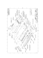
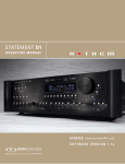
1
MPX 200
24-Bit
Dual Channel Processor
Service
Manual
Product Name Service Manual
Precautions
Save these instructions for later use.
Follow all instructions and warnings marked on the unit.
Always use with the correct line voltage. Refer to the manufacturers operating instructions for power requirements. Be advised that
different operating voltages may require the use of a different line cord and/or attachment plug.
Do not install the unit in an unventilated rack, or directly above heat producing equipment such as power amplifiers. Observe the
maximum ambient operating temperature listed in the product specification.
Slots and openings on the case are provided for ventilation; to ensure reliable operation and prevent it from overheating, these
openings must not be blocked or covered. Never push objects of any kind through any of the ventilation slots. Never spill a liquid of
any kind on the unit.
This product is equipped with a 3-wire grounding type plug. This is a safety feature and should not be defeated.
Never attach audio power amplifier outputs directly to any of the unit’s connectors.
To prevent shock or fire hazard, do not expose the unit to rain or moisture, or operate it where it will be exposed to water.
Do not attempt to operate the unit if it has been dropped, damaged, exposed to liquids, or if it exhibits a distinct change in performance
indicating the need for service.
This unit should only be opened by qualified service personnel. Removing covers will expose you to hazardous voltages.
This triangle, which appears on your component, alerts you to the presence of uninsulated, dangerous voltage inside the
enclosure… voltage that may be sufficient to constitute a risk of shock.
CAUTION
RISK OF ELECTRIC SHOCK
DO NOT OPEN
This triangle, which appears on your component, alerts you to important operating and maintenance Instructions in this
accompanying literature.
Notice
This equipment generates and uses radio frequency energy and if not installed and used properly, that is, in strict accordance with the
manufacturer's instructions, may cause interference to radio and television reception. It has been type tested and found to comply with
the limits for a Class B computing device in accordance with the specifications of Part 15 of FCC Rules, which are designated to
provide reasonable protection against such interference in a residential installation. However, there is no guarantee that interference
will not occur in a particular installation. If this equipment does cause interference to radio or television reception, which can be
determined by turning the equipment OFF and ON, the user is encouraged to try to correct the interference by one or more of the
following measures:
Reorient the receiving antenna
Relocate the computer with respect to the receiver
Move the computer away from the receiver
Plug the computer into a different outlet so that the computer and receiver are on different branch circuits.
If necessary, the user should consult the dealer or an experienced radio/television technician for additional suggestions. The user may
find the following booklet prepared by the Federal Communications Commission helpful:
“How to identify and Resolve Radio/TV Interference Problems.
This booklet is available from the U.S. Government Printing Office, Washington, DC 20402, Stock No. 004-000-00345-4.
Le présent appareil numérique n'émet pas de bruits radioélectriques dépassant les limites applicables aux appareils numériques de Ia
class B prescrites dans le Règlement sur le brouillage radioélectrique édicté par le ministère des Communications du Canada.
Copyright © 1999 Lexicon, Inc.
All Rights Reserved
Lexicon Inc. ● 3 Oak Park ● Bedford, MA 01730-1441 ● Tel (781) 280-0300 ● Customer Service Fax (781) 280-0499
Lexicon Part # 070-14827 Rev 0
Printed in the United States of America
Lexicon
Safety Suggestions
Read Instructions Read all safety and operating
instructions before operating the unit.
Retain Instructions Keep the safety and
operating instructions for future reference.
Heed Warnings Adhere to all warnings on the
unit and in the operating instructions.
Follow Instructions Follow operating and use
instructions.
Heat Keep the unit away from heat sources such
as radiators, heat registers, stoves, etc., including
amplifiers which produce heat.
Ventilation Make sure that the location or
position of the unit does not interfere with its
proper ventilation. For example, the unit should
not be situated on a bed, sofa, rug, or similar
surface that may block the ventilation openings;
or, placed in a cabinet which impedes the flow of
air through the ventilation openings.
Wall or Ceiling Mounting Do not mount the unit
to a wall or ceiling except as recommended by
the manufacturer.
Power Sources Connect the unit only to a power
supply of the type described in the operating
instructions, or as marked on the unit.
Grounding or Polarization* Take precautions
not to defeat the grounding or polarization of the
unit’s power cord.
*Not applicable in Canada.
Power Cord Protection Route power supply
cords so that they are not likely to be walked on
or pinched by items placed on or against them,
paying particular attention to cords at plugs,
convenience receptacles, and the point at which
they exit from the unit.
Nonuse Periods Unplug the power cord of the
unit from the outlet when the unit is to be left
unused for a long period of time.
Water and Moisture Do not use the unit near
water — for example, near a sink, in a wet
basement, near a swimming pool, near an open
window, etc.
Object and liquid entry Do not allow objects to
fall or liquids to be spilled into the enclosure
through openings.
Cleaning The unit should be cleaned only as
recommended by the manufacturer.
Servicing Do not attempt any service beyond
that described in the operating instructions. Refer
all other service needs to qualified service
personnel.
Damage requiring service The unit should be
serviced by qualified service personnel when:
the power supply cord or the plug has been
damaged, objects have fallen, or liquid has been
spilled into the unit, the unit has been exposed to
rain, the unit does not appear to operate normally
or exhibits a marked change in performance, the
unit has been dropped, or the enclosure
damaged.
MPX 200 Service Manual
Lexicon
Table of Contents
Chapter 1 Reference Documents, Required Equipment............................. 1-1
Reference Documents............................................................................................................................. 1-1
Required Equipment................................................................................................................................ 1-1
Tools .................................................................................................................................................... 1-1
Test Equipment.................................................................................................................................... 1-1
Chapter 2 General Information ................................................................... 2-1
Periodic Maintenance .............................................................................................................................. 2-1
Ordering Parts ......................................................................................................................................... 2-1
Returning Units to Lexicon for Service .................................................................................................... 2-1
Chapter 3 Specifications............................................................................. 3-1
Chapter 4 Performance Verification............................................................ 4-1
Initial Inspection:...................................................................................................................................... 4-1
Functional Tests: ..................................................................................................................................... 4-1
Initial Power Up Check:........................................................................................................................ 4-1
Normal Power Up:................................................................................................................................ 4-1
Setup.................................................................................................................................................... 4-1
Switch Test (8) ..................................................................................................................................... 4-2
Encoder Test (9) .................................................................................................................................. 4-2
MIDI Test (10) ...................................................................................................................................... 4-2
LED Test (11)....................................................................................................................................... 4-3
EXIT Test (12)...................................................................................................................................... 4-3
I/O Test:................................................................................................................................................... 4-3
Setup:................................................................................................................................................... 4-3
Analog In To Analog Out Audio Test:................................................................................................... 4-3
Frequency Response: ............................................................................................................................. 4-4
Analog In To Analog Out Frequency Response Test:.......................................................................... 4-4
THD+N Measurement:............................................................................................................................. 4-4
Analog In To Analog Out THD+N Test:................................................................................................ 4-4
Crosstalk Test:......................................................................................................................................... 4-4
Analog In To Analog Out Crosstalk Test:............................................................................................. 4-4
Dynamic Range Test: .............................................................................................................................. 4-4
Analog In To Analog Out Dynamic Range Test: .................................................................................. 4-4
Digital I/O Functionality............................................................................................................................ 4-5
Listening Test: ......................................................................................................................................... 4-5
Shock Test:.............................................................................................................................................. 4-5
Lexicon Audio Precision ATE Summary .................................................................................................. 4-6
Chapter 5 Troubleshooting ......................................................................... 5-1
Diagnostics .............................................................................................................................................. 5-1
Introduction .......................................................................................................................................... 5-1
Diagnostics Test Descriptions.............................................................................................................. 5-1
Power-On Self Tests (POST)............................................................................................................... 5-1
Pass/Fail Status: .................................................................................................................................. 5-2
Diagnostic Failures: ............................................................................................................................. 5-2
Power On Test Descriptions ................................................................................................................ 5-2
EXTENDED DIAGNOSTICS................................................................................................................ 5-5
Extended Diagnostic Test Desriptions ................................................................................................. 5-6
Service Notes: ....................................................................................................................................... 5-15
WARNING
: ................................................................................................................................ 5-15
Chapter 6 Theory of Operation ................................................................... 6-1
Main Board .............................................................................................................................................. 6-1
MPX 200 Service Manual
Schematic Walkthrough........................................................................................................................6-1
Front Panel Board ..................................................................................................................................6-10
Schematic Walkthrough......................................................................................................................6-10
Chapter 7 - Parts List.................................................................................. 7-1
MPX200 MAIN BOARD ASSEMBLY........................................................................................................7-1
MPX200 FRONT PANEL BOARD ASSEMBLY .......................................................................................7-3
MPX200 MECHANICAL ASSEMBLY.......................................................................................................7-3
MPX200 POWER CORD OPTIONS ........................................................................................................7-3
MPX200 SHIPPING MATERIALS ............................................................................................................7-4
Chapter 8 Schematics and Drawings ......................................................... 8-1
Schematics:..............................................................................................................................................8-1
Drawings: .................................................................................................................................................8-1
Lexicon
Chapter 1 Refe r ence Documents, Required Equipment
Reference Documents
MPX 200 Owner's Manual - Lexicon P/N 070-14738 or latest revision
Required Equipment
Tools
The following is a minimum suggested technician's tool kit required for performing disassembly, assembly
and repairs:
• Clean, antistatic, well lit work area
• #0 Phillips tip screwdriver
• #1 Phillips tip screwdriver
• Flat Blade screwdriver
• ¼” Hex Nutdriver
• 5/8” Hex Nutdriver
• 7/16” Hex Nutdriver with Full Hollow-Shaft and plastic insert to prevent Front Panel from scratches
• ¼” Combination Wrench
• Solder: 63/37 - Tin/Lead Alloy composition, low residue, no-clean solder.
• Magnification glasses and lamps
• SMT Soldering / Desoldering bench-top repair station
Test Equipment
The following is a minimum suggested equipment list required for performing the proof of performance
tests.
• Amplifier with speakers or headphones
• Headphones
• Cables: (dependent on your signal source)
• Audio Input Cable (balanced) with shield and a XLR or ¼ “ plug on one end and an appropriate
connector on the opposite end for connection to the Low Distortion Oscillator.
• Audio Output Cable ( balanced ) with shield and a XLR or ¼ “ plug on one end and an appropriate
connector on the opposite end for connection to the Distortion Analyzer
• 5 pin Midi cable
• ¼ inch phone cable (T/R/S)
• Double Footswitch with 15 foot ¼" phone plug cable configured for tip, ring and sleeve, (Lexicon P/N
750-09277) or equivalent
• Low Distortion Oscillator with single-ended or balanced output, < 100 ohms output impedance, < .005%
THD.
• Analog Distortion Analyzer and level meter with single-ended or balanced input and 20kHz or 30kHz Lo
Pass Filter
• 100 MHz oscilloscope
• Digital distortion analyzer & digital function generator (e.g. Stanford Research Systems Model DS360 or
Audio Precision System 1 with DSP Option /System 2).
• Digital signal source (CD player, DAT, etc.)
• D/A converter (ex.: MPX-500)
1-1
Lexicon
Chapter 2 Gene r al Information
Periodic Maintenance
Under normal conditions the MPX 200 system requires minimal maintenance. Use a soft, lint-free cloth
slightly dampened with warm water and mild detergent to clean the exterior surfaces of the connector box.
Do not use alcohol, benzene or acetone-based cleaners or any strong commercial cleaners. Avoid
using abrasive materials such as steel wool or metal polish. It the unit is exposed to a dusty environment, a
vacuum or low-pressure blower may be used to remove dust from the unit's exterior.
Ordering Parts
When ordering parts, identify each part by type, price and Lexicon Part Number. Replacement parts can be
ordered from:
LEXICON, INC.
3 Oak Park
Bedford, MA 01730-1441
Telephone: 781-280-0300; Fax: 781-280-0499; email: [email protected]
ATTN: Customer Service
Returning Units to Lexicon for Service
Before returning a unit for warranty or non-warranty service, consult with Lexicon Customer
Service to determine the extent of the problem and to obtain Return Authorization. No equipment
will be accepted without Return Authorization from Lexicon.
If Lexicon recommends that a MPX 200 be returned for repair and you choose to return the unit to Lexicon
for service, Lexicon assumes no responsibility for the unit in shipment from the customer to the factory,
whether the unit is in or out of warranty. All shipments must be well packed (using the original packing
materials if possible), properly insured and consigned, prepaid, to a reliable shipping agent.
When returning a unit for service, please include the following information:
•
•
•
•
•
•
•
•
•
Name
Company Name
Street Address
City, State, Zip Code, Country
Telephone number (including area code and country code where applicable)
Serial Number of the unit
Description of the problem
Preferred method of return shipment
Return Authorization #, on both the inside and outside of the package
Please enclose a brief note describing any conversations with Lexicon personnel (indicate the name of the
person at Lexicon) and give the name and telephone daytime number of the person directly responsible for
maintaining the unit.
Do no include accessories such as manuals, audio cables, footswitches, etc. with the unit, unless
specifically requested to do so by Lexicon Customer Service personnel.
2-1
Lexicon
Chapter 3 Spec i fications
Analog Inputs
Connectors: 1/4" unbalanced
Impedance: 500K unbalanced for Direct Instrument input (unit detects a mono input on the right input)
A/D Dynamic Range: >95dB typical, 20Hz-20kHz, unweighted
Levels: -30dBu to +4dBu
Resolution: 24-Bit
Analog Outputs
Connectors: 1/4" unbalanced
Impedance: 75 Ohms for Headphone output (Right only used for mono output; Left only used for stereo
headphones)
D/A Dynamic Range: >100dB typical, 20Hz-20kHz, unweighted
Levels : +8dBu typical
Resolution: 24-Bit
Frequency Response: Wet/Dry 20Hz-20kHz, ±1dB
Crosstalk: >55dB
THD: <0.05%, 20Hz-20kHz
Digital Audio Interface
Input Connectors: Coaxial, RCA type; Digital S/PDIF
Output Connectors: Coaxial, RCA type; 24-bit Digital S/PDIF (always active)
Sample Rates: 44.1kHz
Internal Audio Data Path: DSP: 24-bit
Footswitch: Tip/Ring/Sleeve phone jack for Bypass and Tap (optional)
System Specifications
Power Requirements: 100-120/220-240V~; 50-60Hz, 25W
Environment
Operating Temperature: 32° to 104° (0° to 40°C)
Relative Humidity: 95% non-condensing
Dimensions: 19"W x 1.75"H x 5.5" D (483x45x140mm)
Weight: Unit: 3.15lb (1.41kg)
3-1
Lexicon
Chapter 4 Perfo r mance Verification
This section describes a quick verification of the operation of the MPX 200 and the integrity of its analog
and digital audio signal paths.
Initial Inspection:
Inspect the unit for any obvious signs of physical damage. Verify that the front panel controls operate
smoothly and correctly. (Refer to the MPX 200 Owner’ Manual for detailed explanations of this
functionality.) Verify that all screws and rear panel jacks are secure.
Functional Tests:
Initial Power Up Check:
1. The voltage selection switch on the MPX 200 should be checked prior to power-on. It is located on the
right side of the unit. Make sure it is switched to the proper AC voltage setting for your area.
2. Connect the power cord to the back of the MPX 200 and the other end into an isolated variable output
power supply (Variac).
3. Verify the Variac's AC voltage output is set to 0.
4. Turn the MXP 200 power switch to the On position and slowly increase the AC voltage output of the
Variac to the proper voltage.
5. Verify the AC current draw is < .25 amps.
Normal Power Up:
During normal power on, the MPX 200 will perform a series of diagnostic tests. These diagnostic tests
should take 10 seconds or less. The diagnostic test sequence is displayed on the front panel LEDs prior to
the execution of the test wherever possible for troubleshooting purposes.
If there is a failure, the test number indication LED will remain lit indicating which test has failed and the
(Red) LEVEL Clip LEDs will be lit indicating that a failure has occurred. Displaying the Test/Error code on
the LEDs before the test is executed makes it possible to determine which test failed if the unit hangs or
crashes during the test.
The following is a table of the test numbers, the test names and the diagnostic indicator LEDs.
#1
#2
#3
#4
#5
ROM Checksum
SRAM
LEXICHIP3 WCS
LEXICHIP3 INT
EEPROM
Compressor –20dB
Compressor –10dB
Compressor –3dB
Compressor Threshold
Effects Gate
NOTE: The ROM, SRAM, LEXICHIP3 and CPU must be working properly in order for the Diagnostic LEDs
to operate correctly.
If the MPX 200 powers on without a diagnostic failure, the 7-segment display will read “200”, all of the front
panel LEDs will light in sequence from left to right, and the unit will enter normal operating mode.
Note: When the tests are loaded a small ( r ) will appear in the display. This indicates that the test is
running. When the tests are actually performed, two other characters will appear, a ( P ) will indicate the
test preformed has passed, and a ( f ) will indicate the test has failed. After some of the tests, when the load
button is pressed and released, the displays will read ( d ) to indicate that the test has been exited.
Setup
1. Connect one end of the MIDI cable to the jack on the Rear Panel of the unit labeled "MIDI Out/Thru".
4-1
MPX 200 Service Manual
2. Connect the other end of the MIDI cable to the jack on the Rear Panel of the unit labeled "MIDI In".
3. Using the ¼" phone cable, connect one end to the ¼" jack marked footswitch on the back of the
MPX200.
4. Connect the other end ¼" phone cable to the ¼" phone jack on the footswitch.
5. Using the appropriate power cord, connect the MPX 200 to an appropriate AC voltage source.
6. Set the MPX 200 into Extended Diagnostics mode to perform the following functional tests by turning
the power switch to the ON position while holding down the Bypass button.
7. Release the “Bypass” button when the Green LEVEL –30dB LED’s are lit (after approximately 3
seconds).
Switch Test (8)
1.
2.
3.
4.
Turn the encoder knob clockwise until the display reads # 8.
Press and release the load button to execute the test.
The display will read: “r 8”.
The MPX 200 is know ready to test both the footswitch functions and the front panel switches.
Footswitches:
1. Press and hold the Left footswitch (labeled Ring) and observe that the Left –30dB headroom LED is lit.
2. Release the Left footswitch and observe that the Left –30dB headroom LED has turned off.
3. Press and hold the Right footswitch (labeled Tip) and observe that the Right –30dB headroom LED is
lit.
4. Release the Right footswitch and observe that the Right –30dB headroom LED has turned off.
Front Panel Switches:
1.
2.
3.
4.
5.
6.
7.
8.
9.
10.
11.
12.
13.
Press and hold the Edit button and observe that the Edit LED is lit.
Release the Edit button and observe that the Edit LED has turned off.
Press and hold the Store button and observe that the Store LED is lit.
Release the Store button and observe that the Store LED has turned off.
Press and hold the Tap/Cancel button and observe that the Tap/Cancel LED is lit.
Release the Tap/Cancel button and observe that the Tap/Cancel LED has turned off.
Press and hold the Bypass button and observe that the Bypass LED is lit.
Release the Bypass button and observe that the Bypass LED has turned off.
Press and hold the Compressor button and observe that the Compressor LED is lit.
Release the Compressor button and observe that the Compressor LED has turned off.
Press and hold the Load button and observe that the Load LED is lit.
Release the Load button and observe that the Load LED has turned off.
Observe that the 7-segment display reads: “d 8”.
Encoder Test (9)
1.
2.
3.
4.
Turn the encoder knob clockwise until the 7-segment display reads: “9”.
Press and Release the Load button to execute the test.
Observe that the 7-segment display reads: “r 9”.
Turn the encoder one revolution in a clockwise direction one position at time. The display should
indicate the current position of the encoder from 0-15.
5. When the test is complete the display will read: “P 9”.
MIDI Test (10)
1. Turn the encoder knob clockwise until the 7-segment display reads: “ 10”.
2. Press and release the Load button to execute the test.
3. Observe that the display reads: “P10”.
4-2
Lexicon
LED Test (11)
1.
2.
3.
4.
Turn the encoder knob clockwise until the 7-segment display reads: “ 11”.
Press and release the Load button to execute the test.
Observe that all of the front panel's LEDs are lit and that the segments on the displays are all off.
Observe that the colors of the LEDs are correct as shown below:
LEVEL
EFFECTS
COMPRESSOR
ROUTING (DUAL)
EDIT
(Load)
(Compressor)
(Edit)
RED
RED Clip
RED -3dB
GRN Chamber
GRN Room
GRN Ambience
GRN
C
GRN Adjust RED Threshold
GRN
RED
YEL
GRN
GRN -12dB
RED -10dB
GRN Gate
GRN Flange
GRN Chorus
GRN
C
GRN EQ
GRN
GRN
GRN
GRN
GRN -30dB
RED -20dB
GRN Echo/Delay GRN Rotry/Trmlo GRN Pitch/Detune GRN
C
GRN Lvl/Bal RED Release
(Edit)
(Store)
(Tap/Cancel)
L
R
YEL Threshold
RED Compressor GRN Plate
GRN Hall
GRN
C
GRN Mix
RED Ratio
RED Attack
5. Turn the encoder knob clockwise one position.
6. Verify that all of the front panel's LEDs turn off and that the display will read all “8.8.8” as shown below:
NOTE: All of the segments on the 7-segment displays should be lit except the rightmost decimal point.
7. Turn the encoder knob clockwise one position.
8. The display should read: “r11” and the Left Green LEVEL –30dB LED should be lit.
9. Turning the encoder knob clockwise one position at a time, observe that that each of the remaining
front panel's LEDs, as well as the segments on the 7-segment displays, can be lit individually.
10. Press and release the Load button to exit the test.
11. The display will momentarily read: “d11”, then display: “12”.
EXIT Test (12)
1.
2.
3.
4.
Press and release the Load button to execute the test.
The displays should read: “ 1” and jump into normal operating mode.
Set the power switch to the OFF position to power off the MPX 200.
Disconnect all cables from the rear panel of the MPX 200.
I/O Test:
These tests will verify the audio performance of the MPX 200’s audio input and output circuitry.
Setup:
1. Turn on the MPX 200 and wait for the Power On Diagnostics cycle to finish.
2. Turn the Program Select Knob to Program #1.
3. Press the Bypass button on the front panel and verify that the Bypass button LED lights, and the display
flashes bYP.
4. Connect a (balanced) audio cable between the Low Distortion Oscillator and the MPX 200 Left Input.
5. Connect a (balanced) audio cable between the MPX 200 Left output and the Distortion Analyzer.
6. Set the Distortion Analyzer to measure VRMS.
7. Turn the Input Trim knob fully clockwise.
Analog In To Analog Out Audio Test:
1. Apply a 1kHz-sinewave signal to the MPX 200 Left Input @ 775 mVRMS.
2. Measure the Left Output for a level between 2.273 and 1.781 VRMS.
3. Switch the cables to the Right Input/Output connections and repeat step 3.
4-3
MPX 200 Service Manual
Frequency Response:
These tests will verify the frequency response specifications of the Left and Right analog inputs to the Left
and Right output signal paths of the MPX 200.
Analog In To Analog Out Frequency Response Test:
1.
2.
3.
4.
5.
Disable all Filters on the Distortion Analyzer
Apply a 1kHz-sinewave signal to the MPX 200 Left Input @ 218 mVRMS.
Connect the Left Output to the Distortion Analyzer.
Set the Analyzer for a 0dB reference (@1kHz).
Sweep the Oscillator from 20Hz to 20kHz and verify the level stays within +/- 1.0dBr throughout the
sweep.
6. Switch the cables to the Right Input/Output connections and repeat steps 4 and 5.
THD+N Measurement:
These tests will verify the THD+N specifications of the MPX 200 Left and Right input to output circuitry.
Analog In To Analog Out THD+N Test:
1.
2.
3.
4.
5.
6.
Apply a 1kHz-sinewave signal to the MPX 200 Left Input @ 218 mVRMS.
Connect the Left Output to the Distortion Analyzer.
Set the Distortion Analyzer to measure THD.
Enable the Low pass filters on the Analyzer (30kHz, 20kHz).
Verify the Left output THD+Noise level on the Analyzer is <0.05%.
Switch the cables to the Right Input/Output connections and repeat step 5.
Crosstalk Test:
Analog In To Analog Out Crosstalk Test:
1.
2.
3.
4.
5.
Apply a 1kHz-sinewave signal to the MPX 200 Left Input @ 218 mVRMS.
Connect the Right Output to the Distortion Analyzer.
Enable the Low pass filters on the Analyzer (30kHz, 20kHz).
Sweep the Oscillator from 20Hz to 20kHz and verify the level stays < -55dB through out the sweep.
Switch the Input cable to the Right side and the Output cable to the Left and repeat step 4.
Dynamic Range Test:
These tests will verify the Dynamic Range specifications of the MPX 200 Left and Right input to output
circuitry.
Analog In To Analog Out Dynamic Range Test:
1.
2.
3.
4.
5.
6.
7.
8.
9.
10.
11.
12.
4-4
Apply a 1kHz-sinewave signal to the MPX 200 Left Input @ 2.45VRMS
Connect the Left Output to the Distortion Analyzer.
Set the Distortion Analyzer for a 0dB reference.
Remove the Input cable from the Left input.
Enable the Low pass filters on the Analyzer (30kHz, 20kHz).
Verify the Noise level at the Left Output is < -95dB.
Connect the 1kHz-sinewave signal to the Right Input of the MPX 200.
Move the Left Output cable to the Right Output.
Set the Distortion Analyzer for a 0dB reference
Remove the Input cable from the Right input.
Enable the Low pass filters on the Analyzer (30kHz, 20kHz).
Verify the Noise level at the Right Output is < -95dB.
Lexicon
Digital I/O Functionality
This test will verify that the MPX 200 will pass an S/PDIF signal through its input and output circuitry.
1. Connect a Digital signal (CD player, DAT, etc.) to the S/PDIF input jack on the back of the MPX 200.
2. Connect the S/PDIF output for the MPX 200 to a D/A converter (ex.: MPX 500) for conversion back to
an analog signal.
3. Connect the analog output of the D/A converter to your amplifier with speaker output. Be sure to turn
the volume down on the amplifier.
4. Set the MPX 200 System Mode for digital Input.
5. Set the MPX 500 System Mode for digital Input.
6. Start playing your digital source.
7. Turn the volume up on your amplifier and verify you have audio and that it is clean and free of any
audio defects or artifacts (pops, clicks, static, etc.).
Listening Test:
1. Connect the audio input cable from the output of the Distortion Oscillator to the Left input of the MPX
200.
2. Connect the audio output cable from the Right output of the MPX 200 to the input of the Headphone
amplifier.
3. Set the Headphone Amplifier volume control to its lowest setting.
4. Set the Oscillator for 220Hz sinewave at 50m Vrms.
5. Power on the MPX 200 and turn the program knob to the # 111 program: Abyss.
6. Press the Edit button and turn the Mix up to 100%.
7. Put on the headphones and bring the volume up on the Headphone amp to a comfortable listening
level.
8. Sweep the input knob over its entire range and verify there are no pops, clicks, distortion, or static
noises heard when turning the knob.
9. Swap the cables from the Left Input/Output connectors to the Right Input/Output connectors and repeat
the above procedure.
Shock Test:
Note: To prevent damaging the unit, keep the other sides of the unit touching the work surface at all times.
1. While listening to the unit with the headphones lift a corner of the MPX 200 off of the table
approximately 4 inches and then drop.
2. Verify that there is no lose of audio or distortion during this action.
3. Repeat this test lifting at each of all four corners of the MPX 200
4-5
MPX 200 Service Manual
Lexicon Audio Precision ATE Summary
This chart represents a summary of test Audio Precision test equipment settings and parameters used by
Lexicon Manufacturing in production testing of all MPX 200 product. This is provided as a reference and
supplement to bench test settings found in the proof of performance in this manual.
A/D Files
Test
Source
Analyzer
Left
Right
Input
Input
A-DGAIN
-21dBu
-21dBu
A-DFREQ
-31dBu
-31dBu
ADSETLVL
-20dBu
-20dBu
Bal /
Gnd /
Freq
Imp.
Unbal
Float
Level
997
25 Ohm
Unbal
Float
LEVEL(dBFS)
-1.60
20-20k 25 Ohm
Unbal
Float
LEVEL(dBFS)
0.025
Unbal
Float
LEVEL(dBFS)
-20.25
997
25 Ohm
Lower
Filter
Imp
Band
Rate
-0.66
-2.54
Off
------
--------
44.1kHz
1.06
-1.06
Off
------
--------
44.1Khz
-20.00
-20.50
Off
------
--------
44.1kHz
A-DTHD *
-11dBu
-11dBu
Unbal
Float
FLTLVL(%)
0.005
0.05
A-DXTALK *
-11dBu
-11dBu
997
25 Ohm
Unbal
Float
LEVEL(dBFS)
-98.50
-54.94
A-DDYNR *
-50dBu
-50dBu
997
25 Ohm
Unbal
Float FLTLVL(dBF
S)
-102.50
D/A Files
Source
Test
22-20k 25 Ohm
Sample
Reading Upper
0.0007 Band Rej
------
--------
44.1kHz
-120.0
Off
------
--------
44.1kHz
-96.94 -120.00
Off
------
--------
44.1kHz
Lower
Filter
Imp
Band
7.40
Off
100k
10-500k 44.1kHz
10-500k 44.1kHz
Analyzer
Left
Right
Input
Input
Freq
Gnd /
Unbal
Float
Sample
----
--------
-------- AMPL(dBu)
8.46
9.52
Level
Reading Upper
Rate
D-AGAIN
0dBFS
0dBFS
D-AFREQ
0dBFS
0dBFS
20-20k
----
--------
-------- AMPL(dBr)
0.001
1.06
-1.06
Off
100k
D-ATHD
0dBFS
0dBFS
22-20k
----
--------
-------- THD+N(%)
0.005
0.05
0.0007
Off
100k
10-22k
44.1kHz
D-AXTALK
0dBFS
0dBFS
997
----
--------
-------- XTALK(dB)
-95.00
-54.94 -120.00
Off
100k
10-22k
44.1kHz
D-ADYNR
-60dBFS -60dBFS
997
----
--------
-------- AMPL(dBr)
-104.25
-96.94 -120.00
Off
100k
22-22k
44.1kHz
A/A Files
Source
Filter
Imp
Band
Test
997
Bal /
Imp.
Analyzer
Left
Right
Input
Input
Freq
Imp.
Bal /
Gnd /
Unbal
Float
Sample
Level
Reading Upper
Lower
Rate
A-AGAIN *
0dBu
0dBu
997
25 Ohm
Unbal
Float
AMPL(dBu)
8.29
9.35
7.23
Off
100k
10-500k 44.1kHz
AASETLVL
**
A-AFREQ *
0dBu
0dBu
997
25 Ohm
Unbal
Float
AMPL(dBu)
8.29
8.00
8.50
Off
100k
10-500k 44.1kHz
-11dBu
-11dBu
20-20K 25 Ohm
Unbal
Float
AMPL(dBr)
-0.025
1.06
-1.06
Off
100k
10-500k 44.1kHz
A-ATHD *
-11dBu
-11dBu
20-20K 25 Ohm
Unbal
Float
THD+N(%)
0.006
0.05
0.0007
Off
100k
20-22k
A-AXTALK *
-11dBu
-11dBu
20-20K 25 Ohm
Unbal
Float
XTALK(dB)
-64.50
-54.94 -120.00
Off
100k
10-22k
44.1kHz
0dBu
0dBu
997
25 Ohm
Unbal
Float
AMPL(dBr)
-100.50
-94.94 -120.00
Off
100k
20-22k
44.1kHz
A-ADYNRL *
-50dBu
-50dBu
997
25 Ohm
Unbal
Float
THD+N(dBr)
-101.00
-94.94 -120.00
Off
100k
20-22k
44.1kHz
A-ASNRR *
0dBu
0dBu
997
25 Ohm
Unbal
Float
AMPL(dBr)
-100.50
-94.94 -120.00
Off
100k
20-22k
44.1kHz
A-ADYNRR
*
A-AMUTE *
-50dBu
-50dBu
997
25 Ohm
Unbal
Float
THD+N(dBr)
-101.00
-94.94 -120.00
Off
100k
20-22k
44.1kHz
0dBu
0dBu
997
25 Ohm
Unbal
Float
AMPL(dBr)
-38.00
-30.00
-50.00
Off
100k
10-500k 44.1kHz
Off
-24dBu
997
25 Ohm
Unbal
Float
AMPL(dBu)
------
------
------
Off
100k
10-500k 44.1kHz
A-ASNRL*
LISTEN
4-6
44.1kHz
Lexicon
Chapter 5 Trou b leshooting
Check the Lexicon web site for the latest software and information:
http://www.lexicon.com
The Lexicon Studio downloads page:
The Lexicon Support Knowledgebase:
http://www.lexicon.com/kbase/index.asp
Diagnostics
Introduction
This section contains the complete diagnostics descriptions for the Lexicon MPX 200 product.
Diagnostics Test Descriptions
There are two categories of diagnostics that exist in the MPX 200 software: Power On Self Tests (POST),
and Extended Diagnostics. The POST are executed automatically when the system is first powered up. The
Extended Diagnostics are invoked by pressing and holding the front panel BYPASS button while powering
on the unit. The Extended Diagnostics are used to perform functional tests that are not performed during
the Power-On Self Tests, and also for troubleshooting purposes.
NOTE: The Extended Diagnostics can also be invoked by pressing and holding the Bypass Footswitch
(labeled Ring) while powering on the unit.
Power-On Self Tests (POST)
Upon normal power up, the MPX 200 will perform a series of diagnostic tests. For a description of these
tests, refer to Table 2.1. These diagnostic tests have been designed to take less than 10 seconds. The
diagnostic test sequence is displayed on the front panel LEDs prior to the execution of the test wherever
possible for troubleshooting purposes (provided the LEDs are functioning properly).
NOTE: The first time the MPX 200 is powered on, the EEPROM will be initialized during the EEPROM
diagnostic test and the 7-segment display will display “rSt” to indicate that the EEPROM is being
initialized. Once the EEPROM has been initialized, the unit will reset and repeat the POST. This
initialization process takes approximately 40 seconds, otherwise the POST would normally take
approximately 10 seconds.
Throughout this document, these LEDs will be referred to as the Diagnostic LEDs. These LEDs are used to
indicate the corresponding test number, and are turned on before each test is executed. Displaying the
Test/Error code on the LEDs before the test is executed makes it possible to determine which test failed if
the unit hangs or crashes during the test.
Test #
1
2
3
4
6
Test Name
ROM Checksum
SRAM
LEXICHIP3 WCS
LEXICHIP3 INT
EEPROM
Diagnostic LED
COMPRESSOR “–20dB”
COMPRESSOR “–10dB”
COMPRESSOR “–3dB”
COMPRESSOR “Threshold”
EFFECTS “Gate“
Table 2.1
5-1
MPX 200 Service Manual
NOTE: The ROM, SRAM, LEXICHIP3 and CPU must be working properly in order for the Diagnostic LEDs
to operate correctly.
Upon completion of the POST, the 7-segment displays will display “200”, all of the front panel LEDs will light
in sequence from left to right, then the unit will enter normal operating mode.
If a POST fails, the appropriate Diagnostic LED will remain lit indicating which test has failed and the (Red)
LEVEL Clip LEDs are lit indicating a failure has occurred. If a failure has occurred, the unit should be
repaired before proceeding. Refer to the MPX 200 Service Manual, Lexicon P/N 070-14827, for more
information.
Pass/Fail Status:
The front panel LEVEL LEDs are used to indicate the pass/fail status of the POST as follows:
The (Green) LEVEL Clip LEDs are lit to indicate when the test has Passed.
The (Red) LEVEL Clip LEDs are lit to indicate when the test has Failed.
Diagnostic Failures:
When a failure is encountered during the test sequence:
The test code is displayed on the Diagnostic LEDs (Refer to Table 1).
The (Red) LEVEL Clip LEDs are turned on to indicate a failure has occurred.
The unit stops executing the POST sequence.
The audio outputs are muted, and the unit will not become operational.
If the Bypass button is pressed after a failure has occurred, the MPX 200 will attempt to continue on with
the next test of the POST sequence. The MPX 200 will attempt to do this every time the Bypass button is
pressed.
If the STORE button is pressed after a failure has occurred, the MPX 200 will enter the Extended
Diagnostics mode.
If the Tap/Cancel button is pressed after a failure has occurred, the MPX 200 will run the test continuously.
The following diagram shows an example of the Diagnostic LEDs Test/Error code 4. This code indicates
that the Lexichip3 INT Test (4) has failed:
LEVEL
L
R
COMPRESSOR
1 Threshold
<-indicates Lexichip3 INT
test
Indicates Error ->
1
0
0
1
0
0
0
0
0
-3dB
-10dB
-20dB
0
Gate
0 Echo/Delay
Legend: 0 = LED off, 1 = LED on
NOTE: During the POST, the LEVEL LEDs display the pass/fail status for tests 3-6 only.
Power On Test Descriptions
ROM Test (1)
The ROM checksum, is a byte size value that is stored in the last location of each bank. The test adds the
contents of the entire ROM including the checksum byte. The result should equal zero (8 bit value).
5-2
Lexicon
Before the test is executed, the following test code will be displayed on the Diagnostic LEDs:
Test #
1
Test Name
ROM
Diagnostic LED
COMPRESSOR “–20dB”
If a failure occurs, the (Red) LEVEL Clip LEDs will be turned on in addition to the Diagnostic LED, and the
CPU will attempt continuously loop the test for troubleshooting purposes.
If the Bypass button is pressed, the failure is ignored and the next test will be executed.
SRAM Test (2)
The SRAM Test performed during the POST is a destructive test, meaning that any data stored in
SRAM will be lost. The entire contents of the SRAM is tested by first writing 00 hex (00000000
binary) to all of the memory locations, and then verified by reading back all of the memory
locations. This write/read sequence is also performed using the following patterns: 55 hex
(01010101 binary), AA hex (10101010 binary) and FF hex (11111111 binary).
Before the test is executed, the following test code will be displayed on the Diagnostic LEDs:
Test #
2
Test Name
SRAM
Diagnostic LED
COMPRESSOR “–10dB”
If a failure occurs, the (Red) LEVEL Clip LEDs will be turned on in addition to the Diagnostic LED, and the
CPU will attempt continuously loop the test for troubleshooting purposes.
If the Bypass button is pressed, the failure is ignored and the next test will be executed.
Lexichip3 WCS Test (3)
The Lexichip3 WCS test will check the program memory space (the Writeable Control Store) of the
Lexichip3. The RAM (memory space) is first filled with the value 55 hex (01010101 binary), then each
memory location is read to see if it contains 55. If 55 is in the memory location, the location is filled with AA
hex (10101010 binary), and the next location is processed. Once the RAM has been checked for 55's and
filled with AA's, the process is then repeated checking for AA's and storing 0's into memory. Following this
test is an Address test to verify all the address lines are active. Finally, the memory is checked for 0's.
Before the test is executed, the following test code will be displayed on the Diagnostic LEDs:
Test #
3
Test Name
Lexichip3 WCS
Diagnostic LED
COMPRESSOR “–3dB”
If a failure occurs, the (Red) LEVEL Clip LEDs will be turned on in addition to the Diagnostic LED, and the
CPU will attempt continuously loop the test for troubleshooting purposes.
If the Bypass button is pressed, the failure is ignored and the next test will be executed.
If the Tap/Cancel button is pressed, the CPU will attempt to go into a mode where it can execute the test
continuously.
Lexichip3 INT Test (4)
The Lexichip3 INT test will verify that the Lexichip3 interrupt (INT/) is working and occurring at the proper
intervals. The Lexichip3 will provide MPX 200 with the interrupt (INT/) to the Z80's maskable interrupt line.
Before the test is executed, the following test code will be displayed on the Diagnostic LEDs:
5-3
MPX 200 Service Manual
Test #
4
Test Name
Lexichip3 INT
Diagnostic LED
COMPRESSOR “Threshold”
If a failure occurs, the (Red) LEVEL Clip LEDs will be turned on in addition to the Diagnostic LED, and the
CPU will attempt continuously loop the test for troubleshooting purposes.
If the Bypass button is pressed, the failure is ignored and the next test will be executed.
If the Tap/Cancel button is pressed, the CPU will attempt to go into a mode where it can execute the test
continuously.
EEPROM Test (6)
This test will read each byte in the User Register portion of the EEPROM and add them together to
calculate a checksum. This value is compared with the checksum value stored in the EEPROM itself. This
checksum will be recalculated each time a register is stored.
The test will also verify that the EEPROM has been initialized properly. This is done by storing the software
version of the EEPROM in the first five bytes of the EEPROM, and then verifying the stored value is correct
when the test is executed. If the stored value read from the first five bytes of the EEPROM is incorrect, the
EEPROM will be initialized.
Before the test is executed, the following test code will be displayed on the Diagnostic LEDs:
Test #
6
Test Name
EEPROM
Diagnostic LED
EFFECTS “Gate“
If a failure occurs, the (Red) LEVEL Clip LEDs will be turned on in addition to the Diagnostic LED, and the
CPU will attempt continuously loop the test for troubleshooting purposes.
If the Bypass button is pressed, the failure is ignored and the next test will be executed.
If the Tap/Cancel button is pressed, the CPU will attempt to go into a mode where it can execute the test
continuously.
5-4
Lexicon
EXTENDED DIAGNOSTICS
The following tests are available in the Extended Diagnostics:
Test #
1
2
3
4
5
6
7
8
9
10
11
12
13
14
15
16
Test Name
ROM Checksum
SRAM
LEXICHIP3 WCS
LEXICHIP3 INT
LEXICHIP3 ADF
EEPROM
DRAM
Switch
Encoder
MIDI
LED
Exit
Initialize
Unused
Unused
Burn In
Diagnostic LED
COMPRESSOR “–20dB”
COMPRESSOR “–10dB”
COMPRESSOR “–3dB”
COMPRESSOR “Threshold”
EFFECTS “Echo/Delay”
EFFECTS “Gate“
EFFECTS “Chamber”
EFFECTS “Compressor”
EFFECTS “Rotry/Trmlo”
EFFECTS “Flange”
EFFECTS “Room”
EFFECTS “Plate”
EFFECTS “Pitch/Detune”
EFFECTS “Chorus”
EFFECTS “Ambience”
EFFECTS “Hall”
7 Segment
LED Display
1
2
3
4
5
6
7
8
9
10
11
12
13
14
15
16
Note:
1
1
1
1
1
1
3
2
3
3
2
3
LED Off = 0, LED On = 1
Note 1: These tests reside in the POST.
Note 2: These tests require operator interaction and judgment, and do not generate an error message.
Note 3: These tests require operator interaction and judgment, and generate an error message.
The Extended Diagnostics are invoked by pressing and holding the Bypass button while powering on the
unit, then releasing the Bypass button once the Green LEVEL -30dB LEDs have lit. After the Bypass button
is released, the 7-segment displays as well as the Diagnostic LEDs will indicate the test number selected,
and the remaining LEDs will shut off.
For example, when the Lexichip3 ADF Test (5) is selected using the Encoder, the EFFECTS “Echo/Delay”
Diagnostic LEDs will be lit. This is useful for debugging the unit should any of the 7-segment displays
become inoperative.
When a test has been selected, the Load button must be pressed to execute it.
The leftmost 7-segment display is used to indicate the following:
“r” indicates when the test is running
“P” indicates when the test has passed
“F” indicates when the test has failed.
“d” indicates when the test is done.
NOTE: For tests that require operator interaction and judgment, the 7-segment displays will not indicate
when tests are running, or the pass/fail status of the test. For these tests, a “d” is placed in leftmost 7segment display to indicate when the tests has been exited and the test is done.
The Diagnostic LEDs are also used to indicate the test pass/fail status as follows:
5-5
MPX 200 Service Manual
The (Green) LEVEL Clip LEDs are lit to indicate when the test has Passed.
The (Red) LEVEL Clip LEDs are lit to indicate when the test has Failed.
The following tests can be run continuously by pressing the Tap/Cancel button instead of the Load button.
Test #
1
2
3
4
5
6
7
8
9
10
11
Test Name
ROM Checksum
SRAM
LEXICHIP3 WCS
LEXICHIP3 INT
LEXICHIP3 ADF
EEPROM
DRAM
Switch
Encoder
MIDI
LED
Diagnostic LED
COMPRESSOR “–20dB”
COMPRESSOR “–10dB”
COMPRESSOR “–3dB”
COMPRESSOR “Threshold”
EFFECTS “Echo/Delay”
EFFECTS “Gate“
EFFECTS “Chamber”
EFFECTS “Compressor”
EFFECTS “Rotry/Trmlo”
EFFECTS “Flange”
EFFECTS “Room”
7-segment
display
1
2
3
4
5
6
7
8
9
10
11
When a test is run continuously a Pass/fail status will be displayed and updated on the front panel LEVEL
LEDs and the 7-segment displays each time the test is run.
Extended Diagnostic Test Desriptions
ROM Test (1)
This is the same test that resides in the POST. It was included in the Extended Diagnostics for
troubleshooting purposes.
The ROM checksum, is a byte size value that is stored in the last location of each bank. The test adds the
contents of the entire ROM including the Checksum byte. The result should equal zero (8 bit value).
Before the test is executed, the following test code will be displayed on the Diagnostic LEDs, along with the
test number on the 7-segment displays:
Test #
1
Test Name
ROM
Diagnostic LED
COMPRESSOR “–20dB”
7-segment
display
1
Pressing the Load button will execute the test.
Pressing the Tap/Cancel button will run the test continuously.
When the test is executed, the leftmost digit of the 7-segment display will display an “r” to indicate the test is
running. The pass/fail status of the test is displayed on the 7-segment display and front panel LEVEL LEDs.
If the test passed, the (Green) LEVEL -30dB LEDs will light.
If the test failed, the (Red) LEVEL Clip LEDs will light.
SRAM Test (2)
The SRAM Test performed during the Extended Diagnostics is a non-destructive test. The non-destructive
test will test one memory location at a time, saving the contents from the location being tested into a
5-6
Lexicon
register, and then restoring the value when it's done. The entire contents of the SRAM is tested by writing
00 hex (00000000 binary), and verified by reading the same value back from each memory location. This
write/read sequence is also performed using the following patterns: 55 hex (01010101 binary), AA hex
(10101010 binary) and FF hex (11111111 binary).
This test was included in the Extended Diagnostics for troubleshooting purposes.
Before the test is executed, the following test code will be displayed on the Diagnostic LEDs, along with the
test number on the 7-segment display:
Test #
2
Test Name
SRAM
Diagnostic LED
COMPRESSOR “–10dB”
7-segment
display
2
Pressing the Load button will execute the test.
Pressing the Tap/Cancel button will run the test continuously.
When the test is executed, the leftmost digit of the 7-segment display will display an “r” to indicate the test is
running. The pass/fail status of the test is displayed on the 7-segment display and front panel LEVEL LEDs.
If the test passed, the (Green) LEVEL -30dB LEDs will light.
If the test failed, the (Red) LEVEL Clip LEDs will light.
Lexichip3 WCS Test (3)
This is the same test that resides in the power up diagnostics. It was included in the Extended Diagnostics
for troubleshooting purposes.
This test will check the program memory space (the writeable control store) of the Lexichip3. The
RAM (memory space) is first filled with the value 55 hex (01010101 binary), then each memory
location is read to see if it contains 55. If 55 is in the memory location, the location is filled with AA
hex (10101010 binary), and the next location is processed. Once the RAM has been checked for
55's and filled with AA's, the process is then repeated checking for AA's and storing 0's into
memory. Following this test is an Address test to verify all the address lines are active. Finally, the
memory is checked for 0's.
Before the test is executed, the following test code will be displayed on the Diagnostic LEDs, along with the
test number on the 7-segment display:
Test
#
3
Test Name
Diagnostic LED
Lexichip3 WCS
COMPRESSOR “–3dB”
7-segment
display
3
Pressing the Load button will execute the test.
Pressing the Tap/Cancel button will run the test continuously.
When the test is executed, the leftmost 7-segment display will display an “r” to indicate the test is running.
The pass/fail status of the test is displayed on the 7-segment displays and front panel LEVEL LEDs.
If the test passed, the (Green) LEVEL -30dB LEDs will light.
5-7
MPX 200 Service Manual
If the test failed, the (Red) LEVEL Clip LEDs will light.
Lexichip3 INT Test (4)
This is the same test that resides in the power up diagnostics. It was included in the Extended Diagnostics
for troubleshooting purposes.
The Interrupt test will verify that the Lexichip3 interrupt (ZINT/) is working and occurring at the proper
intervals. The Lexichip3 will provide MPX 200 with the interrupt (ZINT/) to the Z80’s maskable interrupt line.
Before the test is executed, the following test code will be displayed on the Diagnostic LEDs, along with the
test number on the 7-segment displays:
Test #
4
Test Name
Lexichip3 INT
Diagnostic LED
COMPRESSOR “Threshold”
7-segment
display
4
Pressing the Load button will execute the test.
Pressing the Tap/Cancel button will run the test continuously.
When the test is executed, the leftmost 7-segment display will display an “r” to indicate the test is running.
The pass/fail status of the test is displayed on the 7-segment displays and front panel LEVEL LEDs.
If the test passed, the (Green) LEVEL -30dB LEDs will light.
If the test failed, the (Red) LEVEL Clip LEDs will light.
Lexichip3 ADF Test (5)
This test will verify that the Lexichip3 Audio Data File memory is working.
The Lexichip3 Audio Data File (ADF) is a fast synchronous 128-word SRAM that provides audio data
buffering and storage for: external memory references, Serial I/O, and the Host-to-Lexichip data port. ADF
locations also function as ARU Registers and as scratchpad memory. This test will verify that the Lexichip3
Audio Data File is working properly.
Before the test is executed, the following test code will be displayed on the Diagnostic LEDs, along with the
test number on the 7-segment displays:
Test #
5
Test Name
Lexichip3 ADF
Diagnostic LED
EFFECTS “Echo/Delay”
7-segment
display
5
Pressing the Load button will execute the test.
Pressing the Tap/Cancel button will run the test continuously.
NOTE: During the Lexichip3 ADF test, several LEDs may flicker. This is normal operation, and not
considered a failure in the unit.
When the test is executed, the left most 7-segment display will display an “r” to indicate the test is running.
The pass/fail status of the test is displayed on the 7-segment displays and front panel LEVEL LEDs.
If the test passed, the (Green) LEVEL -30dB LEDs will light.
5-8
Lexicon
If the test failed, the (Red) LEVEL Clip LEDs will light.
EEPROM Test (6)
This test will read each byte in the User Register portion of the EEPROM and add them together to
calculate a checksum. This value is compared with the checksum value stored in the EEPROM itself. This
checksum will be recalculated each time a register is stored.
The test will also verify that the EEPROM has been initialized properly. This is done by storing the software
version of the EEPROM in the first five bytes of the EEPROM, and then verifying the stored value is correct
when the test is executed. If the stored value read from the first five bytes of the EEPROM is incorrect, the
EEPROM will be initialized.
Before the test is executed, the following test code will be displayed on the Diagnostic LEDs, along with the
test number on the 7-segment displays:
Test #
6
Test Name
EEPROM
Diagnostic LED
EFFECTS “Gate“
7-segment
display
6
Pressing the Load button will execute the test.
Pressing the Tap/Cancel button will run the test continuously.
When the test is executed, the leftmost 7-segment display will display an “r” to indicate the test is running.
The pass/fail status of the test is displayed on the 7-segment displays and front panel LEVEL LEDs.
If the test passed, the (Green) LEVEL -30dB LEDs will light.
If the test failed, the (Red) LEVEL Clip LEDs will light.
DRAM Test (7)
The DRAM test puts the Lexichip3 into a mode that allows the Z80 microprocessor to read and write to the
1M X 4 DRAM through the Lexichip3. To actually test the DRAM, the Z80 performs two tests, a data test
and an address test. During the data test the Z80 writes AA (hex) (10101010) into all of the memory
locations then reads them back to check them. It repeats the process with 55 (01010101). For the address
test, the Z80 writes a count into the memory then reads it back (i.e. 00000001, 00000010, 00000011). This
test will take approximately 45 seconds to complete.
During the test, there is limited control of the front panel LEDs due to the interrupts being turned off.
Because of this, the front panel LEDs cannot be updated to indicate the test number on the Diagnostic
LEDs, or the pass/fail status of the test.
Before the test is executed, the following test code will be displayed on the Diagnostic LEDs, along with the
test number on the 7-segment display:
Test #
7
Test Name
DRAM
Diagnostic LED
EFFECTS “Chamber”
7-segment
display
7
Pressing the Load button will execute the test.
Pressing the Tap/Cancel button will run the test continuously.
5-9
MPX 200 Service Manual
When the test is executed, the leftmost 7-segment display will display an “r” to indicate the test is running.
The pass/fail status of the test is displayed on the 7-segment displays and front panel LEVEL LEDs.
If the test passed, the (Green) LEVEL -30dB LEDs will light.
If the test failed, the (Red) LEVEL Clip LEDs will light.
Switch Test (8)
The Switch Test is essentially two tests in one. The combination of the two tests provide a means for
verifying the operation of the front panel Switches (6) and Footswitches (2) along with their associated
LEDs at the same time.
Before the test is executed, the following test code will be displayed on the Diagnostic LEDs,
along with the test number on the 7-segment displays:
Test #
8
Test Name
Switch
Diagnostic LED
EFFECTS “Compressor”
7-segment
display
8
Pressing the Load button will execute the test.
Pressing and Releasing the Load button will exit the test.
Footswitches:
When the Left Footswitch (labeled Ring) is pressed, the Left –30dB Headroom LED will be lit. When the
Left Footswitch is released, the Left –30dB Headroom LED will go off.
When the Right Footswitch (labeled Tip) is pressed, the Right –30dB Headroom LED will be lit. When the
Right Footswitch is released, the Right –30dB Headroom LED will go off.
Front Panel Switches:
When the Edit button is pressed and held the Edit LED will be lit. When the Edit button is released, the Edit
LED will be turned off.
When the Store button is pressed and held the Store LED will be lit. When the Store button is released, the
Store LED will be turned off.
When the Tap/Cancel button is pressed and held the Tap/Cancel LED will be lit. When the Tap/Cancel
button is released, the Tap/Cancel LED will be turned off.
When the Bypass button is pressed and held the Bypass LED will be lit. When the Bypass button is
released, the Bypass LED will be turned off.
When the Compressor button is pressed and held the Compressor LED will be lit. When the Compressor
button is released, the Compressor LED will be turned off.
When the Load button is pressed and held the Load LED will be lit. When the Load button is released, a “d”
will be placed in the leftmost 7-segment display to indicate that the test has been exited.
Encoder Test (9)
During the Encoder test, the Z80 microprocessor reads the value of the encoder, and then expects the next
value read from the encoder (when the encoder position is moved) will be at a predetermined incremental
5-10
Lexicon
value. Therefore, during the test the encoder must be rotated in a clockwise direction as it’s being tested, or
the test will fail.
Before the test is executed, the following test code will be displayed on the Diagnostic LEDs, along with the
test number on the 7-segment displays:
Test #
9
Test Name
Encoder
Diagnostic LED
EFFECTS “Rotry/Trmlo”
7-segment
display
9
Pressing the Load button will execute the test.
When the test is executed, the leftmost 7-segment display will display an “r” to indicate the test is running,
and the rightmost digit of the 7-segment displays will indicate the value of the encoder’s current position.
The values range from (0-15).
MIDI Test (10)
This test will verify that the MIDI Input and MIDI Output/Thru circuits are working. The test will transmit data
out of the MIDI OUT jack and will attempt to read the data through the MIDI IN jack. To run this test, a 5 Pin
Male DIN to 5 Pin Male DIN Cable (also known as a MIDI cable) must be connected between the MIDI IN
jack and the MIDI OUT jack.
Before the test is executed, the following test code will be displayed on the Diagnostic LEDs, along with the
test number on the 7-segment displays:
Test #
10
Test Name
MIDI
Diagnostic LED
EFFECTS “Flange”
7-segment
display
10
Pressing the Load button will execute the test.
Pressing the Tap/Cancel button will run the test continuously.
When the test is executed, the leftmost 7-segment display will display an “r” to indicate the test is running.
The pass/fail status of the test is displayed on the 7-segment displays and front panel LEVEL LEDs.
If the test passed, the (Green) LEVEL -30dB LEDs will light.
If the test failed, the (Red) LEVEL Clip LEDs will light.
LED Test (11)
This test will verify that the LEDs and LED driver circuits are working. The test has essentially three
sections which perform the following functions:
1. Turn on all of the front panel LEDs, except for the LED segments on the 7-segment display.
2. Turn on all of the LED segments on the 7-segment display only.
3. Turn on each of the front panel LEDs and the LED segments on the 7-segment display individually.
5-11
MPX 200 Service Manual
Before the test is executed, the following test code will be displayed on the Diagnostic LEDs,
along with the test number on the 7-segment displays:
Test #
11
Test Name
LED
Diagnostic LED
EFFECTS “Room”
7-segment
display
11
Pressing the Load button will execute the test.
Pressing the Tap/Cancel button will run the test continuously.
When the test is executed, all of the front panel LEDs will be lit, and the remaining LED segments on the 7segment displays are turned off.
NOTE: The LED colors are indicated in the diagram below:
LEVEL
L
R
EFFECTS
COMPRESSOR
ROUTING (DUAL)
EDIT
YEL Threshold
RED Compressor GRN Plate
GRN Hall
GRN
C
GRN Mix
(Load)
(Compressor)
(Edit)
GRN Adjust RED Threshold
GRN
RED
YEL
GRN
GRN
GRN
(Edit)
(Store)
(Tap/Cancel)
RED Ratio
RED
RED Clip
RED -3dB
GRN Chamber
GRN Room
GRN Ambience
GRN
C
GRN
GRN -12dB
RED -10dB
GRN Gate
GRN Flange
GRN Chorus
GRN
C
GRN EQ
GRN
GRN -30dB
RED -20dB
GRN Echo/Delay GRN Rotry/Trmlo GRN Pitch/Detune GRN
C
GRN Lvl/Bal RED Release
RED Attack
When the encoder knob is turned clockwise one position, the front panel LEDs will be turned off, and all of
the LED segments on the 7-segment displays (except for the rightmost decimal point) will be lit to read:
“8.8.8” as shown below:
When the encoder knob is turned clockwise one position, the 7-segment displays will read: “r11” to indicate
the test is running, and the Left (Green) LEVEL –30dB LED will be lit.
NOTE: From this point on, each of the front panel LEDs and LED segments on the 7-segment
displays can be lit individually by turning the encoder knob clockwise one position at a time.
When the Load button is pressed and released, a “d” will be placed in the leftmost 7-segment display to
indicate that the test has been exited.
Exit Test (12)
This selection will allow the user to exit the Extended Diagnostic Mode into normal operating mode. When
selected, the Diagnostic LEDs will read the following:
Before the test is executed, the following test code will be displayed on the Diagnostic LEDs, along with the
test number on the 7-segment displays:
Test #
12
5-12
Test Name
Exit
Diagnostic LED
EFFECTS “Plate”
7-segment
display
12
Lexicon
Pressing the Load button will execute the test.
Initialize Test (13)
This selection will initialize all of the MPX 200 system parameters to their factory default settings.
Before the test is executed, the following test code will be displayed on the Diagnostic LEDs, along with the
test number on the 7-segment displays:
Test #
13
Test Name
Initialize
Diagnostic LED
EFFECTS “Pitch/Detune”
7-segment
display
13
Pressing the Load button will execute the test.
When the test is executed, the 7-segment displays will display “rSt” to indicate that the EEPROM is being
initialized. Once the EEPROM has been initialized, the unit will reset and perform the POST.
Unused (14)
This is not an actual test. When executed, the 7-segment displays will indicate “d14”.
Before the test is executed, the following test code will be displayed on the Diagnostic LEDs,
along with the test number on the 7-segment displays:
Test #
14
Test Name
Unused
Diagnostic LED
EFFECTS “Chorus”
7-segment
display
14
Pressing the Load button will execute the test.
Pressing the Tap/Cancel button will run the test continuously.
Unused (15)
This is not an actual test. When executed, the 7-segment display will indicate “d15”.
Before the test is executed, the following test code will be displayed on the Diagnostic LEDs, along with the
test number on the 7-segment displays:
Test #
15
Test Name
Unused
Diagnostic LED
EFFECTS “Ambience”
7-segment
display
15
Pressing the Load button will execute the test.
Pressing the Tap/Cancel button will run the test continuously.
Burn In Tests (16)
During the execution of the Diagnostics in the Burn In loop, the appropriate test code will be displayed on
the Diagnostic LEDs (BYPASS, STORE and TAP). This code will be sent to the LEDs before each test is
executed. By displaying a test/error code on the LEDs before the test is activated, it will be easier to
determine which test failed if the unit hangs or crashes during the Burn In loop. The test numbers and
names are also displayed on the 7-segment display, along with the Pass/fail status of each test.
5-13
MPX 200 Service Manual
Before the test is executed, the following test code will be displayed on the Diagnostic LEDs, along with the
test number on the 7-segment displays:
Test #
16
Test Name
Burn In
Diagnostic LED
EFFECTS “Hall”
7-segment
display
16
Pressing the Load button will execute the test.
The Burn In loop will continuously run the following diagnostics:
Test #
1
2
3
4
5
6
7
Test Name
ROM
SRAM
WCS
INT
ADF
EEPROM
DRAM
Diagnostic LED
COMPRESSOR “–20”
COMPRESSOR “–10”
COMPRESSOR “–3”
COMPRESSOR
“Threshold”
EFFECTS “Eko/Dly”
EFFECTS “Gate“
EFFECTS “Chamber”
7-segment
display
1
2
3
4
5
6
7
When the test is executed, the 7-segment displays will indicate that the test is “Running…”, followed by the
Pass/fail status of the test.
If the test passed, the (Green) LEVEL -30dB LEDs will light.
If the test failed, the (Red) LEVEL Clip LEDs will light.
There are two options available when a test has failed during the Burn In loop:
1.
Press the Bypass button to continue the Burn-in loop.
2.
Press the Tap/Cancel button to run the failed test continuously.
5-14
Lexicon
Service Notes:
WARNING
:
Voltage Regulator
CAUTION: THE VOLTAGE REGULATOR (U25) GETS VERY HOT!
Always use caution when testing the unit with the Main PCB removed from the chassis, be sure to place a
heatsink (HEATSINK,TO220,.75X.5X.5"H, Lexicon P/N 704-14132 or equivalent) onto the voltage regulator
at U25 to dissipate excess heat, and protect it from reaching thermal shutdown.
5-15
Lexicon
Chapter 6 Theo r y of Operation
Main Board
Schematic Walkthrough
Sheet 1
This sheet shows the analog input circuitry (U1-U2), the analog output (U6), and the output mute circuitry
(U7).
Input Stage
Separate unbalanced ¼” phone jacks (J1-J2) provide input for the left and right signals. A single input
source will be routed to both left and right input stages if the right channel (J1) is the only one used. These
jacks provide AC coupled chassis ground connections through integrated ground lugs. This AC coupling is
provided via C26 and C45. These components effectively AC couple the analog ground plane to the
chassis by way of the enclosure. This scheme is used to minimize AC hum loops from forming at the inputs.
Capacitors C26 and C47 provide protection from high frequency interference from entering or exiting the
MPX200 via the input cables.
DC Blocking is incorporated by capacitors C29 and C48 in series with the input signal paths.
The input impedance for each channel is set by R7 and R22 (Right and Left channels, respectively). Each
channel has an input impedance of 1M when used in Stereo mode, and a combined input impedance of
500K when used in Mono mode (Right channel only). This was incorporated as a concession to guitarists.
Due to this relatively high input impedance, the unit is susceptible to noise pickup from radiating sources,
particularly if the input cables are routed near the power supply of the unit, so care must be taken when
routing cables into the unit. J1 and J2 short the input paths to ground when no input cables are plugged in.
This prevents noise voltages from being generated by this high impedance.
D1 and D2 provide clamping protection of the input signal paths into U1 and U2, while R6 and R19 provide
input current limiting to U1 and U2. The diodes ensure that the non-inverting inputs of the op-amps never
see voltages more than 0.7V above or below the positive and negative supply rails.
One half of U1 and U2 are used as non-inverting amplifier stages. These first stage components provide a
DC gain of 10.55dB. The input and feedback circuitry comprised of R5, R4, and C6 for the right channel
and R21, R20, and C21 for the left channel form high pass filters shelving at 3kHz and 9kHz. This is the
standard 15/50uS pre-emphasis curve. C5 and C20 provide closed loop frequency compensation for the
input buffer stages.
C2 and C17 remove DC offset from the buffer output stages so that wiper noise from the Level
potentiometer R1 is eliminated. R1 is a dual ganged pot. The mechanical frame of R1 ties into the analog
ground plane on the PCB via R16 and makes contact with the front panel. R16 is currently not installed on
the PCB, therefore direct connection of analog ground and earth ground is not implemented.
The wipers of R1 connect directly to the non-inverting inputs of the second half of devices U1 and U2.
These are simple DC gain stages. The gain of each stage is 21.97dB set by R2/R3 for the right channel and
R17/R18 for the left channel. Feedback capacitors C1 and C16 provide frequency compensation.
The outputs of these stages provide input to the CODEC circuitry on the next page. These are signals
IN_LEFT and IN_RIGHT.
6-1
MPX 200 Service Manual
Output Stage and Muting
The output of the CODEC circuitry re-enters this page as signals OUT_LEFT and OUT_RIGHT.
Provisions are made for an additional low pass filter of these signals by installing capacitors in locations
R45 and R33; additionally, the CODEC signal may be attenuated or “padded” by installing resistors in these
locations, but these have not been implemented in the design. R33 and R45 are left as uninstalled
locations.
C50 and C51 provide AC coupling of the OUT_RIGHT and OUT_LEFT signals. The AC side of these
capacitors are connected to two analog switches comprised of two sections of device U7. These switches
provide output muting during power up and power down conditions. When the MUTE/ signal at pins 9 and
10 of U7 is brought to a logic low, the output signals at pin 4 (Left channel) and pin 15 (Right channel) are
internally switched to pins 5 and 2 respectively. These pins in turn are tied to analog ground, thereby
providing a low impedance path to ground for the OUT_RIGHT and OUT_LEFT signals. Approximately
43dB of attenuation is achieved when the switch is in mute mode.
A dual op-amp (U6) and its associated circuitry comprise the output circuitry. Each stage is set to a fixed
gain of 10.42dB by way of R50/R51 (Right channel) and R52/R53 (Left channel). R48 and R49 set the input
impedance of the op-amp circuitry to 10K. C49 and C56 provide high frequency compensation for the opamps; this keeps the amplifiers from breaking into spurious oscillation. This dual op-amp is powered by +/10V unregulated supplies. In reality, because these supply voltages are unregulated, the actual measured
voltages are more akin to +12V and -15V. This was done to afford the widest possible headroom for the
output. C52 and C53 provide de-coupling for these supplies.
An output impedance of 75 ohms is developed by R59 and R79 for the right and left outputs respectively.
These provide output current limiting protection.
The ¼” unbalanced output jacks (J3 and J4) are configured so that when only the right output is used (J3),
the left and right signals are summed together to provide a monophonic output. The left jack J4) can
support stereo headphones if J3 is unused. The right channel is provided on the tip and the left channel on
the ring of a stereo phone jack. C63 and C73 provide RFI suppression at the output. Like the input jack pair,
these jacks AC couple analog ground to chassis ground via C61 and C71 and the respective ground lugs
on the jacks. This is again to prevent AC hum loops from forming at the outputs.
Although the output op-amp can drive high impedance (>100 ohms) headphones, for best results a
headphone amplifier should be used for low impedance phones.
Sheet 2
This sheet shows the CODEC device (U5), the input signal DC bias circuitry (R14 and R15), the singleended to differential input amplifiers (U3), and the differential to single ended output amplifiers (U4). Shown
also are the various clock and control signals used by the CODEC.
Single-ended to differential converter
Each section of dual op-amp U3 is a unity gain inverting amplifier. Gains are fixed at 0dB by R8 and R9 for
the right channel, and R23 and R24 for the left channel. The non-inverting inputs of each amplifier are tied
to analog ground, creating a virtual ground at the junctions of the input and feedback resistors for each
channel. Signals IN_RIGHT and IN_LEFT from the previous page are AC coupled into the these amplifiers
by C7 and C22. Each phase of the differential output signal pairs are impedance balanced via R10/R11 for
the right channel and R25/R26 for the left, and then AC coupled via C9/C10 and C24/C25 respectively.
Each phase of the differential signal pairs are then DC biased via the resistors R12/R13 and R27/R28. This
DC bias of 2.94V is provided by a resistive divider comprised of R14 and R15 while C12 and C13 de-couple
this bias voltage to remove ripple and noise. Because the CODEC samples the input at 256fs,
R10/R11/C41 and R25/R26/C42 form low pass filters. C9, C10, C24, and C25 simply provide AC coupling
into the CODEC.
6-2
Lexicon
AK4528 CODEC
The AKM CODEC AK4528 is a high performance 24-bit A/D-D/A device which performs anti-alias filtering,
analog to digital conversion, digital to analog conversion, and digital 15/50uS de-emphasis. Although it
supports sampling rates up to 96kHz, the MPX200 only supports 44.1kHz sampling.
The ADC inputs are fully differential. The input signal range is scaled to the VREF pin. Nominally, this range
is defined as (0.56 x VREF) Volts peak to peak. With VREF equal to 5V and a DC input offset voltage of
2.9V The output code of the ADC is 0x7FFFFF positive full scale and 0x800000 negative full scale. The
data is in 2’s complement form. The input is sampled at 64fs (2.8224 MHz with fs = 44.1kHz).
Serial data is clocked in on the rising edge of the bit clock and is aligned with the second bit clock following
the leading edge of each transition in the LRCLK (FS). This alignment is determined by setting the serial
data interface pins to support the I2S format. The Lexichip3 receive port (SDIN0) is configured to support
this format.
During power down, the ADC, DAC, digital filters, and control registers are reset by signal PWR_DWN/.
This is an active low signal and is provided by the Lexichip 3. The CODEC is brought out of power down
mode when the clock signals LEX_256FS, LEX_FS/, and LEX_64FS/ are stable. It these clocks are not
present, then the CODEC is placed back into power down mode. R99 provides a weak pull-down for
PWR_DWN/.
During power down (PDN = 0), the ADC, DAC, digital filters, and control registers are reset. Upon power up
(PDN = 1), the ADC initializes after a period of 516/fs. The DAC initializes after a period of 512/fs.
The DAC uses advanced multi-bit architecture and is configured to support the I2S format. The DAC runs
from a 256fs MC. The Lexichip3 generates this. Data is clocked in on the rising edge of the 64fs clock and
is aligned with the second bit clock following the leading edge of each transition of the fs clock. This
alignment is determined by programming the Lexichip3 Serial Transmit Port (SDOUT0) to support I2S.
Digital de-emphasis is hardwired for 44.1kHz support. De-emphasis may be turned on or off by toggling the
DEM0 pin either 1 (De-emphasis is off) or a 0 (De-emphasis is on). The XD9 port of the Lexichip3 is
programmed to activate or de-activate digital de-emphasis.
C43 and C44 provide power supply de-coupling of the analog supply line and voltage reference of the
AK4528 while C38 de-couples the digital supply line and output buffer supply pins. R46 DC couples the
analog and digital supplies together while providing a measure of isolation of digital switching currents from
leaking back into the analog supply.
C39 and C40 de-couple the VCOM pin of the CODEC. This pin is the bias voltage of the ADC inputs and
the DAC outputs; this voltage is equal to VA/2.
Differential to Single-Ended Output Amplifiers
The analog outputs of the CODEC are full differential with a full-scale swing of (0.54 x VREF) volts peak to
peak. This output signal is centered on 2.5V. Both sections of dual op amp U4 are configured as unity gain
second order low pass filters with an Fc = 93.2kHz. These filters provide summing of the differential signals
for each channel into single-ended signals. R30, R31, R32, R34, R35, R36, C30, C31, and C32 form the
low pass filter for the right channel (OUT_RIGHT) while R38, R39, R40, R42, R43, R44, C35, C36, and C37
comprise the low pass filter for the left channel (OUT_LEFT). Both signals are referred back to page 1 to
the Output and Mute circuitry. Regulated +/-5V rails power these op amps.
Sheet 3
This sheet shows the S/PDIF input and output circuitry, the Digital Audio Receiver, Program Select rotary
encoder, and the glue logic necessary to implement these functions. The S/PDIF IO is implemented in a
dual RCA phono jack.
6-3
MPX 200 Service Manual
S/PDIF Input
The S/PDIF input is brought in via one half of J5. The signal is terminated into 75Ω by R129, AC coupled by
C103, and amplified by U18 (74HCU04). Current limiting resistor R127 and clamping diode D6 provide
input protection. R126 and R128 force one section of U18 into a semi-linear mode of operation creating a
gain stage that amplifies the low-level signal at the input to a CMOS logic level. The second section of U18
provides additional buffering of this signal. R122 is a provision added to the design to bypass this gain and
buffer stage for higher level signals, but this provision has not been implemented. C108 and R146 are
provisions for either AC or DC coupling the ground signals of the S/PDIF connector to chassis ground via
mechanical contact with the chassis. Currently, the ground signals for the S/PDIF input and output are DC
coupled via R146, with C108 left unpopulated.
S/PDIF Output
The S/PDIF OUT is generated by the Lexichip3 and buffered by two gate sections of U18. These two gates
of U18 are connected in parallel to increase drive capability. The resistor combination of R123-R125 forms
a voltage divider that attenuates the buffered signal to 500mVp-p. D5 clamps this voltage to +/- 0.7V. The
resultant signal is AC coupled by C100 and C101 to the output section of J5. C102 prevents high frequency
radiation from getting out onto the cable connected to S/PDIF out.
AK4112 Digital Audio Receiver
The digital audio receiver AK4112 (U13), which delivers a serial stream in I2S format to the Lexichip3,
demodulates the amplified signal from the S/PDIF input circuitry. The signals V/TX, FS96, AUTO, and ERF
allow software to determine the Validity, sample rate, PCM detection status, and error status detected by
U13. The chip is hardwired to 24 bit I2S format, and it may be set as a timing master or slave by toggling
the DIF1 signal (SP_MASTER). This is accomplished by programming the Lexichip3 PIOB_4 pin. When this
signal is low, the receiver is in master mode; when 0, the receiver is set to slave mode. The MPX200 is
always operated in slave mode. The receiver is hardwired to work in parallel mode, with the master clock
source set to be the internal PLL. Master clock output MCK01 is hardwired to provide 256fs locked to the
recovered clock from the input data stream. During a reset cycle, provided by the signal RESET/ tied to the
PDN pin, All internal analog and digital circuits become inactive, along with all clocks. All internal control
registers are held in reset also.
C88 and C89 provide power supply de-coupling for the Input Buffer supply pin. C85 and C86 de-couple the
digital supply to the chip. C91 and C92 de-couple the analog supply to the chip. R110 provides a bias
current for the analog circuitry internal to the AK4112.
R108 and R112 are provisions for alternative DC coupling of the recovered master clock from the AK4112
and also from it’s buffered equivalent as provided by U15. This was done in order to address potential
radiated emissions; if the product was found to be radiating beyond acceptable limits, R108 and R112 may
be replaced by ferrite beads. It was found to not be necessary, so R108 and R112 are 0 ohm resistors.
This device is run off of 3.3 Volts DC. All the I/O on this device is 5 Volt tolerant.
U15 buffers the 256fs master clock and the Serial data to the Lexichip3. This buffer provides level
translation between the 3.3V logic level of the Receiver to the 5V logic level of the Lexichip3. Series
resistors R109 and R111 provide protection from signal over-and under-shoot, which can cause the unit to
radiate high frequencies.
LRCLK and BICK provide 44.1 kHz frame clock (LEX_FS/) and 64fs (LEX_64FS/) when the receiver is in
master mode. In slave mode, these pins become inputs and Lexichip3 provides the clocks.
U15 is a 4 bit wide read buffer that provides status of the AK4112 to the Z80 processor via the internal data
bus. SP_STAT/ is an address-decoded chip select for this buffer.
Address: 0x4C01
Function: Digital Audio Receiver Status
6-4
Lexicon
Read Only
ZD Bus Bits
Function
Digital Audio Receiver Status
3
2
1
Auto
FS96
ERF
7:4
N/A
0
Validity
Auto:
= 1: AC-3 or MPEG Detect
= 0: No Detection
FS96:
= 1: Fs >= 88.2kHz
= 0: Fs <= 54 kHz
ERF: This bit is the logical OR of PLL, Parity, Biphase, and Frame Length status.
= 1: PLL unlocked, Biphase, Parity, or Frame Length error
= 0: No error
Validity: Direct status of validity bit.
U23 is an eight bit wide read buffer that provides status of the footswitch, rotary encoder, and front panel
push button switches to the Z80 processor via the internal data bus. STAT_RD/ is an address-decoded chip
select for this read buffer.
Address: 0x4C00
Function: Switch Status read
Read Only
ZD Bus bits
Signal
7
Foot_Bypass/
6
Foot_Tap/
Switch Status
5
Switch_Row1/
4
Switch_Row0/
3:0
ENC_3:0
Foot_Bypass/:
= 1: Foot_Bypass/ switch is not pressed
= 0: Foot_Bypass/ switch is pressed
Foot_Tap:
= 1: Foot_Tap/ switch is not pressed
= 0: Foot_Tap/ switch is pressed
Switch_Row1/:
This is the OR of the Bypass, Edit, and Tap/Cancel front panel switches. The actual switch status is column
scan dependent.
= 1: One of the above three switches is pressed
= 0: None of the above switches have been pressed.
Switch_Row0/:
This is the OR of the Store, Compressor, and Load front panel switches. The actual switch status is column
scan dependent.
= 1: One of the above three switches is pressed
6-5
MPX 200 Service Manual
= 0: None of the above switches have been pressed.
ENC_3:0:
This is a straight read of the rotary encoder switch SW1.
Possible values range from 0000 to 1111.
Resistors R158 through R161 provide pull-ups for signals ENC_3:0, ensuring that a switch open condition
is properly read back as a logic ‘1’.
R172 and C121 are provisions for either AC or DC coupling the mechanical shell of SW1 to digital ground.
In this instance, it is DC coupled through R172, and C121 is left unpopulated.
Sheet 4
This sheet shows the MIDI IO, the Footswitch circuitry, power-up reset circuit, and the front panel
connector. The MIDI and footswitch connectors provide DC connection of the digital ground plane to
chassis ground on the back panel.
MIDI I/O
The MPX200 MIDI interface complies with the MIDI specification. It incorporates 5-pin female DIN
connectors for input, thru and out (J7 and J6). J6 is shared for thru and out, according to how the Lexichip3
is programmed. MIDI INPUT is brought in on J7 and is opto-coupled for ground isolation through U24. R164
provides current limit protection of U24 and D7 provides input voltage protection by clamping the input
signal to no more than 0.7V at the input of U24. The output of U24 is open collector, necessitating pull-up
resistor R163. R162 and C116 form a first order low pass filter that outputs a sinusoidal equivalent of the
MIDI signal. This signal is then “squared up” by U14 and presented to the MIDI UART within the Lexichip3.
The filter and U14 are essential in that the opto-isolator by itself does not provide sufficient drive capability
to allow daisy chaining more than two or three units together.
The MIDI OUTPUT signal is generated by the Lexichip3 and is fed to current loop driver Q4 and out J6.
FB4 and FB5 and the connector shield ground connection reduce RFI. R149 provides an input bias current
to Q4 while C111 and C110 reduce RFI. C109 and R147 are provisions for AC or DC coupling the
mechanical shell of J6 to chassis ground. Currently this is DC coupled through R147 with C109 left
unpopulated. R150 and C112 provide a de-coupled supply voltage to the MIDI cable via FB5 and pin 4 of
J6.
Footswitch
The tip and ring of the footswitch ¼” phone jack (J8) connect to FOOT_TAP/ and FOOT_BYPASS/,
respectively, through current-limiting resistors R168 and R170. Capacitors C123 and C124 filter out RFI.
D8 and D9 help protect from over voltage or static discharge. Pull-up resistors R169 and R171 default the
non-active switch state to logic high. FOOT_TAP/ and FOOT_BYPASS/ are fed to U23 on the previous
page, which allows software to determine the footswitch state. C119, C120, and R166 are provisions for AC
or DC coupling the mechanical shell of J8 to chassis ground. Currently this is DC coupled through R166
with C119 and C120 left unpopulated.
Power Up Reset
The +10V_UNREG voltage controls reset signaling. If the voltage at the input of the +5VD regulator (U25
sheet 7) is high enough to create a 2 volt or greater drop across the regulator, then the differential between
the voltage divider R60 and R61 at the emitter of Q3 and the regulated +5VD at the base of Q3 will be
enough to turn on Q3. As Q3 turns on, it charges C66 through R62 and D3. The voltage across R63 and
R62 goes from 0V to about +6V. The voltage divider formed by R62 and R63 presents a TTL compatible
signal to the first section of U14, at which point it becomes inverted. The second stage of U14 re-inverts it
back to an active low signal, thereby generating a master reset signal for the front panel PCB, Lexichip3,
6-6
Lexicon
and the AK4112A. R64 is a provision for bypassing the U14 circuitry, but it is not implemented in this
design.
Front Panel Connector
The front panel connector is not precisely a connector. Rather, it is a 16 x 1 row of solder pads that accept
a semi-rigid flat cable that solders directly to the Main PCB and the Front Panel PCB.
FB3 and C94 provide filtering of the power supply going up to the front panel. Because of the high current
demand of the front panel board, and the multiplexing nature of LED activity, FB3 provides a high
impedance to switching noise that would otherwise find it’s way into the supply lines to critical circuitry on
the main board. C94 provides a charge reservoir to meet the demand of the current supplied to the LEDs.
SWITCH_ROW1/ is a logical OR signal of the Bypass, Edit, and Tap/Cancel switches on the front panel.
SWITCH_ROW0/ is a logical OR signal of the Store, Compressor, and Load switches on the front panel.
ROW_REG[2:0]/ are address decoded strobes for three registers on the front panel board. Further
enhancement and address mapping of these strobes will be provided in the walk-through for the Front
Panel PCB.
FP_RESET/ is as the name implies; an active low reset signal for the front panel registers. R130 through
R138 provide edge rate limitations of the data buss and reset signal going off the main PCB. This is done to
aid in RFI elimination.
ZD[7:0] is an eight bit wide data bus that functions as a control for lighting the 60 LED segments that
populate the front panel. This number includes each segment of three seven-segment displays installed on
the front panel.
Sheet 5
This sheet shows the Z80 processor, memory interface, user program storage, flash ROM, and chip select
buffers used throughout the design.
Z80, Memory, Flash, and User Program Storage
The Z80 (U19) handles all basic system control and user interface I/O operation. Normally, the Z80 clock
ZCLK is derived from the Lexichip3 M_ZCLK pin, via multiplexor U9. However, when RESET/ is asserted,
before the Lexichip3 is functioning, U9 feeds a clock signal generated by U14, R81, and C74. Resistors
R80 provides protection from RFI. R82 is a provision for further RFI protection; currently all that is required
is a 0 ohm resistor. Also during power up reset, U9 hardwires a logic low into the RST/ pin of the Z80; this
ensures that the Z80 remains at a hard reset during this time. The Z80 interrupt signal ZINT/ is pulled high
by R142 to ensure that the Z80 receives no false interrupt indications during power up. This is a weak pullup and has no effect during normal operation. The Lexichip3 master clock (CLK_IN, pin 75), is driven by an
11.2896MHz crystal. All the system software and programs are stored in 256Kx8 Flash ROM (U20).
Resistors R143 through R145 ensure that the default states of ROM_A16, ROM_A17, and ROM_EN/ are
inactive; ROM_A[16:17] are pulled inactive low while ROM_EN/ is pulled inactive high. The Z80’s memory
is a 8Kx8 SRAM (U16). User programs are stored in a 4kx8 serial EEPROM (U8). The serial data line
(SERIAL_DATA) is bi-directional. R66 prevents excessive current in either the EEPROM or the Lexichip3
during power-up, when both chips might drive the line. R67 provides pull-up for this data line while R65
provides a pull-up for the EEPROM_CLK. The audio memory for the Lexichip3 is provided by 1Mx16 DRAM
(U17) Located on Sheet 6. Note that all address decoding (RAM_EN/, ROM_EN/, etc.) is done within the
Lexichip3. That is the primary reason the Z80 cannot function if the Lexichip3 is improperly initialized at the
rising edge of RESET/.
6-7
MPX 200 Service Manual
Chip Select Buffers
U22 currently is the only chip select buffer used on the MPX200. Provision has been made to add a second
one (U21) in order to separate out read from write chip selects, but this has not been implemented. Resistor
R154 guarantees that chip select signal REG_SEL/ is held in an inactive state during power up. R157
merely acts as an enable for the chip itself. Resistors R139 through R141 provide RFI protection by slowing
down the edge rates of signals ROW_REG_0/, ROW_REG_1/, and ROW_REG_2/.
Signal REG_SEL/ qualifies each chip select at a base address of 0x4C00 with the three address lines
ZA[2:0]. In other words, whatever the binary value of ZA[2:0], if it is added to 0x4C00 the address decode
for each chip select output may be derived.
ZA[2:0] Value
000
001
010
011
100
101
110
111
Address
0x4C00
0x4C01
0x4C02
0x4C03
0x4C04
0x4C05
0x4C06
0x4C07
Active Chip Select
STAT_RD/
SP_STAT/
ROW_REG_0/
ROW_REG_1/
ROW_REG_2/
Test Point E7
Test Point E6
Test Point E8
Sheet 6
This sheet shows the all the impedimenta necessary to implement DSP algorithms. These are comprised of
the Lexichip3, the Audio Memory, and the clock oscillator.
Lexichip3
Configuration resistors R83-R90 set the operating mode of the Lexichip3 via the internal data bus ZD[7:0]
when the RESET/ is released. The resistors set this configuration constant as follows:
ZD Bits
7
6
5
4:2
1:0
Resistor
R86
R83
R87
R84, R88, R89
R85, R90
Set
0
0
0
010
00
Function CHIP_TRST EXTMCX EXTM
ZCLKSEL
HADEC
CHIP_TRST: The unidirectional output buffers are enabled for normal operation.
EXTMCX2: Source MCX2 (8X XTAL Frequency) from internal PLL..
EXTMC: Generate MC (Masterclock) Internally.
ZCLKSEL: Z80 ZCLK = PLL Clock Divided by 10 (ZCLK clock-tree output).
HADEC: Select Z80 Address Map 0 (More details below).
ADDRESS MAP 0
0000 - 3FFF
16K Common ROM (ZDEC0/)
4000 - 4BFF
3K Lexichip3 Internal Decodes*
4C00 - 4FFF
1K Expansion Area (ZDEC2/)
5000 - 5FFF
4K Common SRAM (ZDEC1/) (* note 3)
6000 - 7FFF
8K Bank-Swapped SRAM (1-16 Banks, 8KB - 128KB) (ZDEC1/)
8000 - FFFF
32K Bank-Swapped ROM (1-16 Banks, 32KB - 512KB) (ZDEC0/)
If any chip on the Z80 data bus erroneously drives the data bus during RESET/, the Lexichip3 will come up
in the wrong mode and the Z80 will not function properly. Therefore, during RESET/, all the relevant chip
6-8
Lexicon
enables must be pulled high and the Z80 must be fed clocks to allow the resistors to work as designed.
Proper initialization of the system is dependent on the static state of the data bus on power up. The PLL
TEST Pins are diode clamped by D4 to RESET/. This ensures that the PLL is held in an inactive state until
the reset cycle ends. R68, R76, and C67 form a reference network for the PLL. R73 and R74 provide weak
pull-ups for SP_MASTER/ and SPDIF_OUT respectively. R92 and R100 provide weak pull-downs for
MUTE/ and DE_EMPH/ respectively. These pull-down components ensure that these signals default to their
active states during power up. Resistors R69, R70, R71, and R77 provide RFI protection by slowing down
the edge rates of LEX_FS/, D/A_DATA, LEX_64FS/, and LEX_256FS respectively. R72 is a provision for
further RFI protection. Currently all that is required is for this component to be a 0-ohm resistor. R75
provides a DC coupled power source to the internal PLL on the Lexichip3. C68 and C69 de-couple this
supply line.
Audio Memory
The audio memory for the Lexichip3 is provided by 1Mx16 DRAM (U17). However, the MPX200 only uses 8
of the available 16 data bits, with the most significant byte pulled up by R114-R121. Effectively this DRAM
is being used as a 1Mx8 device. Note that all address decoding (RAM_EN/, ROM_EN/, etc.) is done within
the Lexichip3. That is the primary reason the Z80 cannot function if the Lexichip3 is improperly initialized at
the rising edge of RESET/. The address bus and memory control signals provided by the Lexichip3 are
series terminated by resistors R93 through R98 and R101 through R107. This is done to provide RFI
protection. Since the most active signals on this bus are LEX_A0 and LEX_A1, these are the ones that will
cause the most emission, therefore R93 and R101 are set to 180 ohms; this value effectively slows down
the edge rates of these two signals. The remaining bus signals (LEX_A[2:9]) are less active and therefore
do not require edge rate reduction; R94, R96 through R98, R102, R105 and R106 are set to 0 ohms.
Control signals CAS/, RAS/ and WE/ require edge rate reduction due to their high level of activity.
Therefore, R95, R103, and R104 are 180 ohms.
Master Clock Generator
Y1, C76, C77, and R91 comprise the master clock generator. Signal LEX_256FS is equal to the frequency
generated here (11.2896MHz). Pins 74 and 75 on the Lexichip3 are essentially the output and input of a
CMOS buffer, respectively.
Sheet 7
This sheet shows the power supply scheme used in the MPX200. It includes the circuitry used to derive
+10VUN, +5VD, +5VA, +3.3VD, -10VUN, and -5VA as well as the rectifier circuit coming off the power
transformer secondary. Bypass capacitors C65, C70, C75, C78-C82, C87, C90, C92, C95-C99, C105C107, C113-C115, and C117 are distributed evenly throughout the PCB and provide Digital Power decoupling. C4, C14, C19, C33, and C55 are distributed evenly throughout the analog section of the PCB and
provide power supply de-coupling of the –5VA line. C3, C15, C18, C34, and C54 are distributed evenly
throughout the analog section of the PCB and provide power supply de-coupling of the +5VA line.
+10VUN and -10VUN
+10VUN is derived from the half wave rectified voltage off of the transformer. Q2, R56, R57, C58, and C60
form a capacitance multiplier. The value of C60 is effectively multiplied by the HFE of Q2, thereby providing
an ultra-clean and stable ripple filter and a large reservoir for charge.
Q1, R54, R55, C57 and C59 provide filtering and reserve in a similar manner for the -10VUN supply.
+5VD
U25, D11, and C131 provide a +5 Volt regulated supply for the entire digital domain in the system. Current
draw through this device is very close to the limit of U25, so a heatsink must always be in place on this
device, especially if the boards are powered up outside of the enclosure. Otherwise U25 will quickly go into
thermal shutdown.
6-9
MPX 200 Service Manual
+5VA
This is a filtered and ferrite bead isolated version of the +5VD supply. The current demands on this rail are
barely appreciable on U25. FB1 and C64 provide noise isolation and charge reserve for this rail, which is
used to power much of the analog domain in the system.
+3.3VD
U12 provides a low current supply for the AK4112 (U13). This is the only device that requires a 3.3 Volt
supply voltage.
-5VA
U11 and C84 regulate the half wave rectified voltage from the power transformer to -5 Volts. This rail is
used to power most of the circuitry in the analog domain in the system.
Rectifier
D10, D12, C122, C127, and C128 comprise a classic half wave rectifier circuit of the power transformer
secondary AC voltage. The positive side of the rectifier (D12, C127, and C128) uses a much larger filter
capacitor scheme because the current draw from this side of the rectifier is much higher than on the
negative side.
Sheet 8
This sheet shows the AC power entry, power transformer, voltage select switch, front panel power switch,
and chassis grounding scheme.
Power is brought onto the PCB via IEC connector J9. Digital ground is tied to the Earth ground lug of this
connector via R173. This same point ties the front panel to Earth by way of a keystone bracket that
mechanically attaches to a threaded stud on the front panel. C130 provides a common mode filter across
the LINE and NEUTRAL AC lines.
F1 is a 250mA slo-blo fuse in series with the LINE and power switch lines (J10 and J11).
SW2 is a voltage select switch that configures the dual winding interconnections on the power transformer
(T1) primary. When in the 120 position, the windings are connected in parallel and the unit is suitable for
use in countries where the line voltage is between 90VAC and 120VAC. When SW2 is in the 240 position,
the windings are connected in series, and the unit is suitable for use in countries where the line voltage is
between 220VAC and 240VAC.
The secondary windings of T1 are wired in series, with one end tied to power ground. This boosts the other
end in voltage.
Front Panel Board
Schematic Walkthrough
Sheet 1
This sheet shows the front panel connector, the Octal Registers, and the column drivers used to activate
the LEDs on the front panel.
Front Panel Connector
Just like on the Main PCB, this is not strictly speaking a connector. Rather, it is a 16 x 1 array of solder
pads for the mounting of a semi-rigid ribbon cable. This is the only interface scheme between the Front and
Main PCBs. This cable provides power (+5VD), ground (DGND), three address decoded register strobes
6-10
Lexicon
(ROW_REG_[2:0]/), a reset line (FP_RESET/), two front panel switch monitoring signals
(SWITCH_ROW[1:0]/) and an eight bit data bus (FRNT_D[7:0]).
Octal Registers
The purpose of these registers (U2-U4) is to latch the data value presented by the Main Board depending
upon which register is selected for activation by the decoded strobes. All LEDs are electrically arranged in a
21 row by 3-column matrix. These three octal registers access the rows and columns of that matrix. U3 and
U4 perform the sole function of accessing sixteen of the matrix rows, while U2 accesses the remaining five
rows and the three columns. The rows are connected to the LED cathodes while the columns are
connected to the LED anodes. R4-R6 provide current limiting to the bases of Q1-Q3, while R1-R3 ensure
that the transistors will turn off when they become inactive.
The outputs of U4 are series terminated with resistors R20-R27. These provide limiting of the forward
current through each LED. The values were chosen to limit the current sinking demands of U4. The strobe
for U4 is decoded from address 0x4C02. The following table illustrates the relationship between Data Bus
and LED. Column division is readily implied by the table layout as well.
Address: 0x4C02
Write Only
Active Row
LED_ROW0/
LED_ROW1/
LED_ROW2/
LED_ROW3/
LED_ROW4/
LED_ROW5/
LED_ROW6/
LED_ROW7/
Data Bus Bit
0
1
2
3
4
5
6
7
Active LED Cathodes
COLUMN_0
D23 (Dual Stereo)
D32 (Threshold:EDIT)
D25 (Mono Split)
D26 (Dual Mono)
D15 (Plate)
D12 (Chamber)
D29 (EQ)
D35 (Load Button LED)
COLUMN_1
D21 (Chorus)
D24 (Cascade)
D33 (Attack)
D17 (Flange)
D27 (Mix)
DISP2 (Segment A)
D5 (R_MID)
DISP2 (Segment F)
COLUMN_2
DISP1 (Segment F)
DISP1 (Segment G)
DISP1 (Segment E)
DISP1 (Segment D)
DISP1 (Segment C)
DISP1 (Segment B)
DISP1 (Segment A)
D28 (Adjust)
U3 performs in exactly the same manner as U4. The series termination resistors are designated as R12R19. The strobe for this register is decoded from address 0x4C03. As before, the column division may be
implied by the table layout.
Address: 0x4C03
Write Only
Active LED Cathodes
Active Row
Data Bus Bit
COLUMN_0
COLUMN_1
COLUMN_2
D11 (Compressor:EDIT)
DISP2 (Segment G)
D19 (Hall)
LED_ROW8/
0
D20 (Ambience)
DISP2 (Segment E)
D30 (Lvl/Bal)
LED_ROW9/
1
D38 (Store Button LED)
DISP2 (Segment D)
D13 (Gate)
LED_ROW10/
2
D14 (Echo/Delay)
DISP2 (Segment C)
D22 (Pitch/Detune)
LED_ROW11/
3
D2 (L_MID)
DISP2 (Segment B)
DISP1 (Decimal
LED_ROW12/
4
D4 (R_CLIP)
DISP2 (Decimal Pt)
D16 (Room)
LED_ROW13/
5
DISP3 (Segment F)
D7 (Threshold:
D31 (Ratio)
LED_ROW14/
6
DISP3 (Segment G)
D18 (Rotary/Tremolo)
D34 (Release)
LED_ROW15/
7
U2 follows the same model as U3 and U4 for FRNT_D[4:0]. The series limiting resistors are designated as
R7-R11. The address decode for this strobe is 0x4C04.
Address: 0x4C04
Write Only
Active LED
Active Row
Data Bus
COLUMN_0
COLUMN_1
COLUMN_2
DISP3 (Segment E)
D1(L Clip)
D37 (Compressor Button
LED_ROW16/
0
DISP3 (Segment D)
D36 (Edit Button LED)
D3 (L_Signal)
LED_ROW17/
1
6-11
MPX 200 Service Manual
LED_ROW18/
LED_ROW19/
LED_ROW20/
2
3
4
DISP3 (Segment C)
DISP3 (Segment B)
DISP3 (Segment A)
D8 (-3dB)
D6 (R_Signal)
D43 (Tap/Cancel Button
D42 (Bypass Button LED)
D9 (-10dB)
D10 (-20dB)
U2 data bits FRNT_D[7:5] are active high and they activate the three columns; the columns are connected
to the LED anodes, so the column signals are by necessity active high. As can be surmised, a write must
be done to this address whenever the software tries to turn on any LEDs at all. The data that is latched into
this register for these data bits are inverted by three of the gates inside U1. The resultant inverted bits are
then used to activate three transistors (Q1-Q3) that provide enough current to light the LEDs in each
column. Since these transistors are PNP types, a second inversion takes place. It could be thought of as
writing a logic 1 to any of these three bits and they are current boosted to drive the LED anodes. These bits
are continuously written by software in a cyclical fashion; no more than one of these bits is active at any
given time.
The next table illustrates the column arrangement as it pertains to these three data bits.
Address: 0x4C04
Write Only
Data Bus Bits (FRNT_D[7:5])
Active Row
Bit 5 (Column 0)
Bit 6 (Column 1)
Bit 7 (Column 2)
LED_ROW0/ D23 (Dual Stereo)
D21 (Chorus)
DISP1 (Segment F)
LED_ROW1/ D32 (Threshold:EDIT)
D24 (Cascade)
DISP1 (Segment G)
LED_ROW2/ D25 (Mono Split)
D33 (Attack)
DISP1 (Segment E)
LED_ROW3/ D26 (Dual Mono)
D17 (Flange)
DISP1 (Segment D)
LED_ROW4/ D15 (Plate)
D27 (Mix)
DISP1 (Segment C)
LED_ROW5/ D12 (Chamber)
DISP2 (Segment A)
DISP1 (Segment B)
LED_ROW6/ D29 (EQ)
D5 (R_MID)
DISP1 (Segment A)
LED_ROW7/ D35 (Load Button LED) DISP2 (Segment F)
D28 (Adjust)
LED_ROW8/ D11
DISP2 (Segment G)
D19 (Hall)
LED_ROW9/ D20 (Ambience)
DISP2 (Segment E)
D30 (Lvl/Bal)
LED_ROW10/ D38 (Store Button LED) DISP2 (Segment D)
D13 (Gate)
LED_ROW11/ D14 (Echo/Delay)
DISP2 (Segment C)
D22 (Pitch/Detune)
LED_ROW12/ D2 (L_MID)
DISP2 (Segment B)
DISP1 (Decimal Pt.)
LED_ROW13/ D4 (R_CLIP)
DISP2 (Decimal Pt)
D16 (Room)
LED_ROW14/ DISP3 (Segment F)
D7 (Threshold: Compressor) D31 (Ratio)
LED_ROW15/ DISP3 (Segment G)
D18 (Rotary/Tremolo)
D34 (Release)
LED_ROW16/ DISP3 (Segment E)
D1 (L_Clip)
D37 (Compressor Button
LED_ROW17/ DISP3 (Segment D)
D36 (Edit Button LED)
D3 (L_Signal)
LED_ROW18/ DISP3 (Segment C)
D8 (-3dB)
D42 (Bypass Button LED)
LED_ROW19/ DISP3 (Segment B)
D6 (R_Signal)
D9 (-10dB)
LED_ROW20/ DISP3 (Segment A)
D43 (Tap/Cancel Button
D10 (-20dB)
De-coupling capacitors are distributed evenly throughout the front panel PCB and provide power supply decoupling for the 5V digital line.
Sheets 2 and 3
These sheets show the non-button related LEDs. The previous section illustrates the row-column
arrangement of these LEDs. No further discussion on this page is necessary.
Sheet 4
This sheet shows the arrangement of the Front Panel buttons and their respective LEDs. The LEDs have
been covered in previous sections, and no further discussion will take place here.
6-12
Lexicon
Front Panel Switches
Like the LEDs, the switches are arranged in a row-column scheme. The arrangement is in a 3x2
architecture. Whenever a button is pressed, a software scan of the SWITCH_ROW[1:0]/ bits at address
0x4C00 determines which button was pressed. The Column signals used by the LEDs are used here as
well. Each column signal is applied to a forward biased diode (D39-D41). The cathodes of these diodes
each connect to two switches. The other sides of the switches are tied in groups of three to either
SWITCH_ROW0/ or SWITCH_ROW1/.
The following table illustrates the arrangement of the switch matrix.
SWITCH_ROW0/
SWITCH_ROW1/
Column_2
Bypass
Store
Column_1
Edit
Compressor
Column_0
Tap/Cancel
Load
Resistors R28 and R29 ensure that the SWITCH_ROW[0:1]/ signals are pulled active low.
6-13
Lexicon
Chapter 7 - Pa r ts List
MPX200 MAIN BOARD ASSEMBLY
PART NO.
120-14142
200-12169
202-09794
DESCRIPTION
ADHESIVE,EPOXY,THERM COND
POT,RTY,5K15AX2,7MMFL,14,15L
RESSM,RO,0 OHM,0805
QTY
0.00
1.00
19.00
202-09795
202-09873
RESSM,RO,5%,1/10W,2.2K OHM
RESSM,RO,5%,1/10W,10K OHM
2.00
31.00
202-09894
202-09897
202-09899
202-10466
202-10557
202-10558
RESSM,RO,5%,1/10W,1M OHM
RESSM,RO,5%,1/10W,470 0HM
RESSM,RO,5%,1/10W,47 OHM
RESSM,RO,5%,1/10W,20K OHM
RESSM,RO,5%,1/10W,4.7K OHM
RESSM,RO,5%,1/10W,47K OHM
3.00
2.00
12.00
4.00
2.00
8.00
202-10559
202-10569
202-10597
RESSM,RO,5%,1/10W,100 OHM
RESSM,RO,5%,1/10W,10 OHM
RESSM,RO,5%,1/10W,180 OHM
4.00
1.00
12.00
202-10892
202-11041
202-11071
202-11072
202-11073
202-11683
202-12836
202-14619
203-10424
203-10581
203-10583
203-10840
203-10894
203-10896
203-10991
203-11075
203-11079
203-11083
203-11723
RESSM,RO,5%,1/10W,2K OHM
RESSM,RO,5%,1/10W,680 OHM
RESSM,RO,5%,1/4W,75 OHM
RESSM,RO,5%,1/4W,220 0HM
RESSM,RO,5%,1/4W,270 OHM
RESSM,RO,5%,1/10W,5.1 OHM
RESSM,RO,5%,1/10W,2.7K OHM
RESSM,RO,5%,1/10W,18K OHM
RESSM,RO,1%,1/10W,4.99K OHM
RESSM,RO,1%,1/10W,3.32K OHM
RESSM,RO,1%,1/10W,10.0K OHM
RESSM,RO,1%,1/10W,750 OHM
RESSM,RO,1%,1/10W,340 OHM
RESSM,RO,1%,1/10W,1.00K OHM
RESSM,RO,1%,1/10W,1.40K OHM
RESSM,RO,1%,1/10W,95.3 OHM
RESSM,RO,1%,1/10W,715 OHM
RESSM,RO,1%,1/10W,49.9K OHM
RESSM,RO,1%,1/10W,4.75K OHM
2.00
1.00
3.00
3.00
1.00
1.00
1.00
1.00
2.00
1.00
3.00
2.00
4.00
1.00
2.00
1.00
2.00
1.00
13.00
203-11734
203-12167
203-12198
203-12199
203-12491
203-13918
240-00611
RESSM,RO,1%,1/10W,4.32K OHM
RESSM,RO,1%,1/10W,374 OHM
RESSM,RO,1%,1/10W,2.15K OHM
RESSM,RO,1%,1/10W,316 OHM
RESSM,RO,1%,1/10W,205 OHM
RESSM,THIN,.1%,1/10W,4.02K OHM
CAP,ELEC,22uF,16V,RAD
2.00
2.00
2.00
2.00
4.00
1.00
18.00
240-00614
240-06611
240-06886
240-09786
240-12330
240-12848
241-00654
244-00661
244-10423
244-10768
244-14616
CAP,ELEC,47uF,16V,20%,RAD
CAP,ELEC,1000uF,25V,20%,RAD
CAP,ELEC,4.7uF,25V,20%,AX
CAP,ELEC,100uF,25V,RAD,LOW ESR
CAPSM,ELEC,2.2uF,35V,20%
CAP,ELEC,3300uF,16V,20%,RAD
CAP,TANT,22uF,16V,RAD
CAP,MYL,.047uF,5%,RAD,BOX
CAP,MYL,.22uF,50V,RAD,5%,BOX
CAP,MYL,.015uF,250V,INTL,.6SP
CAP,MYL,3300pF,100V,RAD,5%,BOX
2.00
1.00
1.00
2.00
1.00
2.00
2.00
2.00
2.00
1.00
2.00
EFFECTIVE • INACTIVE
REFERENCE
U10 HEATSINK
R1
R72,82,94
R96-98,102,105-108
R112,146,147,156,165
R166,172,173
R128,149
R65,67,73,74,76
R83-90,92,99,100
R113-121,142-145
R154,157
R7,22,91
R54,56
R130-141
R12,13,27,28
R168,170
R81,126,158-161
R169,171
R6,19,68,127
R75
R69-71,77,80,93,95
R101,103,104,109,111
R55,57
R66
R59,79,129
R148,150,164
R163
R46
R162
R110
R37,41
R15
R48,49,62
R4,20
R10,11,25,26
R60
R51,52
R123
R124,125
R63
R8,9,14,23,24,30-32
R36,40,42-44
R3,18
R2,17
R50,53
R5,21
R34,35,38,39
R61
C2,7,9,10,12,17,22
C24,25,44,50,51,57
C58,68,85,88,92
C59,60
C122
C84
C64,94
C39
C127,128
C66,131
C6,21
C29,48
C130
C30,37
7-1
MPX 200 Service Manual
PART NO.
245-00596
245-09291
245-09876
245-09895
245-10416
245-10544
245-10561
DESCRIPTION
CAP,CER,.005uF,1.6KV,Z5U
CAPSM,CER,470pF,50V,COG,5%
CAPSM,CER,.01uF,50V,Z5U,20%
CAPSM,CER,10pF,50V,COG,10%
CAPSM,CER,1000pF,50V,COG,5%
CAPSM,CER,220pF,50V,COG,5%
CAPSM,CER,100pF,50V,COG,5%
QTY
1.00
4.00
3.00
3.00
1.00
4.00
9.00
245-10562
245-10976
245-11625
245-11949
245-12485
CAPSM,CER,150pF,50V,COG,10%
CAPSM,CER,47pF,50V,COG,5%
CAPSM,CER,33pF,50V,COG,5%
CAPSM,CER,1500pF,50V,COG,5%
CAPSM,CER,.1uF,25V,Z5U,20%
6.00
2.00
2.00
2.00
44.00
270-06671
270-11545
300-10509
300-10563
300-11599
310-01007
310-01008
310-10510
310-10565
330-10523
330-11990
330-12452
330-12845
330-14244
330-14642
340-10877
340-11573
340-11576
340-13540
340-14643
345-14649
346-10508
350-10545
350-12637
350-14158
350-14748
355-12045
365-09883
375-02247
390-12361
440-14647
451-14648
452-14617
470-14727
510-07888
510-09790
510-11087
510-11548
510-13149
600-02227
630-14670
FERRITE CHOKE,2.5 TURN
FERRITESM,CHIP,600 OHM,0805
DIODESM,1N914,SOT23
DIODESM,DUAL,SERIES,GP,SOT23
DIODESM,GP,1N4002,MELF
TRANSISTOR,2N3904
TRANSISTOR,2N3906
TRANSISTORSM,2N3904,SOT23
TRANSISTORSM,2N3906,SOT23
ICSM,DIGITAL,74HCU04,SOIC
ICSM,LEXICHIP3B,100PIN,PQFP
ICSM,DIGITAL,74VHCT244,SOIC
ICSM,DIGITAL,74HC157,SOIC
ICSM,DIGITAL,74VHCT138,SOIC
ICSM,DIGITAL,74VHCT14,SOIC
ICSM,LIN,4556,DUAL OP AMP,SOIC
ICSM,LIN,NJM4580,DUALOPAMP,SOP
ICSM,LIN,7905,-5V REG,TO263
IC,LINEAR,LM2940C,5V REG,TO220
ICSM,LIN,3.3V REG,LOPWR,SOT23
ICSM,RCVR,AK4112,24B,96k,VSOP
ICSM,SS SWITCH,74HC4053,SOIC
ICSM,SRAM,8KX8,80NS,SOIC,50uA
ICSM,DRAM,1MX16,70NS,SOJ
ICSM,EEPROM,24C32,32K,SER,SOIC
ICSM,FLASH,2M,MPX200,V1.02
ICSM,CODEC,AK4528,24B,96k,VSOP
ICSM,uPROC,Z80,CMOS,10MHz,QFP
IC,OPTO-ISOLATOR,6N138
CRYSTALSM,11.2896MHz,PAR,HC49
FUSE,5X20MM,SLO-BLO,.250A
SW,SL,2P2T,115/230V-SEL,PCRA
SW,RTY,ENC,16POS,4BIT,GRY,20MM
XFORMER,PCMT,115/230V,10V,1.9A
CONN,AC,3MC,PCRA,IEC,10A
CONN,DIN,5FC@180DEG,PCRA,SHLD
1/4"PH JACK,PCRA,3C,SW-TR,G,FT
1/4"PH JACK,PCRA,2C,SW-T,G,FT
CONN,RCA,PCRA,1FCGX2V,WH/RED,G
FUSE CLIP,20MM,PC
WSHR,FL,#4CLX1/4ODX1/32,NYL
2.00
2.00
2.00
7.00
3.00
1.00
1.00
1.00
1.00
1.00
1.00
2.00
1.00
1.00
1.00
1.00
4.00
1.00
1.00
1.00
1.00
1.00
1.00
1.00
1.00
1.00
1.00
1.00
1.00
1.00
1.00
1.00
1.00
1.00
1.00
2.00
2.00
3.00
1.00
2.00
2.00
640-07899
SCRW,4-40X1/2,PHN,PH,ZN
2.00
643-01732
650-03970
675-09102
675-09103
675-14137
701-14147
704-14132
NUT,4-40,KEP,ZN
POPRVT,1/8X1/8,REG PROT HD,SS
WIRE,22G,BLU,3.5",.187QDC/ST
WIRE,22G,BRN,3.5",.187QDC/ST
WIRE,18G,GRN/YEL,7",#6RING/SS
BRACKET,KEYSTONE,633,.140DX2
HEATSINK,TO220,.75X.5X.5"H
2.00
1.00
1.00
1.00
1.00
1.00
1.00
7-2
EFFECTIVE • INACTIVE
REFERENCE
C11
C31,32,35,36
C67,100,103
C1,16,74
C116
C26,45,61,71
C5,8,20,23,49,56
C110-112
C28,47,63,73,123,124
C102,104
C76,77
C41,42
C3,4,13-15,18,19,33
C34,38,40,43,52-55
C65,69,70,75,78-82
C86,87,89-91,93
C95-99,101,105-107
C113-115,117
FB1,3
FB4,5
D4,7
D1-3,5,6,8,9
D10-12
Q2
Q1
Q4
Q3
U18
U10
U15,23
U9
U22
U14
U6
U1-4
U11
U25
U12
U13
U7
U16
U17
U8
U20
U5
U19
U24
Y1
F1
SW2
SW1
T1
J9
J6,7
J4,8
J1-3
J5
F1
J9 (AC CONN)
BOTTOM OF PCB
J9 (AC CONN)
BOTTOM OF PCB
J9 (AC CONN)
KEY1
J10
J11
AC CONN TO FP
KEY1
U10
Lexicon
PART NO.
740-11287
740-14690
DESCRIPTION
LABEL,S/N,PCB,PRINTED
LABEL,FUSE,CAUTION,250MA/250V
QTY
1.00
1.00
EFFECTIVE • INACTIVE
•03/07/01
REFERENCE
PCB NEAR FUSE
MPX200 FRONT PANEL BOARD ASSEMBLY
PART NO.
202-09795
202-09871
202-10891
202-11041
245-12485
300-10509
310-10422
330-10522
330-10536
430-07325
430-07326
430-14638
430-14644
430-14673
430-14674
430-14675
453-12166
680-14618
DESCRIPTION
RESSM,RO,5%,1/10W,2.2K OHM
RESSM,RO,5%,1/10W,1K OHM
RESSM,RO,5%,1/10W,270 OHM
RESSM,RO,5%,1/10W,680 OHM
CAPSM,CER,.1uF,25V,Z5U,20%
DIODESM,1N914,SOT23
TRANSISTORSM,2N4403,SOT23
ICSM,DIGITAL,74HC04,SOIC
ICSM,DIGITAL,74HC273,SOIC
LED,T1,RED,LITEON
LED,T1,GRN,LITEON
LED,T1,YEL,LITEON
LED,DSPLY,7SEG,RED,1DIG,.56"
LED,GRN,RECT,.197X.079
LED,YEL,RECT,.197X.079
LED,RED,RECT,.197X.079
SW,PBM,1P1T,6MMSQ,250GF
CABLE,RIB,24-26AWG,16CX.1,2"L
QTY
2.00
3.00
21.00
3.00
4.00
3.00
3.00
1.00
3.00
1.00
4.00
1.00
3.00
23.00
1.00
10.00
6.00
1.00
EFFECTIVE • INACTIVE
REFERENCE
R28,29
R1-3
R7-27
R4-6
C1-4
D39-41
Q1-3
U1
U2-4
D37
D35,36,38,43
D42
DISP1-3
D2,3,5,6,12-30
D7
D1,4,8-11,31-34
SW1-6
J1
EFFECTIVE • INACTIVE
REFERENCE
REGULATOR U25
SIDE PANELS
MPX200 MECHANICAL ASSEMBLY
PART NO.
100-01759
120-02023
454-11095
550-11929
550-11931
550-14168
630-14688
635-12831
640-02377
DESCRIPTION
QTY
CHEM,HEATSINK COMP,SILICONE
0.00
ADHESIVE,SILICONE,RTV,CLEAR
0.00
SW,ROCKER,1P2T,6A@250,VERTSLIM 1.00
KNOB,.69D,6MM/FL,BLK,LINE
1.00
BUTTON,.24X.64,BLK,W/LT PIPE
6.00
KNOB,.85D,6MM/FL,BLK
1.00
SPCR,4-40X1-1/4,1/4HEX,NYL
3.00
SPCR,.14IDX.25ODX.375L,AL
3.00
SCRW,4-40X1/4,PNH,PH,BLK
5.00
640-02812
SCRW,4-40X3/8,PNH,PH,BLK
2.00
640-14115
641-10989
SCRW,4-40X3/16,PNH,PH,NYL
SCRW,TAP,AB,4X3/8,PNH,PH,BZ
3.00
5.00
641-12759
643-01732
SCRW,TAP,AB,#2X1/4,PNH,PH,BZ
NUT,4-40,KEP,ZN
4.00
4.00
643-01732
NUT,4-40,KEP,ZN
2.00
700-14724
702-14177
702-14640
702-14687
702-14733
702-14744
703-14736
720-14686
720-14686
740-08556
740-08558
740-09538
740-13573
COVER,MPX200
COVER,PROTECTIVE,PS,4.10X4.10
PANEL,SIDE,1.71X5.42,ABS
COVER,PROT,PS,4.1X4.1,W/HOLES
PANEL,FRONT,MPX200
PANEL,SIDE,1.71X5.42,ABS,HOLE
LENS,8.45X1.10,MPX200
TAPE,FOAM,.032X.25X3,BLK
TAPE,FOAM,.032X.25X3,BLK
LABEL,GROUND SYMBOL,0.5"DIA
LABEL,TUV CERTIFIED,BAYERN
LABEL,S/N,CHASSIS,PRINTED
LABEL,MFR ID,.9X.25,SILVER
1.00
1.00
1.00
1.00
1.00
1.00
1.00
2.00
2.00
1.00
1.00
1.00
1.00
MAIN BD
FP BD TO FP
SPCRS TO COVER (3);
COVER TO FP (2)
AC CONN TO COVER(1);
REGULATOR TO CVR (1)
SPCRS TO MAIN BD
COVER TO SIDES (4);
RCA CONN (1)
DIN CONN
KEYSTONE TO FP (1);
FP BD TO FP (3)
AC CONN (1);
REGULATOR U25 (1)
INSIDE TOP COVER.
LEFT SIDE PANEL
COVER, BOTTOM
RIGHT SIDE PANEL
FRONT PANEL
RIGHT SIDE PANEL
INSIDE FP NEAR PWRSW
OUTSIDE BOTTOM COVER
REAR COVER
REAR COVER
MPX200 POWER CORD OPTIONS
PART NO.
680-09149
680-08830
680-10093
DESCRIPTION
CORD,POWER,IEC,10A,2M,NA,SVT
CORD,POWER,IEC,6A,2M,EURO
CORD,POWER,IEC,5A,2M,UK
QTY
1.00
1.00
1.00
EFFECTIVE • INACTIVE
REFERENCE
7-3
MPX 200 Service Manual
PART NO.
680-10094
680-10095
680-10096
680-10097
680-10098
DESCRIPTION
QTY
CORD,POWER,IEC,6A,2M,ITALY
1.00
CORD,POWER,IEC,6A,2M,SWISS
1.00
CORD,POWER,IEC,6A,2M,AUSTRALIA
1.00
CORD,POWER,IEC,6A,2M,JAPAN
1.00
CORD,POWER,IEC,6A,2M,UNIVERSAL
1.00
EFFECTIVE • INACTIVE
REFERENCE
EFFECTIVE • INACTIVE
•03/27/01
REFERENCE
MPX200 SHIPPING MATERIALS
PART NO.
070-14692
070-14738
730-14181
730-14720
750-14739
7-4
DESCRIPTION
GUIDE,USER,ERRATA,MPX200
GUIDE,USER,MPX200
INSERT,FOAM,ENDCAP,1UX5.5
BOX,22X8X4,DSPLY,MPX200
CD,LIT,MULTI-LANG,MPX200
QTY
1.00
1.00
2.00
1.00
1.00
Lexicon
Chapter 8 Sche m atics and Drawings
Schematics:
060- 14659
060- 14669
SCHEM,MAIN BD,MPX200
SCHEM,FP BD,MPX200
Drawings:
080-14718
080-14719
Component Layout - Main Board, MPX200
Component Layout - Front Panel Board,MPX200
ASSY DWG,CHASSIS,MPX200
ASSY DWG,SHIPMENT,MPX200
8-1
A
B
C
D
C46
*
.005/1.6K
C27
*
.005/1.6K
4
*
0
R47
J1
R29
[2/C2]
*
0
8
[6/C3]
[2/B2]
4
3
1
6
150PF
C28
OUT_RIGHT
MUTE/
150PF
C47
OUT_LEFT
220PF
C26
3
1
6
220PF
C45
LEFT I/P
RIGHT I/P
(MONO)
J2
8
C48
.22/50
C29
.22/50
1M
R7
1M
R22
7
7
-5VA
+5VA
100
R6
1%
750
R4
4
8
6
CW
C5
6
C11
*
-5VA
7
8
22/16
C50
U7
16 74HC4053
5
VCC
X
4
Z
3
Y
9
S
6
INH
VEE VSS
+5VA
22/16
C51
-5VA
7
8
U7
16 74HC4053
2
VCC
X
Z
1
Y
10
S
6
INH
VEE VSS
15
+5VA
MUTE SWITCH
0
R16
ISOLGNDD
.005/1.6K
OUT_R
R33
*
6
2
OUT_L
5
7
1
R45
*
R1
5K
C2
MUTE/
CW
22/16
100PF
U1
1
R1
5K
C17
3
10.55dB
22/16
100PF
C20
4580
-5VA
+
+5VA
.047/100
C6
1%
2
3
1
4580
U2
-5VA
4
8
.047/100
C21
1%
316
4.99K
1%
1%
750
316
4.99K
1%
R37
-
+
R20
2
3
R21
R5
R41
BAV99
D2
BAV99
D1
-5VA
+5VA
100
R19
INPUT BUFFER
+5VA
5
5
374
1%
R2
374
1%
R17
7
U2
4
C1
10.0K
1%
-
+
4
8
U6
-
+
4
8
U6
1%
4
2.15K
R50
C56
1%
100PF
C49
1%
1.40K
R51
100PF
RC4556
1
-10V_UNREG
2
3
+10V_UNREG
1%
2.15K
R53
R52
1.40K
RC4556
7
-10V_UNREG
6
5
+10V_UNREG
1%
R3
4.32K
10PF
10.0K
1%
R48
7
4580
U1
-5VA
+
8
1%
R18
4.32K
C16
-5VA
4
4580
10PF
+5VA
-
+
R49
6
5
6
5
8
+5VA
GAIN STAGE
4
10.42dB
R59
75
1/4W
150PF
C73
[2/C8]
[2/D8]
3
OUTPUT STAGE
-10V_UNREG
.1/25
C52
.1/25
C53
75
1/4W
R79
IN_RIGHT
IN_LEFT
+10V_UNREG
IN_R
IN_L
21.97dB
3
C62
*
.005/1.6K
150PF
C63
3
1
6
*
.005/1.6K
C72
3
1
6
5
2
4
R78
J4
C61
R58
*
220PF 0
4
J3
RIGHT O/P
(MONO)
*
220PF 0
C71
LEFT O/P
(PHONES)
NC
8
NOTES
-5VA
7
U7
16 74HC4053
12
VCC
X
14
Z
13
Y
11
S
6
INH
VEE VSS
+5VA
SPARES
REVISED SHT 1 PER DCR 001228-00.
REVISED SHT 8 PER DCR 001227-00-A.
REVISED PER DCR 001109-00
REVISED PER DCR 001002-00
DESCRIPTION
REVISIONS
1
DRAFTER
CHECKER
RWH
10/4/00
CAM
10/12/00
RWH
11/10/00
JV
12/15/00
RWH
1/5/01
CAM
1/6/01
DIGITAL
GROUND
ANALOG
GROUND
CHASSIS
GROUND
POWER
GROUND
Q.C.
AUTH.
CW
10/17/00
JLM
10/17/00
CW
12/27/00
JLM
12/15/00
CW
1/7/01
JLM
1/9/01
*
ARE NOT INSTALLED.
2
ISSUED
Q.C.
CHECKED
JV
CW
CAM
RWH
APPROVALS
DRAWN
9/28/00
9/28/00
9/28/00
8/18/00
DATE
14659-3 . 1
1
SHEET
3
REV
1 OF 8
060-14659
CODE NUMBER
SCHEM,MAIN BD,MPX200
ANALOG I/O
3 OAK PARK
BEDFORD, MA 01730
R1
FILE NAME
B
SIZE
TITLE
exicon
© 2001 Lexicon, Inc.
CONTRACT
NO.
FRONT VIEW
PIN-OUT
1 5 6 2 7 3 X
POTENTIOMETER
DOCUMENT CONTROL BLOCK: #060-14659
SHEET NUMBER REVISION NUMBER
TITLE
ANALOG I/O
1 OF 8
3
2
CODEC
2 OF 8
2
S/PDIF INTERFACE
3 OF 8
CONTROL I/O & RESET
2
4 OF 8
ROM/RAM, uPROC
2
5 OF 8
6 OF 8
LEXICHIP3
2
7 OF 8
REGULATORS & BYPASS CAPS
2
3
POWER TRANSFORMER
8 OF 8
7 COMPONENTS MARKED WITH
SW2, T1, U25, Y1.
6 LAST REFERENCE DESIGNATORS USED: C114, D11, FB4, J12, Q4, R148,
5 [XX/XX] DENOTES [SHEET NUMBER/SECTOR]
4
3 UNLESS OTHERWISE INDICATED, CAPACITORS ARE UF/V
2 UNLESS OTHERWISE INDICATED, RESISTORS ARE 5%
1 UNLESS OTHERWISE INDICATED, RESISTORS ARE 1/10W
3
2
1
REV
2
A
B
C
D
1-10-2001_11:30
Your Notes:
8-4
A
B
C
D
[6/C8]
[6/C8]
[3/C4,6/B8]
[3/C4,6/B8]
[6/B8]
[6/B8]
[1/C3]
[1/D3]
.1/25
22/16
R24
U3
-5VA C8
4
7
4580
4.75K
1%
C24
22/16
C25
22/16
6
22/16
C44
3
2
5
4
6
8
8
PWR_DWN/
DE_EMPH/
R99
10K
D/A_DATA
7
19
9
15
16
17
18
21
20
12
64FS
1500PF
C41
.1/25
C43
5.1
R46
LEX_64FS/
FS
20K
20K
+5VA
11
22/16
C9
22/16
R13
R12
1500PF
C42
14
1%
340
R10
1%
340
R11 C10
1%
340
R26
1%
340
R25
20K
20K
10
256FS
R9 100PF
-
+
8
+5VA
4.75K
1%
7
6
5
U3
1
4580
-5VA C23
4
8
R23 100PF
-
+
R27
R28
LEX_FS/
4.75K
1%
R8
4.75K
1%
2
3
+5VA
6
D/A_DATA
22/16
C7
22/16
C22
C13
C12
BIAS
7
LEX_256FS
IN_RIGHT
IN_LEFT
1%
4.75K
R14
3.32K
1%
R15
+5VA
8
5
AGND
PDN
P/S
CDTI (CKS0)
CCLK (CKS1)
VT
VD
U5
DGND
VCOM
SDTO
AOUTR-
AOUTR+
AOUTL-
AOUTL+
AK4528
CSN (DIF)
DFS
DEM1
DEM0
BICK
LRCK
SDTI
MCLK
AINR-
AINR+
AINL-
AINL+
VREF
VA
5
24
1
13
27
28
25
26
22
23
C39
2.2/35
C40
.1/25
.1/25
C38
4
4
R44
4.75K
1%
R30
4.75K
1%
R32
4.75K
1%
R42
4.75K
1%
1%
C35
205
1%
R34
4
C31
470PF
1
4580
U4
3
A/D_DATA
-5VA
+
-
8
3
2
470PF
+5VA
C32
470PF
7
U4
-5VA
4
205
1%
205
1%
R38
+
4580
8
5
-
205
1%
6
R39
C36
470PF
+5VA
R35
4.75K
R31
3300PF
C30
1%
4.75K
R36
1%
4.75K
R43
3300PF
C37
1%
4.75K
R40
3
A/D_DATA
OUT_RIGHT
OUT_LEFT
[6/B8]
[1/B8]
[1/B8]
CHECKED
2
ISSUED
JV
CW
CAM
RWH
9/28/00
9/28/00
9/28/00
8/18/00
DATE
1
DRAFTER
CHECKER
RWH
10/4/00
CAM
10/12/00
RWH
11/10/00
JV
12/15/00
Q.C.
AUTH.
CW
10/17/00
JLM
10/17/00
CW
12/27/00
JLM
12/15/00
14659-2 . 2
1
SHEET
2
REV
2 OF 8
060-14659
CODE NUMBER
SCHEM,MAIN BD,MPX200
CODEC
3 OAK PARK
BEDFORD, MA 01730
FILE NAME
B
SIZE
TITLE
exicon
REVISED PER DCR 001109-00
APPROVALS
DRAWN
Q.C.
DESCRIPTION
REVISIONS
REVISED PER DCR 001002-00
CONTRACT
NO.
2
1
REV
2
A
B
C
D
12-27-2000_15:49
Your Notes:
8-6
A
B
C
D
C108
[6/B7]
8
[4/A6,5/B8,6/A6]
*
.005/1.6K
3
C104
47PF
RCA
2
0
E5
RESET/
SP_MASTER/
R146
J5
S/PDIF IN
8
75
1/4W
R129
.01/50
100
C103 R127
+5VD
74HCU04
1
2
7
U18
74HCU04
3
4
2.2K
BAV99 U18
D6
R128
*
47K
0
R122
R126
7
[5/D2]
[4/B3]
[4/B3]
[4/C6]
[4/C6]
[5/D2]
.1/25
22/16
C121
STAT_RD/
*
.005/1.6K
25
26
5
6
16
7
+3.3VD
6
1
RX1
RX2/DIF0
RX3/DIF1
RX4/DIF2
DAUX
DVDD
TVDD
C85
.1/25
C86
22/16
0
R172
7
6
AVSS
C92
SW1
8
1
2
4
8
C
U13
ENCODER
22/16
R
4
V/TX
18
ERF
17
FS96
15
AUTO
10
.1/25
20
19
LRCK
21
BICK
SDTO
1
2
3
4
5
180
18K
47K
5
R158
47K
11
13
15
17
19
ENC_0
ENC_1
ENC_2
ENC_3
U15
4
2
4
6
8
1
11
13
15
17
19
2
4
6
8
1
Y4
Y4
A1
A2
A3
A4
G
U23
Y1
16
Y2
14
Y3
12
Y4
18
U23
74VHCT244
A1
A2
A3
A4
G
ZD0
ZD1
ZD2
ZD3
ZD4
ZD5
ZD6
ZD7
R112
R123
D5
BAV99
95.3
1%
ZD0
ZD1
ZD2
ZD3
180
U15
9
Y1
7
Y2
5
Y3
3
74VHCT244
A1
A2
A3
A4
G
18
Y1
16
Y2
14
Y3
12
74VHCT244
NC
R111
715
1%
U18
NC
R124
74HCU04
9
8
9
715
1%
R125
U18
Y1
7
Y2
5
Y3
3
Y4
[2/B8,6/B8]
[2/B8,6/B8]
A1
A2
A3
A4
G
4
74HCU04
11
10
74VHCT244
SPDIF_OUT
LEX_FS/
LEX_64FS/
47K
[6/A4]
R160
R159
0
47K
+5VD
R108
5
R161
R110
R109
NC
AK4112A
24
MCK01
23
MCK02
9
C91
2
DVSS
AVDD
OCKS0/CSN
OCKS1/CCLK
XTI
XTO
P/SN
PDN
28
CM0/CDTO
27
CM1/CDTI
11
12
13
14
22
3
+3.3VD
NC
SWITCH_ROW0/
SWITCH_ROW1/
FOOT_TAP/
FOOT_BYPASS/
SP_STAT/
+3.3VD
C89
C88
+5VD
6
0
+5VD
E3
.1/25
E4
3
ZD[7:0]
3
J5
[4/B5,5/D3,6/A7]
SP_MCLK
LEX_SDIN1
47PF
RCA
C101
C102
1
[6/B8]
[6/B8]
S/PDIF OUT
.01/50
C100
3
CHECKED
2
ISSUED
JV
CW
CAM
RWH
9/28/00
9/28/00
9/28/00
8/18/00
DATE
1
DRAFTER
CHECKER
RWH
10/4/00
CAM
10/12/00
RWH
11/10/00
JV
12/15/00
Q.C.
AUTH.
CW
10/17/00
JLM
10/17/00
CW
12/27/00
JLM
12/15/00
14659-2 . 3
1
SHEET
2
REV
3 OF 8
060-14659
CODE NUMBER
SCHEM, MAIN BD,MPX200
S/PDIF INTERFACE
3 OAK PARK
BEDFORD, MA 01730
FILE NAME
B
SIZE
TITLE
exicon
U18
74HCU04
5
6 NC
U18
74HCU04
13
12 NC
SPARES
REVISED PER DCR 001109-00
APPROVALS
DRAWN
Q.C.
DESCRIPTION
REVISIONS
REVISED PER DCR 001002-00
CONTRACT
NO.
2
1
REV
2
A
B
C
D
12-27-2000_15:53
Your Notes:
8-8
A
B
C
D
22/16
NC
4
+10V_UNREG
9
8
74VHCT14
U14
.1%
4.02K
R61
*
U14
*
7
10
7
RESET/
4.7K
R170
1N914
D7
74VHCT14
11
0
R64
.005/1.6K
C119
3
1
6
5
2
RESET GENERATOR
49.9K
1%
R63
10.0K
1%
R62
2N3906
Q3
1.00K
1%
R60
+5VD
0
*
220
1/4W
R164
MIDI INPUT
FOOTSWITCH
J8
0
R165
1
4
R166
7
NC
C120
2
100PF
*
+5VD
8
BAV99
C66
6
C118
DIN5
3
5
J7
.005/1.6K
D3
NC
8
47
R138
C123
150PF
C124
5
8
VCC 6
150PF
4.7K
R168
3
U24
6N138
2
+5VD
47K
C116
U14
2
4
BAV99
D8
[5/D2]
[5/D2]
[5/D2]
+5VD
[3/B8,5/B8,6/A6]
6
U14
74VHCT14
3
[3/C3,5/D3,6/A7]
BAV99
D9
74VHCT14
1
+5VD
1000PF
RESET/
47K
R171 R169
+5VD
2.7K
R162
270
1/4W
R163
+5VD
6
[6/B8]
ZD[7:0]
ROW_REG_0/
ROW_REG_1/
ROW_REG_2/
FP_RESET/
FOOT_BYPASS/
FOOT_TAP/
MIDI_IN
5
[3/B6]
[3/B6]
[6/B8]
5
ZD0
ZD1
ZD2
ZD3
ZD4
ZD5
ZD6
ZD7
R137
R136
R135
R134
R133
R132
R131
R130
+5VD
MIDI_OUT/_THRU/
47
47
47
47
47
47
47
47
Q4
4
*
2N3904
FRNT_D0
FRNT_D1
FRNT_D2
FRNT_D3
FRNT_D4
FRNT_D5
FRNT_D6
FRNT_D7
C94
100/25
2.5TURN
FB3
2.2K
R149
100PF
C111
4
C110
100PF
J12
1
2
3
4
5
6
7
8
9
10
11
12
13
14
15
16
5
6
J6
*
.005/1.6K
C109
DIN5
NC 3
FRONT PANEL CONNECTOR
220
1/4W
R148
FB4
MIDI OUTPUT
7
3
2
3
SWITCH_ROW0/
SWITCH_ROW1/
0
R147
1 NC
4
FB5
[3/B6]
[3/B6]
100PF
C112
220
1/4W
R150
+5VD
CHECKED
2
ISSUED
JV
CW
CAM
RWH
9/28/00
9/28/00
9/28/00
8/18/00
DATE
1
DRAFTER
CHECKER
RWH
10/4/00
CAM
10/12/00
RWH
11/10/00
JV
12/15/00
Q.C.
AUTH.
CW
10/17/00
JLM
10/17/00
CW
12/27/00
JLM
12/15/00
14659-2 . 4
1
SHEET
2
REV
4 OF 8
060-14659
CODE NUMBER
SCHEM,MAIN BD,MPX200
CONTROL I/O & RESET
3 OAK PARK
BEDFORD, MA 01730
FILE NAME
B
SIZE
TITLE
exicon
REVISED PER DCR 001109-00
APPROVALS
DRAWN
Q.C.
DESCRIPTION
REVISIONS
REVISED PER DCR 001002-00
CONTRACT
NO.
2
1
REV
2
A
B
C
D
12-27-2000_15:53
Your Notes:
8-10
A
B
C
D
[6/A3]
[6/B8]
[6/A3]
[3/B8,4/A6,6/A6]
8
10PF
[6/A3]
ZWAIT/
ZINT/
U14
12
SERIAL_DATA
EEPROM_CLK
RESET/
ZRST_LEXI3
ZCLK_LEXI3
47K
R81
74VHCT14
13
Z80 RESET
C74
[6/A3]
[6/A3]
8
680
R66
10K
24C32
NC
4KX8
U8
1
VCC
A0
2
A1
7
3
WP
A2
6
SCL
5
4
SDA GND
8
U9
12
1
6
D0
D1
D2
D3
D4
D5
D6
D7
CLK
VCC
26
22
12
13
23
21
0
GND
E2 E1
ZCLK
7
A0
A1
A2
A3
A4
A5
A6
A7
A8
A9
A10
A11
A12
A13
A14
A15
BUSACK
RFSH
M1
HALT
IORQ
MREQ
WR
RD
10MHZ
Z80C-10
BUSREQ
INT
NMI
RST
WAIT
11
NC
17
NC
33
NC
39
NC
9
10
7
3
2
4
5
8
180 R82
ZRST/
R80
7
9
NC
4
+5VD
4Y
3Y
2Y
1Y
NC
NC
NC
NC
ZD0
ZD1
ZD2
ZD3
ZD4
ZD5
ZD6
ZD7
+5VD
USER PROGRAM STORAGE EEPROM
R65
10K
R67
1A
1B
2A
2B
3A
3B
4A
4B
G
S
74HC157
+5VD
10K
2
3
5
6
11
10
14
13
15
1
R142
+5VD
7
[6/B3]
[6/B3]
6
NC
NC
NC
[6/B3]
[6/B8]
[6/B8]
U19
20
25
24
14
16
15
19
18
27
28
29
30
31
32
34
35
36
37
38
40
41
42
43
44
6
RAM_EN/
ROM_EN/
ROM_A15
ROM_A16
ROM_A17
ZA0
ZA1
ZA2
ZA3
ZA4
ZA5
ZA6
ZA7
ZA8
ZA9
ZA10
ZA11
ZA12
ZA13
ZA14
ZA15
10K
10K
10K
10K
5
REG_SEL/
R145
R113
+5VD
R144
R143
*
+5VD
0
R155
[6/B8]
5
ZM1/
ZIORQ/
ZMREQ/
ZWR/
ZRD/
[6/B3]
[6/B3]
[6/B3]
[6/B3]
+5VD
+5VD
10K
10K
[6/B3]
R157
+5VD
R154
+5VD
4
0
R156
ZA0
ZA1
ZA2
ZA3
ZA4
ZA5
ZA6
ZA7
ZA8
ZA9
ZA10
ZA11
ZA12
ZA0
ZA1
ZA2
ZA3
ZA4
ZA5
ZA6
ZA7
ZA8
ZA9
ZA10
ZA11
ZA12
ZA13
ZA14
ZA0
ZA1
ZA2
ZA0
ZA1
ZA2
4
Y0
Y1
Y2
Y3
Y4
Y5
Y6
Y7
29F002
A0
A1
A2
A3
A4
A5
A6
A7
A8
A9
A10
A11
A12
D0
D1
D2
D3
D4
D5
D6
D7
VCC
A0
VCC
A1
A2
DQ0
A3
DQ1
A4
DQ2
A5
DQ3
A6
DQ4
A7
DQ5
A8
DQ6
A9
DQ7
A10
A11
A12
A13
A14
A15
A16
A17
256KX8
NC1 70NS
WR
OE
CE
GND
11
12
13
15
16
17
18
19
28
U20
13
14
15
17
18
19
20
21
32
ACCESS TIME <= 110NS
U16
8KX8
80NS
20
CS1
22
OE
27
WE
26
CS2
14
1
GND NC
10
9
8
7
6
5
4
3
25
24
21
23
2
1
31
24
22
16
12
11
10
9
8
7
6
5
27
26
23
25
4
28
29
3
2
30
*
**
NC
ZD0
ZD1
ZD2
ZD3
ZD4
ZD5
ZD6
ZD7
+5VD
ZD0
ZD1
ZD2
ZD3
ZD4
ZD5
ZD6
ZD7
+5VD
NC
NC
R151
R152
R153
NC
NC
NC
U21
15
14
13
12
11
10
9
7
R141
R140
R139
ACCESS TIME <= 90NS
*
6
G1
4
G2A
5
G2B
1
A
2
B
3
C
15
14
13
12
11
10
9
7
U22
74VHCT138
6
G1
4
G2A
5
G2B
Y0
Y1
Y2
Y3
Y4
Y5
Y6
Y7
74VHCT138
1
A
2
B
3
C
47
47
47
47
47
47
3
3
E7
E6
E8
STAT_RD/
SP_STAT/
ROW_REG_0/
ROW_REG_1/
ROW_REG_2/
ZA[15:0]
ZD[7:0]
[3/A6]
[3/B6]
[4/B6]
[4/B6]
[4/B6]
[6/B3]
[3/C3,4/B5,6/A7]
2
CHECKED
2
ISSUED
RWH
JV
CW
CAM
*
10
1
2
3
4
5
6
7
8
9
11
U14
DATE
9/28/00
9/28/00
9/28/00
8/18/00
6
I/O
I/O
I/O
I/O
I/O
I/O
I/O
I/O
VCC
NC
NC
NC
NC
NC
NC
NC
NC
NC
Q.C.
AUTH.
CW
10/17/00
JLM
10/17/00
CW
12/27/00
JLM
12/15/00
14659-2 . 5
1
SHEET
2
5 OF 8
060-14659
CODE NUMBER
REV
3 OAK PARK
BEDFORD, MA 01730
FILE NAME
B
SIZE
TITLE
+5VD
SPARE1
12
13
14
15
16
17
18
19
20
1
DRAFTER
CHECKER
RWH
10/4/00
CAM
10/12/00
RWH
11/10/00
JV
12/15/00
SCHEM,MAIN BD,MPX200
ROM/RAM, uPROC
74VHCT14
5
GND
I
I
I
I
I
I
I
I
I
I
GAL16V8-5
exicon
NC
NC
NC
NC
NC
NC
NC
NC
NC
NC
SPARES
REVISED PER DCR 001109-00
APPROVALS
DRAWN
Q.C.
REVISIONS
DESCRIPTION
REVISED PER DCR 001002-00
CONTRACT
NO.
2
1
REV
A
B
C
D
12-27-2000_15:55
Your Notes:
8-12
A
B
C
D
[3/C3,4/B5,5/D3]
[3/B8,4/A6,5/B8]
[5/B5]
[5/B5]
[5/D5]
[3/B8]
[2/B8,3/C4]
[2/A2]
[2/B8]
[2/B8,3/C4]
[2/B8]
[5/A8]
[3/C2]
[3/C2]
[4/D5]
[4/D4]
[2/B8]
[2/B8]
8
7
10K
10K
10K
10K
10K
10K
10K
10K
100
R72
0
10K
R76
NC
M_E
M_F
M_G
M_H
M_J
(ADCMP_0,ADMX_0,XD_8)
(ADCMP_1,ADMX_1,XD_9)
(ADCMP_2,ADMX_2,XD_10)
(ADCMP_3,ADMX_3,XD_11)
(ADDIS, FSQOUT/)
79
80
81
82
77
PLL_VDD
PLL_TSTVCO
PLL_VSS
PLL_TSTCP
M_MC (MC_IN, MC_OUT)
75
XTI (CLK_IN)
74
XTO
11
12
13
14
15
VCC
60
LEXICHIP-3B
VCC
41
ZD[7:0]
RESET/
ROM_A16
ROM_A17
REG_SEL/
SP_MASTER/
CONFIGURATION
RESISTORS
10K
R73
+5VD
R90
R85
R89
R88
R84
R87
R83
R86
ZD0
ZD1
ZD2
ZD3
ZD4
ZD5
ZD6
ZD7
ZD0
ZD1
ZD2
ZD3
ZD4
ZD5
ZD6
ZD7
180
180
180
R70
R71
R77
6
180
R69
NC
VCC
90
+5VD
XA_0
XA_1
XA_2
XA_3
XA_4
XA_5
XA_6
XA_7
XA_8
32
33
34
35
36
37
38
40
42
43
44
45
46
47
48
49
30
31
20
22
24
16
17
18
19
25
26
27
28
29
100
56
57
59
61
62
63
64
65
MRST/
ZD0
ZD1
ZD2
ZD3
ZD4
ZD5
ZD6
ZD7
M_ZRD/
M_ZWR/
M_ZMREQ/
M_ZIORQ/
M_ZM1/
ZINT/
ZWAIT/
ZRST/
21
GND
39
GND
5
58
GND
73
GND
92
GND
(PIOB_7, DO_C, DO_U, SDOUT1, ZREG0/)
(PIOB_5, DIG_OUT, ZREG1/)
GND
8
(RP3)
(RP4)
(RP5)
(RP6)
(RP7)
WE
RAS
OE
UCAS
LCAS
A0
A1
A2
A3
A4
A5
A6
A7
A8
A9
NC
NC
D0
D1
D2
D3
D4
D5
D6
D7
D8
D9
D10
D11
D12
D13
D14
D15
NC
U10
10K
R74
+5VD
ROM_EN/
RAM_EN/
ROM_A15
ZA[15:0]
10K
R92
U17
3
SPDIF_OUT
EEPROM_CLK
[3/D5]
[5/A8]
[5/B8]
[5/C5]
[5/C5]
[5/C5]
[5/C5]
[5/C5]
[5/C8]
[5/C8]
[5/B8]
[5/B5]
[5/A6]
[5/B6]
[5/D3]
MUTE/
LEX_D0
2
LEX_D1
3
LEX_D2
4
LEX_D3
5
LEX_D4
7
LEX_D5
8
LEX_D6
9
LEX_D7
10
33
34
35
36
38
39
40
41
32 NC
21
VCC
6
VCC
1
VCC
22
GND
37
GND
42
GND 70NS
1MX16
11
NC
12
NC
13
14
29
30
31
17
18
19
20
23
24
25
26
27
28
16
15
ZCLK_LEXI3
+5VD
NC
NC
LEX_A0
LEX_A1
LEX_A2
LEX_A3
LEX_A4
LEX_A5
LEX_A6
LEX_A7
LEX_A8
LEX_A9
NC
NC
72
CAS/
RAS/
WE/
LEX_A9
LEX_A0
LEX_A1
LEX_A2
LEX_A3
LEX_A4
LEX_A5
LEX_A6
LEX_A7
LEX_A8
LEX_A[9:0]
LEX_D[7:0]
3
ZRD/
ZWR/
ZMREQ/
ZIORQ/
ZM1/
ZINT/
ZWAIT/
ZRST_LEXI3
4
180
180
180
R95
R103
R104
ZA0
ZA1
ZA2
ZA3
ZA4
ZA5
ZA6
ZA7
ZA8
ZA9
ZA10
ZA11
ZA12
ZA13
ZA14
ZA15
0
180
180
0
0
0
0
0
0
0
R107
R93
R101
R94
R102
R96
R105
R97
R106
R98
4
66
67
68
69
70
78
83
76
96
M_AB
99
M_AE
(ZCLK_IN, ZCLK_OUT) M_ZCLK
53
M_Q (PIOB_6,RP_1, ZBK_1, PCLK1)
54
M_R (PIOA_6, ZBK_2, RP_2, ZREG2/)
55
M_S (PIOA_7, FS256INB, ZBK_3, ZDEC2/)
50
ZDEC0/
51
(ZDEC1/, SFR0, ADCMP_3) M_N
52
(RP0, PCLK0, ZBK_0) M_P
97
M_AC (PIOB_3, DO_CBL, XA_10)
98
M_AD (PIOB_4, DO_U, DO_C, XA_11, 512FSIN)
(WCIN/, WCOUT/)
M_WC/
(SDIN0, PLL_TSTCLK)
M_SDIN0
M_SDOUT0 (SDOUT0, PLL_TSTOUT)
M_X (SCLK0, FS64OUT)
256FS_OUT
M_Y (PIOB_0, SCLK1, ADCMP_3, FS128OUT)
M_Z (PIOB_1, SFR1, FS256INB)
M_AA (PIOB_2, SDIN1, ZREG3/)
ZA0
ZA1
ZA2
ZA3
ZA4
ZA5
ZA6
ZA7
ZA8
ZA9
ZA10
ZA11
ZA12
ZA13
ZA14
ZA15
(PIOA_4, XA_9) M_K
(PIOA_5, XCAS1/) M_L
XCAS0/
XRAS/
XWE/
VCC
71
86
87
88
89
93
91
94
95
+5VD
C67
.01/50
R68
NC
NC
NC
VCC
VCC
5
M_A (PIOA_0, XD_4)
6
M_B (PIOA_1, XD_5)
7
M_C (PIOA_2, XD_6)
9
M_D (PIOA_3, XD_7)
1
XD_0
2
XD_1
3
XD_2
4
XD_3
23
10
5
84
M_T (MIDI_IN,MCX2_IN, PLL_TSTRN)
85
M_W (MIDI_THRU/, MIDI_OUT/, PLL_SYSCLK)
1N914
D4
10K
R100
LEX_D4
LEX_D5
LEX_D6
LEX_D7
LEX_D0
LEX_D1
LEX_D2
LEX_D3
6
LEX_FS/
A/D_DATA
D/A_DATA
LEX_64FS/
LEX_256FS
SERIAL_DATA
SP_MCLK
LEX_SDIN1
22/16 .1/25
C68 C69
10
R75
+5VD
7
MIDI_IN
MIDI_OUT/_THRU/
C77
33PF
33PF
11.2896MHZ
Y1
1M
R91
DE_EMPH/
PWR_DWN/
C76
8
[1/A8]
R117
R121
R116
R120
R115
R119
R114
R118
10K
10K
10K
10K
10K
10K
10K
10K
+5VD
CHECKED
2
ISSUED
JV
CW
CAM
RWH
9/28/00
9/28/00
9/28/00
8/18/00
DATE
1
DRAFTER
CHECKER
RWH
10/4/00
CAM
10/12/00
RWH
11/10/00
JV
12/15/00
Q.C.
AUTH.
CW
10/17/00
JLM
10/17/00
CW
12/27/00
JLM
12/15/00
14659-2 . 6
1
SHEET
2
REV
6 OF 8
060-14659
CODE NUMBER
SCHEM,MAIN BD,MPX200
LEXICHIP3
3 OAK PARK
BEDFORD, MA 01730
FILE NAME
B
SIZE
TITLE
exicon
REVISED PER DCR 001109-00
APPROVALS
DRAWN
Q.C.
DESCRIPTION
REVISIONS
REVISED PER DCR 001002-00
CONTRACT
NO.
2
1
REV
2
A
B
C
D
12-27-2000_15:57
Your Notes:
8-14
A
B
C
D
C75
.1/25
C65
.1/25
8
.1/25
C70
[8/B3]
8
.1/25
C78
XFRM+
C79
.1/25
C80
.1/25
C82
.1/25
C81
.1/25
.1/25
C87
*
470PF
C125
.1/25
7
C122
1000/25
.1/25
C93
.1/25
C95
.1/25
C96
.1/25
C97
BYPASS CAPACITORS
C90
*
.1/25
D10
1N4002
C128
3300/16
C127
3300/16
C126
1N4002
D12
7
C98
.1/25
LM2940C
GND
2
D11
.1/25
6
.1/25
.1/25
.1/25
.1/25
.1/25
.1/25
C117
C131
22/16
C99 C105 C106 C113 C114 C107
C84
4.7/25
1N4002
U25
CASE=GND
3
VIN
VOUT
CASE=VIN
3
VOUT
VIN
MC7905
TERM
GND
U11
4
1
1
GNDA
2
GNDD
6
+5VD
.1/25
5
C59
C60
47/16
47/16
C115
5
2K
R55
2K
R57
C4
.1/25
C14
470
Q1
R54
-5VA
.1/25
3
1
2N3906
470
R56
Q2
C58
OUT
2
C19
C57
.1/25
C33
GND
C55
U12
4
5
4
.1/25
NC
C64
C83
*
100/25
100/25
TPS76033
.1/25
FB1
2.5TURN
*
2.5TURN
FB2
22/16
22/16
EN
IN
2N3904
4
NC
-5VA
-10VUN
+3.3VD
+5VA
+5VD
+10VUN
C15
.1/25
C3
.1/25
3
.1/25
C18
-5VA
-10V_UNREG
+3.3VD
+5VA
+5VD
.1/25
C34
+10V_UNREG
3
.1/25
C54
+5VA
CHECKED
2
ISSUED
JV
CW
CAM
RWH
9/28/00
9/28/00
9/28/00
8/18/00
DATE
1
Q.C.
AUTH.
CW
10/17/00
JLM
10/17/00
CW
12/27/00
JLM
12/15/00
3 OAK PARK
BEDFORD, MA 01730
DRAFTER
CHECKER
RWH
10/4/00
CAM
10/12/00
RWH
11/10/00
JV
12/15/00
1
SHEET
2
REV
7 OF 8
060-14659
CODE NUMBER
14659-3 . 7
FILE NAME
B
SIZE
SCHEM,MAIN BD,MPX200
REGULATORS & BYPASS CAPS
TITLE
exicon
REVISED PER DCR 001109-00
APPROVALS
DRAWN
Q.C.
DESCRIPTION
REVISIONS
REVISED PER DCR 001002-00
CONTRACT
NO.
2
1
REV
2
A
B
C
D
1-26-2001_14:41
Your Notes:
8-16
A
B
C
D
J9
8
AC
INPUT
8
LINE
GROUND
NEUTRAL
L
E
N
C129
*
.005/1.6K
0
R173
7
7
C130
.015/250
KEY1
20MM
F1
6
240
1
4
VOLTAGE
2
5
120
3
SW2
6
CHANGE
FRONT EXTRUSION KEYSTONE
6
5
5
4
4
7
8
4
6
5
10VA
T1
DIGITAL GROUND
FRONT PANEL
POWER SWITCH
TRANSFORMER
J10
J11
3
2
1
BLU
BRN
0
*
3
XFRM+
COPPER FLOOD
UNDER T1
R167
3
[7/C8]
2
ISSUED
Q.C.
CHECKED
JV
CW
CAM
9/28/00
9/28/00
9/28/00
8/18/00
DATE
1
DRAFTER
CHECKER
RWH
10/4/00
CAM
10/12/00
RWH
11/10/00
JV
12/15/00
RWH
1/5/01
CAM
1/6/01
Q.C.
AUTH.
CW
10/17/00
JLM
10/17/00
CW
12/27/00
JLM
12/15/00
CW
1/7/01
JLM
1/9/01
14659-3 . 8
1
SHEET
3
REV
8 OF 8
060-14659
CODE NUMBER
SCHEM,MAIN BD,MPX200
POWER TRANSFORMER
3 OAK PARK
BEDFORD, MA 01730
FILE NAME
B
SIZE
TITLE
exicon
RWH
APPROVALS
DRAWN
CONTRACT
NO.
REVISED PER DCR 001227-00-A
REVISED PER DCR 001109-00
2
3
REVISED PER DCR 001002-00
DESCRIPTION
REVISIONS
1
REV
2
A
B
C
D
1-10-2001_11:31
Your Notes:
8-18
A
B
C
D
8
SWITCH_ROW0/
[4/D4]
SWITCH_ROW1/
[4/D4]
8
*
J1
1
2
3
4
5
6
7
8
9
10
11
12
13
14
15
16
C2
C3
C4
+5VD
BYPASS CAPS
FRNT_D[7:0]
7
.1/25 .1/25 .1/25 .1/25
C1
ROW_REG_0/
ROW_REG_1/
ROW_REG_2/
FP_RESET/
FRNT_D0
FRNT_D1
FRNT_D2
FRNT_D3
FRNT_D4
FRNT_D5
FRNT_D6
FRNT_D7
+5VD
7
6
FRNT_D0
FRNT_D1
FRNT_D2
FRNT_D3
FRNT_D4
FRNT_D5
FRNT_D6
FRNT_D7
ROW_REG_2/
FP_RESET/
FRNT_D0
FRNT_D1
FRNT_D2
FRNT_D3
FRNT_D4
FRNT_D5
FRNT_D6
FRNT_D7
ROW_REG_1/
FP_RESET/
FRNT_D0
FRNT_D1
FRNT_D2
FRNT_D3
FRNT_D4
FRNT_D5
FRNT_D6
FRNT_D7
ROW_REG_0/
FP_RESET/
6
1Q
8Q
2Q
7Q
3Q
6Q
4Q
5Q
U4
2
19
5
16
6
15
9
12
1D
8D
2D
7D
3D
6D
4D
5D
CLK
CLR
1Q
8Q
2Q
7Q
3Q
6Q
4Q
5Q
U3
2
19
5
16
6
15
9
12
3
18
4
17
7
14
8
13
11
1
1D
8D
2D
7D
3D
6D
4D
5D
CLK
CLR
1Q
8Q
2Q
7Q
3Q
6Q
4Q
5Q
74HC273
U2
2
19
5
16
6
15
9
12
Address: 0x4C04
3
18
4
17
7
14
8
13
11
1
74HC273
Address: 0x4C03
1D
8D
2D
7D
3D
6D
4D
5D
CLK
CLR
74HC273
Address: 0x4C02
3
18
4
17
7
14
8
13
11
1
5
5
270
270
270
270
270
270
270
270
270
270
270
270
270
270
270
270
270
270
270
270
270
10
U1
9
U1
8
74HC04
11
74HC04
U1
12
74HC04
13
R9
R7
R10
R8
R11
R16
R12
R17
R13
R18
R14
R19
R15
R24
R20
R25
R21
R26
R22
R27
R23
680
4
Q3
2N4403
Q1
R6
2N4403
R5
Q2
680
680
2N4403
COLUMN
DRIVERS
R4
LED_ROW_16/
LED_ROW_17/
LED_ROW_18/
LED_ROW_19/
LED_ROW_20/
LED_ROW_8/
LED_ROW_9/
LED_ROW_10/
LED_ROW_11/
LED_ROW_12/
LED_ROW_13/
LED_ROW_14/
LED_ROW_15/
LED_ROW_0/
LED_ROW_1/
LED_ROW_2/
LED_ROW_3/
LED_ROW_4/
LED_ROW_5/
LED_ROW_6/
LED_ROW_7/
4
+5VD
R1
1K
R3
1K
1K
R2
COLUMN_2
COLUMN_1
COLUMN_0
3
COLUMN_[2:0]
LED_ROW_[20:0]/
3
[2/D7,3/C8,4/D7]
[2/A7,3/B8,4/A7]
NOTES
CHANGED PER DCR 000928-00
DESCRIPTION
REVISIONS
1
DRAFTER
CHECKER
RWH
9/28/00
CAM
10/2/00
DIGITAL
GROUND
ANALOG
GROUND
CHASSIS
GROUND
POWER
GROUND
Q.C.
AUTH.
CW
10/2/00
JLM
10/3/00
2
*
ARE NOT ON BOM.
4 NC
U1
DATE
8/15/00
9/28/00
9/28/00
9/28/00
SIZE
CODE
14669-1.1
FILE NAME
B
1
SHEET
1 OF
060-14669
NUMBER
4
1
REV
01730
SCHEM,FP BD,MPX200
ROW/COLUMN DRIVERS
TITLE
3 OAK PARK
BEDFORD, MA
2 NC
U1
exicon
1
74HC04
3
TITLE
ROW/COLUMN DRIVERS
LEDS
SEVEN SEGMENT DISPLAYS
BUTTONS
6 NC
U1
74HC04
5
74HC04
SPARES
REVISION NUMBER
1
1
1
1
DOCUMENT CONTROL BLOCK: #060-14669
APPROVALS
DRAWN
RWH
CHECKED
CAM
Q.C.
CW
ISSUED
JV
CONTRACT
NO.
SHEET NUMBER
1 OF 4
2 OF 4
3 OF 4
4 OF 4
7 COMPONENTS MARKED WITH
SW6, U4.
6 LAST REFERENCE DESIGNATORS USED:C4, D43, DSP3, J1, Q3, R29,
5 [XX/XX] DENOTES [SHEET NUMBER/SECTOR]
4
3 UNLESS OTHERWISE INDICATED, CAPACITORS ARE UF/V
2 UNLESS OTHERWISE INDICATED, RESISTORS ARE 5%
1 UNLESS OTHERWISE INDICATED, RESISTORS ARE 1/10W
1
REV
2
A
B
C
D
10-18-2000_10:55
Your Notes:
8-20
A
B
C
D
8
[1/C3,3/B8,4/A7]
[1/A3,3/C8,4/D7]
8
LED_ROW_[20:0]/
COLUMN_[2:0]
7
7
D5
LED_ROW_20/
LED_ROW_19/
LED_ROW_18/
LED_ROW_14/
RED
COLUMN_2
5
4
LED_ROW_3/
D26
GRN
-20
D10
LED_ROW_2/
D25
COLUMN_2
RED
D9
6
GRN
GRN
-10
RELEASE
ATTACK
THRESHOLD
RATIO
LVL/BAL
EQ
ADJUST
MIX
3
3
DUAL_MONO
MONO_SPLIT
CASCADE
DUAL_STEREO
ROUTING LEDS
D24
LED_ROW_1/
LED_ROW_0/
GRN
COLUMN_1
COLUMN_2
COLUMN_1
COLUMN_0
COLUMN_2
RED
RED
-3
PITCH/DETUNE
CHORUS
AMBIENCE
HALL
LED_ROW_15/
D8
COLUMN_1
D22
GRN
D21
GRN
D20
GRN
D19
GRN
COLUMN_1
D34
ROTRY/TRMLO
GRN
D18
RED
LED_ROW_2/
D33
COLUMN_1
D17
FLANGE
GRN
D32
RED
D31
D30
GRN
D29
GRN
D28
GRN
D27
GRN
EDIT LEDS
RED
LED_ROW_1/
LED_ROW_14/
LED_ROW_9/
LED_ROW_6/
LED_ROW_7/
LED_ROW_4/
D16
COLUMN_2
COLUMN_0
COLUMN_0
COLUMN_2
COLUMN_0
COLUMN_0
D23
THRESHOLD
LED_ROW_11/
LED_ROW_0/
LED_ROW_9/
LED_ROW_8/
LED_ROW_15/
LED_ROW_3/
LED_ROW_13/
ROOM
PLATE
ECHO/DELAY
GATE
CHAMBER
COMPRESSOR
4
D7
YEL
COLUMN_1
D15
GRN
R_MID
D2
LED_ROW_4/
GRN
COLUMN_0
GRN
L_MID
GRN
LED_ROW_11/
D14
COLUMN_1
GRN
R_SIGNAL
D6
GRN
LED_ROW_10/
D13
COLUMN_0
GRN
R_CLIP
D4
RED
D12
LED_ROW_5/
GRN
COLUMN_2
D11
EFFECTS LEDS
D3
L_SIGNAL
LED_ROW_8/
GRN
COLUMN_1
RED
L_CLIP
5
RED
D1
COMPRESSOR METER LEDS
LED_ROW_6/
LED_ROW_12/
LED_ROW_19/
LED_ROW_13/
LED_ROW_17/
LED_ROW_16/
LEVEL METER LEDS
6
COLUMN_0
COLUMN_0
COLUMN_1
COLUMN_0
COLUMN_2
COLUMN_1
COLUMN_0
COLUMN_2
COLUMN_2
COLUMN_0
COLUMN_2
COLUMN_1
CAM
CW
JV
CHECKED
Q.C.
ISSUED
APPROVALS
DRAWN
RWH
2
DESCRIPTION
REVISIONS
9/28/00
9/28/00
9/28/00
8/15/00
DATE
1
3 OAK PARK
BEDFORD, MA
DRAFTER
CHECKER
RWH
9/28/00
CAM
10/2/00
CODE
.
14669-12
FILE NAME
B
SIZE
1
SHEET
2 OF
4
1
REV
01730
Q.C.
AUTH.
CW
10/2/00
JLM
10/3/00
060-14669
NUMBER
SCHEM,FP BD,MPX200
LEDS
TITLE
exicon
CHANGED PER DCR 000928-00
CONTRACT
NO.
1
REV
2
A
B
C
D
10-11-2000_10:24
Your Notes:
8-22
COLUMN_[2:0]
A
B
8
[1/C3,2/A7,4/A7]
LED_ROW_[20:0]/
7
LED_ROW_12/
LED_ROW_4/
LED_ROW_5/
LED_ROW_6/
COLUMN_2
LED_ROW_0/
LED_ROW_1/
LED_ROW_2/
LED_ROW_3/
MOST SIGNIFICANT DIGIT
3
9
10
1
2
8
5
4
6
7
ANODE1
F
G
E
D
ANODE2
DP
C
B
A
E
F
DISP1
D
G
A
C
B
DP
6
5
LED_ROW_13/
LED_ROW_11/
LED_ROW_12/
LED_ROW_5/
COLUMN_1
LED_ROW_7/
LED_ROW_8/
LED_ROW_9/
LED_ROW_10/
3
9
10
1
2
8
5
4
6
7
MIDDLE DIGIT
B
DP
ANODE1
F
G
E
D
ANODE2
DP
C
B
A
E
F
DISP2
D
G
A
C
4
4
3
LED_ROW_18/
LED_ROW_19/
LED_ROW_20/
COLUMN_0
LED_ROW_14/
LED_ROW_15/
LED_ROW_16/
LED_ROW_17/
3
LEAST SIGNIFICANT DIGIT
DESCRIPTION
REVISIONS
NC
3
9
10
1
2
8
5
4
6
7
ANODE1
F
G
E
D
ANODE2
DP
C
B
A
E
F
DISP3
D
G
A
C
B
DP
2
APPROVALS
DRAWN
RWH
CHECKED
CAM
Q.C.
CW
ISSUED
JV
9/28/00
9/28/00
9/28/00
8/15/00
DATE
1
SIZE
CODE
14669-1.3
FILE NAME
B
3 OAK PARK
BEDFORD, MA
DRAFTER
CHECKER
RWH
9/28/00
CAM
10/2/00
1
SHEET
3 OF
060-14669
NUMBER
4
1
REV
01730
Q.C.
AUTH.
CW
10/2/00
JLM
10/3/00
SCHEM,FP BD,MPX200
SEVEN SEGMENT DISPLAYS
TITLE
exicon
CHANGED PER DCR 000928-00
CONTRACT
NO.
1
REV
2
A
B
C
[1/A3,2/D7,4/D7]
5
C
6
D
7
D
8
10-18-2000_10:57
Your Notes:
8-24
A
B
C
D
8
[1/C3,2/A7,3/B8]
[1/A3,2/D7,3/C8]
8
LED_ROW_[20:0]/
COLUMN_[2:0]
7
7
6
LED_ROW_16/
LED_ROW_20/
LED_ROW_10/
LED_ROW_18/
LED_ROW_17/
LED_ROW_7/
6
RED
D37
D43
GRN
D38
GRN
D42
YEL
D36
GRN
D35
GRN
COMPRESSOR
TAP/CANCEL
STORE
BYPASS
EDIT
LOAD
5
COLUMN_2
COLUMN_1
COLUMN_0
COLUMN_2
COLUMN_1
COLUMN_0
5
COLUMN_2
COLUMN_1
COLUMN_0
1N914
D41
1N914
D40
1N914
D39
4
4
SW2
EDIT
SW1
LOAD
SW6
3
4
3
4
1
2
1
2
1
2
1
2
1
2
1
2
BUTTON LEDS
SW4
STORE
SW5
BYPASS
SW3
COMPRESSOR
3
4
3
4
3
4
3
4
TAP/CANCEL
2.2K
2.2K
3
R29
R28
3
SWITCH_ROW1/
SWITCH_ROW0/
[1/D8]
[1/D8]
Read only address:0x4C00
CW
JV
ISSUED
CAM
Q.C.
CHECKED
9/28/00
9/28/00
9/28/00
8/15/00
DATE
1
DRAFTER
CHECKER
RWH
9/28/00
CAM
10/2/00
CODE
14669-1.4
1
SHEET
4 OF
060-14669
NUMBER
Q.C.
AUTH.
CW
10/2/00
JLM
10/3/00
4
1
REV
01730
SCHEM,FP BD,MPX200
BUTTONS
3 OAK PARK
BEDFORD, MA
FILE NAME
B
SIZE
TITLE
exicon
APPROVALS
DRAWN
RWH
2
DESCRIPTION
REVISIONS
CHANGED PER DCR 000928-00
CONTRACT
NO.
1
REV
2
A
B
C
D
10-18-2000_11:00
Your Notes:
8-26
Your Notes:
8-28
Your Notes:
8-30
Your Notes:
8-32
Your Notes:
8-34
Lexicon, Inc.
3 Oak Park
Bedford, MA 01730-1441
Tel: 781-280-0300
Customer Service Fax: 781-280-0499
Email: [email protected]
www.lexicon.com
Lexicon Part No. 070-14827 Rev 0
Printed in U.S.A.