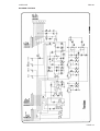
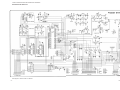
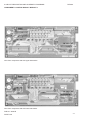
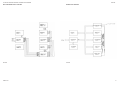
1
TECHNICAL MANUAL
FOR
COMPACT HF SSB RE2100
S.P. RADIO A/S
AALBORG
DENMARK
Please note
Any responsibility or liability for loss or damage in connection with the use of this product and the
accompanying documentation is disclaimed.
The information in this manual is furnished for informational use only, is subject to change without
notice, may contain errors or inaccuracies, and represents no commitment whatsoever.
This agreement is governed by the laws of Denmark.
Doc. no.: M2100GB
Issue: B/0401
RE2100
CONTENTS
1
1.1
1.2
1.3
1.4
1.5
1.6
GENERAL INFORMATION
INTRODUCTION
DESCRIPTION OF SAILOR HF SSB PROGRAMME
GENERAL DESCRIPTION OF SAILOR HF SSB RE2100
TECHNICAL DATA
(complies with SOLAS, ITU, CEPT, MPT, DOC, FTZ, KSR, FCC)
CONTROLS
PRINCIPLE OF OPERATION
1-3
1-5
1-7
2
2.1
2.2
2.3
INSTALLATION
MOUNTING POSSIBILITIES
DIMENSIONS AND DRILLING PLAN
ELECTRICAL CONNECTION AND ASSEMBLING
2-1
2-3
2-8
3
3.1
3.2
3.3
3.4
3.5
3.6
3.7
3.8
3.9
3.10
SERVICE
MAINTENANCE
ALIGNMENT INSTRUCTIONS
PROPOSAL FOR NECESSARY TEST EQUIPMENT
TROUBLE SHOOTING
PERFORMANCE CHECK
MODULE PERFORMANCE CHECK
ADJUSTMENT PROCEDURE
NECESSARY ADJUSTMENT AND CHECK AFTER REPAIR
FUNCTION CHECK
SELECTION AND DESCRIPTION OF THE SERVICE
PROGRAMMES
1-1
1-1
1-2
3-1
3-1
3-2
3-7
3-9
3-21
3-47
3-56
3-58
3-60
4
4.1
MECHANICAL DISASSEMBLING AND MODULE LOCATION
ADJUSTMENTS AND LOCATIONS
4-1
5
5.1
5.2
5.3
5.4
5.5
5.6
5.7
5.8
5.9
CIRCUIT DESCRIPTION AND SCHEMATIC DIAGRAMS
RECEIVER UNIT (MODULE 1) PART NO. 625631
FRONT END UNIT (MODULE 2) PART NO. 625632
SYNTHESIZER UNIT (MODULE 3) PART NO. 625633
EXCITER UNIT (MODULE 4) PART NO. 625634
PROCESSOR UNIT (MODULE 5) PART NO. 625635
KEYBOARD UNIT (MODULE 6) PART NO. 625636
DISPLAY UNIT (MODULE 7) PART NO. 625637
POWER UNIT (MODULE 8) PART NO. 625638
INTERCONNECTION CABLE PLAN
5-1
5-9
5-13
5-23
5-29
5-35
5-37
5-41
5-45
6
6.1
6.2
6.3
MICROTELEPHONE INSTALLATION
NORMAL INSTALLATION RE2100 AND C2140
NORMAL INSTALLATION RE2100 OR C2140 WITH
2 MICRO TELEPHONES
MECHANICAL DIMENSIONS FOR HANDSET
7
PARTS LIST
6-3
6-4
6-5
RE2100
CONTENTS
1
GENERAL INFORMATION
1.1
INTRODUCTION
1-1
1.2
DESCRIPTION OF SAILOR HF SSB PROGRAMME
1-1
1.3
GENERAL DESCRIPTION OF SAILOR HF SSB RE2100
1-2
1.4
TECHNICAL DATA
(complies with SOLAS, ITU, CEPT, MPT, DOC, FTZ, KSR, FCC) 1-3
1.5
CONTROLS
1-5
1.6
PRINCIPLE OF OPERATION
1-7
RE2100
1
GENERAL INFORMATION
1.1 INTRODUCTION
SAILOR Compact HF SSB RE2100 is the control unit in SAILOR Compact HF SSB Programme 2000.
SAILOR Compact HF SSB Programme 2000 is a powerful, advanced, high technology short wave
communication system which is extremely easy to operate.
It has been developed on the basis of S. P. Radio’s many years of experience with short wave
communication equipment.
It has the same high reliability as all SAILOR equipment is known for.
It is extremely easy to operate:
1. Select frequency.
2. Make your call when the tune lamp has been extinguished.
It has been constructed so that it fits in with the other units in the SAILOR Compact Programme 2000.
1.2 DESCRIPTION OF SAILOR HF SSB PROGRAMME
The SAILOR HF SSB programme is designed to meet all requirements within HF radio communication.
The SAILOR HF SSB programme consists of one main control unit and three transmitters with different
power levels (250W, 600W, 1200W PEP).
To obtain maximum performance, the systems are designed with aerial couplers, which can be mounted
outdoors. All the aerial couplers have automatic tuning.
Each of these three systems can be extended with:
-
remote control units C2140
telex/DSC sscanning receiver with built-in modem RM2151
DSC MF/HF watchkeeping receiver with built-in modem RM2150
duplex receiver R2120
The system may be supplied for 24V DC or 110/220V AC power source.
For the system there are following battery chargers available:
-
30 amp battery charger N2174
3 x 30 amp battery charger 2 x N2174
60 amp battery charger N2174 Dual
These battery chargers can be used to charge maintenance free lead-acid batteries and Nickel Cadmium
batteries.
The 600W PEP and 1200W PEP transmitters and power supplies are built up of the following units:
9324
PAGE 1-1
1 GENERAL INFORMATION
RE2100
1)
TX control unit, consisting of output filter, power supply, and audio amplifier for RE2100 and the
TX-processor.
2)
Power amplifier unit, consisting of a 600W power amplifier.
3)
Combiner unit, consisting of power splitter and power combiner.
4)
24V DC power unit, consisting of a 24V DC to 28V and 42V DC switch mode power supply, which
supplies the power amplifier unit.
5)
110/220V AC power supply unit, consisting of a 110/220V AC to 28V DC and 42V DC thyristor
controlled power supply, which supplies the power amplifier unit.
1.3 GENERAL DESCRIPTION OF SAILOR HF SSB RE2100
SAILOR HF SSB RE2100
is an all solid state constructed microcomputer controlled SSB short
wave telephony receiver and exciter.
SAILOR HF SSB RE2100
covers the frequency range from 100 kHz to 30 MHz in receive mode and
from 1.6 MHz to 30 MHz in transmit mode.
SAILOR HF SSB RE2100
can operate in both simplex and semi-duplex.
SAILOR HF SSB RE2100
includes all ITU channels from 4 MHz to 25 MHz.
SAILOR HF SSB RE2100
includes channel scanning facilities.
SAILOR HF SSB RE2100
includes 100 quick select frequency pairs.
SAILOR HF SSB RE2100
has continuous tuning in receive mode.
SAILOR HF SSB RE2100
has clarifier function ±150 Hz in 10 Hz steps.
SAILOR HF SSB RE2100
is fully synthesized and has a high stability reference oscillator (TCXO).
SAILOR HF SSB RE2100
has an easy to read display with red light figures.
SAILOR HF SSB RE2100
has a push-button keyboard offering an attractive tactile feeling and a
safe finger-guide in the metal front. The keyboard is fitted with nightillumination of the lettering.
SAILOR HF SSB RE2100
has one key operation of the distress frequency 2182 kHz.
SAILOR HF SSB RE2100
has integral two tone alarm signal generator in accordance with SOLAS.
SAILOR HF SSB RE2100
has a special serial input (SP-BUS) enabling RE2100 to communicate
with other units.
PAGE 1-2
9324
1 GENERAL INFORMATION
RE2100
1.4 TECHNICAL DATA
(complies with SOLAS, ITU, CEPT, MPT, DOC, FTZ, KSR, FCC)
GENERAL
Frequency Range:
Receiver: 100 kHz to 30 MHz
Transmitter: 1.6 MHz to 30 MHz
Modes:
J3E (USB/LSB), R3E and H3E (AM)
Channel Capacity:
100 user defined quick-select channels and ITU defined channels in the
maritime bands. Each channel contains both RX and TX frequency and
mode settings.
Scanning Facilities:
10 scanning prograammes, each able to contain
128 pairs of frequencies.
Distress Call:
Quick selection of 2182 kHz
Built-in two tone alarm: 1300 Hz and 2200 Hz
with a duration of 45 secs.
Operating Temperature Range:
-15°C to +55°C
Frequency Stability:
Better than 0.34 ppm
Primary Voltage:
24V DC - 10% +30%
Current Drain:
Receiver (standby)0.9A
Transmit voice
Transmit two-tone
Aerials:
7A
13A (T2130)
from 7 - 15 m
TRANSMITTER T2130
Power Output:
250W PEP ±1.4 dB (T2130/I 240W PEP max.)
Intermodulation:
better than 32 dB below PEP
Spurious Emission:
better than 67 dB below PEP
Harmonics:
better than 43 dB below PEP or
better than 67 dB below PEP with aerial coupler AT2110
Carrier Suppression:
better than 46 dB below PEP
Audio Response:
350 Hz to 2700 Hz at -6 dB
RECEIVER RE2100
Receive System:
Double conversion super heterodyne
1st IF 70 MHz. 2nd 10.73 MHz
Selectivity:
J3E (SSB) 350 Hz to 2700 Hz at -6 dB
H3E (AM)
±3.3 kHz at -6 dB
J3E (SSB) <10 dB/uV for 20 dB SINAD
H3E (AM) <24 dB/uV for 20 dB SINAD
Sensitivity:
9324
PAGE 1-3
1 GENERAL INFORMATION
RE2100
Spurious and IF Rejection:
better than -70 dB
Cross Modulaton:
better than 90 dB/uV (CEPT method of test)
Desensitization:
better than 100 dB/uV (CEPT method of test)
AGC:
less than 2 dB audio level change from 10 dB/uV to 80 dB/uV.
Fast attack, slow release time.
Intermodulation:
better than 90 dB/uV (CEPT method of test)
Spurious Emission:
better than 1 nW into dummy aerial
Clarifier:
±150 Hz in steps of 10 Hz
Squelch:
Voice activated, opens for SINAD >6 dB
Audio Power:
5 Watt, 8 ohm, less than 10% distortion
10 Watt, 4 ohm, less than 10% distortion
AERIAL COUPLER AT2110
Power:
250W PEP
Aerials:
7 - 15m
Temperature Range:
-25°C to +70°C
Tuning Time:
Typically less than 2 secs (learn mode typ. 30 secs)
ACCESSORIES
Loudspeaker:
H2054 see special brochure
H2074 see special brochure
Power Supplies:
N2160
Input supply: 12V + 30% - 10%
For more information see the manual for N2160
N2161
Input supply: 110V - 127V - 220V - 240VAC
Input frequency: 50 - 60 Hz
For more information see the manual for N2161
Weight:
PAGE 1-4
RE2100:
T2130:
AT2110:
4.5 kg
14 kg
4.5 kg
9324
1 GENERAL INFORMATION
RE2100
1.5 CONTROLS
VOL
O
F
F
SIGNAL AE CURRENT
0
.5
1
2
RX
kHz
3
1
2
3
4
5
6
7
8
9
0
.
TX
TX POWER
RF
FREQ
FREQ
kHz
TUNE
RX
CLARIF
SEND
ALARM
2182
TEST
ALARM
TX
AGC
DIM
POWER
DUMMY
LOAD
SQ
MODE
CH
SC
ADD
DEL
STOP
ENT
29045
VOL
O
F
F
Volume control and on/off switch for the mains.
RF
Manual RF gain control.
FREQ
Tunes the receive frequency down.
FREQ
Tunes the receive frequency up.
TUNE
CLARIF
Switches between clarifier (10 Hz steps) and tune of receive frequency.
RX
Selects receive functions or converts a channel number to the corresponding frequency.
CH
Selects channel functions.
TX
Selects transmit functions or converts a channel number to the corresponding frequency.
AGC
TX
POWER
Reduce/increase the transmitter output power.
DIM
TX
9331
DUMMY
LOAD
Selects the built-in dummy load in the aerial coupler, and the TX frequency
2206.4 kHz is automatically selected.
PAGE 1-5
1 GENERAL INFORMATION
SEND
ALARM
RE2100
Transmits the distress signal when pressed together with TEST ALARM.
2182
Selects the distress frequency 2182 kHz.
TEST
ALARM
Acoustic check of the alarm signal generator.
DIM
DUMMY
LOAD
Reduces/increases the display light and switches on/off the display and keyboard panel
illumination.
AGC
POWER
Switch the AGC function on/off.
SQ
ADD
Switches the squelch function on/off.
MODE
DEL
Selects modulation type J3E, R3E, H3E and J3E lower side band. (J3E lower side band is
optional).
SC
Selects the scan programme.
7
Digits from 1 to 9 and 0.
STOP
ENT
.
Terminates the keying-in sequence, stops the alarm signal, stops the scanning, and stops
the TX tuning.
Sets the decimal point for the frequency in kHz.
SQ
CH
ADD
(Digits 0-99)
Adds the RX/TX frequency to the channel number.
MODE
CH
DEL
(Digits 0-99)
Deletes the RX/TX frequency from the channel.
TUNE
Resets the tune memory at the selected frequency and starts a new tune-up
TX
CLARIF
PAGE 1-6
cycle.
9331
1 GENERAL INFORMATION
RE2100
1.6 PRINCIPLE OF OPERATION
SAILOR Compact HF SSB RE2100 is the control unit in SAILOR Compact HF SSB Programme 2000. It
contains following circuits.
PROCESSOR UNIT
This unit controls all modules and operate as interface between the user and the radio (keyboard, display).
Nearly all communication from the microprocessor to the modules is done on an internal serial bus (SPI).
The unit holds all memory, and all user defined memory is in an EEPROM, so even when supply voltage
is removed, the contents of the memory is preserved. If the supply voltage to the RE2100 gets too low,
the display will show error 20, and the performance of the RE2100 will be reduced.
There is also an external serial bus (SP-Bus). This bus is used to communicate with other units in the
SAILOR Compact HF SSB Programme 2000, e.g. the transmitter T2130.
The microprocessor also generates the alarm tones (1300 Hz, 2100 Hz).
DISPLAY UNIT
This unit contains the display and the field strength meter.
SYNTHESIZER UNIT
This unit contains all frequency generating parts.
There is only one reference oscillator which is a temperature compensated crystal oscillator (TCXO) with
a frequency of 10.73 MHz.
Both receiver and exciter are using two LO-signals. These signals are generated in two separate PLL’s,
one having output frequencies from 70 MHz to 100 MHz and the other having output frequencies of 59.27
MHz and 80.73 MHz.
The synthesizer which covers from 70 to 100 MHz is a fractional synthesizer with a resolution of 10 Hz.
The other synthesizer is a conventional synthesizer. It has two output frequencies, one for lower sideband
80.73 MHz and another for upper sideband 59.27 MHz.
RECEIVER FRONT END
This unit contains input protection circuit, input filters, mixer and 70 MHz IF.
The input filter is a mixture of lowpass, highpass and bandpass filter to obtain max. performance in the
entire band from 100 kHz to 30 MHz.
The mixer is a FET mixer with a high level LO-injection to give the mixer good high signal quality. The mixer
is followed by a 70 MHz bilitic quartz filter with a bandwidth of 15 kHz.
RECEIVER UNIT
This unit contains all necessary circuits to convert a 70 MHz IF signal to an audio signal.
It starts with the second mixer which is a FET mixer. From the mixer the signal is fed to a high order
monolitic quartz filter, one for AM and one for SSB. The type of filter is selected from the microprocessor.
From the filter the signal is fed to the 10.73 MHz IF amplifier. The gain of this amplifier is regulated from
the AGC amplifier. The regulated IF amplifier is followed by a ceramic filter to reduce the wideband noise.
The signal is from here fed to the demodulator, which can operate as an SSB detector or an AM detector
controlled from the microprocessor. The detector is followed by a filter circuit. In AM mode the filter width
is from 70 Hz to 3000 Hz, and in SSB mode the filter is from 300 Hz to 3000 Hz. From here the AF signal
passes some switches and then it is amplified in three AF amplifiers, one for the microtelephone earpiece,
one for the 0 dBm output, and an amplifier with volume control for the AF signal to the AF power amplifier
in T2130.
The signal from the AF filters is also fed to the voice controlled squelch. This contains a limiting amplifier,
a frequency to voltage converter, and a threshold amplifier. On/off switching of the squelch is controlled
by the microprocessor.
In scan mode the squelch is used to detect if there is signal on the channel in question.
9324
PAGE 1-7
1 GENERAL INFORMATION
RE2100
EXCITER UNIT
This unit contains all necessary circuits to generate an SSB/AM signal in the frequency range from 1.6
- 30 MHz.
It starts with a compressor and AF amplifier.
The AF signal is fed to the balanced modulator to produce a double sideband signal on 10.73 MHz.
The DSB signal is fed to the LSB filter where only the lower sideband passes through. The LSB signal is
fed to a step attenuator, which is controlled from the microprocessor. From the step attenuator the signal
is fed to the first mixer, and the frequency is converted to 70 MHz. If 59.27 MHz LO-signal is used, the
signal will be lower sideband. If 80.73 MHz LOsignal is used, the signal will be upper sideband. From the
mixer the signal is fed to an amplifier, 70 MHz crystal filter and an amplifier. From the amplifier the signal
is fed to the second mixer which converts the frequency from 1.6 MHz to 30 MHz.
After the mixer a lower side signal is converted to an upper sideband signal, and an upper sideband signal
is converted to a lower sideband signal. The output of the mixer is fed to the power unit.
POWER UNIT
This unit contains the final amplifying and filtering of the RF signal, and produces all necessary supply
voltages for the modules in RE2100.
The signal from exciter unit is first amplified, then filtered in a 30 MHz lowpass filter and then amplified
to a level of approx. 2 mW.
The input voltages from T2130 is ±18V and 9V. These voltages passes through seven series regulators
to produce the necessary supply voltages to RE2100. A special ±15V for the exciter is controlled from the
microprocessor, so when the transmitter has not been used for two minutes, it is switched off to reduce
the power consumption in standby.
PAGE 1-8
9324
1 GENERAL INFORMATION
RE2100
BLOCK DIAGRAM RE2100
RF in/out
to T2130
2
Rx/Tx
Highpass
Filter
3
4
Lowpass
Filter
1.st
70MHz
Filter
Mixer
C2
SSB/AM
2.nd
Lo-buffer
Buffer
+
Amp
C2
SSB/AM
70 Hz
Highpass
E2
Det. Mute
1
Bandpass
Filter
18-30MHz
1
Bandpass
Filter
H2
Hang AGC on/off
A1 B1 C1 D1 E1 F1 G1 H1
Shift Register 1
Buffer
A2 B2 C2 D2 E2 F2 G2 H2
Shift Register 2
AMP
Dependent
on Squelch
Independent
on Squelch
SP-bus
G1
0 dBm
F1 0 dBm Switch
AMP
A1 Aux AF Switch
SCI-Tx
Distress
driver
H1
Earpiece Switch
SCI-Rx
+5V power
supply
Bandpass
Filter
SCI-baud
Rote-gen
-5V power
supply
Watch dog
+5V power
supply
Tune/alarm
generator
Volume contr.
Switch
Loudsp.
Loudsp. Switch
u-Processor
Buffer Amp
SPI-adress
select
Earpiece
AMP
EPROM
EEPROM
Keyboard
buffer
B1
Mic. Switch
C1
100-92.5MHz
VCO I
PROCESSOR
(MODULE 5)
1
4
Current
Mirror
VCO-Buffer
1
1
LO-Buffer
85-77.5MHz
VCO III
77.5-70MHz
VCO IV
Prescaler
buffer
latch
Q Sum
clock
A Adder B
overflow
Ex
EXCITER (MODULE 4)
1
1
Programmed
divider
A/D
Converter
Fraction Q
register
Rx
Prescaler
4
1/n Curr.
Logic
Rx/Tx
Switch
2
4
1
EX
Supply
1
1
1
1
1
VCO 1
2nd
Divider
Reference
Divider
VCO-Buffer
Loop
Filter
Phase
detector
LO-Buffer
Rx
Tx
1.6-30 MHz
+18V
-18V
+9V
Supply
+15V
To exciter module
-15V
To exciter module
+15V
-15V
+5V
+3.5V
To all modules
To processor module
To display module
Lowpass
Filter
Prescaler
buffer
1
1
Prescaler
+18V from T2130
-18V
+9V
VCO 2
Programmed
divider
1
ATT Ex
2.nd
70 MHz
Mixer
AMP
70 MHz
1.st
IF AMP
Mixer
Carrier
buffer
Carrier
Level-control
AF-selector
RF on/off
Carrier
Insertion
4
Mode-selector
6
1
Modeselector
3
Display
driver
102
EPROM
Meter
driver
10
Rx and Tx
Meter
10.73 MHz
3
3
4
3
7
Step
attenuator
10
Keyboard
4x8 Matrix
Shift reg.
2
70 MHz
Filter
4
Mode Ex
Ex on/off
LO-buffer
KEY BOARD
(MODULE 6)
7
Shift reg.
POWER (MODULE 8)
Modulus
Control
Logic
Shift reg.
6
10.73MHz
LSB-filter
Modulations
Level-control
3
Balanced
Modulator
AFcompressor
Rx/Tx
Switch
Mic. in
3
92.5-85MHz
VCO II
Telex
Alarm/tune tones
2
1
59.23/80.73 MHz LO1 EX
Control
logic
Loop
Filter
Phase
detector
Sample/Hold
Reference
Divider
Reset
VAPI
2nd
Divider
LO2 EX 70-100 MHz
Rx
Ex
Buffer
300 Hz
Highpass
G2 Tune/Alarm/Ringing
Tones on/off
Volume contr.
F2
Hang Time
AGC
S-Meter on/off S-Meter
E1
AMP
AMP
Squelch Switch
AMP
Vref
A2
Manual RF-gain
Control on/off
Limeting
SSB/AM
C2
AGC
AGC
Detector
-
3 kHz
Lowpass
Limit
AMP
AGC on/off
B2
AM-Filter
10.73MHz
1.st LO
Bandpass
Filter
300kHz BW
10.73MHz
AMP
9-18MHz
6
1
TCXO
30MHz
Bandpass
Filter
4.5-9MHz
1
2
SYNTHESIZER
(MODULE 3)
1.6-4.5MHz
SSB/AM Demodulator
IF
Carrier Reinjection for SSB 10.73 MHz
Shift reg.
1
Bandpass
Filter
LO2 Rx 59.27 MHz/80.73 MHz
Switch
2.nd
Mixer
LO1 Rx 70-100 MHz
Mute
1
IF
Frequency
to voltage
converter
Squelch reset
D1
ADRESS-BUS/16
LSB-Filter
10.73MHz
0.385-1.6MHz
1
Threshold
DATA-BUS/8
RECEIVER (MODULE 1)
Rx Mute
Hand Key
Lowpass
Filter
RECEIVER FRONT END
(MODULE 2)
AF to AFamp. T2130
To microtelephone edv.
Ext. RF-gain controle
0 dBm output
Mic in
VF/AE-current
AUX AF to TX
Distress out
0.385MHz
2
DISPLAY
(MODULE 7)
Dimmer
Dummy load
Tune
Ex RF
2
4-0-25751C
9324
PAGE 1-9
RE2100
CONTENTS
2
INSTALLATION
2.1
MOUNTING POSSIBILITIES
2-1
2.2
DIMENSIONS AND DRILLING PLAN
2-3
2.3
ELECTRICAL CONNECTION AND ASSEMBLING
2-8
RE2100
2
INSTALLATION
2.1 MOUNTING POSSIBILITIES
4-0-25931,4-0-25932,4-0-25933
TABLETOP AND DECKHEAD
Mounting bracket H2055 which offers the same possibilities for the loudspeakers H2054 and H2074.
Mounting kit H2068 and H2055
PAGE 2-1
2 INSTALLATION
RE2100
BULKHEAD AND CONSOLE
Mounting kit H2063 which offers the same possibilities for the loudspeakers H2054 and H2074.
4-0-25926,4-0-25927
Mounting kit H2062 or
Mounting kit H2064.
IN CONJUNCTION WITH OTHER SAILOR EQUIPMENT
Look up the INSTALLATION section for the SAILOR unit in question
PAGE 2-2
2 INSTALLATION
RE2100
2.2 DIMENSIONS AND DRILLING PLAN
4-0-25930,4-0-25922
UNIVERSAL MOUNTING BRACKET H2055
Permits a wide variety of installation possibilities, such as tabletop, bulkhead or deckhead. For other
possibilities such as console installation, the SAILOR 19" rack or all units in the Compact programme
assembled on the bulkhead, see special information concerning installation of the Compact programme.
WEIGHT
Mounting kit H2055:
Loudspeaker H2054:
Loudspeaker H2074:
HF SSB RE2100:
1.5 kg
5.5 kg
4.0 kg
4.5 kg
PAGE 2-3
2 INSTALLATION
RE2100
4-0-25934, 4-0-25928, 4-0-25929
MOUNTING KIT H2068 AND H2055
PAGE 2-4
WEIGHT
Lashing kit H2068:
Mounting kit H2055:
Loudspeaker H2054:
Loudspeaker H2074:
HF SSB RE2100:
1.5 kg
1.5 kg
5.5 kg
4.0 kg
4.5 kg
2 INSTALLATION
RE2100
MOUNTING KIT H2063
4-0-25935, 4-0-25936, 4-0-24703
Free distance must be kept to allow
free air circulation ambient temperature max. 40°C.
WEIGHT
Mounting kit H2063:
Loudspeaker H2054:
Loudspeaker H2074:
HF SSB RE2100:
1.0 kg
5.5 kg
4.0 kg
4.5 kg
PAGE 2-5
2 INSTALLATION
RE2100
MOUNTING KIT H2064
Free distance must be kept to allow
free air circulation ambient temperature max. 4o°C.
PAGE 2-6
1.5 kg
5.5 kg
4.0 kg
4.5 kg
4-0-25937, 4-0-24704, 4-0-25942
WEIGHT
Mounting kit H2064:
Loudspeaker H2054:
Loudspeaker H2074:
HF SSB RE2100:
2 INSTALLATION
RE2100
4-0-25943,4-0-24732, 4-0-25944
MOUNTING KIT H2062
Free distance must be kept to allow
free air circulation ambient temperature max. 40oC.
WEIGHT
Mounting kit H2062:
Loudspeaker H2054:
Loudspeaker H2074:
HF SSB RE2100:
1.5 kg
5.5 kg
4.0 kg
4.5 kg
PAGE 2-7
2 INSTALLATION
RE2100
2.3 ELECTRICAL CONNECTION AND ASSEMBLING
HF SSB RE2100 is the control unit in SAILOR compact HF SSB programme 2000. RE2100 can therefor
be the control unit in a 250W transmitter system or a 600/1200W system. For information how to
interconnect this units with RE2100 please consult the technical manuals describing the units to be
interconnected to
25816
J03-5
Pin no. 1
Pin no. 2
Pin no. 3
Pin no. 4
Pin no. 5
Pin no. 6
Pin no. 7
Pin no. 8
Pin no. 9
Pin no. 10
Pin no. 11
Pin no. 12
Pin no. 13
Pin no. 14
Pin no. 15
Pin no. 16
Pin no. 17
Pin no. 18
Pin no. 19
Pin no. 20
Pin no. 21
Pin no. 22
Pin no. 23
Pin no. 24
Pin no. 25
PAGE 2-8
Mute RX
AF to AMP common
GND Shield
SP BUS interrupt
Black
Brown
Red
Orange
Yellow
AUX AF to TX common Green
-18V
Blue
+9V
Violet
+18V
Grey
Supply on/off
White
Mic key
Brown/pink
VF/AE-current
Brown/yellow
AF to AMP
Brown/green
0 dBm out common
Brown/grey
0 dBm out
White/pink
Ext. RF control
White/yellow
AUX AF to TX
White/green
RF on/off
White/blue
GND
White/grey
+9V
Violet
+18V
Grey/orange
-battery
Red/blue
J03-2
Pin no.
Pin no.
Pin no.
Pin no.
Pin no.
Pin no.
Pin no.
Pin no.
Pin no.
1
2
3
4
5
6
7
8
9
Telephone Red
GND Yellow
Signal GND White
Mic Blue
Mic key
Brown
Ext. SQ on/off
Distress
Ser.+
+18V
9324
RE2100
CONTENTS
3
SERVICE
3.1
MAINTENANCE
3-1
3.2
ALIGNMENT INSTRUCTIONS
3-1
3.3
PROPOSAL FOR NECESSARY TEST EQUIPMENT
3-2
3.4
TROUBLE SHOOTING
3-7
3.5
PERFORMANCE CHECK
3-9
3.5.1
PERFORMANCE CHECK OF DISPLAY AND KEYBOARD
3-9
3.5.2
PERFORMANCE CHECK OF RECEIVER
3-11
3.5.3
PERFORMANCE CHECK OF EXCITER
3-18
3.6
MODULE PERFORMANCE CHECK
3-21
3.6.1
MODULE PERFORMANCE CHECK OF RECEIVER UNIT
3-22
3.6.2
MODULE PERFORMANCE CHECK OF FRONT END UNIT
3-32
3.6.3
MODULE PERFORMANCE CHECK OF SYNTHESIZER UNIT
3-37
3.6.4
MODULE PERFORMANCE CHECK OF EXCITER UNIT
3-40
3.6.5
PERFORMANCE CHECK OF MICROPROCESSOR MODULE 5 3-42
3.6.8
MODULE PERFORMANCE CHECK OF POWER UNIT
3-47
3.7
ADJUSTMENT PROCEDURE
3-47
3.7.1
ADJUSTMENT PROCEDURE FOR FRONT END
AND RECEIVER UNIT
3-47
3.7.2
ADJUSTMENT PROCEDURE FOR SYNTHESIZER UNIT
3-50
3.7.3
ADJUSTMENT PROCEDURE FOR EXCITER UNIT
3-52
3.7.4
ADJUSTMENT PROCEDURE FOR POWER UNIT.
3-55
3.8
NECESSARY ADJUSTMENT AND CHECK AFTER REPAIR
3-56
3.9
FUNCTION CHECK
3-58
3.10
SELECTION AND DESCRIPTION OF THE SERVICE
PROGRAMMES
3-60
3.10.1
HOW TO SELECT A SERVICE PROGRAMME
3-60
3.10.2
DESCRIPTION OF SERVICE PROGRAMMES
3-60
RE2100
3
SERVICE
3.1 MAINTENANCE
PREVENTIVE MAINTENANCE
If the HF SSB RE2100 has been installed in a proper way the maintenance can, dependent on the
environments and working hours, be reduced to a performance check at the service workshop at intervals,
not exceeding 12 months. A complete performance check list is enclosed in this manual, chapter 3.5
PERFORMANCE CHECK.
Inspection of the antenna, cables, and plugs for mechanical defects, salt deposits, corrosion, and any
foreign bodies shall be done at regular intervals not exceeding 12 months.
Along with each RE2100 a test sheet is delivered in which all the measurements, made in the test
department of the factory, are listed. If the control measurings made in the service workshop should not
show the same values as those listed in the test sheet, the set must be adjusted as specified in chapter
3.7 ADJUSTMENT PROCEDURE.
3.2 ALIGNMENT INSTRUCTIONS
INTRODUCTION
The measuring values indicated in chapter 5. CIRCUIT DESCRIPTION AND SCHEMATIC DIAGRAMS
are typical values and as indicated it will be necessary to use instruments in absolute conformity with the
below list:
PAGE 3-1
3 SERVICE
RE2100
3.3 PROPOSAL FOR NECESSARY TEST EQUIPMENT
OSCILLOSCOPE:
Bandwidth
Sensitivity
Output Impedance
E.g. Philips type
DC-35 MHz
2mV/div
1 Mohm//20 pF
PM3050
PASSIVE PROBE:
Attenuator
Input Impedance
Compensation Range
E.g. Philips type
20 dB
10 Mohm//15 pF
10-30 pF
PM8936/091
MULTIMETER:
Sensitivity DC (f.s.d.)
Input Impedance
Accuracy DC (f.s.d.)
E.g. Philips type
100 mV
10 Mohm
1.5%
PM2505
FREQUENCY COUNTER:
Frequency Range
Resolution
Accuracy
Sensitivity
Input Impedance
E.g. Philips type
100 Hz - 120 MHz
1 Hz at f = 100 MHz
1 . 10-7
100 mV RMS
1 Mohm/30 pF
PM6669/031
HF SIGNAL GENERATOR:
Frequency Range
Output Voltage:
Output Impedance
Type of Modulation
Modulation Frequency
E.g. Marconi type
100 kHz - 100 MHz
0dB/uV - 120 dB/uV
50 ohm
AM
External
2019
LF SIGNAL GENERATOR:
Frequency Range
Output Voltage
Output Impedance
Output Waveform
E.g. Philips type
10 Hz - 10 kHz
20 mVRMS - 1VRMS
600 ohm
sine wave
PM5110
LF DISTORTION METER:
Frequency Range
Distortion Range (f.s.d.)
Input Impedance
Accuracy (f.s.d.)
E.g. Philips type
f = 1000 Hz
1-10%
1 Mohm
3%
PM6309
PAGE 3-2
3 SERVICE
RE2100
TEST PROBE
1nF
ceramic
AA119
RF
1nF
ceramic
AA119
To multimeter
LAYOUT OF THE PROBE
70.00
ø10
10.00 12.00
Metal tube
Insulating material
25079
50 OHM DUMMY LOAD
50 ohm -> 50 ohm:
EMF-loss 20 dB
PAGE 3-3
3 SERVICE
POWER SUPPLY:
Vout1
Vout2
Iout1
Iout2
E.g. 2 pcs. ELCANIC type
RE2100
18V DC
18V DC
2 Amp DC
0.5 Amp DC
3010
TESTBOX
To test all the functions of the RE2100 is very difficult when no transmitter T2130 is available. For that
reason S. P. Radio has developed and produced a testbox. When using this testbox it is possible in an
easy way to test all the inputs and outputs of the RE2100.
The testbox has a built-in AF amplifier, which makes it possible to connect a loudspeaker directly to the
testbox.
The testbox has a built-in unit to control the function of the SP-BUS output. By means of the built-in light
emitting diodes and switches it is possible to control all the functions of the RE2100.
Specification of measuring instruments, which can be connected to the testbox is given in the beginning
of this chapter, and to this list an 8 ohm loudspeaker can be added.
The below diagram shows the electric wiring inside the testbox:
PAGE 3-4
5-0-26206 / 4-6-26206A
COMPONENT LOCATION TESTBOX
3 SERVICE
RE2100
DIAGRAM TESTBOX
PAGE 3-5
3 SERVICE
RE2100
The below diagram shows how to connect the testbox with the RE2100 and the external instruments.
4-0-26236A
If no testbox is available, it is possible to operate the RE2100 by connecting the power supply directly to
the 25-pin connector, which is located at the back of the RE2100. In this 25 pin connector it is possible
to find all the other inputs, outputs, and testpoints. The pin configuration for this connector is listed in
chapter 2.3 ELECTRICAL CONNECTION AND ASSEMBLING. But it is only necessary to establish the
following connections:
pin No. 10 -18V/0.2 Amp.
pin No. 11 + 9V/0.5 Amp.
pin No. 12 +18V/0.8 Amp.
pin No. 5 GND
The handset is connected directly to the 9-pin connector at the back of the RE2100.
PAGE 3-6
3 SERVICE
RE2100
3.4 TROUBLE SHOOTING
Trouble shooting should only be performed by persons with sufficient technical knowledge, who have the
necessary measuring instruments at their disposal, and who have carefully studied the operation
principles and structure of the SAILOR Compact HF SSB System.
SAILOR HF SSB RE2100 has a number of trimming cores and trimmers, which must not be touched,
unless adjustments as specified in chapter 3.7 ADJUSTMENT PROCEDURE, can be made.
When measuring the units, short-circuits must be avoided as the transistors would then be spoiled.
LOCATING THE FAULTY UNIT
When a fault has been observed in the HF SSB system, it can be difficult to find out in which unit the fault
can be located.
The first thing to check, is whether the fault is somewhere in the aerial circuit, the handset or in the power
source.
If the fault is not found there, check if an error message has been shown in the RX display of the RE2100.
The error codes listed below are error messages, which are generated by the RE2100, and they therefore
indicate a fault in this unit.
ERROR CODES
00
Internal power supply is low.
Check the power connections to the RE2100, or check the internal power regulators.
11
Illegal transmitting frequency.
The TX frequency, of which a tone sequence has been tried, is not legal.
12
Illegal transmitting mode.
The TX emission mode is not legal for transmitting.
15
Key sequence is not finished by the <ENT> key.
20
The communication link to the transmitter T2130 is interrupted.
Check the coax cable to the T2130 from RE2100.
21
The communication link between RE2100 and control unit C2140 or DSC/telex RM2150/
RM2151 has been stopped. Check the SP-BUS coax cable to the external equipment. If the
“Error 21” flashes up again after the button <STOP/ENT> has been pressed, then check the
SP-BUS interrupt line (J03-5 pin 6). This line has to be normal “High” (approx. +5V).
22
The communication link between the RE2100 and the Duplex/Telegraphy Reveiver R2120T
has been stopped. Check the SP-BUS coax cable between these units.
The error codes listed below are error messages, which are generated by the HF transmitter T2130, and
they therefore indicate a possible fault in this unit.
PAGE 3-7
3 SERVICE
RE2100
These error codes are described more detailed in the instruction manual for T2130, chapter
2.3 SYSTEM DESCRIPTION AND TROUBLE SHOOTING, and in the chapter 3.4 TROUBLE SHOOTING.
ERROR CODES
70
Motor circuit error AT2110.
See instruction manual for T2130, chapter 3.4.
71
Internal signal error.
See instruction manual for T2130, chapter 3.4.
72
Internal signal error.
See instruction manual for T2130, chapter 3.4.
73
High standing wave ratio (SWR) in the tuning of the AT2110.
Check the aerial and see instruction manual for T2130, chapter 3.4.
74
Transmitter temperature too high.
Let the transmitter T2130 have a pause and see instruction manual for T2130, chapter 3.4.
75
High standing wave ratio (SWR) when transmitting.
Check the aerial and see instruction manual for T2130, chapter 3.4.
76
Battery voltage low.
Check the condition of the batteries and the power cables. See instruction manual for T2130,
chapter 3.4.
77
Temperature sensor error.
See instruction manual for T2130, chapter 3.4.
78
Internal high standing wave ratio (SWR).
See instruction manual for T2130, chapter 3.4.
If the error codes indicate that the fault may be found in the RE2100, the fault is probably no transmitter
signal from the RE2100. The exciter can then, without any damage to the transmitter, be set on by
activating the test programme SP-05-0.
The error codes do not indicate any receiver fault.
A receiver fault can be in the aerial coupler AT2110, in the transmitter T2130, or in the receiver unit.
To separate a fault in these units, disconnect the aerial cable at the back of RE2100 and connect a wire
to the RE2100 coax socket. Try to find a broadcast station and check the receiver. If the fault is still
present, it must be located in the RE2100 unit.
LOCATING THE FAULTY MODULE
If the fault has been located to the RE2100, the exciter can be activated in test programme SP-05-0. The
receiver is always activated, when no test programme is activated.
Check the connections to the modules in the RE2100.
The power supply should be the first thing to control, the voltage is indicated in the diagram of each
module.
If the power supply is present, control the amplitude of the local oscillator signals.
The next thing to control is whether the other inputs to the module are present. They are indicated in the
diagrams of each module with reference to a special set-up of the RE2100.
It should now be possible to locate the faulty module.
LOCATING THE FAULTY CIRCUIT
When the faulty module has been found, it can be difficult to find the faulty circuit or component.
One way is to change the module. If this is not possible, the faulty component or circuit can be found in
a more systematic way by using the chapter 3.6 MODULE PERFORMANCE CHECK.
Chapter 3.6 MODULE PERFORMANCE CHECK is divided into sections with a headline indicating a
possibility of checking some main parameters, and this may be a great help.
PAGE 3-8
3 SERVICE
RE2100
3.5 PERFORMANCE CHECK
GENERAL
A performance check is intended to be used as a check after repair and before reinstallation of the
equipment.
A performance check can be used to check the equipment after a certain time to make sure that the
equipment is according to the required technical specifications.
The performance check is divided into three sections, and it is possible to perform one of the sections or
all of them.
Connect the RE2100 with the testbox for the RE2100 and connect the power supply and the handset to
the testbox as described in chapter 3.3 PROPOSAL FOR NECESSARY TEST EQUIPMENT.
If no testbox is available, it is possible to operate the RE2100 by connecting the power supply directly to
the 25 pin connector, which is located at the back of the RE2100. The pin configuration for this connector
is listed in chapter 2.3 ELECTRICAL CONNECTION AND ASSEMBLING. But it is only necessary to
establish the following connections:
pin No. 10 -18V/0.2 Amp.
pin No. 11 + 9V/0.5 Amp.
pin No. 12 +18V/0.8 Amp.
pin No. 5 GND
The handset is connected directly to the 9 pin connector at the back of the RE2100.
This chapter includes a number of measurements where a signal generator is needed. The output level
of the generator is, in this manual, expressed in terms of the Electromotive Force (EMF), and it is
measured in terms of the unit: dB/uV = 20 log(EMF/1uV), (dB above one microvolt).
The output level from signal generators in general is sometimes expressed in terms of the available power
Pa, which is measured in terms of the unit: dBm = 10 log(Pa/1mW), (dB above one milliwatt). For this
reason the conversion formulas between EMF and available power and vice versa are given here:
Pa (dBm) = EMF (dB/uV) - 113 dB
EMF (dB/uV) = Pa (dBm) + 113 dB
where Pa is the available power and EMF is the Electromotive Force of the generator.
3.5.1
PERFORMANCE CHECK OF DISPLAY AND KEYBOARD
Connect the RE2100 with the testbox for RE2100. Connect the power supply +/-18V/2A, the loudspeaker,
and a coax cable from the RE2100, SP-BUS output socket to the proper input terminals on the testbox.
The necessary test equipment to carry out a performance check is described in this manual chapter 3.3
PROPOSAL FOR NECESSARY TEST EQUIPMENT.
3.5.1.1 PERFORMANCE CHECK OF DISPLAY
1.
Select test programme SP-00-2.
2.
Control that the display is switched between all possible combinations of lighted bars.
3.
Control that the mode indicating bars are toggled.
4.
Control that the power reduction bars are alight.
PAGE 3-9
3 SERVICE
RE2100
5.
Press the keyboard ENT key.
6.
Select test programme SP-00-3.
7.
Control that the two led’s marked SP-BUS-TEST on the testbox are alight.
8.
Press the keyboard TUNE button.
9.
Turn the RF GAIN button fully counter clockwise.
10.
Control that the bars in the signal meter are all alight.
11.
Turn the RF gain fully clockwise.
3.5.1.2 PERFORMANCE CHECK OF KEYBOARD
1.
Turn the VOL-OFF button fully counter clockwise and then fully clockwise.
2.
Control that the testbox led marked SUPPLY ON/OFF can be switched on and off by the VOL-OFF
button.
3.
Press the keyboard buttons to key-in the receiver frequency 12345.6 kHz.
4.
Press the keyboard button ENT.
5.
Control that noise is heard from the loudspeaker.
6.
Press the handset button TX.
7.
Control that the point in the TX frequency window is toggled.
8.
Press the keyboard buttons while the point is toggled to key-in the transmitter frequency 7890.0
kHz.
9.
Press the keyboard button ENT.
10.
Pres the keyboard button CH.
11.
The display will now show ‘CH-----’.
12.
Press the keyboard button SC.
13.
The display will now show ‘SC X’.
14.
Press the keyboard button RX.
15.
The display will now show
16.
Control that the emission mode can be toggled by pressing the keyboard button MODE.
17.
Control that the display light can be dimmed by pressing the keyboard button DIM.
18.
Control that the led marked AGC can be toggled by pressing the keyboard button AGC.
19.
Control that the led marked SQ can be toggled by pressing the keyboard button SQ.
20.
Press the keyboard TUNE/CLARIF button.
21.
Control that the RX frequency displayed changes to show the 10 Hz decimal ‘12345.60 kHz’.
PAGE 3-10
‘12345.6 kHz’
‘7890.0 kHz’.
3 SERVICE
22.
Press the keyboard FREQ error buttons to toggle the 10 Hz decimal up and down.
23.
Press the keyboard TUNE/CLARIF button.
24.
Press the keyboard FREQ error buttons to toggle the 100 Hz decimal up and down.
25.
Press the keyboard 2182 button.
26.
Control that the display shows ‘2182.0 kHz’
‘2182.0 kHz’
27.
Press the keyboard TEST ALARM button.
28.
Control that the alarm tones can be heard in the handset earpiece.
29.
Press the keyboard button ENT.
30.
Press the keyboard buttons SEND ALARM and TEST ALARM.
31.
Control that the display shows ‘Error 20’
‘2182.0 kHz’
when these two buttons are pressed simultaneously.
3.5.2
RE2100
PERFORMANCE CHECK OF RECEIVER
Connect the RE2100 with the testbox for RE2100 and connect the power supply and a loudspeaker to
the proper inputs on the testbox.
The necessary test equipment to carry out a performance check is described in this manual, chapter 3.3
PROPOSAL FOR NECESSARY TEST EQUIPMENT.
This chapter contains the following sections:
3.5.2.1. PERFORMANCE CHECK OF RECEIVER SENSITIVITY
3.5.2.2. PERFORMANCE CHECK OF RECEIVER DISTORTION
3.5.2.3. PERFORMANCE CHECK OF RECEIVER AUDIO PASSBAND
3.5.2.4. PERFORMANCE CHECK OF RECEIVER CLARIFIER AND FREQUENCY
3.5.2.5. PERFORMANCE CHECK OF RECEIVER AGC
3.5.2.6. PERFORMANCE CHECK OF RECEIVER SQUELCH
3.5.2.7. PERFORMANCE CHECK OF RECEIVER EXTERNAL CONNECTIONS
3.5.2.1 PERFORMANCE CHECK OF RECEIVER SENSITIVITY
1.
Connect the signal generator to the aerial socket through the 50 ohm dummy load described in this
manual, chapter 3.3.
2.
Connect a voltmeter or a distortion meter to the 0 dBm output on the testbox.
3.
Choose receiver frequency fRX, generator frequency fG, and generator output level VG according to
table in point 5.
4.
Measure the signal to noise ratio SND/N with the distortion meter or the voltmeter as described in
point 6. The measured signal to noise ratio shall be better than 20 dB.
PAGE 3-11
3 SERVICE
RE2100
5.
6.
Measurement of the signal to noise SND/N.
With the specified test signal applied to the receiver, the measurement of SND/N is performed as
described below.
SSB MODE
a.
Turn the RF-GAIN control fully clockwise and make sure that the AGC is operative.
b.
Notice the output LF level by means of a voltmeter.
c.
Turn the AGC OFF and adjust the RF-GAIN control to achieve the output level found in point
6.b.
d.
Change the signal generator frequency fG to fRX + 30 kHz and notice the reduction of the
LF output level, which expresses the signal to noise ratio.
AM MODE
e.
Turn the RF-GAIN fully clockwise and make sure that the AGC is operative.
f.
Notice the output level by means of a voltmeter.
g.
Remove modulation from the generator signal and notice the reduction of the output, which
expresses the signal to noise ratio.
3.5.2.2 PERFORMANCE CHECK OF RECEIVER DISTORTION
To carry out the check as described below, it is necessary to have a distortion meter at your disposal. If
this is not possible, the check can be done by an oscilloscope, but please note that it should not be possible
to see a distortion of 10% or less on the oscillocope.
1.
Connect a distortion meter to the 0 dBm output on the testbox.
2.
Connect a signal generator to the aerial socket through a 50 ohm dummy load.
3.
Choose receiver frequency fRX generator frequency fG and generator output level VG according to
point 5.
PAGE 3-12
3 SERVICE
4.
RE2100
Measure the signal distortion SND/ND with the distortion meter. The measured distortion SND/ND
shall be better than the figures given in the table in point 5.
5.
3.5.2.3 PERFORMANCE CHECK OF RECEIVER AUDIO PASSBAND
1.
Connect the signal generator to the aerial socket through a 50 ohm dummy load.
2.
Connect a voltmeter to the 0 dBm output on the testbox.
3.
Choose receiver frequency fRX, generator frequency fG, generator output level VG according to point
7.
4.
USB-SSB MODE
a.
Set the fRX, fG and VG according to point 1 in the table in point 7.
b.
Turn the RF-GAIN control fully clockwise and make sure that the AGC is operative.
c.
Notice the AF output level by means of the voltmeter.
d.
Turn the AGC off and adjust the RF-GAIN control to achieve the output level found in
point 4.c.
e.
Change the signal generator frequency fG, and the generator output level VG according to
point 2 in table 7, and control the voltage on 0 dBm output to be above the value found in
point 4.c.
f.
Change fG according to point 3 in table 7 and control the voltage on 0 dBm output to be below
the value found in point 4.c.
5.
LSB-SSB MODE
Carry out point 4. USB-SSB MODE, but use the figures mentioned in point 7, under “lower sideband
audio passband”.
6.
AM MODE
a.
Set fRX, fG and VG according to point 4 in table 7.
b.
Notice the AF output level by means of the voltmeter.
c.
Change the modulation frequency according to the figures in point 5 in table 7, and control
that the voltage on 0 dBm output has not dropped 6 dB below the value found in point 6.b.
d.
Change the modulation frequency according to the figures in point 6 in table 7, and control
that the voltage on 0 dBm output has dropped more than 20 dB below the value found in
point 6.b.
PAGE 3-13
3 SERVICE
RE2100
7.
3.5.2.4 PERFORMANCE CHECK OF RECEIVER CLARIFIER AND FREQUENCY
1.
Connect the signal generator to the aerial socket through a 50 ohm dummy load.
2.
Choose receiver frequency fRX, signal generator frequency fG, and the generator output level VG
according to point 6.
3.
Connect a frequency counter to 0 dBm output on the testbox.
4.
Activate the frequency tune and let the frequency fRX change in 100 Hz steps and control with the
counter that this happens.
5.
Activate the clarifier tune and let the frequency fRX change in 10 Hz steps and control with the
counter that this happens.
6.
7.
With the frequency and clarifier tune, set the frequency fRX to 25000.07 kHz.
PAGE 3-14
3 SERVICE
8.
RE2100
Control with the counter the output frequency to be 930 Hz +/-10 Hz.
NOTE!
The frequency tolerance of the signal generator shall be better than +/-2.5 Hz 0.1 ppm. If not and
if the counter has a frequency tolerance of 0.1 ppm, carry out the measurement in section 3.5.3.2.
Performance Check of Exciter Frequency.
3.5.2.5 PERFORMANCE CHECK OF RECEIVER AGC
1.
Connect the signal generator to the aerial socket through a 50 ohm dummy load.
2.
Connect a voltmeter to the 0 dBm output on the testbox.
3.
Choose receiver frequency fRX, generator frequency fG, and generator output level VG according to
the table in point 4.
4.
5.
Turn the RF-GAIN control fully clockwise, and make sure that the AGC is operative.
6.
Notice the AF output level by means of the voltmeter at the 0 dBm output.
7.
Increase the output level of the signal generator to 28 dB/uV.
8.
The increase in AF output level measured with the voltmeter shall be less than 3 dB.
9.
Notice the AF output level by means of the voltmeter at the 0 dBm output.
10.
Turn the AGC OFF and adjust the RF-GAIN control to achieve the output level found in point 9.
11.
Disconnect the signal generator from the aerial socket and notice the reduction of the AF output
level, which shall be at least 35 dB.
12.
Reconnect the signal generator to the aerial socket.
13.
Turn the RF-GAIN control fully clockwise and make sure that the AGC is operative.
14.
Notice the AF output level by means of the voltmeter at the 0 dBm output.
15.
Increase the output level of the signal generator to 78 dB/uV.
16.
The increase in AF output level measured with the voltmeter shall be less than 2 dB.
17.
Connect 0 dBm output from the testbox to channel A on the oscilloscope.
18.
Connect the SP-BUS output socket on RE2100 to channel B on the oscilloscope.
19.
Select test programme SP-04-6.
20.
Set the timebase on the oscilloscope to 20 msecs/div.
21.
Set the oscilloscope to trig on channel B.
22.
Control that the oscilloscope displays the response shown in figure SSB attack.
PAGE 3-15
3 SERVICE
RE2100
SSB ATTACK
A = 0.5V/div
B = 5V /div.
20 msecs/div
23.
Set the timebase on the oscilloscope to 200 msecs/div.
24.
Control that the oscilloscope displays the response shown in figure SSB decay.
SSB DECAY
A = 0.5V/div.
B = 5V /div.
200 msecs/div.
25.
Select test programme SP-04-7.
26.
Set the timebase on the oscilloscope to 50 msecs/div.
27.
Set the signal generator in amplitude modulation mode, modulating LF signal 1.0 kHz and
modulating index M = 0.3.
28.
Control that the oscilloscope displays the response shown in figure AM attack and decay.
PAGE 3-16
3 SERVICE
RE2100
AM ATTACK AND DECAY
A = 1.0V/div.
B = 5.0V/div.
50 msecs/div.
3.5.2.6 PERFORMANCE CHECK OF RECEIVER SQUELCH
1.
Connect a signal generator to the aerial socket through a 50 ohm dummy load.
2.
Choose the receiver frequency fRX, signal generator frequency fG, and the generator output level
VG according to table in point 8.
3.
Make sure that the AGC and SQUELCH are active and adjust the AF volumen until a tone is heard
in the loudspeaker.
4.
Disconnect the signal generator from the aerial socket on the RE2100. You will now hear the
receiver noise from the loudspeaker.
5.
Control that the AF output is muted after about 10 secs.
6.
Connect the signal generator to the aerial socket again.
7.
Control that the squelch opens instantly and that you now hear a 1 kHz tone from the loudspeaker.
8.
Control that the squelch closes after about 10 secs.
9.
3.5.2.7 PERFORMANCE CHECK OF RECEIVER EXTERNAL CONNECTIONS
1.
If no testbox for RE2100 is available, the connections can be found and checked in the 25 pin
connector and the 9 pin connector at the back of the RE2100.
2.
Press the front panel key <2182> fixed.
3.
Control that the light emitting diodes names distress and +18 handset at the testbox are alight.
PAGE 3-17
3 SERVICE
RE2100
4.
Connect a signal generator to the aerial socket through a 50 ohm dummy load.
5.
Choose receiver frequency fRX, signal generator frequency fG and the generator output VG
according to table in point 6.
6.
7.
A 1 kHz tone shall be heard from the loudspeaker and approx. seven bars in the signal strength
meter are alight.
8.
Activate the RX mute switch on the testbox.
9.
No tone or noise shall now be heard from the loudspeaker and approx. 2 bars in the signal strength
meter are alight.
10.
Release the RX mute switch.
11.
Activate the TEST ALARM button on RE2100 and control that the alarm tones can be heard in the
handset earpiece
3.5.3
PERFORMANCE CHECK OF EXCITER
Connect the RE2100 with the testbox for RE2100.
Connect a +/-18V/2A power supply, an LF signal generator, and the handset to the proper inputs on the
testbox.
The necessary test equipment for executing the performance check is described in this manual, chapter
3.3. PROPOSAL FOR NECESSARY TEST EQUIPMENT.
This chapter consists of the following sections:
3.5.3.1. Performance Check of Exciter Output Signal
3.5.3.2. Performance Check of Exciter Frequencies and Classes of Emission
3.5.3.3. Performance Check of Exciter Microphone Amplifier and LF Response
3.5.3.4. Performance Check of Exciter Step Attenuator
3.5.3.1
PERFORMANCE CHECK OF EXCITER OUTPUT SIGNAL
1.
Connect a 50 ohm resistor to the aerial socket. Two 100 ohm resistors in parallel soldered on a coax
cable connected to the aerial socket are sufficient.
2.
Connect an oscilloscope through a 10:1 probe to the 50 ohm resistor.
3.
Connect the LF signal generator to the AF TO TX input on the testbox.
4.
Select test programme SP-05-1 (fTX = 22.000 kHz).
5.
Set the testbox switch RF ON/OFF on.
6.
Adjust the LF signal generator to an output of 1Vpp (0.350VRMS) and a frequency of 1600 Hz.
7.
Control that the HF output shown on the oscilloscope is 3.50 +/-0.50Vpp.
8.
Readjust the oscilloscope gain until full deflection (8 div.) is seen on the screen.
PAGE 3-18
3 SERVICE
RE2100
9.
Select test programme SP-05-5 (fTX = 14.900 kHz).
10.
Control that deflection now seen is approx. 8.0 +/-1.0 div.
11.
Select test programme SP-05-4 (fTX = 28.000 kHz).
12.
Control that deflection now seen is approx. 8.0 +/-1.0 div.
13.
Select test programme SP-05-6 (fTX = 1.600 kHz).
14.
Control that deflection now seen is approx. 8.0 +/-1.0 div.
15.
Set the testbox switch RX ON/OFF off.
16.
Select test programme SP-05-0 (fTX = 22.000 kHz).
17.
Set the testbox switch MIC.KEY on.
18.
Control that the HF output shown on the oscilloscope is 4.0 +/-0.5Vpp and that it is a two tone signal
which is displayed.
19.
Control that approx. 7 bars in the signal strength meter are alight.
20.
Set the testbox switch MIC.KEY off.
21.
Activate the handset key and control that the two tone signal is displayed on the oscilloscope
screen.
22.
Activate the keyboard button TUNE.
23.
Activate the keyboard button TEST ALARM.
24.
Control that the alarm tone can be heard in the handset earpiece.
3.5.3.2 PERFORMANCE CHECK OF EXCITER FREQUENCIES AND CLASSES
OF EMISSION
1.
If only this section is performed, please start by carrying out the section 3.5.3.1. point 1, 2, and 3.
2.
Select test programme SP-05-6 (fTX = 1.600 kHz).
3.
Set the testbox switch RF ON/OFF on.
4.
Adjust the LF signal generator to an output of 1Vpp (0.35VRMS) and a frequency of 1600 Hz.
5.
Adjust the oscilloscope gain until full deflection (8 div.) is seen on the screen.
6.
Toggle the MODE switch on RE2100 between J3E, R3E, H3E, and TELEX, and control that the
deflection is approx. the same in all the classes of emission 8.0 +/-1.0 div.
7.
Disconnect the LF signal generator.
8.
Select the emission mode H3E on RE2100 and control that the deflection seen on the oscilloscope
is 4.6 +/-0.5 div.
9.
Select the emission mode R3E on RE2100 and control that the deflection seen on the oscilloscope
is 1.2 +/-0.2 div.
10.
Select test programme SP-05-4 (fTX = 28.000 MHz).
11.
Select the emission mode H3E on RE2100.
PAGE 3-19
3 SERVICE
RE2100
12.
Connect a frequency counter through a 10:1 probe to the 50 ohm resistor at the HF output socket.
13.
Control that the frequency is 28,000,000 +/-10 Hz.
NOTE! The frequency tolerance of the counter shall be better than 0.1 ppm.
14.
Set the testbox switch RF 50% DUTY CYCLE on.
15.
Connect the oscilloscope through a 10:1 probe to the 50 ohm resistor at the HF output socket, and
disconnect the frequency counter.
16.
The HF signal seen on the oscilloscope screen is switched on for 250 msecs and then off for 250
msecs.
17.
Control that the attack time of the HF signal is not more than 2 msecs, and that the decay time is
not more than 3 msecs.
18.
Set the testbox switch RF 50% DUTY CYCLE off and the testbox switch RF ON/OFF off.
If TELEX MODE is possible carry out the following points, if not go to the next section 3.5.3.3.
19.
Connect the LF signal generator to the AF TO TX input on the testbox.
20.
Adjust the LF signal generator output to 3Vpp/1600 Hz.
21.
Select the emission mode TELEX on RE2100.
22.
Set the testbox switch MIC.KEY on.
23.
Control that the HF output shown on the oscilloscope is 4.0 +/-0.5Vpp.
3.5.3.3 PERFORMANCE CHECK OF EXCITER MICROPHONE AMPLIFIER AND
LF RESPONSE
1.
If only this chapter is performed, please start by carrying out the section 3.5.3.1. point 1, 2, and 3.
2.
Select test programme SP-05-6 (fTX = 1.600 kHz).
3.
Set the testbox MIC-KEY on.
4.
Set the LF signal generator frequency to 1Vpp/1600 Hz.
5.
Adjust the LF signal generator frequency until the deflection seen on the oscilloscope is max.
approx. 1600 Hz.
6.
Adjust the oscilloscope gain until full deflection (8 div.) is seen on the screen.
7.
Adjust the LF signal generator frequency to 350 Hz and to 2700 Hz and control that the deflection
seen on the oscilloscope screen is above 4.0 div.
8.
Set the LF signal generator frequency to 1.0Vpp/1000 Hz.
9.
Adjust the oscilloscope gain until full deflection (8 div.) is seen on the screen.
10.
Adjust the LF signal generator output level until the HF output level seen on the osilloscope is
approx. 7.5 div.
11.
Control that the LF signal generator level at the input of the testbox is now 100 +/-50 mVpp.
PAGE 3-20
3 SERVICE
RE2100
3.5.3.4 PERFORMANCE CHECK OF EXCITER STEP ATTENUATOR
1.
If only this chapter is performed, please start by carrying out the section 3.5.3.1. point 1 and 2.
2.
Select test programme SP-05-2.
3.
Check that the stairs and staircase waveform seen on the oscilloscope screen has a continuous
decreasing amplitude as shown below
4-0-26207
3.6 MODULE PERFORMANCE CHECK
GENERAL
A module performance check is intended to be used as an integral part of the trouble-shooting, because
it gives the technician a chance to control the individual modules and parts of the circuit on each module.
The module performance check is divided into subsections, which correspond to the individual modules,
and each of these subsections contains a number of check procedures.
The module performance check is carried out with all modules mounted in the HF SSB RE2100, and if
a testbox is available, it should be used. The RE2100, the power supply, and the handset are all connected
to the testbox as described in chapter 3.3. PROPOSAL FOR NECESSARY TEST EQUIPMENT.
If no testbox is available, it is possible to operate the RE2100 by connecting the power supply directly to
the 25 pin connector, which is located at the back of the RE2100. The pin configuration for this connector
is listed in chapter 2.3. ELECTRICAL CONNECTION AND ASSEMBLING. But it is only necessary to
establish the following connections:
pin No. 10 -18V/0.2A
pin No. 11 + 9V/0.5A
pin No. 12 +18V/0.8A
pin No. 5 GND
The handset is connected directly to the 9 pin connector at the back of the RE2100.
This chapter includes a number of measurements where a signal generator is needed. The output level
of the generator is, in this manual, expressed in terms of the Electromotive Force (EMF), and it is
measured in terms of the unit: dB/uV = 20 log(EMF/1uV), (dB above one microvolt).
PAGE 3-21
3 SERVICE
RE2100
The output level from signal generators in general is sometimes expressed in terms of the available power
Pa, which is measured in terms of the unit: dBm = 10 log(Pa/1mW), (dB above one milliwatt). For this
reason the conversion formulas between EMF and available power and vice versa are given here:
Pa (dBm) = EMF (dB/uV) - 113 dB
EMF (dB/uV) = Pa (dBm) + 113 dB
where Pa is the available power and EMF is the Electromotive Force of the generator.
3.6.1
MODULE PERFORMANCE CHECK OF RECEIVER UNIT
This chapter contains the following sections:
3.6.1.1. Check of Sensitivity (RX-Module)
3.6.1.2. Check of LO2 and Reinjection Signals
3.6.1.3. Check of Crystal Filters (2nd IF)
3.6.1.4. Check of 2nd IF Amplifier
3.6.1.5. Check of AGC Circuit
3.6.1.6. Check of Detector
3.6.1.7. Check of AF Filters
3.6.1.8. Check of Earpiece Amplifier
3.6.1.9. Check of Squelch Circuit
3.6.1.1 CHECK OF SENSITIVITY (RX_MODULE)
The sensitivity of the receiver unit is mainly determined by the Second Mixer because of its relatively large
power gain of about 8 dB. It is therefore most likely that a degradation of the sensitivity is caused by the
mixer; but be aware that this is not the only possible failure.
A degradation of the sensitivity could also be caused by a failure in the IF-amplifier, detector, audio
frequency circuit, or simply by a missing local oscillator signal (LO2 or carrier reinjection).
To obtain a correct measurement of sensitivity, it is necessary to feed the generator signal through an
impedance matching network as shown below.
4-0-26211
Impedance matching between generator and receiver module.
1.
Connect the generator to receiver module through the impedance matching network shown above.
2.
Connect the voltmeter to earpiece output at testpoint TR2-1 for measuring the AC-voltage.
3.
Turn the RE2100 on.
4.
Choose generator frequency fG and generator output level VG as specified in point 6. Select the
wanted Receiver Module (SSB/AM).
5.
Measure the signal to noise ratio SND/N at the earpiece output and check that it is above 20 dB.
(see section 3.5.2.1., point 6 for instructions about how to measure SND/N).
PAGE 3-22
3 SERVICE
RE2100
6.
3.6.1.2 CHECK OF LO2 AND REINJECTION SIGNALS
The LO2 signal is used in the mixing process from the 1st IF at 70.00064 MHz to the 2nd IF at 10.73152
MHz. The frequency of the LO2 signal is 59.26912 MHz when receiving a H3E signal or J3E-USB signal.
In J3E-LSB mode the frequency of the LO2 signal is 80.73216 MHz.
The carrier reinjection signal is used in the detection of signals with a reduced carrier or signals without
any carrier. The frequency of the carrier reinjection signal is 10.73152 MHz and is given by the TCXO.
1.
Turn the RE2100 on and select J3E-USB mode.
2.
To check the LO2 signal, connect the diode probe across the resistor R188-1, which is located at
the output of the LO buffer at the Receiver Unit (module 1).
3.
Check the measured DC voltage to be 3.3V +/-0.5V.
4.
To check the reinjection signal connect a DC voltmeter through the diode probe to pin 8 at the
detector IC (LM3189).
5.
Check the measured DC voltage to be 300 mV +/-50 mV.
3.6.1.3 CHECK OF CRYSTAL FILTERS (2nd IF)
The selectivity of the second intermediate frequency is given by the crystal filters (SSB or AM filter), which
form an important part of the overall receiver selectivity.
If the 2nd IF selectivity cannot fulfil the specified requirements, it is probably caused by a mistuning of the
two crystal filters or by a mistuning of the 1st IF filter at 70 MHz.
The crystal filters are tuned by the trimming capacitor C18-1, which is located at the receiver unit. The
adjustment procedure for this capacitor is described in section 3.7.1.3.
The 1st IF filter is tuned by three trimming coils and two transformers. The adjustment procedure for these
components is described in section 3.7.1.1.
In this test of selectivity, the 6 dB bandwidth and the stop band attenuation is controlled. The test is
performed by using variations in the level detector output voltage, which can be measured at testpoint
TP1-1 in the AGC circuit. The voltage can be measured by using an analog multimeter, but it is easier
to use a digital multimeter, because the variations in the level detector output voltage are relatively small
(about 200 mV).
PAGE 3-23
3 SERVICE
RE2100
SSB MODE
1.
Connect the generator to the aerial socket at the front end unit (module 2).
2.
Connect the voltmeter to testpoint TP1-1 for measuring the DC voltage at the level detector output.
3.
Connect the counter to earpiece output at testpoint TP2-1.
4.
Turn the RE2100 on.
5.
Turn the RF gain control fully clockwise and make sure that the AGC is operative.
6.
Choose generator frequency fG, generator output level VG and receiver frequency fRX according to
the table in point 20.
7.
Make sure that J3E mode (SSB) is selected and that the AF signal frequency is approx. 1 kHz.
8.
Wait 15 min. before proceeding, to temperature stabilize the receiver.
9.
Turn off the AGC and adjust the manual RF GAIN Control to achieve a voltage of about 5 volt at
testpoint TP1-1.
10.
Finetune the receiver frequency by means of the arrow keys until maximum meter deflection, when
measuring at testpoint TP1-1.
11.
Readjust the manual RF GAIN to achieve a voltage of 5 volt at testpoint TP1-1.
12.
To measure the 6 dB bandwidth, increase VG by 6 dB and notice that the measured voltage will
increase to about 14 Volt.
13.
Increase the receiver by means of the upward arrow key until the voltage at testpoint TP1-1 is just
about 5V.
14.
Activate the clarifier function by pressing the <CLARIF> key and finetune the receiver frequency
with the arrow keys until the voltage measured at testpoint TP1-1 is just above 5 volt. Now notice
the receiver frequency in the display.
15.
Deactivate the clarifier function by pressing the <CLARIF> key and decrease the receiver
frequency by means of the downward arrow key until the measured voltage is just about 5 volt.
16.
Key-in point 14.
17.
Calculate the difference between the two frequencies found in points 14 and 16. This difference
is equal to the 6 dB bandwidth, which must be above 2550 Hz.
18.
To check the stopband attenuation, increase generator output level VG by 20 dB relative to VG in
point 20.
19.
Key-in the frequencies 1987.7 kHz and 1991.2 kHz and remember to turn off the AGC in each case.
Control in both cases the DC voltage at testpoint TP1-1 to be below 5 volt.
20.
PAGE 3-24
3 SERVICE
RE2100
AM MODE
21.
Repeat points 1, 2 and 4-6.
22.
Make sure that H3E mode (AM) is selected.
23.
Repeat point 8-11.
24.
Increase generator output level VG by 6 dB.
25.
To check the 6 dB bandwidth, key-in the frequencies 986,7 kHz and 993.3 kHz, and control in each
case the voltage at testpoint TP1-1 to be above 5 volt. Remember in each case to turn off the AGC.
26.
Increase generator output level VG by 36 dB relative to VG in point 20.
25.
To check the stopband attenuation, key-in the frequencies 982,9 kHz and 997,1 kHz, and control
in each case the voltage at testpoint TP1-1 to be below 5 volt. Remember in each case to turn off
the AGC.
3.6.1.4 CHECK OF 2nd IF AMPLIFIER
In this test the gain of the 2nd IF amplifier is controlled by checking the threshold level of the Automatic
Gain Control.
This threshold level is defined in the figure below, where the AGC-characteristic is sketched.
4-0-26210
AGC-characteristic used to define the sensitivity or threshold level of the AGC.
PAGE 3-25
3 SERVICE
RE2100
Below the threshold level the input signal is too weak to be detected by the AGC circuit. The gain of the
2nd IF amplifier is then unregulated and the receiver output level will increase as 1:1 with increasing input
level.
Above the threshold level the input signal is large enough to be detected by the AGC. The gain of the 2nd
IF amplifier will then be regulated and the output from the receiver will idealistically be kept at a constant
level. However, in practice the receiver output level will increase slightly with increasing input level,
because a constant output level would require an infinite gain of the 2nd IF amplifier.
The performance of the AGC above the threshold level is checked by measuring the “flatness” of the AGC
characteristic. This measurement is also included in the check procedure given below, because it is
measured in the same manner as the threshold level.
The threshold level must, as indicated in the AGC characteristic, be less than the sensitivity level of the
receiver to ensure correct function of the AGC. The threshold level is determined by the level detector
and the open loop gain from the aerial input to the level detector input. To study this in more details, the
simplified block diagram is used in the following description.
4-0-26212
Simplified block diagram for the entire receiver.
PAGE 3-26
3 SERVICE
RE2100
In the level detector, which is built-up around the transistor Q14-1, the base-emitter diode is used to
convert the received AC signal to a DC signal. Thus the input voltage to the level detector is almost a
constant and is equal to the diode cut-in voltage. The open loop gain from the aerial input to the level
detector input must then be sufficiently high to produce the required peak voltage of about 0.65V with an
input signal at the receiver sensitivity level.
In the simplified block diagram, the amplification from the aerial input to the level detector input is divided
into four blocks, which are:
1. Front End Unit
2. 2nd Mixer plus 2nd IF Filter
3. 2nd IF Amplifier
4. AGC Amplifier.
If the receiver does not pass the test of the threshold level given below, it is probably caused by a loss
of gain in one of the four blocks.
The gain of the Front End Unit can be controlled directly by the test procedure given in the section 3.6.2.5.,
while the gain of the 2nd mixer and the 2nd IF filter can only be controlled indirectly by the sensitivity test
of the RX module given in section 3.6.1.1.
The gain of the AGC amplifier can be controlled by measuring the detector output level, which must be
almost constant from one module to another, because of the rectifying diode in the level detector. To
control the detector output level, use the check procedure given in section 3.6.1.6.
If the Front End Unit, the 2nd mixer and 2nd IF filter, and the AGC amplifier all perform as expected, the
2nd IF amplifier must finally be examined. The problem may be solved by adjusting the reference voltage
VREF in the AGC circuit. The adjustment is performed by the trimming resistor R203-1 and is described
in section 3.7.1.4.
1.
Connect the generator to the aerial socket at the front end unit (module 2).
2.
Connect the voltmeter to testpoint TP2-1 for measuring the AC voltage at the earpiece output.
3.
Turn the RE2100 on and turn the RF gain control fully clockwise.
4.
Choose generator frequency fG, generator output level VG, and receiver frequency fRX according to
point 9.
5.
Measure the signal to noise ratio SND/N at the earpiece output (see section 3.5.2.1., point 6 for
instructions about how to measure SND/N).
If the signal to noise ratio SND/N is different from 20 dB, the generator output level must be adjusted
until this value is obtained.
6.
Notice the earpiece output at testpoint TP2-1.
7.
To control the threshold level of the AGC, increase the generator output level VG by 20 dB and
control that the earpiece output level does not increase by more than 2 dB relative to the level
measured in point 6.
8.
To control the flatness of the AGC, increase the generator output level VG by 50 dB so the total
increase is 70 dB. Control that the earpiece output level does not increase by more than 3 dB
relative to the level measured in point 6.
9.
PAGE 3-27
3 SERVICE
RE2100
3.6.1.5 CHECK OF AGC CIRCUIT
In this test the attack and decay time of the automatic gain control is controlled by measuring the step
response of the AGC circuit.
In J3E mode (SSB) the attack time is determined by the resistors R89-1, R91-1 and capacitor C72-1, while
the decay time is determined by R63-1 and C69-1.
In H3E mode (AM) the attack time and decay time are determined by R89-1, R91-1 and C71-1.
The measurement of step response is performed by a sudden increment or decrement of the RF input
level. This step in input level is obtained by toggling the RX mute relay, which is located at the front end
unit. The relay is controlled by two different service programmes.
The step response will be displayed on an oscilloscope, which with advantage may be a storagescope.
1.
Connect the generator to aerial socket at the front end unit (module 2).
2.
Connect the oscilloscope to testpoint TP3-1 for measuring the AGC voltage and select AC
coupling.
3.
Connect a probe from testpoint TP4-2 (collector of transistor Q01-2, located at front end unit) to
the external trigger input on the oscilloscope.
4.
Select external trig source, DC trig mode, and positive slope trig.
5.
Turn the RE2100 on and turn the RF gain control fully clockwise.
6.
Choose generator frequency and generator output level VG as specified in point 12.
7.
In points 8-10 the AGC responses are measured with the oscilloscope and they must be similar
to the responses shown below.
NOTE! It may be necessary to adjust trig level to obtain an image on the oscilloscope.
8.
To measure the attack time in J3E mode, select service programme SP-04-6.
9.
To measure the decay time in J3E mode, select service programme SP-04-6 and change the
setting of the oscilloscope.
NOTE! To change service programme press <STOP>.
10.
To measure the attack and decay time in H3E mode, select service programme SP-04-7 and
change the setting of the oscilloscope. Select positive slope trig.
11.
Press <TUNE> to leave service programme mode.
12.
PAGE 3-28
3 SERVICE
RE2100
The RE2100 is automatically set by the service programmes.
AGC Step Responses.
3.6.1.6 CHECK OF DETECTOR
In this section the audio frequency output level and distortion from the detector are controlled.
The output level from the detector is determined by the input level to the detector and by the detector itself.
The input level to the detector is given by the base-to-emitter voltage of transistor Q14-1 divided by the
voltage gain of the AGC amplifier, which is built-up around transistor Q16-1.
1.
Connect the generator to the aerial socket at the front end unit (module 2).
2.
Connect the voltmeter and a distortion meter to detector output at U06, pin 6.
3.
Turn the RE2100 on, and turn the RF gain control fully clockwise.
4.
Choose generator frequency fG, generator output level VG, and receiver frequency fRX according to
point 6.
5.
Measure the AF output level and distortion at detector output and control the result by comparing
it to the values given in point 6.
6.
PAGE 3-29
3 SERVICE
RE2100
3.6.1.7 CHECK OF AF FILTERS
The audio frequency selectivity is controlled by measuring the overall selectivity of the receiver.
If the measured data cannot fulfil the specified requirements, it is necessary to control the 2nd IF
selectivity before any conclusion can be made.
SSB MODE
1.
Connect the generator to the aerial socket at the front end unit (module 2).
2.
Connect the voltmeter and the counter to testpoint TP2-1 (earpiece output).
3.
Turn the RE2100 on and turn the RF gain control fully clockwise.
4.
Choose generator frequency fG, generator output level VG, and receiver frequency fRX according to
point 11.
5.
Make sure that J3E mode (SSB) is selected, that AGC in on, and that the AF signal frequency is
approx. 1 kHz.
6.
Finetune the receiver frequency by means of the arrow keys until maximum meter deflection when
measuring at testpoint TP2-1.
7.
Notice the AC voltage at testpoint TP2-1.
8.
Turn the AGC off and adjust the RF gain control to achieve the output level found in point 7.
9.
To check the 6 dB bandwidth, choose the generator frequencies 1990.35 kHz and 1992,70 kHz and
control in each case the AC voltage at testpoint TP2-1 not to decrease more than 6 dB relative to
the value measured in point 7.
10.
To check the stopband attenuation, choose the generator frequency 1993,1 kHz and control the AC
voltage at testpoint TP2-1 to decrease more than 20 dB relative to the value measured in point 7.
11.
AM MODE
12.
Repeat point 1-4.
13.
Make sure that H3E mode (AM) is selected, that AGC is on, and that the AF signal frequency is
approx. 1 kHz.
14.
Finetune the receiver frequency by means of the arrow keys until maximum meter deflection at
testpoint TP2-1.
15.
Notice the AC voltage at testpoint TP2-1.
16.
To check the 6 dB bandwidth, change the modulation frequency of the generator to 100 Hz and
3000 Hz, and control in each case the AC voltage at testpoint TP2-1 not to decrease more than
6 dB relative to the value measured in point 15.
PAGE 3-30
3 SERVICE
17.
RE2100
To check the stopband attenuation, change the modulation frequency of the generator to 6 kHz and
control the AC voltage at testpoint TP2-1 to decrease more than 40 dB relative to the value
measured in point 15.
3.6.1.8 CHECK OF EARPIECE AMPLIFIER
The purpose of this test is to control the earpiece amplifier, which is built-up around the integrated circuit
U07. If the earpiece output level is outside the specified range, it is necessary to re-adjust the trimming
resistor R52-1, which is located at the receiver unit. If it is not possible to adjust the output level to be within
the specified range, it is necessary to control the detector output level before any conclusion can be made.
1.
Connect the generator to the aerial socket at the front end unit (module 2).
2.
Connect the voltmeter and the distortion meter to earpiece output at testpoint TP2-1.
3.
Turn the RE2100 on and turn the RF gain control fully clockwise.
4.
Choose generator frequency fG, generator output level VG, and receiver frequency fRX according to
point 7.
5.
Measure the earpiece output level at testpoint TP2-1 and control the result to be within the range
0.7VRMS - 0.9VRMS.
6.
Measure the earpiece output distortion at testpoint TP2-1 and control the result to be less than
1.5%.
7.
3.6.1.9 CHECK OF SQUELCH CIRCUIT
The squelch circuit in the RE2100 is voice activated and it works in principle by detecting deviations in
the frequency of the received signal. This relative complex squelch function is implemented by means of
four separate blocks, which are:
1. Limiting amplifier
2. Frequency to Voltage Converter
3. Voltage Change Detector
4. Hold Circuit
The output voltage from the Hold Circuit is sensed by the microprocessor and this unit is then controlling
the analog switch, which is used to mute the audio frequency output.
In the check procedure given below only the analog part of the squelch is controlled and if this is
performing as expected, a failure may be caused by the microprocessor or the connection cabling.
1.
Connect the generator to the aerial socket at the front end unit.
2.
Connect a handset or loudspeaker to the testbox or directly to the RE2100.
3.
Turn the RE2100 on and turn the RF gain control fully clockwise.
4.
Choose generator frequency fG; generator output level VG, and receiver frequency fRX as specified
in point 15.
PAGE 3-31
3 SERVICE
RE2100
5.
Switch off the squelch and make sure that you now hear a 1600 Hz tone.
6.
To control the limiting amplifier connect the oscilloscope to the output of the operational amplifier
U02/1, pin 1. Control the measured signal to be squarewave with a frequency of 1600 Hz and an
amplitude of about 13Vpp.
7.
To control the frequency to voltage converter, connect the voltmeter to the output of the operational
amplifier U02/4, pin 14 and control the DC voltage to be about 7V.
8.
Increase the generator frequency with 1 kHz and control the DC voltage at U02/4, pin 14, to
increase to about 11V. Decrease the generator frequency with 2 kHz (fG = 1990.6 kHz) and control
the DC voltage to decrease to about 4V.
9.
To control the voltage change detector, connect the oscilloscope to the output of the operational
amplifier U01/4, pin 14. Select DC trig mode and positive slope trig.
10.
Change the generator frequency with +/-1 kHz relative to the frequency specified in point 15 and
control in each case the voltage change detector to generate an impulse with a magnitude of about
13V and a duration of about 350 msecs.
11.
To control the Hold Circuit, choose the generator frequency specified in point 15, and switch on the
squelch.
12.
Connect the voltmeter to the output of the operational amplifier U01/1, pin 1.
13.
Decrease the generator frequency with 1 kHz and control the DC voltage at U01/1, pin 1 to be about
13V. You will now hear a 600 Hz tone in your handset or loudspeaker.
14.
Control the DC voltage at U01/1, pin 1 to fall to 0V after a time period of about 10 secs and control
that the audio frequency output is muted.
15.
3.6.2
MODULE PERFORMANCE CHECK OF FRONT END UNIT
This chapter contains the following sections:
3.6.2.1. Check of Sensitivity (RE2100)
3.6.2.2. Check of Front End Gain
3.6.2.3. Check of Mute and RX/TX Switch
3.6.2.4. Check of Selection Circuit for Pre-Filters
3.6.2.5. Check of LO1 Signal and Buffer
PAGE 3-32
3 SERVICE
RE2100
3.6.2.1 CHECK OF SENSITIVITY(RE2100)
The sensitivity of the entire receiver can in J3E mode be calculated from the following equation:
SENS » 10 log (Ffront +
fRX - 1 ) - 7 dB
Gfront
(dB/uV)
where the following figures shall be taken as typical values:
Ffront
fRX
Gfront
= 5.2 » 7.2 dB : Noise factor and figure for Front End
= 6.3 » 8.0 dB : Noise factor and figure for Receiver
= 0.5 » -3.0 dB : Available power gain for Front End
The equation is only valid when using a single tone SSB test signal, which produces a signal to noise ratio
of 20 dB at the receiver output, and when using a signal generator with an impedance of 50 ohm.
From the figures it can be seen that both the Front End Unit and the Receiver Unit are determining the
sensitivity level.
To exclude the receiver unit, it is necessary to check the sensitivity level of this unit separately, which can
be done by means of the check procedure described in section 3.6.1.1.
The available power gain, Gfront, of the Front End Unit can be controlled by the check procedure given in
the next section (3.6.2.2.).
The check procedure in this section is especially useful to control the insertion loss of the six parallel
coupled bandpass filters, which are used as pre-filters in the Front End Unit. If the sensitivity is poor in
only one band, it is very likely that the corresponding filter or the filter selection circuit has a failure.
The filter selection circuit can be checked by means of the check procedure given in section 3.6.2.3.
1.
Connect the generator to the aerial socket through the 50 ohm impedance matching network
shown in chapter 3.3. PROPOSAL FOR NECESSARY TEST EQUIPMENT.
2.
Connect the voltmeter to the earpiece output at testpoint TP2-1 for measuring the AC voltage.
3.
Turn the RE2100 on.
4.
Choose generator frequency fG, generator output level VG, and Receiver frequency fRX as specified
in point 6.
5.
Measure the signal to noise ratio SND/N at the earpiece output and check that it is above 20 dB.
(See section 3.5.2.1., point 6 for instructions about how to measure SND/N)
PAGE 3-33
3 SERVICE
RE2100
6
Pre-filter
number
Signal Generator
RE2100
fG
VG (EMF)
fRX (kHz)
101
18 dB/uV
100
385
10 dB/uV
Mode
1
384
CW
2
J3E USB
386
10 dB/uV
385
1600
8 dB/uV
1599
995
23 dB/uV
1601
8 dB/uV
1600
4500
8 dB/uV
4499
2182
23 dB/uV
4501
8 dB/uV
4500
9000
8 dB/uV
8999
9001
8 dB/uV
9000
18000
9 dB/uV
12352
8 dB/uV
12353
18001
9 dB/uV
18000
29981
9 dB/uV
29980
18373
23 dB/uV
AM 30%
with 1 kHz
995
H3E
J3E USB
3
AM 30%
with 1 kHz
2182
H3E
4
J3E USB
5
CW
17999
J3E LSB
J3E USB
6
NOTE!
PAGE 3-34
AM 30%
with 1 kHz
18373
H3E
The signal levels given in point 6 are referring to the output of the 50 ohm impedance
matching network, which has an EMF insertion loss of 20 dB. To obtain the setting of the
signal generator, the insertion loss of 20 dB must be added to the levels given in point 6.
3 SERVICE
RE2100
3.6.2.2 CHECK OF FRONT END GAIN
In this test the available power gain of the Front End Unit is controlled. The gain is determined by an
indirect measurement and it is therefore necessary to correct the measured data afterwards.
In the test procedure given below, the input and output levels of the Front End Unit are measured by
means of the diode probe. To avoid mistuning of the 70 MHz output filter, because of the capacitive
loading introduced by the diode probe, it is necessary to measure the output level through a voltage
divider. The Front End Unit must then be terminated as shown in the figures below, where the wanted
loading impedance of 800 ohm is realized with a voltage divider consisting of a resistor of 750 ohm in
series connection with a resistor of 50 ohm.
Termination of the Front End Unit for measurement of the available power gain. The termination is
realized at the Receiver Unit (module 1).
The resistor R185-1 must be disconnected as shown above, before the termination of the Front End Unit
can be implemented.
1.
Terminate the Front End Unit as shown in the figures above.
2.
Turn the RE2100 on.
3.
Choose generator frequency fG, generator output level VG, and receiver frequency fRX as specified
in point 10.
4.
Connect the diode probe across the 50 ohm resistor in the Front End terminating network (see
figure above).
5.
Notice the diode probe voltage.
PAGE 3-35
3 SERVICE
RE2100
6.
Connect the diode probe across the neon lamp at the input of the front end unit.
7.
Adjust the signal generator level VG until the diode probe voltage is equal to the value measured
in point 5.
8.
Calculate the difference between the signal generator level used in point 3 and the level found in
point 7.
9.
The available power gain of the front end unit can now be calculated by means of the equation
Gfront = 12 dB - DVG
where DVG is the difference in generator level found in point 8. The gain should be -2 dB +/- 2 dB.
10.
3.6.2.3 CHECK OF MUTE AND RX/TX SWITCH
The mute relay RE01-2 is used for external mute functions and for protection of the Front End Unit, when
the RE2100 is switched off. The mute function is checked by toggling the relay RE01, which is done by
means of the service programme SP-04-6.
The RX/TX relay RE02-2 is used for switching between receiver and transmitter mode. The RX/TX relay
is normally in the non-activated state, which corresponds to RX-mode. To obtain the TX-mode, the relay
must be activated. This can only be done by means of a service programme, when the RE2100 is
disconnceted from the transmitter T2130.
1.
To check the mute relay, connect the signal generator to the aerial socket at the Front End Unit.
2.
Choose the generator frequency fG = 1991 kHz and the generator level, VG = 70 dB/uV.
3.
Select the service programme SP-04-6 and control the number of lighted LED’s in the signal
strength meter to change between about five and eight with a time interval of about 2 secs.
NOTE! Make sure that the signal strength meter is correctly adjusted.
4.
To check the RX/TX relay connect a handset to the RE2100 for keying the exciter. If a testbox is
available, this can be used instead.
5.
Connect the voltmeter through diode probe to the aerial socket at the front end unit.
6.
Select the service programme SP-05-0 and key the exciter.
7.
Control the DC-voltage measured through the diode probe at the aerial socket to be 6V +/-1V.
8.
To leave service programme mode press <TUNE>.
PAGE 3-36
3 SERVICE
RE2100
3.6.2.4 CHECK OF SELECTION CIRCUIT FOR PRE-FILTERS
The switching between the pre-filters is controlled from the microprocessor through the shift register J012 and six operational amplifiers which are included in the two IC’s U02-2 and U03-2.
1.
Key-in the receiver frequencies and control the DC-voltage at the output of U02-2 and U03-2 to be
in accordance with the table in point 2.
2.
3.6.2.5 CHECK OF LO1 SIGNAL AND BUFFER
In this test the level of the L01 signal at the output of the buffer is controlled.
The L01 signal is used in the mixing process from the receiver frequency fRX to the 1st IF at 70,000,640
MHz.
The frequency of the LO1 signal can be varied from 70 MHz to 100 MHz and is determined by the equation:
fLO1 = fRX + fIF1 = fRX + 70,000,640 MHz
where fRX is the receiver frequency.
1.
Connect the voltmeter through the diode probe across the coil L41-2.
2.
Turn the RE2100 on.
3.
Key-in the receiver frequency 2182 kHz.
4.
Control the measured DC voltage to be 7.5V +/-1V
3.6.3
MODULE PERFORMANCE CHECK OF SYNTHESIZER UNIT
This chapter contains the following sections:
3.6.3.1. Check of TCXO
3.6.3.2. Check of PLL1
3.6.3.3. Check of PLL2
PAGE 3-37
3 SERVICE
RE2100
3.6.3.1 CHECK OF TCXO
The TCXO signal is used as reference frequency in both PLL1 and PLL2, and it is also used as carrier
injection signal for both transmitter and receiver.
1.
Turn the RE2100 on.
NOTE! The RE2100 must be on for at least 15 minutes before the check is carried out.
2.
Connect the counter to TP4-3 through passive probe.
3.
Check the frequency on TP4-3 to be 10.731520 MHz +/-1 Hz.
3.6.3.2 CHECK OF PLL1
The PLL1 consists of four independent VCO’s, which together cover the whole frequency band from 70
MHz to 100 MHz.
1.
Turn the RE2100 on.
2.
Connect the voltmeter to TP1-3.
3.
Connect the counter to TP3-3.
4.
Key-in the RX frequency and check the DC-voltage on TP1-3 and the frequency on TP3-3 to be
in accordance with table in point 5.
5.
6.
Key in the RX-frequency and check the DC-voltage on TP1-3 and the frequency on TP3-3 to be
in accordance with point 7.
7.
8.
Select RX-frequency 2225.4 kHz and measure the frequency on TP3-3.
9.
Select RX-frequency 2075.3 kHz and measure the frequency on TP3-3, then subtract it from the
frequency measured in check point 8. The result must be 150.100 kHz +/-2 Hz.
10.
Connect the voltmeter to TP3-3 through diode probe.
11.
Select RX-frequency and check the voltage on TP3-3 to be in accordance with point 12.
PAGE 3-38
3 SERVICE
RE2100
12.
13.
Connect the voltmeter to TP2-3 through diode probe.
14.
Select service programme SP-04-5 as described in this manual, section 3.10.1. and check the
voltage on TP2-3 to be above 0.8 Volt.
3.6.3.3 CHECK OF PLL2
The PLL2 consists of two independent VCO’s and is capable of delivering two different signals with the
frequencies 59.26912 MHz and 80.73216 MHz.
1.
Turn the RE2100 on.
2.
Connect the voltmeter to TP5-3.
3.
Connect the counter to TP7-3.
4.
Select receiver mode and check the DC-voltage on TP5-3 and the frequency on TP7-3 to be in
accordance with point 5
5.
6.
Connect the voltmeter to TP7-3 through diode probe.
7.
Check the voltage on TP7-3 to be in accordance with table 8.
8.
9.
Connect the voltmeter to TP6-3 through diode probe.
10.
Select service programme SP-04-5 as described in this manual, section 3.10.1., and check the
voltage on TP6-3 to be above 0.8 Volt.
PAGE 3-39
3 SERVICE
3.6.4
RE2100
MODULE PERFORMANCE CHECK OF EXCITER UNIT
This chapter contains the following sections:
3.6.4.1. Check of Compressor and AF Limiter
3.6.4.2. Check of Carrier Limiter Amplifier
3.6.4.3. Check of Modulator
3.6.4.4. Check of SSB Filter
3.6.4.5. Check of RF Limiter and Carrier Insertion
3.6.4.6. Check of Step Attenuator
3.6.4.7. Check of 70 MHz IF and LO Injection
Any value, which differs too much from the values given in this chapter should lead to an adjustment of
the circuit in question. Please, see chapter 3.7.3. ADJUSTMENT PROCEDURE FOR EXCITER UNIT
How to select service programmes is described in the chapter 3.10.
3.6.4.1 CHECK OF COMPRESSOR AND AF LIMITER
1.
Connect a tone generator (1000 Hz) to the testbox at the BNC-socket “AF to TX”. If a testbox is
not available, connect the tone generator directly to the handset plug on the RE2100 (to J03-2, pin
4). Connect it with a capacitor 22 uF/25V because of the DC voltage on the microphone terminal
2.
Connect a scope probe to Q04-4 emitter (TP1-4).
3.
Select service programme SP-05-1 and select J3E mode.
4.
Adjust the tone generator output voltage from a minimum until the level at the scope is just constant.
This limitation must happen at approx. 0.1Vpp measured at the handset plug J03-2, pin 4.
5.
Check that the voltage at Q04-4 (TP1-4) stays approx. at the same level when increasing the tone
generator 20 dB to 1Vpp.
6.
Select service programme SP-05-0.
7.
Connect scope probe to R07-4 and read approx. 0.5 Vpp (tune tones).
8.
Connect scope probe to Q04-4 emitter (TP1-4).
9.
Connect R34-4 (TP7-4) to ground (chassis). That is a short-circuit of R34-4, which means that the
signal exceeds the cutting level.
10.
Adjust the scope to full deflection (8 div).
11.
Disconnect the grounding of R34-3 and read the peak-peak deflection to 6.9 div. +/- 0.3 div.
3.6.4.2 CHECK OF CARRIER LIMITER AMPLIFIER
1.
Select service programme SP-05-0 and press handset key.
2.
Connect a scope probe to J01-4 and measure the carrier injection to approx. 0.1Vpp.
3.
Connect scope probe to the connection between R93-4 and C75-4 (TP2-4) and read the voltage
to 1,55Vpp +/-0.1V.
PAGE 3-40
3 SERVICE
RE2100
3.6.4.3 CHECK OF MODULATOR
1.
Select service programme SP-05-0 and press handset key.
2.
Connect a scope probe to U06-4, pin 10 and read approx. 0.17Vpp.
3.
Connect scope probe to U06-4, pin 1 and read approx. 0.75 Vpp.
4.
Connect scope probe to the connection between C66-4 and C67-4 (TP3-4) and read the voltage
to 6.6 Vpp +/-0.3V.
3.6.4.4 CHECK OF SSB FILTER
1.
Connect a tone generator to the testbox at the BNC-socket “AF to TX”. If a testbox is not available,
connect the tone generator directly to the handset plug on the RE2100 (to J03-2, pin 4). Connect
it with a capacitor 22 uF/25V because of the DC voltage on the microphone terminal. Set the tone
generator output level to 0.3 Vpp.
2.
Select service programme SP-05-1 and select J3E mode on the keyboard.
3.
Press handset key.
4.
Connect a scope probe to Q19-4 emitter (TP4-4).
5.
Control of SSB filter response is carried out by changing the frequency of the tone generator and
controlling the reading on the scope. Max. permissible ripple is 2 dB in the frequency range 500
Hz to 2500 Hz and the -6 dB frequency is approx. 350 Hz and 2700 Hz.
3.6.4.5 CHECK OF RF LIMITER AND CARRIER INSERTION
1.
Select service programme SP-05-0 and press handset key.
2.
Connect the scope probe to Q19-4 emitter (TR4-4) and read the voltage to approx. 1.5Vpp.
3.
Short-circuit R34-4 (TP7-4) to ground, and the signal seen on the scope is now cut.
4.
Adjust the scope until full deflection (8 div) of the cut signal is seen on the scope screen.
5.
Disconnect the grounding of R34-4 and read on the scope the peak-peak voltage to be
7.2 div. +/-0.2 div.
6.
Adjust the scope until full deflection of the signal is seen on the scope screen.
7.
Select service programme SP-05-1 and press handset key.
8.
Select H3E mode on the keyboard.
9.
Check on the scope that the signal is 4.4 div. +/-0.3 div.
10.
Select R3E mode on the keyboard.
11.
Check on the scope that the signal is 1.2 div. +/-0.2 div.
PAGE 3-41
3 SERVICE
RE2100
3.6.4.6 CHECK OF STEP ATTENUATOR
1.
Select service programme SP-05-0 and press handset key.
2.
Connect a scope probe to R169-4 (TP5-4) and read the signal to 0.55Vpp +/-0.05V.
3.
In order to check the liniarity of the step attenuator, please see section 3.7.3.6. points 6-9.
3.6.4.7 CHECK OF 70 MHz IF AND LO INJECTION
1.
Select service programme SP-05-3 and H3E mode.
2.
Press handset key.
3.
Place a diode probe on top of Q17-4 and read approx. 0.95V.
4.
Select service programme SP-05-1 and H3E mode and press handset key.
5.
Place the diode probe on top of Q17-4 and read approx. 1.25V.
6.
Select service programme SP-05-0 and press handset key.
7.
Place a diode probe on J02-4 and read approx. 1.4V.
8.
Place the diode probe on top of Q17-4 and read approx. 1.75V.
9.
Place the diode probe on J04-4 and read 1.8V.
10.
Place the diode probe on top of Q24-4 and read approx. 13.5V
3.6.5
PERFORMANCE CHECK OF MICROPROCESSOR MODULE 5.
GENERAL
To execute a performance check of a microprocessor unit, keyboard unit and display unit (module 5, 6
and 7) it is necessary to dismantle the cover and remote the 2 PCB covers on module 5. Disconnect the
BNC and 25 poles D-connector to T2130. Connect an external +18V power supply at J03 pin 12 or pin
24, an external -18V power supply at J03 pin 10 and an adjustable +9V power supply at J03 pin 11 or pin
23.
CHECK OF ON BOARD POWER SUPPLY
Connect a voltmeter between ground and anode of D02.Control the voltage to:
> 7.0V. Normally 9.0V.
Connect a voltmeter between ground and U15 pin 2. Control the voltage:
4.75V < +5VA < 5.25V.
Connect a voltmeter between ground and U17 pin 3. Control the voltage:
4.50V < +5VB < 5.50V.
Connect a voltmeter between ground and U18 pin 3. Control the voltage:
-4.50V > -5VB > -5.50V.
PAGE 3-42
3 SERVICE
RE2100
CHECK OF MICROPROCESSOR
Control of Strap in P02.
If the strap is connected between pin 1 and pin 2, the microprocessor will read the programme from
internal ROM. This is only used if the microprocessor U07 is mask programmed. In that case the ROM
U06 will not be mounted. If the strap is connected between pin 2 and pin 3, the microprocessor will read
the programme from U06.
Control of Strap in P03.
If the strap is connected between pin 1 and pin 2, the microprocessor will run in service programme mode.
The display will read out “SP- “. Look up the description of Service Programmes in chapter 3.10. If
the strap is connected between pin 2 and pin 3, the microprocessor will run the normal programme.
Control of the Internal Clock Frequency.
Connect a frequency counter to U07 pin 64. The frequency must be 2000 kHz +/-16.0 kHz (X-tal/4).
CHECK OF EXTERNAL ROM
If the microprocessor is strapped to external ROM, control the strap in P01. If the strap is connected
between pin 1 and pin 2, the device (ROM) in socket U06 must be a 256 Kbyte type (e.g 27C256). If the
strap is connected between pin 2 and pin 3, the device (ROM) in socket U06 must be a 128 Kbyte type
(e.g. 27C128).
CHECK OF POWER LOW CIRCUIT AND WATCH DOG CIRCUIT
Control of Power Low Circuit
Adjust the 9V external power supply to 9.0V. When the power is switched on, control that the display will
read out “Error20” (there is no connection to T2130). Press the distress key (2182), and the display will
now read out “_2182.0”. Turn the 9V power supply down slowly and control the power voltage. When the
display reads out “Error00” (the 9V power supply is too low) the power supply must be approx. 7.0V.
Control of Watch Dog Circuit.
Adjust the 9V power supply to approx. 9.0V. Connect an oscilloscope to U15 pin 6 and control that the
square wave seen has a 5.0V +/- 0.5V amplitude, that the duty cycle is 50%, and that the frequency is
one of 3 possible:
1. 15 Hz. Standard after power is switched on.
2. 20 Hz. Standard for Test Alarm mode.
3. 50 Hz. Standard for Scan Run mode.
Connect a test wire between ground and U15 pin 6. Control that the microprocessor will start a reset cycle
after every 1.6 s. (the display will flash an “Error20”. Disconnect the test wire again and control that the
microprocessor will stop the reset cycle.
CHECK OF BAUD RATE GENERATOR
Connect a frequency counter to U02 pin 9. The frequency will be a 26th part of the internal clock frequency
(normally 76.923 kHz +/- 600 Hz.), and the duty cycle is 50%.
CHECK OF TUNE/ALARM TONE GENERATOR
Press the digits 0 and 1 at same time. The equipment will now be in Quick Service mode and the display
will show “SP- “.
PAGE 3-43
3 SERVICE
RE2100
Control of Tune Tone
Connect an oscilloscope to emitter of Q01 and
press the digits 0-2-0 and ENT. The display will
show “SP-02-0”. Control that the wave form seen
is approx. equal to the one shown below. Press
STOP to stop the tone.
Control of Alarm Tone
Connect a frequency counter to emitter of Q01
and press the digits 0-2-2 and ENT. The display
will show “SP-02-2”. Control the frequency to
1300 Hz +/- 1.5%. Press STOP to stop the tone.
Then press the digits 0-2-3 and ENT. The display
will show “SP-02-3”. Control the frequency to
2200 Hz +/- 1.5%. Press STOP to stop the tone.
Press TUNE/CLARIF to exit the Quick Service
mode.
CHECK OF DISTRESS DRIVER
Press “2182” (Distress), the RX- and TX-display will show “ 2182.0”. Connect a voltmeter to collector of
Q03 and control the voltage to be 14.8V +/-1.5V. Key-in a new TX-frequency and control that the voltage
will go down to approx. 0V.
CHECK OF METER AMPLIFIER
Connect a test wire between ground and J03 pin 15. Connect a voltmeter between ground and U12 pin
7. Control the voltage to 600 mV +/- 50mV. Connect the test wire between J03 pin 15 and U17 pin 3.
Control the voltage on U12 pin 7 to 3.6V +/- 250mV.
CHECK OF SPI DATA BUS
Press “2182” (Distress), the RX- and TX-display will show “ 2182.0”. Then press CH-1-ADD and 2-ADD,
the distress frequency is now programmed into channel 1 and 2. Then press SC-8-ENT. If the scanning
is started, press STOP and delete the channels for scan programme No. 8 until the display shows “CHno”. Press 1-ADD-2-ADD-ENT, channel 1 and channel 2 are now programmed in scan programme No.
8, and the receiver will now scan channel 1 and channel 2 with the same frequency. If the scanner stops
at the channel then disconnect the antenna plug.
PAGE 3-44
3 SERVICE
RE2100
Check of SPI Data
Connect an oscilloscope channel A to U10 pin 4 and channel B to U10 pin 10. Set TB=50 uS. Control that
the two wave forms are the same. The voltage is 5Vpp +/-0.5V.
Check of SPI Clock
Connect an oscilloscope channel A to U10 pin 2 and channel B to U10 pin 12. Set TB=50 uS. Control that
the two wave forms are the same. The voltage is 5Vpp +/-0.5V. The clock period is 26 uS.
Check of Timing Between SPI Data and Clock
Connect an oscilloscope channel A to U10 pin 2
and channel B to U10 pin 4. Set TB=5 uS and
control the data set-up time as shown below.
Check of SPI Address Select
Connect an oscilloscope channel A to U09 pin 2.
Set TB=5uS and control the wave form as shown
below. Control the same wave form on U09 pin
3,4,5,6,7,8 and 16.
PAGE 3-45
3 SERVICE
RE2100
Connect an oscilloscope channel A to U09 pin 13.
Set TB=500uS and control the wave form as
shown below. Control the same wave form on U09
pin 14 and 15.
CHECK OF SP-BUS TRANSMITTER/RECEIVER
Press the digits 0 and 1 at the same time. The
equipment will now be in Quick Service mode and
the display will show “SP- “.
Select the service programme SP-00-3 (ref. to
chapter 3.10). If the SP-BUS does not work satisfactorily, an “E” will be displayed in the TX-display.
Connect an oscilloscope to BNC connector J04
(SP-BUS output). Control that the wave form seen
is approx. equal to the one shown below. The 8
data bit and parities bit will change every time the
SP-BUS transmitter sends a new byte. Transmit
speed is 4800 baud and the time between two
bytes is approx. 14 mS.
CHECK OF EEPROM U05
In order to test the Electrical Erasable PROM, the service programme SP-10-0 has to be run. Press the
digits 1 and 0 at same time. The equipment will now be in Quick Service mode and the display will show
“SP- “. Then press the digit 1-0-0 and finish with ENT. The RX-display will read out “SP-10-0 and the
TX-display will start to count from 0 to 512. If the counting stops with 512 and an “A” is shown, the
EEPROM is ok. But if the counting is stopped between 0 and 512 and an “E” is shown, there must be a
programming error.
PAGE 3-46
3 SERVICE
3.6.8
RE2100
MODULE PERFORMANCE CHECK OF POWER UNIT
3.6.8.1 CHECK OF VOLTAGE REGULATORS
1.
Connect a voltmeter to the outputs of the voltage regulators and check the voltages according to
the following table:
U01: +15V +/-1V
U02: -15V +/-1V
U03: +15V +/-1V
U04: -15V +/-1V
U06: +5.3V +/-0.2V
U07: +3.5V +/-0.3V
3.6.8.2 CHECK OF RF AMPLIFIER AND FILTER
1.
Connect a 50 ohm resistor to the aerial socket J01-2. Two 100 ohm resistors in parallel soldered
on a coax cable connected to the aerial socket are sufficient.
2.
Connect an oscilloscope through a 10:1 probe to the 50 ohm resistor.
3.
Connect a signal generator to P03-8 with an output power of -9 dBm.
4.
Control of the lowpass filter response is carried out by changing the frequency of the signal
generator and controlling the reading on the scope. Max. permissible ripple is 2 dB in the frequency
range 1.6 MHz to 30 MHz.
5.
Tune the signal generator to 22 MHz and read on the scope the voltage to 3.5 Vpp +/- 0.5V
3.7 ADJUSTMENT PROCEDURE
This chapter contains the adjustment procedure for all adjustable components in the RE2100.
3.7.1
ADJUSTMENT PROCEDURE FOR FRONT END AND RECEIVER UNIT
This chapter contains the following sections:
3.7.1.1. Adjustment of 70 MHz IF-Filter (Front End and Receiver)
3.7.1.2. Adjustment of 70 MHz Transformer (Receiver)
3.7.1.3. Adjustment of SSB/AM Filter (Receiver)
3.7.1.4. Adjustment of 2nd IF-Gain (Receiver)
3.7.1.5. Adjustment of Signal Meter (Receiver)
3.7.1.6. Adjustment of Earpiece Level (Receiver)
3.7.1.1 ADJUSTMENT OF 70 MHz IF-FILTER (Front End and Receiver)
The 70 MHz IF-filter is adjusted by tuning the three trimming coils L35-2, L36-2, L37-2, and the two
transformers TR04-2, TR01-1.
The components L35-2, L36-2, L37-2 and TR04-2 are all located at the front end unit (module 2), while
TR01-1 is located at the receiver unit (module 1).
The adjustment is performed by using the two service programmes SP-04-0 and SP-04-1. These
programmes set-up the first local oscillator (LO1) as a test signal and therefore no external signal
generator is necessary.
PAGE 3-47
3 SERVICE
RE2100
1.
Disconnect any input to the aerial socket.
2.
Connect a voltmeter to test point TP1-1 for measuring the DC-output voltage from the AGC level
detector.
3.
Turn the RE2100 on.
4.
Select service programme SP-04-0 as described in section 3.10.1. of this manual.
5.
Tune the transformer TR01-1 (Receiver Module) and the trimming coil L37-2 (Front End Module)
to maximum meter deflection.
6.
Select service programme SP-04-1 (press <STOP> to terminate the first service programme).
7.
Tune the transformer TR04-2 and the trimming coils L35-2 and L36-2 to maximum meter deflection.
8.
Select service programme SP-04-0.
9.
Turn off the AGC and adjust the manual RF GAIN until the DC-output voltage from the AGC level
detector is about 5 volt.
10.
Finetune all five components by repeating point 5-7. Remember to turn off the AGC in point 6 after
selecting the service programme SP-04-1.
NOTE! If the DC-output voltage from the AGC level detector is increased to a level above 9 Volt,
it is necessary to readjust the manual RF-gain until the voltage level is about 5 Volt.
11.
Press <TUNE> to leave the service programme mode.
3.7.1.2 ADJUSTMENT OF 70 MHz TRANSFORMER (Receiver)
The position number of the 70 MHz transformer is TR01-1 and it is located at the receiver unit (module
1). The adjustment is performed by tuning TR01-1 until the DC-output voltage from the AGC level detector
is maximum.
The tuning is performed by using the service programme SP-04-0. This programme sets-up the first local
oscillator (LO1) as a test signal and therefore no external signal generator is necessary.
1.
Execute points 1-4 in section 3.7.1.1.
2.
Tune the 70 MHz transformer TR01-1 to maximum meter deflection.
3.
Turn off the AGC and adjust the manual RF GAIN until the DC-output voltage from the AGC level
detector is about 5 Volt.
4.
Finetune TR01-2.
5.
Press <TUNE> to leave the service programme mode.
3.7.1.3 ADJUSTMENT OF SSB/AM-FILTER (Receiver)
The SSB/AM-filter is adjusted by tuning the trimming capacitor C18-1 until the DC-output voltage from
the AGC level detector is maximum.
The trimming capacitor C18-1 is located at the receiver unit (module 1).
The adjustment is performed by using the service programme SP-04-2. This programme sets-up the first
local oscillator (LO1) as a test signal and therefore no external signal generator is necessary.
1.
Execute points 1-3 in section 3.7.1.1.
2.
Select service programme SP-04-2.
PAGE 3-48
3 SERVICE
RE2100
3.
Adjust the manual RF-gain until the DC-output voltage from the AGC level detector is about 5V.
4.
Tune the trimming capacitor C18-1 to maximum meter deflection.
5.
Press <TUNE> to leave the service programme mode.
3.7.1.4 ADJUSTMENT OF 2nd IF-GAIN (Receiver)
To meet the gain variations from one transistor to another, the 2nd IF-amplifier has been constructed with
a reserve of power gain. This implies that the 2nd IF-gain may be very large, which may cause unstable
conditions because of unwanted feedback.
It is therefore necessary to adjust the unregulated gain of the 2nd IF-amplifier, which must be done in
accordance with the procedure given below.
The 2nd IF-gain is adjusted by trimming the resistor R203-1, which is located at the receiver unit (module 1).
The adjustment is performed by using a signal generator and an AC voltmeter.
1.
Connect the signal generator to the aerial socket at the front end unit.
2.
Connect the AC voltmeter to earpiece output at testpoint TP2-1.
3.
Turn the RE2100 on.
NOTE! The RE2100 must be on for at least five minutes before proceding.
4.
Select the setting of the signal generator and the RE2100 according to point 5.
5.
6.
Measure the AC voltage at the earpiece output.
7.
Change the generator output level to 0dB/uV.
8.
Adjust the resistor R203-1 until the AC voltage at earpiece output is decreased by 4 dB relative to
the level measured in point 6.
3.7.1.5 ADJUSTMENT OF SIGNAL METER (Receiver)
The signal meter is adjusted by trimming the resistor R76-1, which is located at the receiver unit (module1).
1.
Disconnect any input to the aerial socket.
2.
Turn the RE2100 on and make sure that J3E-mode (SSB) is selected and that the AGC is operative.
3.
Adjust R76-1 until the first LED-bar in the display is just about to light.
PAGE 3-49
3 SERVICE
RE2100
3.7.1.6 ADJUSTMENT OF EARPIECE LEVEL (Receiver)
The earpiece level is adjusted by trimming the resistor R52-1, which is located at the receiver unit (module1).
The adjustment is performed by using the service programme SP-04-3. This programme sets-up the first
local oscillator (LO1) as a test signal and therefore no external signal generator is necessary.
1.
Disconnect any input to the aerial socket.
2.
Connect a voltmeter to earpiece output at testpoint TP2-1 for measuring the AC-voltage.
3.
Turn the RE2100 on.
4.
Select service programme SP-04-3.
5.
Adjust R52-1 until the earpiece level is 0.8 VRMS +/-0.1 VRMS.
6.
Press <TUNE> to leave the service programme mode.
3.7.2
ADJUSTMENT PROCEDURE FOR SYNTHESIZER UNIT
This chapter contains the following sections:
3.7.2.1. Adjustment of TCXO
3.7.2.2. Adjustment of API Voltage in PLL1
3.7.2.3. Adjustment of the VCO Circuits in PLL1
3.7.2.4. Adjustment of the VCO Circuits in PLL2
3.7.2.1 ADJUSTMENT OF TCXO
The Temperature Compensated X-tal Oscillator (TCXO) delivers the reference frequency, which is
common for both PLL1 and PLL2.
The adjustment is performed by measuring the TCXO frequency at the output of the TCXO buffer at
testpoint TP4-3 (collector of transistor Q26-3).
1.
Turn the RE2100 on
NOTE! The RE2100 must be on for at least 15 minutes before the adjustment is carried out.
2.
Connect the counter to TP4-3 through passive probe.
3.
Adjust the TCXO, until the frequency at TP4-3 is 10.731520 MHz +/-1 Hz.
3.7.2.2 ADJUSTMENT OF API VOLTAGE IN PLL1
The API voltage is adjusted by trimming the resistor R88-3, which is located at the Synthesizer Unit
(module 3).
The adjustment is performed by using the service programme SP-04-4. This programme sets up a special
receiver mode, where the API sideband from the LO1 is passed through the SSB crystal filter and the 2nd
IF-amplifier. The level of the API sideband can then be measured as a DC voltage at the level detector
output at testpoint TP1-1.
1.
Turn the RE2100 on.
2.
Connect the DC voltmeter to TP1-1 located on the Receiver Unit (module 1).
3.
Select service programme SP-04-4 as described in this manual, section 3.10.1.
4.
Adjust potentiometer R88-3 for minimum meter deflection.
PAGE 3-50
3 SERVICE
RE2100
3.7.2.3 ADJUSTMENT OF THE VCO CIRCUITS IN PLL1
The PLL1 consists of four independent Voltage Controlled Oscillators, which each covers about a quarter
of the whole frequency band of 30 MHz.
The VCO circuits are adjusted by four individual coils. The adjustment is performed at the upper frequency
in each of the four VCO bands and the coils are adjusted until the output voltage from the active loop filter
is -11.0 Volt.
1.
Turn the RE2100 on.
2.
Connect the voltmeter to TP1-3.
3.
Key-in the RX-frequencies and adjust VCO coils according to table 4 until voltage on TP1-3 is -11.0
Volt.
4
5.
Key-in the RX-frequencies according to table 6 and check the voltage on TP1-3 to be -3 Volt +/1.0 Volt.
NOTE! No adjustments of VCO coils shall be made.
6.
RX-frequency
100.0
7500.0
15000.0
22500.0
3.7.2.4 ADJUSTMENT OF THE VCO CIRCUITS IN PLL2
The PLL2 consists of two independent Voltage Controlled Oscillators, which are used in USB and LSB
mode respectively.
The VCO circuits are adjusted by two individual coils, which are adjusted until the output voltage from the
active loop filter is -6.5 Volt.
1.
Turn the RE2100 on.
2.
Connect the voltmeter to TP5-3.
3.
Select J3E mode and adjust TR08 until the voltage on TP5-3 is -6.5 Volt.
4.
Select LSB mode and adjust TR07 until the voltage on TP5-3 is -6.5 Volt.
PAGE 3-51
3 SERVICE
3.7.3
RE2100
ADJUSTMENT PROCEDURE FOR EXCITER UNIT
This chapter contains the following sections:
3.7.3.1. Adjustment of Compressor and AF Limiter
3.7.3.2. Adjustment of Carrier Limit Amplifier
3.7.3.3. Adjustment of Modulator
3.7.3.4. Adjustment of RF Limiter
3.7.3.5. Adjustment of Carrier Insertion
3.7.3.6. Adjustment of Step Attenuator
3.7.3.7. Adjustment of 70 MHz IF
For best stability, all coils and transformers are adjusted with the cores in the lower resonant position.
For each circuit to be adjusted, it is a condition that all the previous circuits are adjusted to obtain the best
possible adjustment.
In the adjustment procedure for the Exciter Unit, four service programmes are used, SP-05-0, 1, 2, and
3. How to select the service programmes is described in section 3.10.1.
3.7.3.1 ADJUSTMENT OF COMPRESSOR AND AF LIMITER
The compression level is adjusted by R35-4 and the cutting symmetry is determined by R57-4.
1.
Connect the scope probe to the emitter of Q04-4 (TP1-4).
2.
Select service programme SP-05-0.
3.
A combined square wave signal (tune tones) is seen on the scope.
4.
Turn R35-4 clockwise until the signal reaches a limiting level.
5.
Adjust R57-4 to obtain a symmetrical cutting of the signal. That is, when both top and bottom of the
signal reach the limiting level simultaneously when the signal is increased by means of R35-4.
6.
Turn R35-4 fully clockwise.
7.
Adjust the scope until there is full deflection (8 div.) on the scope.
8.
Adjust R35-4 until the deflection seen on the scope is 7 div. peak-peak. The signal is now under
the limiting level.
9.
If this adjustment is the only one executed after repair, please execute 3.7.3.4. Adjustment of RF
Limiter.
3.7.3.2 ADJUSTMENT OF CARRIER LIMIT AMPLIFIER
1.
Connect scope probe to the connection between R93-4 and C75-4 (TP2-4).
2.
Select service programme SP-05-0.
3.
Press handset key.
4.
Adjust L05-4 to maximum signal.
5.
Release handset key.
PAGE 3-52
3 SERVICE
RE2100
3.7.3.3 ADJUSTMENT OF MODULATOR
1.
Connect scope probe to the connection between C66-4 and C67-4 (TP3-4).
2.
Select service programme SP-05-0.
3.
Press handset key.
4.
Adjust TR01-4 to maximum signal.
5.
Release handset key.
6.
Select service programme SP-05-1.
7.
Select H3E on the keyboard.
8.
Press handset key.
9.
Adjust R190-4 to minimum signal (noise) on the scope.
10.
Release handset key.
11.
If this adjustment is the only one executed after repair, please execute 3.7.3.4. Adjustment of RF
Limiter.
3.7.3.4 ADJUSTMENT OF RF LIMITER
1.
Connect scope probe to emitter of Q19-4 (TP4-4).
2.
Select service programme SP-05-0.
3.
Press handset key.
4.
Adjust LO7-4, LO8-4, and TR02-4 to maximum signal.
5.
Turn R87-4 fully clockwise. The signal is cut.
6.
Adjust scope until there is full deflection on the scope (8 div.).
7.
Adjust R87-4 until the deflection seen on the scope is 7.2 div. The signal is not cut.
8.
Release handset key.
3.7.3.5 ADJUSTMENT OF CARRIER INSERTION
1.
Connect scope probe to emitter of Q19-4 (TP4-4).
2.
Select service programme SP-05-0.
3.
Press handset key.
4.
Adjust scope until there is full deflection (8 div.) on the screen.
5.
Release handset key and press <ENT> on the keyboard.
6.
Select service programme SP-05-1.
7.
Select H3E mode on the keyboard.
8.
Press handset key.
PAGE 3-53
3 SERVICE
9.
Adjust R92-4 until the deflection on the screen of the carrier signal is 4.4 div.
10.
Release handset key.
RE2100
3.7.3.6 ADJUSTMENT OF STEP ATTENUATOR
1.
Connect scope probe to emitter of Q18-4 (TP5-4).
2.
Select service programme SP-05-0.
3.
Press handset key.
4.
Adjust L09-4 to maximum signal.
5.
Release handset key and press <ENT> on the keyboard.
6.
Select service programme SP-05-2.
7.
Connect another scope probe to R143-4 (TP6-4). This signal is used to trig the scope. The scope
must be trigged by the negative transition.
8.
On the scope is now seen a staircase waveform. When adjusting R159-4 it can be seen that one
of the steps changes amplitude.
9.
Adjust R159-4 until the step, which changes amplitude, is approximately equal to the neighbour
steps.
10.
Press <ENT> on the keyboard.
11.
To adjust the RF output power level from the Exciter Unit to the Power Unit (8), it is a condition that
both the 70 MHz IF filter and the Power Unit are correctly adjusted. If not, perform section 3.7.3.7.
and 3.7.4.2.
12.
Connect a 50 ohm resistor to the aerial socket. Two 100 ohm resistors in parallel soldered on a coax
cable connected to the aerial socket are sufficient.
13.
Connect an oscilloscope through a 10:1 probe to the 50 ohm resistor.
14.
Select service programme SP-05-0.
15.
Press handset key.
16.
Adjust R120-4 until the signal on the scope is 3.5 Vpp. If a milliwattmeter is connected to the aerial
socket J01-2 it should read 12 dBm in 50 ohm.
17.
Release handset key.
PAGE 3-54
3 SERVICE
RE2100
3.7.3.7 ADJUSTMENT OF 70 MHz IF
When using the two service programmes SP-05-1 and SP-05-3, the 70 MHz IF filter can be adjusted.
1.
Connect scope probe to the output of the Power Unit at PO4-8 (TP1-8).
2.
Select service programme SP-05-3.
3.
Select H3E on keyboard and press handset key.
4.
Adjust L10-6, L11-4 and L12-4 several times to obtain maximum signal on the scope.
5.
Release handset key and press <ENT> on the keyboard.
6.
Select service programme SP-05-1.
7.
Select H3E mode on keyboard and press handset key.
8.
Readjust only L10-4 to maximum signal.
9.
Release handset key
3.7.4
ADJUSTMENT PROCEDURE FOR POWER UNIT.
This chapter contains the adjustments for the 5V regulator and the RF power output level to the
transmitter.
3.7.4.1 ADJUSTMENT OF +5V
The +5V output voltage must have a value between 5.1V and 5.5V to ensure stability in the Synthesizer
Unit. Normally the resistor R33-8 is removed at the factory. If the regulator U06-8 has been changed for
repair then check the output voltage.
Connect a voltmeter to R16-8 (TP2-8) and measure the output voltage with R33-8 removed, and one of
the following three situations occur:
Measured Value
a:
b:
c:
Vo < 5.15V
5.15V < Vo < 5.40V
Vo > 5.40V
Adjusted Value
=> R32-8 removes
=> nothing
=> R33-8 replaces
=> 5.10 < Vo < 5.30V
=> 5.15V < Vo < 5.40V
=> 5.25 < Vo < 5.45V
3.7.4.2 ADJUSTMENT OF RF OUTPUT LEVEL
1.
Connect a 50 ohm resistor to the aerial socket JO1-2. Two 100 ohm resistors in parallel soldered
on a coax cable connected to the aerial socket are sufficient.
2.
Connect an oscilloscope through a 10:1 probe to the 50 ohm resistor.
3.
Connect a signal generator to PO3-8. Tune the signal generator to deliver -9 dBm output power
at 22 MHz.
5.
Select service programme SP-05-0 to start-up the voltage regulators U01-8 and U02-8.
6.
Adjust R30-8 until the output voltage seen on the scope is 3.25 Vpp.
7.
If a milliwattmeter is connected to the aerial socket J01-2 it should read 14 dBm. RF gain at 22 MHz
is 23 dB.
PAGE 3-55
3 SERVICE
RE2100
3.8 NECESSARY ADJUSTMENT AND CHECK AFTER REPAIR
GENERAL
After repair of the RE2100 it may be necessary to do some adjustments and checks.
The extent of these adjustments and checks can only be decided by the person, who has done the repair,
and this manual section must only be looked upon as a guide.
Any repair must, as mentioned previously, be followed by a function check after reinstallation of the
RE2100.
RECEIVER UNIT (MODULE 1)
After a Change of the Module
Execute 3.7.1.5. Adjustment of Signal Meter, and 3.5.2. Performance Check of Receiver.
Repair in 2nd Mixer and the Corresponding Input Matching Circuit
Execute 3.7.1.2. Adjustment of 70 MHz Transformer, and 3.5.2.1. Performance Check of Receiver
Sensitivity.
Repair in LO2 Buffer
Execute 3.6.1.2. Check of LO2 and Reinjection Signals, and 3.5.2.1. Performance Check of Receiver
Sensitivity.
Repair in SSB/AM Crystal Filters and the Corresponding Input/Output Matching Network
Execute 3.7.1.3. Adjustment of SSB/AM Filter.
Execute 3.6.1.3. Check of Crystal Filters, and 3.5.2.1. Performance Check of Receiver Sensitivity.
Repair in 2nd IF Amplifier and AGC Circuit
Execute 3.7.1.4. Adjustment of 2nd IF Gain, and 3.7.1.5. Adjustment of Signal Meter.
Execute 3.5.2.5. Performance Check of Receiver AGC, and 3.5.2.1. Performance Check of Receiver
Sensitivity.
Repair in Detector
Execute 3.5.2.1. Performance Check of Receiver Sensitivity, and 3.5.2.2. Performance Check of
Receiver Distortion.
Repair in Audio Frequency Filter
Execute 3.5.2.3. Performance Check of Receiver Audio Passband, and 3.5.2.1. Performance Check of
Receiver Distortion.
Repair in Earpiece Amplifier
Execute 3.7.1.6. Performance Check of Earpiece Level, and 3.5.2.2. Performance Check of Receiver
Distortion.
Repair in Squelch Circuit
Execute 3.5.2.6. Performance Check of Receiver Squelch.
FRONT END UNIT (MODULE 2)
After a Change of the Module
Execute 3.5.2.1. Performance Check of Receiver Sensitivity, and 3.5.2.3. Performance Check of
Receiver Audio Passband.
Repair in Input Protection Circuit and Pre-Filters
Execute 3.5.2.1. Performance Check of Receiver Sensitivity, and 3.5.2.2. Performance Check of
Receiver Distortion.
Repair in 1st Mixer and 70 MHz IF Filter
Execute 3.7.1.1. Adjustment of 70 MHz IF Filter.
Execute 3.5.2.1. Performance Check of Receiver Sensitivity, and 3.5.2.3. Performance Check of
Receiver Audio Passband.
PAGE 3-56
3 SERVICE
RE2100
Repair in LO1 Buffer
Execeute 3.5.2.1. Performance Check of Receiver Sensitivity.
SYNTHESIZER UNIT (MODULE 3)
After a Change of the Module
Execute 3.5.2.1. Performance Check of Receiver Sensitivity, and 3.5.2.4. Performance Check of
Receiver Clarifier and Frequency.
Execute 3.5.3.2. Performance Check of Exciter Frequencies and Classes of Emission.
Repair in the TCXO and Buffer
Execute 3.7.2.1. Adjustment of TCXO.
Repair in Phase Detector, Current Mirror and API Circuit (PLL1)
Execute 3.7.2.2. Adjustment of API Voltage in PLL1, and 3.7.2.3. Adjustment of the VCO Circuits in PLL1.
Execute 3.5.2.1. Performance Check of Receiver Sensitivity, and 3.5.2.4. Performance Check of
Receiver Clarifier and Frequency.
Repair in the PLL1
Execute 3.7.2.3. Adjustment of the VCO Circuit in PLL1.
Execute 3.5.2.1. Performance Check of Receiver Sensitivity, 3.5.2.4. Performance Check of Receiver
Clarifier and Frequency, and 3.5.3.2. Performance Check of Exciter Frequencies and Classes of
Emission.
Repair in the PLL2
Execute 3.7.2.4. Adjustment of the VCO Circuits in PLL2.
Execute 3.5.2.1. Performance Check of Receiver Sensitivity, 3.5.2.4. Performance Check of Receiver
Clarifier and Frequency, and 3.5.3.2. Performance Check of Exciter Frequencies and Classes of
Emission.
EXCITER UNIT (MODULE 4)
After a Change of the Module
Execeute 3.5.3. PERFORMANCE CHECK OF EXCITER.
Repair in AF Selector, Compressor, and AF Limiter
Execute 3.7.3.1. Adjustment of Compressor and AF Limiter.
Execute 3.6.4.5. Check of RF Limiter and Carrier Insertion.
Repair in Carrier Limiter Amplifier
Execeute 3.7.3.2. Adjustment of Carrier Limiter Amplifier, and 3.7.3.4. Adjustment of RF Limiter, and
3.7.3.5. Adjustment of Carrier Insertion.
Repair in Modulator and Modulation Level Amplifier
Execute 3.7.3.3. Adjustment of Modulator, and 3.7.3.4. Adjustment of RF Limiter.
Execute 3.6.4.5. Check of RF Limiter and Carrier Insertion.
Repair in RF Limiter, Carrier Insertion and SSB Filter
Execute 3.7.3.4. Adjustment of RF Limiter, and 3.7.3.5. Adjustment of Carrier Insertion.
Repair in Step Attenuator
Execute 3.7.3.6. Adjustment of Step Attenuator.
Repair in 70 MHz IF
Execeute 3.7.3.6. Adjustmnet of 70 MHz IF, and 3.7.3.6. Adjustment of Step Attenuator, section 3.7.3.6.
points 12. - 17.
PAGE 3-57
3 SERVICE
RE2100
PROCESSOR UNIT (MODULE 5)
After a Change or Repair of the Module
Execute 3.5.1.1. and 3.5.1.2. Performance Check of Display and Keyboard.
Execute 3.5.2.4. Performance Check of Receiver Clarifier and Frequency, and 3.5.3.2. Performance
Check of Exciter Frequencies and Classes of Emission.
KEYBOARD UNIT (MODULE 6)
After a Change or Repair of the Module
Execute 3.5.1.2. Performance Check of Keyboard.
DISPLAY UNIT (MODULE 7)
After a Change or Repair of the Module
Execeute 3.5.1.1. Performance Check of Display.
POWER UNIT (MODULE 8)
After a Change of the Module
Execute 3.5.3. PERFORMANCE CHECK OF EXCITER.
Repair of +5V Regulator
Execute 3.7.4.1. Adjustment of +5V.
Repair of the Other Voltage Regulators
Execute 3.6.8.1. Check of Voltage Regulators.
Repair in RF Amplifier and Filter
Execute 3.7.4.2. Adjustment of RF Output Level, and 3.6.8.2. Check of RF Amplifier and Filter
3.9 FUNCTION CHECK
The function check is a simple test to ensure that the RE2100 is working properly after installation.
The function check must always be carried out after a repair of the RE2100.
Any repair of the RE2100 must be followed by a performance check, and after reinstallation a function
check must be carried out in order to make sure that the fault has been repaired and that the RE2100 is
working correctly together with the installed transmitter T2130 and aerial coupler AT2110.
1.
Turn on the VOL-OFF switch and control that noise is heard in the loudspeaker and the display is
alight.
2.
Press the keyboard buttons 0 and 1 simultaneously.
3.
Select the test programme SP-00-2.
4.
Control that all the leds in the display are activated, the mode indicating light emitting diodes are
toggled, and the three light emitting diodes, indicating the power level, are alight.
5.
Press the RF-GAIN control fully counter clockwise and control that all the light emitting diodes in
the signal meter are alight.
7.
Key-in a known broadcast station in the frequency range 100 - 384 kHz.
8.
Notice that the detected AF signal is heard from the loudspeaker and from the handset earpiece
without distortion.
PAGE 3-58
3 SERVICE
RE2100
9.
Toggle the keyboard button MODE, until J3E mode is chosen.
10.
Notice that no beat note is heard in the loudspeaker.
11.
Press the keyboard FREQ arrow buttons to toggle the 100 Hz decimal up and down.
12.
Control that the beat note heard in the loudspeaker changes with the 100 Hz steps.
13.
Key-in a known broadcast station in the frequency range 385 - 1600 kHz.
14.
Notice that the detected AF signal is heard from the loudspeaker without distortion.
15.
Key-in a known coastal station frequency in the frequency range 1600 -3990 kHz.
16.
When listening to the coastal station, activate the clarifier and control that it is working properly.
17.
Key-in one ITU channel in each of the maritime bands from 4.0 - 25.0 MHz and control that the
receiver is working properly.
18.
Activate a scan programme or key-in a scan programme, and control that the scan function is
working correctly.
19.
Active the keyboard AGC and SQ button and control that the leds marked AGC and SQ can be
toggled.
20.
When activating the SQ function, control that the noise from the loudspeaker disappears.
21.
Select the lowest transmitting frequency and press first TX, and then TUNE. When the tune lamp
extinguishes, press the handset key and whistle into the microphone. While whisteling, release the
handset key.
22.
Press the keyboard buttons 0 and 1 simultaneously.
23.
Select the test programme SP-20-0.
24.
Press the keyboard button ENT.
25.
The TX display will now show the battery voltage when transmitting. This voltage must be above
22V DC.
26.
Select the test programme SP-22-2.
27.
Press the keyboard button ENT.
28.
The TX display shows the latest measured Vforward. This voltage must be above 9V DC.
29.
Select the test programme SP-23-0.
30.
Press the keyboard button ENT.
31.
The TX display shows the SWR, which must be below 2.
32.
Select the test programme SP-26-1.
33.
Press the keyboard button ENT.
34.
The TX display shows the drive setting, which must be above 12.
35.
Press the keyboard button TUNE.
36.
Check that it is possible to tune and to transmit in all maritime bands.
PAGE 3-59
3 SERVICE
RE2100
37.
Press the keyboard button TX, and then the button DUMMY LOAD.
38.
Activate the handset key.
39.
When the tune lamp extinguishes, press the keyboard buttons SEND ALARM and TEST ALARM
simultaneously.
40.
The transmitter sends the alarm tone signal to the dummy load, which can be seen on the AEcurrent meter.
41.
The alarm tones will be heard in the handset earpiece.
42.
Press the keyboard button ENT.
43.
The transmitter stops transmitting.
44.
As a final test, make a call to a coast station.
3.10 SELECTION AND DESCRIPTION OF THE SERVICE PROGRAMMES
3.10.1 HOW TO SELECT A SERVICE PROGRAMME
In order to help the operator, and the service engineer during installation or repair, the RE2100 has some
built-in service programmes.
The RE2100 has a service mode, which is activated by pressing the keyboard buttons 1 and 0
simultaneously. The display of the RE2100 will now show ‘SP-’.
The various service programmes can now be selected by keying-in a three digit number. The display of
the RE2100 will then show ‘SP-XX-X’.
A new service programme may be chosen after the keyboard button ENT has been pressed once. The
display shows ‘SP-’ again, and a new three digit number can be keyed-in.
In order to return to normal operation mode, press the keyboard button TUNE/CLARIF.
3.10.2 DESCRIPTION OF SERVICE PROGRAMMES
SP-00-X TEST OF PROCESSOR, KEYBOARD AND DISPLAY MODULE
When 00 has been keyed-in, the RX display shows ‘SP-00-’, and the programmes 0 to 3 and 8 may be
selected.
SP-00-0 READ OUT OF SOFTWARE VERSION NUMBER
In the TX display a 4 digit number will be read out, possibly followed by a letter. The number indicates
S. P. Radio’s internal software number and the letter indicates the software release.
Ex. 1085E => C-number C1085 and rel. E.
SP-00-1 READS OUT WHICH ITU FREQUENCY TABLE IS USED
When P-91 is read out, an earlier ITU table is used. When A-91 is read out, the ITU table in force from
1st June 1991 is used.
When keying-in the digit 0 or 1, the read out will be changed from A-91 to P-91 or P-91 to A-91 respectively.
SP-00-2 STARTS TEST OF THE DISPLAY
This test programme is used in the performance check, section 3.5.1.1.
When pressing <ENT> during the test, the test procedure stops. When pressing <ENT> again, the
programme steps forward. When pressing <0>, the programme continues again automatically.
PAGE 3-60
3 SERVICE
RE2100
SP-00-3 TEST OF SP-BUS
This test programme is used in the performance check, section 3.5.1.1.
The processor sends a byte to itself via the serial SCI communication port. Each time an error is received,
the display reads-out an ‘E’. If there is no error, a bar ‘-’ runs through the TX display.
SP-00-8 TEST OF KEYBOARD
This test programme is used to test all the keyboard buttons. When the programme is selected, press the
keyboard from the top of the right corner down to the left corner. E.g. 1,2,3,4,5,6,-FREQ
DOWN,...........0,.,ENT. When the buttons are pressed, the display reads-out the number of the button
(ref. chapter 5.6. KEYBORD UNIT). If the button does not work, the display reads-out the number of the
button with a letter “E”, when the next button is pressed.
SP-04-X TEST OF FRONTEND, RECEIVER AND SYNTHESIZER MODULE
When 04 has been keyed in, the RX display shows ‘SP-04-’, and the programmes 0 to 7 may be selected.
SP-04-0 ADJUSTMENT OF 70 MHz RECEIVER FILTER
This test programme is used in the adjustment procedure, sections 3.7.1.1. and 3.7.1.2, where it sets up
the synthesizer, frontend, and receiver module for adjustment of the 70 MHz intermediate filter.
SP-04-1 ADJUSTMENT OF 70 MHz RECEIVER FILTER
This test programme is used in the adjustment procedure, section 3.7.1.1., where it sets up the
synthesizer, frontend, and receiver module for adjustment of the 70 MHz intermediate filter.
SP-04-2 ADJUSTMENT OF SSB/AM RECEIVER FILTER
This test programme is used in the adjustment procedure, section 3.7.1.3., where it sets up the
synthesizer, frontend, and receiver module for adjustment of the 10.7 MHz SSB/AM intermediate filter.
SP-04-3 ADJUSTMENT OF EARPIECE LEVEL
This test programme is used in the adjustment procedure, section 3.7.1.6., where it sets up the
synthesizer, frontend, and receiver module for adjustment of the earpiece level.
SP-04-4 ADJUSTMENT OF API VOLTAGE
This test programme is used in the adjustment procedure, section 3.7.2.2., where it sets up the
synthesizer, frontend, and receiver module for adjustment of the API sideband level.
SP-04-5 TEST OF LO1 AND LO2 SIGNALS TO EXCITER
This test programme is used in the module performance check, section 3.6.1.5., where it sets up the
synthesizer, exciter, and frontend module, in order to control that the local oscillator signals are present
at the exciter module.
SP-04-6 TEST OF ATTACK AND DECAY TIME FOR AGC IN SSB MODE
This test programme is used in the module performance check, section 3.6.1.5., and performance check,
section 3.5.2.5., where it sets up the synthesizer, frontend, and receiver module, in order to control that
the SSB AGC attack and decay times are inside the limits.
SP-04-7 TEST OF ATTACK AND DECAY TIME FOR AGC IN AM MODE
This test programme is used in the module performance check, section 3.6.1.5., and performance check,
section 3.5.2.5., where it sets up the synthesizer, frontend, and receiver module, in order to control that
the AM AGC attack and decay time are inside the limits.
SP-05-X TEST OF EXCITER AND POWER MODULE
When the RE2100 is not connected with a transmitter T2130, it is not possible to activate the exciter
module. It is therefore necessary to activate a test programme to get the exciter to work.
When 05 has been keyed-in, the RX display shows ‘SP-05-’, and the test programmes 0 to 6 may be
selected.
SP-05-0 EXCITER ACTIVATED IN TUNE MODE
The exciter output frequency is set to fTX = 22000.0 kHz, the tune tones can be activated by the handset
key, and the transmit mode is J3E. Exciter step attenuator is set to max. output power.
PAGE 3-61
3 SERVICE
RE2100
SP-05-1 EXCITER ACTIVATED IN TELEPHONY MODE
The exciter output frequency is set to fTX = 22000.0 kHz, LF signal generator can be connected to testbox
terminal AF to Telex, and the handset key is valid. Mode shift is possible, but the modulation is turned
off in H3E mode. Exciter step attenuator is set to max. output power.
SP-05-2 TEST OF EXCITER STEP ATTENUATOR
The exciter output frequency is set to fTX = 22000.0 kHz, and the step attenuator is incremented with 1
step every 700 uS, until step 63 is reached. Then the attenuator is reset to step 0.
The test programme is used in the performance check, section 3.5.3.4., module performance check,
section 3.6.4.6., and module adjustment, section 3.7.3.6.
SP-05-3 TEST OF EXCITER 70 MHz FILTER
This test programme is used in the module performance check, section 3.6.4.7., and in module
adjustment, section 3.7.3.7., where it sets up the synthesizer and exciter to control the 70 MHz
intermediate filter.
SP-05-4 EXCITER ACTIVATED IN TELEPHONY MODE
The exciter is activated as in test programme SP-05-1, but the exciter output frequency is changed to
28000.0 kHz.
SP-05-5 EXCITER ACTIVATED IN TELEPHONY MODE
The exciter is activated as in test programme SP-05-1, but the exciter output frequency is changed to
14900.0 kHz.
SP-05-6 EXCITER ACTIVATED IN TELEPHONY MODE
The exciter is activated as in test programme SP-05-1, but the exciter output frequency is changed to
1600.0 kHz and modulation is possible in H3E mode
PAGE 3-62
RE2100
CONTENTS
4
MECHANICAL DISASSEMBLING AND MODULE LOCATION
4.1
ADJUSTMENTS AND LOCATIONS
4-1
RE2100
4
MECHANICAL DISASSEMBLING AND MODULE LOCATION
4.1 ADJUSTMENTS AND LOCATIONS
RF Gain
On / Off / Vol
Display
Rear Chassis
Rear Chassis
Cabinet
Frontplate
RE2100 FOTO NR. 501004,
501005, 501007, 501016, 501017,
501036, 501046, 4-6-26046
Remove
To disassemble RE2100
Cable to Processor Unit
Main Cable
Heat Zink for Power Unit (Module 8)
Remove
To disassemble Front plate
Remove
To disassemble Heat Zink
Power Unit (Module 8)
PAGE 4-1
4 MECHANICAL DISASSEMBLING AND MODULE LOCATION
RE2100
Keyboard Foil
Light Conductor
Front Chassis
Keyboard Unit (Module 5)
Swing Chassis
Right Side Chassis
Exciter Unit (Module 4)
Left Side Chassis
Display (Module 7)
To disassemble
Front Chassis
Remove 2 x screws
To disassemble
Front Chassis
Remove 2 x screws
PAGE 4-2
Front Chassis removed
RE2100 FOTO NR. 501013-501015
501035, 501038, 4-6-26046
Synthesizer Unit (Module 3)
4 MECHANICAL DISASSEMBLING AND MODULE LOCATION
RE2100 FOTO NR. 501018,
501030-501032, 501034, 501037,
501040, 501343, 4-6-26046
Synthesizer Unit (Module 3)
RE2100
Exciter Unit (Module 4)
Receiver Unit (Module 1)
RF Shields
RF Shields
Front End (Module 2)
Processor Unit (Module 5)
PAGE 4-3
RE2100
CONTENTS
5
CIRCUIT DESCRIPTION AND SCHEMATIC DIAGRAMS
5.1
RECEIVER UNIT (MODULE 1) PART NO. 625631
5-1
5.2
FRONT END UNIT (MODULE 2) PART NO. 625632
5-9
5.3
SYNTHESIZER UNIT (MODULE 3) PART NO. 625633
5-13
5.4
EXCITER UNIT (MODULE 4) PART NO. 625634
5-23
5.5
PROCESSOR UNIT (MODULE 5) PART NO. 625635
5-29
5.6
KEYBOARD UNIT (MODULE 6) PART NO. 625636
5-35
5.7
DISPLAY UNIT (MODULE 7) PART NO. 625637
5-37
5.8
POWER UNIT (MODULE 8) PART NO. 625638
5-41
5.9
INTERCONNECTION CABLE PLAN
5-45
RE2100
5
CIRCUIT DESCRIPTION AND SCHEMATIC DIAGRAMS
5.1 RECEIVER UNIT (MODULE 1) PART NO. 625631
The receiver unit consists of a 70.0 MHz to 10.7 MHz mixer followed by an SSB/AM filter and a gain
regulated IF amplifier. From the amplifier the signal is fed to the detector and low frequency filter unit. The
receiver unit contains low frequency derived squelchs which can be set to control the low frequency
output.
SECOND MIXER AND CRYSTAL FILTERS
The signal from the 70 MHz selectivity (module 2) is led through the balanced transformer TR01 to the
gates of the J-FET’s Q01 and Q02.
The second LO signal from the frequency synthesizer (module 3) is led through the LO-buffer Q03 and
BPF (L01, L03, L04, and C04, C05, C11) in order to give about +17 dBm signal to the sources of the FET’s.
The mixed signals are fed through the balanced transformer TR02 and the impedance matching network
(C17-C19 and R10) to one of the two high order monolitic crystal filters FL01 or FL02. The filter selection
is controlled by the microprocessor through the shift register U10, pin 2.
IF AMPLIFIER
The signal from the crystal filters is fed through the diode D07 or D08 to the IF amplifier.
The IF amplifier consists of transistors Q07-Q11 and filter FL03 in cascade.
The gain in Q07, Q08, and Q09, which are dual gate Mos-FET’s, is controlled by the AGC voltage applied
to gate 2 of the FET’s. This is done to keep the input level to the detector at the same level, independent
of the input level to the receiver. From Q09 the signal is led to an amplifier built-up around Q10 and further
to the ceramic filter FL03, which reduces the noise bandwidth to about 300 kHz. From the ceramic filter,
the signal is fed through the emitter follower Q11 to the detector.
AGC GENERATOR
From the amplifier Q11 the signal is fed to the common emitter amplifier Q16. The voltage gain in this
amplifier determines through the AGC system the magnitude of the output from the IF amplifier.
From the amplifier Q16 the signal is fed to transistor Q14, which together with R89, R91, C72, and C71
forms a magnitude detector.
SSB MODE
In SSB mode the signal from the magnitude detector ensures fast control of the gain in the IF amplifier.
A slow control of the gain in the IF amplifier is activated by feeding the detector output voltage to the
amplifier U03/2. U03/2 buffers the charging of C69 through D11 and R69 and the charging is removed
from C69 through R63.
The voltage on C69 is fed through the unity gain buffer U03/1 and D10 to the cathode of D14, where it
is added to the actual voltage level from the detector. The added voltage is then subtracted from a
reference voltage in U03/3 to make the AGC voltage, which is fed through an LP filter to the gates of Q07,
Q08, and Q09.
The fast AGC system ensures noise immunity and the slow AGC system will decrease distortion caused
by the AGC on an SSB signal.
AM MODE
In AM mode C71 is connected parallel to C72 through Q15. This increases both rise and fall time for the
(fast) AGC system, so that modulation compression does not occur. The slow SSB-AGC is disabled by
shunting C69 through Q04.
The manual IF gain voltage is added to the AGC system through D13. In scan mode the IF gain is set to
max., independent of the position of the IF gain potentiometer (on module 7), by short-circuiting the
potentiometer with Q12.
To switch the AGC system off, C71 (and C72 in AM mode) is short-circuited with Q13.
All mode shifts in the AGC system are controlled by the microprocessor through the shift register U10.
9324
PAGE 5-1
5 CIRCUIT DESCRIPTION AND SCHEMATIC DIAGRAMS
RE2100
DETECTOR
The detector circuit, which can demodulate A3E, H3E, R3E, and J3E is builtup around U05. Switching between the two different detector modes, AM and SSB mode is controlled by
the microprocessor through U10, Q17 and the diode switching circuit built-up around D17-D20. AM: D18
and D20 ON, SSB: D17 and D19 ON.
AM MODE
In AM mode the principle is to remove the modulation from the IF signal through the limiting amplifier (pin
1) and leave just the carrier signal. This signal is then mixed with the original IF signal (pin 9) to create
the wanted AF signal (pin 6).
SSB MODE
In SSB mode the carrier reinjection signal (pin 1) is simply mixed with the IF signal (pin 9) and the AF signal
is then created.
U05 features a muting facility controlled by the microprocessor by applying voltage to pin 5.
25923B II
PAGE 5-2
9324
5 CIRCUIT DESCRIPTION AND SCHEMATIC DIAGRAMS
RE2100
AF FILTERS
To reduce white noise from the non-tuned IF amplifier, the AF signal from the detector is led through three
active filters in cascade.
A 5th order, 3 kHz lowpass filter is built-up around U04/3 and U04/4. A 3rd order, 70 Hz highpass filter
is built-up around U04/1, and a 3rd order, 350 Hz highpass filter is built-up around U02/2.
AM MODE
In AM mode only the LP filter and the 70 Hz HP filter is used. This is done by applying a logic high voltage
to the analog switch U07, pin 9.
SSB MODE
In SSB mode all filters are used by applying a logic low voltage to the analog switch U07, pin 9.
Filter selection is controlled by the microprocessor through the shift register U10, pin 2.
AF SWITCHES
From the output of the AF filter, the signal is fed through a number of analog switches, which are all
included in the three IC’s U7, U8, and U9. These switches are used to control the transfer of AF signals
between the RE2100 and the peripheral equipment, which as an example could be a telex modem, a
duplex receiver, and one or more remote control units. The interconnection between the individual
switches is shown in the block diagram below.
BLOCK DIAGRAM AF SWITCHES
DISPLAY MODULE (7)
Signal Meter
Volume Control & on/off
RECEIVER MODULE (1)
Buffer AMP
Loudsp. Buffer
U8
Dependent
on squelch
Indepent
on squelch
U8
3
5
4
2
1
15
9
H1
E1
10
F2
10
RX Mute
Detector
2
1
15
U7
U7
5
3
13 4
12
14
9
C2
11
G2
U8
12
13
U9
11
F1
A2 B2 C2 D2 E2 F2 G2 H2
15 1 2 3 4 5 6 7
A1 B1 C1 D1 E1 F1 G1 H1
Shift
Register 2
2.IF
Filters
1.IF
RX/TX
HANDSET
Earpiece AMP. E2
14
14
15 1 2 3 4 5 6 7
Det. Mute
SSB
AF
AM
Shift
Register 1
Alarm/call tones
13
560R
12
FRONT END MODULE (2)
AGC
Squelch Switch
U7
0 dBm AMP.G1
11
A1
Log. AMP
DC supply for mic. AMP.
U9
5
3
4
0 dBm
U9
Seriel data
AF to AMP
9
B1
1
2
15
10
C1
EXCITER MODULE (4)
Mic.
POWER MODULE (8)
Exciter
AUX AF to TX
PROCESSOR MODULE (5)
Tune Tones
Tune/alarm/call tones
Aux.
560R
56R
Microprocessor
Output from microtelephone to
remote controle units
Input from telex modem to
exciter or input from remote
controle units to exciter
Output from receiver to
remote controle units
Input from remote controle units to
earpiece/loudspeaker or input from
duplex receiver to earpiece/loudspeaker
Output from receiver to
loudspeaker amplifier
26582
9324
PAGE 5-3
5 CIRCUIT DESCRIPTION AND SCHEMATIC DIAGRAMS
RE2100
AF OUTPUT AMPLIFIERS
From the AF switches, the signals are led to three different output amplifiers, which are described below.
AF PRE. AMPLIFIER (LOUDSPEAKER OUTPUT)
The purpose of the Pre. Amplifier is to buffer the AF signal before it is led to the power amplifier placed
on module 4 in T2130. The output level can either be controlled by the volume potentiometer or by a
constant voltage divider. The constant voltage divider is used in the situation where an intercom call to
the RE2100 is detected. This situation is indicated by a ringing tone in the loudspeaker and to avoid this
tone from vanishing it must necessarily be kept independent of the volume potentiometer.
EARPIECE AMPLIFIER
The input signal to the earpiece amplifier is fed through the adjustable resistor R52, where the output level
can be selected. The earpiece output can be means of P1 be selected to follow the squelch or not.
0 DBM AMPLIFIER
In this amplifier the AF signal is amplified in order to give a 0 dBm output (in 600 ohm). The 0 dBm signal
is led to the remote control units and it can by means of P4 be selected to follow the squelch or not.
SQUELCH
The squelch is voice activated, which is realized by detecting whether there is a change in the mean
frequency at the AF-filter output. The squelch circuit, which contains limiting amplifier, frequency to
voltage converter, voltage change detector, and hold circuit, generates a signal by which the microprocessor controls the squelch switch U07 at the receiver output.
LIMITING AMPLIFIER
U02/2 and U02/1 are connected as amplifier with about 100 dB voltage gain so that the output from U02/
1 will be square wave with the same frequency as the input signal from the AF filter.
FREQUENCY TO VOLTAGE CONVERTER
The signal from the limiting amplifier is fed to the frequency to voltage converter, built-up around C99C100, D26-D27, R142, and U02/4. The output from the converter is a voltage with an amplitude
depending on the input frequency.
VOLTAGE CHANGE DETECTOR
The voltage from the frequency to voltage converter is fed to capacitor C98 which only will pass a variation
in the DC voltage. The resulting signal is amplified and filtered in the circuit built around U02/3. The
inverter U01/3 and D22-D23 provide both positive and negative changes in the voltage to be converted
to a positive change before the signal reaches the hold circuit.
HOLD CIRCUIT
The hold circuit has two functions. Fast opening for the AF signal when a conversation begins and keeping
it open for a period after the conversation stops, e.g. during a short interruption of the conversation.
The signal from the voltage change detector is fed to comparator U01/4, which goes high and buffers the
charging of C95 through D21 and R120 when the input signal is higher than the reference voltage
(determined by R127R128). The charging is removed from C95 through R119. As long as the voltage on C95 is higher than
the reference voltage determined by R117-R118 the output from the comparator U01/1 will be high.
PAGE 5-4
9324
5 CIRCUIT DESCRIPTION AND SCHEMATIC DIAGRAMS
RE2100
MICROPROCESSOR CONTROLLING
The output from the comparator U01/1 is led to the microprocessor. If the microprocessor detects a high
voltage, it will turn the squelch switch ON and the AF-signal will then reach the loudspeaker, the earpiece
and the 0 dBm amplifier.
When a conversation stops, C95 will slowly be discharged through R119. After about seven seconds the
voltage across C95 will fall below the reference voltage and the output of comparator U01/1 will go low.
This will be detected by the microprocessor, which will turn the squelch OFF.
In scan mode the squelch circuit is used to control scanning by detecting whether the receiver is scanning
a channel with voice activity.
If the microprocessor detects a high voltage at the output of the comparator U01/1, it will immediately reset
it by discharging C95 through Q20.
If the receiver actually receives a voice signal it will quickly buildup a new voltage across C95 and the output of the comparator will go high again. This cycle of measuring
the comparator voltage and resetting it will be repeated six times to prevent noise spikes from stopping
the scanning.
If the microprocessor after these six dischargings still detects a high voltage, it will stop the scanning for
a period of about 3 secs. In this period the squelch switch will be turned ON and the AF signal will then
reach the loudspeaker.
SIGNAL STRENGTH DETECTOR
The signal strength detector generates a DC voltage to light the LED bar at the display unit (module 7).
The circuit consists of a logarithmic amplifier and a buffer amplifier.
LOGARITHMIC AMPLIFIER
The AGC voltage is fed to the input of the operational amplifier U03/4. With the potentiometer R76 the
output voltage is adjusted so that the first LED in the bar is just about to light with no antenna connected
to the receiver. Because of R69, R72, and D12 the amplifier has an approximately logarithmic
caracteristic, which means that the RF signal level must be much higher to light the last LED’s than to light
the first LED’s.
BUFFER AMPLIFIER
The output from the logarithmic amplifier is fed to a voltage divider, which consists of the resistor R213
and the transistor Q18. With this voltage divider it is possible to ground the signal strength voltage and
thereby turn off the light in the LED bar. From the voltage divider, the signal is fed to the unity gain buffer
U01/2. This buffer is included to avoid the loading by the resistor R213, which is necessary for the wanted
function of the voltage divider.
9324
PAGE 5-5
5 CIRCUIT DESCRIPTION AND SCHEMATIC DIAGRAMS
RE2100
COMPONENT LOCATION RECEIVER UNIT MODULE 1
View from component side with upper side tracks.
View from component side with lower side tracks.
PCB rev. 25631H
PAGE 5-6
9324
5 CIRCUIT DESCRIPTION AND SCHEMATIC DIAGRAMS
RE2100
RECEIVER UNIT MODULE 1
TEST CONDITIONS
Receiver frequency:
fRX = 2058.24kHz
Receiver mode:
J3E/USB
0V
Generator frequency:
fG = 2059.24kHz
10mV/DIV with 10:1 probe
0.05uSec/DIV
Generator level:
VG = 117dB/µV Þ PG = 4dBm
Generator mode:
CW
The generator signal must
be feed to the aerial socket
at the Front End Unit.
0V
500mV/DIV or
50mV/DIV with 10:1 probe
0.5mSec/DIV
0V
0.2V/DIV with 10:1 probe
0.5mSec/DIV
This diagram is valid for PCB rev. 25631H
9739
PAGE 5-7
5 CIRCUIT DESCRIPTION AND SCHEMATIC DIAGRAMS
PAGE 5-8
RE2100
5 CIRCUIT DESCRIPTION AND SCHEMATIC DIAGRAMS
RE2100
5.2 FRONT END UNIT (MODULE 2) PART NO. 625632
This module consists of a transmit/receive relay and the receiver front end. The front end consists of a
receiver input protection circuit, a radio frequency filter unit, a radio frequency to first intermediate
frequency (70 MHz) mixer, and a first IF (70 MHz) filter unit.
AERIAL/EXCITER SWITCH
The aerial signal enters the receiver through the aerial/exciter socket J01, when relay RE02 is in RX
position. The exciter signal from the power module (8) is connected to relay RE02 through the EX socket
J04. When relay RE02 is in TX position the exciter signal will pass through the aerial/exciter socket J01
and a coax cable to the HF power amplifier in T2130. Switching between RX and TX with RE02 is
controlled from the microprocessor through register U01 and Q02.
INPUT PROTECTION
Protection of the pre-filters and the first mixer is done with R02, R03, TR01 and the circuit around D05,
and it guaranties that the voltages to the pre-filters cannot be higher than about 4.5V. In addition the RX
input is grounded with relay RE01 when the transceiver is switched off.
PRE-FILTERS
The pre-filters consists of the following units:
-
100 kHz
385 kHz
385 kHz - 1.6 MHz
1.6 MHz - 4.5 MHz
4.5 MHz - 9 MHz
9 MHz - 18 MHz
18 MHz - 30 MHz
30 MHz
HPF
LPF (1)
BPF (2)
BPF (3)
BPF (4)
BPF (5)
BPF (6)
LPF
consisting of L01-L02 and C08
consisting of L29, C49-C50 and D16-D17
consisting of L24-L26, C42-C44 and D14-D15
consisting of L20-L22, C36-C38 and D12-D13
consisting of L16-L18, C30-C32 and D10-D11
consisting of L12-L14, C24-C26 and D08-D09
consisting of L09-L11, C18-C20 and D06-D07
consisting of L31-L33, and C54-C56
The switching between the filters is controlled from the microprocessor through U01, U02 and U03.
FIRST MIXER AND IF-FILTER
The first mixer is an active J-FET mixer with good, large signal properties and low noise factor.
The signal is led through the balanced transformer TR03 to the sources of the dual J-FET Q04. The first
LO signal from the frequency synthesizer (module 3) is led through the LO buffer (Q03) to give about +17
dBm signal to the gates of the two J-FET transistors. The mixed signals are fed through the balanced
output transformer TR04 to the two high order bilitich crystal filters FL01 and FL02 where the wanted 70
MHz signal is selected. The selected signal is then fed on to the receiver PCB (module 1).
9324
PAGE 5-9
5 CIRCUIT DESCRIPTION AND SCHEMATIC DIAGRAMS
RE2100
COMPONENT LOCATION FRONT END MODULE 2
View from component side with upper side tracks.
View from component side with lower side tracks.
PCB rev. 25632H
PAGE 5-10
9344
5 CIRCUIT DESCRIPTION AND SCHEMATIC DIAGRAMS
RE2100
FRONT END MODULE 2
TEST CONDITIONS
Receiver frequency:
fRX = 2058.24kHz
Receiver mode:
J3E/USB
Generator frequency:
fG = 2059.24kHz
Generator level:
VG = 117dB/µV ⇒ PG = 4dBm
Generator mode:
CW
The generator signal must
be feed to the aerial socket
at the Front End Unit.
0V
20mV/DIV with 10:1 probe
0.2uSec/DIV
This diagram is valid for PCB rev. 25632H
9622
PAGE 5-11
5 CIRCUIT DESCRIPTION AND SCHEMATIC DIAGRAMS
PAGE 5-12
RE2100
5 CIRCUIT DESCRIPTION AND SCHEMATIC DIAGRAMS
5.3
RE2100
SYNTHESIZER UNIT (MODULE 3) PART NO. 625633
The synthesizer unit consists of two phase locked loops. Phase locked loop 1 generates the signal used
as injection to the first mixer in the front end module and as the injection to the second mixer in the exciter
unit. The PLL1 signal has a frequency range from 70 MHz to 100 MHz in steps of 10 Hz.
Phase locked loop 2 generates the injection signal to the first mixer in the exciter unit and the injection
signal to the second mixer in the receiver unit. The PLL2 signal changes between two frequencies 80.7
MHz and 59.3 MHz when the transmitted or received sideband is changed between upper and lower
sideband.
PHASE LOCKED LOOP 1
PLL1 operates as a fractional synthesizer. This means that the dividing figure in the loop can be set to
a non-integer number, making it possible to get a frequency resolution at the VCO output which is smaller
than the reference frequency in the loop. The reference frequency is 40.96 kHz and the frequency
resolution is 10 Hz. The reference frequency is derived from a TCXO, which oscillates at 10.73152 MHz.
Furthermore the TCXO signal is used as carrier signal for both detector in the receiver and SSB generator
in the exciter.
The principle in a fractional synthesizer is that the integer number dividing figure Ni in the loop is changed
at particular times to (Ni+1) determined by the value of fraction number F. By this method the mean
frequency of the VCO is increased as illustrated in the example below:
fvco = (N i + 1) x fref
fvco = Ni x fref
T=
1
fref
fvco mean = (N i + 0,25) x fref
25740A
In the example the integer dividing figure is changed every fourth reference cycle implying an increase
in mean VCO frequency.
Because of the change in the integer number, dividing figure spurious sidebands occur at the VCO output.
These sidebands have to be reduced and this is done through a correction signal fed to the phase
detector. The correction signal is generated in the API (Analog Phase Interpolator) circuit.
VOLTAGE CONTROLLED OSCILLATORS
The frequency range from 70-100 MHz is covered with four independent oscillators:
VCO I :
VCO II :
VCO III :
VCO IV :
70 - 77.5 MHz
77.5 - 85 MHz
85 - 92.5 MHz
92.5 - 100 MHz
The oscillators are in principle identical and each of them is built-up around an earthed drain FET amplifier,
where the output signal is fed back to the input by means of two capacitors. The ratio of the capacitors
determines the amount of feed-back in the oscillator. The oscillator frequency is determined by the LC
circuit located on the gate of the FET, and the tuning of oscillator frequency is done by means of variable
capacitance diodes.
The output signal from the VCO’s is led through switch diodes D2, D5, D7, and D10 to a common buffer
amplifier Q13, which buffers the VCO signal for prescaler buffer and LO buffer respectively.
Selection of the wanted VCO circuit is done by Q1, Q3, Q4, Q6, Q7, Q9, Q10, and Q12. The control of
these transistors is done by serial to parallel register U1.
9406
PAGE 5-13
5 CIRCUIT DESCRIPTION AND SCHEMATIC DIAGRAMS
RE2100
PASSIVE LOOP FILTER
The components R28, R31, C11, C51, C54, and L22 constitute a chebychev lowpass filter with cut-off
frequency equal to approximately 10 kHz.
The major task of the passive filter is to prevent spurious signals arised from the phase detector and
divider circuit, to modulate the VCO and generate sidebands to the VCO output signal.
ACTIVE LOOP FILTER
The filter consists of U16, C66, R33, and R38. The filter secures stabilization in the loop system and is
of vital importance in determination of the loop system bandwidth
PHASE DETECTOR
The phase detector is of the sample and hold type. The detector consists of a sequential phase detector
followed by the current switch, the ramp generator and the sample and hold circuit.
U26 together with U27 form the sequential phase detector which converts the phase difference between
the reference signal and the signal from the programmable divider to a square wave signal measurable
on U26 pin 6. The duty cycle of the square wave signal is inverse proportional to the phase difference.
The sequential phase detector controls the current switch, which is built-up around Q25, D17, R93, D16,
and D15. When the signal on basis of Q25 is at high state, D16 is switched on, the potential on the cathode
of D15 is increased, and D15 is switched off.
When the signal on basis of Q25 is at low state, D16 is switched off, the potential on the cathode of D15
is decreased, and D15 is switched on. The amount of current flowing through D15 and D16 respectively
is determined by the current mirror circuit described elsewhere.
The ramp generator, built-up around U21 and C112, integrates the current drawn from U21 pin 2 in regard
to time. The ramp generator output voltage is then linear in regard to the size of current flowing through
the switch diode D15 and the period of time the diode is switched on.
Q24 connected in parallel to C112 constitutes a switch, which resets the ramp generator by discharging
C112.
The switch is open when the gate voltage is at low state and vice versa.
The ramp generator and current switch connected with the sequential phase detector imply a phase
detector where the output voltage, in a certain period of time in every reference cycle, is linear in regard
to the phase difference between the reference signal and the signal from the programmable divider. In
this period the output voltage has to be sampled and held and this is done by the sample & hold circuit,
consisting of U19, R64, C95, Q19, and R77.
Q19 functions as the switch, which carries out the sampling. The switch is open when the gate voltage
is at low state and vice versa.
C95 is charged to the phase detector voltage through R77 when the sample switch is closed, and carries
out the hold function when the sample switch is open.
The voltage on C95 is led to the active loop filter through the voltage follower U19.
CURRENT MIRROR
The current mirror is built-up around transistor array U20 and the circuit generates reference circuit for
the phase detector and the API-circuit.
The current mirror is so designed that the ratio between reference current for phase detector and APIcircuit respectively will be kept as a constant regardless of the temperature. A change in one of the
currents will be reflected or mirrored into the other.
The nominal value of reference current for the API circuit can be adjusted by means of potentiometer R88.
CONTROL SIGNAL LOGIC
The circuit is built-up around one 8-bit counter U32, which is clocked by the input signal to the reference
divider. The clock frequency is 5.36576 MHz.
The counter is reset by the output signal from the reference divider.
The control logic delivers reset signal to the ramp generator and sample signal for the sample & hold
circuit. The output signals from the circuit are generated through detection of which state the 8-bit counter
is in, and the detection is done by means of the logical circuitry formed by U25 and U29.
PAGE 5-14
9324
5 CIRCUIT DESCRIPTION AND SCHEMATIC DIAGRAMS
RE2100
API CIRCUIT
The circuit delivers signal to the modulus control logic and correction signal (API voltage) for the phase
detector. The circuit is built-up around a 12-bit digital accumulator constituted by U2, U3, U4, U7, U8, U9,
and U12 containing a fraction register, a binary adder, and a sum latch.
Overflow information from the binary adder is led to the modulus control logic and implies a change in the
integer number dividing figure in one reference cycle.
In every reference cycle the contents of the accumulator is renewed by clocking the sum latch, the
clocking is controlled by the control logic circuit.
The output from the binary adder is led to a 12-bit D/A converter U14, which in connection with OP. AMP
U18 generates the API voltage.
The reference current to the D/A converter is derived from the reference current to the phase detector
by means of the current mirror and is led through the current switch and current buffer & filter to the D/
A converter.
D11, D12, Q16, and Q15 constitute the current switch, which adjusts the mean value of the reference
current to the D/A converter as a function of the integer number dividing figure in the loop.
When the signal on basis of Q15 is at high state, D11 is switched on and D12 off and vice versa, and by
changing the duty cycle of a square wave signal on basis of Q15 the mean value of the current to the D/
A converter can be adjusted.
Control of the current switch is carried out by the 1/N correction logic, which as a function of the output
from the programmable divider and the output from the prescaler produces a square wave signal
measurable on U13 pin 13 where the duty cycle is varied as function of the integer number loop dividing
figure so that the duty cycle increases for decreasing VCO frequency and vice versa.
From the current switch the current is led to buffer & filter constituted by Q14, C84, and C85, which buffers
and filters out the reference current to the D/A converter.
MODULUS CONTROL LOGIC
The modulus control logic is constituted by U28 and U23, which as a function of overflow signal from the
accumulator, prescaler output, modulus control signal from the programmable divider and output from the
1/N correction logic, generates modulus control signal for the prescaler.
The circuit does not effect the modulus control signal from the programmable divider when the loop
dividing figure includes a fraction part, the prescaler modulus shall be changed in one prescaler output
period from 32 to 33, if there is a reference cycle where overflow signal is given from the digital
accumulator. This change of prescaler modulus implies the needed change of dividing figure to increase
the mean frequency of the VCO with a fraction of the reference frequency, and the change is timed through
the modulus control logic.
DIVIDER CIRCUITS
The programmable divider consists of a dual modulus prescaler U22 dividing by 32/33 and a programmable divider included in U24. The integer number dividing figure is latched into U24.
The reference divider consists of a D-FF U31 followed by the programmable reference divider U30.
The division ratio of U31 is 2 and the division ratio of U30 is 131. This implies a total division ratio of 262.
BUFFER CIRCUITS
The VCO signal is led from the VCO buffer into LOl buffer and prescaler buffer.
The LOl buffer consists of Q17 and Q22 and the buffer generates the necessary power level for both
receiver and exciter modules.
The output of the buffer is led to relay RE01, which feeds the signal to receiver and exciter respectively,
dependent upon whether the transceiver is in transmit or receive mode.
The control of RE01 is carried out by serial to parallel register.
The prescaler buffer consists of Q18 and Q21 and the major task of the circuit is to prevent spurious
signals created in the prescaler from being added to the VCO signal and through that imply spectral
impurity of the LOl signal.
The TCXO signal is led to the TCXO buffer, which consists of Q27 and Q26.
The buffer delivers signal for the reference divider and carrier reinjection signal for both receiver and
exciter modules.
9324
PAGE 5-15
5 CIRCUIT DESCRIPTION AND SCHEMATIC DIAGRAMS
RE2100
PHASE LOCKED LOOP 2
The change between transmitted and received upper and lower sideband is generated by a frequency
change in PLL2 as illustrated below.
USB Receiver
f RF - fm
0-30 MHz
IF1 - Filter
+
70 MHz
f LO1
25741
LSB - Filter
+
-
10,7 MHz
f IF2
f LO2
70-100 MHz
59,3 MHz
fm = Modulation frequency
fIF2 = fLO1 - fLO2 - fRF - fm.
The modulation frequency fm changes sign meaning that a received upper sideband signal will pass
through the 10.7 MHz lower sideband IF-filter.
LSB Receiver
f RF - f m
0-30 MHz
IF1 - Filter
+
f LO1
25742A
70-100 MHz
70 MHz
LSB - Filter
+
10,7 MHz
f IF2
f LO2
80,7 MHz
fm = Modulation frequency
fIF2 = fLO2 - fLO1 + (fRF - fm)
The modulation frequency fm does not change sign meaning that a received lower sideband signal will
pass through the 10.7 MHz lower sideband IF filter.
PAGE 5-16
9406
5 CIRCUIT DESCRIPTION AND SCHEMATIC DIAGRAMS
RE2100
BLOCK DIAGRAM OF USB/LSB SYNTHESIZER
Fvco
VCO1
R
LO2 to
RX
TCXO
2
131
+
PH
F(S 1)
F(S2)
VCO2
>
>
LO1 to
TX
DATA
CLOCK
STROBE
P
P+1
Divider
MC145158
<
2 Modulus
Prescaler
N
25743A
R
Modulus
Control
From the block diagram it can be shown that the output frequency fVCO has the following function of fTCXO:
fVCO = fTCXO · 1/R · (N · P + A), P chosen to 32.
fTCXO = 10.73152 MHz
When upper sideband is chosen the following counts are read into the divider U35. R = 2 x 131, N = 45,
A = 7, this gives N · P + A = 1447 and the lock frequency is fVCO = 59.269120 MHz.
When lower sideband is chosen the following counts are read into the divider U35. R = 2 x 131, N = 61,
A = 19, this gives N · P + A = 1971 and the lock frequency is fVCO = 80.732160 MHz.
VOLTAGE CONTROLLED OSCILLATOR
The circuit contains two similar VCO’s. One is active in LSB mode and the other is active in USB mode.
The oscillator which is active in the LSB mode is built around the transistor Q30. Coil L31, parallelled with
C130 and C129 in combination with the variable capacitor D19 form the main part of the frequency
determining elements.
D20 and R120 which are connected to the gate of the oscillator transistor prevent the gate source voltage
from becoming positive which will cause the oscillator noise to increase.
To activate the oscillator U01 - pin Qg is “LOW” which means that transistor Q28 is off and the transistors
Q29, Q31 are on supplying the oscillator transistor with DC voltage.
The oscillator which is active in the USB mode is built around the transistor Q33. Coil L37 parallel with
C150 and C149 in combination with the variable capacitor D22 form the main part of the frequency
determining elements.
D23 and R133 which are connected to the gate of the oscillator transistor prevent the gate source voltage
from becoming positive which will cause the oscillator noise to increase.
To activate the oscillator U01. Pin Qg is “high” which means that the transistors Q32 and Q35 are on
supplying the oscillator transistor with DC voltage.
When one oscillator is supplied with DC voltage the other is off.
The DC supply to the oscillator switches the diode D21 or D24 on and thereby supplies DC voltage to the
oscillator buffer transistor Q36. From this transistor the local oscillator signal is fed to the prescaler buffer
and to the output local oscillator buffer.
9406
PAGE 5-17
5 CIRCUIT DESCRIPTION AND SCHEMATIC DIAGRAMS
RE2100
PRESCALER BUFFER
From the oscillator buffer transistor Q36 the signal is fed through the network consisting of R159 and C180
to the grounded basis transistor Q38. The local oscillator signal is amplified here and fed through the
attenuator R168/R170 and the amplifier transistor Q40. The result is an amplitude stabilized signal which
is fed to the prescaler U36.
PRESCALER AND DIVIDER
The programmable divider consists of a dual modulus divider U36, dividing by 32/33 and a programmable
divider included in U35.
The division ratio is determined by the number latched into U35 and together with U36 the divider works
as a conventional dual modulus divider with the modulus control from U35 controlling the prescaler U36.
The reference frequency divider is included in U35.
The reference frequency input on pin 1 has the frequency 5,365.760 MHz and the reference division ratio
R read into U35 is 131 leading to a reference frequency of 40.96 kHz which can be monitored on pin 13.
This 40.96 kHz signal is used as the reference signal to the phase detector. The variable frequency to
the phase detector is the VCO frequency divided with the read in “division ratio”. This ratio is 1447 when
USB mode is chosen, and by LSB mode 1971 leading to the two phase lock frequencies in USB of
59,269.120 MHz and in LSB mode 80,732.160 MHz.
PHASE DETECTOR AND LOOP FILTER
The phase detector is an integrated part of U35. The input reference frequency fR is 40.96 kHz which can
be monitored on pin 13 and the input variable frequency fV can be monitored on pin 3. The three-state
output of the phase detector produces a loop error signal which is used with the loop filter to control the
VCO. The phase detector output is for frequency fV > fR or fV leading, negative pulses. For frequency fV
< fR or fV lagging, positive pulses and for fV = fR and phase coincidence, the output is in high impedance
state.
The loop filter consists of two parts. The first part of the loop filter built around the amplifier U34 and the
R/C network R118 and C131 take care of the loop characteristic. The second part of the filter consisting
of L34, L35 and C141/C143/C146 is a passive lowpass filter which removes the remaining part of the
40.96 kHz reference signal from the VCO control signal.
OUTPUT LOCAL OSCILLATOR BUFFER
From the oscillator buffer transistor Q36 the VCO signal is amplified in transistor Q34 and filtered in the
lowpass filter consisting of C176, L40, and C177. Before the signal is fed to the output terminal it is
amplified in transistor Q37 and fed through the relay RE2.
When the relay is activated the VCO signal is fed into the first mixer on the transmitter module. The diode
D26 is conducting and thereby grounding the remaining part of the signal to the receiver module. When
the relay RE2 is not activated the diode D26 is reversed and the VCO signal is fed to second mixer on
the receiver module.
PAGE 5-18
9324
5 CIRCUIT DESCRIPTION AND SCHEMATIC DIAGRAMS
RE2100
SYNTHESIZER WAVEFORMS
The below waveforms are identified with a signal name, which can be found in the diagram of the
synthesizer module (3).
TEST CONDITIONS
Frequency setting
fRX
Mode
= J3E/USB
= 2058.24 kHz
4-0-27487
4-0-27488
9324
PAGE 5-19
5 CIRCUIT DESCRIPTION AND SCHEMATIC DIAGRAMS
RE2100
COMPONENT LOCATION SYNTHESIZER UNIT MODULE 3
View from component side with upper side tracks.
View from component side with lower side tracks.
PCB rev. 25633F
PAGE 5-20
9826
5 CIRCUIT DESCRIPTION AND SCHEMATIC DIAGRAMS
RE2100
SYNTHESIZER UNIT MODULE 3
This diagram is valid for PCB rev. 25633F
9826
PAGE 5-21
5 CIRCUIT DESCRIPTION AND SCHEMATIC DIAGRAMS
PAGE 5-22
RE2100
5 CIRCUIT DESCRIPTION AND SCHEMATIC DIAGRAMS
RE2100
5.4 EXCITER UNIT (MODULE 4) PART NO. 625634
The exciter module is modulating an audio frequency into a carrier frequency. After some amplification
and filtration the modulated signal is led to the power unit (module 8) for further amplification and filtration.
AF SELECTOR
The exciter unit is able to handle three kinds of AF signals: the microphone signal, the tune/alarm tones,
and some AUX. AF signals. The wanted signal is selected by the analog switch U01, which is switched
on by means of the OP-amp. U03. To select the microphone input, the microprocessor sends an 8-bit
signal to the shift register U07, which controls the analog switch U01/2 by means of U03/4. The other two
AF inputs can be selected in the same way.
From U01 the AF signal is led to the amplifier U02 and through C10 to the compressor circuit. To handle
the AF signal the analog switch U01 and the OP-amp. U02 are biased with R04.
COMPRESSOR AND AF LIMITER
The audio signal from the amplifier U02 is attenuated by means of R20 and the FET Q01. A DC voltage
applied to the gate of Q01 controls the attenuation.
From the amplifier U04/1 the audio signal is split into two ways. One way to the AF limiter and another
way to a dual rectifier. The rectified audio pulses are compared to a DC level determined by means of D02
and R35. A strong audio signal creates new pulses out of the comparator amplifier U04/2 and into C25,
which gives a DC voltage to the gate circuit of Q01.
If the audio signal is so quick and strong that the compressor is unable to handle it, the transistors Q02,
Q03, and Q04 cut the peaks of the signal. The cutting symmetry is adjusted with R57.
CARRIER LIMITER AMPLIFIER
To ensure a constant carrier level to the modulator U05, the transistor Q05 works as an amplitude limiter.
The carrier input signal from the synthesizer unit is amplified in Q06. The transistor Q07 controls the bias
voltage of Q05 and Q06. To switch on the carrier signal to the modulator, the transistor Q07 is switched
on by means of U07 or by an external wire connected to pin 19 in plug P01.
MODULATOR
The carrier signal from the carrier limiter amplifier Q05 is applied to the modulator U06 pin 10. The audio
signal from the AF limiter Q04 is applied to U06 pin 1. The audio signal is multiplied by the carrier signal
in U06, and the resulting modulated signals on pin 12 and pin 6 are added in the transformer TR01. The
output from TR01 is a double sideband signal with suppressed carrier. With R190 the carrier suppression
can be adjusted.
MODULATION LEVEL AMPLIFIER
The modulated signal is led to the voltage divider R77, R78, and R85. The mode selector circuit is forward
biasing one of the diodes D10, D11, or D12 to select the wanted modulation level for the modulation mode
in question. The wanted modulation level is led to the amplifier Q09, and then to the SSB crystal filter where
the unwanted upper sideband is removed. The amplification is adjusted with R87.
CARRIER LEVEL AMPLIFIER
The carrier signal is led to the voltage divider R95 and R96. The wanted amount of carrier insertion for
R3E or H3E mode is selected by one of the diodes D14 or D15 and led to the amplifier Q10. The diodes
D14 and D15 are controlled by the mode selector circuit. In the J3E mode no carrier is wanted, and
therefore D14 and D15 are reverse biased, while D18 is forward biased to short-circuit any carrier signal
for Q10.
9324
PAGE 5-23
5 CIRCUIT DESCRIPTION AND SCHEMATIC DIAGRAMS
RE2100
MODE SELECTOR
Only two bits from the shift register U07 (pin 15 and pin 1) are used to control the mode selector U08 to
select the right combinations of carrier level and modulation level for the mode in question. The outputs
from U08 are forward biasing or reverse biasing the switch diodes in the carrier level amplifier and in the
modulation level amplifier.
CARRIER INSERTION AND RF LIMITER
The SSB signal from the crystal filter FL01 is led to transistor Q11. The wanted amount of carrier signal
from transistor Q10 is added to the modulated SSB signal on the collector of Q11. The output from the
transformer TR02 is connected to a peak to peak RF limiter network, consisting of the diodes D19 and
D20 biased by the zener diode D21. The signal from TR02 is led to the buffer amplifier Q19 at the input
to the step attenuator.
STEP ATTENUATOR AND 1st MIXER
The step attenuator is divided in two parts. Part one consisting of the transistors Q20, Q21, Q22 and Q23
is divided in steps of 0.3 dB, and part two, consisting of the transistors Q14, Q15, and Q16 is divided in
steps of 4.5 dB.
Part one of the step attenuator is working as a voltage divider, where the SSB signal on the emitter of Q19
is divided by R148 and the parallel connection of the resistors R151, R153, R173, and R175, depending
on which one is grounded.
The grounding of the resistors in this attenuator takes place in normal binary code, meaning (0000) is
equal to non attenuation and (1111) is equal to full attenuation.
In part two of the attenuator the voltage gain of transistor Q12 will be changed according to the wanted
attenuation step. From attenuator step 16, R130 will be grounded, and from attenuator step 48, R113,
R140, and R145 will be grounded. The wanted attenuator step is controlled by U09, which converts the
received input serial code to an output parallel code which controls the grounding of the transistors in the
attenuator.
The gain in the amplifier Q12 is adjusted with R120. The potentiometer R159 on the basis of the buffer
transistor Q18 is used to adjust the attenuation at step 16 to be 0.3 dB higher than the attenuation at step
15.
The output from Q12 is in U10 mixed with the 1st local oscillator to give an intermediate frequency of 70
MHz. If the local oscillator frequency is 80.7315 MHz, the upper sideband USB is selected. If the local
oscillator frequency is 59.2685 MHz, the lower sideband LSB is selected.
70 MHZ IF, 2nd MIXER AND LO BUFFER
The output from the mixer U10 is led to the tuned amplifier Q13. The 70 MHz IF filter is consisting of two
monolithic crystal filters FL02 and FL03. From the filter the signal is led to the amplifier Q17 and to the
2nd mixer U11.
Because the 2nd mixer U11 is a high level mixer, it is necessary to amplify the 2nd local oscillator signal.
This is done in the LO buffer amplifier Q24
PAGE 5-24
9324
5 CIRCUIT DESCRIPTION AND SCHEMATIC DIAGRAMS
RE2100
PAGE 5-25
5 CIRCUIT DESCRIPTION AND SCHEMATIC DIAGRAMS
RE2100
COMPONENT LOCATION EXCITER UNIT MODULE 4
View from component side with upper side tracks.
View from component side with lower side tracks.
PCB rev. 25634F
PAGE 5-26
9717
5 CIRCUIT DESCRIPTION AND SCHEMATIC DIAGRAMS
RE2100
EXCITER MODULE 4
0V
0V
Y=1V/DIV
X=500uSec/DIV
REF: GND.
Y=0.1V/DIV
X=500uSec/DIV
REF: GND.
This diagram is valid for PCB rev. 25634F
9739
PAGE 5-27
5 CIRCUIT DESCRIPTION AND SCHEMATIC DIAGRAMS
PAGE 5-28
RE2100
5 CIRCUIT DESCRIPTION AND SCHEMATIC DIAGRAMS
RE2100
5.5 PROCESSOR UNIT (MODULE 5) PART NO. 625635
The processor module has been built up around a microprocessor of the type HD63B03VP with belonging
8.005 MHz crystal. The purpose of the microprocessor is to control the other modules in the RE2100 by
means of a Serial Peripheral Interface Bus (SPI), and to scan the keyboard. Furthermore the processor
must also control the Serial Communication Interface Bus (SCI), also called the SP-BUS.
MICROPROCESSOR
The microprocessor module is normally equipped with a ROM less processor, type HD63BO3VP,
however mass produced types may also occur. The placing of a strap in P02 informs the processor from
where to read the programme. If the strap is placed between pin 1 and pin 2, the programme is read from
the internal ROM store. If the strap is placed between pin 2 and pin 3, the programme is read from the
external store (27C128/27C256). The internal clock frequency of the processor is 2 MHz.
WATCH DOG
The microprocessor supervising circuit U15 works as watch dog and power sense.
In U15, pin 6 (watch dog input) the level must change at least once every 1.6 sec. If not, the U15 generates
a reset pulse to the microprocessor.
Power fail input U15, pin 4 detects when the 9V supply falls below 7.0V. In this case, the microprocessor
receives an interruption via power fail output U15, pin 5. The programme starts storing data in the
EEPROM. This function is used when the receiver is switched off (see the paragraph below: ON BOARD
POWER SUPPLY).
When VCC to U15 is below 4.65V the reset output U15, pin 7 goes low, and the U15 does not generate
a reset to the microprocessor until the VCC is above 4.75V again.
MEMORY
The microprocessor has two memory circuits. One for programmes and one for data.
The programme memory U06 is a 16 or 32 kbyte PROM, e.g. the type 27C128/27C256 with a max. access
time of 250 nS. If 16 kbyte is used, the strap in PO1 is mounted between pin 2 and pin 3. When 32 kbyte
is used, the strap is mounted between pin 1 and pin 2.
The data memory U05 is an 8 kbyte EEPROM, e.g. the type 28C64 with max. access time of 250 nS.
Furthermore it must contain page mode programming of min. 16 kbyte. U15 contains data, such as
frequency tables, country versions, scanning tables, and latest set-up after the receiver has been
switched off.
KEYBOARD
The keyboard module 6 has been built-up as a 4x8 matrix of which 26 keys are used. The keyboard is
scanned by means of 4 ports from the microprocessor and the data bus. When the processor reads from
the keyboard, access is made to the bus driver U04.
EXT. PORT
The Bus Driver U19 acts as an 8-bit input port, which is connected to the internal Data Bus.
ON BOARD POWER SUPPLY
On this PCB, 3 power supplies are found, i.e. 5VA, 5VB and -5VB.
5VA (U16) supplies the microprocessor, memory, watch dog, baud rate generator, and address select.
5VB (U17) supplies the remaining circuits, using +5V.
-5VB (U18) supplies half of the SP-Bus transmitter.
Power supply 5VA is a low drop 5V regulator. The power supply also works as a power back-up, when
the 9V supply disappears. C11 is able to keep the supply for the microprocessor for approx. 50 mS after
the 9V supply has disappeared.
The microprocessor spends approx. 20 mS for storing the data in U05. A parallel connection of C14 and
C45 has been carried out in order to keep the serial resistance below 1 ohm at low temperatures.
Power supply 5VB is a standard 5V regulator (LM340T5).
9324
PAGE 5-29
5 CIRCUIT DESCRIPTION AND SCHEMATIC DIAGRAMS
RE2100
TUNE/ALARM TONE GENERATOR
Tune and alarm tones are generated in the microprocessor and sent out in P26.
Tune tones consist of two simultaneous frequencies of 1000 Hz and 2000 Hz. The microprocessor
generates a signal of 2000 Hz. A divider (1/2 U02), enabled by P54, divides the signal to 1000 Hz, and
the transistor Q01 adds the two signals before they are passed on to the exciter unit (module 4).
The alarm tones consist of two changing frequencies of 1300 Hz and 2200 Hz. Both tones are generated
in the microprocessor. The divider (1/2 U02) will be disabled.
DISTRESS DRIVER
When a distress frequency (2182 kHz) is selected, the microprocessor port P20 goes high and Q03 will
be able to source up to 14 mA. The distress signal is used when connection is made to SAILOR scrambler
CRY2001 or CRY2002.
SERIAL PERIPHERAL INTERFACE BUS (SPI)
The SPI-Bus is a synchronous serial bus supplying the other units with data. The clock speed is 38.5 kHz.
Through 4 drivers in U10, the clock and data are passed on to the modules which are connected to the
SPI-bus. The strobes for the various modules are generated in SPI address select U09. Through the 4
ports of the microprocessor, P60 - P63, an address is set up, which is suitable for the module which is
going to receive the serial data.
BAUD RATE GENERATOR
The baud rate generator U01 and 1/2 U02 divide the internal clock frequency of 2 MHz by 26 by means
of a duty cycle of 50 per cent. The divided frequency is equal to the frequency which must be added to
the internal serial communication interface (SCI) of the microprocessor, so that the baud rate of the SPBus will be 4800 baud.
SP-BUS TRANSMITTER AND RECEIVER
The communication from and to the RE2100 is time multiplexed data bus. It is implemented with a 50 ohm
coaxial cable, terminated in both ends, and a transmitter and a receiver in each connected unit.
The RE2100 is the master and a number of slaves may be connected to the SP-Bus. When a slave (except
from T2130) wants to be called, the slave sends an interrupt to RE2100 on the SP-Bus INTERRUPT. The
transmitter and the receiver are identical in each unit connected to the SP-Bus. The transmitter output is
normally in high impedance state except when transmitting on the SP-Bus. The transmitter consists of
two gates, U13/1 and U13/2 (74HC00), a transistor Q04 (BC558) for level shifting, and two complementary output transistors Q05 (BC640) and Q06 (BC639). The transmitter is connected to the microprocessor P24 (Transmit Data), and P55 (Transmitter Enable).
The receiver consists of an op-amp, (U12/1, MC1458) which is configurated as a Schmitt Trigger and two
diodes D04 and D11 for level conditioning. The receiver is connected to the microprocessor P23 (Receive
Data). As the levels on the SP-Bus approximately match the RS232C standard, it is possible to connect
an RS232C to the SP-Bus. The cable terminations (jumper P04) must be removed when the external
RS232C is to transmit on the bus.
PAGE 5-30
9324
5 CIRCUIT DESCRIPTION AND SCHEMATIC DIAGRAMS
RE2100
PAGE 5-31
5 CIRCUIT DESCRIPTION AND SCHEMATIC DIAGRAMS
RE2100
COMPONENT LOCATION PROCESSOR UNIT MODULE 5
View from component side with upper side tracks.
View from component side with lower side tracks.
PCB rev. 25635M
PAGE 5-32
9324
5 CIRCUIT DESCRIPTION AND SCHEMATIC DIAGRAMS
RE2100
PROCESSOR UNIT MODULE 5
This diagram is valid for PCB rev. 25635M
9606
PAGE 5-33
5 CIRCUIT DESCRIPTION AND SCHEMATIC DIAGRAMS
PAGE 5-34
RE2100
5 CIRCUIT DESCRIPTION AND SCHEMATIC DIAGRAMS
RE2100
5.6 KEYBOARD UNIT (MODULE 6) PART NO. 625636
The keyboard consists of a 4x8 matrix of which 26 keys are used. One side is connected to the
microprocessor data bus by an 8 bit driver. The other side is connected to 4 of the microprocessor ports.
By setting the 4 ports high and reading the data bus alternately it is possible to determine which key has
been activated. In this way the keyboard is scanned 100 times per second.
The keyboard light, consisting of 13 LEDs divided in 5 columns, is controlled by an open collector (Q02)
on the display print PCB, module 7. The power in each column is approx. 8.5 mA.
DIAGRAM KEYBOARD UNIT MODULE 6
This diagram is valid for PCB rev. 25636F
9618
PAGE 5-35
5 CIRCUIT DESCRIPTION AND SCHEMATIC DIAGRAMS
PAGE 5-36
RE2100
5 CIRCUIT DESCRIPTION AND SCHEMATIC DIAGRAMS
RE2100
5.7 DISPLAY UNIT (MODULE 7) PART NO. 625637
The display module uses 13 pcs. 7 segments (U08-U20), 12 pcs. LED (DO3 -D14) and 1 pc. LED-bar
(U01) for reading-out information to the operator.
DISPLAY DRIVER
The display driver U03-U05 is a serial read-in driver, which is able to drive 34 segments. U03, U04, and
U05 in combination drive the RX and TX display and the individual LEDs, except from D06 and D07
(indication of Dummy Load and Tune)
The 34 bit data for each display driver is read-in serially by means of the internal SPI-Bus. The power in
the individual segments is determined by the power in Brightness input, pin 19. The Brightness control
circuit consists of Q03, Q04, Q05, and U07. The adjustment takes place in 4 steps:
1)
2)
3)
4)
OFF.
Min.
Normal.
Max.
All segments are off. U06, pin 15, 1 and 2 are high,
The power in the segments is approx. 0.5 mA. U06, pin 15 goes low.
The power in the segments is approx. 1.0 mA. U06, pin 2 goes low.
The power in the segments is approx. 3.5 mA. U06, pin 15 goes low.
DUMMY LOAD AND TUNE LED
For read-out of the dummy load and tune functions, 2 separate LED’s are used. These LEDs cannot be
reduced or switched off after the functions have been selected. The two LEDs are controlled by U06
(74HC595) an 8 bit serial register, which is also supplied by the internal serial SPI-Bus.
KEYBOARD LIGHT DRIVER
When the light in the keyboard is turned on, U06, pin 3 goes low, after which Q02 is turned on and supplies
the 13 pcs. LEDs on the keyboard with 8V. The zener diode D15 (5V1) prevents Q02 from turning on when
U06, pin 3 is high.
LED-BAR AND LED-BAR DRIVER
For visual read-out of aerial power and RF-gain, a 10 segment LED bar with driver, i.e. U01 and U02, is
used. The two signals are added in D01 and D02, and through the filter R01, R02 and C02 passed on to
U02, pin 5. +5V on U02, pin 6 is reference for the signal. The individual segments in the LED bar are turned
on by a rise in the signal of 500 mV.
The brightness of the LED bar is controlled by bits 4 and 5 in the 8 bit serial register U06. The adjustment
follows the 4 steps, which also apply to brightness in the display. In order to be able to switch off the LED
bar completely, Q01 is set off when U06, bits 4 and 5 are high.
9324
PAGE 5-37
5 CIRCUIT DESCRIPTION AND SCHEMATIC DIAGRAMS
RE2100
COMPONENT LOCATION DISPLAY MODULE 7
View from component side with upper side tracks.
View from component side with lower side tracks.
PCB rev. 25637D
PAGE 5-38
9344
5 CIRCUIT DESCRIPTION AND SCHEMATIC DIAGRAMS
RE2100
DISPLAY UNIT MODULE 7
This diagram is valid for PCB rev. 25637D
9435
PAGE 5-39
5 CIRCUIT DESCRIPTION AND SCHEMATIC DIAGRAMS
PAGE 5-40
RE2100
5 CIRCUIT DESCRIPTION AND SCHEMATIC DIAGRAMS
RE2100
5.8 POWER UNIT (MODULE 8) PART NO. 625638
REGULATORS
The power module receives three voltages +9V, +18V, and -18V from the power supply placed in the
transmitter T2130. Seven regulators are converting these voltages to the different working voltages used
in the RE2100.
U01 and U02 deliver +15V and -15V only to the exciter module. If the transmitter has not been used for
two minutes the microprocessor shuts down the regulators U01 and U02. This takes place via the shift
register U07-4 in the exciter module and the transistors Q01 and Q02. This is done to save power
consumption in the stand-by position. Regulator U06 is factory adjusted to deliver 5.25V output voltage.
RF AMPLIFIER AND FILTER
The transistors Q03, Q04, and Q05 form an RF amplifier to boost the exciter output to a level required
by the transmitter. The output level can be adjusted by means of R30. To reduce harmonics produced
in the exciter module a low pass filter is placed between Q03 and Q04. The RF output is a ready to send
signal.
9324
PAGE 5-41
5 CIRCUIT DESCRIPTION AND SCHEMATIC DIAGRAMS
RE2100
COMPONENT LOCATION POWER UNIT MODULE 8
View from component side with upper side tracks.
View from component side with lower side tracks.
PCB rev. 25638D
PAGE 5-42
9433
5 CIRCUIT DESCRIPTION AND SCHEMATIC DIAGRAMS
RE2100
POWER UNIT MODULE 8
-
0V
Y=0.1V/DIV
X=500uSec/DIV
REF: GND.
0V
Y=0.1V/DIV
X=500uSec/DIV
REF: GND.
This diagram is valid for PCB rev. 25638D
9433
PAGE 5-43
5 CIRCUIT DESCRIPTION AND SCHEMATIC DIAGRAMS
PAGE 5-44
RE2100
5 CIRCUIT DESCRIPTION AND SCHEMATIC DIAGRAMS
RE2100
5.9 INTERCONNECTION CABLE PLAN
25918B
CONNECTION CABLING
25917B
9324
PAGE 5-45
5 CIRCUIT DESCRIPTION AND SCHEMATIC DIAGRAMS
RE2100
BLOCK DIAGRAM SUPPLY CABLING
MAIN BLOCK DIAGRAM
25919B
25920A
PAGE 5-46
9324
RE2100
CONTENTS
6
MICROTELEPHONE INSTALLATION
6.1
NORMAL INSTALLATION RE2100 AND C2140
6-3
6.2
NORMAL INSTALLATION RE2100 OR C2140 WITH
2 MICRO TELEPHONES
6-4
MECHANICAL DIMENSIONS FOR HANDSET
6-5
6.3
RE2100
6
MICROTELEPHONE INSTALLATION
VHF RT2047
SCRAMBLER CRY2001, RE2100, RT2047 prepared for DSC and RT2048
RED
YELLOW
SHORTWAVE S130X
RED
YELLOW
RED
WHITE
BROWN
BROWN
TC801
BROWN
1
TC1
TC1701
6
1
7
5
2
5
3
4
P803
DIN
CONNECTOR
MC801
S1701
4
MIC PRE-AMP
MC1
WHITE
9
P1701
HIRSCHMANN
CONNECTOR
MIC PRE-AMP
5
BLUE
D-CONNECTOR
WHITE
D1
C8
2
HAND KEY
S1
BLUE
MIC PRE-AMP
HAND KEY
1
C11
S801
BLUE
HAND KEY
6
6
3
T3
R9
MC1701
YELLOW
C7
C9
C1
T2
R10
R7
C2
C6
OV
R3
C10
R4
R6
R2
T1
C4
R8
C12
R5
C3
C13
R1
R11
OV
C5
10mV/DIV
0.5msec/DIV
10mV/DIV
0.5msec/DIV
R9
2k7
+10-18v
1n
C9
R10
120k
390
R7
2k2
R5
2k7
R3
8k2
D1
1N4148
10n
C2
100u
C1
R1
1k8
MIC. PRE-AMPLIFIER (100)
C7
C3
C10
For TEST
10n
C11
1n
C8
2u2
27pf
C6
2u2
R8
6k8
C13
C12
R6
4k7
R4
18k
u47
C4
15pf
C14
15pf
C14
10u
MC1
T3
BC547C
T1
BC547C
27pf
*
C5
R2
1k8
10u
T2
BC547C
R11
39k
33u
4-0-24025E
*
In orange marked microtelephone cartridge, R2 is changed from 1k8 to 5k6 ohm.
27777A
PAGE 6-1
6 MICROTELEPHONE INSTALLATION
RE2100
MICROTELEPHONE WITH ELECTRET MIC. AMP.
ECI A/S
4-6-24025D/4-0-24025E
POSITION
DESCRIPTION
MANUFACTOR
TYPE
C1
C2
C3
C4
C5
C6
C7
C8
C9
C10
C11
C12
C13
C14
D1
MC1
R1
R2
R3
R4
R5
R6
R7
R8
R9
R10
R11
S1
T1
T2
T3
TC1
CAPACITOR ELECTROLYTIC
CAPACITOR CERAMIC
CAPACITOR ELECTROLYTIC
CAPACITOR ELECTROLYTIC
CAPACITOR ELECTROLYTIC
CAPACITOR ELECTROLYTIC
CAPACITOR ELECTROLYTIC
CAPACITOR CERAMIC CL2
CAPACITOR CERAMIC CL2
CAPACITOR ELECTROLYTIC
CAPACITOR CERAMIC
CAPACITOR CERAMIC
CAPACITOR CERAMIC
CAPACITOR CERAM. SMD 0805
DIODE
MICROPHONE ELECTRET
RESISTOR MF
RESISTOR MF
RESISTOR MF
RESISTOR MF
RESISTOR MF
RESISTOR MF
RESISTOR MF
RESISTOR MF
RESISTOR MF
RESISTOR MF
RESISTOR MF
MICROSWITCH
TRANSISTOR AF
TRANSISTOR AF
TRANSISTOR AF
TRANSDUCER DYNAMIC FOR
ERO
KCK
ELNA
ELNA
ELNA
ELNA
ELNA
PHILIPS
PHILIPS
ELNA
KCK
KCK
KCK
MURATA
PHILIPS
PANASONIC
PHILIPS
PHILIPS
PHILIPS
PHILIPS
PHILIPS
PHILIPS
PHILIPS
PHILIPS
PHILIPS
PHILIPS
PHILIPS
CHERRY
PHILIPS
PHILIPS
PHILIPS
S.E.K. (KIRK)
EKI 00 BB 310 C M0E
RT-HE70 SK YF 103 Z
RJ2-35-V-100-M-T34(T58)
RJ3-50-V-R47-M-T34
RJ2-50-V-2R2-M-T34
RJ2-50-V-2R2-M-T34
RJ2-35-V-100-M-T34(T58)
2222 630 63102
2222 630 63102
RJ2-16-V-330-M-T34
RT-HE70 SK YF 103 Z
RT-HM60-SK UJ 270 K
RT-HM60-SK UJ 270 K
GRM40 COG 150 J 50 PT
1N4148-143
WM-0344BY
2322 187 73182
2322 187 73182
2322 187 73822
2322 187 73183
2322 187 73272
2322 187 73472
2322 187 73222
2322 187 73682
2322 187 73272
2322 187 73124
2322 187 73393
E62-10H PDT
BC547C-126
BC547C-126
BC547C-126
T802 0113 2715
PAGE 6-2
100uF 20% 10VDC
10nF -20/+80% CL2 50VDC
10uF 20% 35VDC
0.47uF 20% 50VDC
2u2F 20% 50VDC
2u2F 20% 50VDC
10uF 20% 35VDC
1n0F 10% 100V
1n0F 10% 100V
33uF 20% 16VDC
10nF -20/+80% CL2 50VDC
27pF 10% N750 500VDC
27pF 10% N750 500VDC
15pF 5% NPO 50VDC
1N4148 HIGH SPEED
›9.7 x 6.7mm
1k8 OHM 5% 0.33W
1k8 OHM 5% 0.33W
8k2 OHM 5% 0.33W
18k OHM 5% 0.33W
2k7 OHM 5% 0.33W
4k7 OHM 5% 0.33W
2k2 OHM 5% 0.33W
6k8 OHM 5% 0.33W
2k7 OHM 5% 0.33W
120k OHM 5% 0.33W
39k OHM 5% 0.33W
E62-10H PDT
NPN BC547C TO-92
NPN BC547C TO-92
NPN BC547C TO-92
HANDSET •31x18mm 200 OHM
600875
PART NR.
14.607
15.170
14.512
14.504
14.503
14.503
14.512
16.149
16.149
14.518
15.170
16.062
16.062
323.076
25.131
46.012
02.478
02.478
02.494
02.502
02.482
02.488
02.480
02.492
02.482
02.522
02.510
44.025
28.068
28.068
28.068
46.010
6 MICROTELEPHONE INSTALLATION
RE2100
6.1 NORMAL INSTALLATION RE2100 AND C2140
Normal installation RE2100 and C2140 with one Hook Assembly 726233. The Hook Assembly is
delievered with multicable mounted in Supply Terminal Block ST1, this multicable is connected to
either RE2100 J3 or C2140 J1. Plug in the normal microtelephone in Hook Assembly 726233‘s J1 plug.
Mount jumpers on P7 pin 1-2 and on P1 pin 1-2. Supply Terminal Block ST2 is not used.
Quick Installation Hints:
Strap settings with normal installation RE2100 / C2140:
Mount jumper on P7 pin 1-2.
Mount jumper on P1 pin 1-2.
Hook 1
Connection Board (1)
TO RE2100 J3 / C2140 J1
6
TELEPHONE
2
TELE.GND
MIC.GND
7
MIC.
3
MIC.KEY
8
HOOK SWITCH
DISTRESS
4
GND
9
+15V
5
1
RED
VIOLET
YELLOW
GREEN
WHITE
BLACK
BLUE
9 8 7 6 5 4 3 2 1
1
2
3
4
5
6
7
8
9
8
1
PIN
PIN
PIN
PIN
PIN
PIN
PIN
PIN
PIN
BROWN
ST1
PIN
PIN
PIN
PIN
PIN
PIN
PIN
PIN
PIN
1
2
3
4
5
6
7
8
9
TELEPHONE
TELE.GND
MIC.GND
MIC.
MIC.KEY
HOOK SWITCH
DISTRESS
GND
STN2
ST2
2 1
P8
2
6
7
WHITE
3
8
BLUE
4
9
1
BROWN
5
HAND KEY S1
P3
MIC PRE-AMP
6
2
7
3
8
4
9
5
J1
MICROTELEPHONE
RE2100 / C2140
R3
330R
3 2 1
MC1
R2
330R
3 2 1
YELLOW
Q1
BC548
1
C1
1
HOOK SWITCH GND
P7
10K
R1
RED
10n
TC1
47K
R4
NORMAL RE2100 / C2140 MICROTELEPHONE
P8
P1
A
B
P2
C
P3
D
P4
E
P5
P6
4-0-26232A
S1
S1 / S2 SHOWN
WITH MICROTELEPHONE
IN HOOK
S2
26955a
View from component side with upper side
tracks.
View from component side with lower side
tracks.
5-0-26232B
9434
PAGE 6-3
6 MICROTELEPHONE INSTALLATION
RE2100
6.2 NORMAL INSTALLATION RE2100 OR C2140 WITH 2 MICRO TELEPHONES
Normal installation RE2100 and C2140 with two Hook Assembly 726233. The Hook Assembly is
delievered with multicable mounted in Supply Terminal Hook 1: this multicable is connected to either
RE2100 J3 or C2140 J1. Hook 2: replace the multicable in ST1 with your own cable.Plug in the normal
microtelephone in Hook Assembly 726233‘s J1 plug.
Jumper Settings:
Hook 1:
No jumper on P7
No jumper on P1
Mount jumper on P8 pin 1-2.
Hook 2:
No jumper on P1
Mount jumper on P7 pin 1-2.
Hook 1 (S.P.NO: 726233)
Connection Board (1)
TELEPHONE
TELE.GND
MIC.GND
MIC.
MIC.KEY
HOOK SWITCH
DISTRESS
GND
+15V
6
2
7
3
8
4
9
BROWN
5
ST1
9
1
2
3
4
5
6
7
8
9
8
PIN
PIN
PIN
PIN
PIN
PIN
PIN
PIN
PIN
RED
VIOLET
YELLOW
GREEN
WHITE
BLACK
BLUE
1
1
1
TO RE2100 J3 / C2140 J1
ST2
1
P8
47K
R4
2
NORMAL RE2100 / C2140 MICROTELEPHONE
1
WHITE
3
BLUE
4
6
2
7
7
3
8
8
4
9
1
9
5
BROWN
5
HAND KEY S1
P3
J1
MICROTELEPHONE
RE2100 / C2140
MIC PRE-AMP
R3
330R
R2
330R
3
3
2
2
1
MC1
1
2
C1
YELLOW
P7
HOOK SWITCH GND
Q1
BC548
1
6
10K
R1
RED
10n
TC1
P8
P1
A
B
P2
C
P3
D
P4
E
P5
4-0-26232A
P6
S1
S1 / S2 SHOWN
WITH MICROTELEPHONE
IN HOOK
CUSTOMER SUPPLIED CABLE
S2
Hook 2 (S.P. NO: 726235)
1
1
Connection Board (1)
8
PIN
PIN
PIN
PIN
PIN
PIN
PIN
PIN
PIN
TELEPHONE
TELE.GND
MIC.GND
MIC.
MIC.KEY
HOOK SWITCH
DISTRESS
GND
STN2
9
ST1
1
2
3
4
5
6
7
8
9
1
ST2
47K
R4
2
NORMAL RE2100 / C2140 MICROTELEPHONE
3
6
2
7
7
3
8
BLUE
8
4
4
9
1
BROWN
9
5
5
HAND KEY S1
P3
J1
MICROTELEPHONE
RE2100 / C2140
MIC PRE-AMP
R3
330R
R2
330R
1
MC1
1
WHITE
Q1
BC548
1
6
3
3
2
2
2
HOOK SWITCH GND
P7
10K
R1
YELLOW
C1
RED
1
10n
TC1
P8
P1
A
B
P2
C
P3
D
P4
E
P5
P6
4-0-26232A
S1
S1 / S2 SHOWN
WITH MICROTELEPHONE
IN HOOK
S2
28559A
PAGE 6-4
9717
6 MICROTELEPHONE INSTALLATION
RE2100
6.3 MECHANICAL DIMENSIONS FOR HANDSET
81
43
80
64
275
65
151
ø4.5
80
43
ø4.5
32
32
27946
MECHANICAL DIMENSIONS FOR HANDSET HOLDER WITH MICROSWITCH
103
43
80
64
275
65
151
ø4.5
80
43
ø4.5
32
32
26999
PAGE 6-5
6 MICROTELEPHONE INSTALLATION
RE2100
MECHANICAL DIMENSIONS FOR HANDSET
78
80
62
275
65
132
ø4.5
ø4.5
80
4-0-29938
32
32
MECHANICAL DIMENSIONS FOR HANDSET HOLDER WITH MICROSWITCH
103
43
80
64
275
65
151
ø4.5
80
43
ø4.5
4-0-29937
PAGE 6-6
32
32
9437
RE2100
CONTENTS
7
PARTS LIST
RE2100
7
PARTS LIST
HF SSB RE2100
POSITION
DESCRIPTION
VARIOUS
VARIOUS
VARIOUS
VARIOUS
VARIOUS
VARIOUS
1/4 BOX CABINET
FRONTPLATE RE2100
DISTRESS OPERATION FOR
SERVICE AND SALES AGENTS
MANUAL RE2100 ENGLISH
MICROTELEPHONE WITH
SAILOR GREEN
SAILOR GREEN
SAILOR GREEN
SAILOR RE2100, ENGLISH
ADRESSES WORLD WIDE
CRADLE RE2100/C2140
ECI A/S
HF SSB RE2100
802100
MANUFACTOR
TYPE
PART NO.
200101 GR•N RILSAN
225711 LAK
4-0-27944
20010100
22571100
53.759
F1000GB
M2100GB
727501
ECI A/S
HESTBECH
S.P.RADIO A/S
S.P.RADIO A/S
S.P.RADIO A/S
Ver.:
3-0-27501
BASE UNIT RE2100 STD.
ECI A/S
POSITION
DESCRIPTION
MANUFACTOR
TYPE
VARIOUS
VARIOUS
VARIOUS
VARIOUS
VARIOUS
VARIOUS
VARIOUS
VARIOUS
VARIOUS
VARIOUS
VARIOUS
VARIOUS
VARIOUS
VARIOUS
VARIOUS
VARIOUS
VARIOUS
VARIOUS
VARIOUS
-1
-2
-3
-4
-5
-6
-7
-8
R3-7
R4-7
HOUSING FOR REAR PLATE
HOUSING FOR FRONT CHASSIS
KEYBORD FOIL RE2100/C2140
KNOB BLACK
COVER FOR ALLEN SCREW
INTERCONNECTION CABLE
INTERCONNECTION CABLE
INTERCONNECTION CABLE
COAX CABLE •3x23cm/BLUE
COAX CABLE •3x13cm/BLACK
COAX CABLE •3x33,5cm/YELL
COAX CABLE •3x5,8cm
COAX CABLE •3x28,5cm/RED
COAX CABLE •3x18cm
COAX CABLE •3x51,5cm
COAX CABLE •3x35,5cm/RED
INTERCONNECTION CABLE
INTERCONNECTION CABLE
INTERCONNECTION CABLE
RECEIVER MODULE 1
Rx FRONT END MODULE 2
SYNTHESIZER MODULE 3
EXCITER MODULE 4
PROCESSOR MODULE 5
KEYBOARD MODULE 6
DISPLAY MODULE 7
POWER MODULE 8
POTENTIOMETER
POTENTIOMETER
10 POLES L=125mm
14 POLES L=75mm
26:26:20:14:10 POLES
RE2100
RE2100
RE2100, TCXO: 0.34ppm
RE2100
RE2100
RE2100/C2140
RE2100/C2140
RE2100
100k OHM 20% 0.2W LIN.
10k OHM 10% 0.1W LOG
SANDER PLAST
ECI A/S
SANDER PLAST
SANDER PLAST
ECI A/S
ECI A/S
ECI A/S
ECI A/S
ECI A/S
ECI A/S
ECI A/S
ECI A/S
ECI A/S
ECI A/S
ECI A/S
3M
3M
3M
ECI A/S
ECI A/S
ECI A/S
ECI A/S
ECI A/S
ECI A/S
ECI A/S
ECI A/S
NOBLE
NOBLE
48.611 MALES SORT
0-3-25719B & 225710 x 2
1-0-25709B
TG.0-3-25750A
0-3-25350A
3-0-26009A
3-0-26010B
3-0-26011B
3-0-26077
3-0-26084
3-0-26085
3-0-26086
3-0-26087
3-0-26088
3-0-26096
3-0-26097
3-0-26089A
3-0-26091A
3-0-26090C
5-0-25631H / 4-0-25631R
5-0-25632H / 4-0-25632K
625633 w. 0.34ppm TCXO
5-0-25634F/4-0-25634M
5-0-25635M / 4-0-25635M
5-0-25636F / 4-0-25636C
5-0-25637D / 4-0-25637F
5-0-25638D / 4-0-25638F
779-9013-B
V90-10155-D
RE2100
ECI A/S
5-0-25631H / 4-0-25631R
625631
MANUFACTOR
TYPE
PART NO.
AMP
KCK
KCK
KCK
KCK
KCK
KCK
KCK
KCK
KCK
KCK
KCK
KCK
KCK
KCK
KCK
KCK
KCK
DAU
KCK
142270-1
RT-HM60 SK YB 471 K
RT-HE40-SK TH 100 D
RT-HE70 SK YF 103 Z
RT-HE70-SK PH 680 J
RT-HE40-SK-PH 220 J
RT-HM60 SK YB 471 K
RT-HE70 SK YF 103 Z
RT-HE70 SK YF 103 Z
RT-HM60 SK YB 471 K
RT-HE70 SK YF 103 Z
RT-HE70-SK PH 680 J
RT-HM60 SK YB 471 K
RT-HE60-SK PH 470 J
RT-HE70 SK YF 103 Z
RT-HM60 SK YB 471 K
RT-HM60 SK YB 471 K
RT-HE40-SK PH 6R0 D
109.6901.090
RT-HM60 SK YB 102 K
RECEIVER MODULE 1
POSITION
DESCRIPTION
VARIOUS
C1-1
C2-1
C3-1
C4-1
C5-1
C6-1
C7-1
C8-1
C9-1
C10-1
C11-1
C12-1
C13-1
C14-1
C15-1
C16-1
C17-1
C18-1
C19-1
SHUNT CONNECTOR
CAPACITOR CERAMIC
CAPACITOR CERAMIC
CAPACITOR CERAMIC
CAPACITOR CERAMIC
CERAMIC CAPACITOR
CAPACITOR CERAMIC
CAPACITOR CERAMIC
CAPACITOR CERAMIC
CAPACITOR CERAMIC
CAPACITOR CERAMIC
CAPACITOR CERAMIC
CAPACITOR CERAMIC
CAPACITOR CERAMIC
CAPACITOR CERAMIC
CAPACITOR CERAMIC
CAPACITOR CERAMIC
CAPACITOR CERAMIC
CAPACITOR TRIMMING
CAPACITOR CERAMIC
9739
BLACK PLASTIC
BLACK PLASTIC
WITH TELEGRAPHY
•9.5x•6x27mm
6 POLES L=60mm
14 POLES L=50mm
14 POLES L=105mm
FEMALE 2 POLES
470pF 10% 500VDC
10pF 5% N470 50VDC
10nF -20/+80% CL2 50VDC
68pF 5% N150 50VDC
22pF 5% N150 50VDC
470pF 10% 500VDC
10nF -20/+80% CL2 50VDC
10nF -20/+80% CL2 50VDC
470pF 10% 500VDC
10nF -20/+80% CL2 50VDC
68pF 5% N150 50VDC
470pF 10% 500VDC
47pF 5% N150 50VDC
10nF -20/+80% CL2 50VDC
470pF 10% 500VDC
470pF 10% 500VDC
6p0F +/-0.5pF N150 50VDC
9-80pF PTFE
1n0F 10% CL2 500VDC
702100
PART NO.
162.080
164.070
228398
48.689
48.699
526009
526010
526011
526077
526084
526085
526086
526087
526088
526096
526097
56.031
56.032
56.033
625631
625632
727070
625634
625635
625636
625637
625638
08.282
08.257
78.325
16.095
15.848
15.170
15.115
15.075
16.095
15.170
15.170
16.095
15.170
15.115
16.095
15.100
15.170
16.095
16.095
15.019
17.205
15.160
PAGE 7-1
7 PARTS LISTS
POSITION
DESCRIPTION
C20-1
C21-1
C22-1
C23-1
C24-1
C25-1
C26-1
C27-1
C28-1
C29-1
C30-1
C31-1
C32-1
C33-1
C34-1
C35-1
C36-1
C37-1
C38-1
C39-1
C40-1
C41-1
C42-1
C43-1
C44-1
C45-1
C46-1
C47-1
C48-1
C49-1
C50-1
C51-1
C52-1
C53-1
C54-1
C55-1
C57-1
C58-1
C59-1
C60-1
C61-1
C62-1
C63-1
C64-1
C65-1
C66-5
C67-1
C68-1
C69-1
C70-1
C71-1
C72-1
C73-1
C74-1
C75-1
C76-1
C77-1
C78-1
C79-1
C80-1
C81-1
C82-1
C83-1
C84-1
C85-1
C86-1
C87-1
C88-1
C89-1
C90-1
C91-1
C92-1
C93-1
C94-1
CAPACITOR MKT
CAPACITOR CERAMIC
CAPACITOR CERAMIC
CAPACITOR MKT
CAPACITOR MKT
CAPACITOR CERAMIC
CAPACITOR MKT
CAPACITOR MKT
CAPACITOR CERAMIC
CAPACITOR CERAMIC
CAPACITOR CERAMIC
CAPACITOR CERAMIC
CAPACITOR CERAMIC
CAPACITOR CERAMIC
CAPACITOR CERAMIC
CAPACITOR CERAMIC
CAPACITOR CERAMIC
CAPACITOR CERAMIC
CAPACITOR CERAMIC
CAPACITOR CERAMIC
CAPACITOR CERAMIC
CAPACITOR CERAMIC
CAPACITOR CERAMIC
CAPACITOR CERAMIC
CAPACITOR CERAMIC
CAPACITOR CERAMIC
CAPACITOR CERAMIC
CAPACITOR CERAMIC
CAPACITOR CERAMIC
CAPACITOR CERAMIC
CAPACITOR CERAMIC
CAPACITOR CERAMIC
CAPACITOR CERAMIC
CAPACITOR CERAMIC
CAPACITOR CERAMIC
CAPACITOR ELECTROLYTIC
CAPACITOR ELECTROLYTIC
CAPACITOR ELECTROLYTIC
CAPACITOR ELECTROLYTIC
CAPACITOR ELECTROLYTIC
CAPACITOR MKT
CAPACITOR ELECTROLYTIC
CAPACITOR ELECTROLYTIC
CAPACITOR MKT
CAPACITOR MKT
CAPACITOR MKT
CAPACITOR MKT
CAPACITOR ELECTROLYTIC
CAPACITOR ELECTROLYTIC
CAPACITOR CERAMIC
CAPACITOR ELECTROLYTIC
CAPACITOR MKT
CAPACITOR CERAMIC
CAPACITOR MKT
CAPACITOR CERAMIC
CAPACITOR CERAMIC
CAPACITOR CERAMIC
CAPACITOR ELECTROLYTIC
CAPACITOR CERAMIC
CAPACITOR CERAMIC
CAPACITOR CERAMIC
CAPACITOR CERAMIC
CAPACITOR CERAMIC
CAPACITOR ELECTROLYTIC
CAPACITOR ELECTROLYTIC
CAPACITOR CERAMIC
CAPACITOR MKT
CAPACITOR CERAMIC
CAPACITOR CERAMIC
CAPACITOR CERAMIC
CAPACITOR CERAMIC
CAPACITOR CERAMIC
CAPACITOR MKT
CAPACITOR ELECTROLYTIC
PAGE 7-2
RE2100
0.1uF 10% 63VDC
10nF -20/+80% CL2 50VDC
1n0F 10% CL2 500VDC
0.1uF 10% 63VDC
0.1uF 10% 63VDC
1n0F 10% CL2 500VDC
0.1uF 10% 63VDC
0.1uF 10% 63VDC
10nF -20/+80% CL2 50VDC
10nF -20/+80% CL2 50VDC
10nF -20/+80% CL2 50VDC
27pF 5% N150 50VDC
10nF -20/+80% CL2 50VDC
10nF -20/+80% CL2 50VDC
470pF 10% 500VDC
10nF -20/+80% CL2 50VDC
10nF -20/+80% CL2 50VDC
27pF 5% N150 50VDC
10nF -20/+80% CL2 50VDC
10nF -20/+80% CL2 50VDC
470pF 10% 500VDC
10nF -20/+80% CL2 50VDC
10nF -20/+80% CL2 50VDC
27pF 5% N150 50VDC
10nF -20/+80% CL2 50VDC
10nF -20/+80% CL2 50VDC
470pF 10% 500VDC
10nF -20/+80% CL2 50VDC
10nF -20/+80% CL2 50VDC
10nF -20/+80% CL2 50VDC
10nF -20/+80% CL2 50VDC
470pF 10% 500VDC
10nF -20/+80% CL2 50VDC
10nF -20/+80% CL2 50VDC
10nF -20/+80% CL2 50VDC
100uF -10/+50% 25VDC
10uF 20% 35VDC
10uF 20% 35VDC
47uF 20% 25VDC
10uF 20% 35VDC
330nF 10% 63VDC
47uF 20% 25VDC
33uF 20% 16VDC
1u0F 5% 63VDC
1u0F 5% 63VDC
1u0F 5% 63VDC
1u0F 5% 63VDC
22uF 20% 25VDC
10uF 20% 35VDC
10nF -20/+80% CL2 50VDC
22uF 20% 25VDC
100nF 5% 63VDC
10nF -20/+80% CL2 50VDC
10nF 5% 63VDC
10nF -20/+80% CL2 50VDC
10nF -20/+80% CL2 50VDC
10nF -20/+80% CL2 50VDC
22uF 20% 25VDC
10nF -20/+80% CL2 50VDC
10nF -20/+80% CL2 50VDC
10nF -20/+80% CL2 50VDC
10nF -20/+80% CL2 50VDC
10nF -20/+80% CL2 50VDC
10uF 20% 35VDC
10uF 20% 35VDC
10nF -20/+80% CL2 50VDC
1u0F 5% 63VDC
10nF -20/+80% CL2 50VDC
10nF -20/+80% CL2 50VDC
10nF -20/+80% CL2 50VDC
10nF -20/+80% CL2 50VDC
10nF -20/+80% CL2 50VDC
100nF 5% 63VDC
22uF 20% 25VDC
MANUFACTOR
TYPE
PHILIPS
KCK
KCK
PHILIPS
PHILIPS
KCK
PHILIPS
PHILIPS
KCK
KCK
KCK
KCK
KCK
KCK
KCK
KCK
KCK
KCK
KCK
KCK
KCK
KCK
KCK
KCK
KCK
KCK
KCK
KCK
KCK
KCK
KCK
KCK
KCK
KCK
KCK
ERO
ELNA
ELNA
ELNA
ELNA
PHILIPS
ELNA
ELNA
ERO
ERO
ERO
ERO
ELNA
ELNA
KCK
ELNA
PHILIPS
KCK
PHILIPS
KCK
KCK
KCK
ELNA
KCK
KCK
KCK
KCK
KCK
ELNA
ELNA
KCK
ERO
KCK
KCK
KCK
KCK
KCK
PHILIPS
ELNA
2222 370 75104 (78104)
RT-HE70 SK YF 103 Z
RT-HM60 SK YB 102 K
2222 370 75104 (78104)
2222 370 75104 (78104)
RT-HM60 SK YB 102 K
2222 370 75104 (78104)
2222 370 75104 (78104)
RT-HE70 SK YF 103 Z
RT-HE70 SK YF 103 Z
RT-HE70 SK YF 103 Z
RT-HE50-SK PH 270 J
RT-HE70 SK YF 103 Z
RT-HE70 SK YF 103 Z
RT-HM60 SK YB 471 K
RT-HE70 SK YF 103 Z
RT-HE70 SK YF 103 Z
RT-HE50-SK PH 270 J
RT-HE70 SK YF 103 Z
RT-HE70 SK YF 103 Z
RT-HM60 SK YB 471 K
RT-HE70 SK YF 103 Z
RT-HE70 SK YF 103 Z
RT-HE50-SK PH 270 J
RT-HE70 SK YF 103 Z
RT-HE70 SK YF 103 Z
RT-HM60 SK YB 471 K
RT-HE70 SK YF 103 Z
RT-HE70 SK YF 103 Z
RT-HE70 SK YF 103 Z
RT-HE70 SK YF 103 Z
RT-HM60 SK YB 471 K
RT-HE70 SK YF 103 Z
RT-HE70 SK YF 103 Z
RT-HE70 SK YF 103 Z
EKM 00 CC 310 E G5
RJ2-35-V-100-M-T58
RJ2-35-V-100-M-T58
RJ2-25-V-470-M-F1
RJ2-35-V-100-M-T58
2222 370 78334
RJ2-25-V-470-M-F1
RJ2-16-V-330-M-T58
MKT 1826-510/06 4-G
MKT 1826-510/06 4-G
MKT 1826-510/06 4-G
MKT 1826-510/06 4-G
RJ2-25-V-220-M-T58
RJ2-35-V-100-M-T58
RT-HE70 SK YF 103 Z
RJ2-25-V-220-M-T58
2222 370 79104 (76104)
RT-HE70 SK YF 103 Z
2222 370 89103
RT-HE70 SK YF 103 Z
RT-HE70 SK YF 103 Z
RT-HE70 SK YF 103 Z
RJ2-25-V-220-M-T58
RT-HE70 SK YF 103 Z
RT-HE70 SK YF 103 Z
RT-HE70 SK YF 103 Z
RT-HE70 SK YF 103 Z
RT-HE70 SK YF 103 Z
RJ2-35-V-100-M-T58
RJ2-35-V-100-M-T58
RT-HE70 SK YF 103 Z
MKT 1826-510/06 4-G
RT-HE70 SK YF 103 Z
RT-HE70 SK YF 103 Z
RT-HE70 SK YF 103 Z
RT-HE70 SK YF 103 Z
RT-HE70 SK YF 103 Z
2222 370 79104 (76104)
RJ2-25-V-220-M-T58
PART NO.
11.136
15.170
15.160
11.136
11.136
15.160
11.136
11.136
15.170
15.170
15.170
15.076
15.170
15.170
16.095
15.170
15.170
15.076
15.170
15.170
16.095
15.170
15.170
15.076
15.170
15.170
16.095
15.170
15.170
15.170
15.170
16.095
15.170
15.170
15.170
14.610
14.512
14.512
14.524
14.512
11.189
14.524
14.518
11.190
11.190
11.190
11.190
14.514
14.512
15.170
14.514
11.135
15.170
11.134
15.170
15.170
15.170
14.514
15.170
15.170
15.170
15.170
15.170
14.512
14.512
15.170
11.190
15.170
15.170
15.170
15.170
15.170
11.135
14.514
9739
7 PARTSLIST
POSITION
DESCRIPTION
C95-1
C96-1
C97-1
C98-1
C99-1
C100-1
C101-1
C102-1
C103-1
C104-1
C105-1
C106-1
C107-1
C108-1
C109-1
C110-1
C111-1
C112-1
C113-1
C114-1
C115-1
C116-1
C117-1
C118-1
C119-1
C120-1
C121-1
C122-1
C123-1
C124-1
C125-1
C126-1
C127-1
C128-1
C129-1
C130-1
C131-1
C132-1
C133-1
C134-1
C135-1
C136-1
C137-1
C138-1
C139-1
C140-1
C141-1
C142-1
C144-1
C145-1
C146-1
C147-1
C148-1
C149-1
C150-1
C151-1
C152-1
C154-1
C155-1
C156
C157
C158
C159
D1-1
D2-1
D3-1
D4-1
D5-1
D6-1
D7-1
D8-1
D9-1
D10-1
D11-1
CAPACITOR ELECTROLYTIC
CAPACITOR MKT
CAPACITOR ELECTROLYTIC
CAPACITOR MKT
CAPACITOR MKT
CAPACITOR MKT
CAPACITOR CERAMIC
CAPACITOR MKT
CAPACITOR CERAMIC
CAPACITOR CERAMIC
CAPACITOR MKT
CAPACITOR CERAMIC
CAPACITOR MKT
CAPACITOR ELECTROLYTIC
CAPACITOR MKT
CAPACITOR MKT
CAPACITOR MKT
CAPACITOR MKT
CAPACITOR MKT
CAPACITOR MKT
CAPACITOR MKT
CAPACITOR MKT
CAPACITOR POLYSTYRENE
CAPACITOR POLYSTYRENE
CAPACITOR ELECTROLYTIC
CAPACITOR POLYSTYRENE
CAPACITOR POLYSTYRENE
CAPACITOR POLYSTYRENE
CAPACITOR MKT
CAPACITOR CERAMIC
CAPACITOR CERAMIC
CAPACITOR CERAMIC
CAPACITOR CERAMIC
CAPACITOR ELECTROLYTIC
CAPACITOR CERAMIC
CAPACITOR CERAMIC
CAPACITOR ELECTROLYTIC
CAPACITOR ELECTROLYTIC
CAPACITOR CERAMIC
CAPACITOR CERAMIC
CAPACITOR POLYSTYRENE
CAPACITOR POLYSTYRENE
CAPACITOR CERAMIC
CAPACITOR CERAMIC
CAPACITOR CERAMIC
CAPACITOR CERAMIC
CAPACITOR CERAMIC
CAPACITOR MKT
CAPACITOR ELECTROLYTIC
CAPACITOR ELECTROLYTIC
CAPACITOR ELECTROLYTIC
CAPACITOR ELECTROLYTIC
CAPACITOR ELECTROLYTIC
CAPACITOR ELECTROLYTIC
CAPACITOR ELECTROLYTIC
CAPACITOR CERAMIC
CAPACITOR ELECTROLYTIC
CAPACITOR MKT
CAPACITOR MKT
CAPACITOR CERAMIC
CAPACITOR CERAMIC
CAPACITOR CERAMIC
CAPACITOR CERAMIC
DIODE HIGH SPEED
DIODE HIGH SPEED
DIODE HIGH SPEED
DIODE SWITCH
DIODE SWITCH
DIODE SWITCH
DIODE SWITCH
DIODE SWITCH
DIODE
DIODE
DIODE
9739
RE2100
22uF 20% 25VDC
100nF 5% 63VDC
22uF 20% 25VDC
1u0F 5% 63VDC
1u0F 5% 63VDC
10nF 5% 63VDC
220pF 10% 500VDC CL2
22nF 10% 100VDC
10nF -20/+80% CL2 50VDC
220pF 10% 500VDC CL2
22nF 10% 100VDC
10nF -20/+80% CL2 50VDC
220nF 20% 63VDC
100uF -10/+50% 25VDC
1u0F 5% 63VDC
10nF 5% 63VDC
10nF 5% 63VDC
10nF 5% 63VDC
1u0F 5% 63VDC
33nF 5% 100VDC
33nF 5% 100VDC
33nF 5% 100VDC
2nF 1% 160V
180pF 1% 630VDC
22uF 20% 25VDC
240pF 1% 630VDC
1n1F 1% 160VDC
820pF 1% 250VDC
330nF 10% 63VDC
10nF -20/+80% CL2 50VDC
10nF -20/+80% CL2 50VDC
10nF -20/+80% CL2 50VDC
10nF -20/+80% CL2 50VDC
22uF 20% 25VDC
10nF -20/+80% CL2 50VDC
220pF 10% 500VDC CL2
22uF 20% 25VDC
22uF 20% 25VDC
10nF -20/+80% CL2 50VDC
18pF 5% N150 50VDC
270pF 1% 630V
270pF 1% 630V
1n0F 10% CL2 500VDC
2p7F +/-0.25pF N150 50VDC
2p7F +/-0.25pF N150 50VDC
2p7F +/-0.25pF N150 50VDC
2p7F +/-0.25pF N150 50VDC
1u0F 5% 63VDC
22uF 20% 25VDC
22uF 20% 25VDC
22uF 20% 25VDC
22uF 20% 25VDC
22uF 20% 25VDC
22uF 20% 25VDC
10uF 20% 35VDC
10nF -20/+80% CL2 50VDC
220uF 20% 25VDC
330nF 10% 63VDC
220nF 20% 63VDC
2p7F +/-0.25pF N150 50VDC
2p7F +/-0.25pF N150 50VDC
2p7F +/-0.25pF N150 50VDC
2p7F +/-0.25pF N150 50VDC
1N4448
1N4448
1N4448
BA243, BA282
BA243, BA282
BA243, BA282
BA243, BA282
BA243, BA282
1N4148 HIGH SPEED
1N4148 HIGH SPEED
1N4148 HIGH SPEED
MANUFACTOR
TYPE
ELNA
PHILIPS
ELNA
ERO
ERO
PHILIPS
KCK
PHILIPS
KCK
KCK
PHILIPS
KCK
ERO
ERO
ERO
PHILIPS
PHILIPS
PHILIPS
ERO
PHILIPS
PHILIPS
PHILIPS
#PHILIPS
PHILIPS
ELNA
PHILIPS
PHILIPS
PHILIPS
PHILIPS
KCK
KCK
KCK
KCK
ELNA
KCK
KCK
ELNA
ELNA
KCK
KCK
#PHILIPS
#PHILIPS
KCK
KCK
KCK
KCK
KCK
ERO
ELNA
ELNA
ELNA
ELNA
ELNA
ELNA
ELNA
KCK
ELNA
PHILIPS
ERO
KCK
KCK
KCK
KCK
PHILIPS
PHILIPS
PHILIPS
TFK
TFK
TFK
TFK
TFK
PHILIPS
PHILIPS
PHILIPS
RJ2-25-V-220-M-T58
2222 370 79104 (76104)
RJ2-25-V-220-M-T58
MKT 1826-510/06 4-G
MKT 1826-510/06 4-G
2222 370 89103
RT-HM60-SK YB 221 K
2222 370 88223
RT-HE70 SK YF 103 Z
RT-HM60-SK YB 221 K
2222 370 88223
RT-HE70 SK YF 103 Z
MKT 1826-422/06 6-G
EKM 00 CC 310 E G5
MKT 1826-510/06 4-G
2222 370 89103
2222 370 89103
2222 370 89103
MKT 1826-510/06 4-G
2222 370 89333
2222 370 89333
2222 370 89333
2222 429 82002
2222 431 81801
RJ2-25-V-220-M-T58
2222 431 82401
2222 429 81102
2222 430 88201
2222 370 78334
RT-HE70 SK YF 103 Z
RT-HE70 SK YF 103 Z
RT-HE70 SK YF 103 Z
RT-HE70 SK YF 103 Z
RJ2-25-V-220-M-T58
RT-HE70 SK YF 103 Z
RT-HM60-SK YB 221 K
RJ2-25-V-220-M-T58
RJ2-25-V-220-M-T58
RT-HE70 SK YF 103 Z
RT-HE40-SK PH 180 J
2222 431 82701
2222 431 82701
RT-HM60 SK YB 102 K
RT-HE40 SK PJ 2R7 C
RT-HE40 SK PJ 2R7 C
RT-HE40 SK PJ 2R7 C
RT-HE40 SK PJ 2R7 C
MKT 1826-510/06 4-G
RJ2-25-V-220-M-T58
RJ2-25-V-220-M-T58
RJ2-25-V-220-M-T58
RJ2-25-V-220-M-T58
RJ2-25-V-220-M-T58
RJ2-25-V-220-M-T58
RJ2-35-V-100-M-T58
RT-HE70 SK YF 103 Z
RJ2-25-V-221-M-T2
2222 370 78334
MKT 1826-422/06 6-G
RT-HE40 SK PJ 2R7 C
RT-HE40 SK PJ 2R7 C
RT-HE40 SK PJ 2R7 C
RT-HE40 SK PJ 2R7 C
1N4448
1N4448
1N4448
BA282 TAPED
BA282 TAPED
BA282 TAPED
BA282 TAPED
BA282 TAPED
1N4148-143
1N4148-143
1N4148-143
PART NO.
14.514
11.135
14.514
11.190
11.190
11.134
16.090
11.175
15.170
16.090
11.175
15.170
11.183
14.610
11.190
11.134
11.134
11.134
11.190
11.176
11.176
11.176
10.283
10.407
14.514
10.410
10.351
10.348
11.189
15.170
15.170
15.170
15.170
14.514
15.170
16.090
14.514
14.514
15.170
15.061
10.411
10.411
15.160
15.001
15.001
15.001
15.001
11.190
14.514
14.514
14.514
14.514
14.514
14.514
14.512
15.170
14.647
11.189
11.183
15.001
15.001
15.001
15.001
25.146
25.146
25.146
25.386
25.386
25.386
25.386
25.386
25.131
25.131
25.131
PAGE 7-3
7 PARTS LISTS
POSITION
DESCRIPTION
D12-1
D13-1
D14-1
D15-1
D16-1
D17-1
D18-1
D19-1
D20-1
D21-1
D22-1
D23-1
D26-1
D27-1
FL1-1
FL2-1
FL3-1
FP14
FP15
FP16
FP17
FP1-1
FP2-1
FP3-1
FP4-1
FP5-1
FP6-1
FP7-1
FP8-1
FP9-1
FP10-1
FP11-1
FP12-1
FP13-1
J1-1
J2-1
J3-1
J4-1
L1-1
L2-1
L3-1
L4-1
L6-1
L7-1
L8-1
L9-1
L10-1
L11-1
L13-1
L14-1
L15-1
L16-1
L17-1
L18-1
L19-1
L20-1
L22-1
L23-1
P1-1
P2-1
P3-1
P4-1
Q1-1
Q2-1
Q3-1
Q4-1
Q5-1
Q6-1
Q7-1
Q8-1
Q9-1
Q10-1
Q11-1
Q12-1
DIODE
DIODE
DIODE
DIODE
DIODE
DIODE SWITCH
DIODE SWITCH
DIODE SWITCH
DIODE SWITCH
DIODE
DIODE
DIODE
DIODE
DIODE
CRYSTAL FILTER
CRYSTAL FILTER
CERAMIC FILTER
FERRITE BEAD
FERRITE BEAD
FERRITE BEAD
FERRITE BEAD
FERRITE BEAD INDUCTOR
FERRITE BEAD INDUCTOR
FERRITE BEAD
FERRITE BEAD
FERRITE BEAD
FERRITE BEAD
FERRITE BEAD INDUCTOR
FERRITE BEAD
FERRITE BEAD INDUCTOR
FERRITE BEAD
FERRITE BEAD INDUCTOR
FERRITE BEAD INDUCTOR
FERRITE BEAD
SOCKET COAX 30 DEG.
SOCKET COAX 30 DEG.
SOCKET PCB VERSION
SOCKET COAX 30 DEG.
CHOKE FIXED
CHOKE FIXED
CHOKE FIXED
CHOKE FIXED
CHOKE FIXED
CHOKE FIXED
CHOKE FIXED SHILDED
CHOKE FIXED SHILDED
CHOKE FIXED SHILDED
CHOKE FIXED SHILDED
CHOKE FIXED
CHOKE FIXED
CHOKE FIXED
CHOKE FIXED
CHOKE FIXED
CHOKE FIXED
CHOKE FIXED
CHOKE FIXED
CHOKE FIXED
CHOKE FIXED
PLUG
PLUG
PLUG
PLUG
TRANSISTOR N-CHAN. JFET
TRANSISTOR N-CHAN. JFET
TRANSISTOR RF
TRANSISTOR AF
TRANSISTOR AF
TRANSISTOR AF
TRANSISTOR MOSFET
TRANSISTOR MOSFET
TRANSISTOR MOSFET
TRANSISTOR MOSFET
TRANSISTOR RF
TRANSISTOR AF
PAGE 7-4
RE2100
1N4148 HIGH SPEED
1N4148 HIGH SPEED
1N4148 HIGH SPEED
1N4148 HIGH SPEED
1N4148 HIGH SPEED
BA243, BA282
BA243, BA282
BA243, BA282
BA243, BA282
1N4148 HIGH SPEED
1N4148 HIGH SPEED
1N4148 HIGH SPEED
1N4148 HIGH SPEED
1N4148 HIGH SPEED
Fc=10.729995MHz
Fc=10.731520MHz
Fc=10.7MHz +/-30kHz
•3.7x•1.2x3.5mm GRADE 4B1
•3.7x•1.2x3.5mm GRADE 4B1
•3.7x•1.2x3.5mm GRADE 4B1
•3.7x•1.2x3.5mm GRADE 4B1
•3.7x•1.2x3.5mm GRADE 4B1
•3.7x•1.2x3.5mm GRADE 4B1
•3.7x•1.2x3.5mm GRADE 4B1
•3.7x•1.2x3.5mm GRADE 4B1
•3.7x•1.2x3.5mm GRADE 4B1
•3.7x•1.2x3.5mm GRADE 4B1
•3.7x•1.2x3.5mm GRADE 4B1
PCB VERSION
PCB VERSION
2x3 POLES u-MATCH
PCB VERSION
100nH 10%
2u2H 10%
330nH 10%
100nH 10%
2u2H 10%
2u2H 10%
6u8H 10%
6u8H 10%
6u8H 10%
6u8H 10%
2u2H 10%
470uH 5%
2u2H 10%
470uH 5%
2u2H 10%
470uH 5%
2u2H 10%
470uH 5%
2u2H 10%
2u2H 10%
1/10" SIL SQ.PINS 3 POLES
2x7 POLES
2x13 POLES
1/10" SIL SQ.PINS 3 POLES
TIS88A2
TIS88A2
BFW17A NPN TO-39
BC548 NPN TO-92
BC548 NPN TO-92
BC548 NPN TO-92
DUAL GATE N-CHAN.BF964SA
DUAL GATE N-CHAN.BF964SA
DUAL GATE N-CHAN.BF964SA
DUAL GATE N-CHAN.BF964SA
BF199
BC548 NPN TO-92
MANUFACTOR
TYPE
PHILIPS
PHILIPS
PHILIPS
PHILIPS
PHILIPS
TFK
TFK
TFK
TFK
PHILIPS
PHILIPS
PHILIPS
PHILIPS
PHILIPS
NDK
NDK
MURATA
PHILIPS
PHILIPS
PHILIPS
PHILIPS
MURATA
MURATA
PHILIPS
PHILIPS
PHILIPS
PHILIPS
MURATA
PHILIPS
MURATA
PHILIPS
MURATA
MURATA
PHILIPS
TAIKO
TAIKO
AMP
TAIKO
SIEMENS
SIEMENS
SIEMENS
SIEMENS
SIEMENS
SIEMENS
DALE
DALE
DALE
DALE
SIEMENS
SIEMENS
SIEMENS
SIEMENS
SIEMENS
SIEMENS
SIEMENS
SIEMENS
SIEMENS
SIEMENS
AMP
3M
3M
AMP
MOTOROLA
MOTOROLA
SGS
PHILIPS
PHILIPS
PHILIPS
TFK
TFK
TFK
TFK
MOTOROLA
PHILIPS
1N4148-143
1N4148-143
1N4148-143
1N4148-143
1N4148-143
BA282 TAPED
BA282 TAPED
BA282 TAPED
BA282 TAPED
1N4148-143
1N4148-143
1N4148-143
1N4148-143
1N4148-143
SP.SPEC: C1071C
SP.SPEC: C1070C
SFE 10.7 MS2-A
4322 020 34420
4322 020 34420
4322 020 34420
4322 020 34420
BLO1RN1-A62T5
BLO1RN1-A62T5
4322 020 34420
4322 020 34420
4322 020 34420
4322 020 34420
BLO1RN1-A62T5
4322 020 34420
BLO1RN1-A62T5
4322 020 34420
BLO1RN1-A62T5
BLO1RN1-A62T5
4322 020 34420
TMP-J02X-A1
TMP-J02X-A1
0-215079-6
TMP-J02X-A1
B78108-T3101-K
B78108-T1222-K
B78108-T3331-K
B78108-T3101-K
B78108-T1222-K
B78108-T1222-K
IMS-5-6R8uH-10%IMS-5-6R8uH-10%IMS-5-6R8uH-10%IMS-5-6R8uH-10%B78108-T1222-K
B78108-S1474-J
B78108-T1222-K
B78108-S1474-J
B78108-T1222-K
B78108-S1474-J
B78108-T1222-K
B78108-S1474-J
B78108-T1222-K
B78108-T1222-K
0-826629-3 (0-826647-3)
3598-6002 / 7614-6002 JL
2526-6002 / 7626-6002 JL
0-826629-3 (0-826647-3)
TM00 044-2
TM00 044-2
BFW17A
BC548 (-A/-B/-C)126
BC548 (-A/-B/-C)126
BC548 (-A/-B/-C)126
BF964SA
BF964SA
BF964SA
BF964SA
BF199ZL1
BC548 (-A/-B/-C)126
PART NO.
25.131
25.131
25.131
25.131
25.131
25.386
25.386
25.386
25.386
25.131
25.131
25.131
25.131
25.131
40.033
40.032
41.511
35.181
35.181
35.181
35.181
35.188
35.188
35.181
35.181
35.181
35.181
35.188
35.181
35.188
35.181
35.188
35.188
35.181
78.516
78.516
78.192
78.516
20.335
20.351
20.341
20.335
20.351
20.351
20.143
20.143
20.143
20.143
20.351
20.318
20.351
20.318
20.351
20.318
20.351
20.318
20.351
20.351
78.323
78.254
78.248
78.323
29.736
29.736
29.151
28.070
28.070
28.070
28.240
28.240
28.240
28.240
28.178
28.070
9739
7 PARTSLIST
POSITION
DESCRIPTION
Q13-1
Q14-1
Q15-1
Q16-1
Q17-1
Q18-1
Q19-1
Q20-1
R1-1
R2-1
R3-1
R4-1
R5-1
R6-1
R7-1
R8-1
R9-1
R10-1
R11-1
R12-1
R13-1
R14-1
R15-1
R16-1
R17-1
R18-1
R19-1
R20-1
R21-1
R22-1
R23-1
R24-1
R25-1
R26-1
R27-1
R28-1
R29-1
R30-1
R31-1
R32-1
R33-1
R34-1
R35-1
R36-1
R37-1
R38-1
R39-1
R40-1
R41-1
R42-1
R43-1
R44-1
R45-1
R46-1
R47-1
R48-1
R49-1
R50-1
R51-1
R52-1
R53-1
R54-1
R55-1
R56-1
R57-1
R59-1
R60-1
R61-1
R62-1
R63-1
R64-1
R65-1
R66-1
R67-1
TRANSISTOR AF
TRANSISTOR AF
TRANSISTOR AF
TRANSISTOR RF
TRANSISTOR AF
TRANSISTOR AF
TRANSISTOR DARLINGTON
TRANSISTOR AF
RESISTOR MF
RESISTOR MF
RESISTOR MF
RESISTOR MF
RESISTOR MF
RESISTOR MF
RESISTOR MF
RESISTOR MF
RESISTOR MF
RESISTOR MF
RESISTOR MF
RESISTOR MF
RESISTOR MF
RESISTOR MF
RESISTOR MF
RESISTOR MF
RESISTOR MF
RESISTOR MF
RESISTOR MF
RESISTOR MF
RESISTOR MF
RESISTOR MF
RESISTOR MF
RESISTOR MF
RESISTOR MF
RESISTOR MF
RESISTOR MF
RESISTOR MF
RESISTOR MF
RESISTOR MF
RESISTOR MF
RESISTOR MF
RESISTOR MF
RESISTOR MF
RESISTOR MF
RESISTOR MF
RESISTOR MF
RESISTOR MF
RESISTOR MF
RESISTOR MF
RESISTOR MF
RESISTOR MF
RESISTOR MF
RESISTOR MF
RESISTOR MF
RESISTOR MF
RESISTOR MF
RESISTOR MF
RESISTOR MF
RESISTOR MF
RESISTOR MF
PRESET CERMET
RESISTOR MF
RESISTOR MF
RESISTOR MF
RESISTOR MF
RESISTOR MF
RESISTOR MF
RESISTOR MF
RESISTOR MF
RESISTOR MF
RESISTOR MF
RESISTOR MF
RESISTOR MF
RESISTOR MF
RESISTOR MF
9739
RE2100
BC548 NPN TO-92
BC558 PNP TO-92
BC548 NPN TO-92
BF199
BC548 NPN TO-92
BC548 NPN TO-92
NPN BC618
BC548 NPN TO-92
10k OHM 5% 0.33W
470 OHM 5% 0.33W
220 OHM 5% 0.33W
430 OHM 5% 0.33W
3k9 OHM 5% 0.33W
33 OHM 5% 0.33W
56 OHM 5% 0.33W
120 OHM 5% 0.33W
12 OHM 5% 0.33W
3k9 OHM 5% 0.33W
3k3 OHM 5% 0.33W
100 OHM 5% 0.33W
3k3 OHM 5% 0.33W
10k OHM 5% 0.33W
10k OHM 5% 0.33W
5k6 OHM 5% 0.33W
1k0 OHM 5% 0.33W
27k OHM 5% 0.33W
2k7 OHM 5% 0.33W
1k5 OHM 5% 0.33W
1k0 OHM 5% 0.33W
1k5 OHM 5% 0.33W
1k0 OHM 5% 0.33W
2k2 OHM 5% 0.33W
18k OHM 5% 0.33W
4k7 OHM 5% 0.33W
820 OHM 5% 0.33W
100 OHM 5% 0.33W
390 OHM 5% 0.33W
10k OHM 5% 0.33W
2k7 OHM 5% 0.33W
820 OHM 5% 0.33W
100 OHM 5% 0.33W
390 OHM 5% 0.33W
10k OHM 5% 0.33W
2k7 OHM 5% 0.33W
820 OHM 5% 0.33W
100 OHM 5% 0.33W
390 OHM 5% 0.33W
10k OHM 5% 0.33W
2k7 OHM 5% 0.33W
4k7 OHM 5% 0.33W
22k OHM 5% 0.33W
100 OHM 5% 0.33W
330 OHM 5% 0.33W
390 OHM 5% 0.33W
330 OHM 5% 0.33W
8k2 OHM 5% 0.33W
6k8 OHM 5% 0.33W
100 OHM 5% 0.33W
1k8 OHM 5% 0.33W
10k OHM 10% 0.5W
100 OHM 5% 0.33W
100 OHM 5% 0.33W
100 OHM 5% 0.33W
100 OHM 5% 0.33W
820 OHM 5% 0.33W
1k0 OHM 5% 0.33W
15k OHM 5% 0.33W
10 OHM 5% 0.33W
100 OHM 5% 0.33W
680k OHM 5% 0.33W
3k9 OHM 5% 0.33W
15k OHM 5% 0.33W
4k7 OHM 5% 0.33W
15k OHM 5% 0.33W
MANUFACTOR
TYPE
PHILIPS
PHILIPS
PHILIPS
MOTOROLA
PHILIPS
PHILIPS
MOTOROLA
PHILIPS
PHILIPS
PHILIPS
PHILIPS
PHILIPS
PHILIPS
PHILIPS
PHILIPS
PHILIPS
PHILIPS
PHILIPS
PHILIPS
PHILIPS
PHILIPS
PHILIPS
PHILIPS
PHILIPS
PHILIPS
PHILIPS
PHILIPS
PHILIPS
PHILIPS
PHILIPS
PHILIPS
PHILIPS
PHILIPS
PHILIPS
PHILIPS
PHILIPS
PHILIPS
PHILIPS
PHILIPS
PHILIPS
PHILIPS
PHILIPS
PHILIPS
PHILIPS
PHILIPS
PHILIPS
PHILIPS
PHILIPS
PHILIPS
PHILIPS
PHILIPS
PHILIPS
PHILIPS
PHILIPS
PHILIPS
PHILIPS
PHILIPS
PHILIPS
PHILIPS
BOURNS
PHILIPS
PHILIPS
PHILIPS
PHILIPS
PHILIPS
PHILIPS
PHILIPS
PHILIPS
PHILIPS
PHILIPS
PHILIPS
PHILIPS
PHILIPS
PHILIPS
BC548 (-A/-B/-C)126
BC558 (-A/-B/-C)-126
BC548 (-A/-B/-C)126
BF199ZL1
BC548 (-A/-B/-C)126
BC548 (-A/-B/-C)126
BC618 RL1
BC548 (-A/-B/-C)126
2322 187 73103
2322 187 73471
2322 187 73221
2322 187 73431
2322 187 73392
2322 187 73339
2322 187 73569
2322 187 73121
2322 187 73129
2322 187 73392
2322 187 73332
2322 187 73101
2322 187 73332
2322 187 73103
2322 187 73103
2322 187 73562
2322 187 73102
2322 187 73273
2322 187 73272
2322 187 73152
2322 187 73102
2322 187 73152
2322 187 73102
2322 187 73222
2322 187 73183
2322 187 73472
2322 187 73821
2322 187 73101
2322 187 73391
2322 187 73103
2322 187 73272
2322 187 73821
2322 187 73101
2322 187 73391
2322 187 73103
2322 187 73272
2322 187 73821
2322 187 73101
2322 187 73391
2322 187 73103
2322 187 73272
2322 187 73472
2322 187 73223
2322 187 73101
2322 187 73331
2322 187 73391
2322 187 73331
2322 187 73822
2322 187 73682
2322 187 73101
2322 187 73182
3386P-Y91-103
2322 187 73101
2322 187 73101
2322 187 73101
2322 187 73101
2322 187 73821
2322 187 73102
2322 187 73153
2322 187 73109
2322 187 73101
2322 187 73684
2322 187 73392
2322 187 73153
2322 187 73472
2322 187 73153
PART NO.
28.070
28.095
28.070
28.178
28.070
28.070
28.107
28.070
02.496
02.464
02.456
02.463
02.486
02.436
02.442
02.450
02.426
02.486
02.484
02.448
02.484
02.496
02.496
02.490
02.472
02.506
02.482
02.476
02.472
02.476
02.472
02.480
02.502
02.488
02.470
02.448
02.462
02.496
02.482
02.470
02.448
02.462
02.496
02.482
02.470
02.448
02.462
02.496
02.482
02.488
02.504
02.448
02.460
02.462
02.460
02.494
02.492
02.448
02.478
07.889
02.448
02.448
02.448
02.448
02.470
02.472
02.500
02.424
02.448
02.540
02.486
02.500
02.488
02.500
PAGE 7-5
7 PARTS LISTS
POSITION
DESCRIPTION
R68-1
R69-1
R70-1
R71-1
R72-1
R73-1
R74-1
R75-1
R76-1
R77-1
R78-1
R79-1
R80-1
R81-1
R82-1
R83-1
R84-1
R85-1
R86-1
R87-1
R88-1
R89-1
R90-1
R91-1
R92-1
R93-1
R94-1
R95-1
R96-1
R97-1
R98-1
R99-1
R100-1
R101-1
R102-1
R103-1
R104-1
R105-1
R106-1
R107-1
R108-1
R109-1
R110-1
R111-1
R112-1
R113-1
R114-1
R115-1
R116-1
R117-1
R118-1
R119-1
R120-1
R121-1
R122-1
R123-1
R124-1
R125-1
R126-1
R127-1
R128-1
R129-1
R130-1
R131-1
R132-1
R133-1
R134-1
R135-1
R136-1
R137-1
R138-1
R139-1
R140-1
R141-1
RESISTOR MF
RESISTOR MF
RESISTOR MF
RESISTOR MF
RESISTOR MF
RESISTOR MF
RESISTOR MF
RESISTOR MF
PRESET CERMET
RESISTOR MF
RESISTOR MF
RESISTOR MF
RESISTOR MF
RESISTOR MF
RESISTOR MF
RESISTOR MF
RESISTOR MF
RESISTOR MF
RESISTOR MF
RESISTOR MF
RESISTOR MF
RESISTOR MF
RESISTOR MF
RESISTOR MF
RESISTOR MF
RESISTOR MF
RESISTOR MF
RESISTOR MF
RESISTOR MF
RESISTOR MF
RESISTOR MF
RESISTOR MF
RESISTOR MF
RESISTOR MF
RESISTOR MF
RESISTOR MF
RESISTOR MF
RESISTOR MF
RESISTOR MF
RESISTOR MF
RESISTOR MF
RESISTOR MF
RESISTOR MF
RESISTOR MF
RESISTOR MF
RESISTOR MF
RESISTOR MF
RESISTOR MF
RESISTOR MF
RESISTOR MF
RESISTOR MF
RESISTOR MF
RESISTOR MF
RESISTOR MF
RESISTOR MF
RESISTOR MF
RESISTOR MF
RESISTOR MF
RESISTOR MF
RESISTOR MF
RESISTOR MF
RESISTOR MF
RESISTOR MF
RESISTOR MF
RESISTOR MF
RESISTOR MF
RESISTOR MF
RESISTOR MF
RESISTOR MF
RESISTOR MF
RESISTOR MF
RESISTOR MF
RESISTOR MF
RESISTOR MF
PAGE 7-6
RE2100
12k OHM 5% 0.33W
56k OHM 5% 0.33W
100k OHM 5% 0.33W
1k0 OHM 5% 0.33W
30k OHM 5% 0.33W
10k OHM 5% 0.33W
10k OHM 5% 0.33W
8k2 OHM 5% 0.33W
1k0 OHM 10% 0.5W
3k3 OHM 5% 0.33W
7k5 OHM 5% 0.33W
100k OHM 5% 0.33W
100k OHM 5% 0.33W
100k OHM 5% 0.33W
100k OHM 5% 0.33W
22k OHM 5% 0.33W
22k OHM 5% 0.33W
68k OHM 5% 0.33W
22k OHM 5% 0.33W
22k OHM 5% 0.33W
100k OHM 5% 0.33W
15k OHM 5% 0.33W
100 OHM 5% 0.33W
22k OHM 5% 0.33W
10k OHM 5% 0.33W
100 OHM 5% 0.33W
680 OHM 5% 0.33W
10k OHM 5% 0.33W
10k OHM 5% 0.33W
1k0 OHM 5% 0.33W
47 OHM 5% 0.33W
47 OHM 5% 0.33W
10k OHM 5% 0.33W
10k OHM 5% 0.33W
4k3 OHM 5% 0.33W
330 OHM 5% 0.33W
620 OHM 5% 0.33W
47 OHM 5% 0.33W
100 OHM 5% 0.33W
5k6 OHM 5% 0.33W
1k2 OHM 5% 0.33W
2k7 OHM 5% 0.33W
560 OHM 5% 0.33W
100k OHM 5% 0.33W
10k OHM 5% 0.33W
50k OHM 5% 0.33W
100 OHM 5% 0.33W
100 OHM 5% 0.33W
100 OHM 5% 0.33W
12k OHM 5% 0.33W
12k OHM 5% 0.33W
470k OHM 5% 0.33W
100 OHM 5% 0.33W
12k OHM 5% 0.33W
100k OHM 5% 0.33W
100k OHM 5% 0.33W
1k0 OHM 5% 0.33W
100k OHM 5% 0.33W
1M OHM 5% 0.33W
4k53 OHM 1% 0.25W
18k2 OHM 1% 0.25W
12k OHM 5% 0.33W
10k OHM 5% 0.33W
3k9 OHM 5% 0.33W
560 OHM 5% 0.33W
100k OHM 5% 0.33W
100k OHM 5% 0.33W
100k OHM 5% 0.33W
11k5 OHM 1% 0.25W
11k5 OHM 1% 0.25W
100k OHM 5% 0.33W
820k OHM 5% 0.33W
100 OHM 5% 0.33W
39k OHM 5% 0.33W
MANUFACTOR
TYPE
PHILIPS
PHILIPS
PHILIPS
PHILIPS
PHILIPS
PHILIPS
PHILIPS
PHILIPS
BOURNS
PHILIPS
PHILIPS
PHILIPS
PHILIPS
PHILIPS
PHILIPS
PHILIPS
PHILIPS
PHILIPS
PHILIPS
PHILIPS
PHILIPS
PHILIPS
PHILIPS
PHILIPS
PHILIPS
PHILIPS
PHILIPS
PHILIPS
PHILIPS
PHILIPS
PHILIPS
PHILIPS
PHILIPS
PHILIPS
PHILIPS
PHILIPS
PHILIPS
PHILIPS
PHILIPS
PHILIPS
PHILIPS
PHILIPS
PHILIPS
PHILIPS
PHILIPS
PHILIPS
PHILIPS
PHILIPS
PHILIPS
PHILIPS
PHILIPS
PHILIPS
PHILIPS
PHILIPS
PHILIPS
PHILIPS
PHILIPS
PHILIPS
PHILIPS
PHILIPS
PHILIPS
PHILIPS
PHILIPS
PHILIPS
PHILIPS
PHILIPS
PHILIPS
PHILIPS
PHILIPS
PHILIPS
PHILIPS
PHILIPS
PHILIPS
PHILIPS
2322 187 73123
2322 187 73563
2322 187 73104
2322 187 73102
2322 187 73303
2322 187 73103
2322 187 73103
2322 187 73822
3386P-Y91-102
2322 187 73332
2322 187 73752
2322 187 73104
2322 187 73104
2322 187 73104
2322 187 73104
2322 187 73223
2322 187 73223
2322 187 73683
2322 187 73223
2322 187 73223
2322 187 73104
2322 187 73153
2322 187 73101
2322 187 73223
2322 187 73103
2322 187 73101
2322 187 73681
2322 187 73103
2322 187 73103
2322 187 73102
2322 187 73479
2322 187 73479
2322 187 73103
2322 187 73103
2322 187 73432
2322 187 73331
2322 187 73621
2322 187 73479
2322 187 73101
2322 187 73562
2322 187 73122
2322 187 73272
2322 187 73561
2322 187 73104
2322 187 73103
2322 187 73513
2322 187 73101
2322 187 73101
2322 187 73101
2322 187 73123
2322 187 73123
2322 187 73474
2322 187 73101
2322 187 73123
2322 187 73104
2322 187 73104
2322 187 73102
2322 187 73104
2322 187 73105
2322 157 14532
2322 157 11823
2322 187 73123
2322 187 73103
2322 187 73392
2322 187 73561
2322 187 73104
2322 187 73104
2322 187 73104
2322 157 11153
2322 157 11153
2322 187 73104
2322 187 73824
2322 187 73101
2322 187 73393
PART NO.
02.498
02.514
02.520
02.472
02.507
02.496
02.496
02.494
07.886
02.484
02.493
02.520
02.520
02.520
02.520
02.504
02.504
02.516
02.504
02.504
02.520
02.500
02.448
02.504
02.496
02.448
02.468
02.496
02.496
02.472
02.440
02.440
02.496
02.496
02.487
02.460
02.467
02.440
02.448
02.490
02.474
02.482
02.466
02.520
02.496
02.513
02.448
02.448
02.448
02.498
02.498
02.536
02.448
02.498
02.520
02.520
02.472
02.520
02.544
02.219
02.233
02.498
02.496
02.486
02.466
02.520
02.520
02.520
02.230
02.230
02.520
02.542
02.448
02.510
9739
7 PARTSLIST
POSITION
DESCRIPTION
R142-1
R143-1
R144-1
R145-1
R146-1
R147-1
R148-1
R149-1
R150-1
R151-1
R152-1
R153-1
R154-1
R155-1
R156-1
R157-1
R158-1
R159-1
R160-1
R161-1
R162-1
R163-1
R164-1
R165-1
R166-1
R167-1
R168-1
R169-1
R170-1
R171-1
R172-1
R173-1
R174-1
R175-1
R176-1
R177-1
R178-1
R179-1
R180-1
R181-1
R182-1
R183-1
R184-1
R185-1
R186-1
R187-1
R188-1
R189-1
R190-1
R191-1
R192-1
R193-1
R194-1
R195-1
R196-1
R197-1
R198-1
R199-1
R200-1
R201-1
R202-1
R203-1
R204-1
R205-1
R206-1
R207-1
R208-1
R209-1
R210-1
R211-1
R212-1
R213-1
R214-1
R215-1
RESISTOR MF
RESISTOR MF
RESISTOR MF
RESISTOR MF
RESISTOR MF
RESISTOR MF
RESISTOR MF
RESISTOR MF
RESISTOR MF
RESISTOR MF
RESISTOR MF
RESISTOR MF
RESISTOR MF
RESISTOR MF
RESISTOR MF
RESISTOR MF
RESISTOR MF
RESISTOR MF
RESISTOR MF
RESISTOR MF
RESISTOR MF
RESISTOR MF
RESISTOR MF
RESISTOR MF
RESISTOR MF
RESISTOR MF
RESISTOR MF
RESISTOR MF
RESISTOR MF
RESISTOR MF
RESISTOR MF
RESISTOR MF
RESISTOR MF
RESISTOR MF
RESISTOR MF
RESISTOR MF
RESISTOR MF
RESISTOR MF
RESISTOR MF
RESISTOR MF
RESISTOR MF
RESISTOR MF
RESISTOR MF
RESISTOR MF
RESISTOR MF
RESISTOR MF
RESISTOR MF
RESISTOR MF
RESISTOR MF
RESISTOR MF
RESISTOR MF
RESISTOR MF
RESISTOR MF
RESISTOR MF
RESISTOR MF
RESISTOR MF
RESISTOR MF
RESISTOR MF
RESISTOR MF
RESISTOR MF
RESISTOR MF
PRESET CERMET
RESISTOR MF
RESISTOR MF
RESISTOR MF
RESISTOR MF
RESISTOR MF
RESISTOR MF
RESISTOR MF
RESISTOR MF
RESISTOR MF
RESISTOR MF
RESISTOR MF
RESISTOR MF
9739
RE2100
39k OHM 5% 0.33W
1M OHM 5% 0.33W
100k OHM 5% 0.33W
2k7 OHM 5% 0.33W
100k OHM 5% 0.33W
2k7 OHM 5% 0.33W
470k OHM 5% 0.33W
470k OHM 5% 0.33W
680 OHM 5% 0.33W
15k OHM 5% 0.33W
15k OHM 5% 0.33W
470k OHM 5% 0.33W
470k OHM 5% 0.33W
39k OHM 5% 0.33W
1k2 OHM 5% 0.33W
2k2 OHM 5% 0.33W
680k OHM 5% 0.33W
680k OHM 5% 0.33W
20k OHM 5% 0.33W
47k OHM 5% 0.33W
15k OHM 5% 0.33W
91k OHM 5% 0.33W
91k OHM 5% 0.33W
15k OHM 5% 0.33W
100 OHM 5% 0.33W
91k OHM 5% 0.33W
91k OHM 5% 0.33W
10k OHM 5% 0.33W
1M OHM 5% 0.33W
100 OHM 5% 0.33W
15k OHM 5% 0.33W
15k OHM 5% 0.33W
100 OHM 5% 0.33W
100 OHM 5% 0.33W
100k OHM 5% 0.33W
100 OHM 5% 0.33W
1k8 OHM 5% 0.33W
100 OHM 5% 0.33W
100k OHM 5% 0.33W
1k0 OHM 5% 0.33W
100k OHM 5% 0.33W
100k OHM 5% 0.33W
82k OHM 5% 0.33W
100 OHM 5% 0.33W
18 OHM 5% 0.33W
120 OHM 5% 0.33W
120 OHM 5% 0.33W
2k2 OHM 5% 0.33W
1k0 OHM 5% 0.33W
6k8 OHM 5% 0.33W
1k5 OHM 5% 0.33W
100 OHM 5% 0.33W
100 OHM 5% 0.33W
100 OHM 5% 0.33W
100 OHM 5% 0.33W
100 OHM 5% 0.33W
100 OHM 5% 0.33W
68k OHM 5% 0.33W
27k OHM 5% 0.33W
220 OHM 5% 0.33W
330 OHM 5% 0.33W
5k0 OHM 10% 0.5W
100 OHM 5% 0.33W
100 OHM 5% 0.33W
100 OHM 5% 0.33W
100 OHM 5% 0.33W
100 OHM 5% 0.33W
100k OHM 5% 0.33W
10k OHM 5% 0.33W
10k OHM 5% 0.33W
10k OHM 5% 0.33W
10k OHM 5% 0.33W
1k0 OHM 5% 0.33W
10 OHM 5% 0.33W
MANUFACTOR
TYPE
PHILIPS
PHILIPS
PHILIPS
PHILIPS
PHILIPS
PHILIPS
PHILIPS
PHILIPS
PHILIPS
PHILIPS
PHILIPS
PHILIPS
PHILIPS
PHILIPS
PHILIPS
PHILIPS
PHILIPS
PHILIPS
PHILIPS
PHILIPS
PHILIPS
PHILIPS
PHILIPS
PHILIPS
PHILIPS
PHILIPS
PHILIPS
PHILIPS
PHILIPS
PHILIPS
PHILIPS
PHILIPS
PHILIPS
PHILIPS
PHILIPS
PHILIPS
PHILIPS
PHILIPS
PHILIPS
PHILIPS
PHILIPS
PHILIPS
PHILIPS
PHILIPS
PHILIPS
PHILIPS
PHILIPS
PHILIPS
PHILIPS
PHILIPS
PHILIPS
PHILIPS
PHILIPS
PHILIPS
PHILIPS
PHILIPS
PHILIPS
PHILIPS
PHILIPS
PHILIPS
PHILIPS
BOURNS
PHILIPS
PHILIPS
PHILIPS
PHILIPS
PHILIPS
PHILIPS
PHILIPS
PHILIPS
PHILIPS
PHILIPS
PHILIPS
PHILIPS
2322 187 73393
2322 187 73105
2322 187 73104
2322 187 73272
2322 187 73104
2322 187 73272
2322 187 73474
2322 187 73474
2322 187 73681
2322 187 73153
2322 187 73153
2322 187 73474
2322 187 73474
2322 187 73393
2322 187 73122
2322 187 73222
2322 187 73684
2322 187 73684
2322 187 73203
2322 187 73473
2322 187 73153
2322 187 73913
2322 187 73913
2322 187 73153
2322 187 73101
2322 187 73913
2322 187 73913
2322 187 73103
2322 187 73105
2322 187 73101
2322 187 73153
2322 187 73153
2322 187 73101
2322 187 73101
2322 187 73104
2322 187 73101
2322 187 73182
2322 187 73101
2322 187 73104
2322 187 73102
2322 187 73104
2322 187 73104
2322 187 73823
2322 187 73101
2322 187 73189
2322 187 73121
2322 187 73121
2322 187 73222
2322 187 73102
2322 187 73682
2322 187 73152
2322 187 73101
2322 187 73101
2322 187 73101
2322 187 73101
2322 187 73101
2322 187 73101
2322 187 73683
2322 187 73273
2322 187 73221
2322 187 73331
3386P-Y91-502
2322 187 73101
2322 187 73101
2322 187 73101
2322 187 73101
2322 187 73101
2322 187 73104
2322 187 73103
2322 187 73103
2322 187 73103
2322 187 73103
2322 187 73102
2322 187 73109
PART NO.
02.510
02.544
02.520
02.482
02.520
02.482
02.536
02.536
02.468
02.500
02.500
02.536
02.536
02.510
02.474
02.480
02.540
02.540
02.503
02.512
02.500
02.519
02.519
02.500
02.448
02.519
02.519
02.496
02.544
02.448
02.500
02.500
02.448
02.448
02.520
02.448
02.478
02.448
02.520
02.472
02.520
02.520
02.518
02.448
02.430
02.450
02.450
02.480
02.472
02.492
02.476
02.448
02.448
02.448
02.448
02.448
02.448
02.516
02.506
02.456
02.460
07.888
02.448
02.448
02.448
02.448
02.448
02.520
02.496
02.496
02.496
02.496
02.472
02.424
PAGE 7-7
7 PARTS LISTS
POSITION
DESCRIPTION
R216-1
R217-1
TR1-1
TR2-1
TR3-1
U1-1
U2-1
U3-1
U4-1
U5-1
U6-1
U7-1
U8-1
U9-1
U10-1
U11-1
U12-1
RESISTOR MF
RESISTOR MF
TRAFO RF 70MHz ADJUSTABLE
COIL
TRANSFORMER
QUAD OP.AMP.
QUAD OP.AMP.
QUAD OP.AMP.
QUAD OP.AMP.
FM IF SYSTEM
DUAL AF POW.AMPLIFIER
ANALOG MULTIPLEXER
ANALOG MULTIPLEXER
ANALOG MULTIPLEXER
8 BIT SHIFT REG.SERIAL IO
8 BIT SHIFT REG.SERIAL IO
VOLTAGE REGULATOR
Rx FRONT END MODULE 2
POSITION
DESCRIPTION
VARIOUS
C2-2
C3-2
C4-2
C5-2
C6-2
C7-2
C8-2
C9-2
C10-2
C11-2
C12-2
C13-2
C17-2
C18-2
C19-2
C20-2
C21-2
C22-2
C23-2
C24-2
C25-2
C26-2
C27-2
C28-2
C29-2
C30-2
C31-2
C32-2
C33-2
C34-2
C35-2
C36-2
C37-2
C38-2
C39-2
C40-2
C41-2
C42-2
C43-2
C44-2
C45-2
C46-2
C47-2
C48-2
C49-2
C50-2
C51-2
C52-2
C53-2
DISTANCE DISC
CAPACITOR MKT
CAPACITOR CERAMIC
CAPACITOR CERAMIC
CAPACITOR MKT
CAPACITOR MKT
CAPACITOR ELECTROLYTIC
CAPACITOR MKT
CAPACITOR MKT
CAPACITOR CERAMIC
CAPACITOR CERAMIC
CAPACITOR CERAMIC
CAPACITOR MKT
CAPACITOR CERAMIC
CAPACITOR CERAMIC
CAPACITOR CERAMIC
CAPACITOR CERAMIC
CAPACITOR CERAMIC
CAPACITOR CERAMIC
CAPACITOR CERAMIC
CAPACITOR POLYSTYRENE
CAPACITOR POLYSTERENE
CAPACITOR POLYSTYRENE
CAPACITOR CERAMIC
CAPACITOR CERAMIC
CAPACITOR CERAMIC
CAPACITOR POLYSTYRENE
CAPACITOR POLYSTYRENE
CAPACITOR POLYSTYRENE
CAPACITOR CERAMIC
CAPACITOR CERAMIC
CAPACITOR MKT
CAPACITOR POLYSTYRENE
CAPACITOR POLYSTYRENE
CAPACITOR POLYSTYRENE
CAPACITOR MKT
CAPACITOR MKT
CAPACITOR MKT
CAPACITOR POKYSTYRENE
CAPACITOR POLYSTERENE
CAPACITOR POKYSTYRENE
CAPACITOR MKT
CAPACITOR MKT
CAPACITOR MKT
CAPACITOR MKT
CAPACITOR POLYSTYRENE
CAPACITOR POLYSTYRENE
CAPACITOR MKT
CAPACITOR MKT
CAPACITOR MKT
PAGE 7-8
RE2100
MANUFACTOR
TYPE
TL407
TL492
324
324
324
324
3189
LM831N
MC14053BCP
MC14053BCP
MC14053BCP
74HC595
74HC595
-5VOLT 5% 0.1A.
PHILIPS
PHILIPS
MITSUMI
ECI A/S
S.P.RADIO
NAT/SGS
NAT/SGS
NAT/SGS
NAT/SGS
RCA
NATIONAL
MOTOROLA*
MOTOROLA*
MOTOROLA*
MOTOROLA
MOTOROLA
MOTOROLA
2322 187 73562
2322 187 73562
L-2M7-D3/DM-7141
6-0-24246A
6-0-25811
LM324N
LM324N
LM324N
LM324N
CA3189E
LM831N
MC14053BCP
MC14053BCP
MC14053BCP
MC74HC595P / MC74HC595AN
MC74HC595P / MC74HC595AN
LM79L05ACP RA
RE2100
ECI A/S
5-0-25632H / 4-0-25632K
625632
MANUFACTOR
TYPE
PART NO.
FISCHER ELEKTR.
ERO
KCK
KCK
ERO
PHILIPS
ELNA
ERO
ERO
KCK
KCK
KCK
ERO
KCK
PHILIPS
PHILIPS
PHILIPS
KCK
KCK
KCK
PHILIPS
PHILIPS
PHILIPS
KCK
KCK
KCK
PHILIPS
PHILIPS
PHILIPS
KCK
KCK
PHILIPS
PHILIPS
PHILIPS
PHILIPS
PHILIPS
PHILIPS
ERO
PHILIPS
PHILIPS
PHILIPS
ERO
ERO
ERO
ERO
PHILIPS
PHILIPS
PHILIPS
ERO
ERO
MS 54-25
MKT 1826-510/06 4-G
RT-HM60 SK YB 471 K
RT-HM60 SK YB 471 K
MKT 1826-510/06 4-G
2222 370 78104
RJ2-35-V-100-M-T34(T58)
MKT 1818-322/25 4-G
MKT 1826-510/06 4-G
RT-HE70 SK YF 103 Z
RT-HE70 SK YF 103 Z
RT-HE70 SK YF 103 Z
MKT 1826-510/06 4-G
RT-HE70 SK YF 103 Z
2222 689 34121
2222 689 34689
2222 689 34121
RT-HE70 SK YF 103 Z
RT-HE70 SK YF 103 Z
RT-HE70 SK YF 103 Z
2222 431 82001
2222 431 81501
2222 431 82001
RT-HE70 SK YF 103 Z
RT-HE70 SK YF 103 Z
RT-HE70 SK YF 103 Z
2222 431 84301
2222 431 83001
2222 431 84301
RT-HE70 SK YF 103 Z
RT-HE70 SK YF 103 Z
2222 370 78104
2222 430 87501
2222 430 81002
2222 430 87501
2222 370 78104
2222 370 78104
MKT 1826-447/06 4-G
2222 429 81802
2222 428 84702
2222 429 81802
MKT 1826-447/06 4-G
MKT 1826-447/06 4-G
MKT 1826-447/06 4-G
MKT 1826-447/06 4-G
2222 428 86202
2222 428 86202
2222 370 78104
MKT 1826-447/06 4-G
MKT 1826-510/06 4-G
5k6 OHM 5% 0.33W
5k6 OHM 5% 0.33W
TO-5
1u0F 5% 63VDC
470pF 10% 500VDC
470pF 10% 500VDC
1u0F 5% 63VDC
0.1uF 10% 63VDC
10uF 20% 35VDC
22nF 5% 250VDC
1u0F 5% 63VDC
10nF -20/+80% CL2 50VDC
10nF -20/+80% CL2 50VDC
10nF -20/+80% CL2 50VDC
1u0F 5% 63VDC
10nF -20/+80% CL2 50VDC
120pF 2% N150 100VDC
68pF 2% N150 100VDC
120pF 2% N150 100VDC
10nF -20/+80% CL2 50VDC
10nF -20/+80% CL2 50VDC
10nF -20/+80% CL2 50VDC
200pF 1% 630VDC
150pF 1% 630VDC
200pF 1% 630VDC
10nF -20/+80% CL2 50VDC
10nF -20/+80% CL2 50VDC
10nF -20/+80% CL2 50VDC
430pF 1% 630VDC
300pF 1% 630VDC
430pF 1% 630VDC
10nF -20/+80% CL2 50VDC
10nF -20/+80% CL2 50VDC
0.1uF 10% 63VDC
750pF 1% 250VDC
1n00F 1% 250VDC
750pF 1% 250VDC
0.1uF 10% 63VDC
0.1uF 10% 63VDC
470nF 5% 63VDC
1n80F 1% 160VDC
4n70F 1% 63VDC
1n80F 1% 160VDC
470nF 5% 63VDC
470nF 5% 63VDC
470nF 5% 63VDC
470nF 5% 63VDC
6n20F 1% 63VDC
6n20F 1% 63VDC
0.1uF 10% 63VDC
470nF 5% 63VDC
1u0F 5% 63VDC
PART NO.
02.490
02.490
38.438
400407
400492
31.065
31.065
31.065
31.065
31.752
31.431
33.201
33.201
33.201
34.502
34.502
31.131
30.556
11.190
16.095
16.095
11.190
11.136
14.512
11.174
11.190
15.170
15.170
15.170
11.190
15.170
15.143
15.120
15.143
15.170
15.170
15.170
10.408
10.405
10.408
15.170
15.170
15.170
10.428
10.414
10.428
15.170
15.170
11.136
10.347
10.350
10.347
11.136
11.136
11.187
10.282
10.217
10.282
11.187
11.187
11.187
11.187
10.220
10.220
11.136
11.187
11.190
9739
7 PARTSLIST
POSITION
DESCRIPTION
C54-2
C55-2
C56-2
C57-2
C58-2
C59-2
C60-2
C61-2
C62-2
C63-2
C64-2
C65-2
C66-2
C67-2
C68-2
C69-2
C70-2
C71-2
C72-2
C73-2
C74-2
C75-2
C76-2
C77-2
D1-2
D2-2
D3-2
D4-2
D5-2
D6-2
D7-2
D8-2
D9-2
D10-2
D11-2
D12-2
D13-2
D14-2
D15-2
D16-2
D17-2
FL1-2
FL2-2
FP1-2
FP2-2
FP3-2
GL1-2
J1-2
J2-2
J3-2
J4-2
J05-2
L1-2
L2-2
L3-2
L4-2
L5-2
L6-2
L7-2
L8-2
L9-2
L10-2
L11-2
L12-2
L13-2
L14-2
L15-2
L16-2
L17-2
L18-2
L19-2
L20-2
L21-2
L22-2
CAPACITOR CERAMIC
CAPACITOR CERAMIC
CAPACITOR CERAMIC
CAPACITOR CERAMIC
CAPACITOR CERAMIC
CAPACITOR CERAMIC
CAPACITOR MKT
CAPACITOR CERAMIC
CAPACITOR CERAMIC
CAPACITOR CERAMIC
CAPACITOR CERAMIC
CAPACITOR CERAMIC
CAPACITOR CERAMIC
CAPACITOR CERAMIC
CAPACITOR CERAMIC
CAPACITOR CERAMIC
CAPACITOR MKT
CAPACITOR CERAMIC
CAPACITOR CERAMIC
CAPACITOR CERAMIC
CAPACITOR CERAMIC
CAPACITOR CERAMIC
CAPACITOR CERAMIC
CAPACITOR CERAMIC
DIODE GENERAL PURPOSE
DIODE GENERAL PURPOSE
DIODE GENERAL PURPOSE
DIODE GENERAL PURPOSE
DIODE ZENER
DIODE SWITCH
DIODE SWITCH
DIODE SWITCH
DIODE SWITCH
DIODE SWITCH
DIODE SWITCH
DIODE SWITCH
DIODE SWITCH
DIODE SWITCH
DIODE SWITCH
DIODE SWITCH
DIODE SWITCH
CRYSTAL FILTER
CRYSTAL FILTER
FERRITE BEAD
FERRITE BEAD
FERRITE BEAD
NEON LAMP
RECEPTACLE
SOCKET COAX 30 DEG.
SOCKET 9 POLES
SOCKET COAX 30 DEG.
SOCKET COAX 30 DEG.
CHOKE FIXED
CHOKE FIXED
CHOKE FIXED
CHOKE FIXED
CHOKE FIXED
CHOKE FIXED
CHOKE FIXED
CHOKE FIXED
CHOKE FIXED
CHOKE FIXED
CHOKE FIXED
CHOKE FIXED
CHOKE FIXED
CHOKE FIXED
CHOKE FIXED
CHOKE FIXED
CHOKE FIXED
CHOKE FIXED
CHOKE FIXED
CHOKE FIXED
CHOKE FIXED
CHOKE FIXED
9739
RE2100
120pF 2% N150 100VDC
120pF 2% N150 100VDC
47pF 2% N150
4n7F 20% CL2 50VDC
4n7F 20% CL2 50VDC
4p7F +-0.25pF N750 50VDC
22nF 10% 100VDC
5p0F +/-0.25pF N470 50VDC
10nF -20/+80% CL2 50VDC
10pF +/-0.5pF N150 50VDC
47pF 5% N150 50VDC
6p8F +-0.5pF N150 50VDC
18pF 5% N150 50VDC
10pF +/-0.5pF N150 50VDC
470pF 10% 500VDC
470pF 10% 500VDC
0.1uF 10% 63VDC
470pF 10% 500VDC
470pF 10% 500VDC
470pF 10% 500VDC
4n7F 20% CL2 50VDC
10pF +/-0.5pF N150 50VDC
13pF 5% N150 50VDC
10pF +/-0.5pF N150 50VDC
BAV21 200V/0.25A
BAV21 200V/0.25A
BAV21 200V/0.25A
BAV21 200V/0.25A
9V1 5% 5W 1N5346B
MPN3700
MPN3700
MPN3700
MPN3700
MPN3700
MPN3700
MPN3700
MPN3700
BA282
BA282
BA282
BA282
Fc=70MHz,BILIT
Fc=70MHz,BILIT
•3.7x•1.2x3.5mm GRADE 4B1
•3.7x•1.2x3.5mm GRADE 4B1
•3.7x•1.2x3.5mm GRADE 4B1
90V 5kA/5A
BNC RIGHT ANGLE
PCB VERSION
SUB D RIGHT ANGLE
PCB VERSION
PCB VERSION
100uH 5%
100uH 5%
2u2H 10%
2u2H 10%
2u2H 10%
2u2H 10%
2u2H 10%
2u2H 10%
330nH 10%
680nH 10%
330nH 10%
820nH 10%
1u0H 10%
820nH 10%
470nH 10%
1u5H 10%
2u2H 10%
1u5H 10%
1u0H 10%
4u7H 10%
3u3H 10%
4u7H 10%
MANUFACTOR
TYPE
PHILIPS
PHILIPS
PHILIPS
KCK
KCK
KCK
PHILIPS
KCK
KCK
KCK
KCK
KCK
KCK
KCK
KCK
KCK
PHILIPS
KCK
KCK
KCK
KCK
KCK
KCK
KCK
TFK
TFK
TFK
TFK
MOTOROLA
MOTOROLA
MOTOROLA
MOTOROLA
MOTOROLA
MOTOROLA
MOTOROLA
MOTOROLA
MOTOROLA
TFK
TFK
TFK
TFK
NDK
NDK
PHILIPS
PHILIPS
PHILIPS
SIEMENS
ROSENBERGER
TAIKO
SOURIAU
TAIKO
TAIKO
SIEMENS
SIEMENS
SIEMENS
SIEMENS
SIEMENS
SIEMENS
SIEMENS
SIEMENS
SIEMENS
SIEMENS
SIEMENS
SIEMENS
SIEMENS
SIEMENS
SIEMENS
SIEMENS
SIEMENS
SIEMENS
SIEMENS
SIEMENS
SIEMENS
SIEMENS
2222 689 34121
2222 689 34121
2222 689 34479
RT-HE80-SK YD 472 M
RT-HE80-SK YD 472 M
RT-HE40-SK UJ 4R7 C
2222 370 88223
RT-HE40-SK TH 5R0 C
RT-HE70 SK YF 103 Z
RT-HE40 SK PH 100 D
RT-HE60-SK PH 470 J
RT-HE40 SK PH 6R8 D
RT-HE40-SK PH 180 J
RT-HE40 SK PH 100 D
RT-HM60 SK YB 471 K
RT-HM60 SK YB 471 K
2222 370 78104
RT-HM60 SK YB 471 K
RT-HM60 SK YB 471 K
RT-HM60 SK YB 471 K
RT-HE80-SK YD 472 M
RT-HE40 SK PH 100 D
RT-HE40 SK PH 130 J
RT-HE40 SK PH 100 D
BAV21
BAV21
BAV21
BAV21
1N5346B
MPN3700
MPN3700
MPN3700
MPN3700
MPN3700
MPN3700
MPN3700
MPN3700
BA 282 TAPED
BA 282 TAPED
BA 282 TAPED
BA 282 TAPED
70N20B D360B
70N20B D360B
4322 020 34420
4322 020 34420
4322 020 34420
B1-C90/20L-Q69-X184
51K-201-400 A4
TMP-J02X-A1
D 09 S 13A 4 PL 00
TMP-J02X-A1
TMP-J02X-A1
B78108-S1104-J
B78108-S1104-J
B78108-T1222-K
B78108-T1222-K
B78108-T1222-K
B78108-T1222-K
B78108-T1222-K
B78108-T1222-K
B78108-T3331-K
B78108-T3681-K
B78108-T3331-K
B78108-T3821-K
B78108-T1102-K
B78108-T3821-K
B78108-T3471-K
B78108-T1152-K
B78108-T1222-K
B78108-T1152-K
B78108-T1102-K
B78108-T1472-K
B78108-T1332-K
B78108-T1472-K
PART NO.
15.143
15.143
15.102
15.165
15.165
15.872
11.175
15.847
15.170
15.035
15.100
15.020
15.061
15.035
16.095
16.095
11.136
16.095
16.095
16.095
15.165
15.035
15.051
15.035
25.340
25.340
25.340
25.340
26.964
26.115
26.115
26.115
26.115
26.115
26.115
26.115
26.115
25.390
25.390
25.390
25.390
40.031
40.031
35.181
35.181
35.181
45.074
78.443
78.516
78.167
78.516
78.516
20.310
20.310
20.351
20.351
20.351
20.351
20.351
20.351
20.341
20.345
20.341
20.346
20.347
20.346
20.342
20.349
20.351
20.349
20.347
20.355
20.353
20.355
PAGE 7-9
7 PARTS LISTS
POSITION
DESCRIPTION
L23-2
L24-2
L25-2
L26-2
L27-2
L28-2
L29-2
L30-2
L31-2
L32-2
L33-2
L34-2
L35-2
L36-2
L37-2
L38-2
L39-2
L40-2
L41-2
L42-2
P1-2
Q1-2
Q2-2
Q3-2
Q4-2
R1-2
R2-2
R3-2
R4-2
R5-2
R6-2
R7-2
R8-2
R9-2
R10-2
R11-2
R12-2
R13-2
R14-2
R15-2
R16-2
R17-2
R18-2
R19-2
R20-2
R21-2
R22-2
R23-2
R24-2
R25-2
R26-2
R27-2
R28-2
R29-2
R30-2
R31-2
R32-2
R33-2
R34-2
R35-2
R36-2
R37-2
R38-2
R39-2
R40-2
R41-2
R42-2
R43-2
R44-2
R45-2
R47-2
R48-2
R50-2
R51-2
CHOKE FIXED
CHOKE FIXED
CHOKE FIXED
CHOKE FIXED
CHOKE FIXED
CHOKE FIXED
CHOKE FIXED
CHOKE FIXED
CHOKE FIXED
CHOKE FIXED
CHOKE FIXED
CHOKE FIXED
COIL RF 586nH ADJUSTABLE
COIL RF 586nH ADJUSTABLE
COIL RF 586nH ADJUSTABLE
CHOKE FIXED
CHOKE FIXED
CHOKE FIXED
CHOKE FIXED
CHOKE FIXED
PLUG
TRANSISTOR AF
TRANSISTOR AF
TRANSISTOR RF
TRANSISTOR FET DUAL
RESISTOR MF
RESISTOR PMF
RESISTOR PMF
RESISTOR MF
RESISTOR MF
RESISTOR MF
RESISTOR MF
RESISTOR MF
RESISTOR MF
RESISTOR MF
RESISTOR MF
RESISTOR MF
RESISTOR MF
RESISTOR MF
RESISTOR MF
RESISTOR MF
RESISTOR MF
RESISTOR MF
RESISTOR MF
RESISTOR MF
RESISTOR MF
RESISTOR MF
RESISTOR MF
RESISTOR MF
RESISTOR MF
RESISTOR MF
RESISTOR MF
RESISTOR MF
RESISTOR MF
RESISTOR MF
RESISTOR MF
RESISTOR MF
RESISTOR MF
RESISTOR MF
RESISTOR MF
RESISTOR MF
RESISTOR MF
RESISTOR MF
RESISTOR MF
RESISTOR MF
RESISTOR MF
RESISTOR MF
RESISTOR MF
RESISTOR MF
RESISTOR MF
RESISTOR MF
RESISTOR MF
RESISTOR MF
RESISTOR MF
PAGE 7-10
RE2100
1u0H 10%
22uH 5%
8u2H 10%
22uH 5%
1u0H 10%
4m7H 5%
27uH 10%
4m7H 5%
390nH 10%
680nH 10%
680nH 10%
2u2H 10%
2u2H 10%
150nH 10%
270nH 10%
150nH 10%
22uH 5%
2x7 POLES
BC548 NPN TO-92
BC548 NPN TO-92
BFW17A NPN TO-39
N-CHANNEL J-FET U430
82 OHM 5% 0.33W
27 OHM 5% 3W
27 OHM 5% 3W
27k OHM 5% 0.33W
27k OHM 5% 0.33W
1k2 OHM 5% 0.33W
820 OHM 5% 0.33W
2k7 OHM 5% 0.33W
2k7 OHM 5% 0.33W
2k7 OHM 5% 0.33W
2k7 OHM 5% 0.33W
100 OHM 5% 0.33W
100 OHM 5% 0.33W
100 OHM 5% 0.33W
18k OHM 5% 0.33W
12k OHM 5% 0.33W
27k OHM 5% 0.33W
270k OHM 5% 0.33W
27k OHM 5% 0.33W
270k OHM 5% 0.33W
27k OHM 5% 0.33W
270k OHM 5% 0.33W
27k OHM 5% 0.33W
270k OHM 5% 0.33W
27k OHM 5% 0.33W
270k OHM 5% 0.33W
27k OHM 5% 0.33W
270k OHM 5% 0.33W
820 OHM 5% 0.33W
820 OHM 5% 0.33W
820 OHM 5% 0.33W
820 OHM 5% 0.33W
820 OHM 5% 0.33W
820 OHM 5% 0.33W
820 OHM 5% 0.33W
820 OHM 5% 0.33W
820 OHM 5% 0.33W
820 OHM 5% 0.33W
820 OHM 5% 0.33W
820 OHM 5% 0.33W
820 OHM 5% 0.33W
470 OHM 5% 0.33W
220 OHM 5% 0.33W
470 OHM 5% 0.33W
56 OHM 5% 0.33W
120 OHM 5% 0.33W
8k2 OHM 5% 0.33W
33 OHM 5% 0.33W
1k3 OHM 5% 0.33W
MANUFACTOR
TYPE
SIEMENS
SIEMENS
SIEMENS
SIEMENS
SIEMENS
SIEMENS
SIEMENS
SIEMENS
SIEMENS
SIEMENS
SIEMENS
SIEMENS
MITSUMI
MITSUMI
MITSUMI
SIEMENS
SIEMENS
SIEMENS
SIEMENS
SIEMENS
3M
PHILIPS
PHILIPS
SGS
SILICONIX
PHILIPS
PHILIPS
PHILIPS
PHILIPS
PHILIPS
PHILIPS
PHILIPS
PHILIPS
PHILIPS
PHILIPS
PHILIPS
PHILIPS
PHILIPS
PHILIPS
PHILIPS
PHILIPS
PHILIPS
PHILIPS
PHILIPS
PHILIPS
PHILIPS
PHILIPS
PHILIPS
PHILIPS
PHILIPS
PHILIPS
PHILIPS
PHILIPS
PHILIPS
PHILIPS
PHILIPS
PHILIPS
PHILIPS
PHILIPS
PHILIPS
PHILIPS
PHILIPS
PHILIPS
PHILIPS
PHILIPS
PHILIPS
PHILIPS
PHILIPS
PHILIPS
PHILIPS
PHILIPS
PHILIPS
PHILIPS
PHILIPS
B78108-T1102-K
B78108-S1223-J
B78108-T1822-K
B78108-S1223-J
B78108-T1102-K
B78108-S1475-J
B78108-T1273-K
B78108-S1475-J
B78108-T3391-K
B78108-T3681-K
B78108-T3681-K
B78108-T1222-K
L-2M7-D3/DM-8100
L-2M7-D3/DM-8100
L-2M7-D3/DM-8100
B78108-T1222-K
B78108-T3151-K
B78108-T3271-K
B78108-T3151-K
B78108-S1223-J
3598-6002 / 7614-6002 JL
BC548 (-A/-B/-C)126
BC548 (-A/-B/-C)126
BFW17A
U430
2322 187 73829
2322 195 13279
2322 195 13279
2322 187 73273
2322 187 73273
2322 187 73122
2322 187 73821
2322 187 73272
2322 187 73272
2322 187 73272
2322 187 73272
2322 187 73101
2322 187 73101
2322 187 73101
2322 187 73183
2322 187 73123
2322 187 73273
2322 187 73274
2322 187 73273
2322 187 73274
2322 187 73273
2322 187 73274
2322 187 73273
2322 187 73274
2322 187 73273
2322 187 73274
2322 187 73273
2322 187 73274
2322 187 73821
2322 187 73821
2322 187 73821
2322 187 73821
2322 187 73821
2322 187 73821
2322 187 73821
2322 187 73821
2322 187 73821
2322 187 73821
2322 187 73821
2322 187 73821
2322 187 73821
2322 187 73471
2322 187 73221
2322 187 73471
2322 187 73569
2322 187 73121
2322 187 73822
2322 187 73339
2322 187 73132
PART NO.
20.347
20.302
20.358
20.302
20.347
20.330
20.364
20.330
20.340
20.345
20.345
20.351
38.439
38.439
38.439
20.351
20.337
20.339
20.337
20.302
78.254
28.070
28.070
29.151
29.717
02.446
04.660
04.660
02.506
02.506
02.474
02.470
02.482
02.482
02.482
02.482
02.448
02.448
02.448
02.502
02.498
02.506
02.530
02.506
02.530
02.506
02.530
02.506
02.530
02.506
02.530
02.506
02.530
02.470
02.470
02.470
02.470
02.470
02.470
02.470
02.470
02.470
02.470
02.470
02.470
02.470
02.464
02.456
02.464
02.442
02.450
02.494
02.436
02.475
9739
7 PARTSLIST
POSITION
DESCRIPTION
R52-2
R53-2
R54-2
R55-2
RE1-2
RE2-2
TR1-2
TR2-2
TR3-2
TR4-2
U1-2
U2-2
U3-2
RESISTOR MF
RESISTOR MF
RESISTOR MF
RESISTOR MF
RELAY
RELAY
TRANSFORMER
TRANSFORMER
TRANSFORMER
TRAFO RF 70MHz ADJUSTABLE
8 BIT SHIFT REG.SERIAL IO
QUAD OP.AMP.
DUAL OP AMP
SYNTHESIZER MODULE 3
POSITION
DESCRIPTION
-1
X01-3
SYNTHESIZER MODULE 3
TCXO C1089A
SYNTHESIZER MODULE 3
POSITION
DESCRIPTION
C6-3
C7-3
C8-3
C9-3
C10-3
C11-3
C12-3
C13-3
C14-3
C15-3
C16-3
C17-3
C18-3
C19-3
C20-3
C21-3
C22-3
C23-3
C24-3
C25-3
C26-3
C27-3
C28-3
C29-3
C30-3
C31-3
C32-3
C33-3
C34-3
C35-3
C36-3
C37-3
C38-3
C39-3
C40-3
C41-3
C42-3
C43-3
C44-3
C45-3
C46-3
C47-3
C48-3
C49-3
CAPACITOR CERAMIC
CERAMIC CAPACITOR
CAPACITOR CERAMIC
CERAMIC CAPACITOR
CAPACITOR CERAMIC
CAPACITOR MKT
CAPACITOR CERAMIC
CAPACITOR CERAMIC
CAPACITOR CERAMIC
CAPACITOR MKT
CAPACITOR MKT
CAPACITOR MKT
CAPACITOR CERAMIC
CERAMIC CAPACITOR
CAPACITOR MKT
CAPACITOR MKT
CAPACITOR CERAMIC
CERAMIC CAPACITOR
CAPACITOR CERAMIC
CAPACITOR CERAMIC
CAPACITOR MKT
CAPACITOR CERAMIC
CAPACITOR CERAMIC
CAPACITOR MKT
CAPACITOR MKT
CAPACITOR MKT
CAPACITOR CERAMIC
CAPACITOR MKT
CAPACITOR MKT
CAPACITOR CERAMIC
CAPACITOR CERAMIC
CAPACITOR CERAMIC
CAPACITOR CERAMIC
CAPACITOR CERAMIC
CAPACITOR MKT
CAPACITOR CERAMIC
CAPACITOR CERAMIC
CAPACITOR MKT
CAPACITOR MKT
CAPACITOR MKT
CAPACITOR MKT
CAPACITOR MKT
CAPACITOR MKT
CAPACITOR CERAMIC
9826
RE2100
220 OHM 5% 0.33W
100 OHM 5% 0.33W
82 OHM 5% 0.33W
56 OHM 5% 0.33W
12VDC 1SH. 2A.
15V DC 2A 1SH.
TL495
TL519
TL494
74HC595
324
LM358N
MANUFACTOR
TYPE
PHILIPS
PHILIPS
PHILIPS
PHILIPS
ORIGINAL ELECTR
SIEMENS
ECI A/S
ECI A/S
S.P.RADIO
MITSUMI
MOTOROLA
NAT/SGS
MOTOTOLA
2322 187 73221
2322 187 73101
2322 187 73829
2322 187 73569
OUC-SS-112D (-S-/-SH-)
V23040-A0003-B201
6-0-25788A
6-0-25721
6-0-25813
L-2M7-D3/DM-7141
MC74HC595P / MC74HC595AN
LM324N
LM 358N
RE2100, TCXO: 0.34ppm ECI A/S
PART NO.
02.456
02.448
02.446
02.442
21.300
21.062
400495
400519
400494
38.438
34.502
31.065
31.100
625633 w. 0.34ppm TCXO
727070
MANUFACTOR
TYPE
PART NO.
RE2100
10.73152MHz 0.34ppm
ECI A/S
NDK
4-6-25633E / 4-0-25633F
C1089A
RE2100
ECI A/S
4-6-25633F / 4-0-25633G
625633
MANUFACTOR
TYPE
PART NO.
KCK
KCK
KCK
KCK
KCK
PHILIPS
KCK
KCK
KCK
PHILIPS
PHILIPS
PHILIPS
KCK
KCK
PHILIPS
PHILIPS
KCK
KCK
KCK
KCK
PHILIPS
KCK
KCK
PHILIPS
PHILIPS
PHILIPS
KCK
PHILIPS
PHILIPS
KCK
KCK
KCK
KCK
KCK
PHILIPS
KCK
KCK
PHILIPS
PHILIPS
PHILIPS
PHILIPS
PHILIPS
PHILIPS
KCK
RT-HE50 SK PH 330 J
RT-HE40-SK-PH 220 J
RT-HE40-SK PH 5R6 D
RT-HE40-SK-PH 220 J
RT-HE70 SK YF 103 Z
2222 370 79104 (76104)
RT-HM60 SK YB 471 K
RT-HE70 SK YF 103 Z
RT-HM60 SK YB 471 K
2222 370 78105
2222 370 78334
2222 370 78334
RT-HE50 SK PH 390 J
RT-HE40-SK-PH 220 J
2222 370 78224
2222 370 78224
RT-HE40-SK PH 5R6 D
RT-HE40-SK-PH 220 J
RT-HE70 SK YF 103 Z
RT-HM60 SK YB 471 K
2222 370 78105
RT-HE70 SK YF 103 Z
RT-HM60 SK YB 471 K
2222 370 78334
2222 370 78334
2222 370 78105
RT-HE50 SK PH 390 J
2222 370 78224
2222 370 78224
RT-HE40-SK PH 150 J
RT-HE40-SK PH 5R6 D
RT-HE50 SK PH 330 J
RT-HE70 SK YF 103 Z
RT-HM60 SK YB 471 K
2222 370 78105
RT-HE70 SK YF 103 Z
RT-HM60 SK YB 471 K
2222 370 78224
2222 370 78224
2222 370 78224
2222 370 78224
2222 370 78224
2222 370 78224
RT-HM60 SK YB 471 K
33pF 5% N150 50VDC
22pF 5% N150 50VDC
5p6F +/-0.5pF N150 50VDC
22pF 5% N150 50VDC
10nF -20/+80% CL2 50VDC
100nF 5% 63VDC
470pF 10% 500VDC
10nF -20/+80% CL2 50VDC
470pF 10% 500VDC
1u0F 10% 63VDC
330nF 10% 63VDC
330nF 10% 63VDC
39pF 5% N150 50VDC
22pF 5% N150 50VDC
220nF 10% 63VDC
220nF 10% 63VDC
5p6F +/-0.5pF N150 50VDC
22pF 5% N150 50VDC
10nF -20/+80% CL2 50VDC
470pF 10% 500VDC
1u0F 10% 63VDC
10nF -20/+80% CL2 50VDC
470pF 10% 500VDC
330nF 10% 63VDC
330nF 10% 63VDC
1u0F 10% 63VDC
39pF 5% N150 50VDC
220nF 10% 63VDC
220nF 10% 63VDC
15pF 5% N150 50VDC
5p6F +/-0.5pF N150 50VDC
33pF 5% N150 50VDC
10nF -20/+80% CL2 50VDC
470pF 10% 500VDC
1u0F 10% 63VDC
10nF -20/+80% CL2 50VDC
470pF 10% 500VDC
220nF 10% 63VDC
220nF 10% 63VDC
220nF 10% 63VDC
220nF 10% 63VDC
220nF 10% 63VDC
220nF 10% 63VDC
470pF 10% 500VDC
625633
41.028
15.092
15.075
15.013
15.075
15.170
11.135
16.095
15.170
16.095
11.137
11.189
11.189
15.090
15.075
11.095
11.095
15.013
15.075
15.170
16.095
11.137
15.170
16.095
11.189
11.189
11.137
15.090
11.095
11.095
15.055
15.013
15.092
15.170
16.095
11.137
15.170
16.095
11.095
11.095
11.095
11.095
11.095
11.095
16.095
PAGE 7-11
7 PARTS LISTS
POSITION
DESCRIPTION
C50-3
C51-3
C52-3
C53-3
C54-3
C55-3
C56-3
C57-3
C58-3
C59-3
C60-3
C61-3
C62-3
C63-3
C64-3
C65-3
C66-3
C67-3
C68-3
C69-3
C70-3
C71-3
C73-3
C75-3
C76-3
C77-3
C78-3
C79-3
C80-3
C81-3
C82-3
C83-3
C84-3
C85-3
C86-3
C87-3
C88-3
C91-3
C92-3
C93-3
C94-3
C95-3
C96-3
C97-3
C98-3
C99-3
C100-3
C101-3
C102-3
C103-3
C104-3
C105-3
C106-3
C107-3
C108-3
C109-3
C110-3
C112-3
C113-3
C115-3
C117-3
C118-3
C119-3
C123-3
C124-3
C125-3
C126-3
C127-3
C128-3
C129-3
C130-3
C131-3
C132-3
C135-3
CAPACITOR MKT
CAPACITOR MKT
CAPACITOR CERAMIC
CAPACITOR MKT
CAPACITOR MKT
CAPACITOR CERAMIC
CAPACITOR CERAMIC
CAPACITOR CERAMIC
CAPACITOR MKT
CAPACITOR MKT
CAPACITOR ELECTROLYTIC
CAPACITOR CERAMIC
CAPACITOR MKT
CAPACITOR MKT
CAPACITOR MKT
CAPACITOR CERAMIC
CAPACITOR MKT
CAPACITOR MKT
CAPACITOR MKT
CAPACITOR CERAMIC
CAPACITOR CERAMIC
CAPACITOR MKT
CAPACITOR MKT
CAPACITOR MKT
CAPACITOR MKT
CAPACITOR CERAMIC
CAPACITOR CERAMIC
CAPACITOR MKT
CAPACITOR MKT
CAPACITOR CERAMIC
CAPACITOR MKT
CAPACITOR CERAMIC
CAPACITOR ELECTROLYTIC
CAPACITOR ELECTROLYTIC
CAPACITOR CERAMIC
CAPACITOR MKT
CAPACITOR CERAMIC
CAPACITOR CERAMIC
CAPACITOR CERAMIC
CAPACITOR CERAMIC
CAPACITOR CERAMIC
CAPACITOR MULTILAYER
CAPACITOR ELECTROLYTIC
CAPACITOR CERAMIC
CAPACITOR CERAMIC
CAPACITOR CERAMIC
CAPACITOR CERAMIC
CAPACITOR MKT
CAPACITOR CERAMIC
CAPACITOR CERAMIC
CAPACITOR CERAMIC
CAPACITOR CERAMIC
CAPACITOR CERAMIC
CAPACITOR CERAMIC
CAPACITOR CERAMIC
CAPACITOR CERAMIC
CAPACITOR MKT
CAPACITOR MULTILAYER
CAPACITOR ELECTROLYTIC
CAPACITOR CERAMIC
CAPACITOR CERAMIC
CAPACITOR CERAMIC
CAPACITOR CERAMIC
CAPACITOR CERAMIC
CAPACITOR CERAMIC
CAPACITOR CERAMIC
CAPACITOR MKT
CAPACITOR MKT
CAPACITOR ELECTROLYTIC
CERAMIC CAPACITOR
CAPACITOR CERAMIC
CAPACITOR MKT
CAPACITOR CERAMIC
CAPACITOR CERAMIC
PAGE 7-12
RE2100
220nF 10% 63VDC
47nF 5% 63VDC
43pF 5% N150 50VDC
220nF 10% 63VDC
47nF 5% 63VDC
15pF 5% N150 50VDC
5p6F +/-0.5pF N150 50VDC
33pF 5% N150 50VDC
220nF 10% 63VDC
220nF 10% 63VDC
10uF 20% 35VDC
10nF -20/+80% CL2 50VDC
220nF 10% 63VDC
220nF 10% 63VDC
220nF 10% 63VDC
470pF 10% 500VDC
100nF 5% 63VDC
220nF 10% 63VDC
220nF 10% 63VDC
470pF 10% 500VDC
10nF -20/+80% CL2 50VDC
220nF 10% 63VDC
220nF 10% 63VDC
220nF 10% 63VDC
220nF 10% 63VDC
10nF -20/+80% CL2 50VDC
470pF 10% 500VDC
1u0F 10% 63VDC
220nF 10% 63VDC
470pF 10% 500VDC
220nF 10% 63VDC
470pF 10% 500VDC
100uF -10/+50% 25VDC
10uF 20% 35VDC
10nF -20/+80% CL2 50VDC
220nF 10% 63VDC
10nF -20/+80% CL2 50VDC
470pF 10% 500VDC
470pF 10% 500VDC
470pF 10% 500VDC
1p8F +/-0.25pF NP0 100VDC
3n3F 2% NPO 50DC
47uF 20% 25VDC
10nF -20/+80% CL2 50VDC
470pF 10% 500VDC
4p7F +-0.25pF N150 50VDC
470pF 10% 500VDC
220nF 10% 63VDC
470pF 10% 500VDC
470pF 10% 500VDC
470pF 10% 500VDC
470pF 10% 500VDC
10nF -20/+80% CL2 50VDC
470pF 10% 500VDC
470pF 10% 500VDC
10nF -20/+80% CL2 50VDC
220nF 10% 63VDC
3n3F 2% NPO 50DC
47uF 20% 25VDC
470pF 10% 500VDC
470pF 10% 500VDC
470pF 10% 500VDC
10nF -20/+80% CL2 50VDC
10nF -20/+80% CL2 50VDC
10nF -20/+80% CL2 50VDC
10nF -20/+80% CL2 50VDC
220nF 10% 63VDC
220nF 10% 63VDC
4.7uF 20% 50VDC
22pF 5% N150 50VDC
36pF 5% N150 50VDC
39nF 5% 63VDC
470pF 10% 500VDC
10nF -20/+80% CL2 50VDC
MANUFACTOR
TYPE
PHILIPS
PHILIPS
KCK
PHILIPS
PHILIPS
KCK
KCK
KCK
PHILIPS
PHILIPS
ERO
KCK
PHILIPS
PHILIPS
PHILIPS
KCK
PHILIPS
PHILIPS
PHILIPS
KCK
KCK
PHILIPS
PHILIPS
PHILIPS
PHILIPS
KCK
KCK
PHILIPS
PHILIPS
KCK
PHILIPS
KCK
ERO
ERO
KCK
PHILIPS
KCK
KCK
KCK
KCK
PHILIPS
VITRAMON
ERO
KCK
KCK
KCK
KCK
PHILIPS
KCK
KCK
KCK
KCK
KCK
KCK
KCK
KCK
PHILIPS
VITRAMON
ERO
KCK
KCK
KCK
KCK
KCK
KCK
KCK
PHILIPS
PHILIPS
ERO
KCK
KCK
PHILIPS
KCK
KCK
2222 370 78224
2222 370 79473
RT-HE60-SK-PH 430 J
2222 370 78224
2222 370 79473
RT-HE40-SK PH 150 J
RT-HE40-SK PH 5R6 D
RT-HE50 SK PH 330 J
2222 370 78224
2222 370 78224
EKI 00 AA 210 F M5K
RT-HE70 SK YF 103 Z
2222 370 78224
2222 370 78224
2222 370 78224
RT-HM60 SK YB 471 K
2222 370 79104 (76104)
2222 370 78224
2222 370 78224
RT-HM60 SK YB 471 K
RT-HE70 SK YF 103 Z
2222 370 78224
2222 370 78224
2222 370 78224
2222 370 78224
RT-HE70 SK YF 103 Z
RT-HM60 SK YB 471 K
2222 370 78105
2222 370 78224
RT-HM60 SK YB 471 K
2222 370 78224
RT-HM60 SK YB 471 K
EKM 00 CC 310 E G5
EKI 00 AA 210 F M5K
RT-HE70 SK YF 103 Z
2222 370 78224
RT-HE70 SK YF 103 Z
RT-HM60 SK YB 471 K
RT-HM60 SK YB 471 K
RT-HM60 SK YB 471 K
2222 689(679) 09188
VP32 BA332GA-T
EKI 00 BB 247 E M0E
RT-HE70 SK YF 103 Z
RT-HM60 SK YB 471 K
RT-HE40 SK PH 4R7 C
RT-HM60 SK YB 471 K
2222 370 78224
RT-HM60 SK YB 471 K
RT-HM60 SK YB 471 K
RT-HM60 SK YB 471 K
RT-HM60 SK YB 471 K
RT-HE70 SK YF 103 Z
RT-HM60 SK YB 471 K
RT-HM60 SK YB 471 K
RT-HE70 SK YF 103 Z
2222 370 78224
VP32 BA332GA-T
EKI 00 BB 247 E M0E
RT-HM60 SK YB 471 K
RT-HM60 SK YB 471 K
RT-HM60 SK YB 471 K
RT-HE70 SK YF 103 Z
RT-HE70 SK YF 103 Z
RT-HE70 SK YF 103 Z
RT-HE70 SK YF 103 Z
2222 370 78224
2222 370 78224
EKI 00 AA 147 H M5K
RT-HE40-SK-PH 220 J
RT-HE50-SK-PH 360 J
2222 370 79393/86393
RT-HM60 SK YB 471 K
RT-HE70 SK YF 103 Z
PART NO.
11.095
11.156
15.097
11.095
11.156
15.055
15.013
15.092
11.095
11.095
14.512
15.170
11.095
11.095
11.095
16.095
11.135
11.095
11.095
16.095
15.170
11.095
11.095
11.095
11.095
15.170
16.095
11.137
11.095
16.095
11.095
16.095
14.610
14.512
15.170
11.095
15.170
16.095
16.095
16.095
15.008
16.295
14.524
15.170
16.095
15.005
16.095
11.095
16.095
16.095
16.095
16.095
15.170
16.095
16.095
15.170
11.095
16.295
14.524
16.095
16.095
16.095
15.170
15.170
15.170
15.170
11.095
11.095
14.510
15.075
15.088
11.155
16.095
15.170
9826
7 PARTSLIST
POSITION
DESCRIPTION
C136-3
C137-3
C138-3
C139-3
C140-3
C141-3
C142-3
C143-3
C144-3
C145-3
C146-3
C147-3
C148-3
C149-3
C150-3
C151-3
C152-3
C153-3
C154-3
C155-3
C156-3
C157-3
C158-3
C160-3
C170-3
C173-3
C174-3
C175-3
C176-3
C177-3
C178-3
C179-3
C180-3
C181-3
C182-3
C183-3
C184-3
C185-3
C186-3
C187-3
C188-3
C189-3
C190-3
C191-3
C192-3
C193-3
C194-3
C195-3
C196-3
C197-3
C198-3
C199-3
C200-3
C201-3
C202-3
C203-3
C204-3
C205-3
C206-3
C207-3
C208-3
C209-3
C210-3
C211-3
C212-3
C213-3
C214-3
C216-3
C217-3
C218-3
D1-3
D2-3
D3-3
D4-3
CAPACITOR ELECTROLYTIC
CAPACITOR CERAMIC
CAPACITOR MKT
CAPACITOR CERAMIC
CAPACITOR CERAMIC
CAPACITOR MKT
CAPACITOR CERAMIC
CAPACITOR MKT
CAPACITOR CERAMIC
CAPACITOR CERAMIC
CAPACITOR MKT
CAPACITOR MKT
CAPACITOR CERAMIC
CAPACITOR CERAMIC
CAPACITOR CERAMIC
CAPACITOR CERAMIC
CAPACITOR ELECTROLYTIC
CAPACITOR CERAMIC
CAPACITOR MKT
CAPACITOR CERAMIC
CAPACITOR CERAMIC
CAPACITOR CERAMIC
CAPACITOR CERAMIC
CAPACITOR CERAMIC
CAPACITOR CERAMIC
CAPACITOR CERAMIC
CAPACITOR CERAMIC
CAPACITOR CERAMIC
CAPACITOR CERAMIC
CAPACITOR CERAMIC
CAPACITOR MKT
CAPACITOR CERAMIC
CAPACITOR CERAMIC
CAPACITOR CERAMIC
CAPACITOR CERAMIC
CAPACITOR CERAMIC
CAPACITOR CERAMIC
CAPACITOR CERAMIC
CAPACITOR CERAMIC
CAPACITOR CERAMIC
CAPACITOR CERAMIC
CAPACITOR CERAMIC
CAPACITOR CERAMIC
CAPACITOR CERAMIC
CAPACITOR CERAMIC
CAPACITOR MKT
CAPACITOR CERAMIC
CAPACITOR CERAMIC
CAPACITOR CERAMIC
CAPACITOR CERAMIC
CAPACITOR ELECTROLYTIC
CAPACITOR CERAMIC
CAPACITOR CERAMIC
CAPACITOR MKT
CAPACITOR CERAMIC
CAPACITOR CERAMIC
CAPACITOR CERAMIC
CAPACITOR MKT
CAPACITOR MKT
CAPACITOR CERAMIC
CAPACITOR ELECTROLYTIC
CAPACITOR ELECTROLYTIC
CAPACITOR ELECTROLYTIC
CAPACITOR ELECTROLYTIC
CAPACITOR ELECTROLYTIC
CAPACITOR CERAMIC
CAPACITOR CERAMIC
CAPACITOR CERAMIC
CAPACITOR CERAMIC
CAPACITOR CERAMIC
DIODE CAPACITANCE
DIODE SWITCH
DIODE CAPACITANCE
DIODE CAPACITANCE
9826
RE2100
47uF 20% 25VDC
2p7F +/-0.25pF N150 50VDC
22nF 5% 100VDC
13pF 5% N150 50VDC
470pF 10% 500VDC
68nF 5% 63VDC
470pF 10% 500VDC
39nF 5% 63VDC
10nF -20/+80% CL2 50VDC
470pF 10% 500VDC
220nF 10% 63VDC
22nF 5% 100VDC
470pF 10% 500VDC
36pF 5% N150 50VDC
43pF 5% N150 50VDC
10nF -20/+80% CL2 50VDC
4.7uF 20% 50VDC
470pF 10% 500VDC
220nF 10% 63VDC
2p7F +/-0.25pF N150 50VDC
20pF 5% N150 50VDC
10nF -20/+80% CL2 50VDC
470pF 10% 500VDC
470pF 10% 500VDC
470pF 10% 500VDC
470pF 10% 500VDC
470pF 10% 500VDC
470pF 10% 500VDC
10pF +/-0.5pF N150 50VDC
6p8F +-0.5pF N150 50VDC
220nF 10% 63VDC
470pF 10% 500VDC
470pF 10% 500VDC
470pF 10% 500VDC
1n0F 10% CL2 500VDC
470pF 10% 500VDC
10nF -20/+80% CL2 50VDC
470pF 10% 500VDC
470pF 10% 500VDC
470pF 10% 500VDC
10nF -20/+80% CL2 50VDC
10nF -20/+80% CL2 50VDC
470pF 10% 500VDC
470pF 10% 500VDC
470pF 10% 500VDC
100nF 10% 63VDC
470pF 10% 500VDC
470pF 10% 500VDC
470pF 10% 500VDC
10nF -20/+80% CL2 50VDC
47uF 20% 25VDC
10nF -20/+80% CL2 50VDC
10nF -20/+80% CL2 50VDC
1u0F 10% 63VDC
10nF -20/+80% CL2 50VDC
10nF -20/+80% CL2 50VDC
10nF -20/+80% CL2 50VDC
220nF 10% 63VDC
220nF 10% 63VDC
10nF -20/+80% CL2 50VDC
4.7uF 20% 50VDC
4.7uF 20% 50VDC
4.7uF 20% 50VDC
4.7uF 20% 50VDC
47uF 20% 25VDC
470pF 10% 500VDC
470pF 10% 500VDC
330pF 20% 500VDC
270pF 10% CL2 500VDC
270pF 10% CL2 500VDC
4.5pF/28VDC
BA243, BA282
4.5pF/28VDC
4.5pF/28VDC
MANUFACTOR
TYPE
ERO
KCK
PHILIPS
KCK
KCK
PHILIPS
KCK
PHILIPS
KCK
KCK
PHILIPS
PHILIPS
KCK
KCK
KCK
KCK
ERO
KCK
PHILIPS
KCK
KCK
KCK
KCK
KCK
KCK
KCK
KCK
KCK
KCK
KCK
PHILIPS
KCK
KCK
KCK
KCK
KCK
KCK
KCK
KCK
KCK
KCK
KCK
KCK
KCK
KCK
PHILIPS
KCK
KCK
KCK
KCK
ERO
KCK
KCK
PHILIPS
KCK
KCK
KCK
PHILIPS
PHILIPS
KCK
ERO
ERO
ERO
ERO
ERO
KCK
KCK
KCK
KCK
KCK
PHILIPS
TFK
PHILIPS
PHILIPS
EKI 00 BB 247 E M0E
RT-HE40 SK PJ 2R7 C
2222 370 89223
RT-HE40 SK PH 130 J
RT-HM60 SK YB 471 K
2222 370 79683
RT-HM60 SK YB 471 K
2222 370 79393/86393
RT-HE70 SK YF 103 Z
RT-HM60 SK YB 471 K
2222 370 78224
2222 370 89223
RT-HM60 SK YB 471 K
RT-HE50-SK-PH 360 J
RT-HE60-SK-PH 430 J
RT-HE70 SK YF 103 Z
EKI 00 AA 147 H M5K
RT-HM60 SK YB 471 K
2222 370 78224
RT-HE40 SK PJ 2R7 C
RT HE40 SM PH 200 J
RT-HE70 SK YF 103 Z
RT-HM60 SK YB 471 K
RT-HM60 SK YB 471 K
RT-HM60 SK YB 471 K
RT-HM60 SK YB 471 K
RT-HM60 SK YB 471 K
RT-HM60 SK YB 471 K
RT-HE40 SK PH 100 D
RT-HE40 SK PH 6R8 D
2222 370 78224
RT-HM60 SK YB 471 K
RT-HM60 SK YB 471 K
RT-HM60 SK YB 471 K
RT-HM60 SK YB 102 K
RT-HM60 SK YB 471 K
RT-HE70 SK YF 103 Z
RT-HM60 SK YB 471 K
RT-HM60 SK YB 471 K
RT-HM60 SK YB 471 K
RT-HE70 SK YF 103 Z
RT-HE70 SK YF 103 Z
RT-HM60 SK YB 471 K
RT-HM60 SK YB 471 K
RT-HM60 SK YB 471 K
2222 370 75104 (78104)
RT-HM60 SK YB 471 K
RT-HM60 SK YB 471 K
RT-HM60 SK YB 471 K
RT-HE70 SK YF 103 Z
EKI 00 BB 247 E M0E
RT-HE70 SK YF 103 Z
RT-HE70 SK YF 103 Z
2222 370 78105
RT-HE70 SK YF 103 Z
RT-HE70 SK YF 103 Z
RT-HE70 SK YF 103 Z
2222 370 78224
2222 370 78224
RT-HE70 SK YF 103 Z
EKI 00 AA 147 H M5K
EKI 00 AA 147 H M5K
EKI 00 AA 147 H M5K
EKI 00 AA 147 H M5K
EKI 00 BB 247 E M0E
RT-HM60 SK YB 471 K
RT-HM60 SK YB 471 K
RT-HM60-SK YB 331 M
RT-HM60-SK YB 271 K
RT-HM60-SK YB 271 K
BB809
BA282 TAPED
BB809
BB809
PART NO.
14.524
15.001
11.169
15.051
16.095
11.178
16.095
11.155
15.170
16.095
11.095
11.169
16.095
15.088
15.097
15.170
14.510
16.095
11.095
15.001
15.065
15.170
16.095
16.095
16.095
16.095
16.095
16.095
15.035
15.020
11.095
16.095
16.095
16.095
15.160
16.095
15.170
16.095
16.095
16.095
15.170
15.170
16.095
16.095
16.095
11.136
16.095
16.095
16.095
15.170
14.524
15.170
15.170
11.137
15.170
15.170
15.170
11.095
11.095
15.170
14.510
14.510
14.510
14.510
14.524
16.095
16.095
16.093
16.092
16.092
26.125
25.386
26.125
26.125
PAGE 7-13
7 PARTS LISTS
POSITION
DESCRIPTION
D5-3
D6-3
D7-3
D8-3
D9-3
D10-3
D11-3
D12-3
D13-3
D14-3
D15-3
D16-3
D17-3
D18-3
D19-3
D20-3
D21-3
D22-3
D23-3
D24-3
D25-3
D26-3
J1-3
J2-3
J3-3
J4-3
J5-3
J6-3
L1-3
L3-3
L4-3
L5-3
L6-3
L8-3
L9-3
L10-3
L11-3
L12-3
L13-3
L14-3
L16-3
L17-3
L18-3
L19-3
L20-3
L21-3
L22-3
L24-3
L25-3
L26-3
L27-3
L28-3
L29-3
L30-3
L32-3
L33-3
L34-3
L35-3
L36-3
L38-3
L39-3
L40-3
L41-3
L42-3
L43-3
L44-3
L45-3
L46-3
L47-3
L48-3
L49-3
L50-3
P1-3
Q1-3
DIODE SWITCH
DIODE CAPACITANCE
DIODE SWITCH
DIODE CAPACITANCE
DIODE CAPACITANCE
DIODE SWITCH
DIODE HIGH SPEED
DIODE HIGH SPEED
DIODE ZENER
DIODE HIGH SPEED
DIODE HIGH SPEED
DIODE HIGH SPEED
DIODE ZENER
DIODE SWITCH
DIODE CAPACITANCE
DIODE SCHOTTKY BARRIER
DIODE SWITCH
DIODE CAPACITANCE
DIODE SCHOTTKY BARRIER
DIODE SWITCH
DIODE HIGH SPEED
DIODE SWITCH
SOCKET COAX 90 DEG.
SOCKET COAX 90 DEG.
SOCKET COAX 90 DEG.
SOCKET COAX 90 DEG.
SOCKET COAX 90 DEG.
SOCKET COAX 90 DEG.
CHOKE FIXED
CHOKE FIXED
CHOKE FIXED
CHOKE FIXED
CHOKE FIXED
CHOKE FIXED
CHOKE FIXED
CHOKE FIXED
CHOKE FIXED
CHOKE FIXED
CHOKE FIXED
CHOKE FIXED
CHOKE FIXED
CHOKE FIXED
CHOKE FIXED
CHOKE FIXED
CHOKE FIXED
CHOKE FIXED
CHOKE FIXED
CHOKE FIXED
CHOKE FIXED
CHOKE FIXED
CHOKE FIXED
CHOKE FIXED
CHOKE FIXED
CHOKE FIXED
CHOKE FIXED
CHOKE FIXED
CHOKE FIXED
CHOKE FIXED
CHOKE FIXED
CHOKE FIXED
CHOKE FIXED
CHOKE FIXED
CHOKE FIXED
CHOKE FIXED
CHOKE FIXED
CHOKE FIXED
CHOKE FIXED
CHOKE FIXED
CHOKE FIXED
CHOKE FIXED
CHOKE FIXED
CHOKE FIXED
PLUG
TRANSISTOR AF
PAGE 7-14
RE2100
BA243, BA282
4.5pF/28VDC
BA243, BA282
4.5pF/28VDC
4.5pF/28VDC
BA243, BA282
1N4448
1N4448
2V7 5% 0.4W BZX79C2V7
1N4448
1N4448
1N4448
2V4 5% 0.4W BZX79C2V4
BA243, BA282
4.5pF/28VDC
70V/15mA 1N5711/5082-2800
BA243, BA282
4.5pF/28VDC
70V/15mA 1N5711/5082-2800
BA243, BA282
1N4448
BA243, BA282
PCB VERSION
PCB VERSION
PCB VERSION
PCB VERSION
PCB VERSION
PCB VERSION
3u9H 10%
3u9H 10%
470uH 5%
3u9H 10%
3u9H 10%
470uH 5%
3u9H 10%
3u9H 10%
470uH 5%
3u9H 10%
3u9H 10%
3u9H 10%
470uH 5%
100uH 10%
100uH 10%
100uH 10%
100uH 10%
3u9H 10%
4m7H 5%
100uH 10%
100uH 10%
100uH 10%
270nH 10%
3u9H 10%
3u9H 10%
10uH 10%
3u9H 10%
1u5H 10%
4m7H 5%
4m7H 5%
10uH 10%
3u9H 10%
2u2H 10%
0.56uH 10%
3u9H 10%
3u9H 10%
3u9H 10%
3u9H 10%
3u9H 10%
470uH 5%
3u9H 10%
3u9H 10%
3u9H 10%
100uH 10%
2x7 POLES
BC548 NPN TO-92
MANUFACTOR
TYPE
TFK
PHILIPS
TFK
PHILIPS
PHILIPS
TFK
PHILIPS
PHILIPS
PHILIPS
PHILIPS
PHILIPS
PHILIPS
PHILIPS
TFK
PHILIPS
SGS-THOMSON
TFK
PHILIPS
SGS-THOMSON
TFK
PHILIPS
TFK
TAIKO
TAIKO
TAIKO
TAIKO
TAIKO
TAIKO
SIEMENS
SIEMENS
SIEMENS
SIEMENS
SIEMENS
SIEMENS
SIEMENS
SIEMENS
SIEMENS
SIEMENS
SIEMENS
SIEMENS
SIEMENS
SIEMENS
SIEMENS
SIEMENS
SIEMENS
SIEMENS
SIEMENS
SIEMENS
SIEMENS
SIEMENS
SIEMENS
SIEMENS
SIEMENS
SIEMENS
SIEMENS
SIEMENS
SIEMENS
SIEMENS
SIEMENS
SIEMENS
SIEMENS
SIEMENS
SIEMENS
SIEMENS
SIEMENS
SIEMENS
SIEMENS
SIEMENS
SIEMENS
SIEMENS
SIEMENS
SIEMENS
3M
PHILIPS
BA282 TAPED
BB809
BA282 TAPED
BB809
BB809
BA282 TAPED
1N4448
1N4448
BZX79C2V7
1N4448
1N4448
1N4448
BZX79C2V4
BA282 TAPED
BB809
1N5711
BA282 TAPED
BB809
1N5711
BA282 TAPED
1N4448
BA282 TAPED
TMP-J01X-V6
TMP-J01X-V6
TMP-J01X-V6
TMP-J01X-V6
TMP-J01X-V6
TMP-J01X-V6
B78108-T1392-K
B78108-T1392-K
B78108-S1474-J
B78108-T1392-K
B78108-T1392-K
B78108-S1474-J
B78108-T1392-K
B78108-T1392-K
B78108-S1474-J
B78108-T1392-K
B78108-T1392-K
B78108-T1392-K
B78108-S1474-J
B78108-T1104-K
B78108-T1104-K
B78108-T1104-K
B78108-T1104-K
B78108-T1392-K
B78108-S1475-J
B78108-T1104-K
B78108-T1104-K
B78108-T1104-K
B78108-T3271-K
B78108-T1392-K
B78108-T1392-K
B78108-T1103-K
B78108-T1392-K
B78108-T1152-K
B78108-S1475-J
B78108-S1475-J
B78108-T1103-K
B78108-T1392-K
B78108-T1222-K
B78108-T3561-K
B78108-T1392-K
B78108-T1392-K
B78108-T1392-K
B78108-T1392-K
B78108-T1392-K
B78108-S1474-J
B78108-T1392-K
B78108-T1392-K
B78108-T1392-K
B78108-T1104-K
3598-6002 / 7614-6002 JL
BC548 (-A/-B/-C)126
PART NO.
25.386
26.125
25.386
26.125
26.125
25.386
25.147
25.147
26.506
25.147
25.147
25.147
26.505
25.386
26.125
27.500
25.386
26.125
27.500
25.386
25.147
25.386
78.518
78.518
78.518
78.518
78.518
78.518
20.354
20.354
20.318
20.354
20.354
20.318
20.354
20.354
20.318
20.354
20.354
20.354
20.318
20.371
20.371
20.371
20.371
20.354
20.330
20.371
20.371
20.371
20.339
20.354
20.354
20.359
20.354
20.349
20.330
20.330
20.359
20.354
20.351
20.344
20.354
20.354
20.354
20.354
20.354
20.318
20.354
20.354
20.354
20.371
78.254
28.070
9826
7 PARTSLIST
POSITION
DESCRIPTION
Q2-3
Q3-3
Q4-3
Q5-3
Q6-3
Q7-3
Q8-3
Q9-3
Q10-3
Q11-3
Q12-3
Q13-3
Q14-3
Q15-3
Q16-3
Q17-3
Q18-3
Q19-3
Q20-3
Q21-3
Q22-3
Q23-3
Q24-3
Q25-3
Q26-3
Q27-3
Q28-3
Q29-3
Q30-3
Q31-3
Q32-3
Q33-3
Q34-3
Q35-3
Q36-3
Q37-3
Q38-3
Q39-3
Q40-3
R1-3
R2-3
R3-3
R4-3
R5-3
R6-3
R7-3
R8-3
R9-3
R10-3
R11-3
R12-3
R13-3
R14-3
R15-3
R16-3
R17-3
R18-3
R19-3
R20-3
R21-3
R22-3
R23-3
R24-3
R25-3
R26-3
R27-3
R28-3
R29-3
R30-3
R31-3
R32-3
R33-3
R34-3
R35-3
TRANSISTOR FET.
TRANSISTOR AF
TRANSISTOR AF
TRANSISTOR FET.
TRANSISTOR AF
TRANSISTOR AF
TRANSISTOR FET.
TRANSISTOR AF
TRANSISTOR AF
TRANSISTOR FET.
TRANSISTOR AF
TRANSISTOR RF
9826
TRANSISTOR RF SWITCH
TRANSISTOR RF SWITCH
TRANSISTOR RF
TRANSISTOR RF
TRANS. MOSFET N-CHANNEL
TRANSISTOR RF SWITCH
TRANSISTOR RF
TRANSISTOR RF
TRANSISTOR AF
TRANS. MOSFET N-CHANNEL
TRANSISTOR RF SWITCH
TRANSISTOR RF SWITCH
TRANSISTOR RF
TRANSISTOR AF
TRANSISTOR AF
TRANSISTOR FET.
TRANSISTOR AF
TRANSISTOR AF
TRANSISTOR FET.
TRANSISTOR RF
TRANSISTOR AF
TRANSISTOR RF
TRANSISTOR RF
TRANSISTOR RF
TRANSISTOR AF
TRANSISTOR RF
RESISTOR MF
RESISTOR MF
RESISTOR MF
RESISTOR MF
RESISTOR MF
RESISTOR MF
RESISTOR MF
RESISTOR MF
RESISTOR MF
RESISTOR MF
RESISTOR MF
RESISTOR MF
RESISTOR MF
RESISTOR MF
RESISTOR MF
RESISTOR MF
RESISTOR MF
RESISTOR MF
RESISTOR MF
RESISTOR MF
RESISTOR MF
RESISTOR MF
RESISTOR MF
RESISTOR MF
RESISTOR MF
RESISTOR MF
RESISTOR MF
RESISTOR MF
RESISTOR MF
RESISTOR MF
RESISTOR MF
RESISTOR MF
RESISTOR MF
RESISTOR MF
RESISTOR MF
RE2100
MANUFACTOR
BF256C
BC558 PNP TO-92
BC548 NPN TO-92
BF256C
BC558 PNP TO-92
BC548 NPN TO-92
BF256C
BC558 PNP TO-92
BC548 NPN TO-92
BF256C
BC558 PNP TO-92
BFW92A
PHILIPS
MOTOROLA
PHILIPS
PHILIPS
MOTOROLA
PHILIPS
PHILIPS
MOTOROLA
PHILIPS
PHILIPS
MOTOROLA
TFK
PHILIPS
2N2369A
MOTOROLA
MPS3640
MOTOROLA
BF199
MOTOROLA
BF199
MOTOROLA
ENHANCEMENT SD210/BSD214 PHILIPS
2N2369A
MOTOROLA
BF199
MOTOROLA
BFW92A
TFK
BC548 NPN TO-92
PHILIPS
ENHANCEMENT SD210/BSD214 PHILIPS
2N2369A
MOTOROLA
2N2369A
MOTOROLA
BF199
MOTOROLA
BC548 NPN TO-92
PHILIPS
BC548 NPN TO-92
PHILIPS
BF256C
PHILIPS
BC558 PNP TO-92
MOTOROLA
BC548 NPN TO-92
PHILIPS
BF256C
PHILIPS
BF199
MOTOROLA
BC558 PNP TO-92
MOTOROLA
BFW92A
TFK
BFW92A
TFK
BF199
MOTOROLA
BC548 NPN TO-92
PHILIPS
BF199
MOTOROLA
100 OHM 5% 0.33W
PHILIPS
100 OHM 5% 0.33W
PHILIPS
100 OHM 5% 0.33W
PHILIPS
100 OHM 5% 0.33W
PHILIPS
100 OHM 5% 0.33W
PHILIPS
10k OHM 5% 0.33W
PHILIPS
10k OHM 5% 0.33W
PHILIPS
10k OHM 5% 0.33W
PHILIPS
5k6 OHM 5% 0.33W
PHILIPS
56 OHM 5% 0.33W
PHILIPS
910 OHM 5% 0.33W
PHILIPS
5k6 OHM 5% 0.33W
PHILIPS
10k OHM 5% 0.33W
PHILIPS
10k OHM 5% 0.33W
PHILIPS
10k OHM 5% 0.33W
PHILIPS
5k6 OHM 5% 0.33W
PHILIPS
330 OHM 5% 0.33W
PHILIPS
56 OHM 5% 0.33W
PHILIPS
910 OHM 5% 0.33W
PHILIPS
5k6 OHM 5% 0.33W
PHILIPS
10k OHM 5% 0.33W
PHILIPS
10k OHM 5% 0.33W
PHILIPS
10k OHM 5% 0.33W
PHILIPS
5k6 OHM 5% 0.33W
PHILIPS
56 OHM 5% 0.33W
PHILIPS
910 OHM 5% 0.33W
PHILIPS
5k6 OHM 5% 0.33W
PHILIPS
680 OHM 5% 0.33W
PHILIPS
10k OHM 5% 0.33W
PHILIPS
10k OHM 5% 0.33W
PHILIPS
680 OHM 5% 0.33W
PHILIPS
10k OHM 5% 0.33W
PHILIPS
8k2 OHM 5% 0.33W
PHILIPS
5k6 OHM 5% 0.33W
PHILIPS
56 OHM 5% 0.33W
PHILIPS
TYPE
BF256C
BC558 (-A/-B/-C)ZL1
BC548 (-A/-B/-C)126
BF256C
BC558 (-A/-B/-C)ZL1
BC548 (-A/-B/-C)126
BF256C
BC558 (-A/-B/-C)ZL1
BC548 (-A/-B/-C)126
BF256C
BC558 (-A/-B/-C)ZL1
BFW92A
BF256A
2N2369A
MPS-3640
BF199ZL1
BF199ZL1
BSD214
2N2369A
BF199ZL1
BFW92A
BC548 (-A/-B/-C)126
BSD214
2N2369A
2N2369A
BF199ZL1
BC548 (-A/-B/-C)126
BC548 (-A/-B/-C)126
BF256C
BC558 (-A/-B/-C)ZL1
BC548 (-A/-B/-C)126
BF256C
BF199ZL1
BC558 (-A/-B/-C)ZL1
BFW92A
BFW92A
BF199ZL1
BC548 (-A/-B/-C)126
BF199ZL1
2322 187 73101
2322 187 73101
2322 187 73101
2322 187 73101
2322 187 73101
2322 187 73103
2322 187 73103
2322 187 73103
2322 187 73562
2322 187 73569
2322 187 73911
2322 187 73562
2322 187 73103
2322 187 73103
2322 187 73103
2322 187 73562
2322 187 73331
2322 187 73569
2322 187 73911
2322 187 73562
2322 187 73103
2322 187 73103
2322 187 73103
2322 187 73562
2322 187 73569
2322 187 73911
2322 187 73562
2322 187 73681
2322 187 73103
2322 187 73103
2322 187 73681
2322 187 73103
2322 187 73822
2322 187 73562
2322 187 73569
PART NO.
29.707
28.095
28.070
29.707
28.095
28.070
29.707
28.095
28.070
29.707
28.095
29.160
29.705
28.315
28.405
28.178
28.178
29.719
28.315
28.178
29.160
28.070
29.719
28.315
28.315
28.178
28.070
28.070
29.707
28.095
28.070
29.707
28.178
28.095
29.160
29.160
28.178
28.070
28.178
02.448
02.448
02.448
02.448
02.448
02.496
02.496
02.496
02.490
02.442
02.471
02.490
02.496
02.496
02.496
02.490
02.460
02.442
02.471
02.490
02.496
02.496
02.496
02.490
02.442
02.471
02.490
02.468
02.496
02.496
02.468
02.496
02.494
02.490
02.442
PAGE 7-15
7 PARTS LISTS
POSITION
DESCRIPTION
R36-3
R37-3
R38-3
R39-3
R40-3
R41-3
R42-3
R43-3
R44-3
R45-3
R46-3
R47-3
R48-3
R49-3
R50-3
R51-3
R52-3
R53-3
R54-3
R55-3
R56-3
R57-3
R58-3
R59-3
R60-3
R61-3
R62-3
R63-3
R64-3
R65-3
R66-3
R67-3
R68-3
R69-3
R70-3
R71-3
R72-3
R73-3
R74-3
R75-3
R76-3
R77-3
R78-3
R79-3
R80-3
R81-3
R82-3
R83-3
R84-3
R85-3
R86-3
R87-3
R88-3
R89-3
R90-3
R91-3
R92-3
R93-3
R94-3
R95-3
R96-3
R97-3
R98-3
R100-3
R101-3
R102-3
R103-3
R104-3
R105-3
R106-3
R107-3
R108-3
R109-3
R110-3
RESISTOR MF
RESISTOR MF
RESISTOR MF
RESISTOR MF
RESISTOR MF
RESISTOR MF
RESISTOR MF
RESISTOR MF
RESISTOR MF
RESISTOR MF
RESISTOR MF
RESISTOR MF
RESISTOR MF
RESISTOR MF
RESISTOR MF
RESISTOR MF
RESISTOR MF
RESISTOR MF
RESISTOR MF
RESISTOR MF
RESISTOR MF
RESISTOR MF
RESISTOR MF
RESISTOR MF
RESISTOR MF
RESISTOR MF
RESISTOR MF
RESISTOR MF
RESISTOR MF
RESISTOR MF
RESISTOR MF
RESISTOR MF
RESISTOR MF
RESISTOR MF
RESISTOR MF
RESISTOR MF
RESISTOR MF
RESISTOR MF
RESISTOR MF
RESISTOR MF
RESISTOR MF
RESISTOR MF
RESISTOR MF
RESISTOR MF
RESISTOR MF
RESISTOR MF
RESISTOR MF
RESISTOR MF
RESISTOR MF
RESISTOR MF
RESISTOR MF
RESISTOR MF
PRESET CERMET
RESISTOR MF
RESISTOR MF
RESISTOR MF
RESISTOR MF
RESISTOR MF
RESISTOR MF
RESISTOR MF
RESISTOR MF
RESISTOR MF
RESISTOR MF
RESISTOR MF
RESISTOR MF
RESISTOR MF
RESISTOR MF
RESISTOR MF
RESISTOR MF
RESISTOR MF
RESISTOR MF
RESISTOR MF
RESISTOR MF
RESISTOR MF
PAGE 7-16
RE2100
910 OHM 5% 0.33W
5k6 OHM 5% 0.33W
36k OHM 5% 0.33W
5k6 OHM 5% 0.33W
100 OHM 5% 0.33W
100 OHM 5% 0.33W
1k2 OHM 5% 0.33W
56R2 OHM 1% 0.25W
33k OHM 5% 0.33W
12k OHM 5% 0.33W
15k OHM 5% 0.33W
82 OHM 5% 0.33W
7k5 OHM 5% 0.33W
10k OHM 5% 0.33W
82 OHM 5% 0.33W
10k OHM 5% 0.33W
2k2 OHM 5% 0.33W
2k2 OHM 5% 0.33W
2k7 OHM 5% 0.33W
12k OHM 5% 0.33W
5k1 OHM 5% 0.33W
10k OHM 5% 0.33W
10k OHM 5% 0.33W
12k OHM 5% 0.33W
100 OHM 5% 0.33W
220 OHM 5% 0.33W
10 OHM 5% 0.33W
680 OHM 5% 0.33W
1k0 OHM 5% 0.33W
390 OHM 5% 0.33W
390 OHM 5% 0.33W
5k6 OHM 5% 0.33W
100 OHM 5% 0.33W
82 OHM 5% 0.33W
470 OHM 5% 0.33W
1k0 OHM 5% 0.33W
10k OHM 5% 0.33W
10k OHM 5% 0.33W
10k OHM 5% 0.33W
10k OHM 5% 0.33W
2k7 OHM 5% 0.33W
220 OHM 5% 0.33W
1k8 OHM 5% 0.33W
33 OHM 5% 0.33W
470 OHM 5% 0.4W
56 OHM 5% 0.33W
10 OHM 5% 0.33W
100k OHM 5% 0.33W
10k OHM 5% 0.33W
10k OHM 5% 0.33W
5k6 OHM 5% 0.33W
2k32 OHM 1% 0.25W
1k0 OHM 10% 0.5W
909 OHM 1% 0.25W
681 OHM 1% 0.25W
100 OHM 5% 0.33W
100 OHM 5% 0.33W
4k7 OHM 5% 0.33W
100 OHM 5% 0.33W
5k6 OHM 5% 0.33W
1k2 OHM 5% 0.33W
5k6 OHM 5% 0.33W
5k6 OHM 5% 0.33W
100 OHM 5% 0.33W
100 OHM 5% 0.33W
100 OHM 5% 0.33W
470 OHM 5% 0.33W
1k2 OHM 5% 0.33W
220 OHM 5% 0.33W
15k OHM 5% 0.33W
56 OHM 5% 0.33W
56 OHM 5% 0.33W
560 OHM 5% 0.33W
2k2 OHM 5% 0.33W
MANUFACTOR
TYPE
PHILIPS
PHILIPS
PHILIPS
PHILIPS
PHILIPS
PHILIPS
PHILIPS
PHILIPS
PHILIPS
PHILIPS
PHILIPS
PHILIPS
PHILIPS
PHILIPS
PHILIPS
PHILIPS
PHILIPS
PHILIPS
PHILIPS
PHILIPS
PHILIPS
PHILIPS
PHILIPS
PHILIPS
PHILIPS
PHILIPS
PHILIPS
PHILIPS
PHILIPS
PHILIPS
PHILIPS
PHILIPS
PHILIPS
PHILIPS
PHILIPS
PHILIPS
PHILIPS
PHILIPS
PHILIPS
PHILIPS
PHILIPS
PHILIPS
PHILIPS
PHILIPS
PHILIPS
PHILIPS
PHILIPS
PHILIPS
PHILIPS
PHILIPS
PHILIPS
PHILIPS
BOURNS
PHILIPS
PHILIPS
PHILIPS
PHILIPS
PHILIPS
PHILIPS
PHILIPS
PHILIPS
PHILIPS
PHILIPS
PHILIPS
PHILIPS
PHILIPS
PHILIPS
PHILIPS
PHILIPS
PHILIPS
PHILIPS
PHILIPS
PHILIPS
PHILIPS
2322 187 73911
2322 187 73562
2322 187 73363
2322 187 73562
2322 187 73101
2322 187 73101
2322 187 73122
2322 157 15629
2322 187 73333
2322 187 73123
2322 187 73153
2322 187 73829
2322 187 73752
2322 187 73103
2322 187 73829
2322 187 73103
2322 187 73222
2322 187 73222
2322 187 73272
2322 187 73123
2322 187 73512
2322 187 73103
2322 187 73103
2322 187 73123
2322 187 73101
2322 187 73221
2322 187 73109
2322 187 73681
2322 187 73102
2322 187 73391
2322 187 73391
2322 187 73562
2322 187 73101
2322 187 73829
2322 187 73471
2322 187 73102
2322 187 73103
2322 187 73103
2322 187 73103
2322 187 73103
2322 187 73272
2322 187 73221
2322 187 73182
2322 187 73339
2322 181 53471
2322 187 73569
2322 187 73109
2322 187 73104
2322 187 73103
2322 187 73103
2322 187 73562
2322 157 12322
3386P-Y91-102
2322 157 19091
2322 157 16811
2322 187 73101
2322 187 73101
2322 187 73472
2322 187 73101
2322 187 73562
2322 187 73122
2322 187 73562
2322 187 73562
2322 187 73101
2322 187 73101
2322 187 73101
2322 187 73471
2322 187 73122
2322 187 73221
2322 187 73153
2322 187 73569
2322 187 73569
2322 187 73561
2322 187 73222
PART NO.
02.471
02.490
02.509
02.490
02.448
02.448
02.474
02.222
02.508
02.498
02.500
02.446
02.493
02.496
02.446
02.496
02.480
02.480
02.482
02.498
02.489
02.496
02.496
02.498
02.448
02.456
02.424
02.468
02.472
02.462
02.462
02.490
02.448
02.446
02.464
02.472
02.496
02.496
02.496
02.496
02.482
02.456
02.478
02.436
01.191
02.442
02.424
02.520
02.496
02.496
02.490
02.225
07.886
02.218
02.223
02.448
02.448
02.488
02.448
02.490
02.474
02.490
02.490
02.448
02.448
02.448
02.464
02.474
02.456
02.500
02.442
02.442
02.466
02.480
9826
7 PARTSLIST
POSITION
DESCRIPTION
R111-3
R112-3
R113-3
R114-3
R115-3
R116-3
R117-3
R118-3
R119-3
R120-3
R121-3
R122-3
R123-3
R124-3
R125-3
R126-3
R127-3
R128-3
R129-3
R130-3
R131-3
R132-3
R133-3
R134-3
R135-3
R136-3
R137-3
R138-3
R139-3
R140-3
R141-3
R142-3
R143-3
R144-3
R145-3
R146-3
R147-3
R148-3
R150-3
R151-3
R152-3
R153-3
R154-3
R155-3
R156-3
R157-3
R158-3
R159-3
R160-3
R161-3
R162-3
R163-3
R164-3
R165-3
R166-3
R167-3
R168-3
R169-3
R170-3
R171-3
R172-3
R173-3
R174-3
R175-3
R176-3
R177-3
R178-3
R182-3
R183-3
R184-3
R185-3
R186-3
R187-3
R188-3
RESISTOR MF
RESISTOR MF
RESISTOR MF
RESISTOR MF
RESISTOR MF
RESISTOR MF
RESISTOR MF
RESISTOR MF
RESISTOR MF
RESISTOR MF
RESISTOR MF
RESISTOR MF
RESISTOR MF
RESISTOR MF
RESISTOR MF
RESISTOR MF
RESISTOR MF
RESISTOR MF
RESISTOR MF
RESISTOR MF
RESISTOR MF
RESISTOR MF
RESISTOR MF
RESISTOR MF
RESISTOR MF
RESISTOR MF
RESISTOR MF
RESISTOR MF
RESISTOR MF
RESISTOR MF
RESISTOR MF
RESISTOR MF
RESISTOR MF
RESISTOR MF
RESISTOR MF
RESISTOR MF
RESISTOR MF
RESISTOR MF
RESISTOR MF
RESISTOR MF
RESISTOR MF
RESISTOR MF
RESISTOR MF
RESISTOR MF
RESISTOR MF
RESISTOR MF
RESISTOR MF
RESISTOR MF
RESISTOR MF
RESISTOR MF
RESISTOR MF
RESISTOR MF
RESISTOR MF
RESISTOR MF
RESISTOR MF
RESISTOR MF
RESISTOR MF
RESISTOR MF
RESISTOR MF
RESISTOR MF
RESISTOR MF
RESISTOR MF
RESISTOR MF
RESISTOR MF
RESISTOR MF
RESISTOR MF
RESISTOR MF
RESISTOR MF
RESISTOR MF
RESISTOR MF
RESISTOR MF
RESISTOR MF
RESISTOR MF
RESISTOR MF
9826
RE2100
4k7 OHM 5% 0.33W
6k8 OHM 5% 0.33W
10k OHM 5% 0.33W
10k OHM 5% 0.33W
220 OHM 5% 0.33W
10k OHM 5% 0.33W
10k OHM 5% 0.33W
300 OHM 5% 0.33W
10k OHM 5% 0.33W
56k OHM 5% 0.33W
10k OHM 5% 0.33W
300 OHM 5% 0.33W
36k OHM 5% 0.33W
1k0 OHM 5% 0.33W
270 OHM 5% 0.33W
100 OHM 5% 0.33W
18k OHM 5% 0.33W
36k OHM 5% 0.33W
5k6 OHM 5% 0.33W
18k OHM 5% 0.33W
10k OHM 5% 0.33W
10k OHM 5% 0.33W
56k OHM 5% 0.33W
10k OHM 5% 0.33W
1k0 OHM 5% 0.33W
270 OHM 5% 0.33W
100 OHM 5% 0.33W
47 OHM 5% 0.33W
100 OHM 5% 0.33W
100 OHM 5% 0.33W
100k OHM 5% 0.33W
100 OHM 5% 0.33W
220 OHM 5% 0.33W
10 OHM 5% 0.33W
1k0 OHM 5% 0.33W
100 OHM 5% 0.33W
5k6 OHM 5% 0.33W
100k OHM 5% 0.33W
5k6 OHM 5% 0.33W
100 OHM 5% 0.33W
100 OHM 5% 0.33W
1k2 OHM 5% 0.33W
470 OHM 5% 0.33W
1k0 OHM 5% 0.33W
2k7 OHM 5% 0.33W
47 OHM 5% 0.33W
390 OHM 5% 0.4W
82 OHM 5% 0.33W
100 OHM 5% 0.33W
100k OHM 5% 0.33W
2k2 OHM 5% 0.33W
10k OHM 5% 0.33W
10k OHM 5% 0.33W
5k6 OHM 5% 0.33W
10k OHM 5% 0.33W
390 OHM 5% 0.33W
390 OHM 5% 0.33W
100 OHM 5% 0.33W
82 OHM 5% 0.33W
10k OHM 5% 0.33W
10k OHM 5% 0.33W
1k8 OHM 5% 0.33W
15k OHM 5% 0.33W
56 OHM 5% 0.33W
2k2 OHM 5% 0.33W
47 OHM 5% 0.33W
33 OHM 5% 0.33W
56 OHM 5% 0.33W
220 OHM 5% 0.33W
220 OHM 5% 0.33W
150 OHM 5% 0.33W
150 OHM 5% 0.33W
10 OHM 5% 0.33W
10 OHM 5% 0.33W
MANUFACTOR
TYPE
PHILIPS
PHILIPS
PHILIPS
PHILIPS
PHILIPS
PHILIPS
PHILIPS
PHILIPS
PHILIPS
PHILIPS
PHILIPS
PHILIPS
PHILIPS
PHILIPS
PHILIPS
PHILIPS
PHILIPS
PHILIPS
PHILIPS
PHILIPS
PHILIPS
PHILIPS
PHILIPS
PHILIPS
PHILIPS
PHILIPS
PHILIPS
PHILIPS
PHILIPS
PHILIPS
PHILIPS
PHILIPS
PHILIPS
PHILIPS
PHILIPS
PHILIPS
PHILIPS
PHILIPS
PHILIPS
PHILIPS
PHILIPS
PHILIPS
PHILIPS
PHILIPS
PHILIPS
PHILIPS
PHILIPS
PHILIPS
PHILIPS
PHILIPS
PHILIPS
PHILIPS
PHILIPS
PHILIPS
PHILIPS
PHILIPS
PHILIPS
PHILIPS
PHILIPS
PHILIPS
PHILIPS
PHILIPS
PHILIPS
PHILIPS
PHILIPS
PHILIPS
PHILIPS
PHILIPS
PHILIPS
PHILIPS
PHILIPS
PHILIPS
PHILIPS
PHILIPS
2322 187 73472
2322 187 73682
2322 187 73103
2322 187 73103
2322 187 73221
2322 187 73103
2322 187 73103
2322 187 73301
2322 187 73103
2322 187 73563
2322 187 73103
2322 187 73301
2322 187 73363
2322 187 73102
2322 187 73271
2322 187 73101
2322 187 73183
2322 187 73363
2322 187 73562
2322 187 73183
2322 187 73103
2322 187 73103
2322 187 73563
2322 187 73103
2322 187 73102
2322 187 73271
2322 187 73101
2322 187 73479
2322 187 73101
2322 187 73101
2322 187 73104
2322 187 73101
2322 187 73221
2322 187 73109
2322 187 73102
2322 187 73101
2322 187 73562
2322 187 73104
2322 187 73562
2322 187 73101
2322 187 73101
2322 187 73122
2322 187 73471
2322 187 73102
2322 187 73272
2322 187 73479
2322 181 53391
2322 187 73829
2322 187 73101
2322 187 73104
2322 187 73222
2322 187 73103
2322 187 73103
2322 187 73562
2322 187 73103
2322 187 73391
2322 187 73391
2322 187 73101
2322 187 73829
2322 187 73103
2322 187 73103
2322 187 73182
2322 187 73153
2322 187 73569
2322 187 73222
2322 187 73479
2322 187 73339
2322 187 73569
2322 187 73221
2322 187 73221
2322 187 73151
2322 187 73151
2322 187 73109
2322 187 73109
PART NO.
02.488
02.492
02.496
02.496
02.456
02.496
02.496
02.459
02.496
02.514
02.496
02.459
02.509
02.472
02.458
02.448
02.502
02.509
02.490
02.502
02.496
02.496
02.514
02.496
02.472
02.458
02.448
02.440
02.448
02.448
02.520
02.448
02.456
02.424
02.472
02.448
02.490
02.520
02.490
02.448
02.448
02.474
02.464
02.472
02.482
02.440
01.189
02.446
02.448
02.520
02.480
02.496
02.496
02.490
02.496
02.462
02.462
02.448
02.446
02.496
02.496
02.478
02.500
02.442
02.480
02.440
02.436
02.442
02.456
02.456
02.452
02.452
02.424
02.424
PAGE 7-17
7 PARTS LISTS
POSITION
DESCRIPTION
RE1-3
RE2-3
TR1-3
TR2-3
TR3-3
TR4-3
TR5-3
TR6-3
TR7-3
TR8-3
U1-3
U2-3
U3-3
U4-3
U5-3
U6-3
U7-3
U8-3
U9-3
U10-3
U11-3
U12-3
U13-3
U14-3
U15-3
U16-3
U17-3
U18-3
U19-3
U20-3
U21-3
U22-3
U23-3
U24-3
U25-3
U26-3
U27-3
U28-3
U29-3
U30-3
U31-3
U32-3
U33-3
U34-3
U35-3
U36-3
RELAY
RELAY
TRANSFORMER
TRANSFORMER
TRAFO RF 70nH ADJUSTABLE
TRAFO RF 70nH ADJUSTABLE
TRAFO RF 110nH ADJUSTABLE
TRAFO RF 110nH ADJUSTABLE
TRAFO RF 70nH ADJUSTABLE
TRAFO RF 110nH ADJUSTABLE
8 BIT SHIFT REG.SERIAL IO
HEX D-FLIP-FLOP w.CLEAR
8 BIT SHIFT REG.SERIAL IO
4-BIT BIN. FULL ADDERS
NEG. VOLTAGE REG. FIXED
VOLTAGE REGULATOR
4-BIT BIN. FULL ADDERS
HEX D-FLIP-FLOP w.CLEAR
8 BIT SHIFT REG.SERIAL IO
VOLTAGE REGULATOR
VOLTAGE REGULATOR
4-BIT BIN. FULL ADDERS
DUAL D-FF POS TRIG.
12-BIT D/A CONVERTER
8-BIT BIN.COUNT.3-ST OUT
OPERATIONAL AMPLIFIER
HEX INVERTERS
OPERATIONAL AMPLIFIER
OPERATIONAL AMPLIFIER
TRANSISTOR ARRAY
OPERATIONAL AMPLIFIER
ELC PRESCALER
QUAD 2-INP.POS.AND GATE
SERIAL INPUT PLL SYNTHES.
QUAD EXCL.NOR GATE
DUAL D-FF POS TRIG.
QUAD 2-INPUT NAND GATE
DUAL D-FF POS TRIG.
QUAD 2-INPUT NAND GATE
SERIAL INPUT PLL SYNTHES.
DUAL D-FF POS TRIG.
8-BIT BIN.COUNT.3-ST OUT
VOLTAGE REGULATOR
OPERATIONAL AMPLIFIER
SERIAL INPUT PLL SYNTHES.
ELC PRESCALER
EXCITER MODULE 4
POSITION
DESCRIPTION
VARIOUS
C1-4
C2-4
C3-4
C4-4
C5-4
C6-4
C7-4
C8-4
C9-4
C10-4
C11-4
C12-4
C13-4
C14-4
C15-4
C16-4
C17-4
C18-4
C19-4
SHUNT CONNECTOR
CAPACITOR MKT
CAPACITOR MKT
CAPACITOR MKT
CAPACITOR MKT
CAPACITOR ELECTROLYTIC
CAPACITOR CERAMIC
CAPACITOR CERAMIC
CAPACITOR ELECTROLYTIC
RESISTOR MF
CAPACITOR ELECTROLYTIC
CAPACITOR CERAMIC
CAPACITOR CERAMIC
CAPACITOR CERAMIC
CAPACITOR CERAMIC
CAPACITOR MKT
CAPACITOR MKT
CAPACITOR ELECTROLYTIC
CAPACITOR ELECTROLYTIC
CAPACITOR ELECTROLYTIC
PAGE 7-18
RE2100
MANUFACTOR
TYPE
74HC590
JFET INPUT LF356
74HC04
JFET INPUT LF356
JFET INPUT LF356
3046
JFET INPUT LF356
MC12015P
74HC08
MC145158P2
74HC266
74HC74
74HC00
74HC74
74HC00
MC145158P2
74HC74
74HC590
15V 5% 0.1A 78L15AC
JFET INPUT LF356
MC145158P2
MC12015P
SIEMENS
SIEMENS
S.P.RADIO
S.P.RADIO
TOKO
TOKO
TOKO
TOKO
TOKO
TOKO
MOTOROLA
MOTOROLA
MOTOROLA
TEXAS
MOTOROLA
MOTOROLA
TEXAS
MOTOROLA
MOTOROLA
MOTOROLA
MOTOROLA
TEXAS
TEXAS
NATIONAL
TEXAS
MOTOROLA
TEXAS
MOTOROLA
MOTOROLA
NATIONAL
MOTOROLA
MOTOROLA
TEXAS
MOTOROLA
PHILIPS
TEXAS
TEXAS
TEXAS
TEXAS
MOTOROLA
TEXAS
TEXAS
MOTOROLA
MOTOROLA
MOTOROLA
MOTOROLA
V23040-A0003-B201
V23040-A0003-B201
6-0-25812
6-0-25812
E526HN-110440
E526HN-110440
E526-110436
E526-110436
E526HN-110440
E526-110436
MC74HC595P / MC74HC595AN
MC74HC174AN
MC74HC595P / MC74HC595AN
SN74HC283N
MC79L15ACP RA
MC78L15ACP RA
SN74HC283N
MC74HC174AN
MC74HC595P / MC74HC595AN
MC78L12ACP RA
MC78L15ACP RA
SN74HC283N
SN74HC74N
DAC1220LCN
SN74HC590AN (HC590N)
LF356N
SN74HC04N
LF356N
LF356N
LM3046N
LF356N
MC12015P
SN74HC08N
MC145158P2
PC74HC7266P
SN74HC74N
SN74HC00N
SN74HC74N
SN74HC00N
MC145158P2
SN74HC74N
SN74HC590AN (HC590N)
MC78L15ACP RA
LF356N
MC145158P2
MC12015P
21.062
21.062
400493
400493
38.408
38.408
38.407
38.407
38.408
38.407
34.502
34.504
34.502
34.540
31.143
31.140
34.540
34.504
34.502
31.139
31.140
34.540
34.501
32.810
34.530
31.076
34.520
31.076
31.076
31.025
31.076
32.850
34.517
33.492
34.500
34.501
34.515
34.501
34.515
33.492
34.501
34.530
31.140
31.076
33.492
32.850
RE2100
ECI A/S
5-0-25634F/4-0-25634M
625634
MANUFACTOR
TYPE
PART NO.
AMP
ERO
ERO
ERO
ERO
ELNA
KCK
KCK
ELNA
PHILIPS
ELNA
KCK
KCK
KCK
KCK
PHILIPS
ERO
ELNA
ELNA
ELNA
142270-1
MKT 1826-447/06 4-G
MKT 1826-422/06 6-G
MKT 1826-422/06 6-G
MKT 1826-422/06 6-G
RJ2-50-V-4R7-M-T34
RT-HE70 SK YF 103 Z
RT-HE70 SK YF 103 Z
RJ2-25-V-221-M-T2
2322 187 73272
RJ2-50-V-4R7-M-T34
RT-HE70 SK YF 103 Z
RT-HE70 SK YF 103 Z
RT-HE70 SK YF 103 Z
RT-HE70 SK YF 103 Z
2222 370 78104
MKT 1826-422/06 6-G
RJ2-25-V-220-M-T34
RJ2-35-V-100-M-T34(T58)
RJ2-50-V-4R7-M-T34
15V DC 2A 1SH.
15V DC 2A 1SH.
TL493
TL493
74HC595
74HC174
74HC595
WITH FAST CARRY 74HC283
-15V 5% 0.1A 79L15AC
15V 5% 0.1A 78L15AC
WITH FAST CARRY 74HC283
74HC174
74HC595
12V 5% 0.1A 78L12AC
15V 5% 0.1A 78L15AC
WITH FAST CARRY 74HC283
74HC74
FEMALE 2 POLES
470nF 5% 63VDC
220nF 20% 63VDC
220nF 20% 63VDC
220nF 20% 63VDC
4.7uF 20% 50VDC
10nF -20/+80% CL2 50VDC
10nF -20/+80% CL2 50VDC
220uF 20% 25VDC
2k7 OHM 5% 0.33W
4.7uF 20% 50VDC
10nF -20/+80% CL2 50VDC
10nF -20/+80% CL2 50VDC
10nF -20/+80% CL2 50VDC
10nF -20/+80% CL2 50VDC
0.1uF 10% 63VDC
220nF 20% 63VDC
22uF 20% 25VDC
10uF 20% 35VDC
4.7uF 20% 50VDC
PART NO.
78.325
11.187
11.183
11.183
11.183
14.510
15.170
15.170
14.647
02.482
14.510
15.170
15.170
15.170
15.170
11.136
11.183
14.514
14.512
14.510
9826
7 PARTSLIST
POSITION
DESCRIPTION
C20-4
C21-4
C22-4
C23-4
C24-4
C25-4
C26-4
C27-4
C28-4
C29-4
C30-4
C31-4
C32-4
C33-4
C34-4
C35-4
C36-4
C37-4
C38-4
C39-4
C40-4
C41-4
C42-4
C43-4
C44-4
C45-4
C46-4
C47-4
C48-4
C49-4
C50-4
C51-4
C52-4
C53-4
C54-4
C55-4
C56-4
C57-4
C58-4
C59-4
C60-4
C61-4
C63-4
C64-4
C65-4
C66-4
C67-4
C68-4
C69-4
C70-4
C71-4
C72-4
C73-4
C75-4
C76-4
C77-4
C78-4
C79-4
C80-4
C81-4
C82-4
C83-4
C84-4
C85-4
C86-4
C87-4
C88-4
C89-4
C90-4
C91-4
C92-4
C93-4
C94-4
CAPACITOR ELECTROLYTIC
CAPACITOR MKT
CAPACITOR MKT
CAPACITOR ELECTROLYTIC
CAPACITOR CERAMIC
CAPACITOR ELECTROLYTIC
CAPACITOR MKT
CAPACITOR MKT
CAPACITOR ELECTROLYTIC
CAPACITOR MKT
CAPACITOR MKT
CAPACITOR ELECTROLYTIC
CAPACITOR ELECTROLYTIC
CAPACITOR MKT
CAPACITOR MKT
CAPACITOR ELECTROLYTIC
CAPACITOR ELECTROLYTIC
CAPACITOR MKT
CAPACITOR ELECTROLYTIC
CAPACITOR ELECTROLYTIC
CAPACITOR MKT
CAPACITOR CERAMIC
CAPACITOR CERAMIC
CAPACITOR ELECTROLYTIC
CAPACITOR MKT
CAPACITOR MKT
CAPACITOR MKT
CAPACITOR POLYSTYRENE
CAPACITOR CERAMIC
CAPACITOR CERAMIC
CAPACITOR CERAMIC
CAPACITOR CERAMIC
CAPACITOR CERAMIC
CAPACITOR MKT
CAPACITOR CERAMIC
CAPACITOR CERAMIC
CAPACITOR ELECTROLYTIC
CAPACITOR CERAMIC
CAPACITOR MKT
CAPACITOR CERAMIC
CAPACITOR CERAMIC
CAPACITOR CERAMIC
CAPACITOR CERAMIC
CAPACITOR CERAMIC
CAPACITOR MKT
CAPACITOR MKT
CAPACITOR POLYSTYRENE
CAPACITOR MKT
CAPACITOR POLYSTYRENE
CAPACITOR CERAMIC
CAPACITOR CERAMIC
CAPACITOR CERAMIC
CAPACITOR CERAMIC
CAPACITOR CERAMIC
CAPACITOR CERAMIC
CAPACITOR CERAMIC
CAPACITOR CERAMIC
CAPACITOR CERAMIC
CAPACITOR CERAMIC
CAPACITOR CERAMIC
CAPACITOR MKT
CAPACITOR CERAMIC
CAPACITOR POLYSTYRENE
CAPACITOR POLYSTYRENE
CAPACITOR MKT
CAPACITOR CERAMIC
CAPACITOR CERAMIC
CAPACITOR CERAMIC
CAPACITOR CERAMIC
CAPACITOR CERAMIC
CAPACITOR CERAMIC
CAPACITOR MKT
CAPACITOR CERAMIC
9826
RE2100
47uF 20% 25VDC
0.1uF 10% 63VDC
220nF 20% 63VDC
100uF -10/+50% 25VDC
1n0F 10% CL2 500VDC
3.3uF 20% 50VDC
0.1uF 10% 63VDC
220nF 20% 63VDC
100uF -10/+50% 25VDC
0.1uF 10% 63VDC
470nF 5% 63VDC
1uF 20% 50VDC
1uF 20% 50VDC
0.1uF 10% 63VDC
220nF 20% 63VDC
100uF -10/+50% 25VDC
4.7uF 20% 50VDC
220nF 20% 63VDC
4.7uF 20% 50VDC
22uF 20% 25VDC
0.1uF 10% 63VDC
10nF -20/+80% CL2 50VDC
10nF -20/+80% CL2 50VDC
22uF 20% 25VDC
0.1uF 10% 63VDC
0.1uF 10% 63VDC
22nF 5% 100VDC
100pF 1% 630VDC
10nF -20/+80% CL2 50VDC
10nF -20/+80% CL2 50VDC
10nF -20/+80% CL2 50VDC
68pF 5% N150 50VDC
10nF -20/+80% CL2 50VDC
22nF 5% 100VDC
10nF -20/+80% CL2 50VDC
10nF -20/+80% CL2 50VDC
3.3uF 20% 50VDC
10nF -20/+80% CL2 50VDC
22nF 5% 100VDC
10nF -20/+80% CL2 50VDC
39pF 5% N150 50VDC
10nF -20/+80% CL2 50VDC
10nF -20/+80% CL2 50VDC
10nF -20/+80% CL2 50VDC
22nF 5% 100VDC
22nF 5% 100VDC
360pF 1% 630VDC
22nF 5% 100VDC
220pF 1% 630VDC
10nF -20/+80% CL2 50VDC
10nF -20/+80% CL2 50VDC
10nF -20/+80% CL2 50VDC
10nF -20/+80% CL2 50VDC
10nF -20/+80% CL2 50VDC
10nF -20/+80% CL2 50VDC
10nF -20/+80% CL2 50VDC
10nF -20/+80% CL2 50VDC
10nF -20/+80% CL2 50VDC
10nF -20/+80% CL2 50VDC
10nF -20/+80% CL2 50VDC
220nF 20% 63VDC
10nF -20/+80% CL2 50VDC
430pF 1% 630VDC
470pF 1% 630VDC
22nF 5% 100VDC
10nF -20/+80% CL2 50VDC
10nF -20/+80% CL2 50VDC
10nF -20/+80% CL2 50VDC
1n0F 10% CL2 500VDC
4p7F +-0.25pF N750 50VDC
10nF -20/+80% CL2 50VDC
22nF 5% 100VDC
470pF 10% 500VDC
MANUFACTOR
TYPE
ELNA
PHILIPS
ERO
ERO
KCK
ELNA
PHILIPS
ERO
ERO
PHILIPS
ERO
ELNA
ELNA
PHILIPS
ERO
ERO
ELNA
ERO
ELNA
ELNA
PHILIPS
KCK
KCK
ELNA
PHILIPS
PHILIPS
PHILIPS
PHILIPS
KCK
KCK
KCK
KCK
KCK
PHILIPS
KCK
KCK
ELNA
KCK
PHILIPS
KCK
KCK
KCK
KCK
KCK
PHILIPS
PHILIPS
PHILIPS
PHILIPS
PHILIPS
KCK
KCK
KCK
KCK
KCK
KCK
KCK
KCK
KCK
KCK
KCK
ERO
KCK
PHILIPS
PHILIPS
PHILIPS
KCK
KCK
KCK
KCK
KCK
KCK
PHILIPS
KCK
RJ2-25-V-470-M-F1
2222 370 78104
MKT 1826-422/06 6-G
EKM 00 CC 310 E G5
RT-HM60 SK YB 102 K
RJ2-50-V-3R3-M-T34
2222 370 78104
MKT 1826-422/06 6-G
EKM 00 CC 310 E G5
2222 370 78104
MKT 1826-447/06 4-G
RJ2-50-V-010-M-T34
RJ2-50-V-010-M-T34
2222 370 78104
MKT 1826-422/06 6-G
EKM 00 CC 310 E G5
RJ2-50-V-4R7-M-T34
MKT 1826-422/06 6-G
RJ2-50-V-4R7-M-T34
RJ2-25-V-220-M-T34
2222 370 78104
RT-HE70 SK YF 103 Z
RT-HE70 SK YF 103 Z
RJ2-25-V-220-M-T34
2222 370 78104
2222 370 78104
2222 370 89223
2222 431 81001
RT-HE70 SK YF 103 Z
RT-HE70 SK YF 103 Z
RT-HE70 SK YF 103 Z
RT-HE70-SK PH 680 J
RT-HE70 SK YF 103 Z
2222 370 89223
RT-HE70 SK YF 103 Z
RT-HE70 SK YF 103 Z
RJ2-50-V-3R3-M-T34
RT-HE70 SK YF 103 Z
2222 370 89223
RT-HE70 SK YF 103 Z
RT-HE50 SK PH 390 J
RT-HE70 SK YF 103 Z
RT-HE70 SK YF 103 Z
RT-HE70 SK YF 103 Z
2222 370 89223
2222 370 89223
2222 431 83601
2222 370 89223
2222 431 82201
RT-HE70 SK YF 103 Z
RT-HE70 SK YF 103 Z
RT-HE70 SK YF 103 Z
RT-HE70 SK YF 103 Z
RT-HE70 SK YF 103 Z
RT-HE70 SK YF 103 Z
RT-HE70 SK YF 103 Z
RT-HE70 SK YF 103 Z
RT-HE70 SK YF 103 Z
RT-HE70 SK YF 103 Z
RT-HE70 SK YF 103 Z
MKT 1826-422/06 6-G
RT-HE70 SK YF 103 Z
2222 431 84301
2222 431 84701
2222 370 89223
RT-HE70 SK YF 103 Z
RT-HE70 SK YF 103 Z
RT-HE70 SK YF 103 Z
RT-HM60 SK YB 102 K
RT-HE40-SK UJ 4R7 C
RT-HE70 SK YF 103 Z
2222 370 89223
RT-HM60 SK YB 471 K
PART NO.
14.524
11.136
11.183
14.610
15.160
14.508
11.136
11.183
14.610
11.136
11.187
14.506
14.506
11.136
11.183
14.610
14.510
11.183
14.510
14.514
11.136
15.170
15.170
14.514
11.136
11.136
11.169
10.400
15.170
15.170
15.170
15.115
15.170
11.169
15.170
15.170
14.508
15.170
11.169
15.170
15.090
15.170
15.170
15.170
11.169
11.169
10.418
11.169
10.409
15.170
15.170
15.170
15.170
15.170
15.170
15.170
15.170
15.170
15.170
15.170
11.183
15.170
10.428
10.429
11.169
15.170
15.170
15.170
15.160
15.872
15.170
11.169
16.095
PAGE 7-19
7 PARTS LISTS
POSITION
DESCRIPTION
C95-4
C96-4
C97-4
C98-4
C99-4
C100-4
C101-4
C102-4
C103-4
C104-4
C105-4
C106-4
C107-4
C108-4
C109-4
C110-4
C111-4
C112-4
C113-4
C114-4
C115-4
C116-4
C117-4
C118-4
C119-4
C120-4
C121-4
C122-4
C123-4
C124-4
C125-4
C126-4
C127-4
C128-4
C129-4
C130-4
C131-4
C132-4
C133-4
C134-4
C135-4
C136-4
C137-4
C138-4
C139-4
C140-4
D1-4
D2-4
D3-4
D4-4
D5-4
D6-4
D7-4
D8-4
D9-4
D10-4
D11-4
D12-4
D13-4
D14-4
D15-4
D16-4
D17-4
D18-4
D19-4
D20-4
D21-4
D22-4
D23-4
FL1-4
FL2-4
FL3-4
J1-4
J2-4
CAPACITOR ELECTROLYTIC
CAPACITOR MKT
CAPACITOR MKT
CAPACITOR CERAMIC
CAPACITOR MKT
CAPACITOR MKT
CAPACITOR MKT
CAPACITOR MKT
CAPACITOR CERAMIC
CAPACITOR CERAMIC
CAPACITOR MKT
CAPACITOR MKT
CAPACITOR MKT
CAPACITOR CERAMIC
CAPACITOR CERAMIC
CAPACITOR CERAMIC
CAPACITOR CERAMIC
CAPACITOR MKT
CAPACITOR POLYSTYRENE
CAPACITOR POLYSTYRENE
CAPACITOR MKT
CAPACITOR MKT
CAPACITOR MKT
CAPACITOR MKT
CAPACITOR MKT
CAPACITOR MKT
CAPACITOR MKT
CAPACITOR CERAMIC
CAPACITOR CERAMIC
CAPACITOR MKT
CAPACITOR MKT
CAPACITOR MKT
CAPACITOR MKT
CAPACITOR MKT
CAPACITOR MKT
CAPACITOR ELECTROLYTIC
CAPACITOR CERAMIC
CAPACITOR CERAMIC
CAPACITOR CERAMIC
CAPACITOR MKT
CAPACITOR CERAMIC
CAPACITOR CERAMIC
CAPACITOR CERAMIC
CAPACITOR CERAMIC
CAPACITOR CERAMIC
CAPACITOR CERAMIC
DIODE
DIODE ZENER
DIODE
DIODE
DIODE
DIODE SWITCH
DIODE SWITCH
DIODE
DIODE
DIODE SWITCH
DIODE SWITCH
DIODE SWITCH
DIODE ZENER
DIODE SWITCH
DIODE SWITCH
DIODE ZENER
DIODE ZENER
DIODE SWITCH
DIODE
DIODE
DIODE ZENER
DIODE SWITCH
DIODE SWITCH
CRYSTAL FILTER
CRYSTAL FILTER
CRYSTAL FILTER
SOCKET COAX 45 DEG.
SOCKET COAX 45 DEG.
PAGE 7-20
RE2100
4.7uF 20% 50VDC
22nF 5% 100VDC
22nF 5% 100VDC
10nF -20/+80% CL2 50VDC
220nF 20% 63VDC
22nF 5% 100VDC
22nF 5% 100VDC
22nF 5% 100VDC
470pF 10% 500VDC
5p6F +/-0.5pF N150 50VDC
220nF 20% 63VDC
220nF 20% 63VDC
22nF 5% 100VDC
470pF 10% 500VDC
8p2F +-0.5pF N750 50VDC
27pF 10% N750 500VDC
10nF -20/+80% CL2 50VDC
22nF 5% 100VDC
620pF 1% 250VDC
750pF 1% 250VDC
4n7F 10% 63VDC
22nF 5% 100VDC
22nF 5% 100VDC
4n7F 10% 63VDC
22nF 5% 100VDC
2n2F 10% 400VDC
22nF 5% 100VDC
10nF -20/+80% CL2 50VDC
10nF -20/+80% CL2 50VDC
22nF 5% 100VDC
22nF 5% 100VDC
2n2F 10% 400VDC
22nF 5% 100VDC
22nF 5% 100VDC
22nF 5% 100VDC
47uF 20% 25VDC
10nF -20/+80% CL2 50VDC
10nF -20/+80% CL2 50VDC
10nF -20/+80% CL2 50VDC
22nF 5% 100VDC
10nF -20/+80% CL2 50VDC
10nF -20/+80% CL2 50VDC
10nF -20/+80% CL2 50VDC
10nF -20/+80% CL2 50VDC
10nF -20/+80% CL2 50VDC
10nF -20/+80% CL2 50VDC
1N4148 HIGH SPEED
5.6V 2% 0.4W BZX79B5V6
1N4148 HIGH SPEED
1N4148 HIGH SPEED
1N4148 HIGH SPEED
BA243, BA282
BA243, BA282
1N4148 HIGH SPEED
1N4148 HIGH SPEED
BA243, BA282
BA243, BA282
BA243, BA282
4.7V 5% 0.4W BZX79C4V7
BA243, BA282
BA243, BA282
4.7V 5% 0.4W BZX79C4V7
4.7V 5% 0.4W BZX79C4V7
BA243, BA282
BAW62 HIGH SPEED
BAW62 HIGH SPEED
7.5V 5% 0.4W BZX79C7V5
BA243, BA282
BA243, BA282
Fc=10.729995MHz
Fc=70MHz,BILIT
Fc=70MHz,BILIT
PCB VERSION
PCB VERSION
MANUFACTOR
TYPE
ELNA
PHILIPS
PHILIPS
KCK
ERO
PHILIPS
PHILIPS
PHILIPS
KCK
KCK
ERO
ERO
PHILIPS
KCK
KCK
KCK
KCK
PHILIPS
PHILIPS
PHILIPS
PHILIPS
PHILIPS
PHILIPS
PHILIPS
PHILIPS
ERO
PHILIPS
KCK
KCK
PHILIPS
PHILIPS
ERO
PHILIPS
PHILIPS
PHILIPS
ELNA
KCK
KCK
KCK
PHILIPS
KCK
KCK
KCK
KCK
KCK
KCK
PHILIPS
MOTOROLA
PHILIPS
PHILIPS
PHILIPS
TFK
TFK
PHILIPS
PHILIPS
TFK
TFK
TFK
PHILIPS
TFK
TFK
PHILIPS
PHILIPS
TFK
PHILIPS
PHILIPS
PHILIPS
TFK
TFK
NDK
NDK
NDK
TAIKO
TAIKO
RJ2-50-V-4R7-M-T34
2222 370 89223
2222 370 89223
RT-HE70 SK YF 103 Z
MKT 1826-422/06 6-G
2222 370 89223
2222 370 89223
2222 370 89223
RT-HM60 SK YB 471 K
RT-HE40-SK PH 5R6 D
MKT 1826-422/06 6-G
MKT 1826-422/06 6-G
2222 370 89223
RT-HM60 SK YB 471 K
RT-HE40-SK UJ 8R2 D
RT-HM60-SK UJ 270 K
RT-HE70 SK YF 103 Z
2222 370 89223
2222 430 86201
2222 430 87501
2222 370 88472
2222 370 89223
2222 370 89223
2222 370 88472
2222 370 89223
MKT 1818-222/63 5-G
2222 370 89223
RT-HE70 SK YF 103 Z
RT-HE70 SK YF 103 Z
2222 370 89223
2222 370 89223
MKT 1818-222/63 5-G
2222 370 89223
2222 370 89223
2222 370 89223
RJ2-25-V-470-M-F1
RT-HE70 SK YF 103 Z
RT-HE70 SK YF 103 Z
RT-HE70 SK YF 103 Z
2222 370 89223
RT-HE70 SK YF 103 Z
RT-HE70 SK YF 103 Z
RT-HE70 SK YF 103 Z
RT-HE70 SK YF 103 Z
RT-HE70 SK YF 103 Z
RT-HE70 SK YF 103 Z
1N4148-143
BZX79B5V6RL
1N4148-143
1N4148-143
1N4148-143
BA282 TAPED
BA282 TAPED
1N4148-143
1N4148-143
BA282 TAPED
BA282 TAPED
BA282 TAPED
BZX79C4V7
BA282 TAPED
BA282 TAPED
BZX79C4V7
BZX79C4V7
BA282 TAPED
BAW62-143
BAW62-143
BZX79C7V5
BA282 TAPED
BA282 TAPED
SP.SPEC: C1072D
70N20B D360B
70N20B D360B
TMP-J01X-A2
TMP-J01X-A2
PART NO.
14.510
11.169
11.169
15.170
11.183
11.169
11.169
11.169
16.095
15.013
11.183
11.183
11.169
16.095
16.055
16.062
15.170
11.169
10.345
10.347
11.374
11.169
11.169
11.374
11.169
11.143
11.169
15.170
15.170
11.169
11.169
11.143
11.169
11.169
11.169
14.524
15.170
15.170
15.170
11.169
15.170
15.170
15.170
15.170
15.170
15.170
25.131
26.500
25.131
25.131
25.131
25.386
25.386
25.131
25.131
25.386
25.386
25.386
26.524
25.386
25.386
26.524
26.524
25.386
25.350
25.350
26.539
25.386
25.386
40.030
40.031
40.031
78.517
78.517
9826
7 PARTSLIST
POSITION
DESCRIPTION
J3-4
J4-4
L1-4
L2-4
L3-4
L4-4
L5-4
L6-4
L7-4
L8-4
L9-4
L10-4
L11-4
L12-4
L13-4
P1-4
P2-4
Q1-4
Q2-4
Q3-4
Q4-4
Q5-4
Q6-4
Q7-4
Q8-4
Q9-4
Q10-4
Q11-4
Q12-4
Q13-4
Q14-4
Q15-4
Q16-4
Q17-4
Q18-4
Q19-4
Q20-4
Q21-4
Q22-4
Q23-4
Q24-4
Q25-4
Q26-4
Q27-4
R1-4
R2-4
R4-4
R6-4
R7-4
R8-4
R9-4
R11-4
R12-4
R13-4
R18-4
R19-4
R20-4
R21-4
R22-4
R23-4
R24-4
R25-4
R26-4
R27-4
R28-4
R29-4
R30-4
R31-4
R32-4
R33-4
R34-4
R35-4
R36-4
R37-4
SOCKET COAX 45 DEG.
SOCKET COAX 45 DEG.
CHOKE FIXED
CHOKE FIXED
CHOKE FIXED
CHOKE FIXED
COIL RF 10.7MHz ADJUSTABL
CHOKE FIXED
COIL RF 10.7MHz ADJUSTABL
COIL RF 10.7MHz ADJUSTABL
COIL RF 10.7MHz ADJUSTABL
COIL RF 70MHz ADJUSTABLE
COIL RF 586nH ADJUSTABLE
COIL RF 586nH ADJUSTABLE
CHOKE FIXED
PLUG
SIL SQUARE PINS
TRANSISTOR JFET
TRANSISTOR AF
TRANSISTOR AF
TRANSISTOR AF
TRANSISTOR RF
TRANSISTOR RF
TRANSISTOR AF
TRANSISTOR RF
TRANSISTOR RF
TRANSISTOR RF
TRANSISTOR RF
TRANSISTOR RF
TRANSISTOR RF
TRANSISTOR AF
TRANSISTOR AF
TRANSISTOR AF
TRANSISTOR RF
TRANSISTOR RF
TRANSISTOR RF
TRANSISTOR AF
TRANSISTOR AF
TRANSISTOR AF
TRANSISTOR AF
TRANSISTOR RF
TRANS. MOSFET N-CHANNEL
TRANSISTOR RF
TRANSISTOR AF
RESISTOR MF
RESISTOR MF
RESISTOR ARRAY
RESISTOR MF
RESISTOR MF
RESISTOR MF
RESISTOR MF
RESISTOR MF
RESISTOR MF
RESISTOR ARRAY
RESISTOR MF
RESISTOR MF
RESISTOR MF
RESISTOR MF
RESISTOR MF
RESISTOR MF
RESISTOR MF
RESISTOR MF
RESISTOR MF
RESISTOR MF
RESISTOR MF
RESISTOR MF
RESISTOR MF
RESISTOR MF
RESISTOR MF
RESISTOR MF
RESISTOR MF
PRESET CERMET
RESISTOR MF
RESISTOR MF
9826
RE2100
MANUFACTOR
PCB VERSION
PCB VERSION
82uH 5%
82uH 5%
82uH 5%
82uH 5%
TAIKO
TAIKO
NEOSID
NEOSID
NEOSID
NEOSID
MITSUMI
1u5H 10%
SIEMENS
MITSUMI
MITSUMI
MITSUMI
MITSUMI
MITSUMI
MITSUMI
10uH 5%
NEOSID
2x10 POLES
3M
2 POLES CC=1/10"
AMP
TIS88A3 TO-92
MOTORPLA
BC548B NPN TO-92
PHILIPS
BC548B NPN TO-92
PHILIPS
BC548B NPN TO-92
PHILIPS
BF494 PNP TO-92
PHILIPS
BF494 PNP TO-92
PHILIPS
BC558 PNP TO-92
PHILIPS
BF494 PNP TO-92
PHILIPS
BF494 PNP TO-92
PHILIPS
BF494 PNP TO-92
PHILIPS
BF494 PNP TO-92
PHILIPS
BF494 PNP TO-92
PHILIPS
BFW17A NPN TO-39
SGS
BC548B NPN TO-92
PHILIPS
BC548B NPN TO-92
PHILIPS
BC548B NPN TO-92
PHILIPS
BFW17A NPN TO-39
SGS
BF494 PNP TO-92
PHILIPS
BFW17A NPN TO-39
SGS
BC548B NPN TO-92
PHILIPS
BC548B NPN TO-92
PHILIPS
BC548B NPN TO-92
PHILIPS
BC548B NPN TO-92
PHILIPS
BFW17A NPN TO-39
SGS
ENHANCEMENT SD210/BSD214 PHILIPS
BF494 PNP TO-92
PHILIPS
BC558 PNP TO-92
PHILIPS
56 OHM 5% 0.33W
PHILIPS
1k2 OHM 5% 0.33W
PHILIPS
4x10k OHM 5% 1/8W
PANASONIC
560 OHM 5% 0.33W
PHILIPS
6k8 OHM 5% 0.33W
PHILIPS
1k2 OHM 5% 0.33W
PHILIPS
270 OHM 5% 0.33W
PHILIPS
220 OHM 5% 0.4W
PHILIPS
18k OHM 5% 0.33W
PHILIPS
4x10k OHM 5% 1/8W
PANASONIC
2k0 OHM 5% 0.33W
PHILIPS
7k5 OHM 5% 0.33W
PHILIPS
5k6 OHM 5% 0.33W
PHILIPS
10k OHM 5% 0.33W
PHILIPS
15k OHM 5% 0.33W
PHILIPS
470 OHM 5% 0.33W
PHILIPS
30k OHM 5% 0.33W
PHILIPS
560k OHM 5% 0.33W
PHILIPS
120k OHM 5% 0.33W
PHILIPS
47k OHM 5% 0.33W
PHILIPS
33k OHM 5% 0.33W
PHILIPS
2k2 OHM 5% 0.33W
PHILIPS
560k OHM 5% 0.33W
PHILIPS
10k OHM 5% 0.33W
PHILIPS
100k OHM 5% 0.33W
PHILIPS
1k5 OHM 5% 0.33W
PHILIPS
5k6 OHM 5% 0.33W
PHILIPS
10k OHM 10% 0.5W
BOURNS
4k7 OHM 5% 0.33W
PHILIPS
10k OHM 5% 0.33W
PHILIPS
TYPE
TMP-J01X-A2
TMP-J01X-A2
00 6122 11
00 6122 11
00 6122 11
00 6122 11
L-3M7-D3/DM-8097
B78108-T1152-K
L-2M7-D3/DM-8098
L-2M7-D3/DM-8096
L-2M7-D3/DM-8098
L-2M7-D3/DM-8099
L-2M7-D3/DM-8100
L-2M7-D3/DM-8100
00 6122 00
3592-6002 / 7620-6002 JL
0-826629-2
TM 00 044-3
BC548B-126
BC548B-126
BC548B-126
BF494-126
BF494-126
BC558 (-A/-B/-C)-126
BF494-126
BF494-126
BF494-126
BF494-126
BF494-126
BFW17A
BC548B-126
BC548B-126
BC548B-126
BFW17A
BF494-126
BFW17A
BC548B-126
BC548B-126
BC548B-126
BC548B-126
BFW17A
BSD214
BF494-126
BC558 (-A/-B/-C)-126
2322 187 73569
2322 187 73122
EXBF8V103G (4X10K)
2322 187 73561
2322 187 73682
2322 187 73122
2322 187 73271
2322 181 53221
2322 187 73183
EXBF8V103G (4X10K)
2322 187 73202
2322 187 73752
2322 187 73562
2322 187 73103
2322 187 73153
2322 187 73471
2322 187 73303
2322 187 73564
2322 187 73124
2322 187 73473
2322 187 73333
2322 187 73222
2322 187 73564
2322 187 73103
2322 187 73104
2322 187 73152
2322 187 73562
3386P-1-103
2322 187 73472
2322 187 73103
PART NO.
78.517
78.517
20.168
20.168
20.168
20.168
38.435
20.349
38.436
38.434
38.436
38.437
38.439
38.439
20.118
78.250
78.322
29.737
28.076
28.076
28.076
28.201
28.201
28.095
28.201
28.201
28.201
28.201
28.201
29.151
28.076
28.076
28.076
29.151
28.201
29.151
28.076
28.076
28.076
28.076
29.151
29.719
28.201
28.095
02.442
02.474
08.615
02.466
02.492
02.474
02.458
01.183
02.502
08.615
02.479
02.493
02.490
02.496
02.500
02.464
02.507
02.538
02.522
02.512
02.508
02.480
02.538
02.496
02.520
02.476
02.490
07.889
02.488
02.496
PAGE 7-21
7 PARTS LISTS
POSITION
DESCRIPTION
R38-4
R39-4
R40-4
R41-4
R42-4
R43-4
R44-4
R45-4
R46-4
R47-4
R48-4
R49-4
R50-4
R51-4
R52-4
R53-4
R54-4
R55-4
R56-4
R57-4
R58-4
R59-4
R60-4
R61-4
R62-4
R63-4
R64-4
R65-4
R66-4
R67-4
R68-4
R69-4
R70-4
R71-4
R72-4
R73-4
R74-4
R75-4
R76-4
R77-4
R78-4
R79-4
R80-4
R81-4
R82-4
R83-4
R84-4
R85-4
R86-4
R87-4
R88-4
R89-4
R90-4
R91-4
R92-4
R93-4
R94-4
R95-4
R96-4
R97-4
R98-4
R99-4
R100-4
R101-4
R102-4
R103-4
R104-4
R105-4
R106-4
R107-4
R108-4
R109-4
R110-4
R111-4
RESISTOR MF
RESISTOR MF
RESISTOR MF
RESISTOR MF
RESISTOR MF
RESISTOR MF
RESISTOR MF
RESISTOR MF
RESISTOR MF
RESISTOR MF
RESISTOR MF
RESISTOR MF
RESISTOR MF
RESISTOR MF
RESISTOR MF
RESISTOR MF
RESISTOR MF
RESISTOR MF
RESISTOR MF
PRESET CERMET
RESISTOR MF
RESISTOR MF
RESISTOR MF
RESISTOR MF
RESISTOR MF
RESISTOR MF
RESISTOR MF
RESISTOR MF
RESISTOR MF
RESISTOR MF
RESISTOR MF
RESISTOR MF
RESISTOR MF
RESISTOR MF
RESISTOR MF
RESISTOR MF
RESISTOR MF
RESISTOR MF
RESISTOR MF
RESISTOR MF
RESISTOR MF
RESISTOR MF
RESISTOR MF
RESISTOR MF
RESISTOR MF
RESISTOR MF
RESISTOR MF
RESISTOR MF
RESISTOR MF
PRESET CERMET
RESISTOR MF
RESISTOR MF
RESISTOR MF
RESISTOR MF
PRESET CERMET
RESISTOR MF
RESISTOR MF
RESISTOR MF
RESISTOR MF
RESISTOR MF
RESISTOR MF
RESISTOR MF
RESISTOR MF
RESISTOR MF
RESISTOR MF
RESISTOR MF
RESISTOR MF
RESISTOR MF
RESISTOR MF
RESISTOR MF
RESISTOR MF
RESISTOR MF
RESISTOR MF
RESISTOR MF
PAGE 7-22
RE2100
10k OHM 5% 0.33W
10k OHM 5% 0.33W
10k OHM 5% 0.33W
12k OHM 5% 0.33W
10k OHM 5% 0.33W
10k OHM 5% 0.33W
1k0 OHM 5% 0.33W
330 OHM 5% 0.33W
330 OHM 5% 0.33W
10k OHM 5% 0.33W
2k2 OHM 5% 0.33W
1k8 OHM 5% 0.33W
820 OHM 5% 0.33W
56 OHM 5% 0.33W
1k5 OHM 5% 0.33W
1k5 OHM 5% 0.33W
12k OHM 5% 0.33W
100 OHM 5% 0.33W
1k8 OHM 5% 0.33W
100k OHM 10% 0.5W
220k OHM 5% 0.33W
47k OHM 5% 0.33W
47k OHM 5% 0.33W
560 OHM 5% 0.33W
680 OHM 5% 0.33W
120 OHM 5% 0.33W
47 OHM 5% 0.33W
330 OHM 5% 0.33W
1k2 OHM 5% 0.33W
330 OHM 5% 0.33W
3k9 OHM 5% 0.33W
1k0 OHM 5% 0.33W
910 OHM 5% 0.33W
15k OHM 5% 0.33W
1k0 OHM 5% 0.33W
220 OHM 5% 0.33W
10k OHM 5% 0.33W
3k9 OHM 5% 0.33W
680 OHM 5% 0.33W
33 OHM 5% 0.33W
120 OHM 5% 0.33W
3k9 OHM 5% 0.33W
3k9 OHM 5% 0.33W
1k0 OHM 5% 0.33W
5k6 OHM 5% 0.33W
5k6 OHM 5% 0.33W
100 OHM 5% 0.33W
180 OHM 5% 0.33W
1k8 OHM 5% 0.33W
200 OHM 10% 0.5W
47 OHM 5% 0.33W
120 OHM 5% 0.33W
470 OHM 5% 0.33W
1k5 OHM 5% 0.33W
5k0 OHM 10% 0.5W
4k7 OHM 5% 0.33W
3k9 OHM 5% 0.33W
270 OHM 5% 0.33W
82 OHM 5% 0.4W
3k9 OHM 5% 0.33W
5k6 OHM 5% 0.33W
10k OHM 5% 0.33W
100 OHM 5% 0.33W
1k8 OHM 5% 0.33W
47 OHM 5% 0.33W
22 OHM 5% 0.33W
100 OHM 5% 0.33W
3k3 OHM 5% 0.33W
2k7 OHM 5% 0.33W
390 OHM 5% 0.33W
100 OHM 5% 0.33W
47 OHM 5% 0.33W
330 OHM 5% 0.4W
3k3 OHM 5% 0.33W
MANUFACTOR
TYPE
PHILIPS
PHILIPS
PHILIPS
PHILIPS
PHILIPS
PHILIPS
PHILIPS
PHILIPS
PHILIPS
PHILIPS
PHILIPS
PHILIPS
PHILIPS
PHILIPS
PHILIPS
PHILIPS
PHILIPS
PHILIPS
PHILIPS
BOURNS
PHILIPS
PHILIPS
PHILIPS
PHILIPS
PHILIPS
PHILIPS
PHILIPS
PHILIPS
PHILIPS
PHILIPS
PHILIPS
PHILIPS
PHILIPS
PHILIPS
PHILIPS
PHILIPS
PHILIPS
PHILIPS
PHILIPS
PHILIPS
PHILIPS
PHILIPS
PHILIPS
PHILIPS
PHILIPS
PHILIPS
PHILIPS
PHILIPS
PHILIPS
BOURNS
PHILIPS
PHILIPS
PHILIPS
PHILIPS
BOURNS
PHILIPS
PHILIPS
PHILIPS
PHILIPS
PHILIPS
PHILIPS
PHILIPS
PHILIPS
PHILIPS
PHILIPS
PHILIPS
PHILIPS
PHILIPS
PHILIPS
PHILIPS
PHILIPS
PHILIPS
PHILIPS
PHILIPS
2322 187 73103
2322 187 73103
2322 187 73103
2322 187 73123
2322 187 73103
2322 187 73103
2322 187 73102
2322 187 73331
2322 187 73331
2322 187 73103
2322 187 73222
2322 187 73182
2322 187 73821
2322 187 73569
2322 187 73152
2322 187 73152
2322 187 73123
2322 187 73101
2322 187 73182
3386P-1-104
2322 187 73224
2322 187 73473
2322 187 73473
2322 187 73561
2322 187 73681
2322 187 73121
2322 187 73479
2322 187 73331
2322 187 73122
2322 187 73331
2322 187 73392
2322 187 73102
2322 187 73911
2322 187 73153
2322 187 73102
2322 187 73221
2322 187 73103
2322 187 73392
2322 187 73681
2322 187 73339
2322 187 73121
2322 187 73392
2322 187 73392
2322 187 73102
2322 187 73562
2322 187 73562
2322 187 73101
2322 187 73181
2322 187 73182
3386P-1-201
2322 187 73479
2322 187 73121
2322 187 73471
2322 187 73152
3386P-1-502
2322 187 73472
2322 187 73392
2322 187 73271
2322 181 53829
2322 187 73392
2322 187 73562
2322 187 73103
2322 187 73101
2322 187 73182
2322 187 73479
2322 187 73229
2322 187 73101
2322 187 73332
2322 187 73272
2322 187 73391
2322 187 73101
2322 187 73479
2322 181 53331
2322 187 73332
PART NO.
02.496
02.496
02.496
02.498
02.496
02.496
02.472
02.460
02.460
02.496
02.480
02.478
02.470
02.442
02.476
02.476
02.498
02.448
02.478
07.893
02.528
02.512
02.512
02.466
02.468
02.450
02.440
02.460
02.474
02.460
02.486
02.472
02.471
02.500
02.472
02.456
02.496
02.486
02.468
02.436
02.450
02.486
02.486
02.472
02.490
02.490
02.448
02.454
02.478
07.884
02.440
02.450
02.464
02.476
07.888
02.488
02.486
02.458
01.172
02.486
02.490
02.496
02.448
02.478
02.440
02.432
02.448
02.484
02.482
02.462
02.448
02.440
01.187
02.484
9826
7 PARTSLIST
POSITION
DESCRIPTION
R112-4
R113-4
R114-4
R115-4
R116-4
R117-4
R118-4
R119-4
R120-4
R121-4
R122-4
R123-4
R124-4
R125-4
R126-4
R127-4
R128-4
R129-4
R130-4
R131-4
R132-4
R133-4
R134-4
R135-4
R136-4
R137-4
R138-4
R139-4
R140-4
R141-4
R142-4
R143-4
R144-4
R145-4
R146-4
R147-4
R148-4
R149-4
R150-4
R151-4
R152-4
R153-4
R154-4
R155-4
R156-4
R157-4
R158-4
R159-4
R160-4
R161-4
R162-4
R163-4
R164-4
R165-4
R166-4
R167-4
R168-4
R169-4
R170-4
R171-4
R172-4
R173-4
R174-4
R175-4
R176-4
R177-4
R178-4
R179-4
R180-4
R181-4
R182-4
R183-4
R184-4
R185-4
RESISTOR MF
RESISTOR MF
RESISTOR MF
RESISTOR MF
RESISTOR MF
RESISTOR MF
RESISTOR MF
RESISTOR MF
PRESET CERMET
RESISTOR MF
RESISTOR MF
RESISTOR MF
RESISTOR MF
RESISTOR MF
RESISTOR MF
RESISTOR MF
RESISTOR MF
RESISTOR MF
RESISTOR MF
RESISTOR MF
RESISTOR MF
RESISTOR MF
RESISTOR MF
RESISTOR MF
RESISTOR MF
RESISTOR MF
RESISTOR MF
RESISTOR MF
RESISTOR MF
RESISTOR MF
RESISTOR MF
RESISTOR MF
RESISTOR MF
RESISTOR MF
RESISTOR MF
RESISTOR MF
RESISTOR MF
RESISTOR MF
RESISTOR MF
RESISTOR MF
RESISTOR MF
RESISTOR MF
RESISTOR MF
RESISTOR MF
RESISTOR MF
RESISTOR MF
RESISTOR MF
PRESET CERMET
RESISTOR MF
RESISTOR MF
RESISTOR MF
RESISTOR MF
RESISTOR MF
RESISTOR MF
RESISTOR MF
RESISTOR MF
RESISTOR MF
RESISTOR MF
RESISTOR MF
RESISTOR MF
RESISTOR MF
RESISTOR MF
RESISTOR MF
RESISTOR MF
RESISTOR MF
RESISTOR MF
RESISTOR MF
RESISTOR MF
RESISTOR NTC
RESISTOR MF
RESISTOR NTC
RESISTOR MF
RESISTOR MF
RESISTOR MF
9826
RE2100
18k OHM 5% 0.33W
18k OHM 5% 0.33W
8k2 OHM 5% 0.33W
560 OHM 5% 0.33W
1k5 OHM 5% 0.33W
47 OHM 5% 0.33W
270 OHM 5% 0.33W
4k7 OHM 5% 0.33W
200 OHM 10% 0.5W
3k3 OHM 5% 0.33W
1k5 OHM 5% 0.33W
330 OHM 5% 0.33W
270 OHM 5% 0.33W
27 OHM 5% 0.33W
15k OHM 5% 0.33W
150 OHM 5% 0.33W
8k2 OHM 5% 0.33W
5k6 OHM 5% 0.33W
576 OHM 1% 0.25W
1k5 OHM 5% 0.33W
360 OHM 5% 0.33W
680 OHM 5% 0.33W
47 OHM 5% 0.33W
470 OHM 5% 0.33W
1k2 OHM 5% 0.33W
1k8 OHM 5% 0.33W
820 OHM 5% 0.33W
6k8 OHM 5% 0.33W
357 OHM 1% 0.25W
8k2 OHM 5% 0.33W
180 OHM 5% 0.4W
8k2 OHM 5% 0.33W
8k2 OHM 5% 0.33W
215 OHM 1% 0.25W
8k2 OHM 5% 0.33W
120 OHM 5% 0.33W
110 OHM 1% 0.25W
15k OHM 5% 0.33W
470 OHM 5% 0.4W
1k78 OHM 1% 0.25W
6k8 OHM 5% 0.33W
1k00 OHM 1% 0.25W
120 OHM 5% 0.33W
8k2 OHM 5% 0.33W
220 OHM 5% 0.4W
1k8 OHM 5% 0.33W
120 OHM 5% 0.33W
200 OHM 10% 0.5W
2k7 OHM 5% 0.33W
270 OHM 5% 0.33W
680 OHM 5% 0.33W
150 OHM 5% 0.33W
39 OHM 5% 0.33W
5.6 OHM 5% 0.33W
120 OHM 5% 0.33W
120 OHM 5% 0.33W
56 OHM 5% 0.33W
47 OHM 5% 0.33W
8k2 OHM 5% 0.33W
120 OHM 5% 0.33W
3k9 OHM 5% 0.33W
511 OHM 1% 0.25W
2k2 OHM 5% 0.33W
261 OHM 1% 0.25W
120 OHM 5% 0.33W
8k2 OHM 5% 0.33W
33 OHM 5% 0.33W
68 OHM 5% 0.33W
150 OHM 10% 0.5W
62 OHM 5% 0.33W
10 OHM 10% 0.5W
22 OHM 5% 0.4W
180 OHM 5% 0.4W
820 OHM 5% 0.4W
MANUFACTOR
TYPE
PHILIPS
PHILIPS
PHILIPS
PHILIPS
PHILIPS
PHILIPS
PHILIPS
PHILIPS
BOURNS
PHILIPS
PHILIPS
PHILIPS
PHILIPS
PHILIPS
PHILIPS
PHILIPS
PHILIPS
PHILIPS
PHILIPS
PHILIPS
PHILIPS
PHILIPS
PHILIPS
PHILIPS
PHILIPS
PHILIPS
PHILIPS
PHILIPS
PHILIPS
PHILIPS
PHILIPS
PHILIPS
PHILIPS
PHILIPS
PHILIPS
PHILIPS
PHILIPS
PHILIPS
PHILIPS
PHILIPS
PHILIPS
PHILIPS
PHILIPS
PHILIPS
PHILIPS
PHILIPS
PHILIPS
BOURNS
PHILIPS
PHILIPS
PHILIPS
PHILIPS
PHILIPS
PHILIPS
PHILIPS
PHILIPS
PHILIPS
PHILIPS
PHILIPS
PHILIPS
PHILIPS
PHILIPS
PHILIPS
PHILIPS
PHILIPS
PHILIPS
PHILIPS
PHILIPS
PHILIPS
PHILIPS
PHILIPS
PHILIPS
PHILIPS
PHILIPS
2322 187 73183
2322 187 73183
2322 187 73822
2322 187 73561
2322 187 73152
2322 187 73479
2322 187 73271
2322 187 73472
3386P-1-201
2322 187 73332
2322 187 73152
2322 187 73331
2322 187 73271
2322 187 73279
2322 187 73153
2322 187 73151
2322 187 73822
2322 187 73562
2322 157 15761
2322 187 73152
2322 187 73361
2322 187 73681
2322 187 73479
2322 187 73471
2322 187 73122
2322 187 73182
2322 187 73821
2322 187 73682
2322 157 13571
2322 187 73822
2322 181 53181
2322 187 73822
2322 187 73822
2322 157 12151
2322 187 73822
2322 187 73121
2322 157 11101
2322 187 73153
2322 181 53471
2322 157 11782
2322 187 73682
2322 157 11002
2322 187 73121
2322 187 73822
2322 181 53221
2322 187 73182
2322 187 73121
3386P-1-201
2322 187 73272
2322 187 73271
2322 187 73681
2322 187 73151
2322 187 73399
2322 187 73568
2322 187 73121
2322 187 73121
2322 187 73569
2322 187 73479
2322 187 73822
2322 187 73121
2322 187 73392
2322 157 15111
2322 187 73222
2322 157 12611
2322 187 73121
2322 187 73822
2322 187 73339
2322 187 73689
2322 642 62151
2322 187 73629
2322 642 62109
2322 181 53229
2322 181 53181
2322 181 53821
PART NO.
02.502
02.502
02.494
02.466
02.476
02.440
02.458
02.488
07.884
02.484
02.476
02.460
02.458
02.434
02.500
02.452
02.494
02.490
02.217
02.476
02.461
02.468
02.440
02.464
02.474
02.478
02.470
02.492
02.215
02.494
01.181
02.494
02.494
02.212
02.494
02.450
02.211
02.500
01.191
02.205
02.492
02.200
02.450
02.494
01.183
02.478
02.450
07.884
02.482
02.458
02.468
02.452
02.438
02.418
02.450
02.450
02.442
02.440
02.494
02.450
02.486
02.245
02.480
02.243
02.450
02.494
02.436
02.444
07.265
02.443
07.255
01.158
01.181
01.197
PAGE 7-23
7 PARTS LISTS
POSITION
DESCRIPTION
R186-4
R187-4
R188-4
R189-4
R190-4
R191-4
R192-4
R193-4
R196-4
R200-4
R201-4
R202-4
R203-4
R204-4
R205-4
R206-4
R207-4
R208-4
TR1-4
TR2-4
TR3-4
TR4-4
U1-4
U2-4
U3-4
U4-4
U5-4
U6-4
U7-4
U8-4
U9-4
U10-4
U11-4
RESISTOR PMF
RESISTOR MF
RESISTOR MF
RESISTOR MF
PRESET CERMET
RESISTOR MF
RESISTOR NTC
RESISTOR MF
RESISTOR MF
RESISTOR MF
RESISTOR MF
RESISTOR MF
RESISTOR MF
RESISTOR MF
RESISTOR MF
RESISTOR MF
RESISTOR MF
RESISTOR MF
TRAFO RF 2u7H ADJUSTABLE
TRAFO 10.7MHz ADJUSTABLE
TRANSFORMER
TRANSFORMER
QUAD ANALOG SWITCH
DUAL OP AMP
QUAD OP.AMP.
DUAL OPERATIONAL AMP.
DUAL OPERATIONAL AMP.
BALLANCED MODULATOR
8 BIT SHIFT REG.SERIAL IO
QUADRUPLE LINE DRIVER
8 BIT SHIFT REG.SERIAL IO
DIODE MIXER +7dBm
DIODE MIXER +17dBm
PROCESSOR MODULE 5
POSITION
DESCRIPTION
VARIOUS
C1-5
C2-5
C3-5
C4-5
C5-5
C6-5
C7-5
C8-5
C10-5
C11-5
C13-5
C14-5
C15-5
C16-5
C17-5
C18-5
C20-5
C21-5
C23-5
C25-5
C26-5
C27-5
C28-5
C29-5
C30-5
C31-5
C32-5
C33-5
C34-5
C35-5
C36-5
C37-5
C38-5
SHUNT CONNECTOR
CAPACITOR CERAMIC
CAPACITOR CERAMIC
CAPACITOR CERAMIC
CAPACITOR CERAMIC
CAPACITOR CERAMIC
CAPACITOR CERAMIC
CAPACITOR CERAMIC
CAPACITOR CERAMIC
CAPACITOR ELECTROLYTIC
CAPACITOR ELECTROLYTIC
CAPACITOR MKT
CAPACITOR ELECTROLYTIC
CAPACITOR MKT
CAPACITOR MKT
CAPACITOR CERAMIC
CAPACITOR MKT
CAPACITOR CERAMIC
CAPACITOR MKT
CAPACITOR CERAMIC
CAPACITOR CERAMIC
CAPACITOR CERAMIC
CAPACITOR CERAMIC
CAPACITOR CERAMIC
CAPACITOR CERAMIC
CAPACITOR CERAMIC
CAPACITOR CERAMIC
CAPACITOR CERAMIC
CAPACITOR CERAMIC
CAPACITOR CERAMIC
CAPACITOR CERAMIC
CAPACITOR CERAMIC
CAPACITOR CERAMIC
CAPACITOR CERAMIC
PAGE 7-24
RE2100
MANUFACTOR
TYPE
TL492
TL492
MC14066B/CD4066B
LM358N
324
MC1458/LM1458
MC1458/LM1458
MC1496
74HC595
SN75188/MC1488
74HC595
CB312M1B/HPF-505/EMS-505
CB302M2B/SRA-1H/EMA-1H
PHILIPS
PHILIPS
PHILIPS
PHILIPS
BOURNS
PHILIPS
SIEMENS
PHILIPS
PHILIPS
PHILIPS
PHILIPS
PHILIPS
PHILIPS
PHILIPS
PHILIPS
PHILIPS
PHILIPS
PHILIPS
TOKO
MITSUMI
S.P.RADIO
S.P.RADIO
MOTOROLA
MOTOTOLA
NAT/SGS
MOTOROLA
MOTOROLA
MOTOROLA
MOTOROLA
MOTOROLA
MOTOROLA
TDK
TDK
2322 191 31201
2322 187 73152
2322 187 73562
2322 187 73222
3386P-1-202-11
2322 187 73681
Q63016-K4004-K47
2322 187 73152
2322 187 73629
2322 187 73393
2322 187 73102
2322 181 53113
2322 187 73102
2322 187 73151
2322 187 73182
2322 187 73123
2322 187 73122
2322 187 73103
F292MNS-3342BQE
L-2M7-D3/DM-8095
6-0-25811
6-0-25811
MC14066BCP
LM 358N
LM324N
MC1458CP1
MC1458CP1
MC1496P
MC74HC595P / MC74HC595AN
MC1488P
MC74HC595P / MC74HC595AN
CB312M1B
CB 302 M2B
RE2100
ECI A/S
5-0-25635M / 4-0-25635M
625635
MANUFACTOR
TYPE
PART NO.
AMP
KCK
KCK
KCK
KCK
KCK
KCK
KCK
KCK
ELNA
ERO
PHILIPS
ELNA
PHILIPS
PHILIPS
KCK
PHILIPS
KCK
PHILIPS
KCK
KCK
KCK
KCK
KCK
KCK
KCK
KCK
KCK
KCK
KCK
KCK
KCK
KCK
KCK
142270-1
RT-HE70 SK YF 103 Z
RT-HE70 SK YF 103 Z
RT-HM60 SK YB 102 K
RT-HE70 SK YF 103 Z
RT-HE70 SK YF 103 Z
RT-HE70 SK YF 103 Z
RT-HM60 SK CH 220 J
RT-HM60 SK CH 220 J
RJ2-16-V-221-M-T2
EB 00 HD 410 D B5
2222 370 78104
RJ2-16-V-221-M-T2
2222 370 78104
2222 370 78104
RT-HE70 SK YF 103 Z
2222 370 78104
RT-HM60 SK YB 102 K
2222 370 78104
RT-HE70 SK YF 103 Z
RT-HE70 SK YF 103 Z
RT-HE70 SK YF 103 Z
RT-HE70 SK YF 103 Z
RT-HE70 SK YF 103 Z
RT-HE70 SK YF 103 Z
RT-HM60 SK YB 102 K
RT-HM60 SK YB 102 K
RT-HM60 SK YB 102 K
RT-HE60-SK PH 470 J
RT-HM60 SK YB 471 K
RT-HM60 SK YB 102 K
RT-HM60 SK YB 102 K
RT-HM60 SK YB 102 K
RT-HM60 SK YB 102 K
120 OHM 5% 2W
1k5 OHM 5% 0.33W
5k6 OHM 5% 0.33W
2k2 OHM 5% 0.33W
2k0 OHM 5% 0.5W
680 OHM 5% 0.33W
4k7 OHMS 10% .75W
1k5 OHM 5% 0.33W
62 OHM 5% 0.33W
39k OHM 5% 0.33W
1k0 OHM 5% 0.33W
11k OHM 5% 0.4W
1k0 OHM 5% 0.33W
150 OHM 5% 0.33W
1k8 OHM 5% 0.33W
12k OHM 5% 0.33W
1k2 OHM 5% 0.33W
10k OHM 5% 0.33W
FEMALE 2 POLES
10nF -20/+80% CL2 50VDC
10nF -20/+80% CL2 50VDC
1n0F 10% CL2 500VDC
10nF -20/+80% CL2 50VDC
10nF -20/+80% CL2 50VDC
10nF -20/+80% CL2 50VDC
22pF 5% NPO 500VDC
22pF 5% NPO 500VDC
220uF -20/+50% 16VDC
1000uF -10/+50% 16VDC
0.1uF 10% 63VDC
220uF -20/+50% 16VDC
0.1uF 10% 63VDC
0.1uF 10% 63VDC
10nF -20/+80% CL2 50VDC
0.1uF 10% 63VDC
1n0F 10% CL2 500VDC
0.1uF 10% 63VDC
10nF -20/+80% CL2 50VDC
10nF -20/+80% CL2 50VDC
10nF -20/+80% CL2 50VDC
10nF -20/+80% CL2 50VDC
10nF -20/+80% CL2 50VDC
10nF -20/+80% CL2 50VDC
1n0F 10% CL2 500VDC
1n0F 10% CL2 500VDC
1n0F 10% CL2 500VDC
47pF 5% N150 50VDC
470pF 10% 500VDC
1n0F 10% CL2 500VDC
1n0F 10% CL2 500VDC
1n0F 10% CL2 500VDC
1n0F 10% CL2 500VDC
PART NO.
04.178
02.476
02.490
02.480
07.887
02.468
07.280
02.476
02.443
02.510
02.472
01.226
02.472
02.452
02.478
02.498
02.474
02.496
38.431
38.433
400492
400492
33.232
31.100
31.065
31.215
31.215
31.221
34.502
34.304
34.502
27.785
27.782
78.325
15.170
15.170
15.160
15.170
15.170
15.170
15.080
15.080
14.640
14.578
11.136
14.640
11.136
11.136
15.170
11.136
15.160
11.136
15.170
15.170
15.170
15.170
15.170
15.170
15.160
15.160
15.160
15.100
16.095
15.160
15.160
15.160
15.160
9826
7 PARTSLIST
POSITION
DESCRIPTION
C39-5
C40-5
C41-5
C42-5
C43-5
C44-5
C45-5
C46-5
C47-5
C48-5
C49-5
C50-5
C51-5
C52-5
C53-5
C54-5
C55-5
D2-5
D4-5
D5-5
D6-5
D9-5
D11-5
J1-5
J2-5
J3-5
J4-5
L1-5
L2-5
P1-5
P3-5
P4-5
P5-5
P6-5
Q1-5
Q2-5
Q3-5
Q4-5
Q5-5
Q6-5
R1-5
R2-5
R3-5
R4-5
R5-5
R6-5
R7-5
R8-5
R9-5
R19-5
R20-5
R24-5
R25-5
R26-5
R28-5
R29-5
R30-5
R31-5
R32-5
R33-5
R34-5
R35-5
R36-5
R37-5
R39-5
R40-5
R41-5
R42-5
R43-5
R44-5
R45-5
R46-5
R47-5
CAPACITOR MKT
CAPACITOR MKT
CAPACITOR CERAMIC
CAPACITOR CERAMIC
CAPACITOR CERAMIC
CAPACITOR ELECTROLYTIC
CAPACITOR ELECTROLYTIC
CAPACITOR ELECTROLYTIC
CAPACITOR ELECTROLYTIC
CAPACITOR ELECTROLYTIC
CAPACITOR ELECTROLYTIC
CAPACITOR CERAMIC
CAPACITOR CERAMIC
CAPACITOR CERAMIC
CAPACITOR CERAMIC
CAPACITOR CERAMIC
CAPACITOR CERAMIC
DIODE RECTIFIER
DIODE ZENER
DIODE ZENER
DIODE ZENER
DIODE ZENER
DIODE SCHOTTKY
SOCKET 2x7 POLES
SOCKET 2x7 POLES
SOCKET 25 POLES
RECEPTACLE
CHOKE FIXED
CHOKE FIXED
PLUG
PLUG
SIL SQUARE PINS
PLUG
PLUG
TRANSISTOR AF
TRANSISTOR AF
TRANSISTOR AF
TRANSISTOR AF
TRANSISTOR AF SMALL SIGNA
TRANSISTOR AF
RESISTOR MF
RESISTOR MF
RESISTOR MF
RESISTOR MF
RESISTOR MF
RESISTOR ARRAY
RESISTOR ARRAY
RESISTOR MF
RESISTOR MF
RESISTOR MF
RESISTOR MF
RESISTOR MF
RESISTOR MF
RESISTOR MF
RESISTOR MF
RESISTOR MF
RESISTOR MF
RESISTOR MF
RESISTOR MF
RESISTOR MF
RESISTOR MF
RESISTOR MF
RESISTOR MF
RESISTOR MF
RESISTOR MF
RESISTOR MF
RESISTOR MF
RESISTOR MF
RESISTOR MF
RESISTOR MF
RESISTOR MF
RESISTOR ARRAY
RESISTOR MF
9826
RE2100
1uF 10% 63VDC
1uF 10% 63VDC
10nF -20/+80% CL2 50VDC
1n0F 10% CL2 500VDC
10nF -20/+80% CL2 50VDC
220uF -20/+50% 16VDC
220uF -20/+50% 16VDC
220uF -20/+50% 16VDC
100uF -10/+50% 25VDC
100uF -10/+50% 25VDC
220uF -20/+50% 16VDC
10nF -20/+80% CL2 50VDC
10nF -20/+80% CL2 50VDC
10nF -20/+80% CL2 50VDC
10nF -20/+80% CL2 50VDC
470pF 10% 500VDC
10nF -20/+80% CL2 50VDC
1N4002 100V/1A
5.1V 5% 0.4W BZX79C5V1
5.1V 5% 0.4W BZX79C5V1
5.1V 5% 0.4W BZX79C5V1
5.1V 5% 0.4W BZX79C5V1
BAT 43
PCB VERSION
PCB VERSION
SUB D RIGHT ANGLE
BNC RIGHT ANGLE
180uH 5%
220uH 5%
1/10" SIL SQ.PINS 3 POLES
1/10" SIL SQ.PINS 3 POLES
2 POLES CC=1/10"
2x13 POLES
2x5 POLES
BC548 NPN TO-92
BC548 NPN TO-92
BC558 PNP TO-92
BC558 PNP TO-92
BC640
NPN BC639 TO-92
330 OHM 5% 0.33W
2k2 OHM 5% 0.33W
100k OHM 5% 0.33W
56k OHM 5% 0.33W
56k OHM 5% 0.33W
8x10k OHM 5% 1/8W
8x10k OHM 5% 1/8W
10k OHM 5% 0.33W
10k OHM 5% 0.33W
6k8 OHM 5% 0.33W
10k OHM 5% 0.33W
12k OHM 5% 0.33W
47k OHM 5% 0.33W
1k0 OHM 5% 0.33W
10k OHM 5% 0.33W
12k OHM 5% 0.33W
39k2 OHM 1% 0.25W
120k OHM 5% 0.33W
1k2 OHM 5% 0.33W
3kO OHM 5% 0.33W
10k OHM 5% 0.33W
12k OHM 5% 0.33W
12k OHM 5% 0.33W
47k OHM 5% 0.33W
220 OHM 5% 0.33W
5.6 OHM 5% 0.33W
5.6 OHM 5% 0.33W
18 OHM 5% 0.33W
1k0 OHM 5% 0.33W
1k0 OHM 5% 0.33W
10k OHM 5% 0.33W
8x10k OHM 5% 1/8W
51.1 OHM 1% 0.25W
MANUFACTOR
TYPE
PHILIPS
PHILIPS
KCK
KCK
KCK
ELNA
ELNA
ELNA
ERO
ERO
ELNA
KCK
KCK
KCK
KCK
KCK
KCK
MOTOROLA
PHILIPS
PHILIPS
PHILIPS
PHILIPS
THOMSON-CSF
AMP
AMP
AMP
ROSENBERGER
FASTRON
SIEMENS
AMP
AMP
AMP
3M
3M
PHILIPS
PHILIPS
PHILIPS
PHILIPS
PHILIPS
MOTOROLA
PHILIPS
PHILIPS
PHILIPS
PHILIPS
PHILIPS
PANASONIC
PANASONIC
PHILIPS
PHILIPS
PHILIPS
PHILIPS
PHILIPS
PHILIPS
PHILIPS
PHILIPS
PHILIPS
PHILIPS
PHILIPS
PHILIPS
PHILIPS
PHILIPS
PHILIPS
PHILIPS
PHILIPS
PHILIPS
PHILIPS
PHILIPS
PHILIPS
PHILIPS
PHILIPS
PHILIPS
PANASONIC
PHILIPS
2222 370 78105
2222 370 78105
RT-HE70 SK YF 103 Z
RT-HM60 SK YB 102 K
RT-HE70 SK YF 103 Z
RJ2-16-V-221-M-T2
RJ2-16-V-221-M-T2
RJ2-16-V-221-M-T2
EKM 00 CC 310 E G5
EKM 00 CC 310 E G5
RJ2-16-V-221-M-T2
RT-HE70 SK YF 103 Z
RT-HE70 SK YF 103 Z
RT-HE70 SK YF 103 Z
RT-HE70 SK YF 103 Z
RT-HM60 SK YB 471 K
RT-HE70 SK YF 103 Z
1N4002(03/04/05/06/07)RL
BZX79C5V1
BZX79C5V1
BZX79C5V1
BZX79C5V1
BAT43
1-215079-4
1-215079-4
343707-2
51K-201-400 A4
SMCC-181J-02
B78108-S1224-J
0-826629-3 (0-826647-3)
0-826629-3 (0-826647-3)
0-826629-2
3593-6002 / 7626-6002 JL
3654-6002 / 7610-6002 JL
BC548 (-A/-B/-C)126
BC548 (-A/-B/-C)126
BC558 (-A/-B/-C)-126
BC558 (-A/-B/-C)-126
BC640-126
BC639ZL1
2322 187 73331
2322 187 73222
2322 187 73104
2322 187 73563
2322 187 73563
EXB-F9E-103 J
EXB-F9E-103 J
2322 187 73103
2322 187 73103
2322 187 73682
2322 187 73103
2322 187 73123
2322 187 73473
2322 187 73102
2322 187 73103
2322 187 73123
2322 157 13923
2322 187 73124
2322 187 73122
2322 187 73302
2322 187 73103
2322 187 73123
2322 187 73123
2322 187 73473
2322 187 73221
2322 187 73568
2322 187 73568
2322 187 73189
2322 187 73102
2322 187 73102
2322 187 73103
EXB-F9E-103 J
2322 157 15119
PART NO.
11.137
11.137
15.170
15.160
15.170
14.640
14.640
14.640
14.610
14.610
14.640
15.170
15.170
15.170
15.170
16.095
15.170
25.100
26.527
26.527
26.527
26.527
27.600
78.196
78.196
78.169
78.443
20.313
20.314
78.323
78.323
78.322
78.248
78.251
28.070
28.070
28.095
28.095
28.124
28.120
02.460
02.480
02.520
02.514
02.514
08.630
08.630
02.496
02.496
02.492
02.496
02.498
02.512
02.472
02.496
02.498
02.239
02.522
02.474
02.483
02.496
02.498
02.498
02.512
02.456
02.418
02.418
02.430
02.472
02.472
02.496
08.630
02.221
PAGE 7-25
7 PARTS LISTS
POSITION
DESCRIPTION
R48-5
R49-5
R50-5
R52-5
R53-5
R56-5
R59-5
R60-5
R61-5
R62-5
R63-5
U1-5
U2-5
U3-5
U4-5
U5-5
U6-5
U7-5
U9-5
U10-5
U12-5
U13-5
U15-5
U16-5
U17-5
U18-5
U19-5
U20-5
X1-5
RESISTOR MF
RESISTOR MF
RESISTOR ARRAY
RESISTOR MF
RESISTOR MF
RESISTOR MF
RESISTOR ARRAY
RESISTOR ARRAY
RESISTOR MF
RESISTOR
RESISTOR MF
4-BIT BIN.UP(DOWN COUNTER
DUAL D-FF POS TRIG.
QUAD 2-INPUT NAND GATE
OCTAL BUFF.& LINE DRIVERS
EEPROM
PROGRAMMED PROM U6-5
MASTER PROCESSOR UNIT
4 LINE TO 16 LINE DECODER
HEX INVERTERS
DUAL OPERATIONAL AMP.
QUAD 2-INPUT NAND GATE
uC SUPERVISORY CIRCUIT
POS. VOLTAGE REG. FIXED
POS. VOLTAGE REG. 5V/1A
NEG. VOLTAGE REG. FIXED
OCTAL BUFF.& LINE DRIVERS
TRIPLE 3-INPUT NOR GATE
CRYSTAL C1081A
KEYBOARD MODULE 6
POSITION
DESCRIPTION
D1-6
D2-6
D3-6
D4-6
D5-6
D6-6
D7-6
D8-6
D9-6
D10-6
D11-6
D12-6
D13-6
J1-6
R1-6
R2-6
R3-6
R4-6
R5-6
S1-6
S2-6
S3-6
S4-6
S5-6
S6-6
S7-6
S8-6
S9-6
S10-6
S11-6
S12-6
S13-6
S14-6
S15-6
S16-6
S17-6
S18-6
S19-6
LED SUB. MIN YELLOW
LED SUB. MIN YELLOW
LED SUB. MIN YELLOW
LED SUB. MIN YELLOW
LED SUB. MIN YELLOW
LED SUB. MIN YELLOW
LED SUB. MIN YELLOW
LED SUB. MIN YELLOW
LED SUB. MIN YELLOW
LED SUB. MIN YELLOW
LED SUB. MIN YELLOW
LED SUB. MIN YELLOW
LED SUB. MIN YELLOW
SOCKET PCB VERSION
RESISTOR MF
RESISTOR MF
RESISTOR MF
RESISTOR MF
RESISTOR MF
SWITCH KEYBOARD
SWITCH KEYBOARD
SWITCH KEYBOARD
SWITCH KEYBOARD
SWITCH KEYBOARD
SWITCH KEYBOARD
SWITCH KEYBOARD
SWITCH KEYBOARD
SWITCH KEYBOARD
SWITCH KEYBOARD
SWITCH KEYBOARD
SWITCH KEYBOARD
SWITCH KEYBOARD
SWITCH KEYBOARD
SWITCH KEYBOARD
SWITCH KEYBOARD
SWITCH KEYBOARD
SWITCH KEYBOARD
SWITCH KEYBOARD
PAGE 7-26
RE2100
MANUFACTOR
TYPE
1k0 OHM 5% 0.33W
100 OHM 5% 0.33W
4x100 OHM 5% 1/8W
22k1 OHM 1% 0.25W
5k11 OHM 1% 0.25W
10k OHM 5% 0.33W
4x100 OHM 5% 1/8W
4x100 OHM 5% 1/8W
100 OHM 5% 0.33W
22 OHM 5% 0.5W
100 OHM 5% 0.33W
74HC191
74HC74
74HC00
74HC541
8kx8 Taa<= 250nSecs
RE2100
8 BIT SERIAL INTERFACE
74HC154
74HC04
MC1458/LM1458
74HC00
MAX 690
5V 5% 0.1A LM2931AZ-5.0
MC7805, LM340T-5.0
-5V/1A 7905CT/LM320T-5.0
74HC541
74HC27
8.005MHz HC-18/U
PHILIPS
PHILIPS
PANASONIC
PHILIPS
PHILIPS
PHILIPS
PANASONIC
PANASONIC
PHILIPS
PHILIPS
PHILIPS
PHILIPS
TEXAS
TEXAS
TEXAS
XICOR
S.P.RADIO A/S
HITACHI
MOTOROLA
TEXAS
MOTOROLA
TEXAS
MAXIM
MOTOROLA
MOTOROLA
MOTOROLA
TEXAS
MOTOROLA
DANTRONIC
2322 187 73102
2322 187 73101
EXBF8V101G (4X100R)
2322 157 12213
2322 157 15112
2322 187 73103
EXBF8V101G (4X100R)
EXBF8V101G (4X100R)
2322 187 73101
2322 156 12709
2322 187 73101
PC74HC191P
SN74HC74N
SN74HC00N
SN74HC541N
X28HC64P-12 (64PI-12)
0-0-26166 / C1086T-4D53
HD63B03YP
MC74HC154N
SN74HC04N
MC1458CP1
SN74HC00N
MAX 690 CPA (EJA-MJA)
LM2931AZ-5.0 RA
MC7805CT (MC7805BT)
MC7905CT
SN74HC541N
MC74HC27N
SP.SPEC: C1081A
RE2100/C214K0
ECI A/S
5-0-25636F / 4-0-25636C
625636
MANUFACTOR
TYPE
PART NO.
H.P.
H.P.
H.P.
H.P.
H.P.
H.P.
H.P.
H.P.
H.P.
H.P.
H.P.
H.P.
H.P.
AMP
PHILIPS
PHILIPS
PHILIPS
PHILIPS
PHILIPS
OMRON
OMRON
OMRON
OMRON
OMRON
OMRON
OMRON
OMRON
OMRON
OMRON
OMRON
OMRON
OMRON
OMRON
OMRON
OMRON
OMRON
OMRON
OMRON
HLMP-7019 OPTION 1S1
HLMP-7019 OPTION 1S1
HLMP-7019 OPTION 1S1
HLMP-7019 OPTION 1S1
HLMP-7019 OPTION 1S1
HLMP-7019 OPTION 1S1
HLMP-7019 OPTION 1S1
HLMP-7019 OPTION 1S1
HLMP-7019 OPTION 1S1
HLMP-7019 OPTION 1S1
HLMP-7019 OPTION 1S1
HLMP-7019 OPTION 1S1
HLMP-7019 OPTION 1S1
1-215079-4
2322 187 73331
2322 187 73681
2322 187 73681
2322 187 73331
2322 187 73331
B3F-4005
B3F-4005
B3F-4005
B3F-4005
B3F-4005
B3F-4005
B3F-4005
B3F-4005
B3F-4005
B3F-4005
B3F-4005
B3F-4005
B3F-4005
B3F-4005
B3F-4005
B3F-4005
B3F-4005
B3F-4005
B3F-4005
0.4mCd/2mA
0.4mCd/2mA
0.4mCd/2mA
0.4mCd/2mA
0.4mCd/2mA
0.4mCd/2mA
0.4mCd/2mA
0.4mCd/2mA
0.4mCd/2mA
0.4mCd/2mA
0.4mCd/2mA
0.4mCd/2mA
0.4mCd/2mA
2x7 POLES u-MATCH
330 OHM 5% 0.33W
680 OHM 5% 0.33W
680 OHM 5% 0.33W
330 OHM 5% 0.33W
330 OHM 5% 0.33W
12x12mm
12x12mm
12x12mm
12x12mm
12x12mm
12x12mm
12x12mm
12x12mm
12x12mm
12x12mm
12x12mm
12x12mm
12x12mm
12x12mm
12x12mm
12x12mm
12x12mm
12x12mm
12x12mm
PART NO.
02.472
02.448
08.602
02.234
02.228
02.496
08.602
08.602
02.448
03.160
02.448
34.535
34.501
34.515
34.510
32.600
726166
32.575
34.505
34.520
31.215
34.515
32.585
31.134
31.250
31.071
34.510
34.516
39.820
25.649
25.649
25.649
25.649
25.649
25.649
25.649
25.649
25.649
25.649
25.649
25.649
25.649
78.196
02.460
02.468
02.468
02.460
02.460
43.601
43.601
43.601
43.601
43.601
43.601
43.601
43.601
43.601
43.601
43.601
43.601
43.601
43.601
43.601
43.601
43.601
43.601
43.601
9826
7 PARTSLIST
RE2100
POSITION
DESCRIPTION
S20-6
S21-6
S22-6
S23-6
S24-6
S25-6
S26-6
SWITCH
SWITCH
SWITCH
SWITCH
SWITCH
SWITCH
SWITCH
KEYBOARD
KEYBOARD
KEYBOARD
KEYBOARD
KEYBOARD
KEYBOARD
KEYBOARD
DISPLAY MODULE 7
POSITION
DESCRIPTION
C1-7
C2-7
C3-7
C4-7
C5-7
C6-7
C7-7
C8-7
D1-7
D3-7
D4-7
D5-7
D6-7
D7-7
D8-7
D9-7
D10-7
D11-7
D12-7
D13-7
D14-7
D15-7
D16-7
D17-7
J1-7
J2-7
Q1-7
Q2-7
Q3-7
Q4-7
Q5-7
R1-7
R2-7
R3-7
R4-7
R5-7
R6-7
R7-7
R8-7
R9-7
R10-7
R11-7
R12-7
R13-7
R14-7
R15-7
R16-7
R17-7
R18-7
R19-7
U1-7
U2-7
U3-7
U4-7
U5-7
U6-7
U7-7
U8-7
U9-7
U10-7
CAPACITOR ELECTROLYTIC
CAPACITOR CERAMIC
CAPACITOR CERAMIC
CAPACITOR CERAMIC
CAPACITOR CERAMIC
CAPACITOR CERAMIC
CAPACITOR CERAMIC
CAPACITOR CERAMIC
DIODE
DIODE LIGHT EMITTING
DIODE LIGHT EMITTING
DIODE LIGHT EMITTING
DIODE LIGHT EMITTING
DIODE LIGHT EMITTING
DIODE LIGHT EMITTING
DIODE LIGHT EMITTING
DIODE LIGHT EMITTING
DIODE LIGHT EMITTING
DIODE LIGHT EMITTING
DIODE LIGHT EMITTING
DIODE LIGHT EMITTING
DIODE ZENER
DIODE
DIODE
SOCKET
SOCKET 2x7 POLES
TRANSISTOR AF
TRANSISTOR AF
TRANSISTOR AF
TRANSISTOR AF
TRANSISTOR AF
RESISTOR MF
RESISTOR MF
POTENTIOMETER
POTENTIOMETER
RESISTOR MF
RESISTOR MF
RESISTOR MF
RESISTOR MF
RESISTOR MF
RESISTOR MF
RESISTOR MF
RESISTOR MF
RESISTOR MF
RESISTOR MF
RESISTOR MF
RESISTOR MF
RESISTOR MF
RESISTOR MF
RESISTOR MF
LED BAR GRAPH ARRAY
LED BAR DISPLAY DRIVER
LED DISPLAY DRIVERS
LED DISPLAY DRIVERS
LED DISPLAY DRIVERS
8 BIT SHIFT REG.SERIAL IO
DUAL OP AMP
DISPLAY LED
DISPLAY LED
DISPLAY LED
9826
MANUFACTOR
TYPE
12x12mm
12x12mm
12x12mm
12x12mm
12x12mm
12x12mm
12x12mm
OMRON
OMRON
OMRON
OMRON
OMRON
OMRON
OMRON
B3F-4005
B3F-4005
B3F-4005
B3F-4005
B3F-4005
B3F-4005
B3F-4005
RE2100/C2140
ECI A/S
5-0-25637D / 4-0-25637F
625637
MANUFACTOR
TYPE
PART NO.
ELNA
SIEMENS
SIEMENS
SIEMENS
SIEMENS
SIEMENS
SIEMENS
SIEMENS
PHILIPS
H.P.
H.P.
H.P.
H.P.
H.P.
H.P.
H.P.
H.P.
H.P.
H.P.
H.P.
H.P.
PHILIPS
PHILIPS
PHILIPS
AMP
AMP
PHILIPS
PHILIPS
PHILIPS
PHILIPS
PHILIPS
PHILIPS
PHILIPS
NOBLE
NOBLE
PHILIPS
PHILIPS
PHILIPS
PHILIPS
PHILIPS
PHILIPS
PHILIPS
PHILIPS
PHILIPS
PHILIPS
PHILIPS
PHILIPS
PHILIPS
PHILIPS
PHILIPS
H.P.
NATIONAL
NATIONAL
NATIONAL
NATIONAL
MOTOROLA
MOTOTOLA
TELEFUNKEN
TELEFUNKEN
TELEFUNKEN
RJ2-50-V-2R2-M-T34
B37981-F5103-M-/
B37981-F1102-M-54
B37981-F1102-M-54
B37981-F1102-M-54
B37981-F5103-M-/
B37981-F5103-M-/
B37981-F5103-M-/
1N4148-143
HLMP-K150-OPTION 002
HLMP-K150-OPTION 002
HLMP-K150-OPTION 002
HLMP-D155-OPTION 002
HLMP-D155-OPTION 002
HLMP-D155-OPTION 002
HLMP-D155-OPTION 002
HLMP-D155-OPTION 002
HLMP-D155-OPTION 002
HLMP-D155-OPTION 002
HLMP-D155-OPTION 002
HLMP-D155-OPTION 002
BZX79C5V6
1N4148-143
1N4148-143
0-215079-6
1-215079-4
BC558B-126
BC558B-126
BC558B-126
BC558B-126
BC558B-126
2322 187 73103
2322 187 73103
779-9013-B
V90-10155-D
2322 187 73103
2322 187 73472
2322 187 73273
2322 187 73182
2322 187 73123
2322 187 73182
2322 187 73821
2322 187 73272
2322 187 73472
2322 187 73472
2322 187 73823
2322 187 73563
2322 187 73822
2322 187 73822
2322 187 73822
HLCP-J100
LM3914N
MM5450
MM5450
MM5450
MC74HC595P / MC74HC595AN
LM 358N
TDSL 1150
TDSL 1150
TDSL 1150
2u2F 20% 50VDC
10nF -20/+80% 50VDC CL2
1n0F 20% 100VDC CL2
1n0F 20% 100VDC CL2
1n0F 20% 100VDC CL2
10nF -20/+80% 50VDC CL2
10nF -20/+80% 50VDC CL2
10nF -20/+80% 50VDC CL2
1N4148 HIGH SPEED
•3mm RED LOW CURRENT
•3mm RED LOW CURRENT
•3mm RED LOW CURRENT
•5mm RED LOW CURRENT
•5mm RED LOW CURRENT
•5mm RED LOW CURRENT
•5mm RED LOW CURRENT
•5mm RED LOW CURRENT
•5mm RED LOW CURRENT
•5mm RED LOW CURRENT
•5mm RED LOW CURRENT
•5mm RED LOW CURRENT
5V6 5% 0.4W BZX79C5V6
1N4148 HIGH SPEED
1N4148 HIGH SPEED
2x3 POLES
PCB VERSION
BC558B
BC558B
BC558B
BC558B
BC558B
10k OHM 5% 0.33W
10k OHM 5% 0.33W
100k OHM 20% 0.2W LIN.
10k OHM 10% 0.1W LOG
10k OHM 5% 0.33W
4k7 OHM 5% 0.33W
27k OHM 5% 0.33W
1k8 OHM 5% 0.33W
12k OHM 5% 0.33W
1k8 OHM 5% 0.33W
820 OHM 5% 0.33W
2k7 OHM 5% 0.33W
4k7 OHM 5% 0.33W
4k7 OHM 5% 0.33W
82k OHM 5% 0.33W
56k OHM 5% 0.33W
8k2 OHM 5% 0.33W
8k2 OHM 5% 0.33W
8k2 OHM 5% 0.33W
RED 10-ELEMENTS
LM3914
M5450
M5450
M5450
74HC595
LM358N
7 SEGMENT RED H=7mm
7 SEGMENT RED H=7mm
7 SEGMENT RED H=7mm
PART NO.
43.601
43.601
43.601
43.601
43.601
43.601
43.601
14.503
16.302
16.300
16.300
16.300
16.302
16.302
16.302
25.131
25.662
25.662
25.662
25.665
25.665
25.665
25.665
25.665
25.665
25.665
25.665
25.665
26.530
25.131
25.131
78.192
78.196
28.100
28.100
28.100
28.100
28.100
02.496
02.496
08.282
08.257
02.496
02.488
02.506
02.478
02.498
02.478
02.470
02.482
02.488
02.488
02.518
02.514
02.494
02.494
02.494
25.800
32.790
32.826
32.826
32.826
34.502
31.100
25.726
25.726
25.726
PAGE 7-27
7 PARTS LISTS
POSITION
DESCRIPTION
U11-7
U12-7
U13-7
U14-7
U15-7
U16-7
U17-7
U18-7
U19-7
U20-7
DISPLAY LED
DISPLAY LED
DISPLAY LED
DISPLAY LED
DISPLAY LED
DISPLAY LED
DISPLAY LED
DISPLAY LED
DISPLAY LED
DISPLAY LED
POWER MODULE 8
POSITION
DESCRIPTION
C1-8
C2-8
C3-8
C4-8
C5-8
C6-8
C7-8
C8-8
C9-8
C10-8
C11-8
C12-8
C13-8
C14-8
C15-8
C16-8
C17-8
C18-8
C19-8
C20-8
C21-8
C22-8
C24-8
C25-8
C26-8
C27-8
C28-8
C29-8
C30-8
C31-8
C32-8
C33-8
C34-8
C35-8
C36-8
C37-8
C38-8
D1-8
D2-8
D3-8
D4-8
D5-8
D7-8
D8-8
L1-8
L2-8
L3-8
L4-8
L5-8
L6-8
L7-8
L8-8
L9-8
CAPACITOR MKT
CAPACITOR MKT
CAPACITOR CERAMIC
CAPACITOR ELECTROLYTIC
CAPACITOR CERAMIC
CAPACITOR MKT
CAPACITOR CERAMIC
CAPACITOR CERAMIC
CAPACITOR ELECTROLYTIC
CAPACITOR ELECTROLYTIC
CAPACITOR MKT
CAPACITOR MKT
CAPACITOR MKT
CAPACITOR ELECTROLYTIC
CAPACITOR CERAMIC
CAPACITOR POLYSTYRENE
CAPACITOR MKT
CAPACITOR POLYSTYRENE
CAPACITOR MKT
CAPACITOR POLYSTYRENE
CAPACITOR POLYSTYRENE
CAPACITOR MKT
CAPACITOR POLYSTYRENE
CAPACITOR ELECTROLYTIC
CAPACITOR CERAMIC
CAPACITOR POLYSTYRENE
CAPACITOR MKT
CAPACITOR MKT
CAPACITOR MKT
CAPACITOR ELECTROLYTIC
CAPACITOR MKT
CAPACITOR CERAMIC
CAPACITOR MKT
CAPACITOR MKT
CAPACITOR MKT
CAPACITOR CERAMIC
CAPACITOR MKT
DIODE RECTIFIER
DIODE ZENER
DIODE RECTIFIER
DIODE RECTIFIER
DIODE RECTIFIER
DIODE RECTIFIER
DIODE RECTIFIER
CHOKE FIXED
CHOKE FIXED
CHOKE FIXED
CHOKE FIXED
CHOKE FIXED
CHOKE FIXED
CHOKE FIXED
CHOKE FIXED
CHOKE FIXED
PAGE 7-28
RE2100
MANUFACTOR
TYPE
7 SEGMENT RED H=7mm
7 SEGMENT RED H=7mm
7 SEGMENT RED H=7mm
7 SEGMENT RED H=7mm
7 SEGMENT RED H=7mm
7 SEGMENT RED H=7mm
7 SEGMENT RED H=7mm
7 SEGMENT RED H=7mm
7 SEGMENT RED H=7mm
7 SEGMENT RED H=7mm
TELEFUNKEN
TELEFUNKEN
TELEFUNKEN
TELEFUNKEN
TELEFUNKEN
TELEFUNKEN
TELEFUNKEN
TELEFUNKEN
TELEFUNKEN
TELEFUNKEN
TDSL 1150
TDSL 1150
TDSL 1150
TDSL 1150
TDSL 1150
TDSL 1150
TDSL 1150
TDSL 1150
TDSL 1150
TDSL 1150
RE2100
ECI A/S
5-0-25638D / 4-0-25638F
625638
MANUFACTOR
TYPE
PART NO.
PHILIPS
PHILIPS
KCK
ELNA
KCK
ERO
KCK
KCK
ELNA
ELNA
PHILIPS
ERO
PHILIPS
ELNA
KCK
PHILIPS
ERO
PHILIPS
PHILIPS
PHILIPS
PHILIPS
PHILIPS
PHILIPS
ELNA
KCK
PHILIPS
PHILIPS
ERO
ERO
ELNA
PHILIPS
KCK
ERO
PHILIPS
PHILIPS
KCK
PHILIPS
MOTOROLA
PHILIPS
MOTOROLA
MOTOROLA
MOTOROLA
MOTOROLA
MOTOROLA
NEOSID
NEOSID
NEOSID
SIEMENS
FASTRON
FASTRON
SIEMENS
SIEMENS
FASTRON
2222 370 78104
2222 370 78104
RT-HE70 SK YF 103 Z
RJ2-35-V-100-M-T34(T58)
RT-HE70 SK YF 103 Z
MKT 1826-422/06 6-G
RT-HE70 SK YF 103 Z
RT-HE70 SK YF 103 Z
RJ2-35-V-100-M-T34(T58)
RJ2-35-V-100-M-T34(T58)
2222 370 78104
MKT 1826-422/06 6-G
2222 370 78104
RJ2-35-V-100-M-T34(T58)
RT-HE70 SK YF 103 Z
2222 431 87509
MKT 1826-422/06 6-G
2222 431 81301
2222 370 78104
2222 431 86809
2222 431 86809
2222 370 78104
2222 431 81301
RJ2-35-V-100-M-T34(T58)
RT-HE70 SK YF 103 Z
2222 431 87509
2222 370 78104
MKT 1826-422/06 6-G
MKT 1826-422/06 6-G
RJ2-35-V-100-M-T34(T58)
2222 370 78104
RT-HM60 SK CH 180 J
MKT 1826-422/06 6-G
2222 370 78104
2222 370 78104
RT-HE70 SK YF 103 Z
2222 370 78104
1N4002(03/04/05/06/07)RL
BZX79C9V1
1N4002(03/04/05/06/07)RL
1N4002(03/04/05/06/07)RL
1N4002(03/04/05/06/07)RL
1N4002(03/04/05/06/07)RL
1N4002(03/04/05/06/07)RL
00 6122 00
00 6122 00
00 6122 00
B78108-T1272-K
MICC-1R2K-02
MICC-1R2K-02
B78108-T3681-K
B78108-T3681-K
MICC-1R2K-02
0.1uF 10% 63VDC
0.1uF 10% 63VDC
10nF -20/+80% CL2 50VDC
10uF 20% 35VDC
10nF -20/+80% CL2 50VDC
220nF 20% 63VDC
10nF -20/+80% CL2 50VDC
10nF -20/+80% CL2 50VDC
10uF 20% 35VDC
10uF 20% 35VDC
0.1uF 10% 63VDC
220nF 20% 63VDC
0.1uF 10% 63VDC
10uF 20% 35VDC
10nF -20/+80% CL2 50VDC
75p0F 1% 630VDC
220nF 20% 63VDC
130pF 1% 630VDC
0.1uF 10% 63VDC
68p0F 1% 630VDC
68p0F 1% 630VDC
0.1uF 10% 63VDC
130pF 1% 630VDC
10uF 20% 35VDC
10nF -20/+80% CL2 50VDC
75p0F 1% 630VDC
0.1uF 10% 63VDC
220nF 20% 63VDC
220nF 20% 63VDC
10uF 20% 35VDC
0.1uF 10% 63VDC
18pF 5% NPO 500VDC
220nF 20% 63VDC
0.1uF 10% 63VDC
0.1uF 10% 63VDC
10nF -20/+80% CL2 50VDC
0.1uF 10% 63VDC
1N4002 100V/1A
9V1 5% 0.4W BZX79C9V1
1N4002 100V/1A
1N4002 100V/1A
1N4002 100V/1A
1N4002 100V/1A
1N4002 100V/1A
10uH 5%
10uH 5%
10uH 5%
2u7H 10%
1u2H 10%
1u2H 10%
680nH 10%
680nH 10%
1u2H 10%
PART NO.
25.726
25.726
25.726
25.726
25.726
25.726
25.726
25.726
25.726
25.726
11.136
11.136
15.170
14.512
15.170
11.183
15.170
15.170
14.512
14.512
11.136
11.183
11.136
14.512
15.170
10.397
11.183
10.404
11.136
10.396
10.396
11.136
10.404
14.512
15.170
10.397
11.136
11.183
11.183
14.512
11.136
15.060
11.183
11.136
11.136
15.170
11.136
25.100
26.546
25.100
25.100
25.100
25.100
25.100
20.118
20.118
20.118
20.352
20.348
20.348
20.345
20.345
20.348
9826
7 PARTSLIST
POSITION
DESCRIPTION
L10-8
L11-8
L12-8
L13-8
P1-8
P2-8
P3-8
P4-8
Q1-8
Q2-8
Q3-8
Q4-8
Q5-8
R1-8
R2-8
R3-8
R4-8
R5-8
R6-8
R7-8
R8-8
R9-8
R10-8
R11-8
R12-8
R13-8
R14-8
R15-8
R16-8
R17-8
R18-8
R19-8
R20-8
R21-8
R22-8
R23-8
R24-8
R25-8
R26-8
R27-8
R28-8
R29-8
R30-8
R31-8
R32-8
R33-8
R34-8
TR1-8
TR2-8
U1-8
U2-8
U3-8
U4-8
U6-8
U7-8
CHOKE FIXED
CHOKE FIXED
CHOKE FIXED
CHOKE FIXED
PLUG
PLUG
SOCKET COAX 45 DEG.
SOCKET COAX 45 DEG.
TRANSISTOR AF
TRANSISTOR AF
TRANSISTOR RF
TRANSISTOR RF
TRANSISTOR RF
RESISTOR MF
RESISTOR MF
RESISTOR MF
RESISTOR MF
RESISTOR MF
RESISTOR MF
RESISTOR MF
RESISTOR MF
RESISTOR MF
RESISTOR MF
RESISTOR MF
RESISTOR MF
RESISTOR MF
RESISTOR MF
RESISTOR MF
RESISTOR PMF
RESISTOR MF
RESISTOR MF
RESISTOR MF
RESISTOR MF
RESISTOR MF
RESISTOR MF
RESISTOR MF
RESISTOR MF
RESISTOR MF
RESISTOR MF
RESISTOR MF
RESISTOR MF
RESISTOR MF
PRESET CERMET (VERTICAL)
RESISTOR MF
RESISTOR MF
RESISTOR MF
RESISTOR MF
TRANSFORMER
TRANSFORMER
POS. VOLTAGE REG. ADJUST.
NEG. VOLTAGE REG. ADJUST.
POS. VOLTAGE REG. 15V/1A
NEG. VOLTAGE REG. FIXED
POS. VOLTAGE REG. ADJUST.
POS. VOLTAGE REG. ADJUST.
CONNECTION BOARD
POSITION
DESCRIPTION
VARIOUS
C1
J1
P1
P2
P3
P4
P5
P6
P7
P8
SHUNT CONNECTOR
CAPACITOR MKT
SOCKET 9 POLES SUB D
SIL SQUARE PINS
SOLDER LUG
SOLDER LUG
SOLDER LUG
SOLDER LUG
SOLDER LUG
PLUG
PLUG
9826
RE2100
1u2H 10%
10uH 5%
10uH 5%
680nH 10%
2x5 POLES
2x5 POLES
PCB VERSION
PCB VERSION
BC548 NPN TO-92
BC558 PNP TO-92
BFW17A NPN TO-39
BFW17A NPN TO-39
BFW17A NPN TO-39
15k OHM 5% 0.33W
8k2 OHM 5% 0.33W
2k2 OHM 5% 0.33W
200 OHM 5% 0.33W
10k OHM 5% 0.33W
2k2 OHM 5% 0.33W
200 OHM 5% 0.33W
22 OHM 5% 0.4W
470 OHM 5% 0.33W
220 OHM 5% 0.33W
1k2 OHM 5% 0.33W
39 OHM 5% 0.33W
120 OHM 5% 0.33W
10 OHM 5% 0.33W
27 OHM 5% 0.4W
150 OHM 5% 2W
226 OHM 1% 0.25W
560 OHM 5% 0.33W
91 OHM 5% 0.33W
2k0 OHM 5% 0.4W
12 OHM 5% 0.4W
270 OHM 5% 0.4W
27 OHM 5% 0.33W
360 OHM 5% 0.33W
200 OHM 5% 0.33W
470 OHM 5% 0.33W
1k2 OHM 5% 0.33W
2k2 OHM 5% 0.4W
33 OHM 5% 0.4W
100 OHM 10% 0.5W
750 OHM 1% 0.25W
22k1 OHM 1% 0.25W
18k2 OHM 1% 0.25W
10k OHM 5% 0.33W
TL249
TL249
Io=1.5A LM317T
Io=1.5A LM337T
MC7815, LM340T-15
-15V 5% 0.1A 79L15AC
Io=1.5A LM317T
Io=1.5A LM317T
MANUFACTOR
TYPE
FASTRON
NEOSID
NEOSID
SIEMENS
3M
3M
TAIKO
TAIKO
PHILIPS
PHILIPS
SGS
SGS
SGS
PHILIPS
PHILIPS
PHILIPS
PHILIPS
PHILIPS
PHILIPS
PHILIPS
PHILIPS
PHILIPS
PHILIPS
PHILIPS
PHILIPS
PHILIPS
PHILIPS
PHILIPS
PHILIPS
PHILIPS
PHILIPS
PHILIPS
PHILIPS
PHILIPS
PHILIPS
PHILIPS
PHILIPS
PHILIPS
PHILIPS
PHILIPS
PHILIPS
PHILIPS
BOURNS
PHILIPS
PHILIPS
PHILIPS
PHILIPS
ECI A/S
ECI A/S
MOTOROLA
NATIONAL
MOTOROLA
MOTOROLA
MOTOROLA
MOTOROLA
MICC-1R2K-02
00 6122 00
00 6122 00
B78108-T3681-K
3654-6002 / 7610-6002 JL
3654-6002 / 7610-6002 JL
TMP-J01X-A2
TMP-J01X-A2
BC548 (-A/-B/-C)126
BC558 (-A/-B/-C)-126
BFW17A
BFW17A
BFW17A
2322 187 73153
2322 187 73822
2322 187 73222
2322 187 73201
2322 187 73103
2322 187 73222
2322 187 73201
2322 181 53229
2322 187 73471
2322 187 73221
2322 187 73122
2322 187 73399
2322 187 73121
2322 187 73109
2322 181 53279
2322 194 13151
2322 157 12261
2322 187 73561
2322 187 73919
2322 181 53202
2322 181 53129
2322 181 53271
2322 187 73279
2322 187 73361
2322 187 73201
2322 187 73471
2322 187 73122
2322 181 53222
2322 181 53339
3386H-1-101
2322 157 17501
2322 157 12213
2322 157 11823
2322 187 73103
6-0-21572
6-0-21572
LM317T
LM337T
MC7815CT (MC7815BT)
MC79L15ACP RA
LM317T
LM317T
(MODULE 1) FOR 726233 ECI A/S
FEMALE 2 POLES
10nF 5% 63VDC
RIGHT ANGLE PCB VERSION
2 POLES CC=1/10"
PCB VERSION
PCB VERSION
PCB VERSION
PCB VERSION
PCB VERSION
1/10" SIL SQ.PINS 3 POLES
1/10" SIL SQ.PINS 3 POLES
PART NO.
20.348
20.118
20.118
20.345
78.251
78.251
78.517
78.517
28.070
28.095
29.151
29.151
29.151
02.500
02.494
02.480
02.455
02.496
02.480
02.455
01.158
02.464
02.456
02.474
02.438
02.450
02.424
01.160
04.179
02.213
02.466
02.447
01.207
01.152
01.185
02.434
02.461
02.455
02.464
02.474
01.208
01.162
07.904
02.240
02.234
02.233
02.496
400249
400249
31.055
31.070
31.090
31.143
31.055
31.055
5-0-26232B / 4-0-26232A
626232
MANUFACTOR
TYPE
PART NO.
AMP
PHILIPS
SOURIAU
AMP
VOGT AG
VOGT AG
VOGT AG
VOGT AG
VOGT AG
AMP
AMP
142270-1
2222 370 89103
D 09 S 13A 4 UV 00
0-826629-2
01015/Bz-Sn
01015/Bz-Sn
01015/Bz-Sn
01015/Bz-Sn
01015/Bz-Sn
0-826629-3 (0-826647-3)
0-826629-3 (0-826647-3)
78.325
11.134
78.168
78.322
82.005
82.005
82.005
82.005
82.005
78.323
78.323
PAGE 7-29
7 PARTS LISTS
POSITION
DESCRIPTION
Q1
R1
R2
R3
R4
ST1
ST2
TRANSISTOR AF
RESISTOR MF
RESISTOR MF
RESISTOR MF
RESISTOR MF
TERMINAL BLOCK
TERMINAL BLOCK
RE2100
MANUFACTOR
TYPE
PHILIPS
PHILIPS
PHILIPS
PHILIPS
PHILIPS
PTR
PTR
BC548 (-A/-B/-C)126
2322 187 73103
2322 187 73331
2322 187 73331
2322 187 73473
AK500/8DS m.MESS.SKRUER
AK500/9DS m.MESS.SKRUER
HANDSET HOLDER F. C2140 & REMOTE CONTROLLED RE2100
ECI A/S
0-0-26233
726233
POSITION
DESCRIPTION
MANUFACTOR
TYPE
PART NO.
-1
CABLE 1,5m C2140 HANDSET
CONNECTION BOARD
ECI A/S
ECI A/S
0-0-26234
5-0-26232B / 4-0-26232A
HOOK 2 INTERFACE F.REMOTE CONTR. UNIT C2140/CRY2001
ECI A/S
0-0-26235
726235
POSITION
MANUFACTOR
TYPE
PART NO.
DESCRIPTION
CABLE 2m HOOK 2 INTERFACE
HANDSET HOLDER F. C2140 &
PAGE 7-30
BC548 NPN TO-92
10k OHM 5% 0.33W
330 OHM 5% 0.33W
330 OHM 5% 0.33W
47k OHM 5% 0.33W
8 POLES 1.5mm2
9 POLES 1.5mm2
(MODULE 1) FOR 726233
C2140 / CRY2001
ECI A/S
REMOTE CONTROLLED RE2100 ECI A/S
RP
0-0-25913A
0-0-26233
309310
PART NO.
28.070
02.496
02.460
02.460
02.512
81.001
81.002
526234
626232
525913
726233
90.169
9826