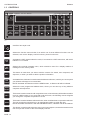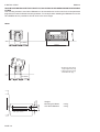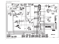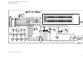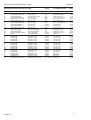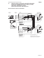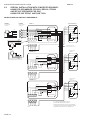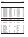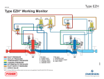
1
TECHNICAL MANUAL
FOR
COMPACT VHF DSC RM2042
S.P. RADIO A/S
AALBORG
DENMARK
RM2042
INSTALLATION INFORMATION RM2042
This VHF DSC RM2042 is delievered with the service switch in position Service Mode. After programming
of MMSI number the service switch must turned into position User Mode. Please refer to the drawing below.
User mode
9401
Service mode
RM2042
CONTENTS
9716
1
1.1
1.2
1.3
1.4
INTRODUCTION
GENERAL DESCRIPTION
TECHNICAL DATA
CONTROLS
PRINCIPLE OF OPERATION AND BLOCK DIAGRAM
1-2
1-3
1-4
1-6
2
2.1
2.2
2.3
2.4
2.5
INSTALLATION
MOUNTING POSSIBILITIES
POWER SUPPLY
HANDSET
ANTENNA
ELECTRICAL CONNECTIONS
2-1
2-5
2-5
2-5
2-6
3
3.1
3.2
3.3
3.4
3.5
3.6
3.7
3.8
3.9
3.10
SERVICE
MAINTENANCE
ALIGNMENT INSTRUCTIONS
PROPOSAL FOR NECESSARY TEST EQUIPMENT
TROUBLE SHOOTING
PERFORMANCE CHECK
ADJUSTMENT PROCEDURE
REPLACEMENT OF COMPONENTS
REPLACEMENT OF MODULES
NECESSARY ADJUSTMENTS AND CHECK AFTER REPAIR
PIN CONFIGURATIONS
3-1
3-1
3-2
3-3
3-3
3-6
3-9
3-9
3-10
3-12
4
4.1
MECHANICAL DESCRIPTION
MECHANICAL DISASSEMBLING AND UNITS LOCATION
4-1
5
5.1
5.2
5.3
5.4
5.6
CIRCUIT DESCRIPTION AND SCHEMATIC DIAGRAMS
INTERFACE (MODULE 1) PART NO. 626941
MICROPROCESSOR (MODULE 2) PART NO. 626942
RECEIVER (MODULE 3) PART NO. 626943
DISPLAY UNIT (MODULE 4) PART NO. 626944
KEYBOARD UNIT (MODULE 6) PART NO. 625636
5-1
5-7
5-13
5-23
5-27
6
6.1
6.2
6.3
MICROTELEPHONE INSTALLATION
SPECIAL INSTALLATION WITH 2 MICROTELEPHONES
SPECIAL INSTALLATION WITH 3 MICROTELEPHONES:
MECHANICAL DIMENSIONS FOR HANDSET
6-3
6-4
6-5
7
PARTS LIST
RM2042
CONTENTS
9716
1
INTRODUCTION
1.1
GENERAL DESCRIPTION
1-2
1.2
TECHNICAL DATA
1-3
1.3
CONTROLS
1-4
1.4
PRINCIPLE OF OPERATION AND BLOCK DIAGRAM
1-6
RM2042
1
INTRODUCTION
The RM2042 VHF receiver modem, has been developed to fullfil the international requirements stated
by IMO, in the Global Maritime Distress and Safety System,known as GMDSS.
The RM2042 is the first self-contained receiver-modem on the market, which includes a separate receiver
with continous watch on calling ch. 70, and a fullfeatured CLASS A modem for reception and generation
of all types of calls.
Combined with a VHF in the compact 2000 program, a complete fully automatic VHF-communication
system can be build. Furthermore the units can be combined with other compact 2000 units to form a
complete GMDSS installation.
The RM2042 combines the IMO requirements on safety, with a lot of user convenient features to be used
in normal VHF-communication. And of course a high security scrambler can be combined with the
system.
This advanced communication controller uses a lot of front end technologies, including a complete new
range of components as well as the well known mechatronic design. Resulting in a high quality product,
able to withstand the harsh environmental conditions present at sea.
In spite of all the precautions taken in the design of this unit, a regular service and maintenance is
recommended, to increase unit life-time and user safety.
S.P. Radio is the European leading manufacturer of maritime radio communication equipment - a position
which has been maintained by means of constant and extensive product development. We have a worldwide network of dealers with general agencies in fifty countries. All our dealers are well-trained, and will
be able to make service on all products.
PAGE 1-1
1 INTRODUCTION
RM2042
1.1 GENERAL DESCRIPTION
RM2042
is a complete VHF receiver-modem, for digital selective calling on the VHF-channels.
RM2042
maintains a continous watch of the calling channel 70, by means of the build-in receiver.
RM2042
decodes and encodes all the messages applicable for a VHF Class A DSC-equipment, as
prescribed by international authorities.
RM2042
is intended for use, both as a part of the safety system on board, as well as a convenient
automatic calling device ship/ship, ship/shore and when implemented from land telephone
subscriber to ship.
RM2042
can be connected to the C2149 GMDSS alarm unit, for remote control of distress calls.
RM2042
has an output for an external alarm unit, indicating reception of distress calls.
RM2042
has an NMEA0183-input, for direct connection to on-board navigational equipment, giving
automatic position update in DSC calls.
RM2042
can be connected to a standard line printer for print out of received messages and other
valueable informations.
RM2042
includes as a standard, an electronic memory message bank for different kinds of calls.
RM2042
includes a user programable quick-call register, not only for numbers, but for complete user
composed DSC-calls.
RM2042
includes a real-time clock with battery back-up.
RM2042
uses a fully alpha-numeric LCD-display, for read-out of all kinds of messages in plain
language.
RM2042
supplies the user with a menu-guided programming interface, making it an easy task to
compose all kinds of calls.
RM2042
can be used for channel selection on your new Compact 2000 VHF transceiver.
RM2042
is housed in a corrosion resistant metal cabinet with a green nylon finish.
RM2042
can of course be used in a manual set-up, as a DSC-encoder, providing the connected VHFunit with key information etc.
PAGE 1-2
1 INTRODUCTION
RM2042
1.2 TECHNICAL DATA
Complies with IMO, ITU, CEPT and other national requirements.
GENERAL
Operation:
As CCIR Rec. 541-3
Protocol:
As CCIR Rec. 493-4 as
VHF Class A equipment.
Printer Interface:
Parallel Centronics.
Navigator Interface:
NMEA 0183
Power Supply:
12V DC -10% to +30%
Power Consumption:
Standby typ. 0.1A
Maximum 0.4A
Temperature Range:
-20 C to +55 C
Dimensions:
Height:
Width :
Depth :
Weight:
App. 2kg.
98mm
225mm
150mm
RECEIVER WITH DECODER
Receiver frequency:
156.525MHz.
Sensitivity:
Symbol error rate below
0.01 at 0.25uV pd.
Spurious radiation:
Less than 2nW.
ENCODER
Modulation:
1700 Hz +- 400 Hz
1200 Baud +- 30 ppm
Output level:
Adjustable between +-10 dBm
in 600 ohms balanced output.
Tx key information:
Vcc or GND.
Programable encoder
output delay:
1 mSec. to 255mSecs.
PAGE 1-3
1 INTRODUCTION
RM2042
1.3 CONTROLS
SAILOR
COMPACT VHF DSC RM2042
S.P. RADIO DENMARK
VOL
O
F
F
ABC
1
JKL
4
STU
FUNC
VHF
CH
RX
MSG
EDIT
DIS
TRESS
ADDR
BOOK
CALL
SEND
LAST
NEXT
7
DEF
3
2
MNO
PQR
5
VWX
8
DEG
.
GHI
6
YZ-
9
STOP
0
ENT
27552
VOL
O
F
F
FUNC
VHF
CH
RX
MSG
EDIT
DIS
TRESS
ADDR
BOOK
On/off/vol turn-style knob.
Selects the function menu window, from which one of seven different functions can be
selected, such as the display control functions, printer function etc.
Activates the VHF channel selection mode, if connected to a VHF transceiver, with serial
interface i.e. RT 2O48.
Selects the received message menu, which should be used for a display readout of
messages in the memory bank.
This button is used when you want to edit the content of a stored, user composed, call
sequence, or when you want to edit the position information.
Activated alone, this button is used to enter the distress call menu, in which you can compose
your distress message to be transmitted.
NOTE! Activated simultaneous with the SEND-button, a distress call will be initiated.
Selects the user programmed address book, where you can save up to forty different
complete call sequences.
CALL
This button is used to enter the call composition menu, where the entry will be either a station
name or a MID number. If you press Edit under this menu, the following menus will guide
you through the complete composition of a call.
SEND
This button is used to initiate a call transmission, when a call has been composed or selected.
The unit permits the transmission by an appropriate readout to guide the user.
NOTE! Activated simultaneous with the DISTRESS-button, a distress call will be initiated.
NEXT
PAGE 1-4
This button is used to select the next menu in an input sequence, and at the same time the
user accepts the content of the actual display read-out.
1 INTRODUCTION
RM2042
This button is used to step backward, to the last selected menu window in an input sequence.
LAST
These buttons is used to scroll between the possible choices in the actual diplayed menu.
Note that these buttons only will be active, when their signs are shown in the display readout.
These buttons are used to scroll between the input fields in the actual displayed menu
window. When an input has been keyed in, and the <-button is pushed the last input will be
cleared.
ABC
1
DEG
.
STOP
ENT
Digits 0 to 9, used for numerical input data to the unit.
These characters will be selected when the user is in a mode where the unit accepts
alphabetic characters. At the first activation the first character will be displayed in the actual
display input field, at the second activation the second character will be displayed etc. When
‘>’-button is activated, the displayed character is selected, and the next input field is shown
with a blinking readout.
This button is used as a delimiter, when time data or position data are entered from the
keyboard.
This key is used to accept the displayed station data in a call composition. When the data
has been accepted it will be possible to enter a telephone number, if the entered station is
a coast station.
The enter button can also be used to accept entered keyboard inputs, when valid data has
been entered in a menu window.
DEG
Selects the degree sign in an input sequence for position data.
STOP
Stops the build-in alarm circuits, when a distress message has been received.
.
ENT
PAGE 1-5
1 INTRODUCTION
RM2042
1.4 PRINCIPLE OF OPERATION AND BLOCK DIAGRAM
RECEIVER
The RF-signal from the antenna is feed to the input amplifier circuit. Here is the initial filtering made by
means of a fixed, double tuned filter before the signal is amplified in the front-end amplifier. This amplifier
is followed by another fixed, double tuned filter. The amplified and filtered signal is feed to the first mixer
stage.
This stage converts the received signal to the first IF frequency on 15.3 MHz. The local oscillator for
this stage is created by means of an XTAL oscillator running at 141.225MHz.
The signal is filtered by means of an XTAL-filter, amplified and then feed to the integrated IF-circuit. This
circuit includes the second XTAL-oscilllator circuit running at 14.85MHz, the second mixer stage and
following limiting amplifiers and detector circuits.
The filtering on the second IF-frequency at 450kHz, is made by means of a ceramic filter.
The detected AF-signal is led through an electrical controlled switch, which is only used for loop back
test purpose. The output from this switch is filtered in the deemphasis filter, before the AF signal selection,
where the selection between the build-in channel-70 receiver and the connected VHF radiotelephone is
performed.
The switch setting of the AF selection is determined by the actual operation of the unit and signal strength
on Channel-70, giving full priority to the Channel-70 receiver output.
From the connected VHF-radiotelephone, the detected AF-signal is feed to a deemphasis filter and a
carrier detect circuit, which provides the needed signals for the demodulator when you are using the public
call facilities.
The selected AF-signal is furthermore feed to the interface board, where it is amplified to source an
internal loudspeaker.
The FSK-modem performs the demodulation of the received FSK-signal, and the modulation of the AFsignal for the transmitter. The circuit is controlled from the microprocessor board.
Internal power supply for the board, is generated with two regulators, one for 5V and one for 10V.
A power low condition is signaled from the 10V regulator to the microprocessor unit, to secure a controlled
power down sequence.
INTERFACE
This module provides the necessary connections between the modules and between the modules and
the externally connected equipment, such as power supply, VHF-transceiver, telephone handset, printer
etc.
This unit must be supplied with 12V DC, which can be provided either directly from batteries or from N420,
24 to 12V converter. The proper operation of the ON/OFF switch is selected by means of the 12/24V wiring
circuit.
Fuse and over/reverse-voltage protection is placed on this module as well.
The 5V power supply for internal digital boards are made on this unit.
The AF power amplifier for the loudspeaker is supplyed by its own 5V regulator and the AF comes from
the receiver module. Alarm and mute signals are generated on the microprocessor module and feed to
the amplifier chain.
Distress channel information for a connected scrambler, is buffered and level shifted, before it is feed
to the 9-pole connector.
AF output for the connected transmitter is buffered and level adjusted in different amplifiers.
When the unit is operating in an automatic system with a VHF-transceiver, is the AF output delivered
as an unbalanced signal adjusted in level to fit the microphone input sensitivity of the transceiver.
When the unit is operating as a DSC-encoder is the AF output port swiched to supply the signal on a 600
ohm balanced output port. The level can be adjusted to 0dBM 10dB by means of a trimming
potentiometer.
When the VHF port communication switch is set for an automatic system, the serial communication link
to the transceiver will be connected to the 9 pole output connector for the VHF.
The remaining circuits on this module consists of input buffers and level shifters for the i/o links to the
microprossor. These links are used for the NMEA interface, printer interface and the interface to C2149,
remote distress unit, or a PC for programming or remote control.
PAGE 1-6
1 INTRODUCTION
RM2042
MICROPROCESSOR
The microprocessor module contains as the central unit, the microprocessor IC, a fast 16 bit type, with
its external program memory and RAM circuits.
The microprocessor clock-signal is derived from an 8 MHz XTAL-oscillator.
The non-volatile memory consist of a single 8kByte EEPROM, where the received messages and internal
programable settings are stored.
As the microcomputer operates with an asyncroneous bus-configuration, some external control logic
is needed to generate the appropriate interrupt signals etc. This block includes the reset circuitry as well.
Address selection of the individual peripheral devices is done by means of a 4 to 16 line address decoder.
The answer back from these circuits to the microprocessor, is done via the uP control logic.
The time division on the microprocessor is partially determined by the outputs from the programable
timers, and partially by the real time clock circuit.
The real time clock circuit is operating with an external XTAL at 32.768kHz, and has a separate primary
battery back-up, to preserve the time settings of the equipment.
The reference clock for the FSK decoder and encoder, is derived from a 4.9152MHz XTAL oscillator,
which among others are devided down to a 1200Hz signal.
Communication with the FSK-modem is done via an USART.
The printer interface is made by means of a standard i/o port circuit, placed on the interface module, while
the strobe pulse needed for the printer is generated by a few gates on this module.
The serial communication with external equipment, is executed via three USART’s placed on the interface
module.
An i/o port circuit, is used for the interface between the microprocessor and the different single bit control
signals. The same circuit is used when the keyboard matrix are scanned.
This module includes, as well, the +5V to -5V voltage converter, the output of which is used on the display
module for the LCD-display.
The voltage for the keyboard light, for night illumination, are also turned on and off on this module.
The switch S1 is used in service.
DISPLAY UNIT
The display unit consist of two circuit boards.
One board connected directly to the microprocessor module. Which includes a D/A converter to control
the DC-amplifiers for viewing angel control and display backlight control, and a socket for connection
to the display module.
The display is a standard dot-matrix LCD-display module, which includes the necessary drivers and
parallel communication circuits.
Power on/off switch and AF-volume potentiometer is mounted on this unit as well.
This unit has been developed to be used in RM2150/51 as well, the identity programming needed is made
by means of a jumper on P5.
KEYBOARD
The keyboard module is a standard module for the 2100-series of products. It consist of a 4x7 keybord
matrix, and light emitting diodes used for night illumination of the keyboard.
PAGE 1-7
1 INTRODUCTION
RM2042
BLOCK DIAGRAM RM2042
RECEIVER
(MODULE 3)
14.850MHz
Rx
amp.
15.3MHz
IF-filter &
amp.
First
mixer
Limit amp.
AF-detect
RF-level det.
2’d Mixer
& osc.
MICROPROCESSOR
(MODULE 2)
DISPLAY UNIT
(MODULE 4)
AF-filter
-6 dB/oct.
+5V
1’st local
osc.
141.225 MHz
450kHz
2’d IFfilter
Buffer
amp.
8.000MHz
XTAL
osc.
Carrier
Detect
PROM
memory
P5
2
EPROM
memory
LCD
Display
module.
View angel
contrrol
+10V
AF-Switch
Control
logic.
+10V reg.
Power fail
gen.
Display
backlight
control
4.9152 MHz
XTAL osc.
&
divider
+5V
AF-filter
-6dB/oct.
+5V reg.
Carrier
Detect
Modulation
det. logic.
Rx-AF
filter
FSK
modem.
RAM
memory
I/O
ports
Tx-AF
filter
VOL
ON/OFF
S1
1
2
2
8
1
1
Modem
commuc.
int.f.
uP.
unit.
Cicuit
select
decoder
Printer
strobe
pulse
gen.
uP
control
logic.
w.reset
Program
able
timers
2
INTERFACE
(MODULE 1)
Power
failure
reset
AF-amp
w.mute.
1
1
2
+5V
12V/24V
Wiring circ.
Distress
ch.inforn.
Ext.alarm.
+5V
reg.
Tx-AF
amps.
2
3
Fuse/rev.
voltage
protection
NMEA
data intf.
3
1
VHFport conn.
switch
Printf. Intf.
&
I/O-Ports
VHFserial com.
C2149/
PC intf.
16
1
2
1
1
2
1
1
1
1
7
Power con.
P3
Vcc
+5V
Keyboard
light on/off
2
Keyboard
matrix
Real time
clock
32.76kHz
Voltage
converter
+
-
3
1
6
KEYBOARD
(MODULE 6)
2
Handset
J1
3
9
1
9
VHF
P2
Keyboard
backlight
+5V
1
25
PRINTER
J4
1
4
C2149/PC
J3
2
NMEA
J2
27502
PAGE 1-9
RM2042
CONTENTS
9716
2
INSTALLATION
2.1
MOUNTING POSSIBILITIES
2-1
2.2
POWER SUPPLY
2-5
2.3
HANDSET
2-5
2.4
ANTENNA
2-5
2.5
ELECTRICAL CONNECTIONS
2-6
RM2042
2
INSTALLATION
2.1 MOUNTING POSSIBILITIES
The VHF DSC RM2042 cabinet is designed in a module called a mini 1/4 box. For this module we can
supply a wide variety of installation brackets etc. which will be described below. We have made a drawing
including dimensions and drilling plan for each type and we kindly ask you to look at the drawing for the
type in question.
VHF DSC RM2042 AND VHF RT2048 MOUNTED ON TOP OF EACH OTHER USING H2067
MOUNTING BRACKET FOR TABLETOP, BULKHEAD OR DECKHEAD FOR MINI 1/4 BOX AND
H2072 LASHING KIT.
This mounting bracket H2067 and lashing kit H2072 is used when RM2042 is to be mounted on top of
each other and next to other units in the Compact 2000 programme mounted in H2055 mounting brackets.
215mm
H2072
27599
60mm
min 80mm*
55mm min 120mm**
213mm
225mm
* dimensions when using
a right-angled VHF plug
** dimensions when using
a standard VHF plug
Weight:
Mounting kit H2067:
Mounting kit H2072:
VHF RT2048:
VHF DSC RM2042:
0.5 kg
0.1 kg
3.2 kg
2.0 kg
PAGE 2-1
2 INSTALLATION
RM2042
H2067 MOUNTING BRACKET FOR TABLETOP, BULKHEAD OR DECKHEAD MOUNTING FOR MINI
1/4 BOX
This mounting bracket is used when RM2042 is to be mounted next to other units in the Compact 2000
programme mounted in H2055 mounting brackets. For example when installing the RM2042 next to the
HF SSB RE2100 it is possible to tilt both units in the same angle.
115mm
H2067
27582
55mm
min 60mm*
55mm min 90mm**
225mm
* dimensions when using
a right-angled VHF plug
** dimensions when using
a standard VHF plug
27593
55 mm
50 mm
27566A
PAGE 2-2
10 mm
175 mm
4 pcs 4.5 mm
36.5 mm
min 80mm*
55mm min 100mm**
8 mm
55mm
Weight:
Mounting kit H2067:
VHF DSC RM2042:
0.5 kg
2.0 kg
2 INSTALLATION
RM2042
H2057 ANGLE HINGES FOR TABLETOP, BULKHEAD OR DECKHEAD MOUNTING FOR MINI 1/4
BOX
H2057 is designed for stationary installation. It offers a lot of mounting possibilities using the different
holes in the angle hinges when tilting the VHF DSC.
min 104mm
H2057
27594
60mm
71mm
min 45mm*
min 75mm**
228mm
252mm
71mm
min 70mm*
min 100mm**
27596
max 177mm
max 177mm
55mm
27595
55mm
71mm
min 70mm*
min 100mm**
4 pcs 5 mm
min 169mm*
max 185mm**
238mm
71mm
59mm
min 156mm
min 99mm
* dimensions when using
a right-angled VHF plug
** dimensions when using
a standard VHF plug
27597
Weight:
Mounting kit H2057:
VHF DSC RM2042:
206mm
71mm
4 pcs 5 mm
59mm
27574A
0.4 kg
2.0 kg
27575A
PAGE 2-3
2 INSTALLATION
RM2042
This mounting kit is used for console flush mounting of 1/4 box and mini 1/4 box.
Free distance must be kept to allow free air circulation, ambient temperature max. 40°C.
H2063
min.160mm
27580
240mm
4.5mm
4.5mm
16mm
16mm
253mm
100mm
4 stk 3.5mm uns for M3 DIN 963
113mm
4 stk 6mm
Mounting kit H2063:
VHF DSC RM2042:
16mm
16mm
Cutting out 231x100mm
27444A
Weight:
4 pcs M3x30
8 pcs M5x8
27581
PAGE 2-4
4 pcs M5x30
1.0 kg
2.0 kg
2 INSTALLATION
RM2042
2.2 POWER SUPPLY
12V OPERATION
The standard power supply for the VHF DSC unit RM2042 is 12V DC.
ANTENNA
2
+ RED 2.5 mm
2
- BLACK 2.5 mm
2
ON/OFF BLUE 0.5 mm
NOT USED WHEN 12V
BATTERY SUPPLY
For 24V DC supply an external power supply with the type number N420 can be used. The N420 is in
principle a 24V DC to 13.2V DC serial regulator.
RM2042
For 110V AC, 127V AC, 220V AC or 237V AC operation, an external power supply with the type number
N163S must be used together with N420.
BLOCK DIAGRAM OF STRAPPING FOR 12V DC
VOL ON/OFF
P3
4
2.3 HANDSET
F1
5
3
6
2A
D2
C4
1
2
3
4
5
6
+13V INT.
2
1
The handset is normaly connected directly to the VHF radiotelephone, but in a VHF DSC installation with
the RM2042, the handset must be connected to this unit instead.
501260
27769
The handset can be placed anywhere near the VHF DSC unit RM2042.
Strap for connection
to external supply (12V)
The cable for the handset is five-cored and must be connected to the rear of RM2042 by means of the
9 pole SUB-D connector J1-1.
For installation of the cable, please see the drawings of the mounting brackets. The cable grommet must
be placed in the most convenient groove in the mounting bracket.
24V OPERATION
If more than one handset is needed, please see section 6, SPECIAL INSTALLATION WITH 2 OR 3
MICROTELEPHONES.
ANTENNA
N420
2
+ RED 2.5 mm
2
- BLACK 2.5 mm
2
ON/OFF BLUE 0.5 mm
RM2042
2.4 ANTENNA
24V DC
All commen 50 antennas, which cover the used frequency range with a reasonable standing wave ratio,
maximum 1.5, are usable.
The antenna is connected to the set by means of a 50 coaxial cable with low loss, e.g. RG213U. At the
cable end a PL259 plug is mounted.
+
-
BLOCK DIAGRAM OF STRAPPING FOR 24V DC
ON/OFF CONTROL TO N420
VOL ON/OFF
The antenna must be placed as high and clear as possible. The horizontal distance to metal parts must
be at least one metre.
P3
4
F1
5
3
6
S. P. Radio has an antenna with the necessary specifications available. The mentioned antenna is
characterized by small external dimensions. For further details, see the special brochure VHF AERIALS.
2A
D2
C4
1
2
3
4
5
6
+13V INT.
2
1
27770
501259
Strap for connection
to N420 (24V)
PAGE 2-5
2 INSTALLATION
RM2042
2.5 ELECTRICAL CONNECTIONS
Connector for
Power Supply
Antenna terminal
501224
Connector for
Handset
Connector for VHF
Radiotelephone
Connector for
Printer
Connector for
PC/Remote Distress
Unit (C2149)
NMEA Interface
POWER CONNECTOR
3
2
4
PIN
PIN
PIN
PIN
PIN
PIN
5
6
1
P3
27772
1
2
3
4
5
6
EXT. LOUDSPEAKER
REMOTE AL. CIRC.
+ BATTERY
EXT. SUPPLY ON/OFF
- BATTERY
EXT. LOUDSPEAKER
1
6
2
3
7
4
8
9
5
CONNECTOR FOR HANDSET
J1
27773
PIN
PIN
PIN
PIN
PIN
PIN
PIN
PIN
PIN
1
2
3
4
5
6
7
8
9
TELEPHONE
GND
MIC.GND
MIC.
KEY
DISTRESS
+12V FROM VHF
PAGE 2-6
2 INSTALLATION
RM2042
5
4
PIN
PIN
PIN
PIN
PIN
PIN
PIN
PIN
PIN
9
3
8
2
7
6
1
CONNECTOR FOR VHF
P2
27774
1
2
3
4
5
6
7
8
9
TELEPHONE
GND
MIC.GND
MIC./TX AF +
KEY
RX AF FROM VHF
DISTRESS / BUS INTERRUPT
DATA/TX AF +12V FROM VHF
1
14
2
3
15
4
16
5
17
6
18
7
19
8
20
21
22
9
10
23
11
24
12
25
13
CONNECTOR FOR PRINTER
J4
PIN
PIN
PIN
PIN
PIN
PIN
PIN
PIN
PIN
PIN
PIN
PIN
PIN
27775
1
2
3
4
5
6
7
8
9
10
11
12
13
STROBE
D0
D1
D2
D3
D4
D5
D6
D7
ACKN
BUSY
PE
SELECT
PIN
PIN
PIN
PIN
PIN
PIN
PIN
PIN
PIN
PIN
PIN
PIN
14
15
16
17
18
19
20
21
22
23
24
25
AUT FEED
ERROR
INIT
SLCT IN
GND
GND
GND
GND
GND
GND
GND
GND
1
6
2
7
3
8
4
9
5
CONNECTOR FOR
PC/REMOTE DISTRESS UNIT
J3
27776
PAGE 2-7
PIN
PIN
PIN
PIN
PIN
PIN
PIN
PIN
PIN
1
2
3
4
5
6
7
8
9
RS232 INPUT
RS232 OUTPUT
GND
DISTRESS UNIT SUPPLY
RM2042
CONTENTS
9716
3
SERVICE
3.1
MAINTENANCE
3-1
3.2
ALIGNMENT INSTRUCTIONS
3-1
3.3
PROPOSAL FOR NECESSARY TEST EQUIPMENT
3-2
3.4
TROUBLE SHOOTING
3-3
3.5
PERFORMANCE CHECK
3-3
3.6
ADJUSTMENT PROCEDURE
3-6
3.6.1
ADJUSTMENT OF INTERFACE (MODULE 1)
3-6
3.6.2
ADJUSTMENT OF MICROPROCESSOR (MODULE 2)
3-7
3.6.3
ADJUSTMENT OF RECEIVER (MODULE 3)
3-8
3.7
REPLACEMENT OF COMPONENTS
3-9
3.8
REPLACEMENT OF MODULES
3-9
3.9
NECESSARY ADJUSTMENTS AND CHECK AFTER REPAIR
3-10
3.9.1
REPAIR/REPLACEMENT OF INTERFACE MODULE (MODULE 1)
3-10
3.9.2
REPAIR/REPLACEMENT OF MICROPROCESSOR MODULE
(MODULE 2)
3-10
3.9.3
REPAIR/REPLACEMENT OF RECEIVER MODULE (MODULE 3)
3-11
3.10
PIN CONFIGURATIONS
3-12
RM2042
3
SERVICE
3.1 MAINTENANCE
PREVENTIVE MAINTENANCE
If the VHF DSC RM2042 has been installed in a proper way the maintenance can, dependent on the
environments and working hours, be reduced to a performance check at the service workshop at intervals,
not exceeding 12 months. A complete performance check list is enclosed in this manual, chapter 3.5
PERFORMANCE CHECK.
Inspection of the antenna, cables, and plugs for mechanical defects, salt deposits, corrosion, and any
foreign bodies shall be done at regular intervals not exceeding 12 months.
Along with each RM2042 a test sheet is delivered in which all the measurements, made in the test
department of the factory, are listed. If the control measurings made in the service workshop should not
show the same values as those listed in the test sheet, the set must be adjusted as specified in
chapter 3.6. ADJUSTMENT PROCEDURE.
CHANGE OF BATTERY FOR BACK-UP
The RM2042 is constructed with a real time clock, which uses a lithium battery for power back-up. By
means of this battery, it is possible to maintain track of time and date even though the RM2042 has been
turned off.
The capacitance of the battery is 180 mAh (milli Ampere hours) and as the real time clock only consumes
a current of about 7µA, the battery should last for a period of at least 2.5 years. However, in practice this
period will be longer, because the battery is only used when the RM2042 is turned off.
The battery is located at the microprocessor (module 2) and is soldered to the PCB to obtain mechanical
stability.
The battery can be ordered from S.P. Radio, Denmark by using the spare part number 47.004.
IMPORTEN! The old battery shall be handed over to the authorities for proper destruction, to avoid
damages of the enviromental by the lithium.
CHANGE OF SOFTWARE
The microprocessor (module 2) includes the two PROM’s U3 and U5, which contain the software. To
locate these PROM’s please see the photo of the microprocessor module given in section 4 in this manual.
NOTE! If the software has to be changed, it is always necessary to change both PROM’s at a time.
3.2 ALIGNMENT INSTRUCTIONS
INTRODUCTION
The measuring values indicated in chapter 5. CIRCUIT DESCRIPTION AND SCHEMATIC DIAGRAMS
are typical values and as indicated it will be necessary to use instruments in absolute conformity with the
list given on the next page.
9403
PAGE 3-1
3 SERVICE
RM2042
3.3 PROPOSAL FOR NECESSARY TEST EQUIPMENT
OSCILLOSCOPE:
Bandwidth
Sensitivity
Input Impedance
E.g. Philips type
DC-35 MHz
2mV/div
1 Mohm//20 pF
PM3050
PASSIVE PROBE:
Attenuation
Input Impedance
Compensation Range
E.g. Philips type
20 dB
10 Mohm//15 pF
10-30 pF
PM8936/091
MULTIMETER:
Sensitivity DC (f.s.d.)
Input Impedance
Accuracy DC (f.s.d.)
E.g. Philips type
100 mV
10 Mohm
1.5%
PM2505
FREQUENCY COUNTER:
Frequency Range
Resolution
Accuracy
Sensitivity
Input Impedance
E.g. Philips type
100 Hz - 165 MHz
1 Hz at f = 100 MHz
1 x 10⁻⁷
100 mV RMS
1 Mohm/30 pF
PM 6674
RF SIGNAL GENERATOR:
Frequency Range
Output Level:
Output Impedance
Type of Modulation
Modulation Frequency
E.g. Rohde & Schwarz
155 MHz - 165 MHz
-124dBm - +7dBm (EMF: 0.25 µVRMS - 1 VRMS)
50 ohm
FM
External: 1.3kHz, 2.1kHz / Internal: 1kHz
CMT
RF MODULATION METER:
Frequency Range
Input Impedance
E.g. Rohde & Schwarz
155 MHz - 165 MHz
50 ohm
CMT
LF SIGNAL GENERATOR:
Frequency Range
Output Level
Output Impedance
E.g. Hewlett-Packard
100 Hz - 3 kHz
10 mV - 1V
50 ohm
HP 8903B
LF DISTORTION METER:
Frequency Range
Distortion Range (f.s.d.)
Input Impedance
Accuracy (f.s.d.)
E.g. Hewlett-Packard
1000 Hz, 1300 Hz, 2100 Hz
0.1-10%
100 kohm
5% of reading
HP 8903B
PAGE 3-2
9403
3 SERVICE
RM2042
3.4 TROUBLE SHOOTING
Trouble shooting should only be performed by persons with sufficient technical knowledge, who have the
necessary measuring instruments at their disposal, and who have carefully studied the operation
principles and structure of the VHF DSC RM2042.
The first thing to check is whether the fault is somewhere in the antennea circuit, the power source, the
handset, or inside the RM2042 it self.
In order to help you during trouble shooting, the section 5. CIRCUIT DESCRIPTION AND SCHEMATIC
DIAGRAMS contains diagrams, principal descriptions, and drawings showing the location of the
individual components. Typical values for the DC and AC voltages are indicated in the diagrams, and also
the test points are indicated in the diagrams.
The RM2042 has a number of trimming cores and trimmers, which must not be touched unless
adjustments as specified in section 3.6. ADJUSTMENT PROCEDURE can be made.
When measuring inside the unit, short circuits must be avoided as the transistors would then be spoiled.
3.5 PERFORMANCE CHECK
CHECK OF SYSTEM PERFORMANCE
With this check procedure it is possible to control the performance of a hole VHF DSC system, which
include the DSC unit it self, the VHF tranceiver, a GPS receiver and a printer.
The idea of this test procedure is first to key-in a call sequence and hereby control the connections to the
key board and display, and the function of these modules. The next step is to send the DSC call to your
self, which is done in the ‘CALL’ menu by keying-in the MID-number of the unit it self. The DSC call is now
generated by the microprocessor and the FSK encoder at the receiver module. The FSK signal is then
modulating the connected VHF radiotelephone and a short piece of wire connected to the antenna
terminal at the VHF will be sufficient to transfer the RF-signal to the channel-70 receiver. The received
signal is then demodulated, decoded, sampled and finally recognized by the microprocessor. As a
response to the receiption of the call, the microprocessor will write the received message to the printer
and at the same time generate a gated tone sequence for the internal loudspeaker.
The primary force of this test is that the function of all modules is controlled and that the connections for
external equipment are checked as well. An other force is the fact that the test procedure does not require
any test equipment.
The check procedure can also be used as a function check after the system has been installed.
1.
Connect the RM2042 to the VHF tranceiver, the printer and the GPS receiver (if available)
2.
Select the ‘FUNC’ menu and then the ‘Position’ menu. Control that the position data is updated by
the GPS receiver.
3.
Select the ‘CALL’ menu and press the ‘up-arrow’ button to key-in the MID-number of the DSC unit
it self.
4.
Press ‘NEXT’ and select ‘Position’ by means of the ‘left-arrow’ and the ‘NEXT’ button.
5.
Press ‘NEXT’ and ‘SEND’ for transmission of the DSC call.
6.
The DSC call should now be received by the RM2042 and the alarm signal will be heard in the
internal loudspeaker. The RM2042 will write the received message to the printer.
9403
PAGE 3-3
3 SERVICE
RM2042
CHECK OF RECEIVER SENSITIVITY
The receiver sensitivity is controlled by applying a RF-signal to the antenna terminal and then measuring
the output signal-to-noise ratio (SND/N) by means of a voltmeter.
1.
Connect a RF-signal generator to the antenna input and adjust the carrier level to -119 dBm (EMF:
-6 dB/µV). Modulate the carrier with 1 kHz to a peak frequency diviation of 3 kHz.
2.
Connect a voltmeter to the analog switch output, pin 14 at U6-3, for measuring the AC-voltage.
3.
Read the meter deflection by means of the dB scale.
4.
Remove the modulation and control that the output level decrease more than 12 dB.
CHECK OF RECEIVER DISTORTION
The receiver distortion is controlled by applying a RF-signal to the antenna terminal and then measuring
the output distortion by means of a distortion meter.
1.
Connect a RF-signal generator to the antenna input and adjust the carrier level to -30 dBm (EMF:
83 dB/µV). Modulate the carrier with 1 kHz to a peak frequency diviation of 3 kHz.
2.
Connect a distortion meter to the analog switch output, pin 14 at U6-3, for measuring the receiver
distortion.
3.
The measured distortion shall be less than 3%.
CHECK OF DSC CALL SENSITIVITY
The DSC call sensitivity is controlled by modulating a RF-signal generator with a DSC call, which is
generated by the DSC unit it self.
NOTE! To perform this test, it is necessary to change the operation mode of the RM2042 from user to
service mode. This change of operation mode is only allowed for trained technicians and the information
of how to do it, is therefore only included in the DSC-VHF INSTALLATION GUIDE.
1.
Select the balanced TX AF amplifier as interface to the RF-signal generator, by turning the switch
S1-1 at the interface module into the position: ‘E’.
2.
Connect the output of the balanced TX AF amplifier to the external modulation input of the RFsignal generator. Use pin 4 (TX AF+) and pin 8 (TX AF-) in the 9 pole SUB-D connector P2
(connector for VHF tranceiver).
3.
Connect the output of the RF-signal generator to the antenna terminal of the RM2042.
4.
Apply an external modulated carrier with the frequncy 156.525 MHz to the antenna terminal and
adjust the output level to -113 dBm (EMF: 0 dB/µV).
5.
Change the operation mode of the RM2042 from user to service mode.
6.
Select the ‘FUNC’ menu and then the ‘Test’ menu. Select ‘Dot pattern’ by means of the ‘left-arrow’
or ‘right-arrow’, and press the ‘NEXT’ button.
7.
Adjust the peak diviation at the RF-signal generator to 3400 Hz and press the ‘STOP/ENT’ button
to terminate the transmission of dot pattern.
8.
Select ‘Test call’ by means of the ‘left-arrow’ or ‘right-arrow’ and press ‘NEXT’ to start the continous
transmission of a test call to the unit it self.
9.
Now control that the RM2042 is receiving a continous sequence of individual calls.
10.
Terminate this procedure by turning the RM2042 off. Remember to change the operation mode
back to user mode.
PAGE 3-4
9403
3 SERVICE
RM2042
CHECK OF RX AF FILTER RESPONSE
The response of the RX AF filter is essential for the bit error rate and must therefore be check carefully.
1.
Disconnect any input to the antenna terminal.
2.
Connect a LF-signal generator to pin 6 (RX AF FROM VHF) and pin 2 (GND) in the 9 pole SUBD connector P2-1 at the interface module.
3.
Connect a voltmeter to the output of the RX AF filter for measuring the AC voltage (U8.4-3, pin 14).
4.
Adjust the frequency of the LF-signal generator to 1700 Hz and the output level to 350 mVRMS.
5.
Measure the output level, which shall be 220mVRMS ±30mV. The measured value is used as
reference in the following measurements.
6.
Change the input frequency to 1300 Hz and control that the output level increase with 1 dB ±0.5
dB.
7.
Change the input frequency to 2100 Hz and control that the output level decrease with 2 dB ±0.5
dB with reference to the value measured in point 5.
8.
Change the input frequency to 650 Hz and control that the output level decrease by more than 20
dB with reference to the value measured in point 5.
9.
Change the input frequency to 3000 Hz and control that the output level decrease by more than
20 dB with reference to the value measured in point 5.
CHECK OF TX AF LEVEL
The TX AF level is controlled by checking that the peak diviation of the transmitted RF-signal is correct.
NOTE! To perform this test, it is necessary to change the operation mode of both the RM2042 and the
VHF tranceiver from user to service mode. This change of operation mode is only allowed for trained
technicians and the information of how to do it is therefore only included in the DSC-VHF INSTALLATION
GUIDE.
1.
Connect the RM2042 to the VHF tranceiver by means of the 9 pole SUB-D connector P2-1 at the
interface module.
2.
Reduce the output RF-power from the VHF tranceiver to 1 Watt.
3.
Connect a modulation meter through an attenuator to the antenne terminal at the VHF tranceiver.
NOTE !
To protect the modulation meter from damages caused by the large output voltage,
it is necessary to use an attenuator of about 30dB.
4.
Change the operation mode of the RT2047 or the RT2048 from user to service mode. Select a DSC
VHF channel different from channel 70 and change the operation mode back to user mode.
5.
Change the operation mode of the RM2042 from user to service mode.
6.
Start the transmission of a mark signal by pressing ‘FUNC’ and selecting ‘Test’ and ‘mark’ in the
display.
7.
Control that the peak frequency diviation is 2600 Hz ±10%.
8.
Start the transmission of a space signal.
9.
Control that the peak frequency diviation is 4200 Hz ±10%.
10.
Change the operation mode of the RM2042 back to user mode.
11.
Change the DSC VHF channel setting back to channel 70.
9403
PAGE 3-5
3 SERVICE
RM2042
CHECK OF TX AF DISTORTION
The TX AF distortion is controlled by measuring the distortion of the TX AF signal at pin 4 in the 9 pole
SUB-D connector P2-1 at the interface module.
NOTE! To perform this test, it is necessary to change the operation mode of the RM2042 from user to
service mode. This change of operation mode is only allowed for trained technicians and the information
of how to do it is therefore only included in the DSC-VHF INSTALLATION GUIDE.
1.
Connect a LF-distortion meter to the output of the used TX AF amplifier.
Unbalanced TX AF amplifier: use pin 4 (TX AF+) and pin 2 (GND) in P2-1.
Balanced TX AF amplifier:
use pin 4 (TX AF+) and pin 8 (TX AF-) in P2-1.
2.
Change the operation mode of the RM2042 from user to service mode.
3.
Start the transmission of a mark signal by pressing ‘FUNC’ and selecting ‘Test’ and ‘mark’ in the
display.
4.
Control that the distortion is less than 5%.
5.
Start the transmission of a space signal.
6.
Control that the distortion is less than 5%.
7.
Change the operation mode of the RM2042 back to user mode.
3.6 ADJUSTMENT PROCEDURE
This section contains the adjustment procedures for all adjustable components in the RM2042.
3.6.1
ADJUSTMENT OF INTERFACE (MODULE 1)
ADJUSTMENT OF UNBALANCED TX AF AMPLIFIER
When the RM2042 is operating as an automatic system together with one of our VHF tranceiver, the TX
AF output is delivered as an unbalanced signal adjusted in level to give a modulation index of 2, measured
at the transmitter output. During the adjustment, the RM2042 must be connected to the same VHF
tranceiver as it is going to be installed with. This demand is motivated by the fact, that the microphone
input sensitivity may vary from one tranceiver to an other.
The unbalanced signal is amplified by the operational amplifier U3.3 and the output level is adjusted by
means of the trimpot R22-1.
NOTE! To perform this test, it is necessary to change the operation mode of the RM2042 and the VHF
tranceiver from user to service mode. This change of operation mode is only allowed for trained
technicians and the information of how to do it is therefore only included in the DSC-VHF INSTALLATION
GUIDE.
1.
Connect the RM2042 to the VHF tranceiver by means of the 9 pole SUB-D connector P2-1 at the
interface module.
2.
Reduce the output RF-power from the VHF tranceiver to 1 Watt.
3.
Connect a modulation meter through an attenuator to the antenne terminal at the VHF tranceiver.
NOTE !
To protect the modulation meter from damages caused by the large output
voltage, it is necessary to use an attenuator of about 30dB.
4.
Change the operation mode of the RT2047 or the RT2048 from user to service mode. Select a DSC
VHF channel different from channel 70 and change the operation mode back to user mode.
5.
Change the operation mode of the RM2042 from user to service mode.
6.
Turn the switch S1-1 at the interface (module 1) into the position: ‘1’.
PAGE 3-6
9403
3 SERVICE
RM2042
7.
Start the transmission of a mark signal by pressing ‘FUNC’ and selecting ‘Test’ and ‘mark’ in the
display.
8.
Adjust R22 until the peak frequency diviation is 2600 Hz ±10%.
9.
Start the transmission of a space signal.
10.
Control that the peak frequency diviation is 4200 Hz ±10%.
11.
Change the operation mode of the RM2042 back to user mode.
12.
Change the DSC VHF channel setting back to channel 70.
ADJUSTMENT OF BALANCED TX AF AMPLIFIER
When the RM2042 is used as an encoder in a semi automatic system, the balanced TX AF output has
to be used. The balanced amplifier is build-up around the operational amplifier U3.2-1, the transistor Q41 and the transformer TR1-1. The output level is adjustable to 0 dBm ±10 dB by means of the trimpot R171 and must be adjusted in order to give a modulation index of 2 ±10%. As mentioned in the previous
adjustment procedure, it is necessary to use the same VHF tranceiver during the adjustment as the one
the RM2042 is going to be installed with.
NOTE! To perform this test, it is necessary to change the operation mode of both the RM2042 and the
VHF tranceiver from user to service mode. This change of operation mode is only allowed for trained
technicians and the information of how to do it is therefore only included in the DSC-VHF INSTALLATION
GUIDE.
1.
Repeat point 1 - 5 in the previous adjustment procedure.
2.
Turn the switch S1-1 into the position: ‘E’.
3.
Start the transmission of a mark signal by pressing ‘FUNC’ and selecting ‘Test’ and ‘mark’ in the
display.
4.
Adjust R17 until the peak frequency diviation is 2600 Hz ±10%.
5.
Repeat point 9, 10 and 11 in the previous adjustment procedure.
3.6.2
ADJUSTMENT OF MICROPROCESSOR (MODULE 2)
ADJUSTMENT OF 4.9152 MHz OSCILLATOR
The 4.9152 MHz oscillator is build-up around the inverter U16.4-2 as a gate oscillator and is adjusted by
the trimming capacitor C45-2. The oscillator is used for baud rate generation and must therefore be
adjusted carefully.
1.
Connect a frequency counter by means of a passive probe to the output CT0 (pin 9) of the counter
U20-2.
2.
Adjust C45-2 until the frequency is 2.4576 MHz ±2 Hz.
ADJUSTMENT OF 32.768 kHz OSCILLATOR
The 32.768 kHz oscillator is build-up around U31-2 and is adjusted by the trimmer capacitor C39-2. The
oscillator is used for real time clock generation and must therefor be adjusted carefully.
1.
Connect a frequency counter by means of a passive probe to the MFO output (pin 16) of the
integreted real time clock circuit.
2.
Adjust C39-2 until the frequency is 32.768 kHz ±1 Hz.
9403
PAGE 3-7
3 SERVICE
3.6.3
RM2042
ADJUSTMENT OF RECEIVER (MODULE 3)
ADJUSTMENT OF FIRST LOCAL OSCILLATOR
The 1st. local oscillator is adjusted by the coil L6-3.
1.
Connect a frequency counter by means of a passive probe to the tap of the two capacitors C893 and C90-3.
2.
Adjust the coil L6-3 by a plastic or ceramic stick until the frequency is 141.225 MHz ±100 Hz.
ADJUSTMENT OF SECOND LOCAL OSCILLATOR
The 2nd. local oscillator is partly build into the integreted IF circuit and is adjusted by the external trimmer
capacitor C34-3. The oscillator is adjusted by measuring the frequency of the down converted signal at
the 2nd. IF = 450 kHz.
1.
Apply an unmodulated carrier with the frequncy 156.525 MHz to the antenna terminal and adjust
the output level of the RF-signal generator to 0 dBm (EMF: 113 dB/µV).
2.
Connect a frequency counter by means of a passive probe to the limiter output (pin 7) at U1-3.
3.
Adjust C34-3 until the frequency is 450 kHz ±25 Hz.
NOTE!
Be careful not to press the trimming capacitor, while the adjustment is performed.
The trimming capacitor is constructed with a ceramic plate and is therefore easily
damage by pressure.
ADJUSTMENT OF FRONT-END FILTERS AND MIXER TRANSFORMERS
The front-end filters contains four adjustable coils and the mixer includes two adjustable transformers.
All components are adjusted to maximum meter deflection at the field stregth meter output and the mixer
output transformer TR2-3 is afterwards adjusted to minimum distortion.
1.
Apply an unmodulated carrier with the frequncy 156.525 MHz to the antenna terminal and adjust
the output level to -80 dBm (EMF: 33 dB/µV).
2.
Connect a multimeter to the field strength meter output, pin 13 at U1, for measuring the DC-voltage.
3.
Adjust the coils L1-3, L2-3, L3-3, L4-3 and the two transformers TR1-3 and TR2-3 to maximum
meter deflection.
4.
Connect a distortion meter to the output of the deemphasis filter, pin 8 at U3.3-3.
5.
Modulate the RF-carrier with a 1 kHz tone to a peak diviation of 3 kHz. Increase the RF-carrier level
to -30 dBm (EMF: 83 dB/µV).
6.
Adjust the output transformer TR2-3 to minimum distortion and control that the distortion is less
than 3%.
ADJUSTMENT OF AF OUTPUT LEVEL
The AF output level from the detector is adjusted to match the RX AF input level from the connected VHF
tranceiver.
1.
Connect a RF-signal generator to the antenna input and adjust the carrier level to -50 dBm (EMF:
63 dB/µV). Modulate the carrier with 1 kHz to a peak frequency diviation of 3 kHz.
2.
Connect a multimeter to the analog switch output, pin 14 at U6-3 for measuring the AC-voltage.
3.
Adjust the trimpot R66-3 until the output level is 260 mVRMS ±5mV.
PAGE 3-8
9403
3 SERVICE
RM2042
ADJUSTMENT OF TRIGGER LEVEL FOR CHANNEL-70 CARRIER DETECT
The channel-70 carrier detect circuit is constructed as a noise triggered squelch and the trigger level is
adjusted by the trimming resistor R36-3.
1.
Apply an unmodulated carrier with the frequncy 156.525 MHz to the antenna terminal and adjust
the output level of the RF-signal generator to -126 dBm (EMF: -13 dB/µV).
2.
Connect a multimeter or an oscilloscope to the output of the voltage comparator, pin 14 at U4.33, for measuring the DC-voltage.
3.
Turn the trimpot R36-3 counter clockwise until the output goes high.
4.
Increase the RF-input level to -125 dBm (EMF: -12 dB/µV).
5.
Now adjust R36-3 clockwise until the output goes low.
6.
Increase the RF-input level to -122 dBm (EMF: -9 dB/µV) and control that the output goes high.
ADJUSTMENT OF TRIGGER LEVEL FOR VHF CARRIER DETECT
The VHF carrier detect circuit is identical to the corresponding carrier detect circuit for the build-in
channel-70 receiver and the trigger level is adjusted by the trimming resistor R93-3.
1.
Connect the RM2042 to the VHF tranceiver by means of the 9 pole SUB-D connector.
2.
Apply an unmodulated carrier with the frequncy 156.525 MHz to the antenna terminal at the
connected VHF tranceiver and adjust the output level of the RF-signal generator to -126 dBm
(EMF: -13 dB/µV).
3.
Connect a multimeter or an oscilloscope to the output of the voltage comparator, pin 13 at U4.43, for measuring the DC-voltage.
4.
Turn the trimpot R93-3 counter clockwise until the output goes high.
5.
Increase the RF-input level to -125 dBm (EMF: -12 dB/µV).
6.
Now adjust R93-3 clockwise until the output goes low.
7.
Increase the RF-input level to -122 dBm (EMF: -9 dB/µV) and control that the output goes high.
ADJUSTMENT OF 10V
The 10V power supply is used by the build-in channel-70 receiver and the FSK encoder/decoder.
1.
Connect a voltmeter to the output of the 10V power regulator, pin 1 at U10-3.
2.
Adjust the DC voltage to 10V ±10mV.
3.7 REPLACEMENT OF COMPONENTS
When replacing integreted circuits, transistors, diodes, resistors, capacitors and similar components you
must use a small “pencil” soldering iron with a maximum temperature of 300°C (572°F). The soildering
must be performed rapidly to avoid superheating and the use of a desoldering wire is recommended, as
otherwise there is a risk that both the components and the printed circuit will be spoiled.
3.8 REPLACEMENT OF MODULES
If a fault has been located to a single module, it may often be worth-while to replace it and then repair it
later on.
9403
PAGE 3-9
3 SERVICE
RM2042
3.9 NECESSARY ADJUSTMENTS AND CHECK AFTER REPAIR
3.9.1
REPAIR/REPLACEMENT OF INTERFACE MODULE (MODULE 1)
REPLACEMENT OF INTERFACE MODULE (MODULE 1)
If the RM2042 is used in a semi automatic system, where the balanced TX AF amplifier is used, it is
necessary to perform section 3.6.1, “ADJUSTMENT OF BALANCED TX AF AMPLIFIER” and then
perform section 3.5, “CHECK OF SYSTEM PERFORMANCE”
However, if the RM2042 is used in a automatic system with RT2047 or RT2048 and if the interface module
is replaced with a new one, which is factory adjusted, it is only necessary to perform section 3.5, “CHECK
OF SYSTEM PERFORMANCE”.
REPAIR IN UNBALANCED/BALANCED TX AF AMPLIFIER (MODULE 1)
Perform section 3.6.1, “ADJUSTMENT OF UNBALANCED/BALANCED TX AF AMPLIFIER”.
Perform section 3.5, “CHECK OF SYSTEM PERFORMANCE”.
REPAIR IN S.P. BUS INTERFACE (MODULE 1)
Connect the RM2042 to the VHF tranceiver (RT2047 or RT2048) by means of the 9 pole SUB-D connector
P2-1 and select the ‘VHF CH’ menu at the RM2042.
Now try to key-in a channel number with two digits (e.g. channel number 12) and control that the channel
number also change in the display at the VHF tranceiver.
REPAIR IN PRINTER INTERFACE (MODULE 1)
Press the ‘FUNC’ button and select the ‘Print’ menu, by pressing ‘NEXT’. Use the ‘up-arrow’ or ‘downarrow’ to select ‘Options/setup’. Start the print procedure by pressing ‘NEXT’ and control that the options/
setup parameters are printed correctly.
REPAIR IN C2149/PC INTERFACE (MODULE 1)
Connect a GPS receiver to the remote control unit C2149 and connect this unit to the VHF DSC RM2042.
Disconnect any GPS input to the RM2042 it self.
Press the ‘FUNC’ button and select the ‘Position’ menu. Control that the ships position is continously
opdated and equals the position determined by the GPS receiver.
NOTE! The position update rate may be very slow.
REPAIR IN NMEA INTERFACE (MODULE 1)
Connect a GPS receiver to the VHF DSC unit and control that the ships position is updated as described
above.
3.9.2
REPAIR/REPLACEMENT OF MICROPROCESSOR MODULE (MODULE 2)
REPLACEMENT OF MICROPROCESSOR MODULE (MODULE 2)
If the microprocessor module is replaced with a new one, which is factory adjusted, it is only necessary
to perform section 3.5, “CHECK OF SYSTEM PERFORMANCE”.
REPLACEMENT OF SOFTWARE (MODULE 2)
Perform section 3.5, “CHECK OF SYSTEM PERFORMANCE”.
REPAIR IN 4.9152 MHz OSCILLATOR (MODULE 2)
Perform section 3.6.2, “ADJUSTMENT OF 4.9152 MHz OSCILLATOR”.
Perform section 3.5, “CHECK OF SYSTEM PERFORMANCE”.
PAGE 3-10
9403
3 SERVICE
RM2042
REPAIR IN 32.768 kHz OSCILLATOR (MODULE 2)
Perform section 3.6.2, “ADJUSTMENT OF 32.768 kHz OSCILLATOR”.
Check that the real time clock is performing correctly, by inspection of the display.
3.9.3
REPAIR/REPLACEMENT OF RECEIVER MODULE (MODULE 3)
REPLACEMENT OF RECEIVER MODULE (MODULE 3)
If the receiver module is replaced with a new one, which is factory adjusted, it is only necessary to perform
section 3.5, “CHECK OF SYSTEM PERFORMANCE”.
REPAIR IN RECEIVER FRONT-END, FIRST MIXER AND 1st. IF. (MODULE 3)
Perform section 3.6.3, “ADJUSTMENT OF FRONT-END FILTERS AND MIXER TRANFORMERS”.
Perform section 3.5, “CHECK OF RECEIVER SENSITIVITY”.
REPAIR IN LO1. (MODULE 3)
Perform section 3.6.3, “ADJUSTMENT OF FIRST LOCAL OSCILLATOR”.
Perform section 3.5, “CHECK OF RECEIVER SENSITIVITY”.
REPAIR IN LO2 AND 2nd IF. (MODULE 3)
Perform section 3.6.3, “ADJUSTMENT OF SECOND LOCAL OSCILLATOR”.
Perform section 3.6.3, “ADJUSTMENT OF AF OUTPUT LEVEL”.
Perform section 3.5, “CHECK OF RECEIVER SENSITIVITY”.
REPAIR IN AF FILTERS (MODULE 3)
Perform section 3.5, “CHECK OF RX AF FILTER RESPONSE”.
Perform section 3.5, “CHECK OF DSC CALL SENSITIVITY”.
REPAIR IN FSK ENCODER/DECODER (MODULE 3)
Perform section 3.5, “CHECK OF TX AF LEVEL”.
Perform section 3.5, “CHECK OF TX AF DISTORTION”.
Perform section 3.5, “CHECK OF DSC CALL SENSITIVITY”.
REPAIR IN CHANNEL-70 CARRIER DETECT (MODULE 3)
Perform section 3.6.3, “ADJUSTMENT OF TRIGGER LEVEL FOR CHANNEL-70 CARRIER DETECT”
REPAIR IN VHF CARRIER DETECT (MODULE 3)
Perform section 3.6.3, “ADJUSTMENT OF TRIGGER LEVEL FOR VHF CARRIER DETECT”
9403
PAGE 3-11
3 SERVICE
RM2042
3.10 PIN CONFIGURATIONS
DIODE:
BAT54S (SOT-23 CASE)
2
2
3
1
1
3
TRANSISTOR:
BC848B, BC858B, BFR92A (SOT-23 CASE)
C
E
B
C
BF996SB (SOT-143 CASE)
C
G2
D
G1
S
E
NPN
C
C
E
G2
G1
B
B
BCP52-16, BCP55-16 (SOT-223 CASE)
D
B
E
B
C
C
S
E
B
PNP
E
NPN
PNP
TIS88 (SOT-23 CASE)
1
Source 1
Gate
2
Drain 3
2
Top view
3
VOLTAGE REGULATOR and CONVERTER:
7805 (TO-220 CASE)
78M05 (DPAK PACKAGE)
78L05 (SO-8 PACKAGE)
4
input
1
output
GND
output
GND
1
input
GND
output
input
2
3
2, 4
3
OUTPUT
1
8
INPUT
COMMON
2
7
COMMON
COMMON
3
6
COMMON
NC
4
5
NC
1
output
input
3
GND
2, 3, 6, 7
LP2951 (SO-8 PACKAGE)
OUTPUT
1
8
INPUT
SENSE
2
7
FEED BACK
SHUTDOWN
3
6
5V TAP
GND
4
5
ERROR
LTC1044 (SO-8 PACKAGE)
BOOST
1
8
VDD
CAP+
2
7
OSC
GND
3
6
LV
CAP-
4
5
VD
PAGE 3-12
9403
3 SERVICE
RM2042
INTEGREATED CIRCUIT, ANALOG:
16
15
13
12
Mixer
53k
1
2
3
4
5
6
7
DECOUP
LIMITER OUT
7
LIMITER IN
6
VCC
5
IF OUTPUT
4
X-TAL
3
X-TAL
2
Oscillator
INPUT 2 +
1
9
10pF
1
7
AF OUT
10
AF
Amp
Demodulator
Limiter
Amp
2
FILTER IN
11
Filter
Amp
Squelch Trigger
with Hysteresis
3+
FILTER OUT
SQUELCH
METER
14
8
QUAD IN
10
INPUT 2 -
6
INPUT 2 -
5
INPUT 2 +
4
V CC
3
INPUT 1 +
2
INPUT 1 -
OUTPUT 1
1
11
4+
INPUT 1 +
+
+2
-
1
12
INPUT 1 -
+3
13
V CC
4+
14
OUTPUT 1
10
OUTPUT 2
11
OUTPUT 2
12
+
13
+
14
MUTE
8
GND
INPUT 3 -
9
IF INPUT
INPUT 3 +
MC3372 (SO-16 CASE)
INPUT 4 -
INPUT 4 +
GND
8
OUTPUT 4
OUTPUT 3
9
OUTPUT 3
INPUT 3 -
INPUT 3 +
GND
INPUT 4 +
INPUT 4 -
OUTPUT 4
LM339 (SO-8 PACKAGE)
+
-
LM324 (SO-8 PACKAGE)
TDA7052 (DIL-8 PACKAGE)
VDD
1
VDD
1
8
OUTPUT 2
INPUT
2
7
NC
GROUND
3
6
GROUND
NC
4
5
OUTPUT 1
5
INPUT
GROUND
OUTPUT 1
2
3
8
OUTPUT 2
6
GND
MSM6927 (24-LEAD FLAT-PACK)
9403
PAGE 3-13
3 SERVICE
RM2042
INTEGREATED CIRCUIT, DIGITAL:
R/W
*LDS
*UDS
*AS
D0
D1
D2
D3
D4
D5
D6
D7
D8
D9
D10
D11
D12
9
8
7
6
5
4
3
2
1
68
67
66
65
64
63
62
61
68HC000 (68-LEAD PLCC PACKAGE)
*DTACK
10
60
D13
*BG
11
59
D14
*BGACK
12
58
D15
*BR
13
57
GND
VCC
14
56
GND
CLK
15
55
A23
GND
16
54
A22
GND
17
53
A21
NC
18
52
VCC
*HALT
19
51
A20
*RESET
20
50
A19
*VMA
21
49
A18
E
22
48
A17
*VPA
23
47
A16
*BERR
24
46
A15
*IPL2
25
45
A14
*IPL1
26
44
A13
27
28
29
30
31
32
33
34
35
36
37
38
39
40
41
42
43
*PL0
FC2
FC1
FC0
NC
A1
A2
A3
A4
A5
A6
A7
A8
A9
A10
A11
A12
TOP VIEW
MSM5165/OKI & HM6264/HITACHI (28-LEAD FLAT-PACK)
27PC512 (28-LEAD PLCC PACKAGE)
A0
A1
A2
A3
A4
A5
A6
A7
A8
A9
A10
A11
A12
A13
A14
A15
*E
11
9
8
7
6
PAGE 3-14
A
5
A
4
A
A
29
A
28
A
24
A
27
A
3
A
13
4
15
18
19
20
21
22
Q1
Q2
Q3
Q4
Q5
Q6
Q7
Q8
30
31
2
23
25
*G/VPP
0
10
15
(PWR DWN)
&
EN
9403
3 SERVICE
RM2042
28C64A (32-LEAD PLCC PACKAGE)
71051/NEC & 82C51/OTHERS (28-LEAD PLCC PACKAGE)
71054/NEC & 82C54/OTHERS (28-LEAD PLCC PACKAGE)
9403
PAGE 3-15
3 SERVICE
RM2042
71055/NEC & 82C55/OTHERS (44-LEAD PLCC PACKAGE)
8573A (28-LEAD PLCC PACKAGE)
AD232 (SO-16L PACKAGE)
PAGE 3-16
9403
3 SERVICE
RM2042
MOC207 (SO-8 PACKAGE)
9403
1
8
2
7
3
6
4
5
74HC00 (SO-14 PACKAGE)
74HC02 (SO-14 PACKAGE)
74HC04 (SO-14 PACKAGE)
74HC05 (SO-14 PACKAGE)
74HC08 (SO-14 PACKAGE)
74HC14 (SO-14 PACKAGE)
74HC21 (SO-14 PACKAGE)
74HC32 (SO-14 PACKAGE)
74HC74 (SO-14 PACKAGE)
PAGE 3-17
3 SERVICE
74HC32 (SO-14 PACKAGE)
RM2042
74HC74 (SO-14 PACKAGE)
74HC132 (SO-14 PACKAGE)
74HC138 (SO-16 PACKAGE)
74HC148 (SO-16 PACKAGE)
PAGE 3-18
9403
3 SERVICE
RM2042
74HC154 (SO-24L PACKAGE)
74HC174 (SO-16 PACKAGE)
74HC393 (SO-14 PACKAGE)
74HC4053 (SO-16PACKAGE)
74HC4040 (SO-16 PACKAGE)
9403
PAGE 3-19
RM2042
CONTENTS
9716
4
MECHANICAL DESCRIPTION
4.1
MECHANICAL DISASSEMBLING AND UNITS LOCATION
4-1
RM2042
4
MECHANICAL DESCRIPTION
4.1 MECHANICAL DISASSEMBLING AND UNITS LOCATION
Top view
Buttom view
Screw for front plate
501225 501226 501227
501229 501232 501236
Screw for cover
Front view without frontplate
Screw for Microprocessor module
Screw for Display section
Clock backup battery
DSC AF-output
selection switch
Unbalanced AF-output
level adjustment
Switch for mode select
Balanced AF-output
level adjustment
Key information switch
727499
727498
Cable for Display module
Remove indicated cable and screws for removal of Microprocessor module, and draw the module gently toward the
front
PAGE 4-1
RM2042
CONTENTS
9716
5
CIRCUIT DESCRIPTION AND SCHEMATIC DIAGRAMS
5.1
INTERFACE (MODULE 1) PART NO. 626941
5-1
5.2
MICROPROCESSOR (MODULE 2) PART NO. 626942
5-7
5.3
RECEIVER (MODULE 3) PART NO. 626943
5-13
5.4
DISPLAY UNIT (MODULE 4) PART NO. 626944
5-23
5.6
KEYBOARD UNIT (MODULE 6) PART NO. 625636
5-27
RM2042
5
CIRCUIT DESCRIPTION AND SCHEMATIC DIAGRAMS
5.1 INTERFACE (MODULE 1) PART NO. 626941
All connections to external equipment and the corresponding interface circuits are located at the interface
module. The interface circuits are in this discription divided into the following blocks, which again are
divided into an analog and a digital groupe:
Analog interface
Loudspeaker amplifier
Balanced TX AF amplifier
Unbalanced TX AF amplifier
12V/24V wiring circuit
5V power supply
Power failure reset circuit
Digital interface
S.P. bus interface
Printer interface
C2149/PC interface
NMEA interface (Navigational equipment interface according to the National Marine Electronics
Association)
LOUDSPEAKER AMPLIFIER
The loudspeaker amplifier is build-up around the integrated power amplifier TDA7052 (U4), which has
a voltage gain of about 40dB and is able to deliver about 0.5 Watt into an 8 ohm loudspeaker.
In a normal operation situation, where no call signal has been detected, the received signal from the
external connected VHF or the build-in channel-70 receiver will be leaded to the internal loudspeaker. The
received signal comming from the receiver module is buffered by an operational amplifier (U3.4) and is
then led to the volume control at the front panel, where it is attenuated. The attenuated signal is buffered
at the interface module by the transistor Q8 and then finaly led to the power amplifier and loudspeaker.
If a call signal (distress or ordinary) is received, the microprocessor will generate an indication signal
(gated 600Hz tone) that will be leaded to the loudspeaker instead of the received signal. The received
signal is removed from the loudspeaker by means of the transistor Q3, which at the same time is
grounding the signal and removing the bias for the buffer transistor Q8. The controle signal to transistor
Q3 is generated by the printer interface unit U10 and is filtered by R13, R14 and C52 to avoid a suddenly
change in the bias of transistor Q8, which else would result in an irritating “DC-blop” in the loudspeaker.
BALANCED TX AF AMPLIFIER
The VHF DSC RM2042 has two seperate transmitter outputs - an unbalanced with a low generator
impedance and a balanced with a 600 ohm generator impedance. To establish a balanced connection
between RM2042 and the connected VHF radiotelephone, it will be necessary to use two wires, while an
unbalanced connection only requires one. Because the number of wires in the connection cable is limit
to nine and all are in use, it is necessary to change the function of the serial data bus and use this as the
second wire in the balanced connection. As a consequence, the balanced connection can not be used
in instalations where RM2042 is connected to the duplex VHF radiotelephone RT2047 or the simplex VHF
radiotelephone RT2048, because the serial data communication is essential in these cases. The
switching between balanced and unbalanced mode is done manualy by turning the switch S1 with a
screwdriver or equal.
The input signal to the balanced TX AF amplifier is a FSK-signal (Frequency-Shift Keying signal), which
is generated by the MODEM-IC located at the Receiver Module. This FSK-signal is led to the operational
amplifier (U3.2) and the transistor Q4 at the Interface Module. The feedback signal to the OP AMP is taken
from the emitter of Q4, which minimize the harmonic distortion. The balance is obtained by means of the
transformer TR1, which is placed between the battery voltage and the collector of Q4. The output level
is adjustable from -10dBm to +10dBm (600 ohm) and is controlled by the trimming potentiometer R17.
9716
PAGE 5-1
5 CIRCUIT DESCRIPTION AND SCHEMATIC DIAGRAMS
RM2042
UNBALANCED TX AF AMPLIFIER
As mentioned above the unbalanced output has to be used, if RM2042 is connected to RT2047 or
RT2048. The input signal to the unbalanced TX AF amplifier is attenuated and buffered by the operational
amplifier U3.3. The output level is adjustable from -30dBm to -10dBm and is controlled by the trimming
potentiometer R22.
12V/24V WIRING CIRCUIT
The RM2042 can be supplied from two different sources, which are:
12V battery
SAILOR power supply, N420 or N418 (24V to 12V)
To select the wanted power source, the interface module is mounted with a strap field, which is accessible
from the rear panel. How to code this strap field is shown in chapter 2, which deal with the installation of
RM2042.
5V POWER SUPPLY
The interface module include two separate 5V serial regulators. The one, U5, is only used to supply the
loudspeaker amplifier and this voltage is designated +5VA in the diagram. The other one, U1, is used to
supply all digital circuits at the interface, microprocessor and display modules. This regulator is
constructed with an energy reservoir at its input terminal. The energy reservoir is realized by a 1000F
capacitor (C3). This capacitor is able to hold the regulator output constantly at 5V for a periode of about
20msecs, even if the supply voltage is completely removed. This time periode is sufficient for the
microprocessor to succeed the saving of all importen data. The hold function of the 5V supply voltage is
included to handle situations, where RM2042 is turned off or the power supply voltage is removed
because of a failure. The diode D1 is used to avoid immediate discharging of C3, if the input power supply
voltage is grounded in a failure situation.
POWER FAILURE RESET CIRCUIT
The power failure reset circuit is included to handle those cases, where the input power supply voltage
shortly drops out. Such a power failure will immediately be detected by the microprocessor by means of
an error signal, which is generated by the 10V voltage regulator at the receiver module. The microprocessor will then save all data and write an error message to the display.
If the power supply is completely lost, the RM2042 will simply be turned off and when the power supply
is re-established, the RM2042 will be restarted by a power on reset pulse, generated at the microprocessor module.
But if the input power supply only drops out shortly, the 5V may not be lost completely, because the
capacitor C3 will hold this voltage for about 20msecs. If the 5V supply for a short instant drops to about
4.5V, the microprocessor will probably lose control and may then by an accident overwrite someimporten
data. To avoid this situation it is necessary to reset the microprocessor, which is done by the power failure
reset circuit at the interface module. This circuit is build-up around the voltage comparator U2.3 and use
a divided part of the 10V supply voltage as reference. The capacitor C63 is used to hold the reference
voltage and the diode D7 avoid discharging backward to the 10V supply, when this drops out. Under
normale operation condition, the voltage at the noninverting terminal will be higher than the reference at
the inverting terminal and the output voltage will then be high. If the 5V supply voltage shortly drops below
4.5V, the voltage at the noninverting terminal will be lower than the reference voltage and the output
voltage will then go low. This will hold the microprocessor in reset in a periode, determined by the capacitor
C27 and the two resistors R27 and R75.
S.P. BUS INTERFACE
The serial S.P. bus interface is implemented in order to be able to control a connected S.P. VHF
transceiver. The connected VHF has to have a similar serial interface in order to be fully controllable for
automatic/semi-automatic operation. If the connected VHF does not have a S.P. bus interface RM2042
can only function as a DSC encoder.
Data is sent and received by the UART U9. The transmission rate is 4800 baud, even parity, 8 data bits,
and 1 stopbit or in RS232 terms 4800, E, 8, 1. When the UART are ready to transmit another databyte,
it uses the TXRDY pin to interrupt the microprocessor.
PAGE 5-2
9341
5 CIRCUIT DESCRIPTION AND SCHEMATIC DIAGRAMS
RM2042
The received serial data is stripped for start, parity and stopbits and converted to parallel data. When a
parallel databyte is ready, the UART uses RXRDY to interrupt the microprocessor, which fetches the byte
for further processing.
The UART is a full duplex device, but the interface is constructed with a single line by means of Q6 and
U2.1, using half duplex communication. In order to avoid conflict on the line, a master/slave relationship
is established. RM2042 is the master and has control over the line. If the VHF wants to use the line it
interrupts RM2042 via pin 7 in P2.
The signal levels are 0 and 5V DC.
PRINTER INTERFACE
The printer interface is a Centronics compatible parallel interface implemented by the port IC U10.
The microprocessor writes parallel data to port A. When data is accepted by the port IC, pin PC7 goes
low, and the printer strobe generator circuit on the microprocessor module, generates a 2 s delayed, and
4 s wide logical low strobe. The printer answers by setting the busy flag high (input to PC0). When the
printer has processed the data, the busy flag is removed (now logical low), and the printer generates a
logical low acknowledge pulse which is input to pin PC6. PC7 changes to logical high, and the port IC is
ready to write another byte to the printer. If PC6 is kept low, data written to port A is lost, because output
on PC7 is inhibited and no strobe is generated.
C2149/PC INTERFACE
The C2149/PC interface is a standard RS232C interface implemented with the UART U8 and the RS232
line driver/line receiver U11. U11 generates the RS232 signal levels of +/-9V from the single 5V supply.
The UART handles the transmission and reception of serial data. The transmission rate is 4800, E, 8, 1.
During transmission, the UART uses TXRDY to interrupt the microprocessor when it is ready to transmit
another byte. During reception, the UART uses RXRDY to interrupt the microprocessor and tell that a byte
has been received.
If a C2149 remote box is connected, it can receive its supply voltage via pin 6 in J3.
NMEA 0183 INTERFACE
NMEA0183 is the international standard for interfacing marine electronics navigational devices.
NMEA0183 provides for asyncronus transmission, with a single talker and multiple listeners per line. The
standard uses an 8 bit ASCII, parity disabled, block oriented protocol with a transmission rate of 4800
baud.
The incoming signal is electrically isolated from RM2042, by the optocoupler OC1. Because of the signal
deformation in the optocoupler, the signal is sent trough the Schmitt-trigger build round U2.4. The serial
data is received by the UART U7. The UART uses RXRDY to interrupt the microprocessor whenever a
byte is received.
9341
PAGE 5-3
5 CIRCUIT DESCRIPTION AND SCHEMATIC DIAGRAMS
RM2042
COMPONENT LOCATION INTERFACE MODULE 1
Seen from component side with upper side tracks.
Seen from soldering side with lower side tracks.
PCB rev. 26941F
PAGE 5-4
9341
5 CIRCUIT DESCRIPTION AND SCHEMATIC DIAGRAMS
RM2042
INTERFACE MODULE 1
This diagram is valid for PCB rev. 26941F
9341
PAGE 5-5
5 CIRCUIT DESCRIPTION AND SCHEMATIC DIAGRAMS
PAGE 5-6
RM2042
9341
5 CIRCUIT DESCRIPTION AND SCHEMATIC DIAGRAMS
RM2042
5.2 MICROPROCESSOR (MODULE 2) PART NO. 626942
The microprocessor module contains a micro computer, build round a general purpose microprocessor
with its basic external control logic, memory banks and timers. Furthermore the microprocessor module
contains a syncronus receiver, and three 8 bit ports.
MICROPROCESSOR UNIT
The microprocessor unit U6 is a 16 bit MC68HC000 general purpose microprocessor.
8.000 MHz OSCILLATOR
The 8 MHz oscillator is build as a gate oscillator round U16, with the crystal X1 to control the oscillation
frequency. The output is used as clock input to the microprocessor U6.
CONTROL LOGIC
The control logic consist of three major blocks. A reset circuit, a DTACK and VPA generator, and interrupt
control logic.
The reset circuit build round U13.3 is used to insure correct initialization of the microprocessor during
power-on. The microprocessors RESET and HALT inputs must be kept at a logical low level for at least
100 ms, after Vcc has reached 5V. If this fails the microprocessor goes into a double bus fault state and
halts (HALT pin is low while RESET is high). R3 and C14 determines the power-on reset time constant.
The microprocessor uses an asyncronus databus to communicate with all peripherals. This means that
the peripherals have to supply the data acknowledge signal (DTACK) to the microprocessor in order to
tell when they have finished reading the databus, or when data placed on the bus by the peripherals is
valid. If a peripheral does not assert the DTACK signal, the microprocessor will continue to insert waitstates, or ultimately issue a bus error and halt the system.
The used memory and peripheral devices do not have an acknowledge signal. The DTACK is instead
generated by the binary counter U14, controlled by the 8 MHz clock and the upper and lower data strobes
(UDS and LDS) on the microprocessor. When U14-CT1 is used as output, the microprocessor inserts 1
wait-state in each read/write cycle. This means that the maximum access time for the memory chips and
peripheral devices are 250 ns.
One device, i.e. the LCD dot-matrix display, uses a 1U s bus cycle which is equivalent to the bus cycle used
by M6800 devices. The M6800 bus cycle is supported by the MC68HC000 microprocessor if the VPA
(valid peripheral address) signal is asserted instead of the DTACK signal. This is done each time the
display is accessed, by gating output no. 7 on U24, i.e. the displays chip select, back to the VPA input
on the microprocessor (via U10.5, U9.3 and U10.1), and at the same time use it to inhibit the generation
of DTACK (U9.4, pin 12 is at a logic high level).
The interrupt logic consists of U17 that encodes the interrupts, and U23 that clears the presently served
interrupt. A logical low input to U17 indicates that an interrupt needs to be served. The microprocessors
interrupt decoder is level sensitive, but inputs to U17 is latched on D-type Flip-Flops, in order to make the
interrupts from the peripheral devices edge triggered instead of level triggered.
The interrupt source, i.e. the D-type Flip-Flop that has latched the interrupt signal, is cleared during an
interrupt acknowledge cycle. The interrupt acknowledge cycle is recognized when the microprocessors
function code outputs (FC0 - FC3) are high. In order to tell the microprocessor that the interrupt
acknowledge cycle has been recognized, the VPA signal must be asserted. An interrupt acknowledge
cycle is under execution when output from U11.2 is high, this output is gated to the microprocessor in order
to assert VPA.
9716
PAGE 5-7
5 CIRCUIT DESCRIPTION AND SCHEMATIC DIAGRAMS
RM2042
CIRCUIT SELECT DECODER
All peripheral devices are memory mapped, and can therefore be recognized by their address/addresses
in the systems address space. By using address lines A16 to A19 as input to U24, a 4 to 16 line decoder,
the address space is divided into 16 64 kbytes pages. Each output 0 to 15 on U24 selects a single 64
kbytes memory page. Each peripheral device is placed on the start address of a new 64 kbytes memory
page, and the 16 outputs on U24 is therefore used to chip select the various peripheral devices.
As described above, the display uses an M6800 device bus cycle instead of the normal M68HC000 bus
cycle. The display is, contrary to the other peripheral devices, not equipped with a chip select pin. The
chip select (output no. 7 on U24) is instead used to generate a VPA (valid peripheral device) signal. When
the microprocessor has detected the VPA input, it asserts the VMA (valid memory address) output. This
output is gated trough U11.2 along with the E output from the microprocessor and the display chip select
output from U24, to form the correct enable pulse E (J4 pin 17) to chip select the display.
EPROM MEMORY
The two IC’s U3 and U5 contains the executable program code used by the microprocessor. Since they
occupy 128 kbytes, equal to two 64 kbytes memory pages, the IC’s are selected when either output 0 or
output 1 on U24 are at a logical low level.
RAM MEMORY
The two IC’s U2 and U4 are used to store intermediate and volatile values used by the microprocessor.
EEPROM MEMORY
The IC U1 is the programmable non-volatile memory. The non-volatile memory is used for storing
identification numbers, setup, quick call numbers, station register and received distress messages.
PROGRAMMABLE TIMERS
U27 contains 3 programmable 16 bit timers. These timers are used to interrupt and hereby control the
real time operation of the microprocessor. OUT0 interrupts with an interval of approx. 13 ms. This timer
is however under continuous software control and the time interval cannot be found to be stabile. OUT1
is an approx. 1 ms interrupt source. This timer is not under software control and should be stabile.
REAL-TIME CLOCK
U31 is a battery backed real-time clock. The IC maintains track of time and date. The time is controlled
by a 32.768 kHz crystal. The IC interrupts the microprocessor each 10 ms by means of the INTR output.
For reference, the 32.768 kHz is output on pin 16 (MFO). The oscillation frequency can be adjusted to
the nominal value by use of C39. When RM2042 is turned on, and a message appears, telling that the
time has stopped running, the battery may be extinct, and has to be replaced.
I/O PORTS
The port IC U22 contains three 8 bit parallel ports, which is used to scan the keyboard, and to control the
various hardware settings in the the system.
Input pin PA0 is used for setting service mode. A low level input sets RM2042 in service mode.
Input pins PA1 - PA7 and output pins PC4 - PC7 are used to scan the 7x4 keyboard matrix. A logical low
pulse on an input pin means a key is currently being pressed.
Output pin PB0 controls the keyboard light. A logical high turns the keyboard light on, and a logical low
turns the keyboard light off.
Output pins PB1 and PB3 are used to control the signal switch unit on the receiver module.
A logical high output on pin PB2 is used to tell the scrambler CRY2001 that the connected VHF is on
channel 16.
PAGE 5-8
9341
5 CIRCUIT DESCRIPTION AND SCHEMATIC DIAGRAMS
RM2042
Output pin PB4 is used to control a remote alarm circuit.
Output pin PB5 is used to control the relay on the interface module.
Output pin PB6 is used to control output from the syncronus transmitter U26, and the modem IC on the
receiver module. A logic low level starts the transmission, and a logical high level ends the transmission.
Output pin PB7 is used to control the generation of alarm tones by U21.1. A logical low disables, and a
logical high enables the output from U21.1.
Input pin PC0 is used to determine the status of the key input from the PTT.
Input pin PC1 is used to determine the status of the carrier detect.
Input pin PC2 is the serial bus interrupt request from the connected VHF.
Input pin PC3 is a signal from the power fail circuit, telling that VBAT is dropping below 10V.
4.9152 MHz OSCILLATOR WITH DIVIDER
The 4.9152 MHz oscillator is build as a gate oscillator around U16, with the crystal X2 to control the
oscillation frequency. The oscillator is used as a reference clock for the divider that generates baud rates
for syncronus and asyncronus communication.
PRINTER STROBE GENERATOR
When the STRB(P27) signal from the interface module goes low, U14.2 generates, after delay of 2U s, a
4U s logic low strobe pulse to the printer (STROBE (LPT)).
MODEM COMMUNICATION INTERFACE
The modem communication interface U26, is a syncronus 1200 baud receiver/transmitter. The receiver
is controlled by a an external SYNC signal, and a syncronus sampling clock. The SYNC signal is the
MODULATION DETECT signal from the channel-70 receiver. When this signal goes high, and the first
high going edge on RXDATA is detected, the syncronus receiver clock is started and RXDATA is sampled.
Each bit is sampled 8 times (RXCLX is 9600 Hz), and whenever one bit is received, RXRDY goes high,
and the microprocessor is interrupted. Data is then fetched by the microprocessor, for further processing.
U26 converts data it receives via the parallel data bus to serial data. The data is output on TXDATA, if/
when the CTS input pin is low. Whenever the U26 is ready to send another byte, TXRDY goes high and
interrupts the microprocessor. If the microprocessor has more data to send, another byte is written to U26.
Transmission is disabled by setting the CTS input high.
VOLTAGE CONVERTER
The voltage converter U32 is used to generate -5V from the +5V supply. The -5V is used to control the
view angle of the lcd dot-matrix display.
KEYBOARD LIGHT ON/OFF
The two transistors Q2 and Q3 are used to control the keyboard light. When PB0 on U22 is high Q2 and
Q3 is on, and VBAT is supplied to the LED’s on the keyboard module.
9341
PAGE 5-9
5 CIRCUIT DESCRIPTION AND SCHEMATIC DIAGRAMS
RM2042
COMPONENT LOCATION MICROPROCESSOR MODULE 2
Seen from component side with upper side tracks.
Seen from component side with lower side tracks.
PCB rev. 26942L
PAGE 5-10
9716
5 CIRCUIT DESCRIPTION AND SCHEMATIC DIAGRAMS
RM2042
MICROPROCESSOR MODULE 2
This diagram is valid for PCB rev. 26942L
9505
PAGE 5-11
5 CIRCUIT DESCRIPTION AND SCHEMATIC DIAGRAMS
PAGE 5-12
RM2042
9341
5 CIRCUIT DESCRIPTION AND SCHEMATIC DIAGRAMS
RM2042
5.3 RECEIVER (MODULE 3) PART NO. 626943
The receiver module contains a fully channel-70 receiver, FSK decoder/encoder, switches and controle
logic for automaticly change over between the build-in channel-70 receiver and the connected VHF
radiotelephone.
The block diagram of the build-in channel-70 receiver is shown below. This receiver is constructed in
accordance with the double super heterodyne principle, which is characterized by having two intermediate frequencies. The input signal to the receiver, which is an FM signal, is received by means of a
separate antenna connected directly to the RM2042.
Receiver
Front-end
156.525 MHz
First Mixer
Second Mixer
1. IF.
15,3 MHz
f LO1 = 141,225 MHz
27677
2. IF.
450 kHz
Quadrature
Detector
f LO2 = 14,85 MHz
Channel-70 receiver
RECEIVER FRONT-END
The receiver front-end is tuned to channel 70 (i.e. 156.525 MHz) and consist of the low noise dual gate
MOSFET transistor Q1 surrounded by two double tuned bandpass filters with high quality factor Q.
From the antenna the signal is led to the input bandpass filter, that consist of two resonance circuits, which
is critically coupled to each other by the series connection of the two capacitors C2 and C3.
The two resonance circuits is tuned by the two adjustable coils L1 and L2 and has a total bandwidth of
about 10 MHz. The two diodes D1 and D2 is located in the second section of the input bandpass filter to
protect the RF-amplifier from damage by high voltages.
The configuration of the intermediate filter at the output of the RF-amplifier is identical to the input
bandpass filter. The intermediate filter is tuned by the two adjustable coils L3 and L4 and has a bandwidth
of about 4 MHz.
The front-end selectivity gives the necessary attenuation of unwanted out of band signals, which as an
exampel could be a signal at the image frequency (i.e. fIM = 125.925 MHz).
FIRST MIXER
The first mixer is an balanced active J-FET mixer with good large signal properties and low noise factor.
The signal from the receiver front-end is led through the unbalanced to balanced transformer TR1 to the
gates of the two J-FET’s Q2 and Q3. These J-FET’s are switched by injecting the 1st. LO signal to the
sources and a multiplum of the RF- and LO-signal is then generated. This new signal is led to the output
transformer TR2, where the wanted signal at the first intermediate frequency at 15.3 MHz is selected by
the tuned circuit consisting of TR2 and C24.
FIRST LOCAL OSCILLATOR
The first local oscillator is generating the injection signal at 141.225 MHz to the first mixer. The oscillator
is crystal controlled and is oscillating directly at the wanted LO frequency.
9716
PAGE 5-13
5 CIRCUIT DESCRIPTION AND SCHEMATIC DIAGRAMS
RM2042
The crystal X3 is constructed to work at the 7th. overtone and is used in a series resonance mode.
Unfortunately the crystal has also a parallel resonance frequency, which is located only 4 to 5 kHz above
the wanted series resonance. This parallel resonance frequency is determined by the static capacitance
Co and is effecting the phase response of the crystal in an unwanted maner, which is lowering the tracking
range. To overcome this problem, the crystal is parallel connected with the inductor L9, which partly is
eliminating the static capacitance.
The oscillator is build-up around the bipolar NPN transistor Q5, which has a typical transition frequency
ft of 5 GHz. The transistor is used in a commen base configuration, where the capacitor C79 is used to
ground the signal at the base terminale.
The oscillation is obtained by feeding back the collector signal to the emitter, where the crystal is used
as the feed back element. The adjustable coil L6 at the collector form a resonance circuit together with
the series connection of the capacitors C80, C81 and C82. The oscillation frequency can be adjusted by
tuning the resonance freguency of this tank circuit, which will increase or decrease the phase shift in the
open loop response.
The oscillator is followed by two buffers - an oscillator buffer and an LO buffer.
To minimize the capacitive loading of the oscillator, the output signal is taped across a relative large
capacitor of 56pF. The taped signal is buffered by the transistor Q6, which is working as an emitter
follower.
The output signal from Q6 is loaded with a resistor of 47 , which will camouflage the capacitive loading
by the input of the LO buffer and then stabilize the oscillator buffer at higher frequencies.
In the LO buffer, the signal is amplified to give an output level of 7 dBm into 50 . The LO buffer is buildup around the transistor Q7, which is used in a commen emitter configuration. By means of the two
capacitors C89 and C90, the output impedance is matched to the mixer input of about 170 .
CRYSTAL FILTER AND FIRST IF BUFFER AMPLIFIER
The receiver adjacent channel selectivity is obtained by means of the crystal filter FL1 at the 1st. IF and
the ceramic filter FL2 at the 2nd. IF.
The input and output of the crystal filter is impedance matched to 3k, which is obtained by means of the
resistors R13, R14, R15 and R16.
From the 1st. mixer, the signal is led through the crystal filter to the input of the 2nd. IF buffer amplifier.
This amplifier is build-up around the dual gate MOSFET transistor Q4, which has a tuned drain circuit
consisting of the inductor L5 and the capacitors C29 and C31.
SECOND MIXER & LO, CERAMIC FILTER, FM-DETECTOR AND AF AMPLIFIER
The 2nd. mixer and LO, FM-detector and AF amplifier are all included in the integreted circuit U1, which
is of the type MC3372.
From the 1st. IF buffer amplifier, the signal is led to the 2nd. mixer, where it is mixed with LO2.
The second local oscillator frequency is crystal controlled and is tuned to 14.85 MHz by the trimming
capacitor C34. The LO2 signal is generated by a build-in bipolar NPN transistor, which form a colpitts
oscillator by means of the crystal X1 and four external capacitors.
The output of the 2nd. mixer is led to the ceramic filter FL2, which is centered at 450 kHz. The 2nd. IF
signal is then amplified by the limiting IF amplifier, that approximately has a gain of 92 dB.
The signal is detected by the build-in quadrature detector, which use an external capacitor and ceramic
resonator as the 90° phase shift network.
After detection, the signal is amplified by the build-in AF amplifier, and the carrier component at 450 kHz
is removed by means of the resistor R38 and the capacitor C51. The output level from the following deemphasis filter is adjusted by the trimming resistor R66 to 250 mV with an input carrier modulated with
1 kHz to give a peak frequency deviation of 3 kHz.
As an extra facillity, the MC3372 has a level meter output, which in this design only is used to adjust the
front-end filters. The level meter output is formed as a current generator, that produce a DC-current
proportional to the carrier level measured in dBm. The current is transformed to a voltage by means of
the resistor R27 and is filtered by the capacitor C43.
AF FILTERS
The output signal from the AF amplifier inside U1 is led through the MOSFET switch U6 to the deemphasis filter, which is build-up around the operational amplifier U3.1. This filter is implemented as a
second order band pass filter with a center frequency at 950 Hz.
PAGE 5-14
9341
5 CIRCUIT DESCRIPTION AND SCHEMATIC DIAGRAMS
RM2042
An exact copy of this de-emphasis filter, with the same component values, is used in the receiver signal
path from the connected VHF radiotelephone. This filter is build-up around the operational amplifier
U7.3.
The signals from the build-in channel-70 receiver and the connected VHF radiotelephone are led to
the input of the second switch inside U6, where the signal selection is performed.
The selected signal is filtered by a 6th. order Gaussian high pass filter with a cutoff frequency of about
1 kHz followed by a 4th. order Chebychev low pass filter with a cutoff frequency of about 3 kHz. These
filters are all together optimized with respect to stopband attenuation and group delay distortion.
The 6th. order Gaussian filter is realized as an infinite-gain multiple-feedback filter and is build-up
around the three operational amplifiers U3.2, U3.3 and U3.4.
The 4th. order Chebychev filter is realized as a voltage controlled voltage source filter (VCVS filter)
and is build-up around the two operational amplifiers U8.3 and U8.4.
The output signal from the 4th. order Chebychev filter is led to the voltage divider consisting of R112
and R113, where the signal level is attenuated to about 10mVRMS. This signal is used as input to the
FSK decoder.
FSK DECODER/ENCODER
The FSK (Frequency-Shift Keying) decoder and encoder is integreted in U2, which is a 1200 baud
SINGLE CHIP MODEM of type MSM6927 from the manufacturer OKI.
FSK decoder
The FSK decoder consist of receive filter, FSK demodulator and AF signal detect circuit.
The receive filter is a 12th. order band pass filter with a lower cutoff frequency at 600 Hz and an upper
cutoff frequency at 2700 Hz, which gives a bandwidth of 2.1 kHz.
The AF signal detect circuit consist of an AC to DC converter, that produce a DC-voltage proportional
to the input signal level. This DC-voltage is compared with a reference voltage, which can be modified
by changing the voltage divider consisting of the two resistors R64 and R65. The output of this
comparator is led to pin 12 (CD1) at U2, which will be logical low, if an AF signal is detected.
The bit stream output from the FSK demodulator is available at pin 10 (RD), but the output will be keept
logical high, if no AF signal is detected.
FSK encoder
The FSK encoder consist of FSK modulator and transmit filter.
The bit stream input to the FSK modulator is led to pin 9 (XD) and to enable the FSK modulator, the
REQUEST TO SEND signal (RS1) at pin 4 must be logical low. The FSK modulator is generating a
tone signal, where the frequency is altered between 1300 Hz (mark = ‘1’) and 2100 Hz (space = ‘0’)
in accordance with the input bit stream. The frequency of the mark and space signals is controlled by
the crystal X2, which is working at 3.5795 MHz.
The generated FSK signal is led through the transmit filter to the analog output (Aout) at pin 34. The
output signal is then led to the external transmit filter, which is a 2nd. order Chebychev low pass filter
with 0.1 dB ripple and a cutoff frequency of 3.9 kHz. This filter is build around the operational amplifier
U7.4 and the output level is 0 dBm (600 ) 2 db.
9341
PAGE 5-15
5 CIRCUIT DESCRIPTION AND SCHEMATIC DIAGRAMS
RM2042
SIGNAL SWITCHES AND CONTROL LOGIC
The receiver module contains two analog switches, which are included in the CMOS-IC U6.
The first switch is only used for loop back test purpose and is controlled by the microprocessor.
The second switch is used for switching between the build-in channel-70 receiver and the connected VHF
radiotelephone. This switch is controlled by the logical signal Q, which is generated by combinating the
output of the channel-70 carrier detect circuit and the two logic signals A and B.
The function of the signal switches and the corresponding control logic is described by the block diagram
below, which also include the logical circuits used to genereate the CH70 CARRIER DETECT, VHF
CARRIER DETECT and MODULATION DETECT signals.
RM2042 Receiver (Module 3)
U7.3
de-emphasis
Rx
Tx
filter
U7.4
Tx AF
filter
U6
Build-in
Channel-70
Receiver
U2
FSK
encoder
U3.3
de-emphasis
U6
filter
Rx AF
filters
Channel-70
carrier
detect
VHF
carrier
detect
CD
External
Connected
VHF
Radiotelephone
FSK
decoder
XD
(Tx data)
RSI
(Request to send)
RD
(Rx data)
CD1 (AF Signal detect)
VHF-Carrier detect
U9.2
U9.3
Modulation detect
Q
U5.1
Channel-70 Carrier detect
U5.2
U9.1
U9.4
B
A
Loop back test
27542
The truth table for the switch controle signal Q is shown below.
NOTE! The signal CD is generated by means of the Channel-70 Carrier Detect circuit and indicate
whether a carrier on channel 70 is received (CD = ‘1’ if a carrier is detected and CD = ‘0’ if no carrier is
detected).
A
B
Q
REMARKS
0
0
1
CH70 used for reception of DSC.
0
1
0
VHF used for reception of DSC.
1
0
1
1
PAGE 5-16
CD VHF used as default for reception of
DSC, but CH70 used instead if carrier
CD detected.
9341
5 CIRCUIT DESCRIPTION AND SCHEMATIC DIAGRAMS
RM2042
CHANNEL-70 CARRIER DETECT
The receiver module is constructed with two identicale carrier detect circuits - one for the build-in channel70 receiver and one for the external connected VHF radiotelephone.
The carrier detect circuit for the build-in channel-70 receiver is included to avoid emission of a DSC call,
while an other unit is transmitting. In addition the CH70 CARRIER DETECT signal is used to generate
the MODULATION DETECT signal, which is described later on.
The carrier detect circuit is constructed as an ordinary noise triggered squelch, which in principle is
measuring the noise level above the upper frequency component in the information signal.
From the output of the FM detector, the received signal is led to a band pass filter with a center frequency
of about 45 kHz, formed by the two operational amplifiers U8.1 and U8.2. The output signal from this filter
is rectified by the double diode D4 and the resulting DC voltage is compared to a reference voltage by
means of U4.3.
The level of the rectified voltage and thereby the trigger level of the carrier detect circuit can be adjusted
by the trimming resistor R36.
If only a noise signal is received, the rectified input signal to the inverting terminal at the voltage
comparator will be large enough to keep the output low. But if a carrier is received, the output noise from
the FM detector will be reduced and the comparator output will change to logical high.
VHF CARRIER DETECT
The VHF carrier detect circuit is used to detect whether a carrier signal is received by the external
connected VHF radiotelephone. This information is required to control the termination of a radiotelephone
contact on a working channel between a ship station and a cost station. According to the recommendation
689 given by the international organisation CCIR, a radiotelephone contact, which is iniatated by a DSC
call, shall be considered to be complete, if the ship station equipment detects the absence of the cost
station’s carrier for a periode greather than 5 seconds.
As mentioned above the VHF carrier detect circuit is identical to the corresponding carrier detect circuit
for the build-in channel-70 receiver. The band pass filter is build-up around the two operational amplifiers
U7.1 and U7.2, while U4.4 is used as the voltage comparator.
The trigger level of the VHF carrier detect circuit is adjusted by the trimming resistor R93.
MODULATION DETECT
To initialize the sampling of the received bit stream, a MODULATION DETECT signal is generated by
means of the two NOR gates U9.2 and U9.3. The truth tabel for the MODULATION DETECT signal is
given on the following page.
Please note the bar above the signal name: “AF SIGNAL DETECT” in the truth tabel, which is indicating
that this signal is inverted.
9341
PAGE 5-17
5 CIRCUIT DESCRIPTION AND SCHEMATIC DIAGRAMS
CH70 CARRIER
VHF CARRIER
AF SIGNAL
MODULATION
DETECT
DETECT
DETECT
DETECT
0
0
0
0
0
0
1
0
0
1
0
1
0
1
1
0
1
0
0
1
1
0
1
0
1
1
0
1
1
1
1
0
RM2042
REMARKS
No carrier detected at CH70 receiver,
and no carrier detected at ext. VHF.
Af signal detected because of noise.
Non existing combination.
No carrier detected at CH70 receiver,
byt carrier detected at ext. VHF.
AF signal detected from ext. VHF.
No carrier detected at CH70 receiver,
but carrier detected at ext. VHF.
No AF signal detected from ext. VHF.
Carrier detected at CH70 receiver,
and no carrier detected at ext. VHF.
AF signal detected from CH70 receiver.
Carrier detected at CH70 receiver,
and no carrier detected at ext. VHF.
No AF signal detected from CH70 receiver.
Carrier detected at CH70 receiver,
and carrier detected at ext. VHF.
AF signal detected from CH70 receiver.
Carrier detected at CH70 receiver,
and no carrier detected at ext. VHF.
No AF signal detected from CH70 receiver.
5V SUPPLY
The 5V supply is generated from the battery voltage by the series voltage regulator U11.
This regulator is of the type 78L05AC, which is able to deliver a current of about 50mA without any heat
sink.
10V SUPPLY
The 10V supply is generated from the battery voltage by the series voltage regulator U10, which is of the
type LP2951C. The output voltage is determined by four feed back resistors (R121 to R124) and is
adjustable by means of the trimming resistor R124.
The LP2951C has a build-in facillity for generating an error signal, when the output voltage drops more
than 5% with respect to the programmed output voltage. This error signal is watch every one milli second
by the microprocessor to ensure a controlled power down sequence.
PAGE 5-18
9341
5 CIRCUIT DESCRIPTION AND SCHEMATIC DIAGRAMS
9341
RM2042
PAGE 5-19
5 CIRCUIT DESCRIPTION AND SCHEMATIC DIAGRAMS
RM2042
COMPONENT LOCATION RECEIVER MODULE 3
Seen from component side with upper side tracks.
Seen from component side with lower side tracks.
PCB rev. 26943E
PAGE 5-20
9716
5 CIRCUIT DESCRIPTION AND SCHEMATIC DIAGRAMS
RM2042
RECEIVER MODULE 3
This diagram is valid for PCB rev. 26943E
9716
PAGE 5-21
5 CIRCUIT DESCRIPTION AND SCHEMATIC DIAGRAMS
PAGE 5-22
RM2042
9341
5 CIRCUIT DESCRIPTION AND SCHEMATIC DIAGRAMS
RM2042
5.4 DISPLAY UNIT (MODULE 4) PART NO. 626944
An LCD display of 2 times 24 characters with LED backlight is used to read out information to the operator.
DISPLAY MODULE
The display module is mounted on top of the display unit by means of two connectors and four screws.
The display module has a dot matrix LCD display with 2 times 24 characters and a build-in LCD driver
controller. This controller has a built-in character generator and a display data RAM. All the display
functions are controlled by instructions from the microprocessor.
DISPLAY INTERFACE
The display is interfaced with the microprocessor (module 2) through the ribbon cable connector P4.
The display enable pulse (E signal) is led directly to the LCD display by means of the strap field P5.
The delay circuit consisting of four NAND gates (U4) and three buffers (U5) is not used in this product,
but nevertheless it is mounted, because the display unit also is used in other of our products.
BRIGHTNESS CONTROL
Brightness or viewing angle control is performed by a four bit digital to analog converter, which gives 16
steps for regulation.
The D/A converter is build-up around four D-type flip-flops integreted in U1 and the operational amplifier
U2.1. The four D-type flip-flops is used as parallel input/output latches and each of the output pins Q1,
Q2, Q3 and Q4 are connected through one of the resistors R6, R8, R9 and R10 to the inverting input of
U2.1.
The output voltage from the D/A converter (i.e. output at U2.1) is divided by 2 by means of two resistors
(R16 and R18) and is then led to the non-inverting input at the amplifier U2.4. The inverting input at this
amplifier is connected to a resistor network, which include the NTC resistor R12. This circuit compensates
for the temperature change of the brightness controle voltage.
The output from the amplifier U2.4 is connected to the display brightness controle at pin 6 in the connector
J1.
BACKLIGHT CONTROL
The current through the backlight LED’s is controlled by the transistor Q1, which again is controlled by
the amplifier circuit build-up around U2.2.
The current running in the backlight LED’s is also running through the emitter resistors and the voltage
across R25 and R28 is therefore a function of the backlight current.
This voltage will almost be equal to the voltage at the non-inverting terminale, because of the relative large
voltage gain given by the ratio of R20 to R22.
The voltage at the non-inverting input is only determined by the two flip-flops Q5 and Q6 integreted in U1
and the voltage divider given by the resistors R21, R23 and R24. The current running in the emitter of Q1
can therefore be controlled by combinating the digital outputs from U1. This means, that the current
running through the backlight LED’s can be controlled by U1 in four steps, with step 1 as 0 mA and step 4
as 180 mA.
9716
PAGE 5-23
5 CIRCUIT DESCRIPTION AND SCHEMATIC DIAGRAMS
RM2042
COMPONENT LOCATION DISPLAY UNIT MODULE 4
Seen from component side with upper side tracks.
Seen from component side with lower side tracks.
PCB rev. 26944F
PAGE 5-24
9739
5 CIRCUIT DESCRIPTION AND SCHEMATIC DIAGRAMS
RM2042
DISPLAY UNIT MODULE 4
This diagram is valid for PCB rev. 26944F
9915
PAGE 5-25
5 CIRCUIT DESCRIPTION AND SCHEMATIC DIAGRAMS
PAGE 5-26
RM2042
9341
5 CIRCUIT DESCRIPTION AND SCHEMATIC DIAGRAMS
RM2042
5.6 KEYBOARD UNIT (MODULE 6) PART NO. 625636
The keyboard consist of a 4 times 8 matrix of which 26 keys are used.
The 4 rows are set high alternately and by reading the output at the 8 columns it is possible to determine
which key has been activated. This scanning of the keyboard takes place 100 times per second.
The keyboard can be illuminated by 13 LED’s. The voltage accross the LED’s is controlled by the two
transistors Q2 and Q3, placed at the microprocessor (module 2) and the current in each LED is roughly
8.5 mA.
This diagram is valid for PCB rev. 25636F
9505
PAGE 5-27
RM2042
CONTENTS
9716
6
MICROTELEPHONE INSTALLATION
6.1
SPECIAL INSTALLATION WITH 2 MICROTELEPHONES
6-3
6.2
SPECIAL INSTALLATION WITH 3 MICROTELEPHONES:
6-4
6.3
MECHANICAL DIMENSIONS FOR HANDSET
6-5
RM2042
6
MICROTELEPHONE INSTALLATION
VHF RT2047
SCRAMBLER CRY2001, RE2100, RT2047 prepared for DSC and RT2048
RED
YELLOW
SHORTWAVE S130X
RED
YELLOW
RED
WHITE
BROWN
BROWN
TC801
BROWN
1
TC1
TC1701
6
1
7
5
2
5
3
4
P803
DIN
CONNECTOR
MC801
S1701
4
MIC PRE-AMP
MC1
WHITE
9
P1701
HIRSCHMANN
CONNECTOR
MIC PRE-AMP
5
BLUE
D-CONNECTOR
WHITE
D1
C8
2
HAND KEY
S1
BLUE
MIC PRE-AMP
HAND KEY
1
C11
S801
BLUE
HAND KEY
6
6
3
T3
R9
MC1701
YELLOW
C7
C9
C1
T2
R10
R7
C2
C6
OV
R3
C10
R4
R6
R2
T1
C4
R8
C12
R5
C13
R1
R11
C3
OV
C5
10mV/DIV
0.5msec/DIV
10mV/DIV
0.5msec/DIV
R9
2k7
+10-18v
1n
C9
R10
120k
390
R7
2k2
R5
2k7
R3
8k2
1N4148
D1
10n
C2
100u
C1
R1
1k8
MIC. PRE-AMPLIFIER (100)
C7
10u
T2
BC547C
C3
C10
For TEST
10n
C11
1n
C8
2u2
27pf
C6
2u2
R8
6k8
C13
C12
R6
4k7
R4
18k
u47
C4
15pf
C14
15pf
C14
10u
MC1
T3
BC547C
T1
BC547C
27pf
*
C5
R2
1k8
R11
39k
33u
4-0-24025E
*
9716
In orange marked microtelephone cartridge, R2 is changed from 1k8 to 5k6 ohm.
27777A
PAGE 6-1
6 MICROTELEPHONE INSTALLATION
RM2042
MICROTELEPHONE WITH ELECTRET MIC. AMP.
ECI A/S
4-6-24025D/4-0-24025E
POSITION
DESCRIPTION
MANUFACTOR
TYPE
C1
C2
C3
C4
C5
C6
C7
C8
C9
C10
C11
C12
C13
C14
D1
MC1
R1
R2
R3
R4
R5
R6
R7
R8
R9
R10
R11
S1
T1
T2
T3
TC1
CAPACITOR ELECTROLYTIC
CAPACITOR CERAMIC
CAPACITOR ELECTROLYTIC
CAPACITOR ELECTROLYTIC
CAPACITOR ELECTROLYTIC
CAPACITOR ELECTROLYTIC
CAPACITOR ELECTROLYTIC
CAPACITOR CERAMIC CL2
CAPACITOR CERAMIC CL2
CAPACITOR ELECTROLYTIC
CAPACITOR CERAMIC
CAPACITOR CERAMIC
CAPACITOR CERAMIC
CAPACITOR CERAM. SMD 0805
DIODE
MICROPHONE ELECTRET
RESISTOR MF
RESISTOR MF
RESISTOR MF
RESISTOR MF
RESISTOR MF
RESISTOR MF
RESISTOR MF
RESISTOR MF
RESISTOR MF
RESISTOR MF
RESISTOR MF
MICROSWITCH
TRANSISTOR AF
TRANSISTOR AF
TRANSISTOR AF
TRANSDUCER DYNAMIC FOR
ERO
KCK
ELNA
ELNA
ELNA
ELNA
ELNA
PHILIPS
PHILIPS
ELNA
KCK
KCK
KCK
MURATA
PHILIPS
PANASONIC
PHILIPS
PHILIPS
PHILIPS
PHILIPS
PHILIPS
PHILIPS
PHILIPS
PHILIPS
PHILIPS
PHILIPS
PHILIPS
CHERRY
PHILIPS
PHILIPS
PHILIPS
S.E.K. (KIRK)
EKI 00 BB 310 C M0E
RT-HE70 SK YF 103 Z
RJ2-35-V-100-M-T34(T58)
RJ3-50-V-R47-M-T34
RJ2-50-V-2R2-M-T34
RJ2-50-V-2R2-M-T34
RJ2-35-V-100-M-T34(T58)
2222 630 63102
2222 630 63102
RJ2-16-V-330-M-T34
RT-HE70 SK YF 103 Z
RT-HM60-SK UJ 270 K
RT-HM60-SK UJ 270 K
GRM40 COG 150 J 50 PT
1N4148-143
WM-0344BY
2322 187 73182
2322 187 73182
2322 187 73822
2322 187 73183
2322 187 73272
2322 187 73472
2322 187 73222
2322 187 73682
2322 187 73272
2322 187 73124
2322 187 73393
E62-10H PDT
BC547C-126
BC547C-126
BC547C-126
T802 0113 2715
PAGE 6-2
100uF 20% 10VDC
10nF -20/+80% CL2 50VDC
10uF 20% 35VDC
0.47uF 20% 50VDC
2u2F 20% 50VDC
2u2F 20% 50VDC
10uF 20% 35VDC
1n0F 10% 100V
1n0F 10% 100V
33uF 20% 16VDC
10nF -20/+80% CL2 50VDC
27pF 10% N750 500VDC
27pF 10% N750 500VDC
15pF 5% NPO 50VDC
1N4148 HIGH SPEED
›9.7 x 6.7mm
1k8 OHM 5% 0.33W
1k8 OHM 5% 0.33W
8k2 OHM 5% 0.33W
18k OHM 5% 0.33W
2k7 OHM 5% 0.33W
4k7 OHM 5% 0.33W
2k2 OHM 5% 0.33W
6k8 OHM 5% 0.33W
2k7 OHM 5% 0.33W
120k OHM 5% 0.33W
39k OHM 5% 0.33W
E62-10H PDT
NPN BC547C TO-92
NPN BC547C TO-92
NPN BC547C TO-92
HANDSET •31x18mm 200 OHM
600875
PART NR.
14.607
15.170
14.512
14.504
14.503
14.503
14.512
16.149
16.149
14.518
15.170
16.062
16.062
323.076
25.131
46.012
02.478
02.478
02.494
02.502
02.482
02.488
02.480
02.492
02.482
02.522
02.510
44.025
28.068
28.068
28.068
46.010
9716
6 MICROTELEPHONE INSTALLATION
6.1
RM2042
SPECIAL INSTALLATION WITH 2 MICROTELEPHONES:
H2086 FOR SCRAMBLER CRY2001, RE2100, RT2048
AND RT2047 PREPARED FOR DSC.
H2087 FOR VHF RT2047 AND SSB T2031.
MICROTELEPHONE ONE WITH PREFERENCE
H2087
H2086
MICROTELEPHONE
CONNECTOR
MICROTELEPHONE
CONNECTOR
NORMAL MICROTELEPHONE
program 2000 (HANDSET)
Hook 1
TC
RED
YELLOW
1
RED
7
RED
6
6
2
YELLOW
4
WHITE
YELLOW
3
WHITE
4
BLUE
8
BLUE
WHITE
9
BLUE
5
BROWN
S1
BROWN
BROWN
BLUE
WHITE
HAND KEY 1
BLUE/GREEN
BLUE/BLACK
MIC PRE-AMP
MC
5
9
Connection Board (1)
5-0-24281 B
J2
BROWN
4
8
RED
3
7
YELLOW
2
6
BLUE
1
BROWN
RED
WHITE
P1
YELLOW
WHITE
J2 (H2087)
BLUE
6
1
7
1
2
6
3
7
4
8
5
9
BROWN
BLUE
WHITE
YELLOW
5
RED
2
The cable between the Hooks
is not factory delivered (7 x 0.14 mm 2 )
P2
3
4
P2 (H2087)
MICROTELEPHONE
(HANDSET 2)
HOOK 2/3
6
7
1
3
TC
WHITE
BLUE
WHITE
YELLOW
RED
BROWN
RED
YELLOW
1 2 3 4 5 6 7
BROWN
RED
YELLOW
WHITE
BLUE
1
2
6
1
3
7
2
6
3
7
27778
4
8
4
8
S2
BROWN
BLUE
WHITE
BLUE/GREEN
BLUE/BLACK
HAND KEY 2
MIC PRE-AMP
MC
5
9
J3
Connection Board (1)
5-0-24281 B
5
9
P3
BROWN
5
BLUE
2
WHITE
4
YELLOW
2
YELLOW
7
1
5
RED
RED
3
1 2 3 4 5 6 7
BROWN
P1
S1. 2. 3 is shown with microtelephone in Hook.
Recommended cable lenght max. 20 meters.
If H2087 is used and if there is "Hum" or noice problems with
the modulations, the ground wires white and yellow in P3 must
be seperated. Yellow wire on Pin 2, and white wire in P7.
PAGE 6-3
6 MICROTELEPHONE INSTALLATION
6.2
RM2042
SPECIAL INSTALLATION WITH 3 MICROTELEPHONES:
H2088 FOR SCRAMBLER CRY2001, RE2100, RT2048
AND RT2047 PREPARED FOR DSC.
H2089 FOR VHF RT2047 AND SSB T2031.
MICROTELEPHONE ONE WITH PREFERENCE
H2089
H2088
MICROTELEPHONE
CONNECTOR
MICROTELEPHONE
CONNECTOR
NORMAL MICROTELEPHONE
program 2000 (HANDSET)
Hook 1
TC
RED
YELLOW
RED
7
1
RED
2
YELLOW
6
6
3
YELLOW
2
RED
7
1
5
4
YELLOW
3
WHITE
WHITE
8
WHITE
4
BLUE
BLUE
5
BROWN
BLUE
WHITE
HAND KEY 1
BLUE
9
BROWN
1 2 3 4 5 6 7
BROWN
P1
S1
BROWN
BLUE/GREEN
BLUE/BLACK
MIC PRE-AMP
MC
5
9
Connection Board (1)
5-0-24281 B
J2
BROWN
4
8
RED
3
7
YELLOW
2
6
BLUE
1
BROWN
RED
WHITE
P1
YELLOW
WHITE
J2 (H2089)
BLUE
6
1
7
1
2
6
3
7
4
8
5
9
BROWN
BLUE
WHITE
YELLOW
5
RED
2
The cable between the Hooks
is not factory delivered (7 x 0.14 mm 2 )
P2
3
4
P2 (H2089)
MICROTELEPHONE
(HANDSET 2)
HOOK 2/3
6
7
1
3
TC
WHITE
BLUE
WHITE
YELLOW
RED
BROWN
RED
YELLOW
BROWN
RED
YELLOW
WHITE
1
2
3
7
4
Connection Board (1)
5-0-24281 B
J3
MC
BROWN
MIC PRE-AMP
5
9
8
WHITE
RED
YELLOW
6
4
8
HAND KEY 2
BLUE/GREEN
BLUE/BLACK
RED
3
7
WHITE
5
9
P3
BROWN
2
6
BLUE
1
S2
BLUE
YELLOW
BLUE
BROWN
BLUE
5
WHITE
2
1 2 3 4 5 6 7
4
MICROTELEPHONE
(HANDSET 3)
HOOK 2/3
TC
RED
YELLOW
1 2 3 4 5 6 7
BROWN
RED
YELLOW
WHITE
BLUE
2
27779
PAGE 6-4
3
7
YELLOW
RED
6
4
8
4
8
BLUE
WHITE
BLUE/GREEN
BLUE/BLACK
HAND KEY 3
MIC PRE-AMP
MC
5
9
J4
Connection Board (1)
5-0-24281 B
5
9
P4
BROWN
1
3
7
BLUE
2
6
WHITE
1
S3
BROWN
S1. 2. 3 is shown with microtelephone in Hook.
Recommended cable lenght max. 20 meters.
If H2089 is used and if there is "Hum" or noice problems with
the modulations, the ground wires white and yellow in P3 must
be seperated. Yellow wire on Pin 2, and white wire in P7.
6 MICROTELEPHONE INSTALLATION
RM2042
6.3 MECHANICAL DIMENSIONS FOR HANDSET
81
43
80
64
275
65
151
ø4.5
80
43
ø4.5
27946
32
32
MECHANICAL DIMENSIONS FOR HANDSET HOLDER WITH MICROSWITCH
103
43
80
64
275
65
151
ø4.5
80
43
ø4.5
26999
9440
32
32
PAGE 6-5
6 MICROTELEPHONE INSTALLATION
RM2042
MECHANICAL DIMENSIONS FOR HANDSET
78
80
62
275
65
132
ø4.5
ø4.5
80
4-0-29938
32
32
MECHANICAL DIMENSIONS FOR HANDSET HOLDER WITH MICROSWITCH
103
43
80
64
275
65
151
ø4.5
80
43
ø4.5
4-0-29937
PAGE 6-6
32
32
9440
RM2042
CONTENTS
7
9716
PARTS LIST
RM2042
7
PARTS LIST
VHF DSC RM2042
POSITION
DESCRIPTION
VARIOUS
VARIOUS
VARIOUS
VARIOUS
VARIOUS
VARIOUS
VARIOUS
VARIOUS
MINI 1/4 BOX CABINET
POWER CABLE WITH PLUG
INTERCONNECTION CABLE
DISTRESS PROCEDURE FOR
AERIAL PLUG
OPERATION MANUAL
SERVICE AND SALES AGENTS
MANUAL RM2042 ENGLISH
SAILOR GREEN
S.P. RADIO A/S VHF DSC RM2042
802042
MANUFACTOR
TYPE
PART NO.
225435 GR•N RILSAN
503758 POWERKABEL
3-0-26947B
4-0-27939B
PL259/LODDE/TEFLON INDER
22543500
503758
526947
53.770
78.502
B2042GB
F1000GB
M2042GB
SAILOR GREEN
SAILOR RM2042 ENGLISH
PL259
RM2042 ENGLISH
ADRESSES WORLD WIDE
ECI A/S
ECI A/S
HESTBECH
* RODAN
HESTBECH & CO.
S.P.RADIO A/S
S.P.RADIO A/S
Ver.
BASE UNIT RM2042 STD.
ECI A/S
POSITION
DESCRIPTION
MANUFACTOR
TYPE
-1
-2
-3
-4
-6
U1-1
U3-2
U5-2
INTERFACE MODULE 1
MICROPROCESSOR (MODULE 2)
RECEIVER (MODULE 3) RM204
DISPLAY PRINT
KEYBOARD MODULE 6
POS. VOLTAGE REG. 5V/1A
PROGRAMMED PROM U3-2
PROGRAMMED PROM U5-2
RM2042
RM2042
RM2042
RM2042 / RM2150 / RM2151
RE2100/C2140
MC7805, LM340T-5.0
RM2042 (C1123,“ODD“)
RM2042 (C1124,“EVEN“)
ECI A/S
ECI A/S
ECI A/S
ECI A/S
ECI A/S
MOTOROLA
ECI A/S
ECI A/S
5-0-26941F / 4-0-26941K
5-0-26942L / 4-0-26942M
5-0-26943E / 4-0-26943J
5-0-26944F / 4-0-24944G
5-0-25636F / 4-0-25636C
MC7805CT (MC7805BT)
0-0-29653 / C1123D-6A3A
0-0-29654 / C1124D-9795
RM2042
ECI A/S
5-0-26941F / 4-0-26941K
626941
MANUFACTOR
TYPE
PART NO.
KEYSTONE
MURATA
EUROPE CHEMICON
SAMHWA ELEC.
SAMHWA ELEC.
ERO
MURATA
MURATA
MURATA
MURATA
MURATA
EUROPE CHEMICON
MURATA
MURATA
MURATA
EUROPE CHEMICON
ERO
MURATA
MURATA
MURATA
MURATA
MURATA
MURATA
MURATA
MURATA
MURATA
MURATA
EUROPE CHEMICON
EUROPE CHEMICON
EUROPE CHEMICON
EUROPE CHEMICON
EUROPE CHEMICON
MURATA
MURATA
MURATA
MURATA
MURATA
MURATA
CAT.NO.3521
GRM40 X7R 104 K 25 PT
Al-Chip-MKV 16V/10 M
SV-1000uF-35WV
SV-1000uF-35WV
CB 225020 M E17
GRM40 X7R 104 K 25 PT
GRM40 X7R 104 K 25 PT
GRM40 X7R 473 K 50 PT
GRM40 X7R 102 K 50 PT
GRM40 X7R 104 K 25 PT
Al-Chip-MKV 16V/10 M
GRM40 X7R 104 K 25 PT
GRM40 X7R 104 K 25 PT
GRM40 X7R 103 K 50 PT
Al-Chip-MKV 50V/3u3 M
MKT 1826 515/05 5-G
GRM40 X7R 104 K 25 PT
GRM40 X7R 104 K 25 PT
GRM40 X7R 102 K 50 PT
GRM40 X7R 104 K 25 PT
GRM40 X7R 104 K 25 PT
GRM40 X7R 104 K 25 PT
GRM40 X7R 104 K 25 PT
GRM42-6 Y5V 105 Z 16 PT10
GRM40 X7R 102 K 50 PT
GRM40 X7R 104 K 25 PT
Al-Chip-MKV 16V/10 M
Al-Chip-MKV 16V/10 M
Al-Chip-MKV 16V/10 M
Al-Chip-MKV 16V/10 M
Al-Chip-MKV 16V/10 M
GRM40 X7R 104 K 25 PT
GRM40 X7R 102 K 50 PT
GRM40 X7R 222 K 50 PT
GRM40 X7R 222 K 50 PT
GRM40 X7R 222 K 50 PT
GRM40 X7R 222 K 50 PT
INTERFACE MODULE 1
POSITION
DESCRIPTION
VARIOUS
C1-1
C2-1
C3-1
C4-1
C5-1
C6-1
C7-1
C8-1
C9-1
C10-1
C11-1
C12-1
C13-1
C14-1
C15-1
C16-1
C17-1
C18-1
C22-1
C23-1
C24-1
C25-1
C26-1
C27-1
C28-1
C29-1
C30-1
C31-1
C32-1
C33-1
C34-1
C35-1
C36-1
C37-1
C38-1
C39-1
C40-1
FUSECLIP
CAPACITOR CERAM. SMD 0805
CAPACITOR ELECTROLYTIC SM
CAPACITOR ELECTROLYTIC
CAPACITOR ELECTROLYTIC
CAPACITOR TANTALUM 3528
CAPACITOR CERAM. SMD 0805
CAPACITOR CERAM. SMD 0805
CAPACITOR CERAM. SMD 0805
CAPACITOR CERAM. SMD 0805
CAPACITOR CERAM. SMD 0805
CAPACITOR ELECTROLYTIC SM
CAPACITOR CERAM. SMD 0805
CAPACITOR CERAM. SMD 0805
CAPACITOR CERAM. SMD 0805
CAPACITOR ELECTROLYTIC SM
CAPACITOR MKT
CAPACITOR CERAM. SMD 0805
CAPACITOR CERAM. SMD 0805
CAPACITOR CERAM. SMD 0805
CAPACITOR CERAM. SMD 0805
CAPACITOR CERAM. SMD 0805
CAPACITOR CERAM. SMD 0805
CAPACITOR CERAM. SMD 0805
CAPACITOR CERAM. SMD 1206
CAPACITOR CERAM. SMD 0805
CAPACITOR CERAM. SMD 0805
CAPACITOR ELECTROLYTIC SM
CAPACITOR ELECTROLYTIC SM
CAPACITOR ELECTROLYTIC SM
CAPACITOR ELECTROLYTIC SM
CAPACITOR ELECTROLYTIC SM
CAPACITOR CERAM. SMD 0805
CAPACITOR CERAM. SMD 0805
CAPACITOR CERAM. SMD 0805
CAPACITOR CERAM. SMD 0805
CAPACITOR CERAM. SMD 0805
CAPACITOR CERAM. SMD 0805
9823
FOR 20x5mm FUSELINK
100nF 10% X7R 25VDC
10uF 20% 16VDC
1000uF 20% 35VDC
1000uF 20% 35VDC
2u2F 20% 16VDC
100nF 10% X7R 25VDC
100nF 10% X7R 25VDC
47nF 10% X7R 50VDC
1n0F 10% X7R 50VDC
100nF 10% X7R 25VDC
10uF 20% 16VDC
100nF 10% X7R 25VDC
100nF 10% X7R 25VDC
10nF 10% X7R 50VDC
3u3F 20% 50VDC
1u5F 10% 50VDC
100nF 10% X7R 25VDC
100nF 10% X7R 25VDC
1n0F 10% X7R 50VDC
100nF 10% X7R 25VDC
100nF 10% X7R 25VDC
100nF 10% X7R 25VDC
100nF 10% X7R 25VDC
1u0F -20/80% Y5V 16VDC
1n0F 10% X7R 50VDC
100nF 10% X7R 25VDC
10uF 20% 16VDC
10uF 20% 16VDC
10uF 20% 16VDC
10uF 20% 16VDC
10uF 20% 16VDC
100nF 10% X7R 25VDC
1n0F 10% X7R 50VDC
2n2F 10% X7R 50VDC
2n2F 10% X7R 50VDC
2n2F 10% X7R 50VDC
2n2F 10% X7R 50VDC
702042
PART NO.
626941
626942
626943
626944
625636
31.250
729653
729654
78.396
328.348
333.079
14.655
14.655
334.028
328.348
328.348
328.344
328.324
328.348
333.079
328.348
328.348
328.336
333.073
11.191
328.348
328.348
328.324
328.348
328.348
328.348
328.348
328.806
328.324
328.348
333.079
333.079
333.079
333.079
333.079
328.348
328.324
328.328
328.328
328.328
328.328
PAGE 7-1
7 PARTSLIST
POSITION
DESCRIPTION
C41-1
C42-1
C43-1
C44-1
C45-1
C46-1
C47-1
C48-1
C49-1
C50-1
C51-1
C52-1
C53-1
C54-1
C55-1
C56-1
C57-1
C58-1
C59-1
C60-1
C61-1
C62-1
C63-1
C64-1
C65-1
D1-1
D2-1
D3-1
D4-1
D5-1
D6-1
D7-1
D8-1
F1-1
FP1-1
FP2-1
J1-1
J2-1
J3-1
J4-1
L1-1
L2-1
OC1-1
P1-1
P2-1
P3-1
P4-1
P5-1
P6-1
P7-1
P8-1
P9-1
Q2-1
Q3-1
Q4-1
Q5-1
Q6-1
Q7-1
Q8-1
Q9-1
R2-1
R3-1
R4-1
R5-1
R6-1
R7-1
R8-1
R9-1
R10-1
R11-1
R12-1
R13-1
R14-1
R15-1
CAPACITOR CERAM. SMD 0805
CAPACITOR CERAM. SMD 0805
CAPACITOR CERAM. SMD 0805
CAPACITOR CERAM. SMD 0805
CAPACITOR CERAM. SMD 0805
CAPACITOR EMI
CAPACITOR EMI
CAPACITOR EMI
CAPACITOR EMI
CAPACITOR EMI
CAPACITOR EMI
CAPACITOR TANTALUM 3528
CAPACITOR TANTALUM 3528
CAPACITOR CERAM. SMD 0805
CAPACITOR CERAM. SMD 0805
CAPACITOR EMI
CAPACITOR EMI
CAPACITOR CERAM. SMD 1206
CAPACITOR CERAM. SMD 0805
CAPACITOR CERAM. SMD 0805
CAPACITOR CERAM. SMD 0805
CAPACITOR CERAM. SMD 1206
CAPACITOR TANTALUM 3528
CAPACITOR ELECTROLYTIC SM
CAPACITOR TANTALUM 3528
DIODE RECTIFIER
DIODE ZENER 20V 5% SMC
DIODE SMALL SIGNAL
DIODE SMALL SIGNAL
DIODE ZENER
DIODE SMALL SIGNAL
DIODE SMALL SIGNAL
DIODE SMALL SIGNAL
FUSE
EMI FERRITE BEAD
EMI FERRITE BEAD
SOCKET SUB D 9 POLES
SOCKET BNC
SOCKET SUB D 9 POLES
SOCKET SUB D
COIL RF
COIL RF
OPTO COUPLER
PLUG
PLUG SUB D 9 POLES
PLUG
PLUG 2 POLES
SMD PLUG (MALE)
SMD PLUG (MALE)
SMD PLUG (MALE)
SMD PLUG (MALE)
SMD PLUG (MALE)
TRANSISTOR AF NPN
TRANSISTOR AF NPN
TRANSISTOR LF
TRANSISTOR AF NPN
TRANSISTOR PNP
TRANSISTOR AF NPN
TRANSISTOR AF NPN
TRANSISTOR AF SMALL SIGN
RESISTOR SMD 0805
RESISTOR SMD 0805
RESISTOR SMD 0805
RESISTOR SMD 0805
RESISTOR SMD 0805
RESISTOR SMD 0805
RESISTOR SMD 0805
RESISTOR SMD 0805
RESISTOR SMD 0805
RESISTOR SMD 0805
RESISTOR SMD 0805
RESISTOR SMD 0805
RESISTOR SMD 0805
RESISTOR SMD 0805
PAGE 7-2
RM2042
2n2F 10% X7R 50VDC
2n2F 10% X7R 50VDC
2n2F 10% X7R 50VDC
2n2F 10% X7R 50VDC
100nF 10% X7R 25VDC
KOND.EMI 2n2 100V
KOND.EMI 2n2 100V
KOND.EMI 2n2 100V
KOND.EMI 2n2 100V
KOND.EMI 2n2 100V
KOND.EMI 2n2 100V
2u2F 20% 16VDC
2u2F 20% 16VDC
10nF 10% X7R 50VDC
100nF 10% X7R 25VDC
KOND.EMI 2n2 100V
KOND.EMI 2n2 100V
1u0F -20/80% Y5V 16VDC
100nF 10% X7R 25VDC
10nF 10% X7R 50VDC
1n0F 10% X7R 50VDC
100nF 10% X7R 50VDC
2u2F 20% 16VDC
3u3F 20% 50VDC
2u2F 20% 16VDC
1N4002 100V/1A
SMC20A
SOD-80 BAS32L
SOD-80 BAS32L
5.1V 2% 0.5W SOD-80
SOD-80 BAS32L
SOD-80 BAS32L
SOD-80 BAS32L
2AF 5x20mm
4.5x1.6x1.6mm 0.5A
4.5x1.6x1.6mm 0.5A
PCB VERSION 2x 4-40 NUT
PCB VERSION
PCB VERSION 2x 4-40 NUT
25 POLES PCB VERSION
8u2
8u2
MOC207, IL207
1/10" DIL SQ.PINS 6 POLES
PCB VERSION 4-40 THREAD
6 POLES
VERTICAL PCB VERSION
16 POLES
16 POLES
16 POLES
16 POLES
16 POLES
BC848B
BC848B
BCP55-16 NPN SMD
BC848B
BCP52-16 1.5W
BC848B
BC848B
SOT23
BC858B
100k OHM 5% 0.1W
2k2 OHM 5% 0.1W
100k OHM 5% 0.1W
100 OHM 5% 0.1W
100k OHM 5% 0.1W
47k OHM 5% 0.1W
10k OHM 5% 0.1W
27k OHM 5% 0.1W
47k OHM 5% 0.1W
27k OHM 5% 0.1W
10k OHM 5% 0.1W
220k OHM 5% 0.1W
220k OHM 5% 0.1W
220k OHM 5% 0.1W
MANUFACTOR
TYPE
MURATA
MURATA
MURATA
MURATA
MURATA
MURATA
MURATA
MURATA
MURATA
MURATA
MURATA
ERO
ERO
MURATA
MURATA
MURATA
MURATA
MURATA
MURATA
MURATA
MURATA
MURATA
ERO
EUROPE CHEMICON
ERO
MOTOROLA
GENERAL INSTRUM
PHILIPS
PHILIPS
TFK
PHILIPS
PHILIPS
PHILIPS
LITTELFUSE
MURATA
MURATA
EDA INC.
ROSENBERGER
EDA INC.
EDA INC.
SIEMENS
SIEMENS
MOTOROLA
AMP
EDA INC.
HIRSCHMANN
JST
AMP
AMP
AMP
AMP
AMP
MOTOROLA
MOTOROLA
SIEMENS
MOTOROLA
PHILIPS
MOTOROLA
MOTOROLA
MOTOROLA
ROHM
ROHM
ROHM
ROHM
ROHM
ROHM
ROHM
ROHM
ROHM
ROHM
ROHM
ROHM
ROHM
ROHM
GRM40 X7R 222 K 50 PT
GRM40 X7R 222 K 50 PT
GRM40 X7R 222 K 50 PT
GRM40 X7R 222 K 50 PT
GRM40 X7R 104 K 25 PT
NFM41R10C222T1
NFM41R10C222T1
NFM41R10C222T1
NFM41R10C222T1
NFM41R10C222T1
NFM41R10C222T1
CB 225020 M E17
CB 225020 M E17
GRM40 X7R 103 K 50 PT
GRM40 X7R 104 K 25 PT
NFM41R10C222T1
NFM41R10C222T1
GRM42-6 Y5V 105 Z 16 PT10
GRM40 X7R 104 K 25 PT
GRM40 X7R 103 K 50 PT
GRM40 X7R 102 K 50 PT
GRM42-6 X7R 104 K 50 PT
CB 225020 M E17
Al-Chip-MKV 50V/3u3 M
CB 225020 M E17
1N4002(03/04/05/06/07)RL
TSMC20A-57 (-59)
BAS32L
BAS32L
TZM/B5V1
BAS32L
BAS32L
BAS32L
217002.
BLM 41 A 800 S PT
BLM 41 A 800 S PT
8TO-009SS-244T(144T,344T)
51K102-400 A4
8TO-009SS-244T(144T,344T)
8TO-025SS-244T
B82412-A1822-M
B82412-A1822-M
MOC207 R1 (R2)
826656-3
8TO-009PS-241T
973 887-100
B2B-ZR
4-175643-6
4-175643-6
4-175643-6
4-175643-6
4-175643-6
BC848BLT1 (T3)
BC848BLT1 (T3)
BCP55-16
BC848BLT1 (T3)
BCP52-16
BC848BLT1 (T3)
BC848BLT1 (T3)
BC858BT1 (T3)
MCR 10 EZH J 104
MCR 10 EZH J 222
MCR 10 EZH J 104
MCR 10 EZH J 101
MCR 10 EZH J 104
MCR 10 EZH J 473
MCR 10 EZH J 103
MCR 10 EZH J 273
MCR 10 EZH J 473
MCR 10 EZH J 273
MCR 10 EZH J 103
MCR 10 EZH J 224
MCR 10 EZH J 224
MCR 10 EZH J 224
PART NO.
328.328
328.328
328.328
328.328
328.348
335.422
335.422
335.422
335.422
335.422
335.422
334.028
334.028
328.336
328.348
335.422
335.422
328.806
328.348
328.336
328.324
328.648
334.028
333.073
334.028
25.100
341.430
340.032
340.032
340.417
340.032
340.032
340.032
45.556
370.031
370.031
78.164
78.444
78.164
78.166
337.135
337.135
353.057
78.340
78.163
78.315
78.448
375.005
375.005
375.005
375.005
375.005
345.048
345.048
345.355
345.048
346.352
345.048
345.048
345.058
302.072
302.052
302.072
302.036
302.072
302.068
302.060
302.065
302.068
302.065
302.060
302.076
302.076
302.076
9716
7 PARTSLIST
POSITION
DESCRIPTION
R16-1
R17-1
R18-1
R19-1
R20-1
R21-1
R22-1
R23-1
R24-1
R25-1
R26-1
R27-1
R28-1
R29-1
R30-1
R38-1
R39-1
R40-1
R41-1
R42-1
R43-1
R44-1
R45-1
R46-1
R47-1
R48-1
R49-1
R50-1
R51-1
R52-1
R53-1
R54-1
R55-1
R56-1
R57-1
R58-1
R59-1
R60-1
R61-1
R62-1
R63-1
R64-1
R65-1
R66-1
R67-1
R68-1
R69-1
R70-1
R71-1
R72-1
R73-1
R74-1
R75-1
R76-1
R77-1
RE1-1
S1-1
S2-1
TR1-1
U1-1
U2-1
U3-1
U4-1
U5-1
U7-1
U8-1
U9-1
U10-1
U11-1
U12-1
W1-1
W2-1
W3-1
RESISTOR SMD 0805
PRESET SEALED
RESISTOR SMD 0805
RESISTOR SMD 0805
RESISTOR SMD 0805
RESISTOR SMD 0805
PRESET SEALED
RESISTOR SMD 0805
RESISTOR SMD 0805
RESISTOR SMD 0805
RESISTOR SMD 0805
RESISTOR SMD 0805
RESISTOR SMD 0805
RESISTOR SMD 0805
RESISTOR SMD 0805
RESISTOR SMD 0805
RESISTOR SMD 0805
RESISTOR SMD 0805
RESISTOR SMD 0805
RESISTOR SMD 0805
RESISTOR SMD 0805
RESISTOR SMD 0805
RESISTOR SMD 0805
RESISTOR SMD 0805
RESISTOR SMD 0805
RESISTOR SMD 0805
RESISTOR SMD 0805
RESISTOR SMD 0805
RESISTOR SMD 0805
RESISTOR SMD 0805
RESISTOR SMD 0805
RESISTOR SMD 0805
RESISTOR SMD 0805
RESISTOR SMD 0805
RESISTOR SMD 0805
RESISTOR SMD 0805
RESISTOR SMD 0805
RESISTOR SMD 0805
RESISTOR SMD 0805
RESISTOR SMD 0805
RESISTOR SMD 0805
RESISTOR SMD 0805
RESISTOR SMD 0805
RESISTOR SMD 0805
RESISTOR SMD 0805
RESISTOR SMD 0805
RESISTOR SMD 0805
RESISTOR SMD 0805
RESISTOR SMD 0805
RESISTOR SMD 0805
RESISTOR SMD 0805
RESISTOR SMD 0805
RESISTOR SMD 0805
RESISTOR SMD 0805
RESISTOR SMD 0805
RELAY DPDT 12VDC/1ADC
SWITCH CS-4-22YTA
ROTARY SWITCH SP
TRAFO AF
POS. VOLTAGE REG. 5V/1A
QUAD COMPARATOR LOW POW.
QUAD OP.AMP.
AF POWER AMPLIFIER
VOLTAGE REGULATOR
INTEGRATED CIRCUIT
INTEGRATED CIRCUIT
INTEGRATED CIRCUIT
INTEGRATED CIRCUIT
RS 232 DRIVER/RECEIVER
VOLTAGE REGULATOR
SHUNT CONNECTOR
SHUNT CONNECTOR
SHUNT CONNECTOR
9716
RM2042
2k2 OHM 5% 0.1W
100k OHM 20% 1/4W
47k OHM 5% 0.1W
2k2 OHM 5% 0.1W
27 OHM 5% 0.1W
1k0 OHM 5% 0.1W
100k OHM 20% 1/4W
2k7 OHM 5% 0.1W
100k OHM 5% 0.1W
100k OHM 5% 0.1W
1k0 OHM 5% 0.1W
27 OHM 5% 0.1W
205k OHM 1% 50mW
2k2 OHM 5% 0.1W
10k OHM 5% 0.1W
100k OHM 5% 0.1W
10k OHM 5% 0.1W
120k OHM 5% 0.1W
330 OHM 5% 0.1W
330 OHM 5% 0.1W
2k7 OHM 5% 0.1W
100k OHM 5% 0.1W
3k9 OHM 5% 0.1W
47 OHM 5% 0.1W
10k OHM 5% 0.1W
10k OHM 5% 0.1W
10k OHM 5% 0.1W
10k OHM 5% 0.1W
1k0 OHM 5% 0.1W
4k7 OHM 5% 0.1W
4k7 OHM 5% 0.1W
4k7 OHM 5% 0.1W
4k7 OHM 5% 0.1W
4k7 OHM 5% 0.1W
4k7 OHM 5% 0.1W
100k OHM 5% 0.1W
100 OHM 5% 0.1W
47k OHM 5% 0.1W
47k OHM 5% 0.1W
1k0 OHM 5% 0.1W
10k OHM 5% 0.1W
3k9 OHM 5% 0.1W
100k OHM 5% 0.1W
390 OHM 5% 0.1W
100k OHM 5% 0.1W
100k OHM 5% 0.1W
10k OHM 5% 0.1W
10k OHM 5% 0.1W
10k OHM 5% 0.1W
10k OHM 5% 0.1W
10k OHM 5% 0.1W
1k0 OHM 5% 0.1W
100k OHM 1% 50mW
205k OHM 1% 50mW
100k OHM 1% 50mW
ON-OFF-ON
1:1 600 OHMS
MC7805, LM340T-5.0
SO14, LM339 LM239
LM324
DIL 8 1W BTL.
5V/0.5A
82C51
82C51
82C51
82C55
AD232/MAX232/DS14C232C
5V/0.1A
78L05A
FEMALE 2 POLES
FEMALE 2 POLES
FEMALE 2 POLES
MANUFACTOR
TYPE
ROHM
BOURNS
ROHM
ROHM
ROHM
ROHM
BOURNS
ROHM
ROHM
ROHM
ROHM
ROHM
PHILIPS
ROHM
ROHM
ROHM
ROHM
ROHM
ROHM
ROHM
ROHM
ROHM
ROHM
ROHM
ROHM
ROHM
ROHM
ROHM
ROHM
ROHM
ROHM
ROHM
ROHM
ROHM
ROHM
ROHM
ROHM
ROHM
ROHM
ROHM
ROHM
ROHM
ROHM
ROHM
ROHM
ROHM
ROHM
ROHM
ROHM
ROHM
ROHM
ROHM
PHILIPS
PHILIPS
PHILIPS
MEISEI
COPAL*
COPAL
SCANELECTRIC
MOTOROLA
TEXAS
MOTOROLA
PHILIPS
MOTOTOLA
OKI*
OKI*
OKI*
OKI
NATIONAL
MOTOROLA
AMP
AMP
AMP
MCR 10 EZH J 222
3314J-1-104-E(G)
MCR 10 EZH J 473
MCR 10 EZH J 222
MCR 10 EZH J 27R
MCR 10 EZH J 102
3314J-1-104-E(G)
MCR 10 EZH J 272
MCR 10 EZH J 104
MCR 10 EZH J 104
MCR 10 EZH J 102
MCR 10 EZH J 27R
2322 734 2/62054
MCR 10 EZH J 222
MCR 10 EZH J 103
MCR 10 EZH J 104
MCR 10 EZH J 103
MCR 10 EZH J 124
MCR 10 EZH J 331
MCR 10 EZH J 331
MCR 10 EZH J 272
MCR 10 EZH J 104
MCR 10 EZH J 392
MCR 10 EZH J 47R
MCR 10 EZH J 103
MCR 10 EZH J 103
MCR 10 EZH J 103
MCR 10 EZH J 103
MCR 10 EZH J 102
MCR 10 EZH J 472
MCR 10 EZH J 472
MCR 10 EZH J 472
MCR 10 EZH J 472
MCR 10 EZH J 472
MCR 10 EZH J 472
MCR 10 EZH J 104
MCR 10 EZH J 101
MCR 10 EZH J 473
MCR 10 EZH J 473
MCR 10 EZH J 102
MCR 10 EZH J 103
MCR 10 EZH J 392
MCR 10 EZH J 104
MCR 10 EZH J 391
MCR 10 EZH J 104
MCR 10 EZH J 104
MCR 10 EZH J 103
MCR 10 EZH J 103
MCR 10 EZH J 103
MCR 10 EZH J 103
MCR 10 EZH J 103
MCR 10 EZH J 102
2322 734 2/61004
2322 734 2/62054
2322 734 2/61004
P-12
CS-4-22YTA
CS-4-12YTA
714.065.79.1
MC7805CT (MC7805BT)
LM339DR (LM239DR)
LM324D R2
TDA7052
MC78M05CDTRK
MSM82C51A-2JS
MSM82C51A-2JS
MSM82C51A-2JS
M82C55A-2V
DS 14C232CWMX
MC78L05ACD R2
142270-1
142270-1
142270-1
PART NO.
302.052
310.412
302.068
302.052
302.029
302.048
310.412
302.053
302.072
302.072
302.048
302.029
302.600
302.052
302.060
302.072
302.060
302.073
302.042
302.042
302.053
302.072
302.055
302.032
302.060
302.060
302.060
302.060
302.048
302.056
302.056
302.056
302.056
302.056
302.056
302.072
302.036
302.068
302.068
302.048
302.060
302.055
302.072
302.043
302.072
302.072
302.060
302.060
302.060
302.060
302.060
302.048
302.570
302.600
302.570
21.074
373.102
373.100
22.502
31.250
350.540
350.530
31.432
350.125
356.610
356.610
356.610
356.616
356.605
350.100
78.325
78.325
78.325
PAGE 7-3
7 PARTSLIST
POSITION
RM2042
DESCRIPTION
INTERFACE MODULE 1
POSITION
DESCRIPTION
C66-1
C67-1
C68-1
R79-1
R80-1
R81-1
R82-1
R83-1
R84-1
R85-1
R86-1
R87-1
R88-1
R89-1
R90-1
R91-1
R92-1
R93-1
R94-1
R95-1
U13-1
U14-1
U15-1
U16-1
U17-1
CAPACITORCERAM.SMD0805
CAPACITORCERAM.SMD0805
CAPACITORCERAM.SMD0805
RESISTORSMD0805
RESISTORSMD0805
RESISTORSMD0805
RESISTORSMD0805
RESISTORSMD0805
RESISTORSMD0805
RESISTORSMD0805
RESISTORSMD0805
RESISTORSMD0805
RESISTORSMD0805
RESISTORSMD0805
RESISTORSMD0805
RESISTORSMD0805
RESISTORSMD0805
RESISTORSMD0805
RESISTORSMD0805
RESISTORSMD0805
QUAD8BITADCPARALLEL
DUAL 8BITDACPARALLEL
WATCHDOG5VINCL.TIMER
RS485DUPLEXTRANCEIVER
INTEGRATEDCIRCUIT
MICROPROCESSOR (MODULE 2)
POSITION
DESCRIPTION
B1-2
C1-2
C2-2
C3-2
C4-2
C5-2
C6-2
C7-2
C8-2
C9-2
C10-2
C11-2
C12-2
C13-2
C14-2
C15-2
C16-2
C17-2
C18-2
C19-2
C20-2
C21-2
C23-2
C24-2
C25-2
C26-2
C27-2
C28-2
C29-2
C30-2
C31-2
C32-2
C33-2
C34-2
C35-2
C36-2
BATTERYLITHIUM
CAPACITORCERAM.SMD0805
CAPACITORCERAM.SMD0805
CAPACITORCERAM.SMD0805
CAPACITORCERAM.SMD0805
CAPACITORCERAM.SMD0805
CAPACITORCERAM.SMD0805
CAPACITORCERAM.SMD0805
CAPACITORCERAM.SMD0805
CAPACITORCERAM.SMD0805
CAPACITORCERAM.SMD0805
CAPACITORCERAM.SMD0805
CAPACITORCERAM.SMD0805
CAPACITORCERAM.SMD0805
CAPACITORTANTALUM3216
CAPACITORCERAM.SMD0805
CAPACITORCERAM.SMD0805
CAPACITORCERAM.SMD0805
CAPACITORCERAM.SMD0805
CAPACITORCERAM.SMD0805
CAPACITORCERAM.SMD0805
CAPACITORCERAM.SMD0805
CAPACITORCERAM.SMD0805
CAPACITORCERAM.SMD0805
CAPACITORCERAM.SMD0805
CAPACITORCERAM.SMD0805
CAPACITORCERAM.SMD0805
CAPACITORCERAM.SMD0805
CAPACITORCERAM.SMD0805
CAPACITORCERAM.SMD0805
CAPACITORCERAM.SMD0805
CAPACITORCERAM.SMD0805
CAPACITORCERAM.SMD0805
CAPACITORCERAM.SMD0805
CAPACITORCERAM.SMD0805
CAPACITORCERAM.SMD0805
PAGE 7-4
MANUFACTOR
TYPE
ECI A/S
5-0-26941F / 4-0-26941K
MANUFACTOR
TYPE
MAX488
74HC32D
MURATA
MURATA
MURATA
ROHM
ROHM
ROHM
ROHM
ROHM
ROHM
PHILIPS
PHILIPS
ROHM
ROHM
ROHM
ROHM
ROHM
ROHM
ROHM
ROHM
ROHM
ANALOGDEVICES
ANALOGDEVICES
MAXIM
MAXIM
TEXAS*
GRM40X7R104K25PT
GRM40X7R104K25PT
GRM40X7R104K25PT
MCR10EZHJ102
MCR10EZHJ103
MCR10EZHJ102
MCR10EZHJ102
MCR10EZHJ102
MCR10EZHJ102
23227342/61003
23227342/61003
MCR10EZHJ102
MCR10EZHJ102
MCR10EZHJ102
MCR10EZHJ102
MCR10EZHJ121
MCR10EZHJ121
MCR10EZHJ102
MCR10EZHJ101
MCR10EZHJ101
AD7824KR
AD7302BR
MAX705CSA REEL
MAX488CSA(ESA)
#SN74HC32DR
RM2042
ECI A/S
5-0-26942L / 4-0-26942M
MANUFACTOR
TYPE
SANYO
MURATA
MURATA
MURATA
MURATA
MURATA
MURATA
MURATA
MURATA
MURATA
MURATA
MURATA
MURATA
MURATA
ERO
MURATA
MURATA
TDK
TDK
TDK
TDK
MURATA
MURATA
MURATA
MURATA
MURATA
MURATA
MURATA
MURATA
MURATA
MURATA
MURATA
MURATA
MURATA
MURATA
MURATA
CR-1/3N-FT1
GRM40X7R104K25PT
GRM40X7R104K25PT
GRM40X7R104K25PT
GRM40X7R104K25PT
GRM40X7R104K25PT
GRM40X7R104K25PT
GRM40X7R104K25PT
GRM40X7R104K25PT
GRM40X7R104K25PT
GRM40X7R104K25PT
GRM40X7R104K25PT
GRM40X7R104K25PT
GRM40X7R104K25PT
CA155016ME17
GRM40X7R104K25PT
GRM40X7R104K25PT
C2012 COG 1H 330 J T NiBa
C2012 COG 1H 330 J T NiBa
C2012 COG 1H 330 J T NiBa
C2012 COG 1H 100 D T NiBa
GRM40X7R104K25PT
GRM40X7R104K25PT
GRM40X7R104K25PT
GRM40X7R104K25PT
GRM40X7R104K25PT
GRM40X7R104K25PT
GRM40X7R104K25PT
GRM40X7R104K25PT
GRM40X7R104K25PT
GRM40X7R104K25PT
GRM40X7R104K25PT
GRM40X7R104K25PT
GRM40X7R104K25PT
GRM40X7R104K25PT
GRM40X7R104K25PT
RM2042
100nF10%X7R25VDC
100nF10%X7R25VDC
100nF10%X7R25VDC
1k0OHM5%0.1W
10kOHM5%0.1W
1k0OHM5%0.1W
1k0OHM5%0.1W
1k0OHM5%0.1W
1k0OHM5%0.1W
10k0OHM1%50mW
10k0OHM1%50mW
1k0OHM5%0.1W
1k0OHM5%0.1W
1k0OHM5%0.1W
1k0OHM5%0.1W
120OHM5%0.1W
120OHM5%0.1W
1k0OHM5%0.1W
100OHM5%0.1W
100OHM5%0.1W
AD7824
AD7302
3V0.17Ah •12x11.5mm
100nF10%X7R25VDC
100nF10%X7R25VDC
100nF10%X7R25VDC
100nF10%X7R25VDC
100nF10%X7R25VDC
100nF10%X7R25VDC
100nF10%X7R25VDC
100nF10%X7R25VDC
100nF10%X7R25VDC
100nF10%X7R25VDC
100nF10%X7R25VDC
100nF10%X7R25VDC
100nF10%X7R25VDC
1u5F20%16VDC
100nF10%X7R25VDC
100nF10%X7R25VDC
33pF5%NPO50VDC
33pF5%NPO50VDC
33pF5%NPO50VDC
10pF5%NPO50VDC
100nF10%X7R25VDC
100nF10%X7R25VDC
100nF10%X7R25VDC
100nF10%X7R25VDC
100nF10%X7R25VDC
100nF10%X7R25VDC
100nF10%X7R25VDC
100nF10%X7R25VDC
100nF10%X7R25VDC
100nF10%X7R25VDC
100nF10%X7R25VDC
100nF10%X7R25VDC
100nF10%X7R25VDC
100nF10%X7R25VDC
100nF10%X7R25VDC
PART NO.
62694101
PARTNO.
328.348
328.348
328.348
302.048
302.060
302.048
302.048
302.048
302.048
302.470
302.470
302.048
302.048
302.048
302.048
302.037
302.037
302.048
302.036
302.036
351.854
351.806
356.642
356.607
355.217
626942
PARTNO.
47.004
328.348
328.348
328.348
328.348
328.348
328.348
328.348
328.348
328.348
328.348
328.348
328.348
328.348
334.007
328.348
328.348
323.080
323.080
323.080
323.074
328.348
328.348
328.348
328.348
328.348
328.348
328.348
328.348
328.348
328.348
328.348
328.348
328.348
328.348
328.348
9716
7 PARTSLIST
POSITION
DESCRIPTION
C37-2
C38-2
C39-2
C40-2
C41-2
C42-2
C43-2
C44-2
C45-2
C46-2
C47-2
C48-2
C49-2
C50-2
C51-2
C52-2
C53-2
C54-2
C55-2
D1-2
D2-2
FP1-2
FP2-2
FP3-2
FP4-2
FP5-2
FP6-2
FP7-2
FP8-2
FP9-2
FP10-2
FP11-2
FP12-2
FP13-2
FP14-2
FP15-2
FP16-2
FP17-2
FP18-2
FP19-2
FP20-2
FP21-2
FP22-2
FP23-2
FP24-2
J1-2
J2-2
J3-2
J4-2
J5-2
J6-2
L1-2
Q1-2
Q2-2
Q3-2
Q4-2
R1-2
R2-2
R3-2
R4-2
R5-2
R6-2
R7-2
R8-2
R9-2
R10-2
R11-2
R12-2
R13-2
R14-2
R15-2
R16-2
R17-2
R18-2
CAPACITOR CERAM. SMD 0805
CAPACITOR CERAM. SMD 0805
CAPACITOR TRIMMER SMD
CAPACITOR CERAM. SMD 0805
CAPACITOR ELECTROLYTIC SM
CAPACITOR ELECTROLYTIC SM
CAPACITOR CERAM. SMD 0805
CAPACITOR CERAM. SMD 0805
CAPACITOR TRIMMER SMD
CAPACITOR ELECTROLYTIC SM
CAPACITOR CERAM. SMD 0805
CAPACITOR CERAM. SMD 0805
CAPACITOR CERAM. SMD 0805
CAPACITOR CERAM. SMD 0805
CAPACITOR CERAM. SMD 0805
CAPACITOR CERAM. SMD 0805
CAPACITOR CERAM. SMD 0805
CAPACITOR CERAM. SMD 0805
CAPACITOR CERAM. SMD 0805
DIODE SMALL SIGNAL
DIODE SMALL SIGNAL
EMI FERRITE BEAD
EMI FERRITE BEAD
EMI FERRITE BEAD
EMI FERRITE BEAD
EMI FERRITE BEAD
EMI FERRITE BEAD
EMI FERRITE BEAD
EMI FERRITE BEAD
EMI FERRITE BEAD
EMI FERRITE BEAD
EMI FERRITE BEAD
EMI FERRITE BEAD
EMI FERRITE BEAD
EMI FERRITE BEAD
EMI FERRITE BEAD
EMI FERRITE BEAD
EMI FERRITE BEAD
EMI FERRITE BEAD
EMI FERRITE BEAD
EMI FERRITE BEAD
EMI FERRITE BEAD
EMI FERRITE BEAD
EMI FERRITE BEAD
EMI FERRITE BEAD
SOCKET 2x8 POLES
SOCKET 2x7 POLES
SOCKET 2x8 POLES
SOCKET PCB VERSION
SOCKET 2x8 POLES
SOCKET 2x8 POLES
CHOKE FIXED
TRANSISTOR AF NPN
TRANSISTOR AF NPN
TRANSISTOR AF SMALL SIGN
TRANSISTOR AF NPN
RESISTOR SMD 0805
RESISTOR SMD 0805
RESISTOR SMD 0805
RESISTOR SMD 0805
RESISTOR SMD 0805
RESISTOR SMD 0805
RESISTOR SMD 0805
RESISTOR SMD 0805
RESISTOR SMD 0805
RESISTOR SMD 0805
RESISTOR SMD 0805
RESISTOR SMD 0805
RESISTOR SMD 0805
RESISTOR SMD 0805
RESISTOR SMD 0805
RESISTOR SMD 0805
RESISTOR SMD 0805
RESISTOR SMD 0805
9716
RM2042
100nF 10% X7R 25VDC
47pF 5% NPO 50VDC
4-25P
100nF 10% X7R 25VDC
10uF 20% 16VDC
10uF 20% 16VDC
100nF 10% X7R 25VDC
100nF 10% X7R 25VDC
4-25P
10uF 20% 16VDC
100nF 10% X7R 25VDC
100nF 10% X7R 25VDC
1n0F 10% X7R 50VDC
1n0F 10% X7R 50VDC
1n0F 10% X7R 50VDC
1n0F 10% X7R 50VDC
1n0F 10% X7R 50VDC
1n0F 10% X7R 50VDC
1n0F 10% X7R 50VDC
SOD-80 BAS32L
SOD-80 BAS32L
3.2x1.6x1.6mm 0.2A
3.2x1.6x1.6mm 0.2A
3.2x1.6x1.6mm 0.2A
3.2x1.6x1.6mm 0.2A
3.2x1.6x1.6mm 0.2A
3.2x1.6x1.6mm 0.2A
3.2x1.6x1.6mm 0.2A
3.2x1.6x1.6mm 0.2A
3.2x1.6x1.6mm 0.2A
3.2x1.6x1.6mm 0.2A
3.2x1.6x1.6mm 0.2A
3.2x1.6x1.6mm 0.2A
3.2x1.6x1.6mm 0.2A
3.2x1.6x1.6mm 0.2A
3.2x1.6x1.6mm 0.2A
3.2x1.6x1.6mm 0.2A
3.2x1.6x1.6mm 0.2A
3.2x1.6x1.6mm 0.2A
3.2x1.6x1.6mm 0.2A
3.2x1.6x1.6mm 0.2A
3.2x1.6x1.6mm 0.2A
3.2x1.6x1.6mm 0.2A
3.2x1.6x1.6mm 0.2A
3.2x1.6x1.6mm 0.2A
1/20" PCB VERSION
PCB VERSION
1/20" PCB VERSION
2x10 POLES u-MATCH
1/20" PCB VERSION
1/20" PCB VERSION
1u0H 10%
BC848B
BC848B
SOT23
BC858B
BC848B
10k OHM 5% 0.1W
10k OHM 5% 0.1W
270k OHM 5% 0.1W
1M0 OHM 5% 0.1W
1M0 OHM 5% 0.1W
4k7 OHM 5% 0.1W
4k7 OHM 5% 0.1W
4k7 OHM 5% 0.1W
4k7 OHM 5% 0.1W
4k7 OHM 5% 0.1W
56k OHM 5% 0.1W
100k OHM 5% 0.1W
10k OHM 5% 0.1W
56k OHM 5% 0.1W
100k OHM 5% 0.1W
10k OHM 5% 0.1W
4k7 OHM 5% 0.1W
4k7 OHM 5% 0.1W
MANUFACTOR
TYPE
MURATA
TDK
MURATA
MURATA
EUROPE CHEMICON
EUROPE CHEMICON
MURATA
MURATA
MURATA
EUROPE CHEMICON
MURATA
MURATA
MURATA
MURATA
MURATA
MURATA
MURATA
MURATA
MURATA
PHILIPS
PHILIPS
MURATA
MURATA
MURATA
MURATA
MURATA
MURATA
MURATA
MURATA
MURATA
MURATA
MURATA
MURATA
MURATA
MURATA
MURATA
MURATA
MURATA
MURATA
MURATA
MURATA
MURATA
MURATA
MURATA
MURATA
AMP
AMP
AMP
AMP
AMP
AMP
SIEMENS
MOTOROLA
MOTOROLA
MOTOROLA
MOTOROLA
ROHM
ROHM
ROHM
ROHM
ROHM
ROHM
ROHM
ROHM
ROHM
ROHM
ROHM
ROHM
ROHM
ROHM
ROHM
ROHM
ROHM
ROHM
GRM40 X7R 104 K 25 PT
C2012 COG 1H 470 J T NiBa
TZB04Z250BA
GRM40 X7R 104 K 25 PT
Al-Chip-MKV 16V/10 M
Al-Chip-MKV 16V/10 M
GRM40 X7R 104 K 25 PT
GRM40 X7R 104 K 25 PT
TZB04Z250BA
Al-Chip-MKV 16V/10 M
GRM40 X7R 104 K 25 PT
GRM40 X7R 104 K 25 PT
GRM40 X7R 102 K 50 PT
GRM40 X7R 102 K 50 PT
GRM40 X7R 102 K 50 PT
GRM40 X7R 102 K 50 PT
GRM40 X7R 102 K 50 PT
GRM40 X7R 102 K 50 PT
GRM40 X7R 102 K 50 PT
BAS32L
BAS32L
BLM 31 B 601 S PT
BLM 31 B 601 S PT
BLM 31 B 601 S PT
BLM 31 B 601 S PT
BLM 31 B 601 S PT
BLM 31 B 601 S PT
BLM 31 B 601 S PT
BLM 31 B 601 S PT
BLM 31 B 601 S PT
BLM 31 B 601 S PT
BLM 31 B 601 S PT
BLM 31 B 601 S PT
BLM 31 B 601 S PT
BLM 31 B 601 S PT
BLM 31 B 601 S PT
BLM 31 B 601 S PT
BLM 31 B 601 S PT
BLM 31 B 601 S PT
BLM 31 B 601 S PT
BLM 31 B 601 S PT
BLM 31 B 601 S PT
BLM 31 B 601 S PT
BLM 31 B 601 S PT
BLM 31 B 601 S PT
4-175639-6
1-215079-4
4-175639-6
2-215079-0 / 9-215079-0
4-175639-6
4-175639-6
B78108-T1102-K
BC848BLT1 (T3)
BC848BLT1 (T3)
BC858BT1 (T3)
BC848BLT1 (T3)
MCR 10 EZH J 103
MCR 10 EZH J 103
MCR 10 EZH J 274
MCR 10 EZH J 105
MCR 10 EZH J 105
MCR 10 EZH J 472
MCR 10 EZH J 472
MCR 10 EZH J 472
MCR 10 EZH J 472
MCR 10 EZH J 472
MCR 10 EZH J 563
MCR 10 EZH J 104
MCR 10 EZH J 103
MCR 10 EZH J 563
MCR 10 EZH J 104
MCR 10 EZH J 103
MCR 10 EZH J 472
MCR 10 EZH J 472
PART NO.
328.348
323.082
335.024
328.348
333.079
333.079
328.348
328.348
335.024
333.079
328.348
328.348
328.324
328.324
328.324
328.324
328.324
328.324
328.324
340.032
340.032
370.021
370.021
370.021
370.021
370.021
370.021
370.021
370.021
370.021
370.021
370.021
370.021
370.021
370.021
370.021
370.021
370.021
370.021
370.021
370.021
370.021
370.021
370.021
370.021
376.006
78.196
376.006
78.198
376.006
376.006
20.347
345.048
345.048
345.058
345.048
302.060
302.060
302.077
302.084
302.084
302.056
302.056
302.056
302.056
302.056
302.069
302.072
302.060
302.069
302.072
302.060
302.056
302.056
PAGE 7-5
7 PARTSLIST
POSITION
DESCRIPTION
R19-2
R20-2
R21-2
R22-2
R23-2
R24-2
R25-2
R26-2
R27-2
R28-2
R29-2
R30-2
R31-2
R32-2
R33-2
R34-2
R35-2
R36-2
R37-2
R38-2
R39-2
R40-2
R41-2
S1-2
U1-2
U2-2
U3-2
U4-2
U5-2
U6-2
U7-2
U8-2
U9-2
U10-2
U11-2
U12-2
U13-2
U14-2
U15-2
U16-2
U17-2
U18-2
U19-2
U20-2
U21-2
U22-2
U23-2
U24-2
U25-2
U26-2
U27-2
U28-2
U29-2
U30-2
U31-2
U32-2
U33-2
U34-2
X1-2
X2-2
X3-2
RESISTOR SMD 0805
RESISTOR SMD 0805
RESISTOR SMD 0805
RESISTOR SMD 0805
RESISTOR SMD 0805
RESISTOR SMD 0805
RESISTOR SMD 0805
RESISTOR SMD 0805
RESISTOR SMD 0805
RESISTOR SMD 0805
RESISTOR SMD 0805
RESISTOR SMD 0805
RESISTOR SMD 0805
RESISTOR SMD 0805
RESISTOR SMD 0805
RESISTOR SMD 0805
RESISTOR SMD 0805
RESISTOR SMD 0805
RESISTOR SMD 0805
RESISTOR SMD 0805
RESISTOR SMD 0805
RESISTOR SMD 0805
RESISTOR SMD 0805
ROTARY SWITCH SP
EEPROM 8kx8 Taa<=200nSecs
SRAM 8kx8 Taa<=150nSecs
PROGRAMMED PROM U3-2
SRAM 8kx8 Taa<=150nSecs
PROGRAMMED PROM U5-2
INTEGRATED CIRCUIT
INTEGRATED CIRCUIT
INTEGRATED CIRCUIT
INTEGRATED CIRCUIT
HEX INVERTERS 74HC04
INTEGRATED CIRCUIT
QUAD 2-INPUT NAND GATES
INTEGRATED CIRCUIT
INTEGRATED CIRCUIT
INTEGRATED CIRCUIT
HEX INVERTERS 74HC04
INTEGRATED CIRCUIT
DUAL D-FF SET/RESET
INTEGRATED CIRCUIT
INTEGRATED CIRCUIT
DUAL D-FF SET/RESET
INTEGRATED CIRCUIT
3 TO 8 LINE DECODER
INTEGRATED CIRCUIT
INTEGRATED CIRCUIT
INTEGRATED CIRCUIT
INTEGRATED CIRCUIT
INTEGRATED CIRCUIT
DUAL D-FF SET/RESET
DUAL D-FF SET/RESET
INTEGRATED CIRCUIT
INTEGRATED CIRCUIT
DUAL D-FF SET/RESET
INTEGRATED CIRCUIT
CRYSTAL
CRYSTAL
CRYSTAL 32.768kHz
RECEIVER (MODULE 3) RM204
POSITION
DESCRIPTION
C1-3
C2-3
C3-3
C4-3
C5-3
CAPACITOR CERAM. SMD 1206
CAPACITOR CERAM. SMD 0805
CAPACITOR CERAM. SMD 0805
CAPACITOR CERAM. SMD 1206
CAPACITOR CERAM. SMD 1206
PAGE 7-6
RM2042
10k OHM 5% 0.1W
10k OHM 5% 0.1W
2k2 OHM 5% 0.1W
2k2 OHM 5% 0.1W
10k OHM 5% 0.1W
4k7 OHM 5% 0.1W
10k OHM 5% 0.1W
100 OHM 5% 0.1W
100 OHM 5% 0.1W
100 OHM 5% 0.1W
100 OHM 5% 0.1W
100 OHM 5% 0.1W
100 OHM 5% 0.1W
100 OHM 5% 0.1W
10k OHM 5% 0.1W
10k OHM 5% 0.1W
100k OHM 5% 0.1W
56k OHM 5% 0.1W
100k OHM 5% 0.1W
1M0 OHM 5% 0.1W
100 OHM 5% 0.1W
100 OHM 5% 0.1W
100 OHM 5% 0.1W
ON-OFF-ON
28C64A, 28C64B
UM6264BM,MSM5165AL,HM6264
RM2042 (C1123,“ODD“)
UM6264BM,MSM5165AL,HM6264
RM2042 (C1124,“EVEN“)
68HC000
74HC32D
74HC32D
74HC32D
74HC21D
74HC00
74HC08D
74HC393D
74HC05D
74HC148
MC74HC74, SN74HC74
74HC32D
74HC4040
MC74HC74, SN74HC74
82C55
74HC138
74HC154
74HC4040
82C51
82C54
74HC08D
MC74HC74, SN74HC74
MC74HC74, SN74HC74
DP8573A
LTC1044
MC74HC74, SN74HC74
74HC08D
8.000MHz HC-49/U
4.9152 MHz HC-49/U
RM2042
1n0F 10% X7R 500VDC
2p7F +/-0.25pF NPO 50VDC
1p0F +/-0.25pF NP0 50VDC
1n0F 10% X7R 500VDC
2p2F +/- 0.25p NPO 500VDC
MANUFACTOR
TYPE
PART NO.
ROHM
ROHM
ROHM
ROHM
ROHM
ROHM
ROHM
ROHM
ROHM
ROHM
ROHM
ROHM
ROHM
ROHM
ROHM
ROHM
ROHM
ROHM
ROHM
ROHM
ROHM
ROHM
ROHM
COPAL
CATALYST
UMC
ECI A/S
UMC
ECI A/S
MOTOROLA
TEXAS*
TEXAS*
TEXAS*
TEXAS
TEXAS*
TEXAS
TEXAS*
TEXAS*
TEXAS*
TEXAS
SGS-THOMSON*
MOTOROLA
TEXAS*
TOSHIBA
MOTOROLA
OKI
TEXAS
MOTOROLA*
TOSHIBA
OKI*
OKI*
TEXAS*
MOTOROLA
MOTOROLA
NATIONAL*
LINEAR TECHNOLO
MOTOROLA
TEXAS*
NDK
NDK
NDK
MCR 10 EZH J 103
MCR 10 EZH J 103
MCR 10 EZH J 222
MCR 10 EZH J 222
MCR 10 EZH J 103
MCR 10 EZH J 472
MCR 10 EZH J 103
MCR 10 EZH J 101
MCR 10 EZH J 101
MCR 10 EZH J 101
MCR 10 EZH J 101
MCR 10 EZH J 101
MCR 10 EZH J 101
MCR 10 EZH J 101
MCR 10 EZH J 103
MCR 10 EZH J 103
MCR 10 EZH J 104
MCR 10 EZH J 563
MCR 10 EZH J 104
MCR 10 EZH J 105
MCR 10 EZH J 101
MCR 10 EZH J 101
MCR 10 EZH J 101
CS-4-12YTA
CAT28C64BN-20 TE7/TE13
UM 6264BM-10L
0-0-29653 / C1123D-6A3A
UM 6264BM-10L
0-0-29654 / C1124D-9795
MC68HC000FN8
#SN74HC32DR
#SN74HC32DR
#SN74HC32DR
SN74HC04D R
#SN74HC21DR
SN74HC00DR(TAPE&REEL)
SN74HC08DR(TAPE&REEL)
#SN74HC393DR
SN74HC05DR(TAPE&REEL)
SN74HC04D R
SN74HC148M1
MC74HC74D R2
#SN74HC32DR
TC74HC4040AFN
MC74HC74D R2
M82C55A-2V
SN74HC138D R
#MC74HC154DWR2
TC74HC4040AFN
MSM82C51A-2JS
MSM82C54JS
SN74HC08DR(TAPE&REEL)
MC74HC74D R2
MC74HC74D R2
DP8573AV
LTC1044AIS8
MC74HC74D R2
SN74HC08DR(TAPE&REEL)
LN-P-0002 8.000MHz
LN-P-00014.9152MHz
MU-206S
ECI A/S
5-0-26943E / 4-0-26943J
626943
MANUFACTOR
TYPE
PART NO.
MURATA
MURATA
TDK
MURATA
MURATA
GRM42-6 X7R 102 K 500 PT
GRM40 COG 2R7 C 50 PT
C2012 COG 1H 010 C T NiBa
GRM42-6 X7R 102 K 500 PT
GRM42-6 COG 2R2 C 500 PT
302.060
302.060
302.052
302.052
302.060
302.056
302.060
302.036
302.036
302.036
302.036
302.036
302.036
302.036
302.060
302.060
302.072
302.069
302.072
302.084
302.036
302.036
302.036
373.100
356.210
356.310
729653
356.310
729654
356.000
355.217
355.217
355.217
355.205
355.214
355.200
355.208
355.281
355.207
355.205
355.237
355.223
355.217
355.307
355.223
356.616
355.235
355.239
355.307
356.610
356.614
355.208
355.223
355.223
356.630
350.010
355.223
355.208
39.771
39.769
39.765
324.688
323.067
323.062
324.688
324.266
9716
7 PARTSLIST
POSITION
DESCRIPTION
C6-3
C7-3
C8-3
C9-3
C10-3
C11-3
C12-3
C13-3
C14-3
C15-3
C16-3
C17-3
C18-3
C19-3
C20-3
C21-3
C22-3
C23-3
C24-3
C25-3
C26-3
C27-3
C28-3
C29-3
C30-3
C31-3
C32-3
C33-3
C34-3
C35-3
C36-3
C37-3
C38-3
C39-3
C40-3
C41-3
C42-3
C43-3
C44-3
C45-3
C46-3
C47-3
C48-3
C49-3
C50-3
C51-3
C52-3
C53-3
C56-3
C57-3
C58-3
C59-3
C60-3
C61-3
C62-3
C63-3
C64-3
C65-3
C66-3
C68-3
C69-3
C70-3
C71-3
C72-3
C73-3
C74-3
C75-3
C76-3
C77-3
C78-3
C79-3
C80-3
C81-3
C82-3
CAPACITOR CERAM. SMD 1206
CAPACITOR CERAM. SMD 0805
CAPACITOR CERAM. SMD 0805
CAPACITOR CERAM. SMD 0805
CAPACITOR CERAM. SMD 0805
CAPACITOR CERAM. SMD 0805
CAPACITOR CERAM. SMD 0805
CAPACITOR CERAM. SMD 0805
CAPACITOR CERAM. SMD 0805
CAPACITOR CERAM. SMD 0805
CAPACITOR CERAM. SMD 0805
CAPACITOR CERAM. SMD 0805
CAPACITOR CERAM. SMD 0805
CAPACITOR CERAM. SMD 0805
CAPACITOR CERAM. SMD 0805
CAPACITOR CERAM. SMD 0805
CAPACITOR CERAM. SMD 0805
CAPACITOR CERAM. SMD 0805
CAPACITOR CERAM. SMD 0805
CAPACITOR CERAM. SMD 0805
CAPACITOR CERAM. SMD 0805
CAPACITOR CERAM. SMD 0805
CAPACITOR CERAM. SMD 0805
CAPACITOR CERAM. SMD 0805
CAPACITOR CERAM. SMD 1206
CAPACITOR CERAM. SMD 0805
CAPACITOR CERAM. SMD 0805
CAPACITOR CERAM. SMD 0805
CAPACITOR TRIMMER SMD
CAPACITOR CERAM. SMD 0805
CAPACITOR CERAM. SMD 0805
CAPACITOR CERAM. SMD 0805
CAPACITOR CERAM. SMD 0805
CAPACITOR CERAM. SMD 0805
CAPACITOR CERAM. SMD 0805
CAPACITOR ELECTROLYTIC SM
CAPACITOR CERAM. SMD 0805
CAPACITOR CERAM. SMD 0805
CAPACITOR CERAM. SMD 1206
CAPACITOR CERAM. SMD 1206
CAPACITOR CERAM. SMD 0805
CAPACITOR CERAM. SMD 0805
CAPACITOR CERAM. SMD 0805
CAPACITOR CERAM. SMD 0805
CAPACITOR CERAM. SMD 0805
CAPACITOR CERAM. SMD 0805
CAPACITOR ELECTROLYTIC SM
CAPACITOR ELECTROLYTIC SM
CAPACITOR CERAM. SMD 0805
CAPACITOR CERAM. SMD 0805
CAPACITOR ELECTROLYTIC SM
CAPACITOR CERAM. SMD 1206
CAPACITOR CERAM. SMD 1206
CAPACITOR CERAM. SMD 0805
CAPACITOR CERAM. SMD 0805
CAPACITOR CERAM. SMD 0805
CAPACITOR CERAM. SMD 0805
CAPACITOR CERAM. SMD 1206
CAPACITOR CERAM. SMD 0805
CAPACITOR CERAM. SMD 0805
CAPACITOR ELECTROLYTIC SM
CAPACITOR CERAM. SMD 0805
CAPACITOR ELECTROLYTIC SM
CAPACITOR ELECTROLYTIC SM
CAPACITOR TANTALUM 3528
CAPACITOR CERAM. SMD 0805
CAPACITOR CERAM. SMD 0805
CAPACITOR CERAM. SMD 0805
CAPACITOR CERAM. SMD 0805
CAPACITOR CERAM. SMD 0805
CAPACITOR CERAM. SMD 0805
CAPACITOR CERAM. SMD 0805
CAPACITOR CERAM. SMD 0805
CAPACITOR CERAM. SMD 0805
9716
RM2042
3p3F +/- 0.25p NPO 500VDC
6p8F +/-0.25pF N150 50VDC
5p6F +/-0.25pF N150 50VDC
18pF 5% NPO 50VDC
1n0F 10% X7R 50VDC
1n0F 10% X7R 50VDC
1n0F 10% X7R 50VDC
56pF 5% NPO 50VDC
1n0F 10% X7R 50VDC
12pF 5% N150 50VDC
3p3F +/-0.25pF N150 50VDC
8p2F +/-0.25pF N150 50VDC
8p2F +/-0.25pF N150 50VDC
3p3F +/-0.25pF N150 50VDC
12pF 5% N150 50VDC
10nF 10% X7R 50VDC
10nF 10% X7R 50VDC
56pF 5% NPO 50VDC
33pF 5% N150 50VDC
2p7F +/-0.25pF NPO 50VDC
10nF 10% X7R 50VDC
10nF 10% X7R 50VDC
10nF 10% X7R 50VDC
10nF 10% X7R 50VDC
1n0F 10% X7R 500VDC
33pF 5% N150 50VDC
10nF 10% X7R 50VDC
270pF 5% NPO 50VDC
4-25P
56pF 5% NPO 50VDC
56pF 5% NPO 50VDC
100nF 10% X7R 25VDC
100nF 10% X7R 25VDC
56pF 5% NPO 50VDC
100nF 10% X7R 25VDC
10uF 20% 16VDC
100nF 10% X7R 25VDC
22nF 10% X7R 50VDC
3n9F 5% NPO 50VDC
3n9F 5% NPO 50VDC
10nF 10% X7R 50VDC
100nF 10% X7R 25VDC
100nF 10% X7R 25VDC
100nF 10% X7R 25VDC
100nF 10% X7R 25VDC
220pF 5% NPO 50VDC
10uF 20% 16VDC
10uF 20% 16VDC
100nF 10% X7R 25VDC
1n0F 10% X7R 50VDC
10uF 20% 16VDC
3n9F 5% NPO 50VDC
3n9F 5% NPO 50VDC
100nF 10% X7R 25VDC
10nF 10% X7R 50VDC
330pF 5% NPO 50VDC
10nF 10% X7R 50VDC
1n5 5% NPO 50VDC
100nF 10% X7R 25VDC
100nF 10% X7R 25VDC
10uF 20% 16VDC
100nF 10% X7R 25VDC
3u3F 20% 50VDC
10uF 20% 16VDC
2u2F 20% 16VDC
10nF 10% X7R 50VDC
p47F +/-0.25pF NPO 50VDC
p56F +/- 0.25p NPO 50VDC
1n0F 10% X7R 50VDC
1n0F 10% X7R 50VDC
1n0F 10% X7R 50VDC
18pF 5% N150 50VDC
27pF 5% N150 50VDC
56pF 5% N150 50VDC
MANUFACTOR
TYPE
MURATA
MURATA
MURATA
TDK
MURATA
MURATA
MURATA
TDK
MURATA
MURATA
MURATA
MURATA
MURATA
MURATA
MURATA
MURATA
MURATA
TDK
MURATA
MURATA
MURATA
MURATA
MURATA
MURATA
MURATA
MURATA
MURATA
TDK
MURATA
TDK
TDK
MURATA
MURATA
TDK
MURATA
EUROPE CHEMICON
MURATA
MURATA
MURATA
MURATA
MURATA
MURATA
MURATA
MURATA
MURATA
TDK
EUROPE CHEMICON
EUROPE CHEMICON
MURATA
MURATA
EUROPE CHEMICON
MURATA
MURATA
MURATA
MURATA
TDK
MURATA
MURATA
MURATA
MURATA
EUROPE CHEMICON
MURATA
EUROPE CHEMICON
EUROPE CHEMICON
ERO
MURATA
TDK
MURATA
MURATA
MURATA
MURATA
MURATA
MURATA
MURATA
GRM42-6 COG 3R3 C 500 PT
GRM40 P2H 6R8 C 50 PT
GRM40 P2H 5R6 C 50 PT
C2012 COG 1H 180 J T NiBa
GRM40 X7R 102 K 50 PT
GRM40 X7R 102 K 50 PT
GRM40 X7R 102 K 50 PT
C2012 COG 1H 560 J T NiBa
GRM40 X7R 102 K 50 PT
GRM40 P2H 120 J 50 PT
GRM40 P2H 3R3 C 50 PT
GRM40 P2H 8R2 C 50 PT
GRM40 P2H 8R2 C 50 PT
GRM40 P2H 3R3 C 50 PT
GRM40 P2H 120 J 50 PT
GRM40 X7R 103 K 50 PT
GRM40 X7R 103 K 50 PT
C2012 COG 1H 560 J T NiBa
GRM40 P2H 330 J 50 PT
GRM40 COG 2R7 C 50 PT
GRM40 X7R 103 K 50 PT
GRM40 X7R 103 K 50 PT
GRM40 X7R 103 K 50 PT
GRM40 X7R 103 K 50 PT
GRM42-6 X7R 102 K 500 PT
GRM40 P2H 330 J 50 PT
GRM40 X7R 103 K 50 PT
C2012 COG 1H 271 J T NiBa
TZB04Z250BA
C2012 COG 1H 560 J T NiBa
C2012 COG 1H 560 J T NiBa
GRM40 X7R 104 K 25 PT
GRM40 X7R 104 K 25 PT
C2012 COG 1H 560 J T NiBa
GRM40 X7R 104 K 25 PT
Al-Chip-MKV 16V/10 M
GRM40 X7R 104 K 25 PT
GRM40 X7R 223 K 50 PT
GRM42-6COG392J 50PT
GRM42-6COG392J 50PT
GRM40 X7R 103 K 50 PT
GRM40 X7R 104 K 25 PT
GRM40 X7R 104 K 25 PT
GRM40 X7R 104 K 25 PT
GRM40 X7R 104 K 25 PT
C2012 COG 1H 221 J T NiBa
Al-Chip-MKV 16V/10 M
Al-Chip-MKV 16V/10 M
GRM40 X7R 104 K 25 PT
GRM40 X7R 102 K 50 PT
Al-Chip-MKV 16V/10 M
GRM42-6COG392J 50PT
GRM42-6COG392J 50PT
GRM40 X7R 104 K 25 PT
GRM40 X7R 103 K 50 PT
C2012 COG 1H 331 J T NiBa
GRM40 X7R 103 K 50 PT
GRM42-6COG152J50PT
GRM40 X7R 104 K 25 PT
GRM40 X7R 104 K 25 PT
Al-Chip-MKV 16V/10 M
GRM40 X7R 104 K 25 PT
Al-Chip-MKV 50V/3u3 M
Al-Chip-MKV 16V/10 M
CB 225020 M E17
GRM40 X7R 103 K 50 PT
C2012 COG 1H R47 C T NiBa
GRM40 COG R56 C 50 PT
GRM40 X7R 102 K 50 PT
GRM40 X7R 102 K 50 PT
GRM40 X7R 102 K 50 PT
GRM40 P2H 180 J 50 PT
GRM40 P2H 270 J 50 PT
GRM40 P2H 560 J 50 PT
PART NO.
324.268
323.472
323.471
323.077
328.324
328.324
328.324
323.083
328.324
323.475
323.468
323.473
323.473
323.468
323.475
328.336
328.336
323.083
323.480
323.067
328.336
328.336
328.336
328.336
324.688
323.480
328.336
323.091
335.024
323.083
323.083
328.348
328.348
323.083
328.348
333.079
328.348
328.340
324.105
324.105
328.336
328.348
328.348
328.348
328.348
323.090
333.079
333.079
328.348
328.324
333.079
324.105
324.105
328.348
328.336
323.092
328.336
324.100
328.348
328.348
333.079
328.348
333.073
333.079
334.028
328.336
323.058
323.059
328.324
328.324
328.324
323.477
323.479
323.483
PAGE 7-7
7 PARTSLIST
POSITION
DESCRIPTION
C83-3
C84-3
C85-3
C86-3
C87-3
C88-3
C89-3
C90-3
C91-3
C92-3
C93-3
C94-3
C95-3
C96-3
C97-3
C98-3
C99-3
C100-3
C101-3
C102-3
C103-3
C104-3
C105-3
C106-3
C107-3
C108-3
C109-3
C110-3
C111-3
C112-3
C113-3
C114-3
C115-3
C116-3
C117-3
C118-3
C119-3
C120-3
C121-3
C122-3
C123-3
C124-3
C125-3
C126-3
C127-3
C128-3
C129-3
C130-3
D1-3
D2-3
D3-3
D4-3
FL1-3
FL2-3
J1-3
J2-3
L1-3
L2-3
L3-3
L4-3
L5-3
L6-3
L7-3
L8-3
L9-3
Q1-3
Q2-3
Q3-3
Q4-3
Q5-3
Q6-3
Q7-3
R1-3
R2-3
CAPACITOR CERAM. SMD 0805
CAPACITOR CERAM. SMD 0805
CAPACITOR CERAM. SMD 0805
CAPACITOR CERAM. SMD 0805
CAPACITOR CERAM. SMD 0805
CAPACITOR CERAM. SMD 0805
CAPACITOR CERAM. SMD 0805
CAPACITOR CERAM. SMD 0805
CAPACITOR CERAM. SMD 0805
CAPACITOR CERAM. SMD 0805
CAPACITOR CERAM. SMD 0805
CAPACITOR CERAM. SMD 0805
CAPACITOR CERAM. SMD 0805
CAPACITOR CERAM. SMD 0805
CAPACITOR CERAM. SMD 1206
CAPACITOR CERAM. SMD 0805
CAPACITOR CERAM. SMD 0805
CAPACITOR CERAM. SMD 0805
CAPACITOR CERAM. SMD 1206
CAPACITOR CERAM. SMD 1206
CAPACITOR CERAM. SMD 1206
CAPACITOR CERAM. SMD 1206
CAPACITOR CERAM. SMD 1206
CAPACITOR CERAM. SMD 1206
CAPACITOR CERAM. SMD 1206
CAPACITOR CERAM. SMD 1206
CAPACITOR CERAM. SMD 1206
CAPACITOR CERAM. SMD 1206
CAPACITOR CERAM. SMD 0805
CAPACITOR CERAM. SMD 0805
CAPACITOR CERAM. SMD 0805
CAPACITOR CERAM. SMD 0805
CAPACITOR CERAM. SMD 0805
CAPACITOR ELECTROLYTIC SM
CAPACITOR ELECTROLYTIC SM
CAPACITOR ELECTROLYTIC SM
CAPACITOR CERAM. SMD 1206
CAPACITOR ELECTROLYTIC SM
CAPACITOR CERAM. SMD 0805
CAPACITOR CERAM. SMD 0805
CAPACITOR CERAM. SMD 0805
CAPACITOR CERAM. SMD 0805
CAPACITOR CERAM. SMD 0805
CAPACITOR CERAM. SMD 0805
CAPACITOR CERAM. SMD 1206
CAPACITOR CERAM. SMD 0805
CAPACITOR CERAM. SMD 0805
CAPACITOR CERAM. SMD 0805
DIODE SMALL SIGNAL
DIODE SMALL SIGNAL
DIODE DUAL SCHOTTKY
DIODE DUAL SCHOTTKY
CRYSTAL FILTER
CERAMIC FILTER
ANTENNA JACK (FEMALE)
SOCKET 2x8 POLES
COIL RF 110nH ADJUSTABLE
COIL RF 110nH ADJUSTABLE
COIL RF 110nH ADJUSTABLE
COIL RF 110nH ADJUSTABLE
CHOKE FIXED
TRAFO RF 110nH ADJUSTABLE
CHOKE FIXED
CHOKE FIXED 1206
CHOKE FIXED
DUAL GATE MOS-FET N-CHANN
TRANSISTOR N-CHAN. JFET
TRANSISTOR N-CHAN. JFET
DUAL GATE MOS-FET N-CHANN
TRANSISTOR RF NPN
TRANSISTOR RF NPN
TRANSISTOR RF NPN
RESISTOR MF
RESISTOR SMD 0805
PAGE 7-8
RM2042
1n0F 10% X7R 50VDC
1n0F 10% X7R 50VDC
1n0F 10% X7R 50VDC
1n0F 10% X7R 50VDC
1n0F 10% X7R 50VDC
1n0F 10% X7R 50VDC
10pF 5% N150 50VDC
39pF 5% N150 50VDC
1n0F 10% X7R 50VDC
270pF 5% NPO 50VDC
27pF 5% NPO 50VDC
270pF 5% NPO 50VDC
100nF 10% X7R 25VDC
150pF 5% NPO 50VDC
1n5 5% NPO 50VDC
100nF 10% X7R 25VDC
100nF 10% X7R 25VDC
100nF 10% X7R 25VDC
3n9F 5% NPO 50VDC
3n9F 5% NPO 50VDC
3n9F 5% NPO 50VDC
3n9F 5% NPO 50VDC
3n9F 5% NPO 50VDC
3n9F 5% NPO 50VDC
3n9F 5% NPO 50VDC
3n9F 5% NPO 50VDC
3n9F 5% NPO 50VDC
3n9F 5% NPO 50VDC
100nF 10% X7R 25VDC
100nF 10% X7R 25VDC
100nF 10% X7R 25VDC
68pF 5% NPO 50VDC
330pF 5% NPO 50VDC
3u3F 20% 50VDC
3u3F 20% 50VDC
3u3F 20% 50VDC
3n9F 5% NPO 50VDC
10uF 20% 16VDC
1n0F 10% X7R 50VDC
270pF 5% NPO 50VDC
27pF 5% NPO 50VDC
270pF 5% NPO 50VDC
100nF 10% X7R 25VDC
150pF 5% NPO 50VDC
1n5 5% NPO 50VDC
100nF 10% X7R 25VDC
100nF 10% X7R 25VDC
100nF 10% X7R 25VDC
SOD-80 BAS32L
SOD-80 BAS32L
BAT54S
BAT54S
Fc=15.3MHz
Fc=450kHz BW=20kHz
SO239
1/20" PCB VERSION
3u3H 5%
120nH 5%
68nH 10%
270nH 5%
BF996S
TIS88A1
TIS88A1
BF996S
BFR92A
BFR92A
BFR92A
47k OHM 5% 0.4W
100k OHM 5% 0.1W
MANUFACTOR
TYPE
MURATA
MURATA
MURATA
MURATA
MURATA
MURATA
MURATA
MURATA
MURATA
TDK
TDK
TDK
MURATA
TDK
MURATA
MURATA
MURATA
MURATA
MURATA
MURATA
MURATA
MURATA
MURATA
MURATA
MURATA
MURATA
MURATA
MURATA
MURATA
MURATA
MURATA
TDK
TDK
EUROPE CHEMICON
EUROPE CHEMICON
EUROPE CHEMICON
MURATA
EUROPE CHEMICON
MURATA
TDK
TDK
TDK
MURATA
TDK
MURATA
MURATA
MURATA
MURATA
PHILIPS
PHILIPS
PHILIPS
PHILIPS
* NDK
MURATA
KAJ V HANSEN
AMP
TOKO
TOKO
TOKO
TOKO
COILCRAFT
TOKO
COILCRAFT
COILCRAFT
COILCRAFT
PHILIPS
MOTOROLA
MOTOROLA
PHILIPS
PHILIPS
PHILIPS
PHILIPS
PHILIPS
ROHM
GRM40 X7R 102 K 50 PT
GRM40 X7R 102 K 50 PT
GRM40 X7R 102 K 50 PT
GRM40 X7R 102 K 50 PT
GRM40 X7R 102 K 50 PT
GRM40 X7R 102 K 50 PT
GRM40 P2H 100 D 50 PT
GRM40 P2H 390 J 50 PT
GRM40 X7R 102 K 50 PT
C2012 COG 1H 271 J T NiBa
C2012 COG 1H 270 J T NiBa
C2012 COG 1H 271 J T NiBa
GRM40 X7R 104 K 25 PT
C2012 COG 1H 151 J T NiBa
GRM42-6COG152J50PT
GRM40 X7R 104 K 25 PT
GRM40 X7R 104 K 25 PT
GRM40 X7R 104 K 25 PT
GRM42-6COG392J 50PT
GRM42-6COG392J 50PT
GRM42-6COG392J 50PT
GRM42-6COG392J 50PT
GRM42-6COG392J 50PT
GRM42-6COG392J 50PT
GRM42-6COG392J 50PT
GRM42-6COG392J 50PT
GRM42-6COG392J 50PT
GRM42-6COG392J 50PT
GRM40 X7R 104 K 25 PT
GRM40 X7R 104 K 25 PT
GRM40 X7R 104 K 25 PT
C2012 COG 1H 680 J T NiBa
C2012 COG 1H 331 J T NiBa
Al-Chip-MKV 50V/3u3 M
Al-Chip-MKV 50V/3u3 M
Al-Chip-MKV 50V/3u3 M
GRM42-6COG392J 50PT
Al-Chip-MKV 16V/10 M
GRM40 X7R 102 K 50 PT
C2012 COG 1H 271 J T NiBa
C2012 COG 1H 270 J T NiBa
C2012 COG 1H 271 J T NiBa
GRM40 X7R 104 K 25 PT
C2012 COG 1H 151 J T NiBa
GRM42-6COG152J50PT
GRM40 X7R 104 K 25 PT
GRM40 X7R 104 K 25 PT
GRM40 X7R 104 K 25 PT
BAS32L
BAS32L
BAT 54 S
BAT 54 S
SP.SPEC: C1076 (15N15B)
SFR450D
SO239
4-175639-6
E526HN-100117
E526HN-100117
E526HN-100117
E526HN-100117
1008CS-332-XJBC
E526-110436
1008CS-121-XJBC
1206CS-680XKBC
1008CS-271-XJBC
BF996S-215
TM 00 044 -1
TM 00 044 -1
BF996S-215
BFR92A
BFR92A
BFR92A
2322 181 53473
MCR 10 EZH J 104
PART NO.
328.324
328.324
328.324
328.324
328.324
328.324
323.474
323.481
328.324
323.091
323.079
323.091
328.348
323.088
324.100
328.348
328.348
328.348
324.105
324.105
324.105
324.105
324.105
324.105
324.105
324.105
324.105
324.105
328.348
328.348
328.348
323.084
323.092
333.073
333.073
333.073
324.105
333.079
328.324
323.091
323.079
323.091
328.348
323.088
324.100
328.348
328.348
328.348
340.032
340.032
340.310
340.310
40.029
41.513
78.504
376.006
38.409
38.409
38.409
38.409
337.280
38.407
337.263
337.110
337.267
347.096
29.735
29.735
347.096
345.530
345.530
345.530
01.241
302.072
9716
7 PARTSLIST
POSITION
DESCRIPTION
R3-3
R4-3
R5-3
R6-3
R7-3
R8-3
R9-3
R10-3
R11-3
R12-3
R13-3
R14-3
R15-3
R16-3
R17-3
R18-3
R19-3
R20-3
R21-3
R22-3
R23-3
R24-3
R25-3
R26-3
R27-3
R28-3
R29-3
R30-3
R31-3
R32-3
R33-3
R34-3
R35-3
R36-3
R38-3
R39-3
R40-3
R41-3
R42-3
R43-3
R44-3
R46-3
R47-3
R48-3
R49-3
R50-3
R51-3
R52-3
R53-3
R54-3
R55-3
R56-3
R57-3
R58-3
R59-3
R60-3
R61-3
R62-3
R63-3
R64-3
R65-3
R66-3
R67-3
R68-3
R69-3
R70-3
R71-3
R72-3
R73-3
R74-3
R75-3
R76-3
R77-3
R78-3
RESISTOR SMD 0805
RESISTOR SMD 0805
RESISTOR SMD 0805
RESISTOR SMD 0805
RESISTOR SMD 0805
RESISTOR SMD 0805
RESISTOR SMD 0805
RESISTOR SMD 0805
RESISTOR SMD 0805
RESISTOR SMD 0805
RESISTOR SMD 0805
RESISTOR SMD 0805
RESISTOR SMD 0805
RESISTOR SMD 0805
RESISTOR SMD 0805
RESISTOR SMD 0805
RESISTOR SMD 0805
RESISTOR SMD 0805
RESISTOR SMD 0805
RESISTOR SMD 0805
RESISTOR SMD 0805
RESISTOR SMD 0805
RESISTOR SMD 0805
RESISTOR SMD 0805
RESISTOR SMD 0805
RESISTOR SMD 0805
RESISTOR SMD 0805
RESISTOR SMD 0805
RESISTOR SMD 0805
RESISTOR SMD 0805
RESISTOR SMD 0805
RESISTOR SMD 0805
RESISTOR SMD 0805
PRESET SEALED
RESISTOR SMD 0805
RESISTOR SMD 0805
RESISTOR SMD 0805
RESISTOR SMD 0805
RESISTOR SMD 0805
RESISTOR SMD 0805
RESISTOR SMD 0805
RESISTOR SMD 0805
RESISTOR SMD 0805
RESISTOR SMD 0805
RESISTOR SMD 0805
RESISTOR SMD 0805
RESISTOR SMD 0805
RESISTOR SMD 0805
RESISTOR SMD 0805
RESISTOR SMD 0805
RESISTOR SMD 0805
RESISTOR SMD 0805
RESISTOR SMD 0805
RESISTOR SMD 0805
RESISTOR SMD 0805
RESISTOR SMD 0805
RESISTOR SMD 0805
RESISTOR SMD 0805
RESISTOR SMD 0805
RESISTOR SMD 0805
RESISTOR SMD 0805
PRESET SEALED
RESISTOR SMD 0805
RESISTOR SMD 0805
RESISTOR SMD 0805
RESISTOR SMD 0805
RESISTOR SMD 0805
RESISTOR SMD 0805
RESISTOR SMD 0805
RESISTOR SMD 0805
RESISTOR SMD 0805
RESISTOR SMD 0805
RESISTOR SMD 0805
RESISTOR SMD 0805
9716
RM2042
27k OHM 5% 0.1W
12k OHM 5% 0.1W
22k OHM 5% 0.1W
100 OHM 5% 0.1W
100 OHM 5% 0.1W
330 OHM 5% 0.1W
560 OHM 5% 0.1W
560 OHM 5% 0.1W
100 OHM 5% 0.1W
100 OHM 5% 0.1W
3k92 OHM 1% 50mW
475R OHM 1% 50mW
7k50 OHM 1% 50mW
4k99 OHM 1% 50mW
12k OHM 5% 0.1W
47k OHM 5% 0.1W
100 OHM 5% 0.1W
100 OHM 5% 0.1W
1k5 OHM 5% 0.1W
820 OHM 5% 0.1W
1k8 OHM 5% 0.1W
47k OHM 5% 0.1W
1k5 OHM 5% 0.1W
100 OHM 5% 0.1W
68k OHM 5% 0.1W
470k OHM 5% 0.1W
82k OHM 5% 0.1W
100k OHM 5% 0.1W
68k OHM 5% 0.1W
39k OHM 5% 0.1W
270k OHM 5% 0.1W
47k OHM 5% 0.1W
10k OHM 5% 0.1W
50k OHM 25% 0.1W
3k9 OHM 5% 0.1W
27k OHM 5% 0.1W
27k OHM 5% 0.1W
47k OHM 5% 0.1W
10k OHM 5% 0.1W
10k OHM 5% 0.1W
100k OHM 5% 0.1W
100 OHM 5% 0.1W
820 OHM 5% 0.1W
22k OHM 5% 0.1W
100k OHM 5% 0.1W
100 OHM 5% 0.1W
100k OHM 5% 0.1W
33k OHM 5% 0.1W
82k OHM 5% 0.1W
10k OHM 5% 0.1W
68k OHM 5% 0.1W
39k OHM 5% 0.1W
3k9 OHM 5% 0.1W
270k OHM 5% 0.1W
121k OHM 1% 50mW
10k OHM 5% 0.1W
30k1 OHM 1% 50mW
270k OHM 5% 0.1W
68k OHM 5% 0.1W
47k OHM 5% 0.1W
47k OHM 5% 0.1W
50k OHM 25% 0.1W
10k OHM 5% 0.1W
100k OHM 5% 0.1W
100 OHM 5% 0.1W
22k OHM 5% 0.1W
4k7 OHM 5% 0.1W
100 OHM 5% 0.1W
2k7 OHM 5% 0.1W
330 OHM 5% 0.1W
100 OHM 5% 0.1W
3k9 OHM 5% 0.1W
4k7 OHM 5% 0.1W
100 OHM 5% 0.1W
MANUFACTOR
TYPE
ROHM
ROHM
ROHM
ROHM
ROHM
ROHM
ROHM
ROHM
ROHM
ROHM
PHILIPS
PHILIPS
PHILIPS
PHILIPS
ROHM
ROHM
ROHM
ROHM
ROHM
ROHM
ROHM
ROHM
ROHM
ROHM
ROHM
ROHM
ROHM
ROHM
ROHM
ROHM
ROHM
ROHM
ROHM
BOURNS
ROHM
ROHM
ROHM
ROHM
ROHM
ROHM
ROHM
ROHM
ROHM
ROHM
ROHM
ROHM
ROHM
ROHM
ROHM
ROHM
ROHM
ROHM
ROHM
ROHM
PHILIPS
ROHM
PHILIPS
ROHM
ROHM
ROHM
ROHM
BOURNS
ROHM
ROHM
ROHM
ROHM
ROHM
ROHM
ROHM
ROHM
ROHM
ROHM
ROHM
ROHM
MCR 10 EZH J 273
MCR 10 EZH J 123
MCR 10 EZH J 223
MCR 10 EZH J 101
MCR 10 EZH J 101
MCR 10 EZH J 331
MCR 10 EZH J 561
MCR 10 EZH J 561
MCR 10 EZH J 101
MCR 10 EZH J 101
2322 734 2/63922
2322 734 2/64751
2322 734 2/67502
2322 734 2/64992
MCR 10 EZH J 123
MCR 10 EZH J 473
MCR 10 EZH J 101
MCR 10 EZH J 101
MCR 10 EZH J 152
MCR 10 EZH J 821
MCR 10 EZH J 182
MCR 10 EZH J 473
MCR 10 EZH J 152
MCR 10 EZH J 101
MCR 10 EZH J 683
MCR 10 EZH J 474
MCR 10 EZH J 823
MCR 10 EZH J 104
MCR 10 EZH J 683
MCR 10 EZH J 393
MCR 10 EZH J 274
MCR 10 EZH J 473
MCR 10 EZH J 103
3374X-1-503-E (G)
MCR 10 EZH J 392
MCR 10 EZH J 273
MCR 10 EZH J 273
MCR 10 EZH J 473
MCR 10 EZH J 103
MCR 10 EZH J 103
MCR 10 EZH J 104
MCR 10 EZH J 101
MCR 10 EZH J 821
MCR 10 EZH J 223
MCR 10 EZH J 104
MCR 10 EZH J 101
MCR 10 EZH J 104
MCR 10 EZH J 333
MCR 10 EZH J 823
MCR 10 EZH J 103
MCR 10 EZH J 683
MCR 10 EZH J 393
MCR 10 EZH J 392
MCR 10 EZH J 274
2322 734 2/61214
MCR 10 EZH J 103
2322 734 2/63013
MCR 10 EZH J 274
MCR 10 EZH J 683
MCR 10 EZH J 473
MCR 10 EZH J 473
3374X-1-503-E (G)
MCR 10 EZH J 103
MCR 10 EZH J 104
MCR 10 EZH J 101
MCR 10 EZH J 223
MCR 10 EZH J 472
MCR 10 EZH J 101
MCR 10 EZH J 272
MCR 10 EZH J 331
MCR 10 EZH J 101
MCR 10 EZH J 392
MCR 10 EZH J 472
MCR 10 EZH J 101
PART NO.
302.065
302.061
302.064
302.036
302.036
302.042
302.045
302.045
302.036
302.036
302.427
302.335
302.454
302.437
302.061
302.068
302.036
302.036
302.050
302.047
302.051
302.068
302.050
302.036
302.070
302.080
302.071
302.072
302.070
302.067
302.077
302.068
302.060
310.450
302.055
302.065
302.065
302.068
302.060
302.060
302.072
302.036
302.047
302.064
302.072
302.036
302.072
302.066
302.071
302.060
302.070
302.067
302.055
302.077
302.578
302.060
302.516
302.077
302.070
302.068
302.068
310.450
302.060
302.072
302.036
302.064
302.056
302.036
302.053
302.042
302.036
302.055
302.056
302.036
PAGE 7-9
7 PARTSLIST
POSITION
DESCRIPTION
R79-3
R80-3
R81-3
R82-3
R83-3
R84-3
R85-3
R86-3
R87-3
R88-3
R89-3
R90-3
R91-3
R92-3
R93-3
R94-3
R95-3
R96-3
R97-3
R98-3
R99-3
R100-3
R101-3
R102-3
R103-3
R104-3
R105-3
R106-3
R107-3
R108-3
R109-3
R110-3
R111-3
R112-3
R113-3
R114-3
R115-3
R116-3
R117-3
R118-3
R119-3
R120-3
R121-3
R122-3
R123-3
R124-3
R125-3
R126-3
R127-3
R128-3
R129-3
R130-3
R131-3
R132-3
R133-3
R134-3
R135-3
TR1-3
TR2-3
U1-3
U2-3
U3-3
U4-3
U5-3
U6-3
U7-3
U8-3
U9-3
U10-3
U11-3
X1-3
X2-3
X3-3
XR1-3
RESISTOR SMD 0805
RESISTOR SMD 0805
RESISTOR SMD 0805
RESISTOR SMD 0805
RESISTOR SMD 0805
RESISTOR SMD 0805
RESISTOR SMD 0805
RESISTOR SMD 0805
RESISTOR SMD 0805
RESISTOR SMD 0805
RESISTOR SMD 0805
RESISTOR SMD 0805
RESISTOR SMD 0805
RESISTOR SMD 0805
PRESET SEALED
RESISTOR SMD 0805
RESISTOR SMD 0805
RESISTOR SMD 0805
RESISTOR SMD 0805
RESISTOR SMD 0805
RESISTOR SMD 0805
RESISTOR SMD 0805
RESISTOR SMD 0805
RESISTOR SMD 0805
RESISTOR SMD 0805
RESISTOR SMD 0805
RESISTOR SMD 0805
RESISTOR SMD 0805
RESISTOR SMD 0805
RESISTOR SMD 0805
RESISTOR SMD 0805
RESISTOR SMD 0805
RESISTOR SMD 0805
RESISTOR SMD 0805
RESISTOR SMD 0805
RESISTOR SMD 0805
RESISTOR SMD 0805
RESISTOR SMD 0805
RESISTOR SMD 0805
RESISTOR SMD 0805
RESISTOR SMD 0805
RESISTOR SMD 0805
RESISTOR SMD 0805
RESISTOR SMD 0805
RESISTOR SMD 0805
PRESET SEALED
RESISTOR SMD 0805
RESISTOR SMD 0805
RESISTOR SMD 0805
RESISTOR SMD 0805
RESISTOR SMD 0805
RESISTOR SMD 0805
RESISTOR SMD 0805
RESISTOR SMD 0805
RESISTOR SMD 0805
RESISTOR SMD 0805
RESISTOR SMD 0805
TRAFO 157MHz ADJUSTABLE
TRAFO RF 2u7H ADJUSTABLE
NBFM IF SYSTEM
1200 bps FSK MODEM
QUAD OP.AMP.
QUAD COMPARATOR LOW POW.
INTEGRATED CIRCUIT
TRIPLE 2-CHANNEL ANALOG
QUAD OP.AMP.
QUAD OP.AMP.
QUAD 2-INPUT NOR GATE
VOLTAGE REG. ADJUSTABLE
VOLTAGE REGULATOR
CRYSTAL C1074
CRYSTAL 3.579545MHz 50ppm
CRYSTAL OVERTONE
CERAMIC RESONATOR
PAGE 7-10
RM2042
1k0 OHM 5% 0.1W
100 OHM 5% 0.1W
2k7 OHM 5% 0.1W
2k7 OHM 5% 0.1W
100 OHM 5% 0.1W
1k0 OHM 5% 0.1W
5R6 OHM 5% 0.1W
680 OHM 5% 0.1W
100k OHM 5% 0.1W
270k OHM 5% 0.1W
2k2 OHM 5% 0.1W
2k2 OHM 5% 0.1W
100k OHM 5% 0.1W
27k OHM 5% 0.1W
50k OHM 25% 0.1W
22k OHM 5% 0.1W
100k OHM 5% 0.1W
270k OHM 5% 0.1W
47k OHM 5% 0.1W
10k OHM 5% 0.1W
470k OHM 5% 0.1W
820 OHM 5% 0.1W
47 OHM 5% 0.1W
11k5 OHM 1% 50mW
36k5 OHM 1% 50mW
9k53 OHM 1% 50mW
121k OHM 1% 50mW
4k53 OHM 1% 50mW
487k OHM 1% 50mW
100k OHM 1% 50mW
205k OHM 1% 50mW
30k1 OHM 1% 50mW
487k OHM 1% 50mW
27k OHM 5% 0.1W
1k0 OHM 5% 0.1W
10k OHM 5% 0.1W
10k OHM 5% 0.1W
10k OHM 5% 0.1W
10k OHM 5% 0.1W
100k OHM 5% 0.1W
100k OHM 5% 0.1W
100k OHM 5% 0.1W
100k OHM 5% 0.1W
10k OHM 5% 0.1W
10k OHM 5% 0.1W
50k OHM 25% 0.1W
120k OHM 5% 0.1W
100k OHM 5% 0.1W
100 OHM 5% 0.1W
680 OHM 5% 0.1W
3k9 OHM 5% 0.1W
2k2 OHM 5% 0.1W
2k2 OHM 5% 0.1W
27k OHM 5% 0.1W
100k OHM 5% 0.1W
100k OHM 5% 0.1W
100 OHM 5% 0.1W
MC3372
MSM6927
LM324
SO14, LM339 LM239
74HC132D
MULTIPLEXER, 74HC4053
LM324
LM324
HCMOS
74HC02
Io=100mA
LP2951C
5V/0.1A
78L05A
14.850MHz 10ppm NC18C
141.225MHz 10ppm HC43/U
Fr = 450kHz
MANUFACTOR
TYPE
ROHM
ROHM
ROHM
ROHM
ROHM
ROHM
ROHM
ROHM
ROHM
ROHM
ROHM
ROHM
ROHM
ROHM
BOURNS
ROHM
ROHM
ROHM
ROHM
ROHM
ROHM
ROHM
ROHM
PHILIPS
PHILIPS
PHILIPS
PHILIPS
PHILIPS
PHILIPS
PHILIPS
PHILIPS
PHILIPS
PHILIPS
ROHM
ROHM
ROHM
ROHM
ROHM
ROHM
ROHM
ROHM
ROHM
ROHM
ROHM
ROHM
BOURNS
ROHM
ROHM
ROHM
ROHM
ROHM
ROHM
ROHM
ROHM
ROHM
ROHM
ROHM
SUMIDA ELEC.CO.
TOKO
MOTOROLA
OKI
MOTOROLA
TEXAS
TEXAS*
PHILIPS
MOTOROLA
MOTOROLA
MOTOROLA
NATIONAL
MOTOROLA
DANTRONIC
NDK
DANTRONIC
MURATA
MCR 10 EZH J 102
MCR 10 EZH J 101
MCR 10 EZH J 272
MCR 10 EZH J 272
MCR 10 EZH J 101
MCR 10 EZH J 102
MCR 10 EZH J 5R6
MCR 10 EZH J 681
MCR 10 EZH J 104
MCR 10 EZH J 274
MCR 10 EZH J 222
MCR 10 EZH J 222
MCR 10 EZH J 104
MCR 10 EZH J 273
3374X-1-503-E (G)
MCR 10 EZH J 223
MCR 10 EZH J 104
MCR 10 EZH J 274
MCR 10 EZH J 473
MCR 10 EZH J 103
MCR 10 EZH J 474
MCR 10 EZH J 821
MCR 10 EZH J 47R
2322 734 2/61153
2322 734 2/63653
2322 734 2/69532
2322 734 2/61214
2322 734 2/64532
2322 734 2/64874
2322 734 2/61004
2322 734 2/62054
2322 734 2/63013
2322 734 2/64874
MCR 10 EZH J 273
MCR 10 EZH J 102
MCR 10 EZH J 103
MCR 10 EZH J 103
MCR 10 EZH J 103
MCR 10 EZH J 103
MCR 10 EZH J 104
MCR 10 EZH J 104
MCR 10 EZH J 104
MCR 10 EZH J 104
MCR 10 EZH J 103
MCR 10 EZH J 103
3374X-1-503-E (G)
MCR 10 EZH J 124
MCR 10 EZH J 104
MCR 10 EZH J 101
MCR 10 EZH J 681
MCR 10 EZH J 392
MCR 10 EZH J 222
MCR 10 EZH J 222
MCR 10 EZH J 273
MCR 10 EZH J 104
MCR 10 EZH J 104
MCR 10 EZH J 101
S-7GD / 0237-1756
F292MNS-3342BQE
MC3372D
MSM6927GS-K
LM324D R2
LM339DR (LM239DR)
#SN74HC132DR
74HC4053D
LM324D R2
LM324D R2
MC74HC02DR2
LP2951CM (LP2951ACM)
MC78L05ACD R2
ECI SPEC: C1074
LN-P-0002-3.579545MHz
SP SPEC: C1099A
CDBM450C7
PART NO.
302.048
302.036
302.053
302.053
302.036
302.048
302.021
302.046
302.072
302.077
302.052
302.052
302.072
302.065
310.450
302.064
302.072
302.077
302.068
302.060
302.080
302.047
302.032
302.476
302.524
302.464
302.578
302.433
302.636
302.570
302.600
302.516
302.636
302.065
302.048
302.060
302.060
302.060
302.060
302.072
302.072
302.072
302.072
302.060
302.060
310.450
302.073
302.072
302.036
302.046
302.055
302.052
302.052
302.065
302.072
302.072
302.036
38.430
38.431
350.570
356.620
350.530
350.540
355.231
355.313
350.530
350.530
350.202
350.050
350.100
39.839
39.767
39.842
41.507
9716
7 PARTSLIST
POSITION
RM2042
DESCRIPTION
MANUFACTOR
TYPE
PART NO.
DISPLAY PRINT RM2042 / RM2150 / RM2151
ECI A/S
5-0-26944F / 4-0-26944G
626944
POSITION
DESCRIPTION
MANUFACTOR
TYPE
PART NO.
C1
C2
C3
C4
C5
C6
D1
D2
J1
J2
J3
J5
P1
P2
P4
Q1
R1
R2
R5
R6
R7
R8
R9
R10
R11
R12
R13
R14
R15
R16
R17
R18
R19
R20
R21
R22
R23
R24
R25
R26
R27
R28
U1
U2
U4
U5
W1
CAPACITOR CERAM. SMD 0805
CAPACITOR CERAM. SMD 0805
CAPACITOR CERAM. SMD 0805
CAPACITOR CERAM. SMD 0805
CAPACITOR CERAM. SMD 0805
CAPACITOR CERAM. SMD 0805
DIODE SMALL SIGNAL
DISPLAY LCD RM215x
SOCKET STRIP
SOCKET STRIP
SOCKET STRIP
SIL SQUARE PINS
• PIN STRIP
• PIN STRIP
INTERCONNECTION CABLE
TRANSISTOR LF
POTENTIOMETER
RESISTOR SMD 0805
RESISTOR SMD 0805
RESISTOR SMD 0805
RESISTOR SMD 0805
RESISTOR SMD 0805
RESISTOR SMD 0805
RESISTOR SMD 0805
RESISTOR SMD 0805
RESISTOR NTC
RESISTOR SMD 0805
RESISTOR SMD 0805
RESISTOR SMD 0805
RESISTOR SMD 0805
RESISTOR SMD 0805
RESISTOR SMD 0805
RESISTOR SMD 0805
RESISTOR SMD 0805
RESISTOR SMD 0805
RESISTOR SMD 0805
RESISTOR SMD 0805
RESISTOR SMD 0805
RESISTOR SMD 0805
RESISTOR SMD 0805
RESISTOR SMD 0805
RESISTOR SMD 0805
INTEGRATED CIRCUIT
QUAD OP.AMP.
SCHMITT-TRIGGER INVERTERS
HEX INVERTERS 74HC04
SHUNT CONNECTOR
10nF 10% X7R 50VDC
10nF 10% X7R 50VDC
10nF 10% X7R 50VDC
10nF 10% X7R 50VDC
10nF 10% X7R 50VDC
220pF 5% NPO 50VDC
SOD-80 BAS32L
2x24 CHARACTERS
7 POLES
7 POLES
3 POLES
3 POLES CC=1/10"
7 POLES
7 POLES
20 POLES L=87mm
BCP55-16 NPN SMD
10k OHM 10% 0.1W LOG
100 OHM 5% 0.1W
100 OHM 5% 0.1W
36k5 OHM 1% 50mW
100 OHM 5% 0.1W
18k2 OHM 1% 50mW
9k09 OHM 1% 50mW
4k53 OHM 1% 50mW
1k5 OHM 5% 0.1W
4K7 OHM 10% 0.25W
2k2 OHM 5% 0.1W
2k2 OHM 5% 0.1W
47k OHM 5% 0.1W
47k OHM 5% 0.1W
4k53 OHM 1% 50mW
47k OHM 5% 0.1W
47k OHM 5% 0.1W
120k OHM 5% 0.1W
36k5 OHM 1% 50mW
1k2 OHM 5% 0.1W
18k2 OHM 1% 50mW
1k30 OHM 1% 50mW
5R6 OHM 5% 0.1W
10k OHM 5% 0.1W
120k OHM 5% 0.1W
5R6 OHM 5% 0.1W
74HC174D
LM324
74HC14
74HC04
FEMALE 2 POLES
MURATA
MURATA
MURATA
MURATA
MURATA
TDK
PHILIPS
WYLE GINSBURY
ADV.INTERCONNEC
ADV.INTERCONNEC
ADV.INTERCONNEC
AMP
ADV.INTERCONNEC
ADV.INTERCONNEC
ESPERA
SIEMENS
NOBLE
ROHM
ROHM
PHILIPS
ROHM
PHILIPS
PHILIPS
PHILIPS
ROHM
SIEMENS
ROHM
ROHM
ROHM
ROHM
PHILIPS
ROHM
ROHM
ROHM
PHILIPS
ROHM
PHILIPS
PHILIPS
ROHM
ROHM
ROHM
ROHM
NATIONAL
MOTOROLA
TEXAS*
TEXAS
AMP
GRM40 X7R 103 K 50 PT
GRM40 X7R 103 K 50 PT
GRM40 X7R 103 K 50 PT
GRM40 X7R 103 K 50 PT
GRM40 X7R 103 K 50 PT
C2012 COG 1H 221 J T NiBa
BAS32L
PM2309
LNB-007-04-TG
LNB-007-04-TG
LNB-003-04-TG
0-826629-3 (0-826647-3)
KSA-007-80-G
KSA-007-80-G
3-0-26925A
BCP55-16
V90-10155-D
MCR 10 EZH J 101
MCR 10 EZH J 101
2322 734 2/63653
MCR 10 EZH J 101
2322 734 2/61823
2322 734 2/69092
2322 734 2/64532
MCR 10 EZH J 152
B57621-C472-K62
MCR 10 EZH J 222
MCR 10 EZH J 222
MCR 10 EZH J 473
MCR 10 EZH J 473
2322 734 2/64532
MCR 10 EZH J 473
MCR 10 EZH J 473
MCR 10 EZH J 124
2322 734 2/63653
MCR 10 EZH J 122
2322 734 2/61823
2322 734 2/61302
MCR 10 EZH J 5R6
MCR 10 EZH J 103
MCR 10 EZH J 124
MCR 10 EZH J 5R6
#MM74HC174MX
LM324D R2
SN74HC14DR
SN74HC04D R
142270-1
RE2100/C2140
ECI A/S
5-0-25636F / 4-0-25636C
625636
MANUFACTOR
TYPE
PART NO.
H.P.
H.P.
H.P.
H.P.
H.P.
H.P.
H.P.
H.P.
H.P.
H.P.
H.P.
H.P.
H.P.
HLMP-7019 OPTION 1S1
HLMP-7019 OPTION 1S1
HLMP-7019 OPTION 1S1
HLMP-7019 OPTION 1S1
HLMP-7019 OPTION 1S1
HLMP-7019 OPTION 1S1
HLMP-7019 OPTION 1S1
HLMP-7019 OPTION 1S1
HLMP-7019 OPTION 1S1
HLMP-7019 OPTION 1S1
HLMP-7019 OPTION 1S1
HLMP-7019 OPTION 1S1
HLMP-7019 OPTION 1S1
KEYBOARD MODULE 6
POSITION
DESCRIPTION
D1-6
D2-6
D3-6
D4-6
D5-6
D6-6
D7-6
D8-6
D9-6
D10-6
D11-6
D12-6
D13-6
DIODE LIGHT EMITTING
DIODE LIGHT EMITTING
DIODE LIGHT EMITTING
DIODE LIGHT EMITTING
DIODE LIGHT EMITTING
DIODE LIGHT EMITTING
DIODE LIGHT EMITTING
DIODE LIGHT EMITTING
DIODE LIGHT EMITTING
DIODE LIGHT EMITTING
DIODE LIGHT EMITTING
DIODE LIGHT EMITTING
DIODE LIGHT EMITTING
9823
SUB MIN. LOW C. YELLOW
SUB MIN. LOW C. YELLOW
SUB MIN. LOW C. YELLOW
SUB MIN. LOW C. YELLOW
SUB MIN. LOW C. YELLOW
SUB MIN. LOW C. YELLOW
SUB MIN. LOW C. YELLOW
SUB MIN. LOW C. YELLOW
SUB MIN. LOW C. YELLOW
SUB MIN. LOW C. YELLOW
SUB MIN. LOW C. YELLOW
SUB MIN. LOW C. YELLOW
SUB MIN. LOW C. YELLOW
328.336
328.336
328.336
328.336
328.336
323.090
340.032
25.710
78.835
78.835
78.831
78.323
78.376
78.376
526925
345.355
08.257
302.036
302.036
302.524
302.036
302.495
302.462
302.433
302.050
306.810
302.052
302.052
302.068
302.068
302.433
302.068
302.068
302.073
302.524
302.049
302.495
302.381
302.021
302.060
302.073
302.021
355.252
350.530
355.213
355.205
78.325
25.649
25.649
25.649
25.649
25.649
25.649
25.649
25.649
25.649
25.649
25.649
25.649
25.649
PAGE 7-11
7 PARTSLIST
POSITION
DESCRIPTION
J1-6
R1-6
R2-6
R3-6
R4-6
R5-6
S1-6
S2-6
S3-6
S4-6
S5-6
S6-6
S7-6
S8-6
S9-6
S10-6
S11-6
S12-6
S13-6
S14-6
S15-6
S16-6
S17-6
S18-6
S19-6
S20-6
S21-6
S22-6
S23-6
S24-6
S25-6
S26-6
SOCKET 2x7 POLES
RESISTOR MF
RESISTOR MF
RESISTOR MF
RESISTOR MF
RESISTOR MF
SWITCH KEYBOARD
SWITCH KEYBOARD
SWITCH KEYBOARD
SWITCH KEYBOARD
SWITCH KEYBOARD
SWITCH KEYBOARD
SWITCH KEYBOARD
SWITCH KEYBOARD
SWITCH KEYBOARD
SWITCH KEYBOARD
SWITCH KEYBOARD
SWITCH KEYBOARD
SWITCH KEYBOARD
SWITCH KEYBOARD
SWITCH KEYBOARD
SWITCH KEYBOARD
SWITCH KEYBOARD
SWITCH KEYBOARD
SWITCH KEYBOARD
SWITCH KEYBOARD
SWITCH KEYBOARD
SWITCH KEYBOARD
SWITCH KEYBOARD
SWITCH KEYBOARD
SWITCH KEYBOARD
SWITCH KEYBOARD
PAGE 7-12
RM2042
PCB VERSION
330 OHM 5% 0.33W
680 OHM 5% 0.33W
680 OHM 5% 0.33W
330 OHM 5% 0.33W
330 OHM 5% 0.33W
12x12mm
12x12mm
12x12mm
12x12mm
12x12mm
12x12mm
12x12mm
12x12mm
12x12mm
12x12mm
12x12mm
12x12mm
12x12mm
12x12mm
12x12mm
12x12mm
12x12mm
12x12mm
12x12mm
12x12mm
12x12mm
12x12mm
12x12mm
12x12mm
12x12mm
12x12mm
MANUFACTOR
TYPE
AMP
PHILIPS
PHILIPS
PHILIPS
PHILIPS
PHILIPS
OMRON
OMRON
OMRON
OMRON
OMRON
OMRON
OMRON
OMRON
OMRON
OMRON
OMRON
OMRON
OMRON
OMRON
OMRON
OMRON
OMRON
OMRON
OMRON
OMRON
OMRON
OMRON
OMRON
OMRON
OMRON
OMRON
1-215079-4
2322 187 73331
2322 187 73681
2322 187 73681
2322 187 73331
2322 187 73331
B3F-4005
B3F-4005
B3F-4005
B3F-4005
B3F-4005
B3F-4005
B3F-4005
B3F-4005
B3F-4005
B3F-4005
B3F-4005
B3F-4005
B3F-4005
B3F-4005
B3F-4005
B3F-4005
B3F-4005
B3F-4005
B3F-4005
B3F-4005
B3F-4005
B3F-4005
B3F-4005
B3F-4005
B3F-4005
B3F-4005
PART NO.
78.196
02.460
02.468
02.468
02.460
02.460
43.601
43.601
43.601
43.601
43.601
43.601
43.601
43.601
43.601
43.601
43.601
43.601
43.601
43.601
43.601
43.601
43.601
43.601
43.601
43.601
43.601
43.601
43.601
43.601
43.601
43.601
9823