1
L50A(L50C)
Multiscanning Color Monitor
http://hyundaiQ.com
http://monitor.hei.co.kr
TECHNICAL SERVICE MANUAL
L50A(L50C) Technical Service Manual
Safety Precaution
WARNING
Service should not be attempted by anyone unfamiliar with the necessary precautions on this
monitor.
The followings are the necessary precautions to be observed before servicing.
1. When managing this monitor , cover with shield plate to avoid to scrach on LCD surface.
2. When replacing a chassis in the cabinet, always be certain that all the protective devices are
put back in place, such as nonmetallic control knobs, insulating covers, shields, isolation
resistor capacitor network etc.
3. Before returning the monitor to the customer, always perform an AC leakage current check
on the exposed metallic parts of the cabinet, such as signal connectors, terminals, screw
heads, metal overlays, control shafts etc, to be sure the monitor is safe to operate without
danger of electrical shock.
General Information
1. Description
This 15" LCD color display monitor is operated in R, G, B drive mode input.
2. Operating instructions
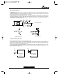
2-1. Front
Power Switch , Menu, Select, Down, Up, DPMS (Power) LED
2-2. Rear
Input connector (AC & Signal Cable)
2-3. OSD Controls
H/V Position, Clock Phase, Brightness, Contrast, Recall,Color Control, Language, Auto
Adjust, Miscellaneous
3. Electrical Characteristic
3-1. Power Supply
AC/DC - Input Voltage : 90V~264V
Input Current : 1.0 A Max
Input Ferquency : 50 ~ 60Hz
- Output Voltage 12V/5V
Output Vurrent 2A/2A
3-2. Video Input Signal
Level : 0.7 Vp-p analog signal(at 75 ohm termination to ground)
Polarity : Positive
3-3. Horizontal Synchronization Signal
Level : TTL High : 2.4V min
Low : 0.4V max
Polarity : - or +
Frequency : 31kHz ~ 60kHz
3-4. Vertical Synchronization Signal
Level : TTL High : 2.4V min
Low : 0.4V max
Polarity : - or +
Frequency : 56Hz ~ 75Hz
--1--
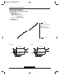
Control Description
Front View
LED Indicator
Soft Power Switch
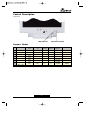
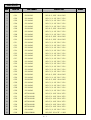
Support Modes
NO
Resolution
H Frequency
(kHz)
V Frequency
(Hz)
H
Polarity
V
Polarity
V
Polarity
Refresh rate
1
720 x 400
31.5
70.0
0
1
28.322
70.087
2
640 x 480
31.5
59.9
0
0
25.175
59.940
3
640 x 480
37.9
72.8
0
0
31.500
72.809
4
800 x 600
37.9
60.3
1
1
40.000
60.317
5
800 x 600
46.9
75.0
1
1
49.500
75.000
6
1024 x 768
48.4
60.0
0
0
65.000
60.004
7
1024 x 768
56.5
70.1
0
0
75.000
70.069
8
1024 x 768
60.0
75.0
1
1
78.750
75.029
--2--
L50A(L50C) Technical Service Manual
Video Input Signal
Recommended signal are shown below
•Video Signal
Video level : 0 to 700mV
Polarity : positive
Video Input : RGB separated
Analog level
Sync input : H-Sync(TTL level)
V-Sync (TTL level)
•Waveform
Video input(R.G.B)
255
700mV
254
253
252
251
• Signal: 256 level gray
scale
• Linear stepping:
(2.73mV ~ 256 Steps)
4
3
2
1
0
0mV
• H-Sync
• V-Sync
ACTIVE (T4)
ACTIVE (T4)
Front Porch
(T5)
Period (T1)
Back Porch (T3)
Sync Width (T2)
Front Porch
(T5)
--3--
Period (T1)
Back Porch (T3)
Sync Width (T2)
Video Input Terminal
A 15 Pin D-sub connector is used as the input signal connector
Pin and input signals are shown in the table below.
Pin Description
SEPARATE SYNC/
DDC 1/2B
SIGNAL
PIN NO.
1
RED
2
GREEN
3
BLUE
4
GND
5
RETURN
6
RED GROUND
7
GREEN GROUND
8
BLUE GROUND
9
N.C
10
LOGIC GROUND
11
GROUND
12
SDA
13
H-SYNC(TTL)
14
V-SYNC(VCLK)
SCL
15
D-Sub miniature connector
--4--
L50A(L50C) Technical Service Manual
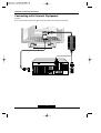
Connecting with External Equipment
Cautions
Be sure to turn off the power of your computer before connecting the monitor.
--5--
Theory of Operation
1. AC/DC Adapter
Input voltage :
Input current :
Inrush current :
90 ~ 264 Vac, 50/60 Hz
Max 1A (Vin : 90Vac , 50Hz)
15A peak (At 115Vac Max . Load)
30A peak (At 230Vac Max. Load)
2. DC/AC INVERTER
Input voltage :
Input current :
Frequency(switching) :
On/off control voltage :
DC 12V
2.0A(Max)
40 - 80 KHz
5.0V
3. DPMS MODE
Reference to DPMS files
Mode
LED
LED
Indicator
Normal
Green
40W
Suspend
Orange
10W
off
Orange
5W
Unplugged
Not illuminated
0W
--6--
L50A(L50C) Technical Service Manual
On Screen Controls & LED Indicator
The menu for screen setting adjustment is located in the OSD and can be viewed in one of
five languages OSD feature andmain funcrions are as follows:
The OSD adjustments available to you are listed below.
BRIGHTNESS
Adjust the brightness of the screen.
CONTRAST
Adjust the contrast of the screen.
COLOR CONTROL
Color temperature affects the tint of the image. With lower color
temperatures the image turns reddish and with higher temperatures
bluish.
There are three color settings available: Mode 1(a warm white), Mode 2(a cool white)
or USER. With the USER setting you can set individual values for red, green and blue.
H/V POSITION
H-POSITION
Adjusts the horizontal position of the entire screen image.
V-POSITION
Adjusts the vertical position of the entire screen image.
--7--
CLOCK PHASE
PHASE
Adjust the noise of the screen image.
CLOCK
Adjust the horizontal size of the entire screen image.
AUTO ADJUST
You can adjust the shape of screen automatically at the full screen pattern.
MISCELLANEOUS
RECALL
Recall the saved color data.
OSD TIMER
You can set the displayed time of OSD Menu window on the screen by using this
adjustment.
OSD POSITION
Adjust the OSD menu's horizontal or vertical position on the screen.
LANGUAGE
You can select the language in which adjustment menus are displayed.
The following languages are available : English, French, German, Italian,
Spanish, Swedish, Finnish, Danish, P
--8--
L50A(L50C) Technical Service Manual
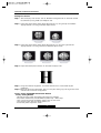
Getting Fine Picture
Step 1. At first Display, a full screen, such as, Window's background or "H" character should
be achieved by using Editor (ex: Notepad. exe)
Step 2. Adjust the screen to the center of the Display(LCD), by using the top and bottom
display controls. (i.e.Using V-Position Adjust menu)
Step 3. Adjust the screen to the center of the Display(LCD), by using the right and left
display controls. (i.e.Using Clock and H-Position adjust menu)
Step 4. Adjust the Clock-phase until the "H" Character displays clear.
Step 5. Using the Contrast. Brightness, and Color Control menu, set the color to your
preference.
Step 6. When you finish the adjustment, you can save your settings by pressing on the menu
until the OSD screen has disappeared.
Factory Setting & EEPROM Initialization Method
Factory Setting Method
- Connect the signal cable and power cable to the LCD monitor.
- Press Power switch with pressed MENU key.(Menu key + Power key).
- Then, a User can change the factory setting value in OSD menu.
- Save changed value and Turn off the power s/w.
- Turn on the power, adjust the screen.
--9--
Specification
SIZE
Dot Pitch
LCD Module
Brightness
Response Time
Signal
15” Viewable diagonal
0.297mm
180 cd/m2 (MIN), 250 cd/m2 (TYP)
20m- sec (Typ)
R.G.B Analog
Input
Connector
15 pin D-SUB Connector
H-Freq
31.0kHz ~ 60.0kHz
V-Freq
56.0Hz ~ 75Hz
SYNC
Display
Area
304(H)X228(V)mm
Color
16.2M Colors
1024 X 768 @ 75Hz
Resolution
Video Bandwidth
Contrast,Brightness,H-V Position,
User Control
&
OSD Control
Clock Phase, Color Control, Language,
Auto Adjust, Miscellaneous
Power Management
Plug & Play
Safety &
Regulation
80MHz
VESA DPMS Standard
VESA DDC 1/2B
EMC
FCC CLASS B , CE , VCCI
Safety
cULus, CE, TUV-GS, SEMKO
Ergonomi
TCO
Operating
5 to 35 °C
Storage
- 5 to 45 °C
Temperature
Operating
30 to 80%(Non-condensing)
Humidity
Storage
5 to 90%(Non-condensing)
unpacked
3.1Kg
packed
4.4Kg
Weight
Dimension(WXHXD mm)
367X353X188.3mm
* Specification is subject to change without notice for performance improvement.
--10--
L50A(L50C) Technical Service Manual
Critical Parts Specification
1. LCD Module
HT-15X13(LTM150XH-L01 is a a-si TFT active matrix color liquid crystal comprising
amorphous silicon TFT attached to each signal electrode, a driving circuit and a backlight.
HT-15X13(LTM150XH-L01 has a built-in backlight display area contains 1024X768 pixels
and can display full color (16.2M colors)
Display area
304(H)X228(V)mm
Drive system
a-si TFT
Display color
16.2M Colors
Number of Pixel
1024X768
Pixel arrangement
RGB vertical strip
Pixel pitch
0.297(H)X0.297(V)mm
Weight
300:1
Viewing angle
Horizontal:
80 degree(3’ clock, 9’ clock)/45(12 ’ clock) 80 (6’ clock)
Vertical:
40 degree(12’ clock) ,55 degree(6’ clock)/65(3 ’ clock, 9 ’ clock)
Response time
20ms(Typr)
Luminance
250cd/m2(Typ)
Signal system
Digital RGB signals, Sync signals(H, V-Sync),
Dot clock(DCLK) , DE(Data Enable)
Supply voltage
3.3V
Backlight
Edge light type: Four colt cathode fluorescent lamps
With in- verter
Power consumption
1.5W(TYP) without B/L
--11--
2) INTERFACE CONNEXTION
2-1) Electrical Interface
CN1
Interface connector : DF14H-20P-1.25H(HIROSE) or equivalent
User side connector : DF14-20S-1.25C(HIROSE)or equivalent
Pin No
Symbol
Pin No
1
VDD1
Power Supply : +3.3V
2
VDD2
Power Supply : +3.3V
3
VSS
Ground
4
VSS
Ground
5
RIN0-
LVDS Negative data signal (-)
Tx pin #48
6
RIN0+
LVDS Negative data signal (+)
Tx pin #47
7
VSS
Ground
8
RIN0-
LVDS Negative data signal (-)
Tx pin #46
9
RIN0+
LVDS Negative data signal (+)
Tx pin #45
10
VSS
Ground
11
RIN2-
LVDS Negative data signal (-)
Tx pin #42
12
RIN2+
LVDS Negative data signal (+)
Tx pin #41
13
VSS
Ground
14
RCLKIN-
LVDS Negative data signal (-)
Tx pin #40
15
RCLKIN+
LVDS Negative data signal (+)
Tx pin #39
16
VSS
Ground
17
RIN3-
LVDS Negative data signal (-)
Tx pin #38
18
RIN3+
LVDS Negative data signal (+)
Tx pin #37
19
VSS
Ground
20
NC
Reserved
--12--
Remark
L50A(L50C) Technical Service Manual
2-2) LVDS Infcrface
LVDS Transmitter : THC63LVDM83A or equivalent.
Input
Transmitter
signal
Pin No Pin No
Interface
DF14H-20P-1.25H
System (Tx)
TFT-LCD (Rx)
Pin No
R0
51
R1
52
R2
54
48
OUT 0-
IN0-
5
R3
55
47
OUT +
IN0+
6
R4
56
R5
3
G0
4
G1
6
G2
7
G3
11
46
OUT1+
IN1-
8
G4
12
45
OUT1+
IN1+
9
G5
14
B0
15
B1
19
B2
20
B3
22
B4
23
42
OUT2-
IN2-
11
B5
24
41
OUT2+
IN2+
12
HSYNC
27
VSYNC
28
DE
30
MCLK
31
40
CLKOUT-
CLKIN-
14
39
CLKOUT+
CLKIN+
15
R6
50
R7
2
G6
8
38
OUT+
IN3-
17
G7
10
37
OUT-
IN3+
18
B6
16
B7
18
RSVD
25
--13--
Remark
gmZAN1
.
Features
The gmZAN1 device utilizes Genesisí patented thirdgeneration Advanced Image Magnification technology as
well as a proven integrated ADC/PLL to provide excellent
image quality within a cost-effective SVGA / XGA LCD
monitor solution.
As a pin-compatible replacement for the gmB120, the
gmZAN1 incorporates all of the gmB120 features plus
many enhanced features; including 10-bit gamma
correction, Adaptive Contrast Enhancement (ACE)
filtering, and an enhanced OSD.
•
Features
•
• Fully integrated 135MHz 8-bit triple-ADC, PLL,
and pre-amplifier
• gmZ2 scaling algorithm featuring new Adaptive
Contrast Enhancement (ACE)
• On-chip programmable OSD engine
• Integrated PLLs
• 10-bit programmable gamma correction
• Host interface with 1 or 4 data bits
• Pin-compatible with gmB120
•
•
Integrated 8-bit triple ADC
Up to 135MHz sampling rates
No additional components needed
All color depths up to 24-bits/pixel are
supported
High-Quality Advanced Scaling
• Fully programmable zoom
• Independent horizontal / vertical zoom
• Enhanced and adaptive scaling algorithm for
optimal image quality
• Recovery Mode / Native Mode
•
•
Built In High-Speed Clock Generator
• Fully programmable timing parameters
• On-chip PLLs generate clocks for the on-chip
ADC and pixel clock from a single reference
oscillator
Auto-Configuration / Auto-Detection
• Phase and image positioning
• Input format detection
•
Operating Modes
• Bypass mode with no filtering
• Multiple zoom modes:
with filtering
with adaptive (ACE) filtering
•
Integrated On-Screen Display
• On-chip character RAM and ROM for better
customization
• External OSD supported for greater flexibility
• Many other font capabilities including: blinking,
overlay and transparency
Integrated Analog Front End
•
•
•
•
Output Format
• Support for 8 or 6-bit panels (with high quality
dithering)
• One or two pixel output format
Package
•
160-pin PQFP
Applications
•
•
Input Format
• Analog RGB up to XGA 85Hz
--14--
Multi-synchronous LCD monitors
Other fixed-resolution pixelated display devices
L50A(L50C) Technical Service Manual
Pin Out Diagram
120
119
118
117
116
115
114
113
112
111
110
109
108
107
106
105
104
103
102
101
100
99
98
97
96
95
94
93
92
91
90
89
88
87
86
85
84
83
82
81
OSD_DATA2
OSD_DATA1
OSD_DATA0
OSD_CLK
OSD_VREF
OSD_HREF
CVSS4
MFB0
MFB1
MFB2
MFB3
MFB4
CVDD4
MFB5
MFB6
MFB7
MFB8
HCLK
MFB9
IRQ
RESETn
HDATA
HFS
N/C
ADC_RVDDA
RED+
REDADC_RGNDA
ADC_GVDDA
GREEN+
GREENADC_GGNDA
ADC_BVDDA
BLUE+
BLUEADC_BGNDA
ADC_VDDA
Reserved
ADC_GNDA
SUB_GNDA
Figure 1. gmZAN1 Pin Diagram
gmZAN1 (160-Pin PQFP)
NOTE: For all power pads:
C: Core
R: Ring
S: From pad 125 to 132, S represents Sclk DDS (source clk)
D: From pad 133 to 140, D represents Dclk DDS (destination clk)
NOTE: SRVSS1, SRVSS2 are connected to core VSS and SRVDD1 and
SRVDD2 are connected to core VDD.
NOTE: The following signals have the same function but different nam es in
the gmB120 datasheet:
OSD-HREF is here called OSD_HREF
OSD-VREF is here called OSD_VREF
OSD-CLK is here called OSD_CLK
OSD-DATA0 is here called OSD_DATA0
OSD-DATA1 is here called OSD_DATA1
OSD-DATA2 is here called OSD_DATA2
OSD-DATA3 is here called OSD_DATA3
SYVDD is here called SYN_VDD
SYVSS is here called SYN_VSS
NOTE: when connected to a pull-down resistor, the MFB5 strapping option
(sampled at reset) enables the use of an external crystal. MFB5 has an
internal pull-up resistor, so an external oscillator is the default.
NOTE: MFB6 is a strapping option to select a host data bus width of four
when connected to a pull-down (sampled at reset). Since MFB6 has an
internal pull-up resistor, a 1-wire host bus width is the default.
1
2
3
4
5
6
7
8
9
10
11
12
13
14
15
16
17
18
19
20
21
22
23
24
25
26
27
28
29
30
31
32
33
34
35
36
37
38
39
40
121
122
123
124
125
126
127
128
129
130
131
132
133
134
135
136
137
138
139
140
141
142
143
144
145
146
147
148
149
150
151
152
153
154
155
156
157
158
159
160
CVSS1
Reserved
PSCAN
Reserved
Reserved
PD47
PD46
RVSS1
PD45
PD44
SRVDD1
RVDD1
PD43
PD42
PD41
PD40
PD39
SRVSS1
PD38
PD37
SRVDD2
PD36
PD35
PD34
PD33
PD32
PD31
PD30
PD29
RVSS2
PD28
PD27
RVDD2
PD26
PD25
PD24
PD23
PD22
PD21
CVDD1
OSD_DATA3
OSD_FSW
MFB11
MFB10
DVDD
DVSS
DAC_DGNDA
DAC_DVDDA
PLL_DVDDA
Reserved
PLL_DGNDA
SUB_DGNDA
SUB_SGNDA
PLL_SGNDA
Reserved
PLL_SVDDA
DAC_SVDDA
DAC_SGNDA
SVDD
SVSS
TCLK
XTAL (Reserved)
PLL_RVDDA
PLL_RGNDA
Reserved
SUB_RGNDA
Reserved
VSYNC
SYN_VDD
HSYNC/CS
SYN_VSS
Reserved
STI_TM1
STI_TM2
SCAN_IN1
Reserved
SCAN_IN2
SRVSS2
SCAN_OUT1
SCAN_OUT2
--15--
80
79
78
77
76
75
74
73
72
71
70
69
68
67
66
65
64
63
62
61
60
59
58
57
56
55
54
53
52
51
50
49
48
47
46
45
44
43
42
41
ADC_GND1
ADC_VDD1
ADC_GND2
ADC_VDD2
PPWR
PBIAS
PHS
PVS
CVSS3
PD0
PD1
PD2
PD3
PD4
PD5
RVDD3
PD6
PD7
PD8
RVSS4
Reserved
Reserved
CVDD2
PD9
PD10
PD11
PD12
PD13
PD14
PD15
PD16
RVSS3
PD17
PD18
PD19
PCLKB
PCLKA
PDISPE
PD20
CVSS2
FEATURES
MTV312M64
•
•
•
•
•
•
•
•
•
•
•
•
•
•
•
8051 core, 12MHz operating frequency with double CPU clock option
0.35uM process; 5V/3.3V power supply and I/O; 3.3V core operating
1024-byte RAM; 64K-byte program Flash-ROM support In System Programming (ISP)
Maximum 14 channels of PWM DAC
Maximum 31 I/O pins
SYNC processor for composite separation/insertion, H/V polarity/frequency check and polarity adjustment
Built-in low power reset circuit
Built-in self-test pattern generator with four free-running timings
Compliant with VESA DDC1/2B/2Bi/2B+ standard
Dual slave IIC addresses; H/W auto transfer DDC1/DDC2x data
Single master IIC interface for internal device communication
Maximum 4-channel 6-bit ADC
Watchdog timer with programmable interval
Flash-ROM program code protection selection
40-pin DIP, 42-pin SDIP or 44-pin PLCC package
GENERAL DESCRIPTIONS
The MTV312M micro-controller is an 8051 CPU core embedded device especially tailored for CRT/LCD
Monitor applications. It includes an 8051 CPU core, 1024-byte SRAM, 14 built-in PWM DACs, VESA DDC
interface, 4-channel A/D converter, and a 64K-byte internal program Flash-ROM.
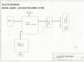
BLOCK DIAGRAM
P0.0-7
P1.0-7
P2.0-3
P3.0-2
P3.4-5
8051
CORE
RST
X1
X2
RD
WR
ALE
INT1
P0.0-7
P2.0-3
RD
WR
ALE
INT1
XFR
AD0-3
ADC
AUXRAM&
DDCRAM
H/VSYNC
CONTROL
HSYNC
VSYNC
HBLANK
VBLANK
PWM DAC
P6.0-7
P5.0-6
AUX
I/O
DA0-13
P4.0-2
--16--
DDC& IIC
INTERFACE
ISCL
ISDA
HSCL
HSDA
L50A(L50C) Technical Service Manual
PIN CONNECTION
DA2/P5.2
DA1/P5.1
DA0/P5.0
VDD3
VDD
VSS
X2
X1
ISDA/P3.4/T0
ISCL/P3.5/T1
STOUT/P4.2
P6.2/AD2/HLFHI
P1.0
P1.1
P3.2/INT0
P1.2
P1.3
P1.4
P1.5
P1.6
1
2
3
4
5
6
7
8
9
10
11
12
13
14
15
16
17
18
19
20
MTV312M
40 Pin
PDIP
40
39
38
37
36
35
34
33
32
31
30
29
28
27
26
25
24
23
22
21
VSYNC
HSYNC
DA3/P5.3
DA4/P5.4
DA5/P5.5
DA8/HLFHO
DA9/HALFV
HBLANK/P4.1
VBLANK/P4.0
DA7/HCLAMP
DA6/P5.6
RST
P6.6/DA12
P6.5/DA11
P6.4/DA10
HSCL/P3.0/Rxd
HSDA/P3.1/Txd
P6.0/AD0
P6.1/AD1
P1.7
DA2/P5.2
DA1/P5.1
DA0/P5.0
VDD3
NC
NC
RST
VDD
VSS
X2
X1
ISDA/P3.4/T0
ISCL/P3.5/T1
STOUT/P4.2
P6.2/AD2/HLFHI
P1.0
P1.1
P3.2/INT0
P1.2
P1.3
P1.4
1
2
3
4
5
6
7
8
9
10
11
12
13
14
15
16
17
18
19
20
21
MTV312M
42 Pin
SDIP
DA5/P5.5
DA4/P5.4
DA3/P5.3
HSYNC
VSYNC
DA2/P5.2
DA1/P5.1
DA0/P5.0
VDD3
NC
NC
40
41
42
43
44
1
2
3
4
5
6
RST
VDD
P6.3/AD3
VSS
X2
X1
ISDA/P3.4/T0
ISCL/P3.5/T1
STOUT/P4.2
P6.2/AD2/HLFHI
P1.0
7
8
9
10
11
12
13
14
15
16
17
MTV312M
44 Pin
PLCC
28
27
26
25
24
23
22
21
20
19
18
HSDA/P3.1/Txd
P6.0/AD0
P6.1/AD1
P1.7
P1.6
P1.5
P1.4
P1.3
P1.2
P3.2/INT0
P1.1
--17--
39
38
37
36
35
34
33
32
31
30
29
DA8/HLFHO
DA9/HALFV
HBLANK/P4.1
VBLANK/P4.0
DA7/HCLAMP
DA6/P5.6
P6.7/DA13
P6.6/DA12
P6.5/DA11
P6.4/DA10
HSCL/P3.0/Rxd
42
41
40
39
38
37
36
35
34
33
32
31
30
29
28
27
26
25
24
23
22
VSYNC
HSYNC
DA3/P5.3
DA4/P5.4
DA5/P5.5
DA8/HLFHO
DA9/HALFV
HBLANK/P4.1
VBLANK/P4.0
DA7/HCLAMP
DA6/P5.6
P6.6/DA12
P6.5/DA11
P6.4/DA10
HSCL/P3.0/Rxd
HSDA/P3.1/Txd
P6.0/AD0
P6.1/AD1
P1.7
P1.6
P1.5
PIN CONFIGURATION
A ìCMOS output pinî means it can sink and drive at least 4mA current. It is not recommended to use such
pin as input function.
A ìopen drain pinî means it can sink at least 4mA current but only drive 10~20uA to VDD. It can be used as
input or output function and needs an external pull up resistor.
A ì8051 standard pinî is a pseudo open drain pin. It can sink at least 4mA current when output is at low level,
and drives at least 4mA current for 160nS when output transits from low to high, then keeps driving at 100uA
to maintain the pin at high level. It can be used as input or output function. It needs an external pull up
resistor when driving heavy load device.
4mA
10uA
120uA
8051 St andard Pin
2 OSC
period
delay
Pin
4mA
Output
Data
Input
Data
4mA
No Current
Output
Data
Pin
Input
Data
Pin
4mA
4mA
Output
Data
Open Drain Pin
CMOS Output Pin
POWER CONFIGURATION
The MTV312M can work on 5V or 3.3V power supply system.
In 5V power system, the VDD pin is connected to 5V power and the VDD3 needs an external capacitor, all
output pins can swing from 0~5V, input pins can accept 0~5V input range. And ADC conversion range is 5V.
However, X1 and X2 pins must be kept below 3.3V.
In 3.3V power system, the VDD and VDD3 are connected to 3.3V power, all output pins swing from 0~3.3V,
HSYNC, VSYNC and open drain pin can accept 0~5V input range, other pins must be kept below 3.3V. And
the ADC conversion range is 3.3V.
3.3V
5V
VDD
VDD
VDD3
VDD3
10u
MTV312M in
3.3V System
MTV312M in
5V System
--18--
L50A(L50C) Technical Service Manual
CS5828
GENERAL DESCRIPTION
FEATURES
The CS5828 receives four sets of 7-bit data in
CMOS logic level and converts them into four lowvoltage differential signaling (LVDS) serial channels.
The 7-bit input data is referenced to the CKIN signal.
The RF pin selects either rising or falling edge trigger
of CKIN. Parallel to serial conversion is performed by
a 7X internal generated clock reference using onchip PLL using CKIN. A copy of CKIN but phaselocked to the output serial streams, CLKOUT, is also
converted to the fifth LVDS channel. The CS5828
offers a reliable communication media using LVDS
signaling and provides low EMI dealing with wide,
high-speed TTL interfaces.
This is especially attractive for interfaces between
GUI controller and display systems such as LCD
panels for SVGA/XGA/SXGA applications.
•
•
•
•
•
•
•
•
•
•
•
Four 7-bit serial and one clock LVDS channels.
Compatible with ANSI TIA/EIA-644 LVDS standard.
Wide CKIN ranges from 31MHz to 85MHz.
Fully integrated on-chip PLL that provides 7X
CKIN serial shift clock.
Pin selectable for rising or falling edge trigger.
Support power-down mode.
5V/3.3V tolerant data input.
Single 3.3V supply operation.
CMOS low power consumption.
Functional compatible with DS90C385.
Available in 56-pin TSSOP package.
BLOCK DIAGRAM
D0,D1,D2,D3,
D4,D6,D7
DIN
PARALLEL-IN SERIAL-OUT
7-Bit SHIFT REGISTER
SHIFT/LOAD_N
CLK
D8,D9,D12,D13,
D14,D15,D18
DIN
PARALLEL-IN SERIAL-OUT
7-Bit SHIFT REGISTER
SHIFT/LOAD_N
CLK
D19,D20,D21,D22,
D24,D25,D26
DIN
DIN
PARALLEL-IN SERIAL-OUT
7-Bit SHIFT REGISTER
SHIFT/LOAD_N
CLK
RF
CKIN
SHTDN
7xCLK
PHASE LOCK LOOP
SHIFT/LOAD_N
R/F
CLK
CONTROL LOGIC
CS5828
--19--
Y0N
Y1P
EN
PARALLEL-IN SERIAL-OUT
SHIFT/LOAD_N 7-Bit SHIFT REGISTER
CLK
D27,D5,D10,D11,
D16,D17,D23
Y0P
EN
Y1N
Y2P
EN
Y2N
Y3P
EN
Y3N
CKOP
EN
CKON
PIN CONNECTION DIAGRAM
VDD
1
56
D4
D5
2
55
D3
D6
3
54
D2
D7
4
53
VSS
VSS
5
52
D1
D8
6
51
D0
D9
7
50
D27
D10
8
49
LVDS_VSS
VDD
9
48
Y0M
D11
10
47
Y0P
D12
11
46
Y1M
D13
12
45
Y1P
VSS
13
44
LVDS_VDD
D14
14
43
LVDS_VSS
D15
15
42
Y2M
D16
16
41
Y2P
RF
17
40
CKOM
D17
18
39
CKOP
D18
19
38
Y3M
D19
20
37
Y3P
VSS
21
36
LVDS_VSS
D20
22
35
PLL_VSS
D21
23
34
PLL_VDD
D22
24
33
PLL_VSS
D23
25
32
SHTDN
VDD
26
31
CKIN
D24
27
30
D26
D25
28
29
VSS
CS5828
Figure-1 56-pin TSSOP
--20--
#
$%
!
!
!
!
!
!
"
!
"
#
$%
"&
"&
!"
"&
!"
"&
!"
"
!"
"
!"
"
!"
"
#
$%
$%#%
%'
%'
$
$
$!
$
$
'%$
$
$
'%$
$
$
'%$
$
$
'%$
$
$%
$
$!
%('%
$
$
$%%$
$
$
$%%$
$
$
$%%$
$
$
'%$
$
$%
$
$!
%('%
""
%'"
""
%'"
""
%'"
""
%'"
%'
%'
%'
""
%'"
""
%'"
""
%'"
""
%'"
""
%'"
""
%'"
""
%'"
""
%'"
""
%'"
""
%'"
""
%'"
""
%'"
""
%'"
""
%'"
#
$%
""
%'"
""
%'"
""
%'"
""
%'"
""
%'"
""
%'"
""
%'"
""
%!
)('
""
%!
)('
""
%!
)('
""
%!
)('
""
%!
)('
""
%'"
""
%'"
""
%'"
""
%'"
""
%'"
""
%'"
""
%'"
""
%'"
""
%'"
""
%'"
""
%'"
""
%'"
""
%'"
""
%'"
""
%!
)('
&*%!
(%%
%$%#%
%
%
%
%
%%
%
$%$
#*%$!
#*% !%$
!
!
!
#
#
#! #$!
%
#
&'
%
#
&'
%
#
&'
%
# !&
%
# !&
#
&
#
&
%
#
&'
(
$
$
%
$
)
$
*+!),
%
(
%
%
*$,
%
%
*$,
%
%
*$,
%
%
(+
-*,
%
+
-*$,
%
!
%
-*,
%%
!+
-*$,
!*', *
! *
!
"
!
!
%
!*$,
!
!*$,
!
%
!!
$!*,..
%
!$
!
%
*$,
(
%
%
#*,#
%
!!!.
%
!!$
%
%
%
%
%%
!!
$
%
/%
%
-*!,
%
!#
! #
#!!+%
%
#
%%
!
$
-
0*
,
%
%
-
!
$+
-
+
-
-*,
!
$
+!
!
*',
!
*
',
!+
A
B
C
D
E
5
5
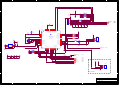
L50C(S527B/L550B/L1510B) Schematic
4
4
CONTENTS
REVISION HISTORY
SHEET
SCHEMATIC
1. Contents, Revision History
1
2. gmZAN1/2
2
Ver
Date
Author
Comments
01.09.04
G.H.NAM
A
Initial release ver A
01.09.20
W.S.IM
B
L50C VP
3. MCU(MTV312M)
3
01.10.10
W.S.IM
C
L50C VP-A
4. LVDS & Power
4
01.10.23
E.J.NAM
D
L50C VP-B
5. BLOCK DIAGRAM
5
01.11.29
E.J.NAM
E
S527 NOISE SOLUTION
3
3
2
2
1
1
Title
Size
B
Date:
A
B
C
D
1. Contents
Document Number
NONE
Thursday, November 29, 2001
Rev
E
Sheet
E
1
of
5
5
4
3
2
+3.3V
DVDDA
C201
C203
C204
22uF/16V
0.1uF
0.1uF
+3.3V
3.3
DIGITAL
SUPPLY
DECOUPLING
SVDDA
D
C206
C207
C208
22uF/16V
0.1uF
0.1uF
1
C210
C211
C213
C214
C216
C218
C221
22uF/16V
0.1uF
0.1uF
0.1uF
0.1uF
0.1uF
0.1uF
D
GND
+5V
ZAN1_3.3V/ ZAN2_2.5V
KDS226
SOT23
KDS226
SOT23
KDS226
SOT23
RVDDA
C223
C224
22uF/16V
0.1uF
D207
D206
D205
VDDA
ANALOG SUPPLY
DECOUPLING
RED
1
6
2
7
3
8
4
9
5
10
100
C230
0.01uF
R201
100
C231
0.01uF
R202
100
C232
0.01uF
100
R207
100
R208
100
C233
0.01uF
C234
0.01uF
C235
0.01uF
RED+
GREEN+
BLUE+
95
91
87
+5V
REDGREENBLUE-
94
90
86
GND
VGA_CON
SHEET 3
GND
D208
6.2V
2
4
GND
U203A
14
C209
0.1uF
22uF/16V
0
152
156
U203C
14
U203D
14
5
6
9
8
6.2V
SOT23
D202
141
142
7
74LCX14 SO14
7
74LCX14 SO14
D203
150
148
X200
C240
6.2V
SOT23
C241 C242
GND
0
R220
47pF
5pF
153
154
155
157
159
160
3
5pF
20MHz
REV. E
R218
0
GND
B
R211
R211 NC
115
116
117
118
119
120
121
122
0
Default R218
+5V
GND
D204
RLS4148
C239
R213
U202
47K
VGA_SCL
VGA_SDA
8
7
6
5
VCC
NC
VCLK NC
SCL
NC
SDA GND
0.1uF
1
2
3
4
24LC21 8P SOIC
D201
SHEET 3
SHEET 3
SHEET 3
SHEET 3
SHEET 3
HFS
HCLK
HDATAF0
ZAN_RST
/IRQ
SHEET 3
SHEET 3
SHEET 3
SHEET 3
MENU
SELECT
KEY_DOWN
KEY_UP
SHEET 3
SHEET 3
SHEET 3
HDATAF1
HDATAF2
HDATAF3
HFS
HCLK
HDATA0
RESETn
IRQ
98
103
99
100
101
MFB0
MFB1
MFB2
MFB3
113
112
111
110
109
107
106
105
104
102
124
123
GND
6.2V
SOT23
MFB7
MFB8
MFB9
12
33
40
60
65
108
149
11
21
58
125
139
79
77
143
137
136
129
128
RESERVED
N/C
RESERVED
RESERVED
RESERVED
RESERVED
RESERVED
HSYNC/CS
VSYNC
TCLK
XTAL/RESERVED
STI_TM1
STI_TM2
SCAN_IN1
SCAN_IN2
SCAN_OUT1
SCAN_OUT2
PSCAN
OSD_HREF
OSD_VREF
OSD_CLK
OSD_DATA0
OSD_DATA1
OSD_DATA2
OSD_DATA3
OSD_FSW
HFS
HCLK
HDATA
RESETn
IRQ
MFB0
MFB1
MFB2
MFB3
MFB4
MFB5
MFB6
MFB7
MFB8
MFB9
MFB10
MFB11
GND
R217
R216
10K
10K
gmZAN1/gmZAN2
PCLKA
PCLKB
PDISPE
PVS
PHS
PPWR
PBIAS
71
70
69
68
67
66
64
63
62
57
56
55
54
53
52
51
50
48
47
46
42
39
38
37
36
35
34
32
31
29
28
27
26
25
24
23
22
20
19
17
16
15
14
13
10
9
7
6
PD0
PD1
PD2
PD3
PD4
PD5
PD6
PD7
PD8
PD9
PD10
PD11
PD12
PD13
PD14
PD15
PD16
PD17
44
45
43
PCLKA
73
74
PVS
PHS
PD[6..11]
PD[12..17]
PD36
PD37
PD38
PD39
PD40
PD41
PDISPE
PD[0..5]
SHEET 4
PD[6..11]
SHEET 4
PD[12..17]
SHEET 4
PD36
PD37
PD38
PD39
PD40
PD41
SHEET 4
SHEET 4
SHEET 4
SHEET 4
SHEET 4
SHEET 4
PCLKA
SHEET 4
PDISPE
SHEET 4
PVS
PHS
SHEET 4
SHEET 4
C
B
76
75
CVSS1
CVSS1A
RVSS1
SRVSS1
RVSS2
CVSS2
RVSS3
CVSS2A
RVSS4
CVSS3
CVSS4
DVSS
SVSS
CVSS5
SYN_VSS
SRVSS2
7
7
74LCX14 SO14
R219
GND
6.2V
SOT23
C222
0.1uF
1
5
8
18
30
41
49
59
61
72
114
126
140
147
151
158
83
97
130
135
145
133 SUB_SGNDA
132 SUB_DGNDA
146 SUB_RGNDA
4
74LCX14 SO14
22
D200
RESERVED
RESERVED
DAC_DGNDA
PLL_DGNDA
PLL_SGNDA
DAC_SGNDA
PLL_RGNDA
3
REV. E
47K
REDGREENBLUE-
127
131
134
138
144
2
NC
100
100
C220
0.1uF
PD0
PD1
PD2
PD3
PD4
PD5
PD6
PD7
PD8
PD9
PD10
PD11
PD12
PD13
PD14
PD15
PD16
PD17
PD18
PD19
PD20
PD21
PD22
PD23
PD24
PD25
PD26
PD27
PD28
PD29
PD30
PD31
PD32
PD33
PD34
PD35
PD36
PD37
PD38
PD39
PD40
PD41
PD42
PD43
PD44
PD45
PD46
PD47
U203B
14
1
C243
R214
R215
C219
0.1uF
PD[0..5]
RED+
GREEN+
BLUE+
U203A NC
22
R212
C217
0.1uF
RVDD1
RVDD2
RVDD2A
RVDD2B
RVDD3
R203
CVDD4
SYN_VDD
75
SRVDD1
SRVDD2
CVDD2
R206
75
DVDD
SVDD
R205
75
ADC_VDD1
ADC_VDD2
R204
DB15HD
R210
C215
0.1uF
GND
U200
C
R209
C212
BLUE
PLL_RVDDA
DAC_SVDDA
PLL_SVDDA
PLL_DVDDA
DAC_DVDDA
15
GREEN
R200
96
92
88
84
VGA_SCL
3.3
DIGITAL
SUPPLY
DECOUPLING
GND
ADC_RVDDA
ADC_GVDDA
ADC_BVDDA
ADC_VDDA
14
22uF/16V
GND
ADC_GNDA
SUB_GNDA
ADC_GND1
ADC_GND2
13
VGA_VSYNC
0.1uF
ADC_RGNDA
ADC_GGNDA
ADC_BGNDA
VGA_HSYNC
C229
0.1uF
82
81
80
78
12
C228
0.1uF
93
89
85
VGA_SDA
C227
0.1uF
C200
0.1uF
GND
CN200
11
C226
C205
0.1uF
ZAN1_3.3V/ ZAN2_2.5V
GND
VGA INPUT
CONNECTOR
C225
22uF/16V
C202
A
A
GND
GND
GND
NOTE:
GND
GND
GND
ANALOG AND DIGITAL GROUNDS MUST BE
INTERCONNECTED AT A SINGLE POINT
Title
2. gmZAN2
Size
C
Document Number
NONE
Date:
5
4
3
2
Rev
E
Thursday, November 29, 2001
1
Sheet
2
of
5
5
4
3
2
1
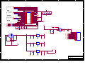
+5V
D
D
R321
R322
R312
R313
R323
R324
R315
C313
0.1UF
10K
10K
10K
330
330
10K
10K
GND
CN301
8
7
6
5
4
3
2
1
C305
R319
R314
LED_ORANGE_EN
LED_GRN_EN
KEY_UP
KEY_DOWN
SELECT
C314
0.1uF
HEADER 8
10uF/16V
470
470
C315
0.1uF
C316
0.1uF
C317
0.1uF
C318
0.1uF
SHEET 2
SHEET 2
SHEET 2
SHEET 2
KEY_UP
KEY_DOWN
SELECT
MENU
C319
0.1uF
GND
GND
GND
41
42
43
44
1
2
40
DA5/P5.5
DA4/P5.4
DA3/P5.3
HSYNC
VSYNC
DA2/P5.2
3
P3.0/Rxd
MTV312M
39
R309
4.7K
38
R308
4.7K
37
R310
4.7K
R334
10K
+12V
CN302
36
1
2
3
4
5
6
35
34
R307
PWM_BRIGHT
33
1K
32
HEADER 6
C309
INVERTER
CONNECTOR
31
1uF/50V
30
29
P3.1/Txd
GND
GND
VGA_CON
28
P1.1
PANEL_POWER
+5V
DA1/P5.1
4
P6.4/DA10
P1.0
24LC08SOIC
SHEET 4
DA0/P5.0
P6.2/AD2/HLFHI
P6.0/AD0
17
27
16
GND
P6.5/DA11
P6.1/AD1
10K
STOUT/P4.2
26
10K
8
7
6
5
P6.6/DA12
P1.7
VCC
WP
SCL
SDA
P6.7/DA13
P1.6
A0
A1
A2
VSS
15
DA6/P5.6
ISCL/P3.5/T1
25
1
2
3
4
R301
VBLANK/P4.0
DA7/HCLAMP
ISDA/P3.4/T0
18
R300
14
P1.5
13
24
18pF
X1
23
18pF
12MHz
X2
P1.4
C307
MTV312M
44Pin
PLCC
VSS
22
12
C308
HBLANK/P4.1
P6.3/AD3
P1.3
X300
DA9/HALFV
21
11
DA8/HALFH
P1.2
10
C
VDD
20
9
+5V
RST
P3.2/INTO
8
19
7
RLS4148
U301
5
C304
10uF/16V
D301
+5V
VDD3
NC
+5V
C
NC
U303
6
+5V
SHEET 2
MUTE
GND
R302
R303
R304
R306
R305
B
10K
10K
10K
10K
10K
B
+5V
C300
C301
C302
C303
C306
10uF/16V
0.1uF
0.1uF
0.1uF
0.1uF
HDATAF0
HDATAF1
HDATAF2
HDATAF3
GND
HDATAF[0..3]
SHEET 2
HCLK
SHEET 2
HFS
SHEET 2
ZAN_RST
SHEET 2
/IRQ
SHEET 2
LVDS_EN
SHEET 4
+5V
+12V
CN303
1
2
3
4
5
HEADER 7
GND
Only L1510B
A
A
Title
3. MCU(MTV312M)
Size
C
Document Number
NONE
Date:
5
4
3
2
Rev
E
Thursday, November 29, 2001
1
Sheet
3
of
5
5
4
3
2
1
1pxl/clk
SHEET 2
SHEET 2
SHEET 2
PD36
PD37
PD0
PD1
PD36
PD37
D
PD[0..5]
PD[0..5]
D
PD2
PD3
PD4
PD5
RED
LVDS_3.3V
U403
SHEET 2
SHEET 2
PD38
PD39
SHEET 2
PD[6..11]
PD38
PD39
PD6
PD7
PD[6..11]
PD8
PD9
PD10
PD11
GREEN
SHEET 2
SHEET 2
SHEET 2
1
2
3
4
5
6
7
8
9
10
11
12
13
14
15
16
17
18
19
20
21
22
23
24
25
26
27
28
PD40
PD41
PD12
PD13
PD40
PD41
PD[12..17]
PD[12..17]
PD14
PD15
PD16
PD17
BLUE
SO-TD6
SLVDSR/F
C
SHEET 2
PHS
SHEET 2
PVS
SHEET 2
PDISPE
SHEET 2
PCLKA
PHS
R402 33
PVS
R403 33
PDISPE
R404 33
PCLKA
R405 33
VCC
TD1
TA5
TA6
GND
TB0
TB1
TD2
VCC1
TD3
TB2
TB3
GND1
TB4
TB5
TD4
R/F
TD5
TB6
TC0
GND2
TC1
TC2
TC3
TD6
VCC2
TC4
TC5
56
55
54
53
52
51
50
49
48
47
46
45
44
43
42
41
40
39
38
37
36
35
34
33
32
31
30
29
TA4
TA3
TA2
GND3
TA1
TA0
TD0
LVDSGND
TATA+
TBTB+
LVDSVCC
LVDSGND1
TCTC+
TCLKTCLK+
TDTD+
LVDSGND2
PLLGND
PLLVCC
PLLGND1
/PDWN
CLKIN
TC6
GND4
RX0RX0+
RX1RX1+
C401
C402
C400
C404
C403
0.1uF
0.1uF
0.1uF
0.1uF
0.1uF
RX0RX0+
RX1RX1+
RX2RX2+
RXCLKRXCLK+
RX3RX3+
GND
RX2RX2+
RXCLKRXCLK+
RX3RX3+
SPLL-VCC
SPLL-GND
SLVDSPDN
LVDS_EN
SHEET 3
STTL-GND
C
CS5824
PANEL_3.3V
R400
R401
1K
1K
C419
33pF
C420
33pF
C421
33pF
SHEET 2
C422
33pF
R406
PANEL_POWER
4.7K
U404
1
2
3
4
GND
C423
C425
100uF/16V
0.1uF
S
S
S
G
D
D
D
D
8
7
6
5
C426
C424
100uF/16V
0.1uF
SI4435 SO8
GND
GND
CN401
1
2
3
4
5
6
7
8
9
10
11
12
13
14
15
16
17
18
19
20
CN400
POWER
+5V
U401
ZAN1 RC1117_3.3 / ZAN2 RC1117_2.5
ZAN1_3.3V / ZAN2_2.5V
RX0RX0+
GND
2
1
5V
3
12V
C410
C409
22uF/16V
0.1uF
VIN
GND
B
2
GND
4
3
VOUT
SOT223
1
C412
C411
0.1uF
22uF/16V
RX1RX1+
RX2RX2+
RXCLKRXCLK+
GND
5
6
5V
GND
12V
GND
GND
GND
RX3RX3+
GND
RX0RX0+
RX1RX1+
RX2RX2+
RXCLKRXCLK+
RX3RX3+
B
DF-14A-20P-1.25H
GND
U400
RC1117.3.3
VDD
VDD
GND
GND
RX0RX0+
GND
RX1RX1+
GND
RX2RX2+
GND
RXCLKRXCLK+
GND
RX3RX3+
GND
NC
+3.3V
GND
3
+12V
C405
C406
22uF/16V
0.1uF
GND
VIN
VOUT
2
GND
SOT223
GND
1
GND
C408
C407
0.1uF
22uF/16V
GND
GND
LVDS_3.3V
PANEL_3.3V
U402
RC1117.3.3
3
C413
C415
22uF/16V
0.1uF
VIN
GND
GND
VOUT
2
GND
A
SOT223
GND
C416
C414
0.1uF
22uF/16V
A
1
GND
GND
Title
Size
C
Date:
5
4
3
2
4.
LVDS & POWER
Document Number
Rev
E
NONE
Thursday, November 29, 2001
1
Sheet
4
of
5
!"
#
$%
&&'!
(
%
&'
!
!
" !
#!!
!
)' %!
%
!
* !
&'
!
&'*!