1
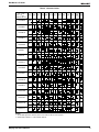
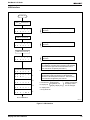
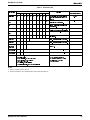
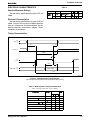
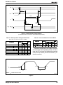
Bilaga: Dot-Matrix LCD Units HARDWARE Interface Signals Table 2. Interface Signals 6,*1$/ 1$0( ,1387287387 56 ,QSXW (;7(51$/ )81&7,21 &211(&7,21 038 5HJLVWHU VHOHFW VLJQDO ,QVWUXFWLRQ UHJLVWHU ZKHQ ZULWLQJ %XV\ IODJ DQG DGGUHVV FRXQWHU ZKHQ UHDGLQJ 'DWD UHJLVWHU ZKHQ ZULWLQJ DQG UHDGLQJ 5: ,QSXW 038 5HDGZULWH VHOHFW VLJQDO :ULWLQJ 5HDGLQJ ( ,QSXW 038 2SHUDWLRQ GDWD UHDGZULWH HQDEOH VLJQDO '% '% ,QSXW2XWSXW 038 +LJKRUGHU OLQHV RI GDWD EXV ZLWK WKUHHVWDWH ELGLUFWLRQDO IXQFWLRQ IRU XVH LQ GDWD WUDQVDFWLRQV ZLWK WKH 038 '% PD\ DOVR EH XVHG WR FKHFN WKH EXV\ IODJ '% '% ,QSXW2XWSXW 038 /RZRUGHU OLQHV RI GDWD EXV ZLWK WKUHHVWDWH ELGLUHFWLRQDO IXQFWLRQ IRU XVH LQ GDWD WUDQVDFWLRQV ZLWK WKH 038 7KHVH OLQHV DUH QRW XVHG ZKHQ LQWHUIDFLQJ ZLWK D ELW PLFURSURFHVVRU 9'' 966 3RZHU 6XSSO\ 9'' 9 966 *1' 9 3RZHU 6XSSO\ &RQWUDVW DGMXVWPHQW YROWDJH Functional Blocks Registers The LCD unit has two 8-bit registers - an instruction r egister ( IR) and a data r egister ( DR). The instruction register stores instruction codes such as "clear display" or " shift cur sor", and als o stor es address information for the display data RAM and character generator RAM. The IR can be accessed by the microprocessor only for writing. The data r egister is used for temporarily storing data during data transactions with the microprocessor. When writing data to the LCD unit, the data is initially stored in the data register, and is then automatically written into either the display data RAM or character gener ator RAM , as deter mined by the current operation. The data register is also used as a temporary storage area when reading data from the display data RAM or character generator RAM. When address information is written into the instruction register, the corresponding data from the display data RAM or character generator RAM is moved to the data register. Data transfer is completed when the microprocessor reads the contents of the data register by the next instruction. After the transfer is completed, data from the next address position of the appropriate RAM is moved to the data register, in preparation for subsequent reading operations by the microprocessor. One of the two r egisters is selected by the register select (RS) signal. Table 3. Register Selection 56 5: :ULWH WR LQVWUXFWLRQ UHJLVWHU DQG H[HFXWH LQWHUQDO RSHUDWLRQ FOHDU GLVSOD\ HWF 5HDG EXV\ IODJ '% DQG DGGUHVV FRXQWHU '% '% :ULWH WR GDWD UHJLVWHU DQG H[HFXWH LQWHUQDO RSHUDWLRQ '5 5HDG GDWD UHJLVWHU DQG H[HFXWH LQWHUQDO RSHUDWLRQ '' 5$0 Display Unit User’s Manual 23(5$7,21 → '' 5$0 RU '5 → &* 5$0 → '5 RU &* 5$0 → '5 4 Dot-Matrix LCD Units Busy Flag (BF) a. Address type a . . . .For dual-line display When the busy flag is set at a logical "1", the LCD unit is executing an inter nal operation, and no instruction will be accepted. The state of the busy flag is output on data line DB7 in response to the register selection signals RS = 0, R/W= 1 as shown in Table 3. The next ins truction m ay be enter ed after the busy flag is reset to logical "0". Address Counter (AC) The address counter generates the addr ess for the di splay d ata R AM an d c haracter ge nerator RAM. When the address set ins truction is written into the instruction register, the address information is sent tothe address counter. The same instruciton also deter mines which of the two RAM’s is to be selected. After data has been wr itten to or read from the display data RAM or character generator RAM, the address counter is autom atically incr emented or decremented by one. The contents of the address counter ar e output on data lines DB 0 - DB6 in response to the r egister selection signals RS = 0, R/W = 1 as shown in Table 3. Display Data RAM (DD RAM) This 80 x 8 bitRAM stores up to 80 8-bit character codes as display data. The unused area of the RAM may be us ed by the m icroprocessor as a gener al purpose RAM area. The display data RAM address, set in the address counter, is expressed in hexadec imal (HEX) numbers as follows: High-order Bits AC AC6 AC5 AC4 AC3 AC2 AC1 AC0 0 HEX Digit 0 1 4 1 1 3 4 5 6 7 8 9 Display Position 39 40 Line 1 00H 01H 02H 03H 04H 05H 06H 07H 08H Line 2 40H 41H 42H 43H 44H 45H 46H 47H 48H ... ... 26H 27H 66H 67H DD RAM Address (HEX) When a display shift takes place, the addresses shift is as follows: Left 01H 02H 03H 04H 05H 06H 07H 08H 09H Shift 41 42 43 44 45 46 47 48 49 H H H H H H H H H ... ... 27H 00H Right 27H 00H 01H 02H 03H 04H 05H 06H 07H Shift 67 40 41 42 43 44 45 46 47 H H H H H H H H H ... ... 25H 26H 67H 40H 65H 66H The addresses for the s econd line ar e not c ontinuous to the addresses for the first line. A40-character RAM area is assigned to each of the two line as follows: line 1: 00H - 27H line 2: 40H - 67H For an LCD unit with a dis play capacity of less than 40 char acters per line, c haracters equal in number to the display c apacity, as counted from display position 1, are displayed. b. Address type b . . . .For single-line display with logically dual-line addressing Digit Display Position 1 2 3 4 5 6 7 8 9 10 11 12 13 14 15 16 Line 00 01 02 03 04 05 06 07 40 41 42 43 44 45 46 H H H H H H H H H H H H H H H 47H 1 DD RAM Address (HEX) Right 27 00 01 02 03 04 05 06 67 40 41 42 43 44 45 46 H H H H H H H H H H H H H H H H Shift 0 E The address of the dis play data RAM c orresponds to the display position on the LCD panel as follows: Display Unit User’s Manual 2 Left 01 02 03 04 05 06 07 08 41 42 43 44 45 46 47 48 Shift H H H H H H H H H H H H H H H H Example: DD RAM address '4E' 1 1 When a display shift takes place, the addresses shift as follows: Lower-order Bits HEX Digit Digit The right-hand eight characters, for the purposes of addr essing and shifting, m ay be cons idered to constitute a sec ond display line. For the addr ess type of each model, see Table 12. 5 Dot-Matrix LCD Units EL backlight LED backlight EL Inverter (See note 2) Display Data Signals LCD Panel Scanning Signals VLED VLSS Segment Electrode Drive Circuit 4 3 Common Electrode Drive Circuit 4 3 3 7 7 Timing Generator Cursor/Blink Controller 7 7 Character Generator ROM (CG ROM) 7,200 bits 8 Display Data RAM (DD RAM) 80 x 8 bits 7 Address Counter (AC) 5V 8 5 8 7 7 8 Instruction Decoder Character Generator ROM (CG ROM) 512 bits 5 Parallel-to-Serial Converter 6 7 8 Data Register (DR) Instruction Register (/R) 8 Busy Flag (BF) 8 Bias Voltage Generator (See Note 1) I/O Buffer 4 RS R/W E 4 VDD VO VSS DB4 - DB7 DB0 - DB3 NOTES: 1. LM16152 incorporates a temperature compensation circuit within the bias voltage generator. See table 12. 2. For the inverters of EL backlights, please contact your representative. LCD27-6 Figure 1. Functional Block Diagram Display Unit User’s Manual 7 Dot-Matrix LCD Units Table 4. Character Codes HIGH-ORDER 4 BIT LOWORDER 4 BIT xxxx0000 xxxx0001 xxxx0010 xxxx0011 xxxx0100 xxx0101 xxx0110 xxxx0111 xxxx1000 xxxx1001 xxxx1010 xxxx1011 xxxx1100 0000 0010 0011 0100 0101 0110 0111 1010 1011 1100 1101 1110 1111 CG RAM (1) (2) (3) (4) (5) (6) (7) (8) (1) (2) (3) (4) (5) xxxx1101 (6) xxxx1110 (7) xxxx1111 (8) NOTES: 1. The CG RAM generates character patterns in accordance with the user's program. 2. Shaded areas indicate 5 x 10 dot character patterns. Display Unit User’s Manual 8 Dot-Matrix LCD Units 4-Bit Interface Power ON Wait 15 ms or more after VDD reaches 4.5 V RS R/W DB7 DB6 DB5 DB4 0 0 0 0 1 Busy flag can't be checked before execution of this instruction 1 Function Set (8-Bit Interface) Wait 4.1 ms or more Busy flag can't be checked before execution of this instruction RS R/W DB7 DB6 DB5 DB4 0 0 0 0 1 1 Function Set (8-Bit Interface) Wait 100 µs or more Busy flag can't be checked before execution of this instruction RS R/W DB7 DB6 DB5 DB4 0 0 0 0 1 1 RS R/W DB7 DB6 DB5 DB4 0 0 0 0 1 0 0 0 0 0 1 0 0 0 N F * * 0 0 0 0 0 0 0 0 1 0 0 0 0 0 0 0 0 O 0 0 0 0 0 1 0 0 0 0 0 0 0 0 0 1 I/D S Function Set (8-Bit Interface) (a) Busy flag can be checked after the following instructions are completed. If the busy flag is not going to be checked, then a wait time longer than the total execution time of these instructions is required (See Table 7.) I II III IV V I Function Set (4-Bit Interface) This instruction signals the LCD unit to begin accepting and sending data in dual 4-bit transfers for all subsequent transfers for all subsequent transactions. This is the only 4-bit instruction recognized by the LCD unit. II Function Set III Display Off 4-Bit Interface, Single/Dual Line Display, Display Font Caution: At this point, the display format can't be changed. IV Display Clear V Entry Mode Set End of Initialization LCD21-11 Figure 4. 4-Bit Interface Display Unit User’s Manual 14 Dot-Matrix LCD Units Table 7. Instruction Set &2'( ,16758&7,21 )81&7,21 56 5: '% '% '% '% '% '% '% '% 'LVSOD\ &OHDU &OHDU HQWHU GLVSOD\ DUHD UHVWRUH GLVSOD\ IURP (;(&87,21 7,0( PD[ I &3 RU I26& N+] PV VKLIW DQG ORDG DGGUHVV FRXQWHU ZLWK '' 5$0 DGGUHVV + 'LVSOD\&XUVRU 5HVWRUH GLVSOD\ IURP VKLIW DQG ORDG DGGUHVV PV FRXQWHU ZLWK '' 5$0 DGGUHVV + +RPH (QWU\ 0RGH ,' 6 6HW 6SHFLI\ FXUVRU DGYDQFH GLUHFWLRQ DQG GLVSOD\ µV µV VKLIW PRGH 7KLV RSHUDWLRQ WDNHV SODFH DIWHU HDFK GDWD WUDQVIHU 'LVSOD\ 212)) ' & % 6SHFLI\ DFWLYDWLRQ RI GLVSOD\ ' FXUVRU & DQG EOLQNLQJ RI FKDUDFWHU DW FXUVRU SRVLWLRQ % 'LVSOD\&XUVRU 6& 5/ 6KLIW GLVSOD\ RU PRYH FXUVRU µV '/ 1 6HW LQWHUIDFH GDWD OHQJWK '/ DQG QXPEHU RI µV µV µV 6KLIW )XQFWLRQ 6HW GLVSOD\ OLQHV 1 &* 5$0 $&* /RDG WKH DGGUHVV FRXQWHU ZLWK D &* 5$0 DGGUHVV 6XEVHTXHQW GDWD LV &* 5$0 GDWD $GGUHVV 6HW '' 5$0 /RDG WKH DGGUHVV FRXQWHU ZLWK D '' 5$0 $'' DGGUHVV 6XEVHTXHQW GDWD LV '' 5$0 GDWD $GGUHVV 6HW %XV\ %) $& 5HDG EXV\ IODJ %) DQG FRQWHQWV RI DGGUHVV )ODJ$GGUHVV µV FRXQWHU $& &RXQWHU 5HDG &* 5$0'' :ULWH GDWD :ULWH GDWD WR &* 5$0 RU '' 5$0 µV 5HDG GDWD 5HDG GDWD IURP &* 5$0 RU '' 5$0 µV 5$0 'DWD :ULWH &* 5$0'' 5$0 'DWD 5HDG ,' 6 ,QFUHPHQW ,' 'HFUHPHQW &* 5$0 &KDUDFWHU *HQHUDWRU 5$0 6& 6KLIW 'LVSOD\ 6& 5/ 6KLIW 5LJKW 5/ '/ 1 %) '' 5$0 'LVSOD\ 'DWD 5$0 'LVSOD\ 6KLIW 2Q %LW '/ $&* &KDUDFWHU *HQHUDWRU 5$0 $GGUHVV 0RYH &XUVRU $'' 'LVSOD\ 'DWD 5$0 $GGUHVV 6KLIW /HIW $& %LW 'XDO /LQH 1 $GGUHVV &RXQWHU 6LQJOH /LQH ,QWHUQDO 2SHUDWLRQ %) 5HDG\ IRU ,QVWUXFWLRQ NOTES: 1. Symbol "*" signifies a "don’t care" bit. 2. Correct input value for "N" is predetermined for each model (see Table 12). Display Unit User’s Manual 18 Dot-Matrix LCD Units ELECTRICAL CHARACTERISTICS Table 8. Absolue Maximum Ratings 3$5$0(7(5 See the device specifications for each LCD unit model. 2XWSXW 9ROWDJH 6<0%2/ + 92+ / 92/ 7(67 &21',7,216 ,2+ ,2/ P$ P$ 0,1 0$; 81,7 9 9 Electrical Characteristics See the device specificiations for each LCD unit model. Som e of the cur rently available specifications do not desc ribe the test conditions for the high-level and low- level output v oltages. Thes e conditions are as follows: Timing Characteristics RS VIH VIL tAS tAH R/W VIL PWEH tAH tEf VIH E V IL tEr tDSW VIH DB0 - DB7 V IL tH VALID DATA tcycE LCD27-24 Figure 5. Write Operation Timing Diagram (For data sent from the external microprocessor to the LCD unit) Table 9. Write Operation Timing Characteristics (VDD = 5.0 ± 5%, VSS = 0 V, TA = 0 ~ 50°C) 9$/8( 3$5$0(7(5 6<0%2/ 81,7 0,1 (QDEOH &\FOH 7LPH (QDEOH 3XOVH :LGWK +LJK /HYHO (QDEOH 5LVH)DOO 7LPH 6HWXS 7LPH $GGUHVV +ROG 7LPH 'DWD 6HWXS 7LPH 'DWD +ROG 7LPH Display Unit User’s Manual 56 5:( 0$; W&<&( 3:(+ W(U W(I W$6 W$+ W'6: W+ QV QV QV QV QV QV QV 19 Dot-Matrix LCD Units RS VIH VIL tAS tAH R/W VIH PWEH E tAH VIH VIL tEr tEf tDDR DB0 - DB7 tDHR VOH VOL VALID DATA tcycE LCD27-25 Figure 6. Read Operation Timing Diagram (For data sent from the LCD unit to the external microprocessor) Table 11. Power Conditions for Internal Reset Table 10. Read Operation Timing Characteristics (VDD = 5.0 ± 5%, VSS = 0 V, Ta = 0 ~ 50°C) 9$/8( 3$5$0(7(5 9$/8( 3$5$0(7(5 6<0%2/ (QDEOH 3XOVH :LGWK +LJK /HYHO (QDEOH 5LVH)DOO 7LPH WF\F( 3: (+ W(U W(I W$6 0$; 9ROWDJH %XLOG8S 7LPH QV QV W$+ 'DWD 'HOD\ 7LPH W''5 QV 'DWD +ROG 7LPH W2+5 QV 56 5:( $GGUHVV +ROG 7LPH 3RZHU2II 3HULRG WUFF W2)) 7<3 0$; PV PV QV 6HWXS 7LPH 81,7 0,1 81,7 0,1 (QDEOH &\FOH 7LPH 6<0%2/ QV QV If the above conditions are not satisfied, the internal reset circuit will not operate normally. In such a case, the LCD unit must be initialized by executing a ser ies of instr uctions ( see the Ex ecution by Instructions section). 4.5 V VDD 0.2 V 0.2 V 0.1 ms ≤ trCC ≤ 10 ms 0.2 V tOFF ≥ 1 ms NOTE: * tOFF indicates Power-off Period. LCD27-26 Figure 7. Display Unit User’s Manual 20 Dot-Matrix LCD Units 2. 4-Bit Data Transfer with a Single-Line, 16-Character Display (Using Internal Reset). Table 14 shows a sample operating procedure for an LCD unit in this mode. After power has been turned on, the 8-bit data transfer mode is in effect, and the first write operation is assumed to be an 8-bit data transfer. Since the data lines DB 0 - DB3 ar e not c onnected, this data is not accepted and m ust be written again ( i.e. the func tion s et instruction must be written twice). Subsequent data transfers are completed in two 4-bit transfer operations (see Table 14). RS R/W E OPERATING STATUS DB7 INTERNAL OPERATION IR7 IR3 Write Instruction BUSY READY FOR DATA NOT BUSY AC3 Check Busy Flag AC3 Check Busy Flag D7 D3 Write Instruction NOTE: IR7, IR3: Instruction bits 7 and 3. AC3: Address counter bit 3. LCD27-32 Figure 9. 4-Bit Interface Timing (Example) SM200 O1 RS O2 R/W O3 E P10 - P13 4 LCD UNIT DB4 - DB7 LCD27-33 Figure 10. Connection to SM200 Display Unit User’s Manual 23