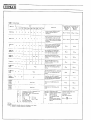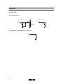
1
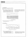
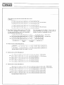
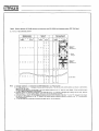
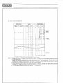
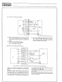
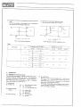
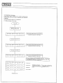
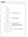
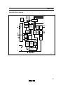
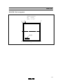
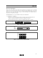
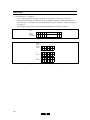
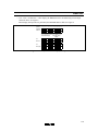
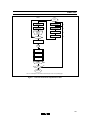
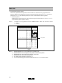
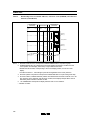
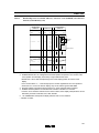
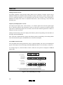
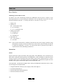
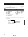
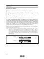
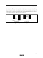
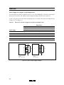
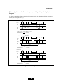
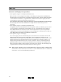
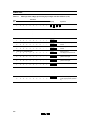
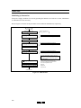
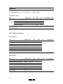
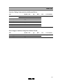
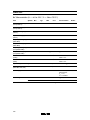
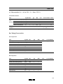
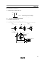
HD44780U (LCD-II) (Dot Matrix Liquid Crystal Display Controller/Driver) Description The HD44780U dot-matrix liquid crystal display controller and driver LSI displays alphanumerics, Japanese kana characters, and symbols. It can be configured to drive a dot-matrix liquid crystal display under the control of a 4- or 8-bit microprocessor. Since all the functions such as display RAM, character generator, and liquid crystal driver, required for driving a dot-matrix liquid crystal display are internally provided on one chip, a minimal system can be interfaced with this controller/driver. A single HD44780U can display up to one 8-character line or two 8-character lines. The HD44780U has pin function compatibility with the HD44780S which allows the user to easily replace an LCD-II with an HD44780U. The HD44780U character generator ROM is extended to generate 208 5 × 8 dot character fonts and 32 5 × 10 dot character fonts for a total of 240 different character fonts. The low power supply (2.7V to 5.5V) of the HD44780U is suitable for any portable battery-driven product requiring low power dissipation. Features • 5 × 8 and 5 × 10 dot matrix possible • Low power operation support: 2.7 to 5.5V • Wide range of liquid crystal display driver power 3.0 to 11V • Liquid crystal drive waveform A (One line frequency AC waveform) • Correspond to high speed MPU bus interface 2 MHz (when VCC = 5V) • 4-bit or 8-bit MPU interface enabled • 80 × 8-bit display RAM (80 characters max.) • 9,920-bit character generator ROM for a total of 240 character fonts 208 character fonts (5 × 8 dot) 32 character fonts (5 × 10 dot) 167 HD44780U • 64 × 8-bit character generator RAM 8 character fonts (5 × 8 dot) 4 character fonts (5 × 10 dot) • 16-common × 40-segment liquid crystal display driver • Programmable duty cycles 1/8 for one line of 5 × 8 dots with cursor 1/11 for one line of 5 × 10 dots with cursor 1/16 for two lines of 5 × 8 dots with cursor • Wide range of instruction functions: Display clear, cursor home, display on/off, cursor on/off, display character blink, cursor shift, display shift • Pin function compatibility with HD44780S • Automatic reset circuit that initializes the controller/driver after power on • Internal oscillator with external resistors • Low power consumption Ordering Information Type No. Package CGROM HD44780UA00FS HCD44780UA00 HD44780UA00TF HD44780UA02FS HCD44780UA02 HD44780UA02TF FP-80B Chip TFP-80F FP-80B Chip TFP-80F Japanese standard font HD44780UBxxFS HCD44780UBxx HD44780UBxxTF FP-80B Chip TFP-80F Custom font Note: xx: ROM code No. 168 European standard font HD44780U HD44780U Block Diagram OSC1 OSC2 M Reset circuit ACL Timing generator CPG 8 RS R/W E Instruction register (IR) 7 Input/ output buffer 8 16-bit shift register Common signal driver 40-bit latch circuit Segment signal driver 7 40-bit shift register 8 7 DB4 to DB7 D Display data RAM (DDRAM) 80 × 8 bits Instruction decoder MPU interface Address counter DB0 to DB3 CL1 CL2 SEG1 to SEG40 7 Data register (DR) 8 40 8 8 LCD drive voltage selector Busy flag GND COM1 to COM16 Character generator ROM (CGROM) 9,920 bits Character generator RAM (CGRAM) 64 bytes 5 Cursor and blink controller 5 Parallel/serial converter and attribute circuit VCC V1 V2 V3 V4 V5 169 HD44780U LCD-II Family Comparison Item HD44780S HD44780U Power supply voltage 5 V ±10% 2.7 to 5.5 V 1/4 bias 3.0 to 11.0V 3.0 to 11.0V 1/5 bias 4.6 to 11.0V 3.0 to 11.0V Maximum display digits per chip 16 digits (8 digits × 2 lines) 16 digits (8 digits × 2 lines) Display duty cycle 1/8, 1/11, and 1/16 1/8, 1/11, and 1/16 CGROM 7,200 bits (160 character fonts for 5 × 7 dot and 32 character fonts for 5 × 10 dot) 9,920 bits (208 character fonts for 5 × 8 dot and 32 character fonts for 5 × 10 dot) CGRAM 64 bytes 64 bytes DDRAM 80 bytes 80 bytes Segment signals 40 40 Common signals 16 16 Liquid crystal drive waveform A A Oscillator Clock source External resistor, external ceramic filter, or external clock External resistor or external clock Rf oscillation frequency (frame frequency) 270 kHz ±30% (59 to 110 Hz for 1/8 and 1/16 duty cycles; 43 to 80 Hz for 1/11 duty cycle) 270 kHz ±30% (59 to 110 Hz for 1/8 and1/16 duty cycles; 43 to 80 Hz for 1/11 duty cycle) Rf resistance 91 kΩ ±2% 91 kΩ ±2% (when VCC = 5V) 75 kΩ ±2% (when VCC = 3V) Liquid crystal drive voltage VLCD Instructions Fully compatible within the HD44780S CPU bus timing 1 MHz 1 MHz (when VCC = 3V) 2 MHz (when VCC = 5V) Package FP-80 FP-80A FP-80B TFP-80F 170 HD44780U 65 66 67 68 69 70 71 72 73 74 75 76 77 78 1 64 2 63 3 62 4 61 5 60 6 59 7 58 8 57 9 56 10 55 11 54 FP-80B (Top view) 12 13 53 52 40 39 38 37 36 41 35 42 24 34 43 23 33 44 22 32 45 21 31 46 20 30 47 19 29 48 18 28 49 17 27 50 16 26 51 15 25 14 SEG39 SEG40 COM16 COM15 COM14 COM13 COM12 COM11 COM10 COM9 COM8 COM7 COM6 COM5 COM4 COM3 COM2 COM1 DB7 DB6 DB5 DB4 DB3 DB2 OSC2 V1 V2 V3 V4 V5 CL1 CL2 VCC M D RS R/W E DB0 DB1 SEG22 SEG21 SEG20 SEG19 SEG18 SEG17 SEG16 SEG15 SEG14 SEG13 SEG12 SEG11 SEG10 SEG9 SEG8 SEG7 SEG6 SEG5 SEG4 SEG3 SEG2 SEG1 GND OSC1 79 80 SEG23 SEG24 SEG25 SEG26 SEG27 SEG28 SEG29 SEG30 SEG31 SEG32 SEG33 SEG34 SEG35 SEG36 SEG37 SEG38 HD44780U Pin Arrangement (FP-80B) 171 HD44780U 61 62 63 64 65 66 67 68 69 70 71 72 73 74 75 76 77 78 1 60 2 59 3 58 4 57 5 56 6 55 7 54 8 53 9 52 TFP-80F (Top view) 10 11 51 50 40 39 38 37 36 35 34 33 32 GND OSC1 OSC2 V1 V2 V3 V4 V5 CL1 CL2 VCC M D RS R/W E DB0 DB1 DB2 DB3 31 41 30 42 20 29 43 19 28 44 18 27 45 17 26 46 16 25 47 15 24 48 14 23 49 13 22 12 21 SEG20 SEG19 SEG18 SEG17 SEG16 SEG15 SEG14 SEG13 SEG12 SEG11 SEG10 SEG9 SEG8 SEG7 SEG6 SEG5 SEG4 SEG3 SEG2 SEG1 79 80 SEG21 SEG22 SEG23 SEG24 SEG25 SEG26 SEG27 SEG28 SEG29 SEG30 SEG31 SEG32 SEG33 SEG34 SEG35 SEG36 SEG37 SEG38 SEG39 SEG40 HD44780U Pin Arrangement (TFP-80F) 172 COM16 COM15 COM14 COM13 COM12 COM11 COM10 COM9 COM8 COM7 COM6 COM5 COM4 COM3 COM2 COM1 DB7 DB6 DB5 DB4 HD44780U HD44780U Pad Arrangement Chip size: 4.90 × 4.90 mm2 Coordinate: Pad center (µm) 2 1 Origin: Chip center Pad size: 114 × 114 µm2 80 63 Y Type code HD44780U 23 42 X 173 HD44780U HCD44780U Pad Location Coordinates Pad No. 1 2 3 4 5 6 7 8 9 10 11 12 13 14 15 16 17 18 19 20 21 22 23 24 25 26 27 28 29 30 31 32 33 34 35 36 37 38 39 40 174 Function SEG22 SEG21 SEG20 SEG19 SEG18 SEG17 SEG16 SEG15 SEG14 SEG13 SEG12 SEG11 SEG10 SEG9 SEG8 SEG7 SEG6 SEG5 SEG4 SEG3 SEG2 SEG1 GND OSC1 OSC2 V1 V2 V3 V4 V5 CL1 CL2 VCC M D RS R/ E DB0 DB1 : Coordinate X (um) Y (um) –2100 2313 –2280 2313 –2313 2089 –2313 1833 –2313 1617 –2313 1401 –2313 1186 –2313 970 –2313 755 –2313 539 –2313 323 –2313 108 –2313 –108 –2313 –323 –2313 –539 –2313 –755 –2313 –970 –2313 –1186 –2313 –1401 –2313 –1617 –2313 –1833 –2313 –2073 –2280 –2290 –2080 –2290 –1749 –2290 –1550 –2290 –1268 –2290 –941 –2290 –623 –2290 –304 –2290 –48 –2290 142 –2290 309 –2290 475 –2290 665 –2290 832 –2290 1022 –2290 1204 –2290 1454 –2290 1684 –2290 Pad No. 41 42 43 44 45 46 47 48 49 50 51 52 53 54 55 56 57 58 59 60 61 62 63 64 65 66 67 68 69 70 71 72 73 74 75 76 77 78 79 80 Function DB2 DB3 DB4 DB5 DB6 DB7 COM1 COM2 COM3 COM4 COM5 COM6 COM7 COM8 COM9 COM10 COM11 COM12 COM13 COM14 COM15 COM16 SEG40 SEG39 SEG38 SEG37 SEG36 SEG35 SEG34 SEG33 SEG32 SEG31 SEG30 SEG29 SEG28 SEG27 SEG26 SEG25 SEG24 SEG23 Coordinate X (um) Y (um) 2070 –2290 2260 –2290 2290 –2099 2290 –1883 2290 –1667 2290 –1452 2313 –1186 2313 –970 2313 –755 2313 –539 2313 –323 2313 –108 2313 108 2313 323 2313 539 2313 755 2313 970 2313 1186 2313 1401 2313 1617 2313 1833 2313 2095 2296 2313 2100 2313 1617 2313 1401 2313 1186 2313 970 2313 755 2313 539 2313 323 2313 108 2313 –108 2313 –323 2313 –539 2313 –755 2313 –970 2313 –1186 2313 –1401 2313 –1617 2313 HD44780U Pin Functions Signal No. of Lines I/O Device Interfaced with RS 1 I MPU Selects registers. 0: Instruction register (for write) Busy flag: address counter (for read) 1: Data register (for write and read) 1 I MPU Selects read or write. 0: Write 1: Read E 1 I MPU Starts data read/write. DB4 to DB7 4 I/O MPU Four high order bidirectional tristate data bus pins. Used for data transfer and receive between the MPU and the HD44780U. DB7 can be used as a busy flag. DB0 to DB3 4 I/O MPU Four low order bidirectional tristate data bus pins. Used for data transfer and receive between the MPU and the HD44780U. These pins are not used during 4-bit operation. CL1 1 O Extension driver Clock to latch serial data D sent to the extension driver CL2 1 O Extension driver Clock to shift serial data D M 1 O Extension driver Switch signal for converting the liquid crystal drive waveform to AC D 1 O Extension driver Character pattern data corresponding to each segment signal COM1 to COM16 16 O LCD Common signals that are not used are changed to non-selection waveforms. COM9 to COM16 are non-selection waveforms at 1/8 duty factor and COM12 to COM16 are non-selection waveforms at 1/11 duty factor. SEG1 to SEG40 40 O LCD Segment signals V1 to V5 5 — Power supply Power supply for LCD drive VCC –V5 = 11 V (max) VCC, GND 2 — Power supply VCC: 2.7V to 5.5V, GND: 0V OSC1, OSC2 2 — Oscillation resistor clock When crystal oscillation is performed, a resistor must be connected externally. When the pin input is an external clock, it must be input to OSC1. R/ : Function 175 HD44780U Function Description Registers The HD44780U has two 8-bit registers, an instruction register (IR) and a data register (DR). The IR stores instruction codes, such as display clear and cursor shift, and address information for display data RAM (DDRAM) and character generator RAM (CGRAM). The IR can only be written from the MPU. The DR temporarily stores data to be written into DDRAM or CGRAM and temporarily stores data to be read from DDRAM or CGRAM. Data written into the DR from the MPU is automatically written into DDRAM or CGRAM by an internal operation. The DR is also used for data storage when reading data from DDRAM or CGRAM. When address information is written into the IR, data is read and then stored into the DR from DDRAM or CGRAM by an internal operation. Data transfer between the MPU is then completed when the MPU reads the DR. After the read, data in DDRAM or CGRAM at the next address is sent to the DR for the next read from the MPU. By the register selector (RS) signal, these two registers can be selected (Table 1). Busy Flag (BF) When the busy flag is 1, the HD44780U is in the internal operation mode, and the next instruction will not be accepted. When RS = 0 and R/ = 1 (Table 1), the busy flag is output to DB7. The next instruction must be written after ensuring that the busy flag is 0. : Address Counter (AC) The address counter (AC) assigns addresses to both DDRAM and CGRAM. When an address of an instruction is written into the IR, the address information is sent from the IR to the AC. Selection of either DDRAM or CGRAM is also determined concurrently by the instruction. After writing into (reading from) DDRAM or CGRAM, the AC is automatically incremented by 1 (decremented by 1). The AC contents are then output to DB0 to DB6 when RS = 0 and R/ = 1 (Table 1). : Table 1 Register Selection : RS R/ 0 0 IR write as an internal operation (display clear, etc.) 0 1 Read busy flag (DB7) and address counter (DB0 to DB6) 1 0 DR write as an internal operation (DR to DDRAM or CGRAM) 1 1 DR read as an internal operation (DDRAM or CGRAM to DR) 176 Operation HD44780U Display Data RAM (DDRAM) Display data RAM (DDRAM) stores display data represented in 8-bit character codes. Its extended capacity is 80 × 8 bits, or 80 characters. The area in display data RAM (DDRAM) that is not used for display can be used as general data RAM. See Figure 1 for the relationships between DDRAM addresses and positions on the liquid crystal display. The DDRAM address (ADD) is set in the address counter (AC) as hexadecimal. • 1-line display (N = 0) (Figure 2) When there are fewer than 80 display characters, the display begins at the head position. For example, if using only the HD44780, 8 characters are displayed. See Figure 3. When the display shift operation is performed, the DDRAM address shifts. See Figure 3. High order bits Low order bits Example: DDRAM address 4E AC (hexadecimal) AC6 AC5 AC4 AC3 AC2 AC1 AC0 1 0 0 1 1 1 0 Figure 1 DDRAM Address Display position (digit) 1 2 DDRAM 00 01 address (hexadecimal) 3 4 02 5 03 04 79 .................. 80 4E 4F Figure 2 1-Line Display Display position 1 2 3 4 5 6 7 8 DDRAM address 00 01 02 03 04 05 06 07 For shift left 01 02 03 04 05 06 07 08 For shift right 4F 00 01 02 03 04 05 06 Figure 3 1-Line by 8-Character Display Example 177 HD44780U • 2-line display (N = 1) (Figure 4) Case 1: When the number of display characters is less than 40 × 2 lines, the two lines are displayed from the head. Note that the first line end address and the second line start address are not consecutive. For example, when just the HD44780 is used, 8 characters × 2 lines are displayed. See Figure 5. When display shift operation is performed, the DDRAM address shifts. See Figure 5. Display position 1 2 00 01 DDRAM address (hexadecimal) 40 41 3 4 5 39 40 02 03 04 .................. 26 27 42 43 44 .................. 66 67 Figure 4 2-Line Display Display position 1 2 3 4 5 6 7 8 DDRAM address 00 01 02 03 04 05 06 07 For shift left 01 02 03 04 05 06 07 08 40 41 42 43 44 45 46 47 41 42 43 44 45 46 47 48 27 00 01 02 03 04 05 06 For shift right 67 40 41 42 43 44 45 46 Figure 5 2-Line by 8-Character Display Example 178 HD44780U Case 2: For a 16-character × 2-line display, the HD44780 can be extended using one 40-output extension driver. See Figure 6. When display shift operation is performed, the DDRAM address shifts. See Figure 6. Display position DDRAM address 1 2 3 4 5 6 7 8 9 10 11 12 13 14 15 16 00 01 02 03 04 05 06 07 08 09 0A 0B 0C 0D 0E 0F 40 41 42 43 44 45 46 47 48 49 4A 4B 4C 4D 4E 4F HD44780U display For shift left Extension driver display 01 02 03 04 05 06 07 08 09 0A 0B 0C 0D 0E 0F 10 41 42 43 44 45 46 47 48 49 4A 4B 4C 4D 4E 4F 50 27 00 01 02 03 04 05 06 07 08 09 0A 0B 0C 0D 0E For shift right 67 40 41 42 43 44 45 46 47 48 49 4A 4B 4C 4D 4E Figure 6 2-Line by 16-Character Display Example 179 HD44780U Character Generator ROM (CGROM) The character generator ROM generates 5 × 8 dot or 5 × 10 dot character patterns from 8-bit character codes (Table 4). It can generate 208 5 × 8 dot character patterns and 32 5 × 10 dot character patterns. User-defined character patterns are also available by mask-programmed ROM. Character Generator RAM (CGRAM) In the character generator RAM, the user can rewrite character patterns by program. For 5 × 8 dots, eight character patterns can be written, and for 5 × 10 dots, four character patterns can be written. Write into DDRAM the character codes at the addresses shown as the left column of Table 4 to show the character patterns stored in CGRAM. See Table 5 for the relationship between CGRAM addresses and data and display patterns. Areas that are not used for display can be used as general data RAM. Modifying Character Patterns • Character pattern development procedure The following operations correspond to the numbers listed in Figure 7: 1. 2. 3. 4. 5. Determine the correspondence between character codes and character patterns. Create a listing indicating the correspondence between EPROM addresses and data. Program the character patterns into the EPROM. Send the EPROM to Hitachi. Computer processing on the EPROM is performed at Hitachi to create a character pattern listing, which is sent to the user. 6. If there are no problems within the character pattern listing, a trial LSI is created at Hitachi and samples are sent to the user for evaluation. When it is confirmed by the user that the character patterns are correctly written, mass production of the LSI proceeds at Hitachi. 180 HD44780U Hitachi User Start Computer processing Create character pattern listing 5 Evaluate character patterns No Determine character patterns 1 Create EPROM address data listing 2 Write EPROM 3 EPROM → Hitachi 4 OK? Yes Art work M/T Masking Trial Sample Sample evaluation OK? 6 No Yes Mass production Note: For a description of the numbers used in this figure, refer to the preceding page. Figure 7 Character Pattern Development Procedure 181 HD44780U • Programming character patterns This section explains the correspondence between addresses and data used to program character patterns in EPROM. The HD44780U character generator ROM can generate 208 5 × 8 dot character patterns and 32 5 × 10 dot character patterns for a total of 240 different character patterns. Character patterns EPROM address data and character pattern data correspond with each other to form a 5 × 8 or 5 × 10 dot character pattern (Tables 2 and 3). Table 2 Example of Correspondence between EPROM Address Data and Character Pattern (5 × 8 Dots) Data EPROM Address LSB A 1 1A 1 0 A9 A8 A7 A6 A5 A4 A3 A2 A1 A0 O 4 O3 O2 O1 O0 0 1 1 0 0 0 Character code Notes: 1. 2. 3. 4. 5. 6. 182 1 0 0 0 0 0 1 0 0 0 0 0 0 0 1 1 0 0 0 0 0 0 1 0 1 0 1 1 0 0 0 1 1 1 1 0 0 1 0 1 0 0 1 0 0 0 1 0 1 0 1 1 0 0 0 1 0 1 1 0 1 1 1 1 0 0 1 1 1 0 0 0 0 0 1 0 0 0 0 0 0 0 0 1 0 0 1 0 0 0 0 0 1 0 1 0 0 0 0 0 0 1 0 1 1 0 0 0 0 0 1 1 0 0 0 0 0 0 0 1 1 0 1 0 0 0 0 0 1 1 1 0 0 0 0 0 0 1 1 1 1 0 0 0 0 0 Cursor position Line position EPROM addresses A11 to A4 correspond to a character code. EPROM addresses A3 to A0 specify a line position of the character pattern. EPROM data O4 to O0 correspond to character pattern data. EPROM data O5 to O7 must be specified as 0. A lit display position (black) corresponds to a 1. Line 9 and the following lines must be blanked with 0s for a 5 × 8 dot character fonts. HD44780U Handling unused character patterns 1. EPROM data outside the character pattern area: Always input 0s. 2. EPROM data in CGRAM area: Always input 0s. (Input 0s to EPROM addresses 00H to FFH.) 3. EPROM data used when the user does not use any HD44780U character pattern: According to the user application, handled in one of the two ways listed as follows. a. When unused character patterns are not programmed: If an unused character code is written into DDRAM, all its dots are lit. By not programing a character pattern, all of its bits become lit. (This is due to the EPROM being filled with 1s after it is erased.) b. When unused character patterns are programmed as 0s: Nothing is displayed even if unused character codes are written into DDRAM. (This is equivalent to a space.) Table 3 Example of Correspondence between EPROM Address Data and Character Pattern (5 × 10 Dots) EPROM Address Data LSB A 1 1A 1 0 A9 A8 A7 A6 A5 A4 A3 A2 A1 A0 O 4 O3 O2 O1 O0 0 1 0 1 0 0 Character code Notes: 1. 2. 3. 4. 5. 6. 1 0 0 0 0 0 0 0 0 0 0 0 0 0 1 0 0 0 0 0 0 0 1 0 0 1 1 0 1 0 0 1 1 1 0 0 1 1 0 1 0 0 1 0 0 0 1 0 1 0 1 1 0 0 0 1 0 1 1 0 0 1 1 1 1 0 1 1 1 0 0 0 0 1 1 0 0 0 0 0 0 0 1 1 0 0 1 0 0 0 0 1 1 0 1 0 0 0 0 0 0 1 0 1 1 0 0 0 0 0 1 1 0 0 0 0 0 0 0 1 1 0 1 0 0 0 0 0 1 1 1 0 0 0 0 0 0 1 1 1 1 0 0 0 0 0 Cursor position Line position EPROM addresses A11 to A3 correspond to a character code. EPROM addresses A3 to A0 specify a line position of the character pattern. EPROM data O4 to O0 correspond to character pattern data. EPROM data O5 to O7 must be specified as 0. A lit display position (black) corresponds to a 1. Line 11 and the following lines must be blanked with 0s for a 5 × 10 dot character fonts. 183 HD44780U Table 4 Correspondence between Character Codes and Character Patterns (ROM Code: A00) Lower 4 Bits Upper 4 Bits 0000 0001 0010 0011 0100 0101 0110 0111 1000 1001 1010 xxxx0000 CG RAM (1) xxxx0001 (2) xxxx0010 (3) xxxx0011 (4) xxxx0100 (5) xxxx0101 (6) xxxx0110 (7) xxxx0111 (8) xxxx1000 (1) xxxx1001 (2) xxxx1010 (3) xxxx1011 (4) xxxx1100 (5) xxxx1101 (6) xxxx1110 (7) xxxx1111 (8) Note: The user can specify any pattern for character-generator RAM. 184 1011 1100 1101 1110 1111 HD44780U Table 4 Correspondence between Character Codes and Character Patterns (ROM Code: A02) Lower 4 Bits Upper 4 Bits 0000 0001 0010 0011 0100 0101 0110 0111 1000 1001 1010 1011 1100 1101 1110 1111 xxxx0000 CG RAM (1) xxxx0001 (2) xxxx0010 (3) xxxx0011 (4) xxxx0100 (5) xxxx0101 (6) xxxx0110 (7) xxxx0111 (8) xxxx1000 (1) xxxx1001 (2) xxxx1010 (3) xxxx1011 (4) xxxx1100 (5) xxxx1101 (6) xxxx1110 (7) xxxx1111 (8) 185 HD44780U Table 5 Relationship between CGRAM Addresses, Character Codes (DDRAM) and Character Patterns (CGRAM Data) For 5 × 8 dot character patterns Character Codes (DDRAM data) CGRAM Address Character Patterns (CGRAM data) 7 6 5 4 3 2 1 0 5 4 3 2 1 0 7 6 5 4 3 2 1 0 High High Low 0 0 0 0 * 0 0 0 0 0 0 0 * 0 0 1 0 0 0 0 * 1 1 1 0 0 0 0 0 1 1 1 1 Low 0 0 0 0 1 1 1 1 0 0 0 0 1 1 1 1 0 0 0 0 1 1 0 0 1 1 0 0 1 1 0 0 1 1 0 0 0 1 0 1 0 1 0 1 0 1 0 1 0 1 0 1 0 1 1 1 1 1 0 0 1 1 0 1 0 1 High * * * * * * * * * * * * * * * Low 1 1 1 1 1 1 1 0 1 0 1 0 1 0 0 0 1 0 0 1 0 0 0 0 0 1 1 0 1 0 0 0 1 0 0 1 1 0 0 0 0 0 1 1 1 1 1 0 1 0 0 1 0 1 0 0 0 1 1 0 1 0 0 0 0 1 1 0 0 0 1 0 1 0 1 0 1 0 0 0 Character pattern (1) Cursor position Character pattern (2) Cursor position * * * Notes: 1. Character code bits 0 to 2 correspond to CGRAM address bits 3 to 5 (3 bits: 8 types). 2. CGRAM address bits 0 to 2 designate the character pattern line position. The 8th line is the cursor position and its display is formed by a logical OR with the cursor. Maintain the 8th line data, corresponding to the cursor display position, at 0 as the cursor display. If the 8th line data is 1, 1 bits will light up the 8th line regardless of the cursor presence. 3. Character pattern row positions correspond to CGRAM data bits 0 to 4 (bit 4 being at the left). 4. As shown Table 5, CGRAM character patterns are selected when character code bits 4 to 7 are all 0. However, since character code bit 3 has no effect, the R display example above can be selected by either character code 00H or 08H. 5. 1 for CGRAM data corresponds to display selection and 0 to non-selection. * Indicates no effect. 186 HD44780U Table 5 Relationship between CGRAM Addresses, Character Codes (DDRAM) and Character Patterns (CGRAM Data) (cont) For 5 × 10 dot character patterns Character Codes (DDRAM data) CGRAM Address Character Patterns (CGRAM data) 7 6 5 4 3 2 1 0 5 4 3 2 1 0 7 6 5 4 3 2 1 0 High High Low 0 0 0 0 * 0 0 * 0 0 0 0 * 1 1 * 0 0 1 1 Low 0 0 0 0 0 0 0 0 1 1 1 1 1 1 1 1 0 0 0 0 0 0 1 1 1 1 0 0 0 0 1 1 1 1 0 0 0 0 1 1 0 0 1 1 0 0 1 1 0 0 1 1 0 0 0 1 0 1 0 1 0 1 0 1 0 1 0 1 0 1 0 1 1 1 1 1 1 1 1 0 0 0 1 1 1 1 0 1 1 0 0 1 1 1 0 1 0 1 0 1 High * * * * * * * * * * * * * * * Low 0 0 1 1 1 1 1 1 1 1 0 * 0 0 0 1 0 0 1 0 0 0 0 * 0 0 1 0 0 0 1 0 0 0 0 * 0 0 1 0 0 0 1 0 0 0 0 * 0 0 0 1 1 1 0 0 0 0 0 * Character pattern Cursor position * * * * * * * * * * * * * * * * * * * * * * * * Notes: 1. Character code bits 1 and 2 correspond to CGRAM address bits 4 and 5 (2 bits: 4 types). 2. CGRAM address bits 0 to 3 designate the character pattern line position. The 11th line is the cursor position and its display is formed by a logical OR with the cursor. Maintain the 11th line data corresponding to the cursor display positon at 0 as the cursor display. If the 11th line data is “1”, “1” bits will light up the 11th line regardless of the cursor presence. Since lines 12 to 16 are not used for display, they can be used for general data RAM. 3. Character pattern row positions are the same as 5 × 8 dot character pattern positions. 4. CGRAM character patterns are selected when character code bits 4 to 7 are all 0. However, since character code bits 0 and 3 have no effect, the P display example above can be selected by character codes 00H, 01H, 08H, and 09H. 5. 1 for CGRAM data corresponds to display selection and 0 to non-selection. * Indicates no effect. 187 HD44780U Timing Generation Circuit The timing generation circuit generates timing signals for the operation of internal circuits such as DDRAM, CGROM and CGRAM. RAM read timing for display and internal operation timing by MPU access are generated separately to avoid interfering with each other. Therefore, when writing data to DDRAM, for example, there will be no undesirable interferences, such as flickering, in areas other than the display area. Liquid Crystal Display Driver Circuit The liquid crystal display driver circuit consists of 16 common signal drivers and 40 segment signal drivers. When the character font and number of lines are selected by a program, the required common signal drivers automatically output drive waveforms, while the other common signal drivers continue to output non-selection waveforms. Sending serial data always starts at the display data character pattern corresponding to the last address of the display data RAM (DDRAM). Since serial data is latched when the display data character pattern corresponding to the starting address enters the internal shift register, the HD44780U drives from the head display. Cursor/Blink Control Circuit The cursor/blink control circuit generates the cursor or character blinking. The cursor or the blinking will appear with the digit located at the display data RAM (DDRAM) address set in the address counter (AC). For example (Figure 8), when the address counter is 08H, the cursor position is displayed at DDRAM address 08H. AC6 AC5 AC4 AC3 AC2 AC1 AC0 AC 0 0 0 1 0 0 0 For a 1-line display Display position 1 2 3 4 5 6 7 8 9 10 11 DDRAM address (hexadecimal) 00 01 02 03 04 05 06 07 08 09 0A 1 2 3 4 5 6 7 8 9 10 11 00 01 02 03 04 05 06 07 08 09 0A 40 41 42 43 44 45 46 47 48 49 4A cursor position For a 2-line display Display position DDRAM address (hexadecimal) cursor position Note: The cursor or blinking appears when the address counter (AC) selects the character generator RAM (CGRAM). However, the cursor and blinking become meaningless. The cursor or blinking is displayed in the meaningless position when the AC is a CGRAM address. Figure 8 Cursor/Blink Display Example 188 HD44780U Interfacing to the MPU The HD44780U can send data in either two 4-bit operations or one 8-bit operation, thus allowing interfacing with 4- or 8-bit MPUs. • For 4-bit interface data, only four bus lines (DB4 to DB7) are used for transfer. Bus lines DB0 to DB3 are disabled. The data transfer between the HD44780U and the MPU is completed after the 4-bit data has been transferred twice. As for the order of data transfer, the four high order bits (for 8-bit operation, DB4 to DB7) are transferred before the four low order bits (for 8-bit operation, DB0 to DB3). The busy flag must be checked (one instruction) after the 4-bit data has been transferred twice. Two more 4-bit operations then transfer the busy flag and address counter data. • For 8-bit interface data, all eight bus lines (DB0 to DB7) are used. RS R/W E DB7 IR7 IR3 BF AC3 DR7 DR3 DB6 IR6 IR2 AC6 AC2 DR6 DR2 DB5 IR5 IR1 AC5 AC1 DR5 DR1 DB4 IR4 IR0 AC4 AC0 DR4 DR0 Instruction register (IR) write Busy flag (BF) and address counter (AC) read Data register (DR) read Figure 9 4-Bit Transfer Example 189 HD44780U Reset Function Initializing by Internal Reset Circuit An internal reset circuit automatically initializes the HD44780U when the power is turned on. The following instructions are executed during the initialization. The busy flag (BF) is kept in the busy state until the initialization ends (BF = 1). The busy state lasts for 10 ms after VCC rises to 4.5 V. 1. Display clear 2. Function set: DL = 1; 8-bit interface data N = 0; 1-line display F = 0; 5 × 8 dot character font 3. Display on/off control: D = 0; Display off C = 0; Cursor off B = 0; Blinking off 4. Entry mode set: I/D = 1; Increment by 1 S = 0; No shift Note: If the electrical characteristics conditions listed under the table Power Supply Conditions Using Internal Reset Circuit are not met, the internal reset circuit will not operate normally and will fail to initialize the HD44780U. For such a case, initial-ization must be performed by the MPU as explained in the section, Initializing by Instruction. Instructions Outline Only the instruction register (IR) and the data register (DR) of the HD44780U can be controlled by the MPU. Before starting the internal operation of the HD44780U, control information is temporarily stored into these registers to allow interfacing with various MPUs, which operate at different speeds, or various peripheral control devices. The internal operation of the HD44780U is determined by signals sent from the MPU. These signals, which include register selection signal (RS), read/ : write signal (R/ ), and the data bus (DB0 to DB7), make up the HD44780U instructions (Table 6). There are four categories of instructions that: • • • • Designate HD44780U functions, such as display format, data length, etc. Set internal RAM addresses Perform data transfer with internal RAM Perform miscellaneous functions 190 HD44780U Normally, instructions that perform data transfer with internal RAM are used the most. However, autoincrementation by 1 (or auto-decrementation by 1) of internal HD44780U RAM addresses after each data write can lighten the program load of the MPU. Since the display shift instruction (Table 11) can perform concurrently with display data write, the user can minimize system development time with maximum programming efficiency. When an instruction is being executed for internal operation, no instruction other than the busy flag/address read instruction can be executed. Because the busy flag is set to 1 while an instruction is being executed, check it to make sure it is 0 before sending another instruction from the MPU. Note: Be sure the HD44780U is not in the busy state (BF = 0) before sending an instruction from the MPU to the HD44780U. If an instruction is sent without checking the busy flag, the time between the first instruction and next instruction will take much longer than the instruction time itself. Refer to Table 6 for the list of each instruc-tion execution time. Table 6 Instructions Execution Time (max) (when fcp or Code : DB7 Instruction RS R/ Clear display 0 0 0 DB6 DB5 DB4 DB3 DB2 DB1 DB0 Description 0 0 0 0 0 0 1 Clears entire display and sets DDRAM address 0 in address counter. Return home 0 0 0 0 0 0 0 0 1 — Sets DDRAM address 0 in 1.52 ms address counter. Also returns display from being shifted to original position. DDRAM contents remain unchanged. Entry mode set 0 0 0 0 0 0 0 1 I/D S Sets cursor move direction and specifies display shift. These operations are performed during data write and read. Display on/off control 0 0 0 0 0 0 1 D C B Sets entire display (D) on/off, 37 µs cursor on/off (C), and blinking of cursor position character (B). Cursor or display shift 0 0 0 0 0 1 S/C R/L — — Moves cursor and shifts display without changing DDRAM contents. 37 µs Function set 0 0 0 0 1 DL N F — — Sets interface data length (DL), number of display lines (N), and character font (F). 37 µs Set CGRAM address 0 0 0 1 ACG ACG ACG ACG ACG ACG Sets CGRAM address. CGRAM data is sent and received after this setting. 37 µs Set DDRAM address 0 0 1 ADD ADD ADD ADD ADD ADD ADD Sets DDRAM address. DDRAM data is sent and received after this setting. 37 µs Read busy 0 flag & address 1 BF AC AC AC AC AC AC AC fOSC is 270 kHz) 37 µs Reads busy flag (BF) 0 µs indicating internal operation is being performed and reads address counter contents. 191 HD44780U Table 6 Instructions (cont) : DB7 Execution Time (max) (when fcp or Code fOSC is 270 kHz) Instruction RS R/ Write data to CG or DDRAM 1 0 Write data Writes data into DDRAM or CGRAM. 37 µs tADD = 4 µs* Read data 1 from CG or DDRAM 1 Read data Reads data from DDRAM or CGRAM. 37 µs tADD = 4 µs* = 1: = 0: = 1: = 1: = 0: = 1: = 0: = 1: = 1: = 1: = 1: = 0: Increment Decrement Accompanies display shift Display shift Cursor move Shift to the right Shift to the left 8 bits, DL = 0: 4 bits 2 lines, N = 0: 1 line 5 × 10 dots, F = 0: 5 × 8 dots Internally operating Instructions acceptable DDRAM: Display data RAM CGRAM: Character generator RAM ACG: CGRAM address ADD: DDRAM address (corresponds to cursor address) AC: Address counter used for both DD and CGRAM addresses Execution time changes when frequency changes Example: When fcp or fOSC is 250 kHz, I/D I/D S S/C S/C R/L R/L DL N F BF BF Note: DB6 DB5 DB4 DB3 DB2 DB1 DB0 Description 270 = 40 µs 250 — indicates no effect. * After execution of the CGRAM/DDRAM data write or read instruction, the RAM address counter is incremented or decremented by 1. The RAM address counter is updated after the busy flag turns off. In Figure 10, tADD is the time elapsed after the busy flag turns off until the address counter is updated. Busy signal (DB7 pin) Busy state Address counter (DB0 to DB6 pins) A A+1 t ADD Note: t ADD depends on the operation frequency t ADD = 1.5/(f cp or f OSC ) seconds Figure 10 Address Counter Update 192 37 µs × HD44780U Instruction Description Clear Display Clear display writes space code 20H (character pattern for character code 20H must be a blank pattern) into all DDRAM addresses. It then sets DDRAM address 0 into the address counter, and returns the display to its original status if it was shifted. In other words, the display disappears and the cursor or blinking goes to the left edge of the display (in the first line if 2 lines are displayed). It also sets I/D to 1 (increment mode) in entry mode. S of entry mode does not change. Return Home Return home sets DDRAM address 0 into the address counter, and returns the display to its original status if it was shifted. The DDRAM contents do not change. The cursor or blinking go to the left edge of the display (in the first line if 2 lines are displayed). Entry Mode Set I/D: Increments (I/D = 1) or decrements (I/D = 0) the DDRAM address by 1 when a character code is written into or read from DDRAM. The cursor or blinking moves to the right when incremented by 1 and to the left when decremented by 1. The same applies to writing and reading of CGRAM. S: Shifts the entire display either to the right (I/D = 0) or to the left (I/D = 1) when S is 1. The display does not shift if S is 0. If S is 1, it will seem as if the cursor does not move but the display does. The display does not shift when reading from DDRAM. Also, writing into or reading out from CGRAM does not shift the display. Display On/Off Control D: The display is on when D is 1 and off when D is 0. When off, the display data remains in DDRAM, but can be displayed instantly by setting D to 1. C: The cursor is displayed when C is 1 and not displayed when C is 0. Even if the cursor disappears, the function of I/D or other specifications will not change during display data write. The cursor is displayed using 5 dots in the 8th line for 5 × 8 dot character font selection and in the 11th line for the 5 × 10 dot character font selection (Figure 13). B: The character indicated by the cursor blinks when B is 1 (Figure 13). The blinking is displayed as switching between all blank dots and displayed characters at a speed of 409.6-ms intervals when f cp or fOSC is 250 kHz. The cursor and blinking can be set to display simultaneously. (The blinking frequency changes according to fOSC or the reciprocal of fcp. For example, when fcp is 270 kHz, 409.6 × 250/270 = 379.2 ms.) 193 HD44780U Cursor or Display Shift Cursor or display shift shifts the cursor position or display to the right or left without writing or reading display data (Table 7). This function is used to correct or search the display. In a 2-line display, the cursor moves to the second line when it passes the 40th digit of the first line. Note that the first and second line displays will shift at the same time. When the displayed data is shifted repeatedly each line moves only horizontally. The second line display does not shift into the first line position. The address counter (AC) contents will not change if the only action performed is a display shift. Function Set DL: Sets the interface data length. Data is sent or received in 8-bit lengths (DB7 to DB0) when DL is 1, and in 4-bit lengths (DB7 to DB4) when DL is 0.When 4-bit length is selected, data must be sent or received twice. N: Sets the number of display lines. F: Sets the character font. Note: Perform the function at the head of the program before executing any instructions (except for the read busy flag and address instruction). From this point, the function set instruction cannot be executed unless the interface data length is changed. Set CGRAM Address Set CGRAM address sets the CGRAM address binary AAAAAA into the address counter. Data is then written to or read from the MPU for CGRAM. 194 HD44780U RS Clear display Code 0 RS Return home Code 0 RS Entry mode set Code 0 RS Display on/off control Code 0 R/W DB7 DB6 DB5 DB4 DB3 DB2 DB1 DB0 0 0 0 0 0 0 0 0 1 R/W DB7 DB6 DB5 DB4 DB3 DB2 DB1 DB0 0 0 0 0 0 0 0 0 1 Note: * Don’t care. R/W DB7 DB6 DB5 DB4 DB3 DB2 DB1 DB0 0 0 0 0 0 0 0 0 1 R/W DB7 DB6 DB5 DB4 DB3 DB2 DB1 DB0 0 0 0 0 0 0 0 0 1 Figure 11 RS Cursor or display shift Code 0 RS Function set Code 0 RS Set CGRAM address Code 0 R/W DB7 DB6 DB5 DB4 DB3 DB2 DB1 DB0 0 0 0 0 1 S/C R/L * * Note: * Don’t care. R/W DB7 DB6 DB5 DB4 DB3 DB2 DB1 DB0 0 0 0 0 DL N F * * R/W DB7 DB6 DB5 DB4 DB3 DB2 DB1 DB0 0 0 0 A A A Higher order bit A A A Lower order bit Figure 12 195 HD44780U Set DDRAM Address Set DDRAM address sets the DDRAM address binary AAAAAAA into the address counter. Data is then written to or read from the MPU for DDRAM. However, when N is 0 (1-line display), AAAAAAA can be 00H to 4FH. When N is 1 (2-line display), AAAAAAA can be 00H to 27H for the first line, and 40H to 67H for the second line. Read Busy Flag and Address Read busy flag and address reads the busy flag (BF) indicating that the system is now internally operating on a previously received instruction. If BF is 1, the internal operation is in progress. The next instruction will not be accepted until BF is reset to 0. Check the BF status before the next write operation. At the same time, the value of the address counter in binary AAAAAAA is read out. This address counter is used by both CG and DDRAM addresses, and its value is determined by the previous instruction. The address contents are the same as for instructions set CGRAM address and set DDRAM address. Table 7 Shift Function S/C R/L 0 0 Shifts the cursor position to the left. (AC is decremented by one.) 0 1 Shifts the cursor position to the right. (AC is incremented by one.) 1 0 Shifts the entire display to the left. The cursor follows the display shift. 1 1 Shifts the entire display to the right. The cursor follows the display shift. Table 8 Function Set N F No. of Display Lines 0 0 1 5 × 8 dots 1/8 0 1 1 5 × 10 dots 1/11 1 * 2 5 × 8 dots 1/16 Note: 196 * Character Font Duty Factor Indicates don’t care. Remarks Cannot display two lines for 5 × 10 dot character font HD44780U Cursor 5 × 8 dot character font 5 × 10 dot character font Alternating display Cursor display example Blink display example Figure 13 Cursor and Blinking RS Set DDRAM address Code 0 R/W DB7 DB6 DB5 DB4 DB3 DB2 DB1 DB0 0 1 A A A A Higher order bit RS Read busy flag and address Code 0 A A A Lower order bit R/W DB7 DB6 DB5 DB4 DB3 DB2 DB1 DB0 1 BF A A A Higher order bit A A A A Lower order bit Figure 14 197 HD44780U Write Data to CG or DDRAM Write data to CG or DDRAM writes 8-bit binary data DDDDDDDD to CG or DDRAM. To write into CG or DDRAM is determined by the previous specification of the CGRAM or DDRAM address setting. After a write, the address is automatically incremented or decremented by 1 according to the entry mode. The entry mode also determines the display shift. Read Data from CG or DDRAM Read data from CG or DDRAM reads 8-bit binary data DDDDDDDD from CG or DDRAM. The previous designation determines whether CG or DDRAM is to be read. Before entering this read instruction, either CGRAM or DDRAM address set instruction must be executed. If not executed, the first read data will be invalid. When serially executing read instructions, the next address data is normally read from the second read. The address set instructions need not be executed just before this read instruction when shifting the cursor by the cursor shift instruction (when reading out DDRAM). The operation of the cursor shift instruction is the same as the set DDRAM address instruction. After a read, the entry mode automatically increases or decreases the address by 1. However, display shift is not executed regardless of the entry mode. Note: The address counter (AC) is automatically incremented or decremented by 1 after the write instructions to CGRAM or DDRAM are executed. The RAM data selected by the AC cannot be read out at this time even if read instructions are executed. Therefore, to correctly read data, execute either the address set instruction or cursor shift instruction (only with DDRAM), then just before reading the desired data, execute the read instruction from the second time the read instruction is sent. RS Write data to CG or DDRAM Code 1 R/W DB7 DB6 DB5 DB4 DB3 DB2 DB1 DB0 0 D D D D D Higher order bits RS Read data from CG or DDRAM Code 1 D D Lower order bits R/W DB7 DB6 DB5 DB4 DB3 DB2 DB1 DB0 1 D D Higher order bits Figure 15 198 D D D D D D Lower order bits D HD44780U Interfacing the HD44780U Interface to MPUs • Interfacing to an 8-bit MPU See Figure 17 for an example of using a I/O port (for a single-chip microcomputer) as an interface device. In this example, P30 to P37 are connected to the data bus DB0 to DB7, and P75 to P77 are connected to E, R/ , and RS, respectively. : RS R/W E Internal operation Functioning Data Busy Busy Instruction write Busy flag check Busy flag check DB7 Not busy Data Busy flag check Instruction write Figure 16 Example of Busy Flag Check Timing Sequence H8/325 HD44780U P30 to P37 P77 P76 P75 8 DB0 to DB7 COM1 to COM16 16 E RS R/W SEG1 to SEG40 40 LCD Figure 17 H8/325 Interface (Single-Chip Mode) 199 HD44780U • Interfacing to a 4-bit MPU The HD44780U can be connected to the I/O port of a 4-bit MPU. If the I/O port has enough bits, 8-bit data can be transferred. Otherwise, one data transfer must be made in two operations for 4-bit data. In this case, the timing sequence becomes somewhat complex. (See Figure 18.) See Figure 19 for an interface example to the HMCS4019R. Note that two cycles are needed for the busy flag check as well as for the data transfer. The 4-bit operation is selected by the program. RS R/W E Internal operation DB7 Functioning IR7 IR3 Instruction write Busy AC3 Not busy AC3 Busy flag check Busy flag check D7 D3 Instruction write Note: IR7 , IR3 are the 7th and 3rd bits of the instruction. AC3 is the 3rd bit of the address counter. Figure 18 Example of 4-Bit Data Transfer Timing Sequence HMCS4019R HD44780 D15 RS D14 R/W D13 E 4 R10 to R13 DB4 to DB7 COM1 to COM16 16 LCD SEG1 to SEG40 40 Figure 19 Example of Interface to HMCS4019R 200 HD44780U Interface to Liquid Crystal Display Character Font and Number of Lines: The HD44780U can perform two types of displays, 5 × 8 dot and 5 × 10 dot character fonts, each with a cursor. Up to two lines are displayed for 5 × 8 dots and one line for 5 × 10 dots. Therefore, a total of three types of common signals are available (Table 9). The number of lines and font types can be selected by the program. (See Table 6, Instructions.) Connection to HD44780 and Liquid Crystal Display: See Figure 20 for the connection examples. Table 9 Common Signals Number of Lines Character Font Number of Common Signals Duty Factor 1 5 × 8 dots + cursor 8 1/8 1 5 × 10 dots + cursor 11 1/11 2 5 × 8 dots + cursor 16 1/16 HD44780 COM1 COM8 SEG1 SEG40 Example of a 5 × 8 dot, 8-character × 1-line display (1/4 bias, 1/8 duty cycle) HD44780 COM1 COM11 SEG1 SEG40 Example of a 5 × 10 dot, 8-character × 1-line display (1/4 bias, 1/11 duty cycle) Figure 20 Liquid Crystal Display and HD44780 Connections 201 HD44780U Since five segment signal lines can display one digit, one HD44780U can display up to 8 digits for a 1line display and 16 digits for a 2-line display. The examples in Figure 20 have unused common signal pins, which always output non-selection waveforms. When the liquid crystal display panel has unused extra scanning lines, connect the extra scanning lines to these common signal pins to avoid any undesirable effects due to crosstalk during the floating state (Figure 21). HD44780 COM1 COM8 COM9 COM16 SEG1 SEG40 Example of a 5 × 8 dot, 8-character × 2-line display (1/5 bias, 1/16 duty cycle) Figure 20 Liquid Crystal Display and HD44780 Connections (cont) Cursor 5 × 8 dot character font 5 × 10 dot character font Cursor display example Alternating display Blink display example Figure 21 Using COM9 to Avoid Crosstalk on Unneeded Scanning Line 202 HD44780U Connection of Changed Matrix Layout: In the preceding examples, the number of lines correspond to the scanning lines. However, the following display examples (Figure 22) are made possible by altering the matrix layout of the liquid crystal display panel. In either case, the only change is the layout. The display characteristics and the number of liquid crystal display characters depend on the number of common signals or on duty factor. Note that the display data RAM (DDRAM) addresses for 4 characters × 2 lines and for 16 characters × 1 line are the same as in Figure 20. Cursor 5 × 8 dot character font 5 × 10 dot character font Cursor display example Alternating display Blink display example Figure 22 Changed Matrix Layout Displays 203 HD44780U Power Supply for Liquid Crystal Display Drive Various voltage levels must be applied to pins V1 to V5 of the HD44780U to obtain the liquid crystal display drive waveforms. The voltages must be changed according to the duty factor (Table 10). VLCD is the peak value for the liquid crystal display drive waveforms, and resistance dividing provides voltages V1 to V5 (Figure 23). Table 10 Duty Factor and Power Supply for Liquid Crystal Display Drive Duty Factor 1/8, 1/11 1/16 Bias Power Supply 1/4 1/5 V1 VCC–1/4 VLCD VCC–1/5 VLCD V2 VCC–1/2 VLCD VCC–2/5 VLCD V3 VCC–1/2 VLCD VCC–3/5 VLCD V4 VCC–3/4 VLCD VCC–4/5 VLCD V5 VCC–VLCD VCC–VLCD VCC (+5 V) VCC (+5 V) VCC VCC R V2 R R VLCD V3 R V4 R V5 R V1 V1 V2 R V3 R V4 R V5 VR VR –5 V –5 V 1/4 bias (1/8, 1/11 duty cycle) 1/5 bias (1/16, duty cycle) Figure 23 Drive Voltage Supply Example 204 VLCD HD44780U Relationship between Oscillation Frequency and Liquid Crystal Display Frame Frequency The liquid crystal display frame frequencies of Figure 24 apply only when the oscillation frequency is 270 kHz (one clock pulse of 3.7 µs). 1/8 duty cycle COM1 400 clocks 1 2 3 4 8 1 2 11 1 2 1 2 VCC V1 V2 (V3) V4 V5 1 frame 1 frame = 3.7 µs × 400 × 8 = 11850 µs = 11.9 ms 1 Frame frequency = = 84.3 Hz 11.9 ms 1/11 duty cycle COM1 400 clocks 1 2 3 4 VCC V1 V2 (V3) V4 V5 1 frame 1 frame = 3.7 µs × 400 × 11 = 16300 µs = 16.3 ms 1 Frame frequency = = 61.4 Hz 16.3 ms 1/16 duty cycle COM1 200 clocks 1 2 3 4 16 VCC V1 V2 V3 V4 V5 1 frame 1 frame = 3.7 µs × 200 × 16 = 11850 µs = 11.9 ms 1 Frame frequency = = 84.3 Hz 11.9 ms Figure 24 Frame Frequency 205 HD44780U Instruction and Display Correspondence • 8-bit operation, 8-digit × 1-line display with internal reset Refer to Table 11 for an example of an 8-digit × 1-line display in 8-bit operation. The HD44780U functions must be set by the function set instruction prior to the display. Since the display data RAM can store data for 80 characters, as explained before, the RAM can be used for displays such as for advertising when combined with the display shift operation. Since the display shift operation changes only the display position with DDRAM contents unchanged, the first display data entered into DDRAM can be output when the return home operation is performed. • 4-bit operation, 8-digit × 1-line display with internal reset The program must set all functions prior to the 4-bit operation (Table 12). When the power is turned on, 8-bit operation is automatically selected and the first write is performed as an 8-bit operation. Since DB0 to DB3 are not connected, a rewrite is then required. However, since one operation is completed in two accesses for 4-bit operation, a rewrite is needed to set the functions (see Table 12). Thus, DB4 to DB7 of the function set instruction is written twice. • 8-bit operation, 8-digit × 2-line display For a 2-line display, the cursor automatically moves from the first to the second line after the 40th digit of the first line has been written. Thus, if there are only 8 characters in the first line, the DDRAM address must be again set after the 8th character is completed. (See Table 13.) Note that the display shift operation is performed for the first and second lines. In the example of Table 13, the display shift is performed when the cursor is on the second line. However, if the shift operation is performed when the cursor is on the first line, both the first and second lines move together. If the shift is repeated, the display of the second line will not move to the first line. The same display will only shift within its own line for the number of times the shift is repeated. Note: When using the internal reset, the electrical characteristics in the Power Supply Conditions Using Internal Reset Circuit table must be satisfied. If not, the HD44780U must be initialized by instructions. See the section, Initializing by Instruction. 206 HD44780U 8-Bit Operation, 8-Digit × 1-Line Display Example with Internal Reset Table 11 Step No. RS Instruction : R/ DB7 DB6 DB5 DB4 DB3 DB2 DB1 DB0 Display Operation 1 Power supply on (the HD44780U is initialized by the internal reset circuit) Initialized. No display. 2 Function set 0 0 0 Sets to 8-bit operation and selects 1-line display and 5 × 8 dot character font. (Number of display lines and character fonts cannot be changed after step #2.) 3 4 5 6 0 1 1 0 0 * * Display on/off control 0 0 0 0 0 0 1 1 1 0 Entry mode set 0 0 0 0 0 0 1 1 0 Write data to CGRAM/DDRAM 1 0 0 1 0 0 1 0 0 0 Write data to CGRAM/DDRAM 1 0 0 1 0 0 1 0 0 1 0 7 8 9 10 Writes H. DDRAM has already been selected by initialization when the power was turned on. The cursor is incremented by one and shifted to the right. H_ Writes I. HI_ · · · · · Write data to CGRAM/DDRAM 1 0 0 1 0 0 1 0 0 1 Entry mode set 0 0 0 0 0 1 1 1 Write data to CGRAM/DDRAM 1 0 0 0 1 0 0 0 0 0 0 Sets mode to increment the address by one and to shift the cursor to the right at the time of write to the DD/CGRAM. Display is not shifted. _ · · · · · 0 Turns on display and cursor. Entire display is in space mode because of initialization. _ HITACHI_ HITACHI_ ITACHI _ Writes I. Sets mode to shift display at the time of write. Writes a space. 207 HD44780U 8-Bit Operation, 8-Digit × 1-Line Display Example with Internal Reset (cont) Table 11 Step No. RS 11 Instruction : R/ DB7 DB6 DB5 DB4 DB3 DB2 DB1 DB0 Display Write data to CGRAM/DDRAM 1 0 0 1 0 0 Operation Writes M. 1 1 0 1 Cursor 5 × 8 dot character font 5 × 10 dot character font Alternating display Cursor display example 12 13 14 15 16 17 18 19 · · · · · 21 208 · · · · · Write data to CGRAM/DDRAM 1 0 0 1 0 0 1 1 1 1 Cursor or display shift 0 0 0 0 0 1 0 0 * * Cursor or display shift 0 0 0 0 0 1 0 0 * * Write data to CGRAM/DDRAM 1 0 0 1 0 0 0 0 1 1 Cursor or display shift 0 0 0 0 0 1 1 1 * * Cursor or display shift 0 0 0 0 0 1 0 1 * * Write data to CGRAM/DDRAM 1 0 0 1 0 0 1 1 0 1 20 MICROKO_ 0 0 Writes O. MICROKO _ Shifts only the cursor position to the left. MICROKO _ Shifts only the cursor position to the left. ICROCO _ Writes C over K. The display moves to the left. MICROCO _ Shifts the display and cursor position to the right. MICROCO_ Shifts the display and cursor position to the right. ICROCOM_ · · · · · Return home 0 0 0 Blink display example Writes M. · · · · · 0 0 0 1 0 HITACHI _ Returns both display and cursor to the original position (address 0). HD44780U 4-Bit Operation, 8-Digit × 1-Line Display Example with Internal Reset Table 12 Step No. RS Instruction : R/ DB7 DB6 DB5 DB4 Display Operation 1 Power supply on (the HD44780U is initialized by the internal reset circuit) Initialized. No display. 2 Function set 0 0 0 0 1 0 Sets to 4-bit operation. In this case, operation is handled as 8 bits by initialization, and only this instruction completes with one write. Function set 0 0 0 0 0 0 0 0 1 * 0 * Display on/off control 0 0 0 0 0 0 1 1 0 1 0 0 Entry mode set 0 0 0 0 0 0 0 1 0 0 3 4 5 6 Note: 0 1 Write data to CGRAM/DDRAM 1 0 0 1 0 0 1 0 1 0 0 0 Sets 4-bit operation and selects 1-line display and 5 × 8 dot character font. 4-bit operation starts from this step and resetting is necessary. (Number of display lines and character fonts cannot be changed after step #3.) _ Turns on display and cursor. Entire display is in space mode because of initialization. Sets mode to increment the address by one and to shift the cursor to the right at the time of write to the DD/CGRAM. Display is not shifted. H_ Writes H. The cursor is incremented by one and shifts to the right. The control is the same as for 8-bit operation beyond step #6. 209 HD44780U 8-Bit Operation, 8-Digit × 2-Line Display Example with Internal Reset Table 13 Step No. RS Instruction : R/ DB7 DB6 DB5 DB4 DB3 DB2 DB1 DB0 Display Operation 1 Power supply on (the HD44780U is initialized by the internal reset circuit) Initialized. No display. 2 Function set 0 0 0 Sets to 8-bit operation and selects 2-line display and 5 × 8 dot character font. 3 4 5 0 1 1 1 0 * * Display on/off control 0 0 0 0 0 0 1 1 1 0 Entry mode set 0 0 0 0 0 0 1 1 0 Write data to CGRAM/DDRAM 1 0 0 1 0 0 1 0 0 0 8 210 Sets mode to increment the address by one and to shift the cursor to the right at the time of write to the DD/CGRAM. Display is not shifted. _ 0 6 7 Turns on display and cursor. All display is in space mode because of initialization. _ · · · · · · · · · · Write data to CGRAM/DDRAM 1 0 0 1 0 0 1 0 0 1 Set DDRAM address 0 0 1 1 0 0 0 0 0 Writes H. DDRAM has already been selected by initialization when the power was turned on. The cursor is incremented by one and shifted to the right. H_ 0 HITACHI_ HITACHI _ Writes I. Sets DDRAM address so that the cursor is positioned at the head of the second line. HD44780U 8-Bit Operation, 8-Digit × 2-Line Display Example with Internal Reset (cont) Table 13 Step No. RS 9 Instruction : R/ DB7 DB6 DB5 DB4 DB3 DB2 DB1 DB0 Display Write data to CGRAM/DDRAM 1 0 0 1 0 0 10 11 12 13 1 0 1 · · · · · Writes M. HITACHI M_ · · · · · Write data to CGRAM/DDRAM 1 0 0 1 0 0 1 1 1 1 HITACHI MICROCO_ Entry mode set 0 0 0 0 0 1 1 1 HITACHI MICROCO_ Write data to CGRAM/DDRAM 1 0 0 1 0 0 1 1 0 1 ITACHI ICROCOM_ 0 0 14 15 1 Operation · · · · · Return home 0 0 0 0 0 Writes O. Sets mode to shift display at the time of write. Writes M. Display is shifted to the left. The first and second lines both shift at the same time. · · · · · 0 0 0 1 0 HITACHI _ MICROCOM Returns both display and cursor to the original position (address 0). 211 HD44780U Initializing by Instruction If the power supply conditions for correctly operating the internal reset circuit are not met, initialization by instructions becomes necessary. Refer to Figures 25 and 26 for the procedures on 8-bit and 4-bit initializations, respectively. Power on Wait for more than 40 ms after VCC rises to 2.7 V Wait for more than 15 ms after VCC rises to 4.5 V RS R/WDB7 DB6 DB5 DB4 DB3DB2 DB1 DB0 0 0 0 0 1 1 * * * * BF cannot be checked before this instruction. Function set (Interface is 8 bits long.) Wait for more than 4.1 ms RS R/WDB7 DB6 DB5 DB4 DB3 DB2 DB1 DB0 0 0 0 0 1 1 * * * * BF cannot be checked before this instruction. Function set (Interface is 8 bits long.) Wait for more than 100 µs RS R/WDB7 DB6 DB5 DB4 DB3 DB2 DB1 DB0 0 0 0 0 1 1 * * * * BF cannot be checked before this instruction. Function set (Interface is 8 bits long.) BF can be checked after the following instructions. When BF is not checked, the waiting time between instructions is longer than the execution instuction time. (See Table 6.) RS R/WDB7 DB6 DB5 DB4 DB3 DB2 DB1 DB0 0 0 0 0 1 1 N F * * 0 0 0 0 0 0 1 0 0 0 0 0 0 0 0 0 0 0 0 1 0 0 0 0 0 0 0 1 I/D S Function set (Interface is 8 bits long. Specify the number of display lines and character font.) The number of display lines and character font cannot be changed after this point. Display off Display clear Entry mode set Initialization ends Figure 25 8-Bit Interface 212 HD44780U Power on Wait for more than 15 ms after VCC rises to 4.5 V RS R/W DB7 DB6 DB5 DB4 0 0 0 0 1 1 Wait for more than 40 ms after VCC rises to 2.7 V BF cannot be checked before this instruction. Function set (Interface is 8 bits long.) Wait for more than 4.1 ms RS R/W DB7 DB6 DB5 DB4 0 0 0 0 1 1 BF cannot be checked before this instruction. Function set (Interface is 8 bits long.) Wait for more than 100 µs RS R/W DB7 DB6 DB5 DB4 0 0 0 0 1 1 BF cannot be checked before this instruction. RS R/W DB7 DB6 DB5 DB4 0 0 0 0 1 0 BF can be checked after the following instructions. When BF is not checked, the waiting time between instructions is longer than the execution instuction time. (See Table 6.) 0 0 0 0 0 0 0 0 0 0 0 0 0 0 0 0 0 N 0 1 0 0 0 0 0 F 0 0 0 0 0 1 1 0 * * 0 0 0 0 0 0 0 1 0 0 I/D S Function set (Interface is 8 bits long.) Function set (Set interface to be 4 bits long.) Interface is 8 bits in length. Function set (Interface is 4 bits long. Specify the number of display lines and character font.) The number of display lines and character font cannot be changed after this point. Display off Display clear Initialization ends Entry mode set Figure 26 4-Bit Interface 213 HD44780U Absolute Maximum Ratings* Item Symbol Value Unit Notes Power supply voltage (1) VCC–GND –0.3 to +7.0 V 1 Power supply voltage (2) VCC–V5 –0.3 to +13.0 V 1, 2 Input voltage Vt –0.3 to VCC +0.3 V 1 Operating temperature Topr –20 to +75 °C Storage temperature Tstg –55 to +125 °C 4 Note: * If the LSI is used above these absolute maximum ratings, it may become permanently damaged. Using the LSI within the following electrical characteristic limits is strongly recommended for normal operation. If these electrical characteristic conditions are also exceeded, the LSI will malfunction and cause poor reliability. 214 HD44780U DC Characteristics (VCC = 2.7 to 4.5 V, Ta = –20 to +75°C*3) Item Symbol Min Typ Max Unit Input high voltage (1) (except OSC1) VIH1 0.7VCC — VCC V 6 Input low voltage (1) (except OSC1) VIL1 –0.3 — 0.55 V 6 Input high voltage (2) (OSC1) VIH2 0.7VCC — VCC V 15 Input low voltage (2) (OSC1) VIL2 — — 0.2VCC V 15 Output high voltage (1) VOH1 (DB0–DB7) 0.75VCC — — V –IOH = 0.1 mA 7 Output low voltage (1) (DB0–DB7) — — 0.2VCC V IOL = 0.1 mA 7 Output high voltage (2) VOH2 (except DB0–DB7) 0.8VCC — — V –IOH = 0.04 mA 8 Output low voltage (2) (except DB0–DB7) VOL2 — — 0.2VCC V IOL = 0.04 mA 8 Driver on resistance (COM) RCOM — 2 20 kΩ ±Id = 0.05 mA, VLCD = 4 V 13 Driver on resistance (SEG) RSEG — 2 30 kΩ ±Id = 0.05 mA, VLCD = 4 V 13 Input leakage current ILI –1 — 1 µA VIN = 0 to VCC 9 Pull-up MOS current (DB0–DB7, RS, R/ ) : –Ip 10 50 120 µA VCC = 3 V Power supply current ICC — 0.15 0.30 mA Rf oscillation, external clock VCC = 3 V, fOSC = 270 kHz LCD voltage VLCD1 3.0 — 11.0 V VCC–V5, 1/5 bias 16 VLCD2 3.0 — 11.0 V VCC–V5, 1/4 bias 16 Note: * VOL1 Test Condition Notes* 10, 14 Refer to the Electrical Characteristics Notes section following these tables. 215 HD44780U AC Characteristics (VCC = 2.7 to 4.5 V, Ta = –20 to +75°C*3) Clock Characteristics Item Symbol Min Typ Max Unit External External clock frequency clock External clock duty operation External clock rise time fcp 125 250 350 kHz Duty 45 50 55 % trcp — — 0.2 µs tfcp — — 0.2 µs fOSC 190 270 350 kHz External clock fall time Clock oscillation Rf oscillation frequency Note: * Test Condition Note* 11 Rf = 75 kΩ, VCC = 3 V 12 Refer to the Electrical Characteristics Notes section following these tables. Bus Timing Characteristics Write Operation Item Symbol Min Typ Max Unit Test Condition Enable cycle time tcycE 1000 — — ns Figure 27 Enable pulse width (high level) PWEH 450 — — Enable rise/fall time tEr, tEf — — 25 tAS 60 — — Address hold time tAH 20 — — Data set-up time tDSW 195 — — Data hold time tH 10 — — Symbol Min Typ Max Unit Test Condition Enable cycle time tcycE 1000 — — ns Figure 28 Enable pulse width (high level) PWEH 450 — — Enable rise/fall time tEr, tEf — — 25 tAS 60 — — Address hold time tAH 20 — — Data delay time tDDR — — 360 Data hold time tDHR 5 — — Address set-up time (RS, R/ : to E) Read Operation Item Address set-up time (RS, R/ 216 : to E) HD44780U Interface Timing Characteristics with External Driver Item Symbol Min Typ Max Unit Test Condition High level tCWH 800 — — ns Figure 29 Low level tCWL 800 — — Clock set-up time tCSU 500 — — Data set-up time tSU 300 — — Data hold time tDH 300 — — M delay time tDM –1000 — 1000 Clock rise/fall time tct — — 200 Clock pulse width Power Supply Conditions Using Internal Reset Circuit Item Symbol Min Typ Max Unit Test Condition Power supply rise time t rCC 0.1 — 10 ms Figure 30 Power supply off time tOFF 1 — — 217 HD44780U DC Characteristics (VCC = 4.5 to 5.5 V, Ta = –20 to +75°C*3) Item Symbol Min Typ Max Unit Input high voltage (1) (except OSC1) VIH1 2.2 — VCC V 6 Input low voltage (1) (except OSC1) VIL1 –0.3 — 0.6 V 6 Input high voltage (2) (OSC1) VIH2 VCC–1.0 — VCC V 15 Input low voltage (2) (OSC1) VIL2 — — 1.0 V 15 Output high voltage (1) VOH1 (DB0–DB7) 2.4 — — V –IOH = 0.205 mA 7 Output low voltage (1) (DB0–DB7) — — 0.4 V IOL = 1.2 mA 7 Output high voltage (2) VOH2 (except DB0–DB7) 0.9 VCC — — V –IOH = 0.04 mA 8 Output low voltage (2) (except DB0–DB7) VOL2 — — 0.1 VCC V IOL = 0.04 mA 8 Driver on resistance (COM) RCOM — 2 20 kΩ ±Id = 0.05 mA, VLCD = 4 V 13 Driver on resistance (SEG) RSEG — 2 30 kΩ ±Id = 0.05 mA, VLCD = 4 V 13 Input leakage current ILI –1 — 1 µA VIN = 0 to VCC 9 Pull-up MOS current (DB0–DB7, RS, R/ ) : –Ip 50 125 250 µA VCC = 5 V Power supply current ICC — 0.35 0.60 mA Rf oscillation, external clock VCC = 5 V, fOSC = 270 kHz 10, 14 LCD voltage VLCD1 3.0 — 11.0 V VCC–V5, 1/5 bias 16 VLCD2 3.0 — 11.0 V VCC–V5, 1/4 bias 16 Note: 218 * VOL1 Test Condition Refer to the Electrical Characteristics Notes section following these tables. Notes* HD44780U AC Characteristics (VCC = 4.5 to 5.5 V, Ta = –20 to +75°C*3) Clock Characteristics Item Symbol Min Typ Max Unit External External clock frequency clock External clock duty operation External clock rise time fcp 125 250 350 kHz 11 Duty 45 50 55 % 11 trcp — — 0.2 µs 11 tfcp — — 0.2 µs 11 190 270 350 kHz External clock fall time Clock oscillation frequency fOSC Rf oscillation Note: * Test Condition Notes* Rf = 91 kΩ VCC = 5.0 V 12 Refer to the Electrical Characteristics Notes section following these tables. Bus Timing Characteristics Write Operation Item Symbol Min Typ Max Unit Test Condition Enable cycle time tcycE 500 — — ns Figure 27 Enable pulse width (high level) PWEH 230 — — Enable rise/fall time tEr, tEf — — 20 tAS 40 — — Address hold time tAH 10 — — Data set-up time tDSW 80 — — Data hold time tH 10 — — Symbol Min Typ Max Unit Test Condition Enable cycle time tcycE 500 — — ns Figure 28 Enable pulse width (high level) PWEH 230 — — Enable rise/fall time tEr, tEf — — 20 tAS 40 — — Address hold time tAH 10 — — Data delay time tDDR — — 160 Data hold time tDHR 5 — — Address set-up time (RS, R/ : to E) Read Operation Item Address set-up time (RS, R/ : to E) 219 HD44780U Interface Timing Characteristics with External Driver Item Symbol Min Typ Max Unit Test Condition High level tCWH 800 — — ns Figure 29 Low level tCWL 800 — — Clock set-up time tCSU 500 — — Data set-up time tSU 300 — — Data hold time tDH 300 — — M delay time tDM –1000 — 1000 Clock rise/fall time tct — — 100 Clock pulse width Power Supply Conditions Using Internal Reset Circuit Item Symbol Min Typ Max Unit Test Condition Power supply rise time trCC 0.1 — 10 ms Figure 30 Power supply off time tOFF 1 — — 220 HD44780U Electrical Characteristics Notes 1. All voltage values are referred to GND = 0 V. VCC B V1 A = VCC –V5 B = VCC –V1 A ≥ 1.5 V B ≤ 0.25 × A A V5 2. 3. 4. 5. The conditions of V1 and V5 voltages are for proper operation of the LSI and not for the LCD output level. The LCD drive voltage condition for the LCD output level is specified as LCD voltage VLCD. VCC ≥ V1 ≥ V2 ≥ V3 ≥ V4≥V5 must be maintained. For die products, specified up to 75°C. For die products, specified by the die shipment specification. The following four circuits are I/O pin configurations except for liquid crystal display output. Input pin Pin: E (MOS without pull-up) Output pin Pins: CL1, CL2, M, D Pins: RS, R/W (MOS with pull-up) VCC VCC PMOS PMOS VCC PMOS PMOS NMOS NMOS (pull up MOS) NMOS I/O Pin Pins: DB0 –DB7 (MOS with pull-up) VCC (pull-up MOS) VCC (input circuit) PMOS PMOS Input enable NMOS VCC NMOS PMOS Output enable Data NMOS (output circuit) (tristate) 221 HD44780U 6. Applies to input pins and I/O pins, excluding the OSC1 pin. 7. Applies to I/O pins. 8. Applies to output pins. 9. Current flowing through pull–up MOSs, excluding output drive MOSs. 10. Input/output current is excluded. When input is at an intermediate level with CMOS, the excessive current flows through the input circuit to the power supply. To avoid this from happening, the input level must be fixed high or low. 11. Applies only to external clock operation. Th Oscillator Open Tl OSC1 0.7 VCC 0.5 VCC 0.3 VCC OSC2 t rcp Duty = t fcp Th × 100% Th + Tl 12. Applies only to the internal oscillator operation using oscillation resistor Rf. OSC1 Rf OSC2 R f : 75 k Ω ± 2% (when VCC = 3 V) R f : 91 k Ω ± 2% (when VCC = 5 V) Since the oscillation frequency varies depending on the OSC1 and OSC2 pin capacitance, the wiring length to these pins should be minimized. VCC = 3 V 500 400 400 300 (270) max. 200 typ. f OSC (kHz) f OSC (kHz) VCC = 5 V 500 300 (270) max. 200 typ. min. 100 50 (91)100 R f (k Ω) 222 150 100 50 (75) 100 R f (k Ω) min. 150 HD44780U 13. RCOM is the resistance between the power supply pins (VCC, V1, V4, V5) and each common signal pin (COM1 to COM16). RSEG is the resistance between the power supply pins (VCC, V2, V3, V5) and each segment signal pin (SEG1 to SEG40). 14. The following graphs show the relationship between operation frequency and current consumption. VCC = 5 V VCC = 3 V 1.8 1.8 1.6 1.6 1.4 1.4 1.2 1.0 max. 0.8 typ. 0.6 ICC (mA) ICC (mA) 1.2 1.0 0.8 0.6 0.4 0.4 0.2 0.2 0.0 0.0 0 100 200 300 fOSC or fcp (kHz) 400 500 max. typ. 0 100 200 300 400 500 fOSC or fcp (kHz) 15. Applies to the OSC1 pin. 16. Each COM and SEG output voltage is within ±0.15 V of the LCD voltage (VCC, V1, V2, V3, V4, V5) when there is no load. 223 HD44780U Load Circuits Data Bus DB0 to DB7 VCC = 5 V For VCC = 4.5 to 5.5 V For VCC = 2.7 to 4.5 V 3.9 k Ω Test point Test point 90 pF 11 k Ω IS2074 H diodes External Driver Control Signals: CL1, CL2, D, M Test point 30 pF 224 50 pF HD44780U Timing Characteristics VIH1 VIL1 RS VIH1 VIL1 tAS R/W tAH VIL1 VIL1 PWEH tAH tEf VIH1 VIL1 E VIH1 VIL1 tEr VIH1 VIL1 DB0 to DB7 VIL1 tH tDSW VIH1 VIL1 Valid data tcycE Figure 27 Write Operation VIH1 VIL1 RS VIH1 VIL1 tAS tAH VIH1 R/W VIH1 PWEH tAH tEf VIH1 VIL1 E VIH1 VIL1 VIL1 tEr tDHR tDDR DB0 to DB7 VOH1 VOL1 * Valid data VOH1 * VOL1 tcycE Note: * VOL1 is assumed to be 0.8 V at 2 MHz operation. Figure 28 Read Operation 225 HD44780U tct VOH2 CL1 VOH2 VOL2 tCWH tCSU CL2 tCWH VOH2 VOL2 tCWL tct tCSU VOH2 VOL2 D tDH tSU VOH2 M t DM Figure 29 Interface Timing with External Driver VCC 2.7 V/4.5 V*2 0.2 V 0.2 V trcc 0.1 ms ≤ trcc ≤ 10 ms 0.2 V tOFF*1 tOFF ≥ 1 ms Notes: 1. tOFF compensates for the power oscillation period caused by momentary power supply oscillations. 2. Specified at 4.5 V for 5-V operation, and at 2.7 V for 3-V operation. 3. For if 4.5 V is not reached during 5-V operation, the internal reset circuit will not operate normally. In this case, the LSI must be initialized by software. (Refer to the Initializing by Instruction section.) Figure 30 Internal Power Supply Reset 226