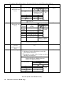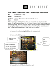
1
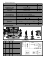
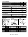
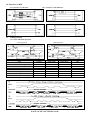
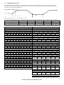
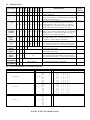
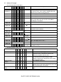
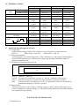
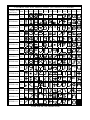
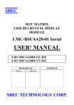
SDEC
DOT MATRIX
LIQUID CRYSTAL DISPLAY
MODULE
LMC-SSC2E16-01 Serial
USER‘ MANUAL
LMC-SSC2E16DRG-01
LMC-SSC2E16DEGB-01
LMC-SSC2E16DLGY-01
LMC-SSC2E16DLGY-E01
PROPOSED BY
Design
LMC-SSC2E16DRY-01
LMC-SSC2E16DEYW-01
LMC-SSC2E16DLYY-01
LMC-SSC2E16DLYY-E01
APPROVED
Approved
SDEC TECHNOLOGY CORP.
CONTENTS
1.
2
3.
4.
5.
6.
7.
8.
9.
10.
Mechanical Specification
Mechanical Diagram
Interface Pin Connections
Block Diagram
Absolute Maximum Rating
Electrical Characteristics
Optical Characteristics
Optical Definitions
Display Address
Interface to MPU
10.1 Interface to Z-80 CPU
10.2 Interface to MC6800 CPU
10.3 Interface to 4-bit CPU ( HMCS43C )
10.4 Interface to HD6805 MP
PAGE
2
2
2
2
3
3
3
3
3
4
4
4
4
4
11. Timing Control
11.1 Write and Read Operation
11.2 Busy flag check timing
4
4
4
12.
13.
14.
15.
5
6
6
7
7
7
Initialization of LCM
Instruction Set
User Font Patterns
Software Example
15.1 8-bit operation ( 8 bits 2 lines )
15.2 4-bit operation ( 4 bits 2 lines )
16. Reliability Condition
17. Function Test & Inspection Criteria
18 Character Generator ROM Map
PAGE 1 (LMC-SSC2E16-01 Serial)
8
8
10
1.
Mechanical Specification
ITEM
NUMBER OF CHARACTERS
CHARACTER FORMAT
MODULE DIMENSION
VIEWING DISPLAY AREA
ACTIVE DISPLAY AREA
CHARACTER SIZE
CHARACTER PITCH
DOT SIZE
DOT PITCH
LMC-SSC2E16DRG-01
LMC-SSC2E16DRY-01
LMC-SSC2E16DEGB-01
LMC-SSC2E16DEYW-01
LMC-SSC2E16DLGY-01
LMC-SSC2E16DLYY-01
LMC-SSC2E16DLGY-E01
LMC-SSC2E16DLYY-E01
EL Use Inverter Type
Inverter Input
Inverter Output
Backlight Half-Lift Time
LED Backlight Color
Backlight Input
Backlight Half-Lift Time
E Mode LED Backlight Color
Backlight Input
Backlight Half-Lift Time
2.
STANDARD VALUE
UNIT
16 CHARACTERS X 2 LINES
-5 X 8 DOTS
-84.0 (W) X 44.0 (H) X 9.0 (T)
84.0 (W) X 44.0 (H) X 13.2 (T)
mm
65.0 (W) X 18.0 (H)
mm
56.21 (W) X 11.50 (H)
mm
2.96 (W) X 5.56 (H)
mm
3.55 (W) X 5.94 (H)
mm
0.56 (W) X 0.66 (H)
mm
0.60 (W) X 0.70 (H)
mm
STN , Gray , 1/16 Duty , 6 O‘clock
STN , Yellow Green , 1/16 Duty , 6 O‘clock
STN , Gray , 1/16 Duty , 6 O‘clock , EL Backlight ( color is Blue )
STN , Yellow Green , 1/16 Duty , 6 O‘clock , EL Backlight ( color is White )
STN , Gray , 1/16 Duty , 6 O‘clock , LED Backlight
STN , Yellow Green , 1/16 Duty , 6 O‘clock , LED Backlight
STN , Gray , 1/16 Duty , 6 O‘clock , E Mode LED Backlight
STN , Yellow Green , 1/16 Duty , 6 O‘clock , E Mode LED Backlight
SDEC-I001A
DC +5V
V
25
mA
AC 90 ~ 110
V
400 ~ 700
Hz
3,000
HR.
Yellow Green
DC +4.2V
V
100
mA
50,000
HR.
Yellow Green
DC +4.2V
V
40
mA
30,000
HR.
Mechanical Diagram
3. Interface Pin Connections
NO
1
2
3
4
5
6
7
8
9
10
11
12
13
14
15
16
SYMBOL
VSS
VDD
VO
RS
R/W
E
DB0
DB1
DB2
DB3
DB4
DB5
DB6
DB7
A+ (EL1)
K- (EL2)
LEVEL
-H/L
H/L
H/L
H/L
H,H→L
H/L
H/L
H/L
H/L
H/L
H/L
H/L
H/L
---
4. Black Diagram
FUNCTION
GND ( 0V)
DC +5V
Contrast Adjust
Register select
Read/Write
Enable signal
Data Bit 0
Data Bit 1
Data Bit 2
Data Bit 3
Data Bit 4
Data Bit 5
Data Bit 6
Data Bit 7
A (EL Backlight 1)
K (EL Backlight 2)
PAGE 2 (LMC-SSC2E16-01 Serial)
5. Absolute Maximum Ratings
ITEM
OPERATING TEMPERATURE
STORAGE TEMPERATURE
INPUT VOLAGE
SUPPLY VOLTAGE FOR LOGIC
SUPPLY VOLTAGE FOR LCD
STATIC ELECTRICITY
SYMBOL
MIN.
TYPE
MAX.
TOP
0/-20
-+50/+70
TST
-10/-30
-+60/+80
VI
VSS
-VDD
VDD-VSS
-5.0
6.5
VDD-VO
--6.5
Be sure that you are grounded when handing LCM.
UNIT
℃
℃
V
V
V
6. Electrical Characteristics
ITEM
SUPPLY VOLTAGE FOR LOGIC
SYN
VDD-VSS
MIN.
4.5
----
TYPE
5.0
4.8/5.0
4.4
4.1/3.9
MAX.
5.5
----
UNIT
V
V
V
V
VIH
VIL
VOH
VOL
IDD
CONDITION
-Ta= 0/-20 ℃
Ta= 25℃
Ta= +50/+70 ℃
----VDD=+5V
SUPPLY VOLTAGE FOR LCD
VDD-VO
INPUT HIGH VOLTAGE
INPUT LOW VOLTAGE
OUTPUT HIGH VOLTAGE
OUTPUT LOW VOLTAGE
SUPPLY CURRENT
2.2
0
2.4
---
----3.0
VDD
0.6
-0.4
4.5
V
V
V
V
mA
SYM
θ
φ
CR
TON
TOFF
CONDITION
CR≧2
CR≧2
----
MIN.
-10
-30
----
TYPE
--5
180
100
MAX.
40
30
-230
150
UNIT
deg.
deg.
-mS
mS
7. Optical Characteristics
ITEM
VIEW ANGLE (V)
VIEW ANGLE (H)
CONTRAST RATIO
RESPONSE TIME
RESPONSE TIME
8. Optical Definitions
Response Time
Contrast Ration
View Angle
9. Display Address
Line 1
Line 2
Line 3
Line 4
1
80
C0
2
81
C1
3
82
C2
4
83
C3
5
84
C4
6
85
C5
7
86
C6
8
87
C7
9
88
C8
10
89
C9
11 12 13 14 15
8A 8B 8C 8D 8E
CA CB CC CD CE
16
8F
CF
17
18
19
20
21
22
23
24
25
26
27
28
29
30
31
36
37
38
39
40
32
33
Line 1
Line 2
Line 3
Line 4
PAGE 3 (LMC-SSC2E16-01 Serial)
34
35
10. Interface to MPU
10.1 Interface to Z-80 CPU
10.2 Interface to MC6800 CPU
10.3 Interface to 4-bit CPU ( HMCS43C )
10.4 Interface to HD6805 MP
11. Timing Control
11.1 Write and Read Operation
Write Operation
Item
Enable Cycle Time
Enable Pules Width ( High level )
Enable Rise/Fall Time
Address Set-Up Time ( RS,R/W,E )
Address Hole Time
Data Set-Up Time
Data Delay Time
Data Hold Time
Read Operation
Symbol
tCYCE
PWEH
tER,tEF
tAS
tAH
tDSW
tDDR
tDHR
Limit (Min.)
1000
450
-100
10
100
-20
11.2 Busy flag check timing
Note : IR7, IR3 : Instruction 7th bit , 3rd bit ; AC3 : Address Counter 3rd bit.
PAGE 4 (LMC-SSC2E16-01 Serial)
Limit (Max.)
--25
---190
--
Unit
ns
ns
ns
ns
ns
ns
ns
ns
12. Initialization of LCM
The LCM automatically initializes ( reset ) when power is turned on using the internal reset circuit. If the power supply
conditions for correctly operating of the internal reset circuit are not met, initialization by instruction is required. Use the
procedure is next page for initialization.
Internal Power Supply reset
4.5V
0.2V
Vcc
toff
trcc
→
←
(Note 1) 10 ms ≧ trcc ≧ 0.1 ms , toff ≧ 1 ms.
←------→
(Note 2) toff stipulates the time of power OFF for momentary power supply dip or when power supply cycles ON and OFF.
Item
Power supply rise time
Power supply off time
RS
0
RS
0
RS
0
RS
0
RS
0
RS
0
RS
0
Symbol
trcc
toff
Test condition
---
Limit (Min.)
0.1
1
Limit (Max.)
10
--
Unit
ms
ms
(a) 8-bit interface
(b) 4-bit interface
Power ON
↓
Wait more than 15ms after VDD rises to 0.9VDD
↓
Function Set
R/W DB7 DB6 DB5 DB4 DB3 DB2 DB1
0
0
0
1
1
*
*
*
↓
Wait more than 4.1 ms
↓
Function Set
R/W DB7 DB6 DB5 DB4 DB3 DB2 DB1
0
0
0
1
1
*
*
*
↓
Wait more than 100μs
↓
Function Set
R/W DB7 DB6 DB5 DB4 DB3 DB2 DB1
0
0
0
1
1
*
*
*
↓
Wait more than 100μs or Busy Flag Check
↓
Function Set
R/W DB7 DB6 DB5 DB4 DB3 DB2 DB1
0
0
0
1
1
N
F
*
↓
Display Off
R/W DB7 DB6 DB5 DB4 DB3 DB2 DB1
0
0
0
0
0
1
0
0
↓
Display Clear
R/W DB7 DB6 DB5 DB4 DB3 DB2 DB1
0
0
0
0
0
0
0
0
↓
Entry Mode Set
R/W DB7 DB6 DB5 DB4 DB3 DB2 DB1
0
0
0
0
0
0
1
I/D
↓
Write data to the DD/CG RAM and set the Instruction
Power ON
↓
Wait more than 15ms after VDD rises to 0.9VDD
↓
Function Set
RS
R/W
DB7
DB6
DB5
DB4
0
0
0
0
1
1
↓
Wait more than 4.1 ms
↓
Function Set
RS
R/W
DB7
DB6
DB5
DB4
0
0
0
0
1
1
↓
Wait more than 100μs
↓
Function Set
RS
R/W
DB7
DB6
DB5
DB4
0
0
0
0
1
1
↓
Wait more than 100μs or Busy Flag Check
↓
Function Set
RS
R/W
DB7
DB6
DB5
DB4
0
0
0
0
1
1
↓
Function Set
RS
R/W
DB7
DB6
DB5
DB4
0
0
0
0
1
0
0
0
N
F
*
*
↓
Display Off
RS
R/W
DB7
DB6
DB5
DB4
0
0
0
0
0
0
0
0
1
0
0
0
↓
Display Clear
RS
R/W
DB7
DB6
DB5
DB4
0
0
0
0
0
0
0
0
0
0
0
1
↓
Entry Mode Set
RS
R/W
DB7
DB6
DB5
DB4
0
0
0
0
0
0
0
0
0
1
I/D
S
↓
Write data to the DD/CG RAM and set the Instruction
DB0
*
DB0
*
DB0
*
DB0
*
DB0
0
DB0
1
DB0
S
PAGE 5 (LMC-SSC2E16-01 Serial)
13. Instruction Set
R R D D D D D D D D
EXECU.
S /W B B B B B B B B
DESCRIPTION
TIME*
7 6 5 4 3 2 1 0
(MAX.)
1.64ms
Clear Display 0 0 0 0 0 0 0 0 0 1 Clears entire display and returns the cursor to home
position ( address 0 ).
Return Home 0 0 0 0 0 0 0 0 1 x Return the cursor to the home position. Also returns the 1.64ms
display being shifted to the original position. DD RAM
contents remain unchanged.
Set cursor move direct and specifies display shift.These 40μs
Entry mode
I
operations are performed during data rite/read. For
set
0 0 0 0 0 0 0 1 / S normal operation, set S to zero. I/D=1 : increment ;
D
0 :decrement ;S=1 : accompanies display shift when
data is written, for normal operation, set to zero.
Set ON/OFF all display(D),cursor ON/OFF(C), and
40μs
Display
0 0 0 0 0 0 1 D C B blink of cursor position character(B). D=1: ON display;
ON/OFF
0:OFF display. C=1: ON cursor;0: OFF cursor. B=1:
control
ON blink cursor; 0: OFF blink cursor.
S R
Move the cursor and shift the display without changing
40μs
Cursor or
0 0 0 0 0 1 / / x x DD RAM contents. S/C=1: Display shift; 0:Cursor
Display
C L
move. R/L=1: shift to right; 0: shift to left.
shift
Set the interface data length (DL). Number of display
40μs
Function
0 0 0 0 1 D N F x x lines (N) and character font (F). DL=1: 8 bits; 0:4 bits.
Set
L
N=1: 2 lines; 0: 1 lines. F=1: 5x10 dots; 0: 5x7 dots.
ACG
Set CG RAM address. CG RAM data is sent and
40μs
Set CG RAM 0 0 0 1
received after this setting.
address
ADD
Set DD RAM address. DD RAM data is sent and
40μs
Set DD RAM 0 0 1
received after this setting
address
Reads Busy Flag (BF) indicating internal operation is
1 μs
Read busy
0 1 B
AC
being performed and reads address counter contents.
flag &
F
BF=1: internally operating. 0: can accept instruction
address
WRITE DATA
Write data into DD RAM or CG RAM.
40μs
Write Data to 1 0
CG/DDRAM
READ DATA
Read data from DD RAM or CG RAM
40μs
Read Data for 1 1
CG/DDRAM
FUNCTION
14. User Font Patterns ( CG RAM Character )
Character Code (DD RAM data)
Hi
76543210
Lo
CG RAM Address
543
0000x000
000
0000x001
001
----------------
0000x111
210
000
001
010
011
100
101
110
111
000
001
010
011
100
101
110
111
----------------
111
Character Pattern (CG RAM data)
Hi
765
xxx
xxx
xxx
xxx
xxx
xxx
xxx
xxx
xxx
xxx
xxx
xxx
xxx
xxx
xxx
xxx
4
1
1
1
1
1
1
1
0
1
0
1
0
1
0
0
0
3
1
0
0
1
0
0
0
0
0
1
1
0
1
0
0
0
2
1
0
0
1
1
0
0
0
0
0
1
1
1
1
1
0
1
1
0
0
1
0
1
0
0
0
1
1
0
1
1
0
0
0
0
1
1
0
0
0
1
0
1
0
1
0
1
0
0
0
--------------------------------
000
001
010
011
100
101
110
111
PAGE 6 (LMC-SSC2E16-01 Serial)
Lo
15. Software Example
15.1 8-bit operation ( 8 bits 2 lines )
Function
R R D D D D D D D D
S w 7 6 5 4 3 2 1 0
Display
Power on delay
Description
Function set
0 0 0 0 1 1 0 0 x x
Display OFF
0 0 0 0 0 0 1 0 0 0
Initialization. No display appears.
Sets to 8-bit operation and selects 2-line display and 5x7
dots character font. ( Note: number of display lines and
character fonts cannot be chang after this. )
Turn off display.
Display ON
0 0 0 0 0 0 1 1 1 0
Turn on display and cursor
Entry Mode
Set
0 0 0 0 0 0 0 1 1 0
Write data to
CG/DD RAM
Write data to
CG/DD RAM
Set DD RAM
Write data to
CG/DD RAM
Cursor or
display shift
Write data to
CG/DD RAM
Entry Mode
Set
Write data to
CG/DD RAM
Write data to
CG/DD RAM
Return Home
Set mode to increment the address by one and to shift the
cursor to the right, at the time of write, to the DD/CG
RAM Display is not shifted.
Write “S”. Cursor incremented by one and shift to right.
1 0 0 1 0 1 0 0 1 1 S
1
1
1
0
0
0
0
0
0
0
0
1
1
1
1
1
0
0
0
0
0
0
0
0
0
0
0
0
1
1
0
0
0
0
1
0
Write “D” , “E” , and “C”.
0 SDEC
1
1
0 SDEC
*
SDEC
*
CR
0 0 0 0 0 1 0 0 x x SDEC
CR
*
SDEC
*
CO., LTD.
0 0 0 0 0 0 0 1 1 1 SDEC
CO., LTD.
DEC
1 0 0 1 1 1 1 0 0 0 O., LTD. x
*
*
0 0 0 0 0 0 0 0 1 0 SDEC
CO., LTD.
Set RAM address so that the cursor is propositioned
at the head of the second line.
Write “C” , and “R”.
Shift only the cursor position to the left.
Write “O., LTD.” .
Set display mode shift at the time during writing operation.
Write “ x”. Cursor incremented by one and shift to
right. ( The display move to left. )
Write other characters.
Return both display and cursor to the original position
( Set address to zero).
15.2 4-bit operation ( 4-bit, 1 line )
Function
RS R/ D7 D6 D5 D4
W
power on delay
Function set
0
0
0
0
1
0
0
0
0
0
0
0
0
0
1
x
0
x
Display ON/OFF
Control
Entry Mode Set
0
0
0
0
0
0
0
0
0
1
0
0
0
1
0
1
0
1
0
1
0
0
0
0
Write data to CG/DD
RAM
1
1
0
0
0
0
1
0
0
1
Function set
Display
Description
initialization. No display appears.
Sets to 4-bit operation. In this case, operation is
handled as 8-bits by initialization, and only this
instruction completes with one write.
Sets 4-bit operation and selects 1-line display and 5x7
dot character font on and resetting is needed.
( number of display lines and character fonts cannot
be changed hence after ).
Turn on display and cursor.
Set mode to incremented the address by one and to
shift the cursor to the right, at the time of write. to the
DD/CG RAM display is not shifted.
1 S
Write “S”. Cursor incremented by one and shift to
1
right.
same as 8-bit operation
PAGE 7 (LMC-SSC2E16-01 Serial)
16. Reliability Condition
TN Type
Normal Temp.
Wide Temp.
Viewing
Horizontal Φ
±30°
±30°
Angle
Vertical Θ(㎜)
10°to 30°
10°to 30°
Operating Temperature
-10 to 70℃
-25 to 80℃
Storage Temperature
-20 to 80℃
-35 to 90℃
High Temperature (Power Off)
240 Hours
240 Hours
@70℃
@90℃
Low Temperature (Power Off)
240 Hours
240 Hours
@-20℃
@-35℃
High Temperature (Power On)
240 Hours
240 Hours
@70℃
@80℃
Low Temperature (Power On)
240 Hours
240 Hours
@-10℃
@-25℃
High Temperature & High
55℃/90%RH
75℃/90%RH
Humidity
240 Hours
240 Hours
Thermal Shock
C
A 60min@-20℃ 60min@-35℃
5 Cycle
B
B 5min@25℃
5min@25℃
A
C 60min@70℃
60min@90℃
Expected Lift
50,000 Hours
50,000 Hours
STN Type
Normal Temp.
Wide Temp.
±30°
±30°
-10°to 40°
-10°to 40°
*
0 to 50℃
-20 to 70℃
*
-20 to 70℃
-30 to 80℃
240 Hours
240 Hours
@65℃
@75℃
240 Hours
240 Hours
@-15℃
@-25℃
240 Hours
240 Hours
@60℃
@70℃
240 Hours
240 Hours
@-10℃
@-20℃
45℃/90%RH
65℃/90%RH
240 Hours
240 Hours
60min@-20℃ 60min@-30℃
5min@25℃
5min@25℃
60min@70℃
60min@80℃
50,000 Hours
50,000 Hours
*
Wide temp. version may not available for some products, Please consult our sales engineer or respresentative.
17. Functional Test & Inspection Criteria
17.1 Sample plan
Sample plan according to MIL-STD-105D level 2, and acceptance/rejection criteria is.
Base on :
Major defect : AQL 0.65
Minor defect : AQL 2.5
17.2 Inspection condition
Viewing distance for cosmetic inspection is 30cm with bare eyes, and under an environment of
800 lus (20W) light intensity. All direction for inspecting the sample should be within 45°
against perpendicular line.
17.3 Definition of Inspection Zone in LCD
C
A
B
Zone A :
Zone B :
Zone C :
Note :
Character / Digit area
Viewing area except Zone A ( Zone A + Zone B = minimum Viewing area )
Outside viewing area ( invisible area after assembly in customer’s product )
As a general rule, visual defects in Zone C are permissible, when it is no trouble for
quality and assembly of customer’s product.
17.4 Major Defect
All functional defects such as open ( or missing segment ), short, contrast differential, excess
power consumption, smearing, leakage, etc. and overall outline dimension beyond the drawing.
Are classified as major defects.
PAGE 8 (LMC-SSC2E16-01 Serial)
17.5 Minor Defect
Except the Major defects above, all cosmetic defects are classified as minor defects.
Item No. Item to be Inspected
Inspection Standard
Classification of
defects
1.
Spot defect
Zone size (mm)
Acceptable Qty
Minor
( Defects in spot
A
B
C
from )
AcceptaAcceptable
Φ≦0.15
ble
( clutering of spot
not allowed )
1
2
0.15≦Φ≦0.20
0
1
0.20≦Φ≦0.25
0
0
Φ>0.25
Remarks : for dark/white spot, size Φ is defined as
Φ=1/2(X+Y)
2.
Line defect
Size (mm)
Acceptable Qty
Minor
( Defects in line
L
W
Zone
form )
Length
Width
A B
C
AccepAccep- AccepW≦0.02
table
table
table
2
L≦3.0
W≦0.03
0
L>2.5
W≦0.03
2
L≦3.0
0.03<W≦0.05
0
L>2.5
0.03<W≦0.05
Counted as spot
W>0.05
defect ( Follows
item 17.5.1 )
Remarks: The total of spot defect and line defect
shall not exceed four.
3.
Orientation defect Not allowed inside viewing area ( Zone A or Zone
Minor
( such as
B)
misalignment of
L/C)
Minor
4.
Polarizing
17.5.4.1 Polarizer Position
1. Shifting in Position Should not exceed the
glass outline dimension.
2. Incomplete covering of the viewing area due to
Shifting is not allowed.
17.5.4.2 Seratches, bubble or dent on Glass/
Polarizer/Reflector, Bubble between
Polarizer & Reflector/Glass:
Size (mm)
Acceptable Qty
Zone
A
B
C
Acceptable
AccepΦ≦0.20
table
3
0.20<Φ≦0.50
0.50<Φ≦1.00
Φ>1.00
2
0
PAGE 9 (LMC-SSC2E16-01 Serial)
18. Character Generator ROM Map
CHARACTER PATTERN CHART (5×7 DOTS +CURSOR)
Higher 4 bit
0000 0010 0011 0100 0101 0110 0111 1010 1011 1100 1101 1110 1111
Lower 4 bit
CG RAM
XXXX0000
(1)
XXXX0001
(2)
XXXX0010
(3)
XXXX0011
(4)
XXXX0100
(5)
XXXX0101
(6)
XXXX0110
(7)
XXXX0111
(8)
XXXX1000
(1)
XXXX1001
(2)
XXXX1010
(3)
XXXX1011
(4)
XXXX1100
(5)
XXXX1101
(6)
XXXX1110
(7)
XXXX1111
(8)
PAGE 10 (LMC-SSC2E16-01 Serial)
SDEC
SDEC TECHNOLOGY CORP.
6TH FLOOR, NO. 81, KUAN FU RD., SEC. 1
SAN CHUNG CITY, TAIPEI HSIEN, TAIWAN R.O.C.
TEL: 886-2-2995-6152~3
886-2-2278-2884~5
FAX: 886-2-2278-1869
886-2-2995-4706
EMAIL:[email protected]
[email protected]
http://www.sdec.com.tw