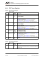
1
Cover
88F5182-based Storage
Networking Platforms
Open Source Community
Programmer’s User Guide
Doc. No. MV-S400130-00, Rev. 0.5
June 25, 2007
Marvell. Moving Forward Faster
Document Classification: Proprietary
88F5182
Open Source Community Programmer’s User Guide
Document Conventions
Note: Provides related information or information of special importance.
Caution: Indicates potential damage to hardware or software, or loss of data.
Warning: Indicates a risk of personal injury.
Document Status
Doc Status: Preliminary
Technical Publication: 0.x
For more information, visit our website at: www.marvell.com
Disclaimer
No part of this document may be reproduced or transmitted in any form or by any means, electronic or mechanical, including photocopying and recording, for any purpose,
without the express written permission of Marvell. Marvell retains the right to make changes to this document at any time, without notice. Marvell makes no warranty of any
kind, expressed or implied, with regard to any information contained in this document, including, but not limited to, the implied warranties of merchantability or fitness for any
particular purpose. Further, Marvell does not warrant the accuracy or completeness of the information, text, graphics, or other items contained within this document.
Marvell products are not designed for use in life-support equipment or applications that would cause a life-threatening situation if any such products failed. Do not use
Marvell products in these types of equipment or applications.
With respect to the products described herein, the user or recipient, in the absence of appropriate U.S. government authorization, agrees:
1) Not to re-export or release any such information consisting of technology, software or source code controlled for national security reasons by the U.S. Export Control
Regulations ("EAR"), to a national of EAR Country Groups D:1 or E:2;
2) Not to export the direct product of such technology or such software, to EAR Country Groups D:1 or E:2, if such technology or software and direct products thereof are
controlled for national security reasons by the EAR; and,
3) In the case of technology controlled for national security reasons under the EAR where the direct product of the technology is a complete plant or component of a plant,
not to export to EAR Country Groups D:1 or E:2 the direct product of the plant or major component thereof, if such direct product is controlled for national security reasons
by the EAR, or is subject to controls under the U.S. Munitions List ("USML").
At all times hereunder, the recipient of any such information agrees that they shall be deemed to have manually signed this document in connection with their receipt of any
such information.
Copyright © . Marvell International Ltd. All rights reserved. Marvell, the Marvell logo, Moving Forward Faster, Alaska, Fastwriter, Datacom Systems on Silicon, Libertas, Link
Street, NetGX, PHYAdvantage, Prestera, Raising The Technology Bar, The Technology Within, Virtual Cable Tester, and Yukon are registered trademarks of Marvell. Ants,
AnyVoltage, Discovery, DSP Switcher, Feroceon, GalNet, GalTis, Horizon, Marvell Makes It All Possible, RADLAN, UniMAC, and VCT are trademarks of Marvell. All other
trademarks are the property of their respective owners.
Doc. No. MV-S400130-00 Rev. 0.5
Page 2
Copyright © 2007 Marvell
Document Classification: Proprietary
June 25, 2007, Preliminary
88F5182
Open Source Community Programmer’s User Guide
Table of Contents
Preface ................................................................................................................................... 9
About This Document ............................................................................................................................ 9
Related Documents ............................................................................................................................... 9
Document Conventions ....................................................................................................................... 10
Section 1. Overview.......................................................................................................... 11
Section 2. Address Map ................................................................................................... 13
2.1
2.2
2.3
2.4
2.5
2.6
2.7
2.8
2.9
2.10
Marvell Processor Core Address Map ...................................................................................... 13
PCI Express Address Map ........................................................................................................ 13
PCI Address Map ...................................................................................................................... 13
SATA Address Map................................................................................................................... 14
Gigabit Ethernet Address Map .................................................................................................. 14
USB0 Address Map................................................................................................................... 14
USB1 Address Map................................................................................................................... 14
IDMA Address Map ................................................................................................................... 14
XOR Address Map .................................................................................................................... 14
Default Address Map................................................................................................................. 14
Section 3. DDR SDRAM Controller Interface ................................................................. 16
Section 4. PCI Express Interface..................................................................................... 17
Section 5. PCI Interface.................................................................................................... 18
5.1
5.2
5.3
Functional Description............................................................................................................... 18
PCI Master Operation ............................................................................................................... 18
PCI Target Operation ................................................................................................................ 19
Section 6. SATA II Interface............................................................................................. 20
Section 7. Serial-ATA II Host Controller (SATAHC)....................................................... 21
7.1
7.2
SATAHC Block Diagram ........................................................................................................... 21
EDMA Operation ....................................................................................................................... 21
Doc. No. MV-S400130-00 Rev. 0.5
Page 3
Copyright © 2007 Marvell
Document Classification: Proprietary
June 25, 2007, Preliminary
Table of Contents
Section 8. Gigabit Ethernet Controller Interface ........................................................... 33
8.1
8.2
Functional Description ............................................................................................................... 33
Port Features ............................................................................................................................. 34
Section 9. USB 2.0 Interface ........................................................................................... 36
9.1
Functional Description ............................................................................................................... 36
Section 10. Cryptographic Engines and Security Accelerator....................................... 37
10.1 Functional Overview .................................................................................................................. 37
10.2 Cryptographic Engines Operational Description........................................................................ 38
Section 11. Two-Wire Serial Interface (TWSI) .................................................................. 40
11.1 Functional Description ............................................................................................................... 40
11.2 TWSI Master Operation ............................................................................................................. 43
11.3 TWSI Slave Operation ............................................................................................................... 44
Section 12. UART Interface................................................................................................ 46
12.1 Functional Description ............................................................................................................... 46
12.2 UART Interface Pin Assignment ................................................................................................ 46
Section 13. Device Controller Interface............................................................................ 47
13.1
13.2
13.3
13.4
13.5
Functional Description ............................................................................................................... 47
Device Interface Pin Assignment............................................................................................... 47
Device Interface Block Diagram ................................................................................................ 48
Address Multiplexing.................................................................................................................. 49
NAND Flash Controller Implementation..................................................................................... 49
Section 14. IDMA Controller .............................................................................................. 50
14.1 Functional Description ............................................................................................................... 50
14.2 IDMA Descriptors....................................................................................................................... 50
Section 15. XOR Engine..................................................................................................... 52
15.1 Theory of Operation................................................................................................................... 52
15.2 Descriptor Chain ........................................................................................................................ 53
Copyright © 2007 Marvell
June 25, 2007, Preliminary
Doc. No. MV-S400130-00 Rev. 0.5
Document Classification: Proprietary
Page 4
88F5182
Open Source Community Programmer’s User Guide
Section 16. General Purpose I/O Port Interface............................................................... 58
Section 17. Interrupt Controller......................................................................................... 59
17.1
17.2
17.3
17.4
17.5
Functional Description............................................................................................................... 59
Local Interrupt Cause and Mask Registers ............................................................................... 59
Main Interrupt Cause and Mask Registers ................................................................................ 60
Doorbell Interrupt ...................................................................................................................... 60
88F5182 Interrupt Controller Scheme ....................................................................................... 61
Section 18. Timers.............................................................................................................. 62
18.1 Functional Description............................................................................................................... 62
18.2 32-bit-wide Timers..................................................................................................................... 62
18.3 Watchdog Timer........................................................................................................................ 62
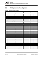
Appendix A. 88F5182 Register Set ................................................................................... 88
Appendix B. Revision History......................................................................................... 388
Doc. No. MV-S400130-00 Rev. 0.5
Page 5
Copyright © 2007 Marvell
Document Classification: Proprietary
June 25, 2007, Preliminary
List of Tables
List of Tables
Table 1:
Table 2:
Table 3:
Table 4:
Table 5:
Table 6:
Table 7:
Table 8:
Table 9:
Table 10:
Table 11:
Table 12:
Table 13:
Table 14:
Table 15:
Table 16:
Table 17:
Table 18:
Table 19:
Table 20:
Table 21:
Table 22:
Table 23:
Table 24:
Table 25:
Table 26:
Table 27:
Table 28:
Table 29:
Table 30:
Table 31:
Table 32:
Table 33:
Table 76:
Table 107:
Table 178:
Table 179:
Table 180:
Table 181:
Table 182:
88F5182 Default Address Map...........................................................................................................14
EDMA CRQB Data Structure Map .....................................................................................................25
CRQB DW0—cPRD Descriptor Table Base Low Address.................................................................25
CRQB DW1—cPRD Descriptor Table Base High Address................................................................26
CRQB DW2—Control Flags ...............................................................................................................26
CRQB DW3—Data Region Byte Count..............................................................................................27
CRQB DW4—ATA Command............................................................................................................27
CRQB DW5—ATA Command............................................................................................................27
CRQB DW6—ATA Command............................................................................................................28
CRQB DW7—ATA Command............................................................................................................28
ePRD Table Data Structure Map........................................................................................................29
ePRD DWORD 0................................................................................................................................29
ePRD DWORD 1................................................................................................................................30
ePRD DWORD 2................................................................................................................................30
ePRD DWORD 3................................................................................................................................30
EDMA CRPB Data Structure Map......................................................................................................31
CRPB ID Register ..............................................................................................................................31
CRPB Response Flags Register ........................................................................................................32
CRPB Time Stamp Register...............................................................................................................32
Acronyms, Abbreviations, and Definitions..........................................................................................37
Setting the Baud Rate Register..........................................................................................................42
UART Pin Assignments......................................................................................................................46
Device Controller Pin Assignments ....................................................................................................47
IDMA Descriptor Definitions ...............................................................................................................51
Descriptor Status Word Definition ......................................................................................................55
Descriptor CRC-32 Result Word Definition ........................................................................................55
Descriptor Command Word Definition................................................................................................55
Descriptor Next Descriptor Address Word .........................................................................................56
Descriptor Byte Count Word...............................................................................................................56
Descriptor Destination Address Word ................................................................................................57
Descriptor Source Address #N Words ...............................................................................................57
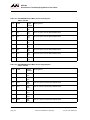
88F5182 Internal Registers Address Map..........................................................................................89
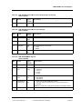
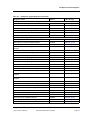
CPU Register Map .............................................................................................................................90
DDR SDRAM Register Map .............................................................................................................109
PCI Express Register Map Table .....................................................................................................127
PCI Slave Address Decoding Register Map.....................................................................................169
PCI Control Register Map ................................................................................................................170
PCI Configuration Access Register Map ..........................................................................................170
PCI Error Report Register Map ........................................................................................................171
PCI Configuration, Function 0, Register Map...................................................................................171
Copyright © 2007 Marvell
June 25, 2007, Preliminary
Doc. No. MV-S400130-00 Rev. 0.5
Document Classification: Proprietary
Page 6
88F5182
Open Source Community Programmer’s User Guide
Table 183:
Table 184:
Table 185:
Table 186:
Table 288:
Table 289:
Table 290:
Table 291:
Table 292:
Table 293:
Table 364:
Table 419:
Table 420:
Table 421:
Table 435:
Table 491:
Table 499:
Table 512:
Table 521:
Table 522:
Table 523:
Table 524:
Table 541:
Table 564:
Table 573:
Table 579:
PCI Configuration, Function 1, Register Map .................................................................................. 172
PCI Configuration, Function 2, Register Map .................................................................................. 172
PCI Configuration, Function 3, Register Map .................................................................................. 172
PCI Configuration, Function 4, Register Map .................................................................................. 172
SATAHC Address Space................................................................................................................. 213
SATAHC Arbiter Registers Map ...................................................................................................... 213
EDMA Registers Map ...................................................................................................................... 214
Shadow Register Block Registers Map ........................................................................................... 215
Basic DMA Register Map ................................................................................................................ 216
Serial-ATA Interface Registers Map ................................................................................................ 217
Ethernet Unit Global Registers Map ................................................................................................ 267
USB 2.0 Controller Register Map
(Offsets Port0: 0x50000–0x502FF, Port1: 0xA0000–0xA02FF)...................................................... 305
USB 2.0 Bridge Register Map (Port0: 0x50300–0x503FF, Port1: 0xA0300–0xA03FF) ................. 306
USB 2.0 PHY Register Map (Port0: 0x50400, Port1: 0xA0300)..................................................... 307
Cryptographic Engine and Security Accelerator Register Map ....................................................... 314
TWSI Interface Register Map .......................................................................................................... 335
UART Interface Registers Map........................................................................................................ 340
Device Registers Map ..................................................................................................................... 348
IDMA Descriptor Register Map........................................................................................................ 353
IDMA Address Decoding Register Map........................................................................................... 353
IDMA Control Register Map............................................................................................................. 354
IDMA Interrupt Register Map........................................................................................................... 354
XOR Engine Register Map .............................................................................................................. 364
GPIO Registers Map ....................................................................................................................... 380
MPP Register Map .......................................................................................................................... 384
Revision History............................................................................................................................... 388
Doc. No. MV-S400130-00 Rev. 0.5
Page 7
Copyright © 2007 Marvell
Document Classification: Proprietary
June 25, 2007, Preliminary
List of Figures
List of Figures
Figure 1:
Figure 2:
Figure 3:
Figure 4:
Figure 5:
Figure 6:
Figure 7:
Figure 8:
Figure 9:
Figure 10:
Figure 11:
Figure 12:
Figure 13:
Figure 14:
Figure 15:
Figure 16:
88F5182 Interface Block Diagram .................................................................................................... 11
SATAHC Block Diagram ................................................................................................................... 21
Command Request Queue—32 Entries............................................................................................ 22
Command Response Queue—32 Entries ......................................................................................... 23
Command Request Queue—128 Entries.......................................................................................... 23
Command Response Queue—128 Entries ....................................................................................... 24
TWSI Examples ................................................................................................................................ 41
Device Block Diagram Example ........................................................................................................ 48
Address Multiplexing ......................................................................................................................... 49
Mask ALE during NAND Flash Read Data Phase ............................................................................ 49
Generate Dedicated NAND Flash WE Signal ................................................................................... 49
Generate CE Covers All NAND Flash Transaction ........................................................................... 49
IDMA Descriptors ............................................................................................................................. 51
XOR Descriptor Format..................................................................................................................... 54
88F5182 Interrupt Controller Scheme ............................................................................................... 61
SATAHC Address Space ................................................................................................................ 213
Copyright © 2007 Marvell
June 25, 2007, Preliminary
Doc. No. MV-S400130-00 Rev. 0.5
Document Classification: Proprietary
Page 8
88F5182
Open Source Community Programmer’s User Guide
Preface
About This Document
This document provides a product overview, interface descriptions and registers for the 88F5182.
Related Documents
•
•
•
•
•
•
•
•
•
•
•
•
•
•
•
•
ARM Architect Reference Manual, Second Edition
AMBA™ Specification, Rev 2.0
PCI Local Bus Specification, Revision 2.2
PCI Express Base Specification, Revision 1.0a
Serial-ATA II Phase 1.0 Specification (Extension to SATA I Specification)
Universal Serial Bus Specification, Revision 2.0, April 2000, Compaq, Hewlett-Packard, Intel, Lucent,
Microsoft, NEC, Philips
Enhanced Host Controller Interface Specification for Universal Serial Bus, Revision 0.95, November 2000,
Intel Corporation
USB-HS High-Speed Controller Core reference
RFC 1321 (The MD5 Message-Digest Algorithm)
FIBS 180-1 (Secure Hash Standard)
FIBS 46-2 (Data Encryption Standard)
FIBS 81 (DES Modes of Operation)
RFC 2104 (HMAC: Keyed-Hashing for Message Authentication).
RFC 2405 – The ESP DES-CBC Cipher Algorithm With Explicit IV
RFC 1851 – The ESP Triple DES Transform
FIBS draft - Advanced Encryption Standard (Rijndeal)
Doc. No. MV-S400130-00 Rev. 0.5
Page 9
Copyright © 2007 Marvell
Document Classification: Proprietary
June 25, 2007, Preliminary
Preface
Document Conventions
Document Conventions
This document has the following name and usage conventions:
Signal Range
A signal name followed by a range enclosed in brackets represents a range of
logically related signals. The first number in the range indicates the most significant
bit (MSb) and the last number indicates the least significant bit (LSb).
Example: DB_AD[31:0]
Active Low Signals n
A "n” symbol at the end of a signal name indicates that the signal’s active state occurs
when voltage is low.
Example: INTn
State Names
State names are indicated in italic font.
Example: linkfail
Register Naming
Conventions
Register field names are enclosed in angle brackets.
Example: <Dwidth>
OR
Example: SDRAM_Configuration<Dwidth>,
Where Global Control represents the register name, and <Dwidth> represents the
register field name.
Register field bits are enclosed in brackets.
Example: Field [1:0]
Register addresses are represented in hexadecimal format
Example: 0x0
Reserved: The contents of the register are reserved for internal use only or for future
use.
Copyright © 2007 Marvell
June 25, 2007, Preliminary
Doc. No. MV-S400130-00 Rev. 0.5
Document Classification: Proprietary
Page 10
88F5182
Open Source Community Programmer’s User Guide
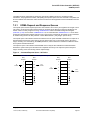
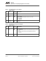
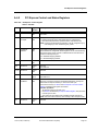
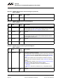
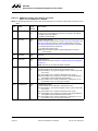
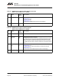
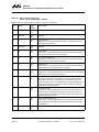
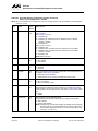
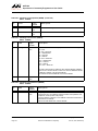
Section 1. Overview
The Marvell 88F5182 is a high performance, highly integrated, Storage Networking System Engine based on
Marvell proprietary, ARMv5TE-compliant, CPU core.
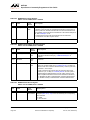
Figure 1 is a block diagram of the 88F5182 interfaces.
Figure 1: 88F5182 Interface Block Diagram
Marvell CPU
Local bus
Bridge
Memory Controller
System Bus
SATA II
with
integrated
PHYs
X 2 ports
IDMA,
Xor,
Cryptographic
Engine
GPPs,
UART x2,
TWSI,
Device
PCI Express
with
intergrated
SERDES
X 1 port
PCI
32-bit
port
Gigabit
Ethernet
port
USB 2.0
with
integrated
PHYs
X 2 ports
The 88F5182 incorporates the following functions/interfaces.
Marvell Processor
Core
Marvell ARM9te-compliant core
DDR SDRAM
Memory Controller.
The PCI Express interface includes a single PCI Express (X1) host port, with an
integrated low power SERDES.
PCI Express
PCI
The PCI Express port can also be configured as an Endpoint port.
The 88F5182 integrates a 32-bit conventional PCI interface.
Doc. No. MV-S400130-00 Rev. 0.5
Page 11
Copyright © 2007 Marvell
Document Classification: Proprietary
June 25, 2007, Preliminary
Overview
SATA II
The 88F5182 accommodates a total of two SATA II ports. It is fully compliant with SATA II
Phase 1.0 specification (Extension to SATA I specification), supporting:
• SATA II Native command queuing
• Backwards compatibility to SATA I 1.5-Gbps speed and devices
In addition to full support of SATA II Phase 1.0 specification (Extension to SATA I specification), the 88F5182 supports the following advanced SATA II Phase 2.0 specification
features:
• SATA II 3-Gbps speed
• Advanced SATA PHY characteristics for SATA backplane support
• SATA II Port Multiplier Advanced Support
• SATA II Port Selector control: Generates the protocol-based OOB sequence to select
the active host of the SATA II Port Selector.
Gigabit Ethernet
The Gigabit Ethernet interface consists of a single 10/100/1000 Mbps full-duplex Gigabit
Ethernet (GbE) port. It can be configured to a 10/100 Mbps MII interface or a 10/100/1000
Mbps RGMII/GMII interface. This is useful for higher throughput interfacing to the Marvell
Fast Ethernet switches.
USB 2.0
The 88F5182 integrates two USB 2.0 high-speed ports each with an embedded PHY.
They can be configured to either host ports or peripheral ports.
Cryptographic Engine The 88F5182 integrates a Cryptographic Engine and Security Accelerator, to support data
encryption and authentication. It also contains a dedicated DMA to feed data from the
and Security
local SRAM into the arithmetic hardware.
Accelerator
Two-Wire Serial
Interface (TWSI)
The 88F5182 includes a single Two-Wire Serial Interface (TWSI) port.
UART
The UART Interface consists of two UART ports.
Device Bus
The 88F5182 includes a 16-bit Device interface.
IDMA Engines
The 88F5182 incorporates four IDMA engines. Each IDMA engine has the capability to
transfer data between any interface.
The 88F5182 incorporates two additional XOR DMA engines, useful for Redundant Array
of Independent Disks (RAID) applications.
XOR Engine
Each XOR DMA runs on a linked list of descriptors. It can read from up to eight sources,
perform bitwise XOR between the eight sources, and writes the result to a destination.
The sources and destination can reside in any of the 88F5182 interfaces.
General Purpose IO
Port
The 88F5182 contains 26-bit general purpose IOs.
Interrupt Controller
The 88F5182 includes an advanced interrupt controller, which handles interrupts from all
of the various sources and forwards them to the Marvell processor core.
When working in Endpoint mode the interrupts can be forwarded also to the Endpoint
PCI Express interface.
Timers
The 88F5182 includes two general purpose 32-bit-wide timers and a single 32-bit-wide
watchdog timer.
Internal Architecture
The 88F5182 internal architecture is optimized for high-performance applications..
Copyright © 2007 Marvell
June 25, 2007, Preliminary
Doc. No. MV-S400130-00 Rev. 0.5
Document Classification: Proprietary
Page 12
88F5182
Open Source Community Programmer’s User Guide
Section 2. Address Map
The 88F5182 has a fully programmable address map. There is a separate address map for each of the device
master interfaces. Each interface includes programmable address windows that allow it to access any of the
88F5182 resources.
•
•
•
•
•
•
•
•
Marvell processor core address map
PCI Express address map
PCI address map
SATA address map
Ethernet Controller address map
USB address map
IDMAs address map
XOR address map
Note
Although each master has independent address windows, when a resource is used by multiple masters,
all masters must use the same address map for this resource. This means that all masters use the
identical address window for each resource.
2.1
Marvell Processor Core Address Map
The Marvell processor core interface address map consists of eight programmable address windows for the
different interfaces and additional four dedicated windows for the DDR interface. See Appendix A.4.1 "CPU
Address Map Registers" on page 91 and Appendix A.5.1 "DDR SDRAM Controller Address Decode Registers" on
page 110.
For default address map see Table 1, “88F5182 Default Address Map,” on page 14.
2.2
PCI Express Address Map
The PCI Express interface address map consists of three BARs that map the chip address space. One BAR is
dedicated for the chip internal registers while the other two are further sub-decoded by six programmable address
windows to the different interfaces of the chip. See Appendix A.6.1 "PCI Express BAR Control Registers" on page
129.
For the default address map, see Table 1, with following exceptions.
•
•
By default, access from the PCI Express interface to PCI interface is disabled.
By default, access from the PCI Express to Device CS0 and Device CS1 is disabled.
2.3
PCI Address Map
The PCI interface address map consists of 12 BARS address windows for the different interfaces.
For the default address map, see Table 1, with following exceptions.
•
•
•
By default, access from the PCI interface to the PCI Express interface is disabled.
By default, access from the PCI interface to Device CS0 and Device CS1 is disabled.
By default, I/O access from the PCI interface to the chip internal registers is disabled.
Doc. No. MV-S400130-00 Rev. 0.5
Page 13
Copyright © 2007 Marvell
Document Classification: Proprietary
June 25, 2007, Preliminary
Address Map
SATA Address Map
2.4
SATA Address Map
The SATAHC interface address map consists of four programmable address windows for the different interfaces.
See Section A.8.7 "SATAHC Arbiter Registers" on page 218. By default the SATAHC address map is enabled and
addressed to the DRAM as specified in Table 1, “88F5182 Default Address Map,” on page 14.
2.5
Gigabit Ethernet Address Map
The Gigabit Ethernet interface address map consists of six programmable address windows for the different
interfaces. By default the Gigabit Ethernet MAC address map is disabled.
2.6
USB0 Address Map
The USB0 interface address map consists of four programmable address windows for the different interfaces. By
default the USB0 address map is disabled.
2.7
USB1 Address Map
The USB1 interface address map consists of four programmable address windows for the different interfaces. By
default the USB1 address map is disabled.
2.8
IDMA Address Map
The IDMA interface address map consists of eight programmable address windows for the different interfaces.
See Section A.15.2 "IDMA Address Decoding Registers" on page 356. By default the IDMA address map is
disabled.
2.9
XOR Address Map
The XOR interface address map consists of eight programmable address windows for the different interfaces. See
Section A.16.4 "XOR Engine Address Decoding Registers" on page 372. By default the XOR address map is
disabled.
Note
Windows base addresses of the 88F5182 must be aligned to their size (for example, a 128 KB address
window should be aligned to 128 KB).
2.10
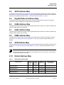
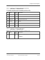
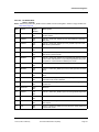
Default Address Map
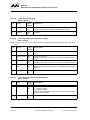
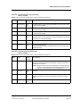
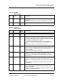
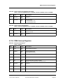
Table 1:
88F5182 Default Address Map
Target Interface
Target
Interface
ID1
Target
Interface
Attribute2
Address
Space Size
Address Range in
Hexadecimal
DDR SDRAM CS0
0
0x0E
256 MByte
0000.0000–0FFF.FFFF
DDR SDRAM CS1
0
0x0D
256 MByte
1000.0000–1FFF.FFFF
DDR SDRAM CS2
0
0x0B
256 MByte
2000.0000–2FFF.FFFF
DDR SDRAM CS3
0
0x07
256 MByte
3000.0000–3FFF.FFFF
Copyright © 2007 Marvell
June 25, 2007, Preliminary
Doc. No. MV-S400130-00 Rev. 0.5
Document Classification: Proprietary
Page 14
88F5182
Open Source Community Programmer’s User Guide
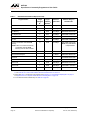
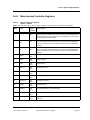
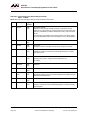
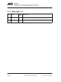
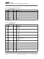
Table 1:
88F5182 Default Address Map (Continued)
Target
Interface
ID1
Target
Interface
Attribute2
Address
Space Size
Address Range in
Hexadecimal
Reserved
-
-
1 GByte
4000.0000–7FFF.FFFF
PCI Express Memory
4
0x59
512 MByte
8000.0000–9FFF.FFFF
PCI Memory
3
0x59
512 MByte
A000.0000–BFFF.FFFF
PCI Express I/O
4
0x51
64 KByte
C000.0000–C000.FFFF
Reserved
-
-
-
C001.0000–C7FF.FFFF
PCI I/O
3
0x51
64 KByte
C800.0000–C800.FFFF
Security Accelerator Internal SRAM
Memory
NOTE:There is no access to Security
Accelerator Internal SRAM
Memory from the PCI interface.
9
0x00
64 KByte
C801.0000–C801.FFFF
NOTE:Only 8 KB SRAM
is implemented.
Reserved
-
-
C802.0000–CFFF.FFFF
Internal Address Space3
-
1 MByte
D000.0000–D00F.FFFF
Target Interface
Reserved
-
-
-
D010.0000–DFFF.FFFF
Device CS0
1
0x1E
128 MByte
E000.0000–E7FF.FFFF
Device CS1
1
0x1D
128 MByte
E800.0000–EFFF.FFFF
Device CS2
1
0x1B
128 MByte
F000.0000–F7FF.FFFF
Flash Boot CS
1
0x0F
128 MByte
F800.0000–FFFF.FFFF
1. Defines field <Target> in the window control registers. See Appendix A.4.1 "CPU Address Map Registers" on page
91 and Appendix A.6.4 "PCI Express Address Window Control Registers" on page 134.
2. Defines field <Attr> in the window control registers. See Appendix A.4.1 "CPU Address Map Registers" on page 91
and Appendix A.6.4 "PCI Express Address Window Control Registers" on page 134.
3. For the 88F5182 Internal Address Map, see Table 32 on page 89.
Doc. No. MV-S400130-00 Rev. 0.5
Page 15
Copyright © 2007 Marvell
Document Classification: Proprietary
June 25, 2007, Preliminary
DDR SDRAM Controller Interface
Section 3. DDR SDRAM Controller Interface
The DDR SDRAM (Double Data Rate-Synchronous DRAM) controller supports:
• Both 16- and 32-bit DDR SDRAM interfaces
• Supports DDR1 and DDR2
• Up to two dual sided DIMMs (four physical banks)
• A variety of DDR SDRAM components—x8 and x16 devices, at densities of 128 Mbits, 256 Mbits, and
512 Mbits
• Up to 1 GByte (32-bit interface) and 0.5 GByte (16-bit interface) total memory space
Copyright © 2007 Marvell
June 25, 2007, Preliminary
Doc. No. MV-S400130-00 Rev. 0.5
Document Classification: Proprietary
Page 16
88F5182
Open Source Community Programmer’s User Guide
Section 4. PCI Express Interface
The PCI Express interface is a x1 Root Complex. This interface has the following features:
•
•
•
•
•
•
•
•
•
•
•
•
•
•
•
•
•
•
•
•
PCI Express Base 1.0a compatible
Root Complex port
Can be configured also as an Endpoint port
Embedded PCI Express PHY based on proven Marvell® SERDES technology
x1 link width
2.5 GHz signalling
Lane polarity inversion support
Replay buffer
Maximum payload size of 128 bytes
Single Virtual Channel (VC-0)
Ingress and egress flow control
Extended Tag support
Interrupt emulation message support
Power management: L0s-Rx and SW L1 support
Advanced Error Reporting (AER) capability support
Single function device configuration header.
Message Signaled Interrupts (MSI) capability support, as an Endpoint.
Power Management (PM) capability support, as an Endpoint.
Expansion ROM support
Programmable address map.
Doc. No. MV-S400130-00 Rev. 0.5
Page 17
Copyright © 2007 Marvell
Document Classification: Proprietary
June 25, 2007, Preliminary
PCI Interface
Functional Description
Section 5. PCI Interface
5.1
Functional Description
The PCI interface runs up to 66 MHz. It supports a 32-bit bus operation. It also supports 64-bit addressing.
It can act as host bridge, translating CPU transactions to PCI memory, I/O, and configuration cycles. It can also
act as PCI Endpoint, responding to host configuration cycles, and having access to all of the chip internal
registers.
It also integrates a PCI bus arbiter, to support up to six masters.
5.2
PCI Master Operation
The 88F5182 PCI master supports the following transactions:
• Memory Read
• Memory Write
• Memory Read Line
• Memory Read Multiple
• Memory Write & Invalidate
• I/O Read
• I/O Write
• Configuration Read
• Configuration Write
• Interrupt Acknowledge
• Special Cycle
• Dual Address Cycles
Note
Only partial I/O transactions are supported.
The master generates a Memory Write and Invalidate transaction if:
• The transaction accessing the PCI memory space requests a data transfer size equal to multiples of the PCI
cache line size, with all byte enables active.
• The transaction address is cache aligned.
• Memory Write and Invalidate Enable bit in the Configuration Command register is set
The master generates a Memory Read Line transaction if:
• The transaction accessing the PCI memory space requests a data transfer size equal to multiples of the PCI
cache line size.
• The transaction address is cache aligned.
A Memory Read Multiple transaction is carried out when the transaction accessing the PCI memory space
requests a data transfer that crosses the PCI cache line size boundary.
Copyright © 2007 Marvell
June 25, 2007, Preliminary
Doc. No. MV-S400130-00 Rev. 0.5
Document Classification: Proprietary
Page 18
88F5182
Open Source Community Programmer’s User Guide
Note
The 88F5182 supports four cache line size values—4 words (16 bytes), 8 words (32 bytes), 16 words (64
bytes), and 32 words (128 bytes). Setting the cache line size to any other value is treated as if cache line
size is set to 0.
A Dual Address Cycles (DAC) transaction is carried out if the requested address is beyond 4 GByte (address bits
[63:32] are not 0).
The 88F5182 PCI master performs configuration read/write cycles, Interrupt Acknowledge cycles, or Special
cycles using the Config Address and Config Data registers. For full details on generating these transactions.
The master consists of 512 bytes of posted write data buffer and 512 bytes of read buffer. It can absorb up to four
128 byte write transactions plus four 128 byte read transactions. The PCI master posted write buffer in the
88F5182 permits the initiator to complete the write even if the PCI bus is busy. The posted data is written to the
target PCI device when the PCI bus becomes available. The read buffer absorbs the incoming data from PCI.
Read and Write buffers implementation guarantees that there are no wait states inserted by the master.
Note
PCI_IRDYn is never de-asserted in the middle of a transaction.
5.3
PCI Target Operation
The 88F5182 responds to the following PCI cycles as a target device:
• Memory Read
• Memory Write
• Memory Read Line
• Memory Read Multiple
• Memory Write and Invalidate
• I/O Read
• I/O Write
• Configuration Read
• Configuration Write
• DAC Cycles
The 88F5182 does not act as a target for Interrupt Acknowledge and Special cycles (these cycles are ignored).
The 88F5182 does not support Exclusive Accesses. It treats Locked transactions as regular transactions (it does
not support LOCKn pin).
Doc. No. MV-S400130-00 Rev. 0.5
Page 19
Copyright © 2007 Marvell
Document Classification: Proprietary
June 25, 2007, Preliminary
SATA II Interface
Section 6. SATA II Interface
This section provides technical information about the Serial-ATA (SATA) II interface.
Based on the Marvell® SATA host controllers (SATAHC) and SATA proven technology. The 88F5182 is fully compatible with SATA II phase 1.0 specification (Extension to SATA I specification).
The 88F5182 employs the latest SATA II PHY technology, with 3.0 Gbps (Gen2i) and backwards compatible with
1.5 Gbps (Gen1i) SATA I. The Marvell 88F5182 SATA II PHY accommodates the following features:
• SATA II 3 Gb/s speed
• Backwards compatible with SATA I PHYs and devices1
• Support Spread Spectrum Clocking (SSC)
• Programmable PHY for industry leading backplane drive capability
• SATA II power management compliant
• SATA II Device Hot-Swap compliant
• Low power consumption — Less then 200 mW per SATA II PHY
• PHY isolation Debug mode
The SATA II interface supports the following protocols:
• Non Data type command
• PIO read command
• PIO write command
• DMA read command
• DMA write command
• Queued DMA read command
• Queued DMA write command
• Read FPDMAQueued command
• Write FPDMAQueued command
The SATA II interface does not support the following protocols:
• ATAPI (Packet) command
• CFA commands
1.AC coupling is still required while working with Gen1 devices.
Copyright © 2007 Marvell
June 25, 2007, Preliminary
Doc. No. MV-S400130-00 Rev. 0.5
Document Classification: Proprietary
Page 20
88F5182
Open Source Community Programmer’s User Guide
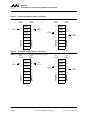
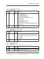
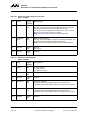
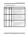
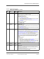
Section 7. Serial-ATA II Host Controller (SATAHC)
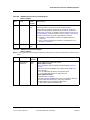
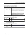
The 88F5182 incorporates a Serial-ATA (SATA) host controller (SATAHC). The SATAHC integrates two
independent SATA ports. A dedicated Enhanced DMA (EDMA) controls each port.
7.1
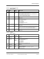
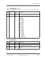
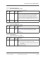
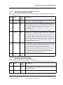
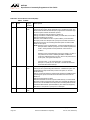
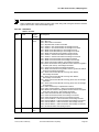
SATAHC Block Diagram
The 88F5182 SATAHC consists of an arbiter, two EDMAs and two SATA ports. Both EDMAs are independent and
may work concurrently (see Figure 2).
Figure 2: SATAHC Block Diagram
MBUS Interface
SATAHC Arbiter Unit
7.2
EDMA
Port 1
EDMA
Port 0
SATA
Interface
SATA
Interface
SATA Port 1
SATA Port 0
EDMA Operation
The SATAHC contains two EDMAs. This document only describes the operation of a single EDMA within the
SATAHC. See Figure 2, “SATAHC Block Diagram,” on page 21 and refer to Appendix A.8 "Serial-ATA Host
Controller (SATAHC) Registers" on page 213.
The interface between host CPU and each EDMA consists of two queues: the request queue and the response
queue. The request queue is the interface that the host CPU uses to queue ATA DMA commands as a request
between the system memory and the device. The response queue is the interface that the EDMA uses to notify the
host CPU that a data transaction between the system memory and the device was completed. Each entry in the
request queue consists of an ATA DMA command and the EDMA parameters and descriptors to initiate the device
and to perform the data transaction.
Doc. No. MV-S400130-00 Rev. 0.5
Page 21
Copyright © 2007 Marvell
Document Classification: Proprietary
June 25, 2007, Preliminary
Serial-ATA II Host Controller (SATAHC)
EDMA Operation
The EDMA is further responsible for parsing the commands, initializing the device, controlling the data
transactions, verifying the device status, and updating the response queue when the command is completed. This
all occurs without CPU intervention. Direct access to the device is also supported for device initialization and error
handling.
7.2.1
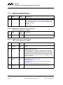
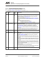
EDMA Request and Response Queues
The request queue and the response queue are each located in CPU memory and organized as a length of 32 or
128 entries, circular queues (FIFO) whose location is configured by the Queue In-Pointer and the Queue OutPointer entries. The entry length is set using <eEDMAQueLen> field in the EDMA Configuration Register
(Table 228, p. 228)—for 32 entries <eEDMAQueLen>=0, for 128 entries field <eEDMAQueLen>=1. Since these
pointers are implemented as indexes and each entry in the queue is a fixed length, the pointer can be converted to
an address using the formula: Entry address = Queue Base address + (entry length * pointer value).
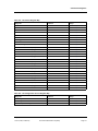
The request queue is the interface that the CPU software uses to queue ATA DMA commands as a request for a
data transaction between the system memory and the device. Each entry in the request queue is 32 bytes in
length, consisting of a command tag, the EDMA parameters, and the ATA device command to initiate the device
and to perform the data transaction.
The response queue is the interface that the EDMA uses to notify the CPU software that a data transaction
between the system memory and the device has completed. Each entry in the response queue is 8 bytes in
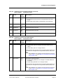
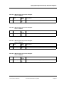
length, consisting of the command tag and the response flags.
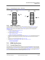
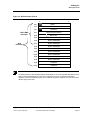
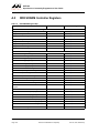
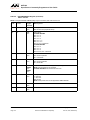
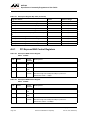
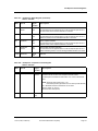
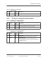
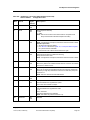
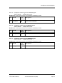
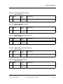
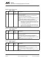
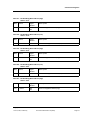
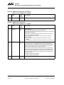
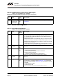
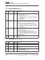
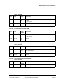
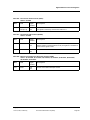
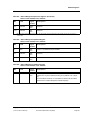
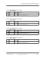
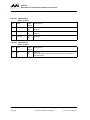
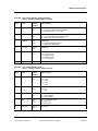
Figure 3: Command Request Queue—32 Entries
NOTE: Field <eEDMAQueLen>=0 in EDMA Configuration Register
Entry
Number
In
Pointer
Byte
Number
Entry
Number
Byte
Number
0
CRQB
0
1
CRQB
32
2
Empty
64
0
Empty
0
1
Empty
32
2
Empty
64
3
Empty
96
3
CRQB
96
4
Empty
128
4
CRQB
128
31
Out
Pointer
In
Pointer
Empty
CRQB
Empty
CRQB
Empty
1024
31
Copyright © 2007 Marvell
June 25, 2007, Preliminary
CRQB
Out
Pointer
1024
Doc. No. MV-S400130-00 Rev. 0.5
Document Classification: Proprietary
Page 22
88F5182
Open Source Community Programmer’s User Guide
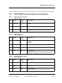
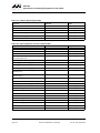
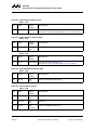
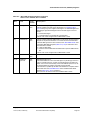
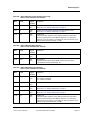
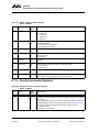
Figure 4: Command Response Queue—32 Entries
NOTE: Field <eEDMAQueLen>=0 in EDMA Configuration Register
Entry
Number
In
Pointer
Byte
Number
Entry
Number
Byte
Number
0
CRPB
0
1
CRPB
8
2
Empty
16
0
Empty
0
1
Empty
8
2
Empty
16
3
Empty
24
3
CRPB
24
4
Empty
32
4
CRPB
32
31
Out
Pointer
In
Pointer
Empty
CRPB
Empty
CRPB
Empty
256
31
CRPB
Out
Pointer
256
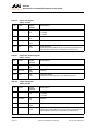
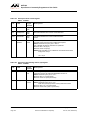
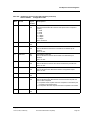
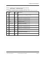
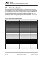
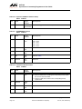
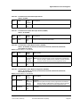
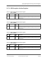
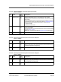
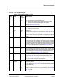
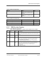
Figure 5: Command Request Queue—128 Entries
NOTE: Field <eEDMAQueLen>=1 in EDMA Configuration Register
Entry
Number
In
Pointer
Byte
Number
Entry
Number
0
CRQB
0
1
CRQB
32
2
Empty
64
0
Empty
0
1
Empty
32
2
Empty
64
3
Empty
96
3
CRQB
96
4
Empty
128
4
CRQB
128
127
Out
Pointer
In
Pointer
Empty
CRQB
Empty
CRQB
Empty
127
4096
Doc. No. MV-S400130-00 Rev. 0.5
Page 23
Byte
Number
CRQB
Out
Pointer
4096
Copyright © 2007 Marvell
Document Classification: Proprietary
June 25, 2007, Preliminary
Serial-ATA II Host Controller (SATAHC)
EDMA Operation
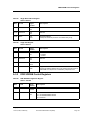
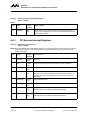
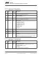
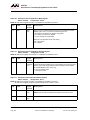
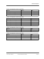
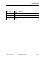
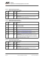
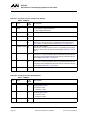
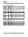
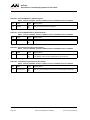
Figure 6: Command Response Queue—128 Entries
NOTE: Field <eEDMAQueLen>=1 in EDMA Configuration Register
Entry
Number
In
Pointer
Entry
Number
Byte
Number
0
CRPB
0
1
CRPB
8
2
Empty
16
0
Empty
0
1
Empty
8
2
Empty
16
3
Empty
24
3
CRPB
24
4
Empty
32
4
CRPB
32
127
7.2.2
Byte
Number
Out
Pointer
In
Pointer
Empty
CRPB
Empty
CRPB
Empty
1024
127
CRPB
Out
Pointer
1024
EDMA Configuration
The EDMA configuration is determined according to EDMA Configuration Register (Table 311 p. 226). The
registers listed below may be changed only when the <eEnEDMA> field in the EDMA Command Register
(Table 236, p. 236), is cleared, and the EDMA is disabled. These registers must not be changed when
<eEnEDMA> is set.
• In the SATAHC Address Space (Table 288 p. 213)
–
•
•
•
•
SATAHC Configuration Register
In the EDMA Registers Map (Table A.8.3 p. 214)
–
–
EDMA Configuration Register
–
–
<FIS Interrupt Cause Register>
EDMA Command Delay Threshold Register
All registers in the Shadow Register Block Registers Map (Table A.8.4 p. 215), except that the host is allowed
to change the <HOB> bit (bit [7]) in the ATA Device Control register (offset 0x82120) while the EDMA is
active.
All registers in the Basic DMA Registers Map (Table A.8.5 p. 216)
All registers in the <Serial-ATA Registers Map> field in the (Table 217, p. 217)
<FIS Interrupt Mask Register>
7.2.3
EDMA Data Structures
7.2.3.1
Command Request Queue
The request queue is the interface that the CPU software uses to request data transactions between the system
memory and the device. The request queue has a length of 32 entries (the <eEDMAQueLen> field in the EDMA
Configuration Register (Table 228, p. 228) = 0) or 128 entries (field <eEDMAQueLen>=1). The request queue is a
circular queue (FIFO) whose location is configured by the EDMA Request Queue In-Pointer Register (Table 316
p. 233), and the EDMA Request Queue Out-Pointer Register (Table 317 p. 234).
Copyright © 2007 Marvell
June 25, 2007, Preliminary
Doc. No. MV-S400130-00 Rev. 0.5
Document Classification: Proprietary
Page 24
88F5182
Open Source Community Programmer’s User Guide
•
•
A queue is empty when Request Queue Out-pointer reaches to the Request Queue In-pointer.
A queue is full when Request Queue In-pointer is written with the same value as the Request Queue Outpointer. A full queue contains 128/32 entries (as configured in field <eEDMAQueLen>).
• A queue contains N entries when the Request Queue Out-pointer is N less than the Request Queue Inpointer, taking into account the wraparound condition.
See Figure 3, “Command Request Queue—32 Entries,” on page 22 and Figure 5, “Command Request Queue—
128 Entries,” on page 23.
Each 32-byte EDMA Command Request Block (CRQB) entry consists of EDMA parameters and commands for
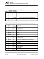
the ATA device. The CRQB data structure is written by the CPU. Table 2 provides a map of the CRQB data
structure registers.
7.2.3.2
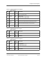
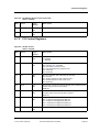
EDMA Command Request Block (CRQB) Data
Table 2:
EDMA CRQB Data Structure Map
R e g is t e r
Offset
Page
CRQB DW0—cPRD Descriptor Table Base Low Address
0x00
Table 3, p. 25
CRQB DW1—cPRD Descriptor Table Base High Address
0x04
Table 4, p. 26
CRQB DW2—Control Flags
0x08
Table 5, p. 26
CRQB DW3—Data Region Byte Count
0x0C
Table 6, p. 27
CRQB DW4—ATA Command
0x10
Table 7, p. 27
CRQB DW5—ATA Command
0x14
Table 8, p. 27
CRQB DW6—ATA Command
0x18
Table 9, p. 28
CRQB DW7—ATA Command
0x1C
Table 10, p. 28
Table 3:
CRQB DW0—cPRD Descriptor Table Base Low Address
Offset: 0x00
B i ts
F ie l d
D e s c r i p t io n
31:0
cPRD[31:0]
CRQB ePRD.
When <cPRDMode> is cleared to 0:
The CPU at initialization should construct a ePRD table in memory. This table contains
consecutive descriptors that describe the data buffers allocated in memory for this
command. This DWORD contains bit [31:4] of the physical starting address of this table.
Bits [3:0] must be 0x0.
When <cPRDMode> is set to 1:
This DWORD contains bits [31:1] of the physical starting address of a data region in
system memory. Bit [0] must be 0.
Doc. No. MV-S400130-00 Rev. 0.5
Page 25
Copyright © 2007 Marvell
Document Classification: Proprietary
June 25, 2007, Preliminary
Serial-ATA II Host Controller (SATAHC)
EDMA Operation
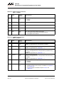
Table 4:
CRQB DW1—cPRD Descriptor Table Base High Address
Offset: 0x04
B i ts
F i el d
D e s c r i p t io n
31:0
cPRD[63:32]
CRQB ePRD.
When <cPRDMode> is cleared to 0:
This DWORD contains bits [63:32] of the physical starting address of a PRD table in
system memory.
When <cPRDMode> is set to 1:
This DWORD contains bits [63:32] of the physical starting address of a data region in
system memory.
Must be set to 0.
Table 5:
CRQB DW2—Control Flags
Offset: 0x08
B i ts
F i el d
D e s c r i p t io n
0
cDIR
CRQB Direction of Data Transaction
0 = System memory to Device
1 = Device to system memory
5:1
cDeviceQueTag
CRQB Device Queue Tag
This field contains the Queued commands used as tags attached to the command
provided to the drive.
11:6
Reserved
Reserved
Must be 0.
15:12
cPMport
PM Port Transmit
This field specifies the Port Multiplier (PM) port (bits [11:8] in DW0 of the FIS header)
inserted into the FISs transmission associate to this command.
16
cPRDMode
CRQB PRD Mode
This bit defines how the physical data that resides in the system memory is described.
0 = PRD tables are being used. <cPRD[31:0]> and <cPRD[63:32]> provide the ePRD
table starting address.
1 = Single data region, <cPRD[31:0]> and <cPRD[63:32]> provide its starting address.
<cDataRegionByteCount> provides its length.
23:17
cHostQueTag
CRQB Host Queue Tag
This 7-bit field contains the host identification of the command.
31:24
Reserved
Reserved
Copyright © 2007 Marvell
June 25, 2007, Preliminary
Doc. No. MV-S400130-00 Rev. 0.5
Document Classification: Proprietary
Page 26
88F5182
Open Source Community Programmer’s User Guide
Table 6:
CRQB DW3—Data Region Byte Count
Offset: 0x0C
B i ts
F ie l d
D e s c r i p t io n
15:0
cDataRegionBy
teCount
Data Region Byte Count
When <cPRDMode> is cleared to 0:
This field is reserved.
When <cPRDMode> is set to 1:
This field contains the count of the region in bytes. Bit [0] is force to 0.
There is a 64 KB maximum. A value of 0 indicates 64 KB. The data in the buffer must
not cross the boundary of the 32-bit address space; that is, the 32-bit high address of all
data in the buffer must be identical.
31:16
Reserved
Reserved
Note
The naming of the fields in the next four tables complies with the Serial-ATA convention. The
corresponding name according to the ATA convention appears in parentheses.
Table 7:
CRQB DW4—ATA Command
Offset: 0x10
B i ts
F ie l d
D e s c r i p t io n
15:0
Reserved
Reserved
23:16
Command
This field contains the contents of the Command register of the Shadow Register Block
(see Table 291 on page 215).
31:24
Features
This field contains the contents of the Features (Features Current) register of the
Shadow Register Block.
Table 8:
CRQB DW5—ATA Command
Offset: 0x14
B i ts
F ie l d
D e s c r i p t io n
7:0
Sector Number
This field contains the contents of the Sector Number (LBA Low Current) register of the
Shadow Register Block (see Table 291 on page 215).
15:8
Cylinder Low
This field contains the contents of the Cylinder Low (LBA Mid Current) register of the
Shadow Register Block.
23:16
Cylinder High
This field contains the contents of the Cylinder High (LBA High Current) register of the
Shadow Register Block.
Doc. No. MV-S400130-00 Rev. 0.5
Page 27
Copyright © 2007 Marvell
Document Classification: Proprietary
June 25, 2007, Preliminary
Serial-ATA II Host Controller (SATAHC)
EDMA Operation
Table 8:
CRQB DW5—ATA Command (Continued)
Offset: 0x14
B i ts
F i el d
D e s c r i p t io n
31:24
Device/Head
This field contains the contents of the Device/Head (Device) register of the Shadow
Register Block.
Table 9:
CRQB DW6—ATA Command
Offset: 0x18
B i ts
F i el d
D e s c r i p t io n
7:0
Sector Number
(Exp)
This field contains the contents of the Sector Number (Exp) (LBA Low Previous) register
of the Shadow Register Block (see Table 291 on page 215).
15:8
Cylinder Low
(Exp)
This field contains the contents of the Cylinder Low (Exp) (LBA Mid Previous) register of
the Shadow Register Block
23:16
Cylinder High
(Exp)
This field contains the contents of the Cylinder High (Exp) (LBA High Previous) register
of the Shadow Register Block.
31:24
Features (Exp)
This field contains the contents of the Features (Exp) (Features Previous) register of the
Shadow Register Block.
Table 10: CRQB DW7—ATA Command
Offset: 0x1C
B i ts
F i el d
D e s c r i p t io n
7:0
Sector Count
This field contains the contents of the Sector Count (Sector Count Current) register of
the Shadow Register Block (see Table 291 on page 215).
15:8
Sector Count
(Exp)
This field contains the contents of the Sector Count (exp) (Sector Count Previous)
register of the Shadow Register Block
31:16
Reserved
Reserved
When the EDMA is in Non-Queued mode:
The following commands are supported.
• READ DMA
• READ DMA EXT
• READ STREAM DMA
• WRITE DMA
• WRITE DMA EXT
• WRITE DMA FUA EXT
• WRITE STREAM DMA
Copyright © 2007 Marvell
June 25, 2007, Preliminary
Doc. No. MV-S400130-00 Rev. 0.5
Document Classification: Proprietary
Page 28
88F5182
Open Source Community Programmer’s User Guide
When the EDMA is in Queued mode:
The following commands are supported.
• READ DMA QUEUED
• READ DMA QUEUED EXT
• WRITE DMA QUEUED
• WRITE DMA QUEUED EXT
• WRITE DMA QUEUED FUA EXT
When the EDMA is in Native Command Queuing mode:
The following commands are supported.
• Read FPDMA Queued
• Write FPDMA Queued
Note
Other commands cause unpredictable results.
7.2.3.3
EDMA Physical Region Descriptors (ePRD) Table Data Structure
The physical memory region to be transferred is described by the EDMA Physical Region Descriptor [ePRD] for
DWORDs 0–3. The data transfer proceeds until all regions described by the ePRDs in the table have been
transferred. The starting address of this table must be 16B aligned, i.e., bits [3:0] of the table base address must
be 0x0.
Note
The total number of bytes in the PRD table (total byte count in DMA command) must be 4-byte aligned!.
Table 11:
ePRD Table Data Structure Map
Descriptor
Ta b l e , P a g e
ePRD DWORD 0
Table 12, p. 29
ePRD DWORD 1
Table 13, p. 30
ePRD DWORD 2
Table 14, p. 30
ePRD DWORD 3
Table 15, p. 30
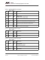
Table 12: ePRD DWORD 0
B i ts
F ie l d
D e s c r i p t io n
0
Reserved
Reserved
31:1
PRDBA[31:1]
The byte address of a physical memory region corresponds to address bits [31:1].
Doc. No. MV-S400130-00 Rev. 0.5
Page 29
Copyright © 2007 Marvell
Document Classification: Proprietary
June 25, 2007, Preliminary
Serial-ATA II Host Controller (SATAHC)
EDMA Operation
Table 13: ePRD DWORD 1
B i ts
F i el d
D e s c r i p t io n
15:0
ByteCount
Byte Count
The count of the region in bytes. Bit 0 is force to 0.
There is a 64-KB maximum. A value of 0 indicates 64 KB. The data in the buffer must
not cross the boundary of the 32-bit address space, that is the 32-bit high address of all
data in the buffer must be identical.
30:16
Reserved
Reserved
31
EOT
End Of Table
The data transfer operation terminates when the last descriptor has been retired.
0 = Not end of table
1 = End of table
NOTE:The total number of bytes in the PRD table (total byte count in DMA
command) must be 4-byte aligned.
Table 14: ePRD DWORD 2
B i ts
F i el d
D e s c r i p t io n
31:0
PRDBA[63:32]
The byte address of a physical memory region corresponds to bits [64:32].
Must be set to 0x0.
Table 15: ePRD DWORD 3
B i ts
F i el d
D e s c r i p t io n
31:0
Reserved
Reserved
7.2.3.4
Command Response Queue
The response queue is the interface that the EDMA uses to notify the CPU software that a data transaction
between the system memory and the device was completed. The response queue is a 128/32 entry, circular
queue (FIFO) whose location is configured by the EDMA Response Queue In-Pointer Register (Table 319 p. 234)
and the EDMA Response Queue Out-Pointer Register (Table 320 p. 235).
The queue status is determined by comparing the two pointers:
• A queue is empty when the Response Queue Out-pointer reaches the Response Queue In-pointer.
• A queue is full when Response Queue In-pointer is written with same value as a Response Queue Outpointer. A full queue contains 128/32 entries (as configured in the <eEDMAQueLen> field in the EDMA
Configuration Register (Table 228, p. 228)).
• A queue contains N entries when the Response Queue Out-pointer is N less than the Response Queue Inpointer, taking into account the wraparound condition.
Copyright © 2007 Marvell
June 25, 2007, Preliminary
Doc. No. MV-S400130-00 Rev. 0.5
Document Classification: Proprietary
Page 30
88F5182
Open Source Community Programmer’s User Guide
Note
The EDMA may write over existing entries when the queue is full.
See Figure 4, “Command Response Queue—32 Entries,” on page 23 and Figure 6, “Command Response
Queue—128 Entries,” on page 24.
Each 8-byte command response entry consists of command ID, response flags, and a timestamp, see Table 16,
“EDMA CRPB Data Structure Map,” on page 31. The CRPB data structure, described in Table 2, “EDMA CRQB
Data Structure Map,” on page 25, is written by the EDMA.
7.2.3.5
EDMA Command Response Block (CRPB) Data
Table 16 provides a map of the EDMA command response block data structure tables.
Table 16:
EDMA CRPB Data Structure Map
R e g is t e r
Offset
Ta b l e , P a g e
CRPB ID Register
0x00
Table 17, p. 31
CRPB Response Flags Register
0x02
Table 18, p. 32
CRPB Time Stamp Register
0x04
Table 19, p. 32
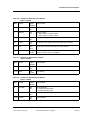
Table 17: CRPB ID Register
Offset: 0x00
B i ts
F ie l d
D e s c r i p t io n
6:0
cHostQueTag
CRPB ID
In queued DMA commands, these bits are used as a tag.
This field contains the host identification of the command.
These bits are copied from field <cHostQueTag> of Table 5, “CRQB DW2—Control
Flags,” on page 26.
15:7
Reserved
Reserved
Doc. No. MV-S400130-00 Rev. 0.5
Page 31
Copyright © 2007 Marvell
Document Classification: Proprietary
June 25, 2007, Preliminary
Serial-ATA II Host Controller (SATAHC)
EDMA Operation
Table 18: CRPB Response Flags Register
Offset: 0x02
B i ts
F i el d
D e s c r i p t io n
6:0
cEdmaSts
CRPB EDMA Status
This field contains a copy of the EDMA Interrupt Error Cause Register (see Table 313 on
page 230) bits [6:0] accepted in the last command.
NOTE:When the EDMA is in NCQ mode, ignore this field since the value of this
field may reflect the status of other commands.
7
Reserved
Reserved
This bit is always 0.
15:8
cDevSts
CRPB Device Status
This field contains a copy of the device status register accepted in the last read of the
register from the device.
Table 19: CRPB Time Stamp Register
Offset: 0x04
B i ts
F i el d
D e s c r i p t io n
31:0
cTS
CRPB TS
When the command is completed, the content of the EDMA Timer Register (see
Table 312 on page 230) is written into this field. This data may be used to estimate the
command execution time.
Copyright © 2007 Marvell
June 25, 2007, Preliminary
Doc. No. MV-S400130-00 Rev. 0.5
Document Classification: Proprietary
Page 32
88F5182
Open Source Community Programmer’s User Guide
Section 8. Gigabit Ethernet Controller Interface
The Gigabit Ethernet controller operates at 10, 100, and 1000 Mbps. It interfaces with the PHY via a MII, GMII, or
RGMII interface. The interface is also configurable as a proprietary 200-Mbps Marvell® MII (MMII) interface. For
full details on the different pinout configurations, see the applicable Gigabit Ethernet pin multiplexing sections and
the Reset Configuration section in the 88F5182 88F5182-based Storage Networking Platforms, Datasheet.
8.1
Functional Description
The Gigabit Ethernet port includes an IEEE 802.3 compliant 10-/100-/1000-Mbps MAC that supports GMII, MII,
and RGMII interfaces with an external PHY/SERDES device. The port speed, duplex and 802.3 flow control can
be auto-negotiated, according to IEEE standards 802.3u and 802.3x. Backpressure is supported for half-duplex
mode when operating at 10-/100-Mb speeds. Each port supports MIB counters.
The receive port includes a dedicated MAC-DA (Destination Address) with address filtering of up to 16-Unicast
MAC addresses, 256 IP Multicast addresses, and 256 Multicast/Broadcast address. The receive port may also
detect Layer2 frame-type encapsulation, as well as common Layer3 and Layer4 protocols.
IP checksum, Transmission Control Protocol (TCP) checksum, and User Datagram Protocol (UDP) checksum are
always checked on received traffic, and may be generated for transmitted traffic. This capability increases
performance significantly by off-loading these operations from the CPU. Jumbo-frames are also supported.
Each port includes eight dedicated receive DMA queues and one dedicated transmit DMA queue, plus two
dedicated DMA engines (one for receive and one for transmit) that operate concurrently. Each queue is managed
by buffer-descriptors that are chained together and managed by the software. Memory space may be mapped
using configurable address windows to fetch/write buffer data and descriptors to any of the other interfaces of the
device.
Queue classification on received traffic is assigned to the DMA queue based upon a highly configurable analysis,
which evaluates the DA-MAC, IP, ToS (Type of Service), 802.1P priority tag, and protocol (ARP, TCP, or UDP). An
example for use of this feature is the implementation of differentiated services in a router interface or for real-time,
jitter-sensitive voice/video traffic intermixed with data traffic. As each queue has its own buffering, blocking is
avoided and latency is reduced for service by the CPU.
Detailed status is given for each receive frame in the packet descriptors, while statistics are accumulated for
received and transmitted traffic in the MIB counters, on a per port basis.
The 10-/100-/1000-Mbps Gigabit Ethernet unit handles all functionality associated with moving packet data
between local memory and the Ethernet ports.
The port’s speed (10, 100, or 1000 Mbps) is auto-negotiated through the PHY and does not require user
intervention. Auto-Negotiation for MII and GMIII is according to 802.3ab, draft 5.0, using the SMI interface. The
1000-Mbps unit operates only in full-duplex mode. The 100- and 10-Mbps units operate either in half- or fullduplex mode, with the selection of the duplex mode auto-negotiated through the PHY without user intervention.
There is no Auto-Negotiation for speed on the PCS. GMII only supports symmetric flow control.
Note
When Auto-Negotiation is disabled, the link must be forced down when changing port speed.
There are eight receive queues and a single transmit queue. Receive/Transmit buffer management is by bufferdescriptor linked lists. Buffers and descriptors can reside throughout the entire device memory space. A Transmit
Doc. No. MV-S400130-00 Rev. 0.5
Page 33
Copyright © 2007 Marvell
Document Classification: Proprietary
June 25, 2007, Preliminary
Gigabit Ethernet Controller Interface
Port Features
buffer of any byte alignment and any size, above 8 bytes, is supported. The Receive Buffers must be 64-bit
aligned. The core frequency assumption is a minimum of 83 MHz in gigabit operation.
Frame type/encapsulation detection is available on Layer 2 for Bridge Protocol Data Unit (BPDU), VLAN
(programmable VLAN-ethertype), Ethernet v2, LLC/SNAP, on Layer 3 for IPv4 (according to Ethertype), other (no
MPLS or IPv6 detection), and on Layer 4 (only over IPv4) for Transmission Control Protocol (TCP), User
Datagram Protocol (UDP), and other. Frame enqueueing is according to DA, VLAN-802.1p, IP-ToS, using the
highest priority counts. Frame enqueueing is OR captured according to the protocol type for TCP, UDP, ARP, or
BPDU. Frames smaller than the programmable minimum frame size are automatically discarded. Reception and
transmission of long frames, up to 9700 bytes, are supported. The frame type, encapsulation method, errors, and
checksums are reported in the buffer descriptor. Automatic IP header 32-bit alignment is done in memory by
adding 2 bytes at the beginning of each frame. The TCP and UDP checksum calculations are put into the receive
descriptor (and are compared with the frame checksum for non-IP fragmented frames), even for frames over
9 KB.
The Ethernet port provides a great amount of flexibility with many programmable features. The TCP, UDP, and IP
checksums are generated on any frame size. This is programmable per frame by command settings in the first
descriptor of the frame. In addition, Cyclic Redundancy Check (CRC) generation is programmable for each frame.
There are separate, programmable transmit and receive interrupt coalescing mechanisms to aggregate several
interrupts (on a time based masking window) before sending an indication to the CPU. The unit provides
programmable zero padding of short frames—frames less that 64 bytes.
A transmit buffer of any byte alignment and any size (greater than 8 bytes) is supported. Minimum packet size is
32 bytes.
In the event of collision, frames are retransmitted automatically without additional fetch. An Error and Collision
report is provided in the last buffer descriptor.
8.2
Port Features
The 10-/100-/1000-Mbps Gigabit Ethernet port provide the following features:
•
•
•
•
•
•
•
•
IEEE 802.3 compliant MAC layer function.
IEEE 802.3u compliant MII interface.
1000-Mbps operation—full duplex.
10-/100-Mbps operation—half and full duplex.
GMII symmetric flow control: IEEE 802.3x flow-control for full-duplex operation mode.
MII symmetric flow control: Backpressure for half-duplex operation mode.
RGMII mode (non delay).
Transmit functions:
–
–
–
–
–
–
–
Zero padding for short frames (less than 64 Bytes).
Long frames transmission (limited only by external memory size).
Checksum on transmit frames for frames up to 1.5 KB.
Programmable values for Inter Packet Gap and Blinder timers.
CRC generation (programmable per frame).
Backoff algorithm execution.
Error reporting.
Copyright © 2007 Marvell
June 25, 2007, Preliminary
Doc. No. MV-S400130-00 Rev. 0.5
Document Classification: Proprietary
Page 34
88F5182
Open Source Community Programmer’s User Guide
•
Receive functions:
–
Address filtering modes:
-
16 Unicast
-
256 IP Multicast
Unicast promiscuous mode reception (receptions of Unicast frames, even those not matched in the
DA filter).
256 Multicast
Broadcast
Broadcast reject mode.
–
–
Automatic discard of error frames, smaller than the programmable minimum frame size.
–
–
CRC checking.
Reception of long frames (Programmable legal frame size is up to 9700 bytes).
Note: Frames larger than the limit are actually received, however, they are mark in the descriptor as
Oversize errors.
Error reporting.
Doc. No. MV-S400130-00 Rev. 0.5
Page 35
Copyright © 2007 Marvell
Document Classification: Proprietary
June 25, 2007, Preliminary
USB 2.0 Interface
Functional Description
Section 9. USB 2.0 Interface
The 88F5182 supports two USB 2.0 ports each with an embedded USB 2.0 PHY.
The USB 2.0 interface can act either as a USB high-speed peripheral (device) or as a USB host controller. It is
fully compliant with the Universal Serial Bus Specification, Revision 2.0 (USB 2.0).
Each USB 2.0 interface contains a single dual-role controller that can act as a host or a peripheral controller (aka
USB controller). A bridge connects the controller to the internal Crossbar interface (aka USB bridge).
The USB 2.0 port contains an embedded USB 2.0 PHY (aka USB PHY), allowing a significant saving in the
number device pins and the size of the board. The PHY supports both host and peripheral modes.
9.1
Functional Description
The USB 2.0 interface supports:
• A single USB 2.0 port acting as either a peripheral or a host.
• Embedded USB 2.0 PHY.
USB 2.0 host controller features:
• EHCI compliant as a host.
• As a host, supports direct connection to all peripheral device types—Low Speed (LS), Full Speed (FS), High
Speed (HS).
USB 2.0 peripheral features:
• USB 2.0 compliant peripheral controller.
• As a peripheral, connecting to all host types (HS, FS) and hubs.
• Four independent endpoints support control, interrupt, bulk and isochronous data transfers.
Embedded USB 2.0 PHY features:
• 480 Mbps High Speed (HS)/ 12 Mbps FS, FS only and LS only 1.5 Mbps serial data transmission rates.
• SYNC/EOP generation and checking.
• Data and clock recovery from serial stream on the USB.
• NRZI encoding/decoding with bit stuffing/unstuffing.
• Bit stuff error detections.
• Bit stuffing/unstuffing; bit stuff error detection.
• Holding registers to stage transmit and receive data.
• Supports USB 2.0 Test Modes.
• Ability to switch between FS and HS terminations/signaling.
Note
For more details refer to controller specification document: USB-HS High-Speed Controller Core
Reference.
Copyright © 2007 Marvell
June 25, 2007, Preliminary
Doc. No. MV-S400130-00 Rev. 0.5
Document Classification: Proprietary
Page 36
88F5182
Open Source Community Programmer’s User Guide
Section 10. Cryptographic Engines and Security
Accelerator
10.1
Functional Overview
The 88F5182 integrates hardware-based cryptographic engines and security accelerator. These engines, have
been designed for the purpose of performing time consuming cryptographic operations such as AES/DES/3DES
encryption and MD5/SHA1 authentication to reduce CPU packet processing overhead.
10.1.1 Acronyms, Abbreviations, and Definitions
The acronyms, abbreviations and definitions shown in Table 20 are used in this section of the datasheet.
Table 20:
Acronyms, Abbreviations, and Definitions
Acronym
Definition
AES
Advanced Encryption Standard
AES128/128
128 data bits AES with 128-bit key width
AES128/192
128 data bits AES with 192-bit key width
AES128/256
128 data bits AES with 256-bit key width
Block/data
Block of 512 bits in the authentication engine
CBC
Cipher Block Chain
CFB
Cipher Feedback
DES
Data Encryption Standard
3DES
Triple Data Encryption Standard
ECB
Electronic Code Book
EDE
Encryption Decryption Encryption
EEE
Encryption Encryption Encryption
IV
Initial Vector / Initial Value
MD5
Message Digest 5
OFB
Output Feedback
SHA-1
Secure Hash Algorithm 1
W0…W15
Designates the 16 words in an authentication input data block; W0 is the first
word and W15 is the last word.
WORD
32-bit
Doc. No. MV-S400130-00 Rev. 0.5
Page 37
Copyright © 2007 Marvell
Document Classification: Proprietary
June 25, 2007, Preliminary
Cryptographic Engines and Security Accelerator
Cryptographic Engines Operational Description
10.1.2 Functionality
There are four cryptographic engines that operate independently. They implement the following algorithms:
• Encryption: DES (ECB and CBC mode) and Triple DES (ECB and CBC mode, EDE and EEE)
• Encryption: AES128/128, AES128/192, AES128/256.
• Authentication: SHA-1 and MD5
10.1.3 Cryptographic Engine Features
•
•
•
•
•
•
•
•
•
•
•
•
•
Authentication in the MD5 or SHA algorithm, selectable by the user
Authentication Continue mode, enables chaining between blocks
Authentication Automatic Padding mode
Encryption and Decryption in Single DES, Single (ECB) or Block (CBC) mode, or 3DES, EEE or EDE mode,
selectable by the user
DES write pipeline
Optimal external update of Authentication and Encryption (in CBC) initial values, enabling flexibility of use—
multi-packet calculation, sharing between resources
Byte Swap support for Data input and initial values
Byte Swap support for DES/3DES and AES data output.
Automatic Engine activation when the required data block is loaded, (Saves write cycles)
Authentication and encryption can be done simultaneously
Authentication and encryption termination interrupts
Supports DES OFB and CFB modes with additional software
AES encryption and decryption—completely separate engines that can work simultaneously
10.1.4 Security Accelerator Features
•
•
•
Performs a complete over-the-packet operation with no software intervention
Supports two consecutive sessions allowing pipelining in packets processing
Supports four types of operation:
– Authentication only (MD5 / SHA-1 / HMAC-MD5 / HMAC-SHA1)
– Encryption/Decryption only (DES / 3DES / AES - both ECB and CBC)
– Authentication followed by Decryption/Encryption
– Decryption/Encryption followed by Authentication
10.2
Cryptographic Engines Operational Description
10.2.1 General
The unit combines four separate engines:
• DES encryption/decryption engine,
• AES128 encryption engine,
• AES128 decryption engine
Copyright © 2007 Marvell
June 25, 2007, Preliminary
Doc. No. MV-S400130-00 Rev. 0.5
Document Classification: Proprietary
Page 38
88F5182
Open Source Community Programmer’s User Guide
•
Authentication MD5/SHA engine
Each of these engines has separate registers for data, control, and operation modes.
Doc. No. MV-S400130-00 Rev. 0.5
Page 39
Copyright © 2007 Marvell
Document Classification: Proprietary
June 25, 2007, Preliminary
Two-Wire Serial Interface (TWSI)
Functional Description
Section 11. Two-Wire Serial Interface (TWSI)
11.1
Functional Description
The 88F5182 provides full Two-Wire Serial Interface (TWSI) support. It can act as master generating read/write
requests and as a slave responding to read/write requests. It fully supports a multiple TWSI-masters environment
(clock synchronization, bus arbitration).
The TWSI interface can be used for various applications. It can be used to control other TWSI on board devices,
to read DIMM SPD ROM, and for serial ROM initialization. For more details, see the Reset Pins and Configuration
section in the 88F5182 88F5182-based Storage Networking Platforms, Datasheet.
The TWSI port consists of two open drain signals:
•
•
TW_SCK (Serial Clock)
TW_SDA (Serial address/data)
The TWSI master starts a transaction by driving a start condition followed by a 7- or 10-bit slave address and a
read/write bit indication. The target TWSI slave responds with acknowledge.
In case of a write access (R/W bit is 0, following the TWSI slave acknowledge), the master drives 8-bit data and
the slave responds with acknowledge. This write access (8-bit data followed by acknowledge) continues until the
TWSI master ends the transaction with a stop condition.
In case of read access following the TWSI slave address acknowledge, the TWSI slave drives 8-bit data and the
master responds with acknowledge. This read access (8-bit data followed by acknowledge) continues until the
TWSI master ends the transaction by responding with no acknowledge to the last 8-bit data, followed by a stop
condition.
A target slave that cannot drive valid read data right after it received the address, can insert “wait states” by forcing
TW_SCK low until it has valid data to drive on the TW_SDA line.
A master is allowed to combine two transactions. After the last data transfer, it can drive a new start condition
followed by a new slave address, rather than driving a stop condition. Combining transactions guarantees that the
master does not loose arbitration to some other TWSI master. The TWSI interface master and slave activities are
handled by Marvell core access to internal registers, plus the interrupt interface.
TWSI examples are shown in Figure 7.
Copyright © 2007 Marvell
June 25, 2007, Preliminary
Doc. No. MV-S400130-00 Rev. 0.5
Document Classification: Proprietary
Page 40
88F5182
Open Source Community Programmer’s User Guide
Figure 7: TWSI Examples
Data Transfer Sequence
SCL
SDA
Start
Condition
Valid
Data
Data
may
Change
Stop
Condition
Sequential Read
s
t
a
r
t
First Data
s
t
o
p
Last Data
r/w
s 1 0 1 0 x x x 1
p
a
c
k
n
o
a
c
k
a
c
k
Address
Combined Access
s
t
a
r
t
s
t
a
r
t
r/w
s 1 0 1 0 x x x 0
a
c
k
Address
r/w
s
t
o
p
s 1 0 1 0 x x x 1
p
Last Data
a
c
k
a
c
k
Address
Doc. No. MV-S400130-00 Rev. 0.5
Page 41
a
c
k
n
o
a
c
k
Copyright © 2007 Marvell
Document Classification: Proprietary
June 25, 2007, Preliminary
Two-Wire Serial Interface (TWSI)
Functional Description
11.1.1 TWSI Slave Addressing
The TWSI slave interface supports both 7-bit and 10-bit addressing. The slave address is programmed by the
TWSI Slave Address register (see Table 492 on page 335) and TWSI Extended Slave Address register (see Table
493 on page 335).
When the TWSI receives a 7-bit address after a start condition, it compares it against the value programmed in the
Slave Address register, and if it matches, it responds with acknowledge.
If the received 7 address bits are 11110xx, meaning that it is an 10-bit slave address, the TWSI compares the
received 10-bit address with the 10-bit value programmed in the TWSI Slave Address (Table 492 p. 335) and
TWSI Extended Slave Address (Table 493 p. 335) registers, and if it matches, it responds with acknowledge.
The TWSI interface also support slave response to general call transactions. If the <GCE> bit in the TWSI Slave
Address register is set to 1, the TWSI also responds to the general call address (0x0).
11.1.2 TWSI Data
An 8-bit TWSI Data (Table 494 p. 336) register is used both in master and slave modes.
In master mode, the Marvell core must place the slave address or write data to be transmitted. In the case of read
access, it contains received data (need to be read by the Marvell core).
In slave mode, the Data register contains data received from master on write access, or data to be transmitted
(written by the Marvell core) on read access. TWSI Data register MSB contains the first bit to be transmitted or
being received.
11.1.3 TWSI Control
An 8-bit TWSI Control (Table 495 p. 336) register is used both in master and slave modes.
11.1.4 TWSI Status
An 8-bit TWSI Status (Table 496 p. 338) register is used both in master and slave modes.
This 8-bit register contains the current status of the TWSI interface. Bits [7:3] are the status code, bits [2:0] are
Reserved (read only 0).
11.1.5 Baud Rate Register
TWSI specification defines TW_SCK frequency of 100 KHz (400 KHz in fast mode). The TWSI module contains a
clock divider to generate the TW_SCK clock. Setting bits[6:0] of TWSI Baud Rate (Table 497 p. 339) register
(offset 0x1100C) defines TW_SCK frequency as follows:
Table 21:
Setting the Baud Rate Register
TCl k
N
M
T WSI F req ue ncy
(i n k Hz)
3
10
94.3
3
13
74.1
4
9
51.8
6
12
99.7
166 MHz
Copyright © 2007 Marvell
June 25, 2007, Preliminary
Doc. No. MV-S400130-00 Rev. 0.5
Document Classification: Proprietary
Page 42
88F5182
Open Source Community Programmer’s User Guide
As defined in the TWSI specification, the maximum supported TW_SCK frequency is 100 kHz. Fast mode (where
TW_SCK frequency is 400 kHz) is not supported.
11.2
TWSI Master Operation
The Marvell processor core can initiate TWSI master read and write transactions via TWSI registers, as described
in the following sections.
11.2.1 Master Write Access
A master write access consists of the following steps:
1. The Marvell processor core sets the <Start> bit in the TWSI Control register (see Table 495 on page 336) to
1. The TWSI master then generates a start condition as soon as the bus is free, sets an Interrupt flag, and
sets the Status register to 0x8.
2. The Marvell processor core writes 7-bit address plus a write bit to the TWSI Data register (see Table 494 on
page 336) and clears Interrupt flag for the TWSI master interface to drive the slave address on the bus. The
target slave responds with acknowledge. This causes an Interrupt flag to be set and a status code of 0x18 is
registered in the Status register.
3.
4.
If the target TWSI device has an 10-bit address, the Marvell processor core needs to write the remainder 8-bit
address bits to the Data register. The Marvell processor core then clears the Interrupt flag for the master to
drive this address on the bus. The target device responds with acknowledge, causing an Interrupt flag to be
set, and status code of 0xD0 be registered in the TWSI Status register (see Table 496 on page 338).
The Marvell processor core writes data byte to the TWSI Data register, and then clears Interrupt flag for the
TWSI master interface to drive the data on the bus. The target slave responds with acknowledge, causing
Interrupt flag to be set, and status code of 0x28 be registered in the Status register. The Marvell processor
core continues this loop of writing new data to the Data register and clear Interrupt flag, as long as it needs to
transmit write data to the target.
After the last data transmit, the Marvell processor core may terminate the transaction or restart a new
transaction. To terminate the transaction, the Marvell processor core sets the Control register’s <Stop> bit
and then clears the Interrupt flag, causing the TWSI master to generate a stop condition on the bus, and go
back to idle state. To restart a new transaction, the Marvell processor core sets the TWSI Control register’s
<Start> bit and clears the Interrupt flag, causing TWSI master to generate a new start condition.
Note
This sequence describes a normal operation. There are also abnormal cases, such as a slave not
responding with acknowledge or arbitration loss. Each of these cases is reported in the TWSI Status
register and needs to be handled by the Marvell processor core.
11.2.2 Master Read Access
A master read access consists of the following steps:
1. Generate, a start condition, exactly the same as in the case of write access, see Section 11.2.1 Master Write
Access.
2. Drive 7- or 10-bit slave address, exactly the same as in the case of write access, with the exception that the
status code after the first address byte transmit is 0x40, and after 2nd address byte transmit (in case of 10-bit
address) is 0xE0.
3. Read data being received from the target device is placed in the data register and acknowledge is driven on
the bus. Also, an interrupt flag is set, and status code of 0x50 is registered in the Status register. The Marvell
Doc. No. MV-S400130-00 Rev. 0.5
Page 43
Copyright © 2007 Marvell
Document Classification: Proprietary
June 25, 2007, Preliminary
Two-Wire Serial Interface (TWSI)
TWSI Slave Operation
4.
processor core reads data from Data register and clears the Interrupt flag to continue receiving next read data
byte. This loop is continued as long as the Marvell processor core wishes to read data from the target device.
To terminate, the read access needs to respond with no acknowledge to the last data. It then generates a stop
condition or generates a new start condition to restart a new transaction. With last data, the Marvell processor
core clears the TWSI Control register’s Acknowledge bit (when clearing the Interrupt bit), causing the TWSI
master interface to respond with no acknowledge to last received read data. In this case, the Interrupt flag is
set with status code of 0x58. Now, the Marvell processor core can issue a stop condition or a new start
condition.
Note
The above sequence describes a normal operation. There are also abnormal cases, such as the slave not
responding with acknowledge, or arbitration loss. Each of these cases is reported in the Status register
and needs to be handled by Marvell processor core.
11.3
TWSI Slave Operation
The TWSI slave interface can respond to a read access, driving read data back to the master that initiated the
transaction, or respond to write access, receiving write data from the master.
The two cases are described in the following sections.
11.3.1 Slave Read Access
Upon detecting a new address driven on the bus with read bit indication, the TWSI slave interface compares the
address against the address programmed in the Slave Address register. If it matches, the slave responds with
acknowledge. It also sets the Interrupt flag, and sets status code to 0xA8.
Note
If the TWSI slave address is 10-bit, the Interrupt flag is set and status code changes only after receiving
and identify address match also on the 2nd address byte).
The Marvell processor core now must write new read data to the Data register and clears the Interrupt flag,
causing TWSI slave interface to drive the data on the bus. The master responds with acknowledge causing an
Interrupt flag to be set, and status code of 0xB8 to be registered in the Status register.
If the master does not respond with acknowledge, the Interrupt flag is set, status code 0f 0xC0 is registered, and
TWSI slave interface returns back to idle state.
If the master generates a stop condition after driving an acknowledge bit, the TWSI slave interface returns back to
idle state.
11.3.2 Slave Write Access
Upon detecting a new address driven on the bus with write bit indication, the TWSI slave interface compares the
address against the address programmed in the Slave Address register and, if it matches, responds with
acknowledge. It also sets an Interrupt flag, and sets status code to 0x60 (0x70 in case of general call address, if
general call is enabled).
Following each write byte received, the TWSI slave interface responds with acknowledge, sets an Interrupt flag,
and sets status code to 0x80 (0x90 in case of general call access). The Marvell processor core then reads the
received data from Data register and clears Interrupt flag, to allow transfer to continue.
Copyright © 2007 Marvell
June 25, 2007, Preliminary
Doc. No. MV-S400130-00 Rev. 0.5
Document Classification: Proprietary
Page 44
88F5182
Open Source Community Programmer’s User Guide
If a stop condition or a start condition of a new access is detected after driving the acknowledge bit, an Interrupt
flag is set and a status code of 0xA0 is registered.
Doc. No. MV-S400130-00 Rev. 0.5
Page 45
Copyright © 2007 Marvell
Document Classification: Proprietary
June 25, 2007, Preliminary
UART Interface
Functional Description
Section 12. UART Interface
12.1
Functional Description
The 88F5182 supports two Universal Asynchronous Receiver/Transmitter (UART) ports. One of the UART ports is
multiplexed on the MPP port. For complete information regarding the UART, refer to the Synopsis DW_16550
specification.
The UART is integrated into the device to support data input/output operations for peripheral devices connected
through a standard UART interface.
The UART includes the following features:
• Synchronous interface
• FIFO mode permanently selected for transmit and receive operations
• Modem control functions (CTSn, RSTn)
12.2
UART Interface Pin Assignment
The 88F5182 supports the UART interface through the UA0/1_TXD and UA0/1_RXD pins and provides modem
control functions through the UA0/1_CTSn and UA0/1_RTSn pins.
Table 22 shows the signal names on the 88F5182 and the description of the pins.
Table 22:
UART Pin Assignments
Pin Name
Type
De scr iption
UA0_TX
UA1_TX
O
The UA0/1_TX signals are the serial data output to the modem, data set, or
peripheral device. The UA0/1_TX signals are set high when the reset is applied.
UA0_RX
UA1_RX
I
The UA0/1_RX signals are the serial data input from the modem, data set, or
peripheral device.
I
CLEAR TO SEND: When low, these pins indicate that the receiving UART is
ready to receive data. When the receiving UART de-asserts UA0/1_CTSn high,
the transmitting UART should stop transmission to prevent overflow of the
receiving UART buffer. The UA0/1_CTSn signals are a modem-status input
whose condition can be tested by the host processor or by the UART when in
Autoflow mode.
O
REQUEST TO SEND: When low, these pins informs the remote device that the
UART is ready to receive data.
UA0_CTSn
UA1_CTSn
UA0_RTSn
UA1_RTSn
Note
For more information, refer to Section A.13 "UART Interface Registers" on page 340.
Copyright © 2007 Marvell
June 25, 2007, Preliminary
Doc. No. MV-S400130-00 Rev. 0.5
Document Classification: Proprietary
Page 46
88F5182
Open Source Community Programmer’s User Guide
Section 13. Device Controller Interface
13.1
Functional Description
The 88F5182 Device controller interface supports up to four banks of devices. Each bank supports up to
512 MBytes of address space. Each bank has its own timing parameters register. Bank width can be programmed
to 8- or 16-bits. Bank timing parameters can be programmed to support different device types (e.g., sync burst
SRAM, Flash, ROM, I/O Controllers).
The four chip selects are typically separated into three individual chip selects and one chip select for a boot
device. The boot device bank is the same as any of the other banks except that the core boots from the boot
device and its default width is sampled at reset.
The device controller multiplexes the address and data buses. The interface latches the address into latches to
support up to 512 MBytes of address space. The interface supports any size access up to 128 bytes. See Table
23 for device controller pin assignment.
Note
All output signals are driven with the rising edge of TCLK and all inputs are sampled with the rising edge
of TCLK.
13.2
Device Interface Pin Assignment
Table 23 provides a list of the Device interface pins and describes their function.
Table 23:
Device Controller Pin Assignments
Pin Name
Ty pe
De scription
DEV_CEn[2:0]
O
Device Bus Chip Enable correspond to bank [2:0]
DEV_BootCEn
O
Device Bus Chip Enable correspond to Boot Bank
DEV_OEn
O
Device Bus Output Enable
DEV_WEn[1:0]
O
Device Bus Write Enable
DEV_ALE[1:0]
O
Device Bus Address Latch Enable correspond to ALE[0].
DEV_D[8:0]
t/s I/O
Device Bus Multiplexed Address/Data bus
DEV_D[15:9]
t/s I/O
Device Bus Data bus
DEV_A[2:0]
O
Device Bus Address
DEV_READY
O
Device Ready
DEV_BURSTn/DEV_LASTn
O
Device Burst/Device last
Doc. No. MV-S400130-00 Rev. 0.5
Page 47
Copyright © 2007 Marvell
Document Classification: Proprietary
June 25, 2007, Preliminary
Device Controller Interface
Device Interface Block Diagram
13.3
Device Interface Block Diagram
Figure 8 provides a diagram of the Device block.
Figure 8: Device Block Diagram Example
DEV_ALE[0]
CK
A[26:15]
A[26:19]
A[18:16]
Up to 512 MByte
A[15]
DEV_ALE[1]
Device
CK
A[14]
A[14:3]
A[13:6]
A[5:3]
DEV_A[2:0]
A[2:0]
D[15:9]
DEV_D[15:9]
DEV_D[8]
D[8]
D[7:0]
DEV_D[7:0]
DEV_OEn
OEn
DEV_WEn[0]
WEn[0]
DEV_WEn[1]
WEn[1]
DEV_CEn
CEn
Note
In the figures that follow, the signal names appear without the DEV_ prefix.
Copyright © 2007 Marvell
June 25, 2007, Preliminary
Doc. No. MV-S400130-00 Rev. 0.5
Document Classification: Proprietary
Page 48
88F5182
Open Source Community Programmer’s User Guide
13.4
Address Multiplexing
Figure 9 provides a diagram of the address multiplexing.
Figure 9: Address Multiplexing
TClk
ALE[1]
ALE[0]
A[2:0]
A[5:3]
A[18:16]
D[7:0]
A[13:6]
A[26:19]
Data0
Data1
Address
D[8]
A[14]
A[15]
Data0
Data1
Address
OEn
A[15]
WEn[0]
A[16]
A[2:0]
A[2:0]+1
Address
CEn
13.5
NAND Flash Controller Implementation
The NAND Flash controller implementation is shown in detailed in Figure 10 through Figure 12.
It is controlled by NAND Flash Control Register (Table 517 p. 350). Burst transactions are supported by toggling
the RE signal every read cycle as described in Figure 10.
Figure 10: Mask ALE during NAND Flash Read Data Phase
A[1]
A[1] {New}
NFOEn
Figure 11: Generate Dedicated NAND Flash WE Signal
WEn[0]
CEn(i)
WEn[0](i) {connected to MPP i/f}
Figure 12: Generate CE Covers All NAND Flash Transaction
NF(i)
SNFActCEn(i)
CEn(i)
CEn(i) {New}
Doc. No. MV-S400130-00 Rev. 0.5
Page 49
Copyright © 2007 Marvell
Document Classification: Proprietary
June 25, 2007, Preliminary
IDMA Controller
Functional Description
Section 14. IDMA Controller
The 88F5182 has four independent IDMA engines. The IDMA engines optimize system performance by moving
large amounts of data without significant CPU intervention.
Each IDMA engine can move data between any source to any destination. It can transfer a single data buffer of up
to 16 MB. It can also run in chain mode, in that mode each buffer has its own descriptor.
14.1
Functional Description
IDMA unit contains four 512-byte buffers, one buffer per IDMA channel.
When a channel is activated, data is read from the source into the buffer, and then written to the destination. Read
and write transactions are handled independently. The IDMA engine transfers the buffer in chunks of from 8 up to
128 bytes. The IDMA engine reads from the source as long as it has place in the buffer. It writes to the destination,
as long as there is valid data in the buffer to be transferred. This independency results in concurrent reads and
writes, and maximum utilization of the IDMA interface.
The four channels share the same resources. They use fixed round-robin arbitration.
14.2
IDMA Descriptors
Each IDMA Channel Descriptor consists of four 32-bit registers. Each channel can be configured to work in 64-KB
Descriptor mode, or in 16-MB Descriptor mode, as shown in Figure 13.
Copyright © 2007 Marvell
June 25, 2007, Preliminary
Doc. No. MV-S400130-00 Rev. 0.5
Document Classification: Proprietary
Page 50
88F5182
Open Source Community Programmer’s User Guide
Figure 13: IDMA Descriptors
64-KB Mode
Remaind BC
16-MB Mode
Byte Count
Source Address
Source Address
Destination Address
Destination Address
Next Descriptor Pointer
Table 24:
Byte Count
Next Descriptor Pointer
IDMA Descriptor Definitions
ID MA D e s c r i p t or
De f i ni t io n
Byte Count
Number of bytes of data to transfer.
The maximum number of bytes to which the IDMA controller can be configured
transfer is 64 KB-1 (16-bit register) in 64 KB descriptor mode or 16 MB-1 (24-bit
register) in the 16 MB descriptor mode.
This register decrements at the end of every burst of transmitted data from the
source to the destination. When the byte count register is 0, the IDMA transaction is
finished or terminated.
Source Address
Bits [31:0] of the IDMA source address.
According to the setting of the Channel Control register, this register either
increments or holds the same value.
Destination Address
Bits [31:0] of the IDMA destination address.
According to the setting of the Channel Control register, this register either
increments or holds the same value.
Pointer to the Next
Descriptor
Bits [31:0] of the IDMA Next Descriptor address for chained operation.
The descriptor must be 16 sequential bytes located at 16-bytes aligned address
(bits [3:0] are 0).
NOTE:This descriptor is used only used when the channel is configured to Chained
mode.
Doc. No. MV-S400130-00 Rev. 0.5
Page 51
Copyright © 2007 Marvell
Document Classification: Proprietary
June 25, 2007, Preliminary
XOR Engine
Theory of Operation
Section 15. XOR Engine
The XOR engine is a generic acceleration engine for storage applications that provides a low latency, high
throughput xor calculation capabilities, enabling CPU xor calculation off-loading in various RAID implementations.
In addition, the XOR engine provides iSCSI CRC32C calculation, DMA operation, memory initialization, and memory ECC errors cleanup operation support.
The XOR engine enables PC/Server manufactures (ROM), Internal RAID Controllers and External RAID systems
to speed up overall system performance.
XOR engine features:
•
•
•
•
•
•
•
•
•
•
•
•
•
Two separate channels for enabling concurrent operation (e.g., concurrent XOR and iSCSI CRC32C calculations).
1KB temporary result store queue per channel. Arranged as 128 X 8B buffer.
Support packing/unpacking of unaligned data transfers.
XOR calculation for up to eight data block sources.
Data block size up to 16 MB.
Programmable maximum burst size on read and write.
Descriptor chain mechanism.
Hot insertion of new descriptors to chain.
iSCSI CRC32C calculation that is compliant with IPS iSCSI version 13 draft.
DMA operation.
Memory initialization support.
Memory ECC cleanup support.
Write access protection of configuration registers.
15.1
Theory of Operation
XOR engine unit (XEunit) has five main operation modes:
• XOR calculation Mode (XOR)
• iSCSI CRC32C Calculation Mode (CRC)
• DMA Operation Mode (DMA)
• Memory initialization Mode (MemInit)
•
Memory ECC error cleanup mode (ECC)
The XOR engine has two independent channels. Each channel can be configured to one of the operation modes
at a time. The operation mode is defined through the <OperationMode> field in the XOR Engine [0..1] Configuration (XExCR) (Table 543 p. 366)(bits[2:0]). In the XOR, CRC and DMA operation modes, the XOR engine is controlled by chain descriptors and responds to similar activation scheme. These modes differ only in the
interpretation of the chain descriptor fields. In ECC and MemInit modes, the XOR engine responds to different
activation schemes. It is controlled by programming internal registers directly. On all operation modes, XOR
engine uses the same address decoding scheme.
Upon startup, the two XOR engine channels are in an inactive state and can be configured to any operation mode
(XOR, CRC, DMA, MemInit or ECC). After being configured, the XOR engine channel can be activated. It can be
stopped or paused by software at any time. After stopped by software, the engine re-enters inactive state and can
Copyright © 2007 Marvell
June 25, 2007, Preliminary
Doc. No. MV-S400130-00 Rev. 0.5
Document Classification: Proprietary
Page 52
88F5182
Open Source Community Programmer’s User Guide
be configured to another operation mode and re-activated. This also applies if the XOR engine channel finished
the operation (reached End Of Chain) without being stopped by the software. Again, the engine re-enters an inactive state and can be configured to another operation mode, and re-activated. After paused by software, the XOR
engine channel suspends the current operation at the earliest opportunity. Upon activating the channel again, it
resumes executing the same operation.
Notes
•
•
The two XOR engine channels are independent in their operation modes. The only exception is that
both engines must not be configured to ECC or MemInit operation modes. These modes share
hardware resources.
Attempting to change the channels operation mode during a pause will result in unexpected behavior.
15.2
Descriptor Chain
15.2.1
Descriptor Format
The XOR engine descriptor format supports 32-bit addressing. In XOR mode, the descriptor consists of sixteen
32-bit words which totals the 64B size of each descriptor. In CRC and DMA modes, only the upper 32B of the
descriptor is needed. Therefore, the descriptor consists of eight 32-bit words, totalling to a 32B size for each
descriptor, see Figure 14.
By fetching a descriptor from memory, the XOR engine gets all the information about the next operation to be performed. When the XOR engine finishes the operation associated with a descriptor, it closes the descriptor by
updating the status word. This means the operation completed successfully and returns the ownership of the
descriptor to the CPU.
Note
Chain descriptor operation is valid only in XOR, CRC and DMA operation modes. In ECC and MemInit
modes, the XOR engine gets the operation data directly from its internal registers.
Doc. No. MV-S400130-00 Rev. 0.5
Page 53
Copyright © 2007 Marvell
Document Classification: Proprietary
June 25, 2007, Preliminary
XOR Engine
Descriptor Chain
Figure 14: XOR Descriptor Format
31
0x0
0x4
0x8
CRC & DMA
Descriptor
XOR
Descriptor
0xC
0x10
0
Status
CRC-32 Result
Command
Next Descriptor Address
Byte Count
0x14
Destination Address
0x18
Source Address #0
0x1C
Source Address #1
0x20
Source Address #2
0x24
Source Address #3
0x28
Source Address #4
0x2C
Source Address #5
0x30
Source Address #6
0x34
Source Address #7
0x38
Reserved
0x3C
Reserved
Note
The XOR descriptor must be 64 Bytes aligned (Address[5:0]=0). The CRC and DMA descriptors must be
32 Bytes aligned (Address[4:0]=0). There are no restrictions on source or destination data block
alignment. Source and destination blocks can have different alignments. Different source blocks can have
different alignments as well.
Copyright © 2007 Marvell
June 25, 2007, Preliminary
Doc. No. MV-S400130-00 Rev. 0.5
Document Classification: Proprietary
Page 54
88F5182
Open Source Community Programmer’s User Guide
Table 25:
Descriptor Status Word Definition
Bit
F ield
D escr ip tio n
29:0
Reserved
Reserved.
30
Success
Successful descriptor execution indication.
Indicates whether the operation completed successfully.
0 = Completed unsuccessfully - Transfer terminated before the whole byte count was
transferred.
1 = Completed successfully - The whole byte count transferred.
That field is updated upon closing the descriptor
NOTE: In ECC cleanup mode the success bit indicates successful execution, even if
ECC errors where found and not corrected.
31
Own
Ownership Bit
Indicates whether the descriptor is owned by the CPU or the XOR engine.
0 = CPU owned.
1 = XOR engine owned.
That field is updated upon closing a descriptor - XOR engine gives back ownership to
the CPU by clearing the own bit.
Table 26:
Descriptor CRC-32 Result Word Definition
Bit
F ield
D escr ip tio n
31:0
CRCresult
Result of CRC-32 calculation
Valid only in the last descriptor of a CRC source block chain, after it was closed by the
XOR engine.
NOTE: Valid only in CRC mode.
Table 27:
Descriptor Command Word Definition
Bit
F ield
D escr ip tio n
0
Src0Cmd
Specifies the type of operation to be carried out on the data pointed by SA#0 (Source
Address 0 word of the descriptor).
0x0 = Null Command - Data from Source will be disregarded in the current descriptor operation.
0x1 = XOR Command - Data from source will be transferred and will be significant in the
XOR calculation.
NOTE: Relevant only on XOR operation mode. disregarded in all other operation modes.
1
Src1Cmd
Specifies the type of operation to be carried out on the data pointed by SA#1 (Source
Address #1 word of the descriptor).
NOTE: Relevant only on XOR operation mode. Disregard in all other operation modes.
2
Src2Cmd
Specifies the type of operation to be carried out on the data pointed by SA#2 (Source
Address #2 word of the descriptor).
NOTE: Relevant only on XOR operation mode. Disregard in all other operation modes.
3
Src3Cmd
Specifies the type of operation to be carried out on the data pointed by SA#3 (Source
Address #3 word of the descriptor).
NOTE: Relevant only on XOR operation mode. Disregard in all other operation modes.
Doc. No. MV-S400130-00 Rev. 0.5
Page 55
Copyright © 2007 Marvell
Document Classification: Proprietary
June 25, 2007, Preliminary
XOR Engine
Descriptor Chain
Table 27:
Descriptor Command Word Definition (Continued)
Bit
F ield
D escr ip tio n
4
Src4Cmd
Specifies the type of operation to be carried out on the data pointed by SA#4 (Source
Address #4 word of the descriptor).
NOTE: Relevant only on XOR operation mode. Disregard in all other operation modes.
5
Src5Cmd
Specifies the type of operation to be carried out on the data pointed by SA#5 (Source
Address #5 word of the descriptor).
NOTE: Relevant only on XOR operation mode. Disregard in all other operation modes.
6
Src6Cmd
Specifies the type of operation to be carried out on the data pointed by SA#6 (Source
Address #6 word of the descriptor).
NOTE: Relevant only on XOR operation mode. disregarded in all other operation modes.
7
Src7Cmd
Specifies the type of operation to be carried out on the data pointed by SA#7 (Source
Address #7 word of the descriptor).
NOTE: Relevant only on XOR operation mode. Disregard in all other operation modes.
29:8
Reserved
Reserved
30
CRCLast
Indicated last descriptor in a CRC-32 calculation chain.
0 = Not last descriptor in a CRC calculation chain.
1 = Last descriptor in a CRC calculation chain. When closing the descriptor, the XOR
engine writes the CRC result to its CRC-32 Result word. The next descriptor in the
descriptor chain initiates a new CRC calculation. If the source block is represented by
one descriptor only, it should be marked as last.
NOTE: Relevant only in CRC operation mode.
31
EODIntEn
End Of Descriptor Interrupt Enable.
Specifies if the EOD interrupt is asserted upon closure of that descriptor.
1 - EOD Enabled.
0 - EOD Disabled.
Table 28:
Descriptor Next Descriptor Address Word
Bits
F ield
De scr ip tio n
31:0
NDA
Next descriptor address pointer
XOR Mode: NDA must be 64-byte aligned (bits[5:0] must be 0x0).
CRC/DMA Mode: NDA must be 32-byte aligned (bits[4:0] must be 0x0).
NDA field of the last descriptor of a descriptor chain must be NULL.
Table 29:
Descriptor Byte Count Word
Bit
Fi e l d
D e s c r i pt i on
23:0
ByteCount
XOR mode: Size of source and destination blocks in bytes.
CRC mode: Size of source block part represented by the descriptor.
DMA mode: Size of source and destination block in bytes.
Minimum blocks’ size: 16B.
Maximum blocks’ size: 16MB-1
31:24
Reserved
Reserved.
Copyright © 2007 Marvell
June 25, 2007, Preliminary
Doc. No. MV-S400130-00 Rev. 0.5
Document Classification: Proprietary
Page 56
88F5182
Open Source Community Programmer’s User Guide
Table 30:
Descriptor Destination Address Word
Bits
F ield
De scr ip tio n
31:0
DA
Destination Block address pointer
XOR Mode: Destination Block address pointer.
CRC mode: Not used.
DMA mode: Destination Block address pointer.
Table 31:
Descriptor Source Address #N Words
Bits
F ield
De scr ip tio n
31:0
SA#0
Source
Address #0
source block #0 address pointer.
XOR Mode: Source Block #0 address pointer.
CRC mode: Address pointer to part of source block represented by the descriptor.
DMA Mode: Source Block address pointer.
31:0
SA#N
[N=1..7]
Source
Address #N
source block #N address pointer.
XOR mode: Source Block #N address pointer.
CRC mode: Not used.
DMA mode: Not used.
Doc. No. MV-S400130-00 Rev. 0.5
Page 57
Copyright © 2007 Marvell
Document Classification: Proprietary
June 25, 2007, Preliminary
General Purpose I/O Port Interface
Section 16. General Purpose I/O Port Interface
The 88F5182 contains a 26-bit General Purpose Port I/O (GPIO). The GPIO interface provides the following
features:
• Each of the GPIO pins can be assigned to act as a general purpose input or output pin.
• A dedicated register provides the GPIO input value.
• Each of the GPIO input pins can be programmed to generate an Edge sensitive or a Level sensitive maskable
interrupt.
• A dedicated register provides the GPIO output value.
• Each of the GPIO outputs can be programmed for the LED to blink every ~100 ms.
Note
The GPIO interface is multiplexed on the external pins as described in Section A.18.1 "MPP Registers"
on page 384.
For the 88F5182 GPIO registers, see Table 564, “GPIO Registers Map,” on page 380.
Copyright © 2007 Marvell
June 25, 2007, Preliminary
Doc. No. MV-S400130-00 Rev. 0.5
Document Classification: Proprietary
Page 58
88F5182
Open Source Community Programmer’s User Guide
Section 17. Interrupt Controller
17.1
Functional Description
The 88F5182 includes an interrupt controller that routes internal interrupt requests as well as external interrupt
requests (GPIOs) to the Marvell processor core.
The 88F5182 interrupt controller drives two interrupt signals to the Marvell CPU core—FIQ (high priority) and IRQ
(regular priority). All interrupts are level sensitive. The interrupt is kept active as long as there is at least one nonmasked cause bit set in the Interrupt Cause register.
The 88F5182 can also be used as the interrupt controller for external devices generating interrupts to the Marvell
CPU core via GPIO inputs. The interrupt controller can also receive interrupt messages from an external PCI
Express device.
The 88F5182 can also act as a PCI or PCI Express Endpoint. As such, it can generate the PCI Express INTA
emulation message or the INTAn signal.
17.2
Local Interrupt Cause and Mask Registers
The 88F5182 handles interrupts in two stages. The first stage is specific unit cause and mask registers, that
distinguish between a specific interrupt events within the unit.
Once an interrupt event occurs, its corresponding bit in the unit cause register is set to 1. If the interrupt is not
masked by the unit mask register, it is marked in the Main Interrupt Cause register. The unit local mask register
has no affect on the setting of interrupt bits in the unit local cause register. It only affects the setting of the interrupt
bit in the Main Interrupt Cause register
When working in level mode, the GPIO Data In register must be used. Do not use the GPIO Interrupt Cause
register.
The different units cause registers are:
Local to System Bridge Interrupt Cause register
PCI Express Interrupt Cause registers
PCI Interrupt Cause register
SATAHC Main Interrupt Cause register
GbE Port Interrupt Cause register
USB0/1 Interrupt Cause register
Cryptographic Engine Security Accelerator Cause register
TWSI Interrupt Cause register
UART0/1 Interrupt Cause registers
Device Interrupt Cause register
GPIO Interrupt Cause register
IDMA Interrupt Cause register
•
•
•
•
•
•
•
•
•
•
•
•
•
XOR Engine Interrupt Cause register
Doc. No. MV-S400130-00 Rev. 0.5
Page 59
Copyright © 2007 Marvell
Document Classification: Proprietary
June 25, 2007, Preliminary
Interrupt Controller
Main Interrupt Cause and Mask Registers
17.3
Main Interrupt Cause and Mask Registers
The second stage includes the Main Interrupt Cause register and Main Interrupt mask registers that summarize
the interrupts generated by each unit. The interrupt handler first reads the main cause register, and then reads the
specific unit cause register.
Note
The Main Interrupt Cause register bits are Read Only. To clear an interrupt cause, the software needs to
clear the active bit(s) in the specific unit cause register.
There are two mask registers corresponding to the two CPU interrupt lines—IRQ and FIQ. Setting these registers
allows the reporting of different interrupt events on the different interrupt lines. If a bit in the mask register is set
to 1, the corresponding interrupt event is enabled. The setting of the mask bits has no affect on the value
registered in the Main Interrupt Cause register, it only affects the assertion of the interrupt pin. An interrupt is
asserted if at least one of the non masked bits in the cause register is set to 1.
When the 88F5182 functions as Endpoint, a third mask register corresponding to PCI Express/PCI interrupt is
used to generate an interrupt towards the host. The host is connected to 88F5182 through the interface defined by
bit <EndPointIF> in the CPU Configuration Register (Table 55 p. 99). The INTA interrupt or MSI is routed to host
according to this bit value.
Notes
•
•
17.4
See Table 33, “CPU Register Map,” on page 90.
See Table 17.5, “88F5182 Interrupt Controller Scheme,” on page 61.
Doorbell Interrupt
When 88F5182 functions as Endpoint, a doorbell mechanism is provided to communicate between Marvell
processor core and the external host.
The 88F5182 supports 32-bit doorbell interrupt register from host to Marvell CPU core. See Table 72, “Host-toCPU Doorbell Register,” on page 107 and Table 73, “Host-to-CPU Doorbell Mask Register,” on page 107.
The 88F5182 supports 32-bit doorbell interrupt register from Marvell CPU core to host. See Table 74, “CPU-toHost Doorbell Register,” on page 108 and Table 75, “CPU-to-Host Doorbell Mask Register,” on page 108.
Copyright © 2007 Marvell
June 25, 2007, Preliminary
Doc. No. MV-S400130-00 Rev. 0.5
Document Classification: Proprietary
Page 60
88F5182
Open Source Community Programmer’s User Guide
17.5
88F5182 Interrupt Controller Scheme
Figure 15: 88F5182 Interrupt Controller Scheme
UNIT 0
UNIT 1
UNIT N
Interrupt Cause Reg.
Interrupt Cause Reg.
Interrupt Cause Reg.
Interrupt Mask Reg.
Interrupt Mask Reg.
Interrupt Mask Reg.
Main Interrupt Controller
Main Interrupt Cause Reg.
Main IRQ Interrupt Mask Reg.
IRQ
Main FIQ Interrupt Mask Reg.
FIQ
Main PCI/PCI Express Interrupt
Mask Reg.
PEX
INTA
PCI
EndpointIF bit
masks routing to
PEX and PCI
Doc. No. MV-S400130-00 Rev. 0.5
Page 61
Copyright © 2007 Marvell
Document Classification: Proprietary
June 25, 2007, Preliminary
Timers
Functional Description
Section 18. Timers
18.1
Functional Description
The 88F5182 provides two general purpose timers and one watchdog timer.
18.2
32-bit-wide Timers
The 88F5182 provides two 32-bit-wide timers. Each timer decrements with every TCLK rising edge if the
corresponding enabled bit is enabled. Reads and write from/to the timer are done to the counter itself.
The timers provide auto mode:
When the timers are set to auto mode disabled and the timers reach to 0, the timers stop counting.
When the timers are set to auto mode enabled and the timers reach to 0, the timers preload and continue
counting.
•
•
Regardless of whether auto mode is enabled or disabled, when the timers reach 0, a maskable interrupt is
generated.
18.3
Watchdog Timer
The 88F5182 internal watchdog timer is a 32-bit count down counter that can be used to generate a maskable
interrupt or reset the system in the event of unpredictable software behavior.
After the watchdog is enabled, it is a free running counter that needs to be serviced periodically to prevent its
expiration. After reset, the watchdog is enabled or disabled according to sample at reset pin value.
When the watchdog timer expires and bit <WDRstOutEn> is set to 1 in the RSTOUTn Mask Register (Table 57
p. 100), the SYSRST_OUTn output signal is set.
Note
See Section A.4.4 "CPU Timers Registers" on page 105.
Copyright © 2007 Marvell
June 25, 2007, Preliminary
Doc. No. MV-S400130-00 Rev. 0.5
Document Classification: Proprietary
Page 62
88F5182 Register Set
Copyright © 2007 Marvell
CONFIDENTIAL
June 25, 2007, Preliminary
Document Classification: Proprietary
Doc. No. MV-S400130-00 Rev. 0.5
Page 63
88F5182
Open Source Community Programmer’s User Guide
THIS PAGE INTENTIONALLY LEFT BLANK
Doc. No. MV-S400130-00 Rev. 0.5
Page 64
Copyright © 2007 Marvell
Document Classification: Proprietary
June 25, 2007, Preliminary
88F5182
Open Source Community Programmer’s User Guide
List of Registers
A.1
Register Description......................................................................................................... 88
A.2
Register Types .................................................................................................................. 88
A.3
Internal Registers Address Map...................................................................................... 89
A.4
Local to System Bridge Registers .................................................................................. 90
Table 34:
Window0 Control Register ........................................................................................................................... 91
Table 35:
Window0 Base Register............................................................................................................................... 92
Table 36:
Window0 Remap Low Register.................................................................................................................... 92
Offset: 0x20000
Offset: 0x20004
Offset: 0x20008
Table 37:
Window0 Remap High Register ................................................................................................................... 92
Offset: 0x2000C
Table 38:
Window1 Control Register ........................................................................................................................... 92
Offset: 0x20010
Table 39:
Window1 Base Register............................................................................................................................... 93
Table 40:
Window1 Remap Low Register.................................................................................................................... 93
Table 41:
Window1 Remap High Register ................................................................................................................... 93
Table 42:
Window2 Control Register ........................................................................................................................... 94
Table 43:
Window2 Base Register............................................................................................................................... 94
Table 44:
Window3 Control Register ........................................................................................................................... 94
Offset: 0x20014
Offset: 0x20018
Offset: 0x2001C
Offset: 0x20020
Offset: 0x20024
Offset: 0x20030
Table 45:
Window3 Base Register............................................................................................................................... 95
Offset: 0x20034
Table 46:
Window4 Control Register ........................................................................................................................... 95
Offset: 0x20040
Table 47:
Window4 Base Register............................................................................................................................... 95
Table 48:
Window5 Control Register ........................................................................................................................... 96
Table 49:
Window5 Base Register............................................................................................................................... 96
Table 50:
Window6 Control Register ........................................................................................................................... 96
Table 51:
Window6 Base Register............................................................................................................................... 97
Offset: 0x20044
Offset: 0x20050
Offset: 0x20054
Offset: 0x20060
Offset: 0x20064
Doc. No. MV-S400130-00 Rev. 0.5
Page 65
Copyright © 2007 Marvell
Document Classification: Proprietary
June 25, 2007, Preliminary
List of Registers
Table 52:
Window7 Control Register............................................................................................................................ 97
Offset: 0x20070
Table 53:
Window7 Base Register ............................................................................................................................... 98
Offset: 0x20074
Table 54:
88F5182 Internal Registers Base Address Register .................................................................................... 98
Offset: 0x20080
Table 55:
CPU Configuration Register ......................................................................................................................... 99
Table 56:
CPU Control and Status Register............................................................................................................... 100
Table 57:
RSTOUTn Mask Register........................................................................................................................... 100
Table 58:
System Soft Reset Register ....................................................................................................................... 101
Table 59:
Local to System Bridge Interrupt Cause Register ...................................................................................... 101
Table 60:
Local to System Bridge Interrupt Mask Register ........................................................................................ 101
Offset: 0x20100
Offset: 0x20104
Offset: 0x20108
Offset: 0x2010C
Offset: 0x20110
Offset: 0x20114
Table 61:
Main Interrupt Cause Register.................................................................................................................... 102
Offset: 0x20200
Table 62:
Main IRQ Interrupt Mask Register .............................................................................................................. 104
Offset: 0x20204
Table 63:
Main FIQ Interrupt Mask Register .............................................................................................................. 104
Offset: 0x20208
Table 64:
Endpoint Interrupt Mask Register ............................................................................................................... 104
Offset: 0x2020C
Table 65:
CPU Timers Control Register ..................................................................................................................... 105
Table 66:
CPU Timer0 Reload Register ..................................................................................................................... 105
Table 67:
CPU Timer 0 Register ................................................................................................................................ 106
Table 68:
CPU Timer1 Reload Register ..................................................................................................................... 106
Offset: 0x20300
Offset: 0x20310
Offset: 0x20314
Offset: 0x20318
Table 69:
CPU Timer 1 Register ................................................................................................................................ 106
Offset: 0x2031C
Table 70:
CPU Watchdog Timer Reload Register...................................................................................................... 106
Offset: 0x20320
Table 71:
CPU Watchdog Timer Register .................................................................................................................. 107
Table 72:
Host-to-CPU Doorbell Register .................................................................................................................. 107
Table 73:
Host-to-CPU Doorbell Mask Register......................................................................................................... 107
Table 74:
CPU-to-Host Doorbell Register .................................................................................................................. 108
Table 75:
CPU-to-Host Doorbell Mask Register......................................................................................................... 108
Offset: 0x20324
Offset: 0x20400
Offset: 0x20404
Offset: 0x20408
Offset: 0x2040C
Copyright © 2007 Marvell
June 25, 2007, Preliminary
Doc. No. MV-S400130-00 Rev. 0.5
Document Classification: Proprietary
Page 66
88F5182
Open Source Community Programmer’s User Guide
A.5
DDR SDRAM Controller Registers ................................................................................ 109
Table 77:
CS[0]n Base Address Register .................................................................................................................. 110
Offset: 0x01500
Table 78:
CS[0]n Size Register.................................................................................................................................. 110
Table 79:
CS[1]n Base Address Register .................................................................................................................. 110
Table 80:
CS[1]n Size Register.................................................................................................................................. 111
Table 81:
CS[2]n Base Address Register .................................................................................................................. 111
Table 82:
CS[2]n Size Register.................................................................................................................................. 111
Table 83:
CS[3]n Base Address Register .................................................................................................................. 112
Offset: 0x01504
Offset: 0x01508
Offset: 0x0150C
Offset: 0x01510
Offset: 0x01514
Offset: 0x01518
Table 84:
CS[3]n Size Register.................................................................................................................................. 112
Offset: 0x0151C
Table 85:
DDR SDRAM Configuration Register......................................................................................................... 112
Offset: 0x01400
Table 86:
DDR SDRAM Control Register .................................................................................................................. 113
Table 87:
DDR SDRAM Timing (Low) Register ......................................................................................................... 114
Table 88:
DDR SDRAM Timing (High) Register ........................................................................................................ 115
Table 89:
DDR2 SDRAM Timing (Low) Register ....................................................................................................... 116
Table 90:
DDR2 SDRAM Timing (High) Register ...................................................................................................... 116
Table 91:
DDR SDRAM Address Control Register .................................................................................................... 117
Offset: 0x01404
Offset: 0x01408
Offset: 0x0140C
Offset: 0x01428
Offset: 0x0147C
Offset: 0x01410
Table 92:
DDR SDRAM Open Pages Control Register ............................................................................................. 117
Offset: 0x01414
Table 93:
DDR SDRAM Operation Register .............................................................................................................. 118
Offset: 0x01418
Table 94:
DDR SDRAM Operation Control Register.................................................................................................. 118
Table 95:
DDR SDRAM Mode Register ..................................................................................................................... 118
Offset: 0x0142C
Offset: 0x0141C
Table 96:
Extended DDR SDRAM Mode Register..................................................................................................... 120
Offset: 0x01420
Table 97:
DDR SDRAM Initialization Control Register............................................................................................... 121
Table 98:
DDR SDRAM Address/Control Pads Calibration Register ......................................................................... 121
Table 99:
DDR SDRAM Data Pads Calibration Register ........................................................................................... 122
Offset: 0x01480
Offset: 0x014C0
Offset: 0x014C4
Table 100: DDR2 SDRAM ODT Control (Low) Register .............................................................................................. 122
Offset: 0x01494
Doc. No. MV-S400130-00 Rev. 0.5
Page 67
Copyright © 2007 Marvell
Document Classification: Proprietary
June 25, 2007, Preliminary
List of Registers
Table 101: DDR2 SDRAM ODT Control (High) Register ............................................................................................. 123
Offset: 0x01498
Table 102: DDR2 SDRAM ODT Control Register ........................................................................................................ 124
Offset: 0x0149C
Table 103: DDR SDRAM Interface Mbus Control (Low) Register ................................................................................ 125
Offset: 0x01430
Table 104: DDR SDRAM Interface Mbus Control (High) Register ............................................................................... 125
Offset: 0x01434
Table 105: DDR SDRAM Interface Mbus Timeout Register......................................................................................... 126
Offset: 0x01438
Table 106: DDR SDRAM MMask Register................................................................................................................... 126
Offset: 0x014B0
A.6
PCI Express Interface Registers ....................................................................................127
Table 108: PCI Express BAR1 Control Register .......................................................................................................... 129
Offset: 0x41804
Table 109: PCI Express BAR2 Control Register .......................................................................................................... 129
Offset: 0x41808
Table 110: PCI Express Expansion ROM BAR Control Register ................................................................................. 130
Offset: 0x4180C
Table 111: PCI Express Configuration Address Register............................................................................................. 130
Offset: 0x418F8
Table 112: PCI Express Configuration Data Register .................................................................................................. 131
Offset: 0x418FC
Table 113: PCI Express Interrupt Cause...................................................................................................................... 131
Offset: 0x41900
Table 114: PCI Express Interrupt Mask........................................................................................................................ 134
Offset: 0x41910
Table 115: PCI Express Window0 Control Register..................................................................................................... 134
Offset: 0x41820
Table 116: PCI Express Window0 Base Register ........................................................................................................ 135
Offset: 0x41824
Table 117: PCI Express Window0 Remap Register..................................................................................................... 135
Offset: 0x4182C
Table 118: PCI Express Window1 Control Register..................................................................................................... 136
Offset: 0x41830
Table 119: PCI Express Window1 Base Register ........................................................................................................ 136
Offset: 0x41834
Table 120: PCI Express Window1 Remap Register..................................................................................................... 136
Offset: 0x4183C
Table 121: PCI Express Window2 Control Register..................................................................................................... 137
Offset: 0x41840
Table 122: PCI Express Window2 Base Register ........................................................................................................ 137
Offset: 0x41844
Table 123: PCI Express Window2 Remap Register..................................................................................................... 137
Offset: 0x4184C
Table 124: PCI Express Window3 Control Register..................................................................................................... 138
Offset: 0x41850
Copyright © 2007 Marvell
June 25, 2007, Preliminary
Doc. No. MV-S400130-00 Rev. 0.5
Document Classification: Proprietary
Page 68
88F5182
Open Source Community Programmer’s User Guide
Table 125: PCI Express Window3 Base Register........................................................................................................ 138
Offset: 0x41854
Table 126: PCI Express Window3 Remap Register .................................................................................................... 138
Offset: 0x4185C
Table 127: PCI Express Window4 Control Register .................................................................................................... 139
Offset: 0x41860
Table 128: PCI Express Window4 Base Register........................................................................................................ 139
Offset: 0x41864
Table 129: PCI Express Window4 Remap Register .................................................................................................... 139
Offset: 0x4186C
Table 130: PCI Express Window5 Control Register .................................................................................................... 140
Offset: 0x41880
Table 131: PCI Express Window5 Base Register........................................................................................................ 140
Offset: 0x41884
Table 132: PCI Express Window5 Remap Register .................................................................................................... 140
Offset: 0x4188C
Table 133: PCI Express Default Window Control Register .......................................................................................... 141
Offset: 0x418B0
Table 134: PCI Express Expansion ROM Window Control Register ........................................................................... 141
Offset: 0x418C0
Table 135: PCI Express Expansion ROM Window Remap Register ........................................................................... 141
Offset: 0x418C4
Table 136: PCI Express Control Register .................................................................................................................... 142
Offset: 0x41A00
Table 137: PCI Express Status Register...................................................................................................................... 143
Offset: 0x41A04
Table 138: PCI Express Completion Timeout Register................................................................................................ 144
Offset: 0x41A10
Table 139: PCI Express Flow Control Register............................................................................................................ 145
Offset: 0x41A20
Table 140: PCI Express Acknowledge Timers (1X) Register....................................................................................... 145
Offset: 0x41A40
Table 141: PCI Express TL Control Register ............................................................................................................... 146
Offset: 0x41AB0
Table 142: PCI Express Device and Vendor ID Register............................................................................................. 146
Offset: 0x40000
Table 143: PCI Express Command and Status Register ........................................................................................... 146
Offset: 0x40004
Table 144: PCI Express Class Code and Revision ID Register ................................................................................... 149
Offset: 0x40008
Table 145: PCI Express BIST, Header Type and Cache Line Size Register............................................................... 149
Offset: 0x4000C
Table 146: PCI Express BAR0 Internal Register ......................................................................................................... 150
Offset: 0x40010
Table 147: PCI Express BAR0 Internal (High) Register............................................................................................... 150
Offset: 0x40014
Table 148: PCI Express BAR1 Register ...................................................................................................................... 150
Offset: 0x40018
Doc. No. MV-S400130-00 Rev. 0.5
Page 69
Copyright © 2007 Marvell
Document Classification: Proprietary
June 25, 2007, Preliminary
List of Registers
Table 149: PCI Express BAR1 (High) Register ............................................................................................................ 151
Offset: 0x4001C
Table 150: PCI Express BAR2 Register....................................................................................................................... 151
Offset: 0x40020
Table 151: PCI Express BAR2 (High) Register ............................................................................................................ 152
Offset: 0x40024
Table 152: PCI Express Subsystem Device and Vendor ID......................................................................................... 152
Offset: 0x4002C
Table 153: PCI Express Expansion ROM BAR Register.............................................................................................. 152
Offset: 0x40030
Table 154: PCI Express Capability List Pointer Register ............................................................................................. 153
Offset: 0x40034
Table 155: PCI Express Interrupt Pin and Line Register.............................................................................................. 153
Offset: 0x4003C
Table 156: PCI Express Power Management Capability Header Register .................................................................. 153
Offset: 0x40040
Table 157: PCI Express Power Management Control and Status Register ................................................................. 154
Offset: 0x40044
Table 158: PCI Express MSI Message Control Register.............................................................................................. 155
Offset: 0x40050
Table 159: PCI Express MSI Message Address Register ............................................................................................ 155
Offset: 0x40054
Table 160: PCI Express MSI Message Address (High) Register ................................................................................. 156
Offset: 0x40058
Table 161: PCI Express MSI Message Data Register.................................................................................................. 156
Offset: 0x4005C
Table 162: PCI Express Capability Register ................................................................................................................ 156
Offset: 0x40060
Table 163: PCI Express Device Capabilities Register.................................................................................................. 157
Offset: 0x40064
Table 164: PCI Express Device Control Status Register ............................................................................................. 158
Offset: 0x40068
Table 165: PCI Express Link Capabilities Register ...................................................................................................... 161
Offset: 0x4006C
Table 166: PCI Express Link Control Status Register.................................................................................................. 161
Offset: 0x40070
Table 167: PCI Express Advanced Error Report Header Register............................................................................... 163
Offset: 0x40100
Table 168: PCI Express Uncorrectable Error Status Register...................................................................................... 163
Offset: 0x40104
Table 169: PCI Express Uncorrectable Error Mask Register ....................................................................................... 165
Offset: 0x40108
Table 170: PCI Express Uncorrectable Error Severity Register................................................................................... 165
Offset: 0x4010C
Table 171: PCI Express Correctable Error Status Register ......................................................................................... 165
Offset: 0x40110
Table 172: PCI Express Correctable Error Mask Register ........................................................................................... 166
Offset: 0x40114
Copyright © 2007 Marvell
June 25, 2007, Preliminary
Doc. No. MV-S400130-00 Rev. 0.5
Document Classification: Proprietary
Page 70
88F5182
Open Source Community Programmer’s User Guide
Table 173: PCI Express Advanced Error Capability and Control Register .................................................................. 167
Offset: 0x40118
Table 174: PCI Express Header Log First DWORD Register ...................................................................................... 167
Offset: 0x4011C
Table 175: PCI Express Header Log Second DWORD Register................................................................................. 168
Offset: 0x40120
Table 176: PCI Express Header Log Third DWORD Register ..................................................................................... 168
Offset: 0x40124
Table 177: PCI Express Header Log Fourth DWORD Register................................................................................... 168
Offset: 0x40128
A.7
PCI Interface Registers .................................................................................................. 169
Table 187: CSn[0] BAR Size........................................................................................................................................ 173
Offset: 0x30C08
Table 188: CSn[1] BAR Size........................................................................................................................................ 173
Offset: 0x30D08
Table 189: CSn[2] BAR Size........................................................................................................................................ 173
Offset: 0x30C0C
Table 190: CSn[3] BAR Size........................................................................................................................................ 173
Offset: 0x30D0C
Table 191: DevCSn[0] BAR Size ................................................................................................................................. 174
Offset: 0x30C10
Table 192: DevCSn[1] BAR Size ................................................................................................................................. 174
Offset: 0x30D10
Table 193: DevCSn[2] BAR Size ................................................................................................................................. 174
Offset: 0x30D18
Table 194: Boot CSn BAR Size ................................................................................................................................... 174
Offset: 0x30D14
Table 195: P2P Mem0 BAR Size ................................................................................................................................. 174
Offset: 0x30D1C
Table 196: P2P I/O BAR Size ...................................................................................................................................... 175
Offset: 0x30D24
Table 197: Expansion ROM BAR Size......................................................................................................................... 175
Offset: 0x30D2C
Table 198: Base Address Registers Enable ................................................................................................................ 175
Offset: 0x30C3C
Table 199: CSn[0] Base Address Remap .................................................................................................................... 176
Offset: 0x30C48
Table 200: CSn[1] Base Address Remap .................................................................................................................... 177
Offset: 0x30D48
Table 201: CSn[2] Base Address Remap .................................................................................................................... 177
Offset: 0x30C4C
Table 202: CSn[3] Base Address Remap .................................................................................................................... 177
Offset: 0x30D4C
Table 203: DevCSn[0] Base Address Remap.............................................................................................................. 177
Offset: 0x30C50
Table 204: DevCSn[1] Base Address Remap.............................................................................................................. 177
Offset: 0x30D50
Doc. No. MV-S400130-00 Rev. 0.5
Page 71
Copyright © 2007 Marvell
Document Classification: Proprietary
June 25, 2007, Preliminary
List of Registers
Table 205: DevCSn[2] Base Address Remap .............................................................................................................. 178
Offset: 0x30D58
Table 206: BootCSn Base Address Remap ................................................................................................................. 178
Offset: 0x30D54
Table 207: P2P Mem0 Base Address Remap (Low).................................................................................................... 178
Offset: 0x30D5C
Table 208: P2P Mem0 Base Address Remap (High) ................................................................................................... 178
Offset: 0x30D60
Table 209: P2P I/O Base Address Remap ................................................................................................................... 178
Offset: 0x30D6C
Table 210: Expansion ROM Base Address Remap ..................................................................................................... 179
Offset: 0x30F38
Table 211: DRAM BAR Bank Select ............................................................................................................................ 179
Offset: 0x30C1C
Table 212: PCI Address Decode Control ..................................................................................................................... 179
Offset: 0x30D3C
Table 213: PCI DLL Control ......................................................................................................................................... 180
Offset: 0x31D20
Table 214: PCI/MPP Pads Calibration ......................................................................................................................... 181
Offset: 0x31D1C
Table 215: PCI Command ............................................................................................................................................ 182
Offset: 0x30C00
Table 216: PCI Mode.................................................................................................................................................... 184
Offset: 0x30D00
Table 217: PCI Retry .................................................................................................................................................... 185
Offset: 0x30C04
Table 218: PCI Discard Timer ...................................................................................................................................... 185
Offset: 0x30D04
Table 219: MSI Trigger Timer....................................................................................................................................... 186
Offset: 0x30C38
Table 220: PCI Arbiter Control ..................................................................................................................................... 186
Offset: 0x31D00
Table 221: PCI P2P Configuration ............................................................................................................................... 187
Offset: 0x31D14
Table 222: PCI Access Control Base 0 (Low) .............................................................................................................. 187
Offset: 0x31E00
Table 223: PCI Access Control Base 0 (High) ............................................................................................................. 188
Offset: 0x31E04
Table 224: PCI Access Control Size 0 ......................................................................................................................... 188
Offset: 0x31E08
Table 225: PCI Access Control Base 1 (Low) .............................................................................................................. 189
Offset: 0x31E10
Table 226: PCI Access Control Base 1 (High) ............................................................................................................. 189
Offset: 0x31E14
Table 227: PCI Access Control Size 1 ......................................................................................................................... 190
Offset: 0x31E18
Table 228: PCI Access Control Base 2 (Low) .............................................................................................................. 190
Offset: 0x31E20
Copyright © 2007 Marvell
June 25, 2007, Preliminary
Doc. No. MV-S400130-00 Rev. 0.5
Document Classification: Proprietary
Page 72
88F5182
Open Source Community Programmer’s User Guide
Table 229: PCI Access Control Base 2 (High) ............................................................................................................. 190
Offset: 0x31E24
Table 230: PCI Access Control Size 2 ......................................................................................................................... 190
Offset: 0x31E28
Table 231: PCI Access Control Base 3 (Low).............................................................................................................. 190
Offset: 0x31E30
Table 232: PCI Access Control Base 3 (High) ............................................................................................................. 191
Offset: 0x31E34
Table 233: PCI Access Control Size 3 ......................................................................................................................... 191
Offset: 0x31E38
Table 234: PCI Access Control Base 4 (Low).............................................................................................................. 191
Offset: 0x31E40
Table 235: PCI Access Control Base 4 (High) ............................................................................................................. 191
Offset: 0x31E44
Table 236: PCI Access Control Size 4 ......................................................................................................................... 191
Offset: 0x31E48
Table 237: PCI Access Control Base 5 (Low).............................................................................................................. 192
Offset: 0x31E50
Table 238: PCI Access Control Base 5 (High) ............................................................................................................. 192
Offset: 0x31E54
Table 239: PCI Access Control Size 5 ......................................................................................................................... 192
Offset: 0x31E58
Table 240: PCI Configuration Address......................................................................................................................... 192
Offset: 0x30C78
Table 241: PCI Configuration Data .............................................................................................................................. 193
Offset: 0x30C7C
Table 242: PCI Interrupt Acknowledge ........................................................................................................................ 193
Offset: 0x30C34
Table 243: PCI SERRn Mask....................................................................................................................................... 194
Offset: 0x30C28
Table 244: PCI Interrupt Cause ................................................................................................................................... 195
Offset: 0x31D58
Table 245: PCI Interrupt Mask ..................................................................................................................................... 196
Offset: 0x31D5C
Table 246: PCI Error Address (Low) ............................................................................................................................ 197
Offset: 0x31D40
Table 247: PCI Error Address (High) ........................................................................................................................... 197
Offset: 0x31D44
Table 248: PCI Error Command................................................................................................................................... 197
Offset: 0x31D50
Table 249: PCI Device and Vendor ID ......................................................................................................................... 198
Offset: 0x00
Table 250: PCI Status and Command ......................................................................................................................... 198
Offset: 0x04
Table 251: PCI Class Code and Revision ID ............................................................................................................... 200
Offset: 0x08
Table 252: PCI BIST, Header Type/Initial Value, Latency Timer, and Cache Line ...................................................... 200
Offset: 0x0C
Doc. No. MV-S400130-00 Rev. 0.5
Page 73
Copyright © 2007 Marvell
Document Classification: Proprietary
June 25, 2007, Preliminary
List of Registers
Table 253: PCI CSn[0] Base Address (Low) ................................................................................................................ 201
Offset: 0x10
Table 254: PCI CSn[0] Base Address (High) ............................................................................................................... 201
Offset: 0x14
Table 255: PCI CSn[1] Base Address (Low) ................................................................................................................ 202
Offset: 0x18
Table 256: PCI CSn[1] Base Address (High) ............................................................................................................... 202
Offset: 0x1C
Table 257: PCI Internal Registers Memory Mapped Base Address (Low) ................................................................... 202
Offset: 0x20
Table 258: PCI Internal Registers Memory Mapped Base Address (High) .................................................................. 202
Offset: 0x24
Table 259: PCI Subsystem Device and Vendor ID....................................................................................................... 203
Offset: 0x2C
Table 260: PCI Expansion ROM Base Address Register............................................................................................. 203
Offset: 0x30
Table 261: PCI Capability List Pointer Register ........................................................................................................... 203
Offset: 0x34
Table 262: PCI Interrupt Pin and Line .......................................................................................................................... 203
Offset: 0x3C
Table 263: PCI Power Management ............................................................................................................................ 204
Offset: 0x40
Table 264: PCI Power Management Control and Status.............................................................................................. 205
Offset: 0x44
Table 265: PCI VPD Address ....................................................................................................................................... 205
Offset: 0x48
Table 266: PCI VPD Data............................................................................................................................................. 206
Offset: 0x4C
Table 267: PCI MSI Message Control .......................................................................................................................... 206
Offset: 0x50
Table 268: PCI MSI Message Address ........................................................................................................................ 207
Offset: 0x54
Table 269: PCI MSI Message Upper Address.............................................................................................................. 207
Offset: 0x58
Table 270: PCI Message Data ..................................................................................................................................... 207
Offset: 0x5C
Table 271:
CompactPCI HotSwap............................................................................................................................... 208
Offset: 0x68
Table 272: PCI CSn[2] Base Address (Low) ................................................................................................................ 208
Offset: 0x10
Table 273: PCI CSn[2] Base Address (High) ............................................................................................................... 209
Offset: 0x14
Table 274: PCI CSn[3] Base Address (Low) ................................................................................................................ 209
Offset: 0x18
Table 275: PCI CSn[3] Base Address (High) ............................................................................................................... 209
Offset: 0x1C
Table 276: PCI DevCS[0] Base Address (Low)............................................................................................................ 209
Offset: 0x10
Copyright © 2007 Marvell
June 25, 2007, Preliminary
Doc. No. MV-S400130-00 Rev. 0.5
Document Classification: Proprietary
Page 74
88F5182
Open Source Community Programmer’s User Guide
Table 277: PCI DevCSn[0] Base Address (High)......................................................................................................... 210
Offset: 0x14
Table 278: PCI DevCSn[1] Base Address (Low) ......................................................................................................... 210
Offset: 0x18
Table 279: PCI DevCSn[1] Base Address (High)......................................................................................................... 210
Offset: 0x1C
Table 280: PCI DevCSn[2] Base Address (Low) ......................................................................................................... 210
Offset: 0x20
Table 281: PCI DevCSn[2] Base Address (High)......................................................................................................... 210
Offset: 0x24
Table 282: PCI BootCS Base Address (Low) .............................................................................................................. 211
Offset: 0x18
Table 283: PCI BootCSn Base Address (High)............................................................................................................ 211
Offset: 0x1C
Table 284: PCI P2P Mem0 Base Address (Low) ......................................................................................................... 211
Offset: 0x10
Table 285: PCI P2P Mem0 Base Address (High) ........................................................................................................ 211
Offset: 0x14
Table 286: PCI P2P I/O Base Address ........................................................................................................................ 211
Offset: 0x20
Table 287: PCI Internal Registers I/O Mapped Base Address ..................................................................................... 212
Offset: 0x24
A.8
Serial-ATA Host Controller (SATAHC) Registers ........................................................ 213
Table 294: SATAHC Configuration Register................................................................................................................ 218
Offset: 0x80000
Table 295: SATAHC Request Queue Out-Pointer Register......................................................................................... 218
Offset: 0x80004
Table 296: SATAHC Response Queue In-Pointer Register......................................................................................... 219
Offset: 0x80008
Table 297: SATAHC Interrupt Coalescing Threshold Register .................................................................................... 219
Offset: 0x8000C
Table 298: SATAHC Interrupt Time Threshold Register .............................................................................................. 220
Offset: 0x80010
Table 299: SATAHC Interrupt Cause Register ............................................................................................................ 220
Offset: 0x80014
Table 300: Reserved Register ..................................................................................................................................... 222
Offset: 0x80018
Table 301: SATAHC Main Interrupt Cause Register.................................................................................................... 222
Offset: 0x80020
Table 302: SATAHC Main Interrupt Mask Register ..................................................................................................... 223
Offset: 0x80024
Table 303: Window0 Control Register ......................................................................................................................... 223
Offset: 0x80030
Table 304: Window0 Base Register............................................................................................................................. 224
Offset: 0x80034
Table 305: Window1 Control Register ......................................................................................................................... 224
Offset: 0x80040
Doc. No. MV-S400130-00 Rev. 0.5
Page 75
Copyright © 2007 Marvell
Document Classification: Proprietary
June 25, 2007, Preliminary
List of Registers
Table 306: Window1 Base Register ............................................................................................................................. 224
Offset: 0x80044
Table 307: Window2 Control Register.......................................................................................................................... 225
Offset: 0x80050
Table 308: Window2 Base Register ............................................................................................................................. 225
Offset: 0x80054
Table 309: Window3 Control Register.......................................................................................................................... 225
Offset: 0x80060
Table 310: Window3 Base Register ............................................................................................................................. 226
Offset: 0x80064
Table 311: EDMA Configuration Register .................................................................................................................... 226
Offset: Port 0: 0x82000, Port 1: 0x84000
Table 312: EDMA Timer Register................................................................................................................................. 230
Offset: Port 0: 0x82004, Port 1: 0x84004
Table 313: EDMA Interrupt Error Cause Register ........................................................................................................ 230
Offset: Port 0: 0x82008, Port 1: 0x84008
Table 314: EDMA Interrupt Error Mask Register.......................................................................................................... 233
Offset: Port 0: 0x8200C, Port 1: 0x8400C
Table 315: EDMA Request Queue Base Address High Register................................................................................. 233
Offset: Port 0: 0x82010, Port 1: 0x84010
Table 316: EDMA Request Queue In-Pointer Register ................................................................................................ 233
Offset: Port 0: 0x82014, Port 1: 0x84014
Table 317: EDMA Request Queue Out-Pointer Register ............................................................................................. 234
Offset: Port 0: 0x82018, Port 1: 0x84018
Table 318: EDMA Response Queue Base Address High Register .............................................................................. 234
Offset: Port 0: 0x8201C, Port 1: 0x8401C
Table 319: EDMA Response Queue In-Pointer Register ............................................................................................. 234
Offset: Port 0: 0x82020, Port 1: 0x84020
Table 320: EDMA Response Queue Out-Pointer Register .......................................................................................... 235
Offset: Port 0: 0x82024, Port 1: 0x84024
Table 321: EDMA Command Register ......................................................................................................................... 236
Offset: Port 0: 0x82028, Port 1: 0x84028
Table 322: EDMA Test Control Register ...................................................................................................................... 237
Offset: Port 0: 0x8202C, Port 1: 0x8402C
Table 323: EDMA Status Register................................................................................................................................ 238
Offset: Port 0: 0x82030, Port 1: 0x84030
Table 324: EDMA IORdy Timeout Register.................................................................................................................. 239
Offset: Port 0: 0x82034, Port 1: 0x84034
Table 325: EDMA Command Delay Threshold Register .............................................................................................. 239
Offset: Port 0: 0x82040, Port 1: 0x84040
Table 326: EDMA Halt Conditions Register ................................................................................................................. 239
Offset: Port 0: 0x82060, Port 1: 0x84060
Table 327: EDMA NCQ0 Done/TCQ0 Outstanding Status Register ............................................................................ 240
Offset: Port 0: 0x82094, Port 1: 0x84094
Table 328: EDMA NCQ1 Done/TCQ1 Outstanding Status Register ............................................................................ 240
Offset: Port 0: 0x82098, Port 1: 0x84098
Table 329: EDMA NCQ2 Done/TCQ2 Outstanding Status Register ............................................................................ 240
Offset: Port 0: 0x8209C, Port 1: 0x8409C
Copyright © 2007 Marvell
June 25, 2007, Preliminary
Doc. No. MV-S400130-00 Rev. 0.5
Document Classification: Proprietary
Page 76
88F5182
Open Source Community Programmer’s User Guide
Table 330: EDMA NCQ3 Done/TCQ3 Outstanding Status Register............................................................................ 241
Offset: Port 0: 0x820A0, Port 1: 0x840A0
Table 331: Basic DMA Command Register ................................................................................................................. 241
Offset: Port 0: 0x82224, Port 1: 0x84224
Table 332: Basic DMA Status Register........................................................................................................................ 243
Offset: Port 0: 0x82228, Port 1: 0x84228
Table 333: Descriptor Table Low Base Address Register ........................................................................................... 244
Offset: Port 0: 0x8222C, Port 1: 0x8422C
Table 334: Descriptor Table High Base Address Register........................................................................................... 244
Offset: Port 0: 0x82230, Port 1: 0x84230
Table 335: Data Region Low Address Register ........................................................................................................... 245
Offset: Port 0: 0x82234, Port 1: 0x84234
Table 336: Data Region High Address Register .......................................................................................................... 245
Offset: Port 0: 0x82238, Port 1: 0x84238
Table 337: SStatus Register ........................................................................................................................................ 246
Offset: Port 0: 0x82300, Port 1: 0x84300
Table 338: SError Register .......................................................................................................................................... 246
Offset: Port 0: 0x82304, Port 1: 0x84304
Table 339: SError Interrupt Mask Register .................................................................................................................. 248
Offset: Port 0: 0x82340, Port 1: 0x84340
Table 340: SControl Register....................................................................................................................................... 248
Offset: Port 0: 0x82308, Port 1: 0x84308
Table 341: LTMode Register........................................................................................................................................ 249
Offset: Port 0: 0x8230C, Port 1: 0x8430C
Table 342: PHY Mode 3 Register ................................................................................................................................ 250
Offset: Port 0: 0x82310, Port 1: 0x84310
Table 343: PHY Mode 4 Register ................................................................................................................................ 251
Offset: Port 0: 0x82314, Port 1: 0x84314
Table 344: PHY Mode 1 Register ................................................................................................................................ 252
Offset: Port 0: 0x8232C, Port 1: 0x8432C
Table 345: PHY Mode 2 Register ................................................................................................................................ 252
Offset: Port 0: 0x82330, Port 1: 0x84330
Table 346: BIST Control Register ................................................................................................................................ 253
Offset: Port 0: 0x82334, Port 1: 0x84334
Table 347: BIST-DW1 Register.................................................................................................................................... 254
Offset: Port 0: 0x82338, Port 1: 0x84338
Table 348: BIST-DW2 Register.................................................................................................................................... 254
Offset: Port 0: 0x8233C, Port 1: 0x8433C
Table 349: Serial-ATA Interface Configuration Register .............................................................................................. 254
Offset: Port 0: 0x82050, Port 1: 0x84050
Table 350: Serial-ATA Interface Control Register........................................................................................................ 256
Offset: Port 0: 0x82344, Port 1: 0x84344,
Table 351: Serial-ATA Interface Test Control Register................................................................................................ 258
Offset: Port 0: 0x82348, Port 1: 0x84348
Table 352: Serial-ATA Interface Status Register ......................................................................................................... 259
Offset: Port 0: 0x8234C, Port 1: 0x8434C
Table 353: Vendor Unique Register............................................................................................................................. 261
Offset: Port 0: 0x8235C, Port 1: 0x8435C
Doc. No. MV-S400130-00 Rev. 0.5
Page 77
Copyright © 2007 Marvell
Document Classification: Proprietary
June 25, 2007, Preliminary
List of Registers
Table 354: FIS Configuration Register ......................................................................................................................... 262
Offset: Port 0: 0x82360, Port 1: 0x84360
Table 355: FIS Interrupt Cause Register...................................................................................................................... 263
Offset: Port 0: 0x82364, Port 1: 0x84364
Table 356: FIS Interrupt Mask Register........................................................................................................................ 265
Offset: Port 0: 0x82368, Port 1: 0x84368
Table 357: FIS DW0 Register....................................................................................................................................... 265
Offset: Port 0: 0x82370, Port 1: 0x84370
Table 358: FIS DW1 Register....................................................................................................................................... 265
Offset: Port 0: 0x82374, Port 1: 0x84374
Table 359: FIS DW2 Register....................................................................................................................................... 266
Offset: Port 0: 0x82378, Port 1: 0x84378
Table 360: FIS DW3 Register....................................................................................................................................... 266
Offset: Port 0: 0x8237C, Port 1: 0x8437C
Table 361: FIS DW4 Register....................................................................................................................................... 266
Offset: Port 0: 0x82380, Port 1: 0x84380
Table 362: FIS DW5 Register....................................................................................................................................... 266
Offset: Port 0: 0x82384, Port 1: 0x84384
Table 363: FIS DW6 Register....................................................................................................................................... 266
Offset: Port 0: 0x82388, Port 1: 0x84388
A.9
Gigabit Ethernet Controller Registers...........................................................................267
Table 365: PHY Address .............................................................................................................................................. 270
Offset: 0x72000
Table 366: SMI ............................................................................................................................................................. 270
Offset: 0x72004
Table 367: Ethernet Unit Default Address (EUDA)....................................................................................................... 271
Offset: 0x72008
Table 368: Ethernet Unit Default ID (EUDID) ............................................................................................................... 271
Offset: 0x7200C
Table 369: Ethernet Unit Reserved (EU)...................................................................................................................... 271
Offset: 0x72014
Table 370: Ethernet Unit Interrupt Cause (EUIC)......................................................................................................... 272
Offset: 0x72080
Table 371: Ethernet Unit Interrupt Mask (EUIM) .......................................................................................................... 273
Offset: 0x72084
Table 372: Ethernet Unit Error Address (EUEA) .......................................................................................................... 273
Offset: 0x72094
Table 373: Ethernet Unit Internal Address Error (EUIAE) ............................................................................................ 273
Offset: 0x72098
Table 374: Ethernet Unit Port Pads Calibration (EUPCR)............................................................................................ 273
Offset: 0x720A0
Table 375: Ethernet Unit Control (EUC) ....................................................................................................................... 274
Offset: 0x720B0
Table 376: Base Address ............................................................................................................................................. 275
Offset: BA0 0x72200, BA1 0x72208, BA2 0x72210, BA3 0x72218, BA4 0x72220, BA5 0x72228
Table 377: Size (S)....................................................................................................................................................... 275
Offset: SR0 0x72204, SR1 0x7220C, SR2 0x72214, SR3 0x7221C, SR4 0x72224, SR5 0x7222C
Copyright © 2007 Marvell
June 25, 2007, Preliminary
Doc. No. MV-S400130-00 Rev. 0.5
Document Classification: Proprietary
Page 78
88F5182
Open Source Community Programmer’s User Guide
Table 378: High Address Remap (HA)......................................................................................................................... 276
Offset: HARR0 0x72280, HARR1 0x72284, HARR2 0x72288, HARR3 0x7228C
Table 379: Base Address Enable (BARE) ................................................................................................................... 276
Offset: 0x72290
Table 380: Ethernet Port Access Protect (EPAP) ........................................................................................................ 276
Offset: 0x72294
Table 381: Port Configuration (PxC) ............................................................................................................................ 277
Offset: 0x72400
Table 382: Port Configuration Extend (PxCX) ............................................................................................................. 278
Offset: 0x72404
Table 383: MII Serial Parameters ................................................................................................................................ 279
Offset: 0x72408
Table 384: GMII Serial Parameters.............................................................................................................................. 280
Offset: 0x7240C
Table 385: VLAN EtherType (EVLANE)....................................................................................................................... 280
Offset: 0x72410
Table 386: MAC Address Low (MACAL)...................................................................................................................... 280
Offset: 0x72414
Table 387: MAC Address High (MACAH) .................................................................................................................... 280
Offset: 0x72418
Table 388: SDMA Configuration (SDC) ....................................................................................................................... 281
Offset: 0x7241C
Table 389: IP Differentiated Services CodePoint 0 to Priority (DSCP0) ...................................................................... 282
Offset: 0x72420
Table 390: IP Differentiated Services CodePoint 1 to Priority (DSCP1) ...................................................................... 283
Offset: 0x72424
Table 391: IP Differentiated Services CodePoint 2 to Priority (DSCP2, DSCP3, DSCP4, DSCP5) ............................ 283
Offset: DSCP2 0x72428, DSCP3 0x7242C, DSCP4 0x72430, DSCP5 0x72434
Table 392: IP Differentiated Services CodePoint 6 to Priority (DSCP6) ...................................................................... 283
Offset: 0x72438
Table 393: Port Serial Control (PSC) ........................................................................................................................... 284
Offset: 0x7243C
Table 394: VLAN Priority Tag to Priority (VPT2P) ....................................................................................................... 287
Offset: 0x72440
Table 395: Ethernet Port Status (PS)........................................................................................................................... 287
Offset: 0x72444
Table 396: Transmit Queue Command (TQC)............................................................................................................. 289
Offset: 0x72448
Table 397: Maximum Transmit Unit (MTU) .................................................................................................................. 290
Offset: 0x72458
Table 398: Port Interrupt Cause (IC)............................................................................................................................ 290
Offset: 0x72460
Table 399: Port Interrupt Cause Extend (ICE) ............................................................................................................. 292
Offset: 0x72464
Table 400: Port Interrupt Mask (PIM)........................................................................................................................... 294
Offset: 0x72468
Table 401: Port Extend Interrupt Mask (PEIM) ............................................................................................................ 294
Offset: 0x7246C
Doc. No. MV-S400130-00 Rev. 0.5
Page 79
Copyright © 2007 Marvell
Document Classification: Proprietary
June 25, 2007, Preliminary
List of Registers
Table 402: Port Rx FIFO Urgent Threshold (PRFUT) .................................................................................................. 294
Offset: 0x72470
Table 403: Port Tx FIFO Urgent Threshold (PTFUT) ................................................................................................... 294
Offset: 0x72474
Table 404: Port Rx Minimal Frame Size (PMFS) ......................................................................................................... 295
Offset: 0x7247C
Table 405: Port Rx Discard Frame Counter (PxDFC) .................................................................................................. 295
Offset: 0x72484
Table 406: Port Overrun Frame Counter (POFC) ........................................................................................................ 296
Offset: 0x72488
Table 407: Port Internal Address Error (EUIAE)........................................................................................................... 296
Offset: 0x72494
Table 408: Ethernet Current Receive Descriptor Pointers (CRDP).............................................................................. 296
Offset: Q0 0x7260C, Q1 0x7261C, Q2 0x7262C, Q3 0x7263C, Q4 0x7264C, Q5 0x7265C, Q6 0x7266C,
Q7 0x7267C
Table 409: Receive Queue Command (RQC).............................................................................................................. 297
Offset: 0x72680
Table 410: Transmit Current Served Descriptor Pointer .............................................................................................. 298
Offset: 0x72684
Table 411: Transmit Current Queue Descriptor Pointer (TCQDP) ............................................................................... 298
Offset: Q0 0x726C0
Table 412: Transmit Queue Token-Bucket Counter (TQxTBC) ................................................................................... 298
Offset: Q0 0x72700, Q1 0x72710, Q2 0x72720, Q3 0x72730, Q4 0x72740, Q5 0x72750, Q6 0x72760,
Q7 0x72770
Table 413: Transmit Queue Token Bucket Configuration (TQxTBC) ........................................................................... 298
Offset: Q0 0x72704, Q1 0x72714, Q2 0x72724, Q3 0x72734, Q4 0x72744, Q5 0x72754, Q6 0x72764,
Q7 0x72774
Table 414: Transmit Queue Arbiter Configuration (TQxAC)......................................................................................... 299
Offset: Q0 0x72708, Q1 0x72718, Q2 0x72728, Q3 0x72738, Q4 0x72748, Q5 0x72758, Q6 0x72768,
Q7 0x72778
Table 415: Destination Address Filter Special Multicast Table (DFSMT)..................................................................... 299
Offset: 0x 73400–0x734FC
Table 416: Destination Address Filter Other Multicast Table (DFUT) .......................................................................... 300
Offset: 0x73500–0x735FC
Table 417: Destination Address Filter Unicast Table (DFUT) ...................................................................................... 301
Offset: 0x73600–0x7360C
Table 418: MAC MIB Counters..................................................................................................................................... 302
Offset: 0x73000–0x7307C
A.10
USB 2.0 Registers ...........................................................................................................305
Table 422: USB 2.0 Bridge Control Register................................................................................................................ 307
Offset: Port0: 0x50300, Port1: 0xA0300
Table 423: USB 2.0 Bridge Interrupt Cause Register................................................................................................... 307
Offset: Port0: 0x50310, Port1: 0xA0310
Table 424: USB 2.0 Bridge Interrupt Mask Register .................................................................................................... 308
Offset: Port0: 0x50314, Port1: 0xA0314
Table 425: USB 2.0 Bridge Error Address Register ..................................................................................................... 308
Offset: Port0: 0x5031C, Port1: 0xA031C
Table 426: USB 2.0 Window0 Control Register ........................................................................................................... 309
Offset: Port0: 0x50320, Port1: 0xA0320
Copyright © 2007 Marvell
June 25, 2007, Preliminary
Doc. No. MV-S400130-00 Rev. 0.5
Document Classification: Proprietary
Page 80
88F5182
Open Source Community Programmer’s User Guide
Table 427: USB 2.0 Window0 Base Register .............................................................................................................. 309
Offset: Port0: 0x50324, Port1: 0xA0324
Table 428: USB 2.0 Window1 Control Register ........................................................................................................... 309
Offset: Port0: 0x50330, Port1: 0xA0330
Table 429: USB 2.0 Window1 Base Register .............................................................................................................. 310
Offset: Port0: 0x50334, Port1: 0xA0334
Table 430: USB 2.0 Window2 Control Register ........................................................................................................... 310
Offset: Port0: 0x50340, Port1: 0xA0340
Table 431: USB 2.0 Window2 Base Register .............................................................................................................. 311
Offset: Port0: 0x50344, Port1: 0xA0344
Table 432: USB 2.0 Window3 Control Register ........................................................................................................... 311
Offset: Port0: 0x50350, Port1: 0xA0350
Table 433: USB 2.0 Window3 Base Register .............................................................................................................. 311
Offset: Port0: 0x50354, Port1: 0xA0354
Table 434: USB 2.0 Power Control Register................................................................................................................ 312
Offset: Port0: 0x50400, Port1: 0xA0400
A.11
Cryptographic Engine and Security Accelerator Registers ....................................... 314
Table 436: DES Data Out Low Register ...................................................................................................................... 316
Offset: 0x9DD78
Table 437: DES Data Out High Register...................................................................................................................... 316
Offset: 0x9DD7C
Table 438: DES Data Buffer Low Register................................................................................................................... 316
Offset: 0x9DD70
Table 439: DES Data Buffer High Register.................................................................................................................. 316
Offset: 0x9DD74
Table 440:
DES Initial Value Low Register ................................................................................................................. 316
Offset: 0x9DD40
Table 441: DES Initial Value High Register ................................................................................................................. 317
Offset: 0x9DD44
Table 442: DES Key0 Low Register............................................................................................................................. 317
Offset: 0x9DD48
Table 443: DES Key0 High Register............................................................................................................................ 317
Offset: 0x9DD4C
Table 444: DES Key1 Low Register............................................................................................................................. 317
Offset: 0x9DD50
Table 445: DES Key1 High Register............................................................................................................................ 317
Offset: 0x9DD54
Table 446: DES Key2 Low Register............................................................................................................................. 318
Offset: 0x9DD60
Table 447: DES Key2 High Register............................................................................................................................ 318
Offset: 0x9DD64
Table 448: DES Command Register............................................................................................................................ 318
Offset: 0x9DD58
Table 449: SHA-1/MD5 Data In Register ..................................................................................................................... 319
Offset: 0x9DD38
Table 450: SHA-1/MD5 Bit Count Low Register .......................................................................................................... 319
Offset: 0x9DD20
Doc. No. MV-S400130-00 Rev. 0.5
Page 81
Copyright © 2007 Marvell
Document Classification: Proprietary
June 25, 2007, Preliminary
List of Registers
Table 451: SHA-1/MD5 Bit Count High Register.......................................................................................................... 319
Offset: 0x9DD24
Table 452: SHA-1/MD5 Initial Value/Digest A Register................................................................................................ 320
Offset: 0x9DD00
Table 453: SHA-1/MD5 Initial Value/Digest B Register................................................................................................ 320
Offset: 0x9DD04
Table 454: SHA-1/MD5 Initial Value/Digest C Register................................................................................................ 320
Offset: 0x9DD08
Table 455: SHA-1/MD5 Initial Value/Digest D Register................................................................................................ 320
Offset: 0x9DD0C
Table 456: SHA-1 Initial Value/Digest E Register ........................................................................................................ 320
Offset: 0x9DD10
Table 457: SHA-1/MD5 Authentication Command Register......................................................................................... 321
Offset: 0x9DD18
Table 458: AES Encryption Data In/Out Column 3 Register ........................................................................................ 322
Offset: 0x9DDA0
Table 459: AES Encryption Data In/Out Column 2 Register ........................................................................................ 322
Offset: 0x9DDA4
Table 460: AES Encryption Data In/Out Column 1 Register ........................................................................................ 323
Offset: 0x9DDA8
Table 461: AES Encryption Data In/Out Column 0 Register ........................................................................................ 323
Offset: 0x9DDAC
Table 462: AES Encryption Key Column 3 Register .................................................................................................... 323
Offset: 0x9DD90
Table 463: AES Encryption Key Column 2 Register .................................................................................................... 323
Offset: 0x9DD94
Table 464: AES Encryption Key Column 1 Register .................................................................................................... 324
Offset: 0x9DD98
Table 465: AES Encryption Key Column 0 Register .................................................................................................... 324
Offset: 0x9DD9C
Table 466: AES Encryption Key Column 7 Register .................................................................................................... 324
Offset: 0x9DD80
Table 467: AES Encryption Key Column 6 Register .................................................................................................... 324
Offset: 0x9DD84
Table 468: AES Encryption Key Column 5 Register .................................................................................................... 325
Offset: 0x9DD88
Table 469: AES Encryption Key Column 4 Register .................................................................................................... 325
Offset: 0x9DD8C
Table 470: AES Encryption Command Register .......................................................................................................... 325
Offset: 0x9DDB0
Table 471: AES Decryption Data In/Out Column 3 Register ........................................................................................ 326
Offset: 0x9DDE0
Table 472: AES Decryption Data In/Out Column 2 Register ........................................................................................ 326
Offset: 0x9DDE4
Table 473: AES Decryption Data In/Out Column 1 Register ........................................................................................ 326
Offset: 0x9DDE8
Table 474: AES Decryption Data In/Out Column 0 Register ........................................................................................ 326
Offset: 0x9DDEC
Copyright © 2007 Marvell
June 25, 2007, Preliminary
Doc. No. MV-S400130-00 Rev. 0.5
Document Classification: Proprietary
Page 82
88F5182
Open Source Community Programmer’s User Guide
Table 475: AES Decryption Key Column 3 Register.................................................................................................... 327
Offset: 0x9DDD0
Table 476: AES Decryption Key Column 2 Register.................................................................................................... 327
Offset: 0x9DDD4
Table 477: AES Decryption Key Column 1 Register.................................................................................................... 327
Offset: 0x9DDD8
Table 478: AES Decryption Key Column 0 Register.................................................................................................... 327
Offset: 0x9DDDC
Table 479: AES Decryption Key Column 7 Register.................................................................................................... 328
Offset: 0x9DDC0
Table 480: AES Decryption Key Column 6 Register.................................................................................................... 328
Offset: 0x9DDC4
Table 481: AES Decryption Key Column 5 Register.................................................................................................... 328
Offset: 0x9DDC8
Table 482: AES Decryption Key Column 4 Register.................................................................................................... 328
Offset: 0x9DDCC
Table 483: AES Decryption Command Register.......................................................................................................... 329
Offset: 0x9DDF0
Table 484: Security Accelerator Command Register ................................................................................................... 329
Offset: 0x9DE00
Table 485: Security Accelerator Descriptor Pointer Session 0 Register ...................................................................... 330
Offset: 0x9DE04
Table 486: Security Accelerator Descriptor Pointer Session 1 Register ...................................................................... 330
Offset: 0x9DE14
Table 487: Security Accelerator Configuration Register .............................................................................................. 331
Offset: 0x9DE08
Table 488: Security Accelerator Status Register ......................................................................................................... 331
Offset: 0x9DE0C
Table 489: Cryptographic Engines and Security Accelerator Interrupt Cause Register .............................................. 332
Offset: 0x9DE20
Table 490: Cryptographic Engines and Security Accelerator Interrupt Mask Register ................................................ 334
Offset: 0x9DE24
A.12
Two-Wire Serial Interface (TWSI) Registers ................................................................. 335
Table 492: TWSI Slave Address .................................................................................................................................. 335
Offset: 0x11000
Table 493: TWSI Extended Slave Address.................................................................................................................. 335
Offset: 0x11010
Table 494: TWSI Data.................................................................................................................................................. 336
Offset: 0x11004
Table 495: TWSI Control.............................................................................................................................................. 336
Offset: 0x11008
Table 496: TWSI Status ............................................................................................................................................... 338
Offset: 0x1100C
Table 497: TWSI Baud Rate ........................................................................................................................................ 339
Offset: 0x1100C
Table 498: TWSI Soft Reset ........................................................................................................................................ 339
Offset: 0x1101C
Doc. No. MV-S400130-00 Rev. 0.5
Page 83
Copyright © 2007 Marvell
Document Classification: Proprietary
June 25, 2007, Preliminary
List of Registers
A.13
UART Interface Registers ...............................................................................................340
Table 500: Receive Buffer Register (RBR)................................................................................................................... 341
Offset: UART 0: 0x12000, UART 1: 0x12100
Table 501: Transmit Holding Register (THR) ............................................................................................................... 341
Offset: UART 0: 0x12000, UART 1: 0x12100
Table 502: Divisor Latch Low (DLL) Register............................................................................................................... 342
Offset: UART 0: 0x12000, UART 1: 0x12100
Table 503: Interrupt Enable Register (IER) .................................................................................................................. 342
Offset: UART 0: 0x12004, UART 1: 0x12104
Table 504: Divisor Latch High (DLH) Register ............................................................................................................. 343
Offset: UART 0: 0x12004, UART 1: 0x12104
Table 505: Interrupt Identity Register (IIR) ................................................................................................................... 343
Offset: UART 0: 0x12008, UART 1: 0x12108
Table 506: FIFO Control Register (FCR)...................................................................................................................... 343
Offset: UART 0: 0x12008, UART 1: 0x12108
Table 507: Line Control Register (LCR) ....................................................................................................................... 344
Offset: UART 0: 0x1200C, UART 1: 0x1210C
Table 508: Modem Control Register (MCR) ................................................................................................................. 345
Offset: UART 0: 0x12010, UART 1: 0x12110
Table 509: Line Status Register (LSR)......................................................................................................................... 346
Offset: UART 0: 0x12014, UART 1: 0x12114
Table 510: Modem Status Register (MSR)................................................................................................................... 347
Offset: UART 0: 0x12018, UART 1: 0x12118
Table 511: Scratch Pad Register (SCR)....................................................................................................................... 347
Offset: UART 0: 0x1201C, UART 1: 0x1211C
A.14
Device Controller Registers ...........................................................................................348
Table 513: Device Bank0 Parameters Register ........................................................................................................... 348
Offset: 0x1045C
Table 514: Device Bank1 Parameters Register ........................................................................................................... 349
Offset: 0x10460
Table 515: Device Bank2 Parameters Register ........................................................................................................... 350
Offset: 0x10464
Table 516: Boot Device Parameters Register .............................................................................................................. 350
Offset: 0x1046C
Table 517: NAND Flash Control Register..................................................................................................................... 350
Offset: 0x104E8
Table 518: Device Interface Control ............................................................................................................................. 351
Offset: 0x104C0
Table 519: Device Interrupt Cause............................................................................................................................... 352
Offset: 0x104D0
Table 520: Device Interrupt Mask Register .................................................................................................................. 352
Offset: 0x104D4
A.15
IDMA Controller Interface Registers..............................................................................353
Table 525: Channel IDMA Byte Count Register ........................................................................................................... 354
Offset: Channel 0 0x60800, Channel 1 0x60804, Channel 2 0x60808, Channel 3 0x6080C
Table 526: Channel IDMA Source Address Register ................................................................................................... 355
Offset: Channel 0 0x60810, Channel 1 0x60814, Channel 2 0x60818, Channel 3 0x6081C
Copyright © 2007 Marvell
June 25, 2007, Preliminary
Doc. No. MV-S400130-00 Rev. 0.5
Document Classification: Proprietary
Page 84
88F5182
Open Source Community Programmer’s User Guide
Table 527: Channel IDMA Destination Address Register ............................................................................................ 355
Offset: Channel 0 0x60820, Channel 1 0x60824, Channel 2 0x60828, Channel 3 0x6082C
Table 528: Channel Next Descriptor Pointer Register ................................................................................................. 355
Offset: Channel 0 0x60830, Channel 1 0x60834, Channel 2 0x60838, Channel 3 0x6083C
Table 529: Channel Current Descriptor Pointer Register............................................................................................. 355
Offset: Channel 0 0x60870, Channel 1 0x60874, Channel 2 0x60878, Channel 3 0x6087C
Table 530: Base Address Register x............................................................................................................................ 356
Offset: BAR0 0x60A00, BAR1 0x60A08, BAR2 0x60A10, BAR3 0x60A18, BAR4 0x60A20, BAR5 0x60A28,
BAR6 0x60A30, BAR7 0x60A38
Table 531: Size Register x ........................................................................................................................................... 356
Offset: SR0 0x60A04, SR1 0x60A0C, SR2 0x60A14, SR3 0x60A1C, SR4 0x60A24, SR5 0x60A2C,
SR6 0x60A34, SR7 0x60A3C
Table 532: High Address Remap x Register................................................................................................................ 356
Offset: Register 0 0x60A60, Register 1 0x60A64, Register 2 0x60A68, Register 3 0x60A6C
Table 533: Base Address Enable Register .................................................................................................................. 357
Offset: 0x60A80
Table 534: Channelx Access Protect Register............................................................................................................. 357
Offset: Channel 0 0x60A70, Channel 1 0x60A74, Channel 2 0x60A78, Channel 3 0x60A7C
Table 535: Channel Control (Low) Register................................................................................................................. 358
Offset: Channel 0 0x60840, Channel 1 0x60844, Channel 2 0x60848, Channel 3 0x6084C
Table 536: Channel Control (High) Register ................................................................................................................ 360
Offset: Channel 0 0x60880, Channel 1 0x60884, Channel 2 0x60888, Channel 3 0x6088C
Table 537: Interrupt Cause Register ............................................................................................................................ 360
Offset: 0x608C0
Table 538: Interrupt Mask Register.............................................................................................................................. 361
Offset: 0x608C4
Table 539: Error Address Register............................................................................................................................... 362
Offset: 0x608C8
Table 540: Error Select Register.................................................................................................................................. 363
Offset: 0x608CC
A.16
XOR Engine Registers.................................................................................................... 364
Table 542: XOR Engine Channel Arbiter (XECHAR) ................................................................................................... 366
Offset: 0x60900
Table 543: XOR Engine [0..1] Configuration (XExCR)................................................................................................. 366
Offset: XOR0 0x60910, XOR1 0x60914
Table 544: XOR Engine [0..1] Activation (XExACTR).................................................................................................. 368
Offset: XOR0 0x60920, XOR1 0x60924
Table 545: XOR Engine Interrupt Cause (XEICR) ....................................................................................................... 369
Offset: 0x60930
Table 546: XOR Engine Interrupt Mask (XEIMR) ........................................................................................................ 370
Offset: 0x60940
Table 547: XOR Engine Error Cause (XEECR) ........................................................................................................... 371
Offset: 0x60950
Table 548: XOR Engine Error Address (XEEAR) ........................................................................................................ 371
Offset: 0x60960
Table 549: XOR Engine [0..1] Next Descriptor Pointer (XExNDPR)............................................................................ 372
Offset: XOR0 0x60B00, XOR1 0x60B04
Doc. No. MV-S400130-00 Rev. 0.5
Page 85
Copyright © 2007 Marvell
Document Classification: Proprietary
June 25, 2007, Preliminary
List of Registers
Table 550: XOR Engine [0..1] Current Descriptor Pointer (XExCDPR)........................................................................ 372
Offset: XOR0 0x60B10, XOR1 0x60B14
Table 551: XOR Engine [0..1] Byte Count (XExBCR) .................................................................................................. 372
Offset: XOR0 0x60B20, XOR1 0x60B24
Table 552: XOR Engine [0..1] Window Control (XExWCR).......................................................................................... 372
Offset: XOR0 0x60B40, XOR1 0x60B44
Table 553: XOR Engine Base Address (XEBARx)....................................................................................................... 374
Offset: XEBAR0 0x60B50, XEBAR1 0x60B54, XEBAR2 0x60B58, XEBAR3 0x60B5C, XEBAR4 0x60B60,
XEBAR5 0x60B64, XEBAR6 0x60B68, XEBAR7 0x60B6C
Table 554: XOR Engine Size Mask (XESMRx) ............................................................................................................ 374
Offset: XESMR0 0x60B70, XESMR1 0x60B74, XESMR2 0x60B78, XESMR3 0x60B7C,
XESMR4 0x60B80, XESMR5 0x60B84, XESMR6 0x60B88, XESMR7 0x60B8C
Table 555: XOR Engine High Address Remap (XEHARRx) ........................................................................................ 374
Offset: XEHARR0 0x60B90, XEHARR1 0x60B94, XEHARR2 0x60B98, XEHARR3 0x60B9C
Table 556: XOR Engine [0..1] Address Override Control (XExAOCR)......................................................................... 375
Offset: XE0AOCR 0x60BA0, XE1AOCR 0x60BA4
Table 557: XOR Engine [0..1] Destination Pointer (XExDPR0).................................................................................... 377
Offset: XOR0 0x60BB0, XOR1 0x60BB4
Table 558: XOR Engine[0..1] Block Size (XExBSR) .................................................................................................... 377
Offset: XOR0 0x60BC0, XOR1 0x60BC4
Table 559: XOR Engine Timer Mode Control (XETMCR) ............................................................................................ 377
Offset: 0x60BD0
Table 560: XOR Engine Timer Mode Initial Value (XETMIVR) .................................................................................... 378
Offset: 0x60BD4
Table 561: XOR Engine Timer Mode Current Value (XETMCVR) ............................................................................... 378
Offset: 0x60BD8
Table 562: XOR Engine Initial Value Low (XEIVRL) .................................................................................................... 378
Offset: 0x60BE0
Table 563: XOR Engine Initial Value High (XEIVRH)................................................................................................... 379
Offset: 0x60BE4
A.17
General Purpose Port Registers ....................................................................................380
Table 565: GPIO Data Out Register............................................................................................................................. 380
Offset: 0x10100
Table 566: GPIO Data Out Enable Control Register .................................................................................................... 380
Offset: 0x10104
Table 567: GPIO Blink Enable Register ....................................................................................................................... 381
Offset: 0x10108
Table 568: GPIO Data In Polarity Register................................................................................................................... 381
Offset: 0x1010C
Table 569: GPIO Data In Register................................................................................................................................ 381
Offset: 0x10110
Table 570: GPIO Interrupt Cause Register .................................................................................................................. 382
Offset: 0x10114
Table 571: GPIO Interrupt Mask Register .................................................................................................................... 382
Offset: 0x10118
Table 572: GPIO Interrupt Level Mask Register........................................................................................................... 382
Offset: 0x1011C
Copyright © 2007 Marvell
June 25, 2007, Preliminary
Doc. No. MV-S400130-00 Rev. 0.5
Document Classification: Proprietary
Page 86
88F5182
Open Source Community Programmer’s User Guide
A.18
Pins Multiplexing Interface Registers........................................................................... 384
Table 574: MPP Control 0 Register ............................................................................................................................. 384
Offset: 0x10000
Table 575: MPP Control 1 Register ............................................................................................................................. 385
Offset: 0x10004
Table 576: MPP Control 2 Register ............................................................................................................................. 385
Offset: 0x10050
Table 577: Device Multiplex Control Register .............................................................................................................. 386
Offset: 0x10008
Table 578: Sample at Reset Register .......................................................................................................................... 387
Offset: 0x10010
Doc. No. MV-S400130-00 Rev. 0.5
Page 87
Copyright © 2007 Marvell
Document Classification: Proprietary
June 25, 2007, Preliminary
88F5182 Register Set
Register Description
Appendix A. 88F5182 Register Set
This appendix provides full definitions for the 88F5182 registers.
A.1
Register Description
All registers are 32-bits wide [31:0]. The 88F5182 registers use the PCI Byte Ordering (Little Endian) in which the
Most Significant Byte (MSB) of a multi-byte expression is located in the highest address. The bits within a given
byte are always ordered so that Bit [7] is the Most Significant Bit (MSb) and Bit [0] is the Least Significant Bit
(LSb).
A.2
Register Types
The 88F5182 registers are made up of up to 32-bit fields, where each field is associated with one or more bits.
Each of these register fields have a unique programming functionality and their operation is defined by the field’s
type. The following list describes the function of each type:
Ty pe
RES
RO
ROC
RW
RW0
RW1
RWC
SC
WO
Desc ri pti on
Reserved for future use. All reserved bits are read as zero unless otherwise noted.
Read Only. Writing to this type of field may cause unpredictable results.
Read Only Clear. After read, the register field is cleared to zero. Writing to this type of field may
cause unpredictable results.
Read and Write with initial value indicated.
Read and Write 0.
Read and Write 1.
Read/Write Clear on Read. All bits are readable and writable. After reset or after the register is
read, the register field is cleared to zero.
Self-Clear. Writing a one to this register causes the desired function to be immediately executed,
then the register field is cleared to zero when the function is complete.
Write only
Copyright © 2007 Marvell
June 25, 2007, Preliminary
Doc. No. MV-S400130-00 Rev. 0.5
Document Classification: Proprietary
Page 88
88F5182
Open Source Community Programmer’s User Guide
A.3
Internal Registers Address Map
88F5182 Internal registers reside in 1-MByte address space distributed into 64-KByte segments among the
various 88F5182 modules as indicated in Table 32.
Table 32:
88F5182 Internal Registers Address Map
Unit ID
Unit Name
Address Space Size
Address Range
Address Range in
Hexadecimal
0
DDR registers
64 KByte
0–64K
0x00000–0x0FFFF
1
Device Bus registers
64 KByte
64K–128K
0x10000–0x1FFFF
2
Local to System Bridge
registers
64 KByte
128K–192K
0x20000–0x2FFFF
3
PCI register
64 KByte
192K–256K
0x30000–0x3FFFF
4
PCI Express registers
64 KByte
256K–320K
0x40000–0x4FFFF
5
USB registers Port 0
64 KByte
320K-384K
0x50000–0x5FFFF
6
IDMA registers and
XOR registers
64 KByte
384K–448K
0x60000–0x6FFFF
7
Gigabit Ethernet registers
64 KByte
448K–512K
0x70000–0x7FFFF
8
SATA registers
64 KByte
512K–576K
0x80000–0x8FFFF
9
Cryptographic Engine and
Security Accelerator registers
64 KByte
576K–640K
0x90000–0x9FFFF
A
USB Registers Port 1
64 KByte
640K-704K
0xA0000–0xAFFFF
-
704K–1024K
0xB0000–0xFFFFF
B–F
Reserved
Doc. No. MV-S400130-00 Rev. 0.5
Page 89
Copyright © 2007 Marvell
Document Classification: Proprietary
June 25, 2007, Preliminary
Local to System Bridge Registers
A.4
Local to System Bridge Registers
Table 33:
CPU Register Map
Reg is t er Name
Offset
Table Nu mbe r and
P age N um ber
0x20000
Table 34, p.91
Window0 Base Register
0x20004
Table 35, p.92
Window0 Remap Low Register
0x20008
Table 36, p.92
Window0 Remap High Register
0x2000C
Table 37, p.92
Window1 Control Register
0x20010
Table 38, p.92
Window1 Base Register
0x20014
Table 39, p.93
Window1 Remap Low Register
0x20018
Table 40, p.93
Window1 Remap High Register
0x2001C
Table 41, p.93
Window2 Control Register
0x20020
Table 42, p.94
Window2 Base Register
0x20024
Table 43, p.94
Window3 Control Register
0x20030
Table 44, p.94
Window3 Base Register
0x20034
Table 45, p.95
Window4 Control Register
0x20040
Table 46, p.95
Window4 Base Register
0x20044
Table 47, p.95
Window5 Control Register
0x20050
Table 48, p.96
Window5 Base Register
0x20054
Table 49, p.96
Window6 Control Register
0x20060
Table 50, p.96
Window6 Base Register
0x20064
Table 51, p.97
Window7 Control Register
0x20070
Table 52, p.97
Window7 Base Register
0x20074
Table 53, p.98
88F5182 Internal Registers Base Address Register
0x20080
Table 54, p.98
CPU Configuration Register
0x20100
Table 55, p.99
CPU Control and Status Register
0x20104
Table 56, p.100
RSTOUTn Mask Register
0x20108
Table 57, p.100
System Soft Reset Register
0x2010C
Table 58, p.101
Local to System Bridge Interrupt Cause Register
0x20110
Table 59, p.101
Local to System Bridge Interrupt Mask Register
0x20114
Table 60, p.101
Main Interrupt Cause Register
0x20200
Table 61, p.102
Main IRQ Interrupt Mask Register
0x20204
Table 62, p.104
Main FIQ Interrupt Mask Register
0x20208
Table 63, p.104
Endpoint Interrupt Mask Register
0x2020C
Table 64, p.104
CPU Address Map Registers
Window0 Control Register
CPU Control and Status Registers
Main Interrupt Controller Registers
Copyright © 2007 Marvell
June 25, 2007, Preliminary
Doc. No. MV-S400130-00 Rev. 0.5
Document Classification: Proprietary
Page 90
88F5182
Open Source Community Programmer’s User Guide
Table 33:
CPU Register Map (Continued)
Reg is t er Name
Offset
Table Nu mbe r and
P age N um ber
CPU Timers Control Register
0x20300
Table 65, p.105
CPU Timer0 Reload Register
0x20310
Table 66, p.105
CPU Timer 0 Register
0x20314
Table 67, p.106
CPU Timer1 Reload Register
0x20318
Table 67, p.106
CPU Timer 1 Register
0x2031C
Table 68, p.106
CPU Watchdog Timer Reload Register
0x20320
Table 70, p.106
CPU Watchdog Timer Register
0x20324
Table 71, p.107
Host-to-CPU Doorbell Register
0x20400
Table 72, p.107
Host-to-CPU Doorbell Mask Register
0x20404
Table 73, p.107
CPU-to-Host Doorbell Register
0x20408
Table 74, p.108
CPU-to-Host Doorbell Mask Register
0x2040C
Table 75, p.108
CPU Timers Registers
CPU Doorbell Registers
A.4.1
CPU Address Map Registers
Table 34:
Window0 Control Register
Offset: 0x20000
Bits
F ield
Typ e/
Ini tVal
De scrip tio n
0
win_en
RW
0x1
Window0 Enable
0 = Disabled: Window is disabled.
1 = Enabled: Window is enabled.
3:1
Reserved
RSVD
0x0
Reserved
7:4
Target
RW
0x4
Specifies the target interface associated with this window.
See Section 2.10 "Default Address Map" on page 14.
NOTE: Do not configure this field to the SDRAM Controller.
15:8
Attr
RW
0x59
Specifies the target interface attributes associated with this window.
See Section 2.10 "Default Address Map" on page 14.
31:16
Size
RW
0x1FFF
Window Size
Used with the Base register to set the address window size and location.
Must be programmed from LSB to MSB as sequence of 1’s followed by
sequence of 0’s. The number of 1’s specifies the size of the window in
64 KByte granularity (e.g., a value of 0x00FF specifies 256 = 16 MByte).
NOTE: A value of 0x0 specifies 64-KByte size.
Doc. No. MV-S400130-00 Rev. 0.5
Page 91
Copyright © 2007 Marvell
Document Classification: Proprietary
June 25, 2007, Preliminary
Local to System Bridge Registers
Table 35:
Window0 Base Register
Offset: 0x20004
NOTE: If the remap function for this register is not used, the <Remap> field in the Window0 Remap Low Register must
be set to same value as the <Base> field in this register!
Bits
F ield
Typ e/
Ini tVal
De scr ip tio n
15:0
Reserved
RSVD
0x0
Reserved
31:16
Base
RW
0x8000
Base Address
Used with the <Size> field to set the address window size and location.
Corresponds to transaction address[31:16].
Table 36:
Window0 Remap Low Register
Offset: 0x20008
Bits
F ield
Typ e/
Ini tVal
De scr ip tio n
15:0
Reserved
RSVD
0x0
Reserved
31:16
Remap
RW
0x8000
Remap Address
Used with the <Size> field to specifies address bits[31:0] to be driven to the
target interface.
Table 37:
Window0 Remap High Register
Offset: 0x2000C
Bits
F ield
Typ e/
Ini tVal
De scr ip tio n
31:0
RemapHigh
RW
0x0
Remap Address
Specifies address bits[63:32] to be driven to the target interface.
Table 38:
Window1 Control Register
Offset: 0x20010
Bits
F ield
Typ e/
Ini tVal
De scr ip tio n
0
win_en
RW
0x1
Window1 Enable.
See the Window0 Control Register (Table 34 p. 91).
3:1
Reserved
RSVD
0x0
Reserved
7:4
Target
RW
0x3
Specifies the unit ID (target interface) associated with this window.
See the Window0 Control Register (Table 34 p. 91).
Copyright © 2007 Marvell
June 25, 2007, Preliminary
Doc. No. MV-S400130-00 Rev. 0.5
Document Classification: Proprietary
Page 92
88F5182
Open Source Community Programmer’s User Guide
Table 38:
Window1 Control Register (Continued)
Offset: 0x20010
Bits
F ield
Typ e/
Ini tVal
De scrip tio n
15:8
Attr
RW
0x59
Target specific attributes depending on the target interface.
See the Window0 Control Register (Table 34 p. 91).
31:16
Size
RW
0x1FFF
Window Size
See the Window0 Control Register (Table 34 p. 91).
Table 39:
Window1 Base Register
Offset: 0x20014
NOTE: If the remap function for this register is not used, the <Remap> field in the Window1 Remap Low Register must
be set to same value as the <Base> field in this register!
Bits
F ield
Typ e/
Ini tVal
De scrip tio n
15:0
Reserved
RSVD
0x0
Reserved
31:16
Base
RW
0xA000
Base Address
See the Window0 Base Register.
Table 40:
Window1 Remap Low Register
Offset: 0x20018
Bits
F ield
Typ e/
Ini tVal
De scrip tio n
15:0
Reserved
RSVD
0x0
Reserved
31:16
Remap
RW
0xA000
Remap Address
See the Window0 Remap Low Register.
Table 41:
Window1 Remap High Register
Offset: 0x2001C
Bits
F ield
Typ e/
Ini tVal
De scrip tio n
31:0
RemapHigh
RW
0x0
Remap Address
See the Window0 Remap High Register.
Doc. No. MV-S400130-00 Rev. 0.5
Page 93
Copyright © 2007 Marvell
Document Classification: Proprietary
June 25, 2007, Preliminary
Local to System Bridge Registers
Table 42:
Window2 Control Register
Offset: 0x20020
Bits
F ield
Typ e/
Ini tVal
De scr ip tio n
0
win_en
RW
0x1
Window2 Enable
See the Window0 Control Register (Table 34 p. 91).
3:1
Reserved
RSVD
0x0
Reserved
7:4
Target
RW
0x4
Specifies the unit ID (target interface) associated with this window.
See the Window0 Control Register (Table 34 p. 91).
15:8
Attr
RW
0x51
Target specific attributes depending on the target interface.
See the Window0 Control Register (Table 34 p. 91).
31:16
Size
RW
0x0
Window Size
See the Window0 Control Register (Table 34 p. 91).
Table 43:
Window2 Base Register
Offset: 0x20024
NOTE:
Bits
F ield
Typ e/
Ini tVal
De scr ip tio n
15:0
Reserved
RSVD
0x0
Reserved
31:16
Base
RW
Base Address
See the Window0 Base Register.
0xC000
Table 44:
Window3 Control Register
Offset: 0x20030
Bits
F ield
Typ e/
Ini tVal
De scr ip tio n
0
win_en
RW
0x1
Window3 Enable
See the Window0 Control Register (Table 34 p. 91).
3:1
Reserved
RSVD
0x0
Reserved
7:4
Target
RW
0x3
Specifies the unit ID (target interface) associated with this window.
See the Window0 Control Register (Table 34 p. 91).
15:8
Attr
RW
0x51
Target specific attributes depending on the target interface.
See the Window0 Control Register (Table 34 p. 91).
Copyright © 2007 Marvell
June 25, 2007, Preliminary
Doc. No. MV-S400130-00 Rev. 0.5
Document Classification: Proprietary
Page 94
88F5182
Open Source Community Programmer’s User Guide
Table 44:
Window3 Control Register (Continued)
Offset: 0x20030
Bits
F ield
Typ e/
Ini tVal
De scrip tio n
31:16
Size
RW
0x0
Window Size
See the Window0 Control Register (Table 34 p. 91).
Table 45:
Window3 Base Register
Offset: 0x20034
NOTE:
Bits
F ield
Typ e/
Ini tVal
De scrip tio n
15:0
Reserved
RSVD
0x0
Reserved
31:16
Base
RW
Base Address
See the Window0 Base Register.
0xC800
Table 46:
Window4 Control Register
Offset: 0x20040
Bits
F ield
Typ e/
Ini tVal
De scrip tio n
0
win_en
RW
0x1
Window4 Enable
See the Window0 Control Register (Table 34 p. 91).
3:1
Reserved
RSVD
0x0
Reserved
7:4
Target
RW
0x9
Specifies the unit ID (target interface) associated with this window.
See the Window0 Control Register (Table 34 p. 91).
15:8
Attr
RW
0x0
Target specific attributes depending on the target interface.
See the Window0 Control Register (Table 34 p. 91).
31:16
Size
RW
0x0
Window Size
See the Window0 Control Register (Table 34 p. 91).
Table 47:
Window4 Base Register
Offset: 0x20044
Bits
F ield
Typ e/
Ini tVal
De scrip tio n
15:0
Reserved
RSVD
0x0
Reserved
Doc. No. MV-S400130-00 Rev. 0.5
Page 95
Copyright © 2007 Marvell
Document Classification: Proprietary
June 25, 2007, Preliminary
Local to System Bridge Registers
Table 47:
Window4 Base Register (Continued)
Offset: 0x20044
Bits
F ield
Typ e/
Ini tVal
De scr ip tio n
31:16
Base
RW
0xC801
Base Address
See the Window0 Base Register.
Table 48:
Window5 Control Register
Offset: 0x20050
Bits
F ield
Typ e/
Ini tVal
De scr ip tio n
0
win_en
RW
0x0
Window5 Enable
See the Window0 Control Register (Table 34 p. 91).
3:1
Reserved
RSVD
0x0
Reserved
7:4
Target
RW
0x0
Specifies the unit ID (target interface) associated with this window.
See the Window0 Control Register (Table 34 p. 91).
15:8
Attr
RW
0x0
Target specific attributes depending on the target interface.
See the Window0 Control Register (Table 34 p. 91).
31:16
Size
RW
0x0
Window Size
See the Window0 Control Register (Table 34 p. 91).
Table 49:
Window5 Base Register
Offset: 0x20054
Bits
F ield
Typ e/
Ini tVal
De scr ip tio n
15:0
Reserved
RSVD
0x0
Reserved
31:16
Base
RW
0x0
Base Address
See the Window0 Base Register.
Table 50:
Window6 Control Register
Offset: 0x20060
Bits
F ield
Typ e/
Ini tVal
De scr ip tio n
0
win_en
RW
0x1
Window6 Enable
See the Window0 Control Register (Table 34 p. 91).
Copyright © 2007 Marvell
June 25, 2007, Preliminary
Doc. No. MV-S400130-00 Rev. 0.5
Document Classification: Proprietary
Page 96
88F5182
Open Source Community Programmer’s User Guide
Table 50:
Window6 Control Register (Continued)
Offset: 0x20060
Bits
F ield
Typ e/
Ini tVal
De scrip tio n
1
WinWrProt
RW
0x0
Window6 Write Protection.
When this bit is set to 1, the window is write protected and a write transaction to this window responds to the Marvell processor core with an indication.
0 = Not protected: Not write protected
1 = Protected: Write protected
3:2
Reserved
RSVD
0x0
Reserved
7:4
Target
RW
0x1
Specifies the unit ID (target interface) associated with this window.
See the Window0 Control Register (Table 34 p. 91).
15:8
Attr
RW
0x1B
Target specific attributes depending on the target interface.
See the Window0 Control Register (Table 34 p. 91).
31:16
Size
RW
0x07FF
Window Size
See the Window0 Control Register (Table 34 p. 91).
Table 51:
Window6 Base Register
Offset: 0x20064
Bits
F ield
Typ e/
Ini tVal
De scrip tio n
15:0
Reserved
RSVD
0x0
Reserved
31:16
Base
RW
0xF000
Base Address
See the Window0 Base Register.
Table 52:
Window7 Control Register
Offset: 0x20070
Bits
F ield
Typ e/
Ini tVal
De scrip tio n
0
win_en
RW
0x1
Window7 Enable
See the Window0 Control Register (Table 34 p. 91).
1
WinWrProt
RW
0x0
Window7 Write Protection
When this bit is set to 1, the window is write protected and a write transaction to this window responds to the Marvell processor core with an error
indication.
0 = Not protected: Not write protected
1 = Protected: Write protected
3:2
Reserved
RSVD
0x0
Reserved
Doc. No. MV-S400130-00 Rev. 0.5
Page 97
Copyright © 2007 Marvell
Document Classification: Proprietary
June 25, 2007, Preliminary
Local to System Bridge Registers
Table 52:
Window7 Control Register (Continued)
Offset: 0x20070
Bits
F ield
Typ e/
Ini tVal
De scr ip tio n
7:4
Target
RW
0x1
Specifies the unit ID (target interface) associated with this window.
See the Window0 Control Register (Table 34 p. 91).
15:8
Attr
RW
0x0F
Target specific attributes depending on the target interface.
See the Window0 Control Register (Table 34 p. 91).
31:16
Size
RW
0x07FF
Window Size
See the Window0 Control Register (Table 34 p. 91).
Table 53:
Window7 Base Register
Offset: 0x20074
Bits
F ield
Typ e/
Ini tVal
De scr ip tio n
15:0
Reserved
RSVD
0x0
Reserved
31:16
Base
RW
0xF800
Base Address
See the Window0 Base Register.
Table 54:
88F5182 Internal Registers Base Address Register
Offset: 0x20080
Bits
F ield
Typ e/
Ini tVal
De scr ip tio n
19:0
Reserved
RSVD
0x0
Reserved
The size of the 88F5182 Internal registers address space is 1 MByte.
31:20
Base
RW
0xD00
Internal registers Base Address
Copyright © 2007 Marvell
June 25, 2007, Preliminary
Doc. No. MV-S400130-00 Rev. 0.5
Document Classification: Proprietary
Page 98
88F5182
Open Source Community Programmer’s User Guide
A.4.2
CPU Control and Status Registers
Table 55:
CPU Configuration Register
Offset: 0x20100
Bits
F ield
Type /
In itVal
Desc ription
0
EndPointIF
RW
Sample
at reset
When the 88F5182 functions as Endpoint, this bit defines the interface connected to host.
The default value of this bit is 0 when PCI Express0 functions as Endpoint.
The default value of this bit is 1 when PCI Express0 functions as Root Complex.
0 = PCI Express: Host is connected to PCI Express interface.
1 = PCI: Host is connected to PCI interface.
1
VecInitLoc
RW
0x1
Determines the reset location of the boot starting address.
0 = 0x00000000: Boot starting address is 0x00000000.
1 = 0xFFFF0000: Boot starting address is 0xFFFF0000.
2
AHBErrorProp
RW
0x1
AHB Error propogation
0 = Error not propagated: Error indications are not propagated to AHB bus.
The transactions are completed normally.
1 = Error propagated: Error indications are propagated to AHB bus.
3
EndianInit
RW
Sample
at reset
value of
DEV_D[
17]
Endian Initialization
Determines the endianess of the 88F5182 CPU core operation after reset.
This bit defines the initial value of bit [7] <B> of the Control Register—R1.
0 = Little Endian: Little Endian mode
1 = Big Endian: Big Endian mode
4
Reserved
RSVD
0x0
Reserved
5
MMU_Disabled
RW
0x0
MMU Disabled
When set to 1, this bit disables the MMU and activates the MPU instead.
22:6
Reserved
RSVD
0x0
Reserved
23
PexLinkdownR
esetCpu
RW
0x0
PCI Express Link Down Reset of CPU
0 = PCI Express link down value does not affect CPU reset.
1 = CPU reset remains asserted when PCI Express link down is asserted.
31:24
Reserved
RSVD
0x0
Reserved
Doc. No. MV-S400130-00 Rev. 0.5
Page 99
Copyright © 2007 Marvell
Document Classification: Proprietary
June 25, 2007, Preliminary
Local to System Bridge Registers
Table 56:
CPU Control and Status Register
Offset: 0x20104
Bits
F ield
Type /
In itVal
Desc ription
0
PCIDs
RW
0x1
When this bit is set to 1,
PCI transaction towards 88F5182 address space is terminated with retry
and PCI Express link negotiation is disabled.
This is used to block PCI Express from access 88F5182 while CPU boot is
still in progress.
0 = PCI and PCI Express Enable
1 = PCI and PCI Express Disable
1
CPUReset
RO CPU
RW other
0x0
CPU Reset
When this bit is set to 1, the Marvell processor core is reset.
2
SelfInt
SC
0x0
When set to 1, bit <CPUSelfInt> in <Local to System Bridge Interrupt Cause
Register> is also set to 1.
14:3
Reserved
RSVD
0x0
Reserved
15
BigEndian
RO
0x0
Big Endian
Reflects the value of the Big Endian field of the Marvell processor core
CP15 register.
0x0 = Little Endian mode
0x1 = Big Endian mode
31:16
Reserved
RSVD
0x0
Reserved
Table 57:
RSTOUTn Mask Register
Offset: 0x20108
Bits
F ield
Typ e/
I nit Val
Des cription
0
PexRstOutEn
RW
0x0
If set to 1, the 88F5182 asserts RSTOUTn upon receiving a PCI Express
reset indication from the PCI Express Endpoint interface, as configured in
bit <EndPointIF> in the CPU Configuration Register (see Table 55 on
page 99).
1
WDRstOutEn
RW
0x0
If set to 1, the 88F5182 asserts RSTOUTn upon watchdog timer expiration
(See Table 71, “CPU Watchdog Timer Register,” on page 107)
2
SoftRstOutEn
RW
0x0
If set to 1, the 88F5182 asserts RSTOUTn upon SW reset.
(See Table 58, “System Soft Reset Register,” on page 101)
31:3
Reserved
RO
0x0
Reserved
Read only
Copyright © 2007 Marvell
June 25, 2007, Preliminary
Doc. No. MV-S400130-00 Rev. 0.5
Document Classification: Proprietary
Page 100
88F5182
Open Source Community Programmer’s User Guide
Table 58:
System Soft Reset Register
Offset: 0x2010C
Bits
F ield
Typ e/
I nit Val
Des cription
0
SystemSoftRst
RW
0x0
When SW set this bit to 1 and bit <SoftRstOutEn> is set to 1 in the
RSTOUTn Mask Register, the 88F5182 asserts the RSTOUTn pin.
31:1
Reserved
RSVD
0x0
Reserved
Table 59:
Local to System Bridge Interrupt Cause Register
Offset: 0x20110
NOTE: A cause bit is set upon an error condition occurrence. Writing a 0 value clears the bit. Writing a 1 value has no
affect.
Bits
Field
Typ e/
I nit Val
Des cription
0
CPUSelfInt
RWC
0x0
This bit is set when bit <SelfInt> is set to 1 in CPU Control and Status Register.
1
CPUTimer0IntR
eq
RWC
0x0
CPU Timer 0 Interrupt
This bit is set when field <CPUTimer0> in CPU Timer 0 Register reaches 0.
2
CPUTimer1IntR
eq
RWC
0x0
CPU Timer 1 Interrupt
This bit is set when field <CPUTimer1> in CPU Timer 1 Register reaches 0.
3
CPUWDTimerIn
tReq
RWC
0x0
CPU Watchdog Timer Interrupt
This bit is set when field <CPUWDTimer> in CPU Watchdog Timer Register
reaches 0.
31:4
Reserved
RWC
0x0
Reserved
Table 60:
Local to System Bridge Interrupt Mask Register
Offset: 0x20114
Bits
F ield
Typ e/
Ini tVal
De scrip tio n
3:0
Mask
RW
0x0
There is a mask bit per each cause bit.
0 = Interrupt is masked.
1 = Interrupt is enabled.
Mask only affects the assertion of interrupt pins. It does not affect the setting
of bits in the Cause register.
31:4
Reserved
RSVD
0x0
Reserved
Doc. No. MV-S400130-00 Rev. 0.5
Page 101
Copyright © 2007 Marvell
Document Classification: Proprietary
June 25, 2007, Preliminary
Local to System Bridge Registers
A.4.3
Main Interrupt Controller Registers
Table 61:
Main Interrupt Cause Register
Offset: 0x20200
NOTE: All bits are read only. To clear an interrupt, software must access the Local Interrupt Cause registers.
Bits
F ie ld
Typ e/
Ini tVal
De scr ip tio n
0
Bridge
RO
0x0
Local to System Bridge interrupt
This bit is set when at least one bit is set in Local to System Bridge Interrupt
Cause Register and is not masked by the corresponding bit in Local to System Bridge Interrupt Mask Register
1
Host2CPUDoor
bell
RO
0x0
Doorbell interrupt
This bit is set when at least one bit is set in Host-to-CPU Doorbell Register
and is not masked by the corresponding bit in Host-to-CPU Doorbell Mask
Register.
2
CPU2HostDoor
bell
RO
0x0
Doorbell interrupt
This bit is set when at least one bit is set in CPU-to-Host Doorbell Register
and is not masked by the corresponding bit in CPU-to-Host Doorbell Mask
Register.
3
UART0
RO
0x0
UART0 interrupt
4
UART1
RO
0x0
UART1 Interrupt
5
TWSI
RO
0x0
TWSI interrupt
6
GPIO7_0
RO
0x0
GPIO[7:0] interrupt
7
GPIO15_8
RO
0x0
GPIO[15:8] interrupt
8
GPIO23_16
RO
0x0
GPIO[23:16] interrupt
9
GPIO25_24
RO
0x0
GPIO[25:24] interrupt
10
PEX0Err
RO
0x0
PCI Express error
11
PEX0INT
RO
0x0
PCI Express INTA, B, C, and D message
12
USBCnt1
RO
0x0
USB Port 1 controller interrupt
13
Reserved
RO
0x0
Reserved
Read only
Copyright © 2007 Marvell
June 25, 2007, Preliminary
Doc. No. MV-S400130-00 Rev. 0.5
Document Classification: Proprietary
Page 102
88F5182
Open Source Community Programmer’s User Guide
Table 61:
Main Interrupt Cause Register (Continued)
Offset: 0x20200
NOTE: All bits are read only. To clear an interrupt, software must access the Local Interrupt Cause registers.
Bits
F ie ld
Typ e/
Ini tVal
De scrip tio n
14
DEVErr
RO
0x0
Device bus error (DEV_READY timeout)
15
PCIErr
RO
0x0
PCI error
16
USBBr
RO
0x0
USB bridge Port 0 or 1 error
17
USBCnt0
RO
0x0
USB Port 0 controller interrupt
18
GbERx
RO
0x0
GbE receive interrupt
19
GbETx
RO
0x0
GbE transmit interrupt
20
GbEMisc
RO
0x0
GbE miscellaneous interrupt
21
GbESum
RO
0x0
GbE summary
22
GbEErr
RO
0x0
GbE error
23
DMAErr
RO
0x0
DMA or XOR error
24
IDMA0
RO
0x0
IDMA Channel0 completion
25
IDMA1
RO
0x0
IDMA Channel1 completion
26
IDMA2
RO
0x0
IDMA Channel2 completion
27
IDMA3
RO
0x0
IDMA Channel3 completion
28
SecurityInterrup
t
RO
0x0
Security accelerator interrupt indication
29
SataInterrupt
RO
0x0
Serial-ATA interrupt indication
30
XOR0
RO
0x0
XOR engine 0 completion interrupt indication
31
XOR1
RO
0x0
XOR engine 1 completion interrupt indication
Doc. No. MV-S400130-00 Rev. 0.5
Page 103
Copyright © 2007 Marvell
Document Classification: Proprietary
June 25, 2007, Preliminary
Local to System Bridge Registers
Table 62:
Main IRQ Interrupt Mask Register
Offset: 0x20204
Bits
Field
Ty pe/
Ini tVal
D escr ip tio n
31:0
Mask
RW
0x0
Mask bit per each cause bit
0 = Interrupt is masked.
1 = Interrupt is enabled.
Mask only affects the assertion of Marvell processo core IRQ interrupt line. It
does not affect the setting of bits in the Cause register.
Table 63:
Main FIQ Interrupt Mask Register
Offset: 0x20208
Bits
Field
Ty pe/
Ini tVal
D escr ip tio n
31:0
Mask
RW
0x0
Mask bit per each cause bit
0 = Interrupt is masked.
1 = Interrupt is enabled.
Mask only affects the assertion of Marvell processor core FIQ interrupt line.
It does not affect the setting of bits in the Cause register.
Table 64:
Endpoint Interrupt Mask Register
Offset: 0x2020C
Bits
F ie ld
Typ e/
Ini tVal
De scr ip tio n
31:0
Mask
RW
0x0
Mask bit per each cause bit
0 = Interrupt is masked.
1 = Interrupt is enabled.
Mask only affects the assertion of the interrupt pin. It does not affect the setting of bits in the Cause register. The interrupt pin is asserted in the appropriate interface as defined by bit <EndPointIF> in the CPU Configuration
Register.)
Copyright © 2007 Marvell
June 25, 2007, Preliminary
Doc. No. MV-S400130-00 Rev. 0.5
Document Classification: Proprietary
Page 104
88F5182
Open Source Community Programmer’s User Guide
A.4.4
CPU Timers Registers
Table 65:
CPU Timers Control Register
Offset: 0x20300
B i ts
F ie l d
Ty p e /
In i tVa l
D e s c r i p t io n
0
CPUTimer0En
RW
0x0
CPU Timer 0 Enable
0 = Timer0 is disabled.
1 = Timer0 is enabled.
1
CPUTimer0Auto
RW
0x0
CPU Timer 0 Auto Mode
When this bit is cleared to 0 and <CPUTimer0> has reached zero,
<CPUTimer0> stops counting.
When this bit is set to 1 and <CPUTimer0> has reached zero,
<CPUTimer0Rel> is reload to <CPUTimer0>, then it continues to count.
2
CPUTimer1En
RW
0x0
CPU Timer 1 Enable
0 = Timer1 is disabled.
1 = Timer1 is enabled.
3
CPUTimer1Auto
RW
0x0
CPU Timer 1 Auto Mode
When this bit is clear to 0 and <CPUTimer1> has reached to zero,
<CPUTimer1> stops counting
When this bit is set to 1 and <CPUTimer1> has reached zero,
<CPUTimer1Rel> is reload to <CPUTimer1>, then it continues to count.
4
CPUWDTimerE
n
RW
Sample
at reset
CPU Watchdog Timer Enable
0 = Watchdog timer is disabled.
1 = Watchdog timer is enabled.
5
CPUWDTimerA
uto
RW
0x0
CPU Watchdog Timer Auto Mode
When this bit is clear to 0 and <CPUWDTimer> has reached zero, <CPUWDTimer> stops counting.
When this bit is set to 1 and <CPUWDTimer> has reached zero,
<CPUTimer0Rel> is reload to <CPUWDTimer>, then it continues to count.
31:6
Reserved
RW
0x0
Reserved
Table 66:
CPU Timer0 Reload Register
Offset: 0x20310
B i ts
F ie l d
Ty p e /
In i tVa l
D e s c r i p t io n
31:0
CPUTimer0Rel
RW
0x0
CPU Timer 0 Reload
This field contains the reload value of timer 0, it is used as the reload value
in Periodic mode.
Doc. No. MV-S400130-00 Rev. 0.5
Page 105
Copyright © 2007 Marvell
Document Classification: Proprietary
June 25, 2007, Preliminary
Local to System Bridge Registers
Table 67:
CPU Timer 0 Register
Offset: 0x20314
B i ts
F i el d
Ty p e /
In it Va l
D e sc r ip ti on
31:0
CPUTimer0
RW
0x0
CPU Timer 0
This 32-bit counter is decremented every 88F5182 internal clock
When <CPUTimer0En> = 0,
<CPUTimer0> stop.
When <CPUTimer0En> = 1 and <CPUTimer0Auto> = 0,
CPUTimer0 is decremented until it reaches to 0, then it stops.
When <CPUTimer0En> = 1 and <CPUTimer0Auto> = 1,
<CPUTimer0> is decremented until it reaches to 0, then <CPUTimer0Rel> is
reload to <CPUTimer0> and then <CPUTimer0> continues to count.
When <CPUTimer0> reaches 0, bit <CPUTimer0IntReq> is set to 1 in <Local
to System Bridge Interrupt Cause Register>.
Table 68:
CPU Timer1 Reload Register
Offset: 0x20318
B i ts
F i el d
Ty p e /
In it Va l
D e sc r ip ti on
31:0
CPUTimer1R
el
RW
0x0
CPU Timer 1 Reload
See the CPU Timer0 Reload Register.
Table 69:
CPU Timer 1 Register
Offset: 0x2031C
B i ts
F i el d
Ty p e /
In it Va l
D e sc r ip ti on
31:0
CPUTimer1
RW
0x0
CPU Timer 0
See the CPU Timer 0 Register.
Table 70:
CPU Watchdog Timer Reload Register
Offset: 0x20320
B i ts
F i el d
Ty p e /
In it Va l
D e sc r ip ti on
31:0
CPUWDTim
erLen
RW
0x0
CPU Timer 1 Length
See the CPU Timer0 Reload Register.
Copyright © 2007 Marvell
June 25, 2007, Preliminary
Doc. No. MV-S400130-00 Rev. 0.5
Document Classification: Proprietary
Page 106
88F5182
Open Source Community Programmer’s User Guide
Table 71:
CPU Watchdog Timer Register
Offset: 0x20324
B i ts
F ie l d
Ty p e /
In it Va l
D es c r ip t i o n
31:0
CPUWDTim
er
RW
0x7FFF
_FFFF
CPU Watchdog Timer
See the CPU Timer 0 Register.
A.4.5
CPU Doorbell Registers
Table 72:
Host-to-CPU Doorbell Register
Offset: 0x20400
B i ts
F ie l d
Ty p e /
In it Va l
D e s c r i p t io n
31:0
HostIntCs
Host: RW1
CPU: RWC
0x0
Host Command Cause
When this bit is not zero and the corresponding bit <HostIntCsMask> in the
Host-to-CPU Doorbell Mask Register is set, bit <Host2CPUDoorbell> is set
in the Main Interrupt Cause Register.
A Host write of 1 set the bits in this field. A Host write of 0 has no affect.
An CPU write of 0 clear the bits in this field. An CPU write of 1 has no affect.
Table 73:
Host-to-CPU Doorbell Mask Register
Offset: 0x20404
B i ts
F ie l d
Ty p e /
In it Va l
D e s c r i p t io n
31:0
HostIntCsMa
sk
RW
0x0
Host Interrupt Cause Mask
Mask bit per each cause bit in the <HostIntCs> field in the Host-to-CPU
Doorbell Register.
0 = Interrupt is masked.
1 = Interrupt is enabled.
Mask only affects the assertion of interrupt bit in Main Interrupt Cause Register. It does not affect the setting of bits in the Host-to-CPU Doorbell Register.
Doc. No. MV-S400130-00 Rev. 0.5
Page 107
Copyright © 2007 Marvell
Document Classification: Proprietary
June 25, 2007, Preliminary
Local to System Bridge Registers
Table 74:
CPU-to-Host Doorbell Register
Offset: 0x20408
B i ts
F i el d
Ty p e /
In it Va l
D e s c r i p t io n
31:0
CPUIntCs
CPU: RW1
Host: RWC
0x0
CPU Interrupt Cause
When a bit in this field is set and the corresponding bit in <CPUIntCsMask>
in the CPU-to-Host Doorbell Mask Register is also set, bit
<Host2CPUDoorbell> is set in the Main Interrupt Cause Register.
An CPU write of 1 set the bits in this field.An CPU write of 0 has no affect.
A Host write of 0 clear the bits in this field. A Host write of 1 has no affect.
Table 75:
CPU-to-Host Doorbell Mask Register
Offset: 0x2040C
B i ts
F i el d
Ty p e /
In it Va l
D e s c r i p t io n
31:0
CPUIntCsMa
sk
RW
0x0
CPU Interrupt Cause Mask
Mask bit per each cause bit in <CPUIntCs> field in the CPU-to-Host Doorbell Register.
0 = Interrupt is masked.
1 = Interrupt is enabled.
Mask only affects the assertion of the interrupt bit in the Main Interrupt
Cause Register. It does not affect the setting of bits in the CPU-to-Host
Doorbell Register.
Copyright © 2007 Marvell
June 25, 2007, Preliminary
Doc. No. MV-S400130-00 Rev. 0.5
Document Classification: Proprietary
Page 108
88F5182
Open Source Community Programmer’s User Guide
A.5
DDR SDRAM Controller Registers
Table 76:
DDR SDRAM Register Map
Reg is t er Name
Offset
Table an d Pag e
DDR SDRAM Controller Address Decode Registers
CS[0]n Base Address Register
0x01500
Table 77, p.110
CS[0]n Size Register
0x01504
Table 78, p.110
CS[1]n Base Address Register
0x01508
Table 79, p.110
CS[1]n Size Register
0x0150C
Table 80, p.111
CS[2]n Base Address Register
0x01510
Table 81, p.111
CS[2]n Size Register
0x01514
Table 82, p.111
CS[3]n Base Address Register
0x01518
Table 83, p.112
CS[3]n Size Register
0x0151C
Table 84, p.112
0x01400
Table 85, p.112
DDR SDRAM Control Register
0x01404
Table 86, p.113
DDR SDRAM Timing (Low) Register
0x01408
Table 87, p.114
DDR SDRAM Timing (High) Register
0x0140C
Table 88, p.115
DDR2 SDRAM Timing (Low) Register
0x01428
Table 89, p.116
DDR2 SDRAM Timing (High) Register
0x0147C
Table 90, p.116
DDR SDRAM Address Control Register
0x01410
Table 91, p.117
DDR SDRAM Open Pages Control Register
0x01414
Table 92, p.117
DDR SDRAM Operation Register
0x01418
Table 93, p.118
DDR SDRAM Operation Control Register
0x0142C
Table 94, p.118
DDR SDRAM Mode Register
0x0141C
Table 95, p.118
Extended DDR SDRAM Mode Register
0x01420
Table 96, p.120
DDR SDRAM Initialization Control Register
0x01480
Table 97, p.121
DDR SDRAM Address/Control Pads Calibration
Register
0x014C0
Table 98, p.121
DDR SDRAM Data Pads Calibration Register
0x014C4
Table 99, p.122
DDR2 SDRAM ODT Control (Low) Register
0x01494
Table 100, p.122
DDR2 SDRAM ODT Control (High) Register
0x01498
Table 101, p.123
DDR2 SDRAM ODT Control Register
0x0149C
Table 102, p.124
DDR SDRAM Interface Mbus Control (Low) Register
0x01430
Table 103, p.125
DDR SDRAM Interface Mbus Control (High) Register
0x01434
Table 104, p.125
DDR SDRAM Interface Mbus Timeout Register
0x01438
Table 105, p.126
DDR SDRAM MMask Register
0x014B0
Table 106, p.126
DDR SDRAM Control Registers
DDR SDRAM Configuration Register
Doc. No. MV-S400130-00 Rev. 0.5
Page 109
Copyright © 2007 Marvell
Document Classification: Proprietary
June 25, 2007, Preliminary
DDR SDRAM Controller Registers
The base and size of a base address register may be changed only when that base address register is disabled.
A.5.1
DDR SDRAM Controller Address Decode Registers
Table 77:
CS[0]n Base Address Register
Offset: 0x01500
Bits
Field
Typ e/
In itVal
De scrip tio n
15:0
Reserved
RO
0x0
Reserved
23:16
Reserved
RW
0x0
Reserved
31:24
Base
RW
0x00
CS[0] Base Address.
Corresponds to Marvell processor core address bits [31:24].
Table 78:
CS[0]n Size Register
Offset: 0x01504
Bits
Field
Typ e/
In itVal
De scrip tio n
0
En
RW
0x1
Window Enable
0 = Disable
1 = Enable
15:1
Reserved
RO
0x0
Reserved
23:16
Reserved
RW
0xFF
Reserved
31:24
Size
RW
0x0F
CS[0]n Bank Size
Corresponds to Base Address bits [31:24]. Must be programmed from
LSB to MSB as a sequence of 1’s followed by a sequence of 0’s.
Table 79:
CS[1]n Base Address Register
Offset: 0x01508
Bits
Field
Ty pe/
I ni t Va l
D escr ip tio n
15:0
Reserved
RO
0x0
Reserved
23:16
Reserved
RW
0x0
Reserved
31:24
Base
RW
0x10
CS[1] Base Address.
Corresponds to Marvell processor core address bits [31:24].
Copyright © 2007 Marvell
June 25, 2007, Preliminary
Doc. No. MV-S400130-00 Rev. 0.5
Document Classification: Proprietary
Page 110
88F5182
Open Source Community Programmer’s User Guide
Table 80:
CS[1]n Size Register
Offset: 0x0150C
Bits
Field
Typ e/
In i tVal
De scrip tio n
0
En
RW
0x1
Window Enable
0 = Disable
1 = Enable
15:1
Reserved
RO
0x0
Reserved
23:16
Reserved
RW
0xFF
Reserved
31:24
Size
RW
0x0F
CS[1]n Bank Size
Corresponds to Base Address bits [31:24]. Must be programmed from
LSB to MSB as a sequence of 1’s followed by a sequence of 0’s.
Table 81:
CS[2]n Base Address Register
Offset: 0x01510
Bits
F ield
Type /
I ni t Va l
Desc rip t ion
15:0
Reserved
RO
0x0
Reserved
23:16
Reserved
RW
0xFF
Reserved
31:24
Base
RW
0x20
CS[2] Base Address.
Corresponds to Marvell processor core address bits [31:24].
Table 82:
CS[2]n Size Register
Offset: 0x01514
Bits
F ield
Type /
I ni t Va l
Desc rip t ion
0
En
RW
0x1
Window Enable
0 = Disable
1 = Enable
15:1
Reserved
RO
0x0
Reserved
23:16
Reserved
RW
0xFF
Reserved
31:24
Size
RW
0x0F
CS[2]n Bank Size
Corresponds to Base Address bits [31:24]. Must be programmed from
LSB to MSB as a sequence of 1’s followed by a sequence of 0’s.
Doc. No. MV-S400130-00 Rev. 0.5
Page 111
Copyright © 2007 Marvell
Document Classification: Proprietary
June 25, 2007, Preliminary
DDR SDRAM Controller Registers
Table 83:
CS[3]n Base Address Register
Offset: 0x01518
Bits
F ield
Type /
I ni t Va l
Desc rip t ion
15:0
Reserved
RO
0x0
Reserved
23:16
Reserved
RW
0x0
Reserved
31:24
Base
RW
0x30
CS[3] Base Address.
Corresponds to Marvell processor core address bits [31:24].
Table 84:
CS[3]n Size Register
Offset: 0x0151C
Bits
F ield
Type /
I ni t Va l
Desc rip t ion
0
En
RW
0x1
Window Enable
0 = Disable
1 = Enable
15:1
Reserved
RO
0x0
Reserved
23:16
Reserved
RW
0xFF
Reserved
31:24
Size
RW
0x0F
CS[3]n Bank Size
Corresponds to Base Address bits [31:24]. Must be programmed from
LSB to MSB as a sequence of 1’s followed by a sequence of 0’s.
A.5.2
DDR SDRAM Control Registers
Table 85:
DDR SDRAM Configuration Register
Offset: 0x01400
Bits
F i eld
Ty pe/
Ini tVal
D escr ip tio n
13:0
Refresh
RW
0x0400
Refresh interval count value
15:14
Dwidth
RW
0x2
0x0 = Reserved
0x1 = 16-bit DDR SDRAM interface
0x2 = 32-bit DDR SDRAM interface
0x3 = Reserved
Copyright © 2007 Marvell
June 25, 2007, Preliminary
Doc. No. MV-S400130-00 Rev. 0.5
Document Classification: Proprietary
Page 112
88F5182
Open Source Community Programmer’s User Guide
Table 85:
DDR SDRAM Configuration Register (Continued)
Offset: 0x01400
Bits
F i eld
Ty pe/
Ini tVal
D escr ip tio n
16
Dtype
RW
Reset
Strap
DDR SDRAM Type
0 = DDR1
1 = DDR2
17
RegDIMM
RW
0x0
Registered DIMM enable
0 = Non-buffered DIMM
1 = Registered DIMM
NOTE: Even if using DDR SDRAM devices on board, this register can still
be used to buffer DDR SDRAM address/control signals. In that case,
set <RegDIMM> bit to 1.
18
Perr
RW
0x1
Erroneous write data policy
0 = Ignore erroneous data indication. Write data to DDR SDRAM.
1 = Do not write to DDR SDRAM upon erroneous data indication.
19
Reserved
RW
0x0
Reserved
21:20
DCfg
RW
0x2
DDR SDRAM devices configuration
0x0 = Reserved
0x1 = x16 devices
0x2 = x8 devices
0x3 = Reserved
23:22
Reserved
RO
0x0
Reserved
24
SRMode
RW
0x1
Reserved
Must be 0x1.
25
SRClk
RW
0x1
Clock drive upon self refresh
0 = Clock is kept driven during self refresh.
1 = Clock is gated during self refresh.
31:26
Reserved
RO
0x0
Reserved
Table 86:
DDR SDRAM Control Register
Offset: 0x01404
Bits
F i eld
Ty pe/
Ini tVal
D escr ip tio n
5:0
Reserved
RO
0x0
Reserved
Doc. No. MV-S400130-00 Rev. 0.5
Page 113
Copyright © 2007 Marvell
Document Classification: Proprietary
June 25, 2007, Preliminary
DDR SDRAM Controller Registers
Table 86:
DDR SDRAM Control Register (Continued)
Offset: 0x01404
Bits
F i eld
Ty pe/
Ini tVal
D escr ip tio n
6
CtrlPos
RW
0x1
Address/Control Output Timing
0 = Toggle on falling edge of clock
1 = Toggle on rising edge of clock
NOTE: Set according to board timing simulation results.
11:7
Reserved
RO
0x0
Reserved
12
Clk1Drv
RW
0x1
M_CLK_OUT[1] Drive
0 = M_CLK_OUT[1] and M_CLK_OUTn[1] are high-z.
1 = M_CLK_OUT[1] and M_CLK_OUTn[1] are driven normally.
NOTE: When not using M_CLK_OUT[1], set it to high-z.
13
Reserved
RO
0x0
Reserved
17:14
Reserved
RO
0x0
Reserved
18
LockEn
RW
0x1
CPU Lock Enable
0 = Disable
1 = Enable
23:19
Reserved
RO
0x0
Reserved
27:24
StBurstDel
RW
0x3
Number of sample stages on StartBurstIn
Program StBurstDel based on CL, registered/non-buffered DIMM.
31:28
Reserved
RO
0x0
Reserved
Table 87:
DDR SDRAM Timing (Low) Register
Offset: 0x01408
NOTE: The default values fit DDR2-400 speed grade. Change these timing parameters according to the DDR SDRAM
type and operating frequency.
Bits
Field
Ty pe/
Ini tVal
D escr ip tio n
3:0
Reserved
RO
0x0
Reserved
7:4
tRCD
RW
0x2
Activate to Command
Value 0 means one cycle; value of 1 means two cycles; and so on.
11:8
tRP
RW
0x2
Precharge Period (precharge to active)
Value 0 means one cycle; value of 1 means two cycles; and so on.
15:12
tWR
RW
0x2
Write Command to Precharge
Value 0 means one cycle; value of 1 means two cycles; and so on.
Copyright © 2007 Marvell
June 25, 2007, Preliminary
Doc. No. MV-S400130-00 Rev. 0.5
Document Classification: Proprietary
Page 114
88F5182
Open Source Community Programmer’s User Guide
Table 87:
DDR SDRAM Timing (Low) Register (Continued)
Offset: 0x01408
NOTE: The default values fit DDR2-400 speed grade. Change these timing parameters according to the DDR SDRAM
type and operating frequency.
Bits
Field
Ty pe/
Ini tVal
D escr ip tio n
19:16
tWTR
RW
0x1
Write Command to Read Command
Value 0 means one cycle; value of 1 means two cycles; and so on.
23:20
tRAS
RW
0x8
Minimum Row Active Time (active to precharge)
Value 0 means one cycle; value of 1 means two cycles; and so on.
27:24
tRRD
RW
0x1
Activate Bank A to Activate Bank B
Value 0 means one cycle; value of 1 means two cycles; and so on.
31:28
tRTP
RW
0x1
Read Command to Precharge
Value 0 means one cycle; value of 1 means two cycles; and so on.
NOTE: Must be set to 0x1 (two cycles) when using DDR1.
Table 88:
DDR SDRAM Timing (High) Register
Offset: 0x0140C
Bits
Field
Ty pe/
Ini tVal
D escr ip tio n
3:0
tRFC
RW
0xD
Refresh Command Period
Value 0 means one cycle; value of 1 means two cycles; and so on.
5:4
tR2R
RW
0x0
Minimum Gap Between DDR SDRAM Read Accesses
This timing parameter is not part of the JEDEC standard. It is used to
prevent contention between read data driven from two different DDR
SDRAM devices (DIMMs).
0 = One cycle
1 = Two cycles
2, 3 = Reserved
7:6
tR2W_W2R
RW
0x0
Minimum Gap Between DDR SDRAM Read and Write Accesses
This timing parameter is not part of the JEDEC standard. It is used to
prevent contention between read and write data driven from two different
devices (same parameter for read after write and write after read).
0 = One cycle
1 = Two cycles
2, 3 = Reserved
9:8
tRFC
RW
0x0
Extension (MSB) of tRFC (bits [3:0])
11:10
tW2W
RW
0x0
Minimum Gap between Write to Write to different DDR SDRAM devices.
Value 0 means no gap; value 1 means one cycle gap; and so on.
31:12
Reserved
RO
0x0
Reserved
Doc. No. MV-S400130-00 Rev. 0.5
Page 115
Copyright © 2007 Marvell
Document Classification: Proprietary
June 25, 2007, Preliminary
DDR SDRAM Controller Registers
Table 89:
DDR2 SDRAM Timing (Low) Register
Offset: 0x01428
Bits
Field
Ty pe/
Ini tVal
D escr ip tio n
3:0
Reserved
RW
0x5
Reserved
7:4
tODT_ON_RD
RW
0x0
The number of cycles from Read command to the assertion of M_ODT
signal. Value 0 means same cycle as read command; value of 1 means one
cycle later and so on. This value depends on DDR SDRAM CL and t AOND
timing parameters. For CL = 3 and tAOND = 2, set tODT_ON to 0.
11:8
tODT_OFF_RD
RW
0x3
The number of cycles from Read command to de-asserting M_ODT signal.
Value depends on DDR SDRAM CL and tAOfD timing parameters. For
CL = 3 and tAOFD = 2.5, set tODT_OFF to 0x3.
15:12
tODT_ON_CTL_R
RW
0x3
The number of cycles from Read command to the assertion of the internal
ODT signal to the DDR SDRAM controller I/O buffer. The same as tODT_ON
RW
0x6
The number of cycles from Read command to de-asserting of the internal
ODT signal to the DDR SDRAM controller I/O buffer. The same as tODT_OFF.
RO
0x0
Reserved
D
19:16
tODT_OFF_CTL_R
D
31:20
Reserved
Table 90:
DDR2 SDRAM Timing (High) Register
Offset: 0x0147C
Bits
Field
Ty pe/
Ini tVal
D escr ip tio n
3:0
tODT_ON_WR
RW
0x0
The number of cycles from Write command to the assertion of M_ODT
signal. Value 0 means one cycle before write command; value of 1 means
the same cycle as write command, value 2 means one cycle latter and so
on. Value depends on DDR SDRAM CL and tAOND timing parameters. For
CL = 3 and tAOND = 2, set tODT_ON_WR to 0.
7:4
tODT_OFF_WR
RW
0x3
The number of cycles from Write command to de-asserting M_ODT signal.
Value depends on DDR SDRAM CL and tAOFD timing parameters. For
CL = 3 and tAOFD = 2.5, set tODT_OFF_WR to 0x3.
11:8
tODT_ON_CTL_W
RW
0x3
The number of cycles from Write command to the assertion of the internal
ODT signal to the DDR SDRAM controller I/O buffer. Same as
tODT_ON_CTL_WR.
RW
0x6
The number of cycles from Write command to de-asserting of the internal
ODT signal to the DDR SDRAM controller I/O buffer. Same as
tODT_OFF_CTL_WR.
RO
0x0
Reserved
R
15:12
tODT_OFF_CTL_
WR
31:16
Reserved
Copyright © 2007 Marvell
June 25, 2007, Preliminary
Doc. No. MV-S400130-00 Rev. 0.5
Document Classification: Proprietary
Page 116
88F5182
Open Source Community Programmer’s User Guide
Table 91:
DDR SDRAM Address Control Register
Offset: 0x01410
Bits
Field
Ty pe/
Ini tVal
D escr ip tio n
3:0
Reserved
RO
0x0
Reserved
5:4
DSize
RW
0x1
0x0 = 128 Mbits
NOTE: 128 Mbits DDR SDRAM is relevant only to DDR1
0x1 = 256 Mbits
0x2 = 512 Mbits
0x3 = Reserved
31:6
Reserved
RO
0x0
Reserved
Table 92:
DDR SDRAM Open Pages Control Register
Offset: 0x01414
Bits
F ie ld
Typ e/
Ini tVal
De scrip tio n
0
OPEn
RW
0x0
Open Page Enable
0 = The DDR Controller keeps the corresponding bank page open whenever
it can.
1 = The DDR Controller always closes the page at the end of the
transaction.
31:1
Reserved
RO
0x0
Reserved
Doc. No. MV-S400130-00 Rev. 0.5
Page 117
Copyright © 2007 Marvell
Document Classification: Proprietary
June 25, 2007, Preliminary
DDR SDRAM Controller Registers
Table 93:
DDR SDRAM Operation Register
Offset: 0x01418
Bits
Field
Ty pe/
Ini tVal
D escr ip tio n
3:0
Cmd
SC
0x0
DDR SDRAM Mode Select
0x0 = Normal SDRAM Mode
0x1 = Precharge all banks command
0x2 = Refresh all banks command
0x3 = Mode Register Set (MRS) command
0x4 = Extended Mode Register Set (EMRS) command
0x5 = NOP command
0x6 = Reserved
0x7 = Enter self refresh
0x8 = EMRS2 command (DDR2 only)
0x9 = EMRS3 command (DDR2 only)
0xA–0xF = Reserved
Setting this field results in the DDR Controller execution of the required
command to the DDR SDRAM. Then, the DDR Controller resets this field to
the default 0x0 value.
31:4
Reserved
RO
0x0
Reserved
Table 94:
DDR SDRAM Operation Control Register
Offset: 0x0142C
Bits
F ie ld
Typ e/
Ini tVal
De scrip tio n
1:0
CS
RW
0x0
DDR SDRAM chip select
Defines to which DDR SDRAM bank to issue the EMRS1 command. This is
useful for setting different ODT values for different DDR SDRAM banks.
0x0 = M_CSn[0]
0x1 = M_CSn[1]
0x2 = M_CSn[2]
0x3 = M_CSn[3]
31:2
Reserved
RO
0x0
Reserved
Table 95:
DDR SDRAM Mode Register
Offset: 0x0141C
NOTE: If configured to DDR1 SDRAM, bits[11:9] are not relevant, and must be set to 0x0.
Bits
Field
Typ e/
Ini tVal
De scrip tio n
2:0
BL
RW
0x2
Burst Length
Must be set to 0x2 (burst length of 4).
Copyright © 2007 Marvell
June 25, 2007, Preliminary
Doc. No. MV-S400130-00 Rev. 0.5
Document Classification: Proprietary
Page 118
88F5182
Open Source Community Programmer’s User Guide
Table 95:
DDR SDRAM Mode Register (Continued)
Offset: 0x0141C
NOTE: If configured to DDR1 SDRAM, bits[11:9] are not relevant, and must be set to 0x0.
Bits
Field
Typ e/
Ini tVal
De scrip tio n
3
BT
RW
0x0
Burst Type
Must be set to 0x0 (sequential burst).
6:4
CL
RW
0x3
CAS Latency
For DDR1 SDRAM:
0x2 = CL = 2
0x3 = CL = 3
0x4 = CL = 4
0x5 = CL = 1.5
0x6 = CL = 2.5
0x0, 0x1, 0x7 = Reserved
For DDR2 SDRAM:
0x3 = CL = 3
0x4 = CL = 4
0x5 = CL = 5
0x0–0x2, 0x6, 0x7 = Reserved
7
TM
RW
0x0
Test Mode
0x0 = Normal operation
0x1 = Test mode
8
DLL
RW
0x0
Reset DLL
0x0 = Normal operation
0x1 = Reset DLL
11:9
WR
RW
DDR2:
0x2
DDR1:
0x0
For DDR2 SDRAM: Write recovery for auto-precharge
NOTE: Auto-precharge is not supported.
For DDR1 SDRAM: Reserved must be set to 0x0.
12
PD
RW
0x0
Active power down exit time
0 = Fast exit
1 = Slow exit
Must be 0x0.
NOTE: Active power down is not supported for DDR2 SDRAM.
13
Reserved
RW
0x0
Reserved
31:14
Reserved
RO
0x0
Reserved
Doc. No. MV-S400130-00 Rev. 0.5
Page 119
Copyright © 2007 Marvell
Document Classification: Proprietary
June 25, 2007, Preliminary
DDR SDRAM Controller Registers
Table 96:
Extended DDR SDRAM Mode Register
Offset: 0x01420
NOTE: If configured to DDR1 SDRAM, bits[13:2] are not relevant, and must be set to 0x0.
Bits
Field
Typ e/
Ini tVal
De scrip tio n
0
DLL
RW
0x0
DDR SDRAM DLL Enable
0 = Enable
1 = Disable
1
DS
RW
0x0
DDR SDRAM Drive Strength
0 = Normal
1 = Reduced
2
Rtt[0]
RW
DDR2:
0x1
DDR1:
0x0
DDR2 SDRAM: Rtt[1:0] is ODT Control
0x0 = ODT disable
0x1 = 75 ohm termination
0x2 = 150 ohm termination
0x3 = Reserved
Refer to the Design Considerations for this product.
DDR1 SDRAM: Reserved must be set to 0x0.
5:3
AL
RW
DDR2:
0x0
DDR1:
0x0
DDR2 SDRAM: Additive Latency
Must be 0x0.
NOTE: Additive Latency is not supported.
DDR1 SDRAM: Reserved must be set to 0x0.
6
Rtt[1]
RW
DDR2:
0x0
DDR1:
0x0
DDR2 SDRAM: See <Rtt[0]>.
Refer to the Design Considerations for this product.
DDR1 SDRAM: Reserved must be set to 0x0.
9:7
Reserved
RW
0x0
Reserved
10
DQS
RW
DDR2:
0x1
DDR1:
0x0
DDR2 SDRAM: Single ended DQS must be 0x1.
DDR1 SDRAM: Reserved must be set to 0x0.
11
RDQS
RW
DDR2:
0x0
DDR1:
0x0
DDR2 SDRAM: Read DQS
0 = RDQS disabled
1 = RDQS enabled
Must be 0x0.
NOTE: Read DQS is not supported.
DDR1 SDRAM: Reserved must be set to 0x0.
Copyright © 2007 Marvell
June 25, 2007, Preliminary
Doc. No. MV-S400130-00 Rev. 0.5
Document Classification: Proprietary
Page 120
88F5182
Open Source Community Programmer’s User Guide
Table 96:
Extended DDR SDRAM Mode Register (Continued)
Offset: 0x01420
NOTE: If configured to DDR1 SDRAM, bits[13:2] are not relevant, and must be set to 0x0.
Bits
Field
Typ e/
Ini tVal
De scrip tio n
12
Qoff
RW
DDR2:
0x0
DDR1:
0x0
DDR2 SDRAM: DDR SDRAM output buffer enable
0 = Enabled
1 = Disabled
DDR1 SDRAM: Reserved must be set to 0x0.
13
Reserved
RW
0x0
Reserved
31:14
Reserved
RO
0x0
Reserved
Table 97:
DDR SDRAM Initialization Control Register
Offset: 0x01480
Bi ts
F ie ld
Ty pe /
In itVal
Desc rip t io n
0
InitEn
SC
0x0
Initialization enable
DDR SDRAM initialization sequence starts upon setting this bit to 1.This bit
is cleared when initialization completes.
31:1
Reserved
RO
0x0
Reserved
Table 98:
DDR SDRAM Address/Control Pads Calibration Register
Offset: 0x014C0
Bits
F i eld
Type /
I nit Val
Desc ription
5:0
DrvN
RW
0x0
Pad Driving N Strength
Refer to the Design Considerations for this product.
NOTE: Only applicable when auto-calibration is disabled.
11:6
DrvP
RW
0x0
Pad Driving P Strength
Refer to the Design Considerations for this product.
NOTE: Only applicable when auto-calibration is disabled.
13:12
DriveStrength
RW
0x0
Drive Strength
This field defines the output drive strength.
For DDR2 SDRAM: The value is 0x3.
For DDR1 SDRAM: The value is 0x1.
15:14
Reserved
RO
0x0
Read Only
Doc. No. MV-S400130-00 Rev. 0.5
Page 121
Copyright © 2007 Marvell
Document Classification: Proprietary
June 25, 2007, Preliminary
DDR SDRAM Controller Registers
Table 98:
DDR SDRAM Address/Control Pads Calibration Register (Continued)
Offset: 0x014C0
Bits
F i eld
Type /
I nit Val
Desc ription
16
TuneEn
RW
0x1
Set to 1 enables the auto-calibration of pad driving strength.
22:17
LockN
RO
0x0
When auto-calibration is enabled, represents the final N locked value of the
driving strength.
Read Only
Refer to the Design Considerations for this product.
28:23
LockP
RO
0x0
When auto-calibration is enabled, represents the final P locked value of the
driving strength.
Read Only
Refer to the Design Considerations for this product.
30:29
Reserved
RO
0x0
Read Only
31
WrEn
RW
0x0
Write Enable
0 = Register is read only (except for bit [31]).
1 = Register is writable.
Table 99:
DDR SDRAM Data Pads Calibration Register
Offset: 0x014C4
Bits
F i eld
Typ e/
InitVal
Des cription
31:0
Various
RW
RO
0x144
Same as the DDR SDRAM Address/Control Pads Calibration Register
register.
Table 100: DDR2 SDRAM ODT Control (Low) Register
Offset: 0x01494
Bits
F i eld
Typ e/
I nit Val
Des cription
3:0
ODT0Rd
RW
0x0
M_ODT[0] control for read transactions
Bit[0] = if set to 1, M_ODT[0] is asserted during read from DDR SDRAM
bank 0.
Bit[1] = if set to 1, M_ODT[0] is asserted during read from DDR SDRAM
bank 1.
Bit[2] = if set to 1, M_ODT[0] is asserted during read from DDR SDRAM
bank 2.
Bit[3] = if set to 1, M_ODT[0] is asserted during read from DDR SDRAM
bank 3.
Refer to the Design Considerations for this product.
Copyright © 2007 Marvell
June 25, 2007, Preliminary
Doc. No. MV-S400130-00 Rev. 0.5
Document Classification: Proprietary
Page 122
88F5182
Open Source Community Programmer’s User Guide
Table 100: DDR2 SDRAM ODT Control (Low) Register (Continued)
Offset: 0x01494
Bits
F i eld
Typ e/
I nit Val
Des cription
7:4
ODT1Rd
RW
0x0
M_ODT[1] control for read transactions
Same as <ODT0Rd>.
11:8
ODT2Rd
RW
0x0
M_ODT[2] control for read transactions
Same as <ODT0Rd>.
15:12
ODT3Rd
RW
0x0
M_ODT[3] control for read transactions
Same as <ODT0Rd>.
19:16
ODT0Wr
RW
0x0
M_ODT[0] control for write transactions
Bit[0] = if set to 1, M_ODT[0] is asserted during write to DDR SDRAM bank
0.
Bit[1] = if set to 1, M_ODT[0] is asserted during write to DDR SDRAM bank
1.
Bit[2] = if set to 1, M_ODT[0] is asserted during write to DDR SDRAM bank
2.
Bit[3] = if set to 1, M_ODT[0] is asserted during write to DDR SDRAM bank
3.
Refer to the Design Considerations for this product.
23:20
ODT1Wr
RW
0x0
M_ODT[1] control for write transactions
Same as <ODT0Wr>.
27:24
ODT2Wr
RW
0x0
M_ODT[2] control for write transactions
Same as <ODT0Wr>.
31:28
ODT3Wr
RW
0x0
M_ODT[3] control for write transactions
Same as <ODT0Wr>.
Table 101: DDR2 SDRAM ODT Control (High) Register
Offset: 0x01498
Bits
F i eld
Ty pe/
Ini tVal
D escr ip tio n
1:0
ODT0En
RW
0x0
M_ODT[0] Enable
0x0, 0x2 = M_ODT[0] assertion/de-assertion is controlled by DDR2 SDRAM
ODT Control Low register
0x1 = M_ODT[0] is never active
0x3 = M_ODT[0] is always active
Refer to the Design Considerations for this product.
3:2
ODT1En
RW
0x0
M_ODT[1] Enable
Same as <ODT0En>.
5:4
ODT2En
RW
0x0
M_ODT[2] Enable
Same as <ODT0En>.
7:6
ODT3En
RW
0x0
M_ODT[3] Enable
Same as <ODT0En>.
Doc. No. MV-S400130-00 Rev. 0.5
Page 123
Copyright © 2007 Marvell
Document Classification: Proprietary
June 25, 2007, Preliminary
DDR SDRAM Controller Registers
Table 101: DDR2 SDRAM ODT Control (High) Register (Continued)
Offset: 0x01498
Bits
F i eld
Ty pe/
Ini tVal
D escr ip tio n
31:8
Reserved
RO
0x0
Reserved
Table 102: DDR2 SDRAM ODT Control Register
Offset: 0x0149C
Bits
F ie ld
Typ e/
I nit Val
Des cription
3:0
ODTRd
RW
0x0
DDR Controller I/O buffer ODT control for read transactions
Bit[0] = if set to 1, internal ODT is asserted during read from DDR SDRAM
bank 0.
Bit[1] = if set to 1, internal ODT is asserted during read from DDR SDRAM
bank 1.
Bit[2] = if set to 1, internal ODT is asserted during read from DDR SDRAM
bank 2.
Bit[3] = if set to 1, internal ODT is asserted during read from DDR SDRAM
bank 3.
Refer to the Design Considerations for this product.
7:4
ODTWr
RW
0x0
DDR Controller I/O buffer ODT control for write transactions
Bit[0] = if set to 1, internal ODT is asserted during write to DDR SDRAM
bank 0.
Bit[1] = if set to 1, internal ODT is asserted during write to DDR SDRAM
bank 1.
Bit[2] = if set to 1, internal ODT is asserted during write to DDR SDRAM
bank 2.
Bit[3] = if set to 1, internal ODT is asserted during write to DDR SDRAM
bank 3.
Refer to the Design Considerations for this product.
9:8
ODTEn
RW
0x0
DDR Controller I/O buffer ODT Enable
0x0, 0x2 = internal ODT assertion/de-assertion is controlled by <ODTRd>/
<ODTWr> fields
0x1 = Internal ODT is never active.
0x3 = Internal ODT is always active.
Refer to the Design Considerations for this product.
11:10
ODTSel4DqDq
sDm
RW
0x0
DDR Controller I/O Buffer ODT Select for DQ, DQS, and DM
0x0 = Turned off
0x1 = 150 ohm
0x2 = 75 ohm
0x3 = 50 ohm
31:12
Reserved
RO
0x0
Reserved
Copyright © 2007 Marvell
June 25, 2007, Preliminary
Doc. No. MV-S400130-00 Rev. 0.5
Document Classification: Proprietary
Page 124
88F5182
Open Source Community Programmer’s User Guide
Table 103: DDR SDRAM Interface Mbus Control (Low) Register
Offset: 0x01430
Bits
F ie ld
Typ e/
Ini tVal
De scrip tio n
3:0
Arb0
RW
0x0
Slice 0 of device controller Mbus SDRAM arbiter
7:4
Arb1
RW
0x1
Slice 1 of device controller Mbus SDRAM arbiter
11:8
Arb2
RW
0x2
Slice 2 of device controller Mbus SDRAM arbiter
15:12
Arb3
RW
0x3
Slice 3 of device controller Mbus SDRAM arbiter
19:16
Arb4
RW
0x4
Slice 4 of device controller Mbus SDRAM arbiter
23:20
Arb5
RW
0x5
Slice 5 of device controller Mbus SDRAM arbiter
27:24
Arb6
RW
0x6
Slice 6 of device controller Mbus SDRAM arbiter
31:28
Arb7
RW
0x7
Slice 7 of device controller Mbus SDRAM arbiter
Table 104: DDR SDRAM Interface Mbus Control (High) Register
Offset: 0x01434
Bits
F ie ld
Typ e/
I nit Val
Des cription
3:0
Arb8
RW
0x8
Slice 8 of device controller Mbus SDRAM arbiter
7:4
Arb9
RW
0x9
Slice 9 of device controller Mbus SDRAM arbiter
11:8
Arb10
RW
0xA
Slice 10 of device controller Mbus SDRAM arbiter
15:12
Arb11
RW
0xB
Slice 11 of device controller Mbus SDRAM arbiter
19:16
Arb12
RW
0xC
Slice 12 of device controller Mbus SDRAM arbiter
23:20
Arb13
RW
0xD
Slice 13 of device controller Mbus SDRAM arbiter
27:24
Arb14
RW
0xE
Slice 14 of device controller Mbus SDRAM arbiter
Doc. No. MV-S400130-00 Rev. 0.5
Page 125
Copyright © 2007 Marvell
Document Classification: Proprietary
June 25, 2007, Preliminary
DDR SDRAM Controller Registers
Table 104: DDR SDRAM Interface Mbus Control (High) Register (Continued)
Offset: 0x01434
Bits
F ie ld
Typ e/
I nit Val
Des cription
31:28
Arb15
RW
0xF
Slice 15 of device controller Mbus SDRAM arbiter
Table 105: DDR SDRAM Interface Mbus Timeout Register
Offset: 0x01438
Bits
F ie ld
Typ e/
Ini tVal
De scr ip tio n
7:0
Timeout
RW
0xFF
Mbus SDRAM Arbiter Timeout Preset Value
15:8
Reserved
RO
0x0
Reserved
16
TimeoutEn
RW
0x1
Mbus SDRAM Arbiter Timer Enable
0 = Enable
1 = Disable
31:17
Reserved
RO
0x0
Reserved
Table 106: DDR SDRAM MMask Register
Offset: 0x014B0
Bits
Field
Ty pe/
I ni t Va l
Des cription
1:0
Reserved
RES
Reserved
3:2
ODTSel4StartB
urst
RW
0x0o
DDR Controller I/O Buffer ODT Select for StartBurst
0 = Turned off
1 = 150 ohm
2 = 75 ohm
3 = 50 ohm
4
ODTEn4StartB
urst
RW
0x0
DDR Controller I/O Buffer ODT Enable
0 = ODT disable
1 = ODT enable
8:5
DDR2PADCom
pPowerDown
0xF
Reserved
RES
31:9
0 = Power down of DDR1/DDR2 PAD receiver
When the receiver is powered down, a simple CMOS receiver is
activated.
NOTE: This mode is only valid when working with a 16-bit DDR interface.
Reserved
Copyright © 2007 Marvell
June 25, 2007, Preliminary
Doc. No. MV-S400130-00 Rev. 0.5
Document Classification: Proprietary
Page 126
88F5182
Open Source Community Programmer’s User Guide
A.6
PCI Express Interface Registers
Table 107: PCI Express Register Map Table
Reg is t er Name
Offs et
Table & Pag e
PCI Express BAR1 Control Register
0x41804
Table 108, p. 129
PCI Express BAR2 Control Register
0x41808
Table 109, p. 129
PCI Express Expansion ROM BAR Control Register
0x4180C
Table 110, p. 130
PCI Express BAR Control Registers
PCI Express Configuration Requests Generation Registers
PCI Express Configuration Address Register
0x418F8
Table 111, p. 130
PCI Express Configuration Data Register
0x418FC
Table 112, p. 131
PCI Express Interrupt Cause
0x41900
Table 113, p. 131
PCI Express Interrupt Mask
0x41910
Table 114, p. 134
0x41820
Table 115, p. 134
PCI Express Window0 Base Register
0x41824
Table 116, p. 135
PCI Express Window0 Remap Register
0x4182C
Table 117, p. 135
PCI Express Window1 Control Register
0x41830
Table 118, p. 136
PCI Express Window1 Base Register
0x41834
Table 119, p. 136
PCI Express Window1 Remap Register
0x4183C
Table 120, p. 136
PCI Express Window2 Control Register
0x41840
Table 121, p. 137
PCI Express Window2 Base Register
0x41844
Table 122, p. 137
PCI Express Window2 Remap Register
0x4184C
Table 123, p. 137
PCI Express Window3 Control Register
0x41850
Table 124, p. 138
PCI Express Window3 Base Register
0x41854
Table 125, p. 138
PCI Express Window3 Remap Register
0x4185C
Table 126, p. 138
PCI Express Window4 Control Register
0x41860
Table 127, p. 139
PCI Express Window4 Base Register
0x41864
Table 128, p. 139
PCI Express Window4 Remap Register
0x4186C
Table 129, p. 139
PCI Express Window5 Control Register
0x41880
Table 130, p. 140
PCI Express Window5 Base Register
0x41884
Table 131, p. 140
PCI Express Window5 Remap Register
0x4188C
Table 132, p. 140
PCI Express Default Window Control Register
0x418B0
Table 133, p. 141
PCI Express Expansion ROM Window Control Register
0x418C0
Table 134, p. 141
PCI Express Expansion ROM Window Remap Register
0x418C4
Table 135, p. 141
PCI Express Interrupt Registers
PCI Express Address Window Control Registers
PCI Express Window0 Control Register
Doc. No. MV-S400130-00 Rev. 0.5
Page 127
Copyright © 2007 Marvell
Document Classification: Proprietary
June 25, 2007, Preliminary
PCI Express Interface Registers
Table 107: PCI Express Register Map Table (Continued)
Reg is t er Name
Offs et
Tab le & Pag e
PCI Express Control Register
0x41A00
Table 136, p. 142
PCI Express Status Register
0x41A04
Table 137, p. 143
PCI Express Completion Timeout Register
0x41A10
Table 138, p. 144
PCI Express Flow Control Register
0x41A20
Table 139, p. 145
PCI Express Acknowledge Timers (1X) Register
0x41A40
Table 140, p. 145
PCI Express TL Control Register
0x41AB0
Table 141, p. 146
PCI Express Device and Vendor ID Register
0x40000
Table 142, p. 146
PCI Express Command and Status Register
0x40004
Table 143, p. 146
PCI Express Class Code and Revision ID Register
0x40008
Table 144, p. 149
PCI Express BIST, Header Type and Cache Line Size
Register
0x4000C
Table 145, p. 149
PCI Express BAR0 Internal Register
0x40010
Table 146, p. 150
PCI Express BAR0 Internal (High) Register
0x40014
Table 147, p. 150
PCI Express BAR1 Register
0x40018
Table 148, p. 150
PCI Express BAR1 (High) Register
0x4001C
Table 149, p. 151
PCI Express BAR2 Register
0x40020
Table 150, p. 151
PCI Express BAR2 (High) Register
0x40024
Table 151, p. 152
PCI Express Subsystem Device and Vendor ID
0x4002C
Table 152, p. 152
PCI Express Expansion ROM BAR Register
0x40030
Table 153, p. 152
PCI Express Capability List Pointer Register
0x40034
Table 154, p. 153
PCI Express Interrupt Pin and Line Register
0x4003C
Table 155, p. 153
PCI Express Power Management Capability Header
Register
0x40040
Table 156, p. 153
PCI Express Power Management Control and Status
Register
0x40044
Table 157, p. 154
PCI Express MSI Message Control Register
0x40050
Table 158, p. 155
PCI Express MSI Message Address Register
0x40054
Table 159, p. 155
PCI Express MSI Message Address (High) Register
0x40058
Table 160, p. 156
PCI Express MSI Message Data Register
0x4005C
Table 161, p. 156
PCI Express Capability Register
0x40060
Table 162, p. 156
PCI Express Device Capabilities Register
0x40064
Table 163, p. 157
PCI Express Device Control Status Register
0x40068
Table 164, p. 158
PCI Express Link Capabilities Register
0x4006C
Table 165, p. 161
PCI Express Link Control Status Register
0x40070
Table 166, p. 161
PCI Express Advanced Error Report Header Register
0x40100
Table 167, p. 163
PCI Express Control and Status Registers
PCI Express Configuration Header Registers
Copyright © 2007 Marvell
June 25, 2007, Preliminary
Doc. No. MV-S400130-00 Rev. 0.5
Document Classification: Proprietary
Page 128
88F5182
Open Source Community Programmer’s User Guide
Table 107: PCI Express Register Map Table (Continued)
Reg is t er Name
Offs et
Table & Pag e
PCI Express Uncorrectable Error Status Register
0x40104
Table 168, p. 163
PCI Express Uncorrectable Error Mask Register
0x40108
Table 169, p. 165
PCI Express Uncorrectable Error Severity Register
0x4010C
Table 170, p. 165
PCI Express Correctable Error Status Register
0x40110
Table 171, p. 165
PCI Express Correctable Error Mask Register
0x40114
Table 172, p. 166
PCI Express Advanced Error Capability and Control Register
0x40118
Table 173, p. 167
PCI Express Header Log First DWORD Register
0x4011C
Table 174, p. 167
PCI Express Header Log Second DWORD Register
0x40120
Table 175, p. 168
PCI Express Header Log Third DWORD Register
0x40124
Table 176, p. 168
PCI Express Header Log Fourth DWORD Register
0x40128
Table 177, p. 168
A.6.1
PCI Express BAR Control Registers
Table 108: PCI Express BAR1 Control Register
Offset: 0x41804
Bits
F ield
Typ e/
I nit Val
Des cription
0
Bar1En
RW
0x1
BAR1 Enable
15:1
Reserved
RSVD
0x0
Reserved
31:16
Bar1Size
RW
0x3FFF
BAR1 Size
BAR sizes range from 64 KByte to 4 GByte in powers of 2.
default value: 03FFF = 1 GByte
Table 109: PCI Express BAR2 Control Register
Offset: 0x41808
Bits
F ield
Typ e/
I nit Val
Des cription
0
Bar2En
RW
0x1
BAR2 Enable
15:1
Reserved
RSVD
0x0
Reserved
31:16
Bar2Size
RW
0x0FFF
BAR2 Size
BAR sizes range from 64 KByte to 4 GByte in powers of 2.
default value: 0x0FFF = 256 MByte
Doc. No. MV-S400130-00 Rev. 0.5
Page 129
Copyright © 2007 Marvell
Document Classification: Proprietary
June 25, 2007, Preliminary
PCI Express Interface Registers
Table 110: PCI Express Expansion ROM BAR Control Register
Offset: 0x4180C
Bits
Field
Typ e/
I nit Val
Des cription
0
ExpROMEn
RW
0x0
Expansion ROM BAR Enable
18:1
Reserved
RSVD
0x0
Reserved
21:19
ExpROMSz
RW
0x0
Expansion ROM Address Bank Size
0 = 512: 512 KByte
1 = 1024:1024 KByte
2 = 2048: 2048 KByte
3 = 4093: 4096 KByte
31:22
Reserved
RSVD
0x0
Reserved
A.6.2
PCI Express Configuration Cycles Generation Registers
Table 111: PCI Express Configuration Address Register
Offset: 0x418F8
NOTE:
Bits
Field
Ty pe/
Ini tVal
D escr ip tio n
1:0
Reserved
RSVD
0x0
Reserved
7:2
RegNum
RW
0x0
Register Number
10:8
FunctNum
RW
0x0
Function Number
15:11
DevNum
RW
0x0
Device Number
23:16
BusNum
RW
0x0
Bus Number
27:24
ExtRegNum
RW
0x0
Extended Register Number
30:28
Reserved
RSVD
0x0
Reserved
31
ConfigEn
RW
0x0
Configuration Enable Bit
Copyright © 2007 Marvell
June 25, 2007, Preliminary
Doc. No. MV-S400130-00 Rev. 0.5
Document Classification: Proprietary
Page 130
88F5182
Open Source Community Programmer’s User Guide
Table 112: PCI Express Configuration Data Register
Offset: 0x418FC
NOTE:
Bits
Field
Typ e/
I n it Val
De scr ip tio n
31:0
ConfigData
RW
0x0
Write access to this register generates a corresponding Configuration
TLP on the PCI Express port or an access to the PCI Express port configuration header registers.
A.6.3
PCI Express Interrupt Registers
Table 113: PCI Express Interrupt Cause
Offset: 0x41900
NOTE:All bits except bits[27:24] are Read/Write Clear only. A cause bit sets upon an event occurrence. A write of
0 clears the bit. A write of 1 has no affect. Bits[24:27} are set and cleared upon reception of interrupt
emulation messages.
Bits
Field
Typ e/
I nit Val
Des cription
0
Reserved
RSVD
0x0
Reserved
1
MDis
RW0C
Attempt to generate a PCI transaction while the master is disabled.
0x0
2
Reserved
RW0C
0x0
Reserved
3
ErrWrToReg
RW0C
0x0
Erroneous write attempt to PCI Express internal register.
Set when an erroneous write request to PCI Express internal register is
received, either from the PCI Express (EP set) or from the internal bus
(bit[64] set).
4
HitDfltWinErr
RW0C
0x0
Hit Default Window Error
7:5
Reserved
RSVD
0x0
Reserved
8
CorErrDet
RW0C
0x0
Correctable Error Detected
Indicates status of correctable errors detected by 88F5182.
9
NFErrDet
RW0C
0x0
Non-Fatal Error Detected
Indicates status of Non-Fatal errors detected by 88F5182.
Doc. No. MV-S400130-00 Rev. 0.5
Page 131
Copyright © 2007 Marvell
Document Classification: Proprietary
June 25, 2007, Preliminary
PCI Express Interface Registers
Table 113: PCI Express Interrupt Cause (Continued)
Offset: 0x41900
NOTE:All bits except bits[27:24] are Read/Write Clear only. A cause bit sets upon an event occurrence. A write of
0 clears the bit. A write of 1 has no affect. Bits[24:27} are set and cleared upon reception of interrupt
emulation messages.
Bits
Field
Typ e/
I nit Val
Des cription
10
FErrDet
RW0C
0x0
Fatal Error Detected
Indicates status of Fatal errors detected by 88F5182.
11
DstateChange
RW0C
0x0
Dstate Change Indication
Any change in the Dstate asserts this bit.
NOTE: This bit is relevant only for Endpoint.
12
BIST
RW0C
0x0
PCI Express BIST activated
BIST is not supported.
15:13
Reserved
RW0C
0x0
Reserved
16
RcvErrFatal
RW0C
0x0
Received ERR_FATAL message
Set when a downstream device detected the error and sent an error message upstream.
Relevant for Root Complex only.
17
RcvErrNonFatal
RW0C
0x0
Received ERR_NONFATAL message
Set when a downstream device detected the error and sent an error message upstream.
Relevant for Root Complex only.
18
RcvErrCor
RW0C
0x0
Received ERR_COR message
Set when a downstream device detected the error and sent an error message upstream.
Relevant for Root Complex only.
19
RcvCRS
RW0C
0x0
Received CRS completion status
A downstream PCI Express device can respond to a configuration request
with CRS (Configuration Request Retry Status) if it is not ready yet to serve
the request. RcvCRS interrupt is set when such a completion status is
received.
20
PexSlvHot
Reset
RW0C
0x0
Received Hot Reset Indication
The bit sets when a hot-reset indication is received from the opposite device
on the PCI Express port.
NOTE: Sticky bit—not initialized by reset.
21
PexSlvDisLink
RW0C
0x0
Slave Disable Link Indication
The bit sets when the opposite device on the PCI Express port is acting as a
disable link master, and link was disabled.
NOTE: Sticky bit—not initialized by reset.
Copyright © 2007 Marvell
June 25, 2007, Preliminary
Doc. No. MV-S400130-00 Rev. 0.5
Document Classification: Proprietary
Page 132
88F5182
Open Source Community Programmer’s User Guide
Table 113: PCI Express Interrupt Cause (Continued)
Offset: 0x41900
NOTE:All bits except bits[27:24] are Read/Write Clear only. A cause bit sets upon an event occurrence. A write of
0 clears the bit. A write of 1 has no affect. Bits[24:27} are set and cleared upon reception of interrupt
emulation messages.
Bits
Field
Typ e/
I nit Val
Des cription
22
PexSlvLb
RW0C
0x0
Slave Loopback Indication
The bit sets when the opposite device on the PCI Express port is acting as a
loopback master, and loopback mode was entered.
NOTE: Sticky bit—not initialized by reset.
23
PexLinkFail
RW0C
0x0
Link Failure indication
PCI Express link dropped from active state (L0, L0s or L1) to Detect state
due to link errors.
NOTE: When dropping to Detect via Hot Reset, Disable Link or Loopback
states, the interrupt is not asserted.
Sticky bit—not initialized by reset.
24
RcvIntA
RO
0x0
IntA status
Reflects IntA Interrupt message emulation status.
Set when IntA_Assert message received.
Cleared when IntA_Deassert message received, or upon link failure scenario (Dl_down).
NOTE: This bit is not RW0C as some other bits in this register, since it is
cleared by the interrupting device downstream.
Relevant for Root Complex only.
25
RcvIntB
RO
0x0
IntB status
Reflects IntB Interrupt message emulation status.
Set when IntB_Assert message received.
Cleared when IntB_Deassert message received, or upon link failure scenario (Dl_down).
NOTE: This bit is not RW0C as some other bits in this register, since it is
cleared by the interrupting device downstream.
Relevant for Root Complex only.
26
RcvIntC
RO
0x0
IntC status
Reflects IntC Interrupt message emulation status.
Set when IntC_Assert message received.
Cleared when IntC_Deassert message received, or upon link failure scenario (Dl_down).
NOTE: This bit is not RW0C as some other bits in this register, since it is
cleared by the interrupting device downstream.
Relevant for Root Complex only.
Doc. No. MV-S400130-00 Rev. 0.5
Page 133
Copyright © 2007 Marvell
Document Classification: Proprietary
June 25, 2007, Preliminary
PCI Express Interface Registers
Table 113: PCI Express Interrupt Cause (Continued)
Offset: 0x41900
NOTE:All bits except bits[27:24] are Read/Write Clear only. A cause bit sets upon an event occurrence. A write of
0 clears the bit. A write of 1 has no affect. Bits[24:27} are set and cleared upon reception of interrupt
emulation messages.
Bits
Field
Typ e/
I nit Val
Des cription
27
RcvIntD
RO
0x0
IntDn status
Reflects IntD Interrupt message emulation status.
Set when IntD_Assert message received.
Cleared when IntD_Deassert message received, or upon link failure scenario (Dl_down).
NOTE: This bit is not RW0C as some others bit in this register, since it is
cleared by the interrupting device downstream.
Relevant for Root Complex only.
31:28
Reserved
RSVD
0x0
Reserved
Table 114: PCI Express Interrupt Mask
Offset: 0x41910
Bits
F ield
Typ e/
Ini tVal
De scr ip tio n
31:0
Mask
RW
0x0
Mask bit per cause bit. If a bit is set to 1, the corresponding event is
enabled. Mask does not affect setting of the Interrupt Cause register bits; it
only affects the assertion of the interrupt.
NOTE: Bits [23:20] are sticky bits—not initialized by reset.
A.6.4
PCI Express Address Window Control Registers
Table 115: PCI Express Window0 Control Register
Offset: 0x41820
Bits
Field
Ty pe/
Ini tVal
D escr ip tio n
0
WinEn
RW
0x1
Window0 Enable
0 = Disabled: Window is disabled.
1 = Enabled: Window is enabled.
1
BarMap
RW
0x0
Mapping to BAR
0 = BAR1: Window is mapped to BAR1.
1 = BAR2: Window is mapped to BAR2.
3:2
Reserved
RSVD
0x0
Reserved
Copyright © 2007 Marvell
June 25, 2007, Preliminary
Doc. No. MV-S400130-00 Rev. 0.5
Document Classification: Proprietary
Page 134
88F5182
Open Source Community Programmer’s User Guide
Table 115: PCI Express Window0 Control Register (Continued)
Offset: 0x41820
Bits
Field
Ty pe/
Ini tVal
D escr ip tio n
7:4
Target
RW
0x0
Specifies the unit ID (target interface) associated with this window.
See Section 2.2 "PCI Express Address Map" on page 13.
15:8
Attr
RW
0x0E
Target specific attributes depending on the target interface.
See Section 2.2 "PCI Express Address Map" on page 13.
31:16
Size
RW
0x0FFF
Window Size
Used with the Base register to set the address window size and location.
Must be programmed from LSB to MSB as a sequence of 1’s followed by a
sequence of 0’s. The number of 1’s specifies the size of the window in
64 KByte granularity.
(A value of 0x0FFF specifies 256 MByte).
Table 116: PCI Express Window0 Base Register
Offset: 0x41824
Bits
Field
Ty pe/
Ini tVal
D escr ip tio n
15:0
Reserved
RSVD
0x0
Reserved
31:16
Base
RW
0x0000
Base Address
Used with the <Size> field to set the address window size and location.
Corresponds to transaction address [31:16].
Table 117: PCI Express Window0 Remap Register
Offset: 0x4182C
Bits
Field
Ty pe/
Ini tVal
D escr ip tio n
0
RemapEn
RW
0x0
Remap Enable Bit
0 = Disabled: Remap disabled.
1 = Enabled: Remap enabled.
15:1
Reserved
RSVD
0x0
Reserved
31:16
Remap
RW
0x0
Remap Address
Used with the <Size> field to specifies address bits[31:0] to be driven to the
target interface.
Doc. No. MV-S400130-00 Rev. 0.5
Page 135
Copyright © 2007 Marvell
Document Classification: Proprietary
June 25, 2007, Preliminary
PCI Express Interface Registers
Table 118: PCI Express Window1 Control Register
Offset: 0x41830
Bits
Field
Ty pe/
Ini tVal
D escr ip tio n
0
WinEn
RW
0x1
Window Enable.
1
BarMap
RW
0x0
Mapping To BAR
0 = BAR1: Window is mapped to BAR1.
1 = BAR2: Window is mapped to BAR2.
3:2
Reserved
RSVD
0x0
Reserved
7:4
Target
RW
0x0
Specifies the unit ID (target interface) associated with this window:
15:8
Attr
RW
0x0D
Target specific attributes depending on the target interface.
31:16
Size
RW
0x0FFF
Window Size
(A value of 0x0FFF specifies 256 MByte).
Table 119: PCI Express Window1 Base Register
Offset: 0x41834
Bits
Field
Ty pe/
Ini tVal
D escr ip tio n
15:0
Reserved
RSVD
0x0
Reserved
31:16
Base
RW
0x1000
Base Address
Table 120: PCI Express Window1 Remap Register
Offset: 0x4183C
Bits
Field
Ty pe/
Ini tVal
D escr ip tio n
0
RemapEn
RW
0x0
Remap Enable Bit
0 = Disabled: Remap disabled.
1 = Enabled: Remap enabled.
15:1
Reserved
RSVD
0x0
Reserved
31:16
Remap
RW
0x0
Remap Address
Copyright © 2007 Marvell
June 25, 2007, Preliminary
Doc. No. MV-S400130-00 Rev. 0.5
Document Classification: Proprietary
Page 136
88F5182
Open Source Community Programmer’s User Guide
Table 121: PCI Express Window2 Control Register
Offset: 0x41840
Bits
Field
Ty pe/
Ini tVal
D escr ip tio n
0
WinEn
RW
0x1
Window Enable
1
BarMap
RW
0x0
Mapping To BAR
0 = BAR1: Window is mapped to BAR1.
1 = BAR2: Window is mapped to BAR2.
3:2
Reserved
RSVD
0x0
Reserved
7:4
Target
RW
0x0
Specifies the unit ID (target interface) associated with this window.
15:8
Attr
RW
0x0B
Target specific attributes depending on the target interface.
31:16
Size
RW
0x0FFF
Window Size
Table 122: PCI Express Window2 Base Register
Offset: 0x41844
Bits
Field
Ty pe/
Ini tVal
D escr ip tio n
15:0
Reserved
RSVD
0x0
Reserved
31:16
Base
RW
0x2000
Base Address
Table 123: PCI Express Window2 Remap Register
Offset: 0x4184C
Bits
Field
Ty pe/
Ini tVal
D escr ip tio n
0
RemapEn
RW
0x0
Remap Enable Bit
0 = Disabled: Remap disabled.
1 = Enabled: Remap enabled.
15:1
Reserved
RSVD
0x0
Reserved
31:16
Remap
RW
0x0
Remap Address
Doc. No. MV-S400130-00 Rev. 0.5
Page 137
Copyright © 2007 Marvell
Document Classification: Proprietary
June 25, 2007, Preliminary
PCI Express Interface Registers
Table 124: PCI Express Window3 Control Register
Offset: 0x41850
Bits
Field
Ty pe/
Ini tVal
D escr ip tio n
0
WinEn
RW
0x1
Window Enable.
Window is disabled by default.
1
BarMap
RW
0x0
Mapping To BAR
0 = BAR1: Window is mapped to BAR1.
1 = BAR2: Window is mapped to BAR2.
3:2
Reserved
RSVD
0x0
Reserved
7:4
Target
RW
0x0
Specifies the unit ID (target interface) associated with this window.
15:8
Attr
RW
0x07
Target specific attributes depending on the target interface.
31:16
Size
RW
0x0FFF
Window Size
Table 125: PCI Express Window3 Base Register
Offset: 0x41854
Bits
Field
Ty pe/
Ini tVal
D escr ip tio n
15:0
Reserved
RSVD
0x0
Reserved
31:16
Base
RW
0x3000
Base Address
Table 126: PCI Express Window3 Remap Register
Offset: 0x4185C
Bits
Field
Ty pe/
Ini tVal
D escr ip tio n
0
RemapEn
RW
0x0
Remap Enable Bit
0 = Disabled: Remap disabled.
1 = Enabled: Remap enabled.
15:1
Reserved
RSVD
0x0
Reserved
31:16
Remap
RW
0x0
Remap Address
Copyright © 2007 Marvell
June 25, 2007, Preliminary
Doc. No. MV-S400130-00 Rev. 0.5
Document Classification: Proprietary
Page 138
88F5182
Open Source Community Programmer’s User Guide
Table 127: PCI Express Window4 Control Register
Offset: 0x41860
Bits
Field
Ty pe/
Ini tVal
D escr ip tio n
0
WinEn
RW
0x1
Window Enable
1
BarMap
RW
0x1
Mapping To BAR
0 = BAR1: Window is mapped to BAR1.
1 = BAR2: Window is mapped to BAR2.
3:2
Reserved
RSVD
0x0
Reserved
7:4
Target
RW
0x1
Specifies the unit ID (target interface) associated with this window.
15:8
Attr
RW
0x1B
Target specific attributes depending on the target interface.
31:16
Size
RW
0x07FF
Window Size
(A value of 0x07FF specifies 128 MByte).
Table 128: PCI Express Window4 Base Register
Offset: 0x41864
Bits
Field
Ty pe/
Ini tVal
D escr ip tio n
15:0
Reserved
RSVD
0x0
Reserved
31:16
Base
RW
0xF000
Base Address
Table 129: PCI Express Window4 Remap Register
Offset: 0x4186C
Bits
Field
Ty pe/
Ini tVal
D escr ip tio n
0
RemapEn
RW
0x0
Remap Enable Bit
0 = Disabled: Remap disabled.
1 = Enabled: Remap enabled.
15:1
Reserved
RSVD
0x0
Reserved
31:16
Remap
RW
0x0
Remap Address
Doc. No. MV-S400130-00 Rev. 0.5
Page 139
Copyright © 2007 Marvell
Document Classification: Proprietary
June 25, 2007, Preliminary
PCI Express Interface Registers
Table 130: PCI Express Window5 Control Register
Offset: 0x41880
Bits
Field
Ty pe/
Ini tVal
D escr ip tio n
0
WinEn
RW
0x1
Window Enable
1
BarMap
RW
0x1
Mapping To BAR
0 = BAR1: Window is mapped to BAR1.
1 = BAR2: Window is mapped to BAR2.
3:2
Reserved
RSVD
0x0
Reserved
7:4
Target
RW
0x1
Specifies the unit ID (target interface) associated with this window.
15:8
Attr
RW
0x0F
Target specific attributes depending on the target interface.
31:16
Size
RW
0x07FF
Window Size
(A value of 0x07FF specifies 128 MByte).
Table 131: PCI Express Window5 Base Register
Offset: 0x41884
Bits
Field
Ty pe/
Ini tVal
D escr ip tio n
15:0
Reserved
RSVD
0x0
Reserved
31:16
Base
RW
0xF800
Base Address
Table 132: PCI Express Window5 Remap Register
Offset: 0x4188C
Bits
Field
Ty pe/
Ini tVal
D escr ip tio n
0
RemapEn
RW
0x0
Remap Enable Bit
0 = Disabled: Remap disabled.
1 = Enabled: Remap enabled.
15:1
Reserved
RSVD
0x0
Reserved
31:16
Remap
RW
0x0
Remap Address
Copyright © 2007 Marvell
June 25, 2007, Preliminary
Doc. No. MV-S400130-00 Rev. 0.5
Document Classification: Proprietary
Page 140
88F5182
Open Source Community Programmer’s User Guide
Table 133: PCI Express Default Window Control Register
Offset: 0x418B0
Bits
Field
Ty pe/
Ini tVal
D escr ip tio n
3:0
Reserved
RSVD
0x0
Reserved
7:4
Target
RW
0x0
Specifies the unit ID (target interface) associated with this window:
15:8
Attr
RW
0x0
Target specific attributes depending on the target interface.
31:16
Reserved
RSVD
0x0
Reserved
Table 134: PCI Express Expansion ROM Window Control Register
Offset: 0x418C0
Bits
Field
Ty pe/
Ini tVal
D escr ip tio n
3:0
Reserved
RSVD
0x0
Reserved
7:4
Target
RW
0x1
Specifies the unit ID (target interface) associated with this window.
15:8
Attr
RW
0x0F
Target specific attributes depending on the target interface.
31:16
Reserved
RSVD
0x0
Reserved
Table 135: PCI Express Expansion ROM Window Remap Register
Offset: 0x418C4
Bits
Field
Ty pe/
Ini tVal
D escr ip tio n
0
RemapEn
RW
0x0
Remap Enable Bit
0 = Disabled: Remap disabled.
1 = Enabled: Remap enabled.
15:1
Reserved
RSVD
0x0
Reserved
31:16
Remap
RW
0x0
Remap Address
Doc. No. MV-S400130-00 Rev. 0.5
Page 141
Copyright © 2007 Marvell
Document Classification: Proprietary
June 25, 2007, Preliminary
PCI Express Interface Registers
A.6.5
PCI Express Control and Status Registers
Table 136: PCI Express Control Register
Offset: 0x41A00
Bits
Field
Ty pe/
Ini tVal
D escr ip tio n
0
Reserved
RSVD
0x1
Reserved
Must write 1.
1
ConfRoot
Complex
RO
0x0
PCI Express Device Type Control
0 = Endpoint: Endpoint device (downstream device / upstream link).
1 = Root: Root Complex device. (upstream device / downstream link).
NOTE: Cannot be configured during operation, must be configured only by
reset strapping or from TWSI during auto_loader.
2
CfgMapTo
MemEn
RW
0x1
Configuration Header Mapping to Memory Space Enable
When enabled, the configuration header registers can be accessed directly
through the memory space. Access is enabled both from the internal bus
and from the PCI Express port.
0x0 = Disabled: Mapping disabled.
0x1 = Enabled: Mapping enabled.
7:3
Reserved
RSVD
0x1
Reserved
9:8
Reserved
RSVD
0x3
Reserved
Must write 0x3.
15:10
Reserved
RSVD
0x0
Reserved
23:16
Reserved
RSVD
0x14
Reserved
Must write 0x14.
24
ConfMstr
HotReset
RW
0x0
Master Hot-Reset
When set, a hot-reset command is transmitted downstream, causing the
downstream PCI Express hierarchy to enter a hot-reset cycle.
This bit can be set only if LnkDis in the PCI Express Link Control Status
Register and bit[26] of this register are cleared.
Activation procedure:
1. Set this bit to trigger a hot-reset cycle.
2. Poll DLDown de-assertion (PCI Express Status Register, bit 0) to ensure
hot-reset cycle is done.
3. Clear this bit to exit to detect and re-establish the PCI-Express link.
NOTE: This bit should be used only when working in Root Complex mode.
25
Reserved
RSVD
0x0
Reserved
Copyright © 2007 Marvell
June 25, 2007, Preliminary
Doc. No. MV-S400130-00 Rev. 0.5
Document Classification: Proprietary
Page 142
88F5182
Open Source Community Programmer’s User Guide
Table 136: PCI Express Control Register (Continued)
Offset: 0x41A00
Bits
Field
Ty pe/
Ini tVal
D escr ip tio n
26
ConfMstrLb
RW
0x0
Master Loopback
When set, a loopback command is transmitted downstream, causing the
downstream device to transmit back the traffic that it receives.
This bit can be set only if bits[24] of this register and <LnkDis> in the PCI
Express Link Control Status Register are cleared.
NOTE: Use this bit only when working in Root Complex mode.
27
ConfMstrDis
Scrmb
RW
0x0
Master Disable Scrambling
When set, a scrambling disable command is transmitted downstream, causing the scrambling to be disabled on both sides of the link.
NOTE: This should be programmed before the start of link initialization.
28
Reserved
RSVD
0x0
Reserved
Must write 0.
31:29
Reserved
RSVD
0x0
Reserved
Table 137: PCI Express Status Register
Offset: 0x41A04
Bits
Field
Ty pe/
Ini tVal
D escr ip tio n
0
DLDown
RO
DL_Down indication
0 = Active: DL is up
1 = Inactive: DL is down
4:1
Reserved
RSVD
0x0
Reserved
7:5
Reserved
RSVD
0x0
Reserved
15:8
PexBusNum
RW
0x0
Bus Number Indication
This field is used in the RequesterID field of the transmitted TLPs.
In Endpoint mode, the field updates whenever a CfgWr access is received.
20:16
PexDevNum
RW
0x0
Device Number Indication
This field is used in the RequesterID field of the transmitted TLPs.
In Endpoint mode, the field updates whenever a CfgWr access is received.
23:21
Reserved
RSVD
0x0
Reserved
Doc. No. MV-S400130-00 Rev. 0.5
Page 143
Copyright © 2007 Marvell
Document Classification: Proprietary
June 25, 2007, Preliminary
PCI Express Interface Registers
Table 137: PCI Express Status Register (Continued)
Offset: 0x41A04
Bits
Field
Ty pe/
Ini tVal
D escr ip tio n
24
PexSlvHot
Reset
RO
0x0
Slave Hot Reset Indication
This field sets when the opposite device on the PCI Express port acts as a
hot-reset master, and a hot-reset indication is received.
25
PexSlvDisLink
RO
0x0
Slave Disable Link Indication
This field sets when the opposite device on the PCI Express port acts as a
disable link master, and a link disabled indication is received.
26
PexSlvLb
RO
0x0
Slave Loopback Indication
This field sets when the opposite device on the PCI Express port acts as a
loopback master, and a loopback indication is received.
27
PexSlvDis
Scrmb
RO
0x0
Slave Disable Scrambling Indication
This field sets when the opposite device on the PCI Express port acts as a
disable scrambling master, and a scrambling disabled indication is received.
31:28
Reserved
RSVD
0x0
Reserved
Table 138: PCI Express Completion Timeout Register
Offset: 0x41A10
Bits
Field
Typ e/
I nit Val
Des cription
15:0
ConfCmpToThrshld
RW
0x2710
Completion Timeout Threshold
This field controls the size of the completion timeout interval.
The NP request is cleared from MCT within -0% +100% of the timeout
value.
NOTE: Timescale: 256*symbol_time = 1 µs
Initial Value (0x2710) represents a 10 ms value (10,000 decimal)
0x0 = Disabled. No timeout mechanism on N.P TLPs.
Minimum Value: 40 (40 µs)
Maximum Value: 25K (25 ms)
31:16
Reserved
RSVD
0x0
Reserved
Copyright © 2007 Marvell
June 25, 2007, Preliminary
Doc. No. MV-S400130-00 Rev. 0.5
Document Classification: Proprietary
Page 144
88F5182
Open Source Community Programmer’s User Guide
Table 139: PCI Express Flow Control Register
Offset: 0x41A20
Bits
Field
Typ e/
I nit Val
Des cription
7:0
ConfPhInitFc
RW
0x0
Posted Headers Flow Control Credit Initial Value
15:8
ConfNphInitFc
RW
0x8
Non-Posted Headers Flow Control Credit Initial Value
23:16
ConfChInitFc
RW
0x0
Completion Headers Flow Control Credit Initial Value
Infinite.
31:24
ConfFc
UpdateTo
RW
0x78
Flow Control Update Timeout
This field controls the Flow Control update interval period.
NOTE: Timescale: 64*symbol_time = 256 ns
0x0 = Disabled. No timeout mechanism on update FC.
Minimum Value: 120 (30 µs)
Maximum Value: 180 (45 µs)
NOTE: When extended sync is enabled the check threshold should be
configured to 120 µs.
120 = 30 µs
Table 140: PCI Express Acknowledge Timers (1X) Register
Offset: 0x41A40
Bits
Field
Typ e/
I nit Val
Des cription
15:0
AckLatTOX1
RW
0x4
Acknowledge Latency Timer Timeout Value for 1X Link
Used when the PHY link width Auto-Negotiation result is 1X.
NOTE: Timescale: symbol_time = 4 ns
Minimum Value: 4 (4 symbol times)
Maximum Value: 237 (237symbol times)
31:16
AckRplyTOX1
RW
0x320
Acknowledge Replay Timer Timeout Value for 1X
NOTE: Timescale: symbol_time = 4 ns
Initial value (0x320) represents a 800 symbol times timeout.
Minimum Value: 711 (711 symbol times)
Maximum Value: 64K-1 (64K-1 symbol times)
Doc. No. MV-S400130-00 Rev. 0.5
Page 145
Copyright © 2007 Marvell
Document Classification: Proprietary
June 25, 2007, Preliminary
PCI Express Interface Registers
Table 141: PCI Express TL Control Register
Offset: 0x41AB0
Bits
Field
Typ e/
I nit Val
Des cription
31:0
Reserved
RSVD
0x0
Reserved
A.6.6
PCI Express Configuration Header Registers
Table 142: PCI Express Device and Vendor ID Register
Offset: 0x40000
Configuration: 0x0
Bits
F ield
Typ e/
In itVal
De scr ip tio n
15:0
VenID
RO
0x11AB
Vendor ID
This field identifies Marvell® as the Vendor of the device.
31:16
DevID
RO
0x5182
Device ID
Table 143: PCI Express Command and Status Register
Offset: 0x40004
Configuration: 0x4
Bits
Field
Ty pe/
Ini tVal
D escr ip tio n
0
IOEn
RW
0x0
IO Space Enable.
The IO space is not enabled; therefore, this bit is not functional.
1
MemEn
RW
0x0
Memory Space Enable
Controls 88F5182 response to PCI Express memory accesses.
0 = Disable: All Memory accesses from PCI Express are completed as
Unsupported Requests.
1 = Enable:
Copyright © 2007 Marvell
June 25, 2007, Preliminary
Doc. No. MV-S400130-00 Rev. 0.5
Document Classification: Proprietary
Page 146
88F5182
Open Source Community Programmer’s User Guide
Table 143: PCI Express Command and Status Register (Continued)
Offset: 0x40004
Configuration: 0x4
Bits
Field
Ty pe/
Ini tVal
D escr ip tio n
2
MasEn
RW
0x0
Master Enable
This bit controls the ability of the 88F5182 to act as a master on the PCI
Express port.
When set to 0, no memory or I/O read/write request packets are generated
to PCI Express.
0 = Disable: Neither memory nor I/O requests are transmitted to the PCI-E
port.
1 = Enable: Memory and I/O requests are transmitted to the PCI-E port.
NOTE: Message Signal Interrupts (MSI) are memory write requests, and as
such are disabled in accordance to this bit. Messages and
completions are transmitted to the PCI Express regardless of the
setting of this bit.
5:3
Reserved
RSVD
0x0
Does not apply to PCI Express devices.
This bit is hardwired to 0.
6
PErrEn
RW
0x0
Parity Error Enable
This bit controls the ability of the 88F5182 to respond to poisoned data
errors as a requestor (master) on the PCI Express port.
Controls MasDataPerr status bit assertion in PCMDSTT register.
0 = Disabled: MasDataPerr assertion is disabled.
1 = Enabled: MasDataPerr assertion is enabled.
NOTE: The setting of this bit does not affect the DetectedPErr status bit.
7
Reserved
RSVD
0x0
Does not apply to PCI Express.
This bit is hardwired to 0.
8
SErrEn
RW
0x0
This bit controls the ability of the 88F5182 to report fatal and non-fatal errors
to the Root Complex. This bit affects both assertion of SSysErr status bit[30]
in this register and uncorrectable error message generation.
0 = Disabled: SSysErr assertion is disabled.
1 = Enabled: SSysErr assertion is enabled. In addition uncorrectable error
messages generation is enabled.
NOTE: PCI Express uncorrectable error messages are reported if enabled
either through this bit or through bits NFErrRepEn or FErrRepEn in
Table 164, “PCI Express Device Control Status Register”.
9
Reserved
RSVD
0x0
Does not apply to PCI Express.
This bit is hardwired to 0.
10
IntDis
RW
0x0
Interrupt Disable
This bit controls the ability of the 88F5182 to generate interrupt emulation
messages. When set, interrupt messages are not generated.
0 = Enabled: Interrupt messages enabled.
1 = Disabled: Interrupt messages disabled.
Root Complex mode: this bit has no affect, received interrupt messages are
still forwarded to the internal interface.
Doc. No. MV-S400130-00 Rev. 0.5
Page 147
Copyright © 2007 Marvell
Document Classification: Proprietary
June 25, 2007, Preliminary
PCI Express Interface Registers
Table 143: PCI Express Command and Status Register (Continued)
Offset: 0x40004
Configuration: 0x4
Bits
Field
Ty pe/
Ini tVal
D escr ip tio n
18:11
Reserved
RSVD
0x0
This bit is hardwired to 0.
19
IntStat
RO
0x0
Interrupt Status
When set, this bit indicates that an interrupt message is pending internally in
the device.
0 = Disabled: No interrupt asserted.
1 = Enabled: Interrupt asserted.
20
CapList
RO
0x1
Capability List Support
This bit indicates that the 88F5182 configuration header includes capability
list.
This bit is hardwired to 1, since this is always supported in PCI Express.
23:21
Reserved
RSVD
0x0
This bit is hardwired to 0.
24
MasDataPerr
SC
0x0
Master Data Parity Error
Set by the 88F5182 when poisoned data is detected as a requestor (master).
Set when PErrEn bit[6] is set and either:
•
Poisoned completion is received for the PCI-E port
or
•
Poisoned TLP is transmitted to the PCI-E port.
Write 1 to clear.
26:25
Reserved
RSVD
0x0
Does not apply to PCI Express.
These bits are hardwired to 0.
27
STarAbort
SC
0x0
Signaled Target Abort
This bit is set when the 88F5182, as a completer (target), completes a transaction as a Completer Abort.
Write 1 to clear.
28
RTAbort
SC
0x0
Received Target Abort
This bit is set when the 88F5182, as a requester (master), receives a completion with the status Completer Abort.
Write 1 to clear.
29
RMAbort
SC
0x0
Received Master Abort.
This bit is set when the 88F5182, as a requester (master), receives a completion with the status Unsupported Request.
Write 1 to clear.
30
SSysErr
SC
0x0
Signalled System Error
This bit is set when the 88F5182 sends an ERR_FATAL or
ERR_NONFATAL message. This bit is not set if the <SErrEn> field in this
register is de-asserted.
Write 1 to clear.
Copyright © 2007 Marvell
June 25, 2007, Preliminary
Doc. No. MV-S400130-00 Rev. 0.5
Document Classification: Proprietary
Page 148
88F5182
Open Source Community Programmer’s User Guide
Table 143: PCI Express Command and Status Register (Continued)
Offset: 0x40004
Configuration: 0x4
Bits
Field
Ty pe/
Ini tVal
D escr ip tio n
31
DetParErr
SC
0x0
Detected Parity Error
This bit is set when the 88F5182 receives a poisoned TLP.
NOTE: The bit is set regardless of the state of the <PErrEn> bit in this
register.
Write 1 to clear.
Table 144: PCI Express Class Code and Revision ID Register
Offset: 0x40008
Configuration: 0x8
Bits
F ie ld
Typ e/
In itVal
Desc ription
7:0
RevID
RO
0x0
88F5182 Revision Number
15:8
ProgIF
RO
0x0
Register Level Programming Interface
23:16
SubClass
RO
0x80
88F5182 Sub class—Other Memory Controller
31:24
BaseClass
RO
0x05
88F5182 Base Class—Memory Controller
Table 145: PCI Express BIST, Header Type and Cache Line Size Register
Offset: 0x4000C
Configuration: 0xC
Bits
F ie ld
Typ e/
Ini tVal
De scrip tio n
7:0
CacheLine
RW
0x00
88F5182 Cache Line Size
15:8
Reserved
RSVD
0x0
Does not apply to PCI Express.
This bit is hardwired to 0.
23:16
HeadType
RO
0x0
88F5182 Configuration Header Type
Type 0 single-function configuration header.
27:24
BISTComp
RO
0x0
BIST Completion Code
0x0 = BIST passed.
Other = BIST failed.
29:28
Reserved
RSVD
0x0
Reserved
30
BISTAct
RO
0x0
BIST Activate bit
BIST is not supported.
Doc. No. MV-S400130-00 Rev. 0.5
Page 149
Copyright © 2007 Marvell
Document Classification: Proprietary
June 25, 2007, Preliminary
PCI Express Interface Registers
Table 145: PCI Express BIST, Header Type and Cache Line Size Register (Continued)
Offset: 0x4000C
Configuration: 0xC
Bits
F ie ld
Typ e/
Ini tVal
De scr ip tio n
31
BISTCap
RO
0x0
BIST Capable Bit
BIST is not supported.
This bit must be set to 0.
Table 146: PCI Express BAR0 Internal Register
Offset: 0x40010
Configuration: 0x10
Bits
F ield
Typ e/
I nit Val
Des cription
0
Space
RO
0x0
Memory Space Indicator.
2:1
Type
RO
0x2
BAR Type.
BAR can be located in 64-bit memory address space.
3
Prefetch
RO
0x1
Prefetch Enable
Indicates that pre-fetching is enabled.
19:4
Reserved
RSVD
0x0
Reserved
31:20
Base
RW
0xD00
Internal register memory Base Address
Indicates a 1 MByte address space.
Corresponds to address bits[31:20].
Table 147: PCI Express BAR0 Internal (High) Register
Offset: 0x40014
Configuration: 0x14
Bits
F ield
Typ e/
I nit Val
Des cription
31:0
Base
RW
0x0
Base address
Corresponds to address bits[63:32].
Table 148: PCI Express BAR1 Register
Offset: 0x40018
Configuration: 0x18
Bits
F ield
Typ e/
I nit Val
Des cription
0
Space
RO
0x0
Memory Space Indicator
Copyright © 2007 Marvell
June 25, 2007, Preliminary
Doc. No. MV-S400130-00 Rev. 0.5
Document Classification: Proprietary
Page 150
88F5182
Open Source Community Programmer’s User Guide
Table 148: PCI Express BAR1 Register (Continued)
Offset: 0x40018
Configuration: 0x18
Bits
F ield
Typ e/
I nit Val
Des cription
2:1
Type
RO
0x2
BAR Type
BAR can be located in 64-bit memory address space.
3
Prefetch
RO
0x1
Prefetch Enable
Indicates that pre-fetching is enabled.
15:4
Reserved
RSVD
0x0
Reserved
31:16
Base/Reserved
RSVD
0x0000
Base address
Defined according to Table 108, “PCI Express BAR1 Control Register”. Indicates a 64-KByte up to 4-GByte address space.
Corresponds to address bits[31:16].
Table 149: PCI Express BAR1 (High) Register
Offset: 0x4001C
Configuration: 0x1C
Bits
F ield
Typ e/
I nit Val
Des cription
31:0
Base
RW
0x0
Base address
Corresponds to address bits[63:32].
Table 150: PCI Express BAR2 Register
Offset: 0x40020
Configuration: 0x20
Bits
F ield
Typ e/
I nit Val
Des cription
0
Space
RO
0x0
Memory Space Indicator
2:1
Type
RO
0x2
BAR Type
BAR can be located in 64-bit memory address space.
3
Prefetch
RO
0x1
Prefetch Enable
Indicates that pre-fetching is enabled.
15:4
Reserved
RSVD
0x0
Reserved
31:16
Base/Reserved
RSVD
0xF000
Base address
Defined according to Table 109, “PCI Express BAR2 Control Register”. Indicates 64-KByte up to 4-GByte address space.
Corresponds to address bits[31:16].
Doc. No. MV-S400130-00 Rev. 0.5
Page 151
Copyright © 2007 Marvell
Document Classification: Proprietary
June 25, 2007, Preliminary
PCI Express Interface Registers
Table 151: PCI Express BAR2 (High) Register
Offset: 0x40024
Configuration: 0x24
Bits
F ield
Typ e/
I nit Val
Des cription
31:0
Base
RW
0x0
Base address
Corresponds to address bits[63:32].
Table 152: PCI Express Subsystem Device and Vendor ID
Offset: 0x4002C
Configuration: 0x2C
Bits
F ield
Typ e/
Ini tVal
De scr ip tio n
15:0
SSVenID
RO
0x11AB
Subsystem Manufacturer ID Number
The default is the Marvell® Vendor ID.
31:16
SSDevID
RO
0x11AB
Subsystem Device ID Number
The default is the Marvell Vendor ID.
Table 153: PCI Express Expansion ROM BAR Register
Offset: 0x40030
Configuration: 0x30
NOTE:If expansion ROM is not enabled via the ExpROMEn bit[0] in Table 110, “PCI Express Expansion ROM
BAR Control Register”, this register is Reserved.
Bits
F ield
Typ e/
Ini tVal
De scr ip tio n
0
RomEn
RW
0x0
Expansion ROM Enable
0 = Disabled:
1 = Enabled:
NOTE: 88F5182 expansion ROM address space is enabled only if both this
bit (RomEn) and <MemEn> in the PCI Express Command and
Status Register (Table 143 p. 146) are set.
18:1
Reserved
RSVD
0x0
Reserved
21:19
RomBase/
Reserved
RSVD
0x0
These bits are defined according to field <ExpROMSz> in the PCI Express
Expansion ROM BAR Control Register (Table 110 p. 130).
When ROM Size is:
0 = 512KByteSpace: Bits[21:19] are used as Expansion ROM Base
Address[21:19].
1 = 1MByteSpace: Bits[21:20] are used as Expansion ROM Base
Address[21:20], and bit[19] is reserved.
2 = 2MByteSpace: Bits[21] used as Expansion ROM Base Address[21], and
bits[20:19] are reserved.
3 = 4MByteSpace: Bits[21:19] are reserved.
31:22
RomBase
RW
0x0
Expansion ROM Base Address[31:22]
Copyright © 2007 Marvell
June 25, 2007, Preliminary
Doc. No. MV-S400130-00 Rev. 0.5
Document Classification: Proprietary
Page 152
88F5182
Open Source Community Programmer’s User Guide
Table 154: PCI Express Capability List Pointer Register
Offset: 0x40034
Configuration: 0x34
Bits
Field
Typ e/
I nit Val
Des cription
7:0
CapPtr
RO
0x40
Capability List Pointer
The current value in this field points to the PCI Power Management capability set in the PCI Express Power Management Capability Header Register
(Table 156 p. 153) at offset 0x40.
31:8
Reserved
RSVD
0x0
Reserved
Table 155: PCI Express Interrupt Pin and Line Register
Offset: 0x4003C
Configuration: 0x3C
Bits
Field
Typ e/
I nit Val
Des cription
7:0
IntLine
RW
0x00
Provides interrupt line routing information.
15:8
IntPin
RO
0x01
Indicates that 88F5182 is using INTA in the interrupt emulation messages.
31:16
Reserved
RSVD
0x0
Does not apply to PCI Express
This field is hardwired to 0.
Table 156: PCI Express Power Management Capability Header Register
Offset: 0x40040
Configuration: 0x40
Bits
Field
Typ e/
I nit Val
Des cription
7:0
CapID
RO
0x01
Capability ID
Current value identifies the PCI Power Management capability.
15:8
NextPtr
RO
0x50
Next Item Pointer
Current value points to MSI capability.
18:16
PMCVer
RO
0x2
PCI Power Management Capability Version.
20:19
Reserved
RSVD
0x0
Does not apply to PCI Express
This field must be hardwired to 0.
21
DSI
RO
0x0
Device Specific Initialization
88F5182 does not requires device specific initialization.
24:22
AuxCur
RO
0x0
Auxiliary Current Requirements
Doc. No. MV-S400130-00 Rev. 0.5
Page 153
Copyright © 2007 Marvell
Document Classification: Proprietary
June 25, 2007, Preliminary
PCI Express Interface Registers
Table 156: PCI Express Power Management Capability Header Register (Continued)
Offset: 0x40040
Configuration: 0x40
Bits
Field
Typ e/
I nit Val
Des cription
25
D1Sup
RO
0x0
This bit indicates whether the device supports D1 Power Management state.
The 88F5182 does not support D1 state.
26
D2Sup
RO
0x0
This bit indicates whether the device supports D2 Power Management state.
The 88F5182 does not support D2 state.
31:27
PMESup
RO
0x00
This field indicates whether the device supports PM Event generation.
The 88F5182 does not support the PMEn pin.
Table 157: PCI Express Power Management Control and Status Register
Offset: 0x40044
Configuration: 0x44
Bits
Field
Typ e/
I nit Val
Des cription
1:0
PMState
RW
0x0
Power State
This field controls the Power Management state of the 88F5182. The device
supports all Power Management states.
0 = D0:
1 = D1:
2 = D2:
3 = D3:
7:2
Reserved
RSVD
0x0
Reserved
8
PMEEn
RW
0x0
PM_PME Message Generation Enable
0 = Disabled
1 = Enabled
NOTE: Sticky bit—not initialized by hot reset.
12:9
PMDataSel
RW
0x0
Data Select
This 4-bit field is used to select which data is to be reported through the
<PMDataScale> and <PMData> fields of this register.
14:13
PMDataScale
RO
0x0
Data Scale
Indicated the scaling factor to be used when interpreting the value of the
<PMData> field of this register. The read value depends on the setting of the
<PMDataSel> field of this register.
15
PMEStat
RW
0x0
PME Status
Write 1 to clear.
NOTE: Sticky bit—not initialized by hot reset.
23:16
Reserved
RSVD
0x0
Does not apply to PCI Express.
This field must be hardwired to 0.
Copyright © 2007 Marvell
June 25, 2007, Preliminary
Doc. No. MV-S400130-00 Rev. 0.5
Document Classification: Proprietary
Page 154
88F5182
Open Source Community Programmer’s User Guide
Table 157: PCI Express Power Management Control and Status Register (Continued)
Offset: 0x40044
Configuration: 0x44
Bits
Field
Typ e/
I nit Val
Des cription
31:24
PMData
RO
0x0
State Data
This field is used to report the state dependent data requested by the
<PMDataSel> field of this register. The value of this field is scaled by the
value reported by the <PMDataScale> field of this register.
Table 158: PCI Express MSI Message Control Register
Offset: 0x40050
Configuration: 0x50
Bits
Field
Ty pe/
Ini tVal
D escr ip tio n
7:0
CapID
RO
0x5
Capability ID
The current value of this field identifies the PCI MSI capability.
15:8
NextPtr
RO
0x60
Next Item Pointer
The current value of this field points to PCI Express capability.
16
MSIEn
RW
0x0
MSI Enable
This bit controls the 88F5182 interrupt signaling mechanism.
0 = Disabled: Interrupts are signalled through the interrupt emulation
messages.
1 = Enabled: Interrupts are signaled through MSI mechanism.
19:17
MultiCap
RO
0x0
Multiple Message Capable
The 88F5182 is capable of driving a single message.
22:20
MultiEn
RW
0x0
Multiple Messages Enable
The number of messages the system allocates to the 88F5182 (This number must be smaller or equal to what is in the <MultiCap> field).
23
Addr64
RO
0x1
64-bit Addressing Capable
This field indicates whether the 88F5182 is capable of generating a 64-bit
message address.
0 = Not Capable:
1 = Capable:
31:24
Reserved
RSVD
0x0
Reserved
Table 159: PCI Express MSI Message Address Register
Offset: 0x40054
Configuration: 0x54
Bits
F ield
Typ e/
Ini tVal
De scrip tio n
1:0
Reserved
RSVD
0x0
Reserved
Doc. No. MV-S400130-00 Rev. 0.5
Page 155
Copyright © 2007 Marvell
Document Classification: Proprietary
June 25, 2007, Preliminary
PCI Express Interface Registers
Table 159: PCI Express MSI Message Address Register (Continued)
Offset: 0x40054
Configuration: 0x54
Bits
F ield
Typ e/
Ini tVal
De scr ip tio n
31:2
MSIAddr
RW
0x0
Message Address
This field corresponds to Address[31:2] of the MSI MWr TLP.
Table 160: PCI Express MSI Message Address (High) Register
Offset: 0x40058
Configuration: 0x58
Bits
F ield
Typ e/
I nit Val
Des cription
31:0
MSIAddrh
RW
0x0
Message Upper Address
This field corresponds to Address[63:32] of the MSI MWr TLP.
Table 161: PCI Express MSI Message Data Register
Offset: 0x4005C
Configuration: 0x5C
Bits
Field
Ty pe/
Ini tVal
D escr ip tio n
15:0
MSIData
RW
0x0
Message Data
31:16
Reserved
RSVD
0x0
Reserved
Table 162: PCI Express Capability Register
Offset: 0x40060
Configuration: 0x60
Bits
Field
Typ e/
I nit Val
Des cription
7:0
CapID
RO
0x10
Capability ID
The current value of this field identifies the PCI PE capability.
15:8
NextPtr
RO
0x0
Next Item Pointer
The current value of this field points to the end of the capability list (NULL).
19:16
CapVer
RO
0x1
Capability Version
This field indicates the PCI Express Base spec 1.0 version of the
PCI-Express capability.
23:20
DevType
RO
0x0
Device/Port Type
24
SlotImp
RO
0x0
Slot Implemented
hardwired to 0.
Copyright © 2007 Marvell
June 25, 2007, Preliminary
Doc. No. MV-S400130-00 Rev. 0.5
Document Classification: Proprietary
Page 156
88F5182
Open Source Community Programmer’s User Guide
Table 162: PCI Express Capability Register (Continued)
Offset: 0x40060
Configuration: 0x60
Bits
Field
Typ e/
I nit Val
Des cription
29:25
IntMsgNum
RO
0x0
Interrupt Message Number
This bit is hardwired to 0.
31:30
Reserved
RSVD
0x0
Reserved
Table 163: PCI Express Device Capabilities Register
Offset: 0x40064
Configuration: 0x64
Bits
Field
Typ e/
I nit Val
Des cription
2:0
MaxPldSizeSup
RO
0x0
Maximum Payload Size Supported
128B MPS support.
5:3
Reserved
RO
0x0
Reserved
These bits are hardwired to 0.
8:6
EPL0sAccLat
RO
0x2
Endpoint L0s Acceptable Latency
This field indicates the amount of latency that can be absorbed by the
88F5182 due to the transition from L0s to L0.
0 = Under64ns: Less than 64 ns.
1 = 64to128ns: 64 ns–128 ns.
2 = 128to256ns: 128 ns–256 ns.
3 = 256to512ns: 256 ns–512 ns.
4 = 512nsto1us: 512 ns–1 µs.
5 = 1to2us: 1 µs–2 µs.
6 = 2to4us: 2 µs–4 µs.
7 = Above4us: more than 4 µs.
11:9
EPL1AccLat
RO
0x0
Endpoint L1 Acceptable Latency
This field indicates the amount of latency that can be absorbed by the
88F5182 due to the transition from L1 to L0.
The current value specifies less than 1 µs.
12
AttButPrs
RO
0x0
Attention Button Present
0x0 = Not Implemented: Attention button is not implemented on the card/
module.
0x1 = Implemented: Attention button is implemented on the card/module.
13
AttIndPrs
RO
0x0
Attention Indicator Present
0 = Not Implemented: Attention indicator is not implemented on the card/
module.
1 = Implemented: Attention indicator is implemented on the card/module.
Doc. No. MV-S400130-00 Rev. 0.5
Page 157
Copyright © 2007 Marvell
Document Classification: Proprietary
June 25, 2007, Preliminary
PCI Express Interface Registers
Table 163: PCI Express Device Capabilities Register (Continued)
Offset: 0x40064
Configuration: 0x64
Bits
Field
Typ e/
I nit Val
Des cription
14
PwrIndPrs
RO
0x0
Power Indicator Present
0 = Not Implemented: Power indicator is not implemented on the card/
module.
1 = Implemented: Power indicator is implemented on the card/module.
17:15
Reserved
RSVD
0x0
Reserved
25:18
CapSPLVal
RO
0x0
Captured Slot Power Limit Value
27:26
CapSPLScl
RO
0x0
Captured Slot Power Limit Scale
31:28
Reserved
RSVD
0x0
Reserved
Table 164: PCI Express Device Control Status Register
Offset: 0x40068
Configuration: 0x68
Bi ts
F ie ld
Ty pe/
Ini tVal
D escr ip tio n
0
CorErrRepEn
RW
0x0
Correctable Error Reporting Enable
0 = Disabled: ERR_COR error messages are masked. Status bit is not
masked.
1 = Enabled: ERR_COR error messages enabled.
In Root Complex mode, reporting of errors is internal to status registers only.
An external error message must not be generated; therefore, always write
0x0.
NOTE: ERR_NONFATAL error messages are still enabled when this field is
0, if the <SErrEn> bit in the Table 143, “PCI Express Command and
Status Register” is set.
1
NFErrRepEn
RW
0x0
Non-Fatal Error Reporting Enable
0 = Disabled: ERR_NONFATAL error messages are masked. Status bit is
not masked.
1 = Enabled: ERR_NONFATAL error messages enabled.
In Root Complex mode, reporting of errors is internal to status registers only.
An external error message must not be generated, therefore always write
0x0.
NOTE: ERR_NONFATAL error messages are still enabled when this field is
0, if the <SErrEn> bit in Table 143, “PCI Express Command and
Status Register” is set.
Copyright © 2007 Marvell
June 25, 2007, Preliminary
Doc. No. MV-S400130-00 Rev. 0.5
Document Classification: Proprietary
Page 158
88F5182
Open Source Community Programmer’s User Guide
Table 164: PCI Express Device Control Status Register (Continued)
Offset: 0x40068
Configuration: 0x68
Bi ts
F ie ld
Ty pe/
Ini tVal
D escr ip tio n
2
FErrRepEn
RW
0x0
Fatal Error Reporting Enable
0 = Disabled: ERR_FATAL error messages are masked. Status bit is still
affected.
1 = Enabled: ERR_FATAL error messages enabled.
In Root Complex mode, reporting of errors is internal to status registers only.
An external error message must not be generated; therefore, always write
0x0.
NOTE: ERR_FATAL error messages are still enabled when this field is 0, if
the <SErrEn> bit in Table 143, “PCI Express Command and Status
Register” is set.
3
URRepEn
RW
0x0
Unsupported Request (UR) Reporting Enable
0 = Disabled: UR related error messages are masked. Status bit is not
masked.
1 = Enabled: UR related error messages enabled.
In Root Complex mode, reporting of errors is internal to status registers only.
An external error message must not be generated, therefore always write
0x0.
NOTE: UR related error messages are still enabled when URRepEn=0, if
<SErrEn> bit in Table 143, “PCI Express Command and Status
Register” is set.
NOTE:
4
EnRO
RO
0x0
Enable Relaxed Ordering
88F5182 never sets the Relaxed Ordering attribute in transactions it initiates
as a requester.
Hardwired to 0x0.
7:5
MaxPldSz
RW
0x0
Maximum Payload Size
The maximum payload size supported is 128B (refer to bit <MaxPldSizeSup> in the Table 163, “PCI Express Device Capabilities Register”).
0x0 = 128B
Other = Reserved
9:8
Reserved
RO
0x0
Reserved
These bits are hardwired to 0.
10
Reserved
RSVD
0x0
Reserved
11
EnNS
RO
0x0
Enable No Snoop
88F5182 never sets the No Snoop attribute in transactions it initiates as a
requester.
Hardwired to 0x0.
Doc. No. MV-S400130-00 Rev. 0.5
Page 159
Copyright © 2007 Marvell
Document Classification: Proprietary
June 25, 2007, Preliminary
PCI Express Interface Registers
Table 164: PCI Express Device Control Status Register (Continued)
Offset: 0x40068
Configuration: 0x68
Bi ts
F ie ld
Ty pe/
Ini tVal
D escr ip tio n
14:12
MaxRdRqSz
RW
0x2
Maximum Read Request Size
This field limits the 88F5182 maximum read request size as a requestor
(master).
0 = 128B:
1 = 256B:
2 = 512B:
3 = 1 KByte:
4 = 2 KByte:
5 = 4 KByte:
Other = Reserved
15
Reserved
RSVD
0x0
Reserved
16
CorErrDet
SC
0x0
Correctable Error Detected
This bit indicates the status of the correctable errors detected by the
88F5182.
Write 1 to clear.
17
NFErrDet
SC
0x0
Non-Fatal Error Detected
This bit indicates the status of the Non-Fatal errors detected by the
88F5182.
Write 1 to clear.
18
FErrDet
SC
0x0
Fatal Error Detected
This bit indicates the status of the Fatal errors detected by the 88F5182.
Write 1 to clear.
19
URDet
SC
0x0
Unsupported Request Detected
This bit indicates that the 88F5182 received an unsupported request.
Write 1 to clear.
20
Reserved
RSVD
0x0
Reserved
21
TransPend
RO
0x0
Transactions Pending
This bit indicates that the 88F5182 has issued Non-Posted requests that
have not been completed.
0 = Completed: All NP requests have been completed or terminated by the
Completion Timeout Mechanism.
1 = Uncompleted: Not all NP requests have been completed or terminated.
31:22
Reserved
RSVD
0x0
Reserved
Copyright © 2007 Marvell
June 25, 2007, Preliminary
Doc. No. MV-S400130-00 Rev. 0.5
Document Classification: Proprietary
Page 160
88F5182
Open Source Community Programmer’s User Guide
Table 165: PCI Express Link Capabilities Register
Offset: 0x4006C
Configuration: 0x6C
Bits
Field
Type /
I ni t Va l
D escr ip tio n
3:0
MaxLinkSpd
RO
0x1
Maximum Link Speed
The current value identifies the 2.5 Gbps link.
9:4
MaxLnkWdth
RO
0x1
Maximum Link Width
The current value identifies a X1 link.
11:10
AspmSup
RO
0x1
Active State Link PM Support
The current value identifies L0s Entry Support.
14:12
L0sExtLat
RO
0x2
L0s Exit Latency
The time required by the 88F5182 to transition its Rx lanes from L0s to L0.
0 = Under64ns: Less than 64 ns.
1 = 64to128ns: 64 ns–128 ns.
2 = 128to256ns: 128 ns–256 ns.
3 = 256to512ns: 256 ns–512 ns.
4 = 512nsto1us: 512 ns–1 µs.
5 = 1to2us: 1 µs–2 µs.
6 = 2to4us: 2 µs–4 µs.
7 = Reserved:
17:15
Reserved
RSVD
0x7
Reserved
23:18
Reserved
RSVD
0x0
Reserved
31:24
PortNum
RO
0x0
Port Number
Controls the PCI Express port number as advertised in the link training process.
In Endpoint mode, indicates the PCI Express port number as was advertised by the Root Complex during the link training process.
Table 166: PCI Express Link Control Status Register
Offset: 0x40070
Configuration: 0x70
Bits
Field
Typ e/
I nit Val
Des cription
1:0
AspmCnt
RW
0x0
Active State Link PM Control
This field controls the level of active state PM supported on the link.
0 = Disabled: Disabled.
1 = L0Support: L0s entry supported.
2 = Reserved:
3 = L0L1Support: L0s and L1 entry supported.
Doc. No. MV-S400130-00 Rev. 0.5
Page 161
Copyright © 2007 Marvell
Document Classification: Proprietary
June 25, 2007, Preliminary
PCI Express Interface Registers
Table 166: PCI Express Link Control Status Register (Continued)
Offset: 0x40070
Configuration: 0x70
Bits
Field
Typ e/
I nit Val
Des cription
2
Reserved
RSVD
0x0
Reserved
3
RCB
RW
0x1
Read Completion Boundary
0 = 64b:
1 = 128B:
NOTE: This bit has no effect on the device behavior. Completions are
always returned with 128B read completion boundary.
4
LnkDis
RW
0x0
Link Disable
NOTE: If configured as an Endpoint, this field is reserved and has no affect.
Activation procedure:
1. Set this bit to trigger link disable.
2. Poll <DLDown> de-assertion (Table 137, “PCI Express Status Register”,
bit 0) ensure the link is disabled.
3. Clear the bit to exit to detect and enable the link again.
5
RetrnLnk
RW
0x0
Retrain Link
This bit forces the device to initiate link retraining.
Always returns 0 when read.
NOTE: If configured as an Endpoint, this field is reserved and has no affect.
6
CmnClkCfg
RW
0x0
Common Clock Configuration
When set by SW, this bit indicates that both devices on the link use a distributed common reference clock.
7
ExtdSnc
RW
0x0
Extended Sync
When set, this bit forces extended transmission of 4096 FTS ordered sets
followed by a single skip ordered set in exit from L0s and extra (1024) TS1
at exit from L1.
NOTE: This bit is used for test and measurement.
15:8
Reserved
RSVD
0x0
Reserved
19:16
LnkSpd
RO
0x1
Link Speed
This field indicates the negotiated link speed.
The current value indicates 2.5 Gbps.
25:20
NegLnkWdth
RO
Negotiated Link Width
This field indicates the negotiated link width.
1 = X1
Other = Reserved
This field is initialized by the hardware.
NOTE: This field is only valid once the link is up.
26
Reserved
RO
0x0
Reserved
Copyright © 2007 Marvell
June 25, 2007, Preliminary
Doc. No. MV-S400130-00 Rev. 0.5
Document Classification: Proprietary
Page 162
88F5182
Open Source Community Programmer’s User Guide
Table 166: PCI Express Link Control Status Register (Continued)
Offset: 0x40070
Configuration: 0x70
Bits
Field
Typ e/
I nit Val
Des cription
27
LnkTrn
RO
0x0
Link Training
This bit indicates that link training is in progress or that 1b was written to the
Retrain Link bit, but Link training has not yet begun.
This bit is cleared once link training is complete.
28
SltClkCfg
RO
0x1
Slot Clock Configuration
0 = Independent: The 88F5182 uses an independent clock, irrespective of
the presence of a reference clock on the connector.
1 = Reference: The 88F5182 uses the reference clock that the platform
provides.
31:29
Reserved
RSVD
0x0
Reserved
Table 167: PCI Express Advanced Error Report Header Register
Offset: 0x40100
Configuration: 0x100
Bits
Field
Typ e/
I nit Val
Des cription
15:0
PECapID
RO
0x1
Extended Capability ID
The current value of this field identifies the Advanced Error Reporting capability.
19:16
CapVer
RO
0x1
Capability Version
31:20
NextPtr
RO
0x0
Next Item Pointer
This field indicates the last item in the extended capabilities linked list.
Table 168: PCI Express Uncorrectable Error Status Register
Offset: 0x40104
Configuration: 0x104
NOTE:All fields in this register are sticky—not initialized or modified by hot reset.
All fields in this register (except for reserved fields) are SC—write 1 to clear. A write of 0 has no affect.
Bits
Field
Typ e/
I nit Val
Des cription
3:0
Reserved
RSVD
0x0
Reserved
4
DLPrtErr
SC
0x0
Data Link Protocol Error Status
NOTE: Hot sticky bit—not initialized by hot reset.
11:5
Reserved
RSVD
0x0
Reserved
Doc. No. MV-S400130-00 Rev. 0.5
Page 163
Copyright © 2007 Marvell
Document Classification: Proprietary
June 25, 2007, Preliminary
PCI Express Interface Registers
Table 168: PCI Express Uncorrectable Error Status Register (Continued)
Offset: 0x40104
Configuration: 0x104
NOTE:All fields in this register are sticky—not initialized or modified by hot reset.
All fields in this register (except for reserved fields) are SC—write 1 to clear. A write of 0 has no affect.
Bits
Field
Typ e/
I nit Val
Des cription
12
RPsnTlpErr
SC
0x0
Poisoned TLP Status
NOTE: Hot sticky bit—not initialized by hot reset.
13
Reserved
SC
0x0
Reserved
NOTE: Sticky bit—not initialized by hot reset.
14
CmpTOErr
SC
0x0
Completion Timeout Status
NOTE: Sticky bit—not initialized by hot reset.
15
CAErr
SC
0x0
Completer Abort Status
NOTE: Sticky bit—not initialized by hot reset.
16
UnexpCmpErr
SC
0x0
Unexpected Completion Status
NOTE: Sticky bit—not initialized by hot reset.
17
Reserved
SC
0x0
Reserved
NOTE: Sticky bit—not initialized by hot reset.
18
MalfTlpErr
SC
0x0
Malformed TLP Status
NOTE: Sticky bit—not initialized by hot reset.
19
Reserved
RSVD
0x0
Reserved.
20
URErr
SC
0x0
Unsupported Request Error Status
NOTE: Sticky bit—not initialized by hot reset.
31:21
Reserved
RSVD
0x0
Reserved
Copyright © 2007 Marvell
June 25, 2007, Preliminary
Doc. No. MV-S400130-00 Rev. 0.5
Document Classification: Proprietary
Page 164
88F5182
Open Source Community Programmer’s User Guide
Table 169: PCI Express Uncorrectable Error Mask Register
Offset: 0x40108
Configuration: 0x108
NOTE:All fields in this register are sticky—not initialized or modified by hot reset.
Bits
Field
Typ e/
I nit Val
Des cription
31:0
Mask
RW
0x0
When an error is indicated in the PCI Express Uncorrectable Error Status
Register (Table 168 p. 163) and the corresponding bit is set:
- the header is not logged in the Header Log Register
- the First Error Pointer is not updated
- an error message is not generated.
Status bit is set regardless of the mask setting.
0x0 = Not masked
0x1 = Masked
Table 170: PCI Express Uncorrectable Error Severity Register
Offset: 0x4010C
Configuration: 0x10C
NOTE:All fields in this register are hot sticky—not initialized or modified by reset.
Bits
Field
Typ e/
I nit Val
Des cription
31:0
Severity
RW
0x00060
010
Uncorrectable Error Severity Control
Controls the severity indication of the Uncorrectable errors. Each bit controls
the error type of the corresponding bit in the PCI Express Uncorrectable
Error Status Register (Table 168 p. 163).
0 = Error type is Non-Fatal.
1 = Error type is Fatal.
Table 171: PCI Express Correctable Error Status Register
Offset: 0x40110
Configuration: 0x110
NOTE:All fields in this register are sticky—not initialized or modified by hot reset.
All fields in this register (except for reserved fields) are SC—write 1 to clear.
Bits
Field
Typ e/
I nit Val
Des cription
0
RcvErr
SC
0x0
Receiver Error Status
NOTE: When set, this bit indicates that a Receiver error has occurred.
5:1
Reserved
RSVD
0x0
Reserved
Doc. No. MV-S400130-00 Rev. 0.5
Page 165
Copyright © 2007 Marvell
Document Classification: Proprietary
June 25, 2007, Preliminary
PCI Express Interface Registers
Table 171: PCI Express Correctable Error Status Register (Continued)
Offset: 0x40110
Configuration: 0x110
NOTE:All fields in this register are sticky—not initialized or modified by hot reset.
All fields in this register (except for reserved fields) are SC—write 1 to clear.
Bits
Field
Typ e/
I nit Val
Des cription
6
BadTlpErr
SC
0x0
Bad TLP Status
7
BadDllpErr
SC
0x0
Bad DLLP Status
8
RplyRllovrErr
SC
0x0
Replay Number Rollover Status
11:9
Reserved
RSVD
0x0
Reserved
12
RplyTOErr
SC
0x0
Replay Timer Timeout status
31:13
Reserved
RSVD
0x0
Reserved
Table 172: PCI Express Correctable Error Mask Register
Offset: 0x40114
Configuration: 0x114
NOTE:All fields in this register are sticky—not initialized or modified by hot reset.
Bits
Field
Typ e/
I nit Val
Des cription
31:0
Mask
RW
0x0
If set, an error message is not generated upon occurrence of a Receiver
error.
0 = Not masked
1 = Masked
Copyright © 2007 Marvell
June 25, 2007, Preliminary
Doc. No. MV-S400130-00 Rev. 0.5
Document Classification: Proprietary
Page 166
88F5182
Open Source Community Programmer’s User Guide
Table 173: PCI Express Advanced Error Capability and Control Register
Offset: 0x40118
Configuration: 0x118
Bits
Field
Typ e/
I nit Val
Des cription
4:0
FrstErrPtr
RO
0x0
First Error Pointer
This field reports the bit position of the first error reported in the Table 168,
“PCI Express Uncorrectable Error Status Register”.
This field locks upon receipt of the first uncorrectable error that is not
masked. It remains locked until software clears it by writing 1 to the corresponding status bit. Upon receipt of the next uncorrectable error that is not
masked, the field locks again until cleared as described above. This lock
and clear process continues to repeat itself.
NOTE: The bits in this field are sticky bits—they are not initialized or
modified by reset.
4 = DLP: Data Link Protocol Error
12 = TLP: Poisoned TLP Error
13 = FCP: Flow Control Protocol Error
14 = CT: Completion Timeout Error
15 = CAS: Completer Abort Status
16 = UCE: Unexpected Completion Error
17 = ROE: Receiver Overflow Error
18 = Mutant TLP: Malformed TLP Error
19 = Reserved
20 = URE: Unsupported Request Error
Other = Reserved
31:5
Reserved
RSVD
0x0
Reserved
Bits [5] and [7] are Read Only and are hardwired to 0.
Table 174: PCI Express Header Log First DWORD Register
Offset: 0x4011C
Configuration: 0x11C
NOTE:All fields in this register are sticky—not initialized or modified by hot reset.
Bits
Field
Typ e/
I nit Val
Des cription
31:0
Hdrlog1DW
RO
0x0
Header Log First DWORD
Logs the header of the first error reported in the Table 168, “PCI Express
Uncorrectable Error Status Register”.
This field locks upon receipt of the first uncorrectable error that is not
masked. It remains locked until software clears it by writing 1 to the corresponding status bit. Upon receipt of the next uncorrectable error that is not
masked, the field locks again until cleared as described above. This lock
and clear process continues to repeat itself.
Doc. No. MV-S400130-00 Rev. 0.5
Page 167
Copyright © 2007 Marvell
Document Classification: Proprietary
June 25, 2007, Preliminary
PCI Express Interface Registers
Table 175: PCI Express Header Log Second DWORD Register
Offset: 0x40120
Configuration: 0x120
NOTE:All fields in this register are sticky—not initialized or modified by hot reset.
Bits
Field
Typ e/
I nit Val
Des cription
31:0
Hdrlog2DW
RO
0x0
Header Log Second DWORD
Table 176: PCI Express Header Log Third DWORD Register
Offset: 0x40124
Configuration: 0x124
NOTE:All fields in this register are sticky—not initialized or modified by hot reset.
Bits
Field
Typ e/
I nit Val
Des cription
31:0
Hdrlog3DW
RO
0x0
Header Log Third DWORD
Table 177: PCI Express Header Log Fourth DWORD Register
Offset: 0x40128
Configuration: 0x128
NOTE:All fields in this register are sticky—not initialized or modified by hot reset.
Bits
Field
Typ e/
I nit Val
Des cription
31:0
Hdrlog4DW
RO
0x0
Header Log Fourth DWORD
Copyright © 2007 Marvell
June 25, 2007, Preliminary
Doc. No. MV-S400130-00 Rev. 0.5
Document Classification: Proprietary
Page 168
88F5182
Open Source Community Programmer’s User Guide
A.7
PCI Interface Registers
The PCI interface registers consist of configuration registers (PCI configuration header) and internal registers.
The internal registers are part of the entire chip internal registers map. They can be accesses from the local CPU.
They can also be accessed from external PCI host, via Memory mapped (or I/O mapped) Internal registers BAR
space. The specified register offset, is in respect to the Internal registers window base address.
The configuration registers are located at their standard offset as defined in PCI specification. They can be
accessed from the local CPU, using Configuration Address and Configuration Data registers. They can also be
accessed by an external PCI host, using type 0 configuration cycle. The specified register offset, is the address
within the PCI configuration header of the specific function number.
Table 178: PCI Slave Address Decoding Register Map
R e g is t e r
O f f s e ts
Page
CSn[0] BAR Size
0x30C08
Table 187, p.173
CSn[1] BAR Size
0x30D08
Table 188, p.173
CSn[2] BAR Size
0x30C0C
Table 189, p.173
CSn[3] BAR Size
0x30D0C
Table 190, p.173
DevCSn[0] BAR Size
0x30C10
Table 191, p.174
DevCSn[1] BAR Size
0x30D10
Table 192, p.174
DevCSn[2] BAR Size
0x30D18
Table 193, p.174
Boot CSn BAR Size
0x30D14
Table 194, p.174
P2P Mem0 BAR Size
0x30D1C
Table 195, p.174
P2P I/O BAR Size
0x30D24
Table 196, p.175
Expansion ROM BAR Size
0x30D2C
Table 197, p.175
Base Address Registers Enable
0x30C3C
Table 198, p.175
CSn[0] Base Address Remap
0x30C48
Table 199, p.176
CSn[1] Base Address Remap
0x30D48
Table 200, p.177
CSn[2] Base Address Remap
0x30C4C
Table 201, p.177
CSn[3] Base Address Remap
0x30D4C
Table 202, p.177
DevCSn[0] Base Address Remap
0x30C50
Table 203, p.177
DevCSn[1] Base Address Remap
0x30D50
Table 204, p.177
DevCSn[2] Base Address Remap
0x30D58
Table 205, p.178
BootCSn Base Address Remap
0x30D54
Table 206, p.178
P2P Mem0 Base Address Remap (Low)
0x30D5C
Table 207, p.178
P2P Mem0 Base Address Remap (High)
0x30D60
Table 208, p.178
P2P I/O Base Address Remap
0x30D6C
Table 209, p.178
Expansion ROM Base Address Remap
0x30F38
Table 210, p.179
DRAM BAR Bank Select
0x30C1C
Table 211, p.179
PCI Address Decode Control
0x30D3C
Table 212, p.179
Doc. No. MV-S400130-00 Rev. 0.5
Page 169
Copyright © 2007 Marvell
Document Classification: Proprietary
June 25, 2007, Preliminary
PCI Interface Registers
Table 179: PCI Control Register Map
R e g is t e r
O f f s e ts
Page
PCI DLL Control
0x31D20
Table 213, p.180
PCI/MPP Pads Calibration
0x31D1C
Table 214, p.181
PCI Command
0x30C00
Table 215, p.182
PCI Mode
0x30D00
Table 216, p.184
PCI Retry
0x30C04
Table 217, p.185
PCI Discard Timer
0x30D04
Table 218, p.185
MSI Trigger Timer
0x30C38
Table 219, p.186
PCI Arbiter Control
0x31D00
Table 220, p.186
PCI P2P Configuration
0x31D14
Table 221, p.187
PCI Access Control Base 0 (Low)
0x31E00
Table 222, p.187
PCI Access Control Base 0 (High)
0x31E04
Table 223, p.188
PCI Access Control Size 0
0x31E08
Table 224, p.188
PCI Access Control Base 1 (Low)
0x31E10
Table 225, p.189
PCI Access Control Base 1 (High)
0x31E14
Table 226, p.189
PCI Access Control Size 1
0x31E18
Table 227, p.190
PCI Access Control Base 2 (Low)
0x31E20
Table 228, p.190
PCI Access Control Base 2 (High)
0x31E24
Table 229, p.190
PCI Access Control Size 2
0x31E28
Table 230, p.190
PCI Access Control Base 3 (Low)
0x31E30
Table 231, p.190
PCI Access Control Base 3 (High)
0x31E34
Table 232, p.191
PCI Access Control Size 3
0x31E38
Table 233, p.191
PCI Access Control Base 4 (Low)
0x31E40
Table 234, p.191
PCI Access Control Base 4 (High)
0x31E44
Table 235, p.191
PCI Access Control Size 4
0x31E48
Table 236, p.191
PCI Access Control Base 5 (Low)
0x31E50
Table 237, p.192
PCI Access Control Base 5 (High)
0x31E54
Table 238, p.192
PCI Access Control Size 5
0x31E58
Table 239, p.192
Table 180: PCI Configuration Access Register Map
R e g is t e r
O f f s e ts
Page
PCI Configuration Address
0x30C78
Table 240, p.192
PCI Configuration Data
0x30C7C
Table 241, p.193
PCI Interrupt Acknowledge
0x30C34
Table 242, p.193
Copyright © 2007 Marvell
June 25, 2007, Preliminary
Doc. No. MV-S400130-00 Rev. 0.5
Document Classification: Proprietary
Page 170
88F5182
Open Source Community Programmer’s User Guide
Table 181: PCI Error Report Register Map
R e g is t e r
O f f s e ts
Page
PCI SERRn Mask
0x30C28
Table 243, p.194
PCI Interrupt Cause
0x31D58
Table 244, p.195
PCI Interrupt Mask
0x31D5C
Table 245, p.196
PCI Error Address (Low)
0x31D40
Table 246, p.197
PCI Error Address (High)
0x31D44
Table 247, p.197
PCI Error Command
0x31D50
Table 248, p.197
Table 182: PCI Configuration, Function 0, Register Map
R e g is t e r
O f f s e ts
Pa g e
PCI Device and Vendor ID
0x00
Table 249, p.198
PCI Status and Command
0x04
Table 250, p.198
PCI Class Code and Revision ID
0x08
Table 251, p.200
PCI BIST, Header Type/Initial Value, Latency
Timer, and Cache Line
0x0C
Table 252, p.200
PCI CSn[0] Base Address (Low)
0x10
Table 253, p.201
PCI CSn[0] Base Address (High)
0x14
Table 254, p.201
PCI CSn[1] Base Address (Low)
0x18
Table 255, p.202
PCI CSn[1] Base Address (High)
0x1C
Table 256, p.202
PCI Internal Registers Memory Mapped Base
Address (Low)
0x20
Table 257, p.202
PCI Internal Registers Memory Mapped Base
Address (High)
0x24
Table 258, p.202
PCI Subsystem Device and Vendor ID
0x2C
Table 259, p.203
PCI Expansion ROM Base Address Register
0x30
Table 260, p.203
PCI Capability List Pointer Register
0x34
Table 261, p.203
PCI Interrupt Pin and Line
0x3C
Table 262, p.203
PCI Power Management
0x40
Table 263, p.204
PCI Power Management Control and Status
0x44
Table 264, p.205
PCI VPD Address
0x48
Table 265, p.205
PCI VPD Data
0x4C
Table 266, p.206
PCI MSI Message Control
0x50
Table 267, p.206
PCI MSI Message Address
0x54
Table 268, p.207
PCI MSI Message Upper Address
0x58
Table 269, p.207
PCI Message Data
0x5C
Table 270, p.207
CompactPCI HotSwap
0x68
Table 271, p.208
Doc. No. MV-S400130-00 Rev. 0.5
Page 171
Copyright © 2007 Marvell
Document Classification: Proprietary
June 25, 2007, Preliminary
PCI Interface Registers
Table 183: PCI Configuration, Function 1, Register Map
R e g is t e r
O f f s e ts
Pa g e
PCI CSn[2] Base Address (Low)
0x10
Table 272, p.208
PCI CSn[2] Base Address (High)
0x14
Table 273, p.209
PCI CSn[3] Base Address (Low)
0x18
Table 274, p.209
PCI CSn[3] Base Address (High)
0x1C
Table 275, p.209
Table 184: PCI Configuration, Function 2, Register Map
R e g is t e r
O f f s e ts
Page
PCI DevCS[0] Base Address (Low)
0x10
Table 276, p.209
PCI DevCSn[0] Base Address (High)
0x14
Table 277, p.210
PCI DevCSn[1] Base Address (Low)
0x18
Table 278, p.210
PCI DevCSn[1] Base Address (High)
0x1C
Table 279, p.210
PCI DevCSn[2] Base Address (Low)
0x20
Table 280, p.210
PCI DevCSn[2] Base Address (High)
0x24
Table 281, p.210
Table 185: PCI Configuration, Function 3, Register Map
R e g is t e r
O f f s e ts
Page
PCI BootCS Base Address (Low)
0x18
Table 282, p.211
PCI BootCSn Base Address (High)
0x1C
Table 283, p.211
Table 186: PCI Configuration, Function 4, Register Map
R e g is t e r
O f f s e ts
Page
PCI P2P Mem0 Base Address (Low)
0x10
Table 284, p.211
PCI P2P Mem0 Base Address (High)
0x14
Table 285, p.211
PCI P2P I/O Base Address
0x20
Table 286, p.211
PCI Internal Registers I/O Mapped Base Address
0x24
Table 287, p.212
Copyright © 2007 Marvell
June 25, 2007, Preliminary
Doc. No. MV-S400130-00 Rev. 0.5
Document Classification: Proprietary
Page 172
88F5182
Open Source Community Programmer’s User Guide
A.7.1
PCI Slave Address Decoding Registers
Table 187: CSn[0] BAR Size
Offset: 0x30C08
B i ts
F ie l d
Ty p e /
I n itVa l
D e s c r ip t i o n
11:0
Reserved
RO
0x0
Read only.
31:12
BARSize
RW
0x0FFFF
CSn[0] BAR Address Bank Size
Must be programmed from LSB to MSB as sequence of ‘1s’ followed by
sequence of ‘0s’. For example, a 0x0FFF.F000 size register value
represents a BAR size of 256 MB.
Table 188: CSn[1] BAR Size
Offset: 0x30D08
B i ts
F ie l d
Ty p e /
I n itVa l
D e s c r ip t i o n
31:0
Various
RO
RW
0x0FFFF000
Same as CSn[0] BAR Size
Table 189: CSn[2] BAR Size
Offset: 0x30C0C
B i ts
F ie l d
Ty p e /
I n itVa l
D e s c r ip t i o n
31:0
Various
RO
RW
0x0FFFF000
Same as CSn[0] BAR Size
Table 190: CSn[3] BAR Size
Offset: 0x30D0C
B i ts
F ie l d
Ty p e /
I n itVa l
D e s c r ip t i o n
31:0
Various
RO
RW
0x0FFFF000
Same as CSn[0] BAR Size
Doc. No. MV-S400130-00 Rev. 0.5
Page 173
Copyright © 2007 Marvell
Document Classification: Proprietary
June 25, 2007, Preliminary
PCI Interface Registers
Table 191: DevCSn[0] BAR Size
Offset: 0x30C10
B i ts
F ie l d
Ty p e /
I n itVa l
D e s c r ip t i o n
31:0
Various
RO
RW
0x07FFF000
Same as CSn[0] BAR Size
Table 192: DevCSn[1] BAR Size
Offset: 0x30D10
B i ts
F ie l d
Ty p e /
I n itVa l
D e s c r ip t i o n
31:0
Various
RO
RW
0x07FFF000
Same as CSn[0] BAR Size
Table 193: DevCSn[2] BAR Size
Offset: 0x30D18
B i ts
F ie l d
Ty p e /
I n itVa l
D e s c r ip t i o n
31:0
Various
RO
RW
0x07FFF000
Same as CSn[0] BAR Size
Table 194: Boot CSn BAR Size
Offset: 0x30D14
B i ts
F ie l d
Ty p e /
I n itVa l
D e s c r ip t i o n
31:0
Various
RO
RW
0x07FFF000
Same as CSn[0] BAR Size
Table 195: P2P Mem0 BAR Size
Offset: 0x30D1C
B i ts
F ie l d
Ty p e /
I n itVa l
D e s c r i p t io n
31:0
Various
RO
RW
0x1FFFF000
Same as CSn[0] BAR Size
Copyright © 2007 Marvell
June 25, 2007, Preliminary
Doc. No. MV-S400130-00 Rev. 0.5
Document Classification: Proprietary
Page 174
88F5182
Open Source Community Programmer’s User Guide
Table 196: P2P I/O BAR Size
Offset: 0x30D24
B i ts
F ie l d
Ty p e /
I n itVa l
D e s c r i p t io n
31:0
Various
RO
RW
0x0000F000
Same as CSn[0] BAR Size
Table 197: Expansion ROM BAR Size
Offset: 0x30D2C
B i ts
F ie l d
Ty p e /
I n itVa l
D e s c r ip t i o n
31:0
Various
RO
RW
0x0
Same as CSn[0] BAR Size
Table 198: Base Address Registers Enable
Offset: 0x30C3C
B i ts
F ie l d
Ty p e /
I n itVa l
D e s c r ip t i o n
0
CS0En
RW
0x0
CSn[0] BAR Enable
0 = Enable
1 = Disable
1
CS1En
RW
0x0
CSn[1] BAR Enable
0 = Enable
1 = Disable
2
CS2En
RW
0x0
CSn[2] BAR Enable
0 = Enable
1 = Disable
3
CS3En
RW
0x0
CSn[3] BAR Enable
0 = Enable
1 = Disable
4
DevCS0En
RW
0x1
DevCSn[0] BAR Enable
0 = Enable
1 = Disable
5
DevCS1En
RW
0x1
DevCSn[1] BAR Enable
0 = Enable
1 = Disable
Doc. No. MV-S400130-00 Rev. 0.5
Page 175
Copyright © 2007 Marvell
Document Classification: Proprietary
June 25, 2007, Preliminary
PCI Interface Registers
Table 198: Base Address Registers Enable (Continued)
Offset: 0x30C3C
B i ts
F ie l d
Ty p e /
I n itVa l
D e s c r ip t i o n
6
DevCS2En
RW
0x0
DevCSn[2] BAR Enable
0 = Enable
1 = Disable
7
Reserved
RW
0x1
Must be 1.
8
BootCSEn
RW
0x0
BootCSn BAR Enable
0 = Enable
1 = Disable
9
IntMemEn
RW
0x0
Memory Mapped Internal Registers BAR Enable
0 = Enable
1 = Disable
10
IntIOEn
RW
0x1
I/O Mapped Internal Registers BAR Enable
0 = Enable
1 = Disable
NOTE: The 88F5182 prevents disabling both memory mapped and I/O mapped BARs (bits [9] and [10] cannot
simultaneously be set to 1).
11
P2PMem0En
RW
0x1
P2P Mem0 BAR Enable
0 = Enable
1 = Disable
12
Reserved
RW
0x1
Reserved
13
P2PIOEn
RW
0x1
P2P IO BAR Enable
0 = Enable
1 = Disable
15:14
Reserved
RW
0x3
Reserved
Must be 0x3.
31:16
Reserved
RES
0xFFFF
Reserved
Table 199: CSn[0] Base Address Remap
Offset: 0x30C48
B i ts
F ie l d
Ty p e /
I n itVa l
D e s c r ip t i o n
11:0
Reserved
RO
0x0
Read only.
31:12
CS0Remap
RW
0x00000
CSn[0] BAR Remap Address
Copyright © 2007 Marvell
June 25, 2007, Preliminary
Doc. No. MV-S400130-00 Rev. 0.5
Document Classification: Proprietary
Page 176
88F5182
Open Source Community Programmer’s User Guide
Table 200: CSn[1] Base Address Remap
Offset: 0x30D48
B i ts
F ie l d
Ty p e /
I n itVa l
D e s c r ip t i o n
31:0
Various
RO
RW
0x10000000
Same as CSn[0] Base Address Remap
Table 201: CSn[2] Base Address Remap
Offset: 0x30C4C
B i ts
F ie l d
Ty p e /
I n itVa l
D e s c r ip t i o n
31:0
Various
RO
RW
0x20000000
Same as CSn[0] Base Address Remap
Table 202: CSn[3] Base Address Remap
Offset: 0x30D4C
B i ts
F ie l d
Ty p e /
I n itVa l
D e s c r ip t i o n
31:0
Various
RO
RW
0x30000000
Same as CSn[0] Base Address Remap
Table 203: DevCSn[0] Base Address Remap
Offset: 0x30C50
B i ts
F ie l d
Ty p e /
I n itVa l
D e s c r ip t i o n
31:0
Various
RW
0xE0000000
Same as CSn[0] Base Address Remap
Table 204: DevCSn[1] Base Address Remap
Offset: 0x30D50
B i ts
F ie l d
Ty p e /
I n itVa l
D e s c r ip t i o n
31:0
Various
RW
0xE8000000
Same as CSn[0] Base Address Remap
Doc. No. MV-S400130-00 Rev. 0.5
Page 177
Copyright © 2007 Marvell
Document Classification: Proprietary
June 25, 2007, Preliminary
PCI Interface Registers
Table 205: DevCSn[2] Base Address Remap
Offset: 0x30D58
B i ts
F ie l d
Ty p e /
I n itVa l
D e s c r ip t i o n
31:0
Various
RW
0xF0000000
Same as CSn[0] Base Address Remap
Table 206: BootCSn Base Address Remap
Offset: 0x30D54
B i ts
F ie l d
Ty p e /
I n itVa l
D e s c r ip t i o n
31:0
Various
RW
0xF8000000
Same as CSn[0] Base Address Remap
Table 207: P2P Mem0 Base Address Remap (Low)
Offset: 0x30D5C
B i ts
F ie l d
Ty p e /
I n itVa l
D e s c r ip t i o n
31:0
Various
RW
0x80000000
Same as CSn[0] Base Address Remap
Table 208: P2P Mem0 Base Address Remap (High)
Offset: 0x30D60
B i ts
F ie l d
Ty p e /
I n itVa l
D e s c r ip t i o n
31:0
P2P0Remap
RW
0x0
P2P Mem0 BAR Remap Address
Table 209: P2P I/O Base Address Remap
Offset: 0x30D6C
B i ts
F ie l d
Ty p e /
I n itVa l
D e s c r ip t i o n
31:0
Various
RW
0xC0000000
Same as CSn[0] Base Address Remap
Copyright © 2007 Marvell
June 25, 2007, Preliminary
Doc. No. MV-S400130-00 Rev. 0.5
Document Classification: Proprietary
Page 178
88F5182
Open Source Community Programmer’s User Guide
Table 210: Expansion ROM Base Address Remap
Offset: 0x30F38
B i ts
F ie l d
Ty p e /
I n itVa l
D e s c r ip t i o n
31:0
Various
RW
0xE0000000
Same as CSn[0] Base Address Remap
Table 211: DRAM BAR Bank Select
Offset: 0x30C1C
B i ts
F ie l d
Ty p e /
I n itVa l
D e s c r ip t i o n
1:0
DB0
RW
0x0
DRAM CS0n BAR select:
0x0 = CS0n
0x1 = CS1n
0x2 = CS2n
0x3 = CS3n
3:2
DB1
RW
0x1
Same as <DB0>
5:4
DB2
RW
0x2
Same as <DB0>
7:6
DB3
RW
0x3
Same as <DB0>
31:8
Reserved
RO
0x0
Reserved
Table 212: PCI Address Decode Control
Offset: 0x30D3C
B i ts
F ie l d
Ty p e /
I n itVa l
D e s c r ip t i o n
0
RemapWrDis
RW
0x0
Address Remap Registers Write Disable
0 = Writes to a BAR result in updating the corresponding remap register
with the new value of the BAR.
1 = Writes to a BAR have no affect on the corresponding Remap
register value.
2:1
Reserved
RES
0x0
3
Reserved
RW
0x1
Reserved
7:4
Reserved
RES
0x0
Reserved
Doc. No. MV-S400130-00 Rev. 0.5
Page 179
Copyright © 2007 Marvell
Document Classification: Proprietary
June 25, 2007, Preliminary
PCI Interface Registers
Table 212: PCI Address Decode Control (Continued)
Offset: 0x30D3C
B i ts
F ie l d
Ty p e /
I n itVa l
D e s c r ip t i o n
24:8
VPDHighAddr
RW
0x0
Bits [31:15] of the VPD address
31:25
Reserved
RES
0x0
Reserved
A.7.2
PCI Control Registers
Table 213: PCI DLL Control
Offset: 0x31D20
B i ts
F ie l d
Ty p e /
I n itVa l
D e s c r ip t i o n
0
En
RW
0x0
DLL Enable
0 = Disabled
1 = Enabled
2:1
Mode
RW
0x1
DLL Mode
Only relevant if <En> is enabled.
0x0 = Use PCLK as reference clock.
0x1 = Use inverted PCLK as reference clock.
0x2 = Reserved
0x3 = Reserved
4:3
Err
RO
0x0
DLL Error indication—DLL reach delay line boundary
0x0 = No error
0x1 = Delay line pointer at start, and down count.
0x2 = Delay line pointer at end, and up count.
0x3 = Reserved
8:5
RCnt
RO
0x0
Row Counter. Current row number of the delay line. Calculate the TAPs
number, using row and column numbers.
Read only.
12:9
CCnt
RO
0x0
Column Counter. Current column number of the delay line. Calculate
the TAPs number, using row and column numbers.
Read only.
14:13
Init
RW
0x0
Delay line initial state
0x0 = 4 Taps from the beginning of delay line.
0x1 = 8 Taps from the beginning of delay line.
0x2 = 16 Taps from the beginning of delay line.
0x3 = 50 Taps from the beginning of delay line.
15
Reserved
RES
0x0
Reserved
Copyright © 2007 Marvell
June 25, 2007, Preliminary
Doc. No. MV-S400130-00 Rev. 0.5
Document Classification: Proprietary
Page 180
88F5182
Open Source Community Programmer’s User Guide
Table 213: PCI DLL Control (Continued)
Offset: 0x31D20
B i ts
F ie l d
Ty p e /
I n itVa l
D e s c r ip t i o n
16
CompEn
RW
0x0
Enable Pad Delay Compensation
0 = Disable
1 = Enable
19:17
Reserved
RW
0x0
Reserved
21:20
DLLDelicateTun
e
RW
0x1
DLL Delicate Tune Control
30:22
Reserved
RES
0x0
Reserved
31
WrEn
RW
0x0
DLL Status and Control Register Write Enable
0 = The register becomes read only (except for bit [31]).
1 = The register can be written to.
Only applicable when MPPSetEN = 0.
Table 214: PCI/MPP Pads Calibration
Offset: 0x31D1C
B i ts
F ie l d
Ty p e /
I n itVa l
D e s c r ip t i o n
3:0
DrvN
RW
0xF
PCI Pad Driving N Strength
NOTE: Only applicable when auto-calibration is disabled.
7:4
MppDrvP0
RES
0xF
MPP Pad Driving P Strength
NOTE: Only applicable when <MPPSetEn> = 1.
11:8
MppDrvN1
RW
0xF
MPP Pad Driving N Strength
Useful for changing MPP drive N strength after the automatic tuning
completes.
NOTE: Only applicable when <MPPSetEn> = 0.
15:12
MppDrvP1
RES
0xF
MPP Pad Driving P Strength
Useful for changing MPP drive P strength after the automatic tuning
completes.
NOTE: Only applicable when <MPPSetEn> = 0.
16
TuneEn
RW
0x1
Auto-calibration of Pad Driving Strength
0 = Disabled
1 = Enabled
17
MPPSetEn
RW
0x1
MPP Drive Strength Enable
0 = Enables changing the drive strength of the MPPs via <MppDrvN1>
and <MppDrvP1>.
1 = The drive strength of the MPPs is equal to <DrvN> and
<MppDrvP0>.
Doc. No. MV-S400130-00 Rev. 0.5
Page 181
Copyright © 2007 Marvell
Document Classification: Proprietary
June 25, 2007, Preliminary
PCI Interface Registers
Table 214: PCI/MPP Pads Calibration (Continued)
Offset: 0x31D1C
B i ts
F ie l d
Ty p e /
I n itVa l
D e s c r ip t i o n
21:18
Lock
RO
0x0
When auto-calibration is enabled, this field represent the final locked
value of the driving strength.
Read Only.
30:22
Reserved
RES
0x0
Reserved
31
WrEn
RW
0x0
PCI/MPP Pads Calibration Register Write Enable
0 = The register becomes read only (except for bit [31]).
1 = The register can be written to.
If set to 1, this register is writable. If set to 0, the register becomes read
only (except for bit [31])
Table 215: PCI Command
Offset: 0x30C00
B i ts
F ie l d
Ty p e /
I n itVa l
D e s c r ip t i o n
0
MByteSwap
RW
0x1
PCI Master Byte Swap
When set to 0, the 88F5182 PCI master swaps the bytes of the
incoming and outgoing PCI data (swap the 8 bytes of a long-word).
3:1
Reserved
RES
0x0
Read Only.
4
MWrCom
RW
0x1
PCI Master Write Combine Enable
When set to 1, write combining is enabled.
NOTE: Write combining must not be enabled when using cache line
size of 4.
5
MRdCom
RW
0x1
PCI Master Read Combine Enable
When set to 1, read combining is enabled.
6
MWrTrig
RW
0x1
PCI Master Write Trigger
0 = Accesses the PCI bus only when the whole burst is written into the
master write buffer.
1 = Accesses the PCI bus when the first data is written into the master
write buffer.
7
MRdTrig
RW
0x0
PCI Master Read Trigger
0 = Returns read data to the initiating unit only when the whole burst is
written into master read buffer.
1 = Returns read data to the initiating unit when the first read data is
written into master read buffer.
8
MRdLine
RW
0x1
PCI Master Memory Read Line Enable
0 = Disable
1 = Enable
Copyright © 2007 Marvell
June 25, 2007, Preliminary
Doc. No. MV-S400130-00 Rev. 0.5
Document Classification: Proprietary
Page 182
88F5182
Open Source Community Programmer’s User Guide
Table 215: PCI Command (Continued)
Offset: 0x30C00
B i ts
F ie l d
Ty p e /
I n itVa l
D e s c r ip t i o n
9
MRdMul
RW
0x1
PCI Master Memory Read Multiple Enable
0 = Disable
1 = Enable
10
MWordSwap
RW
0x0
PCI Master Word Swap
When set to 1, the 88F5182 PCI master swaps the 32-bit words of the
incoming and outgoing PCI data.
11
SWordSwap
RW
0x0
PCI Slave Word Swap
When set to 1, the 88F5182 PCI slave swaps the bytes of the incoming
and outgoing PCI data (swaps the two words of a long-word).
12
Reserved
RES
0x0
Reserved
13
Reserved
RES
0x1
Reserved
14
Reserved
RW
0x1
Reserved
15
Reserved
RES
0x0
Reserved
16
SByteSwap
RW
0x1
PCI Slave Byte Swap
When set to 0, the 88F5182 PCI slave swaps the bytes of the incoming
and outgoing PCI data (swap the 8 bytes of a long-word).
17
MDACEn
RW
0x1
PCI Master DAC Enable
0 = The PCI master never drives the DAC cycle.
1 = The PCI master drives the DAC cycle, if the upper 32-bit address is
not 0.
18
Reserved
RES
0x0
Reserved
19
PErrProp
RW
0x0
Parity/ECC Errors Propagation Enable
0 = The PCI interface always drives correct parity on the PAR signal.
1 = In case of erroneous data indication, the PCI interface drives bad
parity on the PAR signal (PCI slave read data or PCI master write
data).
20
SSwapEn
RW
0x0
PCI Slave Swap Enable
0 = PCI slave data swapping is determined via <SByteSwap> and
<SWordSwap> bits (bits [16] and [11]).
1 = PCI slave data swapping is determined via <PCISwap> bits [7:6] in
the PCI Access Control registers.
NOTE: If PCI address does not match any of the Access Control
windows, the PCI slave data swapping works according to
<SByteSwap> and <SWordSwap> bits, even if the <SSwapEn>
bit is set to 1.
Doc. No. MV-S400130-00 Rev. 0.5
Page 183
Copyright © 2007 Marvell
Document Classification: Proprietary
June 25, 2007, Preliminary
PCI Interface Registers
Table 215: PCI Command (Continued)
Offset: 0x30C00
B i ts
F ie l d
Ty p e /
I n itVa l
D e s c r ip t i o n
21
MSwapEn
RW
0x0
PCI Master Swap Enable
0 = PCI master data swapping is determined via <MByteSwap> and
<MWordSwap> bits (bits 0 and 10).
1 = PCI master data swapping is determined via <PCISwap> bits in the
different unit Base Address registers.
23:22
Reserved
RW
0x0
Reserved
Must be 0x0
25:24
SIntSwap
RW
0x1
PCI Slave data swap control on PCI accesses to the 88F5182 internal
and configuration registers.
00 = Byte Swap
01 = No swapping
10 = Both byte and word swap
11 = Word swap
27:26
Reserved
RW
0x0
Reserved
Must be 0x0
28
SSBInt
RW
0x0
PCI-to-CPU Ordering enable—internal registers access.
If set to 1, PCI to CPU ordering is maintained by hardware upon any
PCI read access from any of the 88F5182 internal registers.
31:29
Reserved
RW
0x0
Reserved
Must be 0x3.
Table 216: PCI Mode
Offset: 0x30D00
B i ts
F ie l d
Ty p e /
I n itVa l
D e s c r ip t i o n
3:0
Reserved
RES
0x0
Reserved
5:4
PciMode
RW
Sampled at
reset.
PCI Interface Mode of Operation
0x0 = Conventional PCI
0x1 = Reserved
0x2 = Reserved
0x3 = Reserved
NOTE: Must not be changed after reset.
7:6
Reserved
RES
0x0
Reserved
8
ExpRom
RW
0x0
Expansion ROM Active
When set to 1, the expansion ROM BAR is supported.
Read Only from PCI.
Copyright © 2007 Marvell
June 25, 2007, Preliminary
Doc. No. MV-S400130-00 Rev. 0.5
Document Classification: Proprietary
Page 184
88F5182
Open Source Community Programmer’s User Guide
Table 216: PCI Mode (Continued)
Offset: 0x30D00
B i ts
F ie l d
Ty p e /
I n itVa l
D e s c r ip t i o n
30:9
Reserved
RES
0x0
Reserved
31
PRst
RO
0x1
PCI Interface Reset Indication
Set to 0 as long as the PCI_RSTn pin is asserted.
Read Only.
Table 217: PCI Retry
Offset: 0x30C04
B i ts
F ie l d
Ty p e /
I n itVa l
D e s c r ip t i o n
15:0
Reserved
RES
0x0
Reserved
23:16
RetryCtr
RW
0x0
Retry Counter
Specifies the number of times the 88F5182 retries a transaction before
it quits.
Applies to the PCI Master when acting as a requester.
A 0x00 value means a “retry forever”.
31:24
Reserved
RES
0x0
Reserved
Table 218: PCI Discard Timer
Offset: 0x30D04
NOTE: This register should not be updated while read buffers are not cleared.
B i ts
F ie l d
Ty p e /
I n itVa l
D e s c r ip t i o n
15:0
Timer
RW
0x0
Specifies the number of PCLK cycles the 88F5182 PCI slave keeps a
non-accessed read buffers (non-completed delayed read) before
invalidating the buffer.
Set to 0 to disable the timer. The PCI slave waits for delayed read
completion forever.
NOTE: Must be set to a number greater than 0x7F, unless using the
“wait for ever” setting 0x0.
Must not be updated while there are pending read requests.
31:16
Reserved
RES
0x0
Reserved
Doc. No. MV-S400130-00 Rev. 0.5
Page 185
Copyright © 2007 Marvell
Document Classification: Proprietary
June 25, 2007, Preliminary
PCI Interface Registers
Table 219: MSI Trigger Timer
Offset: 0x30C38
B i ts
F ie l d
Ty p e /
I n itVa l
D e s c r ip t i o n
15:0
Timer
RW
0xFFFF
Specifies the number of TCLK cycles between consecutive MSI
requests.
NOTE: If set to 0x0, the timer is disabled.
31:16
Reserved
RES
0x0
Reserved
Table 220: PCI Arbiter Control
Offset: 0x31D00
NOTE: Arbiter setting can not be changed while in work. It should only be set once.
B i ts
F ie l d
Ty p e /
I n itVa l
D e s c r ip t i o n
0
Reserved
RES
0x0
Reserved
1
BDEn
RW
0x0
Broken Detection Enable
If set to 1, broken master detection is enabled. A master is said to be
broken if it fails to respond to grant assertion within a window specified
in BV field.
2
Reserved
RES
0x0
Reserved
6:3
BV
RW
0x6
Broken Value
The value sets the maximum number of cycles that the arbiter waits for
a PCI master to respond to its grant assertion. If a PCI master fails to
assert PCI_FRAMEn within this time, the PCI arbiter aborts the
transaction and performs a new arbitration cycle and a maskable
interrupt is generated.
NOTE: Must be greater than 1.
13:7
Reserved
RES
0x0
Reserved
20:14
PD[6:0]
RW
0x0
Parking Disable
When a PD bit is set to 1, parking on the associated PCI master is
disabled.
NOTE: The arbiter parks on the last master granted unless disabled
through the PD bit. Also, if PD bits are all 1, the PCI arbiter
parks on the internal PCI master.
PD0 corresponds to the internal master. PD1 corresponds to
PCI_GNTn.
30:21
Reserved
RES
0x0
Reserved
Copyright © 2007 Marvell
June 25, 2007, Preliminary
Doc. No. MV-S400130-00 Rev. 0.5
Document Classification: Proprietary
Page 186
88F5182
Open Source Community Programmer’s User Guide
Table 220: PCI Arbiter Control (Continued)
Offset: 0x31D00
NOTE: Arbiter setting can not be changed while in work. It should only be set once.
B i ts
F ie l d
Ty p e /
I n itVa l
D e s c r ip t i o n
31
EN
RW
0x0
Enable Internal Arbiter Operation
0 = Disable
1 = Enable
Table 221: PCI P2P Configuration
Offset: 0x31D14
B i ts
F ie l d
Ty p e /
I n itVa l
D e s c r ip t i o n
15:0
Reserved
RW
0xFF
Reserved
Must be 0xFF
23:16
BusNumber
RW
0x0
The number of the PCI bus to which the PCI interface is connected.
28:24
DevNum
RW
0x0
The Device number of the PCI interface
31:29
Reserved
RES
0x0
Reserved
Table 222: PCI Access Control Base 0 (Low)
Offset: 0x31E00
B i ts
F ie l d
Ty p e /
I n itVa l
D e s c r ip t i o n
0
En
RW
0x0
Access control window enable
0 = Disable
1 = Enable
3:1
Reserved
RW
0x0
Reserved
4
AccProt
RW
0x0
Access Protect
0 = PCI access to this region is allowed.
1 = PCI access to this region is forbidden.
5
WrProt
RW
0x0
Write Protect
0 = PCI write is to this region is allowed.
1 = PCI write to this region is forbidden.
7:6
PCISwap
RW
0x0
PCI Slave Data Swap Control
00 = Byte Swap
01 = No swapping
10 = Both byte and word swap
11 = Word swap
Doc. No. MV-S400130-00 Rev. 0.5
Page 187
Copyright © 2007 Marvell
Document Classification: Proprietary
June 25, 2007, Preliminary
PCI Interface Registers
Table 222: PCI Access Control Base 0 (Low) (Continued)
Offset: 0x31E00
B i ts
F ie l d
Ty p e /
I n itVa l
D e s c r ip t i o n
9:8
RdMBurst
RW
0x0
Read Maximum Burst
Specifies the maximum read burst size for a single transaction between
a PCI slave and the other interfaces.
00 = 32 bytes
01 = 64 bytes
10 = 128 bytes
11 = Reserved
11:10
RdSize
RW
0x0
Typical PCI Read Transaction Size
Defines the amount of data the slave prefetches from the target unit:
00 = 32 bytes
01 = 64 bytes
10 = 128 bytes
11 = 256 bytes
NOTE: If the transaction address hits a non prefetchable space
(prefetch bit of the BAR is cleared), the slave reads a single
data, regardless of the setting of this field.
31:12
Base
RW
0x0
Access Control Base Address
Corresponds to address bits [31:12].
Table 223: PCI Access Control Base 0 (High)
Offset: 0x31E04
B i ts
F ie l d
Ty p e /
I n itVa l
D e s c r ip t i o n
31:0
Base
RW
0x0
Base Address High
Corresponds to address bits [63:32].
Table 224: PCI Access Control Size 0
Offset: 0x31E08
B i ts
F ie l d
Ty p e /
I n itVa l
D e s c r ip t i o n
3:0
Reserved
RW
0x0
Reserved
4
AggrWM1
RW
0x0
Aggressive Prefetch Water Mark 1
0 = The 88F5182 drives read data on the bus as soon as it has one
256-byte read buffer valid
1 = The 88F5182 drives read data on the bus as soon as it has two 256byte read buffers valid.
Copyright © 2007 Marvell
June 25, 2007, Preliminary
Doc. No. MV-S400130-00 Rev. 0.5
Document Classification: Proprietary
Page 188
88F5182
Open Source Community Programmer’s User Guide
Table 224: PCI Access Control Size 0 (Continued)
Offset: 0x31E08
B i ts
F ie l d
Ty p e /
I n itVa l
D e s c r ip t i o n
7:5
AggrWM2
RW
0x0
Aggressive Prefetch Water Mark 2
Defines at which point the 88F5182 PCI slave prefetches the next buffer
from memory.
0 = Fetches next buffer after driving one 64-bit word on the bus.
1 = Fetches after driving two 64-bit words on the bus, and so on.
9:8
WrMBurst
RW
0x0
Write Max Burst
Specifies the maximum burst size for a single write transaction between
a PCI slave and the other interfaces
00 = 32 bytes
01 = 64 bytes
10 = 128 bytes
11 = Reserved
10
Aggr
RW
0x0
Aggressive Prefetch Enable
If set to 1, RdSize setting is ignored, and the 88F5182 PCI slave
prefetches read data as long as the requester does not DISCONNECT.
11
PciOR
RW
0x0
PCI Ordering required
0 = Hardware does not support PCI ordering.
1 = Hardware enforced PCI ordering
31:12
Size
RW
0x0
PCI access window size
Must be programmed from LSB to MSB as sequence of ‘1s’ followed by
sequence of ‘0s’. For example, a 0x00FFF size register value
represents a window size of 16 MB
Table 225: PCI Access Control Base 1 (Low)
Offset: 0x31E10
B i ts
F ie l d
Ty p e /
I n itVa l
D e s c r ip t i o n
31:0
Various
RW
RES
0x0
Same as in Access Control Base 0 (Low)
Table 226: PCI Access Control Base 1 (High)
Offset: 0x31E14
B i ts
F ie l d
Ty p e /
I n it Va l
D e s c r i p t io n
31:0
Various
RW
0x0
Same as in Access Control Base 0 (High)
Doc. No. MV-S400130-00 Rev. 0.5
Page 189
Copyright © 2007 Marvell
Document Classification: Proprietary
June 25, 2007, Preliminary
PCI Interface Registers
Table 227: PCI Access Control Size 1
Offset: 0x31E18
B i ts
F ie l d
Ty p e /
I n itVa l
D e s c r ip t i o n
31:0
Various
RES
RW
0x0
Same as in PCI Access Control Size 0
Table 228: PCI Access Control Base 2 (Low)
Offset: 0x31E20
B i ts
F ie l d
Ty p e /
I n it Va l
D e s c r i p t io n
31:0
Various
RW
RES
0x0
Same as in Access Control Base 0 (Low)
Table 229: PCI Access Control Base 2 (High)
Offset: 0x31E24
B i ts
F ie l d
Ty p e /
I n it Va l
D e s c r i p t io n
31:0
Various
RW
0x0
Same as in Access Control Base 0 (High)
Table 230: PCI Access Control Size 2
Offset: 0x31E28
B i ts
F ie l d
Ty p e /
I n itVa l
D e s c r ip t i o n
31:0
Various
RES
RW
0x0
Same as in PCI Access Control Size 0
Table 231: PCI Access Control Base 3 (Low)
Offset: 0x31E30
B i ts
F ie l d
Ty p e /
I n itVa l
D e s c r ip t i o n
31:0
Various
RW
RES
0x0
Same as in Access Control Base 0 (Low)
Copyright © 2007 Marvell
June 25, 2007, Preliminary
Doc. No. MV-S400130-00 Rev. 0.5
Document Classification: Proprietary
Page 190
88F5182
Open Source Community Programmer’s User Guide
Table 232: PCI Access Control Base 3 (High)
Offset: 0x31E34
B i ts
F ie l d
Ty p e /
I n itVa l
D e s c r ip t i o n
31:0
Various
RW
0x0
Same as in Access Control Base 0 (High)
Table 233: PCI Access Control Size 3
Offset: 0x31E38
B i ts
F ie l d
Ty p e /
I n itVa l
D e s c r ip t i o n
31:0
Various
RES
RW
0x0
Same as in PCI Access Control Size 0
Table 234: PCI Access Control Base 4 (Low)
Offset: 0x31E40
B i ts
F ie l d
Ty p e /
I n itVa l
D e s c r ip t i o n
31:0
Various
RW
RES
0x0
Same as in Access Control Base 0 (Low)
Table 235: PCI Access Control Base 4 (High)
Offset: 0x31E44
B i ts
F ie l d
Ty p e /
I n itVa l
D e s c r ip t i o n
31:0
Various
RW
0x0
Same as in Access Control Base 0 (High)
Table 236: PCI Access Control Size 4
Offset: 0x31E48
B i ts
F ie l d
Ty p e /
I n itVa l
D e s c r ip t i o n
31:0
Various
RES
RW
0x0
Same as in PCI Access Control Size 0
Doc. No. MV-S400130-00 Rev. 0.5
Page 191
Copyright © 2007 Marvell
Document Classification: Proprietary
June 25, 2007, Preliminary
PCI Interface Registers
Table 237: PCI Access Control Base 5 (Low)
Offset: 0x31E50
B i ts
F ie l d
Ty p e /
I n itVa l
D es c r ip t i o n
31:0
Various
RW
RES
0x0
Same as in Access Control Base 0 (Low)
Table 238: PCI Access Control Base 5 (High)
Offset: 0x31E54
B i ts
F ie l d
Ty p e /
I n itVa l
D e s c r ip t i o n
31:0
Various
RW
0x0
Same as in Access Control Base 0 (High)
Table 239: PCI Access Control Size 5
Offset: 0x31E58
B i ts
F ie l d
Ty p e /
I n itVa l
D e s c r ip t i o n
31:0
Various
RES
RW
0x0
Same as in PCI Access Control Size 0
A.7.3
PCI Configuration Access Registers
Note
PCI Configuration Address, PCI Configuration Data, and PCI Interrupt Acknowledge registers are only
accessible by CPU. They must not be accessed from PCI.
Table 240: PCI Configuration Address
Offset: 0x30C78
NOTE: This register is also accessible via the a PCI slave read and write transaction.
B i ts
F ie l d
Ty p e /
I n itVa l
D e s c r ip t i o n
1:0
Reserved
RES
0x0
Read Only.
7:2
RegNum
RW
0x0
Register number
Copyright © 2007 Marvell
June 25, 2007, Preliminary
Doc. No. MV-S400130-00 Rev. 0.5
Document Classification: Proprietary
Page 192
88F5182
Open Source Community Programmer’s User Guide
Table 240: PCI Configuration Address (Continued)
Offset: 0x30C78
NOTE: This register is also accessible via the a PCI slave read and write transaction.
B i ts
F ie l d
Ty p e /
I n itVa l
D e s c r ip t i o n
10:8
FunctNum
RW
0x0
Description number
15:11
DevNum
RW
0x0
Device number
23:16
BusNum
RW
0x0
Bus number
30:24
Reserved
RES
0x0
Read Only.
31
ConfigEn
RW
0x0
When set, an access to the Configuration Data register is translated into
a Configuration or Special cycle on the PCI bus.
Table 241: PCI Configuration Data
Offset: 0x30C7C
B i ts
F ie l d
Ty p e /
I n itVa l
D e s c r ip t i o n
31:0
ConfigData
RW
0x0
The data is transferred to/from the PCI bus when the CPU accesses this
register and the ConfigEn bit in the Configuration Address register is
set.
A CPU access to this register causes the 88F5182 to perform a
Configuration or Special cycle on the PCI bus.
Table 242: PCI Interrupt Acknowledge
Offset: 0x30C34
B i ts
F ie l d
Ty p e /
I n itVa l
D e s c r ip t i o n
31:0
IntAck
RO
0x0
A CPU read access to this register forces an interrupt acknowledge
cycle on the PCI bus.
A.7.4
PCI Error Report Registers
Doc. No. MV-S400130-00 Rev. 0.5
Page 193
Copyright © 2007 Marvell
Document Classification: Proprietary
June 25, 2007, Preliminary
PCI Interface Registers
Table 243: PCI SERRn Mask
Offset: 0x30C28
NOTE: 88F5182 only asserts PCI_SERRn if the PCI Status and Command register’s <SErrEn> bit [8] is enabled, see
Table 250 on page 198.
B i ts
F ie l d
Ty p e /
I n itVa l
D e s c r ip t i o n
0
DPErr
RW
0x0
If set to 1, asserts PCI_SERRn upon internal data path error detection in
the PCI interface
1
SWrPerr
RW
0x0
If set to 1, asserts PCI_SERRn upon PCI slave detection of bad write
data parity.
2
SRdPerr
RW
0x0
If set to 1, asserts PCI_SERRn upon a PCI_PERRn response to read
data driven by the PCI slave.
4:3
Reserved
RES
0x0
Reserved
5
MWrPerr
RW
0x0
If set to 1, asserts PCI_SERRn upon a PCI_PERRn response to write
data driven by the PCI master.
6
MRdPerr
RW
0x0
If set to 1, asserts PCI_SERRn upon a bad data parity detection during
a PCI master read transaction or upon bad parity detection during split
completion to a write transaction initiated by the master.
7
Reserved
RES
0x0
Reserved
8
MMabort
RW
0x0
If set to 1, asserts PCI_SERRn upon a PCI master generation of master
abort.
9
MTabort
RW
0x0
If set to 1, asserts PCI_SERRn upon a PCI master detection of target
abort.
10
MDis
RW
0x0
If set to 1, assert PCI_SERRn upon an attempt to generate a PCI
transaction while master is disabled.
11
MRetry
RW
0x0
If set to 1, asserts PCI_SERRn upon a PCI master reaching retry
counter limit.
16:12
Reserved
RES
0x0
Reserved
17
STabort
RW
0x0
If set to 1, asserts PCI_SERRn upon a PCI slave generate Target Abort.
19:18
Reserved
RES
0x0
Reserved
20
SRdBuf
RW
0x0
If set to 1, asserts PCI_SERRn if the PCI slave’s read buffer, discard
timer expires.
21
Arb
RW
0x0
If set to 1, asserts PCI_SERRn upon the internal PCI arbiter detection of
a broken PCI master.
Copyright © 2007 Marvell
June 25, 2007, Preliminary
Doc. No. MV-S400130-00 Rev. 0.5
Document Classification: Proprietary
Page 194
88F5182
Open Source Community Programmer’s User Guide
Table 243: PCI SERRn Mask (Continued)
Offset: 0x30C28
NOTE: 88F5182 only asserts PCI_SERRn if the PCI Status and Command register’s <SErrEn> bit [8] is enabled, see
Table 250 on page 198.
B i ts
F ie l d
Ty p e /
I n itVa l
D e s c r ip t i o n
31:22
Reserved
RES
0x0
Reserved
Note
Error Address is not latched with the following interrupt events: <MDis> bit [10], <SRdBuf> bit [20], <Arb>
bit [21], <BIST> bit [24], <PMG> bit [25], and <PRST> bit [26] (see Table 243, “PCI SERRn Mask,” on
page 194).
Table 244: PCI Interrupt Cause
Offset: 0x31D58
NOTE: All bits are Read/Write Clear only. A cause bit sets upon error event occurrence. A write of 0 clears the bit. A
write of 1 has no affect.
B i ts
F ie l d
Ty p e /
I n itVa l
D e s c r ip t i o n
23:0
Cause
RWC
0x0
Cause bit per event, as described in the SERRn Mask register.
24
BIST
RWC
0x0
PCI BIST Interrupt
25
PMG
RWC
0x0
PCI Power Management Interrupt
Doc. No. MV-S400130-00 Rev. 0.5
Page 195
Copyright © 2007 Marvell
Document Classification: Proprietary
June 25, 2007, Preliminary
PCI Interface Registers
Table 244: PCI Interrupt Cause (Continued)
Offset: 0x31D58
NOTE: All bits are Read/Write Clear only. A cause bit sets upon error event occurrence. A write of 0 clears the bit. A
write of 1 has no affect.
B i ts
F ie l d
Ty p e /
I n itVa l
D e s c r ip t i o n
26
PRST
RWC
0x0
PCI Reset Assert
31:27
Sel
RWC
0x0
Specifies the error event currently being reported in the Error Address
registers:
0x0 = Reserved
0x1 = SWrPerr
0x2 = SRdPerr
0x3 = Reserved
0x4 = Reserved
0x5 = MWrPerr
0x6 = MRdPerr
0x7 = Reserved
0x8 = MMabort
0x9 = MTabort
0xA = Reserved
0xB = MRetry
0xC = Reserved
0xD = Reserved
0xE = Reserved
0xF = Reserved
0x10 = Reserved
0x11 = STabort
0x12 = Reserved
0x13 = Reserved
0x14 = Reserved
0x15 = Reserved
0x16 = Reserved
0x17 = Reserved
0x18–0x1F = Reserved
Table 245: PCI Interrupt Mask
Offset: 0x31D5C
B i ts
F ie l d
Ty p e /
I n itVa l
D e s c r ip t i o n
26:0
Mask
RW
0x0
Mask bit per cause bit. If a bit is set to 1, the corresponding event is
enabled. Mask does not affect setting of the Interrupt Cause register
bits, it only affects the assertion of interrupt.
31:27
Reserved
RES
0x0
Reserved
Copyright © 2007 Marvell
June 25, 2007, Preliminary
Doc. No. MV-S400130-00 Rev. 0.5
Document Classification: Proprietary
Page 196
88F5182
Open Source Community Programmer’s User Guide
Table 246: PCI Error Address (Low)
Offset: 0x31D40
B i ts
F ie l d
Ty p e /
I n itVa l
D e s c r ip t i o n
31:0
ErrAddr
RO
0x0
PCI address bits [31:0] are latched as a result of an error latched in the
Interrupt Cause Register.
Upon address latched, no new address can be registered (due to
another error) until the register is being read.
An error which is masked in the Interrupt Mask Register will not set this
register.
In case of a split completion by an external completer with any error, the
PCI address error samples the address of split completion.
NOTE: Do not compare the four least significant bits (of the seven
address bits) of the completion address to the original crossbar
request address. The master always issues transaction on the
PCI with address aligned to 32-bits.
In case the internal completer initiates a split completion and
detects an error, the unit samples and locks the split completion
address and not the original address.
Table 247: PCI Error Address (High)
Offset: 0x31D44
B i ts
F ie l d
Ty p e /
I n itVa l
D e s c r ip t i o n
31:0
ErrAddr
RO
0x0
PCI address bits [63:32] are latched as a result of an error latched in the
Interrupt Cause Register.
Upon address latched, no new address can be registered (due to
another error) until the Address Low register is being read.
An error which is masked in the Interrupt Mask Register will not set this
register.
NOTE: Applicable only when running DAC cycle.
Table 248: PCI Error Command
Offset: 0x31D50
B i ts
F ie l d
Ty p e /
I n itVa l
D e s c r ip t i o n
3:0
ErrCmd
RO
0x0
PCI Command bits [3:0] are latched as a result of an error latched in the
Interrupt Cause Register.
When latched, no new command can be registered (due to another
error) until the Address Low register is being read.
An error which is masked in the Interrupt Mask Register will not set this
register.
Doc. No. MV-S400130-00 Rev. 0.5
Page 197
Copyright © 2007 Marvell
Document Classification: Proprietary
June 25, 2007, Preliminary
PCI Interface Registers
Table 248: PCI Error Command (Continued)
Offset: 0x31D50
B i ts
F ie l d
Ty p e /
I n itVa l
D e s c r ip t i o n
4
DAC
RO
0x0
If set to 1, indicates that the transaction latched in the error registers is a
DAC transaction (meaning the address is composed of Error Address
Low and High registers).
31:5
Reserved
RES
0x0
Reserved
A.7.5
Function 0 Configuration Registers
Table 249: PCI Device and Vendor ID
Offset: 0x00
B i ts
F ie l d
Ty p e /
I n itVa l
D e s c r ip t i o n
15:0
VenID
RW
0x11AB
Marvell’s Vendor ID.
Read only from PCI.
31:16
DevID
RW
0x5182
88F5182 Device ID.
Read only from PCI.
Table 250: PCI Status and Command
Offset: 0x04
B i ts
F ie l d
Ty p e /
I n itVa l
D e s c r ip t i o n
0
IOEn
RW
0x0
Controls the 88F5182’s ability to response to PCI I/O accesses.
0 = Disable
1 = Enable
1
MEMEn
RW
0x0
Controls the 88F5182’s ability to response to PCI Memory accesses.
0 = Disable
1 = Enable
2
MasEn
RW
0x0
Controls the 88F5182’s ability to act as a master on the PCI bus.
0 = Disable
1 = Enable
3
SpecialEn
RO
0x0
Controls the 88F5182’s ability to respond to PCI special cycles.
Read only 0 (88F5182 PCI slave does not support special cycles).
4
MemWrInv
RW
0x0
Controls the 88F5182’s ability to generate memory write and invalidate
commands on the PCI bus.
0 = Disable
1 = Enable
Copyright © 2007 Marvell
June 25, 2007, Preliminary
Doc. No. MV-S400130-00 Rev. 0.5
Document Classification: Proprietary
Page 198
88F5182
Open Source Community Programmer’s User Guide
Table 250: PCI Status and Command (Continued)
Offset: 0x04
B i ts
F ie l d
Ty p e /
I n itVa l
D e s c r ip t i o n
5
VGA
RO
0x0
VGA Palette Snoops
Not supported.
Read only 0.
6
PErrEn
RW
0x0
Controls the 88F5182’s ability to respond to parity errors on the PCI.
If this bit is disable the 88F5182 ignores any Parity Errors.
0 = Disable
1 = Enable
NOTE: The 88F5182 asserts PCI_PERRn only when detects data parity
error.
7
AddrStep
RW
0x0
Address Stepping Enable
The 88F5182 PCI master performs address stepping only on
configuration accesses.
NOTE: Read only from the PCI.
8
SErrEn
RW
0x0
Controls the 88F5182’s ability to assert the PCI_SERRn pin.
0 = Disable
1 = Enable
9
FastBTBEn
RW
0x0
Controls the 88F5182’s ability to generate fast back-to-back
transactions.
0 = Disable
1 = Enable
19:10
Reserved
RO
0x0
Read only.
20
CapList
RW
0x1
Capability List Support
Indicates that the 88F5182 configuration header includes capability list.
NOTE: Read only from the PCI.
21
66MHzEn
RW
0x1
66 MHz Capable
Indicates that the 88F5182 PCI interface is capable of running at
66 MHz
NOTE: Read only from PCI.
22
Reserved
RES
0x0
Read only.
23
TarFastBB
RW
0x1
Indicates that the 88F5182 is capable of accepting fast back-to-back
transactions on the PCI bus.
NOTE: Read only from the PCI.
24
DataPerr
RWC
0x0
Set by the 88F5182 Master when detects or generates Perr.
Clear only by writing 1.
26:25
DevSelTim
RW
0x1
Indicates the 88F5182‘s DEVSEL timing (medium).
NOTE: Read only from the PCI.
27
SlaveTabort
RWC
0x0
Set when the 88F5182’s slave terminates a transaction with Target
Abort.
Clear only by writing 1.
Doc. No. MV-S400130-00 Rev. 0.5
Page 199
Copyright © 2007 Marvell
Document Classification: Proprietary
June 25, 2007, Preliminary
PCI Interface Registers
Table 250: PCI Status and Command (Continued)
Offset: 0x04
B i ts
F ie l d
Ty p e /
I n itVa l
D e s c r ip t i o n
28
MasterTabort
RWC
0x0
Set when the 88F5182’s master detects a Target Abort termination.
Clear only by writing 1.
29
MAbort
RWC
0x0
Set when the 88F5182’s master generates a Master Abort (except of
special cycle).
Clear only by writing 1.
30
SysErr
RWC
0x0
Set when the 88F5182 asserts PCI_SERRn.
Clear only by writing 1.
31
DetParErr
RWC
0x0
Set upon the 88F5182 detection of Parity error (both as master and
slave).
Clear only by writing 1.
Table 251: PCI Class Code and Revision ID
Offset: 0x08
B i ts
F ie l d
Ty p e /
I n itVa l
D e s c r ip t i o n
7:0
RevID
RW
Rev. A1: 0x1
Rev. A2: 0x2
Indicates the Revision number.
NOTE: Read only from PCI.
15:8
Reserved
RO
0x0
Read only.
23:16
SubClass
RW
0x80
Indicates the Subclass.
NOTE: Read only from PCI.
31:24
BaseClass
RW
0x05
Indicates the Base Class.
NOTE: Read only from PCI.
Table 252: PCI BIST, Header Type/Initial Value, Latency Timer, and Cache Line
Offset: 0x0C
B i ts
F ie l d
Ty p e /
I n itVa l
D e s c r ip t i o n
7:0
CacheLine
RW
0x00
Specifies the 88F5182’s cache line size.
15:8
LatTimer
RW
0x0
Specifies in units of PCI clock cycles the latency timer value of the
88F5182. Used by the PCI master when acting as a requester.
23:16
HeadType/
InitVal
RW
0x80
Specifies Configuration Header Type/ Initial Value
NOTE: Read only from PCI.
Copyright © 2007 Marvell
June 25, 2007, Preliminary
Doc. No. MV-S400130-00 Rev. 0.5
Document Classification: Proprietary
Page 200
88F5182
Open Source Community Programmer’s User Guide
Table 252: PCI BIST, Header Type/Initial Value, Latency Timer, and Cache Line (Continued)
Offset: 0x0C
B i ts
F ie l d
Ty p e /
I n itVa l
D e s c r ip t i o n
27:24
BISTComp
RW
0x0
BIST Completion Code
Written by the CPU upon BIST completion.
NOTE: Read only from PCI.
29:28
Reserved
RES
0x0
Reserved
30
BISTAct
RW
0x0
BIST Activate bit
Set to 1 by PCI to activate BIST.
Cleared by CPU upon BIST completion.
31
BISTCap
RW
0x1
BIST Capable Bit
NOTE: Read Only from PCI.
Table 253: PCI CSn[0] Base Address (Low)
Offset: 0x10
B i ts
F ie l d
Ty p e /
I n itVa l
D e s c r ip t i o n
0
MemSpace
RO
0x0
Memory Space Indicator
2:1
Type/
InitVal
RW
0x2
BAR Type/Initial Value
Located anywhere in 64-bit address space.
NOTE: Read only from PCI.
3
Prefetch
RW
0x1
Prefetch Enable
NOTE: Read only from PCI.
11:4
Reserved
RES
0x0
Read only.
31:12
Base
RW
0x00000
Base address. Corresponds to address bits [31:12].
Table 254: PCI CSn[0] Base Address (High)
Offset: 0x14
B i ts
F ie l d
Ty p e /
I n itVa l
D e s c r ip t i o n
31:0
Base
RW
0x0
Base address
Corresponds to address bits [63:32].
Doc. No. MV-S400130-00 Rev. 0.5
Page 201
Copyright © 2007 Marvell
Document Classification: Proprietary
June 25, 2007, Preliminary
PCI Interface Registers
Table 255: PCI CSn[1] Base Address (Low)
Offset: 0x18
B i ts
F ie l d
Ty p e /
I n itVa l
D e s c r ip t i o n
31:0
Various
RW
0x10000000
Same as CSn[0] Base Address (Low)
Table 256: PCI CSn[1] Base Address (High)
Offset: 0x1C
B i ts
F ie l d
Ty p e /
I n itVa l
D e s c r ip t i o n
31:0
Various
RW
0x0
Same as CSn[0] Base Address (High)
Table 257: PCI Internal Registers Memory Mapped Base Address (Low)
Offset: 0x20
B i ts
F ie l d
Ty p e /
I n itVa l
D e s c r ip t i o n
0
MemSpace
RO
0x0
Memory Space Indicator
2:1
Type/
InitVal
RW
0x2
BAR Type/Initial Value
Located anywhere in 64-bit address space.
NOTE: Read only from PCI.
3
Prefetch
RW
0x0
Prefetch Enable
NOTE: Read only from PCI.
15:4
Reserved
RES
0x0
Read only.
31:16
Base
RW
0xD0000
Base Address
Corresponds to address bits [31:16]
Table 258: PCI Internal Registers Memory Mapped Base Address (High)
Offset: 0x24
B i ts
F ie l d
Ty p e /
I n itVa l
D e s c r ip t i o n
31:0
Base
RW
0x0
Base address
Corresponds to address bits [63:32]
Copyright © 2007 Marvell
June 25, 2007, Preliminary
Doc. No. MV-S400130-00 Rev. 0.5
Document Classification: Proprietary
Page 202
88F5182
Open Source Community Programmer’s User Guide
Table 259: PCI Subsystem Device and Vendor ID
Offset: 0x2C
B i ts
F ie l d
Ty p e /
I n itVa l
D e s c r ip t i o n
15:0
VenID
RW
0x0
Subsystem Manufacturer ID Number
NOTE: Read only from PCI.
31:16
DevID
RW
0x0
Subsystem Device ID Number
NOTE: Read only from PCI.
Table 260: PCI Expansion ROM Base Address Register
Offset: 0x30
NOTE: If Expansion ROM is not enabled (PCI Mode register), this register is Reserved (Read Only 0)
B i ts
F ie l d
Ty p e /
I n itVa l
D e s c r ip t i o n
0
ExpROMEn
RW
0x0
Expansion ROM Enable
0 = Disable
1 = Enable
11:1
Reserved
RES
0x0
Reserved
31:12
Base
RW
0xE0000
Expansion ROM Base Address
Table 261: PCI Capability List Pointer Register
Offset: 0x34
B i ts
F ie l d
Ty p e /
I n itVa l
D e s c r ip t i o n
7:0
CapPtr
RW
0x40
Capability List Pointer
NOTE: Read only from PCI.
31:8
Reserved
RES
0x0
Reserved
Table 262: PCI Interrupt Pin and Line
Offset: 0x3C
B i ts
F ie l d
Ty p e /
I n itVa l
D e s c r ip t i o n
7:0
IntLine
RW
0x0
Provides interrupt line routing information.
15:8
IntPin
RW
0x1
Indicates which interrupt pin is used by the 88F5182.
NOTE: Read only from PCI.
Doc. No. MV-S400130-00 Rev. 0.5
Page 203
Copyright © 2007 Marvell
Document Classification: Proprietary
June 25, 2007, Preliminary
PCI Interface Registers
Table 262: PCI Interrupt Pin and Line (Continued)
Offset: 0x3C
B i ts
F ie l d
Ty p e /
I n itVa l
D e s c r ip t i o n
31:16
Reserved
RES
0x0
Read only.
Table 263: PCI Power Management
Offset: 0x40
B i ts
F ie l d
Ty p e /
I n itVa l
D e s c r ip t i o n
7:0
CapID
RW
0x1
Capability ID
NOTE: Read only from PCI.
15:8
NextPtr
RW
0x48
Next Item Pointer
NOTE: Read only from PCI.
18:16
PMCVer
RW
0x2
PCI Power Management Spec Revision
NOTE: Read only from PCI.
19
PMEClk
RW
0x1
PME Clock
Indicates that the PCI clock is required for the 88F5182 to assert
PCI_PMEn
NOTE: Read only from PCI.
20
Reserved
RES
0x0
Read only from PCI
21
DSI
RW
0x0
Device Specific Initialization
NOTE: Read only from PCI.
24:22
AuxCur
RW
0x0
Auxiliary Current Requirements
NOTE: Read only from PCI.
25
D1Sup
RW
0x1
D1 Power Management State Support
0 = Not supported
1 = Supported
NOTE: Read only from PCI.
26
D2Sup
RW
0x1
D2 Power Management State Support
0 = Not supported
1 = Supported
NOTE: Read only from PCI.
31:27
PMESup
RW
0xf
PCI_PMEn Signal Support
Indicates in which power states the 88F5182 supports the PCI_PMEn
pin. Each bit corresponds to different state (bit [0]—D0, bit [1]—D1, bit
[2]—D2, bit [3]—D3-hot, bit [4]—D3-cold). For example, ‘b01001 stands
for supporting PCI_PMEn only on D0 and D3-hot states.
NOTE: Read only from PCI.
Copyright © 2007 Marvell
June 25, 2007, Preliminary
Doc. No. MV-S400130-00 Rev. 0.5
Document Classification: Proprietary
Page 204
88F5182
Open Source Community Programmer’s User Guide
Table 264: PCI Power Management Control and Status
Offset: 0x44
B i ts
F ie l d
Ty p e /
I n itVa l
D e s c r ip t i o n
1:0
PState
RW
0x0
Power State
00 = D0
01 = D1
10 = D2
11 = D3-hot
7:2
Reserved
RW
0x0
Read only
8
PME_EN
RW
0x0
PCI_PMEn Pin Assertion Enable
12:9
DSel
RW
0x0
Data Select
14:13
DScale
RW
0x0
Data Scale
NOTE: Read only from PCI.
15
PME_Stat
RW
0x0
PCI_PMEn Pin Status
CPU set only by writing 1.
PCI clear only by writing 1.
When set to 1, the 88F5182 asserts PCI_PMEn pin.
23:16
P2P
RW
0x0
Power Management Status and Control for P2P Bridge
NOTE: Read only from PCI.
31:24
Data
RW
0x0
State Data
NOTE: Read only from PCI.
Table 265: PCI VPD Address
Offset: 0x48
B i ts
F ie l d
Ty p e /
I n itVa l
D e s c r ip t i o n
7:0
CapID
RW
0x3
Capability ID
NOTE: Read only from PCI.
15:8
NextPtr
RW
0x50
Next Item Pointer
NOTE: Read only from PCI.
30:16
Addr
RW
0x0
VPD Address
Points to the location of the VPD structure in memory.
NOTE: The 88F5182 also implements remapping of the high address
bits through the PCI Address Decoding Control register.
Doc. No. MV-S400130-00 Rev. 0.5
Page 205
Copyright © 2007 Marvell
Document Classification: Proprietary
June 25, 2007, Preliminary
PCI Interface Registers
Table 265: PCI VPD Address (Continued)
Offset: 0x48
B i ts
F ie l d
Ty p e /
I n itVa l
D e s c r ip t i o n
31
Flag
RW
0x0
Flag Flipped by System or 88F5182 during VPD Access
On VPD writes, system sets the flag to 1 indicating VPD write is
required. The 88F5182 clears the flag to indicate that the VPD write is
done (data from the VPD Data register was written to memory).
On VPD reads, the system sets the flag to 0, indicating VPD read is
required. The 88F5182 sets the flag to 1 when the read is done (data
has been read from memory and put in VPD Data register).
Table 266: PCI VPD Data
Offset: 0x4C
B i ts
F ie l d
Ty p e /
I n itVa l
D e s c r ip t i o n
31:0
Data
RW
0x0
VPD Data
Table 267: PCI MSI Message Control
Offset: 0x50
B i ts
F ie l d
Ty p e /
I n itVa l
D e s c r ip t i o n
7:0
CapID
RW
0x5
Capability ID
NOTE: Read only from PCI.
15:8
NextPtr
RW
0x68
Next Item Pointer
NOTE: Read only from PCI.
16
MSIEn
RW
0x0
MSI Enable
0 = Disable
The 88F5182 generates a PCI interrupt.
1 = Enabled
The 88F5182 generates MSI messages instead of interrupts.
19:17
MultiCap
RW
0x0
Multiple Messages Capable
The 88F5182 is capable of driving a single message.
NOTE: Read only from PCI.
22:20
MultiEn
RW
0x0
Multiple Messages Enable
The number of messages the system allocates to the 88F5182 (must be
smaller or equal to MultiCap).
Copyright © 2007 Marvell
June 25, 2007, Preliminary
Doc. No. MV-S400130-00 Rev. 0.5
Document Classification: Proprietary
Page 206
88F5182
Open Source Community Programmer’s User Guide
Table 267: PCI MSI Message Control (Continued)
Offset: 0x50
B i ts
F ie l d
Ty p e /
I n itVa l
D e s c r ip t i o n
23
Addr64
RW
0x1
64-bit Addressing Capable
Indicates whether the 88F5182 is capable of generating 64-bit message
address.
Read only from PCI.
0 = Not capable
1 = Capable
31:24
Reserved
RO
0x0
Read only 0.
Table 268: PCI MSI Message Address
Offset: 0x54
B i ts
F ie l d
Ty p e /
I n itVa l
D e s c r ip t i o n
31:0
Addr
RW
0x0
Message Address
Table 269: PCI MSI Message Upper Address
Offset: 0x58
B i ts
F ie l d
Ty p e /
I n itVa l
D e s c r ip t i o n
31:0
Addr
RW
0x0
Message Upper Address
32 upper address bits.
If set to a value other than 0, the 88F5182 issues MSI message as DAC
cycle.
Table 270: PCI Message Data
Offset: 0x5C
B i ts
F ie l d
Ty p e /
I n itVa l
D e s c r ip t i o n
15:0
Data
RW
0x0
Message Data
Initiated by the system.
31:16
Reserved
RES
0x0
Read only 0.
Doc. No. MV-S400130-00 Rev. 0.5
Page 207
Copyright © 2007 Marvell
Document Classification: Proprietary
June 25, 2007, Preliminary
PCI Interface Registers
Table 271: CompactPCI HotSwap
Offset: 0x68
B i ts
F ie l d
Ty p e /
I n itVa l
D e s c r ip t i o n
7:0
CapID
RW
0x6
Capability ID
NOTE: Read only from PCI.
15:8
NextPtr
RO
0x0
Next Item Pointer
NOTE: Read only from PCI. This is a null pointer
16
Reserved
RES
0x0
Read only 0.
17
EIM
RW
0x0
PCI_ENUMn Interrupt Mask
0 = Enable signal
1 = Mask signal
18
Reserved
RES
0x0
Read only 0.
19
LOO
RW
0x0
LED On/Off
0 = LED off
1 = LED on
21:20
Reserved
RES
0x0
Read only 0.
22
Ext
RWC
0x0
Extraction
Indicates that the board is about to be extracted (set to 1).
NOTE: Write 1 to clear.
23
Ins
RWC
0x0
Insertion
Indicates that the board has just been inserted (set to 1).
NOTE: Write 1 to clear.
31:24
Reserved
RES
0x0
Read only 0.
A.7.6
Function 1 Configuration Registers
Table 272: PCI CSn[2] Base Address (Low)
Offset: 0x10
B i ts
F ie l d
Ty p e /
I n itVa l
D e s c r ip t i o n
31:0
Various
RO
0x0
Same as CSn[0] Base Address (Low)
See Table 253, “PCI CSn[0] Base Address (Low),” on page 201.
Copyright © 2007 Marvell
June 25, 2007, Preliminary
Doc. No. MV-S400130-00 Rev. 0.5
Document Classification: Proprietary
Page 208
88F5182
Open Source Community Programmer’s User Guide
Table 273: PCI CSn[2] Base Address (High)
Offset: 0x14
B i ts
F ie l d
Ty p e /
I n itVa l
D e s c r ip t i o n
31:0
Various
RW
0x0
Same as CSn[0] Base Address (High)
See Table 254, “PCI CSn[0] Base Address (High),” on page 201.
Table 274: PCI CSn[3] Base Address (Low)
Offset: 0x18
B i ts
F ie l d
Ty p e /
I n itVa l
D e s c r ip t i o n
31:12
Various
RO
0x0
Same as CSn[0] Base Address (Low)
Table 275: PCI CSn[3] Base Address (High)
Offset: 0x1C
B i ts
F ie l d
Ty p e /
I n itVa l
D e s c r ip t i o n
31:0
Various
RW
0x0
Same as CSn[0]Base Address (High)
A.7.7
Function 2 Configuration Registers
Table 276: PCI DevCS[0] Base Address (Low)
Offset: 0x10
B i ts
F ie l d
Ty p e /
I n itVa l
D e s c r ip t i o n
0
MemSpace
RO
0x0
Memory Space Indicator
2:1
Type/
InitVal
RW
0x2
BAR Type/Initial Value
Located anywhere in 64-bit address space.
NOTE: Read only from PCI.
3
Prefetch
RW
0x0
Prefetch Enable
NOTE: Read only from PCI.
11:4
Reserved
RES
0x0
Read only.
31:12
Various
RW
0xE0000
Same as CSn[0] Base Address (Low)
Doc. No. MV-S400130-00 Rev. 0.5
Page 209
Copyright © 2007 Marvell
Document Classification: Proprietary
June 25, 2007, Preliminary
PCI Interface Registers
Table 277: PCI DevCSn[0] Base Address (High)
Offset: 0x14
B i ts
F ie l d
Ty p e /
I n itVa l
D e s c r ip t i o n
31:0
Various
RW
0x0
Same as CSn[0] Base Address (High)
Table 278: PCI DevCSn[1] Base Address (Low)
Offset: 0x18
B i ts
F ie l d
Ty p e /
I n itVa l
D e s c r ip t i o n
31:0
Various
0x0
Same as DevCSn[0] Base Address (Low)
Table 279: PCI DevCSn[1] Base Address (High)
Offset: 0x1C
B i ts
F ie l d
Ty p e /
I n itVa l
D e s c r ip t i o n
31:0
Various
RW
0x0
Same as CSn[0] Base Address (High)
Table 280: PCI DevCSn[2] Base Address (Low)
Offset: 0x20
B i ts
F ie l d
Ty p e /
I n itVa l
D e s c r ip t i o n
31:0
Various
0x0
Same as DevCSn[0] Base Address (Low)
Table 281: PCI DevCSn[2] Base Address (High)
Offset: 0x24
B i ts
F ie l d
Ty p e /
I n itVa l
D e s c r ip t i o n
31:0
Various
RW
0x0
Same as CSn[0] Base Address (High)
Copyright © 2007 Marvell
June 25, 2007, Preliminary
Doc. No. MV-S400130-00 Rev. 0.5
Document Classification: Proprietary
Page 210
88F5182
Open Source Community Programmer’s User Guide
Table 282: PCI BootCS Base Address (Low)
Offset: 0x18
B i ts
F ie l d
Ty p e /
I n itVa l
D e s c r ip t i o n
31:0
Various
0xF8000000
Same as DevCSn[0] Base Address (Low)
See Table 276, “PCI DevCS[0] Base Address (Low),” on page 209.
Table 283: PCI BootCSn Base Address (High)
Offset: 0x1C
B i ts
F ie l d
Ty p e /
I n itVa l
D e s c r ip t i o n
31:0
Various
RW
0x0
Same as CSn[0] Base Address (High).
Table 284: PCI P2P Mem0 Base Address (Low)
Offset: 0x10
B i ts
F ie l d
Ty p e /
I n itVa l
D e s c r ip t i o n
31:0
Various
0x80000000
Same as CSn[0] Base Address (Low)
See Table 253, “PCI CSn[0] Base Address (Low),” on page 201.
Table 285: PCI P2P Mem0 Base Address (High)
Offset: 0x14
B i ts
F ie l d
Ty p e /
I n itVa l
D e s c r ip t i o n
31:0
Various
RW
0x0
Same as CSn[0] Base Address (High)
Table 286: PCI P2P I/O Base Address
Offset: 0x20
B i ts
F ie l d
Ty p e /
I n itVa l
D e s c r ip t i o n
0
IOSpace
RO
0x1
I/O Space Indicator
11:1
Reserved
RO
0x0
Read only.
31:12
Various
RW
0xC0000
Same as CSn[0]Base Address (Low)
Doc. No. MV-S400130-00 Rev. 0.5
Page 211
Copyright © 2007 Marvell
Document Classification: Proprietary
June 25, 2007, Preliminary
PCI Interface Registers
Table 287: PCI Internal Registers I/O Mapped Base Address
Offset: 0x24
B i ts
F ie l d
Ty p e /
I n itVa l
D e s c r ip t i o n
0
IOSpace
RO
0x1
I/O Space Indicator
11:1
Reserved
RO
0x0
Read only.
31:12
Various
RW
0xD0000
Same as CSn[0] Base Address
Copyright © 2007 Marvell
June 25, 2007, Preliminary
Doc. No. MV-S400130-00 Rev. 0.5
Document Classification: Proprietary
Page 212
88F5182
Open Source Community Programmer’s User Guide
A.8
Serial-ATA Host Controller (SATAHC) Registers
A.8.1
SATAHC Address Space
The SATAHC contains two SATA ports. In the address space of the SATAHC, three regions are allocated, one
region per port and an additional region for the common registers. See Figure 16 and Table 288. Reading from
non existing address space results in reading a data of 0.
Figure 16: SATAHC Address Space
SATAHC Arbiter Registers
EDMA Port 1
Registers
EDMA Port 0
Registers
Table 288: SATAHC Address Space
Of f se t
Ta rge t
80000–81FFF
SATAHC Arbiter Registers
83000–83FFF
EDMA Port 0 Registers
84000–85FFF
EDMA Port 1 Registers
A.8.2
SATAHC Arbiter Registers Map
Table 289: SATAHC Arbiter Registers Map
R e g is t e r
Offset
Ta b l e , P a g e
SATAHC Configuration Register
0x80000
Table 294, p. 218
SATAHC Request Queue Out-Pointer Register
0x80004
Table 295, p. 218
SATAHC Response Queue In-Pointer Register
0x80008
Table 296, p. 219
SATAHC Interrupt Coalescing Threshold Register
0x8000C
Table 297, p. 219
SATAHC Interrupt Time Threshold Register
0x80010
Table 298, p. 220
SATAHC Interrupt Cause Register
0x80014
Table 299, p. 220
Reserved Register
0x80018
Table 300, p. 222
SATAHC Main Interrupt Cause Register
0x80020
Table 301, p. 222
SATAHC Main Interrupt Mask Register
0x80024
Table 302, p. 223
Doc. No. MV-S400130-00 Rev. 0.5
Page 213
Copyright © 2007 Marvell
Document Classification: Proprietary
June 25, 2007, Preliminary
Serial-ATA Host Controller (SATAHC) Registers
Table 289: SATAHC Arbiter Registers Map (Continued)
R e g is t e r
Offset
Ta b l e , P a g e
Window0 Control Register
0x80030
Table 303, p. 223
Window0 Base Register
0x80034
Table 304, p. 224
Window1 Control Register
0x80040
Table 305, p. 224
Window1 Base Register
0x80044
Table 306, p. 224
Window2 Control Register
0x80050
Table 307, p. 225
Window2 Base Register
0x80054
Table 308, p. 225
Window3 Control Register
0x80060
Table 309, p. 225
Window3 Base Register
0x80064
Table 310, p. 226
A.8.3
EDMA Registers Map
Each port contains an independent set of the following registers.
Table 290: EDMA Registers Map
Regis t er
Offset
Tab le , P ag e
EDMA Configuration Register
Port 0: 0x82000, Port 1: 0x84000
Table 311, p. 226
EDMA Timer Register
Port 0: 0x82004, Port 1: 0x84004
Table 312, p. 230
EDMA Interrupt Error Cause Register
Port 0: 0x82008, Port 1: 0x84008
Table 313, p. 230
EDMA Interrupt Error Mask Register
Port 0: 0x8200C, Port 1: 0x8400C
Table 314, p. 233
EDMA Request Queue Base Address High
Register
Port 0: 0x82010, Port 1: 0x84010
Table 315, p. 233
EDMA Request Queue In-Pointer Register
Port 0: 0x82014, Port 1: 0x84014
Table 316, p. 233
EDMA Request Queue Out-Pointer Register
Port 0: 0x82018, Port 1: 0x84018
Table 317, p. 234
EDMA Response Queue Base Address High
Register
Port 0: 0x8201C, Port 1: 0x8401C
Table 318, p. 234
EDMA Response Queue In-Pointer Register
Port 0: 0x82020, Port 1: 0x84020
Table 319, p. 234
EDMA Response Queue Out-Pointer Register
Port 0: 0x82024, Port 1: 0x84024
Table 320, p. 235
EDMA Command Register
Port 0: 0x82028, Port 1: 0x84028
Table 321, p. 236
EDMA Test Control Register
Port 0: 0x8202C, Port 1: 0x8402C
Table 322, p. 237
EDMA Status Register
Port 0: 0x82030, Port 1: 0x84030
Table 323, p. 238
EDMA IORdy Timeout Register
Port 0: 0x82034, Port 1: 0x84034
Table 324, p. 239
EDMA Command Delay Threshold Register
Port 0: 0x82040, Port 1: 0x84040
Table 325, p. 239
EDMA Halt Conditions Register
Port 0: 0x82060, Port 1: 0x84060
Table 326, p. 239
Copyright © 2007 Marvell
June 25, 2007, Preliminary
Doc. No. MV-S400130-00 Rev. 0.5
Document Classification: Proprietary
Page 214
88F5182
Open Source Community Programmer’s User Guide
Table 290: EDMA Registers Map (Continued)
Regis t er
Offset
Tab le , P ag e
EDMA NCQ0 Done/TCQ0 Outstanding Status
Register
Port 0: 0x82094, Port 1: 0x84094
Table 327, p. 240
EDMA NCQ1 Done/TCQ1 Outstanding Status
Register
Port 0: 0x82098, Port 1: 0x84098
Table 328, p. 240
EDMA NCQ2 Done/TCQ2 Outstanding Status
Register
Port 0: 0x8209C, Port 1: 0x8409C
Table 329, p. 240
EDMA NCQ3 Done/TCQ3 Outstanding Status
Register
Port 0: 0x820A0, Port 1: 0x840A0
Table 330, p. 241
A.8.4
Shadow Register Block Registers Map
Table 291: Shadow Register Block Registers Map
Bi ts
31 -24
B its
23 -16
B its
1 5- 8
B its
7-0
Of f se t
Reserved
Reserved
Device PIO Data register
Port 0: 0x82100, Port 1: 0x84100
Reserved
Reserved
Reserved
Device Features (Features Current)/
Error register
Port 0: 0x82104, Port 1: 0x84104
Reserved
Reserved
Reserved
Device - Sector
Count (Sector
Count Current)
register
Port 0: 0x82108, Port 1: 0x84108
Doc. No. MV-S400130-00 Rev. 0.5
Page 215
Tab le , P age
see ATA/
ATAPI
specification
Copyright © 2007 Marvell
Document Classification: Proprietary
June 25, 2007, Preliminary
Serial-ATA Host Controller (SATAHC) Registers
Table 291: Shadow Register Block Registers Map (Continued)
Bi ts
31 -24
B its
23 -16
B its
1 5- 8
Reserved
Reserved
Reserved
Reserved
Reserved
Reserved
Of f se t
Tab le , P age
Device - LBA
Low register
Port 0: 0x8210C, Port 1: 0x8410C
Reserved
Device - LBA
Mid register
Port 0: 0x82110, Port 1: 0x84110
see
ATA/ATAPI
specification
Reserved
Reserved
Device - LBA
High register
Port 0: 0x82114, Port 1: 0x84114
Reserved
Reserved
Reserved
Device - Device/
Head (Device)
register
Port 0: 0x82118, Port 1: 0x84118
Reserved
Reserved
Reserved
Device - Command/Status
register
Port 0: 0x8211C, Port 1: 0x8411C
Reserved
Reserved
Reserved
Device - Control/
Alternate Status
register
Port 0: 0x82120, Port 1: 0x84120
A.8.5
B its
7-0
Basic DMA Registers Map
Table 292: Basic DMA Register Map
Offset
Regis t er
Tab le , P ag e
Basic DMA Command Register
Port 0: 0x82224, Port 1: 0x84224
Table 331, p. 241
Basic DMA Status Register
Port 0: 0x82228, Port 1: 0x84228
Table 332, p. 243
Descriptor Table Low Base Address Register
Port 0: 0x8222C, Port 1: 0x8422C
Table 333, p. 244
Descriptor Table High Base Address Register
Port 0: 0x82230, Port 1: 0x84230
Table 334, p. 244
Data Region Low Address Register
Port 0: 0x82234, Port 1: 0x84234
Table 335, p. 245
Data Region High Address Register
Port 0: 0x82238, Port 1: 0x84238
Table 336, p. 245
Copyright © 2007 Marvell
June 25, 2007, Preliminary
Doc. No. MV-S400130-00 Rev. 0.5
Document Classification: Proprietary
Page 216
88F5182
Open Source Community Programmer’s User Guide
A.8.6
Serial-ATA Registers Map
Table 293: Serial-ATA Interface Registers Map
Offset
Re gister
Tab le , P ag e
SStatus Register
Port 0: 0x82300, Port 1: 0x84300
Table 337, p. 246
SError Register
Port 0: 0x82304, Port 1: 0x84304
Table 338, p. 246
SError Interrupt Mask Register
Port 0: 0x82340, Port 1: 0x84340
Table 339, p. 248
SControl Register
Port 0: 0x82308, Port 1: 0x84308
Table 340, p. 248
LTMode Register
Port 0: 0x8230C, Port 1: 0x8430C
Table 341, p. 249
PHY Mode 3 Register
Port 0: 0x82310, Port 1: 0x84310
Table 342, p. 250
PHY Mode 4 Register
Port 0: 0x82314, Port 1: 0x84314
Table 343, p. 251
PHY Mode 1 Register
Port 0: 0x8232C, Port 1: 0x8432C
Table 344, p. 252
PHY Mode 2 Register
Port 0: 0x82330, Port 1: 0x84330
Table 345, p. 252
BIST Control Register
Port 0: 0x82334, Port 1: 0x84334
Table 346, p. 253
BIST-DW1 Register
Port 0: 0x82338, Port 1: 0x84338
Table 347, p. 254
BIST-DW2 Register
Port 0: 0x8233C, Port 1: 0x8433C
Table 348, p. 254
Serial-ATA Interface Configuration Register
Port 0: 0x82050, Port 1: 0x84050
Table 349, p. 254
Serial-ATA Interface Control Register
Port 0: 0x82344, Port 1: 0x84344,
Table 350, p. 256
Serial-ATA Interface Test Control Register
Port 0: 0x82348, Port 1: 0x84348
Table 351, p. 258
Serial-ATA Interface Status Register
Port 0: 0x8234C, Port 1: 0x8434C
Table 352, p. 259
Vendor Unique Register
Port 0: 0x8235C, Port 1: 0x8435C
Table 353, p. 261
FIS Configuration Register
Port 0: 0x82360, Port 1: 0x84360
Table 354, p. 262
FIS Interrupt Cause Register
Port 0: 0x82364, Port 1: 0x84364
Table 355, p. 263
FIS Interrupt Mask Register
Port 0: 0x82368, Port 1: 0x84368
Table 356, p. 265
FIS DW0 Register
Port 0: 0x82370, Port 1: 0x84370
Table 357, p. 265
FIS DW1 Register
Port 0: 0x82374, Port 1: 0x84374
Table 358, p. 265
FIS DW2 Register
Port 0: 0x82378, Port 1: 0x84378
Table 359, p. 266
FIS DW3 Register
Port 0: 0x8237C, Port 1: 0x8437C
Table 360, p. 266
FIS DW4 Register
Port 0: 0x82380, Port 1: 0x84380
Table 361, p. 266
FIS DW5 Register
Port 0: 0x82384, Port 1: 0x84384
Table 362, p. 266
FIS DW6 Register
Port 0: 0x82388, Port 1: 0x84388
Table 363, p. 266
Doc. No. MV-S400130-00 Rev. 0.5
Page 217
Copyright © 2007 Marvell
Document Classification: Proprietary
June 25, 2007, Preliminary
Serial-ATA Host Controller (SATAHC) Registers
A.8.7
SATAHC Arbiter Registers
Table 294: SATAHC Configuration Register
Offset: 0x80000
Bits
Field
Typ e/
InitVal
Desc rip t io n
7:0
Timeout
RW
0xFF
SATAHC interface Crossbar Arbiter Timeout Preset Value
15:8
Reserved
RES
0x0
Reserved
16
TimeoutEn
RW
0x1
Crossbar Arbiter Timer Enable
0 = Enable
1 = Disable
23:17
Reserved
RES
0x0
Reserved
25:24
CoalDis
RW
0x0
Coalescing Disable
When a bit in field <CoalDis> is set to 1, the completing indication of the corresponding port is ignored in the following coalescing counters:
1.
2.
Table 297, “SATAHC Interrupt Coalescing Threshold Register,” on page 219
Table 298, “SATAHC Interrupt Time Threshold Register,” on page 220
CoalDis[0] (Bit 24)
0 = Coalescing enabled for port 0
1 = Coalescing disable for port 0
CoalDis[1] (bit 25)
0 = Coalescing enabled for port 1
1 = Coalescing disable for port 1
31:26
Reserved
RES
0x0
Reserved
Table 295: SATAHC Request Queue Out-Pointer Register
Offset: 0x80004
B i ts
F i el d
Ty p e /
In i tVa l
D e s c r i p t io n
6:0
eRQQOP0
RO
0x0
EDMA Request Queue Out-Pointer Port 0
This field reflects the value of bits [11:5] in the EDMA Request Queue OutPointer Register (see Table 317 on page 234) located in port 0.
7
Reserved
RES
0x0
Reserved
14:8
eRQQOP1
RO
0x0
EDMA Request Queue Out-Pointer Port 1
This field reflects the value of bits [11:5] in the EDMA Request Queue OutPointer Register located in port 1.
15
Reserved
RES
0x0
Reserved
Copyright © 2007 Marvell
June 25, 2007, Preliminary
Doc. No. MV-S400130-00 Rev. 0.5
Document Classification: Proprietary
Page 218
88F5182
Open Source Community Programmer’s User Guide
Table 295: SATAHC Request Queue Out-Pointer Register (Continued)
Offset: 0x80004
B i ts
F ie l d
Ty p e/
In it Va l
D e s c r i p t io n
31:16
Reserved
RES
0x0
Reserved
Table 296: SATAHC Response Queue In-Pointer Register
Offset: 0x80008
B i ts
F ie l d
Ty p e/
In it Va l
D e s c r i p t io n
6:0
eRPQIP0
RO
0x0
EDMA Response Queue In-Pointer Register Port 0
This field reflects the value of bits [9:3] in the EDMA Response Queue InPointer Register (see Table 319 on page 234) located in port 0.
7
Reserved
RES
0x0
Reserved
14:8
eRPQIP1
RO
0x0
EDMA Response Queue In-Pointer Register Port 1
This field reflects the value of bits [9:3] in the EDMA Response Queue InPointer Register located in port 1.
15
Reserved
RES
0x0
Reserved
31:16
Reserved
RES
0x0
Reserved
Table 297: SATAHC Interrupt Coalescing Threshold Register
Offset: 0x8000C
B i ts
F ie l d
Ty p e/
In it Va l
D e s c r i p t io n
7:0
SAICOALT
RW
0x0
SATA Interrupt Coalescing Threshold
This field provides a way to minimize the number of interrupts to off load the
CPU. It defines the number of SaCrpbXDone indications before asserting
the <SaIntCoal> field in the SATAHC Interrupt Cause Register (Table 299
p. 221).
Once the accumulated number of SaCrpbXDone indications provided by
both SATAHC ports reaches the SAICOALT value, <SaIntCoal> interrupt is
asserted.
When SaIntCoal is negated or when SATAHC Interrupt Coalescing Threshold Register is written, the interrupts counter is cleared.
0 = Assertion of SaCrpbXDone causes an immediate assertion of
<SaIntCoal>.
n = <SaIntCoal> assertion is provided for every n * SaCrpbXDone assertion.
31:8
Reserved
RES
0x0
Reserved
Doc. No. MV-S400130-00 Rev. 0.5
Page 219
Copyright © 2007 Marvell
Document Classification: Proprietary
June 25, 2007, Preliminary
Serial-ATA Host Controller (SATAHC) Registers
Table 298: SATAHC Interrupt Time Threshold Register
Offset: 0x80010
B i ts
F i el d
Ty p e /
In i tVa l
D e s c r i p t io n
23:0
SAITMTH
RW
0x0
SATA Interrupt Time Threshold
This field provides a way to ensure maximum delay between
<SaCrpbXDone> assertion and assertion of <SaIntCoal> (even if the
number of <SaCrpbXDone> indications did not reach the <SAICOALT>
value). When <SaIntCoal> is negated or when the SATAHC Interrupt Time
Threshold Register is written, the down counter is cleared. A new count is
enabled in the assertion of the next <SaCrpbXDone> indication.
0 = Assertion of <SaCrpbXDone> causes an immediate assertion of
<SaIntCoal>.
n = Up to n internal clocks between assertion of <SaCrpbXDone> and
assertion of <SaIntCoal>.
31:24
Reserved
RES
0x0
Reserved
Table 299: SATAHC Interrupt Cause Register
Offset: 0x80014
NOTE: A corresponding cause bit is set every time that an interrupt occurs. A write of 0 clears the bit. A write of 1 has no
affect.
Bi ts
F i el d
Typ e /
I n itVa l
D e s c r ip t i o n
0
SaCrpb0Done/
DMA0Done
RW0
0x0
SATA CRPB 0 Done / Basic DMA 0 Done
When EDMA is enable:
(The <eEnEDMA> field in the EDMA Command Register (Table 321
p. 236).
This field is set when the EDMA in port 0 places a new CRPB in the
response queue.
0 = A new CRPB was not placed in the response queue.
1 = A new CRPB was placed in the response queue.
When EDMA is disabled:
(Field eEnEDMA is cleared.)
This field is set when the Basic DMA in port 0 completes the data transfer, clears field <BasicDMAActive>, and move to idle state.
0 = Basic DMA has not completed the data transfer.
1 = Basic DMA completed the data transfer.
Copyright © 2007 Marvell
June 25, 2007, Preliminary
Doc. No. MV-S400130-00 Rev. 0.5
Document Classification: Proprietary
Page 220
88F5182
Open Source Community Programmer’s User Guide
Table 299: SATAHC Interrupt Cause Register (Continued)
Offset: 0x80014
NOTE: A corresponding cause bit is set every time that an interrupt occurs. A write of 0 clears the bit. A write of 1 has no
affect.
B i ts
F ie l d
Typ e /
I n itVa l
D e s c r ip t i o n
1
SaCrpb1Done/
DMA1Done
RW0
0x0
SATA CRPB 1 Done / Basic DMA 1 Done
When EDMA is enable:
(Field <eEnEDMA> is set.)
This field is set when the EDMA in port 1 places a new CRPB in the
response queue.
0 = A new CRPB was not placed in the response queue.
1 = A new CRPB was placed in the response queue.
When EDMA is disabled:
(Field <eEnEDMA> is cleared.)
This field is set when the Basic DMA in port 1 completes the data transfer, clears field <BasicDMAActive>, and moves to idle state.
0 = Basic DMA has not completed the data transfer.
1 = Basic DMA completed the data transfer.
3:2
Reserved
RES
0x0
Reserved
4
SaIntCoal
RW0
0x0
SATA Interrupt Coalescing
This bit is set:
•
When the accumulated number of <SaCrpbXDone> indications
from the ports that participate in the coalescing mechanism
according to the setting of the <CoalDis> field in the SATAHC
Configuration Register (Table 294 p. 218), since the last <SaIntCoal> negation, reaches the value set in the SATAHC Interrupt
Coalescing Threshold Register,
or
•
When the time from first <SaCrpbXDone> assertion after
<SaIntCoal> negation reaches the value set in the SATAHC
Interrupt Time Threshold Register.
0 = Cause for Interrupt Coalescing did not occur.
1 = Cause for Interrupt Coalescing occurs.
7:5
Reserved
RES
0x0
Reserved
8
SaDevInterrupt0
RW0
0x0
SATA Device Interrupt Port 0
This bit is set if field <eEnEDMA> is cleared and the ATA interrupt line in
port 0 is active.
0 = The ATA interrupt line in port 0 was not active.
1 = The ATA interrupt line in port 0 was active.
9
SaDevInterrupt1
RW0
0x0
SATA Device Interrupt Port 1
This bit is set if field <eEnEDMA> is cleared and the ATA interrupt line in
port 1 is active.
0 = The ATA interrupt line in port 1 was not active.
1 = The ATA interrupt line in port 1 was active.
Doc. No. MV-S400130-00 Rev. 0.5
Page 221
Copyright © 2007 Marvell
Document Classification: Proprietary
June 25, 2007, Preliminary
Serial-ATA Host Controller (SATAHC) Registers
Table 299: SATAHC Interrupt Cause Register (Continued)
Offset: 0x80014
NOTE: A corresponding cause bit is set every time that an interrupt occurs. A write of 0 clears the bit. A write of 1 has no
affect.
Bi ts
F i el d
Typ e /
I n itVa l
D e s c r ip t i o n
31:10
Reserved
RES
0x0
Reserved
Table 300: Reserved Register
Offset: 0x80018
B i ts
F i el d
Ty p e /
In i tVa l
D e s c r i p t io n
31:0
Reserved
RW
0x0
Reserved
Table 301: SATAHC Main Interrupt Cause Register
Offset: 0x80020
NOTE: The bits in this register mirror the interrupt indications coming from the other SATAHC interrupt cause registers.
Bits
Field
Typ e/
I ni t Val
Des cription
0
Sata0Err
RO
0x0
SATA port0 error
1
Sata0Done
RO
0x0
SATA port0 command done.
This bit is set when one of the following occurs:
•
The <SaCrpb0Done/DMA0Done> field in the SATAHC Interrupt Cause Register (Table 299 p. 220) of the SATAHC is set.
•
The <SaDevInterrupt0> of the same register of the SATAHC
is set.
2
Sata1Err
RO
0x0
SATA port1 error
3
Sata1Done
RO
0x0
SATA port1 command done.
This bit is set when one of the following occurs:
•
<SaCrpb1Done/DMA1Done> of the SATAHC is set.
•
<SaDevInterrupt1> of the SATAHC is set.
4
Sata0DmaDone
RO
0x0
SATA port0 DMA done
This bit is set when both of the following occur:
•
<SaCrpb0Done/DMA0Done> field in Table 299, “SATAHC
Interrupt Cause Register,” on page 220 of SATAHC is set.
•
<SaDevInterrupt0> in Table 299, “SATAHC Interrupt Cause
Register,” on page 220 of the SATAHC is set.
Copyright © 2007 Marvell
June 25, 2007, Preliminary
Doc. No. MV-S400130-00 Rev. 0.5
Document Classification: Proprietary
Page 222
88F5182
Open Source Community Programmer’s User Guide
Table 301: SATAHC Main Interrupt Cause Register (Continued)
Offset: 0x80020
NOTE: The bits in this register mirror the interrupt indications coming from the other SATAHC interrupt cause registers.
Bits
Field
Typ e/
I ni t Val
Des cription
5
Sata1DmaDone
RO
0x0
SATA port1 DMA done
This bit is set when both of the following occur:
•
<SaCrpb1Done/DMA1Done> of SATAHC is set.
•
<SaDevInterrupt1> of the SATAHC is set.
6:7
Reserved
RO
0x0
Reserved
8
SataCoalDone
RO
0x0
SATA ports coalescing done.
This bit is set when field <SaIntCoal> of SATAHC is set.
NOTE: SATA completion fields <Sata0Done> and <Sata1Done> must
be masked to use this bit.
31:9
Reserved
RO
0x0
Reserved
Table 302: SATAHC Main Interrupt Mask Register
Offset: 0x80024
Bits
Field
Ty pe/
I ni t Va l
Desc rip t io n
31:0
Mask
RW
0x0
Mask bit per each cause bit.
0 = Interrupt is masked.
1 = Interrupt is enabled.
Mask only affects the assertion of interrupt pins. It does not affect the setting of bits in the Cause register.
Table 303: Window0 Control Register
Offset: 0x80030
Bits
F ield
Typ e/
Ini tVal
De scrip tio n
0
WinEn
RW
0x1
Window 0 Enable
0x0 = Window is disabled.
0x1 = Window is enabled.
3:1
Reserved
RES
0x0
Reserved
7:4
Target
RW
0x0
Specifies the target interface associated with this window.
See Section 2.10 "Default Address Map" on page 14.
NOTE: Do not configure this field to the SDRAM Controller.
15:8
Attr
RW
0x0E
Specifies the target interface attributes associated with this window.
See Section 2.10 "Default Address Map" on page 14.
Doc. No. MV-S400130-00 Rev. 0.5
Page 223
Copyright © 2007 Marvell
Document Classification: Proprietary
June 25, 2007, Preliminary
Serial-ATA Host Controller (SATAHC) Registers
Table 303: Window0 Control Register (Continued)
Offset: 0x80030
Bits
F ield
Typ e/
Ini tVal
De scr ip tio n
31:16
Size
RW
0x0FFF
Window Size
Used with the Base register to set the address window size and location.
Must be programmed from LSB to MSB as sequence of 1’s followed by
sequence of 0’s. The number of 1’s specifies the size of the window in
64 KByte granularity (e.g., a value of 0x00FF specifies 256 = 16 MByte).
NOTE: A value of 0x0 specifies 64-KByte size.
Table 304: Window0 Base Register
Offset: 0x80034
Bits
F ield
Typ e/
Ini tVal
De scr ip tio n
15:0
Reserved
RES
0x0
Reserved
31:16
Base
RW
0x0000
Base Address
Used with the <Size> field to set the address window size and location.
Corresponds to transaction address[31:16].
Table 305: Window1 Control Register
Offset: 0x80040
Bits
F ield
Typ e/
Ini tVal
De scr ip tio n
0
WinEn
RW
0x1
Window1 Enable.
See the Window0 Control Register (Table 303 p. 223).
3:1
Reserved
RES
0x0
Reserved
7:4
Target
RW
0x0.
Specifies the unit ID (target interface) associated with this window.
See the Window0 Control Register.
15:8
Attr
RW
0x0D
Target specific attributes depending on the target interface.
See the Window0 Control Register.
31:16
Size
RW
0x0FFF
Window Size
See the Window0 Control Register.
Table 306: Window1 Base Register
Offset: 0x80044
Bits
F ield
Typ e/
Ini tVal
De scr ip tio n
15:0
Reserved
RES
0x0
Reserved
Copyright © 2007 Marvell
June 25, 2007, Preliminary
Doc. No. MV-S400130-00 Rev. 0.5
Document Classification: Proprietary
Page 224
88F5182
Open Source Community Programmer’s User Guide
Table 306: Window1 Base Register (Continued)
Offset: 0x80044
Bits
F ield
Typ e/
Ini tVal
De scrip tio n
31:16
Base
RW
0x1000
Base Address
See the Window0 Base Register.
Table 307: Window2 Control Register
Offset: 0x80050
Bits
F ield
Typ e/
Ini tVal
De scrip tio n
0
WinEn
RW
0x1
Window2 Enable
See the Window0 Control Register (Table 303 p. 223).
3:1
Reserved
RES
0x0
Reserved
7:4
Target
RW
0x0
Specifies the unit ID (target interface) associated with this window.
See the Window0 Control Register.
15:8
Attr
RW
0x0B
Target specific attributes depending on the target interface.
See the Window0 Control Register.
31:16
Size
RW
0x0FFF
Window Size
See the Window0 Control Register.
Table 308: Window2 Base Register
Offset: 0x80054
Bits
F ield
Typ e/
Ini tVal
De scrip tio n
15:0
Reserved
RES
0x0
Reserved
31:16
Base
RW
0x2000
Base Address
See the Window0 Base Register.
Table 309: Window3 Control Register
Offset: 0x80060
Bits
F ield
Typ e/
Ini tVal
De scrip tio n
0
WinEn
RW
0x1
Window3 Enable
See the Window0 Control Register (Table 303 p. 223).
3:1
Reserved
RES
0x0
Reserved
7:4
Target
RW
0x0
Specifies the unit ID (target interface) associated with this window.
See the Window0 Control Register.
Doc. No. MV-S400130-00 Rev. 0.5
Page 225
Copyright © 2007 Marvell
Document Classification: Proprietary
June 25, 2007, Preliminary
Serial-ATA Host Controller (SATAHC) Registers
Table 309: Window3 Control Register (Continued)
Offset: 0x80060
Bits
F ield
Typ e/
Ini tVal
De scr ip tio n
15:8
Attr
RW
0x07
Target specific attributes depending on the target interface.
See the Window0 Control Register.
31:16
Size
RW
0x0FFF
Window Size
See the Window0 Control Register.
Table 310: Window3 Base Register
Offset: 0x80064
Bits
F ield
Typ e/
Ini tVal
De scr ip tio n
15:0
Reserved
RES
0x0
Reserved
31:16
Base
RW
0x3000
Base Address
See the Window0 Base Register.
A.8.8
EDMA Registers
Table 311: EDMA Configuration Register
Offset: Port 0: 0x82000, Port 1: 0x84000
B i ts
F i el d
Ty p e /
In i tVa l
D e s cr ip t i o n
4:0
Reserved
RW
0x1F
Reserved
5
eSATANatvCmdQue
RW
0x0
EDMA SATA Native Command Queuing.
When EDMA uses SATA Native Command Queuing, this bit must be set
to 1. When this bit is set, bit[9] <eQue> is ignored.
0 = Native Command Queuing is not in use.
1 = Native Command Queuing is in use.
7:6
Reserved
RW
0x0
Reserved
8
eRdBSz
RW
0x0
EDMA Burst Size.
This bit sets the maximum burst size initiated by the DMA to the Mbus.
This bit is related to read operation.
0 = 128B
1 = Reserved
NOTE: This field must be set to 0.
9
eQue
RW
0x0
EDMA Queued.
When EDMA uses queued DMA commands, this bit must be set to 1.
0 = Non-Queued DMA commands are in use.
1 = Only Queued DMA commands are in use.
Copyright © 2007 Marvell
June 25, 2007, Preliminary
Doc. No. MV-S400130-00 Rev. 0.5
Document Classification: Proprietary
Page 226
88F5182
Open Source Community Programmer’s User Guide
Table 311: EDMA Configuration Register (Continued)
Offset: Port 0: 0x82000, Port 1: 0x84000
B i ts
F ie l d
Ty p e /
In i tVa l
D e s cr ip t i o n
10
Reserved
RW
0x0
Reserved
11
eRdBSzExt
RO
0x0
RW
0x0
EDMA Burst Size Ext.
This bit sets the maximum burst size initiated by the DMA to the Mbus.
This bit is related to the read operation.
0 = EDMA Burst size is configured according to field <eRdBSz>.
1 = Reserved
NOTE: This field must be set to 0.
12
Reserved
RW
0x1
Reserved
This field must be set to 0x1.
13
eWrBufferLen
RW
0x0
EDMA Write Buffers Length.
This bit defines the length of the write buffers.
0 = Write buffer is 256B.
1 = Reserved
NOTE: This field must be set to 0.
NOTE: This bit value is ignored and assumed to be 0 if <eRdBSzExt> is
cleared to 0.
15:14
Reserved
RW
0x0
Reserved
16
eEDMAFBS
RW
0x0
EDMA FIS (Frame Information Structure) Based Switching.
When cleared to 0, the EDMA issue a new command only when the previous command was completed or released by the drive.
When set to 1, EDMA issues a new command to the drive as soon as
the target device is available, regardless to the status of all of the other
devices.
17
eCutThroughEn
RW
0x0
This bit enables Basic DMA cut-though operation when writing data to
the drive.
When the maximum read burst size initiated by the DMA to the Mbus in
a read is limited to 128B (bits [8] <eRdBSz> and [11] <eRdBSzExt> in
this register are both 0), the value of the <eCutThroughEn> bit is
ignored and the cut-though operation is disabled.
0 = Store and forward.
1 = Cut through.
Doc. No. MV-S400130-00 Rev. 0.5
Page 227
Copyright © 2007 Marvell
Document Classification: Proprietary
June 25, 2007, Preliminary
Serial-ATA Host Controller (SATAHC) Registers
Table 311: EDMA Configuration Register (Continued)
Offset: Port 0: 0x82000, Port 1: 0x84000
B i ts
F i el d
Ty p e /
In i tVa l
D e s cr ip t i o n
18
eEarlyCompletionEn
RW
0x0
This bit enables Basic DMA Early completion.
When this bit is set to 1, Basic DMA Early completion is enabled. The
DMA completes operation when all data is transferred from the drive to
the Mbus, and it updates the following bits immediately, instead of
waiting for this data to be visible in the system memory:
•
The <BasicDMAActive> field in the Basic DMA Status Register
(Table 332 p. 243) is cleared to 0.
•
When EDMA is disabled, Bits[3:0] <DMAxDone> in the
SATAHC Interrupt Cause Register (Table 299 p. 220) is set
to 1.
Regardless to this bit value, when EDMA is enabled, the EDMA ensures
all data is visible in system memory and only then it sets bit
<SaCrpbxDone> in the EDMA Interrupt Error Cause Register
(Table 313 p. 230).
When EDMA controls the Basic DMA, it is recommended to set this bit
to 1.
When the CPU controls the Basic DMA directly, it is recommended to
clear this bit to 0.
0 = Early DMA completion disabled.
1 = Early DMA completion enabled.
19
eEDMAQueLen
RW
0x0
EDMA response queue and request queues length
0 = 32 entries
1 = 128 entries
21:20
Reserved
RW
0x0
Reserved
22
eHostQueueCacheEn
RW
0x0
EDMA Host Queue Cache Enable
When set to 1, the EDMA is capable of storing up to four commands
internally, before sending the commands to the drive.
This bit enables the EDMA to send multiple commands across multiple
drives much faster. It also enables the EDMA to send commands to any
available drive, while other drives are busy executing previous commands.
0 = Host Queue Cache is disabled. EDMA stores a single command
internally. Only when the command is sent to the drive, it fetches a
new command from the CRQB.
1 = Host Queue Cache is enabled.
23
eMaskRxPM
RW
0x0
This bit masks the PM field in the incoming FISs.
0 = Mask the PM field in incoming FISs.
1 = Do not mask.
24
ResumeDis
RW
0x0
When set to 1, the EDMA never sets the <ContFromPrev> field in the
Basic DMA Command Register (Table 331 p. 242).
When cleared to 0, the EDMA sets field <ContFromPrev> whenever
possible.
Copyright © 2007 Marvell
June 25, 2007, Preliminary
Doc. No. MV-S400130-00 Rev. 0.5
Document Classification: Proprietary
Page 228
88F5182
Open Source Community Programmer’s User Guide
Table 311: EDMA Configuration Register (Continued)
Offset: Port 0: 0x82000, Port 1: 0x84000
B i ts
F ie l d
Ty p e /
In i tVa l
D e s cr ip t i o n
25
Reserved
RW
0x0
Reserved
26
eDMAFBS
RW
0x0
Port Multiplier, FIS Based Switching mode.
When cleared to 0, the Basic DMA continues the data transfer until the
end of the PRD table. Then, it clears field <BasicDMAActive>, clears
field <BasicDMAPaused>, and halts. These two fields are in the Basic
DMA Status Register (Table 332 p. 243).
When this field is set to 1, the Basic DMA stops on the FIS boundary.
During a write command, the Basic DMA:
1. Completes the 8-KB FIS transmission to the drive
(Max frame transmission size can be change by the <TransFrmSiz> field in the Serial-ATA Interface Test Control Register
(Table 351 p. 259)).
2. Clears <BasicDMAActive>.
3. Sets <BasicDMAPaused> if the command was not completed.
4. Halts.
During a read command, the Basic DMA:
1. Completes the data transfer associates with a single FIS reception.
2. If field <eEarlyCompletionEn> is set it waits for data visible in the
system memory.
3. Clears <BasicDMAActive>.
4. Sets <BasicDMAPaused> if command was not completed.
5. Halts.
0 = FIS based Switching mode disabled. Basic DMA stops on a
command (PRD) boundary.
1 = FIS Based Switching mode enabled. Basic DMA stops on a FIS
boundary.
NOTE: This bit must be set to 1 when FIS based switching mode is
used. For the best Performance when a single drive is connected, clear this bit to 0.
When bit[16] <eEDMAFBS> in this register is set to 1, the Basic
DMA ignores the value of this bit, and a value of 1 is assumed.
31:27
Reserved
RES
0x0
Reserved
Doc. No. MV-S400130-00 Rev. 0.5
Page 229
Copyright © 2007 Marvell
Document Classification: Proprietary
June 25, 2007, Preliminary
Serial-ATA Host Controller (SATAHC) Registers
Table 312: EDMA Timer Register
Offset: Port 0: 0x82004, Port 1: 0x84004
B i ts
F i el d
Ty p e /
In i tVa l
D e s c r i p t io n
31:0
eTimer
RW
0x0
EDMA Timer.
This 32-bit counter is increment every 16 clocks, when the EDMA is
enabled (i.e., the <eEnEDMA> field in the EDMA Command Register
(Table 321 p. 236) is set to 1). When EDMA command is completed, the
content of this register is written into the command response queue. This
data may be used to estimate the command execution time.
Table 313: EDMA Interrupt Error Cause Register
Offset: Port 0: 0x82008, Port 1: 0x84008
NOTE: A corresponding cause bit is set every time that an interrupt occurs. A write of 0 clears the bit. A write of 1 has no
affect.
B i ts
F i el d
Ty p e /
In i tVa l
D e s c r i p t io n
1:0
Reserved
RW0
0x0
Reserved
2
eDevErr
RW0
0x0
EDMA Device Error
This bit is set to 1 when:
1. The EDMA is enabled (i.e., field <eEnEDMA> is set to 1) and
2. Register - Device to Host FIS (Frame Information Structure) or Set
Device Bits FIS is received with bit <ERR> set to 1.
3
eDevDis
RW0
0x0
EDMA Device Disconnect
This bit is set to 1 if the device is disconnected.
0 = Device was not disconnected.
1 = Device was disconnected.
NOTE: After DevDis interrupt, device hard reset is required. Set the
<eAtaRst> field in the EDMA Command Register (Table 321 p. 236)
to 1.
4
eDevCon
RW0
0x0
EDMA Device Connected
This bit is set to 1 if the device was disconnected and is connected again.
0 = Device was not reconnected.
1 = Device was reconnected.
5
SerrInt
RW0
0x0
This bit is set to 1 when at least one bit in SError Register (see Table 338 on
page 246) is set to 1and the corresponding bit in SError Interrupt Mask
Register (see Table 339 on page 248) is enabled.
0 = A bit in SError Register was not set to 1.
1 = A bit in SError Register was set to 1.
NOTE: This bit should be cleared only after clearing the SError Register.
6
Reserved
RW0
0x0
Reserved
Copyright © 2007 Marvell
June 25, 2007, Preliminary
Doc. No. MV-S400130-00 Rev. 0.5
Document Classification: Proprietary
Page 230
88F5182
Open Source Community Programmer’s User Guide
Table 313: EDMA Interrupt Error Cause Register (Continued)
Offset: Port 0: 0x82008, Port 1: 0x84008
NOTE: A corresponding cause bit is set every time that an interrupt occurs. A write of 0 clears the bit. A write of 1 has no
affect.
B i ts
F ie l d
Ty p e/
In it Va l
D e s c r i p t io n
7
eSelfDis
RW0
0x0
EDMA Self Disable
This bit is set to 1 if the EDMA encounters error and clears <eEnEDMA>.
0 = EDMA was not self disabled.
1 = EDMA was self disabled.
8
eTransInt
RW0
0x0
Transport Layer Interrupt
This bit is set when at least one bit in the FIS Interrupt Cause Register (see
Table 355 on page 263) is set to 1 and the corresponding bit in the FIS
Interrupt Mask Register (see Table 356 on page 265) is set to 1 (enabled).
0 = Transport layer does not wait for host.
1 = Transport layer waits for host.
NOTE: This bit should be cleared only after clearing the FIS Interrupt
Cause Register.
11:9
Reserved
RW0
0x0
Reserved
12
eIORdyErr
RW0
0x0
EDMA IORdy Error
IORdy timeout occurred. See Table 324, “EDMA IORdy Timeout Register,”
on page 239.
NOTE: This bit is only set when the EDMA is disabled.
16:13
LinkCtlRxErr
RW0
0x0
Link Control Receive Error
This field indicates when a control FIS is received with errors.
Bit [0] of this field (i.e., bit [13] of this register) is set to 1 when a SATA CRC
error occurs.
Bit [1] of this field is set to 1 when an internal FIFO error occurs.
Bit [2] of this field is set to 1 when the Link Layer is reset (to Idle state) by
the reception of SYNC primitives from the device.
Bit [3] of this field is set to 1 when Link state errors, coding errors, or running disparity errors occur during FIS reception.
20:17
LinkDataRxErr
RW0
0x0
Link Data Receive Error
This field indicates when a data FIS is received with errors.
Bit [0] of this field (i.e., bit [17] of this register) is set to 1 when a SATA CRC
error occurs.
Bit [1] of this field is set to 1 when an internal FIFO error occurs.
Bit [2 of this field] is set to 1 when the Link Layer is reset (to Idle state) by
the reception of SYNC primitives from the device.
Bit [3] of this field is set to 1 when Link state errors, coding errors, or running disparity errors occur during FIS reception.
Doc. No. MV-S400130-00 Rev. 0.5
Page 231
Copyright © 2007 Marvell
Document Classification: Proprietary
June 25, 2007, Preliminary
Serial-ATA Host Controller (SATAHC) Registers
Table 313: EDMA Interrupt Error Cause Register (Continued)
Offset: Port 0: 0x82008, Port 1: 0x84008
NOTE: A corresponding cause bit is set every time that an interrupt occurs. A write of 0 clears the bit. A write of 1 has no
affect.
B i ts
F i el d
Ty p e /
In i tVa l
D e s c r i p t io n
25:21
LinkCtlTxErr
RW0
0x0
Link Control Transmit Error
This field indicates when a control FIS is transmitted with errors.
Bit [0] of this field (i.e., bit [21] of this register) is set to 1 when a SATA CRC
error occurs.
Bit [1] of this field is set to 1 when an internal FIFO error occurs.
Bit [2] of this field is set to 1 when the Link Layer is reset (to Idle state) by
the reception of SYNC primitives from the device.
Bit [3] of this field is set to 1 when the Link Layer accepts a DMAT primitive
from the device.
Bit [4] of this field is set to 1 to indicate when FIS transmission is aborted
due to collision with Rx traffic.
30:26
LinkDataTxErr
RW0
0x0
Link Data Transmit Error
This field indicates when a data FIS is transmitted with errors.
Bit [0] of this field (i.e., bit [26] of this register) is set to 1 when a SATA CRC
error occurs.
Bit [1] of this field is set to 1 when an internal FIFO error occurs.
Bit [2] of this field is set to 1 when the Link Layer is reset (to Idle state) by
the reception of SYNC primitives from the device.
Bit [3] of this field is set to 1 when the Link Layer accepts a DMAT primitive
from the device.
Bit [4] of this field is set to 1 to indicate when FIS transmission is aborted
due to collision with Rx traffic.
31
TransProtErr
RW0
0x0
Transport Protocol Error
This bit is set when a control FIS is received with a non transient transport
protocol error.
This bit is set when a:
• Link error indication is set during reception of a DMA/PIO data frame
or control frame (i.e., when the Link Layer is reset to Idle state by the
reception of SYNC primitives from the device).
During control frame reception, bit [15] in this register is also set to 1.
During data frame reception, bit [19] in this register is also set to 1.
• Control frame is too short or too long.
• Incorrect FIS type
• Illegal transfer count on a PIO transaction
Copyright © 2007 Marvell
June 25, 2007, Preliminary
Doc. No. MV-S400130-00 Rev. 0.5
Document Classification: Proprietary
Page 232
88F5182
Open Source Community Programmer’s User Guide
Table 314: EDMA Interrupt Error Mask Register
Offset: Port 0: 0x8200C, Port 1: 0x8400C
B i ts
F ie l d
Ty p e/
In it Va l
D e s c r ip t i o n
31:0
eIntErrMsk
RW
0x0
EDMA Interrupt Error Mask Bits
Each of these bits checks the corresponding bit in the EDMA Interrupt
Error Cause Register (Table 313 p. 230), and if these bits are set (0),
they mask the interrupt.
0 = Mask
1 = Do not mask
Table 315: EDMA Request Queue Base Address High Register
Offset: Port 0: 0x82010, Port 1: 0x84010
B i ts
F ie l d
Ty p e/
In it Va l
D e s c r i p t io n
31:0
eRqQBA[63:32]
RW
0x0
The EDMA Request Queue Base Address corresponds to bits [63:32].
Table 316: EDMA Request Queue In-Pointer Register
Offset: Port 0: 0x82014, Port 1: 0x84014
B i ts
F ie l d
Ty p e/
In it Va l
D e s c r i p t io n
4:0
Reserved
RES
0x0
Reserved
9:5
eRqQIP
RW
0x0
EDMA Request Queue In-Pointer
The EDMA request queue in-pointer is written/increment by the system
driver to indicate that a new CRQB has been placed on the request queue.
The EDMA compares the EDMA Request Queue In-Pointer to the EDMA
Request Queue Out-Pointer to determine when the request queue is empty.
If there are CRQBs in the request queue, then, when the EDMA is ready, it
process the commands.
11:10
eRqQIP/
eRqQBA
RW
0x0
Function of this field depends on the <eEDMAQueLen> field in the EDMA
Configuration Register (Table 311 p. 228).
<eEDMAQueLen>=0
This field serves as the EDMA Request Queue Base Address[11:10].
<eEDMAQueLen>=1
This field serves as the EDMA Request Queue In-Pointer[6:5].
31:12
eRqQBA[31:12]
RW
0x0
EDMA Request Queue Base Address corresponds to bits [31:12].
Doc. No. MV-S400130-00 Rev. 0.5
Page 233
Copyright © 2007 Marvell
Document Classification: Proprietary
June 25, 2007, Preliminary
Serial-ATA Host Controller (SATAHC) Registers
Table 317: EDMA Request Queue Out-Pointer Register
Offset: Port 0: 0x82018, Port 1: 0x84018
B i ts
F i el d
Ty p e /
In i tVa l
D e s c r i p t io n
4:0
Reserved
RES
0x0
Reserved
9:5
eRqQOP
RW
0x0
EDMA Request Queue Out Pointer
The EDMA request queue out-pointer is updated/increment by the EDMA
each time a CRQB is copied from the command queue into the EDMA internal memory. The system driver reads this register to determine if the
request queue is full.
11:10
eRqQOP
RW
0x0
Function of this field depends on <eEDMAQueLen>.
<eEDMAQueLen>=0
This field is reserved.
<eEDMAQueLen>=1
This field serve as EDMA Request Queue Out Pointer[6:5]
31:12
Reserved
RES
0x0
Reserved
Table 318: EDMA Response Queue Base Address High Register
Offset: Port 0: 0x8201C, Port 1: 0x8401C
B i ts
F i el d
Ty p e /
In i tVa l
D e s c r i p t io n
31:0
eRpQBA[63:32]
RW
0x0
The EDMA Response Queue Base Address corresponds to bits [63:32].
Table 319: EDMA Response Queue In-Pointer Register
Offset: Port 0: 0x82020, Port 1: 0x84020
B i ts
F i el d
Ty p e /
In i tVa l
D e s c r i p t io n
2:0
Reserved
RES
0x0
Reserved
7:3
eRpQIP
RW
0x0
EDMA Response Queue In-Pointer
The EDMA response queue in-pointer is updated/increment by the EDMA
each time a command execution is completed and a new CRPB is moved
from the EDMA internal memory to the response queue by the EDMA. The
system driver compares the EDMA Response Queue In-Pointer with the
EDMA Response Queue Out-Pointer to determine if there is a CRPB in the
response queue that needs processing.
Copyright © 2007 Marvell
June 25, 2007, Preliminary
Doc. No. MV-S400130-00 Rev. 0.5
Document Classification: Proprietary
Page 234
88F5182
Open Source Community Programmer’s User Guide
Table 319: EDMA Response Queue In-Pointer Register (Continued)
Offset: Port 0: 0x82020, Port 1: 0x84020
B i ts
F ie l d
Ty p e/
In it Va l
D e s c r i p t io n
9:8
eRpQIP
RW
0x0
Function of this field depends on <eEDMAQueLen>.
<eEDMAQueLen>=0
This field is reserved.
<eEDMAQueLen>=1
This field serve as EDMA Response Queue In-Pointer[6:5]
31:10
Reserved
RES
0x0
Reserved
Table 320: EDMA Response Queue Out-Pointer Register
Offset: Port 0: 0x82024, Port 1: 0x84024
B i ts
F ie l d
Ty p e/
In it Va l
D e s c r i p t io n
2:0
Reserved
RES
0x0
Reserved
7:3
eRPQOP
RW
0x0
EDMA Response Queue Out-Pointer
The EDMA response queue out-pointer is updated/increment by the system
driver after the driver completes processing the CRPB pointed to by this
register. The EDMA compares the EDMA Response Queue Out-Pointer to
the EDMA Response Queue In-Pointer to determine if the response queue
is full.
9:8
eRPQBA/eRpQIP
RW
0x0
The function of this field depends on <eEDMAQueLen>.
<eEDMAQueLen>=0
The EDMA Response Queue base address corresponds to bits [9:8].
<eEDMAQueLen>=1
This field serves as the EDMA Response Queue Out-Pointer[6:5].
31:10
eRPQBA[31:10]
RW
0x0
The EDMA Response Queue base address corresponds to bits [31:10].
Doc. No. MV-S400130-00 Rev. 0.5
Page 235
Copyright © 2007 Marvell
Document Classification: Proprietary
June 25, 2007, Preliminary
Serial-ATA Host Controller (SATAHC) Registers
Table 321: EDMA Command Register
Offset: Port 0: 0x82028, Port 1: 0x84028
B i ts
F i el d
Ty p e /
In i tVa l
D e s c r i p t io n
0
eEnEDMA
RW
0x0
Enable EDMA
When this bit is set to 1, the EDMA is activated.
All control registers, request queues, and response queues must be initialized before this bit is set to 1.
The EDMA clears this bit when:
1. Bit <eDsEDMA> (bit [1]) is set or
2. An error condition occurs and not masked corresponding bit in EDMA
Halt Conditions Register (Table 326 p. 239) or
3. Link is down and not masked corresponding bit in EDMA Halt Conditions Register
Writing 0 to this bit is ignored.
0 = The EDMA is idle.
1 = The EDMA is active.
1
eDsEDMA
SC
0x0
Disable EDMA
This bit is self negated.
When this bit is set to 1, the EDMA aborts the current Command and then
clears <eEnEDMA> (bit [0]).
If the EDMA operation is aborted during command execution, the host SW
must set <eAtaRst> (bit [2]) to recover.
2
eAtaRst
RW
0x0
ATA Device Reset
When this bit is set to 1, Serial-ATA transport, link, and physical layers are
reset, All Serial-ATA Interface Registers (see Table 293, “Serial-ATA Interface Registers Map,” on page 217) are reset except the Serial-ATA Interface Configuration Register, and the OOB COMRESET signal is sent to the
device, after configuring the <DET> field in the SControl Register
(Table 340 p. 248). Host must not read/write Serial-ATA Interface Registers,
If Host initiates a read/write to Serial-ATA Interface Registers when this bit
is set, the transaction gets stuck until EDMA IORdy Timeout Register
expires.
0 = Normal operation.
1 = Device reset.
• When this bit is set and EDMA is enabled (<eEnEDMA> is set to 1) the
EDMA operation must be aborted: set <eDsEDMA> to 1.
• When this bit is set and the Basic DMA is enabled (the <Start> field in
the Basic DMA Command Register (Table 331 p. 241) is set to 1) the
Basic DMA operation must be aborted: clear <Start> to 0.
3
Reserved
RW
0x0
Reserved
4
eEDMAFrz
RW
0x0
EDMA Freeze
When this bit is set, EDMA does not pull new commands from CRQB. If
commands are pending in EDMA cache, these commands are sent to the
drive regardless to this bit value.
0 = Pull new commands from CRQB and insert them into the drive.
1 = Do not Pull new commands from CRQB.
Copyright © 2007 Marvell
June 25, 2007, Preliminary
Doc. No. MV-S400130-00 Rev. 0.5
Document Classification: Proprietary
Page 236
88F5182
Open Source Community Programmer’s User Guide
Table 321: EDMA Command Register (Continued)
Offset: Port 0: 0x82028, Port 1: 0x84028
B i ts
F ie l d
Ty p e/
In it Va l
D e s c r i p t io n
31:5
Reserved
RES
0x0
Reserved
Table 322: EDMA Test Control Register
Offset: Port 0: 0x8202C, Port 1: 0x8402C
B i ts
F ie l d
Ty p e/
In it Va l
D e s c r i p t io n
0
eOddPry
RW
0x0
EDMA Odd Parity
This bit is used for debug of internal parity mechanism.
When this bit is set and a write transaction to internal memory is performed,
odd parity bit is calculated.
When this bit is cleared and a write transaction to internal memory is performed, even parity bit is calculated.
During a read transaction from internal memory, the even parity bit is
always calculated.
0 = Even bit parity is inserted during the write transaction to internal
memory.
1 = Odd bit parity is inserted during the write transaction to internal memory.
1
eLoopBack
RW
0x0
EDMA Loopback Mode
When this bit is set to 1, the EDMA loopback mode is enabled and the
SATA is reset. When store operation to the device is performed, the data
written to the link layer is written into an 8-bit temporary register, which
receives the last 8 bits of data in the store command.
When in load, it duplicates the 8-bit data either four times or eight times
depending on the PCI bus width. For every PCI width data phase (either
64 bits or 32 bits) the loopback data is inverted (i.e., for example, in 32-bit
PCI, if the last 8 bits in store were 0, the data returned on load would be
32'b0, 32'b1, 32'b0).
0 = EDMA Loopback mode disabled.
1 = EDMA Loopback mode enabled.
31:2
Reserved
RES
0x0
Reserved
Doc. No. MV-S400130-00 Rev. 0.5
Page 237
Copyright © 2007 Marvell
Document Classification: Proprietary
June 25, 2007, Preliminary
Serial-ATA Host Controller (SATAHC) Registers
Table 323: EDMA Status Register
Offset: Port 0: 0x82030, Port 1: 0x84030
B i ts
F i el d
Ty p e /
In i tVa l
D e s c r i p t io n
4:0
eDevQueTAG
RO
0x0
EDMA Tag
This field indicates the tag of the last command used by the EDMA.
The EDMA updates this field with field <cDeviceQueTag> of the CRQB:
•
When a new command is written to the device, or
•
When the tag is read from the device after a service command
(TCQ), or
•
When the tag is read from the device in DMA Setup (SU) FIS
(NCQ).
5
eDevDir
RO
0x0
Device Direction
The EDMA updates this field with field <cDIR> of the CRQB when a new
command is written to the device, or when the tag is read from the device
after a service command (TCQ), or when the tag is read from the device in
DMA Setup FIS (NCQ).
0 = System memory to device
1 = Device to system memory
6
eCacheEmpty
RO
0x1
Cache Empty
This field indicates if EDMA cache is empty.
0 = Cache not empty
1 = Cache empty
7
EDMAIdle
RO
0x0
This bit is set to 1 when all of the following conditions occur:
•
No commands are pending in EDMA request queue AND
•
All command EDMAs taken from the EDMA request queue were
delivered to the drive AND
•
All command completions EDMA received from the drive were
delivered to the host response queue AND
•
All commands sent to the drives were either completed or
released AND
•
EDMA is in idle state.
•
EDMA is enabled.
NOTE: This bit may be set when a command is still pending in the drive.
15:8
eSTATE
RO
0x0
EDMA State
These bits indicate the current state of the machine.
21:16
eIOId
RO
0x0
EDMA IO ID
This field indicates the IO ID of the last command used by the EDMA. The
EDMA updates this field when a new command is written to the device, or
when the device sends a completion FIS (NonQ, TCQ — RegD2H with
<REL> bit cleared and <DRQ> bit cleared. NCQ — reception of SDB FIS)
or when the DMA is activated (after a reception of DMA Activate FIS or a
reception of a DATA FIS).
31:22
Reserved
RES
0x0
Reserved
Copyright © 2007 Marvell
June 25, 2007, Preliminary
Doc. No. MV-S400130-00 Rev. 0.5
Document Classification: Proprietary
Page 238
88F5182
Open Source Community Programmer’s User Guide
Table 324: EDMA IORdy Timeout Register
Offset: Port 0: 0x82034, Port 1: 0x84034
B i ts
F ie l d
Ty p e/
In it Va l
D e s c r i p t io n
15:0
eIORdyTimeout
RW
0xBC
EDMA IORdy Signal Timeout Value
If SATAHC unit is not ready to complete the transaction for the number of
system cycles set in this field, a timeout will occur and the transaction will
be completed. If the transaction is terminated as a result of the IORdy timeout, field <eIORdyErr> is set.
0 = eIORdy timeout is ignored; the transaction will not be aborted.
x = Timeout will occur after x system clocks.
31:16
Reserved
RES
0x0
Reserved
Table 325: EDMA Command Delay Threshold Register
Offset: Port 0: 0x82040, Port 1: 0x84040
B i ts
F ie l d
Ty p e /
In i tVa l
D e s c r i p t io n
15:0
CmdDelayThrshd
RW
0x0
This field indicates the length of delay to insert before sending a
command to the drive when [31], <CMDDataoutDelayEn> is
enabled.
30:16
Reserved
RES
0x0
Reserved
31
CMDDataoutDelayEn
RW
0x0
When this bit is set to 1, when the DMA completes write data transaction, the content of field [15:0] <CmdDelayThrshd> is written to a
16-bit counter. This counter is decrement every 16 clock cycles until
it reaches 0. Then it stops.
A new command is issue to the drive only when the value of this
counter is 0 (i.e., a delay of <CmdDelayThrshd>*16 clock cycles is
inserted after the data transaction from the system memory to the
drive completes and before it issues a new command to the drive.)
0 = Disabled. No delay is inserted before command retransmission.
1 = Enabled. A delay is inserted before command retransmission.
Table 326: EDMA Halt Conditions Register
Offset: Port 0: 0x82060, Port 1: 0x84060
B i ts
F ie l d
Ty p e/
In it Va l
D e s c r i p t io n
31:0
eHaltMask
RW
0xFC1E0E1F
EDMA halts when any bit is set to 1 in the EDMA Interrupt Error Cause
Register (Table 313 p. 230) and is not masked by the corresponding
bit in this field.
0 = Mask
1 = Do not mask
Doc. No. MV-S400130-00 Rev. 0.5
Page 239
Copyright © 2007 Marvell
Document Classification: Proprietary
June 25, 2007, Preliminary
Serial-ATA Host Controller (SATAHC) Registers
Table 327: EDMA NCQ0 Done/TCQ0 Outstanding Status Register
Offset: Port 0: 0x82094, Port 1: 0x84094
NOTE: When the EDMA is disabled, the fields in this register are Read Only.
B i ts
F i el d
Ty p e /
In i tVa l
D e s c r i p t io n
31:0
NCQDone/
TCQOutstand[31:0]
RW
0x0
When in NCQ mode: NCQ Completion Status
Each bit represents a completed NCQ command corresponding to the host
command ID. When set the NCQ command corresponding to the host command ID has been completed but not yet updated in the host response
queue in system memory [CRPB].
When in TCQ mode: TCQ Outstanding Commands Status
Each bit represents an outstanding command corresponding to the host
command ID. When set, the command was sent to the device but it has not
yet completed and updated in the host response queue in system memory
[CRPB]. EDMA sets the corresponding bit when sent a new command,
EDMA clears the corresponding bit when the command is completed and
updated in the host response queue in system memory [CRPB].
Table 328: EDMA NCQ1 Done/TCQ1 Outstanding Status Register
Offset: Port 0: 0x82098, Port 1: 0x84098
NOTE: When the EDMA is disabled, the fields in this register are Read Only.
B i ts
F i el d
Ty p e /
InitVal
D e s c r i p t io n
31:0
NCQDone/
TCQOutstand[63:32]
RW
0x0
See Table 327, “EDMA NCQ0 Done/TCQ0 Outstanding Status Register,”
on page 240.
Table 329: EDMA NCQ2 Done/TCQ2 Outstanding Status Register
Offset: Port 0: 0x8209C, Port 1: 0x8409C
NOTE: When the EDMA is disabled, the fields in this register are Read Only.
B i ts
F i el d
Ty p e /
In i tVa l
D e s c r i p t io n
31:0
NCQDone[95:64]/
TCQOutstand
RW
0x0
See Table 327, “EDMA NCQ0 Done/TCQ0 Outstanding Status Register,”
on page 240.
Copyright © 2007 Marvell
June 25, 2007, Preliminary
Doc. No. MV-S400130-00 Rev. 0.5
Document Classification: Proprietary
Page 240
88F5182
Open Source Community Programmer’s User Guide
Table 330: EDMA NCQ3 Done/TCQ3 Outstanding Status Register
Offset: Port 0: 0x820A0, Port 1: 0x840A0
NOTE: When the EDMA is disabled, the fields in this register are Read Only.
B i ts
F ie l d
Ty p e/
In it Va l
D e s c r i p t io n
31:0
NCQDone[127:96]/
TCQOutstand
RW
0x0
See Table 327, “EDMA NCQ0 Done/TCQ0 Outstanding Status Register,”
on page 240.
A.8.9
Basic DMA Registers
Table 331: Basic DMA Command Register
Offset: Port 0: 0x82224, Port 1: 0x84224
B i ts
F ie l d
Ty p e/
In it Va l
D e s c r i p t io n
0
Start
RW
0x0
Basic DMA operation is enabled by setting this bit to 1.
Basic DMA operation begins when this bit is detected changing from a 0 to
a 1. The Basic DMA transfers data between the ATA device and memory
only when this bit is set.
The Basic DMA operation can be halted by writing a 0 to this bit. All state
information is lost when a 0 is written. The Basic DMA operation cannot be
stopped and then resumed. This bit is intended to be reset by the CPU after
the data transfer is completed.
If a Basic DMA operation is aborted during command execution to the drive,
the host software must set <eAtaRst> (bit [2]) to recover.
2:1
Reserved
RW
0x0
Reserved
3
Read
RW
0x0
This bit sets the direction of the Basic DMA transfer:
0 = Basic reads are performed:
Read from system memory and store in the device.
1 = Basic writes are performed:
Load from the device and write to system memory.
This bit must not be changed when the Basic DMA is active.
7:4
Reserved
RW
0x0
Reserved
8
DRegionValid
RW
0x0
This bit indicates if the <DataRegionByteCount> field [31:16] in this register,
the Data Region Low Address Register (Table 335 p. 245) and the Data
Region High Address Register (Table 336 p. 245) are valid and to be used
by the DMA.
0 = Data Region is not valid.
1 = Data Region is valid.
This bit must not be changed when the Basic DMA is active.
Doc. No. MV-S400130-00 Rev. 0.5
Page 241
Copyright © 2007 Marvell
Document Classification: Proprietary
June 25, 2007, Preliminary
Serial-ATA Host Controller (SATAHC) Registers
Table 331: Basic DMA Command Register (Continued)
Offset: Port 0: 0x82224, Port 1: 0x84224
B i ts
F i el d
Ty p e /
In i tVa l
D e s c r i p t io n
9
DataRegionLast
RW
0x0
This bit is valid only if bit[8] <DRegionValid> is set to 1.
This bit indicates if the data region described by the <DataRegionByteCount> field [31:16] in this register, Data Region Low Address Register and
Data Region High Address Register are the last data region to be transferred.
0 = Not last data region.
1 = Last data region to be transferred in the PRD table.
This bit must not be changed when the Basic DMA is active.
10
ContFromPrev
RW
0x0
This bit indicates if the Basic DMA needs to continue from the point where it
stopped on its previous transaction or if it needs to load a new PRD table.
The Basic DMA ignores the value of this bit, if the <BasicDMAPaused> field
in the Basic DMA Status Register (Table 332 p. 243) is cleared to 0 and a
new PRD table is loaded.
0 = Load new PRD table.
1 = Continue from the PRD table associated with its previous DMA transaction.
This bit must not be changed when the Basic DMA is active.
15:11
Reserved
RW
0x0
Reserved
31:16
DataRegionByteCount
RW
0x0
Data Region Byte Count
This field indicates the count of the data region in bytes. Bit [0] is force to 0.
There is a 64 KB maximum. A value of 0 indicates 64 KB. The data in the
buffer must not cross the boundary of the 32-bit address space, that is, the
32-bit high address of all data in the buffer must be identical.
This field value is updated by the DMA and indicates the completion status
of the DMA when the <BasicDMAActive> field in the Basic DMA Status
Register (Table 332 p. 243) is cleared to 0.
The host must not write to this bit when the Basic DMA is active.
Copyright © 2007 Marvell
June 25, 2007, Preliminary
Doc. No. MV-S400130-00 Rev. 0.5
Document Classification: Proprietary
Page 242
88F5182
Open Source Community Programmer’s User Guide
Table 332: Basic DMA Status Register
Offset: Port 0: 0x82228, Port 1: 0x84228
B i ts
F ie l d
Ty p e/
In it Va l
D e s c r i p t io n
0
BasicDMAActive
RO
0x0
This bit is set when the start bit is written to the command register.
This bit is cleared when the last transfer for the region is performed, where
EOT for that region is set in the region descriptor or a complete FIS is transferred. It is also cleared when the start bit is cleared in the command register.
When this bit is read as a 0, all data transferred form the drive during the
previous Basic DMA is visible in system memory, unless the Basic DMA
command was aborted.
This bit is set when the start bit is written to the command register.
This bit is cleared when
•
The last transfer for the region is performed, where EOT for that
region is set in the region descriptor OR
•
The <eEDMAFBS> field in the EDMA Configuration Register
(Table 311 p. 227) is set and a complete FIS is received or a complete FIS is transmitted OR
•
The start bit is cleared in the command register.
When the <eEarlyCompletionEn> field in the EDMA Configuration Register
(Table 311 p. 228) is set, this bit is cleared as soon as last data leaves the
DMA.
When field <eEarlyCompletionEn> is cleared and
this bit is read as a 0, all data transferred form the drive in a read transaction
during the previous Basic DMA is visible in system memory, unless the
Basic DMA command was aborted.
0 = The DMA is in idle state.
1 = The DMA is active.
1
BasicDMAError
RO
0x0
This bit is valid when bit[0] <BasicDMAActive> in this register is cleared.
This bit is set when an error is encounters or when the DMA halts abnormally
0 = No error.
1 = Error.
2
BasicDMAPaused
RO
0x0
This bit is valid when bit[0] <BasicDMAActive> in this register is cleared.
This bit is set when:
•
Bit <eEDMAFBS> is set and
•
Bit[0] <BasicDMAActive> is cleared and
•
The last transfer for the region is not yet performed, or EOT for
that region is not set in the region descriptor.
This bit is cleared when:
•
Bit[0] <BasicDMAActive> is cleared and
•
The last transfer for the region is performed, where EOT for that
region is set in the region descriptor OR
•
The start bit is cleared in the command register.
0 = The DMA is in idle state.
1 = The DMA is paused.
Doc. No. MV-S400130-00 Rev. 0.5
Page 243
Copyright © 2007 Marvell
Document Classification: Proprietary
June 25, 2007, Preliminary
Serial-ATA Host Controller (SATAHC) Registers
Table 332: Basic DMA Status Register (Continued)
Offset: Port 0: 0x82228, Port 1: 0x84228
B i ts
F i el d
Ty p e /
In i tVa l
D e s c r i p t io n
3
BasicDMALast
RO
0x0
This bit is valid when bit[0] <BasicDMAActive> in this register is cleared.
This bit is set when:
•
Field <eEDMAFBS> is set and
•
Field <BasicDMAActive> is cleared and
•
EOT for that region is set in the region descriptor
This bit is cleared when:
•
Field <BasicDMAActive> is cleared and
•
EOT for that region is cleared in the region descriptor
0 = DMA halts before the last data region.
1 = DMA halts in the last data region.
31:4
Reserved
RES
0x0
Reserved
Table 333: Descriptor Table Low Base Address Register
Offset: Port 0: 0x8222C, Port 1: 0x8422C
NOTE: Enhanced Physical Region Descriptors are in use to enable 64-bit memory addressing. See Section 7.2.3.3
"EDMA Physical Region Descriptors (ePRD) Table Data Structure" on page 29.
The CPU accesses this register for direct access to the device when the EDMA is disabled.
B i ts
F i el d
Ty p e /
In i tVa l
D e s c r i p t io n
3:0
Reserved
RES
0x0
Reserved
31:4
Descriptor Table
Base Address
RW
0x0
The Descriptor Table Base Address corresponds to address A[31:4]. The
descriptor table must be 16-byte aligned.
Table 334: Descriptor Table High Base Address Register
Offset: Port 0: 0x82230, Port 1: 0x84230
NOTE: Enhanced Physical Region Descriptors are in use to enable 64-bit memory addressing. See Section 7.2.3.3
"EDMA Physical Region Descriptors (ePRD) Table Data Structure" on page 29.
B i ts
F i el d
Ty p e /
In i tVa l
D e s c r i p t io n
31:0
Descriptor Table
Base Address
RW
0x0
The Descriptor Table Base Address corresponds to address A[63:32].
Copyright © 2007 Marvell
June 25, 2007, Preliminary
Doc. No. MV-S400130-00 Rev. 0.5
Document Classification: Proprietary
Page 244
88F5182
Open Source Community Programmer’s User Guide
Table 335: Data Region Low Address Register
Offset: Port 0: 0x82234, Port 1: 0x84234
NOTE: The CPU accesses this register for direct access to the device when the EDMA is disabled. Field <eEnEDMA> in
EDMA Command Register (see Table 321 on page 236) is cleared. While the EDMA is enabled, the host must
not write this register. If any of these bits are written when field <eEnEDMA> is set, the write transaction will
cause unpredictable behavior.
B i ts
F ie l d
Ty p e/
In it Va l
D e s c r i p t io n
31:0
DataRegion[31:0]
RW
0x0
DataRegion.
This DWORD contains bit [31:1] of the current physical region starting
address.
Bit 0 must be 0.
This field is updated by the DMA and indicates the completion status of the
DMA when <BasicDMAActive> is cleared to 0.
The host must not write to this bit when the Basic DMA is active.
Table 336: Data Region High Address Register
Offset: Port 0: 0x82238, Port 1: 0x84238
NOTE: The CPU accesses this register for direct access to the device when the EDMA is disabled. Field <eEnEDMA> in
EDMA Command Register (see Table 321 on page 236) is cleared. While the EDMA is enabled, the host must
not write this register. If any of these bits are written when field <eEnEDMA> is set, the write transaction will
cause unpredictable behavior.
B i ts
F ie l d
Ty p e/
In it Va l
D e s c r i p t io n
31:0
DataRegion[63:32]
RW
0x0
DataRegion.
This DWORD contains bits [64:32] of the current physical region starting
address.
This field is updated by the DMA and indicates the completion status of the
DMA when <BasicDMAActive> is cleared to 0.
The host must not write to this bit when the Basic DMA is active.
Doc. No. MV-S400130-00 Rev. 0.5
Page 245
Copyright © 2007 Marvell
Document Classification: Proprietary
June 25, 2007, Preliminary
Serial-ATA Host Controller (SATAHC) Registers
A.8.10 Serial-ATA Interface Registers
Table 337: SStatus Register
Offset: Port 0: 0x82300, Port 1: 0x84300
NOTE: See the Serial-ATA specification for a detailed description.
B i ts
Name
Ty p e /
In i tVa l
D e s c r i p t io n
3:0
DET
RO
0x4
These bits set the interface device detection and PHY state.
0000 = No device detected, and PHY communication is not established.
0001 = Device presence detected, but PHY communication is not established.
0011 = Device presence detected, and PHY communication is established.
0100 = PHY in offline mode as a result of the interface being disabled or
running in a loopback mode.
All other values are reserved.
7:4
SPD
RO
0x0
These bits set whether the negotiated interface communication speed is
established.
0000 = No negotiated speed. The device is not present or communication is
not established.
0001 = Generation 1 communication rate negotiated.
0010 = Generation 2 communication rate negotiated.
All other values are reserved.
11:8
IPM
RO
0x0
These bits set the current interface power management state.
0000 = Device not present, or communication not established.
0001 = Interface in active state.
0010 = Interface in PARTIAL power management state.
0110 = Interface in SLUMBER power management state.
All other values are reserved.
31:12
Reserved
RES
0x0
Reserved
Table 338: SError Register
Offset: Port 0: 0x82304, Port 1: 0x84304
NOTE: A write of 1 clears the bits in this register. A write of 0 has no affect.
B i ts
Name
Ty p e /
In i tVa l
D e s c r i p t io n
0
Reserved
RES
0x0
Reserved
1
M
RW
0x0
Recovered communication error.
Communication between the device and host was temporarily lost but was
re-established. This can arise from a device temporarily being removed,
from a temporary loss of PHY synchronization, or from other causes and
may be derived from the PhyNRdy signal between the PHY and Link layers.
No action is required by the host software since the operation ultimately
succeeded, however, the host software may elect to track such recovered
errors to gauge overall communications integrity and potentially step down
the negotiated communication speed.
Copyright © 2007 Marvell
June 25, 2007, Preliminary
Doc. No. MV-S400130-00 Rev. 0.5
Document Classification: Proprietary
Page 246
88F5182
Open Source Community Programmer’s User Guide
Table 338: SError Register (Continued)
Offset: Port 0: 0x82304, Port 1: 0x84304
NOTE: A write of 1 clears the bits in this register. A write of 0 has no affect.
B i ts
Name
Ty p e /
In it Va l
D e s c r i p t io n
10:2
Reserved
RES
0x0
Reserved
15:11
Reserved
RES
0x0
Reserved
16
N
RW
0x0
PhyRdy change.
When set to 1, this bit indicates that the PhyRdy changed state since the
last time this bit was cleared.
17
Reserved
RES
0x0
Reserved
18
W
RW
0x0
Comm Wake.
When set to 1, this bit indicates that a Comm Wake signal was detected by
the PHY since the last time this bit was cleared.
19
B
RW
0x0
10-bit to 8-bit Decode Error.
When set to 1, this bit indicates that one or more 10-bit to 8-bit decoding
errors occurred since the bit was last cleared.
20
D
RW
0x0
Disparity Error.
When set to one, this bit indicates that incorrect disparity was detected one
or more times since the last time the bit was cleared.
21
C
RW
0x0
CRC Error.
When set to 1, this bit indicates that one or more CRC errors occurred with
the Link Layer since the bit was last cleared.
22
H
RW
0x0
Handshake Error.
When set to one, this bits indicates that one or more R_ERR handshake
responses was received in response to frame transmission. Such errors
may be the result of a CRC error detected by the recipient, a disparity or 10bit to 8-bit decoding error, or other error conditions leading to a negative
handshake on a transmitted frame.
23
S
RW
0x0
Link Sequence Error.
When set to 1, this bit indicates that one or more Link state machine error
conditions was encountered since the last time this bit was cleared. The
Link Layer state machine defines the conditions under which the link layer
detects an erroneous transition.
24
T
RW
0x0
Transport state transition error.
When set to 1, this bit indicates that an error has occurred in the transition
from one state to another within the Transport layer since the last time this
bit was cleared.
25
Reserved
RES
0x0
Reserved
Doc. No. MV-S400130-00 Rev. 0.5
Page 247
Copyright © 2007 Marvell
Document Classification: Proprietary
June 25, 2007, Preliminary
Serial-ATA Host Controller (SATAHC) Registers
Table 338: SError Register (Continued)
Offset: Port 0: 0x82304, Port 1: 0x84304
NOTE: A write of 1 clears the bits in this register. A write of 0 has no affect.
B i ts
Name
Ty p e /
In i tVa l
D e s c r i p t io n
26
X
RW
0x0
Exchanged.
When set to 1 this bit indicates that device presence has changed since the
last time this bit was cleared. The means by which the implementation
determines that the device presence has changed is vendor specific.
This bit may be set anytime a PHY reset initialization sequence occurs as
determined by reception of the COMINIT signal whether in response to: a
new device being inserted, a COMRESET having been issued, or powerup.
31:27
Reserved
RES
0x0
Reserved
Table 339: SError Interrupt Mask Register
Offset: Port 0: 0x82340, Port 1: 0x84340
B i ts
F i el d
Ty p e /
In i tVa l
D e s c r i p t io n
31:0
eSErrIntMsk
RW
0x019C0
000
SError Interrupt Mask Bits
Each of these bits checks the corresponding bit in SError Register
(Table 338 p. 246), and if these bits are disabled (0), they mask the interrupt.
0 = Mask
1 = Do not mask
Table 340: SControl Register
Offset: Port 0: 0x82308, Port 1: 0x84308
NOTE: See the Serial-ATA specification for a detailed description.
B i ts
Name
Ty p e /
In i tVa l
D e s c r i p t io n
3:0
DET
RW
0x4
This field controls the host adapter device detection and interface initialization.
0000 = No device detection or initialization action requested.
0001 = Perform interface communication initialization sequence to establish
communication.
0100 = Disable the Serial-ATA interface and put the PHY in offline mode.
All other values are reserved.
Copyright © 2007 Marvell
June 25, 2007, Preliminary
Doc. No. MV-S400130-00 Rev. 0.5
Document Classification: Proprietary
Page 248
88F5182
Open Source Community Programmer’s User Guide
Table 340: SControl Register (Continued)
Offset: Port 0: 0x82308, Port 1: 0x84308
NOTE: See the Serial-ATA specification for a detailed description.
B i ts
Name
Ty p e /
In it Va l
D e s c r i p t io n
7:4
SPD
RW
0x0
This field represents the highest allowed communication speed the interface is able to negotiate.
0000 = No speed negotiation restrictions.
0001 = Limit speed negotiation to a rate not greater than Generation 1 communication rate.
0010 = Limit speed negotiation to a rate not greater than Generation 2 communication rate.
All other values are reserved.
11:8
IPM
RW
0x0
This field represents the enabled interface power management states that
can be invoked via the Serial-ATA interface power management capabilities.
0000 = No interface power management state restrictions.
0001 = Transition to the PARTIAL power management state disabled.
0010 = Transition to the SLUMBER power management state disabled.
0011 = Transition to both the PARTIAL and SLUMBER power management
states disabled.
All other values are reserved.
15:12
SPM
RO
0x0
This field is used to select a power management state. A value written to
this field is treated as a one-shot.
This field will be read as 0000.
0000 = No power management state transition requested.
0001 = Transition to the PARTIAL power management state initiated.
0010 = Transition to the SLUMBER power management state initiated.
0100 = Transition to the active power management state initiated.
All other values are reserved.
This field is read only 0000.
31:16
Reserved
RES
0x0
Reserved
Table 341: LTMode Register
Offset: Port 0: 0x8230C, Port 1: 0x8430C
B i ts
Name
Ty p e /
In it Va l
D e s c r i p t io n
5:0
RcvWaterMark
RW
0x30
WaterMark Receiving flow control settings (values in DWORDs). When the
Rx FIFO’s available entry is less than this value, Serial-ATA flow control is
performed by sending HOLD primitives.
6
Reserved
RES
0x0
Reserved
7
NearEndLBEn
RW
0x1
Near-End Loopback Enable.
0 = Near-end loopback (BIST) is disabled.
1 = Near-end loopback (BIST) is enabled.
Doc. No. MV-S400130-00 Rev. 0.5
Page 249
Copyright © 2007 Marvell
Document Classification: Proprietary
June 25, 2007, Preliminary
Serial-ATA Host Controller (SATAHC) Registers
Table 341: LTMode Register (Continued)
Offset: Port 0: 0x8230C, Port 1: 0x8430C
B i ts
Name
Ty p e /
In i tVa l
D e s c r i p t io n
13:8
Reserved
RW
0x0
Reserved
NOTE: Perform a read-modify-write access to this field to avoid the contents being changed.
14
Reserved
RW
0x0
Reserved
16:15
Reserved
RW
0x1
Reserved
NOTE: Perform a read-modify-write access to this field to avoid the contents being changed.
18:17
Reserved
RW
0x0
Reserved
NOTE: Perform a read-modify-write access to this field to avoid the contents being changed.
20:19
Reserved
RW
0x0
Reserved
NOTE: Perform a read-modify-write access to this field to avoid the contents being changed.
23:21
Reserved
RW
Reserved
24
Reserved
RW
0x1
Reserved
NOTE: Perform a read-modify-write access to this field to avoid the contents being changed.
31:25
Reserved
RW
Reserved
Table 342: PHY Mode 3 Register
Offset: Port 0: 0x82310, Port 1: 0x84310
NOTE: This register must be fully written on every write access to any of its fields.
B i ts
Name
Ty p e /
In i tVa l
D e s c r i p t io n
1:0
Reserved
RES
0x2
Reserved
4:2
SQ
RW
0x2
Squelch Detector Threshold.
000 = 50 mV (peak-to-peak)
001 = 100 mV (peak-to-peak)
010 = 150 mV (peak-to-peak) — default
011 = 200 mV (peak-to-peak)
100 = 250 mV (peak-to-peak)
101 = 300 mV (peak-to-peak)
110 = 350 mV (peak-to-peak)
111 = 400 mV (peak-to-peak)
Copyright © 2007 Marvell
June 25, 2007, Preliminary
Doc. No. MV-S400130-00 Rev. 0.5
Document Classification: Proprietary
Page 250
88F5182
Open Source Community Programmer’s User Guide
Table 342: PHY Mode 3 Register (Continued)
Offset: Port 0: 0x82310, Port 1: 0x84310
NOTE: This register must be fully written on every write access to any of its fields.
B i ts
Name
Ty p e /
In it Va l
D e s c r i p t io n
31:5
Reserved
RES
0x0
Reserved
NOTE: Must write the value 27h'5815601 to this field on every access.
Table 343: PHY Mode 4 Register
Offset: Port 0: 0x82314, Port 1: 0x84314
NOTE: This register must be fully written on every write access to any of its fields.
B i ts
Name
Ty p e /
In it Va l
D e s c r i p t io n
1:0
PhyIntConfPara
RW
0x2
PHY Internal Configuration Parameter
Must initialize 0x01 to this field.
17:2
Reserved
RES
0x0
Reserved
NOTE: Must write the value 16h'0001 to this field on every access.
20:18
HotPlugTimer
RW
0x011
Delay to Disconnect Hot Plug
000 = 2 ms
001 = 4 ms
010 = 10 ms
011 = 16 ms—Default
100 = 32 ms
101 = 64 ms
110 = 128 ms
111 = 256 ms
24:21
Reserved
RW
0x0
Reserved
NOTE: Must write the value 4h'0 to this field on every access.
25
PortSelector
RW
0x0
Port Selector
0 = Port Selector function is off.
1 = A 0-to-1 transition of this bit will cause Port Selector protocol-based
OOB sequence to be sent.
28:26
Reserved
RES
0x0
Reserved
NOTE: Must write the value 0x0 to this field on every access.
29
DisSwap
RW
0x0
Hot Swap detection.
0 = On
1 = Off. When hot swapping, no COMRESET/COMINIT will be sent.
30
Reserved
RES
0x0
Reserved
NOTE: Must write the value 0x0 to this field on every access.
31
OOBBypass
RW
0x0
Out of band bypass.
PHY Ready method selection
0 = Normal
1 = Bypass OOB handshake, and force PhyRdy.
Doc. No. MV-S400130-00 Rev. 0.5
Page 251
Copyright © 2007 Marvell
Document Classification: Proprietary
June 25, 2007, Preliminary
Serial-ATA Host Controller (SATAHC) Registers
Table 344: PHY Mode 1 Register
Offset: Port 0: 0x8232C, Port 1: 0x8432C
NOTE: This register must be fully written on every write access to any of its fields.
B i ts
Name
Ty p e /
In i tVa l
D e s c r i p t io n
31:0
Reserved
RES
0x0
Reserved
NOTE: Must write the value 32h'40550520 to this field on every access.
Table 345: PHY Mode 2 Register
Offset: Port 0: 0x82330, Port 1: 0x84330
NOTE: This register must be fully written on every write access to any of its fields.
B i ts
Name
Ty p e /
In i tVa l
D e s c r i p t io n
4:0
Reserved
7:5
TxPre
RW
0x2
Transmitter Pre-emphasis.
000 = 1-0.00Z^-1
001 = 1-0.05Z^-1
010 = 1-0.10Z^-1
011 = 1-0.15Z^-1
100 = 1-0.20Z^-1
101 = 1-0.25Z^-1
110 = 1-0.30Z^-1
111 = 1-0.35Z^-1
10:8
TxAmp
RW
0x4
Transmitter Differential Amplitude.
000 = I=4 mA, V=200 mVp-p
001 = I=6 mA, V=300 mVp-p
010 = I=8 mA, V=400 mVp-p
011 = I=10 mA, V=500 mVp-p
100 = I=12 mA, V=600 mVp-p
101 = I=14 mA, V=700 mVp-p
110 = I=16 mA, V=800 mVp-p
111 = I=18 mA, V=900 mVp-p
11
Loopback
RW
0x0
Loopback function as near-end loopback.
0 = Analog PHY is in Normal mode.
1 = Analog PHY is in Loopback mode.
19:12
Reserved
RW
0x0
Reserved
NOTE: Must write the value 8h'09 to this field on every access.
23:20
Reserved
RW
0x9
Reserved
NOTE: Perform a read-modify-write access to this field to avoid the contents being changed.
25:24
Reserved
RW
0x0
Reserved
NOTE: Must write the value 0x0 to this field on every access.
Reserved
NOTE: Must write the value 5h'0F to this field on every access.
Copyright © 2007 Marvell
June 25, 2007, Preliminary
Doc. No. MV-S400130-00 Rev. 0.5
Document Classification: Proprietary
Page 252
88F5182
Open Source Community Programmer’s User Guide
Table 345: PHY Mode 2 Register (Continued)
Offset: Port 0: 0x82330, Port 1: 0x84330
NOTE: This register must be fully written on every write access to any of its fields.
B i ts
Name
Ty p e /
In it Va l
D e s c r i p t io n
29:26
Reserved
RW
0x9
Reserved
NOTE: Perform a read-modify-write access to this field to avoid the contents being changed.
31:30
Reserved
RW
0x0
Reserved
NOTE: Must write the value 0x0 to this field on every access.
Table 346: BIST Control Register
Offset: Port 0: 0x82334, Port 1: 0x84334
B i ts
Name
Ty p e /
In it Va l
D e s c r i p t io n
7:0
BISTPattern
RW
0x0
BIST Pattern
Test pattern, refer to bits [15:8] of the first DWORD of the BIST Activate FIS.
8
BISTMode
RW
0x0
BIST mode
Test direction.
0 = BIST Activate FIS Receiver mode.
1 = BIST Activate FIS Transmitter mode.
9
BISTEn
RW
0x0
BIST Test enable. On the assertion of the signal, BIST mode starts.
0 = Disabled.
1 = Enabled.
10
BISTResult
RO
0x0
BIST Test Pass
0 = Passed.
1 = Failed.
15:11
Reserved
RES
0x0
Reserved
NOTE: Perform a read-modify-write access to this field to avoid the contents being changed.
22:16
Reserved
RES
0x0
Reserved
31:23
Reserved
RES
0x1
Reserved
NOTE: Perform a read-modify-write access to this field to avoid the contents being changed.
Doc. No. MV-S400130-00 Rev. 0.5
Page 253
Copyright © 2007 Marvell
Document Classification: Proprietary
June 25, 2007, Preliminary
Serial-ATA Host Controller (SATAHC) Registers
Table 347: BIST-DW1 Register
Offset: Port 0: 0x82338, Port 1: 0x84338
B i ts
Name
Ty p e /
In i tVa l
D e s c r i p t io n
31:0
BistDw1
WO
0x0
In BIST mode:
(The <BISTEn> field in the BIST Control Register (Table 346 p. 253) is set
to 1).
This field is the second DWORD of the BIST Activate FIS.
In PHY Loopback mode:
(The <LBEnable> field in the Serial-ATA Interface Test Control Register
(Table 351 p. 258) is set to 1).
This field is the high DWORD [63:32] of the user specified loopback pattern
of the BIST Activate FIS.
Table 348: BIST-DW2 Register
Offset: Port 0: 0x8233C, Port 1: 0x8433C
B i ts
Name
Ty p e /
In i tVa l
D e s c r i p t io n
31:0
BistDw2
WO
0x0
In BIST mode:
(Field <BISTEn> is set to 1).
This field is the third DWORD of the BIST Activate FIS.
In PHY Loopback mode:
(Field <LBEnable> is set to 1).
This field is the low DWORD [31:0] of the user specified loopback pattern of
the BIST Activate FIS.
Table 349: Serial-ATA Interface Configuration Register
Offset: Port 0: 0x82050, Port 1: 0x84050
NOTE: After any modification in this register, the host must set bit[2]<eAtaRst> field in the EDMA Command Register
(Table 321 p. 236).
B i ts
F i e ld
Ty p e /
InitVal
D e s c r i p t io n
1:0
RefClkCnf
RW
0x01
PHY PLL Reference clock frequency.
00 = 20 MHz
01 = 25 MHz
10 = 30 MHz
11 = 40 MHz
NOTE: Must be set to 01.
3:2
RefClkDiv
RW
0x01
PHY PLL Reference clock divider.
00 = Divided by 1.
01 = Divided by 2. Used when PHY PLL Reference clock is 20 MHz or 25 MHz
10 = Divided by 4. Used when PHY PLL Reference clock is 40 MHz
11 = Divided by 3. Used when PHY PLL Reference clock is 30 MHz
NOTE: Must be set to 01.
Copyright © 2007 Marvell
June 25, 2007, Preliminary
Doc. No. MV-S400130-00 Rev. 0.5
Document Classification: Proprietary
Page 254
88F5182
Open Source Community Programmer’s User Guide
Table 349: Serial-ATA Interface Configuration Register (Continued)
Offset: Port 0: 0x82050, Port 1: 0x84050
NOTE: After any modification in this register, the host must set bit[2]<eAtaRst> field in the EDMA Command Register
(Table 321 p. 236).
B i ts
F i e ld
Ty p e /
InitVal
D e s c r i p t io n
5:4
RefClkFeedDiv
RW
0x01
PHY PLL Reference clock feedback divider. Its setting is configured according
to bit <Gen2En>.
When Gen2En is set to 0:
00 = Divided by 50.
01 = Divided by 60. Used when PHY PLL Reference clock is 25 MHz
10 = Divided by 75. Used when PHY PLL Reference clock is 20 MHz,
30 MHz, or 40 MHz
11 = Divided by 90.
When Gen2En is set to 1:
00 = Divided by 100.
01 = Divided by 120. Used when PHY PLL Reference clock is 25 MHz
10 = Divided by 150. Used when PHY PLL Reference clock is 20 MHz,
30 MHz, or 40 MHz
11 = Divided by 180.
NOTE: Must be set to 01.
6
PhySSCEn
RW
0x0
SSC enable
0 = SSC disable
1 = SSC enable
7
Gen2En
RW
0x1
Generation 2 communication speed support.
0 = Disabled
1 = Enabled
8
CommEn
RW
0x0
PHY communication enable signal to override field <DET> field in the SControl Register (Table 340 p. 248) setting.
0 = DET setting is not overridden.
1 = If DET value is 0x4, its value is overridden with a value of 0x0.
9
PhyShutdown
RW
0x0
PHY shutdown.
0 = PHY is functional.
1 = PHY is in Shutdown mode.
10
TargetMode
RW
0x0
Target Mode.
This bit defines the Serial-ATA port that functions as a target during Target
mode operation. This bit may be set only when bit[11] <ComChannel> is also
set.
0 = Target
1 = Initiator
11
ComChannel
RW
0x0
Communication Channel Operating Mode.
This bit defines if the Serial-ATA port functions in Target mode operation.
0 = Disk controller
1 = Target mode operation
NOTE: In Target mode, the ATA task registers are updated when the Register
Device to Host FIS is received, regardless to the value of <BSY> bit in
the ATA Status register (see Table 291, “Shadow Register Block Registers Map,” on page 215).
Doc. No. MV-S400130-00 Rev. 0.5
Page 255
Copyright © 2007 Marvell
Document Classification: Proprietary
June 25, 2007, Preliminary
Serial-ATA Host Controller (SATAHC) Registers
Table 349: Serial-ATA Interface Configuration Register (Continued)
Offset: Port 0: 0x82050, Port 1: 0x84050
NOTE: After any modification in this register, the host must set bit[2]<eAtaRst> field in the EDMA Command Register
(Table 321 p. 236).
B i ts
F i e ld
Ty p e /
InitVal
D e s c r i p t io n
23:12
Reserved
RW
0x9B7
Reserved
This field must be written with a value of 0x9B7.
24
IgnoreBsy
RW
0x0
When this bit is set to 1, the ATA task registers are updated when Register
Device to Host FIS is received or when the host writes to the ATA Status registers, regardless of the value of the <BSY> bit in the ATA Status register (see
Table 291, “Shadow Register Block Registers Map,” on page 215).
When EDMA is enabled the transport layer ignores the value of this bit and
assume a value of 1.
This bit must be cleared before the host issues any PIO commands.
25
LinkRstEn
RW
0x0
When this bit is set to 1 and when bit <RST> is set to 1 in the ATA status register (see Table 291, “Shadow Register Block Registers Map,” on page 215) in
the middle of data FIS reception, the link layer responds with a SYNC primitive to reception of data FIS. When the transport layer receives SYNC in the
back channel in response, it sends the Control FIS with the <SRST> bit set to 1.
When this bit is cleared to 0 and when bit <RST> is set to 1 in the ATA status
register, in a middle of data FIS reception, the transport layer drops the data of
the incoming FIS. When the incoming data FIS completes, it sends the Control FIS with the <SRST> bit set to 1.
26
CmdRetxDs
RW
0x0
When this bit is cleared to 0 and Register Host to Device FIS transmission
was not completed successfully as indicated by the <FISTxDone> field and
the <FISTxErr> field in the FIS Interrupt Cause Register (Table 355 p. 264),
the transport layer retransmits the Register Host to Device FIS.
When this bit is set to 1 and Register Host to Device FIS transmission was not
completed successfully, as indicated by fields <FISTxDone> and <FISTxErr>,
the transport layer does not retransmit the Register Host to Device FIS.
When the EDMA is enabled, this bit value is ignored and assumed to be 1.
EDMA retransmits the Register Host to Device FIS.
31:27
Reserved
RES
0x0
Reserved
Table 350: Serial-ATA Interface Control Register
Offset: Port 0: 0x82344, Port 1: 0x84344,
NOTE: When field <eEnEDMA> is set, this register must not be written.
If this register is written when field <eEnEDMA> is set, the write transaction will cause unpredictable behavior.
B i ts
F i el d
Ty p e /
In i tVa l
D e s c r i p t io n
3:0
PMportTx
RW
0x0
Port Multiplier Transmit.
This field specifies the Port Multiplier (bits [11:8] in DW0 of the FIS header)
of any transmitted FIS.
7:4
Reserved
RW
0x0
Reserved
Copyright © 2007 Marvell
June 25, 2007, Preliminary
Doc. No. MV-S400130-00 Rev. 0.5
Document Classification: Proprietary
Page 256
88F5182
Open Source Community Programmer’s User Guide
Table 350: Serial-ATA Interface Control Register (Continued)
Offset: Port 0: 0x82344, Port 1: 0x84344,
NOTE: When field <eEnEDMA> is set, this register must not be written.
If this register is written when field <eEnEDMA> is set, the write transaction will cause unpredictable behavior.
B i ts
F ie l d
Ty p e/
In it Va l
D e s c r i p t io n
8
VendorUqMd
RW
0x0
Vendor Unique mode
This bit is set to 1 to indicate that the next FIS, going to be transmitted, is a
Vendor Unique FIS. Only when this bit is set, the host may write to the
Vendor Unique Register (Table 353 p. 261).
When this bit is cleared, the <VendorUqDn> field and the <VendorUqErr>
field in the Serial-ATA Interface Status Register (Table 352 p. 260) are also
cleared.
Before setting this bit the Host must verify:
•
No pending commands are in progress.
•
The EDMA is disabled, field <eEnEDMA> is cleared.
9
VendorUqSend
RW
Send vendor Unique FIS.
This bit is set to 1 by the host SW to indicate that the next DWORD written
to the Vendor Unique Register is the last DWORD in the payload.
Field <VendorUqDn> is set when the transmission is completed; field
<VendorUqErr> of that same register is also set if the transmission ends
with an error.
When the host SW writes to the Vendor Unique Register with this bit set
to 1, the Serial-ATA transport layer closes the FIS and clears this bit.
0x0
15:10
Reserved
RES
0x0
Reserved
16
eDMAActivate
RW
0x0
DMA Activate
This bit has an effect only if the Serial-ATA port is in Target mode operation
(i.e., the <ComChannel> field in the Serial-ATA Interface Configuration
Register (Table 349 p. 255) is set).
When this bit is set the transport layer sends (multiple) data FISs, as long
as the DMA is active, to complete the data transaction associated with the
command.
When the port functions as a target in Target mode operation, this bit is set
by the target host SW to activate read data transactions from the target to
the initiator.
When the port functions as an initiator in Target mode operation, this bit is
set when a DMA Activate FIS is received to activate the write data transaction from the initiator to the target.
This bit is cleared when the DMA completes the data transaction associated
with the command.
0 = Transport layer does not send DMA data FISs.
1 = Transport layer keeps sending (multiple) DMA data FISs until the data
transaction associated with the command is completed.
23:17
Reserved
RES
0x0
Reserved
Doc. No. MV-S400130-00 Rev. 0.5
Page 257
Copyright © 2007 Marvell
Document Classification: Proprietary
June 25, 2007, Preliminary
Serial-ATA Host Controller (SATAHC) Registers
Table 350: Serial-ATA Interface Control Register (Continued)
Offset: Port 0: 0x82344, Port 1: 0x84344,
NOTE: When field <eEnEDMA> is set, this register must not be written.
If this register is written when field <eEnEDMA> is set, the write transaction will cause unpredictable behavior.
B i ts
F i el d
Ty p e /
In i tVa l
D e s c r i p t io n
24
ClearStatus
SC
Status Self-Clear
This bit clears bits [16], [30], and [31] in the Serial-ATA Interface Status
Register (see Table 352 on page 259).
0 = Does not clear bits.
1 = Clears the bits.
0x0
25
SendSftRst
SC
0x0
31:26
Reserved
RES
0x0
Self-Negate
When this bit is set to 1, the transport layer sends Register - Host to Device
control FIS to the device.
Reserved
Table 351: Serial-ATA Interface Test Control Register
Offset: Port 0: 0x82348, Port 1: 0x84348
B i ts
F i el d
Ty p e /
In i tVa l
D e s c r i p t io n
0
MBistEn
RW
0x0
Memory BIST Enable
Start Memory BIST test in MBIST mode.
0 = Memory BIST test disabled.
1 = Memory BIST test enabled.
1
TransFrmSizExt
RW
0x0
Maximum Transmit Frame Size Extended
See field <TransFrmSiz> [15:14].
3:2
Reserved
RW
0x0
Reserved
5:4
Reserved
RO
0x0
Reserved
7:6
Reserved
RW
0x0
Reserved
8
LBEnable
RW
0x0
PHY Loopback Enable
This bit enables SATA near-end PHY loopback.
0 = PHY near-end Loopback disabled.
1 = PHY near-end Loopback enabled.
12:9
LBPattern
RW
0x0
PHY Loopback pattern
Copyright © 2007 Marvell
June 25, 2007, Preliminary
Doc. No. MV-S400130-00 Rev. 0.5
Document Classification: Proprietary
Page 258
88F5182
Open Source Community Programmer’s User Guide
Table 351: Serial-ATA Interface Test Control Register (Continued)
Offset: Port 0: 0x82348, Port 1: 0x84348
B i ts
F ie l d
Ty p e/
In it Va l
D e s c r i p t io n
13
LBStartRd
RW
0x0
Loopback Start
BIST-DW1 Register (Table 347 p. 254) is used as a User-specified test pattern low DWORD.
BIST-DW2 Register (Table 348 p. 254) is used as a User-specified test pattern high DWORD.
These registers must be initiated before this bit is set.
0 = Disable
1 = Enable Loopback Start.
15:14
TransFrmSiz
RW
0x0
Maximum Transmit Frame Size
When<TransFrmSizExt> is 0:
00 = Maximum Transmit Frame Size is 8 KB.
01 = Maximum Transmit Frame Size is 512B.
10 = Maximum Transmit Frame Size is 64B.
11 = Maximum Transmit Frame Size is 128B.
When <TransFrmSizExt> is 1:
00 = Maximum Transmit Frame Size is 256B.
01 = Maximum Transmit Frame Size is 1 KB.
10 = Maximum Transmit Frame Size is 2 KB.
11 = Maximum Transmit Frame Size is 4 KB.
31:16
PortNumDevErr
RO
0x0
Each bit in this field is set to 1 when Register - Device to Host FIS or Set
Device Bits FIS is received with bit <ERR> from the corresponding PM port
set to 1.
All bits in this field are cleared to 0 when the value of the <eEnEDMA> field
is changed from 0 to 1.
Table 352: Serial-ATA Interface Status Register
Offset: Port 0: 0x8234C, Port 1: 0x8434C
B i ts
F ie l d
Ty p e/
In it Va l
D e s c r i p t io n
7:0
FISTypeRx
RO
0x0
FIS Type Received.
This field specifies the FIS Type of the last received FIS.
11:8
PMportRx
RO
0x0
Port Multiplier Received.
This field specifies the Port Multiplier (bits [11:8] in DW0 of the FIS header)
of the last received FIS.
It also specifies the Port Multiplier (bits [11:8] in DW0 of the FIS header) of
the next Data - Host to Device transmit FISs.
12
VendorUqDn
RO
0x0
Vendor Unique FIS Transmission Done.
This bit is set when the Vendor Unique FIS transmission has completed.
0 = Vendor Unique FIS transmission has not completed.
1 = Vendor Unique FIS transmission has completed.
Doc. No. MV-S400130-00 Rev. 0.5
Page 259
Copyright © 2007 Marvell
Document Classification: Proprietary
June 25, 2007, Preliminary
Serial-ATA Host Controller (SATAHC) Registers
Table 352: Serial-ATA Interface Status Register (Continued)
Offset: Port 0: 0x8234C, Port 1: 0x8434C
B i ts
F i el d
Ty p e /
In i tVa l
D e s c r i p t io n
13
VendorUqErr
RO
0x0
Vendor Unique FIS Transmission Error.
This bit indicates if the Vendor Unique FIS transmission has completed successfully. This bit is valid when field <VendorUqDn> of this register is set.
0 = Vendor Unique FIS transmission has completed successfully.
1 = Vendor Unique FIS transmission has completed with error.
14
MBistRdy
RO
0x1
Memory BIST Ready
This bit indicates when the memory BIST test is completed.
0 = Memory BIST test is not completed.
1 = Memory BIST test is completed.
15
MBistFail
RO
0x0
Memory BIST Fail
This bit indicates if the memory BIST test passed. It is valid when field
<MBistRdy> of this register is set.
0 = Pass
1 = Fail
16
AbortCommand
RO
0x0
Abort Command
This bit indicates if the transport has aborted a command as a response to
collision with incoming FIS.
0 = Command was not aborted.
1 = Command was aborted.
NOTE: This bit is cleared when the <ClearStatus> field in the Serial-ATA
Interface Control Register (Table 350 p. 258).
17
LBPass
RO
0x0
Near-end Loopback Pass
This bit indicates if the Near-end Loopback test passed.
0 = Fail
1 = Pass
18
DMAAct
RO
0x0
DMA Active
This bit indicates if the transport DMA FSM is active.
0 = Idle
1 = Active
19
PIOAct
RO
0x0
PIO Active
This bit indicates if the transport PIO FSM is active.
0 = Idle
1 = Active
20
RxHdAct
RO
0x0
Rx Header Active
This bit indicates if the transport Rx Header FSM is active.
0 = Idle
1 = Active
21
TxHdAct
RO
0x0
Tx Header Active
This bit indicates if the transport Tx Header FSM is active.
0 = Idle
1 = Active
Copyright © 2007 Marvell
June 25, 2007, Preliminary
Doc. No. MV-S400130-00 Rev. 0.5
Document Classification: Proprietary
Page 260
88F5182
Open Source Community Programmer’s User Guide
Table 352: Serial-ATA Interface Status Register (Continued)
Offset: Port 0: 0x8234C, Port 1: 0x8434C
B i ts
F ie l d
Ty p e/
In it Va l
D e s c r i p t io n
22
PlugIn
RO
0x0
Cable plug-in indicator and device presence indication.
This signal becomes invalid when the core is in SATA Power Management
modes. This indicator is also reflected in the <X> field in the SError Register
(Table 338 p. 248).
0 = Device presence not detected.
1 = Device presence detected.
23
LinkDown
RO
0x1
SATA communication is not ready. Primitives or FISs
are not able to be transmitted or received.
0 = Link is ready.
1 = Link is not ready.
28:24
TransFsmSts
RO
0x0
Transport Layer FSM status
0x00 = Transport layer is idle.
0x00–0x1F = Transport layer is not idle.
29
Reserved
RO
0x0
Reserved
30
RxBIST
RO
0x0
Set to 1 when BIST FIS is received.
NOTE: This bit is cleared when the <ClearStatus> field in the Serial-ATA
Interface Control Register (Table 350 p. 258) is set to 1.
31
N
RO
0x0
Set to 1 when the Set Devices Bits FIS is received with the Notification (N)
bit set to 1.
NOTE: This bit is cleared when the <ClearStatus> field is set to 1.
Table 353: Vendor Unique Register
Offset: Port 0: 0x8235C, Port 1: 0x8435C
B i ts
Name
Ty p e /
In it Va l
D e s c r i p t io n
31:0
VendorUqDw
RW
0x0
Vendor Unique DWORD.
The data written to this register is transmitted as a vendor unique FIS.
This Data includes the FIS header as well as the payload.
Doc. No. MV-S400130-00 Rev. 0.5
Page 261
Copyright © 2007 Marvell
Document Classification: Proprietary
June 25, 2007, Preliminary
Serial-ATA Host Controller (SATAHC) Registers
Table 354: FIS Configuration Register
Offset: Port 0: 0x82360, Port 1: 0x84360
B i ts
Name
Ty p e /
In i tVa l
D e s c r i p t io n
7:0
FISWait4RdyEn
RW
0x0
This field identifies whether the transport layer waits for the upper layer
(EDMA or host) to acknowledge reception of the current FIS before
enabling the link layer to response with R_RDY for the next FIS.
When <eEnEDMA> is set to 1, the transport layer ignores the value of bits
[4:0] of this field and assume a value of 0x1F, i.e., it waits for the EDMA to
acknowledge reception of the current FIS before enabling the link layer to
response with R_RDY for the next FIS.
0 = Do not wait for host ready.
1 = Wait for host ready.
The function of each bit in this field is:
<FISWait4RdyEn>[0]: Register — Device to Host FIS
<FISWait4RdyEn>[1]: SDB FIS is received with <N> bit cleared to 0.
<FISWait4RdyEn>[2]: DMA Activate FIS
<FISWait4RdyEn>[3]: DMA Setup FIS
<FISWait4RdyEn>[4]: Data FIS first DW
<FISWait4RdyEn>[5]: Data FIS entire FIS
<FISWait4RdyEn>[7:6]: Reserved
15:8
FISWait4HostR
dyEn
RW
0x0
This field identifies whether the transport layer waits for the upper layer
(host) to acknowledge reception of the current FIS before enabling the link
layer to response with R_RDY for the next FIS.
0 = Do not wait for host ready.
1 = Wait for host ready.
The function of each bit in this field is:
<FISWait4HostRdyEn>[0]: Register — Device to Host FIS with <ERR> or
<DF> bit set to 1.
<FISWait4HostRdyEn>[1]: SDB FIS is received with <N> bit set to 1.
<FISWait4HostRdyEn>[2]: SDB FIS is received with <ERR> bit set to 1.
<FISWait4HostRdyEn>[3]: BIST activate FIS
<FISWait4HostRdyEn>[4]: PIO Setup FIS
<FISWait4HostRdyEn>[5]: Data FIS with Link error
<FISWait4HostRdyEn>[6]: Unrecognized FIS type
<FISWait4HostRdyEn>[7]: Any FIS
16
FISDMAActiveSyncResp
RW
0x0
This bit identifies whether the transport layer responses with a single SYNC
primitive after the DMA activates FIS reception.
0 = Normal response
1 = Response with single SYNC primitive. Must be set to 1 when bit
<eEDMAFBS> field in the EDMA Configuration Register (Table 311
p. 227) is set to 1.
17
FISUnrecTypeCont
RW
0x0
When this bit is set, the transport layer state machine ignores incoming FIS
with unrecognized FIS type.
0 = When an unrecognized FIS type is received, the transport layer goes
into error state and asserts a protocol error.
1 = When an unrecognized FIS type is received, the transport layer does
not go into error state and does not assert a protocol error.
31:18
Reserved
RES
0x0
Reserved
Copyright © 2007 Marvell
June 25, 2007, Preliminary
Doc. No. MV-S400130-00 Rev. 0.5
Document Classification: Proprietary
Page 262
88F5182
Open Source Community Programmer’s User Guide
Table 355: FIS Interrupt Cause Register
Offset: Port 0: 0x82364, Port 1: 0x84364
NOTE: A corresponding cause bit is set every time that an interrupt occurs. A write of 0 clears the bit. A write of 1 has no
affect.
B i ts
Name
Ty p e /
In it Va l
D e s c r i p t io n
7:0
FISWait4Rdy
RW0
0x0
This field indicates the reception of the following FISs.
<FISWait4Rdy>[0]: Register — Device to Host FIS
<FISWait4Rdy>[1]: SDB FIS is received with <N> bit cleared to 0.
<FISWait4Rdy>[2]: DMA Activate FIS
<FISWait4Rdy>[3]: DMA Setup FIS
<FISWait4Rdy>[4]: Data FIS first DW
<FISWait4Rdy>[5]: Data FIS entire FIS
<FISWait4Rdy>[7:6]: Reserved
0 = No interrupt indication.
1 = Corresponding interrupt occurs.
For any FIS other than data FIS, the corresponding bit is set when the
entire FIS is received from the link layer without an error, that is, FIS DW0
Register through FIS DW6 Register are updated with the content of the FIS,
(see Table 357 on page 265–Table 363 on page 266).
If the non-data FIS length is shorter than 7 DWORDs, only the relevant registers are updated with the content of the FIS.
If the non-data FIS length is longer than 7 DWORDS, FIS DW0 Register
through FIS DW6 Register are updated with the content of the FIS. The rest
of FIS is dropped.
For data FIS, <FISWait4Rdy>[4] is set when the first DWORD of the FIS is
received from the link layer and <FISWait4Rdy>[5] is set when the entire
FIS is received from the link layer, regardless of whether or not an error
occurred. Only FIS DW0 Register is updated with the content of the FIS.
FIS DW1 Register through FIS DW6 Register are not updated.
When at least one bit in this field is set and the corresponding bit in the
<FISWait4RdyEn> field in the FIS Configuration Register (Table 354
p. 262) is enabled (set to 1), the transport layer prevents assertion of the
primitive R_RDY and the reception of the next FIS.
Doc. No. MV-S400130-00 Rev. 0.5
Page 263
Copyright © 2007 Marvell
Document Classification: Proprietary
June 25, 2007, Preliminary
Serial-ATA Host Controller (SATAHC) Registers
Table 355: FIS Interrupt Cause Register (Continued)
Offset: Port 0: 0x82364, Port 1: 0x84364
NOTE: A corresponding cause bit is set every time that an interrupt occurs. A write of 0 clears the bit. A write of 1 has no
affect.
B i ts
Name
Ty p e /
In i tVa l
D e s c r i p t io n
15:8
FISWait4HostR
dy
RW0
0x0
This field indicates the reception of the following FISs.
<FISWait4HostRdy>[0]: Register— Device to Host FIS with <ERR> bit
set to 1.
<FISWait4HostRdy>[1]: SDB FIS is received with <N> bit set to 1.
<FISWait4HostRdy>[2]: SDB FIS is received with <ERR> bit set to 1.
<FISWait4HostRdy>[3]: BIST activates FIS
<FISWait4HostRdy>[4]: PIO Setup FIS
<FISWait4HostRdy>[5]: Data FIS with Link error
<FISWait4HostRdy>[6]: Unrecognized FIS type
<FISWait4HostRdy>[7]: Any FIS.
0 = No interrupt indication.
1 = Corresponding interrupt occurs.
For any FIS other than data FIS, the corresponding bit is set when the FIS
is received from the link layer without an error, that is, FIS DW0 Register
through FIS DW6 Register are updated with the content of the FIS up to the
FIS length.
For the data FIS, the corresponding bit is set when the entire FIS is
received from the link layer, if a link error occurs. Only the FIS DW0 Register is updated with the content of the FIS. FIS DW1 Register through FIS
DW6 Register are not updated.
If the non-data FIS length is shorter than 7 DWORDs, only the relevant registers are updated with the content of the FIS.
If the non-data FIS length is longer than 7 DWORDS, FIS DW0 Register
through FIS DW6 Register are updated with the content of the FIS. The rest
of FIS is dropped.
When at least one bit in this field is set and the corresponding bit in the
<FISWait4HostRdyEn> field in the FIS Configuration Register (Table 354
p. 262) is enabled (set to 1), the transport layer prevents assertion of the
primitive R_RDY and the reception of the next FIS.
23:16
Reserved
RW0
0x0
Reserved.
24
FISTxDone
RW0
0x0
This bit is set to 1 when the FIS transmission is done, either aborted or
completed with R_OK or R_ERR.
0 = Frame transmission continues.
1 = Frame transmission completed, either with R_ERR or R_OK, or frame
transmission aborted.
25
FISTxErr
RW0
0x0
This bit is valid when bit[24] <FISTxDone> is set to 1.
This bit is set to 1 when the FIS transmission is done, bit[24] <FISTxDone>
is set to 1 and one of the following occurs:
•
FIS transmission is aborted due to collision with the received FIS.
•
FIS transmission is completed with R_ERR.
0 = Frame transmission was completed successful with R_OK.
1 = Frame transmission was not completed successful.
Copyright © 2007 Marvell
June 25, 2007, Preliminary
Doc. No. MV-S400130-00 Rev. 0.5
Document Classification: Proprietary
Page 264
88F5182
Open Source Community Programmer’s User Guide
Table 355: FIS Interrupt Cause Register (Continued)
Offset: Port 0: 0x82364, Port 1: 0x84364
NOTE: A corresponding cause bit is set every time that an interrupt occurs. A write of 0 clears the bit. A write of 1 has no
affect.
B i ts
Name
Ty p e /
In it Va l
D e s c r i p t io n
31:26
Reserved
R0
0x0
Reserved
Table 356: FIS Interrupt Mask Register
Offset: Port 0: 0x82368, Port 1: 0x84368
B i ts
Name
Ty p e /
In it Va l
D e s c r i p t io n
25:0
FISIntMask
RW
0x0000A
00
FIS Interrupt Error Mask Bits
Each of these bits mask the corresponding bit in the FIS Interrupt Cause
Register (Table 355 p. 263).
If a bit in the FIS Interrupt Cause Register is set and the corresponding bit
in this register is set to 1, the <eTransInt> field in the EDMA Interrupt Error
Cause Register (Table 313 p. 231) in EDMA Interrupt Error Cause Register
(Table 313 p. 230) is also set to 1.
0 = Mask
1 = Do not mask
31:26
Reserved
RO
0x0
Reserved
Table 357: FIS DW0 Register
Offset: Port 0: 0x82370, Port 1: 0x84370
B i ts
Name
Ty p e /
In it Va l
D e s c r i p t io n
31:0
RxFISDW0
RO
0x0
This field contains DWORD 0 of the incoming data or non-data FIS.
Table 358: FIS DW1 Register
Offset: Port 0: 0x82374, Port 1: 0x84374
B i ts
Name
Ty p e /
In it Va l
D e s c r i p t io n
31:0
RxFISDW1
RO
0x0
This field contains DWORD 1 of the incoming non-data FIS.
Doc. No. MV-S400130-00 Rev. 0.5
Page 265
Copyright © 2007 Marvell
Document Classification: Proprietary
June 25, 2007, Preliminary
Serial-ATA Host Controller (SATAHC) Registers
Table 359: FIS DW2 Register
Offset: Port 0: 0x82378, Port 1: 0x84378
B i ts
Name
Ty p e /
In i tVa l
D e s c r i p t io n
31:0
RxFISDW2
RO
0x0
This field contains DWORD 2 of the incoming non-data FIS.
Table 360: FIS DW3 Register
Offset: Port 0: 0x8237C, Port 1: 0x8437C
B i ts
Name
Ty p e /
In i tVa l
D e s c r i p t io n
31:0
RxFISDW3
RO
0x0
This field contains DWORD 3 of the incoming non-data FIS.
Table 361: FIS DW4 Register
Offset: Port 0: 0x82380, Port 1: 0x84380
B i ts
Name
Ty p e /
In i tVa l
D e s c r i p t io n
31:0
RxFISDW4
RO
0x0
This field contains DWORD 4 of the incoming non-data FIS.
Table 362: FIS DW5 Register
Offset: Port 0: 0x82384, Port 1: 0x84384
B i ts
Name
Ty p e /
In i tVa l
D e s c r i p t io n
31:0
RxFISDW5
RO
0x0
This field contains DWORD 5 of the incoming non-data FIS.
Table 363: FIS DW6 Register
Offset: Port 0: 0x82388, Port 1: 0x84388
B i ts
Name
Ty p e /
In i tVa l
D e s c r i p t io n
31:0
RxFISDW6
RO
0x0
This field contains DWORD 6 of the incoming non-data FIS.
Copyright © 2007 Marvell
June 25, 2007, Preliminary
Doc. No. MV-S400130-00 Rev. 0.5
Document Classification: Proprietary
Page 266
88F5182
Open Source Community Programmer’s User Guide
A.9
Gigabit Ethernet Controller Registers
Notes
•
•
If the Ethernet Unit Control (EUC) register's <Port0_PW> bits [18] is set to 0 (deactivated), the specific
port's registers can not be accessed. An attempt to read from a deactivated port's registers will cause
a system hang.
All interrupt cause registers are write 0 to clear, meaning that writing 1 value has no effect, while
writing 0 resets the relevant bit in the register.
Table 364: Ethernet Unit Global Registers Map
D e s c r i p t io n
Offset
Ta b l e , P a g e
PHY Address
0x72000
Table 365, p.270
SMI
0x72004
Table 366, p.270
Ethernet Unit Default Address (EUDA)
0x72008
Table 367, p.271
Ethernet Unit Default ID (EUDID)
0x7200C
Table 368, p.271
Ethernet Unit Reserved (EU)
0x72014
Table 369, p.271
Ethernet Unit Interrupt Cause (EUIC)
0x72080
Table 370, p.272
Ethernet Unit Interrupt Mask (EUIM)
0x72084
Table 371, p.273
Ethernet Unit Error Address (EUEA)
0x72094
Table 372, p.273
Ethernet Unit Internal Address Error (EUIAE)
0x72098
Table 373, p.273
Ethernet Unit Port Pads Calibration (EUPCR)
0x720A0
Table 374, p.273
Ethernet Unit Control (EUC)
0x720B0
Table 375, p.274
Base Address
BA0 0x72200,
BA1 0x72208,
BA2 0x72210,
BA3 0x72218,
BA4 0x72220,
BA5 0x72228
Table 376, p.275
Size (S)
SR0 0x72204,
SR1 0x7220C,
SR2 0x72214,
SR3 0x7221C,
SR4 0x72224,
SR5 0x7222C
Table 377, p.275
High Address Remap (HA)
HARR0 0x72280,
HARR1 0x72284,
HARR2 0x72288,
HARR3 0x7228C
Table 378, p.276
Base Address Enable (BARE)
0x72290
Table 379, p.276
Ethernet Port Access Protect (EPAP)
0x72294
Table 380, p.276
0x72400
Table 381, p.277
Ethernet Unit Global Registers
Ethernet Unit Port Registers
Port Configuration (PxC)
Doc. No. MV-S400130-00 Rev. 0.5
Page 267
Copyright © 2007 Marvell
Document Classification: Proprietary
June 25, 2007, Preliminary
Gigabit Ethernet Controller Registers
Table 364: Ethernet Unit Global Registers Map (Continued)
D e s c r i p t io n
Offset
Ta b l e , P ag e
Port Configuration Extend (PxCX)
0x72404
Table 382, p.278
MII Serial Parameters
0x72408
Table 383, p.279
GMII Serial Parameters
0x7240C
Table 384, p.280
VLAN EtherType (EVLANE)
0x72410
Table 385, p.280
MAC Address Low (MACAL)
0x72414
Table 386, p.280
MAC Address High (MACAH)
0x72418
Table 387, p.280
SDMA Configuration (SDC)
0x7241C
Table 388, p.281
IP Differentiated Services CodePoint 0 to Priority (DSCP0)
0x72420
Table 389, p.282
IP Differentiated Services CodePoint 1 to Priority (DSCP1)
0x72424
Table 390, p.283
IP Differentiated Services CodePoint 2 to Priority (DSCP2,
DSCP3, DSCP4, DSCP5)
DSCP2 0x72428,
DSCP3 0x7242C,
DSCP4 0x72430,
DSCP5 0x72434
Table 391, p.283
IP Differentiated Services CodePoint 6 to Priority (DSCP6)
0x72438
Table 392, p.283
Port Serial Control (PSC)
0x7243C
Table 393, p.284
VLAN Priority Tag to Priority (VPT2P)
0x72440
Table 394, p.287
Ethernet Port Status (PS)
0x72444
Table 395, p.287
Transmit Queue Command (TQC)
0x72448
Table 396, p.289
Reserved
0x72454
-
Maximum Transmit Unit (MTU)
0x72458
Table 397, p.290
Port Interrupt Cause (IC)
0x72460
Table 398, p.290
Port Interrupt Cause Extend (ICE)
0x72464
Table 399, p.292
Port Interrupt Mask (PIM)
0x72468
Table 400, p.294
Port Extend Interrupt Mask (PEIM)
0x7246C
Table 401, p.294
Port Rx FIFO Urgent Threshold (PRFUT)
0x72470
Table 402, p.294
Port Tx FIFO Urgent Threshold (PTFUT)
0x72474
Table 403, p.294
Port Rx Minimal Frame Size (PMFS)
0x7247C
Table 404, p.295
Port Rx Discard Frame Counter (PxDFC)
0x72484
Table 405, p.295
Port Overrun Frame Counter (POFC)
0x72488
Table 406, p.296
Port Internal Address Error (EUIAE)
0x72494
Table 407, p.296
Ethernet Current Receive Descriptor Pointers (CRDP)
Q0 0x7260C,
Q1 0x7261C,
Q2 0x7262C,
Q3 0x7263C,
Q4 0x7264C,
Q5 0x7265C,
Q6 0x7266C,
Q7 0x7267C
Table 408, p.296
Receive Queue Command (RQC)
0x72680
Table 409, p.297
Copyright © 2007 Marvell
June 25, 2007, Preliminary
Doc. No. MV-S400130-00 Rev. 0.5
Document Classification: Proprietary
Page 268
88F5182
Open Source Community Programmer’s User Guide
Table 364: Ethernet Unit Global Registers Map (Continued)
D e s c r i p t io n
Offset
Ta b l e , P a g e
Transmit Current Served Descriptor Pointer
0x72684
(Read Only)
Table 410, p.298
Transmit Current Queue Descriptor Pointer (TCQDP)
Q0 0x726C0
Table 411, p.298
Transmit Queue Token-Bucket Counter (TQxTBC)
NOTE: Transmit Queues 1–7 are reserved.
Q0 0x72700,
Q1 0x72710,
Q2 0x72720,
Q3 0x72730,
Q4 0x72740,
Q5 0x72750,
Q6 0x72760,
Q7 0x72770
Table 412, p.298
Transmit Queue Token Bucket Configuration (TQxTBC)
NOTE: Transmit Queues 1–7 are reserved.
Q0 0x72704,
Q1 0x72714,
Q2 0x72724,
Q3 0x72734,
Q4 0x72744,
Q5 0x72754,
Q6 0x72764,
Q7 0x72774
Table 413, p.298
Transmit Queue Arbiter Configuration (TQxAC)
NOTE: Transmit Queues 1–7 are reserved.
Q0 0x72708,
Q1 0x72718,
Q2 0x72728,
Q3 0x72738,
Q4 0x72748,
Q5 0x72758,
Q6 0x72768,
Q7 0x72778
Table 414, p.299
Destination Address Filter Special Multicast Table (DFSMT)
0x 73400–0x734FC
Table 415, p.299
Destination Address Filter Other Multicast Table (DFUT)
0x73500–0x735FC
Table 416, p.300
Destination Address Filter Unicast Table (DFUT)
0x73600–0x7360C
Table 417, p.301
MAC MIB Counters
0x73000–0x7307C
Description under
Appendix A.9.3
"Port MIB Counter
Register" on page
302.
Doc. No. MV-S400130-00 Rev. 0.5
Page 269
Copyright © 2007 Marvell
Document Classification: Proprietary
June 25, 2007, Preliminary
Gigabit Ethernet Controller Registers
A.9.1
Gigabit Ethernet Unit Global Registers
Table 365: PHY Address
Offset: 0x72000
B i ts
F i el d
Ty p e /
In i tVa l
D e s cr ip t i o n
4:0
PhyAd_0
RW
0x8
PHY device address
14:5
Reserved
RW
0x0
Reserved
31:15
Reserved
RO
0x0
Reserved
Table 366: SMI
Offset: 0x72004
B i ts
F i el d
Ty p e /
In i tVa l
D e s cr ip t i o n
15:0
Data
RW
N/A
Management for SMI READ operation: Two transactions are required: (1)
management write to the SMI register where <Opcode> = 1, <PhyAd>,
<RegAd> with the Data having any value. (2) management read from the
SMI register. When reading back the SMI register, the Data is the addressed
PHY register contents if the ReadValid bit[27] is 1. The Data remains undefined as long as ReadValid is 0.
Management for SMI WRITE operation: One Management transaction is
required: Management write to the SMI register with <Opcode> = 0,
<PhyAd>, <RegAd> with the Data to be written to the addressed PHY register.
20:16
PhyAd
RW
0x0
PHY device address
25:21
RegAd
RW
0x0
PHY device register address
26
Opcode
RW
0x1
0 = Write
1 = Read
27
ReadValid
RO
0x0
1 = Indicates that the Read operation for the addressed RegAd register has
completed, and that the data is valid on the <Data> field.
28
Busy
RO
0x0
1 = Indicates that an operation is in progress and that the CPU should not
write to the SMI register during this time.
31:29
N/A
RW
0x0
These bits should be driven 0x0 during any write to the SMI register.
Copyright © 2007 Marvell
June 25, 2007, Preliminary
Doc. No. MV-S400130-00 Rev. 0.5
Document Classification: Proprietary
Page 270
88F5182
Open Source Community Programmer’s User Guide
Table 367: Ethernet Unit Default Address (EUDA)
Offset: 0x72008
B i ts
F ie l d
Ty p e/
In it Va l
D e s cr ip t i o n
31:0
DAR
RW
0x0
Specifies the Default Address to which the Ethernet unit directs no match,
multiple address hits, and address protect violations.
Occurrence of this event may be the result of programming errors of the
descriptor pointers or buffer pointers.
Table 368: Ethernet Unit Default ID (EUDID)
Offset: 0x7200C
B i ts
F ie l d
Ty p e/
In it Va l
D e s cr ip t i o n
3:0
DIDR
RW
0x0
Specifies the ID of the target unit to which the Ethernet unit directs no match
and address protect violations. Identical to Base Address register’s <Target>
field encoding.
11:4
DATTR
RW
0xE
Specifies the Default Attribute of the target unit to which the Ethernet unit
directs no match and address protect violations.
Identical to Base Address register’s <Attr> field encoding.
31:12
Reserved
RO
0x0
Read Only
Table 369: Ethernet Unit Reserved (EU)
Offset: 0x72014
B i ts
F ie l d
Ty p e /
I ni tVa l
D e s c r i p t io n
0
Fast MDC
RW
0x0
Use Faster MDC.
0 = Normal mode.
1 = MDC clock will be set to TCLK dividing by 16.
1
ACCS
RW
0x0
Accelerate Slot Time.
0 = Normal mode.
1 = MDC clock will be set to TCLK dividing by 8.
31:2
Reserved
RO
0x0
Read Only
Doc. No. MV-S400130-00 Rev. 0.5
Page 271
Copyright © 2007 Marvell
Document Classification: Proprietary
June 25, 2007, Preliminary
Gigabit Ethernet Controller Registers
Table 370: Ethernet Unit Interrupt Cause (EUIC)
Offset: 0x72080
NOTE: Write 0 to clear interrupt bits. Writing 1 does not effect the interrupt bits.
B i ts
F i el d
Ty p e /
In i tVa l
D e s cr ip t i o n
0
EtherIntSum
RO
0x0
Ethernet Unit Interrupt Summary
This bit is a logical OR of the unmasked bits[12:1] in the register.
1
Parity
RW
0x0
Parity Error
Effect on Tx DMA operation: If a parity error occurs on the first descriptor
fetch, the DMA stops and disables the queue. If it is on a non-first descriptor,
the Tx DMA, in addition, asserts the Tx Error interrupt. If it is on a packet's
data, the Tx DMA continues with the transmission but does not ask to generate CRC at the end of the packet.
Effect on Rx DMA operation: If a parity error occurs on the first descriptor
fetch, the DMA stops and disables the queue. If it is on a non-first descriptor,
the Rx_DMA, in addition, asserts the Rx Error interrupt.
2
Address
Violation
RW
0x0
This bit is set if an Ethernet DMA violates a window access protection
3
Address
NoMatch
RW
0x0
This bit is set if an Ethernet DMA address does not match any of the Ethernet address decode windows.
4
SMIdone
RW
0x0
SMI Command Done
Indicates the SMI completed a MII management command (either read or
write) that was initiated by the CPU writing to the SMI register.
5
Count_wa
RW
0x0
Counters Wrap Around Indication
MIB Counter WrapAround Interrupt is set if one of the MIB counters
wrapped around (passed 32 bits).
6
Reserved
RO
0x0
Reserved
7
Internal
AddrError
RW
0x0
Internal Address Error is set when there is an access to an illegal offset of
the internal registers. When set, the Internal Address Error register locks the
address that caused the error.
8
Reserved
RO
0x0
Reserved
9
Port0_DPErr
RW
0x0
Port Internal data path parity error detected.
11:10
Reserved
RW
0x0
Reserved
12
TopDPErr
RW
0x0
G Top Internal data path parity error detected.
31:13
Reserved
RO
0x0
Reserved
Copyright © 2007 Marvell
June 25, 2007, Preliminary
Doc. No. MV-S400130-00 Rev. 0.5
Document Classification: Proprietary
Page 272
88F5182
Open Source Community Programmer’s User Guide
Table 371: Ethernet Unit Interrupt Mask (EUIM)
Offset: 0x72084
B i ts
F ie l d
Ty p e/
In it Va l
D e s cr ip t i o n
12:0
Various
RW
0x0
Mask bits for Unit Interrupt Cause register
0 = Mask
1 = Do not mask
31:13
Reserved
RO
0x0
Reserved
Table 372: Ethernet Unit Error Address (EUEA)
Offset: 0x72094
B i ts
F ie l d
Ty p e/
In it Va l
D e s cr ip t i o n
31:0
Error Address
RO
0x0
Locks the address, if there is an address violation of the DMA such as:
Multiple Address window hit, No Hit, Access Violations.
The Address is locked until the register is read.
(Used for software debug after address violation interrupt is raised.)
This field is read only.
Table 373: Ethernet Unit Internal Address Error (EUIAE)
Offset: 0x72098
B i ts
F ie l d
Ty p e/
In it Va l
D e s cr ip t i o n
8:0
Internal
Address
RO
0x0
If there is an address violation of unmapped access to the Gigabit Ethernet
unit top registers, locks the relevant internal address bits (bit 12 and bits
9:2).
The Address is locked until the register is read.
NOTE: This field is used for software debugging after an address violation
interrupt is raised.
31:9
Reserved
RO
0x0
Reserved
Table 374: Ethernet Unit Port Pads Calibration (EUPCR)
Offset: 0x720A0
B i ts
F ie l d
Ty p e/
In it Va l
D e s cr ip t i o n
4:0
DrvN
RW
0xB
Pad Nchannel Driving Strength
NOTE: Only applicable when auto-calibration is disabled.
Doc. No. MV-S400130-00 Rev. 0.5
Page 273
Copyright © 2007 Marvell
Document Classification: Proprietary
June 25, 2007, Preliminary
Gigabit Ethernet Controller Registers
Table 374: Ethernet Unit Port Pads Calibration (EUPCR) (Continued)
Offset: 0x720A0
B i ts
F i el d
Ty p e /
In i tVa l
D e s cr ip t i o n
15:5
Reserved
RO
0x0
Reserved
16
TuneEn
RW
0x0
Set to 1 enables the auto-calibration of pad driving strength.
21:17
LockN
RO
0x0
When auto-calibration is enabled, represents the final locked value of the
Nchannel Driving Strength.
Read Only
23:22
Reserved
RO
0x0
Reserved
28:24
Offset
RO
0x0
NOTE: Reserved for Marvell® usage.
30:29
Reserved
RO
0x0
Reserved
31
WrEn
RW
0x0
Write Enable CPU Pads Calibration register
0 = Register is read only (except for bit [31]).
1 = Register is writable.
Table 375: Ethernet Unit Control (EUC)
Offset: 0x720B0
B i ts
F i el d
Ty p e /
In i tVa l
D e s cr ip t i o n
0
Port0_DPPar
RW
0x0
Gigabit Ethernet port data path parity select:
0 = Even parity
1 = Odd parity
NOTE: Should be set to even parity for normal operation. Odd parity is for
debugging only.
2:1
Reserved
RW
0x0
Reserved
3
Top_DPPar
RW
0x0
Gigabit Ethernet Top data path parity select:
0 = Even parity
1 = Odd parity
NOTE: Should be set to even parity for normal operation. Odd parity is for
debugging only.
15:4
Reserved
RO
0x0
Reserved
16
Port0_PW
RW
0x1
Gigabit Ethernet port power management:
0 = Power Down (port deactivate)
1 = Power Up (normal operation)
NOTE: Reserved for Marvell usage.
Copyright © 2007 Marvell
June 25, 2007, Preliminary
Doc. No. MV-S400130-00 Rev. 0.5
Document Classification: Proprietary
Page 274
88F5182
Open Source Community Programmer’s User Guide
Table 375: Ethernet Unit Control (EUC) (Continued)
Offset: 0x720B0
B i ts
F ie l d
Ty p e/
In it Va l
D e s cr ip t i o n
18:17
Reserved
RW
0x0
Reserved
31:19
Reserved
RO
0x0
Reserved
Table 376: Base Address
Offset: BA0 0x72200, BA1 0x72208, BA2 0x72210, BA3 0x72218, BA4 0x72220, BA5 0x72228
B i ts
F ie l d
Ty p e/
In it Va l
D e s cr ip t i o n
3:0
Target
RW
0x0
Specifies the target resource associated with this window.
See Address Decoding chapter for full details
7:4
Reserved
RO
0x0
Reserved
15:8
Attr
RW
0x0
Specifies target specific attributes depending on the target interface.
See Address Decoding chapter for full details.
31:16
Base
RW
0x0
Base address
Used together with the size register to set the address window size and
location within the range of 4 GB space.
An address driven by one of the Ethernet SDMAs is considered as a window
hit if
(address | size) == (base | size).
Table 377: Size (S)
Offset: SR0 0x72204, SR1 0x7220C, SR2 0x72214, SR3 0x7221C, SR4 0x72224, SR5 0x7222C
B i ts
F ie l d
Ty p e/
In it Va l
D e s cr ip t i o n
15:0
Reserved
RO
0x0
Reserved
31:16
Size
RW
0x0
Window size
Used together with the size register to set the address window size and
location within the range of 4 GB space. Must be programmed from LSB to
MSB as sequence of 1’s followed by sequence of 0’s. The number of 1’s
specifies the size of the window in 64 KB granularity (for example, a value of
0x00FF specifies 256x64k = 16 MB).
An address driven by one of the Ethernet MACs is considered as a window
hit if
(address | size) == (base | size).
Doc. No. MV-S400130-00 Rev. 0.5
Page 275
Copyright © 2007 Marvell
Document Classification: Proprietary
June 25, 2007, Preliminary
Gigabit Ethernet Controller Registers
Table 378: High Address Remap (HA)1
Offset: HARR0 0x72280, HARR1 0x72284, HARR2 0x72288, HARR3 0x7228C
B i ts
F i el d
Ty p e /
In i tVa l
D e s cr ip t i o n
31:0
Remap
RW
0x0
Remap address
Specifies address bits[63:32] to be driven to the target interface. Relevant
only for target interfaces that supports more than 4 GB of address space.
1. Remap 0 corresponds to Base Address register 0, Remap 1 to Base Address register 1, Remap 2 to Base Address register 2 and
Remap 3 to Base Address register 3.
Table 379: Base Address Enable (BARE)
Offset: 0x72290
B i ts
F i el d
Ty p e /
In i tVa l
D e s cr ip t i o n
5:0
En
RW
0x3F
Address window enable
This is one bit per window. If it is set to 0, the corresponding address window
is enabled.
(Bit[0] matches to the Window0; bit[1] matches to Window1, etc.)
0 = Enable
1 = Disable
31:6
Reserved
RO
0x0
Reserved
Table 380: Ethernet Port Access Protect (EPAP)
Offset: 0x72294
B i ts
F i el d
Ty p e /
In i tVa l
D e s cr ip t i o n
1:0
Win0
RW
0x3
Window0 access control
0x0 = No access allowed.
0x1 = Read Only
0x2 = Reserved
0x3 = Full access (read or write)
In case of access violation (for example, write data to a read only region), an
interrupt is set, and the transaction is written or read from the default
address, as specified in the default address register.
3:2
Win1
RW
0x3
Window1 access control (the same as Win0 access control)
5:4
Win2
RW
0x3
Window2 access control (the same as Win0 access control)
7:6
Win3
RW
0x3
Window3 access control (the same as Win0 access control)
Copyright © 2007 Marvell
June 25, 2007, Preliminary
Doc. No. MV-S400130-00 Rev. 0.5
Document Classification: Proprietary
Page 276
88F5182
Open Source Community Programmer’s User Guide
Table 380: Ethernet Port Access Protect (EPAP) (Continued)
Offset: 0x72294
B i ts
F ie l d
Ty p e/
In it Va l
D e s cr ip t i o n
9:8
Win4
RW
0x3
Window4 access control (the same as Win0 access control)
11:10
Win5
RW
0x3
Window5 access control (the same as Win0 access control)
31:12
Reserved
RO
0x0
Reserved
A.9.2
Port Control Registers
Table 381: Port Configuration (PxC)
Offset: 0x72400
B i ts
F ie l d
Ty p e/
In it Va l
D e s cr ip t i o n
0
UPM
RW
0x0
Unicast Promiscuous mode
0 = Normal mode. Unicast frames are received only if the destination
address is found in the DA-filter table and DA is matched against the
port DA MAC Address base.
1 = Promiscuous mode. Unicast unmatched frames are received in the Rx
queue.
3:1
RXQ
RW
0x0
Default Rx Queue
Is the Default Rx Queue for not matched Unicast frames when UPM bit is
set. It is also the default Rx Queue for all MAC broadcast (except for ARP
broadcast that has a different field for default queue) if receiving them is
enabled.
6:4
RXQArp
RW
0x0
Default Rx Queue for ARP Broadcasts, if receiving ARP Broadcasts is
enabled.
7
RB
RW
0x0
Reject mode of MAC Broadcasts that are not IP or ARP Broadcast.
0 = Receive to the RXQ queue
1 = Reject
8
RBIP
RW
0x0
Reject mode of MAC Broadcasts that are IP (Ethertype 0x800).
0 = Receive to the RXQ queue
1 = Reject
9
RBArp
RW
0x0
Reject mode of MAC Broadcasts that are ARP (Ethertype 0x806).
0 = Receive to RXQArp queue
1 = Reject
11:10
Reserved
RW
0x0
Reserved
Doc. No. MV-S400130-00 Rev. 0.5
Page 277
Copyright © 2007 Marvell
Document Classification: Proprietary
June 25, 2007, Preliminary
Gigabit Ethernet Controller Registers
Table 381: Port Configuration (PxC) (Continued)
Offset: 0x72400
B i ts
F i el d
Ty p e /
In i tVa l
D e s cr ip t i o n
12
AMNoTxES
RW
0x0
Automatic mode not updating Error Summary in Tx descriptor
The advantage of using this bit is that it avoids another write to memory to
update the error status.
13
Reserved
RW
0x0
Reserved
Must be set to 0.
14
TCP_CapEn
RW
0x0
Capture TCP frames to <TCPQ>.
1 = Enable
0 = Disable
15
UDP_CapEn
RW
0x0
Capture UDP frames to <UDPQ>.
1 = Enable
0 = Disable
18:16
TCPQ
RW
0x0
Captured TCP frames are directed to this Queue number.
21:19
UDPQ
RW
0x0
Captured UDP frames are directed to this Queue number.
24:22
BPDUQ
RW
0x7
Captured BPDU frames (if PCXR<Span> is set) are directed to this Queue
number.
25
RxCS
RW
0x1
Rx TCP checksum mode
0 = Calculate without pseudo header.
1 = Calculation include pseudo header.
31:26
Reserved
RO
0x0
Reserved
Table 382: Port Configuration Extend (PxCX)
Offset: 0x72404
B i ts
F i el d
Ty p e /
In i tVa l
D e s cr ip t i o n
0
Reserved
RO
0x0
Reserved
1
Span
RW
0x0
Spanning Tree packets capture enable
0 = BPDU packets are treated as normal Multicast packets.
1 = BPDU packets are trapped and sent to the Port Configuration register
BPDU queue.
2
Reserved
RO
0x0
Reserved
31:3
Reserved
RO
0x0
Reserved
Copyright © 2007 Marvell
June 25, 2007, Preliminary
Doc. No. MV-S400130-00 Rev. 0.5
Document Classification: Proprietary
Page 278
88F5182
Open Source Community Programmer’s User Guide
Table 383: MII Serial Parameters
Offset: 0x72408
B i ts
F ie l d
Ty p e/
In it Va l
D e s cr ip t i o n
1:0
JAM LENGTH
RW
0x3
These two bits determine the JAM Length (in Back Pressure) as follows:
00 = 12K bit times
01 = 24K bit times
10 = 32K bit times
11 = 48K bit times
NOTE: These bits can only be changed when <PortEn> field is set to 0 in
the Port Control Register (Port is disabled).
6:2
JAM-IPG
RW
0x8
These five bits determine the JAM IPG. The step is 4-bit times. The
<JAM IPG> varies between 4- and 124-bit times.
NOTE: These bits can only be changed when <PortEn> field is set to 0 in
the Port Control Register (Port is disabled).
The <JAM IPG> bit cannot be programmed to 0 or 1.
11:7
IPGJAM_TO_DATA
RW
0x10
These five bits determine the IPG JAM to DATA. The step is 4-bit times. The
value may vary between 4- and 128-bit times.
NOTE: These bits can only be changed when <PortEn> field is set to 0 in
the Port Control Register (Port is disabled).
16:12
IPG-DATA
RW
0x18
Inter-Packet Gap (IPG)
The step is 4-bit times. The value may vary between 12- and 124-bit times.
NOTE: These bits can only be changed when <PortEn> field is set to 0 in
the Port Control Register (Port is disabled).
21:17
DataBlind
RW
0x10
Data Blinder
The number of nibbles from the beginning of the IFG, in which the port
restarts the IFG counter when detecting a carrier activity. Following this
value, the port enters the Data Blinder zone and does not reset the IFG
counter. This ensures fair access to the medium.
The value must be written in hexadecimal format.
The default is 10 hex (64-bit times; 2/3 of the default IPG). The step is 4-bit
times. Valid range is 3 to 1F hex nibbles.
NOTE: These bits can only be changed when <PortEn> field is set to 0 in
the Port Control Register (Port is disabled).
31:22
Reserved
RO
0x0
Reserved
Doc. No. MV-S400130-00 Rev. 0.5
Page 279
Copyright © 2007 Marvell
Document Classification: Proprietary
June 25, 2007, Preliminary
Gigabit Ethernet Controller Registers
Table 384: GMII Serial Parameters
Offset: 0x7240C
B i ts
F i el d
Ty p e /
In i tVa l
D e s cr ip t i o n
2:0
IPG-DATA
RW
0x6
Inter-Packet Gap (IPG)
The step is 16-bit times. The value may vary between 48- to 112-bit times.
GMII is full-duplex only.
NOTE: These bits may be changed only when <PortEn> field is set to 0 in
the Port Control Register (Port is disabled).
31:3
Reserved
RO
0x0
Reserved
Table 385: VLAN EtherType (EVLANE)
Offset: 0x72410
B i ts
F i el d
Ty p e /
In i tVa l
D e s cr ip t i o n
15:0
VL_EtherType
RW
0x8100
The Ethertype for packets carrying the VLAN tag, for 802.1p priority field
processing, and for continued parsing of the received frames Layer3/4
headers.
31:16
Reserved
RO
0x0
Reserved
Table 386: MAC Address Low (MACAL)
Offset: 0x72414
B i ts
F i el d
Ty p e /
In i tVa l
D e s cr ip t i o n
15:0
MAC[15:0]
RW
0x0
The least significant bits of the MAC Address
Used for both flow-control Pause frames as a source address, as well as for
address filtering.
31:16
Reserved
RO
0x0
Read Only
Table 387: MAC Address High (MACAH)
Offset: 0x72418
B i ts
F i el d
Ty p e /
In i tVa l
D e s cr ip t i o n
31:0
MAC[47:16]
RW
0x0
The most significant bits of the MAC Address
Used for both flow-control Pause frames as source address, as well as for
address filtering.
NOTE: <MAC[40]> is the Multicast/Unicast bit.
Copyright © 2007 Marvell
June 25, 2007, Preliminary
Doc. No. MV-S400130-00 Rev. 0.5
Document Classification: Proprietary
Page 280
88F5182
Open Source Community Programmer’s User Guide
Table 388: SDMA Configuration (SDC)
Offset: 0x7241C
B i ts
F ie l d
Ty p e/
In it Va l
D e s cr ip t i o n
0
RIFB
RW
0x0
Receive Interrupt on Frame Boundaries
When set, the SDMA Rx generates interrupts only on frame boundaries (i.e.
after writing the frame status to the descriptor).
See also the <IPGIntRx> field description (bits[21:8]) for further masking.
3:1
RxBSZ
RW
0x4
Rx Burst Size
Sets the maximum burst size for Rx SDMA transactions:
000 = Burst is limited to 1 64-bit words.
001 = Burst is limited to 2 64-bit words.
010 = Burst is limited to 4 64-bit words.
011 = Burst is limited to 8 64-bit words.
100 = Burst is limited to 16 64-bit words.
NOTE: This field effects only data-transfers. Descriptor fetch is done always
with 4LW burst size.
Should not be changed (other values degrade performance).
However, a larger value is optimal for DDR SDRAM performance.
4
BLMR
RW
0x1
Big/Little Endian Receive Mode
The DMA supports Big or Little Endian configurations per channel. The
BLMR bit only affects data transfer to memory.
1 = No swap.
0 = Byte swap.
5
BLMT
RW
0x1
Big/Little Endian Transmit Mode
The DMA supports Big or Little Endian configurations per channel. The
BLMT bit only affects data transfer from memory.
1 = No swap.
0 = Byte swap.
6
SwapMode
RW
0x0
Swap mode
The DMA supports swapping, for descriptors only, for both receive and
transmit ports, on every access to memory space.
0 = No swapping
1 = Byte swap: In every 64-bit word of the descriptor, the byte order is
swapped such that byte 0 is placed in byte 7, byte 7 is placed in byte 0,
byte 1 is placed in byte 6, byte 6 is placed in byte 1, byte 2 is placed in
byte 5, etc.
7
Reserved
RW
0x0
Reserved
Doc. No. MV-S400130-00 Rev. 0.5
Page 281
Copyright © 2007 Marvell
Document Classification: Proprietary
June 25, 2007, Preliminary
Gigabit Ethernet Controller Registers
Table 388: SDMA Configuration (SDC) (Continued)
Offset: 0x7241C
B i ts
F i el d
Ty p e /
In i tVa l
D e s cr ip t i o n
21:8
IPGIntRx
RW
0x0
Rx frame IPG between interrupts counter and enable
This field provides a way to force a delay from the last ICR[RxBufferQueue]
interrupt from any of the queues, to the next RxBufferQueue interrupt from
any of the queues.
The ICR bits still reflect the new interrupt, but this masking is reflected by
potentially not propagating to the chip main interrupt cause register. This
provides a way for interrupt coalescing on receive packet events.
The time is calculated in multiples of 64 clock cycles.
Valid values are 0 (No delay between packets to CPU, the counter is effectively disabled.), through 0x3FFF (1,048,544 clock cycles).
24:22
TxBSZ
RW
0x4
Tx Burst Size
Sets the maximum burst size for Tx SDMA transactions:
000 = Burst is limited to 1 64-bit words.
001 = Burst is limited to 2 64-bit words.
010 = Burst is limited to 4 64-bit words.
011 = Burst is limited to 8 64-bit words.
100 = Burst is limited to 16 64-bit words.
NOTE: This field effects only data-transfers. Descriptor fetch is done always
with 4LW burst size.
Must not be changed (other values degrade performance). However,
a larger value is optimal for DDR SDRAM performance.
31:25
Reserved
RO
0x0
Read Only
Table 389: IP Differentiated Services CodePoint 0 to Priority (DSCP0)
Offset: 0x72420
B i ts
F i el d
Ty p e /
In i tVa l
D e s cr ip t i o n
29:0
TOS_Q[29:0]
RW
0x0
The Priority queue mapping of received frames with DSCP values 0 (corresponding to TOS_Q[2:0]) through 9 (corresponding to TOS_Q[29:27]).
NOTE: The initial value means that ToS does not effect queue decisions.
31:30
Reserved
RO
0x0
Reserved
Copyright © 2007 Marvell
June 25, 2007, Preliminary
Doc. No. MV-S400130-00 Rev. 0.5
Document Classification: Proprietary
Page 282
88F5182
Open Source Community Programmer’s User Guide
Table 390: IP Differentiated Services CodePoint 1 to Priority (DSCP1)
Offset: 0x72424
B i ts
F ie l d
Ty p e/
In it Va l
D e s cr ip t i o n
29:0
TOS_Q[59:30]
RW
0x0
The Priority queue mapping of received frames with DSCP values 10 (corresponding to TOS_Q[32:30]) through 19 (corresponding to TOS_Q[59:57]).
NOTE: The initial value means that ToS does not effect queue decisions.
31:30
Reserved
RO
0x0
Reserved
Table 391: IP Differentiated Services CodePoint 2 to Priority (DSCP2, DSCP3, DSCP4, DSCP5)
Offset: DSCP2 0x72428, DSCP3 0x7242C, DSCP4 0x72430, DSCP5 0x72434
B i ts
F ie l d
Ty p e/
In it Va l
D e s cr ip t i o n
29:0
TOS_Q[89:60]
RW
0x0
The Priority queue mapping of received frames with DSCP values 20 (corresponding to TOS_Q[62:60]) through 29 (corresponding to TOS_Q[89:87]).
NOTE: The initial value means that ToS does not effect queue decisions.
31:30
Reserved
RO
0x0
Reserved
Table 392: IP Differentiated Services CodePoint 6 to Priority (DSCP6)
Offset: 0x72438
B i ts
F ie l d
Ty p e/
In it Va l
D e s cr ip t i o n
11:0
TOS_Q[191:18
0]
RW
0x0
The Priority queue mapping of received frames with DSCP values 60 (corresponding to TOS_Q[2:0]) through 63 (corresponding to TOS_Q[191:180]).
NOTE: The initial value means that ToS does not effect queue decisions.
31:12
Reserved
RO
0x0
Reserved
Note
The following steps for changing the value of the Port Serial Control register bits do not apply to
<Force_Link_ Pass> bit[1], <ForceFCMode> bits[6:5], <ForceBPMode> bits[8:7], and <ForceLinkFail>
bit [10].
Doc. No. MV-S400130-00 Rev. 0.5
Page 283
Copyright © 2007 Marvell
Document Classification: Proprietary
June 25, 2007, Preliminary
Gigabit Ethernet Controller Registers
When changing the value of the Port Serial Control register bits, the following steps must be taken:
• If the Tx DMA is enabled before, it must be disabled through its command registers. The CPU must verify that
it is disabled by polling the TxQ Command register, then the CPU must poll each port’s Port Status register to
verify that:
–
–
There is no transmission in progress (<TxInProg> bit[7] is 0)
It’s Tx FIFO is empty (<TcFIFOEmp> bit[10] is 1)
Read the Port Serial Control register.
Disable the Serial port by writing a 0 to bit[0] (<PortEn>) of the Port Serial Control register.
Set the desired bits in the Port Serial Control register.
Enable the Serial port by writing a 1 to bit[0] (<PortEn>) of the Port Serial Control register.
Re-enable the Tx DMAs, according to their initialization sequence, as necessary.
•
•
•
•
•
Table 393: Port Serial Control (PSC)
Offset: 0x7243C
B i ts
F i el d
Ty p e /
In i tVa l
D e s cr ip t i o n
0
PortEn
RW
0x0
Serial Port Enable
No frames will be received of transmitted while serial port is disabled.
0 = Serial Port is disabled.
1 = Serial Port is enabled.
NOTE: Disabling the port should not happen during Tx DMA operation. See
guidelines above this table.
Force_Link_
Pass
RW
0x0
Force Link status on port to Link UP state
0 = Do NOT Force Link Pass
1 = Force Link pass
AN_Duplex
RW
0x0
Enable Auto-Negotiation for duplex mode
0 = Enable
1 = Disable
NOTE: Half-Duplex mode is not supported in 1000 Mbps mode.
Link
1
Duplex
2
802.3x Flow Control and Backpressure
3
AN_FC
RW
0x1
Enable Auto-Negotiation for Flow Control
0 = Enable
1 = Disable
When enabled, the port can either advertise no flow control or symmetric
flow-control according to the Port Serial Control Register’s <Pause_Adv>
bit.
Asymmetric flow-control advertisement is not supported.
Copyright © 2007 Marvell
June 25, 2007, Preliminary
Doc. No. MV-S400130-00 Rev. 0.5
Document Classification: Proprietary
Page 284
88F5182
Open Source Community Programmer’s User Guide
Table 393: Port Serial Control (PSC) (Continued)
Offset: 0x7243C
B i ts
F ie l d
Ty p e/
In it Va l
D e s cr ip t i o n
4
Pause_Adv
RW
0x1
Flow control advertise
0 = Advertise no flow control.
1 = Advertise symmetric flow control support in Auto-Negotiation.
The port does not modify this bit as result of the Auto-Negotiation process
(unlike the Port Status Register’s <EnFC> bit which may be modified based
on Auto-Negotiation results).
6:5
ForceFCMode
RW
0x0
The port will transmit Pause enable and disable frames depending on the
CPU writing 00 and 01 values, conditioned with the flow-control operation
enable as reflected in the PSR <EnFC> bit being set in the following way:
00 = No Pause disable frames are sent. However, when the value of the
field is changed by the CPU from 01 to 00, the port will send a single
Pause enable packet (timer=0x0000) to enable the other side to
transmit.
01 = When this field is set to 01 value, and Flow-control is enabled (The
PSR <EnFC> bit is set) then Pause disable frames (timer=0xFFFF) are
retransmitted at least every 4.2 msec (1000 Mbps), 42 msec (100
Mbps), or 420 msec (10 Mbps).
10 = Reserved
11 = Reserved
NOTE: Only one mode is supported for enabling flow-control.
When the link falls, this field goes to disabled 0x00 and must be
reprogrammed only after the link is up.
8:7
ForceBPMode
RW
0x0
When this bit is set, the port will start transmitting JAM on the line (Backpressure) in half-duplex (which is only supported in 10/100 Mbps) according
to the following settings:
00 = No JAM (no backpressure)
01 = JAM is transmitted continuously, on next frame boundary.
10 = Reserved
11 = Reserved
NOTE: When the link falls, this field goes to disabled 0x00 and must be
reprogrammed only after the link is up.
9
Reserved
RW
0x1
Reserved
Must be set to 1.
10
ForceLinkFail
RW
0x0
Force Link status on port to Link DOWN state
0 = Force Link Fail
1 = Do NOT Force Link Fail
12:11
Reserved
RW
0x0
Reserved
13
ANSpeed
RW
0x0
Enable Auto-Negotiation of interface speed in GMII mode
0 = Enable update
1 = Disable update
Doc. No. MV-S400130-00 Rev. 0.5
Page 285
Copyright © 2007 Marvell
Document Classification: Proprietary
June 25, 2007, Preliminary
Gigabit Ethernet Controller Registers
Table 393: Port Serial Control (PSC) (Continued)
Offset: 0x7243C
B i ts
F i el d
Ty p e /
In i tVa l
D e s cr ip t i o n
14
DTEAdvert
RW
0x0
DTE advertise
The value of this bit is written to bit 9.10 of the 1000BaseT PHY device after
power up or detection of a link failure.
16:15
Reserved
RW
0x0
Reserved
19:17
MRU
RW
0x1
The Maximal Receive Packet Size
0 = Accept packets up to 1518 bytes in length
1 = Accept packets up to 1522 bytes in length
2 = Accept packets up to 1552 bytes in length
3 = Accept packets up to 9022 bytes in length
4 = Accept packets up to 9192 bytes in length
5 = Accept packets up to 9700 bytes in length
6–7 = Reserved
NOTE: Modes 3–5 are supported only when operating in 1000 Mbps mode.
Receiving 9700 byte frames is supported only during 1000 Mbps
operation.
Receiving frames over 2 KB during 100 Mbps operation may result
in overrun/underrun in some cases.
20
Reserved
RW
0x0
Reserved
21
Set_FullDx
RW
0x1
Half/Full Duplex Mode
0 = Port works in Half Duplex mode.
1 = Port works in Full Duplex mode.
NOTE: This bit is meaningless when the PSCR’s <AN_Duplex> bit is set to
enable.
22
SetFCEn
RW
0x1
Enable receiving and transmitting of 802.3x Flow Control frames in full
duplex,
Or enabling of backpressure in half duplex.
0 = Disabled
1 = Enabled
NOTE: This bit is meaningless when this PSCR<AN_FC> is set to enable.
23
SetGMIISpeed
RW
0x1
0 = Port works at 10/100 Mbps.
1 = Port works at 1000 Mbps.
NOTE: This bit is meaningless when <ANSpeed> is set to enable.
24
SetMIISpeed
RW
0x1
If Speed Auto-Negotiation is disabled (<ANSpeed> = 1) and
<SetGMIISpeed> = 0, then this bit should set the speed of the MII interface.
0 = Port works in 10 Mbps
1 = Port works in 100 Mbps
NOTE: This bit is meaningless when <ANSpeed> is enabled.
25
Reserved
RW
0x0
Reserved
Copyright © 2007 Marvell
June 25, 2007, Preliminary
Doc. No. MV-S400130-00 Rev. 0.5
Document Classification: Proprietary
Page 286
88F5182
Open Source Community Programmer’s User Guide
Table 393: Port Serial Control (PSC) (Continued)
Offset: 0x7243C
B i ts
F ie l d
Ty p e/
In it Va l
D e s cr ip t i o n
27:26
Reserved
RW
0x0
Reserved
Must be 0.
31:28
Reserved
RO
0x0
Read Only
Table 394: VLAN Priority Tag to Priority (VPT2P)
Offset: 0x72440
B i ts
F ie l d
Ty p e/
In it Va l
D e s cr ip t i o n
23:0
Priority[23:0]
RW
0x0
The Priority queue mapping of received frames with 802.1p priority field values 0 (corresponding to Priority[2:0]) through 7 (corresponding to Priority[23:21]).
NOTE: The initial value means that Priority does not effect the queue
decisions.
31:24
Reserved
RO
0x0
Reserved
Table 395: Ethernet Port Status (PS)
Offset: 0x72444
B i ts
F ie l d
Ty p e/
In it Va l
D e s cr ip t i o n
0
Reserved
RO
Sampled at
reset
0x0
Reserved
LinkUp
RO
0x0
The Link Status
0 = Link is down.
1 = Link is up.
This bit is set forced to 1 when <Force_Link_ Pass> = 1.
This bit is set forced to 0 when <ForceLinkFail> = 0.
Link
1
Doc. No. MV-S400130-00 Rev. 0.5
Page 287
Copyright © 2007 Marvell
Document Classification: Proprietary
June 25, 2007, Preliminary
Gigabit Ethernet Controller Registers
Table 395: Ethernet Port Status (PS) (Continued)
Offset: 0x72444
B i ts
F i el d
Ty p e /
In i tVa l
D e s cr ip t i o n
FullDx
RW
Determined
by AutoNegotiation for
duplex
mode, if
the Port
Control
register’s
<AN_Du
plex> bit
is
enabled.
Half-/Full-Duplex mode.
0 = Port works in Half-Duplex mode.
1 = Port works in Full-Duplex mode.
This bit may change in any time when the <AN_Duplex> bit is set to enable.
When <AN_Duplex> in clear (disabled), this bit is set by the management in
PSCR <Set_FullDx>.
Read Only.
NOTE: Half-Duplex is not supported in 1000 Mbps.
Duplex
2
802.3x Flow Control and Backpressure
3
EnFC
RO
NOTE: Set by Flow_Control Auto-Negotiation if PSCR<AN_FC> is enabled.
Enables receiving 802.3x Flow_Control frames in full-duplex mode:
0 = Disabled
1 = Enabled
If Port Control register’s <AN_FC>bit is enabled, then each time that AutoNegotiation is performed on the GMII/MII/RGMII interface, the value in the
<EnFC> bit may change.
4
GMIISpeed
RO
NOTE: Determined by Auto-Negotiation for speed mode when AN_Speed is
enabled.
0 = Port works in 10/100 Mbps mode.
1 = Port works in 1000 Mbps mode.
If the <ANSpeed> bit is enabled, then each time that Auto-Negotiation is
performed, the value in the <GMIISpeed> field may change.
When this bit is 0, the <MIISpeed> defines whether it is 10 Mbps or
100 Mbps.
When the <ANSpeed> bit is disabled, this bit is set by the management in
the PSCR <SetGMIISpeed>.
5
MIISpeed
RO
AutoNegotiation for
duplex
mode
when
AN_Spe
ed is
enabled.
MII Speed
This field is meaningful only when <GMIISpeed> = 10/100 Mbps.
0 = Port works at 10 Mbps
1 = Port works at 100 Mbps
If <ANSpeed> is enabled, then each time that Auto-Negotiation is performed, the value in the <MIISpeed> may change.
When <ANSpeed> is disabled, this bit is set by the management in PSCR
<SetMIISpeed>.
Copyright © 2007 Marvell
June 25, 2007, Preliminary
Doc. No. MV-S400130-00 Rev. 0.5
Document Classification: Proprietary
Page 288
88F5182
Open Source Community Programmer’s User Guide
Table 395: Ethernet Port Status (PS) (Continued)
Offset: 0x72444
B i ts
F ie l d
Ty p e/
In it Va l
D e s cr ip t i o n
7
TxInProg
RO
0x0
Transmit in Progress
Indicates that the port’s transmitter is in an active transmission state.
9:8
Reserved
RO
0x0
Reserved
10
TxFIFOEmp
RO
0x0
Set when the port Transmit FIFO is empty.
31:11
Reserved
RO
0x0
Read Only.
Table 396: Transmit Queue Command (TQC)
Offset: 0x72448
B i ts
F ie l d
Ty p e/
In it Va l
D e s cr ip t i o n
0
ENQ
RW
0x0
Enable Queue
Writing 1 enables the queue. The transmit DMA will fetch the first descriptor
programmed to the FDP register for the queue and starts the transmit process.
Writing 1 to the ENQ bit resets the matching DISQ bit.
Writing 1 to the ENQ bit of a DMA that is already in enable state, has not
effect.
Writing 0 to the ENQ bit has no effect.
When transmit DMA encounters queue end either by a null terminated
descriptor pointer or a descriptor with a parity error or a CPU owned descriptor,
The DMA will clear the ENQ bit for that queue. Thus reading these bits
reports the active enable status for each queue.
NOTE: The ENQ bits will be cleared on link down. After link is up, the CPU
has to restart the DMA (set ENQ bits).
7:1
Reserved
RW
0x0
Reserved
Doc. No. MV-S400130-00 Rev. 0.5
Page 289
Copyright © 2007 Marvell
Document Classification: Proprietary
June 25, 2007, Preliminary
Gigabit Ethernet Controller Registers
Table 396: Transmit Queue Command (TQC) (Continued)
Offset: 0x72448
B i ts
F i el d
Ty p e /
In i tVa l
D e s cr ip t i o n
8
DISQ
RW
0x0
Disable Queue
Writing 1 disables the queue. The transmit DMA will stop the transmit process from this queue on next packet boundary.
Writing 1 to the DISQ bit resets the matching ENQ bit (when the DMA is finished with the queue and if the current active queue has been disabled).
Writing 0 to the DISQ bit has no effect.
When transmit DMA encounters queue end either by a null terminated
descriptor pointer or by a CPU owned descriptor or by a descriptor with a
parity error, the DMA will disable the queue but not set the DISQ bit for the
queue, thus reading DISQ and ENQ bits discriminates between queues disables by the CPU and those stopped by DMA due to null pointer or CPU
owned descriptor or parity error on descriptor.
NOTE: The DISQ bits will be cleared on link down.
31:9
Reserved
RO
0x0
Reserved
Table 397: Maximum Transmit Unit (MTU)
Offset: 0x72458
B i ts
F i e ld
Ty p e /
I ni tVa l
D e s c r i p t io n
5:0
Reserved
RW
9 KB/256 =
36 (=0x24)
Reserved.
NOTE: Must be programmed to 0x0.
31:6
Reserved
RO
0x0
Reserved
Table 398: Port Interrupt Cause (IC)
Offset: 0x72460
NOTE: Write 0 to clear interrupt bits. Writing 1 does not effect the interrupt bits.
B i ts
F i el d
Ty p e /
In i tVa l
D e s cr ip t i o n
0
RxBuffer
RW
0x0
Rx Buffer Return
Indicates a Rx buffer returned to CPU ownership or that the port finished
reception of a Rx frame in either priority queues.
NOTE: To get a Rx Buffer return per priority queue, use bits[9:2]. To limit the
interrupts to frame (rather than buffer) boundaries, the user should
set the SDCR<RIFB> bit.
1
Extend
RW
0x0
Interrupt Cause Extend register (ICERx) of this port has a bit set.
Copyright © 2007 Marvell
June 25, 2007, Preliminary
Doc. No. MV-S400130-00 Rev. 0.5
Document Classification: Proprietary
Page 290
88F5182
Open Source Community Programmer’s User Guide
Table 398: Port Interrupt Cause (IC) (Continued)
Offset: 0x72460
NOTE: Write 0 to clear interrupt bits. Writing 1 does not effect the interrupt bits.
B i ts
F ie l d
Ty p e/
In it Va l
D e s cr ip t i o n
2
RxBufferQueue
[0]
RW
0x0
Rx Buffer Return in Priority Queue[0] indicates a Rx buffer returned to CPU
ownership or that the port completed reception of a Rx frame in receive priority queue[0].
3
RxBufferQueue
[1]
RW
0x0
Rx Buffer Return in Priority Queue[1] indicates a Rx buffer returned to CPU
ownership or that the port completed reception of a Rx frame in receive priority queue[1].
4
RxBufferQueue
[2]
RW
0x0
Rx Buffer Return in Priority Queue[2] indicates a Rx buffer returned to CPU
ownership or that the port completed reception of a Rx frame in receive priority queue[2].
5
RxBufferQueue
[3]
RW
0x0
Rx Buffer Return in Priority Queue[3] indicates a Rx buffer returned to CPU
ownership or that the port completed reception of a Rx frame in receive priority queue[3].
6
RxBufferQueue
[4]
RW
0x0
Rx Buffer Return in Priority Queue[4] indicates a Rx buffer returned to CPU
ownership or that the port completed reception of a Rx frame in receive priority queue[4].
7
RxBufferQueue
[5]
RW
0x0
Rx Buffer Return in Priority Queue[5] indicates a Rx buffer returned to CPU
ownership or that the port completed reception of a Rx frame in receive priority queue[5].
8
RxBufferQueue
[6]
RW
0x0
Rx Buffer Return in Priority Queue[6] indicates a Rx buffer returned to CPU
ownership or that the port completed reception of a Rx frame in receive priority queue[6].
9
RxBufferQueue
[7]
RW
0x0
Rx Buffer Return in Priority Queue[7] indicates a Rx buffer returned to CPU
ownership or that the port completed reception of a Rx frame in receive priority queue[7].
10
RxError
RW
0x0
Rx Resource Error indicates a Rx resource error event in either Rx priority
queues.
To get a Rx Resource Error Indication per priority queue, use bits[18:11].
11
RxErrorQueue[
0]
RW
0x0
Rx Resource Error in Priority Queue[0] indicates a Rx resource error event
in receive priority queue[0].
12
RxErrorQueue[
1]
RW
0x0
Rx Resource Error in Priority Queue[1] indicates a Rx resource error event
in receive priority queue[1].
13
RxErrorQueue[
2]
RW
0x0
Rx Resource Error in Priority Queue[2] indicates a Rx resource error event
in receive priority queue[2].
14
RxErrorQueue[
3]
RW
0x0
Rx Resource Error in Priority Queue[3] indicates a Rx resource error event
in receive priority queue[3].
15
RxErrorQueue[
4]
RW
0x0
Rx Resource Error in Priority Queue[0] indicates a Rx resource error event
in receive priority queue[4].
Doc. No. MV-S400130-00 Rev. 0.5
Page 291
Copyright © 2007 Marvell
Document Classification: Proprietary
June 25, 2007, Preliminary
Gigabit Ethernet Controller Registers
Table 398: Port Interrupt Cause (IC) (Continued)
Offset: 0x72460
NOTE: Write 0 to clear interrupt bits. Writing 1 does not effect the interrupt bits.
B i ts
F i el d
Ty p e /
In i tVa l
D e s cr ip t i o n
16
RxErrorQueue[
5]
RW
0x0
Rx Resource Error in Priority Queue[1] indicates a Rx resource error event
in receive priority queue[5].
17
RxErrorQueue[
6]
RW
0x0
Rx Resource Error in Priority Queue[2] indicates a Rx resource error event
in receive priority queue[6].
18
RxErrorQueue[
7]
RW
0x0
Rx Resource Error in Priority Queue[3] indicates a Rx resource error event
in receive priority queue[7].
19
TxEnd
RW
0x0
Tx End indicates that the Tx DMA stopped processing the queue after a stop
command (DISQ), or that it reached the end of the descriptor chain (through
a null pointer or not owned descriptor).
30:20
Reserved
RW
0x0
Reserved
31
EtherIntSum
RO
0x0
Ethernet Interrupt Summary
This bit is a logical OR of the (unmasked) bits[30:0] in the Interrupt Cause
register of the port.
Table 399: Port Interrupt Cause Extend (ICE)
Offset: 0x72464
NOTE: Write 0 to clear interrupt bits. Writing 1 does not effect the interrupt bits.
B i ts
F i el d
Ty p e /
In i tVa l
D e s cr ip t i o n
0
TxBuffer
RW
0x0
Tx Buffer
Indicates a Tx buffer returned to CPU ownership or that the port finished
transmission of a Tx frame.
NOTE: This bit is set upon closing any Tx descriptor which has its EI bit set.
In order to limit the interrupts to frame (rather than buffer) boundaries, the user should set EI only in the last descriptor.
7:1
Reserved
RW
0x0
Reserved
8
TxError
RW
0x0
Tx Resource Error
Indicates a Tx resource error event during packet transmission from the
queue.
15:9
Reserved
RW
0x0
Reserved
Copyright © 2007 Marvell
June 25, 2007, Preliminary
Doc. No. MV-S400130-00 Rev. 0.5
Document Classification: Proprietary
Page 292
88F5182
Open Source Community Programmer’s User Guide
Table 399: Port Interrupt Cause Extend (ICE) (Continued)
Offset: 0x72464
NOTE: Write 0 to clear interrupt bits. Writing 1 does not effect the interrupt bits.
B i ts
F ie l d
Ty p e/
In it Va l
D e s cr ip t i o n
16
PhySTC
RW
0x0
PHY Status Change
Indicates a status change reported by the PHY connected to this port.
If there is any change in the link, speed, duplex mode, or flow control capability as it is detected by the MDIO interface with the PHY, this interrupt will
be set.
This interrupt is set regardless of the actual changes in the status register,
since Auto-Negotiation might be set to disabled on some of the parameters.
17
Reserved
RO
0x0
Reserved
18
RxOVR
RW
0x0
Rx Overrun
Indicates an overrun event that occurred during reception of a packet.
19
TxUdr
RW
0x0
Tx Underrun
Indicates an underrun event that occurred during transmission of packet
from either queue.
20
LinkChange
RW
0x0
Link State Change
This bit is set by upon a change in the link state (down->up,
up->down).
21
Reserved
RW
0x0
Reserved
22
Reserved
RW
0x0
Reserved
23
InternalAddr
Error
RW
0x0
Internal Address Error is set when there is an access to an illegal offset of
the internal registers. When set, the Internal Address Error register locks the
address that caused the error.
30:24
Reserved
RO
0x0
Reserved.
31
EtherIntSum
RO
0x0
Ethernet Interrupt Extend Summary
This bit is a logical OR of the (unmasked) bits[30:0] in the Interrupt Cause
Extend register.
Doc. No. MV-S400130-00 Rev. 0.5
Page 293
Copyright © 2007 Marvell
Document Classification: Proprietary
June 25, 2007, Preliminary
Gigabit Ethernet Controller Registers
Table 400: Port Interrupt Mask (PIM)
Offset: 0x72468
B i ts
F i el d
Ty p e /
In i tVa l
D e s cr ip t i o n
26:0
Various
RW
0x0
Mask bits for Interrupt Cause register
0 = Mask
1 = Do not mask
31:27
Reserved
RO
0x0
Reserved
Table 401: Port Extend Interrupt Mask (PEIM)
Offset: 0x7246C
B i ts
F i el d
Ty p e /
In i tVa l
D e s cr ip t i o n
23:0
Various
RW
0x0
Mask bits for Port Extend Interrupt Cause register
0 = Mask
1 = Do not mask
31:24
Reserved
RO
0x0
Reserved
Table 402: Port Rx FIFO Urgent Threshold (PRFUT)
Offset: 0x72470
B i ts
F i el d
Ty p e /
In i tVa l
D e s cr ip t i o n
4:0
RxUThreshold
RW
0x10
Contains the Rx FIFO Threshold to start an Urgent indication.
0x0 = Disable Urgent
0x1–0x1F = Threshold for Urgent is 16–240 entries (128–1920 byte).
31:5
Reserved
RO
0x0
Reserved
Table 403: Port Tx FIFO Urgent Threshold (PTFUT)
Offset: 0x72474
B i ts
F i el d
Ty p e /
In i tVa l
D e s cr ip t i o n
3:0
Reserved
RW
0x0
Must be 0.
Copyright © 2007 Marvell
June 25, 2007, Preliminary
Doc. No. MV-S400130-00 Rev. 0.5
Document Classification: Proprietary
Page 294
88F5182
Open Source Community Programmer’s User Guide
Table 403: Port Tx FIFO Urgent Threshold (PTFUT) (Continued)
Offset: 0x72474
B i ts
F ie l d
Ty p e/
In it Va l
D e s cr ip t i o n
17:4
IPGIntTx
RW
0x0
Tx frame IPG between interrupt counter and enable
This field provides a way to force a delay from the last Port Interrupt Cause
Extend (ICE) TxBuffer interrupt (Table 399 on page 292), from any of the
queues, to the next TxBuffer interrupt, from any of the queues.
The ICE bits still reflect the new interrupt, but this masking is reflected by
potentially not propagating to the chip main interrupt cause register. This
provides a way for interrupt coalescing on receive packet events.
The time is calculated in multiples of 64 clock cycles.
Valid values are 0 (no delay between packets to CPU, the counter is effectively disabled), through 0x3FFF (1,048,544 clock cycles).
31:18
Reserved
RO
0x0
Read Only.
Table 404: Port Rx Minimal Frame Size (PMFS)
Offset: 0x7247C
B i ts
F ie l d
Ty p e/
In it Va l
D e s cr ip t i o n
1:0
RxMFS[1:0]
RO
0x0
Read Only.
6:2
RxMFS[6:2]
RW
0x10
(Corresponding to 64
bytes)
Contains the Receive Minimal Frame Size in bytes.
Valid Range of <RxMFS[6:2]> is 0xA–0x10.
(RxMFS = 40,44,48,52,56,60,64 bytes)
31:7
Reserved
RO
0x0
Read Only.
Table 405: Port Rx Discard Frame Counter (PxDFC)
Offset: 0x72484
B i ts
F ie l d
Ty p e/
In it Va l
D e s cr ip t i o n
31:0
Rx
Discard[31:0]
RO
0x0
Number of frames that were discarded because of a resource error.
This register is reset every time the CPU reads from it.
Doc. No. MV-S400130-00 Rev. 0.5
Page 295
Copyright © 2007 Marvell
Document Classification: Proprietary
June 25, 2007, Preliminary
Gigabit Ethernet Controller Registers
Table 406: Port Overrun Frame Counter (POFC)
Offset: 0x72488
B i ts
F i el d
Ty p e /
In i tVa l
D e s cr ip t i o n
31:0
Rx
Overrun[31:0]
RO
0x0
Number of frames that were received and overrun
This register is reset every time the CPU reads from it.
Table 407: Port Internal Address Error (EUIAE)
Offset: 0x72494
B i ts
F i el d
Ty p e /
In i tVa l
D e s cr ip t i o n
8:0
InternalAddress
RO
0x0
Locks the relevant internal address bits (bit 12 and bits 9:2), if there is an
address violation of unmapped access to the port registers. The Address is
locked until the register is read.
31:9
Reserved
RO
0x0
Reserved
Table 408: Ethernet Current Receive Descriptor Pointers (CRDP)
Offset: Q0 0x7260C, Q1 0x7261C, Q2 0x7262C, Q3 0x7263C, Q4 0x7264C, Q5 0x7265C,
Q6 0x7266C, Q7 0x7267C
B i ts
F i el d
Ty p e /
In i tVa l
D e s cr ip t i o n
31:0
RxCDP
RW
0x0
Receive Current Queue Descriptor Pointer
Copyright © 2007 Marvell
June 25, 2007, Preliminary
Doc. No. MV-S400130-00 Rev. 0.5
Document Classification: Proprietary
Page 296
88F5182
Open Source Community Programmer’s User Guide
Table 409: Receive Queue Command (RQC)
Offset: 0x72680
B i ts
F ie l d
Ty p e/
In it Va l
D e s cr ip t i o n
7:0
ENQ
RW
0x0
Enable Queue[7:0]
One bit per each queue. Writing these bits set to 1 enables the queue. The
Receive DMA will fetch the first descriptor programmed to the RxCDP register for that queue and start the Receive process.
Writing 1 to ENQ bit resets the matching <DISQ> bit.
Writing 1 to ENQ bit of a DMA that is already in enable state, has not effect.
Writing 0 to ENQ bit has no effect.
When the receive DMA encounters a queue ended by a null terminated
descriptor pointer or a descriptor with a parity error, the DMA will clear the
ENQ bit for that queue. Thus reading these bits reports the active enable
status for each queue.
NOTE: Reaching a CPU owned descriptor, a null terminated descriptor or a
descriptor that is read with a parity error in the middle of a packet will
result in closing the status of the packet with a resource error
condition.
Reaching a CPU owned descriptor either in the middle or on start of
new packet will not result in disabling the DMA, and DMA will
continue to read the descriptor it is using, when a new packet arrives
to this queue, until it gets ownership of it.
For these cases – a not owned descriptor, a null terminated
descriptor, or a parity error on descriptor – the DMA will assert the
resource RxErrorQueue interrupt.
15:8
DISQ
RW
0x0
Disable Queue[7:0]
One bit per each queue.Writing these bits set to 1 disables the queue. The
transmit DMA will stop the Receive process to this queue, on the next
packet boundary.
Writing 1 to DISQ bit resets the matching ENQ bit after the RxDMA finished
processing the queue, if the ENQ bit was used while the CPU wrote the
DISQ for it.
Writing 0 to DISQ bit has no effect.
When transmit DMA encounters a queue ended either by a null terminated
descriptor pointer or a descriptor with a parity error, the DMA will disable the
queue but not set the DISQ bit for that queue, thus reading DISQ and ENQ
bits discriminates between queues disables by CPU and those stopped by
DMA due to a null pointer or a parity error on descriptor.
31:16
Reserved
RO
0x0
Read Only.
Doc. No. MV-S400130-00 Rev. 0.5
Page 297
Copyright © 2007 Marvell
Document Classification: Proprietary
June 25, 2007, Preliminary
Gigabit Ethernet Controller Registers
Table 410: Transmit Current Served Descriptor Pointer
Offset: 0x72684
B i ts
F i el d
Ty p e /
In i tVa l
D e s cr ip t i o n
31:0
TxCDP
RO
0x0
Transmit Current Descriptor Pointer
Table 411: Transmit Current Queue Descriptor Pointer (TCQDP)
Offset: Q0 0x726C0
B i ts
F i el d
Ty p e /
In i tVa l
D e s cr ip t i o n
31:0
TxCDP
RW
0x0
Transmit Current Queue Descriptor Pointer
Table 412: Transmit Queue Token-Bucket Counter (TQxTBC)
Offset: Q0 0x72700, Q1 0x72710, Q2 0x72720, Q3 0x72730, Q4 0x72740, Q5 0x72750,
Q6 0x72760, Q7 0x72770
NOTE: Transmit Queues 1–7 are reserved.
B i ts
F ie l d
Ty p e /
I n it Va l
D e s c r i p t io n
29:0
Reserved
RW
Undefined.
Must be
initialized.
Reserved
NOTE: Queue 0 (offset 0x72700) must be programmed to 0x3FFFFFFF.
Queue 1 through 7 (offset 0x72710, 0x72720, 0x72730, 0x72740,
0x72750, 0x72760, 0x72770) must be programmed to 0x0.
31:30
Reserved
RO
0x0
Read only.
Table 413: Transmit Queue Token Bucket Configuration (TQxTBC)
Offset: Q0 0x72704, Q1 0x72714, Q2 0x72724, Q3 0x72734, Q4 0x72744, Q5 0x72754,
Q6 0x72764, Q7 0x72774
NOTE: Transmit Queues 1–7 are reserved.
B i ts
F ie l d
Ty p e /
In i tVa l
Description
25:0
Reserved
RW
Undefined
Must be
initialized.
Reserved
NOTE: Queue 0 (offset 0x72704) must be programmed to 0x3FFFFFF.
Queue 1 through 7 (offset 0x72714, 0x72724, 0x72734, 0x72744,
0x72754, 0x72764, 0x72774) must be programmed to 0x0.
31:26
Reserved
RO
0x0
Read Only
Copyright © 2007 Marvell
June 25, 2007, Preliminary
Doc. No. MV-S400130-00 Rev. 0.5
Document Classification: Proprietary
Page 298
88F5182
Open Source Community Programmer’s User Guide
Table 414: Transmit Queue Arbiter Configuration (TQxAC)
Offset: Q0 0x72708, Q1 0x72718, Q2 0x72728, Q3 0x72738, Q4 0x72748, Q5 0x72758,
Q6 0x72768, Q7 0x72778
NOTE: Transmit Queues 1–7 are reserved.
B i ts
F i e ld
Ty p e /
I ni tVa l
D e s cr ip t i o n
25:0
Reserved
RW
Undefined
Must be
initialized.
Reserved
NOTE: Queue 0 (offset 0x72708) must be programmed to 0xFF.
Queue 1 through 7 (offset 0x72718, 0x72728, 0x72738, 0x72748,
0x72758, 0x72768, 0x72778) must be programmed to 0x0.
31:25
Reserved
RO
0x0
Reserved
Table 415: Destination Address Filter Special Multicast Table (DFSMT)
Offset: 0x 73400–0x734FC
NOTE: Every register holds four entries. A total of 64 registers appear in the table in consecutive order.
B i ts
F ie l d
Ty p e/
In it Va l
D e s cr ip t i o n
0
Pass[0]
RW
N/A
Determines whether to filter or accept, for pointer index 0.
0 = Reject (filter) frame
1 = Accept frame
3:1
Queue[0]
RW
N/A
For pointer index 0: Determines the Queue number if Pass[0]=1.
4
Reserved[0]
RW
N/A
Reserved
Must be set to 0.
7:5
Unused[0]
RO
N/A
Reserved
8
Pass[1]
RW
N/A
Determines whether to filter or accept, for pointer index 1.
0 = Reject (filter) frame
1 = Accept frame
11:9
Queue[1]
RW
N/A
For pointer index 1: Determines the Queue number if Pass[1]=1.
12
Reserved[1]
RW
N/A
Reserved
Must be set to 0.
15:13
Unused[1]
RO
N/A
Reserved
16
Pass[2]
RW
N/A
Determines whether to filter or accept, for pointer index 2.
0 = Reject (filter) frame
1 = Accept frame
19:17
Queue[2]
RW
N/A
For pointer index 2: Determines the Queue number if Pass[2]=1.
Doc. No. MV-S400130-00 Rev. 0.5
Page 299
Copyright © 2007 Marvell
Document Classification: Proprietary
June 25, 2007, Preliminary
Gigabit Ethernet Controller Registers
Table 415: Destination Address Filter Special Multicast Table (DFSMT) (Continued)
Offset: 0x 73400–0x734FC
NOTE: Every register holds four entries. A total of 64 registers appear in the table in consecutive order.
B i ts
F i el d
Ty p e /
In i tVa l
D e s cr ip t i o n
20
Reserved[2]
RW
N/A
Reserved
Must be set to 0.
23:21
Unused[2]
RO
N/A
Reserved
24
Pass[3]
RW
N/A
Determines whether to filter or accept, for pointer index 3.
0 = Reject (filter) frame
1 = Accept frame
27:25
Queue[3]
RW
N/A
For pointer index 0: Determines the Queue number if Pass[3]=1.
28
Reserved[3]
RW
N/A
Reserved
Must be set to 0.
31:29
Unused[3]
RO
N/A
Reserved
Table 416: Destination Address Filter Other Multicast Table (DFUT)
Offset: 0x73500–0x735FC
NOTE: Every register holds four entries. A total of 64 registers appear in this table in consecutive order.
B i ts
F i el d
Ty p e /
In i tVa l
D e s cr ip t i o n
0
Pass[0]
RW
N/A
Determines whether to filter or accept, for pointer index 0.
0 = Reject (filter) frame
1 = Accept frame
3:1
Queue[0]
RW
N/A
For pointer index 0: Determines the Queue number if Pass[0]=1.
4
Reserved[0]
RW
N/A
Reserved
Must be set to 0.
7:5
Unused[0]
RO
N/A
Reserved
8
Pass[1]
RW
N/A
Determines whether to filter or accept, for pointer index 1.
0 = Reject (filter) frame
1 = Accept frame
11:9
Queue[1]
RW
N/A
For pointer index 1: Determines the Queue number if Pass[1]=1.
12
Reserved[1]
RW
N/A
Reserved
Must be set to 0.
15:13
Unused[1]
RO
N/A
Reserved
Copyright © 2007 Marvell
June 25, 2007, Preliminary
Doc. No. MV-S400130-00 Rev. 0.5
Document Classification: Proprietary
Page 300
88F5182
Open Source Community Programmer’s User Guide
Table 416: Destination Address Filter Other Multicast Table (DFUT) (Continued)
Offset: 0x73500–0x735FC
NOTE: Every register holds four entries. A total of 64 registers appear in this table in consecutive order.
B i ts
F ie l d
Ty p e/
In it Va l
D e s cr ip t i o n
16
Pass[2]
RW
N/A
Determines whether to filter or accept, for pointer index 2.
0 = Reject (filter) frame
1 = Accept frame
19:17
Queue[2]
RW
N/A
For pointer index 2: Determines the Queue number if Pass[2]=1.
20
Reserved[2]
RW
N/A
Reserved
Must be set to 0.
23:21
Unused[2]
RO
N/A
Reserved
24
Pass[3]
RW
N/A
Determines whether to filter or accept, for pointer index 3.
0 = Reject (filter) frame
1 = Accept frame
27:25
Queue[3]
RW
N/A
For pointer index 3: Determines the Queue number if Pass[3]=1.
28
Reserved[3]
RW
N/A
Reserved
Must be set to 0.
31:29
Unused[3]
RO
N/A
Reserved
Table 417: Destination Address Filter Unicast Table (DFUT)
Offset: 0x73600–0x7360C
NOTE: Every register holds four entries. A total of four registers appear in this table in consecutive order.
B i ts
F ie l d
Ty p e/
In it Va l
D e s cr ip t i o n
0
Pass[0]
RW
N/A
Determines whether to filter or accept, for pointer index 0.
0 = Reject (filter) frame
1 = Accept frame
3:1
Queue[0]
RW
N/A
For pointer index 0: Determines the Queue number if Pass[0]=1.
4
Reserved[0]
RW
N/A
Reserved
Must be set to 0.
7:5
Unused[0]
RO
N/A
Reserved
8
Pass[1]
RW
N/A
Determines whether to filter or accept, for pointer index 1.
0 = Reject (filter) frame
1 = Accept frame
Doc. No. MV-S400130-00 Rev. 0.5
Page 301
Copyright © 2007 Marvell
Document Classification: Proprietary
June 25, 2007, Preliminary
Gigabit Ethernet Controller Registers
Table 417: Destination Address Filter Unicast Table (DFUT) (Continued)
Offset: 0x73600–0x7360C
NOTE: Every register holds four entries. A total of four registers appear in this table in consecutive order.
B i ts
F i el d
Ty p e /
In i tVa l
D e s cr ip t i o n
11:9
Queue[1]
RW
N/A
For pointer index 1: Determines the Queue number if Pass[1]=1.
12
Reserved[1]
RW
N/A
Reserved
Must be set to 0.
15:13
Unused[1]
RO
N/A
Reserved
16
Pass[2]
RW
N/A
Determines whether to filter or accept, for pointer index 2.
0 = Reject (filter) frame
1 = Accept frame
19:17
Queue[2]
RW
N/A
For pointer index 2: Determines the Queue number if Pass[2]=1.
20
Reserved[2]
RW
N/A
Reserved
Must be set to 0.
23:21
Unused[2]
RO
N/A
Reserved
24
Pass[3]
RW
N/A
Determines whether to filter or accept, for pointer index 3.
0 = Reject (filter) frame
1 = Accept frame
27:25
Queue[3]
RW
N/A
For pointer index 3: Determines the Queue number if Pass[3]=1.
28
Reserved[3]
RW
N/A
Reserved
Must be set to 0.
31:29
Unused[3]
RO
N/A
Reserved
A.9.3
Port MIB Counter Register
Table 418: MAC MIB Counters
Offset: 0x73000–0x7307C
NOTE: MIB counters are ROC (Read Only Clear). Read from MIB counter resets the value to 0.
Offset
W idth
C o u n t er N a m e
D es c r ip t i o n
0x0
64
GoodOctetsReceived
The sum of lengths of all good Ethernet frames received—frames
that are not Bad frames NOR MAC Control frames
NOTE: This does not include 802.3x pause messages, but, does
include bridge control packets like LCAP and BPDU.
0x8
32
BadOctetsReceived
The sum of lengths of all bad Ethernet frames received
Copyright © 2007 Marvell
June 25, 2007, Preliminary
Doc. No. MV-S400130-00 Rev. 0.5
Document Classification: Proprietary
Page 302
88F5182
Open Source Community Programmer’s User Guide
Table 418: MAC MIB Counters (Continued)
Offset: 0x73000–0x7307C
NOTE: MIB counters are ROC (Read Only Clear). Read from MIB counter resets the value to 0.
Offset
W idth
Counter Name
D es c r ip t i o n
0x10
32
GoodFramesReceived
The number of Ethernet frames received that are not Bad Ethernet
frames or MAC Control packets.
NOTE: This does include Bridge Control packets.
0xC
32
MACTransError
The number of frames not transmitted correctly or dropped due to
internal MAC transmit error, for example, underrun.
0x14
32
BadFramesReceived
The number of bad Ethernet frames received
0x18
32
BroadcastFramesReceived
The number of good frames received that had a Broadcast destination MAC address.
0x1C
32
MulticastFramesReceived The number of good frames received that had a Multicast destination MAC address.
NOTE: This does not include 802.3 Flow Control messages as
they are considered MAC Control messages.
0x20
32
Frames64Octets
The total number of received and transmitted, Good and Bad
frames that are 64 bytes in size or are between the minimum-size
(as specified in <RxMFS[6:2]> in the Port Rx Minimal Frame Size
(PMFS) (Table 404 p. 295) register) and 64 bytes.
NOTE: This does not include MAC Control frames.
0x24
32
Frames65to127Octets
The total number of received and transmitted, Good and Bad
frames that are 65 to 127 bytes in size.
NOTE: This does not include MAC Control frames.
0x28
32
Frames128to255Octets
The total number of received and transmitted, Good and Bad
frames that are 128 to 255 bytes in size.
NOTE: This does not include MAC Control frames.
0x2C
32
Frames256to511Octets
The total number of received and transmitted, Good and Bad
frames that are 256 to 511 bytes in size.
NOTE: This does not include MAC Control frames.
0x30
32
Frames512to1023Octets
The total number of received and transmitted, Good and Bad
frames that are 512 to 1023 bytes in size.
NOTE: This does not include MAC Control frames.
0x34
32
Frames1024toMaxOctets
The total number of received and transmitted, Good and Bad
frames that are more than 1023 bytes in size and less than the
MRU.
NOTE: This does not include MAC Control frames.
0x38
64
GoodOctetsSent
The sum of lengths of all good Ethernet frames sent from this
MAC. This does not include 802.3 Flow Control frames NOR packets dropped due to excessive collision NOR packets with an Tx
Error Event.
0x40
32
GoodFramesSent
The number of Ethernet frames sent from this MAC. This does not
include 802.3 Flow Control frames NOR packets dropped due to
excessive collision NOR packets with an Tx Error Event.
Doc. No. MV-S400130-00 Rev. 0.5
Page 303
Copyright © 2007 Marvell
Document Classification: Proprietary
June 25, 2007, Preliminary
Gigabit Ethernet Controller Registers
Table 418: MAC MIB Counters (Continued)
Offset: 0x73000–0x7307C
NOTE: MIB counters are ROC (Read Only Clear). Read from MIB counter resets the value to 0.
Offset
W idth
0x48
32
C o u n t er N a m e
MulticastFramesSent
D es c r ip t i o n
The number of good frames sent that had a Multicast destination
MAC address.
NOTE: This does NOT include 802.3 Flow Control messages, as
they are considered MAC Control messages, NOR does it
include packets with an Tx Error Event.
This counter counts frames of all sizes, including frames
smaller than the Minimal Frame Size and frames larger
than the MRU.
0x4C
32
BroadcastFramesSent
The number of good frames sent that had a Broadcast destination
MAC address. This does not include 802.3 Flow Control frames
NOR packets dropped due to excessive collision NOR packets with
an Tx Error Event.
NOTE: This counter counts frames of all sizes, including frames
smaller than the Minimal Frame Size and frames larger
than the MRU.
0x50
32
UnrecogMACControl
Received
The number of received MAC Control frames that have an opcode
different than 00-01.
0x58
32
GoodFCReceived
The number of good flow control messages received
0x5C
32
BadFCReceived
The number of bad flow control frames received
0x60
32
Undersize
The number of undersize packets received
0x64
32
Fragments
The number of fragments received
0x68
32
Oversize
The number of oversize packets received
0x6C
32
Jabber
The number of jabber packets received
0x70
32
MACRcvError
The number of Rx Error events seen by the receive side of the
MAC
0x74
32
BadCRC
The number CRC error events
0x78
32
Collisions
The number of collision events seen by the MAC
0x7C
32
Late Collision
The number of late collisions seen by the MAC
Note
The 802.3 Single Collision Frames and 802.3 Multiple Collision Frames are not implement.
Copyright © 2007 Marvell
June 25, 2007, Preliminary
Doc. No. MV-S400130-00 Rev. 0.5
Document Classification: Proprietary
Page 304
88F5182
Open Source Community Programmer’s User Guide
A.10
USB 2.0 Registers
Note
USB 2.0 Controller Registers (0x50000–0x502FF): refer to ARC USB-HS OTG High-Speed Controller
Core reference V 4.0.1. The base address for the controller registers is 0x50000. The offsets remain the
same as in the above document.
Table 419: USB 2.0 Controller Register Map
(Offsets Port0: 0x50000–0x502FF, Port1: 0xA0000–0xA02FF)
R e g is t e r
Offset
ID
Port0: 0x50000, Port1: 0xA0000
HWGENERAL
Port0: 0x50004, Port1: 0xA0004
HWHOST
Port0: 0x50008, Port1: 0xA0008
HWDEVICE
Port0: 0x5000C, Port1: 0xA000C
HWTXBUF
Port0: 0x50010, Port1: 0xA0010
HWRXBUF
Port0: 0x50014, Port1: 0xA0014
HWTTTXBUF
Port0: 0x50018, Port1: 0xA0018
HWTTRXBUF
Port0: 0x5001C, Port1: 0xA001C
Reserved
Port0: 0x50020–0x500FC, Port1: 0xA0020–0xA00FC
CAPLENGTH
Port0: 0x50100, Port1: 0xA0100
Reserved
Port0: 0x50101, Port1: 0xA0101
HCIVERSION
Port0: 0x50102, Port1: 0xA0102
HCSPARAMS
Port0: 0x50104, Port1: 0xA0104
HCCPARAMS
Port0: 0x50108, Port1: 0xA0108
Reserved
Port0: 0x5010C-0x5011F, Port1: 0xA010C–0xA011F
DCIVERSION
Port0: 0x50120, Port1: 0xA0120
Reserved
Port0: 0x50122, Port1: 0xA0122
DCCPARAMS
Port0: 0x50124, Port1: 0xA0124
Reserved
Port0: 0x50128-0x5013C, Port1: 0xA0128–0xA013C
USBCMD
Port0: 0x50140, Port1: 0xA0140
USBSTS
Port0: 0x50144, Port1: 0xA0144
USBINTR
Port0: 0x50148, Port1: 0xA0148
FRINDEX
Port0: 0x5014C, Port1: 0xA014C
Reserved
Port0: 0x50150, Port1: 0xA0150
PERIODICLISTBASE / Device Addr
Port0: 0x50154, Port1: 0xA0154
ASYNCLISTADDR / Endpointlist Addr
Port0: 0x50158, Port1: 0xA0158
TTCTRL
Port0: 0x5015C, Port1: 0xA015C
BURSTSIZE
Port0: 0x50160, Port1: 0xA0160
TXFILLTUNING
Port0: 0x50164, Port1: 0xA0164
Doc. No. MV-S400130-00 Rev. 0.5
Page 305
Copyright © 2007 Marvell
Document Classification: Proprietary
June 25, 2007, Preliminary
USB 2.0 Registers
Table 419: USB 2.0 Controller Register Map
(Offsets Port0: 0x50000–0x502FF, Port1: 0xA0000–0xA02FF) (Continued)
R e g is t e r
Offset
TXTTFILLTUNING
Port0: 0x50168, Port1: 0xA0168
N/A
Port0: 0x5016C, Port1: 0xA016C
N/A
Port0: 0x50170-0x5017C, Port1: 0xA0170–0xA017C
CONFIGFLAG
Port0: 0x50180, Port1: 0xA0180
PORTSC1
Port0: 0x50184, Port1: 0xA0184
OTGSC
Port0: 0x501A4, Port1: 0xA01A4
USBMODE
Port0: 0x501A8, Port1: 0xA01A8
ENPDTSETUPSTAT
Port0: 0x501AC, Port1: 0xA01AC
ENDPTPRIME
Port0: 0x501B0, Port1: 0xA01B0
ENDPTFLUSH
Port0: 0x501B4, Port1: 0xA01B4
ENDPTSTATUS
Port0: 0x501B8, Port1: 0xA01B8
ENDPTCOMPLETE
Port0: 0x501BC, Port1: 0xA01BC
ENDPTCTRL0
Port0: 0x501C0, Port1: 0xA01C0
ENDPTCTRL1
Port0: 0x501C4, Port1: 0xA01C4
ENDPTCTRL2
Port0: 0x501C8, Port1: 0xA01C8
ENDPTCTRL3
Port0: 0x501CC, Port1: 0xA01CC
Table 420: USB 2.0 Bridge Register Map (Port0: 0x50300–0x503FF, Port1: 0xA0300–0xA03FF)
Reg is t er
Of f se t
P age
Port0: 0x50300,
Port1: 0xA0300
Table 422, p. 307
USB 2.0 Bridge Interrupt Cause Register
Port0: 0x50310,
Port1: 0xA0310
Table 423, p. 307
USB 2.0 Bridge Interrupt Mask Register
Port0: 0x50314,
Port1: 0xA0314
Table 424, p. 308
USB 2.0 Bridge Error Address Register
Port0: 0x5031C,
Port1: 0xA031C
Table 425, p. 308
USB 2.0 Window0 Control Register
Port0: 0x50320,
Port1: 0xA0320
Table 426, p. 309
USB 2.0 Window0 Base Register
Port0: 0x50324,
Port1: 0xA0324
Table 427, p. 309
USB 2.0 Window1 Control Register
Port0: 0x50330,
Port1: 0xA0330
Table 428, p. 309
USB 2.0 Window1 Base Register
Port0: 0x50334,
Port1: 0xA0334
Table 429, p. 310
Bridge Control And Status Registers
USB 2.0 Bridge Control Register
Bridge Interrupt and Error Registers
Bridge Address Decoding Registers
Copyright © 2007 Marvell
June 25, 2007, Preliminary
Doc. No. MV-S400130-00 Rev. 0.5
Document Classification: Proprietary
Page 306
88F5182
Open Source Community Programmer’s User Guide
Table 420: USB 2.0 Bridge Register Map (Continued) (Port0: 0x50300–0x503FF, Port1: 0xA0300–0xA03FF)
Reg is t er
Of f se t
P age
USB 2.0 Window2 Control Register
Port0: 0x50340,
Port1: 0xA0340
Table 430, p. 310
USB 2.0 Window2 Base Register
Port0: 0x50344,
Port1: 0xA0344
Table 431, p. 311
USB 2.0 Window3 Control Register
Port0: 0x50350,
Port1: 0xA0350
Table 432, p. 311
USB 2.0 Window3 Base Register
Port0: 0x50354,
Port1: 0xA0354
Table 433, p. 311
Table 421: USB 2.0 PHY Register Map (Port0: 0x50400, Port1: 0xA0300)
Reg is t er
Of f se t
P age
USB 2.0 Power Control Register
Port0: 0x50400,
Port1: 0xA0400
Table 434, p. 312
A.10.1
USB 2.0 Bridge Control and Status Registers
Table 422: USB 2.0 Bridge Control Register
Offset: Port0: 0x50300, Port1: 0xA0300
Bits
F ie ld
Typ e/
Ini tVal
De scrip tio n
3:0
Reserved
RO
0x0
Reserved
7:4
Reserved
RW
0x0
Reserved
31:8
Reserved
RES
0x0
Reserved
A.10.2
USB 2.0 Bridge Interrupt and Error Registers
Table 423: USB 2.0 Bridge Interrupt Cause Register1
Offset: Port0: 0x50310, Port1: 0xA0310
Bi t
F ie ld
Typ e/
Ini tVal
De scrip tio n
0
AddrDecErr
RWC
0x0
Address Decoding Error
Asserted upon address decoding error.
Doc. No. MV-S400130-00 Rev. 0.5
Page 307
Copyright © 2007 Marvell
Document Classification: Proprietary
June 25, 2007, Preliminary
USB 2.0 Registers
Table 423: USB 2.0 Bridge Interrupt Cause Register1 (Continued)
Offset: Port0: 0x50310, Port1: 0xA0310
Bi t
F ie ld
Typ e/
Ini tVal
De scr ip tio n
3:1
Reserved
RWC
0x0
Reserved
31:4
Reserved
RO
0x0
Reserved
1. All cause bits are clear only. They are set to ‘1’ upon an interrupt event and cleared when the software writes a value of 0. Writing 1
has no affect.
Table 424: USB 2.0 Bridge Interrupt Mask Register
Offset: Port0: 0x50314, Port1: 0xA0314
Bi t
F ie ld
Typ e/
Ini tVal
De scr ip tio n
0
Mask
RW
0x0
If set to 1, the related interrupt is enabled.
3:1
Reserved
RW
0x0
Reserved
31:4
Reserved
RES
0x0
Reserved
Table 425: USB 2.0 Bridge Error Address Register
Offset: Port0: 0x5031C, Port1: 0xA031C
Bi t
F ie ld
Typ e/
Ini tVal
De scr ip tio n
31:0
ErrAddr
RO
0x0
Error Address
Latched upon any of the address decoding errors (address miss, multiple
hit).
Once the address is latched, no new address is latched until SW reads it
(Read access to USB 2.0 Bridge Error Address Register).
Copyright © 2007 Marvell
June 25, 2007, Preliminary
Doc. No. MV-S400130-00 Rev. 0.5
Document Classification: Proprietary
Page 308
88F5182
Open Source Community Programmer’s User Guide
A.10.3
USB 2.0 Bridge Address Decoding Registers
Table 426: USB 2.0 Window0 Control Register
Offset: Port0: 0x50320, Port1: 0xA0320
Bits
F ie ld
Typ e/
Ini tVal
F un ct i on
0
win_en
RW
0x0
Window0 Enable
0x0 = Window is disabled.
0x1 = Window is enabled.
3:1
Reserved
RES
0x0
Reserved
7:4
Target
RW
0x0
Specifies the target interface associated with this window.
See Section 2.10 "Default Address Map" on page 14.
15:8
Attr
RW
0x0
Specifies the target interface attributes associated with this window.
See Section 2.10 "Default Address Map" on page 14.
31:16
Size
RW
0x0
Window Size
Used with the Base register to set the address window size and location.
Must be programmed from LSB to MSB as sequence of 1’s followed by
sequence of 0’s. The number of 1’s specifies the size of the window (e.g. a
value of 0x00FF specifies 256x64k = 16 MB).
Table 427: USB 2.0 Window0 Base Register
Offset: Port0: 0x50324, Port1: 0xA0324
Bits
F ie ld
Typ e/
Ini tVal
F un ct i on
15:0
Reserved
RES
0x0
Reserved
31:16
Base
RW
0x0
Base Address
Used with the size field to set the address window size and location.
Corresponds to transaction address[31:16]
Table 428: USB 2.0 Window1 Control Register
Offset: Port0: 0x50330, Port1: 0xA0330
Bits
F ie ld
Typ e/
Ini tVal
F un ct i on
0
win_en
RW
0x0
Window0 Enable
0x0 = Window is disabled.
0x1 = Window is enabled.
3:1
Reserved
RES
0x0
Reserved
Doc. No. MV-S400130-00 Rev. 0.5
Page 309
Copyright © 2007 Marvell
Document Classification: Proprietary
June 25, 2007, Preliminary
USB 2.0 Registers
Table 428: USB 2.0 Window1 Control Register (Continued)
Offset: Port0: 0x50330, Port1: 0xA0330
Bits
F ie ld
Typ e/
Ini tVal
F un ct i on
7:4
Target
RW
0x0
Specifies the target interface associated with this window.
See Section 2.10 "Default Address Map" on page 14.
15:8
Attr
RW
0x0
Specifies the target interface attributes associated with this window.
See Section 2.10 "Default Address Map" on page 14.
31:16
Size
RW
0x0
Window Size
Used with the Base register to set the address window size and location.
Must be programmed from LSB to MSB as sequence of 1’s followed by
sequence of 0’s. The number of 1’s specifies the size of the window (e.g. a
value of 0x00FF specifies 256x64k = 16 MB).
Table 429: USB 2.0 Window1 Base Register
Offset: Port0: 0x50334, Port1: 0xA0334
Bits
F ie ld
Typ e/
Ini tVal
F un ct i on
15:0
Reserved
RES
0x0
Reserved
31:16
Base
RW
0x0
Base Address
Used with the size field to set the address window size and location.
Corresponds to transaction address[31:16]
Table 430: USB 2.0 Window2 Control Register
Offset: Port0: 0x50340, Port1: 0xA0340
Bits
F ie ld
Typ e/
Ini tVal
F un ct i on
0
win_en
RW
0x0
Window0 Enable
0x0 = Window is disabled.
0x1 = Window is enabled.
3:1
Reserved
RES
0x0
Reserved
7:4
Target
RW
0x0
Specifies the target interface associated with this window.
See Section 2.10 "Default Address Map" on page 14.
15:8
Attr
RW
0x0
Specifies the target interface attributes associated with this window.
See Section 2.10 "Default Address Map" on page 14.
31:16
Size
RW
0x0
Window Size
Used with the Base register to set the address window size and location.
Must be programmed from LSB to MSB as sequence of 1’s followed by
sequence of 0’s. The number of 1’s specifies the size of the window (e.g. a
value of 0x00FF specifies 256x64k = 16 MB).
Copyright © 2007 Marvell
June 25, 2007, Preliminary
Doc. No. MV-S400130-00 Rev. 0.5
Document Classification: Proprietary
Page 310
88F5182
Open Source Community Programmer’s User Guide
Table 431: USB 2.0 Window2 Base Register
Offset: Port0: 0x50344, Port1: 0xA0344
Bits
F ie ld
Typ e/
Ini tVal
F un ct i on
15:0
Reserved
RES
0x0
Reserved
31:16
Base
RW
0x0
Base Address
Used with the size field to set the address window size and location.
Corresponds to transaction address[31:16]
Table 432: USB 2.0 Window3 Control Register
Offset: Port0: 0x50350, Port1: 0xA0350
Bits
F ie ld
Typ e/
Ini tVal
F un ct i on
0
win_en
RW
0x0
Window0 Enable
0 = Window is disabled.
1 = Window is enabled.
3:1
Reserved
RES
0x0
Reserved
7:4
Target
RW
0x0
Specifies the target interface associated with this window.
See Section 2.10 "Default Address Map" on page 14.
15:8
Attr
RW
0x0
Specifies the target interface attributes associated with this window.
See Section 2.10 "Default Address Map" on page 14.
31:16
Size
RW
0x0
Window Size
Used with the Base register to set the address window size and location.
Must be programmed from LSB to MSB as sequence of 1’s followed by
sequence of 0’s. The number of 1’s specifies the size of the window (e.g. a
value of 0x00ff specifies 256x64k = 16 MB).
Table 433: USB 2.0 Window3 Base Register
Offset: Port0: 0x50354, Port1: 0xA0354
Bits
F ie ld
Typ e/
Ini tVal
F un ct i on
15:0
Reserved
RES
0x0
Reserved
31:16
Base
RW
0x0
Base Address
Used with the size field to set the address window size and location.
Corresponds to transaction address[31:16]
Doc. No. MV-S400130-00 Rev. 0.5
Page 311
Copyright © 2007 Marvell
Document Classification: Proprietary
June 25, 2007, Preliminary
USB 2.0 Registers
A.10.4
USB 2.0 PHY Registers
Table 434: USB 2.0 Power Control Register
Offset: Port0: 0x50400, Port1: 0xA0400
Bits
F ie ld
Typ e/
Ini tVal
F un ct i on
0
Pu
RW
0x1
Input Power Up
1
PuPll
RW
0x1
Input Power Up PLL
2
SUSPENDM
RW
0x1
Input SUSPENDM
3
VBUS_PWR_
FAULT
RW
0x0
Vbus Power Fault
Connect to the Core, not to the PHY.
4
PWRCTL_
WAKEUP
RW
0x0
USB Power Control Wake Up
Connect to the Core, not to the PHY.
5
PuRef
RW
0x1
Power Up Reference
Connect to ana_grp.
7:6
BG_VSEL
RW
0x1
BG VSEL
Connect to ana_grp.
8
REG_ARC_DP
DM_MODE
RW
0x1
0 = Use register programmed pulldown.
1 = Use dp_pulldown and dm_pulldown from controller core.
9
REG_DP_PULL
DOWN
RW
0x0
Register DP Pull
0 = No DP pulldown
1 = Pull down DP.
10
REG_DM_PUL
LDOWN
RW
0x0
Register DM Pull
0 = No DM pulldown.
1 = Pull down DM.
22:11
Reserved
RW
0x0
Reserved
23
utmi_sessend
RW
0x0
UTMI Session End
24
utmi_vbus_valid
RW
0x1
UTMI Vbus Valid
25
utmi_avalid
RW
0x1
UTMI A Valid
26
utmi_bvalid
RW
0x1
UTMI B Valid
27
TX_BIT_STUFF
RW
0x1
Transmit Bit Stuff
Copyright © 2007 Marvell
June 25, 2007, Preliminary
Doc. No. MV-S400130-00 Rev. 0.5
Document Classification: Proprietary
Page 312
88F5182
Open Source Community Programmer’s User Guide
Table 434: USB 2.0 Power Control Register (Continued)
Offset: Port0: 0x50400, Port1: 0xA0400
Bits
F ie ld
Typ e/
Ini tVal
F un ct i on
31:28
Reserved
RW
0x1F
Reserved
Doc. No. MV-S400130-00 Rev. 0.5
Page 313
Copyright © 2007 Marvell
Document Classification: Proprietary
June 25, 2007, Preliminary
Cryptographic Engine and Security Accelerator Registers
A.11
Cryptographic Engine and Security Accelerator
Registers
Table 435: Cryptographic Engine and Security Accelerator Register Map
Register
O f f s et
Ta b le , P a g e
0x9DD78
Table 436, p. 316
DES Data Out High Register
0x9DD7C
Table 437, p. 316
DES Data Buffer Low Register
0x9DD70
Table 438, p. 316
DES Data Buffer High Register
0x9DD74
Table 439, p. 316
DES Initial Value Low Register
0x9DD40
Table 440, p. 316
DES Initial Value High Register
0x9DD44
Table 441, p. 317
DES Key0 Low Register
0x9DD48
Table 442, p. 317
DES Key0 High Register
0x9DD4C
Table 443, p. 317
DES Key1 Low Register
0x9DD50
Table 444, p. 317
DES Engine Registers
DES Data Out Low Register
DES Key1 High Register
0x9DD54
Table 445, p. 317
DES Key2 Low Register
0x9DD60
Table 446, p. 318
DES Key2 High Register
0x9DD64
Table 447, p. 318
DES Command Register
0x9DD58
Table 448, p. 318
0x9DD38
Table 449, p. 319
SHA-1/MD5 Bit Count Low Register
0x9DD20
Table 450, p. 319
SHA-1/MD5 Bit Count High Register
0x9DD24
Table 451, p. 319
SHA-1/MD5 Initial Value/Digest A Register
0x9DD00
Table 452, p. 320
SHA-1/MD5 Initial Value/Digest B Register
0x9DD04
Table 453, p. 320
SHA-1/MD5 Initial Value/Digest C Register
0x9DD08
Table 454, p. 320
SHA-1/MD5 Initial Value/Digest D Register
0x9DD0C
Table 455, p. 320
SHA-1 Initial Value/Digest E Register
0x9DD10
Table 456, p. 320
SHA-1/MD5 Authentication Command Register
0x9DD18
Table 457, p. 321
AES Encryption Data In/Out Column 3 Register
0x9DDA0
Table 458, p. 322
AES Encryption Data In/Out Column 2 Register
0x9DDA4
Table 459, p. 322
AES Encryption Data In/Out Column 1 Register
0x9DDA8
Table 460, p. 323
AES Encryption Data In/Out Column 0 RegisterA
0x9DDAC
Table 461, p. 323
AES Encryption Key Column 3 Register
0x9DD90
Table 462, p. 323
AES Encryption Key Column 2 Register
0x9DD94
Table 463, p. 323
AES Encryption Key Column 1 Register
0x9DD98
Table 464, p. 324
AES Encryption Key Column 0 Register
0x9DD9C
Table 465, p. 324
AES Encryption Key Column 7 Register
0x9DD80
Table 466, p. 324
SHA-1 and MD5 Interface Registers
SHA-1/MD5 Data In Register
AES Encryption Interface Registers
Copyright © 2007 Marvell
June 25, 2007, Preliminary
Doc. No. MV-S400130-00 Rev. 0.5
Document Classification: Proprietary
Page 314
88F5182
Open Source Community Programmer’s User Guide
Table 435: Cryptographic Engine and Security Accelerator Register Map (Continued)
Register
O f f se t
Ta b le , P a g e
AES Encryption Key Column 6 Register
0x9DD84
Table 467, p. 324
AES Encryption Key Column 5 Register
0x9DD88
Table 468, p. 325
AES Encryption Key Column 4 Register
0x9DD8C
Table 469, p. 325
AES Encryption Command Register
0x9DDB0
Table 470, p. 325
AES Decryption Data In/Out Column 3 Register
0x9DDE0
Table 471, p. 326
AES Decryption Data In/Out Column 2 Register
0x9DDE4
Table 472, p. 326
AES Decryption Data In/Out Column 1 Register
0x9DDE8
Table 473, p. 326
AES Decryption Data In/Out Column 0 Register
0x9DDEC
Table 474, p. 326
AES Decryption Key Column 3 Register
0x9DDD0
Table 475, p. 327
AES Decryption Key Column 2 Register
0x9DDD4
Table 476, p. 327
AES Decryption Key Column 1 Register
0x9DDD8
Table 477, p. 327
AES Decryption Key Column 0 Register
0x9DDDC
Table 478, p. 327
AES Decryption Key Column 7 Register
0x9DDC0
Table 479, p. 328
AES Decryption Key Column 6 Register
0x9DDC4
Table 480, p. 328
AES Decryption Key Column 5 Register
0x9DDC8
Table 481, p. 328
AES Decryption Key Column 4 Register
0x9DDCC
Table 482, p. 328
AES Decryption Command Register
0x9DDF0
Table 483, p. 329
0x9DE00
Table 484, p. 329
Security Accelerator Descriptor Pointer Session 0 Regis- 0x9DE04
ter
Table 485, p. 330
Security Accelerator Descriptor Pointer Session 1 Regis- 0x9DE14
ter
Table 486, p. 330
Security Accelerator Configuration Register
0x9DE08
Table 487, p. 331
Security Accelerator Status Register
0x9DE0C
Table 488, p. 331
Cryptographic Engines and Security Accelerator Interrupt Cause Register
0x9DE20
Table 489, p. 332
Cryptographic Engines and Security Accelerator Interrupt Mask Register
0x9DE24
Table 490, p. 334
AES Decryption Interface Registers
Security Accelerator Registers
Security Accelerator Command Register
Interrupt Cause Registers
Doc. No. MV-S400130-00 Rev. 0.5
Page 315
Copyright © 2007 Marvell
Document Classification: Proprietary
June 25, 2007, Preliminary
Cryptographic Engine and Security Accelerator Registers
A.11.1 DES Engine Registers
Table 436: DES Data Out Low Register
Offset: 0x9DD78
B its
F ie l d
Ty p e /
In i tVa l
D e s c r ip t i o n
31:0
DataOutLo
RO
NA
When the DES (or the Triple DES) completes the calculation, this field will
contains the low bits of the DES result.
Table 437: DES Data Out High Register
Offset: 0x9DD7C
B its
F ie l d
Ty p e /
In i tVa l
D e s c r ip t i o n
31:0
DataOutHi
RO
NA
When the DES (or the Triple DES) completes the calculation, this field will
contains the high bits of the DES result.
Table 438: DES Data Buffer Low Register
Offset: 0x9DD70
B its
F i e ld
Ty p e /
I ni tVa l
D e s c r i p t io n
31:0
DataBufLo
WO
0x0
The host writes data blocks of low words to be encrypted/decrypted to this
register.
Table 439: DES Data Buffer High Register
Offset: 0x9DD74
B its
F i e ld
Ty p e /
I ni tVa l
D e s c r i p t io n
31:0
DataBufHi
WO
0x0
The host writes data blocks of high words to be encrypted/decrypted to this
register.
Table 440: DES Initial Value Low Register
Offset: 0x9DD40
B its
F ie l d
Ty p e /
In i tVa l
D e s c r ip t i o n
31:0
DESIVLo
RW
0x0
Contains low bits of the Initial Value in CBC mode. (This register is ignored in
ECB mode.)
Copyright © 2007 Marvell
June 25, 2007, Preliminary
Doc. No. MV-S400130-00 Rev. 0.5
Document Classification: Proprietary
Page 316
88F5182
Open Source Community Programmer’s User Guide
Table 441: DES Initial Value High Register
Offset: 0x9DD44
B its
F ie l d
Ty p e /
In i tVa l
D e s c r ip t i o n
31:0
DESIVHi
RW
0x0
Contains high bits of the Initial Value in CBC mode. (This register is ignored in
ECB mode.)
Table 442: DES Key0 Low Register
Offset: 0x9DD48
B its
F ie l d
Ty p e /
In i tVa l
D e s c r ip t i o n
31:0
DESKey0Lo
RW
0x0
Contains the low bits of the DES key or of the first key of the Triple DES keys.
Table 443: DES Key0 High Register
Offset: 0x9DD4C
B its
F ie l d
Ty p e /
In i tVa l
D e s c r ip t i o n
31:0
DESKey0Hi
RW
0x0
Contains the high bits of the DES key or of the first key of the Triple DES keys.
Table 444: DES Key1 Low Register
Offset: 0x9DD50
B its
F ie l d
Ty p e /
In i tVa l
D e s c r ip t i o n
31:0
DESKey1Lo
RW
0x0
Contains the low bits of the second key of the Triple DES keys. (This register
is ignored in DES mode.)
Table 445: DES Key1 High Register
Offset: 0x9DD54
B its
F ie l d
Ty p e /
In i tVa l
D e s c r ip t i o n
31:0
DESKey1Hi
RW
0x0
Contains the high bits of the second key of the Triple DES keys. (This register
is ignored in DES mode.)
Doc. No. MV-S400130-00 Rev. 0.5
Page 317
Copyright © 2007 Marvell
Document Classification: Proprietary
June 25, 2007, Preliminary
Cryptographic Engine and Security Accelerator Registers
Table 446: DES Key2 Low Register
Offset: 0x9DD60
B its
F ie l d
Ty p e /
In i tVa l
D e s c r ip t i o n
31:0
DESKey2Lo
RW
0x0
Contains the low bits of the third key of the Triple DES keys. (This register is
ignored in DES mode.)
Table 447: DES Key2 High Register
Offset: 0x9DD64
B its
F ie l d
Ty p e /
In i tVa l
D e s c r ip t i o n
31:0
DESKey2Hi
RW
0x0
Contains the high bits of the third key of the Triple DES keys. (This register is
ignored in DES mode.)
Table 448: DES Command Register
Offset: 0x9DD58
B its
F ie l d
Ty p e /
In i tVa l
D e s c r ip t i o n
0
Direction
RW
0x0
This bit controls the direction of the operation: encryption or decryption.
0 = Encryption
1 = Decryption
1
Algorithm
RW
0x0
This bit controls whether the DES or Triple DES algorithm is used.
0 = DES
1= Triple DES (3DES)
2
TripleDESMode
RW
0x0
This bit controls the Triple DES encryption/decryption mode.
0 = EEE
1 = EDE
3
DESMode
RW
0x0
This bit controls the DEC encryption/decryption mode.
0 = ECB
1 = CBC
4
DataByteSwap
RW
0x0
This bit controls whether data byte swap is activated on input.
0 = No byte swap
1 = Byte swap
5
Reserved
RES
0x0
Reserved
6
IVByteSwap
RW
0x0
This bit controls whether initial value byte swap is activated.
0 = No byte swap
1 = Byte swap
7
Reserved
RES
0x0
Reserved
Copyright © 2007 Marvell
June 25, 2007, Preliminary
Doc. No. MV-S400130-00 Rev. 0.5
Document Classification: Proprietary
Page 318
88F5182
Open Source Community Programmer’s User Guide
Table 448: DES Command Register (Continued)
Offset: 0x9DD58
B its
F ie l d
Ty p e /
In i tVa l
D e s c r ip t i o n
8
OutByteSwap
RES
0x0
This bit controls whether byte swap is activated for output.
0 = No byte swap
1 = Byte swap
28:9
Reserved
RES
0x0
Reserved
29
WriteAllow
RW
0x1
This bit indicates that the host can write data to the engine.
0 = Write not allowed.
1 = Write allowed.
30
AllTermination
RW
0x1
This bit indicates to the host that the encryption calculation has been completed and that the encryption parameters may be updated and data may be
written.
31
Termination
RO
0x1
This bit is set by the engine to indicate completion of a DES calculation process. Any write to the encryption engine will clear this bit.
A.11.2 SHA-1 and MD5 Interface Registers
Table 449: SHA-1/MD5 Data In Register
Offset: 0x9DD38
B its
F ie l d
Ty p e /
In i tVa l
D e s c r ip t i o n
31:0
DataIn
WO
0x0
Words of the 512-bit hash block should be written to this register.
With each write, the data in this field is pushed into the authentication engine’s
16-word FIFO.
Table 450: SHA-1/MD5 Bit Count Low Register
Offset: 0x9DD20
B its
F i e ld
Ty p e /
I ni tVa l
D e s c r i p t io n
31:0
BitCntLo
WO
0x0
Fourteenth word of data in the array
This register is accessed only when automatic padding is needed.
Table 451: SHA-1/MD5 Bit Count High Register
Offset: 0x9DD24
B its
F i e ld
Ty p e /
I ni tVa l
D e s c r i p t io n
31:0
BitCntHi
WO
0x0
Fifteenth word of data in the array
This register is accessed only when automatic padding is needed.
Doc. No. MV-S400130-00 Rev. 0.5
Page 319
Copyright © 2007 Marvell
Document Classification: Proprietary
June 25, 2007, Preliminary
Cryptographic Engine and Security Accelerator Registers
Table 452: SHA-1/MD5 Initial Value/Digest A Register
Offset: 0x9DD00
B its
F ie l d
Ty p e /I n i t Va l
D es c r ip t i o n
31:0
IVDigA
RW
0x67452301
IV A contains the first word of the Initial Value, and Digest A contains
the first word of the digest.
Table 453: SHA-1/MD5 Initial Value/Digest B Register
Offset: 0x9DD04
B its
F ie l d
Ty p e /I n i t Va l
D es c r ip t i o n
31:0
IVDigB
RW
0xEFCDAB89
IV B contains the second word of the Initial Value, and Digest B contains the second word of the digest.
Table 454: SHA-1/MD5 Initial Value/Digest C Register
Offset: 0x9DD08
B its
F ie l d
Ty p e /I n i t Va l
D es c r ip t i o n
31:0
IVDigC
RW
0x98BADCFE
IV C contains the third word of the Initial Value, and Digest C contains the third word of the digest.
Table 455: SHA-1/MD5 Initial Value/Digest D Register
Offset: 0x9DD0C
B its
F ie l d
Ty p e /I n i t Va l
D es c r ip t i o n
31:0
IVDigD
RW
0x10325476
IV D contains the fourth word of the Initial Value, and Digest D contains the fourth word of the digest.
Table 456: SHA-1 Initial Value/Digest E Register
Offset: 0x9DD10
B its
F ie l d
Ty p e /I n i t Va l
D es c r ip t i o n
31:0
IVDigE
RW
0xC3D2E1F0
IV E contains the fifth word of the Initial Value, and Digest E contains
the fifth word of the digest.
NOTE: This register is only used in SHA-1 since SHA mode requires
a 5-word initial value to produce the 5-word SHA signature.
Copyright © 2007 Marvell
June 25, 2007, Preliminary
Doc. No. MV-S400130-00 Rev. 0.5
Document Classification: Proprietary
Page 320
88F5182
Open Source Community Programmer’s User Guide
Table 457: SHA-1/MD5 Authentication Command Register
Offset: 0x9DD18
B its
F ie l d
Ty p e /
In i tVa l
D e s c r ip t i o n
0
Algorithm
RW
0x0
This bit controls the mode of operation: SHA-1 or MD5.
0 = MD5
1 = SHA1
These are two different algorithms for calculating the authentication signature.
They are described in the references.
• SHA calculation takes 85 clock cycles; where MD5 takes 65 clock cycles.
• SHA mode results in a 5-word signature (and a 5-word initial value is
required) where MD5 results in a 4-word signature (and a 4-word initial
value is required).
• The MD5 is byte swapped compared to the SHA.
• These algorithms differ in their complexity and security levels, and it is left
to the user to choose the algorithm.
1
Mode
RW
0x0
This bit controls whether the initial value is used or the operation continues
from the last value.
0 = Use initial value
1 = Continue from the last value
Both SHA and MD5 algorithms do a computational process on ‘chunks’ of 512
bits where the last 64 bits in the last chunk are reserved for packet size.
When a packet length is less then 448 bits, the host must add one bit of 1 to
the end of the packet and pad it to 448-bit size with zeros. Then, the host adds
a double word (64 bits) that contains the length. After that the “chunk” is ready
for processing by the engine.
Packets may be of arbitrary length (up to 2^64 bits). They are broken into
512-bit chunks. The last chunk of the packet is padded to 448 bits as
described above, and 64 bits representing packet length are added to make a
512-bit block.
Prior to writing the first chunk of a packet, the host must select the Initial mode
(0) in the command register. After the first chunk is processed, all the proceeding chunks of the packet must be processed using Continue mode (1). In Initial mode the engine starts processing the data block using the initial values of
the algorithm. In Continue mode the results of the previous calculation are
used.
The user may want to share the engine for multiple packet signature calculations. That is done by calculating a chunk or chunks of a specific packet, reading the intermediate digest, and saving the digest in a memory. Then it is
possible to start to process another packet. To continue processing the first
packet, the host must write the intermediate digest that was saved in the
memory, to the initial values registers and continue packet processing in Continue mode.
NOTE: When the host wants to use initial values other than the ones defined
by the algorithm, Continue mode must be selected.
Doc. No. MV-S400130-00 Rev. 0.5
Page 321
Copyright © 2007 Marvell
Document Classification: Proprietary
June 25, 2007, Preliminary
Cryptographic Engine and Security Accelerator Registers
Table 457: SHA-1/MD5 Authentication Command Register (Continued)
Offset: 0x9DD18
B its
F ie l d
Ty p e /
In i tVa l
D e s c r ip t i o n
2
DataByteSwap
RW
0x0
This bit controls whether data-byte swap is activated.
0 = No byte swap (data to engine W0...W15 — 0x01234567)
1 = Byte swap (data to engine W0...W15 — 0x67452301)
Packet data written to the engine, can be used as is or swapped by the engine
before processing.
The main purpose of this field is for processing different notations of packet
data—data may be annotated as Big Endian or Little Endian.
3
Reserved
RES
0x0
Reserved
4
IVByteSwap
RW
0x0
This bit controls whether initial value byte swap is activated.
0 = No byte swap
1 = Byte swap
This is the same as the data swap, but only for initial values written to the IV/
Digest registers.
30:5
Reserved
RES
0x0
Reserved
31
Termination
RO
0x1
This bit is set by the engine to indicate completion of a hash calculation process. Any write to the Authentication engine will clear this bit.
A.11.3 AES Encryption Interface Registers
Table 458: AES Encryption Data In/Out Column 3 Register
Offset: 0x9DDA0
B its
F ie l d
Ty p e /
In i tVa l
D e s c r ip t i o n
31:0
AesEncDatCol3
RW
NA
At first this field contains Column 3 of the input data block to be encrypted.
When the AES completes the calculation, this field will contain the Column 3
of the AES result.
Table 459: AES Encryption Data In/Out Column 2 Register
Offset: 0x9DDA4
B i ts
Field
31:0
AesEncDatCol2
Ty p e /
I n i t Va l D e s c r i p t i o n
RW
NA
At first this field contains Column 2 of the input data block to be encrypted.
When the AES completes the calculation, this field will contain the Column 2
of the AES result.
Copyright © 2007 Marvell
June 25, 2007, Preliminary
Doc. No. MV-S400130-00 Rev. 0.5
Document Classification: Proprietary
Page 322
88F5182
Open Source Community Programmer’s User Guide
Table 460: AES Encryption Data In/Out Column 1 Register
Offset: 0x9DDA8
B its
F ie l d
Ty p e /
In i tVa l
D e s c r ip t i o n
31:0
AesEncDatCol1
RW
NA
At first this field contains Column 1 of the input data block to be encrypted.
When the AES completes the calculation, this field will contain the Column 1
of the AES result.
Table 461: AES Encryption Data In/Out Column 0 Register
Offset: 0x9DDAC
B its
F ie l d
Ty p e /
In i tVa l
D e s c r ip t i o n
31:0
AesEncDatCol0
RW
NA
At first this field contains Column 0 of the input data block to be encrypted.
When the AES completes the calculation, this field will contain the Column 0
of the AES result.
Table 462: AES Encryption Key Column 3 Register
Offset: 0x9DD90
B its
F ie l d
Ty p e /
In i tVa l
D e s c r ip t i o n
31:0
AesEncKeyCol3
RW
0x0
Contains Column 3 of the AES encryption key or Column 3 of the decryption
key when AES Key Read Mode is set.
Table 463: AES Encryption Key Column 2 Register
Offset: 0x9DD94
B its
F ie l d
Ty p e /
In i tVa l
D e s c r ip t i o n
31:0
AesEncKeyCol2
RW
0x0
Contains Column 2 of the AES encryption key or Column 2 of the decryption
key when AES Key Read Mode is set.
Doc. No. MV-S400130-00 Rev. 0.5
Page 323
Copyright © 2007 Marvell
Document Classification: Proprietary
June 25, 2007, Preliminary
Cryptographic Engine and Security Accelerator Registers
Table 464: AES Encryption Key Column 1 Register
Offset: 0x9DD98
B its
F ie l d
Ty p e /
In i tVa l
D e s c r ip t i o n
31:0
AesEncKeyCol1
RW
0x0
Contains Column 1 of the AES encryption key or Column 1 of the decryption
key when AES Key Read Mode is set.
Table 465: AES Encryption Key Column 0 Register
Offset: 0x9DD9C
B its
F ie l d
Ty p e /
In i tVa l
D e s c r ip t i o n
31:0
AesEncKeyCol0
RW
0x0
Contains Column 0 of the AES encryption key or Column 0 of the decryption
key when AES Key Read Mode is set.
Table 466: AES Encryption Key Column 7 Register
Offset: 0x9DD80
B its
F ie l d
Ty p e /
In i tVa l
D e s c r ip t i o n
31:0
AesEncKeyCol7
RW
0x0
Contains Column 7 of the AES encryption key or Column 7 of the decryption
key when AES Key Read Mode is set.
Table 467: AES Encryption Key Column 6 Register
Offset: 0x9DD84
B its
F ie l d
Ty p e /
In i tVa l
D e s c r ip t i o n
31:0
AesEncKeyCol6
RW
0x0
Contains Column 6 of the AES encryption key or Column 6 of the decryption
key when AES Key Read Mode is set.
Copyright © 2007 Marvell
June 25, 2007, Preliminary
Doc. No. MV-S400130-00 Rev. 0.5
Document Classification: Proprietary
Page 324
88F5182
Open Source Community Programmer’s User Guide
Table 468: AES Encryption Key Column 5 Register
Offset: 0x9DD88
B its
F ie l d
Ty p e /
In i tVa l
D e s c r ip t i o n
31:0
AesEncKeyCol5
RW
0x0
Contains Column 5 of the AES encryption key or Column 5 of the decryption
key when AES Key Read Mode is set.
Table 469: AES Encryption Key Column 4 Register
Offset: 0x9DD8C
B its
F ie l d
Ty p e /
In i tVa l
D e s c r ip t i o n
31:0
AesEncKeyCol4
RW
0x0
Contains Column 4 of the AES encryption key or Column 4 of the decryption
key when AES Key Read Mode is set.
Table 470: AES Encryption Command Register
Offset: 0x9DDB0
B its
F ie l d
Ty p e /
In i tVa l
D e s c r ip t i o n
1:0
AesEncKeyMode RW
0x0
This field specifies the AES128 key size used.
00 = 128-bit key
01 = 192-bit key
10 = 256-bit key
11 = Reserved
3:2
Reserved
RES
0x0
Reserved
4
DataByteSwap
RW
0x0
This bit controls whether data byte swap is activated on input.
0 = No byte swap
1 = Byte swap
7:5
Reserved
RES
0x0
Reserved
8
OutByteSwap
RW
0x0
This bit controls whether byte swap is activated for output.
0 = No byte swap
1 = Byte swap
30:9
Reserved
RES
0x0
Reserved
31
Termination
RO
0x1
This bit is set by the engine to indicate completion of a AES calculation process. Any write to the encryption engine will clear this bit.
Doc. No. MV-S400130-00 Rev. 0.5
Page 325
Copyright © 2007 Marvell
Document Classification: Proprietary
June 25, 2007, Preliminary
Cryptographic Engine and Security Accelerator Registers
A.11.4 AES Decryption Interface Registers
Table 471: AES Decryption Data In/Out Column 3 Register
Offset: 0x9DDE0
B its
F ie l d
Ty p e /
In i tVa l
D e s c r ip t i o n
31:0
AesDecDatCol3
RW
NA
At first this field contains Column 3 of the input data block to be decrypted.
When the AES completes the calculation, this field will contain the Column 3
of the AES result.
Table 472: AES Decryption Data In/Out Column 2 Register
Offset: 0x9DDE4
B its
F ie l d
Ty p e /
In i tVa l
D e s c r ip t i o n
31:0
AesDecDatCol2
RW
NA
At first this field contains Column 2 of the input data block to be decrypted.
When the AES completes the calculation, this field will contain the Column 2
of the AES result.
Table 473: AES Decryption Data In/Out Column 1 Register
Offset: 0x9DDE8
B its
F ie l d
Ty p e /
In i tVa l
D e s c r ip t i o n
31:0
AesDecDatCol1
RW
NA
At first this field contains Column 1 of the input data block to be decrypted.
When the AES completes the calculation, this field will contain the Column 1
of the AES result.
Table 474: AES Decryption Data In/Out Column 0 Register
Offset: 0x9DDEC
B its
F ie l d
Ty p e /
In i tVa l
D e s c r ip t i o n
31:0
AesDecDatCol0
RW
NA
At first this field contains column 0 of the input data block to be decrypted.
When the AES completes the calculation, this field will contain the Column 0
of the AES result.
Copyright © 2007 Marvell
June 25, 2007, Preliminary
Doc. No. MV-S400130-00 Rev. 0.5
Document Classification: Proprietary
Page 326
88F5182
Open Source Community Programmer’s User Guide
Table 475: AES Decryption Key Column 3 Register
Offset: 0x9DDD0
B its
F ie l d
Ty p e /
In i tVa l
D e s c r ip t i o n
31:0
AesDecKeyCol3
RW
0x0
Contains Column 3 of the AES decryption key
Table 476: AES Decryption Key Column 2 Register
Offset: 0x9DDD4
B its
F ie l d
Ty p e /
In i tVa l
D e s c r ip t i o n
31:0
AesDecKeyCol2
RW
0x0
Contains Column 2 of the AES decryption key
Table 477: AES Decryption Key Column 1 Register
Offset: 0x9DDD8
B its
F ie l d
Ty p e /
In i tVa l
D e s c r ip t i o n
31:0
AesDecKeyCol1
RW
0x0
Contains Column 1 of the AES decryption key
Table 478: AES Decryption Key Column 0 Register
Offset: 0x9DDDC
B its
F ie l d
Ty p e /
In i tVa l
D e s c r ip t i o n
31:0
AesDecKeyCol0
RW
0x0
Contains Column 0 of the AES decryption key
Doc. No. MV-S400130-00 Rev. 0.5
Page 327
Copyright © 2007 Marvell
Document Classification: Proprietary
June 25, 2007, Preliminary
Cryptographic Engine and Security Accelerator Registers
Table 479: AES Decryption Key Column 7 Register
Offset: 0x9DDC0
B its
F ie l d
Ty p e /
In i tVa l
D e s c r ip t i o n
31:0
AesDecKeyCol7
RW
0x0
Contains Column 7 of the AES decryption key
Table 480: AES Decryption Key Column 6 Register
Offset: 0x9DDC4
B its
F ie l d
Ty p e /
In i tVa l
D e s c r ip t i o n
31:0
AesDecKeyCol6
RW
0x0
Contains Column 6 of the AES decryption key
Table 481: AES Decryption Key Column 5 Register
Offset: 0x9DDC8
B its
F ie l d
Ty p e /
In i tVa l
D e s c r ip t i o n
31:0
AesDecKeyCol5
RW
0x0
Contains Column 5 of the AES decryption key
Table 482: AES Decryption Key Column 4 Register
Offset: 0x9DDCC
B its
F ie l d
Ty p e /
In i tVa l
D e s c r ip t i o n
31:0
AesDecKeyCol4
RW
0x0
Contains Column 4 of the AES decryption key
Copyright © 2007 Marvell
June 25, 2007, Preliminary
Doc. No. MV-S400130-00 Rev. 0.5
Document Classification: Proprietary
Page 328
88F5182
Open Source Community Programmer’s User Guide
Table 483: AES Decryption Command Register
Offset: 0x9DDF0
B its
F ie l d
Ty p e /
In i tVa l
D e s c r ip t i o n
1:0
AesDecKeyMode RW
0x0
These bits specify what AES128 key size is used.
00 = 128-bit key
01 = 192-bit key
10 = 256-bit key
11 = Reserved
2
AesDecMakeKey RW
0x0
This bits controls whether the decryption key is calculated in the engine prior
to the data decryption.
0 = No decryption key calculation
1 = Decryption key calculation
3
Reserved
RES
0x0
Reserved
4
DataByteSwap
RW
0x0
This bit controls whether data byte swap is activated on input.
0 = No byte swap
1 = Byte swap
7:5
Reserved
RES
0x0
Reserved
8
OutByteSwap
RW
0x0
This bit controls whether byte swap is activated for output.
0 = No byte swap
1 = Byte swap
30:9
Reserved
RES
0x0
Reserved
31
Termination
RO
0x1
This bit is set by the engine to indicate completion of a AES calculation process. Any write to the decryption engine will clear this bit.
A.11.5 Security Accelerator Registers
Table 484: Security Accelerator Command Register
Offset: 0x9DE00
B its
F ie l d
Ty p e /
In i tVa l
D e s c r ip t i o n
0
EnSecurityAccl0
RW
0x0
Setting this bit activates session 0 of the accelerator. After operation
completion, this bit is cleared to zero by the hardware. Writing zero to this bit
has no effect.
Security acceleration assures in-order execution and completion. If session 0
is activated before session 1 (by setting this bit before bit <EnSecurityAccl1>),
the Security acceleration always execute session 0 before session 1.
0 = Session 0 is idle.
1 = Session 0 is set to active.
Doc. No. MV-S400130-00 Rev. 0.5
Page 329
Copyright © 2007 Marvell
Document Classification: Proprietary
June 25, 2007, Preliminary
Cryptographic Engine and Security Accelerator Registers
Table 484: Security Accelerator Command Register (Continued)
Offset: 0x9DE00
B its
F ie l d
Ty p e /
In i tVa l
D e s c r ip t i o n
1
EnSecurityAccl1
RW
0x0
Setting this bit activates session 1 of the accelerator. After operation
completion this bit is cleared to zero by the hardware. Writing zero to this bit
has no effect.
Security acceleration assures in-order execution and completion. If session 1
is activated before session 0 (by setting this bit before bit <EnSecurityAccl0>),
the Security acceleration always execute session 1 before session 0.
0 = Session 0 is idle.
1 = Session 0 is set to active.
2
DsSecurityAccl
ARZ
0x0
Disable accelerator
This bit is self negated.
When this bit is set to 1, the accelerator aborts the current command and then
clears bits AccInt0, AccInt1.
NOTE: ARZ: Auto-Reset to Zero after the AccInt0, AccInt1 bits are cleared.
31:3
Reserved
RO
0x0
Reserved
Table 485: Security Accelerator Descriptor Pointer Session 0 Register
Offset: 0x9DE04
B its
F ie l d
Ty p e /
In i tVa l
15:0
SecurityAcclDesc RW
Ptr0
0x0
Security accelerator descriptor pointer for session 0 (DWORD aligned)
Bits [0], [1], [2], [13], [14] and [15] are reserved and are assumed to be and
are read as 0 regardless of programming.
31:16
Reserved
Reserved
RW
0x0
D e s c r ip t i o n
Table 486: Security Accelerator Descriptor Pointer Session 1 Register
Offset: 0x9DE14
B its
F ie l d
Ty p e /
In i tVa l
15:0
SecurityAcclDesc RW
Ptr1
0x0
Security accelerator descriptor pointer for session 1 (DWORD aligned)
Bits [16], [17], [18], [29], [30] and [31] are reserved and are assumed to be and
are as 0 regardless of programming.
31:16
Reserved
Reserved
RW
0x0
D e s c r ip t i o n
Copyright © 2007 Marvell
June 25, 2007, Preliminary
Doc. No. MV-S400130-00 Rev. 0.5
Document Classification: Proprietary
Page 330
88F5182
Open Source Community Programmer’s User Guide
Table 487: Security Accelerator Configuration Register
Offset: 0x9DE08
B its
F ie l d
Ty p e /
In i tVa l
0
StopOnDecodeDi RW
gestErr
0x1
Controls whether the engine stops when digest error in decode.
0 = Do not stop on digest decode error
1 = Stop on digest decode error
1
Reserved
RW
0x0
Must be 0.
6:2
Reserved
RES
0x0
Reserved
7
Ch0WaitForIDMA RW
0x0
Channel 0 Wait for IDMA
When set to 1, Security channel 0 is activated only when bit[4] channel 0
<Own> field in the Interrupt Cause Register (Table 537 p. 360) is set to 1.
8
Ch1WaitForIDMA RW
0x0
Channel 1 Wait for IDMA
When set to 1, Security accelerator channel 1 is activated only when bit[12]
channel 1 <Own> field in the Interrupt Cause Register (Table 537 p. 360) is
set to 1.
9
Ch0ActivateIDMA RW
0x0
Channel 0 Activation for IDMA
When set to 1, Security accelerator channel 0 activates the IDMA channel 0
when bit[5] in the Cryptographic Engines and Security Accelerator Interrupt
Cause Register (Table 489 p. 332) is set to 1.
10
Ch1ActivateIDMA RW
0x0
Channel 1 Activation for IDMA
When set to 1, Security accelerator channel 1 activates the IDMA channel 1
when bit[6] in the Cryptographic Engines and Security Accelerator Interrupt
Cause Register (Table 489 p. 332) is set to 1.
31:11
Reserved
Reserved
RES
0x0
D e s c r ip t i o n
Table 488: Security Accelerator Status Register
Offset: 0x9DE0C
B its
F ie l d
Ty p e /
In i tVa l
D e s c r ip t i o n
0
SecurityActive0
RO
0x0
State of the session 0
This bit equals <AccInt0>.
0 = Session 0 is idle.
1 = Session 0 is active.
1
SecurityActive1
RO
0x0
State of the session 1
This bit equals <AccInt1>.
0 = Session 0 is idle.
1 = Session 0 is active.
7:2
Reserved
RO
0x0
Reserved
Doc. No. MV-S400130-00 Rev. 0.5
Page 331
Copyright © 2007 Marvell
Document Classification: Proprietary
June 25, 2007, Preliminary
Cryptographic Engine and Security Accelerator Registers
Table 488: Security Accelerator Status Register (Continued)
Offset: 0x9DE0C
B its
F ie l d
Ty p e /
In i tVa l
D e s c r ip t i o n
8
DecodeDigestErr RO
0
0x0
Signals a decode digest error during session 0. This bit is cleared when session 0 is activated.
9
DecodeDigestErr RO
1
0x0
Signals a decode digest error during session 1. This bit is cleared when session 1 is activated.
12:10
Reserved
RO
0x0
Reserved
31:13
AcclState
RO
0x0
Internal State of the accelerator
A.11.6 Interrupt Cause Registers
Table 489: Cryptographic Engines and Security Accelerator Interrupt Cause Register
Offset: 0x9DE20
NOTE: The cryptographic engine has a dedicated Interrupt Cause register. This register is set by events occurring in the
engine. Clearing this register’s bits is done by writing 0 to the cause bits. Writing 1 to a bit has no effect. This
register is shared by the DES and the Authentication engine.
B its
F ie l d
Ty p e /
In i tVa l
D e s c r ip t i o n
0
ZInt0
RW0
0x0
This bit is the authentication termination clear indication. The interrupt is set
when the authentication engine finishes the calculation process.
1
ZInt1
RW0
0x0
This bit is the DES encryption all termination clear indication. The interrupt is
set when the encryption engine finishes the calculation process.
2
Zin2
RW0
0x0
This bit is the AES encryption termination clear indication. The interrupt is set
when the AES encryption engine finishes the calculation process.
3
Zint3
RW0
0x0
This bit is the AES decryption termination clear indication. The interrupt is set
when the AES decryption engine finishes the calculation process.
4
ZInt4
RW0
0x0
This bit is the encryption termination clear indication. The interrupt is set when
the encryption engine finishes the calculation process.
5
AccInt0
RW0
0x0
This bit is the Security accelerator session 0 termination clear indication. The
interrupt is set when the Security accelerator session 0 completes its operation.
NOTE: Cleared this bit before writing 1 to <EnSecurityAccl0> field in the
Security Accelerator Command Register (Table 484 p. 329).
6
AccInt1
RW0
0x0
This bit is the Security accelerator session 1 termination clear indication. The
interrupt is set when the Security accelerator session 1 completes its operation.
NOTE: Cleared this bit before writing 1 to <EnSecurityAccl1> field in the
Security Accelerator Command Register (Table 484 p. 330).
Copyright © 2007 Marvell
June 25, 2007, Preliminary
Doc. No. MV-S400130-00 Rev. 0.5
Document Classification: Proprietary
Page 332
88F5182
Open Source Community Programmer’s User Guide
Table 489: Cryptographic Engines and Security Accelerator Interrupt Cause Register (Continued)
Offset: 0x9DE20
NOTE: The cryptographic engine has a dedicated Interrupt Cause register. This register is set by events occurring in the
engine. Clearing this register’s bits is done by writing 0 to the cause bits. Writing 1 to a bit has no effect. This
register is shared by the DES and the Authentication engine.
B its
F ie l d
Ty p e /
In i tVa l
7
AccAndIDMAInt0 RW0
0x0
Acceleration and IDMA Interrupt 0
This bit is set to 1 when the entire security accelerator process is completed,
including both encryption/authentication processes and their associate IDMA
operation.
• When the IDMA is configured to copy the outcome of the security
accelerator process back to the DDR (that is, when the
<Ch0ActivateIDMA> field in the Security Accelerator Configuration
Register (Table 487 p. 331) is set to 1), <AccAndIDMAInt0> is set to 1
after the IDMA completes copying the data back to the DDR.
• When the IDMA is NOT configured to copy the outcome of the security
accelerator process back to the DDR (that is, when the
<Ch0ActivateIDMA> field in the Security Accelerator Configuration
Register (Table 487 p. 331) is set to 0), <AccAndIDMAInt0> is set after the
security accelerator completes the process and data is valid in the local
SRAM.
8
AccAndIDMAInt1 RW0
0x0
Acceleration and IDMA Interrupt 1
This bit is set to 1 when the entire security accelerator process is completed,
including both encryption/authentication processes and their associate IDMA
operation:
• When the IDMA is configured to copy the outcome of the security
accelerator process back to the DDR (that is, when the
<Ch1ActivateIDMA> field in the Security Accelerator Configuration
Register (Table 487 p. 331) is set to 1), <AccAndIDMAInt1> is set to 1
after the IDMA completes copying the data back to the DDR.
• When the IDMA is NOT configured to copy the outcome of the security
accelerator process back to the DDR (that is, when the
<Ch1ActivateIDMA> field in the Security Accelerator Configuration
Register (Table 487 p. 331) is set to 0), <AccAndIDMAInt1> is set after the
security accelerator completes the process and data is valid in the local
SRAM.
31:9
Reserved
Reserved
RES
0x0
D e s c r ip t i o n
Doc. No. MV-S400130-00 Rev. 0.5
Page 333
Copyright © 2007 Marvell
Document Classification: Proprietary
June 25, 2007, Preliminary
Cryptographic Engine and Security Accelerator Registers
Table 490: Cryptographic Engines and Security Accelerator Interrupt Mask Register
Offset: 0x9DE24
B i ts
F ie l d
Ty p e /
I n it Va l
D e s c r ip t i o n
31:0
Mask
RW
0x0
Mask bit per each cause bit
0 = Interrupt is masked.
1 = Interrupt is enabled.
Mask only affects the assertion of interrupt pins. It does not affect the
setting of bits in the Cause register.
Copyright © 2007 Marvell
June 25, 2007, Preliminary
Doc. No. MV-S400130-00 Rev. 0.5
Document Classification: Proprietary
Page 334
88F5182
Open Source Community Programmer’s User Guide
A.12
Two-Wire Serial Interface (TWSI) Registers
Table 491: TWSI Interface Register Map
R e g is t e r
Offset
Page
TWSI Slave Address
0x11000
Table 492, p.335
TWSI Extended Slave Address
0x11010
Table 493, p.335
TWSI Data
0x11004
Table 494, p.336
TWSI Control
0x11008
Table 495, p.336
TWSI Status
0x1100C
Table 496, p.338
TWSI Baud Rate
0x1100C
Table 497, p.339
TWSI Soft Reset
0x1101C
Table 498, p.339
A.12.1 TWSI Registers
Table 492: TWSI Slave Address
Offset: 0x11000
B i ts
F ie l d
Ty p e/
In it Va l
D e s cr ip t i o n
0
GCE
RW
0x0
General Call Enable
If set to 1, the TWSI slave interface responds to general call accesses.
7:1
SAddr
RW
0x0
Slave address
For a 7-bit slave address, bits [7:1] are the slave address.
For a 10-bit address, SAddr[7:3] must be set to 11110 and SAddr[2:1] stands
for the two MSB (bits [9:8]) of the 10-bit address.
31:8
Reserved
RO
0x0
Reserved
Table 493: TWSI Extended Slave Address
Offset: 0x11010
B i ts
F ie l d
Ty p e/
In it Va l
D e s cr ip t i o n
7:0
SAddr
RW
0x0
Bits [7:0] of the 10-bit slave address
31:8
Reserved
RO
0x0
Reserved
Doc. No. MV-S400130-00 Rev. 0.5
Page 335
Copyright © 2007 Marvell
Document Classification: Proprietary
June 25, 2007, Preliminary
Two-Wire Serial Interface (TWSI) Registers
Table 494: TWSI Data
Offset: 0x11004
B i ts
F i el d
Ty p e /
In i tVa l
D e s cr ip t i o n
7:0
Data
RW
0x0
Data/Address byte to be transmitted by the TWSI master or slave, or data
byte received
In the case of the Address byte, bit [0] is the Read/Write Command bit.
31:8
Reserved
RO
0x0
Reserved
Table 495: TWSI Control
Offset: 0x11008
B i ts
F i el d
Ty p e /
In i tVa l
D e s cr ip t i o n
1:0
Reserved
RO
0x0
Reserved
2
ACK
RW
0x0
Acknowledge
When set to 1, the TWSI drives an acknowledge bit on the bus in response
to a received address (slave mode), or in response to a data received (read
data in master mod, write data in slave mode).
For a master to signal a TWSI target a read of last data, the Marvell
processor core must clear this bit (generating no acknowledge bit on the
bus).
For the slave to respond, this bit must always be set back to 1.
3
IFlg
RW
0x0
Interrupt Flag
If any of the status codes other than 0xF8 are set, the TWSI hardware sets
the bit to 1. If set to 1 and TWSI interrupts are enabled through bit [7], an
interrupt is asserted.
Cleared by a Marvell processor core write of 0.
4
Stop
RW
0x0
Stop
When set to 1, the TWSI master initiates a stop condition on the bus.
The bit is set only. It is cleared by TWSI hardware after a stop condition is
driven on the bus.
5
Start
RW
0x0
Start
When set to 1, the TWSI master initiates a start condition on the bus, when
the bus is free, or a repeated start condition, if the master already drives the
bus.
The bit is set only. It is cleared by TWSI hardware after a start condition is
driven on the bus.
6
TWSIEn
RW
0x0
TWSI Enable
If set to 1, the TWSI slave responds to calls to its slave address, and to
general calls if enabled.
If set to 0, TW_SDA and TW_SCK inputs are ignored. The TWSI slave does
not respond to any address on the bus.
Copyright © 2007 Marvell
June 25, 2007, Preliminary
Doc. No. MV-S400130-00 Rev. 0.5
Document Classification: Proprietary
Page 336
88F5182
Open Source Community Programmer’s User Guide
Table 495: TWSI Control (Continued)
Offset: 0x11008
B i ts
F ie l d
Ty p e/
In it Va l
D e s cr ip t i o n
7
IntEn
RW
0x0
Interrupt Enable
When set to 1, an interrupt is generated each time the interrupt flag is set.
31:8
Reserved
RO
0x0
Reserved
Doc. No. MV-S400130-00 Rev. 0.5
Page 337
Copyright © 2007 Marvell
Document Classification: Proprietary
June 25, 2007, Preliminary
Two-Wire Serial Interface (TWSI) Registers
Note
Status and Baud Rate registers share the same offset. When being read, this register functions as Status
register. When written, it acts as Baud Rate register.
Table 496: TWSI Status
Offset: 0x1100C
B i ts
F i el d
Ty p e /
In i tVa l
D e s cr ip t i o n
7:0
Stat
RO
0xF8
TWSI Status
0x00 = Bus error.
0x08 = Start condition transmitted.
0x10 = Repeated start condition transmitted.
0x18 = Address + write bit transmitted, acknowledge received.
0x20 = Address + write bit transmitted, acknowledge not received.
0x28 = Master transmitted data byte, acknowledge received.
0x30 = Master transmitted data byte, acknowledge not received.
0x38 = Master lost arbitration during address or data transfer.
0x40 = Address + read bit transmitted, acknowledge received.
0x48 = Address + read bit transmitted, acknowledge not received.
0x50 = Master received read data, acknowledge transmitted.
0x58 = Master received read data, acknowledge not transmitted.
0x60 = Slave received slave address, acknowledge transmitted.
0x68 = Master lost arbitration during address transmit, address is targeted to
the slave (write access), acknowledge transmitted.
0x70 = General call received, acknowledge transmitted.
0x78 = Master lost arbitration during address transmit, general call address
received, acknowledge transmitted.
0x80 = Slave received write data after receiving slave address,
acknowledge transmitted.
0x88 = Slave received write data after receiving slave address,
acknowledge not transmitted.
0x90 = Slave received write data after receiving general call, acknowledge
transmitted.
0x98 = Slave received write data after receiving general call, acknowledge
not transmitted.
0xA0 = Slave received stop or repeated start condition.
0xA8 = Slave received address + read bit, acknowledge transmitted.
0xB0 = Master lost arbitration during address transmit, address is targeted
to the slave (read access), acknowledge transmitted.
0xB8 = Slave transmitted read data, acknowledge received.
0xC0 = Slave transmitted read data, acknowledge not received.
0xC8 = Slave transmitted last read byte, acknowledge received.
0xD0 = Second address + write bit transmitted, acknowledge received.
0xD8 = Second address + write bit transmitted, acknowledge not received.
0xE0 = Second address + read bit transmitted, acknowledge received.
0xE8 = Second address + read bit transmitted, acknowledge not received.
0xF8 = No relevant status. Interrupt flag is kept 0.
31:8
Reserved
RO
0x0
Reserved
Copyright © 2007 Marvell
June 25, 2007, Preliminary
Doc. No. MV-S400130-00 Rev. 0.5
Document Classification: Proprietary
Page 338
88F5182
Open Source Community Programmer’s User Guide
Table 497: TWSI Baud Rate
Offset: 0x1100C
B i ts
F ie l d
Ty p e/
In it Va l
D e s cr ip t i o n
2:0
N
WO
0x4
See exact frequency calculation in the TWSI section.
Write only.
6:3
M
WO
0x4
See exact frequency calculation in the TWSI section.
Write only.
31:7
Reserved
RO
0x0
Reserved
Table 498: TWSI Soft Reset
Offset: 0x1101C
B i ts
F ie l d
Ty p e/
In it Va l
D e s cr ip t i o n
31:0
Rst
WO
0x0
Write Only
Write to this register resets the TWSI logic and sets all TWSI registers to
their reset values.
Doc. No. MV-S400130-00 Rev. 0.5
Page 339
Copyright © 2007 Marvell
Document Classification: Proprietary
June 25, 2007, Preliminary
UART Interface Registers
A.13
UART Interface Registers
Note
A number of UART registers share the same offsets (see Table 499). In addition to writing to these register
addresses, <DivLatchRdWrt> bit[7] of the Line Control Register (LCR) Register(Table 507 p. 344) must
be set/cleared as follows:
• Set <DivLatchRdWrt> to address the Divisor Latch Low (DLL) Register and Divisor Latch High (DLH)
Register.
• Clear <DivLatchRdWrt> to address the Receive Buffer Register (RBR), Transmit Holding Register
(THR), and Interrupt Enable Register (IER).
Table 499: UART Interface Registers Map
R e g is t e r
Offset
Ta b l e , P a g e
Ty p e
<DivLatchRdWrt>
Set tin g
Receive Buffer Register (RBR)
UART 0: 0x12000,
UART 1: 0x12100
Table 500, p. 341
RO
0
Transmit Holding Register (THR)
UART 0: 0x12000,
UART 1: 0x12100
Table 501, p. 341
WO
0
Divisor Latch Low (DLL) Register
UART 0: 0x12000,
UART 1: 0x12100
Table 502, p. 342
RW
1
Interrupt Enable Register (IER)
UART 0: 0x12004,
UART 1: 0x12104
Table 503, p. 342
RW
0
Divisor Latch High (DLH) Register
UART 0: 0x12004,
UART 1: 0x12104
Table 504, p. 343
RW
1
Interrupt Identity Register (IIR)
UART 0: 0x12008,
UART 1: 0x12108
Table 505, p. 343
RO
NA
FIFO Control Register (FCR)
UART 0: 0x12008,
UART 1: 0x12108
Table 506, p. 343
WO
NA
Line Control Register (LCR)
UART 0: 0x1200C,
UART 1: 0x1210C
Table 507, p. 344
RW
NA
Modem Control Register (MCR)
UART 0: 0x12010,
UART 1: 0x12110
Table 508, p. 345
RW
NA
Line Status Register (LSR)
UART 0: 0x12014,
UART 1: 0x12114
Table 509, p. 346
RO
NA
Modem Status Register (MSR)
UART 0: 0x12018,
UART 1: 0x12118
Table 510, p. 347
RO
NA
Scratch Pad Register (SCR)
UART 0: 0x1201C,
UART 1: 0x1211C
Table 511, p. 347
RW
NA
Copyright © 2007 Marvell
June 25, 2007, Preliminary
Doc. No. MV-S400130-00 Rev. 0.5
Document Classification: Proprietary
Page 340
88F5182
Open Source Community Programmer’s User Guide
A.13.1
UART Interface Registers
Table 500: Receive Buffer Register (RBR)
Offset: UART 0: 0x12000, UART 1: 0x12100
NOTE: <DivLatchRdWrt> bit[7] of the Line Control Register (LCR) Register(Table 507 p. 344) must be set to 0.
Bits
F ie ld
Typ e/
In itVal
Desc ription
7:0
RxBuf
RO
0x0
The RBR is a read-only register that contains the data byte transmitted to
the serial port. The data in this register is valid only if the LSR <DataRxStat> bit in the Line Status Register (LSR) is set (see Table 509 on
page 346). In the non-FIFO mode (fifo_mode = 0), the data in the RBR
must be read before the next data arrives; otherwise it will be overwritten,
resulting in an overrun error.
In the FIFO mode (fifo_mode = 1), this register accesses the head of the
receive FIFO.
If the receive FIFO is full and this register is not read before the next data
word arrives, then the data already in the FIFO will be preserved but any
incoming data will be lost.
31:8
Reserved
RSVD
Reserved
Table 501: Transmit Holding Register (THR)
Offset: UART 0: 0x12000, UART 1: 0x12100
NOTE: <DivLatchRdWrt> bit[7] of the Line Control Register (LCR) Register(Table 507 p. 344) must be set to 0.
Bits
F ie ld
Typ e/
In itVal
Desc ription
7:0
TxHold
WO
0x0
The THR is a write-only register that contains data to be transmitted from
the serial port. Any time that the Transmit Holding Register Empty
<THRE> bit of the Line Status Register (LSR) is set (see Table 509 on
page 346), data can be written to the LSR <TxEmpty> to be transmitted
from the serial port.
If FIFOs are not enabled and THRE is set, writing a single word to the
THR resets the THRE and any additional writes to the THR before the
<THRE> is set again causes the THR data to be overwritten.
If FIFOs are enabled and <THRE> is set, up to 16 words of data may be
written to the THR before the FIFO is full. Any attempt to write data when
the FIFO is full results in the write data being lost.
31:8
Reserved
RSVD
Reserved
Doc. No. MV-S400130-00 Rev. 0.5
Page 341
Copyright © 2007 Marvell
Document Classification: Proprietary
June 25, 2007, Preliminary
UART Interface Registers
Table 502: Divisor Latch Low (DLL) Register
Offset: UART 0: 0x12000, UART 1: 0x12100
NOTE: <DivLatchRdWrt> bit[7] of the Line Control Register (LCR) Register(Table 507 p. 344) must be set to 1.
Bits
F ie ld
Typ e/
In itVal
Desc ription
7:0
DivLatchLow
WO
0x0
The DLH (Divisor Latch High) register in conjunction with DLL (Divisor
Latch Low) register forms a 16-bit, read/write, Divisor Latch register that
contains the baud rate divisor for the UART. It is accessed by first setting
the DivLatchRdWrt bit in the Line Control Register (LCR). The output
baud rate is equal to the input clock frequency divided by sixteen times
the value of the baud rate divisor.
baud = (clock frequency) / (16 * divisor)
31:8
Reserved
RSVD
Reserved
Table 503: Interrupt Enable Register (IER)
Offset: UART 0: 0x12004, UART 1: 0x12104
NOTE: <DivLatchRdWrt> bit[7] of the Line Control Register (LCR) Register(Table 507 p. 344) must be set to 0.
Bits
F ie ld
Typ e/
In itVal
Desc ription
0
RxDataIntEn
RW
0x0
Enable Received Data Available Interrupt (ERBFI)
0 = Disable interrupt
1 = Enable interrupt
When the FIFO mode is set in FIFO Control Register, this interrupt provides
a character timeout indication.
1
TxHoldIntEn
RW
0x0
Enable Transmitter Holding Register Empty Interrupt (ETBEI)
0 = Disable interrupt
1 = Enable interrupt
2
RxLineStatIntEn
RW
0x0
Enable Receiver Line Status Interrupt (ELSI)
0 = Disable interrupt
1 = Enable interrupt
3
ModStatIntEn
RW
0x0
Enable Modem Status Interrupt (EDSSI)
0 = Disable interrupt
1 = Enable interrupt
31:4
Reserved
RSVD
Reserved
Copyright © 2007 Marvell
June 25, 2007, Preliminary
Doc. No. MV-S400130-00 Rev. 0.5
Document Classification: Proprietary
Page 342
88F5182
Open Source Community Programmer’s User Guide
Table 504: Divisor Latch High (DLH) Register
Offset: UART 0: 0x12004, UART 1: 0x12104
NOTE: <DivLatchRdWrt> bit[7] of the Line Control Register (LCR) Register(Table 507 p. 344) must be set to 1.
Bits
F ie ld
Typ e/
In itVal
Desc ription
7:0
DivLatchHigh
WO
0x0
The DLH (Divisor Latch High) register in conjunction with DLL (Divisor
Latch Low) register forms a 16-bit, read/write, Divisor Latch register that
contains the baud rate divisor for the UART. It is accessed by first setting
the DivLatchRdWrt bit in the Line Control Register (LCR). The output
baud rate is equal to the input clock frequency divided by sixteen times
the value of the baud rate divisor.
baud = (clock frequency) / (16 * divisor)
31:8
Reserved
RSVD
Reserved
Table 505: Interrupt Identity Register (IIR)
Offset: UART 0: 0x12008, UART 1: 0x12108
Bits
F ie ld
Typ e/
In itVal
Desc ription
3:0
InterruptID
RO
0x0
Interrupt ID
0000 = Modem Status Changed
0001 = No interrupt pending
0010 = THR empty
0100 = Received Data available
0110 = Receiver Status
1100 = Character Time Out
5:4
Reserved
RO
0x0
Reserved
7:6
FIFOEn
RO
0x0
FIFO Enable
00 = FIFOs are disabled (default in FIFO mode)
11 = FIFOs are enabled
31:8
Reserved
RSVD
Reserved
Table 506: FIFO Control Register (FCR)
Offset: UART 0: 0x12008, UART 1: 0x12108
Bits
F ie ld
Typ e/
In itVal
Desc ription
0
FIFOEn
WO
0x0
Enable transmit and receive FIFOs. This register controls the read and
write data FIFO operation and the mode of operation for the DMA signals
UA0_CTSn, UA1_CTSn, UA0_RTSn, and UA1_RTSn.
0 = Disable FIFOs
1 = Enable FIFOs
Doc. No. MV-S400130-00 Rev. 0.5
Page 343
Copyright © 2007 Marvell
Document Classification: Proprietary
June 25, 2007, Preliminary
UART Interface Registers
Table 506: FIFO Control Register (FCR) (Continued)
Offset: UART 0: 0x12008, UART 1: 0x12108
Bits
F ie ld
Typ e/
In itVal
Desc ription
1
RxFIFOReset
WO
0x0
Receive FIFO reset
0 = Do not flush data from the receive FIFO
1 = Flush data from the receive FIFO
2
TxFIFOReset
WO
0x0
Transmit FIFO reset
0 = Do not flush data from the transmit FIFO
1 = Flush data from the transmit FIFO
3
DMAMode
WO
0x0
DMA mode.
0 = Single transfer DMA mode 0
1 = Multi transfer DMA mode 1
5:4
Reserved
RSVD
0x0
Reserved
7:6
RxTrigger
WO
0x0
Receive Trigger
00 = 1 byte in FIFO
01 = 4 bytes in FIFO
10 = 8 bytes in FIFO
11 = 14 bytes FIFO
31:8
Reserved
RSVD
Reserved
Table 507: Line Control Register (LCR)
Offset: UART 0: 0x1200C, UART 1: 0x1210C
Bits
F ie ld
Typ e/
In itVal
Desc ription
1:0
WLS
RW
0x0
Number of bits per character
00 = 5 bits
01 = 6 bits
10 = 7 bits
11 = 8 bits
2
Stop
RW
0x0
Stop bits transmitted
0 = 1 bit
1 = 2 bits
3
PEN
RW
0x0
Parity enable
0 = Parity disabled
1 = Parity enabled
4
EPS
RW
0x0
Even or odd parity select
0 = Odd parity
1 = Even parity
5
Reserved
RSVD
0x0
Reserved
Copyright © 2007 Marvell
June 25, 2007, Preliminary
Doc. No. MV-S400130-00 Rev. 0.5
Document Classification: Proprietary
Page 344
88F5182
Open Source Community Programmer’s User Guide
Table 507: Line Control Register (LCR) (Continued)
Offset: UART 0: 0x1200C, UART 1: 0x1210C
Bits
F ie ld
Typ e/
In itVal
Desc ription
6
Break
RW
0x0
The <Break> bit sends a break signal by holding the SOUT line low until
the <Break> bit is reset.
0 = Do not send a break signal.
1 = Send a break signal.
7
DivLatchRdWrt
RW
0x0
This bit must be set to address (reading and writing) of the Divisor Latch
Low (DLL) Register Register(Table 502 p. 342) and Divisor Latch High
(DLH) Register Register(Table 504 p. 343)) to set the baud rate of the
UART.
This bit must be cleared to address the Receive Buffer Register (RBR)
Register(Table 500 p. 341), Transmit Holding Register (THR)
Register(Table 501 p. 341) and the Interrupt Enable Register (IER)
Register(Table 503 p. 342).
31:8
Reserved
RSVD
Reserved
Table 508: Modem Control Register (MCR)
Offset: UART 0: 0x12010, UART 1: 0x12110
Bits
F ie ld
Typ e/
In itVal
Desc ription
0
Reserved
RSVD
Reserved
1
RTS
RW
0x0
Request To Send
The <RTS> bit is inverted and then drives the corresponding UA0_RTSn
and UA1_RTSn output.
3:2
Reserved
RSVD
Reserved
4
Loopback
RW
0x0
Loopback
The <Loopback> bit loops the data on the sout line back to the sin line. In
this mode all the interrupts are fully functional. This feature is used for
diagnostic purposes.
0 = No loopback
1 = Loopback
31:5
Reserved
RSVD
Reserved
Doc. No. MV-S400130-00 Rev. 0.5
Page 345
Copyright © 2007 Marvell
Document Classification: Proprietary
June 25, 2007, Preliminary
UART Interface Registers
Table 509: Line Status Register (LSR)
Offset: UART 0: 0x12014, UART 1: 0x12114
Bits
F ie ld
Typ e/
In itVal
Desc ription
0
DataRxStat
RO
0x0
Receive buffer status
0 = No characters in the receive buffer or FIFO.
1 = Receive buffer or FIFO contains at least one character. A read
operation of the Receiver Buffer Register clears this bit.
This bit is cleared when the Receive Buffer Register (RBR)
Register(Table 500 p. 341) is read.
1
OverRunErr
ROC
0x0
Overrun Error
0 = No overrun
1 = Overrun error has occurred
2
ParErr
ROC
0x0
Parity Error
This bit indicates a parity error in the receiver if the <PEN> bit in the Line
Control Register (LCR) Register(Table 507 p. 344) is set. In the FIFO
mode, since the parity error is associated with a character received, it is
revealed when the character with the bad parity comes to the head of the
FIFO.
3
FrameErr
ROC
0x0
Frame Error
The FE bit flags a framing error in the receiver. A framing error occurs
when the receiver does not detect a valid STOP bit in the received data.
In the FIFO mode, since the framing error is associated with a character
received, it is revealed when the character with the framing error comes
to the head of the FIFO. The OE, PE and FE bits are reset when a read
on the Line Control Register (LCR) Register(Table 507 p. 344) is performed.
4
BI
ROC
0x0
The <BI> bit is set whenever the serial input (sin) is held in a logic 0 state
for longer than the sum of start time + data bits + parity + stop bits. In the
FIFO mode, the BI indication is carried through the FIFO and is revealed
when the character is at the top of the FIFO. Reading the Line Control
Register (LCR) Register(Table 507 p. 344) clears the <BI>.
5
THRE
RO
0x1
Transmit Holding. If the <THRE> bit is set, the device can accept a new
character for transmission. If interrupts are enabled, it can cause an interrupt to occur when data from the Transmit Holding Register (THR)
Register(Table 501 p. 341) is transmitted to the transmit shift register.
0 = Do not accept a new character for transmission
1 = Accept a new character for transmission
6
TxEmpty
RO
0x1
Transmitter Empty bit
In FIFO mode, this bit is set whenever the Transmit Holding Register
(THR) Register(Table 501 p. 341), the Transmitter Shift Register, and the
FIFO are all empty.
7
RxFIFOErr
ROC
0x1
This bit is only active when FIFOs are enabled. It is set when there is at
least one parity error, framing error, or break indication in the FIFO. This
bit is cleared when the Line Control Register (LCR) Register(Table 507
p. 344) is read.
Copyright © 2007 Marvell
June 25, 2007, Preliminary
Doc. No. MV-S400130-00 Rev. 0.5
Document Classification: Proprietary
Page 346
88F5182
Open Source Community Programmer’s User Guide
Table 509: Line Status Register (LSR) (Continued)
Offset: UART 0: 0x12014, UART 1: 0x12114
Bits
F ie ld
Typ e/
In itVal
Desc ription
31:8
Reserved
RSVD
0x0
Reserved
Table 510: Modem Status Register (MSR)
Offset: UART 0: 0x12018, UART 1: 0x12118
Bits
F ie ld
Typ e/
In itVal
Desc ription
0
DCTS
RW
0x0
The <DCTS> bit records whether the modem control line UA0_CTSn/
UA1_CTSn has changed since the last time the Marvell processor core
read the MSR.
In Loopback mode, <DCTS> reflects changes on Modem Control Register (MCR) Register(Table 508 p. 345) bit[1] <RTS>.
3:1
Reserved
RSVD
Reserved
4
CTS
RSVD
The CTS Modem Status bit—<CTS>—contains information on the current state of the modem control line. <CTS> is the compliment of
UA0_CTSn/UA1_CTSn.
In Loopback Mode, <CTS> is the same as Modem Control Register
(MCR) Register(Table 508 p. 345) bit[1] <RTS>.
31:5
Reserved
RSVD
Reserved
Table 511: Scratch Pad Register (SCR)
Offset: UART 0: 0x1201C, UART 1: 0x1211C
Bits
F ie ld
Typ e/
In itVal
Desc ription
7:0
Scratch
RW
0x0
The SCR register is an 8-bit read/write register for programmers to use
as a temporary storage space.
31:8
Reserved
RSVD
Reserved
Doc. No. MV-S400130-00 Rev. 0.5
Page 347
Copyright © 2007 Marvell
Document Classification: Proprietary
June 25, 2007, Preliminary
Device Controller Registers
A.14
Device Controller Registers
Table 512: Device Registers Map
R e g is t e r
Offset
Ta b l e, P a g e
Device Bank0 Parameters Register
0x1045C
Table 513, p. 348
Device Bank1 Parameters Register
0x10460
Table 514, p. 349
Device Bank2 Parameters Register
0x10464
Table 515, p. 350
Boot Device Parameters Register
0x1046C
Table 516, p. 350
NAND Flash Control Register
0x104E80x104
E8
Table 517, p. 350
Device Interface Control
0x104C0
Table 518, p. 351
Device Interrupt Cause
0x104D0
Table 519, p. 352
Device Interrupt Mask Register
0x104D4
Table 520, p. 352
Table 513: Device Bank0 Parameters Register
Offset: 0x1045C
B i ts
F i el d
Ty p e /
In i tVa l
D e s cr ip t i o n
2:0
TurnOff
RW
0x7
The number of cycles in a read access between the negation of DEV_CEn
to a new Device bus cycle.
Minimal value = 0x2
NOTE: This field uses an additional bit in field <TurnOffExt> (bit [22]).
6:3
Acc2First
RW
0xF
Defines the number of cycles in a read access between the negation of
DEV_ALE[0] and the cycle containing the first data sampled by the
88F5182.
Number of cycles = <Acc2First> - 3.
Minimal value = 0x
NOTE: This field uses an additional bit in field <Acc2FirstExt> (bit [23]).
10:7
Acc2Next
RW
0xF
The number of cycles in a burst read access between the cycle containing
the first data sampled by the 88F5182 and the cycle containing the next data
sampled.
Minimal value = 0x2
NOTE: This field uses an additional bit in field <Acc2NextExt> (bit [24]).
13:11
ALE2Wr
RW
0x7
Defines the number of cycles in a write access from the DEV_ALE[0]
negation to the assertion of DEV_WEn.
Number of cycles = <ALE2Wr> - 3.
Minimal value = 0x4
NOTE: This field uses an additional bit in field <ALE2WrExt> (bit [25]).
Copyright © 2007 Marvell
June 25, 2007, Preliminary
Doc. No. MV-S400130-00 Rev. 0.5
Document Classification: Proprietary
Page 348
88F5182
Open Source Community Programmer’s User Guide
Table 513: Device Bank0 Parameters Register (Continued)
Offset: 0x1045C
B i ts
F ie l d
Ty p e/
In it Va l
D e s cr ip t i o n
16:14
WrLow
RW
0x7
The number of cycles in a write access that the DEV_WEn signal is kept
active.
NOTE: This field uses an additional bit in field <WrLowExt> (bit [26]).
19:17
WrHigh
RW
0x7
The number of cycles in a burst write access that the DEV_WEn signal is
kept de-asserted.
NOTE: This field uses an additional bit in field <WrHighExt> (bit [27]).
21:20
DevWidth
RW
Sampled
at reset
Device Width
00 = 8 bits
01 = 16 bits
10 = Reserved
11 = Reserved
22
TurnOffExt
RW
0x1
TurnOff Extension
The MSB of the TurnOff parameter.
23
Acc2FirstExt
RW
0x1
Acc2First Extension
The MSB of the Acc2First parameter.
24
Acc2NextExt
RW
0x1
Acc2Next Extension
The MSB of the Acc2Next parameter.
25
ALE2WrExt
RW
0x1
ALE2Wr Extension
The MSB of the ALE2Wr parameter.
26
WrLowExt
RW
0x1
WrLow Extension
The MSB of the WrLow parameter.
27
WrHighExt
RW
0x1
WrHigh Extension
The MSB of the WrHigh parameter.
29:28
BadrSkew
RW
0x0
Cycles gap between BAdr toggle to read data sample
This is useful when interfacing sync burst SRAM.
0x0 = No gap (default setting)
0x1 = One cycle gap
0x2 = Two cycle gaps
0x3 = Reserved
31:30
Reserved
RW
Must be 0x2.
Table 514: Device Bank1 Parameters Register
Offset: 0x10460
B i ts
F ie l d
Ty p e/
In it Va l
D e s cr ip t i o n
31:0
Various
RW
0x8FCF
FFFF
These fields function as in Device Bank0.
Doc. No. MV-S400130-00 Rev. 0.5
Page 349
Copyright © 2007 Marvell
Document Classification: Proprietary
June 25, 2007, Preliminary
Device Controller Registers
Table 515: Device Bank2 Parameters Register
Offset: 0x10464
B i ts
F i el d
Ty p e /
In i tVa l
D e s cr ip t i o n
31:0
Various
RW
0x8FCF
FFFF
These fields function as in Device Bank0.
Table 516: Boot Device Parameters Register
Offset: 0x1046C
B i ts
F i el d
Ty p e /
In i tVa l
D e s cr ip t i o n
31:0
Various
RW
0x8F?F
FFFF1
These fields function as in Device Bank0.
1. The boot device width (bits [21:20]) are sampled at reset (see the Pins Sample Configuration in the 88F5182 88F5182-based
Storage Networking Platforms Datasheet and the initial value for bits [23:22] is '11.
Table 517: NAND Flash Control Register
Offset: 0x104E8
B i ts
F i el d
Ty p e /
In i tVa l
D e s cr ip t i o n
0
NFBoot
RW
SAR
Defines if DEV_BootCEn is connected to NAND Flash.
0 = Not connected to NAND Flash.
1 = Connected to NAND Flash.
Sample at reset.
1
NFActCEnBoot
RW
SAR
If both <NFBoot> and <NFActCEnBoot> bits are set to 1, DEV_BootCEn is
forced to 0. This bit is used for CE care NAND Flash
Sample at reset.
2
NF0
RW
0x0
Defines if CEn[0] is connected to NAND Flash.
0 = Not connected to NAND Flash.
1 = Connected to NAND Flash.
3
NFActCEn0
RW
0x0
If both <NF0> and <NFActCEn0> bits are set to 1, DEV_CEn[0] is forced to
0. This bit is used for CE care NAND Flash.
0 = Regardless of <NF0> value, DEV_CEn[0] is not forced to 0.
1 = If <NF0> is set to 1, DEV_CEn[0] is forced to 0.
4
NF1
RW
0x0
See <NF0> description.
5
NFActCEn1
RW
0x0
See <NFActCEn0> description
Copyright © 2007 Marvell
June 25, 2007, Preliminary
Doc. No. MV-S400130-00 Rev. 0.5
Document Classification: Proprietary
Page 350
88F5182
Open Source Community Programmer’s User Guide
Table 517: NAND Flash Control Register
Offset: 0x104E8
B i ts
F ie l d
Ty p e/
In it Va l
D e s cr ip t i o n
6
NF2
RW
0x0
See <NF0> description
7
NFActCEn2
RW
0x0
See <NFActCEn0> description
8
NFISD
RW
SAR
NAND Flash Initialization Sequence Disabled
0 = Enabled Initialization Sequence
1 = Disabled Initialization Sequence
Sampled at reset.
13:9
NFOEnW
RW
0xC
Defines DEV_OEn high width <(NFOEnHW+1) Core clocks>. Applies to all
NAND Flash devices (connected to DEV_BootCEn, DEV_CEn0,
DEV_CEn1, and DEV_CEn2).
For the default: 0x0E, the calculation is: (15/166 MHz ~90 ns).
18:14
NFTr
RW
0x1F
NAND Flash Time Ready.
Defines the maximum time it takes the boot NAND Flash to transfer the data
from the array to the register. <(NFTr+1) x 1024 Core clocks>.
The CPU is forced to reset during this time, before it starts the boot
procedures.
For the default value, 0x1F, the calculation is: (32x1024/166 MHz ~ 197 us).
19
NFOEnDel
RW
0x0
See <NFActCEn0> description
0 = Delay the falling edge of DEV_OEn by one cycle after the DEV_CEn
falling edge in access to don’t care NAND Flash.
1 = DEV_OEn and DEV_CEn fall on the same edge.
31:20
Reserved
RW
0x0
Reserved
Table 518: Device Interface Control
Offset: 0x104C0
B i ts
F ie l d
Ty p e/
In it Va l
D e s cr ip t i o n
15:0
Timeout
RW
0xFFFF
Timeout Timer Preset Value
If the device access is not completed within period of this preset value (due
to a lack of READYn assertion), the Device controller completes the
transaction as if READYn was asserted, and it asserts an interrupt.
NOTE: If set to 0x0, the Device controller waits for READYn assertion
forever.
16
Reserved
RO
0x0
Must be cleared to 0x0.
17
Reserved
RO
0x0
Reserved
Doc. No. MV-S400130-00 Rev. 0.5
Page 351
Copyright © 2007 Marvell
Document Classification: Proprietary
June 25, 2007, Preliminary
Device Controller Registers
Table 518: Device Interface Control (Continued)
Offset: 0x104C0
B i ts
F i el d
Ty p e /
In i tVa l
D e s cr ip t i o n
19:18
Reserved
RO
0x3
Must be 3.
31:20
Reserved
RO
0x0
Reserved
Table 519: Device Interrupt Cause
Offset: 0x104D0
NOTE: All cause bits are clear only. They are set upon error condition cleared upon a value write of 0. Writing a value of
1 has no affect.
B i ts
F i el d
Ty p e /
In i tVa l
D e s cr ip t i o n
0
Reserved
RW0
0x0
Reserved
1
DRdyErr
RW0
0x0
Ready Timer Expired
31:2
Reserved
RES
0x0
Reserved
Table 520: Device Interrupt Mask Register
Offset: 0x104D4
B i ts
F i el d
Ty p e /
In i tVa l
D e s cr ip t i o n
0
Reserved
RO
0x0
Reserved
1
Mask
RW
0x0
Mask bit per each cause bit
0 = Interrupt is masked.
1 = Interrupt is enabled.
Mask only affects the assertion of interrupt pins. It does not affect the setting
of bits in the Cause register.
31:2
Reserved
RES
0x0
Reserved
Copyright © 2007 Marvell
June 25, 2007, Preliminary
Doc. No. MV-S400130-00 Rev. 0.5
Document Classification: Proprietary
Page 352
88F5182
Open Source Community Programmer’s User Guide
A.15
IDMA Controller Interface Registers
Table 521: IDMA Descriptor Register Map
R e g is t e r
O f f s e ts
Pa g e
Channel IDMA Byte Count Register
Channel 0 0x60800, Channel 1
0x60804, Channel 2 0x60808, Channel
3 0x6080C
Table 525, p.354
Channel IDMA Source Address Register
Channel 0 0x60810, Channel 1
0x60814, Channel 2 0x60818, Channel
3 0x6081C
Table 526, p.355
Channel IDMA Destination Address Register
Channel 0 0x60820, Channel 1
0x60824, Channel 2 0x60828, Channel
3 0x6082C
Table 527, p.355
Channel Next Descriptor Pointer Register
Channel 0 0x60830, Channel 1
0x60834, Channel 2 0x60838, Channel
3 0x6083C
Table 528, p.355
Channel Current Descriptor Pointer Register
Channel 0 0x60870, Channel 1
0x60874, Channel 2 0x60878, Channel
3 0x6087C
Table 529, p.355
Table 522: IDMA Address Decoding Register Map
R e g is t e r
O f f s e t ( s)
Pa g e
Base Address Register x
BAR0 0x60A00, BAR1 0x60A08, BAR2
0x60A10, BAR3 0x60A18, BAR4
0x60A20, BAR5 0x60A28, BAR6
0x60A30, BAR7 0x60A38
Table 530, p.356
Size Register x
SR0 0x60A04, SR1 0x60A0C, SR2
0x60A14, SR3 0x60A1C, SR4 0x60A24,
SR5 0x60A2C, SR6 0x60A34,
SR7 0x60A3C
Table 531, p.356
High Address Remap x Register
Register 0 0x60A60, Register 1
0x60A64, Register 2 0x60A68, Register
3 0x60A6C
Table 532, p.356
Base Address Enable Register
0x60A80
Table 533, p.357
Channelx Access Protect Register
Channel 0 0x60A70, Channel 1
0x60A74, Channel 2 0x60A78, Channel
3 0x60A7C
Table 534, p.357
Doc. No. MV-S400130-00 Rev. 0.5
Page 353
Copyright © 2007 Marvell
Document Classification: Proprietary
June 25, 2007, Preliminary
IDMA Controller Interface Registers
Table 523: IDMA Control Register Map
R e g is t e r
Offset
Page
Channel Control (Low) Register
Channel 0 0x60840, Channel 1
0x60844, Channel 2 0x60848, Channel
3 0x6084C
Table 535, p.358
Channel Control (High) Register
Channel 0 0x60880, Channel 1
0x60884, Channel 2 0x60888, Channel
3 0x6088C
Table 536, p.360
R e g is t e r
Offset
Page
Interrupt Cause Register
0x608C0
Table 537, p.360
Interrupt Mask Register
0x608C4
Table 538, p.361
Error Address Register
0x608C8
Table 539, p.362
Error Select Register
0x608CC
Table 540, p.363
Table 524: IDMA Interrupt Register Map
A.15.1
IDMA Descriptor Registers
Table 525: Channel IDMA Byte Count Register1
Offset: Channel 0 0x60800, Channel 1 0x60804, Channel 2 0x60808, Channel 3 0x6080C
B i ts
F i el d
Ty p e
D e s cr ip t i o n
23:0
ByteCnt
RW
0x0
Number of bytes left for the IDMA to transfer
When running in 64K descriptor mode, the byte count is 16-bit only (bits
[15:0]).
29:24
Reserved
RES
0x0
Reserved
30
BCLeft
RW
0x0
Left Byte Count
When running in 16M descriptor mode and when closing a descriptor,
indicates whether the whole byte count was completely transferred.
0 = The whole byte count transferred.
1 = Transfer terminated before the whole byte count was transferred.
31
Own
RW
0x0
Ownership Bit
When running in 16M descriptor mode, this bit indicates whether the
descriptor is owned by the CPU (0) or the IDMA engine (1).
0 = CPU owned.
1 = IDMA engine owned.
1. When running in 64K descriptor mode and when closing the descriptor, the IDMA writes to bits [31:16] the left byte count to be
transferred.
Copyright © 2007 Marvell
June 25, 2007, Preliminary
Doc. No. MV-S400130-00 Rev. 0.5
Document Classification: Proprietary
Page 354
88F5182
Open Source Community Programmer’s User Guide
Table 526: Channel IDMA Source Address Register
Offset: Channel 0 0x60810, Channel 1 0x60814, Channel 2 0x60818, Channel 3 0x6081C
B i ts
F ie l d
Ty p e
D e s cr ip t i o n
31:0
SrcAdd
RW
0x0
Bits [31:0] of the IDMA source address
Table 527: Channel IDMA Destination Address Register
Offset: Channel 0 0x60820, Channel 1 0x60824, Channel 2 0x60828, Channel 3 0x6082C
B i ts
F ie l d
Ty p e
D e s cr ip t i o n
31:0
DestAdd
RW
0x0
Bits [31:0] of the IDMA destination address
Table 528: Channel Next Descriptor Pointer Register
Offset: Channel 0 0x60830, Channel 1 0x60834, Channel 2 0x60838, Channel 3 0x6083C
B i ts
F ie l d
Ty p e
D e s cr ip t i o n
31:0
NextDescPtr
RW
0x0
Bits [31:0] of the IDMA next descriptor address
The address must be 32-byte aligned (bits [3:0] must be 0x0).
Table 529: Channel Current Descriptor Pointer Register
Offset: Channel 0 0x60870, Channel 1 0x60874, Channel 2 0x60878, Channel 3 0x6087C
B i ts
F ie l d
Ty p e
D e s cr ip t i o n
31:0
CDPTR0/1/2/3
RW
0x0
Bits [31:0] of the address from which the current descriptor was fetched
Doc. No. MV-S400130-00 Rev. 0.5
Page 355
Copyright © 2007 Marvell
Document Classification: Proprietary
June 25, 2007, Preliminary
IDMA Controller Interface Registers
A.15.2 IDMA Address Decoding Registers
Table 530: Base Address Register x
Offset: BAR0 0x60A00, BAR1 0x60A08, BAR2 0x60A10, BAR3 0x60A18, BAR4 0x60A20,
BAR5 0x60A28, BAR6 0x60A30, BAR7 0x60A38
B i ts
F i el d
Ty p e
D e s cr ip t i o n
3:0
Target
RW
0x0
Target unit ID.
Specifies the target interface associated with this window.
0x0 = DRAM
0x1 = Devices
0x2 = Reserved
0x3 = PCI
0x3 = Reserved
0x4 = PCI Express
0x5 = Tunit SRAM
Other values = Reserved
7:4
Reserved
RO
0x0
Reserved
15:8
Attr
RW
0x0
Specifies target unit specific attributes
31:16
Base
RW
0x0
Window Base Address
Table 531: Size Register x
Offset: SR0 0x60A04, SR1 0x60A0C, SR2 0x60A14, SR3 0x60A1C, SR4 0x60A24,
SR5 0x60A2C, SR6 0x60A34, SR7 0x60A3C
B i ts
F i el d
Ty p e
D e s cr ip t i o n
15:0
Reserved
RO
0x0
Reserved
31:16
Size
RW
0x0
Window Size
The number of 1s specifies the size of the window in 64 KB granularity (e.g.
a value of 0x00ff specifies 256x64k = 16 MB).
Table 532: High Address Remap x Register1
Offset: Register 0 0x60A60, Register 1 0x60A64, Register 2 0x60A68, Register 3 0x60A6C
B i ts
F i el d
Ty p e
D e s cr ip t i o n
31:0
Remap
RW
0x0
Remap Address
Specifies address bits [63:32] to be driven to the target interface.
Only relevant for target interfaces that supports more than 32-bit addressing
1. Remap 0 corresponds to Base Address register 0, Remap 1 to Base Address register 1, Remap 2 to Base Address register 2 and
Remap 3 to Base Address register 3.
Copyright © 2007 Marvell
June 25, 2007, Preliminary
Doc. No. MV-S400130-00 Rev. 0.5
Document Classification: Proprietary
Page 356
88F5182
Open Source Community Programmer’s User Guide
Table 533: Base Address Enable Register
Offset: 0x60A80
B i ts
F ie l d
Ty p e
D e s cr ip t i o n
7:0
En
RW
0xFF
Address Window Enable
Bit per window.
If set to 0, the corresponding address window is enabled.
31:8
Reserved
RO
0x0
Read only.
Table 534: Channelx Access Protect Register
Offset: Channel 0 0x60A70, Channel 1 0x60A74, Channel 2 0x60A78, Channel 3 0x60A7C
B i ts
F ie l d
Ty p e
D e s cr ip t i o n
1:0
Win0
RW
0x3
Window0 Access control
0x0 = No access allowed
0x1 = Read Only
0x2 = Reserved
0x3 = Full access (read or write)
In case of access violation (e.g. write data to a read only region), an interrupt
is set, and the transaction is not driven to the target interface
3:2
Win1
RW
0x3
Window1 access control
5:4
Win2
RW
0x3
Window2 access control
7:6
Win3
RW
0x3
Window3 access control
9:8
Win4
RW
0x3
Window4 access control
11:10
Win5
RW
0x3
Window5 access control
13:12
Win6
RW
0x3
Window6 access control
15:14
Win7
RW
0x3
Window7 access control
31:16
Reserved
RO
0x0
Read only.
Doc. No. MV-S400130-00 Rev. 0.5
Page 357
Copyright © 2007 Marvell
Document Classification: Proprietary
June 25, 2007, Preliminary
IDMA Controller Interface Registers
A.15.3 IDMA Channel Control Registers
Table 535: Channel Control (Low) Register
Offset: Channel 0 0x60840, Channel 1 0x60844, Channel 2 0x60848, Channel 3 0x6084C
B i ts
F i el d
Ty p e
D e s cr ip t i o n
2:0
DstBurstLimit
RW
0x0
000 = 8 Bytes
001 = 16 Bytes
010 = Reserved
011 = 32 Bytes
100 = 128 Bytes
101 = Reserved
110 = Reserved
111 = 64 Bytes
3
SrcHold
RW
0x0
Source Hold
0 = Increment source address.
1 = Hold in the same value.
4
Reserved
RW
0x0
Reserved
5
DestHold
RW
0x0
Destination Hold
0 = Increment destination address.
1 = Hold in the same value.
8:6
SrcBurstLimit
RW
0x0
Burst Limit in Each IDMA Access
000 = 8 Bytes
001 = 16 Bytes
010 = Reserved
011 = 32 Bytes
100 = 128 Bytes
101 = Reserved
110 = Reserved
111 = 64 Bytes
9
ChainMode
RW
0x0
Chained Mode
0 = Chained mode
1 = Non-Chained mode
10
IntMode
RW
0x0
Interrupt Mode
0 = Interrupt asserted every time the IDMA byte count reaches 0.
1 = Interrupt asserted when the Next Descriptor pointer is NULL and the
IDMA byte count reaches 0.
NOTE: IntMode is only relevant in chain mode.
11
Reserved
RW
0x0
Reserved
Must be set to 1.
12
ChanEn
RW
0x0
Channel Enable
0 = The channel is suspended.
1 = The channel is activated.
Re-setting the bit to 1, allows the channel to continue the IDMA transfer.
Copyright © 2007 Marvell
June 25, 2007, Preliminary
Doc. No. MV-S400130-00 Rev. 0.5
Document Classification: Proprietary
Page 358
88F5182
Open Source Community Programmer’s User Guide
Table 535: Channel Control (Low) Register (Continued)
Offset: Channel 0 0x60840, Channel 1 0x60844, Channel 2 0x60848, Channel 3 0x6084C
B i ts
F ie l d
Ty p e
D e s cr ip t i o n
13
FetchND
RWC
0x0
Fetch Next Descriptor
If set to 1, forces a fetch of the next descriptor.
Cleared after the fetch is completed.
NOTE: FetchND is only relevant in chain mode.
14
ChanAct
RO
0x0
IDMA Channel Active
Read only.
0 = Channel is not active.
1 = Channel is active.
16:15
Reserved
RW
0x0
Reserved
17
CDEn
RW
0x0
Close Descriptor Enable
If enabled, the IDMA writes the upper byte(s) of the byte count field back to
memory. In 64K descriptor mode, it writes the remainder byte count into bits
[31:16] of the byte count field. In n16M descriptor mode, it writes the
ownership and status bits into bits [31:24] of byte count field.
0 = Disable
1 = Enable
NOTE: Enable in chain mode only.
Disable when a new chain is begun by directly programming the first
descriptor of the chain into the channel registers instead of fetching
the descriptor from memory using the <FetchND> bit [13].
19:18
Reserved
RW
0x0
Reserved
Must be 0x0
20
Abr
RW
0x0
Channel Abort
When the software sets this bit to 1, the IDMA aborts in the middle.
The bit is cleared by the IDMA hardware.
22:21
SAddrOvr
RW
0x0
Override Source Address
00 = No override.
01 = Source interface and attributes are taken from BAR 1
10 = Source interface and attributes are taken from BAR 2
11 = Source interface and attributes are taken from BAR 3
24:23
DAddrOvr
RW
0x0
Override Destination Address
00 = No override.
01 = Destination interface and attributes are taken from BAR 1
10 = Destination interface and attributes are taken from BAR 2
11 = Destination interface and attributes are taken from BAR 3
26:25
NAddrOvr
RW
0x0
Override Next Descriptor Address
00 = No override.
01 = Next descriptor interface and attributes are taken from BAR 1
10 = Next descriptor interface and attributes are taken from BAR 2
11 = Next descriptor interface and attributes are taken from BAR 3
Doc. No. MV-S400130-00 Rev. 0.5
Page 359
Copyright © 2007 Marvell
Document Classification: Proprietary
June 25, 2007, Preliminary
IDMA Controller Interface Registers
Table 535: Channel Control (Low) Register (Continued)
Offset: Channel 0 0x60840, Channel 1 0x60844, Channel 2 0x60848, Channel 3 0x6084C
B i ts
F i el d
Ty p e
D e s cr ip t i o n
30:27
Reserved
RW
0x0
Reserved
31
DescMode
RW
0x0
Descriptor Mode
0 = 64K descriptor mode
1 = 16M descriptor mode
Table 536: Channel Control (High) Register
Offset: Channel 0 0x60880, Channel 1 0x60884, Channel 2 0x60888, Channel 3 0x6088C
B i ts
F i el d
Ty p e
D e s cr ip t i o n
7:0
Reserved
RW
0x0
Reserved
Must be set to 0x3.
31:8
Reserved
RO
0x0
Read Only.
A.15.4 IDMA Interrupt Registers
Table 537: Interrupt Cause Register1
Offset: 0x608C0
B i ts
F i el d
Ty p e
D e s cr ip t i o n
0
Comp
RW
0x0
Channel0 IDMA Completion
1
AddrMiss
RW
0x0
Channel0 Address Miss
Failed address decoding.
2
AccProt
RW
0x0
Channel0 Access Protect Violation
3
WrProt
RW
0x0
Channel0 Write Protect
4
Own
RW
0x0
Channel0 Descriptor Ownership Violation
Attempt to access the descriptor owned by the CPU.
7:5
Reserved
RW
0x0
Reserved
12:8
Various
RW
0x0
Same as channel0 cause bits
15:13
Reserved
RES
0x0
Reserved
Copyright © 2007 Marvell
June 25, 2007, Preliminary
Doc. No. MV-S400130-00 Rev. 0.5
Document Classification: Proprietary
Page 360
88F5182
Open Source Community Programmer’s User Guide
Table 537: Interrupt Cause Register1 (Continued)
Offset: 0x608C0
B i ts
F ie l d
Ty p e
D e s cr ip t i o n
20:16
Various
RW
0x0
Same as channel0 cause bits
23:21
Reserved
RES
0x0
Reserved
28:24
Various
RW
0x0
Same as channel0 cause bits
31:29
Reserved
RES
0x0
Reserved
1. All cause bits are clear only. They are set to 1 upon an interrupt event and cleared when the software writes a value of 0. Writing 1
has no affect.
Table 538: Interrupt Mask Register
Offset: 0x608C4
B i ts
F ie l d
Ty p e
D e s cr ip t i o n
0
Comp
RW
0x0
Comp Interrupt
0 = Disable
1 = Enable
1
AddrMiss
RW
0x0
Address Miss Interrupt
0 = Disable
1 = Enable
2
AccProt
RW
0x0
Access Protection Interrupt
0 = Disable
1 = Enable
3
WrProt
RW
0x0
Write Protection Interrupt
0 = Disable
1 = Enable
4
Own
RW
0x0
Ownership Violation Interrupt
0 = Disable
1 = Enable
7:5
Reserved
RES
0x0
Reserved
12:8
Various
RW
0x0
Same as channel0 mask bits
15:13
Reserved
RES
0x0
Reserved
20:16
Various
RW
0x0
Same as channel0 mask bits
23:21
Reserved
RES
0x0
Reserved
Doc. No. MV-S400130-00 Rev. 0.5
Page 361
Copyright © 2007 Marvell
Document Classification: Proprietary
June 25, 2007, Preliminary
IDMA Controller Interface Registers
Table 538: Interrupt Mask Register (Continued)
Offset: 0x608C4
B i ts
F i el d
Ty p e
D e s cr ip t i o n
28:24
Various
RW
0x0
Same as channel0 mask bits
31:29
Reserved
RES
0x0
Reserved
Table 539: Error Address Register
Offset: 0x608C8
B i ts
F i el d
Ty p e
D e s cr ip t i o n
31:0
ErrAddr
RW
0x0
Bits [31:0] of Error Address
Latched upon any of the error events interrupts (address miss, access
protection, write protection, ownership violation).
Once the address is latched, no new address is latched until the register is
read.
NOTE: No address will be latched where the respective interrupt is masked
(disabled). See Table 538, “Interrupt Mask Register,” on page 361.
Copyright © 2007 Marvell
June 25, 2007, Preliminary
Doc. No. MV-S400130-00 Rev. 0.5
Document Classification: Proprietary
Page 362
88F5182
Open Source Community Programmer’s User Guide
Table 540: Error Select Register
Offset: 0x608CC
B i ts
F ie l d
Ty p e
D e s cr ip t i o n
4:0
Sel
RW
0x0
Specifies the error event currently reported in the Error Address register:
0x0 = Reserved
0x1 = AddrMiss0
0x2 = AccProt0
0x3 = WrProt0
0x4 = Own0
0x5–0x7 = Reserved
0x8 = Reserved
0x9 = AddrMiss1
0xA = AccProt1
0xB = WrProt1
0xC = Own1
0xD–0xF = Reserved
0x10 = Reserved
0x11 = AddrMiss2
0x12 = AccProt2
0x13 = WrProt2
0x14 = Own2
0x15–0x17 = Reserved
0x18 = Reserved
0x19 = AddrMiss3
0x1A = AccProt3
0x1B = WrProt3
0x1C = Own3
0x1D–0x1F = Reserved
Read Only.
31:5
Reserved
RO
0x0
Read only.
Doc. No. MV-S400130-00 Rev. 0.5
Page 363
Copyright © 2007 Marvell
Document Classification: Proprietary
June 25, 2007, Preliminary
XOR Engine Registers
A.16
XOR Engine Registers
Table 541: XOR Engine Register Map
R e g is t e r
Offset
Ta b le , P a g e
XOR Engine Channel Arbiter (XECHAR)
0x60900
Table 542, p. 366
XOR Engine [0..1] Configuration (XExCR)
XOR0 0x60910,
XOR1 0x60914
Table 543, p. 366
XOR Engine [0..1] Activation (XExACTR)
XOR0 0x60920,
XOR1 0x60924
Table 544, p. 368
XOR Engine Interrupt Cause (XEICR)
0x60930
Table 545, p. 369
XOR Engine Interrupt Mask (XEIMR)
0x60940
Table 546, p. 370
XOR Engine Error Cause (XEECR)
0x60950
Table 547, p. 371
XOR Engine Error Address (XEEAR)
0x60960
Table 548, p. 371
XOR Engine [0..1] Next Descriptor Pointer (XExNDPR)
XOR0 0x60B00,
XOR1 0x60B04
Table 549, p. 372
XOR Engine [0..1] Current Descriptor Pointer (XExCDPR)
XOR0 0x60B10,
XOR1 0x60B14
Table 550, p. 372
XOR Engine [0..1] Byte Count (XExBCR)
XOR0 0x60B20,
XOR1 0x60B24
Table 551, p. 372
XOR Engine [0..1] Window Control (XExWCR)
XOR0 0x60B40,
XOR1 0x60B44
Table 552, p. 372
XOR Engine Base Address (XEBARx)
XEBAR0 0x60B50,
XEBAR1 0x60B54,
XEBAR2 0x60B58,
XEBAR3 0x60B5C,
XEBAR4 0x60B60,
XEBAR5 0x60B64,
XEBAR6 0x60B68,
XEBAR7 0x60B6C
Table 553, p. 374
XOR Engine Control Registers
XOR Engine Interrupt Registers
XOR Engine Descriptor Registers
XOR Engine Address Decoding Registers
Copyright © 2007 Marvell
June 25, 2007, Preliminary
Doc. No. MV-S400130-00 Rev. 0.5
Document Classification: Proprietary
Page 364
88F5182
Open Source Community Programmer’s User Guide
Table 541: XOR Engine Register Map (Continued)
R e g is t e r
Offset
Ta b le , P a g e
XOR Engine Size Mask (XESMRx)
XESMR0 0x60B70,
XESMR1 0x60B74,
XESMR2 0x60B78,
XESMR3 0x60B7C
,
XESMR4 0x60B80,
XESMR5 0x60B84,
XESMR6 0x60B88,
XESMR7 0x60B8C
Table 554, p. 374
XOR Engine High Address Remap (XEHARRx)
XEHARR0 0x60B9
0,
XEHARR1 0x60B9
4,
XEHARR2 0x60B9
8,
XEHARR3 0x60B9
C
Table 555, p. 374
XOR Engine [0..1] Address Override Control (XExAOCR)
XE0AOCR 0x60BA
0,
XE1AOCR 0x60BA
4
Table 556, p. 375
XOR Engine [0..1] Destination Pointer (XExDPR0)
XOR0 0x60BB0,
XOR1 0x60BB4
Table 557, p. 377
XOR Engine[0..1] Block Size (XExBSR)
XOR0 0x60BC0,
XOR1 0x60BC4
Table 558, p. 377
XOR Engine Timer Mode Control (XETMCR)
0x60BD0
Table 559, p. 377
XOR Engine Timer Mode Initial Value (XETMIVR)
0x60BD4
Table 560, p. 378
XOR Engine Timer Mode Current Value (XETMCVR)
0x60BD8
Table 561, p. 378
XOR Engine Initial Value Low (XEIVRL)
0x60BE0
Table 562, p. 378
XOR Engine Initial Value High (XEIVRH)
0x60BE4
Table 563, p. 379
XOR Engine ECC/MemInit Registers
Doc. No. MV-S400130-00 Rev. 0.5
Page 365
Copyright © 2007 Marvell
Document Classification: Proprietary
June 25, 2007, Preliminary
XOR Engine Registers
A.16.1 XOR Engine Control Registers
Table 542: XOR Engine Channel Arbiter (XECHAR)
Offset: 0x60900
B i ts
F ie l d
Ty p e /
I n it Va l
D e s c r ip t i o n
0
Slice0
RW
0x0
Slice #0 of the channel pizza arbiter.
0 - slice is owned by channel 0.
1 - slice is owned by channel 1.
1
Slice1
RW
0x1
Slice #1 of the channel pizza arbiter.
2
Slice2
RW
0x0
Slice #2 of the channel pizza arbiter.
3
Slice3
RW
0x1
Slice #3 of the channel pizza arbiter.
4
Slice4
RW
0x0
Slice #4 of the channel pizza arbiter.
5
Slice5
RW
0x1
Slice #5 of the channel pizza arbiter.
6
Slice6
RW
0x0
Slice #6 of the channel pizza arbiter.
7
Slice7
RW
0x1
Slice #7 of the channel pizza arbiter.
31:8
Reserved
RO
0x0
Reserved.
Table 543: XOR Engine [0..1] Configuration (XExCR)
Offset: XOR0 0x60910, XOR1 0x60914
B i ts
F ie l d
Ty p e /
I n it Va l
D e s c r ip t i o n
2:0
OperationMode
RW
0x0
Specifies the type of operation to be carried out by XOR Engine.
0x0 = XOR calculate operation.
0x1 = CRC-32 calculate operation.
0x2 = DMA operation.
0x3 = ECC cleanup operation.
0x4 = Memory Initialization operation.
0x5 = Reserved.
0x6 = Reserved.
0x7 = Reserved.
3
Reserved
RW
0x0
Reserved
Copyright © 2007 Marvell
June 25, 2007, Preliminary
Doc. No. MV-S400130-00 Rev. 0.5
Document Classification: Proprietary
Page 366
88F5182
Open Source Community Programmer’s User Guide
Table 543: XOR Engine [0..1] Configuration (XExCR) (Continued)
Offset: XOR0 0x60910, XOR1 0x60914
B i ts
F ie l d
Ty p e /
I n it Va l
D e s cr ip t i o n
6:4
SrcBurstLimit
RW
0x4
Burst Limit in each source read request access over the Internal Crossbar
0x0 = Reserved.
0x1 = Reserved.
0x2 = 32 Bytes
0x3 = 64 Bytes
0x4 = 128 Bytes.
0x5 = Reserved.
0x5 = Reserved.
0x7 = Reserved.
7
Reserved
RW
0x0
Reserved
10:8
DstBurstLimit
RW
0x4
Burst Limit in each destination write request access over the Internal
Crossbar
0x0 = Reserved.
0x1 = Reserved.
0x2 = 32 Bytes
0x3 = 64 Bytes
0x4 = 128 Bytes
0x5 = Reserved.
0x5 = Reserved.
0x7 = Reserved.
NOTE: When using cache coherency, the burst limit must not exceed 32
bytes.
11
Reserved
RW
0x0
Reserved
12
DrdResSwp
RW
0x0
Data Read Response Endianess Swap control.
0 = Do not swap endianess.
1 = Swap endianess.
If swapping is enabled, byte0 is exchanged with byte7, byte1 with byte 6
etc.
13
DwrReqSwp
RW
0x0
Data Write request Endianess Swap control.
0 = Do not swap endianess.
1 = Swap endianess.
If swapping is enabled, byte0 is exchanged with byte7, byte1 with byte 6
etc.
14
DesSwp
RW
0x0
Descriptor read/write Endianess Swap control.
0 = Do not swap endianess.
1 = Swap endianess.
If swapping is enabled, byte0 is exchanged with byte7, byte1 with byte 6
etc.
Doc. No. MV-S400130-00 Rev. 0.5
Page 367
Copyright © 2007 Marvell
Document Classification: Proprietary
June 25, 2007, Preliminary
XOR Engine Registers
Table 543: XOR Engine [0..1] Configuration (XExCR) (Continued)
Offset: XOR0 0x60910, XOR1 0x60914
B i ts
F ie l d
Ty p e /
I n it Va l
D e s c r ip t i o n
15
RegAccProtect
RW
0x1
Internal Register Access protection Enable.
0 = Access protection mechanism is disabled.
1 = Access protection mechanism is enabled.
31:16
Reserved
RO
0x0
Reserved.
Table 544: XOR Engine [0..1] Activation (XExACTR)
Offset: XOR0 0x60920, XOR1 0x60924
B i ts
F ie l d
Ty p e /
I n it Va l
D e s c r ip t i o n
0
XEStart
WO
0x0
0 = Clearing this bit has no meaning and will be disregarded by XOR
Engine.
1 = XOR Engine Start. When the software sets this bit, it activates the
relevant XOR Engine channel. Setting it again after XOR Engine
entered inactive state, initiates a new operation.Setting it again after
XOR Engine channel entered pause state, re-activates the channel
and resumes the suspended operation execution. After entering
active state, XOR Engine will signal the software by setting the
XEactive bit.
NOTE: Software must confirm that XOR Engine is inactive before setting
XEstart. Setting it when XOR Engine is active will be disregarded.
1
XEstop
WO
0x0
0 = Clearing this bit has no meaning and will be disregarded by XOR
Engine.
1 = XOR Engine Stop. When the software sets this bit, it de-activates the
relevant XOR Engine channel. XOR Engine will stop the current
operation at the earliest opportunity (refer to Stop Operation section).
After entering de-active state XOR Engine will signal the software by
clearing XEactive bit and asserting the stopped interrupt.
NOTE: Setting XEstop when XOR Engine is inactive or paused will be
disregarded.
2
XEpause
WO
0x0
0 = Clearing this bit has no meaning and will be disregarded by XOR
Engine.
1 = XOR Engine Pause. When the software sets this bit, it pauses the
relevant XOR Engine channel. XOR Engine will suspend at the
earliest opportunity (refer to Pause Operation section). After entering
paused state XOR Engine will signal the software by clearing
XEactive bit and asserting the paused interrupt.
3
XErestart
WO
0x0
XOR Engine Restart after Pause Control
0 = Clearing this bit has no meaning and will be disregarded by the XOR
Engine.
1 = The XOR Engine restart after pause. Setting this bit after the XOR
Engine channel enters the pause state re-activates the channel and
resumes the suspended operation execution.
Copyright © 2007 Marvell
June 25, 2007, Preliminary
Doc. No. MV-S400130-00 Rev. 0.5
Document Classification: Proprietary
Page 368
88F5182
Open Source Community Programmer’s User Guide
Table 544: XOR Engine [0..1] Activation (XExACTR)
Offset: XOR0 0x60920, XOR1 0x60924
B i ts
F ie l d
Ty p e /
I n it Va l
D e s cr ip t i o n
5:4
XEstatus
RO
0x0
XOR Engine Status indication.
0 = Channel not active.
1 = Channel active.
2 = Channel paused.
3 = Reserved.
31:6
Reserved
RO
0x0
Reserved.
A.16.2 XOR Engine Interrupt Registers
Table 545: XOR Engine Interrupt Cause (XEICR1)
Offset: 0x60930
Bit
Field
Ty p e /
I n it Va l
D e s c r ip t io n
0
EOD0
CO
0x0
End of Descriptor - Asserted when the XOR Engine finished the transfer
of the current descriptor operation. (byteCount==0). Software can control EOD interrupt assertion per descriptor through EODIntEn bit in the
Command field of the descriptor.
1
EOC0
CO
0x0
End of Chain - Asserted when the XOR Engine finished transfer of current descriptor operation. and it is currently the last in the descriptor
chain. (byteCount==0) and (XENDP=NULL). Also asserted upon end of
chain processing due to error condition.
2
Stopped0
CO
0x0
XOR Engine completed stopping routine, after receiving stop command
(setting XEstop). It has entered Inactive state.
3
Paused0
CO
0x0
XOR Engine completed Pausing routine, after receiving pause command (setting XEpause). It has entered paused state.
4
AddrDecode0
CO
0x0
Failed address decoding. Address is not in any window or matches
more than one window.
5
AccProt0
CO
0x0
Access Protect Violation.
Trying to access an address in a window in which access is not allowed.
6
WrProt0
CO
0x0
Write Protect violation.
Trying to write to a window which is write protected.
7
OwnErr0
CO
0x0
Descriptor Ownership Violation
Attempt to access the descriptor owned by the CPU.
8
IntParityErr0
CO
0x0
Parity error. caused by erroneous internal buffer read.
Doc. No. MV-S400130-00 Rev. 0.5
Page 369
Copyright © 2007 Marvell
Document Classification: Proprietary
June 25, 2007, Preliminary
XOR Engine Registers
Table 545: XOR Engine Interrupt Cause (XEICR1) (Continued)
Offset: 0x60930
Bit
Field
Ty p e /
I n it Va l
D e s c r ip t io n
9
XbarErr0
RW
0x0
Crossbar Parity error
Caused by erroneous read response from the Crossbar.
15:10
Reserved
RO
0x0
Reserved.
25:16
Channel #1
CO
0x0
Same for XOR Engine channel #1.
31:26
Reserved
RO
0x0
Reserved.
1. All cause bits are clear only. They are set to 1 upon an interrupt event and cleared when the software writes a value of 0. Writing 1
has no affect (don’t care). XOR Engine will disregard such write attempts.
Table 546: XOR Engine Interrupt Mask (XEIMR)
Offset: 0x60940
Bit
Field
Ty p e /
I ni tVa l
D es c r ip t i o n
0
EODMask0
RW
0x0
If set to 1, EOD interrupt is enabled.
1
EOCMask0
RW
0x0
If set to 1, EOC interrupt is enabled.
2
StoppedMask0
RW
0x0
If set to 1, Stopped interrupt is enabled.
3
PauseMask0
RW
0x0
If set to 1, Paused interrupt is enabled.
4
AddrDecodeMask0
RW
0x0
If set to 1, AddrDecode interrupt is enabled.
5
AccProtMask0
RW
0x0
If set to 1, AccProt interrupt is enabled.
6
WrProtMask0
RW
0x0
If set to 1, WrProt interrupt is enabled.
7
OwnMask0
RW
0x0
If set to 1, OwnErr interrupt is enabled.
8
IntParityMask0
RW
0x0
If set to 1, IntParityErr interrupt is enabled.
9
XbarMask0
RW
0x0
If set to 1,XbarErr interrupt is enabled.
15:10
Reserved
RW
0x0
Reserved.
Copyright © 2007 Marvell
June 25, 2007, Preliminary
Doc. No. MV-S400130-00 Rev. 0.5
Document Classification: Proprietary
Page 370
88F5182
Open Source Community Programmer’s User Guide
Table 546: XOR Engine Interrupt Mask (XEIMR) (Continued)
Offset: 0x60940
Bit
Field
Ty p e /
In i tVa l
D es c r ip t i o n
25:16
Channel #1
RO
0x0
Same for XOR Engine Channel #1.
31:26
Reserved
RO
0x0
Reserved.
Table 547: XOR Engine Error Cause (XEECR)
Offset: 0x60950
Bit
Field
Ty p e /
I n it Va l
D e s c r i p t io n
4:0
ErrorType
ROC
0x0
Specifies the error event currently reported in the Error Address register:
0x0 = Null
0x1–0x3 = Reserved.
0x4 = AddrDecode0
0x5 = AccProt0
0x6 = WrProt0
0x7–0x13 = Reserved.
0x14 = AddrDecode1
0x15 = AccProt1
0x16 = WrProt1
0x17–0x1F = Reserved.
This field is self cleared by reading the Error Address Register (XEEAR).
Once the error cause is latched, no new error cause or address is latched
to XEECR or XEEAR, until SW reads XEEAR.
The Software should read XEECR first, and than XEEAR.
31:5
Reserved
RO
0x0
Reserved.
Table 548: XOR Engine Error Address (XEEAR)
Offset: 0x60960
Bit
Field
Ty p e /
In i tVa l
Description
31:0
ErrAddr
RO
0x0
Bits[31:0] of Error Address
Latched upon any of the address windows violation event (address miss,
multiple hit, access protect, write protect).
Once the address is latched, no new address is latched until SW reads it
(Read access to XEEAR).
SW should read XEECR first, and than XEEAR.
Doc. No. MV-S400130-00 Rev. 0.5
Page 371
Copyright © 2007 Marvell
Document Classification: Proprietary
June 25, 2007, Preliminary
XOR Engine Registers
A.16.3 XOR Engine Descriptor Registers
Table 549: XOR Engine [0..1] Next Descriptor Pointer (XExNDPR)
Offset: XOR0 0x60B00, XOR1 0x60B04
Bit
Field
Ty p e /
In i tVa l
D e s c r ip t io n
31:0
NextDescPtr
[4:0] RO
0x0
[31:5]RW
0x0
XOR Engine’s next descriptor address pointer.
In XOR mode, bits[5:0] must be zero.
In CRC/DMA mode, bits[4:0] must be zero.
NOTE: The value 0x0 is reserved for end of chain NULL indication.
Descriptors must not be placed at address 0x0. The XOR Engine
will ignore attempts to read a descriptor from that address.
Table 550: XOR Engine [0..1] Current Descriptor Pointer (XExCDPR)
Offset: XOR0 0x60B10, XOR1 0x60B14
Bit
Field
Ty p e /
In i tVa l
D e s c r i p t io n
31:0
CurrentDescPtr
RO
0x0
XOR Engine current descriptor address pointer. points to the last descriptor that was fetched.
Table 551: XOR Engine [0..1] Byte Count (XExBCR)
Offset: XOR0 0x60B20, XOR1 0x60B24
Bit
Field
Ty p e /
In i tVa l
Description
31:0
ByteCnt
RO
0x0
Number of bytes left for the XOR Engine to execute the current descriptor
operation.
in XOR, DMA, ECC and MemInit modes: updated after every write action.
in CRC mode: updated after every calculation operation.
A.16.4 XOR Engine Address Decoding Registers
Table 552: XOR Engine [0..1] Window Control (XExWCR)
Offset: XOR0 0x60B40, XOR1 0x60B44
B i ts
F ie l d
Ty p e
Description
0
Win0en
RW
0x0
Window0 Enable.
0x0 = Window 0 is disabled.
0x1 = Window 0 is enabled
1
Win1en
RW
0x0
Window1 Enable.
2
Win2en
RW
0x0
Window2 Enable.
Copyright © 2007 Marvell
June 25, 2007, Preliminary
Doc. No. MV-S400130-00 Rev. 0.5
Document Classification: Proprietary
Page 372
88F5182
Open Source Community Programmer’s User Guide
Table 552: XOR Engine [0..1] Window Control (XExWCR) (Continued)
Offset: XOR0 0x60B40, XOR1 0x60B44
B i ts
F ie l d
Ty p e
Description
3
Win3en
RW
0x0
Window3 Enable.
4
Win4en
RW
0x0
Window4 Enable.
5
Win5en
RW
0x0
Window5 Enable.
6
Win6en
RW
0x0
Window6 Enable.
7
Win7en
RW
0x0
Window7 Enable.
15:8
Reserved
RO
0x0
Reserved.
17:16
Win0acc
RW
0x3
Window0 Access control:
0x0 = No access allowed
0x1 = Read Only
0x2 = Reserved
0x3 = Full access (read or write)
In case of write protect violation (e.g. write data to a read only region), an
interrupt is set, and the transaction is not driven to the target interface
19:18
Win1acc
RW
0x3
Window1 access control.
21:20
Win2acc
RW
0x3
Window2 access control.
23:22
Win3acc
RW
0x3
Window3 access control.
25:24
Win4acc
RW
0x3
Window4 access control.
27:26
Win5acc
RW
0x3
Window5 access control.
29:28
Win6acc
RW
0x3
Window6 access control.
31:30
Win7acc
RW
0x3
Window7 access control.
Doc. No. MV-S400130-00 Rev. 0.5
Page 373
Copyright © 2007 Marvell
Document Classification: Proprietary
June 25, 2007, Preliminary
XOR Engine Registers
Table 553: XOR Engine Base Address (XEBARx)
Offset: XEBAR0 0x60B50, XEBAR1 0x60B54, XEBAR2 0x60B58, XEBAR3 0x60B5C,
XEBAR4 0x60B60, XEBAR5 0x60B64, XEBAR6 0x60B68, XEBAR7 0x60B6C
Bit
Field
Ty p e /
In i tVa l
Description
3:0
Target
RW
0x0
Specifies the target interface associated with this window:
See Address Decoding chapter for full details
7:4
Reserved
RO
0x0
Reserved.
15:8
Attr
RW
0x0
Specifies target specific attributes depending on the target interface.
See Table 1, “88F5182 Default Address Map,” on page 14.
31:16
Base
RW
0x0
Base Address
Used with the size register to set the address window size and location
within the range of 4 GB space.
Table 554: XOR Engine Size Mask (XESMRx)
Offset: XESMR0 0x60B70, XESMR1 0x60B74, XESMR2 0x60B78, XESMR3 0x60B7C,
XESMR4 0x60B80, XESMR5 0x60B84, XESMR6 0x60B88, XESMR7 0x60B8C
Bit
Field
Ty p e /
I n it Va l
D e s c r ip t i o n
15:0
Reserved
RO
0x0
Reserved.
31:16
SizeMask
RW
0x0
Window Size
Used with the size register to set the address window size and location
within the range of 4 GB space. Must be programed from LSB to MSB as
sequence of 1s followed by sequence of 0s. The number of 1s specifies
the size of the window in 64 KB granularity (e.g. a value of 0x00ff specifies 256x64k = 16 MB).
Table 555: XOR Engine High Address Remap (XEHARRx1)
Offset: XEHARR0 0x60B90, XEHARR1 0x60B94, XEHARR2 0x60B98, XEHARR3 0x60B9C
Bit
Field
Ty p e /
I n it Va l
D e s c r ip t i o n
31:0
Remap
RW
0x0
Remap Address
Specifies address bits[63:32] to be driven to the target interface.
Only relevant for target interfaces that supports more than 4 GB address
space.
When using target interface that do not support more than 4GB address
space, this register must be cleared.
1. High Address Remap Register #N corresponds to Base Address register #N, respectively.
Copyright © 2007 Marvell
June 25, 2007, Preliminary
Doc. No. MV-S400130-00 Rev. 0.5
Document Classification: Proprietary
Page 374
88F5182
Open Source Community Programmer’s User Guide
Table 556: XOR Engine [0..1] Address Override Control (XExAOCR)
Offset: XE0AOCR 0x60BA0, XE1AOCR 0x60BA4
Bit
Field
Ty p e /
I n it Va l
D e s cr ip t i o n
0
SA0OvrEn
RW
0x0
Override Source Address #0 Control
0x0 = No Override.
0x1 = Override is enabled.
2:1
SA0OvrPtr
RW
0x0
Override Source Address #0 Pointer
Specifies the register from which the override parameters will be taken.
0x0 = Target and attributes are taken from XEBAR0. Address[63:32] taken
from XEHARR0.
0x1 = Target and attributes are taken from XEBAR1. Address[63:32] taken
from XEHARR1.
0x2 = Target and attributes are taken from XEBAR2. Address[63:32] taken
from XEHARR2.
0x3 = Target and attributes are taken from XEBAR3. Address[63:32] taken
from XEHARR3.
NOTE: Valid only if SA0OvrEn is set.
3
SA1OvrEn
RW
0x0
Override Source Address #1 Control
5:4
SA1OvrPtr
RW
0x0
Override Source Address #1 Pointer.
NOTE: Valid only if SA1OvrEn is set.
6
SA2OvrEn
RW
0x0
Override Source Address #2 Control
8:7
SA2OvrPtr
RW
0x0
Override Source Address #2 Pointer
NOTE: Valid only if SA2OvrEn is set.
9
SA3OvrEn
RW
0x0
Override Source Address #3 Control
11:10
SA3OvrPtr
RW
0x0
Override Source Address #3 Pointer.
NOTE: Valid only if SA3OvrEn is set.
12
SA4OvrEn
RW
0x0
Override Source Address #4 Control
14:13
SA4OvrPtr
RW
0x0
Override Source Address #4 Pointer
NOTE: Valid only if SA4OvrEn is set.
15
SA5OvrEn
RW
0x0
Override Source Address #5 Control
17:16
SA5OvrPtr
RW
0x0
Override Source Address #5 Pointer
NOTE: Valid only if SA5OvrEn is set.
18
SA6OvrEn
RW
0x0
Override Source Address #6 Control.
20:19
SA6OvrPtr
RW
0x0
Override Source Address #6 Pointer
NOTE: Valid only if SA6OvrEn is set.
Doc. No. MV-S400130-00 Rev. 0.5
Page 375
Copyright © 2007 Marvell
Document Classification: Proprietary
June 25, 2007, Preliminary
XOR Engine Registers
Table 556: XOR Engine [0..1] Address Override Control (XExAOCR) (Continued)
Offset: XE0AOCR 0x60BA0, XE1AOCR 0x60BA4
Bit
Field
Ty p e /
I n it Va l
D e s cr ip t i o n
21
SA7OvrEn
RW
0x0
Override Source Address #7 Control
23:22
SA7OvrPtr
RW
0x0
Override Source Address #7 Pointer
NOTE: Valid only if SA7OvrEn is set.
24
DAOvrEn
RW
0x0
Override Destination Address Control
0x0 - No Override.
0x1 - Override is enabled.
26:25
DAOvrPtr
RW
0x0
Override Destination Address Pointer
Specifies the register from which the override parameters will be taken.
0x0 = Target and attributes are taken from XEBAR0. Address[63:32] taken
from XEHARR0.
0x1 = Target and attributes are taken from XEBAR1. Address[63:32] taken
from XEHARR1.
0x2 = Target and attributes are taken from XEBAR2. Address[63:32] taken
from XEHARR2.
0x3 = Target and attributes are taken from XEBAR3. Address[63:32] taken
from XEHARR3.
NOTE: Valid only if DAOvrEn is set.
27
NDAOvrEn
RW
0x0
Override Next Descriptor Address Control
0x0 = No Override.
0x1 = Override is enabled.
29:28
NDAOvrPtr
RW
0x0
Override Next Descriptor Address Pointer
Specifies the register from which the override parameters will be taken.
0x0 = Target and attributes are taken from XEBAR0. Address[63:32] taken
from XEHARR0.
0x1 = Target and attributes are taken from XEBAR1. Address[63:32] taken
from XEHARR1.
0x2 = Target and attributes are taken from XEBAR2. Address[63:32] taken
from XEHARR2.
0x3 = Target and attributes are taken from XEBAR3. Address[63:32] taken
from XEHARR3.
NOTE: Valid only if NDAOvrEn is set.
31:30
Reserved
RES
0x0
Reserved
Copyright © 2007 Marvell
June 25, 2007, Preliminary
Doc. No. MV-S400130-00 Rev. 0.5
Document Classification: Proprietary
Page 376
88F5182
Open Source Community Programmer’s User Guide
A.16.5 XOR Engine ECC/MemInit Registers
Table 557: XOR Engine [0..1] Destination Pointer (XExDPR0)
Offset: XOR0 0x60BB0, XOR1 0x60BB4
Bit
Field
Ty p e /
In i tVa l
D e s c r ip t io n
31:0
DstPtr
RW
0x0
Points to target block of ECC/MemInit operations.
NOTE: Valid only on ECC, MemInit modes.
Table 558: XOR Engine[0..1] Block Size (XExBSR)
Offset: XOR0 0x60BC0, XOR1 0x60BC4
Bit
Field
Ty p e /
In i tVa l
D e s c r ip t io n
31:0
BlockSize
RW
0x0
Size of Block in bytes for ECC or MemInit Operation. Along with XE0DPR
or XE1DPR (Destination pointer registers), defines the target block for
those operations.
Minimum value: 128B.
Maximum Value: 4GB
The value 0x00000000 stands for 4GB block size. Block must not cross
4GB boundary.
NOTE: Valid only on ECC, MemInit modes.
Table 559: XOR Engine Timer Mode Control (XETMCR)
Offset: 0x60BD0
Bit
Field
Ty p e /
I n it Va l
Description
0
TimerEn
RW
0x0
Enable Timer Mode.
Enables triggering ECC operation with timer. If Enabled the target block
will be divided to Sections according to SectionSizeCtrl value and the
ECC timer will be enabled. Upon expiration of the timer, one section will
be processed. When the timer expires in the second time, the next section will be processed, and so on, until all the target block is processed.
The XOR Engine will than start cleaning the target block all over again.
In order to stop the operation, XEstop must be set.
1 = Timer Mode Enabled.
0 = Timer Mode Disabled.
the ECC timer will be activated upon setting XEstart of a channel, which
is in ECC timer operation mode.
NOTE: Valid only on ECC mode.
7:1
Reserved
RO
0x0
Reserved
Doc. No. MV-S400130-00 Rev. 0.5
Page 377
Copyright © 2007 Marvell
Document Classification: Proprietary
June 25, 2007, Preliminary
XOR Engine Registers
Table 559: XOR Engine Timer Mode Control (XETMCR) (Continued)
Offset: 0x60BD0
Bit
Field
Ty p e /
I n it Va l
Description
12:8
SectionSizeCtrl
RW
0x0
Section size control
Specifies the section size for ECC timer mode operation.
actual section size (in bytes) = 2^SectionSizeCtrl
Minimum Value: 7 (section size of 128B).
Maximum Value: 31 (section size of 2GB). Must be less than Block Size
(XEBSR)
Reserved values: 0..6
NOTE: Valid only on ECC timer mode.
31:13
Reserved
RO
0x0
Reserved
Table 560: XOR Engine Timer Mode Initial Value (XETMIVR)
Offset: 0x60BD4
Bit
Field
Ty p e /
In i tVa l
D e s c r ip t io n
31:0
TimerInitVal
RW
0x0
ECC timer mode initial value for count-down.
Controls the time period between executions of subsequent sections ECC
cleanup. It specifies the number of Tclk cycles between subsequent sections cleanup. If timer expires before current section cleanup has ended, it
will be disregarded.
NOTE: Valid only if one of the XOR Engine channels is in ECC timer mode.
Table 561: XOR Engine Timer Mode Current Value (XETMCVR)
Offset: 0x60BD8
Bit
Field
Ty p e /
In i tVa l
D e s c r ip t io n
31:0
TimerCrntVal
RO
0x0
ECC timer mode Current value.
NOTE: Valid only if one of the XOR Engine channels is in ECC timer mode.
Table 562: XOR Engine Initial Value Low (XEIVRL)
Offset: 0x60BE0
Bit
Field
Ty p e /
In i tVa l
D e s c r ip t io n
31:0
InitValL
RW
0x0
LSB of Initial Value to be written cyclically to target block in MemInit mode.
Mapped to bits[31:00] of initial value.This register is shared between the
two XOR Engine channels.
The XOR Engine will compose a 64 bit Initial Value out of InitValL and
InitValH registers and write it cyclically to the target block. Target block can
be of any alignment.
NOTE: Valid only on MemInit modes.1
Copyright © 2007 Marvell
June 25, 2007, Preliminary
Doc. No. MV-S400130-00 Rev. 0.5
Document Classification: Proprietary
Page 378
88F5182
Open Source Community Programmer’s User Guide
Table 563: XOR Engine Initial Value High (XEIVRH)
Offset: 0x60BE4
Bit
Field
Ty p e /
In i tVa l
D e s c r ip t io n
31:0
InitValH
RW
0x0
MSB of Initial Value to be written cyclically to target block in MemInit mode.
Mapped to bits[63:32] of initial value. This register is shared between the
two XOR Engine channels.
The XOR Engine will compose a 64 bit Initial Value out of InitValL and
InitValH registers and write it cyclically to the target block. Target block can
be of any alignment.
NOTE: Valid only on MemInit modes.
Doc. No. MV-S400130-00 Rev. 0.5
Page 379
Copyright © 2007 Marvell
Document Classification: Proprietary
June 25, 2007, Preliminary
General Purpose Port Registers
A.17 General Purpose Port Registers
Table 564: GPIO Registers Map
R e g is t e r
Offset
Ta b l e, P a g e
GPIO Data Out Register
0x10100
Table 565, p. 380
GPIO Data Out Enable Control Register
0x10104
Table 566, p. 380
GPIO Blink Enable Register
0x10108
Table 567, p. 381
GPIO Data In Polarity Register
0x1010C
Table 568, p. 381
GPIO Data In Register
0x10110
Table 569, p. 381
GPIO Interrupt Cause Register
0x10114
Table 570, p. 382
GPIO Interrupt Mask Register
0x10118
Table 571, p. 382
GPIO Interrupt Level Mask Register
0x1011C
Table 572, p. 382
A.17.1 GPIO Registers Description
Table 565: GPIO Data Out Register
Offset: 0x10100
B i ts
F i el d
Ty p e /
In i tVa l
D e s cr ip t i o n
25:0
GPIODOut
RW
0x0
GPIO Output Pins Value, bit per each GPIO pin
31:26
Reserved
RW
0x0
Reserved
Table 566: GPIO Data Out Enable Control Register
Offset: 0x10104
B i ts
F i el d
Ty p e /
In i tVa l
D e s cr ip t i o n
25:0
GPIODOutEn
RW
0xFFFF
GPIO Port Output Enable
This field is active low. Data is driven when the corresponding bit value is 0.
31:26
Reserved
RW
0x0
Reserved
Copyright © 2007 Marvell
June 25, 2007, Preliminary
Doc. No. MV-S400130-00 Rev. 0.5
Document Classification: Proprietary
Page 380
88F5182
Open Source Community Programmer’s User Guide
Table 567: GPIO Blink Enable Register
Offset: 0x10108
B i ts
F ie l d
Ty p e/
In it Va l
D e s cr ip t i o n
25:0
GPIODBlink
RW
0x0
GPIO Data Blink
When set and the corresponding bit in GPIO Data Out Enable Control
Register is enabled, the GPIO pin blinks every ~100 ms (a period of 2^24
TCLK clocks).
When set and the corresponding pin on the MPP interface is set for the
SATA LED indication, then the LED blinks every ~100 ms (a period of 2^24
TCLK clocks).
31:26
Reserved
RW
0x0
Reserved
Table 568: GPIO Data In Polarity Register
Offset: 0x1010C
B i ts
F ie l d
Ty p e/
In it Va l
D e s cr ip t i o n
25:0
GPIODataInAct
Low
RW
0x0
GPIO Data in Active Low
When set to 1 GPIO Data In Register reflects the inverted value of the
corresponding pin.
31:26
Reserved
RW
0x0
Reserved
Table 569: GPIO Data In Register
Offset: 0x10110
B i ts
F ie l d
Ty p e/
In it Va l
D e s cr ip t i o n
25:0
GPIODIn
RO
0x0
Each bit in this field reflects the value of the corresponding GPIO pin.
If corresponding bit in GPIO Data In Polarity Register is cleared to 0,
the bit reflects the pin value with no change.
If corresponding bit in GPIO Data In Polarity Register is set to 1,
the bit reflects the pin inverted value.
31:26
Reserved
RW
0x0
Reserved
Doc. No. MV-S400130-00 Rev. 0.5
Page 381
Copyright © 2007 Marvell
Document Classification: Proprietary
June 25, 2007, Preliminary
General Purpose Port Registers
Table 570: GPIO Interrupt Cause Register
Offset: 0x10114
B i ts
F i el d
Ty p e /
In i tVa l
D e s cr ip t i o n
25:0
GPIOInt
RW0
0x0
A bit in this field is set on the transition of the corresponding bit in the
<GPIODIn> field, in the GPIO Data In Register, from 0 to 1.
31:26
Reserved
RW
0x0
Reserved
Table 571: GPIO Interrupt Mask Register
Offset: 0x10118
B i ts
F i el d
Ty p e /
In i tVa l
D e s cr ip t i o n
25:0
GPIOIntEdgeMask
RW
0x0
GPIO Interrupt Edge Sensitive Mask
The mask bit for each cause bit in the <GPIOInt> field of the GPIO Interrupt
Cause Register (see Table 570 on page 382).
0 = Interrupt is masked.
1 = Interrupt is enabled.
The mask only affects the assertion of the interrupt bits in Main Interrupt
Cause Register (Table 61 p. 102). It does not affect the setting of bits in the
GPIO Interrupt Cause Register.
31:26
Reserved
RW
0x0
Reserved
Table 572: GPIO Interrupt Level Mask Register
Offset: 0x1011C
B i ts
F i el d
Ty p e /
In i tVa l
D e s cr ip t i o n
25:0
GPIOIntLevelMask
RW
0x0
GPIO Interrupt Level Sensitive Mask
The mask bit for each bit in the <GPIODIn> field of the GPIO Data In
Register (see Table 569 on page 381).
0 = Interrupt is masked.
1 = Interrupt is enabled
The mask only affects the assertion of the interrupt bit in Main Interrupt
Cause Register. It does not affect the value of bits in the GPIO Data In
Register.
31:26
Reserved
RW
0x0
Reserved
Copyright © 2007 Marvell
June 25, 2007, Preliminary
Doc. No. MV-S400130-00 Rev. 0.5
Document Classification: Proprietary
Page 382
88F5182
Open Source Community Programmer’s User Guide
Note
To set an edge sensitive interrupt, set the corresponding bit in GPIO Interrupt Mask Register.
To set a level sensitive interrupt, set the corresponding bit in GPIO Interrupt Level Mask Register.
Doc. No. MV-S400130-00 Rev. 0.5
Page 383
Copyright © 2007 Marvell
Document Classification: Proprietary
June 25, 2007, Preliminary
Pins Multiplexing Interface Registers
A.18
Pins Multiplexing Interface Registers
Table 573: MPP Register Map
R e g is t e r
Offset
Page
MPP Control 0 Register
0x10000
Table 574, p. 384
MPP Control 1 Register
0x10004
Table 575, p. 385
MPP Control 2 Register
0x10050
Table 576, p. 385
Device Multiplex Control Register
0x10008
Table 577, p. 386
Sample at Reset Register
0x10010
Table 578, p. 387
A.18.1 MPP Registers
Table 574: MPP Control 0 Register
Offset: 0x10000
B i ts
F i el d
Ty p e /
In i tVa l
D e s cr ip t i o n
3:0
MPPSel0
RW
Sample
at reset
MPP0 Select
See the MPP Function Summary table and the Reset Configuration table in
the 88F5182 88F5182-based Storage Networking Platforms, Datasheet.
7:4
MPPSel1
RW
Sample
at reset
MPP1 Select
See field MPPSel0.
11:8
MPPSel2
RW
Sample
at reset
MPP2 Select
See field MPPSel0.
15:12
MPPSel3
RW
Sample
at reset
MPP3 Select
See field MPPSel0.
19:16
MPPSel4
RW
Sample
at reset
MPP4 Select
See field MPPSel0.
23:20
MPPSel5
RW
Sample
at reset
MPP5 Select
See field MPPSel0.
27:24
MPPSel6
RW
Sample
at reset
MPP6 Select
See field MPPSel0.
31:28
MPPSel7
RW
Sample
at reset
MPP7 Select
See field MPPSel0.
Copyright © 2007 Marvell
June 25, 2007, Preliminary
Doc. No. MV-S400130-00 Rev. 0.5
Document Classification: Proprietary
Page 384
88F5182
Open Source Community Programmer’s User Guide
Table 575: MPP Control 1 Register
Offset: 0x10004
B i ts
F ie l d
Ty p e/
In it Va l
D e s cr ip t i o n
3:0
MPPSel8
RW
Sample
at reset
MPP8 Select
See the MPP Function Summary table in the 88F5182 88F5182-based
Storage Networking Platforms, Datasheet.
7:4
MPPSel9
RW
Sample
at reset
MPP9 Select
See field MPPSel8.
11:8
MPPSel10
RW
Sample
at reset
MPP10 Select
See field MPPSel8.
15:12
MPPSel11
RW
Sample
at reset
MPP11 Select
See field MPPSel8.
19:16
MPPSel12
RW
Sample
at reset
MPP12 Select
See field MPPSel8.
23:20
MPPSel13
RW
Sample
at reset
MPP13 Select
See field MPPSel8.
27:24
MPPSel14
RW
Sample
at reset
MPP14 Select
See field MPPSel8.
31:28
MPPSel15
RW
Sample
at reset
MPP15 Select
See field MPPSel8.
Table 576: MPP Control 2 Register
Offset: 0x10050
B i ts
F ie l d
Ty p e/
In it Va l
D e s cr ip t i o n
3:0
MPPSel16
RW
Sample
at reset
MPP16 Select
See the MPP Function Summary table in the 88F5182 88F5182-based
Storage Networking Platforms, Datasheet.
7:4
MPPSel17
RW
Sample
at reset
MPP17 Select
See field MPPSel16.
Doc. No. MV-S400130-00 Rev. 0.5
Page 385
Copyright © 2007 Marvell
Document Classification: Proprietary
June 25, 2007, Preliminary
Pins Multiplexing Interface Registers
Table 576: MPP Control 2 Register (Continued)
Offset: 0x10050
B i ts
F i el d
Ty p e /
In i tVa l
D e s cr ip t i o n
11:8
MPPSel18
RW
Sample
at reset
MPP18 Select
See field MPPSel16.
15:12
MPPSel19
RW
Sample
at reset
MPP19 Select
See field MPPSel16.
31:16
Reserved
RES
0x0
Reserved
Table 577: Device Multiplex Control Register
Offset: 0x10008
B i ts
F i el d
Ty p e /
In i tVa l
D e s cr ip t i o n
31:0
Reserved
RES
0x03FF0
000
Reserved
NOTE: Must be 0x03FF0000.
Copyright © 2007 Marvell
June 25, 2007, Preliminary
Doc. No. MV-S400130-00 Rev. 0.5
Document Classification: Proprietary
Page 386
88F5182
Open Source Community Programmer’s User Guide
Note
For additional information about the reset pins referred to in the Sample at Reset Register, see the Reset
Configuration table in the 88F5182 88F5182-based Storage Networking Platforms, Datasheet for this
device.
Table 578: Sample at Reset Register
Offset: 0x10010
NOTE: Writing to this register has no effect on the reset-strapped features. This is a status register only.
For further details on the functionality of each bit see the reset section in the 88F5182 Datasheet.
B i ts
F ie l d
Ty p e/
In it Va l
D e s cr ip t i o n
25:0
SampleAtReset
RW
Sample
during
reset
[0] = DEV_OEn
[1] = DEV_WEn[1]
[2] = DEV_WEn[0]
[3] = DEV_BURSTn
[4] = DEV_AD[14]
[5] = DEV_AD[13]
[6] = Reserved
[10:7] = DEV_AD[11:8]
[11] = DEV_A[2]
[13:12] = DEV_A[1:0]
[15:14] = DEV_ALE[1:0]
[17:16] = DEV_AD[7:6]
[18] = DEV_AD[12]
[19] = DEV_AD[15]
[20] = DEV_AD[4]
[21] = DEV_AD[2]
[22] = DEV_AD[5]
[23] = DEV_AD[3]
[25:24] = DEV_AD[1:0]
31:26
Reserved
RW
0x0
Reserved
Doc. No. MV-S400130-00 Rev. 0.5
Page 387
Copyright © 2007 Marvell
Document Classification: Proprietary
June 25, 2007, Preliminary
Revision History
Appendix B. Revision History
Table 579: Revision History
Doc ume nt Ty pe
Revi si on
Date
Preliminary
0.5
June 25, 2007
Copyright © 2007 Marvell
June 25, 2007, Preliminary
Doc. No. MV-S400130-00 Rev. 0.5
Document Classification: Proprietary
Page 388
Back Cover
Marvell Semiconductor, Inc.
5488 Marvell Lane
Santa Clara, CA 95054, USA
Tel: 1.408.222.2500
Fax: 1.408.752.9028
www.marvell.com
Marvell. Moving Forward Faster