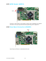
1
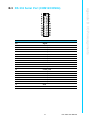
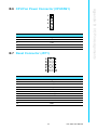
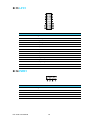
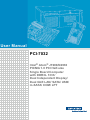
User Manual PCI-7032 Intel® Atom® J1900/N2930 PICMG 1.0 PCI Half-size Single Board Computer with DDR3L 1333/ Dual Independent Display/ Dual GbE LAN/ SATA/ USB/ m-SATA/ COM/ LPT Copyright The documentation and the software included with this product are copyrighted 2015 by Advantech Co., Ltd. All rights are reserved. Advantech Co., Ltd. reserves the right to make improvements in the products described in this manual at any time without notice. No part of this manual may be reproduced, copied, translated or transmitted in any form or by any means without the prior written permission of Advantech Co., Ltd. Information provided in this manual is intended to be accurate and reliable. However, Advantech Co., Ltd. assumes no responsibility for its use, nor for any infringements of the rights of third parties, which may result from its use. Acknowledgements AMIBIOS is a trademark of American Megatrends Inc. Intel® Atom® is trademark of Intel® Corporation. Nuvoton® is a trademark of Nuvoton Technology Corp. All other product names or trademarks are the properties of their respective owners. Product Warranty (2 years) Advantech warrants to you, the original purchaser, that each of its products will be free from defects in materials and workmanship for two years from the date of purchase. This warranty does not apply to any products which have been repaired or altered by persons other than repair personnel authorized by Advantech, or which have been subject to misuse, abuse, accident or improper installation. Advantech assumes no liability under the terms of this warranty as a consequence of such events. Because of Advantech’s high quality-control standards and rigorous testing, most of our customers never need to use our repair service. If an Advantech product is defective, it will be repaired or replaced at no charge during the warranty period. For outof-warranty repairs, you will be billed according to the cost of replacement materials, service time and freight. Please consult your dealer for more details. If you think you have a defective product, follow these steps: 1. Collect all the information about the problem encountered. (For example, CPU speed, Advantech products used, other hardware and software used, etc.) Note anything abnormal and list any onscreen messages you get when the problem occurs. 2. Call your dealer and describe the problem. Please have your manual, product, and any helpful information readily available. 3. If your product is diagnosed as defective, obtain an RMA (return merchandise authorization) number from your dealer. This allows us to process your return more quickly. 4. Carefully pack the defective product, a fully-completed Repair and Replacement Order Card and a photocopy proof of purchase date (such as your sales receipt) in a shippable container. A product returned without proof of the purchase date is not eligible for warranty service. 5. Write the RMA number visibly on the outside of the package and ship it prepaid to your dealer. Part No. 2001703210 Edition 1 January 2015 PCI-7032 User Manual ii Declaration of Conformity FCC Class A Note: This equipment has been tested and found to comply with the limits for a Class A digital device, pursuant to part 15 of the FCC Rules. These limits are designed to provide reasonable protection against harmful interference when the equipment is operated in a commercial environment. This equipment generates, uses, and can radiate radio frequency energy and, if not installed and used in accordance with the instruction manual, may cause harmful interference to radio communications. Operation of this equipment in a residential area is likely to cause harmful interference in which case the user will be required to correct the interference at his own expense. A Message to the Customer Advantech Customer Services Each and every Advantech product is built to the most exacting specifications to ensure reliable performance in the harsh and demanding conditions typical of industrial environments. Whether your new Advantech equipment is destined for the laboratory or the factory floor, you can be assured that your product will provide the reliability and ease of operation for which the name Advantech has come to be known. Your satisfaction is our primary concern. Here is a guide to Advantech’s customer services. To ensure you get the full benefit of our services, please follow the instructions below carefully. Technical Support We want you to get the maximum performance from your products. So if you run into technical difficulties, we are here to help. For the most frequently asked questions, you can easily find answers in your product documentation. These answers are normally a lot more detailed than the ones we can give over the phone. So please consult this manual first. If you still cannot find the answer, gather all the information or questions that apply to your problem, and with the product close at hand, call your dealer. Our dealers are well trained and ready to give you the support you need to get the most from your Advantech products. In fact, most problems reported are minor and are able to be easily solved over the phone. In addition, free technical support is available from Advantech engineers every business day. We are always ready to give advice on application requirements or specific information on the installation and operation of any of our products. iii PCI-7032 User Manual Battery Information Batteries, battery packs, and accumulators should not be disposed of as unsorted household waste. Please use the public collection system to return, recycle, or treat them in compliance with the local regulations. Memory Compatibility PCI-7032 Compatible Memory Brand Size Speed Type ECC Vendor PN Memory Advantech PN AQD 2GB DDR3 1600 SODIMM DDR3 N 665205-0397 SEC 310 XYKO K4B2G084GD AQD-SD3L2GN16-SQ AQD 2GB DDR3 1600 SODIMM DDR3 N 201403504691 HYNIX H5TC2G83EFR AQD-SD3L2GN16-HQ AQD 4GB DDR3 1600 SODIMM DDR3 N 665723-0556 SEC 401 XYKO K4B4G0846B AQD-SD3L4GN16-SG AQD 4GB DDR3L 1600 SODIMM DDR3 N MICRON 4CK72D9PSH AQD-SD3L4GN16-MQ Backplane Support Matrix Table P/N Segment Slot Size PCA-6104P4-0B2E 1 4 110x180 mm (4.3"x7") PCA-6105P5-0B2E 1 5 143x155 mm (5.6"x6") PCA-6108P8-0A2E 1 8 182x185 mm (7.2"x7.3") Specification Comparison Model Name PCI7032G200A1E PCI7032VG00A1E USB RSCOM 232/ LPT LAN Port 422/ 485 Choose 2 interfaces from VGA/ 2 DVI/LVDS 1 x USB 3.0 6 x USB 2.0 4 1 2 COM12, COM34 Choose 2 interfaces from VGA/ 2 DVI/LVDS 1 x USB 3.0 5 x USB 2.0 2 1 1 COM12 Dual FanIndependent less Display SoC Memory DIMM Slot J1900 Dual channel DDR3L-1333 up to 8GB (204-pin SODIMM socket x2) 2 No N2930 Dual channel DDR3L-1333 up to 8GB (204-pin SODIMM socket x1) 1 Yes SATA/ m-SATA Operation System Support List Win8 (32/64), Win8.1 (32/64), Win 7(32/64), Linux, WES7, WES8 PCI-7032 User Manual iv Initial Inspection Before you begin installing your motherboard, please make sure that the following materials have been shipped: 1 PCI-7032 Single Board Computer 1 CD with utility 1 PCI-7032 Start-up Manual 1 Serial ATA HDD Data Cable 1 Serial ATA HDD Power Cable 2 2-port COM Cable Kit 1 4-port USB 2.0 Cable Kit 1 ATX feature cable 1 1-port LPT Cable Kit 1 Keyboard and Mouse Y Cable 1 Jumper Package 1 Warranty Card P/N: 2061703200 P/N: 2001703200 P/N: 1700003194 P/N: 1700022749-11 P/N: 1700008762 P/N: 1700014398-11 P/N: 1700002343 P/N: 1700002223 P/N: 1700060202 P/N: 9689000068 If any of these items are missing or damaged, contact your distributor or sales representative immediately. We have carefully inspected the PCI-7032 mechanically and electrically before shipment. It should be free of marks and scratches and in perfect working order upon receipt. As you unpack the PCI-7032, check it for signs of shipping damage. (For example, damaged box, scratches, dents, etc.) If it is damaged or it fails to meet the specifications, notify our service department or your local sales representative immediately. Also notify the carrier. Retain the shipping carton and packing material for inspection by the carrier. After inspection, we will make arrangements to repair or replace the unit. v PCI-7032 User Manual PCI-7032 User Manual vi Contents Chapter 1 Hardware Configuration......................1 1.1 1.2 1.3 Introduction ............................................................................................... 2 Features & Benefits................................................................................... 2 Specifications ............................................................................................ 3 1.3.1 System .......................................................................................... 3 1.3.2 Memory ......................................................................................... 3 1.3.3 Input/Output .................................................................................. 4 1.3.4 Graphics........................................................................................ 4 1.3.5 Ethernet LAN ................................................................................ 4 1.3.6 Industrial Features ........................................................................ 4 1.3.7 Mechanical and Environmental Specifications.............................. 5 Jumpers and Connectors .......................................................................... 5 Table 1.1: Jumper List ................................................................. 5 Table 1.2: Connectors ................................................................. 6 Board Layout: Jumper and Connector Locations...................................... 7 Figure 1.1 Jumper and connector locations (G2 SKU) ................ 7 Figure 1.2 Jumper and connector locations (VG SKU)................ 7 Figure 1.3 Jumper and connector locations (backside) ............... 8 Block Diagram........................................................................................... 8 Figure 1.4 PCI-7032 block diagram ............................................. 8 Safety Precautions .................................................................................... 9 Jumper Settings ........................................................................................ 9 1.8.1 How to Set Jumpers...................................................................... 9 1.8.2 BIOS (JCMOS1) ......................................................................... 10 Table 1.3: Clear BIOS CMOS (JCMOS1).................................. 10 1.8.3 Watchdog Timer Output (JWDT1) and Hardware Monitor Alarm (JOBS1) ...................................................................................... 10 Table 1.4: Watch Dog Timer (JWDT1) and Hardware Monitor Alarm (JOBS1) ......................................................... 10 Buzzer Setting......................................................................................... 10 Table 1.5: Buzzer Setting (BZ1) ................................................ 10 AT/ATX mode HW selection (ATXF1)..................................................... 11 Table 1.6: AT/ATX Mode HW Selection (ATXF1)...................... 11 LVDS Panel Voltage Selection (JLVDS1, JLVDS2)................................ 11 Table 1.7: LVDS Panel Voltage Selection (JLVDS1, JLVDS2) . 11 LVDS VESA, JEIDA Format Selection.................................................... 12 Table 1.8: LVDS VESA, JEIDA Format Selection ..................... 12 1.4 1.5 1.6 1.7 1.8 1.9 1.10 1.11 1.12 Chapter 2 Connecting Peripherals ....................13 2.1 2.2 2.3 2.4 2.5 2.6 2.7 2.8 2.9 2.10 Introduction ............................................................................................. 14 Parallel Port (LPT1)................................................................................. 14 USB Ports (USB12, USB34, USB56, USB7) .......................................... 15 VGA Connector (VGA1) .......................................................................... 16 DVI Connector (DVI1) ............................................................................. 16 LVDS (LVDS1) ........................................................................................ 17 Serial Ports (COM12).............................................................................. 18 PS/2 Keyboard and Mouse Connector (KBMS1) .................................... 18 CPU Fan Connector (CPUFAN1)............................................................ 19 Front Panel Connectors (JFP1) .............................................................. 19 Table 2.1: Power LED status.................................................... 20 H/W Monitor for G2 SKU/Watchdog Timer ............................................. 20 2.11.1 H/W monitor alarm for G2 SKU (JOBS1).................................... 20 2.11.2 Watchdog timer (JWDT1) ........................................................... 21 2.11 vii PCI-7032 User Manual 2.12 2.16 2.17 2.18 LAN Ports (LAN1 & LAN2)...................................................................... 21 Table 2.2: LAN LED Indicators.................................................. 21 Figure 2.1 Jumper and connector locations of PCA-AUDIOHDA1E ..................................................................... 21 GPIO Header (GPIO1)............................................................................ 22 Case Open Connector (JCASE1) ........................................................... 22 Front Panel LAN Indicator Connector (LANLED1).................................. 23 Table 2.3: LAN LED Indicators.................................................. 23 Serial ATA Interface (SATA1, SATA2).................................................... 24 LPC Extension Interface (LPC1)............................................................. 25 12V/5V/5VSB Power Connector (ATX1)................................................. 25 3 AMI BIOS Setup................................. 27 3.1 Introduction ............................................................................................. 28 Figure 3.1 Setup Program Initial Screen ................................... 28 Entering Setup ........................................................................................ 29 3.2.1 Main Setup.................................................................................. 29 Figure 3.2 Main Setup Screen................................................... 29 3.2.2 Advanced BIOS Features Setup................................................. 30 Figure 3.3 Advanced BIOS Features Setup Screen.................. 30 Figure 3.4 ACPI Settings ........................................................... 31 Figure 3.5 NCT6106D Super IO Configuration.......................... 32 Figure 3.6 Serial Port 1 Configuration ....................................... 32 Figure 3.7 Serial Port 2 Configuration ....................................... 33 Figure 3.8 Serial Port 3 Configuration ....................................... 33 Figure 3.9 Serial Port 4 Configuration ....................................... 34 Figure 3.10Parallel Port Configuration ....................................... 34 Figure 3.11NCT6106D Configuration ......................................... 35 Figure 3.12S5 RTC configuration ............................................... 35 Figure 3.13Serial Port Console Redirection ............................... 36 Figure 3.14CPU Configuration ................................................... 36 Figure 3.15PPM Configuration ................................................... 37 Figure 3.16IDE Configuration ..................................................... 38 Figure 3.17Miscellaneous Configuration .................................... 38 Figure 3.18PCI Subsystem Settings........................................... 39 Figure 3.19Network Stack Configuration.................................... 39 Figure 3.20CSM Configuration ................................................... 40 Figure 3.21PCI-7032 USB Configuration ................................... 41 Figure 3.22Security Configuration .............................................. 41 3.2.3 Chipset........................................................................................ 42 Figure 3.23Chipset ..................................................................... 42 Figure 3.24North Bridge ............................................................. 42 Figure 3.25 Intel IGD Configuration............................................ 43 Figure 3.26Graphics Power Management Control ..................... 43 Figure 3.27LCD Control.............................................................. 44 Figure 3.28South Bridge............................................................. 44 Figure 3.29PCI Express Configuration ....................................... 46 3.2.4 Security....................................................................................... 46 Figure 3.30 Security ................................................................... 46 3.2.5 Boot ............................................................................................ 47 Figure 3.31 Boot ......................................................................... 47 3.2.6 Save & Exit ................................................................................. 47 Figure 3.32Save & Exit............................................................... 47 2.13 2.14 2.15 Chapter 3.2 Chapter 4 PCI-7032 User Manual Value-Added Software Services49 viii 4.1 Value-Added Software Services ............................................................. 50 4.1.1 Software API ............................................................................... 50 5 Chipset Software Installation Utility 51 5.1 5.2 5.3 Before You Begin .................................................................................... 52 Introduction ............................................................................................. 52 Windows 7/8 Driver Setup....................................................................... 53 6 Integrated Graphic Device Setup .....55 6.1 6.2 Introduction ............................................................................................. 56 Windows 7/8 Driver Setup....................................................................... 56 7 LAN Configuration.............................57 7.1 7.2 7.3 Introduction ............................................................................................. 58 Installation ............................................................................................... 58 Windows 7/8 Driver Setup (LAN) ............................................................ 58 8 Intel® USB 3.0 ....................................59 8.1 8.2 Introduction ............................................................................................. 60 Installation ............................................................................................... 60 Appendix A Programming the Watchdog Timer..61 A.1 Programming the Watchdog Timer ......................................................... 62 A.1.1 Watchdog Timer Overview.......................................................... 62 A.1.2 Programming the Watchdog Timer ............................................. 62 Table A.1: Watchdog Timer Registers ....................................... 64 A.1.3 Example Program ....................................................................... 65 Appendix B I/O Pin Assignments..........................69 B.1 Parallel Port Connector (LPT1) ............................................................... 70 Table B.1: Parallel Port Connector (LPT1) ................................ 70 VGA Connector (VGA1) .......................................................................... 70 Table B.2: VGA Connector (VGA1) ........................................... 70 RS 232 Serial Port (COM12/COM34) ..................................................... 71 Table B.3: RS-232 Serial Port (COM12/COM34) ...................... 71 USB 2.0 Header (USB12-USB56)........................................................... 72 Table B.4: USB Header (USB12-USB56) .................................. 72 PS/2 Keyboard/Mouse Connector (KBMS1) ........................................... 72 Table B.5: PS/2 Keyboard/Mouse Connector (KBMS1) ............ 72 CPU Fan Power Connector (CPUFAN1) ................................................ 73 Table B.6: CPU Fan Power Connector (CPUFAN1).................. 73 Reset Connector (JFP1) ......................................................................... 73 Table B.7: Reset Connector (JFP1 / RESET)............................ 73 High-definition Audio Link Connector (HDAUD1).................................... 74 Table B.8: High-definition Audio Link Connector (HDAUD1) ..... 74 LAN1 and LAN2 LED Connector (LANLED1) ......................................... 74 Table B.9: LAN1 and LAN2 LED Connector (LANLED1)........... 74 GPIO Header (GPIO1) ............................................................................ 74 Table B.10:GPIO Header (GPIO1) ............................................. 75 Chapter Chapter Chapter Chapter B.2 B.3 B.4 B.5 B.6 B.7 B.8 B.9 B.10 ix PCI-7032 User Manual B.11 B.12 B.13 B.14 B.15 B.16 B.17 B.18 B.19 JWDT1 and JOBS1................................................................................. 75 Table B.11:JWDT1 and JOBS1 .................................................. 75 JCASE1 .................................................................................................. 75 Table B.12:JCASE1.................................................................... 75 LPC1 ....................................................................................................... 76 Table B.13:LPC1 ........................................................................ 76 PWR1...................................................................................................... 76 Table B.14:PWR1 ....................................................................... 76 DVI1 ........................................................................................................ 77 Table B.15:DVI1 ......................................................................... 77 Fixed I/O Ranges Decoded by Intel PCH ............................................... 78 Table B.16:Fixed I/O Ranges Decoded by Intel PCH................. 78 System I/O Ports..................................................................................... 78 Table B.17:PCI-7032 System I/O Ports ...................................... 78 Interrupt Assignments ............................................................................. 79 Table B.18:Interrupt Assignments .............................................. 79 1 MB Memory Map.................................................................................. 79 Table B.19:1 MB memory map ................................................... 79 Appendix C Programming the GPIO .................... 81 C.1 C.2 C.3 Supported GPIO Register ....................................................................... 82 GPIO Registers....................................................................................... 82 GPIO Example Program-1 ...................................................................... 82 PCI-7032 User Manual x Chapter 1 Hardware Configuration 1 1.1 Introduction PCI-7032 is an Intel® based PICMG 1.0 half-size PCI interface single board computer. PCI-7032G2, with Intel® Celeron® J1900, offers a dual GbE LAN, high computing solution; PCI-7032VG, adopting Intel® Atom® N2930, provides a single GbE LAN and fanless computing core with high reliability that resists heat, dust, vibration and shock in any application environment. Both J1900 and N2930 SoC are designed for the embedded market. Besides computing speed enhancement with quad core architecture, the SoCs integrate DDR3L memory controller, PCIe Gen2 expansion and storage/display/audio functions in low power BGA type chips, offering energy saving products with only 7.5W to 10W thermal design power, providing customers with low power and rugged embedded solutions. In addition, SoCs support embedded OS, such as WES7, WES8, and Linux, fulfilling a variety of applications, for example, machine tool, CNC, textile machine, factory inspection facility, factory motion controller, and data acquisition center. PCI-7032 is rich in I/O interfaces: it has two SATA ports (300 MB/sec) for mainstream SSD (solid state disk), HDD, and ODD connections, and one of them can be configured as m-SATA for embedded OS installation as an economical, easy to maintain SSD device. Additionally, the dual Gigabit Ethernet LANs offer strong networking capability; PCI-7032G2 with four and PCI-7032VG with two serial ports (COM ports) can be used as reliable legacy device control interfaces, which can be configured into RS232, RS-422, or RS-485 mode, helping system integrators to build safe and flexible legacy connections in factory. Users can also purchase Advantech’s COM port upgrade module (P/N: PCA-COM485-00A1E/PCA-COM232-00A1E) to add four extra serial ports. In addition to board-level products, Advantech also offers a series of wall-mount chassis; with PCI-7032 joining the product portfolio, Advantech now can provide compact-size, low-power and high-reliability system-level solutions for industrial customers. With outstanding performance, and flexible expansion capability, PCI-7032 is an ideal computing platform for modern industrial applications. 1.2 Features & Benefits Features Benefits PCI-7032 supports Intel® The computing frequency of Intel® Celeron® J1900 and N2930 is up to 2GHz. The processor speed increases 20% compared to N450 and D510 (PCI-7031). Celeron® J1900 and N2930 Providing higher memory data transmission and processPCI-7032 supports DDR3L 1333 ing efficiency, bringing higher system performance, and SDRAM, up to 8GB the cost of memory module decreases compared with DDR2 (G2 SKU: 2 Slots; VG SKU: 1 Slot). Advantech SUSI APIs and Utilities support. Reducing customer S/W development effort with more reliable S/W quality, also providing value-added utilities such as system monitor and panel backlight control. m-SATA support Supporting compact size storage device which is suitable for embedded OS, such as WES7, WES8. In addition, mSATA device can prevent HDD error in vibration conditions. USB 3.0 support Providing high transfer data performance interface; USB 3.0 data transfer rate is 5Gbps which is 10 times faster than USB2.0. PCI-7032 User Manual 2 1.3 Specifications 1.3.1 System CPU: – VG SKU:Intel® Celeron® N2930 L2 Cache: 2 MB BIOS: AMI SPI BIOS (64 Mb SPI) SATA hard disk drive interface: PCI-7032 has two SATA interface configuration: – Two SATA II (300 MB/s) connectors – One SATA II (300 MB/s) connector, and one SATA II (300 MB/s) m-SATA SO015 socket ACPI Sleep State: S4, S5 Note! PCI-7032 does NOT support PATA(IDE) interface. Note! J1900/N2930 does not support ACPI S1. 1.3.2 Memory RAM: PCI-7032 supports dual channel DDR3L 1333, up to 8GB with two 204pin SO-DIMM socket (up to 4GB/DIMM. G2 SKU: 2 Slots; VG SKU: 1 Slot). Note! 1. 2. 3. Due to the inherent limitations of the PC architecture, the system may not fully detect 16 GB RAM when 16 GB of RAM is installed. A 32-bit OS may not fully detect 4 GB of RAM when 4 GB is installed. To power on the system with only one memory module, please insert the module in DIMMA1. 3 PCI-7032 User Manual Hardware Configuration – G2 SKU:Intel® Celeron® J1900 Chapter 1 Users can choose two types of display interface from VGA, DVI, and LVDS. These features fulfill requirements in an abundance of different applications. Dual display 1.3.3 Input/Output PCI bus: Four 32 bit/33 MHz PCI bus masters to backplane Enhanced parallel port: This EPP/SPP/ECP port can be configured to LPT1 or disabled. A standard DB-25 female connector provided. Serial ports: PCI-7032G2 with four and PCI-7032VG with two serial ports can be configured as RS-232, RS-422 or RS-485 (with auto flow control). PS/2 keyboard and mouse connector: One 6-pin mini-DIN connectors is located on the mounting bracket for easy connection to a PS/2 keyboard and mouse via the Y-cable included in the package. USB port: – G2 SKU: USB 3.0 *1 (5Gbps, rear I/O), and USB 2.0*6 (480 Mbps, pin headers) – VG SKU: USB 3.0*1 (5Gbps, rear I/O), and USB 2.0*5 (480 Mbps, 1x rear I/ O, 4x pin headers) LPC: One LPC connector to support optional TPM (PCA-TPM-00A1E), COM232 (PCA-COM232-00A1E), COM-422/485 (PCA-COM485-00A1E) modules. GPIO: Supports 8-bit GPIO from super I/O for general purpose control application. 1.3.4 Graphics Controller: Intel® HD graphics embedded in the processor. Display memory: Shared memory is subject to OS Dual display: Choose two display interface from VGA, DVI, and LVDS – VGA: up to 2560x1600@60Hz – DVI: up to 2560x1600@60Hz – LVDS: 48 bit (dual channel 24-bit LVDS) up to 1920x1200@60Hz 1.3.5 Ethernet LAN Supports single/dual 10/100/1000 Mbps Ethernet port(s) via the dedicated PCI Express x1 bus which provides 500 MB/s data transmission rate. Controller: – LAN 1: Intel® I211 (VG and G2) – LAN 2: Intel® I211 (G2 only) 1.3.6 Industrial Features Watchdog timer: Can generate a system reset. The watchdog timer is programmable, with each unit equal to one second or one minute (255 levels). PCI-7032 User Manual 4 Operating temperature: 0 ~ 60 °C (32 ~ 140 °F, Depending on CPU and thermal solution) Storage temperature: -40 ~ 85 °C (-40 ~ 185 °F) Operating humidity: 40° C @ 85% RH, non-Condensing Non-operating humidity: 60 °C @ 95% RH, non-Condensing Power supply voltage: +5 V, +12 V, +5 VSB Power consumption: Intel® Celeron® J1900 (2GHz), DDR3L 1333, 4GB SO-DIMM module*2 Voltage 5V 12V 5VSB Current 0.737 A 0.298 A 0.044 A Total 7.481 W Board size: 185 mm x 122 mm (7.3" x 4.8") Board weight: – G2 SKU: 0.264 Kg – VG SKU:0.198 Kg 1.4 Jumpers and Connectors Connectors on the PCI-7032 single host board link it to external devices such as hard disk drives and a keyboard. In addition, the board has a number of jumpers used to configure your system for your application. The tables below list the function of each of jumpers and connectors. Later sections in this chapter give instructions on setting jumpers. Chapter 2 gives instructions for connecting external devices to your motherboard. Table 1.1: Jumper List Label Function JCMOS1 CMOS clear ATXF1 AT/ATX mode selection JWDT1 + JOBS1 Watchdog timer output selection and HW monitor alarm BZ1 Buzzer setting JLVDS1, JLVDS2 LVDS panel voltage selection JLVDS_VCON1 LVDS VESA, JEIDA format selection 5 PCI-7032 User Manual Hardware Configuration PCI-7032G2-00A1E Chapter 1 1.3.7 Mechanical and Environmental Specifications Table 1.2: Connectors Label Function LPT1 Parallel port, Parallel port x 1, supports SPP/EPP/ECP mode LAN1 Intel® I211 LAN2 (G2 SKU) Intel® I211 VGA1 VGA connector KBMS1, KBMS2 PS/2 keyboard and mouse connector. KBMS1 in on rear I/O; KBMS2 connects chassis front panel. COM12, COM34 (G2 SKU) Serial port: RS-232/422/485 JFP1 Power Switch / Reset connector JCASE1 Case Open CPUFAN1 CPU FAN connector (4-pin) LANLED1 LAN1/2 LED extension connector HDAUD1 HD audio extension module connector USB12, USB34 USB port 1-4 (USB 2.0, 480Mbps, pin header) USB56 (G2 SKU) USB port 5, 6 (USB 2.0, 480Mbps, pin header) USB6 (VG SKU) USB port 6 (USB 2.0, 480Mbps, rear I/O) USB7 USB port 7 (USB 3.0, 5Gbps, rear I/O) SATA1 Serial ATA1 (300 MB/s) SATA2/MSATA1 SATA2 (300MB/s) and MSATA1(mSATA SO-015) share the same SATA port. m-SATA has higher priority when both of them connects with devices. DIMMA1 Memory connector channel A DIMMB1 (G2 SKU) Memory connector channel B GPIO1 GPIO pin header (SMD pitch-2.0 mm) LPC1 COM port module expansion pin-header ATX1 12 V, 5 V, 5VSB power connector DVI1 DVI connector LVDS1 LVDS connector SMBUS1 SMBUS connector INV1 LVDS inverter connector PCI-7032 User Manual 6 COM34 COM12 SATA1 SATA2 DVI1 USB12 JCASE1 DIMMA1 ATX1 ATXF1 JFP1 GPIO1 VGA1 SWA1-4 LANLED1 LAN1 LAN2 SMBUS1 JOBS1+JWDT1 INV1 JCOMS1 USB7 KBMS1 KBMS2 USB34 USB56 BZ1 LVDS1 JLVDS_VCON1 J1900 DIMMB1 HDAUD1 CPUFAN1 JLVDS2 JLVDS1 Figure 1.1 Jumper and connector locations (G2 SKU) Figure 1.2 Jumper and connector locations (VG SKU) 7 PCI-7032 User Manual Hardware Configuration LPT1 Chapter 1 1.5 Board Layout: Jumper and Connector Locations MSATA1 LPC1 Figure 1.3 Jumper and connector locations (backside) 1.6 Block Diagram VGA x 1* LVDS x 1* DDR3L 1333 (4GB) 204 pin SO-DIMM Socket Channel B DDR3L 1333 (4GB) 204 pin SO-DIMM Socket DDI0 DVI x 1* SATA 2.0 x 2 or SATA 2.0 x 1 & m-SATA x 1** Channel A (G2 SKU) DDI 1 300 MB/s Intel Celeron J1900 (G2, cooler) N2930 (VG, fanless) PCIex1 Intel I211 PCIex1 G2: Intel I211 USB 3.0 x 1 (Rear I/O) PCIex1 IT8892 32/33 PCI GF to BP G2: USB 2.0 x 6 VG: USB 2.0 x 5 RS-232/422/485 x 4 PS/2 (G2 SKU) LPC PCA-TPM-00A1E (Optional) PCA-COM232-00A1E (Optional) SIO: NCT6106D PCA-COM485-00A1E (Optional) 8bit GPIO * Dual display, choose two interface from VGA (Default), DVI, and LVDS (Default) ** SATA2 connector can be configured as m-SATA. Figure 1.4 PCI-7032 block diagram PCI-7032 User Manual 8 LPT Warning! Always completely disconnect the power cord from your chassis whenever you work with the hardware. Do not make connections while the power is on. Sensitive electronic components can be damaged by sudden power surges. Only experienced electronics personnel should open the PC chassis. Caution! The computer is provided with a battery-powered Real-time Clock. There is a danger of explosion if battery is incorrectly replaced. Replace only with same or equivalent type recommended by the manufacturer. Discard used batteries according to manufacturer's instructions. Caution! There is a danger of a new battery exploding if it is incorrectly installed. Do not attempt to recharge, force open or heat the battery. Replace the battery only with the same or equivalent type recommended by the manufacturer. Discard used batteries according to the manufacturer’s instructions. 1.8 Jumper Settings This section provides instructions on how to configure your motherboard by setting the jumpers. It also includes the motherboard’s default settings and your options for each jumper. 1.8.1 How to Set Jumpers You can configure your motherboard to match the needs of your application by setting the jumpers. A jumper is a metal bridge that closes an electrical circuit. It consists of two metal pins and a small metal clip (often protected by a plastic cover) that slides over the pins to connect them. To “close” (or turn ON) a jumper, you connect the pins with the clip. To “open” (or turn OFF) a jumper, you remove the clip. Sometimes a jumper consists of a set of three pins, labeled 1, 2 and 3. In this case you connect either pins 1 and 2, or 2 and 3. A pair of needle-nose pliers may be useful when setting jumpers. 9 PCI-7032 User Manual Hardware Configuration Caution! Always ground yourself to remove any static charge before touching the motherboard. Modern electronic devices are very sensitive to static electrical discharges. As a safety precaution, use a grounding wrist strap at all times. Place all electronic components on a static-dissipative surface or in a static-shielded bag when they are not in the chassis. Chapter 1 1.7 Safety Precautions 1.8.2 BIOS (JCMOS1) PCI-7032 CPU card contains a jumper that can erase BIOS CMOS data and reset the system BIOS information. Normally this jumper should be set with pins 1-2 closed. If you want to reset those data, set JCMOS1 to 2-3 closed for just a few seconds, and then move the jumper back to 1-2 closed. This procedure will reset the CMOS to its last status or default setting. Table 1.3: Clear BIOS CMOS (JCMOS1) Function Jumper Setting 1 *Keep BIOS CMOS data 1-2 closed 1 Clear BIOS CMOS data 2-3 closed * default setting 1.8.3 Watchdog Timer Output (JWDT1) and Hardware Monitor Alarm (JOBS1) PCI-7032 contains a watchdog timer that will reset the CPU in the event the CPU stops processing. This feature means PCI-7032 will recover from a software failure or an EMI problem. The JWDT1 jumper settings control the outcome of what the computer will do in the event the watchdog timer is tripped. PCI-7032 also provide jumper: JOBS1 to enable or disable hardware monitor alarm. Table 1.4: Watch Dog Timer (JWDT1) and Hardware Monitor Alarm (JOBS1) Function Jumper Setting 1 *Enable watch dog timer (2+3) and Enable Hardware Monitor Alarm (4+5) 5 2-3 closed AND 4-5 closed * default setting 1.9 Buzzer Setting PCI-7032 provides jumpers for customer to enable buzzer via hardware settings. Table 1.5: Buzzer Setting (BZ1) Function Jumper Setting 1 *Enable buzzer Connect external speaker (Buzzer and speaker together: okay) 3-4 closed 1 external speaker: 1-2 * default setting PCI-7032 User Manual 10 Table 1.6: AT/ATX Mode HW Selection (ATXF1) Function Jumper Setting Jumper Setting *AT mode Short Pin 1,2 ATX mode Connecting to backplane with cable: 1700002343 * Default setting 1.11 LVDS Panel Voltage Selection (JLVDS1, JLVDS2) Table 1.7: LVDS Panel Voltage Selection (JLVDS1, JLVDS2) Function Jumper Setting 3.3 V* 5V 12 V * Default setting 11 PCI-7032 User Manual Hardware Configuration The PCI-7032 can support an advanced soft power switch function. When using an ATX power supply, please follow the instructions below to enable ATX functions. 1. Find ATX feature cable (1700002343). 2. Connect the 3-pin plug of the cable to ATXF1 (ATX feature connector). And connect another plug to backplane HCN1 connector. 3. Connect the power on/off button cable of the chassis to pin 9 and pin 10 of JFP1. Default value is set ATXF1 to short pin 1,2 (do not short pin 2,3) to support AT power. Chapter 1 1.10 AT/ATX mode HW selection (ATXF1) 1.12 LVDS VESA, JEIDA Format Selection Table 1.8: LVDS VESA, JEIDA Format Selection Function Jumper Setting Pull high to +3.3 V 1-2 Pull down to GND* 2-3 * Default setting PCI-7032 User Manual 12 Chapter 2 Connecting Peripherals 2 2.1 Introduction You can access most of the connectors from the top of the board. If you have a number of cards installed, you may need to partially remove a card to make all connections. 2.2 Parallel Port (LPT1) LPT1 The parallel port is normally used to connect the motherboard to a printer. PCI-7032 includes an onboard parallel port, accessed through a 26-pin flat-cable connector, LPT1. PCI-7032 User Manual 14 PCI-7032 provides up to 7 USB (Universal Serial Bus) on-board ports with complete Plug & Play and hot swap support. These USB ports comply with USB Specification 2.0 and 3.0, support transfer rates up to 480 Mbps (USB2.0), and 5 Gbps (USB3.0). For G2 SKU, USB 1-6 are USB 2.0 ports with pin header on board, and USB7 is a USB 3.0 port on rear I/O. For VG SKU, USB 1-4 are USB 2.0 ports with pin header, and USB6 (USB2.0)/ USB7 (USB 3.0) are on rear I/O bracket. Connecting Peripherals USB12 USB7 USB34 USB56 PCI-7032G2 PCI-7032VG 15 Chapter 2 2.3 USB Ports (USB12, USB34, USB56, USB7) PCI-7032 User Manual 2.4 VGA Connector (VGA1) VGA1 This CPU card has VGA outputs that can drive conventional CRT displays. VGA1 is a standard 15-pin D-SUB connector commonly used for VGA. 2.5 DVI Connector (DVI1) DVI1 DVI1 is a 20-pin connector, supporting up to 2560 x 1600 @ 60Hz. Please place order no. 1700021831-01 for standard DVI connector on bracket. PCI-7032 User Manual 16 LVDS1 for dual channel 24-bit LVDS panel. Please check the pin definitions before installing your panel. Connecting Peripherals LVDS1 1 3 5 7 9 11 13 15 17 19 21 23 25 27 29 31 33 35 37 39 2 4 6 8 10 12 14 16 18 20 22 24 26 28 30 32 34 36 38 40 Pin Signal Pin Signal 1 VDD_LVDS1 21 LVDS1_A2P 2 VDD_LVDS1 22 LVDS1_A6P 3 LVDS1_DET# 23 GND 4 GND 24 GND 5 VDD_LVDS1 25 LVDS1_CLK1N 6 VDD_LVDS1 26 LVDS1_CLK2N 7 LVDS1_A0N 27 LVDS1_CLK1P 8 LVDS1_A4N 28 LVDS1_CLK2P 9 LVDS1_A0P 29 GND 10 LVDS1_A4P 30 GND 11 GND 31 LVDS1_SCD 12 GND 32 LVDS1_SDD 13 LVDS1_A1N 33 GND 14 LVDS1_A5N 34 GND 15 LVDS1_A1P 35 LVDS1_A3N 16 LVDS1_A5P 36 LVDS1_A7N 17 GND 37 LVDS1_A3P 18 GND 38 LVDS1_A7P 19 LVDS1_A2N 39 LVDS1_ENBKL1 20 LVDS1_A6N 40 LVDS1_VCON 17 Chapter 2 2.6 LVDS (LVDS1) PCI-7032 User Manual 2.7 Serial Ports (COM12) COM34 COM12 PCI-7032G2 offers four serial ports and PCI-7032VG offers two serial ports. These ports can connect to serial devices, such as a mouse or a printer, or to a communications network. They can be configured as RS-232, RS-422, or RS-485 in the BIOS menu. The IRQ and address ranges for four ports are fixed. However, if you want to disable the port or change these parameters later, you can do this in the system BIOS setup. 2.8 PS/2 Keyboard and Mouse Connector (KBMS1) KBMS1 KBMS2 A 6-pin mini-DIN connectors (KBMS1) on rear I/O bracket provide connection to PS/2 keyboard. An onboard 6-pin header connects to I/O board of chassis, providing a PS/2 connector on the chassis front panel. PCI-7032 User Manual 18 This connector supports cooling fans of 500 mA (6 W) or less, and it also supports smart fan control when using 4-pin or 3-pin cooler. 2.10 Front Panel Connectors (JFP1) FP1 is a 10-pin connector which connects to the front panel switch to control system power on/off and reset. JFP1 19 PCI-7032 User Manual Connecting Peripherals CPUFAN1 Chapter 2 2.9 CPU Fan Connector (CPUFAN1) 1 2 HDD LED 3 4 Power LED 5 6 SNMP 7 8 Reset buƩon 9 10 Power buƩon Table 2.1: Power LED status Power mode LED System On On System Suspend Fast flashes System Off Off 2.11 H/W Monitor for G2 SKU/Watchdog Timer JOBS1+JWDT1 1 5 2.11.1 H/W monitor alarm for G2 SKU (JOBS1) This 2-pin header is for enabling/disabling H/W monitor alarm function. 4-5 Closed: Enables hardware monitor alarm (Default) 4-5 Open: Disables hardware monitor alarm PCI-7032 User Manual 20 Chapter 2 2.11.2 Watchdog timer (JWDT1) This is for an setting action trigger on the watchdog timer. 2-3 Closed: Enable watchdog timer (Default) 2-3 Open: No action 2.12 LAN Ports (LAN1 & LAN2) Connecting Peripherals LAN1 LAN2 PCI-7032 is equipped with one or two high-performance 1000 Mbps Ethernet LANs. They are supported by all major network operating systems. The RJ-45 jacks on the rear plate provide convenient connectivity. Table 2.2: LAN LED Indicators LAN Mode LED1 LED2 1000Mbps Link On Green On On 1000Mbps Active Green On Flash 1000Mbps Link Off Off Off 100Mbps Link On Orange On On 100Mbps Active Orange On Flash 100Mbps Link Off Off Off 10Mbps Link On Off On 10Mbps Active Off Flash 10Mbps Link Off Off Off Figure 2.1 Jumper and connector locations of PCA-AUDIO-HDA1E 21 PCI-7032 User Manual 2.13 GPIO Header (GPIO1) GPIO1 Provides a 10-pin header for 8-bit Digital I/O usage. Refer to Appendix B for detailed information on the pin assignments and the programming guide in Appendix C. 2.14 Case Open Connector (JCASE1) JCASE1 The 2-pin case open connector is for chassis with a case open sensor. When the case is open, the buzzer on motherboard will sound. PCI-7032 User Manual 22 Table 2.3: LAN LED Indicators LAN1 (1,3 pin) LAN2 (2, 4 pin) 1000Mbps Link On On On 1000Mbps Active Flash Flash 1000Mbps Link Off Off Off 100Mbps Link On On On 100Mbps Active Flash Flash 100Mbps Link Off Off Off 10Mbps Link On On On 10Mbps Active Flash Flash 10Mbps Link Off Off Off Connecting Peripherals LAN Mode LANLED1 23 Chapter 2 2.15 Front Panel LAN Indicator Connector (LANLED1) PCI-7032 User Manual 2.16 Serial ATA Interface (SATA1, SATA2) SATA1 SATA2 MSATA1 PCI-7032 features high performance serial ATA interface which eases cabling to hard drives or CD/DVD drives with long cables. SATA2 can be configured as m-SATA. The socket is on the back side of the board. PCI-7032 User Manual 24 Chapter 2 2.17 LPC Extension Interface (LPC1) LPC1 2.18 12V/5V/5VSB Power Connector (ATX1) ATX1 PCI-7032 supports ATX power supply. ATX1 supplies main power (5V,12V, 5VSB) via a 6x2 power connector. 25 PCI-7032 User Manual Connecting Peripherals LPC1 is a 14-pin female pin header for adopting Advantech LPC module, such as PCA-COM232-00A1E, PCA-COM485-00A1E, or PCA-TPM-00A1E. PCI-7032 User Manual 26 Chapter 3 AMI BIOS Setup 3 3.1 Introduction AMI BIOS has been integrated into motherboards for decades. In the past, people often referred to the AMI BIOS setup menu as BIOS, BIOS setup or CMOS setup. With the AMI BIOS Setup program, you can modify BIOS settings and control the special features of your computer. The Setup program uses a number of menus for making changes and turning special features on or off. This chapter describes the basic navigation of the PCI-7032 setup screens. Figure 3.1 Setup Program Initial Screen PCI-7032 User Manual 28 Turn on the computer and the BIOS is activated as well. The setup program can be triggered by pressing "DEL" or "F2" key. Note! If the message disappears before you press the "DEL" or "F2" key, please restart the computer and try again. When you first enter the BIOS Setup Utility, you will enter the Main setup screen. You can always return to the Main setup screen by selecting the Main tab. There are two Main Setup options. They are described in this section. The Main BIOS Setup screen is shown below. Figure 3.2 Main Setup Screen The Main BIOS setup screen has two main frames. The left frame displays all the options that can be configured. Grayed-out options cannot be configured; options in blue can. The right frame displays the key legend. Above the key legend is an area reserved for a text message. When an option is selected in the left frame, it is highlighted in white. Often a text message will accompany it. System Time / System Date Use this option to change the system time and date. Highlight System Time or System Date using the <Arrow> keys. Enter new values through the keyboard. Press the <Tab> key or the <Arrow> keys to move between fields. The date must be entered in MM/DD/YY format. The time must be entered in HH:MM:SS format. 29 PCI-7032 User Manual AMI BIOS Setup 3.2.1 Main Setup Chapter 3 3.2 Entering Setup 3.2.2 Advanced BIOS Features Setup Select the Advanced tab from the PCI-7032 setup screen to enter the Advanced BIOS Setup screen. You can select any of the items in the left frame of the screen, such as CPU Configuration, and press Enter to go to the sub menu for that item. You can display an Advanced BIOS Setup option by highlighting it using the <Arrow> keys. All Advanced BIOS Setup options are described in this section. The Advanced BIOS Setup screen is shown below, and the sub menus are described on the following pages. Figure 3.3 Advanced BIOS Features Setup Screen PCI-7032 User Manual 30 Chapter 3 3.2.2.1 ACPI Settings AMI BIOS Setup Figure 3.4 ACPI Settings Enable ACPI Auto Configuration Enable Hibernation "Enable or Disable" Hibernate (OS/S4 Sleep State). This option may not be effective with some OSs. Lock Legacy Resources Enable or disable lock of legacy resources. 31 PCI-7032 User Manual 3.2.2.2 NCT6106D Super IO Configuration Figure 3.5 NCT6106D Super IO Configuration Serial Port 1 Configuration Figure 3.6 Serial Port 1 Configuration PCI-7032 User Manual 32 Serial Port 2 Configuration Chapter 3 AMI BIOS Setup Figure 3.7 Serial Port 2 Configuration Serial Port 3 Configuration Figure 3.8 Serial Port 3 Configuration 33 PCI-7032 User Manual Serial Port 4 Configuration Figure 3.9 Serial Port 4 Configuration Parallel Port Configuration Figure 3.10 Parallel Port Configuration PCI-7032 User Manual 34 Chapter 3 3.2.2.3 NCT6106D Configuration AMI BIOS Setup Figure 3.11 NCT6106D Configuration 3.2.2.4 S5 RTC Wake Setting Figure 3.12 S5 RTC configuration 35 PCI-7032 User Manual 3.2.2.5 Serial Port Console Redirection Figure 3.13 Serial Port Console Redirection 3.2.2.6 CPU Configuration Figure 3.14 CPU Configuration Limit CPUID Maximum Setting this item to [Enable] allows legacy operating systems to boot even without support for CPUs with extended CPUID functions. PCI-7032 User Manual 36 3.2.2.7 PPM Configuration Figure 3.15 PPM Configuration 37 PCI-7032 User Manual AMI BIOS Setup Execute Disable Bit This item specifies the Execute Disable Bit Feature. The settings are Enabled and Disabled. The Optimal and Fail-Safe default setting is Enabled. If Disabled is selected, the BIOS forces the XD feature flag to always return to 0. Intel Virtualization Technology This feature is used to enable or disable the Intel Virtualization Technology (IVT) extension. It allows multiple operating systems to run simultaneously on the same system. It does this by creating virtual machines, each running its own x86 operating system. Power Technology Chapter 3 3.2.2.8 IDE Configuration Figure 3.16 IDE Configuration 3.2.2.9 Miscellaneous Configuration Figure 3.17 Miscellaneous Configuration PCI-7032 User Manual 38 Chapter 3 3.2.2.10 PCI Subsystem Settings AMI BIOS Setup Figure 3.18 PCI Subsystem Settings 3.2.2.11 Network Stack Configuration Figure 3.19 Network Stack Configuration 39 PCI-7032 User Manual 3.2.2.12 CSM Configuration Figure 3.20 CSM Configuration PCI-7032 User Manual 40 Chapter 3 3.2.2.13 USB Configuration AMI BIOS Setup Figure 3.21 PCI-7032 USB Configuration 3.2.2.14 Security Configuration Figure 3.22 Security Configuration 41 PCI-7032 User Manual 3.2.3 Chipset Figure 3.23 Chipset 3.2.3.1 North Bridge Figure 3.24 North Bridge PCI-7032 User Manual 42 Chapter 3 AMI BIOS Setup Figure 3.25 Intel IGD Configuration Figure 3.26 Graphics Power Management Control 43 PCI-7032 User Manual Figure 3.27 LCD Control 3.2.3.2 South Bridge Figure 3.28 South Bridge PCI-7032 User Manual 44 Azalia Control detection of the Azalia device. Disable=Azalia will be unconditionally disabled Enable=Azalia will be unconditionally enabled Auto=Azalia will be enabled if present, disabled otherwise. XHCI Mode Select Smart auto, Auto, Enable, and Disable mode of operation of XHCI controller. Chapter 3 AMI BIOS Setup Note! Smart auto setting remembers last setting, but auto mode does not. 45 PCI-7032 User Manual Figure 3.29 PCI Express Configuration 3.2.4 Security Figure 3.30 Security Select Security Setup from the PCI-7032 setup main BIOS setup menu. All Security Setup options, such as password protection and virus protection are described in this section. To access the sub menu for the following items, select the item and press <Enter>. PCI-7032 User Manual 46 Chapter 3 3.2.5 Boot AMI BIOS Setup Figure 3.31 Boot 3.2.6 Save & Exit Figure 3.32 Save & Exit 47 PCI-7032 User Manual Save changes and exit* When you have completed system configuration, select this option to save your changes, exit BIOS setup and boot into the OS so the new system configuration parameters can take effect. Discard changes and exit Select this option to quit Setup without making any permanent changes to the system configuration. Save changes and Reset When you have completed system configuration, select this option to save your changes, exit BIOS setup and reboot into the computer so the new system configuration parameters can take effect. Discard changes and Reset Select this option to quit setup and reset computer without making any permanent changes to the system configuration. Save Changes Select this option to save your changes. Discard Changes Select this option to discard your changes. Restore Defaults Select this option to restore BIOS configuration as origin. Save as User Defaults Select this option to save user's configuration. Restore User Defaults Select this option to restore BIOS to user's configuration. Launch EFI Shell from file system device This option allows you to attempt to launch the EFI Shell application (shellx64.efi) from one of the available file system devices. *If you do certain critical changes, the system will reboot, even if you choose "Save changes and exit". PCI-7032 User Manual 48 Chapter 4 Value-Added Software Services 4 4.1 Value-Added Software Services Software APIs are interfaces that define the ways in which an application program may request services from libraries and/or operating systems. They provide not only the underlying drivers required but also a rich set of user-friendly, intelligent and integrated interfaces, which speed development, enhance security and offer add-on value for Advantech platforms. APIs plays the role of catalyst between developer and solution, and make Advantech embedded platforms easier and simpler to adopt and operate with customer applications. This API and utility is only for XP (32/64 bit), Win7 (32/64bit), and Win8 (32/64bit), so if users needs Linux version API and utilities, please contact an Advantech representative for support. For Windows systems, please install the .NET Framework v 3.5 from the driver CD. 4.1.1 Software API 4.1.1.1 Control GPIO General Purpose Input/Output is a flexible parallel interface that allows a variety of custom connections. It allows users to monitor the level of signal input or set the output status to switch on/off the device. Our API also provides Programmable GPIO, which allows developers to dynamically set the GPIO input or output status. 4.1.1.2 Monitor Watchdog A watchdog timer (WDT) is a device that performs a specific operation after a certain period of time if something goes wrong and the system does not recover on its own. A watchdog timer can be programmed to perform a warm boot (restarting the system) after a certain number of seconds. Hardware Monitor The Hardware Monitor (HWM) API is a system health supervision API that inspects certain condition indexes, such as fan speed, temperature and voltage. PCI-7032 User Manual 50 Chapter 5 Chipset Software Installation Utility 5 5.1 Before You Begin To facilitate the installation of the enhanced display drivers and utility software, read the instructions in this chapter carefully. The drivers for the PCI-7032 are located on the software installation CD. The drivers in the folder of the driver CD will guide and link you to the utilities and drivers for Windows. Updates are provided via Service Packs from Microsoft®. Note! The files on the software installation CD are compressed. Do not attempt to install the drivers by copying the files manually. You must use the supplied SETUP program to install the drivers. Before you begin, it is important to note that most display drivers need to have the relevant software application already installed in the system prior to installing the enhanced display drivers. In addition, many of the installation procedures assume that you are familiar with both the relevant software applications and operating system commands. Review the relevant operating system commands and the pertinent sections of your application software’s user manual before performing the installation. 5.2 Introduction The Intel® Chipset Software Installation (CSI) utility installs the Windows INF files that outline to the operating system how the chipset components will be configured. This is needed for the proper functioning of the following features: PCIe Support SATA Storage Support USB Support Identification of Intel® Chipset Components in device manager PCI-7032 User Manual 52 1. Insert the driver CD into your system’s CD-ROM drive. You can see the driver folder items. Navigate to the "01_Chipset" folder, choosing the operating system, and click "SetupChipset.exe" to complete the installation of the driver. Note! Wrong driver installation may cause unexpected system instability. Chapter 5 5.3 Windows 7/8 Driver Setup Chipset Software Installation Utility 53 PCI-7032 User Manual PCI-7032 User Manual 54 Chapter 6 6 Integrated Graphic Device Setup 6.1 Introduction 4th generation Intel® CPUs have integrated graphics controllers. You need to install the VGA driver to enable this function. 6.2 Windows 7/8 Driver Setup Note! Before installing this driver, make sure the INF driver has been installed in your system. See Chapter 5 for information on installing the INF driver. Insert the driver CD into your system’s CD-ROM drive. You can see the driver folder items. Navigate to the "02_VGA" folder, choosing the operating system and click "setup.exe" to complete the installation of the driver. Note! Wrong driver installation may cause unexpected system instability. PCI-7032 User Manual 56 Chapter 7 7 LAN Configuration 7.1 Introduction PCI-7032 has dual Gigabit Ethernet LANs via dedicated PCI Express x1 lanes (For PCI-7032, LAN1 is Intel® I211, and LAN2 is I211) that offer bandwidth of up to 500 MB/sec, eliminating network data flow bottlenecks and incorporating Gigabit Ethernet at 1000 Mbps. 7.2 Installation Note! Before installing the LAN drivers, make sure the CSI utility has been installed on your system. See Chapter 5 for information on installing the CSI utility. PCI-7032 Gigabit integrated controllers support all major network operating systems. However, the installation procedure varies from system to system. Please find and use the section that provides the driver setup procedure for the operating system you are using. 7.3 Windows 7/8 Driver Setup (LAN) Insert the driver CD into your system’s CD-ROM drive. Navigate to the "03_LAN driver" folder and click "xxxxxxxx.exe" to complete the installation of the driver. Note! Wrong driver installation may cause unexpected system instability. PCI-7032 User Manual 58 Chapter 8 Intel® USB 3.0 8 8.1 Introduction PCI-7032 provides Intel® USB 3.0 and the data transfer rates of USB 3.0 (5 Gbps) which is 10 times faster that USB 2.0 (480Mbps). 8.2 Installation Insert the driver CD into your system’s CD-ROM drive. Navigate to the "05_USB3" folder and click "setup.exe" to complete the installation of the driver. PCI-7032 User Manual 60 Appendix A A Programming the Watchdog Timer A.1 Programming the Watchdog Timer The PCI-7032's watchdog timer can be used to monitor system software operation and take corrective action if the software fails to function within the programmed period. This section describes the operation of the watchdog timer and how to program it. A.1.1 Watchdog Timer Overview The watchdog timer is built into the super I/O controller NCT6106D. It provides the following user-programmable functions: Can be enabled and disabled by user program. Timer can be set from 1 to 255 seconds or 1 to 255 minutes. Generates an interrupt or reset signal if the software fails to reset the timer before time-out. A.1.2 Programming the Watchdog Timer The I/O port address of the watchdog timer is 2E (hex) and 2F (hex). 2E (hex) is the address port. 2F (hex) is the data port. You must first assign the address of register by writing an address value into address port 2E (hex), then write/read data to/from the assigned register through data port 2F (hex). PCI-7032 User Manual 62 Appendix A Programming the Watchdog Timer Unlock NCT6106D Select register of watchdog timer Enable the function of the watchdog timer Use the function of the watchdog timer Lock NCT6106D 63 PCI-7032 User Manual Table A.1: Watchdog Timer Registers Address of Register (2E) Attribute Read/Write Value (2F) & description 87 (hex) ----- Write this address to I/O address port 2E (hex) twice to unlock the NCT6106D. 07 (hex) write Write 08 (hex) to select register of watchdog timer. 30 (hex) write Write 01 (hex) to enable the function of the watchdog timer. Disabled is set as default. F0 (hex) write Set seconds or minutes as units for the timer. Write 0 to bit 3: set second as counting unit. [default] Write 1 to bit 3: set minutes as counting unit. F1 (hex) write 0: stop timer [default] 01~FF (hex): The amount of the count, in seconds or minutes, depends on the value set in register F5 (hex). This number decides how long the watchdog timer waits for strobe before generating an interrupt or reset signal. Writing a new value to this register can reset the timer to count with the new value. F2 (hex) read/write Bit 7:Write 1 to enable mouse to reset the timer, 0 to disable [default]. Bit 6: Write 1 to enable keyboard to reset the timer, 0 to disable.[default] Bit 5: Write 1 to generate a timeout signal immediately and automatically return to 0. [default=0] Bit 4: Read status of watchdog timer, 1 means timer is “timeout”. AA (hex) ----- Write this address to I/O port 2E (hex) to lock the watchdog timer 2. PCI-7032 User Manual 64 1. Enable watchdog timer and set 10 sec. as timeout interval ;----------------------------------------------------------Mov dx,2eh ; Unlock NCT6106D Mov al,87h Out dx,al Out dx,al ;----------------------------------------------------------Mov al,07h ; Select registers of watchdog timer Out dx,al Inc dx Mov al,08h Out dx,al ;----------------------------------------------------------Dec dx ; Enable the function of watchdog timer Mov al,30h Out dx,al Inc dx Mov al,01h Out dx,al ;----------------------------------------------------------Dec dx ; Set second as counting unit Mov al,0f0h Out dx,al Inc dx In al,dx And al,not 08h Out dx,al ;----------------------------------------------------------Dec dx ; Set timeout interval as 10 seconds and start counting Mov al,0f1h Out dx,al Inc dx Mov al,10 Out dx,al ;----------------------------------------------------------Dec dx ; Lock NCT6106D Mov al,0aah Out dx,al 2. Enable watchdog timer and set 5 minutes as timeout interval ;----------------------------------------------------------Mov dx,2eh ; Unlock NCT6106D Mov al,87h Out dx,al 65 PCI-7032 User Manual Appendix A Programming the Watchdog Timer A.1.3 Example Program Out dx,al ;----------------------------------------------------------Mov al,07h ; Select registers of watchdog timer Out dx,al Inc dx Mov al,08h Out dx,al ;----------------------------------------------------------Dec dx ; Enable the function of watchdog timer Mov al,30h Out dx,al Inc dx Mov al,01h Out dx,al ;----------------------------------------------------------Dec dx ; Set minute as counting unit Mov al,0f0h Out dx,al Inc dx In al,dx Or al,08h Out dx,al ;----------------------------------------------------------Dec dx ; Set timeout interval as 5 minutes and start counting Mov al,0f1h Out dx,al Inc dx Mov al,5 Out dx,al ;----------------------------------------------------------Dec dx ; Lock NCT6106D Mov al,0aah Out dx,al 3. Enable watchdog timer to be reset by mouse ;----------------------------------------------------------Mov dx,2eh ; Unlock NCT6106D Mov al,87h Out dx,al Out dx,al ;----------------------------------------------------------Mov al,07h ; Select registers of watchdog timer Out dx,al Inc dx Mov al,08h Out dx,al PCI-7032 User Manual 66 67 PCI-7032 User Manual Appendix A Programming the Watchdog Timer ;----------------------------------------------------------Dec dx ; Enable the function of watchdog timer Mov al,30h Out dx,al Inc dx Mov al,01h Out dx,al ;----------------------------------------------------------Dec dx ; Enable watchdog timer to be reset by mouse Mov al,0f2h Out dx,al Inc dx In al,dx Or al,80h Out dx,al ;----------------------------------------------------------Dec dx ; Lock NCT6106D Mov al,0aah Out dx,al 4. Enable watchdog timer to be reset by keyboard ;----------------------------------------------------------Mov dx,2eh ; Unlock NCT6106D Mov al,87h Out dx,al Out dx,al ;----------------------------------------------------------Mov al,07h ; Select registers of watchdog timer Out dx,al Inc dx Mov al,08h Out dx,al ;----------------------------------------------------------Dec dx ; Enable the function of watchdog timer Mov al,30h Out dx,al Inc dx Mov al,01h Out dx,al ;----------------------------------------------------------Dec dx ; Enable watchdog timer to be strobed reset by keyboard Mov al,0f2h Out dx,al Inc dx In al,dx Or al,40h Out dx,al ;----------------------------------------------------------Dec dx ; Lock NCT6106D Mov al,0aah Out dx,al 5. Generate a time-out signal without timer counting ;----------------------------------------------------------Mov dx,2eh ; Unlock NCT6106D Mov al,87h Out dx,al Out dx,al ;----------------------------------------------------------Mov al,07h ; Select registers of watchdog timer Out dx,al Inc dx Mov al,08h Out dx,al ;----------------------------------------------------------Dec dx ; Enable the function of watchdog timer Mov al,30h Out dx,al Inc dx Mov al,01h Out dx,al ;----------------------------------------------------------Dec dx ; Generate a time-out signal Mov al,0f2h Out dx,al ;Write 1 to bit 5 of F7 register Inc dx In al,dx Or al,20h Out dx,al ;----------------------------------------------------------Dec dx ; Lock NCT6106D Mov al,0aah Out dx,al PCI-7032 User Manual 68 Appendix B B I/O Pin Assignments B.1 Parallel Port Connector (LPT1) 25 23 3 1 26 24 4 2 Table B.1: Parallel Port Connector (LPT1) Pin Signal Pin Signal 1 STROBE* 2 AUTOFD* 3 D0 4 GND 5 D1 6 INIT* 7 D2 8 SLCTINI* 9 D3 10 GND 11 D4 12 GND 13 D5 14 GND 15 D6 16 GND 17 D7 18 GND 19 ACK* 20 GND 21 BUSY 22 GND 23 PE 24 GND 25 SLCT 26 N/C * low active B.2 VGA Connector (VGA1) 5 1 10 6 15 11 Table B.2: VGA Connector (VGA1) Pin Signal Pin Signal 1 RED 9 VCC 2 GREEN 10 GND 3 BLUE 11 NC 4 GND 12 VGA1_b_DDAT 5 GND 13 VGA1_c_HS 6 VGA1_FOC_ON 14 VGA1_c_VS 7 GND 15 VGA1_b_DCLK 8 GND PCI-7032 User Manual 70 Appendix B I/O Pin Assignments B.3 RS 232 Serial Port (COM12/COM34) Table B.3: RS-232 Serial Port (COM12/COM34) Pin Signal 1 COM1_DCD 2 COM1_DSR 3 COM1_SIN 4 COM1_RTS 5 COM1_SOUT 6 COM1_CTS 7 COM1_DTR 8 COM1_RI 9 GND 10 GND 11 COM2_DCD 12 COM2_DSR 13 COM2_SIN 14 COM2_RTS 15 COM2_SOUT 16 COM2_CTS 17 COM2_DTR 18 COM2_RI 19 GND 20 GND 71 PCI-7032 User Manual B.4 USB 2.0 Header (USB12-USB56) Table B.4: USB Header (USB12-USB56) Pin Signal Pin Signal 1 USB_VCC5 6 USB2_D+ 2 USB_VCC5 7 GND 3 USB1_D- 8 GND 4 USB2_D- 9 NC 5 USB1_D+ 10 Key B.5 PS/2 Keyboard/Mouse Connector (KBMS1) 6 5 4 3 2 1 Table B.5: PS/2 Keyboard/Mouse Connector (KBMS1) Pin Signal 1 KB DATA 2 MS DATA 3 GND 4 VCC 5 KB CLOCK 6 MS CLOCK PCI-7032 User Manual 72 1 2 3 4 Table B.6: CPU Fan Power Connector (CPUFAN1) Pin Signal 1 GND 2 +12V 3 Detect 4 NC B.7 Reset Connector (JFP1) Table B.7: Reset Connector (JFP1 / RESET) Pin Signal 1 HDD_LED+ 2 HDD_LED- 3 PW_LED 4 GND 5 SNMP_SCL 6 SNMP_SDA 7 RESET# 8 GND 9 PWR-BTN 10 GND 73 PCI-7032 User Manual Appendix B I/O Pin Assignments B.6 CPU Fan Power Connector (CPUFAN1) B.8 High-definition Audio Link Connector (HDAUD1) Table B.8: High-definition Audio Link Connector (HDAUD1) Pin Signal Pin Signal 1 ACZ_VCC 2 GND 3 ACZ_SYNC 4 ACZ_BITCLK 5 ACZ_SDOUT 6 ACZ_SDIN0 7 ACZ_SDIN1 8 -ACZ_RST 9 ACZ_12V 10 GND 11 GND 12 N/C B.9 LAN1 and LAN2 LED Connector (LANLED1) 1 2 3 4 Table B.9: LAN1 and LAN2 LED Connector (LANLED1) Pin Signal 1 #LAN1_ACT 2 #LAN2_ACT 3 V33_AUX 4 V33_AUX B.10 GPIO Header (GPIO1) PCI-7032 User Manual 1 2 3 4 5 6 7 8 9 10 74 Appendix B I/O Pin Assignments Table B.10: GPIO Header (GPIO1) Pin Signal 1 SIO_GPIO0 (3.3v logic) 2 SIO_GPIO4 (3.3v logic) 3 SIO_GPIO1 (3.3v logic) 4 SIO_GPIO5 (3.3v logic) 5 SIO_GPIO2 (3.3v logic) 6 SIO_GPIO6 (3.3v logic) 7 SIO_GPIO3 (3.3v logic) 8 SIO_GPIO7 (3.3v logic) 9 VCC_GPIO (5.0v) 10 GND B.11 JWDT1 and JOBS1 1 5 Table B.11: JWDT1 and JOBS1 Pin Signal 1 N/C 2 SIO_WG# 3 SRST# 4 ERR_BEEP 5 OBS_BEEP B.12 JCASE1 Table B.12: JCASE1 Pin Signal 1 CASEOP# 2 GND 75 PCI-7032 User Manual B.13 LPC1 Table B.13: LPC1 Pin Signal 1 CLK25M_LPC 2 LPC_AD1 3 PLTRST_LPC0# 4 LPC_AD0 5 LPC_FRAME# 6 3.3V 7 LPC_AD3 8 GND 9 LPC_AD2 10 LPC1_SMB_CLK 11 PCI_SERIRQ 12 LPC1_SMB_DATA 13 5VSB 14 5V B.14 PWR1 Table B.14: PWR1 Pin Signal 1 5V 2 GND 3 GND 4 12V PCI-7032 User Manual 76 Appendix B I/O Pin Assignments B.15 DVI1 Table B.15: DVI1 Pin Signal 1 GND 2 GND 3 DDPB TX0- B 4 DDPB TX3- B 5 DDPB TX0+ B 6 DDPB TX3+ B 7 GND 8 N/C 9 DDPB TX1- B 10 N/C 11 DDPB TX1+ B 12 DDPB_AUX- 13 GND 14 DDPB_AUX+ 15 DDPB TX2- B 16 GND 17 DDPB TX2+ B 18 DDPB_HPD_Q 19 VCC_DP1 20 VCC_DP1 77 PCI-7032 User Manual B.16 Fixed I/O Ranges Decoded by Intel PCH Table B.16: Fixed I/O Ranges Decoded by Intel PCH Device IO Address 8259 Master 20h-21h, 24h-25h, 28h-29h, 2Ch-2Dh, 30h-31h, 34h-35h, 38h-39-, 3Ch-3Dh 8254s 40h-43h, 50h-53h PS2 Control 60h, 64h NMI Controller 61h, 63h, 65h, 67h RTC 70h-77h Port 80h 80h-83h Init Register 92h 8259 Slave A0h-A1h, A4h-A5h, A8h-A9h, ACh-ADh, B0h-B1h,B4h-B5h, B8h-B9h, BCh-BDh, 4D0h-4D1h PCU UART 3F8h-3FFh Reset Control CF9h Active Power Management B2h-B3h Comments Overlaps PCI IO registers B.17 System I/O Ports Table B.17: PCI-7032 System I/O Ports I/O Address (Hex) Device 290h-29Fh H/W Monitor 2F8h-2FFh Communication Port (COM2) 378h-37Fh ECP Printer Port(LPT1) 3B0h-3BBh Graphics 3C0h-3DFh Graphics 3F8h-3FFh Communication Port (COM1) 800h~87Fh PMBASE C00h~C7Fh GPIOBASE 600h-67Fh PCA-COM485 Module I/O used 778h-77Fh ECP Printer Port(LPT1) 240-258 Communication port (COM3-6) for PCA-COM232 module 270-298 Communication port (COM8-11) for PCA-COM485 module PCI-7032 User Manual 78 Table B.18: Interrupt Assignments Interrupt# Interrupt source IRQ0 System timer IRQ1 Keyboard IRQ2 Interrupt from controller 2 (cascade) IRQ3 Communication port (COM2) IRQ4 Communication port (COM1) IRQ5 Available IRQ6 Communication port (COM8-11) for PCA-COM485 module IRQ7 LPT IRQ8 System COMS/Real-time clock IRQ9 Available IRQ10 Intel 8/C220 series SMBus Controller IRQ11 Communication port (COM3-6) for PCA-COM232 module IRQ12 PS/2 mouse IRQ13 Numeric data processor IRQ14 Available IRQ15 Available B.19 1 MB Memory Map Table B.19: 1 MB memory map Address Range Device E8000h - FFFFFh BIOS D0000h - E7FFFh Unused C0000h - CFFFFh VGA BIOS A0000h - BFFFFh Video Memory 00000h - 9FFFFh Base memory 79 PCI-7032 User Manual Appendix B I/O Pin Assignments B.18 Interrupt Assignments PCI-7032 User Manual 80 Appendix C C Programming the GPIO C.1 Supported GPIO Register Below are detailed descriptions of the GPIO addresses and a programming sample. C.2 GPIO Registers Bank Offset Description 09h 30h Write 1 to bit 7 to enable GPIO E0h GPIO I/O Register When set to a '1', respective GPIO port is programmed as an input port. When set to a '0', respective GPIO port is programmed as an output port. E1h GPIO Data Redister If a port is programmed to be an output port, then its respective bit can be read/written. If a port is programmed to be an input port, then its respective bit can only be read. E2h GPIO Inversion Register When set to a '1', the incoming/outgoing port value is inverted. When set to a '0', the incoming/outgoing port value is the same as in data register. 07h 07h 07h C.3 GPIO Example Program-1 -----------------------------------------------Enter the extended function mode, interruptible double-write -----------------------------------------------MOV DX,2EH MOV AL,87H OUT DX,AL OUT DX,AL --------------------------------------------------------------Configure logical device, configuration register CRE0,CRE1,CRE2 --------------------------------------------------------------MOV DX,2EH MOV AL,09H OUT DX,AC DEC DX MOV AL,30H OUT DX,AL INC DX IN AL,DX OR AL,10000000B DEC DX MOV AL,07H OUT DX,AL PCI-7032 User Manual 82 83 Appendix C Programming the GPIO INC DX MOV AL,07H ; Select logical device 7 OUT DX,AL ; DEC DX MOV AL,E0H OUT DX,AL INC DX MOV AL,00H ; 1:Input 0:output for GPIO respective OUT DX,AL DEC DX MOV AL,E2H ; OUT DX,AL INC DX MOV AL,00H ;Set GPIO is normal not inverter OUT DX,AL; DEC DX MOV AL,E1H OUT DX,AL INC DX MOV AL,??H ; Put the output value into AL OUT DX,AL -----------------------------------------Exit extended function mode | -----------------------------------------MOV DX,2EH MOV AL,AAH OUT DX,AL PCI-7032 User Manual www.advantech.com Please verify specifications before quoting. This guide is intended for reference purposes only. All product specifications are subject to change without notice. No part of this publication may be reproduced in any form or by any means, electronic, photocopying, recording or otherwise, without prior written permission of the publisher. All brand and product names are trademarks or registered trademarks of their respective companies. © Advantech Co., Ltd. 2015