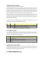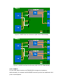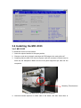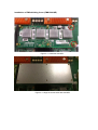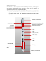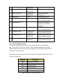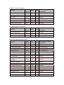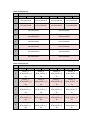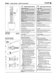
1
User Manual MIC-5333 AdvancedTCA® 40GbE Dual Socket CPU Blade with Intel® Xeon® E5-2600 series EP Processors Revision History Revision Index 1.0 Brief Description of Changes Date of Issue 1st release August 30th, 2012 Copyright The documentation and the software included with this product are copyrighted 2012 by Advantech Co., Ltd. All rights are reserved. Advantech Co., Ltd. reserves the right to make improvements in the products described in this manual at any time without notice. No part of this manual may be reproduced, copied, translated or transmitted in any form or by any means without the prior written permission of Advantech Co., Ltd. Information provided in this manual is intended to be accurate and reliable. However, Advantech Co., Ltd. assumes no responsibility for its use, nor for any infringements of the rights of third parties, which may result from its use. Acknowledgements ATCA and AMC are trademarked by PCI Industrial Computer Manufacturers Group whilst Xeon, QPI and C600-B are trademarked by the Intel Corp. All other product names or trademarks are properties of their respective owners. Product Warranty (2 years) Advantech warrants to you, the original purchaser, that each of its products will be free from defects in materials and workmanship for two years from the date of purchase. This warranty does not apply to any products which have been repaired or altered by persons other than repair personnel authorized by Advantech, or which have been subject to misuse, abuse, accident or improper installation. Advantech assumes no liability under the terms of this warranty as a consequence of such events. Because of Advantech’s high quality-control standards and rigorous testing, most of our customers never need to use our repair service. If an Advantech product is defective, it will be repaired or replaced at no charge during the warranty period. For out-of-warranty repairs, you will be billed according to the cost of replacement materials, service time and freight. Please consult your dealer for more details. If you think you have a defective product, follow these steps: 1. Collect all the information about the problem encountered, for example, Advantech products used, other hardware and software used, etc. Note anything abnormal and list any onscreen messages you get when the problem occurs. 2. Call your dealer and describe the problem. Please have your manual, product, and any helpful information readily available. 3. If your product is diagnosed as defective, obtain an RMA (return merchandise authorization) number from your dealer. This allows us to process your return more quickly. 4. Carefully pack the defective product, a fully-completed Repair and Replacement Order Card and a photocopy proof of purchase date (such as your sales receipt) in a shippable container. A product returned without proof of the purchase date is not eligible for warranty service. 5. Write the RMA number visibly on the outside of the package and ship it prepaid to your dealer. Declaration of Conformity CE This product has passed the CE test for environmental specifications when shielded cables are used for external wiring. We recommend the use of shielded cables. FCC Class A Note: This equipment has been tested and found to comply with the limits for a Class A digital device, pursuant to part 15 of the FCC Rules. These limits are designed to provide reasonable protection against harmful interference when the equipment is operated in a commercial environment. This equipment generates, uses, and can radiate radio frequency energy and, if not installed and used in accordance with the instruction manual, may cause harmful interference to radio communications. Operation of this equipment in a residential area is likely to cause harmful interference in which case the user will be required to correct the interference at his or her own expense. Technical Support and Assistance 1. Visit the Advantech web site at www.advantech.com/support where you can find the latest information about the product. 2. Contact your distributor, sales representative, or Advantech’s customer service center for technical support if you need additional assistance. Please have the following information ready before you call: Product name and serial number Description of your peripheral attachments Description of your firmware version A complete description of the problem The exact wording of any error messages Warnings, Cautions and Notes Warning! Warnings indicate conditions, which if not observed, can cause personal injury. Caution! Cautions are included to help you avoid damaging hardware or losing data, for example, there is a danger of a new battery exploding if it is incorrectly installed. Do not attempt to recharge, force open, or heat the battery. Replace the battery only with the same or equivalent type recommended by the manufacturer. Discard used batteries according to the manufacturer’s instructions. Note! Notes provide optional additional information. Document Feedback To assist us in making improvements to this manual, we would welcome comments and constructive criticism. Please send all such - in writing to: [email protected] Packing List RJ45 to DB9 Console Cable x1, p/n: 1700002270 Mini-USB to USB Console Cable x1, p/n: 1700018550 Warranty certificate document x, p/n: 2190000902 If any of these items are missing or damaged, contact your distributor or sales representative immediately. Safety Instructions This section provides warnings that precede potentially dangerous procedures throughout this manual. Instructions contained in the warnings must be followed during all phases of operation, service, and repair of this equipment. You should also employ all other safety precautions necessary for the operation of the equipment in your operating environment. Failure to comply with these precautions or with specific warnings elsewhere in this manual could result in personal injury or damage to the equipment. Advantech intends to provide all necessary information to install and handle the product in this manual. Because of the complexity of this product and its various uses, we do not guarantee that the given information is complete. If you need additional information, ask your Advantech representative. The product has been designed to meet the standard industrial safety requirements. It must not be used except in its specific area of office telecommunication industry and industrial control. Only personnel trained by Advantech or persons qualified in electronics or electrical engineering are authorized to install, remove or maintain the product.The information given in this manual is meant to complete the knowledge of a specialist and must not be used as replacement for qualified personnel. Keep away from live circuits inside the equipment. Operating personnel must not remove equipment covers. Only factory authorized service personnel or other qualified service personnel may remove equipment covers for internal subassembly or component replacement or any internal adjustment. Do not install substitute parts or perform any unauthorized modification of the equipment or the warranty may be voided. Contact your local Advantech representative for service and repair to make sure that all safety features are maintained. Safety Precaution - Static Electricity Follow these simple precautions to protect yourself from harm and the products from damage. 1. 2. 3. To avoid electrical shock, always disconnect the power from your system chassis before you work on it. Don’t touch any components on the CPU card or other cards while the system is on. Disconnect power before making any configuration changes. The sudden rush of power as you connect a jumper or install a card may damage sensitive electronic components. When unpacking a static-sensitive component from its shipping carton, do not remove the component's antistatic packing material until you are ready to install the component in a computer. Just before unwrapping the antistatic packaging, be sure you are at an ESD workstation, or grounded with an ESD strap. This will discharge any static electricity that may have built up in your body. 4. When transporting a sensitive component, first place it in an antistatic container or packaging. We Appreciate Your Input Please let us know of any aspect of this product, including the manual, which could use improvement or correction. We appreciate your valuable input in helping make our products better. This page is left blank intentionally. Glossary ACPI Advanced Configuration and Power Interface AHCI Advanced Host Controller Interface AMC Advanced Mezzanine Card APIC Advanced Programmable Interrupt Controller ATCA Advanced Telecommunications Computing Architecture BI Base Interface BMC Baseboard Management Controller CMC Carrier Management Controller EHCI Enhanced Host Controller Interface FI Fabric Interface FMM Fabric Mezzanine Module FRU Field Replaceable Unit FW Firmware GbE Gigabit Ethernet HPM Hardware Platform Management IOH I/O Controller Hub IPMC Intelligent Platform Management Controller IPMI Intelligent Platform Management Interface MCH Memory Controller Hub NVRAM Non-volatile Random Access Memory OOS Out Of Service PCH Platform Controllers Hub PCIe PCI Express PECI Platform Environment Control Interface PICMG PCI Industrial Computer Manufacturers Group PXE Pre-boot Execution Environment QPI QuickPath Interconnection RDIMM Registered DIMMs RMCP Remote Management Control Protocol RTM Rear Transition Module RX Receive SAS Serial Attached SCSI SATA Serial Advanced Technology Attachment SCSI Small Computer System Interface SDR Sensor Data Record SerDes Serializer/Deserializer ShMC Shelf Manager Controller SOL Serial Over LAN TCLK Telecom Clock TPM Trusted Platform Module TX Transmit UDIMM Unbuffered DIMMs UHCI Universal Host Controller Interface VLP Very Low Profile XAUI X (means ten) Attachment Unit Interface Chapter 1 Product Overview This chapter briefly describes the MIC-5333. 1.1 MIC-5333 Overview Advantech’s MIC-5333 is a 40G dual processor ATCA blade based on the Intel® Xeon® CrystalForest Server Platform. It enables the highest performance available in the ATCA form factor, with up to 16 cores and 32 threads of processing power, scalable offload based on Intel® QuickAssist® technology, and supports up to four 40G fabric ports. Fast PCI Express gen. 3 lanes running at up to 8Gbps, and best in class virtualization support combined with superior thermal design make it an integrator’s choice for ultra high performance applications and workload consolidation from special purpose processors to Intel® architecture. Two QPI interfaces between the CPUs improve memory and I/O access throughput and latencies when one processor needs to access resources hosted by the other socket. With four DDR3 DIMMs per socket in a quad channel design running up to 1600MT/s, the MIC-5333 not only offers superior memory bandwidth over 3-channel designs, but can also support memory densities up 256GB using latest LR DIMM technology. It outperforms previous generation dual socket designs while keeping similar thermal characteristics with balanced airflow resistance. Intel’s CaveCreek PCH provides power and cost efficient integration standard peripheral interfaces (e.g., PCI Express, SATA, USB, etc.) along with Intel® QuickAssist® hardware acceleration. QuickAssist hardware acceleration and offload can be scaled by adding additional CaveCreek devices via Fabric Mezzanine Modules (FMMs) on the blade or an attached Rear Transition Module (RTM). Fabric connectivity is implemented using up to two FMM type I sites, each site connecting to two backplane fabric channels. This allows the MIC-5333 to scale from legacy 10GE to high speed 40GE network interfaces as well as optional dual dual star support for the most demanding applications in high end data and enterprise networking utilizing 4 hub blades per system. A variety of Advantech standard FMMs can be used to implement,10GBaseKR & 40GBaseKR4 interfaces. Beyond that, a Fabric Mezzanine Module type II socket with PCIe x8 connectivity provides extension possibilities for additional front port I/O, offload and acceleration controllers such as Intel® QuickAssist accelerators, IPSec offload engines or customer specific logic. FMMs not only have higher PCI Express bandwidth than AMCs, but also integrate well in terms of thermal design, cost and board real estate when compared to Advanced Mezzanine Cards. This unmatched flexibility combined with the highest performance Intel® Xeons available make the MIC-5333 equally well suited for application and data plane workloads. The onboard IPMI firmware based on Advantech’s IPMI core just offers greater modularity and flexibility for the customization of system management features, and also provides the framework for added value features enhancing Reliability, Availability, Serviceability, Usability and Manageability (RASUM) of the product. HPM.1 based updates are available for all programmable components (BIOS, BIOS Settings, IPMC firmware, FPGA) including rollback support. Advantech’s IPMI solution, combined with an optimized UEFI BIOS continues to offer advanced features used on previous generation MIC-532x blades, such as Dynamic Power Budgeting, BIOS redundancy, Real Time Clock Synchronization, CMOS Backup, CMOS Override and MAC Mirroring. Advantech IPMI firmware has been tested for CP-TA compliance using the Polaris Networks ATCA Test Suite, and against a variety of AdvancedTCA shelf management solutions. Figure 1.1 MIC-5333 Overview (Top Side) 1.2 Block Diagram The hardware implementation is shown in the following block diagram. Refer to Table 1.1 (next page) for the detailed product technical specification. Figure 1.2 MIC-5333 Block Diagram 1.3 Product Configurations Model Name MIC-5333S42-P1E MIC-5333S42-P2E MIC-5333S12-P1E MIC-5333S12-P2E Configurations MIC-5333 with dual Intel® Xeon® E5-2658 CPU, with Cave Creek SKU4, , no FMM, no memory, no MO-297 SSD MIC-5333 with dual Intel® Xeon® E5-2648L CPU, with Cave Creek SKU4, no FMM, no memory, no MO-297 SSD MIC-5333 with dual Intel® Xeon® E5-2658 CPU with Cave Creek SKU1, no FMM, no memory, no MO-297 SSD MIC-5333 with dual Intel® Xeon® E5-2648L CPU with Cave Creek SKU1 no FMM, no memory, no MO-297 SSD Table 1.1 MIC-5333 Configurations , 1.4 Related Products Model Name Configurations RTM-5106 ATCA RTM for MIC-5333 with eight SFP+ interfaces FMM-5001BE Dual 10GE Module with 2x fabric ports for dual dual star support based on i82599EB FMM-5001FE Dual 10GE Module with 2x SFP+ front IO based on i82599ES FMM-5001QE Quad Intel® 82599ES for 2x quad 10G FI support FMM-5004ME Dual Mellanox CX3 for 2x 40GBase-KR4 FI support FMM-5002E Server Graphics Module with external VGA Port FMM-5006E Intel PCH Cave Creek SKU4 with Quick Assist Accelerator support. Table 1.2 MIC-5333 Related Products Note: Contact Advantech for information on available and future RTMs and FMMs. Chapter 2 Board Features This chapter describes the MIC-5333 hardware features. 2.1 Technical Data Processor System CPU Dual Intel® Xeon® E5-2648L/E5-2658 8-core processors(1) Max. Speed 2.1GHz Chipset Intel Cave Creek (SKU1 and SKU4) BIOS Dual 64-Mbit BIOS firmware flashes with AMI UEFI based BIOS QPI 8.0 GT/s Technology Memory Four channel DDR3 1066/1333/1600MHz SDRAM (72-bit ECC Un-/ Registered), LR DIMM support Max. Capacity Configurable up to 256 GB Socket 8 VLP DIMMs 4/8 x 10GBaseKR with dual star backplane topology supported ( via Zone 2 Fabric interface FMM-5001Q) 2/4 x 40GBaseKR4 with dual star backplane topology supported (via FMM-5004M) Base interface Front I/O Interface Operating Serial (COM) Watchdog Timer FMM 2 x 16C550 compatible Serial Ports (1 RJ-45 connector, 1 mini-USB connector) Ethernet 2 x 10/100/1000BASE-T through PCIe based i350 MAC/PHY USB 2.0 2 x Type A ports Compatibility WindRiver PNE/LE 4.2, RedHat Enterprise 5.7 & 6.2, CentOS 6.1, Windows Server 2008 64bit System IPMC i350 GbE MAC/PHY supporting two 10/100/1000Base-T ports BMC Controller NXP LPC1768 (Cortex M) IPMI Compliant with IPMI 2.0 using Advantech IPMI code base Supervision 1 for x86 BIOS POST, OS Boot, Application Interval IPMI compliant Site 1 FMM type II socket, 2 FMM type I sockets Interface FMM type I: 2 x PCIe x8 from CPU socket 0 and 1 FMM type II: 1x PCIex8 from CPU socket 1 Miscellaneous Storage 2 x MO-297 SSD Real Time Clock Built-in Configuration 2 x E5-2658 or E5-2648L 95W, 128GB memory, FMM-5001Q, FMM-5001F, 2x 64GB MO-297 SSDs Power Consumption *283W for E5-2658(real measurement for) 242.8 W for E5-2648L(Real Measurement) Requirement Test Programs: TDISK.sh, LAN_FN.sh, PTU Gen, Memorytester OS: Red Hat Enterprise Linux 6.2 64bit Zone 3 (RTM) RTM Advantech common RTM interface Type 2 Interface 2 x PCIex16, 1x PCIex4(DMI), 2 x USB, , 1x COM, 2 x SGMII Physical PCB Dimensions 6HP, 280.00 x 322.25 mm (11.02" x 12.69") (W x D) Characteristics Weight 3.275kg Environment Operating Non-operating Temperature 0 ~ 55° C (32 ~ 131° F) - 40 ~ 70° C (-40 ~ 158° F) Humidity 5 to 93%@40°C (non 95% @ 40° C (non-condensing) condensing) Shock 4 G each axis 20 G each axis Vibration (5~500Hz) 0.5 Grms 2.16 Grms, 30 mins each axis Environment Compliance ETSI EN300019-2-1 Class1.2, EN300019-2-2 Class 2.3, ETSI EN300019-2-3 Class 3.1E, Designed to meet GR63-CORE PICMG 3.0 R3.0, 3.1 R1.0, HPM.1 Safety , UL60950-1/CSAC22.2 EMC FCC47 CFR Part15, Class A, CE Mark (EN55022 / EN55024 / EN300386), Designed to meet GR1089-CORE Table 2.1 MIC-5333 Technical Data Note: 1. MIC-5333 supports 2 x 95W CPUs. Special system airflow requirements apply. MIC-5333 will be compliant to PICMG3.1 R2.0 when released. 2.2 Product Features 2.2.1 Processors The MIC-5333 supports dual Intel® Xeon® E5-2600 series processors, using the latest 32nm silicon architecture with a built-in memory controller. It is a two-chip platform (CPU and PCH) as opposed to a traditional three-chip platform (CPU, MCH and IOH). The Intel® Xeon® E5-2600 series feature (per socket) two Intel® QuickPath Interconnect point-to-point links capable of up to 8.0 GT/s, up to 40 lanes of Gen 3 PCI Express links capable of 8.0 GT/s, and 4 lanes of DMI2/PCI Express Gen 2 interface with a peak transfer rate of 5.0 GT/s. The processor supports up to 46 bits of physical address space and 48-bit of virtual address space. It is also capable of supporting up to 4 channels DDR3 DIMM memory, supporting both UDIMMs and RDIMMs (for more details about DDR3 DIMM supported specification, please refer to section 2.3). The currently supported processors on the MIC-5333 are listed on table 2.2: Model Cores/Threads Frequency L3 cache DDR3 support TDP Socket Xeon E5-2648L 8C/16T 1.80 GHz 20 MB DDR3-1600 70 Watt LGA2011 Xeon E5-2658 8C/16T 2.10 GHz 20 MB DDR3-1600 95 Watt LGA2011 Table 2.2 MIC-5333 Supported Processors List The E5 series Xeon processors support cache memory as listed below: A 32-KB instruction and 32-KB data first-level cache (L1) for each core. A 256-KB shared instruction/data mid-level (L2) cache for each core. Up to 20 MB last level cache (LLC): up to 2.5 MB per core instruction/data last level cache (LLC), shared among all cores. 2.2.2 Platform Controller Hub (PCH) Intel’s CaveCreek PCH provides power and cost efficient integrated standard peripheral interfaces (e.g., DMI Gen1, 4x PCIe Gen1 root ports, 2x SATA 3Gb/s, 6x USB 2.0, and supports four internal GbE MAC) (MIC-5333 uses 2 for SGMII interface to Zone3) as well as Intel® QuickAssist® hardware acceleration and offload. For more details, please refer to section 2.3. 2.2.3 DMI Gen1 Direct Media Interface (DMI) is the chip-to-chip connection between the processor and PCH. This high-speed interface integrates advanced priority-based servicing allowing for concurrent traffic and true isochronous transfer capabilities. Base functionality is completely software transparent, permitting current and legacy software to operate normally. For the CaveCreek chipset, the DMI interface operates at 2.5 GT/s. 2.2.4 PCI Express Port Configuration Intel® Xeon® E5-2600 series processors support 40 PCI Express Gen3 ports. On the MIC-5333, each processor is configured to one x16 port and three x8 ports/. The PCI Express interface is connected for FMM and RTM use. CPU Port No. Width 0 1 Description 0 x4 Connection for DMI between the CPU and PCH 1 x8 connected to FMM2-1 (to Fabric Interface Channel 1/2) 2 x16 For RTM use, connected to Zone 3 3A x8 connected to FMM1-1 (to Fabric Interface Channel 3/4) 3C x8 Connected to PCH 0 x4 For RTM use, connected to Zone3 (reserved) 1 x8 connected to FMM2-2 2 x16 For RTM use, connected to Zone 3 3A x8 connected to FMM3 3C x8 connected to FMM1-2 Table 2.3 PCI Express Port Configuration on the MIC-5333 2. Note: PCIe hot swap is not supported for graphic controllers (e.g. FMM-5002E) installed on a RTM. 2.2.5 Redundant BIOS Flash The MIC-5333 has two SPI flash devices for storing redundant x86 firmware (BIOS, BIOS configuration, etc.). The integrated management controller (IPMC) controls which flash device is active. Failover and rollback operations between the flash devices are compliant to HPM.1. By default, the MIC-5333 starts to boot from the active BIOS chip, and will switch to the backup BIOS chip if it detects a problem, such as the BIOS is stuck in POST or fails to boot. For more details, please refer to Chapter 5, about AMI BIOS setup. From an OS point of view, there is only one active BIOS SPI flash visible at any time. 2.2.6 Serial ATA Controller The MIC-5333 supports a total of 2 SATA lanes. In the legacy interface, there are two modes of operation to support different operating system conditions. In the Native IDE enabled operating system the PCH utilizes two controllers to enable all six ports of the bus. The first controller supports ports 0-3 and the second controller supports ports 4 and 5. In AHCI mode, only one controller is utilized, enabling all six ports, and the second controller will be disabled. Since the built-in Serial ATA (SATA) controller in the Intel® CaveCreek PCH is used to support only 2 ports, only one controller is utilized to support both ports 4 and 5 in each mode: the first controller is enabled in AHCI mode, while the second controller is enabled in Native IDE mode. On the MIC-5333, SATA 3Gbps support is available on PCH Ports 4 and 5, and reserved for onboard MO-297 SSD storage modules. Port No. Speed Description 4 3Gbps on board MO-297 storage module (optional) 5 3Gbps on board MO-297 storage module (optional) Table 2.4 SATA Port Configuration on the MIC-5333 2.2.7 USB Controller In the Intel® CaveCreek PCH there are 6x USB ports, controlled through Enhanced Host Controller Interface (EHCI) for USB 2.0 high speed support. The USB port connection in the MIC-5333 is listed in table 2.6. Port No. Description 0-1 Front Panel Ports 2-3 USB devices on an RTM (connected to Zone 3) 4-5 Not used Table 2.5 USB Ports on the MIC-5333 2.2.8 Real-time Clock (RTC) Because there is no battery installed on the MIC-5333, the integrated real-time clock is fed by IPMC management power. Due to the on-board super cap, the date and time can be kept for up to 2 hour periods of power loss 2.3 DDR3 DIMM Memory 2.3.1 Memory Characteristics The MIC-5333 uses DDR3 VLP SDRAM. As shown in Figure 2.1, each CPU uses 4 channels on the MIC-5333, and each channel supports one un-buffered/registered ECC VLP DIMM, for a total of 8 sockets. Supported memory characteristics on the MIC-5333 are listed on table 2.7. Figure 2.1 DIMM slots on the MIC-5333 DIMM Type Size RDIMMs UDIMMs 2GB, 4GB, 8GB, 16GB and 2GB, 4GB and 8GB 32GB Speed Ranks 1066 / 1333 / 1600 SR, DR, QR (only for LRDIMMs 8GB, 16GB and 32GB 1066 / 1333 SR, DR 1066/1333) QR Table 2.6: Supported DIMM Configurations 3. Note: 2G, 4G and 8GB DDR3 DRAM technologies are supported for these devices: UDIMMs x8, x16 RDIMMs x4, x8 LRDIMMs x4, x8 Up to 4 ranks supported per memory channel: 1, 2 or 4 ranks per DIMM. Supports a maximum of 256GB DDR3-1600 memory. At time of manual publication, Advantech has tested 16GB DDR3-1600 RDIMMs. 2.3.2 RAS Mode Four DRAM RAS modes are supported by the memory controller which can be configured in BIOS setup menu. Independent Channel Mode (Default) Channels can be populated in any order in Independent Channel Mode. All four channels may be populated in any order, and have no matching requirements. All channels must run at the same interface frequency, but individual channels may run at different DIMM timings (RAS latency, CAS latency, etc.). Rank Sparing Mode In Rank Sparing Mode, one rank is a spare of the other ranks on the same channel. The spare rank is held in reserve and is not available as system memory. The spare rank must have identical or larger memory capacity than all the other ranks (sparing source ranks) on the same channel. After sparing, the sparing source rank will be lost. Mirrored Channel Mode In Mirrored Channel Mode, the memory contents are mirrored between Channel 0 and Channel 2 and also between Channel 1 and Channel 3. As a result of the mirroring, the total physical memory available to the system is half of what is populated. Mirrored Channel Mode requires that Channel 0 and Channel 2, and Channel 1 and Channel 3 must be populated identically with regards to size and organization. DIMM slot populations within a channel do not have to be identical but the same DIMM slot location across Channel 0 and Channel 2 and across Channel 1 and Channel 3 must be populated the same. Lockstep Channel Mode In Lockstep Channel Mode, each memory access is a 128-bit data access that spans Channel 0 and Channel 1 and Channel 2 and Channel 3. Lockstep Channel mode is the only RAS mode that allows SDDC for x8 devices. Lockstep Channel Mode requires that Channel 0 and Channel 1, and Channel 2 and Channel 3 must be populated identically with regards to size and organization. DIMM slot populations within a channel do not have to be identical but the same DIMM slot location across Channel 0 and Channel 1 and across Channel 2 and Channel 3 must be populated identically. 4. 5. Note: The memory channel mode can be configured in BIOS setup menu, described in Chapter 5, AMI BIOS Setup. 6. Regarding the correct installation of memory modules, please refer to Section 3.2, Memory for further details. 2.4 Ethernet Interface 2.4.1 Base Interface The MIC-5333 uses an Intel® i350-AM4 LAN controller, connected to the CaveCreek PCH through a PCIe x4 interface to provide dual GbE ports for the Base Interface. The Intel® Ethernet Controller I350 is a single, compact, low power component that supports quad port and dual port gigabit Ethernet designs. The device offers four fully-integrated gigabit Ethernet media access control (MAC), physical layer (PHY) ports and four SGMII/SerDes ports that can be connected to an external PHY. The I350 supports PCI Express* (PCIe v2.1 (2.5GT/s and 5GT/s)). The device enables two-port or four port 1000BASE-T implementations using integrated PHY’s. The MIC-5333 also supports PXE boot and SoL (Serial-over-LAN) over the Base Interface channels. PXE boot can be enabled with “Launch PXE OpROM” through the BIOS setup menu (see Section 5.4., Advanced BIOS Features Setup). Information about the PXE expansion ROM configuration is also provided in this section. The Intel i350 controller supports side-band functionality. This side-band interface (NC-SI) is used by the IPMC to establish LAN sessions, to enable RMCP/RMCP+ based communication to the management part. See Section 4.6, Serial-over-LAN for details on setting up connections to the BMC. 2.4.2 Fabric Interface The fabric connectivity of MIC-5333 is implemented using a FMM (Fabric Mezzanine Module) concept. This allows the MIC-5333 to scale from legacy 10GE to high speed 40GE network interfaces. For a standard dual star topology, the traffic from Fabric Interface channel 1 and 2 goes to the CPU through FMM #2. To implement a dual-dual star topology, additional fabric channels (3 and 4) can be supported by installing a FMM-5004M or FMM-5001B on the FMM #1, for 40GE or 10GE network interface, respectively. 2.4.2.1 40GE FI For the 40GE fabric interface, two kinds of FMM solutions are offered: one is the FMM-5001Q, using quad Intel® 82599ES controllers to provide four 10GBaseKR for each Fabric Interface channel 1 and 2. FI#1 0 1 FI#2 2 3 0 1 2 3 KR Routing 1 0 Niantic 1 0 1 Niantic 3 0 1 Niantic 2 0 1 Niantic 4 PCIe x8 CPU 0 CPU 1 Figure 2.2 40GE Dual Star Solution #1 (MIC-5333+FMM-5001Q) The other is the FMM-5004M, using Mellanox ConnectX®-3 EN controllers to provide dual 40GBaseKR4 interface to the fabric interface. Figure 2.3 40GE Dual Star Solution #2 (MIC-5333+FMM-5004M) Figure 2.4 40GE Dual Dual Star Solution (MIC-5333+2x FMM-5004M) 2.4.2.2 10GE FI For the 10GE fabric interface, the FMM-5001B is designed to implement thisfunctionality. An onboard Intel® 82599EB controller provides two additional XAUI ports to the backplane. Figure 2.5 10GE Dual Star Solution (MIC-5333+FMM-5001B) Figure 2.6 10GE Dual Dual Star Solution (MIC-5333+2x FMM-5001B) Below is the summary of the MIC-5333 Fabric Interface options: Ethernet Interface per channel Topology 40G 4x KR Dual Star 40G KR4 Dual Star FMM #1 FMM #2 FMM-5001Q -- FMM-5004M 40G KR4 Dual-Dual Star FMM-5004M FMM-5004M 10G XAUI Dual Star -- FMM-5001B 10G XAUI Dual-Dual Star FMM-5001B FMM-5001B Table 2.7: MIC-5333 Fabric Interface Options The MIC-5333 Fabric Interface supports PICMG 3.1 Option 1 or 9. 2.4.3 I/O Ethernet Interface There are two RJ-45 I/O LAN ports on the MIC-5333 front panel, which are implemented using an Intel® i350-AM4 quad port GbE controller. Interface Connection Base Interface Backplane Chip Intel® i350-AM4 Ports 0, 1 Media Speed PXE/SoL Copper 10/100/1000 Mb/s 9 Quad Intel® 82599 Fabric Interface Backplane or Mellanox CX-3 KR or KR4 10/40 Gb/s (via FMM) I/O Interface Front Panel Intel® i350-AM4 Ports 2, 3 Copper 10/100/1000 Mb/s 9 Table 2.8: Ethernet Interface Link Speed Configuration For further information regarding the front panel I/O LED description, please see chapter “3.4.6 LED Definition” 2.5 Zone 3 Interface (RTM) The MIC-5333 supports the following connectivity to an optional RTM through the zone 3 interface (please refer to the Appendix E, Zone 3 Interface (RTM) pin-out): 2x PCI Express x16 (From CPU0, CPU1) 1x PCI Express x4 (From CPU1_DMI) 2x USB 2.0 (From PCH) 1x COM (From FPGA) RTM Link (From FPGA) 2 x SGMII (From PCH) The rear transition module (RTM) is used to provide additional I/O expansion for the main CPU board. It is managed with an on-board MMC, and is fully hot swappable. Customers may use the standard Advantech RTM-5104, or request acustomized RTM (for more information, please contact your local Advantech representative).. For detailed specifications of the RTM-5104, please refer to table 2.9. For the detailed pin definition of the Zone 3 interface, please see Appendix E, Zone 3 Interface (RTM) pin-out. Model Name Storage USB LAN COM RTM-5106S00E N/A N/A 8 x SFP+ N/A FMM Support N/A Table 2.9: Advantech RTM-5104 Specifications 7. Note: Please contact your local Advantech representative for more information about the RTM-5104. 2.6 Fabric Mezzanine Module (FMM) The FMM board is used to provide an option to expand the feature set, of both the main CPU board and RTM board. It is managed by the main board’s IPMC or RTM board’s MMC, but does not support hot-swap functionality. FMM site #1 st #2 nd st #3 nd PCIe width 1 PCIex8 2 PCIex8 1 PCIex8 2 PCIex8 PCIex8 PCIe source CPU0 CPU1 CPU0 CPU1 CPU1 Table 2.10 FMM PCIe Source on the MIC-5333 The MIC-5333 supports 3 FMM sites to provide the most flexibility. The FMM-5001Q, a double-sized FMM, uses four Intel® i82599 controllers, andprovides two fabric interfaces with four 10GBaseKR ports each. The other option to deploy the MIC-5333 with 40G technology is by using the FMM-5004M, which uses Mellanox CX-3 EN controllers to provide dual 40GBaseKR4 interfaces. Model Name Description FMM-5001Q Four 10GBaseKR FI Chip FMM #1 FMM #2 Quad Intel® 82599ES V V FMM-5004M 40GBaseKR4 FI Mellanox CX-3 V FMM-5001B Intel® 82599EB V 10GBaseKX4 and XAUI FI Table 2.11: Advantech FMM-5000 Series Configuration at Fabric Site For the front panel, customers may choose from the following Advantech FMM-5000 options, or request a customized FMM For detailed Advantech standard product FMM specifications, please refer to table 2.12. Model Name Description FMM-5001F Dual 10GE Module with 2x SFP+ front IO FMM-5002 Server Graphic Support for Debug/Bring Up FMM-5006 QuickAssist Accelerator FMM Chip I/O Intel® 82599 2x SFP+ SM750 1x VGA port Intel® CaveCreek N/A Table 2.12: Advantech FMM-5000 Series Configuration on the front panel FMM #3 Site Chapter 3 Installation This chapter describes the procedure to install the MIC-5333 into a chassis. Peripherals (DIMMs, SSD) installation, jumper settings, and LED definitions are also described here. 3.1 Processor The MIC-5333 is shipped with two CPUs and heat sinks installed from the factory Please do not attempt to remove the heat sinks, or the cooling performance will be affected. Tampering with the heat sinks will result in a loss of warranty. 3.2 Memory 3.2.1 Requirement As described in Section 2.3, DDR3 DIMMs, the MIC-5333 supports 8 x DDR3 VLP (very low-profile, 0.72inch; 18.29mm) un-buffered/registered ECC SDRAM DIMMs. To allow proper MIC-5333 functionality, please comply with population requirements when installing memory modules: Mixing of Registered and Unbuffered DIMMs is not allowed. To optimize the memory performance by balanced sharing the load on each channel of a socket, Advantech requires the use of identical memory modules, with the same density, rank, speed, timing parameters, and other factors. Although unbalanced configurations might work, they are not supported by Advantech. For supported memory characteristics, please refer to Table 2.7, Supported DIMM Configurations. 3.2.2 Memory Installation Please review the following procedures for memory installation: CPU0 CH H1 CPU U0 CH0 CPU0 CH H2 CPU1 1 CH0 CPU U0 CH3 CPU1 CH3 CPU1 CH1 CPU1 CH2 C Fig gure 3.1 MIC-5333 DIMM M Slots Overvview 1. Open the ejector e on th he empty DIIMM sockett where you want to insstall the DIM MM. 2. Insert the memory m mo odule into the t empty slot. s Please e align the notches on n the module with the socke et keys. 3. Push the module m into socket s until the ejectorrs firmly lock. 4. Repeat steps 1~3 for the t remainin ng modules s to be popu ulated. 5. Install the MIC-5333 into the chassis and boot the bo oard, checkking thatthe e full memory qu uantity show wn in the BIOS menu is correct. (See ( Sectio on 3.3, Con nsole Terminal Setup and Se ection 3.4, Installing th he MIC-5333 3) To remove r DIM MM moduless, please fo ollow the ins structions lissted below: 1. Remove th he MIC-53 333 from the t chassis s. (See Se ection 3.4, Installing the MIC-5333) D to rem move, and push p the DIIMM ejectorr on each side of the DIMM 2. Select the DIMM socket outw ward simulta aneously. The T module shall pop out o by itself. e of the empty DIMM D socke et. 3. Close the ejectors 4. Repeat steps 2, 3 for the t remainin ng modules s to be remo oved. 3.3 3 Cons sole Te erminall Setup p The e MIC-5333 contains fiive serial in nterfaces lis sted below. More deta ails about setup will described through t an example, to t show how w to configure the MIC C-5333 con nsole with h the following example e sections. COM1 (RJ45) on the front panel COM2 (miniUSB) on the front panel Serial-over-LAN, SoL (via I/O or BI Ethernet interface) UART1 routed to Zone 3 3.3.1 UART Multiplexer The UART multiplexer can be set to route the console to any of the connections mentioned above. By default the UART multiplexer is set to automatic mode. This means that the mux will automatically switch to the connection except for SOL, where an input character needs to be received. The UART multiplexer switch can also be set via OEM command, please refer to Appendix B, Advantech OEM IPMI Command Set for details. For example, when a RJ45 to DB9 cable is plugged into the MIC-5333, by detecting a character entered through the cable, the UART multiplexer will automatically bridge the console to the terminal PC through this interface. Once another mini-USB cable is connected and the user enters any character, the multiplexer will then switch the output to this interface, as this is the latest request. The previous RJ45 link will consequently become disconnected. RJ45 Step1. The user establishes a console link through any available output (e.g. RJ-45) miniUSB SoL UART MUX UART1 Zone3 Step2. When the user plugs another console RJ45 cable into the MIC-5333, (e.g. miniUSB), the UART MUX will switch the output from RJ45 to this new interface (last in, first serve rule) miniUSB SoL UART MUX UART1 Zone3 Step3. The original link (RJ-45) becomes RJ45 disconnected X miniUSB SoL UART MUX UART1 Zone3 Figure 3.2 UART Multiplexer Switching Mechanism RJ45 (COM1) For a terminal PC to connect to the console function on the MIC-5333 with a RJ45 to DB9 cable, no additional driver is needed. Pin Number Definition Pin Number Definition 1 TX+ 7 NC3 2 TX- 8 NC4 3 RX+ 9 PTH_1 4 NC1 10 PTH_2 5 NC2 11 NPTH_1 6 RX- 12 NPTH_2 Prerequisite: RJ45 to DB9 cable(Advantech P/N; 1700002270) mini-USB (COM2) The MIC-5333 uses a USB-to-UART bridge called CP2102-GM from Silicon Labs® to convert data traffic between USB and UART formats. This chip includes a complete USB 2.0 full-speed function controller, bridge control logic, and a UART interface with transmit/receive buffers and modem handshake signals. For a terminal PC to connect to the console function on the MIC-5333 with a mini-USB to USB cable, the CP2102 driver is available for download from Silicon Labs® website (hyperlink below), and must be installed on the terminal PC. The PC can, for example, run a Linux 2.4 or 2.6 kernel or Windows XP). The miniUSB port is bus powered (i.e. powered by the terminal PC) and the COM port will not be lost when power cycling the blade or ATCA system. Prerequisite: Commercial mini-USB to USB cable (Advantech P/N: 1700018550) CP2102 driver (needed to be installed on the terminal PC before using the console), please download from https://www.silabs.com/products/interface/usbtouart/Pages/default.aspx Serial-over-LAN, SoL User may also establish the console via SoL function, which is described in section 4.6, Serial-over-LAN (SoL). Prerequisite: RJ45 Ethernet cable and IPMItool (see section 4.6.2.1 IPMItool) Note: When SoL is used as the console terminal, please skip Section 3.3.2 and 3.3.3. UART1 & UART2 (Zone3) The MIC-5333 connects two UART interfaces to the Zone 3. To establish the console link through the RTM, please refer to the RTM user manual. 3.3.2 Terminal Emulator A terminal emulator application must be available on the terminal PC in order to access the console screen. If your terminal PC runs on Microsoft Windows, a common application that can act as a client for the SSH, Telnet, rlogin, and raw TCP protocols called PuTTY can be installed and used. PuTTY was originally written for Microsoft Windows; however, it has also been ported to various Unix-like operating systems. It is available as open source software for download from the internet. 3.3.3 PuTTY Configuration Assuming both the CP2102 driver and PuTTY have been installed successfully on the terminal PC with Microsoft Windows, the user can check the COM port (UART) number under “COM and LPT” in the “Device Manager”, which can be accessed by entering the “Control Panel” followed by opening up “System” and then “Hardware”. Let us assume the CP210x USB to UART Bridge Controller has been assigned with “COM12”. You can open up PuTTY and begin the configuration as shown below. If you use the RJ45 (COM1) and a serial port on the terminal PC, please use the COM port number of that serial port instead of “COM12”. Specify COM12 under serial line and 115200 for speed, no parity, no flow control. Check Serial for connection type. Click the “Open” button and a PuTTY terminal screen will appear. Figure 3.3a PuTTY Configuration Figure 3.3b PuTTY Configurations If the connection is successful and the user enters BIOS setup menu, upon boot the MIC-5333 BIOS setup menu will be displayed on the PuTTY screen. Figure 3.4 MIC-5333 BIOS setup menu shown on PuTTY screen 3.4 Installing the MIC-5333 3.4.1 MIC-5333 To install MIC-5333 into the chassis: 1. Leave the ejector handles in the open position. 2. Choose a node slot in chassis, and align the PCB edge to the card guide rail.* 3. Carefully slide the MIC-5333 into the system until the connector contacts start to mate into the backplane. Make sure the front panel alignment pin falls into the receptacle. Retaining Thumbscrews Figure 3.5 Alignment pin slides into the receptacle 4. Hold both handle ejectors on either side of the board, and then close them to make the board becomes fully seated. Make ensure the handles are latched securely. 5. Fasten the retaining thumbscrews on either side of the MIC-5333 blade. 6. The blue hot-swap LED on the front panel will show a “ONÆBlinkÆOFF” transition to indicate a normal power-on sequence of the MIC-5333. Once the finrmware and payload has been successfully activated, the PICMG 3.0 LEDs will be shown as below: Out of Service Health Hot swap Table 3.1 PICMG3.0 LEDs Definition All the LEDs status shown on the front panel is listed in Section 3.6, Jumper Setting & LED Definition. Note: Regarding the slot information, please refer to the backplane/chassis manual The MIC-5333 also supports hot-swap, i.e. no need to turn off the chassis power before installing the board. To extract the MIC-5333 from the chassis: 1. Unlock the ejector handle at the bottom side, next to the FMM bay. 2. The extraction request will be delivered to the IPMC. The IPMC will perform a graceful shutdown of the ACPI aware operating system. The blue hot-swap LED will start blinking once the ejector handle is unlocked. 3. After the x86 subsystem on the blade has been powered down, the blue hot-swap LED will light up, which indicates the board is ready to be removed. 4. Unfasten the retaining thumbscrews. 5. Unlock the other handle, and fully open both handles (pushing both handles outwards) to extract the board. 6. Pull the MIC-5333 out of the chassis. Figure 3.6 Unlock the ejector handle Caution! DO NOT attempt to extract the board when the blue LED is off or blinking. This may cause non-recoverable damage to the board. 3.4.2 FMM The MIC-5333 supports three FMM sites for feature flexibility and expansion, such as 40G/10G FI option, VGA output, and Intel® QuickAssist support (for details, please refer to table 2.10). This chapter assumes that the MIC-5333 is shipped with the FMM installed. Mounting instructions are provided here to support customer development, as well as in-house RMA and repair. For installation of the FMM, please follow the below procedures: 1. Locate the appropriate FMM1, FMM2, or FMM3 site on the blade, depending on which FMM site you wish to populate (refer to figure 3.9) and make sure the module and the carrier connectors are aligned. Insert the FMM module until the connector is firmly seated in the socket. 2. Install the screws (refer to figure 3.10), and power on the MIC-5333 to make sure the installation is completed. 3. To remove the FMM, follow the procedure in reverse. Installation w/ screws on the MIC-5333 Figure 3.7 FMM Module top (left) and bottom (right) views FMM Module FMM Module Storage Module FMM Module Figure 3.8 MIC-5333 w/ FMM module and Storage Module locations Figure 3.9 Locate the appropriate FMM site on the blade Figure 3.10 Install the screws Installation of EMI shielding Cover (FMM-5001QE) Figure 3.11 Install the standoffs Figure 3.13 Align the screw holes with standoffs Figure 3.14 Install the screws Installation of EMI shielding Cover (FMM-5001FE) Figure 3.15 Install the standoffs Figure 3.16 Align the screw holes with standoffs Figure 3.17 Install the screws 3.4.3 RTM (Optional) For installation of the RTM, please refer to the RTM user manual. Please make sure that the RTM used in conjunction with the MIC-5333 is compliant. Please contact your Advantech representative to obtain a list of compliant RTMs (the current compliant RTM at the time of publication is the RTM-5106). 3.4.4 Storage (Optional) Dual MO-297 Solid State Drive (SSD) modules are available to be installed on the MIC-5333. It is an option installed by customer request, and the MIC-5333 will need to be installed with a specific daughter board and bracket from the factory. This chapter assumes that the MIC-5333 is shipped with the storage module installed. Mounting instructions are still provided here to support customer development, as well as in-house RMA or replacement. For installation of the storage module, please follow the below procedures: 1. Loosen the screws as marked below and remove them on the storage module. 2. Extract the MO-297 SSD gently. If the user needs to remove the 2nd MO-297 as well, repeat step 1 and 2 again. 3. To install the SSD, insert the MO-297 module until the golden fingers are firmly seated in the socket. 4. Install the module on the MIC-5333 then fasten the screws. To obtain a list of compliant SSDs, please contact your Advantech representative 3.4.5 Front Panel The MIC-5333 is 100% compatible to AdvancedTCA specifications. All LED signals are shown on the front panel. Users can refer to section 3.6, “LED definition” to understand the details of the board operating status. Button1 and 2 are reserved for customization. Button1 is set as a reset function by default, while Button2 is not assigned. Users can define the functions for each. For details, please contact your Advantech representative to obtain further information. Retaining Thumbscrews Handle (Top side) FI Channel 1/2/3/4 Status LEDs BI Channel 1/2 Status LEDs Dual Color User LEDs OOS LED Health LED Button2 (Reserved) Button1 (Reserved) USB2 USB1 COM2 (miniUSB) COM1 (RJ45) LAN2 LAN1 Hot Swap LED FMM Bay Handle (Bottom side) Retaining Thumbscrews Figure 3.11 MIC-5333 Front Panel Configuration 3.4.6 LED Definition This section describes how to identify the system operating status via LED signals from the front panel. Before starting, please refer to table 3.2 to learn the LED signal identification in this manual. In the following section, we will use amber as an example: Display Status Bright … Blink Off Table 3.2 LED Signal Identification LED Name Function Display 4x KR interface all link FI port (FMM-5001Q) 1/2 Speed/Link/ Active … 4x KR interface all Active Not all of 4x KR interface link … Not all of 4x KR interface Active No Link 40Gb/s Link FI port 1/2/ Speed/Link/ (FMM-5004M) 3/4 Active … 40Gb/s Active 10Gb/s Link … 10G Active No Link 10Gb/s Link FI port 1/2/ Speed/Link/ (FMM-5001B) 3/4 Active … 10Gb/s Active 1Gb/s Link … 1G Active No Link S BI port 1/2 Speed BI Port 1/2 L USR Status 1/2/3 /4 BI port 1/2 Link / Active N/A 1Gb/s 100Mb/s 10Mb/s Link … Active No Link User defined User defined 1Gb/s Speed LAN Port 100Mb/s 10Mb/s 1/2 Link Link/Active … Active No Link Out of System out of service Service System normal FW active, payload enabled Health Status … FW active, payload disabled FW is not active Board is not activated (ready to be swapped) Hot swap … Board is de-/activating, unsafe to swap Board is active, unsafe to swap Table 3.3 LED Definition Note: FI channel 3 and 4 support is optional, and only active when populating the board with the FMM-5004ME(40G version) or FMM-5001BE(10G version) of the n FMM site #1 on the MIC-5333. 3.4.7 Jumper Settings This section describes the jumper definition users should not need to accessor Jumper JP1 JP6 Feature of the MIC-5333 f. In normal operation, or modify jumpers. Setting Operation 1-2 Closed Normal Mode (Default) 2-3 Closed Clear CMOS Clean CMOS GND Connection 2-3 Closed 1-2 Closed Table 3.4 Jumper Settings Shelf GND open to logic GND (Default) Shelf GND short to logic GND JP1 JP6 Figure 3.12 Jumper Locations Chapter 4 Hardware Management This chapter describes the IPMC firmware features. 4.1 Intelligent Platform Management Controller The term “Intelligent Platform Management Controller” (IPMC) describes an IPMI Baseboard Management Controller (BMC) located on a PICMG compliant ATCA board. The IPMC is the essential part involved in management of the platform. It’s implemented on NXP’s ARM Cortex-M3 LPC1768 controller and acts as standard IPMI management controller with additional ATCA functionality extensions. Main tasks are the module healthy (monitoring voltage and temperature sensors), hot swap state management participation, ATCA information data storage and providing several IPMI communication interfaces. A Lattice LFXP2F17 FPGA is used to provide additional connectivity for the IPMC and payload. It provides extension interfaces with configurable routing options as well as some additional stand-alone functionality. 4.2. IPMI Interface The management controller provides four IPMI messaging interfaces. These are the IPMB-0 bus for communication with the shelf manager, the local IPMB bus (IPMB-L) for basic communication with subsidiary FRUs like RTM’s, the LAN side band interface (RMCP/RMCP+) and the on-board payload interface to x86 (KCS). Figure 4.1 IPMC Interface Block Diagram 4.2.1 IPMB-0 Interface The IPMB0 interface is the communication path between the ShMC and IPMC through Zone 1. Redundant IPMB-0 channels (IPMB0-A and IPMB0-B) provide failure safe message transfer over the backplane. The IPMB address of IPMC is determined by Hardware Address pins (HA[7:0]) on the Zone 1 connector. The manual of the chassis/backplane contains information that allows relating the physical IPMB address to the slot location within the chassis. The IPMC is accessible over the Shelf manager with following bridged command: ipmitool -I lan -H <ShMM IP-Address> -A none –t <Blade IPMB address><Command> Command Line Syntax: -I lan Specifies Ethernet interface -H <ShMMIP-Address> IP address assigned to the Shelf Manager of the ATCA Chassis -A none Authentication type, default “none” -t <Blade IPMB address> IPMC’s remote IPMB target address (ATCA slot dependent!) 4.2.2 KCS The Keyboard Controller Style (KCS) protocol is used as IPMI system interface connection to the x86 part on the blade. It’s based on the Low Pin Count (LPC) bus and used as the local IPMC interface to BIOS and the Operating System (OS) on the x86 blade. KCS is a fast IPMI interface compared to IPMB, but is only accessible from a running OS.. IPMI driver support is needed to be able to use the IPMItool from OS level via the KCS IPMC interface (See Appendix).With working IPMI driver, the IPMC can be easily accessed from OS via KCS. No interface parameters are needed at all, to use the local onboard IPMI connection: Ipmitool <Command> 4.2.3 LAN Interface The IPMI LAN Interface on the blade is accomplished by using a shared LAN Controller together with the x86 system. In addition to systems PCI-Express link, a LAN controller side-band interface (Network Controller Sideband Interface, short NC-SI) is connected to the IPMC. This NC-SI channel is used by the IPMC to receive and transmit IPMI management traffic from and to network with help of the LAN controller. IPMI over LAN (IOL) uses the Remote Management Control Protocol (RMCP, specified in IPMI v1.5) in request-response manner for IPMI communication. IPMI v1.5 LAN messages are encapsulated in RMCP packets, while IPMI v2.0 specification added an enhanced protocol (RMCP+) for transferring IPMI messages and other types of payloads. RMCP+ uses RMCP overall packet format, but defines extensions, such as encryption and the ability to carry additional traffic types (e.g. serial data) in addition to IPMI messages. (See Chapter 4.8.3 SoL Session with IPMItool) Four Ethernet interfaces can be used for IPMI over LAN: Two Front IO interfaces 1/2 ‐ Two backplane BI interfaces 1/2 ‐ Note: The LAN controller used for IPMI communication is connected to the management power domain. Thus, the LAN interface is accessible, even if payload power is off. Following IPMItool parameters are needed to connect to the IPMC vial LAN: ipmitool -I lan -H <IP-Address> -U <User> -P <Password><Command> Command Line Syntax: -I lan Specifies Ethernet interface -H <IP-Address> IP address assigned to the IPMC -U<User> User account, default “administrator” -P <Password> Password used with specified user account (default password for user “administrator” is “advantech”) 4.2.4 IPMB-L Interface IPMB-L is the local interface between the Front Board IPMC and a Module Management Controller (MMC) on a compliant Rear Transition Module (such as the RTM-5104). The RTM is connected to the IPMB-L bus through I2C bus isolators. A RTM can only be reached bridged via one of the blades three main interfaces (described in preceding chapters): Simplest way to bridge from blade IPMC to RTM MMC is via the onboard KCS interface: ipmitool -b 7 –t 0xA6 <Command> Below example uses the IPMC LAN interface: ipmitool -I lan -H <IP-Address> -U <User> -P <Password> -b 7 –t 0xA6 <Command> Double bridged IPMItool commands are needed, to use the IPMB-0 interface (via Shelf Manager LAN) for RTM accesses: ipmitool -I lan -H <ShMM IP-Address> -A none –T <Transit address> -b 7 –t 0xA6 <Command> Command Line Syntax: -T <Transit address > IPMC’s IPMB address (ATCA slot dependent!) is the transit address for double bridging. -B<Transitchannel> Transit channel for double bridging is IPMB-0. It’s the default value (-B 0) and can be skipped in command therefore. -t<Target address> RTM’s MMC IPMB-L address is the target address of the bridging(0xA6 according to iRTM specification). -b<Target channel> Target channel number for IPMB-L is 7 and needs to be specified in the command (-b 7) 4.3 FRU Information The IPMC provides IPMI defined Field Replaceable Unit (FRU) information about the ATCA board and the connected extension modules. The MIC-5333 FRU data include general board information’s such as product name, HW version or serial number. A total of 2kB non-volatile storage space is reserved for the FRU data. The boards IPMI FRU information can be made accessible via all IPMC interfaces and the information can be retrieved at any time. 4.3.1 PICMG FRU Records In addition to the standard IPMI FRU data areas, the MIC-5333 FRU stores ATCA specification (PICMG 3.0 R3.0) defined PICMG records. These FRU records (e.g. E-Keying information) are mandatory for the ATCA board functionality. Please note that the PICMG FRU data records are essential for any ATCA blade. Improper record data or wrong modifications can influence the correct activation through the shelf manager and behavior of the board. 4.3.2 FRU Information Access Commands The FRU device IPMI commands are supported by the IPMC to read and write the board’s FRU information. Correct and board specific FRU data is programmed to each MIC-5333 during manufacturing. Please be very careful using the regular IPMI FRU write command (avoid if possible). 4.3.3 MIC-5333 FRU Data Details 4.3.3.1 Board Information Area Field description Board information Format version 0x01 Board area length (calculated) Language code 0x19(English) Manufacturer date/time (Based on manufacturing date) Board manufacturer type/length 0xC9 Board manufacturer Advantech Board product name type/length 0xC8 Board product name MIC-5333 Board serial number type/length 0xCA Board serial number (10 characters, written during manufacturing) Board part number type/length 0xC8 Board part number MIC-5333 FRU file ID type/length 0xCB FRU file ID frudata.xml Additional custom Mfg. Info fields. (unused) C1h (No more info fields) 0xC1 00h (unused space) 0x00 0x00 0x00 0x00 Board area checksum (calculated) Table 4.1 Board Information Area 4.3.3.2 Product Information Area Field description Board information Format version 0x01 Product area length (calculated) Language code 0x19(English) Product Manufacturer type/length 0xC9 Product manufacturer Advantech Product name type/length 0xC8 Product name MIC-5333 Product part/model number type/length 0xC8 Product part/model number MIC-5333 Product version type/length 0xC5 Product version (Hardware Version) Product serial number type/length 0xCA Product serial number (10 characters, written during manufacturing) Assert Tag type/length 0xC0 Assert Tag (unused) FRU File ID type/length 0xCC FRU File ID frudata.xml Custom product info area fields (unused) C1h (no more info fields) 0xC1 00h (any remaining unused space) 0x00 Product area checksum (calculated) Table 4.2 Product Information Area 4.3.4 FRU Data Example Below example shows a default MIC-5333 FRU data cutout (Board and Product Info areas) using the Linux “IPMItool”: [root@localhost ~]# ipmitool fru FRU Device Description :Builtin FRU Device (ID 0) Board Mfg Date : Mon Jan 1 00:00:00 1996 Board Mfg : Advantech Board Product : MIC-5333 Board Serial : AKA1234567 Board Part Number : MIC-5333 Product Manufacturer : Advantech Product Name : MIC-5333 Product Part Number : MIC-5333 Product Version : B1 01 Product Serial : AKA1234567 4.4 Sensors One of the main IPMC tasks is the sensor part with monitoring board voltages and temperatures and providing a lot of other helpful board operation information’s. All important voltages and temperatures are connected to the IPMC. Moreover, the IPMC Management Subsystem also registers the below logical sensors: • PICMG Hot Swap sensors • PICMG IPMB sensor • BMC Watchdog sensor • FW Progress sensor • Version change sensor • Advantech OEM Sensor: Integrity Sensor 4.4.1 Sensor List A complete MIC-5333 sensor list (inclusive all FRU Device Locator records) could be found in below table: No. Sensor ID Sensor Type Description (Event/Reading Type) 0 MIC-5333 1 HOTSWAP 2 3 HS_RTM BMC_WATCHDOG IPMI FRU Device Locator Hot Swap PICMG Front board Hot Swap (Discrete) sensor Hot Swap PICMG RTM Hot Swap (Discrete) sensor Watchdog 2 IPMI BMC Watchdog sensor (Discrete) 4 FW_PROGRESS System Firmware IPMI FW Progress sensor Progress (Discrete) 5 VERSION_CHANGE Version IPMI Version Change Change sensor (Discrete) 6 IPMB_0 IPMB Link PICMG IPMB-0 status sensor (Discrete) 7 VR_HOT OEM (Discrete) Voltage regulator HOT Status 8 PROC_HOT OEM (Discrete) Processor HOT status 9 THERM_TRIP OEM (Discrete) CPU 0/1 Thermal Trip 10 BOARD_POWER Other Units-based Total Board Power indication Sensor (Threshold) 11 V48-CUR Current (Threshold) 48V Power Input module current 12 13 HU-CAP-VOL V48_A-VOL Voltage 48V Hold Up capacitor (Threshold) voltage Voltage 48V Power Input module 14 15 V48_B-VOL BAT_3_0-VOL (Threshold) voltage A Voltage 48V Power Input module (Threshold) voltage B Voltage “Battery” (Gold cap) voltage (Threshold) 16 17 18 MAN_3_3-VOL MAN_5_0_VOL PAY_3_3-VOL Voltage Management Power voltage (Threshold) 3.3V Voltage Management Power voltage (Threshold) 5V Voltage Payload Power voltage 3.3V (Threshold) 19 PAY_5_0-VOL Voltage Payload Power voltage 5V (Threshold) 20 PAY_12-VOL Voltage Payload Power voltage 12V (Threshold) 21 22 23 LAN_1_0-VOL LAN_1_8-VOL PCH_1_0-VOL Voltage i350LAN controller voltage (Threshold) 1.0V Voltage i350LAN controller voltage (Threshold) 1.8V Voltage PCH supply voltage 1.0V (Threshold) 24 PCH_1_5-VOL Voltage PCH supply voltage 1.5V (Threshold) 25 PCH_1_8-VOL Voltage PCH supply voltage 1.8V (Threshold) 26 CPU0_0_85-VOL Voltage CPU-0 voltage 0.85V (Threshold) 27 CPU0_1_05-VOL Voltage CPU-0 voltage 1.05V (Threshold) 28 CPU0_CORE-VOL Voltage CPU-0 Core voltage (Threshold) 29 CPU0_1_80-VOL Voltage CPU-0 voltage 1.80V (Threshold) 30 CPU1_0_85-VOL Voltage CPU-1 voltage 0.85V (Threshold) 31 CPU1_1_05-VOL Voltage CPU-1 voltage 1.05V (Threshold) 32 CPU1_CORE-VOL Voltage CPU-1 Core voltage (Threshold) 33 CPU1_1_80-VOL Voltage CPU-1 voltage 1.80V (Threshold) 34 DDR_AB-VOL Voltage DDR DIMM A/B voltage 1.5V (Threshold) 35 DDR_CD-VOL Voltage DDR DIMM C/D voltage 1.5V (Threshold) 36 DDR_EF-VOL Voltage DDR DIMM E/F voltage 1.5V (Threshold) 37 DDR_GH-VOL Voltage DDR DIMM G/H voltage 1.5V (Threshold) 38 39 V48-TMP INTAKE0-TMP Temperature 48V Power Input module (Threshold) temperature Temperature LM75 Intake temperature (Threshold) 40 41 POWER-TMP OUTLET0-TMP Temperature LM7512V Power module (Threshold) temperature Temperature LM75 Exhaust 0 temperature (Threshold) 42 OUTLET1-TMP Temperature LM75 Exhaust 1 temperature (Threshold) 43 CPU_0-TMP Temperature CPU-0 temperature (PECI) (Threshold) 44 CPU_1-TMP Temperature CPU-1 temperature (PECI) (Threshold) 45 CPU0_DIMM0-TMP Temperature DIMM temperature (PECI) (Threshold) 46 CPU0_DIMM1-TMP Temperature DIMM temperature (PECI) (Threshold) 47 CPU0_DIMM2-TMP Temperature DIMM temperature (PECI) (Threshold) 48 CPU0_DIMM3-TMP Temperature DIMM temperature (PECI) (Threshold) 49 CPU1_DIMM0-TMP Temperature DIMM temperature (PECI) (Threshold) 50 CPU1_DIMM1-TMP Temperature DIMM temperature (PECI) (Threshold) 51 CPU1_DIMM2-TMP Temperature DIMM temperature (PECI) (Threshold) 52 CPU1_DIMM3-TMP Temperature DIMM temperature (PECI) (Threshold) 53 LAN_IO/BI-TMP 54 INTEGRITY 55 MEZMODULE1 Temperature i350 LAN controller (Threshold) temperature OEM OEM Integrity sensor 1st FMM FRU Device Locator (only if FMM is plugged) 56 MEZMODULE2 2nd FMM FRU Device Locator (only if FMM is plugged) 57 MEZMODULE3 3rd FMM FRU Device Locator (only if FMM is plugged) 58 59 60 FMMXXXX-TMP FMMXXXX-TMP FMMXXXX-TMP Temperature FMM Temperature sensor (Threshold) (only if FMM is plugged) Temperature FMM Temperature sensor (Threshold) (only if FMM is plugged) Temperature FMM Temperature sensor (Threshold) (only if FMM is plugged) 4.4.2 Threshold Based Sensors According to the IPMI specification, sensor event thresholds are classified as Non-critical, Critical, or Non-recoverable. When different thresholds are reached, different actions may be executed by shelf manager (e.g. fan speed adjustment for temperature sensor events). Below table list the six sensor thresholds specified for threshold based sensors in the following subchapters. Threshold UNR UC Description Upper Non-recoverable Upper Critical UNC Upper Non-critical LNC Lower Non-critical LC LNR Lower Critical Lower Non-recoverable Table 4.3 Sensor Threshold Description 4.4.2.1 Voltage Sensors All power rails produced from +12V are monitored by the NXP LPC1768 ADC and NuvoTon NCT7904D hardware monitor devices. The ADC of LPC1768 and NCT7904D provide 8-bit resolution for voltage sensing. All the voltage sensors are listed in Table 4.4: Sensor Name Nomina LNR LCR LNC UNC UCR UNR l Value HU-CAP-VOL 65 - - - 80.0 85.0 90.0 V48_A-VOL 48.0 36.0 38.0 40.0 70.0 75.0 80.0 V48_B-VOL 48.0 36.0 38.0 40.0 70.0 75.0 80.0 BAT_3_0-VOL 3.00 2.30 2.80 2.90 3.45 3.60 3.80 MAN_3_3-VOL 3.30 2.80 3.00 3.15 3.45 3.60 3.80 MAN_5_0_VOL 5.00 4.30 4.50 4.65 5.35 5.50 5.70 PAY_3_3-VOL 3.30 2.80 3.00 3.15 3.45 3.60 3.80 PAY_5_0-VOL 5.00 4.30 4.50 4.75 5.25 5.50 5.70 PAY_12-VOL 12.0 10.4 10.6 11.0 13.0 13.4 13.6 LAN_1_0-VOL 1.0 0.85 0.90 0.93 1.07 1.10 1.15 LAN_1_8-VOL 1.8 1.55 1.62 1.71 1.89 1.98 2.05 PCH_1_0-VOL 1.0 0.70 0.78 0.84 1.16 1.22 1.30 PCH_1_5-VOL 1.5 1.28 1.35 1.42 1.57 1.65 1.72 PCH_1_8-VOL 1.8 1.53 1.62 1.71 1.89 1.98 2.07 CPU0_0_85-VOL 0.85 0.50 0.54 0.57 1.26 1.32 1.40 CPU0_1_05-VOL 1.05 0.75 0.90 0.95 1.15 1.20 1.40 CPU0_CORE-VOL 1.10 0.50 0.54 0.57 1.42 1.46 1.50 CPU0_1_80-VOL 1.80 1.45 1.55 1.62 1.89 1.95 2.00 CPU1_0_85-VOL 0.85 0.50 0.54 0.57 1.26 1.32 1.40 CPU1_1_05-VOL 1.05 0.75 0.90 0.95 1.15 1.20 1.40 CPU1_CORE-VOL 1.10 0.50 0.54 0.57 1.42 1.46 1.50 CPU1_1_80-VOL 1.80 1.45 1.55 1.62 1.89 1.95 2.00 DDR_AB-VOL 1.50 1.20 1.35 1.425 1.575 1.65 1.975 DDR_CD-VOL 1.50 1.20 1.35 1.425 1.575 1.65 1.975 DDR_EF-VOL 1.50 1.20 1.35 1.425 1.575 1.65 1.975 DDR_GH-VOL 1.50 1.20 1.35 1.425 1.575 1.65 1.975 Table 4.4 MIC-5333 Voltage Sensors List 4.4.2.2 Current Sensor The 48V power module provides an output (payload power only) current draw reading. This value is used for the 48V current sensor supported by IPMC. Sensor Name Nominal LNR LCR LNC UNC Value V48-CUR - - - - 8 9 U U C N R R 10 4.4.2.3 Board Power Sensor The actual ATCA board power (managment power and payload power) is calculated and readable over IPMI via one IPMC sensor. Sensor Name Nominal LNR LCR LNC UNC UCR UNR - - - 400 400 400 Value BOARD_POWER - Table 4.4 MIC-5333 Current Sensor List 4.4.2.4 Temperature Sensors The MIC-5333 ATCA blade supports several temperature sensors, either via board populated IC’s (e.g. TMP75) or Intel PECI readings from CPU. Sensor Name Value LNR LCR LNC UNC UCR UNR V48-TMP 40 -15 -10 -5 80 90 100 INTAKE0-TMP 33 -15 -10 -5 45 55 70 POWER-TMP 40 -15 -10 -5 65 75 85 OUTLET0-TMP 40 -15 -10 -5 65 75 85 OUTLET1-TMP 40 -15 -10 -5 65 75 85 CPU_0-TMP 40 -15 -10 -5 85 105 115 CPU_1-TMP 40 -15 -10 -5 85 105 115 CPU0_DIMM0-TMP 40 -15 -10 -5 70 75 85 CPU0_DIMM1-TMP 40 -15 -10 -5 70 75 85 CPU0_DIMM2-TMP 40 -15 -10 -5 70 75 85 CPU0_DIMM3-TMP 40 -15 -10 -5 70 75 85 CPU1_DIMM0-TMP 40 -15 -10 -5 70 75 85 CPU1_DIMM1-TMP 40 -15 -10 -5 70 75 85 CPU1_DIMM2-TMP 40 -15 -10 -5 70 75 85 CPU1_DIMM3-TMP 40 -15 -10 -5 70 75 85 LAN_IO/BI-TMP 40 -15 -10 -5 85 95 110 Table 4.5 MIC-5333 Current Sensor List Note: Please refer to the FMM user manual for the FMM temperature sensors. 4.4.3 Discrete sensors 4.4.3.1 IPMC Device Locator Each IPMC provides a PICMG compliant FRU device locator for the subsystem. This record is used to hold location and type information of the IPMC. 4.4.3.2 Mezzanine Module Device Locator The FRU device locator for each Add-In card is also placed in the front board sensor data repository. 4.4.3.3 FRU Hotswap Sensor (Front blade) Each IPMC contains a PICMG compliant Hot Swap sensor inside it’s sensor data repository. 4.4.3.4 FRU Hotswap Sensor (RTM) The front board SDR also supports the FRU Hot Swap sensor for a possible connected Rear Transition Module. 4.4.3.5 BMC Watchdog Sensor The BMC Watchdog sensor is supported according to the Watchdog 2 sensor type listed in the IPMI specification. 4.4.3.6 FW Progress Sensor The IPMC SDR contains a FW Progress sensor in order to support logging of the OS boot process. The IPMC supports adding and forwarding of SEL entries from the BIOS/OS system firmware progress events by sending ‘Add sel entry’ commands with the matching sensor type to the IPMC through the KCS interface. 4.4.3.7 Version Change Sensor A Version Change sensor is supported according to the IPMI specification. 4.4.3.8 Physical IPMB-0 Sensor The physical IPMB-0 sensor is implemented by IPMC according to the PICMG ATCA specification. It‘s used to monitor the state of the local board IPMBs (IPMB-A and IPMB-B) from the IPMC to the backplane connector. 4.4.3.9 VR HOT Sensor The IPMC contains a sensor to monitor the state of the voltage regulators on each subsystem. The sensor is implemented as a discrete OEM sensor. The single bits can be seen in following table. Bit 7 6 5 4 3 2 1 0 Description - - - - - - VR VR CPU 1 CPU 0 HOT HOT Table 4.7: Voltage Regulator Sensor Bits 4.4.3.10 PROC HOT Sensor The IPMC contains a sensor to monitor the state of the CPU Processor Hot signals on each subsystem. The sensor is implemented as a discrete OEM sensor and the underlying bitmask of the sensor is provided in below table. Bit 7 6 5 4 3 2 1 0 Description - - - - - - PROC PROC HOT HOT CPU 1 CPU 0 Table 4.8: Processor Hot Sensor Bits 4.4.3.11 Therm Trip Sensor The IPMC contains a sensor to monitor the CPU Therm Trip state through the FPGA on each subsystem. The sensor is implemented as a discrete OEM sensor. The single bits can be seen in the following table. Bit 7 6 5 4 3 2 1 0 Description - - Memory Memory Memory Memory Therm Therm Hot G/H Hot E/F Hot C/D Hot A/B Trip Trip CPU 1 CPU 0 Table 4.6: Therm Trip Sensor Bits 4.4.4 Integrity Sensor 4.4.4.1 Overview The Advantech Integrity Sensor is an OEM sensor according to the SDR (Sensor Data Record) definitions in the IPMI specification. Its main purpose is to monitor internal firmware states and report events to the operator that would otherwise go unnoticed (hence “integrity sensor”). Examples for those events are checksum errors, firmware update success/failure, firmware rollbacks. 4.4.4.2 Sensor Characteristics The Integrity sensor does not support sensor reading, but generates event messages only. These events are stored in the local System Event Log (SEL) and sent to the default event receiver. The event message contains three bytes of event data. The first byte defines how the event is supposed to be treated: the value of 0xA0 defines that event data 2 and 3 contain OEM data (please verify the IPMI specification for details on OEM sensors). Event data 2 is used to identify which component the event relates to. This can either be a HPM.1 component, a logical component/feature on the board (for example FRU, RTC) or simply a board specific event. Event data 3 [7..3] identifies the action or a subcomponent. For example: If the component in byte 2 was a HPM.1 component, it might report if this was an update, a rollback, or boot failure. If the component in byte 2 was “FRU”, it might indicate the subcomponent within the FRU that the event relates to. Event data 3 [2..0] holds the result code. For the HPM.1 example above, it might report that an update or rollback either succeeded or failed. For the FRU example, it might indicate a checksum error. 4.4.4.3 Event Data Table All event data combinations supported by the IPMC Integrity Sensor can be found in following list. Component Action Result Byte 1 Byte 2 IPMC FW Update Successful 0x01 0x00 Update Timeout 0x01 0x04 Update Aborted 0x01 0x02 Activation Failed 0x01 0x21 FPGA BIOS IPMC FRU RTC Manual Rollback Initiated 0x01 0x15 Automatic Rollback Initiated 0x01 0x1D Rollback Finished 0x01 0x0E Rollback Failed 0x01 0x09 Graceful Shutdown Timeout 0x01 0x74 Update Successful 0x02 0x00 Update Timeout 0x02 0x04 Update Aborted 0x02 0x02 Activation Failed 0x02 0X21 Manual Rollback Initiated 0x02 0X15 Automatic Rollback Initiated 0x02 0x1D Recovery Finished 0x02 0x0E Rollback Failed 0x02 0x09 Update Successful 0x03 0x00 Update Timeout 0x03 0x04 Update Aborted 0x03 0x02 Flash 0 boot Failed 0x03 0x29 Flash 1 boot Failed 0x03 0x31 Common header CKS Error 0x08 0x3B Internal area CKS Error 0x08 0x43 Chassis info area CKS Error 0x08 0x4B Board info area CKS Error 0x08 0x53 Product info area CKS Error 0x08 0x5B Multi record area CKS Error 0x08 0x63 Time sync with ShMM Successful 0x09 0x68 Time sync with ShMM Failed 0x09 0x69 Table 4.8 Integrity Sensor List For example, below is a SEL entry generated by the integrity sensor: By referring to Table 4.8, Integrity Sensor List, this event can be interpreted as: the RTC has been successfully synced time with the ShMM. 4.5 System Event Log The IPMC supports a non volatile System Event Log (SEL), which stores events of onboard sensors as well as hosted FRUs such as RTM modules. The SEL can hold up to 4095 SEL entries. In case of a fully populated SEL, System Management Software needs to clear the System Event Log. Besides putting logs in local SPI Flash, these events will also be delivered to the Shelf Manager with platform events via IPMB-0 interface. Below is an example shows an IPMC System Event Log read using the Linux “IPMItool” [root@localhost ~]# ipmitoolselelist 1 | 08/16/2012 | 15:20:46 | FRU Hot Swap HOTSWAP | Transition to M1 | Asserted 2 | 08/16/2012 | 15:22:15 | FRU Hot Swap HOTSWAP | Transition to M2 | Asserted 3 | 08/16/2012 | 15:22:16 | FRU Hot Swap HOTSWAP | Transition to M3 | Asserted 4 | 08/16/2012 | 15:22:17 | FRU Hot Swap HOTSWAP | Transition to M4 | Asserted 5 | 08/16/2012 | 16:38:46 | OEM INTEGRITY | OEM Specific | Asserted 6 | 08/16/2012 | 18:43:20 | FRU Hot Swap HOTSWAP | Transition to M6 | Asserted 7 | 08/16/2012 | 18:43:28 | FRU Hot Swap HOTSWAP | Transition to M1 | Asserted 8 | 08/17/2012 | 09:17:02 | FRU Hot Swap HOTSWAP | Transition to M2 | Asserted 9 | 08/17/2012 | 09:17:03 | FRU Hot Swap HOTSWAP | Transition to M3 | Asserted a | 08/17/2012 | 09:17:04 | FRU Hot Swap HOTSWAP | Transition to M4 | Asserted b | 08/17/2012 | 09:34:57 | OEM INTEGRITY | OEM Specific | Asserted 4.6 Watchdog Timers Two kinds of watchdog timers are built into the IPMC. One is used to supervise the IPMC firmware (IPMC watchdog), and the other is used to supervise the x86 payload (BMC watchdog). When the IPMC is firmware is stuck, the IPMC watchdog bites and resets the IPMC. The payload is not affected from this watchdog event. The BMC Watchdog of the MIC-5333 IPMC is used for: BIOS Power On Self Test (POST) watchdog OS load watchdog Application level watchdog (user application dependent) After Payload power on, the BMC Watchdog will monitor the BIOS POST process and will bite in case the BIOS fails. When the watchdog bites, the payload will be reset and the IPMC selects the other BIOS image to boot. Once BIOS POST is finished successfully, the BMC watchdog timer is disabled (before the OS boot loader starts). If the BMC watchdog is enabled again for OS load supervision, the user needs to make sure the running OS will reset or disable the BMC watchdog afterwards. If not, the IPMC will reset the payload as the timeout action. The default timeout period for the BMC watchdog used as the BIOS POST timer and OS load supervision is 60 seconds. This setting can be changed through the BIOS setup menu. Note: To assure a safe booting process, the BMC watchdog timer cannot be set to less than 60 seconds. 4.7 E-Keying Electronic Keying (E-Keying) is a mandatory mechanism of PICMG® 3.0 system management infrastructure, which is used to dynamically satisfy the needs that had traditionally been satisfied by various mechanical connector keying solutions: Prevent damage to boards Prevent mis-operation Verify fabric compatibility 4.7.1 Zone3 (RTM) The IPMC on the MIC-5333 and the MMC on the RTM handle the E-keying control. For the RTM, the PCI Express ports need E-keying to carry out the hot swap function. Brief E-keying information of Zone 3 is listed in Table 4.10. The user may also get a detailed E-keying connectivity record via a CLI command through the shelf manager. Channel E-keying Connected Source Controlled by Zone3 PCI Express port 0 Physical CPU0 (Intel Xeon E5-2600) PCIe port 2 IPMC/MMC(R) Zone3 PCI Express port 1 Physical CPU1 (Intel Xeon E5-2600) PCIe port 2 IPMC/MMC(R) Table 4.9 Zone 3 E-keying Information 4.8 Serial-over-LAN (SoL) Serial over LAN (SOL) is an extension to IPMI over LAN (IOL) and allows to transmit serial data via LAN in addition to IPMI commands (verify chapter 4.2 IPMI Interfaces) It’s defined in the IPMI v2.0 specification and based on the RMCP+ protocol to encapsulate serial data in network packets and exchange them via LAN. With the help of SOL, the user can connect to a virtual serial console (e.g. payload x86 system) from remote. SOL can be used on the blade for serial-based OS and pre-OS communication over LAN (e.g. OS command-line interface and serial redirected BIOS menu). 4.8.1 Preconditions for SOL 4.8.1.1 Supported LAN Interfaces Four Ethernet interfaces can be used for Serial over LAN: ‐ Base interface channel 1/2 ‐ Front panel I/O interfaces 1/2 Important note: The LAN controller used for SOL is connected to the management power domain. Thus it’s also possible to gain a connection to IPMC, even if payload power is off. Figure 4.3 SoL Functional Block Diagram 4.8.1.2 LAN Controller and UART MUX Configuration The LAN and UART configuration of the x86 blade is flexible and allows different configurations. To avoid “wrong” setups, users should always verify the actual LAN and UART configuration settings (verify chapter 4.16.2 - Configuration Setting OEM commands), before working with SOL: 1.) Select the LAN interface to be used (front panel or base interface) 2.) Make sure the LAN channel priority is appropriate 3.) Select UART interface to be used (COM1 or COM2) 4.8.1.3 Default Parameter Following default parameters are used for the initial LAN setup: IP-Address: 192.168.1.1 LAN Channel Number: 5 Username: "administrator" Password: "advantech" 4.8.2 LAN Configuration with IPMItool The open source IPMItool utility is used in this chapter for the SOL and LAN parameter configuration. Any other utility, based on standard IPMI commands, can be used as well. To get an overview of all possible commands within an IPMItool command group, please use the single keywords (e.g. “lan”, “user” or “sol”) only. 4.8.2.1 LAN Commands - lan print [channel number] Get the LAN configuration parameters for a given channel. [root@localhost ~]# ipmitool lan print Set in Progress : Set Complete Auth Type Support : NONE MD5 PASSWORD Auth Type Enable : Callback : NONE MD5 PASSWORD : User : NONE MD5 PASSWORD : Operator : NONE MD5 PASSWORD : Admin : NONE MD5 PASSWORD : OEM : IP Address Source : Static Address IP Address : 192.168.1.1 Subnet Mask : 255.255.255.0 MAC Address : 00:0b:ab:3e:45:87 Default Gateway IP : 0.0.0.0 RMCP+ Cipher Suites : 0,1,2,3,6,7,8,11,12 Cipher Suite Priv Max : aaaaaaaaaXXXXXX : X=Cipher Suite Unused : c=CALLBACK : u=USER : o=OPERATOR : a=ADMIN : O=OEM - lan set <channel> <command> [option] This command can be used to change several IPMC LAN parameters (e.g. IP address, netmask, gateway IP address,…). Below example demonstrates how to change the BMC IP address. [root@localhost ~]# ipmitool lan set 5 ipaddr 172.21.35.104 Setting LAN IP Address to 172.21.35.104 4.8.2.2 User Commands - user list Get the list of all supported users. [root@localhost ~]# ipmitool user list ID Name Callin Link Auth IPMI Msg Channel Priv Limit 1 true true true NO ACCESS 2 callback true true true NO ACCESS 3 user true true true NO ACCESS 4 operator true true true NO ACCESS - user set name <user id> [username] This command is used to change the user name. [root@localhost ~]# ipmitool user set name 2 newuser - user set password <user id> [password] This command is used change the user password. [root@localhost ~]# ipmitool user set password 2 newpassword 4.8.3 SoL Session with IPMItool Advantech recommends using IPMItool to successful open a SOL session. The “lanplus” interface (RMCP+) of IPMItool must be used to be able to change SOL parameters and establish SOL sessions. Following general IPMItool parameters are needed for RMCP+ and IPMItool “sol” commands: ipmitool -I lanplus -H <IP-Address> -U <User> -P <Password> sol <SOL-Command> Command Line Syntax: -I lanplus Specifies RMCP+ as desired protocol -H <IP-Address> -U <User> IP address assigned to the IPMC User account, default “administrator” -P <Password> Password used with specified user account (default password for user “administrator” is “advantech”) 4.8.3.1 SOL Parameter Commands - sol info [channel number] Read out the SOL configuration parameters for a given channel. # ipmitool -I lanplus <IP-Address> -U <User> -P <Password> sol info Set in progress Enabled : set-complete : false Force Encryption Force Authentication Privilege Level : true : true : ADMINISTRATOR Character Accumulate Level (ms) : 250 Character Send Threshold Retry Count Retry Interval (ms) Volatile Bit Rate (kbps) : 32 : 2 : 1000 : 115.2 Non-Volatile Bit Rate (kbps) : 115.2 Payload Channel : 7 (0x07) Payload Port : 623 - sol set <parameter> <value> [channel] This command allows modifying special SOL configuration parameters. # ipmitool -I lanplus <IP-Address> -U <User> -P <Password> sol set SOL set parameters and values: set-in-progress set-complete | set-in-progress | commit-write enabled true | false force-encryption true | false force-authentication true | false privilege-level user | operator | admin | oem character-accumulate-level <in 5 ms increments> character-send-threshold N retry-count N retry-interval <in 10 ms increments> non-volatile-bit-rate volatile-bit-rate 4.8.3.2 serial | 9.6 | 19.2 | 38.4 | 57.6 | 115.2 serial | 9.6 | 19.2 | 38.4 | 57.6 | 115.2 SOL Session Activation Finally, the IPMItool “sol activate” command need to be issued to establish the SOL session from remote. # ipmitool -I lanplus <IP-Address> -U <User> -P <Password> sol activate [SOL Session operational. Use ~? for help] … ~. [terminated ipmitool] To terminate an active IPMItool SOL session, please use the key sequence“~” + “.” (tilde and dot). Note: There can only be one Serial over LAN session active at once! 4.9 Dynamic Power Budgeting Before the Shelf Manager can activate an ATCA blade (M4 Hot Swap state), it needs to check the power demand of that FRU (PICMG Get Power Level IPMI command) and perform power budgeting based on the power capabilities of the ATCA Shelf. Instead of reporting a static and predefined value (e.g. 300W) to Shelf Manager, the Advantech ATCA blade IPMC uses an intelligent mechanism to calculate its own power demand dynamically. The IPMC detects the current CPU type, the amount and size of populated memory DIMMs, the RTM power draw (if plugged) and the needed FMM power (if modules present). Based on this data the IPMC calculate and report a power value, which is representing the real power requirements of the current blade configuration. Note: The dynamic power budget mechanism can be enabled and disabled with the help of Advantech OEM IPMI commands: (default value is enabled) “ipmitool raw 0x2e 0x40 0x39 0x28 0x00 0x06 0x00 0x00”. 4.10 MAC Address Mirroring All MAC addresses consumed by the MIC-5333 will also be stored in the FRU EEPROM, making them available to be read even if the payload is not powered. User can easily get all the MAC addresses via Advantech’s IPMI OEM command. (See Appendix B, OEM Commands) 4.11 RTC Synchronization Several different clock sources are available in any ATCA system. To avoid system time differences, a synchronization mechanism between this sources is needed (e.g. to align System Event Log timestamps). Advantech x86 ATCA blades support RTC synchronization between these clock sources. This feature offers users the possibility to determine the desired master real time clock on the ATCA board. Below drawing illustrates the given clock sources and provides an overview of possible clock synchronization directions. Figure 4.4 Real Time Clock Synchronization Overview From the IPMC’s point of view are two more participants in an ATCA System, which maintain their own time, because they implement a separate Real-Time-Clock. These are the Shelf Manager and the on-board payload. The IPMC firmware has implemented a RTC synchronization feature, which allows configuring the RTC synchronization between Shelf Manager, IPMC and payload according to the need of each user. The IPMC will synchronize the time from Shelf Manager as soon as the ShMC is ready to communicate with the IPMC. This is done with the help of the “Get SEL Time” IPMI command. 4.11.1 Shelf Manager Time Synchronization The IPMC will synchronize to Shelf Manager time, as soon as the ShMM is ready to communicate with the IPMC. This is done with the help of the “Get SEL Time” IPMI command. The IPMC will do a specified number of tries to read out the Shelf Manager time. If not successful, it will generate an integrity sensor event. 4.11.2 Payload Time Synchronization IPMC synchronization with payload is initiated by the payload itself (payload has to use and issue the “Get/Set SEL Time” IPMI commands). This is done by BIOS and can be performed by an OS driver via the IPMC KCS interface. 4.11.3 RTC Synchronization Relations RTC synchronization with Shelf Manager is only done during the early initialization of IPMC. Synchronization with payload is always done later, after the ATCA board transitioned to M4. Means synchronization from IPMC with Shelf Manager and payload is basically independent from each other. Chapter 5 Firmware Upgrade This chapter describes how to update the IPMC FW, FPGA and BIOS for the MIC-5333. 5.1 HPM.1 Upgrade Functionality The term HPM.1 Update describes the update of following software / firmware components: ‐ IPMC Firmware ‐ FPGA Configuration ‐ BIOS Image ‐ NVRAM Image (BIOS Settings) 5.1.1 IPMItool Before upgrading, users need to prepare a HPM.1 capable update utility. Advantech recommends to use the open and verified “IPMItool” (>= version 1.8.10). In general, any tool compliant to the PICMG HPM.1 R1.0 specification can be used. 5.1.2 Interfaces HPM.1 provides a way to upgrade firmware via different interfaces (verify chapter 4.2 IPMI Interfaces). The MIC-5333 ATCA blade supports following IPMI interfaces: ‐ KCS (local payload interface, active payload and OS support needed) ‐ IPMB-0 (remote, bridged via Shelf Manager, independent of payload) ‐ LAN interface (remote, payload independent) The upgrade procedures in the following chapters are described with the help of KCS, since this is the easiest method. Using LAN or IPMB is similar, only the IPMItool interface parameters, which need to be used, are different. 5.2 IPMC Firmware Upgrade 5.2.1 Upload the new IPMC firmware image Type IPMItool HPM.1 upgrade command and select the new IPMC firmware image. [root@localhost ~]# ipmitool hpm upgrade mic5333_standard_hpm_fw_00_38.img PICMG HPM.1 Upgrade Agent 1.0.2: Validating firmware image integrity...OK Performing preparation stage... Services may be affected during upgrade. Do you wish to continue? y/n y OK Performing upgrade stage: ------------------------------------------------------------------------------|ID | Name | | | Versions | Upload Progress | Upload| Image | | Active| Backup| File |0% 50% 100%| Time | Size | |---|-----------|-------|-------|-------||----+----+----+----||-------|-------| | 1 |5333 IPMCC | 0.36 | 0.34 | 0.38 ||...................|| 00.51 | 4bf31 | ------------------------------------------------------------------------------- Firmware upgrade procedure successful 5.2.2 Activate IPMC FW image Although the new IPMC FW is successfully downloaded to the board (called the “deferred” version), it needs to be activated before it will be functional. Use the following HPM.1 command: [root@localhost ~]# ipmitool hpm activate PICMG HPM.1 Upgrade Agent 1.0.2: Waiting firmware activation...OK NOTE: The front panel FRU LED’s 1 and 2 (red OOS and green payload LED) are flashing during the FW update activation! This procedure needs around 20 seconds to finalize the update. 5.3 FPGA Upgrade 5.3.1 Upload new FPGA image Type IPMItool HPM.1 upgrade command and select the new FPGA image. [root@localhost ~]# ipmitool hpm upgrade mic5333_standard_hpm_fpga_01_28.img PICMG HPM.1 Upgrade Agent 1.0.2: Validating firmware image integrity...OK Performing preparation stage... Services may be affected during upgrade. Do you wish to continue? y/n y OK Performing upgrade stage: ------------------------------------------------------------------------------|ID | Name | | | Versions | Upload Progress | Upload| Image | | Active| Backup| File |0% 50% 100%| Time | Size | |---|-----------|-------|-------|-------||----+----+----+----||-------|-------| |*2 |5333 FPGAA | 1.26 | 1.18 | 1.28 ||...................|| 01.24 | 6eea0 | ------------------------------------------------------------------------------(*) Component requires Payload Cold Reset Firmware upgrade procedure successful 5.3.2 Activate HPM FPGA image Although the new FPGA configuration is successfully stored on the board (“deferred” version), it needs to be activated before it’s loaded into the FPGA chip. Following two actions are needed to finish the upgrade. 5.3.2.1 HPM.1 activate command Schedule the FPGA load with the HPM.1 “Activate” command: [root@localhost ~]# ipmitool hpm activate PICMG HPM.1 Upgrade Agent 1.0.2: 5.3.2.2 Payload cold reset In order to activate the new FPGA image a payload cold reset is required. (*) Component requires Payload Cold Reset The payload reset can be performed through different ways: ‐ If the user is working on the local OS (KCS), a linux “reboot”,”poweroff” or “halt”. ‐ If the user accesses the IPMC through another interface (LAN/IPMB), a deactivation and activation cycle is needed, in order to update the FPGA. NOTE: The front panel FRU LED’s 1 and 2 (red OOS and green payload LED) are flashing during the FW update activation! This procedure needs around 60 seconds to finalize the update 5.4 BIOS Upgrade 5.4.1 Upload new BIOS image Type IPMItool HPM.1 upgrade command and select the new BIOS image. [root@localhost ~]# ipmitool hpm upgrade mic5333_standard_hpm_bios_00_24.img PICMG HPM.1 Upgrade Agent 1.0.2: Validating firmware image integrity...OK Performing preparation stage... Services may be affected during upgrade. Do you wish to continue? y/n y OK Performing upgrade stage: ------------------------------------------------------------------------------|ID | Name | | | Versions | Upload Progress | Upload| Image | | Active| Backup| File |0% 50% 100%| Time | Size | |---|-----------|-------|-------|-------||----+----+----+----||-------|-------| |*3 |5333 BIOSS | 0.22 | 0.20 | 0.24 ||...................|| 20.48 | 7c000c| ------------------------------------------------------------------------------(*) Component requires Payload Cold Reset Firmware upgrade procedure successful NOTE: During the BIOS update the front panel FRU LED’s 1 and 2 (red OOS and green payload LED) will flash! This procedure needs around 26 minutes viaa KCS with HPM.1 to complete the update. Please do not power off or otherwise disrupt the board during the firmware update process. 5.4.2 Activate HPM BIOS image Although the new BIOS image is successfully loaded (“deferred” version), it needs to be activated before users can boot the new BIOS. Following two actions are needed to finish the upgrade. 5.4.2.1 HPM.1 activate command Schedule the BIOS load with the HPM.1 “Activate” command: [root@localhost ~]# ipmitool hpm activate PICMG HPM.1 Upgrade Agent 1.0.2: 5.4.2.2 Payload cold reset A payload cold reset is required to activate the new BIOS image. (*) Component requires Payload Cold Reset The payload reset can be performed through different ways: ‐ If the user is working on the local OS (KCS), a linux “reboot”,”poweroff” or “halt”. ‐ If the user accesses the IPMC through the other interfaces (LAN/IPMB), a deactivation and activation cycle is needed to load the new BIOS image. 5.5 NVRAM Upgrade In contrast to the BIOS image update, the setting update image is not directly written to any of the BIOS SPI flashes. The BIOS settings are stored in the external SPI flash of the IPMC, to support a deferred activation. For extended flexibility the external SPI flash supports different sections to store up to four BIOS setting images in the external flash at the same time. Each of these settings can be set to “active” at any time, and will be copied to the active BIOS flash at the next OS boot. 5.5.1 Select Upgrade Section (optional) As described above, the IPMC provides multiple upgrade sections for different NVRAM sections. OEM commands are used to select the upload and activation setting from the different BIOS setting sections in the external flash. [root@localhost ~]#ipmitool raw 0x2E 0x40 0x39 0x28 0x00 0x03 0x01 <section> Default section for a NVRAM update is section zero (0x00), if the OEM command is not used. 5.5.2 Load New NVRAM Image Type IPMItool HPM.1 upgrade command and select the new NVRAM image. [root@localhost ~]# ipmitool hpm upgrade mic5333_standard_hpm_nvram_00_04.img PICMG HPM.1 Upgrade Agent 1.0.2: Validating firmware image integrity...OK Performing preparation stage... Services may be affected during upgrade. Do you wish to continue? y/n y OK Performing upgrade stage: ------------------------------------------------------------------------------|ID | Name | | | Versions | Upload Progress | Upload| Image | | Active| Backup| File |0% 50% 100%| Time | Size | |---|-----------|-------|-------|-------||----+----+----+----||-------|-------| |*4 |5333 NVRAMM| 0.02 | --.-- | 0.04 ||...................|| 00.37 | 4000c | ------------------------------------------------------------------------------(*) Component requires Payload Cold Reset Firmware upgrade procedure successful 5.5.3 Activate HPM NVRAM image Following two actions are needed to boot BIOS with the new NVRAM image and BIOS settings. 5.5.3.1 OEM NVRAM section activate command Since more than one possible NVRAM sections exist, an OEM command is used to activate a selected NVRAM section. The default section is 0x00. [root@localhost ~]# ipmitool raw 0x2E 0x40 0x39 0x28 0x00 0x03 0x02 <section> 5.5.3.2 Payload cold reset A payload cold reset is required to activate the new NVRAM image. (*) Component requires Payload Cold Reset The payload reset can be performed through different ways: If the user is working on the local OS (KCS), a linux “reboot”,”poweroff” or ‐ “halt”. If the user accesses the IPMC through the other interfaces (LAN/IPMB), a ‐ deactivation and activation cycle is needed to load the new NVRAM image. 5.6 Verify Successful Upgrades To verify successful updates, the IPMItool hpm check command can be used. [root@localhost ~]# ipmitool hpm check PICMG HPM.1 Upgrade Agent 1.0.2: -------Target Information------Device Id : 0x2d Device Revision : 0x81 Product Id : 0x5333 Manufacturer Id : 0x2839 (Unknown (0x2839)) --------------------------------|ID | Name | | | Versions | | Active| Backup| --------------------------------| 0 |5333 BLL | 0.36 | --.-- | | 1 |5333 IPMCC | 0.38 | 0.36 | |*2 |5333 FPGAA | 1.28 | 1.26 | |*3 |5333 BIOSS | 0.24 | 0.22 | |*4 |5333 NVRAMM| 0.04 | --.-- | --------------------------------(*) Component requires Payload Cold Reset After a successful upgrade, the new backup version should be the former active version (if “Backup” versions are supported). And the new “Active” version should be the version of the used upload file. Appendix A IPMI/PICMG Command Subset Supported by IPMC IPM Device “Global” Commands Command IPMI Spec Ref NetFn CMD IPMI / PICMG3.0 / AMC2.0 Requirement Get Device ID 20.1 App 01h Mandatory Cold Reset 20.2 App 02h Optional Warm Reset 20.3 App 03h Optional Get Self Test Results 20.4 App 04h Mandatory Get Device GUID 20.8 App 08h Optional Broadcast “Get Device ID 20.9 App 01h Mandatory NetFn CMD BMC Watchdog Timer Commands Command IPMI Spec Ref IPMI / PICMG3.0 / AMC2.0 Requirement Reset Watchdog Timer 27.5 App 22h Mandatory Set Watchdog Timer 27.6 App 24h Mandatory Get Watchdog Timer 27.7 App 25h Mandatory NetFn CMD BMC Device and Messaging Commands Command IPMI Spec Ref IPMI / PICMG3.0 / AMC2.0 Requirement Set BMC Global Enables 22.1 App 2Eh Optional/Mandatory Get BMC Global Enables 22.2 App 2Fh Optional/Mandatory Clear Message Flags 22.3 App 30h Optional/Mandatory Get Message Flags 22.4 App 31h Optional/Mandatory Get Message 22.6 App 33h Optional/Mandatory Send Message 22.7 App 34h Optional/Mandatory Get System GUID 22.14 App 37h Optional 22.13 App 38h Optional Get Session Challenge 22.15 App 39h Optional Activate Session 22.17 App 3Ah Optional Set Session Privilege Level 22.18 App 3Bh Optional Close Session 22.19 App 3Ch Optional Get Session Info 22.20 App 3Dh Optional Set Channel Access 22.22 App 40h Optional Get Channel Access 22.23 App 41h Optional Get Channel Info 22.24 App 42h Optional Get Channel Authentication Capabilities Set User Access 22.26 App 43h Optional Get User Access 22.27 App 44h Optional Set User Name 22.28 App 45h Optional Get User Name 22.29 App 46h Optional Set User Password 22.30 App 47h Optional Activate Payload 24.1 App 48h None Deactivate Payload 24.2 App 49h None Set User Payload Access 24.6 App 4Ch None Get User Payload Access 24.7 App 4Dh None Get Channel Payload Support 24.8 App 4Eh None Get Channel Payload Version 24.9 App 4Fh None Master Write-Read 22.11 App 52h Optional/Mandatory Get Channel Cipher Suites 22.15 App 54h None Set Channel Security Keys 22.25 App 56h None NetFn CMD Event Commands Command IPMI Spec Ref IPMI / PICMG3.0 / AMC2.0 Requirement Set Event Receiver 29.1 S/E 00h Mandatory Get Event Receiver 29.2 S/E 01h Mandatory 23.3 S/E 02h Mandatory NetFn CMD Platform Event (a.k.a. “Event Message”) Sensor Device Commands Command IPMI Spec Ref IPMI / PICMG3.0 / AMC2.0 Requirement Get Device SDR Info 35.2 S/E 20h Mandatory Get Device SDR 35.3 S/E 21h Mandatory Reserve Device SDR Repository 35.4 S/E 22h Mandatory Get Sensor Reading Factors 35.5 S/E 23h Optional Set Sensor Hysteresis 35.6 S/E 24h Optional Get Sensor Hysteresis 35.7 S/E 25h Optional Set Sensor Threshold 35.8 S/E 26h Optional Get Sensor Threshold 35.9 S/E 27h Optional Set Sensor Event Enable 35.10 S/E 28h Optional Get Sensor Event Enable 35.11 S/E 29h Optional Get Sensor Event Status 35.13 S/E 2Bh Optional Get Sensor Reading 35.14 S/E 2Dh Mandatory Get Sensor Type 35.16 S/E 2Fh Optional NetFn CMD FRU Device Commands Command IPMI Spec Ref IPMI / PICMG3.0 / AMC2.0 Requirement Get FRU Inventory Area Info 34.1 Storage 10h Mandatory Read FRU Data 34.2 Storage 11h Mandatory Write FRU Data 34.3 Storage 12h Mandatory NetFn CMD SEL Device Commands Command IPMI Spec Ref IPMI / PICMG3.0 / AMC2.0 Requirement Get SEL Info 31.2 Storage 40h Mandatory Reserve SEL 31.4 Storage 42h Optional Get SEL Entry 31.5 Storage 43h Mandatory Add SEL Entry 31.6 Storage 44h Mandatory Clear SEL 31.9 Storage 47h Mandatory Get SEL Time 31.10 Storage 48h Mandatory Set SEL Time 31.11 Storage 49h Mandatory NetFn CMD 23.1 Transport 01h Optional/Mandatory 23.2 Transport 02h Optional/Mandatory NetFn CMD LAN Device Commands Command Set LAN Configuration Parameters Get LAN Configuration Parameters IPMI Spec Ref IPMI / PICMG3.0 / AMC2.0 Requirement Serial/Modem Device Commands Command IPMI Spec Ref IPMI / PICMG3.0 / AMC2.0 Requirement Set Serial/Modem Configuration 25.1 Transport 10h Optional/Mandatory Get Serial/Modem Configuration 25.2 Transport 11h Optional/Mandatory 26.2 Transport 21h None 26.3 Transport 22h None Set SOL Configuration Parameters Get SOL Configuration Parameters AdvancedTCA® Commands Command PICMG® 3.0 Table NetFn CMD IPMI / PICMG3.0 / AMC2.0 Requirement Get PICMG Properties 3-11 PICMG 00h Mandatory Get Address Info 3-10 PICMG 01h Mandatory FRU Control 3-27 PICMG 04h Mandatory Get FRU LED Properties 3-29 PICMG 05h Mandatory Get LED Color Capabilities 3-30 PICMG 06h Mandatory Set FRU LED State 3-31 PICMG 07h Mandatory Get FRU LED State 3-32 PICMG 08h Mandatory Set IPMB State 3-70 PICMG 09h Mandatory Set FRU Activation Policy 3-20 PICMG 0Ah Mandatory Get FRU Activation Policy 3-21 PICMG 0Bh Mandatory Set FRU Activation 3-19 PICMG 0Ch Mandatory Get Device Locator Record ID 3-39 PICMG 0Dh Mandatory Set Port State 3-59 PICMG 0Eh Optional/Mandatory Get Port State 3-60 PICMG 0Fh Optional/Mandatory Compute Power Properties 3-82 PICMG 10h Mandatory Set Power Level 3-84 PICMG 11h Mandatory Get Power Level 3-83 PICMG 12h Mandatory Get IPMB Link Info 3-68 PICMG 18h Optional/Mandatory FRU Control Capabilities 3-26 PICMG 1Eh Mandatory NetFn CMD HPM.1 Upgrade Commands Command HPM.1 Table IPMI / PICMG3.0 / AMC2.0 Requirement Get target upgrade capabilities 3-3 PICMG 2Eh Mandatory Get component properties 3-5 PICMG 2Fh Mandatory Abort Firmware Upgrade 3-15 PICMG 30h Optional Initiate upgrade action 3-8 PICMG 31h Mandatory Upload firmware block 3-9 PICMG 32h Mandatory Finish firmware upload 3-10 PICMG 33h Mandatory Get upgrade status 3-2 PICMG 34h Optional/Mandatory Activate firmware 3-11 PICMG 35h Mandatory Query Self-test Results 3-12 PICMG 36h Optional/Mandatory Query Rollback status 3-13 PICMG 37h Optional/Mandatory Initiate Manual Rollback 3-14 PICMG 38h Optional/Mandatory Appendix B Advantech OEM IPMI Command Set Advantech management solutions support extended OEM IPMI command sets, based on the IPMI defined OEM/Group Network Function (NetFn) Codes 2Eh, 2Fh. The first three data bytes of IPMI requests and responses under the OEM/Group Network Function explicitly identify the OEM vendor that specifies the command functionality. To be more precise, the vendor IANA Enterprise Number for the defining body occupies the first three data bytes in a request, and the first three data bytes following the completion code position in a response. Advantech’s IANA Enterprise Number used for OEM commands is 002839h. The BMC supports Advantech IPMI OEM commands listed in the below table. Command LUN NetFn CMD Store Configuration Settings 00h 2Eh, 2Fh 40h Read Configuration Settings 00h 2Eh, 2Fh 41h Read Port 80 (BIOS POST Code) 00h 2Eh, 2Fh 80h Clear CMOS 00h 2Eh, 2Fh 81h Read MAC Address 00h 2Eh, 2Fh E2h Load Default Configuration 00h 2Eh, 2Fh F2h B.1 IPMItool raw command To be able to use the Advantech OEM commands with the open source IPMItool, users have to use the “raw” command of IPMItool. Please find the below command structure details of the IPMItool raw commands. General raw request: ipmitool raw <netfn> <cmd> [data] Response, if raw <netfn> is 2Eh (OEM/Group): <IANA Enterprise Number> [data] B.2 Configuration Setting OEM commands The Read and Store Configuration OEM commands can be used to read and change several important board settings. The following sub-chapters describe the needed command details. B.2.1 LAN controller interface selection The MMC firmware provides an OEM IPMI command to allow users to switch the MMC connected NC-SI interface between one front panel LAN IO RJ-45 connector and the AMC connector Base interface (AMC Ports 0 & 1). These commands can be used to read out the actual selected IPMI-over-LAN / Serial-over-LAN interface and to change the selection. LAN controller interface selection settings: 00h: Front panel LAN IO 01h: Base Interface LAN BI (default) Read LAN Interface selection: ipmitool raw 0x2e 0x41 0x39 0x28 0x00 0x04 0x00 Response: 39 28 00 <setting> Change LAN Interface selection: ipmitool raw 0x2e 0x40 0x39 0x28 0x00 0x04 0x00 <setting> Response: 39 28 00 B.2.2 LAN controller channel selection and priority In addition to the selected LAN controller interface, users may need to configure each single LAN controller channel (port) as a dedicated NC-SI interface to the BMC. Additional OEM commands for the configuration of the NC-SI LAN controller channel selection and priority are provided to allow a flexible configuration. LAN channel selection priority setting list: 0 = The first channel that links up, gets the NC-SI connection to the BMC. 1 = Channel 1 is the preferred port if it is up, otherwise use channel 2 if it is up. 2 = Channel 2 is the preferred port if it is up, otherwise use channel 1 if it is up. 3 = Channel 1 is the only allowed port, always use it, never change to channel 2. 4 = Channel 2 is the only allowed port, always use it, never change to channel 1. The NC-SI LAN controller channel setting will be stored permanently, in the non-volatile EEPROM. The default value is 0. Read LAN channel selection priority: ipmitool raw 0x2e 0x41 0x39 0x28 0x00 0x04 0x01 Response: 39 28 00 <setting> Change LAN channel selection priority: ipmitool raw 0x2e 0x40 0x39 0x28 0x00 0x04 0x01 <setting> Response: 39 28 00 B.2.3 FPGA COM port UART MUX MIC-5333 implements several serial interfaces, which can be configured in some ways. This is done inside the FPGA with the help of an UART MUX (refer to Section 3.3.1 UART Multiplexer). The BMC provides OEM commands to configure these UARTs via IPMI. The following COM1 / COM2 port settings are available. (Caution: Verify the note below about the UART dependency!) COM interfaces: Port Interface 0x00 COM1 0x01 COM2 Table B.1: COM interfaces COM1 MUX: Setting Connection 0x00 no interface connected, open 0x01 Serial-over-LAN (SOL) 0x02 Front Panel RJ45 0x03 Front panel mini-USB 0x04 RTM mini-USB 0x05 RTM RJ45 0x0F Automatic mode (default) Table B.2: COM1 UART MUX settings COM2 MUX: Setting Connection 0x00 no interface connected, open (default) 0x01 Serial-over-LAN (SOL) 0x02 Front Panel RJ45 0x03 Front panel mini-USB 0x04 RTM mini-USB 0x05 RTM RJ45 Table B.3: COM2 UART MUX settings Read COM port UART MUX setting: ipmitool raw 0x2e 0x41 0x39 0x28 0x00 0x08 <port> Response: 39 28 00 <setting> Change COM port UART MUX setting: ipmitool raw 0x2e 0x40 0x39 0x28 0x00 0x08 <port> <setting> Response: 39 28 00 B.2.4 Dynamic Power Budgeting The IPMC provides the option to calculate the power demand depending on the population on the blade (e.g. CPU type, RAM, FMM). This option can be enabled and disabled with commands below (default: enabled). A fixed value is reported by the “Get Power Level” command in case of disabled power budgeting. Read dynamic power budgeting setting: ipmitool raw 0x2e 0x41 0x39 0x28 0x00 0x06 0x00 Response: 39 28 00 <setting> Enable dynamic power budgeting: ipmitool raw 0x2e 0x40 0x39 0x28 0x00 0x06 0x00 0x01 Response: 39 28 00 Disable dynamic power budgeting: ipmitool raw 0x2e 0x40 0x39 0x28 0x00 0x06 0x00 0x00 Response: 39 28 00 B.2.5 Proc Hot Interrupt The IPMC provides the option to enable and disable PROCHOT interrupts to the x86 part. The interrupt generation is disabled by default. The IPMC provides following commands to enable/disable this feature: Read PROC HOT interrupts setting: ipmitool raw 0x2e 0x41 0x39 0x28 0x00 0x0D 0x00 Response: 39 28 00 <setting> Enable PROC HOT interrupts: ipmitool raw 0x2e 0x40 0x39 0x28 0x00 0x0D 0x00 0x01 Response: 39 28 00 Disable PROC HOT interrupts: ipmitool raw 0x2e 0x40 0x39 0x28 0x00 0x0D 0x00 0x00 Response: 39 28 00 B.2.6 Graceful Shutdown Timeout The IPMC provides the option to wait at system halt for the x86 part to finish the shutdown process. If this procedure isn’t finished within a default timeout of 60 seconds, the blade payload power will be turned off immediately. The value can be changed from 0 up to 255 seconds with following command Read graceful shutdown timeout value: ipmitool raw 0x2e 0x41 0x39 0x28 0x00 0x0E 0x01 Response: 39 28 00 <timeout> Change graceful shutdown timeout: ipmitool raw 0x2e 0x40 0x39 0x28 0x00 0x0E 0x01 <timeout> Response: 39 28 00 B.2.7 Temperature Failure Retry Mechanism In case of upper non recoverable temperature sensor events of payload dependent sensors (e.g. CPU temperature), the ATCA board would “loop” (deactivation / activation) through the FRU states “forever”. To prevent this, a maximum number of 15 temperature failure activation retries is implemented, in case such critical situations occur. The retry number can be changed and disabled with following commands: Read temperature failure activation retry number: ipmitool raw 0x2e 0x41 0x39 0x28 0x00 0x05 0x01 Response: 39 28 00 <retries> Set retry value: ipmitool raw 0x2e 0x40 0x39 0x28 0x00 0x05 0x01 <retries> Response: 39 28 00 Disable retry mechanism: ipmitool raw 0x2e 0x40 0x39 0x28 0x00 0x05 0x01 0xFF Response: 39 28 00 B.2.8 RTC Synchronization The IPMC firmware implements a RTC synchronization feature, which allows users to sync system times between Shelf Manager, IPMC and payload (refer to chapter 4.13 RTC Synchronization). The following setting values are available to configure the described synchronization mechanism. Setting Synchronization mechanism 0x00 Shelf Manager & Payload Time Sync (default) 0x01 ‐ IPMC gets time from ShMM, ‐ x86 payload gets time from IPMC during BIOS execution, ‐ IPMC time is updated, if time is changed in BIOS menu Shelf Manager Time Sync only ‐ IPMC gets time from ShMM, ‐ x86 payload gets time from IPMC during BIOS execution, ‐ IPMC time is NOT updated, if time is changed in BIOS menu 0x02 0x03 Payload Time Sync only ‐ x86 payload gets time from IPMC during BIOS execution, ‐ IPMC time is updated, if time is changed in BIOS menu No Time Synchronization ‐ 0x04 Time sync feature disabled IPMC Time Sync from x86 payload ‐ IPMC time is overwritten with x86 payload time by BIOS Read RTC synchronization setting: ipmitool raw 0x2e 0x41 0x39 0x28 0x00 0x07 0x00 Response: 39 28 00 <setting> Store RTC synchronization setting: ipmitool raw 0x2e 0x40 0x39 0x28 0x00 0x07 0x00 <setting> Response: 39 28 00 B.3 Read Port 80 (BIOS POST Code) OEM command To be able to read out the actual BIOS boot state via IPMI, the IPMC provides an Advantech OEM command to reflect the actual BIOS POST (Port 80) code. ipmitool raw 0x2e 0x80 0x39 0x28 0x00 Response: 39 28 00 <POST Code> In case of upper non recoverable temperature sensor events of payload dependent The IPMC provides the option to calculate the power demand depending on the B.4 Load NVRAM Defaults OEM command The IPMC implements an OEM command to be able to load the NVRAM default values from SW side without the need of extracting the blade and performing any jumper plug and re-plug. ipmitool raw 0x2e 0x81 0x39 0x28 0x00 Response: 39 28 00 B.5 MAC Address Mirroring OEM command The blade LAN Controller MAC addresses will also be stored in the FRU EEPROM, making the MAC’s available even if the payload is not powered. This helps to relate the MAC address and the physical/logical ATCA blade location. The board is equipped with 5 MAC addresses in total. Please find below the used order in the FRU EEPROM Internal Use Area: MAC Number LAN Interface 0 Base interface 1 1 Base interface 2 2 IO Interface 1 3 IO Interface 2 4 IPMC MAC 5..x FMM MAC addresses (if plugged) Table B.4: MAC Address mapping table Read MAC Address OEM command: ipmitool raw 0x2e 0xe2 0x39 0x28 0x00 <MAC Number> Response: 39 28 00 <MAC-Address> B.6 Load Default Configuration OEM command Several configurations settings are provided by the MMC (verify chapter B.2 Configuration Setting OEM commands>). To reset all of them to their default values, a single OEM command is available to perform this task, with only one IPMI command. ipmitool raw 0x2e 0xF2 0x39 0x28 0x00 Response: 39 28 00 Appendix C Zone 1 P10 Pin-out Pin pin name Pin use 1 Reserved No connected 2 Reserved No connected 3 Reserved No connected 4 Reserved No connected 5 HA0 Hardware Address bit 0 6 HA1 Hardware Address bit 1 7 HA2 Hardware Address bit 2 8 HA3 Hardware Address bit 3 9 HA4 Hardware Address bit 4 10 HA5 Hardware Address bit 5 11 HA6 Hardware Address bit 6 12 HA7/P Hardware Address bit 7 13 SCL_A IPMB0-A clock 14 SDA_A IPMB0-A data 15 SCL_B IPMB0-B clock 16 SDA_B IPMB0-B data 17 MT1_TIP No connected 18 MT2_TIP No connected 19 RING_A No connected 20 RING_B No connected 21 MT1_RING No connected 22 MT2_RING No connected 23 RRTN_A No connected 24 RRTN_B- No connected 25 SHELF_GND Connect to shelf ground 26 LOGIC_GND Connect to logic ground 27 ENABLE_B Enable -48V_B power 28 VRTN_A -48V return voltage VRTN_A input 29 VRTN_B -48V return voltage VRTN_B input 30 -48V_EARLY_A -48V pre-charge input for -48V_A 31 -48V_EARLY_B -48V pre-charge input for -48V_B 32 ENABLE_A Enable -48V_A power 33 -48V_A -48V input feed A 34 -48V_B -48V input feed B Appendix D Zone 2 Interface pin-out Zone 2 J22 pin out – Base Interface and Fabric Interface J22 Pin Row A B C D E F G H 1 N.C. N.C. N.C. N.C. N.C. N.C. N.C. N.C. 2 N.C. N.C. N.C. N.C. N.C. N.C. N.C. N.C. 3 N.C. N.C. N.C. N.C. N.C. N.C. N.C. N.C. 4 N.C. N.C. N.C. N.C. N.C. N.C. N.C. N.C. 5 N.C. N.C. N.C. N.C. N.C. N.C. N.C. N.C. 6 N.C. N.C. N.C. N.C. N.C. N.C. N.C. N.C. 7 FI_CH4 Tx2+ FI_CH4 Tx2‐ FI_CH4 Rx2+ FI_CH4 Rx2‐ FI_CH4 Tx3+ FI_CH4 Tx3‐ FI_CH4 Rx3+ FI_CH4 Rx3‐ 8 FI_CH4 Tx0+ FI_CH4 Tx0‐ FI_CH4 Rx0+ FI_CH4 Rx0‐ FI_CH4 Tx1+ FI_CH4 Tx1‐ FI_CH4 Rx1+ FI_CH4 Rx1‐ 9 FI_CH3 Tx2+ FI_CH3 Tx2‐ FI_CH3 Rx2+ FI_CH3 Rx2‐ FI_CH3 Tx3+ FI_CH3 Tx3‐ FI_CH3 Rx3+ FI_CH3 Rx3‐ 10 FI_CH3 Tx0+ FI_CH3 Tx0‐ FI_CH3 Rx0 FI_CH3 Rx0‐ FI_CH3 Tx1+ FI_CH3 Tx1‐ FI_CH3 Rx1+ FI_CH3 Rx1‐ Zone 2 J23 pin out – Base Interface and Fabric Interface Pin J23 Row A B C D E F G H 1 FI_CH2 Tx2+ FI_CH2 Tx2‐ FI_CH2 Rx2+ FI_CH2 Rx2‐ FI_CH2 Tx3+ FI_CH2 Tx3‐ FI_CH2 Rx3+ FI_CH2 Rx3‐ 2 FI_CH2 Tx0+ FI_CH2 Tx0‐ FI_CH2 Rx0+ FI_CH2 Rx0‐ FI_CH2 Tx1+ FI_CH2 Tx1‐ FI_CH2 Rx1+ FI_CH2 Rx1‐ 3 FI_CH1 Tx2+ FI_CH1 Tx2‐ FI_CH1 Rx2+ FI_CH1 Rx2‐ FI_CH1 Tx3+ FI_CH1 Tx3‐ FI_CH1 Rx3+ FI_CH1 Rx3‐ 4 FI_CH1 Tx0+ FI_CH1 Tx0‐ FI_CH1 Rx0+ FI_CH1 Rx0‐ FI_CH1 Tx1+ FI_CH1 Tx1‐ FI_CH1 Rx1+ FI_CH1 Rx1‐ 5 BI_CH1 DA+ BI_CH1 DA‐ BI_CH1 DB+ BI_CH1 DB‐ BI_CH1 DC+ BI_CH1 DC‐ BI_CH1 DD+ BI_CH1 DD‐ 6 BI_CH2 DA+ BI_CH2 DA‐ BI_CH2 DB+ BI_CH2 DB‐ BI_CH2 DC+ BI_CH2 DC‐ BI_CH2 DD+ BI_CH2 DD‐ 7 N.C. N.C. N.C. N.C. N.C. N.C. N.C. N.C. 8 N.C. N.C. N.C. N.C. N.C. N.C. N.C. N.C. 9 N.C. N.C. N.C. N.C. N.C. N.C. N.C. N.C. 10 N.C. N.C. N.C. N.C. N.C. N.C. N.C. N.C. Appendix E Zone 3 Interface (RTM) pin-out Zone 3 J31 pin out J31 Row Pin M A RTM_+12V 8 7 RTM_MMC_R RTM_ENABLE RTM_PERST0# DY# 6 RTM_3.3V_MP RTM_PS# # RTM_MDIO1 RTM_MDIO0 RTM_IPMBL RTM_LINK RTM_USB1 RTM_USB0 5 RTM_SGMII1 RTM_SGMII0 4 not connected RTM_UART1 3 not connected RTM_PCIE2_CLK RTM_PCIE1_CLK RTM_PCIE0_CLK 2 PEx4_2: RTM_PE4‐2_3 PEx4_2: RTM_PE4‐2_2 1 PEx4_2: RTM_PE4‐2_1 PEx4_2: RTM_PE4‐2_0 Zone 3 J32 pin out J32 Row Pin M A 8 not connected not connected not connected not connected 7 not connected not connected not connected not connected 6 not connected not connected 5 not connected not connected 4 not connected not connected 3 not connected not connected 2 not connected not connected 1 not connected not connected Zone 3 J33 pin out J34 Row Pin M A PEx16_1: RTM_PE16‐1_0 RX PEx16_1: RTM_PE16‐1_4 RX PEx16_1: RTM_PE16‐1_0 TX PEx16_1: RTM_PE16‐1_4 TX PEx16_1: RTM_PE16‐1_8 PEx16_1: RTM_PE16‐1_12 PEx16_1: RTM_PE16‐1_8 PEx16_1: RTM_PE16‐1_12 RX RX TX TX 6 PEx16_1: RTM_PE16‐1_1 RX PEx16_1: RTM_PE16‐1_5 RX PEx16_1: RTM_PE16‐1_1 TX PEx16_1: RTM_PE16‐1_5 TX 5 PEx16_1: RTM_PE16‐1_9 RX PEx16_1: RTM_PE16‐1_13 RX PEx16_1: RTM_PE16‐1_9 TX PEx16_1: RTM_PE16‐1_13 TX 4 PEx16_1: RTM_PE16‐1_2 RX PEx16_1: RTM_PE16‐1_6 RX PEx16_1: RTM_PE16‐1_2 TX PEx16_1: RTM_PE16‐1_6 TX 8 7 3 PEx16_1: RTM_PE16‐1_10 RX PEx16_1: RTM_PE16‐1_14 RX PEx16_1: RTM_PE16‐1_10 TX PEx16_1: RTM_PE16‐1_14 TX 2 PEx16_1: RTM_PE16‐1_3 RX PEx16_1: RTM_PE16‐1_7 RX PEx16_1: RTM_PE16‐1_3 TX PEx16_1: RTM_PE16‐1_7 TX 1 PEx16_1: RTM_PE16‐1_11 RX PEx16_1: RTM_PE16‐1_15 RX PEx16_1: RTM_PE16‐1_11 TX PEx16_1: RTM_PE16‐1_15 TX Zone 3 J34 pin out J34 Row Pin M A 8 PEx16_0: RTM_PE16‐1_0 RX PEx16_0: RTM_PE16‐1_4 RX PEx16_0: RTM_PE16‐1_0 TX PEx16_0: RTM_PE16‐1_4 TX 7 PEx16_0: RTM_PE16‐1_8 RX PEx16_0: RTM_PE16‐1_12 RX PEx16_0: RTM_PE16‐1_8 TX PEx16_0: RTM_PE16‐1_12 TX 6 PEx16_0: RTM_PE16‐1_1 RX PEx16_0: RTM_PE16‐1_5 RX PEx16_0: RTM_PE16‐1_1 TX PEx16_0: RTM_PE16‐1_5 TX 5 PEx16_0: RTM_PE16‐1_9 RX PEx16_0: RTM_PE16‐1_13 RX PEx16_0: RTM_PE16‐1_9 TX PEx16_0: RTM_PE16‐1_13 TX 4 PEx16_0: RTM_PE16‐1_2 RX PEx16_0: RTM_PE16‐1_6 RX PEx16_0: RTM_PE16‐1_2 TX PEx16_0: RTM_PE16‐1_6 TX 3 PEx16_0: RTM_PE16‐1_10 RX PEx16_0: RTM_PE16‐1_14 RX PEx16_0: RTM_PE16‐1_10 TX PEx16_0: RTM_PE16‐1_14 TX 2 PEx16_0: RTM_PE16‐1_3 RX PEx16_0: RTM_PE16‐1_7 RX PEx16_0: RTM_PE16‐1_3 TX PEx16_0: RTM_PE16‐1_7 TX 1 PEx16_0: RTM_PE16‐1_11 RX PEx16_0: RTM_PE16‐1_15 RX PEx16_0: RTM_PE16‐1_11 TX PEx16_0: RTM_PE16‐1_15 TX Appendix F FMM Interface pin-out FMM1 pin out F E D C B A 1 NC GND FM_PRSNT# GND NC GND 2 GND NC GND FI3_RX0_P GND PCIE1_TX0_P 3 GND NC GND FI3_RX0_N GND PCIE1_TX0_N 4 NC GND FI3_RX1_P GND PCIE1_TX1_P GND 5 NC GND FI3_RX1_N GND PCIE1_TX1_N GND 6 GND NC GND FI3_RX2_P GND PCIE1_TX2_P 7 GND NC GND FI3_RX2_N GND PCIE1_TX2_N 8 NC GND FI3_RX3_P GND PCIE1_TX3_P GND 9 NC GND FI3_RX3_N GND PCIE1_TX3_N GND 10 GND NC GND FI4_RX0_P GND PCIE1_TX4_P 11 GND NC GND FI4_RX0_N GND PCIE1_TX4_N 12 NC GND FI4_RX1_P GND PCIE1_TX5_P GND 13 NC GND FI4_RX1_N GND PCIE1_TX5_N GND 14 GND NC GND FI4_RX2_P GND PCIE1_TX6_P 15 GND NC GND FI4_RX2_N GND PCIE1_TX6_N 16 NC GND FI4_RX3_P GND PCIE1_TX7_P GND 17 NC GND FI4_RX3_N GND PCIE1_TX7_N GND 18 GND NC GND PCIE0_RX0_P GND PCIE1_RX0_P 19 GND NC GND PCIE0_RX0_N GND PCIE1_RX0_N 20 NC GND PCIE0_RX1_P GND PCIE1_RX1_P GND 21 NC GND PCIE0_RX1_N GND PCIE1_RX1_N GND 22 GND NC GND PCIE0_RX2_P GND PCIE1_RX2_P 23 GND NC GND PCIE0_RX2_N GND PCIE1_RX2_N 24 NC GND PCIE0_RX3_P GND PCIE1_RX3_P GND 25 NC GND PCIE0_RX3_N GND PCIE1_RX3_N GND 26 GND NC GND PCIE0_RX4_P GND PCIE1_RX4_P 27 GND NC GND PCIE0_RX4_N GND PCIE1_RX4_N 28 NC GND PCIE0_RX5_P GND PCIE1_RX5_P GND 29 NC GND PCIE0_RX5_N GND PCIE1_RX5_N GND 30 GND NC GND PCIE0_RX6_P GND PCIE1_RX6_P 31 GND NC GND PCIE0_RX6_N GND PCIE1_RX6_N 32 NC GND PCIE0_RX7_P GND PCIE1_RX7_P GND 33 NC GND PCIE0_RX7_N GND PCIE1_RX7_N GND GND PCIE1_REF_CLK_P PCIE0_REF_CLK_ 34 GND NC GND P PCIE0_REF_CLK_ 35 GND NC GND P GND PCIE1_REF_CLK_P 36 NC GND #FI3_LED_HS GND NC GND 37 NC GND #FI3_LED_LS RST# NC NC 38 GND NC 3.3V_SB I2C_SCL GND NC 39 12V NC JTAG_EN# I2C_SDA NC GND 40 12V GND GA1 GA0 NC NC HPC only K LPC J H HPC only G 1 NC GND PGD GND 2 GND NC GND FI3_TX0_P 3 GND NC GND FI3_TX0_N 4 NC GND FI3_TX1_P GND 5 NC GND FI3_TX1_N GND 6 GND NC GND FI3_TX2_P 7 GND NC GND FI3_TX2_N 8 NC GND FI3_TX3_P GND 9 NC GND FI3_TX3_N GND 10 GND NC GND FI4_TX0_P 11 GND NC GND FI4_TX0_N 12 NC GND FI4_TX1_P GND 13 NC GND FI4_TX1_N GND 14 GND NC GND FI4_TX2_P 15 GND NC GND FI4_TX2_N 16 NC GND FI4_TX3_P GND 17 NC GND FI4_TX3_N GND 18 GND NC GND PCIE0_TX0_P 19 GND NC GND PCIE0_TX0_N 20 NC GND PCIE0_TX1_P GND 21 NC GND PCIE0_TX1_N GND 22 GND NC GND PCIE0_TX2_P 23 GND NC GND PCIE0_TX2_N 24 NC GND PCIE0_TX3_P GND 25 NC GND PCIE0_TX3_N GND 26 GND NC GND PCIE0_TX4_P 27 GND NC GND PCIE0_TX4_N 28 NC GND PCIE0_TX5_P GND 29 NC GND PCIE0_TX5_N GND 30 GND NC GND PCIE0_TX6_P 31 GND NC GND PCIE0_TX6_N 32 NC GND PCIE0_TX7_P GND 33 NC GND PCIE0_TX7_N GND 34 GND NC GND NC 35 GND NC GND NC 36 NC GND NC GND 37 NC GND NC NC 38 GND NC GND #FI4_LED_HS 39 NC NC 12V #FI4_LED_LS 40 NC GND 12V GND HPC only LPC FMM2 pin out F E D C B A 1 NC GND FM_PRSNT# GND NC GND 2 GND NC GND FI1_RX0_P GND PCIE1_TX0_P 3 GND NC GND FI1_RX0_N GND PCIE1_TX0_N 4 NC GND FI1_RX1_P GND PCIE1_TX1_P GND 5 NC GND FI1_RX1_N GND PCIE1_TX1_N GND 6 GND NC GND FI1_RX2_P GND PCIE1_TX2_P 7 GND NC GND FI1_RX2_N GND PCIE1_TX2_N 8 NC GND FI3_RX3_P GND PCIE1_TX3_P GND 9 NC GND FI3_RX3_N GND PCIE1_TX3_N GND 10 GND NC GND FI2_RX0_P GND PCIE1_TX4_P 11 GND NC GND FI2_RX0_N GND PCIE1_TX4_N 12 NC GND FI2_RX1_P GND PCIE1_TX5_P GND 13 NC GND FI2_RX1_N GND PCIE1_TX5_N GND 14 GND NC GND FI2_RX2_P GND PCIE1_TX6_P 15 GND NC GND FI2_RX2_N GND PCIE1_TX6_N 16 NC GND FI2_RX3_P GND PCIE1_TX7_P GND 17 NC GND FI2_RX3_N GND PCIE1_TX7_N GND 18 GND NC GND PCIE0_RX0_P GND PCIE1_RX0_P 19 GND NC GND PCIE0_RX0_N GND PCIE1_RX0_N 20 NC GND PCIE0_RX1_P GND PCIE1_RX1_P GND 21 NC GND PCIE0_RX1_N GND PCIE1_RX1_N GND 22 GND NC GND PCIE0_RX2_P GND PCIE1_RX2_P 23 GND NC GND PCIE0_RX2_N GND PCIE1_RX2_N 24 NC GND PCIE0_RX3_P GND PCIE1_RX3_P GND 25 NC GND PCIE0_RX3_N GND PCIE1_RX3_N GND 26 GND NC GND PCIE0_RX4_P GND PCIE1_RX4_P 27 GND NC GND PCIE0_RX4_N GND PCIE1_RX4_N 28 NC GND PCIE0_RX5_P GND PCIE1_RX5_P GND 29 NC GND PCIE0_RX5_N GND PCIE1_RX5_N GND 30 GND NC GND PCIE0_RX6_P GND PCIE1_RX6_P 31 GND NC GND PCIE0_RX6_N GND PCIE1_RX6_N 32 NC GND PCIE0_RX7_P GND PCIE1_RX7_P GND 33 NC GND PCIE0_RX7_N GND PCIE1_RX7_N GND GND PCIE1_REF_CLK_P PCIE0_REF_CLK_ 34 GND NC GND P PCIE0_REF_CLK_ 35 GND NC GND P GND PCIE1_REF_CLK_P 36 NC GND #FI1_LED_HS GND NC GND 37 NC GND #FI1_LED_LS RST# NC NC 38 GND NC 3.3V_SB I2C_SCL GND NC 39 12V NC JTAG_EN# I2C_SDA NC GND 40 12V GND GA1 GA0 NC NC HPC only K LPC J H HPC only G 1 NC GND PGD GND 2 GND NC GND FI1_TX0_P 3 GND NC GND FI1_TX0_N 4 NC GND FI1_TX1_P GND 5 NC GND FI1_TX1_N GND 6 GND NC GND FI1_TX2_P 7 GND NC GND FI1_TX2_N 8 NC GND FI1_TX3_P GND 9 NC GND FI1_TX3_N GND 10 GND NC GND FI2_TX0_P 11 GND NC GND FI2_TX0_N 12 NC GND FI2_TX1_P GND 13 NC GND FI2_TX1_N GND 14 GND NC GND FI2_TX2_P 15 GND NC GND FI2_TX2_N 16 NC GND FI2_TX3_P GND 17 NC GND FI2_TX3_N GND 18 GND NC GND PCIE0_TX0_P 19 GND NC GND PCIE0_TX0_N 20 NC GND PCIE0_TX1_P GND 21 NC GND PCIE0_TX1_N GND 22 GND NC GND PCIE0_TX2_P 23 GND NC GND PCIE0_TX2_N 24 NC GND PCIE0_TX3_P GND 25 NC GND PCIE0_TX3_N GND 26 GND NC GND PCIE0_TX4_P 27 GND NC GND PCIE0_TX4_N 28 NC GND PCIE0_TX5_P GND 29 NC GND PCIE0_TX5_N GND 30 GND NC GND PCIE0_TX6_P 31 GND NC GND PCIE0_TX6_N 32 NC GND PCIE0_TX7_P GND 33 NC GND PCIE0_TX7_N GND 34 GND NC GND NC 35 GND NC GND NC 36 NC GND NC GND 37 NC GND NC NC 38 GND NC GND #FI2_LED_HS 39 NC NC 12V #FI2_LED_LS 40 NC GND 12V GND HPC only LPC FMM3 pin out F E D C B A 1 NC GND FM_PRSNT# GND NC GND 2 GND NC GND NC GND NC 3 GND NC GND NC GND NC 4 NC GND NC GND NC GND 5 NC GND NC GND NC GND 6 GND NC GND NC GND NC 7 GND NC GND NC GND NC 8 NC GND NC GND NC GND 9 NC GND NC GND NC GND 10 GND NC GND NC GND NC 11 GND NC GND NC GND NC 12 NC GND NC GND NC GND 13 NC GND NC GND NC GND 14 GND NC GND NC GND NC 15 GND NC GND NC GND NC 16 NC GND NC GND NC GND 17 NC GND NC GND NC GND 18 GND NC GND PCIE0_RX0_P GND NC 19 GND NC GND PCIE0_RX0_N GND NC 20 NC GND PCIE0_RX1_P GND NC GND 21 NC GND PCIE0_RX1_N GND NC GND 22 GND NC GND PCIE0_RX2_P GND NC 23 GND NC GND PCIE0_RX2_N GND NC 24 NC GND PCIE0_RX3_P GND NC GND 25 NC GND PCIE0_RX3_N GND NC GND 26 GND NC GND PCIE0_RX4_P GND NC 27 GND NC GND PCIE0_RX4_N GND NC 28 NC GND PCIE0_RX5_P GND NC GND 29 NC GND PCIE0_RX5_N GND NC GND 30 GND NC GND PCIE0_RX6_P GND NC 31 GND NC GND PCIE0_RX6_N GND NC 32 NC GND PCIE0_RX7_P GND NC GND 33 NC GND PCIE0_RX7_N GND NC GND 34 GND NC GND PCIE0_REF_CLK_P GND NC 35 GND NC GND PCIE0_REF_CLK_P GND NC 36 NC GND NC GND NC GND 37 NC GND NC RST# NC NC 38 GND NC 3.3V_SB I2C_SCL GND NC 39 12V NC JTAG_EN# I2C_SDA NC GND 40 12V GND GA1 GA0 NC NC HPC only K LPC J H HPC only G 1 NC GND PGD GND 2 GND NC GND NC 3 GND NC GND NC 4 NC GND NC GND 5 NC GND NC GND 6 GND NC GND NC 7 GND NC GND NC 8 NC GND NC GND 9 NC GND NC GND 10 GND NC GND NC 11 GND NC GND NC 12 NC GND NC GND 13 NC GND NC GND 14 GND NC GND NC 15 GND NC GND NC 16 NC GND NC GND 17 NC GND NC GND 18 GND NC GND PCIE0_TX0_P 19 GND NC GND PCIE0_TX0_N 20 NC GND PCIE0_TX1_P GND 21 NC GND PCIE0_TX1_N GND 22 GND NC GND PCIE0_TX2_P 23 GND NC GND PCIE0_TX2_N 24 NC GND PCIE0_TX3_P GND 25 NC GND PCIE0_TX3_N GND 26 GND FPGA_GPIO_P0 GND PCIE0_TX4_P 27 GND FPGA_GPIO_N0 GND PCIE0_TX4_N 28 FPGA_GPIO_P2 GND PCIE0_TX5_P GND 29 FPGA_GPIO_N2 GND PCIE0_TX5_N GND 30 GND FPGA_GPIO_P4 GND PCIE0_TX6_P 31 GND FPGA_GPIO_N4 GND PCIE0_TX6_N 32 FPGA_GPIO_P6 GND PCIE0_TX7_P GND 33 FPGA_GPIO_N6 GND PCIE0_TX7_N GND 34 GND NC GND NC 35 GND NC GND NC 36 NC GND NC GND 37 NC GND NC NC 38 GND NC GND NC 39 NC NC 12V NC 40 NC GND 12V GND HPC only LPC