1
Chapter 5 Power Management Controller (PMC/MODECTL)
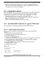
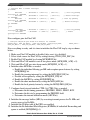
Mid 1 trip point selected (VLVW = VLVW2) - 1.84
Mid 2 trip point selected (VLVW = VLVW3) - 1.94
High trip point selected (VLVW = VLV4)
- 2.04
*/
NVICICPR0|=(1<<20);
NVICISER0|=(1<<20);
}
//Clear any pending interrupts on LVD
//Enable interrupts from LVD module
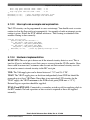
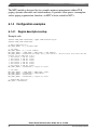
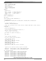
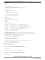
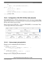
5.1.2.3 Interrupt code example and explanation
The LVD circuitry can be programmed to cause an interrupt. You should create a service
routine to clear the flags and react appropriately. An example of such an interrupt service
routine is given. Notice the NVIC module references. This clearing is redundant if the
module clearing is done correctly.
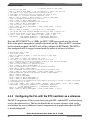
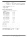
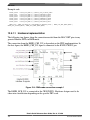
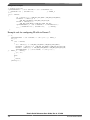
void pmc_lvd_isr(void){
printf("\rPMC_LVD ISR entered** ");
if ( PMC_LVDSC2 & PMC_LVDSC2_LVWF_MASK)
PMC_LVDSC2 |= PMC_LVDSC2_LVWACK_MASK;
if ( PMC_LVDSC1 & PMC_LVDSC1_LVDF_MASK)
PMC_LVDSC1 |= PMC_LVDSC1_LVDACK_MASK;
NVICICPR0|=(1<<20);
//Clear any pending interrupts on LVD
}
5.1.2.4 Hardware implementation
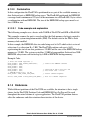
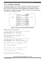
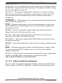
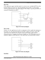
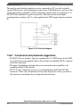
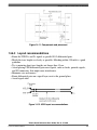
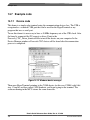
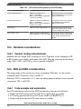
RESET PIN: The reset pin is driven out if the internal circuitry detects a reset. This is
true for all resets, including a reset that causes a recovery from the VLLSx modes. Since
these could be warm starts, customers who do want not their external circuitry reset do
not want to connect external circuitry to the MC reset pin.
VDD: The Vdd supply pins can be driven between 1.71 V and 3.6 V DC.
VBAT: The VBAT supply pins can be driven independently from VDD but should be
powered up to at least VBATmin. Since there is no equivalent LVD circuitry for the
VBAT supply, the VBAT minimum is the POR release point [POR max = 1.5 V].
External bypass capacitors should be supplied.
XTAL32 and EXTAL32: Connected to a secondary watch crystal for supplying clock to
the RTC module. No load capacitors or bias resistor is required as these are supplied
internally.
Kinetis Quick Reference User Guide, Rev. 0, 11/2010
Freescale Semiconductor
53






































































![[マンスリーコラム]](http://vs1.manualzilla.com/store/data/006615967_2-79082b143ac2ddabb4b33d93f7707170-150x150.png)