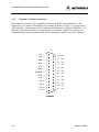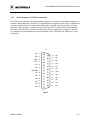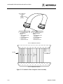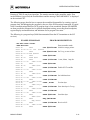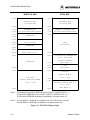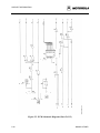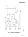
1
M68HC11EVM/AD8
February 1994
M68HC11EVM
EVALUATION MODULE
USER’S MANUAL
Information contained in this document applies to
REVision (G) M68HC11EVM Evaluation Modules,
serial numbers 1000 through 9999.
Copyright 1989, 1994 by Motorola Inc.
Motorola reserves the right to make changes without further notice to any products herein to
improve reliability, function or design. Motorola does not assume any liability arising out of the
application or use of any product or circuit described herein; neither does it convey any license
under its patent rights nor the rights of others. Motorola products are not designed, intended, or
authorized for use as components in systems intended for surgical implant into the body, or other
applications intended to support or sustain life, or for any other application in which the failure of
the Motorola product could create a situation where personal injury or death may occur. Should
Buyer purchase or use Motorola products for any such unintended or unauthorized application,
Buyer shall indemnify and hold Motorola and its officers, employees, subsidiaries, affiliates, and
distributors harmless against all claims, costs, damages, and expenses, and reasonable attorney
fees arising out of, directly or indirectly, any claim of personal injury or death associated with
such unintended or unauthorized use, even if such claim alleges that Motorola was negligent
regarding the design or manufacture of the part.
The computer program stored in the Read Only Memory of the device contains material
copyrighted by Motorola Inc., first published 1985, and may be used only under a license such as
the License For Computer Programs (Article 14) contained in Motorola’s Terms and Conditions
of Sale, Rev. 1/79.
EVMbug and EXORciser are trademarks of Motorola Inc.
IBM-PC is a registered trademark of International Business Machines Corp.
PREFACE
Unless otherwise specified, all address references are in
hexadecimal throughout this manual.
An asterisk (*) following the signal name denotes that the signal is
true or valid when the signal is low.
Throughout this manual AX family MCU device reference
indicates either A0, A1, or A8. Similarly, EX family MCU device
reference indicates either E0, E1, E9, or 811E2.
CONTENTS
CONTENTS
CHAPTER 1 GENERAL INFORMATION
1.1
1.2
1.3
1.4
1.5
INTRODUCTION .............................................................................................................. 1-1
FEATURES ........................................................................................................................ 1-1
SPECIFICATIONS............................................................................................................. 1-2
GENERAL DESCRIPTION............................................................................................... 1-3
EQUIPMENT REQUIRED ................................................................................................ 1-4
CHAPTER 2
HARDWARE PREPARATION AND INSTALLATION
2.1
2.2
2.3
INTRODUCTION .............................................................................................................. 2-1
UNPACKING INSTRUCTIONS....................................................................................... 2-1
HARDWARE PREPARATION......................................................................................... 2-1
2.3.1 Evaluation Mode Select Headers (J9 and J19) .......................................................... 2-2
2.3.2 Pseudo ROM Disable Header (J10)........................................................................... 2-4
2.3.3 Pseudo EEPROM Disable Header (J11).................................................................... 2-4
2.3.4 Clock Input Select Headers (J12 and J13)................................................................. 2-5
2.3.5 RTS and CTS Signal Enable Headers (J14 and J15)................................................. 2-6
2.3.6 Write Enable Header (J16) ........................................................................................ 2-7
2.3.7 Serial Enable Header (J18) ........................................................................................ 2-8
2.3.8 AX/EX Select Header (J20)....................................................................................... 2-8
2.4 INSTALLATION INSTRUCTIONS.................................................................................. 2-9
2.4.1 Power Supply - EVM Interconnection....................................................................... 2-9
2.4.2 Terminal - EVM Interconnection ............................................................................ 2-10
2.4.3 Host Computer - EVM Interconnection................................................................... 2-11
2.4.4 Target System - EVM (Single-Chip Mode) Interconnection................................... 2-13
2.4.5 Target System - EVM (Expanded-Multiplexed Mode) Interconnection ................. 2-13
2.4.6 Target System - EVM Operation............................................................................. 2-13
M68HC11EVM/D
v
CONTENTS
CHAPTER 3
OPERATING INSTRUCTIONS
3.1
3.2
3.3
3.4
3.5
3.6
INTRODUCTION ..................................................................................................................1
CONTROL SWITCHES.........................................................................................................2
LIMITATIONS.......................................................................................................................3
OPERATING PROCEDURE.................................................................................................5
COMMAND LINE FORMAT ...............................................................................................7
MONITOR (EVMBUG) COMMANDS ................................................................................8
3.6.1 Assembler/Disassembler..............................................................................................10
3.6.2 Block Fill .....................................................................................................................12
3.6.3 Breakpoint Set .............................................................................................................13
3.6.4 Bulk Erase....................................................................................................................14
3.6.5 Check ...........................................................................................................................15
3.6.6 Copy.............................................................................................................................16
3.6.7 Erase Bytes ..................................................................................................................17
3.6.8 Go ................................................................................................................................18
3.6.9 Help..............................................................................................................................19
3.6.10 Load .............................................................................................................................20
3.6.11 Memory Display ..........................................................................................................21
3.6.12 Memory Modify...........................................................................................................22
3.6.13 Remove Breakpoint .....................................................................................................23
3.6.14 Proceed ........................................................................................................................24
3.6.15 Program........................................................................................................................25
3.6.16 Register Display...........................................................................................................27
3.6.17 Register Modify ...........................................................................................................28
3.6.18 Speed............................................................................................................................29
3.6.19 Trace ............................................................................................................................30
3.6.20 Transparent Mode........................................................................................................31
3.6.21 Verify...........................................................................................................................32
3.7 EEPROM OR EPROM MCU PROGRAMMING PROCEDURES ....................................33
3.7.1 Checking ......................................................................................................................34
3.7.2 Erasing .........................................................................................................................35
3.7.3 Programming ...............................................................................................................36
3.7.4 Copying........................................................................................................................37
3.7.5 Verifying......................................................................................................................38
3.7.6 Reprogramming MCU Configuration Register ...........................................................39
vi
M68HC11EVM/D
CONTENTS
CHAPTER 3
3.8
3.9
OPERATING INSTRUCTIONS (continued)
ASSEMBLING/DISASSEMBLING PROCEDURES.........................................................40
DOWNLOADING PROCEDURES.....................................................................................44
3.9.1 EXORciser to EVM.....................................................................................................45
3.9.2 IBM-PC to EVM..........................................................................................................46
CHAPTER 4
4.1
4.2
INTRODUCTION .............................................................................................................. 4-1
EVM DESCRIPTION......................................................................................................... 4-1
4.2.1 MCU and Control Circuits ........................................................................................ 4-1
4.2.1.1 ...Map Switching.................................................................................................. 4-2
4.2.1.2 ...Abort ................................................................................................................. 4-4
4.2.1.3 ...64-Cycle Timeout ............................................................................................. 4-4
4.2.1.4 ...Address Decoding............................................................................................. 4-4
4.2.2 Monitor and User Memory ........................................................................................ 4-5
4.2.2.1 ...AX Monitor Map Area ..................................................................................... 4-5
4.2.2.2 ...AX User Map Area........................................................................................... 4-6
4.2.2.3 ...EX Monitor Map Area...................................................................................... 4-6
4.2.2.4 ...EX User Map Area ........................................................................................... 4-6
4.2.3 Terminal and Host Computer I/O Ports..................................................................... 4-9
4.2.4 MCU Extension I/O Ports.......................................................................................... 4-9
4.2.5 EEPROM MCU Programmer .................................................................................. 4-10
4.2.5.1 ...Programming Algorithm................................................................................. 4-10
4.2.5.2 ...Programming .................................................................................................. 4-11
CHAPTER 5
5.1
5.2
5.3
5.4
FUNCTIONAL DESCRIPTION
SUPPORT INFORMATION
INTRODUCTION .............................................................................................................. 5-1
CONNECTOR SIGNAL DESCRIPTIONS ....................................................................... 5-1
PARTS LIST....................................................................................................................... 5-7
DIAGRAMS ..................................................................................................................... 5-12
M68HC11EVM/D
vii
CONTENTS
APPENDIX A
A.1
A.2
A.3
A.4
S-RECORD INFORMATION
S RECORD CONTENT .....................................................................................................A-1
S-RECORD TYPES ...........................................................................................................A-2
S-RECORD CREATION ...................................................................................................A-3
S-RECORD EXAMPLE.....................................................................................................A-3
FIGURES
2-1.
2-2.
2-3.
2-3.
4-1.
4-2.
4-3.
5-1.
5-2.
EVM Connector, Switch, and Jumper Header Location Diagram...................................... 2-3
Terminal or Host Computer Cable Assembly................................................................... 2-12
Target System Emulation Cable Assembly Diagram (Sheet 1 of 2.................................. 2-15
Target System Emulation Cable Assembly Diagram (Sheet 2 of 2)................................. 2-16
EVM Block Diagram.......................................................................................................... 4-3
EVM (AX) Memory Map................................................................................................... 4-7
EVM (EX) Memory Map ................................................................................................... 4-8
EVM Parts Location Diagram .......................................................................................... 5-13
EVM Schematic Diagram................................................................................................. 5-14
TABLES
1-1.
1-2.
3-1.
3-2.
5-1.
5-2.
5-3.
5-4.
5-5.
5-6.
viii
EVM Specifications............................................................................................................ 1-2
External Equipment Requirements ..................................................................................... 1-4
EVM Control Switches....................................................................................................... 3-2
Monitor (EVMbug) Commands ......................................................................................... 3-9
Single-Chip Connector J1 Pin Assignments....................................................................... 5-2
Expanded-Multiplexed Connector J3 Pin Assignments ..................................................... 5-3
Input Power Connector J5 Pin Assignments ...................................................................... 5-4
RS-232C Terminal Port Connector J6 Pin Assignments.................................................... 5-5
RS-232C Host Port Connector J7 Pin Assignments ........................................................... 5-6
EVM Parts List ................................................................................................................... 5-7
M68HC11EVM/D
GENERAL INFORMATION
CHAPTER 1
GENERAL INFORMATION
1.1
INTRODUCTION
This manual provides general information, hardware preparation, installation instructions,
operating instructions, functional description, and support information for the M68HC11EVM
Evaluation Module (hereafter referred to as EVM). Appendix A contains EVM downloading Srecord information.
NOTE
Throughout this manual AX family MCU device reference
indicates either A0, A1, or A8. Similarly, EX family MCU device
reference indicates either E0, E1, E9, or 811E2.
1.2
FEATURES
EVM features include:
•
Economical means of evaluating target systems incorporating M68HC11 (AX and/or
EX) HCMOS MCU family devices
•
Monitor/debugger firmware
•
One-line assembler/disassembler
•
Host computer download capability
•
Dual 64K-byte memory maps:
− 16K-byte monitor EPROM
− 8K/16K-byte user pseudo ROM
•
EEPROM MCU programmer
•
MCU (single-chip/expanded-multiplexed mode) extension I/O ports
•
RS-232C terminal and host computer I/O ports
M68HC11EVM/D
1-1
GENERAL INFORMATION
1.3
SPECIFICATIONS
Table 1-1 lists the EVM specifications.
Table 1-1. EVM Specifications
Characteristics
Clock:
Internal
External
1-2
Specifications
2 MHz bus operation (8 MHz, crystal
controlled, divided-by-four)
0 to 8.4 MHz, divided-by-four (0 to 2.1
MHz bus operation)
Monitor map size:
64K bytes
Monitor EPROM
16K bytes
User map size:
64K bytes
Pseudo EEPROM
512 bytes
Pseudo ROM
8K/16K bytes
MCU extension I/O ports
HCMOS compatible
Terminal/host I/O ports
RS-232C compatible
Temperature:
Operating
Storage
+25 degrees C
-40 to +85 degrees C
Relative humidity
0 to 90% (non-condensing)
Power requirements:
Module
+5 Vdc @ 1.0 A (max)
+12 Vdc @ 0.1 A (max)
-12 Vdc @ 0.1 A (max)
Dimensions:
11.0 in. (27.9 cm) X 8.5 in. (21.5 cm)
M68HC11EVM/D
GENERAL INFORMATION
1.4
GENERAL DESCRIPTION
The EVM provides a tool for designing, debugging, and evaluating MC68HC11 Microcontroller
Unit (MCU) based target system equipment. By providing all of the essential MCU timing and
I/O circuitry, the EVM simplifies user evaluation of the prototype hardware/software product.
The EVM requires a user-supplied power supply and an RS-232C compatible terminal for
operation.
The MC68HC11AX and/or MC68HC11EX family of HCMOS MCU devices are evaluated
(emulated) by the EVM resident MC68HC11 MCU. Entering data, program debugging, and
EEPROM MCU programming is accomplished by the monitor EPROM firmware via an external
RS-232C compatible terminal connected to the EVM terminal port connector. Downloading
programs directly from an RS-232C compatible host computer to the EVM is accomplished via
the host port connector. Downloading programs from a remote host computer via a modem may
also be performed.
The EVM evaluates both the single-chip and expanded-multiplexed modes of operation. MCU
I/O port connectors, labeled SINGLE CHIP and EXPANDED MULTIPLEXED, facilitate
interconnection of the EVM to the target system for evaluation purposes. Generating, executing,
and debugging target system MCU code is accomplished in either mode.
MCU code may be generated using the resident one-line assembler/disassembler, or may be
downloaded to the user program RAM through the host or terminal port connectors. User code
may then be executed using various debugging commands in the monitor. User code may also be
executed using the user reset switch. MCU device ROM is simulated by write protecting user
program RAM during program execution.
Independent 150-19.2K baud rate selection capabilities are provided for the terminal and host I/O
ports. An auto-baud rate selection is provided for the terminal port and a software selectable baud
rate selection is provided for the host port.
Jumper selectable options such as evaluation mode and clock input selection are provided on the
EVM, as well as an EEPROM MCU programmer. The EEPROM MCU programmer, under
monitor firmware control, enables the user to check, erase, program, verify, and copy the
contents of either 48-pin Dual-In-line Package (DIP) or 52-lead Plastic Leaded Chip Carrier
(PLCC) package EEPROM MCU devices. Switches allow user control of the reset and abort
functions, and EEPROM MCU programming functions.
M68HC11EVM/D
1-3
GENERAL INFORMATION
A jumper header is used to select either the MC68HC11AX or MC68HC11EX family MCU
device evaluation and programming operations. When evaluating or programming a specific
MCU, the resident MCU socket (location U2) must contain the applicable MCU
(MC68HC11A1FN or MC68HC11E1FN). When evaluating or programming an MC68HC11EX
family device, a 6264 (8K RAM) device is installed at socket location U15. This device must be
removed when evaluating or programming an MC68HC11AX family device.
NOTE
Throughout this manual AX family MCU device reference
indicates either A0, A1, or A8. Similarly, EX family MCU device
reference indicates either E0, E1, E9, or 811E2.
1.5
EQUIPMENT REQUIRED
Table 1-2 lists the external equipment requirements for EVM operation.
Table 1-2. External Equipment Requirements
External Equipment
+5, +12, -12 Vdc power supply(1)
Terminal (RS-232C compatible)
Host computer (RS-232C compatible)(2)
Terminal/host computer – EVM RS-232C cable assembly(1)
Target system – EVM emulator cable assembly(3)
1. Refer to Chapter 2 for details.
2. Optional - not required for basic operation.
3. Supplied with EVM.
1-4
M68HC11EVM/D
HARDWARE PREPARATION AND INSTALLATION
CHAPTER 2
HARDWARE PREPARATION AND INSTALLATION
2.1
INTRODUCTION
This chapter provides unpacking instructions, hardware preparation, and installation instructions
for the EVM.
2.2
UNPACKING INSTRUCTIONS
NOTE
If shipping carton is damaged upon receipt, request carrier’s agent
be present during unpacking and inspection of the EVM.
Unpack EVM from shipping carton. Refer to packing list and verify that all items are present.
Save packing material for storing or reshipping the EVM.
2.3
HARDWARE PREPARATION
This portion of text describes the inspection/preparation of EVM components prior to target
system installation. This description will ensure the user that the EVM components are properly
configured for target system operation. The EVM has been factory-tested and is shipped with
factory-installed jumpers.
EVM should be inspected/prepared for jumper placements prior to target system installation.
Figure 2-1 illustrates the EVM connector, switch, and jumper header locations.
M68HC11EVM/D
2-1
HARDWARE PREPARATION AND INSTALLATION
Connectors J1, J3, and J5 through J7 facilitate interconnection of external equipment to the
EVM. Switches S1 through S5 provide user control of the EVM. Refer to Chapter 3 for the
switch descriptions. Jumper header locations J9 through J16, and J18 through J20 provide the
following selection capabilities:
•
Evaluation mode select (J9 and J19)
•
Pseudo ROM disable (J10)
•
Pseudo EEPROM disable (J11)
•
Clock input select (J12 and J13)
•
RTS and CTS signal enable (J14 and J15)
•
Write enable (J16)
•
Serial enable (J18)
•
AX/EX select (J20)
Reference designations J2, J4, J8, and J17 are not used.
2.3.1
Evaluation Mode Select Headers (J9 and J19)
Jumper headers J9 and J19 are used to select either the expanded-multiplexed or single-chip
mode of operation. Configuration for the jumper headers are as follows:
Mode of Operation
Single-Chip
Expanded-Multiplexed
Header
Jumper
Placement
J9
J19
1-2
2-3
J9 J19
2-3 1-2
The EVM is shipped factory-configured for the single-chip mode of operation as shown below.
J9
J19
1
2
1
2
3
3
2-2
M68HC11EVM/D
HARDWARE PREPARATION AND INSTALLATION
Figure 2-1. EVM Connector, Switch, and Jumper Header Location Diagram
M68HC11EVM/D
2-3
HARDWARE PREPARATION AND INSTALLATION
2.3.2
Pseudo ROM Disable Header (J10)
When evaluating the MC68HC11AX MCU in the expanded-multiplexed mode of operation, the
EVM user pseudo ROM ($E000-$FFFF) may be enable/disable using jumper header J10. The
EVM is factory-configured and shipped with the pseudo ROM enabled (a jumper installed on
jumper header J10). To disable the pseudo ROM, remove jumper from pins 1 and 2.
J10
1
2
When evaluating the MC68HC11EX MCU in the expanded-multiplexed mode of operation, the
EVM user pseudo ROM # 2 ($E000-$FFFF) may be enable/disable using jumper header J10.
User pseudo ROM # 1 ($C000-$DFFF) is not affected by this jumper header. To access
addresses $C000-$DFFF in the user’s target system, you must disable pseudo ROM # 1. To
disable pseudo ROM # 1, install a jumper on J10 pins 1 and 2 and remove the 6264 device
installed at location U15.
2.3.3
Pseudo EEPROM Disable Header (J11)
EVM pseudo EEPROM ($B600-$B7FF) is only available when the MCU CONFIG register
EEON bit is programmed to a logic zero (0). The EVM is shipped with the EEON bit
programmed to a logic one (1), therefore, the MCU 512-byte internal EEPROM ($B600-$B7FF)
is selected. Refer to Chapter 3 (paragraph 3.7.6) for additional MCU CONFIG register EEON bit
programming information.
When the MCU CONFIG register EEON bit is programmed to a logic zero (0), jumper header
J11 is used to disable the EVM 512-byte pseudo EEPROM (RAM). The EVM is factoryconfigured and shipped with the fabricated jumper installed on pins 1 and 2 as shown below. To
disable the pseudo EEPROM, remove jumper from pins 1 and 2.
J11
1
2
2-4
M68HC11EVM/D
HARDWARE PREPARATION AND INSTALLATION
2.3.4
Clock Input Select Headers (J12 and J13)
Jumper headers J12 and J13 are used to select either internal or external clock source to be used
by the EVM. The internal clock source is a 8 MHz crystal. The EVM is factory-configured and
shipped with the clock input selected to internal 8 MHz clock operation. This is accomplished by
the installation of fabricated jumpers on both jumper headers J12 and J13 as shown below. To
select an external clock source, remove jumper from jumper header J12 pins 2 and 3, and
reinstall jumper on pins 1 and 2. Remove jumper from jumper header J13 pins 1 and 2.
J13
J12
1
EXTERNAL
2
3
1
2
INTERNAL
When the external clock source is selected, the user supplies an external clock on the EXTAL’
pin (pin 7) of either the SINGLE CHIP connector J1 or the EXPANDED MULTIPLEXED
connector J3. If 2 MHz operation is desired, the user must supply an external 8 MHz clock signal
via the EXTAL’ pin of either connector J1 or J3 (pin 7).
M68HC11EVM/D
2-5
HARDWARE PREPARATION AND INSTALLATION
2.3.5
RTS and CTS Signal Enable Headers (J14 and J15)
Jumper headers J14 and J15 are used to configure the RS-232C terminal and host computer I/O
ports for semi- or full-handshaking operation. The EVM is factory-configured for semihandshaking (high level) operation. This semi-handshaking (high level) configuration is
accomplished by the installation of fabricated jumpers on jumper headers J14 and J15 as shown
below.
J14
1
2
HIGH
LEVEL
J15
3
FULL
HANDSHAKE
RTS
1
2
HIGH
LEVEL
3
FULL
HANDSHAKE
CTS
Should the terminal or host computer or modem require full handshake capability, jumpers are to
be repositioned between pins 2 and 3. Refer to the schematic diagram located in Chapter 5
(Figure 5-2, sheet 12 of 12) for RTS and CTS signal wiring information.
2-6
M68HC11EVM/D
HARDWARE PREPARATION AND INSTALLATION
2.3.6
Write Enable Header (J16)
Jumper header (connector) J16 is used to route a Write Enable (WE*’) signal from the EVM to
the target system during the expanded-multiplexed mode of operation. Connector J16 is used
only if the target system contains ROM (EPROM). In this mode of operation, the user must
replace the target system ROM with RAM, and also supply a WE*’ signal to the RAM. This
device replacement and external wiring additions enable the user to perform trace or breakpoint
operations in target system RAM locations.
NOTE
User must also remove target system crystal and capacitor from the
MCU XTAL pin during this wiring installation.
J16
GND
GND
1
WE*’
2
WE*’
TARGET
SYSTEM
RAM
(OPTIONAL EXTERNAL WIRING)
CAUTION
The EVM is factory-configured and shipped with this connector
not having any fabricated jumper installed. EVM circuit damage
will result if a fabricated jumper is installed between pins 1 and 2.
The above external wiring is optional. The user can install an external wire from connector J16
pin 2 to the target system RAM circuitry. Note that connector J16 pin 1 is connected to EVM
ground (GND). If required, an additional external ground (GND) wire from connector J16 pin 1
to the target system circuitry can be implemented by the user. Refer to the schematic diagram
located in Chapter 5 (Figure 5-2, sheet 11 of 12) for WE*’ signal wiring information.
M68HC11EVM/D
2-7
HARDWARE PREPARATION AND INSTALLATION
2.3.7
Serial Enable Header (J18)
NOTE
Jumper header J18 is for factory use only.
Jumper header J18 is used for factory use only. The installed fabricated jumper (shown below)
must not be removed during normal EVM operations.
J18
1
2
2.3.8
AX/EX Select Header (J20)
Jumper header J20 is used to select either MC68HC11AX or MC68HC11EX family MCU
evaluation and programming operations. The EVM is shipped with an MC68HC11A1 MCU
installed in socket U2, and jumper header J20 is factory configured as shown below.
J20
1
2
A8
3
E9
NOTE
Throughout this manual AX family MCU device reference
indicates either A0, A1, or A8. Similarly, EX family MCU device
reference indicates either E0, E1, E9, or 811E2.
If evaluation of the MC68HC11EX family MCU is desired, the user must replace the resident
MC68HC11A1 device with the MC68HC11E1 device (socket location U2) and place the
fabricated jumper between pins 2 and 3. A 6264 (8K RAM) device must also be installed at
socket location U15. This device provides an additional 8K-byte of user pseudo ROM at
locations $C000-$DFFF.
When emulating an MC68HC11AX MCU in expanded mode, you may use additional emulation
RAM by installing a 6264 (8K RAM) device in the socket at location U15 and placing the
fabricated jumper between pins 2 and 3 . To emulate an MC68HC11AX MCU in single-chip
mode remove the RAM (U15) and place the fabricated jumper between pins 1 and 2.
2-8
M68HC11EVM/D
HARDWARE PREPARATION AND INSTALLATION
2.4
INSTALLATION INSTRUCTIONS
The EVM is designed for table top operation. A user supplied power supply and RS-232C
compatible terminal are required for EVM operation. An RS-232C compatible host computer
may be connected to the EVM, but is not required for basic EVM operation.
2.4.1
Power Supply - EVM Interconnection
The EVM requires +5 Vdc @ 1.0 A, +12 Vdc @ 0.1 A, and -12 Vdc @ 0.1 A for operation. The
user supplied power supply is connected to connector J5, which is a terminal block designed to
accept 14-22 AWG wire. Interconnection of the power supply wiring to the EVM is shown
below.
J5
1
VPP
2
+5 Vdc
3
-12 Vdc
4
+12 Vdc
5
GND
6
GND
NOTE
Connector J5 pin 1 labeled (VPP) is reserved for future use.
M68HC11EVM/D
2-9
HARDWARE PREPARATION AND INSTALLATION
2.4.2
Terminal - EVM Interconnection
Interconnection of an RS-232C compatible terminal to the EVM is accomplished via a user
supplied 20 or 25 conductor flat ribbon cable assembly as shown in Figure 2-2. One end of the
cable assembly is connected to the EVM connector J6 (shown below) labeled TERMINAL. The
other end of the cable assembly is connected to the user supplied terminal. For connector pin
assignments and signal descriptions of the EVM terminal port connector J6, refer to Chapter 5.
J6
NC
1
TXD
2
RXD 3
RTS
4
CTS
5
DSR
6
SIG-GND 7
DCD
8
NC
9
NC 10
NC 11
NC 12
NC 13
14
NC
15
NC
16
NC
17
NC
18
NC
19
NC
20
NC
21
NC
22
NC
23
NC
24
NC
25
NC
TERMINAL
2-10
M68HC11EVM/D
HARDWARE PREPARATION AND INSTALLATION
2.4.3
Host Computer - EVM Interconnection
The EVM can be operated with a host computer directly or a remotely located host computer via
a modem. Interconnection of an RS-232C compatible host computer to the EVM is accomplished
via a user supplied 20 or 25 conductor flat ribbon cable assembly as shown in Figure 2-2. One
end of the cable assembly is connected to the EVM connector J7 (shown below) labeled HOST.
The other end of the cable assembly is connected to the user supplied host computer or modem.
For connector pin assignments and signal descriptions of the EVM host port connector J7, refer
to Chapter 5.
J7
NC
1
TXD
2
RXD 3
RTS
4
CTS
5
NC
6
SIG-GND 7
NC
8
NC
9
NC 10
NC 11
NC 12
NC 13
14
NC
15
NC
16
NC
17
NC
18
NC
19
NC
20
DTR
21
NC
22
NC
23
NC
24
NC
25
NC
HOST
M68HC11EVM/D
2-11
HARDWARE PREPARATION AND INSTALLATION
20 OR 25 CONDUCTOR
FLAT RIBBON
CABLE
3M #3365-20
OR
3M #3365-25
25 "D" SUBMINIATURE MALE
(PIN) CONNECTOR
PART #’S:
25 "D" SUBMINIATURE FEMALE
(SOCKET) CONNECTOR
PART #’S:
1. CIRCUIT ASSEMBLY CORP
#CA•25•SMD•P
1. CIRCUIT ASSEMBLY CORP
#CA•25•SMD•S
2. ITT CANNON #DBSP-B25P
2. ITT CANNON #DBSP-B25S
3. ANSLEY #609•25P
3. ANSLEY #609•25S
4. WINCHESTER #49•1125P
4. WINCHESTER #49•1125S
25 PIN "D" SUBMINIATURE CONNECTOR
1
2
14
3
15
4
16
5
17
6
18
7
19
8
20
9
21
10
22
11
23
12
24
13
25
1
2
14
3
15
4
16
5
17
6
18
DTR
NOT CONNECTED
7
19
DCD
SIGNAL GND
DSR
CTS
RTS
RXD
TXD
RED WIRE
8
20
9
21
10
22
11
23
12
24
13
25
25 PIN "D" SUBMINIATURE CONNECTOR
Figure 2-2. Terminal or Host Computer Cable Assembly
2-12
M68HC11EVM/D
HARDWARE PREPARATION AND INSTALLATION
2.4.4
Target System - EVM (Single-Chip Mode) Interconnection
Target system to EVM interconnection for the single-chip mode of operation is accomplished via
EVM connector J1 and a target system emulation cable assembly as shown in Figure 2-3. MCU
I/O port connector J1 is a 60-pin header (shown on the following page) that facilitates the
interconnection of the cable assembly for evaluation purposes. For connector pin assignments
and signal descriptions of the EVM SINGLE CHIP connector J1, refer to Chapter 5.
2.4.5
Target System - EVM (Expanded-Multiplexed Mode) Interconnection
Target system to EVM interconnection for the expanded-multiplexed mode of operation is
accomplished via EVM connector J3 , and a target system emulation cable assembly as shown in
Figure 2-3. MCU I/O port connector J3 is a 60-pin header (shown on the following page) that
facilitates the interconnection of the cable assembly for evaluation purposes. For connector pin
assignments and signal descriptions of the EVM EXPANDED MULTIPLEXED connector J3,
refer to Chapter 5.
2.4.6
Target System - EVM Operation
CAUTION
Damage to the EVM LIR*’ buffer circuitry will result if the target
system MCU circuitry mode select pins (MODA/LIR and MODB)
are connected directly to +5 Vdc or ground.
NOTE
When connecting the EVM to target system circuitry, the user must
ensure that the target system MCU circuitry MODA/LIR and
MODB pins are not connected.
When operating the target system in the single-chip mode, the MCU MODA/LIR pin would
normally be connected to ground and the MODB pin would normally be connected to +5 Vdc.
When operating the target system in the expanded-multiplexed mode, the MODB pin would
normally be connected to +5 Vdc and the MODA/LIR pin would normally be connected to a
pullup resistor.
The mode of operation of the EVM is established by the use of the MCU I/O port connectors.
Connector J1 is used for the single-chip mode of operation, and connector J3 is used for the
expanded-multiplexed mode of operation. The LIR*’ pin (pin 3) of both connectors J1 and J3 are
buffered output signals used for opcode fetch detection.
M68HC11EVM/D
2-13
HARDWARE PREPARATION AND INSTALLATION
J1
J3
GND
1
2
NC
GND
1
2
NC
LIR*’
3
4
STRA
LIR*’
3
4
BAS
BE
5
6
STRB
BE
5
6
BRW
EXTAL’
7
8
NC
EXTAL’
7
8
NC
PC0
9
10
PC1
A/D0’
9
10
A/D1’
PC2
11
12
PC3
A/D2’
11
12
A/D3’
PC4
13
14
PC5
A/D4’
13
14
A/D5’
PC6
15
16
PC7
A/D6’
15
16
A/D7’
RESET*’
17
18
XIRQ*
RESET*’
17
18
XIRQ*
IRQ*
19
20
PD0
IRQ*
19
20
PD0
PD1
21
22
PD2
PD1
21
22
PD2
PD3
23
24
PD4
PD3
23
24
PD4
PD5
25
26
NC
PD5
25
26
NC
PA7
27
28
PA6
PA7
27
28
PA6
PA5
29
30
PA4
PA5
29
30
PA4
PA3
31
32
PA2
PA3
31
32
PA2
PA1
33
34
PA0
PA1
33
34
PA0
PB7
35
36
PB6
A15’
35
36
A14’
PB5
37
38
PB4
A13’
37
38
A12’
PB3
39
40
PB2
A11’
39
40
A10’
PB1
41
42
PB0
A9’
41
42
A8’
PE0
43
44
PE4
PE0
43
44
PE4
PE1
45
46
PE5
PE1
45
46
PE5
PE2
47
48
PE6
PE2
47
48
PE6
PE3
49
50
PE7
PE3
49
50
PE7
VRL
51
52
VRH
VRL
51
52
VRH
NC
53
54
NC
NC
53
54
NC
NC
55
56
NC
NC
55
56
NC
NC
57
58
NC
NC
57
58
NC
NC
59
60
NC
NC
59
60
NC
SINGLE CHIP
2-14
EXPANDED MULTIPLEXED
M68HC11EVM/D
HARDWARE PREPARATION AND INSTALLATION
Figure 2-3. Target System Emulation Cable Assembly Diagram (Sheet 1 of 2)
M68HC11EVM/D
2-15
HARDWARE PREPARATION AND INSTALLATION
Figure 2-3. Target System Emulation Cable Assembly Diagram (Sheet 2 of 2)
2-16
M68HC11EVM/D
OPERATING INSTRUCTIONS
CHAPTER 3
OPERATING INSTRUCTIONS
3.1
INTRODUCTION
This chapter provides the necessary information to initialize and operate the EVM in a target
system environment. EEPROM MCU programming, assembling/disassembling, and
downloading procedures are also provided. Information contained in this chapter will be
presented in the following order:
•
Control switch descriptions
•
Limitations
•
Operating procedures
•
EEPROM MCU programming procedures
•
Assembling/disassembling procedures
•
Downloading procedures
The monitor is the resident firmware (EVMbug) for the EVM, which provides a self contained
programming and operating environment. The monitor interacts with the user through predefined
commands that are entered from a terminal. These commands perform functions such as display
or modify memory, display or modify MCU internal registers, program execution under various
levels of control, control access to various I/O peripherals connected to the EVM, and control
programming and reading of MCU EEPROM.
M68HC11EVM/D
3-1
OPERATING INSTRUCTIONS
3.2
CONTROL SWITCHES
The EVM contains five switches that allow the user to control specific functions. Switches S1
through S3 control the reset and abort functions. Switches S4 and S5 control the EEPROM MCU
programming functions. Table 3-1 identifies these switches by name, description, and function.
Table 3-1. EVM Control Switches
Name
3-2
Description And Function
ABORT
switch (S1)
Momentary action pushbutton switch – when pressed, returns
EVM operation to the monitor map from the user map assuming
proper operation of user code. (If MCU gets lost in the user
map, the abort is useless and a master reset must be issued.)
The abort function has no effect when operating in the monitor
map.
USER RESET
switch (S2)
Momentary action pushbutton switch – when pressed, resets
EVM MCU and user I/O, and enables map switching to the user
map. This switch is used as a map switch for execution of user
code from the user reset vector.
MASTER RESET
switch (S3)
Momentary action pushbutton switch – when pressed, resets
EVM MCU and user I/O, places EVM operation in the monitor
map, and enables the EVM prompt to be displayed on terminal
CRT.
Programmer
reset (RST)
switch (S4)
On-off slide switch – resets internal state of the programmable
EEPROM MCU device installed in socket U32/U56. Reset
function is activated when the switch is placed in the RST
position. When placed in the OUT position, reset function is
deactivated, and the EEPROM MCU device is allowed to be
programmed via the user pseudo EEPROM.
Programmer
power (PWR)
switch (S5)
On-off slide switch – applies +5 Vdc power to the
programmable EEPROM MCU device installed in socket
U32/U56. Power is applied when the switch is placed in the
PWR position.
M68HC11EVM/D
OPERATING INSTRUCTIONS
3.3
LIMITATIONS
Mixing interrupt requests (IRQs) and user software interrupts (SWIs) should be avoided
whenever possible, due to IRQ-SWI EVM timing. If a concurrent hardware interrupt and SWI
should happen, an EVM failure could occur which may stop program execution. Activation of
the master reset switch will restore the EVM to proper operation. These conditions will
statistically occur very seldom.
The user may not trace an RTI instruction with an interrupt enabled and pending due to MCU
interrupt handling. Attempting this will cause an interrupt in the monitor map which will perform
a EVM software reset. User breakpoints will be left in the user map, but will not be recognized
by the monitor. The user stack pointer will also reflect the occurrence of an interrupt.
To reduce the amount of external circuitry required, a Write Enable*’ (WE*’) signal line is
available via jumper header J16. This signal may be used for the target system RAM write enable
signal. The WE*’ signal will write protect the target system RAM, thereby creating a pseudo
ROM. The RAM may then only be written via the EVM monitor. The user may place this target
system RAM anywhere in the map.
The EVM dual memory map operation is controlled by the user and master reset circuitry. A user
reset will attempt to place the EVM in the user map, while a monitor reset will attempt to place
the EVM in the monitor map. If both resets occur simultaneously, the EVM operation will
become undefined. If reset to the EVM was allowed by the target system, both will attempt to
reset into corresponding maps during Power On Reset (POR) which will cause an EVM
operational malfunction to occur. For this reason the RESET* signal is accessible to the target
system via the MCU I/O port connectors as an output line only. Target system reset circuitry
should be removed since the EVM provides the hardware reset signal. If different power supplies
are used for the EVM and target system, a master reset must be issued to reset the target system
before debugging may begin.
Code will not run or trace if it is loaded into location $0000. You must start at location $0001.
The host I/O port DCD signal is not implemented, therefore it may be possible for an error to
occur when downloading from a modem.
During EEPROM programming operations (check, copy, erase, program, and verify) the EVM
MCU must be connected to the on-board 8.0 MHz crystal. External clock operation is prohibited
during EEPROM programming operations.
CAUTION
The user may not map internal register or internal RAM over
pseudo ROM (E000-FFFF). If this occurs, monitor operation may
be affected and damage may occur to the EVM.
M68HC11EVM/D
3-3
OPERATING INSTRUCTIONS
The resident MC68HC11 MCU device computer operating properly (COP) subsystem feature
may be used only if these conditions are true:
1. The EVMbug stored in the EPROM (U14) must be revision 2.8 or higher. The latest
monitor is available on the Motorola bulletin board system (BBS), 512-891-3733.
2. The NOCOP bit in the resident MCU CONFIG register ($103F) must be programmed
to a logic 0.
MC68HC811A2/E2 ADDRESS LOCATION LIMITATION
Pseudo ROM located at $C000-$FFFF may be used as pseudo EEPROM (i.e., RAM) for
MC68HC811A2/E2 device emulation. If the MC68HC811A2/E2 device is used as the emulator
MCU, then the exact emulation of the MCU EEPROM is accomplished. There are address
limitations when performing this type of emulation.
The user must restrict the upper nibble of the MC68HC811A2/E2 configuration (CONFIG)
register to a value other than $E or $F. Not restricting the upper nibble would inhibit the use of
the monitor since the MCU EEPROM, as an internal resource, would have priority over the
monitor.
Programming the MC68HC811A2/E2 device can be accomplished as long as the CONFIG
register upper nibble is $C, $D, $E, or $F. If an upper nibble other than $C, $D, $E, or $F is
programmed in the CONFIG register, the CONFIG register must be reprogrammed to $C, $D,
$E, or $F since pseudo ROM/EEPROM resides from $C000-$FFFF. After EEPROM
programming is accomplished, the upper nibble of the CONFIG register can be moved to a
desired location.
NOTE
The above address limitation does not apply if programming from
external (target system) memory.
3-4
M68HC11EVM/D
OPERATING INSTRUCTIONS
3.4
OPERATING PROCEDURE
Applying power to the EVM causes a Power On Reset (POR) to occur. This POR condition
causes the MCU and user I/O port circuitry to be reset, and the monitor invoked. All user
registers are in an unknown state during monitor power up.
Upon initial power up or whenever the master reset switch S3 is pressed, the user must depress
the terminal keyboard carriage return (<CR>) key. This action enables the monitor to determine
the baud rate of the terminal connected to the EVM terminal I/O port. The monitor automatically
configures the baud rate settings for both EVM terminal and host I/O ports. The host I/O port
baud rate can be reconfigured via the SPEED command. The default baud rate for the host I/O
port is the same as the terminal I/O port baud rate.
Any ASCII character with a logic one in the least-significant bit will also perform the same
function as the (RETURN) key just described. The input serial format for the EVM terminal I/O
port must be configured for 8-data bits, 1-stop bit, no parity, and any of the following baud rates:
150, 300, 600, 1200, 2000, 2400, 4800, 9600, or 19.2K.
The terminal Cathode Ray Tube (CRT) displays the following message after the terminal
keyboard carriage return (<CR>) key is depressed:
EVMbug11 Rev X.X
P=XXXX Y=XXXX X=XXXX
>
A=XX
B=XX
C=D0 SX.I....
S=XXXX
where:
X is a revision of the software or an unknown register state.
Condition code register (CCR) SXHINZVC bits are as follows:
S
= Stop disable bit
X
= X interrupt mask bit
H
= Half carry bit
I
M68HC11EVM/D
= I interrupt mask bit
N
= Negative bit
Z
= Zero bit
V
= Overflow bit
C
= Carry/borrow bit
3-5
OPERATING INSTRUCTIONS
Status of the CCR bits are displayed as follows:
When all CCR bits are set (logic 1), bits are displayed as follows:
P=XXXX
Y=XXXX
X=XXXX
A=XX
B=XX
C=FF SXHINZVC
S=XXXX
When all CCR bits are cleared (logic 0), bits are displayed as follows:
P=XXXX
Y=XXXX
X=XXXX
A=XX
B=XX
C=00 ........
S=XXXX
When a specific bit is set (I), bits are displayed as follows:
P=XXXX
Y=XXXX
X=XXXX
A=XX
B=XX
C=10 ...I....
S=XXXX
When specific bits are set (H, I, and Z), bits are displayed as follows:
P=XXXX
Y=XXXX
X=XXXX
A=XX
B=XX
C=34 ..HI.Z..
S=XXXX
After initialization or return of control to the monitor, the terminal CRT displays the prompt " > "
and waits for a response. If an invalid response is entered, the terminal CRT displays
"ILLEGAL/INSUFFICIENT ENTRY" followed by the prompt " > ".
The EVM waits for a command line input from the user terminal. When a proper command is
entered, the operation continues in one of two basic modes. If the command causes execution of
a user program, the monitor may or may not be reentered, depending upon the desire of the user.
For the alternate case, the command is executed under the control of the monitor, and the system
returns to a waiting condition after the command is completed. During command execution,
additional user input may be required, depending on the command function.
The user can use any of the commands supported by the monitor. A standard input routine
controls the EVM operation while the user types a command line. Command processing begins
only after the command line has been terminated by depressing the keyboard carriage return
(<CR>) key.
3-6
M68HC11EVM/D
OPERATING INSTRUCTIONS
3.5
COMMAND LINE FORMAT
The command line format is as follows:
><command> [<parameters>](RETURN)
where:
>
EVMbug monitor prompt.
<command>
Command mnemonic.
<parameters>
Expression or address.
(<CR>)
Carriage return keyboard key - depressed to enter command.
NOTES:
1. The command line format is defined using special characters which have the
following syntactical meanings:
<>
Enclose syntactical variable
[]
Enclose optional fields
[ ]...
Enclose optional fields repeated
These characters are not entered by the user, but are for definition purposes only.
2. Fields are separated by a single space.
3. All input numbers are interpreted as hexadecimal. A dollar sign ($) may precede any
number input, but is not required.
4. All input commands can be entered either upper or lower case lettering. All input
commands are converted automatically to upper case lettering except for downloading
commands sent to the host computer, or when operating in the transparent mode.
5. A maximum of 46 characters may be entered on a command line. After the 46th
character is entered, the monitor automatically terminates the command entry and
processes the command line.
6. Parameters are interpreted to be the last two or three characters in the parameter file.
Parameter errors may be corrected by backspacing. This is accomplished via the
terminal keyboard (CTRL)H function.
M68HC11EVM/D
3-7
OPERATING INSTRUCTIONS
3.6
MONITOR (EVMBUG) COMMANDS
The monitor (EVMbug) commands are listed alphabetically by mnemonic in Table 3-2. Each of
the commands are described in detail following the tabular command listing.
Additional terminal keyboard functions are as follows:
•
(BREAK) Abort command
•
(CTRL)A Default transparent mode exit character
•
(CTRL)H Backspace
•
(CTRL)W Freeze screen
•
(CTRL)X Cancel command line
•
(RETURN)
Enter command
NOTE
When using the control key with a specialized command such as
(CTRL)X, the (CTRL) key is depressed and held, then the X key is
depressed. Both keys are then released.
During memory display output to terminal, (CTRL)W delays the output until another character is
entered.
Command line input examples in this chapter are amplified with the following:
•
Underscore entries are user-entered on the terminal keyboard.
•
Command line input is entered when the keyboard (RETURN) key is depressed.
Typical example of this explanation is as follows:
>MD F000 F100
3-8
M68HC11EVM/D
OPERATING INSTRUCTIONS
Table 3-2. Monitor (EVMbug) Commands
COMMAND
DESCRIPTION
ASM <address>
Assembler/disassembler (interactive)
BF <addr1> <addr2> <data>
Block fill memory with data
BR [<address>]...
Breakpoint set
BULK [<103F>]
Bulk erase EEPROM or CONFIG
register
CHCK <addr1> [<addr2>]
Check EEPROM
COPY <addr1> [<addr2>] [<addr3>]
Copy EEPROM to user map
ERASE <addr1> [<addr2>]
Erase individual EEPROM bytes
G [<address>]
Go (execute program)
HELP
Help (display commands)
LOAD <port> [=<text>]
Load S-records(1) from I/O port
MD <addr1> [<addr2>]
Memory display
MM <address>
Memory modify (interactive)
NOBR [<address>]...
Remove breakpoint
P [<count>]
Proceed (thru breakpoint)
PROG <addr1> [<addr2>] [<data>]
Program EEPROM via pseudo
EEPROM
RD
Register display
RM
Register modify (interactive)
SPEED <baud rate>
Baud rate select for host I/O port
T [<count>]
Trace
TM [<exit character>]
Transparent mode
VERF <addr1> [<addr2>] [<addr3>]
Verify EEPROM against user map
1. Refer to Appendix A for S-record information.
M68HC11EVM/D
3-9
OPERATING INSTRUCTIONS
ASM
3.6.1
Assembler/Disassembler
Assembler/Disassembler
ASM <address>
where <address> is the starting address for the assembler operation.
The assembler/disassembler is an interactive assembler/editor in which the source program is not
saved. Each source line is converted into the proper machine language code and is stored in
memory on a line-by-line basis at the time of entry. In order to display an instruction, the
machine code is disassembled and the instruction mnemonic and operands are displayed. All
valid opcodes are converted to assembly language mnemonic. All invalid opcodes return a Form
Constant Byte (FCB) conversion.
The ASM command allows the user to create, modify, and debug MC68HC11 MCU code. No
provision is made for line numbers or labels.
Assembler input must have exactly one space between the mnemonic and the operand. There
must be no space between the operand and the index specification (,X) except in the case of
indexed no offset. Assembler input must be terminated by a carriage return. No comments, etc.,
are allowed after the instruction input. Examples are:
>LDAA 0,X
>STAA 10,X
>ASLD
>CMPA 200
After each new assembler input line, the new line is disassembled for the user before stepping to
the new instruction. The new line may assemble to a different number of bytes than the previous
one.
Each of the instruction pairs Arithmetic Shift Left (ASL)/Logical Shift Left (LSL) have the same
opcode, so disassembly always displays the ASL mnemonic. Similarly, for Branch if High or
Same (BHS)/Branch if Carry Clear (BCC) mnemonics, disassembly displays the BCC
mnemonic. For Branch if Lower (BLO)/Branch if Carry Set (BCS) mnemonics, disassembly
displays the BCS mnemonic.
Branch address offsets are automatically calculated by the assembler, thus the address is inputted
as the operand rather than an offset value.
3-10
M68HC11EVM/D
OPERATING INSTRUCTIONS
ASM
Assembler/Disassembler
The assembler is terminated by entering a period (.) followed by a carriage return as the only
entry on the command input line. Entering a carriage return alone on an input line steps to the
next instruction.
Entering (CTRL)X cancels an input line. The monitor remains in the assembler mode. If an
invalid address is specified, the invalid address and the message "BAD MEMORY" is displayed
on the terminal CRT.
EXAMPLES
>ASM F800<CR>
F800 01
NOP
F800 86 55
LDAA #$55
DESCRIPTION
>LDAA #$55<CR>
Immediate mode addressing,
requires # before operand.
F802 00
F802 97 C0
TEST
STAA $C0
>STAA $C0<CR>
Direct mode addressing, may
have $ but not necessary.
F804 00
F804 AE 00
TEST
LDS $00,X
>LDS 0,X<CR>
Index mode, if not offset (,X)
will be accepted.
F806 01
F806 20 F8
NOP
BRA $F800
>BRA $F800<CR>
Branch offsets calculated
automatically, address required
as conditional branch operand.
F808 00
>
TEST
>.
Assembler operation terminated.
Refer to the end of this chapter for additional operational information pertaining to the use of the
assembler/disassembler.
M68HC11EVM/D
3-11
OPERATING INSTRUCTIONS
BF
3.6.2
Block Fill
Block Fill
BF <address1> <address2> <data>
where:
<address1>
Lower limit for fill operation.
<address2>
Upper limit for fill operation.
<data>
Fill pattern hexadecimal value.
The BF command allows the user to repeat a specific pattern throughout a determined user
memory range.
Caution should be used when modifying locations which are internal to the MC68HC11 MCU
device (i.e., port addresses, timer registers, etc.). The monitor examines each modified user
memory location to insure that valid memory exists.
No operation is performed if address1 is greater than address2. If an invalid address is specified,
the invalid address and the message "BAD MEMORY" is displayed on the terminal CRT.
If a block fill of an invalid memory sector is attempted, the monitor will activate the audible
alarm for every byte mismatched. To exit this operation, the user must depress the keyboard
(BREAK) key.
EXAMPLES
3-12
DESCRIPTION
>BF F000 F100 FF<CR>
Fill each byte of memory from F000 through
F100 with data pattern FF.
>BF F000 F000 0<CR>
Set location F000 to 0.
M68HC11EVM/D
OPERATING INSTRUCTIONS
BR
3.6.3
Breakpoint Set
Breakpoint Set
BR [<address>]...
The BR command sets the address into the breakpoint address table. During execution of the user
program, a debug halt occurs immediately preceding the execution of any instruction address in
the breakpoint table.
The user should not place a breakpoint on a software interrupt SWI instruction because this is the
instruction that the monitor uses to breakpoint/single step a user program. The user may use the
SWI instruction in the user program.
A maximum of five breakpoints may be set. After setting the breakpoint, the current breakpoint
addresses, if any, are displayed.
COMMAND FORMATS
DESCRIPTION
BR
Display all current breakpoints.
BR <address>
Set breakpoint.
BR <address1> <address2> ...
Set several breakpoints.
EXAMPLES
DESCRIPTION
>BR F830<CR>
Brkpts=F830
>
Set breakpoint at address location
F830.
>BR F830 F89B FC20<CR>
Brkpts=F830
F89B
>
FC20
Sets three breakpoints. Breakpoints
at same address will result in only
one breakpoint being set. Stack pointer
must be pointing to a valid RAM
address for breakpoint to occur.
>BR<CR>
Brkpts=F830
>
FC20
M68HC11EVM/D
Display all current breakpoints.
F89B
3-13
OPERATING INSTRUCTIONS
BULK
3.6.4
Bulk Erase
Bulk Erase
BULK [<103F>]
The BULK command can be invoked with or without an address. If the command is invoked
without an address, a default to location $B600 occurs and 512 bytes of EEPROM are bulk
erased. If an address is specified with the command, only the CONFIG register address ($103F)
can be used. Specifying the $103F address with the BULK command will erase the CONFIG
register and the EEPROM array.
On MC68HC811A2 devices, the BULK command without an address will not erase anything
because the default location $B600 is not an EEPROM address. The BULK command with the
address location $103F (BULK 103F) must be used to bulk erase the CONFIG and the entire
EEPROM array.
Prior to entering this command, the user must follow the EEPROM erasing procedure as
described in paragraph 3.7.2. This procedure removes the reset condition applied to the MCU,
and enables the MCU EEPROM to be erased.
EXAMPLES
3-14
DESCRIPTION
>BULK<CR>
>
Erase all EEPROM MCU locations starting at
B600. Prompt indicates erase sequence
completed.
>BULK 103F<CR>
>
Erase CONFIG location (103F) and EEPROM.
Prompt indicates erase sequence completed.
M68HC11EVM/D
OPERATING INSTRUCTIONS
CHCK
3.6.5
Check
Check
CHCK <starting address> [<ending address>]
The CHCK command allows the user to be sure that the MCU internal EEPROM installed in the
programming socket U32/U56 is properly erased.
Prior to entering this command, the user must follow the EEPROM content checking procedure
as described in paragraph 3.7.1. This procedure removes the reset condition applied to the MCU,
and enables the MCU EEPROM to be checked.
The CHCK command is now entered via the terminal keyboard to check the contents of the
MCU internal EEPROM. EEPROM contents within the specified start and ending address range
is checked and the results (blank or not blank) are displayed on the terminal CRT. The erased
state of the EEPROM is $FF.
EXAMPLES
DESCRIPTION
>CHCK B600 B7FF<CR>
>
Check MCU EEPROM locations B600 thru B7FF.
Prompt indicates blank EEPROM.
>CHCK B600 B7FF<CR>
M68HC11 NOT BLANK
>
Check MCU EEPROM locations B600 thru B7FF.
Message indicates data stored in specified
EEPROM locations.
M68HC11EVM/D
3-15
OPERATING INSTRUCTIONS
COPY
3.6.6
Copy
Copy
COPY <address1> [<address2>] [<address3>]
where:
<address1>
EEPROM starting address.
[<address2>]
EEPROM ending address (optional).
[<address3>]
User map starting address (optional).
The COPY command allows the user to copy the contents of the programmed MCU internal
EEPROM into the EVM user map pseudo EEPROM/ROM, or user supplied memory (expandedmultiplexed mode only).
Prior to entering this command, the user must follow the EEPROM copying procedure as
described in paragraph 3.7.4. This procedure removes the reset condition applied to the MCU,
and enables the MCU EEPROM to be copied.
The COPY command is now entered via the terminal keyboard to enable the MCU EEPROM
contents to be copied into the EVM user map. A "READ COMPLETE" message followed by the
EVMbug prompt is displayed on the terminal CRT upon completion of the copying operation.
If an invalid address is specified, the invalid address and the message "BAD MEMORY" is
displayed on the terminal CRT. A "ERROR IN READ" message indicates a software timeout has
occured during the copy operation. If the third token [<address3>] is not entered, then the starting
address for the user map is the same as the EEPROM <address1>.
EXAMPLES
3-16
DESCRIPTION
>COPY B600 B7FF<CR>
READ COMPLETE
>
Copy MCU EEPROM contents B600 thru B7FF.
Message indicates copy sequence completed.
>COPY B600 B7FF E000<CR>
Copy MCU EEPROM contents B600 thru B7FF into
user map E000 through E1FF.
M68HC11EVM/D
OPERATING INSTRUCTIONS
ERASE
3.6.7
Erase Bytes
Erase Bytes
ERASE <starting address> [<ending address>]
The ERASE command allows the user to erase individual bytes of the programmed MCU
internal EEPROM.
Prior to entering this command, the user must follow the EEPROM erasing procedure as
described in paragraph 3.7.2. This procedure removes the reset condition applied to the MCU,
and enables the MCU EEPROM to be erased.
The ERASE command is now entered via the terminal keyboard to erase the MCU EEPROM
contents. No messages will be displayed on the terminal CRT upon completion of the erase
operation, only the EVMbug prompt is displayed.
On MC68HC11A0, A1, and A8 devices byte erasing the configuration (CONFIG) register
($103F) cannot be performed because the CONFIG register is bulk erase only.
EXAMPLES
DESCRIPTION
>ERASE B600 B602<CR>
>
Erase MCU EEPROM contents B600 thru B602.
Prompt indicates erase sequence completed.
>ERASE B600 B602<CR>
M68HC11 NOT BLANK
>
Erase MCU EEPROM locations B600 thru B602.
Message indicates data stored in specified
EEPROM locations is not blank.
M68HC11EVM/D
3-17
OPERATING INSTRUCTIONS
G
3.6.8
Go
Go
G [<address>]
where
<address>
The starting program execution address.
The G command you initiate user program execution (free run in real time). The user may
optionally specify a starting address where execution is to begin. Execution starts at the current
Program Counter (PC) address location, unless a starting address is specified. Program execution
continues until a breakpoint is encountered, or the EVM ABORT switch S1 is activated
(pressed), or the MASTER RESET switch S3 is pressed.
Before executing a G command, the user must insure that the Stack Pointer (SP) is preset to a
valid RAM address. This is accomplished by the use of the RM command. If an invalid address
is specified and the SP is preset to an invalid RAM address, the G command entry is aborted, the
invalid address and the message "BAD MEMORY" is displayed on the terminal CRT.
EXAMPLES
DESCRIPTION
>G<CR>
Go to user map and begin program execution at
current PC address location.
>G F000<CR>
Go to user map and begin program execution at PC
address location F000.
>G F000<CR>
XXXX BAD MEMORY
Message after G command indicates SP register not
preset to valid RAM address
XXXX BAD MEMORY
STACK POINTER SET TO BAD MEMORY LOCATION
>
>G<CR>
3-18
EVMbug prompt not present indicating loss of
EVMbug monitor control. Master reset switch S3
used to restore EVMbug monitor control if invalid
SP address is used, or no breakpoints were preset
prior to the G command entry.
M68HC11EVM/D
OPERATING INSTRUCTIONS
HELP
3.6.9
Help
Help
HELP
The HELP command enables the user available EVM command information to be displayed on
the terminal CRT for quick reference purposes.
EXAMPLE
>HELP<CR>
BREAK = Abort command, CTRL-A = Exit transparent mode, CTRL-H =
Backspace,
CTRL-W = Freeze screen, CTRL-X = Cancel command line
ASM <START ADDR>- Single line assembler/disassembler
BF <START ADDR> <END ADDR> <DATA>- Block fill memory
BR [<ADDR1 - ADDR5>]- Set 1 TO 5 breakpoints
BULK [<103F>]- Bulk erase slave MCU EEPROM or CONFIG
CHCK <START ADDR> [<END ADDR>]- Blank check slave MCU EEPROM.
Blank byte = FF
COPY <START ADDR> [<END ADDR> <MAP ADDR>]- Copy slave MCU EEPROM
to user map
ERASE <START ADDR> [<END ADDR>]- Byte erase slave MCU EEPROM
G [<START ADDR>]- Go to user map and execute program
LOAD <PORT> [=<TEXT>]- Download (H)ost or (T)erminal port to user
map
MD <START ADDR> [<END ADDR>]- Memory display
MM <ADDRESS>- Memory modify
NOBR [<ADDR1 - ADDR5>]- Remove breakpoints
P [<COUNT>]- Proceed 1-FFFF times through a breakpoint
PROG <START ADDR> [<END ADDR> <DATA>]- Program slave MCU EEPROM
RD- Register display
RM- Register modify
SPEED <BAUD RATE>- Select host baud rate
T [<COUNT>]- Trace 1-FFFF instructions
TM [<EXIT CHARACTER>]- Enter transparent mode
VERF <START ADDR> [<END ADDR> <MAP ADDR>]- Verify slave MCU
EEPROM to user map
>
M68HC11EVM/D
3-19
OPERATING INSTRUCTIONS
LOAD
3.6.10
Load
Load
LOAD <port> [=<text>]
where:
<port>
H for host port or T for terminal port.
<text>
Text following the = sign is the host command sent to the port, which
instructs the external host computer to download S-records to the EVM.
The LOAD command moves (downloads) object data in S-record format (see Appendix A) from
an external host computer to EVM user pseudo ROM.
When downloading data from a host computer file, the data received by the EVM monitor is
echoed to the terminal. If the terminal is running at a baud rate less than the host computer, the Srecord echo may be scrambled but the data is entered correctly to EVM user map.
As the EVM monitor processes only valid S-record data, it is possible for the monitor to hang up
during a load operation (there is no timeout because the terminal and host computer may be
running at different baud rates).
If an S-record starting address points to an invalid memory location, the invalid address and the
message "BAD MEMORY" is displayed on the terminal CRT.
EXAMPLES
>LOAD T<CR>
DESCRIPTION
LOAD command entered to downloaddata from host
computer to EVM via terminal port.
>LOAD H=COPY EXORT.LX,#CN<CR> LOAD command entered to download data from
EXORciser to EVM through host port. EXORT file
with copy to terminal implemented.
Refer to the downloading procedures at the end of this chapter for additional information
pertaining to the use of the LOAD command.
3-20
M68HC11EVM/D
OPERATING INSTRUCTIONS
MD
3.6.11
Memory Display
Memory Display
MD <address1> [<address2>]
where:
<address1>
Beginning address of the memory to be displayed.
<address2>
Ending address of the memory to be displayed.
The MD command is used to display a section of user memory beginning at address1 and
continuing to address2. If address2 is not entered, 16 bytes are displayed beginning at address1. If
address1 is greater than address2, the display will wrap around the 64k user memory map.
EXAMPLES
>MD F800
F800 AA
F810 AA
F820 AA
>
F820<CR>
AA AA AA AA AA AA AA AA AA AA AA AA AA AA AA
AA AA AA AA AA AA AA AA AA AA AA AA AA AA AA
AA AA AA AA AA AA AA AA AA AA AA AA AA AA AA
>MD F810<CR>
F810 AA AA AA AA AA AA AA AA AA AA AA AA AA AA AA AA
>
M68HC11EVM/D
................
................
................
................
3-21
OPERATING INSTRUCTIONS
MM
3.6.12
Memory Modify
Memory Modify
MM <address>
where:
<address>
The memory location at which to start display/modify.
The MM command allows the user to examine/modify contents in user memory at specified
locations in an interactive manner. Once entered, the MM command has several submodes of
operation that allow modification and verification of data. The following terminators are
recognized.
[<data>]<CR>
Update location and sequence forward.
[<data>]^<CR>
Update location and sequence backward.
[<data>]=<CR>
Update location and reopen same location.
[<data>].<CR>
Update location and terminate.
An entry of only ".<CR>" terminates the memory modify interactive operation. (CTRL)X may be
used to cancel any input line; the monitor remains in this command.
If an invalid address is specified, the invalid address and the message "BAD MEMORY" is
displayed on the terminal CRT.
EXAMPLES
3-22
DESCRIPTION
>MM F800<CR>
F800=00>AA=<CR>
F800=AA>
F801=11>44^<CR>
F800=AA>
F801=44>33.<CR>
>
Display memory location F800.
Change data at F800 & reexamine location.
>MM F802<CR>
F802=22>55<CR>
F803=AA>.<CR>
>
Display memory location F802.
Do not change data at F803.
Terminate MM operation.
Change data at F801 & backup one location.
Change data at F801 and terminate MM operation.
M68HC11EVM/D
OPERATING INSTRUCTIONS
NOBR
3.6.13
Remove Breakpoint
Remove Breakpoint
NOBR [<address>]...
The NOBR command is used to remove one or more breakpoints from the internal breakpoint
table. This command functions oppositely of the BR command. After removing the breakpoint,
the current breakpoint address, if any, are displayed.
COMMAND FORMATS
DESCRIPTION
NOBR
Removes all current breakpoints.
NOBR <address>
Removes breakpoint.
EXAMPLES
>NOBR F900<CR>
Brkpts=FA00 FC00
>
DESCRIPTION
Removes breakpoint located at F900.
FD00
>NOBR FA00 FC00<CR>
Brkpts=FD00
>
Removes breakpoints located at FA00 and FC00.
>NOBR<CR>
Brkpts=
>
Removes all breakpoints.
M68HC11EVM/D
3-23
OPERATING INSTRUCTIONS
P
3.6.14
Proceed
Proceed
P [<count>]
where:
<count>
The number (in hexadecimal, $FFFF max.) of times the current breakpoint
location is to be passed before the breakpoint returns control to the
monitor. All other breakpoints are ignored during this command.
This command is ideal for applications where registers must be examined after a given number of
passes within a software loop.
EXAMPLE
>P 5<CR>
3-24
DESCRIPTION
Current breakpoint location is passed five
times before breakpoint returns control to
the monitor.
M68HC11EVM/D
OPERATING INSTRUCTIONS
PROG
3.6.15
Program
Program
PROG <starting address> [<ending address>]
PROG <starting address> [<ending address>] <data>
NOTE
Third token <data> byte should be no greater than 8-bits (e.g.,
$AA, $00). If a 16-bit <data> byte is entered the most significant
byte will be truncated (e.g., for $F0AA, $F0 will be ignored).
The PROG command is used to program the MCU internal EEPROM. Two token PROG
command is used when programming data is downloaded from the user pseudo EEPROM. Three
token PROG command is used to block fill specific memory locations with an assigned
hexadecimal data value. This command is also used to program the MCU configuration register
located at $103F.
Prior to entering this command, the user must follow the EEPROM MCU programming
procedure as described in paragraphs 3.7 and 3.7.3. EEPROM MCU programming cautions and
general warnings must be followed. The procedures remove the reset condition applied to the
MCU, and enable the MCU EEPROM to be programmed.
The PROG command is now entered via the terminal keyboard to program the MCU internal
EEPROM. After entering the PROG command, the EVM checks the EEPROM contents within
the specified start and ending address. If any EEPROM locations are not empty, the EVM
monitor will prompt the user with a message to either continue the programming sequence or exit
the PROG command. A carriage return (<CR>) entry restarts the programming operation, while
entering any other character terminates the PROG command. This lets you reprogram devices.
During the programming operation, the terminal CRT display is updated with each address being
programmed.
A "ERROR IN READ" message indicates a software timeout has occurred during the
programming operation. Verification status messages (VERIFY COMPLETE or MC68HC11
DOES NOT VERIFY) are displayed on the terminal CRT upon the completion of the
programming operation.
M68HC11EVM/D
3-25
OPERATING INSTRUCTIONS
PROG
Program
EXAMPLES
DESCRIPTION
>PROG B600 B7FF<CR>
BXXX
Program data from user memory locations B600B7FF into MCU EEPROM locations B600-B7FF.
Display address BXXX updated for each location
programmed.
MC68HC11 NOT BLANK
ENTER RETURN TO CONTINUE
<CR>
BXXX
Message indicates data is stored at memory
locations B600-B7FF. Carriage return key depressed
to program new data over old data. BXXX is
updated for each location programmed.
VERIFY COMPLETE
>
Message indicates programming sequence was
successful.
>PROG B600 B7FF AA<CR>
BXXX
Block fill hexadecimal data value $AA into
MCU EEPROM locations B600-B7FF. Display
address BXXX updated for each location
programmed.
MC68HC11 DOES NOT VERIFY
>
Message indicates programming sequence did
not verify correctly.
VERIFY COMPLETE
>
Message indicates programming sequence was
successful.
When programming the configuration register a "MC68HC11 DOES NOT VERIFY" message is
always displayed on the terminal CRT. This is because the configuration register cannot be read
without resetting the MCU. To check proper programming of the configuration register, first
reset the MCU via the programmer reset switch S4, and then copy the location into RAM. The
configuration register is then verified visually.
3-26
>PROG 103F 103F 0E<CR>
103F
Program hexadecimal data value $0E into
MCU configuration register at location $103F.
MC68HC11 DOES NOT VERIFY
>
Message indicates programming sequence did
not verify correctly.
M68HC11EVM/D
OPERATING INSTRUCTIONS
RD
3.6.16
Register Display
Register Display
RD
The RD command displays the MCU register contents.
COMMAND FORMAT
RD
DESCRIPTION
Contents of the following registers are displayed:
P = Program counter
Y = Y index register
X = X index register
A = A accumulator
B = B accumulator
C = Condition codes
S = Stack pointer
EXAMPLE
>RD<CR>
Regs
P=FFFF Y=FFFF
>
X=FFFF
A=FF
B=FF
C=FF SXHINZVC
S=00FF
DESCRIPTION
Condition code register (CCR) SXHINZVC bits are displayed as follows:
All CCR bits
All CCR bits
Specific CCR
Specific CCR
M68HC11EVM/D
set (logic 1)
cleared (logic 0)
bit set (I)
bits set (H, I, and Z)
C=FF
C=00
C=10
C=34
SXHINZVC
........
...I....
..HI.Z..
3-27
OPERATING INSTRUCTIONS
RM
Register Modify
3.6.17
Register Modify
RM
The RM command is used to modify the MCU registers contents. The RM command takes no
parameters and starts by displaying the S (stack pointer) register contents and allowing changes
to be made. The order of the registers displayed are:
S
P
Y
X
A
B
C
(stack pointer)
(program counter)
(index register Y)
(index register X)
(accumulator A)
(accumulator B)
(condition code)
Once entered, the RM command has several submodes of operation that allow modification and
verification of data. The following terminators are recognized.
[<data>]<CR>
Update register and sequence forward.
[<data>]^<CR>
Update register and sequence backward.
[<data>]=<CR>
Update register and reopen same location.
[<data>].<CR>
Update register and terminate.
An entry of only ".<CR>" terminates the register modify interactive mode. (CTRL)X may be
used to cancel any input line; the monitor remains in this command. If an invalid address is
specified, the invalid address and the message "BAD MEMORY" is displayed on the terminal
CRT. The stack pointer must point to a valid RAM location before registers are modified.
EXAMPLES
>RM<CR>
S=030A>FF=<CR>
S=00FF>
P=FFFF>F800<CR>
Y=FFFF>1000
X=FFFF>2000<CR>
A=FF>AA<CR>
B=FF>
C=FF>.<CR>
3-28
DESCRIPTION
Command entered.
Change S register and re-examine.
Re-examine S register and go to P register.
Change P register and go to Y register.
Change Y register.
Change X register.
Change A register.
Examine B register.
Examine C register and terminate command.
M68HC11EVM/D
OPERATING INSTRUCTIONS
SPEED
3.6.18
Speed
Speed
SPEED <baud rate>
where:
<baud rate>
Possible baud ratesare: 150, 300, 600, 1200, 1800, 2000, 2400, 4800,
9600, or 19.2K.
The monitor determines the baud rate of the terminal connected to the EVM terminal I/O port,
and automatically configures the baud rate settings for both EVM terminal and host I/O ports.
The SPEED command only allows the user to reassign or modify the baud rate operating speed
of the EVM host I/O port for specific applications.
NOTE
When entering the 19.2K baud rate, the decimal point is not
required for the command entry. This baud rate command is
entered as SPEED 192.
EXAMPLES
DESCRIPTION
>SPEED 2400<CR>
>
Reassign or modify EVM host I/O port to
operate at the baud rate speed of 2400 baud.
Prompt indicates speed reassignment sequence
completed.
>SPEED 192<CR>
>
Reassign or modify EVM host I/O port to
operate at the baud rate speed of 19,200 (19.2K)
baud. Note that decimal point is not entered
during the command entry.
M68HC11EVM/D
3-29
OPERATING INSTRUCTIONS
T
3.6.19
Trace
Trace
T [<count>]
where:
<count>
The number (in hexadecimal, $FFFF max.) of instructions to execute.
The T command allows the user to monitor program execution on an instruction-by-instruction
basis. The user may optionally execute several instructions at a time by entering a count value
(up to $FFFF). Execution starts at the current PC. The PC displayed with the event message is of
the next instruction to be executed. During the tracing operation, breakpoints are active and the
user program execution stops upon the PC encountering a breakpoint address.
The user should not try to trace an instruction that branches to itself (e.g., BRA). Because the
monitor places an SWI instruction on the object of the branch, the instruction would never be
executed. However, it would look to the user as if the instruction executed. The user may enter a
G command while the PC points to this type of instruction as long as the instruction is not a
breakpoint address. The user should also not trace an RTI instruction with the interrupt enabled
and pending.
The monitor issues an "ILLEGAL/INSUFFICIENT ENTRY" message if the user attempts to
trace at an address that contains an invalid opcode. For an invalid SP location, a "STACK
POINTER SET TO BAD MEMORY LOCATION" message is displayed on the terminal CRT.
SINGLE TRACE EXAMPLE
>T<CR>
F805 01
NOP
P=F805 Y=1000 X=2000
A=FF
B=FF
C=F9 SXHIN..C
S=00FF
MULTIPLE TRACE EXAMPLE
>T 2<CR>
F806 01
NOP
P=F806 Y=1000 X=2000
F807 01
NOP
P=F807 Y=1000 X=2000
3-30
A=FF
B=FF
C=F9 SXHIN..C
S=00FF
A=FF
B=FF
C=F9 SXHIN..C
S=00FF
M68HC11EVM/D
OPERATING INSTRUCTIONS
TM
3.6.20
Transparent Mode
Transparent Mode
TM [<exit character>]
where:
<exit character>
The user entry to terminate the transparent mode.
The TM command connects the EVM host port to the terminal port, which allows direct
communication between the terminal and the host computer. All I/O between the ports are
ignored by the EVM until the exit character is entered from the terminal.
When the TM command is entered, an exit character is entered following the TM command (e.g.,
>TM X). The exit character (X) can be any keyboard character (printable or non-printable). The
default exit command is (CTRL)A. When the user task is completed, the transparent mode is
terminated by entering the same exit character.
EXAMPLES
DESCRIPTION
>TM<CR>
MDOS
=DIR<CR>
.
.
.
=(CTRL)A<CR>
>
Command followed by a carriage return.
(CTRL)A is default exit command.
MDOS program entered.
>TM X<CR>
MDOS
=DIR<CR>
.
.
.
=X<CR>
>
Command followed by exit character (X).
MDOS program entered.
Directory called up.
Task complete. Enter exit command (CTRL)A.
TM command terminated.
Task complete. Enter exit character (X).
TM command terminated.
Refer to the downloading procedures at the end of this chapter for additional information
pertaining to the use of the TM command.
M68HC11EVM/D
3-31
OPERATING INSTRUCTIONS
VERF
3.6.21
Verify
Verify
VERF <address1> [<address2>] [<address3>]
where:
<address1>
EEPROM starting address.
[<address2>]
EEPROM ending address (optional).
[<address3>]
User map starting address (optional).
The VERF command allows the user to verify the contents of the programmed MCU internal
EEPROM against the EVM user map pseudo EEPROM/ROM, or user supplied memory
(expanded multiplexed mode only).
Prior to entering this command, the user must follow the EEPROM MCU verification procedure
as described in paragraph 3.7.5. This procedure removes the reset condition applied to the MCU,
and enables the MCU EEPROM to be verified.
The VERF command is now entered via the terminal keyboard to enable the MCU EEPROM
contents to be verified with the contents of the user map. If any differences between the MCU
EEPROM and the user map exist, an error message will be displayed on the terminal CRT. A
"ERROR IN READ" message indicates a software timeout has occured during the verify
operation. If the third token [<address3>] is not entered, then the starting address for the user
map is the same as the EEPROM <address1>.
EXAMPLES
3-32
DESCRIPTION
>VERF B600 B7FF<CR>
VERIFY COMPLETE
>
Verify MCU EEPROM locations B600 thru B7FF.
Message indicates verifying sequence was
successful.
>VERF B600 B7FF E000<CR>
MC68HC11 DOES NOT VERIFY
>
Verify MCU EEPROM locations B600 thru B7FF
against user map E000 through E1FF.
Message indicates verifying sequence did not
verify correctly.
M68HC11EVM/D
OPERATING INSTRUCTIONS
3.7
EEPROM OR EPROM MCU PROGRAMMING PROCEDURES
When performing EEPROM or EPROM MCU programming procedures the user must be aware
of the following cautions and general warnings/limitations (notes) to prevent damage to the
EEPROM or EPROM MCU device being programmed:
NOTES
EVM must be disconnected from target system equipment when
performing EEPROM MCU programming procedures.
Excessive programming in the same location will cause data
degradation of adjacent locations if the location is not erased first.
During EEPROM or EPROM MCU programming operations
(check, copy, erase, program, and verify) the EVM MCU must be
connected to the on-board 8.0 MHz crystal. External clock
operation is prohibited during EEPROM or EPROM MCU
programming operations.
When required, the 52-lead PLCC MC68HC11 EEPROM MCU is inserted right side up in
programming socket (location U56) as shown below.
NOTCH
7
47
46
8
20
34
21
33
52-lead PLCC MC68HC11 EEPROM MCU (U56) Installation
The following paragraphs describe the EEPROM MCU programming procedures. Once any of
the commands (BULK, CHCK, COPY, ERASE, PROG, or VERF) are initiated, the user need
not repeat the initial procedural steps involving switches S3, S4, and S5 manipulation. For
example, upon completion of steps (a) through (f) of the erasing procedure, programming may
begin by starting with step (g) of the programming procedure.
M68HC11EVM/D
3-33
OPERATING INSTRUCTIONS
3.7.1
Checking
EEPROM MCU content checking is accomplished by the use of the CHCK command. This
command allows the user to be sure that the MCU internal EEPROM is properly erased. To
perform the EEPROM MCU content checking procedure, perform the following:
1. Apply power to the EVM board via connector J5.
2. Launch your terminal emulation software on the PC and install a 25 pin, straight serial
cable from your PC to the EVM (9600 baud, 8 data bits, 1 stop bit, and no parity).
3. Press a carriage return (<CR>) to synchronize communications. The EVMBug prompt
should appear in addition to the register display. If not, return to step 2, ensuring that
power, cable, protocol, and COM port are all correct.
4. Enter the LOAD T command to download your previously assembled S-records to the
EVM board. The EVM board is now waiting for your terminal emulator to send the Srecord file. In IASM11, use the F6 key to send a file to the EVM. IASM11 prompts
for a file name. Type the file name and press a carriage return (<CR>). You should
see the S-records on your screen as they are downloaded. The last line of all your Srecords should be “S9030000FC”. Press a carriage return (<CR>) and ignore the
Illegal Command Error. You may visually verify the download by entering the MD
command followed by the address you wish to see. For example, type “MD E000” to
see the memory at $E000.
5. Move switches S4 to RESET and S5 to OFF.
6. Insert the MCU to be programmed in U32 or U56. Follow the orientation and
placement information shown in paragraph 3.7.
7. Apply power to the MCU by moving switch S5 from OFF to PWR.
8. Depress and release the master reset switch (S3). Press a carriage return (<CR>) on
your keyboard. If the board and the PC are communicating correctly, you will see the
EVMBug prompt and the register display.
9. Move switch S4 from RESET to OUT to bring the MCU in the programming socket
out of reset in bootstrap mode.
10. Enter CHCK command via the terminal keyboard to check the contents of the MCU
internal EEPROM. EEPROM MCU contents within the specified start and ending
address range is checked and the results (blank or not blank) are displayed on the
terminal CRT.
11. Remove power to the programming socket by moving switch S4 to RESET and
switch S5 to OFF.
12. Remove the programmed MCU from the programming socket.
3-34
M68HC11EVM/D
OPERATING INSTRUCTIONS
3.7.2
Erasing
EEPROM MCU erasing is accomplished by the use of either the BULK or ERASE commands.
These commands allows the user to erase memory locations in the MCU internal EEPROM. To
perform the EEPROM MCU erasing procedure, perform the following:
1. Apply power to the EVM board via connector J5.
2. Launch your terminal emulation software on the PC and install a 25 pin, straight serial
cable from your PC to the EVM (9600 baud, 8 data bits, 1 stop bit, and no parity).
3. Press a carriage return (<CR>) to synchronize communications. The EVMBug prompt
should appear in addition to the register display. If not, return to step 2, ensuring that
power, cable, protocol, and COM port are all correct.
4. Enter the LOAD T command to download your previously assembled S-records to the
EVM board. The EVM board is now waiting for your terminal emulator to send the Srecord file. In IASM11, use the F6 key to send a file to the EVM. IASM11 prompts
for a file name. Type the file name and press a carriage return (<CR>). You should
see the S-records on your screen as they are downloaded. The last line of all your Srecords should be “S9030000FC”. Press a carriage return (<CR>) and ignore the
Illegal Command Error. You may visually verify the download by entering the MD
command followed by the address you wish to see. For example, type “MD E000” to
see the memory at $E000.
5. Move switches S4 to RESET and S5 to OFF.
6. Insert the MCU to be programmed in U32 or U56. Follow the orientation and
placement information shown in paragraph 3.7.
7. Apply power to the MCU by moving switch S5 from OFF to PWR.
8. Depress and release the master reset switch (S3). Press a carriage return (<CR>) on
your keyboard. If the board and the PC are communicating correctly, you will see the
EVMBug prompt and the register display.
9. Move switch S4 from RESET to OUT to bring the MCU in the programming socket
out of reset in bootstrap mode.
10. Enter the applicable erase command (BULK or ERASE) via the terminal keyboard.
After entering the erase command, the EVM erases the EEPROM MCU contents
within the specified start and ending address.
11. Remove power to the programming socket by moving switch S4 to RESET and
switch S5 to OFF.
12. Remove the programmed MCU from the programming socket.
M68HC11EVM/D
3-35
OPERATING INSTRUCTIONS
3.7.3
Programming
EEPROM MCU programming is accomplished by the use of the PROG command. This
command allows the user to program the MCU internal EEPROM. To perform the EEPROM
MCU programming procedure, perform the following:
1. Apply power to the EVM board via connector J5.
2. Launch terminal emulation software on the PC and install a 25 pin, straight serial
cable from your PC to the EVM (9600 baud, 8 data bits, 1 stop bit, and no parity).
3. Press a carriage return (<CR>) to synchronize communications. The EVMBug prompt
should appear in addition to the register display. If not, return to step 2, ensuring that
power, cable, protocol, and COM port are all correct.
4. Enter the LOAD T command to download your previously assembled S-records to the
EVM board. The EVM board is now waiting for your terminal emulator to send the Srecord file. In IASM11, use the F6 key to send a file to the EVM. IASM11 prompts
for a file name. Type the file name and press RETURN. You should see the S-records
on your screen as they are downloaded. The last line of all your S-records should be
“S9030000FC”. Press a carriage return (<CR>) and ignore the Illegal Command
Error. You may visually verify the download by entering the MD command followed
by the address you wish to see. For example, type “MD E000” to see the memory at
$E000.
5. Move switches S4 to RESET and S5 to OFF.
6. Insert the MCU to be programmed in U32 or U56. Follow the orientation and
placement information shown in paragraph 3.7.
7. Apply power to the MCU by moving switch S5 from OFF to PWR.
8. Depress and release the master reset switch (S3). Press a carriage return (<CR>) on
your keyboard. If the board and the PC are communicating correctly, you will see the
EVMBug prompt and the register display.
9. Move switch S4 from RESET to OUT to bring the MCU in the programming socket
out of reset in bootstrap mode.
10. Enter PROG command via the terminal keyboard. After entering the PROG
command, the EVM checks the EEPROM MCU contents within the specified start
and ending address. If any EEPROM MCU locations are not empty, the EVM monitor
prompts the user with a message to either continue the programming sequence or exit
the PROG command. A 'RETURN' entry continues with the programming operation,
while entering any other character causes you to exit the PROG command subroutine.
This allows changes to be made to already programmed devices. During the
programming operation, the terminal CRT display is updated with each address being
programmed. Upon completion of the programming sequence, the sequence is
automatically verified and the status is displayed on the terminal CRT.
3-36
M68HC11EVM/D
OPERATING INSTRUCTIONS
11. Remove power to the programming socket by moving switch S4 to RESET and
switch S5 to OFF.
12. Remove the programmed MCU from the programming socket.
3.7.4
Copying
EEPROM MCU content copying is accomplished by the use of the COPY command. This
command allows the user to copy the contents of the programmed MCU internal EEPROM into
the EVM user map pseudo EEPROM/ROM, or user supplied memory (expanded multiplexed
mode only). To perform the EEPROM MCU copying procedure, perform the following:
1. Apply power to the EVM board via connector J5.
2. Launch your terminal emulation software on the PC and install a 25 pin, straight serial
cable from your PC to the EVM (9600 baud, 8 data bits, 1 stop bit, and no parity).
3. Press a carriage return (<CR>) to synchronize communications. The EVMBug prompt
should appear in addition to the register display. If not, return to step 2, ensuring that
power, cable, protocol, and COM port are all correct.
4. Enter the LOAD T command to download your previously assembled S-records to the
EVM board. The EVM board is now waiting for your terminal emulator to send the Srecord file. In IASM11, use the F6 key to send a file to the EVM. IASM11 prompts
for a file name. Type the file name and press RETURN. You should see the S-records
on your screen as they are downloaded. The last line of all your S-records should be
“S9030000FC”. Press a carriage return (<CR>) and ignore the Illegal Command
Error. You may visually verify the download by entering the MD command followed
by the address you wish to see. For example, type “MD E000” to see the memory at
$E000.
5. Move switches S4 to RESET and S5 to OFF.
6. Insert the MCU to be programmed in U32 or U56. Follow the orientation and
placement information shown in paragraph 3.7.
7. Apply power to the MCU by moving switch S5 from OFF to PWR.
8. Depress and release the master reset switch (S3). Press a carriage return (<CR>) on
your keyboard. If the board and the PC are communicating correctly, you will see the
EVMBug prompt and the register display.
9. Move switch S4 from RESET to OUT to bring the MCU in the programming socket
out of reset in bootstrap mode.
10. Enter COPY command via the terminal keyboard to copy the contents of the MCU
EEPROM into the EVM user pseudo EEPROM.
11. Remove power to the programming socket by moving switch S4 to RESET and
switch S5 to OFF.
12. Remove the programmed MCU from the programming socket.
M68HC11EVM/D
3-37
OPERATING INSTRUCTIONS
3.7.5
Verifying
EEPROM MCU content verification is accomplished by the use of the VERF command. This
command allows the user to verify the contents of the programmed MCU internal EEPROM into
the EVM user map pseudo EEPROM/ROM, or user supplied memory (expanded-multiplexed
mode only). To perform the EEPROM MCU verification procedure, perform the following:
1. Apply power to the EVM board via connector J5.
2. Launch your terminal emulation software on the PC and install a 25 pin, straight serial
cable from your PC to the EVM (9600 baud, 8 data bits, 1 stop bit, and no parity).
3. Press a carriage return (<CR>) to synchronize communications. The EVMBug prompt
should appear in addition to the register display. If not, return to step 2, ensuring that
power, cable, protocol, and COM port are all correct.
4. Enter the LOAD T command to download your previously assembled S-records to the
EVM board. The EVM board is now waiting for your terminal emulator to send the Srecord file. In IASM11, use the F6 key to send a file to the EVM. IASM11 prompts
for a file name. Type the file name and press RETURN. You should see the S-records
on your screen as they are downloaded. The last line of all your S-records should be
“S9030000FC”. Press a carriage return (<CR>) and ignore the Illegal Command
Error. You may visually verify the download by entering the MD command followed
by the address you wish to see. For example, type “MD E000” to see the memory at
$E000.
5. Move switches S4 to RESET and S5 to OFF.
6. Insert the MCU to be programmed in U32 or U56. Follow the orientation and
placement information shown in paragraph 3.7.
7. Apply power to the MCU by moving switch S5 from OFF to PWR.
8. Depress and release the master reset switch (S3). Press a carriage return (<CR>) on
your keyboard. If the board and the PC are communicating correctly, you will see the
EVMBug prompt and the register display.
9. Move switch S4 from RESET to OUT to bring the MCU in the programming socket
out of reset in bootstrap mode.
10. Enter VERF command via the terminal keyboard to verify the contents of the MCU
EEPROM to the EVM user pseudo EEPROM. If any differences between the MCU
EEPROM and the user pseudo EEPROM exist, an error message will be displayed on
the terminal CRT.
11. Remove power to the programming socket by moving switch S4 to RESET and
switch S5 to OFF.
12. Remove the programmed MCU from the programming socket.
3-38
M68HC11EVM/D
OPERATING INSTRUCTIONS
3.7.6
Reprogramming MCU Configuration Register
Reprogramming the EVM resident MC68HC11A1 MCU CONFIG register allows proper slave
MCU EEPROM programming operations. The EVM contains a resident MC68HC11A1 MCU
emulating processor with the internal EEPROM enabled. Having the actual EEPROM instead of
the pseudo EEPROM at locations $B600-$B7FF, can affect the slave MCU programming
operation.
The user cannot download or perform memory modify operations from locations $B600-$B7FF,
unless the EEPROM is disabled and the pseudo EEPROM disable header J11 configured to
enable the pseudo EEPROM. This is not to say that normal EEPROM programming routines will
not work, however.
The following procedure applies to all MC68HC11A1 MCU mask sets. This procedure utilizes a
spare MC68HC11A1 MCU to reprogram the resident MCU. The procedure allows the user to
reprogram the CONFIG register ($103F) from $0D to $0C utilizing a spare MC68HC11A1
MCU. Perform this procedure as follows:
1. Apply +5 V, +12 V, -12 V and ground to the EVM board via connector J5.
2. Launch terminal emulation program on the PC. (Use 8 data bits, 1 stop bit, and no
parity. The PC should be connected to EVM through a 25-pin serial cable from the
PC COM port to the TERMINAL connector of EVM.)
3. Press ENTER to synchronize communications.
4. Move switches S4 and S5 of the EVM to RESET and OFF, respectively.
5. Insert the new MCU device into socket U56 (see paragraph 3.7).
6. Apply power to the MCU by moving switch S5 from OFF to PWR.
7. Depress and release the master reset switch, S3. Press ENTER to resynchronize (You
should see the EVMBug prompt and the register display.)
8. Move switch S4 from RESET to OUT to bring the new MCU device out of reset in
bootstrap mode.
9. Type “prog 103F 103F XX”, where XX should be replaced with the hexadecimal
value you want in the CONFIG register.
Note: In all devices except the MC68HC811E2, a Verification Failed message
appears now. If you are programming the MC68HC811E2 and no error message
appeared, proceed to step 12. All others continue at step 10.
10. Move switch S4 from OUT to RESET, then back to OUT again.
11. Type “copy 103F 103F E000”. Wait for the prompt to reappear. Then type “md
E000”. If the value in $E000 does not match your intended value for the CONFIG
register, return to step 4 and try again, otherwise proceed.
M68HC11EVM/D
3-39
OPERATING INSTRUCTIONS
12. Move switches S4 and S5 to RESET and OFF respectively.
13. Remove the new MCU from the programming socket U56.
14. Remove power to the EVM via connector J5. MCU in socket U2.
15. Remove the resident MCU from socket U2. Place the new MCU in socket U2 with
the same orientation as the old resident MCU.
16. Reapply power to the EVM via connector J5.
To reprogram the CONFIG register from $0C back to $0D, the above procedure is performed
with the exception of step d. The CONFIG register ($103F) is first bulk erased prior to
reprogramming the CONFIG register with $0D.
3.8
ASSEMBLING/DISASSEMBLING PROCEDURES
The assembler/disassembler is an interactive assembler/editor in which the source program is not
saved. Each source line is converted into the proper machine language code and is stored in
memory on a line-by-line basis at the time of entry. In order to display an instruction, the
machine code is disassembled and the instruction mnemonic and operands are displayed. All
valid opcodes are converted to assembly language mnemonic. All invalid opcodes return a Form
Constant Byte (FCB) conversion.
The ASM command allows the user to create, modify, and debug MC68HC11 MCU code. No
provision is made for line numbers or labels.
Assembler input must have exactly one space between the mnemonic and the operand. There
must be no space between the operand and the index specification (,X) except in the case of
indexed no offset. Assembler input must be terminated by a carriage return. No comments, etc.,
are allowed after the instruction input.
After each new assembler input line, the new line is disassembled for the user before stepping to
the new instruction. The new line may assemble to a different number of bytes than the previous
one.
Each of the instruction pairs Arithmetic Shift Left (ASL)/Logical Shift Left (LSL) have the same
opcode, so disassembly always displays the ASL mnemonic. Similarly, for Branch if High or
Same (BHS)/Branch if Carry Clear (BCC) mnemonics, disassembly displays the BCC
mnemonic. For Branch if Lower (BLO)/Branch if Carry Set (BCS) mnemonics, disassembly
displays the BCS mnemonic. The assembler will take either mnemonic as a valid instruction.
Branch address offsets are automatically calculated by the assembler, thus the address is inputted
as the operand rather than an offset value.
The assembler is terminated by entering a period (.) followed by a carriage return. Entering a
carriage return alone on an input line steps to the next instruction.
3-40
M68HC11EVM/D
OPERATING INSTRUCTIONS
Entering (CTRL)X cancels an input line. The monitor remains in the assembler mode. If an
invalid address is specified, the invalid address and the message "BAD MEMORY" is displayed
on the terminal CRT.
The following pages describe how to operate the assembler/disassembler by creating a typical
program loop, and debugging the program by the use of the EVM monitor commands. A typical
Serial Communications Interface (SCI) program loop is first assembled. Routine EXAMPLES
are then provided to illustrate how to perform breakpoint setting, proceeding from breakpoint,
register display and modification, and initiation of user program execution.
The following is a program loop (RAM data transmited from the SCI transmitter to the SCI
receiver).
EXAMPLE PROGRAM
>BF E000 E0FF
>ASM E000<CR>
E000 00
E000 18 CE 00
E004 00
E004 CE F0 00
E007 00
E007 86 00
E009 00
E009 B7 10 2C
E00C 00
E00C 86 0C
E00E 00
E00E B7 10 2D
E011 00
E011 86 30
E013 00
E013 B7 10 2B
E016 00
E016 B6 10 2E
E019 00
E019 A6 00
E01B 00
E01B B7 10 2F
E01E 00
E01E B6 10 2E
E021 00
E021 84 80
E023 00
E023 27 F9
E025 00
E025 B6 10 2E
E028 00
M68HC11EVM/D
PROGRAM DESCRIPTION
00<CR>
TEST
>LDY #$0050<CR>
50 LDY #$0050
TEST
>LDX #$F000<CR>
LDX #$F000
TEST
>LDAA #$00<CR>
LDAA #$00
TEST
>STAA $102C<CR>
STAA $102C
TEST
>LDAA #$0C<CR>
LDAA #$0C
TEST
>STAA $102D<CR>
STAA $102D
TEST
>LDAA #$30<CR>
LDAA #$30
TEST
>STAA $102B<CR>
STAA $102B
TEST
>LDAA $102E<CR>
LDAA $102E
TEST
>LDAA ,X<CR>
LDAA $00,X
TEST
>STAA $102F<CR>
STAA $102F
TEST
>LDAA $102E<CR>
LDAA $102E
TEST
>ANDA #$80<CR>
ANDA #$80
TEST
>BEQ $E01E<CR>
BEQ $E01E
TEST
>LDAA $102E<CR>
LDAA $102E
TEST
>ANDA #$20<CR>
Enter assembler mode.
Initialize storage pointer.
Set X reg. to start of data.
1 start, 8 data, 1 stop bit.
Enable SCI Tx and Rx.
Set 9600 baud rate.
Get data byte.
Store data byte in Tx reg..
Send data byte.
Receiver full?
3-41
OPERATING INSTRUCTIONS
E028
E02A
E02A
E02C
E02C
E02F
E02F
E032
E032
E033
E033
E035
E035
E038
E038
E03A
E03A
E03D
E03D
E03F
>
84
00
27
00
B6
00
18
00
08
00
18
00
8C
00
27
00
7E
00
20
00
20
F9
10 2F
A7 00
08
F0 1F
03
E0 19
FE
ANDA #$20
TEST
BEQ $E025
TEST
LDAA $102F
TEST
STAA $00,Y
TEST
INX
TEST
INY
TEST
CPX #$F01F
TEST
BEQ $E03D
TEST
JMP $E019
TEST
BRA $E03D
TEST
>BEQ $E025<CR>
No, go test again.
>LDAA $102F<CR> Yes, get received byte.
>STAA ,Y<CR>
Store data byte.
>INX<CR>
>INY<CR>
Increment storage pointer.
>CPX #$F01F<CR> Done sending data?
>BEQ $E03D<CR>
>JMP $E019<CR>
No, get next data byte.
>BRA $E03D<CR>
Yes, stop here.
>.<CR>
Exit assembler mode.
The following routines are performed on the SCI program loop just assembled:
NOTE
Connector J1 pins 20 and 21 are connected (connects SCI
transmitter to the receiver) in order to perform the following
routines.
3-42
M68HC11EVM/D
OPERATING INSTRUCTIONS
TERMINAL CRT/KEYBOARD
>RD<CR>
Regs
P=FFFF Y=FFFF X=FFFF
>RM<CR>
S=022A>FF<CR>
P=FFFF>E000<CR>
Y=0506>
X=0304>
A=02>
B=01>
C=00>FF.<CR>
>BF F000 F01F 55<CR>
>MD F000 F01F<CR>
ROUTINE DESCRIPTION
Register display user machine state.
A=FF
B=FF
C=FF SXHINZVC S=00FF
Modify SP register to valid memory location, and
modify PC register to program start address.
Block fill with $55.
Verify block fill.
F000 55 55 55 55 55 55 55 55 55 55 55 55 55 55 55 55
F010 55 55 55 55 55 55 55 55 55 55 55 55 55 55 55 55
>BR E032 E03D<CR>
Set breakpoints.
Brkpts=E032 E03D
>
>G<CR>
Brkpt
P=E032 Y=0050 X=F000
>P 15<CR>
Brkpt
P=E032 Y=0065 X=F015
>MD 50 6F<CR>
Begin execution of program.
A=55
B=18
C=F1 SXHI...C S=00FF
Proceed 21 times within loop.
A=55
B=18
C=F1 SXHI...C S=00FF
Display mach. state after 21st loop.
0055 55 55 55 55 55 55 55 55 55 55
0060 55 55 55 55 55 55 00 00 00 00
>G<CR>
Brkpt
P=E032 Y=0066 X=F016 A=55 B=18
>NOBR E032<CR>
Brkpts=E03D
>G<CR>
Brkpt
P=E03D Y=006F
>
M68HC11EVM/D
UUUUUUUUUUUUUUUU
UUUUUUUUUUUUUUUU
55 55 55 55 55 55
UUUUUUUUUUUUUUUU
00 00 00 00 00 00
UUUUUU..........
Cont. execution, stop at 2nd brkpt.
C=F1 SXHI...C S=00FF
Remove 1st breakpoint.
Cont. execution, stop at final brkpt.
X=F01F
A=55
B=18
C=F4 SXHI.Z..
S=00FF
3-43
OPERATING INSTRUCTIONS
3.9
DOWNLOADING PROCEDURES
This portion of text describes the EVM downloading procedures. The downloading operation
enables the user to transfer information from a host computer to the EVM (or target system
memory) using the LOAD command.
Specific downloading procedures are described enabling the user to perform downloading
operations with an EXORciser and IBM Personal Computer (PC) host computer systems.
EXORciser downloading operation is accomplished utilizing the TM and LOAD commands. The
TM (Transparent Mode) command connects the EVM host port to the terminal port, which
allows direct communication between the terminal and host computer. All I/O between the ports
are ignored by the EVM until the exit command (CTRL)A is entered from the terminal. The
LOAD command moves data information in S-record format (see Appendix A) from an external
host computer to the EVM user pseudo ROM. When moving data to the EVM, the same data
transmitted through the host port is also echoed to the terminal port.
Stopping a host I/O port downloading operation already in progress is accomplished by
depressing any alphanumeric key on the terminal keyboard. If an incorrect keyboard entry is
made during a downloading procedure which causes a terminal lockup condition, this lockup
condition is removed by depressing any alphanumeric keyboard key.
The transparent mode of operation is not applicable to the IBM-PC to EVM operation. Therefore
the TM command is not utilized in the IBM-PC downloading procedure.
The following pages provide EXAMPLES and descriptions of how to perform EVM
downloading operations in conjunction with an EXORciser and IBM-PC host computer systems.
3-44
M68HC11EVM/D
OPERATING INSTRUCTIONS
3.9.1
EXORciser to EVM
To perform the EXORciser to EVM downloading procedure, perform/observe the following:
EXAMPLES
>TM<CR>
<CR>
EXBUG09 2.1
*E MDOS
MDOS09 3.05
=(CTRL)A
>LOAD H=COPY EXORT.LX,#CN<CR>
DESCRIPTION
EXORciser initialized into MDOS via TM
command to download S-records.
Exit transparent mode.
LOAD command entered to download data to
EVM through host port. EXORT file with copy
to terminal implemented.
>LOAD H=COPY EXORT.LX,#CN<CR>
LOAD command entered to download data.
COPY EXORT.LX,#CN
Host port will display data data as transferred.
S0030000FC
S110001F424547204C4F414420484552457E
S1110100243130302057494C4C204C4F4144A0
S1110200243230302057494C4C204C4F41449E
S1110300243330302057494C4C204C4F41449C
S1110400243430302057494C4C204C4F41449A
S1110500243530302057494C4C204C4F414498
S1110600243530302057494C4C204C4F414496
S1110700243530302057494C4C204C4F414494
S9030000FC
>
M68HC11EVM/D
3-45
OPERATING INSTRUCTIONS
3.9.2
IBM-PC to EVM
Prior to performing any IBM-PC operation, ensure that both IBM-PC and EVM baud rates are
identical, and that the IBM-PC asynchronous port is configured for terminal mode of operation.
If the asynchronous port is hard wired for host mode of operation and cannot be reconfigured for
a terminal mode of operation, the use a null modem (transmit (TxD) and receive (RxD) and
associated handshake lines are cross coupled) is required.
NOTE
IBM-PC to EVM interconnection is accomplished by one RS-232C
cable assembly. This cable is connected to the EVM terminal I/O
port connector J6 for downloading operations.
To perform the IBM-PC to EVM downloading procedure, perform/observe the following:
EXAMPLE
DESCRIPTION
C>KERMIT<CR>
IBM-PC Kermit-MS VX.XX
Type ? for help
IBM-PC prompt. Enter Kermit program.
Kermit-MS>SET BAUD 9600<CR>
Kermit-MS>CONNECT<CR>
Set IBM-PC baud rate.
Connect IBM-PC to EVM.
[Connecting to host, type Control-] C to return to PC]
<CR>
>LOAD T<CR>
EVM download command (via terminal port)
entered.
(CTRL)]C
Kermit-MS>PUSH<CR>
The IBM Personal Computer DOS
Version X.XX (C)Copyright IBM Corp 1981, 1982, 1983
3-46
C>TYPE (File Name) > COM1<CR>
Motorola S-record file name.
C>EXIT<CR>
S-record downloading completed.
Kermit-MS>CONNECT<CR>
Return to EVM monitor program.
>(CTRL)]C
Kermit-MS>EXIT<CR>
Exit Kermit program.
M68HC11EVM/D
FUNCTIONAL DESCRIPTION
CHAPTER 4
FUNCTIONAL DESCRIPTION
4.1
INTRODUCTION
This chapter provides an overall description of the EVM. This description is supported by a
block diagram (Figure 4-1) that illustrates the interconnection of the EVM circuits and I/O ports,
and a memory map diagram (Figure 4-2).
4.2
EVM DESCRIPTION
The EVM is designed to evaluate an MC68HC11AX and/or MC68HC11EX family MCU based
target system via the resident MC68HC11 MCU (XC68HC11A1FN/XC68HC11E1FN). The
EVM contains two memory maps (monitor or user map) that are switchable (transparent to the
user) to allow modification of user memory and execution of user programs. Data transfer within
the EVM is controlled by the monitor EPROM firmware. This firmware is controlled from an
external RS-232C compatible terminal.
Figure 4-1 illustrates the EVM block diagram. Basically, the EVM consists of the following
functional circuits:
•
•
•
•
•
4.2.1
MCU and control
Monitor and user memory
Terminal and host computer I/O ports
MCU Extension I/O ports
EEPROM MCU programmer
MCU and Control Circuits
The EVM contains an MC68HC11 MCU and associated control circuits that provide the basic
evaluation capabilities for target system use. As shown in Figure 4-1, specific control circuits are
implemented into the EVM, and are as follows:
•
•
•
•
Map switching
Abort
64-cycle timeout
Address decoding
M68HC11EVM/D
4-1
FUNCTIONAL DESCRIPTION
4.2.1.1
Map Switching
The EVM operates in either one of two memory maps (monitor or user maps) as illustrated in
Figures 4-2 and 4-3. Two types of memory map switching (temporary or permanent) can be
performed. Temporary map switching allows modification of user memory, and permanent map
switching allows execution of user programs.
Temporary map switching is used to modify user pseudo ROM (RAM). The opcode and operand
are fetched from the monitor map, memory maps are switched for one cycle, and the read or
write cycle is executed in user space. Memory maps are then automatically switched back to the
monitor map on the next cycle.
Permanent map switching is initiated by a command from the monitor, or by the user reset switch
S2. The return from interrupt (RTI) opcode is fetched from the monitor map, memory maps are
switched, and the user register contents are fetched from the user stack. The Program Counter
(PC) content is fetched from the user stack and execution proceeds from the current PC value.
When the user reset switch S2 is activated (pressed), the MCU and user I/O ports are reset,
memory maps are switched to the user map, and the reset vector is fetched from the user map by
the MCU. Breakpoints are ignored during this operation.
Execution of user code continues until a software interrupt (SWI) is decoded on the data bus
during a Load Instruction Register (LIR) cycle. SWI occurs when either a breakpoint is detected,
or the abort switch S1 is activated. The memory map is switched back to the monitor map after
the user register contents are saved on the user stack. An SWI which occurs when no breakpoint
is set -- or when the abort switch is not activated -- does not cause memory map switching to take
place. This allows user SWIs to be executed in real time.
The abort switch, when activated, forces an SWI on the data bus during the LIR cycle. The user
register contents are saved on the user stack, and memory maps are switched to the monitor map.
The abort switch has no effect on the monitor map.
When the user reset switch is activated, MCU and user I/O ports are reset, memory map is
switched to the user map, and the user restart vector is fetched from the user map. When the
abort switch is activated while in the user map, the monitor map is re-entered (assuming the
MCU is operating properly in the user map).
4-2
M68HC11EVM/D
FUNCTIONAL DESCRIPTION
Figure 4-1. EVM Block Diagram
M68HC11EVM/D
4-3
FUNCTIONAL DESCRIPTION
4.2.1.2
Abort
The abort circuitry generates internal abort signals upon the activation of the abort switch S1. A
software interrupt opcode is placed on the MCU data bus synchronously with the LIR*’ signal,
and the memory map is switched to the monitor map.
NOTE
This memory map switching operation assumes proper operation in
the user map. If the MCU is not operating properly in the user map
(i.e., an illegal opcode or stop instruction executed) the abort
switch may not cause a map switch.
4.2.1.3
64-Cycle Timeout
The 64-cycle timeout circuitry is provided to write protect the initialization registers of both the
MC68HC24 Port Replacement Unit (PRU) and the MC68HC11 MCU devices. Without this
timeout circuitry it would be possible to write to the initialization register of the PRU and not to
the MCU (after 64 cycles). If this occurred, the registers duplicated in the PRU may be mapped
to a different location than those on the MCU and certain register accesses would prohibit proper
EVM operation in the single chip mode. If a write occurred to internal RAM which had been
mapped over externally by the PRU, then the duplicated ports would not function properly. To
prevent this from happening a 64 cycle timer is used to inhibit write operations to the
initialization register 64 cycles after reset. If a write to the initialization register is detected after
the 64 cycles timeout, RAM emulating ROM behaves as normal. The initialization register is
latched externally, and a comparator is used to compare the initialization register contents to the
upper four address lines to determine if a possible internal register access is being performed.
4.2.1.4
Address Decoding
Address decoding is accomplished via a Field Programmable Logic Array (FPLA) device
(82S100) that provides the required chip select signals for memory and peripheral device
circuitry that are memory mapped in the EVM.
4-4
M68HC11EVM/D
FUNCTIONAL DESCRIPTION
4.2.2
Monitor and User Memory
The EVM evaluates and programs either the MC68HC11AX or MC68HC11EX family MCU
device. Depending upon which type of MCU operation is selected by the AX/EX select jumper
header J20, determines which EVM memory map is configured (see Figures 4-2 and 4-3). In
either the AX or EX family MCU configuration, the EVM operates in one of two maps (monitor
or user map). Both maps are 64K bytes, and are decoded via the FPGA. Both maps also include
the M68HC11 MCU internal 256-byte RAM and 64-byte registers.
NOTE
Throughout this manual AX family MCU device reference
indicates either A0, A1, or A8. Similarly, EX family MCU device
reference indicates either E0, E1, E9, or 811E2.
4.2.2.1
AX Monitor Map Area
As shown in Figure 4-2, the AX family MCU monitor map area contains (in addition to the MCU
internal 256-byte RAM and 64-byte registers) the monitor I/O (terminal and host) MC2681 dual
asynchronous receiver/transmitter (DUART), 512-byte monitor scratch pad RAM, and 16K-byte
monitor EPROM. The EVMbug monitor EPROM contents are not available to the user.
All monitor operations are controlled via the monitor I/O (terminal and host DUART). Both
terminal and host computer I/O ports are also controlled by the DUART. The DUART is
available only in the monitor map. User programs in the user map cannot access these peripheral
ports.
The scratch pad RAM (512 bytes) is used by the monitor for general monitor operations such as
temporary data storage, command entries, S-record downloading, etc.. The monitor write latch is
located in the scratch pad RAM (location $B5FF), and is used for temporary and permanent map
switching operations, user memory protection when in the monitor map, and
breakpoint/trace/abort monitor flagging. The write latch is only controlled by the monitor.
M68HC11EVM/D
4-5
FUNCTIONAL DESCRIPTION
4.2.2.2
AX User Map Area
As shown in Figure 4-2, the AX family MCU user map area contains (in addition to the MCU
internal 256-byte RAM and 64-byte registers) 512-byte pseudo EEPROM, and 8K bytes of
pseudo ROM.
The user RAM/stack is resident in memory locations $0000 through $00FF by default, although
the RAM/stack can be moved by the input register. The stack pointer value is displayed on the
terminal CRT when the trace and breakpoint functions are executed. The stack pointer value may
be set by the user, using the RM command, or under user program control.
All user I/O ports are available in the user map for evaluation purposes. User pseudo ROM
($E000-$FFFF) is actually external RAM. This RAM is write protected during user program
execution. This feature requires all programs to be ROMable and protects against program errors
which would otherwise overwrite the program space.
4.2.2.3
EX Monitor Map Area
As shown in Figure 4-3, the EX family MCU monitor map area is identical to the AX family
MCU monitor map area as described above.
4.2.2.4
EX User Map Area
As shown in Figure 4-3, the EX family MCU user map area is similar to the AX family MCU
user map ares described above with only exception. This exception applies to the additional 6264
8K-byte RAM (pseudo ROM # 1) device installed at location U15 (locations $C000-$DFFF).
The 8K-byte RAM at locations $E000-$FFFF is reidentified as pseudo ROM # 2, and is still
disabled by jumper header J10.
NOTE
If pseudo ROM # 1 disabling is required, the user must physically
remove the 6264 RAM device located at U15. If pseudo ROM # 1
is removed, the user must insure that target system RAM is
installed at the appropriate memory locations for the EVM to
operate properly.
4-6
M68HC11EVM/D
FUNCTIONAL DESCRIPTION
MONITOR MAP
0000
00FF
INTERNAL MCU
256-BYTE RAM
0100
0FFF
1000
103F
RESERVED
INTERNAL MCU
64-BYTE REGISTER BLOCK
1040
A1FF
RESERVED
A200
A20F
USER MAP
0000
00FF
INTERNAL MCU
256-BYTE RAM
0100
0FFF
UNUSED
1000
103F
DEFAULT INTERNAL MCU
64-BYTE REGISTER BLOCK
1040
DUART
(U19) MC2681
A210
AFFF
RESERVED
B400
B5FF
512-BYTE SCRATCH PAD
RAM (U18) 6264
B600
USER
AVAILABLE
B5FF
B600
RESERVED
512-BYTE MCU EEPROM OR
(U18) 6264 RAM
(PSEUDO EEPROM)
B7FF
B800
(SEE NOTE 1)
BFFF
C000
USER
AVAILABLE
16K-BYTE
EVMbug MONITOR EPROM
(U16) 27128
FFFF
DFFF
E000
FFFF
8K-BYTE PSEUDO ROM
(U17) 6264
(SEE NOTE 2)
Note 1. EVM shipped with MCU EEPROM selected (MCU CONFIG EEON = 1).
EVM pseudo EEPROM (U18) available (if MCU CONFIG EEON = 0).
EVM pseudo EEPROM disabling accomplished via jumper header J11.
Note 2. Pseudo ROM disabling accomplished via jumper header J10.
Figure 4-2. EVM (AX) Memory Map
M68HC11EVM/D
4-7
FUNCTIONAL DESCRIPTION
MONITOR MAP
0000
0000
INTERNAL MCU
INTERNAL MCU
512-BYTE RAM
512-BYTE RAM
0FFF
1000
103F
1040
A1FF
A200
A20F
0FFF
INTERNAL MCU
64-BYTE REGISTER BLOCK
RESERVED
1000
103F
DEFAULT INTERNAL MCU
64-BYTE REGISTER BLOCK
1040
DUART
(U19) MC2681
A210
AFFF
RESERVED
B400
B5FF
512-BYTE SCRATCH PAD
RAM (U18) 6264
B600
USER
AVAILABLE
B5FF
B600
RESERVED
BFFF
C000
512-BYTE MCU EEPROM OR
(U18) 6264 RAM
(PSEUDO EEPROM)
B7FF
B800
(SEE NOTE 1)
USER
AVAILABLE
BFFF
C000
16K-BYTE
EVMbug MONITOR EPROM
(U16) 27128
FFFF
USER MAP
DFFF
E000
8K-BYTE
PSEUDO ROM # 1
(U15) 6264
8K-BYTE PSEUDO ROM # 2
FFFF
(U17) 6264
(SEE NOTE 2)
Note 1. EVM shipped with MCU EEPROM selected (MCU CONFIG EEON = 1).
EVM pseudo EEPROM (U18) available (if MCU CONFIG EEON = 0).
EVM pseudo EEPROM disabling accomplished via jumper header J11.
Note 2. Pseudo ROM # 1 disabling accomplished via (U15) 6264 device removal.
Pseudo ROM # 2 disabling accomplished via jumper header J10.
Figure 4-3. EVM (EX) Memory Map
4-8
M68HC11EVM/D
FUNCTIONAL DESCRIPTION
4.2.3
Terminal and Host Computer I/O Ports
The EVM terminal I/O port communicates with an RS-232C compatible terminal via the
terminal connector J6 and a user supplied cable assembly. The MC2681 dual asynchronous
receiver/transmitter (DUART) - based terminal interface circuitry provides communication and
data transfer operations for the EVM and user terminal. Auto-baud rate generation and selection
capabilities, and RS-232C drivers/receivers are also implemented for this port. Refer to Chapter
5 for additional port information.
A software transparent mode allows direct communications between the terminal and host
computer I/O ports. Also, files may be downloaded through the terminal I/O port using the
LOAD command.
The EVM host computer I/O port communicates with an RS-232C compatible host computer
directly or by modem via the host connector J7 and a user supplied cable assembly. The MC2681
DUART - based host interface circuitry provides communications and data transfer operations
for the EVM and user host computer. Baud rate generation and selection capabilities, and RS232C drivers/receivers are also implemented for this port. Baud rates for the host port are also
software selectable via the SPEED command. Refer to Chapter 5 for additional port information.
4.2.4
MCU Extension I/O Ports
The EVM provides two user MCU extension I/O ports for target system evaluation purposes.
User memory map and MCU-based enhanced Non-Return-to-Zero (NRZ) Serial
Communications Interface (SCI), Serial Peripheral Interface (SPI), timer, and interrupts are
available for I/O both ports. The EVM operates in two evaluation modes (single chip and
expanded multiplexed).
The single chip I/O port utilizes an MC68HC24 HCMOS Port Replacement Unit (PRU). This
device provides ports B and C of the EVM MCU during single chip evaluation operation. The
balance of the ports (A, D, and E) are provided directly by the EVM MCU device. Refer to
Chapter 5 for additional port information. Target system to EVM interconnection for the singlechip mode of operation is accomplished via the SINGLE CHIP connector J1, and the target
system emulation cable assembly.
The expanded multiplexed I/O port utilizes HCMOS type line driver/receiver type devices
(HC244). These devices provide ports B (high order address output lines A8’-A15’) and C
(multiplexed output address and bidirectional data lines A/D0’-A/D7’) of the EVM MCU during
the expanded multiplexed evaluation operation. The balance of the ports (A, D, and E) are
provided directly by the EVM MCU device. Refer to Chapter 5 for additional port information.
Interconnection for the expanded-multiplexed mode of operation is accomplished via the
EXPANDED MULTIPLEXED connector J3, and the target system emulation cable assembly.
M68HC11EVM/D
4-9
FUNCTIONAL DESCRIPTION
4.2.5
EEPROM MCU Programmer
The EEPROM MCU programmer accommodates and programs two types of MC68HC11 MCU
device packages. The first device package is a 48-pin Dual-In-line Package (DIP), and the second
device package is a 52-lead Plastic Leaded Chip Carrier (PLCC) package. Programming socket
located at U32 is used for the 48-pin DIP package, and the socket located at U56 is used for the
52-lead PLCC package.
Programming of a slave EEPROM MCU device installed in either U32 or U56 is controlled by
the programmer reset switch S4 and programmer power switch S5. A master reset (via master
reset switch S3) must be issued prior to the placement of switches S5 and S4 to the PWR and
OUT positions, respectively. This initializes port D to an input mode as required by the
programming firmware. When the PROG command is executed, programming data residing in
the user map is transferred via the EVM resident MCU (master) to the slave MCU.
In a similar method, by executing a COPY command, the contents of the slave MCU (installed in
either U32 or U56), is copied to the user map pseudo EEPROM/ROM, or user supplied memory
(expanded multiplexed mode only). Additional functions for checking, verifying, and erasing
slave MCU EEPROM contents are also provided via the CHECK, VERF, and BULK/ERASE
commands, respectively. For additional information pertaining to the EEPROM MCU
programming procedures and applicable terminal keyboard commands, refer to Chapter 3.
4.2.5.1
Programming Algorithm
EEPROM MCU programming utilizes the MC68HC11 MCU bootstrap mode of operation to
download a program. In the bootstrap mode, the MCU (installed in either U32 or U56) executes a
bootstrap loader program which is used to retrieve the slave program which performs the
programming operations (check, copy, erase, program, or verify).
The EVMbug monitor EPROM contains the programming algorithm (instructions). This 256byte program is downloaded into the slave MCU (via slave bootstrap loader). The slave MCU,
while operating in the bootstrap mode, obtains the program from the EVM MCU (master) via the
Serial Communications Interface (SCI). Once the slave MCU receives and places the program
into internal RAM, program control is passed to the first internal RAM location and program
execution begins.
The slave program monitors the SCI receive line for a 5-byte data block. This data block contains
a 2-byte start address, 2-byte end address, and a 1-byte command (BULK, CHCK, COPY,
ERASE, PROG, or VERF). Once the command is received by the slave MCU, (depending upon
the command) the program is executed. On completion of the program, the slave MCU returns to
the bootstrap loader program.
4-10
M68HC11EVM/D
FUNCTIONAL DESCRIPTION
The master loads the slave bootstrap program prior to every program execution. Bootstrap
downloading takes approximately 10 seconds for a 1 MHz clock operation, and five seconds for
a 2MHz operation. During this time interval, no terminal CRT display movement is detected.
4.2.5.2
Programming
EVM EEPROM MCU programming is performed with the use of two token or three token
PROG commands. Two token command (e.g., PROG B600 B7FF) is used to program the slave
MCU EEPROM or EPROM at specified locations. Three token command (e.g., PROG B600
B7FF AA) is used to block fill program the slave MCU EEPROM or EPROM locations with a
specified hexidecimal value ($AA). This command is also used to program the slave MCU
configuration register located in the internal 64-byte register block (location $103F).
Two token PROG command (e.g., PROG B600 B7FF) is used when programming data is
downloaded from the user pseudo EEPROM via the master MCU. This type of command
consists of a starting address (B600) and ending address (B7FF) locations of the EEPROM data
to be programmed into the slave MCU. The master MCU obtains this data from the EVM user
map (user pseudo EEPROM) locations B600-B7FF.
The three token PROG command (e.g., PROG B600 B7FF AA) is used to block fill specified
memory locations (B600-B7FF) with an assigned hexidecimal data value ($AA). This command
(e.g., PROG 103F 103F 0E) is also used to program the slave MCU configuration register (at
location $103F) with an assigned hexidecimal value ($0E). The configuration register in the
master MCU is not accessible to the user (with the exception of a read operation). Since the
configuration register is a EEPROM byte, the user cannot write to that address location in either
map. In order to program the slave MCU configuration register, the three token command is
utilized.
M68HC11EVM/D
4-11
FUNCTIONAL DESCRIPTION
4-12
M68HC11EVM/D
SUPPORT INFORMATION
CHAPTER 5
SUPPORT INFORMATION
5.1
INTRODUCTION
This chapter provides the connector signal descriptions, parts list with associated parts location
diagram, and schematic diagrams for the EVM.
5.2
CONNECTOR SIGNAL DESCRIPTIONS
The EVM provides two input/output (I/O) connectors that are used to interconnect the EVM to a
target system. Connectors J1 and J3 facilitate this interconnection depending upon the mode of
operation. In the single-chip mode, connector J1 is used; and in the expanded-multiplexed mode,
connector J3 is used. Reference designations J2 and J4 are not used.
Connector J5 interconnects an external power supply to the EVM. Connectors J6 and J7 are also
provided to facilitate interconnection of a terminal and a host computer, respectively.
Pin assignments for the above connectors (J1, J3, and J5 through J7) are identified in Tables 5-1
through 5-5, respectively. Connector signals are identified by pin number, signal mnemonic, and
signal name and description.
M68HC11EVM/D
5-1
SUPPORT INFORMATION
Table 5-1. Single-Chip Connector J1 Pin Assignments
5-2
Pin
Mnemonic
Description
1
GND
2, 8, 26,53-60
NC
3
LIR*’
LOAD INSTRUCTION REGISTER – An active low output line
used to signify the first E- clock cycle of each instruction cycle
and remains low for the duration of cycle (opcode fetch).
4
STRA
STROBE A – Bi-directional control line used to latch data into
ports B and C.
5
BE
BUFFERED ENABLE – An output control line used for timing
reference.
6
STRB
STROBE B – An output control line used to control data into
ports B and C.
7
EXTAL'
9 – 16
PC0 – PC7
17
RESET*'
18
XIRQ*
19
IRQ*
20 – 25
PD0 – PD5
PORT D BITS 0 – 5 – General purpose input/output (I/O) lines.
27 – 34
PA7 – PA0
PORT A (bits 0-7) – General purpose input/output (I/O) lines.
35 – 42
PB7 – PB0
PORT B (bits 0-7) – General purpose output lines.
43 – 50
PE0 – PE7
PORT E (bits 0-7) – General purpose input or A/D channel
input lines.
51
VRL
VOLTAGE REFERENCE LOW – Input reference supply
voltage (low) line for the MCU analog-to-digital (A/D) converter.
Used to increase accuracy of the A/D conversion.
52
VRH
VOLTAGE REFERENCE HIGH – Input reference supply
voltage (high) line. Same purpose as pin 51.
GROUND
Not connected.
EXTAL – MCU clock input line.
PORT C (bits 0-7) – General purpose input/output (I/O) lines.
RESET – An active low bi-directional control line used to
initialize the MCU.
X INTERRUPT REQUEST – An active low input line used to
request MCU asynchronous non-maskable interrupts.
INTERRUPT REQUEST – An active low input line used to
request MCU asynchronous interrupts.
M68HC11EVM/D
SUPPORT INFORMATION
Table 5-2. Expanded-Multiplexed Connector J3 Pin Assignments
Pin
Mnemonic
1
GND
2, 8, 26, 53 – 60
NC
3
LIR*'
LOAD INSTRUCTION REGISTER – An active low output line
used to signify the first E-clock cycle of each instruction cycle
and remains low for the duration of cycle (opcode fetch).
4
BAS
BUFFERED ADDRESS STROBE – Bi-directional control line
used to de-multiplex address and data, and control memory
and I/O read and write operations.
5
BE
BUFFERED ENABLE – An output control line used for timing
reference.
6
BRW
7
EXTAL'
9 – 16
A/D0' – A/D7'
PORT C (bits 0-7) – Multiplexed output address and bidirectional data lines.
17
RESET*'
RESET – An active low bi-directional control line used to
initialize the MCU.
18
XIRQ*
19
IRQ*
20 – 25
PD0 – PD5
PORT D (bits 0-5) – General purpose input/output (I/O) lines.
27 – 34
PA7 – PA0
PORT A (bits 0-7) – General purpose input/output (I/O) lines.
35 – 42
A15' – A8'
PORT B (bits 0-7) – High order address output lines.
M68HC11EVM/D
Description
GROUND
Not connected.
BUFFERED READ WRITE – An output control line used to demultiplex address and data, and control memory and I/O read
and write operations.
EXTAL – MCU clock input line.
X INTERRUPT REQUEST – An active low input line used to
request MCU asynchronous non-maskable interrupts.
INTERRUPT REQUEST – An active low input line used to
request MCU asynchronous interrupts.
5-3
SUPPORT INFORMATION
Table 5-2. Expanded-Multiplexed Connector J3 Pin Assignments (continued)
Pin
Mnemonic
Description
43 – 50
PE0 – PE7
51
VRL
VOLTAGE REFERENCE LOW – Input reference supply
voltage (low) line for the MCU analog-to-digital (A/D) converter.
Used to increase accuracy of the A/D conversion.
52
VRH
VOLTAGE REFERENCE HIGH – Input reference supply
voltage (high) line. Same purpose as pin 51.
PORT E (bits 0-7) – General purpose input or A/D channel
input lines.
Table 5-3. Input Power Connector J5 Pin Assignments
5-4
Pin
Mnemonic
Description
1
VPP
Programming Voltage – Reserved for future use.
2
+5V
+5 Vdc Power – Input voltage (+5 Vdc @ 1.0 A) used by the
EVM logic circuits.
3
-12V
-12 Vdc Power – Input voltage (-12 Vdc @ 0.1 A) used by the
EVM logic circuits.
4
+12V
+12 Vdc Power – Input voltage (+12 Vdc @ 0.1 A) used by the
EVM logic circuits.
5, 6
GND
GROUND
M68HC11EVM/D
SUPPORT INFORMATION
Table 5-4. RS-232C Terminal Port Connector J6 Pin Assignments
Pin
Mnemonic
1
—
2
TXD
TRANSMIT DATA – Serial data input line.
3
RXD
RECEIVE DATA – Serial data output line.
4
RTS
REQUEST TO SEND – An input signal used to request
permission to transfer data. (Refer to paragraph 2.3.5.)
5
CTS
CLEAR TO SEND – An output signal used to indicate a readyto-transfer data status.
6
DSR
DATA SET READY – An output signal (held high) used to
indicate an on-line/in-service/active status.
7
SIG-GND
SIGNAL GROUND – This line provides signal ground or
common return connection between the EVM and RS-232C
compatible terminal. This line establishes the common ground
reference potential between the EVM and RS-232C compatible
terminal circuitry.
8
DCD
DATA CARRIER DETECT – An output signal (held high) used
to indicate an acceptable carrier signal has been detected.
9-25
—
M68HC11EVM/D
Description
Not connected.
Not connected.
5-5
SUPPORT INFORMATION
Table 5-5. RS-232C Host Port Connector J7 Pin Assignments
Pin
Mnemonic
Description
1
—
Not connected.
2
TXD
TRANSMIT DATA – Serial data output line.
3
RXD
RECEIVE DATA – Serial data input line.
4
RTS
REQUEST TO SEND – An output signal used to request
permission to transfer data.
5
CTS
CLEAR TO SEND – An input signal used to indicate ready-totransfer data status. (Refer to paragraph 2.3.5.)
6
—
Not connected.
7
SIG-GND
SIGNAL GROUND – This line provides signal ground or
common return connection between the EVM and RS-232C
compatible host computer. This line establishes the common
ground reference potential between the EVM and RS-232C
compatible host computer circuitry.
8-19
—
Not connected.
20
DTR
DATA TERMINAL READY – An output line (held high) used to
indicate an on-line/in-service/active status.
21-25
—
Not connected.
5-6
M68HC11EVM/D
SUPPORT INFORMATION
5.3
PARTS LIST
Table 5-6 lists the components of the EVM by reference designation order. The reference
designation is used to identify the particular part on the parts location diagram (Figure 5-1) that is
associated with the parts list table. This parts list reflects the latest issue of hardware at the time
of printing.
Table 5-6. EVM Parts List
REFERENCE DESIGNATION
Printed Wiring Board (PWB)
C1-C4, C9-C23, C28-C46,
C48-C62
M68HC11EVM
Capacitor, ceramic, 0.1 uF, +/- 20%, @ 50 Vdc
C5
Capacitor, electrolytic, 2.2 uF, +/- 20%, @ 50
Vdc
C6-C8
Capacitor, electrolytic, 47 uF, +/- 20%, @ 25
Vdc
C24, C26, C27
Capacitor, mica, 15 pF, +/- 10%, @ 50 Vdc
C25
Capacitor, mica, 5 pF, +/- 10%, @ 50 Vdc
C47
Capacitor, ceramic, 100 pF, +/- 20%, @ 50
Vdc
CR1
Not used.
CR2-CR5
Diode, 1N914
CR6
Diode, 1N4735
CR7, CR8
Diode, 1N4001
F1
Fuse, Bussman # GMA-3/4, 250 V, 750 mA,
ferrule 5mm x 20mm
J1, J3
Header, double row post, 60 pin, Aptronics #
929715-01-30
J2, J4, J8
J5
M68HC11EVM/D
COMPONENT DESCRIPTION
Not used.
Terminal block, 6 position, Electrovert #
25.104.0653
5-7
SUPPORT INFORMATION
Table 5-6. EVM Parts List (continued)
REFERENCE DESIGNATION
J6, J7
Connector, AMP # 206584-2 DB25S
J9, J12, J14, J15, J19, J20
Header, single row post, 3 pin, Aptronics
#929705-01-03
J10, J11, J13, J16, J18
Header, single row post, 2 pin, Aptronics
#929705-01-02
J17
Not used.
R1
Resistor, 330 ohm, 5%, 1/4 W
R2
Resistor network, seven 2k ohm, Bourns
#4608R-101-202, or CTS # 750-81-R2K
R3, R6, R13, R14, R17
Resistor network, seven 10k ohm, Bourns
#4608R-101-103, or CTS # 750-81-R10K
R4
Resistor network, seven 470 ohm, Bourns
#4608R-101-471, or CTS # 750-81-R470
R5
Resistor network, seven 39k ohm, Bourns
#4608R-101-393, or CTS # 750-81-R39K
R12, R18
R7, R8, R20
5-8
COMPONENT DESCRIPTION
Resistor, 10k ohm, 5%, 1/4 W
Not used.
R9, R10
Resistor network, four 51 ohm, Bourns
#4608R-102-510, or CTS # 750-81-R51
R11, R24
Resistor network, nine 10k ohm, Bourns
#4610R-101-103, or CTS # 750-103-R10K
R15, R23
Resistor, 1k ohm, 5%, 1/4 W
R16
Resistor, 4.7k ohm, 5%, 1/4 W
R19
Resistor, 1.5k ohm, 5%, 1/4 W
R21
Resistor, 10M ohm, 5%, 1/4 W
R22
Resistor, 47 ohm, 5%, 1/4 W
M68HC11EVM/D
SUPPORT INFORMATION
Table 5-6. EVM Parts List (continued)
REFERENCE DESIGNATION
S1-S3
COMPONENT DESCRIPTION
Switch, pushbutton, SPDT, C&K #8125SD9R2BE
S4
Switch, slide, SPDT, C&K # 1101M2CQE
S5
Switch, slide, DPDT, Stackpole #S-9022CD010, or Switchcraft # C56206L2
U1, U22, U23, U26
U2
I.C. 74HC244
I.C. XC68HC11A1FN or XC68HC11E1FN,
resident MCU
U3, U47
I.C. 74HC30
U4, U11, U41
I.C. 74HC04
U5, U10, U29, U37, U55
I.C. 74HC08
U6, U46, U54
I.C. 74HC02
U7, U39, U49, U52
I.C. 74HC00
U8
I.C. 74HC126
U9
I.C. 74HC139
U12, U48
I.C. 74HC14
U13, U38, U40
I.C. 74HC10
M68HC11EVM/D
U14
I.C. 82S100, address map decoder FPLA,
programmed (SEE NOTE)
U15
I.C. 6264 (MCM6064P), 8K RAM, user pseudo
ROM # 1
U16
I.C. 27128, EVMbug monitor EPROM,
programmed (SEE NOTE)
5-9
SUPPORT INFORMATION
Table 5-6. EVM Parts List (continued)
5-10
Reference Designation
Component Description
U17
I.C. 6264 (MCM6064P), 8K RAM, user pseudo
ROM # 2
U18
I.C. 6264 (MCM6064P), 8k RAM, monitor
scratch pad RAM/user pseudo EEPROM
U19
I.C. MC2681 DUART
U20
I.C. MC1488
U21
I.C. MC1489A
U24
I.C. 74HC373
U25
I.C. 74HC245
U27, U30
I.C. 74HC32
U28
I.C. 74HC4078
U31
I.C. 74HC393
U32
I.C. socket, programming, 48-pin DIL package,
low profile, Robinson Nugent # ICL-486-55-TG
U33
I.C. MC68HC24, single-chip mode Port
Replacement Unit (PRU)
U34, U35
I.C. 74HC85
U36
I.C. 74HC374
U42, U44, U50, U51, U53
I.C. 74HC74
U43
I.C. 74HC4002
U45
I.C. 74HC4024
U56
I.C. socket, programming, 52-lead PLCC
package, Plastronics # P2052SP
M68HC11EVM/D
SUPPORT INFORMATION
Table 5-6. EVM Parts List (continued)
Reference Designation
U57
Component Description
Voltage detector, 3.80-4.20 Vdc, Motorola
#MC34064P or Seiko # S-8054HN
Y1
Crystal, 8.0 MHz, ECS # 80, or Nymph
#NYP080-18
Y2
Crystal, 3.6864 MHz, ECS # ECS3686.4, or
Nymph # NYP037
Fabricated jumper
Aptronics # 929955-00 (use with jumper
headers)
I.C. socket
14-pin DIL, low profile, Robinson Nugent # ICL143-S6-TG (for U20 and U21)
I.C. socket
28-pin DIL, low profile, Robinson Nugent # ICL286-S7-TG (for U14-U18)
I.C. socket
40-pin DIL, low profile, Robinson Nugent # ICL406-S7-TG (for U19)
I.C. socket
44-pin, PC mount, PLCC, AMP #821575-1 (for
U33)
I.C. socket
52-pin, PC mount, PLCC, AMP #821551-1 (for
U2)
NOTE: When ordering use number labeled on part.
M68HC11EVM/D
5-11
SUPPORT INFORMATION
5.4
DIAGRAMS
Figure 5-2 is the EVM schematic diagram.
5-12
M68HC11EVM/D
SUPPORT INFORMATION
Figure 5-1. EVM Parts Location Diagram
M68HC11EVM/D
5-13
SUPPORT INFORMATION
Figure 5-2. EVM Schematic Diagram (Sheet 1 of 12)
5-14
M68HC11EVM/D
SUPPORT INFORMATION
Figure 5-2. EVM Schematic Diagram (Sheet 2 of 12)
M68HC11EVM/D
5-15
SUPPORT INFORMATION
Figure 5-2. EVM Schematic Diagram (Sheet 3 of 12)
5-16
M68HC11EVM/D
SUPPORT INFORMATION
Figure 5-2. EVM Schematic Diagram (Sheet 4 of 12)
M68HC11EVM/D
5-17
SUPPORT INFORMATION
Figure 5-2. EVM Schematic Diagram (Sheet 5 of 12)
5-18
M68HC11EVM/D
SUPPORT INFORMATION
Figure 5-2. EVM Schematic Diagram (Sheet 6 of 12)
M68HC11EVM/D
5-19
SUPPORT INFORMATION
Figure 5-2. EVM Schematic Diagram (Sheet 7 of 12)
5-20
M68HC11EVM/D
SUPPORT INFORMATION
Figure 5-2. EVM Schematic Diagram (Sheet 8 of 12)
M68HC11EVM/D
5-21
SUPPORT INFORMATION
Figure 5-2. EVM Schematic Diagram (Sheet 9 of 12)
5-22
M68HC11EVM/D
SUPPORT INFORMATION
Figure 5-2. EVM Schematic Diagram (Sheet 10 of 12)
M68HC11EVM/D
5-23
SUPPORT INFORMATION
Figure 5-2. EVM Schematic Diagram (Sheet 11 of 12)
5-24
M68HC11EVM/D
SUPPORT INFORMATION
Figure 5-2. EVM Schematic Diagram (Sheet 12 of 12)
M68HC11EVM/D
5-25
SUPPORT INFORMATION
5-26
M68HC11EVM/D
S-RECORD INFORMATION
APPENDIX A
S-RECORD INFORMATION
The S-record format for output modules was devised for the purpose of encoding programs or
data files in a printable format for transportation between computer systems. The transportation
process can thus be visually monitored and the S-records can be more easily edited.
A.1
S RECORD CONTENT
When viewed by the user, S-records are essentially character strings made of several fields which
identify the record type, record length, memory address, code/data and checksum. Each byte of
binary data is encoded as a 2-character hexadecimal number; the first character representing the
high-order 4 bits, and the second the low-order 4 bits of the byte.
The five fields which comprise an S-record are shown below:
TYPE
RECORD LENGTH
ADDRESS
CODE/DATA
CHECKSUM
Where the fields are composed as follows:
Field
Printable
Characters
type
2
S-records type -- S0, S1, etc.
record
length
2
The count of the character pairs in the record, excluding type and record
length.
address
4,6,or 8
code/data
0-n
From 0 to n bytes of executable code, memory-loadable data, or descriptive
information. For compatibility with teletypewriters, some programs may limit
the number of bytes to as few as 28 (56 printable characters in the Srecord).
checksum
2
The least significant byte of the one’s complement of the sum of the values
represented by the pairs of characters making up the records length,
address, and the code/data fields.
M68HC11EVM/D
Contents
The 2-, 3-, or 4-byte address at which the data field is to be loaded into
memory.
A-1
S-RECORD INFORMATION
Each record may be terminated with a CR/LF/NULL. Additionally, an S-record may have an
initial field to accommodate other data such as line numbers generated by some time-sharing
systems.
Accuracy of transmission is ensured by the record length (byte count) and checksum fields.
A.2
S-RECORD TYPES
Eight types of S-records have been defined to accommodate the several needs of the encoding,
transportation, and decoding functions. The various Motorola upload, download, and other
record transportation control programs, as well as cross assemblers, linkers, and other filecreating or debugging programs, utilize only those S-records which serve the purpose of the
program. For specific information on which S-records are supported by a particular program, the
user manual for that program must be consulted.
NOTE
The EVM monitor supports only the S1 and S9 records. All data
before the first S1 record is ignored. Thereafter, all records must be
S1 type until the S9 record terminates data transfer.
An S-record format module may contain S-records of the following types:
S0
The header record for each block of S-records. The code/data field may contain any descriptive
information identifying the following block of S-records. The address field is normally zeroes.
S1
A record containing code/data and the 2-byte address at which the code/data is to reside.
S2-S8
S9
Not applicable to EVM.
A termination record for a block of S1 records. The address field may optionally contain the 2byte address of the instruction to which control is to be passed. If not specified, the first entry
point specification encountered in the object module input will be used. There is no code/data
field.
Only one termination record is used for each block of S-records. Normally, only one header
record is used, although it is possible for multiple header records to occur.
A-2
M68HC11EVM/D
S-RECORD INFORMATION
A.3
S-RECORD CREATION
S-record format programs may be produced by several dump utilities, debuggers, or several cross
assemblers or cross linkers. Several programs are available for downloading a file in S-record
format from a host system to an 8-bit or 16-bit microprocessor-based system.
A.4
S-RECORD EXAMPLE
Shown below is a typical S-record format module, as printed or displayed:
S00600004844521B
S1130000285F245F2212226A000424290008237C2A
S11300100002000800082629001853812341001813
S113002041E900084E42234300182342000824A952
S107003000144ED492
S9030000FC
The above module consists of an S0 header record, four S1 code/data records, and an S9
termination record.
The S0 header record is comprised of the following character pairs:
S0
S-record type S0, indicating a header record.
06
Hexadecimal 06 (decimal 6), indicating six character pairs (or ASCII bytes) follow.
00
00
Four-character 2-byte address field, zeroes.
48
44
52
ASCII H, D, and R – "HDR".
1B
Checksum of S0 record.
The first S1 code/data record is explained as follows:
S1
S-record type S1, indicating a code/data record to be loaded/verified at a 2-byte address.
13
Hexadecimal 13 (decimal 19), indicating 19 character pairs, representing 19 bytes of binary
data, follow.
00
Four-character 2-byte address field; hexadecimal address 0000, indicates location where the
following data is to be loaded.
M68HC11EVM/D
A-3
S-RECORD INFORMATION
The next 16 character pairs are the ASCII bytes of the actual program code/data. In this assembly
language example, the hexadecimal opcodes of the program are written in sequence in the
code/data fields of the S1 records:
OPCODE
INSTRUCTION
28
24
22
22
00
29
08
BHCC
BCC
BHI
BHI
BRSET
BHCS
BRSET
5F
5F
12
6A
04 24
00
23 7C
.
.
(Balance of this code is continued in the code/data
fields of theremaining S1 records, and stored in
memory
location 0010, etc..)
.
2A
$0161
$0163
$0118
$0172
0,$04,$012F
$010D
4,$23,$018C
Checksum of the first S1 record.
The second and third S1 code/data records each also contain $13 (19) character pairs and are
ended with checksums 13 and 52, respectively. The fourth S1 code/data record contains 07
character pairs and has a checksum of 92.
The S9 termination record is explained as follows:
S9
S-record type S9, indicating a termination record.
03
Hexadecimal 03, indicating three character pairs (3 bytes) follow.
00
00
Four-character 2-byte address field, zeroes.
FC
Checksum of S9 record.
Each printable character in an S-record is encoded in hexadecimal (ASCII in this example)
representation of the binary bits which are actually transmitted. For example, the first S1 record
above is sent as shown below.
TYPE
S
5
LENGTH
1
3
3
1
1
3
ADDRESS
3
1
3
0
3
3
0
0
3
CODE/DATA
0
0
3
0
0
3
2
0
3
8
2
3
CHECKSUM
5
8
3
F
5
4
•••
6
•••
2
3
A
2
4
1
0101 0011 0011 0001 0011 0001 0011 0011 0011 0000 0011 0000 0011 0000 0011 0000 0011 0010 0011 1000 0011 0101 0100 0110 ••• 0011 0010 0100 0001
A-4
M68HC11EVM/D