1
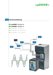
>pDRIVE<
Operating instructions Profibus
>pDRIVE< MX eco 4V
>pDRIVE< MX pro 4V
>pDRIVE< MX pro 6V
>pDRIVE< MX multi-eco
>pDRIVE< MX multi-pro
General remarks
The following symbols should assist you in handling the instructions:
Advice, tip !
General information, note exactly !
The requirements for successful commissioning are correct selection of the device, proper planning and installation. If you have
any further questions, please contact the supplier of the device.
Capacitor discharge !
Before performing any work on or in the device, disconnect it from the mains and wait at least 15 minutes until the capacitors have
been fully discharged to ensure that there is no voltage on the device.
Automatic restart !
With certain parameter settings it may happen that the frequency inverter restarts automatically when the mains supply returns
after a power failure. Make sure that in this case neither persons nor equipment is in danger.
Commissioning and service !
Work on or in the device must be done only by duly qualified staff and in full compliance with the appropriate instructions and
pertinent regulations. In case of a fault contacts which are normally potential-free and/or PCBs may carry dangerous voltages. To
avoid any risk to humans, obey the regulations concerning "Work on Live Equipment" explicitly.
Terms of delivery
The latest edition "General Terms of Delivery of the Austrian Electrical and Electronics Industry Association" form the basis of our
deliveries and services.
Specifications in this instructions
We are always anxious to improve our products and adapt them to the latest state of the art. Therefore, we reserve the right to
modify the specifications given in this instructions at any time, particular those referring to measures and dimensions. All planning
recommendations and connection examples are non-binding suggestions for which we cannot assume liability, particularly
because the regulations to be complied depend on the type and place of installation and on the use of the devices.
Regulations
The user is responsible to ensure that the device and its components are used in compliance with the applicable regulations. It is
not permitted to use these devices in residential environments without special measures to suppress radio frequency
interferences.
Trademark rights
Please note that we do not guarantee that the connections, devices and processes described herein are free from patent or
trademark rights of third parties.
Option Profibus DP for the frequency inverters
>pDRIVE< MX pro
This instructions describe the functions software version APSpro_B00_02 and higher
Theme
Page
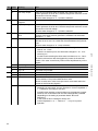
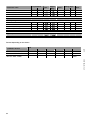
Profibus DP................................................................ 3
PBO11 / Profibus DP function.............................................4
Hardware ................................................................. 13
Mechanical construction ...................................................14
HAST
Process data area.................................................... 19
General ..............................................................................20
Control word......................................................................20
Main reference value (Auxiliary reference values) .............26
Status word .......................................................................27
Main actual value (Auxiliary actual values) ........................30
Parameterization – PKW area .................................. 31
General ..............................................................................32
8 P01 327 EN.00/00
Inverter settings ....................................................... 39
Bus - Diagnostics..................................................... 59
Diagnostics of the control / status word ...........................60
Diagnostics of the "Bus raw data" ....................................62
Application examples .............................................. 63
General ..............................................................................64
Appendix.................................................................. 67
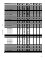
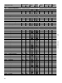
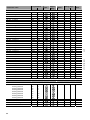
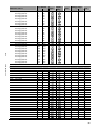
Parameter list of the >pDRIVE< MX pro ........................68
Inverter messages .............................................................93
The instructions in hand cover the topics operation, parameterization and diagnostics of the Profibus
DP option PBO11. Moreover, the principles of the Profibus architecture and their main components are
explained in detail.
Use this instructions additionally to the device documentation "Description of functions" and
"Mounting instructions".
The slave-specific configuration file pDMX09F9.gsd (8783448) is required for parameterization and
configuration of the DP master. It is provided on the CD-ROM which is attached to each inverter as
well as under www.pdrive.com.
In order to address an inverter via fieldbus also during mains cut-off (line contactor control,
disconnecting switch, ...) the >pDRIVE< MX pro has to be supplied with an external 24 V buffer
voltage.
1
2
8 P01 327 EN.00/00
HAST
8 P01 327 EN.00/00
HAST
Profibus DP
3
PBO11 / Profibus DP function
The fieldbus system Profibus DP is coupled with the >pDRIVE< MX pro frequency inverter by installing the
fieldbus option >pDRIVE< PBO11 at the front side of the device (see also chapter "Hardware").
The data exchange between "DP master" and "DP slave (MX)" is designed in accordance with the
specifications for the Profibus DP as defined in the standard DIN EN 50170.
Principle function
The serial fieldbus concept "Profibus" is structured as a logical TokenRing bus. It physically represents an
asynchronous, half-duplex RS485 system. Several Profibus masters can exist on the bus at the same time. The
master authorization (Token) is handed over to the next master after each telegram cycle. A conflict of bus
access is prevented because only that master which holds the Token has write access for the bus.
After each telegram sent by the master, the addressed slave confirms the message and sends a response
telegram to the master. The telegrams are processed cyclically (continuous) (DPV0).
The different types of protocols FMS, DP and PA are based on this system.
In the area of drive engineering, the Profibus DP (Decentralized Periphery) profile is mostly used. This is a fast
operating system with a definite hierarchy.
HAST
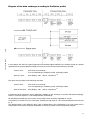
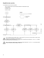
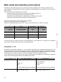
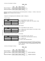
Structure of the Profibus DP user data / Drive profile
User data
Protocol frame
Parameter (PKW)
PKW: Parameter-Code-Value
(Parameter area)
4
Process data (PZD)
PZD: Process Data
(Process data area)
Protocol frame
8 P01 327 EN.00/00
The structure of the user data is arranged according to the profile for variable speed drives and is described in
the VDE Directive 3689 Sheet 1.
8 P01 327 EN.00/00
HAST
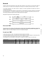
Diagram of the data exchange according to Profidrive profile
In accordance with the PPO types (Parameter Process-data Object) defined in the Profibus Profile for variable
speed drives the process data area (PZD) of the control word consists of the following user data:
Control word:
16 bit chain of commands,
11 bit corresponding to Profidrive profile, 5 bit freely usable
Main ref. value:
16 bit display, -200...+200 %, resolution 2
-14
The status word consists of the following user data:
Control word:
16 bit chain of commands,
11 bit corresponding to Profidrive profile, 5 bit freely usable
Main actual value:
16 bit display, -200...+200 %, resolution 2
-14
If parameter values should be read or adjusted in addition to the exchange of process data (data exchange),
further 4 words are required → see PKW (Parameter Code Value).
All data (PKW and PZD) are 16-bit chains of information which should be regarded as "words".
Transmission is carried out in two 8-bit bytes, whereby the high byte (8...15) is transmitted before the low byte
(0...7).
The desired length of the telegram (PPO type) is defined during the configuration of the DP master and is
transmitted to the inverter during the initialization of the bus by means of the configuration telegram.
5
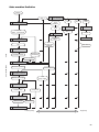
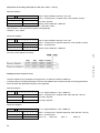
Structure of the telegram
*
Parameter code value
Process data
Parameter code
Index
Parameter value
STW: Control word
ZSW: Status word
HSW: Main reference value
HIW: Main actual value
According to the communication-specific demands, the process data word PZD2 can be also
used as second control word or second status word.
In addition to the telegram structure predefined by the Profidrive profile, the lengths of the telegrams can also
be freely defined for both directions (master → slave / slave → master). As a result the telegram length can be
optimized according to the existing requirements of the process. The configuration of the freely definable
telegrams or the selection of the PPO type is performed with the applied bus configuration tool (e.g. SyCon /
company Hilscher).
Example of an optimized telegram
6
8 P01 327 EN.00/00
PKW:
PZD:
PKE:
IND:
PWE:
HAST
The Parameter Process-data Object (PPO) is defined for the cyclical transmission of data between DP master
and slave. Process data as well as parameters can be transmitted with this object. It describes the number and
the meaning of the individual words of the available user data structures. PPO types 3 and 4 are purely
process data objects, types 1 and 2 additionally enable cyclical parameter processing.
Network configuration
Use the slave-specific Profibus DP device master file for the network configuration of a DP master connection.
For the frequency inverters >pDRIVE< MX pro the configuration file pDMX09F9.gsd (8783448) has to be used.
It is provided on the CD-ROM which is attached to each inverter as well as in the Internet under
www.pdrive.com.
; -------------------------------------------------------------------; (c) VA TECH ELIN EBG Elektronik GmbH & Co
; 8783448
; Geraetestammdatei für die Frequenzumrichter
; der Reihen: >pDRIVE< MX Eco
;
>pDRIVE< MX Pro
; Profibus DP Anschaltung mit Optionskarte PBO11
;
; Erstellt:
; 17.10.2005 TS/Jagodic
;
; Aenderungen:
;
; -------------------------------------------------------------------;
;
#PROFIBUS_DP
8 P01 327 EN.00/00
HAST
GSD_Revision
= 1
; Device identification
Vendor_Name
= "VA TECH ELIN EBG Elektronik"
Model_Name
= ">pDRIVE< MX eco/pro"
Revision
= "Version 1.00"
Ident_Number
= 0x09F9
Protocol_Ident
= 0
; DP protocol
Station_Type
= 0
; DP Slave device
FMS_supp
= 0
; FMS not supported
Hardware_Release = "8P01103" ; Option PBO11
Software_Release = "PBS01"
; Supported baudrates
9.6_supp
= 1
19.2_supp
= 1
.
.
.
The device master file contains the whole information (according to Profibus DP standard) which are required
for coupling the >pDRIVE< MX pro with a Profibus DP network. The file is designed in such a manner that it
can be read by means of a text editor.
If the GSD-file is read in to the bus configuration tool, specific bus data like ident number, Watch Dog
information, available baud rate and communication types a.s.o. are available in the device. The address
ranges are defined by means of configuration and the configuration settings are transmitted during boot up of
the network from the master to the individual slaves via the parameterization and configuration telegram. The
slave checks the plausibility of both telegrams. If the parameterization telegram as well as the configuration
telegram are valid the slave changes to "data exchange" mode and participates in the cyclical data exchange
of the bus network.
7
In addition to the GSD-file also three graphic files are available which can be optionally used in the
configuration tool.
Modifying the GSD-file leads to faulty action and is therefore not allowed!
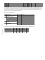
Examples for slave configuration
Communication type PPO2
Optimized telegram length
PZD master → slave 2 words
slave → master 6 words + PKW service
(configuration tool SyCon)
Using the parameters D6.34 to D6.42 it is possible to make a diagnosis of the configuration which is
set by the bus master.
In case of problems with the network configuration please ensure that the valid GSD-file is used.
Please contact the supplier of the Profibus DP master system for support.
8
8 P01 327 EN.00/00
HAST
(configuration tool SyCon)
Structure of the network
The bus access method of the Profibus DP is based on the master/slave principle whereby a slave can be read
from each master but it can only be written to the slave by one master.
A maximum of 126 subscribers can be operated on the bus, but only in separately segments. The maximum
number of subscribers per segment is 32 including the repeater.
8 P01 327 EN.00/00
HAST
Electric network
Rt ... Terminating resistor
Technical data of on electrical network
Max. number of subscribers
126 in all segments
Max. number of subscribers
per segment
32 including the repeater
Maximum repeater cascading 7 at 500 kbaud bus speed
4 at 1.5 Mbaud bus speed
Bus cable
Use a screened, twisted two-wire line as bus cable (wire type A, e.g.
LAPPKABEL UNITRONIC® BUS-L2/FIP UL/CSA).
Characteristic impedance:
Distributed capacitance:
Loop resistance:
Wire cross-section:
150 Ω ± 15Ω
< 30 nF / km
< 110 Ω / km
> 0.64 mm2
Each bus segment must be provided with a resistance combination at both ends. The terminal resistors are in
the bus plug of the two outer bus subscribers, which also supply them with electricity.
9
The bus is connected using a 9-pin sub-D plug connector. The male multipoint connector is located on the bus
cable, the multipoint socket connector (female) is located on the bus subscriber.
The bus plugs option >pDRIVE< PROFIBUS PLUG (order number 8 P01 306) are designed as T junctions,
whereby the bus line sections are connected inside of the plug connector. The terminal resistors are located in
the bus plug and can be switched on and off using DIP switches.
Meaning
1
2
3
4
5
6
7
8
9
Screen
Ground of 24 V output voltage
Received/Transmitted data -P
Control signals for the repeater
Reference potential for 5 V
Supply voltage of the terminating resistor +5 V
Output voltage +24 V
Received/Transmitted data -N
Control signals of the repeater for control of direction
Screen
M24
RXD/TxD-P
CNTR-P
DGND
VP
P24
RxD/TxD-N
CNTR-P
Depending on the baud rate and when using the described bus cable (type A), the following line lengths per
segment are permitted:
Baud rate [kbit/s]
9.6
19.2
93.75
187.5
500
1500
3000
6000
12000
Length [m]
1200
1200
1200
1000
400
200
100
100
100
10
8 P01 327 EN.00/00
9-pin Sub-D (female)
Pole Signal
HAST
Assignment of the Profibus interface at the option card PBO11
Optical (mixed) network
The optical network can be built up in a line, ring or star structure by means of OLM's (Optical Link Modules or
active star connectors.
Optical Link Module (OLM’s)
− optical coupling modules for connecting electric segments with repeater function
− 9.6 kbaud to 12 Mbaud transmission rate
Optical bus terminal
8 P01 327 EN.00/00
HAST
− for connecting individual subscribers with OLM's or star connectors
− supply from the bus subscriber
Active star connectors
− to build up star structures
− max. 16 slots (subscribers)
− slots for optical waveguides made of plastics and glass
For technical details of the optical bus components, please refer to the relevant documentation of the
manufacturer.
11
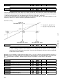
Cycle times
8 P01 327 EN.00/00
HAST
The bus cycle times depending on the number of DP bus subscribers are given in the following diagrams for
each PPO type.
The following calculation principles apply to the calculation of the bus cycle time:
tsdi = 37 bit; tsdr = 11 bit; for worst case 50% telegram repeats ! (pessimistic assumption)
12
8 P01 327 EN.00/00
HAST
Hardware
13
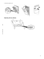
Mechanical construction
Installing the option >pDRIVE< PBO11
1. Remove the Matrix operating panel BE11 from the front side of the device.
2. Remove the front cover of the device by releasing both mechanical interlocks.
14
8 P01 327 EN.00/00
Only install the option card when there is no voltage on the inverter. Non-observance leads to
destruction of the card.
HAST
Installing of the option card into the >pDRIVE< MX pro frequency inverter is finished after a few steps.
3. Mount the option card.
8 P01 327 EN.00/00
HAST
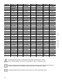
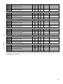
Adjusting the bus address
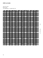
15
Address
Switch
Address
Switch
Address
Switch
0
0000 00100
32
0010 0000
64
0100 0000
96
0110 0000
1
0000 0001
33
0010 0001
65
0100 0001
97
0110 0001
2
0000 0010
34
0010 0010
66
0100 0010
98
0110 0010
3
0000 0011
35
0010 0011
67
0100 0011
99
0110 0011
4
0000 0100
36
0010 0100
68
0100 0100
100
0110 0100
5
0000 0101
37
0010 0101
69
0100 0101
101
0110 0101
6
0000 0110
38
0010 0110
70
0100 0110
102
0110 0110
7
0000 0111
39
0010 0111
71
0100 0111
103
0110 0111
8
0000 1000
40
0010 1000
72
0100 1000
104
0110 1000
9
0000 1001
41
0010 1001
73
0100 1001
105
0110 1001
10
0000 1010
42
0010 1010
74
0100 1010
106
0110 1010
11
0000 1011
43
0010 1011
75
0100 1011
107
0110 1011
12
0000 1100
44
0010 1100
76
0100 1100
108
0110 1100
13
0000 1101
45
0010 1101
77
0100 1101
109
0110 1101
14
0000 1110
46
0010 1110
78
0100 1110
110
0110 1110
15
0000 1111
47
0010 1111
79
0100 1111
111
0110 1111
16
0001 0000
48
0011 0000
80
0101 0000
112
0111 0000
17
0001 0001
49
0011 0001
81
0101 0001
113
0111 0001
18
0001 0010
50
0011 0010
82
0101 0010
114
0111 0010
19
0001 0011
51
0011 0011
83
0101 0011
115
0111 0011
20
0001 0100
52
0011 0100
84
0101 0100
116
0111 0100
21
0001 0101
53
0011 0101
85
0101 0101
117
0111 0101
22
0001 0110
54
0011 0110
86
0101 0110
118
0111 0110
23
0001 0111
55
0011 0111
87
0101 0111
119
0111 0111
24
0001 1000
56
0011 1000
88
0101 1000
120
0111 1000
25
0001 1001
57
0011 1001
89
0101 1001
121
0111 1001
26
0001 1010
58
0011 1010
90
0101 1010
122
0111 1010
27
0001 1011
59
0011 1011
91
0101 1011
123
0111 1011
28
0001 1100
60
0011 1100
92
0101 1100
124
0111 1100
29
0001 1101
61
0011 1101
93
0101 1101
125
0111 1101
30
0001 1110
62
0011 1110
94
0101 1110
126
0111 1110
31
0001 1111
63
0011 1111
95
0101 1111
The bus addresses 0 and 1 are reserved for the Profibus master (class 1 and 2).
Avoid using bus address 126 due to incompatibility to various configuration tools.
The bus address which is adjusted by means of the DIP switches is active after booting the PBO11.
Therefrom changes which are carried out during operation are without any effect !
The adjusted (effective) bus address can be read out by means of parameter D6.30.
16
HAST
Switch
8 P01 327 EN.00/00
Address
LED - Indicator lamps
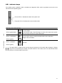
The Profibus option >pDRIVE< PBO11 includes two diagnostic LED's which are placed at the front of the
device left to the operating panel.
The red LED 2.1 indicates the state of the option card
The green LED 2.2 indicates the communication state
HAST
Meaning of the LED indication
LED 2.1 (red)
The bus option has received a valid parameter and configuration telegram
from the master.
LED 2.2 (green) lights
Communication state "Data Exchange" is active, that means that cyclical
data exchange with the DP master takes place.
LED 2.1 (red) flashes
The bus option expects a valid parameterization and configuration
telegram from the master.
8 P01 327 EN.00/00
LED 2.2 (green)
LED 2.1 (red) lights
Bus fault
LED 2.2 (green)
The green LED L2.2 lights as soon and as long as the slave is in the mode "data exchange". If Watch
Dog was not activated by the master, the slave remains in this mode, even if no data transfer takes
place; e.g. if the bus cable is removed !
17
18
8 P01 327 EN.00/00
HAST
8 P01 327 EN.00/00
HAST
Process data area
19
General
During the cyclical exchange of process data, binary or analog reference and actual values are exchanged
between the bus subscribers, i.e. between DP master and DP slaves.
The achievable cycle time depends on the bus structure, the number of bus subscribers and the transmission
rate. See chapter "Network configuration".
Every 5 ms the inverter internally reads in a control word or prepares a status word for the master.
HAST
The standardized information in the control and status word (bit 0...10) do not require any further internal
inverter settings. The reference use, the assignment of actual values as well as the use of the free bits 11...15)
of the first (STW1) and second control word (STW2) must be adjusted accordingly in matrix field "D6 Fieldbus".
Control word
8 P01 327 EN.00/00
Assignment
Bit 15
Bit 14
5 freely configurable
Bit 13
control bits for internal or external
Bit 12
frequency inverter commands
Bit 11
20
Bit 10
Control O.K.
No control
Bit 9
–
–
Bit 8
–
–
Bit 7
Reset
–
Bit 6
Release reference value
Lock reference value
Bit 5
Release ramp integrator
Lock ramp integrator
Bit 4
Release ramp output
Lock ramp output
Bit 3
Release operation
Lock operation
Bit 2
Operating condition
OFF 3 (Fast stop)
Bit 1
Operating condition
OFF 2 (Impulse inhibit)
Bit 0
On
OFF 1
High = 1
Low = 0
Description of control word bits
Bit
Value
Meaning
Note
0
1
ON
− Is accepted when the drive state is "1 .. Ready to switch on" and
changes to drive state "3 Ready to run" if the DC link is charged.
− At active line contactor control: Change to drive state "2 .. Charge
DC link", after successful charging the drive state changes to
"3 .. Ready to run".
0
OFF 1
− When the command has been accepted, the drive state changes to
"13 .. OFF 1 active" and thus the drive is shut down along the
deceleration ramp.
− When the output frequency reaches zero Hz: the drive state changes
from "0 .. Not ready to switch on" to "1 .. Ready to switch on" if the
basic state (bit 1 = 0, bit 2 = 1, bit 3 = 1 and bit 10 = 1) is present.
− If a renewed OFF 1 (On) command occurs during deceleration, the
inverter tries to reach the given reference value along the
acceleration ramp. Thereby the drive state changes to "7 .. Run".
− At active line contactor control, the line contactor is switched off if
the drive state changes to "1 .. Ready to switch on".
1
Operating condition
"OFF 2" command canceled
0
OFF 2
(Impulse inhibit)
− When the command has been accepted, the inverter will be locked
and the drive state changes to "19 .. Lock switching-on".
HAST
1
− At active line contactor control the main contactor is switched off.
− If the basic state (bit 1 = 0, bit 2 = 1, bit 3 = 1 and bit 10 = 1) is given,
the drive state changes to "1 .. Ready to switch on".
8 P01 327 EN.00/00
The OFF 2 command can also be triggered by means of the terminal
function Impulse enable !
2
1
Operating condition
"OFF 3" command canceled
0
OFF 3
− When the command has been accepted, the drive state changes to
"14 .. OFF 3 active" and the drive is shut down as quickly as
possible with maximum current and maximum DC link voltage.
− When the output frequency reaches zero Hz, the drive state changes
to "19 .. Lock switching-on".
− Thereby, at active line contactor control the main contactor is
switched off. If the OFF 3 command (bit 2 = 1) is canceled during
deceleration, fast stop is executed all the same.
3
1
Operation released
When the command has been accepted, the inverter is released
(Impulse enable) in drive state "3 .. Ready to run" and afterwards the
drive state changes to "4 .. Operation released".
0
Lock operation
− When the command has been accepted, the inverter will be locked
and the drive state changes to "3 .. Ready to run".
− If the drive state is "13 .. OFF 1 active", the inverter will be locked
and the drive state changes to "0 .. Not ready to switch on".
− Thereby, at active line contactor control the main contactor is
switched off.
− If the basic state (bit 1 = 0, bit 2 = 1, bit 3 = 1 and bit 10 = 1) is given,
the drive state changes to "1 .. Ready to switch on".
− If the drive state is "14 .. OFF 3 active", the procedure is executed all
the same !
21
Value
Meaning
Note
4
1
Release ramp output
Drive state "5 .. Ramp output released"
0
Lock ramp output
When the command has been accepted, the output of the ramp
function generator is set to zero. The drive stops with maximum current
and maximum DC link voltage.
The drive state changes to "4 .. Operation released".
1
Release ramp
integrator
Drive state "6 .. Ramp output released"
0
Stop ramp integrator
When the command has been accepted, the output of the ramp
function generator is set to zero. The drive stops with maximum current
and maximum DC link voltage.
The drive state changes to "4 .. Operation released".
1
Release reference
value
When the command has been accepted, the given reference value at
the input of the ramp function generator is released. The drive state
changes to "7 .. Run".
0
Lock reference value
When the command has been accepted, the input of the ramp function
generator is set to zero. As a result the drive decelerates along the set
ramp.
The drive state changes to "6 .. Ramp released".
1
Reset
− The reset command is accepted at the positive edge when the drive
state is "20 .. Fault".
5
6
7
− If there is no fault anymore, the drive state changes to "19 .. Lock
switching-on".
− If a fault is still remaining the drive state is furthermore "20 .. Fault".
HAST
Bit
8
9
10
0
no meaning
1
Jog 1 start
Command not provided
0
Jog 1 off
Command not provided
1
Jog 2 start
Command not provided
0
Jog 2 off
Command not provided
1
Control O.K.
When the command has been accepted, the DP slave is controlled via
the bus interface. The process data become valid.
This bit must be set in order to accept control commands and/or the
free bits as well as analog signals !
0
No control
− When the command has been accepted, all data are processed
depending in status bit 9 "Control requested". Control requested ==
1 → Behaviour according to bus fault
− If the DP slave requests control furthermore, the frequency inverter
switches over to fault state with the fault message BUS_COMM2
(depending on the setting of parameter D6.03 "Bus error
behaviour").
In this case an alarm message is always set !
Control requested == 0 → Data to 0 ! → only I/O or panel
operation
22
8 P01 327 EN.00/00
The reset command can also be triggered by means of the terminal
function "Ext. reset" as well as by means of the Stop/Reset key on the
keypad.
Summary of the most important control commands
Control word
Function
Binary
Hexadecimal
0000010001111111
47F
ON
Start with controlled
acceleration
OFF 1
0000010001111110
Stop according to the set
deceleration ramp
corresponds with the
"basic state"
OFF 2
0000010001111101
results in drive state
Lock switching-on !
Impulse inhibit
(free-wheeling)
HAST
OFF 3
results in drive state
Lock switching-on !
Reset
8 P01 327 EN.00/00
47D
0000010001111011
Emergency stop
(deceleration at current or DC
link voltage limit)
xxxxx1xx1xxxxxxx
0000010001111111
+0010000000000000
0010010001111111
Use of a free bit (e.g. 13)
during operation
Canceling
"Lock switching-on"
47E
Basic state
start command
"15 Lock switching-on"
0000010001111110
0000010001111111
47B
e.g. 480
47F
+2000
247F
e.g.:
47E
47F
23
Simplified state machine
For standard control with the commands:
− Start / Stop along the inverter-internal acceleration / deceleration ramps
− Impulse inhibit
− Emergency stop
8 P01 327 EN.00/00
HAST
− Reset of a fault
The commands Impulse inhibit (OFF 2), Fast stop (OFF 3) as well as a fault which has been reset
always result in drive state "Lock switching-on" !
In order to reach drive state "Run" it is necessary to send the basic state (bit 0 = 0, bit 1, 2 = 1) before
transmitting the start command (bit 0 = 1).
After connecting the mains (bootup of the drive) the basic state (bit 0 = 0, bit 1, 2 =1) must be provided
in order to reach drive state "Ready to switch on".
24
State machine Profidrive
Bootup
OFF 1
0
19 Lock switching-on
Lock
operation
Not ready to switch on
f is 0
Control OK +
OFF1 + basic state
OFF 1
Ready to switch on
On +
ON after OFF1
released
ON
2
No
fault
20 Fault
Fault
All states
also OFF 3!
Charge DC link
Hardware
Not Ready
Hardware Ready
HAST
14 OFF 3 active
OFF 2
OFF 3
13 OFF 1 active
1
f is 0
Lock operation
8 P01 327 EN.00/00
3
Ready to run
Release operation
4
Lock operation
Operation released
Lock
ramp output
Release ramp output
5
Ramp output released
Release ramp
6
Ramp released
Release SW
7
Ramp hold
Lock SW
Run
Lowest priority
Top priority
25
Main reference value (Auxiliary reference values)
Depending on the used PPO type one to nine reference values are available in the Profibus user data protocol.
The meaning of the individual reference values (each 16 bit) is defined by parameterization of the >pDRIVE<
MX pro using the Matrix surface.
The reference values can be divided into two groups:
− inverter-internal reference values like e.g. f-reference, PID actual/reference value and suchlike (according
to the reference use)
− forwarding to the analog outputs for external use, without influencing the inverter control (bit 10 STW
must be 1 !).
The reference values are linear scaled values with 16 bit display.
That is: 0 % = 0 (0 hex), 100 % = 214 (4000 hex)
Therefrom a presentable data range of -200...+200 % with a resolution of 2-14 (0.0061 %) results.
Hexadecimal
Decimal
199.9939
01111111 11111111
7FFF
32767
100.0000
01000000 00000000
4000
16384
0.0061
00000000 00000001
0001
1
0.0000
00000000 00000000
0000
0
-0.0061
11111111 11111111
FFFF
-1
-100.0000
11000000 00000000
C000
-16384
-200.0000
10000000 00000000
8000
-32768
The reference values are scaled by means of parameterization in matrix field D6. All reference values are
scaled in Hz or %.
Using bits 11...15 of the control word
According to the Profibus profile bits 11...15 are not defined and therefore they can be freely used by the user.
If more than five free control bits are required, process data word PZD2 can be defined as additional control
word STW2 using parameter D6.100.
When the frequency inverter is parameterized appropriate, this digital information can be used
− for inverter-internal control signals (corresponding to the use of the digital inputs) or
− totally separated from the inverter functions in order to transmit information using the digital outputs of
the frequency inverter (bit 10 STW1 must be 1 !).
Use
Inverter – "internal"
Inverter – "external"
26
Free control bits
f-reference 2
2nd ramp
External fault
PID active
Mains ON(OFF)
...
(for the complete list see matrix filed D6)
Relay and digital outputs of the basic card
or the option card IO11 or IO12
Possible reference values
f-reference 1
f-reference 2
f-correction
PID ref. value
PID actual value
Analog output of the basic card or
the option card >pDRIVE< IO12
HAST
Binary
8 P01 327 EN.00/00
%
Status word
Assignment
Bit 15
Bit 14
5 freely configurable
Bit 13
status bits for internal or external
Bit 12
frequency inverter messages
8 P01 327 EN.00/00
HAST
Bit 11
Bit 10
f (n) ≥ f level
f (n) ≤ f level
Bit 9
Control requested
No control rights requested
Bit 8
f (n) = f (n) ref
f (n) ≠ f (n) ref
Bit 7
Alarm
No alarm
Bit 6
Lock switching-on
No Lock switching-on
Bit 5
No OFF 3
OFF 3 (Emergency stop)
Bit 4
No OFF 2
OFF 2 (Impulse inhibit)
Bit 3
Fault
No fault
Bit 2
Operation released
Operation locked
Bit 1
Ready to run
Not ready to run
Bit 0
Ready to switch on
Not ready to switch on
High = 1
Low = 0
Listing of the most important
drive states
Status word bits
10
9
8
7
6
5
4
3
2
1
0
0 .. Not ready to switch on
x
1
x
x
0
x
x
0
0
0
0
1 .. Ready to switch on
x
1
x
x
0
x
x
0
0
0
1
3 .. Ready to run
x
1
x
x
0
x
x
0
0
1
1
7 .. Run
x
1
x
x
0
1
1
0
1
1
1
19 .. Lock switching on
x
1
x
x
1
x
x
0
0
0
0
20 .. Fault
x
1
x
x
0
x
x
1
0
0
0
0 .. Bit state zero
1 .. Bit state one
x .. Bit state is undefined
27
Description of status word bits
Bit
Value
0
1
Meaning
Ready to switch on
Note
The drive state is "1 .. Ready to switch on".
The inverter is locked.
At active line contactor control the main contactor is switched off.
1
0
Not ready to switch on The drive state is "0 .. Not ready to switch on" or "19 .. Lock
switching-on".
1
Ready to run
The drive state is "3 .. Ready to run".
That means that there is voltage on the power part and there are no
faults. But the inverter is still locked.
At active line contactor control the Run message already occurs
during charging → drive state "2 .. Charge DC link"
2
0
Not ready to run
1
Operation released
The drive state is "4 .. Operation released", "5 .. Ramp output
released", "6 .. Ramp released", "7 .. Run", "13 .. OFF 1 active" or
"14 .. OFF 3 active".
Operation locked
1
Fault
The drive is not in operation due to a fault. The drive state is
"20 .. Fault".
After successful trouble shooting and reset of the fault the drive state
changes to "19 .. Lock switching-on".
4
5
6
0
Failure-free
1
no OFF 2
0
OFF 2 (Impulse inhibit) An OFF 2 (impulse inhibit) command is given.
1
no OFF 3
0
OFF 3 (emergency
stop)
An OFF 3 (emergency stop) command is given.
1
Lock switching-on
The inverter has drive state "19 .. Lock switching-on".
This state occurs in consequence of the commands OFF 2, OFF 3
and "Lock operation" as well as after successful resetting of a fault.
This drive state is canceled by means of bit 0 STW = 0.
The drive state "Lock switching-on" is canceled by means of bit 1 of
the control word (OFF1/ON).
7
8
28
0
No lock switching-on
1
Alarm
0
No alarm
1
f, (n) = f, (n) ref
0
f, (n) ≠ f, (n) ref
There is an alarm message, resetting is not required.
Comparison of reference and actual value for frequency or speed.
A tolerance of 0.5 Hz is accepted.
8 P01 327 EN.00/00
3
0
HAST
The inverter is operating with impulse enable and there is voltage on
the output terminals.
Bit
Value
9
1
Meaning
Control requested
Note
If the frequency inverter is parameterized for bus operation by means
of parameter D6.01 (control via bus), the inverter asks the DP master
for assumption of control after mains connection or connecting an
external 24 V buffer voltage.
As long as the master does not assume control, an alarm message
(ZTW bit 7) is given.
0
No bus operation
If the inverter is disconnected from the bus communication because
of switching to panel mode (key on the keypad), bit 9 is reset to zero.
− If the master does not send "Control OK" (STW bit10 = 0), an
alarm message is set.
− If the drive is switched to remote mode = bus operation again, the
automation system has to answer with "Control OK" within 2
seconds. Otherwise the drive is switched back to panel mode
automatically.
1
f ≥ f level
Function not provided
0
f ≤ f level
Function not provided
8 P01 327 EN.00/00
HAST
10
29
Main actual value (Auxiliary actual values)
Depending on the used PPO type one to nine actual values are available in the Profibus user data protocol.
The meaning of the individual actual values is defined by parameterization of the >pDRIVE< MX pro using the
Matrix surface.
The actual values can be divided into two groups:
− inverter-internal actual values like e.g. actual value of speed, torque a.s.o.
(according to the analog outputs of the frequency inverter)
− assumption of the analog inputs for external use by means of the DP master
(without influencing the inverter control). Bit 10 STW must be 1 !
The actual values are linear scaled values with 16 bit display.
That is 0 % = 0 (0 hex), 100 % = 214 (4000 hex)
Therefrom a presentable data range of -200...+200 % with a resolution of 2-14 (0.0061 %) results.
Hexadecimal
Decimal
199.9939
01111111 11111111
7FFF
32767
100.0000
01000000 00000000
4000
16384
0.0061
00000000 00000001
0001
1
0.0000
00000000 00000000
0000
0
-0.0061
11111111 11111111
FFFF
-1
-100.0000
11000000 00000000
C000
-16384
-200.0000
10000000 00000000
8000
-32768
The actual values are scaled by means of parameterization in matrix field D6. The scaling of the individual
actual values is fixed for each output value. See matrix field D6.
Using bits 11...15
According to the Profibus profile bits 11...15 of the status word ZTW1 are not defined and therefore they can
be freely used by the user. When the frequency inverter is parameterized appropriate, this digital information
can be derived from inverter-internal operating states (corresponding to the digital outputs) as well as totally
separated from the inverter functions by means of the digital inputs of the frequency inverter.
If more than five free status word bits are required, process data word PZD2 can be defined as additional
status word ZTW2 using parameter D6.137 Fieldbus actual values.
Use
Inverter – "internal"
Free status word bits
Actual values
Ready
Output frequency
Run
|Output frequency|
Ready / run
Output current
Fault
Torque
...
...
(for the complete list see matrix field D6) (for the complete list see matrix field D6)
Inverter – "external"
30
DI1...DI6
DI7...DI10 or DI11...DI14
Analog inputs of the basic card or the
option card >pDRIVE< IO12
HAST
Binary
8 P01 327 EN.00/00
%
8 P01 327 EN.00/00
HAST
Parameterization – PKW area
31
General
Using the PKW service (Parameter code value) each parameter of the inverter can be read and written by
means of the bus. The PKW service is designed on the basis of the Profidrive profile and contains 4 words.
In the PKW mechanism, the master frames a request, the inverter processes the request and returns a
corresponding response.
Processing parameterization happens inverter-internal in the background. Parameter requests are processed
time-optimized there, i.e. a request is accepted and a response is provided to be picked up at the same time.
The inverter provides the response until the master frames a new request.
HAST
Request and response are of following data type:
The parameter code is used to select parameters by means of their logical address. Addresses are valid in the
range of 0...2047 (11 bits) and they are mentioned in the parameter list which is provided in the appendix. The
address is used in the request telegram as well as in the response telegram.
Second word "IND"
In the second word, the "index", the request and response code is transmitted.
In the request telegram there is a read and write command defined. If a request telegram is executed positive,
the original request is transmitted as response code in the response telegram.
If the requests are not executable the value 004E hex is appears as response code in the index field.
Request code
Index
Pos. response
Neg. response
No request
0000 hex
0 dec
0000 hex
0 dec
0000 hex
0 dec
Request parameter value (read)
0052 hex
82 dec
0052 hex
82 dec
004E hex
78 dec
Write parameter value
0057 hex
87 dec
0057 hex
87 dec
004E hex
78 dec
32
8 P01 327 EN.00/00
First word "PKE"
Third and fourth word "PWE - High", "PWE - Low"
If read or write requests are successfully processed, the value of the parameter which is defined by the logical
address is transmitted in the two words PWE-High and PWE-Low. Thereby the value of the third word is
always zero.
If a request is not executable, a corresponding fault code is transmitted in the 4th word (PWE-Low) instead of
the parameter value.
Fault code (PWE-Low)
Fault
0000 hex = dec
Faulty addressing
Possible causes of fault
− Inadmissible logical address
− Access to a logical address which does not exist
− Parameter is of type "actual value"
− Parameter cannot be changed during operation
0001 hex = dec
Faulty parameterization
− Parameter cannot be changed due to double
assignment
− Parameterising station (F6.03) is not set to "Profibus"
HAST
Rules for processing of requests / responses
• The master must repeat a request until he receives a corresponding response from the inverter. During
processing the request the inverter still sends the response of the previous request.
• The master has to identify the response to the sent request:
• due to evaluation of the response code
8 P01 327 EN.00/00
• due to evaluation of the parameter number
• due to evaluation of the parameter value
• requests and responses must be transmitted completely in one telegram, combined requests are not
possible.
• In case of responses which include actual values the inverter always returns the actual value when
repeating the response telegrams.
• If no information should be exchanged by means of the PKW mechanism, the master has to define the
request code "no request".
• For write requests, the value which is transmitted in the answer must be evaluated (the request is canceled
if the value remains the same or if a fault occurs).
• After responses which contain a fault number (response code 4E) "no response" must be entered in the
request list if the next regular request refers to the same logical address (deleting the last fault message).
• After changing a parameter a storage command must be sent in order to protect the data against voltage
loss. The storage command takes place when writing value 1 to the logical address 0028 hex / 40 dec.
After successful storage the value must be set to 0 again.
33
Examples
Reading the shaft power (parameter A2.07)
Request telegram
0 0 0 0 0 0 0 1 0 0 0 0 0 1 1 1
A2.07: logical address 107 dec / 006B hex
0 0 0 0 0 0 0 0 0 1 0 1 0 0 1 0
Bit 8...15 always zero / request code "read" (82 dec / 52 hex)
0 0 0 0 0 0 0 0 0 0 0 0 0 0 0 0
No entry required
0 0 0 0 0 0 0 0 0 0 0 0 0 0 0 0
No entry required
Response telegram
0 0 0 0 0 0 0 1 0 0 0 0 0 1 1 1
A2.07: logical address 107 dec / 006B hex
0 0 0 0 0 0 0 0 0 1 0 1 0 0 1 0
Bit 8...15 always zero / positive response "read" (82 dec / 52 hex)
0 0 0 0 0 0 0 0 0 0 0 0 0 0 0 0
Bit 0...15 always zero
0 0 0 0 0 0 0 0 0 1 1 1 1 0 1 1
Binary value of the actual shaft power = 123 dec
Scaling: Real value = transmitted value / factor (see the factor in the parameter list given in the appendix)
HAST
P = 123 / 10 = 12.3 kW
Adjusting the parameterizing station to Profibus (F6.03 = setting 4)
Request telegram
0 0 0 0 0 1 0 0 0 1 1 1 1 0 1 0
F6.03: logical address 1146 dec / 047A hex
0 0 0 0 0 0 0 0 0 1 0 1 0 1 1 1
Bit 8...15 always zero / request code "write" (87dec / 57hex)
0 0 0 0 0 0 0 0 0 0 0 0 0 0 0 0
No entry required
0 0 0 0 0 0 0 0 0 0 0 0 0 1 0 0
Binary value 4
Response telegram
0 0 0 0 0 1 0 0 0 1 1 1 1 0 1 0
F6.03: logical address 1146 dec / 047A hex
0 0 0 0 0 0 0 0 0 1 0 1 0 1 1 1
Bit 8...15 always zero / positive response "write" (87dec / 57hex)
0 0 0 0 0 0 0 0 0 0 0 0 0 0 0 0
Bit 0...15 always zero
0 0 0 0 0 0 0 0 0 0 0 0 0 1 0 0
Binary value 4
34
8 P01 327 EN.00/00
Summary of the telegram exchange
Summary of the telegram exchange
It is necessary to set parameter F6.03 "Parametrising station" to setting "4 .. Profibus" in order to be
qualified for adjusting other parameters.
Assignment of the digital input DI1 to Motorpot + (D2.01 = setting 14)
8 P01 327 EN.00/00
HAST
Request telegram
0 0 0 0 0 0 1 0 1 1 1 1 1 1 1 1
D2.01: logical address 767 dec / 02FF hex
0 0 0 0 0 0 0 0 0 1 0 1 0 1 1 1
Bit 8...15 always zero / request code "write" (87dec / 57hex)
0 0 0 0 0 0 0 0 0 0 0 0 0 0 0 0
No entry required
0 0 0 0 0 0 0 0 0 0 0 0 1 1 1 0
Binary value 14
Response telegram (when the request has been accepted
0 0 0 0 0 0 1 0 1 1 1 1 1 1 1 1
D2.01: logical address 767 dec / 02FF hex
0 0 0 0 0 0 0 0 0 1 0 1 0 1 1 1
Bit 8...15 always zero / positive response "write" (87dec / 57hex)
0 0 0 0 0 0 0 0 0 0 0 0 0 0 0 0
Bit 0...15 always zero
0 0 0 0 0 0 0 0 0 0 0 0 1 1 1 0
Binary value 14
Response telegram (when the request is not executable)
0 0 0 0 0 0 1 0 1 1 1 1 1 1 1 1
D2.01: logical address 767 dec / 02FF hex
0 0 0 0 0 0 0 0 0 1 0 0 1 1 1 0
Bit 8...15 always zero / fault code (78 dec / 004E hex)
0 0 0 0 0 0 0 0 0 0 0 0 0 0 0 0
Bit 0...15 always zero
0 0 0 0 0 0 0 0 0 0 0 0 0 0 0 1
Fault code 01 (faulty parameterization)
01 .. Parameter value cannot be written (Adjusting parameters is
only permitted during impulse inhibit. You try to assign the digital
function "Motorpot +" twice or the parameterization station is not
set to "Profibus".)
Summary of the telegram exchange
35
Adjustment of an analog value (D3.04 "AO1 max. value" = 150 %)
Request telegram
0 0 0 0 0 0 1 1 0 0 0 1 0 0 0 1
D3.04: logical address 785 dec / 0311 hex
0 0 0 0 0 0 0 0 0 1 0 1 0 1 1 1
Bit 8...15 always zero / request code "write" (87dec / 57hex)
0 0 0 0 0 0 0 0 0 0 0 0 0 0 0 0
No entry required
0 0 1 1 1 0 1 0 1 0 0 1 1 0 0 0
Binary value 15000 dec / 3A98 hex
Scaling: value which should be transmitted = real value * factor
(see the factor in the parameter list given in the appendix)
150.00% * 100 =15000
Response telegram
0 0 0 0 0 0 1 1 0 0 0 1 0 0 0 1
D3.04: logical address 785 dec / 0311 hex
0 0 0 0 0 0 0 0 0 1 0 1 0 1 1 1
Bit 8...15 always zero / positive response "write" (87dec / 57hex)
0 0 0 0 0 0 0 0 0 0 0 0 0 0 0 0
Bit 0...15 always zero
0 0 1 1 1 0 1 0 1 0 0 1 1 0 0 0
Binary value 15000 dec / 3A98 hex
8 P01 327 EN.00/00
HAST
Summary of the telegram exchange
Reading the drive reference F1.01
The drive reference is a parameter of the type text. It is read out in ASCII-coded form.
Corresponding to the expected length of text the start address and a certain number of ensuing parameters
has to be read. See parameter list given in the appendix.
Request telegram
0 0 0 0 0 0 0 0 0 0 0 0 1 0 1 1
F1.01: logical address 11 dec / 000B hex
0 0 0 0 0 0 0 0 0 1 0 1 0 0 1 0
Bit 8...15 always zero / request code "read" (82 dec / 52 hex)
0 0 0 0 0 0 0 0 0 0 0 0 0 0 0 0
No entry required
0 0 0 0 0 0 0 0 0 0 0 0 0 0 0 0
No entry required
Response telegram
0 0 0 0 0 0 0 0 0 0 0 0 1 0 1 1
F1.01: logical address 11 dec / 000B hex
0 0 0 0 0 0 0 0 0 1 0 1 0 0 1 0
Bit 8...15 always zero / positive response "read" (82 dec / 52 hex)
0 0 0 0 0 0 0 0 0 0 0 0 0 0 0 0
Bit 0...15 always zero
0 1 0 0 1 1 0 1 0 1 0 1 1 0 0 0
bit 8...15:
36
ASCII "M"
bit 0...7:
ASCII "X"
Request telegram
0 0 0 0 0 0 0 0 0 0 0 0 1 1 0 0
Response for logical address 12 dec / 000C hex
. . .
0 1 1 0 0 1 0 1 0 1 1 0 0 0 1 1
bit 8...15:
0 0 0 0 0 0 0 0 0 0 0 0 1 1 0 1
Response for logical address 13 dec / 000D hex
. . .
0 1 1 0 1 1 1 1 0 1 1 0 1 0 0 0
bit 8...15:
0 0 0 0 0 0 0 0 0 0 0 0 1 1 1 0
Response for logical address 14 dec / 000E hex
. . .
0 1 0 1 0 1 1 0 0 0 1 1 0 0 0 1
bit 8...15:
0 0 0 0 0 0 0 0 0 0 0 0 1 1 1 1
Response for logical address 15 dec / 000F hex
. . .
0 0 1 0 1 1 1 0 0 0 1 1 0 1 0 1
bit 8...15:
0 0 0 0 0 0 0 0 0 0 0 1 0 0 0 0
Response for logical address 16 dec / 0010 hex
ASCII "e"
ASCII "o"
ASCII "V"
ASCII "."
bit 0...7:
bit 0...7:
bit 0...7:
bit 0...7:
ASCII "c"
ASCII "4"
ASCII "1"
ASCII "5"
HAST
. . .
0 0 1 0 0 0 0 0 0 0 0 0 0 0 0 0
bit 8...15:
ASCII "_"
bit 0...7:
ASCII "\n"
0 0 0 0 0 0 0 0 0 0 0 1 0 0 0 1
Response for logical address 17 dec / 0011 hex
8 P01 327 EN.00/00
. . .
0 0 0 0 0 0 0 0 0 0 0 0 0 0 0 0
bit 8...15:
ASCII "\n"
bit 0...7:
ASCII "\n"
0 0 0 0 0 0 0 0 0 0 0 0 0 0 1 0
Response for logical address 18 dec / 0012 hex
. . .
0 0 0 0 0 0 0 0 0 0 0 0 0 0 0 0
bit 8...15:
ASCII "\n"
bit 0...7:
ASCII "\n"
Summary of the telegram exchange
If you string the characters decoded
with ASCII together, you get the drive
reference
MXeco4V1.5_
(in case of this device only 10
characters are used)
4D 58 65 63 6F 34 56 31 2E 35 20 00 00 00 00 00
(MXeco4V1.5_)
37
ASCII code table
ISO / IEC 10 367
Basic G0 Set
38
Char
hex
Char
hex
Char
hex
Char
hex
Char
hex
Char
20
Space
40
@
60
`
A1
¡
C1
Á
E1
á
21
!
41
A
61
a
A2
¢
C2
Â
E2
â
22
"
42
B
62
b
A3
£
C3
Ã
E3
ã
23
§
43
C
63
c
A4
¤
C4
Ä
E4
ä
24
$
44
D
64
d
A5
¥
C5
Å
E5
å
25
%
45
E
65
e
A6
¦
C6
Æ
E6
æ
26
&
46
F
66
f
A7
§
C7
Ç
E7
ç
27
´
47
G
67
g
A8
¨
C8
È
E8
è
28
(
48
H
68
h
A9
©
C9
É
E9
é
29
)
49
I
69
i
AA
ª
CA
Ê
EA
ê
2A
*
4A
J
6A
j
AB
«
CB
Ë
EB
ë
2B
+
4B
K
6B
k
AC
¬
CC
Ì
EC
ì
2C
,
4C
L
6C
l
AD
CD
Í
ED
í
2D
-
4D
M
6D
m
AE
®
CE
Î
EE
î
2E
.
4E
N
6E
n
AF
¯
CF
Ï
EF
ï
2F
/
4F
O
6F
o
B0
°
D0
Ð
F0
ð
30
0
50
P
70
p
B1
±
D1
Ñ
F1
ñ
31
1
51
Q
71
q
B2
²
D2
Ò
F2
ò
32
2
52
R
72
r
B3
³
D3
Ó
F3
ó
33
3
53
S
73
s
B4
´
D4
Ô
F4
ô
34
4
54
T
74
t
B5
μ
D5
Õ
F5
õ
35
5
55
U
75
u
B6
¶
D6
Ö
F6
ö
36
6
56
V
76
v
B7
·
D7
×
F7
÷
37
7
57
W
77
w
B8
¸
D8
Ø
F8
ø
38
8
58
X
78
x
B9
¹
D9
Ù
F9
ù
39
9
59
Y
79
y
BA
º
DA
Ú
FA
ú
3A
:
5A
Z
7A
z
BB
»
DB
Û
FB
û
3B
;
5B
[
7B
{
BC
¼
DC
Ü
FC
ü
3C
<
5C
\
7C
|
BD
½
DD
Ý
FD
ý
3D
=
5D
]
7D
}
BE
¾
DE
Þ
FE
þ
3E
>
5E
^
7E
~
BF
¿
DF
ß
FF
ÿ
3F
?
5F
_
7F
DEL
C0
À
E0
à
0
\n
8 P01 327 EN.00/00
hex
HAST
Latin Alphabet No. 1 supplementary set
8 P01 327 EN.00/00
HAST
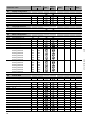
Inverter settings
39
D6
Fieldbus
Settings of the serial communication properties
General fieldbus settings
Parameter group D6 Fieldbus is used for configuration of all fieldbus connections which are possible with the
>pDRIVE< MX pro. The two fieldbus connections CANopen and Modus are available as standard. Further
fieldbuses like e.g. Profibus DP can be realized by means of optional PCBs which can be built-in.
According to the used bus which is selected with parameter D6.01 only parameters for this bus are displayed
in matrix field D6.
D6.01
Bus selection
0 .. No bus
The desired fieldbus system is activated by means of parameter D6.01 "Bus selection". The
activation influences the principle data exchange between the bus subscribers in respect of the
transmitted process data (reference / actual values) and the parameterization service.
In order to use the bus control word of the respective bus profile for the control of the >pDRIVE<
MX pro, Control source 1 or 2 (E4.01, E4.02) must be set to "Bus".
HAST
0 ...No bus
1 ...Modbus
2 ...CanOpen
3 ...Profibus
D6.02
Control requested
1 .. Active
0 ...Not active
1 ...Active
In order to recognize a communication problem at the serial fieldbus interface, two different
monitoring routines are available.
Watch dog timing
The watch dog timing checks the fieldbus interface for a cyclical signal of the active bus master or
scanner and therefrom it is a check of the bus hardware (cable break, malfunction of the master
component, ...). The monitoring time depends on the existing network configuration like the number
of subscribers, set baud rate a.s.o.. It is automatically transmitted from the master to the slave by
means of the parameterization telegram or it has to be set at the inverter.
Loss of control
In contrast to the watch dog timing the control monitoring checks the data content of the serial data
traffic. If a malfunction occurs at the fieldbus master or its respective PLC, all outgoing data are set
to zero (Fail Save Mode). Therefore, the slave receives a telegram (with data content zero)
periodically whereby the triggering of the watch dog timing is prevented.
In order to recognize this state and to take suitable measures, a monitoring of control can be
activated with parameter D6.02 (typical for Profibus DP).
If parameter D6.02 Control requested is set to "1 .. Active" the inverter monitors bit 10 of the control
word. If this bit equals state "Low", loss of control is detected.
40
8 P01 327 EN.00/00
See also parameter group E4 of the >pDRIVE< MX pro Description of functions.
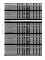
D6.03
Bus error behaviour
1 .. Trip
1 ...Trip
2 ...Last ref. val & alarm
3 ...Emerg. ref.val. & alarm
D6.04
Bus error delay time
0.5 s
0...3200 s
Parameter D6.03 defines the behaviour of the inverter if a bus error occurs. Depending on the
process demands one of the following reactions can be selected:
Setting
Behaviour in case of a bus fault
1 .. Trip
Fault shut-down with the message "Bus fault".
2 .. Last ref. val & alarm
The alarm message "Bus fault" is set. The
operation and uses the last valid reference
instead of the missing bus reference value. If
available again, the bus reference value is
message is reset.
drive still remains in
value of this source
the bus connection is
used and the alarm
HAST
The alarm message "Bus fault" is set. The drive still remains in
operation and uses the value according setting SW1-9 emergency
3 .. Emerg. ref.val. & alarm value (see matrix field D6) instead of the missing bus reference value.
If the bus connection is available again, the bus reference value is
used and the alarm message is reset.
8 P01 327 EN.00/00
Profibus DP settings
D6.30
DP slave address
For control reasons, parameter D6.30 "DP slave address" shows the adjusted slave address which
is set using the DIP switches at the Profibus option PBO11.
After adjusting the address (using the DIP switches) the drive has to be disconnected from the mains
(and a possibly existing 24 V buffer voltage) for a short time or activate the routine Software reset
(F2.46) in order to reboot the drive and to assign the set slave address to the communication
processor.
D6.31
DP baud rate
0 ...12000 kbaud
1 ...6000 kbaud
2 ...3000 kbaud
3 ...1500 kbaud
4 ...500 kbaud
5 ...187,5 kbaud
6... 93,75 kbaud
7... 45,45 kbaud
8... 19,2 kbaud
9... 9,6 kbaud
If a running DP master is operating on the bus the PBO11 interface is automatically synchronized to
the bus speed given from the DP master. Parameter D6.31 shows the active baud rate.
41
D6.32
Slave state
0 ...Init
1 ...Real-time operation
2 ...Parametrisation phase
5 ...Fault
6 ...Busy
7 ...Config. phase
Displays the actual operating state of the Profibus connection.
D6.33
Function
Meaning
0 .. Init
Boot phase after initialization of the communication processor
state if no PBO11 option is installed
1 .. Real-time operation
Data exchange between master/slave active
2 .. Parametrisation phase
PBO11 is waiting for the parameterization telegram of the DP master
5 .. Fault
CPU fault at PBO11
7 .. Config. phase
PBO11 is waiting for the configuration telegram of the DP master
On after off 1
1 .. Active
Parameter D6.33 "On after off 1" defines whether anew acceleration is possible during deceleration
(initiated by an OFF 1 command, i.e. bit 0 is set to 0) by means of resetting this bit to "1".
HAST
0 ...Inactive
1 ...Active
Diagnostics of the configuration settings
D6.34
Request master
0 .. Ident number OK
1 .. Watch dog
2 .. Freeze mode
3 .. Sync mode
D6.35
/
/
/
/
DP master address
Parameters D6.34 and D6.35 show the most important information of the parameter telegram sent from the
master to the slave.
42
8 P01 327 EN.00/00
In case of "0 .. Inactive" the inverter changes to "Lock switching-on", i.e. before restart the "basic
state" must be provided.
D6.36
Config buffer 1
hex
D6.37
Config buffer 2
hex
D6.38
Config buffer 3
hex
The configuration buffer contains the code bytes of the configuration telegram sent from the DP master to the
DP slave which is defined in Profibus DP. It contains the amount of the input/output data ranges as well as
information about the data length and their consistency. Each configuration buffer corresponds with one byte
(8 bit) of the telegram and is displayed hexadecimal.
Meaning of the individual bits:
Bit
Designation
Value (bin) Meaning
Length of data (+1)
4, 5
Special code format
Input data
Output data
Input/output data
6
Length
7
Consistency
HAST
0...3
0001
0101
00
01
10
11
0
1
0
1
2 words
6 words
According EN 50170 vol. 2
Status word, actual values
Control word, reference values
Equal length of input/output data
Byte
Word
Byte or word
Total length
8 P01 327 EN.00/00
According to the defined PPO types the configuration buffers contain the following values:
PPO1
PPO2
PPO3
PPO4
PPO5
Configuration buffer 1
F3 hex
F3 hex
F1 hex
F5 hex
F3 hex
Configuration buffer 2
F1 hex
F5 hex
00 hex
00 hex
F9 hex
Configuration buffer 3
00 hex
00 hex
00 hex
00 hex
00 hex
43
D6.39
DP diagnostic buffer 1
hex
DP diagnostic buffer 1 includes the data contents of the diagnostic telegram (Station_status_1) of
the DP slave which is defined in Profibus DP. The buffer corresponds with one byte (8 bit) of the
telegram.
Octet 1 shows the bit oriented station status 1 in hexadecimal form.
The individual bits have following meaning:
Bit Function
0
Diag. Station_Non_Existent
Meaning
This bit is set by the DP master if the DP slave cannot be
reached via the bus. When this bit is set the diagnostic bits
contain the state of the last diagnostic report or the initial
value.
Diag. Station_Not_Ready
This bit is set by the DP slave if it is not ready for data
exchange yet.
2
Diag. Cfg_Fault
This bit is set from the DP slave as soon as the last
configuration data transmitted from the DP master do not
correspond with those the DP slave determined.
3
Diag. Ext_Diag
Not provided by PBO11.
4
Diag. Not_Supported
This bit is set from the DP slave as soon as a function is
requested which is not provided by the DP slave.
5
Diag. Invalid_Slave_Response
This bit is set from the DP master as soon as it receives an
implausible response from the addressed slave. The DP
slave sets this bit fix to zero.
6
Diag. Prmt_Fault
This bit is set from the DP slave if the last parameterization
telegram was faulty.
Diag. Master_Lock
The DP slave has been parameterized from another master.
This bit is set from the DP master (class 1) if the address in
octet 4 is not 255 and not the same as its own address. The
DP slave sets this bit fix to zero.
7
44
8 P01 327 EN.00/00
1
HAST
The DP slave sets this bit fix to zero.
D6.40
DP diagnostic buffer 2
hex
The DP diagnostic buffer 2 includes the data contents of the diagnostic telegram (Station_status_2)
of the DP slave which is defined in Profibus DP. The buffer corresponds with one byte (8 bit) of the
telegram.
Octet 2 shows the bit oriented station status 2 in hexadecimal form.
The individual bits have following meaning:
Bit Function
HAST
0
If the DP slave sets this bit, it must be parameterized and configured
again.
If the DP slave sets this bit, the DP master has to continue collecting
diagnostic information until this bit is canceled.
1
Diag. Stat_Diag
2
Fixed to 1
3
Diag. WD_On
The bit is set from the DP slave as soon as its Watch Dog timing is
activated.
4
Diag. Freeze_Mode
The bit is set from the DP slave as soon as it received the Freeze
control command.
5
Diag. Sync_Mode
The bit is set from the DP slave as soon as it received the Sync
control command.
6
Reserved
7
8 P01 327 EN.00/00
Diag. Prm_Req
Meaning
Diag. Deactivated
For example, the DP slave sets this bit if it cannot provide valid user
data.
This bit is set from the DP master as soon as the DP slave is marked
as inactive in the respective parameter set and has been excluded
from the cyclical processing. The DP slave sets this bit always to
zero.
45
D6.41
Group number
D6.42
Global command
The Global command includes the data content of the command "Global control" from the DP master to the
DP slave which is defined in Profibus DP. Octet 1 shows the bit oriented command which should be carried
out in hexadecimal form.
The individual bits have following meaning:
Meaning
Reserved
1
Clear_Data
All outputs are canceled.
2
Unfreeze
The freezing of the inputs is canceled.
3
Freeze
The states of the inputs are read and frozen. This process is repeated when the
Freeze command is given again.
4
Unsync
The command Unsync cancels the command Sync.
5
Sync
The output states transmitted with the Data_Exchange function are issued and
frozen. Output data which are transmitted afterwards are not issued until the next
Sync control command is given.
6
Reserved
7
Reserved
8 P01 327 EN.00/00
0
HAST
Bit Function
46
Configuration of the fieldbus reference values
Corresponding to the configured telegram length one to nine reference values are available in addition to the
digital control word.
D6.100
No. of Bus-ref. values
1 ...1 STW + 1 SW
2 ...1 STW + 2 SW
3 ...1 STW + 3 SW
4 ...1 STW + 4 SW
5 ...1 STW + 5 SW
6 ...1 STW + 6 SW
5 .. 1 STW + 5 SW
7... 1 STW + 7 SW
8... 1 STW + 8 SW
9... 1 STW + 9 SW
10 .. 2 STW + 1 SW
11 .. 2 STW + 2 SW
12 .. 2 STW + 3 SW
13...2 STW + 4 SW
14...2 STW + 5 SW
15...2 STW + 6 SW
16...2 STW + 7 SW
17...2 STW + 8 SW
HAST
According to the set number of reference values D6.100 only relevant parameters are displayed in
matrix field D6 in order to guarantee clear parameterization.
PPO type
Number of bus reference
values
PPO1
1 STW + 1 SW
PPO2
1 STW + 5 SW
PPO3
1 STW + 1 SW
PPO4
1 STW + 5 SW
PPO5
1 STW + 9 SW
8 P01 327 EN.00/00
The references for the different functions of the >pDRIVE< MX pro can be provided in different ways
(see chapters reference sources /reference value distributor in the Description of functions).
One way is the usage of fieldbus reference values. Thereby, the reference values are provided by
means of automation devices (PLC) which transmit the required reference values serial to the
activated fieldbus interface.
D6.101
Ref. value1 selection
0 ...Not used
1 ...f-reference 1 [Hz]
2 ...f-reference 2 [Hz]
3 ...f-correction [Hz]
6 ...PID-reference val. [%]
7 ...PID-actual value [%]
0 .. Not used
8... T-ref. in %
9... T-limitation in %
14 .. Load measurement
15 .. Request [%]
The output of the reference source Bus SW1 can be set as source for different uses according to
the reference value distributor. Parameter D6.101 "Ref. value1 selection" assigns the reference
value to the desired use (see also chapter reference sources, reference value distributor in the
Description of functions).
47
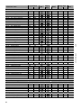
D6.102
Ref. value1 min. value
0 % or Hz
-300...300 % or Hz
D6.103
Ref. value1 max. value
50 % or Hz
-300...300 % or Hz
The two parameters D6.102 "Ref. value1 min. value" and D6.103 "Ref. value1 max. value" are used for linear
scaling of the transmitted reference value. D6.102 assigns an output value to the reference point at 0 % (0 dec
= 0000 hex), D6.103 assigns it to the reference point at 100 % (16384 dec = 4000 hex).
The unit of the reference value is scaled according to the reference use "D6.101 "Ref. value1 selection" for all
frequency values in Hz, while the remaining signals are scaled in %.
D6.104
Ref. value1 emergency
0 hex
0...65535 hex
In case of setting D6.03 Bus error behaviour to "3 .. Emerg. ref.val. & alarm" the set emergency
reference value is used during a bus fault. The unit of the emergency reference value corresponds
to that of the min/max scaling.
It is not possible to assign reference paths twice. If you try to assign a second reference source to a
use which is already allocated in the reference value distributor, the parameterization will prevent this
and the alarm message " Multiple usage of inputs not possible !" will be shown in the display.
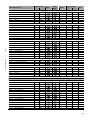
D6.105
Ref. value2 selection
0 .. Not used
D6.106
Ref. value2 min. value
0
D6.107
Ref. value2 max. value
50
D6.108
Ref. value2 emergency
0 hex
D6.109
Ref. value3 selection
0 .. Not used
D6.110
Ref. value3 min. value
0
D6.111
Ref. value3 max. value
50
D6.112
Ref. value3 emergency
0 hex
48
8 P01 327 EN.00/00
HAST
Bus SW-1 scaling
HAST
8 P01 327 EN.00/00
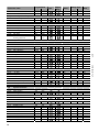
D6.113
Ref. value4 selection
0 .. Not used
D6.114
Ref. value4 min. value
0
D6.115
Ref. value4 max. value
50
D6.116
Ref. value4 emergency
0 hex
D6.117
Ref. value5 selection
0 .. Not used
D6.118
Ref. value5 min. value
0
D6.119
Ref. value5 max. value
50
D6.120
Ref. value5 emergency
0 hex
D6.121
Ref. value6 selection
0 .. Not used
D6.122
Ref. value6 min. value
0
D6.123
Ref. value6 max. value
50
D6.124
Ref. value6 emergency
0 hex
D6.125
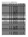
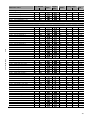
Ref. value7 selection
0 .. Not used
D6.126
Ref. value7 min. value
0
D6.127
Ref. value7 max. value
50
D6.128
Ref. value7 emergency
0 hex
D6.129
Ref. value8 selection
0 .. Not used
D6.130
Ref. value8 min. value
0
D6.131
Ref. value8 max. value
50
D6.132
Ref. value8 emergency
0 hex
D6.133
Ref. value9 selection
0 .. Not used
D6.134
Ref. value9 min. value
0
D6.135
Ref. value9 max. value
50
D6.136
Ref. value9 emergency
0 hex
The settings of the bus reference values 2...9 are logical identical with those of bus reference value 1 (see
parameters D6.101...D6.104).
49
Configuration of the fieldbus actual values
Corresponding to the configured telegram length one to nine actual values are available in addition to the
digital status word.
D6.137
Number actual values
1 ...1 ZTW + 1 IW
2 ...1 ZTW + 2 IW
3 ...1 ZTW + 3 IW
4 ...1 ZTW + 4 IW
5 ...1 ZTW + 5 IW
6 ...1 ZTW + 6 IW
5 .. 1 ZTW + 5 IW
7... 1 ZTW + 7 IW
8... 1 ZTW + 8 IW
9... 1 ZTW + 9 IW
10 .. 2 ZTW + 1 IW
11 .. 2 ZTW + 2 IW
12 .. 2 ZTW + 3 IW
13.. 2 ZTW + 4 IW
14.. 2 ZTW + 5 IW
15.. 2 ZTW + 6 IW
16.. 2 ZTW + 7 IW
17.. 2 ZTW + 8 IW
PPO type
Number of bus actual values
PPO1
1 ZTW + 1 IW
PPO2
1 ZTW + 5 IW
PPO3
1 ZTW + 1 IW
PPO4
1 ZTW + 5 IW
PPO5
1 ZTW + 9 IW
HAST
According to the set number of actual values D6.137 only relevant parameters are displayed in
matrix field D6 in order to guarantee clear parameterization.
8 P01 327 EN.00/00
The >pDRIVE< MX pro provides analog outputs and serial fieldbus actual values to forward analog
information of the actual values. The size to be issued as well as their scaling can be freely
configured.
50
8 P01 327 EN.00/00
HAST
Following process sizes can be transmitted as actual values:
Process size
1 .. Output frequency
2 .. |Output frequency|
3 .. Motor current
4 .. Torque
5 .. |Torque|
8 .. Power
9 .. |Power|
10 .. Motor voltage
11 .. Speed
12 .. |Speed|
15 .. Int. f-ref. before ramp
16 .. Int. f-ref. after ramp
17 .. PID-reference val. [%]
18 .. PID-actual value [%]
19 .. PID-deviation [%]
20 .. PID-output
23 .. Int. ref. switch-over
24 .. Calculator
25 .. Curve generator
26 .. Counter (average)
27 .. Total counter
30 .. T reference value
33 .. DC voltage
34 .. Tmax motor
35 .. Tmax generator
36 .. Thermal load M1
37 .. Thermal load M2
38 .. Thermal load BR
39 .. Thermal load VSD
41 .. AI 1
42 .. AI 2
43 .. AI 3
44 .. AI 4
45 .. Frequency input
47 .. Bus SW 1
48 .. Bus SW 2
49 .. Bus SW 3
50 .. Bus SW 4
51 .. Bus SW 5
52 .. Bus SW 6
53 .. Bus SW 7
54 .. Bus SW 8
55 .. Bus SW 9
58 .. Act. Error Code
59 .. Act. alarm Code
62 .. Position value LOW
63 .. Position value HIGH
Value
100.0
100.0
100.0
100.0
100.0
100.0
100.0
100.0
100.0
100.0
100.0
100.0
100.0
100.0
100.0
100.0
100.0
100.0
100.0
100.0
100.0
100.0
100.0
100.0
100.0
100.0
100.0
100.0
100.0
100.0
100.0
100.0
100.0
100.0
100.0
100.0
100.0
100.0
100.0
100.0
100.0
100.0
100.0
−
−
−
−
Unit
Hz
Hz
%
%
%
%
%
%
%
%
Hz
Hz
%
%
%
%
Hz
%
%
%
%
%
%
%
%
%
%
%
%
%
%
%
%
%
%
%
%
%
%
%
%
%
%
Integer
Integer
hex
hex
Scaling
100.0
100.0
Nominal current >pDRIVE< MX pro
Nominal motor torque
Nominal motor torque
Nominal inverter power
Nominal inverter power
Nominal voltage motor
Nominal speed at fMAX (C2.02)
Nominal speed at fMAX (C2.02)
100.0
100.0
100.0
100.0
100.0
100.0
100.0
100.0
100.0
100.0
100.0
Nominal motor torque
1000 V DC
Nominal motor torque
Nominal motor torque
100.0
100.0
100.0
100.0
10 V = 4000 hex
10 V or 20 mA = 4000 hex
20 mA = 4000 hex
10V or 20 mA = 4000 hex
D1.33 = 4000 hex
100.0
100.0
100.0
100.0
100.0
100.0
100.0
100.0
100.0
See table alarm index given in the appendix
See table alarm index given in the appendix
51
D6.138
Act. value1 selection
0 ...Not used
1 ...Output frequency
2 ...|Output frequency|
3 ...Motor current
4 ...Torque
5 ...|Torque|
8 ...Power
9 ...|Power|
10...Motor voltage
11...Speed
12...|Speed|
15...Int. f-ref. before ramp
16...Int. f-ref. after ramp
17...PID-reference val. [%]
18...PID-actual value [%]
19...PID-deviation [%]
20...PID-output
1 .. Output frequency
23 .. Int. ref. switch-over
24 .. Calculator
25 .. Curve generator
26 .. Counter (average)
27 .. Total counter
30 .. T reference value
33 .. DC voltage
34 .. Tmax motor
35 .. Tmax generator
36 .. Thermal load M1
37 .. Thermal load M2
38 .. Thermal load BR
39 .. Thermal load VSD
41 .. AI 1
42 .. AI 2
43 .. AI 3
44 .. AI 4
45...Frequency input
47...Bus SW 1
48...Bus SW 2
49...Bus SW 3
50...Bus SW 4
51...Bus SW 5
52...Bus SW 6
53...Bus SW 7
54...Bus SW 8
55...Bus SW 9
58...Act. Error Code
59...Act. alarm Code
62...Position value LOW
63...Position value HIGH
Selection of the size which should be transmitted at bus actual value 1.
D6.139
Act. value1 min. value
0 % or Hz
D6.140
Act. value1 max. value
50 % or Hz
HAST
-300...300 % or Hz
The two parameters D6.139 "Act. value1 min. value" and D6.140 "Act. value1 max. value" are used for linear
scaling of the transmitted bus actual value. D6.139 assigns the minimum value to the actual value point 0 %
(0 dec = 0000 hex), D6.140 assigns the maximum value of a process size to the actual value point 100 %
(16384 dec = 4000 hex).
The scaling of the process size and their unit can be seen from the table above.
Settings example for bus actual value 1
Process size Scaling
8 .. Power
52
D6.139 "Act. value1 D6.140 "Act. value1 Scaling of the output signal
min. value"
max. value"
100 % = Nom. 0 %
motor power
(e.g. 90 kW)
100 %
4000 hex (16384 dec) at
100 % PN Motor
(max. presentable range = 200 %)
8 P01 327 EN.00/00
-300...300 % or Hz
D6.141
Act. value1 filter-time
0.1 s
0...30 s
During the measurement of dynamically changing values, such as current or torque, it may be a
good idea to filter the actual value which should be transmitted already in the inverter. The
measurement value can be stabilized before transmission by setting an appropriate filter time at the
output filter.
8 P01 327 EN.00/00
HAST
At setting 0.0 seconds the filter is deactivated.
D6.142
Act. value2 selection
3 .. Motor current
D6.143
Act. value2 min. value
0
D6.144
Act. value2 max. value
100
D6.145
Act. value2 filter-time
0.1 s
D6.146
Act. value3 selection
4 .. Torque
D6.147
Act. value3 min. value
0
D6.148
Act. value3 max. value
100
D6.149
Act. value3 filter-time
0.1 s
D6.150
Act. value4 selection
8 .. Power
D6.151
Act. value4 min. value
0
D6.152
Act. value4 max. value
100
D6.153
Act. value4 filter-time
0.1 s
D6.154
Act. value5 selection
0 .. Not used
D6.155
Act. value5 min. value
0
D6.156
Act. value5 max. value
100
D6.157
Act. value5 filter-time
0.0 s
D6.158
Act. value6 selection
0 .. Not used
D6.159
Act. value6 min. value
0
D6.160
Act. value6 max. value
100
D6.161
Act. value6 filter-time
0.1 s
D6.162
Act. value7 selection
0 .. Not used
D6.163
Act. value7 min. value
0
D6.164
Act. value7 max. value
100
D6.165
Act. value7 filter-time
0.1 s
D6.166
Act. value8 selection
0 .. Not used
D6.167
Act. value8 min. value
0
D6.168
Act. value8 max. value
100
D6.169
Act. value8 filter-time
0.1 s
53
D6.170
Act. value9 selection
0 .. Not used
D6.171
Act. value9 min. value
0
D6.172
Act. value9 max. value
100
D6.173
Act. value9 filter-time
0.1 s
The settings of the bus reference values 2...9 are logical identical with those of bus reference value 1 (see
parameters D6.138...D6.141).
Configuration of bits 11...15 of the control word STW1
Bit 11 STW1 selection
40 .. Feed in pressure OK
41 .. Level OK
42 .. Level <
45 .. T-limitation active
46 .. Ext. T-limitation active
47 .. 2nd I-limit active
56 .. Mains cut-off
57 .. ON-lock
58 .. Locking
59 .. Feedb. motor cont.
60 .. Motor heating
61 .. Operation with IR
64 .. Pulse counter input
65 .. Pulse counter reset
66 .. n-monitoring
67 .. Parameter locked
68 .. Curve gen. start
69 .. Curve gen. reset
70 .. Curve gen. hold
75 .. 2nd motor
76.. 2nd parameter set
77.. 15P selection B
78.. 15P selection C
81.. n-contr. active (M/S)
82.. n-controller ext. I
83.. n-controller static on
86.. S-ramp OFF
87.. Save reference value
88.. Feedback brake
89.. Enable BU
90.. Reset position
93.. Position switch FW
94.. Position switch REV
95.. Position switch OFF
98.. Slowdown FWD
99.. Position switch FWD
100 Slowdown REV
101 Position switch REV
102 Pos/Slowdown OFF
HAST
0 ...Not used
9 ...Jog REV
11...f-ref reverse
14...Motor pot. +
15...Motor pot. 16...Pre-set A
17...Pre-set B
18...Pre-set C
19...Pre-set D
22...f-reference 2 [Hz]
23...Control source 2
24...2nd ramp
25...Reference value B
26...Panel operation
29...Ext. fault 1
30...Ext. fault 2
32...Emergency oper.
35...PID-active
36...PID-lock
37...PID-wind up
0 .. Not used
Parameter D6.174 assigns a digital input function to bit 11 of the control word. A description of this
function can be found in the >pDRIVE< MX pro Description of functions (matrix field D2).
D6.175
Bit 12 STW1 selection
0 .. Not used
D6.176
Bit 13 STW1 selection
0 .. Not used
D6.177
Bit 14 STW1 selection
0 .. Not used
D6.178
Bit 15 STW1 selection
0 .. Not used
Setting possibilities see D6.174.
54
8 P01 327 EN.00/00
D6.174
D6.179
Bit at term.-mode act.
0 ...STW1 Bit 11
1 ...STW1 Bit 12
2 ...STW1 Bit 13
3 ...STW1 Bit 14
4 ...STW1 Bit 15
/
/
/
/
/
When the control source selection (see Matrix field E4) is used to switch between terminal and
fieldbus operation it might be necessary to have individual bits (11...15) of the bus control word
active despite the fact that the control source has been switched to the terminals.
This exception from switch-over can be configured by the appropriate selection with parameter
D6.179 "Bit at term.-mode act.".
Example: External fault
In case of a process fault the inverter is shut-down systematically using bit 11 of the control word.
This behaviour should be also guaranteed in case of controlling the drive via local operation (by
means of terminal commands). Digital input DI4 can be used to switch between terminal strip
operation and bus operation.
D6.174 "Bit 11 STW1 selection" = "29 .. Ext. fault 1"
HAST
If a switch-over from bus operation to terminal strip operation takes place, the commands of the
control word become ineffective ! The parameterized function "Ext. fault 1" is not effective any
longer.
For this reason, for control word bits that shall be effective both in the bus operation as well as the
terminal operation bit 11 must be marked in parameter D6.179 "Bit at term.-mode act.".
8 P01 327 EN.00/00
Adjust parameter D2.15 "DI at bus mode active" on the other hand, if a digital input should
be effective in terminal operation as well as in bus operation,
If a control signal is configured both on a free bit at the bus as well as on the terminals
which are active during bus operation, the bus command will be preferred.
55
Configuration of bits 0...15 of the control word STW2
Bit 0 STW2 selection
40 .. Feed in pressure OK
41 .. Level OK
42 .. Level <
45 .. T-limitation active
46 .. Ext. T-limitation active
47 .. 2nd I-limit active
56 .. Mains cut-off
57 .. ON-lock
58 .. Locking
59 .. Feedb. motor cont.
60 .. Motor heating
61 .. Operation with IR
64 .. Pulse counter input
65 .. Pulse counter reset
66 .. n-monitoring
67 .. Parameter locked
68 .. Curve gen. start
69 .. Curve gen. reset
70 .. Curve gen. hold
75 .. 2nd motor
76.. 2nd parameter set
77.. 15P selection B
78.. 15P selection C
81.. n-contr. active (M/S)
82.. n-controller ext. I
83.. n-controller static on
86.. S-ramp OFF
87.. Save reference value
88.. Feedback brake
89.. Enable BU
90.. Reset position
93.. Position switch FW
94.. Position switch REV
95.. Position switch OFF
98.. Slowdown FWD
99.. Position switch FWD
100 Slowdown REV
101 Position switch REV
102 Pos/Slowdown OFF
Parameter D6.180 assigns a digital input function to bit 0 of the control word STW2. A description
of this function can be found in the >pDRIVE< MX pro Description of functions (matrix field D2).
D6.181
Bit 1 STW2 selection
0 .. Not used
D6.182
Bit 2 STW2 selection
0 .. Not used
D6.183
Bit 3 STW2 selection
0 .. Not used
D6.184
Bit 4 STW2 selection
0 .. Not used
D6.185
Bit 5 STW2 selection
0 .. Not used
D6.186
Bit 6 STW2 selection
0 .. Not used
D6.187
Bit 7 STW2 selection
0 .. Not used
D6.188
Bit 8 STW2 selection
0 .. Not used
D6.189
Bit 9 STW2 selection
0 .. Not used
D6.190
Bit 10 STW2 selection
0 .. Not used
D6.191
Bit 11 STW2 selection
0 .. Not used
D6.192
Bit 12 STW2 selection
0 .. Not used
D6.193
Bit 13 STW2 selection
0 .. Not used
D6.194
Bit 14 STW2 selection
0 .. Not used
D6.195
Bit 15 STW2 selection
0 .. Not used
Setting possibilities see D6.180.
56
HAST
0 ...Not used
9 ...Jog REV
11...f-ref reverse
14...Motor pot. +
15...Motor pot. 16...Pre-set A
17...Pre-set B
18...Pre-set C
19...Pre-set D
22...f-reference 2 [Hz]
23...Control source 2
24...2nd ramp
25...Reference value B
26...Panel operation
29...Ext. fault 1
30...Ext. fault 2
32...Emergency oper.
35...PID-active
36...PID-lock
37...PID-wind up
0 .. Not used
8 P01 327 EN.00/00
D6.180
D6.196
Bit at term.-mode act.
0 ...STW 2 Bit 00
1 ...STW 2 Bit 01
2 ...STW 2 Bit 02
3 ...STW 2 Bit 03
4 ...STW 2 Bit 04
5 ...STW 2 Bit 05
6 ...STW 2 Bit 06
7 ...STW 2 Bit 07
/
/
/
/
/
/
/
/
8 .. STW 2 Bit 08
9 .. STW 2 Bit 09
10 .. STW 2 Bit 10
11 .. STW 2 Bit 11
12 .. STW 2 Bit 12
13 .. STW 2 Bit 13
14 .. STW 2 Bit 14
15 .. STW 2 Bit 15
When the control source selection (see Matrix field E4) is used to switch between terminal and
fieldbus operation it might be necessary to have individual bits (0...15) of the bus control word
STW2 active despite the fact that the control source has been switched to the terminals.
This exception from switch-over can be configured by the appropriate selection with parameter
D6.196 "Bit at term.-mode act.".
Configuration of bits 11...15 of the status word ZTW1
D6.197
Bit 11 ZTW1 selection
8 P01 327 EN.00/00
HAST
0 ...Not used
1 ...Ready
2 ...Operation
3 ...Ready / run
4 ...Trip
5 ...Sum alarm
6 ...Motor turns
7 ...f = f ref
8 ...Generator operation
9 ...T-controller at n-limit
11...Shut down
12...Panel mode active
13...Motor 1 active
14...Motor 2 active
15...Param.-set 1 active
16...Param.-set 2 active
19...Safe standstill active
20...Limitation active
21...BU active
0 .. Not used
22 .. Ext. T-limitation active
23 .. T-control active
24 .. Motor heating active
25 .. Motorfluxing active
27 .. DC link charged
28 .. Line Contactor ON
29 .. Motor contactor ON
36 .. Alarm cat. 1
37 .. Alarm cat. 2
38 .. Alarm cat. 3
41 .. Output T1
42 .. Output T2
43 .. Output T3
44 .. Output T4
45 .. Output T5
46 .. Output T6
49 .. Brake release
50 .. Hoist emerg. (n≠0)
54 .. Bus STW bit 11
55...Bus STW bit 12
56...Bus STW bit 13
57...Bus STW bit 14
58...Bus STW bit 15
61...Digital input DI1
62...Digital input DI2
63...Digital input DI3
64...Digital input DI4
65...Digital input DI5
66...Digital input DI6
67...Digital input DI7
68...Digital input DI8
69...Digital input DI9
70...Digital input DI10
71...Digital input DI11
72...Digital input DI12
73...Digital input DI13
74...Digital input DI14
Parameter D6.197 assigns the respective digital state information to bit 11 of the status word. A
description of the individual digital output functions can be found in the >pDRIVE< MX pro
Description of functions (matrix field D4).
D6.198
Bit 12 ZTW1 selection
0 .. Not used
D6.199
Bit 13 ZTW1 selection
0 .. Not used
D6.200
Bit 14 ZTW1 selection
0 .. Not used
D6.201
Bit 15 ZTW1 selection
0 .. Not used
Setting possibilities see D6.179.
57
Configuration of bits 0...15 of the status word ZTW2
Bit 0 ZTW2 selection
22 .. Ext. T-limitation active
23 .. T-control active
24 .. Motor heating active
25 .. Motorfluxing active
27 .. DC link charged
28 .. Line Contactor ON
29 .. Motor contactor ON
36 .. Alarm cat. 1
37 .. Alarm cat. 2
38 .. Alarm cat. 3
41 .. Output T1
42 .. Output T2
43 .. Output T3
44 .. Output T4
45 .. Output T5
46 .. Output T6
49 .. Brake release
50 .. Hoist emerg. (n≠0)
54 .. Bus STW bit 11
55.. Bus STW bit 12
56.. Bus STW bit 13
57.. Bus STW bit 14
58.. Bus STW bit 15
61.. Digital input DI1
62.. Digital input DI2
63.. Digital input DI3
64.. Digital input DI4
65.. Digital input DI5
66.. Digital input DI6
67.. Digital input DI7
68.. Digital input DI8
69.. Digital input DI9
70.. Digital input DI10
71.. Digital input DI11
72.. Digital input DI12
73.. Digital input DI13
74.. Digital input DI14
Parameter D6.202 assigns the respective digital state information to bit 0 of the status word ZTW2.
A description of the individual digital output functions can be found in the >pDRIVE< MX pro
Description of functions (matrix field D4).
D6.203
Bit 1 ZTW2 selection
0 .. Not used
D6.204
Bit 2 ZTW2 selection
0 .. Not used
D6.205
Bit 3 ZTW2 selection
0 .. Not used
D6.206
Bit 4 ZTW2 selection
0 .. Not used
D6.207
Bit 5 ZTW2 selection
0 .. Not used
D6.208
Bit 6 ZTW2 selection
0 .. Not used
D6.209
Bit 7 ZTW2 selection
0 .. Not used
D6.210
Bit 8 ZTW2 selection
0 .. Not used
D6.211
Bit 9 ZTW2 selection
0 .. Not used
D6.212
Bit 10 ZTW2 selection
0 .. Not used
D6.213
Bit 11 ZTW2 selection
0 .. Not used
D6.214
Bit 12 ZTW2 selection
0 .. Not used
D6.215
Bit 13 ZTW2 selection
0 .. Not used
D6.216
Bit 14 ZTW2 selection
0 .. Not used
D6.217
Bit 15 ZTW2 selection
0 .. Not used
Setting possibilities see D6.202.
58
HAST
0 ...Not used
1 ...Ready
2 ...Operation
3 ...Ready / run
4 ...Trip
5 ...Sum alarm
6 ...Motor turns
7 ...f = f ref
8 ...Generator operation
9 ...T-controller at n-limit
11...Shut down
12...Panel mode active
13...Motor 1 active
14...Motor 2 active
15...Param.-set 1 active
16...Param.-set 2 active
19...Safe standstill active
20...Limitation active
21...BU active
0 .. Not used
8 P01 327 EN.00/00
D6.202
8 P01 327 EN.00/00
HAST
Bus - Diagnostics
59
Diagnostics of the control / status word
Diagnostics STW (Bus → Inverter)
D6.218
Bus STW hex
D6.219
Bus STW bin
0 .. STW1 Bit 0
1 .. STW1 Bit 1
2 .. STW1 Bit 2
3 .. STW1 Bit 3
4 .. STW1 Bit 4
5 .. STW1 Bit 5
6 .. STW1 Bit 6
7 .. STW1 Bit 7
hex
/
/
/
/
/
/
/
/
8 .. STW1 Bit 8
9 .. STW1 Bit 9
10 .. STW1 Bit 10
11 .. STW1 Bit 11
12 .. STW1 Bit 12
13 .. STW1 Bit 13
14 .. STW1 Bit 14
15 .. STW1 Bit 15
/
/
/
/
/
/
/
/
Presentation of the control word STW1 received at the >pDRIVE< MX pro.
D6.221
Bus STW2 bin
0 ...STW 2 Bit 0
1 ...STW 2 Bit 1
2 ...STW 2 Bit 2
3 ...STW 2 Bit 3
4 ...STW 2 Bit 4
5 ...STW 2 Bit 5
6 ...STW 2 Bit 6
7 ...STW 2 Bit 7
hex
HAST
Bus STW2 hex
/
/
/
/
/
/
/
/
8 .. STW 2 Bit 8
9 .. STW 2 Bit 9
10 .. STW 2 Bit 10
11 .. STW 2 Bit 11
12 .. STW 2 Bit 12
13 .. STW 2 Bit 13
14 .. STW 2 Bit 14
15 .. STW 2 Bit 15
/
/
/
/
/
/
/
/
8 P01 327 EN.00/00
D6.220
Presentation of the control word STW2 received at the >pDRIVE< MX pro.
Diagnostics ZTW (Inverter → Bus)
D6.222
Bus ZTW hex
D6.223
Bus ZTW bin
0 .. ZTW1 Bit 0
1 .. ZTW1 Bit 1
2 .. ZTW1 Bit 2
3 .. ZTW1 Bit 3
4 .. ZTW1 Bit 4
5 .. ZTW1 Bit 5
6 .. ZTW1 Bit 6
7 .. ZTW1 Bit 7
hex
/
/
/
/
/
/
/
/
8 .. ZTW1 Bit 8
9 .. ZTW1 Bit 9
10 .. ZTW1 Bit 10
11 .. ZTW1 Bit 11
12 .. ZTW1 Bit 12
13 .. ZTW1 Bit 13
14 .. ZTW1 Bit 14
15 .. ZTW1 Bit 15
Presentation of the status word ZTW1 sent at the >pDRIVE< MX pro.
60
/
/
/
/
/
/
/
/
D6.224
Bus ZTW2 hex
D6.225
Bus ZTW2 bin
0 ...ZTW 2 Bit 0
1 ...ZTW 2 Bit 1
2 ...ZTW 2 Bit 2
3 ...ZTW 2 Bit 3
4 ...ZTW 2 Bit 4
5 ...ZTW 2 Bit 5
6 ...ZTW 2 Bit 6
7 ...ZTW 2 Bit 7
hex
8 .. ZTW 2 Bit 8
9 .. ZTW 2 Bit 9
10 .. ZTW 2 Bit 10
11 .. ZTW 2 Bit 11
12 .. ZTW 2 Bit 12
13 .. ZTW 2 Bit 13
14 .. ZTW 2 Bit 14
15 .. ZTW 2 Bit 15
/
/
/
/
/
/
/
/
/
/
/
/
/
/
/
/
Presentation of the status word ZTW2 sent at the >pDRIVE< MX pro.
HAST
Diagnostics of the operating state
D6.226
Internal control word
D6.227
Internal condition
0 ...Ready to switch on
1 ...Ready to run
2 ...Operation released
3 ...Fault
4 ...No Off 2
5 ...No Off 3
hex
/
/
/
/
/
/
6 .. Lock switching on
7 .. Alarm
8 .. f = f ref.
9 .. Control
10 .. f > level
/
/
/
/
/
8 P01 327 EN.00/00
Presentation of the internal affecting drive state.
61
Diagnostics of the "Bus raw data"
D6.228
PRx 01
hex
D6.229
PRx 02
hex
D6.230
PRx 03
hex
D6.231
PRx 04
hex
D6.232
PRx 05
hex
D6.233
PRx 06
hex
D6.234
PRx 07
hex
D6.235
PRx 08
hex
D6.236
PRx 09
hex
D6.237
PRx 10
hex
PTx 01
hex
D6.243
PTx 02
hex
D6.244
PTx 03
hex
D6.245
PTx 04
hex
D6.246
PTx 05
hex
D6.247
PTx 06
hex
D6.248
PTx 07
hex
D6.249
PTx 08
hex
D6.250
PTx 09
hex
D6.251
PTx 10
hex
Presentation of the outgoing data words 1...10 at the bus.
62
8 P01 327 EN.00/00
D6.242
HAST
Presentation of the incoming data words 1...10 at the bus.
8 P01 327 EN.00/00
HAST
Application examples
63
General
In addition to the typical "Bus operation" (all inverters are controlled via fieldbus) also a "Mixed operation" (i.e.
simultaneous use of bus control and conventional control via terminals) is available due to the simple
configuration of the reference and actual values and the free areas of the control and status word.
Following all three basic control types are described in form of block diagrams.
A mixed operation of these variants is certainly possible.
Controlling the MX by means of the fieldbus interface → "Pure bus operation"
The whole control and diagnostics of the inverter is carried out by means of the bus coupling.
The possibility to implement conventional control elements is not used.
8 P01 327 EN.00/00
HAST
In order to address an inverter via fieldbus also during mains cut-off (line contactor control,
disconnecting switch, ...) the >pDRIVE< MX pro has to be supplied with an external 24 V buffer
voltage.
64
Controlling the MX alternatively by means of the fieldbus interface or the
terminals → "Control source switch-over"
8 P01 327 EN.00/00
HAST
The inverter is controlled depending on a digital signal (at the terminals or the bus) via the bus control word or
digital commands at the inverter terminals. Further information about the selection of the control source are
given in matrix field E4 and the presetting of macro 4 in matrix field B2.
In order to address an inverter via fieldbus also during mains cut-off (line contactor control,
disconnecting switch, ...) the >pDRIVE< MX pro has to be supplied with an external 24 V buffer
voltage.
65
Controlling the MX by means of the fieldbus interface and the terminals of the
device → "Mixed operation"
The whole control and diagnostics of the inverter is carried out by means of the bus coupling. However, also
additionally external information for inverter operation (additional reference values, control signals) or system
information which do not directly affect the drive are implemented in the automation concept using the
standard terminals or the terminal extension IO11 or IO12.
Example 1:
Use of the MX internal PID process controller
Reference value: provided serial from the fieldbus
Actual value:
A sensor provides a 0...10 V analog signal directly for the control terminals of
the inverter.
Example 2:
A screw conveyor is connected and disconnected by means of a filling level indicator.
The filling level indicator provides two floating-ground signals which can be directly integrated in
the telegram to the DP master by means of the digital inputs DI1 and DI2 of the inverter and thus
they are available for the control program of the system.
66
8 P01 327 EN.00/00
HAST
An external supply of the inverter electronics with 24 V buffer voltage is necessary if the system information
have to be exchanged furthermore via the DP master even if the inverter is cut from the mains.
8 P01 327 EN.00/00
HAST
Appendix
67
Parameter list of the >pDRIVE< MX pro
Parameter name
Log. address
dec
hex
Speed
101
65
A2.02
Direction of rotation
102
66
A2.03
Torque
103
67
A2.04
Operating quadrant
104
68
A2.05
Motor current in A
105
A2.06
Motor current in %
106
A2.07
Shaft power in kW
107
A2
Type
Adjustability
Factor
Setting range
min
max
Unit
Motor values
Motor values
1
rpm
see table
Nm
69
see table
A
6A
1
%
6B
see table
kW
Hp
A2.08
Shaft power in HP
108
6C
see table
A2.09
Apparent power
109
6D
see table
kVA
A2.10
Motor voltage
110
6E
1
V
A2.11
Thermal load M1
111
6F
1
%
A2.12
Thermal load M2
112
70
1
%
A2.13
Process speed
113
71
10
A2.14
A2.15
A2.16
A2.17
Multiplier - n
Divisor - n
Offset - n
Symbol for A2.13
Ensuing parameter
Unit for A2.13
Ensuing parameter
451
452
453
454
458
456
457
1C3
1C4
1C5
1C6
1CA
1C8
1C9
1
1
100
A2.18
A2.19
Process torque
459
1CB
1
A2.20
A2.21
A2.22
A2.23
Multiplier - T
Divisor - T
Offset - T
Symbol for A2.19
Ensuing parameter
Unit for A2.19
Ensuing parameter
460
461
462
463
464
465
466
1CC
1CD
1CE
1CF
1D0
1D1
1D2
1
1
100
A2.24
1000
1000
100
1
1
-100
10000
1000
100
rpm
%
%
A2.25
Active motor
114
72
A2.26
Position value Low
115
73
1
hex
A2.27
Position value High
116
74
1
hex
A3
Inverter values
Inverter values
A3.01
Output frequency
117
75
100
Hz
A3.02
Inverter load
118
76
1
%
A3.03
Mains voltage
119
77
1
V
A3.04
DC voltage
120
78
1
V
A3.05
Thermal load VSD
121
79
1
%
A3.06
Active pulse frequency
122
7A
10
kHz
A3.07
Thermal load BR
124
7C
1
%
A4
Reference values
Monitoring of analog inputs
A4.01
AI1 ref. value [%]
125
7D
10
%
A4.02
AI1 ref. value scaled
126
7E
100
% / Hz
A4.03
AI2 ref. value [%]
127
7F
10
%
A4.04
AI2 ref. value scaled
128
80
100
% / Hz
A4.05
AI3 ref. value [%]
129
81
10
%
68
HAST
rpm
-1000
1
-100
8 P01 327 EN.00/00
A2.01
Parameter name
A4.06
AI3 ref. value scaled
Log. address
Type
Adjustability
Factor
dec
hex
130
82
100
Setting range
min
max
Unit
% / Hz
A4.07
AI4 ref. value [%]
131
83
10
%
A4.08
AI4 ref. value scaled
132
84
100
% / Hz
A4.09
FP ref. value in kHz
133
85
100
kHz
A4.10
FP ref. value scaled
134
86
100
% / Hz
% / Hz
Monitoring of digital reference sources
A4.11
Motor pot. ref. value
135
87
100
A4.12
MX-wheel ref. value
136
88
100
Hz
A4.13
Pre-set reference
137
89
100
% / Hz
Monitoring of internal reference sources
A4.14
Ref. value switch-over
138
8A
100
% / Hz
A4.15
Calculator
139
8B
100
% / Hz
A4.16
Act. value selection
140
8C
100
% / Hz
A4.17
Curve generator
141
8D
100
% / Hz
Monitoring of digital inputs
A4.18
DI state basic device
142
8E
A4.19
DI state IO11
143
8F
A4.20
DI state IO12
144
90
8 P01 327 EN.00/00
HAST
Monitoring of bus reference sources
A4.21
Bus reference 1 scaled
145
91
100
% / Hz
A4.22
Bus reference 2 scaled
146
92
100
% / Hz
A4.23
Bus reference 3 scaled
147
93
100
% / Hz
A4.24
Bus reference 4 scaled
148
94
100
% / Hz
A4.25
Bus reference 5 scaled
149
95
100
% / Hz
A4.26
Bus reference 6 scaled
150
96
100
% / Hz
A4.27
Bus reference 7 scaled
151
97
100
% / Hz
A4.28
Bus reference 8 scaled
152
98
100
% / Hz
A4.29
Bus reference 9 scaled
153
99
100
% / Hz
A5
Counter
Operating hours
A5.01
Operating hours motor1
154
9A
1
A5.02
Interval motor 1
468
1D4
1
A5.03
Interval counter M1
155
9B
1
A5.04
Operating hours motor2
156
9C
1
A5.05
Interval motor 2
469
1D5
1
A5.06
Interval counter M2
157
9D
1
A5.07
Power on hours
158
9E
1
A5.08
Interval power on
470
1D6
1
A5.09
Interval count. PowerOn
159
9F
1
h
0
10000
h
h
h
0
10000
h
h
h
0
10000
h
h
A5.10
Operating hours fan
160
A0
1
A5.11
Interval fan
471
1D7
1
A5.12
Interval counter fan
161
A1
1
h
A5.13
Clear intervall counter
162
A2
MWh meter mot.
163
A3
1
MWh
A5.15
kWh meter mot.
164
A4
10
kWh
A5.16
MWh meter gen.
165
A5
1
MWh
A5.17
kWh meter gen.
166
A6
10
kWh
h
0
10000
h
Energy meter
A5.14
69
Parameter name
A6
hex
472
473
474
475
398
1D8
1D9
1DA
1DB
18E
477
1DD
Adjustability
Factor
Setting range
Unit
min
max
1
1
10
1
10
1
10
1
10
1
10
0
0
0
0
0
0
0
0
0
0
0
1000
1000
300
1000
300
1000
300
1000
300
1000
300
V
V
Hz
V
Hz
V
Hz
V
Hz
V
Hz
1
1
1
25
0
100
200
150
200
%
%
%
Language selection
Language selection
B1.01
Select language
B2
dec
Type
Display configuration
Configuration of the display
A6.01
Selection upper field
A6.02
Selection middle field
A6.03
Selection lower field
A6.04
View all parameters
A6.05
Limitations
B1
Log. address
Macro configuration
Active parameter set
167
A7
B2.02
B2.03
B2.04
B2.05
B2.06
B2.07
Macro selection
Parameter mode
Create backup
Restore backup
Copy parameter set
Name parameter set 1
Ensuing parameter
Ensuing parameter
Ensuing parameter
Ensuing parameter
Ensuing parameter
Ensuing parameter
Name parameter set 2
Ensuing parameter
Ensuing parameter
Ensuing parameter
Ensuing parameter
Ensuing parameter
Ensuing parameter
478
479
1801
1802
1803
481
482
483
484
485
486
487
488
489
490
491
492
493
494
1DE
1DF
709
70A
70B
1E1
1E2
1E3
1E4
1E5
1E6
1E7
1E8
1E9
1EA
1EB
1EC
1ED
1EE
Line voltage
B3.01
Mains voltage
495
1EF
Motor control
B3.02
Control mode
B3.03
Starting voltage
B3.04
V/f - V1
B3.05
V/f - f1
B3.06
V/f - V2
B3.07
V/f - f2
B3.08
V/f - V3
B3.09
V/f - f3
B3.10
V/f - V4
B3.11
V/f - f4
B3.12
V/f - V5
B3.13
V/f - f5
B3.16
Inverter power
B3.17
Starting torque
B3.18
Slip compensation
B3.19
Vmax field weakening
496
497
498
499
500
501
502
503
504
505
506
507
1151
508
509
510
1F0
1F1
1F2
1F3
1F4
1F5
1F6
1F7
1F8
1F9
1FA
1FB
47F
1FC
1FD
1FE
B2.08
B3
70
8 P01 327 EN.00/00
B2.01
HAST
Parameter management
Inverter data
Parameter name
General settings
B3.24
Stop mode
B3.25
decel. persistant freq.
B3.26
decel. persistant time
B3.27
Motor fluxing
B3.30
Skip frequency
B3.32
Vmot optimization
B3.35
Catch on the fly
B3.36
Allowed catch direction
B3.37
Sensibility
B3.40
Output filter
B3.41
Fan control
B3.42
Auto tune at power on
B3.43
Automatic SC test
B3.44
Operation with IR
B4
Log. address
dec
hex
513
515
516
514
517
519
520
521
522
523
524
525
526
527
201
203
204
202
205
207
208
209
20A
20B
20C
20D
20E
20F
528
529
1804
210
211
70C
Type
Adjustability
Factor
Setting range
Unit
min
max
10
1
0
0
50
3600
Hz
s
10
2
16
kHz
10
0.4
12
0.2
0
0
0
0
3500
4000
1000
300
65000
Motor data
HAST
Motor data M1
B4.05
B4.06
B4.07
B4.08
B4.09
Nominal power M1
Nominal current M1
Nominal voltage M1
Nominal frequency M1
Nominal speed M1
531
532
533
534
535
213
214
215
216
217
see table
see table
1
10
1
8 P01 327 EN.00/00
Motor selection
B4.01
Motor type
B4.02
Motor selection
B4.03
Start tuning
B4.10
Nominal slip M1
168
A8
100
B4.11
No. of pole pairs M1
169
A9
1
B4.12
B4.13
B4.14
B4.15
Stator resistor M1
Rotortime constant M1
Fluxing current M1
Stray reactance M1
536
537
538
539
218
219
21A
21B
see table
1
10
100
0
0
0
0
65000
10000
4000
655.35
mOhm
ms
A
mH
Motor data M2
B4.17
Nominal power M2
B4.18
Nominal current M2
B4.19
Nominal voltage M2
B4.20
Nominal frequency M2
B4.21
Nominal speed M2
541
542
543
544
545
21D
21E
21F
220
221
see table
see table
1
10
1
0.2
0
0
0
0
3500
4000
1000
300
65000
kW
A
V
Hz
rpm
B4.22
Nominal slip M2
170
AA
100
B4.23
No. of pole pairs M2
171
AB
1
B4.24
B4.25
B4.26
B4.27
Stator resistor M2
Rotortime constant M2
Fluxing current M2
Stray reactance M2
546
547
548
549
222
223
224
225
see table
1
10
100
kW
A
V
Hz
rpm
Hz
Hz
0
0
0
0
65000
10000
4000
655.35
mOhm
ms
A
mH
Motor data M0
B4.29
Nominal power M0
172
AC
see table
kW
B4.30
Nominal current M0
173
AD
see table
A
B4.31
Nominal voltage M0
174
AE
1
V
B4.32
Nominal frequency M0
175
AF
10
Hz
B4.33
Nominal speed M0
176
B0
1
rpm
B4.34
Nominal slip M0
177
B1
100
Hz
B4.35
No. of pole pairs M0
178
B2
1
B4.36
Stator resistor M0
179
B3
see table
mOhm
71
Parameter name
Log. address
Type
Adjustability
Factor
Setting range
hex
Rotortime constant M0
180
B4
1
ms
B4.38
Fluxing current M0
181
B5
10
A
B4.39
Stray reactance M0
182
B6
100
mH
B4.40
Load default motor
397
18D
551
552
1152
553
554
227
228
480
229
22A
B4.37
Motor data SM1
B4.44
Nominal power SM1
B4.45
Nominal current SM1
B4.46
Nominal voltage SM1
B4.47
Nominal speed SM1
B4.48
No. of pole pairs SM1
see table
see table
1
1
1
min
max
Unit
dec
0.2
0
0
0
1
3500
4000
1000
65000
100
kW
A
V
rpm
B4.49
Nominal frequency SM1
556
22C
10
B4.50
B4.51
B4.52
B4.53
EMC constant SM1
d-axis inductivity SM1
q-axis inductivity SM1
Stator resistor SM1
555
558
1153
557
22B
22E
481
22D
10
100
100
see table
0
0
0
0
6553.5
655.35
655.35
65000
V
mH
mH
mOhm
560
561
1154
562
563
230
231
482
232
233
see table
see table
1
1
1
0.2
0
0
0
1
3500
4000
1000
65000
100
kW
A
V
rpm
0
0
0
0
6553.5
655.35
655.35
65000
Hz
Nominal power SM2
Nominal current SM2
Nominal voltage SM2
Nominal speed SM2
No. of pole pairs SM2
B4.60
Nominal frequency SM2
565
235
10
B4.61
B4.62
B4.63
B4.64
EMC constant SM2
d-axis inductivity SM2
q-axis inductivity SM2
Stator resistor SM2
564
567
1155
566
234
237
483
236
10
100
100
see table
Hz
V
mH
mH
mOhm
Motor data SM0
B4.66
Nominal power SM0
569
239
see table
kW
B4.67
Nominal current SM0
183
B7
see table
A
B4.68
Nominal voltage SM0
406
196
1
V
B4.69
Nominal speed SM0
184
B8
1
rpm
B4.70
No. of pole pairs SM0
185
B9
1
B4.71
Nominal frequency SM0
187
BB
10
Hz
B4.72
EMC constant SM0
186
BA
10
V
B4.73
d-axis inductivity SM0
189
BD
100
mH
B4.74
q-axis inductivity SM0
407
197
100
mH
B4.75
Stator resistor SM0
188
BC
see table
mOhm
B5
Brake function
570
23A
244
246
247
248
249
24A
1
700
785
V
10
100
10
0
0
0.5
200
650
1000
s
kW
Ohm
Brake mode
B5.01
Braking mode
Braking unit
B5.02
BU-braking level
B5.05
BR overload activation
B5.06
BR overload response
B5.07
Time Δt
B5.08
B5.09
BR continuous power
BR Ohm value
580
582
583
584
585
586
B5.10
BR-thermal load
190
BE
10
DC-brake
B5.15
DC-brake I-start
B5.16
DC-brake t-start
B5.17
DC-brake I-cont.
B5.18
DC-brake t-cont.
571
572
573
574
23B
23C
23D
23E
1
10
1
10
72
%
0
0
0
0
100
100
100
100
%
s
%
s
8 P01 327 EN.00/00
B4.55
B4.56
B4.57
B4.58
B4.59
HAST
Motor data SM2
Parameter name
dec
hex
575
576
577
578
579
23F
240
241
242
243
Preset reference values
C1.01 Pre-set ref. selection
C1.02 Pre-set reference 1
C1.03 Pre-set reference 2
C1.04 Pre-set reference 3
C1.05 Pre-set reference 4
C1.06 Pre-set reference 5
C1.07 Pre-set reference 6
C1.08 Pre-set reference 7
C1.09 Pre-set reference 8
C1.10 Pre-set reference 9
C1.11 Pre-set reference 10
C1.12 Pre-set reference 11
C1.13 Pre-set reference 12
C1.14 Pre-set reference 13
C1.15 Pre-set reference 14
C1.16 Pre-set reference 15
C1.17 Pre-set reference 16
588
589
590
591
592
593
594
595
596
597
598
599
600
601
602
603
604
24C
24D
24E
24F
250
251
252
253
254
255
256
257
258
259
25A
25B
25C
Motor potentiometer
C1.18 Motor pot. selection
C1.19 Motor pot. control
C1.20 Motor pot. min. value
C1.21 Motor pot. max. value
C1.22 Motor pot. accel. time
C1.23 Motor pot. decel. time
C1.24 Motor pot. ref. storage
C1.25 Motor pot. tracking
605
606
607
608
609
610
611
612
DC-Holdingbrake
B5.20
DC-holdingbrake
B5.21
DC-holdingbrake I-start
B5.22
DC-holdingbrake t-start
B5.23
DC-holdingbrake I-cont.
B5.24
DC-holdingbrake t-cont.
HAST
C1
8 P01 327 EN.00/00
Log. address
Type
Adjustability
Factor
Setting range
Unit
min
max
1
10
1
10
0
0
0
0
100
100
100
100
%
s
%
s
100
100
100
100
100
100
100
100
100
100
100
100
100
100
100
100
-300
-300
-300
-300
-300
-300
-300
-300
-300
-300
-300
-300
-300
-300
-300
-300
300
300
300
300
300
300
300
300
300
300
300
300
300
300
300
300
% / Hz
% / Hz
% / Hz
% / Hz
% / Hz
% / Hz
% / Hz
% / Hz
% / Hz
% / Hz
% / Hz
% / Hz
% / Hz
% / Hz
% / Hz
% / Hz
25D
25E
25F
260
261
262
263
264
100
100
10
10
-300
-300
0
0
300
300
6500
6500
% / Hz
% / Hz
s
s
613
614
615
616
617
618
619
265
266
267
268
269
26A
26B
10
10
10
10
100
0
0
-300
-300
0
300
300
300
300
50
Hz
Hz
%
%
620
621
622
623
624
625
626
627
628
26C
26D
26E
26F
270
271
272
273
274
100
1
1
100
100
-300
1
1
-300
-300
300
30000
1000
300
300
Int. reference
Panel reference sources
C1.29
C1.30
C1.31
C1.32
C1.33
C1.34
C1.35
MX-wheel selection
MX-wheel f min. value
MX-wheel f max. value
MX-wheel T-min. value
MX-wheel T max. value
MX-wheel single step
Store MX-wheel ref.
Calculator
C1.38 Calculator selection
C1.39 Calculator input A
C1.40 Calculator input B
C1.41 Calculator function
C1.42 Reference value
C1.43 Multiplier
C1.44 Divisor
C1.45 Calculator min. value
C1.46 Calculator max. value
% / Hz
% / Hz
73
dec
hex
Actual value selection
C1.49 Actual value usage
C1.50 Actual value selection
C1.51 Actual value filter time
C1.52 Value at 0Hz [%]
C1.53 Value at 100Hz [%]
629
630
631
632
633
275
276
277
278
279
Reference value switch
C1.54 Ref. val. switch usage
C1.55 Ref. val. switch selec.
C1.56 Ref. val. switch input A
C1.57 Ref. val. switch input B
634
635
636
637
27A
27B
27C
27D
Jog mode
C1.58 Jog frquency
C1.59 Jog ramp
638
1156
Curve generator
C1.61 Curve generator selec.
C1.62 Curve gen. start mode
C1.63 Ref. value 0
C1.64 Time - Δt1
C1.65
C1.66
Ref. value 1
Time - Δt2
C1.67
C1.68
Ref. value 2
Time - Δt3
C1.69
C1.70
Ref. value 3
Time - Δt4
C1.71
C1.72
Ref. value 4
Time - Δt5
C1.73
C1.74
Ref. value 5
Time - Δt6
C1.75
C1.76
Ref. value 6
Time - Δt7
XY Graph
C1.90 XY graph selection
C1.91 XY graph input selection
C1.92 No. of value pairs
C1.93 XY Graph min
C1.94 XY Graph max
C1.95 XY Graph - IN 1
C1.96 XY Graph - OUT 1
C1.97 XY Graph - IN 2
C1.98 XY Graph - OUT 2
C1.99 XY Graph - IN 3
C1.100 XY Graph - OUT 3
C1.101 XY Graph - IN 4
C1.102 XY Graph - OUT 4
C1.103 XY Graph - IN 5
C1.104 XY Graph - OUT 5
C1.105 XY Graph - IN 6
C1.106 XY Graph - OUT 6
C2
Adjustability
Factor
Setting range
Unit
min
max
100
100
100
0
-300
-300
20
300
300
s
% / Hz
% / Hz
27E
484
10
10
0
0
20
300
Hz
s
639
640
641
642
643
644
645
646
647
648
649
650
651
652
653
654
27F
280
281
282
283
284
285
286
287
288
289
28A
28B
28C
28D
28E
100
100
100
100
100
100
100
100
100
100
100
100
100
100
-300
0
-300
0
-300
0
-300
0
-300
0
-300
0
-300
0
300
650
300
650
300
650
300
650
300
650
300
650
300
650
% / Hz
s
% / Hz
s
% / Hz
s
% / Hz
s
% / Hz
s
% / Hz
s
% / Hz
s
1157
1158
1159
1160
1161
1162
1163
1164
1165
1166
1167
1168
1169
1170
1171
1172
1173
485
486
487
488
489
48A
48B
48C
48D
48E
48F
490
491
492
493
494
495
1
100
100
100
100
100
100
100
100
100
100
100
100
100
100
2
-300
-300
-300
-300
-300
-300
-300
-300
-300
-300
-300
-300
-300
-300
6
300
300
300
300
300
300
300
300
300
300
300
300
300
300
% / Hz
% / Hz
% / Hz
% / Hz
% / Hz
% / Hz
% / Hz
% / Hz
% / Hz
% / Hz
% / Hz
% / Hz
% / Hz
% / Hz
655
656
28F
290
10
10
0
10
300
300
Hz
Hz
% / Hz
Ramp / frequency
Frequency range
C2.01 Minimum frequency
C2.02 Maximum frequency
74
Type
HAST
Log. address
8 P01 327 EN.00/00
Parameter name
Parameter name
dec
hex
Direction of rotation
C2.03 Direction enable
C2.04 Phase rotation
657
658
291
292
Acceleration/deceleration ramps
C2.05 Acceleration ramp 1
C2.06 Deceleration ramp 1
C2.07 Acceleration ramp 2
C2.08 Deceleration ramp 2
C2.09 Switch 1st/2nd accel.
C2.10 Switch 2nd/1st decel.
C2.11 Start ramp
C2.12 S-ramp mode
C2.13 S-ramp
C2.14 Limitation
659
660
661
662
663
664
665
666
667
1174
293
294
295
296
297
298
299
29A
29B
496
1175
1180
1178
1182
1186
1179
1187
1181
1185
1189
1176
1177
1184
1190
497
49C
49A
49E
4A2
49B
4A3
49D
4A1
4A5
498
499
4A0
4A6
1191
1192
1193
1194
1195
HAST
C3
8 P01 327 EN.00/00
Log. address
Ramp time
Feedback Timeout
External load measurement
C3.65 Loadadapting brakecont.
C3.66 Loadpoint 1
C3.67 Starting torque 1
C3.68 Loadpoint 2
C3.69 Starting Torque 2
C4
Adjustability
Factor
Setting range
Unit
min
max
10
10
10
10
10
10
10
0
0
0
0
0
0
0
6000
6000
6000
6000
300
300
6000
s
s
s
s
Hz
Hz
s
1
1
100
%
10
100
10
100
100
1
10
100
0
0
0
0
0
0
0
0
10
5
10
5
5
120
10
5
Hz
s
Hz
s
s
%
Hz
s
1
1
100
10
0
0
0
0
140
140
5
5
%
%
s
s
4A7
4A8
4A9
4AA
4AB
1
1
1
1
-300
-140
-300
-140
300
140
300
140
%
%
%
%
Crane application
Crane control
C3.45 Brake control
C3.46 Engage frequency
C3.47 Brake release time
C3.48 Release frequency
C3.49 Stop delay time
C3.50 Brake engage time
C3.51 DC-brake current
C3.52 Skipfrequency 0Hz
C3.53 Start delay
C3.56 Hoist options
C3.57 Starting torque ↑
C3.58 Starting torque ↓
C3.59
C3.60
Type
PID configuration
Monitoring of PID values
C4.01
PID reference value
196
C4
10
%
C4.02
PID actual value
197
C5
10
%
C4.03
PID deviation
198
C6
1
%
C4.04
PID output
199
C7
100
% / Hz
Basic setting
C4.07 Control mode
C4.08 Control sense
C4.09 Proportional gain
C4.10 Integration time
C4.11 Derive time
C4.12 Max. D-part
C4.13 Output level min.
C4.14 Output level max.
C4.15 Limitation
C4.17 Frequency tracking
694
695
696
697
698
699
700
701
1196
702
2B6
2B7
2B8
2B9
2BA
2BB
2BC
2BD
4AC
2BE
1000
100
100
100
100
100
0
0
0
0
-300
-300
30
600
600
300
300
300
s
s
75
Parameter name
Log. address
703
704
2BF
2C0
705
706
707
Factor
Setting range
Unit
max
10
10
0
0
6000
6000
s
s
2C1
2C2
2C3
10
10
10
0
0
0
300
300
300
%
Hz
s
711
712
713
714
715
716
717
2C7
2C8
2C9
2CA
2CB
2CC
2CD
1
1
100
-1000
1
-100
1000
1000
100
Speed controller
C5.01 Speed prop. gain
C5.02 Speed time integral
C5.03 Ref. Filterfactor
1197
1198
1199
4AD
4AE
4AF
1
1
1
0
1
0
1000
1000
100
%
%
%
T-controller
C5.07 Torque controller
C5.08 T-offset value
C5.09 positiv T-ramp
C5.10 neg. T-Ramp
C5.11 T-ref min
C5.12 T ref max
C5.13 Limitation
1200
1213
1206
1207
1208
1209
1210
4B0
4BD
4B6
4B7
4B8
4B9
4BA
100
10
10
10
10
-300
0
0
-300
-300
300
300
300
300
300
%
s
s
%
%
1211
1212
1201
1202
4BB
4BC
4B1
4B2
100
100
0
0
300
300
Hz
Hz
10
0
100
s
1203
1204
4B3
4B4
1
0
3600
s
Motor heating
C6.05 Motor heating
C6.06 Heating current
722
723
2D2
2D3
1
0
50
%
Line contactor control
C6.07 Contactor control
724
2D4
Motor contactor control
C6.08 Motor contactor control
725
2D5
Standby Mode
C6.11 Standby mode
C6.12 Off delay time
C6.13 On delay time
C6.14 Max. level
C6.15 Min. level
726
727
728
729
730
2D6
2D7
2D8
2D9
2DA
10
10
10
10
1
1
0
0
3000
100
300
300
s
s
%
%
Impulse Counter
C6.18 Pulse counter
731
2DB
C6.19
200
C8
Ref. value acceleration
Ref. value deceleration
hex
Adjustability
min
C4.18
C4.19
dec
Type
Compensation of pressure drop
Pressure drop
Start compensation
Compensation dynamic
Advanced functions
C4.32 PID-lock
C4.33 Wind-up behaviour
C4.34 PID multiplier
C4.35 PID divisor
C4.36 PID offset
C4.37 Process unit
Ensuing parameter
n/T-controller
Speed limitation
C5.16 + Δn limit
C5.17 - Δn limit
C5.18
C5.19
Response at n-limitation
Time Δt
Stop behaviour
C5.22 T-controller stop mode
C5.23 Standby time
C6
76
Special functions
Total counter
10
HAST
C5
8 P01 327 EN.00/00
C4.22
C4.23
C4.24
Parameter name
HAST
dec
hex
Type
Adjustability
Factor
Setting range
min
max
Unit
C6.20
Counter (average)
201
C9
10
C6.21
C6.22
C6.23
C6.24
Scaling
Time base pulse counter
Pulse type
Symbol pulse counter
Ensuing parameter
Pulse counter unit
Ensuing parameter
732
733
734
735
736
737
738
2DC
2DD
2DE
2DF
2E0
2E1
2E2
1000
1
0
0
65
3600
s
Correction reference value
C6.26 f-correction
740
2E4
Load balance
C6.29 Load sharing
C6.30 Correction frequency
C6.31 Load sharing f-start
C6.32 Load sharing T-start
C6.33 Dynamic
1214
1215
1216
1218
1219
4BE
4BF
4C0
4C2
4C3
10
10
1
10
0
0
0
0
300
300
300
20
Hz
Hz
%
s
SlowDown Functionality
C6.37 SlowDown
C6.38 SlowDown function
C6.39 Deceleration time
C6.40 Persistence time
C6.41 Start distancemeasuring
1220
1221
1222
1223
1813
4C4
4C5
4C6
4C7
715
10
10
0
0
3200
3600
s
s
1224
1225
1226
4C8
4C9
4CA
100
0
10
s
AI1 selection
AI1 level
AI1 min. value
AI1 max. value
AI1 filter-time
741
742
743
744
745
2E5
2E6
2E7
2E8
2E9
100
100
100
-300
-300
0
300
300
30
% / Hz
% / Hz
s
Analog input AI2
D1.08
AI2 selection
D1.09
AI2 level
D1.10
AI2 min. value
D1.11
AI2 max. value
D1.12
AI2 filter-time
746
747
748
749
750
2EA
2EB
2EC
2ED
2EE
100
100
100
-300
-300
0
300
300
30
% / Hz
% / Hz
s
Analog input AI3
D1.15
AI3 selection
D1.16
AI3 level
D1.17
AI3 min. value
D1.18
AI3 max. value
D1.19
AI3 filter-time
751
752
753
754
755
2EF
2F0
2F1
2F2
2F3
100
100
100
-300
-300
0
300
300
30
% / Hz
% / Hz
s
Analog input AI4
D1.22
AI4 selection
D1.23
AI4 level
D1.24
AI4 min. value
D1.25
AI4 max. value
D1.26
AI4 filter-time
756
757
758
759
760
2F4
2F5
2F6
2F7
2F8
100
100
100
-300
-300
0
300
300
30
% / Hz
% / Hz
s
Frequency input FP
D1.29
FP selection
D1.30
FP min.
761
762
2F9
2FA
100
0
30
kHz
C6.25
8 P01 327 EN.00/00
Log. address
Reference take over
C6.44
C6.45
C6.46
Reference take over
Delaytime
Edge
D1
Analog inputs
Analog input AI1
D1.01
D1.02
D1.03
D1.04
D1.05
77
Log. address
dec
hex
763
764
765
766
2FB
2FC
2FD
2FE
767
768
769
770
771
772
773
774
775
776
777
778
779
780
781
2FF
300
301
302
303
304
305
306
307
308
309
30A
30B
30C
30D
Analog output AO1
D3.01
AO1 selection
D3.02
AO1 level
D3.03
AO1 min. value
D3.04
AO1 max. value
D3.05
AO1 filter-time
782
783
784
785
786
D3.06
D1.31
D1.32
D1.33
D1.34
FP max.
FP min. value
FP max. value
FP filter-time
D2
Digital inputs
Digital Inputs
D2.01
DI1 selection
D2.02
DI2 selection
D2.03
DI3 selection
D2.04
DI4 selection
D2.05
DI5 selection
D2.06
DI6 selection
D2.07
DI7 selection
D2.08
DI8 selection
D2.09
DI9 selection
D2.10
DI10 selection
D2.11
DI11 selection
D2.12
DI12 selection
D2.13
DI13 selection
D2.14
DI14 selection
D2.15
DI at bus mode active
Adjustability
Factor
Unit
min
max
100
100
100
100
0
-300
-300
0
30
300
300
30
kHz
% / Hz
% / Hz
s
30E
30F
310
311
312
100
100
100
-300
-300
0
300
300
30
% / Hz
% / Hz
s
Analog outputs
64
40
100
Analog output AO2
D3.08
AO2 selection
D3.09
AO2 level
D3.10
AO2 min. value
D3.11
AO2 max. value
D3.12
AO2 filter-time
787
788
789
790
791
313
314
315
316
317
100
100
100
D3.13
65
41
100
Analog output AO3
D3.15
AO3 selection
D3.16
AO3 level
D3.17
AO3 min. value
D3.18
AO3 max. value
D3.19
AO3 filter-time
792
793
794
795
796
318
319
31A
31B
31C
100
100
100
D3.20
AO3 value
66
42
100
D4
Digital outputs
797
798
799
800
801
802
31D
31E
31F
320
321
322
AO1 value
AO2 value
Digital outputs
D4.01
R1 selection
D4.02
R2 selection
D4.03
R3 selection
D4.04
DO1 selection
D4.05
DO2 selection
D4.06
R4 selection
78
Setting range
V / mA
-300
-300
0
300
300
30
% / Hz
% / Hz
s
V / mA
-300
-300
0
300
300
30
% / Hz
% / Hz
s
V / mA
8 P01 327 EN.00/00
D3
Type
HAST
Parameter name
Parameter name
Log. address
dec
hex
803
804
805
323
324
325
Encoder
D5.01
SFB use for
D5.02
Encoder pulses
D5.03
SFB signals
D5.04
Encoder rotation
1227
1228
1229
1230
4CB
4CC
4CD
4CE
Encoder failure
D5.06
Encoder slip detection
D5.07
f-detection level
D5.08
Delay time
1231
1232
1233
D4.07
D4.08
D4.11
DO3 selection
DO4 selection
DO invertation
D5
Encoder configuration
Type
Adjustability
Factor
Setting range
Unit
min
max
1
100
5000
4CF
4D0
4D1
10
10
0
0.1
100
10
Hz
s
408
198
1
0
0
3200
247
s
0
0
300
127
s
Encoder
D5.09
Encoder pulses calc.
D6
Fieldbus
8 P01 327 EN.00/00
HAST
Fieldbus configuration
D6.01
D6.02
D6.03
D6.04
D6.10
D6.11
D6.12
Bus selection
Control requested
Bus error behaviour
Bus error delay time
Modbus address
Modbus baud rate
Modbus format
1301
1302
1303
1304
1305
1306
1307
515
516
517
518
519
51A
51B
D6.13
Modbus frame count
202
CA
D6.14
Modbus CRC errors
203
CB
1
D6.15
D6.20
D6.21
Modbus time-out
CANopen address
CANopen baud rate
1308
1319
1320
51C
527
528
10
1
D6.22
CANopen status
206
CE
D6.23
CANopen error register
207
CF
D6.24
CANopen Rx errorcount
204
CC
1
D6.25
CANopen Tx errorcount
205
CD
1
D6.30
DP slave address
1321
529
1
D6.31
DP baud rate
208
D0
D6.32
Slave state
209
D1
D6.33
On after off 1
1322
52A
D6.34
Request master
210
D2
D6.35
DP master address
211
D3
1
D6.36
Config buffer 1
212
D4
1
0
FA
hex
D6.37
Config buffer 2
213
D5
1
0
FA
hex
D6.38
Config buffer 3
214
D6
1
0
FA
hex
D6.39
DP diagnostic buffer 1
215
D7
1
hex
D6.40
DP diagnostic buffer 2
216
D8
1
hex
D6.41
Group number
217
D9
1
D6.42
Global command
218
DA
1
1323
1324
1325
1326
1327
52B
52C
52D
52E
52F
100
100
1
Fieldbus references
D6.100 No. of Bus-ref. values
D6.101 Ref. value1 selection
D6.102 Ref. value1 min. value
D6.103 Ref. value1 max. value
D6.104 Ref. value1 emergency
10
1
1
-300
-300
0
300
300
FFFF
% / Hz
% / Hz
hex
79
dec
hex
Ref. value2 selection
Ref. value2 min. value
Ref. value2 max. value
Ref. value2 emergency
Ref. value3 selection
Ref. value3 min. value
Ref. value3 max. value
Ref. value3 emergency
Ref. value4 selection
Ref. value4 min. value
Ref. value4 max. value
Ref. value4 emergency
Ref. value5 selection
Ref. value5 min. value
Ref. value5 max. value
Ref. value5 emergency
Ref. value6 selection
Ref. value6 min. value
Ref. value6 max. value
Ref. value6 emergency
Ref. value7 selection
Ref. value7 min. value
Ref. value7 max. value
Ref. value7 emergency
Ref. value8 selection
Ref. value8 min. value
Ref. value8 max. value
Ref. value8 emergency
Ref. value9 selection
Ref. value9 min. value
Ref. value9 max. value
Ref. value9 emergency
1328
1329
1330
1331
1332
1333
1334
1335
1336
1337
1338
1339
1340
1341
1342
1343
1344
1345
1346
1347
1348
1349
1350
1351
1352
1353
1354
1355
1356
1357
1358
1359
530
531
532
533
534
535
536
537
538
539
53A
53B
53C
53D
53E
53F
540
541
542
543
544
545
546
547
548
549
54A
54B
54C
54D
54E
54F
Fieldbus actual values
D6.137 Number actual values
D6.138 Act. value1 selection
D6.139 Act. value1 min. value
D6.140 Act. value1 max. value
D6.141 Act. value1 filter-time
D6.142 Act. value2 selection
D6.143 Act. value2 min. value
D6.144 Act. value2 max. value
D6.145 Act. value2 filter-time
D6.146 Act. value3 selection
D6.147 Act. value3 min. value
D6.148 Act. value3 max. value
D6.149 Act. value3 filter-time
D6.150 Act. value4 selection
D6.151 Act. value4 min. value
D6.152 Act. value4 max. value
D6.153 Act. value4 filter-time
D6.154 Act. value5 selection
D6.155 Act. value5 min. value
D6.156 Act. value5 max. value
D6.157 Act. value5 filter-time
D6.158 Act. value6 selection
D6.159 Act. value6 min. value
1360
1361
1362
1363
1364
1365
1366
1367
1368
1369
1370
1371
1372
1373
1374
1375
1376
1377
1378
1379
1380
1381
1382
550
551
552
553
554
555
556
557
558
559
55A
55B
55C
55D
55E
55F
560
561
562
563
564
565
566
D6.105
D6.106
D6.107
D6.108
D6.109
D6.110
D6.111
D6.112
D6.113
D6.114
D6.115
D6.116
D6.117
D6.118
D6.119
D6.120
D6.121
D6.122
D6.123
D6.124
D6.125
D6.126
D6.127
D6.128
D6.129
D6.130
D6.131
D6.132
D6.133
D6.134
D6.135
D6.136
80
Type
Adjustability
Factor
Setting range
Unit
min
max
100
100
1
-300
-300
0
300
300
FFFF
% / Hz
% / Hz
hex
100
100
1
-300
-300
0
300
300
FFFF
% / Hz
% / Hz
hex
100
100
1
-300
-300
0
300
300
FFFF
% / Hz
% / Hz
hex
100
100
1
-300
-300
0
300
300
FFFF
% / Hz
% / Hz
hex
100
100
1
-300
-300
0
300
300
FFFF
% / Hz
% / Hz
hex
100
100
1
-300
-300
0
300
300
FFFF
% / Hz
% / Hz
hex
100
100
1
-300
-300
0
300
300
FFFF
% / Hz
% / Hz
hex
100
100
1
-300
-300
0
300
300
FFFF
% / Hz
% / Hz
hex
100
100
100
-300
-300
0
300
300
30
% / Hz
% / Hz
s
100
100
100
-300
-300
0
300
300
30
% / Hz
% / Hz
s
100
100
100
-300
-300
0
300
300
30
% / Hz
% / Hz
s
100
100
100
-300
-300
0
300
300
30
% / Hz
% / Hz
s
100
100
100
-300
-300
0
300
300
30
% / Hz
% / Hz
s
100
-300
300
% / Hz
HAST
Log. address
8 P01 327 EN.00/00
Parameter name
Parameter name
Log. address
dec
hex
1383
1384
1385
1386
1387
1388
1389
1390
1391
1392
1393
1394
1395
1396
567
568
569
56A
56B
56C
56D
56E
56F
570
571
572
573
574
1397
1398
1399
1400
1401
1402
575
576
577
578
579
57A
Assignment bit 0 - 15 PZD2 STW
D6.180 Bit 0 STW2 selection
D6.181 Bit 1 STW2 selection
D6.182 Bit 2 STW2 selection
D6.183 Bit 3 STW2 selection
D6.184 Bit 4 STW2 selection
D6.185 Bit 5 STW2 selection
D6.186 Bit 6 STW2 selection
D6.187 Bit 7 STW2 selection
D6.188 Bit 8 STW2 selection
D6.189 Bit 9 STW2 selection
D6.190 Bit 10 STW2 selection
D6.191 Bit 11 STW2 selection
D6.192 Bit 12 STW2 selection
D6.193 Bit 13 STW2 selection
D6.194 Bit 14 STW2 selection
D6.195 Bit 15 STW2 selection
D6.196 Bit at term.-mode act.
1403
1404
1405
1406
1407
1408
1409
1410
1411
1412
1413
1414
1415
1416
1417
1418
1419
57B
57C
57D
57E
57F
580
581
582
583
584
585
586
587
588
589
58A
58B
Assignment free bits ZTW
D6.197 Bit 11 ZTW1 selection
D6.198 Bit 12 ZTW1 selection
D6.199 Bit 13 ZTW1 selection
D6.200 Bit 14 ZTW1 selection
D6.201 Bit 15 ZTW1 selection
1420
1421
1422
1423
1424
58C
58D
58E
58F
590
Assignment bit 0 - 15 PZD2 ZTW
D6.202 Bit 0 ZTW2 selection
D6.203 Bit 1 ZTW2 selection
D6.204 Bit 2 ZTW2 selection
D6.205 Bit 3 ZTW2 selection
D6.206 Bit 4 ZTW2 selection
D6.207 Bit 5 ZTW2 selection
D6.208 Bit 6 ZTW2 selection
D6.209 Bit 7 ZTW2 selection
D6.210 Bit 8 ZTW2 selection
D6.211 Bit 9 ZTW2 selection
1425
1426
1427
1428
1429
1430
1431
1432
1433
1434
591
592
593
594
595
596
597
598
599
59A
D6.160
D6.161
D6.162
D6.163
D6.164
D6.165
D6.166
D6.167
D6.168
D6.169
D6.170
D6.171
D6.172
D6.173
Act. value6 max. value
Act. value6 filter-time
Act. value7 selection
Act. value7 min. value
Act. value7 max. value
Act. value7 filter-time
Act. value8 selection
Act. value8 min. value
Act. value8 max. value
Act. value8 filter-time
Act. value9 selection
Act. value9 min. value
Act. value9 max. value
Act. value9 filter-time
Type
Adjustability
Factor
Setting range
Unit
min
max
100
100
-300
0
300
30
% / Hz
s
100
100
100
-300
-300
0
300
300
30
% / Hz
% / Hz
s
100
100
100
-300
-300
0
300
300
30
% / Hz
% / Hz
s
100
100
100
-300
-300
0
300
300
30
% / Hz
% / Hz
s
Assignment free bits STW
8 P01 327 EN.00/00
HAST
D6.174
D6.175
D6.176
D6.177
D6.178
D6.179
Bit 11 STW1 selection
Bit 12 STW1 selection
Bit 13 STW1 selection
Bit 14 STW1 selection
Bit 15 STW1 selection
Bit at term.-mode act.
81
Parameter name
Log. address
dec
hex
1435
1436
1437
1438
1439
1440
59B
59C
59D
59E
59F
5A0
D6.218 Bus STW hex
219
DB
D6.219 Bus STW bin
220
DC
D6.212
D6.213
D6.214
D6.215
D6.216
D6.217
Bit 10 ZTW2 selection
Bit 11 ZTW2 selection
Bit 12 ZTW2 selection
Bit 13 ZTW2 selection
Bit 14 ZTW2 selection
Bit 15 ZTW2 selection
Type
Adjustability
Factor
Setting range
min
max
Unit
Diagnosis STW (BUS -> VSD)
D6.220 Bus STW2 hex
221
DD
D6.221 Bus STW2 bin
222
DE
1
hex
1
hex
1
hex
1
hex
1
hex
Diagnosis ZTW (VSD -> BUS)
D6.222 Bus ZTW hex
223
DF
D6.223 Bus ZTW bin
224
E0
D6.224 Bus ZTW2 hex
225
E1
D6.225 Bus ZTW2 bin
226
E2
D6.226 Internal control word
227
E3
D6.227 Internal condition
228
E4
D6.228 PRx 01
230
E6
1
hex
D6.229 PRx 02
231
E7
1
hex
D6.230 PRx 03
232
E8
1
hex
D6.231 PRx 04
233
E9
1
hex
D6.232 PRx 05
234
EA
1
hex
D6.233 PRx 06
235
EB
1
hex
Diagnosis of the operating state
236
EC
1
hex
D6.235 PRx 08
237
ED
1
hex
D6.236 PRx 09
238
EE
1
hex
D6.237 PRx 10
239
EF
1
hex
Diagnosis VSD -> BUS
D6.242 PTx 01
250
FA
1
hex
D6.243 PTx 02
251
FB
1
hex
D6.244 PTx 03
252
FC
1
hex
D6.245 PTx 04
253
FD
1
hex
D6.246 PTx 05
254
FE
1
hex
D6.247 PTx 06
255
FF
1
hex
D6.248 PTx 07
256
100
1
hex
D6.249 PTx 08
257
101
1
hex
D6.250 PTx 09
258
102
1
hex
D6.251 PTx 10
259
103
1
hex
806
807
1234
808
809
810
811
814
815
326
327
4D2
328
329
32A
32B
32E
32F
1
1
10
10
165
165
%
%
1
1
10
10
300
300
%
%
1
1
10
10
300
300
%
%
E1
Process protection
Limitations
E1.01
I max 1
E1.02
I max 2
E1.03
Inverter temp. model
E1.05
T max. motor
E1.06
T max generator
E1.07
T lim activation
E1.08
T limit source
E1.13
P max. motor
E1.14
P max. generator
82
8 P01 327 EN.00/00
D6.234 PRx 07
HAST
Diagnosis BUS -> VSD
Parameter name
dec
hex
816
817
818
819
820
821
330
331
332
333
334
335
Skip frequencies
E1.25
Skip frequency 1
E1.26
Hysteresis 1
E1.27
Skip frequency 2
E1.28
Hysteresis 2
E1.29
Skip frequency 3
E1.30
Hysteresis 3
E1.31
Skip frequency 4
E1.32
Hysteresis 4
822
823
824
825
826
827
828
829
Speed monitoring
E1.38
n-monitoring
E1.39
Pulse / rotation
E1.40
Filter-time
E1.41
E1.42
HAST
Type
Adjustability
Factor
Setting range
Unit
min
max
100
0
300
s
100
0
300
s
336
337
338
339
33A
33B
33C
33D
10
100
10
100
10
100
10
100
-300
0
-300
0
-300
0
-300
0
300
10
300
10
300
10
300
10
Hz
Hz
Hz
Hz
Hz
Hz
Hz
Hz
830
831
832
33E
33F
340
1
10
0
0
100
300
Detected speed
270
10E
10
Ratio factor
833
341
100
Behaviour at limitations
E1.17
Reaction at limitation
E1.18
Time Δt
8 P01 327 EN.00/00
Log. address
E1.19
E1.21
E1.22
Ref. after acc. extension
Reaction at deceleration
Time Δt
E1.23
Ref. after dec. extension
s
rpm
0
10
E1.43
Calculated slip
271
10F
10
E1.44
E1.45
E1.46
Tolerance
n-monitoring response
Time Δt
834
835
836
342
343
344
10
0
500
rpm
10
0
300
s
Feed-in monitoring
E1.49
Feed in monitoring
E1.50
Feed in mon. reaction
E1.51
Time Δt
837
838
839
345
346
347
10
0
300
s
Rotation angle monitoring
E1.54
Rot. angle monitoring
E1.55
Revolutions
E1.56
Response
E1.57
Time Δt
1235
1236
1237
1238
4D3
4D4
4D5
4D6
100
0
500
rpm
10
0
300
409
199
840
841
842
843
844
845
846
847
848
849
850
851
852
853
854
348
349
34A
34B
34C
34D
34E
34F
350
351
352
353
354
355
356
E1.58
Δ- rotational angle
E2
Motor protection
Thermistor control
E2.01
TH1 motor allocation
E2.02
TH1 activation
E2.03
TH1 response
E2.04
TH1 Time Δt
E2.05
E2.06
E2.07
E2.08
E2.09
TH1 verification
TH2 motor allocation
TH2 activation
TH2 response
TH2 Time Δt
E2.10
E2.11
E2.12
E2.13
E2.14
TH2 verification
TH3 motor allocation
TH3 activation
TH3 response
TH3 Time Δt
E2.15
TH3 verification
rpm
100
s
rpm
1
0
300
s
1
0
300
s
1
0
300
s
83
Thermal mathematical motor model
E2.18
M1 - overl. monitoring
E2.19
M1 - response
E2.20
M1 - Imax at 0Hz
E2.21
M1 - Imax at f nom.
E2.22
M1 - therm. f-limitation
E2.23
M1 - motor-time
E2.24
M1 - cooling temp.
E2.25
M1 - alarm level
E2.26
M1 - trigger level
Log. address
Type
Adjustability
Factor
dec
hex
855
856
857
858
859
860
861
862
863
357
358
359
35A
35B
35C
35D
35E
35F
1
1
10
1
1
1
1
E2.27
M1 - thermal load
272
110
1
E2.30
E2.31
E2.32
E2.33
E2.34
E2.35
E2.36
E2.37
E2.38
M2 - overl. monitoring
M2 - response
M2 - Imax at 0Hz
M2 - Imax at f nom.
M2 - therm. f-limitation
M2 - motor-time
M2 - cooling temp.
M2 - alarm level
M2 - trigger level
864
865
866
867
868
869
870
871
872
360
361
362
363
364
365
366
367
368
1
1
10
1
1
1
1
E2.39
Setting range
min
max
0
0
0
0
-10
0
0
300
150
300
500
80
300
300
Unit
%
%
Hz
min
°C
%
%
%
0
0
0
0
-10
0
0
300
150
300
500
80
300
300
%
%
Hz
min
°C
%
%
273
111
1
873
874
875
876
369
36A
36B
36C
10
10
1
0
0
0
200
20
150
s
Hz
%
Overspeed protection
E2.48
Overspeed monitoring
E2.49
Overspeed response
E2.50
Overspeed level
E2.51
Time Δt
877
878
879
880
36D
36E
36F
370
1
10
0
0
20000
300
rpm
s
Loss of motor phase
E2.54
Motor phase monitor
881
371
882
883
884
885
886
887
888
889
372
373
374
375
376
377
378
379
1
1
1
10
10
10
0
0
0
0
0
0
100
100
100
300
300
300
%
%
%
s
s
s
Behaviour in case of faults
E3.01
Reaction at a trip
E3.03
Auto reset
E3.04
Auto reset selection
E3.06
Auto reset trials
E3.07
Period
890
891
892
893
275
37A
37B
37C
37D
113
1
1
1
60
20
600
s
Emergency operation
E3.09
Enable emergency op.
894
37E
E3.10
276
114
Underload protection
E2.61
Underload monitor
E2.62
Underload response
E2.63
Underload level n²
E2.64
Underload level ½ fn
E2.65
Underload level fn
E2.66
Underload start time
E2.67
Time Δt
E2.68
Filter-time
E3
Fault configuration
84
Emergency op. active
%
HAST
M2 - thermal load
Stall protection
E2.42
Stall protection
E2.43
Stalling time
E2.44
Stalling frequency
E2.45
Stalling current
8 P01 327 EN.00/00
Parameter name
Parameter name
Log. address
dec
hex
Loss of reference value
E3.13
AI2 - 4mA monitor
E3.14
AI2 - 4mA response
E3.15
AI2 - emergency val.
E3.16
AI3 - 4mA monitor
E3.17
AI3 - 4mA response
E3.18
AI3- emergency val.
E3.19
AI4 - 4mA monitor
E3.20
AI4 - 4mA response
E3.21
AI4 - emergency val.
E3.22
FP - f monitoring
E3.23
FP - monitoring resp.
E3.24
FP - emergency val.
895
896
897
898
899
900
901
902
903
904
905
906
37F
380
381
382
383
384
385
386
387
388
389
38A
Loss of line phase
E3.27
Mains phase monitoring
907
38B
Behaviour at undervoltage
E3.29
V< response
E3.30
Allowed V< time
E3.31
Max. V< time
908
909
910
38C
38D
38E
Ext. fault 2 name
Ensuing parameter
Ensuing parameter
Ensuing parameter
Ensuing parameter
Ensuing parameter
Ensuing parameter
Ensuing parameter
911
912
913
914
915
916
917
918
919
920
921
922
923
924
925
926
927
928
929
930
931
932
933
934
38F
390
391
392
393
394
395
396
397
398
399
39A
39B
39C
39D
39E
39F
3A0
3A1
3A2
3A3
3A4
3A5
3A6
ON lock
E3.48
ON lock activation
E3.49
ON lock response
E3.50
Time Δt
935
936
937
3A7
3A8
3A9
Alarm categories
E3.51
Alarm category 1
E3.54
Alarm category 2
E3.57
Alarm category 3
938
940
942
3AA
3AC
3AE
Type
Adjustability
Factor
Setting range
Unit
min
max
10
4
20
mA
10
4
20
mA
10
4
20
mA
100
0
30
kHz
10
10
0
0
300
3000
s
s
10
10
0
0
600
300
s
s
10
10
0
0
600
300
s
s
10
0
300
s
8 P01 327 EN.00/00
HAST
External fault
E3.34
E3.35
E3.36
E3.37
Ext. fault 1 monitor
Ext. fault 1 response
Start delay time
Time Δt
E3.38
Ext. fault 1 name
Ensuing parameter
Ensuing parameter
Ensuing parameter
Ensuing parameter
Ensuing parameter
Ensuing parameter
Ensuing parameter
Ext. fault 2 monitor
Ext. fault 2 response
Start delay time
Time Δt
E3.41
E3.42
E3.43
E3.44
E3.45
85
Parameter name
Log. address
dec
hex
944
945
946
3B0
3B1
3B2
947
948
949
3B3
3B4
3B5
1805
1806
70D
70E
Comparator C1 - C4
E6.01
Comparator C1
E6.02
C1 signal A selection
E6.03
C1 signal A filter-time
E6.04
C1 signal B selection
E6.05
C1 signal B ref. value
E6.06
C1 signal B filter-time
E6.07
C1 function
E6.08
C1 hysteresis/band
950
951
952
953
954
955
956
957
3B6
3B7
3B8
3B9
3BA
3BB
3BC
3BD
E6.09
C1 output
277
115
E6.10
E6.11
E6.12
E6.13
E6.14
E6.15
E6.16
E6.17
Comparator C2
C2 signal A selection
C2 signal A filter-time
C2 signal B selection
C2 signal B ref. value
C2 signal B filter-time
C2 function
C2 hysteresis/band
958
959
960
961
962
963
964
965
3BE
3BF
3C0
3C1
3C2
3C3
3C4
3C5
E6.18
C2 output
278
116
E6.19
E6.20
E6.21
E6.22
E6.23
E6.24
E6.25
E6.26
Comparator C3
C3 signal A selection
C3 signal A filter-time
C3 signal B selection
C3 signal B ref. value
C3 signal B filter-time
C3 function
C3 hysteresis/band
966
967
968
969
970
971
972
973
3C6
3C7
3C8
3C9
3CA
3CB
3CC
3CD
E6.27
C3 output
279
117
E6.28
E6.29
E6.30
E6.31
E6.32
E6.33
E6.34
E6.35
Comparator C4
C4 signal A selection
C4 signal A filter-time
C4 signal B selection
C4 signal B ref. value
C4 signal B filter-time
C4 function
C4 hysteresis/band
974
975
976
977
978
979
980
981
3CE
3CF
3D0
3D1
3D2
3D3
3D4
3D5
E6.36
C4 output
280
118
E4
Adjustability
Factor
Setting range
Unit
min
max
100
0
300
s
100
100
-300
0
300
300
s
100
0
650
100
0
300
s
100
100
-300
0
300
300
s
100
0
650
100
0
300
s
100
100
-300
0
300
300
s
100
0
650
100
0
300
s
100
100
-300
0
300
300
s
100
0
650
Control configuration
Control logic
E4.01
Control source 1
E4.02
Control source 2
E4.03
3-wire-control
E5
Type
Keypad
Panel operation
Local mode
Local reset
Keypad stop button
Parametertransfer with keypad
E5.04
Copy: MX -> Keypad
E5.05
Copy: Keypad -> MX
86
Function blocks
HAST
E6
8 P01 327 EN.00/00
E5.01
E5.02
E5.03
8 P01 327 EN.00/00
HAST
Parameter name
Log. address
dec
hex
Logic module L1 - L6
E6.46
Logic 1
E6.47
LM1 signal A selection
E6.48
LM1 signal B selection
E6.49
LM1 signal C selection
E6.50
LM1 function
E6.51
LM1 output reverse
982
983
984
985
986
987
3D6
3D7
3D8
3D9
3DA
3DB
E6.52
LM1 output
281
119
E6.53
E6.54
E6.55
E6.56
E6.57
E6.58
Logic 2
LM2 signal A selection
LM2 signal B selection
LM2 signal C selection
LM2 function
LM2 output reverse
988
989
990
991
992
993
3DC
3DD
3DE
3DF
3E0
3E1
E6.59
LM2 output
282
11A
E6.60
E6.61
E6.62
E6.63
E6.64
E6.65
Logic 3
LM3 signal A selection
LM3 signal B selection
LM3 signal C selection
LM3 function
LM3 output reverse
994
995
996
997
998
999
3E2
3E3
3E4
3E5
3E6
3E7
E6.66
LM3 output
283
11B
E6.67
E6.68
E6.69
E6.70
E6.71
E6.72
Logic 4
LM4 signal A selection
LM4 signal B selection
LM4 signal C selection
LM4 function
LM4 output reverse
1000
1001
1002
1003
1004
1005
3E8
3E9
3EA
3EB
3EC
3ED
E6.73
LM4 output
284
11C
E6.74
E6.75
E6.76
E6.77
E6.78
E6.79
Logic 5
LM5 signal A selection
LM5 signal B selection
LM5 signal C selection
LM5 function
LM5 output reverse
1006
1007
1008
1009
1010
1011
3EE
3EF
3F0
3F1
3F2
3F3
E6.80
LM5 output
285
11D
E6.81
E6.82
E6.83
E6.84
E6.85
E6.86
Logic 6
LM6 signal A selection
LM6 signal B selection
LM6 signal C selection
LM6 function
LM6 output reverse
1012
1013
1014
1015
1016
1017
3F4
3F5
3F6
3F7
3F8
3F9
E6.87
LM6 output
286
11E
1018
1019
1020
1021
3FA
3FB
3FC
3FD
Flip Flop
E6.94
SR module 1
E6.95
SR1 signal S selection
E6.96
SR1 signal R selection
E6.97
SR1 function
E6.98
SR1 output
287
11F
E6.99
E6.100
E6.101
E6.102
SR module 2
SR2 signal S selection
SR2 signal R selection
SR2 function
1022
1023
1024
1025
3FE
3FF
400
401
E6.103
SR2 output
288
120
Type
Adjustability
Factor
Setting range
min
max
Unit
87
dec
hex
Time device
E6.109 Time module 1
E6.110 T1 signal A selection
E6.111 T1 function
E6.112 T1 Time Δt
1026
1027
1028
1029
402
403
404
405
E6.113
T1 output
289
121
E6.114
E6.115
E6.116
E6.117
E6.118
T1 selection
Time module 2
T2 signal A selection
T2 function
T2 Time Δt
1030
1031
1032
1033
1034
406
407
408
409
40A
E6.119
T2 output
290
122
E6.120
E6.121
E6.122
E6.123
E6.124
T2 selection
Time module 3
T3 signal A selection
T3 function
T3 Time Δt
1035
1036
1037
1038
1039
40B
40C
40D
40E
40F
E6.125
T3 output
291
123
E6.126
E6.127
E6.128
E6.129
E6.130
T3 selection
Time module 4
T4 signal A selection
T4 function
T4 Time Δt
1040
1041
1042
1043
1044
410
411
412
413
414
E6.131
T4 output
292
124
E6.132
E6.133
E6.134
E6.135
E6.136
T4 selection
Time module 5
T5 signal A selection
T5 function
T5 Time Δt
1045
1046
1047
1048
1049
415
416
417
418
419
E6.137
T5 output
293
125
E6.138
E6.139
E6.140
E6.141
E6.142
T5 selection
Time module 6
T6 signal A selection
T6 function
T6 Time Δt
1050
1051
1052
1053
1054
41A
41B
41C
41D
41E
E6.143
T6 output
294
126
E6.144
T6 selection
1055
41F
F1
Info
Drive reference
Ensuing parameter
Ensuing parameter
Ensuing parameter
Ensuing parameter
Ensuing parameter
Ensuing parameter
Ensuing parameter
11
12
13
14
15
16
17
18
B
C
D
E
F
10
11
12
F1.02
Nominal power
295
127
F1.03
Nominal current
296
128
Type
Adjustability
Factor
Setting range
Unit
min
max
10
0
6500
s
10
0
6500
s
10
0
6500
s
10
0
6500
s
10
0
6500
s
10
0
6500
s
Identification of the device
F1.01
F1.04
Nominal voltage
297
129
F1.05
Drive serial number
19
13
88
10
1
A
HAST
Log. address
8 P01 327 EN.00/00
Parameter name
Parameter name
dec
hex
F1.06
Facility description
Ensuing parameter
Ensuing parameter
Ensuing parameter
Ensuing parameter
Ensuing parameter
Ensuing parameter
Ensuing parameter
23
24
25
26
27
28
29
30
17
18
19
1A
1B
1C
1D
1E
F1.07
APP software
Ensuing parameter
Ensuing parameter
Ensuing parameter
Ensuing parameter
Ensuing parameter
Ensuing parameter
Ensuing parameter
31
32
33
34
35
36
37
38
1F
20
21
22
23
24
25
26
F1.08
Service notice
Ensuing parameter
Ensuing parameter
Ensuing parameter
Ensuing parameter
Ensuing parameter
Ensuing parameter
Ensuing parameter
Ensuing parameter
Ensuing parameter
Ensuing parameter
Ensuing parameter
1993
1994
1995
1996
1997
1998
1999
2000
2001
2002
2003
2004
7C9
7CA
7CB
7CC
7CD
7CE
7CF
7D0
7D1
7D2
7D3
7D4
F2
Test routines
1807
1056
1057
1058
1059
1060
1061
1062
1063
1064
1065
1066
1067
1068
1069
1070
1071
1072
1073
1074
1075
1076
1077
1078
1079
70F
420
421
422
423
424
425
426
427
428
429
42A
42B
42C
42D
42E
42F
430
431
432
433
434
435
436
437
HAST
8 P01 327 EN.00/00
Log. address
Type
Adjustability
Factor
Setting range
min
max
-10
10
Unit
Force operation
F2.01
F2.02
F2.03
F2.04
F2.05
F2.06
F2.07
F2.08
F2.09
F2.10
F2.11
F2.12
F2.13
F2.14
F2.15
F2.16
F2.17
F2.18
F2.19
F2.20
F2.21
F2.22
F2.23
F2.24
F2.25
Force operation
Force DI1
Force DI2
Force DI3
Force DI4
Force DI5
Force DI6
Force DI7
Force DI8
Force DI9
Force DI10
Force DI11
Force DI12
Force DI13
Force DI14
Force R1
Force R2
Force R3
Force DO1
Force DO2
Force R4
Force DO3
Force DO4
Force AI1
Force value AI1
100
V
89
Parameter name
F2.26
F2.27
F2.28
F2.29
F2.30
F2.31
F2.32
F2.33
F2.34
F2.35
F2.36
F2.37
F2.38
F2.39
Force AI2
Force value AI2
Force AI3
Force value AI3
Force AI4
Force value AI4
Force FP
Force value FP
Force AO1
Force value AO1
Force AO2
Force value AO2
Force AO3
Force value AO3
Log. address
dec
hex
1080
1081
1082
1083
1084
1085
1086
1087
1088
1089
1090
1091
1092
1093
438
439
43A
43B
43C
43D
43E
43F
440
441
442
443
444
445
Type
Adjustability
Factor
Setting range
Unit
min
max
100
0
20
V / mA
100
0
20
mA
100
0
20
V / mA
100
0
30
kHz
100
0
20
V / mA
100
-20
20
V / mA
100
-20
20
V / mA
0
300
%
F2.40
Start IGBT test
1808
710
F2.41
Test charging circuit
1809
711
F2.42
Test encoder
1814
716
F2.43
Status SFB
1816
718
F2.45
F2.46
F2.47
F2.48
Simulation mode
Software reset
Test Brake
Testing torque
1094
1095
1815
1812
446
447
717
714
1
F3
Fault memory
1
HAST
Test routines
F3.01
Number of faults
298
12A
F3.02
Review
1096
448
F3.03
Fault number
299
12B
F3.04
Fault cause
300
12C
F3.05
Operating hours
301
12D
1
h
F3.06
Min / sec
302
12E
100
m:s
F3.07
Reference value [Hz]
303
12F
10
Hz
F3.08
Actual value [Hz]
304
130
10
Hz
F3.09
Output current
305
131
see table
A
F3.10
DC voltage
306
132
1
V
F3.11
Thermal load VSD
307
133
1
%
F3.12
Control mode
308
134
F3.13
Operating status
309
135
F3.14
Alarm message
310
136
F3.15
Drive state
312
138
F3.16
Control word bus
311
137
F3.17
Bus statusword
313
139
F4
Diagnosis
1097
1098
1099
1100
1101
1102
1103
449
44A
44B
44C
44D
44E
44F
Data-Logger
F4.01
Data logger channel 1
F4.02
Data logger channel 2
F4.03
Data logger channel 3
F4.04
Time base
F4.05
Rating channel 1
F4.06
Rating channel 2
F4.07
Rating channel 3
90
1
1
0
1500
min
8 P01 327 EN.00/00
Fault memory
Parameter name
Log. address
dec
hex
Type
Adjustability
Factor
Setting range
min
max
Unit
State digital inputs
F4.10
DI state basic device
314
13A
F4.11
DI state IO11
315
13B
F4.12
DI state IO12
316
13C
State digital outputs
F4.13
DO state basic device
317
13D
F4.14
DO state IO11
318
13E
F4.15
DO state IO12
319
13F
8 P01 327 EN.00/00
HAST
Analog checkpoints
F4.16
f-reference 1 [Hz]
320
140
10
Hz
F4.17
f-reference 2 [Hz]
321
141
10
Hz
F4.18
f-reference after sel.
322
142
10
Hz
F4.19
f-ref. after FW/REV
323
143
10
Hz
F4.20
f-correction
324
144
10
Hz
F4.21
f-ref. before ramp
325
145
10
Hz
F4.22
f-ref. after ramp
326
146
10
Hz
F4.23
f-ref. after PID act.
327
147
10
Hz
F4.24
f-ref. after loc/rem
328
148
10
Hz
F4.25
f-ref. after f-corr.
329
149
10
Hz
F4.26
PID reference value
330
14A
10
%
F4.27
PID actual value
331
14B
10
%
F4.28
PID deviation
332
14C
1
%
F4.29
PID output
333
14D
100
F4.30
T reference
334
14E
1
%
F4.31
T-ref after PID active
335
14F
1
%
F4.32
T before ramp
336
150
1
%
F4.33
T after ramp
337
151
1
%
F4.35
Ext. T-limit
339
153
1
%
F4.36
T max motor
340
154
1
%
F4.37
T max generator
341
155
1
%
F4.38
I limit
342
156
10
A
F4.39
Load measure signal
343
157
1
%
Power part
F4.44
DC voltage
344
158
1
F4.45
IGBT overload time
123
7B
1
F4.46
Thermal load VSD
345
159
1
%
F4.47
Thermal load M1
346
15A
1
%
F4.48
Thermal load M2
347
15B
1
%
1
%
F4.49
Thermal load BR
348
15C
F4.50
Fan status
349
15D
V
0
65535
s
State option cards
F4.56
Option 1 type
350
15E
F4.57
Option 2 type
351
15F
F4.58
SFB type
352
160
F4.59
Status SFB
353
161
F4.60
Status APP
354
162
F4.61
Status MC
355
163
F4.62
Status LCD-keypad
356
164
Reference value linkage
F4.65
Source f-reference 1
399
18F
F4.66
Source f-reference 2
400
190
F4.67
Source f-correction
401
191
F4.68
Source PID-reference
402
192
91
Log. address
Parameter name
dec
hex
403
193
F4.69
Source PID-actual
F4.70
Source T-reference
404
194
F4.71
Source T-limit
405
195
F6
Code
1144
1145
1146
1147
1148
478
479
47A
47B
47C
40
28
Security settings
F6.01
Code
F6.02
Code value
F6.03
Parametrising station
F6.04
Impulse inhibit
F6.05
Service code
Type
Adjustability
Factor
Setting range
min
max
1
1
0
0
9999
9999
1
0
59999
Unit
System parameters
Store parameter values
Factors depending on the device
Unit
kW
kVA
Hp
Nm
mΩ
MX eco 4V0,75...4V7,5
100
100
100
100
100
1
MX eco 4V11...4V75
10
10
10
10
10
1
MX eco 4V90...4V630
1
1
1
1
1
1000
8 P01 327 EN.00/00
A
HAST
>pDRIVE< devices
92
Inverter messages
Alarm/Info messages
Matrix operating panel
HAST
Description
Force active
01
The force mode is active (see F2.01 Force operation).
Emergency op. active
02
The inverter is switched over to the status "Emergency
operation" via a digital input command. See parameter
E3.10.
03
An external fault is signalized via a digital input command
(see E3.34 to E3.38).
It is processed as an alarm message corresponding to the
setting of E3.35 Ext. fault 1 response.
Ext. fault 2
(or free editable text
E3.45)
04
An external fault is signalized via a digital input command
(see E3.41 to E3.45).
It is processed as an alarm message corresponding to the
setting of E3.42 Ext. fault 2 response.
Undervoltage
05
There is an undervoltage situation. This leads to an alarm
message corresponding to the setting of E3.29 V<
response.
06
At analog input AI2 the reference value fell below 2 mA.
This leads to an alarm message corresponding to the
setting of E3.13 AI2 - 4mA monitor and E3.14 AI2 - 4mA
response. If the reference value exceeds 2.5 mA again, the
alarm message will be reset.
07
At analog input AI3 the reference value fell below 2 mA.
This leads to an alarm message corresponding to the
setting of E3.16 AI3 - 4mA monitor and E3.17 AI3 - 4mA
response. If the reference value exceeds 2.5 mA again, the
alarm message will be reset.
Reference fault AI4
08
At analog input AI4 the reference value fell below 2 mA.
This leads to an alarm message corresponding to the
setting of E3.19 AI4 - 4mA monitor and E3.20 AI4 - 4mA
response. If the reference value exceeds 2.5 mA again, the
alarm message will be reset.
Bus fault
09
According to the setting of D6.03 Bus error behaviour a
bus fault caused by exceeded runtime or a loss of control
leads to an alarm message.
BR overload
10
The thermal mathematical model has detected an overload
of the braking resistor.
Reference fault FP
11
At the frequency input FP the reference value fell short by
50 % of the setting fmin. This leads to an alarm message
corresponding to the setting of E3.22 FP - f monitoring and
E3.23 FP - monitoring resp..
Feed in <
12
According to the setting of E1.49 Feed in monitoring and
E1.50 Feed in mon. reaction the trigger of the feed-in
monitoring leads to an alarm message.
ON-lock from DI
13
The digital input function ON-lock (E3.48) signalizes a
problem which leads to an alarm message corresponding
to the setting of E3.49 ON lock response.
Speed check fault
14
The function n-monitoring (E1.38) leads to an alarm
message corresponding to the setting of E1.45 nmonitoring response.
ϧ M1 >
15
The thermal mathematical motor model has reached the
set alarm level for motor M1.
See parameter E2.19 M1 - response.
Ext. fault 1
(or free editable text
E3.38)
Reference fault AI2
Reference fault AI3
8 P01 327 EN.00/00
Alarm index (dec.)
93
Description
ϧ M2 >
16
The thermal mathematical motor model has reached the
set alarm level for motor M2.
See parameter E2.31 M2 - response.
Overspeed
17
The overspeed protection (E2.48) has triggered and
signalizes an alarm corresponding to the setting of the
parameter E2.49 Overspeed response.
18
At least one of the thermistors (PTC) or thermal switches
assigned to motor M1 (see motor assignment E2.01, E2.06,
E2.11) has detected an overtemperature.
An alarm message is as a result activated corresponding to
the reaction setting for the respective thermistor.
19
At least one of the thermistors (PTC) or thermal switches
assigned to motor M1 (see motor assignment E2.01, E2.06,
E2.11) has detected an overtemperature.
An alarm message is as a result activated corresponding to
the reaction setting for the respective thermistor.
TH - ϧ Ext >
20
At least one of the thermistors (PTC) or thermal switches,
which is planned for the general use (see assignment
E2.01, E2.06, E2.11) has detected an overtemperature.
An alarm message is as a result activated corresponding to
the reaction setting for the respective thermistor.
Underload
21
The underload function (E2.61) recognises a motor
underload and activates an alarm message corresponding
to the setting of E2.62 Underload response.
Limitation active
22
A limitation function is active.
Ramp adaption
23
The set acceleration or deceleration ramp cannot be
maintained and is automatically extended.
Service M1
24
The operating hours counter (A5.01) for motor M1 has
exceeded the set time interval (A5.02).
Service M2
25
The operating hours counter (A5.04) for motor M2 has
exceeded the set time interval (A5.05).
Service Power On
26
The operating hours counter (A5.07) for the power part of
the device (device is supplied with mains voltage) has
exceeded the set time interval (A5.08).
Service fan
27
The operating hours counter (A5.10) for the power part fan
has exceeded the set time interval (A5.11).
Simulation active
28
The Simulation mode (F2.45) is activated.
Download active
29
The PC program Matrix 3 executes a parameter download.
After transmission it is necessary to confirm the
parameterization on the LED keypad with shortcut "Digit +
↑" (or shortcut "Digit + ↓" to deny parameterization) in
order to return to the regular operating state.
Alternatively confirmation is possibly by means of the
service code F6.05 = 33.
(When using the matrix operating panel BE11 the function
keys F1/F3 are provided for confirmation.)
E6 incomplete
30
Parameterization alarm
One or several function modules in parameter group E6 are
parameterized incompletely or faulty.
XY-Graph set faulty
31
Parameterization alarm
The reference source XY graph is parameterized
incompletely or faulty.
TH - ϧ M1 >
TH - ϧ M2 >
94
HAST
Alarm index (dec.)
8 P01 327 EN.00/00
Matrix operating panel
Matrix operating panel
Alarm index (dec.)
Description
8 P01 327 EN.00/00
HAST
Parameterization alarm
wrong control mode
32
Δϕ >
33
The monitoring of the rotation angle has detected a too
high deviation.
Hoist emerg. (n≠0)
34
A speed was measured at the motor in spite of closed
brake → malfunction of the brake
Hoist emergency (def)
35
The state of the brake and the confirmation are
contradictory.
Para. Set 1
36
Faulty Eprom-zone for parameter set 1
Para. Set 2
37
Faulty Eprom-zone for parameter set 2
IGBT ϧ >
38
IGBT overtemperature, determined by the thermal
mathematical inverter model
SFB-selection faulty
39
Parameterization alarm
If B3.02 Control mode is set to "4 .. VC feedback", the use
of the encoder D5.01 has to be set to "2 .. VC feedback".
V/f 7 point set faulty
40
Parameterization alarm
Incomplete or faulty parameterization of the V/f
characteristic.
Stopfrequency <<
41
Parameterization alarm
Parameter C3.48 Release frequency is set greater than or
equal with the start frequency. (The start frequency must
be set at least 0.1 Hz greater than the stop frequency.)
T-controller at n-limit
42
Torque control operation has been interrupted because of
active speed limitation.
43
Parameterization alarm
Using the hoist options "Emergency operation at brake
fault" and "Emergency operation at n ≠ 0" is only possible
when B3.02 Control mode is set to "4 .. VC feedback".
44
Parameterization alarm
The hoist option "Monitor brake feedback always" requires
a digital input which is parameterized to the function
"Feedback brake".
Hoist emergency (SFB)
Brake monitoring fault
The selected function cannot be combined with the actual
control mode.
95
Trip messages
Description
01
There is an undervoltage situation.
See parameter E3.29 V< response.
V>> at deceleration
02
The DC link voltage has exceeded the hardware protection
level of 825 V due to a deceleration.
Extend deceleration ramps or activate motor brake B5.01
Braking mode.
Line overvoltage
03
The DC link voltage has exceeded the protection level of
756 V. As the fault evaluation only occurs with impulse
inhibit, a line overvoltage situation takes place !
MC not ready
04
The charging process of the DC link could not be
completed.
DC missing
05
The frequency inverter is operated at the intelligent rectifier
>pDRIVE< LX. The DC link voltage, made available by this
rectifier, has shut down.
Precharging fault
06
Fault of the soft charge device (half controlled thyristor
bridge).
Only for devices larger than >pDRIVE< MX pro 4V18.
Precharging fault
07
The given start command could not be carried out because
the DC link is not charged yet.
Line fault 1p
08
Loss of one mains phase
Line fault 2-3p
09
Loss of two or three mains phases
Overcurrent
10
Overcurrent at the output
Motor earth fault
11
Earth fault at the output
Registration by means of the software (only with devices up
to and including >pDRIVE< MX pro 4V75)
Insulation fault
12
The differential current determined from the three motor
phases is larger than 25 % of the nominal current of the
inverter.
Overcurrent
13
Overcurrent at the output
Registration by means of the software (only with devices up
to and including >pDRIVE< MX pro 4V75)
IGBT ϧ >>
14
IGBT overtemperature, determined by the thermal
mathematical inverter model
Motor phase fault 3p
15
Loss of the three motor phases
Motor phase U lost
16
Loss of motor phase U
Motor phase V lost
17
Loss of motor phase V
Motor phase W lost
18
Loss of motor phase W
Inverter overtemp.
19
Inverter overtemperature (overload, cooling problem)
Unknown MC
20
Unknown power part
PTC short circuit
21
Short-circuit at a thermistor sensor (PTC).
PTC open circuit
22
A thermistor sensor (PTC) is open
ASIC Init fault
23
Asic on the motor control cannot be initialised.
SFB fault
24
Fault at the encoder
IGBT fault
25
The desaturation protection of an IGBT has triggered.
The registration of this fault occurs only with devices larger
than >pDRIVE< MX pro 4V75.
IGBT schort circuit
27
Electronically determined short circuit at one of the IGBTs.
Undervoltage
96
HAST
Trip index (dec.)
8 P01 327 EN.00/00
Matrix operating panel
Matrix operating panel
HAST
Description
28
The automatically running test routine B3.43 Automatic SC
test has detected a short circuit at the output.
Current measure fault
30
Fault of the current transformer, its voltage supply or the
evaluation electronics.
The registration of this fault occurs only with devices larger
than >pDRIVE< MX pro 4V75.
Braking unit fault
31
Fault at the braking unit
MC E² zones invalid
32
Motor control EEProm defect
CPU fault
33
Internal electronic fault
ISL fault
34
Communication fault on the internal serial link
MTHA fault
35
Asic for time measurement defect (undervoltage time
determination)
Overspeed
36
The motor has exceeded the maximum allowed Overspeed
level (E2.50).
Safe Standstill
37
There is a fault in the area of the internal monitoring for
function "Safe Standstill" (PWR).
IO12 comm. fault
38
Communication fault at option card >pDRIVE< IO12
Opt. comm. fault
39
Communication fault at an option card
Wrong option board
40
Defect or unknown option card used
Bus fault
41
A bus fault occurred due to exceeded run time or loss of
control.
Param. config. fault
42
Parameter settings invalid
Reference fault AI2
43
At analog input AI2 the reference value fell below 2 mA.
Reference fault AI3
44
At analog input AI3 the reference value fell below 2 mA.
Reference fault AI4
45
At the analog input AI4 the reference value fell below 2 mA.
Reference fault FP
46
At the frequency input FP the reference value fell short by
50 % of the setting fmin.
TH ϧ M1 >>
47
At least one of the thermistors (PTC) or thermal switches
assigned to motor M1 (see motor assignment E2.01, E2.06,
E2.11) has detected an overtemperature.
TH ϧ M2 >>
48
At least one of the thermistors (PTC) or thermal switches
assigned to motor M2 (see motor assignment E2.01, E2.06,
E2.11) has detected an overtemperature.
TH ϧ Ext >>
49
At least one of the thermistors (PTC) or thermal switches,
which is planned for the general use (see assignment E2.01,
E2.06, E2.11), has detected an overtemperature.
ϧ M1 >>
50
The thermal mathematical motor model has reached the set
trigger level for motor M1.
ϧ M2 >>
51
The thermal mathematical motor model has reached the set
trigger level for motor M2.
Stall protection
52
The stall protection has triggered due to a rotor blockade or
a highly overloaded starting. See parameters E2.42 to
E2.45.
Underload
53
The underload function (E2.61) has recognized a motor
underload.
Speed check fault
54
The function n-monitoring (E1.38) has recognized an
overspeed.
Feed in <<
55
The function Feed in monitoring(E1.49) has triggered.
AT-fault 1
56
Fault at the execution of the autotuning routine
Config. fault
57
EEProm application software incompatible or changed
power part
Motor short circuit
8 P01 327 EN.00/00
Trip index (dec.)
97
Description
Ext. fault 1
58
An external fault is signalized via a digital input function (see
E3.34 to E3.38).
Ext. fault 2
59
An external fault is signalized via a digital input function (see
E3.41 to E3.45).
Contactor fault
60
Line contactor control defect (response monitoring)
Motor contactor error
61
Feedback for motor contactor control faulty
Motor contactor error
62
Feedback for motor contactor control faulty
ON-lock
63
The digital input function ON-lock (E3.48) caused a
protective shut-down.
Internal SW error
64
Internal software bug
Power rating fault
65
Unclear power part assignment
Incompatible MC
66
Motor control is not compatible to the application software
Flash fault APP
67
Flash Eprom on the application software defect
Indus zone fault
68
Value for calibration on the application software defect
Eprom fault APP
69
EEProm on the application software defect
BR - fault
70
Shut-down by the thermal mathematical model due to
inadmissible high temperature of the braking resistor.
Limitation active
71
A limitation function of the motor control (current or torque)
is active.
Ramp adaption
72
The set acceleration or deceleration ramp cannot be
maintained and is automatically extended.
24V fault
73
Problem with the external 24 V buffer voltage
Encoder fault
74
An inadmissible high slip, coupling break or loss of the
signal has been detected at the encoder.
Encoder test failed
75
The test of the encoder could not be carried out.
T-controller at n-limit
76
An inadmissible long speed limitation occurred during
torque control operation.
No motor available
77
No motor for prefluxing available.
Brake fault
78
The state of the brake and the confirmation are
contradictory.
Δϕ >>
79
The monitoring of the rotation angle has detected a too high
deviation.
98
HAST
Trip index (dec.)
8 P01 327 EN.00/00
Matrix operating panel
Schneider Electric Power Drives GmbH
Ruthnergasse 1
A-1210 Vienna
Phone: +43 (0)1 29191 0
Fax:
+43 (0)1 29191 15
www.pdrive.com
>pDRIVE< stands for intelligent high-performance.
www.pdrive.com
Information quick at hand - under www.pdrive.com.
In addition to company specifications we have made
available to you a detailed list of technical data for all
our products as well as helpful software tools to set up
the parameters of our inverters.
8 P01 327 EN.00/00a
HAST
The right to make technical changes is reserved.
As one of the leading providers of inverters and motors,
we know from experience that quality without compromising,
consolidated advice and more flexible service lead to
longstanding research and expertise.
Therefore we dedicate an essential part of our activities
to permanently optimising processes and developing
solutions for target groups which will meet even the
highest demands.