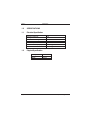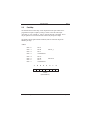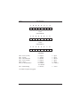
1
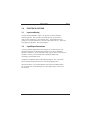
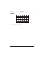
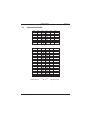
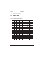
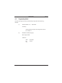
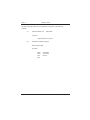
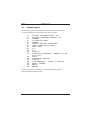
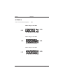
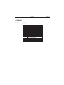
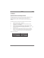
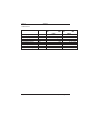
ISA-PIO
48 Channel TTLDigital
I/O Board
User Manual
ISA-PIO
User Manual
Document Part No
Document Reference
Document Issue Level
0127-0181
ISA-PIO\..\0127-0181.Doc
0.8
Manual covers PCBs identified
ISA-PIO Rev B
All rights reserved. No part of this publication may be reproduced, stored in any retrieval system, or
transmitted, in any form or by any means, electronic, mechanical, photocopied, recorded or otherwise,
without the prior permission, in writing, from the publisher. For permission in the UK contact Blue
Technology.
Information offered in this manual is correct at the time of printing. Blue Chip Technology accepts no
responsibility for any inaccuracies. This information is subject to change without notice.
All trademarks and registered names acknowledged.
Blue Chip Technology Ltd.
Chowley Oak, Tattenhall
Chester, Cheshire
CH3 9EX.
Telephone : 01829 772000 Facsimile : 01829 772001.
Chip
Amendment History
Issue
Level
0.7
0.8
Issue
Date
05.05.89
21.07.97
Author
Amendment Details
LP
SEJ
First issue
Window front cover and new logo
Contents
OUTLINE DESCRIPTION
................................ ................................ .. 1
1.0 SPECIFICATION ................................ ................................ ..........
1.1 Electrical Specification ................................ ............................
1.2 Physical Specification
................................ ............................
Electromagnetic Compatibility (EMC)
................................ .............
EMC Specification ................................ ................................ .........
2
2
2
3
4
2.0 USER ADJUSTMENTS ................................ ................................
2.1 Selecting the Base Address
................................ ......................
Figure 1 - Selecting the Base Address
................................ ............
2.2 Port Map ................................ ................................ ..................
5
5
6
7
3.0 ELECTRICAL OPTIONS
................................ ............................. 9
3.1 Input conditioning ................................ ................................ .... 9
3.2 Input/Output Connections ................................ ........................ 9
Pin Detail ................................ ................................ ..................... 10
3.3 Connector Pin Details ................................ ............................ 11
4.0 OPERATING GUIDE ................................ ................................ 12
4.1 Using the Device ................................ ................................ .. 12
4.2 Programming Guide ................................ .............................. 13
4.3 Example Program ................................ ................................ . 16
5.0 COMMERCIAL DATA ACQUISITION PACKAGES
.................. 17
5.1 Use of the ISA-PIO Board with ASYST
................................ ... 17
Blue Chip Technology Ltd.
01270181.doc
Contents
APPENDIX A ................................ ................................ ................... 18
APPENDIX B ................................ ................................ ................... 20
PC/XT/AT Port Map ................................ ................................ ..... 20
I/O Address Map ................................ ................................ .......... 20
APPENDIX C ................................ ................................ ................... 21
PC/XT Interrupt Map ................................ ................................ .... 21
APPENDIX D ................................ ................................ ................... 22
AT Interrupt Map ................................ ................................ .......... 22
APPENDIX F ................................ ................................ .................... 23
Application Notes for Interfacing the ISA-PIO
................................ . 23
Glossary ................................ ................................ ....................... 25
01270181.doc
Blue Chip Technology Ltd.
Outline Description
Page 1
OUTLINE DESCRIPTION
This card provides 48 programmable digital I/O channels. It is suitable for sensing
the presence of or driving TTL connections only. There is provision for a set of on
board pull up resistors to enable the board to be used to detect contact closures on
push buttons, relay contacts etc.
Blue Chip Technology Ltd
01270181.doc
Page 1
Page 2
Specification
1.0
SPECIFICATIONS
1.1
Electrical Specification
Number of channels
I/O Logic Levels ‘ ON’
Maximum I/O Voltage
Power Requirement
Power Dissipation
Max Sink Current (Output)
Max Source Current
1.2
Physical Specification
Height
Width
Depth
Page 2
48
2.4V to 5V TTL Level
5V
5V D.C. @ 150mA
500mW
1.7mA @ 0.45V
200uA @ 2.4V
107mm
15mm
132mm
01270181.doc
Blue Chip Technology Ltd
Electromagnetic Compatibility (EMC)
Page 3
Electromagnetic Compatibility (EMC)
This product meets the requirements of the European EMC Directive
(89/336/EEC) and is eligible to bear the CE mark.
It has been assessed operating in a Blue Chip Technology Icon industrial PC.
However, because the board can be installed in a variety of computers, certain
conditions have to be applied to ensure that the compatibility is maintained. It
meets the requirements for an industrial environment (Class A product) subject
to those conditions.
The board must be installed in a computer system which provides screening
suitable for the industrial environment.
Any recommendations made by the computer system manufacturer/supplier
must be complied with regarding earthing and the installation of boards.
The board must be installed with the backplate securely screwed to the
chassis of the computer to ensure good metal-to-metal (i.e. earth) contact.
Most EMC problems are caused by the external cabling to the board. Boards
fitted with IDC ribbon cable connectors on the metal mounting bracket
require particularly careful installation of the external cabling. The cabling
must be totally screened; the type of ribbon cable which is rolled to a round
form with a braided wire screen is best. Standard ribbon cable will not be
adequate unless it is contained wholly within the cabinetry housing the
industrial PC. Keep the unscreened section as short as possible. The
mounting bracket of the board includes a captive nut as an screen earth
point. Connect the screen of the cable to this by the shortest possible wire.
To ensure that the board meets the industrial radiated field immunity of
10V/metre, the cable should also be fitted with a ferrite clamp on the
external cable as close as possible to the connector. The preferred type is the
Chomerics clip-on-style, type H8FE-1004-AS.
Blue Chip Technology Ltd
01270181.doc
Page 3
Page 4
Electromagnetic Compatibility (EMC)
Ensure that the screen of the ribbon cable is bonded to a good RF earth at the
remote end of the cable.
Cables which connect externally to boards at TTL levels should not exceed
two metres in length. This restriction does not apply to opto-isolated boards.
Failure to observe these recommendations may invalidate the EMC compliance.
Warning
This is a Class A product. In a domestic environment this
product may cause radio interference in which case the user may
be required to take adequate measures.
EMC Specification
A Blue Chip Technology Icon industrial PC fitted with this card meets the
following specification:
Emissions:
EN 55022:1995
Radiated
Conducted
Immunity:
Page 4
Class A
Class A & B
pr EN 50082-2:1991 incorporating:
Electrostatic Discharge
IEC 801-2:1984
Performance Criteria A
Radio Frequency Susceptibility
IEC 801-3:1984
Performance Criteria A
Fast Burst Transients
IEC 801-4:1988
Performance Criteria A
01270181.doc
Blue Chip Technology Ltd
User Adjustments
2.0
USER ADJUSTMENTS
2.1
Selecting the Base Address
Page 5
The board may be located in any 62 pin slot in the PC motherboard but must be
set up to appear at a specified position (or ‘ address’ ) in the port map. Available
positions are shown in the IBM-PC Technical Reference Guide. However, for
those who do not possess a copy of this document a good place is the location
normally allocated to the prototyping card as supplied by IBM. This address is
300 Hex or 768 decimal.
All Blue Chip Technology cards are preset to this address at the factory. However,
no two devices should be used while set to the same address since contention will
occur and neither board will work. If your machine contains a card with a
conflicting address then another reasonably safe address is 200 to
21F (Hex).
A set of links is provided on the board to set the base address of the board
within the IBM-PC port map. The address is in binary with the presence of a
link representing a 0 and the absence of a link representing a 1.
To set the base address to 768 Decimal (300 Hex) set the following pattern on the links
as indicated below
Blue Chip Technology Ltd
01270181.doc
Page 5
Page 6
User Adjustments
Figure 1 - Selecting the Base Address
Note: View board with back panel on RHS.
Middle 7 bits of port address on links.
MSB
LSB
8
10
20
40
80 100 200
More example addresses are shown in Appendix A.
Note: No two cards must occupy the same address.
Page 6
01270181.doc
Blue Chip Technology Ltd
User Adjustments
2.2
Page 7
Port Map
The ISA-PIO has two 8255 chips. Each chip has three 8 bit ports which can be
programmed as input or output by writing a control word to the control port.
(See Table 3). Port A and B (A’ and B’ ) must be all input or all output. Port C
may be split into two 4 bit sections each of which may be input or output.
The board occupies eight read/write addresses (four for each 8255 chip) in the
IBM-PC port map.
Address
Base + 0
Base + 1
Base + 2
Base + 3
Port A
Port B
Port C
Command Port
Base + 4
Base + 5
Base + 6
Base + 7
Port A’
Port B’
Port C’
Command Port
7
6
5
4
8255 N 1
8255 N 2
3
2
1
0
DATA
(8255 PORT A)
Blue Chip Technology Ltd
01270181.doc
Page 7
Page 8
User Adjustments
7
6
5
4
3
2
1
0
2
1
0
1
0
DATA
(8255 PORT B)
7
6
5
4
3
DATA
(8255 PORT C)
7
6
5
4
3
2
CONTROL
Bit 0 = Port C (Lower)
Bit 1 = Port B
Bit 2 = Mode Selection
Bit 3 = Port C (Upper)
Bit 4 = Port A
Bits 5,6 = Mode Selection
Bit 7 = Mode Set Flag
0 = Output,
0 = Output,
0 = Mode 0,
0 = Output,
0 = Output,
00 = Mode 0,
1X = Mode 2.
0 = Inactive,
1 = Input.
1 = Input.
1 = Mode 1.
1 = Input.
1 = Input.
01 = Mode 1,
1 = Active.
See Table 3 for quick set-up guide.
Page 8
01270181.doc
Blue Chip Technology Ltd
Electrical Options
3.0
ELECTRICAL OPTIONS
3.1
Input conditioning
Page 9
The 8255 has high impedance inputs. An option is provided to terminate
external input lines. This is useful in an electrically noisy environment or
where a load is required (e.g. open collector drive). The termination may be
pull up (to 5V) or pull down (to 0V) via 6 SIL resistor packs (RP 2-7). Links B-G
select pull up or pull down. (See circuit diagram).
3.2
Input/Output Connections
A 50 way insulation displacement connector (IDC) is provided on the PC rear
panel of the board for I/O channel signal connection. If access to individual
channels is required, a 50 way IDC ribbon cable may be used to connect the I/O
channels to a 50 way screw terminal block available from Blue Chip
Technology as part number ST-24.
The pins are numbered as shown in the following diagram. Pins 1-48 contain
the I/O channels and pins 49 and 50 are connected to digital ground.
When the connector is viewed from the back of the system odd numbered pins
are on the left and even numbered pins are on the right with pin 1 at the top of
the connector.
Blue Chip Technology Ltd
01270181.doc
Page 9
Page 10
Electrical Options
Pin Detail
Pin
Pin
1
3
Pin
Pin
.
.
.
.
.
.
.
Pin
Pin
2
4
.
.
.
.
.
.
.
47
49
Pin
Pin
48
50
View with gold edge connectors downwards.
Page 10
01270181.doc
Blue Chip Technology Ltd
Electrical Options
3.3
Page 11
Connector Pin Details
Port
A
Bit
0
1
2
3
4
5
6
7
Pin
1
3
5
7
9
11
13
15
Pin
2
4
6
8
10
12
14
16
Port
B
Bit
0
1
2
3
4
5
6
7
Pin
17
19
21
23
25
27
29
31
Pin
18
20
22
24
26
28
30
32
Bit
0
1
2
3
4
5
6
7
Port
B’
Port
C
Bit
0
1
2
3
4
5
6
7
Pin
33
35
37
39
41
43
45
47
Pin
34
36
38
40
42
44
46
48
Bit
0
1
2
3
4
5
6
7
Port
C’
Digital Ground
Blue Chip Technology Ltd
49
50
Bit
0
1
2
3
4
5
6
7
Port
A’
Digital Ground
01270181.doc
Page 11
Page 12
Operating Gu ide
4.0
OPERATING GUIDE
4.1
Using the Device
A total of 24 I/O channel signals may be connected to each of the 8255 I/O
devices on the ISA-PIO board providing 6 eight bit ports. Each signal is
connected to one bit within one of these ports, i.e.
Port
Add
+0
+1
+2
Page 12
Bit
Hex
Decimal
0
1
2
3
4
5
6
7
01
02
04
08
10
20
40
80
1
2
4
8
1
32
64
128
0
1
2
3
4
5
6
7
01
02
04
08
10
20
40
80
1
2
4
8
16
32
64
128
0
1
2
3
4
5
6
7
01
02
04
08
10
20
40
80
1
2
4
8
16
32
64
128
Port
Add
+4
+5
+6
01270181.doc
Bit
Hex
Decimal
0
1
2
3
4
5
6
7
01
02
04
08
10
20
40
80
1
2
4
8
16
32
64
128
0
1
2
3
4
5
6
7
01
02
04
08
10
20
40
80
1
2
4
8
16
32
64
128
0
1
2
3
4
5
6
7
01
02
04
08
10
20
40
80
1
2
4
8
16
32
64
128
Blue Chip Technology Ltd
Operating Guide
4.2
Page 13
Programming Guide
The state of the input lines may be determined by using either of the following
methods:(a)
Microsoft BASIC A or
GW BASIC.
X=INP (P)
Returns the byte from port P and assigns this value to
the variable, X.
(b)
8088/8086 Assembly language.
PORT EQU 0300H
GETDAT:
MOV
IN
RET
Blue Chip Technology Ltd
DX, PORT
AL,DX
01270181.doc
Page 13
Page 14
Operating Guide
The state of the output lines may be modified by using either of the following
methods:(a)
Microsoft BASIC A or
GW BASIC.
OUT P, D
Outputs the byte D to port P.
(b)
8088/8086 Assembly language
PORT EQU 0300H
PUTDAT:
MOV
MOV
OUT
RET
Page 14
DX, PORT
AX, DATA
DX, AL
01270181.doc
Blue Chip Technology Ltd
Operating Guide
Page 15
The following table gives a summary of the most commonly used ‘ control
words’ which must be written to the control port to configure the 8255 before
using this module.
The 8255 can operate in one of 3 modes (mode 0-2).
In the first mode (mode 0) the 8255 provides simple I/O for 3, 8 bit ports. Data
is simply written to or read from a specified port (A, B or C) without the use of
handshaking. The following Control Code Table (3) assumes mode 0 is
required.
Mode 1 enables the transfer of data to or from a specified 8 bit port (A or B) in
conjunction with strobes or handshaking signals.
In mode 2 data is transferred via one bi-directional 8 bit port (A) with
handshakes (Port C).
Control
Word
(Hex)
80
81
82
83
88
89
8A
8B
90
91
92
93
98
99
9A
9B
Control
Word
(Decimal)
128
129
130
131
136
137
138
139
144
145
146
147
152
153
154
155
Sets All
of
Port A To
Output
Output
Output
Output
Output
Output
Output
Output
Input
Input
Input
Input
Input
Input
Input
Input
Sets All
of
Port B To
Output
Output
Input
Input
Output
Output
Input
Input
Output
Output
Input
Input
Output
Output
Input
Input
Sets High
4 Bits of
Port C To
Output
Output
Output
Output
Input
Input
Input
Input
Output
Output
Output
Output
Input
Input
Input
Input
Sets Low
4 Bits of
Port C To
Output
Input
Output
Input
Output
Input
Output
Input
Output
Input
Output
Input
Output
Input
Output
Input
Table 3 - Control Word Table
Blue Chip Technology Ltd
01270181.doc
Page 15
Page 16
4.3
Operating Guide
Example Program
The following program in Microsoft Basic will test the operation of the ISA-PIO
if a link is made between corresponding pins on the rear connector.
10
15
20
30
40
50
60
70
80
90
100
110
120
130
140
150
160
170
180
P1=&H300 : REM BASE OF FIRST PIA
P2 = &H304 : REM BASE OF SECOND PIA
GOSUB 60
P1 = &H304 : P2 = &H300
GOSUB 60
GOTO 10 : REM LOOP CONTINUOSLY
OUT P1+3, &H80 : OUT P2+3, &H9B
FOR P = 0 TO 2
F=0
A=1
OUT P1+P, A
IF INP (P2+P)<>A THEN PRINT
ERROR , P, A, INP
(P2+P) : F=F+1
A=A+A
IF A=256 THEN GOTO 150
GOTO 100
IF F>0 THEN PRINT P,
FAILED , F : GOTO 170
PRINT P, PASSED
NEXT P
RETURN
The above program runs continuously and can only be stopped by pressing
control and break on the PC keyboard.
Page 16
01270181.doc
Blue Chip Technology Ltd
Commercial Data Acquisition Packages
5.0
Page 17
COMMERCIAL DATA ACQUISITION PACKAGES
The Blue Chip Technology ISA-PIO can be used with almost any data acquisition
package that can read information directly from a PC input port.
5.1
Use of the ISA-PIO Board with ASYST
The board has been tested with and is installable as an 8255.PORT digital
device in the ASYST scientific software package by Macmillan Software
Company.
For more details about this package and other PC data acquisition software
please contact Blue Chip Technology.
Whilst every effort has been taken to ensure that the information provided is
accurate, Blue Chip Technology cannot assume responsibility for any error in
this manual or their consequences. Should any errors be detected, the company
would greatly appreciate being informed of them. A policy of continuous
product development is operated, resulting in the contents of this document
being subject to change without notice.
Blue Chip Technology Ltd
01270181.doc
Page 17
Page 18
Appendix A
APPENDIX A
Note: View board with back panel on
RHS.
Address Settings for Port 300H
MSB
LSB
8
10
20
40
80 100 200
Address Settings for Port 200H
MSB
LSB
8
10
20
40
80 100 200
Address Settings for Port 208H
MSB
LSB
8
Page 18
10
20
40
01270181.doc
80 100 200
Blue Chip Technology Ltd
Appendix A
Page 19
Address Settings for Port 210H
MSB
LSB
10
8
20
40
80 100 200
Address Settings for Port 220H
MSB
LSB
8
10
20
40
80 100 200
Address Settings for Port 230H
MSB
LSB
8
Blue Chip Technology Ltd
10
20
40
80 100 200
01270181.doc
Page 19
Page 20
Appendix B
APPENDIX B
PC/XT/AT Port Map
I/O Address Map
Address
000-01F
020-03F
040-05F
060-06F
070-07F
080-09F
0A0-0BF
0F0
0F1
0F8-0FF
1F0-1F8
200-207
278-27F
2F8-2FF
300-31F
360-36F
378-37F
380-38F
3A0-3AF
3B0-3BF
3C0-3CF
3D0-3DF
3F0-3F7
3F8-3FF
Page 20
DMA Controller 1, 8237A-5
Interrupt Controller 1, 8259A
Timer, 8254
Keyboard Controller, 8742; Control Port B
RTC and CMOS RAM, NMI Mask (Write)
DMA Page Register (Memory
Mapper)
Interrupt Controller 2, 8259
Clear NPX (80287) Busy
Reset NPX, 80287
Numeric Processor Extension, 80287
Hard Disk Drive Controller
Reserved
Reserved for Parallel Printer Port 2
Reserved for Serial Port 2
Reserved
Reserved
Parallel Printer Port 1
Reserved for SDLC Communications,
Bisynchronous 2
Reserved for Bisynchronous 1
Reserved
Reserved
Display Controller
Diskette Drive Controller
Serial Port 1
01270181.doc
Blue Chip Technology Ltd
Appendix C
Page 21
APPENDIX C
PC/XT Interrupt Map
Number
Usage
NMI
Parity
0
1
2
3
Timer
Keyboard
Reserved
Asynchronous Communications
(Secondary)
SDLC Communications
Asynchronous Communications
(Primary)
SDLC Communications
Fixed Disk
Diskette
Parallel Printer
4
5
6
7
Blue Chip Technology Ltd
01270181.doc
Page 21
Page 22
Appendix D
APPENDIX D
AT Interrupt Map
Level
Function
Microprocessor NMI
Parity or I/O Channel Check
Interrupt Controllers
CTLR 1
CTLR2
IRQ 0
IRQ 1
IRQ 2
IRQ 8
IRQ 9
IRQ 10
IRQ 11
IRQ 12
IRQ 13
IRQ 14
IRQ 15
IRQ 3
IRQ 4
IRQ 5
IRQ 6
IRQ 7
Page 22
Timer Output 0
Keyboard (Output Buffer Full)
Interrupt from CTLR 2
Realtime Clock Interrupt
Software Redirected to INT 0AH ( IRQ 2)
Reserved
Reserved
Reserved
Coprocessor
Fixed D isk Controller
Reserved
Serial Port 2
Serial Port 1
Parallel Port 2
Diskette Controller
Parallel Port 1
01270181.doc
Blue Chip Technology Ltd
Appendix F
Page 23
APPENDIX F
Application Notes for Interfacing the ISA-PIO
The signals present at ports A, B & C on either the NMOS or CMOS 8255 are TTL
(Transistor Transistors Logic) compatible, that is they will interface into
standard 74LS logic. However, TTL has limitations when interfacing to other
circuitry.
The following should be considered when attempting to interface the ISA-PIO:
1).
2).
3).
4).
5).
ISA-PIO cannot drive high capacitances.
ISA-PIO cannot sink loads greater than 2.5mA and retain an output
voltage that is TTL compatible.
ISA-PIO cannot source loads greater than - 200uA (-400uA for CMOS
version) and retain an output voltage that is TTL compatible.
ISA-PIO cannot interface to any voltage greater than VCC ( VDD) + 0.5 or
lower than - 0.5V.
ISA-PIO cannot drive long lengths of cable into other TTL compatible
devices. TTL is a standard for onboard interfacing primarily and is too
susceptible to interference and noise to be used with long cable runs.
General TTL requirement:LOW
HIGH
Input 0.5 - 0.8V
Output 0 - 0.45V
2.0 - Vcc ( VDD)
2.4 - Vcc ( VDD)
Blue Chip Technology Ltd
01270181.doc
Page 23
Page 24
Appendix F
Characteristics:
DC PARAMETER
SYMBOL
8255
82C55
MIN
MAX
MIN
LIMITS
Input Voltage High
Input Voltage Low
Output Voltage High
Output Voltage Low
Input Leakage Current High
Input Leakage Current Low
Output Leakage Current High
Output Leakage Current Low
Supply Current (Dynamic)
Supply Current (Standby)
Page 24
VIH
VIL
VOH
VOL
ILIH
ILIL
ILOH
ILOL
IDDI
IDD2
2
-O.5V
2.4V
01270181.doc
VCC
0.8V
@-20uA
IOL=1.7MA 0.45V
VI = VCC 10uA
-10uA
10uA
-10uA
120mA
120mA
MAX
LIMITS
2.2
-0.5V
3.5
2uA
Blue Chip Technology Ltd
VDD+0.3V
0.8V
IOH=-400uA
IOL=2.5MA 0.4V
VI = VDD 10uA
VI = 0V -10uA
VO = VDD 10uA
VO = OV -10uA
15MA
50uA
Glossary
Page 25
Glossary
VIH -
High level input voltage - the minimum and maximum voltages that
can be applied ( ref to 0V) for a high to be recognised.
VIL -
Low level input voltage - the minimum and maximum voltages that
can be applied ( ref to 0V) for a low to be recognised.
VOH -
High level output voltage - the minimum that will be presented at the
output as a high at a given max current source current.
VOL -
Low level output voltage - the maximum voltage that will be presented at
the output as a low at a given maximum current load.
Blue Chip Technology Ltd
01270181.doc
Page 25