1
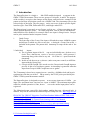
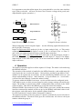
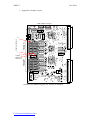
GREAT
P.J.Coleman-Smith: 14/1/2004
TDR Pattern Register User Manual
Contents
1. Introduction.
2. Function.
a. Block Diagram.
b. VME interface specification.
c. SHARC interface data format.
3. Setting up.
a. VME Address Jumpers
b. Input selection.
4. Operation
a. Single input mode
b. Gated Group
c. GroupA AND GroupB.
5. Software Interface.
6. Front Panel Interface.
7. Logic Inspection Signal examples.
8. What can stop the module working, or Error management.
Appendices
A. Layout of the PCB with Jumper locations.
B. Front Panel Layout.
C. MIDAS control window.
Refers to pcb 25/9275A.
[email protected] 1
GREAT
14/1/2004
1. Introduction
The Pattern Register is a single w
idth VME module designed to operate in the
GREAT TDR environment. There are two groups of 16 inputs, A and B. The purpose
of the module is to regist er the changes on the inputs, and send a tim estamped 16 bit
pattern to the Data Acquisition system via a SHARC link. The timestamp refers to the
selected edge of the input. The two groups can be set to one of three specific digital
interface types. Fast NIM, Differential ECL, and Single ended ECL.
The Pattern input is operated as two Groups, each in one of three operating m odes.
All the pattern inputs are AND' ed with a programm able m ask bit, which allows
individual bits to be disabled, for exam ple where one input is firing in noise. GroupA
can be pulse stretched under computer control.
1.
Gated Group:
The front edge of the Gr oup Gate input will latch the m aster 100MHz counter
and all inpu ts which are active at any tim e during th e Group Gate will b e
included in the pattern. The pattern and timestamp is outpu t at the end of the
Gate.
2. Individual
inputs:
a) The 16 pattern inputs of the Gr oup are individually sam pled on every
clock. Thos e that becam e active s ince th e previous clock generate a
timestamp along with a label to say wh ich of the 16 i nputs caused the
timestamp.
b) In this m ode the user m ay choose (under com puter control) to AND the
input with the Group Gate.
c) GroupA AND GroupB. This m ode uses the GroupA and GroupB inputs to
provide 16 bits of co-incidence pattern. A timestamp is generated when the
input from GroupA AND GroupB are true to-gether.
The Ti mestamp is based on a counter increm ented by a 100Mhz clock and kept in
synchronism with the rest of the T DR sy stem by the SYNC pulse provided by the
GREAT TDR system Metronome module.
The Pattern Register is designed to operate at an average input rate of 10Khz per
input. The maximum burst rate into one input is 10Mhz. T he m inimum input pulse
width for reliable operation is 50ns, howev
er m uch s maller input pulses can be
registered.
The following docum ents will h elp in unders tanding the term s discussed in th is
manual. They can be found at the Nuclear Physics Group web site : http://npg.dl.ac.uk
EDOC502 The GREAT Triggerless Total Data Readout Method (IEEE TNS, VOL.
48, NO. 3, JUNE 2001)
EDOC503 The GREAT 32 Channel Peak Sensing ADC : User Manual
EDOC504 The GREAT data format.
EDOC507 The GREAT TDR system Error recovery, and experiment timing
EDOC511 Metronome User Manual Version6 ( C1100 )
[email protected] 2
GREAT
14/1/2004
2. Function
The function of the module is carried out by two Altera FPGA devices programmed at
power-up from serial EPROMs. There is an LED for each FPGA which is lit when the
programming has completed successfully.
The user of the m odule must decide the inte rface type for each of the 16 inputs in the
two Groups. The jum pers m ust then be set accordingly. Refer to section 3.b and
appendix A for setting the different interface choices.
The inputs to be reg istered are chosen by using the MIDAS interface window. See
appendix C for an example of the window for the Pattern Register.
The sense of each input can be inverted, controlled via MIDAS, prior to being applied
to the Register timestamp logic. This allows the user to decide which edge of the input
signal causes the tim estamp. It is always
the rising edge of the input that is
timestamped.
As mentioned in the introduction each group operates in one of two modes. The mode
must be selected via the MIDAS interface.
To operate the m odule must be connected to a TDR Metronom e output, or a sim ilar
source of 100Mhz, and SYNC pulses.
a. Block Diagram
The block diagram shows the path of data from input signal to SHARC output.
32 signal inputs DIFF.ECL,
2 Gate inputs
Fast NIM,
S.E.ECL to
TTL
conversion
100Mhz clock
SYNC
RESET
ERROR
Register
Pattern and
timestamp
Format and
SHARC output
FIFO
SHARC Link to DAQ
VME output
memory
48-bit Timestamp
counter
Parameter header store
Metronome Interface
General and s pecific
controls and status
Data and address paths
VME slave
interface
Group mode
GREAT Pattern Register
P.J.Coleman-Smith
b. VME interface specification
The Pattern Register is an A32/D3 2 slav e. Th e in terface will respon d to acces ses
made using D16, and D08, however they will not return the correct values.
The Pattern Register o ccupies 2 16 bytes in A32 m emory space. T he address of
location 0 is specified by jum pers set on the pcb. See section 3.a and appendix A for
setting the address base.
[email protected] 3
GREAT
14/1/2004
c. SHARC interface data format.
The Pattern Register outputs two 32 bit words for every Item. An Item can be for an
input transition from Gr oupA, or GroupB, a SY NC pulse, a flow control Pause, or a
flow control Resum e. Refer to E DOC504 for m ore inform ation about the bit
allocation of these two words.
Here is an outline of the Item format extracted from the EDOC.
Group Pattern Data format
31
30
29
28
27 to 16
15 to 0
1
1
0
0
Data Source Ident,
Pattern data
31 to 28
27 to 0
0
Time Stamp 27:0
Other Information.
31 30
29 to 24
1
0
Module Number
23 to 20
Information
Code
31 to 28
0
19 to 0
Information Field
27 to 0
Time Stamp 27:0
The Module number identifies the source of the information.
The Information codes used in the Pattern Register are as follows:
Information Type
Code
Information Field Definition
Undefined Data
0
Pause Timestamp
2
Timestamp bits 47 : 28
Resume Timestamp
3
Timestamp bits 47 : 28
SYNC100 Timestamp
4
Timestamp bits 47 : 28
3. Setting Up
a. VME Address Jumpers.
Refer to the picture of the m odule shown in Appendix A. T he VME address jum pers
are in two, eight jum per blocks at the m iddle of the top of the pcb. The address of
location 0 o f the m odule address sp ace is sp ecified by placing, or not, shorting links
ion the jum pers. Placing a shorting link on a ju mper will se lect that add ress bit to b e
seen as a logic 0.
For example to select address 0x80000000 for th e base address, shorting links should
be placed on every jumper except the one for A31. (This is the jumper at the left most
end of the row, as indicated by the white writing ).
b. Input Selection
Each of the 32 inputs can be selected to interf ace to signals of one of three types. Fast
NIM, Differential ECL, and Single ended EC L. The following jumper diagrams show
how to select each of the possible types.
Differential ECL does not require a specific reference voltage selected, but the Fas t
NIM, and Single Ended ECL do.
[email protected] 4
GREAT
14/1/2004
1
S.E.ECL
Differential ECL
Group A
Single Ended ECL
Group B
Fast NIM
Input Selection Jumper Positions
Fast NIM
1
Top of Board
S.E.ECL
1
Fast NIM
JP85
JP86
JP91
It is important to note that all the inputs for a group should be set to the same interface
type. Failu re to do this will resu lt in incor rect ref erence v oltages bein g used, and
unpredictable register operation ;-)
Voltage Reference selection
When connecting to the front panel inputs use the following signal allocations with
the 34 pin IDC connectors.
Input 0 in Differential ECL mode pin1 is the +ve input, and pin 2 the –ve. This carries
on through the connector with Input 15 on pin 31 for +ve an d pin 32 for –ve. Pins 33,
and 34 are not connected on both Group A and B input connectors.
Input 0 in Fast NIM, and Single Ended ECL mode pin1 is the Signal input, and pin 2
the GND. This carries on through the conne ctor with Input 15 on pin 31 for Signal
input and pin 32 for GND. Pins 33, and 34 are not connected on both Group A and B
input connectors.
4. Operation
The mode of operation applies to all the inputs of a Group. The mode is selected using
the MIDAS interface.
The operation of the module is handled by the MIDAS interface, and would norm ally
only require the user to select the inputs, their polarity, and the Group Modes. If the
module is to be operated in an environm ent not controlled by MIDAS, then a m uch
deeper understanding of the m odule function is requ ired than is co vered in this
version of the user manual. Contact the author for help .
To operate within the MIDAS environm ent the m odule must be configured in the
VME address space, an d the correct Group In terface jumper settings selected for th e
inputs. The module is entered in the VME configuration table accessed via the VME
control window. This allows the MIDAS to set-up and control the module.
With the SHARC link connected to the TDR Collato r processor, and the Me tronome
interface connected the module will be set-up by the MIDAS with initial values in all
the registers, and valid entries for the module readout identifiers.
Use the Experiment Control window Setup and Go buttons.
The mode of operation of the two groups of inputs is controlled by m enu selection in
the MIDAS interface. The tab le below gives th e valid m odes. A# refers to the inp ut
number within the group A.
[email protected] 5
GREAT
Value
0
1
2
4
5
6
12
13
14/1/2004
Mode name
Single: input(A/B)# AND Gate(A/B)
Single: input(A/B)#
Gated Group
Single : A# AND B# AND GateA
Single : A# AND B#
Gated Group : A# AND B#
Single : Stretched A# AND B# AND GateA
Single : Stretched A# AND B#
Comment
Group A input only
Group A input only
Group A input only
Group A input only
Group A input only
a. Single Input mode.
In this m ode each inpu t operates alone. E ach input m ust be enabled via the MIDAS
interface. The Group Gate input can be selected to be AN Ded with th e inputs. Th is
selection operates for the whole of a group.
b. Gated Group.
The front edge of the Group Gate in put will latch the master 100MHz counter and all
inputs which are active at any time during the Group Gate will be in
cluded in th e
pattern. The Group Gate input is a Fast NIM signal.
c. GroupA AND GroupB, or Using the TDR Pattern
Register for providing timed suppression data.
The purpos e is to co mbine the VETO signal from the Eurogam Phase 1 BGO
detectors and electronics with a Ge CFD to give a tim estamped data item indicating
the co-incidence of the two signals.
The Pattern Register 32 inputs are allocated as two groups of 16. Group B is used for
the Single Ended ECL VETO signals from the BGO electronics, and Group A is used
for the Fast NIM Ge CFDs from the LeCroy CFD modules.
The Ge CFD signals a re str etched in the Pattern Registe r to align th em with the
slower VETO signals. Fig 1 shows when th e tim estamped Item is generated for a
single CFD and VETO.
It shou ld be noted that a tim estamped Item will be gene rated f or every coincid ence
between the VETO, and CFD. Fig 2 show s how this can occur during m ultiple
VETOs
[email protected] 6
GREAT
14/1/2004
Delayed BGO VETO
Stretched Ge CFD
Item Generated
Fig 1: Single CFD Aligned with VETO
Delayed BGO VETO
Stretched Ge CFD
Item Generated
Fig 2: Multiple VETOs align with one CFD
When setting up for an experim ent it will be necessary to ch eck the alignment of the
Ge CFD and VETO signals, as well as the width of the CFD.
Logic Inspection Lines are provided in each Pattern Register for this job.
The width of the CFD output pulse will also affect the number of co-incidences.
5. Software Interface
Access to th e regis ters o n the Pattern Re gister are via the V ME bus interface using
A32/D32 commands. The register s are defined in the table in Appendix E at the end
of this docum ent. For further information about register function contact the author
via email.
The normal method of control is via the MIDAS control window. The module should
be initialized after power-up with registers set as follows.
6. Front Panel Interface
The front panel layout is shown in a diagram in Appendix B.
The connections are detailed in the following Tables.
SHARC Link.
Pin
1
2
3
4
5
6
7
8
Function
Clock
Acknowledge
GND
Data 0
Data 1
Data 2
Data 3
GND
[email protected] 7
Source
Pattern Register
VME Processor
Pattern Register
Pattern Register
Pattern Register
Pattern Register
GREAT
14/1/2004
Group Inputs (A/B) Differential ECL Interface
Pin
1
3
….
31
33
Function
Input 0 +ve
Input 1 +ve
Input 15 +ve
No Connection
Pin
2
4
….
31
34
Function
Input 0 -ve
Input 1 –ve
Input 15 –ve
No Connection
Group Inputs (A/B) Single Ended ECL Interface
Pin
1
3
….
31
33
Function
Input 0
Input 1
Input 15
No Connection
Pin
2
4
….
31
34
Function
Ground
Ground
Pin
2
4
….
31
34
Function
Ground
Ground
Ground
No Connection
Group Inputs (A/B) Fast NIM Interface
Pin
1
3
….
31
33
Function
Input 0
Input 1
Input 15
No Connection
Ground
No Connection
7. Logic Inspection Signal examples
During normal use of the module the inputs, and Gate signals are the most likely to be
required. The examples show which edge of the signal as seen through the Inspection
Lines generates the Timestamp.
8. What can stop the module working, or Error
management.
1. Lost Track.
Refer to the block diagram in section 2.a. There is a FIFO between the
timestamping input stage, and the formatting and SHARC link stage. The
data is placed into the FIFO with a four bit count to keep track of the data
through the FIFO. If the data coming through the FIFO is not in step, then
the module will stop working, the Lost Track LED will light, and the
relevant bit is set in the status register. The operation of the module is restarted by a system STOP/SETUP/GO action.
2. Using the wrong edge of the input for timing.
[email protected] 8
GREAT
14/1/2004
3. Appendix A Jumper Layout
VME Address Jumpers
GroupA
Input type Jumpers
15
1
GroupB
0
Voltage
Reference
Selection A
Outline of the Pattern Register for location of Jumpers.
[email protected] 9
GREAT
Appendix B Front Panel Layout
[email protected] 10
14/1/2004
GREAT
14/1/2004
Appendix C MIDAS control window.
Appendix D Logic Inspection signal examples.
Appendix E Software Register definitions.
Register definitions:
Address offset
Hexadecimal
0
Name
Function
Module Control
4
Module Status
8
Interrupt Control
C
Interrupt Select
10
14
Read FIFO
Read Tracking
Registers
18
FIFO Flags
1C
Spare Bus
0 : ignore track. 1= Ignore the tracking data when reading
FIFO
1 : SHARC enable. 1 = Enable SHARC link readout of the
FIFO.
2 : Reset FIFO
3 : STARX enable. 1= Enable STARX to reset FIFO.
4 : Soft Reset input chip.
5 => 15 : registered data, but no action.
16 => 31 : always return 0.
0 : interrupt.
1 : lost track.
2 : FIFO Half full.
3 => 31 : Always return 0.
0 => 7 : Interrupt vector.
8 => 10: Select IRQ line to drive on VME bus.
11 => 15 : registered data, but no action.
16 => 31 : always return 0.
0 => 3 : Select Interrupt source.
0: Lost Track.
1: FIFO half full.
2 => 15 not defined.
4: Method. 0 = Edge triggered, 1 = Level Triggered
5: Edge. 0 = Rising edge, 1 = falling edge.
6: Level. 0 = High Level, 1 = Low level.
7: Enable 0 = Disabled, 1 = Enabled.
8 => 15 : registered data, but no action.
16 => 31 : always return 0.
0 => 31: FIFO output data.
0 => 3 : Readout track Counter
4 => 7 : Track number from FIFO.
8 => 11 : ID track number from last ID word.
12 => 15 : Track number from last Time stamp.
16 => 31: 0.
All these flags are active low.
0 : Almost full.
7 spaces remaining.
1 : Almost empty. 7 words written.
2 : Half full.
131,072 words written
3 : Empty.
4 : Full.
262,144 words written
5 => 31 : 0.
0 => 31 : VME chip end of Spare connections between the
two Alteras
100
Group A input
enable
[email protected] 11
Bits 15 => 0 enable an input when set.
GREAT
14/1/2004
104
108
Group A Invert
Group A mode
110
204
208
Group A Stretch
value
Group B input
enable
Group B Invert
Group B mode
300
304
308
30C
Inspection Line 0
Inspection Line 1
Inspection Line 2
Inspection Line 3
Selects the signal source
Selects the signal source
Selects the signal source
Selects the signal source
400
Input Chip control
404
Input Status
0 : Reset input FIFOs
1 : Count Enable. 1 = Enable Time stamp counter.
2 : SYNC error reset.
3 : SYNC to Error ( STARY ) connect.
4 : No effect, but registered.
5 : Run Enable. 1 = Enable input of SYNC, and Data to the
FIFOs.
6 => 15 : registered data, but no action.
16 => 31 : always return 0.
Timestamp errors and others ( NYI !!! )
500
504
Time FIFO LS
Time FIFO MS
508
Time FIFO word
count
200
50C
510
514
518
51C
520
524
528
52C
530
534
538
53C
540
544
548
54C
550
554
Bits 15 => 0 invert the logic of the input bit when set.
Selects registered/free/free & Gate mode.
0: Free Transition Mode. 1= enabled.
1: Registered Mode.
1 = enabled.
2: AND mode ( CFD + VETO ) 1= enabled.
3: Stretch input pulses. 1 = enabled.
Bits 3 => 0 select the pulse stretch value in steps of 50ns.
Bits 15 => 0 enable an input when set.
Bits 15 => 0 invert the logic of the input bit when set.
Selects registered/free/free & Gate mode.
0 => 31 : Time stamp bits 0 => 31.
0 => 15 : Timestamp bits 32 => 47.
16 => 31 : 0.
0 => 8 : Number of words in the Timestamp FIFO
Group A fifo data
0 => 15 : Group A Pattern
16 => 31 : 0
Group A fifo word
count
0 => 8 : Number of words in the Group A FIFO
16 => 31 : 0
Group B fifo data
0 => 15 : Group B Pattern
16 => 31 : 0
Group B fifo word
count
0 => 8 : Number of words in the Group B FIFO
16 => 31 : 0
Type fifo data
0 => 7 : Event type data.
8 => 31 : 0.
Type fifo word
count
0 => 8 : Number of words in the Event type FIFO
16 => 31 : 0
Group A Ident
Group B Ident
SYNC Ident
Pause Ident
Resume Ident
Undefined Ident
0 => 31 : Ident for Group A pattern.
0 => 31 : Ident for Group B pattern.
0 => 31 : Ident for SYNC.
0 => 31 : Ident for Pause.
0 => 31 : Ident for Resume.
0 => 31 : Ident for Undefined.
[email protected] 12
GREAT
14/1/2004
558
55C
560
Write to FIFO.
0 => 31 : write to FIFO.
FIFO flags
0 : Group A FIFO empty
1 : Group A FIFO full
2 : Group B FIFO empty
3 : Group B FIFO full
4 : Control FIFO empty
5 : Control FIFO full.
6 : Timestamp FIFO empty
7 : Timestamp FIFO full.
8 : External FIFO almost full.
9 : External FIFO full.
10 => 31 : 0
600
Load Timestamp
700
Spare bus read
Load a new value into the Timestamp counter for loading at
a re-sync SYNC pulse.
0 => 31 : Data for new Timestamp 16 => 47 value.
A write to this register sets the Re_SYNC enable.
0 => 31 : Input chip end of Spare connections between the
two Alteras.
Appendix F. Logic Inspection Line signal selection.
Logic Inspection Line Signal selection.
This inform ation is provided for
completeness, it is not intended f or a us er to need to vie w the m ajority of thes e
signals.
Code
Signal Name
Description
0 => 1F
Disconnected
Allows other units to drive the line.
20 => 2F Group A inputs Input monitors for Group A.
0 => 15
30 => 3F Group B inputs Input monitors for Group B.
0 => 15
40
Group B Hit
Group B Pattern hit.
41
Group B End
Group B Gated mode End signal
42
Gate A
Group A Gate input.
43
Gate B
Group B Gate input.
44
Sync pulse
Sync detected 10nS pulse
45
Sync error
Sync error flag
46
Aneb
Output of Timestamp sync comparator
47
Re-load window Window a fter S YNC pulse during which a re-load
can occur.
48
Load stamp
Re-load pu lse. Loads the new value into the
Timestamp counter
49
Load Enable
Indicates a re-load has been programmed.
4A
Time FIFO read FIFO read request signal for the Timestamp FIFO
4B
Time FIFO full
Flag
4C
Time
FIFO Flag
empty
4D
Group A FIFO FIFO read request signal for the Group A FIFO
read
4E
Group A FIFO Flag
[email protected] 13
GREAT
4F
50
51
52
53
54
55
56
57
58
59
5A
5B
5C
5D
5E
5F
60
61
62
63
70 => 7F
80
81
82
83
84
85
86
87
88
89
8a
8b
8c
14/1/2004
full
Group A FIFO
empty
Group B FIFO
read
Group B FIFO
full
Group B FIFO
empty
Time
FIFO
write
Group A FIFO
write
Group B FIFO
write
Pause
Resume
Type FIFO read
Type FIFO full
Type
FIFO
empty
SYNC
STARX
Out of step
Ext FIFO write
clock
Ext FIFO write
Ext FIFO almost
full
Ext FIFO full
Group A Hit
Group A End
Group A
stretched 0 =>
15
Loadreg
Chip select
Asn
DS0n
DS1n
DTACK
STARX
Iackn
Irq1
Irq2
Irq3
Irq4
Flag
FIFO read request signal for the Group B FIFO
Flag
Flag
FIFO write request for the Timestamp FIFO
FIFO write request for the Group A FIFO
FIFO write request for the Group B FIFO
Pause signal
Resume signal
FIFO read request signal for the Type FIFO
Flag
Flag
SYNC pulse from the Metronome
STARX ( Reset ) from the Metronome
Internal FIFOs are out of step ???????
FIFO Write clock to the external FIFO
FIFO Write request to the external FIFO
Flag ( active low )
Flag ( active low )
Group A Pattern hit.
Group A Gated mode End signal
The Stretched inputs for Group A.
Load signal, enables reg isters when selected to load
data
Active to select vme access to the input chip
VME address strobe
VME Data strobe 0
VME Data strobe 1
VME data acknowledge
VME Interrupt acknowledge cycle identifier
Interrupt line
Interrupt line
Interrupt line
Interrupt line
[email protected] 14
GREAT
8d
8e
8f
90
91
92
93
94
95
96
97
98 – 9f
A0
A1
A2
A3
A4
A5
A6
A7
A8
A9
Aa
Ab
Ac
Ad
Ae
Af
B0
14/1/2004
Irq5
Irq6
Irq7
Iackinn
Iackoutn
Sharc_clock
Sharc_ack
Sharc data0
Sharc data1
Sharc data2
Sharc data3
NYI
Fifo pafn
Fifo paen
Fifo hfn
Fifo ffn
Fifo efn
Fifo erclk
Fifo erenn
Fifo rclk
Fifo rcsn
Fifo renn
Fifo oen
Fifo prsn
Fifo mrsn
Fifo ready
Fifo rdreq
Vme req
Lost track
Interrupt line
Interrupt line
Interrupt line
Interrupt cycle chain token in
Interrupt cycle chain token out
SHARC bus clock pulses.
SHARC bus acknowledge
SHARC data bit
FIFO programmable almost full
FIFO programmable almost empty
FIFO Half empty
FIFO full
FIFO empty
Fifo erclk ?????
Fifo erenn ????
Fifo read clock
Fifo read chip select
Fifo read enable
Fifo output enable
Fifo partial reset
Fifo master reset
Fifo data has been read, and is ready for use
Request from sharc software for a fifo read
Request from vme for a read of fifo data
Output of the track comparison system ?
[email protected] 15