1
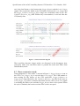
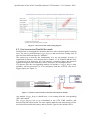
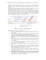
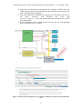
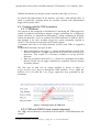
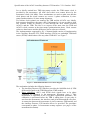
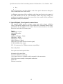
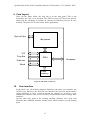
Specification of the AGAVA ancillary detector GTS interface. V 2.0 October. 2005
AGATA Ancillary Detectors and Ancillary
Detector Integration Working Group
Specifications of the AGAVA (AGata Ancillary
Vme Adapter) Ancillary Detector GTS Interface
Work Document
Version 2.0, October 2005
Contributors: D. Bazzacco, P. Bednarczyk, M. Bellato, P.J. Coleman-Smith, A.
Czermak, B. Dulny, A. Gadea, Ch. Houarner, R. Isocrate, P. Jones, W. Meczyński,
L. Olivier, V. Pucknell, Ch. Theisen, Ch. Weber, G. Wittwer, M. Ziębliński.
1
Specification of the AGAVA ancillary detector GTS interface. V 2.0 October. 2005
1. Introduction
The Advance Gamma-ray Tracking Array (AGATA) is a step forward in many
aspects of the gamma-ray spectroscopy technology. The concept of tracking the
gamma ray will allow having large efficiency and peak to total ratios for large
multiplicity cascades of gamma-rays. But this is not the only breaking through
aspect of the project, new concepts on the data processing, based on digital
electronics, is being developed. Among the characteristics of this new electronics,
two of them have an important impact on the ancillary devices and associated
electronics:
• the sustainable high counting rates
• the capability of processing potentially 224 trigger requests every clock
cycle (10ns) and therefore, even if the real trigger gate is several cycles,
since the processing time of the data is orders of magnitude longer, the
system will do parallel processing of the signals.
The full AGATA will be design to cope with up to 50 kHz counting rate in a
single crystal and with a global trigger rate of ≈500 kHz. This corresponds to
more that an order of magnitude increase on trigger rate with respect to previous
Compton suppressed arrays. The conventional electronics, with common dead
time, used in most (if not all) the existing ancillary detectors will not be able to
work at such trigger rate; therefore developments should be foreseen in the next
years to avoid situations where the ancillary device is limiting the rate of the full
AGATA array.
AGATA requires, in almost all circumstances, ancillary devices to exploit all the
capabilities of the tracking and get the best performance figures. The emission
point of the gamma ray and the trajectory and velocity of the emitting nuclei are
basic information for the reconstruction of the Doppler effects. And several
ancillaries will be needed to develop the experimental program with radioactive
and stable beams.
To obtain the maximum performance figures of the AGATA-ancillary detector
complex, the electronics of the ancillary detector and the trigger interface have to
be compliant with the previously mentioned points.
While many ancillary devices already support high counting rates, the processing
time of the accepted events and the impossibility to process in parallel events,
even if they come from different sub-detectors, is a generalize handicap of present
generation electronics.
In the present document we will try to define a trigger interface for ancillary
detectors to be used in the phase of the AGATA demonstrator, and therefore to be
used initially with a less demanding setup, we should study and include as many
features as possible in compatibility with the time and funds scale.
This document should contain the basic characteristics of the GTS interface
2. Basic consideration on the standards to be used in the
construction of the interface
Since most of the ancillary detectors available in our community have a frontend/read-out based in VME or VXI standard, the ancillary detector GTSmezzanine interface will be developed in VME standard with full compatibility
with the VXI read-out modes. VME and VXI are asynchronous busses and
therefore the time required for a read/write cycle depends strongly on the
2
Specification of the AGAVA ancillary detector GTS interface. V 2.0 October. 2005
capability of the slave (in this case the interface) to answer. We should be aware
that fast readout cycles ≤ 1 µs (is like that for most existing slaves) should be
supported.
3. Trigger or not trigger?
Before describing the details of the card, it may be useful to make comments on
the AGATA trigger. AGATA has a fully digital pipelined electronics and all
detectors are time stamped. It is a priori not necessary to use trigger conditions
and the system could be considered as a trigger-less system. As explained in the
GTS documents1, the GTS has a minimum latency time of 6 to 7µs. No “prompt”
signals are provided; therefore, the GTS does no provide information such as “do
something at a given time”, but rather “what you have done is relevant, data must
be kept”. “Trigger” is indeed not an appropriate name. One should rather use
“Data filtering”.
With these considerations, it seems difficult to reconcile the GTS with detectors
having a standard electronics, requiring prompt signal for signal processing,
coding, and having a dead-time. If the ancillary detector is a necessary condition
to accept AGATA, data losses can not be avoided.
Let us consider a few typical examples;
•
•
•
Master ancillary detector. One should remember that some experiments
produce a large amount of unwanted gamma-ray which will be in any case
thrown-away. This is for instance the case when a spectrometer is used:
only gamma-rays in coincidence with the spectrometer are relevant. The
spectrometer rate is in general low and the spectrometer dead-time has
little consequences on the “dead-time” induced on AGATA. On-line data
filtering has also the advantage to reduce the data flow, in particular in the
pulse-shape processor farm which may act as a bottle-neck when Ge
detectors rate is high. If the ancillary detector has a large counting rate
(and therefore some dead-time), event are lost. Dead-time is in this case a
drawback for the ancillary detector and for AGATA. A typical example is
a beam tracker or the RFD.
Slave ancillary detector. One should also consider the case of an ancillary
detector producing additional information like the neutron wall, a Si ball...
In this case, the ancillary detector information in not requested in all cases:
data are relevant only if they are in coincidence with AGATA. The aim is
then to reduce the ancillary detector data flow. In this case, the ancillary
detector dead-time is a draw-back for the ancillary detector itself and for
the data quality, but not for AGATA.
Finally, one should consider intermediate cases mixing “slave” and
“master” modes. For instance, a condition like “at least one gamma-ray
and silicon ball, or at least three gamma-rays”. Dead time is induced on
AGATA when the first condition is fulfilled, but not in the second case.
Let us now take into account the GTS latency.
Most of the ancillary detector electronics is working in common dead time mode.
The mezzanine latency is on the order of 7µs (time between the trigger request
and the trigger accepted/rejected signals). This latency is too long for standard
electronics which has to know within a short time if signals have to be processed
1
“Draft version of the CMC GTS Node Design Specification” M. Bellato, D. Bortolato, R. Isocrate
3
Specification of the AGAVA ancillary detector GTS interface. V 2.0 October. 2005
or not. If an event has to be rejected after 7µs, a “late reject” has to be used,
inducing a dead-time which is dramatic for fast detectors such as beam trackers,
the RFD, those using QDC’s… Some detectors like those using eurogam-like
trigger have the possibility to use a second trigger level (the validation) which fits
in time with the 7µs latency. However, interesting events occurring between the
fast trigger level and the validation level are lost, inducing again a dead time.
Systems having no second level trigger have to use in any case a “fast clear”
signal.
A fast logic signal is therefore mandatory to accommodate most of the existing
ancillary detectors. It has been therefore requested to the ADP group (former LLP
group) to provide a prompt gamma multiplicity signal (as soon as possible after
Ge detector response). A maximum latency of 500ns was agreed2.
Note again that using AGATA gamma multiplicity AND ancillary detector (in
common dead time) as a condition for AGATA is equivalent to have a common
dead time mode for AGATA. In the long term, this is not acceptable. All future
ancillary detectors will be requested to work in parallel mode, using for instance
digital electronics.
4. Backwards compatibility with existing systems
The interface will be a VME module compatible with VXI Eurogam-like and
VME and VME (CBLT, …) transfer protocols. The VXI readout protocol has to
be implemented according to the document EDOC 076 “Specification of the VXI
Readout Mechanism”3.
VME/VXI host processor and real time kernel: an agreement for a common
processor and real-time kernel is very unlikely since existing ancillary detectors
have already VME hardware and software. The ancillary detector/host laboratory
should therefore provide its own processor and software.
Data transfer protocol to the AGATA merger has to be compliant with AGATA
transfer protocol.
5. AGATA GTS mezzanine compatibility
The interface has to be fully compatible with the hosted GTS mezzanine. The
VME interface can be simply viewed as an interface between the GTS mezzanine
and VME/VXI backplane on one side, and front panel connections on the other
side.
We have to make clear once again that the VME interface is not a trigger module.
Trigger signals for the ancillary detector (such as ADC gates) have to be
generated outside the interface module using output signals such as Local_Trigger
or Busy.
6. Trigger-request/Trigger acceptance protocol
The basis of the GTS trigger cycle is shown in Figure 1. The interface mechanism
will be based on the GTS cycle. The protocol includes two latency times. The first
2
3
Notes from the ADP meeting held at Legnaro on the 1st December 2004.
available on the EDOC web server http://npg.dl.ac.uk/documents/
4
Specification of the AGAVA ancillary detector GTS interface. V 2.0 October. 2005
one is the local latency (1µs) between the Trigger_Request and the Local_Trigger
signals. The second one, which is the GTS latency between the Local_Trigger and
the Trigger_Validation or Trigger_Reject flags, has a minimum value of 6µs. The
Validation_Rejection_Tag (time followed by event number) is received after the
GTS latency time.
Figure 1: General GTS time diagram
Three ancillary detectors trigger modes are discussed in this document: slow
conversion mode, fast conversion mode or parallel like mode and TDR (Total
Data Readout) mode.
6.1. Slow conversion mode
Timing diagram for “slow mode” is shown in Figure 2. Trigger_Request is sent to
the GTS. Local_Trigger_Tag is received after Local_trigger. The VME module is
then waiting for the answer of the GTS supervisor: Trigger_Validation or
Trigger_Reject flag followed by the Validation_Rejection_Tag (time is the same as
Local_Trigger_Tag). Since a common dead-time is used, a Busy (Dead time) signal
is set during the whole cycle and other Trigger_Request have to be rejected. When
the cycle is finished, data can be read-out if the event is accepted.
5
Specification of the AGAVA ancillary detector GTS interface. V 2.0 October. 2005
Figure 2: "Slow conversion" mode timing diagram
6.2. Fast conversion/Parallel like mode
Parallel mode is meaningful for modular detectors with consistent global counting
rates. The aim is avoid blocking Trigger_Request and conversions coming close in
time, but from different detector “modules”.
The easiest way to describe the functionality is to use an example: an array of
segmented Si detectors, each detector has a number “n” of channels and the array
is composed of m detectors. We can consider a situation where the detectors
signals are amplified and readout by ASIC electronics in a multiplexed line.
If a detector fires the corresponding module will produce a Trigger_Request that,
probably, will be processed if it is in coincidence with the AGATA “first level”
trigger signal (see Figure 3).
Figure 3 : Scheme of the electronics associated with a detector module
Any module Trigger_Request should have a veto coming from the corresponding
ADC and readout.
The Trigger_Request has to be transmitted to the GTS VME interface and
therefore an OR will be build. The same signal (might be with some delay) will be
used to build a module hit pattern, and to provide a gate for the module ADCs.
6
Specification of the AGAVA ancillary detector GTS interface. V 2.0 October. 2005
This part is critical, from the arrival of the Trigger_Request to the readout of the
module bit pattern and the local trigger clock, any Trigger_Request should be
vetoed.
Once the VME CPU (readout unit) has in the event table the pattern, and the local
trigger clock, any other module can provide a new Trigger_Request.
On the arrival of the Trigger_Validation or Trigger_Reject flag associated with the
clock and event counter (Validation_Rejection_Tag), via the GTS, the readout unit
will proceed (after the conversion time) to readout or reset the ADC indicated by
the corresponding bit pattern in case of validation or rejection respectively.
Figure 4 and Figure 5 describes the parallel mode cycle.
Figure 4: "Fast conversion" mode timing diagram
De description of the cycle in terms of steps is:
1. Arrival of a module trigger to do a coincidence with the AGATA “first
level” trigger.
2. If in coincidence any trigger from other and the same module are blocked.
(if it is not in coincidence the module electronics should be reset)
3. From the coincidence three signals are generated, one to contribute to the
Trigger_Request “or”, one to generate a bit pattern and one to generate the
ADC gate.
4. The Trigger_Request “or” is sent to the GTS, the bit pattern is generated
and the ADC starts conversion (this might be delay waiting for the
Local_Trigger)
5. The VME readout unit gets the time stamp associated with the
Local_Trigger_Tag and the bit pattern.
6. The time stamp and bit pattern are place in the waiting table of the readout
unit.
7. The veto for all the modules except for the one converting is released.
From this point on the cycle might start (from point 1) for a different
module. (Expected dead time form 1. to 7. ≤ 2 µs)
8. The VME readout checks the arrival of Trigger_Validation or
Trigger_Reject flags and reads the corresponding time stamp and tags
(Validation_Rejection_Tag).
9. If the trigger is rejected the ADC is reset, the event is taken out from the
table and once the reset is completed the veto is released for the module.
If the trigger is accepted the event tag (Validation_Rejection_Tag) is
associated to the event in the waiting table.
7
Specification of the AGAVA ancillary detector GTS interface. V 2.0 October. 2005
10. Once the event has been accepted and after waiting a sensible time, the
VME readout unit will start checking for the end of the conversion for the
ADCs indicated in the bit pattern.
11. Once the conversion is finished, the readout unit, will readout the data for
all
ADCs
involved,
will
associate
the
event
tags
(Validation_Rejection_Tag) to the readout data and will place the event in
the output buffer.
12. After completion of the readout process the veto for the corresponding
detector module will be released.
Figure 5: Scheme and time diagram for the complete (including external control) parallel mode
cycle.
8
Specification of the AGAVA ancillary detector GTS interface. V 2.0 October. 2005
With the described cycle the gain in time could be in the order of 5 to 6 µs.
To include this functionality in the interface will allow, with limited effort, to
build a parallel-like working mode for modular systems with differentiated
triggers and separate ADCs.
6.3. Coupling with the TDR acquisition
6.3.1. TDR Mode
We propose in this paragraph a mechanism for interfacing the TDR trigger-less
system. It might be surprising to suggest a trigger mechanism for a trigger-less
system. However, as mentioned in paragraph 3, setting conditions on AGATA
reduces the data flow. As far as we know, the TDR electronics for GREAT, RITU
and Jurogam is the only available trigger-less system potentially coupled to
AGATA. The discussion is therefore based on this system.
A common clock has to be shared between AGATA and TDR, as suggested
below.
TDR produces basically two types of data:
• Data participating to the trigger, i.e. silicon stripped detectors (recoil), ToF
detector. In this case, a trigger request has to be sent to the AGATA GTS
supervisor. This request is a necessary condition to accept AGATA
detectors.
• Data not correlated with AGATA, i.e. silicon box, germanium focal plane
detector. In this case no trigger conditions are requested. Data are merged
for further analysis.
The first type of data can be simply handled as shown in Figure 6:
Trigger_Request (Time_Request) through the VME interface. A Busy signal has
however to be set until the Local_Trigger signal has been generated by the
mezzanine.
Figure 6 : Time diagram for the TDR mode
6.3.2. TDR and AGATA clock counter alignment
The TDR clock mechanism is described in the document “VME Metronome unit
manual”4
4
available on the EDOC web server http://npg.dl.ac.uk/documents/
9
Specification of the AGAVA ancillary detector GTS interface. V 2.0 October. 2005
Let us briefly remind how TDR time-stamp works: the TDR master clock is
provided by the metronome. All ADCs have their own counter driven by the
metronome clock (100 MHz). Three mechanisms are used to make sure that the
clock phases and the clock counters are correct: i) phase calibration, ii) timestamp synchronization, iii) time-stamp alignment.
Two master clock counters are running: the TDR and the AGATA one. Ideally,
both counters should have the same value. Unfortunately, it is not possible to align
two counters within an accuracy of 10ns through the slow control between
AGATA and the TDR. The idea is to request at the same time the TDR and
AGATA clock counters at the time-stamp synchronization phase. Clock counter
values are then known and the difference can be software corrected.
The implementation suggested by P.J. Coleman-Smith consists of implementing
in the Ancillary Detector GTS VME interface (FPGA) an embedded TDR data
source (ETDS) which behaves like any other TDR ADC: see Figure 7.
Figure 7 : Embedded TDR data source block diagram.
The mechanism includes the following features:
• The Ancillary Detector GTS interface provides the 100 MHz clock (LVDS
differential signal) to the TDR Metronome VME module.
• Phase calibration. ADC’s and ETDS clock signals have to be phase
calibrated as explained in the metronome document, page 3. This
mechanism is equivalent to the GTS phase equalization procedure. The
calibration is performed before the TDR is taking data. A sync pulse is
sent from the metronome; the interface sends it back through the error line.
A connection between the metronome 9 pin D connector (differential) and
the Ancillary Detector GTS interface has to be provided. The procedure
corresponds to phase 2 of metronome startup sequence (see page 6 of the
metronome document).
10
Specification of the AGAVA ancillary detector GTS interface. V 2.0 October. 2005
•
•
Time-stamp synchronization. This procedure is performed to load the
current TDR metronome timestamp value into all of the timestamp
counters in the TDR system at the same time to guarantee all counters are
synchronized to within 10ns. The procedure is performed when the TDR
starts: a double pulse (re-sync) is sent by the metronome to and recognized
by the timestamp counters throughout the TDR system as an instruction to
load.. This procedure corresponds to phase 8 of metronome startup
sequence (see page 6 of the metronome document).
Time-stamp alignment. This procedure is performed every 65536 clock
cycles to make sure that no misalignment occurs inside the TDR. In
addition, the Ancillary Detector GTS interface will return the AGATA
clock counter value which is then sent as three different data items
(3*16=48 bits) over the Sharc link. The TDR data acquisition and
Software Event builder will treat the GTS timestamp data items in the
same way as TDR ADC items. They will be included in the data stream,
and will be available to the experimentalists (as well as to the AGATA
merge) in the same way as other TDR data. If the GTS is busy (normal
trigger request) and cannot provide the GTS timestamp when requested,
then no data items are sent to the TDR system. Since this is data and not
required by the TDR system it is not considered as an error by the TDR
system. It is suggested that the ETDS will be responsible for sending the
regular sync item required by the TDR system. However, such trigger
request corresponding to sync pulses are equivalent to normal trigger
requests on the GTS supervisor side but they should simply be ignored by
the GTS supervisor.
Requirements are therefore:
• LVDS 100MHz output.
• Interface with the metronome 9 pin D connector. We suggest using a 2 row
ECL connector on the GTS interface.
• Shark link for clock counter transfer to the TDR collate module.
With this implementation, there are no modifications to be done to the collate and
event-builder TDR software modules. The TDR data source code requires
occasional (at startup) access to the VME bus for software control and status. This
would be about 16 address locations with 32 bit data. P.J. Coleman-Smith offers
to provide the VHDL code for the interface. A test system for the TDR would be
available at CCLRC Daresbury laboratory for commissioning the AGATA
ancillary detector GTS interface card.
7. Inspection lines, remote diagnostic, slow control
The card will include a trigger requested generator, ORed with the external trigger
request. Two options will be implemented: i) one pulse when a register is set, or
ii) activate an internal pulse generator (programmable frequency) when a register
is set.
Scalers for the most relevant signals should be available including:
• Trigger_request
• Local_Trigger
• Trigger_Validation
• Trigger_Reject
11
Specification of the AGAVA ancillary detector GTS interface. V 2.0 October. 2005
• Busy
• …
Four inspection lines will be available on the front panel. Mezzanine debug line
will be connected to the VME carrier.
An Ethernet connection will be available on the front panel for the slow control of
the VME module and of the GTS mezzanine. Since only basic settings are
mandatory to setup the card (mode), most of the slow control will be performed
through the VME(VXI) backplane.
8. Input/Output, Front panel connections
The interface should provide a trigger request input and a trigger validation
output. The interface might provide a reset signal after a validation timeout (20µs,
provided by the mezzanine); to be used in case the conversion has to be started
before the end of the GTS latency time.
Inputs:
NIM Trigger request
NIM Back pressure
Outputs:
NIM Local Trigger + Diode
NIM Busy + Diode
NIM Reject + Diode
NIM Validation + Diode
NIM Time-out (VME interface internal signal)
LVDS 100MHz clock output
ECL I/O connector (for TDR metronome compatibility).
Data ready diode
Four spares used as inspection lines
Mezzanine I/O optical fiber
Mezzanine Ethernet connection
A free space has to be available in the front panel for the mezzanine.
JTAG bus; not necessarily a front panel connection.
Shark link
Ethernet connection
12
Specification of the AGAVA ancillary detector GTS interface. V 2.0 October. 2005
9. Card Layout
Note: On the figure below, the Jtag bus is on the front panel. This is not
necessarily the case; to be decided. The FPGA Virtex-4 FX has been chosen,
which has the advantage to include an interface to Ethernet port (no IP core
needed). The power PC is reserved for future applications.
Optical fiber
Mezzanine
I/O
Jtag Bus
FPGA
Ethernet
Backplane
Shark
Flash
memory
Figure 8: Schematic card layout
10.
User interface
In the ideal case, all ancillary detectors should use the same user interface: the
AGATA one. However, the AGATA user interface has not been decided and it
seems unrealistic to force a detector having his interface to switch to a new
standard. For instance, how can we convince a spectrometer team to change their
interface?
On the other side, most of the existing ancillary detectors were used with
Euroball, and a MIDAS interface already exists, which could be a good starting
point.
13
Specification of the AGAVA ancillary detector GTS interface. V 2.0 October. 2005
11.
Documentation
Reference document when detailed specifications agreed.
User manual when interface ready.
Documentation and working documents on the interface are available on a
dedicated web site http://wega.ifj.edu.pl.
12.
Design, prototype, tests and production schedule
It has been agreed to define specifications between Ganil and IFJ Krakow, with
substantial contributions from M. Bellato, V. Pucknell and GSI engineers. Design
will be made by IFJ Krakow which will produce two prototypes. Tests will be
made both at Ganil and IFJ Krakow.
In order to perform tests without the GTS supervisor, the GTS mezzanine has to
be programmed in standalone mode.
Ganil propose to write real-time software (VME host processor) for the tests.
Suggestions:
• Finish this document and submit it to the AGATA ancillary detector group
for approval.
• IFJ Krakow starts to write detailed specifications; then feedbacks with
Ganil and contributors until an agreement is found.
Figure 9: Schedule
13.
Cost
Prototype:
The mezzanine has to be bought using ancillary detectors funds. The cost is ~
2300€ per mezzanine. A total of 10 k€ for two fully equipped prototypes is
estimated. Costs of software or any other durable tools used for the development
have not been included.
Production:
Since the number of units to be produced are relatively small (6 units) we do not
expect a consistent drop of cost between the prototype and production phase, we
expect a cost of 2500€ per interface, without mezzanine. The production of 6
interfaces, with four additional mezzanines is therefore ~ 25 k€.
Total cost for the prototypes and the production is therefore ~35 k€.
14
Specification of the AGAVA ancillary detector GTS interface. V 2.0 October. 2005
Appendixes
A. Registers
LT Ready
LT TAG
VAL Ready
VAL TAG
Test/Debug (Trigger_Request_Generator)
Scalers
And many others to be defined…
15