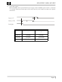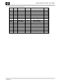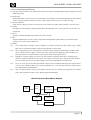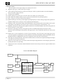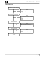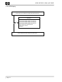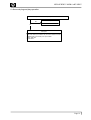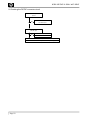
1
Service Manual
17-inch LCD Monitor
f1723/FP7317/L1702/ vf17/FP17
Service Manual Versions and Revision
N o.
Ve rs ion
R e le as e D ate
R e vis ion
1.
1.0
Feb. 20, 2003
Original release
2.
2.0
April 8, 2003
Update
Copyright
Trademarks
Copyright 2003 LiteOn Technology Corp.
LiteOn is a registered trademark of LiteOn
Technology Corp.
All Rights Reserved
This manual may not, in whole or in part, be copied,
photocopied, reproduced, translated, or converted to any
electronic or machine readable form without prior written
permission of LiteOn Technology Corp.
f1723 / FP7317 / L1702 / vf17 / FP17 Service Manual.
All other trademarks are the property of their
respective owners.
f1723 / FP7317 / L1702 / vf17 / FP17
1) Circuit Description
1.
Audio circuit ------------------------------------------------------------------------------------------------------------------- 3
1.1 Audio input ----------------------------------------------------------------------------------------------------------------- 3
1.2 Audio output --------------------------------------------------------------------------------------------------------------- 3
2.
Power supply ------------------------------------------------------------------------------------------------------------------- 3
3.
Video input circuit ------------------------------------------------------------------------------------------------------------- 3
4.
Definition converter LSI peripheral circuit --------------------------------------------------------------------------------- 3
5.
System reset, LED control circuit -------------------------------------------------------------------------------------------- 3
6.
E2PROM ------------------------------------------------------------------------------------------------------------------------- 4
7.
Controller circuit --------------------------------------------------------------------------------------------------------------- 4
7.1 Dection of POWER switch status --------------------------------------------------------------------------------------- 4
7.2 Display mode identification ---------------------------------------------------------------------------------------------- 4
7.3 User control ---------------------------------------------------------------------------------------------------------------- 6
7.4 Control of identification converter LSI --------------------------------------------------------------------------------- 7
7.5 I2C bus control ------------------------------------------------------------------------------------------------------------- 7
7.6 Power ON sequence ------------------------------------------------------------------------------------------------------ 8
7.7 Power OFF sequence ----------------------------------------------------------------------------------------------------- 9
7.8 List of CPU assignments ----------------------------------------------------------------------------------------------- 10
8 Power Board Operation Therory ---------------------------------------------------------------------------------------------- 11
9 Inverter Circuit ------------------------------------------------------------------------------------------------------------------- 12
Page 1
f1723 / FP7317 / L1702 / vf17 / FP17
2) Trouble Shooting
1.
No display of screen (Screen is black, color of LED is amber) -------------------------------------------------------- 13
2.
Nothing displays on screen (Screen is black, color of LED is green) ------------------------------------------------ 14
3.
Checking the back light unit ----------------------------------------------------------------------------------------------- 16
4.
Abnormal screen ------------------------------------------------------------------------------------------------------------- 17
5.
No OSM display ------------------------------------------------------------------------------------------------------------- 18
6.
Abnormal plug and play operation --------------------------------------------------------------------------------------- 19
7.
Checking the interface circuit of sync signal ---------------------------------------------------------------------------- 20
7.1 Checking the control circuit of horizontal sync pulse ------------------------------------------------------------- 20
7.2 Checking the control circuit of vertical sync pulse ---------------------------------------------------------------- 20
8.
Checking the resolution change IC movement -------------------------------------------------------------------------- 21
9.
Checking the DC/DC converter circuit ----------------------------------------------------------------------------------- 22
10. Power board ------------------------------------------------------------------------------------------------------------------ 23
3) Recommended Parts List
Recommended Parts List --------------------------------------------------------------------------------------------------- 24
Page 2
f1723 / FP7317 / L1702 / vf17 / FP17
1) Circuit Description
1. Audio circuit (Circuit diagrams Main PWB 5/5) (Optional)
1.1
Audio input
The audio signal input received from the audio input terminal (P305) is applied to the amplifier I309 of 1 and 9
through the low-pass filter consisting of R361, R360, C370, C371, C361 and C363.
In this audio circuit, controls of Volume, and mute are conducted. The audio signal controlled by a VR determines
the attenuation of output of the amplifiers.
1.2
Audio output
The audio signal is output from the jack output terminal (P306) to the internal speaker system.
2. Interface board and panel power supply (Circuit daigrams MAIN PWB 2/5)
2.1
P301 connector
A 5V power supply for LCD module, CPU, and logic is generated from the P301 connector.
2.2
I301-pin 1 :4-terminal regulator
A 3.3V power supply for Scaler IC I304, is generated from the 5V source.
2.3
I301-pin 1:5-terminal regulator
A 2.5V power supply for Scaler IC I304 is generated from the 5V source.
Q302, Q303 ON/OFF control for LCD Module
ON/OFF control is performed for power ON/OFF and also for the power saving sequence.
3. Video input circuit (Circuit diagram MAIN PWB 3/5)
The analog video signal input entered from P302, the AC-coupled video signal is used to clamp the black level at
0V).
4. Definition converter LSI peripheral circuit (Circuit diagram MAIN PWB 4/5)
I304 gm2121 is the definition converter LSI.
The analog R, G, B signal input entered from the video input circuit is converted into the digital data of video
signal through the incorporated A/D converter. Based on this conversion, this device performs interpolation
during pixel extension. The source voltage for this device is 3.3V, 2.5V and the system clock frequency is 14.318
MHz. The withstand voltage level for the input signal voltage of I304 is 3.3V and 5V.
5. System reset, LED control circuit (Circuit diagram MAIN PWB 4/5, 2/5)
5.1
System reset
System reset is performed by detecting the rising and falling of the 5V source voltage at I305.
5.2
LED control circuit
Green / amber is lit with the control signal of the LED GREEN and LED AMBER signal pin 34, 33 from I304
Page 3
f1723 / FP7317 / L1702 / vf17 / FP17
6. E2PROM (Circuit diagram MAIN PWB 4/5)
Data transfer between I307 (24LC16) and Scaller IC I304 is effected through the IIC bus SCL (pin 37) and SDA (pin
36) of I304. The data to be transferred to each device are stored in I307.
l
I304 control data.
l
OSD related setting data.
l
Other control data for service menu.
7. Controller circuit (Circuit diagram MAIN PWB 4/5)
Scaller IC I304 functions as the Controller.
The source voltage for the device are 3.3V and 2.5V and the system clock frequency is 14.318MHz.
7.1
Detection of POWER switch status
The CPU identifies the ON status of the two power supplies. The identification is made when the power supply
is turned off. For example, if the power supply is turned off with the POWER switch, the POWER switch must be
turned on when activating the power supply again. If the power supply is turned off by pulling out the power
cord, then this power supply can be turned on by connecting the power cord, without pressing the POWER
switch.
7.2
Display mode identification
7.2.1 Functions
(1) Display mode identification
l
The display mode of input signal is identified based on Table 1.
l
When the mode has been identified through the measurement of horizontal and vertical frequencies, the total
number of lines is determined with a formula of “ Horizontal frequency / Vertical frequency = Total number
of lines. “Final identification can be made by examining the coincidence of the obtained figure with the
number of lines for the mode identified from the frequency. The boundary number of lines in each mode is
shown in Table 2.
l
When the detected frequency if the sync signal has changed, the total number of lines should be counted even
though it is an identified frequency in the same mode.
(2) Power save mode.
The power save mode is assumed when the horizontal / vertical signals are as specified below.
l
If there is no horizontal sync signal input.
l
If there is no vertical sync signal input.
l
If the horizontal sync signal is outside the measuring range of gm2121.
l
If the vertical sync signal is outside the measuring range of gm2121.
Page 4
f1723 / FP7317 / L1702 / vf17 / FP17
Table 1
Mode
Resolution
H-freq
Band Width
Polarity
(KHz)
(MHz)
H
V
1.
VGA 640 x 480 60Hz
31.47
25.175
-
-
2.
VESA 640 X 480 72Hz
37.86
31.5
-
-
3.
VESA 640 X 480 75Hz
37.5
31.5
-
-
4.
VGA 720 x 400 70Hz
31.47
28.322
-
+
5.
VESA 800 x 600 60Hz
37.88
40
+
+
6.
VESA 800 x 600 72Hz
48.08
50
+
+
7.
VESA 800 x 600 75Hz
46.88
49.5
+
+
8.
MAC 832 x 624 75Hz
49.72
57.283
-
-
9.
VESA 1024 x 768 60Hz
48.36
65
-
-
10.
VESA 1024 x 768 70Hz
56.48
75
-
-
11.
VESA 1024 x 768 75Hz
60.02
78.75
+
+
12.
MAC 1152 x 870 75Hz
68.68
100
-
-
13.
SUN 1152 x 90 76Hz
71.71
105.6
-
-
14.
SXGA 1280 x 1024 60Hz
64
108
+
+
15.
SXGA 1280 x 1024 75Hz
80
135
+
+
Page 5
f1723 / FP7317 / L1702 / vf17 / FP17
Table 2 the number of the lines, Vsync distinction
Indication resolution
The number of the
distinction lines
640 x 480
487 < LINE < 607
800 x 600
607 < LINE < 777
832 x 624
1024 x 768
640 < LINE
768 < LINE < 870
1152 x 864
1280 x 960
1280 x 1024
7.3
Distinction Vsync
fV < 63 Hz
63 Hz < fV < 68
68 Hz < fV < 74
74 Hz < fV < 78
fV < 58 Hz
58 Hz < fV < 63
63 Hz < fV < 73
73 Hz < fV < 78
fV < 63 Hz
68 Hz < fV < 73
73 Hz < fV < 78
Hz
Hz
Hz
Hz
Hz
Hz
Hz
Hz
870 < LINE < 1031
960 < LINE < 1027
1027 < LINE
User Control
7.3.1 Related ports and pin of I304
Port
Pin No.
I/O
GPIO3
GPIO7
GPIO6
GPIO21
I304, 26
I304, 32
I304, 29
I304, 16
I
I
I
I
Signal name
MENU
MINUS
PLUS
POWER
Function
EXIT/ENTER switch input
switch input
switch input
soft power switch input
Remarks
Auto-Adj.
7.3.2 Functions
Control is effected for the push-switches to be used when the user changes the parameters, in order to modify the
respective setting values. Whether the switch has been pressed is identified with the switch input level that is
turned “L”.
Each switch input port is pulled up at outside of ASIC
Each parameter is stored in the EEPROM, the contents of which are updated as required.
.
Page 6
f1723 / FP7317 / L1702 / vf17 / FP17
7.4
Control of definition converter LSI
7.4.1 Functions
Major function of I304 are as follows:
(1) Expansion of the display screen.
(2) Timing control for various signal types.
(3) Power-supply sequence (LCD panel).
7.5
I2C bus control
7.5.1 I2C-controlled functions
The following functional controls are effected by I2C.
(1) Control of EEPROM I307 for parameter setting.
(2) Control of audio preamplifier.
Page 7
f1723 / FP7317 / L1702 / vf17 / FP17
7.6
Power ON sequence
When the POWER switch is pressed, the POWER signal is turned “L”. When this “L” potential is detected, the
CPU begins to establish the respective power supplies according to the sequence shown below.
Panel_V C C
Panel_D A T A
B acklight
Page 8
A
B
Panel-AU
0 ms min
250 ms min
Panel-HD
20~50 ms
500 ms min
Panel-LG
0.01~50 ms
200 ms min
f1723 / FP7317 / L1702 / vf17 / FP17
7.7
Power OFF sequence
When the POWER switch is pressed while the power supply is ON, the POWER signal is turned “L”. When this
“L” potential is detected, the CPU begins to turn off the respective power supplies according to the sequence
shown below.
Panel_V C C
Panel_D A TA
B acklight
C
D
Panel-AU
0 ms min
0 ms min
Panel-HD
0~50 ms
100 ms min
Panel-LG
0.01~50 ms
200 ms min
Page 9
f1723 / FP7317 / L1702 / vf17 / FP17
7.8 List of GPIO Pin Assignments of the I304
Port
Pin No. Signal Name
Initial Setting Function
Remark
GPIO1
24
MUTE
H
Audio Mute Enable
GPIO21
16
KEY_POWER
H
ON/OFF Monitor Power
GPIO4
27
UART_DI
H
UART interface data IN
GPIO5
28
UART_DO
H
UART interface data OUT
GPIO13
37
NVRAM_SCL
H
NVRAM_SCL
GPIO12
36
NVRAM_SDA
H
NVRAM_SDA
GPIO9
33
LED_AMBER
L
LED_AMBER Enable
GPIO10
34
LED_GRN
H
LED_GRN Enable
GPIO7
32
KEY_MINUS
H
KEY_LEFT Enable
GPIO0
23
BKLT-ADJ
-
Backlight Brightness Control
GPIO11
35
WRn
-
Flash Rom Write Enable
GPIO18
12
A16
-
Address Input
GPIO19
11
A17
-
Address Input
GPIO26
29
KEY_PLUS
H
KEY_RIGHT
PBIAS
41
BKLT_EN
H
Backlight_Enable
PPWR
40
PANEL_EN
H
Panel_Vcc Enable
Page 10
f1723 / FP7317 / L1702 / vf17 / FP17
8. Power Board Operation Therory
8.1 Line filter consists of C801, T801, C802, C803, C804, C837, C838. It eliminates high frequency interference to meet
EMI’s requirement.
8.2 Rec & Filter
Bridge diode D801 converts AC source into pulsed DC. This pulsed DC is smoothed and filtered by C805. R802 is
an NTC ( negative thermal coefficient ) resistor, used to reduce inrush current to be within safe range.
8.3 Power transformer :
T802 converts energy for square wave from power source C805 to secondary side to generate +12V and +22.5V.
8.4 Output :
The square wave from T802 is rectified by D809, D810, then filtered by C817, C822 to generate +22.5V and +12V
respectively.
8.5 Driver :
Q803 drive T802 from PWM control of I801 for power converted.
8.6 FB :
Negative feedback CKT consists of photo coupler I802 and adjustable regulator I803. It can maintain output
voltages +22.5V and +12V at a stable level.
8.7 PWM :
8.7.1
Start : When power is turned on. C807 is charged a 15 volt and a starting current above 40uA to pin 7 of I801.
I801 starts to oscillate and outputs a pulse train through pin 6 to drive Q803.
8.7.2
OPP : When Q803 turns on, C805 supplies a linearly increasing triangle current through the primary inductance of T802 to the driver Q803, once the peak value of this current multiplied by R811 exceeds1 volt,
pulse train will be turn off immediately to protect Q803, T802 from being burned out.
8.7.3
Regulation : If output voltage +22.5V goes up, the R terminal of I803 gets more bias, accordingly photo
transistor and photo diode flows more current. The voltage of pin 2 goes up too, making the pulse width of
pin 6 to become narrower. So the output voltage +22.5V will be pulled down to a stable value.
8.7.4
OVP : If +22.5V goes up too much, the induced voltage on pin 4 of T802 becomes large also. Suppose that it
is over 18 volts, ZD801 conducts, pin 3 of I801 is pulled up over 1 volt. The pulse train at pin 6 goes down to
zero, shutting Q803 off immediately.
8.7.5
SCP : If output terminal is short to ground, photo transistor does not conduct, hence Q806 does not conduct
either. Then oscillation of I801 is stop, shutting Q803 off immediately.
HPD-K17AA Power Board Block Diagram
Line
Filter
Rec. &
Filter
Power
Transformer
PWM
Driver
Outpur Rec. & Filter
FB
Page 11
f1723 / FP7317 / L1702 / vf17 / FP17
9. Inverter Circuit
This unit operates on an output voltage of 15V from power source.
9.1
Regulator: Q101 get a +5VDC for I101 power supply.
9.2
UVP: Q106 turns off when the Vin is under 10V. Then pin 3 of I101 is pulled low and inverter off immediately.
That is the under voltage protection.
9.3
Control IC: I101 (OZ960S)
9.3.1 Enable : When pin 3 of I101 is over 1.5V, I101 works. If it is under 1.5V, I101 turns off.
9.3.2 OSC: When I101 enabled, R108/C115 (pin 17/pin18 of I101) determine the operating frequency.
9.3.3 SST: C104 (pin 4 of I101) provides soft start function.
9.3.4 Ignition: R109 (pin 8 of I101) provides higher operating frequency for more striking voltage until regulation of
feedback of lamp current. C103 (pin 1 of I101) determine the striking time.
9.3.5 Dimming control: The divided voltage of R106/R105/R104 control the duty pulse of burst-mode to drive Q105
and perform a wide dimming control for the CCFL. The burst-mode frequency is determined by C116.
9.3.6 Regulation: Pin 9/pin 10 of I101 provide regulation of the CCFL current from feedback. The non-inverting reference
(pin 10 of I101) is at 1.25V nominal.
9.3.7 Protection: Open-lamp protection in the ignition period is provided through both pin1 and pin 2 of I101.
Removal of the CCFL during normal operation will trigger Q107 to turns on and shuts off the inverter. This is latch
function.
9.3.8 Output drivers: The configuration prevents any shoot-through issue associated with bridge-type power
conversion applications. Adjusting the overlap conduction between I102 P-MOSFET and I103 N-MOSFET, I102 NMOSFET and I103 P-MOSFET, the CCFL current regulation is achieved, same as I104 and I105.
9.4
Full-bridge swit ching/Transformer: I102/I103/C123/I104/I105/C137/T101/T102 compose full-bridge swit ching to
convert DC into AC for driver the CCFL.
9.5
Detection: C128/C129/C130/C131/C132/C133 detect the output voltage and ensure a rated voltage by pin2 of I101/
Q108/Q109 ensure not a open-lamp.
9.6
Feedback: D116/D117/D122/D123/D109/R120/R121/D108 sense the lamp current for negative feedback and
regulation.
Inverter Board Block Diagram
VCC
Regulator
VDD
Control IC : OZ960
ON / OFF
Brightness
control
Page 12
U.V.P.
Enable
Output driver
OSC
Protection
SST
Ignition
Dimming
control
Regulation
Full-bridge switching
Transformer
Detection
Feed back
Lamp
f1723 / FP7317 / L1702 / vf17 / FP17
2) Trouble Shooting
1. No display of screen (Screen is black, color of LED is amber)
Does OSM display when you push
MENU button.
When a signal isn't
being inputted, it is
indicated with "VIDEO
INPUT". It is indicated
Yes
with "OUT OF RANGE"
at the time of the
frequency that it can't be
distinguished.
No
Preceed "Nothing displays on
screen"section.
Check if the sync signal from Computer
is output and if the video cable is
connected normally.
OK
NG
Input the sync signal of computer, or
change the cable.
Proceed "Checking the resolution change
IC movement" section.
Page 13
f1723 / FP7317 / L1702 / vf17 / FP17
2. Nothing displays on screen (Screen is black, color of LED is green)
Is backlight lit?
NG
Refer "Checking the backlight unit" section
OK
Does computer output RGB video signals?
OK
NG
1) Change pattern of video signal output on the
host.
2) Reconnect the video cable.
3) Change the video cable.
Check OSM menu is displayed on screen
when you push the "MENU" key.
OK
NG
Check if the signal cable is connected between the
MAIN PWB and LCD module.
Failure Point
NG
Proceed "Abnormal screen" section.
OK
Next Page
Page 14
The Cable is disconnected.
f1723 / FP7317 / L1702 / vf17 / FP17
Continue
Check the 3.3 V power are supplied on I301, pin 4.
NG
Check if the voltage on I301 pin 1 that
is high level DC at 5V.
Failure point
OK
OK
NG
1) Printed wire broke between P301 pin 7, 8 and
and I301.
2) Check power board.
Failure point
I301 Failure
Failure point
1) The cable broke between P303 and LCD
module.
2) LCD module failure.
Page 15
f1723 / FP7317 / L1702 / vf17 / FP17
3. Checking the back light unit
Is +22.5V supplied to inverter PWB?
OK
Failure point
NG
1) Inverter cable disconnection.
2) Power board failure.
Check the BKLT_EN signal of the rectangle input P301 pin 2 at TTL high level
Is a "H" level being output in the TTL level from I304 pin 41
Or, is BKLT_EN signal of the rectangle being output?
NG
NG
OK
Failure point
Printed wire broke between
I304 pin 41 and R387.
Check the PWM signal of the input from I304 pin 23 is a PWM signal.
Failure point
OK
NG
Failure point
1) Inverter cable disconnection.
2) Inverter of LCD module failure.
Page 16
1) Printed wire broke between
I304 pin 23 and R301.
2) I304 failure.
f1723 / FP7317 / L1702 / vf17 / FP17
4. Abnormal screen
Check the R, G, B video signal from computer input on
D-Sub R, G, B connector.
Failure point
OK
NG
1) No R, G and B video signal output from host computer. Check
computer
2) Video signal cable disconnection.
Check the R, G, B input signals on I304 pin 135, 131, 127
respectively that their level is 0.7Vp-p maximum.
Failure point
NG
OK
In the case of the Red signal. (A Green and Blue signal is the same
path, too.)
1) Printed wire broke between D-Sub(R) and I304 pin 135.
2) R323 short.
3) C317 open.
4) R321 open.
Check the horizontal sync pulse
input to I304 pin 101 at TTL level.
Failure point
OK
NG
1) Printed wire broke between I304 pin 101 and P302 pin 8.
2) I304 failure
Check the vertical sync pulse
input to I304 pin 100 at TTL level.
Failure point
OK
NG
1) Printed wire broke between I304 pin 100 and P302 pin 9.
2) I304 failure
Process "Checking the resolution change IC movement"
section.
Page 17
f1723 / FP7317 / L1702 / vf17 / FP17
5. No OSM display
Check the input TTL level whether was changed when pressed function keys.
Failure point
OK
NG
1) Printed wire broke between P308 pin 5 and I304 pin 29.
2) Printed wire broke between P308 pin 6 and I304 pin 32.
3) Printed wire broke between P308 pin 7 and I304 pin 22.
4) Printed wire broke between P308 pin 8 and I304 pin 26.
5) Printed wire broke between P308 pin 4 and I304 pin 16.
6) FB325, FB326, FB327, FB328. FB329 open
7) RN302, RN301, short/open.
8) I304 failure.
Proceed "Checking the resolution change IC movement" section.
Page 18
f1723 / FP7317 / L1702 / vf17 / FP17
6. Abnormal plug and play operation
Confirm the output of serial data on I303 pin 6 synchronize SCLK at TTL level.
Failure point
NG
I304 failure.
OK
Failure point
1) The host machine isn't communicating in DDC2 mode.
2) The video cable may have failed or may not to have connections for DDC.
3) Between I303 pin 6 and P302 pin 12 may have failed.
4) R310, R385 open.
5) Cable failure.
Page 19
f1723 / FP7317 / L1702 / vf17 / FP17
7. Checking the interface circuit of sync signal
7.1 Checking the control circuit of horizontal sync pulse
Check the horizontal sync signal on I304
pin 101 TTL level.
Failure point
NG
OK
1) Video cable may have failed.
2) Printed wire broke between P302 pin 8
and I304 pin 101
3) FB303, R305 open
4) R306, C303 short
Process "Checking the resolution
change IC movement" section.
7.2 Checking the control circuit of vertical sync pulse
Check the vertical sync signal on I304 pin
100 TTL level.
Failure point
NG
OK
1) Video cable may have failed.
2) Printed wire broke between P302 pin 9 and I304 pin 100
3) FB302, R303 open
4) R307, C304 short
Process "Checking the resolution
change IC movement" section.
Page 20
f1723 / FP7317 / L1702 / vf17 / FP17
8. Checking the resolution change IC movement
Is there +3.3V supply on I304 pin 124,136,132,128, 113, 108, 104, 106, 110,
115, 14, 30, 90, 143, 157.
OK
NG
Proceed "Checking the DC/DC converter circuit" section.
Is there +2.5V supply on I304 pin 119, 117, 20, 43, 79, 98, 138.
NG
Proceed "Checking the DC/DC converter circuit" section.
OK
Is 14.318MHz clock input to I304 pin
102 and pin 103 at TTL level?
NG
OK
Is 14.318MHz clock output from
X301 pin 1 at TTL level?
OK
NG
Failure point
X301 failure
Failure point
Print wire broke between X301 pin 1
and I304 pin 102.
Failure point
I304 failure
Page 21
f1723 / FP7317 / L1702 / vf17 / FP17
9. Checking the DC/DC converter circuit
Check if the 5V is output from P301
pin 7, 8.
OK
NG
Printed wire broke between P301 pin
7, 8 and I301 pin 1.
Check the output of 3.3V line voltage
from I301 pin 4.
OK NG
Failure point
I301 failure
Failure point
Printed wire broke between I301 pin 4 and IC 304 power supply pin.
Page 22
f1723 / FP7317 / L1702 / vf17 / FP17
10. Power Board
Check output voltage +22.5V, +12V
is right or not.
No
Yes
It is not power board problem.
Check power switch is turn on or not.
Yes
No
Turn switch on.
Check power cord (P801), signal
cable (P302), P802, P803, CN102,
CN103 is connected right or not.
No
Yes
Connect it right
Check C805 is about DC140V-330V
or not.
Yes
No
Check F801, D801, P801 and repair
them.
Check C807 is over 10V or not.
Yes
No
Check R805, R803, I801 and repair
them.
Check pin 6 of I801 have same
pulse or not.
Yes
No
Check peripheral co,of I801 and
repair them.
Check pin 1 of T802 have same
pulse or not.
Yes
No
Check Q803, R813, R814, D806,
R812 and repair them.
Check peak voltage of R811 triangle
pulse is up to 1 volt or not.
Yes
No
Check D804, R807 and repair them.
Check D809, D810,C816, C821,
T802 have same short circuit, or the
output +22.5V, 12.5V is over load.
No
Repair them.
Yes
Check feedback circuit around I802,
I803 and the other components and
repair them.
Page 23
f1723 / FP7317 / L1702 / vf17 / FP17
1. Recommended Parts List
Note: 1.
The components identified by “
only the same parts specified.
“ mark are critical for X-ray safety. Replace these with
2.
The components identified by “ * “ mark are critical parts.
3.
There is only OTP IC at the model beginning (FPR stage or before). When it put in mass
production and there must be Mask coming out. Please checkyou have spart parts need, please
check BOM to get the last release part number and related information.
No.
Location
Part Number
Description
1 *
V170
6814700100
6841700900
6814701300
Panel-AU-M170EN05
Panel-HD-HT12E12-200
Panel-LG-LM170E01-A5K2
2
I307
6448016508
IC 24LC16B/SN 8P SOP
3
I303
6448018208
IC 24LC02B 8PIN SOP MICROCHIP
4 *
I309
6442015400
IC-LINEAR TDA1517/N3-9PIN SIL9MPF-PHILIPS
5
I308
6444010438
IC CMOS SST395SF020A-70-4C-NH-32PIN
6 *
I304
6444012806
IC CMOS GM2121 208PIN
7
I301
6442033908
IC LINEAR FAN1537PA 5PIN
8
X301
6449006400
X'TAL 14.318MHZ AT-49
9
I801
6442032800
6442022030
IC 0Z960
IC SG3842
10
T101
T102
6131020600
XFMER TPW-1097
11
L802
6111156136
COIL CHOKE 15uH
12
I804
6442035900
IC MP1410EP
13
I102~I105
6444011300
IC CMOS-A09600
Page 24
LITE-ON TECHNOLOGY CORP.
5 F, No. 16, Sec. 4, Nanking E. Road, Taipei, Taiwan
Tel: 886-2-25706999
Fax: 886-2-25706888
URL:// www.liteontc.com.tw
Printed in Taiwan