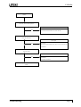
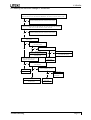
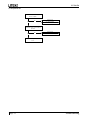
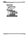
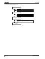
1
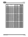
Service Manual 17-inch LCD Monitor U170ATA U170ATA Table of Contents 1. Audio circuit --------------------------------------------------------------------------------------------------------------- 1 1.1 Audio input ------------------------------------------------------------------------------------------------------------ 1 1.2 Audio output ---------------------------------------------------------------------------------------------------------- 1 2. Power supply -------------------------------------------------------------------------------------------------------------- 1 3. Video input circuit -------------------------------------------------------------------------------------------------------- 1 4. Definition converter LSI peripheral circuit ---------------------------------------------------------------------------- 1 5. System reset, LED control circuit --------------------------------------------------------------------------------------- 1 6. E2PROM for PNP --------------------------------------------------------------------------------------------------------- 1 7. E2PROM -------------------------------------------------------------------------------------------------------------------- 2 8. CPU circuit ----------------------------------------------------------------------------------------------------------------- 2 8.1 Dection of POWER switch status ---------------------------------------------------------------------------------- 2 8.2 Display mode identification ----------------------------------------------------------------------------------------- 2 8.3 User control ----------------------------------------------------------------------------------------------------------- 4 8.4 Control of identification converter LSI (IC 14) ------------------------------------------------------------------ 5 8.5 I2C bus control -------------------------------------------------------------------------------------------------------- 5 8.6 Power ON sequence -------------------------------------------------------------------------------------------------- 6 8.7 Power OFF sequence ------------------------------------------------------------------------------------------------- 7 8.8 List of CPU assignments --------------------------------------------------------------------------------------------- 8 Circuit Description Index U170ATA 1. Audio circuit (Circuit diagrams Main PWB 1/1 JACK PWB 1/1) 1.1 1.2 Audio input The audio signal input received from the audio input terminal (JK011) is applied to the pre-amplifier I006 of 2 (L-CH) and 29 (R-CH) through the low-pass filter consisting of R047, R049, R048, R050, C062 and C063. In this pre-amplifier, controls of Volume, Balance, Bass, and Treble are conducted. The audio signal controlled at the pre-amplifier is entered in and amplified at the AMP I007 of 9 (L-CH) and 1 (R-CH). Since then, the signal is to the output jack. Audio output The audio signal is output from the output terminal (P012) of the jack to the speaker system. 2. Power supply (Circuit daigrams MAIN PWB 8/10, 9/10, 10/10) 1. I322:DC-DC converter A 5V power supply for LCD module, CPU, and logic is generated from the 19V source. 2. I323:3-terminal regulator A 3.3V power supply for Scaler IC I315, LVDS IC I319, I320 is generated from the 5V source. 3. I330:3-terminal regulator A 3.3V power supply for SDRAM IC I316, I317, I318 is generated from the 5V source. 4. I324:3-terminal regulator A 2.5V power supply for Scaler IC I315 is generated from the 5V source. Q307, I321 ON/OFF control for LCD Module ON/OFF control is performed for power ON/OFF and also for the power saving sequence. 3. Video input circuit (Circuit diagram MAIN PWB 4/10) The AC-coupled video signal is used to clamp the black level at 0V). 4. Definition converter LSI peripheral circuit (Circuit diagram MAIN PWB) I315 gm5020 is the definition converter LSI. The analog R, G, B signal input entered from the video input circuit is converted into the digital data of video signal through the incorporated A/D converter. Based on this conversion, this device performs interpolation during pixel extension. The source voltage for this device is 3.3V, 2.5V and the system clock frequency is 24MHz. The withstand voltage level for the input signal voltage if I315 is 3.3V and 5V. 5. System reset, LED control circuit (Circuit diagram MAIN PWB 3/10) 5.1 5.2 System reset System reset is performed by detecting the rising and falling of the 5V source voltage at I301. LED control circuit Green / amber is lit with the control signal of the LED GREEN and LED AMBER signal pin 15, 12 from I306 (Circuit diagram MAIN PWB 2/8). 6. E2PROM for PnP (Circuit diagram MAIN PWB 4/10) Circuit Description Page 1 U170ATA 7. E2PROM (Circuit diagram MAIN PWB 3/10) Data transfer between I305 (AT24 C16) and CPU (Circuit diagram MAIN PWB 2/8 (I302) is effected through the IIC bus SCL (pin 15) and SDA (pin 16) of I302. The data to be transferred to each device are stored in I305. l I315 control data. l OSD related setting data. l Other control data for service menu. 8. CPU circuit (Circuit diagram MAIN PWB 3/10) I302 (87C51RD2) functions as the CPU. The source voltage for the device is 5.0V and the system clock frequency is 24MHz. 8.1 Detection of POWER switch status The CPU identifies the ON status of the two power supplies. The identification is made when the power supply is turned off. For example, if the power supply is turned off with the POWER switch, the POWER switch must be turned on when activating the power supply again. If the power supply is turned off by pulling out the power cord, then this power supply can be turned on by connecting the power cord, without pressing the POWER switch. 8.2 Display mode identification 8.2.1 Functions (1) Display mode identification l The display mode of input signal is identified based on Table 1. l When the mode has been identified through the measurement of horizontal and vertical frequencies, the total number of lines is determined with a formula of Horizontal frequency / Vertical frequency = Total number of lines. Final identification can be made by examining the coincidence of the obtained figure with the number of lines for the mode identified from the frequency. The boundary number of lines in each mode is shown in Table 2. l When the detected frequency if the sync signal has changed, the total number of lines should be counted even through it is rge identified frequency in the same mode. (2) Power save mode. This power save mode is assumed when the frequency of the horizontal / vertical signal is as specified below. l Vertical frequency : 50 ~ 86 Hz l Horizontal frequency : 24 ~ 92 KHz l VTOTAL : 1200 or more. (3) Power save mode. The power save mode is assumed when the horizontal / vertical signals are as specified below. l l l l If there is no horizontal sync signal input. If there is no vertical sync signal input. If the horizontal sync signal is outside the measuring range of gm5020. If the vertical sync signal is outside the measuring range of gm5020. Page 2 Circuit Description U170ATA Table 1 Mode Resolution H-freq Band Width Polarity (KHz) (MHz) H V 1. VGA 720 x 400 70Hz 31.47 28.322 - + 2. VGA 640 x 480 60Hz 31.47 25.175 - - 3. MAC 640 x 480 66Hz 35 32.24 - - 4. VESA 640 X 480 72Hz 37.86 31.5 - - 5. VESA 640 X 480 75Hz 37.5 31.5 - - 6. VESA 640 X 480 85Hz 43.27 36 - - 7. VESA 800 x 600 56Hz 35.16 36 + + 8. VESA 800 x 600 60Hz 37.88 40 + + 9. VESA 800 x 600 75Hz 46.88 49.5 + + 10. VESA 800 x 600 72Hz 48.08 50 + + 11. VESA 800 x 600 85Hz 53.67 56.25 + + 12. MAC 832 x 624 49.72 57.283 - - 13. VESA 1024 x 768 60Hz 48.36 65 - - 14. VESA 1024 x 768 70Hz 56.48 75 - - 15. VESA 1024 x 768 75Hz 60.02 78.75 + + 16. VESA 1024 x 768 85Hz 68.68 94.5 + + 17. VESA 1280 x 1024 60Hz 64 108 + + 18. VESA 1280 x 1024 75Hz 80 135 + + 19. VESA 1280 x 1024 85Hz 91.1 157.5 + + 20. VESA 1152 x 864 75Hz 67.5 108 + + 21. VESA 1280 x 960 60Hz 60 108 + + 22. VESA 1280 x 960 85Hz 85.9 148.5 + + Circuit Description 75Hz Page 3 U170ATA Table 2 the number of the lines, Vsync distinction Indication resolution The number of the distinction lines Distinction Vsync The fixed mode 640 x 480 487 < LINE < 607 800 x 600 607 < LINE < 777 832 x 624 1024 x 768 640 < LINE 768 < LINE < 870 fV < 63 Hz 63 Hz < fV < 68 Hz 68 Hz < fV < 74 Hz 74 Hz < fV < 78 Hz 78 Hz < fV fV < 58 Hz 58 Hz < fV < 63 Hz 63 Hz < fV < 73 Hz 73 Hz < fV < 78 Hz 78 Hz < fV fV < 63 Hz 68 Hz < fV < 73 Hz 73 Hz < fV < 78 Hz 78 Hz < fV 1152 x 864 1280 x 960 1280 x 1024 870 < LINE < 1031 960 < LINE < 1027 1027 < LINE 2 3 4 5 6 7 8 10 9 11 12 13 14 15 16 20 21, 22 17, 18, 19 9.3 User Control 9.3.1 Related ports of I315 and pin of I302 Port Pin No. I/O Signal name Function GPI04 I315, M1 1 MENU EXIT/ENTER switch input GPI05 GPI06 GPI07 GPI0 I315, L1 I315, G18 I315, G19 I302, 15 1 1 1 1 DOWN + POWER switch input switch input switch input soft power switch input Remarks ENTER/Withdraw from OSD ( ) key ( ) key ( ) key ( power ) key 9.3.2 Functions Control is effected for the push-switches to be used when the user changes the parameters, in order to modify the respective setting values. Whether the switch has been pressed is identified with the switch input level that is turned L. Each switch input port is pulled up at outside of ASIC Each parameter is stored in the EEPROM, the contents of which are updated as required. . Page 4 Circuit Description U170ATA 8.4 Control of definition converter LSI I315 8.4.1 Ports related to control Pin No. R3 P1 P3, P4, R1, R2 P2 I/O I O I/O O Signal name Function IRQ gmZan1 interrupt signal HCLK gmZan1 serial clock HDATA gmZan1 serial data HFS gmZan1 serial select 8.4.2 Functions Major function of I315 are as follows: (1) Expansion of the display screen. (2) Timing control for various signal types. (3) Power-supply sequence (LCD panel). 8.5 I2C bus control 8.5.1 Related ports of I302 Port P3.5 P3.4 Pin No. 17 16 I/O I I/O Signal name Function IICCLK IIC bus clock IICDATA IIC bus data 8.5.2 I2C-controlled functions The following functional controls are effected by I2C. (1) Control of EEPROM I305f for parameter setting. (2) Control of audio preamplifier. Circuit Description Page 5 U170ATA 8.6 Power ON sequence When the POWER switch is pressed, the POWER OFF signal is turned H. When this H potential is detected, the CPU begins to establish the respective power supplies according to the sequence shown below. POWER LED LVCC (Audio_EN) Panel_VCC PCLK/DATA Backlight_EN Page 6 Circuit Description U170ATA 8.7 Power OFF sequence When the POWER switch is pressed while the power supply is ON, the POWER ON signal is turned H. When this H potential is detected, the CPU begins to turn off the respective power supplies according to the sequence shown below. POWER LVCC (Audio_EN) LED Panel_VCC Backlight_EN PCLK/DATA Circuit Description Page 7 U170ATA 8.8 List of CPU Pin Assignments Port Pin No. Signal Name Initial Setting Function Remark ~ 1 NC ~ ~ P1.0 2 HDATA0 ~ gm5020 4bit interface data P1.1 3 HDATA1 ~ gm5020 4bit interface data P1.2 4 HDATA2 ~ gm5020 4bit interface data P1.3 5 HDATA3 ~ gm5020 4bit interface data P1.4 6 HCLK ~ gm5020 4bit interface Clock P1.5 7 HFS ~ gm5020 data enable P1.6 8 Bank ~ ~ P1.9 9 PWM ~ Pulse width modulation ~ 10 RST L Reset CPU P3.0 11 RXD H Receive data ~ 12 NC ~ ~ P3.1 13 TXD H Transmit data P3.2 14 IRQ ~ gm5020 interrupt signal P3.3 15 PWR_SW ~ ON/OFF monitor power P3.4 16 SDA H IIC Bus Data P3.5 17 SCL ~ IIC Bus Data P3.6 18 P3.6 H External Memory Write Enable P3.7 19 DDC_GND L Detect Dsub cable plug-in ~ 20 XTAL2 ~ Crystal signal out ~ 21 XTAL ~ Crystal signal in ~ 22 GND ~ ~ ~ 23 NC ~ ~ P2.0 24 A8 ~ High-order address byte P2.1 25 A9 ~ High-order address byte P2.2 26 A10 ~ High-order address byte P2.3 27 A11 ~ High-order address byte P2.4 28 A12 ~ High-order address byte P2.5 29 A13 ~ High-order address byte P2.6 30 A14 ~ High-order address byte P2.7 31 A15 ~ High-order address byte ~ 32 PSEN# H Program store enable ~ 33 ALE ~ Address latch enable ~ 34 NC ~ ~ ~ 35 EA# H External Access Enable P0.7 36 D7(USB_ON) H USB HUB power Enable (option) P0.6 37 D6(MUTE) H Audio MUTE Enable P0.5 38 D5(LVCC) L Audio suspend Enable P0.4 39 D4(LEDGRN) H LED Green ON P0.3 40 D3(LEDAMBER) L LED AMBER ON P0.2 41 D2(BKLT_EN) ~ Inverter Back light Enable P0.1 42 D1(LVDS ON) H LVDS IC Enable P0.0 43 D0(PANEL EN) H Panel power Enable ~ 44 VCC ~ VCC Page 8 Active H Active L Circuit Description U170ATA Table of Contents 1. No display of screen (Screen is black, color of LED is amber) ----------------------------------------------------- 1 2. Nothing displays on screen (Screen is black, color of LED is green) ---------------------------------------------- 2 3. Checking the back light unit --------------------------------------------------------------------------------------------- 5 4. Abnormal screen ---------------------------------------------------------------------------------------------------------- 6 5. Abnormal Auto adjustment ---------------------------------------------------------------------------------------------- 8 5.1 NO OSM display ----------------------------------------------------------------------------------------------------- 8 5.2 OSD Adjust problem ------------------------------------------------------------------------------------------------- 8 6. Abnormal plug and play operation ------------------------------------------------------------------------------------- 9 6.1 Abnormal DDC2 ------------------------------------------------------------------------------------------------------ 9 7. Checking the interface circuit of sync signal ------------------------------------------------------------------------- 10 7.1 Checking the control circuit of horizontal sync pulse ---------------------------------------------------------- 10 7.2 Checking the control circuit of vertical sync pulse -------------------------------------------------------------- 10 8. Checking the resolution change IC movement ----------------------------------------------------------------------- 11 9. No power on -------------------------------------------------------------------------------------------------------------- 12 10. Checking the DC/DC converter circuit -------------------------------------------------------------------------------- 13 11. Checking the operation of CPU ---------------------------------------------------------------------------------------- 14 12. Checking the audio circuit ---------------------------------------------------------------------------------------------- 15 Index Trouble Shooting U170ATA 1. No display of screen (Screen is black, color of LED is amber) Does OSM display when you push PROCEED button. When a signal isn't being inputted, it is indicated with "VIDEO INPUT". It is indicated Yes with "OUT OF RANGE" at the time of the frequency that it can't be distinguished. No Preceed "No OSM display"section. Check if the sync signal from Computer is output and if the video cable is connected normally. NG OK Input the sync signal of computer, or change the cable. Proceed "Checking the resolution change IC movement" section. Trouble Shooting Page 1 U170ATA 2. Nothing displays on screen (Screen is black, color of LED is green) Is backlight lit? NG Refer "Checking the backlight unit" section OK Does computer output RGB video signals? OK NG Check the video cable for failure. Check the host for output signal with all black only. 1) Change pattern of video signal output on the host. 2) Reconnect the video cable. 3) Change the video cable. Check OSM menu is displayed on screen when you push the "PROCEED" key. OK NG Check if the LCD video signal cable is connected between the MAIN PWB and LCD module. Failure Point NG Proceed "Abnormal screen" section. OK The Cable is disconnected. Next Page Page 2 Trouble Shooting U170ATA Continue Check the 3.3 V power are supplied on I323, I330 pin 2. NG Check if the voltage on I323, I330 pin 3 that is high level DC at 5V. Failure point OK OK NG 1) Printed wire broke between I322 and I323, I330 2) I322 failure. Failure point I323, I330 Failure Is a dot clock being outputted under the condition that a LCD module is connected to L322 pin 2? Failure point OK NG 1) I315 failure 2) Printed wire broke between I315 and L322 pin 2. Check the H-sync pulse of negative polarity is output on RN314 pin 8 at TTL level. Failure point OK NG 1) I315 failure 2) Printed wire broke between I315 and RN314 pin 8. Check the V-sync of negative polarity are output on RN314 pin 7. Failure point OK NG 1) I315 failure 2) Printed wire broke between I315 and RN314 pin 7. Next Page Trouble Shooting Page 3 U170ATA Continue Check the data enable of positive polarity are output on RN314 pin 6. Failure point OK NG 1) I315 failure. 2) Printed wire broke between I315 and RN314 pin 6. Check the data signal output on I315 R, G, B data pin. Failure point OK NG 1) I315 failure. Check I319, I320 all LVDS signal pins. Failure point OK NG 1) I319, I320 failure. 2) Printed wire broke between I319, I320 and P307. Failure point 1) The cable broke between P304 and LCD module. 2) LCD module failure. Page 4 Trouble Shooting U170ATA 3. Checking the back light unit Is +19V supplied to F301 pin 1. NG Are connected AC adapters normal goods? OK Failure point NG OK Is +19V supplied to P308 pin 3, 4 to inverter PWB? Failure point Failure point Inverter cable disconnection. Printed wire broke between P312 pin 1. NG OK An AC adapter is changed to the normal goods. Check the BKLT_EN signal of the rectangle input I327 pin 3 at TTL high level Is a "H" level being output in the TTL level from I306 pin 14 Or, is BKLT_EN signal of the rectangle being output? NG NG OK Failure point Printed wire broke between I306 pin 14 and I327 pin 3. Check the PWM signal of the input from I315 pin M4 (R374 pin 2) is a PWM signal. Failure point NG OK 1) Printed wire broke between I315 pin M4 and R374 pin 2. 2) I315 failure. Failure point 1) Inverter cable disconnection. 2) Inverter of LCD module failure. Trouble Shooting Page 5 U170ATA 4. Abnormal screen Check the R, G, B video signal from computer input on D-Sub R, G, B connector. Failure point OK NG 1) No R, G and B video signal output from host computer. Check computer 2) Video signal cable disconnection. Check the R, G, B input signals on I315 pin E1, D2, C1 respectively that their level is 0.7Vp-p maximum. Failure point OK NG In the case of the Red signal. (A Green and Blue signal is the same path, too.) 1) Printed wire broke between D-Sub(R) and I315 pin E1. 2) R339 short. 3) C359 open. 4) R337 open. Is the pulse of the TTL level being output to I319, I320 from the data line of I315? OK NG Failure point 1) Printed wire broke between I315 data line and I319, I320. 2) I315 failure. Check the negative horizontal sync pulse output to RN314 pin 8 from I315 pin F20 at TTL level. Failure point OK NG 1) Printed wire broke between I315 pin F20 and RN314 pin 8. 2) I315 failure Check the negative vertical sync pulse output to RN314 pin 7 from I315 pin F19 at TTL level. Failure point OK NG 1) Printed wire broke between I315 pin 73 and RN314 pin 7. 2) I315 failure Check the positive DE pulse output to RN314 pin 6 from I315 pin F18 at TTL level. Failure point OK NG 1) Printed wire broke between I315 pin F18 and RN314 pin 6. 2) I315 failure Check the SHFCLK OUTPUT to L322 pin 2 from I315 pin G20 at TTL level. Failure point OK NG 1) Printed wire broke between I315 pin G20 and L322 pin 2. 2) L321 open 3) C583 short 4) C590 short 5) L322 short 6) I315 failure Next Page Page 6 Trouble Shooting U170ATA Continue Check I319, I320 all LVDS signal pins. Failure point OK NG 1) I319, I320 faulure. 2) Printed wire broken between I319, I320 and P307. Check SDRAM IC clk signal output to I318, I316, I317, pin 35 from I315 pin T3. Failure point OK NG 1) R396 open. 2) Printed wire broken between I318, I316, I317 pin 35 and I315 pin T3.. 3) I315 failure. Check all Data/Address pins signal between I315 and I316, I317, I318. Failure point OK NG 1) Printed wire broke between I318, I316, I317 and I315. 2) I315 failure 3) I318, I316, I317 failure. Process "Checking the resolution change IC movement" section. Trouble Shooting Page 7 U170ATA 5. Abnormal OSM display 5.1 NO OSM display Check the input of 3.3Vp-p pulse from I315 pin P3, P4, R1, R2, P2, P1. Failure point 1) 2) 3) 4) 5) 6) 7) NG OK Printed wire broke between I315 pin P3 and I302 pin 5. Printed wire broke between I315 pin P4 and I302 pin 4. Printed wire broke between I315 pin R1 and I302 pin 3. Printed wire broke between I315 pin R2 and I302 pin 2. Printed wire broke between I315 pin P2 and I302 pin 7. Printed wire broke between I315 pin P1 and I302 pin 6. RN301, RN303 open/short. Proceed "Checking the resolution change IC movement" section. 5.2 OSD Adjust problem Check the input TTL level whether was changed when pressed function keys. Failure point NG OK 1) Printed wire broke between P302 pin 3 and I302 pin 15. 2) Printed wire broke between P302 pin 4 and I315 pin G19. 3) Printed wire broke between P302 pin 5 and I315 pin G18. 4) Printed wire broke between P302 pin 6 and I315 pin L1. 5) Printed wire broke between P302 pin 7 and I315 pin M1. 6) C322, C323, C324, C326, C327 short. 7) RN306, RN307, short/open. 8) I315 failure. Proceed "Checking the resolution change IC movement" section. Page 8 Trouble Shooting U170ATA 6. Abnormal plug and play operation 6.1 Abnormal DDC2 Confirm the output of serial data on I312 pin 6, I310 pin 6 synchronize SCLK at TTL level. Failure point NG OK I310, I312 failure. Failure point 1) 2) 3) 4) 5) 6) Trouble Shooting The host machine isn't communicating in DDC2 mode. The video cable may have failed or may not to have connections for DDC. Between I312 pin 6 and P304 pin 15 may have failed. Between I310 pin 6 and P303 pin 6 may have failed. R335, R326 open. Cable failure. Page 9 U170ATA 7. Checking the interface circuit of sync signal 7.1 Checking the control circuit of horizontal sync pulse Check the horizontal sync signal on I315 pin L2 TTL level. Failure point NG OK 1) Video cable may have failed. 2) Printed wire broke between P304 pin 13 and I315 pin L2 3) FB305, R329 open 4) R330, C352 short Process "Checking the resolution change IC movement" section. 7.2 Checking the control circuit of vertical sync pulse Check the vertical sync signal on I315 pin K1 TTL level. Failure point NG OK 1) Video cable may have failed. 2) Printed wire broke between P304 pin 14 and I315 pin K1 3) FB328, FB304 open 4) R331, C353 short Process "Checking the resolution change IC movement" section. Page 10 Trouble Shooting U170ATA 8. Checking the resolution change IC movement Is there +3.3V supply on I315 pin D13, D15, D16, E17, G17, J17, L17, N17, R17, U17, U15, U13, U12, U10, U8, U6, U5, T4, L4, B2, B6, B7, B8, B9, B11, C3, D3, E3, F2, F4, G1, G3, H1, J1, J3. OK NG Proceed "Checking the DC/DC converter circuit" section. Is there +2.5V supply on I315 pin D12, D14, D17, F17, K17, M17, P17, T17, U16, U14, U11, U9, U7, U4, N4, K4, A6, A7, A8, A9, A10, A11. NG Proceed "Checking the DC/DC converter circuit" section. OK Is 24MHz clock input to I315 pin J4 at TTL level? NG Is 24MHz clock output from X303 pin 5 at TTL level? OK OK NG Is +3.3V supplied to X303 pin 8? Failure point Failure point OK Print wire broke between X303 pin 5 and I315 pin J4. NG Print wire broke between and X303 pin 8 and power supply. Failure point Is +5.0V supplied to I315 pin T1 at High level (Reset signal)? OK NG X303 failure Check the output of 5.0V "H" pulse from I301 pin 6. NG Is 5.0V supplied to I301 pin 7? Failure point I315 failure OK NG OK Failure point Print wire broke between I301 pin 6 and I315 pin T1. Trouble Shooting Failure point 1) I322 failure 2) L315 open Failure point I301 failure Page 11 U170ATA 9. No power on Check the +19V power is supplied from AC adapter. NG OK Failure point AC adapter failure. Is LED turned on in amber momentarily when a power button is pushed? NG OK Failure point Fuse failure. Proceed "Checking the operation of CPU". Page 12 Trouble Shooting U170ATA 10. Checking the DC/DC converter circuit Check if the 5V is output from I322 pin 2. OK NG Printed wire broke between I322 pin 1 and L314 pin 2. Check the output of 3.3V line voltage from I323 pin 2. NG Is the output FB335 being inputted to I315 pin 3? Failure point NG OK OK Printed wire broke between I323 pin 3 and output of FB335. Failure point I323 failure Failure point Printed wire broke between I323 pin 2 and IC 315 power supply pin. Trouble Shooting Page 13 U170ATA 11. Checking the operation of CPU Is there +5.0V supply on I302 pin 44 OK Failure point NG Printed wire broke between output of FB331 and I302 power supply pin. Is 24MHz clock input to I302 pin 20 and 21 at TTL level? OK Failure point NG X301 failure. Check the input of 5V "H" pulse from I302 pin 10 are same as I306 pin 1. Failure point NG OK 1) Printed wire broke between I302 pin 10 and I306 pin 1. 2) I208 failure. I302 failure. Page 14 Trouble Shooting U170ATA 12. Checking the audio circuit Is a cable with the host PC connected? OK Failure point NG Audio cable disconntction. Aren't the setups of the host PC a minimum and off? OK Failure point NG The setup of the host PC is changed. Is correct output waveform being inputted from JK011 pin 2, 3 of the host PC? Failure point NG OK Audio cable disconntction. Is the waveform which is the same as JK011 being inputted to I006 pin 2, 29? Failure point NG 1) 2) 3) 4) OK Printed wire broke between JK011 pin 2, 3 and I006 pin 2, 29. R047, R048 open. R049, R050 short. C062, C063 open. Is output wavefrom being outputted in I006 pin 9, 22? NG OK Is 9V supplied to I006 pin 10? OK NG Is 19V supplied to I008 pin 2? a Failure point OK NG I006 failure Proceed section 10 "Checking the DC/DC converter circuit". b Trouble Shooting Page 15 U170ATA a b Is the output waveform which is the same as I006 pin 9, 22 being inputted to I007 pin 1,9? Failure point NG 1) 2) 3) 4) 5) OK Is the "H" signal of the TTL level being inputted to I008 pin 1? NG Printed wire broke between I006 pin 9, 22 and I007 pin 1, 9. C015, C018 open. C015, C018 failure. R051, R052 open. R051, R052 failure. OK NG NG OK Proceed section 11 "Checking the operation of CPU". Failure point Is the input waveform amplified by I007 being outputted? OK Is the "H" signal of the TTL level being outputted from I306 pin 17? Printed wire broke between I306 pin 17 and I008 pin 1. Failure point Failure point I007 failure. Is the output waveform of I007 pin 4,6 being inputted to P012 pin 2, 3? 1) C039 short. 2) I008 failure. Failure point OK NG 1) Printed wire broke between I007 pin 4, 6 and P012 pin 2, 3. 2) C016, C017 open. 3) C016, C017 failure. Failure point 1) Speaker cable disconnection. 2) Speaker failure. Page 16 Trouble Shooting U170ATA 1. Recommended Parts List Note: 1. 2. No. The components identified by only the same parts specified. mark are critical for X-ray safety. Replace these with There is only OTP IC at the model beginning (FPR stage or before). When it put in mass production and there must be Mask coming out. If you have spart parts need, please use BOM to get the last release part number and related information. Location Part Number Description 1 INVA 6716009400 INVERTER DC-AC 19V-TAD585 TDK 2 V002 6711300030 HARNESS 30P 200mm 20276#28-3 3 V170 6814002100 LCD L170E3 ACER 4 D312 6412001778 DIODE MM4148 SMD GOODARK 5 D316 6414056038 DIODE ZNR RLZ TE 11 5.6B LL 34 6 F301 6851105092 FUSE SLOW TR5 T CG90L=4.3+-0.3 7 I301 6444006108 IC MOS M51953AFP 8P SOP 8 I302 6448015548 IC CPU PROM P87C51RD+IA 44P PL 9 I304 6446006608 IC TTL 74HCT573DT 20P SMD PHIL 10 I305 6448016508 IC 24LC16B/SN 8P SOP 11 I310 6448018208 IC 24LC02B 8PIN SOP MICROCHIP 12 I315 6444007608 IC CMOS gm5020 292P BGA GENESI 13 I316 6448018108 IC NT56V1616AOT 50P TSOP NANYA 14 I319 6444007708 IC CPU SN75LVDS83 56PIN DGG TI 15 I321 6442027308 IC Linear Si4431DY 8P SOP 16 I322 6442024106 IC Linear LM2596S 5.0 5P TO 26 17 I323 6442023326 IC Linear AIC1084 33CM 3P TO26 18 I324 6442028308 IC Linear Si3025LS 8P SOP SANK 19 I325 6446002406 IC TTL 74HCT08 14P SMD 20 I326 6446002506 IC TTL 74HCT04 14P SMD 21 I327 6442001908 IC LM358DT 8P SOP ST 22 L302 6855003500 EMI FILTER EF 1T2012 050T C&C 23 X301 6449002650 CRYSYAL 24MHz AT 49 50pp 24 X303 6449200800 RESONATOR 24MHz half size Recommended Spare Parts List Page 1 U170ATA No. Location Part Number Description 25 0000 5113800002 FUNCTION KEY BD U170ATUAV(99) 26 0000 5114600001 CONTROL BD U170ATUAV(99) 27 D501 6418004401 LED LTL 36EDJP 1(Y)3(G) LITEON 28 I006 6442027700 IC Linear BH3856S 30P SDIP ROH 29 I007 6442033000 IC TDA2616 9P SOT131 PHILIPS 30 I008 6442027600 IC Linear BA09ST 5P TO 220 ROH 31 L006 6111456131 COIL CHOKE uH 45 K DRWW10x10L 32 PC02 6716009500 ADAPTOR POWER AC DC 19V/65W BL Page 2 Recommended Spare Parts List LITE-ON TECHNOLOGY CORP. 5 F, No. 16, Sec. 4, Nanking E. Road, Taipei, Taiwan Tel: 886-2-25706999 Fax: 886-2-25706888 URL:// www.liteontc.com.tw Printed in Taiwan