1
Master Series
Service Manual
Within this publication the term 'BBC' is used as an abbreviation for
'British Broadcasting Corporation' .
Copyright Acorn Computers Limited 1986
Neither the whole or any part of the information contained in, or the product described in, this manual
may be adapted or reproduced in any material form except with the prior written approval of Acorn
Computers Limited (Acorn Computers).
The product described in this manual and products for use with it, are subject to continuous
development and improvement. All information of a technical nature and particulars of the product and
its use (including the information and particulars in this manual) are given by Acorn Computers in
good faith. However, it is acknowledged that there may be errors or omissions in this manual. A list of
details of any mendments or revisions to this manual can be obtained upon request from Acorn
Computers Technical Enquiries. Acorn Computers welcome comments and suggestions relating to the
product and this manual.
All correspondence should be addressed to:Technical Enquiries
Acorn Computers Limited
Newmarket Road
Cambridge
CB5 8pD
All maintenance and service on the product must be carried out by Acorn Computers' authorised
dealers. Acorn Computers can accept no liability whatsoever for any loss or damage caused by service
or maintenance by unauthorised personnel. This manual is intended only to assist the reader in the use
of this product, and therefore Acorn Computers shall not be liable for any loss or damage whatsoever
arising from the use of any information or particulars in, or any error or omission in, this manual, or
any incorrect use of the product.
This manual is for the sole use of Acorn Computers' authorised dealers and must only be used by them
in connection with the product described within.
First published 1986
Published by Acorn Computers Limited
1 Issue 1
Master Series
Service Manual
WARNING: THE COMPUTER MUST BE EARTHED
IMPORTANT: The wires in the mains lead for the apparatus are coloured in accordance with the
following code:
Green & Yellow Earth
Blue Neutral
Brown Live
The moulded plug must be used with the fuse and fuse carrier firmly in place. The fuse carrier is of the
same basic colour (though not necessarily the same shade of that colour) as the coloured insert in the
base of the plug. Different manufacturers' plugs and fuse carriers are not interchangeable. In the event
of loss of the fuse carrier, the moulded plug MUST NOT be used. Either replace the moulded plug with
another conventional plug wired as detailed below, or obtain a replacement fuse carrier from an
authorised Acorn dealer. In the event of the fuse blowing it should be replaced, after clearing any
faults, with a 3 amp fuse that is ASTA approved to BS1362.
If the socket outlet available is not suitable for the plug supplied, the plug should be cut off and the
appropriate plug fitted and wired as previously noted. The moulded plug which was cut off must be
disposed of as it would be a potential shock hazard if it were to be plugged in with the cut off end of
the mains cord exposed.
As the colours of the wires may not correspond with the coloured markings identifying the terminals in
your plug, proceed as follows:
The wire which is coloured green and yellow must be connected to the terminal in the plug which is
marked by the letter E, or by the safety earth symbol , or coloured either green or green and yellow.
The wire which is coloured blue must be connected to the terminal which is marked with, the letter N,
or coloured black.
The wire which is coloured brown must be connected to the terminal which is marked with the letter L,
or coloured red.
2 Issue 1
2
Issue 1
Master Series
Service Manual
BBC Master Series Microcomputer Service Manual
Contents
1 - Introduction
2 - Packaging and installation
3 - Disassembly and assembly
4 - Selection links
5 - Hardware description
5.1 Introduction
5.2 Core machine
5.3 Internal I/O
5.4 External I/O
6 - Test equipment
7 - Fault finding
7.1 Switch on
7.2 Sideways RAM
7.3 Video
7.4 Real time clock
7.5 Analogue port
7.6 Rs423 port
7.7 Cassette interface
7.8 Disc drive interface
7.9 Parallel printer port
7.10 User port
7.11 1MHz bus
7.12 The Tube
7.13 Internal co-processor
7.14 Sound output
7.15 Modem connector
7.16 Cartridge port
7.17 Econet
Appendix
Connector pinouts
Parts list
Component locations
PCB circuit diagram
Final assembly
EPROM cartridge circuit diagram
Econet module circuit diagram
Keyboard circuit diagram
3
Issue 1
Master Series
Service Manual
1 Introduction
This manual is intended to provide the information required to diagnose and repair faults on the BBC
Master Series Microcomputer which was designed by Acorn Computers Ltd of Cambridge, England.
The information contained in this manual is aimed at service engineers and Acorn dealers who will be
servicing the BBC Master Series Microcomputer on behalf of Acorn Computers Ltd.
4 Issue 1
4
Issue 1
Master Series
Service Manual
2 Packaging and installation
The microcomputer is supplied with three-part moulded polystyrene packing in a cardboard box.
Supplied with the microcomputer is a Welcome Guide, an aerial lead, a welcome tape, a welcome disc,
two reversible keyboard inserts, a VIEW reference card, a ViewSheet reference card, and a guarantee
card.
The mains supply for UK models is 240v AC 50Hz. The microcomputer is supplied with a moulded 13
amp square pin plug. If this plug is unsuitable then it must be cut off and thrown away. Instructions for
fitting a replacement plug are given right at the front of this manual.
The microcomputer is turned on by a switch at the back of the microcomputer next to the mains lead.
Do not use the microcomputer in conditions of extreme heat, cold, humidity or dust or in places subject
to vibration. Do not block ventilation under or behind the computer. Ensure that no foreign objects are
inserted through any openings in the icrocomputer.
5 Issue 1
5
Issue 1
Master Series
Service Manual
3 Disassembly and assembly
To service the BBC Master Series Microcomputer. first disconnect the power supply plug from the
mains and remove all peripheral connections from the computer.
To disassemble
The lid of the microcomputer case may be removed after undoing the four fixing screws underneath the
case. DO NOT remove the lid with the mains power connected.
Inside the microcomputer are four main sub-assemblies:
keyboard
speaker and battery unit (the cartridge nest)
power supply unit
main printed circuit board
To remove the keyboard. first unplug the 2 keyboard connectors from the main printed circuit board.
Undo the 3 screws holding the keyboard to the case bottom. and the 1 screw which holds it to the
power supply unit.
To remove the speaker and battery unit. simply lift the casing upwards and then unplug the two
connectors joining it to the board.
The power supply unit is connected to the main circuit board by seven push-on connectors which must
be unplugged. Three screws on the underside of
the case are undone allowing the unit to be removed. On reassembly' ensure that the same type of screw
is used (M3x6mm).
The main printed circuit board is removed complete with the metal back-plate. To remove the main
printed circuit board, undo the 4 fixing screws which pass through the cartridge connectors into the
case bottom, and the 1 screw which holds the metal back-plate to the power supply unit. Remove the
circuit board from the case by lifting it slightly at the rear and then sliding it backwards.
To reassemble
Replace the main printed circuit board by putting the front edge (with connector headers) in first and
pulling it forwards until the metal back-plate drops in. Make sure that all the lugs on the lower case
locate with all the correct points on the PCB and back-plate. Replace the 4 PCB fixing screws which
pass through the cartridge connectors, and the single screw which joins the back-plate to the power
supply unit.
Reconnect the power supply, being careful to route the wires neatly, and connect the wires (seven) to
the push-on connectors on the PCB, being very
careful to get the polarity right.
PCB connectors marked +5V must have a red wire attached (three).
PCB connectors marked 0V must have a black wire attached (three) .
The connector marked -5V has the purple wire attached (one).
6 Issue 1
6
Issue 1
Master Series
Service Manual
Replace the speaker and battery unit, first plugging the two connectors into their correct positions on
the board, the battery connector to PL8 either way round, and the speaker connector to PL9 either way
round. Note that although the battery connector can be plugged either way round, it must locate on all
three pins or the polarity will be wrong. Check carefully.
Replace the keyboard. Replace the 4 screws, 3 to the lower case and 1 to the power supply unit. Be
careful to reconnect the keyboard ribbon sockets so that all the pins are engaged; it is easy to displace
the connectors one pin to right or left.
Make one final check that all reconnections have been made correctly, especially the power supplies
which will short circuit if any two are reversed.
Replace the lid, and insert and tighten the four fixing screws.
7 Issue 1
7
Issue 1
Master Series
Service Manual
4 Selection links
LKl PCB track, made A: lMHz Bus Audio Input/Output
2 position link.
In the A position the lMHz Bus signal is an input to the computer's audio mixer.
In the B position the lMHz Bus signal is an output from the computer's audio circuit (Minimum load 1k
ohm).
This link is a permanent track in the A position. The track must be cut before a wire link is used to
make the B position.
LK2 PCB track, made: Cartridge -5V decoupler.
One position link.
In some instances, particular cartridge hardware may need a -5V supply that is decoupled from the
main computer -5V load. To do this R9 needs to be fitted and LK2 which is a track on the circuit board
should be cut.
LK3 : Not present.
LK4 plug, made: Clock chip IRQ.
One position link.
The 6818 clock/RAM chip has a daily alarm function built in. When the alarm is triggered, the CPU is
interrupted via its IRQ line. Removing the shunt from LK4 disconnects the CPU IRQ line to the clock
line. This function is not supported by the operating system as this feature may not be present in future
versions of the circuit board. Consequently the clock chip must be directly operated by the application
software.
LK5 PCB track, made East: CSYNC polarity.
Two position link.
The polarity of the composite synchronisation signal is determined by this link. It is supplied as a track
on the PCB causing negative synchronisation polarity. This track must be broken and a piece of wire
used to make the other side of the link for positive synchronisation.
8 Issue 1
8
Issue 1
Master Series
Service Manual
LK6(0) and LK6(1) plug, made A B: Main Clock Select.
Multi-function link.
This group of 4 pins can take either one or two shorting plugs as follows:
Link between A and B - The computer main 16MHz reference is provided by on-board circuitry. This
is normally how computers are shipped.
Link between B and D - The computer main 16 MHz reference must be provided from pin A17 on
either of the cartridge connectors. Note that in this case a clock source MUST be provided or the
dynamic memories could be destroyed.
Link between C and D - The cartridges are clocked by the 8 MHz signal from the computer. This is a
synchronous signal with the 2 MHz (phi2) signal, also supplied to the cartridges. Note that the link
between A and B must also be fitted.
LK7 PCB track, made East: Video polarity.
Two position link.
The polarity of the video RGB signals is determined by this link. It is supplied as a track on the bottom
of the PCB causing true polarity. This track must be broken and a piece of wire used to make the link
West for negative polarity.
LK8 : Not present.
LK9 : Not present.
LK10 fitted for NTSC only. Channel Select.
Two position link.
When used with NTSC VHF televisions, the modulator enables one of two channels to be selected.
Note that the computer as supplied for use in the UK is fitted with a UHF modulator so LK10 is not
fitted.
LK11 : Not present.
LK12 Plug, made B (East): CSYNC/Cartridge Machine Detect.
Two position link.
Position A - This connection to the computer CSYNC line is provided for
GENLOCK purposes.
Position B - Certain hardware cartridges may need to detect whether they are plugged into a Master
Series computer or an Acorn Electron. Master computers are shipped with this link in the B position,
causing a logic LOW to appear on pin A10 of the cartidges. The Electron has no connection to this pin.
9 Issue 1
9
Issue 1
Master Series
Service Manual
LK13 PCB track, made West: A to D converter reference select.
Two position link.
As shipped, this link is a track on the bottom of the PCB causing the A to D converter reference voltage
input to be 1.8v.
If the LK13 track is cut then the voltage reference must be applied between analogue ground and Vref
on the external connector.
If the LK13 track is cut and LK13 made East with a wire link, a precision reference can be fitted in the
position PR1 shown on the circuit diagram.
LK14 PCB track, made: Serial data clock reference.
One position link.
As shipped, this link is a track on the PCB connecting the CHROMA chip 1.23MHz output to the
Serial Processor. This link is provided for production purposes and should not be modified.
LK15 PCB track, made West: PAL/NTSC select.
Two position link.
As shipped in the UK, this link is a track on the bottom of the PCB causing the CHROMA chip to
encode colour information on to the television output in PAL format. If the track is cut and a wire link
used to make the other side of the link, then colour information will be encoded in NTSC. In general,
televisions within the UK can only accept the PAL format.
LK16 wire link, not fitted: Chrominance information luma trap bypass.
One position link.
This link is not normally fitted. It is provided for those applications where filtering of the luminance
information from the chrominance part of the television signal is not required.
LK17 : Not present.
LK18 plug, made West: Paged ROM/RAM Select.
Two position link.
When fitted in the West position, this link causes 16Kbyte of RAM to appear in each of the "sideways"
memory "slots" 6 and 7.
When fitted in the East position, a 32Kbyte ROM occupying slots 6 and 7 may be plugged into socket
labelled IC41.
10 Issue 1
10
Issue 1
Master Series
Service Manual
LK19 plug, made West: Paged ROM/RAM Select.
Two position link.
When fitted in the West position, this link causes 16Kbyte of RAM to appear in each of the "sideways"
memory "slots" 4 and 5.
When fitted in the East position, a 32Kbyte ROM occupying slots 4 and 5 may be plugged into socket
labelled Ic37.
LK20 : Not present.
LK21 plug, not made: Light Pen Strobe to cartridge.
This link is not normally made, so position B1O on the cartridges is merely a connection from one to
the other. When the shunt is fitted, the CRTC Light Pen Strobe input is connected to B1O. This is to
facilitate GENLOCK and an alternative LPSTB connection to the rear analogue connector.
11 Issue 1
11
Issue 1
Master Series
Service Manual
5 Hardware description
5.1 Introduction
The Master Series Microcomputer consists of a central processing unit with associated memory and
various input/output devices for communication with . external equipment. Only a fully configured
system will be described here although reference to sub-systems will be made where relevant.
The Core Machine
All input/output (I/O) computing is performed by a 65C12 CPU with its principal ancillary components
:128 Kbyte of Dynamic Random Access memory:- Special expansion options allow a further expansion
of 64 Kbyte. Dedicated hardware can be used to expand this almost indefinitely.
262 Kbyte of Read Only Memory:- Special expansion options allow a further expansion of
approximately 1/2 Mbyte of ROM. Plug in cartridges are available which accept up to 256 Kbyte of
ROM.
Internal I/O
Various I/O devices operate solely within the confines of the system to either improve facilities or
increase throughput. These are as follows:6522 VIA devices - Two of these are provided and interface to:1) A 93 contact keyboard with 2 key rollover.
3-Channel sound generator with additional noise channel.
Battery backed up Real-Time Clock and fifty bytes of RAM.
2) The Printer Port and User Port
Co-processors
These consist of an additional CPU with associated memory. They have no I/O capability of their own
and depend entirely on the main processor to supply such information. They do all the computation not
associated with I/O operations.
When a co-processor is not fitted, the main processor has to perform both I/O and non I/O computation.
12 Issue 1
12
Issue 1
Master Series
Service Manual
External I/O
Video display:- A 6845 CRT controller is provided to format the output from RGB, composite video
and PAL/NTSC connectors.
Analogue to Digital Converter:- A four channel A-D converter provides 10 bit binary conversions in
5ms. The absolute accuracy will depend on the
conditions of use.
Tape Interface: - Facilities to both save and retrieve data from audio cassettes is provided.
Disc Interface:- Facilities to both save and retrieve data from standard Shugart connected media.
Filing systems are provided to support data encoded in FM or MFM.
Network Interface:- Connection to the EC0NET is provided by a 68B54 advanced data link
controller. This is fitted on a daughter board and may as such be fitted as an optional extra (standard on
the ET machine).
1MHz Bus:- The standard BBC computer 1MHz bus is provided.
External Second Processor'- An external second processor may be connected. Selection of either
internal co-processor or external second processor is performed by software. 0nly one second or coprocessor can be active at a
time.
Centronics Printer Port:- Connection is provided for the standard parallel printer port configuration.
User Port:- The user port is an eight bit bidirectional bus with two extra handshaking/serial lines.
These are unbuffered.
RS1423:- A serial RS423 port is provided.
Audio Output:- The output from the sound generator is amplified to a
speaker and provided at a phono style connector. Sound transfer to and
from the modem is provided.
Modem:- Connection for a modem with both dial pulse and dual tone multi-frequency dialling is
provided. This facility is provided to support third party hardware.
13 Issue 1
13
Issue 1
Master Series
Service Manual
5.2 Core machine
Operation of the RAM and ROM is controlled by the Memory Controller integrated circuit. The
principal function of this device is to control the memory paging structure.
Memory Map
The 65C12 can directly address 64K locations. As over 1/2 Mbyte may be resident depending on the
users configuration), a paging scheme is implemented to allow access to it.
The basic memory assignment is as follows:
--------------------------- <--&FFFF
I
ROM
I
I--------------------------I <--&FF00 \ Memory
I
I/O OR ROM I } Mapped
I------------------------- I <--&FE00 / I/O
I
ROM
I
I--------------------------I <--&E000
I
ROM/RAM I
I
( REGION b ) I
I
I
I-------------------------I <--&C000
I ROM/
I
I( '' Sideways" RAM ) I
I--------------------------I <--&9000
I
ROM/RAM I
I--------------------------I <--&8000
I
ROM/RAM I
I
(REGION a) I
I--------------------------I <--&3000
I
RAM
I
I--------------------------I <--&0000
Figure 1
14 Issue 1
14
Issue 1
Master Series
Service Manual
The current memory map is dictated by the contents of the two latches, ROM SELect and ACCess
CONtrol located at &FE3° and &FE34 respectively.
The contents of these two latches are as follows:d7
d6
d5
d4
(&FE3O)
RAM O
O
O
(&FE34)
IRR
TST
IFJ
ITU
d3
PM3
Y
d2
PM2
X
d1
PM1
E
dO
PMO
D
The contents of ROMSEL dictate the selection of memory which resides from &8000 to &FFFF.
ACCCON
The contents of ACCCON principally dictate the activity of two regions of memory:
(a) &3000 to &7FFF
(b) &C000 to &DFFF
128 Kbyte RAM
The RAM is functionally split up into two regions: The main region supports the language workspaces,
buffers etc. and provides the bit mapped screen. The second region provides four , 16K ''Sideways''
RAM segments . These are link selected into ROM locations 4,5,6 and 7. They may be deselected,
reinstating the ROM sockets in "chunks" of 32 Kbyte.
Within the main 64 Kbyte region, the lower 32K is used within the &OOOO to &7FFF region of the
CPU memory map, as shown in figure 1.
The upper 32K is split up into three, self-contiguous regions. The largest portion of this is a 2O Kbyte
region designated LYNNE . This can be overlayed on the region (a) of main memory.
* When bit D in ACCCON is set, the CRT controller will display the contents of LYNNE. When bit D
is cleared, the region (a) of main memory will be displayed.
* When bit E in ACCCON is set, if the address range is &3OOO to &7FFF the CPU will read/write
Lynne according to the flow shown in figure 2.
15 Issue 1
15
Issue 1
Master Series
Service Manual
---------------->------------------Wait until end of CPU clock cycle
|
v
|
Was the last cycle an opcode fetch I -->------N
|
(SYNC = 1) From &C000 to
|
^
&DFFF in RAM ?
v
|
v
|
|
Y
|
|
Is this cycle an opcode fetch ?-------->------- Y
^|
v
|
|
N
v
|
v
|
|
Read/Write Lynne
Access main memory
|
v
v
|----------------------<------------------------<------------------------<---------------------Figure 2
This system allows for the screen bit map to be removed from the main CPU memory map, of which it
occupies a significant proportion. It will, however, only work if the screen is being accessed by
opcodes from a known region - i.e. the MOS VDU drivers. A mechanism is also provided to permit
'illegal' screen access:
* Bit X in ACCCON, when set, causes all accesses to region (a) to be re-directed to LYNNE. This
occurs irrespective of the opcode address, hence considerable care will have to be exercised in its use.
When cleared, the memory map returns to its usual format.
In the same way that the BASIC variable HIMEM will always have the value &8000
when LYNNE is used, it is desirable for the variable PAGE to have the value &E00, irrespective of the
current filing system.
16 Issue 1
16
Issue 1
Master Series
Service Manual
This is achieved by providing a filing system workspace as follows:* Bit Y in ACCCON when set, causes 8 Kbyte of RAM referred to as HAZEL to be overlayed on the
MOS VDU drivers, i.e. from &C000 to &DFFF.
Clearly, when this bit has been set, no calls may be made to the MOS for VDU operation. The code
which performs this paging operation is responsible for resetting the Y bit, as no hardware is provided
for this purpose.
The remaining bits in ACCCON are used to control various peripheral systems:* The bit ITU in ACCCON when set enables the CPU to access the internal second processor rather
than the external one.
* The bit IRR in ACCCON is InterRupt Request. When set, this bit causes an open drain output to pull
the CPU NIRQ pin down to Vss.
ROMSEL
The contents of ROMSEL determine the paging of memory in the 16K region &8ooo to &BFFF. One
of sixteen, unique 16 Kbyte ROM memory segments may be selected. One additional 4 Kbyte RAM
segment may be selected from &8000 to &8FFF.
Eight of the segments are assumed to be in four, 32 Kbyte ROMs where the least significant bit of
ROMSEL selects between the upper and lower segments. Seven of the segments exist together with a
ROM which is active from &C000 to &FFFF, within a 128 Kbyte ROM. This ROM is connected via a
separate data bus. The four, 32 Kbyte devices and one, 16 Kbyte device are connected in a matrixing
scheme as shown in figure 3.
Segments
Output
Enable
Cartridge
R0Ms
Chip Select
8
7,6
5,4
o
o
o
I
I
I
o-------------------------------I
I
I
I
I
o-------------------------------I
I
I
I
o
o
Segments
3,2
1,0
...... Chip Selects
or RAM enabling
..... Output enables
Figure 3
17 Issue 1
17
Issue 1
Master Series
Service Manual
In this way, fewer connections to the controller logic are required to select agiven ROM, although the
power dissipation will be increased if all the ROMs in one column are inserted.
A chip select will be driven low if an access to one of the segments (4 to 8) is required. If a cartridge
ROM is required, then the Cartridge ROM chip select will be driven high. All chip selects are a decode
of the CPU address most significant nibble.
An output enable is turned active low during the CPU phi2 period depending on which segment is
required.
The segment to be selected is determined by the binary number held within the least significant nibble
of ROMSEL.
Overlaid RAM in ROM area
When the bit RAM is set in ROMSEL, accesses to the region &8000 to &8FFF are redirected from the
currently selected ROM to a region of RAM referred to as ANDY. It is the responsibility of the code
which set RAM to clear it after accessing ANDY. This is necessary to ensure correct operation of
software in ROM.
Summary of RAM memory map
The 64K of DRAM is distributed as follows:-
RAM
ADDRESS
FFFF
/
I
I B000
I
I
I 9000
I
I
I 8000
\
0000
I------------------------------- I7FFF \
I
I
\ With
\
I
I
> E or X \
I------------------------------- I 3000 /active
I
I
I DFFF\
I
I
I
> With
I
I------------------------------- I C000/ Y active
I
I
I 8FFF\
>
I
I
>
I
I------------------------------- I 8000/ RAM active:
I
I
I
/
--------------------------------- 0000
/
\ /
-\/Bits in ACCCON
CPU
ADDRESS
Figure 4
A further 64 Kbyte of RAM is available as four pages of 16 Kbyte from &88OOO to &8BFFF. The
ROM slots 4,5,6 and 7 are not active when this RAM is link selected to be active.
18 Issue 1
18
Issue 1
Master Series
Service Manual
5-3 Internal I/O
Slow peripherals:- These are subsystems which are provided with data from port A of the system
VIA. This data is stable until next programmed by the CPU.
Keyboard
General description:- 93 keys are provided. 92 of these are in a modified 8 x 13 matrix as shown in
figure 5. A keyboard encoder, IC16 is used to scan the keyboard. During idle (free run) mode, pressing
any key will cause an IRQ to be generated via the system 6522. A connection is provided from IC16 to
a 6522 'CA' type connection. Hence the interrupts thus generated are controlled by the 6522 control
register. Depression of either of the shift keys, or the control key does not cause an interrupt to occur.
Keys are arranged as a QWERTY style keyboard with extra keys for a numeric keypad. Ten additional
'function keys' together with cursor control buttons, etc., are provided.
The "BREAK" key will reset the CPU and abort any access to the clock/RAM chip. To prevent
accidental operation, a mechanical lock is provided. This is a plastic cam which is rotated through 90
degrees to stop the keytop from being depressed.
Keyboard Operation:- During free run mode, the keyboard column lines are continually scanned by
incrementing a counter, decoding its outputs and pulling low a column line. Any key depressed will
cause the interrupt to be generated. A signal, KeyBoard ENable is generated to stop free running mode.
The counter contents are now loaded by CPU operation to determine on which row the key was
pressed. The rows are then individually selected to determine which key was pressed.
IC16 is supplied with data from the slow data bus:PAO to PA6:- These are the slow bus connections. PA0 to PA3 are the column select inputs and PAll
to PA6 are the row select inputs. PA7 is a three state connection which is driven active low when a
row/column combination describes a depressed key.
RO to R7:- The keyboard row input connections are normally held high by internal pull-up resistors. If
a key is depressed it will cause the appropriate row connection to be pulled low when its column is
selected.
CO to C14:- These open collector column driving outputs are sequentially taken active low in auto
scan mode at a rate of 1MHz. In polled mode (nKBEN active low) the slow bus inputs PA0 to PA3
determine which output will be low. The selected column output is a direct decode of these inputs.
CA2:- Connected to the system VIA, this output will cause the VIA to generate an nIRQ. The line will
be active low when an active key is detected.
19 Issue 1
19
Issue 1
Master Series
Service Manual
nKBEN:- Generated by the system VIA, this line is taken active low to enable the row and column
addresses to be determined by the Operating System.
MHz1:- This is the timing reference,
SWT1, RSTO:- These connections are not used.
The Keyboard Matrix
The keys are physically arranged as a QWERTY type keyboard with 1O function keys, 4 cursor control
keys and a 19 key numeric keypad.
The matrix is as follows:-
RO
C0 C1 C2 C3 C4 C5 C6 C7 C8 C9 C10 C11 C12
ESC f1 f2 f3 f5 f6 f8 f9 I @ 4' 5'
2’
R1
TAB Z
sp V
B M
,
.
R2
SHIFT S
LOCK
C
G
H
N
L
; ]
R3
X
F
Y
J
K
@
R4
CAPS A
LOCK
!
“
1
2
R5
f0
W
D
E
#
3
R6
Q
R7
SHIFT CTRL
R
T
$
4
7
%
5
&
U
6
I
f4 8
O
,
9
< >
/ copy 0'
1’
3’
+ }
del #'
*’
,’
: ret
P
[
-
*
del'
{
+’
@
)
0 _ @
(
f7
/'
8'
=
^ @
£
.’
-’ ret’
9'
~
6' 7'
Figure 5
Sound Generator
The sound generator is an SN7694A device, Three sound channels plus one pseudo random noise
channel are provided. The full description of it is found in the manufacturers data sheet. It is provided
with a reference clock of 4MHz from central timing. The output is filtered as described in the section
'Audio Circuitry' .
The output can also be connected by screened cable to the optional modem.
This output is mixed on the modem board to generate dialling tones for DTMF exchanges where the
modem hardware does not provide such tones itself.
20 Issue 1
20
Issue 1
Master Series
Service Manual
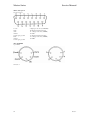
Real time clock with RAM
Battery back-up
A 146818 RTC and RAM chip is provided with battery backed supply. The chip operation is described
in the manufacturers data sheet . In its fully charged state, the internal lithium manganese dioxide
battery will provide over one year of back up power. Alternatively, components may be fitted to the
circuit board which provide for the fitting of a rechargeable battery on the keyboard. This battery, like
its support components are not fitted as standard. If these are fitted by the user , the warranty may be
invalidated.
The keyboard mounted battery is charged whilst the computer is running from the mains supply. The
proportion of charge accummulated during operation is shown in figure 6 for an initially flat battery .
This is an approximation dependent on conditions of use , as the actual charge accumulated will vary
with temperature and duty cycle (i.e. ratio of time on charge, to time on discharge).
100
90
80
70
typical %
charge
accumulated
60
10
5
0
Figure 6
I
:
.
I
:
I
:
.
I
:
.
I
:
I
:
.
I
:
I
: .
I
:
I
:.
~
:
.................................................................
~
:
I
:
I
:
I .. :
I .
:
I.
:
I_____//_____________________
0 1 2 100 120 140 160 180
Time switched on (hours)
An over_charge prevention circuit is provided with the following action:
a) Upon switch on, charging current of about 30mA is applied.
b) After approximately 15 minutes the charging current falls to 1mA.
c ) ''Trickle'' charging continues at 1mA for as long as mains power is applied.
The minimum charge burst is designed to provide battery back_up over a weekend after just a few
minutes operation.
21 Issue 1
21
Issue 1
Master Series
Service Manual
A 10uf capacitor is connected across the clock chip supply connections. This is to prevent loss of data
in the event of accidental battery disconnection.
Configuration Status : - Fifty bytes of CMOS RAM are available within the chip. Twenty of these are
used by the operating and filing systems for initial configuration of the hardware. Of the remainder ,
ten are reserved for future use by ACORN , ten are for ' Third Party ' use and the remainder are for the
user.
Clock:- The clock operates from a 32.768KHz crystal oscillator. A trimming capacitor is provided as is
a test point with the buffered clock output. Year, month, day, hour, minute and second information is
provided with automatic leap year (but not automatic leap century) correction. An alarm is also
included within the chip, but operating system support to this facility is not provided. An optional nIRQ
connection can be made to the CPU from the clock chip, enabling the alarm to change program flow.
Operation of the clock chip in this manner involves direct manipulation of the chip control signals and
should only be attempted by competent programmers. Acorn Computers are not responsible for
incorrect programming by the user/software supplier.
If power is removed during an access to this chip, the chip select will become invalid. This cannot
however remove the possibility of write accesses being corrupted. This is done by inverting the chip
select with a transistor whose collector resistor is connected to the battery backed supply. As power
fails to the main circuitry, the transistor base current reduces and the transistor switches off deselecting
the chip.
1 MHz Internal IO:- Various devices operate at a 1MHz bus rate. Only one internal I/O component
works at this speed - the system VIA.
22 Issue 1
22
Issue 1
Master Series
Service Manual
System VIA:- A 6522 allows several sources to create maskable interrupts.
The sources are:a) CRTC vertical synchronisation.
b ) A-D converter; end of conversion signal.
c) CRTC light pen strobe.
d) Keyboard key detect.
It also provides the previously mentioned slow data bus.
Port B on this device generates and reads a number of internal hardware strobes. These are as follows:Port B Data Strobe Active Level
Port B
Data
D7
DO
DXXXXXXX
X DXXXXXX
XXDXXXXX
XXXD XXXX
XXXXD 0 0 0
XXXXD 0 0 1
XXXXD 0 1 0
XXXXD 0 1 1
XXXXD 1 0 0
XXXXD 1 0 1
XXXXD 1 1 0
XXXXD 1 1 1
Strobe
Active Level
Clock Address
Clock chip enable
'Fire' button 1
'Fire' button 2
Sound chip select
Clock R/W
Clock Data
Keyboard enable
C0 } Screen control
C1 } Signals
Caps Lock indicator
Shift Lock indicator
H
H
Input
Input
L
L
Q
Q
L
H
L
L
Note: Q is the value of D after the port write operation is completed
2MHz Internal I/0:- 0nly one internal I/0 component operates at this speed, the internal second
processor TUBE. Its data bus is connected directly to the CPU data bus.
The second processor interface will only be specified as a hardware data transfer definition. In this
way, the actual second processor used will not be constrained by this specification.
This is a parallel port providing the following data access signals:i) D0 to D7 . . . . A bi-directional bus to TTL levels . ii) A0 to A2 . . . . A uni-directional bus to CM0S
levels.
The following control and timing signals are provided:i) Host CPU phi2
ii) System Reset
iii) Host CPU nIRQ
.... CM0S levels
.... TTL levels
.... This must be an 'open collector' node with an active low
TTL level
iv) 8MHz timing reference .... TTL levels
v) TUBE chip select
.... CM0S levels
vi) Read/Write
.... TTL levels
23 Issue 1
23
Issue 1
Master Series
Service Manual
5.4 External I/O
lMHz External 1/0:Screen Output : - There are two chips primarily responsible for providing the screen output : a) 6845
b) Acorn proprietary VIDPROC (IC42)
High Resolution Modes:- The 6845 generates a linear memory address sequence which increments
every 0.5 us or lus , depending on the video bandwidth selected and video data format.
The amount of memory reserved for screen use is also varied. The available options are shown in figure
7
Video Data Formats
''Mode'' Format
0
l
2
3
4
5
6
7
l28
l29
l30
l3l
l32
l33
l34
l35
Pixels/Byte
8
4
2
8
8
4
8
Teletext
8
4
2
8
8
4
8
Teletext
Reserved Memory
Bytes
20K
20K
20K
l6K
l0K
l0K
8K
lK
20K
20K
20K
20K
20K
20K
20K
20K
\
I
I Reserved
> in
I LYNNE
I
I
/
Figure 7
All modes except 7 and l35 display a bit mapped image of the reserved memory. The 6845 may be reprogrammed to display any arbitrary section of memory. If this is done, however, the hardware
scrolling will not work correctly, as it assumes that the screen memory is in its usual location. The
screen always ends at &7FFF and starts l,8,l0 or 20K further down than that, depending on the selected
mode.
The selection of video bandwidth and data format is performed by programming the VIDPROC. The
cursor size and position is also controllable by VIDPROC. Special measures have been taken to ensure
correct cursor operation in the Teletext modes.
24 Issue l
24
Issue 1
Master Series
Service Manual
Teletext
The Teletext modes do not generate a bit mapped display, but a character cell one. The
character/graphics ROM within a SAA5050 device generates RGB signals according to the desired
character/graphics information within the reserved memory space. Each byte of memory is therefore
just a definition of the character/graphics symbol required.
Other SAA505X devices may be used when different languages are required.
Only 1 Kbyte of memory is needed for either of the Teletext modes, although 20K is reserved for it in
mode 135. The MOS uses the spare 19K to speed up inter-filing system file transfers but the user may
use this memory if no such transfers are to be done.
The VIDPROC has to be re-programmed to use the SAA5050 RGB outputs.
The 6845 is still used to generate the cursor. As a delay of 2.75 us will occur after a character is read
from RAM, before outputting the appropriate RGB signals , the 6845 has to be programmed
accordingly . The ''start'' of screen signal is given a 1.5 byte-time offset, and the SAA5050 has a further
1 byte-time offset to restore the correct cursor/data phase.
The VIDPROC has further adjustment which allows for the cursor to be adjusted to pixel accuracy.
Hardware Scroll:- Scrolling may be achieved in any mode by re-programming the 6845 start of screen
address to an integral number of video lines further down the memory map than the nominal start of
screen.
This of course causes the linear address generator to attempt to display an end of screen which is out of
the reserved video area. To overcome this effect, hardware scrolling is provided with a variable address
wrap-around.
In effect, when the address generator would otherwise attempt to access out-of-screen RAM, its
addresses are modified to point to the gap between the original start of screen and scr.olled start of
screen. When this is done, only the end of screen needs to be written over in RAM. (If this is not done,
the entire screen appears to ''roll-over'' ). The amount of modification to be used is controlled by two
nodes; C0 and C1.
Video Output:- Three outputs are provided for displaying video data.
These are:
a) PAL/NTSC encoded, UHF carrier On channel 36 with 1.5mV into 75 ohm.
b) Composite video. This is a 1v peak to peak signal.
c) Digital Red, Green, Blue outputs. These are approximately 75 ohm outputs.
For use with NTSC, the modulator. has to be changed from UM1233/E36 to a VHF equivalent.
Provision is made for selection of either one of two channels with V.H.F. A Molex type link has to be
inserted for this.
25 Issue 1
25
Issue 1
Master Series
Service Manual
Analogue Port:- This 15 way D-type connector provides access to an NEC uPD7002, 4 channel, 10 bit
analogue to digital converter. The sampled input is compared to a 1.8V reference derived from three
small signal diodes in series.
A tracked link may be cut to deselect this reference. The user may then solder in a two pin precision
reference in the holes provided or supply an external reference. Any user supplied reference should
have a maximum voltage of 2.5V.
Conversion:- An input voltage on any one of the 4 channels wil be digitised when the A/D control
register is so instructed. Conversions are in the range 0 to 1.8V.
The voltage reference is made available at the connector. Provision is made on the board for an
additional high stability reference, if required.
A link will have to be made for the additionl reference to be used.
Conversions take place in 5mS and the "end of conversion'' pulse causes an IRQ to be generated by the
sys tem VIA .
Auxiliary Connections:- Two "fire buttons'' are provided for with the connections IO, I1. These are
connected to the system VIA and cause interrupts (as IRQ) to be generated.
A light pen may be connected to the signal LPSTB. This also causes the system VIA to generate an
IRQ (if enabled). It also causes the 6845 CRTC to latch the address of the currently selected video data
byte. This may not be the same as the displayed byte, and some software correction may be necessary.
Factors such as phosphor characteristics, light pen response and the angle at which the pen is used, may
all affect the correction needed.
Serial Ports - Cassette and RS423:- Much circuitry used to provide the RS423 port also generates
cassette interface signals. For this reason, these will be described together, with the differences where
appropriate.
U.A.R.T.:- The device responsible for providing most of the serial port functions is the 6850 UART.
This has all the receive/transmit and data formatting/error checking that is neccessary for both
systems.It is fully described in the March 1983 edition of the Hitachi Microcomputer Databook.
SERPROC:- The AC0RN proprietary part, the SERPR0C is effectively a multiplexer and baud rate
generator for the 685°. It also generates the phase-continuous transmission circuitry for use with the
cassette interface.
Buffer Components:- The Rs423 transmit data and CTS lines are buffered by an AM26LS30, or
equivalent. This provides a single ended transmission with s1ew rate limited output.
RS423 receive data and RTS is buffered by a uA9637AC or equivalent. Both buffers are connected
with single ended input configurations.
26 Issue 1
26
Issue 1
Master Series
Service Manual
Cassette data output from the SERPROC is buffered by a single, non-inverting operational amplifier
with a simple, single pole filter. a.c. coupling capacitor and current limiting output resistor.
2MHz External I/O
Two peripheral devices operate at 2MHz. These are the external second processor connection and the
ECONET connection.
ECONET Module:- Connection is made to the ECONET by a five way DIN connector mounted on
the main circuit board. The interface electronics including the 68B54, line drivers, receivers and chatter
disconnect components are mounted on a separate circuit board. This board has two connectors:a) A 5 way connector which has a one-to-one connection with the DIN connector.
b) A 15 way connector provides the CPU data bus together with address, timing reference, chip select
and interrupt signals. The main pcb has two further address connections for future expansion.
External Second Processor:- This interface has a buffered data bus via the Peripheral Bus Controller
(PBC). The EXbus on this component provides for good data set up and hold times. Together with a
limited degree of line matching, this ensures reliable high speed data transfer with unspecified cable
lengths. A maximum cable length of one metre is suggested to prevent noise problems.
The interface operates at 2Mhz. This means that if a 1Mhz bus peripheral is also connected, then the
address and data buses on this connector will appear to perform both 1 and 2MHz cycles.
The connections are:DO to D7 Data Bus CMOS levels
A0 to A7 Address Bus TTL levels
IRQ Interrupt Request Open collector TTL levels
nTUBE Parasite chip select TTL levels
Supply +5V
Ground 0V
27 Issue 1
27
Issue 1
Master Series
Service Manual
6 Test equipment
A PORT tester is available for the microcomputer. It will check the DRAMs (including sideways
RAM), CMOS RAM, and all the I/O ports on the microcomputer. disc, printer, user, lMHz bus, TUBE,
UHF, video, RGB, RS423, cassette, A to D, and sound output.
To use this tester, the microcomputer must at least have the CPU running and the MOS/BASIC ROM
working and some of the RAM working.
The PORT test software is contained in a cartridge ROM and on disc. Full operating instructions are
supplied with the equipment.
28 Issue l
28
Issue 1
Master Series
Service Manual
7 Fault finding
This section goes step by step through fault finding in each section of hardware. It should be studied in
conjunction with the circuit diagram and component location tables in the Appendix.
If any part of the machine is suspected of being faulty, the following points should always be checked
first:
1 no loose connectors and broken cables
2 no broken or shorting tracks
3 ICs plugged into their sockets correctly
4 power supply working and reaching the components concerned
5 all digital signals are either at clean TTL logic levels (greater than 2.4v for 1, less than .5V for 0), or
clean CMOS logic levels (greater than 3v for 1, less than 1V for 0). 0n timed signals this must be true
for the period 150ns before phi2 on read cycles and 300ns before phi2 on write cycles.
Hints for repair.
1 Never solder to a computer which is switched on.
2 Remove all user R0Ms before starting (Remember to put them back afterwards !)
3 Use sharp pointed meter probes to push through solder resist. This will make finding short/open
circuits more reliable.
4 Always suspect connectors.
5 If you find a recurrent fault (e.g. more than 10 machines), let us know at AC0RN so that we can
include it in this manual if appropriate.
29 Issue 1
29
Issue 1
Master Series
Service Manual
The following items of test equipment are required for fault finding :
A set of screwdrivers
Pliers
Cutters
10A Multimeter
RGB monitor
logic probe
5 ohm 5W resistor
The repair will be quicker with :
100MHz dual beam oscilloscope
Good quality scope probes
TV, composite monitor, colour monitor
cassette player
disc drive
P0RT tester
frequency counter
A known good computer to use as a signal model
30 Issue 1
30
Issue 1
Master Series
Service Manual
Master Series Service Manual
Note: the Peripheral Bus Controller IC21 is used to buffer the data bus around the system. It also
isolates may parts of the system from each other to help improve reliability. It may disguise data bus
failures or open circuits. Be sure not to assume that any node is connected to any other unless you have
checked it. This particularly applies to the SAA5050 and all 1MHz operating components. E.g. the
User VIA going down could stop the System VIA.
31 Issue 1
31
Issue 1
Master Series
Service Manual
7.1 Switch on
If the suspect microcomputer has a second or co-processor fitted then disconnect it. Connect the
suspect microcomputer to a UHF TV and an RGB monitor (connecting both a TV and a monitor will
show up any fault in the connecting leads, or the polarity of CSYNC). Connect the mains supply and
switch on both the monitors and the computer. One of the following will happen.
7.1.1 There is noise on the monitor screens (no signal from computer). There is no power-on beep
sound and the keyboard power indicator does not light.
Results: the power supply is dead.
Follow the sequence of checks shown below.
1 Check the power supply (see 7.2). Try replacing the power supply anyway as the fuse may have
blown.
7.1.2 The power supply is working (the keyboard indicator is lit), but nothing else happens.
Results: There is a board fault.
Follow the sequence of checks shown below.
1 Check that all ICs have power and ground on the correct pins at the correct voltage. Make good any
dry joints.
2 Feel whether any of the ICs are hot. Check for shorted PCB tracks. Watch for shorts from -5V to the
IO controller causing it to latch-up. Clear shorted tracks and then replace any affected Ics.
Note: ICs which get abnormally hot due to a fault, but which work after the fault has been cured,
should still be replaced. Their long term reliablility may well be impaired.
3 Check the 16MHz oscillator output Ic43 pin 2, and check that it is reaching the VIDPROC IC42 pin
8. The signal should be reasonably clean, 4v peak to peak. If not then check the crystal controlled
oscillator circuit formed by half of IC43 and X2.
Warning: if the system 16MHz clock does not work, the DRAM RAS and CAS lines could be held
low. This can make the ICs heat up causing permanent damage. If the oscillator is not working, or the
clock is not reaching the VIDPROC, try to find the fault and repair it as quickly as possible. Do not
leave the computer switched on for more than 30 seconds at a time.
4 Check the 1 2 4 and 8 MHz signals from the VIDPROC, IC42 pins 4 5 6 and 7 respectively. If any is
missing, or is not a clean square wave with TTL logic levels then replace the VIDPROC IC42.
5 Check that there is a clean 2 MHz signal on the CPU clock input, IC14 pin 37. If it is missing or
incorrect then check for broken or shorting track.
6 Check that all data and address bus lines are clear of shorts between themselves, +5V and ground.
32 Issue 1
32
Issue 1
Master Series
Service Manual
7 Check that the system ROM is plugged in.
8 Check the RAS and CAS signals to the main DRAMs, ICs 17 and 23, pin 5 (RAS) and pin 16 (CAS).
The main DRAM timing is shown in figure 8.
Figure 8 DRAM timing
RAS and CAS should be good 4MHz square waves. If one or both is missing then check for shorted
tracks. Remember the DRAMs can be destroyed if RAS is stuck low.
RAS is generated from 4M and 8M by the D-type IC28 pin 9.
CAS for the main DRAMs is generated from 2M, inverted by a NAND in Ic34 to give phi2 IN, gated
with DRAMEN which enables the main RAM, and finally gated with 4M through another NAND in
IC34.
9 Check that the auxiliary DRAM CAS line, when inverted at IC36 pin 8 is low. If it is high at this
point then it will suppress the main DRAMs.
10 Check the multiplexed address lines into the main DRAMs, ICs 17 and 23 pins 6 7 8 10 11 12 13
and 14. The address lines should switch after RAS, with an approximate 20ns hold time as shown in
figure 8.
Also check that the address lines are correctly switching after phi2, as shown in figure 8.
If any of the DRAM timing is found to be out of specification then check that c26 is fitted and is the
correct value.
33 Issue 1
33
Issue 1
Master Series
Service Manual
7.1.3 There is a sort of display with rolling lines and/or diagonal stripes.
1 Check the MA and RA lines from the 68115 CRTC IC22. There are 14 MA lines from MA0 (pin 4)
to MA13 (pin 17) inclusive. There are 4 RA lines from RA0 (pin 38) to RA3 (pin 35) inclusive (RA4 is
not connected).
These lines form the video RAM addresses in the various screen modes. Check that they are not stuck,
and that they oscillate between good logic 0 and logic 1 voltage levels. If not then first replace the
6845, then look for shorted tracks.
Check that all are getting through to the CRTC/MUX IC31.
2 Check VSYNC pin 40 IC22. This line should pulse low every 20ms.
3 Check HSYNC pin 39 IC22. This line should pulse low every 64us.
4 Check that CSYNC (both HSYNC and VSYNC superimposed) is available at IC25 pin 8 and also at
pin 4 of SK9, the RGB connector.
5 If the RGB display alone is not working then the CSYNC polarity for that particular monitor is
probably incorrect. Alter LK5.
6 Check all video connections.
7.1.4 There is a cursor stuck at the top left corner of the screen, but nothing else.
1 Disconnect any second or co-processor which may be fitted.
2 Check all connections to and from the keyboard and keyboard encoder IC16.
Replace IC16.
7.1.5 The screen says
ACORN MOS
AC0RN ADFS
but nothing else.
1 Disconnect any second or co-processor which may be fitted.
2 Try typing CTRL F BREAK. If this works then either connect up a disc drive and put an ADFS disc
in it or type
*configure nodir RETURN
Turn the power on and off. The machine should now work.
3 The configuration memory may have been set incorrectly or is faulty. Turn the power off and on
again whilst holding down the R key. Then press CTRL F BREAK. All previous configuration
commands will be reset to zero.
34 Issue 1
34
Issue 1
Master Series
Service Manual
7.1.6 BASIC is printed on the screen, but no > prompt appears.
1 Disconnect any second or co-processor which may be fitted.
2 Check that the IRQ line on the CPU IC14 pin 4 is not stuck in one logic state. If it is then check the
address and chip select lines of the system VIA IC8.
7.1.7 The BASIC prompt > appears, but the keyboard does not respond.
1 Check the address and ship select lines of the system VIA Ic8.
2 Check all connections to the keyboard encoder IC16.
3 If all else fails then try a different keyboard. If this works, look for broken leads and tracks on the
original one.
4 Check that the IRQ line IC14 pin 4 is not stuck low or high. The memory controller IC20 and CM0S
clock/RAM IC11 both have direct connections to the IRQ line. The latter part has a link LK4 which
can be used to isolate it from IRQ.
Note: the system VIA Ic8 generates an interrupt every 100th of a second. If this interrupt is not cleared
by the operating system each time it occurs the IRQ line will appear to be stuck low. This could occur
if some other installed software is faulty or if an address or data line to the VIA is faulty.
7.1.8 Not all keys work on the keyboard.
One of two possible keyboard circuits may be fitted:
a) A 40 pin keyboard encoder IC16 on the main circuit board and two 15 way connectors (possibly
with an intermediate buffer board) joined to the keyboard with ribbon cables.
1 If more than one key is affected, check for a faulty connection from the keyboard encoder IC16 to the
keyboard.
2 If more than one key is affected, check for a broken track in the middle of a row or column of the
keyboard matrix.
3 If one key only is affected, check for a broken track at the end of a row or column in the keyboard
matrix.
4 If one key only is affected then check the keyswitch itself.
Note: the beginning of a row or column is the end of a PCB track which is immediately connected to
the encoder circuitry. The end of a row or column is the other end of the PCB track. Because of the
layout, the beginning and end of a track are not necessarily the parts of the track which are visually
nearer or farther from the encoder circuitry.
35 Issue 1
35
Issue 1
Master Series
Service Manual
b) A 17 way connector rising to a keyboard with the encoder circuitry on it.
1 All of 1 to 4 in the previous section.
2 Check for a faulty connection from the main board to the keyboard which may cause the entire
keyboard to be affected.
7.1.9 All the keys are working, but CTRL BREAK behaves as BREAK.
(CTRL BREAK should invoke the configuration settings.)
1 Check that all power-down components around the CMOS clock/RAM chip IC11 are present and
have the correct value.
On some early computers, C11 needs to be 1OOuF instead of 1OuF, D8 should be changed to IN4OO1,
and Q3 should have a 1k8 resistor between its base and emitter.
2 Check that the chip enable pin 13 of IC11 is normally high with just occasional excursions low. If not
then check the system VIA Ic8 for the RTC chip select pulses which should be on pin 16.
3 Real time clock chip control lines should be in the following state at all times when not being
accessed by the user.
CE IC11 pin 13 high
AS IC11 pin 14 low
DS IC11 pin 17 low
4 Check that R/W IC11 pin 15 wiggles when alternate reads and writes are performed.
7.1.10 The computer powers up in terminal mode, and *configure will not change it.
1 Check 1 and 2 in the section above.
2 Check all connections to the clock/RAM chip IC11 for open circuits or short circuits.
7.1.11 The computer works, but random dots or characters appear on the screen.
1 Type a short program or piece of text into the machine - about two lines in any screen mode are
adequate. Leave it for a few minutes and then see if the screen has been corrupted. If it has then there is
a memory system fault. If it hasn't then enter a longer piece of program or text - enough to fill a screen
and repeat the test.
Any fault showing itself will be due to a memory system failure. These are rarely due to the RAM
chips themselves as these are usually very reliable.Check the following very carefully.
36 Issue 1
36
Issue 1
Master Series
Service Manual
2 Check all connections from the CPU address bus (IC14 pins 9 to 20 and pins 22 to 25 inclusive) to
the DRAM address multiplexers (ICs 29 30 and 33, see circuit diagram for pin numbers). Then check
the voltage levels of these signals at the multiplexer input pins. All signals should have good CM0S
levels (less than 1V for 0, greater than 3v for 1). A constant 0 or 5V level implies a short to the relevant
power rail. Poor logic levels imply shorting to another logic signal.
3 Check that the address at the DRAM inputs is stable for at least 15ns after RAS goes low and changes
no later than 50ns after that edge, see figure 8. This should occur once for every active high period of
the system 2MHz clock out of the VIDPR0C and once for every active low period.
4 Check that the noise around logic L0W signals is generally less than 500mV. If it is not, then some
signals may be shorting or a decoupling capacitor may be missing.
5 Check that the data bus is properly connected between the CPU and the DRAMs.
7.1.12 You can type but get two or more copies around the screen.
1 Check Test Points TP.7 to TP20 (the CRTC scanning outputs, shown on circuit diagram to the left of
the CRTC IC22) to make sure that the correct addresses are being generated. Any line stuck high or
low or shorting to another pin will give strange screen effects.Note: MA13 IC22 pin 1.7 is used to
switch the address multiplexing circuits between modes 7/135 and any other modes. This line should be
static in any given mode.
2 Check that all of the lines from the CRTC IC22 to the CRTC Multiplexer IC31 actually get there.
3 Check that the lines C0 and C1 from the 74LS259 (IC10 pins 4 and 5) to the CRTC Multiplexer
(IC31 pins 38 and 39) are properly connected and change at least once if you switch between modes.
4 Check that the lines from the CRTC/MUX IC31 to the DRAMs are correct with no short or open
circuits.
7-2 Sideways RAM
1 Check all connections to the memory address multiplexers.
2 Check RAS and CAS at the DRAMs, see figure 8.
3 Check that the two links LK18 and LK19 are in the correct position for your use.
37 Issue 1
37
Issue 1
Master Series
Service Manual
7.3 Video
To debug the video, all three different types of monitor should be connected: TV, RGB and composite.
7-3.1 The display scrolls vertically round the screen.
Does it occur on RGB, UHF and Composite video?
1 If so, check VSYNC is correct on the CRTC IC22 pin 40.
2 Then follow the signal through the exclusive-0R gates IC25 where it is combined with HSYNC. If
the signal does not make good logic levels at any node, then there is probably a short in that area.Note:
when VSYNC (period 20ms) is EXORed with HSYNC (period 64us), the former will be difficult to
spot within the latter. A way of getting round this is to synchronise the oscilloscope from the VYSNC
output of the CRTC IC22 pin 40 and then examine the EXOR gate output.
Does it only occur on one of the video outputs?
1 Is the CSYNC polarity link LK5 correct for your monitor?
2 If it only occurs on composite video, check that all the resistors (R147 to R150 inclusive) to the
output transistors are correct in accordance with the circuit diagram. Do they all have good signals
going into them?
3 If it only occurs On UHF, check the signal as it passes through the resistor network, Ic40 pins 12 to
19 inclusive through resistors R69 75 77 78 84 85 87 and 89.
4 If it only occurs On RGB, check all the signals going to the back of the connector.
7-3.2 The display is correct vertically, but is broken into moving diagonal lines.Does it occur on RGB,
UHF and Composite video?
1 If so, check HSYNC is correct on the CRTC CRTC IC22 pin 39.
2 Then follow the signal through the exclusive-OR gates IC25 where it is combined with VSYNC. If
the signal does not make good logic levels at any node, then there is probably a short in that area.
Note: when HSYNC (period 64us) is EXORed with VSYNC (period 20ms), the former will have the
latter superimposed upon it. This will make the former appear to have glitches. This should be ignored
in the measurement of HSYNC period.
38 Issue 1
38
Issue 1
Master Series
Service Manual
Does it only occur on one of the video outputs?
1 Is the CSYNC polarity link LK5 correct for your monitor?
2 If it only occurs on composite video, check that all the resistors (R147 to R150 inclusive) to the
output transistors are correct in accordance with the circuit diagram. Do they all have good signals
going into them?
3) If it only occurs on UHF, check the signal as it passes through the resistor network, IC40 pins 12 to
19 inclusive through resistors R69 75 77 78 84 85 87 and 89 .
7-3-3 There is no colour on UHF.
1 Is the variable capacitor VC2 set to give the correct frequency of 17.7345MHz at IC43 pin 12?
2 Check connection to IC40 pin 11, and resistor summing node through L1 and C81 Q12 C88 and
R140.
3 Check +5V supply on IC40 pin 20.
4 Try replacing IC40 as a last resort.
7-3.4 There is only one colour.
0n RGB
1 Check the RGB connections out of the VIDPROC IC42 pins 14 12 and 10.
2 If the fault is only in mode 7 or 135 then check RGB connections from SAA5050 IC32 pins 24 23
and 22 to the VIDPROC IC42 pins 13 11 and 9.
On UHF
1 Check RGB inputs to IC40 pins 6 7 and 8. If there are any faults, check the connections from the
VIDPR0C IC42 pins 14 12 and 10. If any nodes are stuck at +5V or ground then check for shorts. As a
last resort, try changing chips.
2 Check resistors R69 75 77 78 84 85 87 89 90 for the correct values and that they have good signal
levels at their IC40 ends.
7-3-5 The screen displays the wrong colours.
1 Check 1 and 2 above .
39 Issue 1
39
Issue 1
Master Series
Service Manual
7-3.6 The display works in all modes except 7 and 135.
These modes work very differently from the others, using the SAA5050. There are a number of faults
which only exhibit themselves in these modes.
1 There is a cursor which can be moved, but no text. Check the 6MHz input to the SAA5050. It will
have a slightly variable duty cycle, certainly not 50%, but no part of the waveform should be narrower
than about 40ns. If so, check all components and signals around the 6MHz generator Ic39 and IC25.
2 The text is at all fragmented. Check as above.
3 Not all colours are present. Check all connections to the VIDPROC IC42.
Are the pull-up resistors R51 R54 and R56 present and the correct values?
4 Not all characters can be obtained. Check all data bus connections the the PBC IC21 pins 21 to 28.
5 Lines of normal size text appear cut in half. Check VSYNC at the CRTC IC22 pin 40.
6 Rounded characters appear unstable. Check the components and signals around the 6MHz generator
IC39 and IC25.
7) Lines are broken up. Check all connections to the PBC IC21.
7.4 Real time clock
7.4.1 Gives strange characters.
1 Type in the correct time and try again.
7.4.2 Does not increment.
1 Check that the variable capacitor VC1 is in the circuit. Check that 32.768 KHz is at IC11 pin 2. If it is
not, check all the values in the oscillator circuit X1 VC1 C6 C7 R17 and R24.
2 Are all connections to the system VIA correct?
3 Are all the components in the chip select/power-down circuit fitted correctly ? See 7.1.9.
7.4.3 Loses a lot of time.
1 Is the battery connector PL8 securely fitted with all three pins engaged?
Are the battery leads properly soldered to the battery clips?
2 Is the battery flat? If it is then replace it in its holder next to the speaker inside the computer, being
careful to insert the new battery with the same polarity as the old one.
3 Is there at least 2.6v at the clock chip with mains power switched off?
If not the battery may still be flat, but check the FET Q4 and surrounding components first.
40 Issue 1
40
Issue 1
Master Series
Service Manual
7-5 Analogue port
7.5.1 Gives completely erroneous results on all channels.
1 Are all the connections on the external plug correct?
2 Has it got an incorrect or faulty integration capacitor C49?
3 Check that the reference voltage is approximately 1.8V across pins 8 and 9 of Ic49 and has very little
noise on it.
4 Are all the address and data bus connections to Ic49 correct?
5 Are the input voltages within the range 0 to 2.5V? If not, the converter will not work correctly.
6 Have any of the terminals in the connector been connected to voltages greater than 5.5V or less than
0.5V? If so the AID converter is likely to be damaged. Replace IC49.
7 Is the chip select from the IO controller IC15 pin 35 correctly connected to IC49 pin 23?
8 Does IC49 have a 1MHz timing reference on pin 2?
7.5.2 Gives erroneous results on just one channel.
1 The plug and cable connections are the most likely sources of problems.
Point 6 above may also apply.
7.6 RS423 port
7.6.1 Does not work at all.
1 Are the data format and baud rate settings the same as the remote computer?
Note: these will be set to the configuration values after power on Or CTRL BREAK. Make Sure that
these are correct as well.
2 Is the cable properly connected?
Note. this connector CAN be inserted the wrong way Up! .
3 Are all the cable connections correct, i.e. no open/short circuits?
4 Are the device se1ect connections to the SERPROC and ACIA from the I0 controller correct (IC15
pin 34 and pin 36 respectively), with no short circuits to either power supply rail?
41 Issue 1
41
Issue 1
Master Series
Service Manual
5 Is the SERPROC getting a 1.23MHz timing reference, IC48 pin25?
This signal could come from either one of two sources a) A 74LS169 counter.
b) The chroma chip.
Whichever it SHOULD come from is dependent on the build standard of the computer. In any case, the
SERPROC should get this signal from some source.Check that it is the correct frequency.
6 Is the -5V supply correctly connected (and working) to the RS423 transmitter chip IC50 pin 8?
7 Are either CTS (IC48 pin 2O) or RTS (IC48 pin 23) stuck high or low?
8 If all else fails, check all remaining connections to the ACIA and SERPROC.
7.6.2 Will only receive data.
1 Does the remote computer use different transmit and receive rates? If so check that your computer
has the equivalent receive and transmit respectively.
2 Check 3 6 and 7 as above.
3 Check that data going into the line driver IC5° comes out of it. The driver could be faulty otherwise.
4 Check that the Tx CLK going into the ACIA is correct, IC45 pin 4.
7.6-3 Will only transmit data.
1 Does the remote computer use different transmit and receive rates? If so check that your computer
has the equivalent receive and transmit respectively.
2 Check 3 6 and 7 as above.
3 Check that data going into the line receiver IC51 comes out of it.
4 Check that the Rx CLK going into the ACIA is correct, IC45 pin 3.
7-7 Cassette interface
7-7.1 Will not load or save data.
1 Check the cable and data recorder (with another computer if possible).
2 Check that the ACIA and SERPROC have correct (i.e. no open or short circuit) connections on all
pins.
3 Check that the back panel connector has no dry joints or short circuits between it and the interface
circuitry.
42 Issue 1
42
Issue 1
Master Series
Service Manual
4 Are the connector pins in good condition? If not, the fault could show itself as intermittent operation.
5 Check the 1.23MHz connection to the ACIA.
7-7-2 Will not load data.
1 Check 1 3 and 4 above .
2 Check that the ACIA is receiving an Rx CLK, IC45 pin 3.
2 Check the connections between the SERPROC IC48 and ACIA IC45.
3 Check that incoming data is appearing at the pin at the back of the connector.
4 Follow the signal path through the high and low pass filters. It should finish up as a 1.2V peak to
peak signal at the CASIN input to the SERPROC, IC48 pin 12. If it disappears at any point there is
probably a dry joint.
5 The cassette data input has a static protection network on it. Check that all the components in this are
fitted and have the correct values. A faulty component could mean that the LM324 has been
subsequently damaged.
6 Check that the ACIA and SERPROC have correct (i.e. no open or short circuit) connections on all
pins.
7 Check the 1.23MHz connection to the ACIA.
8 As a last resort, change the SERPROC and try again, then try the ACIA. This should not be necessary
as both of these components are very reliable.
7-7.3 Will not save data.
1 Check the cable and data recorder (with another computer if possible).
2 Check that the ACIA is getting a Tx CLK, IC45 pin 4.
3 Check the connections between the SERPROC and ACIA.
4 Check that the back panel connector has no dry joints or short circuits between it and the interface
circuitry.
5 Are the connector pins in good condition? If not, the fault could show itself as intermittent operation.
6 Check that data is coming out of the CASOUT output from the SERPROC, IC48 pin 27. If not, check
all the data and address connections to the SERPROC and ACIA.
7 Follow the signal (if it exists) from the SERPROC to the connector. If it disappears then a dry joint or
short to power or ground is likely.
43 Issue 1
43
Issue 1
Master Series
Service Manual
7.8 Disc drive interface
7.8.1 Refuses to work at all.
1 Check that both the signal connector and power connector are securely pushed home.
2 Try another disc drive if possible, to eliminate the chance of a fault in this.
3 Try the disc drive with another computer, if possible.
4 Check that the 1770/1772 and 74LS174 have valid logic 0 levels at their device select inputs (IC3 pin
1 and IC4 pin 1) and that all data and address bus connections are present, with no open or short
circuits. If either IC is not being selected then check the outputs on the IO controller, IC15 pin 1
(FDCON) and pin 4 (FDC). If these signals are not available then check that the disc software is fitted
and is selected.
7.8.2 The drive select light comes on.
You cannot read a catalogue .
1 Has the correct filing system for the disc been selected (i.e. ADFS or DFS)?
2 Is the disc formatted?
3 Is the disc in the right way round?
4 Is the Read Data input to the 1770/1772 (IC3 pin 19) wiggling when you attempt to read the disc? If
not then check the signal cable and if necessary check that data is getting onto it from the disc drive.
5 Are the pull-up resistors (Rl R3 R5 and R6) on the 1770/1772 disc inputs fitted and correct?
6 Is the 8MHz input to the 1770/1772 correct? Check that it is available at IC3 pin 18. If not then trace
it back to IC19 pin 4 and IC42 pin 7.
7 Is the 1770/1772 DRQ line (IC3 pin 27) normally low but going high once every 32us (when then
disc interface has been asked to read, say, a catalogue)? If not then check that this line is not shorted to
power or ground and is connected to the IO Controller (IC15 pin 5).
8 Check that the DRQ transitions (IC3 pin 27) appear logically inverted at the NMI pin on the CPU
(IC14 pin 6) .
9 Check that the 1770/1772 INTRQ output (IC3 pin 28) produces a high going pulse at the end of every
command issued to the 1770/1772. If the INTRQ line is shorted high it will cause the IO Controller to
hold the CPU NMI line low , thus masking DRQ transitions .
44 Issue 1
44
Issue 1
Master Series
Service Manual
7.8-3 The catalogue can be read, but the entries are corrupted.
1 Some computers have 220 pF capacitor C27 fitted from the DRQ line to ground. Is this fitted? Is its
value correct? There will be no place on the PCB for computers that do not need this capacitor.
2 Are one or two disc drives present? If two, make sure that only one of them has line termination
resistors in.
7.8.4 The catalogue can be read, but not the data (or the directory cannot be changed in ADFS ) .
1 (Issue 1 boards only). There should be a small capacitor from the DRQ line to ground. Is this fitted?
Is its value correct?
2 Are one or two disc drives present? If two, make sure that only one of them has line termination
resistors in.
7.8.5 Data can be read but it is wrong (or you get Bad FS map in ADFS) .
1 Try the disc drive in another computer. If the fault persists, then the disc drive is at fault.
2 (Issue 1 boards only). There should be a small capacitor from the DRQ line to ground. Is this fitted?
Is its value correct?
3 There may be a fault in the memory system. Check that the address inputs to the Memory Controller
(IC20 pins 21 to 28 inclusive) are switching with good logic levels. Check that the outputs: the AA and
AT lines are switching. A good test here is to press BREAK repeatedly and look at each line in turn.
4 Check that the AA and AT lines are correctly connected to the address multiplexers, IC29 and Ic33.
5 Use a memory test program to validate memory. This is rarely necessary as the memory chips are
highly reliable.
7.8.6 Data can be read correcty but cannot be written reliably.
1 Is the disc formatted for DFS but being used with ADFS or vice versa? The built in formatter is only
for use with DFS.
2 Check the disc drive on another computer if possible.
3 Check that data transitions are appearing on the 1770 WD and WG pins, IC3 pins 22 and 21. If not
then check all connections to the 1770 (IC3) and the 74Ls174 (IC4).
4 Follow the signal path of WD to the connector.
Note: a disc drive must be connected at this stage as pull-up resistors for the line driver outputs are
within the disc drive. The output should be normally high with low going transitions.
45 Issue 1
45
Issue 1
Master Series
Service Manual
5 Follow the signal path of WG to the connector.
Note: a disc drive must be connected at this stage as pull-up resistors for the line driver outputs are
within the disc drive. The output should be normally high with low going transitions.
7.8.7 Data can be read and written correctly. but only one disc drive can be selected out of two.
1 Check all connections to the 74LS174 (IC4).
2 Check that only one drive select output is a logic LOW from the 7438. IC2 pins 3 and 6.
7-9 Parallel printer port
1 Check that the configuration system is set up correctly (i.e. *CONFIGURE PRINT 1). Use the
default printer driver to conduct the tests.
2 If the fault only shows up with a custom printer driver. test the software carefully first.
3 Check the printer with another computer if possible.
4 Check the computer with another printer if possible.
5 Check that pin 4o on the User VIA (Ic6) has a pull up to +5V (R11) but is not short circuited to +5V.
6 Check that data appearing on Port A of the VIA (Ic6 pins 2 to 9) appears on the outputs of the
74LS244 buffer (IC5).
7 Check that a strobe pulse appears on Ic6 pin 39 for every character transmitted. If not then check all
address. data and control pins on the User VIA.
8 Check that a strobe pulse is found inverted at pin 11 of the 7438 (IC2) and true at pin 8 of the 7438
(IC2).
7.10 User port
1 Is the software illegal. for example. using peek and poke type commands from a second or COprocessor? If so. this is the cause of the problem. It would work on the I/O processor alone but this is
not recommended.
2 Is the shift register being used to transfer data on the CA lines? There is a fault in some
manufacturers' 6522's and for this reason the use of this feature of the 6522 is not specified for the
computer.
3 Check the software very carefully.
4 Check all address. data and control lines to the User VIA IC6.
46 Issue 1
46
Issue 1
Master Series
Service Manual
5 Have voltages outside the supply range been applied to any of the pins? If so , the VIA may have
been damaged .Note: this could arise if a cable is left connected the the User Port and the other end is,
for instance, left trailing across a carpet.
7.11 1MHz bus
1 Is there anything in the configuration system that would cause the 1MHz bus to be deselected? For
example, this would happen if the computer were configured to power up with a floppy disc drive as
the default rather than a hard disc, therefore making the hard disc seem not to work.
2 Ensure that the software has not selected the internal pages &FC and &FD.
3 As with any straightforward parallel data bus, any faults with this have to be found by methodical
checking of all connections.
a) Ensure the remote equipment is not at fault (if possible).
b) Ensure the cables and connectors are in good condition and are correctly assembled, i.e. cable
clamps are fitted and effective.
c) Ensure that any non-polarised connectors are correctly inserted.
d) Cables longer than 1m should in general not be used.
e) Check that each and every connection is correct as per the circuit diagram.
f) Check that the READY signal from the IO Controller (IC15 pin 17) goes to both the CPU (IC14 pin
2) and the Peripheral Bus Controller (IC21 pin 11).
g) Check that the FIT connection from the IO controller (IC15 pin 38) goes to the PBC (IC21 pin 5).
h) Check that all address connections to the Memory Controller (IC20) are correct.
i) Check that the two data bus connections to the I0 Controller are correct (IC15 pins 18 and 19).
7.12 The Tube
1 Check 3 a) b) c) d) e) f) g) h) and i) as for 1MHz bus above.
7.13 Internal co-processor
7.13.1 Not being recognised.
1 Is the configuration status correct?
2 Are the two connectors correctly mated?
47 Issue 1
47
Issue 1
Master Series
Service Manual
3 Are two bits of the data bus correctly connected to the IO Controller (IC15 pins 18 and 19)?
4 Are all connections to the two connectors correct?
7.13.2 Recognised, but just a cursor in the top left hand corner of the screen.
1 Is the co-processor working? Try it in another computer.
2 Are the two connectors correctly mated?
3 Are the boot ROM(s) correctly inserted in the co-processor?
7.14 Sound output
7.14.1 Will not work at all.
1 Is the speaker connected?
2 Is there an external speaker (to the sound phono connector at the rear of the machine) which is short
circuited or of very low impedance (less than 4 ohms)? If so. remove it.
7.14.2 Will not work with all envelopes.
1 Has your software requested too many channels? The envelopes use memory shared with serial data
buffer space.
7.14-3 Produces strange sounds whenever a key is pressed.
1 Are all the connections to the sound chip correct as shown in the circuit diagram?
2 Try pressing BREAK. If the sound goes away then it may be mains noise affecting the computer.
This could happen in places with poor mains supplies.
3 On some early computers, pin 15 of IC10 was connected to PRST. It should now be connected to
+5V.
7.15 Modem connector
1 Check the controlling software VERY carefully
2 Check all connections to the connector.
3 Check that a signal arriving at the connector goes through it, i.e. there are no dry joints Or faulty
connector sockets.
48 Issue 1
48
Issue 1
Master Series
Service Manual
7.16 Cartridge port
7.16.1 Causes the sound output to be noisy.
1 Check the cartridge for shorts and general layout.
7.16.2 Will not recognise some cartridges.
1 Is the cartridge for the Electron? Not all of these are compatible.
2 Are all the links assocciated with the cartridge in the correct position.
3 Is the cartridge edge connector excessively worn, e.g. gold plating worn through?
4 Are all connections to the edge connectors correct without shorts to each other?
5 Are any of the edge connector blades bent or worn? If so, the connector must be replaced.
7.17 Econet
Econet can only be serviced properly by Econet service centres, who will have the necessary test
equipment to check the system thoroughly. However, there are a few simple things which can be
checked without the test equipment. Follow the Econet board circuit diagram in the Appendix.
1 Check that the two connectors on the Econet module are correctly inserted. The longer connector has
two spare pins on the left of the PCB socket. If the module is displaced and is plugged into one or both
of these spare pins, it will not work.
2 Check that the Econet module is installed and fitted correctly.
3 Check that NMI on the CPU pin 6 IC14 (TP 3) is not being held low.
49 Issue 1
49
Issue 1
Master Series
Service Manual
Appendix
50 Issue 1
50
Issue 1
Master Series
Service Manual
Connector pinouts
TV UHF out phono
outer: ground
inner: UHF
SK8 video out
BNC
outer: ground
inner: video
SK9 RGB
6-pin DIN
SK10 RS423
5-pin DIN
SK11 cassette
7-pin DIN
51 Issue 1
51
Issue 1
Master Series
Service Manual
SK12 analogue in
15-way D-type
1 +5V
2 0V
3 0V
4 CH3
5 analogue ground
6 0V
7 CH1
8 analogue ground
9 light pen strobe (notLPSTB)
10 digital switch input (I1)
11 voltage reference (VREF)
12 CH2
13 digital switch input (IO)
14 voltage reference (VREF)
15 CH0
SK7 ECONET
5-pin DIN
52 Issue 1
52
Issue 1
Master Series
Service Manual
PL1 disc drive
34-way IDC
1 0V
3 0V
5 0V
7 0V
9 0V
11 0V
13 0V
15 0V
17 0V
19 0V
21 0V
23 0V
25 0V
27 0V
29 0V
31 0V
33 0V
2 (notS/SEL 8'' )
4 (notINX 8'')
6 NC
8 notINX 5 1/4"
10 notS0
12 notS1
14 NC
16 notM0T0R
18 notDIR
20 notSTEP
22 notW/DATA
24 notWR/EN
26 notTK0
28 notWR PCT
30 notR/DATA
32 notS/SEL 5 1/4"
34 (notRDY 8")
PL3 printer
26-way IDC
1 STB
3 PA0
5 PA1
7 PA2
9 PA3
11 PA4 12 0V
13 PA5 14 0V
15 PA6 16 0V
17 PA7 18 0V
19 ACK
21 NC
23 NC
25 NC
2 0V
4 0V
6 0V
8 0V
10 0V
20 0V
22 0V
24 0V
26 NC
53 Issue 1
53
Issue 1
Master Series
Service Manual
PL4 user port
20-way IDC
1 +5V
3 +5V
5 0V
7 0V
9 0V
11 0V
13 0V
15 0V
17 0V
19 0V
2 CB1
4 CB2
6 PB0
8 PB1
10 PB2
12 PB3
14 PB4
16 PB5
18 PB6
20 PB7
PL5 1MHz bus
34-way IDC
1 0V
3 0V
5 0V
7 0V
9 0V
11 0V
13 0V
15 0V
17 0V
19 D1
21 D3
23 D5
25 D7
27 A0
29 A2
31 A4
33 A6
2 R/notW
4 1E
6 notNMI
8 notIRQ
10 notPGFC
12 notPGFD
14 notRS
16 audio in/out (see LKl)
18 D0
20 D2
22 D4
24 D6
26 0V
28 A1
30 A3
32 A5
34 A7
54 Issue 1
54
Issue 1
Master Series
Service Manual
PL6 TUBE
40-way IDC
1 0V
3 0V
6 notIRQ
8 notTUBE
10 notRS
12 D0
14 D1
16 D2
18 D3
20 D4
22 D5
24 D6
26 D7
28 A0
30 A1
32 A2
34 A3
36 A4
38 NC
40 NC
2 R/notW
4 2E 5 0v
7 0V
9 0V
11 0V
13 0V
15 0V
17 0V
19 0V
21 0V
23 0V
25 0V
27 0V
29 0V
31 +5V
33 +5V
35 +5V
37 +5V
39 +5V
55 Issue 1
55
Issue 1
Master Series
Service Manual
PL11 and PL24 keyboard
2x15-pin molex
PL11
1 C6
2 BAT
3 R0
4 R6
5 R7
6 R2
7 R1
8 C11
9 C10
10 C12
11 C0
12 C2
13 c9
14 c4
15 C5
PL24
1 C8
2 C7
3 C3
4 C1
5 R5
6 R4
7 R3
8C
9 SHIFT LOCK
10 CAPS LOCK
11 POWER
12 S
13 KBD SW
14 0VB
15 +5VB
56 Issue 1
56
Issue 1
Master Series
Parts list
ITEM PART NO
Service Manual
DESCRIPTION
QTY
REMARKS
BARE B0ARD ISS, 1
ASSEMBLY DRAWING
1
1
PER BATCH
IC VIDEO PR0CESSOR
IC SERIAL PROCESS0R
1
1
IC42
IC48
PCB REAR PANEL
IC EROS lMB ROM
IC MSI KEYBD ENC (CF3001l7) 1
IC MSI P.B.C. (CF3001l9)
IC MSI CRTC MUX (CF3001l8) 1
IC MSI I/0 CTRL (CF30050)
1
1
IC16
1
IC31
1
1 0243,000
2 0143,000
3
4 0201,647
5 0201,648
6
7 0201,796
10 0201,843
11 0201,844
12 0201,845
13 0201,846
14 0201,847
15
16 2201,211
17 2201,213
l8
19
20
21
22
23 0502,100
24 0502,101
25 0502,102
IC MSI CHROMA (CF30060)
IC MSI MEM SW (CF30058)
1
1
IC1l0
IC20
RES 10R C/MF 5% 0W25
RES l00R C/MF 5% 0W25
RES lK0 C/MF 5% 0W25
4
17
26
27
28 0502,103
R27,37,38,113
11
R1l8,1l9,57,58
R13,33,34,43,47,
51,54,56,75,117,
122,133,137,145,
148,150,151
RES 10K C/MF 5% 0W25
18
29
30
31 0502,104
32 0502,105
33 0502,122
34 0502,151
35 0502,152
36
37 0502,154
38
39 0502,182
40
41
42 0502,221
43 0502,222
44
57 Issue 1
57
RES 100K C/MF 5% 0W25
RES lM0 C/MF 5% 0W25
RES lK2 C/MF 5% 0W25
RES 150R C/MF 5% 0W25
RES lK5 C/MF 5% 0W25
2
3
3
RES 150K C/MF 5% 0W25
IC24
IC21
IC15
R8,14,18-21,23,
28,29,32,53,71,
81,83,102,109,
114,120
5
R10,22,21l,30,80
R1l6,155
R77,78,89
5
Rl,3,5,6,59
R65,108,140
2
Rl10,111
RES lK8 C/MF 5% 0W25
1
R69
RES 220R C/MF 5% 0W25
RES 2K2 C/MF 5% 0W25
8
3
R44,50,121
R4,11,76,90,105,
107,134,149
Issue 1
Master Series
Service Manual
ITEM
45
46
47
48
49
50
51
52
PART NO
0502,223
0502,224
0502,272
0502,273
0502,274
DESCRIPTION
QTY
RES 22K C/MF 5% 0W25
RES 220K C/MF 5% 0W25
RES 2K7 C/MF 5% 0W25
RES 27K C/MF 5% 0W25
RES 270K C/MF 5% 0W25
REMARKS
1
R36
2
R35,104
3
R88,103,131
1
R52
1
R70
0502,330
0502,331
RES 33R C/MF 5% 0W25
RES 330R C/MF 5% 0W25
53
54
55
56
57
58
59
60
61
62
63
64
65
66
67
68
0502,332
0502,333
0502,391
0502,392
0502,393
RES 3K3 C/MF 5% 0W25
RES 33K C/MF 5% 0W25
RES 390R C/MF 5% 0W25
RES 3K9 C/MF 5% 0W25
RES 39K C/MF 5% 0W25
3
7
98,100
5
1
1
3
3
0502,471
0502,472
RES 470R C/MF 5% 0W25
RES 4K7 C/MF 5% 0W25
0502,473
RES 47K C/MF 5% 0W25
2
R153,154
9
R7,26,72,73,84,
125,126,128,129
1
R115
0502,562
0502,563
0502,565
RES 5K6 C/MF 5% 0W25
RES 56k C/MF 5% 0W25 1
RES 5M6 C/MF 5% 0W25
1
R82
1
0502,680
RES 68R C/MF 5% 0W25
69
70
71
72
73
74
75
76
77
78
79
80
81
82
83
84
85
86
87
88
89
90
91
92
93
94
95
96
0502,681
0502,682
RES 680R C/MF 5% 0W25
RES 6K8 C/MF 5% 0W25
8
R55,138,139,
141-144,152
1
R85
1
R116
0502,820
0502,822
0502,824
RES 82R C/MF 5% 0W25
RES 8K2 C/MF 5% 0W25
RES 820K C/MF 5% 0W25
3
2
1
R68,94,95
R92,101
R112
0590,222
RES NET 2K2 TF 10% 9P
2
RP1,2
0611,047
0611,100
0611,470
CPCTR TANT 4u7 16V 20
CPCTR TANT 10u 16V 20
CPCTR TANT 47u 16V 20
1
3
1
C14
C15,17,60
C21
0613,100
0613,101
CPCTR TANT 1u0 35v 20
CPCTR TANT 10u 35v 20
2
1
C32,49
C11
0629,002
0629,004
0629,010
CPCTR CPLT 2n2 30v 80
CPCTR CPLT 4n7 30v 80
CPCTR CPLT 10n 30v 8o
3
2
1
C9.12,35
C40,43
C47
0630,082
CPCTR CPLT 820p 30v 1C
2
C55,56
58
R62,64,127
R40,41,42,96,97,
R66,67,87,118,13
R119
R136
R132,146,147
R31,39,91
R74
R17
Issue 1
Master Series
ITEM
97
98
99
100
101
102
103
104
105
106
107
108
109
110
111
112
113
114
115
116
117
118
119
120
121
122
123
124
125
126
128
129
130
131
132
133
134
135
137
138
139
140
141
142
143
145
146
147
148
150
59
Service Manual
PART NO
0631,010
0631,022
0631,027
0631,033
0631,039
0631,047
0631,100
0631,150
0631,220
0631,270
0634,010
0635,470
0637,104
0637,473
DESCRIPTION
CPCTR CPLT 10p 30v 2%
CPCTR CPLT 22p 30v 2%
CPCTR CPLT 27p 30v 2%
CPCTR CPLT 33p 30v 2%
CPCTR CPLT 39p 30v 2%
CPCTR CPLT 1l7p 30v 2%
CPCTR CPLT 100p 30v 2%
CPCTR CPLT 150p 30v 2%
CPCTR CPLT 220p 30v 2%
CPCTR CPLT 270p 30v 2%
CPCTR CPLT 10n 50V 80%
CPCTR ALEC 117u 16V RAD
CPCTR CML 100n 50V 80%
CPCTR CML 1l7n 50v 80%
QTY
0650,333
0650,334
0651,224
CPCTR MPSTR 33n 50V 20%
CPCTR MPSTR 330n 50V 20%
CPCTR CER 220n 12V 80%
0680,002
0680,005
CPCTR DCPLR 33/47n 0.2''
CPCTR DCPLR 33/47n 5Px6H
0699,001
0699,004
0701,770
0704,105
0705,050
0706,489
0706,512
0706,522
0706,524
0706,818
0706,845
0706,850
0707,002
0709,637
0733,691
CPCTR TRMR 2/22p 50V
CPCTR TRMR 5.5/40p 250V
IC WD1770 FDC 5.25''
IC 4464 DRAM 120nS 64Kx4
IC SAA5050 CHTR GEN
IC 761189 S0UND GEN
IC 65C12 CPU CM0S 2MHZ
IC 6522 VIA NM0S 1MHZ
IC 6522 VIA CM0S 1MHZ
IC 6818 RTC CM0S
IC 68115 CRTC NM0S 1MHZ
IC 6850 ACIA NM0S 1MHZ
IC 7002 ADC 12 BIT
IC 9637A RS422/423 RCVR
IC 3691 RS422/423 DRVR
0740,006
0740,016
0740,038
IC 7406 TTL 14/0-3
IC 7416 TTL 14/0.3
IC 7438 TTL 14/0-3
0741,000
0741,004
IC 74S00 TTL 14/0-3
IC 74S04 TTL 14/0.3
1
1
IC34
IC43
0742,000
0744,000
IC 74LS00 TTL 14/0.3
IC 74ALS00 TTL 14/0.3
1
IC38
OPTION
0742,002
0742,014
0742,086
0744,086
IC 74LS02 TTL 14/0.3
IC 74LS14 TTL 14/0.3
IC 74LS86 TTL 14/0.3
IC 74ALS86 TTL 14/0.3
1
1
1
IC39
IC19
IC25
OPTION
4
3
1
2
1
1
1
4
1
1
1
1
REMARKS
1
C19
1
C26
1
C80
4
C6,7,83,84
1
C81
5
C23,44,45,88,92
3
C3,85,86
1
C87
2
C24,27
4
C62,63,64,69
1
C91
C18,71-73
C2,10,22
1
C16
C36
C4,79
2
45
C1
C34,46
A
1
VC1
VC2
IC3
IC17,18,23,26
IC32
IC12
1
IC14
2
IC6,8
OPTION
1
IC11
IC22
IC45
1
IC49
1
IC51
1
IC50
1
1
IC1
OPTION
IC2
Issue 1
Master Series
ITEM
151
152
153
155
156
158
159
161
162
163
164
165
166
167
168
169
170
171
172
173
174
175
176
177
178
179
180
181
182
183
184
185
186
187
188
189
190
191
192
193
194
195
196
197
198
199
200
201
202
203
60
Service Manual
PART NO
0742,174
0742,244
0742,257
0744,257
DESCRIPTION
IC 74LS174 TTL 16/0.3
IC 71lLS244 LL 20/0-3
IC 74LS257 LL 16/0.3
IC 71lALS257 LL 16/0.3
QTY
1
1
1
REMARKS
IC4
IC5
IC30
0PTI0N
0742,259
0744,259
IC 71lLs259 LL 16/0.3
IC 74ALS259 LL 16/0.3
1
IC10
0PTI0N
0742,373
0744,373
0748,000
0748,074
IC 74LS373 LL 20/0-3
IC 74ALS373 TTL 20/0-3
IC 74F00 TTL 14/0.3
IC 74F74 LL 14/0.3
1
IC7
0PTI0N
1
IC36
1
IC28
0749,253
IC 74HCT253 CM0S 16/0.3
0770,324
0770,386
IC LM324 QUAD 0P AMP
IC LM386 AUDI0 AMP
0780,177
FET J177 T092 30v P-CHAN
0780,239
8
Q3,5,6,8,9,
0780,309
TRANS BC239 NPN
10,12,14
TRANS BC309 PNP
2
Q11,13
0794,148
DI0DE SI 1N4148
14
D7-10,12,13,17-24
0800,001
0800,002
0800,003
0800,004
0800,006
0800,007
0800,008
0800,009
C0NR 5W SKT DIN RA D0M
1
C0NR 6w SKT DIN RA PCB
1
C0NR 7w SKT DIN RA PCB
1
C0NR 5W SKT DIN RA PCB
1
C0NR 34w HDR IDC RA 4 WALL2
C0NR 1l0w HDR IDC RA 4 WALL
C0NR 26w HDC IDC RA 4 WALL1
C0NR 20W HDC IDC RA 4 WALL
SK10
SK9
SK11
SK7
PL1,5
1
PL3
1
0800,043
0800,050
0800,051
0800,067
0800,070
0800,091
C0NR 44w EDGE DS ST FLNG
C0NR 2W WAFR 0.1'' ST PCB
C0NR 3w WAFR 0.1 ST PCB
C0NR 5W WAFR 0.1'' RA llPIN
C0NR 2W SHUNT 0.1
C0NR 2W WAFR .1 RA PCB
SK3,4
LKll,21,60,61
PL8,LK12,18,19
PL10
LK4,12,18,19,60
PL9
0800,128
SKT IC 28/0.6 N0RM
3
IC27,37,41
0800,203
FSTN TAB 6.3mm ST PCB
7
PL17-23
0800,304
C0NR 15W SKT D RA E2.84
2
IC29,33
1
2
IC13
IC9,46
1
Q4
2
11
11
1
5
1
1
PL6
PLll
SK12
Issue 1
Master Series
Service Manual
ITEM PART NO
DESCRIPTION
QTY
REMARKS
204
205
206
207
208
209
210
211
212
213
214
215
216
217
218
219
220
221
222
223
224
225
226
227
228
229
230
231
232
233
234
235
236
237
238
239
240
0800,455
C0NR 15W WAFR .1 ST PCB
2
PL11,PL24
0800,481
0800,482
0800,483
C0NR 5W SKT HSNG 0.1 PCB 1
C0NR 12W SKT HSNG 0.1 PCB 2
C0NR 19w SKT HSNG 0.1 PCB 1
SK6
SK1,2
SK5
0800,600
0800,611
0801,200
C0NR BNC SKT 75R PNL
C0NR PH0N0 SKT RA PCB
C0NR 20W 0.1 SR ZIF llwR
1
1
1
0810,001
RLY 1P C0 5V 50R PCB
0820,160
0820,177
0821,327
XTAL 16.000MHz HC18/U
XTAL 17.7345MHz HC18/U
XTAL 32-768KHz CC 0.05
1
1
1
X2
X3
X1
0825,000
M0DUL UHF PAL WB E36
1
MD1
0860,005
C0IL RF 33uH AX Q=45
1
L1
0870,420
WIRE 22SWG CPR TIN
A/R
L4-10
0884,042
RIVET P0P D0ME HD 3.2mmD
4
1
SK8
SK13
PL12
RL1
61 Issue 1
61
Issue 1
Master Series
Service Manual
Component Locations
The following tables show the positions of ICs, resistors, capacitors, diodes, and transistors on the
circuit diagram given later in the Appendix. The circuit diagram is split into 2 sheets, and the sheet on
which the component appears is given in the Sheet column. The Position column gives the x,y
coordinate of each component with respect to a 10 by 10 grid drawn sheet of the circuit diagram.
y
0
62
x
Issue 1
Master Series
IC nos
1
2
3
11
5
6
7
8
9
10
11
12
13
14
15
16
17
18
19
20
21
22
23
24
25
26
27
28
29
30
31
32
33
34
35
36
37
38
39
40
41
42
43
44
45
46
47
48
49
50
51
Service Manual
Location
1,8/1,9
2,5/1,7
2,8
2,7
2,6
2,5/2,6
2,2
2,8
11,2/5,4/5,5/6,5 2
11,8
6,7
6,6
4,3
2,8
2,6
6,3
6,0
4,0
9,11/3,5/6,6/0,8/0,9
3,8
9,3/9,4
7,1
5,0
3,8/11,8
1
6,5/7,9
3,0
4,8
4,2/5,6
11,7
11,5
4,4
7,3
11,6
2,1/6,2/7,9
9,5/9,6
2,0/2,1/3,1
5,8
5,1/5,7/6,7
5,5/0,8/1,8/0,9/1,9
7,7
6,8
6,3/6,4
8,5/8,6
Sheet
2
2
2
2
2
2
2
2
7,7/7,8
8,6/7,6/8,7
2
2
7,8
7,5
8,8
8,7
2
2
2
2
2
2
2
2
1
1
2
1
1
1
1
1
2
1
1
1
1
1
1
1
1
1
1
1
1
1
1
1
1
1
1
1
1
63 Issue 1
63
Issue 1
Master Series
Service Manual
Master Series Servive Manual
R nos
1
2
3
4
5
6
7
8
9
10
11
12
13
14
15
16
17
18
19
20
21
22
23
24
25
26
27
28
29
30
31
32
33
34
35
36
37
38
39
40
41
42
43
44
45
46
47
48
49
Location
7,2/1,9 2
7,2/1,7 2
1,9
2
2,4
2
1,9
2
1,9
2
2,4
2
1,3
2
8,5
1
1,3
2
3,7
2
5,8
2
4,4
2
3,9
2
5,7
2
5,7
5,6
5,5
4,4
3,9
2,4
6,9
5,7
5,6
4,4
4,5
4,4
6,8
5,6
5,4
6,5
3,3
3,3
6,5
5,4
5,4
5,3
6,5
5,9
5,9
5,9
1,9
3,7
9,4
9,4
8,4
0,8
Sheet
2
2
2
2
2
2
2
2
2
2
2
2
2
2
2
2
1
1
2
2
2
2
2
2
2
2
1
1
1
1
1
1
64 Issue 1
64
Issue 1
Master Series
Service Manual
Master Series Servive Manual
R nos
50
51
52
53
54
55
56
57
58
59
60
61
62
63
64
65
66
67
68
69
70
71
72
73
74
75
76
77
78
79
80
81
82
83
84
85
86
87
88
89
90
91
92
93
94
95
96
97
98
99
Location
5,5
7,4
0,9
0,8
7,5
5,2
7,5
5,2
6,6
6,5
6,4/6,5
Sheet
1
1
1
1
1
1
1
1
1
6,7
1
6,2
3,8
7,5
3,3
7,8
7,6
4,3
7,6
7,6
7,6
7,5
7,8
7,7
7,7
7,7
1
1
2
1
1
2
2
2
2
2
2
1
2
1
1
8,7
8,6
9,9
8,6
7,7
7,7
2
2
2
2
1
1
7,7
8,5
7,7
7,7
8,6
8,6
1
2
1
1
2
2
7,8
8,8
8,6
1
1
1
8,6
1
1
65 Issue 1
65
Issue 1
Master Series
R nos Location
100
101
102
103
104
105
106
107
108
109
110
111
112
113
114
115
116
117
118
119
120
121
122
123
124
125
126
127
128
129
130
131
132
133
134
135
136
137
138
139
140
141
142
143
144
145
146
147
148
149
150
151
152
153
154
155
Service Manual
Sheet
8,5
8,6
8,7
8,7
8,5
9,5
1
1
2
2
2
2
2,5
1,8
8,7
9,6
9,6
9,5
8,8
9,6
5,2
5,2
5,2
8,8
1
1
2
2
2
2
1
2
2
2
2
1
6,4
5,3
1,0
2
1
1
3,0
2,0
3,1
5,8
6,8
8,7
8,7
8,7
8,7
8,7
1
1
1
1
1
1
1
1
1
1
8,7
8,7
1
1
9,7
8,8
9,9
9,9
9,9
8,8
8,7
9,7
1
1
1
1
1
1
1
1
9,6
9,6
9,6
9,7
9,7
9,6
6,9
6,8
1
1
1
1
1
1
2
2
66 Issue 1
66
Issue 1
Master Series
C nos
1
2
3
4
5
6
7
8
9
10
11
12
13
14
15
16
17
18
19
20
21
22
23
24
25
26
27
28
29
30
31
32
33
34
35
36
37
38
39
40
41
42
43
44
45
46
47
48
49
50
Service Manual
Location
1,7
5,2
1,3
1,3
4,7
5,6
5,6
5,6
5,4
4,3
5,7
5,5
2,3
6,5
5,4
5,3
5,5
5,3
1,9
9,4
0,4
0,8
5,5
5,5
5,4
6,6
Sheet
2
2
2
1
2
2
2
2
2
2
2
2
1
2
2
2
2
2
1
1
1
1
1
1
1
1
6,5
1
7,7
2
7,6
8,6
2
2
8,5
8,9
2
2
8,5
8,5
2
2
8,7
8,5
9,7
9,5
2
2
1
2
67 Issue 1
67
Issue 1
Master Series
C nos
51
52
53
54
55
56
57
58
59
60
61
62
63
64
65
66
67
68
69
70
71
72
73
74
75
76
77
78
79
80
81
82
83
84
85
86
87
88
89
90
91
92
Service Manual
Location
9,5
9,8
9,7
9,7
9,6
9,6
Sheet
2
1
1
2
2
2
9,6
9,8
8,2
8,1
8,1
8,0
9,2
9,1
9,1
9,0
9,0
9,2
9,1
9,1
9,0
2
1
2
2
2
2
2
2
2
2
2
2
2
2
2
9,4
9,4
5,3
3,7
6,4
5,4
7,7
7,7
8,5
8,6
2
2
2
1
2
1
1
1
1
1
8,5
8,7
8,8
1
1
1
2,3
2,6
1
1
68 Issue 1
68
Issue 1
Master Series
D nos
1
2
3
4
5
6
7
8
9
10
11
12
13
14
15
16
17
18
19
20
21
22
23
24
Q nos
1
2
3
4
5
6
7
8
9
10
11
12
13
14
Service Manual
Location
1,7
1,8
1,7
Sheet
2
2
2
5,7
6,4
5,5
6,8
7,2
7,2
2
2
2
2
2
2
9,4
6,11
6,11
6,11
8,5
8,5
8,5
8,6
9,6
9,6
6,4
6,4
1
1
1
1
2
2
2
2
2
2
2
2
Location
1,7
5,8
6,8
Sheet
2
2
2
7,6
7,6
2
2
8,9
8,9
9,9
8,7
8,8
1
1
1
1
1
8,6
2
69 Issue 1
69
Issue 1