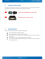
1
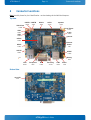
KTT20/pITX KTD-S0044-G The pulse of innovation User Information Table of Contents » Table of Contents « 1 User Information .....................................................................................1 1.1 About This Document ................................................................................................................. 1 1.2 Copyright Notice ....................................................................................................................... 1 1.3 Trademarks .............................................................................................................................. 1 1.4 Standards ................................................................................................................................ 1 1.5 Warranty.................................................................................................................................. 1 1.6 Life Support Policy..................................................................................................................... 2 1.7 Technical Support...................................................................................................................... 2 2 Introduction ...........................................................................................3 2.1 pITX Embedded Line Family ......................................................................................................... 3 2.2 KTT20/pITX Overview.................................................................................................................. 3 3 Specifications .........................................................................................4 3.1 Functional Specifications ............................................................................................................ 4 3.2 Block Diagram........................................................................................................................... 6 3.3 Mechanical Specifications ........................................................................................................... 7 3.4 Electrical Specifications .............................................................................................................. 7 3.5 Real-Time Clock Battery .............................................................................................................. 8 3.6 Environmental Specifications....................................................................................................... 8 3.7 MTBF....................................................................................................................................... 9 4 Equipment Design Rule ........................................................................... 10 5 Getting Started...................................................................................... 10 6 Connector Locations ............................................................................... 11 6.1 I/O Connector Definitions ......................................................................................................... 12 7 Graphics Processing Unit ......................................................................... 13 7.1 DVI-I® Connector..................................................................................................................... 13 7.2 LVDS Flat Panel Connector......................................................................................................... 14 7.3 Connecting a Flat Panel ............................................................................................................ 15 7.4 Flat Panel Power Jumper ........................................................................................................... 15 7.5 Backlight ............................................................................................................................... 16 7.5.1 7.5.2 7.5.3 Power Connector Backlight Pins ..................................................................................................................16 LVDS Connector Backlight Pins....................................................................................................................17 External Backlight Voltage Parameter...........................................................................................................17 KTT20/pITX User's Guide User Information Table of Contents 8 USB Interface........................................................................................ 18 8.1 Standard Connector ................................................................................................................. 18 8.2 Extension Connectors............................................................................................................... 18 8.3 Limitations............................................................................................................................. 19 8.4 USB Client Interface................................................................................................................. 19 9 LAN Controller....................................................................................... 20 9.1 Connector .............................................................................................................................. 20 10 Serial Interface...................................................................................... 21 10.1 Connector .............................................................................................................................. 21 10.2 Serial Console ......................................................................................................................... 21 11 Audio Interface ..................................................................................... 22 11.1 Audio Hardware Features .......................................................................................................... 22 11.2 Analog Connector .................................................................................................................... 22 11.3 Digital Connector (S/PDIF) ........................................................................................................ 22 11.4 Speaker Connector................................................................................................................... 23 11.4.1 Speaker Hardware Features ........................................................................................................................23 12 Secure Digital and Multimedia Card............................................................ 24 12.1 Connector .............................................................................................................................. 24 13 PCI Express® Interface............................................................................. 25 13.1 Connector .............................................................................................................................. 25 14 Digital I/O Interface ............................................................................... 27 14.1 Multifunction Overview ............................................................................................................. 27 14.2 Electrical Specifications ............................................................................................................ 28 14.3 Connector 1............................................................................................................................ 29 14.4 Connector 2............................................................................................................................ 30 15 Power Supply ........................................................................................ 32 15.1 DC Power Connector ................................................................................................................. 32 15.2 External Power Connector ......................................................................................................... 32 15.3 Default Power Configuration ...................................................................................................... 33 15.4 Power Front Panel Header ......................................................................................................... 34 15.4.1 Power LED ...............................................................................................................................................34 15.5 Onboard Status LEDs ................................................................................................................ 35 15.6 Real-Time Clock Battery Connector.............................................................................................. 35 16 Crisis Management or Custom Firmware ...................................................... 36 KTT20/pITX User's Guide User Information Table of Contents Appendix A: System Resources ............................................................................ 38 A.1 Memory Area .......................................................................................................................... 38 A.2 I2CTM Bus ................................................................................................................................ 38 Appendix B: Mechanical Dimensions .................................................................... 39 Appendix C: Connector Overview.......................................................................... 40 C.1 Mating Connectors................................................................................................................... 40 C.2 Pinout Tables.......................................................................................................................... 41 Appendix D: Reference Documents....................................................................... 44 Appendix E: Certifications .................................................................................. 45 Appendix F: Document Revision History ................................................................ 48 KTT20/pITX User's Guide KTD-S0044-G Page 1 1 User Information 1.1 About This Document User Information This document provides information about products from KONTRON Technology A/S and/or its subsidiaries. No warranty of suitability, purpose or fitness is implied. While every attempt has been made to ensure that the information in this document is accurate the information contained within is supplied “as-is” - no liability is taken for any inaccuracies. Manual is subject to change without prior notice. KONTRON assumes no responsibility for the circuits, descriptions and tables indicated as far as patents or other rights of third parties are concerned. 1.2 Copyright Notice Copyright © 2012 - 2013, KONTRON Technology A/S, ALL RIGHTS RESERVED. No part of this document may be reproduced or transmitted in any form or by any means, electronically or mechanically, for any purpose without the express written permission of KONTRON Technology A/S. 1.3 Trademarks Brand and product names are trademarks or registered trademarks of their respective owners. 1.4 Standards KONTRON Technology A/S is certified to ISO 9000 standards. 1.5 Warranty This product is warranted against defects in material and workmanship for the warranty period from the date of shipment. During the warranty period KONTRON Technology A/S will at its discretion decide to repair or replace defective products. Within the warranty period the repair of products is free of charge as long as warranty conditions are observed. The warranty does not apply to defects resulting from improper or inadequate maintenance or handling by the buyer, unauthorized modification or misuse, operation outside of the product’s environmental specifications or improper installation or maintenance. KONTRON Technology A/S will not be responsible for any defects or damages to third party products that are caused by a faulty KONTRON Technology A/S product. KTT20/pITX User's Guide KTD-S0044-G 1.6 Page 2 User Information Life Support Policy KONTRON Technology's products are not for use as critical components in life support devices or systems without express written approval of the general manager of KONTRON Technology A/S. As used herein: Life support devices or systems are devices or systems which a) are intended for surgical implant into body or b) support or sustain life and whose failure to perform, when properly used in accordance with instructions for use provided in the labelling, can be reasonably expected to result in significant injury to the user. A critical component is any component of a life support device or system whose failure to perform can be reasonably expected to cause the failure of the life support device or system or to affect its safety or effectiveness. 1.7 Technical Support Please consult our web site at http://www.kontron.com/support for the latest product documentation, utilities, drivers and support contacts or use the special e-mail address [email protected] for a technical problem. In any case you can always contact your board supplier for technical support. Before contacting support please be prepared to provide as much information as possible: Board identification: S Type S Part number (find PN on label) S Serial number (find SN on label) System environment: S O/S type and version S Driver origin and version S Attached hardware (drives, USB devices, LCD panels ...) KTT20/pITX User's Guide KTD-S0044-G Page 3 2 Introduction 2.1 pITX Embedded Line Family Introduction Each pITX is a member of the 2.5" SBC family of KONTRON Technology A/S based on the Pico-ITXTM specification (only mechanical outer dimensions) from the Small Form Factor Special Interest Group (SFF-SIG). pITX embedded line modules are characterized by the same front-line pinouts and interfaces for reset logic and simple power supply, 2 x USB, LAN, Audio, GPIOs, DVI® and LVDS interface. These embedded line family features allow to use of the same chassis over the whole product line and maximize design reuse. These homogeneous features facilitate easy upgrades within the pITX embedded line product family. 2.2 KTT20/pITX Overview Please refer to the following matrix to choose the product that suits your needs best. Article Number SDRAM Size NAND Flash LVDS Interface 03004-0505-10-0 512 MByte 03004-1005-10-0 1 GByte KTT20/pITX User's Guide KTD-S0044-G Page 4 3 Specifications 3.1 Functional Specifications Specifications System on Chip (SoC): NVIDIA® Tegra® 250 S S S S S S S S S S S S S Dual Cortex-A9 multi-processing ARM® cores up to 900 MHz core frequency ARMv7 instruction set 32 kB data and 32 kB instruction L1 cache per core Shared 1 MB L2 cache DDR2 memory interface up to DDR2-667 with maximum size of 1 GB NAND flash controller with 8/16 bit data interface One SPITM flash controller Three USB ports (EHCI) with one client interface (only two ports available) Audio-Video Processor (AVP, GeForce® GPU) with a dual display controller Integrated audio controller (AC'97 and Inter-IC Sound, called IIS or I2S) One Secure Digital / MultiMedia Card (SD/MMC) controller with four instances Some pins are useable as GPIOs (max. 24 x 3.3V and 16 x 1.8V GPIOs) or as special function pins (e.g. keyboard functionality) Five UARTs with 16450/550 compatible mode (only three UARTs available) Onchip NAND Flash Controller S S Supports PIO and DMA mode access Programmable error correction capability Onchip SPITM Flash Controller S S Supports FIFO and DMA mode access Maximum transfer rate of 52 Mbits/s Onchip Universal Serial Bus (USB) S S S All ports are capable to handle USB 2.0 (EHCI) One port supports only USB client functionality Supports USB 1.1 low and full speed devices without a companion USB 1.1 host controller KTT20/pITX User's Guide KTD-S0044-G Page 5 Specifications Onchip Graphics Processing Unit (GPU) S S S S S S S Ultra low power GPU up to 333 MHz internal clock and 8 cores Two independent display controllers support 2D/3D graphics rendering 720p Video Encode Processor to deliver HD video streams OpenGL® ES 2.0 support DVI® interface (max. 1920x1080 pixel) Low Voltage Differential Signaling (LVDS) flatpanel interface supports 18/24 bit color depth with a maximal resolution of 1680x1050 pixel (only single channel possible) Full hardware acceleration of following video decode standards: H.264, MPEG4 and VC1 Onchip Audio Subsystem S S Codec interface realize the Inter-IC Sound (I2S) specification The audio codec supports a maximal resolution of 24 bit with 96 kHz sample rate Onchip SD/MMC Controller S S S S S S S Only 4 bit data bus width Supports FIFO and DMA mode access Supports SDMEM/SDIO specification V2.0 up to 50/25 MHz interface speed Supports MMC specification V4.3 up to 52 MHz interface speed Supports CE-ATA Digital Protocol specification V1.1 up to 52 MHz interface speed Supports eSD specification V2.1 Supports e.MMC devices Fast Ethernet (USB connection): SMSC® LAN9514 S S S Fully compliant with IEEE802.3®/802.3u® Supports 10BASE-T and 100BASE-TX Full and half duplex mode with flow control USB Hub (USB connection): SMSC® LAN9514 S S Four additional USB 2.0 (EHCI) ports Supports USB 1.1 low and full speed devices Temperature Monitoring (I2CTM connection): ADT7461A S One onchip thermal sensor and one remote temperature sensor (SoC) KTT20/pITX User's Guide KTD-S0044-G 3.2 Page 6 Specifications Block Diagram KTT20/pITX Temp. Sensor ADT7461 EEPROM PMU 24C08 TPS658621 CMOS Battery J600 RTC J1600 J1700 J1401 DVI_ LVDS Transmitter I2C Controller Graphic Controller SD/MMC Controller SDRAM Controller 512 MB / 1 GB DDR2SDRAM NAND Flash Controller 512 MByte NAND Flash SPI Flash Controller 4 MByte SPI Flash SN75LVDS83 SoC J2001 J1300 NVIDIA Tegra 250 GPIOs + I2C + SPI + SDIO 3.3 V 1.8 V GPIOs or Keyboard Audio Controller J1800 J1801 J1802 UARTs PCI Express Port Audio Codec WM8903 USB Controller Client Port J1900 Dual Port J2301 USB Hub 2 x RS232 Transceiver TRS3253 2 x Speaker Driver WM9001 USB Hub / LAN SMSC LAN9514 J2302 Fast Ethernet J2303 S/PDIF J2300 USB PCI Express J2202 J2201 J2200 KTT20/pITX User's Guide J2100 KTD-S0044-G 3.3 Page 7 Specifications Mechanical Specifications Dimensions 3.4 ³ Pico-ITXTM form factor 100 x 72 mm ±0.2 mm (complete with all connectors 100 x 79 mm) ³ Height approx. 23 mm Electrical Specifications Supply Voltage ³ 5V DC ± 5% Supply Voltage Ripple ³ Maximum 100mV peak to peak 0 – 20 MHz Supply Current (Linux®) The power consumption test uses a tool to stress the CPU (100% load) and at the same time another tool to generate a high graphic throughput. The boards were tested with a DVI® monitor (SXGA resolution), USB keyboard & mouse and a 16 GByte USB key as boot device. Variant: 512 MB SDRAM Full Load Idle Variant: 1 GB SDRAM Deep Sleep Full Load Idle Deep Sleep [A] [W] [A] [W] [A] [W] [A] [W] [A] [W] [A] [W] tbd. tbd. tbd. tbd. tbd. tbd. tbd. tbd. 0.31 3.72 0.07 0.85 KTT20/pITX User's Guide KTD-S0044-G 3.5 Page 8 Specifications Real-Time Clock Battery ³ Voltage range: +2.4V - +3.6V (typ. +3.0V) ³ Typical current: 5μA @ +3.0V Lithium battery precautions CAUTION! VORSICHT! Danger of explosion if battery is incorrectly replaced. Replace only with same or equivalent type recommended by manufacturer. Dispose of used batteries according to the manufacturer’s instructions. Explosionsgefahr bei unsachgemäßem Austausch der Batterie. Ersatz nur durch den selben oder einen vom Hersteller empfohlenen gleichwertigen Typ. Entsorgung gebrauchter Batterien nach Angaben des Herstellers. ATTENTION! PRECAUCION! Risque d'explosion avec l'échange inadéquat de la batterie. Remplacement seulement par le même ou un type équivalent recommandé par le producteur. L'évacuation des batteries usagées conformément à des indications du fabricant. Peligro de explosión si la batería se sustituye incorrectamente. Sustituya solamente por el mismo o tipo equivalente recomendado por el fabricante. Disponga las baterías usadas según las instrucciones del fabricante. ADVARSEL! ADVARSEL! Lithiumbatteri – Eksplosionsfare ved fejlagtig håndtering. Udskiftning må kun ske med batteri af samme fabrikat og type. Levér det brugte batteri tilbage til leverandøren. Eksplosjonsfare ved feilaktig skifte av batteri. Benytt samme batteritype eller en tilsvarende type anbefalt av apparatfabrikanten. Brukte batterier kasseres i henhold til fabrikantens instruksjoner. VARNING! VAROITUS! Explosionsfara vid felaktigt batteribyte. Använd samma batterityp eller en ekvivalent typ som rekommenderas av apparattillverkaren. Kassera använt batteri enligt fabrikantens instruktion. Paristo voi räjähtää, jos se on virheellisesti asennettu. Vaihda paristo ainoastaan laltevalmistajan suosittelemaan tyyppiln. Hävitä käytetty paristo valmistajan ohjeiden mukaisesti. 3.6 Environmental Specifications Temperature Operating (with original KONTRON heat-sink): ³ 1) Ambient temperature: 0 to +60°C Ambient temperature: -40 to +85°C Non operating: ³ Note: 1) It is the customer's responsibility to provide sufficient airflow around each of the components to keep them within the allowed temperature range. KTT20/pITX User's Guide KTD-S0044-G Page 9 Specifications Humidity ³ Operating: 10% to 90% (non condensing) ³ Non operating: 5% to 95% (non condensing) Restriction of Hazardous Substances (RoHS) All boards in the pITX embedded line product family are RoHS compliant. 3.7 MTBF The following MTBF (Mean Time Between Failure) values were calculated using a combination of manufacturer’s test data, if the data was available, and a Bellcore calculation for the remaining parts. The Bellcore calculation used is 'method 1 case 1'. In that particular method the components are assumed to be operating at a 50% stress level in a 40°C ambient environment and the system is assumed to have not been burned in. Manufacturer’s data has been used wherever possible. The manufacturer’s data, when used, is specified at 50°C, so in that sense the following results are slightly conservative. The MTBF values shown below are for a 40°C in an office or telecommunications environment. Higher temperatures and other environmental stresses (extreme altitude, vibration, salt water exposure, etc.) cause lower MTBF values. ³ Note: System MTBF (hours): 243526 Fans usually shipped with KONTRON Technology A/S products have 50.000-hour typical operating life. The above estimation assumes no fan but a passive heat sinking arrangement. Estimated RTC battery life (as opposed to battery failures) is not included in the MTBF calculation. The RTC battery lifetime has to be considered separately. Battery life depends on both temperature and operating conditions. When the KONTRON unit has external power; the only battery drain is from leakage paths. KTT20/pITX User's Guide KTD-S0044-G 4 Page 10 Equipment Design Rule Equipment Design Rule If you want to change software features, repair a corrupted bootloader or for service purposes analyze the operating system serial output you should provide the following two interfaces: Serial interface UARTC/UART3 on connector J2202 USB client interface on connector J1900 5 Getting Started Getting started with the KTT20/pITX is easy. Take the following steps: Connect a DVI® monitor to the DVI® connector. Plug a keyboard and/or mouse to the USB connector(s). Attach a microSDTM card or a USB key to the corresponding connector, e.g. with a Linux® operating system. Connect the power supply to the KTT20/pITX power supply connector. Turn on the board by shortening the power button pins on power front panel header (J900) for minimal two seconds. KTT20/pITX User's Guide KTD-S0044-G 6 Page 11 Connector Locations Connector Locations Note: Use this picture for pin 1 identification - not the drawings in the individual chapters. Top View UARTA UARTB J2200 J2201 GPIO2 LVDS Speaker J2001 J1700 J1801 USB Client J1900 Panel Power USB J1701 J2303 Audio USB J1800 J2302 optional mPCIe J2100 GPIO1 External Power J1300 J401 UARTC S/PDIF J2202 J1802 Battery Pin 1 J600 LAN Frontpanel DVI Recovery USB Power J2300 J900 J1600 J1400 J2301 J400 Bottom View microSD J1401 KTT20/pITX User's Guide KTD-S0044-G 6.1 Page 12 Connector Locations I/O Connector Definitions The following sections provide pin definitions and detailed description of all onboard connectors. The connector definitions use the following notation: Column Name Description Pin Shows the pin numbers in the connector. Signal The mnemonic name of the signal at the current pin. The notation “#” states that the signal is active low. Type AI: Analogue Input AO: Analogue Output I: Digital Input IO: Digital Input / Output IOD: Input / Open-Drain output O: Digital Output OD: Output, open-Drain DSO: Differential Signaling Output with complementary signals on two paired wires DSI: Differential Signaling Input with complementary signals on two paired wires DSIO: Differential Signaling Input / Output (combined DSO and DSI) PWR: PoWeR supply or ground reference pins NC: Not Connected Additional notations: Ioh/Iol -50 +5.0V signal voltage level, e.g. I-50 -33 +3.3V signal voltage level, e.g. O-33 -18 +1.8V signal voltage level, e.g. IO-18 Ioh: Typical current in mA flowing out of an output pin through a grounded load while the output voltage has high level. Iol: Typical current in mA flowing into an output pin from a VCC connected load while the output voltage has low level. The abbreviation tbd. is used for specifications which are not available yet or which are not sufficiently specified by the component vendors. KTT20/pITX User's Guide KTD-S0044-G 7 Page 13 Graphics Processing Unit Graphics Processing Unit The graphics accelerator supports a HDMI®/DVI® interface with Full HD resolution and a variety of LCD panels with single clock, color depths of 18/24 bit and resolutions up to WSXGA. 7.1 DVI-I® Connector The DVI® interface is available through the standard 29 pin DVI-I® connector J1600. Header 17 Note: 9 1 C3 C1 C4 C2 Pin Signal Description Type 1 TMDS2- TMDS data 2 (negative) DSO-33 2 TMDS2+ TMDS data 2 (positive) DSO-33 3 GND Ground PWR 4 N.C. Not connected NC 5 N.C. Not connected NC 6 DDC_CLK DDC clock IO-50 7 DDC_DATA DDC data IO-50 8 N.C. Not connected NC 9 TMDS1- TMDS data 1 (negative) DSO-33 10 TMDS1+ TMDS data 1 (positive) DSO-33 11 GND Ground PWR 12 N.C. Not connected NC 13 N.C. Not connected NC 14 VCC5 1) Power +5V PWR 15 GND Ground PWR 16 TMDS_HPD Hotplug detect I-50 17 TMDS0- TMDS data 0 (negative) DSO-33 18 TMDS0+ TMDS data 0 (positive) DSO-33 19 GND Ground PWR 20 N.C. Not connected NC 21 N.C. Not connected NC 22 GND Ground PWR 23 TMDS_CLK+ TMDS clock (positive) DSO-33 24 TMDS_CLK- TMDS clock (negative) DSO-33 C1 N.C. Not connected NC C2 N.C. Not connected NC C3 N.C. Not connected NC C4 N.C. Not connected NC C5 GND Ground PWR 1) To protect the external power lines of peripheral devices make sure that - the wires have the right diameter to withstand the maximum available current. - to enclosure of the peripheral device fulfills the fire-protecting conditions of IEC/EN 60950. KTT20/pITX User's Guide KTD-S0044-G 7.2 Page 14 Graphics Processing Unit LVDS Flat Panel Connector The J1700 connector (40 pins) provides the LVDS interface for flat panels on the top side of the board. A prototype cable with open ends is available (part number 821515). Header Pin Signal Description Type 1-5 VDD 1) Backlight voltage PWR 6 GND Ground PWR 7 VCC5 1) Power +5V PWR 8 GND Ground PWR 9 PANELVCC 1) Panel power +3.3V or +5V PWR 10 PANELVCC 1) Panel power +3.3V or +5V PWR 11 - 12 N.C. Not connected NC 13 BKLTADJ Brightness control (0V to +5V) AO 14 VCCENA Panel power enable (PANELVCC signal) O-33/O-50 15 BKLTON Backlight on/off O-50 16 GND Ground PWR 17 FTX0- First channel data 0 output (negative) DSO-33 18 FTX0+ First channel data 0 output (positive) DSO-33 19 FTX1- First channel data 1 output (negative) DSO-33 20 FTX1+ First channel data 1 output (positive) DSO-33 21 FTX2- First channel data 2 output (negative) DSO-33 22 FTX2+ First channel data 2 output (positive) DSO-33 23 FTXC- First channel clock output (negative) DSO-33 24 FTXC+ First channel clock output (positive) DSO-33 25 FTX3- First channel data 3 output (negative) DSO-33 26 FTX3+ First channel data 3 output (positive) DSO-33 27 - 28 GND Ground PWR 29 - 32 N.C. Not connected NC 33 PANELVCC 1) Panel power +3.3V or +5V PWR 34 VCC5 1) Power +5V PWR SPICLK TM SPI clock signal O-18 SPISDO TM O-18 35 36 37 SPISDI SPI serial data output TM SPI serial data input TM I-18 38 SPICS# SPI chip select O-18 39 - 40 GND Ground PWR KTT20/pITX User's Guide KTD-S0044-G Note: Graphics Processing Unit 1) To protect the external power lines of peripheral devices make sure that - the wires have the right diameter to withstand the maximum available current. - to enclosure of the peripheral device fulfills the fire-protecting conditions of IEC/EN 60950. Warning: 7.3 Check jumper J1701 (Panel Power) for correct settings for your panel – not doing so might cause permanent damage to your panel. Connecting a Flat Panel 7.4 Page 15 Check if you have the correct panel cable. Inspect the cable for damages. Disconnect the power from your system. Check jumper J1701 for correct panel voltage (Pos. 1-2 = +3.3V 2-3 = +5V). Connect an external power supply for the correct backlight voltage (except the power supply complies with the backlight voltage). Connect the cable to the flat panel connector J1700 on the KTT20/pITX and connect the other end to your display. Switch on the power supply and activate/save the desired settings with help of the U-Boot bootloader (for further details see the 'Software Guide' chapter 'U-Boot Setup'). Switch off the power supply. Switch on the power supply. If you only see a blank screen contact your distributor for technical support. Flat Panel Power Jumper J1701 KTT20/pITX User's Guide KTD-S0044-G 7.5 Page 16 Graphics Processing Unit Backlight Backlight is available through the connector J1700. The backlight voltage can be supplied from the onboard +5V voltage if you set one or two short circuit jumper on connector J401. For backlight voltages differing from +5V use pin 9 and/or 11 on connector J401 to supply the backlight (pins 7 and 8 represent the associated ground, identical with board ground). 7.5.1 Power Connector Backlight Pins The following table is an extract of the J401 connector overview. For further details about pin 1 see chapter 'Default Power Configuration'. Pin Signal Description Type 9 VDD 1) External backlight voltage input PWR IN 10 VCC5 1) Onboard power +5V PWR 11 VDD 1) External backlight voltage input PWR IN 12 VCC5 1) Onboard power +5V PWR 7 GND Backlight ground PWR 8 GND Backlight ground PWR External Backlight Power Supply Onboard +5V backlight voltage (with short circuit jumper) 2 2 1 1 20 OR 19 20 19 + System Backlight -- GND Backlight Voltage Top view CAUTION! If you use an external backlight power supply do not forget the three System links (pin 13 to 18) otherwise the board does not start. KTT20/pITX User's Guide KTD-S0044-G 7.5.2 Page 17 Graphics Processing Unit LVDS Connector Backlight Pins The following table is an extract of the J1700 connector overview. Note: Pin Signal Description Type 1-5 VDD 1) Normal backlight voltage PWR 6 and 8 GND Ground PWR 1) To protect the external power lines of peripheral devices make sure that - the wires have the right diameter to withstand the maximum available current. - to enclosure of the peripheral device fulfills the fire-protecting conditions of IEC/EN 60950. 7.5.3 External Backlight Voltage Parameter Parameter Min. Typ. Max. Backlight voltage +5.0 +12.0 +15.0 V tbd. A 0.5 A Continuous current fixed power +5V Continuous current per pin on connector J401 KTT20/pITX User's Guide Units KTD-S0044-G 8 Page 18 USB Interface USB Interface The USB interface comes with five USB ports which follow the EHCI specification (USB 2.0 compliant). You can expand the amount of USB connections by adding external hubs. Two ports are available on a standard connector and more ports on three extension connectors. All ports support USB 1.1 low and full speed devices without a companion USB 1.1 host controller. 8.1 Standard Connector Two USB ports are available through the standard USB connector J2301 (8 pins). Header 1 5 8.2 Pin Signal Description Type 1 VCC5 1) Power +5V PWR 2 USB0- USB port 0 (negative) DSIO-33 3 USB0+ USB port 0 (positive) DSIO-33 4 GND Ground PWR 5 VCC5 1) Power +5V PWR 6 USB1- USB port 1 (negative) DSIO-33 7 USB1+ USB port 1 (positive) DSIO-33 8 GND Ground PWR Extension Connectors The other USB ports are available through the extension connectors J1900, J2302 and J2303 (4 pins). If you want a standard USB interface connector an adapter cable is required (KAB-USB-2, part number 96054-0000-00-2). Important: The connector J1900 provides only the USB client functionality. Header Note: Pin Signal Description Type 1 GND Ground PWR 2 USBn+ USB port n (positive) DSIO-33 3 USBn- USB port n (negative) DSIO-33 4 VCC5 1) Power +5V PWR 1) To protect the external power lines of peripheral devices make sure that - the wires have the right diameter to withstand the maximum available current. - to enclosure of the peripheral device fulfills the fire-protecting conditions of IEC/EN 60950. KTT20/pITX User's Guide KTD-S0044-G 8.3 Page 19 USB Interface Limitations The contacts for USB devices are protected and suitable to supply USB devices with a maximum input current of 500mA. Do not supply external USB devices with higher power dissipation through these pins. 8.4 USB Client Interface The connector J1900 provides the client interface. You need the client functionality for changing the bootloader or update a corrupted bootloader. Together with the recovery pin (see chapter 'Crisis Management') and dedicated software on a desktop computer as well as a standard USB cable (both ends with Type-A connector) and a special KONTRON USB adapter cable (KAB-USB-2, part number 96054-0000-00-2) the upload is easy. KAB-USB-2 Typical Configuration KTT20/pITX User's Guide KTD-S0044-G 9 Page 20 LAN Controller LAN Controller The KTT20/pITX uses a SMSC® LAN9514 Fast Ethernet LAN controller which supports 10/100 Base-T interfaces. The controller auto-negotiates the management of a 10 or 100 Mbps connection. Additionally you can boot up the board via a network connection from a PXE server. 9.1 Connector The LAN interface is available through the standard RJ45 connector J2300 (8 pins). Header 1 Pin Signal Description Type 1 TXD+ 10/100 transmit (positive) DSO 2 TXD- 10/100 transmit (negative) DSO 3 RXD+ 10/100 receive (positive) DSI 4 GND Ground (shield) PWR 5 GND Ground (shield) PWR 6 RXD- 10/100 receive (negative) DSI 7 GND Ground (shield) PWR 8 GND Ground (shield) PWR KTT20/pITX User's Guide KTD-S0044-G 10 Page 21 Serial Interface Serial Interface Three serial ports provide asynchronous serial communication with RS-232 interfaces. They are 16450/ 16550 UART compatible and support 16-byte FIFO buffers for transfer rates from 50 Baud to 115.2 kBaud. Following the connector assignment: J2200 J2201 J2202 10.1 UARTA/UART1 UARTB/UART2 UARTC/UART3 x x x Connector The serial ports are available through the connectors J2200, J2201 and J2202 (5 pins). Header 10.2 Pin Signal Description Type 1 TXD Transmit serial data O 2 RXD Receive serial data I 3 RTS# Request to send O 4 CTS# Clear to send I 5 GND Ground (shield) PWR Serial Console Most operating systems have a defined serial console. The KTT20/pITX uses the third serial port (UARTC/ UART3) on connector J2202 for this purpose. Normally the serial console needs only three signal lines (TXD, RXD and GND). The serial port is assigned to the environment variables stdin, stdout and stderr. If you use U-Boot as bootloader you can interact with U-Boot via a USB keyboard and a standard terminal program on a desktop computer. The following overview shows the default serial settings: S S S S Baudrate Data bits Stop bits Parity 115 kBaud 8 1 No KTT20/pITX User's Guide KTD-S0044-G 11 Page 22 Audio Interface Audio Interface The SoC supports an Inter-IC Sound (I2S) codec with 24 bit resolution and 96 kHz sample rate (the maximum rate of 96 kHz only unidirectional). The analogue-to-digital part of the codec uses 24 bit, 128x oversampled sigma-delta ADCs. The digital-to-analogue part contains two 24 bit sigma-delta DACs. The interface includes LINE OUT, LINE IN, MICROPHONE IN and a digital S/PDIF output. 11.1 11.2 Audio Hardware Features Parameter Values Units Output resolution (LINE OUT, S/PDIF) 16/20/24 bit Output sample rate (LINE OUT, S/PDIF) 44.1/48/96 kHz Output signal-to-noise ratio (LINE OUT) 96 dB Input resolution (LINE IN) 16/20/24 bit Input sample rate (LINE IN) 44.1/48/96 kHz Input signal-to-noise ratio (LINE IN) 92 dB Analog Connector The analog audio interface uses the connector J1800 (6 pins). A prototype adapter cable (open ended) is deliverable (KAB-SOUND-CMP-2, part number 96063-0000-00-1). Header 11.3 Pin Signal Description Type 1 LINE_IN_L Line input left AI 2 MIC_IN Microphone input AI 3 LINE_IN_R Line input right AI 4 LINE_OUT_L Line output left AO 5 GND Ground PWR 6 LINE_OUT_R Line output right AO Digital Connector (S/PDIF) The digital audio output is available through the connector J1802 (2 pins). Header 1 Pin Signal Description Type 1 SPDIF_OUT S/PDIF output O-33 2 GND Ground PWR KTT20/pITX User's Guide KTD-S0044-G 11.4 Page 23 Audio Interface Speaker Connector The audio codec also supports a speaker driver interface. With both speaker drivers it is possible to realize a passive stereo loudspeaker system. The drivers have a thermal shutdown feature. If the junction temperature exceeds approximately 1500C then the output will be disabled. The speaker interface is available through the connector J1801 (4 pins). Header 11.4.1 Pin Signal Description Type 1 SPK_R# Speaker right (negative) AO 2 SPK_R Speaker right (positive) AO 3 SPK_L# Speaker left (negative) AO 4 SPK_L Speaker left (positive) AO Speaker Hardware Features Parameter Values Units Maximal output power 1 @ 8Ω W Output signal-to-noise ratio 97 db Speaker mode Class D KTT20/pITX User's Guide KTD-S0044-G 12 Page 24 Secure Digital and Multimedia Card Secure Digital and Multimedia Card The SD/MMC interface uses only a microSDTM card socket. The controller supports the SD specification revision 2.0 (implies the SDSC and SDHC families) and the MMC specification revision 4.3. The data bus width accounts four bits, the SD transfer rate can be up to 50 MHz and MMC rate up to 52 MHz. 12.1 Connector The microSDTM card socket is named J1401 (8 pins). Header 1 Note: Pin Signal Description Type 1 DATA2 Data bit 2 IO-33 2 CD / DATA3 Card detect / Data bit 3 IO-33 3 CMD Command line IO-33 4 VCC3 1) Power +3.3V PWR 5 CLK Clock O-33 6 GND Ground PWR 7 DATA0 Data bit 0 IO-33 8 DATA1 Data bit 1 IO-33 1) To protect the external power lines of peripheral devices make sure that - the wires have the right diameter to withstand the maximum available current. - to enclosure of the peripheral device fulfills the fire-protecting conditions of IEC/EN 60950. KTT20/pITX User's Guide KTD-S0044-G 13 Page 25 PCI Express® Interface PCI Express® Interface NVIDIAs® Tegra® 250 supports the PCI Express® specification 1.1 with 2.5 GT/s (GigaTransfers/s - identical with Gigabits/s by one lane). One port with one lane is provided for free usage. KONTRON Technology A/S cannot guarantee that all available cards on the market function smoothly. 13.1 Connector The mini PCI Express® port is available through the connector J2100 (52 pins). Header Pin Description Type Pin Signal Description Type Power +3.3V PWR 1 WAKE# Wake event I-33 2 VCC3 1) 3 N.C. Not connected NC 4 GND Ground PWR NC 6 VCC1 1) Power +1.5V PWR PCIe clock request I-33 8 N.C. Not connected NC Ground 5 N.C. 7 CLKREQ# 9 GND 11 1 Signal PE_CLK- Not connected ® PWR 10 N.C. Not connected NC ® DSO 12 N.C. Not connected NC ® PCIe clock (neg.) 13 PE_CLK+ PCIe clock (pos.) DSO 14 N.C. Not connected NC 15 GND Ground PWR 16 N.C. Not connected NC 17 N.C. Not connected NC 18 GND Ground PWR 19 N.C. Not connected NC 20 W_DISABLE# Wireless disable O-33 21 GND Ground PWR 22 PE_RST# PCIe® reset O-33 ® PCIe receive (neg.) DSI 24 VCC3 1) Power +3.3V PWR ® 23 PE_RX- 25 PE_RX+ PCIe receive (pos.) DSI 26 GND Ground PWR 27 GND Ground PWR 28 VCC1 1) Power +1.5V PWR 29 31 GND PE_TX- Ground PWR 30 I2C_CLK 2 TM O-33 2 TM I C clock ® DSO 32 I2C_DATA I C data IO-33 ® PCIe transmit (neg.) 33 PE_TX+ PCIe transmit (pos.) DSO 34 GND Ground PWR 35 GND Ground PWR 36 USB- USB port (neg.) DSIO-33 37 GND Ground PWR 38 USB+ USB port (pos.) DSIO-33 39 VCC3 1) Power +3.3V PWR 40 GND Ground PWR 41 VCC3 1) Power +3.3V PWR 42 N.C. Not connected NC 43 GND Ground PWR 44 N.C. Not connected NC 45 N.C. Not connected NC 46 N.C. Not connected NC 47 N.C. Not connected NC 48 VCC1 1) Power +1.5V PWR 49 N.C. Not connected NC 50 GND Ground PWR 51 N.C. Not connected NC 52 VCC3 1) Power +3.3V PWR KTT20/pITX User's Guide KTD-S0044-G Note: Page 26 PCI Express® Interface 1) To protect the external power lines of peripheral devices make sure that - the wires have the right diameter to withstand the maximum available current. - to enclosure of the peripheral device fulfills the fire-protecting conditions of IEC/EN 60950. CAUTION! ® The PCI Express USB port uses the same lines as the standard USB port on the external connector J2303. Do not use both ports at the same time. KTT20/pITX User's Guide KTD-S0044-G 14 Page 27 Digital I/O Interface Digital I/O Interface The digital I/O interface is a subset of a multifunction part from NVIDIAs® Tegra® 250 SoC. Most of the I/O pins have additional functionalities which can be changed by software using two I/O connectors with different signal voltages. 14.1 Multifunction Overview The following table informs about the dependencies. I/O Pin NVIDIA® Label Second Function Voltage Connector GPIO0 R.05 Keyboard row 5 1.8V J1300 GPIO1 R.06 Keyboard row 6 1.8V J1300 GPIO2 R.07 Keyboard row 7 1.8V J1300 GPIO3 S.00 Keyboard row 8 1.8V J1300 GPIO4 S.01 Keyboard row 9 1.8V J1300 GPIO5 S.02 Keyboard row 10 1.8V J1300 GPIO6 S.04 Keyboard row 12 1.8V J1300 GPIO7 S.05 Keyboard row 13 1.8V J1300 GPIO8 Q.00 Keyboard column 0 1.8V J1300 GPIO9 Q.01 Keyboard column 1 1.8V J1300 GPIO10 Q.02 Keyboard column 2 1.8V J1300 GPIO11 Q.03 Keyboard column 3 1.8V J1300 J1300 GPIO12 Q.04 Keyboard column 4 1.8V GPIO13 Q.05 Keyboard column 5 1.8V J1300 GPIO14 Q.06 Keyboard column 6 1.8V J1300 GPIO15 Q.07 Keyboard column 7 GPIO16 GPIO17 GPIO18 GPIO19 GPIO20 B.02 B.03 T.02 T.03 B.04 1.8V J1300 2 TM 3.3V J2001 2 TM 3.3V J2001 TM 3.3V J2001 TM 3.3V J2001 TM I C clock I C data SPI1 MOSI SPI1 MISO 3.3V J2001 TM SPI1 clock GPIO21 B.05 SPI1 chip select 3.3V J2001 GPIO22 T.04 --------- 3.3V J2001 GPIO23 D.05 SDIO2 command line 3.3V J2001 GPIO24 L.00 SDIO2 data 0 3.3V J2001 GPIO25 L.01 SDIO2 data 1 3.3V J2001 J2001 GPIO26 L.02 SDIO2 data 2 3.3V GPIO27 L.03 SDIO2 data 3 3.3V J2001 GPIO28 L.04 SDIO2 data 4 3.3V J2001 GPIO29 L.05 SDIO2 data 5 3.3V J2001 KTT20/pITX User's Guide KTD-S0044-G 14.2 Page 28 Digital I/O Interface GPIO30 D.06 --------- 3.3V J2001 GPIO31 D.07 --------- 3.3V J2001 GPIO32 T.00 SDIO2 clock 3.3V J2001 GPIO33 T.01 --------- 3.3V J2001 GPIO34 H.01 --------- 3.3V J2001 GPIO35 I.05 --------- 3.3V J2001 GPIO36 L.06 SDIO2 data 6 3.3V J2001 GPIO37 L.07 SDIO2 data 7 3.3V J2001 GPIO38 A.00 --------- 3.3V J2001 GPIO39 D.02 --------- 3.3V J2001 GPIO40 BB.01 --------- 3.3V J2001 GPIO41 J.07 --------- 3.3V J2001 Electrical Specifications Digital Inputs Parameter Min. Typ. Max. Units +0.4 V +2.3 V +0.8 V +3.8 V tbd. kHz Max. Units +0.3 V +1.8 V +0.5 V +3.3 V I/O Voltage 1.8V Input LOW voltage Input HIGH voltage +1.4 1.8 I/O Voltage 3.3V Input LOW voltage Input HIGH voltage +2.5 3.3 General Input rate (U-Boot) Digital Outputs Parameter Min. Typ. I/O Voltage 1.8V Output LOW voltage Output HIGH voltage +1.5 I/O Voltage 3.3V Output LOW voltage Output HIGH voltage +2.8 General Output LOW/HIGH current tbd. mA Switching rate (U-Boot) tbd. kHz KTT20/pITX User's Guide KTD-S0044-G 14.3 Page 29 Digital I/O Interface Connector 1 The digital I/O interface with I/O voltage 1.8V is available through the connector J1300 (20 pins). Header Pin Signal Description Type 1 VCC1 1) Power +1.8V PWR 2 VCC1 1) Power +1.8V PWR 3 GPIO0 I/O R.05 or keyboard row 5 IO-18 4 GPIO1 I/O R.06 or keyboard row 6 IO-18 5 GPIO2 I/O R.07 or keyboard row 7 IO-18 6 GPIO3 I/O S.00 or keyboard row 8 IO-18 7 GPIO4 I/O S.01 or keyboard row 9 IO-18 8 GPIO5 I/O S.02 or keyboard row 10 IO-18 9 GPIO6 I/O S.04 or keyboard row 12 IO-18 10 GPIO7 I/O S.05 or keyboard row 13 IO-18 11 GPIO8 I/O Q.00 or keyboard column 0 IO-18 12 GPIO9 I/O Q.01 or keyboard column 1 IO-18 13 GPIO10 I/O Q.02 or keyboard column 2 IO-18 14 GPIO11 I/O Q.03 or keyboard column 3 IO-18 15 GPIO12 I/O Q.04 or keyboard column 4 IO-18 16 GPIO13 I/O Q.05 or keyboard column 5 IO-18 17 GPIO14 I/O Q.06 or keyboard column 6 IO-18 18 GPIO15 I/O Q.07 or keyboard column 7 IO-18 19 GND Ground PWR 20 GND Ground PWR CAUTION! Do not use signal voltages above 1.8V. All I/O signals are unprotected against overvoltage. Note: 1) To protect the external power lines of peripheral devices make sure that - the wires have the right diameter to withstand the maximum available current. - to enclosure of the peripheral device fulfills the fire-protecting conditions of IEC/EN 60950. KTT20/pITX User's Guide KTD-S0044-G 14.4 Page 30 Digital I/O Interface Connector 2 The digital I/O interface with I/O voltage 3.3V uses the connector J2001 (40 pins). A prototype cable with open ends is available (part number 821515). Header Pin Signal Description Type 1-2 GND Ground PWR 2 TM 3 GPIO17 I/O B.03 or I C data IO-33 4 GPIO16 I/O B.02 or I2CTM clock IO-33 5-6 VCC3 1) Power +3.3V PWR 7 GPIO19 I/O T.03 or SPI1TM MISO IO-33 8 GPIO18 I/O T.02 or SPI1TM MOSI IO-33 9 GPIO20 TM I/O B.04 or SPI1 clock TM IO-33 10 GPIO21 I/O B.05 or SPI1 chip select IO-33 11 - 12 GND Ground PWR 13 GPIO23 I/O D.05 or SDIO2 command line IO-33 14 GPIO22 I/O T.04 IO-33 15 GPIO25 I/O L.01 or SDIO2 data 1 IO-33 16 GPIO24 I/O L.00 or SDIO2 data 0 IO-33 17 GPIO27 I/O L.03 or SDIO2 data 3 IO-33 18 GPIO26 I/O L.02 or SDIO2 data 2 IO-33 19 GPIO29 I/O L.05 or SDIO2 data 5 IO-33 20 GPIO28 I/O L.04 or SDIO2 data 4 IO-33 21 GPIO31 I/O D.07 IO-33 22 GPIO30 I/O D.06 IO-33 23 GPIO33 I/O T.01 IO-33 24 GPIO32 I/O T.00 or SDIO2 clock IO-33 25 - 26 VCC3 1) Power +3.3V PWR 27 - 28 GND Ground PWR 29 GPIO34 I/O H.01 IO-33 30 GPIO35 I/O I.05 IO-33 31 GPIO36 I/O L.06 or SDIO2 data 6 IO-33 32 GPIO39 I/O D.02 IO-33 33 GPIO37 I/O L.07 or SDIO2 data 7 IO-33 34 GPIO38 I/O A.00 IO-33 35 GPIO40 I/O BB.01 IO-33 36 GPIO41 I/O J.07 IO-33 37 - 38 VCC3 1) Power +3.3V PWR 39 - 40 GND Ground PWR KTT20/pITX User's Guide KTD-S0044-G Page 31 Digital I/O Interface CAUTION! Do not use signal voltages above 3.3V. All I/O signals are unprotected against overvoltage. Note: 1) To protect the external power lines of peripheral devices make sure that - the wires have the right diameter to withstand the maximum available current. - to enclosure of the peripheral device fulfills the fire-protecting conditions of IEC/EN 60950. Attention: The KONTRON Board Support Packages (BSPs) do not support most of the second functionality (e.g. keyboard input). KTT20/pITX User's Guide KTD-S0044-G 15 Page 32 Power Supply Power Supply The KTT20/pITX SBC has a power input voltage range from +4.75V to +5.25V DC. All other voltages are generated onboard (e.g. +3.3V / +1.8V system voltage). 15.1 DC Power Connector The power supply is injected through the connector J400 (3 pins, DC power jacket 2.1mm). Header 1 15.2 Pin Signal Description 1 VCC_IN 1) DC power supply input +5V 2 GND Ground 3 GND Ground External Power Connector The connector J401 (20 pins) can also be used to power the board instead of the round power jacket. In any case the green sections should be connected together (pin 13 with pin 14, pin 15 with pin 16 and pin 17 with pin 18). Header 2 1 Pin Signal Description Type 1 GND Ground PWR 2 GND Ground PWR 3 20 19 I2C_SDA 2 TM IO-50 2 TM I C data 4 I2C_SCL I C clock IO-50 5 RSVD Reserved for future use --- 6 RSVD Reserved for future use --- 7 GND Ground PWR 8 GND Ground PWR 9 VDD 1) External backlight voltage input PWR IN 10 VCC5 Onboard power +5V PWR 11 VDD 1) External backlight voltage input PWR IN 12 VCC5 Onboard power +5V PWR 13 VCC_IN 1) DC power supply input +5V PWR IN 14 VCC5 Onboard power +5V PWR 15 VCC_IN 1) DC power supply input +5V PWR IN 16 VCC5 Onboard power +5V PWR 17 VCC_IN 1) DC power supply input +5V PWR IN 18 VCC5 Onboard power +5V PWR 19 N.C. Not connected NC 20 N.C. Not connected NC KTT20/pITX User's Guide KTD-S0044-G Warning: Note: Page 33 Power Supply Do not overload the onboard system voltage +3.3V resp. 1.8V (microSDTM card socket, digital I/O connector). The maximum current should not exceed 250mA. 1) To protect the external power lines of peripheral devices make sure that - the wires have the right diameter to withstand the maximum available current. - to enclosure of the peripheral device fulfills the fire-protecting conditions of IEC/EN 60950. 15.3 Default Power Configuration In the delivery state the three short circuit jumpers are set (DC power jacket configuration). As far as possible all three pins should be used (each VCC_IN and VCC) to minimize the current load per pin. Top view DC Power Jacket Configuration External Power Supply Configuration (short circuit jumper needed) 2 2 1 1 OR 20 19 20 19 System Power Supply Input (only +5V) -- + VCC GND ATTENTION Pin 1 differs from normal position CAUTION! If you use an external power supply do not use another voltage then +5V DC. KTT20/pITX User's Guide KTD-S0044-G 15.4 Page 34 Power Supply Power Front Panel Header The power button and other power signals are available through the pin header J900 (10 pins). Header 1 9 Pin Signal Description Type 1 RST_BTN+ Reset button (positive) I-18 2 PWR_BTN+ Power button (positive) I-18 3 RST_BTN- Reset button (negative) = GND PWR 4 PWR_BTN- Power button (negative) = GND PWR 5 POWER_LED- Power LED (negative) = GND PWR 6 RSVD Reserved --- 7 POWER_LED+ Power LED (positive) O-33 / PWR 8 RSVD Reserved --- 9 RSVD Reserved --- 10 RSVD Reserved --- 2 10 Note: 1) The label PWR_BTN (power button) is identical with NVIDIAs® 'ONKEY' button. CAUTION! If you apply a discrete logic circuit instead the standard buttons to control the reset respectively power button inputs then you should use open drain outputs without a pullup resistor. 15.4.1 Power LED The following picture illustrates the onboard wiring. +3.3V Power LED + + Power LED - Connector 220R KTT20/pITX User's Guide KTD-S0044-G Page 35 15.5 Onboard Status LEDs 15.6 Real-Time Clock Battery Connector Power Supply An external battery is only needed if time and date should be saved when the board turns off. The battery interface uses the pin header J600 (2 pins). Header 1 Note: 2 Pin Signal Description Type 1 GND Ground PWR 2 VBAT3 1) Battery input voltage +3V PWR IN 1) To protect the external power lines of peripheral devices make sure that - the wires have the right diameter to withstand the maximum available current. - to enclosure of the peripheral device fulfills the fire-protecting conditions of IEC/EN 60950. 1 2 J600 KTT20/pITX User's Guide KTD-S0044-G 16 Page 36 Crisis Management or Custom Firmware Crisis Management or Custom Firmware If the board does not boot up or in the case of custom firmware usage (for example the replacement of the KONTRON bootloader) you can overwrite the content of the SPITM flash. The following parts are necessary: S A desktop PC with a Windows® or Linux® operating system S A special NVIDIA® USB driver (only Windows®) S One USB Type A cable and the KONTRON adaptor cable KAB-USB-2 S Two pushbuttons or one pushbutton and one jumper or something similar S An actual bootloader image file For the next step you should create a link from the KTT20/pITX client port to a desktop PC (see chapter 'USB Client Interface'). Make sure that you have the power cable plugged-in. Then connect the pushbuttons or a pushbutton/jumper combination to the pin header J1400 (button or jumper) and J900 (button). J900 J1400 To set the board into recovery mode first the pushbutton J1400 (if you use two buttons) and then the pushbutton J900 must be pressed until the LEDs go on. KTT20/pITX User's Guide KTD-S0044-G Page 37 Crisis Management or Custom Firmware If not already done install the special USB driver on the desktop PC. Open the device manager to check the driver activity. After some seconds you must see the entry USB Client Port Driver (CPD). The last step includes the download of the bootloader image file with NVIDIAs® NVFLASH tool. For further details see the 'KTT20/pITX Software Guide' chapter 'NVFLASH Download Tool'. KTT20/pITX User's Guide KTD-S0044-G Page 38 Appendix A: System Resources Appendix A: System Resources A.1 Memory Area The first 512 MB or 1 GB of SDRAM involve the working memory. All registers of the Tegra® 250 processor are memory-mapped. Do not write to the register range if you have no knowledge about the register function. A.2 Memory Range Used for Available 00000000h - 3FFFFFFFh External SDRAM Yes 40000000h - 4003FFFFh Internal RAM (IRAM) No 50000000h - FFFFFFFFh Processor register No Comment Normally do not access the IRAM I2CTM Bus The KTT20/pITX uses two I2CTM busses. Only one bus is available on a peripheral connector. The other bus cannot be used for external devices. I2CTM Address NVIDIA® Label Device 68h / 69h Z.06 / Z.07 Power management unit 98h / 99h Z.06 / Z.07 Temperature sensor A0h / A1h Z.06 / Z.07 Identification EEPROM 34h / 35h T.05 / T.06 Audio controller KTT20/pITX User's Guide Comment 16 bit access KTD-S0044-G Page 39 Appendix B: Mechanical Dimensions 97,0 100 11,7 0 3,0 Appendix B: Mechanical Dimensions 72 69,1 4x 3,2 50,0 2x 2,6 25,8 KTT20/pITX User's Guide 88,9 81,8 60,4 66,6 24,7 27,9 8,6 0 3,0 0 KTD-S0044-G Page 40 Appendix C: Connector Overview Appendix C: Connector Overview C.1 Mating Connectors The table notes mating connectors. Identifier J401 J1300 J1700 J1800 J1801 J1802 J1900 J2302 - J2303 J2001 J2200 - J2202 Mating Connector 2.0 mm 20 pin (HIROSE DF11-20DS-2C**) 1.0 mm 20 pin (HIROSE DF20A-20DS-1C + HIROSE DF20F-2830SCFA or comp.) 1.27 mm 40 pin (SAMTEC FFSD-20-D-XX-01-N or comp.) 1.25 mm 6 pin (MOLEX 51021-0600 or comp.) 1.25 mm 4 pin (MOLEX 51021-0400 or comp.) 1.25 mm 2 pin (MOLEX 51021-0200 or comp.) 1.25 mm 4 pin (MOLEX 51021-0400 or comp.) 1.27 mm 40 pin (SAMTEC FFSD-20-D-XX-01-N or comp.) 1.25 mm 5 pin (MOLEX 51021-0500 or comp.) Comment external power connector GPIO connector 1 for LVDS interface for analog audio interface for speaker interface for S/PDIF support for USB adapter GPIO connector 2 for serial interfaces KTT20/pITX User's Guide KTD-S0044-G C.2 Page 41 Appendix C: Connector Overview Pinout Tables Pin DVI-I® J1600 LVDS J1700 PCIe® J2100 GPIO 2 J2001 1 2 3 4 5 6 7 8 9 10 11 12 13 14 15 16 17 18 19 20 21 22 23 24 25 / C1 26 / C2 27 / C3 28 / C4 29 / C5 30 31 32 33 34 35 36 37 38 39 40 41 42 43 44 45 46 47 48 49 50 51 52 TMDS2TMDS2+ GND N.C. N.C. DDC_CLK DDC_DATA RSVD TMDS1TMDS1+ GND N.C. N.C. VCC5 GND TMDS_HPD TMDS0TMDS0+ GND N.C. N.C. GND TMDS_CLK+ TMDS_CLKRSVD RSVD RSVD RSVD GND VDD VDD VDD VDD VDD GND VCC5 GND VCC3/VCC5 VCC3/VCC5 N.C. N.C. BKLTADJ VCCENA BKLTON GND FTX0FTX0+ FTX1FTX1+ FTX2FTX2+ FTXCFTXC+ FTX3FTX3+ GND GND N.C. N.C. N.C. N.C. VCC3/VCC5 VCC5 SPICLK SPISDO SPISDI SPICS# GND GND WAKE# VCC3 N.C. GND N.C. VCC1 CLKREQ# N.C. GND N.C. PE_CLKN.C. PE_CLK+ N.C. GND N.C. N.C. GND N.C. W_DISABLE# GND PE_RST# PE_RXVCC3 PE_RX+ GND GND VCC1 GND I2C_CLK PE_TXI2C_DATA PE_TX+ GND GND USBGND USB+ VCC3 GND VCC3 N.C. GND N.C. N.C. N.C. N.C. VCC1 N.C. GND N.C. VCC3 GND GND GPIO17 GPIO16 VCC3 VCC3 GPIO19 GPIO18 GPIO20 GPIO21 GND GND GPIO23 GPIO22 GPIO25 GPIO24 GPIO27 GPIO26 GPIO29 GPIO28 GPIO31 GPIO30 GPIO33 GPIO32 VCC3 VCC3 GND GND GPIO34 GPIO35 GPIO36 GPIO39 GPIO37 GPIO38 GPIO40 GPIO41 VCC3 VCC3 GND GND KTT20/pITX User's Guide KTD-S0044-G Page 42 Appendix C: Connector Overview Pin GPIO 1 J1300 External Power J401 Power Front Header J900 1 2 3 4 5 6 7 8 9 10 11 12 13 14 15 16 17 18 19 20 VCC1.8 VCC1.8 GPIO0 GPIO1 GPIO2 GPIO3 GPIO4 GPIO5 GPIO6 GPIO7 GPIO8 GPIO9 GPIO10 GPIO11 GPIO12 GPIO13 GPIO14 GPIO15 GND GND GND GND I2C_SDA I2C_SCL RSVD RSVD GND GND VDD VCC5 VDD VCC5 VCC_IN VCC5 VCC_IN VCC5 VCC_IN VCC5 N.C. N.C. RST_BTN+ PWR_BTN+ RST_BTNPWR_BTNPOWER_LEDRSVD POWER_LED+ RSVD RSVD RSVD Pin LAN J2300 USB Standard J2301 USB Extension J1900/J2302/J2303 1 2 3 4 5 6 7 8 TXD+ TXDRXD+ GND GND RXDGND GND VCC5 USB0USB0+ GND VCC5 USB1USB1+ GND GND USBn+ USBnVCC5 Pin microSDTM Socket J1401 Serial Ports J2200 - J2202 Battery J600 1 2 3 4 5 6 7 8 DATA2 CD / DATA3 CMD VCC3 CLK GND DATA0 DATA1 TXD RXD RTS# CTS# GND GND VBAT3 KTT20/pITX User's Guide KTD-S0044-G Page 43 Appendix C: Connector Overview Pin Audio J1800 Speaker J1801 S/PDIF J1802 1 2 3 4 5 6 LINE_IN_L MIC_IN LINE_IN_R LINE_OUT_L GND LINE_OUT_R SPK_R# SPK_R SPK_L# SPK_L SPDIF_OUT GND KTT20/pITX User's Guide KTD-S0044-G Page 44 Appendix D: Reference Documents Appendix D: Reference Documents KONTRON Technology A/S can't guarantee the availability of internet addresses. Document Internet Address ® NVIDIA Development http://developer.nvidia.com/tools/Development ® Tegra 2 Technical Reference Manual ® http://developer.nvidia.com/tegra-2-technical-reference-manual ® Linux for Tegra http://developer.nvidia.com/linux-tegra Digital Visual Interface (DVI®) http://www.ddwg.org TM Open LVDS Display Interface Standard Spec. (Open LDI ) ® http://www.national.com/analog/displays/open_ldi IEEE 802.3 Specification (Ethernet) http://standards.ieee.org/getieee802 Universal Serial Bus Specification (USB) http://www.usb.org/developers/docs SDTM Specification (SD Card) http://www.sdcard.org/developers/tech/sdio/sdio_spec KTT20/pITX User's Guide KTD-S0044-G Page 45 Appendix E: Certifications KTT20/pITX User's Guide Appendix E: Certifications KTD-S0044-G Page 46 KTT20/pITX User's Guide Appendix E: Certifications KTD-S0044-G Page 47 KTT20/pITX User's Guide Appendix E: Certifications KTD-S0044-G Page 48 Appendix F: Document Revision History Appendix F: Document Revision History Revision Date Author Changes S0044-G 02/12/13 M. Hüttmann Added UL certification and chapter 'Mechanical Dimensions' S0044-F 02/04/13 M. Hüttmann Changed some minor USB client text passages, added Appendix D S0044-E 11/13/12 M. Hüttmann All pictures replaced for hardware version 2.00 S0044-D 10/26/12 M. Hüttmann Pin 1 marks replaced. Some other little changes S0044-C 09/25/12 M. Hüttmann New KONTRON design. Charger chapter removed and new external power connector added. Connector drawing removed and connector picture added. In all tables TYPE column added. PCI Express chapter added S0044-B 07/05/12 M. Hüttmann CRT interface removed S0044-A 06/07/12 M. Hüttmann Added chapter 'Equipment Design Rule' and some mating connectors, remove 'Video In' as second functionality of GPIOs (replaced with SDIO2) S0044-0 05/09/12 M. Hüttmann Created preliminary manual Corporate Offices Europe, Middle East & Africa North America Asia Pacific Oskar-von-Miller-Str. 1 85386 Eching/Munich Germany Tel.: +49 (0)8165/ 77 777 Fax: +49 (0)8165/ 77 219 [email protected] 14118 Stowe Drive Poway, CA 92064-7147 USA Tel.: +1 888 294 4558 Fax: +1 858 677 0898 [email protected] 17 Building,Block #1,ABP 188 Southern West 4th Ring Road Beijing 100070, P.R.China Tel.: + 86 10 63751188 Fax: + 86 10 83682438 [email protected] KTT20/pITX User's Guide POWERED BY NVIDIA® TEGRA®