1
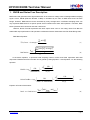
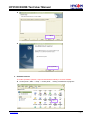
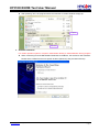
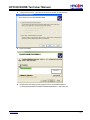
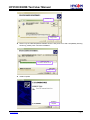
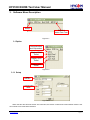
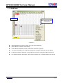
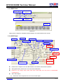
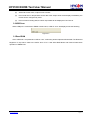
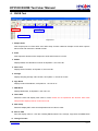
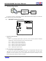
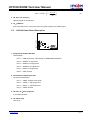
HY310X ENOB Test User Manual . © 2010 HYCON Technology Corp www.hycontek.com APD-SD18016-V01_EN Page 1 HY310X ENOB Test User Manual Table of Contents 1. ENOB AND NOISE FREE DESCRIPTION ............................................................................................... 3 2. HARDWARE/SOFTWARE INSTALLATION ............................................................................................. 4 3. 2.1 MINIMUM SYSTEM REQUIREMENTS ...................................................................................................... 4 2.2 INSTALLATION AND REMOVAL................................................................................................................ 4 SOFTWARE MENU DESCRIPTION ....................................................................................................... 10 3.1 OPTION ............................................................................................................................................ 10 3.1.1 Setup .......................................................................................................................................... 10 3.1.2 RAM Panel ................................................................................................................................. 11 3.1.3 REG Panel.................................................................................................................................. 12 3.1.4 ADC Panel .................................................................................................................................. 12 3.2 USB SCAN ....................................................................................................................................... 13 3.3 READ RAM....................................................................................................................................... 13 4. ENOB TEST ............................................................................................................................................ 14 5. HARDWARE DESCRIPTION.................................................................................................................. 16 5.1 USB ENOB Test Board Description............................................................................................ 16 5.2 HY310x Demo Board Description .............................................................................................. 17 . 6. QUESTION OBVIATION ......................................................................................................................... 18 7. REVISION HISTORY .............................................................................................................................. 19 © 2010 HYCON Technology Corp www.hycontek.com APD-SD18016-V01_EN Page 2 HY310X ENOB Test User Manual 1. ENOB and Noise Free Description RMS Noise that generated from Sigma Delta ADC is the minimum voltage value of distinguishable sampling signal. Hence, ENOB (Effective Number of Bits) is calculated by the ratio of RMS Noise and Full Scale Range. However, RMS Noise must be calculated by many average times. Insufficient sampling times can only represent RMS Noise for a specific period of time instead of the entire ADC operation. Therefore, RMS Noise operation times cannot be less than 1024 times. However, Noise Free Bit represents that ADC output value count is not rolling. Noise Free Bits are stable ADC output performance. Bit operation is defined as Peak-to-Peak Noise and Full Scale Range ratio. RMS Noise Equation: n ADC k 平均 Count → Average = k 1 n (1) 2 n ADC k - Average V k=1 RFE n RMS Noise = Scale 2 (2) In the above equation, n represents total sampling number of ADC and Scale represents ADC total . output bits. ENOB and Noise Free Bits can be gained by taking Equation 1 and Equation 2 to the following equation: ENOB = Log FSR = 2 RMS Noise Noise Free Bits = Log FSR RMS Noise In (3) In 2 FSR = 2 Peak - to - Peak Noise FSR Peak - to - Peak Noise In In 2 (4) Equation of Peak-to-Peak Noise: Peak - to - Peak Noise = © 2010 HYCON Technology Corp www.hycontek.com V ADC - ADC REF Max Min Scale 2 (5) APD-SD18016-V01_EN Page 3 HY310X ENOB Test User Manual 2. Hardware/Software Installation 2.1 Minimum System Requirements 1. Hardware Requirements: ® IBM AT/ATX PC PENTIUM or any above compatible type Memory size > 32MB(>256MB is recommended) Resolution > VGA 1024×768, 256-color display Hard discs space > 10MB USB port 2. Operation System Windows™ 98SE Windows™ 2000 Windows™ XP Windows™ Vista Windows™ 7 Not supportive for 64 bit window, *nix and OSX operation system. Menu could be unreadable code when operating in non-traditional Chinese operation system. 2.2 Installation and Removal 1. Software Installation . For certain operation system, it requires Administrator identity to install software to the computer. Look for Setup.exe and execute it from CD-ROM menu or unzip file. Proceeding the installation procedures as frame indicates. As shown in below dialog window. 執行Setup.exe © 2010 HYCON Technology Corp www.hycontek.com APD-SD18016-V01_EN Page 4 HY310X ENOB Test User Manual 按下一步(Next) 1. 輸入使用者名稱和 公司名稱 . 2. 按下一步(Next) 1. 選擇所要安裝 的位置 2. 按下一步(Next) © 2010 HYCON Technology Corp www.hycontek.com APD-SD18016-V01_EN Page 5 HY310X ENOB Test User Manual 按下一步(Next) . 安裝完成(Finish) 2. Software Removal To certain operation systems, it requires Administrator identity to remove software. Control panel(Start → setup → control panel), clicking "install/remove program". 點選新增或 移除程式 © 2010 HYCON Technology Corp www.hycontek.com APD-SD18016-V01_EN Page 6 HY310X ENOB Test User Manual After pressing "Yes", the program will be removed but no relative window will pop up. 1. 點選移除 2. 按下"是" 3. Software Installation For certain operation systems, it requires Administrator identity to install hardware driving program. When connecting PC and USB ENOB Test Board via USB wire, PC will find a new hardware. Please select "Install from a list or specific location (Advance)" and proceeds next step. . © 2010 HYCON Technology Corp www.hycontek.com APD-SD18016-V01_EN Page 7 HY310X ENOB Test User Manual Select "Don’t search. I will choose the driver to install" and press next. Click "Have Disk". . Have Disk Click browse and assign driving program menu, the default location is ""C:\ProgramFiles\HyEnobTest\HY3106EnobTest\Driver\"" and press yes. © 2010 HYCON Technology Corp www.hycontek.com APD-SD18016-V01_EN Page 8 HY310X ENOB Test User Manual 2. Press Yes 1. Click Browse and assign menu Select "Hycon-USB Temperature Reader Device" and press next. After compatibility warning shows up, please press "continue installation". . 1. 選擇Hycon-USB Temperature Reader Device 2. 按下一步 Install complete Installation complete © 2010 HYCON Technology Corp www.hycontek.com APD-SD18016-V01_EN Page 9 HY310X ENOB Test User Manual 3. Software Menu Description Setup ENOB & Noise Free Test Figure 3-1 3.1 Option Communication and Chip select Display RAM Panel Display REG Panel . Display ADC Panel Figure 3-2 3.1.1 Setup Chip Selection Communicaion Mode Figure 3-3 When test tool and HY310X series are connected, the device number and communication mode is set. User needs not to make other selection © 2010 HYCON Technology Corp www.hycontek.com APD-SD18016-V01_EN Page 10 HY310X ENOB Test User Manual 3.1.2 RAM Panel Memory Content Function list shows up after clicking right button of the mouse . Figure 3-4 Open RAM window, memory content of the chip will be displayed. If the address is inexistent, it will display -. If the address underlined number, it means Hint has been configured. The data in the address can be directly amended by clicking the left button on the address. By double-clicking the left button on the address, the window of amending data will show up. For detailed operation description, please refer to Chapter 3.2 of HY-IDE software user manual. © 2010 HYCON Technology Corp www.hycontek.com APD-SD18016-V01_EN Page 11 HY310X ENOB Test User Manual 3.1.3 REG Panel Indirect Address 0 Indirect Address 1 Data of indirect Address 0 Data of indirect Address 1 Register Figure 3-5 Please refer to Chapter 3.3 Register window operation of HY-IDE software user manual. 3.1.4 ADC Panel Enable LDO LDO Setup ADGN Network DC Offset Network Enable ADC . Enable Clock Source OSR Network Continue/Stop reading data INX Network Select ADC value display Bits display Value format Read ADC data Internal Temperature PGA Network Setup VER BUFF Read Temp. data Figure 3-6 Please refer to Chapter 3.6 of HY-IDE Software User Manual, ADC window operation. Setup parameters; please refer to HY310x Series datasheets. Please do not change setup value when ADC reads data, this may lead to unpredictable consequences. ADC value display: (1) Select ADC value output format, Hex or Dec format output. © 2010 HYCON Technology Corp www.hycontek.com APD-SD18016-V01_EN Page 12 HY310X ENOB Test User Manual (2) Select Bit of ADC value, output from 8 to 24 Bit. (3) Press read ADC or temperature sensor data. ADC output value will be display immediately; the format can be configured by users. (4) Press continue reading data, the ADC output data will be displayed in Dec format. 3.2 USB Scan When USB port is connected to ENOB control board, “USD On Line” will display as like the following Figure 3-7 3.3 Read RAM After “USB Scan” completed and “USB on Line” confirmed, please implement Read RAM. The RAM and Registers of chip will be read to the buffer zone of PC. It will affect RMS Noise and Peak-to-Peak Noise operation of ENOB Test. . © 2010 HYCON Technology Corp www.hycontek.com APD-SD18016-V01_EN Page 13 HY310X ENOB Test User Manual 4. ENOB Test Average of ADC sampling (Count) Peak-to-Peak Noise (nV) ADC output bit RMS Noise (nV) ADC Obtained Data Figure 3-8 1. Sample Point ADC sample point of "Catch ADC" and "ADC-Temp" function. Minimum sample of OTP ADC output is 256 records and maximum is 65536 records. 2. Scale ADC output bit. Minimum ADC output bit is 8-bit and maximum is 24-bit. 3. ENOB Display ENOB, the calculation is shown as Equation 3, the unit is bit. . 4. Noise Free Display Noise Free Bits, as Equation 4, the unit is Bit. 5. Average Display sampling average value of ADC, as Equation 1, the unit is Counts. 6. Vp-p Noise Display Peak-to-Peak Noise, as Equation 5,the unit is nV. 7. RMS Noise Display RMS Noise, as Equation 2, the unit is nV. 8. Catch ADC Real-time catch and display ADC value in order. Please do not implement this function when ADC setup window displays data in continuous mode. 9. ADC-Temp Real-time display ADC value and temperature sensor value in order. 10. Save to CSV Save the display value to *.CSV file, including ENOB, Noise Free, Average, Vp-p Noise and RMS Noise. 11. Change To Chart © 2010 HYCON Technology Corp www.hycontek.com APD-SD18016-V01_EN Page 14 HY310X ENOB Test User Manual Switch chart and value in value display zone. 12. Ref Volt Input Reference Voltage (unit: V). 13. Avr. Times Select software average, the value is display zone will perform average again, according to the times of selection and then display in value display zone. . © 2010 HYCON Technology Corp www.hycontek.com APD-SD18016-V01_EN Page 15 HY310X ENOB Test User Manual 5. Hardware Description Figure 5-1 PC transmits Command to USB ENOB Test Board; USB ENOB Test Board configures and reads ADC value via SPI from Hycon HY310x Demo Board. 5.1 USB ENOB Test Board Description 3 4 4 5 5 6 6 7 7 U9 3 U10 2 U11 2 U12 1 T09011 V02 1 J4 Photo Input Channel J5 2 1 J8 2 1 Photo Power Photo Ground VP SPIDI_Q SPICK_Q SPIDO_Q SPICS_Q VSSP SPIIRQ_Q L1 R3 R2 R1 U6 U3 U7 2 JP1 1 JP2 VBAT J6 VSSBAT . USB power Figure 5-2 1. J4:Optical Coupler SPI Port J4 description PIN 1 → VP, powered by optical coupler IC (U8~U13), J5 and J8 must be opened to completely isolate power. J5 and J8 must be short to use common power supply. PIN 2 → SPIDI_Q, optical coupler DI signal wire. PIN 3 → SPICK_Q, optical coupler CK signal wire. PIN 4 → SPIDO_Q, optical coupler DO signal wire. PIN 5 → SPICS_Q, optical coupler CS signal wire. PIN 6 → VSSP, optical coupler Ground. 2. JP1, JP2, J6 and U3:Power Supply Circuit JP1 and JP2 is external power input that supply power to U3 and generates VDD power. Using USB power, J6 is short circuit. Using external 5V power, JP1 and JP2 inputs, J6 is open circuit. Regulated circuit that composed by U3, R1, R2 and R3 generates VDD power. Amending R1, R2 and R3 can change output voltage, the relation is as follows: © 2010 HYCON Technology Corp www.hycontek.com APD-SD18016-V01_EN Page 16 HY310X ENOB Test User Manual VDD = 1.240V 1 + R 1 +R 2 R3 (6) 3. U9, U10, U11 and U12: Optical coupler IC components 4. U7:USB Port Port connecting to PC, is the power source of entire system (5V), 500mA input. 5.2 HY310x Demo Board Description T09009-1-V01 JP1 VDDA VINN1_1 VINP1_1 VSSA C6 R16 U3 R17 JP4 VDDA VINN2_1 VINP2_1 VSSA HY3100 R18 C10 R19 C34 C30 JP3 1 2 3 4 5 6 7 SPI Figure 5-3 1. JP3:Optical Coupler SPI Port JP description PIN 1 → VDD powered by 3.6V voltage via USB ENOB Test Board PIN 2 → SPISDI, DI signal wire . PIN 3 → SPISCK, CK signal wire PIN 4 → SPISDO, DO signal wire PIN 5 → SPICS, CS signal wire PIN 6 → VSS, Ground. 2. JP1 and JP4:Signal Input End JP1 and JP4 description PIN 1 → VDDA, supplies 3.3V power PIN 2 → VINN1_1, signal input end PIN 3 → SINP1_1, signal input end PIN 4 → VSSA, Ground. 3. C9 and C10:Filter Capacitor 0.1uF SMD capacitor 4. U3:Main Chip HY310x IC © 2010 HYCON Technology Corp www.hycontek.com APD-SD18016-V01_EN Page 17 HY310X ENOB Test User Manual 6. Question Obviation 1. Registers cannot be configured under ADC window? Communication way and IC selection must be configured first. After executing USB Scan and Read RAM, ADC register value can be configured. If USB is connected and confirmed, configuration still cannot be implemented, please close program and remove USB. After plug in the USB, execute the program again. 2. Configuration of ADC window is relatively slow? Please do not change any setup when ADC reads data, this might bring about unpredictable results. 3. Can the data obtained include time? Data obtained from the program includes file that be saved as CSV format but not including time. Users can detect the X axis represents time in graphical display mode, demonstrating in ms. Time recording function will be incorporated in next version of program update. 4. Program cannot be executed, file lack appears and program demands to reinstall. Please print the error window and message and please contact the distributor who provided this DMM EVA Test Tool to you or directly contact HYCON Technology for further support. We are sorry for the inconvenience this has caused to you. . 5. INF error shows up when USB drive program is under installation or is completed and a yellow exclamation mark appears in “device manager”. Please copy all programs of Driver file in the installation menu to c:\windows\system32\drivers. Reinstall driving program again. If error shows up again, please contact the distributor who provided this DMM EVA Test Tool to you or directly contact HYCON Technology for further support. © 2010 HYCON Technology Corp www.hycontek.com APD-SD18016-V01_EN Page 18 HY310X ENOB Test User Manual 7. Revision History Major differences are stated thereinafter: Version V01 Page All Revision Summary First Edition . © 2010 HYCON Technology Corp www.hycontek.com APD-SD18016-V01_EN Page 19