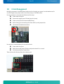
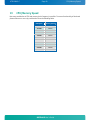
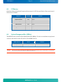
1
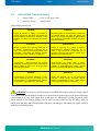
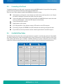
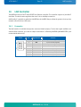
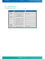
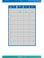
MOPSlcdLX
KTD-S0005-C
User Information
Table of Contents
» Table of Contents «
1
User Information .............................................................................1
1.1
About This Document.................................................................................................... 1
1.2
Copyright Notice.......................................................................................................... 1
1.3
Trademarks................................................................................................................. 1
1.4
Standards................................................................................................................... 1
1.5
Warranty .................................................................................................................... 1
1.6
Life Support Policy ....................................................................................................... 2
1.7
Technical Support ........................................................................................................ 2
2
Introduction ...................................................................................3
2.1
MOPS Embedded Line Family .......................................................................................... 3
2.2
MOPSlcdLX Overview ..................................................................................................... 3
3
Specifications .................................................................................4
3.1
Functional Specifications .............................................................................................. 4
3.2
Block Diagram ............................................................................................................. 6
3.3
Mechanical Specifications.............................................................................................. 7
3.4
Electrical Specifications ................................................................................................ 7
3.5
External Real-Time Clock Battery..................................................................................... 8
3.6
Environmental Specifications ......................................................................................... 9
3.7
MTBF ......................................................................................................................... 9
4
Getting Started.............................................................................. 10
5
System Memory ............................................................................. 11
6
ISA Bus Expansion.......................................................................... 12
6.1
Connector .................................................................................................................12
6.2
Hints ........................................................................................................................12
7
PCI Bus Expansion.......................................................................... 13
7.1
Configuration of VI/O ....................................................................................................13
8
Graphics Interface.......................................................................... 14
8.1
CRT Connector ............................................................................................................14
8.2
Flat Panel Connector....................................................................................................14
8.2.1
Connector .............................................................................................................................. 15
8.3
Connecting a Flat Panel................................................................................................16
8.4
Available Video Modes .................................................................................................16
8.5
Extended VESA Modes ..................................................................................................17
8.6
Backlight Enable Polarity..............................................................................................17
MOPSlcdLX User's Guide
User Information
Table of Contents
9
Serial Port Interfaces ...................................................................... 18
9.1
Connector .................................................................................................................18
10
Parallel Port Interface ..................................................................... 19
10.1
Connector .................................................................................................................19
11
PS/2 Keyboard Interface.................................................................. 20
11.1
Connector .................................................................................................................20
11.2
Signal Description.......................................................................................................20
12
PS/2 Mouse Interface...................................................................... 21
12.1
Connector .................................................................................................................21
13
USB Interface................................................................................ 22
13.1
Connector .................................................................................................................22
13.2
Limitations ................................................................................................................22
14
Floppy Drive Interface..................................................................... 23
14.1
Connector .................................................................................................................23
15
EIDE Interface (P-ATA) .................................................................... 24
15.1
Connector .................................................................................................................24
16
LAN Controller............................................................................... 25
16.1
Connector .................................................................................................................25
17
Power Supply ................................................................................ 26
17.1
Connector .................................................................................................................26
17.2
Power Pins.................................................................................................................26
17.3
External Battery .........................................................................................................27
18
Crisis Management ......................................................................... 28
19
CPU/Memory Speed ........................................................................ 29
20
Special Hardware Hints ................................................................... 30
20.1
ISA Bus Limitations .....................................................................................................30
20.2
PCI Bus Limitations .....................................................................................................30
20.3
Security Block ............................................................................................................30
21
Setup Guide .................................................................................. 31
21.1
Start PHOENIX/AWARD BIOS Setup Utility ........................................................................31
21.2
Menu Bar...................................................................................................................32
21.3
Main Menu.................................................................................................................32
21.3.1
IDE Master or Slave Submenu ..................................................................................................... 33
21.4
Advanced BIOS Features...............................................................................................33
21.5
Advanced Chipset Features ...........................................................................................35
21.6
Integrated Peripherals .................................................................................................36
MOPSlcdLX User's Guide
User Information
Table of Contents
21.7
PnP/PCI Configurations................................................................................................36
21.8
PC Health Status .........................................................................................................37
21.9
Board Information ......................................................................................................37
Appendix A: System Resources ................................................................... 38
A.1
Interrupt Request (IRQ) Lines........................................................................................38
A.2
Direct Memory Access (DMA) Channels ............................................................................39
A.3
Memory Area..............................................................................................................39
A.4
I/O Address Map .........................................................................................................40
A.5
PCI Devices ................................................................................................................41
A.6
System Management Bus (SMBus) ..................................................................................41
Appendix B: Connector Layout.................................................................... 42
B.1
Connector Locations....................................................................................................42
B.2
Mechanical Dimensions ................................................................................................43
B.3
Mating Connectors ......................................................................................................44
B.4
Pinout Tables .............................................................................................................45
Appendix C: Reference Documents .............................................................. 49
Appendix D: Document Revision History ....................................................... 50
MOPSlcdLX User's Guide
KTD-S0005-C
1
User Information
1.1
About This Document
Page 1
User Information
This document provides information about products from KONTRON Technology A/S and/or its subsidiaries.
No warranty of suitability, purpose or fitness is implied. While every attempt has been made to ensure that
the information in this document is accurate the information contained within is supplied 'as-is' - no
liability is taken for any inaccuracies. Manual is subject to change without prior notice.
KONTRON assumes no responsibility for the circuits, descriptions and tables indicated as far as patents or
other rights of third parties are concerned.
1.2
Copyright Notice
Copyright © 2006 - 2011, KONTRON Technology A/S, ALL RIGHTS RESERVED.
No part of this document may be reproduced or transmitted in any form or by any means, electronically or
mechanically, for any purpose without the express written permission of KONTRON Technology A/S.
1.3
Trademarks
Brand and product names are trademarks or registered trademarks of their respective owners.
1.4
Standards
KONTRON Technology A/S is certified to ISO 9000 standards.
1.5
Warranty
This product is warranted against defects in material and workmanship for the warranty period from the
date of shipment. During the warranty period KONTRON Technology A/S will at its discretion decide to
repair or replace defective products.
Within the warranty period the repair of products is free of charge as long as warranty conditions are
observed.
The warranty does not apply to defects resulting from improper or inadequate maintenance or handling by
the buyer, unauthorized modification or misuse, operation outside of the product’s environmental specifications or improper installation or maintenance.
KONTRON Technology A/S will not be responsible for any defects or damages to third party products that
are caused by a faulty KONTRON Technology A/S product.
MOPSlcdLX User's Guide
KTD-S0005-C
1.6
Page 2
User Information
Life Support Policy
KONTRON Technology's products are not for use as critical components in life support devices or systems
without express written approval of the general manager of KONTRON Technology A/S.
As used herein:
Life support devices or systems are devices or systems which
a) are intended for surgical implant into body or
b) support or sustain life and whose failure to perform, when properly used in accordance with instructions
for use provided in the labelling, can be reasonably expected to result in significant injury to the user.
A critical component is any component of a life support device or system whose failure to perform can be
reasonably expected to cause the failure of the life support device or system or to affect its safety or
effectiveness.
1.7
Technical Support
Please consult our Web site at http://www.kontron.com/support for the latest product documentation,
utilities, drivers and support contacts or use the special e-mail address [email protected] for a
technical problem. In any case you can always contact your board supplier for technical support.
Before contacting support please be prepared to provide as much information as possible:
Board identification:
Type
Part number (find PN on label)
Serial number (find SN on label)
Board configuration:
DRAM type and size
BIOS revision (find in the BIOS Setup)
BIOS settings different than default settings (refer to the BIOS Setup section)
System environment:
O/S type and version
Driver origin and version
Attached hardware (drives, USB devices, LCD panels ...)
MOPSlcdLX User's Guide
KTD-S0005-C
Page 3
2
Introduction
2.1
MOPS Embedded Line Family
Introduction
Each MOPS is a member of the PC/104 SBC family of KONTRON Technology A/S.
MOPS embedded line modules are characterized by interfaces for 2 x USB, Fast LAN, PS/2 keyboard and
mouse connector, an ISA bus, CRT interface as well as serial and parallel ports.
These homogeneous features facilitate easy upgrades within the MOPS embedded line product family. Connection of LCD panels is simplified when using the onboard standard JILI (40 pins) or JILI30 interface.
As part of the standard features package all MOPS modules come with a JIDA interface which is integrated
into the BIOS of the SBC modules. This interface enables hardware independent access to the MOPS features that can't be accessed via standard APIs. Functions such as watchdog timer, brightness of panel
backlight and user bytes in EEPROM can be configured with ease by taking advantage of this standard MOPS
module feature.
2.2
MOPSlcdLX Overview
Please refer to the following matrix to choose the product that suits your needs best.
Article number
ISA bus
01036-0000-53-4
01036-0000-53-5
MOPSlcdLX User's Guide
PCI bus
KTD-S0005-C
Page 4
3
Specifications
3.1
Functional Specifications
Specifications
Processor: AMD GeodeTM LX800
64 kB data and 64 kB instruction L1 cache
128 kB L2 cache
Integrated memory controller run with one DDR200 to DDR333 unbuffered DDR-SDRAM (SODIMM form factor) up to 1GB
Integrated display controller with dual display support (CRT/TFT) and up to 254 MB video
RAM (UMA)
Chipset: AMD GeodeTM CS5536
64 bit, 66 MHz GeodeLinkTM interface
External PCI bus with 32 bit / 33 MHz operation (PCI V2.2 compliant)
One parallel ATA PCI IDE controller
Four USB channels (OHCI/EHCI), only two channels available
Onchip Video Graphics Array (VGA)
CRT monitor interface (resolution: up to 1920x1440 pixel)
LVDS flatpanel interface supports single clock with 18/24 bit color depth (resolution: max.
1024x768 pixel)
Onchip Parallel-ATA (P-ATA)
Supports PIO mode, Multiword DMA and Ultra DMA up to UDMA5
Onchip Universal Serial Bus (USB)
Two ports are capable to handle USB1.1 (OHCI) and USB2.0 (EHCI)
Super-I/O (LPC): Winbond W83627DHG
Two serial ports (RS-232 compatible)
One parallel port configurable as enhanced parallel port (EPP) with bidirectional capability
One legacy floppy interface
PS/2 keyboard and mouse controller
Watchdog timer
MOPSlcdLX User's Guide
KTD-S0005-C
Page 5
Fast Ethernet (PCI): Intel® 82551ER
Full duplex operation at 10/100 Mbps
Fully compliant with IEEE 802.3 and IEEE 802.3u
External ISA bus (LPC): Fintek F85226F
One PC/104 bus connector, 8/16 bit I/O and memory access
All ISA interrupts and 8 bit DMA signals available (16 bit DMA not supported)
Bus master mode not supported
External PCI bus
One PCI-104 bus connector, only 3.3V PCI cards supported
BIOS: AWARD, 512 kb Flash BIOS
Real-Time Clock (RTC) with CMOS RAM
MOPSlcdLX User's Guide
Specifications
KTD-S0005-C
3.2
Page 6
Specifications
Block Diagram
MOPSlcdLX
CPU
AMD GeodeTM LX800
LVDS
X12000
X12001
Graphic
Controller
LVDS_
Transmitter
THC63LVD823
DDRSDRAM
SDRAM
Controller
X8000
CRT_
PCI Bus
Temp.
Sensor
LM86
SMBus
Companion
AMD GeodeTM
CS5536
IDE
Controller
P-ATA_
X15005
USB
Controller
USB 0-1_
X15006
X15007
LPC Bus
FWH
Flash
(BIOS)
X11000
PCI Bus_
ISA Bus
X10000
X16000
Ethernet
i82551ER
LAN_
LPC
ISA-Bridge
F85226F
Eeprom
JIDA
AT24C04
I2C_
GPI/O
Watchdog
Super-I/O
W83627DHG
X15002
X14001
PS/2 Keyboard_
PS/2 Mouse +
Keyboard
Parallel Port
Floppy
Serial Ports
PS/2 Mouse_
X15003
MOPSlcdLX User's Guide
X15004
RS-232
Interface
MAX211E
X15000
RS-232
Interface
MAX211E
X15001
KTD-S0005-C
3.3
Page 7
Specifications
Mechanical Specifications
Dimensions
3.4
96 x 90 mm (3.77" x 3.55")
Height on top approx. 11.5 mm
Height on bottom approx. 10.5 mm
Electrical Specifications
Supply Voltage
+5V DC ± 5%
Supply Voltage Ripple
Maximum 100mV peak to peak 0 – 20 MHz
Supply Current (DOS prompt)
Power consumption tests were executed during the DOS prompt with 256 MB DDR SDRAM, CRT monitor, USB
keyboard and CF card as boot device (default BIOS settings).
Full Load
Soft Off S5
[A]
[W]
[A]
[W]
1.10
5.50
0.20
1.00
Supply Current (Windows® XP SP3)
The power consumption tests were executed during Windows® XP SP3 by using a tool to stress the CPU
(100% load) and extensive 2D graphic. The boards were ran with 256 MB DDR SDRAM, CRT monitor, PS/2
keyboard, USB mouse and a CF card as boot device (default BIOS settings).
Full Load
Idle
[A]
[W]
[A]
[W]
1.45
7.25
0.95
4.75
MOPSlcdLX User's Guide
KTD-S0005-C
3.5
Page 8
Specifications
External Real-Time Clock Battery
Voltage range:
+2.4V - +3.6V (typ. +3.0V)
Maximum current
10μA @ +3.0V
Lithium battery precautions
CAUTION!
VORSICHT!
Danger of explosion if battery is incorrectly replaced. Replace only with same or equivalent type
recommended by manufacturer. Dispose of used
batteries according to the manufacturer’s instructions.
Explosionsgefahr bei unsachgemäßem Austausch
der Batterie. Ersatz nur durch den selben oder
einen vom Hersteller empfohlenen gleichwertigen
Typ. Entsorgung gebrauchter Batterien nach Angaben des Herstellers.
ATTENTION!
PRECAUCION!
Risque d'explosion avec l'échange inadéquat de
la batterie. Remplacement seulement par le
même ou un type équivalent recommandé par le
producteur. L'évacuation des batteries usagées
conformément à des indications du fabricant.
Peligro de explosión si la batería se sustituye
incorrectamente. Sustituya solamente por el
mismo o tipo equivalente recomendado por el
fabricante. Disponga las baterías usadas según
las instrucciones del fabricante.
ADVARSEL!
ADVARSEL!
Lithiumbatteri – Eksplosionsfare ved fejlagtig
håndtering. Udskiftning må kun ske med batteri af
samme fabrikat og type. Levér det brugte batteri
tilbage til leverandøren.
Eksplosjonsfare ved feilaktig skifte av batteri.
Benytt samme batteritype eller en tilsvarende type
anbefalt av apparatfabrikanten. Brukte batterier
kasseres i henhold til fabrikantens instruksjoner.
VARNING!
VAROITUS!
Explosionsfara vid felaktigt batteribyte. Använd
samma batterityp eller en ekvivalent typ som
rekommenderas av apparattillverkaren. Kassera
använt batteri enligt fabrikantens instruktion.
Paristo voi räjähtää, jos se on virheellisesti
asennettu. Vaihda paristo ainoastaan laltevalmistajan suosittelemaan tyyppiln. Hävitä käytetty
paristo valmistajan ohjeiden mukaisesti.
ATTENTION: Do not connect the RTC battery to the MOPSlcdLX until just before the supply power is
to be applied to the system. When the battery is connected without power applied to the system the battery
current might be in some cases higher than normal (refer to: AMD Geode™ CS5536 Companion Device
Silicon Revision B1 Specification Update). This can lead to a shorter lifetime of the RTC battery. After the
supply power has been applied to the system once after connecting the RTC battery the regular current is
drained from the battery again.
MOPSlcdLX User's Guide
KTD-S0005-C
3.6
Page 9
Specifications
Environmental Specifications
Temperature
Operating (with original KONTRON heat-sink):
Ambient temperature: 0 to +60°C
1)
Non operating:
Note:
Ambient temperature: -10 to +85°C
It is the customer's responsibility to provide sufficient airflow around each of the components to keep them within the
allowed temperature range.
1)
Humidity
3.7
Operating:
10% to 90% (non condensing)
Non operating:
5% to 95% (non condensing)
MTBF
The following MTBF (Mean Time Between Failure) values were calculated using a combination of manufacturer’s test data, if the data was available, and a Bellcore calculation for the remaining parts. The Bellcore
calculation used is 'Method 1 Case 1'. In that particular method the components are assumed to be
operating at a 50% stress level in a 40°C ambient environment and the system is assumed to have not been
burned in. Manufacturer’s data has been used wherever possible. The manufacturer’s data, when used, is
specified at 50°C, so in that sense the following results are slightly conservative. The MTBF values shown
below are for a 40°C in an office or telecommunications environment. Higher temperatures and other environmental stresses (extreme altitude, vibration, salt water exposure, etc.) cause lower MTBF values.
Note:
System MTBF (hours): tbd
Fans usually shipped with KONTRON Technology A/S products have 50.000-hour typical operating life. The above estimation assumes no fan but a passive heat sinking arrangement. Estimated RTC battery life (as opposed to battery failures)
is not included in the MTBF calculation. The RTC battery lifetime has to be considered separately. Battery life depends on
both temperature and operating conditions. When the KONTRON unit has external power; the only battery drain is from
leakage paths.
MOPSlcdLX User's Guide
KTD-S0005-C
4
Page 10
Getting Started
Getting Started
Getting started with the MOPSlcdLX is very easy. Take the following steps:
Plug a suitable DDR-SDRAM memory module into the RAM socket.
Plug the MOPSlcdLX to the PC/104 bus connector on the starter kit baseboard.
Make all necessary connections from the MOPSlcdLX to the starter kit board (cables come with
the starter kit). The starter kit board offers various interfaces on standard connectors.
Connect the CRT monitor to the CRT interface or a LCD panel to the JILI interface by using the
corresponding adapter cable.
Plug a keyboard and/or mouse to the PS/2 connectors.
Plug a data cable to the hard disk interface. Attach the hard disk to the connector at the opposite end of the cable. If necessary connect the power supply to the hard disk’s power connector.
Make sure all your connections have been made correctly. Turn on the power.
Enter the BIOS by pressing the Del key during boot-up. Make all changes in the BIOS Setup.
See the BIOS Setup chapter of this manual for details.
MOPSlcdLX User's Guide
KTD-S0005-C
5
Page 11
System Memory
System Memory
The MOPSlcdLX uses only 200 pin Small Outline Dual Inline Memory Modules (SODIMMs). One socket is
available for 2.5V unbuffered DDR200 up to DDR333 SDRAM of up to 1 GB.
The total amount of memory available on the SDRAM module is used for main memory and graphic memory
on the MOPSlcdLX. Shared Memory Architecture (SMA) manages the sharing of system memory between
graphic controller and processor. Therefore the full memory size is not available for software applications.
Up to 254 MB of system memory are used as graphic memory.
Attention:
DDR400 modules can only be operated with the DDR333 timing
MOPSlcdLX User's Guide
KTD-S0005-C
6
Page 12
ISA Bus Expansion
ISA Bus Expansion
The design of the MOPSlcdLX follows the standard PC/104 form factor and offers ISA bus signals for the use
of standard PC/104 adapter cards.
The PC/104 bus consists of two connectors that use 104 pins in total.
XT bus connector (64 pins)
AT bus connector (40 pins, which is optional for 16 bit data bus system)
The pinout of the PC/104 bus connectors corresponds to the pinout of the ISA bus connectors with some
added ground pins. The two PC systems with different form factors are electrically compatible.
The XT bus connector, row A and B.
The corresponding 64 pin stackthrough header (ISA bus = 62 pins) has two added ground pins at the end of
the connector (pin A32 and pin B32). The pinout between PC/104 bus and XT ISA bus is identical between
A1 - A31 and B1 - B31.
The AT bus extension connector, row C and D
The corresponding 40 pin stackthrough header (ISA bus = 36 pins) has four added ground pins, two on
each side of the connector. To avoid confusion the first two pins are defined as pin C0 and pin D0. The
additional ground pins at the end of the connector are defined as C19 and D19. The pinout between PC/104
bus and AT ISA bus is identical between C1 - C18 and D1 - D18.
6.1
Connector
The MOPSlcdLX features both – XT bus and AT bus extension – on two dual-row socket connectors with 2.54
mm x 2.54 mm grid (0.1" x 0.1").
The PC/104 XT bus is available through the X10000A connector. The PC/104 AT bus is available through the
X10000B connector.
6.2
Hints
PC/104 adapter cards are mounted in a stack-through manner. Adapter cards are designed with plugs on
their undersides that mate with the PC/104 socket connectors of MOPSlcdLX. PC/104 adapters can support
the socket connector version on their topside and allow additional stacking of adapters.
Whenever possible use the MOPSlcdLX as top module of the PC/104 stack as the CPU board is normally the
board with the highest heat dissipation.
MOPSlcdLX User's Guide
KTD-S0005-C
7
Page 13
PCI Bus Expansion
PCI Bus Expansion
A quad-row socket trough-hole connector with a 2 x 2 mm (0.79" x 0.79") pitch implements the standard
32 bit PCI bus signals. The PCI-104 bus is available through the standard connector X11000.
A description of signals, including electrical characteristics and timings, is beyond the scope of this document. Please refer to the official PCI bus and PC/104-plus specifications for more details.
Under no circumstances 5V PCI cards may be used on the MOPSlcdLX board. Only Universal and 3.3V add on
cards are permitted. VI/O and VCC are open (default) or set to 3.3V on the PCI bus. 5V PCI add on cards can
irretrievably damage the MOPSlcdLX board due to a short curcuit with VI/O or VCC. Before using a PCI add on
card please make absolutely sure that this card is conform to these requirements. The LX chipset does only
support a 3.3V PCI bus.
7.1
Configuration of VI/O
The default settings for VI/O and VCC are not connected. If it is ensured that the PCI expansion cards are
types of 3.3V only zero-ohm bridges can be set.
Attention:
5V PCI expansion cards can damage the board.Please note that the +5V supply voltage is routed to the connector.
Four slots are available via the connector X11000 (IDSEL, /IRQ) but only three slots are busmaster capable.
MOPSlcdLX User's Guide
KTD-S0005-C
8
Page 14
Graphics Interface
Graphics Interface
The graphics accelerator supports CRT monitors and a variety of LCD panels with single clock, color depths
of 18/24 bit and resolutions up to 1920x1440 for CRT and XGA (1024x768) for LCD.
8.1
CRT Connector
The CRT monitor interface is available through the X12001 connector (6 pins). To have the signals available
on a standard DSUB15 CRT monitor connector an adapter cable is required. A 15 pin DSUB cable is available from KONTRON (KAB-VGA-2, part number 96053-0000-00-0).
Header
8.2
Pin
Signal Name
Function
DSUB15
1
HSYNC
Horizontal sync
13
2
VSYNC
Vertical sync
14
3
GND
Ground
5-8
4
BLUE
Blue video signal
3
5
GREEN
Green video signal
2
6
RED
Red video signal
1
Flat Panel Connector
The LVDS interface for the flat panel is available through the X12000 connector (40 pins) on the top side of
the board. The implementation of this subsystem complies with the JILI specification of KONTRON Technology A/S. A variety of cables for different display types are available from KONTRON. Please refer to the
actual cable list on the KONTRON website for part numbers and cable names.
When using a LCD additional voltages may be required to drive the displays logic and supply the backlight
converter. The display logic may require +5V or +3.3V, backlight converters usually are +5V or +12V types.
When using a KONTRON JILI cable you do not need to determine such configurations. Display logic voltage
come preconfigured on the JILI cable. On occasion backlight voltage has to be adjusted on the cable. Even
though the MOPSlcdLX is a +5V only board you need to supply the +12V for the backlight converter additionally when using such a converter type.
MOPSlcdLX User's Guide
KTD-S0005-C
8.2.1
Page 15
Connector
Header
1
Note:
Graphics Interface
Pin
Signal Name
Function
1
N.C.
Not connected
2
FTX0-
First channel data output 0 (negative)
3
FTX0+
First channel data output 0 (positive)
4
ENAVCC
Enable panel power
5
FTX1-
First channel data output 1 (negative)
6
FTX1+
First channel data output 1 (positive)
7
N.C.
Not connected
8
FTX2-
First channel data output 2 (negative)
9
FTX2+
First channel data output 2 (positive)
10
GND
Ground
11
FTXC-
First channel clock output (negative)
12
FTXC+
First channel clock output (positive)
13
GND
Ground
14
FTX3-
First channel data output 3 (negative)
15
FTX3+
First channel data output 3 (positive)
16
SDA
I2C data line
17
RSVD
Reserved
18
RSVD
Reserved
19
SCL
I2C clock line
20
RSVD
Reserved
21
RSVD
Reserved
22
N.C.
Not connected
23
RSVD
Reserved
24
RSVD
Reserved
25
GND
Ground
26
RSVD
Reserved
27
RSVD
Reserved
28
GND
Ground
29
RSVD
Reserved
30
RSVD
Reserved
31 - 34
VCC 1)
Power +5V
35
BKLTON
Backlight on
36 - 37
GND
Ground
38 - 40
VDD 1)
Power +12V if voltage is connected
1) To protect the external power lines of peripheral devices make sure that
- the wires have the right diameter to withstand the maximum available current.
- to enclosure of the peripheral device fulfills the fire-protecting conditions of IEC/EN 60950.
MOPSlcdLX User's Guide
KTD-S0005-C
8.3
Page 16
Graphics Interface
Connecting a Flat Panel
To determine whether your flat panel is supported check the KONTRON website for panel lists. We regularly
update the list of panels that have been tested with the MOPSlcdLX.
If you use one of those adapters supplied by KONTRON configuration is easy:
8.4
Check whether you have the correct adapter and cable for the panel you plan to use. Inspect
the cable for damages. Disconnect the power from your system.
Connect the cable to the flat panel connector X12000 on the MOPSlcdLX and connect the other
end to your JILI adapter - connect the JILI adapter and the display.
Connect the backlight converter.
Supply power to your system.
If no image appears on your display connect a CRT monitor to the CRT connector.
If necessary program the EEPROM on the JILI cable with the matching configuration data.
If you still do not see improvement consider contacting the dealer for technical support.
Available Video Modes
The following list shows the video modes supported by the graphics controller with maximum frame buffer
size. When configured for saller frame buffers and/or using a flat panel on the JILI interface not all of the
video modes listed below may be available. Capability depends on system configuration and on display
capabilities. Different operating systems also may not support all listed modes by the available drivers.
Video Mode
Type
Characters/Pixels
Colors
00h/01h
Text
40 x 25
16
02h/03h
Text
80 x 25
16
04h/05h
Graphic
320 x 200
4
06h
Graphic
640 x 200
2
07h
Text
80 x 25
2
0Dh
Graphic
320 x 200
16
0Eh
Graphic
640 x 200
16
0Fh
Graphic
640 x 350
2
10h
Graphic
640 x 350
4
11h
Graphic
640 x 480
2
12h
Graphic
640 x 480
16
13h
Graphic
320 x 200
256
MOPSlcdLX User's Guide
KTD-S0005-C
8.5
Page 17
Graphics Interface
Extended VESA Modes
Test program: SciTech VBETest (VESA BIOS Extensions Compliance Test).
8.6
VESA Mode
Type
Pixels
Colors
101h
Graphic
640 x 480
256
103h
Graphic
800 x 600
256
105h
Graphic
1024 x 768
256
107h
Graphic
1280 x 1024
256
110h
Graphic
640 x 480
32k
111h
Graphic
640 x 480
64k
112h
Graphic
640 x 480
16M (32 bit)
113h
Graphic
800 x 600
32k
114h
Graphic
800 x 600
64k
115h
Graphic
800 x 600
16M (32 bit)
116h
Graphic
1024 x 768
32k
117h
Graphic
1024 x 768
64k
118h
Graphic
1024 x 768
16M (32 bit)
119h
Graphic
1280 x 1024
32k
11Ah
Graphic
1280 x 1024
64k
11Bh
Graphic
1280 x 1024
16M (32 bit)
131h
Graphic
1600 x 1200
256
133h
Graphic
1600 x 1200
64k
134h
Graphic
1600 x 1200
16M (32 bit)
Backlight Enable Polarity
Use a zero-ohm bridge to define the backlight enable polarity.
Position 1-2 = low active
Position 2-3 = high active
MOPSlcdLX User's Guide
KTD-S0005-C
9
Page 18
Serial Port Interfaces
Serial Port Interfaces
Two fully functional serial ports (COMA and COMB) provide asynchronous serial communications. COMA and
COMB support RS-232 operation modes. They are 16550 high-speed UART compatible and support 16-byte
FIFO buffers for transfer rates from 50 Baud to 115.2 KBaud.
9.1
Connector
COMA is available through the X15000 connector (10 pins) and COMB through the X15001 connector (10
pins). To have the signals available on the standard serial interface connector DSUB9 an adapter cable is
required.
A 9 pin DSUB cable is available from KONTRON (KAB-DSUB9-2, part number 96017-0000-00-0). The following table shows the pinouts for COMA and COMB as well as necessary connections for DSUB adapters.
Header
Note:
Pin
Signal Name
Function
DSUB9
1
/DCD
Data carrier detect
1
2
/DSR
Data set ready
6
3
RXD
Receive data
2
4
/RTS
Request to send
7
5
TXD
Transmit data
3
6
/CTS
Clear to send
8
7
/DTR
Data terminal ready
4
8
/RI
Ring indicator
9
9
GND
Ground
5
10
VCC 1)
Power +5V
---
1) To protect the external power lines of peripheral devices make sure that
- the wires have the right diameter to withstand the maximum available current.
- to enclosure of the peripheral device fulfills the fire-protecting conditions of IEC/EN 60950.
MOPSlcdLX User's Guide
KTD-S0005-C
10
Page 19
Parallel Port Interface
Parallel Port Interface
The MOPSlcdLX incorporates a parallel port that can be set to uni-/bidirectional and supports EPP operating
modes.
10.1
Connector
The parallel port is available through the X15004 connector (26 pins). To have the signals available on a
standard parallel interface connector DSUB25 an adapter cable is required which is offered by KONTRON
(KAB-DSUB25-1, part number 96015-0000-00-0).
Header
Note:
Pin
Signal Name
Function
DSUB25
1
/STB
Strobe
1
2
/AFD
Autofeed
14
3
D0
Data 0
2
4
/ERR
Error
15
5
D1
Data 1
3
6
/INIT
Init
16
7
D2
Data 2
4
8
/SLIN
Select in
17
9
D3
Data 3
5
10
GND
Ground
18
11
D4
Data 4
6
12
GND
Ground
19
13
D5
Data 5
7
14
GND
Ground
20
15
D6
Data 6
8
16
GND
Ground
21
17
D7
Data 7
9
18
GND
Ground
22
19
/ACK
Acknowledge
10
20
GND
Ground
23
21
/BUSY
Busy
11
22
GND
Ground
24
23
PE
Paper out
12
24
GND
Ground
25
25
/SLCT
Select out
13
26
VCC 1)
Power +5V
---
1) To protect the external power lines of peripheral device make sure that
- the wires have the right diameter to withstand the maximum available current.
- to enclosure of the peripheral device fulfills the fire-protecting conditions of IEC/EN 60950.
MOPSlcdLX User's Guide
KTD-S0005-C
11
Page 20
PS/2 Keyboard Interface
PS/2 Keyboard Interface
The keyboard and feature connector of the MOPSlcdLX offers four functions:
11.1
PS/2 Keyboard
Speaker
Battery
Reset button
Connector
The keyboard and feature connector is available through connector X15002 (10 pins). An adapter cable is
required to connect a standard keyboard to this interface. There is an adapter cable for the PS/2 keyboard
available from KONTRON (KAB-KB-PS2, part number 96060-0000-00-0). The adapter cables do not know
the other functions on this interface.
Header
Note:
11.2
Pin
Signal Name
Function
6 pin PS/2
1
SPKR
Speaker
2
GND
Ground
3
/RESIN
Reset input
4
RSVD
Reserved
5
KBDAT
Keyboard data
1
6
KBCLK
Keyboard clock
5
7
GND
Ground
3
8
VCC 1)
Power +5V
4
9
BATT
Battery
10
PWRGD
Power good
1) To protect the external power lines of peripheral devices make sure that
- the wires have the right diameter to withstand the maximum available current.
- to enclosure of the peripheral device fulfills the fire-protecting conditions of IEC/EN 60950.
Signal Description
When POWERGD goes high it starts the reset generator on the CPU module to pull the
onboard reset line high after a valid reset period. You also can use this pin as a low active
hardware reset for modules
A battery (signal BATT) is not needed to hold CMOS setup data. Your configurations for
hard disks, floppy drives and other peripherals are saved in an onboard EEPROM. However
you need a battery to save the CMOS date and time when power supply is turned off
SPKR is an output to drive a piezo electronic speaker
MOPSlcdLX User's Guide
KTD-S0005-C
12
Page 21
PS/2 Mouse Interface
PS/2 Mouse Interface
The Super-I/O of the MOPSlcdLX supports a PS/2 mouse.
12.1
Connector
The PS/2 mouse interface is available on connector X14001 (4 pins). An adapter cable is required to connect a standard PS/2 mouse. The cable is available from KONTRON (KAB-MOUSE-PS2, part number 960620000-00-0).
Header
Note:
Pin
Signal Name
Function
1
MSCLK
Mouse clock
2
GND
Ground
3
VCC 1)
Power +5V
4
MSDAT
Mouse data
1) To protect the external power lines of peripheral devices make sure that
- the wires have the right diameter to withstand the maximum available current.
- to enclosure of the peripheral device fulfills the fire-protecting conditions of IEC/EN 60950.
MOPSlcdLX User's Guide
KTD-S0005-C
13
Page 22
USB Interface
USB Interface
The USB interface comes with two USB ports which follow the OHCI/EHCI specification and are USB 2.0
compliant. You can expand the amount of USB connections by adding external hubs.
13.1
Connector
The USB ports are available through the X15006 and X15007 connectors (each 4 pins). To have the signals
available on the standard USB interface connectors an adapter cable is required. An USB interface cable is
available from KONTRON (KAB-USB-2, part number 96054-0000-00-2).
Header
Note:
Pin
Signal Name
Function
1
GND
Ground
2
USB+
USB port (positive)
3
USB-
USB port (negative)
4
VCC 1)
Power +5V
1) To protect the external power lines of peripheral devices make sure that
- the wires have the right diameter to withstand the maximum available current.
- to enclosure of the peripheral device fulfills the fire-protecting conditions of IEC/EN 60950.
13.2
Limitations
The power contacts for USB devices on pin 1 and pin 4 are protected. They are suitable to supply connected
USB devices with a maximum of 500 mA power dissipation. Do not supply external USB devices with higher
power dissipation through these pins.
MOPSlcdLX User's Guide
KTD-S0005-C
14
Page 23
Floppy Drive Interface
Floppy Drive Interface
The floppy drive interface of the MOPSlcdLX uses a 2.88 MB Super-I/O floppy disk controller and can support one floppy disk drive with densities that range from 360 kB to 2.88 MB. The controller is 100% IBM
compatible.
14.1
Connector
The floppy disk interface is available on the flat-foil connector X15003 (26 pins). This type of connector is
often internally used in notebooks to connect a floppy drive.
Accessories are available for this interface from KONTRON. To connect a standard 3.5” floppy drive use an
adapter cable (ADA-FLOPPY-2, part number 96001-0000-00-0). If you have a slim-line 3.5” floppy drive you
may need a flat-foil cable (KAB-FLOPPY/ MOPS-1, part number 96019-0000-00-0). It also is possible to get
a slim-line 3.5” floppy drive with cable (FLOPPY-MOPS-1, part number 96010-0000-00-0).
Header
1
Note:
Pin
Signal Name
Function
Pin
Signal Name
Function
1
VCC 1)
Power +5V
2
/IDX
Index
3
VCC 1)
Power +5V
4
/DR0
Drive select 0
5
VCC 1)
Power +5V
6
/DSKCHG
Disk change
7
N.C.
Not connected
8
N.C.
Not connected
9
N.C.
Not connected
10
/MTR0
Motor on 0
11
N.C.
Not connected
12
/FDIR
Direction select
13
N.C.
Not connected
14
/STEP
Step
15
GND
Ground
16
/WDATA
Write data
17
GND
Ground
18
/WGATE
Write gate
19
GND
Ground
20
/TRK0
Track 0
21
GND
Ground
22
/WRTPRT
Write protect
23
GND
Ground
24
/RDATA
Read data
25
GND
Ground
26
/HDSEL
Side one select
1) To protect the external power lines of peripheral devices make sure that
- the wires have the right diameter to withstand the maximum available current.
- to enclosure of the peripheral device fulfills the fire-protecting conditions of IEC/EN 60950.
MOPSlcdLX User's Guide
KTD-S0005-C
15
Page 24
EIDE Interface (P-ATA)
EIDE Interface (P-ATA)
The MOPSlcdLX features one EIDE interface (UDMA33/66 mode) that can drive two hard disks. When two
devices share a single adapter they are connected in a master/slave, daisy-chain configuration. If only one
drive is connected you must set it as master.
15.1
Connector
The EIDE interface is available through connector X15005 (44 pins). This interface is designed in 2 mm grid
for optimal connectivity to a 2.5” hard disk. You can use two cables to directly connect a hard disk in a 2.5”
form factor (KAB-IDE-2MM, part number 96021-0000-00-0) or a 3.5” form factor (KAB-IDE-25, part number 96020-0000-00-0).
Header
Note:
Pin
Signal Name
Function
Pin
Signal Name
Function
1
/RESET
Reset
2
GND
Ground
3
D7
Data 7
4
D8
Data 8
5
D6
Data 6
6
D9
Data 9
7
D5
Data 5
8
D10
Data 10
9
D4
Data 4
10
D11
Data 11
11
D3
Data 3
12
D12
Data 12
13
D2
Data 2
14
D13
Data 13
15
D1
Data 1
16
D14
Data 14
17
D0
Data 0
18
D15
Data 15
19
GND
Ground
20
Key (N.C.)
Key pin
21
DRQ
DMA request
22
GND
Ground
23
/IOW
I/O write
24
GND
Ground
25
/IOR
I/O read
26
GND
Ground
27
IOCHRDY
I/O channel ready
28
CSEL 2)
Cable select
29
/DACK
DMA acknowledge
30
GND
Ground
31
IRQ
Interrupt request
32
N.C.
Not connected
33
SA1
Address 1
34
ATAD
UDMA detection
35
SA0
Address 0
36
SA2
Address 2
37
/CS1
Chip select 1
38
/CS3
Chip select 3
39
N.C.
Not connected
40
GND
Ground
41
VCC 1)
Power +5V
42
VCC 1)
Power +5V
43
GND
Ground
44
N.C.
Not connected
1) To protect the external power lines of peripheral devices make sure that
- the wires have the right diameter to withstand the maximum available current.
- to enclosure of the peripheral device fulfills the fire-protecting conditions of IEC/EN 60950.
2) Pin 28 is connected with 470Ω to Ground for Cable Select IDE devices.
MOPSlcdLX User's Guide
KTD-S0005-C
16
Page 25
LAN Controller
LAN Controller
The MOPSlcdLX uses an Intel® 82551ER PCI Fast Ethernet controller. The controller support 10/100 Base-T
interfaces. The devices auto-negotiates the use of a 10 or 100 Mbps connection.
Additionally it is possible to enable the LAN PXE Boot in the BIOS Setup to allow the system to boot up via a
network connection from a PXE server.
16.1
Connector
The LAN interface is available through the connector X16000 (8 pins). To have the signals available on a
standard RJ45 connector you need an adapter cable which is offered by KONTRON (KAB-MOPS-ETN1, part
number 96048-0000-00-0).
Header
Pin
Signal Name
Function
1
TXD+
10/100 transmit (positive)
2
TXD-
10/100 transmit (negative)
3
RXD+
10/100 receive (positive)
4
GND
Ground (shield)
5
GND
Ground (shield)
6
RXD-
10/100 receive (negative)
7
GND
Ground (shield)
8
GND
Ground (shield)
MOPSlcdLX User's Guide
KTD-S0005-C
17
Page 26
Power Supply
Power Supply
In some applications the MOPSlcdLX is intended for use as a stand-alone module without a backplane. You
need to have a power connector available on the board for direct power supply. The MOPSlcdLX is a +5V
only board. Peripherals can obtain additional voltage from the power connector next to the PC/104 bus.
The additional voltages (+12V, -5V and -12V) are not generated onboard.
17.1
Connector
The power connector is available as X10000C (8 pins).
Header
1
2
8
Note:
17.2
Pin
Signal Name
Function
1
GND
Ground
2
VCC 1)
Power supply +5V
3
BATT
Battery
4
+12V 1)
Power supply +12V
5
-5V 1)
Power supply -5V
6
-12V 1)
Power supply -12V
7
GND
Ground
8
VCC 1)
Power supply +5V
1) To protect the external power lines of peripheral devices make sure that
- the wires have the right diameter to withstand the maximum available current.
- to enclosure of the peripheral device fulfills the fire-protecting conditions of IEC/EN 60950.
Power Pins
Every power pin on the power connector supplement is limited to a maximum current and the following
limitations apply:
Note:
Power
Number of Pins
Max. Current per Pin
VCC (+5V)
2
1A
-5V
1
1A
+12V
1
1A
-12V
1
1A
The MOPSlcdLX is not a replacement for a backplane. Use all power pins on the power connector and on the PC/104 connectors for power supply to the MOPSlcdLX and also use all additional power connectors on additional I/O cards if your
system exceeds the above limitations. It is not acceptable to use only the power pins of the PC/104 connector for power
supply to the full PC/104 stack.
MOPSlcdLX User's Guide
KTD-S0005-C
17.3
Page 27
Power Supply
External Battery
You can connect an external battery to pin 3 (BATT) of the power connector instead of pin 9 of the keyboard connector. For more information refer to the keyboard chapter of this manual.
Attention: Pin 3 (power connector) and pin 9 (keyboard connector) are connected to the same signal. The pins are not decoupled,
therefore do not connect two batteries.
MOPSlcdLX User's Guide
KTD-S0005-C
18
Page 28
Crisis Management
Crisis Management
Modifying parameters in the BIOS Setup implies the risk of leaving your system in a unbootable state. In
case this happens two jumper exists to reset the settings to 'Fail-Safe values'.
In case no battery is connected then follow these five steps:
Power down the system
Remove the tagged jumper JP14002 (see the picture)
Power up the system and enter the BIOS Setup
Before saving your new settings with 'Save & Exit' put the jumper back
The board should be functional now
In case there is a backup battery for the real time clock:
Power down the system
Switch the second jumper JP7000 as depicted and wait for 3 seconds
Put the jumper back as it was before
Then continue with the steps from the no battery case.
MOPSlcdLX User's Guide
KTD-S0005-C
19
Page 29
CPU/Memory Speed
CPU/Memory Speed
Not every combination of CPU and memory clock frequency is possible. To ensure functionality of the board
please make sure to use only combinations from the following table.
CPU Speed
Memory Speed
200 MHz
DDR200
333 MHz
DDR200
333 MHz
DDR266
333 MHz
DDR333
400 MHz
DDR200
400 MHz
DDR266
400 MHz
DDR333
433 MHz
DDR266
433 MHz
DDR333
500 MHz
DDR266
500 MHz
DDR333
MOPSlcdLX User's Guide
KTD-S0005-C
Page 30
20
Special Hardware Hints
20.1
ISA Bus Limitations
Special Hardware Hints
The ISA bus implementation has the following four restrictions:
20.2
16 bit DMA cycles (located at DMA5 – DMA7) are not supported
An ISA device may take control of the bus (ISA bus master mode). This mode is not supported
Simultaneous usage of standard legacy floppy and DMA cycles is not possible
Using ISA graphic cards certain high color depth graphic modes may show disturbances
i.e. vertical lines. This is due to non optimum timings in the FINTEK ISA bridge which
cannot be fixed
PCI Bus Limitations
The PCI bus implementation has the following three restrictions:
20.3
Only 3.3V PCI boards/cards are supported (do not use 5V PCI boards/cards without levelshifter)
Only PCI boards/cards with speed of 33 MHz will be run
Some problems exists when using the KONTRON ADA9 Evaluation Board (refering to PCI
slots). KONTRON cannot guarantee that all PCI cards runs error-free
Security Block
The standard version of AMD LX800 doesn't contain an EEPROM for storing a hidden key. Please contact
KONTRON for further information.
MOPSlcdLX User's Guide
KTD-S0005-C
21
Page 31
Setup Guide
Setup Guide
The PHOENIX/AWARD BIOS Setup utility changes system behavior by modifying the BIOS configuration. The
Setup program uses a number of menus to make changes and turn features on or off.
Whenever you contact technical support about BIOS issues providing a BIOS version <PLX8R???> is especially helpful.
21.1
Start PHOENIX/AWARD BIOS Setup Utility
To start the PHOENIX/AWARD BIOS Setup utility press <DEL> when the following string appears during
boot-up.
Press <DEL> to enter Setup
The main menu then appears.
The Setup screen is composed of several sections:
Setup Screen
Location
Function
Menu Bar
Upper half
Lists and selects all top level menus
Legend Bar
Near bottom or bottom
Lists Setup navigation keys
Item Specific Help Window
Bottom or left side
Help for selected item
Menu Bar
The menu bar at the upper half of the window lists different menus. Use the arrow keys to make a selection.
Legend Bar
Use the keys listed in the legend bar on the bottom to make your selections or exit the current menu.
Selecting an Item
Use the ↑ or ↓ key to move the cursor to the field you want. Then use the + and – keys to select a value for
that field.
Displaying Submenus
Use the arrow keys to move the cursor to the submenu you want. Then press <Enter>. A pointer () marks
all submenus.
Note: In the Option column bold shows default settings.
MOPSlcdLX User's Guide
KTD-S0005-C
21.2
Page 32
Menu Bar
Feature
Description
Standard CMOS Features
Defines time, date, harddisk and floppy type
Advanced BIOS Features
Defines virus warning, boot sequence, keyboard and mouse parameters
Advanced Chipset Features
Defines clocks, video settings, LAN, USB and watchdog features
Integrated Peripherals
Defines IDE global settings and onboard devices (COM, LPT)
PnP/PCI Configuration
Defines graphic boot device and PCI/memory resources
PC Health Status
Board Information
Shows temperatures/voltages and defines shutdown temperature
Shows BIOS version/date, serial number and others
Load Fail-Safe Defaults
Overwrite Setup values with fail-safe values
Load Optimized Defaults
Overwrite Setup values with optimized values
Set Supervisor Password
Change, set or disable supervisor password
Set User Password
Change, set or disable user password
Save & Exit Setup
Saves Setup values to CMOS and exit Setup
Exit Without Saving
21.3
Setup Guide
Discards all Setup values and exit Setup
Main Menu
Feature
Option
Description
Date
MM/DD/YYYY
Sets system date
Time
HH:MM:SS
Sets system time
8IDE Master Drive
Submenu
Displays result of IDE autotyping
8IDE Slave Drive
Submenu
Displays result of IDE autotyping
Drive A
None, 360 kBits 5¼ “
1.2 MBits 5¼ “, 720 kBits 3½ “
1.44 MBits 3½ “, 2.88 MBits 3½ “
Halt On
All Errors, No Errors
All, But Keyboard
All, But Diskette
All, But Disk/Key
Determines if errors detected during boot-up
cause system to halt
Base Memory
N/A
Displays amount of conventional memory detected during boot-up
Extended Memory
N/A
Displays amount of extended memory detected
during boot-up
Extended memory = capacity of memory module – selected frame buffer memory size
Total Memory
N/A
Displays amount of total memory detected
during boot-up
Sets type of floppy disk drive
MOPSlcdLX User's Guide
KTD-S0005-C
21.3.1
21.4
Page 33
Setup Guide
IDE Master or Slave Submenu
Feature
Option
Description
HDD Auto-Detection
Press Enter
Master/Slave Drive
None
Auto
Manual
None = disable drive
Auto = auto-detection, the drive itself supplies the information
Manual = user supplies the HDD information
Access Mode
CHS
LBA
Large
Auto
CHS = physically 28bit addressing mode
LBA = mode with logical block numbers
Large = for drives that do not support LBA and
have more than 1024 cylinders
Auto = auto-detection, the drive itself supplies the information
Capacity
N/A
Displays the calculated size of the drive
Cylinder
N/A
Number of cylinders
Head
N/A
Number of read/write heads
Precomp
N/A
Write precompensation cylinder number
Landing Zone
N/A
Defines the head park position
Sector
N/A
Number of sectors per track
Executes HDD auto-detection
Advanced BIOS Features
Feature
Option
Security Option
Setup
System
Setup = password required for Setup
System = password required for system boot
CPU Internal Cache
Disabled
Enabled
Enables or disables internal cache
JRC Extension
Enabled
Disabled
Enables or disables the JRC extension (remote
control)
Darkboot / Custom Logo
Disabled
Enabled
If enabled normally darkboot will be active.
For custom logo contact KONTRON
Virus Warning
Enabled
Disabled
Enables or disables the virus warning for IDE
harddisk boot sector
First Boot Device
Floppy
Harddisk 0 (First)
Harddisk 1
CDROM
USB FDD
USB-ZIP
USB-CDROM
USB-HDD (Second)
LAN
Disabled (Third)
Second Boot Device
Third Boot Device
Description
Standard legacy diskette drive
IDE hard drive
IDE hard drive
Standard CDROM or DVD drive
USB diskette drive
USB ZIP drive (e.g. IOMEGA)
USB CDROM drive
USB hard drive
LAN controller with LAN Boot-ROM
Disables boot device
MOPSlcdLX User's Guide
KTD-S0005-C
Page 34
Setup Guide
Enables or disables the LAN boot option
PXE LAN Boot
Disabled
Enabled
Boot Up Numlock Status
Off
On
On or Off turns NumLock on or off at boot-up
(keyboard feature)
Gate A20 Option
Normal
Fast
Normal = keyboard controller checks Gate A20
Fast = lets chipset control Gate A20
Typematic Rate Setting
Disabled
Enabled
Typematic Rate
6, 8, 10, 12, 15,20, 24, 30
chars/sec.
Sets number of times to repeat a keystroke per
second if you hold the key down
Typematic Delay
250, 500, 750, 1000 ms
Sets delay time after key is held down before it
begins to repeat the keystroke
PS/2 Mouse Function
Disabled
Enabled
Disabled prevents installed PS/2 mouse from
functioning but frees IRQ12
Enabled forces the PS/2 mouse port to be enabled regardless if a mouse is present
Video BIOS Shadow
Disabled
Enabled
Controls shadowing of Video BIOS
C8000-CBFFF Range
ISA/PCI Bus
Shadow RAM
Reserved Memory
ISA/PCI bus = enables normal ISA or PCI bus
access. Reads an extension ROM from external
bus (slow access)
Shadow RAM = shadows an extension ROM on
ISA or PCI bus (fast access)
Reserved Memory = sets the range as memory
(no ISA or PCI access possible)
Shadow Read/Write
Disabled
Enabled
Normally shadow area only readable. Use this
option to enable write operation
Memory Hole at 15M-16M
Disabled
Enabled
Enables or disables the memory hole at 15MB
for ISA bus access
CC000-CFFFF Range
D0000-D3FFF Range
D4000-D7FFF Range
D8000-DBFFF Range
DC000-DFFFF Range
Enables or disables manual adjustability
MOPSlcdLX User's Guide
KTD-S0005-C
21.5
Page 35
Setup Guide
Advanced Chipset Features
Feature
Option
Description
CPU Frequency
Auto, 200 MHz, 333 MHz
400 MHz, 433 MHz, 500 MHz
Selects CPU frequency (Auto uses board strap
options)
Memory Speed
DDR200, DDR266, DDR333
Selects memory speed
Video Memory Size
8, 16, 32, 64, 128, 254 MB
Defines Video memory size. The Video memory
shares system memory
Output Display
CRT, LCD, LCD&CRT
Selects display boot devices. CRT&LCD is the
simultaneous mode
LCD Resolution
Auto, VGA, SVGA, XGA
VGA to XGA provides standard timings for panel resolutions. Auto loads a DisplayID record
Record Protocol
UDS (EDID)
DisplayID
Color Depth
18 Bit
24 Bit
Color Mode
FPDI
LDI
Backlight Value
0, 10, 20, 30, 40, 50, 60
70, 80 100, 120, 150, 180
210, 230, 250
Chooses a value to adjust backlight of the LCD
0 = 0 V and 250 = nearly maximal voltage
Security Block
Disabled
Enabled
Enables or disables the internal Security Block
LAN Controller
Enabled
Disabled
Enables or disables the external PCI LAN controller
USB Controller
Enabled
Disabled
Enables or disables the internal USB controller
Watchdog Mode
Disabled
Generate RESET
Watchdog Timeout
1 sec ... 30 sec
1 min ... 30.5 min
Selects maximum trigger period
Watchdog Delay
1 sec ... 30 sec
1 min ... 30.5 min
Selects time until the watchdog counter starts
the counting
UDS = not longer supported !
DisplayID = VESA specification
Only valid if LCD Resolution = Auto
Defines the LCD color depth
FPDI = Flat Panel Display Interface
LDI = LVDS Display Interface
Only valid of Color Depth = 24 Bit
Selects operation mode
MOPSlcdLX User's Guide
KTD-S0005-C
21.6
21.7
Page 36
Setup Guide
Integrated Peripherals
Feature
Option
Description
Master/Slave Drive PIO
Mode
Auto, Mode 0, Mode 1
Mode 2, Mode 3, Mode 4
Selects HDD PIO mode or Auto for optimum
transfer mode
Master/Slave Drive UDMA
Disabled
Auto
Disables UDMA or selects the optimum transfer
mode
Bus Master Mode
Disabled
Enabled
Enables or disables IDE bus master mode
HDD Block Mode
Disabled
Enabled
Enables or disables IDE block mode. If the
harddrive supports block mode select Enabled
for automatic detection of the optimal number
of block read/writes per sector
Keyboard Input Clock
6 , 8, 12, 16 MHz
Floppy Controller
Disabled
Enabled
Serial Port 1/2
Disabled
3F8/IRQ4 (Port 1)
2F8/IRQ3 (Port 2)
3E8/IRQ4
2E8/IRQ3
Selects I/O base and IRQ of serial port respectively disables the port
Parallel Port
Disabled
378/IRQ7
278/IRQ5
3BC/IRQ7
Selects I/O base and IRQ of serial port respectively disables the port
Parallel Port Mode
Standard
EPP
Standard = bidirectional
EPP = Enhanced Parallel Port specification
EPP Mode Select
EPP1.9, EPP1.7
Selects the keyboard clock
Enables or disables the floppy controller
Selects the EPP specification
PnP/PCI Configurations
Feature
Option
Description
Init Display First
Onboard
ISA Slot
PCI Slot
Defines the search strategy for the primary
graphic controller
Reset Configuration Data
Disabled
Enabled
Enabled erases all configuration data in Extended System Configuration Data (ESCD)
Resources Controlled by
Auto (ESCD)
Manual
First PCI IRQ
IRQ3, IRQ4, IRQ5, IRQ7
IRQ10 (First)
IRQ11 (Second)
IRQ12, IRQ15
Second PCI IRQ
Manual allows user configuration of PCI IRQs
The system BIOS must have two PCI IRQs. PCI
interrupts own the highest priority and disabling legacy (ISA) IRQs, also internal serial
and parallel ports
MOPSlcdLX User's Guide
KTD-S0005-C
21.8
21.9
Page 37
Setup Guide
PC Health Status
Feature
Option
Description
System Temp. (Local)
N/A
Local temperature
CPU Die Temp. (Remote)
N/A
Temperature of CPU
Shutdown Temperature
Disabled
600C / 650C
700C / 750C
800C / 850C
900C / 950C
1000C
Board Voltage +Vcore
N/A
+Vcore voltage (generated onboard)
Board Voltage +3.3V
N/A
+3.3V voltage (generated onboard)
System Voltage +5V
N/A
+5V voltage (external power supply)
System Voltage +12V
N/A
+12V voltage (external power supply)
Defines the shutdown temperature
Board Information
Feature
Option
Description
BIOS Version
N/A
Shows the actual BIOS version
BIOS Date
N/A
Shows the BIOS production date
LX800 Chip Rev.
N/A
Shows the Northbridge (LX800) chip revision
CS5536 Chip Rev.
N/A
Shows the Southbridge (CS5536) chip revision
CPLD Revision
N/A
Shows the CPLD revision
Board Class
N/A
Shows the KONTRON specific board class
Board Name
N/A
Shows the KONTRON specific board name
Hardware Version
N/A
Shows the KONTRON specific hardware version
Manufacturing Date
N/A
Shows the KONTRON specific manufacturing
date
Serial Number
N/A
Shows the KONTRON specific serial number
Boot Counter
N/A
Shows the actual boot counter
MOPSlcdLX User's Guide
KTD-S0005-C
Page 38
Appendix A: System Resources
Appendix A: System Resources
A.1
Interrupt Request (IRQ) Lines
Please note that KONTRON PC/104 devices were designed after the draft of P996 Specification for ISA
systems. Because of this shareable interrupts are not supported. Please ensure that the chosen interrupt is
not already in use by PCI devices.
IRQ #
Used for
Available
0
Timer 0
No
1
Keyboard
No
2
8259 Slave (Cascade)
No
3
Serial Port 2 (COM2)
No
Note (1)
4
Serial Port 1 (COM1)
No
Note (1)
Yes
Note (2)
5
6
Floppy Controller
No
Note (1)
7
Parallel Port (LPT1)
No
Note (1)
8
Real Time Clock (RTC)
No
9
Note:
Comment
Yes
10
PCI IRQ
for PCI
Dynamic (BIOS default)
11
PCI IRQ
for PCI
Dynamic (BIOS default)
12
PS/2 Mouse
No
13
Floating Point Unit (FPU)
No
14
IDE Controller (Primary)
No
Note (1)
15
IDE Controller (Secondary)
No
Note (3)
Note (1)
1) If the Used for device is disabled in the BIOS Setup the corresponding interrupt is free.
2) The parallel port also can be configured for IRQ5.
3) Not usable in Windows® since a PCI IDE controller uses always two channels.
MOPSlcdLX User's Guide
KTD-S0005-C
A.2
Page 39
Direct Memory Access (DMA) Channels
DMA #
Used for
Yes
1
Yes
Floppy Controller
3
4
A.3
Available
0
2
Note:
Appendix A: System Resources
No
Comment
Note (1)
Yes
Cascade
No
5
No
Note (2)
6
No
Note (2)
7
No
Note (2)
1) If the Used for device is disabled in the BIOS Setup the corresponding DMA channel is free.
2) 16 bit DMA channels not available.
Memory Area
The first 640 kB of DRAM are used as main memory. DOS can address 1 MB of memory directly. Memory area
above 1 MB (high memory, extended memory) is accessed under DOS via special drivers such as HIMEM.SYS.
Other operating systems (Linux or Windows® versions) allow you to address the full memory area directly.
Memory Range
Used for
Available
C0000h - C7FFFh
VGA BIOS
No
C8000h - CFFFFh
Yes
D0000h - DFFFFh
Yes
E0000h - E7FFFh
Yes
E8000h - FFFFFh
System BIOS
Comment
if onboard graphic controller is used
Free for ISA bus
No
MOPSlcdLX User's Guide
KTD-S0005-C
A.4
Page 40
Appendix A: System Resources
I/O Address Map
The I/O-port addresses of the MOPSlcdLX are functionally identical to a standard PC/AT. All addresses not
mentioned in this table should be available. We recommend that you do not use I/O addresses below 0100h
with additional hardware for compatibility reasons even though they are available.
I/O Address
Used for
Available
01F0h - 01F7h
IDE Controller (P-ATA)
No
Note (1)
Yes
Possible address of LPT2
0278h - 027Fh
0290h - 0297h
Hardware Monitor
02E8h - 02EFh
No
Yes
Possible address of COM4
02F8h - 02FFh
Serial Port 2
No
Note (1)
0378h - 037Fh
Parallel Port 1
No
Note (1)
Yes
Possible address of LPT3
03BCh - 03C4h
03B0h - 03DFh
Graphic Controller
03E8h - 03EFh
No
Yes
Possible address of COM3
03F0h - 03F7h
Floppy Controller
No
Note (1)
03F8h - 03FFh
Serial Port 1
No
Note (1)
0480h - 048Fh
DMA Extension
No
Chipset
04D0h - 04D8h
PIC Extension
No
Chipset
0A78h - 0A7Fh
PnP Configuration
No
0CF8h - 0CFFh
PCI Configuration
No
Chipset
6000h - 63FFh
AMD PCI ISA-Bridge
No
Chipset
9C00h - 9FFFh
AMD PCI ISA-Bridge
No
Chipset
AC1Ch - AC1Fh
AMD PCI Host Bridge
No
Chipset
FE00h - FE0Fh
AMD PCI IDE Controller
No
Chipset
No
External PCI device
FF00h - FF3Fh
Note:
Comment
®
Intel LAN Controller
1) If the Used for device is disabled in the BIOS Setup the corresponding address is free.
MOPSlcdLX User's Guide
KTD-S0005-C
A.5
Page 41
Appendix A: System Resources
PCI Devices
All devices follow the Peripheral Component Interconnect 2.2 (PCI 2.2) specification. Please see the specification for more details.
A.6
PCI Device
PCI IRQ
Comment
Host Bridge
None
Chipset
Graphics Controller
INTA
Chipset
ISA Bridge
None
Chipset
IDE Controller
None
Chipset
USB Controller 1
INTD
Chipset
USB Controller 2
INTD
Chipset
Encryption Controller
INTA
Chipset
LAN Controller
INTA
PCI bus (AD19)
System Management Bus (SMBus)
The MOPSlcdLX uses an onboard System Management Bus (SMBus). This bus is not available on a peripheral
connector and therefore cannot be used for external SMBus devices.
Warning:
SMBus Address
Device
98h / 99h
Temperature Sensor
A0h / A1h
SPD EEPROM (DDR-SDRAM)
Comment
LM86
Part of the DDR RAM module
There are more devices connected to the SMBus than listed in this table but access to these devices in not permitted.
Don’t access any other device addresses except those listed above.
MOPSlcdLX User's Guide
KTD-S0005-C
Page 42
Appendix B: Connector Layout
Appendix B: Connector Layout
Connector Locations
X15003
X12001 X15006 X15007
X14001
X15000
X12000
X16000
X11000
X15002
X15005
X15001
JP14002
X15004
B.1
JP7000
X10000
MOPSlcdLX User's Guide
Pin 1
KTD-S0005-C
82.55
8.89
3.18
95.9
90.81
10.1
2.5
59.3
5.08
85.09
MOPSlcdLX User's Guide
90.2
0
0
0
5.08
4x
Appendix B: Connector Layout
Mechanical Dimensions
0
B.2
Page 43
KTD-S0005-C
B.3
Page 44
Appendix B: Connector Layout
Mating Connectors
The table notes mating connectors.
Identifier
Mating Connector
X12001
1.25 mm 6 pin
X14001
(MOLEX 51021-0600 or comp.)
1.25 mm 4 pin
X15000
X15001
X15002
X15004
X15005
X15006
X15007
X16000
(MOLEX 51021-0400 or comp.)
2.54 mm 10 pin
(AMP 1-215882-0 or comp.)
2.54 mm 10 pin
(AMP 1-215882-0 or comp.)
2.54 mm 26 pin
(AMP 2-215882-6 or comp.)
2 mm 44 pin
(Berg 89361-144 or comp.)
1.25 mm 4 pin
(MOLEX 51021-0400 or comp.)
2 mm 8 pin
(Berg 90311-008 or comp.)
Comment
for DSUB15 adaptation (CRT)
for PS/2 mouse
for DSUB9 adaption (COMA, COMB)
for keyboard/feature connector
for DSUB25 adaption (LPT)
for IDE connector
for USB connectors
for RJ45 adaption
MOPSlcdLX User's Guide
KTD-S0005-C
B.4
Page 45
Appendix B: Connector Layout
Pinout Tables
Pin
PC/104 (A)
PC/104 (B)
0
1
2
3
4
5
6
7
8
9
10
11
12
13
14
15
16
17
18
19
20
21
22
23
24
25
26
27
28
29
30
31
32
/IOCHCK
SD7
SD6
SD5
SD4
SD3
SD2
SD1
SD0
IOCHRDY
AEN
SA19
SA18
SA17
SA16
SA15
SA14
SA13
SA12
SA11
SA10
SA9
SA8
SA7
SA6
SA5
SA4
SA3
SA2
SA1
SA0
GND
GND
RESET
VCC5 2)
IRQ9
-5V 2)
DRQ2
-12V 2)
/0WS
+12V 2)
GND 1)
/SMEMW
/SMEMR
/IOW
/IOR
/DACK3
DRQ3
/DACK1
DRQ1
/REFRESH
SYSCLK
IRQ7
IRQ6
IRQ5
IRQ4
IRQ3
/DACK2
T/C
BALE
VCC5 2)
OSC
GND
GND
PC/104 (C)
PC/104 (D)
GND
/SBHE
LA23
LA22
LA21
LA20
LA19
LA18
LA17
/MEMR
/MEMW
SD8
SD9
SD10
SD11
SD12
SD13
SD14
SD15
N.C.
GND
/MEMCS16
/IOCS16
IRQ10
IRQ11
IRQ12
IRQ15
IRQ14
/DACK0
DRQ0
/DACK5
DRQ5
/DACK6
DRQ6
/DACK7
DRQ7
VCC5 2)
/MASTER
GND
GND
MOPSlcdLX User's Guide
KTD-S0005-C
Page 46
Appendix B: Connector Layout
Pin
PCI-104 (A)
PCI-104 (B)
PCI-104 (C)
PCI-104 (D)
1
2
3
4
5
6
7
8
9
10
11
12
13
14
15
16
17
18
19
20
21
22
23
24
25
26
27
28
29
30
N.C.
VI/O 2)
AD5
C/BE0
GND
AD11
AD14
VCC3 2)
SERR 3)
GND
STOP
VCC3 2)
FRAME
GND
AD18
AD21
VCC3 2)
IDSEL0 (AD20)
AD24
GND
AD29
VCC5 2)
REQ0
GND
GNT1
VCC5 2)
CLK2
GND
+12V 2)
-12V 2)
Reserved
AD2
GND
AD7
AD9
VI/O 2)
AD13
C/BE1
GND
PERR 3)
VCC3 2)
TRDY
GND
AD16
VCC3 2)
AD20
AD23
GND
C/BE3
AD26
VCC5 2)
AD30
GND
REQ2
VI/O 2)
CLK0
VCC5 2)
INTD
INTA
Reserved
VCC5 2)
AD1
AD4
GND
AD8
AD10
GND
AD15
Reserved
VCC3 2)
LOCK 3)
GND
IRDY
VCC3 2)
AD17
GND
AD22
IDSEL1 (AD21)
VI/O 2)
AD25
AD28
GND
REQ1
VCC5 2)
GNT2
GND
CLK3
VCC5 2)
INTB
Reserved
AD0
VCC5 2)
AD3
AD6
GND
Reserved
AD12
VCC3 2)
PAR
Reserved
GND
DEVSEL
VCC3 2)
C/BE2
GND
AD19
VCC3 2)
IDSEL2 (AD22)
IDSEL3 (AD24)
GND
AD27
AD31
VI/O 2)
GNT0
GND
CLK1
GND
RST
INTC
GND
MOPSlcdLX User's Guide
KTD-S0005-C
Page 47
Appendix B: Connector Layout
Pin
P-ATA
X15005
Floppy
X15003
LPT
X15004
JILI
X12000
1
2
3
4
5
6
7
8
9
10
11
12
13
14
15
16
17
18
19
20
21
22
23
24
25
26
27
28
29
30
31
32
33
34
35
36
37
38
39
40
41
42
43
44
/RESET
GND
D7
D8
D6
D9
D5
D10
D4
D11
D3
D12
D2
D13
D1
D14
D0
D15
GND
KEY (N.C.)
DRQ
GND
/IOW
GND
/IOR
GND
IOCHRDY
CSEL
/DACK
GND
IRQ
N.C.
SA1
ATAD
SA0
SA2
/CS1
/CS3
N.C.
GND
VCC5 2)
VCC5 2)
GND
N.C.
VCC5 2)
/IDX
VCC5 2)
/DR0
VCC5 2)
/DSKCHG
N.C.
N.C.
N.C.
/MTR0
N.C.
/FDIR
N.C.
/STEP
GND
/WDATA
GND
/WGATE
GND
/TRK0
GND
/WRTPRT
GND
/RDATA
GND
/HDSEL
/STB
/AFD
D0
/ERR
D1
/INIT
D2
/SLIN
D3
GND
D4
GND
D5
GND
D6
GND
D7
GND
/ACK
GND
/BUSY
GND
PE
GND
/SLCT
VCC5 2)
N.C.
FTX0FTX0+
ENAVCC
FTX1FTX1+
N.C.
FTX2FTX2+
GND
FTXCFTXC+
GND
FTX3FTX3+
SDA
RSVD
RSVD
SCL
RSVD
RSVD
N.C.
RSVD
RSVD
GND
RSVD
RSVD
GND
RSVD
RSVD
VCC5 2)
VCC5 2)
VCC5 2)
VCC5 2)
BKLTON
GND
GND
+12V 2)
+12V 2)
+12V 2)
MOPSlcdLX User's Guide
KTD-S0005-C
Appendix B: Connector Layout
Pin
PS/2 Keyb.
X15002
PS/2 Mouse
X14001
COM A
X15000
COM B
X15001
1
2
3
4
5
6
7
8
9
10
SPKR
GND
/RESIN
RSVD
KBDAT
KBCLK
GND
VCC5 2)
BATT
PWRGD
MSCLK
GND
VCC5 2)
MSDAT
/DCD
/DSR
RXD
/RTS
TXD
/CTS
/DTR
/RI
GND
VCC5 2)
/DCD
/DSR
RXD
/RTS
TXD
/CTS
/DTR
/RI
GND
VCC5 2)
Pin
CRT
X12001
LAN
X16000
USB A
X15006
USB B
X15007
HSYNC
VSYNC
GND
BLU
GRN
RED
TXD+
TXDRXD+
GND
GND
RXDGND
GND
GND
USB0+
USB0VCC5 2)
GND
USB0+
USB0VCC5 2)
1
2
3
4
5
6
7
8
Note:
Page 48
1) Key pin for PC/104; GND for PC/104+ specification.
2) To protect the external power lines of peripheral devices make sure that
- the wires have the right diameter to withstand the maximum available current.
- to enclosure of the peripheral device fulfills the fire-protecting conditions of IEC/EN 60950.
3) Not supported on the MOPSlcdLX board.
MOPSlcdLX User's Guide
KTD-S0005-C
Page 49
Appendix C: Reference Documents
Appendix C: Reference Documents
KONTRON Technology A/S can't guarantee the availability of internet addresses.
Document
Internet Address
Advanced Configuration and Power Interface (ACPI)
http://www.acpi.info/spec.htm
AT Attachment Storage Interface Specification (ATA)
http://t13.org
Digital Visual Interface (DVI)
http://www.ddwg.org
High Definition Audio Specification (HD Audio)
http://www.intel.com/standards/hdaudio
High Speed Serialized AT Attachment (S-ATA)
http://www.sata-io.org/developers
IEEE 802.3 Specification (Ethernet)
http://standards.ieee.org/getieee802
Low Pin Count Interface Specification (LPC-Bus)
http://developer.intel.com/design/chipsets/industry/lpc.htm
Open LVDS Display Interface Standard Spec. (Open LDI)
http://www.national.com/analog/displays/open_ldi
PC/104 Specifications
http://www.pc104.org/pc104_specs.php
PCI Express Base Specification (PCI Express)
http://www.pcisig.com/specifications
SD Specification (SD Card)
http://www.sdcard.org/developers/tech/sdio/sdio_spec
System Management Bus Specification (SMBus)
http://www.smbus.org/specs
Universal Serial Bus Specification (USB)
http://www.usb.org/developers/docs
MOPSlcdLX User's Guide
KTD-S0005-C
Page 50
Appendix D: Document Revision History
Appendix D: Document Revision History
Revision
Date
Author
S0005-C
07/22/11
M. Hüttmann
Replace the second picture in chapter Crisis Management
Changes
S0005-B
01/24/11
M. Hüttmann
Changed picture in chapter 'PCI Bus Expansion' (PCI VI/O and VCC), added
warning in chapter 'External Real-Time Clock Battery'
S0005-A
08/10/10
M. Hüttmann
Changes for pcb rev. 5.00 and swap the pins of X12001, X15006, X15007 and
X14001.
S0005-0
12/16/09
M. Hüttmann
Adapted to KONTRON Technology A/S guidelines
2.6
10/13/08
D. Zernikow
Remove the chapter ISA Bus Timing
2.5
06/30/08
M. Hüttmann
Added chapter ISA Bus Timing, chapter UDS and DisplayID specification and
the entry Board Information in the Setup Guide
2.4
02/27/08
M. Hüttmann
Added Memory Hole 15M-16M in the Setup Guide
2.3
09/25/07
M. Hüttmann
Delete DDR333 entry
2.2
09/17/07
M. Hüttmann
Added I/O address range 290h-297h as reserved
2.1
07/20/07
M. Hüttmann
Added some memory (DDR-SDRAM) remarks and other minor changes
2.0
05/04/07
M. Hüttmann
Added chapter Color Mode and Crisis Management. Added new BIOS features
from R109. Change Design
1.9
01/08/07
M. Hüttmann
New KONTRON Design
1.8
01/03/07
M. Hüttmann
Delete restriction of PCI-clock-signals (PC104+ connector)
1.7
12/07/06
M. Hüttmann
Change chapter Special BIOS Hints
1.6
11/07/06
M. Hüttmann
Added chapter KONTRON BIOS Extension and some Setup entries
1.5
09/04/06
M. Hüttmann
Change font, added chapter Memory Issues
1.4
08/17/06
M. Hüttmann
Added some chapters (e.g. CPU, Chipset and Super I/O / Modification of panel
parameters / Memory speed)
1.3
07/25/06
M. Hüttmann
Added chapter Watchdog Timer and Onboard Device Configuration
1.2
07/12/06
M. Hüttmann
Minor changes
1.1
07/07/06
S. Laudan
M. Hüttmann
Basic reworking
1.0
05/16/06
S. Laudan
First revision
Corporate Offices
Europe, Middle East & Africa
North America
Asia Pacific
Oskar-von-Miller-Str. 1
85386 Eching/Munich
Germany
Tel.: +49 (0)8165/ 77 777
Fax: +49 (0)8165/ 77 219
[email protected]
14118 Stowe Drive
Poway, CA 92064-7147
USA
Tel.: +1 888 294 4558
Fax: +1 858 677 0898
[email protected]
17 Building,Block #1,ABP
188 Southern West 4th Ring Road
Beijing 100070, P.R.China
Tel.: + 86 10 63751188
Fax: + 86 10 83682438
[email protected]
MOPSlcdLX User's Guide