1
MOTOROLA
Motorola Semiconductor Israel Ltd.
COMMUNICATIONS & ADVANCED
CONSUMER TECHNOLOGY GROUP
MPC821 APPLICATION
DEVELOPMENT SYSTEM
(ADS)
USER’S MANUAL
Board Revision - A
Issue 0.1 - Draft 8/24/95 - ENG
Issue 1.1a - 2/9/96 - ENG Revision
Issue 1.2a - 5/6/96 - PILOT Revision
Issue 1.3a - 6/26/96 - ‘A’ Revision
SIX SIGMA
6σ
MOTOROLA
Thi d
t
t d ith F
M k
404
MPC821ADS, Revision A - User’s Manual
TABLE OF CONTENTS
1 1•1
1•2
1•3
1•4
1•5
1•6
1•7
2 2•1
2•2
2•3
2•3•1
2•3•2
2•3•2•1
2•3•3
2•3•4
2•3•5
2•4
2•4•1
2•4•2
2•4•3
2•4•4
2•4•5
2•4•6
2•4•7
2•4•8
2•4•9
3 3•1
3•2
3•2•1
3•2•2
3•2•3
3•2•4
3•2•5
3•2•6
3•2•7
3•2•8
3•2•9
3•2•10
3•2•11
3•2•12
3•2•13
3•2•14
3•2•15
3•2•16
3•2•17
General Information
Introduction
Abbreviations’ List
Related Documentation
SPECIFICATIONS
MPC821ADS Features
Revision Pilot to Revision A Changes
Revision ENG to Revision PILOT Changes
Hardware Preparation and Installation
INTRODUCTION
UNPACKING INSTRUCTIONS
HARDWARE PREPARATION
ADI Port Address Selection
Clock Source Selection
Clock Generator Replacement - U17
Power-On Reset Source Selection
VDDL Source Selection
Keep Alive Power Source Selection
INSTALLATION INSTRUCTIONS
Host Controlled Operation
Debug Port Controller For Target System
Stand Alone Operation
+5V Power Supply Connection
P8: +12V Power Supply Connection
ADI Installation
Host computer to MPC821ADS Connection
Terminal to MPC821ADS RS-232 Connection
Memory Installation
OPERATING INSTRUCTIONS
INTRODUCTION
CONTROLS AND INDICATORS
SOFT RESET Switch SW1
ABORT Switch SW2
HARD RESET - Switches SW1 & SW2
DS2 - Software Options Switch
J4 Power Bridge
GND Bridges
RUN Indicator - LD1
FLASH ON - LD2
DRAM ON - LD3
ETH ON - LD4
Ethernet RX Indicator - LD5
Ethernet TX Indicator - LD6
Ethernet JABB Indicator - LD7
IRD ON - LD8
Ethernet CLSN Indicator LD9
Ethernet PLR Indicator - LD10
Ethernet LIL Indicator - LD11
1
1
1
1
1
3
5
5
7
7
7
7
9
9
9
10
11
11
12
12
12
13
14
14
15
15
15
16
17
17
17
17
17
17
17
18
18
18
18
18
18
18
18
18
18
19
19
19
Release 1.3a
Thi d
t
t d ith F
M k
404
MPC821ADS, Revision A - User’s Manual
TABLE OF CONTENTS
3•2•18
3•2•19
3•2•20
3•2•21
RS232 ON - LD12
PCMCIA ON - LD13
5V Indicator - LD14
3.3V Indicator - LD15
3•3
MEMORY MAP
3•4
Programming The MPC Registers
3•4•1
Memory Controller Registers Programming
4 Functional Description
4•1
MPC821 Or MPC860
4•2
Reset & Reset - Configuration
4•2•1
Keep Alive Power-On Reset
4•2•2
Main Power - On Reset
4•2•3
Manual Soft Reset
4•2•4
Manual Hard Reset
4•2•5
MPC Internal Sources
4•2•6
Reset Configuration
4•2•6•1 Power - On Reset Configuration
4•2•6•2 Hard Reset Configuration
4•2•6•3 Soft Reset Configuration
4•3
Local Interrupter
4•4
Clock Generator
4•4•1
SPLL Support
4•5
Buffering
4•6
Chip - Select Generator
4•7
DRAM
4•7•1
DRAM 16 Bit Operation
4•7•2
DRAM Performance Figures
4•7•3
Refresh Control
4•7•4
Variable Bus-Width Control
4•8
Flash Memory
4•9
Ethernet Port
4•10
Infra - Red Port
4•11
RS232 Port
4•11•1
RS-232 Port Signal Description
4•12
PCMCIA Port
4•12•1
PCMCIA Power Control
4•13
LCD Port
4•14
Board Control & Status Register - BCSR
4•14•1
BCSR Disable Protection Logic
4•14•2
BCSR0 - Hard Reset Configuration Register
4•14•3
BCSR1 - Board Control Register
4•14•4
BCSR2 - Board Status Register - 1
4•14•5
BCSR3 - Auxiliary Control / Status Register
4•15
Debug Port Controller
4•15•1
MPC821ADS As Debug Port Controller For Target System
4•15•1•1 Debug Port Connection - Target System Requirements
4•15•2
Debug Port Control / Status Register
4•15•3
Standard MPCXXX Debug Port Connector Pin Description
Release 1.3a
19
19
19
19
20
20
21
34
34
34
34
34
34
35
35
35
35
35
36
36
37
37
37
37
38
38
39
40
41
42
44
44
45
45
45
46
46
48
48
48
49
51
53
56
56
57
57
58
MPC821ADS, Revision A - User’s Manual
TABLE OF CONTENTS
4•15•3•1
4•15•3•2
4•15•3•3
4•15•3•4
4•15•3•5
4•15•3•6
4•16
4•16•1
4•16•2
4•16•3
4•16•4
4•16•5
5 5•1
5•1•1
5•1•2
5•1•3
5•1•4
5•1•5
5•1•6
5•1•6•1
5•1•7
5•1•8
5•1•9
5•1•10
5•2
APPENDIX A A•1
A•2
A•3
APPENDIX B B•1
APPENDIX C C•1
C•2
C•2•1
C•3
C•3•1
VFLS(0:1)
HRESET*
SRESET*
DSDI - Debug-port Serial Data In
DSCK - Debug-port Serial Clock
DSDO - Debug-port Serial Data Out
Power
5V Bus
3.3V Bus
2V Bus
12V Bus
Keep Alive Power
Support Information
Interconnect Signals
P1 ADI - Port Connector
P2 - Ethernet Port Connector
P3 - RS232 Port Connector
PCMCIA Port Connector
P5 - External Debug Port Controller Input Interconnect.
P6, P9, P10 & P12 Expansion and Logic Analyzer Connectors.
Connecting Application Boards to the Expansion Connectors
P7 - 5V Power Connector
P8 - 12V Power Connector
P11 - LCD Connector
P13 - QUADS Compatible Communication Connector
MPC821ADS Part List
Programmable Logic Equations
U7 - Debug Port Controller
U10 - Auxiliary Board Control
U11 - Board Control & Status Register
ADI I/F
ADI Port Signal Description
ADI Installation
INTRODUCTION
IBM-PC/XT/AT to MPC821ADS Interface
ADI Installation in IBM-PC/XT/AT
SUN-4 to MPC821ADS Interface
ADI Installation in the SUN-4
Release 1.3a
58
58
59
59
59
59
59
61
61
61
61
61
62
62
62
63
63
64
66
67
67
88
88
88
90
95
101
102
126
142
174
174
176
176
176
176
177
178
MPC821ADS, Revision A - User’s Manual
LIST OF FIGURES
FIGURE 1-1
FIGURE 2-1
FIGURE 2-2
FIGURE 2-3
FIGURE 2-4
FIGURE 2-5
FIGURE 2-6
FIGURE 2-7
FIGURE 2-8
FIGURE 2-9
FIGURE 2-10
FIGURE 2-11
FIGURE 2-12
FIGURE 2-13
FIGURE 2-14
FIGURE 3-1
FIGURE 4-1
FIGURE 4-2
FIGURE 4-3
FIGURE 4-4
FIGURE 4-5
FIGURE 4-6
FIGURE 4-7
FIGURE 4-8
FIGURE A-1
FIGURE A-1
FIGURE A-2
FIGURE A-3
MPC821ADS Block Diagram
MPC821ADS Top Side Part Location diagram
Configuration Dip-Switch - DS1
U17 Power Sources
Power-On Reset Source Selection
VDDL Source Selection
Keep Alive Power Source Selection
Host Controlled Operation Scheme
Debug Port Controller For Target System Operation Scheme
Stand Alone Configuration
P7: +5V Power Connector
P8: +12V Power Connector
P1 - ADI Port Connector
P3 - RS-232 Serial Port Connector
Memory SIMM Installation
DS2 - Description
Refresh Scheme
DRAM Address Lines’ Switching
Flash Memory SIMM Architecture
RS232 Serial Port Connector
PCMCIA Port Configuration
Debug Port Controller Block Diagram
Standard Debug Port Connector
MPC821ADS Power Scheme
ADI Port Connector
Physical Location of jumper JG1 and JG2
JG1 Configuration Options
ADI board for SBus
Release 1.3a
Thi d
t
t d ith F
M k
404
4
8
9
10
11
11
12
12
13
14
14
15
15
16
16
17
40
42
43
45
47
56
58
60
174
177
177
178
MPC821ADS, Revision A - User’s Manual
LIST OF TABLES
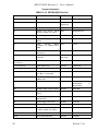
TABLE 1-1.
TABLE 3-1.
TABLE 3-2.
TABLE 3-3.
TABLE 3-4.
TABLE 3-5.
TABLE 3-6.
TABLE 3-7.
TABLE 3-8.
TABLE 3-9.
TABLE 3-10.
TABLE 3-11.
TABLE 3-12.
TABLE 4-1.
TABLE 4-2.
TABLE 4-3.
TABLE 4-4.
TABLE 4-5.
TABLE 4-6.
TABLE 4-7.
TABLE 4-8.
TABLE 4-9.
TABLE 4-10.
TABLE 4-11.
TABLE 4-12.
TABLE 4-13.
TABLE 4-14.
TABLE 4-15.
TABLE 4-16.
TABLE 4-17.
TABLE 5-1
TABLE 5-2
TABLE 5-3
TABLE 5-4.
TABLE 5-5.
TABLE 5-6.
TABLE 5-7.
TABLE 5-8.
TABLE 5-9.
TABLE 5-10.
TABLE 5-11.
TABLE 5-12.
TABLE 5-13.
TABLE 5-14.
MPC821ADS Specifications
MPC821ADS Main Memory Map
SIU REGISTERS’ PROGRAMMING
Memory Controller Initializations For 50Mhz
UPMA Initializations for 60nsec DRAMs @ 50MHz
UPMA Initializations for 70nsec DRAMs @ 50MHz
UPMA Initializations for 60nsec EDO DRAMs @ 50MHz
UPMA Initializations for 70nsec EDO DRAMs @ 50MHz
Memory Controller Initializations For 25Mhz
UPMA Initializations for 60nsec DRAMs @ 25MHz
UPMA Initializations for 70nsec DRAMs @ 25MHz
UPMA Initializations for 60nsec EDO DRAMs @ 25MHz
UPMA Initializations for 70nsec EDO DRAMs @ 25MHz
Regular DRAM Performance Figures
EDO DRAM Performance Figures
DRAM ADDRESS CONNECTIONS
Flash Memory Performance Figures
BCSR0 Description
BCSR1 Description
PCCVPP(0:1) Assignment
BCSR2 Description
Flash Presence Detect (4:1) Encoding
DRAM Presence Detect (2:1) Encoding
DRAM Presence Detect (4:3) Encoding
EXTOOLI(0:3) Assignment
BCSR3 Description
MPC821ADS Revision Number Conversion Table
FLASH Presence Detect (7:5) Encoding
Debug Port Control / Status Register
Off-board Application Maximum Current Consumption
P1 - ADI Port Interconnect Signals
P2 - Ethernet Port Interconnect Signals
P3 - Interconnect Signals
P4 - PCMCIA Connector Interconnect Signals
P5 - Interconnect Signals
P6 - Interconnect Signals
P9 - Interconnect Signals
P10 - Interconnect Signals
P12 - Interconnect Signals
P7 - Interconnect Signals
P8 - Interconnect Signals
P11 - Interconnect Signals
P13 - Interconnect Signals
MPC821ADS Part List
1
20
21
22
24
25
26
27
27
30
31
32
33
39
39
42
44
49
50
51
52
52
53
53
53
54
54
55
57
60
62
63
63
64
67
69
74
79
84
88
88
89
91
95
Release 1.3a
Thi d
t
t d ith F
M k
404
MPC821ADS, Revision A - User’s Manual
General Information
1 - General Information
1•1
Introduction
This document is an operation guide for the MPC821ADS board. It contains operational, functional and
general information about the ADS. The MPC821ADS is meant to serve as a platform for s/w and h/w development around the MPC821. Using its on-board resources and its associated debugger, a developer is
able to load his code, run it, set breakpoints, display memory and registers and connect his own proprietary
h/w via the expansion connectors, to be incorporated to a desired system with the pda.
This board could also be used as a demonstration tool, i.e., application s/w may be burnedA into its flash
memory and ran in exhibitions etc‘.
1•2
Abbreviations’ List
•
PDA - Personal Digital Assistant, the MPC821
•
•
•
•
•
•
•
•
UPM - User Programmable Machine
GPCM - General Purpose Chip-select Machine
GPL - General Purpose Line (associated with the UPM)
I/R - Infra-Red
MPCADS - the MPC821ADS, the subject of this document.
BSCR - Board Control & Status Register.
ZIF - Zero Input Force
BGA - Ball Grid Array
1•3
Related Documentation
•
•
•
•
MPC821 User’s Manual.
MC68160 Data Sheet.
ADI Board Specification.
1•4
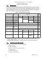
SPECIFICATIONS
The MPC821ADS specifications are given in TABLE 1-1.
TABLE 1-1. MPC821ADS Specifications
CHARACTERISTICS
SPECIFICATIONS
Power requirements (no other boards attached)
+5Vdc @ 1.7 A (typical), 3 A (maximum)
+12Vdc - @1A.
Microprocessor
MPC821 @ 50 MHz
A. Either on or off-board.
1
Release 1.3a
Thi d
t
t d ith F
M k
404
MPC821ADS, Revision A - User’s Manual
General Information
TABLE 1-1. MPC821ADS Specifications
CHARACTERISTICS
Addressing
Total address range:
Flash Memory
Dynamic RAM
SPECIFICATIONS
4 GigaBytes
2 MByte, 32 bits wide expandable to 8 MBytes
4 MByte, 36 bits wide SIMM (32 bit data, 4 bit parity)
option to use higher density SIMM, up to 32 MByte
Operating temperature
0OC - 30OC
Storage temperature
-25OC to 85OC
Relative humidity
5% to 90% (non-condensing)
Dimensions:
Height
Depth
Thickness
9.173 inches (233 mm)
7.08 inches (180 mm)
0.063 inches (1.6 mm)
2
Release 1.3a
MPC821ADS, Revision A - User’s Manual
General Information
1•5
MPC821ADS Features
❏
MPC821, running up to 50 MHz, mounted on ZIF BGA socket.
❏
4 MBytes of 60-nsec DRAM, support is given to various types of memory varying from
4MByte configured as 1M X 32, upto 32MByte configured as 8M X 32.
❏
Support for EDO page mode DRAM SIMMs made by Micron - the MT8D432X and the
MT16D832X.
❏
Automatic Dram SIMM identification.
❏
2 MByte Flash SIMM. Support for upto 8 MByte.
❏
Automatic Flash SIMM identification.
❏
Memory Disable Option for all local memory map slaves.
❏
Board Control & Status Register - BCSR, Controlling Board’s Operation.
❏
Programmable Hard-Reset Configuration via BCSR.
❏
T.P. Ethernet port via MC68160 - EEST on SCC1 with Standby Mode.
❏
Infra-Red Transceiver on SCC2 with Shutdown Option.
❏
5V-only PCMCIA Socket With Full Buffering, Power Control and Port Disable Option. Complies with PCMCIA 2.1+ Standard.
❏
Module Enable Indications.
❏
RS232 port on SMC1 with Low-Power Option.
❏
On - Board Debug Port Controller with ADI I/F.
❏
MPC821ADS Serving as Debug Station for Target System option.
❏
LCD Display Connector.
❏
Optional Hard-Reset Configuration Burned in FlashA.
❏
All MPC Pins Available At Expansion & Logic Analyzer Connectors.
❏
External Tools’ Identification Capability, via BCSR.
❏
Soft / Hard Reset Push - Button
❏
ABORT Push - Button
❏
SingleB 5V Supply.
❏
Reverse / Over Voltage Protection for Power Inputs.
❏
3.3V / 2V MPC Internal Logic Operation, 3.3V MPC I/O Operation.
A. Available only if supported also on-chip.
B. Unless a 12V supply is required for a PCMCIA card.
3
Release 1.3a
MPC821ADS, Revision A - User’s Manual
General Information
❏
External Keep Alive Power Source Option.
❏
Power Indications for Each Power Bus.
❏
Software Option Switch provides 16 S/W options via BCSR.
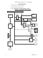
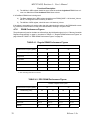
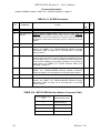
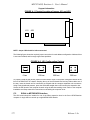
FIGURE 1-1 MPC821ADS Block Diagram
Expansion & Logic - Analyzer Connectors
DATA & ADDRESS
BUFFERS
FLASH Mem.
2 - 8MByte
Reset,
Interrupts
& Clock
Control &
Status
Register
EEST
Debug
Port
Connector
PCMCIA
Buffering
&
Control
PCMCIA
PORT
RS232
PORT
Infra-Red Port
MPC821
ETHERNET
PORT 1
DRAM
4 - 32 Mbyte
Dram Width
& Size Logic
DEBUG
CONTROLLER
LCD
PORT
PORT
(ADI I/F)
ADI PORT
4
Release 1.3a
MPC821ADS, Revision A - User’s Manual
General Information
1•6
Revision Pilot to Revision A Changes
1)
DS2 which on PILOT revision was connected on SP2 with blue wires, is now integrated into the
PCB, located nearby SP2.
2)
UA38 which on revision PILOT was glued and connected with blue-wires, is now integrated into
the PCB. Gate allocation within UA38, is different from revision PILOT, to provide better PCB
routing.
3)
Revision code in BCSR is changed to 2.
4)
Added optional RA21 (0 ohm) and CA7 (0.01µF) for 10-Base-T interface network.
5)
Some SMD pads were enlarged to assist manufacturing.
1•7
Revision ENG to Revision PILOT Changes
1)
Added support for ads to function as debug station:
•
Added independent 20MHz clock generator for debug port controller
•
Added MUX (U38) so that internal logic is clocked by the above generator
•
Removed pervious debug clock logic, derived from CLKOUT of the MPC.
•
Added signal named CHINS~ (CHip-In-Socket, active-low) which is connected to one
of the MPC's GND pins (isolated from GND layer). This signal controls the above mux
and the indication LEDs illumination.
•
Added pull-up resistors on the Chip-Select lines, to avoid possible data-bus contention
when MPC is off-socket.
•
DRAMEN~ becomes active-low to allow buffer manipulation supporting LEDs darkness when MPC off-socket. Signal RUN becomes active-high from the same reason.
(Sh. 1, 7, 8, 9, 11, 14)
2)
Signals EXTM(1:4) changed to BADDR(28:30),AS~ correspondingly, to support future external
master support. (Sh. 1, 11, 13)
3)
MODCK0 renamed to MODCK2, to comply with MPC’s spec convention. (Sh 1, 3, 13)
4)
Signal BCLOS~, which was optional for data buffers’ enable logic, is found redundant and removed from ADS logic. Renamed to GPL4A~. (Sh 1, 2, 3, 12)
5)
Added 3 Flash memory Presence Detect lines - F_PD(5:7) to BCSR (U11/65:67) (ENG - U10)
to support varying flash memory delays. (Sh 3, 4, 11)
6)
Added support for SMART flash simms:
•
12V VPP connected to SIMM
•
BA10 connected also to the SIMM, to support 1M X 8 devices
(Sh. 4)
5
7)
BCSR power on reset logic was changed to support board’s power-up recovery when keep-alive
power remained active. (Sh. 3, 9)
8)
Power-on reset logic changes:
•
KA power-on reset is not driven by U10 (ENG - U9) but directly to the MPC.
•
Added AC14 (U23) powered by KAPWR to support this. (AC14’s s-t is required for
mach connection due to slow rise time of PORST~)
•
D3 and R12 powered from KAPWR from the same reason.
•
Added option for PON reset by main 3.3V bus. (J1)
Release 1.3a
MPC821ADS, Revision A - User’s Manual
General Information
(Sh. 3, 9)
9)
BA9 and BA10 are connected to U10 (ENG - U9) instead of BA11 and BA12, for flash bank selection. Bug correction. (Sh. 3)
10) Renewed support for 32Khz crystal:
•
CLK4IN is gated (UA38), so when working with 32768 Hz crystal, CLK4IN is driven
constantly to '0'. This, to avoid clock jitter with this mode of operation.
•
Parallel resistor increased to 20MΩ.
(Sh. 7)
11) PLL’s XFC capacitors were changed to react for formula change. Lower MF range capacitor is
changed to 5nF to cover 1:5 to 1:10 MF range, while higher MF range capacitor was changed
to 0.68uF to cover 1:458A to 1:1220B MF range
(Sh. 7)
12) PCMCIA power controller is changed to LTC1315 (by Linear Technologies):
•
PCCVPPG~ signal and indication are removed, not supported by this device
•
VPP selection code is changed.
•
DRAMEN no longer controls power to the dram.
•
Old 12V voltage pump remains as contingency for possible unavailability of the device,
although the device switching outputs drive 12V. R55, R56 & R59 are therefore not assembled.
(Sh. 3, 9)
13) Added ADS board revision tag in BCSR.
14) Added signals RS_EN~ and ETHEN~ to P13 - Quads Compatible connector, for tool designer
benefit. (Sh. 16)
15) Added 4-switches dip-switch - DS2, connected over EXTOLI(0:3) lines, to provide s/w option selection capability.
A. Lowest MF allowed with 32768 Hz crystal, due to 15MHz minimal PLL frequency.
B. Highest MF allowed with 32768 Hz crystal, considering 40MHz rated MPC.
6
Release 1.3a
MPC821ADS, Revision A - User’s Manual
Hardware Preparation and Installation
2 - Hardware Preparation and Installation
2•1
INTRODUCTION
This chapter provides unpacking instructions, hardware preparation, and installation instructions for the
MPC821ADS.
2•2
UNPACKING INSTRUCTIONS
NOTE
If the shipping carton is damaged upon receipt,
request carrier’s agent to be present during
unpacking and inspection of equipment.
Unpack equipment from shipping carton. Refer to packing list and verify that all items are present. Save
packing material for storing and reshipping of equipment.
CAUTION
AVOID TOUCHING AREAS OF INTEGRATED
CIRCUITRY;
STATIC
DISCHARGE
CAN
DAMAGE CIRCUITS.
2•3
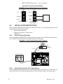
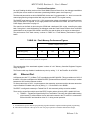
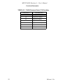
HARDWARE PREPARATION
To select the desired configuration and ensure proper operation of the MPC821ADS board, changes of the
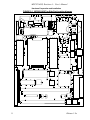
Dip-Switch settings may be required before installation. The location of the switches, LEDs, Dip-Switches,
and connectors is illustrated in FIGURE 2-1. The board has been factory tested and is shipped with DipSwitch settings as described in the following paragraphs. Parameters can be changed for the following
conditions:
•
ADI port address
•
MPC Clock Source
•
Power-On Reset Source.
•
MPC Keep Alive Power Source
•
MPC Internal Logic Supply Source
7
Release 1.3a
MPC821ADS, Revision A - User’s Manual
Hardware Preparation and Installation
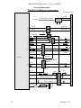
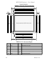
FIGURE 2-1 MPC821ADS Top Side Part Location diagram
8
Release 1.3a
MPC821ADS, Revision A - User’s Manual
Hardware Preparation and Installation
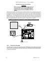
2•3•1
ADI Port Address Selection
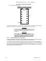
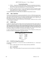
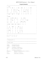
The MPC821ADS can have eight possible slave addresses set for its ADI port, enabling up to eight
MPC821ADS boards to be connected to the same ADI board in the host computer. The selection of the
slave address is done by setting switches 1, 2 & 3 in the Dip-Switch - DS1. Switch 1 stands for the mostsignificant bit of the address and switch 3 stands for the least-significant bit. If the switch is in the ’ON’ state,
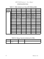
it stands for logical ’1’. In FIGURE 2-2 DS1 is shown to be configured to address ’0’.
FIGURE 2-2 Configuration Dip-Switch - DS1
ON
ADR2
ADR2
1
ADR1
2
ADR1
ADR0
3
ADR0
3 - 5 MHz Generator via CLK4IN
4
32.678 KHz Crystal Resonator
DS1
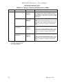
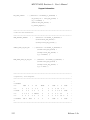
Table 2-1 describes the switch settings for each slave address:
Table 2-1 ADI Address Selection
2•3•2
ADDRESS
Switch 1
Switch 2
Switch 3
0
OFF
OFF
OFF
1
OFF
OFF
ON
2
OFF
ON
OFF
3
OFF
ON
ON
4
ON
OFF
OFF
5
ON
OFF
ON
6
ON
ON
OFF
7
ON
ON
ON
Clock Source Selection
Switch #4 on DS1 selects the clock source for the MPC. When it is in the ’ON’ position while the ADS is
powered-up, the on-board 32.768 KHz crystal resonator becomes the clock source and the PLL
multiplication factor becomes 1:513. When switch #4 is in the ’OFF’ position while the ADS is powered-up,
the on-board 4AMHz clock generator (U17) becomes the clock source while the PLL multiplication factor
becomes 1:5.
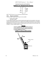
2•3•2•1
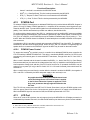
Clock Generator Replacement - U17
When replacing U17 with another clock generator it should be noticed that there are 2 supply level available
at U17:
1)
5V supply at pin 14.
A. A 5MHz clock generator is provided as well.
9
Release 1.3a
MPC821ADS, Revision A - User’s Manual
Hardware Preparation and Installation
2)
3.3V supply available at pin 11.
FIGURE 2-3 U17 Power Sources
14
1
5V
3.3V
GND 7
8
U17
From looking at FIGURE 2-3 "U17 Power Sources" above, we see that 5V oscillator may be used with 14
pins only form-factor while 3.3V oscillators may be used with 8 pins only form-factor.
WARNING
IF A 14 Pin Form-Factor, 3.3V Clock Generator is inserted to U17, PERMANENT DAMAGE Might Be Inflicted To
The Device.
WARNING
Since the MPC clock input is NOT 5V FRIENDLY, any
clock generator inserted to U17, MUST BE 3.3V compatible. If a 5V output clock generator is inserted to U17,
PERMANENT DAMAGE might be inflicted to the MPC.
2•3•3
Power-On Reset Source Selection
As there are differences between MPC revisions regarding the functionality of the Power-On Reset logic,
it is therefore necessary to select different sources for Power-ON reset generation.
J1 on the ADS is used to select Power-On Reset source: when a jumper is placed between positions 1 - 2
of J1, Power-On reset to the MPC is generated by the Keep-Alive power rail. I.e., When KAPWR goes
below 2.005V - Power-On reset is generated. When a jumper is place between position 2 - 3 of J1, PowerOn reset to the MPC is generated from the MAIN 3.3V power rail. I.e, when the MAIN 3.3V power rail goes
below 2.805V Power-On reset is generated.
10
Release 1.3a
MPC821ADS, Revision A - User’s Manual
Hardware Preparation and Installation
FIGURE 2-4 Power-On Reset Source Selection
J1
J1
1
1
KA Power Rail
2•3•4
MAIN Power Rail
VDDL Source Selection
J2 serves as a selector for VDDL - MPC internal logic supply. When a jumper is placed between positions
1 - 2 of J2, VDDL is supplied with 3.3V. When a jumper is placed between positions 2 - 3 of J2, VDDL is
supplied by 2V power source. The jumper on J2 is factory set between positions 1 - 2 to supply 3.3 to
VDDL.
FIGURE 2-5 VDDL Source Selection
J2
1
VDDL - 3.3V
2•3•5
J2
1
VDDL - 2V
Keep Alive Power Source Selection
J3 selects the Keep Alive power source of the MPC. When a jumper is placed between positions 1 - 2 of
J3, the Keep Alive power is fed from the main 3.3V bus. When an external power sourceA is to be connected to the Keep Alive power rail, it should be connected between positions 2 (the positive pole) and position
3 (GND) of J3.
A. E.g., a battery.
11
Release 1.3a
MPC821ADS, Revision A - User’s Manual
Hardware Preparation and Installation
FIGURE 2-6 Keep Alive Power Source Selection
J3
1
3.3V
3.3V
1
KAPWR
KAPWR
+
GND
GND
-
KAPWR From 3.3V
2•4
J3
Ext. Power Supply
KAPWR From Ext.
Power Supply
INSTALLATION INSTRUCTIONS
When the MPC821ADS has been configured as desired by the user, it can be installed according to the
required working environment as follows:
•
Host Controlled Operation
•
Debug Port Controller for Target System
•
Stand-Alone
2•4•1
Host Controlled Operation
In this configuration the MPC821ADS is controlled by a host computer via the ADI through the debug port.
This configuration allows for extensive debugging using on-host debugger.
FIGURE 2-7 Host Controlled Operation Scheme
ADI
Host
Computer
37 Wire
Flat Cable
P1
5V Power Supply
P7
2•4•2
Debug Port Controller For Target System
This configuration resembles the previous, but here the local MPC is removed from its socket while the
ADS is connected via a 10 lead Flat-Cable between P5 and a matching connector on a target system.
12
Release 1.3a
MPC821ADS, Revision A - User’s Manual
Hardware Preparation and Installation
WARNING
When connecting the ADS to a target system via P5 and
a 10 lead flat-cable, the MPC MUST be REMOVED from
its SOCKET (U18). Otherwise, PERMANENT DAMAGE
might be inflicted to either the Local MPC or to the Target MPC.
With this mode of operation, all on-board modules are disabled and can not be accessed in anyway, except
for the debug port controller. Also, all indications except for 5V power, 3.3V power and RUN are darkened.
All debugger commands and debugging features are available in this mode, including s/w download,
breakpoints, etc‘... The target system may be reset or interrupted by the debug port or reset by the ADS’s
RESET switches. It is the responsibility of the target system designer, to provide Power-On-Reset and
HARD-Reset configurations, while SOFT-Reset configuration is provided by the debug-port controller. See
also 4•15•1 "MPC821/860ADS As Debug Port Controller For Target System" on page 56.
FIGURE 2-8 Debug Port Controller For Target System Operation Scheme
Target System
10 Wire
37 Wire
ADI
Host
Computer
Flat Cable
Flat Cable
P1
5V Power Supply
P5
P7
MPC Removed From Socket
2•4•3
Stand Alone Operation
In this mode, the board is not controlled by the host via the ADI/Debug port. It may connect to host via one
of its other ports, e.g., RS232 port, I/R port, Ethernet port, etc‘. Operating in this mode requires an application program to be programmed into the board‘s Flash memory (while with the host controlled operation,
no memory is required at all).
13
Release 1.3a
MPC821ADS, Revision A - User’s Manual
Hardware Preparation and Installation
FIGURE 2-9 Stand Alone Configuration
Et
he
rn
RS et
23
2
Host
Computer
I/R
P2 P3
5V Power Supply
P7
2•4•4
+5V Power Supply Connection
The MPC821ADS requires +5 Vdc @ 5 A max, power supply for operation. Connect the +5V power supply
to connector P7 as shown below:
FIGURE 2-10 P7: +5V Power Connector
+5V
1
GND
2
GND
3
P7 is a 3 terminal block power connector with power plug. The plug is designed to accept 14 to 22 AWG
wires. It is recommended to use 14 to 18 AWG wires. To provide solid ground, two Gnd terminals are
supplied. It is recommended to connect both Gnd wires to the common of the power supply, while VCC is
connected with a single wire.
2•4•5
NOTE
Since hardware applications may be connected to the
MPC821ADS using the expansion connectors P6, P9, P10,
P12 or P13, the additional power consumption should be
taken into consideration when a power supply is connected to
the MPC821ADS.
P8: +12V Power Supply Connection
The MPC821ADS requires +12 Vdc @ 1 A max, power supply for the PCMCIA channel Flash
programming capability. The MPC821ADS can work properly without the +12V power supply, if there is no
need to program a 12V programmable PCMCIA flash card.
Connect the +12V power supply to connector P6 as shown below:
14
Release 1.3a
MPC821ADS, Revision A - User’s Manual
Hardware Preparation and Installation
FIGURE 2-11 P8: +12V Power Connector
+12V
1
GND
2
P8 is a 2 terminal block power connector with power plug. The plug is designed to accept 14 to 22 AWG
wires. It is recommended to use 14 to 18 AWG wires.
2•4•6
ADI Installation
For ADI installation on various host computers, refer to APPENDIX C - "ADI Installation" on page 176.
2•4•7
Host computer to MPC821ADS Connection
The MPC821ADS ADI interface connector, P1, is a 37 pin, male, D type connector. The connection
between the MPC821ADS and the host computer is by a 37 line flat cable, supplied with the ADI board.
FIGURE 2-12 below shows the pin configuration of the connector.
FIGURE 2-12 P1 - ADI Port Connector
Gnd
Gnd
Gnd
Gnd
Gnd
Gnd
(+ 12 v) N.C.
HOST_VCC
HOST_VCC
HOST_VCC
HOST_ENABLE~
Gnd
Gnd
Gnd
PD0
PD2
PD4
PD6
20
21
22
23
24
25
26
27
28
29
30
31
32
33
34
35
36
37
1
2
3
4
5
6
7
8
9
10
11
12
13
14
15
16
17
18
19
N.C
D_C~
HST_ACK
ADS_SRESET
ADS_HRESET
ADS_SEL2
ADS_SEL1
ADS_SEL0
HOST_REQ
ADS_REQ
ADS_ACK
N.C.
N.C.
N.C.
N.C.
PD1
PD3
PD5
PD7
NOTE: Pin 26 on the ADI is connected to +12 v power supply, but it is not used in the MPC821ADS.
2•4•8
Terminal to MPC821ADS RS-232 Connection
A serial (RS232) terminal or any other RS232 equipment, may be connected to the RS-232 connector P3.
The RS-232 connector is a 9 pin, female, D-type connector as shown in FIGURE 2-13.
The connector is arranged in a manner that allows for 1:1 connection with the serial port of an IBM-ATA or
compatibles, i.e. via a flat cable.
A. IBM-AT is a trademark of International Business Machines Inc.
15
Release 1.3a
MPC821ADS, Revision A - User’s Manual
Hardware Preparation and Installation
FIGURE 2-13 P3 - RS-232 Serial Port Connector
CD
TX
1
2
RX
DTR
3
4
5
GND
6
7
8
9
DSR
RTS
CTS
N.C.
NOTE: The RTS line (pin 7) is not connected on the MPC821ADS.
2•4•9
Memory Installation
The MPC821ADS is supplied with two types of memory SIMM:
•
Dynamic Memory SIMM
•
Flash Memory SIMM.
To avoid shipment damage, these memories are packed aside rather than being installed in their sockets.
Therefore, they should be installed on site. To install a memory SIMM, it should be taken out of its package,
put diagonally in its socket (no error can be made here, since the Flash socket has 80 contacts, while the
DRAM socket has 72) and then twisted to a vertical position until the metal lock clips are locked. See
FIGURE 2-14 "Memory SIMM Installation" below.
CAUTION
The memory SIMMs have alignment nibble near their # 1
pin. It is important to align the memory correctly before
it is twisted, otherwise damage might be inflicted to both
the memory SIMM and its socket.
FIGURE 2-14 Memory SIMM Installation
(1)
(2)
Memory
SIMM
Metal Lock Clip
SIMM Socket
16
Release 1.3a
MPC821ADS, Revision A - User’s Manual
OPERATING INSTRUCTIONS
3 - OPERATING INSTRUCTIONS
3•1
INTRODUCTION
This chapter provides necessary information to use the MPC821ADS in host-controlled and stand-alone
configurations. This includes controls and indicators, memory map details, and software initialization of the
board.
3•2
CONTROLS AND INDICATORS
The MPC821ADS has the following switches and indicators.
3•2•1
SOFT RESET Switch SW1
The SOFT RESET switch SW1 performs Soft reset to the MPC internal modules, maintaining MPC’s
configuration (clocks & chip-selects) and dram contents. The switch signal is debounced, and it is not
possible to disable it by software. At the end of the Soft Reset Sequence, the Soft Reset Configuration is
sampled and becomes valid.
3•2•2
ABORT Switch SW2
The ABORT switch is normally used to abort program execution, this by issuing a level 0 interrupt to the
MPC. If the ADS is in stand alone modeA, it is the responsibility of the user to provide means of handling
the interrupt, since there is no resident debugger with the MPC821ADS. The ABORT switch signal is
debounced, and can not be disabled by software.
3•2•3
HARD RESET - Switches SW1 & SW2
When BOTH switches - SW1 and SW2 are depressed simultaneously, HARD reset is generated to the
MPC. When the MPC is HARD reset, all its configuration is lost, including data stored in the DRAM and the
MPC has to be re-initialized. At the end of the Hard Reset sequence, the Hard Reset Configuration stored
in BCSR0 becomes valid.
3•2•4
DS2 - Software Options Switch
DS2 is a 4-switches Dip-Switch, mounted over SP2. This switch is connected over EXTOLI(0:3) lines, and
since EXTOLI(0:3) lines are available at BCSR, S/W options may be manually selected, according to DS2
state.
FIGURE 3-1 DS2 - Description
ON
EXTOLI0 Pulled to ’1’
1
EXTOLI1 Pulled to ’1’
2
EXTOLI1 Driven to ’0’
EXTOLI2 Pulled to ’1’
3
EXTOLI2 Driven to ’0’
EXTOLI3 Pulled to ’1’
4
EXTOLI3 Driven to ’0’
EXTOLI0 Driven to ’0’
DS2
A. I.e., detached from a debug station.
17
Release 1.3a
MPC821ADS, Revision A - User’s Manual
OPERATING INSTRUCTIONS
3•2•5
J4 Power Bridge
J4 is a soldered jumper, which is in series with the 3.3V power bus. This jumper may be removedA if current
measurements on the 3.3V bus are to be held.
Warning
There are also GND bridges on board, which physically
resemble J4. Do not mistake J4 to be a GND jumper, otherwise, permanent damage might be inflicted to the
MPC821ADS.
3•2•6
GND Bridges
There are 4 GND bridges on the MPC821ADS. They are meant to assist general measurements and logicanalyzer connection.
Warning
When connecting to a GND bridge, use only INSULATED
GND clips. Failure in doing so, might result in permanent damage to the MPC821ADS.
3•2•7
RUN Indicator - LD1
When the green RUN led - LD1 is lit, it indicates that the MPC is not in debug mode, i.e., VFLS0 & VFLS1
== 0. It is important to remember, that if the VFLS(0:1) pins are programmed for alternative use rather than
function as VFLS lines, this indication is meaningless.
3•2•8
FLASH ON - LD2
When the yellow FLASH ON led is lit, it indicates that the FLASH module is enabled in the BCSR1 register.
I.e., any access done to the CS0~ address space will hit the flash memory. When it is dark, the flash is
disabled and CS0~ may be used off-board via the expansion connectors.
3•2•9
DRAM ON - LD3
When the yellow DRAM ON led is lit, it indicates the DRAM is enabled in BCSR1. Therefore, any access
made to CS1~ (or CS2~) will hit on the DRAM. When it is dark, it indicates that either the DRAM is disabled
in BCSR1, enabling the use of CS1~ and CS2~ off-board via the expansion connectors.
3•2•10
ETH ON - LD4
When the yellow ETH ON led is lit, it indicates that the ethernet port transceiver - the MC68160 EEST,
connected to SCC1 is active. When it is dark, it indicates that the EEST is in power down mode, enabling
the use of SCC1 pins off-board via the expansion connectors.
3•2•11
Ethernet RX Indicator - LD5
The green Ethernet Receive LED indicator blinks whenever the EEST is receiving data from one of the
Ethernet port.
3•2•12
Ethernet TX Indicator - LD6
The green Ethernet Receive LED indicator blinks whenever the EEST is transmitting data via the Ethernet
port.
3•2•13
Ethernet JABB Indicator - LD7
The red Ethernet TP Jabber LED indicator - JABB, lights whenever a jabber condition is detected on the
TP ethernet port.
3•2•14
IRD ON - LD8
A. By a skilled technician only.
18
Release 1.3a
MPC821ADS, Revision A - User’s Manual
OPERATING INSTRUCTIONS
When the yellow IRD ON led is lit, it indicates that the Infra-Red transceiver - the TFDS3000, connected to
SCC2, is active and enables communication via that medium. When it is dark, the I/R transceiver is in
shutdown mode, enabling the use of SCC2 pins off-board via the expansion connectors.
3•2•15
Ethernet CLSN Indicator LD9
The red Ethernet Collision LED indicator CLSN, blinks whenever a collision condition is detected on the
ethernet port, i.e., simultaneous receive and transmit.
3•2•16
Ethernet PLR Indicator - LD10
The red Ethernet TP Polarity LED indicator - PLR, lights whenever the wires connected to the receiver input
of the ethernet port are reversed. The LED is lit by the EEST, and remains on while the EEST has
automatically corrected for the reversed wires.
3•2•17
Ethernet LIL Indicator - LD11
The yellow Ethernet Twisted Pair Link Integrity LED indicator - LIL, lights to indicate good link integrity on
the TP port. The LED is off when the link integrity fails.
3•2•18
RS232 ON - LD12
When the yellow RS232 ON led is lit, it designates that the RS232 transceiver connected to SMC1, is active
and communication via that medium is allowed. When dark, it designates that the transceiver is in
shutdown mode, so SMC1 pins may be used off-board via the expansion connectors.
3•2•19
PCMCIA ON - LD13
When the yellow PCMCIA ON led is lit, it indicates the following:
1)
Address & strobe buffers are driven towards the PCMCIA card
2)
Data buffers may be driven to / from the PCMCIA card depending on the CE1A~ and CE2A~
signals and transfer direction.
3)
Card status lines are driven towards the MPC from the PCMCIA card.
When it is dark, it indicates that all the above buffers are tri-stated and the pins associated with PCMCIA
channel A, may be used off-board via the expansion connectors.
3•2•20
5V Indicator - LD14
The yellow 5V led, indicates the presence of the +5V supply at P7.
3•2•21
3.3V Indicator - LD15
The yellow 3.3V led indicates that the 3.3V power bus is powered
19
Release 1.3a
MPC821ADS, Revision A - User’s Manual
OPERATING INSTRUCTIONS
3•3
MEMORY MAP
All accesses to MPC821ADS’s memory slaves are controlled by the MPC’s memory controller. Therefore,
the memory map is reprogrammable to the desire of the user. After Hard Reset is performed by the debug
station, the debugger checks to see the size, delay and type of the DRAM and FLASH memory mounted
on board and initializes the chip-selects accordingly. The DRAM and the FLASH memory respond to all
types of memory access i.e., user / supervisory, program / data and DMA.
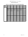
TABLE 3-1. MPC821ADS Main Memory Map
ADDESS RANGE
Memory Type
00000000 - 003FFFFF
DRAM SIMM
00400000 - 007FFFFF
DRAM SIMM
00800000 - 00FFFFFF
DRAM SIMM
01000000 - 01FFFFFF
DRAM SIMM
02000000 - 020FFFFF
Empty Space
02100000 - 02103FFF
BCSR(0:3)a
02104000 - 021FFFFF
Empty Space
02200000 - 02207FFF
MPC Internal
MAPc
02208000 - 027FFFFF
Empty Space
02800000 - 029FFFFF
Flash SIMM
Port
Size
Device Type
MCM36100
MCM36200
MCM36400
MCM36800
32
MCM36200
MCM36400
MCM36800
32
MCM36400
MCM36800
32
MCM36800
32
32b
32
MCM29F020
02A00000 - 02BFFFFF
MCM29F040
SM732A1000A
MCM29F080
SM732A2000
32
MCM29F040
SM732A1000A
MCM29F080
SM732A2000
32
MCM29F080
SM732A2000
32
02C00000 - 02FFFFFF
a. The device appears repeatedly in multiples of its size. E.g., BCSR0 appears at memory locations
2100000, 2100010, 2100020..., while BCSR1 appears at 2100004, 2100014, 2100024... and so on.
b. Only upper 16 bit are in fact used.
c. Refer to the MPC821 User’s Manual for complete description of the MPC internal memory map.
3•4
Programming The MPC Registers
The MPC provides the following functions on the MPC821ADS:
20
1)
DRAM Controller
2)
Chip Select generator.
3)
UART for terminal or host computer connection.
4)
Ethernet controller.
5)
Infra-Red Port Controller
6)
General Purpose I/O signals.
Release 1.3a
MPC821ADS, Revision A - User’s Manual
OPERATING INSTRUCTIONS
The internal registers of the MPC must be programmed after Hard reset as described in the following
paragraphs. The addresses and programming values are in hexadecimal base.
For better understanding the of the following initializations refer to the MPC821 User’s Manual for more
information.
TABLE 3-2. SIU REGISTERS’ PROGRAMMING
Register
Init Value[hex]
Description
SIUMCR
01632440
Internal arbitration, External master arbitration priority - 0, External arbitration
priority - 0, PCMCIA channel II pins - debug pins, Debug Port on JTAG port pins,
FRZ/IRQ6~ - IRQ6~, debug register - locked, No parity for non-CS regions,
DP(0:3)/IRQ(3:6)~ pins - DP(0:3), reservation disabled, SPKROUT - Tri-stated,
BS_A(0:3)~ and WE(0:3)~ are driven just on their dedicated pins, GPL_B5~
enabled, GPL_A/B(2:3)~ function as GPLs.
SYPCR
FFFFFF88
Software watchdog timer count - FFFF, Bus-monitor timing FF, Bus-monitor Enabled, S/W watch-dog - Freeze, S/W watch-dog - disabled, S/W watch-dog (if
enabled) causes NMI, S/W (if enabled) not prescaled.
TBSCR
00C2
No interrupt level, reference match indications cleared, interrupts disabled, no
freeze, time-base disabled.
RTCSC
01C2
Interrupt request level - 1, 32768 Hz source, second interrupt disabled, Alarm
interrupt disabled, Real-time clock - FREEZE, Real-time clock disabled.
PISCR
0082
No level for interrupt request, Periodic interrupt disabled, clear status, interrupt
disabled, FREEZE, periodic timer disabled.
3•4•1
Memory Controller Registers Programming
The memory controller on the MPC821ADS is initialized to 50 MHz operation. I.e., registers’ programming
is based on 50 MHZ timing calculation except for refresh timer which is initialized to 16.67Mhz, the lowest
frequency at which the ADS may wake up. Since the ADS may be made to wake-up at 25MHzA as well,
the initializations are not efficient, since there are too many wait-states inserted. Therefore, additional set
of initialization is provided to support efficient 25MHz operation.
The reason for initializing the ADS for 50Mhz is to allow proper (although not efficient) ADS operation
through all available ADS clock operation frequencies.
A. The only parameter which is initialized to the start-up frequency, is the refresh rate, which would have been inadequate if initialized to 50Mhz while board is running at a lower frequency. Therefore, for best bus bandwidth availability, refresh rate should be adapted to the current system clock frequency.
21
Release 1.3a
MPC821ADS, Revision A - User’s Manual
OPERATING INSTRUCTIONS
Warning
Due to availability problems with few of the supported
memory components, the below initializations were not
tested with all parts. Therefore, the below initializations
are liable to CHANGE, throughout the testing period.
TABLE 3-3. Memory Controller Initializations For 50Mhz
Register
Device Type
BR0
All
Flash
supported.
OR0
Description
02200001
Base at 2200000, 32 bit port size, no parity, GPCM
MCM29F020-90
FFE00D34
2MByte block size, all types access, CS early negate,
6 w.s., Timing relax
MCM29F040-90
SM732A1000A-9
FFC00D34
4MByte block size, all types access, CS early negate,
6 w.s., Timing relax
MCM29F080-90
SM732A2000-9
FF800D34
8MByte block size, all types access, CS early negate,
6 w.s., Timing relax
MCM29F020-12
FFE00D44
2MByte block size, all types access, CS early negate,
8 w.s., Timing relax
MCM29F040-12
SM732A1000A-12
FFC00D44
4MByte block size, all types access, CS early negate,
8 w.s., Timing relax
MCM29F080-12
SM732A2000-12
FF800D44
8MByte block size, all types access, CS early negate,
8 w.s., Timing relax
BR1
BCSR
02100001
Base at 2100000, 32 bit port size, no parity, GPCM
OR1
BCSR
FFFF8110
32 KByte block size, all types access, CS early
negate, 1 w.s.
BR2
All
Dram
Supported
00000081
Base at 0, 32 bit port size, no parity, UPMA
OR2
MCM36100/200-60/70
FFC00800
4MByte block size, all types access, initial address
multiplexing according to AMA.
MCM36400/800-60/70
MT8/16D432/832X-6/7
FF000800
16MByte block size, all types access, initial address
multiplexing according to AMA.
MCM36200-60/70
00400081
Base at 400000, 32 bit port size, no parity, UPMA
MCM36800-60/70
MT16D832X-6/7
01000081
Base at 1000000, 32 bit port size, no parity, UPMA
MCM36200-60/70
FFC00800
4MByte block size, all types access, initial address
multiplexing according to AMA
MCM36800-60/70
MT16D832X-6/7
FF000800
16MByte block size, all types access, initial address
multiplexing according to AMA.
0400
Divide by 16 (decimal)
BR3
OR3
MPTPR
22
All
Dram
Supported
SIMMs
Init Value [hex]
SIMMs
SIMMs
Release 1.3a
MPC821ADS, Revision A - User’s Manual
OPERATING INSTRUCTIONS
TABLE 3-3. Memory Controller Initializations For 50Mhz
Register
MAMR
Device Type
Init Value [hex]
Description
MCM36100-60/70
40A21114a
60A21114b
C0A21114c
refresh clock divided by 40a or 60b or C0c, periodic
timer enabled, type 2 address multiplexing scheme, 1
cycle disable timer, GPL4 disabled for data sampling
edge flexibility, 1 loop read, 1 loop write, 4 beats
refresh burst.
MCM36200-60/70
20A21114a
30A21114b
60A21114c
refresh clock divided by 20a or 30b or 60c, periodic
timer
enabled, type 2 address multiplexing scheme, 1 cycle
disable timer, GPL4 disabled for data sampling edge
flexibility, 1 loop read, 1 loop write, 4 beats refresh
burst.
MCM36400-60/70
MT8D432X-6/7
40B21114a
60B21114b
C0B21114c
refresh clock divided by 40a or 60b or C0c, periodic
timer
enabled, type 3 address multiplexing scheme, 1 cycle
disable timer, GPL4 disabled for data sampling edge
flexibility, 1 loop read, 1 loop write, 4 beats refresh
burst.
MCM36800-60/70
MT16D832-6/7
20B21114a
30B21114b
60B21114c
refresh clock divided by 20a or 30b or 60c, periodic
timer
enabled, type 3 address multiplexing scheme, 1 cycle
disable timer, GPL4 disabled for data sampling edge
flexibility, 1 loop read, 1 loop write, 4 beats refresh
burst.
a. Assuming 16.67 MHz BRGCLK.
b. Assuming 25MHz BRGCLK
c. For 50MHz BRGCLK
23
Release 1.3a
MPC821ADS, Revision A - User’s Manual
OPERATING INSTRUCTIONS
TABLE 3-4. UPMA Initializations for 60nsec DRAMs @ 50MHz
Cycle Type
Single Read
Burst Read
Single Write
Burst Write
Refresh
Exception
Offset in UPM
0
8
18
20
30
3C
0
8FFFEC24
8FFFEC24
8FAFCC24
8FAFCC24
C0FFCC84
33FFCC07
1
0FFFEC04
0FFFEC04
0FAFCC04
0FAFCC04
00FFCC04
X
2
0CFFEC04
08FFEC04
0CAFCC00
0CAFCC00
07FFCC04
X
3
00FFEC04
00FFEC0C
11BFCC47
03AFCC4C
3FFFCC06
X
4
00FFEC00
03FFEC00
X
0CAFCC00
FFFFCC85
5
37FFEC47
00FFEC44
X
03AFCC4C
FFFFCC05
6
X
00FFCC08
X
0CAFCC00
X
7
X
0CFFCC44
X
03AFCC4C
X
Contents
@ Offset +
24
8
00FFEC0C
0CAFCC00
X
9
03FFEC00
33BFCC4F
X
A
00FFEC44
X
X
B
00FFCC00
X
X
C
3FFFC847
X
D
X
X
E
X
X
F
X
X
Release 1.3a
MPC821ADS, Revision A - User’s Manual
OPERATING INSTRUCTIONS
TABLE 3-5. UPMA Initializations for 70nsec DRAMs @ 50MHz
Cycle Type
Single Read
Burst Read
Single Write
Burst Write
Refresh
Exception
Offset In UPM
0
8
18
20
30
3C
0
8FFFCC24
8FFFCC24
8FAFCC24
8FAFCC24
E0FFCC84
33FFCC07
1
0FFFCC04
0FFFCC04
0FAFCC04
0FAFCC04
00FFCC04
X
2
0CFFCC04
0CFFCC04
0CAFCC00
0CAFCC00
00FFCC04
X
3
00FFCC04
00FFCC04
11BFCC47
03AFCC4C
0FFFCC04
X
4
00FFCC00
00FFCC08
X
0CAFCC00
7FFFCC06
5
37FFCC47
0CFFCC44
X
03AFCC4C
FFFFCC85
6
X
00FFEC0C
X
0CAFCC00
FFFFCC05
7
X
03FFEC00
X
03AFCC4C
X
Contents
@ Offset +
25
8
00FFEC44
0CAFCC00
X
9
00FFCC08
33BFCC47
X
A
0CFFCC44
X
X
B
00FFEC04
X
X
C
00FFEC00
X
D
3FFFEC47
X
E
X
X
F
X
X
Release 1.3a
MPC821ADS, Revision A - User’s Manual
OPERATING INSTRUCTIONS
TABLE 3-6. UPMA Initializations for 60nsec EDO DRAMs @ 50MHz
Cycle Type
Single Read
Burst Read
Single Write
Burst Write
Refresh
Exception
Offset in UPM
0
8
18
20
30
3C
0
8FFBEC24
8FFFEC24
8FFFCC24
8FFFCC24
C0FFCC84
33FFCC07
1
0FF3EC04
0FFBEC04
0FEFCC04
0FEFCC04
00FFCC04
X
2
0CF3EC04
0CF3EC04
0CAFCC00
0CAFCC00
07FFCC04
X
3
00F3EC04
00F3EC0C
11BFCC47
03AFCC4C
3FFFCC06
X
4
00F3EC00
0CF3EC00
X
0CAFCC00
FFFFCC85
5
37F7EC47
00F3EC4C
X
03AFCC4C
FFFFCC05
6
X
0CF3EC00
X
0CAFCC00
X
7
X
00F3EC4C
X
03AFCC4C
X
Contents
@ Offset +
26
8
0CF3EC00
0CAFCC00
X
9
00F3EC44
33BFCC4F
X
A
03F3EC00
X
X
B
3FF7EC47
X
X
C
X
X
D
X
X
E
X
X
F
X
X
Release 1.3a
MPC821ADS, Revision A - User’s Manual
OPERATING INSTRUCTIONS
TABLE 3-7. UPMA Initializations for 70nsec EDO DRAMs @ 50MHz
Cycle Type
Single Read
Burst Read
Single Write
Burst Write
Refresh
Exception
Offset In UPM
0
8
18
20
30
3C
0
8FFBCC24
8FFFCC24
8FFFCC24
8FFFCC24
E0FFCC84
33FFCC07
1
0FF3CC04
0FFBCC04
0FEFCC04
0FEFCC04
00FFCC04
X
2
0CF3CC04
0CF3CC04
0CAFCC00
0CAFCC00
00FFCC04
X
3
00F3CC04
00F3CC0C
11BFCC47
03AFCC4C
0FFFCC04
X
4
00F3CC00
03F3CC00
X
0CAFCC00
7FFFCC04
5
37F7CC47
00F3CC44
X
03AFCC4C
FFFFCC86
6
X
00F3EC0C
X
0CAFCC00
FFFFCC05
7
X
0CF3EC00
X
03AFCC4C
X
Contents
@ Offset +
8
00F3EC4C
0CAFCC00
X
9
03F3EC00
33BFCC47
X
A
00F3EC44
X
X
B
00F3CC00
X
X
C
33F7CC47
X
D
X
X
E
X
X
F
X
X
TABLE 3-8. Memory Controller Initializations For 25Mhz
Register
BR0
27
Device Type
All
Flash
supported.
SIMMs
Init Value [hex]
02200001
Description
Base at 2200000, 32 bit port size, no parity, GPCM
Release 1.3a
MPC821ADS, Revision A - User’s Manual
OPERATING INSTRUCTIONS
TABLE 3-8. Memory Controller Initializations For 25Mhz
Register
OR0
Device Type
Init Value [hex]
Description
MCM29F020-90
FFE00D20
2MByte block size, all types access, CS early negate,
2 w.s.
MCM29F040-90
SM732A1000A-9
FFC00D20
4MByte block size, all types access, CS early negate,
2 w.s.
MCM29F080-90
SM732A2000-9
FF800920
8MByte block size, all types access, CS early negate,
2 w.s., Timing relax
MCM29F020-12
FFE00D30
2MByte block size, all types access, CS early negate,
3 w.s.
MCM29F040-12
SM732A1000A-12
FFC00D30
4MByte block size, all types access, CS early negate,
3 w.s.
MCM29F080-12
SM732A2000-12
FF800930
8MByte block size, all types access, CS early negate,
3 w.s.
BR1
BCSR
02100001
Base at 2100000, 32 bit port size, no parity, GPCM
OR1
BCSR
FFFF8110
32 KByte block size, all types access, CS early
negate, 1 w.s.
BR2
All
Dram
Supported
00000081
Base at 0, 32 bit port size, no parity, UPMA
OR2
MCM36100/200-60/70
FFC00800
4MByte block size, all types access, initial address
multiplexing according to AMA.
MCM36400/800-60/70
MT8/16D432/832X-6/7
FF000800
16MByte block size, all types access, initial address
multiplexing according to AMA.
MCM36200-60/70
00400081
Base at 400000, 32 bit port size, no parity, UPMA
MCM36800-60/70
MT16D832X-6/7
01000081
Base at 1000000, 32 bit port size, no parity, UPMA
MCM36200-60/70
FFC00800
4MByte block size, all types access, initial address
multiplexing according to AMA
MCM36800-60/70
MT16D832X-6/7
FF000800
16MByte block size, all types access, initial address
multiplexing according to AMA.
0400
Divide by 16 (decimal)
BR3a
OR3
MPTPR
28
All
Dram
Supported
SIMMs
SIMMs
Release 1.3a
MPC821ADS, Revision A - User’s Manual
OPERATING INSTRUCTIONS
TABLE 3-8. Memory Controller Initializations For 25Mhz
Register
MAMR
Device Type
Init Value [hex]
Description
MCM36100-60/70
60A21114
refresh clock divided by 60, periodic timer enabled,
type 2 address multiplexing scheme, 1 cycle disable
timer, GPL4 disabled for data sampling edge flexibility,
1 loop read, 1 loop write, 4 beats refresh burst.
MCM36200-60/70
30A21114
refresh clock divided by 30, periodic timer
enabled, type 2 address multiplexing scheme, 1 cycle
disable timer, GPL4 disabled for data sampling edge
flexibility, 1 loop read, 1 loop write, 4 beats refresh
burst.
MCM36400-60/70
MT8D432X-6/7
60B21114
refresh clock divided by 60, periodic timer
enabled, type 3 address multiplexing scheme, 1 cycle
disable timer, GPL4 disabled for data sampling edge
flexibility, 1 loop read, 1 loop write, 4 beats refresh
burst.
MCM36800-60/70
MT16D832-6/7
30B21114
refresh clock divided by 30, periodic timer
enabled, type 3 address multiplexing scheme, 1 cycle
disable timer, GPL4 disabled for data sampling edge
flexibility, 1 loop read, 1 loop write, 4 beats refresh
burst.
a. BR3 is not initialized for 36100 or 36400 DRAM SIMMs.
29
Release 1.3a
MPC821ADS, Revision A - User’s Manual
OPERATING INSTRUCTIONS
TABLE 3-9. UPMA Initializations for 60nsec DRAMs @ 25MHz
Cycle Type
Single Read
Burst Read
Single Write
Burst Write
Refresh
Exception
Offset in UPM
0
8
18
20
30
3C
0
0FFFCC04
0FFFCC24
0FAFCC24
0FAFCC04
80FFCC84
33FFCC07
1
08FFCC00
08FFCC00
08AFCC00
08AFCC00
13FFCC04
X
2
33FFCC47
03FFCC4C
3FBFCC47
01AFCC48
FFFFCC87
X
3
X
08FFCC00
X
08AFCC44
FFFFCC05
X
4
X
03FFCC4C
X
0FAFCC08
X
5
X
08FFCC00
X
08AFCC44
X
6
X
03FFCC4C
X
0CAFCC08
X
7
X
08FFCC00
X
38BFCC46
X
Contents
@ Offset +
30
8
33FFCC47
FFFFCC45
X
9
X
X
X
A
X
X
X
B
X
X
X
C
X
X
D
X
X
E
X
X
F
X
X
Release 1.3a
MPC821ADS, Revision A - User’s Manual
OPERATING INSTRUCTIONS
TABLE 3-10. UPMA Initializations for 70nsec DRAMs @ 25MHz
Cycle Type
Single Read
Burst Read
Single Write
Burst Write
Refresh
Exception
Offset In UPM
0
8
18
20
30
3C
0
0FFFEC04
0FFFCC24
0FAFCC04
0FAFCC04
C0FFCC84
33FFCC07
1
08FFEC04
0FFFCC04
08AFCC00
0CAFCC00
01FFCC04
X
2
00FFEC00
08FFCC00
3FBFCC47
01AFCC4C
7FFFCC86
X
3
3FFFEC47
03FFCC4C
X
0CAFCC00
FFFFCC05
X
4
X
08FFCC00
X
01AFCC4C
X
5
X
03FFCC4C
X
0CAFCC00
X
6
X
08FFCC00
X
01AFCC4C
X
7
X
03FFCC4C
X
0CAFCC00
X
Contents
@ Offset +
31
8
08FFCC00
31BFCC43
X
9
33FFCC47
X
X
A
X
X
X
B
X
X
X
C
X
X
D
X
X
E
X
X
F
X
X
Release 1.3a
MPC821ADS, Revision A - User’s Manual
OPERATING INSTRUCTIONS
TABLE 3-11. UPMA Initializations for 60nsec EDO DRAMs @ 25MHz
Cycle Type
Single Read
Burst Read
Single Write
Burst Write
Refresh
Exception
Offset in UPM
0
8
18
20
30
3C
0
0FFBCC04
0FFBCC04
0FEFCC04
0FEFCC04
80FFCC84
33FFCC07
1
0CF3CC04
09F3CC0C
08AFCC04
08AFCC00
13FFCC04
X
2
00F3CC00
09F3CC0C
00AFCC00
07AFCC48
FFFFCC87
X
3
33F7CC47
09F3CC0C
0FBFCC47
08AFCC48
FFFFCC05
X
4
X
08F3CC00
X
08AFCC48
X
5
X
3FF7CC47
X
39BFCC47
X
6
X
X
X
X
7
X
X
X
X
Contents
@ Offset +
32
8
X
X
9
X
X
A
X
X
X
B
X
X
X
C
X
X
D
X
X
E
X
X
F
X
X
Release 1.3a
MPC821ADS, Revision A - User’s Manual
OPERATING INSTRUCTIONS
TABLE 3-12. UPMA Initializations for 70nsec EDO DRAMs @ 25MHz
Cycle Type
Single Read
Burst Read
Single Write
Burst Write
Refresh
Exception
Offset In UPM
0
8
18
20
30
3C
0
0FFBCC04
0FFBEC04
0FEFCC04
0FEFCC04
C0FFCC84
33FFCC07
1
0CF3CC04
08F3EC04
08AFCC04
08AFCC00
01FFCC04
X
2
00F3CC00
03F3EC48
00AFCC00
07AFCC4C
7FFFCC86
X
3
33F7CC47
08F3CC00
0FBFCC47
08AFCC00
FFFFCC05
X
4
X
0FF3CC4C
X
07AFCC4C
X
5
X
08F3CC00
X
08AFCC00
X
6
X
0FF3CC4C
X
07AFCC4C
X
7
X
08F3CC00
X
08AFCC00
X
Contents
@ Offset +
33
8
3FF7CC47
37BFCC47
X
9
X
X
X
A
X
X
X
B
X
X
X
C
X
X
D
X
X
E
X
X
F
X
X
Release 1.3a
MPC821ADS, Revision A - User’s Manual
Functional Description
4 - Functional Description
In this chapter the various modules combining the MPC821ADS are described to their design details.
4•1
MPC821
The MPC821 runs @ frequencies from 15A - 50 MHz and is buffered from the rest of the board’s logic - this
to allow for external hardware development via dedicated expansion connectors. P6, P9, P10 & P12.
4•2
Reset & Reset - Configuration
There are several reset sources on the MPCADS:
1)
Keep Alive Power-On Reset
2)
Main Power On Reset
3)
Manual Soft-Reset
4)
Manual Hard-Reset
5)
Debug Port Soft-Reset
6)
Debug Port Hard-Reset
7)
MPC Internal Sources.
4•2•1
Keep Alive Power-On Reset
The Keep Alive Power - On Reset on the MPC821ADS is generated by a dedicated voltage detector made
by Seiko the S-8051HN-CD-X with detection voltage range of 1.795 to 2.005V. This voltage detector is connected to the Keep Alive power input of the MPC and during keep alive power-on or when there is a voltage
drop of that input into the above range and J1 is set accordingly (see 2•3•3 "Power-On Reset Source Selection" on page 10), Power-On Reset is generated, i.e., PORESET* input of the MPC is asserted for a
period of approximately 4 sec.
When PORESET* is asserted to the MPC, the Power-On reset configuration is made available to MPC.
See 4•2•6•1 "Power - On Reset Configuration" on page 35.
4•2•2
Main Power - On Reset
The Main power on reset generates HARD reset and optionally PON reset, when the MAIN 3.3V bus is
powered-on or there is a drop of voltage level over this bus. The reset is generated by a dedicated voltage
detector made by Seiko the S-8052ANY-NH-X with detection voltage range of 2.595 to 2.805V. When
regular power-on reset conditions exist, the HRESET* signal of the MPC is asserted for a period of approximately 4 sec. In addition, if J1 is set accordingly (see 2•3•3 "Power-On Reset Source Selection" on page
10), Power-On Reset is generated, i.e., PORESET* input of the MPC is asserted for a period of approximately 4 sec.
When HRESET signal is asserted, the HARD reset configuration is made available to the MPC. See
4•2•6•2 "Hard Reset Configuration" on page 35.
When PORESET* is asserted to the MPC, the Power-On reset configuration is made available to MPC.
See 4•2•6•1 "Power - On Reset Configuration" on page 32.
4•2•3
Manual Soft Reset
To support resident application development and debuggers, a soft reset push-button is provided. Depressing that button, asserts the SRESET* pin of the MPC, generating a SOFT RESET sequence. This
A. The MPC’s PLL minimal frequency is 15MHz. Below that, the Low-Power-Divider must be incorporated, during
the operation of which, CLKOUT is no longer 50% duty-cycle, distorting UPM timing.
34
Release 1.3a
MPC821ADS, Revision A - User’s Manual
Functional Description
button is debounced to avoid spikes over the SRESET* line.
When SRESET* is signal is asserted, the SOFT reset configuration is made available to the MPC. See
4•2•6•3 "Soft Reset Configuration" on page 36.
4•2•4
Manual Hard Reset
To support resident application development, a hard reset push-button is providedA. When the soft reset
push-button is depressed in conjunction with the ABORT push-button, the HRESET* line is asserted, generating a HARD RESET sequence. The button sharing is for economy and board space saving and does
not effect in any way, functionality.
4•2•5
MPC Internal Sources
Since the HRESET* and SRESET* lines of the MPC are open-drain and the on-board reset logic drives
these lines with open-drain gates, the correct operation of the internal reset sources of the MPC is facilitated. As a rule, an internal reset source will assert HRESET* and / or SRESET* for a minimum time of 512
system clocks. It is beyond the scope of this document to describe these sources, however Debug-Port
Soft / Hard Resets which are part of the development support systemB, are regarded as such.
4•2•6
Reset Configuration
During reset sequences to their kinds, the MPC device samples the state of some external pins to determine its operation modes and pin configuration. There are 3 kinds of reset levels to the MPC, each level
having its own configuration sampled:
1)
Power - On Reset configuration
2)
Hard Reset configuration
3)
Soft Reset Configuration.
4•2•6•1
Power - On Reset Configuration
Just before PORESET* is negated by the external logic, the power-on reset configuration which include
the MODCK(1:2) pins is sampled. These pins determine the clock operation mode of the MPC. Two clock
modes are supported within the MPC821ADS:
1)
1:5 PLL operation via on-board clock generator.
In this mode MODCK(1:2) are driven with ’11’ duringC power on reset.
2)
1:513 PLL operation via on-board clock generator.
In this mode MODCK(1:2) are driven with ’10’. during power-on reset.
4•2•6•2
Hard Reset Configuration
During HARD reset sequence, when RSTCONF* pin is asserted, the data bus state is sampled to acquire
the MPC’s hard reset configuration. The reset configuration word is driven by BCSR0 register, defaults of
which are set during power-on reset. The BCSR0 drives the half configuration word, i.e., data bits D(0:15)
in which the reserved bits are designated RSRVxx. If the hard-reset configuration is to be changed D,
BCSR0 may be written with new values, which become valid after HARD reset is applied to the ADS.
On the MPCADS, the RSTCONF* line is always driven during HARD reset, i.e., no use is possible with the
MPC’s internal HARD reset configuration defaults.
To allow user programmable, full-word hard reset configuration, i.e., D(0:31) lines being driven during
HARD reset, an option is provided for Flash memory driven hard reset configuration. I.e., the desired hardA. It is not a dedicated button.
B. And therefore mentioned.
C. The MODCK lines are in fact driven longer - by HRESET~ line.
D. With respect the ADS’s power-on defaults.
35
Release 1.3a
MPC821ADS, Revision A - User’s Manual
Functional Description
reset configuration word is taken from the first word of the Flash memory. During hard-reset this word
drives the data bus to set the desired configuration. To support this option, CS0~ of the MPC should be
assertedA during HARD reset and the ADDRESS lines should be driven low. The selection of this option
is done via BCSR1. See TABLE 4-6. "BCSR1 Description" on page 50.
The system parameters to which BCSR0 defaults during power-on reset and are driven at hard-reset are
listed below:
1)
Arbitration: internal arbitration is selected.
2)
Interrupt Prefix: The internal default is interrupt prefix at 0xFFF00000. It is overridden to provide
interrupt prefix at address 0, which is located within the DRAM.
3)
Boot Disable: Boot is enabled.
4)
Boot Port Size: 32 bit boot port size is selected.
5)
Initial Internal Space Base: Immediately after HARD reset, the internal space is located at
$FF000000.
6)
Debug pins configuration: PCMCIA port B pins become debug support pinsB.
7)
Debug port pins configuration. Debug port pins are on the JTAG port.
8)
External Bus Division Factor: 1:1 internal to external clocks ratio is selected.
4•2•6•3
Soft Reset Configuration
The rising edge of SRESET* is used to configure the development port. Before the negation of SRESET*,
DSCKC is sampled to determine for debug-mode enable / disable. After SRESET* is negated, if debug
mode was enabled, DSCK is sampled again for debug-mode entry / non-entry.
DSDI is used to determine the debug port clock mode and is sampled after the negation of SRESET*.D
The Soft Reset configuration is provided by the debug-port controller U7 via the ADI I/F. When an ADI
bundle is connected, i.e., a debug station is connected, debug mode is always enabled, while immediate
entry is determined by the debug station. When a bundle is not connected to the ADI port, or disconnected
from the host computer, debug mode is disabled by means of pulling DSCK low via a pull-down resistor.
4•3
Local Interrupter
The only external interrupt applied to the MPC via its interrupt controller is the ABORT (NMI), which is generated by a push-button - SW2. When this button is depressed, the NMI input to the MPC is asserted (low).
The purpose of this type of interrupt, is support the use of resident debuggers if any is made available to
the MPCADS. All other interrupts to the MPC, are generated internally by the MPC’s peripherals and by
the debug port.
To support external (off-board) generation of an NMI, the IRQ0* line which drives the MPC’s NMI, is driven
by an open-drain gate. This allows for external h/w to also drive this line. If an external h/w indeed does so,
it is compulsory that IRQ0* is driven by an open-drain (or open-collector) gate.
4•4
Clock Generator
There are 2 ways to clock the MPC on the MPC821ADS:
1)
3 - 5MHz Clock generator connected to CLK4IN input. 1:5 PLL mode.
A. May be supported on future revisions of the MPC.
B. I.e., AT, VF, VFLS...
C. DSCK is configured at hard-reset to reside on the JTAG port.
D. With parts from the MPC5XX family DSDI is sampled prior (3 system-clock cycles) to the negation of SRESET*,
to determine the part’s configuration source: internal (default) or external via data bus.
36
Release 1.3a
MPC821ADS, Revision A - User’s Manual
Functional Description
2)
32.768 KHz crystal resonator via EXTAL-XTAL pair of the MPC, 1:513 initial PLL multiplication
factor.
The clock generator (1) above, is a 3.3V operated, or 5V operated with 3.3V compatible output.
The selection between the above modes is done using switch #4 of DS1. See 2•3•2 "Clock Source Selection" on page 9. See also 4•2•6 "Reset Configuration" on page 35. DS1/4 has dual functionality: it is responsible to the combination driven to the MODCK lines during power-on reset and to the connection of
the appropriate capacitor between XFC and VDDSYN lines to match the PLL’s multiplication factor. When
1:5 mode is selected, a capacitor of 5nF is connected, while when 1:513 mode is selected a 0.68µF capacitor is connected parallel to it via a TMOS gate. The capacitors’ values are calculated to support a wider
range of multiplication factors as possible.
When mode (2) above is selected, the output of the clock generator is gated from CLK4IN and driven to ’0’
constantly so that a jitter-free system clock is generated.
4•4•1
SPLL Support
Since the SPLL requires quiet supplies, GNDSYN and GNDSYN1have a dedicated ground plane connected only in one point to the global ground plane of the ads. Bypassing capacitors pairs of 0.1µF and 0.01uF
are connected as close as possible between VDDSYN and GNDSYN. VDDSYN is filtered from the digital
supply using a LC filter with a double pole @ app. 500 hz to provide satisfactoryA attenuation of switching
regulators noise over PLL supply lines.
4•5
Buffering
As the MPCADS is meant to serve also as a hardware development platform, it is necessary to buffer the
MPC from the local bus, so the MPC’s capacitive drive capability is not wasted internally and remains available for user’s off-board applications via the expansion connectors.
Since the total capacitive load over the address lines of all local memory slaves is significant, two parallel
sets of buffers are provided for address - a dedicated group for the Flash memory and PCMCIA (U29, U33
& U34) and a dedicated group for the DRAM (part of U30 and U32). Strobe lines are also buffered (U30,
U35 & U37) while transceivers are provided for data (U39 - U42).
The data transceivers open only if there is an access to a validB board address or during Hard - Reset configurationC. That way data conflicts are avoided in case an off-board memory is read, provided that it is not
mapped to an address valid on board. It is the users’ responsibility to avoid such errors.
4•6
Chip - Select Generator
The memory controller of the MPC is used as a chip-select generator to access on-boardD memories,
saving board’s area reducing cost, power consumption and increasing flexibility. To enhance off-board application development, memory modules (including the BCSRx) may be disabled via BCSR1E in favor of
an external memory connected via the expansion connectors. That way, a CS line may be used off-board
via the expansion connectors, while its associated local memory is disabled.
When a CS region is disabled via BCSR1, the local data transceivers are not open during access to that
A. Approximately -45dB @ 5KHz.
B. An address which is covered in a Chip-Select region and that CS region is enabled via BCSR1.
C. To allow a configuration word stored in Flash memory become active.
D. And off-board. See further.
E. After the BCSR is removed from the local memory map, there is no way to access it but to remove and re-apply
power to the ADS.
37
Release 1.3a
MPC821ADS, Revision A - User’s Manual
Functional Description
region, avoiding
possibleA
contention over data lines.
The MPC’s chip-selects assignment to the various memories / registers on the MPCADS are as follows:
1)
CS0* - Flash memory
2)
CS1* - BCSR
3)
CS2* - DRAM Bank 1.
4)
CS3* - DRAM Bank 2 (if exists).
5)
CS(4:7)* - Unused, user available.
4•7
DRAM
The MPC821ADS is supplied with 4 MBytes of DRAM, with access time of 60 or 70 nsec. Support is given
to memory capacity from 4 MByte with no parity upto 32MByte with parity. Support is given to and only to
the following devices made by Motorola:
MCM36100AS60, MCM36100AS70, MCM36100ASG60, MCM36100ASG70 MCM36100ASH60,
MCM36100ASH70, MCM36100ASHG60, MCM36100ASHG70, MCM36200AS60, MCM36200AS70,
MCM36200ASG60, MCM36200ASG70, MCM36400AS60, MCM36400AS70, MCM36400ASG60,
MCM36400ASG70, MCM36400ASH60, MCM36800S60, MCM36800S70, MCM36800SG60,
MCM36800SG70. MCM36100ASH70, MCM36100ASHG60, MCM36100ASHG70
Also supported are 5V EDO memory SIMMs made by Micron: MT8D132M-6X (4 MByte), MT16D232M-6X
(8 MByte), MT8D432M-6X (16Mbyte), MT16D832M-6X (32 MByte), MT8D432M-7X and MT16D832M6X.
All dram configurations are supported via the Board Control & Status Register (BCSR), i.e., DRAM size
(4M to 32M) and delay (60 / 70 nsec) are read from BCSR2 and the associated registers (including the
UPM) are programmed accordingly.
Dram timing control is performed by UPMA of the MPC via CS2 (and CS3 for 2-bank SIMM) region(s), i.e.,
RAS and CAS signals’ generation, during normalB access as well as during refresh cycles and the necessary address multiplexingC are performed using UPM1. CS2* and CS3* signals are buffered from the
DRAM and each split to 2 to overcome the capacitive load over the dram SIMM RAS lines. The programming of UPM1 and other associated registers to perform that task is described in 3•4•1 "Memory Controller
Registers Programming" on page 21.
The DRAM module may enabled / disabled at any time by writing the DRAMEN~ bit in BCSR1. See TABLE
4-6. "BCSR1 Description" on page 50.
4•7•1
DRAM 16 Bit Operation
To enhance evaluation capabilities, support is given to 16-bit and 32-bit data bus width. That way users
can tailor dram configuration, to get best fit to their application requirements. When the DRAM is in 16 bit
mode, half of it is not used, i.e., memory portion that is connected to data lines D(16:31) is not used at all.
To configure the DRAM for 16 bit data bus width operation, the following steps should be taken:
1)
Set the Dram_Half_Word bit in BCSR1 to Half-Word. See TABLE 4-6. "BCSR1 Description" on
page 50
2)
The Port Size bits of BR2~ (and of BR3~ for a 2-bank DRAM SIMM) should be set to 16 bits.
A. During read cycles.
B. Normal i.e.: Single Read, Single Write, Burst Read & Burst Write.
C. Taking into account support for narrower bus widths.
38
Release 1.3a
MPC821ADS, Revision A - User’s Manual
Functional Description
3)
The AM bits in OR2 register should be set to 1/2 of the nominal single-bank DRAM simm volume or to 1/4 of the nominal dual-bank DRAM simm volume.
If a Dual-Bank DRAM simm is being used:
4)
The Base-Address bits in BR3 register should be set to DRAM_BASE + 1/4 Nominal_Volume,
that is, if a contiguous block of memory is desired.
5)
The AM bits of OR3 register, should be set to 1/4 Nominal_Volume.
If the above is executed out of running code, than this code should not reside on the DRAM while executing, otherwise, erratic behavior is likely to be demonstrated, resulting in a system crash.
4•7•2
DRAM Performance Figures
The performance figures for the dram as reflected from the initializations given in 3•4•1 "Memory Controller
Registers Programming" on page 21 are shown in TABLE 4-1. "Regular DRAM Performance Figures" on
page 39 and in TABLE 4-2. "EDO DRAM Performance Figures" on page 39.
TABLE 4-1. Regular DRAM Performance Figures
Number of System Clock Cycles
System Clock Frequency [MHz]
50
DRAM Delay [nsec]
25
60
70
60
70
Single Read
6
6
3
4
Single Write
4
4
3
3
Burst Read
6,2,3,2
6,3,2,3
3,2,2,2
4,2,2,2
Burst Write
4,2,2,2
4,2,2,2
3,1,2,2
3,2,2,2
Refresh
21a b
25a b
13a b
13a b
a. Four-beat refresh burst.
b. Not including arbitration overhead.
TABLE 4-2. EDO DRAM Performance Figures
Number of System Clock Cycles
System Clock Frequency [MHz]
50
DRAM Delay [nsec]
39
25
60
70
60
70
Single Read
6
6
3
4
Single Write
4
4
2
3
Burst Read
6,2,2,2
6,3,2,2
3,1,1,1
4,1,2,2
Burst Write
4,2,2,2
4,2,2,2
2,1,1,1
3,2,2,2
Refresh
21a b
25a b
13a b
13a b
Release 1.3a
MPC821ADS, Revision A - User’s Manual
Functional Description
a. Four-beat refresh burst.
b. Not including arbitration overhead.
4•7•3
Refresh Control
The refresh to the dram is a CAS before RAS refresh, which is controlled by UPMA as well. The refresh
logic is clocked by the BRG clock which is not influenced by the low-power divider.
FIGURE 4-1 Refresh Scheme
BRG Clock
PTP
PTA
UPMA
DRAM BANKS
As seen in FIGURE 4-1 "Refresh Scheme" above, the BRG clock is twice divided: once by the PTP (Periodic Timer Prescaler) and again by another prescaler - the PTA, dedicated for each UPM. If there are
more than one dram banks, than refresh cycles are performed for consecutive banks, therefore, refresh
should be made faster. The formula for calculation of the PTA is given below:
PTA
=
Refresh_Period X Number_Of_Beats_Per_Refresh_Cycle
Number_Of_Rows_To_Refresh X T_BRG X MPTPR X Number_Of_Banks
Where:
•
•
•
PTA - Periodic Timer A filed in MAMR. The value of the 2’nd divider.
Refresh_Period is the time (usually in msec) required to refresh a dram bank
Number_Of_Beats_Per_Refresh_Cycle: using the UPM looping capability, it is possible to
perform more than one refresh cycle per refresh burst (in fact upto 16).
•
Number_Of_Rows_To_Refresh: the number of rows in a dram bank
•
T_BRG: the cycle time of the BRG clock
•
MPTPR: the value of the periodic timer prescaler (2 to 64)
•
Number_Of_Banks: number of dram banks to refresh.
If we take for example a MCM36200 SIMM which has the following data:
•
Refresh_Period == 16 msec
•
Number_Of_Beats_Per_Refresh_Cycle: on the ADS it is 4.
•
Number_Of_Rows_To_Refresh == 1024
•
T_BRG == 40 nsec (1/2 system clock @ 50 Mhz)
•
MPTPR arbitrarily chosen to be 8
•
Number_Of_Banks == 2 for that SIMM
If we assign the figures to the PTA formula we get the value of PTA should be 97 decimal or 61 hex.
The programming of the appropriate registers and UPM’s memory, controlling this function, is shown in
3•4•1 "Memory Controller Registers Programming" on page 21.
40
Release 1.3a
MPC821ADS, Revision A - User’s Manual
Functional Description
4•7•4
Variable Bus-Width Control
Since a port’s width determines its address connections, i.e., the number of address lines required for byteselection varies (1 for 16-bit port and 2 for 32-bit port) according to the port’s width, it is necessary to
change address connections to a memory port if its width is to be changed. E.g.: if a certain memory is
initially configured as a 32-bit port, the list significant address line which is connected to that memory’s A0
line should be the MPC’s ADD29. Now, if that port is to be reconfigured as a 16-bit port, the LS address
line becomes ADD30.
If a linearA address scheme is to be maintained, all address lines connected to that memory are to be
shifted one bit, this obviously involves extensive multiplexing (passive or active). If linear addressing
scheme is not a must, than only minimal multiplexing is required to support variable port width.
In TABLE 4-3. "DRAM ADDRESS CONNECTIONS" below, the MPCADS’s address connection scheme
is presented:
TABLE 4-3. DRAM ADDRESS CONNECTIONS
Width
Dram ADD
32 - Bit
16 - Bit
Depth
Depth
4M
1M
4M
1M
A0
BA29
BA29
BA29
BA29
A1
BA28
BA28
BA28
BA28
A2
BA27
BA27
BA27
BA27
A3
BA26
BA26
BA26
BA26
A4
BA25
BA25
BA25
BA25
A5
BA24
BA24
BA24
BA24
A6
BA23
BA23
BA23
BA23
A7
BA22
BA22
BA22
BA22
A8
BA21
BA21
BA21
BA21
A9
BA20
BA20
BA20
BA30
A10
BA19
BA30
As can seen from the table above, most of the address lines remain fixed while only 2 lines (the shaded
cells) need switching. The switching scheme is shown in FIGURE 4-2 "DRAM Address Lines’ Switching"
on page 42. The switches on that figure are implemented by active multiplexers controlled by the BCSR1/
Dram_Half_Word* bit.
A. Consequent addresses lead to adjacent memory cells
41
Release 1.3a
MPC821ADS, Revision A - User’s Manual
Functional Description
FIGURE 4-2 DRAM Address Lines’ Switching
DRAM
BA(21:29)
A(0:8)
BA20
A9
BA30
BA19
A10
BA30
4•8
Flash Memory
The MPC821ADS support Flash non-volatile memory SIMMs of the following types: MCM29F020,
MCM29F040 and MCM29F080, volume of which is 2Mbytes, 4Mbytes and 8Mbytes correspondingly.
These devices are internally composed of 1, 2 or 4 banks of 4 Am29F040 devices. The flash SIMM (U15)
resides on an 80 pin SIMM socket. Also supported are SMART’s SM732A1000A 4Mbytes (1Meg X 32) or
SM732A2000 (2 X 1Meg X 32).
To minimize use of MPC’s chip-select lines, only one chip-select line (CS0~) is used to select the flash as
a whole, while distributing chip-select lines among the internal banks is done via on-board programmable
logic, according to the Presence-Detect lines of the Flash SIMM inserted to the ADS.
FIGURE 4-3 Flash Memory SIMM Architecture
Flash Presence-Detect Lines
ADD
CS0~
F_CS1~
M29F040 or
1M X 8
M29F040 or
1M X8
M29F040 or
1M X 8
M29F040 or
1M X 8
F_CS2~
M29F040 or
1M X 8
M29F040 or
1M X 8
M29F040 or
1M X 8
M29F040 or
1M X 8
M29F040
M29F040
M29F040
M29F040
M29F040
M29F040
M29F040
M29F040
U09
F_CS3~
F_CS4~
DATA
MCM29F020
SM732A1000A
MCM29F040
SM732A2000
MCM29F080
The access time of the Flash memory supplied with the ADS is 120 nsec, however, 90 nsec devices may
42
Release 1.3a
MPC821ADS, Revision A - User’s Manual
Functional Description
be used. Reading the delay section of the Flash SIMM Presence-Detect lines, the debugger establishes
(via OR0) the correct number of wait-states (considering 50MHz system clock frequency).
The Motorola parts which are built of MC29F0X0 devices are 5V programmable, i.e., there is no need for
external programming voltage and the flash may be written almostA as a regular memory.
The SMART parts however, require 12V ± 0.5% programming voltage to be applied. If on-boards programming of such device is required, a 12V supply needs to be connected to the ADS. See 2•4•5 "P8: +12V
Power Supply Connection" on page 14.
The control over the flash is done using the GPCM and a dedicated CS0~ region, controlling the whole
bank. During hard - reset initializations, the debugger reads the Flash Presence-Detect lines via BCSR2
and decided how to program BR0 & OR0 in which the size and the delay of the region are determined.
The performance of the flash memory is shown in TABLE 4-4. "Flash Memory Performance Figures"
below:
TABLE 4-4. Flash Memory Performance Figures
Number of System Clock Cycles
System Clock Frequency [MHz]
50
25
Flash Delay [nsec]
90
120
90
120
Read / Writea Access [Clocks]
8
10
4
5
a. The figures in the table refer to the actual write access. The write operation continues internally
and the device has to be polled for completion.
The programming of the associated registers is shown in 3•4•1 "Memory Controller Registers Programming" on page 21.
The Flash module may disabled / enabled at any time by writing ’1’ / ’0’ the FlashEn~ bit in BCSR1.
4•9
Ethernet Port
An Ethernet port with T.P. (10-Base-T) I/F is provided on the MPC821ADS. This port resides over SCC1of
the MPC. Use is done with Motorola’s MC68160 EEST (Enhanced Ethernet Serial Transceiver) to mediate
between the SCC and the Ethernet medium.
To allow external use of SCC1, its pins appear at the expansion connectors and the ethernet transceiver
may be Disabled / Enabled at any time by writing ’1’ / ’0’ to the EthEn~ bit in BCSR1.
The EEST is configured constantly to Twisted Pair I/F with automatic polarity correction enabled.
There are few control lines which control the EEST function and are driven by MPC’s parallel I/O lines:
1)
TPSQEL~ - Twisted Pair Signal Quality Error Test Enable. This active-low signal enables testing
of the internal TP collision detect circuitry after each transmit to the TP media. It is connected to
PC6B of the MPC and should be driven to ’1’ during normal operation.
A. A manufacturer specific dedicated programming algorithm should be implemented during flash programming.
B. After Hard reset this line wakes-up as Tri-state. For proper operation it should be initialized as Output.
43
Release 1.3a
MPC821ADS, Revision A - User’s Manual
Functional Description
2)
TPFLDL~ - Twisted Pair Full Duplex Mode Select. This active low signal allows simultaneous
transmit and receive over the twisted pair lines without indicated collision. This signal is connected to PC5A of the MPC and should be driven to ’0’ during normal operation.
3)
ETHLOOP - Diagnostic Loopback. This active high signal puts the EEST in diagnostic loopback
mode, regardless of the I/F type it is configured to. This line is connected to PC4A of the MPC
and should be driven to ’0’ during normal operation.
For additional information on the EEST refer to the "MC68160 Technical Data" document.
4•10
Infra - Red Port
An infra-red communication port is provided with the MPCADS - the Temic’s TFDS 3000 integrated transceiver, which incorporates both the receiver and transmitter optical devices with the translating logic. This
port resides on SCC2 of the MPC. This device conforms to the IRDA standard, which is supported by the
MPC allowing for glueless connection between the TFDS3000 and the MPC.
To allow SCC2’s off-board use, the infra-red transceiver may be disabled / enabled at any time, by writing
’1’ / ’0’ to the IrdEn~ bit in BCSR1.
4•11
RS232 Port
To assist user’s applications and to provided convenient communication channel with a host computer, an
RS232 port is provided via SMC1 port. Support is given upto 19200 baud rate via an RS232 transceiver.
Use is done with MC145707 transceiver which generates RS232 levels internally using a single 5V supply
and is equipped with OE and shutdown mode. When the RS232EN bit in BCSR1 is asserted (low), the
transceiver is enabled. When negated, the transceiver enters standby mode, in which the receiver outputs
are tri-stated, enabling use of the SMC1 port off-board via the expansion connectors.
In order of saving board space, 9 pins, female D-Type connector is used, configured to be directly (via a
flat cable) connected to a standard IBM-PC like RS232 connector.
FIGURE 4-4 RS232 Serial Port Connector
DCD
TX
RX
DTR
GND
4•11•1
1
2
3
4
5
6
7
8
9
DSR
RTS
CTS
N.C.
RS-232 Port Signal Description
In the list below, the directions ’I’, ’O’, and ’I/O’ are relative to the MPCADS board. (I.e. ’I’ means input to
the MPCADS)
•
•
•
•
44
CD ( O ) - Data Carrier Detect. This line is always asserted by the MPCADS.
TX ( O ) - Transmit Data.
RX ( I ) - Receive Data.
DTR ( I ) - Data Terminal Ready. This signal may be used by the software in the MPCADS to
Release 1.3a
MPC821ADS, Revision A - User’s Manual
Functional Description
detect if a terminal is connected to the MPCADS board.
•
•
•
4•12
DSRA ( O ) - Data Set Ready. This line is always asserted by the MPCADS.
RTS ( I ) - Request To Send. This line is not connected on the MPCADS.
CTS ( O ) - Clear To Send. This line is always asserted by the MPCADS.
PCMCIA Port
To enhance PCMCIA i/f development, a dedicated PCMCIA port is provided with the MPCADS. Support is
given to 5V only PC-Cards, PCMCIA standard 2.1+ compliant. All the necessary control signals are generated by the MPC itself. To protect MPC signals from external hazards, and to provide sufficient drive capability, a set of buffers and latches is provided over address, data & strobe lines.
To conform with the design spirit of the ADS, i.e., making as much as possible MPC resources available
for external application development, input buffers are provided for input control signals, controlled by the
PCC_EN~ bit in BCSR1, so the PCMCIA port may be Disabled / Enabled at any time, by writing ’1’ / ’0’ to
that bit. When the PCMCIA channel is disabled, its associated pins are available off-board via the expansion connectors.
A loudspeaker (SK1) is provided on board and connected to SPKROUT line of the MPC. The speaker is
buffered from the MPC and low-pass filtered. When the PCC_EN~ bit in BCSR1 is negated (high) the
speaker buffer is tri-stated so the SPKROUT signal of the MPC may be used for alternate function.
4•12•1
PCMCIA Power Control
To support hot-insertionB the socket’s power is controlled via a dedicated PCMCIA power controller the
LTC1315 made by LINEAR TECHNOLOGY. This device, controlled by BCSR1, switches 12V VPP for card
programming and controls gates of external MOSFET transistors, through which the PC Card VCC is
switched.
When a card is inserted and the channel is enabled via BCSR1, i.e., both of the CD(1:2)* (Card Detect)
lines are asserted (low), the status of the voltage select lines VS(1:2)* should be read to determine the PC
Card’s operation voltage level and then if the PC-Card is found to be 5V operated, the BCSR1 may be
written to turn on power (5V only) to the PC Card’s VCC. If a 3.3V card is inserted, power should never be
switched-on.
When a card is being removed from the socket while the channel is enabled via BCSR1, the negation of
CD1~ and CD2~ is sensed by the MPC and power supply to the card may be cut.
WARNNING
Any application S/W handling the PCMCIA channel must
check the Voltage-Sense lines before Power is applied
to the PC-Card. Otherwise if power is applied to a 3.3VOnly card, permanent damage might be inflicted to the
PC-Card.
The LTC1315 may control power and VPP for 2 PC-Cards. Since there is only one PCMCIA socket on the
ADS, the power control lines for the 2’nd socket are used for optional 3.3V supply to the DRAM simm.
When the DRMPD5 signal is connected to GND, the DRAM is powered with 3.3V VCC.
4•13
LCD Port
Since the I/F to the LCD is glueless, the only support given by the MPCADS for LCD display connection is
a dedicated 30 pin header connector, from which a flat cable may be drawn to any kind of screen available.
A. Since there are only 3 RS232 transmitters available, DSR will be connected to CD.
B. I.e., card insertion when the MPCADS is powered
45
Release 1.3a
MPC821ADS, Revision A - User’s Manual
Functional Description
All LCD (Port D) pins appear also at P10 and P13 which are the communication connectors.
It is important to remember that the levels issued by the MPC over the LCD lines are between 0 - 3.3V.
Some screens have 5V CMOS compatible inputs for which 3.3V level leaves very small noise margin. For
this kind of screen it is advised to use CMOS buffers with TTL compatible inputs, so that the screen gets
its appropriate levels.
46
Release 1.3a
MPC821ADS, Revision A - User’s Manual
Functional Description
FIGURE 4-5 PCMCIA Port Configuration
PCMCIA SOCKET
PCCVCC
Power Logic
LTC1315
or equiv.
PCMCIA POWER CONTROL
From BCSR
PCCVPP
1
1
1
5V 12V
D[8:15]
Data_A[15:8]
D[0:7]
Data_A[7:0]
8
8
8
8
OE
From BCSR
1
1
CE1_A
CE1
1
CE2_A
CE2
1
1
WE/PGM
2
1
RESET_A
1
WE/PGM
OE
IORD,IOWR
MPC821
PCMCIA_EN
R/W
OE
IORD,IOWR
RESET
POE_A
1
1
2
1
Transparent latch
with OE
A[6:31]
1
1
buffer
with OE
Address_A[25:0]
26
1
1
REG
REG
ALE_A
VDD
OE
26
1
VDD
WAIT_A, IOIS16_A
2
2
RDY/BSY_A, BVD(1:2)_A
3
VDD
VDD
3
5
CD(1:2)_A,VS(1:2)_A,
4
4
1
47
SPKROUT
LPF
Release 1.3a
MPC821ADS, Revision A - User’s Manual
Functional Description
4•14
Board Control & Status Register - BCSR
Most of the hardware options on the MPCADS are controlled or monitored by the BCSR, which is a 32A bit
wide read / write register. The BCSR is accessed via the MPC’s CS1 region and in fact includes 4 registers:
BCSR0 to BCSR3. Since the minimum block size for a CS region is 32KBytes, BCSR0 - BCSR3 are
multiply duplicated inside that region. See also 3•3 "MEMORY MAP" on page 20.
The following functions are controlled / monitored by the BCSR:
1)
MPC’s Hard Reset Configuration.
2)
Flash Module Enable / Disable
3)
Dram Module Enable / Disable
4)
Dram port width - 32 bit / 16 bit.
5)
Ethernet port Enable / Disable.
6)
Infra-Red port Enable / Disable.
7)
RS232 port Enable / Disable.
8)
BCSR Enable / Disable.
9)
Hard_Reset Configuration Source - BCSR0 / FlashB Memory
10) PCMCIA control which include:
•
Channel Enable / Disable.
•
PC Card VCC appliance.
•
PC Card VPP appliance.
11) Dram Type / Size and Delay Identification.
12) Flash Size / Delay Identification.
13) External (off-board) tools identification or S/W option selection switch - DS2 status.
Since most of the MPCADS’s modules are controlled via the BCSR and since they may be disabled in favor
of external hardware, the enable signals for these modules are presented at the expansion connector, so
that off- board hardware may be exclusive-or enabled with on-board modules.
4•14•1
BCSR Disable Protection Logic
The BCSR itself may be disabled in favor of off-board logic. To avoid accidental disable of the BCSR, an
event from which only power down recovers, a protection logic is provided:
The BCSR_EN~ bit resides on BCSR1. This bit wakes-up active (low) during power-up and may not be
changedC unless BCSR_EN_PROTECT~ bit in BCSR3 is written with ’1’ previously.
After the BCSR_EN_PROTECT~ is written with ’1’ to unprotect the BCSR_EN~ bit there is only one shot
at disabling the BCSR, since, immediately after any write to BCSR1, BCSR_EN_PROTECT~ is re-activated and BCSR_EN~ is re-protected and the disabling procedure has to be repeated if desired.
4•14•2
BCSR0 - Hard Reset Configuration Register
BCSR0 is located at offset 0 on BCSR space. It may be read or written at any timeD. BCSR0 gets its
defaults upon MAIN Power-On reset. During Hard-Reset data contained in BCSR0 is driven on the data
A. In fact only the upper 16 bits - D(0:15) are used, but the BCSR is mapped as a 32 bit wide register and should be
accessed as such.
B. Provided that support is provided also within the MPC.
C. It may be written but will not be influenced.
D. Provided that BCSR is not disabled.
48
Release 1.3a
MPC821ADS, Revision A - User’s Manual
Functional Description
bus to provide the Hard-Reset configuration for the MPC, this, if the Flash_Configuration_Enable~ bit in
BCSR1 is not active. BCSR0 may be written at any time to change the Hard-Reset configuration of the
MPC. The new values will become valid when Hard-Reset is issued to the MPC regardless of the HardReset source. The description of BCSR0 bits is shown in TABLE 4-5. "BCSR0 Description" on page 49.
TABLE 4-5. BCSR0 Description
PON
BIT
MNEMONIC
FUNCTION
ATT
DEF.
0
ERB
External Arbitration. When ’0’ during Hard-Reset, Arbitration is performed
internally. When ’1’ during Hard-Reset, Arbitration is performed externally.
0
R,W
1
IP
Interrupt Prefix. When ’0’ during Hard-Reset, Interrupt prefix set to
0xFFF00000, if ’1’ Interrupt Prefix set to 0.
0
R,W
2
Reserved
Implementeda
0
R,W
3
BDIS
Boot Disable. When ’0’ during Hard-Reset, CS0~ region is enabled for boot.
When ’1’, CS0~ region is disabled for boot.
0
R,W
4-5
BPS(0:1)
Boot Port Size. Determines the port size for CS0~ at boot. ’00’ - 32 bit, ’01’ 8 bit, ’10’ - 16 bit, ’11’ - reserved.
’00’
R,W
6
Reserved
Implementeda
0
R,W
7-8
ISB(0:1)
Initial Space Base. Value during Hard-Reset determines the initial base
address of the internal MPC memory map. When ’00’ - initial space at 0,
when ’01’ - initial space at 0x00F00000, when ’10’ - initial space at
0xFF000000, when ’11’ - initial space at 0xFFF00000.
’10’
R,W
9 - 10
DBGC(0:1)
Debug Pins Configuration. Value during Hard-Reset determines the
function of the PCMCIA channel II pins. When ’00’ - these pins function as
PCMCIA channel II pins, when ’01’ - they serve as Watch-Points,’10’ Reserved, when ’11’ - they become show-cycle attribute pins, e.g., VFLS,
VF...
’11’
R,W
11-12
DBPC(0:1)
Debug Port Pins Configuration. Value during Hard-Reset determines the
location of the debug port pins. When ’00’ - debug port pins are on the JTAG
port, when ’01’ - debug port non-existent, ’10’ - Reserved, when ’11’ debug
port is on PCMCIA channel II pins.
’00’
R,W
13 - 14
EBDF(0:1)b
External Bus Division Factor. Value during Hard Reset determines the
factor upon which the CLKOUT of the MPC external bus, is divided with
respect to its internal MPC clock. When ’00’ - CLKOUT is GCLK2 divided by
1, when ’01’, CLKOUT is GCLK2 divided by 2.
’00’
R,W
15
Reserved
Implementeda.
’0’
R,W
16 - 31
Reserved
Un-Implemented
-
-
a. May be read and written as any other fields and are presented at their associated data pins during Hard-Reset.
b. Applicable for MPC’s revision A or above. Otherwise have no influence.
4•14•3
BCSR1 - Board Control Register
The BCSR1 serves as main control register on the MPCADS. It is accessed at offset 4 from BCSR base
49
Release 1.3a
MPC821ADS, Revision A - User’s Manual
Functional Description
address. It may be read or written at any timeA. BCSR1 gets its defaults upon Power-On reset. Most of
BCSR1 pins are available at the expansion connectors, providing visibility towards external logic. BCSR1
fields are described in TABLE 4-6. "BCSR1 Description" on page 50.
TABLE 4-6. BCSR1 Description
PON
BIT
MNEMONIC
Function
ATT.
DEF
0
FLASH_EN
Flash Enable. When this bit is active (low), the Flash memory module is
enabled on the local memory map. When in-active, the Flash memory is
removed from the local memory map and CS0~, to which the Flash memory
is connected may be used off-board via the expansion connectors.
0
R,W
1
DRAM_EN
Dram Enable. When this bit is active (low), the DRAM module is enabled
on the local memory map. When in-active, the DRAM is removed from the
local memory map and CS2~ and CS3~a, to which the DRAM is connected
may be used off-board via the expansion connectors.
1
R,W
2
ETHEN
Ethernet Port Enable. When asserted (low) the EEST connected to SCC1
is enabled. When negated (high) that EEST is in standby mode, while all its
system i/f signals are tri-stated.
1
R,W
3
IRDEN
Infra-Red Port Enable. When asserted (low), the Infra-Red transceiver,
connected to SCC2 is enabled. When negated, the Infra-Red transceiver is
put in shutdown mode. And SCC2 pins are available for off-board use via
the expansion connectors.
1
R,W
4
FLASH_CFG_EN
Flash Configuration Enable. When this bit is asserted (low): (A) - the
Hard-Reset configuration held in BCSR0 is NOT driven on the data bus
during Hard-Reset and (B) - configuration data held at the 1’st word of the
flash memory is driven to the data bus during Hard-Reset. b
1
R,W
5
CNT_REG_EN_P
ROTECT
Control Register Enable Protect. When this bit is active (low) the
BCSR_EN bit in that register can not be written. When in-active, BCSR_EN
may be written to remove the BCSR from the memory map. After any write
to BCSR1 this bit becomes active again. This bit is a read-onlyc bit on that
register.
0
R
6
BCSR_EN
BCSR Enable. When this bit is active (low) the Board Control & Status
Register is enabled on the local memory map. When inactive, the BCSR
may not be read or written and its associated CS1~ is available for off-board
use via the expansion connectors.
This bit may be written with ’1’ only if CNT_REG_EN_PROTECT bit is
negated (1).
When the BCSR is disabled it still continues to configure the board
according the last data held in it even during Hard-Reset.
0
R,W
7
RS232EN
RS232 port Enable. When asserted (low) the RS232 transceiver is
enabled. When negated, the RS232 transceiver is in standby mode and
SMC1 pins are available for off-board use via the expansion connectors.
1
R,W
A. Provided that BCSR is not disabled.
50
Release 1.3a
MPC821ADS, Revision A - User’s Manual
Functional Description
TABLE 4-6. BCSR1 Description
PON
BIT
MNEMONIC
Function
ATT.
DEF
8
PCCEN
PC Card Enable. When asserted (low), the on-board PCMCIA channel is
enabled, i.e., address and strobe buffers are enabled to / from the card.
When negated, all buffers to / from the PCMCIA channel are disabled
allowing off-board use of its associated lines.
1
R,W
9
PCCVCCON
Pc Card VCC ON. When this bit is active (low), 5V supply is applied to the
PCMCIA socket. When inactive, VCC to the PCMCIA channel is tri-stated.
1
R,W
10 - 11
PCCVPP(0:1)
PC Card VPP. These signals determine the voltage applied to the PCMCIA
card’s VPP. Possible values are 0 / 5 / 12 V. For the encoding of these lines
and their associated voltages see TABLE 4-7. "PCCVPP(0:1)
Assignment" on page 51.
1
R,W
12
Dram_Half_Word
Dram Half Word. When this bit is active (low) and the steps listed in 4•7•1
"DRAM 16 Bit Operation" on page 38, are taken, the DRAM becomes
16 bit wide. When inactive the DRAM is 32 bit wide.
1
R,W
13 - 31
Reserved
Un-implemented
-
-
a. In case a Single Bank DRAM SIMM is used CS3~ is free as well.
b. Provided that this option is supported by the MPC by driving address lines low and asserting
CS0~ during Hard-Reset.
c. It is written in BCSR3.
TABLE 4-7. PCCVPP(0:1) Assignment
PCCVPP(0:1)
PC Card VPP
[V]
00
0
01
5
10
12a
11
Hi-Z
a. Provided that a 12V
power supply is applied.
4•14•4
BCSR2 - Board Status Register - 1
BCSR2 is a status register which is accessed at offset 8 from the BCSR base address. Its a read only
register which may be read at any timeA. BCSR2’s various fields are described in TABLE 4-8. "BCSR2 De-
A. Provided that BCSR is not disabled.
51
Release 1.3a
MPC821ADS, Revision A - User’s Manual
Functional Description
scription" on page 52.
TABLE 4-8. BCSR2 Description
PON
BIT
MNEMONIC
Function
ATT.
DEF
0-3
FLASH_PD(4:1)
Flash Presence Detect(4:1). These lines are connected to the Flash SIMM
presence detect lines which encode the type of Flash SIMM mounted on the
Flash SIMM socket - U15. There are additional 3 presence detect lines
which encode the SIMM’s delay but appear in BCSR3. For the encoding of
FLASH_PD(4:1) see TABLE 4-9. "Flash Presence Detect (4:1)
Encoding" on page 52.
-
R
4
DRAM_EDO
Dram Is EDO. When this bit is active (low) it indicates that the DRAM SIMM
is capable of EDO burst read. When inactive, the DRAM SIMM is regular.
-
R
5-8
DRAM_PD(4:1)
Dram Presence Detect. These lines are connected to the DRAM SIMM
presence detect lines which encode the size and the delay of the DRAM
SIMM mounted on the DRAM SIMM socket - U15. For the encoding of
DRAM_PD(4:1) see TABLE 4-10. "DRAM Presence Detect (2:1)
Encoding" on page 53 and TABLE 4-11. "DRAM Presence Detect
(4:3) Encoding" on page 53.
-
R
9 - 12
EXTTOLI(0:3)
External Tolls Identification. These lines, which are available at the
expansion connectors are intended to serve as tools’ identifier or as S/W
option selection. On board s/w may check these lines to detect The
presence of various tools (h/w expansions) at the expansion connectors or
the state of DS2 (see FIGURE 3-1 "DS2 - Description" on page 17) or
a combination of both. Half of the available combinations are reserved while
the other half is available to users’ applications. For the external tools’
codes and their associated combinations see TABLE 4-12.
"EXTOOLI(0:3) Assignment" on page 53.
-
R
13 - 31
Reserved
Un-implemented.
TABLE 4-9. Flash Presence Detect (4:1) Encoding
FLASH_PD(4:1)
0-5
Reserved
6
MCM29080 - 8 MByte SIMM, by Motorola
7
MCM29040 - 4 MByte SIMM, by Motorola
8
MCM29020 - 2 MByte SIMM, by Motorola
9
Reserved
A
SM732A1000A - 4 Mbyte SIMM, by SMART Modular Technologies.
B
SM732A2000 - 8Mbyte SIMM, by SMART Modular Technologies.
C-F
52
FLASH TYPE / SIZE
Reserved.
Release 1.3a
MPC821ADS, Revision A - User’s Manual
Functional Description
TABLE 4-10. DRAM Presence Detect (2:1) Encoding
DRAM_PD(2:1)
DRAM TYPE / SIZE
00
MCM36100 by Motorola or MT8D132X by Micron- 4 MByte SIMM
01
MCM36800 by Motorola or MT16D832X by Micron - 32 MByte SIMM
10
MCM36400 by Motorola or MT8D432X by Micron - 16 MByte SIMM
11
MCM36200 by Motorola or MT16D832X by Micron - 8 MByte SIMM
TABLE 4-11. DRAM Presence Detect (4:3) Encoding
DRAM_PD(4:3)
DRAM DELAY
00
Reserved
01
Reserved
10
70 nsec
11
60 nsec
TABLE 4-12. EXTOOLI(0:3) Assignment
EXTTOOLI(0:3)
External Tool
0000-0111
Reserved
1000-1110
User Available
1111
Non Existent
WARNING
Since EXTOLI(0:3) lines may be DRIVEN LOW (’0’) by
DS2, OFF-BOARD tools should NEVER DRIVE them
HIGH. Failure in doing so, might result in PERMANENT
DAMAGE to the ADS and / or to OFF-BOARD logic.
4•14•5
BCSR3 - Auxiliary Control / Status Register
BCSR3 is an additional control / status register which may be accessed at offset 0xC from BCSR base
address. BCSR3 gets its defaults during Power-On reset and may be read or written at any time. The de-
53
Release 1.3a
MPC821ADS, Revision A - User’s Manual
Functional Description
scription of BCSR3 is shown in TABLE 4-13. "BCSR3 Description" on page 54.
TABLE 4-13. BCSR3 Description
PON
BIT
MNEMONIC
Function
ATT.
DEF
0-4
Reserved
Un-Implemented
-
-
CNT_REG_EN_P
ROTECT
Control Register Enable Protect. When this bit is active (low) the
BCSR_EN bit in that register can not be written. When in-active, BCSR_EN
may be written to remove the BCSR from the memory map. After any write
to BCSR1 this bit becomes active again. This bit is a write-only bit on that
register.
0
W
6-7
Reserved
Un-Implemented
-
-
8
BREVN0
Board Revision Number 0. This is the MS bit of the Board Revision
Number. See TABLE 4-14. "MPC821/860ADS Revision Number
Conversion Table" on page 54, for the interpretation of the Board
Revision Number.
-
R
FLASH_PD(7:5)
Flash Presence Detect(7:5). These lines are connected to the Flash SIMM
presence detect lines which encode the Delay of Flash SIMM mounted on
the Flash SIMM socket - U15. There are additional 4 presence detect lines
which encode the SIMM’s Type but appear in BCSR2. For the encoding of
FLASH_PD(7:5) see TABLE 4-15. "FLASH Presence Detect (7:5)
Encoding" on page 55.
BREVN1
Board Revision Number 1. Second bit of the Board Revision Number. See
-
R
-
R
5
9 - 11
12
TABLE 4-14. "MPC821/860ADS Revision Number Conversion
Table" on page 54, for the interpretation of the Board Revision Number.
13
14 - 15
Reserved
Un-Implemented
BREVN(2:3)
Board Revision Number (2:3). The 2 LS bits of the Board Revision
Number. See TABLE 4-14. "MPC821/860ADS Revision Number
Conversion Table" on page 54, for the interpretation of the Board
Revision Number.
TABLE 4-14. MPC821ADS Revision Number Conversion Table
Revision Number (0:3)
[Hex]
0
ENG (Engineering)
1
PILOT
2
A
3-F
54
MPC821ADS Revision
Reserved
Release 1.3a
MPC821ADS, Revision A - User’s Manual
Functional Description
TABLE 4-15. FLASH Presence Detect (7:5) Encoding
FLASH_PD(7:5)
000 - 001
55
Flash Delay [nsec]
Not Supported
010
120 (Motorola’s SIMMs)
011
90 (Motorola’s SIMMs)
100
90 (SMART’s SIMMs)
101
120 (SMART’s SIMMs)
110
150 (SMART’s SIMMs)
111
Not Supported
Release 1.3a
MPC821ADS, Revision A - User’s Manual
Functional Description
4•15
Debug Port Controller
The debug port of the MPC821ADS is implemented on-board, connected to the MPC via the JTAGA port.
Since the location of the debug port is determined via the Hard-Reset configuration, It is important that the
relevant configuration bits (see 4•2•6 "Reset Configuration" on page 35) are not changed, if working with
the local debug port is desired.
The debug port controller is interfaced to host computer via Motorola’s ADIB port, which is an 8-bit wide
parallel port. Since the debug port is serial, conversion is done by hardware between the parallel and serial
protocols.
The debug port is configured at SOFT-Reset to "Asynchronous Clock Mode" i.e., the debug port drives the
debug clock - DSCK, which may be asynchronous with the MPC system clock.
FIGURE 4-6 Debug Port Controller Block Diagram
ADI Port Connector
P5 Debug Port Conn.
MPC8XX
ADI Address
Selection
HRESET*
ADI - Handshake Logic
& Port Control
SRESET*
VFLS1
VFLS0
Control / Status Register
Data Register
DSDI
DSCK
Parallel <--> Serial
Converter
DSDO
To allow for an external debug port controller to be incorporated with the MPCADS and to allow target
system debug by the ADS, a standard 10 pin, debug port connector (P5) is provided and the local debug
port controller may be disabled by removing the ADI bundle from the its connector - P1.
When the ADI’s 37 lead cable is disconnected from either the ADI connector or from the MPCADS’s 37 pin
connector, the debug port controller is disabled allowing either the connection of an external debug port
controller, or independent s/w run, i.e., the MPC boots from the flash memory to run user’s application
without debug port controller intervention. This feature becomes especially handy regarding demo’s.
The ADI I/F supports upto 8 boards connected on the same bundle. Address selection is done via DS1.
See 2•3•1 "ADI Port Address Selection" on page 9.
The debug port I/F has two registers: a control / status register and a data register. The control / status
register hold I/F related control / status functions, while the data register serves as the parallel side of the
Transmit / Receive shift register.
The control / status register is accessed when D_C~ bit is low while the data register is accessed when
D_C~ is driven high by the host via the ADI port. See APPENDIX B - "ADI I/F" on page 174.
4•15•1
MPC821ADS As Debug Port Controller For Target System
The MPCADS may be used as a debug port controller for a target system, provided that the target system
A. The debug port location is determined by the HARD - Reset configuration.
B. See APPENDIX B - "ADI I/F" on page 174 for further information.
56
Release 1.3a
MPC821ADS, Revision A - User’s Manual
Functional Description
has a 10 pin header connector matching P5. (See TABLE 5-5. "P5 - Interconnect Signals" on page 67).
WARNING
When connecting the ADS to a target system via P5 and
a 10 lead flat-cable, the MPC MUST be REMOVED from
its SOCKET (U18). Otherwise, PERMANENT DAMAGE
might be inflicted to either the local MPC or to the Target
MPC.
In this mode of operation, the on-board debug port controller, is connected to the target system’s debugport connector (see 4•15•1•1 "Debug Port Connection - Target System Requirements" below). Since
DSDO signal is driven by the MPC, it is a must to remove the local MPC from its socket, to avoid contention
over this line.
When the local MPC is removed from its socket, all ADS’s modules are inaccessible, except for the debugport controller. All module-enable indications are darkened, regardless of their associated enable bits in
the BCSR. Pull-up resistor are connected to Chip-Select lines, so they do not float when the MPC is
removed from its socket, avoiding possible contention over data-bus lines.
4•15•1•1 Debug Port Connection - Target System Requirements
In order for a target system may be connected to the ADS, as a debug port controller, few measures need
to be taken on the target system:
1)
A 10-pin header connector should be made available, with electrical connections matching TABLE 5-5. "P5 - Interconnect Signals" on page 67.
2)
Pull-down resistors, of app. 2KΩ should be connected over DSDIA and DSCKA signals. These
resistors are to provide normalB operation, when a debug-port controller, is not connected to the
target system
3)
The debug-port should be enabled and routed to the desired pins. See the DBGC and DBPC
fields within the HARD-RESET configuration word.
4•15•2
Debug Port Control / Status Register
The control / status register is an 8 bit register (bit 7 stands for MSB). For the description of the ADI control
status register see TABLE 4-16. "Debug Port Control / Status Register" on page 57.
TABLE 4-16. Debug Port Control / Status Register
BIT
MNEMONIC
Function
I/F
Res
et
DEF
ATT.
7
MpcRst
Mpc Reset. When this status only bit indicates when active (high) that
either a SOFT or a HARD reset is driven by the MPC.
-
R
6
TxError
Transmit Error. When this status only bit is active (high) it indicates that
the last transmission towards the MPC, was cut by an internal PDA reset
source. This bit is updated for each byte sent.
-
R
5
InDebug
In Debug Mode. When this status only bit is active (high) it indicates that
the MPC is in debug modea.
-
R
A. Remember that the location of DSDI and DSCK is determined by the HARD-Reset configuration.
B. Normal - i.e., boot via CS0~.
57
Release 1.3a
MPC821ADS, Revision A - User’s Manual
Functional Description
TABLE 4-16. Debug Port Control / Status Register
BIT
4-3
MNEMONIC
Function
I/F
Res
et
DEF
ATT.
Reserved
Should be always written with ’00’.
’00’
R/W
2
StatusRequest
Status Request. When the host writes this bit active (low), the I/F will issue
a status read request to the host by asserting ADS_REQ line to the host.
When the host writes the control register with this bit negated, no status
read request is issued.
Upon I/F reset this bit wakes-up active.
0
R/W
1
DiagLoopBack
Diagnostic Loopback Mode. When this control bit is active (low) the I/F is
placed in Diagnostic Loopback Mode. I.e., DSDI is connected internally to
DSDO, DSDI is tri-stated, and each data byte sent to the I/F data register, is
sampled back into the receive shift register. Using this bit allows to check
the I/F upto transmit and receive shift registers.
Upon I/F reset this bit wakes-up active.
0
R/W
0
DebugEntry
Debug Mode Entry. When this bit is active (low), the MPC will enter debug
mode instantly after SOFT reset. When inactive, the MPC will start
executing normally and will enter debug mode only after exception.
Upon I/F reset this bit wakes-up active.
0
R/W
a. Provided that the PCMCIA channel II pins are configured as debug pins - i.e, VFLS(0:1) signals are available. If
not, the debug port can not be operated correctly.
FIGURE 4-7 Standard Debug Port Connector
1
2
3
4
5
6
HRESET 7
8
VFLS0
GND
GND
VDD
4•15•3
SRESET
DSCK
VFLS1
9
10
DSDI
DSDO
Standard MPCXXX Debug Port Connector Pin Description
The pins on the standard debug port connector are the maximal group needed to support debug port controllers for both the MPC5XX and MPC8XX families. Some of the pins are redundant for the MPC8XX
family but are necessary for the MPC5XX family.
4•15•3•1 VFLS(0:1)
These pins indicate to the debug port controller whether or not the MPC is in debug mode. When both
VFLS(0:1) are at ’1’, the MPC is in debug mode. These liens may serve alternate functions with the MPC
but are needed for proper debug port operation.
4•15•3•2 HRESET*
This is the Hard-Reset bidirectional signal of the MPC. When this signal is asserted (low) the MPC enters
hard reset sequence which include hard reset configuration. This signal is made redundant with the
MPC8XX debug port controller since there is a hard-reset command integrated within the debug port pro-
58
Release 1.3a
MPC821ADS, Revision A - User’s Manual
Functional Description
tocol. However, the local debug port controller uses this signal for compatibility with MPC5XX existing
boards and s/w.
4•15•3•3 SRESET*
This is the Soft-Reset bidirectional signal of the MPC8XX. On the MPC5XX it is an output. The debug port
configuration is sampled and determined on the rising-edgeA of SRESET* (for both processor families). On
the MPC8XX it is a bidirectional signal which may be driven externally to generate soft reset sequence.
This signal is in fact redundant regarding the MPC8XX debug port controller since there is a soft-reset
command integrated within the debug port protocol. However, the local debug port controller uses this
signal for compatibility with MPC5XX existing boards and s/w.
4•15•3•4 DSDI - Debug-port Serial Data In
Via the DSDI signal, the debug port controller sends its data to the MPC. The DSDI serves also a role
during soft-reset configuration. (See 4•2•6•3 "Soft Reset Configuration" on page 36).
4•15•3•5 DSCK - Debug-port Serial Clock
During asynchronous clock mode, the serial data is clocked into the MPC accordingB to the DSCK clock.
The DSCK serves also a role during soft-reset configuration. (See 4•2•6•3 "Soft Reset Configuration" on
page 36).
4•15•3•6 DSDO - Debug-port Serial Data Out
DSDO is clocked out by the MPC according to the debug port clock, in parallelC with the DSDI being
clocked in. The DSDO serves also as "READY" signal for the debug port controller to indicate that the
debug port is ready to receive controller’s command (or data).
4•16
Power
There are 4 power buses with the MPC:
1)
I/O
2)
Internal Logic
3)
Keep Alive
4)
PLL
and there are 4 power buses on the MPCADS:
1)
5V bus
2)
3.3V bus
3)
2.0V bus
4)
12V bus
A. In fact that configuration is divided into 2 parts, the first is sampled 3 system clock cycles prior to the rising edge
of SRESET* and the second is sampled 8 clocks after that edge.
B. I.e., DSDI must meat setup / hold time to / from rising edge of the DSCK.
C. I.e., full-duplex communication.
59
Release 1.3a
MPC821ADS, Revision A - User’s Manual
Functional Description
FIGURE 4-8 MPC821ADS Power Scheme
J4
3.3V
2V
F1
J3
J2
K.A.
I.L.
Expansion Con.
P7
5V
VDDSYN
I/O
PCMCIA
Buffers
MPC821
ADS Logic & Peripherals
F2
PCMCIA
Power
Control
VCC
VPP
P8
12V
FLASH MEMORY SOCKET - U15
PCMCIA Socket
To support off-board application development, the power buses are connected to the expansion connectors, so that external logic may be powered directly from the board. The maximum current allowed to be
drawn from the board’s various power buses is as follows:
TABLE 4-17. Off-board Application Maximum Current Consumption
Power BUS
Current
5V
2A
3.3V
0A
2V
0.5A
12V
100 mA.
To protect on board devices against supply spikes, decoupling capacitors (typically 0.1µF) are provided
between the devices’ power leads and GND, located as close as possible to the power leads.
Special care is taken for PLL power leads, which has isolated "clean" ground and filtered VDD.
60
Release 1.3a
MPC821ADS, Revision A - User’s Manual
Functional Description
4•16•1
5V Bus
All of the MPCADS peripherals reside on the 5V bus. Since the MPC is 5V friendly, it may operate with 5V
levels on its lines with no damage. The 5V bus is connected to an external power connector via a fuse F1
of 5A fast-blow.
To protect against reverse-voltage or over-voltage being applied to the 5V inputs a set of high-current
diodes and zener diode are connected between the 5V bus GND. When either over or reverse voltage is
applied to the MPCADS, the protection logic will blow the fuse, while limiting the momentary effects on
board.
4•16•2
3.3V Bus
The MPC itself is powered by the 3.3A bus, which is produced from the 5V bus using a special low-voltage
drop, linear voltage regulator made by Linear Technology, the LT1086 which is capable of driving upto
1.5A. Since the local 3.3V current consumption might be around 1.5A, no power should be drawn from the
3.3V bus via the expansion connectors.
4•16•3
2V Bus
To support evaluation of the MPC operating with two supply levels, i.e., internal logic is powered with 2V
and the I/O is powered with 3.3 - a dedicated 2V voltage regulator (LM317) is provided. That regulator is
also powered by the 5V bus.
The internal logic’s VDD may be switched between the 3.3V bus and the 2V bus, by means of a fabricated
jumper.
4•16•4
12V Bus
The sole purpose of the 12V bus is to supply VPP (programming voltage) for the PCMCIA card and / or to
a FLASH memory residing on U15. It is connected from a dedicated input connector - P8, via a fuse - F2
(1A fast-blow) and protected from over / reverse voltage application by means of Zener diode and highcurrent diodes.
If the PCMCIA channel is not used or if a card which doesn’t require a 12V VPP is being used or the flash
memory available on-board does not require 12V for programming or both of them do not require programming, the 12V input to the MPCADS may be omitted.
4•16•5
Keep Alive Power
The reason for the existence of the KAPWR bus is to allow current measurements over that bus and to
allow the connection of an external power source to the KAPWR input of the MPC. As seen in FIGURE 48 "MPC821/860ADS Power Scheme" on page 60, it is possible to connect an external power source to the
KAPWR rail. This can be done by removing the fabricated jumper from J3 and connected an external power
source between J3/2 and J3/3.
A. At full speed. When lower performance is needed the internal logic may be powered from the 2V bus.
61
Release 1.3a
MPC821ADS, Revision A - User’s Manual
Support Information
5 - Support Information
In this chapter all information needed for support, maintenance and connectivity to the MPC821ADS is provided.
5•1
Interconnect Signals
The MPC821ADS interconnects with external devices via the following set of connectors:
1)
P1 - ADI Port connector
2)
P2 - Ethernet port
3)
P3 - RS232 port
4)
P4 - PCMCIA port
5)
P5 - External Debug port controller input
6)
P6, P9, P10 & P12 - Expansion & Logic Analyzer connection
7)
P7 - 5V Power In
8)
P8 - 12V Power In
9)
P11 - LCD port
10) P13 - Serial Expansion connector
5•1•1
P1 ADI - Port Connector
The ADI port connector - P1, is a 37-pin, Male, 90o, D-Type connector, signals of which are described in
TABLE 5-1 "P1 - ADI Port Interconnect Signals" below:
TABLE 5-1 P1 - ADI Port Interconnect Signals
Pin No.
Signal Name
1
Description
Not connected with this application
2
D_C~
Data / Control selection. When ’1’, the debug port controller’s data register is accessed,
when ’0’ the debug port controller’s control register is accessed.
3
HST_ACK
Host Acknowledge input signal from the host.
4
ADS_SRESET
When asserted (’1’) and the ads is selected by the host, generates Soft Reset to the
MPC.
5
ADS_HRESET
When asserted (’1’) and the ads is selected by the host, generates Hard Reset
to the MPC.
6
ADS_SEL2
ADI I/F address line 2 (MSB).
7
ADS_SEL1
ADI I/F address line 1.
8
ADS_SEL0
ADI I/F address line 0 (LSB).
9
HOST_REQ
HOST Request input signal from the host
10
ADS_REQ
ADS Request output signal from the MPC821ADS to the host
11
ADS_ACK
ADS Acknowledge output signal from the MPC821ADS to the host
12
Not connected with this application
13
Not connected with this application
14
Not connected with this application
15
Not connected with this application
16
PD1
Bit 1 of the ADI port data bus
17
PD3
Bit 3 of the ADI port data bus
62
Release 1.3a
MPC821ADS, Revision A - User’s Manual
Support Information
TABLE 5-1 P1 - ADI Port Interconnect Signals
Pin No.
Signal Name
Description
18
PD5
Bit 5 of the ADI port data bus
19
PD7
Bit 7 of the ADI port data bus
20 - 25
GND
Ground.
26
27 - 29
Not connected with this application
HOST_VCC
HOST VCC input from the host. Used to qualify ADS selection by the host. When host
is off, the debug port controller is disabled.
HOST_ENABLE~
HOST Enable input signal from the host. (Active low). Indicates that the host computer
is connected to ADS. Used, in conjunction with HOST_VCC and ADS_SEL(2:0) to
qualify ADS selection by the host.
31 - 33
GND
Ground.
34
PD0
Bit 0 of the ADI port data bus
35
PD2
Bit 2 of the ADI port data bus
36
PD4
Bit 4 of the ADI port data bus
37
PD6
Bit 6 of the ADI port data bus
30
5•1•2
P2 - Ethernet Port Connector
The Ethernet connector on the MPCADS - P2, is a Twisted-Pair (10-Base-T) compatible connector. Use is
done with 90o, 8-pin, RJ45 connector, signals of which are described in TABLE 5-1.
TABLE 5-2 P2 - Ethernet Port Interconnect Signals
Pin No.
Signal Name
Description
1
TPTX
Twisted-Pair Transmit Data positive output from the MPC821ADS.
2
TPTX~
Twisted-Pair Transmit Data negative output from the MPC821ADS.
3
TPRX
Twisted-Pair Receive Data positive input to the MPC821ADS.
4
-
Not connected
5
-
Not connected
6
TPRX~
Twisted-Pair Receive Data negative input to the MPC821ADS.
7
-
Not connected
8
-
Not connected
5•1•3
P3 - RS232 Port Connector
The RS232 port connector - P3, is a 9 pin, 90o, female D-Type connector, signals of which are presented
in TABLE 5-1.
TABLE 5-3 P3 - Interconnect Signals
Pin No.
63
Signal Name
Description
1
CD
Carrier Detect output from the MPC821ADS.
2
TX
Transmit Data output from the MPC821ADS.
3
RX
Receive Data input to the MPC821ADS.
4
DTR
Data Terminal Ready input to the MPC821ADS.
5
GND
Ground signal of the MPC821ADS.
6
DSR
Data Set Ready output from the MPC821ADS.
7
RTS (N.C.)
Request To Send. This line is not connected in the MPC821ADS.
Release 1.3a
MPC821ADS, Revision A - User’s Manual
Support Information
TABLE 5-3 P3 - Interconnect Signals
Pin No.
Signal Name
Description
8
CTS
Clear To Send output from the MPC821ADS.
9
-
Not connected
5•1•4
PCMCIA Port Connector
The PCMCIA port connector - P4, is a 68 - pin, Male, 900, PC Card type, signals of which are presented in
TABLE 5-4.
TABLE 5-4. P4 - PCMCIA Connector Interconnect Signals
Pin No.
64
Signal Name
Attribute
Description
1
GND
Ground.
2
PCCD3
I/O
PCMCIA Data line 3.
3
PCCD4
I/O
PCMCIA Data line 4.
4
PCCD5
I/O
PCMCIA Data line 5.
5
PCCD6
I/O
PCMCIA Data line 6.
6
PCCD7
I/O
PCMCIA Data line 7.
7
BCE1A~
O
PCMCIA Chip Enable 1. Active-low. Enables EVEN numbered
address bytes.
8
PCCA10
O
PCMCIA Address line 10.
9
OE~
O
PCMCIA Output Enable signal. Active-low. Enables data outputs
from PC-Card during memory read cycles.
10
PCCA11
O
PCMCIA Address line 11.
11
PCCA9
O
PCMCIA Address line 9.
12
PCCA8
O
PCMCIA Address line 8.
13
PCCA13
O
PCMCIA Address line 13.
14
PCCA14
O
PCMCIA Address line 14.
15
WE~/PGM~
O
PCMCIA Memory Write Strobe. Active-low. Strobes data to PCCard during memory write cycles.
16
RDY
I
+Ready/-Busy signal from PC-Card. Allows PC-Card to stall
access from the host, in case a previous access’s processing is
not completed.
17
PCCVCC
O
5V VCC for the PC-Card. Switched by the MPC821ADS, via
BCSR1.
18
PCCVPP
O
12V/5V VPP for the PC-Card programming. 12V available only
if12V is applied to P8. Controlled by the MPC821ADS, via
BCSR1.
19
PCCA16
O
PCMCIA Address line 16.
20
PCCA15
O
PCMCIA Address line 15.
Release 1.3a
MPC821ADS, Revision A - User’s Manual
Support Information
TABLE 5-4. P4 - PCMCIA Connector Interconnect Signals
Pin No.
65
Signal Name
Attribute
Description
21
PCCA12
O
PCMCIA Address line 12.
22
PCCA7
O
PCMCIA Address line 7.
23
PCCA6
O
PCMCIA Address line 6.
24
PCCA5
O
PCMCIA Address line 5.
25
PCCA4
O
PCMCIA Address line 4.
26
PCCA3
O
PCMCIA Address line 3.
27
PCCA2
O
PCMCIA Address line 2.
28
PCCA1
O
PCMCIA Address line 1.
29
PCCA0
O
PCMCIA Address line 0.
30
PCCD0
I/O
PCMCIA Data line 0.
31
PCCD1
I/O
PCMCIA Data line 1.
32
PCCD2
I/O
PCMCIA Data line 2.
33
WP
34
GND
Ground
35
GND
Ground
36
CD1~
37
PCCD11
I/O
PCMCIA Data line 11.
38
PCCD12
I/O
PCMCIA Data line 12.
39
PCCD13
I/O
PCMCIA Data line 13.
40
PCCD14
I/O
PCMCIA Data line 14.
41
PCCD15
I/O
PCMCIA Data line 15.
42
BCE2A~
O
PCMCIA Chip Enable 2. Active-low. Enables ODD numbered
address bytes.
43
VS1
I
Voltage Sense 1 from PC-Card. Indicates in conjunction with VS2
the operation voltage for the PC-Card.
44
IORD~
O
I/O Read. Active-low. Drives data bus during I/O-Cards’ read
cycles.
45
IOWR~
O
I/O Write. Active-low. Strobes data to the PC-Card during I/OCard write cycles.
46
PCCA17
O
PCMCIA Address line 17.
47
PCCA18
O
PCMCIA Address line 18.
48
PCCA19
O
PCMCIA Address line 19.
49
PCCA20
O
PCMCIA Address line 20.
I
I
Write Protect indication from the PC-Card.
Card Detect 1~. Active-low. Indicates in conjunction with CD2~
that a PC-Card is placed correctly in socket.
Release 1.3a
MPC821ADS, Revision A - User’s Manual
Support Information
TABLE 5-4. P4 - PCMCIA Connector Interconnect Signals
Pin No.
Signal Name
Attribute
Description
50
PCCA21
O
PCMCIA Address line 21.
51
PCCVCC
O
5V VCC for the PC-Card. Switched by the MPC821ADS, via
BCSR1.
52
PCCVPP
O
12V/5V VPP for the PC-Card programming. 12V available only
if12V is applied to P8. Controlled by the MPC821ADS, via
BCSR1.
53
PCCA22
O
PCMCIA Address line 22.
54
PCCA23
O
PCMCIA Address line 23.
55
PCCA24
O
PCMCIA Address line 24.
56
PCCA25
O
PCMCIA Address line 25.
57
VS2
I
Voltage Sense 2 from PC-Card. Indicates in conjunction with VS1
the operation voltage for the PC-Card.
58
RESET
O
Reset signal for PC-Card.
59
WAITA~
I
Cycle Wait from PC-Card. Active-low.
60
INPACK~
I
Input Port Acknowledge. Active-low. Indicates that the Pc-Card
can respond to I/O access for a certain address.
61
PCREG~
O
Attribute Memory or I/O Space - Select. Active-low. Used to select
either attribute (card-configuration) memory or I/O space.
62
BVD2
I
Battery Voltage Detect 2. Used in conjunction with BVD1 to
indicate the condition of the PC-Card’s battery.
63
BVD1
I
Battery Voltage Detect 1. Used in conjunction with BVD2 to
indicate the condition of the PC-Card’s battery.
64
PCCD8
I/O
PCMCIA Data line 8.
65
PCCD9
I/O
PCMCIA Data line 9.
66
PCCD10
I/O
PCMCIA Data line 10.
67
CD2~
68
GND
5•1•5
I
Card Detect 2~. Active-low. Indicates in conjunction with CD1~
that a PC-Card is placed correctly in socket.
Ground.
P5 - External Debug Port Controller Input Interconnect.
The debug port connector - P5, is a 10 pin, Male, header connector, signals of which are described in
66
Release 1.3a
MPC821ADS, Revision A - User’s Manual
Support Information
TABLE 5-5.
TABLE 5-5. P5 - Interconnect Signals
Pin No.
Signal Name
Attribute
Description
1
VFLS0
O
Visible history FLushes Status 0. Indicates in conjunction with
VFLS1, the number of instructions flushed from the core’s history
buffer. Indicates also whether the MPC is in debug mode. If not
using the debug port, may be configured for alternate function.
2
SRESET~
I/O
Soft Reset line of the MPC. Active-low, Open-Drain.
3
GND
4
DSCK
5
GND
6
VFLS1
O
See VFLS0.
7
HRESET~
I/O
Hard Reset line of the MPC. Active-low, Open-Drain
8
DSDI
I/O
Debug Serial Data In of the debug port. Configured on the MPC’s
JTAG port.
When the debug-port controller is on the local MPC or when the
ADS is a debug-port controller for a target system - OUTPUT,
when the ADI bundle is disconnected from the ADS - INPUT.
9
V3.3
O
3.3V Power indication. This line is merely for indication. No
significant power may be drawn from this line.
10
DSDO
I/O
Debug Serial Data Output from the MPC. Configured on the
MPC’s JTAG port.
When the debug-port controller is on the local MPC or when the
ADI bundle is disconnected from the ADS - OUTPUT, when the
ADS is a debug-port controller for a target system - INPUT.
5•1•6
Ground.
I/O
Debug Serial Clock. Over the rising edge of which serial date is
sampled by the MPC from DSDI signal. Over the falling edge of
which DSDI is driven towards the MPC and DSDO is driven by
the MPC. Configured on the MPC’s JTAG port.
When the debug-port controller is on the local MPC or when the
ADS is a debug-port controller for a target system - OUTPUT,
when the ADI bundle is disconnected from the ADS - INPUT.
Ground
P6, P9, P10 & P12 Expansion and Logic Analyzer Connectors.
Each of these connectors is composed of quad SMD pin-rows. P6 has a 120 pin-count while the rest have
100 pin count. All MPC pins appear in these connectors plus few auxiliary control pins. These connectors
are arranged in a quadratic assembly around the MPC to provide short PCB routs. The connectors
assembly is shown in FIGURE 5-1 "Expansion Connector Assembly" on page 69. The interconnect signals
of the connectors are described in TABLE 5-5. "P5 - Interconnect Signals" on page 67, in TABLE 5-5. "P5
- Interconnect Signals" on page 67, in TABLE 5-8. "P10 - Interconnect Signals" on page 79 and in TABLE
5-9. "P12 - Interconnect Signals" on page 84.
5•1•6•1
Connecting Application Boards to the Expansion Connectors
The expansion connectors P6, P9, P10 & P12 are arranged in a way that allows for wire-wrap boards to
be connected to it, i.e., connectors’ pins are located on a 0.1" snap grid, as shown in FIGURE 5-1. Any
board that is to be attached to these connectors, should have a rectangle hole in its center, so that the MPC
67
Release 1.3a
MPC821ADS, Revision A - User’s Manual
Support Information
socket may be accessed. The recommended hole size is shown in FIGURE 5-1 as well.
Connecting an application board to the expansion connectors, requires the following connectors, to match
the ADS’s connectors:
•
6 units of - Socket-strip, double-row Wire-Wrap, 50 pin (25 X 2 rows), female, straight. E.g.:
SSQ12524GD by Samtec.
•
2 units of - Socket-strip, double-row Wire-Wrap, 60 pin (30 X 2 rows), female, straight. E.g.:
SSQ13024GD by Samtec.
Using WW connectors even on a printed card, retains logic analyzer connection capability.
68
Release 1.3a
MPC821ADS, Revision A - User’s Manual
Support Information
FIGURE 5-1 Expansion Connector Assembly
0.5"
0.3"
0.1"
0.3"
0.4"
2.9"
P6
2.4"
0.4"
0.3"
Recommended Hole for MPC Socket Access
P10
0.3"
0.2"
P9
P12
0.7"
2.4"
0.7"
TABLE 5-6. P6 - Interconnect Signals
Pin No.
69
Signal Name
Attribute
A1
VCC
-
A2
VCC
-
A3
VCC
-
A4
VCC
-
A5
TEA~
I/O, L,
O.D.
A6
GND
-
Description
MPC821ADS 5V VCC plane.
Transfer Error Acknowledge. Pulled-up, not driven on board.
MPC821ADS Ground plane.
Release 1.3a
MPC821ADS, Revision A - User’s Manual
Support Information
TABLE 5-6. P6 - Interconnect Signals
Pin No.
70
Signal Name
Attribute
Description
A7
GPL5B~
O, L
General Purpose Line 5 of UPMB. Not used within the ADS.
A8
GPL4B~
O, L
General Purpose Line 4 of UPMB. Not used within the ADS.
A9
GND
A10
CE1A~
O, L
PC-Card Enable 1 for PCMCIA slot A. Enables the EVEN address
bytes. Used by on-board PCMCIA port. My be used off-board
when PCMCIA port in disabled.
A11
CE2A~
O, L
PC-Card Enable 2 for PCMCIA slot A. Enables the ODD address
bytes. Used by on-board PCMCIA port. My be used off-board
when PCMCIA port in disabled.
A12
GND
A13
GPL2~
O, L
In fact GPL2A~/GPL2B~/CS2DD~. General Purpose Line 2 for
UPMA or UPMB. May also be used as Chip-Select 2 Double
Drive. Not used within the ADS.
A14
WE1~
O, L
In fact WE1~/BS_B1~/IOWR~. GPCM Write Enable1 or UPMB
Byte Select 1 or PCMCIA I/O Write. Used to qualify write cycles to
the Flash memory and as I/O Write for the PCMCIA channel.
A15
GND
-
A16
BS0A~
O, L
Byte Select 0 for UPMA. Used for Dram access.
A17
BS3A~
O, L
Byte Select 3 for UPMA. Used for Dram access.
A18
GND
-
A19
A21
O, T.S.
MPC’s Address line 21.
A20
A7
O, T.S.
MPC’s Address line 7.
A21
GND
A22
A11
O, T.S.
MPC’s Address line 11.
A23
A9
O, T.S.
MPC’s Address line 9.
A24
GND
-
A25
A27
O, T.S.
MPC’s Address line 27.
A26
A25
O, T.S.
MPC’s Address line 25.
A27
GND
-
A28
A23
O, T.S.
MPC’s Address line 23.
A29
A5
O, T.S.
MPC’s Address line 5.
A30
GND
-
B1
VCC
-
MPC821ADS VCC plane.
B2
VCC
-
MPC821ADS VCC plane.
B3
VCC
-
MPC821ADS VCC plane.
-
.
-
Release 1.3a
MPC821ADS, Revision A - User’s Manual
Support Information
TABLE 5-6. P6 - Interconnect Signals
Pin No.
71
Signal Name
Attribute
Description
O, L
In fact GPL0A~/GPL0B~. General Purpose Line 0 for UPMA or
UPMB. Used as a Write signal for the Dram.
B4
DRM_W~
B5
GND
-
B6
TA~
I/O, L
Transfer Acknowledge. Not driven by on-board logic.
B7
TS~
O, L,
T.S.
MPC Transfer Start. driven only when the MPC is bus master.
B8
GND
-
B9
BI~
B10
CS5~
O, L
B11
GND
-
B12
DRMCS1~
O, L
In fact CS2~ of the MPC. Used for Dram bank 1 selection.
B13
GPL3~
O, L
In fact GPL3A~/GPL3B~/CS3DD~. General Purpose Line 3 for
UPMA or UPMB. May also be used as Chip-Select 3 Double
Drive. Not used within the ADS.
B14
GND
-
B15
WE0~
O, L
In fact WE0~/BS_B0~/ IORD~. GPCM Write Enable 0 or UPMB
Byte Select 0 or PCMCIA I/O Read. Used to qualify write cycles
to the Flash memory and as I/O Read for the PCMCIA channel.
B16
EDOOE~
O, L
In fact OE~/GPL1A~/GPL1B~. GPCM Output Enable or UPMA
General Purpose Line 1 or UPMB General Purpose Line 1. Used
as an Output Enable for EDO Drams, controlled by UPMA.
B17
GND
B18
REG_A~
O, T.S.
In fact TSIZ0/REG~. Transfer Size 0 or PCMCIA slot A REG~.
Used with the PCMCIA port as Attribute memory select or I/O
space select.
B19
A30
O, T.S.
MPC’s Address line 30.
B20
GND
-
B21
A6
O, T.S.
MPC’s Address line 6.
B22
A12
O, T.S.
MPC’s Address line 12.
B23
GND
B24
A16
O, T.S.
MPC’s Address line 16.
B25
A29
O, T.S.
MPC’s Address line 29.
B26
GND
-
B27
N.C.
-
B28
A3
I/O, L,
T.S.
.
Burst Inhibit. Not used on board.
Chip-Select 5. Not used on the ADS.
-
O, T.S.
Not Connected
MPC’s Address line 3.
Release 1.3a
MPC821ADS, Revision A - User’s Manual
Support Information
TABLE 5-6. P6 - Interconnect Signals
Pin No.
72
Signal Name
Attribute
Description
B29
GND
-
B30
A0
C1
VCC
-
MPC821ADS VCC plane.
C2
VCC
-
MPC821ADS VCC plane.
C3
VCC
-
MPC821ADS VCC plane.
C4
VCC
-
MPC821ADS VCC plane.
C5
BURST~
O, T.S.
Burst Transaction Indicator.
C6
GPL4A~
I/O, L
UPWAITA~/GPL4A~. UPMA Wait signal or UPMA General
Purpose Line 4. Not used on ADS.
C7
GND
C8
BCSRCS~
O, L
In fact Chip-Select 1. Used as a Chip-Select for the BCSR,
controlled by the GPCM. May be used off-board when BCSR is
disabled.
C9
GPL5A~
O, L
UMPA General Purpose Line 5. Not used on the ADS.
C10
GND
-
C11
CS6~
O, L
in fact CS6~/CE1_B~. Chip-Select 6 or PCMCIA slot B CE1~. Not
used on the ADS.
C12
DRMCS2~
O, L
In fact CS3~. Selects the upper bank (if exists) of the Dram. May
be used off-board if either exist: (a) the on-board Dram SIMM is a
single-bank SIMM or (b) the Dram is disabled from local memory
map via BCSR1.
C13
GND
-
C14
WE2~
O, L
In fact WE2~/BS2_B~/PCOE~. Used as Write Enable 2 for the
Flash memory and as a PCMCIA Output Enable.
C15
BS2A~
O, L
Byte Select 2 for UPMA. Used for Dram access.
C16
GND
C17
BS1A~
O, L
C18
TSIZ1
O, T.S.
C19
GND
-
C20
A14
O, T.S.
MPC’s Address line 14.
C21
A13
O, T.S.
MPC’s Address line 13.
C22
GND
C23
A10
O, T.S.
MPC’s Address line 10.
C24
A17
O, T.S.
MPC’s Address line 17.
O, T.S.
MPC’s Address line 0.
-
Byte Select 1 for UPMA. Used for Dram access.
Transfer Size 1. Used in conjunction with TSIZ0 to indicate the
number of bytes remaining in an operand transfer. Not used on
the ADS.
Release 1.3a
MPC821ADS, Revision A - User’s Manual
Support Information
TABLE 5-6. P6 - Interconnect Signals
Pin No.
73
Signal Name
Attribute
Description
C25
GND
-
C26
A26
O, T.S.
MPC’s Address line 26.
C27
A24
O, T.S.
MPC’s Address line 24.
C28
GND
-
C29
A2
O, T.S.
MPC’s Address line 2.
C30
A1
O, T.S.
MPC’s Address line 1.
D1
VCC
-
MPC821ADS VCC plane.
D2
VCC
-
MPC821ADS VCC plane.
D3
VCC
-
MPC821ADS VCC plane.
D4
BB~
I/O, L
Bus Busy. Pulled-up. Not used on the ADS.
D5
BR~
I/O, L
Bus Request. Pulled Up. Not used on the ADS.
D6
GND
-
D7
BG~
I/O, L
Bus Grant. Pulled Up. Not used on the ADS.
D8
R_W~
O, T.S.
Read/Write~. Used to change data buffers’ direction.
D9
GND
D10
CS7~
O, L
CS7~/CE2_B~. Chip-Select 6 or PCMCIA slot B CE2~. Not
used on the ADS.
D11
F_CS~
O, L
In fact CS0~. Used as a main chip-select for the Flash memory,
from which the individual banks’ chip-selects are derived. May be
used off-board when the Flash is disabled via BCSR1.
D12
GND
-
D13
CS4~
O, L
D14
WE3~
D15
GND
-
D16
SPARE1
-
D17
A31
O, T.S.
D18
GND
-
D19
A20
O, T.S.
MPC’s Address line 20.
D20
A15
O, T.S.
MPC’s Address line 15.
D21
GND
-
D22
A19
O, T.S.
MPC’s Address line 19.
D23
A18
O, T.S.
MPC’s Address line 18.
Chip-select 4. Not used on the ADS.
WE3~/BS3_B~/PCWE~. GPCM Write Enable 3 or UPMB Byte
Select 3 or PCMCIA Write Enable signal. Used as WE3~ for the
Flash memory or as WE
MPC spare pin 1.
MPC’s Address line 31.
Release 1.3a
MPC821ADS, Revision A - User’s Manual
Support Information
TABLE 5-6. P6 - Interconnect Signals
Pin No.
Signal Name
Attribute
-
Description
D24
GND
.
D25
A8
O, T.S.
MPC’s Address line 8.
D26
A28
O, T.S.
MPC’s Address line 28.
D27
GND
-
D28
A22
O, T.S.
MPC’s Address line 22.
D29
A4
O, T.S.
MPC’s Address line 4.
D30
GND
-
TABLE 5-7. P9 - Interconnect Signals
Pin No.
74
Signal Name
Attribute
Description
A1
GND
-
A2
AT2
I/O
IP_B2/IOIS16~/AT2. PCMCIA slot B Input Port 2 or PCMCIA 16
bit I/O capability indication or Address Type 2. Configured on the
ADS as AT2. May be configured to alternate function.
A3
VF2
I/O
IP_B3/IWP2/VF2. PCMCIA slot B Input Port 3 or Instruction
Watch-Point 2 or Visible Instruction Queue Flushes Status 2.
Configured on the ADS as VF2. May be configured to alternate
function.
A4
GND
-
A5
AT3
I/O
IP_B7/PTR/AT3. PCMCIA slot B Input Port 7 or Program Trace
(instruction fetch indication or Address Type 3. Configured on the
ads as AT3. May be configured to alternate function.
A6
SPKROUT
I/O
KR~/IRQ4~/SPKROUT. Kill Reservation input or Interrupt
Request 4 input or PCMCIA Speaker Output. Configured on the
ADS as SPKROUT. May be configured to alternate function.
A7
GND
A8
POE_A~
A9
O, L
In fact OP1 of the PCMCIA I/F. Enables address buffers towards
the PC-Card.
BADDR29
-
Burst Address Line 29. Dedicated for external master support.
Used to generate Burst address during external master burst
cycles.
A10
GND
-
A11
KAPWR
-
A12
WAIT_B~
A13
GND
I, L
Keep Alive Power rail.
This signal is PCMCIA slot B wait signal. Pulled-up. Not used
otherwise.
-
Release 1.3a
MPC821ADS, Revision A - User’s Manual
Support Information
TABLE 5-7. P9 - Interconnect Signals
Pin No.
75
Signal Name
Attribute
Description
A14
GND
-
A15
GND
-
A16
GND
-
A17
BWP
I, H
Buffered PCMCIA slot A Write Protect. In fact IP_A2/IOIS16A~.
Used as PC-card write protect indication or as 16 bit I/O capability
indication for PCMCIA slot A. When the PCMCIA port is disabled
via BCSR1, this line may be used off-board.
A18
BRDY
I, H
Buffered PCMCIA slot A Ready signal. In fact IP_A7. Used as
PCMCIA port A Card Ready indication. When the PCMCIA port is
disabled via BCSR1, this line may be used off-board.
A19
GND
-
A20
N.C.
-
Not Connected
A21
V3.3
-
3.3V Power Rail.
A22
V3.3
-
A23
V3.3
-
A24
V3.3
-
A25
V3.3
-
B1
GND
-
B2
GND
-
B3
GND
-
B4
IRQ3~
I, L
CR~/IRQ3~. Cancel Reservation input or Interrupt Request line 3.
Pulled-up but otherwise unused on the ADS.
B5
IRQ2~
I/O, L
RSV~/IRQ2~. Reservation output or Interrupt Request line 2
input. Pulled-up but otherwise unused on the ADS.
B6
GND
-
B7
VF1
I/O
IP_B5/LWP1/VF1. Input Port B 5 or Load/Store Watchpoint 1
output or Visible Instruction Queue Flushes Status 1. Configured
on the ADS as VF1. May be used for alternate function.
B8
AT0
I
IP_B6/DSDI/AT0. Input Port B 6 or Debug Serial Data Input or
Address Type 0. Configured on the as AT0. May be used for
alternate function.
B9
GND
-
B10
MODCK1
I/O
OP2/MODCK1/STS~. PCMCIA Output Port 2 or Mode Clock 1
input or Special Transfer Start output. Used at Power-On reset as
MODCK1 and configured afterwards as a STS~. May be used
with alternate function.
Release 1.3a
MPC821ADS, Revision A - User’s Manual
Support Information
TABLE 5-7. P9 - Interconnect Signals
Pin No.
76
Signal Name
Attribute
Description
B11
N.C.
-
Not Connected
B12
GND
-
B13
GND
-
B14
CLK4IN
I
B15
GND
-
B16
HRESET~
I/O, L,
O.D.
MPC Hard Reset. Driven by on-board logic and may be driven by
off-board logic with Open-Drain gate only.
B17
RSTCNF~
I, L
Hard Reset Configuration Input. Driven during Hard Reset to
sample Hard Reset configuration from the data bus.
B18
GND
B19
BCD1~
I, L
Buffered PCMCIA slot A Card Detect 1. In fact IP_A4. Input Port 4
of PCMCIA slot A. Used as Card Detect indication in conjunction
with BCD2~. When the PCMCIA port is disabled via BCSR, may
be used off-board.
B20
BCD2~
I, L
Buffered PCMCIA slot A Card Detect 2 In fact IP_A3. Input Port 4
of PCMCIA slot A. Used as Card Detect indication in conjunction
with BCD1~. When the PCMCIA port is disabled via BCSR, may
be used off-board.
B21
GND
-
B22
DP1
I/O
B23
N.C.
-
Not Connected
B24
N.C.
-
Not Connected
B25
N.C.
-
Not Connected
C1
GND
-
C2
SYSCLK
O
C3
GND
-
C4
GND
-
C5
IRQ6~
External Clock Input. Driven by on-board 4MHz clock generator.
-
I/O
DP1/IRQ4~. Data Parity line1 or Interrupt Request 4. Generates
and receives parity data for D(8:15) bits. May not be configured
as IRQ4~.
System Clock. In fact the CLKOUT of the MPC. Should be used
carefully off-board, otherwise might disrupt proper operation of
the ADS.
FRZ/IRQ6~. Freeze (debug-mode) indication or Interrupt Request
6~. Configured on the ADS as IRQ6~. Not by ADS logic, may be
configured to alternate function if IRQ6~ is not required.
Release 1.3a
MPC821ADS, Revision A - User’s Manual
Support Information
TABLE 5-7. P9 - Interconnect Signals
Pin No.
77
Signal Name
Attribute
Description
C6
VFLS0
IP_B0/IWP0/VFLS0. PCMCIA slot B Input Port 0 or Instruction
Watchpoint 0 or Visible history FLushes Status 0. Configured on
the ADS as VFLS0. Indicates in conjunction with VFLS1, the
number of instructions flushed from the core’s history buffer.
Indicates also whether the MPC is in debug mode. If not using the
debug port, may be configured for alternate function.
C7
GND
-
C8
AT1
I/O
ALE_B/DSCK/AT1. Address Latch Enable for PCMCIA slot B or
Debug Serial Clock or Address Type 1. Configured on the ADS as
AT1. Not used on the ADS. May be configured to alternate
function.
C9
ALE_A
O, H
Address Latch Enable for PCMCIA slot A. Latches address in
external latches at the beginning of access to a PC-Card.
C10
GND
C11
RESETA
O, H
In fact OP0. Serves as PC-Card reset signal.
C12
TEXP
O, H
Timer Expired. Not used on the ADS.
C13
GND
-
C14
GND
-
C15
GND
-
C16
GND
-
C17
BWAITA~
C18
BVS1
I
C19
GND
-
C20
BBVD1
I
Buffered PCMCIA slot A Battery Voltage Detect 1. In fact IP_A6.
Used in conjunction with BBVD2 to determine the battery status
of a PC-Card. When the PCMCIA port is disabled via BCSR1,
may be used off-board.
C21
DP0
I/O
DP0/IRQ3~. Data Parity line 0 or Interrupt Request 3. Generates
and receives parity data for D(0:7) bits. May not be configured
as IRQ3~.
C22
GND
-
C23
N.C.
-
Not Connected.
C24
N.C.
-
Not Connected.
C25
N.C.
-
Not Connected.
-
Buffered PCMCIA slot A WAIT signal. Used to prolong cycles to
slow PC-Cards. When the PCMCIA port is disabled via BCSR1,
may be used off-board.
Buffered PCMCIA slot A Voltage Sense 1. In fact IP_A0. Used in
conjunction with BVS2 to determine the operation voltage of a
PCMCIA card. When the PCMCIA port is disabled via BCSR1,
may be used off-board.
Release 1.3a
MPC821ADS, Revision A - User’s Manual
Support Information
TABLE 5-7. P9 - Interconnect Signals
Pin No.
78
Signal Name
Attribute
Description
D1
GND
-
D2
GND
-
D3
GND
-
D4
VF1
I/O
D5
GND
-
D6
SPARE4
-
D7
VFLS1
D8
GND
-
D9
BADDR30
O
Burst Address Line 30. Dedicated for external master support.
Used to generate Burst address during external master burst
cycles. Valid only when 16 bit memory is being accessed by the
external master.
D10
AS~
I, L
Asynchronous external master Address Strobe signal. When
asserted (L) by the external master, the MPC recognizes an
asynchronous cycle in progress.
D11
GND
-
D12
BADDR28
-
D13
MODCK2
I/O
D14
GND
D15
SRESET~
I/O, L,
O.D.
MPC Soft Reset. Driven by on-board logic and may be driven by
off-board logic with Open-Drain gate only.
D16
KAPORO~
I, L
Keep Alive Power On Reset Output. In fact Power On Reset Input
of the MPC. Driven by the on-board reset logic.
D17
GND
D18
DP3
I/O
IP_B5/LWP1/VF1. PCMCIA slot B Input Port 5 or Load/Store
Watch-Point 1 or Visible Instruction Queue Flushes Status 1.
Configured on the ADS as VF1. May be configured to alternate
function.
MPC spare pin 4.
IP_B1/IWP1/VFLS1. PCMCIA slot B Input Port 1 or Instruction
Watchpoint 1 or Visible history FLushes Status 1. Configured on
the ADS as VFLS1. Indicates in conjunction with VFLS0, the
number of instructions flushed from the core’s history buffer.
Indicates also whether the MPC is in debug mode. If not using the
debug port, may be configured for alternate function.
Burst Address Line 28. Dedicated for external master support.
Used to generate Burst address during external master burst
cycles.
OP3/MODCK2/DSDO. PCMCIA Output Port 3 or Mode Clock 2
input or Special Transfer Start output. Used at Power-On reset as
MODCK2 and configured afterwards as a OP3. May be used
with alternate function.
-
DP3/IRQ6~. Data Parity line 3 or Interrupt Request 6. Generates
and receives parity data for D(24:31) bits. May not be configured
as IRQ6~. (IRQ6~ is already configured on the FRZ pin).
Release 1.3a
MPC821ADS, Revision A - User’s Manual
Support Information
TABLE 5-7. P9 - Interconnect Signals
Pin No.
Signal Name
Attribute
Description
Buffered PCMCIA slot A Voltage Sense 2. In fact IP_A1. Used in
conjunction with BVS1 to determine the operation voltage of a
PCMCIA card. When the PCMCIA port is disabled via BCSR1,
may be used off-board.
D19
BVS2
I
D20
GND
-
D21
BBVD2
I
Buffered PCMCIA slot A Battery Voltage Detect 2. In act IP_A5.
Used in conjunction with BBVD1 to determine the battery status
of a PC-Card. When the PCMCIA port is disabled via BCSR1,
may be used off-board.
D22
DP2
I/O
DP2/IRQ5~. Data Parity line 2 or Interrupt Request 5. Generates
and receives parity data for D(16:23) bits. May not be configured
as IRQ5~.
D23
V2
-
D24
V2
-
D25
V2
-
2V Power Rail. Optional for driving MPC VDDL.
TABLE 5-8. P10 - Interconnect Signals
Pin No.
79
Signal Name
Attribute
Description
A1
GND
-
A2
PA11
I/O
PA11/L1TXDB. Not used on the ADS. Appears also at P13.
A3
PA10
I/O
PA10/L1RXDB. Not used on the ADS. Appears also at P13.
A4
GND
-
A5
PA9
I/O
PA9/L1TXDA. Not used on the ADS. Appears also at P13.
A6
PA8
I/O
PA8/L1RXDA. Not used on the ADS. Appears also at P13.
A7
GND
-
A8
ETHTCK
I/O
Ethernet Port Transmit Clock. In fact PA7/CLK1/TIN1/L1RCLKA/
BRGO1. When the Ethernet port is disabled via BCSR1, may be
used off-board for any alternate function. Appears also at P13.
A9
ETHRCK
I/O
Ethernet Port Receive Clock. In fact PA7/CLK2/TOUT1~/
BRGCLK1. When the Ethernet port is disabled via BCSR1, may
be used off-board for any alternate function. Appears also at P13.
A10
GND
-
A11
PA5
I/O
PA5/CLK3/TIN2/L1TCLKA/BRGOUT2. Not used on the ADS.
Appears also at P13.
A12
PA4
I/O
PA4/CLK4/TOUT2~. Not used on the ADS. Appears also at P13.
Release 1.3a
MPC821ADS, Revision A - User’s Manual
Support Information
TABLE 5-8. P10 - Interconnect Signals
Pin No.
80
Signal Name
Attribute
Description
A13
GND
-
A14
PA3
I/O
PA3/CLK5/TIN3/BRGOUT3. Not used on the ADS.
A15
PA2
I/O
PA2/CLK6/TOUT3/L1RCLKB/BRGCLK2. Not used on the ADS.
A16
GND
-
A17
PA1
I/O
PA1/CLK7/TIN4/BRGO4. Not used on the ADS.
A18
PA0
I/O
PA0/CLK8/TOUT4/L1TCLKB. Not used on the ADS.
A19
GND
-
A20
SHIFT_C
I/O
MPC821’s PD3/SHIFT/CLK. Not used on the ADS. Appears also
at P11 for convenient LCD connection.
A21
LD0
I/O
MPC821’s PD7/LD0. Not used on the ADS. Appears also at P11
for convenient LCD connection.
A22
LD8
I/O
MPC821’s PD15/LD8. Not used on the ADS. Appears also at P11
for convenient LCD connection.
A23
LD6
I/O
MPC821’s PD13/LD6. Not used on the ADS. Appears also at P11
for convenient LCD connection.
A24
GND
-
A25
NMI~
I/O, L
B1
GND
-
B2
ETHRX
B3
GND
B4
ETHTX
B5
GND
B6
RSTXD
I/O
RS232 port Transmit Data. In fact PB25/SMTXD1. When the
RS232 port is disabled via BCSR1, may be used off-board for any
alternate function.
B7
RSRXD
I/O
RS232 port Receive Data. In fact PB24/SMRXD1. When the
RS232 port is disabled via BCSR1, may be used off-board for any
alternate function.
B8
RSDTR~
I/O
RS232 port DTR~ signal. In fact PB23/SMSYN1~/SDACK1~.
When the RS232 port is disabled via BCSR1, may be used offboard for any alternate function.
B9
GND
B10
PB20
I/O
PB20/SMRXD2/L1CLKOA. Not used on the ADS.
I/O
.
Non-Makable Interrupt. In fact IRQ0~ of the MPC. Driven by onboard logic by O.D. gate. May be driven off-board by O.D. gate
only.
Ethernet port Receive Data. In fact PA15/RXD1. When the
Ethernet port is disabled via BCSR1, may be used off-board.
I/O
Ethernet port Transmit Data. In fact PA14/TXD1. When the
Ethernet port is disabled via BCSR1, may be used off-board for
any alternate function.
-
Release 1.3a
MPC821ADS, Revision A - User’s Manual
Support Information
TABLE 5-8. P10 - Interconnect Signals
Pin No.
81
Signal Name
Attribute
Description
B11
PB21
I/O
PB21/SMTXD2/L1CLKOB. Not used on the ADS.
B12
PB22
I/O
PB22/SMSYN2~/SDACK2~. Not used on the ADS.
B13
GND
-
B14
PB17
I/O
PB17/L1RQB/L1ST3. Not used on the ADS.
B15
PB18
I/O
PB18/RTS2~/L1ST2. Not used on the ADS.
B16
E_TENA
B17
GND
-
B18
PB16
I/O
PB16/L1RQA/L1ST4. Not used on the ADS.
B19
PB15
I/O
PB15/BRGO3. Not used on the ADS.
B20
PB14
I/O
PB14/RSTRT1~. Not used on the ADS.
B21
GND
-
B22
LOE
MPC821’s PD6/LCD_AC/LOE. Not used on the ADS. Appears
also at P11 for convenient LCD connection.
B23
LD2
MPC821’s PD9/LD2. Not used on the ADS. Appears also at P11
for convenient LCD connection.
B24
LD1
MPC821’s PD8/LD1. Not used on the
ADS. Appears also at P11 for convenient LCD connection.
B25
SPARE3
-
MPC spare pin 3.
C1
VCC
-
MPC821ADS VCC plane.
C2
VCC
-
MPC821ADS VCC plane.
C3
IRDRXD
I/O
InfraRed Port Receive Data. In fact PA13/RXD2. When the InfraRed port is disabled, may be used off-board for any alternate
function.
C4
IRDTXD
I/O
InfraRed Port Transmit Data. In fact PA12/TXD2. When the InfraRed port is disabled via BCSR1, may be used off-board for any
alternate
function.
C5
GND
C6
BINPAK~
I/O
PCMCIA port Input Port Acknowledge. In fact PC15/DREQ1~/
RTS1~/L1ST1. When the PCMCIA port is disabled via BCSR1,
may be used off-board for any alternate function.
C7
PC14
I/O
PC14/DREQ2~/RTS2~/L1ST2. Not used on the ADS.
C8
PC13
I/O
PC13/L1RQB/L1ST3. Not used on the ADS.
C9
GND
-
I/O, H
Ethernet port Transmit Enable. In fact PB19/RTS1~/L1ST1. When
active, transmit is enabled via the MC68160 EEST. When the
ethernet port is disabled via BCSR1, may be used off-board for
any alternate function.
-
Release 1.3a
MPC821ADS, Revision A - User’s Manual
Support Information
TABLE 5-8. P10 - Interconnect Signals
Pin No.
82
Signal Name
Attribute
I/O
Description
C10
PC12
PC12/L1RQA/L1ST4. Not used on the ADS.
C11
E_CLSN
I/O, H
Ethernet Port Collision indication signala. In fact PC11/CTS1~.
When the ethernet port is disabled via BCSR1, may be used offboard for any alternate function.
C12
E_RENA
I/O, H
Ethernet Receive Enable. In fact PC10/CD1~/TGATE1~. Active
when there is network activity. When the ethernet port is disabled
via BCSR1, may be used off-board for any alternate function.
C13
GND
-
C14
PC9
I/O
PC9/CTS2~. Not used on the ADS.
C15
PC8
I/O
PC8/CD2~/TGATE2~. Not used on the ADS.
C16
PC7
I/O
PC7/L1TSYNCB/SDACK2~. Not used on the ADS.
C17
GND
-
C18
ETHLOOP
I/O, H
Ethernet port Diagnostic Loop-Back. In fact PC4/L1RSYNCA.
When active, the MC68160 EEST is configured into diagnostic
Loop-Back mode, where the transmit output is internally fed back
into the receive section. Since after hard reset, this line wakes-up
tri-stated, it should be initialized as output and given the desired
value.
When the ethernet port is disabled via BCSR1, may be used offboard for any alternate function.
C19
TPFLDL~
I/O, L
Twisted Pair Full-Duplex. In fact PC5/L1TSYNCA/SDACK1~.
When active, the MC68160 EEST is put into full-duplex mode,
where, simultaneous receive and transmit are enabled. Since
after hard reset, this line wakes-up tri-stated, it should be
initialized as output and given the desired value.
When the ethernet port is disabled via BCSR1, may be used offboard for any alternate function.
C20
TPSQEL~
I/O, L
Twisted Pair Signal Quality Error Test Enable. In-fact PC6/
L1RSYNCB. When active, a simulated collision state is generated
within the EEST, so the collision detection circuitry within the
EEST may be tested. Since after hard reset, this line wakes-up
tri-stated, it should be initialized as output and given the desired
value.
When the ethernet port is disabled via BCSR1, may be used offboard for any alternate function.
C21
GND
C22
VSYNC
I/O
MPC821’s PD5/FRAME/VSYNC. Not used on the ADS. Appears
also at P11 for convenient LCD connection.
C23
LD7
I/O
MPC821’s PD14/LD7. Not used on the ADS. Appears also at P11
for convenient LCD connection.
C24
LD3
I/O
MPC821’s PD10/LD3. Not used
on the ADS. Appears also at P11 for convenient LCD connection.
.
-
Release 1.3a
MPC821ADS, Revision A - User’s Manual
Support Information
TABLE 5-8. P10 - Interconnect Signals
Pin No.
83
Signal Name
Attribute
Description
I, L
Interrupt Request 7. The lowest priority interrupt request line. Not
used on the ADS.
C25
IRQ7~
D1
VCC
-
MPC821ADS VCC plane.
D2
VCC
-
MPC821ADS VCC plane.
D3
VCC
-
MPC821ADS VCC plane.
D4
PB31
I/O
PB31/SPISEL~/RRJECT1~. Not used on the ADS.
D5
PB30
I/O
PB30/SPICLK. Not used on the ADS.
D6
PB29
I/O
PB29/SPIMOSI. Not used on the ADS.
D7
GND
-
D8
PB28
I/O
PB28/SPIMISO/BRGO4. Not used on the ADS.
D9
PB27
I/O
PB27/I2CSDA/BRGO1. Not used on the ADS.
D10
PB26
I/O
PB26/I2CSCL/BRGO2. Not used on the ADS.
D11
GND
-
D12
SPARE2
-
MPC spare pin 2.
D13
DSDO
O
DSDO/TDO. Debug Port Serial Data Output or JTAG port Data
Output. Used on the ADS as debug port serial data. If the ADI
bundle is not connected to the ADS, may be used by an external
debug / JTAGb port controllers.
D14
GND
-
D15
DSCK
I/O
D16
GND
-
D17
DSDI
I/O
DSDI/TDI. Debug Port Serial Data Input or JTAG port serial
Data Input. Used on the ADS as debug port serial data, driven
by the debug-port controller. If the ADI bundle is not connected to
the ADS, may be driven by external debug / JTAGb port controller.
D18
TMS
I
JTAG port Test Mode Select input. Used to select test through the
JTAG port. Pulled-up but otherwise not used on the ADS.
D19
TRST~
I, L
JTAG port Reset. Pulled down with a zero ohm resistor, so that
the JTAG logic is constantly reset.
D20
GND
D21
HSYNC
I/O
MPC821’s PD4/LOAD/HSYNC. Not used on the ADS. Appears
also at P11 for convenient LCD connection.
D22
LD5
I/O
MPC821’s PD12/LD5. Not used on the ADS. Appears also at P11
for convenient LCD connection.
DSCK/TCK. Debug Port Serial Clock input or JTAG port serial
clock input. Used on the ADS as debug port serial clock, driven by
the debug-port controller. If the ADI bundle is not connected to the
ADS, may be driven by an external debug / JTAGb port controller.
-
Release 1.3a
MPC821ADS, Revision A - User’s Manual
Support Information
TABLE 5-8. P10 - Interconnect Signals
Pin No.
Signal Name
Attribute
Description
MPC821’s PD11/LD4 . Not used on the ADS. Appears also at P11
for convenient LCD connection.
D23
LD4
I/O
D24
GND
-
D25
IRQ1~
I, L
Interrupt Request 1.Pulled-up but otherwise not used on the ADS.
a. There is also a visible collision indication.
b. Be aware that TRST~ is connected to GND with a zero ohm resistor.
TABLE 5-9. P12 - Interconnect Signals
Pin No.
Signal Name
Attribute
Description
A1
GND
-
.
A2
GND
-
A3
GND
-
A4
GND
-
A5
GND
-
A6
GND
-
A7
GND
-
A8
D3
I/O
MPC’s data line 3.
A9
D0
I/O
MPC’s data line 0.
A10
GND
-
A11
D19
I/O
MPC’s data line 19.
A12
D16
I/O
MPC’s data line 16.
A13
GND
-
A14
D11
I/O
MPC’s data line 11.
A15
D8
I/O
MPC’s data line 8.
A16
GND
-
A17
D27
I/O
MPC’s data line 27.
A18
D25
I/O
MPC’s data line 25.
A19
GND
-
A20
EXTOLI1
I
External Tool Identification 1. Connected to BCSR2. See 4•14•4
"BCSR2 - Board Status Register - 1" on page 51.
A21
EXTOLI0
I
External Tool Identification 0. Connected to BCSR2. See 4•14•4
"BCSR2 - Board Status Register - 1" on page 51.
84
Release 1.3a
MPC821ADS, Revision A - User’s Manual
Support Information
TABLE 5-9. P12 - Interconnect Signals
Pin No.
A22
Signal Name
EXTOLI3
Attribute
I
Description
External Tool Identification 3. Connected to BCSR2. See 4•14•4
"BCSR2 - Board Status Register - 1" on page 51.
A23
GND
-
A24
GND
-
A25
GND
-
B1
GND
-
B2
GND
-
B3
GND
-
B4
GND
-
B5
GND
-
B6
GND
-
B7
D6
I/O
MPC’s data line 6.
B8
D4
I/O
MPC’s data line 4.
B9
GND
-
B10
D22
I/O
MPC’s data line 22.
B11
D20
I/O
MPC’s data line 20.
B12
GND
-
B13
D14
I/O
MPC’s data line 14.
B14
D12
I/O
MPC’s data line 12.
B15
GND
-
B16
D30
I/O
MPC’s data line 30.
B17
D28
I/O
MPC’s data line 28.
B18
GND
-
B19
EXTOLI2
I
External Tool Identification 2. Connected to BCSR2. See 4•14•4
"BCSR2 - Board Status Register - 1" on page 51.
B20
FCFGEN~
O, L
Flash Configuration Enable. Connected to BCSR1. See 4•14•3
"BCSR1 - Board Control Register" on page 49.
B21
PCVCCON~
O, L
PCMCIA Card VCC ON. Connected to BCSR1. See 4•14•3
"BCSR1 - Board Control Register" on page 49.
B22
GND
B23
IRD_EN~
O, L
Infra-Red Enable. Connected to BCSR1. See 4•14•3 "BCSR1 -
Board Control Register" on page 49.
B24
85
PCCVPP1
O
PCMCIA Card VPP control 1. Connected to BCSR1. See 4•14•3
"BCSR1 - Board Control Register" on page 49.
Release 1.3a
MPC821ADS, Revision A - User’s Manual
Support Information
TABLE 5-9. P12 - Interconnect Signals
Pin No.
Signal Name
Attribute
Description
PCMCIA Card VPP control 0. Connected to BCSR1. See 4•14•3
"BCSR1 - Board Control Register" on page 49.
B25
PCCVPP0
O
C1
GND
-
C2
GND
-
C3
GND
-
C4
GND
-
C5
GND
-
C6
GND
-
C7
D7
C8
GND
C9
D1
I/O
MPC’s data line 1.
C10
D23
I/O
MPC’s data line 23.
C11
GND
-
C12
D17
I/O
MPC’s data line 17.
C13
D15
I/O
MPC’s data line 15.
C14
GND
-
C15
D9
I/O
MPC’s data line 9.
C16
D31
I/O
MPC’s data line 31.
C17
GND
-
C18
D26
I/O
C19
ETHEN~
O, L
I/O
MPC’s data line 7.
-
MPC’s data line 26.
Ethernet Port Enable. Connected to BCSR1. See 4•14•3
"BCSR1 - Board Control Register" on page 49.
C20
DRAMEN~
O, H
DRAM Enable. Connected to BCSR1. See 4•14•3 "BCSR1 -
Board Control Register" on page 49.
C21
PCCEN~
O, L
PCMCIA port Enable. Connected to BCSR1. See 4•14•3
"BCSR1 - Board Control Register" on page 49.
C22
GND
-
C23
DRMPD5
O
Dram Presence Detect line 5. Connected to BCSR2. See 4•14•4
"BCSR2 - Board Status Register - 1" on page 51.
C24
DRMPD4
O
Dram Presence Detect line 4. Connected to BCSR2. See 4•14•4
"BCSR2 - Board Status Register - 1" on page 51.
C25
DRMPD3
O
Dram Presence Detect line 3. Connected to BCSR2. See 4•14•4
"BCSR2 - Board Status Register - 1" on page 51.
D1
86
GND
-
Release 1.3a
MPC821ADS, Revision A - User’s Manual
Support Information
TABLE 5-9. P12 - Interconnect Signals
Pin No.
Signal Name
Attribute
Description
D2
GND
-
D3
GND
-
D4
GND
-
D5
GND
-
D6
GND
-
D7
GND
-
D8
D5
I/O
MPC’s data line 5.
D9
D2
I/O
MPC’s data line 2.
D10
GND
-
D11
D21
I/O
MPC’s data line 21.
D12
D18
I/O
MPC’s data line 18.
D13
GND
-
D14
D13
I/O
MPC’s data line 13.
D15
D10
I/O
MPC’s data line 10.
D16
GND
-
D17
D29
I/O
D18
GND
-
D19
D24
I/O
D20
RS_EN~
O, L
MPC’s data line 29.
MPC’s data line 24.
RS232 port Enable. Connected to BCSR1. See 4•14•3 "BCSR1
- Board Control Register" on page 49.
D21
DRMH_W~
O, L
Dram Half Word. Connected to BCSR1. See 4•14•3 "BCSR1 -
Board Control Register" on page 49.
D22
DRMPD1
O
Dram Presence Detect line 1. Connected to BCSR2. See 4•14•4
"BCSR2 - Board Status Register - 1" on page 51.
D23
F_EN~
O, L
Flash Enable. Connected to BCSR1. See 4•14•3 "BCSR1 -
Board Control Register" on page 49.
D24
BCSREN~
O, L
D25
DRMPD2
O
Board Control Status Register Enable. Connected to BCSR1.
See 4•14•3 "BCSR1 - Board Control Register" on page 49.
Dram Presence Detect line 2. Connected to BCSR2. See 4•14•4
"BCSR2 - Board Status Register - 1" on page 51.
5•1•7
P7 - 5V Power Connector
The 5V power connector - P7, is a 3-lead, two-part terminal block. The male part is soldered to the pcb,
87
Release 1.3a
MPC821ADS, Revision A - User’s Manual
Support Information
while the receptacle is connected to the power supply. That way fast connection / disconnection of power
is facilitated and physical efforts are avoided on the solders, which therefore maintain solid connection over
time.
TABLE 5-10. P7 - Interconnect Signals
Pin
Number
Signal Name
Description
1
5V
5V input from external power supply.
2
GND
GND line from external power supply.
3
GND
GND line from external power supply.
5•1•8
P8 - 12V Power Connector
The 12V power connector - P8, is a two-lead, 2 part, terminal block connector, identical in type to the 5V
connector. P8 supplies, when necessary, programming voltage to the PCMCIA slot.
TABLE 5-11. P8 - Interconnect Signals
Pin
Number
Signal Name
Description
1
12V
12V input from external power supply.
2
GND
GND line from external power supply.
5•1•9
P11 - LCD Connector
The LCD connector - P11, is a 30 pin, Male, Header SMD connector, meant to ease connection to LCD’s
88
Release 1.3a
MPC821ADS, Revision A - User’s Manual
Support Information
to their various types. All P11 signals exist also at P10 and P13.
TABLE 5-12. P11 - Interconnect Signals
Pin No.
89
Signal Name
Attribute
1
SHIFT_C
I/O
2
GND
-
3
GND
-
4
GND
-
5
LOE
I/O
6
GND
-
7
HSYNC
8
GND
9
VSYNC
10
GND
-
11
GND
-
12
GND
-
13
LD0
I/O
14
GND
-
15
LD1
I/O
16
GND
-
17
LD2
I/O
18
GND
-
19
LD3
I/O
20
GND
-
21
LD4
I/O
22
GND
-
23
LD5
I/O
24
GND
-
25
LD6
I/O
26
GND
-
27
LD7
I/O
28
GND
-
29
LD8
I/O
I/O
I/O
Description
LCD Shift Clock. Not used on the ADS.
Output Enable for TFT displays or Passive panels LCD_AC~
signal. Not used on the ADS.
.
Display Line beginning mark. Not used on the ADS.
.
New Frame beginning mark. Not used on the ADS.
LCD Data Line 0. Not used on the ADS.
LCD Data Line 1. Not used on the ADS.
LCD Data Line 2. Not used on the ADS.
LCD Data Line 3. Not used on the ADS.
LCD Data Line 4. Not used on the ADS.
LCD Data Line 5. Not used on the ADS.
LCD Data Line 6. Not used on the ADS.
LCD Data Line 7. Not used on the ADS.
LCD Data Line 8. Not used on the ADS.
Release 1.3a
MPC821ADS, Revision A - User’s Manual
Support Information
TABLE 5-12. P11 - Interconnect Signals
Pin No.
30
5•1•10
Signal Name
GND
Attribute
Description
-
P13 - QUADS Compatible Communication Connector
The QUADS compatible Communication connector, P13 is for the benefit of those who developed communication tools for the M68360QUADS or M68360QUADS-040 boards. All SCC pins are routed to the same
90
Release 1.3a
MPC821ADS, Revision A - User’s Manual
Support Information
locations as they existed on those boards. That way it is easy to migrate from the QUICC to the MPC821.
P13 is a 96 pin, Female, DIN 41612 connector.
TABLE 5-13. P13 - Interconnect Signals
Pin No.
91
Signal Name
Attribute
Description
A1
ETHRX
I/O
Ethernet port Receive Data. In fact PA15/RXD1. When the
Ethernet port is disabled via BCSR1, may be used off-board.
A2
ETHTX
I/O
Ethernet port Transmit Data. In fact PA14/TXD1. When the
Ethernet port is disabled via BCSR1, may be used off-board for
any alternate function.
A3
IRDRXD
I/O
InfraRed Port Receive Data. In fact PA13/RXD2. When the InfraRed port is disabled, may be used off-board for any alternate
function.
A4
IRDTXD
I/O
InfraRed Port Transmit Data. In fact PA12/TXD2. When the InfraRed port is disabled via BCSR1, may be used off-board for any
alternate function.
A5
LD4
I/O
MPC821’s PD11/LD4 or MPC860’s PD11/RXD3. Not used on the
ADS. Appears also at P11 for convenient LCD connection.
A6
LD3
I/O
MPC821’s PD10/LD3 or MPC860’s PD10/TXD3. Not used on the
ADS. Appears also at P11 for convenient LCD connection.
A7
LD2
I/O
MPC821’s PD9/LD2 or MPC860’s PD9/RXD4. Not used on the
ADS. Appears also at P11 for convenient LCD connection.
A8
LD1
I/O
MPC821’s PD8/LD1 or MPC860’s PD8/TXD4. Not used on the
ADS. Appears also at P11 for convenient LCD connection.
A9
ETHTCK
I/O
Ethernet Port Transmit Clock. In fact PA7/CLK1/TIN1/L1RCLKA/
BRGO1. When the Ethernet port is disabled via BCSR1, may be
used off-board for any alternate function. Appears also at P13.
A10
ETHRCK
I/O
Ethernet Port Receive Clock. In fact PA7/CLK2/TOUT1~/
BRGCLK1. When the Ethernet port is disabled via BCSR1, may
be used off-board for any alternate function. Appears also at P13.
A11
PA5
I/O
PA5/CLK3/TIN2/L1TCLKA/BRGOUT2. Not used on the ADS.
Appears also at P13.
A12
PA4
I/O
PA4/CLK4/TOUT2~. Not used on the ADS. Appears also at P13.
A13
PA3
I/O
PA3/CLK5/TIN3/BRGOUT3. Not used on the ADS.
A14
PA2
I/O
PA2/CLK6/TOUT3/L1RCLKB/BRGCLK2. Not used on the ADS.
A15
PA1
I/O
PA1/CLK7/TIN4/BRGO4. Not used on the ADS.
A16
PA0
I/O
PA0/CLK8/TOUT4/L1TCLKB. Not used on the ADS.
A17
VCC
-
A18
PA11
I/O
PA11/L1TXDB. Not used on the ADS. Appears also at P13.
A19
PA10
I/O
PA10/L1RXDB. Not used on the ADS. Appears also at P13.
A20
PA9
I/O
PA9/L1TXDA. Not used on the ADS. Appears also at P13.
Release 1.3a
MPC821ADS, Revision A - User’s Manual
Support Information
TABLE 5-13. P13 - Interconnect Signals
Pin No.
Signal Name
Attribute
Description
A21
PA8
I/O
PA8/L1RXDA. Not used on the ADS. Appears also at P13.
A22
GND
-
A23
GND
-
A24
IRQ7~
I, L
Interrupt Request 7. The lowest priority interrupt request line. Not
used on the ADS.
A25
IRQ6~
I/O
FRZ/IRQ6~. Freeze (debug-mode) indication or Interrupt Request
6~. Configured on the ADS as IRQ6~. Not by ADS logic, may be
configured to alternate function if IRQ6~ is not required.
A26
ETHEN~
O, L
Ethernet Port Enable. Connected to BCSR1. See 4•14•3
"BCSR1 - Board Control Register" on page 49.
A27
IRQ3~
I
CR~/IRQ3~. Cancel Reservation input or Interrupt Request line 3.
Pulled-up but otherwise unused on the ADS.
A28
IRQ2~
I/O, L
RSV~/IRQ2~. Reservation output or Interrupt Request line 2
input. Pulled-up but otherwise unused on the ADS.
A29
IRQ1~
I, L
Interrupt Request 1.Pulled-up but otherwise not used on the ADS.
A30
NMI~
I, L
Non-Makable Interrupt. In fact IRQ0~ of the MPC. Driven by onboard logic by O.D. gate. May be driven off-board by O.D. gate
only.
A31
RS_EN~
O,L
RS232 Port Enable. Connected to BCSR1. See 4•14•3 "BCSR1
- Board Control Register" on page 49.
92
A32
GND
-
B1
PB31
I/O
PB31/SPISEL~/RRJECT1~. Not used on the ADS.
B2
PB30
I/O
PB30/SPICLK. Not used on the ADS.
B3
PB29
I/O
PB29/SPIMOSI. Not used on the ADS.
B4
PB28
I/O
PB28/SPIMISO/BRGO4. Not used on the ADS.
B5
PB27
I/O
PB27/I2CSDA/BRGO1. Not used on the ADS.
B6
PB26
I/O
PB26/I2CSCL/BRGO2. Not used on the ADS.
B7
RSTXD
I/O
RS232 port Transmit Data. In fact PB25/SMTXD1. When the
RS232 port is disabled via BCSR1, may be used off-board for any
alternate function.
B8
RSRXD
I/O
RS232 port Receive Data. In fact PB24/SMRXD1. When the
RS232 port is disabled via BCSR1, may be used off-board for any
alternate function.
B9
RSDTR~
I/O
RS232 port DTR~ signal. In fact PB23/SMSYN1~/SDACK1~.
When the RS232 port is disabled via BCSR1, may be used offboard for any alternate function.
B10
PB22
I/O
PB22/SMSYN2~/SDACK2~. Not used on the ADS.
B11
PB21
I/O
PB21/SMTXD2/L1CLKOB. Not used on the ADS.
Release 1.3a
MPC821ADS, Revision A - User’s Manual
Support Information
TABLE 5-13. P13 - Interconnect Signals
Pin No.
93
Signal Name
Attribute
Description
B12
PB20
I/O
PB20/SMRXD2/L1CLKOA. Not used on the ADS.
B13
E_TENA
I/O
Ethernet port Transmit Enable. In fact PB19/RTS1~/L1ST1.
When active, transmit is enabled via the MC68160 EEST. When
the ethernet port is disabled via BCSR1, may be used off-board
for any alternate function.
B14
PB18
I/O
PB18/RTS2~/L1ST2. Not used on the ADS.
B15
PB17
I/O
PB17/L1RQB/L1ST3. Not used on the ADS.
B16
PB16
I/O
PB16/L1RQA/L1ST4. Not used on the ADS.
B17
PB15
I/O
PB15/BRGO3. Not used on the ADS.
B18
PB14
I/O
PB14/RSTRT1~. Not used on the ADS.
B19
GND
-
B20
BINPAK~
I/O
PCMCIA port Input Port Acknowledge. In fact PC15/DREQ1~/
RTS1~/L1ST1. When the PCMCIA port is disabled via BCSR1,
may be used off-board for any alternate function.
B21
PC14
I/O
PC14/DREQ2~/RTS2~/L1ST2. Not used on the ADS.
B22
PC13
I/O
PC13/L1RQB/L1ST3. Not used on the ADS.
B23
PC12
I/O
PC12/L1RQA/L1ST4. Not used on the ADS.
B24
E_CLSN
I/O
Ethernet Port Collision indication signal. In fact PC11/CTS1~.
When the ethernet port is disabled via BCSR1, may be used offboard for any alternate function.
B25
E_RENA
I/O
Ethernet Receive Enable. In fact PC10/CD1~/TGATE1~. Active
when there is network activity. When the ethernet port is disabled
via BCSR1, may be used off-board for any alternate function.
B26
PC9
I/O
PC9/CTS2~. Not used on the ADS.
B27
PC8
I/O
PC8/CD2~/TGATE2~. Not used on the ADS.
B28
PC7
I/O
PC7/L1TSYNCB/SDACK2~(/CTS3~ for MPC860). Not used on
the ADS.
B29
TPSQEL~
I/O
Twisted Pair Signal Quality Error Test Enable. In-fact PC6/
L1RSYNCB(/CD3~ for MPC860). When active, a simulated
collision state is generated within the EEST, so the collision
detection circuitry within the EEST may be tested. Since after
hard reset, this line wakes-up tri-stated, it should be initialized as
output and given the desired value.
B30
TPFLDL~
I/O
Twisted Pair Full-Duplex. In fact PC5/L1TSYNCA/SDACK1~(/
CTS4~ for MPC860). When active, the MC68160 EEST is put into
full-duplex mode, where, simultaneous receive and transmit are
enabled. Since after hard reset, this line wakes-up tri-stated, it
should be initialized as output and given the desired value.
Release 1.3a
MPC821ADS, Revision A - User’s Manual
Support Information
TABLE 5-13. P13 - Interconnect Signals
Pin No.
94
Signal Name
Attribute
Description
I/O
Ethernet port Diagnostic Loop-Back. In fact PC4/L1RSYNCA(/
CD4~ for MPC860). When active, the MC68160 EEST is
configured into diagnostic Loop-Back mode, where the transmit
output is internally fed back into the receive section. Since after
hard reset, this line wakes-up tri-stated, it should be initialized as
output and given the desired value.
B31
ETHLOOP
B32
GND
-
C1
VCC
-
C2
VCC
-
C3
VCC
-
C4
VCC
-
C5
VCC
-
C6
N.C.
-
C7
GND
-
C8
GND
-
C9
GND
-
C10
GND
-
C11
GND
-
C12
GND
-
C13
GND
-
C14
GND
-
C15
LD8
I/O
MPC821’s PD15/LD8 or MPC860’s PD15/L1TSYNCA. Not used
on the ADS. Appears also at P11 for convenient LCD connection.
C16
LD7
I/O
MPC821’s PD14/LD7 or MPC860’s PD14/L1RSYNCA. Not used
on the ADS. Appears also at P11 for convenient LCD connection.
C17
LD6
I/O
MPC821’s PD13/LD6 or MPC860’s PD13/L1TSYNCB. Not used
on the ADS. Appears also at P11 for convenient LCD connection.
C18
LD5
I/O
MPC821’s PD12/LD5 or MPC860’s PD12/L1RSYNCB. Not used
on the ADS. Appears also at P11 for convenient LCD connection.
C19
LD0
I/O
MPC821’s PD7/LD0 or MPC860’s PD7/RTS3~. Not used on the
ADS. Appears also at P11 for convenient LCD connection.
C20
LOE
I/O
MPC821’s PD6/LCD_AC/LOE or MPC860’s PD6/RTS4~. Not
used on the ADS. Appears also at P11 for convenient LCD
connection.
C21
VCC
-
C22
HRESET~
I/O, L
Not Connected
MPC Hard Reset. Driven by on-board logic and may be driven by
off-board logic with Open-Drain gate only.
Release 1.3a
MPC821ADS, Revision A - User’s Manual
Support Information
TABLE 5-13. P13 - Interconnect Signals
Pin No.
Signal Name
Attribute
Description
I/O, L
MPC Soft Reset. Driven by on-board logic and may be driven by
off-board logic with Open-Drain gate only.
C23
SRESET~
C24
N.C.
-
C25
VCC
-
C26
SHIFT_C
C27
VPPIN
-
+12V input for PCMCIA flash programming. Parallel to P8.
C28
VPPIN
-
+12V input for PCMCIA flash programming. Parallel to P8.
C29
GND
-
C30
HSYNC
C31
GND
C32
VSYNC
5•2
Not Connected
I/O
MPC821’s PD3/SHIFT/CLK or MPC860’s PD3/RRJECT4~. Not
used on the ADS. Appears also at P11 for convenient LCD
connection.
I/O
MPC821’s PD4/LOAD/HSYNC or MPC860’s PD4/RRJECT3~.
Not used on the ADS. Appears also at P11 for convenient LCD
connection.
I/O
MPC821’s PD5/FRAME/VSYNC or MPC860’s PD5/RRJECT2~.
Not used on the ADS. Appears also at P11 for convenient LCD
connection.
MPC821ADS Part List
In this section the MPC821ADS’s bill of material is listed according to their reference designation.
TABLE 5-14. MPC821ADS Part List
Reference Designation
Part Description
C1 C4 C5 C8 C10 C12 C14 C16
C19 C21 C22 C23 C24 C25 C26
C27 C28 C29 C30 C32 C33 C34
C35 C36 C38 C39 C40 C41 C42
C45 C46 C47 C48 C49 C50 C51
C52 C53 C54 C56 C57 C58 C59
C60 C62 C63 C64 C65 C66 C67
C68 C69 C70 C71 C72 C73 C74
C76 C77 C78 C81 C82 C83 C84
C87 C88 C89 C93 C94 C95
C96 C99
Capacitor
Ceramic
C2
Capacitor 10nF, 50V, 10%, NPO,
SMD 1210, Ceramic
95
0.1µF
SMD
Manufacturer
1206
Part #
SIEMENS
B37872-K5104K
VITRAMNON
VJ1210A103KXAT
Release 1.3a
MPC821ADS, Revision A - User’s Manual
Support Information
TABLE 5-14. MPC821ADS Part List
Reference Designation
Part Description
Manufacturer
Part #
C3
Capacitor 4.7µF, 20V, 10%, SMD
SIze B, Tantalum
SIEMENS
B45196-H4106-K30
C6 C13 C15 C17 C18 C90 C91
C98
Capacitor 10µF, 20V, 10%, SMD
Size C, Tantalum
SIEMENS
B45196-H4475-K20
C7
Capacitor 100pF, 50V, 10%, SMD
1206, Ceramic
SIEMENS
B37871-K5101K
C9 C11 C55 C97
Capacitor 100µF, 10V, 10%, SMD
Size D, Tantalum
SIEMENS
B45196-H2107-K10
C20 C61 C80 C92
Capacitor 1µF, 25V, 10%, SMD
Size A, Tantalum
SIEMENS
B45196-H5105-K10
C31 C37
Capacitor 68pF, 50V, 5%, SMD
1206, Ceramic
SIEMENS
B37871-K5680J
C43
Capacitor 3900pF, 50V,
COG, SMD 1210 Ceramic
5%,
SIEMENS
B37949-K5392J
C44
Capacitor 0.039µF, 50V, 5%, SMD
1206, Ceramic
SIEMENS
B37872-K5393J
C75 C79
Capacitor 10pF, 50V 10%, COG,
SMD 1206, Ceramic
AVX
AV12065A100KAT00J
C85
Capacitor 5000pF, 50V, 10%,
SMD 1206, Ceramic
AVX
AV12065C 502K A700J
C86
Capacitor 0.68µF, 20V,
SMD, Size A, Tantalum
SIEMENS
B45196-E4684-K9
D1 D2 D3 D4
Diode SMD
Motorola
LL4004G
D5
Zener Diode, 5V SMD
Motorola
1SMC5.0AT3
D6 D7
Diode Pair, common cathode
Motorola
MBRD620CT
D8
Zener Diode, 12V SMD
Motorola
1SMC12AT3
DS1 DS2
Dip-Switch, 4 X SPST, SMD
GRAYHILL
90HBW04S
F1
Fuse, 5A/250V Miniature 5 X
20mm, Fast-blow
F2
Fuse, 1A/250V Miniature 5 X
20mm, Fast-blow
H1 H2 H3 H4
Gnd Bridge, Gold Plated
PRECIDIP
999-11-112-10
J1 J2 J3
Jumper Header, 3 Pole with
Fabricated Jumper
J4
Jumper, Soldered.
L1
Inductor 8.2 mH
BOURNS
PT12133
LD1 LD5 LD6 LD14 LD15
Led Green SMD
SIEMENS
LG T670-HK
96
10%,
Release 1.3a
MPC821ADS, Revision A - User’s Manual
Support Information
TABLE 5-14. MPC821ADS Part List
Reference Designation
Part Description
Manufacturer
Part #
LD2 LD3 LD4 LD8 LD11 LD12
LD13
Led Yellow SMD
SIEMENS
LY T670-HK
LD7 LD9 LD10
Led Red SMD
SIEMENS
LS T670-HK
P1
Connector 37 pin, Male DType,
90o
KCC
DN-37-P-RCZ
P2
Connector
8
Receptacle, 90o
RJ45
KCC
90015-8P8C
P3
Connector 9 pin, Female, DType,
90o
KCC
DN-09-S-RCZ
P4
Connector 68 pin, Male, SMD,
PCMCIA.
MOLEX
53380-6810
P5
Connector header, 10 pin, dual inline, SMD
SAMTEC
TSM-105-03-S-DV
P6
Connector Header, 2 X 60 pin,
Quad In-line, SMD.
SAMTEC
TSM-130-3-S-DV-A-P
P7 (Male Part)
Connector 3 pin, Power, Straight,
with false insertion protection.
WB
8113S-253303353
P7 (Female Part)
Connector 3 pin, Power Plug
WB
8113B-253200353
P8 (Male Part)
Connector 2 pin, Power, Straight,
with false insertion protection.
WB
8113S-253303253
P8 (Female Part)
Connector 2 pin, Power Plug
WB
8113B-253200253
P9 P10 P12
Connector Header 2 X 50 pin,
Quad In-line, SMD
SAMTEC
TSM-125-03-S-DV-A-P
P11
Connector Header, 30 pin, Dual
In-line, SMD
SAMTEC
TSM-115-03-S-DV
P13
Connector 96 pin, Female, DIN
41612, 90o
ELCO
268477096002025
P13 Counterpart
Connector 96 pin, Male, DIN
41612, 90o, WW
ELCO
168457096004025
R1 R2 R3 R4 R5 R16 R17 R18
R19 R20 R27 R36 R38 R41
R42 R43 R44 R46 R48 R49 R50
R51 R52 R57 R58 R63 R64 R73
R74 R77 R78 R79 R80
Resistor 10 KΩ, 1%, SMD 1206,
1/8W
RODERSTEIN
D25 010K FC5
R6
Resistor 10 Ω, 1%, SMD 1206, 1/
8W
RODERSTEIN
D25 10R FCS
R7 R15
Resistor 2 kΩ, 1%, SMD 1206, 1/
8W
BOURNS
CR1206 FX 2001E
R8 R13 R21 R53
Resistor 100 Ω, 1%, SMD 1206, 1/
8W
RODERSTEIN
D25 100R FCS
97
pin,
Release 1.3a
MPC821ADS, Revision A - User’s Manual
Support Information
TABLE 5-14. MPC821ADS Part List
Reference Designation
Part Description
Manufacturer
Part #
R9
Resistor 5.1 KΩ, 1%, SMD 1206,
1/8W
RODERSTEIN
D25 5K1 FCS
R10 R12
Resistor 47 KΩ, 1%, SMD 1206,
1/8W
KYOCERA
CR32 473JT
R11 R14 R26 R32 R39 R45 R47
R61 R62
Resistor 150 Ω, 5% SMD 1206, 1/
8W
BOURNS
CR1206 JW 151 E
R22 R23
Resistor 39.1 Ω, 1%, SMD 1206,
1/8W
TYOHM
RMC 12061/8W 39E
R24 R31 R37
Resistor 22 Ω, 5%, SMD 1206, 1/
8W
RODERSTEIN
D25 24R FCS
R25 R54 R66 R69 R75 R76
Resistor 1 KΩ, 5%, SMD 1206, 1/
8W
AVX
CR32 102F T
R28 R71
Resistor 243 Ω, 1%, SMD 1206, 1/
8W
RODERSTEIN
D25 243R FCS
R29 R30 R33 R34 R35
Resistor 330 Ω, 5%, SMD 1206,
1/8W
RODERSTEIN
D25 332R FC5
R40
Resistor 294 Ω, 1%, SMD 1206,
1/8W
TYOHM
RMC 1206 294E 1%
R55a R56a R59a R70
Resistor 124 KΩ, 5%, SMD 1206,
1/8W
RODERSTEIN
D25 124K FCS
R60
Resistor 510 Ω, 1%, SMD 1206,
1/8W
BOURNS
CR1206 JW 472E
R65
Resistor 20 MΩ, 5%, SMD 1206,
1/8W
RODERSTEIN
D25 020MJS
R67
Resistor 0 Ω, SMD 1206, 1/8W
TYOHM
RMC 1206 0E 1%
R68
Resistor 200 KΩ, 5%, SMD 1206,
1/8W
RODERSTEIN
D25 200K FCS
R72
Resistor 143 Ω, 5%, SMD 1206, 1/
8W
RODERSTEIN
D25 143R FCS
RN1 RN2 RN4 RN5 RN6 RN7
Resistor Network 10 KΩ, 5%, 13
resistors, 14 pin
DALE
SOMC 14 01 103J
RN3
Resistor Network 22 Ω, 5%, 8
resistors, 16 pin.
DALE
SOMC 16 03 220J
SK1
Speaker piezo, Sealed
SOUNDTECH
SEP-1162
SW1
SPDT, push button, RED, Sealed
C&K
KS12R22-CQE
SW2
SPDT, push
Sealed
C&K
KS12R23-CQE
T1 T2 T3
Transistor TMOS, Dual, 3A
Motorola
MMDF3N03HD
U1
Infra-Red Transceiver
Telefunken
TFDS3000
98
button,
BLACK,
Release 1.3a
MPC821ADS, Revision A - User’s Manual
Support Information
TABLE 5-14. MPC821ADS Part List
Reference Designation
Part Description
Manufacturer
Part #
U2
Buffer Schmitt-Trigger
Motorola
MC74LS244D
U3
10 Base-T Filter network
Pulse
Engineering
PE-68026
U4
RS232 Transceiver (3 X 3)
Motorola
MC145707DW
U5
Voltage level detector. Range
2.595V to 2.805V. O.D. output.
Seiko
S-8052ANY-NH-X
U6
Schmitt-Trigger Hex Inverter.
Motorola
74ACT14D
U7 U10 U11
MACH220 - programmable logic
device
AMD
MACH220-12JC
U8
Clock
generator
20MHz,
±100ppM, 5V, HCMOS output,
SMD
Jauch
VX-3A
U9
Enhanced
Transceiver.
Motorola
MC68160FB
U12
Dual Channel PCMCIA Power
Controller
Linear
Technology
LTC1315cG
U13 U19 U24 U29 U30 U32 U33
U34 U35 U37
Octal CMOS Buffer.
Motorola
74ACT541D
U14 U27 U28 U31
Octal CMOS Latch.
Motorola
74ACT373D
U15
2 MByte Flash SIMM.
Motorola
MCM29020
U16
4 MByte DRAM SIMM organized
as 1 M X 4. 70 nsec delay
Motorola
MCM36100-70
U17
4 MHz Clock generator. 3.3V,
CMOS levels.
MGR-Tech
MH14FAD 3.3V 4.00MHz
U18
MPC821, 19 X 19 BGA.
Motorola
PPC821ZP25
PPC821ZP40
PPC821ZP50
U20
Variable Output Voltage regulator.
Motorola
LM317MDT
U21
3.3V Voltage
output.
Linear
LT1086
U22
Quad CMOS buffer with individual
Output Enable.
Motorola
74ACT125D
U23
Schmitt-Trigger Hex Inverter.
Motorola
74AC14D
U25 U26 U39 U40 U41 U42
Octal CMOS Bus Transceiver
Motorola
74ACT245D
U36
Voltage level detector. Range
1.795V to 2.005V. O.D. output.
Seiko
S-8051HN-CD-X
U38
Dual CMOS 4 -> 1 MUX
Motorola
74ACT158D
UA38
Quad CMOS AND Gate.
Motorola
74AC08D
99
Ethernet
Serial
regulator.
1.5A
Release 1.3a
or
or
MPC821ADS, Revision A - User’s Manual
Support Information
TABLE 5-14. MPC821ADS Part List
Reference Designation
Part Description
Manufacturer
Part #
Y1
Crystal resonator, 20 MHz,
Fundamental Oscillation mode,
Frequency tolerance ±50 ppm,
Drive-level - 1mW ±0.2 mW,
Shunt capacitance - 7pF Max.,
Load
capacitance
32pF,
Equivalent Series Resistance 50Ω Max. Insulation Resistance 500 MΩ at 100 VDC.
MEC - Modern
Enterprise
Corporation
HC-49/U-SM-3
Y2
Crystal resonator, 32.768 KHz,
Frequency tolerance ± 30 ppm,
Drive-level - 10µW Max,
Shunt capacitance - 2pF Max.,
Load capacitance - 12.5pF Max.,
Equivalent Series Resistance 35 KΩ Max.
RALTRON
RSM-200-32.768 KHZ
3 X Socket 68 Pin PLCC.
AMP
822279-1
14 pin PC Socket
PD
110-93-314
72 pin SIMM Socket
AMP
822032-4
80 pin SIMM Socket
AMP
822032-5
357 pin 19 X 19 BGA Socket
3M
2-0357-08268-000-019002
a. Not Assembled.
100
Release 1.3a
MPC821ADS, Revision A - User’s Manual
Support Information
APPENDIX A - Programmable Logic Equations
The MPC821ADS has 3 programmable logic devices on it. Use is done with MACH220-12 by AMD. These
device support the following function on the ADS:
101
1)
U7 - Debug Port Controller
2)
U10 - auxiliary board control functions, e.g,. buffers control, local interrupter, reset logic, etc.
3)
U11 - the BCSR.
Release 1.3a
MPC821ADS, Revision A - User’s Manual
Support Information
A•1
U7 - Debug Port Controller
"******************************************************************************
"* Pda ADS Debug Port Controller.
*
"* Mach controller for an interface between Sun ADI port at one side, to
*
"* debug port at the other.
*
"******************************************************************************
"* In this file (6):
"* - RUN signal polarity was changed to active-high, this, to support
"*
other changes for revision PILOT of the ads.
"******************************************************************************
"* In this file (5) added:
"* - protection against spikes on the reset lines, so that the interface
"*
will not be reset by an accidental spike.
"* - D_C~ signal was synchronized to avoid accidental write to control
"*
during data write.
"* - DSDI is given value (H) prior to negation of SRESET* to comply with 5XX
"*
family
"******************************************************************************
"* In this file (4) the polarity of address selection lines is reversed so
"* that ON the switch represent address line at high and vice-versa
"******************************************************************************
"* In this file (3) the Clk2 is not reset at all so it can be used to
"* sync pda reset signals inside.
"* Added consideration for reset generated by the pda:
"* - when pda is reset (i.e., its hard | soft reset signals are asserted,
"*
it is not allowed for the host to initiate data transfer towards the pda.
"*
It can however, access the control / status register to either change
"*
parameters and / or check for status.
"* - The status of reset signals is added to the status register, so it can
"*
be polled by the host.
"******************************************************************************
module dbg_prt6
title
'MPC821ADS Debug Port Controller.'
"******************************************************************************
"* Device declaration.
*
"******************************************************************************
U07 device 'mach220a';
102
Release 1.3a
MPC821ADS, Revision A - User’s Manual
Support Information
"******************************************************************************
"* #######
"* #
*
#
"* #
#
#
#####
#
######
#####
#
#
#
#
#
#
##
#
#
# #
#
"* #####
##
#
#####
#
"* #
##
#
#
#####
#
# #
#
#
#
#
#
######
#
#
"* #
"* #######
#
#
#
#
#
#
##
#
#
#
#
####
#
*
#
#
#
######
#
##
#
#
#
#
#
#
######
*
####
#
*
#
*
#
*
####
*
"******************************************************************************
"******************************************************************************
"* Pins declaration.
*
"******************************************************************************
"ADI Port pins.
HstReq
PIN 20 ;
"Host to ADS, write pulse. (IN)
AdsAck
PIN 31 ISTYPE 'reg, buffer';
"ADS to host, write ack.
"(OUT,3s)
AdsReq
PIN 2 ISTYPE 'reg, buffer';
"ADS to host, write
"signal. (OUT,3s)
HstAck
PIN 54;
"Host to ADS, write ack.
(IN)
AdsHardReset
PIN 50;
"Host to ADS, Hard reset.
(IN)
AdsSoftReset
PIN 17;
"Host to ADS, Soft reset.
(IN)
HstEn~
PIN 3;
"Host connected to ADS.
(IN)
HostVcc
PIN 49;
"Host to ADS, host is on.
(IN)
D_C~
PIN 51;
"Host to ADS, select data
"or control access.
(IN)
AdsSel0,
AdsSel1,
AdsSel2
103
PIN 22, 21, 9;
"Host to ADS, card addr.
(IN)
Release 1.3a
MPC821ADS, Revision A - User’s Manual
Support Information
AdsAddr0,
AdsAddr1,
AdsAddr2
PIN 7, 6, 5; "ADS board address switch. (IN)
AdsSelect~
NODE ISTYPE 'com, buffer'; "ADS selection indicator. (OUT)
"******************************************************************************
"* PDA pins. Including debug port.
*
"******************************************************************************
PdaHardReset~
PIN 40;
"Pda's hard reset input.
(I/O. o.d.)
PdaSoftReset~
PIN 65;
"Pda's soft reset output. (I/O. o.d.)
VFLS0, VFLS1
PIN 10, 11;
"Debug/Trap mode, report. (IN)
DSCK
PIN 48 istype 'com'; "Pda's debug port clock. (Out)
DSDI
PIN 47 istype 'com'; "Pda's debug serial data in (Out)
DSDO
PIN 4;
" Pda's debug serial data output (In)
"******************************************************************************
"* Mach to ADI data bus.
*
"******************************************************************************
PD7,
PD6,
PD5,
PD4,
PD3,
PD2,
PD1,
PD0
PIN 66,60,67,59,58,57,56,55;
"ADI data bus.(I/O)
"******************************************************************************
"* Clock gen pins.
*
"******************************************************************************
SYSCLK
PIN 15;
"System clock.
(IN)
Clkout2
PIN 12 istype 'reg, buffer'; "System clock divided by 2
Clk4
PIN 14 istype 'reg, buffer'; "System clock divided by 4 (Out)
" (Out for testing, may be node)
Clk2
PIN 16;
" Connected to Clkout externally (In)
"******************************************************************************
"* Misc.
"******************************************************************************
Run
104
PIN 23 istype 'com';
"external indication
Release 1.3a
MPC821ADS, Revision A - User’s Manual
Support Information
"******************************************************************************
"*
###
*
"*
#
#
#
#####
"*
#
##
#
"*
#
# #
"*
#
"*
"*
######
#####
#
#
#
#
#
#
##
#
#
#
#####
#
#
# #
#
#
# #
#
#
#####
#
# #
#
#
##
#
#
#
#
###
#
#
#
######
#
#
#
#
##
#
#
#
#
#
#
#
######
#
##
#
#
#
#
#
#
######
####
*
#
*
####
#
*
#
*
#
*
####
*
"******************************************************************************
"******************************************************************************
"* Reset active. (Active when at least one of the reset sources is active)
*
"******************************************************************************
PrimReset
NODE istype 'com';
" Primary Reset. Host initiated
D_PrimReset
NODE istype 'com';
DD_PrimReset
NODE istype 'com';
Reset
NODE istype 'com';
PdaRst
NODE istype 'reg, buffer'; " pda continued / initiated.
" delayed Reset
" double delayed primary reset.
" Interface reset.
" part of the status register.
"******************************************************************************
"* ADS_ACK, ADS_REQ auxiliary internal control signals
*
"******************************************************************************
S_HstReq
NODE istype 'reg';
"sync. host req.
DS_HstReq
NODE istype 'reg';
" double sync. host req.
S_D_C~
NODE istype 'reg, buffer'; " synchronized data/ control selection
S_HstAck
NODE istype 'reg, buffer'; " sync host ack
DS_HstAck
NODE istype 'reg, buffer'; " double sync host ack
BundleDelay1,
BundleDelay0
NODE istype 'reg, buffer';
"delay counter for bundle
" delay compensation
BndTmrExp
NODE istype 'com';
" terminal count for bundle
" delay timer.
PDOe
105
NODE istype 'com';
"Mach to ADI data OE.
Release 1.3a
MPC821ADS, Revision A - User’s Manual
Support Information
PdaHardResetEn
NODE istype 'com';
" enables hard reset buffer.
PdaSoftResetEn
NODE istype 'com';
" enables soft reset buffer.
"******************************************************************************
"* Tx Shift Register
*
"******************************************************************************
TxReg7,
TxReg6,
TxReg5,
TxReg4,
TxReg3,
TxReg2,
TxReg1,
TxReg0
NODE istype 'reg, buffer'; " Transmit latch and
" shift register
"******************************************************************************
"* Tx Control Logic
*
"******************************************************************************
TxWordLen3,
TxWordLen2,
TxWordLen1,
TxWordLen0
NODE istype 'reg, buffer';" Counter, counts (on fast clock,
" to gain 1/2 clock resolution)
" transmission length
TxWordEnd
NODE istype 'com';
" Terminal count, sets transmission
" length.
TxEn
NODE istype 'reg, buffer'; " Transmit Enable.
TxClkSns
NODE istype 'reg, buffer'; " transmit clock polarity
"******************************************************************************
"* Rx Shift Register
*
"******************************************************************************
RxReg0
NODE istype 'reg, buffer';" receive shift register
" and latch
"******************************************************************************
"* Rx Control Logic
*
"******************************************************************************
DsdiEn
106
NODE istype 'reg';
" enables dsdi towards
Release 1.3a
MPC821ADS, Revision A - User’s Manual
Support Information
"******************************************************************************
"* ADI control & status register bits.
*
"******************************************************************************
StatusRequest~
NODE istype 'reg, buffer';
"Status request
DebugEntry~
NODE istype 'reg, buffer';
"Debug enable after reset (L)
DiagLoopBack~
NODE istype 'reg, buffer';
"diagnostic loopback mode (L)
Delay1~,
Delay0~
NODE istype 'reg, buffer';
" bundle delay field (L)
InDebugMode
NODE istype 'reg, buffer';
" sync. VFLSs, became pin
TxError
NODE istype 'reg, buffer';
" tx interrupted by pda
" internal reset.
"******************************************************************************
"*
#####
"* #
#
*
####
#
#
"* #
#
#
##
#
"* #
#
#
# #
#
"* #
#
#
#
# #
#
#
#
##
#
#
"* #
"*
#
#####
####
####
#####
#
#
####
#
##
#
#
#
#####
*
##
#
#
*
# #
#
#
*
#
#
#
#
######
#
# #
#
*
#
#
#
#
#
##
#
*
#
#
#
#
#
#
*
####
#
#
"*
*
"* ######
*
"* #
#
######
"* #
#
#
#
"* #
#
#####
#
#
#
"* #
#
#
#
#
######
#####
*
"* #
#
#
#
#
#
#
#
*
######
#
#
#
"* ######
######
####
#
#
####
#
##
#
#
#
#
"*
*
#
#
*
#
#
#
#
#####
*
*
*
"*
"*
#####
##
#
#
#####
#
####
#
#
#
#
#
*
#
##
#
*
#
*
"*
#
#
#
#
#
#
# #
"*
######
#
#
#
#
#
# #
*
"*
#
#
#
#
#
#
#
##
*
"*
#
#
#
#
#
#
*
####
"******************************************************************************
H, L, X, Z = 1, 0, .X., .Z.;
C, D, U
107
= .C., .D., .U.;
Release 1.3a
MPC821ADS, Revision A - User’s Manual
Support Information
"******************************************************************************
"* Since all state machines operate at 1/2 system clock (Clk2) there is no
"* need to have SYSCLK driven during simulation (it will double the number
"* of vectors required). Therefore, an alternative clock generator was built
"* with which the 1/2 clock is the 1'st in the chain.
"* This alternative clock is compiled in if the SIMULATION variable is defined.
"* If not the original clock generator design is compiled, however simulation
"* will not pass then.
"******************************************************************************
SIMULATION = 1;
"******************************************************************************
"******************************************************************************
"* Signal groups
"******************************************************************************
AdsSel
= [AdsSel2,AdsSel1,AdsSel0];
AdsAddr
= [!AdsAddr2,!AdsAddr1,!AdsAddr0];
AdsRst
= [AdsHardReset, AdsSoftReset];
Rst
= [PdaHardReset~, PdaSoftReset~];
ClkOut
= [Clkout2, Clk4];
PD
= [PD7,PD6,PD5,PD4,PD3,PD2,PD1,PD0];
VFLS
= [VFLS0, VFLS1];
BndDly
= [BundleDelay1, BundleDelay0];
"bundle delay
"compensation timer
TxReg
= [TxReg7..TxReg0];
RxReg
= [TxReg6,TxReg5,TxReg4,TxReg3,TxReg2,TxReg1,TxReg0,RxReg0];
AdiCtrlReg
= [Delay1~, Delay0~, StatusRequest~, DiagLoopBack~,
DebugEntry~];
AdiStatReg
= [PdaRst, TxError, InDebugMode, Delay1~, Delay0~,
StatusRequest~, DiagLoopBack~, DebugEntry~];
BundleDelayField = [Delay1~, Delay0~];
TxWordLen
= [TxWordLen3, TxWordLen2, TxWordLen1, TxWordLen0];
PortEn
= [AdsSel2,AdsSel1,AdsSel0,!AdsAddr2,!AdsAddr1,!AdsAddr0,
HostVcc,HstEn~];
"******************************************************************************
"* Select Logic definitions
"******************************************************************************
108
Release 1.3a
MPC821ADS, Revision A - User’s Manual
Support Information
HOST_VCC_ACTIVE = 1;
HOST_EN~_ACTIVE = 0;
HOST_IS_ON
= ((HstEn~==HOST_EN~_ACTIVE) & (HostVcc==HOST_VCC_ACTIVE));
HOST_IS_OFF = !HOST_IS_ON;
BOARD_IS_SELECTED = 0;
ADS_IS_SELECTED = (AdsSelect~.fb==BOARD_IS_SELECTED) ;
"Data_Cntrl~ line levels.
DATA
= 1;
CONTROL = !DATA;
"******************************************************************************
"* Reset Logic definitions
"******************************************************************************
ADS_HARD_RESET_ACTIVE
= 1;
ADS_SOFT_RESET_ACTIVE
= 1;
"******************************************************************************
"* AdsAck Logic definitions
"******************************************************************************
HOST_REQ_ACTIVE
= 1;
ADS_ACK_ACTIVE
= 1;
"The other state is -
!ADS_ACK_ACTIVE
HOST_ACK_ACTIVE = 1;
HOST_WRITE_ADI = ( (AdsSelect~.fb==BOARD_IS_SELECTED) &
(DS_HstReq.fb ==HOST_REQ_ACTIVE) &
(AdsAck==!ADS_ACK_ACTIVE) &
(HstAck==!HOST_ACK_ACTIVE) );
HOST_WRITE_ADI_CONTROL
= ( (AdsSelect~.fb==BOARD_IS_SELECTED) &
(DS_HstReq.fb ==HOST_REQ_ACTIVE) &
(AdsAck==!ADS_ACK_ACTIVE) &
(D_C~==CONTROL) &
(S_D_C~.fb == CONTROL) &
(HstAck==!HOST_ACK_ACTIVE) );
109
Release 1.3a
MPC821ADS, Revision A - User’s Manual
Support Information
HOST_WRITE_ADI_DATA
= ( (AdsSelect~.fb==BOARD_IS_SELECTED) &
(DS_HstReq.fb==HOST_REQ_ACTIVE) &
(AdsAck==!ADS_ACK_ACTIVE) &
(D_C~==DATA) &
(S_D_C~.fb ==DATA) &
(HstAck==!HOST_ACK_ACTIVE) );
HOST_WRITE_COMPLETE
= ( (AdsSelect~.fb==BOARD_IS_SELECTED) &
(DS_HstReq.fb==!HOST_REQ_ACTIVE) &
(AdsAck==!ADS_ACK_ACTIVE) );
"******************************************************************************
"* Control & Status register definitions
"******************************************************************************
STATUS_REQUEST= 0;
DEBUG_ENTRY= 0;
DIAG_LOOP_BACK= 0;
IN_DEBUG_MODE
= 1;
TX_DONE_OK= 0;
TX_INTERRUPTED
= !TX_DONE_OK;
IS_STATUS_REQUEST = (StatusRequest~.fb == STATUS_REQUEST);
DEBUG_MODE_ENTRY
= (DebugEntry~.fb == DEBUG_ENTRY);
IN_DIAG_LOOP_BACK = (DiagLoopBack~.fb == DIAG_LOOP_BACK);
IS_IN_DEBUG_MODE
= (InDebugMode.fb == IN_DEBUG_MODE);
"******************************************************************************
"* DSDI_ENABLE Logic definitions
"******************************************************************************
DSDI_ENABLED = 1;
DSDI_DISABLED = 0;
STATE_DSDI_ENABLED = (DsdiEn.fb == DSDI_ENABLED);
110
Release 1.3a
MPC821ADS, Revision A - User’s Manual
Support Information
"******************************************************************************
"* Tx enable state machine
"******************************************************************************
TX_ENABLED = 1;
TX_DISABLED = 0;
STATE_TX_ENABLED = (TxEn.fb == TX_ENABLED);
STATE_TX_DISABLED = (TxEn.fb == TX_DISABLED);
TX_WORD_LENGTH
= 14;
" In 1/2 Clk2 clocks
"******************************************************************************
"* TxClkSns state machine
"******************************************************************************
TX_ON_RISING = 0;
TX_ON_FALLING = 1;
STATE_TX_ON_RISING = (TxClkSns.fb == TX_ON_RISING);
STATE_TX_ON_FALLING = (TxClkSns.fb == TX_ON_FALLING);
"******************************************************************************
"* AdsReq machine definitions.
"******************************************************************************
ADS_REQ_ACTIVE = 1;
HOST_READ_ADI
"The other state is -
!ADS_REQ_ACTIVE
= ( (AdsSelect~.fb==BOARD_IS_SELECTED) &
(DS_HstAck.fb==HOST_ACK_ACTIVE) &
(AdsReq==ADS_REQ_ACTIVE) &
(HstReq==!HOST_REQ_ACTIVE) );
HOST_READ_ADI_DATA
= ( (AdsSelect~.fb==BOARD_IS_SELECTED) &
(DS_HstAck.fb==HOST_ACK_ACTIVE) &
(HstReq==!HOST_REQ_ACTIVE) &
(AdsReq==ADS_REQ_ACTIVE) &
(D_C~==DATA) );
HOST_READ_ADI_CONTROL
= ( (AdsSelect~.fb==BOARD_IS_SELECTED) &
(DS_HstAck.fb==HOST_ACK_ACTIVE) &
(HstReq==!HOST_REQ_ACTIVE) &
(AdsReq==ADS_REQ_ACTIVE) &
(D_C~==CONTROL) );
111
Release 1.3a
MPC821ADS, Revision A - User’s Manual
Support Information
ADS_SEND_STATUS
= ( (AdsSelect~.fb==BOARD_IS_SELECTED) &
(DS_HstReq.fb == !HOST_REQ_ACTIVE) &
(D_C~==CONTROL) &
(AdsAck==ADS_ACK_ACTIVE) &
IS_STATUS_REQUEST );
"******************************************************************************
"* ADI Data Bus definitions
"******************************************************************************
DATA_BUFFERS_ENABLE
= (
(AdsSelect~.fb==BOARD_IS_SELECTED) &
(HstAck==HOST_ACK_ACTIVE) &
(HstReq==!HOST_REQ_ACTIVE) );
STATUS_WORD_ON_ADI_BUS
= ( (AdsSelect~.fb==BOARD_IS_SELECTED) &
(HstAck==HOST_ACK_ACTIVE) &
(HstReq==!HOST_REQ_ACTIVE) &
(D_C~==CONTROL) );
READ_DATA_WORD_ON_ADI_BUS
= ( (AdsSelect~.fb==BOARD_IS_SELECTED) &
(HstAck==HOST_ACK_ACTIVE) &
(HstReq==!HOST_REQ_ACTIVE) &
(D_C~== DATA) );
"******************************************************************************
"* Equations, state diagrams.
*
"******************************************************************************
"*
*
"* #######
*
"* #
####
#
#
##
####
#
#
#
#
#
#
##
#
#
#
#
#
#
"* #####
#
#
#
#
#
#
#
#
#
#
# #
"* #
#
# #
#
#
######
#
#
#
#
#
# #
"* #
#
#
#
#
#
#
#
#
#
#
#
##
#
#
#
#
#
#
"*
### #
####
#
#
"* #
"* #######
#
#####
####
####
#
*
####
#
*
*
#
*
#
*
####
*
*
"******************************************************************************
112
Release 1.3a
MPC821ADS, Revision A - User’s Manual
Support Information
"******************************************************************************
"* AdsSelect.
*
"* ADS selection indicator. At low state, when host accesses the ADS.
*
"******************************************************************************
equations
!AdsSelect~ = HOST_IS_ON & (AdsSel==AdsAddr);
"AdsAddr is already inverted
"******************************************************************************
"* Internal Logic Reset.
"******************************************************************************
equations
PrimReset = HOST_IS_OFF #
"internal logic reset
( (AdsHardReset == ADS_HARD_RESET_ACTIVE) &
(AdsSoftReset ==ADS_SOFT_RESET_ACTIVE) &
ADS_IS_SELECTED );
D_PrimReset = PrimReset.fb;
DD_PrimReset = D_PrimReset.fb;
Reset = PrimReset.fb & D_PrimReset.fb & DD_PrimReset.fb;" spike filter
"* reset status
PdaRst.clk = Clk2;
PdaRst := (!PdaHardReset~ # !PdaSoftReset~) &
(AdsSelect~.fb==BOARD_IS_SELECTED);
" synchronized inside.
"******************************************************************************
"* Reset PDA. (Connected to PDA hard and reset inputs) Asynchronous.
*
"******************************************************************************
equations
!PdaHardReset~ = H;
PdaHardReset~.oe = PdaHardResetEn;
113
"open-drain
Release 1.3a
MPC821ADS, Revision A - User’s Manual
Support Information
PdaHardResetEn = ADS_IS_SELECTED &
(AdsHardReset==ADS_HARD_RESET_ACTIVE);
!PdaSoftReset~ = H;
PdaSoftReset~.oe = PdaSoftResetEn;
"needs to be open-drain
PdaSoftResetEn = ADS_IS_SELECTED &
(AdsSoftReset==ADS_SOFT_RESET_ACTIVE );
"******************************************************************************
"* Clock generator. Divides the system clock and generates 2 clocks.
"* 1) Clkout2 which is used for all state machines. (connected to Clk2)
"* 2) Clk4 which is used to generate DSCK and for shift registers' control.
"******************************************************************************
@ifndef SIMULATION {
equations
ClkOut.clk = SYSCLK;
ClkOut.oe = ^h3;
Clkout2 := !Clkout2 & HOST_IS_ON;
"divide by 2
Clk4 := (Clkout2 !$ Clk4) & HOST_IS_ON;
"divide by 4
}
"******************************************************************************
"* For simulation purpose only Clk4 is generated using Clk2 only. (no use of
"* sysclk)
"******************************************************************************
@ifdef SIMULATION {
equations
Clkout2.clk = SYSCLK;
Clkout2 := !Clkout2 & HOST_IS_ON;
114
"divide by 2
Release 1.3a
MPC821ADS, Revision A - User’s Manual
Support Information
Clk4.clk = Clk2;
ClkOut.oe = 3;
ClkOut.ar = Reset;
Clk4 := !Clk4 & HOST_IS_ON;
"divide by 2
}
"******************************************************************************
"* Bundle delay timer. This timer ensures data validity in the following cases:
"* 1) Host write to adi. In that case AdsAck is ASSERTED only after that timer
"*
expired.
"* 2) Host read from adi. In that case AdsReq is NEGATED after that timer
"*
expired, ensuring enough time for data propagation over the bundle.
"* The timer is async reset when both soft and hard reset is applied to the i/f.
"* The timer is sync. reset a clock after it expires.
"* Count starts when either HstReq or HstAck are detected asserted
"* (after proper synchronization)
"* The value upon which the terminal count is asserted, is in the control
"* register. When the interface is reset by the host, this value defaults
"* to its upper bound. Using the diagnostic loop-back mode this value
"* may be re-established for optimal performance. (by means of test & error)
"******************************************************************************
equations
BndDly.ar = Reset;
BndDly.clk = Clk2;
when ( ( (HOST_WRITE_ADI_CONTROL # HOST_READ_ADI_CONTROL ) #
(HOST_WRITE_ADI_DATA # HOST_READ_ADI_DATA) & !PdaRst.fb)
& !BndTmrExp.fb) then
BndDly := BndDly.fb +1;
else
BndDly := 0;
BndTmrExp = (BndDly.fb == (3 - BundleDelayField.fb)) & !AdsAck ;
"delay field
"active low.
115
Release 1.3a
MPC821ADS, Revision A - User’s Manual
Support Information
"******************************************************************************
"* AdsAck.
"* Host write to ads ack. This state machine generates an automatic ADS_ACK,
"* during a host to ADS write.
"* When the host access the ADS data / control register, an automatic
"* acknowledge is generated, after data has been latched into either the
"* tx shift register or the control register.
"* Acknowledge is released when the host removes its write control line.
"*
(HstReq)
"* The machine steps through these states :
"* 0 - !ADS_ACK_ACTIVE
"* 1 - ADS_ACK_ACTIVE
"******************************************************************************
equations
AdsAck.clk
= Clk2;
AdsAck.ar
= Reset;
AdsAck.oe
= ADS_IS_SELECTED;
S_HstReq.clk = Clk2;
DS_HstReq.clk = Clk2;
S_HstReq := HstReq;
DS_HstReq := S_HstReq.fb & HstReq;"double synced
S_D_C~.clk = Clk2;" synchronizing D_C~ selector
S_D_C~ := D_C~;
state_diagram AdsAck
state !ADS_ACK_ACTIVE:
if ( (HOST_WRITE_ADI_CONTROL #
(HOST_WRITE_ADI_DATA & !PdaRst.fb) )
& BndTmrExp.fb) then
ADS_ACK_ACTIVE
else
!ADS_ACK_ACTIVE;
state ADS_ACK_ACTIVE:
if ( DS_HstReq.fb==!HOST_REQ_ACTIVE ) then
!ADS_ACK_ACTIVE
else
ADS_ACK_ACTIVE;
116
Release 1.3a
MPC821ADS, Revision A - User’s Manual
Support Information
"******************************************************************************
"* Transmit Enable logic.
"* Enables transmit of serial data over DSDI and generation of serial
"* clock over DSCK.
"* Transmission begins immediately after data written by the host is latched
"* into the transmit shift register and ends after 7 shifts were made to the
"* tx shift register.
"* Termination is done using a 4 bit counter TxWordLength which has a terminal
"* count (and reset) TxWordEnd.
"******************************************************************************
equations
TxEn.ar = Reset;
TxEn.clk = Clk2;" to provide 1/2 clock resolution
state_diagram TxEn
state TX_DISABLED:
if(HOST_WRITE_ADI_DATA & BndTmrExp.fb & !PdaRst.fb) then
TX_ENABLED
else
TX_DISABLED;
state TX_ENABLED:
if(TxWordEnd # PdaRst.fb) then
TX_DISABLED
else
TX_ENABLED;
"******************************************************************************
"* Transmit Length Counter. This counter determines the length of transmission
"* towards the MPC. The fast clock is used here to allow 1/2 clock resolution
"* with the negation of TxEn, which enables DSCK outside.
"******************************************************************************
equations
TxWordLen.ar = Reset;
TxWordLen.clk = Clk2;
TxWordEnd = (TxWordLen.fb == TX_WORD_LENGTH);
when ( STATE_TX_ENABLED & !TxWordEnd & !PdaRst.fb) then
TxWordLen.d = TxWordLen.fb + 1;
else
TxWordLen.d = 0;
117
Release 1.3a
MPC821ADS, Revision A - User’s Manual
Support Information
"******************************************************************************
"* TxClkSns - Transmit Clock Sense.
"* Since Host req is synced acc to Clk2 and may be detected active when Clk4 is
"* either '1' or '0', DSCK and the clock according to which DSDI is sent and
"* DSDO is sampled should be changed.
"* When TxClkSns is '0' - DSCK will be !Clk4 while transmit will be done
"*
according to Clk4 and receive by !Clk4.
"* When TxClkSns is '1' - DSCK will be Clk4 while transmit will be done
"*
according to !Clk4~ and receive by Clk4.
"******************************************************************************
equations
TxClkSns.clk = Clk2;
TxClkSns.ar = Reset;
state_diagram TxClkSns
state TX_ON_RISING:
if (HOST_WRITE_ADI_DATA & BndTmrExp.fb & Clk4) then
TX_ON_FALLING
else
TX_ON_RISING;
state TX_ON_FALLING:
if (HOST_WRITE_ADI_DATA & BndTmrExp.fb & !Clk4) then
TX_ON_RISING
else
TX_ON_FALLING;
118
Release 1.3a
MPC821ADS, Revision A - User’s Manual
Support Information
"******************************************************************************
"* Tx shift Register.
"* 8 bits shift register which either shifts data out (MSB first) or holds
"* its data. The edge (in Clk4 terms) upon which the above actions are taken,
"* is determined by TxClkSns. The Tx shift register operates according to Clk2.
"* The Tx shift register is 1'st written by the host (data cycle) and along
"* with write being acknowledged to the host data is shifted out via DSDI.
"*
"* In order of saving logic, the Tx shift register is shared with the Receive
"* shift register, this, due to the fact that when a bit is shifted out a FF
"* becomes available. Since the Tx shift register is shifted MSB first, its
"* LSB FFs are gradually becoming available for received data.
"* To provide a 1/2 DSCK hold time for DSDI, a single FF receive SR is used
"* which is the source for the Tx shift register. (if 0 hold is required
"* for DSDI this FF may be omitted)
"******************************************************************************
equations
TxReg.clk = Clk2;
TxReg.ar = Reset;
when ( HOST_WRITE_ADI_DATA & BndTmrExp.fb & !STATE_TX_ENABLED) then
[TxReg7..TxReg1] := [PD7..PD1].pin;
" latching ADI data
else when (STATE_TX_ENABLED & STATE_TX_ON_RISING & !Clk4 #
STATE_TX_ENABLED & STATE_TX_ON_FALLING & Clk4) then
[TxReg7..TxReg1] := [TxReg6..TxReg0].fb;
" shifting out MSB 1'st.
[TxReg7..TxReg1] := [TxReg7..TxReg1].fb;
" Holding value.
else
when ( HOST_WRITE_ADI_DATA & BndTmrExp.fb & !STATE_TX_ENABLED) then
TxReg0 := PD0.pin;
else when (STATE_TX_ENABLED & STATE_TX_ON_RISING & !Clk4 #
STATE_TX_ENABLED & STATE_TX_ON_FALLING & Clk4) then
TxReg0 := RxReg0.fb;
else
TxReg0 := TxReg0.fb;
119
Release 1.3a
MPC821ADS, Revision A - User’s Manual
Support Information
"******************************************************************************
"* Receive Shift Register.
"* A single stage shift register used as a source for the Tx shift register.
"* In normal mode the input for the Rx shift register is the pda's DSDO, while
"* in diagnostic loopback mode, data is taken directly from the Tx shift
"* serial output.
"*
"* The output of the Rx shift register is fed to the input of the Tx shift
"* register. When transmission (and reception) is done the received data
"* word is composed of the Rx shift register (LSB) concatenated with the
"* 7 LSBs of the Tx shift register.
"*
"* The edge (in Clk4 terms) upon which data is shifted in is determined by
"* TxClkSns as with the Tx shift register but on opposite edges, i.e.,
"* data is shifted Out from the Tx shift register on the Falling edge of
"* DSCK while is shifted In to the Rx shift register on the Rising edge
"* DSCK. (DSCK terms are constant in that regard).
"******************************************************************************
equations
RxReg0.clk = Clk2;
RxReg0.ar = Reset;
when ( STATE_TX_ENABLED & STATE_TX_ON_RISING & Clk4 #
STATE_TX_ENABLED & STATE_TX_ON_FALLING & !Clk4) & (!IN_DIAG_LOOP_BACK) then
RxReg0.d = DSDO;
"shift in ext data
else when ( STATE_TX_ENABLED & STATE_TX_ON_RISING & Clk4 #
STATE_TX_ENABLED & STATE_TX_ON_FALLING & !Clk4) & IN_DIAG_LOOP_BACK then
RxReg0.d = TxReg7.fb;"
shift in from transmit reg
else
RxReg0.d = RxReg0.fb;" hold value
"******************************************************************************
"* AdsReq.
"* Host from ads, read acknowledge. This state machine generates an automatic
"* ADS read request from the host when either a byte of data is received in the
"* Rx shift register or the status request bit in the control register is
"* active during a previous host write to the control register.
"* When the host detects AdsReq asserted, it asserts HstAck in return. HstAck
120
Release 1.3a
MPC821ADS, Revision A - User’s Manual
Support Information
"* double synchronized from the ADI port and delayed using the bundle delay
"* compensation timer to negate AdsReq. When the host detects AdsReq negated
"* it knows that data is valid to be read. After the host reads the data it
"* negates HstAck.
"* The machine steps through these states :
"* 0 - !ADS_REQ_ACTIVE
"* 1 - ADS_REQ_ACTIVE
"******************************************************************************
equations
AdsReq.clk
= Clk2;
AdsReq.ar
= Reset;
AdsReq.oe
= ADS_IS_SELECTED;
S_HstAck.clk = Clk2;
DS_HstAck.clk = Clk2;
S_HstAck := HstAck;
DS_HstAck := HstAck & S_HstAck;"double synced
state_diagram AdsReq
state !ADS_REQ_ACTIVE:
if ( TxEn.fb & TxWordEnd
#" end of data shift to PDA
ADS_SEND_STATUS) then" end of control write and status required
ADS_REQ_ACTIVE
else
!ADS_REQ_ACTIVE;
state ADS_REQ_ACTIVE:
if ( HOST_READ_ADI & BndTmrExp.fb ) then
!ADS_REQ_ACTIVE
else
ADS_REQ_ACTIVE;
"******************************************************************************
"* ADI control register.
"* The ADI control register is written upon host to ADI write with a
"* D_C~ line is in control mode. It also may be read when StatusRequest~ bit
"* is active.
"*
"* Control register bits description:
121
Release 1.3a
MPC821ADS, Revision A - User’s Manual
Support Information
"*
"* DebugEntry~: (Bit 0). When this bit is active (L), the pda will enter debug
"*
mode immediately after reset, i.e., DSCK will be held high
"*
after the rising edge of SRESET*. When negated, DSCK will be
"*
held low after the rising edge of SRESET so the pda will start
"*
running instantly.
"* DiagLoopBack~: (Bit 1). When active (L), the interface is in Diagnostic
"*
Loopback mode. I.e., the source for the Rx shift register is
"*
the output of the Tx shift register. During that mode, DSCK
"*
and DSDI are tri-stated, so no arbitrary data is sent to the
"*
debug port. When inactive, the interface is in normal mode,
"*
i.e., DSCK and DSDI are driven and the source of the Rx shift
"*
register is DSDO.
"* StatusRequest~: (Bit 2). When active (L) any write to the control register
"*
will be followed by a status read cycle initiated by the
"*
debug port controller, i.e., AdsReq will be asserted after
"*
the write cycle ends. When inactive, a write to the control
"*
register will not be followed by a read from status register.
"* Delay1~, Delay0~: (Bits 4,3). The contents of this field is the 1's
"*
complement of the number of wait states (in 1/2 system clock
"*
terms - Clk2) inserted during a host write / read cycles.
"*
After the interface has been reset, these bits wake up at 0,
"*
meaning, 3 wait states are inserted.
"*
"* Important!!! All bits wake up active (L) after reset.
"*
"******************************************************************************
equations
AdiCtrlReg.clk = Clk2;
AdiCtrlReg.ar = Reset;"All active low.
when ( HOST_WRITE_ADI_CONTROL & BndTmrExp.fb) then
AdiCtrlReg.d = [PD4.pin, PD3.pin, PD2.pin, PD1.pin, PD0.pin];
else
AdiCtrlReg.d = AdiCtrlReg.fb;
122
Release 1.3a
MPC821ADS, Revision A - User’s Manual
Support Information
"******************************************************************************
"* ADI Data Bus.
"* The Adi data bus is driven towards the host when the host reads the i/f.
"* When D_C~ line is high (data) the Rx shift register contents is driven. If
"* D_C~ is low (control) the status register contents is driven.
"* The status register contains all control register's bits (4:0) with the
"* addition of the following:
"*
"* InDebugMode: (Bit 5). When this bit is active (H), the pda is in debug mode,
"* i.e., VFLS(0:1) lines are driven high.
"* TxError: (Bit 6). When this bit is active (H), it signals that the pda was
"* reset (internally) during data transmission. (i.e., data received
"* during that transmission is corrupted). This bit is reset (L) when
"* either happens: (1) - The interface is reset by the host (both
"*AdsHardReset and AdsSoftReset are asserted (H) by the host
"* while the board is selected). (2) - The host writes the interface with
"* D_C~ signal low (control) and with data bit 6 high. (3) - a new data
"* word is written to the Tx shift register. (I.e., error is not kept
"*indefinitely).
"* PdaRst: (Bit 7). When this bit is active (H), it means that either SRESET*
"*or HRESET* or both are driven by the pda. The host have to wait until
"* this bit negates so that data may be written to the debug port.
"******************************************************************************
equations
PDOe = DATA_BUFFERS_ENABLE ;
PD.oe = PDOe;
when ( READ_DATA_WORD_ON_ADI_BUS) then
PD = RxReg.fb;
elsewhen ( STATUS_WORD_ON_ADI_BUS ) then
PD = [PdaRst.fb, TxError.fb, InDebugMode.fb, Delay1~.fb, Delay0~.fb,
StatusRequest~.fb,
DiagLoopBack~.fb, DebugEntry~.fb ];
InDebugMode.clk = Clk2;
InDebugMode := VFLS1 & VFLS0;
"synchronized.
Run.oe = H;
!Run = IS_IN_DEBUG_MODE;"when 1 lits a led.
123
Release 1.3a
MPC821ADS, Revision A - User’s Manual
Support Information
"******************************************************************************
"* DSCK.
"* PDA debug port, gated serial clock.
"******************************************************************************
equations
DSCK.oe = ADS_IS_SELECTED;
when ( ADS_IS_SELECTED & !PdaSoftReset~ ) then
DSCK = H;
"debug mode enable
else when ( ADS_IS_SELECTED & !TxEn.fb & PdaSoftReset~ ) then
DSCK = !DebugEntry~.fb;"debug mode direct entry
else when (ADS_IS_SELECTED & TxEn.fb & STATE_TX_ON_RISING) then
DSCK = !Clk4;"debug port clock
else when (ADS_IS_SELECTED & TxEn.fb & STATE_TX_ON_FALLING) then
DSCK = Clk4;"debug port inverted clock
else when (!ADS_IS_SELECTED) then
DSCK = H;
"default value, infact X
"******************************************************************************
"* DSDI.
"* Debug Port Serial Data in. (from Pda).
"* To provide better hold time for DSDI from the last rising edge of DSCK,
"* a dedicated enable for DSDI is provided - DSDI_ENABLE.
"******************************************************************************
equations
DsdiEn.ar = Reset;
DsdiEn.clk = Clk2;
state_diagram DsdiEn
state DSDI_DISABLED:
if(HOST_WRITE_ADI_DATA & BndTmrExp.fb & !PdaRst.fb) then
DSDI_ENABLED
else
DSDI_DISABLED;
state DSDI_ENABLED:
if(STATE_TX_DISABLED # PdaRst.fb) then
DSDI_DISABLED
else
DSDI_ENABLED;
124
Release 1.3a
MPC821ADS, Revision A - User’s Manual
Support Information
equations
DSDI.oe = ADS_IS_SELECTED & !IN_DIAG_LOOP_BACK; "avoid junk driven on DSDI input
"during diagnostic loop back mode.
when (ADS_IS_SELECTED & !PdaSoftReset~) then
DSDI = H;
else when (ADS_IS_SELECTED & !STATE_DSDI_ENABLED & PdaSoftReset~ ) then
DSDI = L;
else when (ADS_IS_SELECTED & STATE_DSDI_ENABLED) then
DSDI = TxReg7.fb;
else
DSDI = L;
"******************************************************************************
"* TxError.
"* This bit of the status register is set ('1') when the pda internally resets
"* during data transmission over the debug port.
"* When this bit is written '1' by the adi port (control) the status bit is
"* cleared. Writing '0' has no influence on that bit.
"******************************************************************************
equations
TxError.clk = Clk2;
TxError.ar = Reset;
state_diagram TxError
state TX_DONE_OK:
if(STATE_TX_ENABLED & PdaRst.fb) then
TX_INTERRUPTED
else
TX_DONE_OK;
state TX_INTERRUPTED:
if (HOST_WRITE_ADI_CONTROL & BndTmrExp.fb & PD6.pin
# HOST_WRITE_ADI_DATA & BndTmrExp.fb & !PdaRst.fb) then
TX_DONE_OK
else
TX_INTERRUPTED;
end dbg_prt6
125
Release 1.3a
MPC821ADS, Revision A - User’s Manual
Support Information
A•2
U10 - Auxiliary Board Control
"******************************************************************************
"* In this file (5):
"* 1) The use of BCLOSE~ is removed. This due to the assignment
"*
BCLOSE~ to GPL4A. In order of using of GPL4A bit in the upm to determine
"*
data sampling edge, GPL4A may not be used as a GPL. Therefore DramBankXCs~
"*
must envelope the cycle so that data buffers remain open throughout the
"*
cycle.
"* 2) Removed CS support for flash configuration. I.e., FlashCs1~ will not be
"*
asserted during hard reset. Flash configuration will be supported on
"*
silicon next revisions.
"*
data buffers will still open for flash configuration when hard reset
"*
asserted and flash configuration option bit, asserted.
"* 3) Since Bclose~ is no longer available, the data buffers will open
"*
asynchronously. I.e., driven directly by the various chip-selects.
"*
to provide data hold (0) on write cycles to flash, CSNT bit in the OR
"*
should be programmed active, while ACS == 00.
"******************************************************************************
"* In This file (6), A12 and A11 are removed from the flash selection equation
"* since they can select only a 1/2 Mbyte of flash rather then 2Mbyte selection
"* needed. Therefore, only one bank of 2 Mbyte flash may be used (MCM29F020).
"* The rest of the CS are driven high constantly.
"******************************************************************************
"* In this file (7):
"* - Pon Reset Out is removed. Pon Reset is driven directly to MPC.
"* - Modck0 becomes Modck2
"* - A9 and A10 replace A11 and A12 in flash bank selection
"* - Optional BufClose~ is removed.
"* - DramEn becomes active-low to support debug-station support changes.
"* - Added F_PD(1:3) to support SMART Flash SIMMs.
"* - Support for 32KHz crystal - renewed.
"******************************************************************************
"* In this file (8):
"* - Added protection against data contention for write cycles after
"*
Flash read cycle. This is achieved using a state-machine which identifies
"*
end of flash read and a chain of internal gates serving as a delay line.
"*
This kind of solution guaranties a fixed delay over the data buffer enable
"*
signal, that is, only after a flash read cycle.
"******************************************************************************
"* In this file (9):
126
Release 1.3a
MPC821ADS, Revision A - User’s Manual
Support Information
"* - The addressing scheme of the flash is changed so that the bank does
"*
not occupy a space bigger than its real size. I.e. A9 and A10 use
"*
is conditioned with the module type.
"******************************************************************************
module brd_ctl9
title
'MPC821ADS Board Misc. Control Functions.'
"******************************************************************************
"* Device declaration.
*
"******************************************************************************
U10 device 'mach220a';
"******************************************************************************
"* #######
"* #
*
#
"* #
#
#
#
#####
######
#####
#
#
#
#
#
#
##
#
#
# #
#
"* #####
##
#
#####
#
"* #
##
#
#
#####
#
# #
#
#
#
#
#
######
#
#
"* #
#
"* #######
#
#
#
#
#
##
#
#
#
#
#
#
#
######
#
##
#
#
#
#
#
#
######
####
#
*
####
#
*
*
#
*
#
*
####
*
"******************************************************************************
"******************************************************************************
"* Pins declaration.
*
"******************************************************************************
"******************************************************************************
"* clock generator
"******************************************************************************
SYSCLK PIN 15;" pda clkout
"******************************************************************************
"* Dram Associated Pins.
"******************************************************************************
A9
PIN 55;
A10
PIN 39;
A19
PIN 38;
A20
PIN 2;
127
Release 1.3a
MPC821ADS, Revision A - User’s Manual
Support Information
A30
PIN 36;" pda address lines inputs (IN)
R_W~
PIN 23;
SizeDetect1
PIN 26;
SizeDetect0
PIN 20;
" dram simm size detect lines (IN)
HalfWord~
PIN 51;
" dram port width selection from control register:
" '1' - 32 bit
" '0' - 16 bit
DramBank1Cs~PIN 45;
" 1'st bank chip-select(IN, L)
DramBank2Cs~PIN 46;
" 2'nd bank chip-select (IN, L)
DramEn~
" Dram enable from control reg. (IN, H). Active
PIN 54;
" high to support power control.
DramAdd10
PIN 32 istype 'com';
DramAdd9
PIN 33 istype 'com';" dram address lines
Ras1~
PIN 28 istype 'com';
Ras1DD~
PIN 30 istype 'com';
Ras2~
PIN 29 istype 'com';
Ras2DD~
PIN 31 istype 'com';" dram RAS lines.
"******************************************************************************
"* Flash Associated Pins.
"******************************************************************************
F_PD1
PIN 7;
F_PD2
PIN 65;
F_PD3
PIN 41;
FlashCs~
PIN 49;" flash bank chip-select
FlashEn~
PIN 50;" flash enable from control reg.
FlashCs1~
PIN 12 istype 'com';" Flash bank1 chip-select
FlashCs2~
PIN 22 istype 'com';" Flash bank2 chip-select
FlashCs3~
PIN 57 istype 'com';" Flash bank3 chip-select
FlashCs4~
PIN 24 istype 'com';" Flash bank4 chip-select
128
Release 1.3a
MPC821ADS, Revision A - User’s Manual
Support Information
FlashOe~
PIN 58 istype 'com';" Flash output enable.
"******************************************************************************
"* Control Register pins
"******************************************************************************
ContRegCs~
PIN 59;" control register cs from pda
ContRegEn~
PIN 56;" control register enable from control register.
"******************************************************************************
"* Reset & Interrupt Logic Pins.
"******************************************************************************
Rst0
PIN 13; " connected to N.C. of
Reset P.B.
Rst1
PIN 21; " connected to N.O. of
Reset P.B.
!KAPORIn~
PIN 25; " Keep Alive Power On Reset In. (H)
!RegPORIn~
PIN 9; " Regular Power On Reset In. (H)
HardReset~
PIN 48 istype 'com';
" Actual hard reset output (O.D.)
SoftReset~
PIN 40 istype 'com';
" Actual soft reset output (O.D.)
ResetConfig~PIN 67 istype 'com';
DriveConfig~PIN 63 istype 'com';
" Drives the RSTCONF* signal of the pda.
" Drives configuration data to the pda
Abr0
PIN 10;
" connected to N.C. of
Abort P.B.
Abr1
PIN 11;
" connected to N.O. of
Abort P.B.
NMIEn
NODE istype 'com';
NMI~
PIN 44 istype 'com';
" enables T.S. NMI pin
" Actual NMI pin (O.D.)
"******************************************************************************
"* Power On Reset Configuration Support
"******************************************************************************
ModIn
PIN 64;
" MODCK dip-switch
Modck2
PIN 60 istype 'com';
" MODCK2 output
Modck1
PIN 66 istype 'com';
" MODCK1 output
ModckOe
NODE istype 'com';
" enables MODCKs towards PDA during
" Hard Reset.
129
Release 1.3a
MPC821ADS, Revision A - User’s Manual
Support Information
"******************************************************************************
"* Data Buffers Enables and Reset configuration support
"******************************************************************************
TA~
PIN 6;
" transfer Acknowledge
TEA~
PIN 47;
" Transfer Error Acknowledge.
FlashCfgEn~
PIN 17;
" flash configuration enable from control
" register.
PccEn~
PIN 4;
PccCE1~
PIN 16;
PccCE2~
PIN 43;
" PCMCIA channel enable from control reg.
UpperHalfEn~PIN 3 istype 'com,invert';
" bits 0:15 data buffer enable
LowerHalfEn~PIN 5 istype 'com,invert';
" bits 16:31 data buffer enable
PccEvenEn~
PIN 14 istype 'com,invert';
" pcc upper byte data buffer enable
PccOddEn~
PIN 37 istype 'com,invert';
" pcc lower byte data buffer enable
PccR_W~
PIN 62 istype 'com';" pcmcia data buffers direction
"******************************************************************************
"*
###
*
"*
#
#
#
#####
"*
#
##
#
"*
#
# #
"*
#
"*
"*
######
#####
#
#
#
#
#
#
##
#
#
#
#####
#
#
# #
#
#
# #
#
#
#####
#
# #
#
#
##
#
#
#
#
###
#
#
#
######
#
#
#
#
##
#
#
#
#
#
#
#
######
#
##
#
#
#
#
#
#
######
####
#
*
####
#
*
*
#
*
#
*
####
*
"******************************************************************************
130
Release 1.3a
MPC821ADS, Revision A - User’s Manual
Support Information
"******************************************************************************
"* Reset & Interrupt Logic Pins.
"******************************************************************************
RstDeb1
NODE istype 'com';
" reset push button debouncer
AbrDeb1
NODE istype 'com';
" abort push button debouncer
HardResetEn
NODE istype 'com';
" enables T.S. hard reset pin
SoftResetEn
NODE istype 'com';
" enables T.S. soft reset pin
ConfigHold2,
ConfigHold1,
ConfigHold0
NODE istype 'reg,buffer';" supplies data hold time for
" hard reset configuration
ConfigHoldEnd
NODE istype 'com';
"******************************************************************************
"* data buffers enable.
"******************************************************************************
SyncHardReset~
DSyncHardReset~
SyncTEA~
NODE istype 'reg,buffer';
NODE istype 'reg,buffer';
NODE istype 'reg,buffer';
HoldOffConsideredNODE istype 'reg,buffer';
" synchronized hard reset
" double synchronized hard reset
" needed since TEA~ is O.D.
" data drive hold-off state
" machine.
D_FlashOe~
NODE istype 'com';
" delayed flash output enable
DD_FlashOe~
NODE istype 'com';
" double delayed flash output
" enable
TD_FlashOe~
NODE istype 'com';" triple delayed flash output
" enable
QD_FlashOe~
NODE istype 'com';" quad delayed
PD_FlashOe~
NODE istype 'com';" penta delayed
KeepPinsConnected NODE istype 'com';
131
Release 1.3a
MPC821ADS, Revision A - User’s Manual
Support Information
"******************************************************************************
"*
#####
"* #
*
#
####
#
#
"* #
#
#
##
#
"* #
#
#
# #
#
"* #
#
#
#
# #
#
#
#
##
#
#
"* #
"*
#
#####
####
####
#####
#
#
####
#
##
#
#
#
#####
*
##
#
#
*
# #
#
#
*
#
#
#
#
######
#
# #
#
*
#
#
#
#
#
##
#
*
#
#
#
#
#
#
*
####
#
#
"*
*
"* ######
*
"* #
#
######
"* #
#
#
#
"* #
#
#####
#
#
#
"* #
#
#
#
#
######
#####
*
"* #
#
#
#
#
#
#
#
*
######
#
#
#
"* ######
######
####
#
#
####
#
##
#
#
#
#
#####
*
#
#
*
#
#
#####
#
#
"*
*
*
*
"*
##
"*
#
#
#####
#
####
#
#
#
#
#
*
#
##
#
*
#
*
"*
#
#
#
#
#
#
# #
"*
######
#
#
#
#
#
# #
*
"*
#
#
#
#
#
#
#
##
*
"*
#
#
#
#
#
#
*
####
"******************************************************************************
H, L, X, Z = 1, 0, .X., .Z.;
C, D, U
= .C., .D., .U.;
"******************************************************************************
"* SLOW_32K_LOCK = 1;
"******************************************************************************
"* Signal groups
"******************************************************************************
PdaAdd =
[A9,A10,A19,A20,A30];
DramAdd =
[DramAdd10,DramAdd9];
DramCS~ =
[DramBank2Cs~,DramBank1Cs~];
RAS =
[Ras1~,Ras1DD~,Ras2~,Ras2DD~];
SD =
[SizeDetect1,SizeDetect0];
FlashCsOut =
[FlashCs4~,FlashCs3~,FlashCs2~,FlashCs1~];
Reset =
[HardReset~,SoftReset~];
ResetEn =
[HardResetEn,SoftResetEn];
132
Release 1.3a
MPC821ADS, Revision A - User’s Manual
Support Information
Rst =
[Rst1,Rst0];
Abr =
[Abr1,Abr0];
Debounce =
[RstDeb1,AbrDeb1];
DramCs =
[DramBank2Cs~,DramBank1Cs~];
Cs =
[ContRegCs~,FlashCs~ ,DramBank1Cs~,DramBank2Cs~];
PccCs =
[PccCE1~,PccCE2~];
LocDataBufEn =
[UpperHalfEn~,LowerHalfEn~];
PccDataBufEn =
[PccEvenEn~,PccOddEn~];
ModuleEn =
[DramEn~,FlashEn~,PccEn~,ContRegEn~];
SyncReset =
[SyncHardReset~,DSyncHardReset~];
RstCause =
[Rst1,Rst0,Abr1,Abr0,KAPORIn~,RegPORIn~];
Stp =
[TA~];
Modck =
[Modck2, Modck1];
ConfigHold =
[ConfigHold2, ConfigHold1, ConfigHold0];
F_PD =
[F_PD3, F_PD2, F_PD1];
"******************************************************************************
"* Dram Declarations.
"******************************************************************************
DRAM_ENABLE_ACTIVE = 0;
DRAM_ENABLED = (DramEn~ == DRAM_ENABLE_ACTIVE);
SIMM36100 = (SD == 0);
SIMM36200 = (SD == 3);
SIMM36400 = (SD == 2);
SIMM36800 = (SD == 1);
IS_HALF_WORD = (HalfWord~ == 0);
"******************************************************************************
"* Flash Declarations.
"******************************************************************************
FLASH_ENABLE_ACTIVE = 0;
FLASH_ENABLED = (FlashEn~ == FLASH_ENABLE_ACTIVE);
MCM29020 = (F_PD == 0);
MCM29040 = (F_PD == 7);
MCM29080 = (F_PD == 6);
SM732A1000A = (F_PD == 2);
133
Release 1.3a
MPC821ADS, Revision A - User’s Manual
Support Information
SM732A2000 = (F_PD == 3);
FLASH_BANK1 = ( (MCM29020 # SM732A1000A) #
(MCM29040 & !A10) #
(MCM29080 & !A9 & !A10) #
(SM732A2000 & !A9) );
FLASH_BANK2 = ( (MCM29040 & A10) #
(MCM29080 & !A9 & A10) #
(SM732A2000 & A9) );
FLASH_BANK3 = (A9 & !A10 & MCM29080);
FLASH_BANK4 = (A9 & A10 & MCM29080);
"******************************************************************************
"* Reset Declarations.
"******************************************************************************
KEEP_ALIVE_PON_RESET_ACTIVE = 0;
REGULAR_PON_RESET_ACTIVE = 0;
HARD_RESET_ACTIVE = 0;
SOFT_RESET_ACTIVE = 0;
HARD_CONFIG_HOLD_VALUE = 4;
KEEP_ALIVE_POWER_ON_RESET = (KAPORIn~ == KEEP_ALIVE_PON_RESET_ACTIVE);
DRIVE_MODCK_TO_PDA = (HardReset~ == HARD_RESET_ACTIVE);" have modck stable
" during hard reset.
REGULAR_POWER_ON_RESET = (RegPORIn~ == REGULAR_PON_RESET_ACTIVE);
HARD_RESET_ASSERTED = (SyncHardReset~.fb == HARD_RESET_ACTIVE);
HARD_RESET_NEGATES = ( (SyncHardReset~.fb != HARD_RESET_ACTIVE )
& (DSyncHardReset~.fb == HARD_RESET_ACTIVE));
" detecting hard reset negation
"******************************************************************************
"* data buffers enable.
"******************************************************************************
BUFFER_DISABLED = 1;
BUFFER_ENABLED = !BUFFER_DISABLED;
134
Release 1.3a
MPC821ADS, Revision A - User’s Manual
Support Information
CONTROL_REG_ENABLE_ACTIVE = 0;
FLASH_CONFIG_ENABLED_ACTIVE = 0;
PCMCIA_ENABLE_ACTIVE = 0;
GPL_ACTIVE = 0;
TEA_ASSERTS = (!TEA~ & SyncTEA~.fb);" first clock of TEA~ asserted
CONTROL_REG_ENABLED = (ContRegEn~ == CONTROL_REG_ENABLE_ACTIVE);
FLASH_CONFIGURATION_ENABLED = (FlashCfgEn~ == FLASH_CONFIG_ENABLED_ACTIVE);
PCC_ENABLED = (PccEn~ == PCMCIA_ENABLE_ACTIVE);
NO_HOLD_OFF = 0;
HOLD_OFF_CONSIDERED = 1;
STATE_HOLD_OFF_CONSIDERED = (HoldOffConsidered.fb == HOLD_OFF_CONSIDERED);
STATE_NO_HOLD_OFF = (HoldOffConsidered.fb == NO_HOLD_OFF);
END_OF_FLASH_READ = !TA~ & !FlashCs~ & R_W~;" end of flash read cycle.
END_OF_OTHER_CYCLE = (!TA~ & FlashCs~ #
" another access or
!TA~ & !FlashCs~ & !R_W~); " flash write
HOLD_OFF_PERIOD = (!R_W~ & !PD_FlashOe~.fb);
"******************************************************************************
"* Equations, state diagrams.
*
"******************************************************************************
"*
*
"* #######
*
"* #
####
#
#
##
####
#
#
#
#
#
#
##
#
#
#
#
#
#
"* #####
#
#
#
#
#
#
#
#
#
#
# #
"* #
#
# #
#
#
######
#
#
#
#
#
# #
"* #
#
#
#
#
#
#
#
#
#
#
#
##
#
#
#
#
#
#
"*
### #
####
#
#
"* #
"* #######
#
#####
####
####
#
*
####
#
*
*
#
*
#
*
####
*
*
"******************************************************************************
135
Release 1.3a
MPC821ADS, Revision A - User’s Manual
Support Information
"******************************************************************************
"* Reset Logic
"******************************************************************************
equations
Reset.oe = ResetEn;
Reset = 0;" open drain
RstDeb1 = !( Rst1 & (!( RstDeb1.fb & Rst0) ) );
" Reset push-button debouncer
AbrDeb1 = !( Abr1 & (!( AbrDeb1.fb & Abr0) ) );
" Abort push-button debouncer
HardResetEn = RstDeb1.fb & AbrDeb1.fb " both buttons are depressed;
# REGULAR_POWER_ON_RESET;
SoftResetEn = RstDeb1.fb & !AbrDeb1.fb;" only reset button depressed
"******************************************************************************
"* Power On reset configuration
"******************************************************************************
equations
Modck.oe = ModckOe;
ModckOe = DRIVE_MODCK_TO_PDA;
Modck2 = L;
@ifndef SLOW_32K_LOCK {
Modck2 = ModIn;" support for 1:513 (32KHz crystal) or
Modck1 = ModIn;" 1:5 (5MHz clock gen.) via CLK4IN
}
@ifdef SLOW_32K_LOCK {
Modck2 = !ModIn;" support for 1:1 or 1:5 from CLK4IN only
Modck1 = H; " no support for 32K oscillator.
}
136
Release 1.3a
MPC821ADS, Revision A - User’s Manual
Support Information
"******************************************************************************
"* Hard reset configuration
"******************************************************************************
equations
ResetConfig~.oe = H;
DriveConfig~.oe = H;
"* Configuration hold counter. Since the rise time of the HARD RESET signal
"* is relatively slow, there is a need to provide a hold time for reset
"* configuration.
ConfigHold.clk = SYSCLK;
when (SyncHardReset~.fb & !ConfigHoldEnd.fb) then ConfigHold := ConfigHold.fb +1;
else when (SyncHardReset~.fb & ConfigHoldEnd.fb) then ConfigHold := ConfigHold.fb;
else when (!SyncHardReset~.fb) then ConfigHold := 0;
ConfigHoldEnd = (ConfigHold.fb == HARD_CONFIG_HOLD_VALUE); " terminal count
!ResetConfig~ = !HardReset~;" drives RSTCONF~ to pda
!DriveConfig~ = !ConfigHoldEnd.fb; " drives configuration data on the bus.
"******************************************************************************
"* NMI generation
"******************************************************************************
equations
NMI~.oe = NMIEn;
NMI~ = 0;" O.D.
NMIEn = !RstDeb1.fb & AbrDeb1.fb;" only abort button depressed
"******************************************************************************
"* local data buffers enable
"******************************************************************************
equations
137
Release 1.3a
MPC821ADS, Revision A - User’s Manual
Support Information
SyncHardReset~.clk = SYSCLK;
DSyncHardReset~.clk = SYSCLK;
SyncHardReset~ := HardReset~;
DSyncHardReset~ := SyncHardReset~.fb;
SyncTEA~.clk = SYSCLK;
SyncTEA~ := TEA~;
LocDataBufEn.oe = 3;
!UpperHalfEn~ = (!DramBank1Cs~ & DRAM_ENABLED #
!DramBank2Cs~ & (SIMM36200 # SIMM36800) & DRAM_ENABLED #
!FlashCs~
& FLASH_ENABLED #
!ContRegCs~ & CONTROL_REG_ENABLED #
!PccCE1~ & PCC_ENABLED #
!PccCE2~ & PCC_ENABLED #
!ConfigHoldEnd.fb)
&
(STATE_HOLD_OFF_CONSIDERED & (!HOLD_OFF_PERIOD) #
STATE_NO_HOLD_OFF);
!LowerHalfEn~ = (!DramBank1Cs~ & DRAM_ENABLED & !IS_HALF_WORD #
!DramBank2Cs~ & (SIMM36200 # SIMM36800) & !IS_HALF_WORD & DRAM_ENABLED #
!FlashCs~
& FLASH_ENABLED #
!ConfigHoldEnd.fb & FLASH_CONFIGURATION_ENABLED) &
(STATE_HOLD_OFF_CONSIDERED & !HOLD_OFF_PERIOD #
STATE_NO_HOLD_OFF);
"******************************************************************************
"* local data buffers disable (data contention protection)
"******************************************************************************
equations
HoldOffConsidered.clk = SYSCLK;
D_FlashOe~ = FlashOe~;
DD_FlashOe~ = D_FlashOe~.fb;
TD_FlashOe~ = DD_FlashOe~.fb;
QD_FlashOe~ = TD_FlashOe~.fb;
PD_FlashOe~ = QD_FlashOe~.fb;
138
Release 1.3a
MPC821ADS, Revision A - User’s Manual
Support Information
@ifdef DEBUG {
equations
HoldOffConsidered := HOLD_OFF_CONSIDERED;
}
@ifndef DEBUG {
state_diagram HoldOffConsidered
state NO_HOLD_OFF:
if (END_OF_FLASH_READ & DSyncHardReset~.fb) then
HOLD_OFF_CONSIDERED
else
NO_HOLD_OFF;
state HOLD_OFF_CONSIDERED:
if (END_OF_OTHER_CYCLE # !DSyncHardReset~.fb) then
NO_HOLD_OFF
else
HOLD_OFF_CONSIDERED;
}
"******************************************************************************
"* pcc data buffers enable
"******************************************************************************
equations
PccDataBufEn.oe = 3;
!PccEvenEn~ = !PccCE1~ & PCC_ENABLED & !HARD_RESET_ASSERTED &
(STATE_HOLD_OFF_CONSIDERED & HOLD_OFF_PERIOD #
STATE_NO_HOLD_OFF);
!PccOddEn~ = !PccCE2~ & PCC_ENABLED & !HARD_RESET_ASSERTED &
(STATE_HOLD_OFF_CONSIDERED & HOLD_OFF_PERIOD #
STATE_NO_HOLD_OFF);
"******************************************************************************
"* pcc data buffers direction
"******************************************************************************
equations
139
Release 1.3a
MPC821ADS, Revision A - User’s Manual
Support Information
PccR_W~.oe = H;
PccR_W~ = R_W~;
"******************************************************************************
"* Dram Address lines.
"* These lines are connected to the dram high order address lines A9 and A10
"* (if available). These lines change value according to the dram size and
"* port size.
"* The dram size is encoded from the presence detect lines (see definitions
"* above) and the port size is determined by the control register.
"******************************************************************************
equations
DramAdd.oe = 3;
when (!IS_HALF_WORD # IS_HALF_WORD & (SIMM36400 # SIMM36800)) then
DramAdd9 = A20;
else
DramAdd9 = A30;
when ( (SIMM36400 # SIMM36800) & !IS_HALF_WORD) then
DramAdd10 = A19;
else when ( (SIMM36400 # SIMM36800) & IS_HALF_WORD) then
DramAdd10 = A30;
else
DramAdd10 = 0;
"******************************************************************************
"* RAS generation.
"* Since the dram simm requires RAS signals to be split due to high capacitive
"* load and to allow 16 bit operation. When working with 16 bit port size,
"* the double drive RAS signals are disabled.
"******************************************************************************
equations
RAS.oe = ^hf;
!Ras1~ = !DramBank1Cs~ & DramBank2Cs~ & DRAM_ENABLED;
140
Release 1.3a
MPC821ADS, Revision A - User’s Manual
Support Information
!Ras2~ = !DramBank2Cs~ & DramBank1Cs~ & DRAM_ENABLED & (SIMM36200 # SIMM36800);
!Ras1DD~ = !DramBank1Cs~ & DramBank2Cs~ & DRAM_ENABLED;
!Ras2DD~ = !DramBank2Cs~ & DramBank1Cs~ & DRAM_ENABLED & (SIMM36200 # SIMM36800);
"******************************************************************************
"* Flash Chip Select
"******************************************************************************
equations
FlashCsOut.oe = ^hf;
!FlashCs1~ = FLASH_ENABLED & !FlashCs~ & FLASH_BANK1;
!FlashCs2~ = FLASH_ENABLED & !FlashCs~ & FLASH_BANK2 ;
!FlashCs3~ = FLASH_ENABLED & !FlashCs~ & FLASH_BANK3 ;
!FlashCs4~ = FLASH_ENABLED & !FlashCs~ & FLASH_BANK4 ;
FlashOe~.oe = H;
!FlashOe~ = FLASH_ENABLED & R_W~;
"******************************************************************************
"* Auxiliary functions
"******************************************************************************
equations
KeepPinsConnected = TA~ & KAPORIn~;
end brd_ctl9
141
Release 1.3a
MPC821ADS, Revision A - User’s Manual
Support Information
A•3
U11 - Board Control & Status Register
"******************************************************************************
"* In this file (6):
"* - Added board revision # at BCSR3: 0 ENG
"*
1 - PILOT.
"*
2 - A.
"* - Flash Presence detect lines - added FlashPD(7:5).
"* - Changed polarity of Power-On Reset (now active high)
"* - DramEn becomes active-low to enhance debug-station support changes.
"******************************************************************************
module cnt_reg6
title
'MPC821ADS Board Control and Status Register'
"******************************************************************************
"* Device declaration.
*
"******************************************************************************
U11 device 'mach220a';
"******************************************************************************
"* #######
"* #
"* #
*
#
#
#
#####
#
######
#####
#
#
#
#
#
#
##
#
#
# #
#
"* #####
##
#
#####
#
"* #
##
#
#
#####
#
# #
#
#
#
#
#
######
#
#
"* #
"* #######
#
#
#
#
#
#
##
#
#
#
#
#
#
#
######
#
##
#
#
#
#
#
#
######
####
#
*
####
#
*
*
#
*
#
*
####
*
"******************************************************************************
"******************************************************************************
"* Pins declaration.
*
"******************************************************************************
"* System i/f pins
"******************************************************************************
SYSCLK
PIN 15;
RGPORIn
PIN 49;
ResetConf~
PIN 16;
142
Release 1.3a
MPC821ADS, Revision A - User’s Manual
Support Information
BrdContRegCs~
PIN 50;
TA~
PIN 17;
R_W~
PIN 20;
A28
PIN 51;
A29
PIN 54;
D0
PIN 28;
D1
PIN 29;
D2
PIN 30;
D3
PIN 31;
D4
PIN 36;
D5
PIN 32;
D6
PIN 2;
D7
PIN 26;
D8
PIN 24;
D9
PIN 9;
D10
PIN 6;
D11
PIN 14;
D12
PIN 33;
D13
PIN 37;
D14
PIN 41;
D15
PIN 7;
"******************************************************************************
"* Board Control Pins. Read/Write.
"******************************************************************************
FlashEn~
PIN
44 istype 'reg,buffer';
" flash enable.
DramEn~
PIN
55 istype 'reg,buffer';
" dram enable
EthEn~
PIN
46 istype 'reg,buffer';
" ethernet port enable
InfRedEn~
PIN
59 istype 'reg,buffer';
" infra-red port enable
FlashCfgEn~
PIN
25 istype 'reg,buffer';
" flash configuration enable
CntRegEn~
PIN
13 istype 'reg,buffer';
" control register access enable
RS232En~
PIN
48 istype 'reg,buffer';
" RS232 port enable
PccEn~
PIN
40 istype 'reg,buffer';
" PCMCIA port enable
PccVccOn~
PIN
39 istype 'reg,buffer';
" PCMCIA operation voltage select
PccVpp0
PIN
5 istype 'reg,buffer';
" PCMCIA programming voltage select
PccVpp1
PIN
3 istype 'reg,buffer';
" PCMCIA programming voltage select
HalfWord~
PIN
38 istype 'reg,buffer';
" 32/16 bit dram operation select
143
Release 1.3a
MPC821ADS, Revision A - User’s Manual
Support Information
"******************************************************************************
"* Board Status Pins. Read only.
"******************************************************************************
FlashPD7
PIN 66;
FlashPD6
PIN 65;
FlashPD5
PIN 67;
FlashPD4
PIN 43;
FlashPD3
PIN 23;
FlashPD2
PIN 22;
FlashPD1
PIN 21;" Flash presence detect lines
DramPdEdo~
PIN 12;
DramPD4
PIN 10;
DramPD3
PIN 60;
DramPD2
PIN 56;
DramPD1
PIN 45;" Dram SIMM Identification pins
ExtToolI0
PIN 57;
ExtToolI1
PIN 58;
ExtToolI2
PIN 47;
ExtToolI3
PIN 11;" External Tools Identification pins
PccVppG~
PIN 4;" PCMCIA VPP GOOD indication
"******************************************************************************
"* Auxiliary Pins.
"******************************************************************************
144
Release 1.3a
MPC821ADS, Revision A - User’s Manual
Support Information
"******************************************************************************
"*
###
*
"*
#
#
#
#####
"*
#
##
#
"*
#
# #
"*
#
"*
"*
######
#####
#
#
#
#
#
#
##
#
#
#
#####
#
#
# #
#
#
# #
#
#
#####
#
# #
#
#
##
#
#
#
#
###
#
#
#
######
#
#
#
#
##
#
#
#
#
#
#
#
######
#
##
#
#
#
#
#
#
######
####
#
*
####
#
*
*
#
*
#
*
####
*
"******************************************************************************
"* System Hard Reset Configuration.
"******************************************************************************
ERB
NODE istype 'reg,buffer';
" External Arbitration
IP~
NODE istype 'reg,buffer';
" Interrupt Prefix in MSR
BDIS
NODE istype 'reg,buffer';
" Boot Disable
RSV2
NODE istype 'reg,buffer';
" reserved config bit 2
BPS1
NODE istype 'reg,buffer';
" Boot Port Size
RSV6
NODE istype 'reg,buffer';
" reserved config bit 6
NODE istype 'reg,buffer';
" Internal Space Base
NODE istype 'reg,buffer';
" Debug pins Config.
DBPC1
NODE istype 'reg,buffer';
" Debug Port pins Config
RSV13
NODE istype 'reg,buffer';
" reserved config bit 13
RSV14
NODE istype 'reg,buffer';
" reserved config bit 14
RSV15
NODE istype 'reg,buffer';
" reserved config bit 15
DataOe
NODE istype 'com';" data bus output enable on read.
BPS0,
ISB0,
ISB1
DBGC0,
DBGC1
DBPC0,
"******************************************************************************
"* Control Register Enable Protection.
"******************************************************************************
CntRegEnProtect~
145
NODE istype 'reg,buffer';
Release 1.3a
MPC821ADS, Revision A - User’s Manual
Support Information
"******************************************************************************
"*
#####
"* #
#
*
####
#
#
"* #
#
#
##
#
"* #
#
#
# #
#
"* #
#
#
#
# #
#
#
#
##
#
#
"* #
"*
#
#####
####
####
#####
#
#
####
#
##
#
#
#
#####
*
##
#
#
*
# #
#
#
*
#
#
#
#
######
#
# #
#
*
#
#
#
#
#
##
#
*
#
#
#
#
#
#
*
####
#
#
"*
*
"* ######
*
"* #
#
######
"* #
#
#
#
"* #
#
#####
#
#
#
"* #
#
#
#
#
######
#####
*
"* #
#
#
#
#
#
#
#
*
######
#
#
#
"* ######
######
####
#
#
####
#
##
#
#
#
#
#####
*
#
#
*
#
#
#####
*
#
#
*
"*
*
"*
"*
##
#
#
#####
#
####
#
#
#
#
#
*
#
##
#
*
#
*
"*
#
#
#
#
#
#
# #
"*
######
#
#
#
#
#
# #
*
"*
#
#
#
#
#
#
#
##
*
"*
#
#
#
#
#
#
*
####
"******************************************************************************
H, L, X, Z = 1, 0, .X., .Z.;
C, D, U
= .C., .D., .U.;
"******************************************************************************
SIMULATION = 1;
"* SLOW_PLL_LOCK = 1;
"* DRAM_8_BIT_OPERATION = 1;
"******************************************************************************
"* Signal groups
"******************************************************************************
Add =
[A28,A29];
Data =
[D0..D15];
ConfigReg = [ERB,IP~,RSV2,BDIS,BPS0,BPS1,RSV6,ISB0,ISB1,DBGC0,DBGC1,DBPC0,
DBPC1,RSV13,RSV14,RSV15];
146
Release 1.3a
MPC821ADS, Revision A - User’s Manual
Support Information
BPS =
[BPS0,BPS1];" boot port size
ISB =
[ISB0,ISB1];" Initial Internal Space Base
DBGC =
[DBGC0,DBGC1];" Debug Pins Configuration
DBPC =
[DBPC0,DBPC1];" Debug port location
ContReg =
[FlashEn~,DramEn~,EthEn~,InfRedEn~,FlashCfgEn~,CntRegEnProtect~,
CntRegEn~,RS232En~,PccEn~,PccVccOn~,PccVpp0,PccVpp1,HalfWord~];
ReadContReg1 = [FlashEn~,DramEn~,EthEn~,InfRedEn~,FlashCfgEn~,CntRegEnProtect~.fb,
CntRegEn~,RS232En~,PccEn~,PccVccOn~,PccVpp0,PccVpp1,HalfWord~,
0,0,0];
DrivenContReg = [FlashEn~,DramEn~,EthEn~,InfRedEn~,FlashCfgEn~,
CntRegEn~,RS232En~,PccEn~,PccVccOn~,PccVpp0,PccVpp1,HalfWord~];
PccVcc =
[PccVccOn~];
PccVpp =
[PccVpp0,PccVpp1];
WideContReg = [FlashEn~,DramEn~,EthEn~,InfRedEn~,FlashCfgEn~,CntRegEnProtect~,
CntRegEn~,RS232En~,PccEn~,PccVccOn~,PccVpp0,PccVpp1,HalfWord~];
StatRegIn =
[FlashPD4,FlashPD3,FlashPD2,FlashPD1,DramPdEdo~,DramPD4,DramPD3,
DramPD2,DramPD1,ExtToolI0,ExtToolI1,ExtToolI2,ExtToolI3,PccVppG~];
FlashPdHigh = [FlashPD7,FlashPD6,FlashPD5];
"******************************************************************************
"* Power On Reset definitions
"******************************************************************************
FLASH_CFG_ENABLE = 0;
K_A_PON_RESET_ACTIVE = 1;
RESET_CONFIG_ACTIVE = 0;
"**** changed due to long lock delay of the pda *** 17,7,95 ******************
@ifndef SLOW_PLL_LOCK {
KA_PON_RESET = (RGPORIn == K_A_PON_RESET_ACTIVE);
147
Release 1.3a
MPC821ADS, Revision A - User’s Manual
Support Information
}
@ifdef SLOW_PLL_LOCK {
PON_DEFAULT_ACTIVE = 0;
KA_PON_RESET = (PonDefault~ == PON_DEFAULT_ACTIVE);
}
"*********** end of change ***************
RESET_CONFIG_DRIVEN = ((ResetConf~ == RESET_CONFIG_ACTIVE) &
(FlashCfgEn~ != FLASH_CFG_ENABLE));
"******************************************************************************
"* Register Access definitions
"******************************************************************************
CONFIG_REG_ADD = 0;
CONTROL_REG_ADD = 1;
STATUS_REG1_ADD = 2;
PDA_WRITE_CONFIG_REG = (!BrdContRegCs~ & !TA~ & !R_W~ & !A28 & !A29 & !CntRegEn~);
PDA_WRITE_CONTROL_REG1 = (!BrdContRegCs~ & !TA~ & !R_W~ & !A28 & A29 & !CntRegEn~);
PDA_WRITE_CONTROL_REG2 = (!BrdContRegCs~ & !TA~ & !R_W~ & A28 & A29 & !CntRegEn~);
PDA_READ = (!BrdContRegCs~ & R_W~ & !CntRegEn~);
PDA_READ_CONFIG_REG = (!BrdContRegCs~ & R_W~ & !A28 & !A29 & !CntRegEn~);
PDA_READ_CONTROL_REG1 = (!BrdContRegCs~ & R_W~ & !A28 & A29 & !CntRegEn~);
PDA_READ_STATUS_REG1 = (!BrdContRegCs~ & R_W~ & A28 & !A29 & !CntRegEn~);
PDA_READ_STATUS_REG2 = (!BrdContRegCs~ & R_W~ & A28 & A29 & !CntRegEn~);
"******************************************************************************
"* Config Reg definitions
"******************************************************************************
INTERNAL_ARBITRATION = 0;
EXTERNAL_ARBITRATION = !INTERNAL_ARBITRATION;
148
Release 1.3a
MPC821ADS, Revision A - User’s Manual
Support Information
IP_AT_0xFFF00000 = 0;"active low
IP_AT_0x00000000 = !IP_AT_0xFFF00000;
RSV2_ACTIVE = 1;
BOOT_DISABLE = 1;
BOOT_ENABLE = !BOOT_DISABLE;
BOOT_PORT_32 = 0;
BOOT_PORT_8 = 1;
BOOT_PORT_16 = 2;
BOOT_PORT_RESERVED = 3;
RSV6_ACTIVE = 1;
INT_SPACE_BASE_0x00000000 = 0;
INT_SPACE_BASE_0x00F00000 = 1;
INT_SPACE_BASE_0xFF000000 = 2;
INT_SPACE_BASE_0xFFF00000 = 3;
DEBUG_PINS_PCMCIA_2 = 0;
DEBUG_PINS_WATCH_POINTS = 1;
DEBUG_PINS_RESREVED = 2;
DEBUG_PINS_FOR_SHOW = 3;
DEBUG_PORT_ON_JTAG = 0;
DEBUG_PORT_NON_EXISTANT = 1;
DEBUG_PORT_RESERVED = 2;
DEBUG_PORT_ON_DEBUG_PINS = 3;
RSV13_ACTIVE = 1;
RSV14_ACTIVE = 1;
RSV15_ACTIVE = 1;
"***********************************************
"******* Power On Defaults Assignments *********
"***********************************************
ERB_PON_DEFAULT = INTERNAL_ARBITRATION;
149
Release 1.3a
MPC821ADS, Revision A - User’s Manual
Support Information
IP~_PON_DEFAULT = IP_AT_0x00000000;
RSV2_PON_DEFAULT = !RSV2_ACTIVE;
BDIS_PON_DEFAULT = BOOT_ENABLE;
BPS_PON_DEFAULT = BOOT_PORT_32;
RSV6_PON_DEFAULT = !RSV6_ACTIVE;
ISB_PON_DEFAULT = INT_SPACE_BASE_0xFF000000;
DBGC_PON_DEFAULT = DEBUG_PINS_FOR_SHOW;
DBPC_PON_DEFAULT = DEBUG_PORT_ON_JTAG;
RSV13_PON_DEFAULT = !RSV13_ACTIVE;
RSV14_PON_DEFAULT = !RSV14_ACTIVE;
RSV15_PON_DEFAULT = !RSV15_ACTIVE;
"*******************************************
"******* Data Bits Assignments *************
"*******************************************
ERB_DATA_BIT = [D0];
IP~_DATA_BIT = [D1];
RSV2_DATA_BIT = [D2];
BDIS_DATA_BIT = [D3];
BPS_DATA_BIT = [D4,D5];
RSV6_DATA_BIT = [D6];
ISB_DATA_BIT = [D7,D8];
DBGC_DATA_BIT = [D9,D10];
DBPC_DATA_BIT = [D11,D12];
RSV13_DATA_BIT = [D13];
RSV14_DATA_BIT = [D14];
RSV15_DATA_BIT = [D15];
"******************************************************************************
"* Control Register 1 definitions.
150
Release 1.3a
MPC821ADS, Revision A - User’s Manual
Support Information
"******************************************************************************
HALF_WORD = 0;
ETH_ENABLED = 0;
DRAM_ENABLED = 0;
ETH_LOOP = 1;
TPSQEL = 0;
TP_FULL_DUP = 0;
CONT_REG_ENABLE = 0;
RS232_ENABLE = 0;
PCC_ENABLE = 0;
PCC_VCC_ON = 0;
PCC_VCC_OFF = !PCC_VCC_ON;
PCC_VPP_0 = 0;
PCC_VPP_12 = 2;
PCC_VPP_5 = 1;
PCC_VPP_TS = 3;
FLASH_ENABLED = 0;
INF_RED_ENABLE = 0;
"* FLASH_CFG_ENABLE = 0;
needed to be defined earlier
DRAM_5V = 0;
DRAM_3V = !DRAM_5V;
CNT_REG_EN_PROTECT = 0; " inadvertant write protect
151
Release 1.3a
MPC821ADS, Revision A - User’s Manual
Support Information
"***********************************************
"******* Power On Defaults Assignments *********
"***********************************************
@ifdef DRAM_8_BIT_OPERATION {
HALF_WORD_PON_DEFAULT = HALF_WORD;
}
@ifndef DRAM_8_BIT_OPERATION {
HALF_WORD_PON_DEFAULT = !HALF_WORD;
}
ETH_ENABLE_PON_DEFAULT = !ETH_ENABLED;
DRAM_ENABLE_PON_DEFAULT = DRAM_ENABLED;
CONT_REG_ENABLE_PON_DEFAULT = CONT_REG_ENABLE;
RS232_ENABLE_PON_DEFAULT = !RS232_ENABLE;
PCC_ENABLE_PON_DEFAULT = !PCC_ENABLE;
PCC_VCC_PON_DEFAULT = PCC_VCC_OFF;
PCC_VPP_PON_DEFAULT = PCC_VPP_TS;
FLASH_ENABLE_PON_DEFAULT = FLASH_ENABLED;
INF_RED_ENABLE_PON_DEFAULT = !INF_RED_ENABLE;
FLASH_CFG_ENABLE_PON_DEFAULT = !FLASH_CFG_ENABLE;
CNT_REG_EN_PROTECT_PON_DEFAULT = CNT_REG_EN_PROTECT;
"*******************************************
"******* Data Bits Assignments *************
"*******************************************
FLASH_ENABLE_DATA_BIT = [D0];
DRAM_ENABLE_DATA_BIT = [D1];
152
Release 1.3a
MPC821ADS, Revision A - User’s Manual
Support Information
ETH_ENABLE_DATA_BIT = [D2];
INF_RED_ENABLE_DATA_BIT = [D3];
FLASH_CFG_ENABLE_DATA_BIT = [D4];
CNT_REG_EN_PROTECT_DATA_BIT = [D5];
CONT_REG_ENABLE_DATA_BIT = [D6];
RS232_ENABLE_DATA_BIT = [D7];
PCC_ENABLE_DATA_BIT = [D8];
PCC_VCC_DATA_BIT = [D9];
PCC_VPP_DATA_BIT = [D10,D11];
HALF_WORD_DATA_BIT = [D12];
"******************************************************************************
"* Equations, state diagrams.
*
"******************************************************************************
"*
*
"* #######
*
"* #
####
#
#
##
#
#
#
#
#
#
#
##
#
#
#
#
#
#
"* #####
#
#
#
#
#
#
#
#
#
#
# #
"* #
#
# #
#
#
######
#
#
#
#
#
# #
"* #
#
#
#
#
#
#
#
#
#
#
#
##
#
#
#
#
#
#
### #
####
#
####
"* #
"* #######
#
#####
####
####
*
#
*
####
#
*
#
*
#
*
####
*
"*
*
"******************************************************************************
"* Configuration Register.
"* Gets its default pon reset values which are driven to the data bus when
"* during hard reset configuration.
"* If other values are required, this register may be written with new values
"* to become active for the next hard reset.
"* The state machines are built in a way that its power on value is changed in
"* one place - the declarations area.
"******************************************************************************
equations
@ifdef SLOW_PLL_LOCK {
!PonDefault~ = !ResetConf~ #
RGPORIn;
153
Release 1.3a
MPC821ADS, Revision A - User’s Manual
Support Information
}
ConfigReg.clk = SYSCLK;
state_diagram ERB
state INTERNAL_ARBITRATION:
if (PDA_WRITE_CONFIG_REG &
(ERB_DATA_BIT.pin == EXTERNAL_ARBITRATION) &
(!KA_PON_RESET # (ERB_PON_DEFAULT != INTERNAL_ARBITRATION)) #
(KA_PON_RESET & (ERB_PON_DEFAULT == EXTERNAL_ARBITRATION)) ) then
EXTERNAL_ARBITRATION
else
INTERNAL_ARBITRATION;
state EXTERNAL_ARBITRATION:
if (PDA_WRITE_CONFIG_REG &
(ERB_DATA_BIT.pin == INTERNAL_ARBITRATION) &
(!KA_PON_RESET # (ERB_PON_DEFAULT != EXTERNAL_ARBITRATION)) #
(KA_PON_RESET & (ERB_PON_DEFAULT == INTERNAL_ARBITRATION)) ) then
INTERNAL_ARBITRATION
else
EXTERNAL_ARBITRATION;
"******************************************************************************
state_diagram IP~
state IP_AT_0xFFF00000:
if (PDA_WRITE_CONFIG_REG &
(IP~_DATA_BIT.pin == IP_AT_0x00000000) &
(!KA_PON_RESET # (IP~_PON_DEFAULT != IP_AT_0xFFF00000)) #
(KA_PON_RESET & (IP~_PON_DEFAULT == IP_AT_0x00000000)) ) then
IP_AT_0x00000000
else
IP_AT_0xFFF00000;
state IP_AT_0x00000000:
if (PDA_WRITE_CONFIG_REG &
(IP~_DATA_BIT.pin == IP_AT_0xFFF00000) &
(!KA_PON_RESET # (IP~_PON_DEFAULT != IP_AT_0x00000000)) #
(KA_PON_RESET & (IP~_PON_DEFAULT == IP_AT_0xFFF00000)) ) then
IP_AT_0xFFF00000
else
IP_AT_0x00000000;
154
Release 1.3a
MPC821ADS, Revision A - User’s Manual
Support Information
"******************************************************************************
state_diagram RSV2
state !RSV2_ACTIVE:
if (PDA_WRITE_CONFIG_REG &
(RSV2_DATA_BIT.pin == RSV2_ACTIVE) &
(!KA_PON_RESET # (RSV2_PON_DEFAULT != !RSV2_ACTIVE)) #
(KA_PON_RESET & (RSV2_PON_DEFAULT == RSV2_ACTIVE)) ) then
RSV2_ACTIVE
else
!RSV2_ACTIVE;
state RSV2_ACTIVE:
if (PDA_WRITE_CONFIG_REG &
(RSV2_DATA_BIT.pin == !RSV2_ACTIVE) &
(!KA_PON_RESET # (RSV2_PON_DEFAULT != RSV2_ACTIVE)) #
(KA_PON_RESET & (RSV2_PON_DEFAULT == !RSV2_ACTIVE)) ) then
!RSV2_ACTIVE
else
RSV2_ACTIVE;
"******************************************************************************
state_diagram BDIS
state BOOT_ENABLE:
if (PDA_WRITE_CONFIG_REG &
(BDIS_DATA_BIT.pin == BOOT_DISABLE) &
(!KA_PON_RESET # (BDIS_PON_DEFAULT != BOOT_ENABLE)) #
(KA_PON_RESET & (BDIS_PON_DEFAULT == BOOT_DISABLE)) ) then
BOOT_DISABLE
else
BOOT_ENABLE;
state BOOT_DISABLE:
if (PDA_WRITE_CONFIG_REG &
(BDIS_DATA_BIT.pin == BOOT_ENABLE) &
(!KA_PON_RESET # (BDIS_PON_DEFAULT != BOOT_DISABLE)) #
(KA_PON_RESET & (BDIS_PON_DEFAULT == BOOT_ENABLE)) ) then
BOOT_ENABLE
else
BOOT_DISABLE;
"******************************************************************************
state_diagram BPS
state BOOT_PORT_32:
if (PDA_WRITE_CONFIG_REG &
155
Release 1.3a
MPC821ADS, Revision A - User’s Manual
Support Information
(BPS_DATA_BIT.pin == BOOT_PORT_8) &
(!KA_PON_RESET # (BPS_PON_DEFAULT != BOOT_PORT_32)) #
(KA_PON_RESET & (BPS_PON_DEFAULT == BOOT_PORT_8)) ) then
BOOT_PORT_8
else if (PDA_WRITE_CONFIG_REG &
(BPS_DATA_BIT.pin == BOOT_PORT_16) &
(!KA_PON_RESET # (BPS_PON_DEFAULT != BOOT_PORT_32)) #
(KA_PON_RESET & (BPS_PON_DEFAULT == BOOT_PORT_16)) ) then
BOOT_PORT_16
else if (PDA_WRITE_CONFIG_REG &
(BPS_DATA_BIT.pin == BOOT_PORT_RESERVED) &
(!KA_PON_RESET # (BPS_PON_DEFAULT != BOOT_PORT_32)) #
(KA_PON_RESET & (BPS_PON_DEFAULT == BOOT_PORT_RESERVED)) ) then
BOOT_PORT_RESERVED
else
BOOT_PORT_32;
state BOOT_PORT_8:
if (PDA_WRITE_CONFIG_REG &
(BPS_DATA_BIT.pin == BOOT_PORT_32) &
(!KA_PON_RESET # (BPS_PON_DEFAULT != BOOT_PORT_8)) #
(KA_PON_RESET & (BPS_PON_DEFAULT == BOOT_PORT_32)) ) then
BOOT_PORT_32
else if (PDA_WRITE_CONFIG_REG &
(BPS_DATA_BIT.pin == BOOT_PORT_16) &
(!KA_PON_RESET # (BPS_PON_DEFAULT != BOOT_PORT_8)) #
(KA_PON_RESET & (BPS_PON_DEFAULT == BOOT_PORT_16)) ) then
BOOT_PORT_16
else if (PDA_WRITE_CONFIG_REG &
(BPS_DATA_BIT.pin == BOOT_PORT_RESERVED) &
(!KA_PON_RESET # (BPS_PON_DEFAULT != BOOT_PORT_8)) #
(KA_PON_RESET & (BPS_PON_DEFAULT == BOOT_PORT_RESERVED)) ) then
BOOT_PORT_RESERVED
else
BOOT_PORT_8;
state BOOT_PORT_16:
if (PDA_WRITE_CONFIG_REG &
(BPS_DATA_BIT.pin == BOOT_PORT_32) &
(!KA_PON_RESET # (BPS_PON_DEFAULT != BOOT_PORT_16)) #
(KA_PON_RESET & (BPS_PON_DEFAULT == BOOT_PORT_32)) ) then
BOOT_PORT_32
156
Release 1.3a
MPC821ADS, Revision A - User’s Manual
Support Information
else if (PDA_WRITE_CONFIG_REG &
(BPS_DATA_BIT.pin == BOOT_PORT_8) &
(!KA_PON_RESET # (BPS_PON_DEFAULT != BOOT_PORT_16)) #
(KA_PON_RESET & (BPS_PON_DEFAULT == BOOT_PORT_8)) ) then
BOOT_PORT_8
else if (PDA_WRITE_CONFIG_REG &
(BPS_DATA_BIT.pin == BOOT_PORT_RESERVED) &
(!KA_PON_RESET # (BPS_PON_DEFAULT != BOOT_PORT_16)) #
(KA_PON_RESET & (BPS_PON_DEFAULT == BOOT_PORT_RESERVED)) ) then
BOOT_PORT_RESERVED
else
BOOT_PORT_16;
state BOOT_PORT_RESERVED:
if (PDA_WRITE_CONFIG_REG &
(BPS_DATA_BIT.pin == BOOT_PORT_32) &
(!KA_PON_RESET # (BPS_PON_DEFAULT != BOOT_PORT_RESERVED)) #
(KA_PON_RESET & (BPS_PON_DEFAULT == BOOT_PORT_32)) ) then
BOOT_PORT_32
else if (PDA_WRITE_CONFIG_REG &
(BPS_DATA_BIT.pin == BOOT_PORT_16) &
(!KA_PON_RESET # (BPS_PON_DEFAULT != BOOT_PORT_RESERVED)) #
(KA_PON_RESET & (BPS_PON_DEFAULT == BOOT_PORT_16)) ) then
BOOT_PORT_16
else if (PDA_WRITE_CONFIG_REG &
(BPS_DATA_BIT.pin == BOOT_PORT_8) &
(!KA_PON_RESET # (BPS_PON_DEFAULT != BOOT_PORT_RESERVED)) #
(KA_PON_RESET & (BPS_PON_DEFAULT == BOOT_PORT_8)) ) then
BOOT_PORT_8
else
BOOT_PORT_RESERVED;
"******************************************************************************
state_diagram RSV6
state !RSV6_ACTIVE:
if (PDA_WRITE_CONFIG_REG &
(RSV6_DATA_BIT.pin == RSV6_ACTIVE) &
(!KA_PON_RESET # (RSV6_PON_DEFAULT != !RSV6_ACTIVE)) #
(KA_PON_RESET & (RSV6_PON_DEFAULT == RSV6_ACTIVE)) ) then
RSV6_ACTIVE
else
!RSV6_ACTIVE;
157
Release 1.3a
MPC821ADS, Revision A - User’s Manual
Support Information
state RSV2_ACTIVE:
if (PDA_WRITE_CONFIG_REG &
(RSV6_DATA_BIT.pin == !RSV6_ACTIVE) &
(!KA_PON_RESET # (RSV6_PON_DEFAULT != RSV6_ACTIVE)) #
(KA_PON_RESET & (RSV6_PON_DEFAULT == !RSV6_ACTIVE)) ) then
!RSV6_ACTIVE
else
RSV6_ACTIVE;
"******************************************************************************
state_diagram ISB
state INT_SPACE_BASE_0x00000000:
if (PDA_WRITE_CONFIG_REG &
(ISB_DATA_BIT.pin == INT_SPACE_BASE_0x00F00000) &
(!KA_PON_RESET # (ISB_PON_DEFAULT != INT_SPACE_BASE_0x00000000)) #
(KA_PON_RESET & (ISB_PON_DEFAULT == INT_SPACE_BASE_0x00F00000)) ) then
INT_SPACE_BASE_0x00F00000
else if (PDA_WRITE_CONFIG_REG &
(ISB_DATA_BIT.pin == INT_SPACE_BASE_0xFF000000) &
(!KA_PON_RESET # (ISB_PON_DEFAULT != INT_SPACE_BASE_0x00000000)) #
(KA_PON_RESET & (ISB_PON_DEFAULT == INT_SPACE_BASE_0xFF000000)) ) then
INT_SPACE_BASE_0xFF000000
else if (PDA_WRITE_CONFIG_REG &
(ISB_DATA_BIT.pin == INT_SPACE_BASE_0xFFF00000) &
(!KA_PON_RESET # (ISB_PON_DEFAULT != INT_SPACE_BASE_0x00000000)) #
(KA_PON_RESET & (ISB_PON_DEFAULT == INT_SPACE_BASE_0xFFF00000)) ) then
INT_SPACE_BASE_0xFFF00000
else
INT_SPACE_BASE_0x00000000;
state INT_SPACE_BASE_0x00F00000:
if (PDA_WRITE_CONFIG_REG &
(ISB_DATA_BIT.pin == INT_SPACE_BASE_0x00000000) &
(!KA_PON_RESET # (ISB_PON_DEFAULT != INT_SPACE_BASE_0x00F00000)) #
(KA_PON_RESET & (ISB_PON_DEFAULT == INT_SPACE_BASE_0x00000000)) ) then
INT_SPACE_BASE_0x00000000
else if (PDA_WRITE_CONFIG_REG &
(ISB_DATA_BIT.pin == INT_SPACE_BASE_0xFF000000) &
(!KA_PON_RESET # (ISB_PON_DEFAULT != INT_SPACE_BASE_0x00F00000)) #
(KA_PON_RESET & (ISB_PON_DEFAULT == INT_SPACE_BASE_0xFF000000)) ) then
158
Release 1.3a
MPC821ADS, Revision A - User’s Manual
Support Information
INT_SPACE_BASE_0xFF000000
else if (PDA_WRITE_CONFIG_REG &
(ISB_DATA_BIT.pin == INT_SPACE_BASE_0xFFF00000) &
(!KA_PON_RESET # (ISB_PON_DEFAULT != INT_SPACE_BASE_0x00F00000)) #
(KA_PON_RESET & (ISB_PON_DEFAULT == INT_SPACE_BASE_0xFFF00000)) ) then
INT_SPACE_BASE_0xFFF00000
else
INT_SPACE_BASE_0x00F00000;
state INT_SPACE_BASE_0xFF000000:
if (PDA_WRITE_CONFIG_REG &
(ISB_DATA_BIT.pin == INT_SPACE_BASE_0x00000000) &
(!KA_PON_RESET # (ISB_PON_DEFAULT != INT_SPACE_BASE_0xFF000000)) #
(KA_PON_RESET & (ISB_PON_DEFAULT == INT_SPACE_BASE_0x00000000)) ) then
INT_SPACE_BASE_0x00000000
else if (PDA_WRITE_CONFIG_REG &
(ISB_DATA_BIT.pin == INT_SPACE_BASE_0x00F00000) &
(!KA_PON_RESET # (ISB_PON_DEFAULT != INT_SPACE_BASE_0xFF000000)) #
(KA_PON_RESET & (ISB_PON_DEFAULT == INT_SPACE_BASE_0x00F00000)) ) then
INT_SPACE_BASE_0x00F00000
else if (PDA_WRITE_CONFIG_REG &
(ISB_DATA_BIT.pin == INT_SPACE_BASE_0xFFF00000) &
(!KA_PON_RESET # (ISB_PON_DEFAULT != INT_SPACE_BASE_0xFF000000)) #
(KA_PON_RESET & (ISB_PON_DEFAULT == INT_SPACE_BASE_0xFFF00000)) ) then
INT_SPACE_BASE_0xFFF00000
else
INT_SPACE_BASE_0xFF000000;
state INT_SPACE_BASE_0xFFF00000:
if (PDA_WRITE_CONFIG_REG &
(ISB_DATA_BIT.pin == INT_SPACE_BASE_0x00000000) &
(!KA_PON_RESET # (ISB_PON_DEFAULT != INT_SPACE_BASE_0xFFF00000)) #
(KA_PON_RESET & (ISB_PON_DEFAULT == INT_SPACE_BASE_0x00000000)) ) then
INT_SPACE_BASE_0x00000000
else if (PDA_WRITE_CONFIG_REG &
(ISB_DATA_BIT.pin == INT_SPACE_BASE_0x00F00000) &
(!KA_PON_RESET # (ISB_PON_DEFAULT != INT_SPACE_BASE_0xFFF00000)) #
(KA_PON_RESET & (ISB_PON_DEFAULT == INT_SPACE_BASE_0x00F00000)) ) then
INT_SPACE_BASE_0x00F00000
else if (PDA_WRITE_CONFIG_REG &
159
Release 1.3a
MPC821ADS, Revision A - User’s Manual
Support Information
(ISB_DATA_BIT.pin == INT_SPACE_BASE_0xFF000000) &
(!KA_PON_RESET # (ISB_PON_DEFAULT != INT_SPACE_BASE_0xFFF00000)) #
(KA_PON_RESET & (ISB_PON_DEFAULT == INT_SPACE_BASE_0xFF000000)) ) then
INT_SPACE_BASE_0xFF000000
else
INT_SPACE_BASE_0xFFF00000;
"******************************************************************************
state_diagram DBGC
state DEBUG_PINS_PCMCIA_2:
if (PDA_WRITE_CONFIG_REG &
(DBGC_DATA_BIT.pin == DEBUG_PINS_WATCH_POINTS) &
(!KA_PON_RESET # (DBGC_PON_DEFAULT != DEBUG_PINS_PCMCIA_2)) #
(KA_PON_RESET & (DBGC_PON_DEFAULT == DEBUG_PINS_WATCH_POINTS)) ) then
DEBUG_PINS_WATCH_POINTS
else if (PDA_WRITE_CONFIG_REG &
(DBGC_DATA_BIT.pin == DEBUG_PINS_RESREVED) &
(!KA_PON_RESET # (DBGC_PON_DEFAULT != DEBUG_PINS_PCMCIA_2)) #
(KA_PON_RESET & (DBGC_PON_DEFAULT == DEBUG_PINS_RESREVED)) ) then
DEBUG_PINS_RESREVED
else if (PDA_WRITE_CONFIG_REG &
(DBGC_DATA_BIT.pin == DEBUG_PINS_FOR_SHOW) &
(!KA_PON_RESET # (DBGC_PON_DEFAULT != DEBUG_PINS_PCMCIA_2)) #
(KA_PON_RESET & (DBGC_PON_DEFAULT == DEBUG_PINS_FOR_SHOW)) ) then
DEBUG_PINS_FOR_SHOW
else
DEBUG_PINS_PCMCIA_2;
state DEBUG_PINS_WATCH_POINTS:
if (PDA_WRITE_CONFIG_REG &
(DBGC_DATA_BIT.pin == DEBUG_PINS_PCMCIA_2) &
(!KA_PON_RESET # (DBGC_PON_DEFAULT != DEBUG_PINS_WATCH_POINTS)) #
(KA_PON_RESET & (DBGC_PON_DEFAULT == DEBUG_PINS_PCMCIA_2)) ) then
DEBUG_PINS_PCMCIA_2
else if (PDA_WRITE_CONFIG_REG &
(DBGC_DATA_BIT.pin == DEBUG_PINS_RESREVED) &
(!KA_PON_RESET # (DBGC_PON_DEFAULT != DEBUG_PINS_WATCH_POINTS)) #
(KA_PON_RESET & (DBGC_PON_DEFAULT == DEBUG_PINS_RESREVED)) ) then
DEBUG_PINS_RESREVED
else if (PDA_WRITE_CONFIG_REG &
(DBGC_DATA_BIT.pin == DEBUG_PINS_FOR_SHOW) &
160
Release 1.3a
MPC821ADS, Revision A - User’s Manual
Support Information
(!KA_PON_RESET # (DBGC_PON_DEFAULT != DEBUG_PINS_WATCH_POINTS)) #
(KA_PON_RESET & (DBGC_PON_DEFAULT == DEBUG_PINS_FOR_SHOW)) ) then
DEBUG_PINS_FOR_SHOW
else
DEBUG_PINS_WATCH_POINTS;
state DEBUG_PINS_RESREVED:
if (PDA_WRITE_CONFIG_REG &
(DBGC_DATA_BIT.pin == DEBUG_PINS_PCMCIA_2) &
(!KA_PON_RESET # (DBGC_PON_DEFAULT != DEBUG_PINS_RESREVED)) #
(KA_PON_RESET & (DBGC_PON_DEFAULT == DEBUG_PINS_PCMCIA_2)) ) then
DEBUG_PINS_PCMCIA_2
else if (PDA_WRITE_CONFIG_REG &
(DBGC_DATA_BIT.pin == DEBUG_PINS_WATCH_POINTS) &
(!KA_PON_RESET # (DBGC_PON_DEFAULT != DEBUG_PINS_RESREVED)) #
(KA_PON_RESET & (DBGC_PON_DEFAULT == DEBUG_PINS_WATCH_POINTS)) ) then
DEBUG_PINS_WATCH_POINTS
else if (PDA_WRITE_CONFIG_REG &
(DBGC_DATA_BIT.pin == DEBUG_PINS_FOR_SHOW) &
(!KA_PON_RESET # (DBGC_PON_DEFAULT != DEBUG_PINS_RESREVED)) #
(KA_PON_RESET & (DBGC_PON_DEFAULT == DEBUG_PINS_FOR_SHOW)) ) then
DEBUG_PINS_FOR_SHOW
else
DEBUG_PINS_RESREVED;
state DEBUG_PINS_FOR_SHOW:
if (PDA_WRITE_CONFIG_REG &
(DBGC_DATA_BIT.pin == DEBUG_PINS_PCMCIA_2) &
(!KA_PON_RESET # (DBGC_PON_DEFAULT != DEBUG_PINS_FOR_SHOW)) #
(KA_PON_RESET & (DBGC_PON_DEFAULT == DEBUG_PINS_PCMCIA_2)) ) then
DEBUG_PINS_PCMCIA_2
else if (PDA_WRITE_CONFIG_REG &
(DBGC_DATA_BIT.pin == DEBUG_PINS_WATCH_POINTS) &
(!KA_PON_RESET # (DBGC_PON_DEFAULT != DEBUG_PINS_FOR_SHOW)) #
(KA_PON_RESET & (DBGC_PON_DEFAULT == DEBUG_PINS_WATCH_POINTS)) ) then
DEBUG_PINS_WATCH_POINTS
else if (PDA_WRITE_CONFIG_REG &
(DBGC_DATA_BIT.pin == DEBUG_PINS_RESREVED) &
(!KA_PON_RESET # (DBGC_PON_DEFAULT != DEBUG_PINS_FOR_SHOW)) #
(KA_PON_RESET & (DBGC_PON_DEFAULT == DEBUG_PINS_RESREVED)) ) then
DEBUG_PINS_RESREVED
161
Release 1.3a
MPC821ADS, Revision A - User’s Manual
Support Information
else
DEBUG_PINS_FOR_SHOW;
"******************************************************************************
state_diagram DBPC
state DEBUG_PORT_ON_JTAG:
if (PDA_WRITE_CONFIG_REG &
(DBPC_DATA_BIT.pin == DEBUG_PORT_NON_EXISTANT) &
(!KA_PON_RESET # (DBPC_PON_DEFAULT != DEBUG_PORT_ON_JTAG)) #
(KA_PON_RESET & (DBPC_PON_DEFAULT == DEBUG_PORT_NON_EXISTANT)) ) then
DEBUG_PORT_NON_EXISTANT
else if (PDA_WRITE_CONFIG_REG &
(DBPC_DATA_BIT.pin == DEBUG_PORT_RESERVED) &
(!KA_PON_RESET # (DBPC_PON_DEFAULT != DEBUG_PORT_ON_JTAG)) #
(KA_PON_RESET & (DBPC_PON_DEFAULT == DEBUG_PORT_RESERVED)) ) then
DEBUG_PORT_RESERVED
else if (PDA_WRITE_CONFIG_REG &
(DBPC_DATA_BIT.pin == DEBUG_PORT_ON_DEBUG_PINS) &
(!KA_PON_RESET # (DBPC_PON_DEFAULT != DEBUG_PORT_ON_JTAG)) #
(KA_PON_RESET & (DBPC_PON_DEFAULT == DEBUG_PORT_ON_DEBUG_PINS)) ) then
DEBUG_PORT_ON_DEBUG_PINS
else
DEBUG_PORT_ON_JTAG;
state DEBUG_PORT_NON_EXISTANT:
if (PDA_WRITE_CONFIG_REG &
(DBPC_DATA_BIT.pin == DEBUG_PORT_ON_JTAG) &
(!KA_PON_RESET # (DBPC_PON_DEFAULT != DEBUG_PORT_NON_EXISTANT)) #
(KA_PON_RESET & (DBPC_PON_DEFAULT == DEBUG_PORT_ON_JTAG)) ) then
DEBUG_PORT_ON_JTAG
else if (PDA_WRITE_CONFIG_REG &
(DBPC_DATA_BIT.pin == DEBUG_PORT_RESERVED) &
(!KA_PON_RESET # (DBPC_PON_DEFAULT != DEBUG_PORT_NON_EXISTANT)) #
(KA_PON_RESET & (DBPC_PON_DEFAULT == DEBUG_PORT_RESERVED)) ) then
DEBUG_PORT_RESERVED
else if (PDA_WRITE_CONFIG_REG &
(DBPC_DATA_BIT.pin == DEBUG_PORT_ON_DEBUG_PINS) &
(!KA_PON_RESET # (DBPC_PON_DEFAULT != DEBUG_PORT_NON_EXISTANT)) #
(KA_PON_RESET & (DBPC_PON_DEFAULT == DEBUG_PORT_ON_DEBUG_PINS)) ) then
DEBUG_PORT_ON_DEBUG_PINS
else
162
Release 1.3a
MPC821ADS, Revision A - User’s Manual
Support Information
DEBUG_PORT_NON_EXISTANT;
state DEBUG_PORT_RESERVED:
if (PDA_WRITE_CONFIG_REG &
(DBPC_DATA_BIT.pin == DEBUG_PORT_ON_JTAG) &
(!KA_PON_RESET # (DBPC_PON_DEFAULT != DEBUG_PORT_RESERVED)) #
(KA_PON_RESET & (DBPC_PON_DEFAULT == DEBUG_PORT_ON_JTAG)) ) then
DEBUG_PORT_ON_JTAG
else if (PDA_WRITE_CONFIG_REG &
(DBPC_DATA_BIT.pin == DEBUG_PORT_NON_EXISTANT) &
(!KA_PON_RESET # (DBPC_PON_DEFAULT != DEBUG_PORT_RESERVED)) #
(KA_PON_RESET & (DBPC_PON_DEFAULT == DEBUG_PORT_NON_EXISTANT)) ) then
DEBUG_PORT_NON_EXISTANT
else if (PDA_WRITE_CONFIG_REG &
(DBPC_DATA_BIT.pin == DEBUG_PORT_ON_DEBUG_PINS) &
(!KA_PON_RESET # (DBPC_PON_DEFAULT != DEBUG_PORT_RESERVED)) #
(KA_PON_RESET & (DBPC_PON_DEFAULT == DEBUG_PORT_ON_DEBUG_PINS)) ) then
DEBUG_PORT_ON_DEBUG_PINS
else
DEBUG_PORT_RESERVED;
state DEBUG_PORT_ON_DEBUG_PINS:
if (PDA_WRITE_CONFIG_REG &
(DBPC_DATA_BIT.pin == DEBUG_PORT_ON_JTAG) &
(!KA_PON_RESET # (DBPC_PON_DEFAULT != DEBUG_PORT_ON_DEBUG_PINS)) #
(KA_PON_RESET & (DBPC_PON_DEFAULT == DEBUG_PORT_ON_JTAG)) ) then
DEBUG_PORT_ON_JTAG
else if (PDA_WRITE_CONFIG_REG &
(DBPC_DATA_BIT.pin == DEBUG_PORT_NON_EXISTANT) &
(!KA_PON_RESET # (DBPC_PON_DEFAULT != DEBUG_PORT_ON_DEBUG_PINS)) #
(KA_PON_RESET & (DBPC_PON_DEFAULT == DEBUG_PORT_NON_EXISTANT)) ) then
DEBUG_PORT_NON_EXISTANT
else if (PDA_WRITE_CONFIG_REG &
(DBPC_DATA_BIT.pin == DEBUG_PORT_RESERVED) &
(!KA_PON_RESET # (DBPC_PON_DEFAULT != DEBUG_PORT_ON_DEBUG_PINS)) #
(KA_PON_RESET & (DBPC_PON_DEFAULT == DEBUG_PORT_RESERVED)) ) then
DEBUG_PORT_RESERVED
else
DEBUG_PORT_ON_DEBUG_PINS;
163
Release 1.3a
MPC821ADS, Revision A - User’s Manual
Support Information
"******************************************************************************
state_diagram RSV13
state !RSV13_ACTIVE:
if (PDA_WRITE_CONFIG_REG &
(RSV13_DATA_BIT.pin == RSV13_ACTIVE) &
(!KA_PON_RESET # (RSV13_PON_DEFAULT != !RSV13_ACTIVE)) #
(KA_PON_RESET & (RSV13_PON_DEFAULT == RSV13_ACTIVE)) ) then
RSV13_ACTIVE
else
!RSV13_ACTIVE;
state RSV13_ACTIVE:
if (PDA_WRITE_CONFIG_REG &
(RSV13_DATA_BIT.pin == !RSV13_ACTIVE) &
(!KA_PON_RESET # (RSV13_PON_DEFAULT != RSV13_ACTIVE)) #
(KA_PON_RESET & (RSV13_PON_DEFAULT == !RSV13_ACTIVE)) ) then
!RSV13_ACTIVE
else
RSV13_ACTIVE;
"******************************************************************************
state_diagram RSV14
state !RSV14_ACTIVE:
if (PDA_WRITE_CONFIG_REG &
(RSV14_DATA_BIT.pin == RSV14_ACTIVE) &
(!KA_PON_RESET # (RSV14_PON_DEFAULT != !RSV14_ACTIVE)) #
(KA_PON_RESET & (RSV14_PON_DEFAULT == RSV14_ACTIVE)) ) then
RSV14_ACTIVE
else
!RSV14_ACTIVE;
state RSV14_ACTIVE:
if (PDA_WRITE_CONFIG_REG &
(RSV14_DATA_BIT.pin == !RSV14_ACTIVE) &
(!KA_PON_RESET # (RSV14_PON_DEFAULT != RSV14_ACTIVE)) #
(KA_PON_RESET & (RSV14_PON_DEFAULT == !RSV14_ACTIVE)) ) then
!RSV14_ACTIVE
else
RSV14_ACTIVE;
"******************************************************************************
state_diagram RSV15
state !RSV15_ACTIVE:
if (PDA_WRITE_CONFIG_REG &
164
Release 1.3a
MPC821ADS, Revision A - User’s Manual
Support Information
(RSV15_DATA_BIT.pin == RSV15_ACTIVE) &
(!KA_PON_RESET # (RSV15_PON_DEFAULT != !RSV15_ACTIVE)) #
(KA_PON_RESET & (RSV15_PON_DEFAULT == RSV15_ACTIVE)) ) then
RSV15_ACTIVE
else
!RSV15_ACTIVE;
state RSV15_ACTIVE:
if (PDA_WRITE_CONFIG_REG &
(RSV15_DATA_BIT.pin == !RSV15_ACTIVE) &
(!KA_PON_RESET # (RSV15_PON_DEFAULT != RSV15_ACTIVE)) #
(KA_PON_RESET & (RSV15_PON_DEFAULT == !RSV15_ACTIVE)) ) then
!RSV15_ACTIVE
else
RSV15_ACTIVE;
"******************************************************************************
"* Control Register.
"******************************************************************************
equations
WideContReg.clk = SYSCLK;
DrivenContReg.oe = ^hfff;
state_diagram FlashEn~
state FLASH_ENABLED:
if (PDA_WRITE_CONTROL_REG1 &
(FLASH_ENABLE_DATA_BIT.pin == !FLASH_ENABLED) &
(!KA_PON_RESET # (FLASH_ENABLE_PON_DEFAULT != FLASH_ENABLED)) #
(KA_PON_RESET & (FLASH_ENABLE_PON_DEFAULT == !FLASH_ENABLED)) ) then
!FLASH_ENABLED
else
FLASH_ENABLED;
state !FLASH_ENABLED:
if (PDA_WRITE_CONTROL_REG1 &
(FLASH_ENABLE_DATA_BIT.pin == FLASH_ENABLED) &
(!KA_PON_RESET # (FLASH_ENABLE_PON_DEFAULT != !FLASH_ENABLED)) #
(KA_PON_RESET & (FLASH_ENABLE_PON_DEFAULT == FLASH_ENABLED)) ) then
FLASH_ENABLED
else
!FLASH_ENABLED;
"******************************************************************************
165
Release 1.3a
MPC821ADS, Revision A - User’s Manual
Support Information
state_diagram DramEn~
state DRAM_ENABLED:
if (PDA_WRITE_CONTROL_REG1 &
(DRAM_ENABLE_DATA_BIT.pin == !DRAM_ENABLED) &
(!KA_PON_RESET # (DRAM_ENABLE_PON_DEFAULT != DRAM_ENABLED)) #
(KA_PON_RESET & (DRAM_ENABLE_PON_DEFAULT == !DRAM_ENABLED)) ) then
!DRAM_ENABLED
else
DRAM_ENABLED;
state !DRAM_ENABLED:
if (PDA_WRITE_CONTROL_REG1 &
(DRAM_ENABLE_DATA_BIT.pin == DRAM_ENABLED) &
(!KA_PON_RESET # (DRAM_ENABLE_PON_DEFAULT != !DRAM_ENABLED)) #
(KA_PON_RESET & (DRAM_ENABLE_PON_DEFAULT == DRAM_ENABLED)) ) then
DRAM_ENABLED
else
!DRAM_ENABLED;
"******************************************************************************
state_diagram EthEn~
state ETH_ENABLED:
if (PDA_WRITE_CONTROL_REG1 &
(ETH_ENABLE_DATA_BIT.pin == !ETH_ENABLED) &
(!KA_PON_RESET # (ETH_ENABLE_PON_DEFAULT != ETH_ENABLED)) #
(KA_PON_RESET & (ETH_ENABLE_PON_DEFAULT == !ETH_ENABLED)) ) then
!ETH_ENABLED
else
ETH_ENABLED;
state !ETH_ENABLED:
if (PDA_WRITE_CONTROL_REG1 &
(ETH_ENABLE_DATA_BIT.pin == ETH_ENABLED) &
(!KA_PON_RESET # (ETH_ENABLE_PON_DEFAULT != !ETH_ENABLED)) #
(KA_PON_RESET & (ETH_ENABLE_PON_DEFAULT == ETH_ENABLED)) ) then
ETH_ENABLED
else
!ETH_ENABLED;
"******************************************************************************
state_diagram InfRedEn~
state INF_RED_ENABLE:
if (PDA_WRITE_CONTROL_REG1 &
166
Release 1.3a
MPC821ADS, Revision A - User’s Manual
Support Information
(INF_RED_ENABLE_DATA_BIT.pin == !INF_RED_ENABLE) &
(!KA_PON_RESET # (INF_RED_ENABLE_PON_DEFAULT != INF_RED_ENABLE)) #
(KA_PON_RESET & (INF_RED_ENABLE_PON_DEFAULT == !INF_RED_ENABLE)) ) then
!INF_RED_ENABLE
else
INF_RED_ENABLE;
state !INF_RED_ENABLE:
if (PDA_WRITE_CONTROL_REG1 &
(INF_RED_ENABLE_DATA_BIT.pin == INF_RED_ENABLE) &
(!KA_PON_RESET # (INF_RED_ENABLE_PON_DEFAULT != !INF_RED_ENABLE)) #
(KA_PON_RESET & (INF_RED_ENABLE_PON_DEFAULT == INF_RED_ENABLE)) ) then
INF_RED_ENABLE
else
!INF_RED_ENABLE;
"******************************************************************************
state_diagram FlashCfgEn~
state FLASH_CFG_ENABLE:
if (PDA_WRITE_CONTROL_REG1 &
(FLASH_CFG_ENABLE_DATA_BIT.pin == !FLASH_CFG_ENABLE) &
(!KA_PON_RESET # (FLASH_CFG_ENABLE_PON_DEFAULT != FLASH_CFG_ENABLE)) #
(KA_PON_RESET & (FLASH_CFG_ENABLE_PON_DEFAULT == !FLASH_CFG_ENABLE)) ) then
!FLASH_CFG_ENABLE
else
FLASH_CFG_ENABLE;
state !FLASH_CFG_ENABLE:
if (PDA_WRITE_CONTROL_REG1 &
(FLASH_CFG_ENABLE_DATA_BIT.pin == FLASH_CFG_ENABLE) &
(!KA_PON_RESET # (FLASH_CFG_ENABLE_PON_DEFAULT != !FLASH_CFG_ENABLE)) #
(KA_PON_RESET & (FLASH_CFG_ENABLE_PON_DEFAULT == FLASH_CFG_ENABLE)) ) then
FLASH_CFG_ENABLE
else
!FLASH_CFG_ENABLE;
"******************************************************************************
"* To avoid in advertant write to the Control Register Enable bit, which might
"* result in a need to re-power the board - protection logic is provided.
"* In order of writing the Control Register Enable this bit in the status register
"* must be negated. After any write to the control register, this bit asserts
"* again (to protected mode)
"******************************************************************************
equations
167
Release 1.3a
MPC821ADS, Revision A - User’s Manual
Support Information
CntRegEnProtect~.clk = SYSCLK;
state_diagram CntRegEnProtect~
state CNT_REG_EN_PROTECT:
if (PDA_WRITE_CONTROL_REG2 &
(CNT_REG_EN_PROTECT_DATA_BIT.pin == !CNT_REG_EN_PROTECT) &
(!KA_PON_RESET # (CNT_REG_EN_PROTECT_PON_DEFAULT != CNT_REG_EN_PROTECT)) #
(KA_PON_RESET & (CNT_REG_EN_PROTECT_PON_DEFAULT == !CNT_REG_EN_PROTECT)) ) then
!CNT_REG_EN_PROTECT
else
CNT_REG_EN_PROTECT;
state !CNT_REG_EN_PROTECT:
if (PDA_WRITE_CONTROL_REG2 &
(CNT_REG_EN_PROTECT_DATA_BIT.pin == CNT_REG_EN_PROTECT) &
(!KA_PON_RESET # (CNT_REG_EN_PROTECT_PON_DEFAULT != !CNT_REG_EN_PROTECT)) #
(KA_PON_RESET & (CNT_REG_EN_PROTECT_PON_DEFAULT == CNT_REG_EN_PROTECT)) #
PDA_WRITE_CONTROL_REG1) then " any write to control reg 1
CNT_REG_EN_PROTECT
else
!CNT_REG_EN_PROTECT;
"******************************************************************************
"* protected by CntRegEnProtect~ to prevent from inadvertant write
"******************************************************************************
state_diagram CntRegEn~
state CONT_REG_ENABLE:
if (PDA_WRITE_CONTROL_REG1 & (CntRegEnProtect~.fb != CNT_REG_EN_PROTECT) &
(CONT_REG_ENABLE_DATA_BIT.pin == !CONT_REG_ENABLE) &
(!KA_PON_RESET # (CONT_REG_ENABLE_PON_DEFAULT != CONT_REG_ENABLE)) #
(KA_PON_RESET & (CONT_REG_ENABLE_PON_DEFAULT == !CONT_REG_ENABLE)) ) then
!CONT_REG_ENABLE
else
CONT_REG_ENABLE;
state !CONT_REG_ENABLE:" in fact not applicable
if (PDA_WRITE_CONTROL_REG1 &
(CONT_REG_ENABLE_DATA_BIT.pin == CONT_REG_ENABLE) &
(!KA_PON_RESET # (CONT_REG_ENABLE_PON_DEFAULT != !CONT_REG_ENABLE)) #
(KA_PON_RESET & (CONT_REG_ENABLE_PON_DEFAULT == CONT_REG_ENABLE)) ) then
CONT_REG_ENABLE
else
168
Release 1.3a
MPC821ADS, Revision A - User’s Manual
Support Information
!CONT_REG_ENABLE;
"******************************************************************************
state_diagram RS232En~
state RS232_ENABLE:
if (PDA_WRITE_CONTROL_REG1 &
(RS232_ENABLE_DATA_BIT.pin == !RS232_ENABLE) &
(!KA_PON_RESET # (RS232_ENABLE_PON_DEFAULT != RS232_ENABLE)) #
(KA_PON_RESET & (RS232_ENABLE_PON_DEFAULT == !RS232_ENABLE)) ) then
!RS232_ENABLE
else
RS232_ENABLE;
state !RS232_ENABLE:
if (PDA_WRITE_CONTROL_REG1 &
(RS232_ENABLE_DATA_BIT.pin == RS232_ENABLE) &
(!KA_PON_RESET # (RS232_ENABLE_PON_DEFAULT != !RS232_ENABLE)) #
(KA_PON_RESET & (RS232_ENABLE_PON_DEFAULT == RS232_ENABLE)) ) then
RS232_ENABLE
else
!RS232_ENABLE;
"******************************************************************************
state_diagram PccEn~
state PCC_ENABLE:
if (PDA_WRITE_CONTROL_REG1 &
(PCC_ENABLE_DATA_BIT.pin == !PCC_ENABLE) &
(!KA_PON_RESET # (PCC_ENABLE_PON_DEFAULT != PCC_ENABLE)) #
(KA_PON_RESET & (PCC_ENABLE_PON_DEFAULT == !PCC_ENABLE)) ) then
!PCC_ENABLE
else
PCC_ENABLE;
state !PCC_ENABLE:
if (PDA_WRITE_CONTROL_REG1 &
(PCC_ENABLE_DATA_BIT.pin == PCC_ENABLE) &
(!KA_PON_RESET # (PCC_ENABLE_PON_DEFAULT != !PCC_ENABLE)) #
(KA_PON_RESET & (PCC_ENABLE_PON_DEFAULT == PCC_ENABLE)) ) then
PCC_ENABLE
else
!PCC_ENABLE;
169
Release 1.3a
MPC821ADS, Revision A - User’s Manual
Support Information
"******************************************************************************
state_diagram PccVccOn~
state PCC_VCC_ON:
if (PDA_WRITE_CONTROL_REG1 &
(PCC_VCC_DATA_BIT.pin == !PCC_VCC_ON) &
(!KA_PON_RESET # (PCC_VCC_PON_DEFAULT != PCC_VCC_ON)) #
(KA_PON_RESET & (PCC_VCC_PON_DEFAULT == !PCC_VCC_ON)) ) then
!PCC_VCC_ON
else
PCC_VCC_ON;
state !PCC_VCC_ON:
if (PDA_WRITE_CONTROL_REG1 &
(PCC_VCC_DATA_BIT.pin == PCC_VCC_ON) &
(!KA_PON_RESET # (PCC_VCC_PON_DEFAULT != !PCC_VCC_ON)) #
(KA_PON_RESET & (PCC_VCC_PON_DEFAULT == PCC_VCC_ON)) ) then
PCC_VCC_ON
else
!PCC_VCC_ON;
"******************************************************************************
state_diagram PccVpp
state PCC_VPP_0:
if (PDA_WRITE_CONTROL_REG1 &
(PCC_VPP_DATA_BIT.pin == PCC_VPP_12) &
(!KA_PON_RESET # (PCC_VPP_PON_DEFAULT != PCC_VPP_0)) #
(KA_PON_RESET & (PCC_VPP_PON_DEFAULT == PCC_VPP_12)) ) then
PCC_VPP_12
else if (PDA_WRITE_CONTROL_REG1 &
(PCC_VPP_DATA_BIT.pin == PCC_VPP_5) &
(!KA_PON_RESET # (PCC_VPP_PON_DEFAULT != PCC_VPP_0)) #
(KA_PON_RESET & (PCC_VPP_PON_DEFAULT == PCC_VPP_5)) ) then
PCC_VPP_5
else if (PDA_WRITE_CONTROL_REG1 &
(PCC_VPP_DATA_BIT.pin == PCC_VPP_TS) &
(!KA_PON_RESET # (PCC_VPP_PON_DEFAULT != PCC_VPP_0)) #
(KA_PON_RESET & (PCC_VPP_PON_DEFAULT == PCC_VPP_TS)) ) then
PCC_VPP_TS
else
PCC_VPP_0;
state PCC_VPP_12:
if (PDA_WRITE_CONTROL_REG1 &
170
Release 1.3a
MPC821ADS, Revision A - User’s Manual
Support Information
(PCC_VPP_DATA_BIT.pin == PCC_VPP_0) &
(!KA_PON_RESET # (PCC_VPP_PON_DEFAULT != PCC_VPP_12)) #
(KA_PON_RESET & (PCC_VPP_PON_DEFAULT == PCC_VPP_0)) ) then
PCC_VPP_0
else if (PDA_WRITE_CONTROL_REG1 &
(PCC_VPP_DATA_BIT.pin == PCC_VPP_5) &
(!KA_PON_RESET # (PCC_VPP_PON_DEFAULT != PCC_VPP_12)) #
(KA_PON_RESET & (PCC_VPP_PON_DEFAULT == PCC_VPP_5)) ) then
PCC_VPP_5
else if (PDA_WRITE_CONTROL_REG1 &
(PCC_VPP_DATA_BIT.pin == PCC_VPP_TS) &
(!KA_PON_RESET # (PCC_VPP_PON_DEFAULT != PCC_VPP_12)) #
(KA_PON_RESET & (PCC_VPP_PON_DEFAULT == PCC_VPP_TS)) ) then
PCC_VPP_TS
else
PCC_VPP_12;
state PCC_VPP_5:
if (PDA_WRITE_CONTROL_REG1 &
(PCC_VPP_DATA_BIT.pin == PCC_VPP_0) &
(!KA_PON_RESET # (PCC_VPP_PON_DEFAULT != PCC_VPP_5)) #
(KA_PON_RESET & (PCC_VPP_PON_DEFAULT == PCC_VPP_0)) ) then
PCC_VPP_0
else if (PDA_WRITE_CONTROL_REG1 &
(PCC_VPP_DATA_BIT.pin == PCC_VPP_12) &
(!KA_PON_RESET # (PCC_VPP_PON_DEFAULT != PCC_VPP_5)) #
(KA_PON_RESET & (PCC_VPP_PON_DEFAULT == PCC_VPP_12)) ) then
PCC_VPP_12
else if (PDA_WRITE_CONTROL_REG1 &
(PCC_VPP_DATA_BIT.pin == PCC_VPP_TS) &
(!KA_PON_RESET # (PCC_VPP_PON_DEFAULT != PCC_VPP_5)) #
(KA_PON_RESET & (PCC_VPP_PON_DEFAULT == PCC_VPP_TS)) ) then
PCC_VPP_TS
else
PCC_VPP_5;
state PCC_VPP_TS:
if (PDA_WRITE_CONTROL_REG1 &
(PCC_VPP_DATA_BIT.pin == PCC_VPP_0) &
(!KA_PON_RESET # (PCC_VPP_PON_DEFAULT != PCC_VPP_TS)) #
(KA_PON_RESET & (PCC_VPP_PON_DEFAULT == PCC_VPP_0)) ) then
PCC_VPP_0
171
Release 1.3a
MPC821ADS, Revision A - User’s Manual
Support Information
else if (PDA_WRITE_CONTROL_REG1 &
(PCC_VPP_DATA_BIT.pin == PCC_VPP_12) &
(!KA_PON_RESET # (PCC_VPP_PON_DEFAULT != PCC_VPP_TS)) #
(KA_PON_RESET & (PCC_VPP_PON_DEFAULT == PCC_VPP_12)) ) then
PCC_VPP_12
else if (PDA_WRITE_CONTROL_REG1 &
(PCC_VPP_DATA_BIT.pin == PCC_VPP_5) &
(!KA_PON_RESET # (PCC_VPP_PON_DEFAULT != PCC_VPP_TS)) #
(KA_PON_RESET & (PCC_VPP_PON_DEFAULT == PCC_VPP_5)) ) then
PCC_VPP_5
else
PCC_VPP_TS;
"******************************************************************************
state_diagram HalfWord~
state HALF_WORD:
if (PDA_WRITE_CONTROL_REG1 &
(HALF_WORD_DATA_BIT.pin == !HALF_WORD) &
(!KA_PON_RESET # (HALF_WORD_PON_DEFAULT != HALF_WORD)) #
(KA_PON_RESET & (HALF_WORD_PON_DEFAULT == !HALF_WORD)) ) then
!HALF_WORD
else
HALF_WORD;
state !HALF_WORD:
if (PDA_WRITE_CONTROL_REG1 &
(HALF_WORD_DATA_BIT.pin == HALF_WORD) &
(!KA_PON_RESET # (HALF_WORD_PON_DEFAULT != !HALF_WORD)) #
(KA_PON_RESET & (HALF_WORD_PON_DEFAULT == HALF_WORD)) ) then
HALF_WORD
else
!HALF_WORD;
"******************************************************************************
"* Read Registers.
"* All registers have read capabilty.
"******************************************************************************
equations
DataOe = PDA_READ #
RESET_CONFIG_DRIVEN;
Data.oe = DataOe;
when (PDA_READ_CONFIG_REG #
172
Release 1.3a
MPC821ADS, Revision A - User’s Manual
Support Information
RESET_CONFIG_DRIVEN) then
Data = [ERB.fb,IP~.fb,RSV2.fb,BDIS.fb,BPS0.fb,BPS1.fb,RSV6.fb,
ISB0.fb,ISB1.fb,DBGC0.fb,DBGC1.fb,DBPC0.fb,DBPC1.fb,
RSV13.fb,RSV14.fb,RSV15.fb];
else when (PDA_READ_CONTROL_REG1) then
Data = ReadContReg1;
else when (PDA_READ_STATUS_REG1) then
Data = [FlashPD4,FlashPD3,FlashPD2,FlashPD1,
DramPdEdo~,DramPD4,DramPD3,DramPD2,DramPD1,
ExtToolI0,ExtToolI1,ExtToolI2,ExtToolI3,PccVppG~,0,0];
else when (PDA_READ_STATUS_REG2) then
Data = [0,0,0,0,0,0,0,0,0,FlashPD7,FlashPD6,FlashPD5,0,0,1,0];
" revision number 1 - pilot
end cnt_reg6
173
Release 1.3a
MPC821ADS, Revision A - User’s Manual
Support Information
APPENDIX B - ADI I/F
The ADI parallel port supplies parallel link from the MPCADS to various host computers. This port is connected via a 37 line cable to a special board called ADI (Application Development Interface) installed in the
host computer. Four versions of the ADI board are available to support connection to IBM-PC/XT/AT, MAC
II, VMEbus computers and SUN-4 SPARC stations. It is possible to connect the MPC281ADS board to
these computers provided that the appropriate software drivers are installed on them.
Each MPC281ADS can have 8 possible slave addresses set for its ADI port, enabling up to 8 MPC281ADS
boards to be connected to the same ADI board.
The ADI port connector is a 37 pin, male, D type connector. The connection between the MPC281ADS and
the host computer is by a 37 line flat cable, supplied with the ADI board. FIGURE A-1 below shows the pin
configuration of the connector.
FIGURE A-1 ADI Port Connector
Gnd
Gnd
Gnd
Gnd
Gnd
Gnd
(+ 12 v) N.C.
HOST_VCC
HOST_VCC
HOST_VCC
HOST_ENABLE~
Gnd
Gnd
Gnd
PD0
PD2
PD4
PD6
20
21
22
23
24
25
26
27
28
29
30
31
32
33
34
35
36
37
1
2
3
4
5
6
7
8
9
10
11
12
13
14
15
16
17
18
19
N.C.
D_C~
HST_ACK
ADS_SRESET
ADS_HRESET
ADS_SEL2
ADS_SEL1
ADS_SEL0
HOST_REQ
ADS_REQ
ADS_ACK
N.C.
N.C.
N.C.
N.C.
PD1
PD3
PD5
PD7
NOTE: Pin 26 on the ADI is connected to +12 v power supply, but it is not used in the MPC281ADS.
B•1
ADI Port Signal Description
The ADI port on the MPC281ADS was slightly modified to generate either hard reset or soft reset. This
feature was added to comply with the MPC’s reset mechanism.
In the list below, the directions ’I’, ’O’, and ’I/O’ are relative to the MPC821ADS board. (I.E. ’I’ means input
to the MPC821ADS)
NOTE:
Since the ADI was originated for the DSP56001ADS some of
its signals throughout the boards it was used with, were
designated with the prefix "ADS". This convention is kept with
this design also.
•
174
ADS_SEL(0:2) - ’I’
Release 1.3a
MPC821ADS, Revision A - User’s Manual
Support Information
These three input lines determine the slave address of the MPC821ADS being accessed by the
host computer. Up to 8 boards can be addressed by one ADI board.
•
ADS_SRESET - ’I’
This input line is used to generate Soft Reset for the MPC. When an ads is selected and this line
is asserted by the host computer, Soft Reset will be generated to the MPC along with the Soft
Reset configuration applied during that sequence.
•
HOST_ENABLE~ - ’I’
This line is always driven low by the ADI board. When an ADI is connected to the MPCADS, this
signals enabled the operation of the debug port controller. Otherwise the debug port controller
is disabled and its outputs are tri-stated.
•
ADS_HRESET - ’I’
When a host is connected, this line is used in conjunction with the addressing lines to generate
a Hard Reset to the MPC821ADS board. When this signal is driven in conjunction with the
ADS_SRESET signal, the ADI I/F state machines and registers are reset.
•
HOST_REQ -’I’
This signal initiates a host to MPC821ADS write cycle.
•
ADS_ACK - ’O’
This signal is the MPC821ADS response to the HOST_REQ signal, indicating that the board has
detected the assertion of HOST_REQ.
•
ADS_REQ - ’O’
This signal initiates an MPC821ADS to host write cycle.
•
HST_ACK - ’I’
This signal serves as the host’s response to the ADS_REQ signal.
•
HOST_VCC - ’I’ (three lines)
These lines are power lines from the host computer. In the MPC821ADS, these lines are used
by the hardware to determine if the host computer is powered on.
•
PD(0:7) - ’I/O’
These eight I/O lines are the parallel data bus. This bus is used to transmit and receive data from the host
computer.
175
Release 1.3a
MPC821ADS, Revision A - User’s Manual
Support Information
APPENDIX C - ADI Installation
C•1
INTRODUCTION
This appendix describes the hardware installation of the ADI board into various host computers.
The installation instructions cover the following host computers:
1)
IBM-PC/XT/AT
2)
SUN - 4 (SBus interface)
C•2
IBM-PC/XT/AT to MPC821ADS Interface
The ADI board should be installed in one of the IBM-PC/XT/AT motherboard system expansion slots. A
single ADI can control up to eight MPC821ADS boards. The ADI address in the computer is configured to
be at I/O memory addresses 100-102 (hex), but it may be reconfigured for an alternate address space.
C•2•1
CAUTION
BEFORE REMOVING OR INSTALLING ANY
EQUIPMENT
IN
THE
IBM-PC/XT/AT
COMPUTER, TURN THE POWER OFF AND
REMOVE THE POWER CORD.
ADI Installation in IBM-PC/XT/AT
Refer to the appropriate Installation and Setup manual of the IBM-PC/XT/AT computer for instructions on
removing the computer cover.
The ADI board address block should be configured at a free I/O address space in the computer. The
address must be unique and it must not fall within the address range of another card installed in the
computer.
The ADI board address block can be configured to start at one of the three following addresses:
•
$100 - This address is unassigned in the IBM-PC
•
$200 - This address is usually used for the game port
•
$300 - This address is defined as a prototype port
The ADI board is factory configured for address decoding at 100-102 hex in the IBM-PC/XT/AT I/O address
map. These are undefined peripheral addresses.
176
Release 1.3a
MPC821ADS, Revision A - User’s Manual
Support Information
FIGURE A-1 Physical Location of jumper JG1 and JG2
JG1
JG2
NOTE: Jumper JG2 should be left unconnected.
The following figure shows the required jumper connection for each address configuration. Address 0 hex
is not recommended, and its usage might cause problems.
FIGURE A-2 JG1 Configuration Options
0 hex
100 hex
200 hex
300 hex
To properly install the ADI board, position its front bottom corner in the plastic card guide channel at the
front of the IBM-PC/XT/AT chassis. Keeping the top of the ADI board level and any ribbon cables out of
the way, lower the board until its connectors are aligned with the computer expansion slot connectors.
Using evenly distributed pressure, press the ADI board straight down until it seats in the expansion slot.
Secure the ADI board to the computer chassis using the bracket retaining screw. Refer to the computer
Installation and Setup manual for instructions on reinstalling the computer cover.
C•3
SUN-4 to MPC821ADS Interface
The ADI board should be installed in one of the SBus expansion slots in the Sun-4 SPARCstation
computer. A single ADI can control up to eight MPC821ADS boards.
177
Release 1.3a
MPC821ADS, Revision A - User’s Manual
Support Information
C•3•1
CAUTION
BEFORE REMOVING OR INSTALLING ANY
EQUIPMENT IN THE SUN-4 COMPUTER, TURN
THE POWER OFF AND REMOVE THE POWER
CORD.
ADI Installation in the SUN-4
There are no jumper options on the ADI board for the Sun-4 computer. The ADI board can be inserted into
any available SBus expansion slot on the motherboard.
Refer to the appropriate Installation and Setup manual for the Sun-4 computer for instructions on removing
the computer cover and installing the board in an expansion slot.
FIGURE A-3 ADI board for SBus
ADI
Connector
SBus
Connector
Following is a summary of the Instructions in the Sun manual:
1. Turn off power to the system, but keep the power cord plugged in. Be sure to save all open files and
then the following steps should shut down your system:
•
hostname% /bin/su
•
Password: mypasswd
•
hostname# /usr/etc/halt
•
wait for the following messages.
Syncing file systems... done
Halted
Program Terminated
Type b(boot), c(continue), n(new command mode)
•
When these messages appear, you can safely turn off the power to the system unit.
2. Open the system unit. Be sure to attach a grounding strap to your wrist and to the metal casing of the
power supply. Follow the instructions supplied with your system to gain access to the SBus slots.
3. Remove the SBus slot filler panel for the desired slot from the inner surface of the back panel of the
system unit. Note that the ADI board is a slave only board and thus will function in any available SBus
slot.
4. Slide the ADI board at an angle into the back panel of the system unit. Make sure that the mounting
plate on the ADI board hooks into the holes on the back panel of the system unit.
178
Release 1.3a
MPC821ADS, Revision A - User’s Manual
Support Information
5. Push the ADI board against the back panel and align the connector with its mate and gently press
the corners of the board to seat the connector firmly.
6. Close the system unit.
7. Connect the 37 pin interface flat cable to the ADI board and secure.
8. Turn power on to the system unit and check for proper operation.
179
Release 1.3a