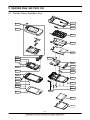
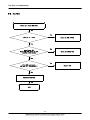
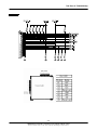
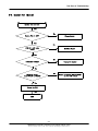
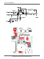
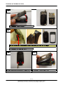
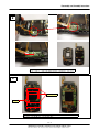
1
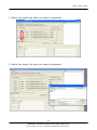
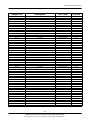
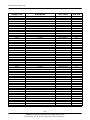
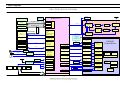
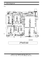
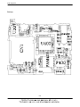
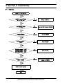
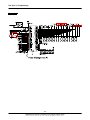
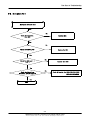
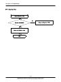
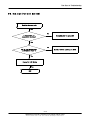
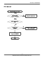
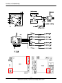
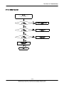
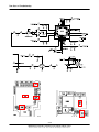
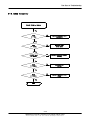
UMTS TELEPHONE
SGH-Z560
UMTS TELEPHONE
CONTENTS
1.
Safety Precautions
2.
Specification
3.
Product Function
4.
Array course control
5.
Exploded View and Parts List
6.
MAIN Electrical Parts List
7.
Block Diagrams
8.
PCB Diagrams
9.
Flow Chart of Troubleshooting
10.
Reference data
11.
Disassembly and Assembly
Instructions
목 차
1. Safety Precautions
1-1. Repair Precaution ...........................................................................1-1
1-2. ESD(Electrostatically Sensitive Devices) Precaution ...........................1-2
2. Specification
2-1. GSM General Specification ..............................................................2-1
2-2. GSM Tx Power Class ......................................................................2-2
3. Product Function
4. Array course control
Software Downloading
4-1. Downloading Binary Files ................................................................4-2
4-2. Pre-requsite for Downloading ..........................................................4-2
4-3. S/W Downloader Program ...............................................................4-2
5. Exploded View and Parts List
5-1. Cellular phone Exploded View .........................................................5-1
5-2. Cellular phone Parts list .................................................................5-2
6. MAIN Electrical Parts List
7. Block Diagrams
8. PCB Diagrams
목 차
9. Flow Chart of Troubleshooting
9-1. Power On.....................................................................................9-1
9-2. Initial ..........................................................................................9-3
9-3. Sim Part ......................................................................................9-4
9-4. Speaker Part(Melody)....................................................................9-7
9-5. Microphone Part ...........................................................................9-9
9-6. Key Data Input...........................................................................9-11
9-7. Receiver Part..............................................................................9-12
9-8. Back Light (for Color Main LCD)..................................................9-13
9-9. Key Back Light...........................................................................9-14
9-10. Camera part.............................................................................9-15
9-11. Touch PAD................................................................................9-16
9-12. GSM Receiver............................................................................9-18
9-13. GSM Transmitter.......................................................................9-21
9-14. DCS Receiver............................................................................9-23
9-15. DCS Transmitter........................................................................9-26
9-16. PCS Receiver ...........................................................................9-28
9-17. PCS Transmitter........................................................................9-31
9-18. WCDMA Receiver.......................................................................9-33
9-19. WCDMA Transmitterr.................................................................9-35
10. Reference data
10-1. Reference Abbreviate..................................................................10-1
11. Disassembly and Assembly Instructions
11-1. Disassemby...............................................................................11-1
11-2. Assembly..................................................................................11-4
1. Safety Precautions
1-1. Repair Precaution
● Repair in Shield Box, during detailed tuning.
Take specially care of tuning or test,
because specipicty of cellular phone is sensitive for surrounding interference(RF noise).
● Be careful to use a kind of magnetic object or tool,
because performance of parts is damaged by the influence of magnetic force.
● Surely use a standard screwdriver when you disassemble this product,
otherwise screw will be worn away.
● Use a thicken twisted wire when you measure level.
A thicken twisted wire has low resistance, therefore error of measurement is few.
● Repair after separate Test Pack and Set because for short danger (for example an
overcurrent and furious flames of parts etc) when you repair board in condition of
connecting Test Pack and tuning on.
● Take specially care of soldering, because Land of PCB is small and weak in heat.
● Surely tune on/off while using AC power plug, because a repair of battery charger is
dangerous when tuning ON/OFF PBA and Connector after disassembling charger.
● Don't use as you pleases after change other material than replacement registered on SEC System.
Otherwise engineer in charge isn't charged with problem that you don't keep this rules.
1-1
SAMSUNG Proprietary-Contents may change without notice
This Document can not be used without Samsung's authorization
Safety Precautions
1-2. ESD(Electrostatically Sensitive Devices) Precaution
Several semiconductor may be damaged easily by static electricity. Such parts are called by ESD
(Electrostatically Sensitive Devices), for example IC,BGA chip etc. Read Precaution below.
You can prevent from ESD damage by static electricity.
● Remove static electricity remained your body before you touch semiconductor or parts with
semiconductor. There are ways that you touch an earthed place or wear static electricity
prevention string on wrist.
● Use earthed soldering steel when you connect or disconnect ESD.
● Use soldering removing tool to break static electricity. , otherwise ESD will be damaged by
static electricity.
● Don't unpack until you set up ESD on product. Because most of ESD are packed by box and aluminum
plate to have conductive power,they are prevented from static electricity.
● You must maintain electric contact between ESD and place due to be set up until ESD is connected
completely to the proper place or a circuit board.
1-2
SAMSUNG Proprietary-Contents may change without notice
This Document can not be used without Samsung's authorization
2. Specification
2-1. GSM General Specification
EG SM9 00
DCS1800
PCS1900
W-CDMA
Fr eq.
Band[MHz]
Uplin k/Down link
8 90~915
9 35~960
17 10~178 5
18 05~188 0
18 50~191 0
19 30~199 0
192 0~1980
211 0~2170
ARF CN ra nge
0~ 124 &
97 5~1023
5 12~885
5 12~810
UL:96 12~988 8
DL:105 62~108 38
T x/Rx spacing
45MHz
95MHz
80MHz
1 90MHz
Mo d. Bit r ate/
Bit Period
270 .833kb ps
3 .692u s
270 .833kb ps
3 .692u s
270 .833kb ps
3 .692u s
3.8 4Mcps
Ti me Slo t
Pe rio d/Fr am e
Per iod
5 76.9u s
4. 615ms
5 76.9u s
4. 615ms
5 76.9u s
4. 615ms
Fr ame len gth : 10ms
Modula tion
0 .3G M SK
0 .3G MSK
0 .3G M SK
Q PS K
HQPSK
MS Power
33d Bm~5dBm
30d Bm~0dBm
30d Bm~0dBm
24 dBm ~ - 50dBm
Powe r Class
4
(max +33dBm)
1
(max +30dBm)
1
(max +30dBm)
3
(max + 24dBm)
Se nsitivity
-10 2dBm
-10 0dBm
-10 0dBm
-1 06.7d Bm
TDMA Mu x
8
8
8
Cell Radiu s
35Km
2Km
2Km
2-1
2Km
Speclflcation
2-2. GSM Tx Power Class
TX Power
control level
GSM900
TX Power
DCS1800
control level
TX Power
control level
PCS1800
5
33±2 dBm
0
30±3 dBm
0
30±3 dBm
6
31±2 dBm
1
28±3 dBm
1
28±3 dBm
7
29±2 dBm
2
26±3 dBm
2
26±3 dBm
8
27±2 dBm
3
24±3 dBm
3
24±3 dBm
9
25±2 dBm
4
22±3 dBm
4
22±3 dBm
10
23±2 dBm
5
20±3 dBm
5
20±3 dBm
11
21±2 dBm
6
18±3 dBm
6
18±3 dBm
12
19±2 dBm
7
16±3 dBm
7
16±3 dBm
13
17±2 dBm
8
14±3 dBm
8
14±3 dBm
14
15±2 dBm
9
12±4 dBm
9
12±4 dBm
15
13±2 dBm
10
10±4 dBm
10
10±4 dBm
16
11±3 dBm
11
8±4dBm
11
8±4dBm
17
9±3dBm
12
6±4 dBm
12
6±4 dBm
18
7±3 dBm
13
4±4 dBm
13
4±4 dBm
19
5±3 dBm
14
2±5 dBm
14
2±5 dBm
15
0±5 dBm
15
0±5 dBm
2-2
3. Product Function
Main Function
-2 Mega with Auto Focus & VGA Dual Camera
-camcorder
-Image editor
-MP3 player
-Phonebook
-Name card
-Multimedia Message Service (MMS)
-E-mail
-Voice recorder
-Bluetooth
-Get personal with photo caller ID
-Web browser
-Java
-Calendar
-External Memory (microSD)
3-1
SAMSUNG Proprietary-Contents may change without notice
This Document can not be used without Samsung's authorization
Product Function
3-2
SAMSUNG Proprietary-Contents may change without notice
This Document can not be used without Samsung's authorization
4. Array course control
Test Jig (GH80-03308A)
Test Cable (GH39-00558A)
(GH39-00559A)
(GH39-00560A)
RF Test Cable (GH39-00397A)
4-1
SAMSUNG Proprietary-Contents may change without notice
This Document can not be used without Samsung's authorization
Array course control
Software Downloading
4-1. Downloading Binary Files
• four binary files for downloading Z560.
– amss/bin : Modem binary for communication function
& Mocha binary for user interface and various application
– Rsrc_Z560_TIM.rc1
: Files need for each application
– Rsrc2_Z560(Low).rc2
: Power on/off animation
– FactoryFs_Z560_TIM.ffs : Default file system to be put into in
initial production
4-2. Pre-requsite for Downloading
• Downloader Program(FastMultiloader3.22.exe)
• Z560 Mobile Phone
• Data Cable
• Binary files
4-3. S/W Downloader Program
1. Boot the Z560 by pressing ‘Power ON key’ after set "boot On key"
If you do properly, you can see the following message on sub LCD “DOWNLOAD
INTIMO”
2. Execute the “FastMultiloader3.25.exe” and select "SMP6275"
4-2
SAMSUNG Proprietary-Contents may change without notice
This Document can not be used without Samsung's authorization
Array course control
3. Select the check box what you want to download.
4. Select the binary file what you want to download
* Up to eight ports are supported.
4-3
SAMSUNG Proprietary-Contents may change without notice
This Document can not be used without Samsung's authorization
Array course control
5. Now press the button ‘DownLoad’.
6. When downloading is complete, you repower on after set "Boot s/w OFF".
- Z560 will format file system automatically and restart.
4-4
SAMSUNG Proprietary-Contents may change without notice
This Document can not be used without Samsung's authorization
5. Exploded View and Parts List
5-1. Cellular Phone Exploded View
QCK01
QCW01
QFR01
QVO01
QFU01
QKP01
QME01
QSH01
QAN01
QCA01
QAN01
QCA03
QMP01
QAN02
QLC01
QCB01
QMO01
QSD01
QFL01
QCW11
QRE01
QCW02
QCR52
QSC02
QCR06
QRF01
QSC01
QSC13
QIF01
QMW01
QBA01
QBA00
5-1
SAMSUNG Proprietary-Contents may change without notice
This Document can not be used without Samsung's authorization
Exploded view and Parts List
5-2. Cellular Phone Parts list
Design LOC
QAN01
QAN02
QBA00
QBA01
QCA01
QCA03
QCB01
QCK01
QCR06
QCR52
QCW01
QCW02
QCW11
QFL01
QFR01
QFU01
QKP01
QLC01
QME01
QME06
QMO01
QMP01
QMW01
QRF01
QSC01
QSC02
QSC13
QSH01
QVO01
QRE01
QIF01
QSD01
Description
SEC CODE
FPCB ANTENNA CHIP
INTENNA-SGHZ560
PMO-COVER BATT
INNER BATTERY PACK-900MAH
UNIT-CAMERA(SELF)
UNIT-CAMERA(REC)
CBF COAXIAL CABLE
PMO-KEY CAM
SCREW-MACHINE
SCREW-MACHINE
PCT-WINDOW CAM AF
PCT-WINDOW CAM VGA
PMO-DECO CASE LOWER
ASSY ACCE-LOWER
ASSY ACCE-FRONT
MEA-FOLDER UPPER KIT(BLACK_TIM
ASSY KEYPAD-(TIM/ZKA)
MEA-LCD MODULE KIT
UNIT-MAIN KEY FPCB
UNIT-SPK,RCV FPCB ASSY
MOTOR DC-SGH-Z560
PBA MAIN-SGH-Z560(A)
ASSY COVER-WINDOW MAIN(TIM)
MPR-COVER RF
RMO-COVER SCREW LOWER L
RMO-COVER SCREW LOWER R
PMO-COVER SCREW REAR
ASSY BRACKET-SHIELD
PMO-KEY VOL
ASSY ACCE-REAR
PMO-COVER IF
PMO-COVER SD
GH42-00794A
GH42-00830A
GH72-30605A
GH43-02398A
GH59-03025A
GH59-03050A
GH39-00469A
GH72-30606A
6001-001155
6001-001300
GH72-30593A
GH72-30597A
GH72-30594A
GH98-01186A
GH98-01187A
GH97-06075A
GH98-01196A
GH97-06072A
GH59-03049A
GH59-03126A
GH31-00245A
GH92-02726A
GH98-01198A
GH74-23919A
GH73-07209A
GH73-07210A
GH72-31652A
GH98-01536A
GH72-30608A
GH98-01194A
GH72-30601A
GH72-30603A
5-2
SAMSUNG Proprietary-Contents may change without notice
This Document can not be used without Samsung's authorization
Exploded view and Parts List
Description
SEC CODE
CARD-WARRANTY
6801-001501
BAG PE
6902-000634
CBF INTERFACE-DATA LINK CABLE
GH39-00444A
ADAPTOR-SGHD800 TA(EU)
GH44-01060A
S/W CD-PC STUDIO
GH46-00252A
UNIT-EARPHONE(BLK)
GH59-02499A
LABEL(P)-WATER SOAK
GH68-02026A
LABEL(P)-WATER SOAK
GH68-02026A
LABEL(P)-MASTER(TIM_BLK)
GH68-09314J
LABEL(R)-MAIN(TIM)
GH68-09857B
MANUAL USERS-TIMITALIAN
GH68-11149A
MANUAL USERS-MPET CARD ITALIAN
GH68-11379A
CUSHION-CASE(EU)
GH69-03847A
BOX-UNIT(TIM)
GH69-03911B
RMO-RUBBER B/T
GH73-07213A
MPR-BOHO VINYL LCD CONN
GH74-15350A
MPR-TAPE WINDOW SUB
GH74-23885A
MPR-CUSHION SPONGE LCD
GH74-23900A
MPR-CUSHION SPONGE CONDUCT LCD
GH74-23905A
MPR-TAPE CONDUCT LCD
GH74-23906A
MPR-TAPE INSULATE LCD 1
GH74-23907A
MPR-TAPE INSULATE LCD 2
GH74-23909A
MPR-TAPE INSULATE LCD 3
GH74-23911A
MPR-TAPE CASE SHIELD
GH74-23912A
MPR-TAPE INSULATE KEYPAD
GH74-23913A
MPR-TAPE INSULATE J-TAG
GH74-23920A
MPR-VINYL BOHO CASE LOWER
GH74-23924A
MPR-VINYL BOHO WINDOW SUB
GH74-23925A
MPR-VINYL BOHO INNER SUB
GH74-24431A
MPR-VINYL BOHO INNER MAIN
GH74-24472A
MPR-TAPE INSULATION REAR
GH74-24750A
MPR-TAPE COVER SHIELD L
GH74-24751A
MPR-TAPE COVER SHIELD R
GH74-24752A
MPR-TAPE LCD TOUCHPAD
GH74-24753A
MPR-TAPE CONDUCT UPPER BRK
GH74-24754A
MPR-SPONGE SIM
GH74-24755A
MPR-SPONGE SPK R
GH74-24756A
MPR-SPONGE SPK L
GH74-24757A
MPR-GASKET PBA
GH74-24759A
MPR-TAPE ABSORBER PCB
GH74-25402A
MEC-HANGER
GH75-03673H
5-3
SAMSUNG Proprietary-Contents may change without notice
This Document can not be used without Samsung's authorization
Exploded view and Parts List
5-4
SAMSUNG Proprietary-Contents may change without notice
This Document can not be used without Samsung's authorization
6. MAIN Electrical Parts List
Design LOC
Discription
SEC Code
STATUS
ANT401
BAT200
BTC300
C100
C101
C102
C103
C104
C105
C106
C107
C108
C109
C110
C111
C112
C113
C114
C115
C116
C117
C118
C119
C120
C121
C122
C123
C124
C125
C126
C127
C128
C129
C130
C131
C132
C133
C134
C135
C136
C137
C138
C139
C140
C141
C142
C143
C144
C145
C146
C147
C148
C149
CONNECTOR-COAXIAL
BATTERY-LI(2ND)
CONNECTOR-BATTERY
C-CER,CHIP
C-CER,CHIP
C-CER,CHIP
C-CER,CHIP
C-CER,CHIP
C-CER,CHIP
C-CER,CHIP
C-CER,CHIP
C-CER,CHIP
C-CER,CHIP
C-CER,CHIP
C-CER,CHIP
C-CER,CHIP
C-CER,CHIP
C-CER,CHIP
C-CER,CHIP
C-CER,CHIP
C-CER,CHIP
C-CER,CHIP
C-CER,CHIP
C-CER,CHIP
C-CER,CHIP
C-CER,CHIP
C-CER,CHIP
C-CER,CHIP
C-CER,CHIP
C-CER,CHIP
C-CER,CHIP
C-CER,CHIP
C-CER,CHIP
C-CER,CHIP
C-CER,CHIP
C-CER,CHIP
C-CER,CHIP
C-CER,CHIP
C-CER,CHIP
C-CER,CHIP
C-CER,CHIP
C-CER,CHIP
C-CER,CHIP
C-CER,CHIP
C-CER,CHIP
C-CER,CHIP
C-CER,CHIP
C-CER,CHIP
C-CER,CHIP
C-CER,CHIP
C-CER,CHIP
C-CER,CHIP
C-CER,CHIP
3705-001225
4302-001180
3711-006003
2203-006423
2203-006423
2203-006423
2203-006423
2203-006423
2203-000489
2203-000628
2203-006423
2203-006423
2203-006423
2203-000628
2203-006562
2203-006423
2203-005480
2203-006194
2203-006423
2203-006617
2203-006423
2203-006423
2203-006617
2203-006423
2203-005482
2203-005682
2203-006194
2203-000233
2203-006194
2203-000233
2203-006562
2203-006423
2203-006423
2203-006423
2203-006423
2203-006194
2203-006194
2203-006194
2203-006194
2203-005806
2203-005806
2203-005806
2203-005806
2203-006208
2203-006399
2203-005806
2203-005806
2203-005806
2203-006194
2203-006194
2203-006194
2203-006423
2203-006423
SA
SA
SA
SA
SA
SA
SA
SA
SA
SA
SA
SA
SA
SA
SA
SA
SA
SA
SA
SA
SA
SA
SA
SA
SA
SA
SA
SA
SA
SA
SA
SA
SA
SA
SA
SA
SA
SA
SA
SA
SA
SA
SA
SA
SA
SA
SA
SA
SA
SA
SA
SA
SA
6-1
SAMSUNG Proprietary-Contents may change without notice
This Document can not be used without Samsung's authorization
Main Electrical Parts List
Design LOC
Discription
SEC Code
STATUS
C150
C151
C152
C153
C154
C155
C156
C157
C158
C159
C160
C161
C162
C163
C164
C165
C166
C167
C168
C169
C170
C171
C172
C173
C200
C201
C202
C203
C204
C205
C206
C207
C208
C209
C210
C211
C212
C213
C214
C215
C216
C217
C218
C219
C220
C221
C222
C223
C224
C225
C226
C227
C228
C-CER,CHIP
C-CER,CHIP
C-CER,CHIP
C-CER,CHIP
C-CER,CHIP
C-CER,CHIP
C-CER,CHIP
C-CER,CHIP
C-CER,CHIP
C-CER,CHIP
C-CER,CHIP
C-CER,CHIP
C-CER,CHIP
C-CER,CHIP
C-CER,CHIP
C-CER,CHIP
C-CER,CHIP
C-CER,CHIP
C-CER,CHIP
C-CER,CHIP
C-CER,CHIP
C-CER,CHIP
C-CER,CHIP
C-CER,CHIP
C-CER,CHIP
C-CER,CHIP
C-CER,CHIP
C-CER,CHIP
C-CER,CHIP
C-CER,CHIP
C-CER,CHIP
C-CER,CHIP
C-CER,CHIP
C-CER,CHIP
C-CER,CHIP
C-CER,CHIP
C-CER,CHIP
C-CER,CHIP
C-CER,CHIP
C-CER,CHIP
C-CER,CHIP
C-CER,CHIP
C-CER,CHIP
C-CER,CHIP
C-CER,CHIP
C-CER,CHIP
C-CER,CHIP
C-CER,CHIP
C-CER,CHIP
C-CER,CHIP
C-CER,CHIP
C-CER,CHIP
C-CER,CHIP
2203-006423
2203-006423
2203-006194
2203-006423
2203-006194
2203-006423
2203-006194
2203-006423
2203-006194
2203-006423
2203-006194
2203-006194
2203-005806
2203-006194
2203-005806
2203-006562
2203-006423
2203-006423
2203-006423
2203-006423
2203-006423
2203-006208
2203-005482
2203-000233
2203-006838
2203-006562
2203-005138
2203-006562
2203-005138
2203-006208
2203-005736
2203-006423
2203-006423
2203-005729
2203-005729
2203-006562
2203-006305
2203-006305
2203-006208
2203-006305
2203-006838
2203-006305
2203-006838
2203-006838
2203-006208
2203-006838
2203-005482
2203-006208
2203-006838
2203-006838
2203-006562
2203-006208
2203-005806
SA
SA
SA
SA
SA
SA
SA
SA
SA
SA
SA
SA
SA
SA
SA
SA
SA
SA
SA
SA
SA
SA
SA
SA
SA
SA
SA
SA
SA
SA
SA
SA
SA
SA
SA
SA
SA
SA
SA
SA
SA
SA
SA
SA
SA
SA
SA
SA
SA
SA
SA
SA
SA
6-2
SAMSUNG Proprietary-Contents may change without notice
This Document can not be used without Samsung's authorization
Main Electrical Parts List
Design LOC
Discription
SEC Code
STATUS
C229
C230
C231
C232
C233
C234
C235
C236
C237
C238
C239
C240
C241
C242
C243
C244
C245
C246
C248
C249
C250
C251
C252
C253
C254
C255
C256
C300
C301
C302
C303
C304
C308
C309
C310
C311
C312
C313
C314
C315
C316
C317
C318
C319
C320
C321
C322
C323
C324
C325
C326
C328
C329
C-CER,CHIP
C-CER,CHIP
C-CER,CHIP
C-CER,CHIP
C-CER,CHIP
C-CER,CHIP
C-CER,CHIP
C-CER,CHIP
C-CER,CHIP
C-CER,CHIP
C-CER,CHIP
C-CER,CHIP
C-CER,CHIP
C-CER,CHIP
C-CER,CHIP
C-CER,CHIP
C-CER,CHIP
C-CER,CHIP
C-CER,CHIP
C-CER,CHIP
C-CER,CHIP
C-CER,CHIP
C-CER,CHIP
C-CER,CHIP
C-CER,CHIP
C-CER,CHIP
C-CER,CHIP
C-CER,CHIP
C-CER,CHIP
C-CER,CHIP
C-CER,CHIP
C-CER,CHIP
C-CER,CHIP
C-CER,CHIP
C-CER,CHIP
C-CER,CHIP
C-CER,CHIP
C-CER,CHIP
C-CER,CHIP
C-CER,CHIP
C-CER,CHIP
C-CER,CHIP
C-CER,CHIP
C-CER,CHIP
C-CER,CHIP
C-CER,CHIP
C-CER,CHIP
C-CER,CHIP
C-CER,CHIP
C-CER,CHIP
C-CER,CHIP
C-CER,CHIP
C-CER,CHIP
2203-006208
2203-005806
2203-006423
2203-005682
2203-006423
2203-005682
2203-005682
2203-006562
2203-006824
2203-006824
2203-006824
2203-006423
2203-006423
2203-006423
2203-006423
2203-006423
2203-006824
2203-006562
2203-000870
2203-006824
2203-006562
2203-006562
2203-006824
2203-005736
2203-006562
2203-006562
2203-006562
2203-006305
2203-005682
2203-005819
2203-006423
2203-006423
2203-005779
2203-005682
2203-005682
2203-005682
2203-005682
2203-005682
2203-005682
2203-005682
2203-005682
2203-005682
2203-005682
2203-005682
2203-005779
2203-005779
2203-005779
2203-005682
2203-005682
2203-005482
2203-005482
2203-000812
2203-000812
SA
SA
SA
SA
SA
SA
SA
SA
SA
SA
SA
SA
SA
SA
SA
SA
SA
SA
SA
SA
SA
SA
SA
SA
SA
SA
SA
SA
SA
SA
SA
SA
SA
SA
SA
SA
SA
SA
SA
SA
SA
SA
SA
SA
SA
SA
SA
SA
SA
SA
SA
SA
SA
6-3
SAMSUNG Proprietary-Contents may change without notice
This Document can not be used without Samsung's authorization
Main Electrical Parts List
Design LOC
Discription
SEC Code
STATUS
C332
C333
C334
C335
C336
C337
C339
C340
C341
C343
C346
C347
C348
C349
C350
C351
C352
C353
C354
C355
C356
C359
C360
C361
C365
C400
C401
C402
C403
C404
C405
C406
C409
C410
C411
C412
C413
C414
C415
C416
C417
C418
C419
C420
C421
C422
C423
C424
C425
C426
C427
C428
C429
C-CER,CHIP
C-CER,CHIP
C-CER,CHIP
C-CER,CHIP
C-CER,CHIP
C-CER,CHIP
C-CER,CHIP
C-CER,CHIP
C-CER,CHIP
C-CER,CHIP
C-CER,CHIP
C-CER,CHIP
C-CER,CHIP
C-CER,CHIP
C-CER,CHIP
C-CER,CHIP
C-CER,CHIP
C-CER,CHIP
C-CER,CHIP
C-CER,CHIP
C-CER,CHIP
C-CER,CHIP
C-CER,CHIP
C-CER,CHIP
C-CER,CHIP
C-CER,CHIP
C-CER,CHIP
C-CER,CHIP
C-CER,CHIP
C-CER,CHIP
C-CER,CHIP
C-CER,CHIP
C-FILM,SMD-PPS
C-CER,CHIP
C-CER,CHIP
C-CER,CHIP
C-CER,CHIP
C-CER,CHIP
C-CER,CHIP
C-CER,CHIP
C-CER,CHIP
C-CER,CHIP
C-CER,CHIP
C-CER,CHIP
C-CER,CHIP
C-CER,CHIP
C-CER,CHIP
C-CER,CHIP
C-CER,CHIP
C-CER,CHIP
C-CER,CHIP
C-CER,CHIP
C-CER,CHIP
2203-005683
2203-005682
2203-006562
2203-006562
2203-006562
2203-006562
2203-003054
2203-005395
2203-006648
2203-005482
2203-003054
2203-000812
2203-005779
2203-000679
2203-000627
2203-005779
2203-006648
2203-005482
2203-006324
2203-006562
2203-006562
2203-003054
2203-005395
2203-006562
2203-006423
2203-005682
2203-006423
2203-005390
2203-000812
2203-006194
2203-005682
2203-005806
2301-001213
2203-001124
2203-006194
2203-006423
2203-005682
2203-005482
2203-000812
2203-005682
2203-006423
2203-006379
2203-006556
2203-000995
2203-006423
2203-005806
2203-005682
2203-006194
2203-005736
2203-006556
2203-000995
2203-006194
2203-006556
SA
SA
SA
SA
SA
SA
SA
SA
SA
SA
SA
SA
SA
SA
SNA
SA
SA
SA
SA
SA
SA
SA
SA
SA
SA
SA
SA
SA
SA
SA
SA
SA
SA
SA
SA
SA
SA
SA
SA
SA
SA
SA
SA
SA
SA
SA
SA
SA
SA
SA
SA
SA
SA
6-4
SAMSUNG Proprietary-Contents may change without notice
This Document can not be used without Samsung's authorization
Main Electrical Parts List
Design LOC
Discription
SEC Code
STATUS
C430
C431
C432
C433
C434
C436
C437
C438
C439
C440
C441
C442
C443
C444
C445
C446
C447
C448
C449
C451
C452
C453
C454
C455
C456
C457
C500
C501
C502
C503
C504
C505
C506
C507
C509
C510
C511
C512
C513
C514
C515
C516
C517
C518
C519
C520
C521
C522
C524
C525
C529
C530
C531
C-CER,CHIP
C-FILM,SMD-PPS
C-CER,CHIP
C-CER,CHIP
C-CER,CHIP
C-CER,CHIP
C-CER,CHIP
INDUCTOR-SMD
INDUCTOR-SMD
C-CER,CHIP
C-CER,CHIP
C-CER,CHIP
C-CER,CHIP
C-CER,CHIP
C-CER,CHIP
C-CER,CHIP
C-CER,CHIP
C-CER,CHIP
C-CER,CHIP
C-CER,CHIP
C-CER,CHIP
C-CER,CHIP
C-CER,CHIP
C-CER,CHIP
C-CER,CHIP
C-CER,CHIP
C-CER,CHIP
C-CER,CHIP
C-CER,CHIP
C-CER,CHIP
C-CER,CHIP
C-CER,CHIP
C-CER,CHIP
C-CER,CHIP
C-CER,CHIP
C-CER,CHIP
C-CER,CHIP
C-CER,CHIP
C-CER,CHIP
C-CER,CHIP
C-CER,CHIP
C-CER,CHIP
C-CER,CHIP
C-CER,CHIP
C-CER,CHIP
C-CER,CHIP
INDUCTOR-SMD
C-CER,CHIP
R-CHIP
C-CER,CHIP
C-CER,CHIP
C-CER,CHIP
C-CER,CHIP
2203-006423
2301-001512
2203-000836
2203-002668
2203-006423
2203-005682
2203-006423
2703-002208
2703-002369
2203-000995
2203-006838
2203-005806
2203-005682
2203-006208
2203-006423
2203-006194
2203-006194
2203-002443
2203-000233
2203-001033
2203-006556
2203-006423
2203-001153
2203-005682
2203-005729
2203-005729
2203-006423
2203-005736
2203-005736
2203-006423
2203-005552
2203-005806
2203-006423
2203-000854
2203-005552
2203-005736
2203-006423
2203-006423
2203-005736
2203-006423
2203-005736
2203-001124
2203-000438
2203-001221
2203-000233
2203-000330
2703-002176
2203-005288
2007-000171
2203-005234
2203-006194
2203-000438
2203-000438
SA
SA
SA
SA
SA
SA
SA
SA
SA
SA
SA
SA
SA
SA
SA
SA
SA
SA
SA
SA
SA
SA
SA
SA
SA
SA
SA
SA
SA
SA
SA
SA
SA
SA
SA
SA
SA
SA
SA
SA
SA
SA
SA
SA
SA
SA
SA
SA
SA
SA
SA
SA
SA
6-5
SAMSUNG Proprietary-Contents may change without notice
This Document can not be used without Samsung's authorization
Main Electrical Parts List
Design LOC
Discription
SEC Code
STATUS
C532
C533
C534
C535
CN1
D200
D300
D301
D305
F300
F301
F302
F303
F304
F305
F400
F500
F501
F502
HDC300
HDC301
IFC300
L200
L201
L400
L401
L402
L403
L405
L406
L407
L408
L409
L410
L411
L412
L415
L416
L500
L501
L502
L503
L504
L505
L506
L507
L508
L509
L510
L511
L512
L513
OSC100
C-CER,CHIP
C-CER,CHIP
C-CER,CHIP
C-CER,CHIP
CONNECTOR-CARD EDGE
DIODE-ARRAY
DIODE-TVS
DIODE-TVS
DIODE-TVS
FILTER-EMI/ESD
FILTER-EMI/ESD
FILTER-EMI/ESD
FILTER-EMI/ESD
FILTER-EMI/ESD
FILTER-EMI/ESD
DUPLEXER-FEM
FILTER-SAW
FILTER-SAW
DUPLEXER-FBAR
HEADER-BOARD TO BOARD
HEADER-BOARD TO BOARD
SOCKET-INTERFACE
INDUCTOR-SMD
INDUCTOR-SMD
INDUCTOR-SMD
INDUCTOR-SMD
INDUCTOR-SMD
INDUCTOR-SMD
INDUCTOR-SMD
INDUCTOR-SMD
BEAD-SMD
INDUCTOR-SMD
INDUCTOR-SMD
INDUCTOR-SMD
INDUCTOR-SMD
INDUCTOR-SMD
INDUCTOR-SMD
INDUCTOR-SMD
INDUCTOR-SMD
INDUCTOR-SMD
INDUCTOR-SMD
INDUCTOR-SMD
INDUCTOR-SMD
INDUCTOR-SMD
INDUCTOR-SMD
INDUCTOR-SMD
INDUCTOR-SMD
INDUCTOR-SMD
C-CER,CHIP
INDUCTOR-SMD
INDUCTOR-SMD
INDUCTOR-SMD
RESONATOR-CERAMIC
2203-006194
2203-005736
2203-006194
2203-006423
3709-001452
0407-001002
0406-001190
0406-001190
0406-001208
2901-001320
2901-001320
2901-001320
2901-001320
2901-001353
2901-001353
2911-000042
2904-001623
2904-001629
2910-000004
3711-005367
3711-005456
3710-002306
2703-002840
2703-002840
2703-002314
2703-002201
2703-002170
2703-002203
2703-002200
2703-002819
3301-001756
2703-002819
2703-002819
2703-002819
2703-002314
2703-002314
2703-002368
2703-002368
2703-002314
2703-002207
2703-002207
2703-002207
2703-002207
2703-002314
2703-002870
2703-002314
2703-002202
2703-002268
2203-000995
2703-002176
2703-002268
2703-002368
2802-001182
SA
SA
SA
SA
SA
SA
SA
SA
SA
SA
SA
SA
SA
SA
SA
SA
SA
SA
SA
SA
SA
SA
SA
SA
SA
SA
SA
SA
SA
SA
SA
SA
SA
SA
SA
SA
SA
SA
SA
SA
SA
SA
SA
SA
SA
SA
SA
SA
SA
SA
SA
SA
SA
6-6
SAMSUNG Proprietary-Contents may change without notice
This Document can not be used without Samsung's authorization
Main Electrical Parts List
Design LOC
Discription
SEC Code
STATUS
OSC200
PAM401
PAM501
Q500
R100
R103
R104
R105
R106
R110
R111
R113
R114
R115
R116
R117
R118
R119
R120
R121
R123
R125
R126
R127
R128
R129
R130
R131
R141
R142
R143
R146
R200
R201
R202
R204
R205
R208
R209
R210
R211
R212
R213
R214
R215
R216
R217
R218
R219
R221
R222
R223
R224
CRYSTAL-SMD
IC-POWER AMP
IC-POWER AMP
TR-DIGITAL
R-CHIP
R-CHIP
R-CHIP
R-CHIP
R-CHIP
R-CHIP
R-CHIP
R-CHIP
R-CHIP
R-CHIP
R-CHIP
R-CHIP
R-CHIP
R-CHIP
R-CHIP
R-CHIP
R-CHIP
R-CHIP
R-CHIP
R-CHIP
R-CHIP
R-CHIP
R-CHIP
R-CHIP
R-CHIP
R-CHIP
R-CHIP
R-CHIP
R-CHIP
R-CHIP
R-CHIP
R-CHIP
R-CHIP
R-CHIP
R-CHIP
R-CHIP
R-CHIP
R-CHIP
R-CHIP
R-CHIP
R-CHIP
R-CHIP
R-CHIP
R-CHIP
R-CHIP
R-CHIP
R-CHIP
R-CHIP
R-CHIP
2801-004466
1201-002288
1201-002404
0504-001151
2007-008516
2007-008516
2007-008516
2007-000137
2007-000140
2007-008542
2007-008542
2007-008055
2007-008516
2007-009170
2007-008964
2007-009170
2007-008516
2007-008964
2007-007318
2007-008542
2007-007135
2007-007314
2007-007741
2007-008483
2007-008483
2007-008483
2007-008483
2007-008483
2007-008516
2007-009170
2007-008052
2007-008516
2007-008516
2007-003015
2007-003015
2007-008483
2007-008806
2007-008055
2007-008516
2007-008516
2007-008516
2007-008516
2007-008516
2007-008964
2007-007468
2007-008648
2007-008542
2007-008055
2007-008542
2007-008055
2007-008055
2007-008587
2007-008055
SA
SA
SA
SA
SA
SA
SA
SA
SA
SA
SA
SA
SA
SA
SA
SA
SA
SA
SA
SA
SA
SA
SA
SA
SA
SA
SA
SA
SA
SA
SA
SA
SA
SA
SA
SA
SA
SA
SA
SA
SA
SA
SA
SA
SA
SA
SA
SA
SA
SA
SA
SA
SA
6-7
SAMSUNG Proprietary-Contents may change without notice
This Document can not be used without Samsung's authorization
Main Electrical Parts List
Design LOC
Discription
SEC Code
STATUS
R226
R227
R228
R229
R230
R300
R302
R303
R304
R305
R306
R307
R308
R309
R310
R311
R312
R314
R315
R316
R317
R318
R319
R320
R322
R400
R401
R402
R403
R404
R405
R406
R407
R408
R409
R410
R411
R412
R413
R414
R415
R416
R417
R418
R419
R420
R421
R422
R423
R424
R500
R501
R502
R-CHIP
R-CHIP
R-CHIP
R-CHIP
R-CHIP
R-CHIP
R-CHIP
R-CHIP
R-CHIP
R-CHIP
R-CHIP
R-CHIP
R-CHIP
R-CHIP
R-CHIP
R-CHIP
R-CHIP
R-CHIP
R-CHIP
R-CHIP
R-CHIP
R-CHIP
R-CHIP
R-CHIP
R-CHIP
R-CHIP
R-CHIP
R-CHIP
R-CHIP
R-CHIP
R-CHIP
R-CHIP
R-CHIP
R-CHIP
R-CHIP
R-CHIP
R-CHIP
R-CHIP
R-CHIP
R-CHIP
R-CHIP
R-CHIP
R-CHIP
R-CHIP
R-CHIP
R-CHIP
R-CHIP
R-CHIP
R-CHIP
R-CHIP
R-CHIP
R-CHIP
R-CHIP
2007-008542
2007-007316
2007-007318
2007-007588
2007-008052
2007-008542
2007-009111
2007-009111
2007-008548
2007-008419
2007-008419
2007-008419
2007-008419
2007-008419
2007-008548
2007-008548
2007-000148
2007-008548
2007-008548
2007-008419
2007-008419
2007-009111
2007-009111
2007-009111
2007-008542
2007-007491
2007-000171
2007-000138
2007-007136
2007-000143
2007-000171
2007-000171
2007-000141
2007-008045
2007-000140
2007-008542
2007-000171
2007-000171
2007-008542
2007-008542
2007-000171
2007-007316
2007-000145
2007-000172
2007-007306
2007-000171
2007-001292
2007-001305
2007-001301
2007-008045
2007-008045
2007-007491
2007-000171
SA
SA
SA
SA
SA
SA
SA
SA
SA
SA
SA
SA
SA
SA
SA
SA
SA
SA
SA
SA
SA
SA
SA
SA
SA
SA
SA
SA
SA
SA
SA
SA
SA
SA
SA
SA
SA
SA
SA
SA
SA
SA
SA
SA
SA
SA
SA
SA
SA
SA
SA
SA
SA
6-8
SAMSUNG Proprietary-Contents may change without notice
This Document can not be used without Samsung's authorization
Main Electrical Parts List
Design LOC
Discription
SEC Code
STATUS
R503
R504
R505
R506
RFS400
TA247
TA300
TA301
TA302
TA303
TA304
TA330
TA331
TA450
TA528
TCX400
TCX500
TR200
TR201
U101
U102
U103
U104
U200
U201
U202
U203
U204
U205
U206
U207
U300
U301
U302
U400
U402
U403
U404
U500
UCP100
UME100
V100
V300
V301
V302
V303
V304
V305
V306
ZD300
ZD302
ZD303
ZD306
R-CHIP
R-CHIP
R-CHIP
R-CHIP
CONNECTOR-COAXIAL
C-TA,CHIP
C-TA,CHIP
C-TA,CHIP
C-TA,CHIP
C-TA,CHIP
C-TA,CHIP
C-TA,CHIP
C-TA,CHIP
C-TA,CHIP
C-TA,CHIP
OSCILLATOR-VCO
OSCILLATOR-VCTCXO
TR-DIGITAL
FET-SILICON
IC-SWITCH
IC-CMOS LOGIC
IC-ANALOG SWITCH
IC-ANALOG SWITCH
IC-VOL. DETECTOR
IC-POWER SUPERVISOR
IC-VOL. DETECTOR
IC-POSI.FIXED REG.
IC-BATTERY
IC-ANALOG SWITCH
DIODE-ARRAY
BLUETOOTH MODULE
IC-SWITCH
IC-POSI.FIXED REG.
IC-AUDIO AMP
IC-TRANSCEIVER
R-NETWORK
R-NETWORK
R-NETWORK
IC-RECEIVER
IC-MODEM
IC-MCP
THERMISTOR-NTC
VARISTOR
VARISTOR
VARISTOR
VARISTOR
VARISTOR
VARISTOR
VARISTOR
DIODE-TVS
DIODE-ZENER
DIODE-ZENER
DIODE-ZENER
2007-000171
2007-007766
2007-008809
2007-000138
3705-001358
2404-001381
2404-001396
2404-001381
2404-001381
2404-001411
2404-001381
2404-001396
2404-001396
2404-001413
2404-001381
2806-001377
2809-001280
0504-000168
0505-001889
1205-002568
0801-003076
1001-001408
1001-001408
1203-004045
1203-004102
1203-003728
1203-003754
1203-003823
1001-001336
0407-001038
4709-001445
1205-002686
1203-003208
1201-002195
1205-002645
2011-001532
2011-001532
2011-001533
1205-002781
1205-002790
1108-000041
1404-001224
1405-001177
1405-001177
1405-001177
1405-001177
1405-001177
1405-001177
1405-001177
0406-001201
0403-001427
0403-001547
0403-001547
SA
SA
SNA
SA
SA
SA
SA
SA
SA
SA
SA
SA
SA
SA
SA
SA
SA
SA
SA
SA
SA
SA
SA
SNA
SA
SA
SA
SA
SA
SA
SA
SA
SA
SA
SA
SA
SA
SA
SA
SA
SA
SA
SA
SA
SA
SA
SA
SA
SA
SA
SA
SA
SA
6-9
SAMSUNG Proprietary-Contents may change without notice
This Document can not be used without Samsung's authorization
Main Electrical Parts List
6-10
SAMSUNG Proprietary-Contents may change without notice
This Document can not be used without Samsung's authorization
7. Block Diagrams
SGH-Z560 BLOCK DIAGRAM
USB
48 MHz
MCP
SDRAM
512M
Bus(EBI1) 1.8V
TCXO
19.2MHz
MSM 6275
EBI 1
Tx I/Q
NAND flash
1G
Bus(EBI2) 2.6V
Sub LCD
1.07'’
I2C
VGA CAM
I2C
TOUCH_PAD
Hanset SPK
Charging
Logic
LTC4075X3
Data[7:0]
V/H Sync
PCLK
I2C Control
M CLK/M RST
KPD
Button
Microphone / RCV
PS_HOLD
Bluetooth RF
BTEM38B2SB
Keypad I/F
JTAG
T A
Ear
Jack
Battery
Control
KPDPWR_N
Power-on
Circuits
Serial Bus
I/F
PM _INT_N
MSM_INT_N
Interrupt
Manager
USB_
DAT/SE0/OE_
N
USIM _M_
CLK/RST/IO
RUIM _M _
CLK/RST/IO
SIM
Card.
RUIM IO
TCXO_EN
TCXO_EN
TCXO_OUT
TCXO
XTAL
UART3/USIM2
Sleep_Xtal_In
Digital Test Bus
Duplexer
SBST/SBDT
SBCK
UART2/USIM1
USB
W CDM A
PAM
PM _SBST
SBDT/SBCK
UART1
USBOTG
UART
Tx
BPF
PM6650
Power Block
PS_HO LD
USB_
DAT/SE0/O E_
N
Connectivity
Key PAD
FEM
RST,I2C control
AMR,EFR
FR,HR,VR
CMX,AAC
MP3,MIDI
EAR-am p
Tx PAM
RFR6250
PON_RESET_N
RESIN _N
AUDIO
D-am p
Stereo headset
Rx I/Q
SLCD_RESET
SUB_LCD_CS
2M CAM
TXVCO
EBI 2
M AIN_LCD_CS
W E2_N
A2(2)
LCD_BACK Light
NRESET _LCD
16bit CPU
Main LCD
QVGA
2.3" 262K TFT
RTR6250
JTAG interface
페이지 1
7-1
SAMSUNG Proprietary-Contents may change without notice
This Document can not be used without Samsung's authorization
USB
`````````
Tranceiver
RUIM Level
Translator
TCXO
Circuits
RTC&
Clk Circuits
SLEEP_CLK
M IC BIAS
1.8V
M otor
3.3V
LDOs
B/L
driver
HKADC
SRAM batt
back up
Coincell
recharger
8. PCB Diagrams
Top
8-1
PCB Diagrams
Bottom
8-2
9. Flow Chart of Troubleshooting
9-1. Power On
' Power On ' does not work
Yes
No
Check the Battery Voltage
is more than 3.3V
Change the Battery
Yes
No
U201PIN57(PS_HOLD)
= 2.6V?
Check the PMIC related to PS_HOLD
Yes
No
Check the Clock at
OSC200=32KHZ
Resolder OSC200
Yes
No
C229(VREG_MSMC) =
1.375V?
Check the PMIC
Yes
C227(VREG_MSME)
C223(VREG_MSMP)
C220(VREG_MSMA)
C211(VREG_TCXO)
=
=
=
=
1.8V?
2.6V?
2.6V?
2.8V?
No
Check the PMIC
Yes
No
Check for the clock at
C208= 19.2MHz
Check the clock generation circuit
(related to TCX500)
Yes
Check the initial operation
Yes
END
9-1
SAMSUNG Proprietary-Contents may change without notice
This Document can not be used without Samsung's authorization
Flow Chart of Troubleshooting
Power On
9-2
SAMSUNG Proprietary-Contents may change without notice
This Document can not be used without Samsung's authorization
Flow Chart of Troubleshooting
9-2. Initial
Initial Failure
Yes
No
TP "RST" (PON_RESET_N) ="H"?
Check the PMIC
Yes
No
Is HDC300 pin 11, 25
(LCD RESET) OK?
Check the LCD RESET Circuit
Yes
END
9-3
SAMSUNG Proprietary-Contents may change without notice
This Document can not be used without Samsung's authorization
Flow Chart of Troubleshooting
9-3. Sim Part
Phone can't access SIM Card
Yes
No
CN1 pin 11 = "H"?
Check the SIM POWER
Yes
No
After Power ON,
Check SIM_CLK Signal on CN1
pin15 in a few second
Check the 32KHz OSC
Yes
No
After SIM card insert,
CN1 pin 13 = "H(SIM_RST)"?
Replace PBA
Yes
Check the SIM Card
Yes
END
9-4
SAMSUNG Proprietary-Contents may change without notice
This Document can not be used without Samsung's authorization
Flow Chart of Troubleshooting
SIM
9-5
SAMSUNG Proprietary-Contents may change without notice
This Document can not be used without Samsung's authorization
Flow Chart of Troubleshooting
- Pin map (Circuit & SIM SOKET componet)
T-Flash
SIM
LMS
1
2
3
4
5
6
7
8
9
10
11
12
13
14
15
16
NC
Pin No.
SPEC
Switch-2
Switch-1
1
2
3
4
5
6
7
8
C1
C5
C2
C6
C3
C7
C4,C8
Name
TYPE
Description
DAT2
DAT3
CMD
VDD
CLK
VSS
DAT0
DAT1
VCC
GND
RST
VPP
CLK
I/O
Reserved
I/O/PP
I/O/PP
PP
S
I
S
I/O/PP
I/O/PP
S
S
I
S
I
I/O
DATA Line [bit2]
Card Detect Data Line [bit3]
Cammand Response
Supply Voltage
Clock
Supply Voltage Ground
DATA Line [bit0]
DATA Line [bit1]
9-6
SAMSUNG Proprietary-Contents may change without notice
This Document can not be used without Samsung's authorization
Flow Chart of Troubleshooting
9-4. Speaker Part (Melody)
Speaker does not work
Yes
No
Battery Volt >= 3.5V
Change battery
Yes
No
LCD J9 = 4.0V pulse
signal?
Resolder J9 pad
Yes
No
Is Speaker working?
Change the Speaker
Yes
No
Check the circuit
from UCP100 to U5(LCD)
Change or Resolder C20,C21,R6,R7
(on the LCD module)
Yes
Change the PBA
Yes
END
9-7
SAMSUNG Proprietary-Contents may change without notice
This Document can not be used without Samsung's authorization
Flow Chart of Troubleshooting
Speaker
GND
SPK_R+ SPK_R-
SPK_+
SPK_L-
EAR10_P
EAR10_N
9-8
SAMSUNG Proprietary-Contents may change without notice
This Document can not be used without Samsung's authorization
Flow Chart of Troubleshooting
9-5. Microphone Part
Microphone does not work
Yes
No
Check the connection
from MIC
Resolder MIC
Yes
No
Change the KEY F_PCB
Replace the MIC
Yes
Check the U301 pin 1 =
1.8V ?
No
Resolder the U301
Yes
No
Check & Resolder the C343,C353,C341,C352
Check the Circuit from
UCP100 to HDC301 pin18,20
R309,R311,R310,R308
Yes
END
9-9
SAMSUNG Proprietary-Contents may change without notice
This Document can not be used without Samsung's authorization
Flow Chart of Troubleshooting
Microphone
9-10
SAMSUNG Proprietary-Contents may change without notice
This Document can not be used without Samsung's authorization
Flow Chart of Troubleshooting
9-6. Key Data Input
Check Initial Operation
Yes
No
When one of the keys is
pushed,
is it displayed on LCD?
Check the Dome sheet & Key FPCB
Yes
No
When one of the keys is
pushed,
KEYSENSE(0)~(4),KYPD9~1
7
Replace the PBA
Yes
END
9-11
SAMSUNG Proprietary-Contents may change without notice
This Document can not be used without Samsung's authorization
Flow Chart of Troubleshooting
9-7. Receiver Part
Receiver does not work
Yes
No
Change the Receiver F_PCB
Resolder J9 PAD(LCD)
Yes
Change the UCP100 or PBA
Yes
END
9-12
SAMSUNG Proprietary-Contents may change without notice
This Document can not be used without Samsung's authorization
Flow Chart of Troubleshooting
9-8. Back Light (for Color Main LCD)
Backlight does not work
Yes
No
Is BACKLIGHT set
AlwaysON in the Menu?
Set BACKLIGHT on AlwaysON
Yes
No
Pin 27 (LCD_BACKLINGT)
at HDC300 is "High" ?
Resolder UCP100 and Removee C316
Yes
Change the LCD Module
Yes
END
9-13
SAMSUNG Proprietary-Contents may change without notice
This Document can not be used without Samsung's authorization
Flow Chart of Troubleshooting
9-9. Key Back Light
Key Backlight does not work
Yes
No
Set BACKLIGHT on AlwaysON
Is BACKLIGHT set
AlwaysON in the Menu?
Yes
No
Resolder as following picture point or
Replace KeyPAD and Resolder
HDC301 pin 17
KEY_EL_DRV = "H"?
Yes
END
9-14
SAMSUNG Proprietary-Contents may change without notice
This Document can not be used without Samsung's authorization
Flow Chart of Troubleshooting
9-10. Camera part
"Camera" function does not work
Yes
No
Check the Camera
connector on LCD module
Connect the camera module
Yes
Change the New Camera
module
Yes
No
Check R18 is "High" and Replace
U4 PIN10,9(L:CD) =
1.8V,2.8V?
U4(on the LCD moduel)
Change the LCD MODULE
END
9-15
SAMSUNG Proprietary-Contents may change without notice
This Document can not be used without Samsung's authorization
Flow Chart of Troubleshooting
9-11. Touch PAD
"Touch pad" function does not work
Yes
No
Check the Touch Pad on
conneotor
Connect the Touch pad module to silk
line
Yes
No
Check LCD U7 pin4 = 3.3V ?
pin1 ="H" ?
Resolder U7
Yes
Change the new Touch Pad Fpcb
END
9-16
SAMSUNG Proprietary-Contents may change without notice
This Document can not be used without Samsung's authorization
Flow Chart of Troubleshooting
9-17
SAMSUNG Proprietary-Contents may change without notice
This Document can not be used without Samsung's authorization
Flow Chart of Troubleshooting
9-12. GSM Receiver
RX ON
RF input : CH center freq +67.7kHz
Amp : -50dBm
Yes
R406
>= -60dBm
No
Resolder F400(FEM)
Yes
Resolder U400
(RTR6250)
Yes
END
9-18
SAMSUNG Proprietary-Contents may change without notice
This Document can not be used without Samsung's authorization
Flow Chart of Troubleshooting
9-19
SAMSUNG Proprietary-Contents may change without notice
This Document can not be used without Samsung's authorization
Flow Chart of Troubleshooting
9-20
SAMSUNG Proprietary-Contents may change without notice
This Document can not be used without Samsung's authorization
Flow Chart of Troubleshooting
9-13. GSM Transmitter
TX ON (5Level)
Yes
PAM401 Pin6
>= 1V
No
Resolder PAM401
(PAM)
Yes
TCX400(TXVCO)
pin1
>= 2dBm
No
Resolder TCX400
(TXVCO)
Yes
PAM401 pin9
>= 20dBm
No
Resolder PAM401 (PAM)
Yes
F400(FEM)
pin12
>= 25dBm
No
Resolder F400
(FEM)
Yes
Check UCP100
(MSM6275)
END
9-21
SAMSUNG Proprietary-Contents may change without notice
This Document can not be used without Samsung's authorization
Flow Chart of Troubleshooting
9-22
SAMSUNG Proprietary-Contents may change without notice
This Document can not be used without Samsung's authorization
Flow Chart of Troubleshooting
9-14. DCS Receiver
RX ON
RF input : CH center freq +67.7kHz
Amp : -50dBm
Yes
L415
>= -60dBm
No
Resolder F400(FEM)
Resolder U400
(RTR6250)
Yes
END
9-23
SAMSUNG Proprietary-Contents may change without notice
This Document can not be used without Samsung's authorization
Flow Chart of Troubleshooting
9-24
SAMSUNG Proprietary-Contents may change without notice
This Document can not be used without Samsung's authorization
Flow Chart of Troubleshooting
9-25
SAMSUNG Proprietary-Contents may change without notice
This Document can not be used without Samsung's authorization
Flow Chart of Troubleshooting
9-15. DCS Transmitter
TX ON (0Level)
Yes
PAM401 Pin6
>= 1V
No
Resolder PAM401
(PAM)
No
Resolder TCX400
(TXVCO)
Yes
TCX400(TXVCO)
pin1
>= 2dBm
Yes
PAM401(PAM) pin15
>= 15dBm
No
Resolder PAM401
Yes
F400(FEM)
pin12
>= 20dBm
No
Resolder F400
(FEM)
Yes
Check U100
(MSM6270)
END
9-26
SAMSUNG Proprietary-Contents may change without notice
This Document can not be used without Samsung's authorization
Flow Chart of Troubleshooting
9-27
SAMSUNG Proprietary-Contents may change without notice
This Document can not be used without Samsung's authorization
Flow Chart of Troubleshooting
9-16. PCS Receiver
RX ON
RF input : CH center freq +67.7kHz
Amp : -50dBm
Yes
R411
>= -60dBm
No
Resolder F400(FEM)
Yes
Resolder U400
(RTR6250)
Yes
END
9-28
SAMSUNG Proprietary-Contents may change without notice
This Document can not be used without Samsung's authorization
Flow Chart of Troubleshooting
9-29
SAMSUNG Proprietary-Contents may change without notice
This Document can not be used without Samsung's authorization
Flow Chart of Troubleshooting
9-30
SAMSUNG Proprietary-Contents may change without notice
This Document can not be used without Samsung's authorization
Flow Chart of Troubleshooting
9-17. PCS Transmitter
TX ON (0Level)
Yes
PAM401 Pin6
>= 1V
No
Resolder PAM401
(PAM)
No
Resolder TCX400
(TXVCO)
Yes
TCX400(TXVCO)
pin1
>= 2dBm
Yes
PAM401(PAM) pin15
>= 15dBm
No
Resolder PAM401(PAM)
Yes
F400(FEM)
pin12
>= 20dBm
No
Resolder F400
(FEM)
Yes
Check U100
(MSM6275)
END
9-31
SAMSUNG Proprietary-Contents may change without notice
This Document can not be used without Samsung's authorization
Flow Chart of Troubleshooting
9-32
SAMSUNG Proprietary-Contents may change without notice
This Document can not be used without Samsung's authorization
Flow Chart of Troubleshooting
9-18. WCDMA Receiver
RX ON
RF input : CH center freq
Amp : -50dBm
C519
>= -60dBm
No
Check & Resolder F400
(FEM)
Yes
C524
>= -65dBm
No
Resolder F502
(DPLX)
Yes
C504
>= -60dBm
No
Resolder F500
(WRX BPF)
Yes
Resolder U500
(RFR6250)
Yes
END
9-33
SAMSUNG Proprietary-Contents may change without notice
This Document can not be used without Samsung's authorization
Flow Chart of Troubleshooting
9-34
SAMSUNG Proprietary-Contents may change without notice
This Document can not be used without Samsung's authorization
Flow Chart of Troubleshooting
9-19. WCDMA Transmitter
TX ON (PDM for 23dBm)
Yes
C520
>= -5Bm
No
Check & Resolder U500
(RTR6250)
No
Resolder F501
(WTX SAW)
Yes
C521
>= -5dBm
Yes
PAM501 pin9
>= 20dBm
No
Check & Resolder PAM501
(WPAM)
Yes
C519
>= 20dBm
No
Resolder F502
(DPLX)
Yes
C403
>= 20dBm
No
Check & Resolder F400
(FEM)
Yes
END
9-35
SAMSUNG Proprietary-Contents may change without notice
This Document can not be used without Samsung's authorization
Flow Chart of Troubleshooting
9-36
SAMSUNG Proprietary-Contents may change without notice
This Document can not be used without Samsung's authorization
10. Reference data
10-1. Reference Abbreviate
AAC: Advanced Audio Coding.
AVC : Advanced Video Coding.
BER : Bit Error Rate
BPSK: Binary Phase Shift Keying
CA : Conditional Access
CDM : Code Division Multiplexing
C/I : Carrier to Interference
DMB : Digital Multimedia Broadcasting
EN : European Standard
ES : Elementary Stream
ETSI: European Telecommunications Standards Institute
MPEG: Moving Picture Experts Group
PN : Pseudo-random Noise
PS : Pilot Symbol
QPSK: Quadrature Phase Shift Keying
RS : Reed-Solomon
SI : Service Information
TDM : Time Division Multiplexing
TS : Transport Stream
10-1
SAMSUNG Proprietary-Contents may change without notice
This Document can not be used without Samsung's authorization
Reference data
10-2
SAMSUNG Proprietary-Contents may change without notice
This Document can not be used without Samsung's authorization
11. Disassembly and Assembly Instructions
11-1.Disassembly
1
1) Disassemble the BATTERY COVER.
2
2) Remove the RF SHEEET, SCREW COVER and six SCREWS.
1) Be careful not to break the LOCKERS.
1) Disassemble the REAR from the downside.
3
1) Disassemble the LCD CONNECTOR and RF CABLE before separating the PBA from the KEY PAD ASS'Y.
11-1
SAMSUNG Proprietary-Contents may change without notice
This Document can not be used without Samsung's authorization
Disassembly and Assembly Instructions
4
1) Disassemble the KEY PAD ASS'Y.
5
Push the YELLOW HINGE. Then Disassemble FRONT from FOLDER.(Be careful not to damage.)
1) Disassemble the FOLDER and FRONT.
7
6
1) Remove SCREW CAPS and unscrew the FOLDER UPPER.
1) Disassemble from the Camera side.
11-2
SAMSUNG Proprietary-Contents may change without notice
This Document can not be used without Samsung's authorization
Disassembly and Assembly Instructions
8
1) Lift up the TOUCH PAD CONNECTOR and disassemble the UPPER.
9
Insulating Tape
Sponge
1) Remove the Sponge and Insulating Tape.
11-3
SAMSUNG Proprietary-Contents may change without notice
This Document can not be used without Samsung's authorization
Disassembly and Assembly Instructions
11-2. Assembly
1
Insulating Tape
Sponge
1) Attach the Sponge and Insulating Tape to the LCD PBA.
2
1) Insert until white line is near
to TOUCHPAD CONNECTOR.
1) Insert into the TOUCHPAD CONNECTOR.
11-4
SAMSUNG Proprietary-Contents may change without notice
This Document can not be used without Samsung's authorization
Disassembly and Assembly Instructions
3
1) Assemble from the lower side.
4
1) Press the yellow hinge.
1) Insert the LCD CONNECTOR to the FRONT as shown above, then assemble the FRONT
pressing YELLOW HINGE.
5
1) Assemble the KEY PAD ASS'Y to the FRONT ASS'Y.
11-5
SAMSUNG Proprietary-Contents may change without notice
This Document can not be used without Samsung's authorization
Disassembly and Assembly Instructions
6
KEY Connector
BT ANTENNA
1) Insert BT ANTENNA to the hole.
2) Combine KEY CONNECTOR to the KEY PAD ASS'Y
7
1) Assemble LCD CONNECTOR and RF CABLE to the PBA.
8
1)Assemble the REAR following the direction of red arrow
as shown above.
2)Insert CAMERA KEY and VOLUME KEY before assembling.
11-6
SAMSUNG Proprietary-Contents may change without notice
This Document can not be used without Samsung's authorization
Disassembly and Assembly Instructions
9
1) Screw up the six points.
2) Put in SCREW COVER, and attach RF SHEET.
3) Assemble the BATTERY COVER.
11-7
SAMSUNG Proprietary-Contents may change without notice
This Document can not be used without Samsung's authorization
Disassembly and Assembly Instructions
11-8
SAMSUNG Proprietary-Contents may change without notice
This Document can not be used without Samsung's authorization
This Service Manual is a property of Samsung Electronics Co.,Ltd.
Any unauthorized use of Manual can be punished under applicable
International and/or domestic law.
ⓒ Samsung Electronics Co.,Ltd.
Code No.: GH68-11689A
2006. 06. Rev.1.0