1
This page intentionally left blank.
SONNET® USER’S GUIDE
Published: April 2009
Release 12
Sonnet Software, Inc.
100 Elwood Davis Road
North Syracuse, NY 13212
Phone: (315) 453-3096
Fax: (315) 451-1694
www.sonnetsoftware.com
© Copyright 1989,1991,1993, 1995-2009 Sonnet Software, Inc. All Rights Reserved
Registration numbers: TX 2-723-907, TX 2-760-739
Copyright Notice
Reproduction of this document in whole or in part, without the prior express written authorization
of Sonnet Software, Inc. is prohibited. Documentation and all authorized copies of documentation
must remain solely in the possession of the customer at all times, and must remain at the software
designated site. The customer shall not, under any circumstances, provide the documentation to any
third party without prior written approval from Sonnet Software, Inc. This publication is subject to
change at any time and without notice. Any suggestions for improvements in this publication or in
the software it describes are welcome.
Trademarks
The program names xgeom, emstatus, emvu, patvu, dxfgeo, ebridge, emgraph, gds, emserver,
emclient, sonntcds, and sonntawr (lower case bold italics), Co-calibrated, Lite, LitePlus,
Level2 Basic, Level2 Silver, and Level3 Gold are trademarks of Sonnet Software, Inc.
Sonnet®, em®, and emCluster® are registered trademarks of Sonnet Software, Inc.
UNIX is a trademark of Unix Systems Labs.
Windows NT, Windows2000, Windows ME, Windows XP and Windows Vista are trademarks of
Microsoft, Inc.
AutoCAD and Drawing Interchange file (DXF) are trademarks of Auto Desk, Inc.
SPARCsystem Open Windows, SUN, SUN-4, SunOS, Solaris, SunView, and SPARCstation are
trademarks of Sun Microsystems, Inc.
HP, HP-UX, Hewlett-Packard are trademarks of Hewlett-Packard Company.
ADS, Touchstone, and Libra are trademarks of Agilent Technologies.
Cadence and Virtuoso are trademarks of Cadence Design Systems, Inc.
AWR and Microwave Office are registered trademarks and EM Socket is a trademark of Applied
Wave Research, Inc.
GDSII is a trademark of Calma Company.
Acresso, FLEXlm, and FLEXnet are registered trademarks of Acresso Software.
OSF/Motif is a trademark of the Open Software Foundation.
IBM is a registered trademark of International Business Machines Corporation.
Linux is a registered trademark of Linus Torvalds.
Redhat is a registered trademark of Red Hat, Inc.
SuSE is a trademark of Novell, Inc.
Adobe® and Acrobat® are registered trademarks of Adobe, Inc.
AWR and Microwave Office are trademarks of Applied Wave Research, Inc.
Platform is a trademark and LSF® is a registered trademark of Platform Computing.
Table of Contents
TABLE OF CONTENTS
1
INTRODUCTION . . . . . . . . . . . . . . . . . . . . . . . . . . . . . . . 15
The Sonnet Design Suite . . . . . . . . . . . . . . . . . . . . . . . . . 15
The Analysis Engine, em . . . . . . . . . . . . . . . . . . . . . . . . . 20
A Simple Outline of the Theory . . . . . . . . . . . . . . . . . 21
Em Origins . . . . . . . . . . . . . . . . . . . . . . . . . . . . . . . . . . 22
2
WHAT’S NEW
IN
RELEASE 12 . . . . . . . . . . . . . . . . . . . . . . 23
Sonnet Lite . . . . . . . . . . . . . . . . . . . . . . . . . . . . . . . . . 23
New Features . . . . . . . . . . . . . . . . . . . . . . . . . . . . . . . . 24
Changes . . . . . . . . . . . . . . . . . . . . . . . . . . . . . . . . . . . 27
3
SUBSECTIONING . . . . . . . . . . . . . . . . . . . . . . . . . . . . . . 29
Tips for Selecting A Good Cell Size . . . . . . . . . . . . . . . . . . 30
Cell Size Calculator . . . . . . . . . . . . . . . . . . . . . . . . . 33
Viewing the Subsections . . . . . . . . . . . . . . . . . . . . . . . . . 33
Subsectioning and Simulation Error. . . . . . . . . . . . . . . . . . 34
Changing the Subsectioning of a Polygon . . . . . . . . . . . . . . 34
Default Subsectioning of a Polygon . . . . . . . . . . . . . . . 34
X Min and Y Min with Edge Mesh Off . . . . . . . . . . . . . . 37
X Min and Y Min with Edge Mesh On. . . . . . . . . . . . . . . 39
Using X Max and Y Max for an Individual Polygon . . . . . . 40
Using the Speed/Memory Control . . . . . . . . . . . . . . . . . . . 41
Setting the Maximum Subsection Size Parameter. . . . . . . . . 43
Defining the Subsectioning Frequency . . . . . . . . . . . . . . . . 44
Conformal Mesh Subsectioning. . . . . . . . . . . . . . . . . . . . . 44
Conformal Mesh Subsectioning Control. . . . . . . . . . . . . 46
4
METALIZATION
AND
DIELECTRIC LAYER LOSS . . . . . . . . . . . . . . 47
Metalization Loss . . . . . . . . . . . . . . . . . . . . . . . . . . . . . 47
Sonnet’s Loss Model . . . . . . . . . . . . . . . . . . . . . . . . . 48
Problems In Determining Metal Loss . . . . . . . . . . . . . . 49
Determining Good Input Values . . . . . . . . . . . . . . . . . 50
Creating Metal Types . . . . . . . . . . . . . . . . . . . . . . . . 50
Metal Libraries . . . . . . . . . . . . . . . . . . . . . . . . . . . . 56
5
Sonnet User’s Guide
Via Loss. . . . . . . . . . . . . . . . . . . . . . . . . . . . . . . . . 56
Setting Losses for the Box Top and Bottom (Ground Plane) .
56
Dielectric Layer Loss . . . . . . . . . . . . . . . . . . . . . . . . . . . 57
Dielectric Layer Parameters . . . . . . . . . . . . . . . . . . . 58
Dielectric Layer Loss . . . . . . . . . . . . . . . . . . . . . . . . 59
How to Create a New Dielectric Layer. . . . . . . . . . . . . 59
Dielectric Libraries . . . . . . . . . . . . . . . . . . . . . . . . . 59
5
PORTS . . . . . . . . . . . . . . . . . . . . . . . . . . . . . . . . . . . . 61
Port Type Overview . . . . . . . . . . . . . . . . . . . . . . . . . . . 61
Port Normalizing Impedances . . . . . . . . . . . . . . . . . . . . . 63
Changing Port Impedance . . . . . . . . . . . . . . . . . . . . . 64
Special Port Numbering . . . . . . . . . . . . . . . . . . . . . . . . . 65
Ports with Duplicate Numbers . . . . . . . . . . . . . . . . . . 65
Ports with Negative Numbers . . . . . . . . . . . . . . . . . . 66
Changing Port Numbering . . . . . . . . . . . . . . . . . . . . . 67
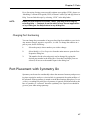
Port Placement with Symmetry On . . . . . . . . . . . . . . . . . 67
Standard Box Wall Port . . . . . . . . . . . . . . . . . . . . . . . . . 69
Adding Box wall Ports . . . . . . . . . . . . . . . . . . . . . . . 69
Ref. Planes and Cal. Lengths for Box Wall Ports . . . . . . 69
Co-calibrated Internal Ports . . . . . . . . . . . . . . . . . . . . . . 70
Ground Node Connection . . . . . . . . . . . . . . . . . . . . . 70
Terminal Width . . . . . . . . . . . . . . . . . . . . . . . . . . . 73
Adding Co-calibrated Ports . . . . . . . . . . . . . . . . . . . . 74
Ref. Planes and Cal. Lengths for Co-calibrated Ports . . . 74
Use in Components . . . . . . . . . . . . . . . . . . . . . . . . . 75
Via Ports. . . . . . . . . . . . . . . . . . . . . . . . . . . . . . . . . . . 75
Adding Via Ports . . . . . . . . . . . . . . . . . . . . . . . . . . . 76
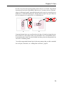
Automatic-Grounded Ports . . . . . . . . . . . . . . . . . . . . . . . 76
Special Considerations for Auto-Grounded Ports . . . . . . 77
Adding Auto-grounded Ports . . . . . . . . . . . . . . . . . . . 78
Ref. Plane and Cal. Length for Autogrounded Ports . . . . 78
Ungrounded Internal Ports . . . . . . . . . . . . . . . . . . . . . . . 78
6
COMPONENTS . . . . . . . . . . . . . . . . . . . . . . . . . . . . . . . . 81
Introduction . . . . . . . . . . . . . . . . . . . . . . . . . . . . . . . . 81
Component Assistant. . . . . . . . . . . . . . . . . . . . . . . . . . . 82
6
Table of Contents
Anatomy of a Component . . . . . . . . . . . . . . . . . . . . . . . . 82
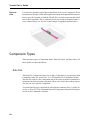
Component Types . . . . . . . . . . . . . . . . . . . . . . . . . . . . . 84
Data File . . . . . . . . . . . . . . . . . . . . . . . . . . . . . . . . 84
Ideal Component . . . . . . . . . . . . . . . . . . . . . . . . . . . 85
Ports Only . . . . . . . . . . . . . . . . . . . . . . . . . . . . . . . 85
Component Properties . . . . . . . . . . . . . . . . . . . . . . . . . . 85
Ground Node Connection. . . . . . . . . . . . . . . . . . . . . . 86
Terminal Width . . . . . . . . . . . . . . . . . . . . . . . . . . . . 88
Reference Planes . . . . . . . . . . . . . . . . . . . . . . . . . . . 91
Calibration Lengths . . . . . . . . . . . . . . . . . . . . . . . . . 91
Physical Size . . . . . . . . . . . . . . . . . . . . . . . . . . . . . . 92
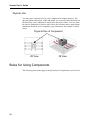
Rules for Using Components . . . . . . . . . . . . . . . . . . . . . . 92
Analysis of a Component. . . . . . . . . . . . . . . . . . . . . . . . . 95
Data File Frequencies . . . . . . . . . . . . . . . . . . . . . . . . 95
Rerunning an Analysis . . . . . . . . . . . . . . . . . . . . . . . . 95
7
DE-EMBEDDING . . . . . . . . . . . . . . . . . . . . . . . . . . . . . . . 97
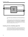
Enabling the De-embedding Algorithm . . . . . . . . . . . . . . . 98
De-embedding Port Discontinuities . . . . . . . . . . . . . . . . . 100
Box-Wall Ports . . . . . . . . . . . . . . . . . . . . . . . . . . . 101
Shifting Reference Planes . . . . . . . . . . . . . . . . . . . . . . . 102
Single Feed Line . . . . . . . . . . . . . . . . . . . . . . . . . . 103
Coupled Transmission Lines . . . . . . . . . . . . . . . . . . . 104
De-embedding Results . . . . . . . . . . . . . . . . . . . . . . . . . 105
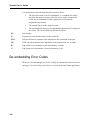
De-embedding Error Codes . . . . . . . . . . . . . . . . . . . . . . 106
8
DE-EMBEDDING GUIDELINES . . . . . . . . . . . . . . . . . . . . . . . 107
Calibration Standards. . . . . . . . . . . . . . . . . . . . . . . . . . 107
Defining Reference Planes . . . . . . . . . . . . . . . . . . . . . . 108
De-embedding Without Reference Planes . . . . . . . . . . 108
Reference Plane Length Minimums . . . . . . . . . . . . . . 109
Reference Plane Lengths at Multiples of a Half-Wavelength .
110
Reference Plane Lengths Greater than One Wavelength 110
Non-Physical S-Parameters . . . . . . . . . . . . . . . . . . . 110
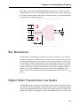
Box Resonances . . . . . . . . . . . . . . . . . . . . . . . . . . . . . 113
Higher Order Transmission Line Modes . . . . . . . . . . . . . . 113
7
Sonnet User’s Guide
9
ADAPTIVE BAND SYNTHESIS (ABS) . . . . . . . . . . . . . . . . . . 115
ABS Resolution. . . . . . . . . . . . . . . . . . . . . . . . . . . . . . 116
Q-Factor Accuracy . . . . . . . . . . . . . . . . . . . . . . . . . . . 116
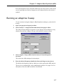
Running an Adaptive Sweep . . . . . . . . . . . . . . . . . . . . . 117
ABS Caching Level . . . . . . . . . . . . . . . . . . . . . . . . . . . 118
Multiple ABS Sweeps and Subsectioning . . . . . . . . . . . 119
Multi-Sweep Caching Scenarios . . . . . . . . . . . . . . . . 120
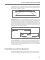
Find Minimum and Find Maximum . . . . . . . . . . . . . . . . . 121
Parameter Sweep . . . . . . . . . . . . . . . . . . . . . . . . . . . . 122
Analysis Issues . . . . . . . . . . . . . . . . . . . . . . . . . . . . . . 124
Multiple Box Resonances . . . . . . . . . . . . . . . . . . . . 124
De-embedding . . . . . . . . . . . . . . . . . . . . . . . . . . . 125
Transmission Line Parameters . . . . . . . . . . . . . . . . . 125
Current Density Data . . . . . . . . . . . . . . . . . . . . . . . 125
Ripple in ABS S-Parameters . . . . . . . . . . . . . . . . . . . 126
Output Files . . . . . . . . . . . . . . . . . . . . . . . . . . . . . 126
Viewing the Adaptive Response . . . . . . . . . . . . . . . . . . . 126
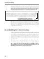
10 PARAMETERIZING YOUR PROJECT . . . . . . . . . . . . . . . . . . . 129
Variables . . . . . . . . . . . . . . . . . . . . . . . . . . . . . . . . . 130
How to Create a Variable . . . . . . . . . . . . . . . . . . . . 131
Equations . . . . . . . . . . . . . . . . . . . . . . . . . . . . . . 133
Dependent Variables . . . . . . . . . . . . . . . . . . . . . . . 135
Dimension Parameters. . . . . . . . . . . . . . . . . . . . . . . . . 136
Anchored Dimension Parameters . . . . . . . . . . . . . . . 137
Symmetrical Dimension Parameters . . . . . . . . . . . . . 139
Radial Dimension Parameters . . . . . . . . . . . . . . . . . 144
Reference Planes . . . . . . . . . . . . . . . . . . . . . . . . . 146
Dependent Dimension Parameters . . . . . . . . . . . . . . 146
Circular Dependencies in Parameters . . . . . . . . . . . . 147
Parameter Sweep . . . . . . . . . . . . . . . . . . . . . . . . . . . . 148
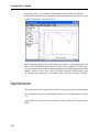
Optimization . . . . . . . . . . . . . . . . . . . . . . . . . . . . . . . 151
11 PARAMETER SWEEP AND OPTIMIZATION TUTORIAL . . . . . . . . . . 155
Setting Up Dimension Parameters . . . . . . . . . . . . . . . . . 156
Anchored Parameters . . . . . . . . . . . . . . . . . . . . . . 157
Symmetric Parameters. . . . . . . . . . . . . . . . . . . . . . 161
8
Table of Contents
Parameter Sweep . . . . . . . . . . . . . . . . . . . . . . . . . . . . 164
Setting Up a Parameter Sweep . . . . . . . . . . . . . . . . . 165
Executing the Parameter Sweep . . . . . . . . . . . . . . . . 168
Observing the Parameter Sweep Data . . . . . . . . . . . . 168
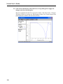
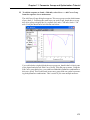
Optimization . . . . . . . . . . . . . . . . . . . . . . . . . . . . . . . 172
Entering New Nominal Values. . . . . . . . . . . . . . . . . . 173
Setting Up an Optimization . . . . . . . . . . . . . . . . . . . 173
Running an Optimization . . . . . . . . . . . . . . . . . . . . . 178
Observing your Optimization Data. . . . . . . . . . . . . . . 178
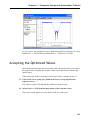
Accepting the Optimized Values. . . . . . . . . . . . . . . . . . . 181
12 CONFORMAL MESH. . . . . . . . . . . . . . . . . . . . . . . . . . . . 185
Introduction . . . . . . . . . . . . . . . . . . . . . . . . . . . . . . . . 185
Use Conformal Meshing for Transmission Lines, Not Patches
187
Applying Conformal Meshing . . . . . . . . . . . . . . . . . . . . . 187
Conformal Meshing Rules . . . . . . . . . . . . . . . . . . . . . . . 188
Memory Save Option. . . . . . . . . . . . . . . . . . . . . . . . 191
Using Conformal Meshing Effectively. . . . . . . . . . . . . . . . 191
Use Conformal Meshing for Non-Manhattan Polygons . . 191
Boundaries Should Be Vertical or Horizontal . . . . . . . . 193
Cell Size and Processing Time . . . . . . . . . . . . . . . . . 193
Current Density Viewing . . . . . . . . . . . . . . . . . . . . . . . . 194
13 NETLIST PROJECT ANALYSIS . . . . . . . . . . . . . . . . . . . . . . 197
Networks . . . . . . . . . . . . . . . . . . . . . . . . . . . . . . . . . . 198
Netlist Project Analyses . . . . . . . . . . . . . . . . . . . . . . . . 199
Creating a Netlist . . . . . . . . . . . . . . . . . . . . . . . . . . . . 199
Netlist Example Files . . . . . . . . . . . . . . . . . . . . . . . 200
Cascading S-, Y- and Z-Parameter Data Files . . . . . . . . . . 200
A Network File with Geometry Project . . . . . . . . . . . . . . 202
Inserting Modeled Elements into a Geometry . . . . . . . . . . 204
Using Ungrounded-Internal Ports . . . . . . . . . . . . . . . 207
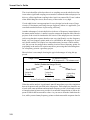
14 CIRCUIT SUBDIVISION . . . . . . . . . . . . . . . . . . . . . . . . . . 211
Introduction . . . . . . . . . . . . . . . . . . . . . . . . . . . . . . . . 211
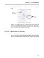
Circuit Subdivision in Sonnet . . . . . . . . . . . . . . . . . . . . . 213
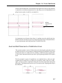
Choosing Subdivision Line Placement . . . . . . . . . . . . . . . 216
9
Sonnet User’s Guide
Good and Bad Placements of Subdivision Lines . . . . . . 217
Subdivision Line Orientation . . . . . . . . . . . . . . . . . . 221
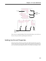
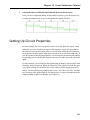
Setting Up Circuit Properties . . . . . . . . . . . . . . . . . . . . 223
Setting Up the Coarse Step Size Frequency Sweep. . . . 224
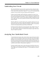
Subdividing Your Circuit . . . . . . . . . . . . . . . . . . . . . . . 225
Analyzing Your Subdivided Circuit . . . . . . . . . . . . . . . . . 225
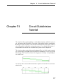
15 CIRCUIT SUBDIVISION TUTORIAL . . . . . . . . . . . . . . . . . . . . 227
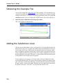
Obtaining the Example File . . . . . . . . . . . . . . . . . . . . . 228
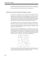
Adding the Subdivision Lines. . . . . . . . . . . . . . . . . . . . . 228
Setting Up Circuit Properties . . . . . . . . . . . . . . . . . . . . 231
Subdividing Your Circuit . . . . . . . . . . . . . . . . . . . . . . . 233
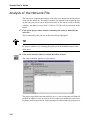
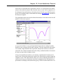
Analysis of the Network File . . . . . . . . . . . . . . . . . . . . . 236
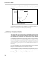
Additional Improvements . . . . . . . . . . . . . . . . . . . . . . . 238
16 VIAS AND 3-D STRUCTURES . . . . . . . . . . . . . . . . . . . . . . 241
Introduction . . . . . . . . . . . . . . . . . . . . . . . . . . . . . . . 241
Restrictions on Vias . . . . . . . . . . . . . . . . . . . . . . . . . . 241
Creating the Vias . . . . . . . . . . . . . . . . . . . . . . . . . . . . 242
Via Direction . . . . . . . . . . . . . . . . . . . . . . . . . . . . 242
Via Types . . . . . . . . . . . . . . . . . . . . . . . . . . . . . . 243
Via Posts . . . . . . . . . . . . . . . . . . . . . . . . . . . . . . . 245
Adding a Via to Ground . . . . . . . . . . . . . . . . . . . . . 246
Multi-layer Vias . . . . . . . . . . . . . . . . . . . . . . . . . . 248
Deleting Vias . . . . . . . . . . . . . . . . . . . . . . . . . . . . 250
Via Loss. . . . . . . . . . . . . . . . . . . . . . . . . . . . . . . . 251
Via Ports . . . . . . . . . . . . . . . . . . . . . . . . . . . . . . 251
Simple Via Example . . . . . . . . . . . . . . . . . . . . . . . . . . 252
A Conical Via . . . . . . . . . . . . . . . . . . . . . . . . . . . . . . . 252
17 THICK METAL . . . . . . . . . . . . . . . . . . . . . . . . . . . . . . 253
Thick Metal Type . . . . . . . . . . . . . . . . . . . . . . . . . . . . 253
Creating a Thick Metal Polygon . . . . . . . . . . . . . . . . . . . 255
Viewing Thick Metal in the Project Editor . . . . . . . . . . . . 257
Restrictions with Thick Metal Polygons . . . . . . . . . . . . . . 259
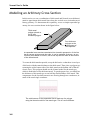
Modeling an Arbitrary Cross-Section . . . . . . . . . . . . . . . . 260
Thick Metal in the Current Density Viewer . . . . . . . . . . . 261
10
Table of Contents
18 DIELECTRIC BRICKS . . . . . . . . . . . . . . . . . . . . . . . . . . . 263
Applications of Dielectric Bricks. . . . . . . . . . . . . . . . . . . 265
Guidelines for Using Dielectric Bricks . . . . . . . . . . . . . . . 265
Subsectioning Dielectric Bricks . . . . . . . . . . . . . . . . . 265
Using Vias Inside a Dielectric Brick . . . . . . . . . . . . . . 265
Air Dielectric Bricks . . . . . . . . . . . . . . . . . . . . . . . . 266
Limitations of Dielectric Bricks . . . . . . . . . . . . . . . . . . . 266
Diagonal Fill . . . . . . . . . . . . . . . . . . . . . . . . . . . . . 266
Antennas and Radiation . . . . . . . . . . . . . . . . . . . . . 266
Interfaces. . . . . . . . . . . . . . . . . . . . . . . . . . . . . . . 266
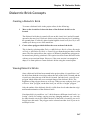
Dielectric Brick Concepts . . . . . . . . . . . . . . . . . . . . . . . 267
Creating a Dielectric Brick. . . . . . . . . . . . . . . . . . . . 267
Viewing Dielectric Bricks. . . . . . . . . . . . . . . . . . . . . 267
Defining Dielectric Brick Materials . . . . . . . . . . . . . . 268
Changing Brick Materials . . . . . . . . . . . . . . . . . . . . . 269
Z-Partitioning . . . . . . . . . . . . . . . . . . . . . . . . . . . . 270
19 ANTENNAS AND RADIATION . . . . . . . . . . . . . . . . . . . . . . . 273
Background . . . . . . . . . . . . . . . . . . . . . . . . . . . . . . . . 274
Modeling Infinite Arrays . . . . . . . . . . . . . . . . . . . . . . . . 274
Modeling an Open Environment . . . . . . . . . . . . . . . . . . . 275
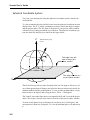
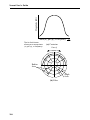
Validation Example . . . . . . . . . . . . . . . . . . . . . . . . . . . 279
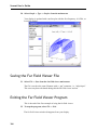
Far Field Viewer . . . . . . . . . . . . . . . . . . . . . . . . . . . . . 280
Analysis Limitations . . . . . . . . . . . . . . . . . . . . . . . . 281
Spherical Coordinate System . . . . . . . . . . . . . . . . . . 282
Normalization . . . . . . . . . . . . . . . . . . . . . . . . . . . . 285
Polarization . . . . . . . . . . . . . . . . . . . . . . . . . . . . . 286
References . . . . . . . . . . . . . . . . . . . . . . . . . . . . . . 286
20 FAR FIELD VIEWER TUTORIAL . . . . . . . . . . . . . . . . . . . . . 287
Creating an Antenna Pattern File . . . . . . . . . . . . . . . . . . 288
Running the Far Field Viewer . . . . . . . . . . . . . . . . . . . . 289
Calculating the Response . . . . . . . . . . . . . . . . . . . . . . . 290
Selecting Phi Values . . . . . . . . . . . . . . . . . . . . . . . . 291
Selecting Frequencies. . . . . . . . . . . . . . . . . . . . . . . 291
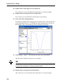
Selecting the Response. . . . . . . . . . . . . . . . . . . . . . . . . 292
Zooming . . . . . . . . . . . . . . . . . . . . . . . . . . . . . . . . . . 295
11
Sonnet User’s Guide
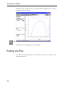
Probing the Plot . . . . . . . . . . . . . . . . . . . . . . . . . . . . . 296
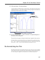
Re-Normalizing the Plot. . . . . . . . . . . . . . . . . . . . . . . . 297
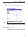
Changing to a Polar Plot . . . . . . . . . . . . . . . . . . . . . . . 299
Turning Off the Legend . . . . . . . . . . . . . . . . . . . . . . . . 299
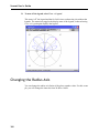
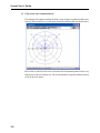
Changing the Radius Axis . . . . . . . . . . . . . . . . . . . . . . . 300
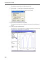
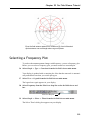
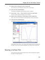
Selecting a Frequency Plot . . . . . . . . . . . . . . . . . . . . . . 303
Viewing a Surface Plot . . . . . . . . . . . . . . . . . . . . . . . . 305
Saving the Far Field Viewer File . . . . . . . . . . . . . . . . . . 306
Exiting the Far Field Viewer Program . . . . . . . . . . . . . . . 306
References . . . . . . . . . . . . . . . . . . . . . . . . . . . . . . . . 307
21 SPICE MODEL SYNTHESIS . . . . . . . . . . . . . . . . . . . . . . . . 309
PI Spice Model . . . . . . . . . . . . . . . . . . . . . . . . . . . . . . 311
Using The PI Model Spice Option . . . . . . . . . . . . . . . 312
A Simple Microwave Example . . . . . . . . . . . . . . . . . 315
Topology Used for PI Model Output. . . . . . . . . . . . . . 316
N-Coupled Line Option . . . . . . . . . . . . . . . . . . . . . . . . 317
Broadband SPICE Model . . . . . . . . . . . . . . . . . . . . . . . . 319
Class of Problems . . . . . . . . . . . . . . . . . . . . . . . . . 320
Creating a Broadband Spice Model . . . . . . . . . . . . . . 321
Checking the Accuracy of the Broadband Spice Model . 323
Improving the Accuracy of the Broadband Spice Model. 326
Broadband Spice Extractor Stability Factor . . . . . . . . 327
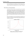
22 PACKAGE RESONANCES . . . . . . . . . . . . . . . . . . . . . . . . . 329
Box Resonances . . . . . . . . . . . . . . . . . . . . . . . . . . . . . 330
Runtime Warning Messages . . . . . . . . . . . . . . . . . . . 330
Observations of Simulated Results . . . . . . . . . . . . . . 332
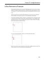
A Box Resonance Example . . . . . . . . . . . . . . . . . . . . . . 333
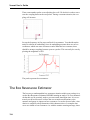
The Box Resonance Estimator . . . . . . . . . . . . . . . . . . . . 334
Box Resonances – Simple Removal . . . . . . . . . . . . . . . . . 336
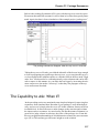
The Capability to Ask: What if? . . . . . . . . . . . . . . . . . . . 337
23
ACCURACY BENCHMARKING . . . . . . . . . . . . . . . . . . . . . . 339
An Exact Benchmark . . . . . . . . . . . . . . . . . . . . . . . . . . 339
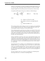
Residual Error Evaluation . . . . . . . . . . . . . . . . . . . . . . . 341
Using the Error Estimates. . . . . . . . . . . . . . . . . . . . . . . 343
12
Table of Contents
APPENDIX I
Em
AND XGEOM
COMMAND LINE
FOR
BATCH . . . . . . . . . 345
em Command Line . . . . . . . . . . . . . . . . . . . . . . . . . . . . 345
Causal Dielectrics . . . . . . . . . . . . . . . . . . . . . . . . . 348
xgeom Command Line. . . . . . . . . . . . . . . . . . . . . . . . . . 349
Example of xgeom Command Line . . . . . . . . . . . . . . . 351
APPENDIX II
SONNET REFERENCES . . . . . . . . . . . . . . . . . . . . . . 353
13
Sonnet User’s Guide
14
Chapter 1 Introduction
Chapter 1
Introduction
The Sonnet User’s Guide is intended to provide in depth discussions of features
of Sonnet’s software. There is a short exposition of the theory behind Sonnet’s
analysis engine, em, followed by discussions of geometry elements and features
available in Sonnet. This manual also contains tutorials demonstrating how to use
some features in Sonnet. The tutorials follow chapters discussing that topic. Please
refer to the Table of Contents to see what tutorials are available.
For installation instructions and the basics of using Sonnet, please refer to the Getting Started manual. To learn about new features in this release, please refer to
Chapter 2, “What’s New in Release 12” on page 23.
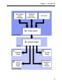
The Sonnet Design Suite
The suite of Sonnet analysis tools is shown on page 19. Using these tools, Sonnet
provides an open environment to many other design and layout programs. The
following is a brief description of all of the Sonnet tools. Check with your system
administrator to find out if you are licensed for these products:
15
Sonnet User’s Guide
Project
Editor
The project editor is a user-friendly graphical interface that enables you to input
your circuit geometry or circuit netlist for subsequent em analysis. If you have
purchased the DXF, GDSII and/or the Gerber translator, the translator interface is
found in the project editor. You also set up analysis controls for your project in the
project editor.
Program module: xgeom
Analysis
Engine
Em is the electromagnetic analysis engine. It uses a modified method of moments
analysis based on Maxwell's equations to perform a true three dimensional current
analysis of predominantly planar structures. Em computes S, Y, or Z-parameters,
transmission line parameters (Z0, Eeff, VSWR, GMax, Zin, and the Loss Factor),
and SPICE equivalent lumped element networks. Additionally, it creates files for
further processing by the current density viewer and the far field viewer. Em’s
circuit netlist capability cascades the results of electromagnetic analyses with
lumped elements, ideal transmission line elements and external S-parameter data.
Program module: em
Analysis
Monitor
The analysis monitor allows you to observe the on-going status of analyses being
run by em as well as creating and editing batch files to provide a queue for em
jobs.
Program module: emstatus
Response
Viewer
The response viewer is the plotting tool. This program allows you to plot your
response data from em, as well as other simulation tools, as a Cartesian graph or
a Smith chart. You may also plot the results of an equation. In addition, the
response viewer may generate Spice lumped models.
Program module: emgraph
Current
Density
Viewer
The current density viewer is a visualization tool which acts as a post-processor to
em providing you with an immediate qualitative view of the electromagnetic
interactions occurring within your circuit. The currents may also be displayed in
3D.
Program module: emvu
16
Chapter 1 Introduction
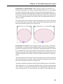
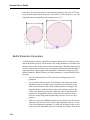
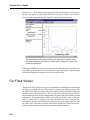
Far Field
Viewer
The far field viewer is the radiation pattern computation and display program. It
computes the far-field radiation pattern of radiating structures (such as patch
antennas) using the current density information from em and displays the far-field
radiation patterns in one of three formats: Cartesian plot, polar plot or surface plot.
Program module: patvu
GDSII
Translator
The GDSII translator provides bidirectional translation of GDSII layout files to/
from the Sonnet project editor geometry format.
Program module: gds
DXF
Translator
The DXF translator provides bidirectional translation of DXF layout files (such as
from AutoCAD) to/from the Sonnet project editor geometry format.
Program module: dxfgeo
Gerber
Translator
The Gerber translator provides bidirectional translation of Gerber single layer and
multi-layer files to/from the Sonnet project editor geometry format.
Agilent ADS
Interface
The Agilent ADS Interface provides a seamless translation capability between
Sonnet and Agilent’s ADS. From within ADS Layout package you can directly
create Sonnet geometry files. Em simulations can be invoked and the results
incorporated into your design without leaving the ADS environment.
Program module: ebridge
AWR
Microwave
Office
Interface
The AWR Microwave Office Interface provides a seamless incorporation of Sonnet’s world class EM simulation engine, em, into the Microwave Office environment using Microwave Office's EM Socket. You can take advantage of Sonnet’s
accuracy without having to learn the Sonnet interface. Although, for advanced users who wish to take advantage of powerful advanced features not presently supported in the integrated environment, the partnership of AWR and Sonnet has
simplified the process of moving EM projects between Microwave Office and
Sonnet.
Program Module: sonntawr
Cadence
Virtuoso
Interface
This Sonnet plug-in for the Cadence Virtuoso suite enables the RFIC designer to
configure and run the EM analysis from a layout cell, extract accurate electrical
models, and create a schematic symbol for Analog Artist and RFDE simulation.
Program Module: sonntcds
Broadband
Spice
Extractor
A Broadband Spice extraction module is available that provides high-order Spice
models. In order to create a Spice model which is valid across a broad band, the
Sonnet broadband SPICE Extractor feature finds a rational polynomial which
“fits” the S-Parameter data. This polynomial is used to generate the equivalent
17
Sonnet User’s Guide
lumped element circuits which may be used as an input to either PSpice or Spectre. Since the S-Parameters are fitted over a wide frequency band, the generated
models can be used in circuit simulators for AC sweeps and transient simulations.
18
Chapter 1 Introduction
Flow
19
Sonnet User’s Guide
Em performs electromagnetic analysis [85, 86, 88] for arbitrary 3-D planar [60]
(e.g., microstrip, coplanar, stripline, etc.) geometries, maintaining full accuracy at
all frequencies. Em is a “full-wave” analysis in that it takes into account all possible coupling mechanisms. The analysis inherently includes dispersion, stray
coupling, discontinuities, surface waves, moding, metalization loss, dielectric loss
and radiation loss. In short, it is a complete electromagnetic analysis. Since em
uses a surface meshing technique, i.e. it meshes only the surface of the circuit metalization, em can analyze predominately planar circuits much faster than volume
meshing techniques.
The Analysis Engine, em
Em analyzes 3-D structures embedded in planar multilayered dielectric on an underlying fixed grid. For this class of circuits, em can use the FFT (Fast Fourier
Transform) analysis technique to efficiently calculate the electromagnetic coupling on and between each dielectric surface. This provides em with its several orders of magnitude of speed increase over volume meshing and other non-FFT
based surface meshing techniques.
Em is a complete electromagnetic analysis; all electromagnetic effects, such as
dispersion, loss, stray coupling, etc., are included. There are only two approximations used by em. First, the finite numerical precision inherent in digital computers. Second, em subdivides the metalization into small subsections made up of
cells.
20
Chapter 1 Introduction
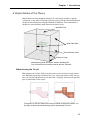
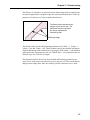
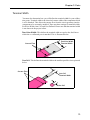
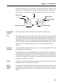
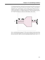
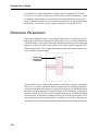
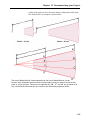
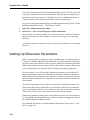
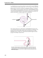
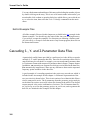
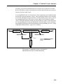
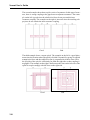
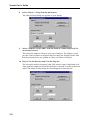
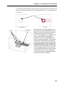
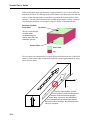
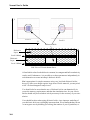
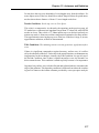
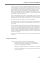
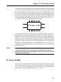
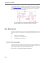
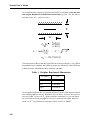
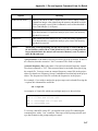
A Simple Outline of the Theory
Em performs an electromagnetic analysis of a microstrip, stripline, coplanar
waveguide, or any other 3-D planar circuit by solving for the current distribution
on the circuit metalization using the Method of Moments. The metalization is
modeled as zero-thickness metal between dielectric layers.
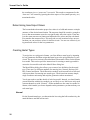
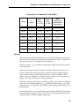
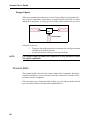
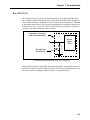
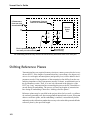
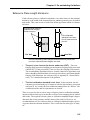
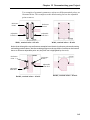
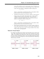
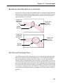
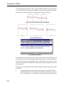
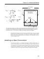
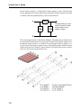
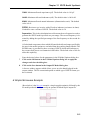
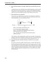
Metal Box Top
Metal Side Walls
Zero-thickness metal
Dielectric Layer
Em analyzes planar structures inside a shielding box.
Port connections are usually made at the box sidewalls.
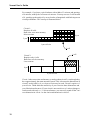
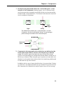
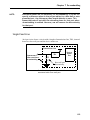
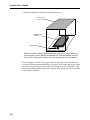
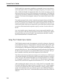
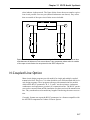
Subsectioning the Circuit
Em evaluates the electric field everywhere due to the current in a single subsection. Em then repeats the calculation for every subsection in the circuit, one at a
time. In so doing, em effectively calculates the “coupling” between each possible
pair of subsections in the circuit.
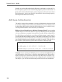
The picture on the left shows the circuit as viewed in the project editor. On
the right is shown the subsectioning used in analyzing the circuit.
21
Sonnet User’s Guide
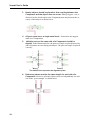
Zero Voltage Across a Conductor
Each subsection generates an electric field everywhere on the surface of the substrate, but we know that the total tangential electric field must be zero on the surface of any lossless conductor. This is the boundary condition: no voltage is
allowed across a perfect conductor.
The problem is solved by assuming current on all subsections simultaneously. Em
adjusts these currents so that the total tangential electric field, which is the sum of
all the individual electric fields just calculated, goes to zero everywhere that there
is a conductor. The currents that do this form the current distribution on the metalization. Once we have the currents, the S-parameters (or Y- or Z-) follow immediately.
If there is metalization loss, we modify the boundary condition. Rather than zero
tangential electric field (zero voltage), we make the tangential electric field (the
voltage on each subsection) proportional to the current in the subsection. Following Ohm’s Law, the constant of proportionality is the metalization surface resistivity (in Ohms/square).
Sonnet is designed to work with your existing CAE software. Since the output data
is in Touchstone or Compact format (at your discretion), em provides a seamless
interface to your CAE tool.
Em Origins
The technique used in em was developed at Syracuse University in 1986 by Rautio
and Harrington [85, 86, 88]. It was originally developed as an extension of an
analysis of planar waveguide probes [90]. The technique expresses the fields inside the box as a sum of waveguide modes and is thus closely related to the spectral domain approach.
The complete theory has been published in detail in peer reviewed journals. A full
list of relevant papers is presented in Appendix II "Sonnet References" on page
353.
22
Chapter 2 What’s New in Release 12
Chapter 2
What’s New in
Release 12
This chapter summarizes new capabilities and changes in release 12 of Sonnet. If
you are not yet familiar with Sonnet, you may want to just skim this chapter, skipping any terms that are unfamiliar. If you are an experienced user, this chapter
merits detailed reading.
Sonnet User’s Manuals are only updated with each full release. However, our
Help is also available at our web site and will periodically be updated with new
material. To access this help, go to www.sonnetsoftware.com/support and click on
the “Knowledge Base” link for the most recent updates.
Sonnet Lite
If you are looking for what’s new and changed in the Sonnet Lite release, please
refer to the What’s New topic in Help in either the Sonnet task bar or the project
editor. For what’s new in the full release, see the sections below.
23
Sonnet User’s Guide
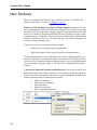
New Features
Below is a summation of the major new features in release 12 of Sonnet. For
changes from release 11, refer to “Changes,” page 27.
Multi-core CPU Parallel Processing on a Single computer: In Release 12, Sonnet’s electromagnetic (EM) simulations are performed more quickly by utilizing
multiple CPU cores on the same computer in parallel, making complete use of the
latest CPU technology from Intel and AMD. The new EM analysis engine creates
multiple processes, or threads, each of which solves a different part of the solution
matrix on a different CPU core—all at the same time. The result is a dramatic decrease in overall simulation time.
There are two new solver engine products available:
•
Desktop Solver (2 parallel processing threads)
•
High-Performance Solver (up to 8 parallel processing threads)
The maximum number of cores enabled by your license, and supported by your
hardware capability, is automatically used on your system. If you wish to use fewer cores on your computer than the maximum possible, you may limit the number
of cores available using the Admin ⇒ Thread Control command on the Sonnet
task bar.
Variables for Material Properties and Thicknesses: You may now control your
materials parametrically using variables to control material properties and thicknesses, as well as for lumped element values in ideal Components. With this new
feature comes the ability to parametrically control:
•
•
•
•
•
24
Dielectric thickness
Dielectric loss properties
Metal Thickness
Metal loss properties
Ideal Component properties
Chapter 2 What’s New in Release 12
Variables and Equations: This release introduces a new variable and equation
feature that enables you to control circuit properties using equations based on
mathematical functions (such as sine, cosine, natural logarithm, etc.).
A circuit property can be a function of one or more independent variables to provide advanced capabilities like:
•
Simulating temperature effects on circuit response by defining metal or
dielectric loss as a function of a temperature variable
•
Defining your own frequency dependent properties by using the new
FREQ constant in an equation
•
Enforcing geometry scaling by defining a variable as a multiple of
another variable
•
Controlling a circuit property based on a table of data from an external
text file
For more information on variables and equations, please see Chapter 10, “Parameterizing your Project” on page 129.
Radial Dimension Parameters: A radial parameter is a new type of dimension
parameter that allows you to fix one end of a parameter then radiate out from that
fixed point; the direction is not restricted to the x or y direction, but may extend at
an angle. See “Radial Dimension Parameters,” page 144 for more information.
Enhanced Meshing Algorithm: Sonnet’s default meshing algorithm has been
improved for circuits containing large ground planes and planar shields, irregular
edges, and interior via connections. Circuits containing these features are accurately meshed with dramatic reduction in memory usage and analysis time. Matrix
solve time reduction of 10x or more are not uncommon for such circuits.
Gerber Translator: Release 12 introduces a new Gerber translator which allows
you to perform single layer or multi-layer import of Gerber files to create a Sonnet
project. You may also export a Sonnet project and create Gerber formatted output
files of your circuit. Please refer to Chapter 5, "The Gerber Translator" in the
Translators manual.
New Parameter Sweep Analysis Definitions: The EM Analysis Engine also has
new parameter sweep analysis types useful for tolerance studies and design-formanufacturing testing. The new parameter sweeps include Corner Sweep Analysis, Sensitivity Sweep Analysis and Mixed Sweep Combinations. For details
about these sweeps, please see Help for details by looking up Corner Sweep, Sensitivity Sweep or Mixed Sweep in the Index.
25
Sonnet User’s Guide
Multiconductor Transmission Line (MTL) modeling: Sonnet’s MTL modeling
(N-Coupled Line Model) has been greatly improved. Analytical extraction of
RLGC per-unit-length parameters from the Scattering Parameters of MTLs has
been implemented. The output format of the RLGC data file is compatible with
the MTLINE model in Cadence (Spectre). Moreover, modal characteristic impedances (Z0) and propagation constants ( α + jβ ) are provided along with their corresponding excitation vectors. For more information, see "N-Coupled Line
Option" on page 317.
Variable Granularity for Optimizations: There is a new Granularity entry box
available in the Optimization Parameters dialog box. The granularity defines the
finest resolution, the smallest interval between values, of a variable for which em
will do a full electromagnetic simulation during optimization. For values which
occur between those set by this resolution, em performs an interpolation to produce the analysis data. Please see Help for the details; look under “granularity” in
the index.
Anisotropic Dielectrics: Standard dielectric layers in the simulation environment
may now be modeled with uniaxial anisotropy. The properties of a given dielectric
layer in the X-Y direction (view in the project editor) may have different dielectric, magnetic and/or conductivity properties from the Z-directed properties.
Click on the Help button in the Dielectric Editor dialog box (Circuit ⇒ Dielectric
Layers) for details.
Measuring Tape Tool: There is a new measuring tool available in the project editor that allows you to quickly measure distances in your geometry. The measuring
tape can provide distance measurement between vertices and “shortest distance”
to an adjacent line in the circuit. There is a button, shown to the left, in the tool bar
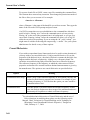
for this tool. For details about the measuring tape, please refer to Tools ⇒ Measuring Tape in Help. To access help, select Help ⇒ Contents from the project editor menu.
Local Origin: The default origin in the project editor is the lower left hand corner
of the substrate. Local origin allows you to move an origin anchor to any location
in your circuit. The origin can be moved in a number of ways, including selecting
and dragging it to the desired position. All the measurements which appear in the
status bar at the bottom of the project editor window are given relative to the location of the origin anchor. For more information, please refer to the command
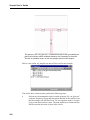
Tools ⇒ Local Origin in Help. The location of the origin is represented in the project editor with this symbol:
Hot Key Mapping: In this release, you may create custom hot keys for your commonly used commands in the project editor, response viewer, current density
viewer and far field viewer. For example, you may set a Hot Key so that whenever
the letter “d” is pressed on the keyboard, the project editor automatically enters
26
Chapter 2 What’s New in Release 12
the “add dimension” mode. To access this feature, select File ⇒ Preferences in
the desired program. In the Preferences dialog box which appears, click on the
General tab, then click on the Keyboard button. For details about creating hot
keys, click on the Help button on the Keyboard dialog box.
New Stability Factor for Broadband Spice Extraction: A new stability factor
has been added to the Broadband Spice Extractor feature which forces the poles
of your model to be stable. For more information, see "Broadband Spice Extractor
Stability Factor" on page 327.
New Append Feature for the DXF and GDSII Translators: You may now import a DXF or GDSII file into an existing project and add the translated objects to
your existing geometry. This feature enables you build up a Sonnet project from
two or more separate DXF or GDSII files. For information about the DXF and
GDSII translators, see the Translators Manual available in PDF format by selecting Help ⇒ Manuals from any Sonnet Application. Information about the Append
feature is available in Help.
Hover Over: A new feature in the project editor displays information about objects in your geometry when the cursor is placed over them. This feature is off by
default. If you wish to turn this on, select View ⇒ Info Hover Over in the project
editor menu.
X-axis Logarithmic Scale: A new feature in the response viewer allows you to
apply a logarithmic scale to the x-axis of your plots. For details please refer to
Help for the Axis Setup dialog box. This dialog box is opened when you select the
command Graph ⇒ Set Axes from the response viewer main menu.
Parameters in Current Density Viewer and Far Field Viewer: There is new
functionality in both the current density viewer and the far field viewer which allows you to choose a parameter combination whose data you wish to display.
FLEXnet 11.5 Support: Sonnet’s license manager is now based upon FLEXnet
version 11.5 which officially supports the Windows Vista operating system.
Changes
Below is a summation of the major changes in release 12 of Sonnet. For new features in release 12, refer to “New Features,” page 24.
Parameters: In release 11, “parameters” were used to identify dimensions in your
geometry and sweep those dimensions in an analysis. These “parameters” are now
defined as “dimension parameters.” The command to add an anchored dimension
27
Sonnet User’s Guide
parameter is now Tools ⇒ Add Dimension Parameter ⇒ Add Anchored and to
add a symmetric dimension parameter is Tools ⇒ Add Dimension Parameter ⇒
Add Symmetric. For details about the new variables feature and how they relate to
dimension parameters, please refer to Chapter 10, “Parameterizing your Project” on page 129.
Highlighting in 3D View: Enhancements have been done in the 3D view to highlight the metal levels and dielectric layers.
Menu Name Change in the Current Density Viewer: The Parameters menu in
the current density viewer has been changed to the Plot menu in release 12.
28
Chapter 3 Subsectioning
Chapter 3
Subsectioning
The Sonnet subsectioning is based on a uniform mesh indicated by the small dots
in the project editor screen. The small dots are placed at the corners of a “cell”.
One or more cells are automatically combined together to create subsections. Cells
may be square or rectangular (any aspect ratio), but must be the same over your
entire circuit. The cell size is specified in the project editor in the Box Settings dialog box which is opened by selecting Circuit ⇒ Box. The analysis solves for the
current on each subsection. Since multiple cells are combined together into a single subsection, the number of subsections is usually considerably smaller than the
number of cells. This is important because the analysis solves an N x N matrix
where N is the number of subsections. A small reduction in the value of N results
in a large reduction in analysis time and memory.
Care must be taken in combining the cells into subsections so that accuracy is not
sacrificed. Em automatically places small subsections in critical areas where current density is changing rapidly, but allows larger subsections in less critical areas,
where current density is smooth or changing slowly.
However, in some cases you may wish to modify the automatic algorithm because
you want a faster, less accurate solution, or a slower, more accurate solution, than
is provided by the automatic algorithm. Also, in some cases, you may have knowledge about your circuit that the software does not. For example, you may know
that there is very little current on a certain area of your metal. Or you may have
chosen a small cell size because you have a small dimension in your circuit, but
29
Sonnet User’s Guide
do not need the accuracy of a small cell size in larger structures within your circuit.
In these cases, you can change the method by which em combines cells into subsections.
This chapter explains how em combines cells into subsections and how you can
control this process to obtain an analysis time or the level of accuracy you require.
There is also a discussion of selecting the cell size and how that may affect the em
analysis.
Conformal Mesh is a special case of subsectioning used to model polygons with
long diagonal or curved edges. For more information on subsectioning when using
conformal mesh, see “Conformal Mesh Subsectioning,” page 44.
Tips for Selecting A Good Cell Size
As you know, em subdivides the circuit into subsections which are made up of
“cells,” the building block in the project editor. The following discussion describes how to select a cell size. You may also use the Sonnet Cell Size Calculator
which allows you to enter important dimensions to calculate the most efficient cell
size which provides the required accuracy. To access the Cell Size calculator,
click on the Cell Size Calculator button in the Box Settings dialog box, which is
invoked when you select Circuit ⇒ Box from the project editor menu.
TIP
Select a cell size that is smaller than 1/20 of a wavelength.
Before calculating a cell size, it is important to calculate the wavelength at your
highest frequency of analysis. An exact number is not important. If you know the
approximate effective dielectric constant of your circuit, use this in the wavelength calculation; otherwise, use the highest dielectric constant in your structure.
Most circuits require that your cell size be smaller than 1/20 of a wavelength.
Larger cell sizes usually result in unacceptable errors due to incorrect modeling of
the distributed effects across the cell. Cell sizes smaller than λ/20 may increase
the accuracy slightly but usually increases the total number of subsections, which
increases the analysis time and memory requirements.
30
Chapter 3 Subsectioning
TIP
When possible, round off dimensions of your circuit so that they have a larger
common multiple.
Since your circuit geometry is snapped to the nearest cell, you must find a cell size
such that all of the dimensions of the circuit are a multiple of this cell size. For
example, if your circuit has dimensions of 30 microns, 40 microns and 60 microns,
possible cell sizes are 10 microns, 5 microns, 2.5 microns, 2 microns, etc. Large
cell sizes result in more efficient analyses, so choosing 10 microns is probably
best.
TIP
Calculate the X cell size and the Y cell size independently.
The X cell size and Y cell size do not have to be the same number. Calculate the
X cell size based on just your dimensions in the X direction, and your Y cell size
based on just your dimensions in the Y direction.
31
Sonnet User’s Guide
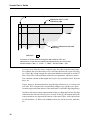
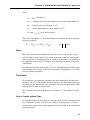
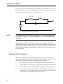
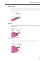
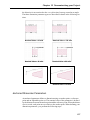
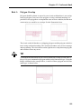
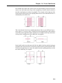
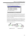
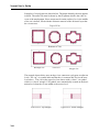
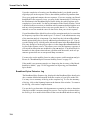
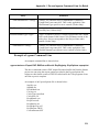
For example, if you have a spiral inductor with widths of 3 microns and spacings
of 8 microns, modify the 3 microns to 4 microns. You may now use 2 cells instead
of 8, speeding up the analysis by several orders of magnitude with little impact on
circuit performance. This concept is illustrated below.
Circuit 1:
Requires 80 cells
Runs slow, uses more memory
More accurate
8 μm
3 μm
1 μm cell size
1 cell
1 cell
Circuit 2:
Requires only 6 cells
Runs fast, uses less memory
Less accurate
8μ
4 μm
4 μm cell size
Circuit 1 takes more time and memory to analyze than circuit 2 even though they
have approximately the same amount of metal. This is because the dimensions in
circuit 2 are divisible by 4, so a 4 µm cell size may be used. Circuit 1 requires a 1
µm cell size. Think about the sensitivity of your circuit to these dimensions and
your fabrication tolerances. If your circuit is not sensitive to a 1 micron change or
can be made with only a +/- 1 micron tolerance, you can easily round off the 3 micron dimension in circuit 1 to the 4 micron dimension in circuit 2.
32
Chapter 3 Subsectioning
Cell Size Calculator
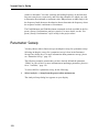
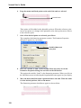
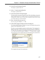
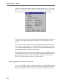
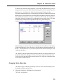
Sonnet also provides a cell size calculator which you may use to calculate the optimal cell size based on your critical circuit parameters. You access the Cell Size
Calculator in the Box Settings dialog box (Circuit ⇒ Box). Using the Cell Size
Calculator is detailed in Chapter 6, “Determining Cell Size” of the Getting Started manual. A detailed discussion of all the entries in the cell size calculator may
be found in Help.
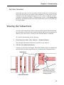
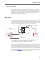
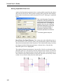
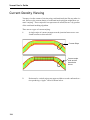
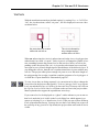
Viewing the Subsections
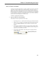
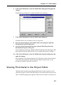
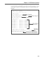
You can see the subsections used by Sonnet by following the instructions below.
Be aware that your dielectric layers must be defined and at least one port must be
added to your circuit before you may use the Estimate Memory command.
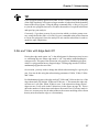
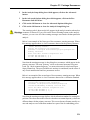
To view the subsectioning, do the following:
1
From the project editor, select Analysis => Estimate Memory.
This calculates the amount of memory required for your analysis.
2
Click the View Subsections button.
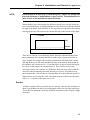
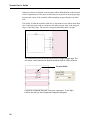
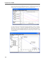
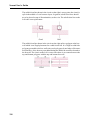
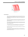
A picture of your circuit will appear. The metal will show up as red, and the subsection borders will show up as black lines as shown in the illustration below:
Metalization
Subsection Borders
Note the use of smaller
subsections in an area
where current density is
changing rapidly.
33
Sonnet User’s Guide
Subsectioning and Simulation Error
As discussed above, Sonnet uses a fixed resolution grid and discretely meshes a
given metallization pattern based on that underlying grid. The edges of metal patterns in a design do not necessarily have to be aligned to the grid, even though
Sonnet only simulates metal fill which is on the grid. Off grid metalization may
be over or under filled depending on the degree of misalignment between grid and
metal pattern. While misalignment gives the user visual feedback of one potential
error source in a Sonnet simulation, it is important to keep in mind that every planar Method of Moments (MoM) simulation contains multiple sources of error.
Unlike Sonnet, most EM software vendors speak very little about error sources
(see “Accuracy Benchmarking,” page 339). The fact that Sonnet shows misalignment between the desired metal pattern and simulation grid does not necessarily
imply that Sonnet simulations will be any less accurate than competitive simulators that mesh using infinite resolution. With all simulation packages the user
should investigate every potential error source (which will vary depending on the
MoM technique used) and ensure a good converged data set is achieved.
Changing the Subsectioning of a Polygon
Sonnet allows you to control how cells are combined into subsections for each
polygon. This is done using the parameters “X Min”, “Y Min”, “X Max” and “Y
Max”. These parameters may be changed for each polygon, allowing you to have
coarser resolution for some polygons and finer resolution for others. See “Modify
- Metal Properties” in the project editor’s Help for information on how to change
these parameters.
Before discussing how to make use of these parameters, we need to first understand em’s automatic subsectioning for a polygon when the parameters are set to
their default settings.
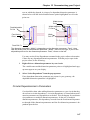
Default Subsectioning of a Polygon
By default, Sonnet fills a polygon with “staircase” subsections. Other, more advanced fill types (diagonal and conformal) are covered in other chapters of this
manual. For diagonal subsections, see Chapter 16, “Vias and 3-D Structures”
on page 241. For conformal mesh, see Chapter 12, “Conformal Mesh” on page
185. This chapter deals exclusively with staircase subsections.
34
Chapter 3 Subsectioning
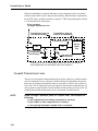
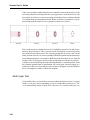
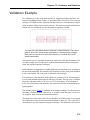
This fill type is referred to as staircase because when using small rectangular subsections to approximate a diagonal edge, the actual metalization takes on the appearance of a staircase, as in the example shown below.
The black outline represents the
polygon input by the user. The
patterned sections represent
the actual metalization
analyzed by em.
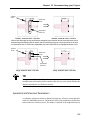
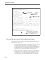
Staircase edge
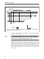
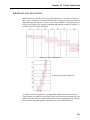
The default values for the subsectioning parameters are X Min = 1, Y Min = 1,
X Max = 100 and Y Max = 100. These numbers specify the smallest and largest
allowed dimensions of the subsections in a polygon. With X Min = 1, the smallest
subsection in the X dimension is one cell. With X Max = 100, subsections are not
allowed to go over 100 cells in length.
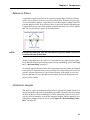
The illustration below shows how these default subsectioning parameters are
used. Notice in the corner, the subsection size is just one cell. The current density
changes most rapidly here, thus, the smallest possible subsection size is used.
35
Sonnet User’s Guide
Subsection size is 1 cell by 1 cell on corner
Subsection size is 1 cell
wide along edge
Interior subsections are wide
and long
Cell Size
=
A portion of circuit metal showing how em combines cells into
subsections. In this case the subsectioning parameters are set to their
default values: X Min = 1, Y Min = 1, X Max = 100 and Y Max = 100.
As we go away from the corner, along the edge, the subsections become longer.
For example, the next subsection is two cells long, the next one is four cells long,
etc. If the edge is long enough, the subsection length increases until it reaches X
Max (100) cells, or the maximum subsection size parameter, whichever comes
first, and then remains at that length until it gets close to another corner, discontinuity, etc.
Notice, however, that no matter how long the edge subsection is, it is always one
cell wide. This is because the current density changes very rapidly as we move
from the edge toward the interior of the metal (this is called the edge singularity).
In order to allow an accurate representation of the very high edge current, the edge
subsections are allowed to be only one cell wide. However, the current density becomes smooth as we approach the interior of the metal. Thus, wider subsections
are allowed there. As before, the width goes from one cell to two cells, then four,
etc.
36
Chapter 3 Subsectioning
TIP
If two polygons butt up against each other or have a small overlap, the modeling
of the edge singularity will require a larger number of subsections at the boundary
between the two polygons. Using the Merge command (Edit ⇒ Merge Polygons)
to join the two polygons into one will reduce the number of required subsections
and speed up your analysis.
Conversely, if you have an area of your circuit at which you desire greater accuracy, using the Divide (Edit ⇒ Divide Polygons) command at the point of interest
to create two polygons, forces the analysis to use smaller subsections in order to
model the edge singularities.
X Min and Y Min with Edge Mesh Off
Having the edge mesh option “on” is the default state for Sonnet projects; however, examining the case where edge mesh is “off” first makes understanding the
concept easier. This part of the discussion only applies to Manhattan polygons,
which is a polygon that has no diagonal edges. Turning edge mesh off for nonmanhattan polygons has no effect.
On occasion, you may wish to change the default subsectioning for a given polygon. You can do this using the subsectioning parameters X Min, Y Min, X Max
and Y Max.
For Manhattan polygons with edge mesh off, X Min and Y Min set the size of the
edge subsections. By default, X Min and Y Min are 1. This means the edge subsections are 1 cell wide. When X Min is set to 2, the subsections along vertical
edges are now 2 cells wide in the X direction (see the figure on page 38). This reduces the number of subsections and reduces the matrix size for a faster analysis.
However, accuracy may also be reduced due to the coarser modeling of the current
density near the structure edge or a discontinuity.
37
Sonnet User’s Guide
1 Cell Wide
(Y Min = 1)
{
{
2 Cells Wide
(X Min = 2)
4 Cells
8 Cells
2 Cells
4 Cells
Y
Cell Size
=
X
A portion of circuit metal showing how em combines cells into subsections for Manhattan
polygons when X Min = 2 and Y Min = 1.
If X min or Y min are greater than your polygon size, em uses subsections as large
as possible to fill the polygon.
NOTE:
The subsection parameters, X Min, Y Min, X Max and Y Max are
specified in cells (not mils, mm, microns, etc.). For example, X Min =
5 means that the minimum subsection size is 5 cells.
Although the X Min and Y Min parameters are very useful options, it is not a substitute for using a larger cell size. For example, a circuit with a cell size of 10 microns by 10 microns with X Min = 1 and Y Min =1 runs faster than the same circuit
with a cell size of 5 microns by 5 microns with X Min = 2 and Y Min = 2. Even
though the total number of subsections for each circuit may be the same, em must
spend extra time calculating the value for each subsection for the circuit with the
smaller cell size.
38
Chapter 3 Subsectioning
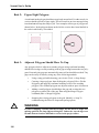
X Min and Y Min with Edge Mesh On
Having the edge mesh option “on” is the default state for Sonnet projects because
it provides a more accurate analysis. Having edge mesh “on” for a polygon changes how the subsections on the very edge are handled. Starting from the left side of
the previous example with edge mesh off, the subsections were 2 cells, 4 cells and
8 cells wide. With edge mesh on, the subsections for the same polygon would be
1 cell, 4 cells, and 8 cells as shown in the illustration below. Notice only the outermost edge is affected.
1 Cell by 1 Cell
on corner
4 Cells
(2 * X Min)
Y
Cell Size =
X
A portion of circuit metal showing how em combines cells into subsections
for polygons with edge mesh on, with X Min = 2 and Y Min = 1. Edge mesh
polygons always have 1 cell wide edge subsections.
As mentioned in the previous section, the edge mesh setting only affects Manhattan polygons (i.e. those with no diagonal or curved edges). Edge mesh is always
“on” for non-Manhattan polygons, regardless of the edge-mesh setting for that
polygon.
39
Sonnet User’s Guide
When used in conjunction with large X Min or Y Min values, the edge mesh option can be very useful in reducing the number of subsections but still maintaining
the edge singularity, as shown in a simple example below. This is very often a
good compromise between accuracy and speed.
In the case pictured above, X Min and Y Min are set to be very large, and the frequency is low enough so that the Max. Subsection size parameter corresponds to
a subsection size that is larger than the polygon.
Using X Max and Y Max for an Individual Polygon
You may control the maximum subsection size of individual polygons by using
the X Max and Y Max parameters. For example, if X Max and Y Max are decreased to 1, then all subsections will be one cell. This results in a much larger
number of subsections and a very large matrix which are the cause of increased
analysis time. Thus, this should be done only on small circuits where extremely
high accuracy is required or you need a really smooth current density plot.
NOTE:
40
If the maximum subsection size specified by X Max or Y Max is larger
than the size calculated by the Max. Subsection Size parameter, the
Max. Subsection Size parameter takes priority. The Max. Subsection
Size is discussed in “Setting the Maximum Subsection Size
Parameter,” page 43.
Chapter 3 Subsectioning
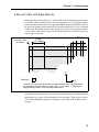
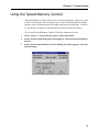
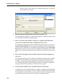
Using the Speed/Memory Control
The Speed/Memory Control allows you to control the memory usage for an analysis by controlling the subsectioning of your circuit. The high memory settings
produce a more accurate answer and usually increase processing time. Conversely, low memory settings run faster but do not yield as accurate an answer.
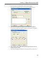
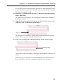
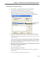
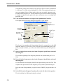
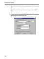
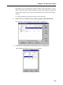
To access the Speed/Memory Control, follow the instructions below.
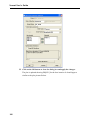
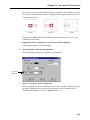
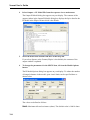
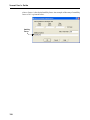
1
Select Analysis ⇒ Setup from the project editor main menu.
2
In the Analysis Setup dialog box which appears, click on the Speed/Memory
button.
3
In the Analysis Speed/Memory Control dialog box which appears, select the
desired setting.
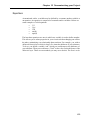
41
Sonnet User’s Guide
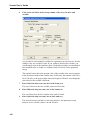
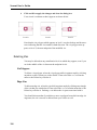
There are three settings for the Speed/Memory Control: Fine/Edge Meshing,
Coarse/Edge Mesh, Coarse/No Edge Meshing. Fine/Edge Meshing is the default
setting and is described in “Default Subsectioning of a Polygon,” page 34. An example is shown below. Again, note that this setting provides the most accurate answer but demands the highest memory and processing time.
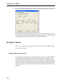
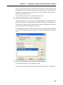
The second option is Coarse/Edge Mesh. This setting is often a good compromise
between speed and accuracy. When this setting is used, the Xmin and Ymin of all
polygons are set to a large number - typically, the value of 50 is used - and edge
mesh is on. Shown below is a typical circuit with this setting. Notice the edges of
the polygons have small subsections, but the inner portions of the polygons have
very large subsections because of the large Xmin and Ymin.
42
Chapter 3 Subsectioning
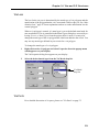
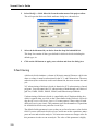
The last option is Coarse/No Edge Meshing. For this setting, all polygons are set
to a large Xmin/Ymin and edge mesh is set to “off.” This yields the fastest analysis, but is also the least accurate. Shown below is the subsectioning of a typical
circuit using this option.
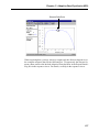
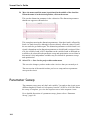
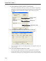
Setting the Maximum Subsection Size Parameter
The parameter Max. Subsection Size allows the specification of a maximum subsection size, in terms of subsections per wavelength, where the wavelength is approximated at the beginning of the analysis. The highest analysis frequency is
used in the calculation of the wavelength. This value is a global setting and is applied to the subsectioning of all polygons in your circuit.
The default of 20 subsections/λ is fine for most work. This means that the maximum size of a subsection is 18 degrees at the highest frequency of analysis. Increasing this number decreases the maximum subsection size until the limit of 1
subsection = 1 cell is reached.
You might want to increase this parameter for a more accurate solution. For example, changing it from 20 to 40 decreases the size of the largest subsections by
a factor of 2, resulting in a more accurate (but slower) solution. Keep in mind that
using smaller subsections in non-critical areas may have very little effect on the
accuracy of the analysis while increasing analysis time.
Another reason for using this parameter is when you require extremely smooth
current distributions using for the current density viewer. With the default value
of 20, large interior subsections may make the current distribution look “choppy.”
43
Sonnet User’s Guide
Setting this value to a large number forces all subsections to be only 1 cell wide,
providing smooth current distribution. Again, analysis time is impacted significantly.
The Max. Subsection Size parameter is specified in the Advanced Subsectioning
Controls which are opened by selecting Analysis ⇒ Advanced Subsectioning from
the project editor main menu.
Defining the Subsectioning Frequency
The subsectioning parameter, Max. Subsection Size, applies to the subsectioning
of all polygons in your circuit, and is defined as subsections per wavelength. Normally, the highest analysis frequency is used to determine the wavelength. However, this may be changed by using the Subsectioning Frequency options in the
Advanced Subsectioning Control dialog box in the project editor. This dialog box
is opened by selecting Analysis ⇒ Advanced Subsectioning from the project editor
main window. For details on what options are available to define the subsectioning frequency, click on the Help button in the Advanced Subsectioning Control dialog box.
The frequency defined by the selected option is now used to determine the maximum subsection size instead of the highest frequency of analysis. Thus, the same
subsectioning can be used for several analyses which differ in the highest frequency being analyzed.
Conformal Mesh Subsectioning
Conformal meshing is a technique which can dramatically reduce the memory and
time required for analysis of a circuit with diagonal or curved polygon edges. For
a detailed discussion of conformal mesh and its rules of use, please refer to “Conformal Mesh,” page 185. Only the effect of conformal mesh on subsectioning is
discussed in this chapter.
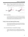
This technique groups together strings of cells following diagonal and curved metal contours to form long subsections along those contours. Whereas staircase fill
results in numerous small X- and Y-directed subsections, conformal mesh results
44
Chapter 3 Subsectioning
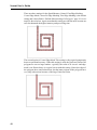
in a few long conformal subsections. The illustration below shows the actual metalization of a conformal section in close up alongside the same section using staircase fill.
Conformal section
Staircase Fill
Conformal sections, like standard subsections, are comprised of cells, so that the
actual metalization still shows a ''jagged'' edge when the polygon has a smooth
edge. However, the sections can be much larger due to conformal meshing. These
larger sections yield faster processing times with lower memory requirements for
your analysis.
Standard subsectioning requires a lot of subsections to model the correct current
distribution across the width of the line. Conformal subsections have this distribution built into the subsection. Sonnet conformal meshing automatically includes
the high edge current in each conformal section. This patented Sonnet capability
is unique. (U.S. Patent No. 6,163,762 issued December 19, 2000.)
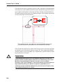
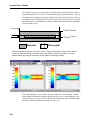
An example of a circuit using both standard subsectioning and conformal mesh is
shown below. The circuit shown at the left is displayed using standard subsectioning (staircase fill). Conformal meshing for the curved part of the circuit is shown
on the right. Note that for the curved part of the geometry, conformal mesh uses
substantially fewer subsections than the number used in the standard subsectioning.
45
Sonnet User’s Guide
Conformal Mesh Subsectioning Control
When you apply conformal mesh to a polygon, it is possible to limit the maximum
length of a conformal section in order to provide a more accurate simulation. The
default length of a conformal section is 1/20 of the wavelength at the subsectioning frequency. For more information on the subsectioning frequency, see “Defining the Subsectioning Frequency,” page 44.
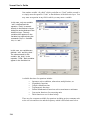
To set the maximum length for a conformal section, do the following:
1
Select the desired polygon(s).
The selected polygons are highlighted.
2
Select Modify ⇒ Metal Properties
This opens the Metalization Properties dialog box.
3
Click on the Maximum Length checkbox in the Conformal Mesh
Subsectioning Controls section of the dialog box.
This will enable the Length text entry box to the right. Note that this checkbox is
only enabled when Conformal is chosen as the Fill Type.
4
Enter the desired Maximum Length in the text entry box.
Click on the OK button to close the dialog box and apply the changes.
For a more detailed discussion of Conformal Mesh, please refer to Chapter 12,
“Conformal Mesh” on page 185. There is also an application note on conformal
mesh available in Help.
46
Chapter 4 Metalization and Dielectric Layer Loss
Chapter 4
Metalization and
Dielectric Layer Loss
This chapter is composed of two parts: metalization loss and dielectric layer loss.
For information on dielectric brick loss, see Chapter 18, “Dielectric Bricks” on
page 263. Both the theoretical aspect of how Sonnet models loss and the practical
how to’s of assigning loss in your circuit are covered, including the use of metal
and dielectric material libraries. The discussion of metalization loss begins below.
For the discussion of dielectric loss, see “Dielectric Layer Loss,” page 57.
There is also a paper available by the president and founder of Sonnet Software,
Dr. James Rautio which contains a detailed discussion of metal losses. You may
find this paper at www.sonnetsoftware.com/support/publications.asp.
Metalization Loss
Metalization loss is specified in the project editor in the Metal Types dialog box
which is opened by selecting Circuit ⇒ Metal Types. Losses may be assigned to
circuit metal, top cover and ground plane. Sidewalls are always assumed to be perfect conductors.
47
Sonnet User’s Guide
A common misconception is that only one type of metalization is allowed on any
given level. In fact, different metalizations (i.e., different losses) can be mixed together on any and all levels. For example, it is possible to have a thin film resistor
next to a gold trace on the same level.
Sonnet allows you to use pre-defined metals, such as gold and copper, using the
global library. The global library allows you to define your own metal types as
well. There is also a local metal library which can be created for an individual or
to share between users.
Sonnet’s Loss Model
The Sonnet model of metal loss uses the concept of surface impedance, measured
in Ohms/sq. This concept allows planar EM Simulators, such as Sonnet em, to
model real 3-dimensional metal in two dimensions.
Real Metal
Modeled Zero Thickness Metal
Substrate
If you are unfamiliar with this concept, please refer to any classic textbook such
as Fields and Waves in Communication Electronics by Simon Ramo, John R.
Whinnery and Theodore Van Duzer, John Wiley & Sons, New York, 1965.
It is important to note that this technique models the loss of the true 3-dimensional
metal fairly accurately, but does not model any change in field distribution due to
the metal thickness. This approximation is valid if the metal thickness is small
with respect to the width of the line, the separation between lines, and the thickness of the dielectric. If the true 3-dimensional affect of the metal is important,
then you should consider using the Thick Metal Model metal type as discussed in
Chapter 17, “Thick Metal” on page 253.
Some electromagnetic analyses use a “perturbational” approach for loss. This
means that they assume the current flowing everywhere is the same as the lossless
case. This approximation works for low loss metals (good conductors). However
for thin film resistors (high loss), the lossless current is not the same as the lossy
current and a perturbational approach fails. Em's loss analysis is not perturbational. It works just as well for a 100 Ohms/square resistor as it does for a 0.004 Ohms/
square good conductor. The Sonnet loss analysis also properly models the transition between electrically thin (low frequency) and electrically thick (high frequen-
48
Chapter 4 Metalization and Dielectric Layer Loss
cy) conductors. See reference [24] in reference Appendix II listed on page 353 for
a detailed description of the theory used by Sonnet. See reference [91] listed on
page 360 for the equations actually used in the Sonnet model.
Another aspect of loss is that the surface impedance of a good conductor has an
imaginary part which is equal to the real part. This reactive surface impedance is
physically due to the increased surface inductance caused by the current being
confined closer to the surface of the conductor. This surface reactance is included
in the Sonnet loss model. The effect is small, but potentially significant in certain
cases.
Keep in mind that a circuit running with lossless metal and dielectrics requires
about one-half the amount of memory and runs about twice as fast. Therefore, the
simplest approximation is to run a lossless simulation. This can be quite useful in
the initial design phase.
Problems In Determining Metal Loss
Sonnet's loss model is very accurate if accurate values are used. In practice, however, there are many aspects of metal loss that cannot easily be accounted for. For
example, surface roughness, metal purity, metal porosity, etc. cannot easily be
measured and included in an all-encompassing loss model. In addition, most software programs, Sonnet included, do not allow you to enter all of the parameters
that determine metal loss. Many users like to use the ideal values as a starting point
and add a little of their own “real-world” loss. But how much should be added to
the ideal models? This question is not easily answered, but is addressed in the next
section.
An additional loss problem exists with planar EM analysis tools such as Sonnet.
The problem stems from the fact that planar EM tools treat the metal conductor as
zero thickness. This means that there is no difference between the top of the conductor and the bottom of the conductor. In some circuits, stripline for example, the
current is symmetrical with half of the current flowing on the top of the conductor
and half flowing on the bottom of the conductor. The zero thickness model works
well in these cases.
In other circuits, such as microstrip, the current can be unequally distributed, resulting in higher loss than the equivalent stripline circuit. If you know the ratio between the top and the bottom currents, you can obtain a better loss model. All
planar solvers must either estimate this value in order to calculate metal loss, or
the information must be input by the user. For this class of circuits, it is difficult
for the user to know an exact value of the current ratio without obtaining measured
data on the circuit. For these cases, assuming all the current flows on one side of
49
Sonnet User’s Guide
the conductor gives a “worst case” loss result. This tends to compensate for the
“best case” loss caused by ignoring the other aspects of loss (metal porosity, etc.)
mentioned earlier.
Determining Good Input Values
The best method to determine proper loss values is to build and measure a simple
structure of the desired metalization. The structure should be sensitive enough to
loss so that measurement errors do not significantly affect the results. Then analyze the same structure on Sonnet and adjust the loss values until the calculated
loss matches the measured loss. This may take several iterations before success,
but then you can use these values for similar circuits. You are now effectively using measured values for the loss parameters.
Creating Metal Types
To assign loss to a polygon in Sonnet, you first define a metal type by inputting
its loss parameters and then assign that metal type to the polygon drawn in your
circuit. The previous section(s) described how to determine values for the Sonnet
loss model. This section provides instructions for creating a metal type and discusses the loss models used in the Metal Editor dialog box.
The Metal Editor dialog box allows you to enter a loss definition for the metal
type. There are five different methods for entering loss: Normal, Resistor, Rd./
Ref, General and Sense. The different loss models are discussed below followed
with a procedure for entering new metal types. The discussions assume simple,
single conductor microstrip and stripline geometries where mentioned.
You do not need to read the details of each loss model. Instead, you should make
yourself familiar with the loss models you are likely to use. Most users only need
concern themselves with “Normal.” All the methods use the same loss model in
Sonnet; which model you choose depends on the parameters you know about your
real metal type.
Normal
For the Normal metal type, you determine the loss using the bulk conductivity, the
metal thickness and the current ratio.
50
Chapter 4 Metalization and Dielectric Layer Loss
NOTE:
Metal thickness is used only in calculating loss; it does not change the
physical thickness of metalization in your circuit. The metalization in
your circuit is still modeled as zero-thickness.
Sonnet models your circuit using zero thickness metal, but your real circuit possesses a metal thickness. At higher frequencies current flows in a thin skin around
the edge of the metal, as pictured below. The current ratio is the ratio of the current
flowing on the top of the metal to the current flowing on the bottom of the metal.
~~~ Current
~~~~~~~~~~~~~~~~~~~~~~~~~
Top
~~~~~~~~~~~~~~~~~~~~~~~~~
Bottom
Cross section of metalization
There are no sides in a zero thickness model; therefore when translating from
these parameters, the current which flows on the sides is ignored. In some circuits, stripline for example, the current is symmetrical with half of the current
flowing on the top of the metal and half flowing on the bottom of the metal. In
this instance, the current ratio is 1. If you had twice as much current flowing on
the top as on the bottom, the current ratio is 2. This could occur for some
microstrip circuits, for example. It is difficult to know an exact value of the current ratio without obtaining measured data on your circuit. All planar solvers
must estimate this value in order to calculate metal loss; this particular model in
Sonnet allows you to enter the value. Note that reciprocal values have the same
effect; i.e., 0.5 results in the same loss as 2.0.
Resistor
To define a metal which you wish to use as a resistor, enter the DC resistance in
ohms/sq in the Rdc text entry box which appears when you select this metal type.
To use this loss model, the resistivity should be constant over the frequency range
of interest.
51
Sonnet User’s Guide
Rdc/Rrf
This method allows you to enter two values: RDC and RRF. The first parameter,
RDC, determines loss at low frequency (where the conductor is much thinner than
the skin depth). Surprisingly, other electromagnetic analyses often predict zero
loss at low frequency because they assume RDC is zero.
The second parameter is the skin effect coefficient, RRF. Em multiplies this number by the square root of the frequency (in Hertz) to yield the Ohms/square value
at high frequency.
The equations for RDC and RRF are:
R DC = 1 ⁄ ( σt )
R RF = Skin effect coefficient =
( πμ ) ⁄ σ
where σ is the bulk conductivity in mhos/meter, t is the metalization thickness in
meters, and μ = 4π x 10-7 H/m. Typical values for RDC and RRF are 0.004 and
3e-7. If you start getting very strange loss results, check RRF, paying special attention to the exponent.
Em also properly models the transition between electrically thin (low frequency)
and electrically thick (high frequency) conductors. The transition frequency from
RDC to RRF is the square of RDC/RRF. At this frequency, and a relatively narrow
band around it, both coefficients are important. If the skin effect coefficient (RRF)
is set to 0.0, then the value of RDC is used over all frequencies. This is the usual
case for resistors.
The above equation for RRF assumes that all of the current travels on just one side
of the conductor. This is a good approximation for some microstrip circuits. However, if the current really travels on both sides, this gives a pessimistic value for
the loss. The equation should be modified for other structures. Stripline, for example, has current of equal amplitude on both the top and bottom of the conductor.
In this case, you should divide the RRF value by two, while maintaining RDC.
As an example, the conductivity (σ) for copper is 5.8E+7 Mhos/m, giving RDC =
0.006 Ohms/square (t = 3 um) and a microstrip RRF = 2.6E-7. In reality, the bulk
conductivity of copper, or any other given metal, may not equal the laboratory value, so the figures as calculated above are likely to be lower than actual results. The
table below provides calculated results of commonly used metals using the equations above.
52
Chapter 4 Metalization and Dielectric Layer Loss
.
Properties of Commonly Used Metals
Metal
σ
(S/M)
RDC
(Ω/sq)
t = 1 μM
RDC
(Ω/sq)
t = 1 mil
RRF
(ΩHz-1/2/sq)
“Skin Effect”
(microstrip)
Aluminum
3.72e7
0.027
1.1e-3
3.3e-7
Brass
1.57e7
0.070
2.5e-3
5.0e-7
Copper
5.80e7
0.017
6.8e-4
2.6e-7
Gold
4.09e7
0.024
9.6e-4
3.1e-7
Nichrome
1.00e6
1.000
3.9e-2
2.0e-6
Silver
6.17e7
0.016
6.4e-4
2.5e-7
Tantalum
6.45e6
0.155
6.1e-3
7.8e-7
Tin
8.70e6
0.115
4.5e-3
6.7e-7
General
This loss model includes the metalization resistivity described above in Rdc/Rrf.
The General loss definition also includes the metalization reactance, composed of
the surface reactance, Xdc and the kinetic inductance, Ls.
Surface reactance, Xdc, is specified, in Ohms/square. Em uses the same reactance
at all frequencies.
Until recently, the only surface resistivities of practical interest were pure real, i.e.,
pure loss. With the growing application of superconductors in high frequency
work, surface reactance reaches significant levels. A superconductive effect
known as “kinetic inductance” slows the velocity of the electrons with no loss of
energy. This can be modeled as a surface inductance.
The effect of surface inductance is to make εeff larger, or the velocity of propagation slower. For normal conductors, εeff can never be larger than εrel. In a superconductor, this is no longer true. This unusual effect becomes significant for very
thin substrates.
Surface inductance, Ls, is specified in the project editor in the Metal Types dialog
box accessed by selecting Circuits ⇒ Metal Types. This parameter takes into account the surface reactance at higher frequencies.
53
Sonnet User’s Guide
There are three recommended approaches to obtaining a value for Ls. A first order
approximation is to assume the metal is a perfect conductor.
R rf = 0
R DC = 0
Ls = 0
This model works well for moderate frequencies (less then 150 GHz) and moderate circuit dimensions which are much greater than the London depth of penetration.
The second approach is a model which is still valid at moderate frequencies, but
includes effects due to kinetic inductance. The kinetic inductance is a function of
temperature and can be approximated in the following manner:
R DC = 0
R rf = 0
Ls = μ0 λL ( T )
where
–7
μ 0 = 4π ( 10 ) H/m
4
λL ( T ) = λ0 ⁄ ( 1 – ( T ⁄ Tc ) )
London depth of penetration at temp.
λ 0 = London depth at T = 0 meters
T c = Critical (Transition) Temperature in degrees Kelvin
The third model should be used to account for high frequency effects or effects
due to small circuit dimensions. In these cases, the surface resistances proportionality to ω2 begins to dominate and the following model is suggested. The resistivity is a function of frequency-squared, and Sonnet presently does not have a
method to do this. Therefore, if you are analyzing over a broad band, you need to
have a separate project for each frequency, using the following equations.1
R rf = 0
1 2 2
R DC = --- ω μ 0 ( λ L ( T ) ) 3 σ N ( η n ⁄ ( η n + η s ) )
2
Ls = μ0 λL ( T )
1.
54
Shen, Z. Y., “High-Temperature Superconducting Microwave Circuits,” Boston, 1994, Artech House.
Chapter 4 Metalization and Dielectric Layer Loss
where
ω = 2πf radians/sec
σ N = Conductivity of the superconductor in its normal state (Mhos/m3)
η n = Normal state carrier density (1/m3)
η s = Superconducting state carrier density (1/m3)
μ 0 and
λL ( T )
are as defined above
The Surface Impedance, Zs, for superconductors is modeled in Sonnet using the
following equation:
Z s = R DC + j ⋅ ( ωL s + X DC )
for
L s > 0.0
Sense
Em solves for the current distribution; however, on occasion, you may want to
view the fields, not the current. You do this with what is called a “sense metal”.
The sense metal is a rectangular patch of conductor placed where you want to see
the tangential electric field. (You cannot view the normal direction of the field
with Sonnet.)
For further discussion of sense metal, see “View Tangential Electric Fields” under
Tips and App notes in Help. You may access help by selecting Help ⇒ Contents
from any Sonnet application.
Thick Metal
For thick metal, you input two parameters: the bulk conductivity and the metal
thickness. The loss is calculated in the same manner as for the Normal metal type,
except that the thickness in this case represents a physical thickness which eliminates the need to enter the current ratio.
For a detailed discussion of thick metal, see Chapter 17, “Thick Metal” on page
260.
How to Create a Metal Type
For detailed instructions on creating a metal type, please refer to “metal types:adding” in the Index of Help. You may access help by selecting Help ⇒ Contents
from the main menu of any Sonnet application or by clicking on the Help button
in any dialog box.
55
Sonnet User’s Guide
Metal Libraries
There are two types of metal libraries available in Sonnet: global and local. The
metal libraries contain standard definitions for metal types which may be used in
your projects. There is no real difference between the global and local library. The
names refer to how they are used. The global library would usually be used as a
group wide library of standard metals for a group of designers.
There is a default global library supplied by Sonnet which contains definitions for
some common metals. The default location for the global library is in <Sonnet Directory>/data/library where <Sonnet Directory> is the directory in which your
Sonnet software is installed. You may choose to use this location or can save this
library in another location.
The local library would usually be used as the user's own library of metal definitions. This library may be stored in a location of the user's choice. You use the
Metal Editor dialog box to add, edit and delete entries to these libraries.
For instructions on adding metals to a metal library, editing metals in a metal library or using metals defined in a metal library, please refer to Sonnet Help available from the Help menu in any Sonnet application.
Via Loss
The loss of a via is accomplished in much the same way as a metal polygon. The
only difference is that a via is a 3D object and a polygon is only two-dimensional.
Therefore, the Sonnet via loss model is only an approximation. In general, edgevias use the loss of the polygon they are attached to, and via-polygons have their
own loss properties. To assign loss to a via polygon, select the via-polygon, and
choose Modify ⇒ Via Properties. In the Via Properties dialog box, select a metal
type in the Via Loss drop list for the via polygon. For extremely precise loss analysis of vias, you should use the same measurement approach as discussed earlier
for polygon loss.
Setting Losses for the Box Top and Bottom (Ground Plane)
You set the loss for the box top or bottom by assigning a metal type to the box top
or bottom. The box top and bottom use the same metal types which are used for
the metalization in your circuit, i.e., the polygons and via polygons. In addition,
56
Chapter 4 Metalization and Dielectric Layer Loss
there are two special metal types available in Sonnet for the Top and Bottom metals: Free Space and Waveguide Load. See Chapter 19, “Antennas and Radiation”
for a discussion of how and why you would use these types.
To assign a metal type to the Box Top or Bottom metal, select Circuit ⇒ Box Settings from the project editor main menu. In the Box Settings dialog box which appears on your display, select the desired metal type for the top metal from the Top
Metal drop list and the desired metal type for the bottom metal from the Bottom
Metal drop list.
Dielectric Layer Loss
The dielectric layer loss calculations in Sonnet are virtually exact, given the substrate really has a frequency independent conductivity, and/or loss tangent. Our
web site has a lossy conductivity benchmark you can perform on any electromagnetic solver (or measurement system). See Benchmarking on the Products section
of our web site, www.sonnetsoftware.com.
The dielectric loss is calculated in Sonnet at the beginning stages of the analysis.
The method Sonnet uses starts with the calculation of a sum of waveguide modes.
The exact solution requires an infinite sum of modes, but Sonnet truncates this
sum to some reasonable value (the truncation has never been a source of error).
So, for each mode, if there is a lossy dielectric, the calculation involves complex
numbers instead of just real numbers. This is NOT a discretized function - it is a
continuous function. Therefore, the dielectric loss calculation can be thought of as
exact (only limited to the precision of the machine).
A more reasonable source of error is in the assumption that the conductivity is
constant with frequency. All real dielectrics have frequency-dependant loss (some
smaller than others). Sonnet supplies you with two parameters (Loss Tan and Diel
Cond) to control this frequency dependency. The equation Sonnet uses to calculate the TOTAL loss is given in “Dielectric Layer Loss,” page 59. There are some
dielectrics with more complicated frequency dependencies, but this equation
works for most dielectrics. Of course, this requires that you know the frequency
dependency of your dielectric. If you have a method of measuring the loss as a
function of frequency (or published data which you can trust), and if it is constant
over your range of frequencies, then dielectric loss is probably not a source of error. Be careful, however, of published loss data. Verify that the data is valid over
your frequency range.
57
Sonnet User’s Guide
Dielectric Layer Parameters
You can set the dielectric constant and loss of a dielectric layer by changing the
following parameters in the project editor by selecting Circuits ⇒ Dielectric Layers, then clicking on the Above, Below or Edit button in the Dielectric Layers dialog box. This opens the Dielectric Editor dialog box which allows you to edit the
parameters below.
•
Erel: The relative dielectric constant (εr). The ratio (ε/εo), where ε is the real
part of the permittivity of the dielectric layer material, and εo is the permittivity of free space. The ratio is dimensionless.
•
Dielectric Loss Tan: The dielectric loss tangent. The ratio (ε’’/ε’), where ε
= ε’ - jε’’, and ε is the complex permittivity of the dielectric layer material.
The ratio is dimensionless.
•
Diel. Cond: The dielectric conductivity, σ, where σ is the bulk conductivity
in siemens per meter.
•
Mrel: The relative magnetic permeability (μr) of the dielectric layer material.
• Magnetic Loss Tan: The magnetic loss tangent of the dielectric layer material.
One last parameter that may be specified for a dielectric layer is the Z Partitioning.
This value may be changed in the Z Partitions dialog box which is opened when
you click on the Z Parts button in the Dielectric Layers dialog box.
•
Z-Partitions: The z-partitioning parameter is the setting which controls the
number of partitions which the dielectric layer is divided into in the z direction. for the dielectric layer. While this parameter is specified in the dielectric
layer window, it only has an effect on the dielectric bricks on that layer.
Changing this value for a particular layer will have absolutely no affect on the
analysis if there are no bricks on the layer. If there are multiple bricks on the
layer, the Z subsectioning for all of those bricks will be identical.
The more partitions (better resolution) used in the Z-dimension, the more accurate the analysis; however, analysis time and memory requirements also increase dramatically.
58
Chapter 4 Metalization and Dielectric Layer Loss
Dielectric Layer Loss
Em uses the above parameters to calculate the total effective tanδ for the dielectric
material as follows:
( Diel Cond -)
tan δ = ( Loss Tan ) + ----------------------------ω ( Erel )ε o
where, ω is the radian frequency (ω = 2πf, where f is frequency in hertz). Note that
tanδ has both a frequency-dependent term and a frequency-independent term.
The above equation for tanδ can also be expressed in terms of conductivity as follows:
Total Effective Cond = ( Loss Tan )ω ( Erel )ε o + ( Diel Cond )
Both equations are equivalent. Each describes how em uses the input dielectric parameters to compute loss in the dielectric material.
See “Circuit ⇒ Dielectric Layers” in the project editor’s Help for information on
setting these parameters.
How to Create a New Dielectric Layer
For detailed instructions on creating a new dielectric layer, please refer to “dielectric layers:adding” in the Index of Help. You may access help by selecting Help
⇒ Contents from the main menu of any Sonnet application or by clicking on the
Help button in any dialog box.
Dielectric Libraries
The dielectric libraries contain standard definitions of dielectric materials which
may be used for your dielectric layers. There are two types of dielectric libraries
available in Sonnet: global and local. There is no real difference between the two
libraries. The names refer to the way in which they are used.
NOTE:
The Dielectric Libraries materials may not be used for dielectric
bricks but only for dielectric layers.
59
Sonnet User’s Guide
The global library would usually be used as a group wide library of standard dielectrics for a group of designers.There is a default global library supplied by Sonnet which contains definitions for dielectric materials. The default location for
the global library is in <Sonnet Directory>/data/library where <Sonnet Directory>
is the directory in which your Sonnet software is installed. You may choose to use
this location or can save this library in another location.
The local library would usually be used as the user's own library of dielectric material definitions. This library may be stored in a location of the user's choice. You
use the Dielectric Editor dialog box to add, edit and delete entries to these libraries.
60
Chapter 5 Ports
Chapter 5
Ports
This chapter describes the five different types of ports used in Sonnet, how they
are modeled and how to place or delete them in your circuit.
The five types of ports used in Sonnet are the standard box-wall port, the co-calibrated internal port, the via port, the auto-grounded port and the ungrounded internal port.
Port Type Overview
As mentioned above, the five types of ports available in Sonnet are the standard
box wall, co-calibrated internal port, via port, autogrounded port and internal ungrounded port. All ports in Sonnet are two-terminal devices. The box wall and cocalibrated port types are those used the majority of the time. Each type of port is
described below.
Box wall:
•
•
•
•
Most common type of port.
Positive terminal is attached to a metal polygon and the negative
terminal is attached to the box wall (ground).
De-embedding is the most accurate for this type.
Used for connections to the periphery of your geometry.
61
Sonnet User’s Guide
•
Reference planes may be used.
For more information on box wall ports, see “Standard Box Wall Port,” page 69.
Co-calibrated internal port:
•
•
•
•
•
•
Used in the interior of a circuit.
Identified as part of a calibration group with a common ground
node connection. The ground node connection can be defined as
floating or the Sonnet box.
When em performs the electromagnetic analysis, the co-calibrated
ports within a group are simultaneously de-embedded.
Highly accurate de-embedding.
Often used by a circuit simulation tool to connect some type of element into your geometry at a later time outside the Sonnet environment.
Reference planes may be used.
For more information on co-calibrated internal ports, see “Co-calibrated Internal
Ports,” page 70.
Via port:
•
•
•
•
•
Used in the interior of a circuit.
Negative terminal is connected to a polygon on a given level and
the positive terminal is connected to a second polygon on another
level above.
Cannot be de-embedded.
Most commonly used to attach a port between two adjacent levels
in your circuit or when you want a port to go up to the box cover
rather than down to ground.
Reference planes cannot be used.
For more information on via ports, see “Via Ports,” page 75.
Auto-grounded port:
•
•
•
•
62
Used in the interior of a circuit.
The positive terminal is attached to the edge of a metal polygon and
the negative terminal is attached to the ground plane through all
intervening dielectric layers.
Used in place of a co-calibrated port to reduce the de-embedding
processing time at the cost of less accuracy.
Reference planes may be used.
Chapter 5 Ports
NOTE:
When using auto-grounded ports, be aware than any coupling
between auto-grounded ports is not accounted for when performing
the de-embedding.
For more information on auto-grounded ports, see “Automatic-Grounded Ports,”
page 76.
Ungrounded Internal Ports:
•
•
•
•
•
•
Used in the interior of a circuit.
Each terminal is attached to one of two adjacent polygons.
Used in place of a co-calibrated port when you do not want any
space between the two polygons.
Will have a different ground reference from the other ports in the
circuit.
Commonly used to add a series element in post em processing.
Reference planes cannot be used.
For more information on ungrounded internal ports, see “Ungrounded Internal
Ports,” page 78.
Port Normalizing Impedances
The default normalizing impedance for a port is 50 ohms. This is done since 50
ohms is an industry standard; some analysis tools only accept the value of 50 ohms
as the normalizing impedance.
In rare cases, you may wish to have S-parameters normalized to some other impedance. The normalizing impedance in Sonnet is represented by four numbers as
shown in the diagram below. First is the real part in ohms. Next comes the reactive
part in ohms. Third is the inductive part in nanohenries (nH). The last number is
63
Sonnet User’s Guide
the capacitive part in picofarads (pF). The inductive and capacitive parts modify
only the reactive portion of the load, they are included so you do not have to manually re-calculate the reactive part at each frequency.
R + jX
L
C
V
Equivalent circuit of an em port.
NOTE:
The normalizing impedances are ignored if Y- or Z-parameters are
specified for output. Y- and Z-parameters are always normalized to
one ohm.
This capability should be used only by the most advanced user. This feature
should never be applied to data which is to be used in a standard circuit theory program other than Sonnet’s. Many programs assume S-parameters normalized to exactly 50 ohms; S-parameters normalized to another value would introduce error
into the analysis.
Changing Port Impedance
There are two methods for changing the impedance of a port. If you wish to
change the impedance of a given port, and do not need to see the impedance values
of other ports, take the following steps using the project editor:
64
1
Select the desired port(s). This will enable the Modify menu option.
2
Select Modify ⇒ Port Properties to open the Port Properties dialog box.
3
The impedance values can be changed by typing the desired values in
the Resistance, Reactance, Inductance and Capacitance text boxes in
the dialog box. This changes the parameters on all ports selected and all
ports with the same number as the ports selected.
Chapter 5 Ports
If you wish to change the impedance of a given port, and wish to see the impedance values of other ports while doing so, proceed as follows:
1
Select Circuit ⇒ Ports from the main menu to open the Port Impedance
dialog box.
2
The impedance values for any port can be changed by typing the desired
values in the Resistance, Reactance, Inductance and Capacitance fields
in the row labeled with the desired port number.
TIP
Note that the impedance of multiple ports may be changed at the same time
through the first method by selecting multiple ports before selecting Modify ⇒
Port Properties, and by the second method, by modifying all the desired port values while the Port Impedance dialog box is open.
Special Port Numbering
All ports are assigned a number at the time they are created in the project editor.
There is no limit on the number of ports and the number of ports has a minimal
impact on the analysis time needed for de-embedding. By default, the ports are
numbered by the order in which they are created (i.e. first port created is assigned
the number 1, second port created is assigned the number 2, etc.). With this default
method, all ports are positive and unique. However, there are some applications
that require the ports to have duplicate, or even negative, numbers.
Ports with Duplicate Numbers
All ports with the same number, as pictured below, are electrically connected together. As many physical ports as desired may be given the same numeric label.
Such ports are sometimes called “even-mode” or “push-push” ports and have
65
Sonnet User’s Guide
many uses, including simulating the even-mode response of a circuit. See “Modeling an Arbitrary Cross-Section,” page 260, for an example of using “push-push”
ports.
Ports with identical
port numbers are
electrically
connected together.
Ports with Negative Numbers
Ports may also have negative numbers as shown in the figure below. This feature
can be used to redefine ground. Strictly speaking, em sums the total current going
into all the positive ports with the same port number and sets that equal to the total
current going out of all the ports with that same negative port number. For example, for a circuit with a +1 port and a -1 port, em sets current flowing into port +1
to be equal to the current flowing out of port -1. Thus, they are sometimes called
“balanced”, “push-pull” or “odd-mode” ports. Coplanar lines can be represented
with balanced ports. See below for an example of push-pull ports.
An example of a
coplanar waveguide
cross junction.
Ports are required to be in sequential order with no numbers missing. If the ports
are not in sequential order, you will receive an error message when you attempt
an analysis. The port order for the S, Y, or Z-parameters will be listed in increasing
numeric order. For the example of a two-port, the output would be S11, S21, S12,
and S22. For a four-port, it would be S11, S12, S13, S14, S21, S22, etc.
66
Chapter 5 Ports
For a discussion of using ports to model coplanar waveguides (CPW), please see
“Modeling Co-Planar Waveguide (CPW) in Sonnet” under Tips and App Notes in
Help. You can find this topic by selecting “CPW” in the help Index.
NOTE:
When you are referred to Sonnet’s Help, you may access Help by
selecting Help ⇒ Contents from the menu of any Sonnet application
or by clicking on the Help button in any dialog box.
Changing Port Numbering
You can change the port number of any port after it has been added to your circuit.
Any nonzero integer, negative or positive, is valid. To change the number on a
port or ports, do the following:
1
Select the port(s) whose number you wish to change.
2
Select Modify ⇒ Port Properties from the main menu to open the Port
Properties dialog box.
3
The number for the selected port(s) can be changed by typing the
desired port number in the dialog box. Note that if multiple ports are
selected, all are set to the number input in the dialog box.
Port Placement with Symmetry On
Symmetry can be used to considerably reduce the amount of memory and processing time required to analyze a circuit which is symmetrical about the midline of
the substrate. When symmetry is turned on in the Box Settings dialog box (Circuit
⇒ Box), everything below the line of symmetry is ignored, and all metal above the
line of symmetry is “reflected” about the symmetry line. Special care should be
given to ports when using symmetry.
67
Sonnet User’s Guide
Normally, if you are using symmetry, ports are placed on the line of symmetry as
pictured below.
Line of Symmetry
Ports are placed
on the line of
symmetry
Ports can be placed off the line of symmetry, but the port placed above the line of
symmetry must have another port equidistant from and below the line of symmetry. These two ports must also have the same port type, port number and properties. The basic premise of symmetry is that the voltage at any give point above the
line of symmetry must be equal to the voltage at the corresponding location below
the line of symmetry. Using the same number port, port type and properties ensures that the voltage is the same at both required points since all ports with the
same number, as pictured below, are electrically connected together.
This circuit has two
sets of ports placed
equidistant from the
line of symmetry.
Port Pair Note that the
corresponding ports
above and below the
line of symmetry have
the same number.
Port Pair
Line of Symmetry
This circuit violates port
usage with symmetry. The
ports are equidistant from
the line of symmetry but
have different port
numbers so that the
voltage is not equal.
68
Chapter 5 Ports
Standard Box Wall Port
A standard box wall port is a grounded port, with the positive terminal attached to
a polygon edge coincident with a box wall and the negative terminal attached to
ground. An example of a standard box-wall port is shown below. Standard boxwall ports can be de-embedded and can also have reference planes. This type of
port is the most commonly used.
-
1
+
Box wall
port on
page 46.
Adding Box wall Ports
You add a standard box wall port to your circuit by selecting the command Tools
⇒ Add Ports and clicking on the polygon edge on the box wall where you wish to
place the port. Ports are numbered automatically, in the order in which they are
added to your circuit, starting at the number one. You may change the properties
of a port after it has been added to the circuit by selecting the port and using the
Modify ⇒ Port Properties command. For detailed instructions for these tasks,
please click on the Help button in the Modify Port Properties dialog box which appears when you select the command.
Ref. Planes and Cal. Lengths for Box Wall Ports
Reference planes and calibration lengths are both used during the de-embedding
process in which the analysis engine removes the port discontinuity and a desired
length of transmission line. For details of how these values are used during the deembedding process, please refer to Chapter 7, “De-embedding” on page 97.
69
Sonnet User’s Guide
For a box wall port, you may set either a reference plane or a calibration length;
both values cannot be set at the same time for box wall ports. All ports on any given box wall use the same reference length. To set either of these values for box
wall ports, use the Circuit ⇒ Ref. Planes/Cal. Length command. For details,
please click on the Help button in the Reference Planes/Calibration Lengths dialog
box which appears when you select the command.
Co-calibrated Internal Ports
Co-calibrated ports are used in the interior of a circuit. These ports are often used
by a circuit simulation tool to connect some type of element into your geometry at
a later time outside the Sonnet environment. Co-calibrated internal ports are identified as part of a calibration group with a common ground node connection. When
em performs the electromagnetic analysis, the co-calibrated ports within a group
are simultaneously de-embedded using a high accuracy de-embedding technique1;
thus, coupling between all the ports within a calibration group is removed during
de-embedding. This type of port is the most commonly used internal port.
Ground Node Connection
You must define how the common ground of your calibration group is connected
to your circuit. There are two types of ground node connection: Sonnet Box and
Floating.
Sonnet Box: When the ground node connection is defined as the Sonnet box, all
co-calibrated ports in the group are globally grounded to the Sonnet box. To do
this, a via is automatically created which connects to the top or bottom of the Sonnet box. You should choose this option if the element model or measured data to
be connected to these ports includes shunt elements. Examples are:
•
•
S-parameter data that includes pads or other coupling to ground.
Transistor data that includes a via in the model/measurement.
1 ”Deembedding the Effect of a Local Ground Plane in Electromagnetic Analysis,” by James C. Rautio, president and founder of Sonnet Software, Inc.
The article is available in PDF format in the Support section of our web site.
70
Chapter 5 Ports
This type of co-calibrated port is illustrated below. The positive terminal is attached to a polygon edge of a feedline and the negative terminal is attached to a
via to ground which is removed during de-embedding.
Via to Ground
Via to Ground
+
+
Box wall
port on
page 46.
When the Sonnet box is selected as the ground node connection, the analysis engine automatically determines the most efficient direction the ground via extends
taking into consideration both the distance and the loss of the box top or bottom.
When using this type of ground, you must make sure that there is a clear path with
no metal on other levels interfering with the path to the box top and bottom.
In addition, either the box top or bottom must have loss less than 50 ohms/sq. For
example, you should not use “Free Space” for both your box top and bottom definition. If the loss is too high on both the box top and bottom for a ground via from
the Component to be attached, the analysis engine will issue an error message.
Floating: When the ground node connection is defined as Floating, all co-calibrated ports in the group are connected to a common ground but not to the Sonnet
box. Instead, the ground node is left unconnected to the rest of your circuit. You
should choose this option if the element model or measurement data that will be
connected to these ports does not have a ground reference, or does not have shunt
elements. Examples of this are:
•
•
A series RL equivalent circuit
S-Parameter data that was measured without any pads
This type of co-calibrated port is illustrated below. Sonnet automatically adds extra metal which connects the co-calibrated ports in a calibration group. This extra
metal is defined as Generalized Local Ground (GLG) metal since it acts as a local
71
Sonnet User’s Guide
ground for the ports in the calibration group. This metal is removed during the deembedding process. The positive terminal of a co-calibrated port is attached to a
polygon edge of a feedline and the negative terminal is attached to GLG metal.
+
GLG Metal
+
To observe the GLG metal for either type of ground node connection, you may select the View ⇒ View Subsections command in the project editor. When the Subsection Viewer appears, select View ⇒ GLG Metal from the subsection viewer’s
main menu. Views of two calibration groups, as viewed in the subsection viewer
with the GLG metal displayed, are shown below. A calibration group which is
grounded to the Sonnet box is shown on the left and one with a floating ground is
shown on the right.
GLG Metal Via
GLG Metal Polygon
Sonnet Box
Floating
Circuit Metal
Note that in the case of the Sonnet box ground node connection, the GLG
metal does not connect the two ports. Instead, there is a via composed of
GLG metal which extends to ground.
72
Chapter 5 Ports
Terminal Width
You must also determine how you will define the terminal width for your calibration group. Terminal width is the electrical contact width of the component which
is to be attached. This allows the current flow from the circuit geometry into the
component to be accurately modeled. There are three settings for terminal width:
Feed Line Width, One Cell, and User Defined. Please note that the terminal width
is not shown in the project editor.
Feed Line Width: This defines the terminal width as equal to the feed line to
which the co-calibrated port is attached. This is illustrated below.
Current Flow
Feed Line Width
Terminal Width
One Cell: This defines the terminal width to the smallest possible size as pictured
below.
Current Flow
One Cell
Terminal Width
One Cell
73
Sonnet User’s Guide
User Defined: This allows you to enter any value desired for the terminal width.
This type of Terminal Width is shown below.
Current Flow
User Defined
Terminal Width
Adding Co-calibrated Ports
You add co-calibrated ports to your circuit by selecting the command Tools ⇒ Add
Ports and clicking on an open polygon edge where you wish to place the port.
Once the ports have been added to the circuit, you select the ports, then use the
Modify ⇒ Port Properties command which allows you to select the co-calibrated
port type and assign each port to a calibration group. For detailed instructions on
this process, please refer to “co-calibrated internal port” in Help’s index.
Ref. Planes and Cal. Lengths for Co-calibrated Ports
You may specify both a reference plane and a calibration length for co-calibrated
ports. For a detailed discussion of how reference lengths and calibration lengths
are used during the de-embedding process, please refer to Chapter 7 "De-embedding" on page 97 and Chapter 8 "De-embedding Guidelines" on page 107. For directions on how to set a reference plane and/or calibration length for a cocalibrated port, please refer to “calibration group” Help’s index.
74
Chapter 5 Ports
Use in Components
Co-calibrated ports are used to implement the Component feature. Many of the
considerations which apply to the property setup of a Component also apply to the
property setup for a calibration group. To gain a deeper understanding of the cocalibrated ports implementation and uses, we highly recommend that you also
read Chapter 6 "Components" on page 81.
Via Ports
A via port has the negative terminal connected to a polygon on a given circuit level
and the positive terminal connected to a second polygon on another circuit level.
A via port can also have the negative terminal connected to the top or bottom of
the box. An example of this port type on an edge via is shown below.
Upper Polygon
+
Level 1
1
Level 0
Via Port
Lower Polygon
An example of a circuit with a standard via port. A side view of
the enclosed area on the circuit is shown in the middle.
Unlike co-calibrated ports, em cannot de-embed via ports. However, in a circuit
which contains a combination of via ports and other port types, the other port types
can still be de-embedded. Em will automatically identify all of the other ports
present in the circuit and de-embed them, but leave the via ports un-de-embedded.
The example file Dual_patch has an example of a via port used in a patch antenna.
This example file can be found in the Sonnet example files.
75
Sonnet User’s Guide
In most cases where you need grounded ports, your first choice would be to use
co-calibrated ports (as discussed earlier), especially since it is possible to accurately de-embed co-calibrated ports. The most common case where a via port would
be used is when you wish to attach a port between two adjacent levels in your circuit. Another application is when you wish to connect a port to the interior of a
polygon, which is not allowed for co-calibrated ports which must be added to an
open polygon edge.
You can not apply reference planes to via ports, since it is not possible for em to
de-embed them.
Adding Via Ports
To add a via port, you must first create a via. The via can be an edge-via or a via
polygon. For more details on how to create vias, see “vias” in Help’s index.
Once the via is in place, click on the Add a Port button in the tool box and click
on the via to add a port.
NOTE:
The via port only appears in the project editor on the bottom level of
the via; if you are adding the port to any other level of the via, the
port is not displayed in the project editor. To see the port, go to the
metal level on which the bottom of the via is placed.
Automatic-Grounded Ports
An automatic-grounded port is a special type of port used in the interior of a circuit
similar to a co-calibrated internal port. This port type has the positive terminal attached to the edge of a metal polygon located inside the box and the negative ter-
76
Chapter 5 Ports
minal attached to the ground plane through all intervening dielectric layers. An
auto-grounded port with a reference plane is shown below. Auto-grounded ports
can be de-embedded by the analysis engine.
Autogrounded
port
picture.
In most circuits, the addition of co-calibrated ports has little influence on the total
analysis time of the em job. However, for some circuits, co-calibrated ports may
require more time in the de-embedding phase of the analysis. In these cases, you
may wish to use auto-grounded ports, which are more efficient but less accurate
than co-calibrated ports, since the de-embedding for auto-grounded ports does not
take into account the coupling between the auto-grounded ports.
Special Considerations for Auto-Grounded Ports
Metal Under Auto-Grounded Ports
Similar to co-calibrated ports which use the Sonnet box as the ground node connection, you cannot have metal directly beneath an auto-grounded port in a multilayer circuit. Auto-grounded ports are two-terminal devices with the positive terminal connected to an edge of a metal polygon and the negative terminal connected to the ground plane. When em detects the presence of an auto-grounded port,
it automatically connects the two terminals in this manner. This includes circuits
which have multiple dielectric layers between the polygon and the ground plane.
However, in order for em to accomplish this, there must be a direct path from the
edge of the metal polygon to the ground plane. When an auto-grounded port is
used in a circuit where there is more than one dielectric layer between the port and
the ground plane, em checks to make sure that there is no metal directly beneath
the auto-grounded port. If metal is found, em prints an error message and stops.
Edge of Metal Polygon is Lossless
Auto-grounded ports can attach to the edge of any metal polygon in the interior of
a circuit. There are no restrictions on the loss parameters of the metal used in the
polygon. However, along the edge of the metal polygon where the port is attached,
77
Sonnet User’s Guide
em does force the cells to be lossless. For most circuits, this should have little or
no effect on the results. If, however, the port is attached to a highly lossy metal
polygon, such as a thin-film resistor, the edge cell(s) of that polygon will be made
lossless, and the output results may be affected.
Adding Auto-grounded Ports
You add an auto-grounded port to your circuit by selecting the command Tools ⇒
Add Ports and clicking on the open polygon edge where you wish to place the port.
Once the port has been added to the circuit, you select the port, then Modify ⇒
Port Properties. In the Port Properties dialog box which appears, you select the
auto-grounded type. For detailed instructions on this process, please refer to “auto-grounded ports” in Help’s index.
Ref. Plane and Cal. Length for Autogrounded Ports
To set a reference plane or calibration length for an auto-grounded port, use the
Modify ⇒ Port Properties command. You enter the desired Reference Plane and/
or Calibration Length in the appropriate field. For detailed instructions please refer to Help. Note that if you enter a reference plane, it applies only to the selected
port(s). For details on how reference planes and calibration lengths are used in the
de-embedding process, please refer to Chapter 7 "De-embedding" on page 97 and
Chapter 8 "De-embedding Guidelines" on page 107.
TIP
Changing a port to an autoground type and setting up a reference plane or calibration length for the port can be accomplished at the same time in the Port Properties
dialog box. It is also possible to set calibration lengths for multiple ports by selecting the desired ports, selecting Modify ⇒ Port Properties and inputting a value in
the calibration length text entry box in the Port Attributes dialog box.
Ungrounded Internal Ports
An ungrounded internal port is located in the interior of a circuit and has its two
terminals connected between abutted metal polygons. An ungrounded internal
port is illustrated below. Note that internal ports have their negative terminals on
78
Chapter 5 Ports
the left or top side of the port depending on how the port is oriented. Ungrounded
internal ports can be de-embedded by em, however, you may not set a reference
plane or calibration length. Ungrounded internal ports are not as accurately de-embedded as co-calibrated internal ports, but they do not require any space between
the two polygons as is required for a co-calibrated port.
1
+
-
1
+
-
a)
b)
Unground internal ports are not allowed on the edge of a single polygon because
this would leave one terminal of the port unattached. Also, care should be taken
in interpreting the results for circuits which use these ports since the ports do not
all access a common ground.
You add an ungrounded-internal port in the same manner that you add a standard
box wall port; for details, see “Adding Box wall Ports,” page 69.
79
Sonnet User’s Guide
80
Chapter 6 Components
Chapter 6
Components
Introduction
The Component feature is built upon the high accuracy de-embedding technique1
used for Sonnet co-calibrated internal ports technology. Using this technique, the
user can insert an ideal element, measurement of a physical component, or even
results from another Sonnet project. In addition, using the Component feature in
conjunction with the Agilent ADS Interface, AWR Microwave Office Interface,
or the Cadence Virtuoso Interface provides a powerful tool to model complex circuits.
The Components features allows for a high level of flexibility by using three different Component types:
•
Data File type: If you would like to insert an S-parameter data file of
your component into your Sonnet model.
•
Ideal type: If you would like to insert an ideal component (R, L, or C)
into your Sonnet model.
•
Ports Only type: If you would like to use a separate circuit simulation
tool for the final, combined simulation, you may insert only ports within
the Sonnet model.
1”Deembedding the Effect of a Local Ground Plane in Electromagnetic Analysis,” by James C. Rautio, president and founder of Sonnet Software, Inc.
The article is available in PDF format in the Support section of our web site.
81
Sonnet User’s Guide
In cases where the data file or ideal component types are used, the Sonnet solver
uses a circuit simulation technique to produce the combined results. Since this is
a post EM analysis step, the user can change the ideal component value, or associated S-parameter data file, without requiring a new EM analysis; only the circuit
simulation part of the analysis is performed by the analysis engine.
Please note that the coupling from the inside of the component to the rest of the
circuit is not considered in the Sonnet analysis. Only the coupling from the component’s terminals is considered.
When connecting external parts to your EM structure, we highly recommend that
you use either the co-calibrated ports or the Component feature. This novel approach provides greatly enhanced accuracy for this application by perfectly deembedding the ports, thus completely removing all coupling between them. Autogrounded Ports have the limitation of not removing any port to port coupling.
Before proceeding to use the Component feature, it would be helpful to become
familiar with the related co-calibrated internal ports discussed in “Co-calibrated
Internal Ports,” page 70 in the Ports chapter.
Component Assistant
When you select any of the Add Component commands in the project editor, the
Component Assistant appears on your display. Whenever you select a control in
the Component Properties dialog box, the assistant provides a description of the
field, and often, an illustration of the principle, so that you may select the correct
setting and model your Component more accurately.
If the Component Assistant does not appear, you should select the “Use Component/Calibration Group Assistant” checkbox on the Hints tab of the Preferences
dialog box in the project editor (File ⇒ Preferences).
Anatomy of a Component
The Component is represented in your circuit by a component symbol. The label
of the Component appears above the component symbol and the terminal numbers
are identified there. Ports, indicating where the terminals of the Component are
82
Chapter 6 Components
connected to the metal in your circuit, are represented by a small rectangle. Component ports are only numbered when the Component model type is Ports Only.
An example of a Component as it appears in the project editor is shown below.
Physical Size
Label
Metal Polygon
Port
Open Polygon
Edge
Component Symbol
Terminal Number
Component
Symbol
This is the symbol which represents your Component in your project.
Port
The Component port defines the point at which the Component is connected to the
circuit metal and must be attached to an open polygon edge. This point also serves
as a reference plane for de-embedding the Component unless a reference plane is
added for the port. There is one Component port for each terminal on the Component. Component ports are modeled using co-calibrated internal ports. For more
information on co-calibrated ports, please see “Co-calibrated Internal Ports,”
page 70.
Terminal
Numbers
Terminal numbers identify the physical pin on your Component connected to the
corresponding Component port.
Components may have an unlimited number of terminals, with the exception of
those Components which use the Ideal Component model, since the available ideal components are limited to two terminals. Terminals and/or ports are numbered
in the order in which they are added to your circuit and may be modified after the
Component is added to your circuit.
Label
The label is user-defined text which identifies the Component in your circuit. Each
Component label in a project must be unique.
Open
Polygon
Edge
Component ports may be placed only on open polygon edges. You may use a reference plane to control how much, if any, of your circuit metal is also de-embedded in addition to the Component. For more information, see “Reference Planes,”
page 91.
83
Sonnet User’s Guide
Physical
Size
You may also optionally enter a physical package size for your Component. These
measurements (height, width, and length) are not used in the em simulation but are
there to provide a graphic in both the 2D and 3D view which represent the actual
size of the Component. This is especially useful for design presentations and reviews. Shown below is a 3D view of the example Component pictured above:
Component Types
There are three types of Component model: Data File, Ideal, and Ports Only. All
three models are described below.
Data File
The Data File Component allows you to add a Component to your geometry that
is modeled with a user specified S, Y, or Z-Parameter file (Touchstone format).
The data file used for your Component can be the result of another simulation or
measured data from an actual component. There is no limit to the number of ports
you may use for a data file Component.
You add a data file type Component by selecting the command Tools ⇒ Add Component ⇒ Data File. This command opens the Components Properties dialog box
as well as the Component Assistant.
84
Chapter 6 Components
Ideal Component
The Ideal component allows you to add a single 2-port ideal component. There are
three types of ideal components available: resistor, capacitor, or inductor. All ideal
components use a series element with two ports as shown below:
Resistor
Capacitor
Inductor
You add an Ideal component by selecting the command Tools ⇒ Add Component
⇒ Ideal. This command opens the Components Properties dialog box as well as
the Component Assistant.
Ports Only
The Ports Only Component allows you to insert internal ports in your circuit
which may be used later in a circuit design program. All of the ports associated
with this Component have a common ground and are simultaneously de-embedded during the electromagnetic analysis. There is no limit to the number of ports
your Component may have. This Component type is functionally equivalent to using co-calibrated internal ports. For a detailed discussion of co-calibrated ports,
see “Co-calibrated Internal Ports,” page 70.
You add a Ports Only type Component by selecting the command Tools ⇒ Add
Component ⇒ Ports Only. This command opens the Components Properties dialog box as well as the Component Assistant.
Component Properties
An important part of modeling a Component in Sonnet is to consider the conditions under which the measured data or model for your Component was obtained.
These conditions should be used to determine:
85
Sonnet User’s Guide
•
•
•
The type of ground node connection
The terminal width
If reference planes are used for the Component ports and if so, of
what length
The em environment should be set up to use the Component in the same manner
that the component was measured. The correct setting of the Component properties is discussed in detail below.
Ground Node Connection
The ground node connection defines how the ground of your Component is connected to your circuit. There are three types of ground node connections: Sonnet
Box, Floating, and Polygon Edge(s).
NOTE:
The Ideal Component does not use a ground node connection by
definition. The ground node connection needs to be specified for the
Data File and Ports Only Component types.
Sonnet uses a common ground for all the Component ports associated with a given
Component. This common ground should model as closely as possible how your
component was measured or modeled. Vendors who supply components often
have measured S-parameters or a model which may be used to create S-parameters. In either case, information about how these values were obtained should also
be available. Use this information to guide your choice of ground node connection. The three types of ground node connection are discussed below.
Floating
When your ground node connection is set to Floating, all the Component ports reference a common local ground as pictured below. This option should be used if
your Component does not have a ground reference, or if there are no shunt elements in your component model or measured data. Any shunt admittance is removed by em.
Floating - No ground reference
86
Chapter 6 Components
Examples of this are:
•
•
A series RL equivalent circuit
S-Parameter data that was measured without pads
Sonnet Box
When your ground node connection is set to Sonnet box, all the Component ports
are globally grounded to the Sonnet box. To accomplish this, a via is automatically
created which connects to the top or bottom of the Sonnet box. This option should
be used if your component model, or measured data, includes shunt elements and
you want the Component’s ground reference to be connected to the Sonnet box.
Ref
Sonnet Box
Examples of this are:
•
•
S-Parameter data that includes pads or other coupling to ground
Transistor data that includes a via to ground in the model/measurement
The analysis engine determines the most efficient direction the ground via extends
taking into consideration both the distance and the loss of the box top or bottom.
When using this type of ground, you must make sure that there is a clear path with
no metal on other levels interfering with the path to either the box top or bottom.
If you are using a Component whose ground node connection is to the Sonnet box,
either the box top or bottom must have loss less than 50 ohms/sq. For example,
you should not use “Free Space” as your box top and bottom definition. If the loss
is too high on both the box top and bottom for a ground via from the Component
to be attached, the analysis engine will issue an error message.
87
Sonnet User’s Guide
Polygon Edge(s)
When your ground node connection is set to Polygon Edge(s), the ground reference of your Component is connected to a polygon edge(s) selected by you when
adding the Component. You may specify as many ground terminals as you need.
Ref
Circuit Metal
Examples of this are:
•
•
NOTE:
Transistor data without parasitics to ground, but with a ground path
included in the Sonnet structure
A multi-pin module with one or more ground pins
The Polygon Edge(s) ground node connection is only available for Data
File type Components.
Terminal Width
The terminal width is the electrical contact width of the Component. Entering a
terminal width allows you to accurately model the current flow from the circuit
geometry into the Component.
There are three types of terminal width: feedline, one cell and user defined. Each
type of terminal width is illustrated and explained below.
88
Chapter 6 Components
Feedline Width
Choosing Feedline Width sets your terminal width to match the length of the polygon edge to which the Component is attached. This option should be used when
the polygon edge is about the same size as the width of the Component. An example is pictured below.
One Cell
One Cell sets your terminal width to the smallest possible size of one cell wide as
pictured below.
User Defined
This option allows you to enter a known electrical contact width. An illustration
of a Component with User Defined terminal widths is shown below.
89
Sonnet User’s Guide
When you select user defined, your terminal width is defined based on the location
of the Component port. The point at which the port is placed on the polygon edge
becomes the center of the terminal width extending an equal distance on either
side.
This ability to limit the terminal width size is important in cases where more than
one Component port needs to connect to the same polygon edge or the polygon
edge is extremely large. The next two images demonstrate these concepts.
The component has two terminals connected to a single polygon edge. The
cell size is 2 mils and the user-defined terminal width is 8 mils as shown.
Terminal Width
A coplanar waveguide that uses a two port component. To the right
is shown the entry in the Component Properties dialog box.
90
Chapter 6 Components
Reference Planes
Components require their ports to be on open polygon edges. Reference Planes
can be used to effectively move your port position away from the polygon edge.
To accomplish this, em uses circuit theory to cascade a negative length of the line
with the analysis results. If no reference plane is specified, then de-embedding the
Component removes none of the feedline metal but the port(s) are still de-embedded. The use of reference planes is illustrated below.
NOTE:
Reference planes may only be used when the ground node connection
is defined as the Sonnet box.
All the Component ports on a side of a Component use the same reference plane.
For a detailed discussion of reference planes and de-embedding, please see Chapter 7, “De-embedding” on page 97.
As with all Sonnet reference planes, the Component reference planes are snapped
to the grid. It is important that you are working with a fine enough cell size to ensure the accurate placement of your reference planes. If the length is set to less
than one half the cell size, then the reference plane will not be displayed in the
project editor window.
Calibration Lengths
The analysis engine will automatically determine appropriate lengths for the calibration standards used in the de-embedding algorithm. Normally, the Auto setting
(default) produces efficient and highly accurate simulation results. In rare cases,
you may wish to manually override the automatic lengths. Before manually overriding these settings, please be sure to read Chapter 8, “De-embedding Guidelines” on page 107.
91
Sonnet User’s Guide
Physical Size
You may enter a physical size for your Component for display purposes. The
physical dimensions length, width, and height, are not used in the simulation but
do affect how your Component is displayed in the project editor. You may enter
the precise dimensions or choose Auto to have the software choose approximate
dimensions based on your Component’s port placements. An example is shown
below.
Physical Size of Component
2D View
3D View
Rules for Using Components
The following restrictions apply to the placement of Components in your circuit:
92
Chapter 6 Components
1. No objects may be placed within the “restricted space” in the
interior of the Component: Metal polygons, vias, or dielectric bricks
may be present in the rectangular area defined by the port locations and the
terminal width, as illustrated below. The bottom circuit shows the restricted
area in a multiport Component.
Illegal
Polygon
Right
Wrong
The dashed boxes identify the “restricted space” for each
Component. On the circuit labeled “Wrong” a metal polygon
passes through the middle of the restricted space.
Restricted
Space
2. Components whose ground node connections are defined as the
Sonnet box require direct access to the Sonnet top or bottom
cover. The analysis engine determines the most efficient direction the
ground via extends taking into consideration both the distance and the loss of
the box top or bottom. When using this type of ground, you must make sure
that there is a clear path with no metal on other levels interfering with the path
to either the box top or box bottom.
In addition, the box top or bottom should not have loss greater than 50 ohms/
sq. If the loss is too high on both the box top or bottom for a ground via from
the Component to be attached, the analysis engine issues an error message.
93
Sonnet User’s Guide
3. Nearby objects should be placed so that coupling between the
Component and the object does not occur: Metal polygons, vias, or
dielectric bricks which couple to the Component ports may decrease the accuracy of the analysis as shown below.
4. All ports must be on a single metal level: Sonnet does not support
multi-level Components.
5.
Multiple ports on the same side of a Component should be
aligned: In the illustration below, the ports on Comp1 are placed incorrectly
and will produce an error during an analysis. The ports on comp2 are placed
correctly.
Correct
Wrong
The dashed lines represent the alignment plane.
6. Reference planes must be the same length for each side of a
Component: However, reference planes can be set independently for each
side of the “port rectangle” as shown below.
94
Chapter 6 Components
Analysis of a Component
Data File Frequencies
When using a data file Component type, frequencies in your data file do not need
to precisely match the Sonnet analysis frequencies. The analysis engine will interpolate between data file frequencies if necessary, but it will not extrapolate outside
the frequency range of the data file.
Rerunning an Analysis
When the analysis engine analyzes your circuit with a Component, it first performs an electromagnetic analysis of the geometry, then uses circuit theory to connect the Component to the geometry. If you change the data file used for a
Component or the value and/or type of an ideal component, in subsequent analyses em only needs to perform the circuit theory part of the analysis, significantly
reducing processing time. Please note that any graphs of the response are not automatically updated. Instead, you need to select Graph ⇒ Freshen Files to update
your graph in the response viewer.
95
Sonnet User’s Guide
96
Chapter 7 De-embedding
Chapter 7
De-embedding
Each port in a circuit analyzed by em introduces a discontinuity into the analysis
results. In addition, any transmission lines that might be present introduce phase
shift, and possibly, impedance mismatch and loss. Depending upon the nature of
your analysis, this may or may not be desirable. De-embedding is the process by
which the port discontinuity and transmission line effects are removed from the
analysis results.
The figure on page 98 illustrates the general layout of a circuit to be analyzed with
em. The device under test (DUT), shown as a box in the figure, is the circuitry for
which we wish to obtain analysis results. The DUT is located inside the metal box
and is connected to one or more ports. The ports may be located on box walls, as
in the figure, or in the interior of the metal box (see Chapter 5 for a description of
port types available in em). Typically, transmission lines are necessary to connect
the ports to the DUT.
When de-embedding is enabled, em performs the following sequence of steps:
1
Calculates port discontinuities.
2
Removes effects of port discontinuities from analysis results.
3
Optionally shifts reference planes (removes effects of feed transmission
lines from analysis results).
4
Calculates transmission line parameters Eeff, and Z0.
97
Sonnet User’s Guide
Metal Box Walls
Port
Transmission Line
Device
Under
Test
(DUT)
Transmission Line Port
General layout of a circuit to be analyzed with em.
Upon completion of the de-embedding process, em outputs de-embedded S-parameter results, transmission line parameters and the calculated port discontinuities.
An abbreviated summary of the de-embedding algorithm used is presented in reference [76] and the complete theory is presented in reference [77] in Appendix II,
“Sonnet References” on page 353. For a discussion of the de-embedding technique used for co-calibrated ports see “Deembedding the Effect of a Local Ground
Plane in Electromagnetic Analysis,” by James C. Rautio The article is available in
PDF format in the Support section of our web site.
Enabling the De-embedding Algorithm
To demonstrate de-embedding with em, we will analyze the filter shown below.
This is an example of a hairpin filter with a passband of approximately 4.0 to 4.15
GHz. This circuit consists of eight sections making up the filter metalization, two
ports and two transmission lines connecting the ports to the filter metalization.
Reference planes have been defined for port 1 and port 2 at the left and right edges
98
Chapter 7 De-embedding
of the filter metalization, respectively. These reference planes instruct em to remove the effects of the transmission lines up to the filter metalization when deembedding is enabled.
Filter Metalization
(DUT)
Port 1
Transmission
Line
Transmission
Line
Port 2
Port discontinuities and transmission lines at the upper left and lower right are
removed from the em analysis results by enabling de-embedding.
NOTE:
Adding reference planes to a circuit in the project editor does not
automatically enable de-embedding in em. However, the De-embed
run option is set by default.
You select the de-embed option in the Advanced Options dialog box in the project
editor. This run option is set by default. To open the Advanced Options dialog
box, select Analysis ⇒ Setup from the project editor main menu. Then click on the
Advanced button in the Analysis Setup dialog box which appears.
An analysis was performed on the filter starting at 3.95 GHz to 4.2 GHz in 0.002
GHz steps with the de-embedding option on.
99
Sonnet User’s Guide
As em performs the analysis, messages are output to the status section of the analysis monitor detailing the various tasks in the process. The actual response data is
shown in the output window when the Response Data button is pressed. Below is
the output response data for the filter as it appeared in the analysis monitor.
Run 1:
Sat Apr 07 15:18:18 2001.
Frequency Sweep.
Frequency: 3.95 GHz
De-embedded 50-Ohm S-Params. Mag/Ang. Touchstone Format. (S11 S21 S12 S22).
3.95000000 0.999998 149.22 0.001765 -113.1 0.001765 -113.1 0.999998 164.55
!< P1 F=3.95 Eeff=(2.93154529 0.0) Z0=(52.0732019 0.0) R=0.0 C=0.0748436
!< P2 F=3.95 Eeff=(2.93105773 0.0) Z0=(52.0687952 0.0) R=0.0 C=0.07484847
De-embedded S-parameter, transmission
parameter, and port discontinuity results
The analysis monitor displays the de-embedded S-parameter results along with
the feed transmission line parameters (Eeff and Z0) and calculated discontinuity (R
and C) for each de-embedded port. “P1” and “P2” stand for “port 1” and “port 2”,
respectively. A detailed discussion concerning the port discontinuities (R and C)
is presented in the next section.
De-embedding Port Discontinuities
All ports in em introduce a discontinuity into the analysis results. Sometimes, this
is desirable. For example, when analyzing a circuit fabricated with box walls, the
effects introduced by a box-wall port discontinuity are real. Under this circumstance, the discontinuity should not be removed. However, in analyses where only
the behavior of the DUT is of interest, all port discontinuities should be removed
by de-embedding.
When enabled, em’s de-embedding algorithm automatically removes the discontinuities for box-wall, co-calibrated, auto-grounded and ungrounded-internal ports
(see “Port Type Overview,” page 61 for a description of port types available in
em). A via port is the only type of port that cannot be de-embedded by em. The
port discontinuity for box wall ports is described in the section that follows. The
discontinuity for the other types of ports is similar in nature.
100
Chapter 7 De-embedding
Box-Wall Ports
Box-wall ports have one port terminal connected to a polygon inside the metal
box, and the second port terminal connected to ground (see the figure on page 69).
The port discontinuity is modeled as a series resistor, R, and capacitor, C, shunted
to ground as shown below. If the circuit being analyzed is completely lossless, the
resistor value, R, is zero. Even with loss in the circuit, the capacitive reactance is
normally very large compared to the resistance.
S-parameters from em
without de-embedding
R
Box-wall port
discontinuity
Device
Under
Test
C
Port discontinuity associated with a box-wall port.
When enabled, em’s de-embedding feature automatically calculates the values of
R and C for each box-wall port present in the circuit. The port discontinuities are
then removed by cascading a negative R and C as illustrated above.
101
Sonnet User’s Guide
S-Parameters
from em with
de-embedding.
S-parameters from em
without de-embedding
Block cascaded to negate
box-wall port discontinuity
-R
R
-C
C
Device
Under
Test
Box-wall port
discontinuity
De-embedding automatically cancels the discontinuity associated with a box-wall port.
Shifting Reference Planes
Transmission lines are required in many circuits to connect ports to the device under test (DUT). If the length of a transmission line is more than a few degrees relative to a wavelength, unwanted phase (and possibly loss) will be added to the Sparameter results. If the impedance of the transmission line differs from the normalizing impedance of the S-parameters (usually 50 ohms), an additional error in
the S-parameters results. Thus, if we are only interested in the behavior of the
DUT, any “long” transmission lines connecting the ports to the DUT should be removed during de-embedding. The process of removing lengths of transmission
line during de-embedding is known as “shifting reference planes”.
Reference planes may be specified in the project editor for box-wall, co-calibrated, and auto-grounded ports, but not ungrounded-internal and via ports. When em
detects a reference plane, and de-embedding is enabled, it automatically builds
and analyzes the calibration standards necessary to de-embed the port and shift the
reference plane by the specified length.
102
Chapter 7 De-embedding
NOTE:
Reference planes are not necessary for de-embedding. If you do not
specify a reference plane in the project editor for a box-wall or autogrounded port, the reference plane length defaults to zero. This
means that em will not shift the reference plane for that port when
de-embedding is enabled. However, em will remove the discontinuity
for that port.
Single Feed Line
The figure below shows a circuit with a length of transmission line, TRL, inserted
between a box-wall port and the device under test.
Transmission line
S-parameters
from em without
de-embedding
TRL
R
C
Device
Under
Test
Box-wall port
discontinuity
Port discontinuity and transmission line
associated with a box-wall port.
103
Sonnet User’s Guide
When de-embedding is enabled, em removes the transmission line in a manner
similar to that used to remove the port discontinuity. Em calculates S-parameters
for the TRL alone, and then cascades a “negative” TRL along with negative R and
C as illustrated in the next figure.
Block cascaded
to negate transmission line
S-parameters from em
with de-embedding
S-parameters from em
without de-embedding
Transmission line
-TRL
Block cascaded
to negate port
discontinuity
TRL
-R
R
-C
C
Device
Under
Test
Box-wall port
discontinuity
Illustration of how de-embedding removes the port discontinuity
and transmission line associated with a box-wall port.
Coupled Transmission Lines
The two previous figures illustrated how the reference plane for a single transmission line attached to a box-wall port is shifted during de-embedding. In general,
there may be multiple transmission lines on a given box wall on one or more circuit levels. This is illustrated in the next figure. In this situation, em shifts the reference plane an equal distance for all transmission lines on the given box wall. All
coupling between the transmission lines is accounted for and removed.
NOTE:
104
When shifting a reference plane for coupled lines, em assumes the
following:
a) all coupled lines are either horizontal or vertical
b) the width of each coupled line is constant
c) the spacing between coupled lines is constant.
Chapter 7 De-embedding
1
Ports
2
.
.
.
N-coupled
transmission
lines
N
Box Wall
De-embedding shifts the reference plane an equal distance for all Ncoupled transmission lines on a given box wall. The coupling between
transmission lines is removed by the de-embedding process.
De-embedding Results
The listing below shows the de-embedded results obtained earlier in the chapter
from the analysis of the example filter circuit (see page 99). This example illustrates the format of the de-embedded data is output in the analysis monitor and
saved as part of your project. If you wish to also have a separate file containing
your response data, you may specify that one be output from an analysis using the
Analysis ⇒ Output Files command in the project editor. See “Analysis - Output
Files” in the project editor’s Help for details on specifying a file.
Run 1:
Wed Oct 11 18:38:10 2000.
Frequency Sweep.
Frequency: 10 GHz
De-embedded 50-Ohm S-Params. Mag/Ang. Touchstone Format. (S11 S21 S12 S22).
10.0000000 1.000000 -72.59 6.414e-4 17.050 6.414e-4 17.050 1.000000 -73.31
!< P1 F=10.0 Eeff=(6.45562325 0.0) Z0=(51.7880826 0.0) R=0.0 C=0.04163932
!< P2 F=10.0 Eeff=(6.47619184 0.0) Z0=(51.8822385 0.0) R=0.0 C=0.04165009
Analysis successfully completed.
Example showing format of results obtained when de-embedding is enabled in em.
105
Sonnet User’s Guide
You should notice the following about the results in above:
•
The line which starts with “De-embedded” is a comment line which
describes the analysis results on the line below. In this example, the
results are de-embedded 50 ohm S-parameters in Touchstone
magnitude/angle format.
•
The second line gives the analysis results.
•
The remaining two lines give de-embedding information for each port in
the circuit. The various fields are defined as follows:
P#:
Port number.
F:
Frequency in units defined earlier in the results file.
Eeff:
Effective dielectric constant of the transmission line connected to the port.
Z0:
TEM equivalent characteristic impedance of the transmission line, in ohms.
R:
Equivalent series resistance of port discontinuity, in ohms.
C:
Equivalent series capacitance of port discontinuity, in pF.
De-embedding Error Codes
Please see “De-embedding Error Codes” in Help for explanations of the error code
messages. To access Help, select Help ⇒ Contents from any Sonnet application.
106
Chapter 8 De-embedding Guidelines
Chapter 8
De-embedding
Guidelines
The previous chapter describes the basics of de-embedding: what it is, how it is
enabled, and what it does when enabled. This chapter presents guidelines for obtaining good de-embedded results.
Calibration Standards
In order to determine the port discontinuity as described on page 100, Sonnet must
electromagnetically analyze several calibration standards which include the same
port discontinuity as the primary circuit. For a single box-wall port, the calibration
standards are two through lines which have the same geometry (width, dielectrics,
distance to box wall, etc.) as the polygon which has the port attached to it. Sonnet
then builds and analyzes two through lines based on this geometry. If there is more
than one port on a box wall, then the calibration standard is a multiple-coupled
line.
The lengths of these two through lines can determine the accuracy of the de-embedding (see below for a discussion of the problems which can occur with improper lengths). By default, Sonnet chooses calibration lengths for you. If the port
107
Sonnet User’s Guide
contains a reference plane, then the first calibration length is the same length as
the reference plane and the second length is double the first. If no reference plane
exists, Sonnet chooses one for you.
If you are having trouble with de-embedding, you may want to change this calibration length using the following sections as a guide. If you are using reference
planes, you can simply change your reference plane length, and the calibration
lengths will change accordingly. If you are not using reference planes, then you
can set the calibration length using Circuit ⇒ Ref. Plane/ Cal Length. This allows
you to set the first calibration length. The second is always twice as long as the
first.
Defining Reference Planes
Sonnet places very few restrictions on the reference planes which may be defined
for a given circuit. This is done intentionally so as to provide maximum flexibility
for all users.
However, there are some basic guidelines concerning reference planes that should
almost always be followed. These guidelines are discussed below.
De-embedding Without Reference Planes
De-embedding does not require reference planes. Reference planes are optional
for all box-wall, co-calibrated, and auto-grounded ports. If you do not specify a
reference plane for a particular port in the project editor, em will assume a zerolength reference plane for that port. This means that de-embedding will remove
the discontinuity associated with that particular port, but will not shift the reference plane for it.
As discussed in the next section, em may generate bad de-embedded results if you
attempt to remove a very short (but greater than zero) reference plane. However,
if you de-embed without a reference plane, em will not attempt to remove any
length of transmission line at all. As a result, de-embedding without a reference
plane does not lead to any error. Therefore, we recommend that you de-embed
without reference planes rather than specify very short, non-zero, reference plane
lengths.
108
Chapter 8 De-embedding Guidelines
Reference Plane Length Minimums
If the reference plane or calibration standard is very short relative to the substrate
thickness or the width of the transmission line, em may generate poor de-embedded results. This is due to one or both of the following reasons which are illustrated below:
Fringing fields from DUT
interact with fringing
fields from port.
1
Box Wall
DUT
First calibration
standard is too short.
Port #1 interacts with
port #2.
1
2
Metal Box
Poor de-embedding results may be obtained when very short (but
non-zero) reference plane lengths are used.
•
The port is too close to the device under test (DUT). There are
fringing fields associated with the port and separate fringing fields associated
with the DUT. If the port and DUT are too close, the fringing fields interact.
The de-embedding algorithm (which is virtually identical to algorithms used
in de-embedding measured data) is based on circuit theory and cannot handle
fringing field interaction. See reference [66] in Appendix II, “Sonnet References,” for a detailed description of the problem.
•
The first calibration standard is too short. In this situation, the discontinuity associated with port #1 interacts with the discontinuity associated
with port #2. As a result, the first calibration standard does not “behave” like
a transmission line and its S-parameters are invalid.
There is no precise rule as to how long a reference plane or calibration standard
must be made in order to prevent the above effects from corrupting the de-embedded results. The required reference plane or calibration standard length is dependent upon the circuit geometry and the nature of the analysis. However, we
recommend that you use reference plane or calibration standard lengths equal to
or greater than one substrate thickness. This is sufficient for most types of analysis.
109
Sonnet User’s Guide
Reference Plane Lengths at Multiples of a Half-Wavelength
Eeff and Z0 cannot be calculated when the length of the reference plane or calibration standard is an integral multiple of a half wavelength. For example, at an extremely low frequency the electrical length of the reference plane or calibration
standard may be a fraction of a degree (i.e., zero half-wavelengths). In this case,
the analysis is unable to accurately evaluate the electrical length and, especially,
the characteristic impedance.
At some point as the length of the reference plane or calibration standard approaches a multiple of a half-wavelength, em is able to determine that the calculated values of Eeff and Z0 are becoming corrupt. When this occurs, em outputs
the error message “undefined: nl” in place of the Eeff and Z0 values (see “De-embedding Error Codes” in Help). Note, however, that while em is unable to determine Eeff and Z0, the de-embedded S-parameter results are still perfectly valid.
Reference Plane Lengths Greater than One Wavelength
If the length of the reference plane or calibration standard is more than one wavelength, incorrect Eeff results might be seen. However, the S-parameters are still
completely valid.
Em’s calculation of Eeff is based on phase length. If the reference plane or calibration standard is, say, 365 degrees long, em first calculates Eeff based on a phase
length of 5 degrees. However, em has some “smarts” built in. If a non-physical result is seen, em increases the calculated phase length by 360 degrees at a time until
physical (i.e., Eeff ≥ 1.0) results are obtained. This usually corrects the problem.
Thus, it takes a particularly long reference plane or calibration standard before the
Eeff calculation fails. When it does fail, it suddenly jumps down to a value just
above 1.0. Z0 and the de-embedded S-parameter data still have full validity. This
failure mode is rarely seen.
Non-Physical S-Parameters
Generally, reference planes should not be set in the project editor such that they
extend beyond a discontinuity in the circuit. Doing so may result in non-physical
S-parameters.
110
Chapter 8 De-embedding Guidelines
To illustrate this problem, consider the circuit shown below. In this circuit, the reference planes do not extend beyond any discontinuities. When de-embedding is
enabled, the port #1 discontinuity is removed along with a transmission line of
width W1 and length L1. Similarly, the port #2 discontinuity is removed along
with a transmission line of width W2 and length L2. The de-embedded result is a
set of 2-port S-parameters for the block in the middle of the circuit.
L1
L2
W1
W2
Now, consider the figure on page 112. This circuit is identical to the circuit shown
above except that the length of the reference plane originating on the left box wall
has been increased. If em is run with de-embedding enabled on this circuit, it “re-
111
Sonnet User’s Guide
moves” a length of transmission line equal to the specified reference plane length.
This occurs even though the actual port transmission line is shorter than the reference plane length. As a result, the de-embedded S-parameters are non-physical.
Aragorn
Discontinuity
begins here
L2
W1
W2
L1
Example circuit for which non-physical S-parameters will
be obtained when em is run with de-embedding enabled.
A second de-embedding example leading to non-physical S-parameter results is
shown in the next figure. In this example, the circuit has two via pads on each side
of the port transmission line. The via pads are grounded to the box wall.
112
Chapter 8 De-embedding Guidelines
When em is run with de-embedding enabled on this circuit, it “removes” three
coupled transmission lines with a length equal to the reference plane length. Since
the reference plane extends from the box wall beyond the vias, the de-embedded
S-parameters are again non-physical.
W1
L2
W2
W4
W3
L
Box Resonances
Because em’s de-embedding algorithm is based on circuit theory, it is unable to
de-embed a structure contained inside a resonant cavity; a limit it shares with all
de-embedding algorithms. Thus, whenever you wish to de-embed a circuit with
box resonances, you must take the necessary steps to remove those box resonances. (See Chapter 22 for a detailed description on identifying and removing box resonances.) Note that if you do de-embed a circuit with box resonances, em may
generate a “bd” de-embedding error code: see section “De-embedding error
codes” in Help. This error code indicates that em has detected bad values for Eeff
and Z0.
Higher Order Transmission Line Modes
De-embedding removes the port discontinuity and the connecting length of transmission line. The de-embedding assumes that there is only one mode propagating
on the connecting transmission line, usually the fundamental quasi-TEM mode. If
higher order modes are propagating, the de-embedded results are not valid. (The
113
Sonnet User’s Guide
same is true for actual, physical, measurements.) If this is the case, we strongly
recommend using a thinner substrate, unless, for some reason, multi-mode operation is desired.
Even when higher order microstrip modes are evanescent, there can still be problems. If the port is so close to the discontinuity of interest that their fringing (evanescent) fields interact, the de-embedding looses validity. Again, this is a problem
which also arises in an actual physical measurement if the device to be de-embedded is too close to the fixture connector.
114
Chapter 9 Adaptive Band Synthesis (ABS)
Chapter 9
Adaptive Band
Synthesis (ABS)
The Adaptive Band Synthesis (ABS) technique provides a fine resolution response for a frequency band requiring only a small number of analysis points. Em
performs a full analysis at a few points and uses the resulting internal, or cache,
data to synthesize a fine resolution band.
TIP
This technique, in most cases, provides a considerable reduction in processing
time.
Using the input frequency band, em first performs a full analysis of the circuit at
the beginning and end frequencies. Em continues solving at discrete points, storing the full analysis data for each point. This process continues until enough internal, or cache, data is generated to synthesize a fine resolution response.
Once the frequency band response is synthesized, em outputs approximately 300
data points for the frequency band. These data points are a combination of the discrete analysis points and synthesized points. This combined data is referred to as
adaptive data.
115
Sonnet User’s Guide
Em dedicates the bulk of the analysis time for an ABS analysis in calculating the
response data at the discrete data points. Once the adaptive band synthesis is complete, calculating the adaptive data for the entire band uses a relatively small percentage of the processing time.
ABS Resolution
The ABS resolution is the value in frequency units between adaptive data points
in your response output from an adaptive sweep. Normally, the resolution in an
adaptive sweep is provided by em such that around 300 data points are output for
a frequency band. It is possible for you to override this setting and use a coarser
or finer resolution for your frequency band.
Entering a manual value to be used for ABS is done in the Advanced Options dialog box which is opened when you click on the Advanced button in the Analysis
Setup dialog box. The Analysis Setup dialog box is opened when you select Analysis ⇒ Setup from the project editor menu. You enter the resolution by clicking
on the Manual radio button in the ABS Resolution section of the Advanced Options dialog box and entering the desired resolution in the adjacent text entry box.
For details on these dialog boxes, please refer to Help for the project editor.
There are several things to be aware of when using the manual setting for the ABS
resolution. Coarse resolution does not speed things up. Once a rational polynomial
is found to “fit” the solution, calculating the adaptive data uses very little processing time. A really coarse resolution could produce bad results by not allowing the
ABS algorithm to analyze at the needed discrete frequencies. Fine resolution does
not slow down the analysis unless the number of frequency points in the band is
above approximately 1000 - 3000 points. A step size resulting in at least 50 points
and less than 2000 points is recommended.
Q-Factor Accuracy
There is a Q-Factor analysis run option available in the Advanced Options dialog
box in the project editor (Select Analysis ⇒ Setup, then click on the Advanced button in the Analysis Setup dialog box). Selecting this option forces a higher accuracy for ABS convergence by including the Q-factor of your analysis as a criterion
for convergence. This is done to insure high accuracy in the Q-Factor result when
ABS is used. The Q-Factor is defined as follows:
( imag Y nn ) ⁄ ( real Y nn )
116
Chapter 9 Adaptive Band Synthesis (ABS)
The result is higher accuracy from the ABS sweep, but. this accuracy comes at the
cost of requiring more discrete frequencies to be analyzed before conversion is
reached.
Running an Adaptive Sweep
To run an analysis using the Adaptive Band Synthesis technique, you do the following:
1
Open your project in the project editor.
2
Select Analysis ⇒ Setup from the main menu of the project editor.
The Analysis Setup dialog box appears on your display with an adaptive sweep
already selected since Adaptive Sweep is the default for analysis control.
3
Select Adaptive Sweep (ABS) from the Analysis Control drop list if
necessary.
This selects the ABS technique for the analysis.
4
Enter the desired frequency band in the Start and Stop text entry boxes.
This defines the frequency band on which you wish to perform the ABS analysis.
The step size is automatically set by em during the analysis. See page 116 for a
description of how the ABS resolution is determined.
117
Sonnet User’s Guide
5
Click on the OK button to close the dialog box and apply the changes.
6
Save the project by selecting File ⇒ Save from the menu or by clicking on
the Save button on the tool bar.
You need to save the file before analyzing it.
7
Select Project ⇒ Analyze from the menu or click on the Analyze button on
the tool bar.
Em performs an adaptive sweep on your project. The analysis monitor appears on
your display, and indicates the progress of the adaptive sweep.
The Adaptive Sweep is also available within the Frequency Sweep Combinations
analysis controls. This allows you to mix adaptive sweeps with other types of
sweeps. For more details, see the “Frequency Sweep Combinations” topic in Help
in the project editor.
ABS Caching Level
There are three levels of ABS caching available: None, Stop/Restart, and MultiSweep plus Stop/Restart. The options for ABS caching level are found in the Advanced Options dialog box. To access the Advanced Options dialog box, select
Analysis ⇒ Setup from the project editor main menu, then click on the Advanced
button in the Analysis Setup dialog box which appears. The default is Stop/Restart.
Stop/Restart retains the cache data while the analysis is proceeding. Once the
adaptive data has been calculated, the cache data is deleted from the project. This
setting provides for the circumstance in which the analysis is stopped or interrupted before the adaptive data is synthesized; you will not lose the internal data produced so far.
Multi-Sweep with Stop/Restart retains all calculated cache data in your project for
every analysis job run. In addition, cache data is calculated and saved for even
non-ABS types of sweeps. This option can reduce processing time on subsequent
ABS analyses of your project but increases project size on non-ABS sweeps. In
118
Chapter 9 Adaptive Band Synthesis (ABS)
order for the cache data to remain useful there are also subsectioning issues of
which you must be aware. For a detailed discussion of the Multi-Sweep cache option, please refer to “Multiple ABS Sweeps and Subsectioning,” page 119.
The third setting for ABS caching level is None. In this setting cache data is not
retained. This option should only be selected if you have constraints on disk space.
!
WARNING
If you select None for the ABS caching level, and an ABS sweep is stopped
before the adaptive data has been calculated, you will have to start the
analysis over from the beginning. Any processing time invested in the
analysis is lost.
Multiple ABS Sweeps and Subsectioning
If you will need to run multiple ABS sweeps on a project, it is important to set your
ABS caching to Multi-sweep to avoid having to re-calculate your caching data
each time you analyze your circuit. But be aware that in order to maintain the validity of the caching data, the subsectioning of the circuit must remain the same.
To control the subsectioning you must use the Advanced Subsectioning Controls
which you open by selecting Analysis ⇒ Advanced Subsectioning from the main
menu of the project editor.
TIP
The most efficient way to obtain response data for your circuit is to run a single
ABS sweep over the entire desired frequency band.
The analysis engine, em, uses the subsectioning frequency to calculate the wavelength which is used in setting the Maximum subsection size. The default setting
used to determine the subsectioning frequency is to use the highest frequency from
the present analysis job. If you perform multiple sweeps over different frequency
bands then the cache data from one run will be invalid for the next, since the subsectioning frequency would be different. In order to avoid this you should select
the Previous Analysis Only option which will use the highest frequency from all
previous analysis jobs run on the project. In this case, you should analyze the frequency band with the highest upper limit first and take care to ensure that the subsectioning frequency being used provides accurate subsectioning for your circuit.
For details on subsectioning, see Chapter 3 "Subsectioning" on page 29.
119
Sonnet User’s Guide
Another way to keep the subsectioning frequency consistent is to select the Use
Fixed Frequency option for the subsectioning frequency and enter the desired frequency. This ensures that all analysis runs on the project will use the same subsectioning frequency. Again, care should be taken that the subsectioning frequency
entered provides the desired accuracy.
Multi-Sweep Caching Scenarios
The analysis engine always attempts to use any existing data in the project which
is consistent with the present analysis. Described below are some common scenarios describing ABS analyses when the ABS caching level is set to Multi-Sweep
with Stop/Restart and how data consistency is maintained.
Higher or Lower Resolution over the Same Frequency Band: You are running
an ABS analysis over the same band as a previous ABS analysis but with higher
or lower resolution; an example is shown below. In order for the caching data to
be valid for the second analysis, your Advanced Subsectioning controls must be
set such that the subsectioning frequency is the same for both runs. If the subsectioning frequency remains the same, the second analysis will usually not require
any re-analysis and the results should be provided very quickly. The only exception would be if the difference between the resolutions is unusually high.
Frequency Band 10 - 40 GHz
1st ABS analysis: 10, 10.1, 10.2, 10. 3 ... 39.8, 39.9, 40
2nd ABS analysis: 10, 10.05, 10.1, 10.15, 10.2 ... 39.85, 39.9, 39.95, 40
Zoom In: You are running an ABS analysis over a narrower band than the previous ABS analysis of the project, as shown in the diagram below. This provides
higher resolution over the narrower band since the ABS analysis defaults to approximately 300 data points. In order for the caching data to be valid for the second analysis, your Advanced Subsectioning controls must be set such that the
120
Chapter 9 Adaptive Band Synthesis (ABS)
subsectioning frequency is the same for both runs. If the subsectioning frequency
remains the same, the second analysis will not require any re-analysis and the results should be provided very quickly.
Frequency band of 1st ABS analysis
10 GHz
15 GHz
30 GHz
Frequency band of 2nd ABS analysis
25 GHz
Extending the Band: You are running an ABS analysis which overlaps a previous
ABS analysis of the project, pictured in the diagram below. The caching data for
the overlap between the two analyses will be reused although some calculation
may need to be done in the extension of the frequency band where it does not overlap with a previous analysis. In order for the caching data to be valid for the second
analysis, your Advanced Subsectioning controls must be set such that the subsectioning frequency is the same for both runs.
Frequency band of 1st ABS analysis
30 - 50 GHz
Overlap
40 - 60 GHz
Frequency band of 2nd ABS analysis
Accuracy Assurance: If you wish to check a particular data point in an ABS analysis and wish to ensure that a full calculation is done at a particular frequency
point, you should select a Linear Sweep. This analysis will calculate caching data
if Multi-sweep is selected for ABS caching data, but will not use the caching data
in producing analysis results.
Find Minimum and Find Maximum
Find Minimum determines the frequency where the circuit response reaches a
minimum. Find Maximum determines the frequency where the circuit response
121
Sonnet User’s Guide
reaches a maximum. You enter a starting and ending frequency in the Start and
Stop text entry boxes, respectively and select the parameter for which you wish
to determine the minimum or maximum value. Em performs an ABS analysis for
the frequency band, then uses the adaptive data to determine the frequency where
the response reaches a minimum or a maximum.
The Find Minimum and Find Maximum commands are both available in the Frequency Sweep Combinations analysis controls. For more details, see the “Frequency Sweep Combinations” topic in Help in the project editor.
Parameter Sweep
You may choose either a linear sweep or an adaptive sweep for a parameter sweep.
Selecting an adaptive sweep for a parameter sweep is done in the Parameter
Sweep Entry dialog box. For more information about parameter sweeps, please
see “Parameter Sweep,” page 122.
The following example assumes that you have already defined the parameter
“Width” in your circuit. For more information on inputting a parameter, please refer to “Variables,” page 130.
To select ABS for a parameter sweep, do the following:
1
Select Analysis ⇒ Setup from the project editor main menu.
The Analysis Setup dialog box appears on your display.
122
Chapter 9 Adaptive Band Synthesis (ABS)
2
Select Parameter Sweep from the Analysis Control drop list.
The dialog box is updated to allow you to specify the parameter sweep.
3
Click on the Add button to the right of the Parameter Sweep list box.
The Parameter Sweep Entry dialog box appears on your display. The default
frequency specification is a linear sweep.
4
Select Adaptive Sweep (ABS) from the Sweep Type drop list to select an
adaptive frequency sweep.
The dialog box changes so that there are only Start and Stop text entry boxes.
123
Sonnet User’s Guide
5
Enter the frequency band for the ABS in the Start and Stop text entry boxes.
This completes setting up an ABS frequency sweep for the parameter sweep. You
would also need to select the parameters which you want to use in the parameter
sweep and enter their data ranges before closing this dialog box.
Analysis Issues
There are several issues you should be aware of before using the ABS technique;
these are covered below.
Multiple Box Resonances
You should be aware that circuits with multiple box resonances make it difficult
for an ABS analysis to converge. The frequency band for an adaptive sweep
should not contain multiple box resonances. If multiple box resonances are present the number of discrete full analysis points goes up dramatically and synthesis
of the data becomes very difficult. If you do not know how to identify box resonances, see Chapter 22, “Package Resonances” for a detailed discussion of box
resonances.
124
Chapter 9 Adaptive Band Synthesis (ABS)
De-embedding
Adaptive data, resulting from an ABS analysis, is either de-embedded or non-deembedded. With other analysis types, when the de-embedding option is enabled
(default), then both de-embedded and non-de-embedded response data is calculated and available for display and output. This is not true for an adaptive sweep.
In an adaptive sweep, if you run with de-embedding enabled, de-embedded data
is available for the whole band. Non-de-embedded data is available only for the
discrete data points at which full analyses were performed while synthesizing the
response.
If you wish to have non-de-embedded data for the whole frequency band, you
must perform an adaptive sweep with the de-embed option disabled. Select Analysis ⇒ Setup from the main menu to open the Analysis Setup dialog box, then
click on the Advanced button to open the Advanced Options dialog box. Click on
the De-embed checkbox to disable de-embedding. For details on these dialog boxes, please refer to Help for the project editor.
For more information about de-embedding, see Chapter 7 "De-embedding" on
page 97 and Chapter 8 "De-embedding Guidelines" on page 107.
Transmission Line Parameters
As part of the de-embedding process, em also calculates the transmission line parameters, Z0 and Eeff. You should be aware that when running an ABS analysis
these parameters are only calculated for the discrete data points at which a full
analysis is run. If you need the transmission line parameters at more data points,
analyze the circuit using a non-ABS analysis.
Current Density Data
Current density data is calculated for your circuit when the Compute Current Density option is enabled in the Analysis Setup dialog box. For non-ABS sweeps, current density data is calculated for all the response data. For an adaptive sweep, the
current density data is only calculated for the discrete data points, therefore, your
plot in the current density viewer shows a coarse resolution of your frequency
band.
125
Sonnet User’s Guide
If you wish to calculate the current density data at more points in your band, run
a non-ABS sweep for the points in question with the Compute Current Density option enabled.
For more information about the Compute Current Density option, see the help topic “Analysis ⇒ Setup” in Help for the project editor.
Ripple in ABS S-Parameters
Please note that when the value of the S-parameters is close to 1 (0 dB) over the
entire band you may have small ripples or oscillations in the S-parameter values.
This is due to the rational fitting model having too many degrees of freedom when
trying to fit a straight line. If this is a problem, it is recommended that you analyze
the frequency band in which this occurs with another type of sweep.
Output Files
You specify additional output files in the Output Files dialog box which appears
on your display when you select Analysis ⇒ Output Files from the project editor
menu. You click on the appropriate button to open the corresponding file entry dialog box. Each entry dialog box has an option pertinent to ABS.
Response File
When you specify an optional output file for your project, you may select which
type of data to output from an adaptive sweep. The data selection is controlled by
the Include Adaptive Data checkbox in the File Entry dialog box. If this checkbox
is selected, which is the default, then all the adaptive data from an ABS analysis
is included in the output file. If this checkbox is cleared, then only the data for the
discrete data points is included in the output file. We recommend leaving this box
checked.
Viewing the Adaptive Response
When viewing an adaptive response (ABS) in the response viewer there are several things of which you need to be aware. The adaptive data is plotted as a line.
A symbol indicating a data point only appears at the discrete frequencies at which
a full analysis was executed as shown in the picture below.
126
Chapter 9 Adaptive Band Synthesis (ABS)
Discrete Data Point
When exporting data, you may choose to output only the discrete frequencies or
the complete response data for the ABS analysis. To output only the discrete frequency data, unselect the Include Adaptive Data checkbox in the Export Data dialog box in the response viewer. For details, see Help in the response viewer.
127
Sonnet User’s Guide
128
Chapter 10 Parameterizing your Project
Chapter 10
Parameterizing your
Project
Sonnet allows you to assign variables and equations to many properties in order
to parameterize your project. Below are some of the reasons you might wish to parameterize your project:
•
•
•
•
•
Avoid creating multiple projects
Parameter Sweep of a project - allows you to vary a circuit property
during an analysis
Optimization of a project
Easier construction and maintenance of a project
Using equations to establish relationships between circuit properties
Variables may be used for the following properties in your project:
•
•
•
•
•
Geometry dimensions
Metal Properties
Dielectric Properties
Ideal Component Values
Layer Thicknesses
The value of a variable may be changed either by you or by the analysis engine
during a parameter sweep or optimization. During a parameter sweep, em sweeps
the variable values through a user defined range, therefore changing the properties
of your circuit. In an optimization, the analysis engine controls the variable value,
129
Sonnet User’s Guide
within a user defined range, in an attempt to reach a user defined goal. Both parameter sweeps and optimization of a project may be performed over a range of
analysis frequencies.
For a tutorial which details how to add variables to your circuit and perform an
optimization, please refer to Chapter 11, “Parameter Sweep and Optimization
Tutorial” on page 155.
For most circuit properties, you simply define a variable and enter that variable in
a property field. However, if you wish to vary the size of your geometry--for example, changing the width of a feed line or the length of a polygon--you define a
dimension parameter which identifies the dimension you wish to change. Once the
dimension parameter is defined, you assign a variable to the dimension parameter.
The first step in performing a parameter sweep or optimization is defining the
variables and dimension parameters in the project editor.
Variables
Variables are user defined circuit attributes that allow the analysis engine to modify the circuit in order to perform parameter sweeps and optimization. Variables
also provide a quick way for the user to change dimensions in the project editor or
multiple elements in a circuit. For example, the length of a transmission line can
be assigned the variable “L.” To change the length of the transmission line, you
edit the value for “L.” Another example would be a circuit which contains 10 resistors, all of which have the same value. Entering a variable “R” for the resistance
of these ideal components allows you to change the value of all 10 resistors by
changing the value in only one place.
NOTE:
Just because it is possible to use a variable in any given property field,
does NOT make it necessary to do so. You may enter a nominal value
for the field instead of a variable if you do not wish to change that
particular property during analysis.
A variable’s value may be defined using:
•
•
•
A constant or nominal value
Another variable
An equation
Any of these definitions may be directly entered into a property field. For a more
detailed discussion of equations, please see "Equations" on page 133.
130
Chapter 10 Parameterizing your Project
How to Create a Variable
You may use two basic approaches to creating variables in your project. The first
approach is to define all the desired variables and then enter these variables as
property values. The second approach is to enter a variable in the desired property
field as needed. If the variable has not been previously defined, you are prompted
to enter a definition. Using the second approach allows you to define variables as
needed rather than defining them all ahead of time.
To define a variable do the following:
1
Open the Add/Edit Variable dialog box.
This dialog box may be opened one of four ways:
•
By selecting Circuit ⇒ Add Variable from the project editor main menu.
•
Select Circuit ⇒ Variable List from the project editor main menu, then
click on the Add or Edit button in the Variable List window which
appears.
•
By entering an undefined variable in a property field in another dialog
box. When the dialog box is closed the Add/Edit Variable dialog box is
opened so you can define the variable.
•
By selecting <Add Variable> from a drop list of a property field in
another dialog box.
Property field drop list
131
Sonnet User’s Guide
When you select <Add Variable> the Add/Edit dialog box is opened so
you can define the variable
2
Enter the desired variable name in the Name text entry box.
If you opened this dialog box by entering an undefined variable in another dialog
box, this field will already contain that name.
3
Enter a constant value, another variable or an equation that defines the
value of the variable in the Value or Equation text entry box.
For information about the functions available and equation syntax, click on the
Equation Syntax Help button. If you wish to use another variable in the equation,
you may select it from the list of Available Variables and click on the Insert into
Eqn button. See the next section for more information on Equations. The variable
name will be entered at the present location of the cursor in the Value text entry
box.
4
Enter a brief description of the variable, if desired, in the Description text
entry box.
This description appears in the Variable list dialog box and allows you to identify
the purpose of the variable or which property it is being used to define. If the
variable is created when editing a dialog box (Dielectric Layers, Metal Types,
etc.) a default description is provided by the software. This may be changed by
entering a different description here. This field is not required.
5
Select the desired units for the variable from the Units drop list.
Available units are the length, frequency, resistance, capacitance and inductance
units presently set in your project. If none of these are suitable, then select Other
It is important to select the units for your variable so that if you change the units
used in your project, the value of the variable is converted correctly.
132
Chapter 10 Parameterizing your Project
Equations
As mentioned earlier, a variable may be defined by a constant, another variable or
an equation. An equation is composed of constants and/or variables. Below are
some examples of valid equations.
•
•
•
•
•
3*3
3*pi
3*H
sin(H)
sqrt(H)
The last three equations are ones in which one variable is used to define another.
This allows you to relate properties in your circuit such that changing one effects
the other, maintaining a set relationship between them. For example, you wish to
define a dielectric layer which is always five times the thickness of your substrate.
To do so, you define a variable “sub” which you would enter as the thickness of
your substrate. Then you would enter “5*sub” as the value for the thickness of the
dielectric layer. There are two methods you may use to do this. The first is to de-
133
Sonnet User’s Guide
fine another variable “die_thick” which you define as “5*sub” and the second is
to simply enter the equation “5*sub” as the thickness of the dielectric layer. You
may enter an equation in any field in which you may enter a variable.
In this case, only one variable
“sub” is defined and the
equation “5*sub” is entered
directly in the Dielectric Layers
dialog box as the thickness of the
dielectric layer. The only
variable which appears in the
Variable List (opened using the
command Circuit ⇒ Variable
List) is “sub.”
In this case, two variables are
defined: “sub” and”die_thick.”
The value entered for the
variable “die_thick” is the
equation “5*sub.” Both variables
appear in the Variable List.
Available functions for equations include:
•
•
•
•
•
•
•
Operators such as addition, subtraction, multiplication, etc.
Logarithmic functions
Complex Math functions
Trigonometric functions
General Mathematical functions such as maximum or minimum
Conversion functions for converting units
Table function to use for data lookup
There are also constants available for equations including project constants such
as the cell size and box size and the frequency which is discussed more below.
134
Chapter 10 Parameterizing your Project
For complete details on all the functions and constants available for equations and
their syntax, please refer to the equation syntax help topics in Help. You may access these topics by clicking on the Equation Syntax Help button in the Add/Edit
Variable dialog box.
If you enter an equation which uses a variable as the definition of another variable,
then the variable defined by the equation is dependent on the variable used in the
equation. This is discussed later in the chapter, in "Dependent Variables" on page
135.
Frequency Dependency
There is a frequency constant, FREQ, available for use in Sonnet equations. This
allows you to model properties whose characteristics are frequency dependent
such as a dielectric. It is important to be aware that if a variable uses the FREQ
constant in its definition that the value of the variable changes during the analysis
even if the variable is NOT selected for the parameter sweep or optimization.
Dependent Variables
One variable is dependent upon another if the value of a variable is defined by an
equation that uses another variable. As the value of the variable in the equation is
changed, so is the dependent variable. If a variable is dependent, you may not directly edit its nominal value; instead, you change its value by changing the value
of the variable on which it is dependent. You may not delete a dependent variable.
If you wish to delete it, you must first remove the dependency by changing the definition of the dependent variable.
Variables which do not depend on another variable for their value are independent
variables. Only independent variables may be selected for a parameter sweep. To
vary a dependent variable in a parameter sweep, you must select the variable on
which it depends. For more details on parameter sweeps, see "Parameter Sweep"
on page 148.
Circular Dependencies in Variables
Care should be taken when adding dependent variables to your circuit that they do
not form a circular dependency. A circular dependency is formed when two variables are dependent on each other. This can happen for two variables or multiple
variables. In the case of multiple variables, the dependency extends from the first
variable through all the variables until the first variable is dependent upon the last.
135
Sonnet User’s Guide
An example of a circuit dependency would be the two equations A=2*B and
B=sin(A). For variables, if the project editor detects a circular dependency, an error message appears and you are forced to correct the problem before proceeding.You need to redefine one of the variables such that it is no longer dependent
on the other. A correction of the example would be A=2*B and B=sin(C).
Dimension Parameters
A dimension parameter allows you to identify dimensions in a geometry project
and assign a variable to the dimension, which allows you to vary those dimensions
within an analysis. The initial value of the dimension parameter is the length that
appears in your circuit. This is the nominal value of the variable assigned to the
dimension parameter. If you change the nominal value of the variable, then the circuit is redrawn with that length.
Anchored
Dimension
Parameter
There are three types of dimension parameters: anchored, symmetric, and radial.
For brevity, we refer to anchored dimension parameters as anchored parameters,
symmetric dimension parameters as symmetric parameters, and radial dimension
parameters as radial parameters for the remainder of this discussion. An anchored
parameter allows you to fix one end of a parameter then vary its length extending
from that point. A symmetric parameter allows you to fix the center point of a dimension parameter and vary the distance it extends on each side. A radial parameter allows you to fix one end of a parameter then radiate out from that fixed point;
136
Chapter 10 Parameterizing your Project
the direction is not restricted to the x or y direction, but may extend at an angle.
The three dimension parameter types are described in detail in the following sections.
Nominal Value = 90 mils
Nominal Value = 120 mils
Nominal Value = 40 mils
Nominal Value = 80 mils
Nominal Value = 60 mils
Nominal Value = 80 mils
Anchored Dimension Parameters
An anchored parameter defines a dimension using an anchor point, a reference
point and an adjustable point set. The nominal value of the parameter is defined
by the distance between the anchor point and the reference point. When the dimension is varied, each point moves relative to the anchor point. When defining your
dimension parameter, you perform the following steps:
137
Sonnet User’s Guide
•
You select the anchor first. This is the fixed starting point for the
parameter.
•
You select the reference point. The reference is the first point in the
adjustable point set, which is the set of points moved relative to the
anchor point when the value of the dimension parameter is changed.
The distance from the anchor point to the reference point is the value of
the dimension parameter. When the value of the dimension parameter is
changed, the anchor retains the same position, but the reference point,
moves to a new position.
•
Third, you select any additional points in your circuit you wish to move
when the reference point moves; this is the adjustable point set. As the
value of the dimension parameter varies and the reference point is
moved, the positions of the points in the adjustable point set also move.
There is a setting associated with each dimension parameter that
determines how the adjustable point set is moved. With the default, and
simplest, option each point in the adjustable point set retains its relative
distance from the reference point. For a discussion of all the options
controlling moving the adjustable point set, see "Moving Adjustable
Point Sets" on page 142.
Note that the anchored parameter is always defined as the distance between the anchor and the reference point in either the X direction or the Y direction, never as
a diagonal distance between them.
Two examples of anchored parameters, each at two different nominal values, are
illustrated below. This example uses the default setting for how the adjustable
point set moves.
138
Chapter 10 Parameterizing your Project
.
Anchor
Point
Reference
Point
⇒
Adjustable
Point Set
Dwidth, nominal value = 60 mils
Dwidth, nominal value = 40 mils
Notice that although the top and bottom examples have identical anchor and reference points
and starting and ending nominal values, that the resulting polygon on the top differs from that
on the bottom due to a different adjustable point set (the point set is highlighted by the oval).
Anchor
Point
Reference
Point
⇒
Adjustable
Point Set
Dtop, nominal value = 40 mils
Dtop, nominal value = 60 mils
TIP
Once you have finished adding a dimension parameter, double-clicking on the
variable name and entering a new nominal value allows you to check whether the
dimension parameter was defined correctly.
Symmetrical Dimension Parameters
A symmetric parameter defines a dimension using two reference points and their
respective adjustable point sets. The nominal value of the parameter is the distance
between the two reference points. The anchor is defined as the midpoint between
139
Sonnet User’s Guide
the two reference points; the user does not define an anchor point for a symmetric
parameter. When the dimension is varied, each point moves relative to the anchor
point. When defining your dimension parameter, you perform the following steps:
•
Select the first reference point.
•
Select the adjustable point set that moves with the first reference point.
•
Select the second reference point. The value of the parameter is the
distance between the two reference points.
•
Select the adjustable point set that moves with the second reference
point.
There is a setting associated with each dimension parameter that determines how
the adjustable point sets are moved. With the default, and simplest, option each
point set moves one half the distance of the difference between the present value
and the previous value out from the middle point, maintaining its relative positive
to the reference point with which it is associated. For a discussion of all the options
controlling moving adjustable point sets, see "Moving Adjustable Point Sets" on
page 142.
Note that the symmetric parameter is always defined as the distance between the
reference points in either the X direction or the Y direction, never as a diagonal
distance between them.
140
Chapter 10 Parameterizing your Project
Two examples of symmetric parameters, each at two different nominal values, are
illustrated below. This example uses the default setting for how the adjustable
point set moves.
Reference
Point 1
Adjustable
Point Set 1
Reference
Point 2
Adjustable
Point Set 2
Width, nominal value = 40 mils
Width, nominal value = 80 mils
Notice that although the top and bottom examples have identical reference points and starting
and ending nominal values, that the resulting polygon on the top differs from that on the bottom
due to a different adjustable point set (the point set is highlighted by the oval).
Reference
Point 1
Adjustable
Point Set 1
Bwidth, nominal value = 40 mils
Reference
Point 2
Adjustable
Point Set 2
Bwidth, nominal value = 80 mils
141
Sonnet User’s Guide
Moving Adjustable Point Sets
Anchored and symmetric parameters have a setting which controls how the adjustable point sets are moved. There are three settings: Move points the same distance,
Scale points in one direction, and Scale points in X and Y. Each type is explained
below.
This is the Parameter Properties
dialog box in which you select the
moving option from the drop list
shown to the left. This dialog box
appears when you are entering a
dimension parameter or when you
select the command Modify ⇒
Parameter Properties when a
dimension parameter is selected.
Moving option drop list
Move Points the Same Distance: This setting moves the adjustable point set
the same distance as the reference point is moved and all the points in the adjustable point set maintain their relative position. This is the default setting. An example using an anchored dimension parameter is shown below. Note that the
adjustable point sets are highlighted.
The anchored dimension parameter is increased by 10 mils, so each point in the
adjustable point set is moved away from the anchor point by 10 mils. As shown in
the illustration, the original distance from the anchor to the circled point was 40
mils; when the value of the parameter is increased, the point was moved by 10 mils
so that it is now 50 mils away from the anchor point.
142
Chapter 10 Parameterizing your Project
Scale Points in one direction: When using this setting, the geometry controlled by the parameter is scaled or stretched along either the x or y axis depending on the orientation of the parameter. Each point in the adjustable point set is
moved by an amount based on its relative distance from the anchor. Points closer
to the anchor are moved a smaller distance then points further away from the anchor. For symmetric parameters, the anchor is the center point between the two
reference points.
The scaling factor used is the ratio of the new nominal value to the present nominal value. Each point is moved by a delta calculated by multiplying its present distance from the anchor point by the scaling factor.
Scale Points in x and y: When using this setting, the geometry controlled by
the parameter is scaled or stretched along both the x and y axis keeping the proportions of the geometry the same. Each point in the adjustable point set is moved
by an amount based on its relative distance from the anchor. Points closer to the
anchor are moved a smaller distance then points further away from the anchor. For
symmetric parameters, the anchor is the center point between the two reference
points.
The scaling factor used is the ratio of the new nominal value to the present nominal value. Each point is moved by a delta calculated by multiplying its present distance from the anchor point by the scaling factor.
An anchored dimension parameter being scaled in both directions is shown below.
The scaling factor is 1.5 since the new nominal value is 120 mils and the present
value is 80 mils. As shown in the illustration, the original distance from the anchor
of the circled point was 36.5 mils along the x axis and 43.5 mils along the y axis;
143
Sonnet User’s Guide
when the value of the parameter is increased the point was moved to 54.75 mils
away from the anchor point along the x axis and 65.25 mils along the y axis; the
original distances multiplied by the scaling factor of 1.5.
Radial Dimension Parameters
A radial parameter defines a dimension using an anchor point, a reference point
and an adjustable point set. The nominal value of the parameter is defined by the
distance between the anchor point and the reference point. When the dimension is
varied, each point moves along a line extending from the anchor point through it’s
original position. Setting up a radial parameter is identical to setting up an anchored parameter. When defining your radial parameter, you perform the following steps:
144
•
You select the anchor first. This is the fixed starting point for the
parameter.
•
You select the reference point. The reference is the first point in the
adjustable point set, which is the set of points moved relative to the
anchor point when the value of the radial parameter is changed. The
diagonal distance from the anchor point to the reference point is the
value of the dimension parameter. When the value of the dimension
parameter is changed, the anchor retains the same position, but the
reference point, along with the adjustable point set, moves to a new
position.
•
Third, you select any additional points in your circuit you wish to move
when the reference point moves; this is the adjustable point set. As the
value of the dimension parameter is varied, the reference point, as well
as the rest of the adjustable point set, is moved accordingly. Each of the
Chapter 10 Parameterizing your Project
points in the point set move the same distance along their radius from
the anchor point. An example is shown below.
Radial = 40 mils
Radial = 80 mils
The view of Radial=40 mils is superimposed over the view of Radial=80 mils. As can
be seen, each adjustable point moves the same distance along its radius from the anchor
point to its new position. Therefore line segments AA’, BB’, CC’ and DD’ are all equal to 40
mils, the difference between the two values of the dimension parameter Radial.
145
Sonnet User’s Guide
Reference Planes
Linking your reference plane to a dimension parameter moves the reference plane
in response to a change in the dimension parameter helping to ensure correct
placement of your reference plane. In order to do this, link your reference plane to
a point in the adjustable point set for the desired dimension parameter as illustrated below.
Link point for the
left reference plane
Link point for the
right reference plane
In the circuit shown at
the top, the reference
planes are a fixed
length. When the
dimension parameter
changes, the reference
plane lengths do not
change resulting in
incorrectly placed
reference planes.
On the bottom, the
reference planes are
linked to points in the
adjustable point set.
When the dimension
parameter is changed,
the reference planes
move with it keeping
the reference planes in
the correct place.
Dependent Dimension Parameters
One dimension parameter is dependent upon another if the anchor point and/or the
reference point(s) for the second parameter are part of an adjustable point set for
the first parameter. This is allowed as long as a circular dependency is not formed;
see the following section. You need to be aware of dependent dimension parameters so that you can take into consideration the complete impact on your circuit
when the value of the primary dimension parameter is changed. When the primary
dimension parameter is changed, a dependent parameter is adjusted, i.e., the anchor point or reference point is moved, along with the primary dimension param-
146
Chapter 10 Parameterizing your Project
eter on which they depend. A picture of a dependent dimension parameter is
shown below with the Anchor and Reference points highlighted as well as the
point sets.
Width Anchor
Point
Feed Adjustable
Pt. Set
Feed Anchor
Point
Width Adjustable
Pt. Set
Width
Ref. Pt.
Feed Ref. Pt.
The dimension parameter “Width” is dependent on the dimension parameter “Feed”. Note
that the anchor point for the dimension parameter “Width”, shown on the right, is part of the
adjustable point set for the dimension parameter “Feed,” shown on the left.
You may use the Select Dependents command in the project editor to determine
if there are any dependent dimension parameters. With the project open in the
project editor, do the following:
1
Right-click on a dimension parameter in your circuit.
The variable name and the dimension parameter point set is highlighted and a popup menu appears on your display.
2
Select “Select Dependents” from the pop-up menu.
If any dependent dimension parameters are present in your geometry, the
dependent dimension parameter is highlighted.
Circular Dependencies in Parameters
Care should be taken when adding dimension parameters to your circuit that they
do not form a circular dependency. A circular dependency is formed when two dimension parameters are dependent on each other. This can happen for two dimension parameters or multiple dimension parameters. In the case of multiple
dimension parameters, the dependency extends from the first dimension parameter through all the dimension parameters until the first dimension parameter is dependent upon the last.
147
Sonnet User’s Guide
If the project editor detects a circular dependency of dimension parameters, all the
involved dimension parameters are shown in red. An example of two dimension
parameters in a circular dependency is shown below.
A circular dependency is an error condition and must be corrected before you can
analyze your circuit. You need to redefine one of the dimension parameters such
that it is no longer dependent on the other.
Parameter Sweep
Once you have defined variables in your circuit, you may use the variables to perform a parameter sweep. A parameter sweep allows you to run through a set of
analyses, with different variable values, all in one step. This allows you to see how
changes in your circuit affect the response of your circuit.
You set up the parameter sweep in the Analysis Setup dialog box in the project
editor. To access this dialog box, select Analysis ⇒ Setup from the main menu of
the project editor. In the dialog box which appears, select “Parameter Sweep”
from the Analysis Control drop list. For details on using this dialog box, please
refer to Help.
All frequency sweep types are available for a parameter sweep. You may allow
one or multiple variables to change when running a parameter sweep.
Sweep modes allow you to control what variable combinations are analyzed for a
parameter sweep. Sweep modes for a parameter sweep include Linear Sweep,
Corner Sweep, Sensitivity Sweep and Mixed Sweep Combinations.
148
•
A linear sweep analyzes your circuit at every available combination of
variable values.
•
A corner sweep allows you to analyze the “extremes” of your variables
by analyzing at all the combinations of the minimum and maximum
Chapter 10 Parameterizing your Project
values of the variables as well as at the nominal values. This allows you
to see how your circuit varies over the data range of your variable. For a
corner sweep, the number of combinations which are analyzed is
Nc = 2
Nv
+1
where Nc is the number of combinations and Nv is the number of independent variables selected for the parameter sweep.
•
A Sensitivity Sweep allows you to see how “sensitive” your circuit is to
changes in any given variable. The nominal value of each variable is
combined with the maximum and minimum values of the other
variables as well as the nominal values. For a sensitivity sweep, the
number of combinations which are analyzed is
Nc = 2 • Nv + 1
where Nc is the number of combinations and Nv is the number of independent variables selected for the parameter sweep.
•
Mixed Sweep Combinations allows you to define a range of values for
each variable, then perform an analysis at each possible combination of
variable values. There are four types of sweeps available: Fixed, Linear,
Linear (# steps), and Exponential.
Parameter Sweep Example
For example, the graphics below illustrate a linear parameter sweep of the circuit
“steps” with a single dimension parameter whose value is defined as the variable
“Width.” The parameter sweep starts with a value of 20 mils for the variable and
increases in steps of 20 until the variable’s value is 60. Em automatically performs
an analysis at each specified frequency for each circuit shown below when the parameter sweep is executed.
Width = 20 mils
Width = 40 mils
Width = 60 mils
149
Sonnet User’s Guide
In the case of this sweep, an ABS analysis from 10 - 20 GHz was performed. The
response data for the parameterization is shown in the graph below.
You may also plot your response data against the parameter values by selecting
the Graph ⇒ Plot Over ⇒ Parameter command in the response viewer. Shown
below is the plot of the magnitude in dB of S21 versus the variable Width at 10
Hz. Data markers have been added to the plot for clarity (Graph ⇒ Marker ⇒ Add
⇒ Data Marker).
150
Chapter 10 Parameterizing your Project
Since an analysis of the circuit at each combination of variable values is executed
for each specified analysis frequency, care should be taken when choosing data
ranges. The higher the number of analysis frequencies and variable values, the
higher the number of analyses that must be computed by em. The number of combinations specified is displayed in the project editor.
Optimization
You may also use variables to perform an optimization on your circuit. An optimization allows you to specify goals - the desired response of your circuit - and
the data range for the variables(s) over which you seek the response. The software,
using a conjugate gradient method, iterates through multiple variable values,
searching for the best set which meets your desired goals.
The conjugate gradient optimizer begins by analyzing the circuit at the nominal
variable values. It then perturbs each variable individually, while holding the others fixed at their nominal values, to determine the gradient of the error function
for that variable. Once it has perturbed each variable, it then performs a line search
in the direction of decreasing error function for all variables. After some iterations
on the line search, the optimizer again calculates the gradients for all variables by
perturbing them from their present “best” values. Following this, a new line search
is performed. This continues until one of three conditions are met: 1) the error
goes to zero 2) the error after the present line search is no better than the error from
the previous line search 3) the maximum number of iterations is reached. When
one of these three conditions is met, the optimizer halts.
151
Sonnet User’s Guide
The equations used to determine the optimization goal error are as follows:
∑ ( Simulation ( f ) – T arg et ( f ) )
EqualOperatorError = -----------------------------------------------------------------------------N
where:
Target(f): Target value of measurement at frequency f.
Simulation(f): Simulated value of measurement at frequency f.
N: Number of frequencies in optimization goal.
∑ ( T arg et ( f ) ) – ( MIN [Simulation ( f ),T arg et ( f )] ) )
GreaterThanOperatorError = ------------------------------------------------------------------------------------------------------------------------------N
where:
Target(f): Target value of measurement at frequency f.
Simulation(f): Simulated value of measurement at frequency f.
MIN[]: Determines minimum value of the specified arguments.
N: Number of frequencies in optimization goal.
∑ ( Simulation ( f ) ) – ( MIN [Simulation ( f ),T arg et ( f )] )
LessThanOperatorError = ----------------------------------------------------------------------------------------------------------------------------------------N
where:
Target(f): Target value of measurement at frequency f.
Simulation(f): Simulated value of measurement at frequency f.
MIN[]: Determines minimum value of the specified arguments.
N: Number of frequencies in optimization goal.
Setting up an optimization consists of five parts:
•
Specifying optimization frequencies
•
Specifying your goals
•
Choosing which variables to vary
•
Specifying data ranges for the chosen variables
•
Specifying the maximum number of iterations
Care should be taken when setting the nominal values for the variables to be optimized. The optimizer starts at the nominal values and converges to the minima
which is closest to those nominal values. Thus, it is highly recommended that you
perform some pre-analysis prior to doing the optimization to ensure that the nom-
152
Chapter 10 Parameterizing your Project
inal values are in the right value range when the optimizer is started. Otherwise,
the optimizer may converge to a local minima for which the error is not the minimum achievable value, as pictured below.
Error
Function
Local Minima
Actual Minimum
Parameter Values
You specify a goal by identifying a particular measurement and what value you
desire it to be. For example S11 < -20 dB. Keep in mind that the goals you specify
may not be possible to satisfy. Em finds the solution with the least error.
You may also specify a goal by equating a measurement in one network to a measurement in another network or file. For example, you may set S11 for network
“Model” equal to S11 for network “Measured.” Likewise, you may equate S11 for
network “Model” to S11 for data file “meas.s2p.”
You may select one or multiple variables to optimize. For each variable that you
select you must specify minimum and maximum bounds. The analysis limits the
variables to values within the specified bounds.
Variables that are used in an optimization have a granularity value assigned to
them; the granularity defines the finest resolution, the smallest interval between
values, of a variable for which em will do a full electromagnetic simulation during
optimization. For values which occur between those set by this resolution, em performs an interpolation to produce the analysis data. By default, the software determines the granularity, but you may enter a value manually.
You specify the number of iterations. For each iteration, em selects a value for
each of the variables included in the optimization, then analyzes the circuit at each
frequency specified in the goals. Depending on the complexity of the circuit, the
number of analysis frequencies and the number of variable combinations, an optimization may take a significant amount of processing time. The number of iterations provides a measure of control over the process. Note that the number of
iterations is a maximum. An optimization can stop after fewer iterations if the optimization goal is achieved or it finds a minima (finds no improvement in the error
in further iterations).
153
Sonnet User’s Guide
Once the optimization is complete, the user has a choice of accepting the optimal
values for the variables resulting from the em analysis. Note that for dimension
parameters, if the results of the optimization are accepted, the actual metalization
in the project editor is the closest approximation which fits the present grid settings. As a matter of fact, em analyzes “snapped” circuits and interpolates to produce responses for circuits which do not exactly fit the grid. For more information
about the grid, see Chapter 3 "Subsectioning" on page 29.
154
Chapter 11 Parameter Sweep and Optimization Tutorial
Chapter 11
Parameter Sweep
and Optimization
Tutorial
This tutorial shows you how to set up variables and dimension parameters in a circuit, set up and execute a parameter sweep, set up and execute an optimization and
view the results of both a parameter sweep and an optimization. For a detailed discussion of parameterization and optimization, please refer to Chapter 10.
This tutorial presumes that you are familiar with Sonnet Software, especially the
project editor and the analysis monitor. If you are new to Sonnet, please review
the tutorials in Chapter 4 and Chapter 5 of the Getting Started manual before performing this tutorial.
This example uses the Sonnet example Par_dstub. If you do not know how to obtain a Sonnet example, select Help ⇒ Examples from any program menu, then
click on the Instructions button.
TIP
If you are using the PDF manuals to read this section, click on the blue link above
to take you to the Par_dstub example.
155
Sonnet User’s Guide
This is an example of a microstrip interdigital bandstop filter. This circuit is used
to perform a parameter sweep and optimization. Most parameter sweeps and optimizations will present more of a challenge, but we have deliberately chosen a
simple example to more clearly demonstrate Sonnet’s methodology.
Our goal is to design the bandstop filter such that a stopband exists from 5 - 6 GHz
and the passbands are from 1 - 4 GHZ and 7-10 GHz.
1
Open Par_dstub in the project editor.
2
Select File ⇒ Save As from the project editor main menu.
Since this file is a Sonnet example, it is a read only project. In order to be able to
edit the circuit and save those changes, you must save a copy to your working
directory.
Use the Save As browse window to save a copy of par_dstub.son to your working
directory.
Setting Up Dimension Parameters
Before executing either a parameter sweep or optimization, it is first necessary to
to add your variables and dimension parameters. Variables should be used for the
properties most critical to the circuit’s response. Dimension parameters should be
added to those dimensions you deem critical to the circuit’s response. These properties and dimensions are the most likely to change as the design progresses.
For this example, you will enter three dimension parameters: two anchored dimension parameters which are linked and one symmetric dimension parameter.
Anchored dimension parameters are referred to as anchored parameters and symmetric dimension parameters are referred to as symmetric parameters for the rest
of the tutorial.
An anchored parameter is one in which one end of the dimension parameter is a
fixed point with a point set which moves in reference to that fixed, or anchored
point. A symmetric parameter is one with two reference points and two point sets
which move relative to the center point between the reference points.
Dimension parameters which appear in more than one place in a circuit but are of
the same length and assigned the same variable are linked. Changing the value of
the variable changes the length of both.
For a detailed discussion of variables and their definitions, please refer to "Variables" on page 130.
156
Chapter 11 Parameter Sweep and Optimization Tutorial
Anchored Parameters
The linked anchored parameters are input first, followed by the symmetric.
3
Select Tools ⇒ Add Dimension Parameter ⇒ Add Anchored from the project
editor’s main menu.
This places the project editor in Add an Anchored Parameter mode indicated by
the change in cursor. Note that the message “Click Mouse to Specify the Anchor
Point” appears in the status bar at the bottom of the project editor window. As you
add a parameter, directions for each step appear in the status bar.
4
To specify the Anchor point for the parameter, click the mouse on the corner
of the upper stub, as shown in the picture below.
Anchor Point
The anchor point is indicated by a small square which appears at the point you
clicked. The next step is to select the reference point.
TIP
If you select the wrong point for either the anchor or reference point, press the Escape key to exit without adding a parameter. You may then start over.
5
Click on the top left end of the top stub to add the reference point.
Reference Point
The reference point is indicated by a small square which appears at the point you
clicked.
In the next step, you select the rest of the adjustable point set. Points may be selected by clicking on individual points or by lassoing a set of points with your
mouse. You do not need to select the reference point since it is automatically included in the adjustable point set.
157
Sonnet User’s Guide
6
Drag the mouse until both points on the end of the stub are selected.
Selected Points
These points will be added to the adjustable point set. When the reference point
moves in response to a change in the parameter value, these points move relative
to the reference point.
7
Once all the desired points are selected, press Enter.
This completes the dimension parameter creation. The Parameter Properties
dialog box appears on your display.
Variable Name text
entry box
8
Enter the variable “Lstub” in the Variable Name text entry box in the
Parameter Properties dialog box and click on the OK button.
This assigns the variable “Lstub” to the dimension parameter. When you click on
the OK button an arrow indicating the length and the name appear on your display.
9
Move the mouse until the name is positioned above the stub. When the name
is in the desired position, click on the mouse.
The dimension parameter should now appear as shown below.
158
Chapter 11 Parameter Sweep and Optimization Tutorial
You will now enter the linked dimension parameter. A linked dimension parameter is another dimension parameter identified in the circuit that has the same nominal value and assigned variable.
10 Select Tools ⇒ Add Dimension Parameter ⇒ Add Anchored from the project
editor’s main menu.
This places the project editor in Add an Anchored Parameter mode indicated by
the change in cursor.
11 To specify the Anchor point for the parameter, click the mouse on the corner
of the lower stub, as shown in the picture below.
Anchor Point
The anchor point is indicated by a small square which appears at the point you
clicked. The next step is to select the reference point.
12 Click on the top right end of the bottom stub to add the reference point.
Reference Point
The reference point is indicated by a small square which appears at the point you
clicked.
In the next step, you select the rest of the adjustable point set. Points may be selected using the any of the edit commands available in the project editor.
159
Sonnet User’s Guide
13 Drag the mouse until both points on the end of the stub are selected.
Selected Points
These points will be added to the adjustable point set. When the reference point
moves, these points move relative to the reference point.
14 Once all the desired points are selected, press Enter.
This completes the dimension parameter creation. The Parameter Properties
dialog box appears on your display.
15 Select the variable name “Lstub” from the drop list in the Variable Name
text entry box in the Properties dialog box and click on the OK button.
Since you have already created
the variable “Lstub” and this
dimension parameter is the
same length as the dimension
parameter to which “Lstub” is
already assigned, the variable
name is available in the drop
list.
This assigns the variable “Lstub” to the dimension parameter. When you click on
the OK button an arrow indicating the length and the variable name appear on your
display. Use your mouse to move the label to the desired location, then click.
Since this dimension parameter’s nominal value is the same as the first parameter
you defined, the project editor allows you to assign the same variable to both dimension parameters. These dimension parameters are now linked. A change in
value of the variable changes both dimension parameters. If the dimension parameters had been of a different length, the variable name “Lstub” would not have appeared in the list. Entering the variable name manually would invoke an error
message.
160
Chapter 11 Parameter Sweep and Optimization Tutorial
Next, you define the last dimension parameter which is symmetric.
Symmetric Parameters
16 Select Tools ⇒ Add Dimension Parameter ⇒ Add Symmetric from the project
editor’s main menu.
This places the project editor in Add a Symmetric Parameter mode indicated by
the change in cursor. Note that the message “Click mouse to specify first reference
point” appears in the status bar at the bottom of the project editor window. As you
add a dimension parameter, directions for each step appear in the status bar and as
tool tips on your screen.
17 To specify the first reference point for the dimension parameter, click the
mouse on the intersection of the inside of the top stub to the transmission
line, as shown in the picture below.
First Reference
Point
The first reference point is indicated by a small square which appears at the point
you clicked. The next step is to select the point set you want attached to the first
reference point.
18 Drag the mouse until all points on the upper stub are selected.
Selected Points
These points will be added to the first adjustable point set. When the first reference
point moves, these points move in the same direction and distance as the reference
point.
161
Sonnet User’s Guide
19 Once all the desired points are selected, press Enter.
This completes the first point set. Your circuit should look similar to this:
The first point set is
indicated by small open
squares on all the points in
the set.
The message “Click Mouse to Specify Second Reference Point” appears on your
display. Next, you will specify the second reference point and its point set.
20 To specify the second reference point for the parameter, click the mouse on
the intersection of the inside of the bottom stub to the transmission line, as
shown in the picture below.
Second Reference
Point
The second reference point is indicated by a small square which appears at the
point you clicked. Note that the first point set continues to be identified by small
squares on all its points. The next step is to select the point set you want attached
to the second reference point.
162
Chapter 11 Parameter Sweep and Optimization Tutorial
21 Drag the mouse until all points on the lower stub are selected.
Selected Points
These points will be added to the second adjustable point set. When the second
reference point moves, these points move in the same direction and distance as the
reference point.
22 Once all the desired points are selected, press Enter.
This completes the second point set and the symmetrical parameter. The
Parameter Properties dialog box appears on your display.
23 Enter the name “Sstub” in the Variable Name text entry box in the
Parameter Properties dialog box and click on the OK button.
This assigns the variable “Sstub” to the dimension parameter. When you click on
the OK button an arrow indicating the length and the variable name appear on your
display. Note that since there is a difference between the reference points in both
the x (horizontal) and y (vertical) direction, you may move the parameter name so
that the parameter is defined in either the x or y direction.
If you were to choose the y direction, moving the mouse to the left or right of both
reference points to define your parameter, it would appear like this:
However, for this example, you define the parameter in the x direction, moving
your mouse up or down, above or below both reference points.
163
Sonnet User’s Guide
24 Move the mouse until the name is positioned in the middle of the thru line.
When the name is in the desired position, click on the mouse.
This sets the dimension parameter in the x direction. The dimension parameter
should now appear as shown below.
This completes entering the dimension parameters. Note that Lstub is affected by
Sstub. As Sstub increases, although it does not directly affect the value of Lstub,
the two stubs do get further apart. The dimension parameter to which Lstub is assigned is dependent on the dimension parameter to which Sstub is assigned. However, the variable Lstub is NOT dependent on the variable Sstub so that both are
available to be selected for the parameter sweep and optimization covered later in
this tutorial. Only independent variables may be selected for parameter sweeps
and optimization.
25 Select File ⇒ Save for the project editor main menu.
This saves the changes you have made to the circuit so that you can analyze it.
The next section of the tutorial teaches you how to setup and run a parameter
sweep on the circuit.
Parameter Sweep
The parameter sweep uses only the Lstub variable. You analyze the circuit at two
different lengths for Lstub over a frequency band of 2.0 GHz to 10.0 GHz. When
the sweep is complete, you view the response curves in the response viewer.
For a detailed discussion of a parameter sweep, please refer to “Parameter
Sweep,” page 148.
164
Chapter 11 Parameter Sweep and Optimization Tutorial
Setting Up a Parameter Sweep
1
Select Analysis ⇒ Setup from the project editor’s main menu.
The Analysis Setup dialog box appears on your display.
2
Select Parameter Sweep from the Analysis Control drop list.
This selects a parameter sweep as the type of analysis. The dialog box’s
appearance changes to accommodate the input needed for a parameter sweep.
Analysis Control
drop list
3
Click on the Add Button in the Analysis Control section of the dialog box.
The Parameter Sweep Entry dialog box appears. This dialog box allows you to add
a parameter sweep.
The first step is to specify the analysis frequencies you wish to use for the parameter sweep. For this example, you wish to perform an ABS sweep from 2.0 GHZ
to 10.0 GHz. Since Adaptive Sweep (ABS) is the default sweep type, you do not
need to take any action to select it.
4
Enter 2.0 in the Start text entry box in the Frequency Specification section of
the Parameter Sweep Entry dialog box.
This is the starting frequency.
5
Enter 10.0 in the Stop text entry box.
This is the highest frequency. This defines a band of 2 GHz to 10 GHz for the
adaptive sweep.
Next, you will select the variables you wish to sweep.
165
Sonnet User’s Guide
6
Click on the checkbox in the Sweep column of the entry for the Lstub
variable.
It is possible to select multiple variables for a parameter sweep; however, for this
example, only one variable is used. If you wished to deselect the variable, you
would simply click on the checkbox again. Unchecked variables are simulated at
their nominal value, so Sstub is a constant, fixed at 220 mils for the parameter
sweep.
The nominal value, that is the present value of the variable in the circuit, appears
in the Nominal column of the variable entry. In this case, the nominal value of Lstub is 220 mils, so the project editor shows the length as 220 mils, even though the
start value for the variable is different.
7
Enter 120 in the Start text entry box in the Lstub row.
This sets 120 mils as the first variable value used for Lstub.
8
Enter 280 in the Stop text entry box in the Lstub row.
This sets 280 mils as the last variable value used for Lstub.
9
Enter 160 in the Step text entry box in the Lstub row.
The interval between variables is 160 mils; therefore, this parameter sweep
analyzes at two variable values, 120 and 280 mils.
166
Chapter 11 Parameter Sweep and Optimization Tutorial
There is a drop list for the Sweep mode just above the entries for the variables. The
default mode of Linear Sweep is used for this example so there is no need to take
any action. For details on sweep modes, please refer to Help by clicking on the
Help button in this dialog box.
This completes the setup for the parameter sweep entry.
10 Click on the OK button to close the dialog box.
When the dialog box is closed, the Analysis Setup dialog box is updated with an
entry for the parameter sweep that you just defined. In this case, since there are
two values for a single variable, there are two parameter combinations. Each combination is analyzed at each analysis frequency.
For example, you have two variables, the first has seven values and the second has
eleven values. In that case, there would be 77 variable combinations for the analysis.
11 Click on the OK button of the Analysis Setup dialog box.
This completes the entry of the parameter sweep.
Next, you run the analysis and use the analysis monitor to observe the progress.
167
Sonnet User’s Guide
Executing the Parameter Sweep
12 Select Project ⇒ Analyze from the project editor’s main menu to invoke the
analysis engine, em, and start the analysis.
If you are prompted, save the file. The output window of the analysis monitor
appears on your display.
13 Click on the Response Data button in the analysis monitor output window.
This allows you to observe the analysis as it progresses. There is a progress bar at
the top of the window which shows what percentage of the total analysis is
complete with the number of frequencies analyzed appearing above it. The
response data is output in the bottom of the window.
The analysis could take a few minutes to run depending on your computer.
Once the analysis is complete, you open the response viewer to look at your
results.
Observing the Parameter Sweep Data
You want to see the data for the S21 response at Lstub = 120 mils and Lstub = 280
mils.
14 Select Project ⇒ View Response ⇒ New Graph from the main menu of the
analysis monitor output window.
The response viewer window appears on your display with S11 displayed.
15 Right click on par_dstub in the Curve Group legend.
A pop-up menu appears on your display.
16 Select Edit Curve Group from the pop-up menu.
The Edit Curve Group dialog box appears on your display.
17 Double click on DB[S11] in the Selected list.
This moves the S11 response to the Unselected list. It will no longer appear in your
plot.
18 Double click on DB[S21] in the Unselected list.
This moves the S21 response to the Selected list so that it appears in your plot.
168
Chapter 11 Parameter Sweep and Optimization Tutorial
19 Click on the Select Combinations button in the Edit Curve Group dialog
box.
The Select Parameters dialog box appears on your display. Note that by default
only variables which are varied during the parameter sweep are displayed, so only
Lstub appears. If you wish to also display variables which were not varied, in this
case Sstub, click on the Configure Columns button and select the “Static”
checkbox in the Configure Columns dialog box.
20 Click on the Select All button above the Selected Parameter Combinations
list.
There should be only one entry in this list; the Select All button was used to
demonstrate its function. This selects all the parameters in the Selected List.
21 Click on the Up Arrow button to move all the parameter combinations to the
Unselected list.
22 Double-click on Lstub = 120 mils in the Unselected List.
This moves this parameter combination to the selected list so that the data for this
combination appears in your plot.
23 Click on the OK button in the Select Parameters dialog box to apply the
changes and close the dialog box.
The entry “Lstub = 120.0 Sstub = 220.0” appears in the Parameter Combinations
section of the Edit Curve Group dialog box.
169
Sonnet User’s Guide
24 Click on the OK button in the Edit Curve Group dialog box to apply the
changes and close the dialog box.
The plot is updated with the S21 response for Sstub = 220 mils, Lstub = 120 mils.
The entry for the curve group, par_dstub appears in the Curve Group Legend. The
graph should be similar to the one shown below.
170
Chapter 11 Parameter Sweep and Optimization Tutorial
25 To add the response at Lstub = 280 mils, select Curve ⇒ Add Curve Group
from the response viewer main menu.
The Add Curve Group dialog box appears. This curve group uses the default name
of par_dstub_2. Following the same steps you used for par_dstub above, set up
this curve group to display the S21 response for Lstub = 280 mils, Sstub = 220
mils. Your plot should now look like the one below.
You could also have right-clicked the curve group par_dstub in the Left Axis pane
of the legend and selected “Edit Curve Group” from the pop-up menu. Using the
Edit Curve group dialog box, you could have added this parameter combination to
this curve group. This would result in one curve group with one symbol representing both parameter combinations. This is useful if you want multiple measure-
171
Sonnet User’s Guide
ments (S21 and S11 for example). Each measurement would use a different
symbol, but each parameter combination with a measurement would use the same
symbol. An example is pictured below.
In the beginning, the goal of the filter design was stated as a stopband between 5.0
and 6.0 GHz. By looking at the graph of Lstub=120 as compared to Lstub=280,
you can see that a filter with the required stopband would fall approximately in the
middle of the two curves. So a value of 220 mils is chosen for the nominal value
for Lstub for the optimization. A nominal value of 220 mils is chosen for Sstub.
Optimization
This next section of the tutorial shows how to set up and execute an optimization.
For a detailed discussion of optimization, please refer to "Optimization" on page
172.
If par_dstub.son is not still open in the project editor, open the file in the project
editor.
172
Chapter 11 Parameter Sweep and Optimization Tutorial
Entering New Nominal Values
Usually for this type of circuit, you would optimize using both of the defined parameters, Lstub and Sstub, but for the sake of processing time, the optimization
only uses one parameter, Lstub.
The nominal value used for Sstub will be 220 mils. This was arrived at by actually
executing the optimization using both parameters and using the closest value on
the grid of the optimized parameter.
26 Double-click on the parameter Sstub in the circuit.
The Parameter Properties dialog box for Sstub appears on your display.
27 Change the nominal value in the Nominal text entry box to 200.
28 Click on the OK button to close the dialog box and apply the new nominal
value.
The circuit is redrawn using the new nominal value for Sstub.
!
WARNING
It is recommended that you change the nominal value of dimension
parameters by using the properties dialog box, since changing your nominal
value this way does not affect any previous response data in your project file.
If you change the nominal value of the dimension parameter by changing the
circuit through editing commands, such as a reshape, all previous response
data is deleted from the project file when you save.
Setting Up an Optimization
29 Select Analysis ⇒ Setup from the main menu of the project editor.
The Analysis Setup dialog box appears on your display.
173
Sonnet User’s Guide
30 Select Optimization from the Analysis Control drop list.
This selects a optimization as the type of analysis. The dialog box’s appearance
changes to accommodate the input needed for an optimization. Note that initially
the nominal values are listed for the variables, since no range has yet been
specified.
Analysis Control
drop list
Variables list
Optimization Goals
31 Click on the Edit button on the right side of the Variables list.
The Optimization Parameters dialog box appears on your display.
Only one variable, Lstub, is used for this optimization. The range for Lstub is 100
mils to 300 mils.
32 Click on the Optimize checkbox next to Lstub.
This selects the Lstub variable to be used in the optimization. Note that the
nominal value appears in the Nominal text entry box. If you wish to change the
nominal value, you may do so by entering a new value. The circuit will be redrawn
174
Chapter 11 Parameter Sweep and Optimization Tutorial
using the new nominal value. Since this is the first optimization run on this project
file the Min and Max entries are blank. If a previous optimization had been run,
the last entered values would remain.
!
WARNING
Editing parameter settings or optimization goals causes any pre-existing
optimization iterations to be deleted from the project file.
33 Enter 100 in the Min text entry box in the Lstub row.
This sets the minimum value for the Lstub variable to 100 mils for the
optimization.
34 Enter 300 in the Max text entry box in the Lstub row.
This sets the maximum value for Lstub to 300 mils for the optimization.
35 Click on the OK button to apply the changes and close the dialog box.
When the dialog box is closed, the Analysis Setup dialog box is updated with an
entry for the optimization variables that you just defined.
Now that you have identified which variable to vary and its range, you must specify the optimization goals. Since this is the first optimization for this project, there
are no previously defined optimization goals and the list is empty. Having no goals
present disables the Edit and Delete buttons. The Edit button allows you to modify
an existing goal, and the delete button removes the goal from the list.
175
Sonnet User’s Guide
As mentioned earlier in the example, our goal for the filter is to have passbands at
1-4 GHz and 7-10 GHz with a stopband at 5-6 GHz. The optimization goals are
set up accordingly. Since all three goals in this case are equally important, each
uses the default Weight of 1.0. In cases where one goal is more essential, assigning
it a higher weight than other goals tells em to concentrate more on reaching that
particular goal.
36 Click on the Add button to the right of the Optimization Goals list.
The Optimization Goal Entry dialog box appears on your display.
Sweep
Type
Specification
Frequency
Controls
Response Type
drop list
Response
drop list
Goal Type
Operand
Value text
entry box
The first goal corresponds to the first passband; therefore, you need to set the ABS
frequency range to 1.0 GHz to 4.0 GHz. There are several different types of frequency sweeps available; you will use the default ABS sweep for this optimization.
37 Enter 1.0 in the Start text entry box in the Frequency Specification section of
the dialog box.
This sets the beginning of the frequency band for this optimization goal at 1.0
GHz.
38 Enter 4.0 in the Stop text entry box in the Frequency Specification section of
the dialog box.
This sets the end of the frequency band for this optimization goal at 4.0 GHz. This
completes the specification of the frequency sweep for this optimization goal.
Since this is the first passband, your goal is to have DB[S21] be greater than -1.0
dB.
39 Select DB from the Response Type drop list on the left side of the equation.
This is the default, so DB may already be selected.
176
Chapter 11 Parameter Sweep and Optimization Tutorial
40 Select S21 from the Response drop list.
The display is updated with “S21.”
41 Select “>” from the Operand drop list.
The display is updated with “>.”
42 Select Value from the Goal Type drop list.
This choice allows you to put in a specific value. This is the default; you may also
specify another project file or another network in your project (if the project is a
Netlist project). In those cases, you may select a response for that circuit to which
you wish to match your selected response.
43 Enter -1.0 in the Value text entry box.
This sets your goal of DB[S21] > -1.0 dB.
44 Click on OK to apply the changes and close the dialog box.
The Analysis Setup dialog box is updated. An entry for this optimization goal now
appears in the Optimization Goals list.
The other two goals should be entered in a similar manner. The second goal is a
adaptive sweep from 5.0 GHz to 6.0 GHz with a desired response of DB[S21] < 30.0 dB. This is the stopband. The third goal is an adaptive sweep from 7.0 GHz
to 10.0 GHz with a desired response of DB[S21] > -1.0. When you have completed entering these goals, the Optimization Goals list should appear as shown below.
This completes the setup for the optimization.
177
Sonnet User’s Guide
Running an Optimization
This optimization took approximately 6.5 minutes on a 2 GHz Pentium 4.
45 Select Project ⇒ Analyze from the main menu of the project editor.
The output window of the analysis monitor appears on your display.
TIP
You can also click on the Analyze button on the project editor tool bar.
46 Click on the Response Data button in the analysis monitor output window if
it is not already displaying the response data.
This allows you to observe the optimization as it progresses. The error for the first,
present and best iteration are displayed and updated as the optimization
progresses. The response data is output in the bottom of the window.
You may notice that some iterations complete more quickly than others. This is
because em can reuse portions of the response data calculated for previous iterations.
Once the analysis is complete, you open the response viewer to look at your
results. Be aware that since this optimization took a number of iterations to
conclude, there may be small delays in opening the response viewer and the Edit
Curve Group dialog box.
TIP
You may use the response viewer to observe data produced by the optimization
while it is still running. The response viewer can chart any data which has been
generated. This allows you to stop the optimization and start it over using new
variable ranges or new goals, if the results are not desirable. If you wish to continue viewing data as the optimization runs, use the Freshen Files command in the
Response Viewer.
Observing your Optimization Data
Plotting the best iteration will allow you to judge whether or not to use the optimized values of the parameters.
178
Chapter 11 Parameter Sweep and Optimization Tutorial
47 Select Project ⇒ View Response ⇒ New Graph from the main menu of the
analysis monitor.
The response viewer menu appears on your display with the DB[S11] response for
the nominal values parameter combination displayed. There may be some delay
while the project loads into the response viewer due to the amount of response data
now included.
48 Click on the DB[S11] curve group in the legend to select it and select Curve
⇒ Edit Curve Group from the main menu of the response viewer.
The Edit Curve Group dialog box appears on your display.
49 Select Optimized from the Data Collection drop list in the Edit Curve Group
dialog box.
Notice that this drop list is now enabled since the project file now contains both
parameter sweep data and optimized data.
50 Move DB[S11] to the Unselected list by double-clicking on the entry.
51 Move DB[S21] to the Selected list by double-clicking on the entry.
Since your optimization goals were set in reference to the DB[S21] response, you
want to plot this response.
Notice that when you selected Optimized data that the parameter combination was
updated to read:
The best iteration is plotted by default when you select optimized data. If the optimization was still running, this provides a useful way of always plotting the best
iteration calculated thus far. Pressing the Freshen Files button on the tool bar of
the response viewer will always show the best iteration.
If you were to click on the Select Iterations button, the dialog box would appear
with all the variable values used in all 25 iterations available to plot. Since you
wish to see the response at the best iteration, you do not need to change the parameter value for this curve group.
179
Sonnet User’s Guide
52 Click on the OK button to close the dialog box and apply the changes.
The plot is updated showing DB[S21] for the best iteration. It should appear
similar to the plot pictured below.
180
Chapter 11 Parameter Sweep and Optimization Tutorial
As you can see, the optimized circuit is producing the desired response of a stopband from 5 - 6 GHz and the passbands from 1 - 4 GHZ and 7-10 GHz.
Accepting the Optimized Values
Since the desired responses have been achieved by the optimization, you return to
the project editor to update the nominal value of your parameters with the optimized values.
If the project par_dstub is still open in the project editor, continue at step 55.
53 Click on the curve group, par_dstub in the Curve Group legend in the
response viewer.
This selects a project file and thereby enables the project menu.
54 Select Project ⇒ Edit from the main menu of the response viewer.
The project editor appears on your display with par_dstub open.
181
Sonnet User’s Guide
55 Select Analysis ⇒ Optimization Results from project editor main menu.
The Optimization Parameters dialog box appears on your display.
Notice that the nominal value of both variables is still the value input at the beginning of the optimization. But the optimization results for both variables are displayed in the last column. Since Sstub was not used in the optimization, its
optimization result is the same as the nominal value.
56 Click on the Update button to replace the present nominal values with the
optimization results.
Note that the entries in the Nominal text entry boxes are updated with the
optimized values.
57 Click on OK to close the dialog box and apply the changes.
Notice that the circuit has been redrawn with the new nominal values for the
dimension parameters. Since the parameter lengths are not integer multiples of the
cell size, the polygons are no longer exactly on the grid. You can see this by
pressing Ctrl-M to turn off the cell fill and looking at the actual polygons. The cell
fill represents the actual metal em analyzes.
The actual metalization analyzed by em is not the same as the optimized values.
Em actually interpolated from data created from analyzing “on grid” versions of
the circuit. If your optimization goals did not include a full frequency sweep, it is
a good idea to perform a full sweep across your frequency band to ensure that your
entire band shows reasonable results. Running a full frequency sweep is detailed
below.
182
Chapter 11 Parameter Sweep and Optimization Tutorial
In order for em to use previously calculated response data, you should edit your
variable value(s) such that they are the closest “on grid” value to the optimization
result. For example, in this case the optimized value for Lstub is 191.6134. You
should edit the nominal value of Lstub to change it to 190 which, since the cell
size is 10, is on the grid.
58 Select Analysis ⇒ Setup from the project editor main menu.
The Analysis Setup dialog box appears on your display.
59 Select Adaptive Sweep (ABS) from the Analysis Control drop list.
The appearance of the dialog box is changed to conform with an adaptive sweep.
Enter 2.0 GHz in the Start text entry box and 10 GHz in the Stop text entry box to
define a frequency band of 1 - 10 GHz for this analysis.
60 Click on OK to close the dialog box and apply the changes.
61 Click on the Analyze button to start the em analysis.
If prompted, save the circuit before analyzing.
62 When the analysis is complete, click on the View Response button on the
analysis monitor’s tool bar.
The response viewer appears on your display with the curve group, par_dstub,
consisting of DB[S11] displayed.
63 Right-click on the curve group, par_dstub, and select Edit Curve Group
from the pop-up menu which appears.
Select DB[S21] for display, move DB[S11] to the Unselected list, and close the
dialog box. Your plot should appear similar to that shown below.
183
Sonnet User’s Guide
The results conform closely enough to the design criteria that this optimization is
considered a success. As was stressed at the beginning of this tutorial, a simple example was chosen in order to clearly demonstrate the optimization process.
You should be aware, however, that most optimization problems are much more
complicated and less straightforward. The designer needs to make decisions about
parameters, the parameter sweeps and optimization goals based on knowledge of
the circuit and design experience. Often, you must observe an optimization while
in progress, judge its viability and, as necessary, stop the optimization and start a
new one with new nominal values and data ranges.
184
Chapter 12 Conformal Mesh
Chapter 12
Conformal Mesh
Introduction
Analyzing circuits which have non-rectangular polygons can require extensive
memory and processing time since the number of subsections needed to model the
non-rectangular shapes is significantly higher than the number of subsections required for a rectangular polygon. Conformal meshing is a technique which can
dramatically reduce the memory and time required for analysis of a circuit with
diagonal or curved polygon edges.
This technique groups together strings of cells following diagonal and curved metal contours. Whereas staircase fill results in numerous small X- and Y-directed
subsections, conformal mesh results in a few long conformal subsections. Fewer
subsections yields faster processing times with lower memory requirements for
your analysis.
In older meshing techniques, large non-rectangular subsections did not include the
high concentration of current on the edge of the lines required by Maxwell’s equations. The results could significantly under-estimate loss and inductance. In contrast, the Sonnet conformal meshing automatically includes the high edge current
185
Sonnet User’s Guide
in each conformal section. In conformal meshing, Sonnet can achieve the speed of
using large subsections, and at the same time enjoy the accuracy of using small
cells. This patented1 Sonnet capability is unique.
Pictured above is a typical circuit which would be appropriate for
Conformal Meshing. The left picture shows the rectangular
subsections created by using staircase fill. This results in
approximately 800 subsections (unknowns). The right picture shows
the conformal sections created by using conformal fill, resulting in
only about 130 subsections. Note that each conformal section shown
represents multiple subsections.
Conformal sections, like standard subsections, are comprised of cells, so that the
actual metalization still shows a “jagged” edge when the polygon has a smooth
edge, as pictured below. However, the sections can be much larger due to conformal meshing. You may now make the underlying grid sufficiently small to accurately resolve challenging circuit dimensions without incurring excessive memory
and analysis time requirements.
1U.S. Patent No. 6,163,762 issued December 19, 2000.
Conformal meshing should be used in places where it will reduce subsection
count. For rectangular polygons with no diagonal or curved edges, it is more efficient to use rectangular subsections (default). However, if a polygon contains a
curved edge, conformal meshing provides a quicker analysis.
For a discussion on subsectioning when using Conformal Mesh, see “Conformal
Mesh Subsectioning,” page 44.
186
Chapter 12 Conformal Mesh
Use Conformal Meshing for Transmission Lines, Not Patches
Conformal meshing assumes most of the current is flowing parallel to the edge of
the conformal subsection. This works well for transmission lines. However, this
is usually not accurate for geometries like patch antennas. For large areas of metal
in both x and y directions, high current can flow parallel to the X axis edges, and
parallel to the Y-axis edges at the same time. Conformal meshing can include only
one of these currents. Thus, conformal meshing should only be used for transmission line geometries, which have a “line width” that is small compared to wavelength.
Applying Conformal Meshing
Conformal Meshing is applied as a property of a metal polygon. To use conformal
meshing for a polygon, do the following:
1
Select the desired polygon(s) by clicking or lassoing.
The selected polygons are highlighted.
2
Select Modify ⇒ Metal Properties from the main menu.
The Metal Properties dialog box appears on your display.
187
Sonnet User’s Guide
3
Select “Conformal” in the Fill Type drop list.
4
Click on the OK button to apply the changes and close the dialog box.
The polygon does not appear any different in the circuit. To see the difference, you
need to use the Analysis ⇒ Estimate Memory command. When the Estimate
Memory dialog box appears, click on the View Subsections button. Shown below
is the subsectioning for the same spiral inductor. The circuit on the left uses
rectangular subsections and the one on the right uses conformal subsections. Note
that the rectangular subsectioning uses a much higher number of subsections for
the spiral inductor than does the conformal meshing. Rectangular subsectioning
was used for the feed lines in both cases.
Spiral inductor with rectangular
subsections. (Default)
Spiral inductor with conformal
subsections.
If you chose Conformal meshing, then the subsectioning controls in the Metalization Properties dialog box - Xmin, Ymin, XMax, YMax and Edge Mesh - are disabled and ignored.
Conformal Meshing Rules
Not all conditions which may affect accuracy or processing time are automatically
identified in the project editor. Below are some basic rules for using conformal
meshing you may follow to prevent causing an error in the analysis engine, em.
188
Chapter 12 Conformal Mesh
Rule 1:
Polygon Overlap
Polygons should be drawn or moved in your circuit such that there is no overlap
between polygons if any one of the polygons is using conformal meshing. It is
possible for two polygons to overlap and not cause an error condition, but the most
conservative use would be no overlaps. See the illustration below.
The circuit on the left has three overlapping polygons and the polygon on the bottom is using conformal meshing. This would cause em to issue an error message
and stop running. The circuit shown on the right has no overlap between polygons
and would not cause any errors.
TIP
To maintain the same metal in your circuit without any overlap, use the Edit ⇒
Merge Polygons command on polygons which use the same metal type. Using the
Merge command on the example above, in which all three polygons are the same
metal type, is shown below.
189
Sonnet User’s Guide
Rule 2:
Figure Eight Polygons
A conformal mesh polygon should not wrap back around itself; in other words, its
vertices should not form a figure eight. This will result in an error message being
issued and em will stop the analysis job. Two examples of this type of polygon are
shown below. In the polygon shown on the left, the vertices have been labelled in
the order in which they were added.
1
2
5
6
3
Rule 3:
4
Adjacent Polygons Should Have No Gap
Any polygon which is adjacent to another polygon using conformal meshing
should have its edges exactly touching with no gap existing between the two polygons. Extremely tiny gaps are automatically removed, but should be avoided. Tiny
gaps can be easily avoided by using any of the following methods:
!
•
Using a snap grid while drawing your circuit. (Tools ⇒ Snap Setup)
•
Creating a larger polygon, then dividing the polygon (Edit ⇒ Divide
Polygons) and applying conformal meshing to one of the resulting
polygons. The resultant polygons are adjacent with no space in between.
•
Adding a small polygon which bridges the gap and overlaps the two
polygons on either side of the gap, then using the Merge Polygon
command (Edit ⇒ Merge Polygons).
•
Snapping the existing polygons to the grid. (Modify ⇒ Snap To
command using the Preserve shape and spacing option).
WARNING
If you are snapping a circuit with curved edges, use the Preserve shape and
spacing option in the Snap Objects dialog box. Otherwise, curved edges can
become distorted and are difficult to restore in the project editor.
190
Chapter 12 Conformal Mesh
Rule 4:
Adjacent Polygons Should Not Have an Interior Vertex
When three polygons are adjacent, a vertex where two polygons meet should not
occur between two vertices of the third polygon. See the illustration below.
Error
Condition
Correct
Placement
Memory Save Option
It is recommended that memory save not be enabled when your circuit has polygons using conformal mesh fill. This is because conformal mesh subsections are
sensitive to precision error. Since using the memory save option involves reducing
the required memory at the expense of increasing precision error, its use may lead
to noisy S-parameter results for circuits with conformal mesh fill.
Using Conformal Meshing Effectively
This section discusses some guidelines to use in order to get the most improvement in processing time and memory use and the most accurate results when using
conformal meshing. Following these guidelines will help you to use conformal
meshing in the most efficient manner.
Use Conformal Meshing for Non-Manhattan Polygons
Conformal meshing should be used for non-Manhattan polygons. Manhattan
polygons are polygons which only have vertical and horizontal edges, no diagonals or curves. For these types of polygons, rectangular subsections are more efficient.
191
Sonnet User’s Guide
You should look at your geometry and, if necessary, divide it up into Manhattan
and non-Manhattan polygons using the Edit ⇒ Divide Polygon. Then set the Manhattan polygons to staircase fill and the non-Manhattan polygons to Conformal
fill. For example, the spiral conductor shown below contains Manhattan sections
in the feed lines and non-Manhattan sections in the circular spiral. It should be divided up such that the feedlines are represented by polygons set to staircase fill,
and the circular spiral is another polygon set to Conformal fill.
Conformal
Staircase Fill
The exception to this rule is when relatively small Manhattan polygons are between conformal mesh polygons. In that case, the inefficiency of switching so frequently between staircase and conformal mesh outweighs the gain of using
Manhattan polygons. In that case, conformal mesh should be applied to all the
polygons. An example is shown below.
.
Normally, these polygons would use staircase fill, but because they are
relatively small areas and in between polygons on which you would use
conformal mesh, it is more efficient to apply conformal meshing to these
Manhattan polygons.
192
Chapter 12 Conformal Mesh
Boundaries Should Be Vertical or Horizontal
For the most efficient results, the boundaries between polygons using conformal
meshing and rectangular subsectioning should be vertical or horizontal as shown
in the first picture below. Diagonal boundaries, as shown in the second picture,
make the analysis less efficient.
Polygon with
rectangular
subsections.
Polygon with
conformal
subsections.
Vertical
Boundary
Polygon with
rectangular
subsections.
Polygon with
conformal
subsections.
Diagonal
Boundary
Cell Size and Processing Time
Care should be taken when choosing your cell size when using conformal mesh.
Many users, especially experienced Sonnet users, will estimate processing time
based on the amount of memory required to analyze a circuit. The amount of
memory used for conformal mesh can be deceptive. Using a smaller cell size in a
circuit which uses conformal mesh may not increase the required memory but will
have a noticeable effect on processing time. The significant factor in determining
processing time with conformal meshing is the number of metalized cells needed
to construct a conformal section. The number of conformal mesh cells displayed
as the result of the Estimate Memory command may be more reliably used as a
guideline.
193
Sonnet User’s Guide
Current Density Viewing
You may view the current of circuits using conformal mesh just like any other circuit. However, the current density of conformal mesh polygons might show unusual “striping”. These stripes do not represent real current, but are a by product
of the conformal meshing algorithm.
There are two types of current striping:
1
A single stripe of current can appear on the junction between two conformal sections as shown below.
Current Stripe
Current stripe
with section
boundaries
shown.
2
194
Horizontal or vertical stripes may appear within a curved conformal section producing a “ripple” effect as shown below.
Chapter 12 Conformal Mesh
Current stripes
For a tutorial on using conformal meshing please see the “Conformal Mesh” topic
under Tips and App notes in Help. You may access Help by selecting Help ⇒
Contents from the menu of any Sonnet application or by clicking on the Help button in any dialog box.
195
Sonnet User’s Guide
196
Chapter 13 Netlist Project Analysis
Chapter 13
Netlist Project
Analysis
Netlist projects provide you with a powerful circuit analysis tool. Examples of
ways in which the netlist may be used include:
•
Cascading Sonnet projects: You can analyze and combine multiple projects using previously existing data for the subprojects if it is available. This
is particularly useful when analyzing large, complex circuits which require
circuit subdivision for an em analysis. When analyzing a netlist project, em
will automatically interpolate between frequencies if there are differences between the frequency sweeps used in the subprojects. It is also possible to impose the same frequency sweep on all the subprojects in a netlist. For more
information about circuit subdivision, see Chapter 14, "Circuit Subdivision".
•
Cascading S-, Y- and Z- parameter data files: You can read and combine multiple sets of S-, Y- and Z-parameter data files. This is particularly
useful if you wish to combine results from another vendor’s software for use
in an analysis by em. When analyzing a netlist project, em will automatically
interpolate between frequencies if there are differences in the frequencies between the data files.
•
Inserting modeled elements into a circuit. Modeled elements, such as
resistors, capacitors, inductors and transmission lines, can be combined with
geometry subprojects and S-, Y- and Z-parameter data files.
197
Sonnet User’s Guide
Networks
A netlist project contains a netlist which consists of one or more networks with
elements connected together. The netlist provides a map in which the ports of individual elements in the netlist are connected to the ports of other elements by the
use of nodes. Nodes represent a connection between netlist elements.
example_net
steps.son
1
1
steps.son
2
3
4
2
GND
The picture above shows the network represented by the netlist shown in the project editor below it. The nodes are represented by the numbered black dots. The geometry project, steps.son, is connected between nodes 1 and 2 with node 1
corresponding to Port 1 in the geometry project and node 2 corresponding to Port
2. A resistor is connected between nodes 2 and 3. A capacitor is connected between node 3 and ground. The project steps.son is also connected between nodes
3 and 4, with Port 1 corresponding to node 4 and Port 2 corresponding to node 3.
Port 1 of the network example_net corresponds to node 1 and port 2 of the network
corresponds to node 4.
A netlist project is simply a list of these elements, as you can see in the netlist pictured above. Notice that the first number after the name of the element is the network node which corresponds to port 1 of the element, the second number is the
network node which corresponds to port 2 of the element, and so on, for all the
ports in an element.
198
Chapter 13 Netlist Project Analysis
Netlist Project Analyses
The sequence of steps for a netlist project analysis may be summarized as follows:
1
You input the netlist using the project editor in netlist mode. The project
editor allows you to create and edit networks, network elements, project
elements, modeled elements, and data file elements in your netlist. You
also input the analysis controls which may include defining parameters
in the netlist.
2
Em reads the netlist project which contains circuit and analysis control
information. This includes S-, Y- and Z-parameter data files, modeled
elements, geometry subprojects (project elements) and network elements.
3
Em uses the analysis controls input as part of the netlist project to run
each electromagnetic analysis invoked by the network file. It is possible
to configure the analysis controls in such a way that geometry subprojects are analyzed using their own analysis controls. Netlist subprojects
always inherit their analysis controls from the present netlist.
4
Once the analysis of geometry subprojects is complete, em performs the
circuit analysis specified in the netlist.
5
Em combines the electromagnetic results with the circuit results to
obtain the desired output results.
Note that the above sequence of steps is generalized for analyses which include
both electromagnetic and circuit analysis. In cases where the overall analysis is restricted to either electromagnetic analysis or circuit analysis, some of the steps are
omitted.
Creating a Netlist
You create a netlist using the project editor. To create a new netlist, select File ⇒
New Netlist from the main menu of the project editor. The project editor tool bar
and menus change for the netlist editor, to allow you to add elements and networks
to your netlist.
The initial netlist file contains a default two-port network named Net. The last network in the netlist is the main network. The main network is the network whose
solution you are solving for in this netlist. When you analyze the netlist, the response data produced in the analysis is for the main network.
199
Sonnet User’s Guide
You can edit the name and attributes of this network including the number of ports
by double-clicking on the entry. This is true of all entries made in the netlist; you
must double-click on them to open the dialog box which allows you to edit the entry or select the item, then select the Tools ⇒ Modify command from the main
menu.
Netlist Example Files
All of the example files used in this chapter are available in the Att example in the
Sonnet examples. You should copy the entire folder into your working directory
if you wish to execute the examples. For directions on obtaining a Sonnet example, select Help ⇒ Examples from the menu of any Sonnet program, then click on
the Instructions button.
Cascading S-, Y- and Z-Parameter Data Files
A particularly useful feature provided by a netlist project is the ability to cascade
multiple S-, Y- and Z-parameter data files. There are no restrictions on the file formats which may be cascaded. For example, you can cascade em Z-parameter data
in Touchstone format with measured S-parameter data in Super-Compact format.
In addition, em can analyze at frequencies which are not included in the data files.
Em automatically interpolates if there are any differences between the requested
frequency points and those in the data files.
A good example of a cascading operation is the project att_cascade.son, which is
included in the Att example for this chapter. A schematic representation of the
two-port circuit is shown below. This circuit consists of two identical thin film resistors connected in series. The S-parameters from the geometry project analysis
on the thin-film resistor are used as a data file element in the netlist. The desired
output network is the series combination of resistors. The S-Parameter data file,
att_res16.s2p, as well as the geometry project, att_res16.son, used to generate the
data file, are included in the examples for this chapter.
200
Chapter 13 Netlist Project Analysis
1
Node 1
S-parameter
file“att_res16.s2p”
Node 2
S-parameter
file“att_res16.s2p”
Node 3
2
The two-port S-parameters contained in file “att_res16.s2p” are
cascaded to obtain an overall set of two-port S-parameters.
The netlist, att_cascade.son, for the circuit is pictured below.
The main network, Resnet, has two ports indicated by the “2” in DEF2P. Port 1
corresponds to node 1 in the network. Port 2 corresponds to node 3. There are two
data file elements in the network. The first entry is the response file att_res16.s2p
with 2 ports. Port 1 corresponds to node 1 of the network, which, as mentioned
above, is port 1 of the whole circuit. Port 2 for the data file corresponds to node 2
of the network. The other entry is also for the data file att_res16.s2p except that
port 1 of the data file goes to node 2 of the network which means that port 1 of the
second data file is connected to port 2 of the first data file. Port 2 of the second
data file corresponds to node 3 of the network. Node 3 of the network is Port 2 of
the network “RESNET”.
201
Sonnet User’s Guide
The S-Parameters for an analysis of the netlist are shown below.
Frequency: 200 MHz
50-Ohm S-Params. Mag/Ang. Touchstone Format. (S11 S21 S12 S22).
200.000000 0.250782 -5.309 0.748778 -6.263 0.748778 -6.263 0.250782 -5.309
Frequency: 300 MHz
50-Ohm S-Params. Mag/Ang. Touchstone Format. (S11 S21 S12 S22).
300.000000 0.250310 -7.963 0.748702 -9.395 0.748702 -9.395 0.250310 -7.963
Frequency: 400 MHz
50-Ohm S-Params. Mag/Ang. Touchstone Format. (S11 S21 S12 S22).
400.000000 0.249650 -10.62 0.748595 -12.53 0.748595 -12.53 0.249650 -10.62
A Network File with Geometry Project
The next example demonstrates a netlist project analysis which invokes a geometry project analysis in conjunction with using previously generated data.
To demonstrate a netlist with a geometry project, the two-port T-attenuator shown
below will be analyzed.
1
Node 1
Node 2
S-parameter
file “att_res16.s2p”
S-parameter
file “att_res16.s2p”
Node 3
geometry project
“att_res67.son”
The two-port T-attenuator will be analyzed with em to demonstrate a
combined electromagnetic/circuit analysis.
202
2
Chapter 13 Netlist Project Analysis
Pictured below is the geometry project “att_res67.son”, which is a 67 ohm thinfilm resistor. This project is read by em and analyzed during the netlist analysis.
The results of the project analysis are used to compute the results for the netlist.
Transmission
Line
67 ohm
Thin-Film
Resistor
Transmission
Line
The netlist project, att_combine.son is shown below. The project att_combine.son
is available as part of the Att example for this chapter.
The primary distinction between the netlist shown above and the previous netlist
is that this netlist contains an instruction to perform a project analysis. The PRJ
keyword instructs em to run an electromagnetic analysis on the project
“att_res67.son” using the analysis controls from the netlist. The analysis control
use is indicated by “Hierarchy Sweep” in the PRJ statement. When control is set
to “Hierarchy Sweep”, em automatically analyzes the subproject at the same frequency sweep and run options as the netlist.
During the analysis, em performs the following steps:
1
Reads S-parameter data from the file “att_res16.s2p”.
2
Performs an electromagnetic analysis of the geometry project
“att_res67.son”, a 67 ohm thin-film resistor.
203
Sonnet User’s Guide
3
Combines the S-parameter results from the electromagnetic analysis
with the S-parameter results from “att_res16.s2p” to obtain an overall
set of S-parameters for the T-attenuator.
TIP
Before executing a PRJ statement, em checks for the existence of data at the specified control frequencies. If the data already exists, and the project has not changed
since the data was generated, em does not execute an electromagnetic analysis, but
uses the available data.
The listing below shows the output of the netlist analysis, as it appears in the analysis monitor, which contains the overall set of S-parameters for the T-attenuator.
Frequency: 200 MHz
50-Ohm S-Params. Mag/Ang. Touchstone Format. (S11 S21 S12 S22).
200.000000 0.008924 67.700 0.500516 -5.758 0.500516 -5.758 0.008924 67.700
Frequency: 300 MHz
50-Ohm S-Params. Mag/Ang. Touchstone Format. (S11 S21 S12 S22).
300.000000 0.013072 68.918 0.501160 -8.647 0.501160 -8.647 0.013072 68.918
Frequency: 400 MHz
50-Ohm S-Params. Mag/Ang. Touchstone Format. (S11 S21 S12 S22).
400.000000 0.017177 67.763 0.502055 -11.54 0.502055 -11.54 0.017177 67.763
Inserting Modeled Elements into a Geometry
Another very useful feature of the netlist project is the ability to insert modeled
elements into a geometry project after an electromagnetic analysis has been performed on that circuit. A modeled element is an ideal element such as a resistor,
inductor, capacitor or transmission line, which has a closed-form solution. No
electromagnetic analyses are performed on modeled elements.
To demonstrate the use of modeled elements, we will again analyze the T attenuator. However, instead of the attenuator being the result of connecting the results
of electromagnetic analyses as shown previously in the chapter, in this case, the
geometry project, att_lgeo.son, has the full attenuator with cutouts where the modeled elements need to be inserted. The three resistors will not be analyzed as part
of the geometry project, but will be inserted as modeled elements in the netlist.
The figure below shows the circuit layout with the modeled resistor elements. A
204
Chapter 13 Netlist Project Analysis
geometry project for the transmission line structures are created first. A netlist
project will then be used to insert the three resistors and calculate two-port S-parameters for the overall circuit.
To accomplish this task, it is necessary to create a geometry project with the transmission line structure and three “holes” where modeled elements will eventually
be inserted. The figure on page 206 shows such a geometry project. Here, pairs of
auto-grounded ports have been placed on the edges of each modeled element
“hole”. When the modeled elements are inserted later on, each is connected across
the corresponding pair of auto-grounded ports. Note that under certain conditions,
ungrounded-internal ports can be used instead of auto-grounded ports. See “Using
Ungrounded-Internal Ports,” page 207, for details.
16.77 Ω
16.77 Ω
1
2
Modeled Elements
Modeled Element
67.11 Ω
Geometry Project
metalization
The two-port T attenuator will be re-analyzed to
demonstrate the use of modeled elements.
205
Sonnet User’s Guide
The geometry file “att_lgeo.son” contains three sets of auto-grounded ports
placed at locations where modeled elements will eventually be inserted.
This file is available as part of the Att example used for this chapter.
Below is the netlist, att_lumped.son, that will be used for this example.
The netlist above instructs em to perform the following steps:
1
206
Perform an electromagnetic analysis on the geometry file “att_lgeo.son”
using the Frequency sweep and run options defined for this netlist. Note
that according to the PRJ line, Ports 1-8 correspond to nodes 1-8 respectively in the main network, atten. The node numbers are listed after the
PRJ keyword in the order of ports in the circuit.
Chapter 13 Netlist Project Analysis
2
Insert a 16.77 ohm resistor between nodes 3 and 4 which is the equivalent of inserting the resistor between autogrounded ports 3 and 4 in the
geometry project.
3
Insert a 16.77 ohm resistor between nodes 5 and 6.
4
Insert a 67.11 ohm resistor between nodes 7 and 8.
5
Calculate an overall set of S-parameters for the T attenuator.
The two projects, att_lgeo.son and att_lumped.son are available in the Att example for this chapter.
The listing below is the analysis output as it appears in the analysis monitor. Note
that these results are similar to the results given above for distributed elements.
Frequency: 200 MHz
50-Ohm S-Params. Mag/Ang. Touchstone Format. (S11 S21 S12 S22).
200.000000 0.007889 66.619 0.500390 -4.888 0.500390 -4.888 0.007889 66.619
Frequency: 300 MHz
50-Ohm S-Params. Mag/Ang. Touchstone Format. (S11 S21 S12 S22).
300.000000 0.011495 69.396 0.500788 -7.336 0.500788 -7.336 0.011495 69.396
Frequency: 400 MHz
50-Ohm S-Params. Mag/Ang. Touchstone Format. (S11 S21 S12 S22).
400.000000 0.015119 69.443 0.501342 -9.787 0.501342 -9.787 0.015119 69.443
Using Ungrounded-Internal Ports
In the example presented above, a pair of auto-grounded ports was placed at each
location in the em circuit layout where a modeled element would eventually be inserted. It is also possible to perform the same analysis using ungrounded-internal
ports, because each resistor in this example is a series modeled element without
access to ground. Any time access to ground is not required for a modeled element, you can replace the pair of auto-grounded ports with a single ungroundedinternal port.
207
Sonnet User’s Guide
The figure below shows a geometry project for the T attenuator with ungroundedinternal ports at each modeled element location. Note that the gaps between polygons at these locations have been removed. This is because you must attach ungrounded-internal ports between two abutted polygons. This slightly impacts the
overall performance of the attenuator.
Z3
The geometry project “att_lgeo2.son” uses ungrounded-internal ports
at locations where modeled elements will eventually be inserted.
The network file shown below connects the desired resistors across the ungrounded-internal ports of the network shown on page 208. Since ungrounded-internal
ports do not have access to ground, only a single node is specified when connecting an element across them.
!
WARNING
Ungrounded-internal ports have one terminal connected to an edge of a
polygon and the second terminal connected to an abutted edge of a second
polygon. Ungrounded-internal ports do not have access to ground.
Therefore, only 1-port elements or 1-port networks may be connected across
ungrounded-internal ports. Resistors, capacitors, and inductors are
technically one-port elements and therefore, may be inserted in place of an
ungrounded-internal port in a netlist.
208
Chapter 13 Netlist Project Analysis
The netlist for this circuit, att_lumped2.son, is shown below. Both the geometry
project, att_lgeo2.son, and this netlist are available in the Att example provided
for this chapter.
An important feature to notice in this netlist is the use of parameters. Three parameters, Z3, Z4 and Z5 have been defined in the netlist project and their values used
for the three resistor modeled elements. Parameters are defined in a netlist by selecting Circuit ⇒ Parameters from the main menu, then entering the parameter
name and nominal value in the Parameters dialog box which appears. Z3 and Z4
are equal to 16.77 and Z5 is equal to 67.11.
The listing below shows the S-parameter results obtained from the analysis with
ungrounded-internal ports. These results are very similar, but not identical, to the
results for auto-grounded ports. The differences are primarily due to the change in
the gap size between polygons at the points where lumped elements are inserted.
Frequency: 200 MHz
50-Ohm S-Params. Mag/Ang. Touchstone Format. (S11 S21 S12 S22).
200.000000 0.009217 68.496 0.500482 -5.785 0.500482 -5.785 0.009217 68.496
Frequency: 300 MHz
50-Ohm S-Params. Mag/Ang. Touchstone Format. (S11 S21 S12 S22).
300.000000 0.013510 70.114 0.500994 -8.683 0.500994 -8.683 0.013510 70.114
Frequency: 400 MHz
50-Ohm S-Params. Mag/Ang. Touchstone Format. (S11 S21 S12 S22).
400.000000 0.017788 69.364 0.501707 -11.59 0.501707 -11.59 0.017788 69.364
209
Sonnet User’s Guide
210
Chapter 14 Circuit Subdivision
Chapter 14
Circuit Subdivision
Introduction
Sonnet provides the capability to take a large circuit and split it into any number
of smaller projects, then connect the results in a netlist project to produce a response for the whole circuit. This method can significantly reduce the required
processing time and memory necessary to analyze the circuit while still obtaining
an accurate answer.
The number of subsections in a circuit is one of the most important factors in determining processing time since the matrix solve time is proportional to N3. To illustrate how circuit subdivision reduces processing time, consider two subprojects
each with half as many subsections as the source project. The total matrix solve
time is now four times faster:
3
2( N ⁄ 2)3 = N ⁄ 4
Circuit subdivision allows you to take advantage of this technique by breaking
your circuit into smaller parts with fewer subsections, hence, requiring less processing time and memory to analyze. The trade off is that you introduce some error into the analysis. However, by subdividing the circuit appropriately you can
minimize the error while still obtaining the reduction in processing time.
211
Sonnet User’s Guide
The circuit should be split where there is no coupling across the subdivision line.
Areas where significant coupling occurs must be contained within a subproject. In
this way, all the significant coupling in the circuit is accounted for. If care is taken
when subdividing the circuit, the accuracy of the results is very high.
Circuit subdivision is not appropriate for every design, but in the cases of large
circuits (5-10 minutes processing time per frequency) where it is applicable, you
can obtain marked increases in processing efficiency.
Another advantage of circuit subdivision is the use of frequency interpolation in
the master netlist analysis. A netlist is used to connect the response data of the subprojects of the circuit to simulate the full circuit. If the subprojects are chosen in
such a way that their response data does not vary significantly over the frequency
band, very few frequency points need to be calculated for the subproject. So not
only do the smaller files require less time and memory because of their smaller
size, but you can also analyze these smaller circuits at fewer frequency points. Interpolating in the netlist file requires much less processing than calculating data
for a frequency point in a geometry project.
Shown below is an example showing the typical advantages of using this approach.
Large Circuit
30 minutes/frequency
X 25 frequencies = 750 minutes total
Netlist (Subdivided Large Circuit)
Small Circuit
4 mins/freq
X 5 freq
20 minutes
Small Circuit
Small Circuit
3 mins/freq
X 5 freq
15 minutes
4 mins/freq
X 5 freq
20 minutes
Netlist Total Analysis Time = 55 minutes - 14X faster
When the netlist analysis is performed, em will interpolate to provide simulation
data at frequencies not specified in the subprojects. Each subproject should be analyzed at the same minimum and maximum frequency as the overall analysis and
at enough points in between to provide for reasonable interpolation of data at frequencies which fall between these values. As you can see from the Smith chart below, while you need many frequency points to obtain reasonable response data for
212
Chapter 14 Circuit Subdivision
the whole circuit, you need far fewer frequency points to obtain accurate data for
the smaller pieces of the whole circuit, whose response data does not vary appreciably.
Whole
Circuit
Circuit
Sections
Be aware, however, that in some cases, you may need the added precision of analyzing all the pieces at the same resolution of the frequency band. Interpolation is
best used when the response of a subproject varies little over the frequency band
and the analysis time of the subproject is appreciable.
Circuit Subdivision in Sonnet
Circuit subdivision in Sonnet allows you to insert subdivision lines in your geometry in the project editor. These subdivision lines create the sections from which
the subdivide command makes geometry subprojects. When you select the subdi-
213
Sonnet User’s Guide
vide command, the software creates a main netlist file and the geometry subprojects. The main netlist connects the subprojects so that the response data for the
netlist may be substituted for the response data of the source project.
Source Circuit with Subdivision Lines Added
s1
s2
s3
Generated Subprojects
Generated Main Netlist
You should also be aware that if your main circuit contains any parameters or dimensions, they are removed during the subdivision process. After the subprojects
are created, you may enter parameters in any of the geometries. In fact, it is possible to run optimizations on the main netlist project using a parameter in one of
the subprojects.
Performing circuit subdivision as a method of analysis should, in general, be done
as follows:
1
214
You should input as many of the circuit properties as possible before
subdividing. Dielectric layers, dielectric brick and metal types, grid size,
top cover height, etc. are inherited by the created geometry subprojects.
Chapter 14 Circuit Subdivision
2
Decide where to subdivide your circuit. This step often requires expertise and experience to avoid splitting the circuit at a junction where there
is coupling across the subdivision line.
3
Create the subdivision lines in the project editor. These lines are used to
create the subprojects. A geometry project is created for each segment
of your circuit. These geometry projects contain significantly smaller
geometries that may be analyzed faster using less memory.
4
If you plan to take advantage of the netlist interpolation feature, set up
the analysis frequency controls as a coarse resolution of the entire
desired frequency band in the project before subdividing. Both the
netlist and geometry subprojects all inherit these frequency specifications. Entering these frequency controls now in the Analysis Setup dialog box saves having to enter them in each individual subproject.
5
Subdivide the circuit in the project editor to create the subprojects and
netlist project which connects the individual subprojects in a network
equivalent to the circuit as a whole. Ports and reference planes are added
to the subprojects as needed to connect to the larger circuit.
6
Edit the subprojects to fine tune the geometries, if needed. Possible
adjustments would include the use of a binary box, adjusting the grid
size, setting z-partitions for bricks, changing the frequency sweep specification, and adding parameters.
TIP
If you add parameters to a subproject in a netlist, the parameters are not automatically displayed in the netlist. You must save the main netlist and re-open it to display the parameters and make them available for editing.
7
Set up the analysis controls in the netlist to use the complete set of
desired analysis frequencies if the subprojects are already set to analyze
the coarse frequency sweep. When the analysis is performed on the
master netlist project, em interpolates between the frequency points in
the subprojects, saving processing time.
You may also use a Hierarchy Sweep in which the frequency band set
up in the master netlist is imposed on the analyses of all the subprojects.
This is useful when additional accuracy is needed in the data and you do
not wish to use interpolation. This is accomplished by setting the Hierarchy Sweep option in the Analysis Setup dialog box in the project editor.
8
Analyze the netlist project. The data response for the netlist project provides analysis results that may be used for the whole circuit.
215
Sonnet User’s Guide
9
It is often a good idea after analyses are complete on the resultant subprojects to check the response data to verify that data was calculated for
enough frequency points to provide accurate interpolated data.
Since it is possible for a netlist project to include a netlist subproject, it is possible
to use “double” subdivision. After subdividing your initial circuit, you then may
use subdivision on one of the resulting geometry subprojects. In this case, you
would need to change the name on the appropriate PRJ line from the old geometry
subproject to the new netlist subproject.
Choosing Subdivision Line Placement
As mentioned above, the difficult part in using circuit subdivision is to decide
where to place your subdivision lines to split the circuit. The subdivision lines
should be placed between polygons which have negligible coupling. Places on the
circuit where a high degree of coupling or rapidly varying currents are present
should be kept within an individual subproject.
The de-embedding of the port discontinuity in Sonnet is done by essentially modeling infinitely long transmission lines at the port. This allows transmission lines
to be subdivided with very little loss of accuracy. This includes microstrip lines,
stripline, and coupled lines including coplanar. This point is illustrated below.
The circuit shown below, on the left, consists of a coupled transmission line. This
is too simple a circuit to require subdivision but is very useful in demonstrating
the principle. When subdivided, the circuit is split into two subprojects both of
216
Chapter 14 Circuit Subdivision
which would resemble the circuit shown on the right. Since the port discontinuity
is modeled as an infinite transmission line when the port is de-embedded the coupling between points A and B is accounted for.
Infinite
Transmission
Line
A
A
B
B
It is important to avoid areas where there is coupling across the subdivision line.
Subdivision lines should not split any diagonal polygon edges. Illustrated below
are good placements and bad placements of subdivision lines.
Good and Bad Placements of Subdivision Lines
This section contains a series of illustrations each showing the good placement of
a subdivision line in a circuit and its counterpart showing a bad (and in some cases
illegal) placement of a subdivision line. Setting a subdivision line perpendicular
to one or more transmission lines provides a good general guideline for line placement.
The first example is a pair of coupled lines. As explained above, when you split
coupled lines as on the left, very little loss of accuracy results. However, on the
right, you have split the coupled pair along the axis where significant interaction
takes place. The subprojects have no way to account for this coupling and will produce bad data.
Good
Bad
217
Sonnet User’s Guide
The second example shows how to split a series of resonators. In this type of structure, there is strong coupling at the gaps between adjacent resonators. The example on the left is good since the subdivision lines do not prevent this interresonator coupling. The example on the right is incorrect since the resulting subprojects do not contain the inter-resonator coupling.
Good
Bad
The third example shows a square spiral. The example on the left is a good placement since the location where the spiral is divided is essentially a group of coupled
transmission lines and the subdivision line is perpendicular to those lines. Here,
the left side of the spiral is sufficiently far from the right side so that coupling is
negligible. The example on the right is bad because the lines on the left side of the
spiral do couple strongly with the lines on the right side.
Good
218
Bad
Chapter 14 Circuit Subdivision
The meander line on the left is split in such a way that Sonnet provides an accurate
answer since the bends on the top are far enough away from the bends on the bottom that coupling between them is negligible. The example on the right provides
an inaccurate result because the coupling between two close transmission lines is
eliminated by the subdivision.
Bad
Good
The circuit shown below has coupled transmission lines on two different layers.
Once again, it is correct to place a subdivision line perpendicular to the transmissions lines, but not parallel to them. Subdivision is valid for multi-layer structures
as long as the coupling across the subdivider is negligible.
Bad
Good
In the double stub circuit shown on the left, the subdivision lines split the polygon
perpendicular to the direction of current flow and far from any discontinuities. The
circuit on the right however, shows the subdivision line splitting the bases of the
two stubs which may be coupled.
Good
Bad
219
Sonnet User’s Guide
The subdivision line shown in the circuit on the right is wrong since the circuit is
split in the middle of a via between layers. In general, subdivision lines should
never be placed on top of discontinuities, such as vias. The subdivision line on the
left is the correct placement.
Good
Bad
The subdivision line shown in the circuit on the right splits a polygon at the box
wall which is an illegal placement for a subdivision line. It is illegal to subdivide
polygons grounded to the box walls since such polygons do not behave like transmission lines. Also, the new ports added during the subdivide would be shorted to
the boxwall. The circuit on the left is correct since there is no contact between the
top and bottom polygons with the top and bottom box wall.
Good
220
Bad
Chapter 14 Circuit Subdivision
Subdivision Line Orientation
Subdividers may split the circuit on a horizontal axis or a vertical axis, but you
may not mix orientation. Choosing the direction in which you split your circuit is
dependent upon the structure of your circuit. Shown below is a typical circuit in
which you would use the vertical orientation and another example in which you
would use the horizontal orientation.
Example of Vertical Subdividers
Example of Horizontal Subdividers
You may use both orientations by using double subdivision mentioned earlier.
The first time you subdivide your main circuit you choose an orientation for your
subdivision lines. Then use circuit subdivision on the resulting geometry subprojects, this time using the opposite orientation for your subdivision lines.
221
Sonnet User’s Guide
Before adding subdividers to your geometry project, you should ensure that specification of your circuit is complete. Subprojects created when you execute the
subdivision inherit their properties from the source project. Such properties as cell
size, metal types, properties of the dielectric layers, dielectric bricks, metal levels,
etc. are all used in the resultant subprojects.
When you place a subdivider in your circuit, a line representing the subdivider
appears in the horizontal or vertical plane running through the point at which you
clicked. The resultant sections of the circuit are automatically labeled.
Subdivision sections are labeled from left to right, or top to bottom, depending
upon orientation. These labels are always sequential and are non-editable.
Once a subdivider has been added to your circuit, you may edit the subdivider as
you would any other object in your geometry. You may click on the subdivider
and move it. You may also control the display and selection of the subdivider lines
and labels in the Object Visibility dialog box and the Selection Filter dialog box.
The following are illegal conditions for subdivision lines:
•
•
•
•
•
•
•
222
May not be off grid.
Should not be placed where there is coupling across the subdivision
line.
May not be colinear with polygon edges.
May not split a diagonal polygon edge.
May not split a port.
May not be below the line of symmetry.
May not split a polygon at a box wall. See the picture below.
Chapter 14 Circuit Subdivision
Legal
Illegal
Subdivision
Lines
Illegal
Subdivision
Lines
Legal
Once you have completed adding all the desired subdividers to your circuit, you
must save the project before performing the subdivision.
Setting Up Circuit Properties
Since the geometry subprojects created by the subdivide inherit their properties
from the source project, you should complete entering all the desired attributes for
your circuit before performing the subdivide. This includes such things as defin-
223
Sonnet User’s Guide
ing the dielectric layers (which includes the height of the box top), top and bottom
box metals, metal and dielectric brick materials, cell size and box size. This saves
the effort of having to enter these values in each of the subprojects.
Setting Up the Coarse Step Size Frequency Sweep
If you plan to use interpolation to obtain response data when analyzing the master
netlist project, you should input the coarse frequency sweep at which you wish to
analyze the geometry subprojects before subdividing the circuit. These frequencies should cover the same frequency range as the analysis frequencies for the
whole circuit but use a coarser step size. The subprojects should be analyzed at the
same minimum and maximum frequency as the overall analysis and at enough
points in between to provide for reasonable interpolation of the response.
By inputting the coarse frequency sweep prior to subdivision, the master netlist
and geometry subprojects created by the subdivide command will all inherit the
analysis setup. After subdividing, you will need to enter the desired finer frequency step size in the master netlist project before analyzing it. In addition, you will
need to turn off Hierarchy Sweep.
The figure below shows a Smith chart with a circuit analyzed at five frequency
points, next to the same circuit analyzed at only two points. As you can see, using
only two data points would result in more interpolating error than using five data
points. Whether or not two data points is acceptable depends upon the proximity
of points A and B. If A and B are very close, then two data points are sufficient.
If A and B are far away, then five or more data points should be used.
B
A
It is always a good idea to check the Smith chart for the response data of your subprojects to ensure that you have chosen enough frequency points at which to calculate data so that any interpolated data is reasonably accurate.
224
Chapter 14 Circuit Subdivision
Subdividing Your Circuit
The actual subdividing of your circuit into separate geometry subprojects and a
master netlist project is performed by the software. You enter the desired names
for the master netlist and geometry subprojects. You may also automatically add
feedlines of lossless metal to any ports generated in the subprojects.
Feedlines should be added when discontinuities contained in sections of your
source circuit need to be moved away from the boxwall to prevent interaction between the boxwalls and the discontinuity. The use of feedlines are optional; if you
choose to add a feedline, you may use the suggested length calculated by the software or input your own value. By default, the software creates feedlines using the
suggested length.
When the subdivide is executed, Sonnet creates a geometry subproject for each
section of the circuit in which you placed the subdividers. It also creates a master
netlist that connects the geometry subprojects together to produce an equivalent
circuit for the original geometry project that you subdivided.
Each of the geometry subprojects uses the properties of the original circuit: cell
size, dielectric layers, dielectric and metal materials, analysis setup, etc. Therefore, all the geometry subprojects contain the same analysis setup with the same
analysis frequencies specified.
Analyzing Your Subdivided Circuit
To obtain the desired response data, edit the analysis setup for the master netlist
so that all of the desired analysis frequencies are specified. Each of the geometry
subprojects are set up with the coarser resolution of analysis frequencies. When
the netlist is analyzed, em runs the geometry project analyses first to produce response data for each part of the network. Then the analysis of the whole network
is executed. Em interpolates to produce data for frequency points in between those
available from the analysis of the geometry subprojects.
If properly subdivided, the results of the netlist analysis should provide an accurate solution for your difficult to handle circuit using fewer resources. The use of
circuit subdivision is demonstrated in Chapter 15 "Circuit Subdivision Tutorial"
on page 227.
225
Sonnet User’s Guide
226
Chapter 15 Circuit Subdivision Tutorial
Chapter 15
Circuit Subdivision
Tutorial
This tutorial walks you through how to add subdivision lines, subdivide your circuit, and analyze the final netlist. The results of this subdivision are compared to
the analysis of the complete circuit in order to demonstrate the accuracy of the results of the subdivision and the savings in memory. For a detailed discussion of
circuit subdivision and the use of subdividers, please refer to Chapter 14.
The circuit, an edge-coupled microstrip bandpass filter, is a fairly simple example
of a circuit which you might decide to subdivide. In addition, it is not a very good
filter design. This circuit was chosen for the purposes of clarity in explaining circuit subdivision.
You will use four vertical subdivision lines to split the circuit into five sections as
shown below.
227
Sonnet User’s Guide
Obtaining the Example File
You use the example file, subdivide.son, for this example. You can obtain a copy
of this file from the Sonnet Examples. If you do not know how to obtain a Sonnet
example, select Help ⇒ Examples from any program menu, then click on the Instructions button. If you are reading this in PDF format, click on the link above.
1
Open the project subdivide.son in the project editor.
The circuit appears as shown below.
Adding the Subdivision Lines
The first step in subdividing a circuit, as discussed in "Choosing Subdivision Line
Placement" on page 216, is to place the subdivision lines that indicate where you
wish to split your circuit. Subdivision lines should be placed in locations where
there is negligible coupling across the lines. The best place to put subdivision lines
in the example used here is at points in the circuit on the coupled lines as far from
the discontinuities as possible. Therefore, a vertical subdivision line will be placed
in the middle of each coupled pair of polygons.
Each coupled pair of polygons is 595 mils in the x direction. Subdivision lines
must be placed on the grid. The closest value to halfway which still remains on the
grid is 295 mils. For the first subdivider, you must take into account the feedline
polygon which is 100 mils in length. Therefore, the first subdivision line should
be placed at 100 mils + 295 mils = 395 mils from the left box wall.
228
Chapter 15 Circuit Subdivision Tutorial
2
Select Tools ⇒ Add Subdivider from the project editor menu while holding
down the shift key.
TIP
Holding down the shift key allows you to enter multiple subdivision lines without
having to select the command multiple times.
Since there were no subdivision lines in the circuit when you selected the Add
Subdivider command, the Subdivider Orientation dialog box appears on your display.
All subdividers in your circuit must have either a vertical (up-down) orientation
or a horizontal (left-right) orientation on the substrate.
3
Click on the vertical radio button to select the vertical orientation for your
subdividers.
This sets the orientation for all subdividers subsequently added to your circuit.
This dialog box does not appear again if you select Tools ⇒ Add Subdivider. The
new subdivider assumes the same orientation. If all the subdividers are deleted
from a circuit, then when the Add Subdivider command is used again, this dialog
box appears.
4
Click on the OK button to apply your selections and close the dialog box.
The cursor changes to indicate that you are adding subdivision lines and a line
appears which moves with your cursor.
229
Sonnet User’s Guide
5
Move your cursor until the X coordinate of the cursor position in the status
bar is 395.0 and click.
A line representing the subdivider appears in the vertical plane running through
the point at which you clicked. The sections of the circuit are now labeled “s1”
and “s2”. Subdivision sections are labeled from left to right, or top to bottom,
depending upon orientation. These labels are always sequential and are noneditable.
Subdivision lines are always snapped to the grid and may not be placed on top of
each other. Once a subdivider has been added to your circuit, you may edit the subdivider as you would any other object in your geometry. You may click on the subdivider and move it. You may also control the display of the subdivider lines and
labels in the Object Visibility dialog box, invoked by selecting View ⇒ Object
Visibility from the project editor’s main menu.
Since each of the coupled line segments are 595 mils long and you wish to place
the subdivision lines at the halfway point, each subsequent subdivision line should
be placed 595 mils further to the right in the circuit. So the second subdivision line
should be placed at 990 mils from the left box wall.
6
Move the cursor until the X coordinate is 990.0 in the status bar and click to
place the second subdivision line.
The subdivision line appears on your circuit and the sections are relabeled as
shown below.
230
Chapter 15 Circuit Subdivision Tutorial
7
Add subdividers at 1585 mils and 2180 mils from the left box wall.
Once you have completed adding all the subdivision lines, press the Escape key
to return to pointer mode. Your circuit should now appear like this:
Setting Up Circuit Properties
For this example, the circuit properties such as box size, dielectric layers, metal
materials, etc. have already been input in the example circuit. It is important to
have the circuit properties input before performing the subdivide since these are
the properties used for all the subprojects created as the result of the subdivide. If
you do not enter all the desired properties, you will need to enter them individually
in each subproject or modify the original source project and execute the subdivide
again.
For this example, you will analyze the netlist using an adaptive sweep (ABS) with
Hierarchy Sweep turned on. When the Hierarchy Sweep option is used, the analysis control settings for the netlist are used to analyze all the subprojects in the
netlist. The desired frequency band for the circuit is 2.3 GHz to 2.5 GHz. An adaptive sweep provides approximately 300 data points. For more information on the
Adaptive Band Synthesis technique, see Chapter 10.
231
Sonnet User’s Guide
8
Select Analysis ⇒ Setup from the main menu.
The Analysis Setup dialog box appears on your display.
9
Select “Adaptive Sweep (ABS)” from the Analysis Control drop list if it is
not already selected.
This selects the Adaptive Sweep as your type of analysis. The adaptive sweep
provides a fine resolution of response data over the given frequency band. Note
that the text entry boxes are updated to reflect your choice of analysis.
10 Enter 2.3 in the Start box and 2.5 in the Stop box.
This sets up the analysis frequency band. This analysis setup is duplicated in all
of the geometry subprojects when the subdivide is executed, as well as in the main
netlist. The Analysis Setup dialog box should appears as shown below.
232
Chapter 15 Circuit Subdivision Tutorial
11 Click on the OK button to save the analysis setup and close the dialog box.
12 Select File ⇒ Save from the main menu.
The file must be saved before executing the subdivide. The position of the
subdivision lines are saved as part of your source project.
Subdividing Your Circuit
The actual subdivision of the project is executed by the software but you must enter names for the resulting main netlist file and subproject files produced as well
as, optionally, defining a feedline length to be added to the subprojects.
Feedlines should be added to the subprojects if you feel it necessary to move discontinuities in the various sections of the circuit further away from the boxwalls
to prevent any interaction between the discontinuities and boxwalls. This can provide a more accurate analysis result for each section of the circuit. Any added
feedlines are of lossless metal, regardless of the metal type to which they are attached.
Sonnet software provides a default recommended value for the feedline or you
may enter your own value.
13 Select Tools ⇒ Subdivide Circuit from the project editor main menu.
The Circuit Subdivision dialog box appears on your display.
14 The name “subdivide_net.son” is provided by default in the Main Netlist
Project text entry box.
This name is used for the main netlist which connects the geometry projects
resulting from the subdivide. The default name is the basename of the source
project with a “_net” added on. You may use any project name you wish but it
must be different than the project name of the source file.
233
Sonnet User’s Guide
If you wish to change the directory in which the resulting files are created, click
on the Browse button to open a browse window. If you select an existing project
file, you are prompted if you wish to overwrite the existing file.
15 Click on OK to set the name and close the dialog box.
The Subproject Specifications dialog box appears on your display as shown
below. This dialog box allows you to enter names for each of the geometry
subprojects that result from performing the subdivide. Default names, consisting
of the main netlist project name with the section number added, are provided but
may be edited. For this example, use the default names.
The names for the subprojects must be unique and must be different from the
source project name and main netlist name.
The suggested length option is already selected for the feedline length. This feedline of lossless metal is added to ports generated when the subdivide is executed.
To enter your own feedline length, you would select the fixed length radio button
and enter the value in the corresponding text entry box. Select the None radio button if you do not wish to add a feedline.
234
Chapter 15 Circuit Subdivision Tutorial
16 Click on the Subdivide button to execute the subdivide.
The main netlist and subprojects are created using the names input by you. The
main netlist project is opened in the project editor.
The main network is defined as subdivide_net and has two ports. This corresponds
to the source circuit. There is a project (PRJ) entry line for each of the subprojects.
The project line includes the setting for the source of the analysis frequencies. A
Hierarchy sweep, in which the netlist frequency sweep is imposed on all the project elements, is on by default. If you turn this off, the project default setting of using its own sweep is displayed.
Pictured below are the geometries for the first two sections, subdivide_net_s1.son
and subdivide_net_s2.son. Note that in subdivide_net_s1.son, feedlines with a reference plane have only been added to ports 2 and 3, the ports created in the subdivide, but not port 1 which is contained in the source project. All the ports in
subdivide_net_s2 have feedlines since all were created in the subdivide. Note that
the feedlines are all of lossless metal.
Original Port
Added Feedlines
subdivide_net_s1.son
subdivide_net_s2.son
235
Sonnet User’s Guide
Analysis of the Network File
The last step to complete the analysis of the filter is to analyze the netlist project
created by the subdivide. The analysis controls you entered in the original project
are the ones you wish to use to analyze the netlist, so the analysis setup is already
complete. An adaptive sweep from 2.3 GHz to 2.5 GHz will be performed on the
netlist.
17 Click on the project editor window containing the netlist to make this the
active file.
This is indicated by the title bar on the netlist being highlighted.
TIP
You can switch the active file in the project editor by clicking on the title bar of
the project window or by selecting the project from the Windows menu on the
main menu.
18 Click on the Analyze button to launch the netlist analysis.
The analysis monitor appears on your display.
The project legend indicates that subdivide_net_s1.son is being analyzed. Em will
perform an adaptive sweep on each of the five subprojects and then use the resulting data to analyze the network. Status messages are output under the progress bar.
236
Chapter 15 Circuit Subdivision Tutorial
There are two results that are significant to observe. A comparison of the netlist
analysis data with the analysis data from the source circuit, and a comparison of
the amount of time and memory each analysis used. We have provided the source
project file including analysis data under the example sub_whole.son available in
the Sonnet Examples.
The graph below shows the results of the netlist analysis versus the results of a full
analysis of the source project.
As you can see there is very good agreement between the two analysis results.
Both files were analyzed on the same computer. The time required for the netlist
was actually longer than the time required to analyze the circuit as a whole because this was a simple example chosen for clarity, and the benefits of circuit subdivision are only seen for larger circuits.
Using circuit subdivision reduces your memory requirements for analysis of a
large circuit. Each of the subprojects requires less subsections to analyze than the
complete circuit. This improvement comes as a result of reducing the number of
subsections for any given analysis since both computation time and memory requirements rise sharply as the subsections go up, as shown on the chart below. For
237
Sonnet User’s Guide
this example, the entire filter circuit used 2006 subsections while the largest individual piece only required 1400 subsections and the smallest only required 854
subsections.
Time &
Memory
Full Filter
Piece wise
Analysis
Number of Subsections
On many larger circuits the use of the automatic circuit subdivision features in
Sonnet can greatly improve the efficiency of your em usage.
Additional Improvements
There are two other ways this circuit could have been made even more efficient.
You could have refrained from adding the automatic feedlines and you could have
taken advantage of the fact that some of the subprojects were virtually identical.
For the purpose of illustration, this tutorial added feedlines to all ports generated
in the subdivide using the recommended length. Feedlines are added to a circuit
to move the discontinuities in the subprojects far enough from the boxwalls to prevent interaction. In the case of this example, either discontinuities were not present
or they were already far enough from the box wall that additional feedlines were
unnecessary.
If you leave the feedlines out by selecting None in the Subprojects Specifications
dialog box, the netlist analysis runs 1.5X faster than previously.
The last method that would allow you to decrease the processing time would be to
use fewer subprojects in the netlist to create the circuit. Observation of the circuit
geometry and response data shows that subdivide_net_s1.son and
subdivide_net_s5.son are virtually identical. The same is true for
238
Chapter 15 Circuit Subdivision Tutorial
subdivide_net_s2.son and subdivide_net_s4.son. You could edit the main netlist,
subdivide_net.son so that you only use three files: subdivide_s1.son,
subidivide_net_s2.son and subdivide_net_s3.son to create the whole circuit. This
eliminates the need to calculate data for two out of five subprojects. This analysis
is 2X faster than the analysis using feedlines and all five subprojects.
239
Sonnet User’s Guide
240
Chapter 16 Vias and 3-D Structures
Chapter 16
Vias and 3-D
Structures
Introduction
Em can handle full 3-D current as well as 2.5 D structures. The third (Z) dimension of current is handled by a special kind of subsection called a via.
The term “via” commonly refers to a connection from metal on the substrate surface to the ground plate beneath the substrate. However, as used in Sonnet, a via
can be used to connect metalization between any substrate or dielectric layer, not
just bottom layer to ground. Thus, em’s vias can be used in modeling airbridges,
spiral inductors, wire bonds and probes as well as the standard ground via.
Restrictions on Vias
Em’s vias use a uniform distribution of current along their height and thus are not
intended to be used to model resonant length vertical structures. The height of the
via should be a small fraction of a wavelength. The via height is the same as the
thickness of the substrate (or dielectric layer) it penetrates.
241
Sonnet User’s Guide
If a microstrip substrate is a significant fraction of a wavelength thick, over-moding also becomes a major problem. If vias are used to form, for example, a septum,
or an interior wall, you may need to model it with multiple layers to achieve an
accurate analysis.
Creating the Vias
Vias may be added to your circuit in a number of ways. Both the direction and type
of via is chosen in the Tools ⇒ Add Via menu. The default may be set to go up one
level, down one level, or down to ground, through multiple layers if necessary.
Vias may be edge vias, rectangular vias, via polygons or circular vias.
Via Direction
A via which goes up one level extends from the level of metalization to which it
is added up through the dielectric layer to the level of metalization above it. For
example, if you draw a via on level 2 with the direction set to Up One Level (Tools
⇒ Add Via ⇒ Up One Level), the via extends from level 2 up through the dielectric to level 1 of your circuit.
A via which goes down one level extends from the level of metalization to which
it is added down through the dielectric layer to the next level of metalization. For
example, you draw a via on level 0 with the direction set to Down One Level
(Tools ⇒ Add Vias ⇒ Down One Level). The via extends from level 0 through the
dielectric layer to metalization level 1.
A via which goes down to ground extends from the level of metalization to which
it is added through all intervening levels until it reaches the ground (bottom) of the
enclosing box. For example, a circuit with 5 dielectric layers has four metalization
levels (3 - 0). If you add a via on metalization level 1 with the direction set to down
to ground (Tools ⇒ Add Vias ⇒ Down to Ground) the via extends from level 1
down through the intervening dielectric layers and metalization levels to the bottom of the enclosing box which is ground. This via is drawn on levels 1, 2, 3 and
ground. The ground level is completely metalized, but the via is drawn here to represent the connection from upper levels.
242
Chapter 16 Vias and 3-D Structures
Via Types
There are basically two types of vias: edge and polygon. The via polygons can be
rectangles, circles or any arbitrary shape.
Via polygons are vias which are a separate object from the metalization polygons.
They allow you to add vias of any shape whose properties are easy to modify. The
via polygon may also be of a different metal type than any metalization polygons
to which it is adjacent.
Edge polygons are vias that are attached to the edge of a metal polygon. The via
extends for the length of the polygon edge and is one cell wide. The metal type
used for an edge via is always the same as the polygon to which the edge via is
attached. If the metal type of the polygon is modified, then the metal type of the
via is also changed.
Via polygons are added to your circuit in much the same way that metal polygons
are added to your circuit. You may add vias in the preset shapes of rectangles or
circles or draw an arbitrary polygon by placing each vertex in its desired location.
Once the shape is complete, the via polygon is drawn in your circuit. The via consists of a one cell wide wall of via subsections and is hollow in the middle. Via
polygons are hollow in the middle since all current moves on the surface of the via
and modeling metal which is not used wastes processing resources. If you wish to
have metal in the center of a via polygon on a metalization level, you may add a
metal polygon on that level.
243
Sonnet User’s Guide
Examples of via polygons are shown below. The shape drawn by the user appears
in black. The actual via metal is shown by the fill pattern which is the video reverse of the metal pattern. Since current travels on the surface of a via, the middle
of the via is hollow, filled with the dielectric material of the dielectric layer that
the via traverses.
Tops of Vias
Bottoms of Vias
Rectangle Via
Circle Via
Polygon Via
The example shown below uses an edge via to connect two polygons on adjacent
levels. The “up” via symbol indicates that the via connects this level to the next
level above. The vias on the upper level are shown with a “down” via symbol
which is a “down” triangle. Via symbols were automatically created on the destination level when the via was added to the source level.
Lower level - up triangles
244
Upper level - down triangles
Chapter 16 Vias and 3-D Structures
Via Posts
With the metalization turned on (default setting), by setting View ⇒ Cell Fill to
“On”, the via subsections, called “via posts”, are also displayed in reverse video
as shown below.
Via posts shown in reverse
video with cell fill on.
The via is indicated by
only triangles and an
outline when cell fill is
When em subsections the circuit, it subsections each edge via or via polygon into
subsectional vias called “via posts”. Each via post is a rectangular cylinder of current, extending between the present level to the next level above or below (depending on the direction of the via). A via post has a horizontal cross-sectional
area equal to one cell and a height equal to the thickness of the dielectric layer. If
you change the cell size, then the via is resubsectioned into via posts with the new
cell size. The project editor places enough via posts to cover the entire length of
the polygon edge for an edge via and the complete perimeter of a via polygon. A
via with the via posts detailed is illustrated on page 247.
To view vias as they are being captured, it is convenient to be able to change the
viewed level in the project editor quickly. To do so, just type Ctrl-U to go up one
level, towards the box top, or Ctrl-D to go down one level.You may also click on
the Up One Level or Down One Level button on the tool bar in the project editor.
Most keyboards also support the up and down arrow keys.
If you want a level to be displayed as a “ghost” outline whenever you are not on
that level, make the level visible in the Levels dialog box which appears in response to selecting View ⇒ Metalization Levels. Then you can see how different
levels of metalization line up. You may also use the Levels dialog box to turn off
the visibility of any given level. By default, the project editor starts with all levels
visible.
245
Sonnet User’s Guide
Adding a Via to Ground
A via to ground can be added from any metalization level. To add a via to ground,
go to the level from which you wish the via to extend downwards and perform the
following:
1
Select Tools ⇒ Add Via ⇒ Down to Ground from the project editor menu.
Any vias subsequently added to your circuit will extend from the level to which
they are added down through all intervening levels to ground.
2
Select Tools ⇒ Add Via ⇒ <Via Type> to add the desired type of via.
The command places you in an add via mode; the type of via is dependent on the
command you selected. Draw the desired via. The via you input is drawn on the
present level and vias are drawn on each level below up to and including the
ground plane at the bottom of the box. If you wanted to add an edge via, you would
first have had to drawn a metal polygon to which to attach the edge via. An
example of a via polygon going from level 0 to ground in a two level circuit is
pictured below.
The via polygon metalization is shown on Level 0. Note that the arrows are pointing down, indicating the direction of the via. The center of the via does not contain
metalization but is filled with the dielectric of the dielectric layer. The ground lev-
246
Chapter 16 Vias and 3-D Structures
el is completely metallized; the outline of the via polygon is drawn on ground level
simply as a reference with up arrows indicating that there is a via polygon in the
level above.
Via Polygon
Ground Level
Via Post
Metalization
Level 0
The lower part of the figure depicts a via
going from the single metalization level to
ground. The same via is shown in the top of
the figure as it appears in the project
editor. The rectangular via is subsectioned
into via posts which are rectangular
cylinders of current, extending between
level 0 and the ground plane. A via post has
a horizontal cross-sectional area equal to
one cell and a height equal to the thickness
of the dielectric layer. The via polygon is
made up of a single-cell wide “fence” which
forms the border of the polygon. The center
of the via polygon does not contain metal;
it is filled with the dielectric material used
in the dielectric layer. If you change the
cell size, then the via is resubsectioned into
via posts with the new cell size.
247
Sonnet User’s Guide
If the via to ground is added when there are multiple intervening metal levels between the present level and ground, the via polygon can be seen on each level. The
intervening levels have via arrows pointing in both directions to indicate that the
via extends both upward and downward. Below is shown a rectangular via polygon extending from metal level 0 to ground in a three level circuit.
Level 0
Level 1
Level 2
Gnd
The via shown above extends from level 0, the highest metal level in the circuit
down to the ground level. The via arrows on the rectangular via on level 0 point
only in the downward direction. The via polygon appears on levels 1 and 2 in the
same position but with via arrows pointing in both the upward and downward position indicating that the via extends in both directions from these levels. Only the
outline of the via polygon is drawn on the ground plane to indicate its position
with the via arrows pointing upward indicating that the via extends upward. Since
the complete ground plane is metalization, the via polygon is drawn simply as a
reference for the user. Note that the center of the via polygon is not metalization
but is a rectangular cylinder of dielectric material.
Multi-layer Vias
It is possible to have a via which traverses more than one dielectric layer. You may
insert a via in your circuit originating on any level and ending on any level. The
via is automatically drawn on each level it traverses. To create a multi-layer via,
248
Chapter 16 Vias and 3-D Structures
first create a via in your circuit, then modify its properties. For example, you have
a four level circuit with an existing via polygon which extends from level 1 to level 0 as shown below.
Level 0
Level 1
Level 2
If you want to modify this via such that it extends from level 0 to level 2, you
would do the following:
1
Right-click on the via polygon on any level on which it appears.
A pop-up menu appears on your display.
2
Select Properties from the pop-up menu.
The Via Properties dialog box appears on your display.
To: Level
drop list
3
Select “2” from the To: Level drop list.
The via originates on level 0 which you do not wish to change. Selecting 2 from
the drop list changes the via so that it goes down to level 2 instead of level 1.
Notice that the number of levels is updated from 1 to 2.
249
Sonnet User’s Guide
4
Click on OK to apply the changes and close the dialog box.
Your circuit is redrawn so that it appears as shown below.
Level 0
Level 1
Level 2
Note that the via polygon which appears on level 1 now has both up and down arrows indicating that the via extends in both direction. The via polygon now appears on level 2, the new endpoint of the modified via.
Deleting Vias
Vias may be deleted on any metalization level on which they appear, even if you
are in the middle of the via between the endpoint levels.
Via Polygons
To delete a via polygon, select the via polygon while in pointer mode by clicking
anywhere on the via that you wish to delete. Then select Edit ⇒ Cut from the
menu or the Delete key to delete it.
Edge Vias
To delete an edge via, select the via while in pointer mode by clicking on a triangle
of the via that you want deleted. Then select Edit ⇒ Cut from the menu bar or the
Delete key to delete it. Deleting a via deletes the via posts associated with it.
You should also note that if you delete or move a polygon from which an edge via
originates, the via is moved or deleted from your circuit as well.
250
Chapter 16 Vias and 3-D Structures
Via Loss
The loss for the via post is determined by the metal type of via polygons and the
metalization of the polygon that the via is associated with for edge vias. See “Metalization Loss,” page 47 for an explanation on how to set the metalization loss for
a metal polygon.
When a via polygon is created, it’s metal type is set to the default metal used for
new metalization. This is controlled in the Metal Types dialog box accessed by selecting Circuit ⇒ Metal Types from the project editor’s menu. You may also
change the metal type of the via polygon after it has been added to the circuit. You
may use any metal type defined in your circuit for a via polygon.
To change the metal type of a via polygon:
1
Right-click on the via polygon and select Properties from the pop-up menu
which appears on your display.
The Via Properties dialog box appears on your display.
2
Select the desired metal type from the Via Metal drop list.
Via Metal
drop list
Via Ports
For a detailed discussion of via ports, please see "Via Ports" on page 75.
251
Sonnet User’s Guide
Simple Via Example
A simple via is stored in the example Via and is shown in the figure on page 252.
For directions on obtaining a Sonnet example, select Help ⇒ Examples from the
menu of any Sonnet program, then click on the Instructions button.
Note that the top end of the via, shown below, is a “pad” which is larger than the
via itself. There are no restrictions on the polygons at the top of a via. Em’s subsectioning algorithm handles the subsectioning accurately.
A simple via to ground. On the left, as it would appear in the project
editor. On the right, a view in perspective.
A Conical Via
One may simulate a conical ground via with a staircase approximation. Simply divide, say, a 100 μM GaAs substrate into four 25 μM substrates. Then put vias at
appropriate places to form a step approximation to the conical via sides. For an
example, see Cvia in the Sonnet examples. This circuit is a conical via to ground
placed in the center of a through line, the purpose being to measure the via inductance. For directions on obtaining a Sonnet example, select Help ⇒ Examples
from the menu of any Sonnet program, then click on the Instructions button.
The “cvia.son” file is a very detailed model of a conical via. If you are modeling
a large circuit (say, an inter-stage matching network) with multiple vias, you may
want to use a simpler model for faster analysis. Another approach would be to use
circuit subdivision where you subdivide the circuit such that the via is simulated
separately-thus providing an accurate via simulation. For more information on circuit subdivision, see Chapter 14, “Circuit Subdivision” on page 211.
252
Chapter 17 Thick Metal
Chapter 17
Thick Metal
Thick Metal Type
The Thick Metal metal type allows you to model physically thick metal. All other
metal types are modeled as having zero thickness where the entered thickness value only affects the metal loss calculations. The Thick Metal type allows you to
more accurately model the true 3D characteristics of thick conductors. Using a
thick metal model not only allows for proper modeling of loss, but also includes
the EM effects of physically thick metal, such as coupling between closely spaced
conductors.
Since thick metal increases both your processing time and memory requirements,
it should only be used when necessary. Metal is considered to be thick metal when
its thickness is comparable to other dimensions in the circuit such as the width of
a conductor or gap between conductors.
253
Sonnet User’s Guide
When using thick metal, the structure is approximated by two or more infinitely
thin sheets of metal. For the typical two sheet model, one sheet represents the top
surface of the structure and a second sheet represents the bottom surface of the
structure. Vias are placed automatically around the perimeter to allow current to
flow between the sheets. An example using two sheets is illustrated below.
Two Sheet (Default)
Top Sheet
Thick Metal
This is a cross section
of thick metal
modeled using two
sheets; note that the
sidewalls are vias.
Bottom Sheet
For two sheets, the current travels on only the top and bottom surface of the thick
metal. Current on the sides of the thick conductor can be approximated by using
three or more sheets.
y
x
z
The two-sheet model: Current
flows in the x-y plane on the top and
bottom of the thick metal polygon
shown here. Current is also allowed to
flow between the top and bottom sheets,
but only in the z-direction. No current flows in
the zy or zx plane.
254
Chapter 17 Thick Metal
For most cases, using the default of two sheets provides a high accuracy solution.
However for very tightly coupled lines, where the gap between the lines is much
less than the metal thickness, the coupling between them may be underestimated.
In these cases, you may need to increase the number of sheets. However, increasing the number of sheets increases the memory requirements and processing time.
Increasing the number of sheets adds more layers of infinitely thin metal between
the top and bottom metal sheet. A cross section of a four sheet model is shown below.
Four Sheet Thick Metal
Top Metal
Interior Sheet
Interior Sheet
Bottom Metal
This is a cross section of thick metal modeled using four sheets; note that the sidewalls are vias.
Creating a Thick Metal Polygon
To create a thick metal polygon in your circuit, you must first define a metal type
using the Thick Metal model, then apply that metal type to the polygon in your
circuit. This creates a thick metal polygon which extends upwards (toward the box
top) from the metal level on which it is created. To do this, perform the following:
1
In the project editor, select Circuit ⇒ Metal Types from the main menu.
The Metal Types dialog box appears on your display.
2
Click on the Add button in the Metal Types dialog box.
The Metal Editor dialog box appears on your display.
255
Sonnet User’s Guide
3
Select Thick Metal Model from the type drop list in the Metal Editor dialog
box.
This updates the dialog box with the text entry boxes for the three parameters
needed for the thick metal model: Conductivity, Thickness, and Number of
Sheets.
4
Enter the three parameters in the appropriate text entry boxes.
5
If you do not wish to use the default metal name, enter the desired name for
the metal type in the Name text entry box.
The Metal Editor dialog box should appear similar to the picture below.
256
Chapter 17 Thick Metal
6
Click on the OK button to close the Metal Editor dialog box and apply the
changes.
The Metal Types dialog box is updated with the new metal type.
7
Click on the OK button to close the Metal Types dialog box.
The thick metal is now available to use in your project.
8
Enter the desired polygon, then double-click on the polygon to open the
Metalization Properties dialog box.
9
Select the thick metal model metal type from the Metal drop list in the
Metalization Properties dialog box.
This will apply the metal type which uses thick metal to the selected polygon. The
thick metal extends upwards from the level on which the polygon was drawn.
10 Click on the OK button to close the Metalization Properties dialog box and
apply the changes.
The fill pattern of the polygon changes to the fill pattern used by the thick metal.
If the thick metal polygon is thicker than the dielectric layer(s) above it, the
polygon also appears on metal levels above.
Viewing Thick Metal in the Project Editor
The thick metal extends upward through the dielectric layer from the level on
which the polygon is drawn. If the thick metal is not as thick as the dielectric layer
above it, then the polygon only appears on the lower level where it was drawn. If
257
Sonnet User’s Guide
the thick metal is the same thickness as the dielectric layer above it appears on
both the metal level where it was drawn and on the metal level above. Examples
of both instances are shown below.
Level 2
Level 1
Level 0
A 3 mil thick metal polygon is drawn on level 2 below a 5 mil thick dielectric layer. The
polygon is visible on level 2 where it was drawn, but only the outline is visible on level 1
above since the thick metal does not pierce the dielectric.
Level 2
Level 1
Level 0
A 5 mil thick metal polygon is drawn on level 2 below a 5 mil thick dielectric layer. The
polygon is visible on level 2 where it was drawn, and also on level 1 above since it is the
same thickness as the dielectric layer. Note that on level 1, the border of the polygon is
drawn with a dashed line to indicate that the origin of this polygon is not on this level.
If the thick metal is thicker than the dielectric above, but not thick enough to pierce
the next dielectric layer, the polygon appears on the level where it was drawn and
on the metal level above. However, note that the top of the thick metal does not
appear in the project editor because it is embedded in a dielectric layer. You will
be able to view the top sheet of metal in the current density viewer which is discussed later in the chapter.
258
Chapter 17 Thick Metal
A side view of a circuit with three 50 mil dielectric layers (A, B, and C) and a 75
mil thick metal polygon on level 2 is shown below. Note that the top of the thick
metal only extends halfway through dielectric layer. The top of this thick metal is
not visible in the project editor.
Z-direction
A
B
C
75 mils
Dielectric
150 mils
Level 0
100 mils
Level 1
50 mils
Level 2
Thick metal
Another important thing to note about the modeling of a thick metal which ends
in the interior of a dielectric layer is that even though you model the thick metal
with 2 sheets, the software actually uses three sheets. The bottom sheet is on level
2 where the polygon originates. The top sheet is in the interior of dielectric layer
A. The third sheet is on metal level 1. Whenever a thick metal polygon traverses
a metal level, a sheet is added on that level. This adds additional computational
time and should be kept in mind when using thick metals which encompass more
than one dielectric layer.
If Single Level select is enabled, then you may only select the thick metal polygon
on the level where it was drawn.
Thick metal polygons are connected to thin metal polygons by drawing the thin
metal polygon on the same level on which the thick metal was drawn and placing
the thin metal polygon adjacent to or overlapping the thick metal. This connects
the two structures electrically.
Restrictions with Thick Metal Polygons
If you are using the thick metal model with more than two sheets of metal, be
aware that analyzing a thick metal of 3 or more sheets at low frequencies may introduce error into the DC loss. To avoid this problem, use only 2 sheets for your
thick metal when analyzing at very low frequencies.
259
Sonnet User’s Guide
Modeling an Arbitrary Cross-Section
In this section, we use a combination of thick metal and Normal (zero thickness)
metal to approximate thick metal lines where the vertical cross-section has an arbitrary geometry. To demonstrate this capability, we use a simple trapezoidal geometry, the cross section shown in the figure below.
Thick metal
polygon placed on
top of zero
thickness polygon.
Zero thickness
polygon as the
wide bottom of
the trapezoid.
A trapezoidal cross-section transmission line viewed in perspective. If the line
has no current going around the edge, it can be modeled, as shown, as two
infinitely thin sheets of current, one at the top and the other at the bottom
of the actual metal.
To create the thick metal trapezoid, set up the dielectrics so that there is one layer
of dielectric with the same thickness as the thick metal. Then, place a polygon representing the wider bottom side of the thick metal on the bottom side of that dielectric layer. This polygon should use the Normal model for the metal type,
which is modeled as a zero-thickness metal. To get the proper loss, you should set
the thickness of this metal type to one half the total thickness of the metal. This
compensates for the fact that current is now flowing through two conductors, instead of the usual single conductor.
The wide bottom of the trapezoidal line is made up of a polygon
using the Normal model for the metal type. This is a zero-thickness
260
Chapter 17 Thick Metal
Then place a polygon representing the top side of the thick metal on the bottom
side of that dielectric layer using the Thick Metal metal type. Make this polygon
as thick as the dielectric layer.
Thick metal polygon on level 1
where it is drawn and placed on
top of the wider zero-thickness
The same polygon shown on level 0.
Since the thick polygon is the same
thickness as the dielectric layer,
the metal also appears on this
level. Only the outline of the zerothickness metal is shown on this
level.
Next, place any desired ports on the thick metal polygon, not on the thin metal
polygon. Since the thick metal polygon is placed on top of the zero-thickness polygon, the two are connected electrically and the port is across both polygons.
A circuit implementing the above transmission line is stored in Thkthru and an example of a thick step junction is stored in a project called Thkstep. Copies of these
projects can be obtained from the Sonnet examples. For directions on obtaining a
Sonnet example, select Help ⇒ Examples from the menu of any Sonnet program,
then click on the Instructions button.
Thick Metal in the Current Density Viewer
The current density viewer allows you to view the current density distribution in
your circuit. When you select the Compute Current Density option in the Analysis
Setup dialog box in the project editor, em calculates current density data for all the
metal levels in your circuit. When you have thick metal in your circuit which ends
in the interior of a dielectric layer, then the current density viewer creates "sublevels" of metal in order to display all the current density data.
261
Sonnet User’s Guide
For instance, you have a circuit with 3 mil thick metal using the default 2 sheets
placed on metal level #1 below a 25 mil dielectric layer as pictured below. The top
of the thick metal structure is placed in the interior of the dielectric layer. The current density viewer displays levels 1b and 1a, where 1b is the metal level on which
the thick metal was drawn and 1a is the top of the thick metal structure embedded
in the dielectric layer.
Z-direction
50 mils Level 0
A
B
3 mils
Dielectric
25 mils Level 1
Thick metal
Below are shown the views of level 1a and 1b in the current density viewer. Note that 1a
is the top of the thick metal structure and is not visible in the project editor. 1b is the
bottom where the polygon was drawn and is visible in the project editor.
The current density viewer creates as many “sublevels” as are needed. A thick
metal which is defined as having 4 sheets placed on level 2 would appear in the
current density viewer as 2a, 2b, 2c and 2d with 2a being the top of the thick metal
structure and 2d being the bottom drawn on level 2.
262
Chapter 18 Dielectric Bricks
Chapter 18
Dielectric Bricks
Although em is primarily a planar electromagnetic simulator, it also has the capability to add “dielectric brick” material anywhere in your circuit. A dielectric brick
is a solid volume of dielectric material embedded within a circuit layer. See the
illustration below. Dielectric bricks can be made from any dielectric material (including air) and can be placed in circuit layers made from any other dielectric material (including air). For example, dielectric bricks can be used to simulate
structures such as an embedded capacitor in an “air” circuit layer, or an “air hole”
in a dielectric substrate circuit layer.
!
WARNING
Misuse of dielectric bricks can lead to significantly inaccurate results. It is
highly recommended that you read this entire chapter before attempting to
use dielectric bricks.
263
Sonnet User’s Guide
Y
Level 1
Level 0
X
Dielectric Brick
Dielectric
Layer
Level 0 Metal
Dielectric
Layer
Level 1 Metal
Z
Side View of Circuit shown above.
All realizable values for the dielectric constant, loss tangent and bulk conductivity
can be used. Furthermore, it is possible to set these parameters independently in
each dimension to create anisotropic dielectric bricks.
Em is appropriate for simple structures using very localized dielectric bricks;
however, when your design requires large areas of brick material, you may need
a full 3-D electromagnetic analysis tool.
You should also be aware that the use of dielectric bricks can dramatically increase the memory requirements, and thus the simulation time, for your circuit.
Bricks should only be used where strictly necessary for the accuracy of your simulation.
Care should be taken when using dielectric bricks, since improper modeling of
your dielectric brick can yield highly inaccurate data. We recommend that you run
a convergence test by doubling (or halving) the number of your Z-partitions, re-
264
Chapter 18 Dielectric Bricks
analyzing your circuit and comparing the two results to ensure that you are using
a sufficient number of Z-partitions. For more information on Z-partitioning, see
“Z-Partitioning,” page 270.
Applications of Dielectric Bricks
The use of dielectric bricks is appropriate for applications where the effects of dielectric discontinuities or anisotropic dielectric materials are important. Examples
of such applications include dielectric resonators, dielectric overlays, airbridges,
microstrip-to-stripline transitions, dielectric bridges and crossovers, microslab
transmission lines, capacitors and module walls.
Guidelines for Using Dielectric Bricks
Subsectioning Dielectric Bricks
A dielectric brick simulates a volume of dielectric material. Because a brick simulates a volume, it must be subsectioned in the X, Y and Z dimensions. The more
subsections (finer resolution) used in each dimension, the more accurate the analysis.
X/Y subsectioning of dielectric bricks is identical to X/Y subsectioning of metal
polygons. You can control the X/Y subsectioning of both through your choice of
grid size, XMIN, YMIN, XMAX, YMAX and subsections-per-wavelength. See
Chapter 3, “Subsectioning,” for details.
Z subsectioning of dielectric bricks is controlled by the “number of Z-partitions”
parameter. This parameter specifies the number of Z subsections for all dielectric
bricks on a particular dielectric layer. See the “Z Partitions dialog box” topic in
the project editor’s Help for information on setting this parameter.
Using Vias Inside a Dielectric Brick
Vias through dielectric bricks are treated the same as vias through the standard dielectric layers. Note that via ports inside dielectric bricks are not allowed.
265
Sonnet User’s Guide
Air Dielectric Bricks
Dielectric bricks can be made of any dielectric material and can be placed in any
circuit layer. This allows, for instance, “alumina” bricks to be created in an “air”
circuit layer. However, it is also possible to reverse this scenario. Dielectric bricks
made of “air” can also be created in alumina circuit layers. This is an important
consideration to remember. Depending upon the circuit geometry for a given application, this ability to reverse the dielectric characteristics may simplify the circuit and make it faster to analyze.
Limitations of Dielectric Bricks
Diagonal Fill
Diagonal fill is not allowed for dielectric bricks. All dielectric bricks must use
“staircase fill”. Thus, dielectric bricks with curved or rounded edges must be
stairstep approximated. Note that the error caused by such an approximation decreases as the X and Y cell sizes are decreased. Thus, it is possible to make this
error arbitrarily small by choosing sufficiently small X and Y cell sizes.
Antennas and Radiation
The far field viewer does not support dielectric bricks. Circuits containing dielectric bricks can be analyzed with the far field viewer, but the radiation effects of the
dielectric bricks are not accounted for in the analysis.
Interfaces
The Agilent ADS Interface, Cadence Virtuoso Interface and AWR MWOffice do
not create dielectric bricks.
266
Chapter 18 Dielectric Bricks
Dielectric Brick Concepts
Creating a Dielectric Brick
To create a dielectric brick in the project editor, do the following:
1
Move to the circuit level where the base of the dielectric brick is to be
located.
The dielectric brick that is created will rest on this circuit level, and will extend
upward to the next level. Dielectric bricks can be placed on any level, including
the ground plane. If a brick is placed on the highest circuit level (level 0), it will
extend up to the top cover of the metal box.
2
Create a base polygon which defines the cross-section of the brick.
This is done by selecting either Tools ⇒ Add Dielectric Brick ⇒ Draw Rectangle
or Tools ⇒ Add Dielectric Brick ⇒ Draw Polygon from the project editor’s main
menu. The first option allows the vertices of arbitrarily shaped base polygons to
be entered on a point by point basis. This option is used to create dielectric bricks
with any cross-sectional shape. However, if the cross-section is rectangular in
shape, it is often quicker to create dielectric bricks using the second option.
Viewing Dielectric Bricks
Once a dielectric brick has been created in the project editor, it is possible to “see”
the brick from both the circuit layer where the base of the brick is located and the
circuit layer where the top of the brick is located. On both levels, you will see a
polygon which defines the cross-sectional shape of the dielectric brick. The
brightness of the polygon, however, will vary. When you are on the top level, you
will see a “dim” polygon; on the base level you will see a “bright” polygon.
Only the outline of the dielectric brick is visible from levels other than the origination and termination of the dielectric brick.
Note that while it is possible to “see” a brick from two different circuit levels, “selecting” a brick, for cutting, copying, moving, changing attributes, etc., can only
be done from the circuit level where the base of the brick is located if you are in
Single layer edit mode. The polygon can be selected on either level if you are in
multilayer select.
267
Sonnet User’s Guide
Finally, it is possible to turn the display of dielectric bricks “on” or “off” in the
project editor. You select View ⇒ Object Visibility from the main menu of the
project editor which opens the Object Visibility dialog box shown below.
Click on the Only Objects Checked Below radio button to enable the object choices, then click on the Dielectric Bricks checkbox to turn off the display of the
bricks.
This will make any bricks present in the circuit invisible and unselectable, but
does not remove them from the circuit. The dielectric bricks can be turned back
“on” by once again selecting View ⇒ Object Visibility and clicking the Dielectric
Bricks checkbox or the All Objects radio button.
Occasionally, when a circuit contains many layers, with overlapping metal polygons and dielectric bricks, it may be somewhat difficult to distinguish the metal
polygons and dielectric bricks from one another. The ability to turn dielectric
bricks “off” usually makes it easier to view such circuits.
Defining Dielectric Brick Materials
Just as it is possible to define a variety of metal types, each with different properties, it is also possible to define a variety of dielectric brick materials, each with
different values for the dielectric constant, loss tangent, and bulk conductivity.
268
Chapter 18 Dielectric Bricks
To define a new dielectric brick material, or to modify the characteristics of an existing material, you use the Brick Materials dialog box, which is opened by selecting Circuit ⇒ Brick Materials from the main menu of the project editor.
The Brick Materials dialog box, shown on page 269, shows all the dielectric brick
materials previously defined, the color/fill pattern assigned to each brick material,
and whether the material is isotropic or anisotropic. To modify the settings for a
particular dielectric brick material, edit that materials text entry boxes. Note that
for anisotropic materials all the parameters do not fit in the dialog box
simultaneously, so that it is necessary to use the scroll bars to access all settings.
The
brick
materi
als
dialog
box.
If the brick type is isotropic only one set of parameters, X, will be set. Conversely,
if the brick material is set to anisotropic, each parameter is defined separately for
the X, Y, and Z dimensions. If you wish to make a brick material anisotropic, click
on the Ani checkbox.
The “default” material used when new dielectric bricks are created can also be set
in the Brick Materials dialog box. Select a brick type from the Default for add
bricks drop list. Once the default material has been set, all bricks created thereafter
will be made of that material.
Changing Brick Materials
The material type for bricks that already exist in a circuit can be changed by following the procedure given below:
1
Select the brick(s) by clicking on it or lassoing it.
The brick is highlighted.
269
Sonnet User’s Guide
2
Select Modify ⇒ Brick Materials from the main menu of the project editor.
This will open the Dielectric Brick attributes dialog box, shown below.
3
Select the brick material you desire from the drop list labeled Brick.
This drop list contains all the types defined for dielectric bricks including the
default type, air.
4
Click on the OK button to apply your selection and close the dialog box.
Z-Partitioning
A dielectric brick simulates a volume of dielectric material. Because a brick simulates a volume, it must be subsectioned in the X, Y, and Z dimensions. The more
subsections (finer resolution) used in each dimension, the more accurate the analysis.
X/Y subsectioning of dielectric bricks is identical to X/Y subsectioning of metal
polygons. You can control the X/Y subsectioning of both through your choice of
grid size, XMIN, YMIN, XMAX, YMAX, and subsections-per-lambda.
Z subsectioning of dielectric bricks is controlled by the Z Partitions dialog box
which is opened when you click on the Z Parts button in the Dielectric Layers dialog box (Circuit ⇒ Dielectric Layers). You may enter a Z Parts value for each
dielectric layer in your circuit. This parameter specifies the number of Z partitions
for all dielectric bricks on a particular circuit layer.
The default for this parameter is zero so that you are forced to enter a value for this
field. If you use a dielectric brick in a layer, and do not set the z-partitions, em reports an error and exits the analysis. You must enter a non-zero integer value for
this parameter in order to run an analysis. The value of this parameter is highly
270
Chapter 18 Dielectric Bricks
dependent on your circuit design; therefore, Sonnet cannot determine a “reasonable” value. This is the reason we suggest you run a convergence test, discussed
earlier in the chapter, on your circuit to determine the best value for the Z-partitioning.
To set this parameter in the project editor, do the following:
1
Select Circuit ⇒ Dielectric Layers from the project editor main menu.
The Dielectric Layers dialog box, shown below, is displayed.
2
Click on the Z-Parts button in the Dielectric Layers dialog box.
The Z Partitions dialog box appears on your display.
271
Sonnet User’s Guide
3
Enter the number of z partitions to be used for each dielectric layer in the
appropriate Z Parts text entry box.
Note that changing this value for a particular layer will have absolutely no affect
on the analysis if there are no bricks on the layer. If there are multiple bricks on
the layer, the Z subsectioning for all of those bricks will be identical. It is not possible to apply different Z partitions to brick polygons which appear on the same
layer.
272
Chapter 19 Antennas and Radiation
Chapter 19
Antennas and
Radiation
To this point, this manual has been focused on using Sonnet for the analysis of
high frequency circuits and transmission structures. However, there is a large class
of radiating structures for which Sonnet has proven very useful. This chapter describes how to use Sonnet to analyze 3-D planar radiating structures, such as microstrip patch arrays and microstrip discontinuities, using the “Open Waveguide
Simulator” technique. The underlying assumptions of this technique are described
in detail. Common modeling mistakes are also pointed out. Examples are provided
to illustrate the correct use of the modeling technique.
This chapter also discusses the far field viewer, an analysis and viewing tool
which calculates far field antenna patterns for arbitrary 3-D planar geometries.
The far field viewer uses the current distribution data in the project as input, and
creates a pattern. The pattern may be viewed as a cartesian, polar or surface plot.
273
Sonnet User’s Guide
Background
Since em is an analysis of 3-D planar circuits in a completely enclosing,
shielding, rectangular box, the analysis of radiating structures is not an application which immediately comes to mind.
However, em can be used to simulate infinite arrays using a waveguide simulator.
In this technique, as shown in on page 275, a portion of the array is placed within
a waveguide. The waveguide tube is vertical, connecting the radiating patches to
the termination, which is a matched load. The images formed by the waveguide
walls properly model the entire infinite array scanned to a specific angle.
The waveguide simulator inspired what we now call the Open Waveguide Simulator Technique described in the next section.
Modeling Infinite Arrays
The sidewalls of the shielding box in the em analysis easily represent the sidewalls
of the waveguide in the infinite array waveguide simulator. A side view is shown
in the figure on page 275.
Providing a termination for the end of the waveguide requires a little more
thought. Any waveguide mode can be perfectly terminated by making the top cover resistivity in em equal to the waveguide mode impedance. This can be done in
the project editor automatically at all frequencies and all modes by selecting “WGLOAD” from the metals in the Top Metal drop list in the Box Settings dialog box.
274
Chapter 19 Antennas and Radiation
Waveguide
Walls
η
Z TE = ------------------------fc 2
1 – ⎛ ----⎞
⎝ f⎠
fc 2
⎛
Z TM = η 1 – ----⎞
⎝ f⎠
f > fc
f > fc
Waveguide
Termination
Array
Patches
v c mπ 2
nπ 2
f c = ------ ⎛ -------⎞ + ⎛ ------⎞
⎝ B⎠
2π ⎝ A ⎠
Substrate
The waveguide simulator for infinite arrays inspired the technique described here. In this
side view, the waveguide walls form images of the array of microstrip patches, simulating
an infinite array. vc is the velocity of light in the medium filling the waveguide.
In a phased array with the array scanned to a specific direction, a single waveguide
mode is generated. The em software can model the waveguide simulator of that
infinite array just by setting the top cover impedance to the impedance of the excited waveguide mode.
Modeling an Open Environment
If we can use a closed (i.e., terminated) waveguide to model an infinite array, we
can also model radiation from a finite array; although, it must be done under certain conditions. It is important to keep in mind that, unless the analysis is carefully
prepared, these conditions are easily violated, yielding incorrect results. When the
conditions are met, useful results can be obtained, as shall be demonstrated.
275
Sonnet User’s Guide
First Condition: Make both of the lateral substrate dimensions greater than one
or two wavelengths.
When using the Open Waveguide Simulator, we view the sidewalls of the shielding box as forming a waveguide whose tube extends in the vertical direction, propagating energy from the antenna toward the “Termination” as shown on page 275.
Radiation is then approximated as a sum of many waveguide modes. If the tube is
too small, there are few, if any, propagating modes, violating the First Condition.
There is an easily made mistake when modeling radiation from small discontinuities. Discontinuities are usually small with respect to wavelength. For a discontinuity analysis, the sidewalls are usually placed one or two substrate thicknesses
from the discontinuity. In this case, the substrate dimensions are unlikely to meet
the First Condition. If the sidewalls form below a cut-off waveguide, there is no
radiation.
Second Condition: Make sure the sidewalls are far enough from the radiating
structure that the sidewalls have no affect.
Another way to look at this condition is to consider the image of the structure (discontinuity or antenna) created by the sidewall. Position the sidewall so that the image it forms has no significant coupling with the desired structure.
Usually two to three wavelengths from the sidewall is sufficient for discontinuities. For single patch antennas, one to three wavelengths is suggested. Requirements for specific structures can easily be greater than these guidelines. If the First
Condition requires a larger substrate dimension than the Second Condition, it is
very important that the larger dimension is used.
If you are using the far field viewer, the larger the box the better. The far field
viewer assumes that S-parameters from em are from a perfect open environment.
If some of the power is reflected due to a box that is too small, the input power
calculated by the far field viewer will be slightly incorrect. The far field viewer
then calculates antenna efficiencies greater then 100%. If this occurs, the box size
should be increased.
Third Condition: Place the top cover outside the fringing fields (i.e., near field)
of the radiating structure, preferably a half wavelength.
If this condition is violated, the resistive top cover becomes involved in the reactive fringing fields which form the near field of the radiator. This changes what
would have been reactive input impedance into resistive input impedance, overestimating the radiation loss.
276
Chapter 19 Antennas and Radiation
Do not place the top cover thousands of wavelengths away from the radiator. Extreme aspect ratios of the box should be avoided. Empirical data for patch antennas has shown that a distance of about 1/2 wavelength works best.
Fourth Condition: Set the top cover to Free Space.
This value is a compromise. As shown by the equations on the previous page, all
TE modes have a characteristic impedance larger than 377 ohms (Ω), while all TM
modes are lower. Thus, while a 377 Ohms/square top cover does not perfectly terminate any mode, it forms an excellent compromise termination for many modes.
This approximates removing the top cover of the box. If the box is large, it, in turn,
approximates radiation, as shall be demonstrated.
Fifth Condition: The radiating structure can not generate a significant surface
wave.
If there is a significant, compared to required accuracy, surface wave, it is reflected by the sidewalls of the box. Unless this is the actual situation, such antennas are
inappropriate for this technique. Actually, the Fifth Condition is a special case of
the Second Condition, since if there is significant surface wave, the Second Condition cannot be met. This condition is stated explicitly because of its importance.
In general, any surface wave is both reflected and refracted when it encounters the
edge of the substrate. This boundary condition is different from either the conducting wall of Sonnet or the infinite substrate provided by a true open space analysis.
277
Sonnet User’s Guide
A dual patch antenna is illustrated conceptually below.
Free Space
Top Cover
Double Patch
Antenna
Feed point
Radiation can be simulated by including a lossy top cover, a lossy dielectric
layer (optional) and by placing the sidewalls far from the radiator (drawing
not to scale). Place the top cover one half wavelengths from the radiator.
The feed point is created in the project editor by creating a via to ground at the
feed point. Then the ground end of that via is specified as a port, just as one would
specify a more typical port on the edge of the substrate at a box sidewall. A file
showing an antenna similar to this one is named “dual_patch.son” and is available
in the Sonnet examples.
278
Chapter 19 Antennas and Radiation
Validation Example
For validation, we offer work performed by E. Ongareau of Matra Defense, Antennas & Stealthness Dept., France, as presented at the 1993 EEsof User’s Group
meeting at HYPER in Paris. (Reprinted with permission.) The antenna is a triple
patch structure, with a top view shown below. The antenna is a test realization intended only for validation. It is not designed for optimum VSWR.
Top view of a triple patch antenna (courtesy of Matra Defense). The central
patch is fed with a coaxial probe (indicated by a down pointing triangle).
Each patch is resonant at a different frequency to increase the overall
antenna bandwidth.
Good results are also regularly obtained on single microstrip patch antennas. We
cite this example as one of the more sophisticated antennas analyzed using the
Open Waveguide Simulator technique.
In this antenna, each patch has a slightly different resonant frequency, resulting in
an increased bandwidth. The antenna is fed from below with a coax probe attached
to the central patch. The feed point is indicated with a triangle.
The substrate is 3.04 mm thick with a dielectric constant of 2.94. The drawing is
to scale with substrate dimensions of 200 mm x 100 mm. The top cover is 200 mm
above the substrate surface. Cell size is 0.78125 mm square. A loss tangent of
0.001 is used in both air and substrate. The small air loss helps terminate the propagating modes.
The antenna project, Tripat, is available in the Sonnet examples. For directions on
obtaining a Sonnet example, select Help ⇒ Examples from the menu of any Sonnet program, then click on the Instructions button.
The chart below shows the result. We see that the low VSWR points of each patch
have differences between measured and calculated of about 1%. This is typical of
most analyses of patch antennas using this technique. The differences in resonant
279
Sonnet User’s Guide
frequency (i.e., the reflection zeros) then determine the differences in the rest of
the plot. The degree to which these differences are due to analysis error, fabrication error and measurement error cannot be determined from this data.
The measured and calculated data for the triple patch antenna were
obtained completely separately, so there was no chance to “tweak” the
model for agreement.
If the typical differences between measured and calculated data shown above are
acceptable, given the specific requirements for a particular project, then the Open
Waveguide Simulator technique can provide useful results.
Far Field Viewer
The purpose of the far field viewer is to calculate the far field pattern of an antenna
for a given excitation and set of directions (for example, phi and theta ranges). The
far field viewer starts by reading the current density data generated by em for the
antenna at the desired frequencies. The far field viewer uses the current distribution information in the project and generates the desired far field antenna pattern
information. This pattern information is viewed in one of three ways: Cartesian,
polar, or surface plot. A default set of values for directions, port excitations and
terminations are used to calculate plots for the first frequency upon start-up of the
far field viewer. Thereafter, the user specifies the frequencies, directions for the
radiation pattern and the desired port excitations and terminations.
280
Chapter 19 Antennas and Radiation
Since the far field viewer uses the current density data generated by em, it can analyze the same types of circuits as em. These include microstrip, coplanar structures, patch antennas, arrays of patches, and any other multi-layer circuit. As with
em, the far field viewer can analyze any number of ports, metal types, and frequencies. The far field viewer cannot analyze circuits which radiate sideways,
structures with radiation due to vertical components, coaxial structures, wire antennas, surface wave antennas, ferrite components, or structures that require multiple dielectric constants on a single layer.
Be aware that although the current data is calculated in em with a metal box, the
metal box is removed in the far field viewer calculations. The modeling considerations discussed earlier in the chapter are important, however, for the accuracy of
the far field viewer data relies on the accuracy of the em simulation.
By default, the far field viewer analyzes the first frequency in the current density
data stored in the project at a default set of angles and port excitations when the
file is opened.
To obtain the antenna pattern for other than the first frequency, you must select
Graph ⇒ Calculate from the far field viewer main menu. The Calculate dialog
box allows you to set up all the parameters for the data you desire to calculate. The
far field viewer calculates the fields radiated by the current that is stored in the
project. The analysis is performed in an open environment with a substrate of infinite extent. For details on the Calculate dialog box, please refer to the Help in the
far field viewer program.
Please refer to “Far Field Viewer Tutorial,” page 287 for a tutorial on using the far
field viewer.
Analysis Limitations
The analysis of the far field viewer has the following limitations:
•
The plotted antenna patterns do not represent de-embedded data.
Therefore, the effect of the port discontinuity is still included even if
you specify de-embedding when running em.
•
Radiation from triangular subsections (i.e., diagonal fill) is not included.
•
The far field viewer patterns are for a substrate which extends to infinity
in the lateral dimensions.
281
Sonnet User’s Guide
Spherical Coordinate System
You view your antenna plot using the spherical coordinate system, which is described below.
To view an antenna plot, the far field viewer uses the spherical coordinate system
shown below. The X, Y, and Z coordinates are those used in the analysis engine
and the project editor. The XY plane is the plane of your project editor window,
with the Z-axis pointing toward the top of the box. The spherical coordinate system uses theta (θ) and phi (φ) as shown in the figure below.
.
Z
Toward Lossy Top
Cover
θ
Eφ
Eθ
This edge is the left
side of the project
editor window.
φ
X
This edge is the top of t
project editor window.
The far field viewer allows values for theta from 0 to 180 degrees. However, values of theta greater than 90 degrees are below the horizon and are only useful for
antennas without infinite ground planes. To view just the top hemisphere, sweep
theta from 0 to 90 degrees and sweep phi from -180 to + 180 degrees.
The X and Y axes in the figure above correspond to the X and Y axes in the project
editor. The origin is always in the lower left corner of the project editor window.
To look at an E-plane cut or an H-plane cut, set phi (φ) to 0 or 90 degrees, and
sweep theta (θ) from 0 to 90 degrees. To view an azimuthal plot, set θ and sweep
φ.
282
Chapter 19 Antennas and Radiation
NOTE:
The far field viewer will allow the user to analyze the same space
twice with the user determining the appropriate angle ranges for each
analysis. For details, see “Graph - Select” in the far field viewer’s
help.
The far field viewer displays three plot types; cartesian, polar, and surface. All
three types of plots are shown below. The cartesian plot allows the magnitude (in
dB) to be plotted on a rectangular graph with your choice of theta (θ), phi (φ), or
frequency for the X-axis as shown in the figure below. The polar plot allows you
to select either theta (θ) or phi (φ) for the angle axis. The surface plot shows all the
calculated values of theta and phi plotted against the gain for a single frequency.
283
Magnitude (dB)
Sonnet User’s Guide
theta (θ), phi (φ), or frequency
The far field viewer
allows you to sweep theta
(θ), phi (φ), or frequency.
(a) Cartesian
θ or φ
Radius
Axes
Angle
Axes
(b) Polar
284
Chapter 19 Antennas and Radiation
(c) Surface Plot
Normalization
There are three types of normalization to chose from in the far field viewer. By
default, the far field viewer displays the power gain. The far field viewer can also
provide directive gain and absolute values. The three types of normalization are
discussed below.
The power gain is defined as the radiation intensity divided by the uniform radiation intensity that would exist if the total power supplied to the antenna were radiated isotropically[1].
Directive gain is defined as the radiation intensity from an antenna in a given direction divided by the uniform radiation intensity for an isotropic radiator with the
same total radiation power.[2]
The Gain and Directive gain may be displayed relative to the isotropic antenna
(i.e. 0 dB), the maximum value of E for the antenna, or an arbitrary value.
Selecting Absolute for the normalization displays the radiated power in Watts/steradian at a given angle.
You may change the normalization in the far field viewer using the Select Normalization dialog box which is opened by selecting Graph ⇒ Normalization from
the far field viewer main menu.
285
Sonnet User’s Guide
Polarization
The far field viewer displays the magnitude of the electric field vector for a given
direction. The magnitude may be represented as the vector sum of two polarization components, E-theta (Εθ) and E-phi (Εφ) as shown in the figure describing
spherical coordinates on page 282.
The far field viewer allows you to see the total magnitude or either component of
the magnitude. Other polarizations are also available in the far field viewer and
are discussed in “Graph - Polarization” in the far field viewer help.
References
286
[1]
Simon Ramo, John R. Whinnery and Theodore Van Duzer, Fields and Waves in
Communication Electronics, John Wiley & Sons, Inc. 1994, pg. 601.
[2]
Ibid, pg. 600.
Chapter 20 Far Field Viewer Tutorial
Chapter 20
Far Field Viewer
Tutorial
This tutorial describes an example of using the far field viewer to display plots.
The far field viewer displays far field radiation patterns using the current density
data created during an em analysis. In this example, we analyze an infinitesimal
dipole antenna above a ground plane, shown below, and compare the results to the
exact theoretical antenna pattern shown on page 303, as provided by reference 2.
For more information about modeling antennas and using the far field viewer,
please refer to Chapter 19.
Although this example is not very practical, it is a good example to use for validation because of its simplicity. The infinitesimal electric dipole is placed one wavelength (300 mm at 1 GHz) above the ground plane (an electric field reflection
boundary).
287
Sonnet User’s Guide
Uniform Current Element
Close-up of the project editor layout
h=λ
Ground Plane
h=λ
Image
Creating an Antenna Pattern File
This tutorial uses an infinitesimal dipole one wavelength above the ground plane.
The project, Infpole, is provided in the Sonnet example files. If you do not know
how to obtain a Sonnet example, select Help ⇒ Examples from any program
menu, then click on the Instructions button.
1
Save a copy of “infpole.son” to your working directory.
The file “infpole.son” is the circuit geometry project file for the dipole antenna
which was created using the project editor. The dipole geometry can be viewed by
using the project editor.
It is important to remember that in order to produce data for input into the far field
viewer, the Compute Current Density option must be selected in the Analysis Setup dialog box in the project editor.
Infpole was analyzed at a linear frequency sweep from 0.8 GHz to 1.2 GHz in intervals of 0.1 GHz.
288
Chapter 20 Far Field Viewer Tutorial
Running the Far Field Viewer
2
Click on the View Far Field button on the Sonnet task bar to invoke the far
field viewer.
A pop-up menu appears on your display.
3
Select “Browse for Project” from the pop-up menu.
A browse window appears on your display.
4
Using the browse window, select your saved copy of “inpole.son”.
The far field viewer window opens on the project file, “infpole.son”.
After the initial calculation is complete, a plot appears on your display as shown
below. When a new file is opened, the far field viewer performs an analysis on the
first frequency based on a default set of values for directions, port excitations and
terminations and displays the Gain (dB) versus theta for the first value of phi. The
calculation defaults are as follows:
•
There are two values of phi: 0° and 90°
•
Theta ranges from -90° to +90° in 5° intervals.
•
Port 1 is set to a 1.0 V source magnitude with a 50.0 Ω load
289
Sonnet User’s Guide
The far field viewer display defaults to a cartesian plot with theta selected on the
X-axis. The polarization defaults to Theta/Phi. The Y-axis is set to display the
Gain (in dB) of the pattern response and is normalized to power gain of the ideal
isotropic antenna.
To change the calculation and display defaults, see File - Preferences in the far
field viewer’s help.
Calculating the Response
As mentioned above, when the far field viewer is invoked, the response data is calculated for only the first frequency in the current response file. To calculate data
for the other frequencies at additional angles, perform the following:
5
Select Graph ⇒ Calculate from the far field viewer main menu.
The Calculation Setup dialog box appears on your display with the Angles tab selected as shown below.
290
Chapter 20 Far Field Viewer Tutorial
Selecting Phi Values
6
Enter 0 in Start text entry box, 90 in the Stop text entry box and 5 in the Step
text entry box of the Phi line.
This analyzes data points from phi = 0° to 90° in intervals of 5°.
Selecting Frequencies
7
Click on the Frequencies tab in the Calculation Setup dialog box.
The Frequencies tab is now displayed, as shown below.
8
Click on the Select All command button under the Available Frequencies.
All of the frequencies are highlighted.
9
Click on the Right Arrow button.
This moves all the selected frequencies to the Calculated Frequencies column.
291
Sonnet User’s Guide
10 Click on the Calculate command button.
There is a delay while the far field viewer calculates the requested data. The calculations for each frequency are performed using the defaults cited above for phi,
theta, port excitation and exclusions, since none of these items were changed before selecting Calculate.
A status box appears on your display to provide updates on calculation progress.
The display is updated when the calculation is completed. Be aware that for larger,
more complicated circuits, this delay might be a considerable one.
Selecting the Response
The far field viewer allows you to select which data items you wish displayed at
any given time. In the next session, you display 1 GHz data at different phi’s.
11 Select Graph ⇒ Select ⇒ Frequencies from the far field viewer main menu.
The Select Frequencies dialog box appears on your display.
The Calculated column displays the frequencies for which data has been calculated, but is not presently displayed. The Plotted Column shows those frequencies
which are presently displayed. In this case, 0.8 GHz.
TIP
You may also open the Select Frequencies dialog box by right-clicking in the
Frequency area of the legend and selecting Select from the menu which appears
on your display.
292
Chapter 20 Far Field Viewer Tutorial
12 Double-click on 0.8 in the Plotted column.
This moves 0.8 to the calculated column, i.e., this frequency is not displayed.
13 Double-click on 1.0 in the Calculated column.
This moves the value 1.0 to the Plotted column.
14 Click on the OK command button.
This closes the dialog box and updates the display with the data for 1.0 GHz at
Phi = 0°.
15 Select Graph ⇒ Select ⇒ Phi from the far field viewer main menu.
The Select Phi’s dialog box appears on your display.
16 Use the scroll bar on the Calculated Column to move down the list until 90.0
Degrees is displayed.
17 Double-click on 90.0 Degrees to move this value to the Plotted column.
Values in this column are displayed in the far field viewer.
293
Sonnet User’s Guide
18 Click on the OK command button.
The dialog box disappears and the far field viewer display is updated. It should
appear similar to the figure below.
The plot is drawn showing two curves: Etotal at phi = 0 and 90 degrees. The upper
curve is the radiation pattern at phi = 90 degrees. The lower curve is the radiation
at phi = 0 degrees.
The far field viewer automatically selects an appropriate scale for the plot.
19 Select Graph ⇒ Select ⇒ Phi from the far field viewer main menu.
The Select Phi’s dialog box appears on your display.
TIP
You may also access the Select Phi’s dialog box by right-clicking in the Phi box
in the legend and selecting Select from the pop-up menu which appears.
20 Double-click on 90.0 degrees in the Plotted column to move it from the Plotted column to the Calculated column.
This removes 90.0 degrees from the plot.
294
Chapter 20 Far Field Viewer Tutorial
21 Click on the OK command button.
The dialog box disappears and the far field viewer plot is updated. It should appear
as below.
Zooming
The zoom button, located on the tool bar, may be used to magnify a specific area
in the plot.
22 Click on the Zoom In button on the Tool bar.
For this example, zoom in on the area from 0 to 10 dB in Gain, where Theta ranges
from 20° to 50°.
You may also use View
⇒ Zoom In or the Space Bar for the zoom function.
23 Click on the point in the plot corresponding to 0 dB Gain and Theta = 20°,
then drag the mouse to the point in the plot corresponding to 10 dB Gain
and Theta = 50°
A rubber band surrounding the area to be magnified follows the mouse.
295
Sonnet User’s Guide
When the mouse is released, the plot is updated with a magnified view of the selected area, as shown below.
24 Click on the Full View button on the Tool bar.
The full plot once again appears on your display.
Probing the Plot
To evaluate the pattern response at any location in your plot you simply click at
the desired location.
296
Chapter 20 Far Field Viewer Tutorial
25 Click on the theta = 45° point on the plot.
A square appears around the point, as shown below. The readout for the point including the frequency, value of theta and phi, and the gain appear in the status bar
at the bottom of the far field viewer window.
Probe
Location
Probe readout on status bar
26 Press the left arrow key, ←, to move to the theta = 40° point on the plot, or
alternately, click on that point.
The probe box now appears at that point and the data is updated in the status bar.
Note that if there is more than one data curve displayed, the up and down arrow
keys, ↑ and ↓, would move the data probe between curves, while the left and right
arrow keys, ← and →, move between data points on any given curve.
Re-Normalizing the Plot
By default, the far field viewer displays the power gain. The power gain is defined
as the radiation intensity divided by the uniform radiation intensity that would exist if the total power supplied to the antenna were radiated isotropically[1].
297
Sonnet User’s Guide
We shall now normalize the plot to the maximum value.
27 Select Graph ⇒ Normalization to change the normalization.
The Select Normalization dialog box appears on your display.
28 Select Max from the Relative To drop list.
This selects the maximum value of radiation for the plot to be the 0 dB point of
the plot.
29 Click on the OK command button.
The dialog box is closed and the display is updated with the data normalized to the
maximum value, which in this case is 5.6026 dB.
298
Chapter 20 Far Field Viewer Tutorial
Changing to a Polar Plot
30 Select Graph ⇒ Type ⇒ Polar to select a polar plot for the display.
A polar plot is chosen since the theoretical data for an infinitesimal dipole is
shown in a polar plot. The display is updated using the polar coordinate system.
Phi is held constant and theta is swept.
TIP
You may select another type of plot by right-clicking in the plot title area of the
far field viewer display and selecting Type from the pop-up menu which appears.
Turning Off the Legend
Since the legends take up a lot of space on the display, you may turn them off, allowing the plot to fill the extra space.
299
Sonnet User’s Guide
31 To turn off the legend, select View ⇒ Legend.
This turns “off” the legend and the far field viewer redraws the plot without the
legends. The menu item toggles the display state of the legend, so that selecting
View ⇒ Legend again displays the legend.
Changing the Radius Axis
You can change the radius axis limits of the plot to another value. For this example, you will change the intervals from 20 dB to 10 dB.
300
Chapter 20 Far Field Viewer Tutorial
32 Select Graph
⇒ Axes from the main the far field viewer menu.
The Axes Properties dialog box appears on your display.
33 Click on the AutoScale checkbox to turn it “off.”
This enables the Min and Max text entry boxes under Autoscale and the Interval
and Number text entry boxes under Tick Labels.
34 Enter “10” in the Interval text entry box.
This sets the intervals on the plot grid to 10 dB.
301
Sonnet User’s Guide
35 Click on the OK command button.
The dialog box disappears and the far field viewer display is updated with the new
interval value for the axes. Your display should be similar to the one shown below.
Shown above is the far field viewer calculated far field antenna pattern for the very
short dipole in the file infpole.son. The result should be compared with theoretical
result in the next figure.
302
Chapter 20 Far Field Viewer Tutorial
Exact far field antenna pattern from reference [2] of an infinitesimal
dipole antenna one wavelength above a ground plane.
Selecting a Frequency Plot
To see how the antenna pattern changes with frequency, you use a frequency plot.
Before you can select a frequency plot, you must return to a cartesian plot.
36 Select Graph ⇒ Type ⇒ Cartesian from the far field viewer main menu.
Your display is updated with a cartesian plot. Note that the autoscale is automatically turned back on when you switch plot types.
37 Select View ⇒ Legend from the far field viewer main menu.
The legend once again appears in your display.
38 Select Frequency from the Plot Over drop list on the far field viewer tool
bar.
Plot Over drop list
39 Select Graph ⇒ Select ⇒ Theta from the far field viewer main menu.
The Select Theta’s dialog box appears on your display.
303
Sonnet User’s Guide
40 Double-click on -90.0 degrees in the Plotted list.
This value moves to the Calculated list which removes it from the display.
41 Double-click on 0.0 degrees in the Calculated list.
This value moves to the Plotted list which adds it to the display.
42 Click on the OK command button.
The display is updated with a frequency plot as shown below. Note that the gain
is now calculated relative to 7.55049 dB, since the Normalization is relative to
Max and this value is the maximum value of radiation for this plot.
43 Select Graph ⇒ Select ⇒ Phi from the far field viewer main menu.
The Select Phi’s dialog box appears on your display.
TIP
You may also invoke the Select Phi’s dialog box by right-clicking on the Phi box
in legend and selecting Select from the pop-up window.
44 Double-click on 0.0 degrees in the Plotted list.
This value moves to the Calculated list which removes it from the display.
304
Chapter 20 Far Field Viewer Tutorial
45 Double-click on 90.0 degrees in the Calculated list.
This value moves to the Plotted list which adds it to the display.
46 Click on the OK command button.
The dialog box disappears and the display window is updated.
47 Select Graph ⇒ Select ⇒ Theta from the far field viewer main menu.
The Select Theta’s dialog box appears on your display.
48 Double-click on 45.0 degrees and 90.0 degrees in the Calculated list.
These values move to the Plotted list which adds these values to the display.
49 Click on the OK command button.
The dialog box disappears and the display is updated as shown below.
Notice that E-Total at Theta = 90 is shown in the legends, but does not appear on
the graph. This occurs because the magnitude is too small to show on the plot.
Viewing a Surface Plot
The surface plot shows all the calculated values of theta and phi plotted against
the gain for a single frequency.
305
Sonnet User’s Guide
50 Select Graph ⇒ Type ⇒ Surface from the main menu.
Your display is updated with a surface plot with the first frequency, 0.8 GHz, selected for display.
Saving the Far Field Viewer File
51 Select File ⇒ Save from the far field viewer main menu.
The file is saved to the same filename with a “.pat” extension, i.e., “infpole.pat”.
This saves any data calculated during this the far field viewer session.
Exiting the Far Field Viewer Program
This is the end of the first example of using the far field viewer.
52 To stop the program, select File ⇒ Exit.
The far field viewer window disappears from your display.
306
Chapter 20 Far Field Viewer Tutorial
References
[1]
Simon Ramo, John R. Whinnery and Theodore Van Duzer, Fields and Waves in
Communication Electronics, John Wiley & Sons, Inc. 1994, pg. 601.
[2]
Constantine A. Balanis, Antenna Theory Analysis and Design; New York;
Harper & Row, 1982, section 4.7.3
307
Sonnet User’s Guide
308
Chapter 21 SPICE Model Synthesis
Chapter 21
SPICE Model
Synthesis
Sonnet’s analysis engine, em, provides a frequency domain solution in the form
of S- Y- and Z-parameters. Many time domain simulators, such as traditional
SPICE engines, do not have the capability to import frequency domain data, or
have problems with efficiency, stability, or accuracy when using frequency domain data.
To address these problems, Sonnet provides the capability to output your frequency domain data into a SPICE-compatible file. You may choose from three different models, depending on your needs:
This chapter discusses three solutions provided by Sonnet:
•
PI (Lumped Element) Spice Model
•
N-Coupled Line (RLGC matrices)
•
Broadband Spice Model using rational polynomial fit (requires a
separate Broadband Spice Extractor license)
The first model is a lumped element fit to the S-parameter data. For this type of
model, the circuit often resembles the symbol “π,” therefore, this type of model is
referred to as a PI Model. Sonnet creates this type of model when you specify a PI
Model output file in the PSpice or Spectre format (Analysis ⇒ Output Files in the
309
Sonnet User’s Guide
project editor or Output ⇒ PI Model File in the response viewer). The PI model
is only applicable for a narrow band. The model that is output is usually one which
is intuitive and easily understood by a user as shown below.
Za
Zb
Zc
This figure shows a 2-port
model, but the PI model
may be used for any
number of ports.
The second output is an N-coupled line (Multiple Transmission Line) model. Sonnet creates this model when you specify an N-Coupled Line Model output file in
the Spectre format (Analysis ⇒ Output Files in the project editor or Output ⇒ NCoupled Line Model in the response viewer). This model produces a RLGC matrix
which can be used in Cadence Virtuoso Spectre. The equivalent circuit is shown
below for four lossless transmission lines.
310
Chapter 21 SPICE Model Synthesis
A third way to bridge the gap between the frequency domain and the time domain
is to fit the frequency domain data with a rational polynomial. Sonnet's Broadband
Spice Extractor feature uses this method to provide a circuit model which is valid
over a broad band. This model, unlike the lumped element model described above,
does not yield an intuitive understanding of a design. Instead, the Broadband Spice
Extractor feature generates a model that can be used in Spice as a “black box” representing the broad band behavior of your circuit as shown below. This type of
model will be referred to as the Broadband Spice model.
filter.olb
This chapter describes how to use Sonnet to automatically synthesize PI Model,
N-Coupled Line Model and Broadband Spice Model files. The PI capability is
useful for circuits which are small with respect to the wavelength at the highest
frequency of interest. This includes structures such as discontinuities like step, tee
and cross junctions. Other applications include modeling cross-talk and propagation delay in digital interconnect circuits and multiple spectrum circuits that combine digital, analog and RF functions. The Broadband Spice model is fitted over a
wide frequency band and can be used in circuit simulators for AC sweeps and transient simulations.
NOTE:
Broadband Spice Extractor is only available if you have purchased a
license from Sonnet which includes the Broadband Spice Extractor
feature. Please see your system administrator if you are unsure of the
availability of this option.
PI Spice Model
Specifying an optional PI Model Spice output file automatically takes the results
of the electromagnetic analysis of a circuit and synthesizes a model using inductors, capacitors, resistors and mutual inductors. This information is then formatted
and saved in one of two SPICE formats: PSpice or Spectre.
311
Sonnet User’s Guide
The PI model Spice generation capabilities are intended for any circuit which is
small with respect to the wavelength at the highest frequency of excitation. Typically, 1/20th wavelength is an appropriate limit. (If a circuit is too large, you can
often split it into two or more circuits and analyze each separately.) This limitation
is due to the circuit theory limitations of modeling a circuit with just a few lumped
elements. The Sonnet electromagnetic analysis is not intrinsically limited in this
fashion.
The model generated by the analysis includes any lumped elements (including
mutual inductors) between any ports of the circuit layout. Lumped elements from
any port to ground are also included. The synthesis capability does not allow internal nodes (nodes which are not connected to a port in the layout) with the single
exception of the internal node required to specify a resistor in series with an inductor.
Any circuit which requires internal nodes for an accurate model should be split
into several parts so that the required points become nodes. Internal ports without
ground reference give incorrect results. Any internal ports should be carefully
specified and checked for reasonable results.
Using The PI Model Spice Option
The PI Model synthesis needs electromagnetic results for at least two frequencies
to accomplish its work. It is not possible to create a PI model if the circuit is analyzed at only one frequency. A PI model is created for pairs of frequencies. The
second frequency is determined by taking the first frequency and adding a percentage specified by the user. The second frequency then becomes the first frequency
for the next pair of frequencies for which a SPICE model is generated. The synthesis continues in this way until all the frequencies have been used.
The default value for the separation percentage is 10%. In this case, a SPICE model is generated using the first frequency and the next highest frequency which provides a 10% gap. This continues until there are no more frequencies. For example,
for a frequency sweep from 10 - 40 GHz with a 0.1 GHz resolution using a separation of 10%, the first few frequencies used would be 10, 11, 12.1 and 13.3 GHz.
After completing the analysis, always do a “reality check” for reasonable values.
If you have bad data, the frequency may be too high or too low. If the frequency
is too low, the solution may have unity S-parameters, causing a strange SPICE
model. To be absolutely sure your results are good, select a different frequency
band and re-analyze the circuit. You should obtain similar results between the two
analyses.
312
Chapter 21 SPICE Model Synthesis
You may obtain PI Model Spice data in two different ways. The first is to specify
an optional output file before executing your analysis. The second is to generate a
PI model from the response viewer. The second method has the advantage of allowing you to perform the data check mentioned above before creating the SPICE
data file.
To specify a PI Model Spice output file from the response viewer, perform the following:
1
Analyze the circuit at the desired frequencies.
The analysis monitor appears on your display to show the progress of the analysis.
It is important to note that if your results contain more than two analysis frequencies, then multiple Spice models, one for each pair of frequencies, will be created
in one file.
2
When the analysis is complete, click on the View Response button on the
analysis monitor’s tool bar.
The response viewer is invoked with a plot of your response data.
3
Click on the project name in the response viewer legend to select it.
An outline appears around the project name to indicate that it is presently selected.
If you have multiple projects open in the response viewer and have not selected a
project before using the extraction command, then a window appears which
allows you to select the desired project.
313
Sonnet User’s Guide
4
Select Output ⇒ PI Model File from the response viewer main menu.
The Output PI Model dialog box appears on your display. The contents of the
output window in the Output PI Model dialog box displays the Spice data for the
PI Model in the PSpice format which is the default.
5
Select the desired file format from the Format drop list.
If you select Spectre as the Format (PSpice is the default), the contents of the
output window is updated.
6
To change the parameters for the SPICE data, click on the Model Options
button.
The PI Model Options dialog box appears on your display. To reduce the number
of lumped elements in the model, open circuit limits can be specified here as
shown below.
The values are defined as follows:
RMAX: Maximum allowed resistance (ohms). The default value is 1000.0 ohms.
314
Chapter 21 SPICE Model Synthesis
CMIN: Minimum allowed capacitance (pF). The default value is 0.01 pF.
LMAX: Maximum allowed inductance (nH). The default value is 100.0 nH.
KMIN: Minimum allowed mutual inductance (dimensionless ratio). The default
value is 0.01.
RZERO: Resistor to go in series with all lossless inductors (resistance in ohms).
Needed for some versions of SPICE. The default value is 0.0
Separation: This is the calculation interval between the two frequencies used to
generate the SPICE model specified as a percentage. The second frequency is obtained by adding the specified percentage of the first frequency to the second frequency.
All calculated component values which fall outside the allowed range specified by
the user in the model options are excluded from the resulting lumped model. The
RZERO entry is provided for those versions of SPICE which need inductors to
have some small loss to avoid numerical difficulties. The default value of 0.0 disables this capability.
Enter the desired values for the parameters in the PI Model Options dialog box.
7
Click on the OK button in the PI Model Options dialog box to apply the
changes and close the dialog box.
8
Click on the Save button in the Output PI Model dialog box.
A browse window appears which allows you to save the data displayed in the
output window. The file extension depends on which type of SPICE format you
have selected.
A Simple Microwave Example
Shown below is the Ste_sym example, a simple step discontinuity followed by the
PI model produced when you set up an optional PI Model Spice output file.
315
Sonnet User’s Guide
* Limits: C>0.01pF L<100.0nH R<1000.0Ohms K>0.01
* Analysis frequencies: 1000.0, 1100.0 MHz
.subckt SonData 1 2 GND
C_C1 1 GND 0.273341pf
C_C2 2 GND 0.232451pf
L_L1 1 2 0.310155nh
.ends SonData
There are two capacitors to ground (node GND) and one inductor connected between node 1 and node 2 in the lumped element model.
Topology Used for PI Model Output
The topology of the lumped element model generated by em depends on the circuit being analyzed. In general, the model contains an inductor (in series with a
resistor if using loss), a capacitor and a resistor (when using loss) connected in
parallel from each port to ground. A similar parallel RLC network is also connected between each port. Therefore, a four-port circuit can contain more elements
than a two-port circuit. Each inductor may also have a mutual inductance to any
316
Chapter 21 SPICE Model Synthesis
other inductor in the network. The figure below shows the most complex equivalent circuit possible for a two-port (mutual inductances not shown). Any values
that are outside of the open circuit limits are not included.
1
2
Equivalent circuit of a two-port structure using the PI Model. Mutual inductances also
exist between all inductors, but are not shown. Any component whose value is outside
of the open circuit limits are not printed in the SPICE output file.
N-Coupled Line Option
Most circuit design programs provide models for single and multiple-coupled
transmission lines. However, it is often desirable to use EM simulated data in circuit design programs. These programs often provide transmission line models
which utilize RLGC parameters. R, L, G, and C are the resistance, inductance,
conductance and capacitance per meter of a transmission line. The RLGC parameters can be extracted from an EM simulation of a short section of the transmission
line. They can then be used to model any length of line having the same cross-section.
Currently, Sonnet can export the RLGC parameters in a format compatible with
the MTLINE component in Cadence Virtuoso Spectre.
317
Sonnet User’s Guide
Shown below is an example of a project composed of four transmission lines.
As in the circuit shown above, the input ports of your project must be numbered 1
through N and the output ports N+1 through 2N. The input of line M should be
port M and its output should be port M+N. The software does not check for this
condition, but issues a warning message if the number of ports is not an even number.
You may generate RLGC parameters automatically by setting up an output file in
the project editor. To setup an output file in the project editor, select Analysis ⇒
Output Files from the project editor main menu, then click on the N-coupled Line
Model button in the Output Files dialog box which appears. You may also generate an output file of RLGC parameters from previously generated response data in
the response viewer. To do so, open your project in the response viewer and select
Output ⇒ N-coupled Line Model from the response viewer’s main menu. RLGC
parameters are generated for each analysis frequency.
318
Chapter 21 SPICE Model Synthesis
Shown below are the RLGC parameters in Spectre format for a two-line project:
After the Sonnet header, the format of the RLGC data is provided. This is followed
by RLGC data and comments for each analysis frequency. Each comment line begins with the “;” character. Though the comment lines can be ignored, they contain useful modal information. Each value in the comment session has both a real
and imaginary part. Characteristic impedance (Z0), propagation constant (γ), and
the modal excitation vectors are provided for each mode.
Broadband SPICE Model
NOTE:
The Broadband Spice Extractor feature is only available if you have
purchased a Broadband Spice Extractor license from Sonnet. Please
see your system administrator if you are unsure of the availability of
this feature.
In order to create a Spice model which is valid across a broad band, the Sonnet
broadband SPICE Extractor feature finds a rational polynomial which “fits” the SParameter data. This polynomial is used to generate the equivalent lumped ele-
319
Sonnet User’s Guide
ment circuits in either PSpice or Spectre format. Since the S-Parameters are fitted
over a wide frequency band, the generated models can be used in circuit simulators for AC sweeps and transient simulations.
To create a Broadband Spice file, you open your project in the response viewer
and select Output ⇒ Broadband Model File from the main menu. (You may also
create a Broadband Model by using the Analysis ⇒ Output Files command in the
project editor. See Help for Details) This opens the Output Broadband Model File
window which allows you to calculate a broadband SPICE file based on the analysis data for your project. You need a minimum of 50 frequency points in order to
generate a Broadband Spice file; therefore, we highly recommend that you use an
ABS sweep when analyzing your circuit to ensure the correct number of analysis
frequencies. If your circuit contains parameterization or optimization data and you
select more than one parameter or iteration combination, then you may choose to
create one file which contains all the Broadband Spice Models or multiple files,
one for each specified combination.
Class of Problems
Be aware that there are several types of responses for which an accurate Broadband Spice Model may not be produced:
•
•
•
•
•
If your response data contains a data point which sharply deviates
from the data curve, such as you would see for a box resonance, or
a narrow band spike, the Broadband Spice model may not accurately model that response.
The Broadband Spice model is generally not accurate for response
data below -60 dB.
A gentle curve may sometimes get fitted with a straight line.
Broadband Spice Extractor has only been tested for passive circuits.
Broadband Spice Extractor has only been tested using S-parameters
produced by em. However, you should be able to use S-parameters
produced by other sources such as other simulators or measured
data to create a Broadband Spice model.
If you are concerned with the accuracy of the model, you should visually inspect
the predicted S-Parameter data, produced by the same rational polynomial which
was used to create the Broadband model, to determine the usefulness of the Broadband Spice model.
320
Chapter 21 SPICE Model Synthesis
NOTE:
Be aware that the processing time needed to create your models can
be significant. The processing time is proportional to the number of
analysis frequencies times the square of the number of ports in your
circuit.
Creating a Broadband Spice Model
You use the response data created as the result of an em analysis to create a Broadband Spice model. For the best results use an Adaptive sweep (ABS) to analyze
your circuit and produce response data spread evenly over the frequency band.
The following procedure demonstrates the method to be used in the response
viewer. For detailed instructions for setting up a Broadband Model file in the project editor, please refer to Help.
Once you have completed the em analysis of your circuit, do the following to create a Broadband Spice model:
1
Open your project in the response viewer.
2
Select Output ⇒ Broadband Model File from the main menu of the response
viewer.
If you have more than one project open in the response viewer, a window appears
which allows you to select the desired project.
3
Select the desired project from the project drop list.
You may only create a Broadband Spice Model for one project at a time.
4
Click on the OK button to select the project and close the dialog box.
The Output Broadband Model File dialog box appears on your display. You may
access Help by clicking on the Help button or use context sensitive help for an
explanation of a particular control or entry.
5
Select the file format of the Broadband Model: PSpice or Spectre from the
Format drop list.
PSpice and Spectre are the two formats of Spice file supported. A PSpice file uses
the extension “.lib” and a Spectre file uses the extension “.scs.”
321
Sonnet User’s Guide
6
Enter the desired name for the Spice model file in the Model File text entry
box.
A default filename is provided which places the Broadband Spice model file in the
same directory as your source project. If you have selected multiple parameter
combinations, a file is produced for each combination. If you wish to use another
name or save the file in another location you may edit the text entry box.
7
Enter the desired error threshold.
The lower the error threshold you set, the more processing time is required to
calculate the model. The error threshold is the error present between the source
data and the fitted curve and is defined as follows:
N
⎛
⎞
⎜
s ( f ) Source – s ( f ) Fit ⎟
⎜
⎟
⎝f = 1
⎠
Error = ------------------------------------------------------------------ ⋅ 100
N
∑
where f = the number of the frequency point
N = the total number of frequency points
s(f)Source = the value of the S-parameter at the frequency
point f in the project source response
s(f)Fit = the value of the S-parameter at the frequency point f
in the fit curve data
The calculation of the Broadband Spice model stops when this error threshold is
reached or when it proves impossible to improve the error. We recommend using
the default value of 0.5% initially and not setting the threshold below 0.1%.
8
Select the Generate Predicted S-Parameter data file if it is not already
selected.
This option is selected by default. When this option is selected, the Predicted SParameter data upon which the model is based is also output to a file. The name
of the file appears below the checkbox and may not be changed. The file is created
in the same directory in which your model file is created. Once the creation of the
model is completed, you may use the response viewer to compare your original
response data to the Predicted S-Parameter data to evaluate the accuracy of the
Broadband model.
322
Chapter 21 SPICE Model Synthesis
9
Click on the Create button to create the Broadband Spice model.
A progress window appears on your display. Be aware that the processing time
needed to create your models can be significant. The processing time is
proportional to the number of analysis frequencies times the square of the number
of ports in your circuit. If you wish to stop the process before it is complete, click
on the Cancel button in the progress window.
10 Once the calculation is complete, the Broadband Spice details dialog box
appears on your display.
A log of the creation process appears in this dialog box. The log contains
information on the error for each parameter, which parameter had the greatest
error, and the filename of the predicted S-Parameter data. It will also indicate
whether the model achieved the error threshold. Use this information to determine
which parameters to examine in the response viewer. You should look at the Sparameter with the greatest error as well as any critical S-parameters whose error
was greater than 0.1%.
For a detailed explanation of the log, see “Broadband Spice Extractor Log,”
page 324.
11 Click on the Plot button to open a plot of your response data versus the
predicted S-Parameter data.
The Predicted S-Parameter data is opened in the response viewer along with the
original response data. You should view the S-parameter with the greatest error
and any other critical response data whose error was greater than 0.1% to judge if
the ''fit'' or accuracy of the model is sufficient for your needs.
If the model is not accurate enough, see “Improving the Accuracy of the Broadband Spice Model,” page 326 for suggestions on improving your Broadband
Spice model.
Checking the Accuracy of the Broadband Spice Model
It is possible to save the predicted S-parameter data created while calculating your
Broadband Spice model so that you may visually check the accuracy of your model when it is complete. To save the predicted S-parameter data, you should select
the Generate Predicted S-Parameter data file checkbox in the Output Broadband Model File dialog box when you create your model. The predicted S-parameter data file is created in the same directory as your Broadband Spice model file.
323
Sonnet User’s Guide
Upon the completion of creating your Broadband model, you should open the
original project in the response viewer, then add the predicted S-parameter data
file to your graph and compare the two responses. If you are creating your Broadband Model in the response viewer, you may do this automatically by clicking on
the Plot button in the Broadband Spice Details dialog box which appears upon
completion of your model. Use the log information in the Details window, which
is detailed in the next section, to determine which parameter had the highest error
and any critical parameters whose error was greater than 0.1%. Check these parameters to see how much the curve fit data varies from your circuit response.
If your Broadband Spice Model is to be used for a transient analysis, be aware that
the frequency response of the model up to 1/T where T is the minimum time step
of the transient analysis is important. You should use the Advanced Broadband
Model options dialog box to specify additional predicted data up to 1/T. You access this dialog box by clicking on the Advanced button in the Broadband Model
File entry dialog box in the project editor or in the Output Broadband Model dialog box in the response viewer. This allows you to view the frequency response of
your model at data points not included in your em analysis. You should look for
anomalies in the response that indicate a problem with the model, such as S-parameters greater than one or unexpected sharp resonances.
You may also use the stability factor in order to ensure a stable transient analysis.
Please see "Broadband Spice Extractor Stability Factor" on page 327.
If the model is not accurate enough, see “Improving the Accuracy of the Broadband Spice Model,” page 326 for suggestions on improving your Broadband
Spice model.
Broadband Spice Extractor Log
The Broadband Spice Extractor log, displayed in the Broadband Spice details window, contains detailed information about the creation of your Spice model file.
You may view a summary of the log or the complete log. To view the summary
of the log, click on the Summary button at the bottom of the window. To return to
the full log, click on the Complete button.
You use the log to determine which parameters to examine in order to determine
if the Spice model is accurate enough for your use. Two log files are shown below,
the first log is for a model which achieved the error threshold and the second log
324
Chapter 21 SPICE Model Synthesis
is one in which the error threshold was not achieved on all the parameters. A warning message is issued for all S-parameters whose error is greater than the error
threshold.
Generating files coup_end.lib and coup_end_predict.snp.
--Model Log for coup_end-Data set has 201 points and 4 ports
--Model Options-Error threshold(%) = 0.5
Error Threshold
Output predicted file: C:\Program Files\sonnet\projCurve Fit Data File
ect\coup_end_predict.snp
Max order target: 200
Maximum Order
--Model Results-S11 Order = 2
S12 Order = 2
S13 Order = 2
S14 Order = 2
S22 Order = 2
S23 Order = 2
S24 Order = 2
S33 Order = 2
S34 Order = 2
S44 Order = 2
Error(%)
Error(%)
Error(%)
Error(%)
Error(%)
Error(%)
Error(%)
Error(%)
Error(%)
Error(%)
=
=
=
=
=
=
=
=
=
=
0.03850722
0.005954352
0.005379771
0.02510101
0.001637623
0.001033019
0.005380005
0.001635971
0.005951772
0.03853657
Error values for
S-parameters
S-parameter
--Model Summary for coup_end-with greatest
Maximum error was for S44, Error(%) = 0.0385366
error
Total model time: 0.391 seconds
Model coup_end successful
Indicates that the Error Threshold
was achieved for all S-parameters
325
Sonnet User’s Guide
Generating files matchnet.lib and matchnet_predict.snp.
--Model Log for matchnet-Data set has 1246 points and 2 ports
--Model Options-Curve Fit
Error Threshold
Error threshold(%) = 0.5
Output predicted file: C:\Program Files\sonnet\proj- Data File
ect\matchnet_predict.snp
Max order target: 200
Warning Messages
--Model Results-S11 Order = 203
Error(%) = 1.387911
WARNING: Error threshold
of 0.5 (%) not achieved
S12 Order = 208
Error(%) = 2.984112
WARNING: Error threshold
of 0.5 (%) not achieved
WARNING: Poor figure of merit on S12 parameter. Visual inspection
of predicted S12 recommended.
S22 Order = 214
Error(%) = 1.833756
WARNING: Error threshold
of 0.5 (%) not achieved
WARNING: Model prediction is not passive at 112 frequency points.
Error threshold may need to be decreased or input data may be non
passive.
--Model Summary for matchnet-Maximum error was for S12, Error(%) = 2.98411
Total model time: 25 minutes 43 seconds
Model matchnet finished with no errors, 5 warnings
Indicates that a “fit” was found
for all S-parameters but for some
the error exceeded the error
Improving the Accuracy of the Broadband Spice Model
If you need to increase the accuracy of your Broadband Spice model, there are
several strategies you may use.
326
•
If the Broadband model met your error threshold criteria but is still not
acceptable, you may decrease the error threshold to increase the
accuracy of the model. Be aware, however, that the processing time may
be significantly increased by lowering the error threshold. Typically,
values below 0.1% result in unacceptably long analysis times.
•
If there are more than 200 frequency points in your response data, try
decreasing the number of frequencies in your response data. To do so,
use the Analysis ⇒ Clean Data command in the project editor to
remove the response data, then run another Adaptive sweep (ABS)
Chapter 21 SPICE Model Synthesis
using a coarser resolution to produce less data points but still more than
50 data points. You may change the resolution of an adaptive sweep in
the Advanced Options dialog box in the project editor. Select Analysis
⇒ Setup, then click on the Advanced button in the Analysis Setup
dialog box which appears.
•
Increase the number of data points in the critical frequency band in
which you are concerned and decrease the number of data points in
frequency ranges which are not as important.
•
You may be able to increase the accuracy of your model by using the
Stability factor. Please see "Broadband Spice Extractor Stability Factor"
in the next section.
Broadband Spice Extractor Stability Factor
Although the extracted model may be a good fit to the S-parameters, a transient
analysis which uses the model may be unstable. To help with this problem, Sonnet
provides a control which pushes the poles away from the unstable region. However, pushing the poles too far could result in a less accurate fit usually by causing
a decrease in the Q of the circuit. Therefore, you should only use this control if
you are having stability problems with the model.
The Broadband Spice stability factor allows you to control the amount by which
the model fitting forces the poles of your model away from the unstable region.
The factor represents a magnitude ratio for which the real part of a pole cannot be
less than the magnitude of the pole.
The higher the stability factor the greater the effect on the model. Reasonable values for the stability factor are between 0.5 to 1.0e-5; the default value is 1.0e-3. If
you are having stability problems, raising this value may result in a stable model.
The forcing done using the stability factor could result in a decrease in Q such that
strongly resonant structures need a lower value, but unstable structures need a
higher value to maintain their stability.
You input the stability factor in the Advanced Broadband Model Options dialog
box, opened when you click on the Advanced button in the Broadband Model Entry dialog box in the project editor or response viewer. You enter the stability factor in the Additional Options text entry box using the following format:
-Stability <factor>
327
Sonnet User’s Guide
where <factor> is the desired stability factor. An example of the entry of a stability
factor of 0.1 is pictured below.
Stability
Factor
328
Chapter 22 Package Resonances
Chapter 22
Package Resonances
Simply stated, the Sonnet analysis is a solution of Maxwell’s equations. These
general equations are not limited to a purely TEM or Quasi TEM analysis. For a
given structure, if a higher order mode (TE or TM) can propagate or an evanescent
mode can exist, it will be included in the results. The strongest evidence of the
presence of a “waveguide” mode occurs when the 6 conducting sides of the Sonnet box create a resonant cavity. As most microwave designers can attest to, these
box resonances occur in practice as well. The designer can use Sonnet to predict
unwanted box resonances in the package or module housing the circuit.
In this chapter, we will outline several ways to detect package resonances within
the Sonnet simulation based on an example project. As you will see, this is a great
way to prove a package design early in the design cycle. We will also outline the
use of the Box Resonance Estimator and give some advice as to how to remove
box resonances from a structure.
329
Sonnet User’s Guide
To obtain the example file (package.son) used in this chapter, get the example
folder Package_resonances from the Sonnet examples. For directions on obtaining
a Sonnet example, select Help ⇒ Examples from the menu of any Sonnet program, then click on the Instructions button.
The file “package.son” is a model of an amplifier used to check for
package resonances. The entire width of the box is not shown.
Box Resonances
The purpose of this section is to give the user a basic understanding of how to detect box resonances in a Sonnet project or simulated data. There are three ways to
do so:
1
Runtime warning messages
2
Observations of simulated results
3
The Box Resonance Estimator
Runtime Warning Messages
If the proper selection is made during the analysis setup, Sonnet will detect box
resonances and output warning messages in the analysis monitor, while the simulation is being performed. The steps to enable this feature are:
1
330
Select Analysis ⇒ Setup from the project editor menu.
Chapter 22 Package Resonances
2
In the Analysis Setup dialog box which appears, click on the Advanced
button.
3
In the Advanced Options dialog box which appears, click on the Box
Resonance Info check box.
4
Click on the OK button to close the Advanced Options dialog box.
5
Click on the OK button to close the Analysis Setup dialog box.
The warning symbol, shown to the left, appears in the analysis monitor when a box
resonance is detected. If you click on the Errors/Warning button on the analysis
monitor, you can view all of the warning messages associated with that particular
analysis.
Below is an example of the first type of box resonance warning message. When
this message appears there is a box resonance detected in the primary structure.
Sonnet Warning- EG2680:
Circuit has potential box resonances.
Filename: C:\Program Files\sonnet\project\package9.son
Primary structure.
First few ideal resonant frequencies are:
30.0866 GHz TE Mode 0, 1, 1
31.7587 GHz TE Mode 0, 1, 2
Note that the warning message is describing box resonances which appear in the
primary structure. The term “primary” refers to the actual structure being analyzed. By “ideal resonant frequency” we mean a theoretical value based on an
empty Sonnet box. The specified dielectric stackup is considered, but the effect of
any circuit metallization and loss parameters are not.
Below is an example of the second type of box resonance warning message. When
this message appears there is a box resonance detected in a calibration standard.
Sonnet Warning- EG2680:
Circuit has potential box resonances.
Filename: C:\Program Files\sonnet\package.son
Second de-embedding standard, left box wall.
First few ideal resonant frequencies are:
30.0871 GHz TE Mode 0, 1, 1
31.7625 GHz TE Mode 0, 1, 2
Note that the warning message defines which calibration standard is causing the
problem. The observant reader will notice that these resonant frequency values are
different than with the primary structure. This occurs because Sonnet actually creates and analyzes two calibration standard as a part of the de-embedding proce-
331
Sonnet User’s Guide
dure. These standards may have a different box size than the primary structure,
which causes the change in the resonant frequencies. For more information on the
calibration standards and de-embedding, please refer to Chapter 7 and Chapter 8.
Observations of Simulated Results
A second way to detect box resonances is with a manual review of the simulated
data. Typically box resonances appear as sharp changes (glitches or spikes) in Sparameter magnitude and phase data.They can also be evident in Eeff and Z0 data.
This is because there is a resonance in at least one of the standards that em creates
for de-embedding. Box resonances can also corrupt de-embedding results. Because em’s de-embedding feature is based on circuit theory, it possesses the same
limitation that all de-embedding algorithms share. It is unable to de-embed a structure contained inside a resonant cavity (box). This means that if a box resonance
exists for a de-embedding calibration standard, the final S-parameters will be suspect.
Below is an S-parameter (S21) curve for the example project “package.son”. Notice that at 31.76 GHz there is a sharp change in the data and it approaches unity.
This indicates a strong, package resonance induced coupling between the input
and output at this frequency.
Results of a search for package resonances shows strong
coupling between input and output at 31.7625 GHz.
332
Chapter 22 Package Resonances
A Box Resonance Example
This example describes how to create a simple geometry file you can use to determine box resonance frequencies before you fabricate the wrong enclosure. Errors
of less than 0.1% can be achieved with no limit on the number of dielectric layers
used.
The basic idea is to re-create the box parameters of your real circuit, using the
same substrate size, dielectric layers, etc. but without the metalization.
Once the box parameter setup is complete, you should create a small probe which
is used to excite the modes. This is just a small (less than 1/8 wavelength) open
stub with a port on it. If you bend the stub, you have a better chance of exciting
both X-directed and Y-directed modes.
To excite Z-directed modes, connect a via to the end of the probe.
Make sure you don’t place the probe precisely in the middle of the box wall. You
want to make sure you excite both even and odd modes.
333
Sonnet User’s Guide
Then create another probe on an adjoining box wall. We do this in order to measure the coupling between the two probes. During a resonant situation, the coupling will increase.
Sweep the frequency in fine steps and look for resonances. You should run the
analysis without de-embedding, since de-embedding assumes there are no box
resonances which can cause erroneous results.When the box resonates, there
should be stronger coupling between your two probes. This can easily be seen by
plotting the magnitude of S21.
The peaks represent box resonances.
The Box Resonance Estimator
The best way to understand the box resonance situation within your package is to
use the Box Resonance Estimator BEFORE running an analysis. It is recommended that this tool be routinely used to prevent wasted simulation time. It is an extremely useful tool because it allows the user to make modifications to the
structure and gauge its impact on box resonances. It can also be used after a simulation is complete to help determine which characteristics of a complex data
curve are related to box resonances. As with the runtime warning message, these
334
Chapter 22 Package Resonances
are theoretical values based on an empty Sonnet box. The specified dielectric layers are considered, but the effect of any circuit metallization and loss parameters
are not.
To access the Box Resonance Estimator, select Analysis ⇒ Estimate Box Resonances from the project editor main menu. The Box Resonances dialog box appears on your display. An example is shown below.
The Box Resonance Estimator displays not only the resonant frequencies contained in the simulation frequency range, but also tells the user the particular mode
type. It is sophisticated enough to realize that when Symmetry is enabled for a circuit that Even Y modes will not exist.
In this particular instance, two Transverse Electric (TE) modes exist in or around
the desired frequency range. The Box Resonance Estimator will detect Transverse Magnetic (TM) modes as well. For a complete description of propagation
modes, please refer to any classic field theory textbook.
NOTE:
The Box Resonance Estimator only checks the primary structure not
the de-embedding calibration standards.
335
Sonnet User’s Guide
Box Resonances – Simple Removal
In the preceding section, we have described several ways to detect box resonances
within a structure. We would now like to offer some advice as to how to remove
them when they are undesirable. By this we mean the case when you simply do
not wish to consider their effect and would like them removed from the data. This
can occur when you analyze a portion of your overall circuit in Sonnet and the
boxwalls artificially introduce resonances. Removal is actually probably not the
best term to describe this approach. It is more of an attempt to push the resonances
out of the desired frequency band or attenuate their levels.
The best way to remove a box resonance is to change the size of the box, either
larger or smaller, to move the resonant frequency out of band. If the problem occurs in de-embedding, you may be able to change the length of the calibration
standard in the project editor to move the box resonance out of the band of interest.
Another simple way to remove or at least attenuate the effect of a box resonance
is to take off the top cover. We can create an approximation of this condition by
setting the top cover resistivity to 377 ohms/square, the impedance of free space.
To do this, open the Box Settings dialog window (Circuit ⇒ Box Settings) and
change top cover to “Free Space”. This is an accurate approximation provided the
cover is not so close that it interacts with the evanescent fringing fields surrounding the circuit. Please note that it is inaccurate to place the top cover directly on
top of the circuit without an intervening dielectric layer.
Using either technique will entail changing basic project parameters making it
necessary to analyze the project again.
336
Chapter 22 Package Resonances
Below is the resulting S-parameter (S21) curve with the top cover set to free space.
Please note that while the resonance is still evident its level has been greatly attenuated. Again, the data is from a simulation of the example project “package.son.”
The package resonances disappear when the top cover is removed.
Taking the top cover off works, provided the sidewalls of the box are large enough
to form a propagating waveguide up to the top cover, or you can place the top cover close enough to the substrate surface to catch the fields in the box mode. High
order “box” modes tend to be confined primarily to the substrate and can be difficult to remove in this manner. As you make the box bigger by increasing the substrate surface area, the modes “loosen up” so that they can propagate to the top
cover and become absorbed.
The Capability to Ask: What if?
In the preceding section we mentioned some simple techniques for removing box
resonances from simulated data. But what if your package is well defined physically, and you can’t simply take the cover off? In this situation, Sonnet can be an
invaluable tool. It allows the user to make changes to the structure and evaluate
the impact on box resonances. As noted earlier, the Box Resonance Estimator is a
great tool to judge, almost in real-time, the effect of the package size. From this
the user can gain an understanding of which dimension controls any one resonance
type (TE or TM) and may provide some insight as to the solution.
337
Sonnet User’s Guide
Some of the techniques used to mitigate box resonances include:
338
•
Adding grounded metal geometries to your structure – In many cases,
ground vias or ground planes will help prevent box resonance modes
from forming. In simple terms, they have the effect of dividing the
structure into smaller compartments, thus pushing the box resonances
higher in frequency. The use of a via fence or CPW type transmission
line can help “channelize” the circuit, preventing unwanted coupling
between traces and reducing unwanted box resonance effects. All of
these features can be included in the Sonnet model.
•
Adding an absorptive material to the model – Another approach which
is normally used once all other package design features have been
optimized, is to add an absorbing material in the housing cavity. The
material is normally iron or carbon loaded so it can provide a fairly high
magnetic or electric loss tangent. It comes in various forms such as
liquid or sheet and is usually placed at a position such that it has a
minimal effect on the circuit performance and a great effect on the box
resonance. The user can easily model this material in Sonnet by adding
a dielectric layer to the stackup.
Chapter 23 Accuracy Benchmarking
Chapter 23
Accuracy
Benchmarking
Electromagnetic analyses are often described as providing what is called “Good
Agreement Between Measured And Calculated” (GABMAC). However, in the
past, there has been little effort to decide just what “good” means. The more useful
result is the “Difference Between Measured And Calculated” (DMAC).
There is an example of a coupled stripline benchmark available in Help under Applications.
An Exact Benchmark
What we need to calculate DMAC is an exact benchmark. One source of an exact
benchmark is stripline. The characteristic impedance of a stripline has an exact
theoretical expression K(k) and is the complete elliptical integral of the first kind.
339
Sonnet User’s Guide
For evaluation on a computer, a polynomial for K(k) is available in Abramowitz
and Stegun, Handbook of Mathematical Functions, pp. 590 - 592. (Be sure to
note the errata, m1 = 1-m2, not 1-m.):
b
w
η 0 K ( k' )
Z 0 ε r = ------ -----------4 K(k)
πw
k = tanh ⎛ --- ----⎞
⎝ 2 b⎠
k' =
1–k
2
η 0 = 376.7303136
The expression for K(k) cited above provides an accuracy of about 1 x 10⁻⁸. When
programmed on a computer, the following values are obtained for three different
transmission line impedances (unity dielectric constant):
Table 1 Stripline Benchmark Dimensions
Z0 (ohms)
w/b
25.0
3.3260319
50.0
1.4423896
100.0
0.50396767
For a length of stripline, there are two parameters of interest: characteristic impedance and propagation velocity. With the w/b given above, we know the exact answer (to within 1 x 10⁻⁸) for Z0. With a dielectric constant of 1.0, we also know
the exact answer for the propagation velocity. It is the speed of light, known to
about 1 x 10⁻⁹. Any difference from these values is error, or, DMAC.
340
Chapter 23 Accuracy Benchmarking
Each of the above three benchmarks is available in the Sonnet examples. To get
the 50 ohm line, get the example S50. The other benchmark circuits are in “S25
and S100. For directions on obtaining a Sonnet example, select Help ⇒ Examples
from the menu of any Sonnet program, then click on the Instructions button.
The “b” dimension is exactly 1.0 mm, the “w” dimension is given by the above
table and the length of each line is 4.99654097 mm with a dielectric constant of
1.0. Each of these lines is precisely 0.25 wavelengths long at 15.0 GHz. The geometry projects have the subsectioning set so the lines are 16 cells wide and 128
cells long.
To evaluate DMAC, do an analysis of the line at 15 GHz, with de-embedding enabled. For the error in characteristic impedance, take the percent difference between the calculated value and the exact value, above. For the error in propagation
velocity, take the percent difference between the calculated S21 phase and -90 degrees. Total error, in percent, is the sum of the two errors.
Some types of analyses do not calculate characteristic impedance. A detailed error
analysis shows that, to first order for a 1/4 wavelength long 50 ohm line, the value
of |S11| is equal to the error in characteristic impedance. For example, an |S11| =
0.02 means that there is about 2% error in characteristic impedance. To use this
approximation for, say, a 25 ohm line, the S-parameters must be converted to 25
ohm S-parameters. This may be done by adding transformers in a circuit theory
program.
Residual Error Evaluation
We have performed a detailed analysis of the relationship between subsectioning
and residual error (DMAC). The simplest way to subsection a line is to use subsections the same width as the line. In Sonnet, and in many other analyses, this results in a uniform current distribution across the width of the line. In reality, the
current distribution is singular at the edges of the line.
Since the current distribution is symmetrical about the center line, using either one
or two subsections across the width of the line gives the same amount of error.
We find that a one or two subsection wide line gives 5% to 6% error. If there is
not much stray coupling, circuit theory can often give a better result. When the line
is 16 cells wide, we see about 1% error, much more reasonable. We have found
(and you can verify) that convergence is very strong: Double the number of cells
per line width and the error is cut in half.
341
Sonnet User’s Guide
When we vary the number of cells per wavelength, along the length of the line, we
see an inverse square relationship. Double the number of cells per wavelength
along the length of the line and the percent error decreases by a factor of four.
An equation which expresses the error as a function of subsectioning is:
16 2
16
E T ≅ -------- + 2 ⎛ -------⎞
⎝N ⎠
NW
L
NW ≥ 3
N L ≥ 16
where
NW = Number of cells per line width,
NL = Number of cells per wavelength along line
length,
ET = Total Error (DMAC) (%).
This equation estimates subsectioning error only. For example, any de-embedding
errors are added to the above error. This error estimate should be valid for any
electromagnetic analysis which uses roof-top subsectioning.
Notice that the quantities used for the error estimate are in terms of cells, not subsections. Cells are the smallest possible subsections size. In Sonnet, subsections
in the corners of polygons are one cell on a side. Subsections along the edge of
polygons are one cell wide and can be many cells long. Interior subsections can
be many cells in both dimensions.
We have found that, for most cases, the cell size is the important parameter in determining error. Or in other words, the smallest subsection size is important. For
example, the stripline benchmark geometry projects, mentioned before, are set to
make the lines 16 cells wide, even though those 16 cells may be merged into only
4 or 5 subsections. It is the 16 cells which determine the level of error, not the 4
or 5 subsections.
In performing this error evaluation, we also found that the error in characteristic
impedance due to NW is always high, never low. Also, there is very little variation
in the error for different impedance lines. The above equation can be very accurate
in evaluating error. And, finally, for NL above about 40 cells per wavelength, all
the error is in the characteristic impedance. The error in velocity of propagation is
essentially zero.
The above equation can be very accurate in evaluating error. With this precise
knowledge of the error, we can now do something about it.
342
Chapter 23 Accuracy Benchmarking
Using the Error Estimates
The above error estimate can be used to estimate the error for an overall circuit.
Let’s say that a cell size is used that makes some high impedance transmission
lines only 1 cell wide. Other, low impedance transmission lines, are, say, 30 cells
wide. The 1 cell wide lines give us about 5% error. The 30 cell wide lines give
about 0.5% error. In non-resonant situations, you can expect the total error to be
somewhere between 5% and 0.5%. If most of the circuit is the low impedance line,
the error is closer to 0.5%, etc.
However, let’s say that our circuit has resonant structures. Let’s say it is a low pass
filter. It is easy to verify by means of circuit theory that the low pass filter is very
sensitive to the high impedance lines. This means we can expect about 5% error,
even though the high impedance lines only make up half the filter.
Given this information, there are several courses of action. First, if 5% error is acceptable, no further effort is needed.
More likely, we wish to analyze the filter with less error. Since we now know the
error in the characteristic impedance is 5%, we can physically widen the line so
that the characteristic impedance is 5% lower to compensate for the known increase in characteristic impedance due to subsectioning the line only one cell
wide. Very precise analyses are possible using this compensation technique.
343
Sonnet User’s Guide
344
Appendix I Em and xgeom Command Line for Batch
Appendix I
Em and xgeom
Command Line for
Batch
em Command Line
If you wish to set up batch or script files to run your analyses overnight or at times
of the day when the processing load is lighter, it is possible to use command lines
to run em from a batch file. You should also be aware that it is possible to setup
batch files with start and stop times using the analysis monitor. For directions on
how to do so, please see How do I create a batch file to run multiple analysis
jobs? in online help.
You should be aware that running from the command line does not provide all of
the status information that is provided in the analysis monitor while running an
analysis.
The syntax of the command line is as follows:
em -[options] <project name> [external frequency file]
where:
345
Sonnet User’s Guide
<options> is one or more of the run options shown in the table below. If you use
multiple options they should be typed with no spaces in between after the minus
sign. Note that other run options may be set in the Analysis Setup dialog box for
your project and will be used during the analysis.
Option
Meaning
-Dlicense
Used for debugging em licensing problems. Displays all environment
information relevant to licensing.
-N
Display number of subsections and estimated required memory. Em
then exits without running a full analysis.
-test
Run em on a test circuit. Used to verify that em can get a license and
run successfully.
-v
Display analysis information as the analysis is performed. The
analysis information is output to the command prompt window or
terminal from which the batch was executed.
-AbsCacheNone
Disable ABS caching (overrides setting in project file).
-AbsCacheStopRestart
Enable ABS stop-restart caching (overrides setting in project file).
-AbsCacheMultiSweep
Enable ABS multi-sweep plus stop-restart caching (overrides project
file).
-AbsNoDiscrete
Used when running ABS with pre-existing cache data. Tells the
analysis engine not to do any more discrete frequencies. If preexisting cache data is sufficient to get converged ABS solution, then
that solution is written to output. Otherwise, no processing is
performed.
-SubFreqHz[value]
where [value] is the subsectioning frequency in Hz. Note there is no
space before the value field.
This option allows subsectioning frequency to be specified on the
command line, thereby overriding the settings in the project file.
-ParamFile <filename>
where <filename> is the name of a file which contains the value(s)
which you wish to use for parameter(s) in the circuit being analyzed.
These values override the value contained in the geometry project for
the analysis, but do not change the contents of the geometry project.
The syntax for the parameter file is <parname>=fnum where
<parname> is the name of the parameter and fnum is a floating point
number which defines the value of the parameter for the analysis.
346
Appendix I Em and xgeom Command Line for Batch
Option
Meaning
-64BitThresh<mem>
Memory threshold in MB to enable the 64-bit solver where <mem>
contains an integer value identifying the memory threshold at which
64-bit processing is used. If this command is not used the threshold is
set to 3600 Mbytes (3.6 Gbytes).
-64BitForce
This option forces the analysis to use 64-bit processing regardless of
how much memory is required to analyze your circuit; the memory
threshold is not used.
-32BitForce
This option forces the analysis to use 32-bit processing regardless of
how much memory is required to analyze your circuit; the memory
threshold is not used.
NOTE:
When using 32-bit processing, em can only access up to 4 GB of RAM on
64 bit Windows and 2 GB on 32 bit Windows. If you try to run problems
larger than this limit, the analysis will run out of memory (even if you have
more RAM) and stop.
<project name> is the name of the project which you wish to analyze. If there is
no extension, then the extension ".son" is assumed. This field is required.
[external frequency file] is the name of an optional external frequency control
file whose extension is ".eff". This extension must be included when specifying
the control file. You may create an external frequency control file in the project
editor. For details see Frequency Sweep Combinations in online help in the project
editor. The frequencies in this file override the frequencies in the project.
For example, if you wish to analyze the project steps.son in a batch file using the
-v option, the command line would be:
em -v steps.son
An example of a batch file which runs multiple analyses is shown below.
em
em
em
em
-v
-v
-v
-v
steps.son
filter.son filter.eff
airbridge.son filter.eff
airbridge.son
To execute a batch file on the PC, you should create a text file containing the
command lines with a “.bat” extension. Then open a DOS prompt window and
type the filename at the prompt and press return.
347
Sonnet User’s Guide
To execute a batch file on UNIX, create a text file containing the command lines.
The filename does not need any extension. Then change the permissions mode of
the file to allow you to execute it. For example:
chmod a+x <filename>
where <filename> is the name of the batch file you wish to execute. Then, type the
name of the file at the UNIX prompt and press return.
On UNIX systems there are several additions to the command line which are
useful to know. Placing “nice” before the command runs it at lower priority.
Placing “&” at the end of the command runs it in background, so you get your
cursor back. Entering “nohup” before the command line allows you to log off
while the em job(s) keep running. If you are using the “&” or the “nohup”, you
might want to consider redirecting the output using “> outfile.” See your system
administrator for details on any of these options.
Causal Dielectrics
If you wish to export data from a Sonnet analysis to be used in a time domain tool,
you may wish to use causal dielectrics. Using a causal dielectric will vary the
properties of the dielectric layer - the relative dielectric constant, the dielectric loss
tangent, and the dielectric conductivity- slightly over a frequency band. The
variations are modeled using Debye functions based on a reference frequency1.
The reference frequency is the frequency at which the values entered for the
properties are known to be accurate based on obtained measurements or given by
the manufacturer. The options to use causal dielectrics are provided below.
Option
Meaning
-CausalDielectrics<freq>
where <freq> is the reference frequency in Hz at which you know the
values for the dielectric properties are accurate. For example if your
reference frequency is 3.0e9 Hz than the option you enter would be CausalDielectrics3.0e9.
-CausalDielectrics
Use this option if you do not know the reference frequency. In this
case, the analysis engine uses the average of the minimum and maximum analysis frequencies to obtain a reference frequency.
1
For a detailed technical discussion of Causal Dielectrics and the use of
Debye functions in modeling them, please see the following article:
Morgan, Chad, "Solutions for Causal Modeling and A Technique for
Measuring Causal, Broadband Dielectric Properties," DesignCon
2008, February 4 - 7, 2008.
348
Appendix I Em and xgeom Command Line for Batch
xgeom Command Line
You may also run the project editor, xgeom, from a command line in order to
perform an export of a project file in DXF, GDSII or Gerber format.
The syntax of the command line is as follows:
xgeom <project> -Export <type> -RWOut <file> -ExpRegistry -ExpOptions <exfile>
<project>
The name of the project which you wish to export. If there is no extension, then
the extension ".son" is assumed. This field is required.
<type>
This identifies the format of the output file. Choices are DXF, GDS or GERBER
This field is required.
<file>
For DXF and GDSII, this is the filename to which you wish to write your output
For Gerber, this is the folder to which you wish to write your output files. This
field is required. Use "." as the folder name, if you wish to use the present folder.
-ExpRegistry
This option instructs xgeom to use the export options from the registry. This field
is optional. If neither -Exp option is included then the default export options are
used. If both -Exp options are included in the command, the export options are
read first from the registry and then from the specified < exfile>. Any options set
in the file will overide those in the registry. Any options in the regristry overides
the default setting. The export options in the registry are what was used the last
time you performed an export from the project editor.
-ExpOptions
<exfile>
This option instructs xgeom to use the export options from the specified file
< exfile>. This field is optional. If neither -Exp option is included then the default
export options are used. This option is not applicable for a GDSII export. Any
options set in this file override any default options or options set in the registry.
Options which can be entered in the Export Options file < exfile> are in the
following table. The < boolean> field can use any of the following entries: yes, no,
true, false, on, off. Each option should be entered on a separate line. Not all
options need to be specified.
349
Sonnet User’s Guide
Each entry corresponds to a control in the DXF or Gerber Export Options dialog
box. Each entry provides syntax and the control to which it corresponds. Please
refer to Help in the project editor for details about the control. You may access
Help by opening the appropriate Export Options dialog box and clicking on the
Help button in the dialog box.
Entry
Definition
SepObj= <boolean>
Separate By Object Types checkbox (DXF & Gerber)
SepMat= <boolean>
Separate By Material Types checkbox (DXF & Gerber)
DivideMulti= <boolean>
Divide Multi-layer Vias checkbox (DXF & Gerber)
Circles= <boolean>
Convert Vias to Circles checkbox (DXF & Gerber)
CircleType= <type>
<type> is inscribed or manual. Inscribed corresponds to the Auto
radio button. Manual corresponds to the Manual radio button.
This option may only be used when the Circles option is used.
CircleSize= <float>
<float> is a floating string number. Manual text entry box. This
option is only used if CircleType is set to "manual."
KeepMetals= <boolean>
Metal Polygons checkbox (DXF & Gerber)
KeepVias= <boolean>
Via Polygons checkbox (DXF & Gerber)
KeepBricks= <boolean>
Brick Polygons checkbox (DXF & Gerber)
KeepEdgeVias= <boolean>
Edge Vias convert to one cell wide vias checkbox (DXF &
Gerber)
KeepParent= <boolean>
Output as Metal checkbox. This is only applicable if the
KeepEdgeVias option is on.
ConvertParent= <boolean>
Convert to Vias checkbox. This is only applicable if the
KeepEdgeVias option is on.
GbrUnits=<unit>
<unit> is either inch or mm (Gerber Only)
GbrWholeDigits=<num>
<num> is an integer number from 2 to 6. Whole digits drop list
GbrDecimalDigits=<num>
<num> is an integer number from 2 to 6. Decimal digits drop list
GbrFilenameType=<type>
350
<type> is default, custom or project. Default corresponds to the
default radio button. Custom corresponds to the Custom Prefix
radio button. Project corresponds to the Project name radio
button. (Gerber Only)
Appendix I Em and xgeom Command Line for Batch
Entry
Definition
GbrFilenamePrefix=<string>
<string> is a character string of alphanumeric characters.
Custom Prefix text entry box. This is only applicable if the
GbrFilenameType option is set to custom. (Gerber Only)
GbrFilenameExt=<string>
<string> is a character string of alphanumeric characters. ext.
text entry box (Gerber Only).
GbrJobFilenameType=<type>
<type> is custom or project. Custom corresponds to the Custom
Prefix radio button in the Netex-G Job Filename section of the
dialog box. Project corresponds to the Project Name radio
button. (Gerber Only).
GbrJobPrefix=<string>
<string> is a character string of alphanumeric characters.
Custom Prefix text entry box. This is only applicable if the
GbrJobFilenameType option is set to custom. (Gerber Only)
Example of xgeom Command Line
An example command line is shown below.
xgeom test.son -Export DXF -RWOut outfile.dxf -ExpRegistry -ExpOptions expopt.txt
The above command creates a DXF output file named outfile.dxf from the Sonnet
project test.son using the export options provided in the Export Options file
expopt.txt. this feature creates a DXF file called outfile.dxf. The programs closes
once the export is complete.
An example of an Export Options file is shown below:
SepObj=yes
SepMat=no
DivideMulti=no
Circles=yes
CircleType=inscribed
CircleSize=5.8
KeepMetals=yes
KeepVias=true
KeepBricks=no
KeepEdgeVias=off
KeepParent=TRUE
ConvertParent=OFF
351
Sonnet User’s Guide
352
Appendix II Sonnet References
Appendix II
Sonnet References
This appendix contains articles written by Sonnet authors or articles which
directly impacted the analysis theory used by Sonnet. An extensive list of articles
in which Sonnet was used as the analysis tool is available on Sonnet’s website at
www.sonnetsoftware.com. Search for “References.”
[1]
James C. Rautio, "In Search of Maxwell," Microwave Journal, Vol. 49, No. 7,
July 2006, pp. 76-88.
[2]
Heng-Tung Hsu, James C. Rautio, and San-Wen Chang, "Novel Planar
Wideband Omni-directional Quasi Log-Periodic Antenna," Asia-Pacific
Microwave Conference 2005, Suzhou, China, December 4-7, 2005.
[3]
James C. Rautio and Vladimir I. Okhmatovski, "Unification of Double-Delay
and SOC Electromagnetic Deembedding," IEEE Transactions on Microwave
Theory and Techniques, Vol. 53, No. 9, September 2005, pp 2892 - 2898.
[4]
James C. Rautio, "Applied numerical electromagnetic analysis for planar highfrequency circuits," Encyclopedia of RF and Microwave Design, Wiley, New
York, Vol. 1, 2005, pp. 397-413.
[5]
James C. Rautio, "Deembedding the Effect of a Local Ground Plane in
Electromagnetic Analysis," IEEE Transactions on Microwave Theory and
Techniques, Vol. 53, No. 2, February 2005, pp. 770 - 776.
[6]
James C. Rautio, "Comments on "On Deembedding of Port Discontinuities in
Full-Wave CAD Models of Multiport Circuits"," IEEE Transactions on
Microwave Theory and Techniques - Letters, Vol. 52, No. 10, October 2004, pp.
2448 - 2449.
353
Sonnet User’s Guide
354
[7]
James C. Rautio, "A Space-Mapped Model of Thick, Tightly Coupled
Conductors for Planar Electromagnetic Analysis," IEEE Microwave Magazine,
Vol. 5, No. 3, September 2004, pp. 62 - 72.James C. Rautio, “Accurate and
Efficient Analysis of Large Spiral Inductors with Thick Metal and Narrow Gaps
Using Space Mapping,” IEEE MTT-S International Microwave Symposium,
Workshop Notes & Short Courses - WFD-7, 6-11 June 2004.
[8]
James C. Rautio, “In Defense of Uselessness,” IEEE Microwave Magazine, Vol.
5, No. 1, March 2004, pp. 100 - 102.
[9]
James C. Rautio, “A Conformal Mesh for Efficient Planar Electromagnetic
Analysis,” IEEE Transactions on Microwave Theory and Techniques, Vol. 52,
No. 1, January 2004, pp. 257 - 264.
[10]
David I. Sanderson, James C. Rautio, Robert A. Groves, and Sanjay Raman,
“Accurate Modeling of Monolithic Inductors Using Conformal Meshing for
Reduced Computation,” Microwave Magazine, Vol. 4, No. 4 December 2003, pp.
87 - 96.
[11]
James C. Rautio, “Testing Limits of Algorithms Associated with High Frequency
Planar Electromagnetic Analysis,” European Microwave Conference Digest,
Munich, October 2003, pp. 463 - 466.
[12]
Rautio, James C., “Generating Spectrally Rich Data Sets Using Adaptive Band
Synthesis Interpolation,” Workshop WFA, IEEE MTT Symposium Digest,
Philadelphia, June 8 - 13, 2003.
[13]
James C. Rautio, “Conformal Subsections for Accurate EM Analysis,”
Microwave Journal, Vol. 46, No. 6, June 2003, pp. 116 - 120. James C. Rautio
and Veysel Demir, “Microstrip Conductor Loss Models for Electromagnetic
Analysis,” IEEE Transactions on Microwave Theory and Techniques, Vol. 51,
No. 3, March 2003, pp. 915 - 921.
[14]
James C. Rautio, “Electromagnetic Analysis Speeds RFID Design,” Microwaves
& RF, Vol. 42, No. 2, February 2003, pp. 55 - 62.
[15]
James C. Rautio, “EM Approach Sets New Speed Records,” Microwaves & RF,
Vol. 41, No. 5, May 2002, pp. 81 - 96.
[16]
James C. Rautio, Shawn Carpenter, et. al., “CAD/EDA virtual panel discussion,”
Microwave Engineering, May 2002, pp. 15 - 25.
[17]
Shawn Carpenter, “Analysis and Optimization of a Compact CPW Filter Using
Planar EM Software,” MIcrowave Product Digest, October 2001, pp. 10-14, 28,
50.
[18]
James C. Rautio, “Making Practical High Frequency Electromagnetic
Simulators-- Past, Present, and Future,” IEICE Transactions on Electronics, Vol.
E84-c, No. 7, July 2001, pp. 855-860.
[19]
J. C. Rautio, “An Investigation of Microstrip Conductor Loss,” IEEE Microwave
Magazine, Volume 1, Number 4, December 2000, pp. 60-67.
Appendix II Sonnet References
[20]
Shawn Carpenter, “Break and Interpolate Technique: A Strategy for Fast EM
Simulation of Planar Filters,” Microwave Project Digest, October 2000, pp. 18 27, 56 - 58.
[21]
James C. Rautio, “The Impact on Education of Widely Available Commercial 3D Planar Electromagnetic Software,” Computer Applications in Engineering
Education, Vol. 8, No. 2, September 2000, pp. 51 - 60.
[22]
G. L. Matthaei, J. C. Rautio, and B. A. Willemsen, “Concerning the influence of
housing dimensions on the response and design of microstrip filters with parallelline couplings,” IEEE MTT Transactions, Vol. 48, August 2000, pp. 1361 –1368.
[23]
James C. Rautio, “Tips and Tricks for Using Sonnet Lite - Free EM software will
radically change the way you do high frequency design,” Microwave Product
Digest, November 1999, pp. 30 - 34, 67 - 70.
[24]
James C. Rautio, “An Investigation of Microstrip Conductor Loss,” IEEE MTT
Magazine, December 2000, pp. 60-67. This article is available in the Support
Section of the Sonnet website, www.sonnetsoftware.com.
[25]
Shawn Carpenter, “Break and Interpolate Technique: A Strategy for Fast EM
Simulation of Planar Filters,” Microwave Project Digest, October 2000, pp. 18 27, 56 - 58.
[26]
James C. Rautio, “The Impact on Education of Widely Available Commercial 3D Planar Electromagnetic Software,” Computer Applications in Engineering
Education, Vol. 8, No. 2, September 2000, pp. 51 - 60.
[27]
James C. Rautio, “Free EM Software Analyzes Spiral Inductor on Silicon,”
Microwaves & RF, September 1999, pp. 165 - 172.
[28]
Takashi MIURA, Hideki NAKANO, Kohji KOSHIJI and Eimei SHU,
“Reduction of time required for electromagnetic analysis by dividing circuit,”
Faculty of Science and Technology, Science University of Tokyo, Japan Institute
of Electronics Packaging, pp.79-80, Mar. 1999. (Article in Japanese)
[29]
James C. Rautio, “Tips and Tricks for Using Sonnet Lite - Free EM software will
radically change the way you do high frequency design,” Microwave Product
Digest, November 1999, pp. 30 - 34, 67 - 70.
[30]
James C. Rautio, “EM Simulation,” 1999 IEEE MTT-S International Microwave
Symposium, Microwave and Millimeter-Wave Design Tool Applications
Workshop, Anaheim, CA, June 13, 1999.
[31]
James C. Rautio, “Application of Electromagnetic Analysis Software to 3-D
Planar High Frequency Design”, International Multilayer Circuits Symposium
(IMCS), March 1999, pp. B2-1 - B2-17.
[32]
Shigeki Nakamura, “Top Interview: Electromagnetic Analysis is not Difficult Big Rush to Install PC Version,” Electronic Products Digest, Vol. 16, No. 1,
January 1999, page 48. (Japanese Article)
355
Sonnet User’s Guide
356
[33]
James C. Rautio, “Comments on ‘Revisiting Characteristic Impedance and Its
Definition of Microstrip Line with a Self-Calibrated 3-D MoM Scheme,’” IEEE
Transactions on Microwave Theory and Techniques, Vol. 47, No. 1, January
1999, pp. 115 - 117.
[34]
James C. Rautio and George Matthaei, “Tracking Error Sources in HTS Filter
Simulations,” Microwaves and RF, Vol. 37, No. 13, December 1998, pp. 119 130.
[35]
J.C. Rautio, “-Electromagnetic Analysis for Microwave Applications,”
Computational Electromagnetics and Its Applications, Vol. 5, Boston: Kluwer
Academic Publishers, 1997, pp. 80-96.
[36]
Yasumasa Noguchi, Shin-ichi Nakao, Hideaki Fujimoto and Nobuo Okamoto,
“Characteristics of Shielded Coplanar Waveguides on Multilayer Substrates,”
Electronic Information and Communications Univerisity Meeting, Electronics
Society Conference, June 29, 1998. (Japanese Article)
[37]
Erik H. Lenzing and James C. Rautio, “A Model for Discretization Error in
Electromagnetic Analysis of Capacitors,” IEEE Transactions on Microwave
Theory and Techniques, Vol. 46, No. 2, February 1998, pp. 162-166.
[38]
J. C. Rautio, “Retracing Key Moments In the Life of Maxwell,” Microwaves &
RF,” Vol. 36, No. 11, November 1997, pp. 35-51.
[39]
J. C. Rautio, “Electromagnetic Analysis for Microwave Applications,” NASA
CEM (Computational Electromagnetics) Workshop, Newport News, VA, May
1996.
[40]
J. C. Rautio, “Seven Years Later,” Applied Microwave and Wireless, November/
December 1996, pp. 99-100.
[41]
J. C. Rautio, “Questionable Reviews,” The Institute (IEEE newspaper), Jan.
1996, pg. 11.
[42]
J. C. Rautio, “An Investigation of an Error Cancellation Mechanism with Respect
to Subsectional Electromagnetic Analysis Validation,” International Journal of
Microwave and Millimeter-Wave Computer-Aided Engineering, Vol. 6, No. 6,
November 1996, pp. 430-435.
[43]
J. C. Rautio, “The Microwave Point of View on Software Validation,” IEEE
Antennas and Propagation Magazine, Vol. 38, No. 2, April 1996, pp. 68-71.
[44]
J. C. Rautio and Hiroaki Kogure, “EMI Applications Of The Electromagnetic
Analysis By The Method Of Moments-Electromagnetic Analysis Applied To
Analog And Digital PCB Design,” JPCA Show 96 Text: Today and Tomorrow of
EMI Design, pp. 11-19.
[45]
J. C. Rautio, “EM-Analysis Error Impacts Microwave Designs,” Microwaves and
RF, September 1996, pp. 134-144.
[46]
James R. Willhite, “Turning Clean Theory into Reality,” Wireless Design and
Development, March 1996, Vol. 4, No. 3, pp. 19-20.
Appendix II Sonnet References
[47]
J. C. Rautio, “Response #2. Comments on Zeland's Standard Stripline
Benchmark Results - MIC Simulation Column,” International Journal of
Microwave and Millimeter- Wave Computer-Aided Engineering, Vol. 5, No. 6,
November 1995, pp. 415-417.
[48]
J. C. Rautio, “EMI Analysis from a Wireless Telecommunication and RF
Perspective,” Proceedings of the 1995 Nepcon West Conference, Anaheim, CA,
USA, pp. 749-755.
[49]
J. C. Rautio and Hiroaki Kogure, “An Overview of the Sonnet Electromagnetic
Analysis,” Proceedings of the 1994 IEICE Fall Conference, Tokyo, pp. 325-326.
[50]
J. C. Rautio, “An Ultra-High Precision Benchmark For Validation Of Planar
Electromagnetic Analyses,” IEEE Tran. Microwave Theory Tech., Vol. 42, No.
11, Nov. 1994, pp. 2046-2050.
[51]
J. C. Rautio, “A Precise Benchmark for Numerical Validation,” IEEE
International Microwave Symposium, Workshop WSMK Digest, Atlanta, June
1993.
[52]
“Comparison of Strategies for Analysis of Diagonal Structures,” Sonnet
Application Note 51-02.
[53]
J. C. Rautio, “MIC Simulation Column - A Standard Stripline Benchmark,”
International Journal of Microwave & Millimeter-Wave Computer-Aided
Engineering, Vol. 4, No. 2, April 1994, pp. 209-212.
[54]
J. C. Rautio, “Response #3. Standard Stripline Benchmark - MIC Simulation
Column,” International Journal of Microwave and Millimeter-Wave ComputerAided Engineering, Vol. 5, No. 5, September 1995, pp. 365-367.
[55]
J. C. Rautio, “Some Comments on Approximating Radiation,” International
Journal of Microwave and Millimeter-Wave Computer-Aided Engineering, Vol.
4, No. 2, 1994, pp. 454-457.
[56]
J. C. Rautio, “Synthesis of Lumped Models from N-Port Scattering Parameter
Data,” IEEE Tran. Microwave Theory Tech., Vol. 42, No. 3, March 1994, pp.
535-537.
[57]
J. C. Rautio, “Educational Use of a Microwave Electromagnetic Analysis of 3-D
Planar Structures,” Computer Applications in Engineering Education, Vol. 1, No.
3, 1993, pp. 243-254.
[58]
J. C. Rautio, “Characterization of Electromagnetic Software,” 42nd ARFTG
Conference Digest, San Jose, CA, Dec. 1993, pp. 81-86.
[59]
J. C. Rautio, “Some Comments on Electromagnetic De-Embedding and
Microstrip Characteristic Impedance” International Journal of Microwave &
Millimeter-Wave Computer-Aided Engineering, Vol. 3, No. 2, April 1993, pp.
151-153.
[60]
J. C. Rautio, “Some Comments on Electromagnetic Dimensionality,” IEEE
MTT-S Newsletter, Winter 1992, pg. 23.
357
Sonnet User’s Guide
358
[61]
J. C. Rautio, “Sonnet Software Reveals Tangential Fields,” EEsof Wavelengths,
Vol. 9, No. 1, March 1993, pg. 12.
[62]
J. C. Rautio, “Sonnet Introduces Antenna Pattern Visualization in New Release,”
EEsof Wavelengths, Vol. 9, No. 2, June 1993, pg. 21.
[63]
J. C. Rautio, “EEsof Joins Forces With Sonnet Software,” EEsof Wavelengths,
Vol. 8, No. 3, Sept. 1992, pg. 14.
[64]
J. C. Rautio, “Electromagnetic Design of Passive Structures - Emerging
Technology in Microwave CAD,” IEEE MTT-S Newsletter, Fall 1990, pp. 21-22.
[65]
J. C. Rautio, “Electromagnetic Microwave Design,” RF/Microwave Applications
Conference, Santa Clara, CA, March 1992, pp. 105-109.
[66]
J. C. Rautio, “Experimental Validation of Microwave Software,” IEEE
International Microwave Symposium, Panel Session PSB Digest, Albuquerque,
June 1992.
[67]
J. C. Rautio, “Current Developments in 3-D Planar Microwave
Electromagnetics,” Microwave Hybrid Circuits Conference, Oct. 1991, Arizona.
[68]
J. C. Rautio, “Current Developments in 3-D Planar Microwave
Electromagnetics,” Microwave Hybrid Circuits Conference, Oct. 1992, Arizona.
[69]
J. C. Rautio, “Current Developments in 3-D Planar Microwave
Electromagnetics,” Microwave Hybrid Circuits Conference, Oct. 1993, Arizona.
[70]
J. C. Rautio, “Current Developments in 3-D Planar Microwave
Electromagnetics,” Microwave Hybrid Circuits Conference, Oct. 1994, Arizona.
[71]
J. C. Rautio, “Experimental Validation of Electromagnetic Software,”
International Journal of Microwave & Millimeter-Wave Computer-Aided
Engineering, Vol. 1, No. 4, Oct. 1991, pp. 379-385.
[72]
J. C. Rautio, “Electromagnetic Microwave Analysis,” IEEE International
Microwave Symposium, Workshop WSA Digest, Albuquerque, June 1992.
[73]
J. C. Rautio, “EM Visualization Assists Designers,” Microwaves and RF, Nov.
1991, pp. 102-106.
[74]
J. C. Rautio, “Reviewing Available EM Simulation Tools,” Microwaves & RF,
June 1991, pp. 16A-20A.
[75]
“Generating Spice Files Using the em Electromagnetic Analysis,” Sonnet
Application Note 104a, Dec. 1998.
[76]
J. C. Rautio, “A New Definition of Characteristic Impedance,” MTT
International Symposium Digest, June 1991, Boston, pp. 761-764.
[77]
J. C. Rautio, “A De-Embedding Algorithm for Electromagnetics,” International
Journal of Microwave & Millimeter-Wave Computer-Aided Engineering, Vol.1,
No. 3, July 1991, pp. 282-287.
Appendix II Sonnet References
[78]
J. C. Rautio, “Triangle Cells in an Electromagnetic Analysis of Arbitrary
Microstrip Circuits,” MTT International Microwave Symposium Digest, Dallas,
June 1990, pp. 701-704.
[79]
J. C. Rautio, “Experimental Validation of Microwave Software,” 35th ARFTG
Conference Digest, Dallas, May 1990, pp. 58-68. (Voted best paper at the
conference.)
[80]
J. C. Rautio, “Preliminary Results of a Time-Harmonic Electromagnetic Analysis
of Shielded Microstrip Circuits,” 27th ARFTG Conference Digest, Dallas, Dec.
1986. (Voted best paper at the conference.)
[81]
J. C. Rautio, “An Experimental Investigation of the Microstrip Step
Discontinuity,” IEEE Tran. Microwave Theory Tech., Vol. MTT-37, Nov. 1989,
pp. 1816-1818.
[82]
J. C. Rautio, “A Possible Source of Error in On-Wafer Calibration,” 34th ARFTG
Conference, Ft. Lauderdale, FL, Dec. 1989, pp. 118-126.
[83]
J. C. Rautio, “Microstrip Program Improves Accuracy of Circuit Models,”
Microwaves & RF, Vol. 27, No. 12, pp. 89-96, Nov. 1988.
[84]
J. C. Rautio, “Reflection Coefficient Analysis of the Effect of Ground on
Antenna Patterns,” IEEE Antennas and Propagation Society Newsletter, Feb. 87,
pp. 5-11.
[85]
J. C. Rautio and R. F. Harrington, “An Electromagnetic Time-Harmonic Analysis
of Shielded Microstrip Circuits,” IEEE Trans. Microwave Theory Tech., Vol.
MTT-35, pp. 726-730, Aug. 1987.
[86]
J. C. Rautio and R. F. Harrington, “An Efficient Electromagnetic Analysis of
Arbitrary Microstrip Circuits,” MTT International Microwave Symposium
Digest, Las Vegas, June 1987, pp. 295-298.
[87]
J. C. Rautio and R. F. Harrington, “Results and Experimental Verification of an
Electromagnetic Analysis of Microstrip Circuits,” Trans. of The Society for
Computer Simulation, Vol. 4, No. 2, pp. 125-156, Apr. 1987.
[88]
J. C. Rautio, “A Time-Harmonic Electromagnetic Analysis of Shielded
Microstrip Circuits,” Ph. D. Dissertation, Syracuse University, Syracuse, NY,
1986.
[89]
J. C. Rautio, “Preliminary Results of a Time-Harmonic Electromagnetic Analysis
of Shielded Microstrip Circuits,” ARFTG Conference Digest, Baltimore, pp.
121-134, June 1986. (Voted best paper at the conference.)
[90]
J. C. Rautio, “Techniques for Correcting Scattering Parameter Data of an
Imperfectly Terminated Multiport When Measured with a Two-Port Network
Analyzer,” IEEE Trans. Microwave Theory Tech., Vol. MTT-31, May 1983, pp.
407-412.
359
Sonnet User’s Guide
360
[91]
R. Horton, B. Easter, A. Gopinath, "Variation of Microstrip Losses with
Thickness of Strip", Electronics Letters, 26th August 1971, Vol. 7, No.17,
pp.490-481.
[92]
R. F. Harrington, Time-Harmonic Electromagnetic Fields, New York:
McGraw-Hill, 1961, section 8-11, pg. 8.
Index
Index
A
ABS caching level 118
subsectioning 119
ABS see adaptive band synthesis
absolute power 285
adaptive band synthesis 115–127
ABS caching level 118
analysis issues 124–126
current density data 125
de-embedding 125
multiple box resonances 124
optional files 126
ripple in S-Parameters 126
transmission line parameters 125
find maximum 121
find minimum 121
parameter sweep 122
resolution 116
running an adaptive sweep 117
viewing the response 126
adaptive sweep 117
add
ports
auto-grounded 78
standard 69
via ports 76
Add Subdivider 229
adjacent polygons 190, 191
adjustable point set 139, 140, 142
ADS interface 17
Agilent ADS Interface 17
air bridges 241
analysis
limitations 281
starting 168
analysis frequencies 165
analysis monitor 168
Analysis Setup dialog box 118, 165, 173
analyze 168
anchored dimension parameters 136, 137
adding 157
anchor point 138, 144
reference point 138, 144
Angle Axis 283
anisotropic dielectric bricks 264, 269
anisotropic dielectrics 26
antennas 273–280
microstrip 279
pattern 288
surface wave 281
wire 281
att 200, 209
att_cascade.son 200
attenuator 206
auto-grounded ports 76, 77, 205
autoscale 301
AWR interface 17
axes 301
axis
Z 282
Axis Properties dialog box 301
B
balanced ports 66
bandpass filter 156
batch file 345
benchmark 339–343
residual error 341
best iteration 179
boundaries 193
box resonance 124, 334
box-wall ports 69
361
Sonnet User’s Guide
bricks see dielectric bricks
broadband spice 319
checking accuracy of model 323
class of problems 320
creating a model 321
improving accuracy of model 326
stability factor 327
C
Cadence Virtuoso Interface 17, 310
CAE software 22
calculate 281, 290
calculating the response 290
Calculation Setup dialog box 290
calculations
defaults 289
status of 292
calibration lengths 107
for co-calibrated internal ports 74
for Components 91
capacitor 85
capacitors 197, 265
cartesian plot 273, 280, 283, 290, 303
cascading data files 197, 200
causal dielectrics 348
cell size 29, 266
determining error 342
processing time 193
selecting 30–32
subsectioning 29, 38
wavelength 30
circuit analyses 197, 199
circuit properties 223
circuit subdivision 211–225
additional improvements 237
analysis 225
coarse frequency sweep 224
comparison of results 237
executing 225, 233
feedlines 234
illegal conditions for subdivision lines
222
main netlist 214
placement of subdivision lines 216–220
procedure 214
362
reference planes 234
subdivision line orientation 221
subproject naming conventions 234
tutorial 227–239
using parameters 215
Circuit Subdivision dialog box 233
circular dependencies 135, 147
CKT 203
coarse frequency sweep 224
coaxial structures 281
co-calibrated internal ports 70–75
adding 74
calibration lengths 74
de-embedding coupling 70
GLG metal 71
ground node connection 70
reference planes 74
terminal width 73
use in Components 82, 83, 85
combined circuit analyses 199
combining data files 197
command line 345
components 81
analysis 95
anatomy of 82
calibration lengths 91
Component Assistant 82
component symbol 83
Data File type 84
defining physical size 92
definition 82
ground node connection 86
Ideal component 85
label 83
physical size 84
ports 83
Ports Only type 85
properties of 85
reference planes 91, 94
restricted space 93
restrictions 92
settings 85
terminal number 83
terminal width 88
types of 84
Index
use rules 92
conformal mesh 185–195
adjacent polygons 190
adjacent polygons with interior vertex
191
applying 187
cell size 193
current density viewer 194
current striping 194
figure-eight polygons 190
Manhattan polygons 191
memory save 191
polygon boundaries 193
polygon overlap 189
processing time 193
rules of use 188
transmission lines 187
using effectively 191
conjugate gradient optimizer 151
convergence test
dielectric bricks 264
coordinate system
spherical 282
coplanar 66, 281
corner sweep 25, 148
coupled line 317
coupling 212, 217
cross-talk 311
current density data 125
current density file 281
current density viewer 16, 43
current striping 194
custom keyboard commands 26
cut 250
cvia 252
D
data blocks
CKT 203
Data File 84
data files 197
cascading 200
de-embedding 97–114, 281
box-wall ports 101, 103
components 70, 81, 98
coupled transmission lines 104
enabling 98
example 98
guidelines 107
higher order modes 113
port discontinuities 100
reference planes 102, 108, 110
de-embedding error codes 106
deleting
vias 250
dependent variable 135
design suite 15
Desktop Solver 24
diagonal fill 266
dialog box
Parameter Properties 158
dialog boxes
Analysis Setup 118, 165, 173
Axis Properties 301
Calculation Setup 290
Circuit Subdivision 233
Dielectric Layers 58
Levels 245
Metal Editor 256
Metal Properties 187
Optimization Goal Entry 176
Optimization Parameters 174
Optimization Results 182
Parameter Sweep Entry 165
Port Impedance 65
Select Frequencies 292
Select Normalization 298
Select Phi’s 293, 304
Subdivider Orientation 229
Subproject Specifications 234
dielectric 281
anisotropic 26
causal 348
multiple constants 281
dielectric bricks 263–272
air 266
anisotropic 269
applications 265
363
Sonnet User’s Guide
convergence test 264
far field viewer 266
limitations 266
materials 268, 269
subsectioning 265
vias 265
visibility 268
Z-partitions 270
dielectric layers
creating new 59
loss 47, 57
loss parameters 58
Dielectric Layers dialog box 58
dielectric library 59
digital interconnect 311
dimension parameter
adjusting point set 142
anchored 136, 137
radial 136, 144
symmetric 136, 139
dipole
infinitesimal 287, 288, 303
directions 280
directive gain 285
discontinuity
lumped models 311
port 113
dual_patch 75, 278
DUT 97
DXF Translator 17
dxfgeo 17
E
E total 294
ebridge 17
edge mesh option 41
edit
cut 250
editing a circuit 16
Eeff 110, 125
electrically thick conductors 52
em
batch file 345
command line 345
description 20
364
theory 21–22
emgraph 16
emstatus 16
emvu 16
E-plane 282
equivalent circuit 71
error codes
de-embedding 106
nl 110
error function 151
error, residual 341
E-Total 305
example files
att 209
att_cascade.son 200
benchmark
s100 341
s25 341
s50 341
cvia 252
dual_patch 75, 278
infpole 302
par_dstub 155
steps 198
sub_whole 237
subdivide 228
Thkthru 261
Tripat 279
via example 252
examples
att 200
excitations 280
default values 289
exit 306
exiting 306
F
far field 273, 280, 303
Far Field Viewer
exiting 306
saving a file 306
tool bar 303
tutorial 287
far field viewer 280–286
dielectric bricks 266
Index
normalization 285
polarization 286
spherical coordinate system 282
feedlines 234
ferrite components 281
figure eight polygons 190
file
exit 306
save 306
filter 156
Find Maximum 122
find maximum 121
Find Minimum 122
find minimum 121
FINDMAX 122
FINDMIN 122
first frequency 281
first reference point 140
floating ground 86
frequencies 284
default value 281
selecting to calculate 291
selecting to plot 292, 303
frequency
maximum 30
frequency interpolation 212
frequency plot 303
frequency specification 165
frequency sweep
coarse 224
fringing fields 114
full view button 296
G
GABMAC 339
gain
directive 285
power 285
relative to 285
max 298
gds 17
GDSII translator 16, 17
general metal type 53
Generalized Local Ground 71
geometry project 202
geometry subprojects 213
Gerber Translator 17
GLG metal 71
global ground 87
goal 153
goals 176
Granularity 26
granularity 153
graph
axes 301
calculate 281, 290
normalization 285, 298
select
frequencies 292
phi 293, 294, 304
theta 303, 305
type
cartesian 303
polar 299
surface 306
ground node connection 86
floating 71, 86
polygon edge(s) 88
Sonnet box 70, 87
ground plane 287, 303
ground reference 86
ground terminals 88
ground via 241, 252
H
highest frequency 30
High-Performance Solver 24
horizontal orientation 221
hot key mapping 26
H-plane 282
I
ideal component 85
ideal element 81
impedance 64, 65, 67
surface 55
importing
measurement data 81
365
Sonnet User’s Guide
independent variable 135
inductor 85
inductors 197
infinite array 274
infinitesimal dipole 287, 288, 303
infpole 302
interdigital 156
interface basics 23
interpolation 212
isotropic 285
iteration 179
iterations 153
selecting for display 179
K
keyboard shortcuts
custom 26
kinetic inductance 53
L
lateral dimensions 281
legend
selecting frequencies 292
selecting phi’s 294, 304
turning off 299
view 300, 303
Levels dialog box 245
libraries
metal 56
library
dielectric 59
metal 56
limitations 281
linear sweep 148
Lite 23
local ground de-embedding 70, 81, 98
local origin 26
loss 22, 47–60
box top and bottom 56
creating metal types 50
dielectric layer 57
dielectric layer library 59
dielectric layer parameters 58
general metal type 53
low frequency 52
366
metal libraries 56
microstrip 49, 51
normal metal type 50
problems in determining 49
properties of commonly used metals
53
Rdc/Rrf metal type 52
related to frequency 52
resistor metal type 51
sense metal type 55
Sonnet model 48
thick metal type 55
vias 56, 251
LRGC 309, 317
lumped elements 204
capacitors 197
inductors 197
inserting 197
inserting in a geometry 204
resistors 197
transmission lines 197
M
main netlist 214
default name 233
Max 298
maximum frequency 30
maximum response 122
maximum subsection size 43
measurement data
importing 81
memory save
using with conformal mesh 191
Metal Editor dialog box 256
metal libraries 56
metal library 56
metal loss
Sonnet model 48
Metal Properties dialog box 187
metal type
creating 50
general 53
instructions for creating. 55, 59
libraries 56
normal 50
Index
properties of commonly used metals
53
Rdc/Rrf 52
resistor 51
sense 55
thick metal 55, 253
metalization
commonly used metals 53
loss 22, 47
metalization levels
visibility 245
metallization loss 47
metallization thickness 52
microstrip 156, 281
patch antennas 279
microstrip loss 49, 51
Microwave Office Interface 17
minima 154
minimum response 122
Mixed Sweep Combinations 25
mixed sweep combinations 148
modeled elements 197
inserting 204
inserting in a geometry 204
modeling assumptions 281
modes
higher order 113
TEM 113
modify
attributes
ports 64, 78
moving adjustable point set 142
MTL 317
MTL coupled line 309
multi-conductor transmission line 309, 317
multi-core processing 24
multi-sweep plus Stop/Restart caching
118
multi-threaded processing 24
N
n-coupled line 309
netlist
creating 199
invoking an analysis of a subproject
202
netlist editor 197
netlist project 197
analysis 199
network file
analysis 236
networks 198
new features 23
nl error code 110
nominal value 136, 137
changing 173
nominal values
update with results 182
non-Manhattan polygons 191
normal metal type 50
normalization 285, 297
changing 285
default 285, 290
directive gain 285
power gain 285
number of iterations 153
O
open environment 281
opening a graph 168
optimization 129–154
best iteration 179
conjugate gradient method 151
data 179
data range for parameters 175
example 155, 172
executing 178
methodology 151
number of iterations 153
process 152
results 154, 181
selecting parameters for 174
setting up 173
specifying goals 153, 176
tutorial 155, 172
Optimization Goal Entry dialog box 176
Optimization Parameters dialog box 174
optimization results
367
Sonnet User’s Guide
update 182
Optimization Results dialog box 182
optimized values 181
optional files 126
orientation of subdivision lines 221
origin 282
output files
lumped.rsp 207
P
package resonances 329–338
par_dstub 155
Parameter Properties dialog box 158
parameter sweep 122, 148, 155
analysis frequencies 165
data 179
setting up 165
viewing the response 168
Parameter Sweep Entry dialog box 165
parameterization 129–154
tutorial 155
parameters
adding 157, 161
adjustable point set 138, 139, 140,
144
adjusting point set 142
anchor point 138, 144
anchored 136, 137
circular dependencies 135, 147
data range for optimization 175
example 155
first reference point 161
in a subproject 215
nominal value 136, 137, 173
ports 65, 67
radial 136, 144
reference planes 146
reference point 138, 144
second reference point 162
select dependents 147
selecting for optimization 174
symmetric 136, 139
patch antenna 273
patch antennas 281
pattern 280, 288
368
pattern response 296
patvu 17
phased arrays 273
phi 282, 283
default values 289
selecting values to plot 293, 294, 304
specifying range for calculation 283,
291
physical size of Component 84
pin number 83
plot
cartesian 273, 280, 283, 290, 303
frequency 303
polar 273, 280, 283, 299
probing 296
selecting type 299
surface 273, 280, 283, 305
title area 299
types 283
Plot Over drop list 303
polar 283, 299
polar plot 273, 280
polarization 286
default 290
polygon edges 217
polygon overlap 189
Port Impedance dialog box 65
ports 61–79
auto-grounded 76, 77, 78, 205
balanced 66
box-wall 69, 101, 103
co-calibrated internal 70
component 83
discontinuities 100, 113
excitations 280, 289
impedance 64, 65, 67
modify attributes 78
numbering 67, 69
push-pull 66
renumbering 65
standard 69
terminations 280, 289
ungrounded-internal 76, 205, 207
using with symmetry 67
via 76
Index
via ports 76, 251
Ports Only Component 85
power gain 285
probe readout 297
probes 241
probing the plot 296
processing time 193
Product Editor origin 282
Project Editor 288
project editor 16
netlist editor 197
project file
circuit geometry 288
properties
circuit 223
push-pull ports 66
R
radial dimension parameters 136, 144
radiation 273, 273–280
radius axis
changing 300
Rdc/Rrf metal type 52
reactive surface impedance 49
reference planes 102, 108, 110
de-embedding without 108
for co-calibrated internal ports 74
for components 91
parameters 146
short length 109
reference point 138, 144, 161, 162
first in symmetrical 140
second in symmetrical 140
references 286, 303, 307
reflection boundary 287
release 7.0
new features 23
remove top cover 336, 337
residual error 341
resistance 58
resistor 85
resistor metal type 51
resistors 197
thin film 48, 200
resonance
box 334
response
maximum 122
minimum 122
response data
calculating 290
selecting 292
response viewer
invoking 168
results of optimization
accepting 181
right-click 147
right-clicking 292, 299, 304
ripple in S-parameters 126
RLCG 309
RLGC 317
run options
edge mesh 41
S
s100 341
s25 341
s50 341
saving a file 306
scroll bar 293
second reference point 140
sections 213
select
phi 294, 304
theta 303, 305
select dependents 147
Select Frequencies dialog box 292
Select Normalization dialog box 298
Select Phi’s dialog box 293, 304
selecting the response 292
sense metal type 55
Sensitivity Sweep 25
sensitivity sweep 148
series RL equivalent circuit 71
shunt elements 71, 86
SMD 81
Sonnet
suite 15
369
Sonnet User’s Guide
Sonnet Lite 23
space bar 295
S-parameter data
importing 81
S-Parameters
ripple in 126
Spectre 17, 310
spherical coordinate system 282
spiral inductors 241
stability factor 327
steps 198
steradian 285
Stop/Restart caching 118
stripline benchmark 339
sub_whole 237
subdivide 228
Subdivide Circuit command 233
Subdivider Orientation dialog box 229
subdividing 225
subdivision 211–225
procedure 214
subdivision lines 213
adding 228
coupling across 212
illegal conditions 222
orientation 221, 229
placement 212, 216–223
placement examples 217
Subproject Specifications dialog box 234
subprojects 213
naming conventions 234
subs/lambda 43
subsectional vias 245
subsectioning 20
ABS caching level 119
cell size 29, 38
frequency 119
subsections 29, 43
of polygon 34
vias 245
XMIN 39
YMIN 37
superconductor 53
surface impedance 55
surface impedance 55
370
surface plot 273, 280, 283, 305
selecting 306
surface reactance 53
surface resistance 58
surface wave antennas 281
sweep
corner 148
linear 148
mixed combinations 148
sensitivity 148
symbol
component 83
symmetric dimension parameter 136, 139
adding 161
first reference point 140
second reference point 140
symmetry 222, 335
port placement 67
T
T attenuator 202, 204
with ungrounded-internal ports 208
TEM 317
TEM modes 113
terminal number 83
terminal width
feedline width 73, 89
one cell 73, 89
user defined 74, 89
terminations 280
default values 289
theory 21–22
theta 282, 283
default values 289
selecting values to plot 303, 305
specifying range for calculation 283
thick metal 66, 253–262
arbitrary cross-section 260
creating a polygon 255
number of sheets 253
restrictions 259
viewing in the current density viewer
261
viewing in the project editor 257
thick metal type 55, 253
Index
thickness
metal 52
thin film resistor 48, 200
two connected 200
Thkthru 261
threads 24
3-D 241
tool bar 245, 303
full view button 296
zoom in button 295
Tools
Add Subdivider 229
Subdivide Circuit 233
top cover 336, 337
resistive 339
top hemisphere 282
translator 16
GDSII 17
Gerber 17
transmission line 317
transmission line parameters 125
transmission lines 197
structures 205
transverse electromagnetic 317
triangular subsections 281
Tripat 279
tutorial 287
optimization 155
parameter sweep 155
two-port T attenuator 202
type
cartesian 303
polar 299
surface 306
dependent 135
independent 135
vertical components 281
vertical orientation 221
setting 229
via 252
via loss 56
via ports 76, 251
via-posts 245
vias 241
conical 252
deleting 250
example 252
ground 252
inside dielectric bricks 265
loss 56, 251
restrictions 241
subsections 245
symbol 244
to ground 246
via-posts 245
view
legend 300, 303
metalization levels 245
zoom in 295
viewing the response 168
U
X
ungrounded-internal ports 205, 207
update nominal values 182
user interface 23
xgeom 16
XMAX 40
XMIN 37, 39
V
Y
validation 287
variables 130
circular dependencies 135
YMAX 40
YMIN 37, 39
W
warnings 208
waveguide simulator 274
wavelength 30
what’s new 23
wire antennas 281
wire bonds 241
371
Sonnet User’s Guide
Z
Z current 241
Z0 110, 125
Z-axis 282
zoom in 295
zoom in button 295
zooming 295
Z-partitioning 264, 265, 270–272
372