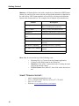
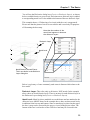
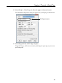
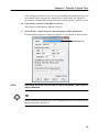
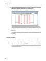
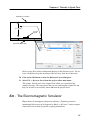
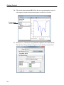
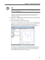
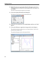
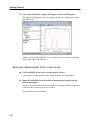
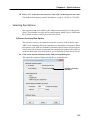
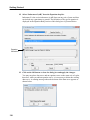
1
High Frequency Electromagnetic Software SONNET ® Suites 13 Getting Started GETTING STARTED RELEASE 13 At Sonnet, we’ve been developing 3D planar high frequency EM software since 1983, and our software has earned a solid reputation as the world’s most accurate commercial planar EM analysis package for single and multilayer planar circuits, packages and antennas. Sonnet Software, Inc., founded by Dr. James C. Rautio, is a private company, entirely dedicated to the development of commercial EM software. We take great pride in providing quality technical support for our products with timely response - which we consider to be essential for high-end technical software products. Sonnet is based in Syracuse, NY, USA with representatives across the globe. GETTING STARTED Published: June 2011 Release 13 Version 13.52 Sonnet Software, Inc. 100 Elwood Davis Road North Syracuse, NY 13212 Phone: (315) 453-3096 Fax: (315) 451-1694 www.sonnetsoftware.com Copyright 1989,1991,1993, 1995-2011 Sonnet Software, Inc. All Rights Reserved Registration numbers: TX 2-723-907, TX 2-760-739 Copyright Notice Reproduction of this document in whole or in part, without the prior express written authorization of Sonnet Software, Inc. is prohibited. Documentation and all authorized copies of documentation must remain solely in the possession of the customer at all times, and must remain at the software designated site. The customer shall not, under any circumstances, provide the documentation to any third party without prior written approval from Sonnet Software, Inc. This publication is subject to change at any time and without notice. Any suggestions for improvements in this publication or in the software it describes are welcome. Trademarks The program names xgeom, emstatus, emvu, patvu, dxfgeo, ebridge, emgraph, gds, emserver, emclient, sonntcds, and sonntawr (lower case bold italics), Co-calibrated, Lite, LitePlus, Level2 Basic, Level2 Silver, and Level3 Gold are trademarks of Sonnet Software, Inc. Sonnet®, em®, and emCluster® are registered trademarks of Sonnet Software, Inc. UNIX is a trademark of Unix Systems Labs. Windows XP, Windows Vista and Windows 7 are trademarks of Microsoft, Inc. AutoCAD and Drawing Interchange file (DXF) are trademarks of Auto Desk, Inc. SPARCsystem Open Windows, SUN, SUN-4, SunOS, Solaris, SunView, and SPARCstation are trademarks of Sun Microsystems, Inc. ADS, Touchstone, and Libra are trademarks of Agilent Technologies. Cadence and Virtuoso are trademarks of Cadence Design Systems, Inc. AWR and Microwave Office are registered trademarks and EM Socket is a trademark of Applied Wave Research, Inc. GDSII is a trademark of Calma Company. Acresso, FLEXlm, and FLEXnet are registered trademarks of Acresso Software. OSF/Motif is a trademark of the Open Software Foundation. IBM is a registered trademark of International Business Machines Corporation. Linux is a registered trademark of Linus Torvalds. MATLAB and Mathworks are registered trademarks of The Mathworks, Inc. Redhat is a registered trademark of Red Hat, Inc. SuSE is a trademark of Novell, Inc. Adobe® and Acrobat® are registered trademarks of Adobe, Inc. AWR and Microwave Office are trademarks of Applied Wave Research, Inc. Platform is a trademark and LSF® is a registered trademark of Platform Computing. Table of Contents TABLE OF CONTENTS TABLE 1 OF CONTENTS . . . . . . . . . . . . . . . . . . . . . . . . 5 WELCOME . . . . . . . . . . . . . . . . . . . . . . . . . . . . . . . 9 Documentation . . . . . . . . . . . . . . . . . . . . . . . . . . . . . 9 Manuals . . . . . . . . . . . . . . . . . . . . . . . . . . . . . . 10 Help: . . . . . . . . . . . . . . . . . . . . . . . . . . . . . . . . 10 Sonnet Technical Support . . . . . . . . . . . . . . . . . . . . . 10 2 INSTALLATION . . . . . . . . . . . . . . . . . . . . . . . . . . . . 11 UNIX and Linux Installation . . . . . . . . . . . . . . . . . . . . Windows Installation . . . . . . . . . . . . . . . . . . . . . . . . Requirements . . . . . . . . . . . . . . . . . . . . . . . . . . Compatibility. . . . . . . . . . . . . . . . . . . . . . . . . . . License Server . . . . . . . . . . . . . . . . . . . . . . . . . . Windows Installation Instructions . . . . . . . . . . . . . 3 THE BASICS . . . . . . . . . . . . . . . . . . . . . . . . . . . . . 15 The Sonnet Design Suite . . . . . . . . . . . . . . . . . . . . . . Sonnet Applications . . . . . . . . . . . . . . . . . . . . . . . . . Sonnet Projects . . . . . . . . . . . . . . . . . . . . . . . . . . . . The Sonnet Box . . . . . . . . . . . . . . . . . . . . . . . . . . . . Coupling to the Box . . . . . . . . . . . . . . . . . . . . . . Box Resonances . . . . . . . . . . . . . . . . . . . . . . . . . Dielectric Layers and Metal Levels. . . . . . . . . . . . . Circuit Metal. . . . . . . . . . . . . . . . . . . . . . . . . . . . . . Cell Size and Meshing . . . . . . . . . . . . . . . . . . . . . . . . Tips. . . . . . . . . . . . . . . . . . . . . . . . . . . . . . . . . . . . 3D View . . . . . . . . . . . . . . . . . . . . . . . . . . . . . . Connectivity Checker . . . . . . . . . . . . . . . . . . . . . Estimate Memory . . . . . . . . . . . . . . . . . . . . . . . . 4 11 11 11 12 12 12 15 17 17 20 21 22 22 26 26 28 28 28 34 TUTORIAL: A QUICK TOUR . . . . . . . . . . . . . . . . . . . . 35 Invoking Sonnet . . . . . . . . . . . . . . . . . . . . . . . . . . . . 36 UNIX & Linux . . . . . . . . . . . . . . . . . . . . . . . . . . . 36 5 Getting Started 5 Windows . . . . . . . . . . . . . . . . . . . . . . . . . . . . . Obtaining the Example Projects. . . . . . . . . . . . . . . . . The Project Editor . . . . . . . . . . . . . . . . . . . . . . . . . Zoom and Cell Fill . . . . . . . . . . . . . . . . . . . . . . . Metal Types . . . . . . . . . . . . . . . . . . . . . . . . . . . Dielectric Layers . . . . . . . . . . . . . . . . . . . . . . . . 37 37 39 41 44 46 Em - The Electromagnetic Simulator . . . . . . . . . . . . . Setting Up the Analysis . . . . . . . . . . . . . . . . . . . . Analysis Run Options . . . . . . . . . . . . . . . . . . . . . Executing an Analysis Run . . . . . . . . . . . . . . . . . . The Response Viewer- Plotting Your Data . . . . . . . . . . Invoking the Response Viewer . . . . . . . . . . . . . . . Displaying a Smith Chart . . . . . . . . . . . . . . . . . . . Selecting Another Curve for Display . . . . . . . . . . . Data Readouts - Smith Chart . . . . . . . . . . . . . . . . Adding a Data Marker . . . . . . . . . . . . . . . . . . . . . Closing the Response Viewer . . . . . . . . . . . . . . . . Current Density Viewer . . . . . . . . . . . . . . . . . . . . . . Invoking the Current Density Viewer . . . . . . . . . . . Current Density Values . . . . . . . . . . . . . . . . . . . . Frequency Controls . . . . . . . . . . . . . . . . . . . . . . Animation . . . . . . . . . . . . . . . . . . . . . . . . . . . . 47 48 49 50 51 52 53 53 57 58 59 59 60 60 61 61 CREATING A CIRCUIT: DSTUB . . . . . . . . . . . . . . . . . . 67 The Substrate, Subsectioning, and Cell Size . . . . . . Metalization Levels and Dielectric Layers . . . . . . . . Entering your Circuit . . . . . . . . . . . . . . . . . . . . . . . . Invoking the Project Editor . . . . . . . . . . . . . . . . . Specifying Box Settings . . . . . . . . . . . . . . . . . . . . Setting the Dielectric Layers . . . . . . . . . . . . . . . . Adding Metalization . . . . . . . . . . . . . . . . . . . . . . Adding Metal Loss . . . . . . . . . . . . . . . . . . . . . . . Adding Ports . . . . . . . . . . . . . . . . . . . . . . . . . . . Saving the Circuit . . . . . . . . . . . . . . . . . . . . . . . Em - The Analysis Engine . . . . . . . . . . . . . . . . . . . . . A Simple Outline of the Theory . . . . . . . . . . . . . . Frequency Sweep . . . . . . . . . . . . . . . . . . . . . . . 6 69 70 71 71 72 74 76 84 91 92 93 94 95 Table of Contents ABS Frequency Sweep . . . . . . . . . . . . . . . . . . . . . Selecting Analysis Options . . . . . . . . . . . . . . . . . . Input the ABS Sweep . . . . . . . . . . . . . . . . . . . . . . Run Options. . . . . . . . . . . . . . . . . . . . . . . . . . . . Executing the Analysis. . . . . . . . . . . . . . . . . . . . . Observing the Data . . . . . . . . . . . . . . . . . . . . . . . . . 95 96 96 97 98 99 Invoking the Response Viewer. . . . . . . . . . . . . . . 100 Adding a Measurement to a Curve Group . . . . . . . 100 Removing a Measurement from a Curve Group . . . . 102 6 SPIRAL INDUCTOR. . . . . . . . . . . . . . . . . . . . . . . . . 103 Introduction . . . . . . . . . . . . . . . . . . . . . . . . . . . . . Vias. . . . . . . . . . . . . . . . . . . . . . . . . . . . . . . . . . . Inputting the Circuit in the Project Editor . . . . . . . . . Obtaining the Example Project . . . . . . . . . . . . . . Creating Metal Types . . . . . . . . . . . . . . . . . . . . Palette of Standard Geometries . . . . . . . . . . . . . Adding a Feedline. . . . . . . . . . . . . . . . . . . . . . . Adding Ports and Reference Planes . . . . . . . . . . . Em - The Electromagnetic Simulator . . . . . . . . . . . . . Setting Up the Analysis . . . . . . . . . . . . . . . . . . . Selecting Run Options . . . . . . . . . . . . . . . . . . . . Checking Memory Requirements . . . . . . . . . . . . . . . . Calculating Cell Size. . . . . . . . . . . . . . . . . . . . . . . . Using the Cell Size Calculator . . . . . . . . . . . . . . . Executing the Analysis. . . . . . . . . . . . . . . . . . . . Viewing your Response . . . . . . . . . . . . . . . . . . . . . . Adding a File to a Graph . . . . . . . . . . . . . . . . . . 103 104 106 106 107 114 119 120 124 124 125 126 129 129 135 135 141 INDEX . . . . . . . . . . . . . . . . . . . . . . . . . . . . . . . 143 7 Getting Started 8 Chapter 1 Welcome CHAPTER 1 WELCOME Welcome to Sonnet’s 3D Planar Electromagnetic software. Sonnet's suites of high-frequency electromagnetic (EM) Software are aimed at today's demanding design challenges involving predominantly planar (3D planar) circuits and antennas. Predominantly planar circuits include microstrip, stripline, coplanar waveguide, PCB (single and multiple layers) and combinations with vias, vertical metal sheets (z-directed strips), and any number of layers of metal traces embedded in stratified dielectric material. The Sonnet Suites develop precise RF models (S-, Y-, Z-parameters or extracted SPICE model) for planar circuits and antennas. The software requires a physical description of your circuit (arbitrary layout and material properties for metal and dielectrics), and employs a rigorous Method-of-Moments EM analysis based on Maxwell's equations that includes all parasitic, cross-coupling, enclosure and package resonance effects. DOCUMENTATION: Sonnet provides manuals, context sensitive help, and an online knowledge base as detailed below. 9 Getting Started MANUALS: All Sonnet Suites come with a complete set of manuals in PDF Format. Sonnet Lite and Lite Plus come with only the applicable manuals as identified in the table below. PDF format manuals are accessed by clicking on the Manuals button in the Sonnet task bar. The complete list of manuals is provided below: Manual Description Getting Started* Quick windows installation & Sonnet Basics including Start up tutorials User’s Guide* Theory, features and feature tutorials Translators* Translators and Interfaces with tutorials UNIX & Linux Installation UNIX & Linux Installation Instructions Remote em Processing Installing remote em Processing Windows Installation Windows Installation including troubleshooting emCluster Computing Installing emCluster Computing FLEXnet User’s Manual Licensing Manager Software User’s Manual *Delivered with Sonnet Lite and LitePlus HELP: May be accessed in any of the following ways: • • • • Selecting Help Contents from any Sonnet application Clicking on the Help button in any dialog box Windows: Click on the ? button at the top of a dialog box and click on the desired control UNIX & Linux: Press Shift+F1, then click on the desired control SONNET TECHNICAL SUPPORT: : • • • • 10 email: [email protected] Voice: (315)453-3096 Toll Free in US: (877) 776-6638 Fax: (315) 451-1694 Web site: www.sonnetsoftware.com/support Chapter 2 Installation CHAPTER 2 INSTALLATION UNIX and Linux Installation If you are installing the software on a UNIX or Linux system, please refer to the UNIX and Linux Installation PDF manual in your download. If you are installing from a CD-ROM, the PDF is available in the top level CD-ROM directory. If you are a new Sonnet user, once you have completed your installation return to the tutorials in this manual. Windows Installation Requirements For a complete list of requirements and testing updates, please see http://www.sonnetsoftware.com/requirements 11 Getting Started Compatibility This release is backward compatible with all prior releases. However, you may not use a release 13 project file in an earlier release of Sonnet. License Server TIP For a standard evaluation, node-locked license or university license, the local machine is the license server. For a floating license, one machine in the network should be designated as the license server. This machine requires a hardware key attached to it. Client machines do not require a hardware key. The license manager, FLEXNet, executes on the license server. For a discussion on types of licenses, please see “Licenses,” page 8 in the Windows Installation Manual available in PDF format from the Sonnet task bar. Windows Installation Instructions 1 Uninstall any previous installations of Sonnet by selecting Start All Programs Sonnet Uninstall. If this is the first time you’ve installed Sonnet, continue at Step 2. 2 Both new and previous Sonnet User’s require a new license for Release 13. Go to www.sonnetsoftware.com/license and fill out the License Request Form. Once you receive your license from Sonnet, you will be able to enable your Sonnet Software. 3 Load the software: Download: To install your software, double-click on the “setup_sonnet13xx.msi file included in your download and follow the on-screen instructions. CD: If you are installing the software from a CD-ROM, load the CDROM on your system, and follow the installation instructions on your screen. 12 Chapter 2 Installation 4 If you are using a hardware key, attach it to your computer, then install the hardware key driver by selecting Admin Hardware Key Install Driver from the Sonnet task bar menu and follow the on-screen instructions. To open the Sonnet task bar, select Start All Programs Sonnet Sonnet from the Windows start menu. 5 Follow the directions in the licensing information e-mail you received from Sonnet Software in response to the License Request Form. 6 Select Project New Geometry from the main menu of the Sonnet task bar to launch the project editor to verify that the installation is correct. If your installation is not successful, please refer to the Windows Installation manual in PDF format for instructions on troubleshooting your installation. For advanced feature installations and setups, please find the applicable installation instructions in PDF format, using the Manuals button on the Sonnet task bar after you have installed Sonnet. If you are viewing the PDF of this manual, click on the appropriate link below. • • Remote em processing emCluster computing 13 Getting Started 14 Chapter 3 The Basics CHAPTER 3 THE BASICS This chapter is intended to provide you with basic information about the Sonnet Design suite which will allow you to quickly and accurately model your circuit while avoiding some of the common mistakes made during EM simulation. The chapters which follow after contain tutorials on using the Sonnet suite. The Sonnet Design Suite The suite of Sonnet analysis tools is shown below. Using these tools, Sonnet provides an open environment to many other design and layout programs. 15 Getting Started 16 Chapter 3 The Basics Sonnet Applications Sonnet's suites of high-frequency electromagnetic (EM) Software are aimed at designs involving predominantly planar (3D planar) circuits and antennas. Predominantly planar circuits include: • • • • • • • • • • Arbitrary microstrip & stripline circuits Planar spiral inductors RFIC & MMIC circuits Planar filter analysis High Speed Digital Interconnects High density interconnects Multi-layer circuits like LTCC and PCB technology Microwave circuit discontinuities Planar (patch) antennas Circuits with vias, vertical metal sheets (z-directed strips), and any number of layers of metal traces embedded in stratified dielectric material For more information on Sonnet’s applications, see our website at: http://www.sonnetsoftware.com/products/em/applications.asp Sonnet Projects There are two types of projects in Sonnet: the Geometry Project and the Netlist Project. A geometry project contains a circuit whose properties are entered by the user or provided by translating a file to the Sonnet environment. A netlist project 17 Getting Started contains a circuit defined by a netlist which consists of one or more networks with elements, which can be other geometry projects, connected together. A geometry project and a netlist project, as they appear in the project editor, are shown below. Geometry Project Netlist Project The most commonly used type of project is the geometry project, and a majority of the documentation concerns the input and analysis of this type of project. The geometry project contains the layout and material properties of a circuit and any internal components. When you analyze a geometry project, em performs an electromagnetic simulation of your circuit. The Netlist project contains ideal components, data files and Sonnet geometry projects. A network is defined which connects any combination of these items together. A common use for a netlist project is to connect two or more geometry projects together. The analysis engine, em, uses circuit theory to analyze the network. 18 Chapter 3 The Basics For both types of projects, the analysis controls (such as analysis frequencies, run options, etc.) and analysis data are stored in the project. You use the same Sonnet project for all the Sonnet programs. In addition to viewing your response within Sonnet, you may also export data files for use in other tools. The table below shows which formats are available. Optional Output Files Format Default File Extension Touchstone .s2p, .s3p, etc. Touchstone response file containing S, Y, or Z-parameter data. The file may contain any number of ports. Databank .s2p, .s3p, etc. Databank format response file containing S, Y, or Zparameter data. The file may contain any number of ports. SCompact .flp SCompact format response file. Spreadsheet .csv Comma separated value data for a spreadsheet such as Excel. Spectre .scs, .dat Cadence format Spice file - Pi model, N-Coupled Line Model or Broadband model. PSpice .lib PSpice file - Pi model or Broadband model. Agilent MDF .mdf Agilent’s Microwave Data Interchange Format. Cadence .dat Response file containing S, Y, or Z-Parameter data for any number of ports. Descriptions 19 Getting Started The Sonnet Box Metal Box Top The Sonnet six-sided shielding box. The metal walls of the box are transparent to allow you to see the interior of the circuit. Metal Side Walls The Sonnet EM analysis is performed inside a six-sided metal box as shown above. This box contains any number of dielectric layers which are parallel to the bottom of the box. Metal polygons may be placed on levels between any or all of the dielectric layers, and vias may be used to connect the metal polygons on one level to another. The four sidewalls of the box are lossless metal, which provide several benefits for accurate and efficient high frequency EM analysis: • The box walls provide a perfect ground reference for the ports. Good ground reference is very important when you need Sparameter data with dynamic ranges that might exceed 50 or 60 dB, and Sonnet’s sidewall ground references make it possible for us to provide S-parameter dynamic range that routinely exceeds 100 dB. • Because of the underlying EM analysis technique, the box walls and the uniform grid allow us to use fast-Fourier transforms (FFTs) to compute all circuit cross-coupling. FFTs are fast, numerically robust, and map very efficiently to computer processing. • There are many circuits that are placed inside of housings, and the box walls give us a natural way to consider enclosure effects on circuit behavior. As an example, a microstrip circuit can be modeled in Sonnet by creating two dielectric layers: one which represents your substrate, and one for the air above the substrate. The metal polygons for the microstrip would be placed on the metal 20 Chapter 3 The Basics level between these two dielectric layers. The bottom of the box is used as the ground plane for the microstrip circuit. The top and bottom of the box may have any loss, allowing you to model ground plane loss. Coupling to the Box Since the four sidewalls of the box are lossless metal, any circuit metal which is close to these walls can couple to the walls - just like what would happen if you fabricated and measured a real circuit with the same box. If you do not want to model this coupling (for example, your real circuit does not have sidewalls), then you must keep the circuit metal far away from the box sidewalls. A good rule to use is at least three to five substrate thicknesses as shown below. This circuit has a substrate of 25 mils. The spiral should be kept at least 75-125 mils from the box walls. 21 Getting Started Box Resonances It is possible for the six conducting sides of the Sonnet box to create a resonant cavity, just like you would see if you fabricated and measured the circuit in the same size box. You can use Sonnet to predict unwanted box resonances in the package or module housing the circuit. Box resonances usually appear as a “spike” in the S-Parameter magnitude and phase data, as shown below. You can detect box resonances by observing your simulated results, through runtime warning messages or by using the Box Resonance Estimator (Analysis Estimate Box Resonances). For a detailed discussion on box resonances and how to detect them, please see Chapter 21, “Package Resonances” on page 365 of the Sonnet User’s Guide. Dielectric Layers and Metal Levels All Sonnet geometry projects are composed of two or more dielectric layers. There is no limit to the number of dielectric layers in a Sonnet geometry project, but each layer must be composed of a single dielectric material. Metal polygons are placed at the interface between any two dielectric layers and are usually modeled as zero-thickness, but can also be modeled using Sonnet’s thick metal model. Vias may also be used to connect metal polygons on one level to metal on another level. 22 Chapter 3 The Basics You will use the Dielectrics dialog box (Circuit Dielectric Layers), as shown below, to add dielectrics to your circuit. Each time a new dielectric layer is added, a corresponding metal level is also added to the bottom of the new dielectric layer. This example shows a 3-D drawing of a circuit (with the z-axis exaggerated). Please note that the pictured circuit is not realistic and is used only for purposes of illustrating the box setup. Note that the number of the metal level appears in between the dielectric layers. Dielectric Layer 0 Metal Level 1 2 Metal Bottom (Ground Plane). This is not shown in the Dielectric Layer dialog box Below is a glossary of some commonly used terms in Sonnet which relate to the box model. Dielectric Layer: This refers only to dielectrics, NOT metals. In the example above, there are four dielectric layers. There is an entry for each dielectric layer in the Dielectric Layers dialog box (Circuit Dielectric Layers). Metal Level: Metal levels are modeled as zero thickness and are attached to the dielectric layer ABOVE them. In the example above, there are three metal levels in addition to the box top and bottom. Since no metal may be placed on the top of the box, it may not be accessed by the user or viewed in the project editor. The bottom of the box is referred to as the GND level and may be accessed in the 23 Getting Started project editor. It is not labeled in the dielectric window. The top and bottom of the box are lossless metal by default, but can be changed in the Box Settings dialog box (Circuit Box Settings). You can use as many different metal types as you wish on a single metal level; for instance, you may use a silver polygon and copper polygon on the same metal level. NOTE: A “layer” refers to a dielectric layer while “level” refers to the metal level which is sandwiched between the two dielectric layers. So, technically, there is no such thing as a “metal layer” in Sonnet. GND Level: You can place polygons on the GND level, but they have no effect because this level is already completely metalized. However, cases do exist in which you may want to place a polygon on the GND level in order to place a via or a dielectric brick there. Viewing Levels: When you view your circuit in the normal 2D view in the project editor, you are always “on” a particular level, as shown by the level drop list in the Project Editor tool bar as shown below. The top level is always “0” and increases as you move downward through the box. You can switch levels by using 24 Chapter 3 The Basics your arrow keys, or using the level drop list. By default, all polygons on your present level are shown in solid, and all polygons on all other levels are shown as dashed outlines. The dotted outline indicates metal on the level below this one. Level 0 is displayed in the level drop list in the project editor. Level 0 The dotted polygon seen above is shown on Level 1 which is below Level 0. You may also change the view to other metal levels by using the Up One Level and Down One Level button on the project editor tool bar. Level 1 As mentioned above, the metal level is associated with the dielectric layer above, such that when you delete a dielectric layer, the metal level directly below the layer is deleted. The total height of the box is determined by the sum of the thicknesses of the dielectric layers since metal is either modeled as zero-thickness or protrudes into the dielectric layer above. If you wish to model microstrip circuits, you will need to place a thick layer of air above your circuit; i.e. the topmost dielectric layer should be at least three to five times the substrate thickness. 25 Getting Started Circuit Metal Metal in your circuit is modeled using two different classes of metal types: planar and via. Planar metal types are used for metal polygons. Via metal types are used to model via polygons. You input your circuit by placing metal polygons on the metal levels of your geometry project and via polygons to connect between the metal levels. You define what type of metal a given polygon is by defining metal types in your project (Circuit Metal Types), then assigning them to the polygons (Modify Metal Properties or Modify Via Properties. There is no limit as to how many different metals are used on any given level or how many metal types you may define for a project. To model loss in your metal, you enter the metal’s loss characteristics when you define the metal type. It is also possible to use a provided library of metal types or define your own metal library to use in multiple projects. Cell Size and Meshing The Sonnet analysis engine, em, calculates the response data for your circuit by dividing the metal into small “subsections” and analyzing the coupling between these subsections. The picture on the left shows the circuit as viewed in the project editor. On the right is shown the subsectioning used in analyzing the circuit. The Sonnet subsectioning is based on the uniform cell size which is represented in the project editor by small dots. The small dots are placed at the corners of a “cell” as shown in the illustration below. One or more cells are automatically combined together to create subsections. Cells may be square or rectangular (any 26 Chapter 3 The Basics aspect ratio), but must be the same over your entire circuit. Note that the cell dimensions do not have to be an integer nor do they have to be equal. For example, you may define a cell size of 1.687 by 2.453 microns. Metal polygons are represented with an outline and a cell fill pattern. The outline represents exactly what you entered or imported. The cell fill represents the actual metalization analyzed by em. Therefore, the actual metalization analyzed by em may differ from that input by you as illustrated below.You turn the cell fill on and off using the control-M key. This shows the circuit with the cell fill turned off. The outline shows the polygon drawn by you. Notice that this polygon is not “on” the grid. This shows the circuit with the cell fill on. The patterned area shows the actual metal that is analyzed by the analysis engine, em. Note that this metal is always “on” the grid. The cell size is specified in the project editor in the Box Settings dialog box which is opened by selecting Circuit => Box from the project editor menu. The analysis solves for the current on each subsection. Since multiple cells are combined together into a single subsection, the number of subsections is usually considerably less than the number of cells. This is important because the analysis solves an N x N matrix where N is the number of subsections. A small reduction in the value of N results in a large reduction in analysis time and memory. Care must be taken in selecting a cell size so that accuracy is not sacrificed. If the cell size is too large, then your results will not be accurate. If the cell size is too small, the analysis may become too costly in processing time. Em automatically places small subsections in critical areas where current density is changing rapidly, but allows larger subsections in less critical areas, where current density is smooth or changing slowly. For a more detailed discussion of cell size and subsectioning, please refer to Chapter 3, Subsectioning, on page 29 of the Sonnet User’s Guide. 27 Getting Started Tips The following items may not look very important to you now, but will be very useful further along in your use of Sonnet. 3D View It is often helpful to view your circuit in 3D. To do so, select the View 3D View command. This command is available in both the project editor and the current density viewer. An example of a 3D view is shown below. Note that the metal levels are numbered on the side of the box and the presently selected dielectric layer is highlighted. 3D View Metal Levels Highlighted Dielectric Layer Connectivity Checker The Connectivity Checker is a tool available in the project editor which allows you to visually check for opens or shorts in your circuit. To use the Connectivity Checker, you select the command Tools Check Connectivity from the main 28 Chapter 3 The Basics menu of the project editor. Once the checker is invoked you can click on any metal or via polygon in the circuit to see the polygons to which it is electrically connected or any shorts created by the polygon. The process is detailed below. NOTE: For via polygons, you must click on the top level of the via. The Connectivity checker uses the cell fill when checking the connectivity. The cell fill represents the actual metalization analyzed by em and may differ from the polygons input by the user, or translated into Sonnet from another tool. Using the Connectivity Checker can identify problems created by the differences between the input polygons and the cell fill. An example where the cell fill creates an open is shown below. The circuit is shown on the left with the cell fill turned off so you see only the input polygons. On the right is a view of the input polygons with the cell fill turned on. The input polygons provide a connected electrical path, but because of the staircase fill, the analysis engine would treat this as an open circuit. Open Cell fill can also create an undesired short as shown below. Short 29 Getting Started An example circuit, connectivity, will be used to explain the operation of the Connectivity Checker and is shown below. This example file can be found in the Sonnet example files. You may access the Sonnet Example browser by selecting Help Browse Examples from the menu of any Sonnet application. For instructions on using the Example Browser, please click on the Help button in the Example Browser window. 2D View 3D View When you invoke the Connectivity Checker, all the polygons and vias in the 2D view are displayed with grey fill while the circuit in the 3D view is displayed as a wire frame as illustrated below. When you click on a polygon, it and all the polygons to which it is electrically connected are highlighted in red. If there are polygons or vias that are connected on another level, they are highlighted in a lighter red. In the graphic below, polygon A was selected. The path starting at Port 1 and extending to Port 2 was 30 Chapter 3 The Basics highlighted. As noted earlier, the feedlines are on another level from the center polygon so in the 2D view they are light red. The whole path is highlighted in red in the 3D view. In the next graphic, shown below, polygon B is selected. Notice that the feedline extending from Port 4 is not highlighted. This indicates an open circuit between the via and the feedline. 31 Getting Started The gap between the via and the feedline is not discernible at full view, but zooming in on the connection shows that it exists. Close up View of Metal Level 1 Feedline Via Gap In the next illustration, the trace at the bottom of the circuit is selected. There is a “bloom” shown at one end of the line. Since there is no port on the box wall, the trace is shorted to ground; this is indicated by the “bloom.” The other end of the polygon has a box wall port. Ports are always considered opens which is why there is no bloom on the other end of the polygon. Short Once you are finished using the Connectivity Checker, press the Escape key to exit this mode and return to Edit mode. 32 Chapter 3 The Basics As mentioned earlier, ports are always considered an open circuit. This includes both internal ports and via ports as pictured below. For both the internal port, shown on the top in 2D and 3D views, and the via port pictured on the bottom, the electrical connection only extends to the port. Internal Port Via Port A complete list of geometry elements and how they are treated by the connectivity checker is provided below. • Ports: All port types are treated as an open. • Components: Components are treated as an open. • Dielectric Bricks: Dielectric Bricks are treated as an open. • Lossy Metal: Lossy Metal is treated as a closed circuit. The loss of the metal is not taken into account by the Connectivity Checker. 33 Getting Started Estimate Memory Once you are done specifying your circuit in the project editor, you may determine if it is possible to analyze your circuit with the computer resources available to you. Selecting Analysis => Estimate Memory from the project editor's main menu opens the Estimate Memory dialog box and subsections your project. A simple status popup appears to indicate that the circuit is being subsectioned. When the subsectioning is complete, the memory use estimate and the subsectioning information, listed by level and total amounts, appears in the dialog box. You may also view the subsectioning used by em. 34 Chapter 4 Tutorial: A Quick Tour CHAPTER 4 TUTORIAL: A QUICK TOUR This tutorial provides you with an overview of the Sonnet products and how they are used together. The second tutorial, in Chapter 5, walks you through a simple example from entering the circuit in the graphical project editor, to viewing your data in the response viewer, our plotting tool. The third tutorial covers design issues which need to be considered in the project editor. There are tutorials on different Sonnet features in the Sonnet User’s Guide as well as tutorials on the use of the translators in the Translator manual. The first tutorial is designed to give you a broad overview of the Sonnet suite, while demonstrating some of the basic functions of the Sonnet products. The following topics are covered: • Invoking Sonnet programs. • Opening a circuit geometry project in the project editor. • Running a simple analysis in em. • Plotting S-parameter data in the response viewer. • Performing a simple animation in the current density viewer. 35 Getting Started Invoking Sonnet You use the Sonnet task bar, shown below, to access all the modules in the Sonnet Suite. Opening the Sonnet task bar, for both Windows and UNIX systems is detailed below. UNIX & Linux 1 Open a terminal. If you do not know how to do this, please see your system administrator. 2 Enter “sonnet” at the prompt. The Sonnet task bar appears on your display. 36 Chapter 4 Tutorial: A Quick Tour Windows 1 Select All Programs Sonnet Sonnet from the Windows desktop Start menu. The Sonnet task bar appears on your display. Obtaining the Example Projects Example projects are supplied with your software and are available through the Example browser. The Example browser allows you to open the project in the Project Editor or, in the case of multifile examples, copy the example folder to your personal working directory. 37 Getting Started To copy the filtwall project to use in this tutorial, do the following: 1 Select Project Browse Examples from the main menu on the Sonnet task bar. The Sonnet Example Browser is opened on your display. 2 Enter “filtwall” in the Search text entry box in the Browser window 3 Select the Name radio button. 4 Click on the Search button. Search text entry box Name radio button Search button The only example displayed in the window is the Filtwall example. 5 Click on the Open button at the bottom of the Example Browser. The project editor is invoked on your display with the file “filtwall.son” open. This file is a read-only to prevent corrupting the example files. 6 Select File Save As from the project editor main menu. The Save As browse window appears. Save the project in your working directory. This allows you to save any changes you make to the circuit. 38 Chapter 4 Tutorial: A Quick Tour You could also have saved the project directly from the Example Browser by clicking on the Save button, then saving the file in your working directory. The Project Editor The project editor, when editing a circuit geometry project, provides you with a graphical interface which allows you to specify all the necessary information concerning the circuit you wish to analyze with the electromagnetic simulator, em. The example circuit, “filtwall.son”, shown on page 40, is a two port microstrip filter with a 15 mil Alumina substrate and 150 mils of air above. Note that the resonators run to the edge of the substrate, shorting them to the box wall. Circuits in Sonnet are modeled as being enclosed in a six-sided metal box which is ground. Any circuit metal touching the box is shorted to ground unless the polygon has a port attached to it. A standard box wall port is a grounded port, with one terminal attached to a polygon edge coincident with a box wall and the second terminal attached to ground. The port, therefore, breaks the connection between the polygon and the wall and is inserted in an “infinitesimal” gap between the polygon and the wall. The signal (plus) portion of the port goes to the polygon, while the ground (negative) portion of the port is attached to the box wall (ground). The model for a box wall port is pictured below. Box wall port on page 46. Box wall -V+ Infinitesimal Gap 39 Getting Started The circuit is placed on top of the substrate. Air Layer 150 mils Short circuits Six-sided metal box Substrate Layer 15 mils A three-dimensional view of the circuit in the six-sided metal box modeled in the project editor. The view shown in the project editor window is a two-dimensional view from the top looking directly down on the substrate. This view is from the 3D viewer which is opened by selecting View View 3D from the project editor main menu. 40 Chapter 4 Tutorial: A Quick Tour Zoom and Cell Fill The project editor has a zoom feature which allows you to take a closer look at any part of your circuit. You will zoom in on a section of the filter, to observe an example of staircase cell fill. The cell fill represents the actual metalization analyzed by em. There are various types of cell fill, one of which is staircase. Staircase uses a “staircase” of cells to approximate any angled edges of polygons. Therefore, the actual metalization analyzed by em may differ from that input by you. 7 Select View Cell Fill from the project editor main menu to turn off the cell fill. This command toggles the state of cell fill. Only the outline of the polygons are displayed. 8 Click on the Zoom In button on the tool bar. The appearance of the cursor changes. A magnifying glass with a plus sign, the icon on the Zoom In button, appears next to the cursor. 9 Select the section of the circuit you wish to zoom in on. Move the mouse to the upper left of the junction of the feed line and the first resonator, as shown below. Click and drag the cursor down and to the right. A rubber band surrounding the area follows the cursor. When you release the mouse button, the project editor zooms in on the selected area. As you can see in the enlargement on page 42, one of the metal polygons has a diagonal edge. 41 Getting Started 10 Select View Cell Fill from the project editor main menu to turn on the cell fill. The metal fill pattern appears in the polygons on your display. Note that the outline of the actual metal has a “staircase” edge which approximates the diagonal edge drawn in the project editor. The default setting in the project editor is staircase fill. Note that em analyzes the staircase edged metal, not the diagonal polygon. Diag onal NOTE: Diagonal fill is not available in Sonnet Lite and Sonnet LitePlus. If you are using either of these suites, skip to step 15. This will not affect simulation results since staircase fill is restored before running the analysis. 11 Click on the polygon circled above to select it. The polygon is highlighted to indicate selection. 42 Chapter 4 Tutorial: A Quick Tour 12 Select Modify Metal Properties from the project editor main menu. The Metalization Properties dialog box appears on your display as shown below. Fill Type drop list 13 Select Diagonal from the Fill Type drop list. Diagonal fill type, while more accurately modeling the input edge, requires more processing time. 43 Getting Started 14 Click on the OK button to apply the changes and close the dialog box. The metal fill is updated, as shown below. As you can see, the metal em analyzes is closer to your input than in the case of staircase fill. But the increased accuracy comes at the price of increased processing time. In this case, staircase fill provides the required degree of accuracy and will be used for the analysis. The fill type will be changed back to staircase later in the tutorial. 15 Click on the Full View button. The whole circuit appears on your display. Metal Types The project editor allows you to define any number of metal types to be used in your circuit. There are two kinds of metal types: planar and via. Planar metal types are used for metal polygons and via metal types are used for via polygons. Since this circuit contains only metal polygons, but does not contain any vias, only planar metal types are used. Multiple planar metal types may be used on any given level. A planar metal type specifies the metalization loss used by em. Both the DC resistivity and the skin effect surface impedance are accurately modeled in em. Metal types, both planar and via, are defined in the Metal Types dialog box where a fill pattern is assigned as part of the definition. For a detailed discussion of metal types and loss, see Chapter 4, “Metalization and Dielectric Layer Loss” in the Sonnet User’s Guide. 44 Chapter 4 Tutorial: A Quick Tour After a polygon is drawn in your circuit, you can change the planar metal type. In our example, all the polygons are comprised of Copper metal. An example is given below of changing the planar metal type of one polygon to “Lossless” metal. 16 Click on any resonator of the filter to select it. The polygon is highlighted to indicate selection. 17 Select Modify Metal Properties from the project editor main menu. The Metalization Properties dialog box appears on your display as shown below. Metal Drop List NOTE: Depending on which Sonnet Suite you have purchased, some controls may be disabled. TIP Double-clicking on a polygon, port, via or component in your circuit opens the appropriate Properties dialog box. 45 Getting Started 18 Click on the Metal drop list and select “Lossless” from the list. Click on the OK button to apply the change and close the dialog box. The fill pattern changes for the selected polygon as shown below. The metal for this polygon now has the loss associated with the default lossless planar metal. The project editor allows you to define any number of metal types for use in your circuit. For details on defining metal types, see the project editor’s online help. You will not be analyzing with lossless metal; the metal is switched back later in the tutorial. Dielectric Layers 19 Select Circuit Dielectric Layers from the project editor main menu. The Dielectric Layers dialog box, which allows specification of the dielectric layers in the box, appears on your display, providing you with an approximate “side view” of your circuit. The project editor “level” number appears on the left. A “level” is defined as the intersection of any two dielectric layers and is where your circuit metal is placed. 46 Chapter 4 Tutorial: A Quick Tour Metal Box (Ground) Air (150 mils) Level 0 Metal Alumina Substrate - 15 mils Metal Box (Ground) Refer to page 40 for a three-dimensional drawing of the dielectric layers. The air layer is required to keep the metal top of the box away from the circuit metal. 20 Click on the OK button to close the Dielectric Layers dialog box. 21 Select File Revert to Saved from the project editor main menu. This returns “filtwall.son” to the original form which you copied from the example directory. This step ensures that you are analyzing the original file and that you are able to successfully launch em from the project editor. Em - The Electromagnetic Simulator Em performs electromagnetic analysis for arbitrary 3-D planar geometries, maintaining full accuracy at all frequencies. Em is a “full-wave” analysis engine which takes into account all possible coupling mechanisms. 47 Getting Started The project editor provides an interactive windows interface to em. This interface consists of menus and dialog boxes which allow you to select run options, set up the analysis type and input parameter values and optimization goals. You may save the settings for an analysis file in a batch file using the analysis monitor. In the next part of this tutorial, you set up the analysis for and analyze the circuit “filtwall.son” which you examined in the project editor. If you have not already done so, load “filtwall.son” into the project editor. Setting Up the Analysis These analysis controls have already been input to this example file, but the steps are explained in order to show how the information is entered. You will be using the Adaptive Band Synthesis (ABS) technique to analyze the circuit. ABS provides a fine resolution response for a frequency band with a small number of analysis points. Em performs a full analysis at a few points and uses the resulting internal data to synthesize a fine resolution band. This technique, in most cases, provides a considerable reduction in processing time. The points at which a full analysis is performed are referred to as discrete data. The remaining data in the band is referred to as adaptive data. For a detailed discussion of ABS, see Chapter 8, “Adaptive Band Synthesis (ABS)” in the Sonnet User’s Guide. 22 Select Analysis Setup from the project editor main menu. The Analysis Setup dialog box appears on your display as shown below. Analysis Control drop list 48 Chapter 4 Tutorial: A Quick Tour Setting Up Analysis Frequencies 23 Select Adaptive Sweep (ABS) from the Analysis Control drop list. Since the default type of sweep is Adaptive, you will not need to take any action for this step. The adaptive sweep uses ABS to analyze the circuit. This enables the Start and Stop text entry boxes. 24 Enter the Start, and Stop values in the appropriate text entry boxes. The frequency band you wish to analyze is from 4.7 GHz to 5.5 GHz, therefore, enter 4.7 in the Start text entry box, and 5.5 in the Stop text entry box. These entries may already be present. If you needed to change the frequency units, you would do so using the Units dialog box, accessed by selecting Circuit Units from the project editor main menu. Analysis Run Options Run options for em are available in the Analysis Setup dialog box. This example uses the De-embed option, which is set by default, and the Compute Current Density option. De-embedding is set in the Advanced Options dialog box which you access by clicking on the Advanced button in the Analysis Setup dialog box. Since it is set by default, you do not need to do this for this example. De-embedding is the process by which the port discontinuity is removed from the analysis results. Inaccurate data may result from failing to implement this option, even when you are not using reference planes. For a detailed discussion of deembedding refer to Chapter 6 "De-embedding" on page 101 in the Sonnet User’s Guide. If this option is on, de-embedded response data is output to the project file. The Compute Current Density run option instructs em to calculate current density information for the entire circuit which can be viewed using the Current Density Viewer. Be aware that for an adaptive sweep, current density data is only calculated for discrete data points. Aside from the beginning and end of the band, the frequencies for the discrete data points are determined by the ABS algorithm and are usually non-uniform values. 49 Getting Started TIP The Memory save option (not used in this example) uses less memory by storing matrix elements as single precision numbers rather than double precision. Its use is recommended in order to execute a simulation that otherwise might not be possible within the bounds of your memory limitations. 25 Click on the OK button to apply the changes and close the dialog box. A Current Density Notice may appear on your display; if you do not wish this warning to appear again, select the Don’t show me this again checkbox. Click OK to close this notice. Executing an Analysis Run The control frequencies and run options are all specified. The analysis time for the circuit will vary depending on the platform on which the analysis is performed. 50 Chapter 4 Tutorial: A Quick Tour 26 Select Project Analyze from the project editor main menu to invoke em and run the analysis. The analysis monitor appears on your display with the output window displaying response data. The analysis time will vary depending on the platform on which you are running the software. This analysis needs only four discrete frequencies to create the adaptive data and complete the analysis. When the analysis is complete, the message “Analysis completed” followed by the data and time appears in the analysis monitor as shown below. The Response Viewer- Plotting Your Data The response viewer is used to display the results from an em analysis as either a Cartesian graph or Smith chart. S-, Y- and Z-Parameters can be displayed alone or simultaneously as well as transmission line parameters. You can also display multiple curves from multiple projects on a single plot or choose to open multiple plots at the same time. It is also possible to display parameter sweeps and optimization results in a number of advanced ways. This tutorial covers only the most basic of the response viewer’s functions. 51 Getting Started Invoking the Response Viewer 27 Select Project View Response New Graph from the project editor main menu to invoke the response viewer. The response viewer window appears on your display with a Cartesian graph of the curve group filtwall with curve DB[S11] displayed. The project file contains multiple curves which are displayed in user-defined curve groups. Plot Legend Curve Group Legend Plot Window A data point is the measurement for a particular frequency. The data for all frequencies makes up a measurement. A measurement is a set of response data uniquely identified by parameter type, response type, port numbers and project file. An example would be: DB[S11] in the filtwall.son file DB identifies the response type as magnitude in dB. S identifies the parameter type as an S-Parameter. 11 identifies the output port as Port 1 and the input port as Port 1. The project file from which the measurement originated is “filtwall.son.” A curve group is made up of one or more measurements. Different curve groups may come from different project files yet be displayed simultaneously. 52 Chapter 4 Tutorial: A Quick Tour Displaying a Smith Chart 28 Change the plot to a Smith Chart by selecting Graph Type Smith from the response viewer main menu. The plot is changed to a Smith chart of “filtwall.son” which appears on your display. Again, the curve group filtwall with the [S11] curve is displayed. This curve group is the default displayed upon startup. TIP You can right-click on most parts of the response viewer window to invoke popup menus. For example, right clicking in the plot window and selecting Type Smith from the pop-up window also displays a Smith Chart. Selecting Another Curve for Display You may display multiple curves from multiple files simultaneously. Curve groups contain one or more measurements. To add a different measurement for display in a curve group, perform the following. 29 Select Graph Type Cartesian from the main menu. This changes the plot back to a Cartesian graph. 53 Getting Started 30 Click on the measurement DB[S11] in the curve group legend to select it. A box appears around the measurement name to indicate its selection. Curve group “filtwall” 31 Select Curve Edit Curve Group from the response viewer main menu. The Edit Curve Group dialog box appears on your display as shown below. 54 Chapter 4 Tutorial: A Quick Tour TIP Double-clicking on the Curve Group in the Curve Group legend also opens the Edit Curve Group dialog box. If this project file contained parameter combinations or optimization data, the dialog box would include a section that allowed you to select parameter combinations to display. 32 Double-click on DB[S21] in the Unselected list to move it to the Selected list. DB[S21] moves to the Selected list. 33 Click on the OK button to apply these changes. The Edit Curve group dialog box is closed and the Cartesian graph is updated to display the curve group filtwall, which now contains the two curves, DB[S11] and DB[S21]. Since the axes are set to autoscale, the values on the axes are automatically adjusted. The graph should appear similar to that pictured below. Note that very few of the symbols ( O ), indicating data points, appear on the curves. When you are displaying adaptive data from an ABS analysis, the only points highlighted with a symbol in the response viewer are those from the discrete points where a full analysis was performed. 55 Getting Started 34 Right-click on the curve group name, filtwall, which appears in the Curve Group legend and select Properties from the pop-up menu which appears on your display. The Data Set Style dialog box appears on your display. 35 Click on the Symbol radio button in the dialog box. The dialog box should appear similar to that shown below. 36 Click on an arrow button next to the Symbol display until the word “None” appears. 37 Click on the OK button to apply these changes and close the dialog box. The symbols for the discrete data points are no longer displayed. Only the line represents all the adaptive data. The graph should appear similar to that pictured below. 56 Chapter 4 Tutorial: A Quick Tour Data Readouts - Smith Chart The response viewer can provide a readout on any given data point on your plot in two different ways. The information provided is dependent upon the type of data point selected. In the next section, you see how to obtain data on the Smith chart. 38 Right-click in the plot window, then select Type Smith from the pop up menu which appears on your display. The plot is changed to a Smith Chart. It is important to note that the curve group filtwall only contains one curve: [S11]. The curve groups defined for Cartesian graphs are independent of those defined for Smith charts. Zooming in on a section of the Smith chart makes it easier to distinguish individual points. 39 Click on the Zoom In button on the tool bar. A change in the cursor indicates that you are in zoom in mode. TIP If you have a three-button mouse, clicking on the center mouse button when the cursor is in the plot window, will put you in zoom in mode. 40 Click and drag your mouse in the Smith chart until the rubber band surrounds the area you wish to magnify. Then release the mouse button. The display is updated with a magnified picture of the selected area. To return to the full graph, click on the Full View button on the tool bar. Zooming operates in the same manner on a Cartesian graph. For our example, select one of the end points of the graph to enlarge. 41 Move the cursor over a discrete data point in the Smith Chart. A discrete data point is indicated by the O symbol. A popup appears, similar to that shown below, on your display with data about that point. 42 Click on the Full View button on the tool bar. The full view of the Smith chart appears in the response viewer window. 57 Getting Started 43 Click on a data point in the Smith chart. The readout for that data point appears in the Status Bar at the bottom of the response viewer window. Selected Point Readout in Status Bar To move between points on a curve use the and keys. To move between curve groups on the display use the and keys. Adding a Data Marker There are markers available in the response view that allow you to annotate your results in order to better interpret your data or make presenting your data simpler. There are six types of markers available; this section teaches you to add a data marker. For more information on markers, please refer to online help. 44 Select Graph Marker Add Data Marker from the main menu of the response viewer. The appearance of the cursor changes. 58 Chapter 4 Tutorial: A Quick Tour 45 Click on the data point to which you wish to add a marker. A label appears on your plot as shown below. Double clicking on the marker allows you to control the data displayed in the marker. Data Marker Closing the Response Viewer To close the program, perform the following: 46 Select File Exit from the response viewer main menu. The response viewer display is closed. Current Density Viewer The current density viewer is a visualization tool used to view the results of circuits previously analyzed with em. Em saves the resulting current density information in the project file ready for input to the current density viewer. To produce the current density data, you must select the Compute Current Density option in the Analysis Setup dialog box in the project editor. This was done for you in the example file. 59 Getting Started Invoking the Current Density Viewer 47 Select Project View Current from the main menu of the project editor or the main menu of the response viewer after clicking on the curve group Filtwall in the legend. The current density viewer window appears on your display with the first frequency in “filtwall.son” displayed. The color plot should appear similar to the one shown below. You are viewing the magnitude of the current density with a 1 Volt, 50 ohm source and Port 2 with a 50 ohm load. Red areas represent high current density, and blue areas represent low current density. A scale is shown on the left of the window which defines the values of each color. Current Density Values 48 Click on any point on your circuit to see a current density value. The current density value (in amps/meter) at the point that you clicked is shown in the status bar at the bottom of your window along with the coordinates of the location. 60 Chapter 4 Tutorial: A Quick Tour Frequency Controls A different frame is displayed for each analysis frequency. 49 Click on the Next Frequency button on the tool bar. The lowest frequency appears on your display as the default, which in this case is at 4.7 GHz. When you click on the Next Frequency button, the display is updated with the current density at 5.0875 GHz. NOTE: The scale to the left of the display is also updated. 50 Click on the Frequency Drop list, and select 5.26. The drop list allows you to go directly to any of the analysis frequencies. As mentioned earlier in the tutorial, the discrete data points in an ABS analysis for which the current density data is calculated, are determined by the ABS algorithm and are usually non-uniform. Animation The current density viewer provides two types of animation: frequency and time. To do an animation in the frequency domain, the current density viewer takes a picture of your circuit at each frequency point and links the pictures together to form a “movie”. In the time domain, the current density viewer takes a picture of your circuit at instantaneous points in time at a given frequency by changing the excitation phase of the input port(s). Animation allows you to see how your response changes with frequency or time, providing insight into the properties of your circuit. The animation menu and controls are the same whether animating as a function of frequency or time. The current density viewer accomplishes this by translating the data into frames. The animation menu then allows you to step one frame at a time, or “play” the frames by displaying them consecutively. How the data relates to a frame in either animation mode is discussed below. Time Animation For Time Animation, each frame corresponds to an input phase. The type of data plotted is determined by the Parameters Response menu. In this case, the data is the JXY Magnitude, the total current density. This is the default setting upon 61 Getting Started opening a current density viewer window. For more details about response types, see “Parameters - Response” in the current density viewer’s help. To invoke help for the current density viewer, select Help Contents from its main menu. 51 Select Plot Scale from the current density viewer main menu. The Set Scale dialog box appears on your display. User Scale radio button 52 Click on the User Scale radio button and enter a value of 100 in the Max Value text entry box. This allows you to set a fixed scale to avoid automatic updates of the scale during the animation. 53 Click on the OK button to close the dialog box and apply the changes. The dialog box disappears and the scale to the left of the current density viewer window is now fixed at a maximum value of 100. 54 Select Animation Settings from the current density viewer main menu. The Animation Settings dialog box appears on your display as shown below. 55 Click on the Time Radio button to select Time Animation. This enables the cycle type drop list and the Number of Steps text entry box. 62 Chapter 4 Tutorial: A Quick Tour 56 Select Half Cycle from the cycle type drop list. Our example uses half cycle, the default, in which the phase ranges from 0 to 180. For Full Cycle the phase ranges from 0 to 360. For Quarter Cycle, the range is 0 to 90. 57 Enter a value of 36 for the Number of Steps. The number of steps is used to determine how many frames the animation includes. There are 180in a half cycle; therefore, 36 steps yield a value of 5 for the phase interval. The lowest phase, 0, corresponds to the first frame and the highest phase, 175 corresponds to the last frame. This phase value represents an offset from the Source Phase for any given port set in the Port Parameters dialog box. For details on how to set the Source Phase, see “Parameters Ports” in the current density viewer’s online help. To access the current density viewer’s help, select Help Contents from its main menu. For this example, the Source Phase for port 1 is set to the default of 0. Port 1 is terminated with a 50 ohm load. 58 Enter 0.1 in the Frame Duration text entry box. Before “playing” the frequency data by displaying consecutive frames, you may set the duration for each frame. This is the amount of time that each frame will appear on the display. The default value is 0.5 seconds. For this example, the frame duration is 0.1 seconds. 59 Click on the OK button in the Settings dialog box. This saves the settings and closes the Animation Settings dialog box. 63 Getting Started 60 Select Animation Animate View from the current density viewer main menu. The current density viewer enters animation mode. The first frame, which displays the Magnitude of JXY(t) at 5.26 GHz and 0 degrees, appears in the window and should resemble the picture below. The response type and frequency are determined by the settings when animation mode was launched. The present mode and frame is identified in the title bar of the window. The Animation Controls, shown below, also appear on your display. 61 Click on the Continuous Play button in the Animation Controls. This button toggles the Play commands in and out of continuous mode. In continuous mode, when the last frame is reached, the current density viewer starts over at the first frame and continues to cycle through the frames until a stop command is received. If the play direction is reverse, when the first frame is reached, the current density viewer starts over at the last frame and continues to display frames, in reverse order, until you press stop. Continuous mode is indicated by a change of color of the Continuous Play mode icon. 64 Chapter 4 Tutorial: A Quick Tour 62 Click on the Play button in the Animation Controls. Selecting Play starts the animation at the present frame, 5.26 GHz and 0 degrees, which corresponds to t = 0. Subsequent frames are displayed consecutively in 5° intervals. Each frame is displayed for 0.1 seconds, the delay set earlier. When the last frame is reached, the display starts over with the first frame and repeats until you press the Stop button in the Animation Controls. Be aware that the first time through, the current density viewer is calculating the displays for each frame. Subsequently, the displays update at a slower rate. After the initial loading cycle of all the frames is complete, the display updates at the input rate of 0.1 seconds. 63 Click on the Stop button in the Animation Controls. This stops the animation, although the window remains in animation mode. 64 Click on the Exit Animation button in the Animation Controls. This exits the animation mode. The Animation Controls disappear from the display. Frequency Animation For Frequency Animation, each frequency will have its own frame. The lowest frequency, 4.7 GHz, corresponds to the first animation frame and the highest frequency, 5.5 GHz, corresponds to the last frame. 65 Select Animation Settings from the current density viewer main menu. The Animation Settings dialog box appears on your display. 66 Click on the Frequency radio button to select Frequency Animation. If the radio buttons, Time and Frequency, in this dialog box are disabled, you stopped the animation but did not exit the animation mode. You must click on the Exit Animation button in the Animation controls to exit the animation mode and allow you to modify the animation settings. Only the Frame Duration may be changed while running an animation. 67 Click on the OK button to close the Animation Settings dialog box and apply the changes. 68 Select Animation Animate View from the current density viewer main menu. The current density viewer enters animation mode. The first frame, which displays the JXY Magnitude response for 4.7 GHz, appears in the window. The response type and frequency are determined by the settings when animation mode was launched. 65 Getting Started Since the ABS band was defined from 4.7 GHz to 5.5 GHz, the first discrete frequency at which the circuit was analyzed is 4.7 GHz. Remember that current density data for an ABS sweep is only calculated for discrete data points not for all the adaptive data. The Animation Controls also appear on your display. Note that Continuous Play mode is still “on” from the previous example. 69 Click on the Play button in the Animation Controls. Selecting Play starts the animation at the present frame, 4.7 GHz. Subsequent frames, consecutively by frequency, are displayed, each for 0.1 seconds, the delay set previously. When the last frame is reached, the display starts over with the first frame and repeats until you press the Stop button in the Animation Controls. Note that a description of each frame’s contents appears in the title bar of the window. 70 Select File Exit from the current density viewer main menu. This command exits the current density viewer. 71 Select File Exit from the project editor main menu. This command exits the project editor program. This completes the first Sonnet tutorial. The next tutorial concentrates on entering a circuit in the project editor. 66 Chapter 5 Creating a Circuit: Dstub CHAPTER 5 CREATING A CIRCUIT: DSTUB The second tutorial walks you through the process of entering a circuit in the project editor, analyzing the circuit using the analysis engine, em, and observing your analysis data in the response viewer. Some of the concepts covered in this tutorial are: • Setting up box settings • Determining cell sizes • Setting up dielectric layers • Adding metal rectangles to a circuit • Adding metal polygons to a circuit • Copying, flipping and moving polygons in a circuit • Performing a simple analysis • Plotting response data The example for this tutorial is a circuit geometry project “dstub.son.” The circuit, as it appears upon completion, is shown following, along with a view showing the orientation when looking at the project editor display. 67 Getting Started Even if you plan on using a translator to import your circuits, this tutorial provides you with the basics of the project editor environment which you need to accurately translate your circuit. The circuit is placed on top of the substrate. Air Layer 100 mils Six-sided metal box Substrate Layer - 20 mils A three-dimensional view of the circuit in the six-sided metal box modeled in the project editor. The view shown in the project editor window is a two-dimensional view from the top looking directly down on the substrate. The analysis engine always analyzes the fill pattern of the polygon, not the actual polygon. Notice the fill pattern around the bends shows a “staircase” shape indicating that the analysis engine analyzes a staircase approximation to the actual diagonal edge. 68 Chapter 5 Creating a Circuit: Dstub The Substrate, Subsectioning, and Cell Size To input a circuit geometry in the project editor, you must set up the box and substrate parameters as well as drawing the circuit. Below is a discussion of some of the factors to consider when setting up the box and cell size. Specifying the parameters of the enclosing box defines the dimensions of the substrate, since the substrate covers the bottom area of the box. There are three interrelated box size parameters: Cell Size, Box Size, and Number of Cells. Their relationship is as follows: (Cell Size) X (Num. Cells) = Box Size Therefore, changing one parameter may automatically cause another parameter to change. Any one of the parameters can be kept constant when changing sizes by clicking on the corresponding Lock checkbox. The electromagnetic analysis starts by automatically subdividing your circuit into small rectangular subsections. Em uses variable size subsections. Small subsections are used where needed and larger subsections are used where the analysis does not need small subsections. A “cell” is the basic building block of all subsections, and each subsection is “built” from one or more cells. Thus a subsection may be as small as one cell or may be multiple cells long or wide. Thus the “Dimensions” of a cell determine the minimum subsection size. The smaller the subsections are made, the more accurate the result is and the longer it takes to get the result. Therefore, there is a trade off between accuracy and processing time to be considered when choosing the cell size. The project editor gives you a measure of control over the subsection size. For a detailed discussion of subsectioning, please see Chapter 3, “Subsectioning” in the Sonnet User’s Guide. Note that the dimensions of a cell do not need to be a “round” number. For example, if you want to analyze a line that is 9.5 mils wide, you need not set your cell dimension to 0.5 mils. You may want to set it to 4.75 mils (9.5 mils divided by 2) or 3.16667 mils (9.5 mils divided by 3). This will speed up the analysis because fewer subsections will be used. Also, the width of the cell does not need to be the same as the length. When viewing your substrate, notice that the project editor displays a grid made up of regularly spaced dots. The distance between each grid point is the cell size. 69 Getting Started The cell size may be entered directly or you may enter the number of cells. This sets the number of cells per substrate side, thus implicitly specifying the cell size in relationship to the box size. Note that the number of cells must be an integer number. TIP When the number of cells per side is large, selection of a power of two value provides em with a significant speed increase. For example, 256 cells per side is more efficient than 250 cells per side. Metalization Levels and Dielectric Layers The analysis engine and the project editor can handle any number of metalization levels. The default in a new project file is two dielectric layers with one metalization level in between. Typically metalization is referred to as “levels” and dielectric as “layers”. Each metalization level is sandwiched between two dielectric layers. It may be helpful to think of a level as being attached to the bottom of the dielectric layer above.You add another metalization level by adding dielectric layers through the Dielectric layers dialog box. When you are in the main window, you are viewing a metalization level of your circuit. 70 Chapter 5 Creating a Circuit: Dstub Entering your Circuit In this section of the tutorial, you input the circuit “dstub.son.” The complete circuit, with dimensions, is shown below. 90 mils 200 mils 20 mils 60 mils 190 mils 60 mils 90 mils 20 mils 330 mils The dimensions of the example file, dstub.son. Invoking the Project Editor 1 Open the Sonnet task bar. If you do not yet know how to do this, please refer to “Invoking Sonnet,” page 36. 2 Click on the Edit Project button in the Sonnet task bar. A pop-up menu appears on the task bar. 71 Getting Started 3 Select New Geometry from the pop-up menu. A project editor window, with an empty substrate, appears on your display as shown below. The view shown in the project editor window is a two-dimensional view from the top looking directly down on the substrate. The tool box, which allows easy access to commonly used functions, also appears on your display. Tool box Specifying Box Settings Before drawing the circuit, you must specify the parameters of the enclosing box, which includes the dimensions of the substrate and the cell size. 4 Select Circuit Box from the project editor main menu. The Box Settings dialog box appears on your display. 72 Chapter 5 Creating a Circuit: Dstub This dialog box is used to set the box size dimensions for your circuit. The box size for our example is 200 mils by 330 mils. 5 Enter 330 in the X text entry box in the Box Size row of the Box Settings dialog box. This sets the x dimension of the box, and thereby, the substrate, to 330 mils. 6 Enter 200 in the Y text entry box in the Box Size row of the Box Settings dialog box. This sets the Y dimension of the box, and thereby, the substrate, to 200 mils. Note that when these values are entered, the number of cells value is updated to correspond to the new box size. Setting Cell Size In observing the dimensions of the circuit, shown on page 71, it can be seen that common factors of the dimensions, in both the x and y directions, are 2, 5, and 10 mils, in order for all the metalization to fall on the cell grid. Off-grid metalization is possible; however, that is addressed elsewhere. A cell size of 10 mils by 10 mils provides enough accuracy for this circuit while needing the least processing time. These are the default values, so that steps 7 and 8 may not be necessary. 7 Enter 10 in the X text entry box in the Cell Size row of the Box Settings dialog box. This sets the x dimension of the cell to 10 mils. 73 Getting Started 8 Enter 10 in the Y text entry box in the Cell Size row of the Box Settings dialog box. This sets the y dimension of the cell to 10 mils. 9 Click on the OK button in the Box Settings dialog box. The dialog box disappears from your display and the substrate is updated to show the new size. Setting the Dielectric Layers Next, you need to specify the dielectric layers. 10 Select Circuit Dielectric Layers from the project editor main menu. The Dielectric Layers dialog box, which allows specification of the dielectric layers in the box, appears on your display. A new geometry project always has two default layers whose material is Air, although the name “Unnamed” is displayed. The project editor “level” number appears on the left providing you with an approximate “side view” of your circuit. A “level” is defined as the intersection of any two dielectric layers and is where your circuit metal is placed. 11 Enter a value of “100” in the Thickness text entry box in the first line of the Dielectric Layers dialog box. This dielectric layer is the air above the actual microstrip. The layer thickness has absolutely no impact on execution time or accuracy. Remember, the analysis is done inside of a six-sided metal box, so there is a metal top cover above the 100 74 Chapter 5 Creating a Circuit: Dstub mils of air. Specifying a small number for this thickness moves the top cover closer to the circuit metalization, providing stronger coupling between the top cover and the circuit metalization. If you do not know the actual dimensions of the box, or if you do not have a top cover, a good rule of thumb for microstrip is to set the air thickness to several (3-5) substrate thicknesses. The rest of the parameters are the default values for Air and do not need to be changed. 12 Click on the second entry line in the Dielectric Layers dialog box to select it, then click on the Edit button. The Dielectric Editor dialog box is opened. You did not need the Dielectric Editor for the first layer since you only wanted to change its thickness and this can be done directly in the Dielectric Layers dialog box. However, to change any other parameter of the dielectric layer you must use the Dielectric Editor dialog box. TIP Double-clicking on an entry in the Dielectric Layers dialog box, opens the Dielectric Editor dialog box on that entry. 13 Enter “Alumina” in the Mat. Name text entry box. The material you wish to use for this dielectric layer is Alumina. 14 Enter a value of “20” in the Thickness text entry box. This specifies a 20 mil thick substrate. 15 Enter a value of “9.8” in the Erel text entry box. The dielectric constant for alumina is 9.8. 16 Click on the OK button to close the Dielectric Editor and apply the changes. The Dielectric Layers dialog box is updated and should appear similar to that shown below. 75 Getting Started Metal Box (Ground) Air (100 mils) Level 0 Metal Alumina Substrate - 20 mils Metal Box (Ground) Note that the thickness of each layer must be specified. If not, the default value, 0.0, causes em to issue an error message and stop execution. The setup of the box size, and dielectric layers is complete. The only planar metal type used for this circuit is lossless, the default metal type available in any new project editor file. In the next section, you input the metal polygons which make up the circuit. 17 Click on the OK button to apply the changes and close the dialog box. Adding Metalization First, you add the center rectangle of the circuit. 18 Click on the Add a Rectangle button in the tool box. The appearance of the cursor changes. 76 Chapter 5 Creating a Circuit: Dstub 19 Move the cursor until the readout in the pointer area of the status bar reads “0.0, 90.0 mils” then click the mouse. 20 Move the cursor up and to the right until you go up two cell grids and towards the right edge of the box. Click on a point a few cells in from the box wall. A rubber band stretches from the first point you clicked to the location of the cursor. When you click a second time, a metal rectangle appears in your circuit as shown below. We have deliberately made the polygon too short in order to demonstrate the Reshape tool. It should appear similar to the picture below. 77 Getting Started Next, we’ll use the reshape tool to extend the polygon to the box wall. 21 Click on the Reshape button in the Tool Box. The appearance of the cursor changes to indicate that you are in reshape mode. 22 Drag the mouse so that the two end points of the polygon are selected. The two selected end points are highlighted as shown below. Distance between the two selected points. 78 Chapter 5 Creating a Circuit: Dstub TIP When two vertices of a polygon are selected, the distance between them is displayed in the status bar at the bottom of the window. 23 Click on one of the selected points and drag it to the box wall. The circuit should appear as pictured below. You may select anywhere from one vertex to all the vertices when in reshape mode. When more than one vertex is selected, moving one vertex causes all other selected vertices to move and retain their relative position to the first vertex as happened in this example. It is also possible to add additional vertices to a polygon by using the Add Points button in the tool box. Next, you’ll add the polygons. 24 Click on the Add a Polygon button in the Tool Box. The appearance of the cursor changes. 79 Getting Started 25 Type “60,90” followed by Enter on the keyboard. This enters the first point on the polygon. A rubber band stretches from this point to the location of the cursor. 26 Type “@20<270” followed by Enter on the keyboard. The sign “@” indicates a relative distance from the last point. The “<270” provides the angle at which the segment should emanate. Therefore, a segment 20 mils in length going straight down is added to the polygon and a line connecting the two points appears. 27 Move the cursor down 20 mils and to the right 20 mils until the status bar reads “20.0 X -20.0 mils” and then click. Another segment is added to the polygon. As before, the rubber band now stretches from the last point to be added. TIP If you add a point in the wrong location, pressing the backspace, or delete key, deletes the last entered point of the polygon. 80 Chapter 5 Creating a Circuit: Dstub 28 Enter “270,50” followed by Enter to enter the next point. Continue adding points in this manner until the polygon is complete. The table below lists all the points in the polygon. Point Coordinates 1 60,90 2 60,70 3 80,50 4 270,50 5 270,70 6 80,70 7 80,90 8 60,90 Note that you can complete the polygon by double-clicking on point 7 or by clicking on point 8 after adding point 7. Your circuit should now appear as shown below. Note that the metal polygons whose edges are touching are connected electrically. 81 Getting Started When a polygon is complete, a fill pattern which defines the actual metalization analyzed by em appears on your display. In the picture above, notice the staircase approximation for the mitered bend. Em does not analyze the bend as you entered it; the staircase approximation is analyzed instead. 29 Enter ^M (Control-M) at the keyboard to turn off the metal fill. The circuit, shown below, appears only with the outline of the polygons you have entered. 30 Enter ^M (Control-M) at the keyboard to turn the metal fill back on. The display is updated with the metal fill on. The metalization, as mentioned above, represents the actual metal used in the simulation by em. TIP Selecting Diagonal fill type for this polygon would have provided a much closer approximation of metalization to the entered polygon, at the cost of increased processing time. That degree of accuracy was not required for this circuit. For more details on Fill Types, see “Modify - Metal Properties” in the project editor’s help. To access the project editor’s help, select Help Contents from its main menu. Duplicating a Polygon You now create the other stub by duplicating the one just entered. 31 Click on the completed polygon to select it. The polygon appears highlighted. 82 Chapter 5 Creating a Circuit: Dstub 32 Select Edit Duplicate from the project editor main menu. A copy of the polygon appears on your circuit. Note that the duplicate polygon is highlighted, indicating its selection for edit commands. 33 Select Modify Flip from the project editor main menu. The Flip dialog box appears on your display. Left/Right Flip Up/Down Flip 34 Click on the Left/Right Flip button in the Flip dialog box. The polygon flips about its center in left/right direction. 35 Click on the Up/Down Flip button in the Flip dialog box. The polygon flips about is center in the up/down direction. 36 Click on the Close button in the Flip dialog box. The Flip dialog box disappears from your display. Your circuit should now appear as shown. 83 Getting Started 37 Move the polygon, by dragging it with the mouse, until it is opposite the other polygon on the other side of the strip. The circuit should now look like this: Adding Metal Loss In the next section of the tutorial, you will define metal loss for all the metal polygons in your circuit. In order to model polygon metal loss, you must first define a planar metal type by inputting its loss parameters. Once you have created the planar metal type, it needs to be applied to the desired polygons in order for that metalization to use the correct loss. If you were defining metal loss for via polygons, then you would define a via metal type. This change is done here for the purpose of demonstration; the polygons will be changed back to lossless metal before analyzing the circuit. 84 Chapter 5 Creating a Circuit: Dstub Defining a Planar Metal Type 38 Select Circuit Metal Types from the project editor main menu. The Metal Types dialog box appears on your display. The only metal presently defined for this circuit is the default Lossless metal whose entry is displayed in the Metal Types dialog box as shown below. 85 Getting Started 39 Click on the Add Planar button in the Metal Types dialog box. The Planar Metal Editor dialog box appears on your display. Note that a default name, “Metal1,” is provided for the planar metal type and the default parameters define a lossless metal. 40 Enter the name “Half Oz Copper” in the Name text entry box. This will be the name of the planar metal type and will appear in any planar metal type menus. You may enter any string of characters for the metal Name. You will use the default model of “Normal” which is used for most circuit metal. The planar metal loss is based on the bulk conductivity, thickness of the conductor and the current ratio. TIP The planar metal type you are defining will only be available for use in this circuit unless you add the planar metal type to your Global or Local metal library. Refer to "Metal Libraries" on page 66 of the Sonnet User’s Guide for details on using metal libraries. 41 Enter “5.8e7” in the Conductivity text entry box. This is the bulk conductivity of Copper in S/M. 86 Chapter 5 Creating a Circuit: Dstub 42 Enter “0.7” in the Thickness text entry box. This will use a thickness of 0.7 mils to calculate loss. Note that the metal thickness is used only in calculating loss; it does not change the physical thickness of metalization in your circuit. The metalization in your circuit is still modeled as zero-thickness. To model physically thick metal, you would use the Thick Metal type. The default value of zero for the current ratio does not need to be changed for this metal. For most microstrip, zero is usually a good value. Time does not allow for an explanation of current ratio here, but for a detailed explanation you may click on the Help button in the dialog box. TIP Online help is available by clicking the Help button in any dialog box or by selecting Help Contents from the menu of any Sonnet application. Clicking on the Help button in a dialog box takes you directly to a topic which describes the functions and purpose of the controls in that dialog box. The dialog box should now appear similar to the illustration below. Note the drop list for the pattern which is used to identify the metal where it is used in your circuit. We are using the default. If you wish to change the Fill Pattern click on the arrows to cycle through your choices. 87 Getting Started 43 Click on the OK button to close the dialog box and apply the changes. The Metal Types dialog box now displays two metal types in the list: lossless and the planar metal Half Oz Copper. Note that the word “unused” appears in the pattern to indicate that this planar metal is not presently being used for any metal polygons. The metal type, planar or via, along with the model used is also part of the entry. Pattern Indicates planar metal type and Normal model 44 Click on the OK button in the Metal Types dialog box to apply the changes and close the dialog box. Now that the Half Oz Copper planar metal type is defined for this circuit, you need to apply the metal type to the desired polygons to use the loss model in your circuit. Any combination of these two metals, lossless and Half Oz Copper, may be used for metal polygons anywhere in your circuit. 88 Chapter 5 Creating a Circuit: Dstub Applying a Metal Type 45 Drag your mouse or press Control-A to select all the polygons in the circuit. All the polygons are highlighted to indicate that they are selected. 46 Select Modify Metal Properties from the project editor main menu. The Metalization Properties dialog box appears on your display. You may use this dialog box to change the properties of multiple polygons. If two or more of the selected polygons have different attributes, the field will display “Mixed” to indicate different values. Any changes you make in the dialog box will be applied to all selected polygons when it is closed. If you do not change a “Mixed” field than no change is made to the polygons. TIP You may also access the Metalization Properties dialog box by double-clicking on any polygon or right-clicking on a polygon and selecting “Metal Properties” from the pop-up menu which appears. 89 Getting Started 47 Select “Half Oz Copper” from the Metal drop list in the Metalization Properties dialog box. This applies the Half Oz Copper metal type to all the selected polygons. The loss for this metalization will be calculated using the definition you entered for Half Oz Copper. 48 Click on the OK button to apply the changes and close the dialog box. Note that the appearance of the circuit has changed, with the fill pattern for Half Oz Copper now appearing on all the polygons. 49 In the same manner, change the metal type for all the polygons back to “Lossless.” This applies the lossless metal type once again to your whole circuit. 90 Chapter 5 Creating a Circuit: Dstub Adding Ports To complete the circuit, you need to add the two ports. The simplest type of port, used in this example, is the box wall port. A box wall port is connected between a polygon and the box wall. NOTE: The polygon must be touching the box wall. The port breaks the connection between the polygon and the box wall (ground). 50 Click on the Add Port button in the tool box while holding down the shift key. The shape of the cursor changes to indicate Add Port mode. Holding down the shift key allows you stay in Add Port mode after adding the first port. This allows you to add multiple ports without having to select the Add Port button each time. TIP Holding down the shift key when selecting any Add command allows you to add multiple instances of that geometry element. When you are done, press the Escape key to return to the pointer mode. Also, double clicking on an icon in the tool box acts the same as pushing the shift key. 51 Click on the left edge of the circuit on the left box wall. Port 1 is added to the circuit. Ports are numbered automatically in the order that they are added. It is possible to change port numbers and types after they have been added to the circuit. For more details, see Chapter 5, “Ports” in the Sonnet User’s Guide. 91 Getting Started 52 Click on the right edge of the circuit on the right box wall. Port 2 is added to the circuit which should appear as shown below. 53 Push the ESC key. This exits Add Port mode and returns the project editor to pointer mode. Note that the ports are actually attached to the polygon; therefore, moving or copying the polygon also moves or copies the ports. Saving the Circuit You have completed defining the circuit in the project editor, but before you analyze the circuit using em, you need to save the circuit. 54 Select File Save from the project editor main menu. The Save File dialog box appears on your display. 92 Chapter 5 Creating a Circuit: Dstub 55 If necessary, browse to the directory in which you wish to save the file. 56 Enter “dstub.son” in the File Name text entry box and click on the Save command button. The file is saved as a circuit geometry project with the name “dstub.son.” Notice that this name now appears in the title bar. This completes the circuit editing section of this tutorial. Em - The Analysis Engine In the next section of the tutorial, the circuit you entered is analyzed using the electromagnetic simulator engine, em. The following discussion provides background on em and explains the theory behind the analysis engine. Instructions continue at step 57 on page 96. The analysis engine, em, performs electromagnetic analyses for arbitrary 3-D planar geometries, maintaining full accuracy at all frequencies. Em is a “fullwave” analysis engine which takes into account all possible coupling mechanisms. Analyses are set up in the project editor. The analysis monitor provides an interface that allows you to monitor analyses and manage batch files for running analyses. Your analysis control settings are saved as part of your project file. 93 Getting Started A Simple Outline of the Theory Em performs an electromagnetic analysis of a microstrip, stripline, coplanar waveguide, or any other 3-D planar circuit, such as the one shown below, by solving for the current distribution on the circuit metalization using the Method of Moments. Metal Box Top Metal Side Walls Zero-thickness metal Dielectric Layer Em analyzes planar structures inside a shielding box. Port connections are usually made at the box sidewalls. Subsectioning the Circuit The analysis starts by subdividing the circuit metalization into small rectangular subsections. In an actual subsectioning, shown below, small subsections are used only where needed. Otherwise, larger subsections are used since the analysis time is directly related to the number of subsections. Triangular subsections can be used to fill in the diagonal “staircase” at the user’s discretion. These subsections are based on the cells specified in the geometry file. 94 Chapter 5 Creating a Circuit: Dstub Em effectively calculates the “coupling” between each possible pair of subsections in the circuit. The picture on the left shows the circuit as viewed in the project editor. On the right is shown the subsectioning used in analyzing the circuit. Frequency Sweep There are three types of analyses that may be done in em: frequency sweep, parameter sweep and optimization. This section of the tutorial describes how to set up an Adaptive Band Synthesis (ABS) frequency sweep, and invoke em. ABS Frequency Sweep The analysis control section of the Analysis Setup dialog box in the project editor allows you to select the type of analysis and the frequencies used in analyzing your circuit. You will be using the ABS technique to analyze the circuit. ABS provides a fine resolution response for a frequency band with a small number of analysis points. Em performs a full analysis at a few points and uses the resulting internal data to synthesize a fine resolution band. This technique, in most cases, provides a considerable reduction in processing time. The points at which a full analysis is performed are referred to as discrete data. The remaining data in the band is referred to as adaptive data. For a detailed discussion of ABS, see Chapter 8, “Adaptive Band Synthesis (ABS)” in the Sonnet User’s Guide. 95 Getting Started Analysis Type Selecting Analysis Options There are two options available in the Analysis Setup dialog box, which may be turned on when you wish to use the option and set to off if the option is not desired. In addition there are other run options in the Advanced Options dialog box which are invoked by selecting the Advanced Options command button in the Analysis Setup dialog box. The De-embed option, found in the Advanced Options dialog box, is set to on by default for a new analysis. This example uses the De-embed option. If the project editor is not still open from the previous part of the tutorial, invoke the project editor and open the file “dstub.son.” 57 Select Analysis Setup from the project editor main menu. The Analysis Setup dialog box appears on your display. The default type of analysis is the Adaptive Sweep (ABS) already displayed in the Analysis Control drop list. The other types of analysis are Linear Frequency Sweep, Frequency Sweep Combinations, Parameter Sweep, Optimization and External Frequency File. Since Adaptive Sweep is the default, you need take no action. Input the ABS Sweep Frequency Control for this analysis is provided by direct input into text entry boxes. The circuit is analyzed from 4.0 GHz to 8.0 GHz. 96 Chapter 5 Creating a Circuit: Dstub 58 Enter “4.0” in the Start text entry box and enter “8.0” in the Stop text entry box. The analysis band for the adaptive sweep starts at 4.0 GHz and ends at 8.0 GHz. Run Options This analysis uses the De-embed run option. The De-embed option is on by default. De-embed Option: De-embedding is the process by which the port discontinuity and transmission line effects are removed from the analysis results. Inaccurate data may result from failing to implement this option. When the De-embed option is set, the circuit is automatically de-embedded to the specified reference planes, or the box edge if no reference planes are specified in the circuit geometry. For a detailed discussion of de-embedding refer to Chapter 6 "De-embedding" on page 101 in the Sonnet User’s Guide. In our case, no reference planes are specified, so that the circuit is de-embedded to the box walls. This completes setting up the analysis run. The Analysis Setup dialog box should appear similar to that shown here. 59 Click on the OK button to apply the changes and close the dialog box. This completes the setup for your analysis. 97 Getting Started 60 Select File Save from the project editor main menu. The file must be saved before analyzing the circuit. If you do not execute a save before analyzing, you will be prompted to do so. Executing the Analysis 61 Select Project Analyze to execute the analysis. The analysis monitor appears on your display with the Response Data window displayed. As the analysis progresses, the response data is output to the window. The progress bar indicates the ongoing status of the analysis. When the job is complete, the message “Analysis successfully completed” appears just below the progress bar and the progress bar is completely filled in. The output data from the analysis is shown in the Response Data window, as pictured above. You can use the scroll bars to the right and bottom of the window to see all your response data. 98 Chapter 5 Creating a Circuit: Dstub 62 Click on the Batch List command button in the analysis monitor window. The batch list appears. The batch list shows the history of your runs and allows you to set up a list of analyses to run sequentially. The data displayed in the analysis monitor applies to the presently selected batch list entry. For more information about batch lists, see help for the analysis monitor. To access the analysis monitor’s help, select Help Contents from its main menu. Observing the Data For this example, you shall display a Cartesian graph of your response data. 99 Getting Started Invoking the Response Viewer 63 Select Project View Response New Graph from the analysis monitor main menu. The response viewer window appears on your display with a Cartesian graph displaying the magnitude (in dB) of S11 of your project. Plot Legend Curve Group Legend Adding a Measurement to a Curve Group We will now add S21 to the graph. 64 Click on Dstub in the Curve Group Legend. A box appears around Dstub in the Curve Group legend and the curve group is highlighted on the plot. 100 Chapter 5 Creating a Circuit: Dstub 65 Select Curve Edit Curve Group from the response viewer main menu. The Edit Curve Group dialog box appears on your display. TIP You may also access this dialog box by right-clicking in the Curve Group Plot and selecting “Edit Curve Group” from the pop-up menu which appears. The project and data collection drop lists are disabled since you are editing an existing curve group. 66 Double click on DB[S21] to move this curve from the unselected list to the selected list. This adds the DB[S21] measurement to the dstub curve group. 101 Getting Started 67 Click on the OK button to apply the changes and close the dialog box. The dialog box disappears from your display and the plot is updated to include both data curves. Another way to add the DB[S21] curve would have been to create an additional curve group. That is shown below. Removing a Measurement from a Curve Group 68 Click on DB[S21] in the Curve Group legend to select it. A box appears around the entry in the legend and the plot is highlighted. 69 Right click on DB[S21] and select Delete Measurement from the pop-up menu which appears. The curve legend and plot window are updated. Your graph should now appear as it did when the response viewer was invoked. This completes the second tutorial. 102 Chapter 6 Spiral Inductor CHAPTER 6 SPIRAL INDUCTOR Introduction The third tutorial is designed to give you a demonstration in using the Cell Size Calculator to obtain the optimal cell size for your circuit as well as using the palette of standard geometries and vias. The following topics are covered: • The cell grid • Using the Cell Size Calculator to determine cell size • Using the Palette of Standard Geometries • Vias • Balancing the needed level of accuracy versus processing requirements For this tutorial, you analyze a rectangular spiral with an air bridge, as shown in the figure below. A comparison is made using a circuit with exact dimensions versus a circuit with approximations that yields a significant improvement in processing time. 103 Getting Started The circuit is a 3 turn spiral inductor whose conductor width is 10 microns and spacing is 3.6 microns. The overall size is 162 microns by 162 microns. The metal is 1 micron thick Gold. Vias The spiral inductor uses an air bridge to connect one end of the inductor to the boxwall port. Vias, which are a special kind of subsection which allows current to flow in the z-direction between metal levels, are needed to model the air bridge. Sonnet vias can be used to connect metal on any level in a circuit to metal on any other level. They are commonly used to model vias to ground, connections to air bridges, and can even be used to approximate wirebonds. Sonnet vias use a uniform distribution of current along their height and thus are not intended to be used to model electrically long vertical structures. Therefore, the height of the via should be a small fraction of a wavelength. Via loss is modeled using via metal types. After creating the desired via metal type, you create a via polygon, then assign the via metal type to it. Or you may designate the via metal type as the default metal for new via polygons, which is the method employed in this tutorial. 104 Chapter 6 Spiral Inductor By default, Sonnet uses a Ring meshing fill for new via polygons, which places via subsections along the entire perimeter of the via polygon with a hollow center. This perimeter is always one cell wide. Other types of meshing fill may be assigned once the via polygon is added to your circuit. The default Ring meshing fill is used in this example. Vias extend in the direction presently selected in the Tools menu. The height of the via is equal to exactly the thickness of the dielectric layers which it traverses. The via subsections are rectangular cylinders with a horizontal cross-sectional area equal to one cell. If you make the cell size smaller, the vias become smaller with more of them along the edge of the via polygon. Of course, the height of the via is unchanged. Metal Level 0 - Metalization - Via Metal Level 1 Vias Via polygons used to construct the air bridge. For a detailed discussion of all the types of vias and how they are modeled, please refer to Chapter 15, “Vias” in the Sonnet User’s Guide. 105 Getting Started Inputting the Circuit in the Project Editor In this section of the tutorial, you input the spiral inductor circuit. The complete circuit, with dimensions, is shown below. To save time, you will obtain an example file spiral_starter.son which has the dielectric layers and analysis setup already included. The dimensions of the spiral inductor circuit. Obtaining the Example Project This tutorial starts with an example file, spiral_starter.son, which already contains the box definition including the cell size of 0.2 microns by 0.2 microns, and the dielectric layer setup, which contains a 100 micron thick Gallium Arsenide layer, with a 2 micron layer of air above it, with a 1000 micron layer of air above that. For instructions on setting up dielectric layers, see , “Setting the Dielectric Layers” on page 74 in the “Creating a Circuit: Dstub” chapter. Also included in the spiral_tutorial example folder is the project spiral_fine.son which includes the original spiral you input with response data included so that you may compare the results of the finer and coarser cell size. The project spiral_coarse.son is also included in the example folder if you wish to compare the results without actually performing the tutorial. Example projects are supplied with your software and are available through the Example browser. The Example browser allows you to open the project in the Project Editor or, in the case of multifile examples, copy the example folder to your personal working directory. To copy the spiral_tutorial example to use in this tutorial, do the following: 106 Chapter 6 Spiral Inductor 1 Select Project Browse Examples from the main menu on the Sonnet task bar. The Sonnet Example Browser is opened on your display. 2 Enter “spiral_tutorial” in the Search text entry box and click on the Name radio button, then the Search button. The spiral_tutorial example appears in the output window. 3 Select the spiral_tutorial example and click on the “Save” button. A browse window appears on your display. Save the files to your working directory. 4 Open the project spiral_starter.son in the project editor. The file appears with a blank substrate of 400 microns by 400 microns and a cell size of 0.2 microns. If you wish to retain a copy of the original file, perform a File Save As command and save the project as spiral_working.son. The setup of the box size, and dielectric layers is complete, however, the planar and via metal losses have not yet been defined. Creating Metal Types Loss for metal polygons and via polygons are defined by the metal type assigned to them. Planar metal types are used for metal polygons and via metal types are used for via polygons. This spiral is modeled using 1 micron thick Gold. Next you will create a Gold via metal type and a Gold planar metal type. 107 Getting Started Creating the Via Metal Type 5 Select Circuit Metal Types from the project editor main menu. The Metal Types dialog box appears on your display. The default metal type of Lossless is displayed. Lossless is the only metal type which may be used for both metal polygons and via polygons. We will first add a via metal type. Lossless metal type Add Via button 108 Chapter 6 Spiral Inductor 6 Click on the Add Via button in the Metal Types dialog box. The Via Metal Editor appears on your display. This dialog box allows you to define a via metal. Pattern Name text entry box Loss Model drop list Conductivity Solid radio button 7 Enter “Gold” in the Name text entry box. A default name appears in the Name text entry box, but you may enter whatever metal name you wish as long as it is unique among via metals. Via metals and planar metals can use the same name, as will be true of this example. There is also a default metal pattern provided which we will use. The metal pattern is used to identify this metal when it is used in your circuit. If you wished to use another pattern, you would click on the Up or Down arrow to step through the available patterns. 8 Select “Volume” from the Model drop list. For Gold, we will use the default via loss model, Volume. If Volume is already selected, you need take no action. The Volume via loss model is the most commonly used model because the values you specify are directly related to the physical properties of the via. For more details on the via metal loss models, see "Via Metalization Loss" on page 60 of the Sonnet User’s Guide. 9 Enter “4.09e7” in the Conductivity text entry box. This is the conductivity of Gold. 109 Getting Started 10 Click on the Solid radio button in the Volume Properties section of the dialog box. The Volume model can treat the via as solid or as a hollow tube. This choice is made since the vias will be solid metal when the via is fabricated. Please note that this choice only affects how the loss of the via is modeled. The via subsections used in the simulation are based on the meshing fill of the via polygon to which the via metal type is assigned. For a detailed discussion of via subsectioning, see "Via Polygons" on page 277 of the Sonnet User’s Guide. This completes the entry of the via metal parameters. The dialog box should appear as shown below. 110 Chapter 6 Spiral Inductor 11 Click on the OK button to close the dialog box and apply the changes. The dialog box is closed and the Metal Types dialog box is updated to display the Gold via metal you just created. Note that the word “Unused” is superimposed on the metal type indicating that it is presently not used in the project. Once you assign this metal to a via polygon, the word will no longer appear here. Gold Via Metal Type Copying a Metal Type Next, we need to create the planar metal type to use for the metal polygons. Since we are also using Gold for the spiral inductor, we will create the planar via metal by copying the via metal type. Note that you also could have created the planar metal type first, and copied it to the via metal type. 12 Click on the Gold Via metal entry in the Metal Types dialog box to select it. The Gold Via metal entry is highlighted and the Edit, Copy and Remove buttons to the right of the dialog box are enabled. 111 Getting Started 13 Click on the Copy button. The Copy Metal dialog box appears on your display. 14 If it is not already selected, click on the “Create a planar metal copy” radio button, then click on the OK button. Making this selection will open the Planar Metal Editor so you can create a planar metal based on the via metal. Note that parameters from the Gold via metal type appear. Gold is entered as the name. Since the via metal you are copying used the Volume loss model, the Normal loss model is selected for the planar metal. The same value for Conductivity also appears. For a detailed discussion of planar loss models, please see "Planar Metalization Loss" on page 50 of the Sonnet User’s Guide. Name Reverse Video pattern Normal Model 112 Chapter 6 Spiral Inductor Note that the pattern used to represent this metal type is the “reverse video” of the pattern used for the via metal. What is white in one pattern, uses the pattern color in the other and what is color in one pattern, is white in the other as pictured below. 15 Enter “1.0” in the Thickness text entry box. Since we are using 1 micron thick gold, that is the thickness we use for the loss model. Please note that this thickness is only used for loss calculations; the metal in the circuit is still modeled as zero thickness metal. The correct conductivity was entered as part of the copy and the default value of 0.0 for the Current ratio does not need to be changed. 16 Click on the OK button in the Planar Metal Editor to close the dialog box and apply the changes. The Metal Types dialog box is updated. An entry for Gold planar metal now appears in the list of metals. Gold Planar Metal Gold Via Metal Since you have not yet added any object to your circuit and know that you wish to use the Gold planar metal for all metal polygons and the Gold via metal for all vias, it is more efficient to set the default metals, then to add default lossless metal polygons and via polygons, then edit them to change the metal type. 17 Select Gold from the Default metal for New Planar drop list. Any new metal polygons added to your project will use the Gold planar metal type. 18 Select Gold from the Default metal for New Via drop list. Any new via polygons added to your project will use the Gold via metal. 19 Click on the OK button in the Metal Types dialog box to close the dialog box and apply the changes. The Metal Types dialog box is closed. 113 Getting Started Palette of Standard Geometries The metalization in this circuit consists of a rectangular spiral and air bridge. You use the Palette of Standard Geometries, pre-defined metalization shapes, to add the rectangular spiral to your circuit. You will also use the automatic air bridge option when adding the spiral to create the air bridge. 20 Select “1” from the Level drop list on the tool bar to go to level 1 in your circuit. The view in the project editor is now level 1 where you wish to place the spiral. 21 Select Tools Add Metalization Rectangular Spiral from the project editor main menu. The Rectangular Spiral Attributes dialog box appears on your display. 22 Enter “3” in the Number of Turns text entry box. The rectangular spiral has 3 turns. 23 Enter “10.0” in the Conductor Width text entry box. The width of the conductor for the spiral is 10.0 microns. 24 Enter “3.6” in the Conductor Spacing text entry box. The spacing for the spiral is 3.6 microns. 25 Enter “162” in the First Length and Second Length text entry boxes. This sets the overall dimensions of the rectangular spiral to 162 by 162. 114 Chapter 6 Spiral Inductor 26 Click on the “Above” radio button under Air Bridge. This setting adds an air bridge one level up from the rectangular spiral when adding it to your circle. The dialog box should appears as shown below: 27 Click on the OK button to add the Spiral. A black outline of the spiral with a cursor fixed at the upper left hand corner appears on your circuit display. As you move the mouse the position of the cursor and spiral change accordingly. 28 Click anywhere in the substrate to place the spiral. The metalization of the spiral is drawn on your circuit.and all of the added metal is selected. The spiral and air bridge should still be selected indicated by highlighting. If this is not true, then select Edit Select All from the main menu before performing the next step. 29 Select Modify Center Both from the project editor main menu. This places the spiral and air bridge in the center of your substrate. NOTE: The precision used in placing the geometry in this example is done to ensure that the results are consistent with results displayed later in the tutorial. In many cases, the exact placement of the spiral would be unimportant. Click anywhere in the substrate to unselect the spiral. The spiral should appear as shown below on the left. 115 Getting Started Note that since the air bridge was automatically added with the spiral, the vias extend upward one level to a metal polygon which connects the two vias of the air bridge as pictured below on the right. air bridge polygon Level 1 Level 0 Next, you need to extend the conductor to the box wall. 30 If you have not already done so, zoom in on the end of the conductor. Your circuit should appear similar to that pictured below. 31 Click on the Reshape button in the project editor tool box. This mode, as indicated by the cursor, allows you to select points on a polygon and move them. 116 Chapter 6 Spiral Inductor 32 Drag your mouse to select the end points of the conductor. The two points appear highlighted. Selected end points 33 Select Modify Snap To from the main menu. The Snap Objects dialog box appears on your display. 34 Click on the Top radio button in the Box Walls section of the dialog box and then click on the OK button to close the dialog box. This will extend the conductor to the box wall. 117 Getting Started 35 Click on the Full View button on the tool bar. The full view of your circuit should resemble the one shown below. 36 Press the Escape key to exit the Reshape mode. The cursor changes its appearance and the status bar at the bottom of the project editor says pointer in the mode field on the right side. 118 Chapter 6 Spiral Inductor Adding a Feedline 37 Zoom in on the via at the upper left hand corner of the spiral to the left box wall. 38 Click on the Add a Rectangle button in the project editor tool box. 39 Click on the upper right hand corner of the via polygon, as shown below. This sets the corner of the polygon you are adding. Starting point 119 Getting Started 40 Enter “@-122.2, -10.0” on the keyboard, then press the “Enter” key. This defines the other corner of the polygon you are adding as being 122.2 microns to the left and 10 microns down relative to the first vertex you clicked on. Be careful to enter the negative signs, as they are what indicate the left and down directions. You may see what you are entering as you type, on the left in the Status bar. The polygon is added to your circuit. The final size of the polygon should be 122.2 X 10.0 microns and is a feedline which connects to the spiral using an air bridge. Your circuit should look like this: Adding Ports and Reference Planes 41 Go to Level 1 if you are not already there. 42 Hold down the Shift key and click on the Add Port button in the project editor tool box. Holding down the shift key allows you to add multiple ports without returning to pointer mode. 43 Click on the feedline at the left box wall. This adds Port 1 to the circuit. 120 Chapter 6 Spiral Inductor 44 Click on the end of the conductor at the top box wall. This adds Port 2 to the circuit. 45 Push the Escape key to return to pointer mode. Next, we will add reference planes to the ports. 46 Click on Port 1 to select it, then select the Modify Port Properties command from the project editor main menu. The Port Properties dialog box appears on your display. You could also have opened this dialog box by double-clicking on Port 1, or right-clicking on Port 1 and selecting “Port Properties” from the pop-up menu which appears. You use this dialog box to set the reference plane for the port. Fixed Radio Button 121 Getting Started 47 Click on the Fixed radio button. This enables the text entry box and Mouse button for the fixed value. This choice uses a fixed value for the reference plane. 48 Enter “112.2” in the Length text entry box for the Fixed radio button and click on the Apply button. The will extend the reference planes from the port on the left side of the box 112.6 mils into the circuit (right up to the via). You could also have set the reference plane by clicking on the mouse button, then selecting one of the vertices at the right end of the feedline polygon. 49 Click OK to close the dialog box and apply the changes. The circuit is updated to display the reference plane as shown below. Reference Plane 50 Double-click on Port 2. The Port Properties dialog box appears on your display. 51 Click on the Linked radio button. This choice allows you link the reference plane to a point on a polygon. If that point is moved for any reason, the length of the reference plane changes accordingly. 52 Click on the Mouse button next to the linked radio button to select a point. The dialog box disappears and the cursor changes to a cross. 122 Chapter 6 Spiral Inductor 53 Move your cursor over the corner of the spiral and when a square appears, click your left mouse button. The square indicates that you are over a vertex to which you can link your reference plane. Click on this point to set the reference plane. The dialog box re-appears. 54 Click on the OK button to close the dialog box and apply the changes. A reference planes extends from port 2 to the vertex you selected. When analyzed by em, the circuit is automatically de-embedded to the reference planes when the De-embed option is selected. De-embedding is the process by which the port discontinuity and any reference plane lengths are negated in the analysis results. Note that the fixed length reference plane is represented by a solid black arrow on the circuit and the linked reference planes is shown by the outline of an arrow. For this particular circuit, there is no real advantage to either type of reference plane; both types were used in order to demonstrate the possibilities available. 123 Getting Started Inputting the circuit is now complete. Your circuit should appear as shown below. 55 Select File Save from the project editor main menu and save the file under the name “spiral_working.son” in your working directory. The Save dialog box appears on your display. You need to save the circuit file before analyzing with em. Em - The Electromagnetic Simulator In the next part of this tutorial, you analyze the circuit “spiral.son” which you input in the project editor. Setting Up the Analysis 56 Select Analysis Setup from the project editor main menu. The Analysis Setup dialog box appears on your display. For this circuit, you will analyze using an adaptive sweep from 1.0 GHz to 15.0 GHz. An adaptive sweep provides approximately 300 data points in the band. For a detailed discussion of Adaptive Band Synthesis, see Chapter 8, “Adaptive Band Synthesis (ABS),” in the Sonnet User’s Guide. 57 Select Adaptive Sweep (ABS) from the Analysis Control drop list if it is not already selected. The text entry boxes for the sweep are updated for an adaptive sweep. 124 Chapter 6 Spiral Inductor 58 Enter “1.0” in the Start text entry box and “15.0” in the Stop text entry box. This defines the frequency band of the adaptive sweep as 1.0 GHz to 15.0 GHz. Selecting Run Options Run options for em are available in the Analysis Setup dialog box in the project editor. This example uses only the De-embed option, which is set by default and the Q-Factor Accuracy which you will need to select. Q-Factor Accuracy Run Option The Q-Factor accuracy run option increases the accuracy of the Q-factor when ABS is used. Normally ABS uses S-parameters to determine convergence. When this option is used, ABS uses both the S-parameters and Q-factor for convergence criteria. Since the Q-factor is important when designing an inductor, this option is useful for this design. Later in the tutorial, you will plot the Q-factor for the circuit. 59 Click on the Advanced button in the Analysis Setup dialog box. This opens the Advanced Options dialog box as pictured below. Q-Factor Accuracy checkbox 125 Getting Started 60 Click on the Q-Factor Accuracy checkbox to select the run option. This is the only change you will make in the Advanced Options. 61 Click on the OK button to close the dialog box and apply the changes. The analysis setup is now complete. The dialog box should appear similar to that shown below. 62 Click on the OK button to apply the changes and close the dialog box. 63 Select File Save from the project editor main menu. This saves the analysis setup as part of your project file. You must perform the save before running em. If the file is not saved when em is invoked, a request to save the file appears before em executes. Checking Memory Requirements Since this circuit uses such a fine resolution on the cell size, the memory requirements can be very high. It is possible to check how much memory your analysis requires before you run your simulation. Note that in order to run the estimate memory command to run, your project must have at least one port and the analysis frequencies must be input. 126 Chapter 6 Spiral Inductor 64 Select Analysis Estimate memory from the project editor main menu. A notice box appears on your display to indicate that the circuit is being subsectioned. Depending on your computer resources, this could take several minutes to complete. Once the subsectioning is complete, the Estimated Memory window appears on your display. This contains various statistics about your circuit. For this circuit, the estimated memory requirement is 810 MB as shown below. If you wish to view the actual subsectioning, you may click on the View Subsectioning button. Estimated memory required 65 Click on the Close button to close the Estimated Memory window. Speed/Memory Settings Since the memory requirements are high for this circuit, the simulation could require more resources than you wish to dedicate to a single simulation. There are strategies you can use to reduce the processing time while still maintaining the necessary level of accuracy. The first thing you can do is to change the Speed/ Memory settings for your project. 127 Getting Started The Speed/Memory settings allow you to control your memory usage for an analysis by controlling the subsectioning of your circuit. For a complete discussion of subsectioning please refer to the Chapter 3 "Subsectioning" on page 29 in the Sonnet User's Guide. 66 Select Analysis Setup from the project editor main menu. The Analysis Setup dialog box appears on your display. 67 Click on the Speed/Memory button in the Analysis Setup dialog box. This opens Analysis Speed/Memory control dialog box. You control this setting using a slider bar. The high memory settings produce a more accurate answer and usually increase processing time. Conversely, low memory settings run faster but do not yield as accurate an answer. 68 Click and drag the slider to the middle position. This setting is the Coarse/Edge meshing setting; the dialog box is updated to display the setting as shown below. For this setting, em uses a coarser subsectioning algorithm in most areas, but still uses a finer resolution for polygon edges. This is because the current density changes very rapidly on metal edges (this is called the edge singularity); in order to allow an accurate representation of the very high edge current, the edge subsections are forced to be only one cell wide. Middle slider setting 69 Click on the Estimate button in the Analysis speed/memory control dialog box. This opens up the Estimated Memory dialog box that was opened earlier in the tutorial using the Analysis Estimate Memory command. Note that the memory estimate is now about 150 MB for the circuit. This is a considerable improvement, but we will assume still too taxing for your processing resources, so further steps are necessary to reduce the memory requirements. 128 Chapter 6 Spiral Inductor 70 Click on the Close button in the Estimated Memory window to close it. 71 Click on the OK button in the Analysis Speed/Memory control dialog box to close it and apply the changes. 72 Click on the OK button in the Analysis Setup dialog box to close it and apply the changes. At this point in the tutorial, your working project is the same as the provided example project, spiral_fine.son. This will be the baseline to which we compare the final project with a larger cell size. Calculating Cell Size In order to achieve the exact dimension of the spiral, a cell size of 0.2 X 0.2 microns was chosen. However, this degree of precision in the cell size is not necessary in order to achieve accurate enough results. In this next part of the tutorial, we use Sonnet’s Cell Size Calculator to determine the optimal cell size based on the critical parameters of your circuit. This should provide a significant reduction in processing resources with a minimal reduction in accuracy. Before using the Cell Size Calculator to determine the cell size for your circuit, you must decide which parameters are the most critical. You use the most critical parameters to calculate the best cell size for your circuit in Sonnet. This eliminates the need for you to do multiple analyses in order to find the optimal cell size. In the case of the spiral inductor the most critical parameters are the conductor widths and spacings. In this example, the overall size of the spiral is not as critical. Using the Cell Size Calculator 73 Select Circuit Box from the project editor main menu. This opens the Box Settings dialog box. The Cell Size calculator is accessed through this dialog box. 129 Getting Started 74 Click on the Cell Size Calculator button in the Box Settings dialog box. A dialog box appears on your display asking if you wish to go straight to the calculator or use the Wizard. For the first few times you use the Cell Size Calculator function, we suggest you use the wizard until you are familiar with how the calculator functions. The Wizard is already selected as the default choice. 75 Click on the Next button to continue using the Wizard. The X Direction Target Entry box appears on your display. As mentioned above, the trace width and spacing were identified as the critical dimensions. The critical dimensions are the same in both the x and y direction for this case. It is possible to have different dimensions be critical in each direction. Remember that the cell size does not have to be a square; the x and y dimensions of a cell may be different. Hence, you enter critical dimensions in both the x and y direction when using the Cell Size Calculator. 130 Chapter 6 Spiral Inductor 76 Enter 10.0 in the X Target text entry box and click on the Add button to the right. The trace width, 10 microns, is added to the list of critical dimensions in the x direction. 77 Enter 3.6 in the X Target text entry box and click on the Add button to the right. The spacing, 3.6 microns, is added to the list of critical dimensions in the x direction. This completes the list of critical dimensions in the x direction. 78 Click on the Next button to continue. The Y Direction Target Entry box appears on your display. This is identical to the previous entry but applies to the y direction. Since the trace width and spacing are the same in both the x and y direction, the same values are entered for the y direction as were entered in the x direction. 131 Getting Started 79 Enter the values 10.0 and 3.6 in the same manner cited above for the x direction. 80 Click on the Next button to continue. The Target Tolerance Entry box appears on your display. You may enter the tolerance of your dimensions as a function of percentage or length units. Your tolerance should be a non-zero value. The default tolerance of 5% is usually sufficient but in order to ensure a more accurate answer, we will use a 1% tolerance. 81 If it is not already selected, click on the “%” radio button. 82 Enter 1.0 in the Tolerance text entry box. This sets the Tolerance to 1%. % Radio button Tolerance text entry 132 Chapter 6 Spiral Inductor 83 Click on the Next button to continue. The suggested cell dimensions are displayed, 0.9 by 0.9 microns for the cell size. This would make the trace width 9.9 microns instead of the original 10 microns. 84 Click on the Estimate Memory button in the Cell Size Wizard. The Estimated Memory window appears and the estimated memory is now about 15 MB for this circuit which considerably reduces the processing requirements. 85 Click on the Close button in the Estimated Memory window to close it. 86 Click on Finish to complete the Wizard and enter the suggested dimensions for the cell size. The cell size dimensions now appear in the Box Settings dialog box. Note that when the new cell size is entered, the box size and Num. Cells entries are updated. The cell size calculator used the original box size of 400 microns by 400 microns to arrive at a box size of 399.6 microns by 399.6 microns (444 cells by 444 cells). 133 Getting Started 87 Click on the OK button in the Box Settings dialog box. The dialog box disappears from your display and the substrate is updated to show the new size. The substrate appears blank with no cell grid visible. In fact, the cell size is simply too small for the grid to show up at a magnification of 1.0. In this particular case, zooming in to a magnification of approximately 25.0x makes the cell grid visible.The magnification level appears in the Status Bar at the bottom of the project editor window. If you zoom in on your circuit, you will notice that the metal polygons are no longer “on” grid. Metal polygons are represented with an outline and a cell fill pattern. The outline represents exactly what you entered or imported. The cell fill represents the actual metalization analyzed by em. In this case, since the dimensions you entered for your spiral no longer fit exactly on the grid as they did with the smaller cell size, there is now a slight different between the input polygon (black highlight) and the actual metalization (cross hatched area) analyzed by em. 88 Click on the Save button on the project editor tool bar to save your project. You must save your project before executing the simulation. 134 Chapter 6 Spiral Inductor Executing the Analysis 89 Click on the Analyze button on the project editor tool bar. The analysis engine, em, is launched and the analysis monitor appears on your display with the Response Data window shown. As the analysis progresses, the response data is output to the Analysis monitor and the progress bar is updated. When the analysis is complete, the “Analysis successfully completed.” message appears in the analysis monitor window. Viewing your Response In the next part of this tutorial, you plot an equation in the response viewer and compare the data to the analysis results of the circuit analyzed at the exact dimensions. 135 Getting Started 90 Select Project View Response New Graph from the analysis monitor main menu. TIP You could also use the View Response button on the analysis monitor’s tool bar to invoke the response viewer. The response viewer appears on your display with the curve group spiral which includes the DB[S11] measurement. Note that since the analysis is an adaptive sweep, symbols only appear on the discrete data points. “spiral_working” curve group is listed in the Curve Group legend. You will use the equations for inductance and Q-factor to plot the inductance of spiral_working.son and the inductance of the circuit which uses the exact dimensions, spiral_fine.son, so that you can compare the results. NOTE: 136 You can invoke the response viewer as soon as the analysis of one frequency is complete. To input subsequent information produced by em, select Graph Freshen Files from the response viewer menu. Chapter 6 Spiral Inductor 91 Select Equation Add Equation Curve from the main menu of the response viewer. The Add Equation Curve dialog box appears on your display. It is also possible to open this dialog box by right clicking in the Curve Group legend area and selecting “Add Equation Curve” from the pop-up menu which appears. 137 Getting Started 92 Select “Inductance2 (nH)” from the Equation drop list. Inductance2 is the series inductance (in nH) between any pair of ports and does not include any capacitance to ground. The definition of any given equation is displayed in the Equation Body section of this dialog box as pictured below. Equation Definition 93 Click on the OK button to close the dialog box and apply the changes. You may not plot a data curve and an equation curve on the same axis of a plot; therefore, when you add an equation curve, it is necessary to delete the existing data curve. A warning message about the deletion of the data curve appears as shown below. 138 Chapter 6 Spiral Inductor 94 Click OK to close the warning message box. If you do not wish to have this warning appear, click on the “Don’t show me this again” checkbox” before you click on the OK button. The plot is updated with the inductance of your circuit as a function of frequency. 95 Right-click in the Right Axis window and select “Add Equation Curve” from the pop-up menu which appears. This will add the equation curve to the right axis. Note that the Right Axis radio button is selected. 139 Getting Started 96 Select Q Factor from the Equation drop list. The equation for Q Factor appears in the Arguments section of the Add Equation Curve dialog box as shown below. Q Factor equation Right Axis radio button 97 Click on the OK button to close the dialog boxes and apply the changes. The plot now displays the inductance on the left axis and the Q factor on the right axis. 140 Chapter 6 Spiral Inductor Adding a File to a Graph For comparison, add the project file for the spiral inductor analyzed at the exact dimensions, spiral_fine.son. This project file was included in the example you copied to your working directory in the beginning of the tutorial. Note that the example also included a project, spiral_coarse.son which should be the same as the project spiral_working.son that you created. 98 Click on the Add File button on the tool bar of the Response Viewer. A Browse dialog box appears on your display. Use the browser to locate the “spiral_fine.son” project file. 99 Click on the Open button to add the new project file. If an equation is presently displayed in your plot, adding another project file will add the same equation curve for the new project. The plot now displays the inductance and Q factor of both projects. As you can see the results achieved with the estimated circuit are close to those of the exact circuit; however, the estimated circuit only took a fraction of the processing time due to a much bigger cell size. The graph title was added by right clicking in the area above the graph in the plot window, then selecting Options from the pop-up menu that appears. The title is entered in the Graph Options dialog box opened by selecting this command. This completes the third tutorial. 141 Getting Started 142 Index Index 3D view 28 A accuracy 74 Add Polygon button 79 Add Port button 91 Add Rectangle button buttons Add Rectangle 76 adding ports 91 rectangle 76 air 20, 25, 74 analysis executing 50, 98 specifying frequencies 49 animate view 64, 65 animation 61 animate view 64, 65 controls 64 Continuous Play button 64 Exit Animation button 65 Play button 65 Stop button 65 exit 65 frames 61 frequency 61, 65 settings 62, 65 time 61 Animation Settings dialog box 62 applications 17 attributes modifying 43, 45 B backspace key 80 box 40 coupling 21 definition 20 size 73 wall 91 box settings specifying 72 Box Settings dialog box 72 box size 69 box wall 39 buttons 65 Add Polygon 79 Add Port 91 Continuous Play 64 Exit Animation 65 Full View 44 Next Frequency 61 Play 65 Zoom In 41 C Cartesian graph 51 cell 69 cell fill 41 diagonal 43 staircase 42 cell grid 69 cell size 26, 69 dimensions 69 setting 73 vias 105 Circuit Layers 46 circuit metal 26 compatibility with prior releases 12 Compute Current Density option 59 connectivity checker 28 contacting Sonnet 10 continuity 28 Continuous Play button 64 coupling mechanisms 93 current density data 59 143 Getting Started current density values 60 current density viewer animation 61 current density data 59 exiting 66 first tutorial 59–66 frequency controls 61 excitation phase 61, 63 exit file 59 exiting project editor 66 D exit 59 revert to saved 47 save 92 file formats 19 filtwall 38 filtwall.geo description 39 flip 83 Flip dialog box 83 formats 19 frame duration 65 frames 61 frequencies specifying 49 frequency animation 61, 65 selecting 65 frequency control current density viewer 61 full-wave analysis 93 data curves selecting 100 de-embed run option 97 delete key 80 design suite 15 dialog boxes Animation Settings 62 Box Settings 72 Dielectric Layers 47, 74 Flip 83 Metalization Attributes 45 Set Scale 62 dielectric layers 22, 46, 70 setting 74 thickness 74 Dielectric Layers dialog box 47, 74 documentation 9 dstub 93 dstub.geo 67, 93 three-dimensional view 68 duplicating 82 F file G grid 26, 69 ground 39 E H Edit Circuit button 71 em 51 accuracy 74 first tutorial 47–66 run options 49, 97 second tutorial 93–99 speed 70 theory 94 third tutorial 124–135 enclosure 20 example files dstub 93 filtwall 38 obtaining 37, 106 spiral inductor 104 hardware key driver 13 help 10 144 I inductor 103 installation Linux and UNIX 11 Windows 11 invoking project editor 71 invoking programs 35, 36 UNIX 36 Windows 37 Index K keyboard entry 81 L layers 46, 70 setting 74 levels 46, 70 license server 12 Linux installation 11 loss 20, 84 M manuals 10 materials 22, 26 memory estimate 34 meshing 26 metal 26 metal box 39, 40 metal levels 22 metal types 44 metalization adding to a circuit 76 levels 70 Metalization Attributes dialog box 45 microstrip 20, 25, 39, 74 modify attributes 43, 45 flip 83 N new circuit selecting 72 Next Frequency button 61 number of cells 69 power of two 70 number of steps 63 O open 28 output files 19 P parameters ports 63 phase 61, 63 Play button 65 polygon adding to a circuit 79 duplicating 82 keyboard entry 81 moving 84 selecting 82 ports adding to a circuit 91 project editor cell fill 41 exiting 66 first tutorial 39–47 invoking 71 saving a project 92 second tutorial 71–93 tool box 72 view orientation 40 zoom 41 projects 17 R rectangle adding to a circuit 76 requirements 11 response viewer first tutorial 51–59 second tutorial 99–102 selecting curves for display 53 third tutorial 135–141 revert to saved 47 run options 49, 97 Compute Current Density 59 de-embed 97 S s2p 19 save file 92 saving a project 92 server 12 license 12 Set Scale dialog box 62 settings animation 62, 65 shielding box 20 short 28 145 Getting Started shortcut keys 80 shorted 39 smith chart 51 opening 53 snp 19 Sonnet invoking programs 36 suite 15 task bar 36 edit circuit 71 Sonnet project 17 source phase 63 spiral inductor 103, 104 Stop button 65 subsectioning 69, 94 subsections 69, 71, 106 substrate 69, 75 T task bar 36 edit circuit 71 technical support 10 thickness layer 74 time animation 61 selecting 62 tool box 72 Add Polygon button 79 Add Port button 91 Add Rectangle button 76 U UNIX installation 11 V via cell size 105 loss 105 posts 105 view 3D 28 full view 44 view orientation project editor 40 W Windows installation 11 146 Windows requirements 11 Z Zoom In button 41 zooming 41