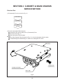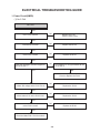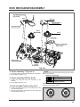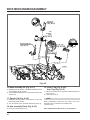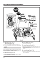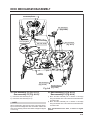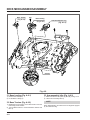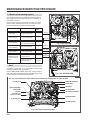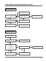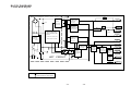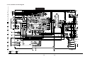
1
SERVICE MANUAL
VIDEO CASSETTE RECORDER
HR-J282EU, HR-J283EU, HR-J285EU,
HR-J290EU, HR-J293EU, HR-J295EK, HR-J295MS,
HR-J582EU, HR-J583EU, HR-J585EU,
HR-J590EU, HR-J593EU, HR-J595EK, HR-J595MS
SPECIFICATIONS (The specifications shown pertain specifically to the model HR-J290EU, J293EU, J590EU and J593EU.)
GENERAL
Power
Power consumption
Power on
Standby mode
Video Head system
HR-J590/J593/
J599EU
HR-J290/J293EU
Tape speed
(SP)
(LP)*
AUDIO
: 200 V – 240 V
, 50 Hz/60 Hz
: Approx. 12 W
: 3.0 W
: DA4 (Double Azimuth) head helical
scan system
: Rotary two-head helical scan system
: 23.39 mm/sec
: 11.69 mm/sec
* HR-J590/J593/J599EU only
Tape format
: Tape width 1/2"
(12.7 mm high density VHS tape)
Maximum recording time
(SP)
: 240 min. with E-240 video cassette
(LP)*
: 480 min. with E-240 video cassette
* HR-J590/J593/J599EU only
Rewind time
Dimensions (W x H x D)
Weight
Operating temperature
Operating humidity
Timer
:
:
:
:
:
:
Approx. 180 sec. with E-180 cassette
360 mm x 94.5 mm x 270 mm
4.0 kg
5°C to 35°C
Less than 80 %
24 hours display type
VIDEO
Signal system
Recording Format
RF reception
RF OUT
RF modulator
Input level
Output level
Signal-to-noise ratio
: PAL-type colour signal and CCIR
monochrome signal, 625 lines
50 fields
: PAL/MESECAM
: PAL (B/G)/SECAM (B/G)
: PAL G
: UHF channels 22 – 68 (Adjustable)
: VIDEO IN (SCART type)
1.0 Vp-p, 75 ohm, unbalanced
: VIDEO OUT (SCART type)
1.0 Vp-p, 75 ohm, unbalanced
: More than 43 dBm
Input level
Output level
HR-J590/J593/
J599EU
HR-J290/J293EU
: AUDIO IN (SCART type)
–6.0 dBm, more than 10 kΩ
: AUDIO OUT (SCART, RCA type)
–6.0 dBm, less than 1 kΩ
: AUDIO OUT (SCART type)
–6.0 dBm, less than 1 kΩ
Audio track
HR-J590/J593/
: Mono track and Hi-Fi track
J599EU
HR-J290/J293EU
: Mono track
Audio frequency response
Normal audio
: 100 Hz to 10,000 Hz
(–6/+3 dBm)
Hi-Fi audio*
: 20 Hz to 20,000 Hz
(–3/+3 dBm)
* HR-J590/J593/J599EU only
Audio signal to noise ratio [HR-J590/J593/J599EU only]
Hi-Fi audio
: More than 70 dB (JIS A filter)
Audio dynamic range [HR-J590/J593/J599EU only]
Hi-Fi audio
: More than 85 dB (JIS A filter)
ACCESSORIES
Provided accessories
: RF cable,
Infrared remote control unit,
“R3” battery x 2
Specifications shown are for SP mode unless specified otherwise.
E. & O.E. Design and specifications subject to change without
notice.
This service manual is printed on 100% recycled paper.
COPYRIGHT © 2002 VICTOR COMPANY OF JAPAN, LTD
V15
No.82915
June 2002
TABLE OF CONTENTS
BLOCK DIAGRAMS . . . . . . . . . . . . . . . . . . . . .3-21
SECTION 1
SUMMARY
1. Power Block Diagram . . . . . . . . . . . . . . . . . . . .3-21
2. Tuner/IF, NICAM & A2 Block Diagram . . . . . . . .3-23
3. VPS Block Diagram . . . . . . . . . . . . . . . . . . . . . .3-24
KEY TO ABBREVIATIONS . . . . . . . . . . . . . . . . 1-1
IMPORTANT SAFETY PRECAUTIONS . . . . . . . . . . 1-2
PROPOSAL FOR APPLYING SHORT
PROTECTION . . . . . . . . . . . . . . . . . . . . . . . . . . .1-4
SERVICE NOTICE ON REPLACING EEPROM . .1-5
SERVICE INFORMATION FOR EEPROM
IC SETTING . . . . . . . . . . . . . . . . . . . . . . . . . . . .1-6
SPECIFICATIONS . . . . . . . . . . . . . . . . . . . . . . . 1-7
4. Y/C Block Diagram . . . . . . . . . . . . . . . . . . . . . .3-25
5. Hi-Fi Block Diagram . . . . . . . . . . . . . . . . . . . . .3-26
6. System Block Diagram . . . . . . . . . . . . . . . . . . .3-27
CIRCUIT DIAGRAMS . . . . . . . . . . . . . . . . . . . .3-29
1. Power Circuit Diagram . . . . . . . . . . . . . . . . . . . .3-29
2. Tuner, NICAM/A2 Circuit Diagram . . . . . . . . . . .3-31
3. A/V, SECAM, VPS Circuit Diagram . . . . . . . . . .3-33
4. System Circuit Diagram . . . . . . . . . . . . . . . . . . .3-35
5. Hi-Fi, SCART Circuit Diagram . . . . . . . . . . . . . .3-39
• CIRCUIT VOLTAGE CHART . . . . . . . . . . . . . . . .3-41
SECTION 2
CABINET & MAIN CHASSIS
PRINTED CIRCUIT BOARD DIAGRAMS . . . . .3-45
1. MAIN P.C.Board . . . . . . . . . . . . . . . . . . . . . . . .3-45
SERVICE METHOD . . . . . . . . . . . . . . . . . . . . . 2-1
Electrical Part . . . . . . . . . . . . . . . . . . . . . . . . . . . . . 2-1
EXPLODED VIEWS . . . . . . . . . . . . . . . . . . . . . . 2-2
1. Cabinet & Main Frame Section . . . . . . . . . . . . . 2-2
2. Packing & Accessory Section
SECTION 4
MECHANISM
. . . . . . . . . . . . . . 2-3
NOTE) The table of contents for this section is edited
NOTE) separately.
SECTION 3
ELECTRICAL
ELECTRICAL ADJUSTMENT POINTS
ARRANGEMENT . . . . . . . . . . . . . . . . . . . . . . . .3-1
ELECTRICAL ADJUSTMENT PROCEDURES . . 3-2
1. Servo Circuit . . . . . . . . . . . . . . . . . . . . . . . . . . . 3-2
ELECTRICAL TROUBLESHOOTING GUIDE . . . 3-4
1. Power Circuit(SMPS) . . . . . . . . . . . . . . . . . . . . . 3-4
2. Servo Circuit
. . . . . . . . . . . . . . . . . . . . . . . . . . .3-7
3. System & Front Panel Circuit . . . . . . . . . . . . . . .3-10
4. Y/C Circuit . . . . . . . . . . . . . . . . . . . . . . . . . . . . .3-12
5. Tuner/IF Circuit . . . . . . . . . . . . . . . . . . . . . . . . .3-16
6. Hi-Fi Circuit . . . . . . . . . . . . . . . . . . . . . . . . . . . .3-19
SECTION 5
REPLACEMENT PARTS LIST
5-1 EXPLODED VIEW . . . . . . . . . . . . . . . . . . . . . . . . .5-1
5-2 REPLACEMENT PARTS LIST. . . . . . . . . . . . . . . . .5-4
SECTION1 SUMMARY
KEY TO ABBREVIATIONS
A
B
C
AC
ACC
ACSS
ADJ
A/E
AFC
AFT
AGC
A.H.SW
ALC
AM
AMP
ANT
APC
ASS’Y
AUX
B
BGP
BPF
BS
BW or B/W
C
CAN
CAP
CAP.BRK
CAP.RVS
CATV
CBA
CCD
C.CTL
CFG
CHROMA
CNR
COMB
COMP
D
E
F
G
H
I
L
CONV
C.ROT SW
CS
C.SYNC
CTL DIV
CUR
CYL
D
D.ADJ
DC
D.CTL
DEMOD
DET
DEV
DHP
DIGITRON
DL
DOC
DUB
D.V SYNC
E
EE
EMPH
ENA
ENV
EP
EQ
EXP
F
FB
FBC
FE
FG
FL
FM
F/R
FS
FSC
F/V
GEN
H
IC
IF
INS
L
LD
LD VTG CTL
LECHA
L.M
LP
:Alternating Current
:Automatic Color Control
:Automatic Channel Setting System
:Adjust
:Audio Erase
:Automatic Frequency Control
:Automatic Fine Tuning
:Automatic Gain Control
:Audio Head Switch
:Automatic Level Control
:Amplitude Modulation
:Amplifier
:Antenna
:Automatic Phase Control
:Assembly
:Auxiliary
:Base
:Burst Gate Pulse
:Bandpass Filter
:Brodcasting Satellite
:Black and White
:Capacitor, Chroma, Collector
:Cancel
:Capstan
:Capstan Brake
:Capstan Reverse
:Cable Television
:Circuit Board Assembly
:Charge Coupled Device
:Chro Control, Capstan Control
:Capstan Frequency Generator
:Chrominance
:Chroma Noise Redution
:Combination
Comb Filter
:Comparator
Composite
Compensation
:Converter
:Color Rotary Switch
:Chip Selcet
:Composite Synchronization
:Control Divide
:Current
:Cylinder
:Drum, Digital, Diode, Drain
:Drum Adjust
:Direct Current
:Drum Control
:Demodulator
:Detector
:Deviation
:Double High Pass
:Digital Display Tube
:Delay line
:Drop Out Compensator
:Dubbing
:Dummy Vertical Synchronization
:Emitter
:Electric to Eletric
:Emphasis
:Enable
:Envelope
:Extended Play
:Equalizer
:Expander
:Fuse
:Feed Back
:Feed Back Clamp
:Full Erase
:Frequency Generator
:Filter
:Frequency Modulation
:Front/Rear
:Frequency Synthesizer
:Subcarrier Frequency
:Frequency Voltage
:Generator
:High, Horizontal
:Integrated Circuit
:Intermediate Frequency
:Insert
:Low, Left, Coil
:LED
:Loading Voltage Control
:Letter Character
:Level Meter
:Long Play
M
N
O
P
Q
R
S
T
U
V
W
X
Y
Z
1-1
LPF
MAX
MD
MECHA.CTL
MIC
MIN
MIX
M.M.
MMV
MOD
MODEM
MPX
NR
:Low Pass Filter
:Maximum
:Modulator
:Mechanism Control
:Microphone
:Minimum
:Mixer, Mixing
:Monostable, Multivibrator
:Mono Multi Vibrator
:Modulation, Modulator
:Modulator-Demodulator
:Multiplex
:Noise Reduction
OSC
OSD
PB
PCB
P.CTL
PRE-AMP
P.F
PG
PLL
PREM.DET
P.P
PS
PWM
PWR CTL
Q
QH
QSR
QTR
QV
R
RE(or RC)
REC
REC S ‘H’
REF
REG
REMOCON
RF
R/P
RTC
S
S.ACCEL
SAOP
SC
S.DET
SH
SHARP
SIF
SLD
S/N
SP
ST
SUB
SW or S/W
SYNC
SYSCON
T
TP
TR
TRK
TRANS
TU
UHF
UNREG
V
VA
VCO
VGC
VHF
V.H.SW
VISS
VPS
VR
V-SYNC
VTG
VV
VXO
W
WHT
W/O
X-TAL
Y/C
YNR
ZD
:Oscillator
:On Screen Display
:Playback
:Printed Circuit Board
:Power Control
:Preamplifier
:Power Failure
:Pulse Generator
:Phase Locked Loop
:Premire Detect
:Peak-to-Peak
:Phase Shift
:Pulse Width Modulation
:Power Control
:Transistor
:Quasi Horizontal
:Quick Setting Record
:Quick Timer Record
:Quasi Vertical
:Resistor, Right
:Remocon, Receiver
:Recording
:Record Start ‘Hight’
:Reference
:Regulated, Regulator
:Remote Control(unit)
:Radio Frequency
:Record/Playback
:Reel Time Counter
:Serial
:Slow Accel
:Second Audio Program
:Scart, Simulcast
:Secam Detect
:Shift
:Sharpness
:Sound Intermediate Frequency
:Side Locking
:Signal to Noise Ratio
:Standard Play
:Stereo
:Subtract, Subcarrier
:Switch
:Synchronization
:System Control
:Coil
:Test Point
:Transistor
:Tracking
:Transformer
:Tuner, Take-up
:Ultra High Frequency
:Unregulated
:Volt, Vertical
:Always Voltage
:Voltage Controlled Oscillator
:Voltage Gain Control
:Very High Frequency
:Video Head Switch
:VHS Index Search
:Video Program System
:Variable Resistor or Volume
:Vertical Synchronization
:Voltage
:Voltage to Voltage
:Voltage X-tal Oscillator
:Watt
:White
:With out
:Crystal
:Luminance/Chrominance
:Luminance Noise Reduction
:Zener Diode
Important Safety Precautions
Prior to shipment from the factory, JVC products are strictly inspected to conform with the recognized product safety and electrical codes
of the countries in which they are to be sold. However, in order to maintain such compliance, it is equally important to implement the
following precautions when a set is being serviced.
v Precautions
during Servicing
12. Crimp type wire connector
In such cases as when replacing the power transformer in sets
where the connections between the power cord and power
transformer primary lead wires are performed using crimp type
connectors, if replacing the connectors is unavoidable, in order to prevent safety hazards, perform carefully and precisely
according to the following steps.
1. Locations requiring special caution are denoted by labels and
inscriptions on the cabinet, chassis and certain parts of the
product. When performing service, be sure to read and comply with these and other cautionary notices appearing in the
operation and service manuals.
2. Parts identified by the
symbol and shaded (
) parts are
critical for safety.
Replace only with specified part numbers.
Note: Parts in this category also include those specified to comply with X-ray emission standards for products using
cathode ray tubes and those specified for compliance
with various regulations regarding spurious radiation
emission.
1) Connector part number : E03830-001
2) Required tool : Connector crimping tool of the proper type
which will not damage insulated parts.
3) Replacement procedure
(1) Remove the old connector by cutting the wires at a point
close to the connector.
Important : Do not reuse a connector (discard it).
3. Fuse replacement caution notice.
Caution for continued protection against fire hazard.
Replace only with same type and rated fuse(s) as specified.
4. Use specified internal wiring. Note especially:
1) Wires covered with PVC tubing
2) Double insulated wires
3) High voltage leads
cut close to connector
Fig.3
5. Use specified insulating materials for hazardous live parts.
Note especially:
1) Insulation Tape
3) Spacers
5) Barrier
2) PVC tubing
4) Insulation sheets for transistors
(2) Strip about 15 mm of the insulation from the ends of
the wires. If the wires are stranded, twist the strands to
avoid frayed conductors.
15 mm
6. When replacing AC primary side components (transformers,
power cords, noise blocking capacitors, etc.) wrap ends of
wires securely about the terminals before soldering.
Fig.4
(3) Align the lengths of the wires to be connected. Insert
the wires fully into the connector.
Fig.1
Metal sleeve
7. Observe that wires do not contact heat producing parts
(heatsinks, oxide metal film resistors, fusible resistors, etc.)
Connector
8. Check that replaced wires do not contact sharp edged or
pointed parts.
Fig.5
9. When a power cord has been replaced, check that 10-15 kg of
force in any direction will not loosen it.
(4) As shown in Fig.6, use the crimping tool to crimp the
metal sleeve at the center position. Be sure to crimp fully
to the complete closure of the tool.
Power cord
Crimping tool
1.2
5
2.0
5.5
Fig.6
Fig.2
(5) Check the four points noted in Fig.7.
10. Also check areas surrounding repaired locations.
11. Products using cathode ray tubes (CRTs)
In regard to such products, the cathode ray tubes themselves,
the high voltage circuits, and related circuits are specified for
compliance with recognized codes pertaining to X-ray emission.
Consequently, when servicing these products, replace the cathode ray tubes and other parts with only the specified parts.
Under no circumstances attempt to modify these circuits.
Unauthorized modification can increase the high voltage value
and cause X-ray emission from the cathode ray tube.
Not easily pulled free
Crimped at approx. center
of metal sleeve
Conductors extended
Wire insulation recessed
more than 4 mm
Fig.7
1
S40888-01
v Safety
Check after Servicing
Examine the area surrounding the repaired location for damage or deterioration. Observe that screws, parts and wires have been
returned to original positions, Afterwards, perform the following tests and confirm the specified values in order to verify compliance with safety standards.
1. Insulation resistance test
Confirm the specified insulation resistance or greater between power cord plug prongs and
externally exposed parts of the set (RF terminals, antenna terminals, video and audio input
and output terminals, microphone jacks, earphone jacks, etc.). See table 1 below.
2. Dielectric strength test
Confirm specified dielectric strength or greater between power cord plug prongs and exposed
accessible parts of the set (RF terminals, antenna terminals, video and audio input and output
terminals, microphone jacks, earphone jacks, etc.). See table 1 below.
3. Clearance distance
When replacing primary circuit components, confirm specified clearance distance (d), (d’) between soldered terminals, and between terminals and surrounding metallic parts. See table 1
below.
Chassis
d
d'
Power cord,
primary wire
Fig. 8
4. Leakage current test
Confirm specified or lower leakage current between earth ground/power cord plug prongs
and externally exposed accessible parts (RF terminals, antenna terminals, video and audio
input and output terminals, microphone jacks, earphone jacks, etc.).
Measuring Method : (Power ON)
Insert load Z between earth ground/power cord plug prongs and externally exposed accessible parts. Use an AC voltmeter to measure across both terminals of load Z. See figure 9 and
following table 2.
a
Externally
exposed
accessible part
b
c
Z
V
Fig. 9
5. Grounding (Class 1 model only)
Confirm specified or lower grounding impedance between earth pin in AC inlet and externally exposed accessible parts (Video in,
Video out, Audio in, Audio out or Fixing screw etc.).
Measuring Method:
Connect milli ohm meter between earth pin in AC inlet and exposed accessible parts. See figure 10 and grounding specifications.
Exposed accessible part
AC inlet
Grounding Specifications
Region
Earth pin
Grounding Impedance (Z)
USA & Canada
Z ≤ 0.1 ohm
Europe & Australia
Z ≤ 0.5 ohm
Milli ohm meter
Fig. 10
AC Line Voltage
100 V
100 to 240 V
110 to 130 V
110 to 130 V
200 to 240 V
Region
Insulation Resistance (R)
R ≤ 1 MΩ/500 V DC
Japan
USA & Canada
Europe & Australia
1 MΩ ≥ R ≥ 12 MΩ/500 V DC
R ≤ 10 MΩ/500 V DC
Dielectric Strength
AC 1 kV 1 minute
AC 1.5 kV 1 miute
AC 1 kV 1 minute
AC 3 kV 1 minute
(Class 2)
AC 1.5 kV 1 minute
(Class 1)
Clearance Distance (d), (d')
d, d' ≤ 3 mm
d, d' ≤ 4 mm
d, d' ≤ 3.2 mm
d ≤ 4 mm
d' ≤ 8 mm (Power cord)
d' ≤ 6 mm (Primary wire)
Table 1 Specifications for each region
AC Line Voltage
Region
100 V
Japan
110 to 130 V
USA & Canada
110 to 130 V
220 to 240 V
Load Z
Leakage Current (i)
a, b, c
i ≤ 1 mA rms
Exposed accessible parts
i ≤ 0.5 mA rms
Exposed accessible parts
2 kΩ
i ≤ 0.7 mA peak
i ≤ 2 mA dc
Antenna earth terminals
50 kΩ
i ≤ 0.7 mA peak
i ≤ 2 mA dc
Other terminals
1 kΩ
Europe & Australia
0.15 µF
1.5 kΩ
Table 2 Leakage current specifications for each region
Note: These tables are unofficial and for reference only. Be sure to confirm the precise values for your particular country and locality.
2
S40888-01
PROPOSAL FOR APPLYING SHORT PROTECTION
• The Contents of Examination
As all the IC that is applied to VCR is controlled by IIC, mutual communication, if Vcc of IC is short or open
with detecting ‘Acknowledge’ data of the specific IC according to each power(5V, 5VT) µ-COM gets unable to
detect ‘ACK’ data.
µ-COM regards this case as abnormal one and if it can’t detect ‘ACK’ data for a certain time(3.5 sec) the signal of ‘Power Control’ and ‘Timer Control’ are switched to ‘Low’. As a result POWER Switching TR is kept from
generating heat and fire.
Conception
BLOCK Diagram
TIMER
CONTROL
5VT SW
SLAVE with 5V
IIC BUS
MASTER
SLAVE with 5V
POWER
CONTROL
5VT SW
• POWER for each IC
5.2V
5.2VT
Modulator
5.3VA
5.3VA
Hi-Fi IC
AVCP IC
TUNER
NICAM IC
SECAM IC
Timer Control
Power Control
• IC to detect ‘ACK’ data is selected as below because IC is different in accordance to region and option
S/
Series
P/Y/I
Series
5V POWER
5VT POWER
5V POWER
5VT POWER
SECAM IC
AVCP IC
Modulator
AVCP IC
*Short protection off mode : DJ01 Diode in
1-4
SERVICE NOTICE ON REPLACING EEPROM
In case that defective EEPROM of PAL models is replaced, to operate these sets from the initial state MP KEY
must be repaired as well before delivering to the customer.
If MP KEY isn’t repaired the setting of RF OUT channel or LANGUAGE might be different from that for custormer’s country.
•MP KEY : In case of PAL VCR if holding the REC button on the front panel and the CLEAR button on the
remote control handset for 5 ~ 7 seconds with power being switch all and no tapes,
OK is displayed at FLD for FLD models and LED becomes on for LED CLOCK models.
This is the state that initializing EEPROM is finished.
(In case of PAL VCP if holding the REC button on the front panel and the MENU button on the
remote control handset for 5 ~ 7 seconds with power being off and no tapes, All the LED DOTs
become on. This is the state that initializing EEPROM is finished.)
•MP KEY's function : MP KEY sets EEPROM's data up to the initial state.
• FLD MODEL:
MP KEY “OK”
OK
REC
VCR
TIMER
• LED CLOCK MODEL:
MP KEY Switch all on a Light
AM
• LED DOT MODEL:
MP KEY Switch all on a Light
1-5
SERVICE INFORMATION FOR EEPROM IC SETTING
MODEL
HR-J283EU
EEPROM option code No. setting
HEX
00
00
00
00
00
00
00
00
00
00
00
00
00
00
00
00
00
00
00
00
00
00
00
00
00
00
00
00
00
00
00
00
00
00
00
00
00
00
00
00
00
00
00
00
00
00
00
00
00
00
00
00
00
00
BINARY
00000000
00000000
00000000
00000000
00000000
00000000
00000000
00000000
00000000
00000000
00000000
00000000
00000000
00000000
00000000
00000000
00000000
00000000
00000000
00000000
00000000
00000000
00000000
00000000
00000000
00000000
00000000
00000000
00000000
00000000
00000000
00000000
00000000
00000000
00000000
00000000
00000000
00000000
00000000
00000000
00000000
00000000
00000000
00000000
00000000
00000000
00000000
00000000
00000000
00000000
00000000
00000000
00000000
00000000
HR-J582EU
HR-J583EU
HEX
00
00
00
00
00
00
00
00
00
00
00
00
00
00
00
00
00
00
BINARY
00000000
00000000
00000000
00000000
00000000
00000000
00000000
00000000
00000000
00000000
00000000
00000000
00000000
00000000
00000000
00000000
00000000
00000000
# Remote control Key action
• OK : Now option data write to EEPROM
• MENU : Menu exit
• EDIT : ▲▼ (Option data change from 0~F
Hexadecimal)
• MOVE : ▲▼ (Cursor move for option data
setting)
▲
NAME
02
C0
C0
B1
30
48
HR-J290EU E2
HR-J293EU C1
C8
B1
30
48
HR-J585EU 0C
C0
C0
B1
30
48
HR-J590EU/ EC
J593EU C1
C8
B1
30
48
HR-J595EK 2C
C0
C8
B4
00
43
HR-J595MS 6C
C0
48
B0
62
40
HR-J295MS 62
C0
48
B0
62
40
HR-J295EK 02
C0
C8
B4
00
43
HR-J282EU 02
C0
C0
B7
00
50
▲
MODEL
HR-J285EU
NAME
02
C0
C8
B7
00
50
0C
C0
C0
B7
00
50
0C
C0
C8
B7
00
50
EEPROM option code No. setting procedure
1. Power Cord plug-in and Power SW on, then
“EEPROM option data setting” screen to the left
will be displayed.
# If not, press the “Child lock” key on the Remote
controller to switch with “CANAL” because the
VCR set has “CANAL IC” inside.
# If your VCR set has “NTSC Line Record”, switch
the VCR set to “AV” mode after inputting the Line
Video signal. If not, the Blue back screen may be
shown in to screen.
2. Refer to option data in the next page and input
the value to the “HEX” field using “EDIT” key
only, and then press the “OK” key on the Remote
controller.
3. Check the basic operation
(Tuner/PB/CUE/REV/AV/REC mode...)
4. Initialize the EEPROM IC pressing the “REC” key
on the Front Panel and “CLEAR” key on the
Remote controller at the same time.
1-6
SPECIFICATIONS
General
Power
Power consumption
Video Head system
Tape speed
Tape format
Maximum recording time
Rewind time
Dimensions (W X H X D)
Weight
Operating temperature
Operating humidity
Timer
Video
Television system
Recording format
Input level
Output level
Signal to noise ratio
Audio
Input level
Output level
Audio track
Audio signal to noise ratio
Audio dynamic range
: 200~240V, 50Hz
: Approx. 12 watts(Energy Saving mode : 3 watts)
: Rotary 2heads, helical scanning system
(2HD Model)
Double azimuth 4 heads, helical scanning system
(4HD MONO, 4HD Hi-Fi Model)
: 23.39 mm/sec (SP mode)11.69 mm/sec(LP mode)
: Tape width 1/2” (12.7 mm high density VHS tape)
: 4 hours in SP mode/8 hours in LP mode (with E-240 tape)
: Approx. 150 sec. (with E-180 tape)
: 360 x 94.5 x 270 mm
: 9.0 lbs. (4.0 kg)
: 41°F-95°F (5°C-35°C)
: Less than 80%
: 24 hours display type
: CCIR standard (625 lines, 50 fields)
PAL colour signal
: PAL B/G (HR-J282EU/J283EU/J582EU/J583EU/J285EU/
J290EU/293EU/J585EU/J590EU/J593EU)
PAL N (HR-J295EK/J595EK)
PAL SECAM-L (HR-J295MS/J595MS)
: VIDEO IN (SCART, RCA type)
1.0 Vp-p, 75 ohm, unbalanced
: VIDEO OUT (SCART type)
1.0 Vp-p, 75 ohm, unbalanced
: More than 43 dBm
: AUDIO IN (SCART type)
Scart type : -6.0dBm, more than 10kΩ
: AUDIO OUT (SCART, RCA type)
Scart type : -6.0dBm, less than 1kΩ
RCA type : -6.0 dBm, less than 1kΩ
Mono track & Hi-Fi track
: Normal : More than 70 dBm(JIS A filter)
: Hi-Fi audio : More than 85 dBm(JIS A filter)
• Design and specifications are subject to change without notice.
:Hi-Fi Model only
1-7
SECTION 2 CABINET & MAIN CHASSIS
SERVICE METHOD
Electrical Part
(1) Re-assembly Flow for service like Fig. 2-1
Timer C.B.A
Main C.B.A
Housing & Deck
Assembly
(2) To check and replace Electrical parts
2 Re-assemble the unit according to No.1) Re-assembly Flow.
3 Place the unit like Fig. 2-1
4 Check and replace Electrical parts.
NOTE :
1 Insert Video Cassette Tape inversely like Fig. 2-1 to check and replace defective parts.
2 In disassembling and reassembling, be careful not to damaged CST switch.
(Positioned Upside Down)
Main C.B.A
Cassette Tape
(Upside Down)
Housing & Deck Ass'y
Timer C.B.A
Fig.2-1
2-1
EXPLODED VIEWS
1. Cabinet and Main Frame Section
452
NOTE) Refer to “SECTION 5 REPLACEMENT
PARTS LIST” in order to look for the
part number of each part.
OPTIONAL PARTS
A46
LED502(LED501)
323
TU70
1(TU
NER
)
1SCART
452
452
2SCART
462
320
300
5
250
462
330
275
4
464
A43
260
A49
452
3
280
277
283
A42
A00
284
457
2
281
1
A
B
C
2-2
D
2.Packing Accessory Section
NOTE) Refer to “SECTION REPLACEMENT PARTS LIST
NOTE) in order to look for the part number of each part.
OPTIONAL PARTS
806
811
810
812
CABLE SET ASS'Y
(Optional parts)
PLUG ASS'Y 1WAY
(Optional parts)
PLUG ASS'Y 2WAY
(Optional parts)
821
801
808
BATTERY
803
PACKING (LF)
SCART CABLE
INSTRUCTION MANUAL
804
BAG. SOFR SHEET
803
802
PACKING (RF)
BOX CARTON
900
2-3
REMOCON
SECTION 3 ELECTRICAL
ELECTRICAL ADJUSTMENT POINTS ARRANGEMENT
: Measurement point
: Adjustment point
SCART JACK
Speak-ez
S
M
P
S
SW/IC
T
U
N
E
R
Hi-Fi
VPS
SECAM
A/V
AVCP
C+
W501
W502
Micom
H.S/W
SYSTEM
EEPROM
NICAM
CLK IC
E2PROM
DISPLAY(DOT,CLK)
(COMPONENT SIDE)
3-1
ELECTRICAL ADJUSTMENT PROCEDURES
1. Servo Adjustment
1) PG Adjustment
• Test Equipment
a) OSCILLOSCOPE
b) PAL TEST TAPE (VHS SP)
c) JIG REMOCON (AUTO PG SETTING)
• Adjustment And Specification
MODE
MEASUREMENT POINT
PLAY
V.Out
H/SW(W501, W502)
ADJUSTMENT POINT
SPECIFICATION
6.5 ± 0.5H
• Adjustment Procedure
a) Insert the PAL SP Test Tape and play.
Note - Adjust the distance of X, pressing the Tracking(+) or Tracking(-) when the “ATR(OSD on monitor)” is blink after PAL SP test Tape is inserted.
b) Press the Auto PG KEY on JIG Remocon(1’st) or Press “Play” key on set and “0” key on
Remocon.(Then check the light 4 Dot LED on CLK/LED - TRK is a Initial)
c) Press the Auto PG Key on JIG Remocon again (2’nd) or press “Play” key on set and “0” key on
Remocon again.(Then check the blink 4 Dot LED - At regular 0.25sec internal, Then check blink “PG
waveform” on oscilloscope(MONO Model)).
• Check the PG
a) Connect the CH1 of the oscilloscope to the H/SW and CD2 to the Video out for the VCR.
b) Trigger the mixed Video Signal of CH2 to the CH1 H/SW(W501, W502), and then check the distance
(time difference), which is from the selected A(B) Head point of the H/SW(W501, W502) signal to the
starting point of the vertical synchronized signal, to 6.5H ± 0.5H (416µs, 1H=64.0µs).
• CONNECTION
V.Out
OSCILLOSCOPE
CH1 CH2
H/SW(W501,W502)
H/SW V.out
(W501, W502)
3-2
ELECTRICAL ADJUSTMENT PROCEDURES
• WAVEFORM
H/SW
6.5H(416us)
Composite
VIDEO
• Attension and Reference
a) The PG checking must do when RF Level is Maximum and SERVO system is Locking (MTR MODE)
b) V.H/SW Level is 2Vpp.
3-3
ELECTRICAL TROUBLESHOOTING GUIDE
1. Power Circuit(SMPS)
(1) No 5.3VA.
No 5.3VA.
YES
Is the F101 normal?
NO
Replace the F101
(Use the same Fuse).
YES
Is the BD101 normal?
NO
Replace the BD101.
YES
Is the R101 normal?
NO
Replace the R101.
YES
Does the oscillation waveform appear at
the IC101 Pin 7?
NO
Is Vcc(about 13~15V) permittable at the
IC101 Pin 3?
NO
YES
Check or Replace the D103.
Is there DC voltage at the IC101 Pin 4?
NO
Replace the IC102.
YES
Is there about 2.5V at the IC103 Vref ?
NO
Replace the IC103.
YES
Is the D106 normal?
NO
YES
Check the Main PCB 5.3VA Line short?
3-4
Replace the D106.
7. Power Circuit(SMPS)
(2) No 12VA.(Capstan)
No 12VA.
YES
Does 5.3VA work normally?
NO
Check whether 5.3VA is out of order.
YES
Is the D109 normal?
NO
Replace the D109.
YES
Check 12VA Line of the Main PCB short.
(3) No 12VA (CANAL, Buffer)
No 12VA.
YES
Is Vcc(about 13VA) put into the Q155(E)?
NO
YES
Is Voltage(about 12V) put into the
Q155(C)?
YES
Check or Replace the Q155.
3-5
Replace the Peripheral Circuitry of D160.
7. Power Circuit(SMPS)
(4) No 5VT(5V)
No 5VT.(5V)
YES
Is 5.3VA put into the Q152(Q151)
collector?
YES
Is the Q163(Q162) Base “H”?
NO
Check the µ-com Control.
YES
Is about 4.7V put into the
Q152(Q151) Base?
NO
YES
Check or Replace the Q152(Q151).
3-6
Check the Q163(Q162)
whether it works normally.
2. Servo Circuit
A.
Unstable Video in PB
Mode.
Does the on screen noise
level change periodically?
YES
Do CTL pulses appear at
IC501 pin 8?
YES
NO
Does the CFG divide
waveform appear at IC501
pin 9?
Is the height of the CTL
Head adjusted correctly?
NO
YES
Do the CTL pulses move
when TRK is operated?
YES
Adjust the CTL Head.
NO
Does the Video Envelope
waveform appear at IC501
Pin 24?
YES
Replace IC501.
Replace IC501.
NO
Check AVCP IC.
3-7
B.
Drum Motor stopped.
Does 12V appear at PMC01 Pin 8?
NO
YES
Does 2.8V appear at PMD01 Pin 12?
Check Power.
NO
Does Drum PWM appear at IC501 Pin
107?
Check Connector and Drum Motor Ass’y.
NO
YES
Check the Components and foil Pattern
between IC501 Pin 26 and PMC01
Pin 12 for shorts.
Do DFG Pulses appear at PMD01 Pin 3?
NO
YES
Do DFG Pulses appear at IC501 Pin 104?
YES
Check Drum Monitor Ass’y.
NO
Check the Components and foil pattern
between PMC01 Pin 11 and IC501
Pin 104 for shorts.
Does the Drum PWM waveform
appear at IC501 Pin 107?
YES
NO
Check the Components and foil Pattern
Connected to IC501 Pin 107 PMC01
Pin 12 for shorts.
Replace IC501.
3-8
C.
Capstan Motor Stopped.
Does 13VA appear at PMC01 Pin 2?
NO
YES
Does 2.8V appear at PMC01 Pin 9?
Check Power.
NO
YES
Check Connector and Capstan
Motor Ass’y.
Does PWM wave appear at IC501
Pin 108?
NO
YES
Check the Components and foil Patterns
Connected between IC501 Pin 108 and
PMC01 Pin 9 for shorts.
Does the CFG signal appear at PMC01
Pin 1?
NO
YES
Does the CFG signal appear at IC501
Pin 9?
YES
Check Capstan Motor Ass’y.
NO
Check Components and foil patterns
between PMC01 Pin 7 and IC501
Pin 9 for shorts.
Does Capstan PWM appear at IC501
Pin 108?
YES
NO
Check the components and foil pattern
connected between IC501 Pin 108 and
PMC01 Pin 9 for shorts
Replace IC501.
3-9
3. System & Front Panel Circuit
A.
Auto stop.
Does SW30 waveform
appear at IC501 Pin 105?
YES
NO
Do Take-up reel pulses
appear at IC501 Pin 49?
YES
Check the Drum Motor
Signal.
NO
Do Take-up reel pulses
appear at the base of
Q514?
Change IC501.
NO
YES
Does 5.3V appear at
RS501.
YES
Replace the Take-Up Reel
Photocoupler in the
Deck(RS501).
3-10
NO
Check the Power.
B.
Cassette tape loading is unstable.
Is REG 14VA applied to PMC01 Pin 8?
YES
NO
Is High signal applied to IC501 Pin 30
when inserting the CST?
Check the power.
NO
Is 5.4VA applied to R544?
YES
YES
Does Low signal occur form PMC01
Pin 10 when inserting the CST?
YES
NO
Check the CST SW and
peripheral circuitry.
Check the power.
NO
Check the Deck Mechanism.
Check IC501 Pins 68, 69, 70, 71.
NOTE : Auto stop may also be caused by lack of lubrication,due to dried grease or oil.
C.
Non working finction buttons.
Is the voltage of IC501 Pin 36, 5V?
YES
NO
Does(LED Ass’y) display change
when a function button is pressed?
YES
Check the power.
NO
Replace IC501.
Check IC506 Pins 6~14, 17, Pins 20~23
pulse output.
Replace the defective switch.
Replace IC506.
3-11
4. Y/C CIRCUIT
(1) No Video in EE Mode,
No Video in EE Mode
Does the Video signal
appear at the IC301 Pin 48?
NO
Check the Video Input
Jack.
(Line In Jack)
YES
NO
Is 5V applied to the IC301
Pins 18, 24, 42, 55, 72, 91?
Check the 5.2VT, 5.4VA
Line. (Power Circuit)
YES
Does the Video signal
appear at the IC301 Pin 65?
NO
YES
Does the Video signal
appear at the IC501 Pin 19?
Is I2C BUS signal applied to
the IC301 Pins 68, 69?
NO
Check the System Circuit.
(Refer to ‘SYSTEM I2C BUS
CHECK Trouble Shooting’)
YES
NO
Chck the path of the signal
between the IC301 Pin 5
and IC501 Pin 17.
YES
Does the Video signal
NO
appear at the Emitter terminal of the Q307, Q308?
Check C316. (AGC)
YES
Does the 12VT, 5.4VA
NO
appear at the Emitter terminal of the Q307, Q308.
Replace the IC301.
YES
Replace the Q307, Q308.
3-12
Check the 12VT, 5.4VA
Line. (Power Circuit)
3. Y/C CIRCUIT
(2) When the Y(Luminance) signal doesn’t appear on the screen in PB Mode,
Is 5.2VT, 5.4VA applied to the
IC301 Pins 24, 42, 55, 72, 91?
NO
Check the line of the 5.2V
Line. (Power Circuit)
YES
Is the I2C Bus siganl applied NO
to the IC301 Pins 68, 69 ?
Refer to ‘SYSTEM I2C BUS
CHECK Trouble Shooting’.
YES
NO
Does the normal RF signal
appear at the IC301 Pin 78?
NO
Is the V.H.S/W signal
applied to the IC301 Pin 70?
Check the System Circuit.
(IC501 Pin 105)
YES
Is V.H.S/W “H” about 3.4V
at the IC301 Pin 70?
NO
Check the V.H.S/W level.
(Check R303, R304)
YES
YES
Clean the Drum.
Does the Y(Luminance) RF NO
signal appear at the IC301
Pin 76?
NO
Check the path of the
Y(Luminance) RF signal.
(Check the C312)
YES
Check the path of the
Y(Luminance) RF signal.
(Check C327)
YES
YES
Is the Y(Luminance) Video
waveform showed up at
theIC301 Pin 43?
NO
YES
Replace the IC301.
3-13
Replace the IC301.
3. Y/C CIRCUIT
(3) When the C(Color) signal doesn’t appear on the screen in PB Mode,
Is 5.2VT/5.4VA applied to the
IC301 Pins 24, 42, 55, 72, 91.
NO
Check the line of the 5.2VT/
5.4VA Line. (Power Circuit)
NO
Check the Color Rotary
Circuit. (IC501 pin 99 )
NO
Check the Color Rotary
level. (Check the R303)
YES
Is the Color Rotary signal
applied to the IC301
Pin 70?
YES
Is Color Rotary “H”
about 3.4V?
YES
Does the Color signal
appear at the IC301
Pin 25 ?
YES
NO
Does the X301(4.43MHZ)
oscillate?
NO
Does the Color signal
appear at the IC301 Pin 21?
YES
Replace the IC301.
NO
Replace the IC301.
3-14
Replace the X301.
Check the Color Pass.
3. Y/C CIRCUIT
(4) When the Video signal doesn’t appear on the screen in REC Mode,
Is the EE signal normal?
NO
Check EE Mode.
YES
Is 5.2VT/5.4VA applied to the
IC301 Pins 24,42,55,72,91?
NO
Check the line of the 5.2VT/
5.4VA Line.(Power Circuit)
YES
Does PB Mdoe operate
normally?
NO
Check PB Mode.
YES
Does the RF signal appear
at the IC301 Pin 78?
NO
Is the REC ‘H’ signal
(about 4V) applied to the
IC301 Pin 80?
NO
Check the System of REC
‘H’. (the IC501 Pin 47
/ the D301)
YES
YES
Does the REC RF signal
appear at the IC301
Pins 88,89,94,95?
NO
Check REC Luminance
Pass & Color Pass.
YES
Check the circuit of the
IC301 Pins 85, 86.
YES
YES
Check the Drum &
Drum Connector
3-15
Replace the IC301.
5. Tuner/IF circuit
(1) No picture on the TV screen
No picture on the
TV screen
YES
Does the Video signal at
the TU701 Pin24?
NO
Is +30VT applied to
TU701 Pin 16?
YES
NO
Check 33VT line.
YES
Is +5VT applied to
TU701 Pin 13?
NO
Check 5VT line.
YES
Does the Clock signal
appear at TU701 Pin 11?
NO
Check the liC Clock
signal of µ-com Pin 59.
NO
Check the liC Data signal
of µ-com Pin 60.
YES
Does the data signal
appear at TU701 Pin 12?
YES
Replace Tuner
Does Sync appear at
IC501 Pin111?
NO
Check the signal flow
from TU701 Pin 24 to
IC301 Pin 67.
YES
Check the signal flow from
IC501 Pin19 to JK901
Pin19.
3-16
(2) No sound (Mono Model)
No sound
YES
Check the Vcc of IC301 Pin 18.
NO
Check 5VT power.
YES
Check the Tuner Audio signal
at IC301 Pin 13.
NO
Chekc the signal flow from TU701
Pin21 to IC301 Pin 13.
YES
Check the Audio signal at IC301 Pin 11.
NO
YES
Check the signal flow from IC301
pin 11 to IC901 Pin 6.
3-17
Replace IC301.
(3) No sound (Hi-Fi Model)
No sound
YES
Check the Vcc of IC751 Pins 1, 19, 33.
NO
Check 5V power.
YES
Check the Tuner SiF signal at IC751 Pin 2.
NO
Check the Tuner Audio of TU701 Pin 21.
YES
Check the oscillator of IC751 Pins 5, 6.
NO
Replace X751.
YES
Check the Audio of IC751 Pins 30, 31.
NO
Check the IIC Clock and Data at
IC751 Pins 12, 13.
NO
Check the signal flow from IC751
Pins 30, 31 to IC801 Pins 2,3.
NO
Check the IIC Clock and Data at
IC801 Pins 42, 43.
YES
Check the Audio of IC801 Pins 2, 3.
YES
Check the Audio of IC801 Pins 18, 19.
YES
Check the signal flow from IC801
pins 18, 19 to JK901 Pins 1, 3.
3-18
6. Hi-Fi Circuit (Hi-Fi Model)
A.
Hi-Fi Playback.
YES
No sound
Check the Vcc of
IC801.(Pins 34, 40)
NO
YES
Check the Hi-Fi Selection
Switch and the Tape quality.
Check power.
YES
Is the RF Envelope at
IC801 Pin 44 over 2Vp-p?
NO
YES
YES
Check the connection at
P3D01 if good then
Replace IC801.
Check IC801 Pin 42(Data),
Pin 43(Clock).
YES
NO
Do Audio signals appear at
IC801 Pin 16(L-CH),
17(R-CH)?
YES
Check the Signal path
of Audio Output.
Is the Head switching signal
IC802 Pin 41 O.K?
Check Ports of µ-COM.
NO
Replace IC801.
3-19
NO
Check IC501 Pin 23.
(Audio head switch 25)
B.
Hi-Fi REC.
It is impossible to record and playback
Hi-Fi Audio signal.
YES
Check Vcc of IC801. (Pins 34,40)
YES
NO
Check IC801 Pin 42(Data),Pin 43(CLOCK).
YES
Check Power.
NO
Do Audio signals appear at IC801
Pins 16, 17?
YES
Check ports of µ-COM.
NO
Do FM Audio signals appear at IC801
Pin 36?
YES
Check Audio input signal of IC801
Pins 2, 3(TU.A.), 6, 7(Scart 1)
NO
Check the Contact Points of Drum
Connector if good then Replace the Drum.
Replace IC801.
3-20
SECTION 4 MECHANISM
CONTENTS
DECK MECHANISM PARTS
LOCATIONS
•
•
Top View...................................................4-1
Bottom View ............................................4-1
DECK MECHANISM
DISASSEMBLY
1. Drum Assembly .........................................4-2
2. Plate Top ...................................................4-4
3. Holder Assembly CST ...............................4-4
4. Opener Door .............................................4-4
5. Bracket Assembly L/D Motor.....................4-4
6. Gear Assembly Rack F/L ..........................4-4
7. Arm Assembly F/L .....................................4-4
8. Lever Assembly S/W .................................4-4
9. Arm Assembly Cleaner..............................4-5
10.Head F/E ...................................................4-5
11. Base Assembly A/C Head .........................4-5
12.Brake Assembly RS ..................................4-6
13.Brake Assembly T .....................................4-6
14.Arm Assembly Tension..............................4-6
15.Reel S / Reel T..........................................4-6
16.Base Assembly P4 ....................................4-7
17.Opener Lid ................................................4-7
18.Arm Assembly Pinch .................................4-7
19.Lever T/up / Arm T/up ...............................4-7
20.Belt Capstan/Motor Capstan .....................4-8
21.Lever F/R ..................................................4-8
22.Clutch assembly D35 ................................4-8
23.Bracket Assembly Capstan .......................4-8
24.Gear Drive/Gear Cam ...............................4-9
25.Gear Sector...............................................4-9
26.Plate Slider................................................4-9
27.Lever Tension ............................................4-9
28.Lever Spring..............................................4-9
29.Gear Assembly P2/
Gear Assembly P3 ..................................4-10
30.Base Assembly P2/
Base Assembly P3 ..................................4-10
31.Base Loading ..........................................4-11
32.Base Tension ...........................................4-11
33.Arm Assembly Idler Jog ..........................4-11
DECK MECHANISM ADJUSTMENT
• Tools and Fixtures for Service.............4-12
1. Mechanism and Mode Switch Alignment
Check ......................................................4-13
2. Deck Preparation for Adjustment ............4-14
3. Checking Torque .....................................4-14
4. Guide Roller Height Adjustment..............4-15
4-1. Preliminary Adjustment ....................4-15
4-2. Precise Adjustment ..........................4-15
5. Audio/Control (A/C) Head Adjustment ....4-16
5-1. Preliminary Adjustment ....................4-16
5-2. Confirmation of Tape Path between
Pinch Roller and Take-up Guide .....4-17
5-3. Precise Adjustment(Azimuth Adjustment)
.........................................................4-17
6. X-Value Adjustment .................................4-17
7. Adjustment after Replacing Drum Assembly
(Video Heads) .........................................4-18
8. Check the Tape Travel after Reassembling
Deck Mechanism.....................................4-18
8-1. Checking Audio and RF Locking Time
during Playback after CUE or REV
.........................................................4-18
8-2. Checking Tape Curling or Jamming
.........................................................4-18
MAIN TENANCE/INSPECTION
PROCEDURE
1.
2.
3.
4.
Check before starting Repairs ................4-19
Required Maintenance ............................4-20
Scheduled Maintenance..........................4-20
Supplies Required for Inspection and
Maintenance............................................4-20
5. Maintenance Procedure ..........................4-20
5-1. Cleaning...........................................4-20
5-2. Greasing ..........................................4-21
MECHANISM TROUBLESHOOTING
GUIDE
1. Deck Mechanism.....................................4-23
2. Front Loading Mechanism.......................4-26
EXPLODED VIEWS
1. Front Loading Mechanism Section .........4-28
2. Moving Mechanism Section (1)...............4-29
3. Moving Mechanism Section (2)...............4-30
DECK MECHANISM PARTS LOCATIONS
• Top View
Pracedure
Starting
No.
1
2
2
3
2
4
5
2
6
3
7
4
9
5
11
10
18
1
16
31
17
19
19
12
14
15
8
33
13
15
• Bottom View
20
24
30
29
29
23
30
20
25
32
27
26
28
24
22
21
NOTE : When reassembly perform the
procedure in the reverse order.
1) When reassembling, confirm Mechanism and Mode
Switch Alignment Position (Pefer to Page 4-14)
2) When disassembling, the Parts for Starting No. Should
be removed first.
4-1
2,3,4
2,3,4,6
6
7
8
9
10
11
2,3
12
2,3
13
2,3
14
2,3,12,13, 15
14
16
17
17
18
17
19
17,18
20
20, 21
21
22
23
24
25
26
Part
Fixing Type
Fig- Viure ew
Drum Assembly
Plate Top
Holder Assembly CST
Opener Door
Bracket Assembly
L/D Motor
Gear Assembly Rack F/L
Arm Assembly F/L
Lever Assembly S/W
Arm Assembly Cleaner
Head F/E
Base Assembly A/C Head
Brake Assembly RS
Brake Assembly T
Arm Assembly Tension
Reel S/Reel T
3 Screw
2 Hook
Chassis Hole
Chassis Hole
3 Hook
A-1
A-2
A-2
A-2
A-2
T
T
T
T
T
1 Hook, Chassis Hole
Chassis Hole
1 Hook
Chassis Embossing
Chassis Embossing
1 Screw
1 Hook
1 Hook
2 Hook
A-2
A-2
A-2
A-3
A-3
A-3
A-4
A-4
A-4
A-4
T
T
T
T
T
T
T
T
T
T
Base Assembly P4
Opener Lid
Arm Assembly Pinch
Lever T/Up / Arm T/Up
Chassis Embossing
Chassis Embossing
Shaft
1 Hook
A-5
A-5
A-5
A-5
T
T
T
T
Belt Capstan/Motor Capstan
Lever F/R
Clutch Assembly D35
Break Assembly Capstan
Gear Drive/Gear Cam
Gear Sector
Plate Slider
3 Screw
Locking Tab
Washer
Locking Tab
Washer/Hook
1 Hook
Shaft Guide
A-6
A-6
A-6
A-6
A-7
A-7
A-7
B
B
B
B
B
B
B
1 Hook
A-7
B
Locking Tab
A7
B
Boss
Chassis Slot
A-8
A-8
B
B
1 Screw
A-9
T
Chassis Embossing
Locking Tab
A-9
A-9
B
T
20,21,23,
24,25
20,21,23, 27 Lever Tension
24,25,26
2,3,14,20, 28 Lever Spring
21,25,23,
24,26
25
29 Gear Assembly P2/Gear Assembly P3
2,3,14,25, 30 Base Assembly P2/Base Assembly P3
29
2,3,14,25, 31 Base Loading
29
2,3,14
32 Base Tension
2,3,20,21, 33 Arm Assembly Idler
22
R: Top, B:Bottom
DECK MECHANISM DISASSEMBLY
Stator
(S2)
(S2)
(S3)
Drum Motor
(S3)
Rotor
Drum Sub Assembly
(A)
Drum FPC
Carbon Brush
(S1)
(S1)
(S1)
H2
H1
Holder FPC
Fig. A-1
1. Drum Assembly (Fig. A-1-1)
(Fig. B-1)
1) Unplug the Drum FPC Connector.
2) Remove three Screws(S1) on bottom side and separate
the Drum assembly.
3) Unhook (H1), (H2) and separate the Holder FPC and
Cap FPC.
Cap FPC
1-1. Drum Motor
1) Remove two Screws(S2) and disassemble the Stator of
the Drum Motor.
(2) Remove two Screws(S3) and separate the Rotor of the
Drum Motor from the Drum Sub assembly.
Drum FPC
Holder FPC
NOTE
When reassembling, confirm (A) portion of the Drum Sub
assembly whether the Carbon Brush is in there or not.
Figure in the opposite direction
4-2
DECK MECHANISM DISASSEMBLY
Plate Top
(Fig. A-2-1)
(C)
(B')
(B)
Holder Assembly CST
(Fig. A-2-2)
(E)
Arm Assembly F/L
(Fig. A-2-6)
Lever Assembly S/W
(Fig. A-2-7)
(H8)
(C1)
Brackert Assembly L/D Motor
Spring Lever S/W
(Fig. A-2-4)
(C')
(D)
(E')
Opener Door
(H6)
(Fig. A-2-3)
Chassis
(A)
Gear Assembly Rack F/L
(Fig. A-2-5)
Fig. A-2
4-3
(B)
DECK MECHANISM DISASSEMBLY
2. Plate Top (Fig. A-2-1)
1) Pull the (B) portion of the Plate Top back in direction of
arrow and separate the right side of it.
2) pull the (B’) portion of the Plate Top back in direction of
arrow and separate the left side of it.
(Used tools : (-) type Drive, anything tool with sharp
point or flat point.)
2) Unhook three Hooks(H3,H4,H5) on bottom side of the
Chassis, lift up the Bracket assembly L/M and disassemble the Bracket assembly L/D Motor.
Bracket assembly L/M
(H4)
(H3)
NOTE
(1) When reassembling, push the Plate Top after alignment
the two position(C), (C’) as Fig.
(H5)
6. Gear Assembly Rack F/L (Fig. A-2-5)
(C')
(C)
(B')
(B)
1) Move the Gear Assembly Rack F/L in direction of
arrow(A) and unhook the Hook(H6) pulling back in front.
2) Separate the Rear Rack F/L in direction of arrow(B).
NOTE
When reassembling, align the Gear part of the Gear
Assembly Rack F/L with the Gear Drive as below Fig.
3. Holder Assembly CST (Fig.A-2-2)
Gear Rack F/L
1) Move the Holder assembly CST in direction of arrow and
separate the left side of it first through the (D) position of
the Chassis.
Holder assembly CST
Chassis
Gear Drive
(D)
7. Arm assembly F/L (Fig. A-2-6)
1) Move the Arm assembly F/L in direction of arrow and
separate the left side of it first.
2) Disassemble the Arm assembly F/L from each guided
Hole of the Chassis.
2) Disassemble the right side of the Holder assembly CST
from each guided hole of the Chassis.
NOTE
When reassembling, insert the (E) part of the Holder assembly CST in the (E’) hole of the Chassis
first and assemble the left side of it.
8. Lever assembly S/W(Fig. A-2-7)
1) Hook the Spring Lever S/W on the Hook(H7) first as
below Fig.
2) Unhook the Hook(H8) in the left side of the Chassis and
move the Lever assembly S/W.
Chassis
4. Opener Door (Figure. A-2-3)
1) Turn the Opener Door clockwise and remove it through
the guide hole of the chassis.
5. Bracket assembly L/D Motor(Fig. A-2-4)
1) Unplug the Connector(C1).
(H8)
(H7)
Spring Lever S/W
4-4
DECK MECHANISM DISASSEMBLY
Arm Assembly
Cleaner
(Fig. A-3-1)
(A)
(S4)
Base Assembly A/C Head
(A)
*(Fig. A-3-3)
Head F/E
(Fig. A-3-2)
Chassis
Fig. A-3
9. Arm assembly Cleaner (Fig. A-3-1)
11. Base assembly A/C Head (Fig. A-3-3)
1) Breakaway the (A) portion as Fig. A-3-1 from the
Embossing of the Chassis, turn the Arm assembly
Cleaner to clockwise direction and lift it up.
1) Remove the Screw(S4) and lift the Base assembly A/C
Head up.
10. Head F/E (Fig. A-3-2)
1) Breakaway the (A) portion of the Head F/E from the
Embossing of the Chassis, turn it to counterclockwise
direction and lift it up.
4-5
DECK MECHANISM DISASSEMBLY
Arm Assembly Tension
(Fig. A-4-3)
(H11)
Spring TB
Brake Assembly T
(Fig. A-4-1)
Spring Tension
Reel S
Reel T
(Fig. A-4-4)
(Fig. A-4-4)
Spring RS
Brake Assembly RS
(Fig. A-4-2)
(H12)
(H9)
(H10)
Base Tension
Chassis
Fig. A-4
12. Brake assembly T (Fig. A-4-1)
1) Unhook the Spring TB from the Hook(H9) of the Chassis.
2) Lift the Brake assembly T up.
NOTE
Difference for Springs
(Difference for Springs)
Spring TB
Spring RS
Spring Tension
13. Brake assembly RS (Fig. A-4-2)
1) Unhook the Spring RS from the Hook(H10) of the
Chassis..
2) Lift the Brake assembly T up.
14. Arm assembly Tension (Fig. A-4-3)
Color (Black)
15. Reel S / Reel T (Fig. A-4-4)
1) Difference for Reel S / Reel T
1) Unhook the Spring Tension from the Hook(H11) of the
Arm assembly tension.
2) Unhook the Hook(H12) of the Base Tension and lift the
Arm assembly Tension up.
Reel S
Reel T
4-6
DECK MECHANISM DISASSEMBLY
Opener Lid
(Fig. A-5-2)
(B)
(B)
Arm
Assembly
Pinch
(Fig. A-5-3)
(C)
Base Assembly P4
Lever T/up
(Fig. A-5-1)
(H13)
(Fig. A-5-4)
(C)
Arm T/up
(H13)
(Fig. A-5-5)
(A)
Chassis
Fig. A-5
16. Base assembly P4 (Fig. A-5-1)
1) Breakaway the (A) portion of the Base assembly P4 from
the Embossing of the Chassis.
2) Turn the Base assembly P4 to counterclockwise direction
and lift it up.
17. Opener Lid (Fig. A-5-2)
1) Breakaway the (B) portion of the Opener Lid from the
Embossing of the Chassis.
2) Turn the Opener Lid to clockwise direction and lift it up.
18. Arm assembly Pinch (Fig. A-5-3)
1) Lift the Arm assembly Pinch up.
4-7
19. Lever T/up (Fig. A-5-4)/
Arm T/up (Fig. A-5-5)
1) Unhook the Hook(H13) of the bottom Chassis and lift the
Lever T/up up.
2) Lift the Arm T/up up.
NOTE
When reassembling, confirm the (C) portion of the Arm
assembly Pinch is inserted to the Chassis Hole
correctly as Fig.
Place the Mechanism face down, or up side down.
DECK MECHANISM DISASSEMBLY
Belt Capstan
(Fig. A-6-1)
Motor Capstan
(Fig. A-6-2)
Washer(W1)
Clutch Assembly D35
(Fig. A-6-4)
(L1)
(L1)
Brake Assembly Capstan
(Fig. A-6-5)
Lever F/R
(Fig. A-6-3)
(L2)
Chassis
(S5)
Fig. A-6
20. Belt Capstan (Fig. A-6-1)/
Motor Capstan (Fig. A-6-2)
1) Remove the Belt Capstan.
2) Remove the three Screws(S5) on bottom Chassis and lift
the Motor Capstan up.
21. Lever F/R (Fig. A-6-3)
1) Unlock the Locking Tab(L1) as Fig. A-6-3 and lift the
Lever F/R up.
22. Clutch assembly D35 (Fig. A-6-4)
1) Remove the Washer(W1) and lift the Clutch assembly
D35 up.
23. Brake assembly Capstan
(Fig. A-6-5)
1) Pull the Locking Tab(L2) back in direction of arrow and lift
it up.
4-8
DECK MECHANISM DISASSEMBLY
(H14)
Gear Cam Hole(B)
Gear Cam
Gear Drive Hole(A)
(Fig. A-7-2)
Gear Sector
Washer (W2)
(Fig. A-7-3)
Plate Slider
Gear Drive
(Fig. A-7-4)
(Fig. A-7-1)
(A)
Lever Tension
(Fig. A-7-5)
Lever spring
(L3)
(Fig. A-7-6)
Gear Drive Hole(C)
Base Loading
(H15)
(H16)
Chassis
Fig. A-7
24. Gear Drive (Fig. A-7-1)/
Gear Cam (Fig. A-7-2)
1) Remove the Washer(W2) and lift the Gear Drive up.
2) Unhook the Hook(H14) of the Gear Cam and lift the Gear
Cam up.
NOTE
When reassembling, align the Gear Drive Hole(A) and the
Gear Cam Hole(B) in a straight line after the Gear Drive
Hole(C) is aligned with the Chassis Hole as Fig.
25. Gear Sector (Fig. A-7-3)
1) Unhook the Hook(H15) of the Base Loading on bottom
Chassis and lift the Gear Sector up.
4-9
26. Plate Slider (Fig. A-7-4)
1) Just lift the Plate Slider up.
27. Lever Tension (Fig. A-7-5)
1) Unhook the (A) portion of the Lever Tension from the
Hook(H16) of the Chassis.
2) Turn the Lever Tension to counterclockwise direction and
lift it up.
28. Lever Spring (Fig. A-7-6)
1) Unlock the Locking Tab(L3) of the bottom Chassis and lift
the Lever Spring up.
DECK MECHANISM DISASSEMBLY
Gear assembly P2 Hole
Gear assembly P3 Hole
Gear Assembly P3
(Fig. A-8-2)
Lever spring Boss
Gear sector Hole(A)
Gear Assembly P2
Plate slider Hole(B)
(Fig. A-8-1)
(B)
(A)
Chassis
Base Assembly P3
(Fig. A-8-4)
Base Assembly P2
Fig. A-8
(Fig. A-8-3)
29. Gear assembly P2 (Fig. A-8-1)/
Gear assembly P3 (Fig. A-8-2)/
30. Base assembly P2 (Fig. A-8-3)/
Base assembly P3 (Fig. A-8-4)
1) Just lift the Gear assembly P2 up.
2) Just lift the Gear assembly P3 up.
1) Move the Base assembly P2 in direction of arrow(A)
along the Guided Hole of the Chassis and disassemble it
on bottom side.
2) Move the Base assembly P3 in direction of arrow(B)
along the Guided Hole of the Chassis and disassemble it
on bottom side.
NOTE
When reassembling, align the two Holes of the Gear assembly P2 and P3 in a straight line after confirmation whether the
Gear Sector Hole(A) and the Plate Slider Hole(B) are aligned
or not as Fig.
Place the Mechanism face down, or return to original
position.
4-10
DECK MECHANISM DISASSEMBLY
Base Tension
(S7)
Base Loading
(Fig. A-9-2)
Arm Assembly Idler Jog
(Fig. A-9-1)
(A)
(B)
(D)
(Fig. A-9-3)
(C)
Chassis
Fig. A-9
31. Base Loading (Fig. A-9-1)
33. Arm assembly Idler (Fig. A-9-3)
1) Remove the Screw(S7).
2) Lift the Base Loading up.
1) Make narrower the two parts, (A) and (B), as Fig. A-9-3.
2) Lift the Arm assembly Idler up.
32. Base Tension (Fig. A-9-2)
1) Breakaway the (A) portion of the Base Tension from the
Embossing of the Chassis.
2) Turn the Base Tension to counterclockwise direction and
lift it up.
4-11
NOTE
When disassembling, be careful not to be caught the (D) part
by the Chassis as Fig.
DECK MECHANISM ADJUSTMENT
• Tools and Fixfures for Service
SR K
1. Cassette Torque meter
1. PUJ42881
1.
-V
HT
-S
2. Alignment tape
MHPE
3. Torque gauge
3. PUJ48075-2
3.
300
250
200
150
0 50
SR
VID K
CAS EO
S
TOR ETTE
Q
MET UE
VHT- ER
303
-T
K- V HT0
SR
50
100
150
200
300
250
4. Post height adjusting driver
(Roller driver)
PTU94002
4-12
DECK MECHANISM ADJUSTMENT
1.Mechanism Alignment Position Check
Purpose:To determine if the Mechanism is in the correct position, when a Tape is ejected.
Test Equipment/ Fixture
Test Conditions (Mechanism
Condition)
• Blank tape
• Eject Mode (with Cassette ejected)
1) Turn the Power S/W on and eject the Cassette by pressing the Eject Button.
2) Remove the Top Cover and Plate Assembly Top, visually check if the Gear Cam Hole is aligned with the
Chassis Hole as below Fig. C-2.
3) IF not, rotate the Shaft of the Loading Motor to either
Clockwise or Counterclockwise until the Alignment is
as below Fig. C-2.
Check Point
• Mechanism and Mode Switch Position
4) Remove the Screw which fixes the Deck Mechanism and
Main Frame and confirm if the Gear Cam is aligned with
the Gear Drive as below Fig. C-1(A).
5) Confirm if the Mode S/W on the Main P.C.Board is
aligned as below Fig. C-1(B).
6) Remount the Deck Mechanism on the Main P.C.Board
and check each operation.
CHECK DIAGRAM
Gear Cam
(C)
Mode S/W
(B)
Gear Drive
Gear Cam (o) and Gear Drive (o) groove alignment
BOTTOM VIEW
Fig. C-1
L/D Motor Assembly
Gear Cam
(B)
(A')
(A)
(B')
Chassis Hole
TOP VIEW
Fig. C-2
4-13
Gear Cam Hole
Gear Cam Hole
DECK MECHANISM ADJUSTMENT
Cassette without Tape.
Cover the Holes of the End Sensors at the both sides of
the Bracket Side(L) and Bracket Assembly Door to prevent a light leak.
Then The Deck Mechanism drives to the Stop Mode.
In this case, The Deck Mechanism can accept inputs of
each mode, however the Rewind and Review Operation
can not be performed for more than a few seconds
because the Take-up Reel Table is in the Stop State
and can not be detected the Reel Pulses.
2. Preparation for Adjustment (To set the
Deck Mechanism to the Loading state
without inserting a Cassette Tape).
1)
2)
3)
4)
Unplug the Power Cord from the AC Outlet.
Disassemble the Top Cover and Plate Assembly Top.
Plug the Power Cord into the AC Outlet.
Turn the Power S/W on and push the Lever Stopper of
the Holder Assembly CST to the back for Loading the
3. Checking Torque
Purpose: To insure smooth Transport of the Tape during each Mode of Operation.
If the Tape Transport is abnormal, then check the Torque as indicated by the chart below.
Test Conditions
(Mechanism Condition)
Test Equipment/ Fixture
• Torque Gauge(600g/cm ATG)
• Torque Gauge Adaptor
• Cassette Torque Meter
Checking Method
• Play (FF) or Review (REW) Mode • Perform each Deck Mechanism Mode without
inserting a Cassette Tape(Refer to above No.2
Preparation for Adjustment).
• Read the Measurement of the Take-up or Supply
Reels on the Cassette Torque Meter(Fig. C-3-2).
• Attach the Torque Gauge Adaptor to the Torque
Gauge and then read the Value of it(Fig. C-3-1).
Mode
Item
Test Equipment
Measurement Reel
Measurement Values
Fast Forward Torque
Fast Forward
Cassette Torque Gauge
Rewind Torque
Rewind
Cassette Torque Gauge Supply Reel
More than 400g/cm
Play Take-Up Torque
Play
Cassette Torque Meter
Take-Up Reel
40~100g/cm
Review Torque
Review
Cassette Torque Meter
Supply Reel
120~210g/cm
NOTE:
Take-Up Reel
More than 400g/cm
NOTE:
The Values are measured by using a Torque Gauge and
Torque Gauge Adaptor with the Torque Gauge affixed.
• Cassette Torque Meter
The Torque reading to measure occurs when the Tape
abruptly changes direction from Fast Forward of Rewind
Mode, when quick bracking is applied to both Reels.
• Torque Gauge
SR K
Torque Gauge
-V
HT
-S
300
250
200
150
SR
K
0 50
VID
CAS EO
S
TOR ETTE
Q
MET UE
E
VHT R
-303
-T
K- V HT0
SR
50
100
150
Torque Gauge
Adaptor
200
300
250
Reel Table
Fig. C-3-2
Fig. C-3-1
4-14
DECK MECHANISM ADJUSTMENT
4.Guide Roller Height Adjustment
Purpose: To regulate the Height of the Tape so that the Bottom of the Tape runs along the
Tape Guide Line on the Lower Drum.
4-1. Preliminary Adjustment
Test Equipment/ Fixture
• Post Height Adjusting Driver
Test Conditions (Mechanism Condition)
• Play or Review Mode
Adjustment Procedure
Adjustment Point
• Guide Roller Height Adjustment
screws on the Supply and Take-Up
Guide Rollers.
ADJUSTMENT DIAGRAM
1) Confirm if the Tape runs along the Tape Guide Line of the
Lower Drum.
2) If the Tape runs the Bottom of the Guide Line, turn the Guide
Roller Height Adjustment Screw to Clockwise direction.
3) If it runs the Top, turn to Counterclockwise direction.
4) Adjust the Height of the Guide Roller to be guided to the
Guide Line of the Lower Drum from the Starting and Ending
Point of the Drum.
Guide Roller Height
Adjustment screw
Upper Flange
Guide Roller
Retaining Screw
Fig. C-4-1
4-2. Precise Adjustment
Test Equipment/Fixture
• Oscilloscope
• Alignment Tape
• Post Height Adjusting
Driver
Test Equipment Connection Points
• CH-1:PB RF Envelope
• CH-2:NTSC: SW 30Hz
PAL: SW 25Hz
• Head Switching Output
Point
• RF Envelope Output
Point
Adjustment Point
Test Conditions VCR(VCP) State
• Guide Roller Height
Adjustment Screws
• Play an Alignment Tape
Waveform Diagrams
P2 POST
ADJUSTMENT
Adjustment Procedure
1) Play an Alignment Tape after connecting the Probe of the
Oscilloscope to the RF Envelope Output Test Point and
Head Switching Output Test Point.
2) Tracking Control(in PB Mode) : Center Position(When
this Adjustment is performed after the Drum Assembly
has been replaced, set the Tracking Control so that the
RF Output is Maximum).
3) Height Adjustment Screw : Flatten the RF Waveform.
(Fig. C-4-2)
4) Turn(Move) the Tracking Control(in PB Mode)
Clockwise and Counterclockwise.(Fig. C-4-3)
5) Check that any Drop of RF Output is uniform at the
Start and End of the Waveform.
NOTE
Turn the Roller Guide Height
Adjustment Screw slightly
to flatten the waveform.
P3 POST
ADJUSTMENT
Fig. C-4-2
Tracking control at center
Turn(Move) the tracking
control to both directions
Fig. C-4-3
Connection Diagram
OSCILLOSCOPE
If the adjustment is excessive or insufficient the tape
will jam or fold.
RF ENVELOPE OUTPUT TEST POINT
HEAD SWITCHING OUTPUT TEST
POINT
4-15
DECK MECHANISM ADJUSTMENT
5. Audio/Control (A/C) Head Adjustment
Purpose: To insure that the Tape passes accurately over the Audio and Control Tracks in
exact Alignment in both the Record and Playback Modes.
5-1. Preliminary Adjustment (Height and Tilt Adjustment)
Perform the Preliminary Adjustment, when there is no Audio Output Signal with the Alignment Tape.
Test Equipment/ Fixture
• Blank Tape
• Screw Driver(+) Type 5mm
Test Conditions (Mechanism Condition)
Adjustment Point
• Tilt Adjustment Screw(C)
• Height Adjustment Screw(B)
• Azimuth Adjustment Screw(A)
• Play the blank tape
Adjustment Procedure/Diagrams
1) Initially adjust the Base Assembly A/C Head as shown
Fig. C-5-1 by using the Height Adjustment Screw(B).
2) Play a Blank Tape and observe if the Tape passes accurately over the A/C Head without Tape Curling or Folding.
3) If Folding or Curling is occured then adjust the Tilt
Adjustment Screw(C) while the Tape is running to resemble Fig. C-5-3.
4) Reconfirm the Tape Path after Playback about 4~5 seconds.
NOTE
Ideal A/C head height occurs, when the tape runs
between 0.2~0.25mm above the bottom edge of the A/C
head core.
Tape
A/C Head
P4
10.9
Tape
0.2~0.25mm
A/C Head Base
Fig. C-5-3
Fig. C-5-1
X-Value Adjustment
Hole
Fixed Screw
Azimuth Adjustment
Screw(A)
Tilt Adjustment
Screw(C)
Height Adjustment
Screw(B)
A/C Head Assembly
Fig. C-5-2
4-16
DECK MECHANISM ADJUSTMENT
5-2. Confirm that the Tape passes smoothly
between the Take-up Guide and Pinch
Roller(using a Mirror or the naked eye).
1)
After completing Step 5-1.(Preliminary Adjustment),
check that the Tape passes around the Take-up Guide
and Pinch Roller without Folding or Curling at the Top or
Bottom.
(1) If Folding or Curling is observed at the Bottom of
the Take-up Guide then slowly turn the Tilt
Adjustment Screw(C) in the Clockwise direction.
(2) If Folding or Curling is observed at the Top of it then
slowly turn the Tilt Adjustment Screw(C) in the
Counterclockwise direction.
NOTE:
Check the RF Envelope after adjusting the A/C Head, if
the RF Waveform differs from Fig. C-5-4, performs
Precise Adjustment to flat the RF Waveform.
5-3. Precise Adjustment (Azimuth adjustment)
Connection Point
Test Equipment/ Fixture
• Oscilloscope
• Alignment Tape(SP)
• Screw Driver(+) Type 5mm
• Audio output jack
Test Conditions
(Mechanism Condition)
• Play an Alignment Tape
6KHz Section
Adjustment Point
• Azimuth Adjustment Screw(A)
• Height Adjustment Screw(B)
Adjustment Procedure
6KHZ
1) Connect the Probe of the Oscilloscope to Audio Output
Jack.
2) Alternately adjust the Azimuth Adjustment Screw(A) and
the Tilt Adjustment Screw(C) for Maximum Output of the
6Khz segment.
A:Maximum
Fig. C-5-4
6. X-Value Adjustment
Purpose: To obtain compatibility with other VCR(VCP) Models.
Test Equipment/ Fixture
• Oscilloscope
• Alignment tape(SP only)
• Screw Driver(+) Type 5mm
Connection Point
• CH-1: PB RF Envelope
• CH-2: NTSC: SW 30Hz
PAL: SW 25Hz
• Head Switching Output
Test Point
• RF Envelope Output Test
Point
Adjustment Procedure
1) Release the Automatic Tracking to run long enough for
Tracking to complete it’s Cycle.
2) Loosen the Fixed Mounting Screw and move the Base
Assembly A/C Head in the direction as shown in the
Diagram to find the center of the peak that allows for the
maximum Waveform Envelope.
This method should allow the 31um Head to be centrally
located over the 58um Tape Track.
3) Tighten the Base Assembly A/C Head mounting Screw.
Test Conditions
(Mechanism Condition)
Adjustment Point
• Play an Alignment Tape
Left
Groove at the
Base A/C
Right
Adjustment Diagram
X-Value Adjustment Hole
Fixed Screw
Azimuth Adjustment
Screw(A)
Tilt Adjustment Screw(C)
Height Adjustment Screw(B)
OSCILLOSCOPE
Connection Diagram
RF ENVELOPE OUTPUT TEST POINT
CH-1 CH-2
HEAD SWITCHING OUTPUT TEST POINT
4-17
DECK MECHANISM ADJUSTMENT
7. Adjustment after Replacing Drum Assembly (Video Heads)
Purpose: To correct for shift in the Roller Guide and X value after replacing the Drum.
Test Equipment/ Fixture
• Oscilloscope
• Alignment tapes
• Blank Tape
• Post Height Adjusting Driver
• Screw Driver(+) Type 5mm
Test Conditions
(Mechanism Condition)
Connection Point
• CH-1: PB RF Envelope
• CH-2: NTSC: SW 30Hz
PAL: SW 25Hz
• Head Switching Output
Test Point
• RF Envelope Output Test Point
Checking/Adjustment Procedure
Adjustment Points
• Guide Roller Precise
Adjustment
• Switching Point
• Tracking Preset
• X-Value
• Play the blank tape
• Play an alignment tape
Connection Diagram
OSCILLOSCOPE
Play a blank tape and check for tape curling or creasing around
the roller guide. If there is a problem then follow the procedure RF ENVELOPE OUTPUT TEST POINT
4. "Guide Roller Height" and 5. "Audio Control(A/C) Head
HEAD SWITCHING OUTPUT TEST
Adjustment".
CH1 CH2
POINT
Waveform
V1/V MAX <
= 0.7
V2/V MAX <
= 0.8
RF ENVELOPE OUTPUT
V1
V
V2
Fig. C-7
8. Check the Tape Travel after Reassembling Deck Assembly.
8-1.Check Audio and RF Locking Time during playback and after CUE or REV (FF/REW)
• Oscilloscope
• Alignment tapes(with 6H
3kHz Color Bar Signal)
• Stop Watch
Test Equipment
Connection Points
Points
Connection
Specification
Test Equipment/ Fixture
• RF Locking Time: Less than 5
sec.
• Audio Locking Time:Less than
10sec
Checking Procedure
• CH-1: PB RF Envelope
• CH-2: Audio Output
• RF Envelope Output Point
• Audio Output Jack
Test Conditions
(Mechanism Condition)
• Play an alignment tape
(with 6H 3kHz Color Bar
Signal)
NOTES:
Play an alignment tape then change the operating mode to
CUE or REV and confirm if the unit meets the above listed
specifications.
1) CUE is fast forward mode (FF)
2) REV is the rewind mode (REW)
3) Referenced to the Play mode
8-2.Check for tape curling or jamming
Test Equipment/ Fixture
• T-160 Tape
• T-120 Tape
Specification
Test Conditions
VCR(VCP)
(Mechanism
State Condition)
• Be sure there is no tape jamming or curling at • Run the CUE, REV play mode at the
the begining, middle or end of the tape.
beginning and the end of the tape.
Checking Procedure
1) Confirm that the tape runs smoothly around the roller
guides, drum and A/C head assemblies while abruptly
changing operating modes from Play to CUE or REV.
This is to be checked at the begining, middle and end
sections of the cassette.
2) Confirm that the tape passes over the A/C head assembly as indicated by proper audio reproduction and proper tape counter performance.
4-18
MAINTENANCE/INSPECTION PROCEDURE
1 Check before starting repairs
The following faults can be remedied by cleaning and oiling. Check the needed lubrication and the conditions of
cleanliness in the unit.
Check with the customer to find out how often the unit is
used, and then determine that the unit is ready for inspection and maintenance. Check the following parts.
Phenomenon
Replacement
Inspection
Color beats
F/E Head
Dirt on full-erase head
o
Poor S/N, no color
Dirt on video head
o
Vertical or
Horizontal jitter
Dirt on video head
Dirt on tape transport system
o
Low volume,
Sound distorted
Dirt on Audio/control head
o
Dirt on pinch roller
o
Belt Capston
Clutch Assembly D33K
Torque reduced
o
Clutch
Assembly D33K
Tape does not run.
Tape is slack
In Review and
Unloading (off mode),
the Tape is rolled up
loosely.
Video Head
Fig. C-9-1 Top VIEW
A/C Head
Pinch Roller
Cleaning Drum and
transport system
Fig. C-9-3
NOTE
If locations marked with o do not operate normally after
cleaning, check for wear and replace.
See the EXPLODED VIEWS at the end of this manual as
well as the above illustrations See the Greasing (Page 4-22)
for the sections to be lubricated and greased.
Fig. C-9-2 BOTTOM VIEW
* No. (1)~(13) Indicates the Tape Path to be traveled from Supply Reel to Take-up Reel.
(6) Base Assembly P3
(3) F/E Head
(7) A/C Head
(8) P4 Post
(5) Drum Assembly
(Video Head)
(10) Pinch Roller
(4) Base
Assembly P2
(2) Tension Post
(11) Take-up Guide Post
(9) Capstan Shaft
(1) Supply Reel
(12) Take-up Reel
Fig. C-9-3 Tape Transport System
4-19
MAINTENANCE/INSPECTION PROCEDURE
2. Required Maintenance
The recording density of a VCR(VCP) is much higher than
that of an audio tape recorder. VCR(VCP) components must
be very precise, at tolerances of 1/1000mm, to ensure compatiblity with other VCRs. If any of these components are
worn or dirty, the symptoms will be the same as if the part is
defective. To ensure a good picture, periodic inspection and
maintenance, including replacement of worn out parts and
lubrication, is necessary.
3. Scheduled Maintenance
Schedules for maintenance and inspection are not fixed
because they vary greatly according to the way in which the
customer uses the VCR(VCP), and the environment in which
the VCR(VCP) is used.
But, in general home use, a good picture will be maintained
if inspection and maintenance is made every 1,000 hours.
The table below shows the relation between time used and
inspection period.
Table 1
When
inspection is
necessary
About 1
year
About 18
months
About 3
years
Average
hours used
per day
4. Supplies Required for Inspection and
Maintence
(1)
(2)
(3)
(4)
Grease : Kanto G-311G (Blue) or equivalent
Isopropyl Alcohol or equivalent
Cleaning Patches
Grease : Kanto G-381(Yellow)
5) Maintenance Procedure
5-1) Cleaning
(1) Cleaning video head
First use a cleaning tape. If the dirt on the head is too
stubborn to remove by tape, use the cleaning patch. Coat
the cleaning patch with Isopropyl Alcohol. Touch the
cleaning patch to the head tip and gently turn the
head(rotating cylinder) right and left.
(Do not move the cleaning patch vertically. Make sure
that only the buckskin on the cleaning patch comes into
contact with the head. Otherwise, the head may be damaged.)
Thoroughly dry the head. Then run the test tape. If lsopropyl Alcohol remains on the video head, the tape may
be damaged when it comes into contact with the head
surface.
(2) Clean the tape transport system and drive system, etc,
by wiping with a cleaning patch wetted with Isporopyl
Alcohol.
NOTES:
One hour
1
Two hours
2
Three hours
It is the tape transport system which comes into contact
with the running tape. The drive system consists of those
parts which moves the tape.
Make sure that during cleaning you do not touch the tape
transport system with the tip of a screw driver and no that
force is that would cause deforming or damage applied to
the system.
Drum
(Rotating Cylinder)
Cleaning Patch
Head Tip
Coat With Isopropyl Alcohol
Touch this section of cleaning
patch to the head tip and gently
turn the Drum (Rotating Cylinder)
Fig. C-9-4
4-20
MAINTENANCE/INSPECTION PROCEDURE
5-2) Greasing
(1) Greasing guidelines
Apply grease, with a cleaning patch. Do not use excess
grease. It may come into contact with the tape transport
or drive system. Wipe any excess and clean with clean
ing patch wetted in Isopropyl Alcohol.
(2) Periodic greasing
Grease specified locations every 5,000 hours.
1) Loading Path Inside & Top side
2) Shaft
3) Gear Rack F/L Moving Section
4) Shaft
NOTE:Greasing Points
1) Loading Path Inside & Top side
2) Base Tension Boss inside Hole
3) Arm Assembly F/L "U" Groove
4) Arm Take-up Rubbing Section
5) L/D Motor Gear Wheel Part
5) Lever Tension Groove
6) Clutch Assembly D33 Shaft
7) Brake "S" Rubbing Section
2
6) Shaft
7) Arm Assembly F/L of Buming
Inside Hole
8) Reel S, T Shaft (G381:Yellow)
9) Brake T Groove
1
2
3
8
4
1
3
4
5
7
6
5
Chassis (Bottom)
6
Chassis (Top)
Gear Part
Gear Cam
Gear Sector
Guide Rack F/L
Gear Drive
Base Loading
Guide Rail
Bracket Side (L)
4-21
Bracket Assembly Door
Gear Rack F/L
GEAR , F/R
GEAR AY, P2 & P3
4-22
MECHANISM TROUBLESHOOTING GUIDE
1.Deck Mechanism
A.
Auto REW doesn't work.
YES
Is the output of END sensor
of supply side "H"?
“H”: more than 3.5V
“L”: less than 0.7V~1V
YES
NO
Is the Vcc. voltage of End
sensor 5V?
NO
Check the syscon power.
YES
Replace End sensor.
Is the voltage across IR LED
between 0.8~1.5V?
NO
Replace LED.
NO
Check syscon circuit.
B.
No F/R modes.
YES
Is the present mode,
F/R Mode?
NO
Is the mode SW assembled
correctly (refer to Pages 4-14.)
YES
NO
Does the Capstan Motor rotate?
YES
Do the T/Up, Supply Reel
rotate?
YES
Check syscon circuit.
4-23
Is the normal voltage supplied to
the Capstan Motor Vcc1, Vcc2.?
YES
Does terminal voltage(Vctl) of
Capstan Motor supply side
more than 4V?
YES
Replace the Capstan Motor.
NO
Check Servo, Power Circuits.
MECHANISM TROUBLESHOOTING GUIDE
C.
AUTO STOP.
(PLAY/CUE/REV)
Check aligment positions (page 414) Check spring Pinch.
In Play/Cue/Rev is the pinch
roller in contact with the capstan
shaft.
NO
Is the output of DFG, DPG OK?
YES
Are there T/up and supply reel
pulses.
Replace Drum Motor.
NO
YES
NO
Check Servo, Syscon.
YES
Check the Syscon, µ-COM.
Replace Reel Sensor.
D.
No cassette loading.
Insert the cassette.
YES
Does the lever Assembly S/W
work normally.
NO
Check Holder Assembly CST.
YES
Is there variation for CST IN S/W
Output?
(In Tape with REC Tab
“L”→“H”→“L”)
(In Tape without REC Tab
“L”→“H”→“L”→“H”)
NO
Does the CST IN S/W work
normally?
NO
Replace CST IN S/W.
YES
YES
NO
Check Syscon Circuit.
Check Syscon Circuit.
4-24
MECHANISM TROUBLESHOOTING GUIDE
E.
In PB mode Tape Presence
not sensed.
Is the Pinch Roller attached
to the Capstan Motor Shaft?
NO
Check Alignment positions
(page 4-14)
YES
Does the T/Up
Reel turn?
NO
NO
Is the Belt ok?
YES
Replace the Belt.
YES
Check the clutch and the Idler
Assembly.
Does the Capstan Motor turn?
YES
Does the Drum
Motor turn?
NO
YES
Is the Voltage supplied to the
Capstan Motor Vcc1,Vcc2 each?
YES
Are there DPG,
DFG Pulses?
Is the terminal voltage of Capstan
Motor supplied more than 4V?
YES
NO
Check Servo,
Power.
YES
Are the T/Up Supply Reel Sensors
ok?
Replace the
Capstan Motor.
YES
NO
Check Servo, Syscon.
Is the Vcc voltage of the Drum
Motor normal?
NO
Check Syscon,
Circuit.
YES
Is the terminal voltage of the
Drum Motor more than 2.3V?
YES
Replace the
Drum Motor.
4-25
NO
Check Syscon,
Circuit.
MECHANISM TROUBLESHOOTING GUIDE
2. Front Loading Mechanism
A.
Cassette cannot be inserted.
Does the Lever Assembly
Switch work?
NO
Is the Lever Assembly Switch
Spring damaged or omitted?
YES
YES
Does the CST IN Switch work
normally?
Is the Vcc of Main P.C.Board
5V?
YES
Replace or add the Lever
Assembly Switch Spring.
NO
Replace CST IN Switch.
YES
Check syscon circuit.
NO
Is the voltage between cassette
switch and GND on Main
P.C.Board 5V??
YES
NO
Check power circuit.
NO
Check Mode switch location and
syscon circuit.
Is there a short circuit between cassette
switch and GND on main P.C.Board?
NO
YES
Remove the short circuit part or
Replace the main P.C.Board.
Replace CST IN Switch.
B.
Cassette will not eject.
Does the L/D motor rotate in reverse?
NO
Check L/D Motor or Drive IC.
YES
Does the Lever Assembly Switch work?
NO
Replace lever Assembly Switch.
YES
NO
Does the Arm Assembly F/L work normally?
Replace Arm Assembly F/L.
YES
NO
Does the Opener Door work?
Replace the Opener Door.
4-26
MECHANISM TROUBLESHOOTING GUIDE
C.
Cassette will not load.
Does the CST insert?
YES
Does the opener Lid work?
YES
NO
Does the Gear Assembly Rack F/L
work?
YES
NO
Does the Opener Door work?
YES
Check the power of L/D Motor.
NO
Replace the Front Loading
Mechanism Assembly.
4-27
Replace the Arm Assembly F/L.
NO
Does the Holder Assembly Cassette
move the Arm Assembly F/L?
YES
Is the opener Door assembled correctly?
NO
Does the L/D Motor work?
YES
Replace the Gear Rack F/L.
NO
Does the Arm Assembly F/L work?
YES
Replace the Opener Lid.
Is the Holder Assembly Cassette
assembled correctly?
EXPLODED VIEWS
1. Front Loading Mechanism Section
103
117
A24
110
116
115
105
100
117
112
106
107
102
A21
113
114
032
A23
054
054A
A22
109
4-28
EXPLODED VIEWS
2. Moving Mechanism Section(1)
031
079
001
402
002A
017
401
022
032
003
402
002
001
012
A01
024
004
405
023
008
406
006
A03
409
007
013
016
014
405
010
A04
015
009
019
018
025
026
027
029
028
020
030
021
4-29
EXPLODED VIEWS
3. Moving Mechanism Section(2)
518
055
058
051
060
056
052A
052
517
A11
078
061
410
067
066
065
077
076
064
A12
032
068
069
070
4-30
MEMO
VICTOR COMPANY OF JAPAN, LIMITED
VIDEO DIVISION
S40894
Printed in Japan
BLOCK DIAGRAMS
1. Power Block Diagram
BD101
!
T101 !
TRANSFORMER
R101
4
2
6
SNUBBER
BLOCK
1
+
3
7
C103
8
(D102,R104,
C105,C106)
Q155
RECTIFIER
& SMOOTHING
TO Canal+
12VA
(D109, C120,
L104,C121)
4
9
RECTIFIER
& SMOOTHING
24V S/W
Q159,R166,R167
(D110, C123)
TO CAPSTAN M
24/12VA
DRIVE & S/W BLOCK
OVER CURRENT LIMIT
BLOCK
R106 R102
LINE FILTER
BLOCK
D155
(IC101, R109, C135, D103,
10
R103,C109, R125, R126)
(C101,L102,
C102)
F. µ-com
SEARCH "H"
Q161
R163
TO DRUM
12VA
RECTIFIER
& SMOOTHING
(D106, C116,
L103,C117)
3
TO TU/IF
33V
11
!
2
RECTIFIER
& SMOOTHING
12
F101
(D105, C115)
!
HOT GND
1
4
!
C113
C112
FEED-BACK
BLOCK
!
3
IC102
BK
WH
(BR)
(BL)
PW101
!
2
!
HOT CIRCUIT
TO SYS, TU/IF
5.4VA
36V S/W
BLOCK
(Q154, R157,
R158,R155)
5VT SW
BLOCK
(Q152, R153,
R154, D156)
TO AV, TU/IF,
5.2VT
5V S/W
BLOCK
(Q151, R151,
R152)
(R116,R117,R118
R119,R120,R121
C114)
PWR CTL
BLOCK
IC103
(Q162, R161)
Q163
TO Hi-Fi, Sensor
SECAM
5.2V
FROM µ-COM
P.CTL"H"
TIMER "H"
FROM µ-COM
'00 11. 30
NOTES :
Symbol denotes AC ground.
Symbol denotes DC chassis ground.
3-21
3-22
60 DATA
55 DAV
59 CLK
141 5.2VA
731
27
144
VPS BLOCK
2
1
SDA5650
IC7V1
13
14
60
VSUP
358 VPS V.out
GND
94
12
(From Power)
T1
59
IIC BUS
INTERFACE
3
4
5
6
7
DA VIN EHB
TIMING
DATA
AQUISITION
8
875
9
5.2VT
143
DATA/SYNV
SLICER
CLOCK PLL
146
5.4VA
141
11 10
CSO
CVBS
SCL
S.V.W
396
VC01
93
Iref
SDA
144
VCS
3-24
PD2/
VC02
3-23
PD1
2. Tu/IF, NICAM & A2 Block Diagram
3. VPS Block Diagram
4. Y/C Block Diagram
5. Hi-Fi Block Diagram
65
63
61
Hi-Fi
PNR
Block
67
S1 V.OUT
68
S2 V.OUT
69
70
V.OUT
(MICOM)
C.SYNC
78
CLOCK
79
C.ROTARY
DATA
V.H.SW
(PB MODE)
60dB AMP
PB FM
AGC
MAIN
DE EMP
SUB LPF
Y/C MIX
Y-LPF
PB FM EQ
V.ENV
FM OEM
84
46
YNR
IC301
LA71750M
87
Y-Delay
43
90
C-Delay
(1H/2H)
BPF
CCD
LPF
21 22
SYNC IN
CNC
29
IC201
LA70100M
14
80
79
78
76
75
70
67
65
59
58
54
52
29
B
A
13
V.IN4
FRONT
V.IN3
DEC
68
V.OUT
MICOM
CLOCK
69
C SYNC
DATA
C.ROTARY
REC'H'
V.H.SW
16 17
IC801
(REC MODE)
37 36 35
18
25
Hi-Fi
REC
Block
21
Scart 2
Audio Out
ACC
DET
Scart 1
Audio Out
96
19 20
MAIN
CONV
ACC
33
32
31
30
29
28
27
26
25
24
23
C LPF
93
16
IC201 LA70100M
NL
EMPHA
SW
AGC
W/D
CLIP
V.IN2 S1
48
V.IN1 TUNER
2
12
DETAIL
ENH
Y-LPF
88
50
1
2
3
4
5
6
7
8
9
10
W/D
CLIP
FBC
REC
FM EQ
46
UP REC
IC301
LA71750M
Killer
C-LPF
BPF
1H/2H
DELAY
Main
Conv
ACC
Main
Conv
COMP
AMP
33
KILL DEC
32
REC APC
VX02
21
27
28
VX02 31
29
CLK-IN
4.43MHz
3-25
3-26
Normal A.IN
(From AVCP)
95
Normal A.out
(To AVCP)
SP REC
Modulator
A.out
(To Tuner)
(To Drum)
43
Y-DELAY
• Tuner
• F.A/V
• Scart1
• Scart2
94
YNR
Audio input
Block
89
(To Drum)
6. System Block Diagram
LD(+)
LD(-)
IC501
HD6432197A
L/M CONTROL
R525, R526
RC501
RC501, R5R7
R5R7, R5R8
C5R, C5R2
2fsc
R524, R514, R518,
R516, R589, C577,
C576, L501, Q504
3-27
3-28
CIRCUIT DIAGRAMS
1. Power Circuit Diagram
D109, C120 are defective.
No 14VA, 12VA are 12VT.
Power dead.
BD101, R101 are defective.
No power.
D102 is defective.
No 5.3VA and 5VG, 5VT.
D106 is defective.
No 5.2VT.
Q152 is defective.
Power dead.
F101 is defective.
Switching dead.
IC101 is defective.
Power dead.
IC102, IC103 are defective.
NOTES)
Symbol denotes AC ground.
NOTES)
Symbol denotes DC chassis ground.
NOTE)
NOTE)
NOTE)
NOTE)
Warning
Parts that are shaded are critical
With respect to risk of fire or
electricial shock.
NOTE :
1. Shaded( ) parts are critical for safety. Replace only
with specified part number.
2. Voltages are DC-measured with a digital voltmeter
during TUNER mode.
3-29
3-30
2. Tuner, NICAM Circuit Diagram
FROM
POWER
F.A/V -
F/To Hi-Fi
F.A/V -
F. SYS
To A/V To Hi-Fi
EE MODE(VIDEO)
TU MODE (AUDIO)
3-31
3-32
3. A/V, SECAM, VPS Circuit Diagram
IC301 Pin70 is defective.
PB COLOR Signal disappear.
Q305 is defective.
EE, PB Screen doesn’t appear.
D301or IC301 Pin 80
REC is defective.
9
3
6
1
2
2
2
IC301 Pin 84 is defective.
Audio Tracking is failed.
14 10
7
IC301 Pin 69, 68 are defective.
PB and Recording is failed.
(IC301 doesn’t operate.)
F/To SYS
4
5
11
12
8 13
IC301 Pin 10 is defective.
PB COLOR Signal disappear.
IC301 is defective.
PB COLOR Signal disappear.
Q302, Q303, Q314
are defective.
No mono Audio Signal
in PB MODE.
PB Y+C
REC Y+C
REC AUDIO
PB Y
REC Y
PB AUDIO(MONO)
PB C
REC C
WAVEFORM
PB SECAM COLOR
REC SECAM COLOR
D301 or IC301 Pin30 is defective.
REC is failded.
FL301, Q301, Q306 are defective.
Normal Audio signal is not recorded.
3-33
3-34
4. System Circuit Diagram
Reset is defective.
Set dead.
IC504 is defective.
CLOCK SETTING will not operate.
X501 is defective.
µ-COM will not operate.
X502 is defective.
LED DOT MODEL ONLY
REC/STANDBY
TIMER
VCR
PWR
5
5
1
2
9 3
4
6
7
8
Remote control’s Pulse will not received.
RC501 is defective.
VCR will not operate.
IC505 is defective.
Deck will not operate.
R575, R576, R577,
R578 are defective.
Auto stop occures.
RS501,RS502,Q514,
Q515 are defective.
Auto Rew will not working.
ES501, ES502, LD501 are
defective.
µ-COM is unstable.
Q501, Q503 are defective.
WAVEFORM
3-35
3-36
WAVEFORM & VOLTAGE SHEET
_ IC301 Oscilloscope Waveform
IC301 Pin 20
PB mode
500mvp-p
IC301 Pins 38,32,31
38, 38
Video in 1Vp-p
IC301 Pin 28
PB/REC mode
4.0Vp-p
IC301 Pin 7
REC mode
1.1Vp-p
IC301 Pin 6
REC mode
2.0Vp-p
IC301 Pin 29
PB mode
2.02Vp-p
IC301 Pin 41
PB mode
400mVp-p
IC301 Pin 64
PB mode
400mVp-p
IC301 Pin 23
PB/REC mode
5Vp-p
IC301 Pin 24
PB/REC mode
5Vp-p
IC301 Pins 71 72
REC mode
340mVp-p
IC301 Pins 51 54
PB mode
300mVp-p
IC301 Pin 63
PB mode
400mVp-p
IC301 Pin 11
PB mode
3.6Vp-p
3-37
* IC501 Waveform Photographs
V.HSW
(IC501 Pin 105)
1V/10mS
REC/PB MODE
DV.SYNC
(IC501 PIN 109)
1V/100uS
QUE/REV MODE
CTL(+)
(IC501 Pin 3)
1V/10mS
CTL(-)
(IC501 Pin4)
1V/10mS
DFG/FG
(IC501 PIN 103,104)
1V/10mS
REC/PB MODE
CFG
(IC501 Pin9)
1V/10mS
V.IN
(IC501 Pin 17)
500mV/20uS
V.OUT
(IC501 Pin 19)
500mV/20uS
EE/PB MODE
C.SYNC
(IC501 Pin 111)
1.0V/100uS
EE/PB MODE
3-38
5. Hi-Fi, SCART Circuit Diagram
IC801 42, 43 Pins are defective.
All Audio is not appear.
F. PWR
F/To A/V
F/To PWR
F/To SYS
F/To A/V
F/SYS
F/SYS
F/SYS
F/To A/V
F/To A/V
F/To SYS
F/To Tuner
F/To A/V
- To STS
or SYSTEM
- F. POWER
NORMAL Audio
V.IN
F. SYS
V.OUT
F. SYS
PB Hi-Fi
F. PWR
F. SYS
3-39
3-40
• CIRCUIT VOLTAGE CHART
MODE
PIN NO.
EE
REC
MODE
PIN NO.
EE
PB
REC
MODE
PIN NO.
EE
PB
REC
R
2.45
2.45
11
2.41
2.41
2.42
47
4.17
4.17
4.17
2.44
12
2.1
2.1
2.08
48
2.35
2.37
A
-0.03
K
4.05
-0.03
0
13
0
5..29
5.29
49
3.18
4.06
4.07
14
5.26
5.26
5.25
50
1.97
15
0
0
0
51
PB
IC103
IC201
MODE
PIN NO.
EE
MODE
PIN NO.
EE
PB
REC
MODE
PIN NO.
2.33
1
0
0
0
55
5.27
5.29
0.08
110
0
56
5.27
5.28
5.28
111
4.2
3.18
3.18
2
2.39
2.57
1.97
1.97
3
2.57
2.57
2.57
57
0
0
0
112
5.29
5.28
3.04
58
0
0
0
0
0
0
4
2.57
2.57
2.1
59
4.91
4.92
4.79
1
0
0
PB
REC
IC501
EE
REC
MODE
PIN NO.
0
0
0.4
0.4
5.27
PB
EE
PB
20
2.6
2.63
2.5
21
2.57
2.59
2.47
22
2.66
2.86
2.55
23
2.63
2.64
2.51
0
24
2.5
2.5
2.39
IC503
REC
1
2.52
2.52
2.52
16
0
0
0
52
1.97
1.97
1.97
5
2.57
2.57
2.57
60
4.91
4.91
4.79
2
0
0
0
25
2.52
2.53
2.4
2
2.4
2.41
2.41
17
0
0
0
53
2.34
2.35
2.35
6
2.56
2.57
2.57
61
5.17
5.18
5.18
3
0
0
0
26
2.36
2.37
2.27
3
0
3.35
3.37
18
0
0
0
54
1.97
1.99
1.99
7
2.58
2.59
2.58
62
5.17
5.19
5.18
4
0
0
0
27
0.01
0
0
4
0
2.59
0
31
55
5.24
5.24
5.24
8
2.55
2.55
2.55
63
2.84
2.83
2.86
5
5.01
4.95
4.79
28
2.51
2.47
2.41
2.6
2.57
2.46
IC301
5
0
0
0
1
5.15
5.14
1.7
56
2.25
2.31
2.29
9
4.62
2.31
2.31
64
5.14
5.14
5.15
6
5.01
4.95
4.8
29
6
2.8
3.72
0
2
0.02
0.03
0.75
57
2.02
2.14
1.99
10
4.85
5.16
5.016
65
0.01
0.01
0.02
7
0
0
0
30
7
0
0
0
3
2.29
2.29
0
58
2.37
2.4
11
1.89
1.91
1.9
66
5.1
5.11
5.11
8
5.29
5.29
5.28
31
2.34
2.41
1.38
8
0
0
0
4
1.46
0.5
59
2.94
2.95
2.93
12
1.89
1.9
1.89
67
0.83
0.83
0.89
32
0.03
0.02
-0.07
9
3.04
3.02
3.04
5
2.28
2.26
2.47
60
1.42
1.55
1.38
13
2.61
2.5
2.49
68
0.01
5.3
5.3
1
5.28
5.28
5.28
33
0.03
0.04
-0.06
10
2.53
2.51
0
6
2.29
2.28
2.29
61
1.72
1.85
2.05
14
0.4
0.4
0.4
69
0.01
5.3
5.3
2
0
0
0
34
12.6
12.5
12.57
0.11
15
0.08
0.1
0.56
70
5.29
5.3
5.3
3
5.28
5.28
5.28
35
3.35
3.31
2.89
16
1.99
1.91
1.98
71
5.29
0
0.01
36
3.29
3.3
2.9
IC504
11
2.1
2.08
2.19
7
2.28
2.28
2.27
62
0.09
0.11
12
3.32
1.96
3.25
8
2.27
2.27
2.27
63
1.75
1.84
13
4.01
4.01
4.01
9
2.26
2.26
3.05
64
0
0
0.
17
2.39
2.34
2.31
72
0.03
0.03
0.04
1
5.28
5.28
5.28
37
3.29
3.3
2.9
14
2.55
2.54
2.56
10
2.29
2.29
2.28
65
1.85
1.85
1.81
18
5.14
5.14
5.11
73
5.24
5.23
5.22
2
0
0
0
38
3.55
3.56
3.42
15
3.06
1.94
3.06
11
2.37
2.39
2.28
66
0
0
0
19
2.41
2.37
2.33
74
0
0
0
3
4.87
4.87
4.87
39
0
0
0.01
16
6.2
3.2
3.22
12
0
0.02
0.11
67
0.
0.44
0.4
20
0
0
0
75
1.49
1.5
1.5
40
5.2
5.2
5.21
17
2.34
4.25
0.22
13
2.26
2.3
2.28
68
4.79
4.91
4.81
21
2.47
2.47
0
76
1.3
1.4
1.21
1
0
0
0
41
2.27
2.29
2.5
18
0.13
3.44
0.13
14
69
4.75
4.81
4.79
22
2.46
2.46
0
77
5.27
5.27
5.27
2
5.01
4.94
4.79
42
4.96
4.98
4.91
19
2.23
2.21
2.22
15
2.26
2.26
2.29
70
5.27
2.69
2.69
23
0
0
0
78
2.55
2.53
2.54
3
5.01
4.94
4.78
43
5.05
5.06
4.97
20
2.08
2.22
2.06
16
5.17
0.16
5.05
71
0.01
0
0.01
24
0.51
2.47
0.01
79
0
0
0
4
0
0
0
44
2.8
2.79
2.69
21
2.27
2.4
2.28
17
2.26
2.26
2.27
72
5.13
5.11
5.09
25
2.81
2.88
2.8
80
5.29
2.58
2.58
5
5.28
5.28
0.39
22
1.42
1.43
0
18
5.17
5.17
5.14
73
1.98
2.21
26
5.27
2.28
5.28
81
3.25
3.25
3.25
6
5.28
5.28
1
5.14
5.15
5.15
23
5.05
5.02
5.06
19
4.24
4.25
3.07
74
2.55
2.63
2.53
27
2.46
2.5
2.54
82
5.28
5.28
5.28
7
0
0
2.66
2
1.51
1.51
1.51
24
5.05
5.02
5.06
20
0
0
0
75
2.46
2.63
2.45
28
5.27
5.28
5.28
83
0
2.7
2.69
8
0
0
0
3
1.51
1.51
1.51
25
2.31
2.07
2.37
21
3.36
1.96
3.25
76
2.47
0.77
2.45
29
5.22
5.27
5.27
84
0
2.77
2.77
9
0.01
0.01
2.31
4
0
0
0
26
2.3
2.02
2.38
22
3.07
3.06
3.06
77
1.59
1.59
1.49
30
0
5.01
0.05
85
0
3.55
3.55
10
0
0
2.36
5
2.47
2.48
2.48
27
2.09
2.08
2.11
23
3.06
3.03
3.05
78
2.7
3.39
2.69
31
0.17
1.9
86
2.65
2.68
2.86
11
0.01
0
2.31
6
2.47
2.48
2.48
28
0.18
0.19
0.18
24
5.16
5.16
5.13
79
2.02
1.91
2.52
32
0.12
87
0
3.3
3.21
12
1.56
1.56
1.56
7
0.54
0.5
0.46
29
0.48
0.26
0.41
25
0.13
3.44
5.13
80
1.06
1.06
4.72
33
0.18
0.18
0.18
88
0
0
0
13
0.99
0.99
1.39
8
0
0
0.45
30
2.08
2.07
2.11
26
1.44
1.82
0
81
1.11
1.12
1.11
34
0.31
0.3
0.43
89
0
0
0
14
5.28
5.29
5.28
9
0
0
0.45
27
2.07
2.1
1.42
82
0
0
0
35
5.27
5.28
5.28
90
0
0
0
10
0
0
0
0
IC401
0.02
IC7V1
IC801
IC751
1
2.84
2.91
2.7
11
5.16
5.16
5.16
2
2.92
2.91
2.81
12
4.91
4.86
4.79
3
2.91
2.9
2.81
13
4.9
4.8
4.79
0
4
2.82
2.81
2.68
14
2.58
0.51
0.57
0.1
0.07
5
2.8
2.86
2.67
15
2.58
0.5
0
0
0
6
2.8
2..86
2.66
16
2.41
0.51
0.57
0
0
7
2.79
2.85
2.65
17
0.53
0.53
0
5.26
5.25
8
2.78
2.85
2.65
18
0.54
0.51
0.58
0
9
2.79
2.84
2.66
19
5.13
5.14
5.14
0
10
2.79
2.84
2.66
20
0
0
0
0.13
0.57
11
2.77
2.83
2.65
21
0.53
0.51
0
0
0
0
12
2.76
2.82
2.64
22
5.16
5.16
5.16
103
0.12
1.39
1.39
13
2.71
2.75
2.59
23
0
0.02
0
104
0.12
1.39
1.39
14
2.49
2.51
2.33
24
0
0.02
0
0
105
0
2.7
0
15
2.48
2.51
2.32
25
0
0
0
0.04
0.02
106
0
2.64
5.12
16
2.64
2.67
2.49
26
0
0.05
0
5.28
5.29
5.29
107
0
2.75
2.74
17
2.64
2.68
2.5
27
0.05
0.05
0
53
0
0
0
108
0
2.78
2.77
18
1.48
2.57
2.32
28
0
0
0
54
5.25
5.26
5.27
109
0.05
0.05
0.05
19
2.63
2.67
2.5
29
0
0
2.8
1
0
0.01
0
28
4.23
4.21
4.18
83
5.13
1.47
1.51
36
5.28
5.29
5.28
91
0
0
2
5.21
5.2
5.21
29
2.83
2.83
2.9
84
0.46
2.43
1.75
37
4.93
4.94
4.94
92
0.95
5.16
3
2.19
2.2
2.19
30
0
0
0
85
0
0
1.36
38
4.88
4.88
4.87
93
0
0
0
4
0
0
0
31
4.7
4.7
4.69
86
0
2.03
39
2.29
2.29
2.28
94
0
0
5
2.91
2.91
2.91
32
4.7
4.7
4.69
87
0
0.72
0.7
40
0
0
0
95
0.29
6
0
0
0
33
2.85
2.06
2.07
88
0.71
0.72
0.7
41
0
0
0
96
0
7
2.92
2.92
2.92
34
0.33
0.31
0.31
89
0.71
0.72
0.7
42
0
0
0
97
0
8
0
0
0
35
2.17
2.16
2.16
90
0.71
0.72
0.7
43
4.88
4.88
4.87
98
5.26
36
3.35
3.35
3.35
91
5.17
5.16
5.11
44
5.24
5.25
5.24
99
0
2.7
1
0
0
0
37
2.09
2.11
2.09
92
0
0
0
45
0
0
0
100
0.01
0
2
2.86
2.86
2.85
38
1.99
2.03
2.02
93
1.95
1.93
0.73
46
0
0
0
101
0.7
3
5.15
5.16
0
39
9.45
9.43
9.39
94
1.95
1.93
0.72
47
0
0
0
102
4
5.29
5.29
5.29
40
0
0
0
95
1.95
1.93
0.72
48
0
0
0
5
4.94
4.94
4.94
41
0
0
0
96
1.95
1.93
4.33
49
0.01
5.28
6
5.29
5.29
5.29
42
5.17
5.16
5.14
97
0
0
0
50
5.25
0
7
5.29
5.2
5.29
43
2.4
2.42
2.39
98
2.29
2.29
2.4
51
4.48
8
2.57
2.57
2.57
44
2.34
4.42
0.08
99
0
2.29
2.4
52
9
0
0
0
45
2.33
2.46
2.46
100
2.29
2.29
2.53
10
5.29
5.29
5.29
46
2.69
2.67
2.68
IC402
IC505
3-41
3-42
MODE
PIN NO.
EE
PB
REC
Transistor
EE
EE Mode
PB
REC
EE
PB Mode
PB
REC
EE
REC Mode
PB
REC
30
2.8
2.8
2.8
Q151
4.55
5.3
5.24
5.34
4.54
5.24
5.3
4.55
5.24
31
2.79
2.79
2.79
Q152
5.31
4.52
5.22
5.31
4.52
5.22
5.3
4.51
5.22
32
0
0.02
0
Q154
32.99
32.34
32.97
33.53
32.89
33.5
33.76
33.12
33.72
33
5.16
5.14
5.15
Q155
12.73
13.4
14.05
12.68
13.35
13.77
12.76
13.42
13.98
34
4.2
4.2
4.21
Q157
0.03
0.84
4.38
0.03
0.84
4.38
-0.03
0.84
4.38
35
0
0
0
Q159
29.84
29.78
13.21
29.79
29.8
12.48
30.14
30.13
12.73
36
2.8
2.8
30.11
2.8
Q161
0.03
0
29.82
0.03
0
29.8
-0.03
0
37
0
Q162
0.02
0.69
0
-0.02
0.69
0
-0.02
0.69
0
38
0
Q163
0.03
5.18
0.03
0.03
5.18
0.03
-0.03
5.18
0.03
0
Q164
-0.03
4.38
-0.01
-0.03
4.38
-0.01
-0.03
4.38
0
40
2.84
2.84
2.79
Q165
14.06
-0.01
14.04
13.74
-0.01
13.71
13.95
-0.01
13.95
41
2.85
2.83
2.79
Q166
4.4
5.3
5.11
5.3
4.41
5.13
5.3
4.4
5.1
42
2.59
2.59
2.59
Q301
0
0.01
5.15
0
0
5.15
0
0.75
1.69
43
2.31
2.31
2.3
Q302
5.18
5.18
-0.42
5.18
4.52
5.12
5.14
5.13
-24.71
44
3.3
0
Q303
0.01
-0.42
0
0
0.69
0.01
-18.22
-24.85
0.01
Q304
0.01
-0.4
0
0
0.71
0
-18.22
-24.7
0
Q305
2.01
1.29
0
2.53
1.83
0
2.5
1.81
0
Q306
5.14
5.19
5.19
5.19
5.16
5.19
1.9
2.14
4.89
Q307
2.69
1.98
0
2.69
1.98
0
2.64
1.93
0
Q308
2.66
1.98
0
2.63
1.96
0
2.6
1.93
0
Q309
3.09
2.41
0
3.05
2.37
0
3.01
2.33
0
Q501
0
0.67
0.01
0
0.67
0.01
0
0.67
0.01
Q502
0
0.71
0.01
0
0.22
2.33
0
0.23
2.29
Q503
5.3
4.61
5.28
5.3
4.61
5.28
5.3
4.61
5.28
Q504
0
0.14
2.69
0.05
0.63
2.65
0.05
0.67
2.67
Q5S1
0.43
0
1.61
2.22
0
2.53
1.92
0
2.5
Q514
0
5.09
0.01
0
Q515
0
0
5.16
0
Q906
0
0.12
1.93
0
0.07
2.37
0
0.13
2.4
Q901
0
5.26
0.01
0
5.25
0.01
0
5.25
0.01
39
0
0
Q7S1
0
0
1.32
0
0
0
0
0.98
Q902
12.73
0.01
12.73
12.66
0.01
12.66
12.72
0.01
12.71
Q903
0
0
12.72
0
0
12.64
0
0
12.71
3-43
3-44
PRINTED CIRCUIT BOARD DIAGRAMS
1. MAIN P.C.Board
LOCATION GUIDE
(Solder Side)
3-45
3-46
SECTION 5
REPLACEMENT PARTS LIST
SAFETY PRECAUTION
Parts identified by the ! symbol are critical for safety. Replace only with specified part numbers.
5.1
EXPLODED VIEW
5.1.1 PACKING AND ACCESSORY ASSEMBLY <M1>
The instruction manual to be provided with this product will differ according to the destination.
OPTIONAL PARTS
806
811
810
812
CABLE SET ASS'Y
(Optional parts)
PLUG ASS'Y 1WAY
(Optional parts)
PLUG ASS'Y 2WAY
(Optional parts)
821
801
808
BATTERY
803
PACKING (LF)
SCART CABLE
INSTRUCTION MANUAL
804
BAG. SOFR SHEET
803
802
PACKING (RF)
BOX CARTON
900
REMOCON
5-1
5.1.2 FINAL ASSEMBLY <M2>
BEWARE OF BOGUS PARTS
Parts that do not meet specifications may
cause trouble in regard to safety and performance. We recommend that genuine JVC
parts be used.
457
464
452
A00
2SCART
320
452
452
462
1SCART
TU70
1(TU
NER
)
323
250
275
462
LED502(LED501)
300
A46
260
A42
283
284
281
A49
280
277
A43
330
OPTIONAL PARTS
5-2
452
5.1.3 MECHANISM ASSEMBLY <M4>
401
[ TOP VIEW ]
402
402
A04
008
002
025
405
010
A01
001
A03
006
002A
026
007
015
004
027
014
030
013
003
405
009
409
029
016
023
022
011
012
031
017
019
018
079
028
021
020
032
024
406
A22
054
109
103
106
117
105
117
054A
A21
[ BOTTOM VIEW ]
107
051
A11
102
100
067
066
052
065
110
112
113
114
A12
517
A23
061
A24
068
064
056
069
058
116
115
078
518
070
077
052A
055
076
032
060
410
5-3
5.2
# REF No.
MODEL
HR-J285EU
HR-J290EU
HR-J585EU
HR-J590EU
HR-J593EU
REPLACEMENT PARTS LIST
PART No.
PART NAME, DESCRIPTION
SPECIFICATION
ABCDEFGHI JKLMN
---- ------- ----------------------- -------------------------------------- -------------------------------------- ------------------------
******************************
PACKING AND ACCESSORY ASSEMBLY <M1>
801
801
801
801
801
801
801
801
801
801
801
802
803
804
804
806
808
810
821
900
900
900
LG-3835RP0075B
LG-3835RP0075C
LG-3835RP0075D
LG-3835RP0075E
LG-3835RP0075F
LG-3835RP0075G
LG-3835RP0075H
LG-3835RP0075K
LG-3835RP0075L
LG-3835RP0075M
LG-3835RP0075N
LG-3890R-H768D
LG-3920R-0067A
LG-292-053A
LG-3880R-H001A
LG-6850R-CAA26
—
LG-6851RP0003A
LG-6850R-SMA21
LG-6711R1P037A
LG-6711R1P037B
LG-6711R1P037C
INSTRUCTION ASSEMBLY
INSTRUCTION ASSEMBLY
INSTRUCTION ASSEMBLY
INSTRUCTION ASSEMBLY
INSTRUCTION ASSEMBLY
INSTRUCTION ASSEMBLY
INSTRUCTION ASSEMBLY
INSTRUCTION ASSEMBLY
INSTRUCTION ASSEMBLY
INSTRUCTION ASSEMBLY
INSTRUCTION ASSEMBLY
BOX
PACKING
BAG
BAG
CABLE,COAXIAL
BATTERY,MANGANESE
CABLE ASSY,RF
CABLE,COAXIAL
REMOTE CONTROLLER ASSEMBLY
REMOTE CONTROLLER ASSEMBLY
REMOTE CONTROLLER ASSEMBLY
(EN,GE,FR,IT,DU)
(PT,GR,SP)
(SW,DA,FI,NO,GE)
(EN,GE,FR,IT,DU)
(PT,GR,SP)
(SW,DA,FI,NO,GE)
(FR)
(EN)
(PO,CZ,HU)
(EN)
(PO,CZ,HU)
EDJ200P NA3GJJX SW3-A 0.858 4
AF999NS 0.02 65 EPS 12 1190 23
SOFT(VCP)
HDPE 500 500 0.03 VCR MIDI
1200M/M PAL-PAL DOUBLE SHIELD
AAAM(R03) SEOTONG 1-5 V - 1PA
CABLE ASSY,RF/SCART/RCA USING
14PIN 1200M/M SCART-SCART DOUB
N5 NOR EDJ209P NA3GJJX JVC W/S
N5 EDJ200P NAEGJJX JVC W/O SHO
N5 EDJ209P NA6NJJY JVC W/SHOWV
AC
AC
AC
B DE
B DE
B DE
J
J
J
FG
I
KM
H
LN
ABCDEFGHI JKLMN
ABCDEFGHI JKLMN
ABCD FG K
E H I J LMN
ABCDEFGHI JKLMN
ABCDEFGHI JKLMN
ABCDEFGHI JKLMN
FG
B D FGHI L N
AC
KM
E J
******************************
FINAL ASSEMBLY <M2>
A00
A00
A00
A43
A43
A43
A43
A43
A43
A43
A43
A43
A43
A43
A43
A43
A43
A46
A46
A46
A46
A46
A46
A46
A46
A46
A46
250
250
260
280
280
283
283
283
283
284
! 300
! 300
320
320
320
320
323
330
452
457
462
LG-6721RF0700D
LG-6721RF0710D
LG-6721RF0750D
LG-3721R-F253A
LG-3721R-F253B
LG-3721R-F253C
LG-3721R-F253D
LG-3721R-F253E
LG-3721R-F253F
LG-3721R-F253G
LG-3721R-F253H
LG-3721R-F253J
LG-3721R-F253K
LG-3721R-F253L
LG-3721R-F253M
LG-3721R-F253N
LG-3721R-F253Q
LG-3501R-5739A
LG-3501R-5739B
LG-3501R-5739C
LG-3501R-5739D
LG-3501R-5739E
LG-3501R-5739F
LG-3501R-5739G
LG-3501R-5739H
LG-3501R-5739J
LG-3501R-5739K
LG-3110R-0128C
LG-3110R-0223G
LG-3210R-0023B
LG-3720R-F193A
LG-3720R-F193B
LG-3580R-V031A
LG-3580R-V031B
LG-3580R-V031C
LG-3580R-V031D
LG-442-681A
LG-6410RBHV01A
LG-6410RCHP03B
LG-3720R-D020A
LG-3720R-D020B
LG-3720R-D020C
LG-3720R-D020D
LG-3111R-0089C
LG-3550R-0210A
LG-353-051A
LG-353-051E
LG-353-136A
DECK ASSEMBLY,VIDEO
DECK ASSEMBLY,VIDEO
DECK ASSEMBLY,VIDEO
PANEL ASSEMBLY,FRONT
PANEL ASSEMBLY,FRONT
PANEL ASSEMBLY,FRONT
PANEL ASSEMBLY,FRONT
PANEL ASSEMBLY,FRONT
PANEL ASSEMBLY,FRONT
PANEL ASSEMBLY,FRONT
PANEL ASSEMBLY,FRONT
PANEL ASSEMBLY,FRONT
PANEL ASSEMBLY,FRONT
PANEL ASSEMBLY,FRONT
PANEL ASSEMBLY,FRONT
PANEL ASSEMBLY,FRONT
PANEL ASSEMBLY,FRONT
BOARD ASSEMBLY
BOARD ASSEMBLY
BOARD ASSEMBLY
BOARD ASSEMBLY
BOARD ASSEMBLY
BOARD ASSEMBLY
BOARD ASSEMBLY
BOARD ASSEMBLY
BOARD ASSEMBLY
BOARD ASSEMBLY
CASE
CASE
FRAME
PANEL,VIDEO
PANEL,VIDEO
DOOR,CASE
DOOR,CASE
DOOR,CASE
DOOR,CASE
SPRING
POWER CORD
POWER CORD
PANEL
PANEL
PANEL
PANEL
CASE ASSEMBLY
COVER
SCREW
SCREW
SCREW
D35(N) DI(2HD, SP ONLY, AHC(X)
D35(N) DI (2HD, NP, AHC(X), B/
D35(N) DI (4HF, PAL, AHC(X), B
EDJ200P (J285EU)
EDJ209P (J290EU)
EDJ904NS (J595MS)
EDJ900NP (J585EU)
EDJ209P (J293EU)
EDJ909NP (J590EU)
EDJ909NP (J593EU)
EDJ204S (J295MS)
EDJ904NI(J595EK)
EDJ200Y (J282EU)
EDJ203Y (J283EU)
EDJ203NI (J295EK)
EDJ903NY (J583EU)
EDJ900NY (J582EU)
JVC DI EC(D) SERIES
JVC DI EC(D) SERIES
JVC DI EC(D) SERIES
JVC DI EC(D) SERIES
JVC DI EC(D) SERIES
JVC DI EC(D) SERIES
JVC DI EC(D) SERIES
JVC DI EC(D) SERIES
JVC DI EC(D) SERIES
JVC DI EC(D) SERIES
TOP(Q280G:B/K),SIDE
TOP( 0128 A288G SIDE SCREW 4EA
MAIN (VII-PJT, 60HR)
FRONT(B589G-SLVER)
FRONT (Q280G)
CST (VCR) (MONO-B589G-SILVER)
CST (VCR) (MONO-Q280G-B.K)
CST (VCR) (HIFI-B589G-SILVER)
CST (VCR) (HIFI-Q280G-BK)
DOOR
H03VVH2-F2 X 0.75MM FILTER VOL
HIT-102/H03VVH2-F (NM) HARNESS
DISTRIBUTOR (PAL-1SCART)
DISTRIBUTOR (PAL-SCART MONO)
DISTRIBUTOR (PAL-2SCART HI-FI)
DISTRIBUTOR (PAL-1SCART HI-FI)
PRE-AMP (02-PAL)
BOTTOM(LARGE)
SPECIAL
SPECIAL (3X12)
SPECIAL(FBK) (353S353A)
AB
G JKL
I
CDEF H MN
A
B
F
C
J
D
E
G
H
K
L
I
N
M
B
J
A
F
C
DE
G
MN
H
KL
I
E J
ABCD FGHI KLMN
ABCDEFGHI JKLMN
ABCD FGHI KLMN
E J
AB G I KL
J
CD F H MN
E
ABCDEFGHI JKLMN
HI
ABCDEFG JKLMN
A
I KL
B G J
DEF H
C
MN
ABCDEFGHI JKLMN
ABCDEFGHI JKLMN
ABCDEFGHI JKLMN
ABCDEFGHI JKLMN
ABCDEFGHI JKLMN
******************************
MECHANISM ASSEMBLY <M4>
A01LG-6723R-0401A DRUM(CIRC) ASSEMBLY
5-4
D35-2CH SP ONLY (8P2)
AB
G JKL
# REF No.
MARK
A
B
C
D
E
PART No.
MODEL
HR-J595MS
HR-J295MS
HR-J595EK
HR-J295EK
HR-J293EU
MARK
F
G
H
I
J
PART NAME, DESCRIPTION
MODEL
HR-J282EU
HR-J283EU
HR-J582EU
HR-J583EU
SPECIFICATION
MARK
K
L
M
N
ABCDEFGHI JKLMN
---- ------- ----------------------- -------------------------------------- -------------------------------------- ------------------------
A01
A01
A04
A04
A11
A12
A21
A22
A23
A24
001
001
001
002
002A
003
004
008
009
010
011
012
013
014
015
016
017
018
019
020
021
022
023
024
025
026
027
028
029
030
031
032
051
052
052A
054
054A
055
056
058
060
061
064
065
066
067
068
069
070
076
077
078
079
100
102
103
105
106
107
109
110
112
113
114
115
116
117
401
402
405
406
409
410
517
518
LG-6723R-0401B
LG-6723R-0403C
LG-4421R-0008A
LG-4811RF0038A
LG-4471R-0005A
LG-4471R-0004A
LG-4931R-0047A
LG-4471R-0006A
LG-4261R-0023A
LG-4510R-0046A
LG-6723R-0304A
LG-6723R-0304B
LG-6723R-0306C
LG-4680R-B005A
LG-5202R00002C
LG-4930R-0284A
LG-5006R-0034A
LG-6850R-HG18Z
LG-4260R-0038A
LG-4810R-0125A
LG-4261R-0022A
LG-3041R-0037A
LG-3041R-0038A
LG-3041R-0039A
LG-5870R-0005A
LG-3041R-0036A
LG-4408R-0003A
LG-4970R-0140A
LG-4421R-0008A
LG-4970R-0128A
LG-4421R-0006A
LG-6520D00002A
LG-3040R-0057A
LG-4261R-0029A
LG-4810R-0118A
LG-4680R-D002A
LG-4470R-0093A
LG-4408R-0004A
LG-4261R-0019A
LG-4510R-0043A
LG-4970R-0123A
LG-3141R-0040A
LG-4400R-0005A
LG-4680R-A007A
LG-4980R-0023A
LG-4470R-0100A
LG-4970R-0124B
LG-4470R-0097A
LG-4470R-0096A
LG-4421R-0007A
LG-4510R-0040A
LG-4265R-0006A
LG-4470R-0098A
LG-4261R-0021A
LG-4970R-0122A
LG-4470R-0095A
LG-4470R-0094A
LG-4970R-0122A
LG-4261R-0020A
LG-4510R-0047A
LG-3300R-M116A
LG-4510R-0041A
LG-3040R-0056A
LG-3301R-M022A
LG-4970R-0130A
LG-4930R-0276A
LG-4930R-0274A
LG-4930R-0275A
LG-4510R-0044A
LG-5870R-0004A
LG-4260R-0035A
LG-3070R-0002A
LG-4970R-0127A
LG-4260R-0036A
LG-4510R-0042A
LG-4970R-0138A
LG-3300R-M137A
LG-1MEC0261518
LG-1MPC0261418
LG-1SZZR-0031B
LG-1MEC0302018
LG-1SZZR-0032B
LG-1APF0262218
LG-1WZZR-0004D
LG-1WZZR-0004A
DRUM(CIRC) ASSEMBLY
DRUM(CIRC) ASSEMBLY
BRAKE ASSEMBLY
BRACKET ASSEMBLY
GEAR ASSY
GEAR ASSY
HOLDER ASSY
GEAR ASSY
ARM ASSY
LEVER
DRUM(CIRC) ASSEMBLY
DRUM(CIRC) ASSEMBLY
DRUM(CIRC) ASSEMBLY
MOTOR(MECH)
BRUSH,CARBON
HOLDER,SHELF
CAP
CABLE,FLAT
ARM
BRACKET
ARM ASSY
BASE ASSY
BASE ASSY
BASE ASSY
OPENER
BASE ASSEMBLY
REEL
SPRING
BRAKE ASSEMBLY
SPRING
BRAKE ASSY
HEAD(CIRC)
BASE
ARM ASSEMBLY
BRACKET
MOTOR(MECH)
GEAR
REEL
ARM ASSY
LEVER
SPRING
CHASSIS ASSY
BELT
MOTOR(MECH)
SUPPORTER
GEAR
SPRING
GEAR
GEAR
BRAKE ASSY
LEVER
CLUTCH ASSEMBLY
GEAR
ARM ASSY
SPRING
GEAR
GEAR
SPRING
ARM ASSY
LEVER
PLATE
LEVER
BASE
PLATE ASSEMBLY
SPRING
HOLDER,SHELF
HOLDER,SHELF
HOLDER,SHELF
LEVER
OPENER
ARM
BODY
SPRING
ARM
LEVER
SPRING
PLATE
SCREW MACHINE,PAN HEAD SPR W
SCREW MACHINE,PAN HEAD
SCREW,DRAWING
PAN HEAD MACHINE SCREW S/W +
SCREW,DRAWING
SCREW TAP TITE(B),PAN HEAD
WASHER
WASHER
D35-2CH SP/EP (8M2)
D35-6CH PAL (8P6C)
RS
L/D(S)
P3
P2
CST
RACK F/L
F/L
ASSY SWITCH
SUB D35-2CH (8P2)
SUB D35-2CH (8M2)
SUB D35-6CH (8P6C)
DRUM I2OAL05 SEJIN-SANKYO ICLE
ASSY D33 (TIP+2 SPRING) 1.4,
FPC(6CH)
FPC
P=1.25 FFC UL2896(0.05X0.8) 7
T/UP(D35)
CHASSIS
TENSION(D35)
P2
P3
P4
LID(D35)
A/C HEAD (ALPS)
S
COIL RS D35
RS
COIL D35 (TB)
T
D35 FE ST FE HEAD
LOADING
IDLER (N)
L/D(S)
LOADING MDB2B66 SANKYO D35 ASP
WHEEL
T
PINCH
T/UP
COIL TENSION(D35)
D35
CAPSTAN
CAPSTAN F2QVB06 SANKYO D35 ASR
CAPSTAN(D35)
RACK F/L
COIL D35 (RACK F/L)
DRIVE(D35)
CAM(D35)
CAPSTAN
F/R(D35)
D35 (N)
SECTOR(D35)
P3
COIL D35
P3
P2
COIL D35
P2
SPRING
SLIDER
TENSION
TENSION(D35)
TOP
COIL D35 (STOPPER)
SIDE(L)
CST
SIDE(R)
STOPPER
DOOR
F/L(L)
F/L
COIL D35 (F/L(R))
F/L(R)
SWITCH
COIL D35 SWITCH
SPRING CST
D2.6 L4.5 MSWR3/FZY
D2.6 L4.0 MSWR3/FZY
D2.6 L5.8 SWRCH16A/FZY TAP
D3.0 L6.0 MSWR3/FZY
D2.6 L5.0 SWRCH18A/FZY TAP
D2.6 L6.8 MSWR3/FZY
STOPPER
STOPPER
I
CDEF H MN
AB G JKL
ABCDEFGHI JKLMN
ABCDEFGHI JKLMN
ABCDEFGHI JKLMN
ABCDEFGHI JKLMN
ABCDEFGHI JKLMN
ABCDEFGHI JKLMN
ABCDEFGHI JKLMN
AB G JKL
I
CDEF H MN
ABCDEFGHI JKLMN
ABCDEFGHI JKLMN
ABCDEFGHI JKLMN
ABCDEFGHI JKLMN
ABCDEFGHI JKLMN
ABCDEFGHI JKLMN
ABCDEFGHI JKLMN
ABCDEFGHI JKLMN
ABCDEFGHI JKLMN
ABCDEFGHI JKLMN
ABCDEFGHI JKLMN
ABCDEFGHI JKLMN
ABCDEFGHI JKLMN
ABCDEFGHI JKLMN
ABCDEFGHI JKLMN
CDEF H I MN
ABCDEFGHI JKLMN
ABCDEFGHI JKLMN
ABCDEFGHI JKLMN
ABCDEFGHI JKLMN
ABCDEFGHI JKLMN
ABCDEFGHI JKLMN
ABCDEFGHI JKLMN
ABCDEFGHI JKLMN
ABCDEFGHI JKLMN
ABCDEFGHI JKLMN
ABCDEFGHI JKLMN
ABCDEFGHI JKLMN
ABCDEFGHI JKLMN
ABCDEFGHI JKLMN
ABCDEFGHI JKLMN
ABCDEFGHI JKLMN
ABCDEFGHI JKLMN
ABCDEFGHI JKLMN
ABCDEFGHI JKLMN
ABCDEFGHI JKLMN
ABCDEFGH JKLMN
ABCDEFGHI JKLMN
ABCDEFGHI JKLMN
ABCDEFGHI JKLMN
ABCDEFGHI JKLMN
ABCDEFGHI JKLMN
ABCDEFGHI JKLMN
ABCDEFGHI JKLMN
ABCDEFGHI JKLMN
ABCDEFGHI JKLMN
ABCDEFGHI JKLMN
ABCDEFGHI JKLMN
ABCDEFGHI JKLMN
ABCDEFGHI JKLMN
ABCDEFGHI JKLMN
ABCDEFGHI JKLMN
ABCDEFGHI JKLMN
ABCDEFGHI JKLMN
ABCDEFGHI JKLMN
ABCDEFGHI JKLMN
ABCDEFGHI JKLMN
ABCDEFGHI JKLMN
ABCDEFGHI JKLMN
ABCDEFGHI JKLMN
ABCDEFGHI JKLMN
ABCDEFGHI JKLMN
ABCDEFGHI JKLMN
ABCDEFGHI JKLMN
ABCDEFGHI JKLMN
ABCDEFGHI JKLMN
ABCDEFGHI JKLMN
ABCDEFGHI JKLMN
ABCDEFGHI JKLMN
ABCDEFGHI JKLMN
ABCDEFGHI JKLMN
ABCDEFGHI JKLMN
MODEL
HR-J285EU
HR-J290EU
HR-J585EU
HR-J590EU
HR-J593EU
# REF No.
PART No.
PART NAME, DESCRIPTION
SPECIFICATION
ABCDEFGHI JKLMN
---- ------- ----------------------- -------------------------------------- -------------------------------------- ------------------------
# REF No.
MAIN BOARD ASSEMBLY <03>
LG-6871R-5739A
PWB(PCB) ASSEMBLY,TOTAL
LG-6871R-5739B
PWB(PCB) ASSEMBLY,TOTAL
LG-6871R-5739C
PWB(PCB) ASSEMBLY,TOTAL
LG-6871R-5739D
PWB(PCB) ASSEMBLY,TOTAL
LG-6871R-5739E
PWB(PCB) ASSEMBLY,TOTAL
LG-6871R-5739F
PWB(PCB) ASSEMBLY,TOTAL
LG-6871R-5739G
PWB(PCB) ASSEMBLY,TOTAL
LG-6871R-5739H
PWB(PCB) ASSEMBLY,TOTAL
LG-6871R-5739J
PWB(PCB) ASSEMBLY,TOTAL
LG-6871R-5739K
PWB(PCB) ASSEMBLY,TOTAL
STR-A6351
IC,POWER MANAGEMENT
LTV-817B
SENSOR
LG-0IKE431000A
IC,KEC
LG-0ILNRSA007A
IC,LINEAR
LG-0ILNRSA005A
IC,LINEAR
LG-0IMCRHI014B
IC,MICRO CONTROLLER
LG-0IMCRHI019A
IC,MICRO CONTROLLER
LG-0IAL241600B
IC,ATMEL
LG-0IKE703100A
IC,KEC
LG-0IKE704200B
IC,KEC
LG-0IIT341700B
IC,ITT
LG-0ILNRMN001A IC,LINEAR
LG-0IPH960500A
IC,PHILIPS
MM1443XJ
IC,MITSUMI
LG-0TR127309AA
TRANSISTOR
LG-0TR127309AA
TRANSISTOR
LG-0TR126809BA
TRANSISTOR,BIPOLARS
LG-0TR320509AB
TRANSISTOR
LG-0TR120309AE
TRANSISTOR
LG-0TR534309BA
TRANSISTOR
LG-0TR120109AC
TRANSISTOR
LG-0TR120309AE
TRANSISTOR
LG-0TR220309AF
TRANSISTOR
LG-0TR127309AA
TRANSISTOR
LG-0TR534309BA
TRANSISTOR
LG-0TR198009CA
TRANSISTOR
LG-0TR534309BA
TRANSISTOR
LG-0TR534309BA
TRANSISTOR
LG-0TR198009CA
TRANSISTOR
LG-0TR534409AA
TRANSISTOR
LG-0TR198009CA
TRANSISTOR
LG-0TR198009CA
TRANSISTOR
LG-0TR198009CA
TRANSISTOR
LG-0TR534309BA
TRANSISTOR
LG-0TR534309BA
TRANSISTOR
LG-0TR127309AA
TRANSISTOR
LG-0TR534309BA
TRANSISTOR
LG-0TR120309AE
TRANSISTOR
LG-0TR120309AE
TRANSISTOR
LG-0TR120309AE
TRANSISTOR
LG-0TR120309AE
TRANSISTOR
LG-0TR120309AE
TRANSISTOR
LG-0TR120309AE
TRANSISTOR
LG-0TR534309BA
TRANSISTOR
LG-0TR534309BA
TRANSISTOR
LG-0TR120309AE
TRANSISTOR
LG-0TR220309AF
TRANSISTOR
LG-0TR120309AE
TRANSISTOR
LG-0TR534309BA
TRANSISTOR
S1WBA60
DIODE
EG01CW
DIODE,RECTIFIER
LG-0DR180209AA DIODE,RECTIFIER
1SS133DIODE,SWITCHING
LG-0DR104009BA DIODE,RECTIFIER
1N5822DIODE,RECTIFIER
LG-0DR202000AB DIODE,RECTIFIER
LG-0DR104009AB DIODE,RECTIFIER
1SS133
DIODE,SWITCHING
1SS133
DIODE,SWITCHING
1SS133
DIODE,SWITCHING
1SS133
DIODE,SWITCHING
1SS133
DIODE,SWITCHING
1SS133
DIODE,SWITCHING
1SS133
DIODE,SWITCHING
1SS133
DIODE,SWITCHING
1SS133
DIODE,SWITCHING
1SS133
DIODE,SWITCHING
MTZ13CT-77
DIODE,ZENERS
EDJ209P (PCB ASSY)
EDJ200P (PCB ASSY)
EDJ904NS (PCB ASSY)
EDJ900NP (PCB ASSY)
EDJ909NP (PCB ASSY)
EC(D) SERIES (PCB ASSY)
EDJ SERIES (HIFI)
EDJ904NI (HIFI)
EDJ SERIES (MONO)
EDJ203I (MONO)
STR-A6351 SANKEN 8 DIP ST SMPS
LTV-817B,PHOTO COUPLER(LITEON)
KIA431 3 PIN TP
LA70100M SANYO 30 SOP ST SECAM
LA71750AM SANYO 100 QFP TRAY A
HD6432197SA06F HITACHI 112 QFP
HD6432197SA09F HITACHI 112P QF
AT24C16 - - - KIA7031P 3P 3.1V RESET(TAPING)
KIA7042P 3P 4.2V RESET(TAPING)
MSP3417D-QG QFP44 BK NICAM+A2
SDA5650 MICRONAS 14 DIP ST VPS
TDA9605H QFP44 BK HIFI AMP+HIF
MM1443XJ SSOP-34 TP CANAL S/W
KTA1273-TP-Y (KTA966A)KEC
KTA1273-TP-Y (KTA966A)KEC
KTA1268-BL TP KEC
KTC3205-TP-Y (KTC2236A)KEC
SRC1203 TP AUK TO92 22K,22K
2SC5343-L TP AUK TO92
SRC1201 TP AUK TO92 4.7K,4.7K
SRC1203 TP AUK TO92 22K,22K
SRA2203 TP AUK TO92 22K,22K
KTA1273-TP-Y (KTA966A)KEC
2SC5343-L TP AUK TO92
2SA1980G TP AUK TO92
2SC5343-L TP AUK TO92
2SC5343-L TP AUK TO92
2SA1980G TP AUK TO92
2SC5344Y TP
2SA1980G TP AUK TO92
2SA1980G TP AUK TO92
2SA1980G TP AUK TO92
2SC5343-L TP AUK TO92
2SC5343-L TP AUK TO92
KTA1273-TP-Y (KTA966A)KEC
2SC5343-L TP AUK TO92
SRC1203 TP AUK TO92 22K,22K
SRC1203 TP AUK TO92 22K,22K
SRC1203 TP AUK TO92 22K,22K
SRC1203 TP AUK TO92 22K,22K
SRC1203 TP AUK TO92 22K,22K
SRC1203 TP AUK TO92 22K,22K
2SC5343-L TP AUK TO92
2SC5343-L TP AUK TO92
SRC1203 TP AUK TO92 22K,22K
SRA2203 TP AUK TO92 22K,22K
SRC1203 TP AUK TO92 22K,22K
2SC5343-L TP AUK TO92
S1WBA60(1A 600V) SHIDENKEN
EG01CW(R-FORM 5MM) TP SANKEN
ERA18-02KFRB TP FUJI DO204AL 2
1SS133 DETECT,SW TP
RL104F TP RECTRON NON 400V 1A
1N5822 BK RECTRON DO201AD 40V
HER202 BK RECTRON NON 100V 2A
RL104 R. TP GULF SEMICONDUCTOR
1SS133 DETECT,SW TP
1SS133 DETECT,SW TP
1SS133 DETECT,SW TP
1SS133 DETECT,SW TP
1SS133 DETECT,SW TP
1SS133 DETECT,SW TP
1SS133 DETECT,SW TP
1SS133 DETECT,SW TP
1SS133 DETECT,SW TP
1SS133 DETECT,SW TP
MTZ13C TP ROHM-K
B
!
!
!
!
J
A
F
C
DE
G
MN
H
KL
I
ABCDEFGHI JKLMN
ABCDEFGHI JKLMN
ABCDEFGHI JKLMN
FG
ABCDEFGHI JKLMN
ABCDEFGHI JKLMN
KLMN
ABCDEFGHI JKLMN
ABCDEFGHI JKLMN
ABCDEFGHI JKLMN
CDEF H MN
B DE J
CDEF H MN
B G J
ABCDEFGHI JKLMN
ABCDEFGHI JKLMN
ABCDEFGHI JKLMN
ABCDEFGHI JKLMN
ABCDEFGHI JKLMN
ABCDEFGHI JKLMN
ABCDEFGHI JKLMN
ABCDEFGHI JKLMN
ABCDEFGHI JKLMN
ABCDEFGHI JKLMN
ABCDEFGHI JKLMN
ABCDEFGHI JKLMN
ABCDEFGHI JKLMN
ABCDEFGHI JKLMN
ABCDEFGHI JKLMN
ABCDEFGHI JKLMN
B DEFGH J
ABCDEFGHI JKLMN
ABCDEFGHI JKLMN
ABCDEFGHI JKLMN
ABCDEFGHI JKLMN
ABCDEFGHI JKLMN
ABCDEFGHI JKLMN
ABCDEFGHI JKLMN
ABCDEFGHI JKLMN
ABCDEFGHI JKLMN
ABCDEFGHI JKLMN
ABCDEFGHI JKLMN
ABCDEFGHI JKLMN
ABCDEFGHI JKLMN
FG
ABCDEFGHI JKLMN
ABCDEFGHI JKLMN
ABCDEFGHI JKLMN
ABCDEFGHI JKLMN
ABCDEFGHI JKLMN
ABCDEFGHI JKLMN
ABCDEFGHI JKLMN
ABCDEFGHI JKLMN
ABCDEFGHI JKLMN
ABCDEFGHI JKLMN
ABCDEFGHI JKLMN
ABCDEFGHI JKLMN
ABCDEFGHI JKLMN
ABCDEFGHI JKLMN
ABCDEFGHI JKLMN
ABCDEFGHI JKLMN
ABCDEFGHI JKLMN
ABCDEFGHI JKLMN
ABCDEFGHI JKLMN
ABCDEFGHI JKLMN
ABCDEFGHI JKLMN
H
ABCDEFGHI JKLMN
PART No.
MODEL
HR-J595MS
HR-J295MS
HR-J595EK
HR-J295EK
HR-J293EU
MARK
F
G
H
I
J
PART NAME, DESCRIPTION
MODEL
HR-J282EU
HR-J283EU
HR-J582EU
HR-J583EU
SPECIFICATION
MARK
K
L
M
N
ABCDEFGHI JKLMN
---- ------- ----------------------- -------------------------------------- -------------------------------------- ------------------------
******************************
PBM00
PBM00
PBM00
PBM00
PBM00
PBM00
PBM00
PBM00
PBM00
PBM00
IC101
! IC102
IC103
IC201
IC301
IC501
IC501
IC503
IC504
IC505
IC751
IC7V1
IC801
IC901
Q151
Q152
Q154
Q155
Q157
Q162
Q163
Q164
Q165
Q166
Q301
Q302
Q303
Q304
Q305
Q306
Q307
Q308
Q309
Q501
Q502
Q503
Q504
Q514
Q515
Q5P2
Q5P3
Q5P4
Q5P5
Q5S1
Q7S1
Q901
Q902
Q903
Q906
! BD101
D102
D103
D104
D105
D106
D109
D155
D156
D159
D160
D301
D502
D509
D901
D902
D903
D904
ZD151
MARK
A
B
C
D
E
!
!
ZD503
ZD801
ZD802
ZD803
ZD804
C101
C101
C102
C102
C103
C105
C106
C109
C112
C113
C114
C115
C116
C117
C120
C121
C127
C135
C153
C190
C201
C202
C203
C204
C205
C206
C207
C208
C209
C210
C211
C212
C213
C214
C215
C216
C301
C302
C303
C304
C305
C306
C307
C308
C309
C310
C311
C312
C313
C314
C315
C316
C317
C318
C319
C320
C321
C322
C323
C324
C325
C326
C327
C328
C329
C330
C331
C333
C334
C335
C336
C337
C338
C339
C340
C341
C342
C343
LG-0DZ622609CA
UZ5.6BSB-T2
UZ5.6BSB-T2
MTZ13AT-77
MTZ13AT-77
LG-624-088F
LG-624-088L
LG-624-088F
LG-624-088L
LG-0CE476CU611
LG-0CQ1031Y519
LG-624-087B
QET41HM-106
LG-0CG3320U630
LG-0CG1010U510
LG-0CQ4732K409
LG-624-085D
LG-0CE108BF630
LG-624-082H
LG-0CE477BH630
LG-0CE227CH618
LG-0CN223AK948
LG-0CN4710K518
QET41CM-106
QET41CM-106
LG-0CN1030F678
LG-0CN1030F678
QET41HM-105
QET41HM-105
LG-0CN1040K948
LG-0CN1030F678
QET41HM-474
LG-0CN1030F678
LG-0CN1030F678
QET41HM-474
LG-0CN2220F668
LG-0CN2220F668
QET41HM-225
LG-0CN1030F678
QET41CM-476
LG-0CN1030F678
QET41HM-475
QET41CM-226
LG-0CN1220F668
QET41CM-476
LG-0CN1030F678
LG-0CN1220F668
QET41HM-105
LG-0CQ1532K409
LG-0CN1210K518
LG-0CQ1032K409
LG-0CE4765K618
LG-0CN1030F678
LG-0CQ2232L559
QET41CM-226
LG-0CE2253K636
QET41CM-106
LG-0CN8220F668
QET41HM-105
LG-0CQ1032K409
QET41HM-105
LG-0CX6800K408
QET41CM-106
QET41CM-106
QET41HM-475
QET41CM-106
LG-0CN1030F678
QET41HM-105
LG-0CN1030F678
LG-0CN1030F678
LG-0CN1040K948
QET41CM-106
QET41CM-476
LG-0CN4730K948
LG-0CN1030F678
QET41CM-476
QET41HM-105
LG-0CN4730K948
QET41HM-105
LG-0CN4730K948
LG-0CN223AK948
LG-0CN1040K948
LG-0CN4730K948
DIODE,ZENER
DIODE,ZENER
DIODE,ZENER
DIODE,ZENER
DIODE,ZENER
CAPACITOR,DRAWING
CAPACITOR,DRAWING
CAPACITOR,DRAWING
CAPACITOR,DRAWING
CAPACITOR,AL.ELECTROLYTIC
CAPACITOR,POLYESTER
CAPACITOR
CAPACITOR,FIXED ELECTROLYTIC
CAPACITOR,SEMI CERAMIC
CAPACITOR,SEMI CERAMIC
CAPACITOR,FIXED FILM
CAPACITOR
CAPACITOR,FIXED ELECTROLYTIC
CAPACITOR
CAPACITOR,AL.ELECTROLYTIC
CAPACITOR,FIXED ELECTROLYTIC
CAPACITOR,TUBULAR(HIGH DIELEC)
CAPACITOR TUBULA(HIGH DIELE)
CAPACITOR,ELECTROLYTIC
CAPACITOR,ELECTROLYTIC
CAPACITOR TUBULA(HIGH DIELE)
CAPACITOR TUBULA(HIGH DIELE)
CAPACITOR,ELECTROLYTIC
CAPACITOR,ELECTROLYTIC
CAPACITOR,FIXED TUBULAR(High d
CAPACITOR TUBULA(HIGH DIELE)
CAPACITOR,ELECTROLYTIC
CAPACITOR TUBULA(HIGH DIELE)
CAPACITOR TUBULA(HIGH DIELE)
CAPACITOR,ELECTROLYTIC
CAPACITOR,TUBULAR(HIGH DIELEC)
CAPACITOR,TUBULAR(HIGH DIELEC)
CAPACITOR,FIXED ELECTROLYTIC
CAPACITOR TUBULA(HIGH DIELE)
CAPACITOR,ELECTROLYTIC
CAPACITOR TUBULA(HIGH DIELE)
CAPACITOR,FIXED ELECTROLYTIC
CAPACITOR,ELECTROLYTIC
CAPACITOR TUBULA(HIGH DIELE)
CAPACITOR,ELECTROLYTIC
CAPACITOR TUBULA(HIGH DIELE)
CAPACITOR TUBULA(HIGH DIELE)
CAPACITOR,ELECTROLYTIC
CAPACITOR,FIXED FILM
CAPACITOR TUBULA(HIGH DIELE)
CAPACITOR,POLYESTER(MYLAR)
CAPACITOR,AL.ELECTROLYTIC
CAPACITOR TUBULA(HIGH DIELE)
CAPACITOR,POLYESTER
CAPACITOR,ELECTROLYTIC
CAPACITOR,FIXED ELECTROLYTIC
CAPACITOR,ELECTROLYTIC
CAPACITOR,TUBULAR(HIGH DIELEC)
CAPACITOR,ELECTROLYTIC
CAPACITOR,POLYESTER(MYLAR)
CAPACITOR,ELECTROLYTIC
CAPACITOR TUBULA(T.C)
CAPACITOR,ELECTROLYTIC
CAPACITOR,ELECTROLYTIC
CAPACITOR,FIXED ELECTROLYTIC
CAPACITOR,ELECTROLYTIC
CAPACITOR TUBULA(HIGH DIELE)
CAPACITOR,ELECTROLYTIC
CAPACITOR TUBULA(HIGH DIELE)
CAPACITOR TUBULA(HIGH DIELE)
CAPACITOR,FIXED TUBULAR(High d
CAPACITOR,ELECTROLYTIC
CAPACITOR,ELECTROLYTIC
CAPACITOR,FIXED TUBULAR(High d
CAPACITOR TUBULA(HIGH DIELE)
CAPACITOR,ELECTROLYTIC
CAPACITOR,ELECTROLYTIC
CAPACITOR,FIXED TUBULAR(High d
CAPACITOR,ELECTROLYTIC
CAPACITOR,FIXED TUBULAR(High d
CAPACITOR,TUBULAR(HIGH DIELEC)
CAPACITOR,FIXED TUBULAR(High d
CAPACITOR,FIXED TUBULAR(High d
GDZJ6.2C 26MM TP GRANDE DO34 0
UZ-5.6BSB 26MM TP PYUNG CHANG
UZ-5.6BSB 26MM TP PYUNG CHANG
MTZ13A TP ROHM-K
MTZ13A TP ROHM-K
PCX2 275V 0.1UF,M (PILKO)
435D SUNIL ELECTRONICS 0.1UF/2
PCX2 275V 0.1UF,M (PILKO)
435D SUNIL ELECTRONICS 0.1UF/2
47UF SHL,SD 400V M FL BK7.5
0.01UF D 630V K PE NI TP
HIGH-VOL 100P/1KV SMPS SAMHWA
10M SRA 50V M FM5 TP(5)
3300 PF 400V M E R(NK,AD,SD)
100 PF 400V K B R (NK,AD,SD)
0.047UF S 50V J PE TP
CE 47UF/50V KME (SMPS)
1000UF KME 16V M FM5 BULK
CE 1000UF/10V SHL(10*12.5)T/P
470UF KME TYPE 25V M FM5 BULK
220UF SHL,SD 25V 20% FL TP 5
0.022UF 50V Z F TA26 S
470P 50V K B TA26
10M SRA 16V M FM5 TP(5)
10M SRA 16V M FM5 TP(5)
0.01M 16V M Y TA26
0.01M 16V M Y TA26
1.0M SRA/SS50V M FM5 TP(5)
1.0M SRA/SS50V M FM5 TP(5)
0.1UF D 50V 80%,-20% F(Y5V) TA
0.01M 16V M Y TA26
0.47M SRA 50V M FM5 TP(5)
0.01M 16V M Y TA26
0.01M 16V M Y TA26
0.47M SRA 50V M FM5 TP(5)
2200P 16V M X TA26
2200P 16V M X TA26
2.2UF SRA,SS 50V 20% FM5 TP 5
0.01M 16V M Y TA26
47M SRA/SS 16V M FM5 TP(5)
0.01M 16V M Y TA26
4.7UF SRA,SS 50V 20% FM5 TP 5
22M SRA 16V M FM5 TP(5)
1200P 16V M X TA26
47M SRA/SS 16V M FM5 TP(5)
0.01M 16V M Y TA26
1200P 16V M X TA26
1.0M SRA/SS50V M FM5 TP(5)
0.015UF S 50V J PE TP
120P 50V K B TA26
0.01UF S 50V J PE TP
47UF SR,SV 50V M FL TP 5
0.01M 16V M Y TA26
0.022UF S 63V K PP NI TP5
22M SRA 16V M FM5 TP(5)
2.2UF SRE,SE 50V 20% FM5 BP(D)
10M SRA 16V M FM5 TP(5)
8200P 16V M X TA26
1.0M SRA/SS50V M FM5 TP(5)
0.01UF S 50V J PE TP
1.0M SRA/SS50V M FM5 TP(5)
68P 50V J SL TA26
10M SRA 16V M FM5 TP(5)
10M SRA 16V M FM5 TP(5)
4.7UF SRA,SS 50V 20% FM5 TP 5
10M SRA 16V M FM5 TP(5)
0.01M 16V M Y TA26
1.0M SRA/SS50V M FM5 TP(5)
0.01M 16V M Y TA26
0.01M 16V M Y TA26
0.1UF D 50V 80%,-20% F(Y5V) TA
10M SRA 16V M FM5 TP(5)
47M SRA/SS 16V M FM5 TP(5)
0.047UF D 50V 80%,-20% F(Y5V)
0.01M 16V M Y TA26
47M SRA/SS 16V M FM5 TP(5)
1.0M SRA/SS50V M FM5 TP(5)
0.047UF D 50V 80%,-20% F(Y5V)
1.0M SRA/SS50V M FM5 TP(5)
0.047UF D 50V 80%,-20% F(Y5V)
0.022UF 50V Z F TA26 S
0.1UF D 50V 80%,-20% F(Y5V) TA
0.047UF D 50V 80%,-20% F(Y5V)
ABCDEFGHI JKLMN
CDEF H MN
CDEF H MN
CDEF H MN
CDEF H MN
ABCDEFGHI J
KLMN
ABCDEFGHI J
KLMN
ABCDEFGHI JKLMN
ABCDEFGHI JKLMN
ABCDEFGHI JKLMN
ABCDEFGHI JKLMN
ABCDEFGHI JKLMN
ABCDEFGHI JKLMN
ABCDEFGHI JKLMN
ABCDEFGHI JKLMN
ABCDEFGHI JKLMN
ABCDEFGHI JKLMN
ABCDEFGHI JKLMN
ABCDEFGHI JKLMN
ABCDEFGHI JKLMN
ABCDEFGHI JKLMN
ABCDEFGHI JKLMN
ABCDEFGHI JKLMN
FG
FG
FG
FG
FG
FG
FG
FG
FG
FG
FG
FG
FG
FG
FG
FG
ABCDEFGHI JKLMN
ABCDEFGHI JKLMN
ABCDEFGHI JKLMN
ABCDEFGHI JKLMN
ABCDEFGHI JKLMN
ABCDEFGHI JKLMN
ABCDEFGHI JKLMN
ABCDEFGHI JKLMN
ABCDEFGHI JKLMN
ABCDEFGHI JKLMN
ABCDEFGHI JKLMN
ABCDEFGHI JKLMN
ABCDEFGHI JKLMN
ABCDEFGHI JKLMN
ABCDEFGHI JKLMN
ABCDEFGHI JKLMN
ABCDEFGHI JKLMN
ABCDEFGHI JKLMN
ABCDEFGHI JKLMN
ABCDEFGHI JKLMN
ABCDEFGHI JKLMN
ABCDEFGHI JKLMN
ABCDEFGHI JKLMN
ABCDEFGHI JKLMN
ABCDEFGHI JKLMN
ABCDEFGHI JKLMN
ABCDEFGHI JKLMN
ABCDEFGHI JKLMN
ABCDEFGHI JKLMN
ABCDEFGHI JKLMN
ABCDEFGHI JKLMN
ABCDEFGHI JKLMN
ABCDEFGHI JKLMN
ABCDEFGHI JKLMN
ABCDEFGHI JKLMN
ABCDEFGHI JKLMN
ABCDEFGHI JKLMN
ABCDEFGHI JKLMN
ABCDEFGHI JKLMN
ABCDEFGHI JKLMN
ABCDEFGHI JKLMN
ABCDEFGHI JKLMN
5-5
MODEL
HR-J285EU
HR-J290EU
HR-J585EU
HR-J590EU
HR-J593EU
# REF No.
PART No.
PART NAME, DESCRIPTION
SPECIFICATION
ABCDEFGHI JKLMN
---- ------- ----------------------- -------------------------------------- -------------------------------------- ------------------------
C344
C345
C346
C347
C348
C349
C353
C355
C356
C357
C358
C359
C360
C361
C362
C363
C364
C365
C366
C367
C368
C369
C370
C371
C372
C373
C375
C500
C500
C501
C502
C503
C504
C505
C506
C508
C509
C510
C511
C512
C513
C514
C515
C516
C518
C519
C520
C523
C524
C525
C526
C527
C533
C534
C535
C543
C544
C545
C546
C547
C551
C552
C561
C564
C567
C570
C571
C575
C576
C577
C578
C581
C582
C583
C589
C596
C5A3
C5A4
C5A5
C5G2
C5G3
C5K1
C5P1
5-6
LG-0CN1010K518
LG-0CN4730K948
QET41CM-476
QET41HM-105
QET41HM-105
QET41CM-476
QET41HM-105
LG-0CN1040K948
QET41HM-105
QET41HM-105
LG-0CX6800K408
QET41HM-105
LG-0CN1040K948
LG-0CN223AK948
QET41CM-106
LG-0CN1030F678
QET41CM-476
QET41CM-106
LG-0CN1040K948
LG-0CN1040K948
LG-0CQ8224K409
LG-0CN1010K518
LG-0CN8200K419
LG-0CN8200K419
LG-0CN8200K419
LG-0CN1040K948
LG-0CN1020K518
LG-0CE4775C638
LG-624-074A
LG-0CN1040K948
QET41CM-476
QET40JM-227
QET40JM-227
QET41CM-476
LG-0CN223AK948
LG-0CN1030F678
LG-0CC2200K415
QET40JM-227
LG-0CN1040K948
LG-0CN1020K518
LG-0CN1020K518
LG-0CC1200K415
LG-0CC1500K415
LG-0CN223AK948
LG-0CN1030F678
LG-0CN1040K948
LG-0CN1020K518
QET41HM-225
QET41CM-476
QET40JM-227
LG-0CE4764J638
LG-0CN2210K518
LG-0CN1020K518
QET41HM-475
QET41HM-475
LG-0CN2220F668
LG-0CQ4732K409
LG-0CN3330K518
LG-0CE4764J638
LG-0CN1030F678
LG-0CQ3332K409
LG-0CN1030F678
QET40JM-227
LG-0CN1020K518
LG-0CN1020K518
LG-0CC1500K415
LG-0CC1500K415
LG-0CN1020K518
LG-0CC2700K415
LG-0CN223AK948
LG-0CN2220F668
LG-0CN1030F678
LG-0CN1030F678
LG-0CN1040K948
LG-0CQ2232K409
LG-0CN1040K948
LG-0CN1040K948
LG-0CN1030F678
QET41HM-105
LG-0CE1086C638
LG-0CN1030F678
LG-0CN1040K948
LG-0CN1030F678
CAPACITOR,TUBULAR(HIGH DIELEC)
CAPACITOR,FIXED TUBULAR(High d
CAPACITOR,ELECTROLYTIC
CAPACITOR,ELECTROLYTIC
CAPACITOR,ELECTROLYTIC
CAPACITOR,ELECTROLYTIC
CAPACITOR,ELECTROLYTIC
CAPACITOR,FIXED TUBULAR(High d
CAPACITOR,ELECTROLYTIC
CAPACITOR,ELECTROLYTIC
CAPACITOR TUBULA(T.C)
CAPACITOR,ELECTROLYTIC
CAPACITOR,FIXED TUBULAR(High d
CAPACITOR,TUBULAR(HIGH DIELEC)
CAPACITOR,ELECTROLYTIC
CAPACITOR TUBULA(HIGH DIELE)
CAPACITOR,ELECTROLYTIC
CAPACITOR,ELECTROLYTIC
CAPACITOR,FIXED TUBULAR(High d
CAPACITOR,FIXED TUBULAR(High d
CAPACITOR,FIXED FILM
CAPACITOR,TUBULAR(HIGH DIELEC)
CAPACITOR,FIXED TUBULAR(High d
CAPACITOR,FIXED TUBULAR(High d
CAPACITOR,FIXED TUBULAR(High d
CAPACITOR,FIXED TUBULAR(High d
CAPACITOR TUBULA(HIGH DIELE)
CAPACITOR,FIXED ELECTROLYTIC
CAPACITOR
CAPACITOR,FIXED TUBULAR(High d
CAPACITOR,ELECTROLYTIC
CAPACITOR,ELECTROLYTIC
CAPACITOR,ELECTROLYTIC
CAPACITOR,ELECTROLYTIC
CAPACITOR,TUBULAR(HIGH DIELEC)
CAPACITOR TUBULA(HIGH DIELE)
CAPACITOR,CERAMIC(TEMP COMP)
CAPACITOR,ELECTROLYTIC
CAPACITOR,FIXED TUBULAR(High d
CAPACITOR TUBULA(HIGH DIELE)
CAPACITOR TUBULA(HIGH DIELE)
CAPACITOR,CERAMIC(TEMP COMP)
CAPACITOR,CERAMIC(TEMP COMP)
CAPACITOR,TUBULAR(HIGH DIELEC)
CAPACITOR TUBULA(HIGH DIELE)
CAPACITOR,FIXED TUBULAR(High d
CAPACITOR TUBULA(HIGH DIELE)
CAPACITOR,FIXED ELECTROLYTIC
CAPACITOR,ELECTROLYTIC
CAPACITOR,ELECTROLYTIC
CAPACITOR,AL.ELECTROLYTIC
CAPACITOR TUBULA(HIGH DIELE)
CAPACITOR TUBULA(HIGH DIELE)
CAPACITOR,FIXED ELECTROLYTIC
CAPACITOR,FIXED ELECTROLYTIC
CAPACITOR,TUBULAR(HIGH DIELEC)
CAPACITOR,FIXED FILM
CAPACITOR,FIXED TUBULAR(High d
CAPACITOR,AL.ELECTROLYTIC
CAPACITOR TUBULA(HIGH DIELE)
CAPACITOR,FIXED FILM
CAPACITOR TUBULA(HIGH DIELE)
CAPACITOR,ELECTROLYTIC
CAPACITOR TUBULA(HIGH DIELE)
CAPACITOR TUBULA(HIGH DIELE)
CAPACITOR,CERAMIC(TEMP COMP)
CAPACITOR,CERAMIC(TEMP COMP)
CAPACITOR TUBULA(HIGH DIELE)
CAPACITOR CERAMIC(TEMP COMP)
CAPACITOR,TUBULAR(HIGH DIELEC)
CAPACITOR,TUBULAR(HIGH DIELEC)
CAPACITOR TUBULA(HIGH DIELE)
CAPACITOR TUBULA(HIGH DIELE)
CAPACITOR,FIXED TUBULAR(High d
CAPACITOR,FIXED FILM
CAPACITOR,FIXED TUBULAR(High d
CAPACITOR,FIXED TUBULAR(High d
CAPACITOR TUBULA(HIGH DIELE)
CAPACITOR,ELECTROLYTIC
CAPACITOR,FIXED ELECTROLYTIC
CAPACITOR TUBULA(HIGH DIELE)
CAPACITOR,FIXED TUBULAR(High d
CAPACITOR TUBULA(HIGH DIELE)
100P 50V K B TA26
0.047UF D 50V 80%,-20% F(Y5V)
47M SRA/SS 16V M FM5 TP(5)
1.0M SRA/SS50V M FM5 TP(5)
1.0M SRA/SS50V M FM5 TP(5)
47M SRA/SS 16V M FM5 TP(5)
1.0M SRA/SS50V M FM5 TP(5)
0.1UF D 50V 80%,-20% F(Y5V) TA
1.0M SRA/SS50V M FM5 TP(5)
1.0M SRA/SS50V M FM5 TP(5)
68P 50V J SL TA26
1.0M SRA/SS50V M FM5 TP(5)
0.1UF D 50V 80%,-20% F(Y5V) TA
0.022UF 50V Z F TA26 S
10M SRA 16V M FM5 TP(5)
0.01M 16V M Y TA26
47M SRA/SS 16V M FM5 TP(5)
10M SRA 16V M FM5 TP(5)
0.1UF D 50V 80%,-20% F(Y5V) TA
0.1UF D 50V 80%,-20% F(Y5V) TA
0.0082UF TE 50V 5% PE TP5
100P 50V K B TA26
82PF D 50V 5% B(Y5P) TA52
82PF D 50V 5% B(Y5P) TA52
82PF D 50V 5% B(Y5P) TA52
0.1UF D 50V 80%,-20% F(Y5V) TA
1000P 50V K B TA26
470UF SR,SV 6.3V 20% FM5 TP 5
SUPER CAP 0.047F/5.5V T/P S/S
0.1UF D 50V 80%,-20% F(Y5V) TA
47M SRA/SS 16V M FM5 TP(5)
220M SRA 6.3V M FM5 TP(5)
220M SRA 6.3V M FM5 TP(5)
47M SRA/SS 16V M FM5 TP(5)
0.022UF 50V Z F TA26 S
0.01M 16V M Y TA26
22P 50V J NP0 TS
220M SRA 6.3V M FM5 TP(5)
0.1UF D 50V 80%,-20% F(Y5V) TA
1000P 50V K B TA26
1000P 50V K B TA26
12P 50V J NP0 TS
15P 50V J NP0 TS
0.022UF 50V Z F TA26 S
0.01M 16V M Y TA26
0.1UF D 50V 80%,-20% F(Y5V) TA
1000P 50V K B TA26
2.2UF SRA,SS 50V 20% FM5 TP 5
47M SRA/SS 16V M FM5 TP(5)
220M SRA 6.3V M FM5 TP(5)
47UF SRA,SS 35V M FM5 TP 5
220P 50V K B TA26
1000P 50V K B TA26
4.7UF SRA,SS 50V 20% FM5 TP 5
4.7UF SRA,SS 50V 20% FM5 TP 5
2200P 16V M X TA26
0.047UF S 50V J PE TP
0.033UF 50V K B TA26
47UF SRA,SS 35V M FM5 TP 5
0.01M 16V M Y TA26
0.033UF S 50V J PE TP
0.01M 16V M Y TA26
220M SRA 6.3V M FM5 TP(5)
1000P 50V K B TA26
1000P 50V K B TA26
15P 50V J NP0 TS
15P 50V J NP0 TS
1000P 50V K B TA26
27P 50V J NP0 TP
0.022UF 50V Z F TA26 S
2200P 16V M X TA26
0.01M 16V M Y TA26
0.01M 16V M Y TA26
0.1UF D 50V 80%,-20% F(Y5V) TA
0.022UF S 50V J PE TP
0.1UF D 50V 80%,-20% F(Y5V) TA
0.1UF D 50V 80%,-20% F(Y5V) TA
0.01M 16V M Y TA26
1.0M SRA/SS50V M FM5 TP(5)
1000000000 PF SMS,SG 6.3V M FM
0.01M 16V M Y TA26
0.1UF D 50V 80%,-20% F(Y5V) TA
0.01M 16V M Y TA26
ABCDEFGHI JKLMN
ABCDEFGHI JKLMN
ABCDEFGHI JKLMN
ABCDEFGHI JKLMN
ABCDEFGHI JKLMN
ABCDEFGHI JKLMN
ABCDEFGHI JKLMN
ABCDEFGHI JKLMN
ABCDEFGHI JKLMN
ABCDEFGHI JKLMN
ABCDEFGHI JKLMN
ABCDEFGHI JKLMN
ABCDEFGHI JKLMN
ABCDEFGHI JKLMN
ABCDEFGHI JKLMN
ABCDEFGHI JKLMN
ABCDEFGHI JKLMN
ABCDEFGHI JKLMN
ABCDEFGHI JKLMN
ABCDEFGHI JKLMN
ABCDEFGHI JKLMN
ABCDEFGHI JKLMN
ABCDEFGHI JKLMN
ABCDEFGHI JKLMN
ABCDEFGHI JKLMN
ABCDEFGHI JKLMN
ABCDEFGHI JKLMN
B DE J
A C FGHI KLMN
ABCDEFGHI JKLMN
ABCDEFGHI JKLMN
ABCDEFGHI JKLMN
ABCDEFGHI JKLMN
ABCDEFGHI JKLMN
ABCDEFGHI JKLMN
ABCDEFGHI JKLMN
ABCDEFGHI JKLMN
ABCDEFGHI JKLMN
ABCDEFGHI JKLMN
ABCDEFGHI JKLMN
ABCDEFGHI JKLMN
ABCDEFGHI JKLMN
ABCDEFGHI JKLMN
ABCDEFGHI JKLMN
ABCDEFGHI JKLMN
ABCDEFGHI JKLMN
ABCDEFGHI JKLMN
ABCDEFGHI JKLMN
ABCDEFGHI JKLMN
ABCDEFGHI JKLMN
ABCDEFGHI JKLMN
ABCDEFGHI JKLMN
ABCDEFGHI JKLMN
ABCDEFGHI JKLMN
ABCDEFGHI JKLMN
ABCDEFGHI JKLMN
ABCDEFGHI JKLMN
ABCDEFGHI JKLMN
ABCDEFGHI JKLMN
ABCDEFGHI JKLMN
ABCDEFGHI JKLMN
ABCDEFGHI JKLMN
ABCDEFGHI JKLMN
ABCDEFGHI JKLMN
ABCDEFGHI JKLMN
ABCDEFGHI JKLMN
ABCDEFGHI JKLMN
ABCDEFGHI JKLMN
ABCDEFGHI JKLMN
ABCDEFGHI JKLMN
ABCDEFGHI JKLMN
ABCDEFGHI JKLMN
ABCDEFGHI JKLMN
ABCDEFGHI JKLMN
ABCDEFGHI JKLMN
ABCDEFGHI JKLMN
ABCDEFGHI JKLMN
ABCDEFGHI JKLMN
ABCDEFGHI JKLMN
ABCDEFGHI JKLMN
ABCDEFGHI JKLMN
ABCDEFGHI JKLMN
ABCDEFGHI JKLMN
# REF No.
MARK
A
B
C
D
E
PART No.
MODEL
HR-J595MS
HR-J295MS
HR-J595EK
HR-J295EK
HR-J293EU
MARK
F
G
H
I
J
PART NAME, DESCRIPTION
MODEL
HR-J282EU
HR-J283EU
HR-J582EU
HR-J583EU
SPECIFICATION
MARK
K
L
M
N
ABCDEFGHI JKLMN
---- ------- ----------------------- -------------------------------------- -------------------------------------- ------------------------
C5P2
C5R1
C5R2
C5S1
C5S3
C701
C703
C704
C705
C706
C707
C710
C711
C712
C713
C714
C751
C752
C753
C754
C755
C756
C757
C758
C759
C760
C761
C764
C765
C766
C769
C770
C771
C772
C773
C790
C7M2
C7M3
C7M6
C7S1
C7V1
C7V2
C7V3
C7V4
C7V5
C805
C806
C807
C808
C809
C810
C811
C813
C814
C817
C818
C819
C820
C821
C822
C823
C824
C825
C826
C827
C828
C829
C830
C831
C832
C835
C8R1
C8R2
C901
C902
C903
C904
C908
C909
C911
C912
C914
C915
LG-0CN1030F678
QET41CM-106
LG-0CN6810K518
LG-0CX4300K408
LG-0CN223AK948
QET41HM-475
QET41CM-106
QET41CM-476
LG-0CN1030F678
LG-0CE4775C618
LG-0CN1030F678
LG-0CX6800K408
LG-0CX3300K408
LG-0CX5R60K508
QET41CM-476
LG-0CN1030F678
QET41CM-476
LG-0CN1030F678
LG-0CX5600K408
LG-0CX5600K408
QET41CM-476
LG-0CN1030F678
QET41CM-476
QET41CM-106
QET41CM-106
LG-0CN1030F678
LG-0CN1030F678
LG-0CN1520F668
LG-0CN1520F668
QET41HM-335
QET41CM-106
LG-0CN1020K518
LG-0CN1030F678
LG-0CC0500K015
LG-0CC0800K015
LG-0CN1030F678
QET41CM-106
LG-0CX2700K408
LG-0CX2700K408
QET41CM-336
QET41CM-476
LG-0CN223AK948
QET41HM-105
LG-0CN4730K948
LG-0CN4730K948
LG-0CN1040K948
QET41HM-475
QET41HM-475
LG-0CN1040K948
LG-0CN1040K948
QET41CM-106
QET41CM-106
QET41CM-106
QET41CM-106
QET41CM-106
QET41HM-475
QET41CM-106
LG-0CQ6822K409
QET41CM-476
QET41CM-106
QET41CM-106
QET41CM-106
QET41CM-476
LG-0CQ6822K409
QET41CM-106
QET41CM-476
LG-0CN1030F678
LG-0CN1040K948
LG-0CN1030F678
QET41CM-476
QET41HM-474
LG-0CN1020K518
LG-0CN1020K518
LG-0CN1020K518
LG-0CE477CF638
LG-0CN1020K518
LG-0CN1020K518
LG-0CN1020K518
LG-0CN1040K948
LG-0CN1020K518
LG-0CE477CF638
LG-0CN1020K518
LG-0CN1040K948
CAPACITOR TUBULA(HIGH DIELE)
CAPACITOR,ELECTROLYTIC
CAPACITOR TUBULA(HIGH DIELE)
CAPACITOR TUBULA(T.C)
CAPACITOR,TUBULAR(HIGH DIELEC)
CAPACITOR,FIXED ELECTROLYTIC
CAPACITOR,ELECTROLYTIC
CAPACITOR,ELECTROLYTIC
CAPACITOR TUBULA(HIGH DIELE)
CAPACITOR,AL.ELECTROLYTIC
CAPACITOR TUBULA(HIGH DIELE)
CAPACITOR TUBULA(T.C)
CAPACITOR TUBULA(T.C)
CAPACITOR TUBULA(T.C)
CAPACITOR,ELECTROLYTIC
CAPACITOR TUBULA(HIGH DIELE)
CAPACITOR,ELECTROLYTIC
CAPACITOR TUBULA(HIGH DIELE)
CAPACITOR,TUBULAR(T.C)
CAPACITOR,TUBULAR(T.C)
CAPACITOR,ELECTROLYTIC
CAPACITOR TUBULA(HIGH DIELE)
CAPACITOR,ELECTROLYTIC
CAPACITOR,ELECTROLYTIC
CAPACITOR,ELECTROLYTIC
CAPACITOR TUBULA(HIGH DIELE)
CAPACITOR TUBULA(HIGH DIELE)
CAPACITOR,TUBULAR(HIGH DIELEC)
CAPACITOR,TUBULAR(HIGH DIELEC)
CAPACITOR,FIXED ELECTROLYTIC
CAPACITOR,ELECTROLYTIC
CAPACITOR TUBULA(HIGH DIELE)
CAPACITOR TUBULA(HIGH DIELE)
CAPACITOR,CERAMIC(TEMP COMP)
CAPACITOR CERAMIC(TEMP COMP)
CAPACITOR TUBULA(HIGH DIELE)
CAPACITOR,ELECTROLYTIC
CAPACITOR TUBULA(T.C)
CAPACITOR TUBULA(T.C)
CAPACITOR,ELECTROLYTIC
CAPACITOR,ELECTROLYTIC
CAPACITOR,TUBULAR(HIGH DIELEC)
CAPACITOR,ELECTROLYTIC
CAPACITOR,FIXED TUBULAR(High d
CAPACITOR,FIXED TUBULAR(High d
CAPACITOR,FIXED TUBULAR(High d
CAPACITOR,FIXED ELECTROLYTIC
CAPACITOR,FIXED ELECTROLYTIC
CAPACITOR,FIXED TUBULAR(High d
CAPACITOR,FIXED TUBULAR(High d
CAPACITOR,ELECTROLYTIC
CAPACITOR,ELECTROLYTIC
CAPACITOR,ELECTROLYTIC
CAPACITOR,ELECTROLYTIC
CAPACITOR,ELECTROLYTIC
CAPACITOR,FIXED ELECTROLYTIC
CAPACITOR,ELECTROLYTIC
CAPACITOR,POLYESTER(MYLAR)
CAPACITOR,ELECTROLYTIC
CAPACITOR,ELECTROLYTIC
CAPACITOR,ELECTROLYTIC
CAPACITOR,ELECTROLYTIC
CAPACITOR,ELECTROLYTIC
CAPACITOR,POLYESTER(MYLAR)
CAPACITOR,ELECTROLYTIC
CAPACITOR,ELECTROLYTIC
CAPACITOR TUBULA(HIGH DIELE)
CAPACITOR,FIXED TUBULAR(High d
CAPACITOR TUBULA(HIGH DIELE)
CAPACITOR,ELECTROLYTIC
CAPACITOR,ELECTROLYTIC
CAPACITOR TUBULA(HIGH DIELE)
CAPACITOR TUBULA(HIGH DIELE)
CAPACITOR TUBULA(HIGH DIELE)
CAPACITOR,AL.ELECTROLYTIC
CAPACITOR TUBULA(HIGH DIELE)
CAPACITOR TUBULA(HIGH DIELE)
CAPACITOR TUBULA(HIGH DIELE)
CAPACITOR,FIXED TUBULAR(High d
CAPACITOR TUBULA(HIGH DIELE)
CAPACITOR,AL.ELECTROLYTIC
CAPACITOR TUBULA(HIGH DIELE)
CAPACITOR,FIXED TUBULAR(High d
0.01M 16V M Y TA26
10M SRA 16V M FM5 TP(5)
680P 50V K B TA26
43P 50V J SL TA26
0.022UF 50V Z F TA26 S
4.7UF SRA,SS 50V 20% FM5 TP 5
10M SRA 16V M FM5 TP(5)
47M SRA/SS 16V M FM5 TP(5)
0.01M 16V M Y TA26
470UF SR,SV 6.3V M FL TP 5
0.01M 16V M Y TA26
68P 50V J SL TA26
33P 50V J SL TA26
5.6PF 50V K SL TA26
47M SRA/SS 16V M FM5 TP(5)
0.01M 16V M Y TA26
47M SRA/SS 16V M FM5 TP(5)
0.01M 16V M Y TA26
56P 50V J SL TA26
56P 50V J SL TA26
47M SRA/SS 16V M FM5 TP(5)
0.01M 16V M Y TA26
47M SRA/SS 16V M FM5 TP(5)
10M SRA 16V M FM5 TP(5)
10M SRA 16V M FM5 TP(5)
0.01M 16V M Y TA26
0.01M 16V M Y TA26
1500P 16V M X TA26
1500P 16V M X TA26
3.3UF SRA,SS 50V 20% FM5 TP 5
10M SRA 16V M FM5 TP(5)
1000P 50V K B TA26
0.01M 16V M Y TA26
5P 50V C NP0 TR
8P 50V C NP0 TS
0.01M 16V M Y TA26
10M SRA 16V M FM5 TP(5)
27P 50V J SL TA26
27P 50V J SL TA26
33M SRA 16V M FM5 TP(5)
47M SRA/SS 16V M FM5 TP(5)
0.022UF 50V Z F TA26 S
1.0M SRA/SS50V M FM5 TP(5)
0.047UF D 50V 80%,-20% F(Y5V)
0.047UF D 50V 80%,-20% F(Y5V)
0.1UF D 50V 80%,-20% F(Y5V) TA
4.7UF SRA,SS 50V 20% FM5 TP 5
4.7UF SRA,SS 50V 20% FM5 TP 5
0.1UF D 50V 80%,-20% F(Y5V) TA
0.1UF D 50V 80%,-20% F(Y5V) TA
10M SRA 16V M FM5 TP(5)
10M SRA 16V M FM5 TP(5)
10M SRA 16V M FM5 TP(5)
10M SRA 16V M FM5 TP(5)
10M SRA 16V M FM5 TP(5)
4.7UF SRA,SS 50V 20% FM5 TP 5
10M SRA 16V M FM5 TP(5)
6800PF S 50V J PE TP
47M SRA/SS 16V M FM5 TP(5)
10M SRA 16V M FM5 TP(5)
10M SRA 16V M FM5 TP(5)
10M SRA 16V M FM5 TP(5)
47M SRA/SS 16V M FM5 TP(5)
6800PF S 50V J PE TP
10M SRA 16V M FM5 TP(5)
47M SRA/SS 16V M FM5 TP(5)
0.01M 16V M Y TA26
0.1UF D 50V 80%,-20% F(Y5V) TA
0.01M 16V M Y TA26
47M SRA/SS 16V M FM5 TP(5)
0.47M SRA 50V M FM5 TP(5)
1000P 50V K B TA26
1000P 50V K B TA26
1000P 50V K B TA26
470UF SHL TYPE 16V M FM5 TP 5
1000P 50V K B TA26
1000P 50V K B TA26
1000P 50V K B TA26
0.1UF D 50V 80%,-20% F(Y5V) TA
1000P 50V K B TA26
470UF SHL TYPE 16V M FM5 TP 5
1000P 50V K B TA26
0.1UF D 50V 80%,-20% F(Y5V) TA
ABCDEFGHI JKLMN
ABCDEFGHI JKLMN
ABCDEFGHI JKLMN
ABCDEFGHI JKLMN
ABCDEFGHI JKLMN
ABCDEFGHI JKLMN
FG
ABCDEFGHI JKLMN
ABCDEFGHI JKLMN
ABCDEFGHI JKLMN
ABCDEFGHI JKLMN
ABCDEFGHI JKLMN
ABCDEFGHI JKLMN
ABCDEFGHI JKLMN
ABCDE H I JKLMN
ABCDE H I JKLMN
CDEF H MN
CDEF H MN
CDEF H MN
CDEF H MN
CDEF H MN
CDEF H MN
CDEF H MN
CDEF H MN
CDEF H MN
CDEF H MN
CDEF H MN
CDEF H MN
CDEF H MN
CDEF H MN
CDEF H MN
ABCDEFGHI JKLMN
CDEF H MN
CDEF H MN
CDEF H MN
ABCDEFGHI JKLMN
ABCDE H I JKLMN
ABCDE H I JKLMN
ABCDE H I JKLMN
FG
B DE J
B DE J
B DE J
B DE J
B DE J
CDEF H MN
CDEF H MN
CDEF H MN
CDEF H MN
CDEF H MN
CDEF H MN
CDEF H MN
CDEF H MN
CDEF H MN
CDEF H MN
CDEF H MN
CDEF H MN
CDEF H MN
CDEF H MN
CDEF H MN
CDEF H MN
CDEF H MN
CDEF H MN
CDEF H MN
CDEF H MN
CDEF H MN
CDEF H MN
CDEF H MN
CDEF H MN
CDEF H MN
CDEF H MN
CDEF H MN
CDEF H MN
BCDEFGH J MN
ABCDEFGHI JKLMN
ABCDEFGHI JKLMN
ABCDEFGHI JKLMN
A
I KL
ABCDEFGHI JKLMN
B DEFGH J
B DEFGH J
B DEFGH J
B DEFGH J
MODEL
HR-J285EU
HR-J290EU
HR-J585EU
HR-J590EU
HR-J593EU
# REF No.
PART No.
PART NAME, DESCRIPTION
SPECIFICATION
ABCDEFGHI JKLMN
---- ------- ----------------------- -------------------------------------- -------------------------------------- ------------------------
C917
C920
C921
C952
C956
C957
C960
C961
C962
C963
C9A1
C9A2
C9A3
C9A4
C9A5
C9A6
C9A7
C9A8
R101
R102
R103
R104
R105
R106
R109
R112
R116
R117
R118
R119
R120
R125
R126
R151
R152
R153
R154
R155
R157
R158
R159
R161
R170
R172
R173
R201
R202
R204
R301
R303
R304
R305
R306
R307
R308
R309
R310
R311
R312
R313
R314
R315
R316
R317
R318
R319
R320
R321
R322
R323
R324
R325
R326
R327
R328
R329
R330
R331
R334
R335
R336
R337
R338
LG-0CX2700K408
LG-0CN1040K948
LG-0CN1040K948
LG-0CN1040K948
QET41HM-105
LG-0CX2700K408
LG-0CN1040K948
LG-0CN1040K948
QET41CM-106
QET41CM-106
QET41HM-105
QET41HM-105
QET41HM-105
LG-0CN1040K948
QET41CM-106
QET41CM-106
QET41CM-106
QET41CM-106
LG-614-007A
QRD161J-184Y
QRD161J-680Y
LG-0RS5602K619
LG-0RF0101A619
QRD161J-184Y
LG-0RS0350K619
QRD161J-104Y
QRD161J-221Y
QRD161J-222Y
QRD161J-102Y
LG-0RN3301F408
LG-0RN3001F408
QRD161J-472Y
QRD161J-681Y
QRD161J-102Y
QRD161J-561Y
QRD161J-102Y
QRD161J-331Y
QRD161J-332Y
QRD161J-102Y
QRD161J-183Y
QRD161J-471Y
QRD161J-472Y
QRD161J-562Y
QRD161J-271Y
QRD161J-271Y
QRD161J-102Y
QRD161J-124Y
QRD161J-473Y
QRD161J-563Y
QRD161J-183Y
QRD161J-103Y
QRD161J-103Y
QRD161J-223Y
QRD161J-222Y
QRD161J-472Y
QRD161J-102Y
QRD161J-472Y
QRD161J-102Y
QRD161J-683Y
QRD161J-2R2
QRD161J-102Y
QRD161J-470Y
QRD161J-101Y
QRD161J-562Y
QRD161J-392Y
QRD161J-561Y
QRD161J-151Y
QRD161J-122Y
QRD161J-102Y
QRD161J-103Y
QRD161J-334Y
QRD161J-471Y
QRD161J-123Y
QRD161J-562Y
QRD161J-271Y
QRD161J-123Y
QRD161J-103Y
QRD161J-472Y
QRD161J-272Y
QRD161J-682Y
QRD161J-104Y
QRD161J-222Y
QRD161J-271Y
CAPACITOR TUBULA(T.C)
CAPACITOR,FIXED TUBULAR(High d
CAPACITOR,FIXED TUBULAR(High d
CAPACITOR,FIXED TUBULAR(High d
CAPACITOR,ELECTROLYTIC
CAPACITOR TUBULA(T.C)
CAPACITOR,FIXED TUBULAR(High d
CAPACITOR,FIXED TUBULAR(High d
CAPACITOR,ELECTROLYTIC
CAPACITOR,ELECTROLYTIC
CAPACITOR,ELECTROLYTIC
CAPACITOR,ELECTROLYTIC
CAPACITOR,ELECTROLYTIC
CAPACITOR,FIXED TUBULAR(High d
CAPACITOR,ELECTROLYTIC
CAPACITOR,ELECTROLYTIC
CAPACITOR,ELECTROLYTIC
CAPACITOR,ELECTROLYTIC
RESISTOR
RESISTOR,FIXED CARBON FILM
RESISTOR,FIXED CARBON FILM
RESISTOR,FIXED METAL OXIDE FIL
RESISTOR,DRAWING
RESISTOR,FIXED CARBON FILM
RESISTOR,FIXED METAL OXIDE FIL
RESISTOR,FIXED CARBON FILM
RESISTOR,FIXED CARBON FILM
RESISTOR,FIXED CARBON FILM
RESISTOR,FIXED CARBON FILM
RESISTOR,FIXED METAL FILM
RESISTOR,FIXED METAL FILM
RESISTOR,FIXED CARBON FILM
RESISTOR,FIXED CARBON FILM
RESISTOR,FIXED CARBON FILM
RESISTOR,FIXED CARBON FILM
RESISTOR,FIXED CARBON FILM
RESISTOR,FIXED CARBON FILM
RESISTOR,FIXED CARBON FILM
RESISTOR,FIXED CARBON FILM
RESISTOR,FIXED CARBON FILM
RESISTOR,FIXED CARBON FILM
RESISTOR,FIXED CARBON FILM
RESISTOR,FIXED CARBON FILM
RESISTOR,FIXED CARBON FILM
RESISTOR,FIXED CARBON FILM
RESISTOR,FIXED CARBON FILM
RESISTOR,FIXED CARBON FILM
RESISTOR,FIXED CARBON FILM
RESISTOR,FIXED CARBON FILM
RESISTOR,FIXED CARBON FILM
RESISTOR,FIXED CARBON FILM
RESISTOR,FIXED CARBON FILM
RESISTOR,FIXED CARBON FILM
RESISTOR,FIXED CARBON FILM
RESISTOR,FIXED CARBON FILM
RESISTOR,FIXED CARBON FILM
RESISTOR,FIXED CARBON FILM
RESISTOR,FIXED CARBON FILM
RESISTOR,FIXED CARBON FILM
RESISTOR,FIXED CARBON FILM
RESISTOR,FIXED CARBON FILM
RESISTOR,FIXED CARBON FILM
RESISTOR,FIXED CARBON FILM
RESISTOR,FIXED CARBON FILM
RESISTOR,FIXED CARBON FILM
RESISTOR,FIXED CARBON FILM
RESISTOR,FIXED CARBON FILM
RESISTOR,FIXED CARBON FILM
RESISTOR,FIXED CARBON FILM
RESISTOR,FIXED CARBON FILM
RESISTOR,FIXED CARBON FILM
RESISTOR,FIXED CARBON FILM
RESISTOR,FIXED CARBON FILM
RESISTOR,FIXED CARBON FILM
RESISTOR,FIXED CARBON FILM
RESISTOR,FIXED CARBON FILM
RESISTOR,FIXED CARBON FILM
RESISTOR,FIXED CARBON FILM
RESISTOR,FIXED CARBON FILM
RESISTOR,FIXED CARBON FILM
RESISTOR,FIXED CARBON FILM
RESISTOR,FIXED CARBON FILM
RESISTOR,FIXED CARBON FILM
27P 50V J SL TA26
0.1UF D 50V 80%,-20% F(Y5V) TA
0.1UF D 50V 80%,-20% F(Y5V) TA
0.1UF D 50V 80%,-20% F(Y5V) TA
1.0M SRA/SS50V M FM5 TP(5)
27P 50V J SL TA26
0.1UF D 50V 80%,-20% F(Y5V) TA
0.1UF D 50V 80%,-20% F(Y5V) TA
10M SRA 16V M FM5 TP(5)
10M SRA 16V M FM5 TP(5)
1.0M SRA/SS50V M FM5 TP(5)
1.0M SRA/SS50V M FM5 TP(5)
1.0M SRA/SS50V M FM5 TP(5)
0.1UF D 50V 80%,-20% F(Y5V) TA
10M SRA 16V M FM5 TP(5)
10M SRA 16V M FM5 TP(5)
10M SRA 16V M FM5 TP(5)
10M SRA 16V M FM5 TP(5)
2.7/2W CEMENT SMPS V
180K OHM 1/6 W 5.00% TA26
68 OHM 1/6 W 5.00% TA26
56K OHM 2 W 5.00% TR
1 OHM 1/2 W(7.0) 5.00% TR
180K OHM 1/6 W 5.00% TA26
0.35 OHM 2 W 5.00% TR
100K OHM 1/6 W 5.00% TA26
220 OHM 1/6 W 5.00% TA26
2.2K OHM 1/6 W 5.00% TA26
1K OHM 1/6 W 5.00% TA26
3.3K OHM 1/6 W 1.00% TA26
3K OHM 1/6 W 1.00% TA26
4.7K OHM 1/6 W 5.00% TA26
680 OHM 1/6 W 5.00% TA26
1K OHM 1/6 W 5.00% TA26
560 OHM 1/6 W 5.00% TA26
1K OHM 1/6 W 5.00% TA26
330 OHM 1/6 W 5.00% TA26
3.3K OHM 1/6 W 5.00% TA26
1K OHM 1/6 W 5.00% TA26
18K OHM 1/6 W 5.00% TA26
470 OHM 1/6 W 5.00% TA26
4.7K OHM 1/6 W 5.00% TA26
5.6K OHM 1/6 W 5.00% TA26
270 OHM 1/6 W 5.00% TA26
270 OHM 1/6 W 5.00% TA26
1K OHM 1/6 W 5.00% TA26
120K OHM 1/6 W 5.00% TA26
47K OHM 1/6 W 5.00% TA26
56K OHM 1/6 W 5.00% TA26
18K OHM 1/6 W 5.00% TA26
10K OHM 1/6 W 5.00% TA26
10K OHM 1/6 W 5.00% TA26
22K OHM 1/6 W 5.00% TA26
2.2K OHM 1/6 W 5.00% TA26
4.7K OHM 1/6 W 5.00% TA26
1K OHM 1/6 W 5.00% TA26
4.7K OHM 1/6 W 5.00% TA26
1K OHM 1/6 W 5.00% TA26
68K OHM 1/6 W 5.00% TA26
2.2 OHM 1/6 W 5.00% TA26
1K OHM 1/6 W 5.00% TA26
47 OHM 1/6 W 5.00% TA26
100 OHM 1/6 W 5.00% TA26
5.6K OHM 1/6 W 5.00% TA26
3.9K OHM 1/6 W 5.00% TA26
560 OHM 1/6 W 5.00% TA26
150 OHM 1/6 W 5.00% TA26
1.2K OHM 1/6 W 5.00% TA26
1K OHM 1/6 W 5.00% TA26
10K OHM 1/6 W 5.00% TA26
330K OHM 1/6 W 5.00% TA26
470 OHM 1/6 W 5.00% TA26
12K OHM 1/6 W 5.00% TA26
5.6K OHM 1/6 W 5.00% TA26
270 OHM 1/6 W 5.00% TA26
12K OHM 1/6 W 5.00% TA26
10K OHM 1/6 W 5.00% TA26
4.7K OHM 1/6 W 5.00% TA26
2.7K OHM 1/6 W 5.00% TA26
6.8K OHM 1/6 W 5.00% TA26
100K OHM 1/6 W 5.00% TA26
2.2K OHM 1/6 W 5.00% TA26
270 OHM 1/6 W 5.00% TA26
B DEFGH J
ABCDEFGHI JKLMN
ABCDEFGHI JKLMN
B G J
ABCDEFGHI JKLMN
ABCDEFGHI JKLMN
ABCDEFGHI JKLMN
ABCDEFGHI JKLMN
DEF
DEF
B G J
B G J
B G J
B G J
B G J
B G J
B G J
B G J
ABCDEFGHI JKLMN
ABCDEFGHI JKLMN
ABCDEFGHI JKLMN
ABCDEFGHI JKLMN
ABCDEFGHI JKLMN
ABCDEFGHI JKLMN
ABCDEFGHI JKLMN
ABCDEFGHI JKLMN
ABCDEFGHI JKLMN
ABCDEFGHI JKLMN
ABCDEFGHI JKLMN
ABCDEFGHI JKLMN
ABCDEFGHI JKLMN
ABCDEFGHI JKLMN
ABCDEFGHI JKLMN
ABCDEFGHI JKLMN
ABCDEFGHI JKLMN
ABCDEFGHI JKLMN
ABCDEFGHI JKLMN
ABCDEFGHI JKLMN
ABCDEFGHI JKLMN
ABCDEFGHI JKLMN
ABCDEFGHI JKLMN
ABCDEFGHI JKLMN
ABCDEFGHI JKLMN
ABCDEFGHI JKLMN
ABCDEFGHI JKLMN
FG
FG
FG
ABCDEFGHI JKLMN
ABCDEFGHI JKLMN
ABCDEFGHI JKLMN
ABCDEFGHI JKLMN
ABCDEFGHI JKLMN
ABCDEFGHI JKLMN
ABCDEFGHI JKLMN
ABCDEFGHI JKLMN
ABCDEFGHI JKLMN
ABCDEFGHI JKLMN
ABCDEFGHI JKLMN
ABCDEFGHI JKLMN
ABCDEFGHI JKLMN
ABCDEFGHI JKLMN
ABCDEFGHI JKLMN
ABCDEFGHI JKLMN
ABCDEFGHI JKLMN
ABCDEFGHI JKLMN
ABCDEFGHI JKLMN
ABCDEFGHI JKLMN
ABCDEFGHI JKLMN
ABCDEFGHI JKLMN
ABCDEFGHI JKLMN
ABCDEFGHI JKLMN
ABCDEFGHI JKLMN
ABCDEFGHI JKLMN
ABCDEFGHI JKLMN
ABCDEFGHI JKLMN
ABCDEFGHI JKLMN
ABCDEFGHI JKLMN
ABCDEFGHI JKLMN
ABCDEFGHI JKLMN
ABCDEFGHI JKLMN
ABCDEFGHI JKLMN
ABCDEFGHI JKLMN
# REF No.
MARK
A
B
C
D
E
PART No.
MODEL
HR-J595MS
HR-J295MS
HR-J595EK
HR-J295EK
HR-J293EU
PART NAME, DESCRIPTION
MARK
F
G
H
I
J
MODEL
HR-J282EU
HR-J283EU
HR-J582EU
HR-J583EU
SPECIFICATION
MARK
K
L
M
N
ABCDEFGHI JKLMN
---- ------- ----------------------- -------------------------------------- -------------------------------------- ------------------------
R339
R340
R341
R342
R343
R344
R345
R346
R347
R349
R350
R351
R3A1
R501
R502
R503
R504
R505
R506
R507
R508
R509
R510
R511
R512
R513
R514
R515
R516
R517
R518
R520
R521
R522
R523
R524
R525
R526
R527
R528
R529
R530
R531
R535
R542
R543
R544
R546
R547
R548
R550
R553
R555
R556
R557
R558
R559
R560
R561
R562
R563
R564
R566
R567
R568
R569
R570
R575
R576
R577
R578
R579
R582
R583
R589
R591
R5A2
R5A3
R5A5
R5B3
R5B4
R5B5
R5C1
QRD161J-561Y
QRD161J-183Y
QRD161J-562Y
QRD161J-561Y
QRD161J-750Y
QRD161J-471Y
QRD161J-471Y
QRD161J-101Y
QRD161J-101Y
QRD161J-182Y
QRD161J-103Y
QRD161J-824Y
QRD161J-103Y
QRD161J-101Y
QRD161J-101Y
QRD161J-472Y
QRD161J-102Y
QRD161J-102Y
QRD161J-103Y
QRD161J-103Y
QRD161J-222Y
QRD161J-222Y
QRD161J-222Y
QRD161J-102Y
QRD161J-102Y
QRD161J-102Y
QRD161J-124Y
QRD161J-271Y
QRD161J-474Y
QRD161J-471Y
QRD161J-102Y
QRD161J-392Y
QRD161J-472Y
QRD161J-102Y
QRD161J-103Y
QRD161J-220Y
QRD161J-562Y
QRD161J-562Y
QRD161J-103Y
QRD161J-472Y
QRD161J-103Y
QRD161J-472Y
QRD161J-103Y
QRD161J-474Y
QRD161J-222Y
QRD161J-101Y
QRD161J-472Y
QRD161J-562Y
QRD161J-123Y
QRD161J-104Y
QRD161J-221Y
QRD161J-221Y
QRD161J-221Y
QRD161J-223Y
QRD161J-273Y
QRD161J-223Y
QRD161J-472Y
QRD161J-472Y
QRD161J-561Y
QRD161J-561Y
QRD161J-562Y
QRD161J-273Y
QRD161J-472Y
QRD161J-103Y
QRD161J-683Y
QRD161J-105Y
QRD161J-472Y
QRD161J-472Y
QRD161J-472Y
QRD161J-472Y
QRD161J-472Y
QRD161J-563Y
QRD161J-101Y
QRD161J-103Y
QRD161J-105Y
QRD161J-104Y
QRD161J-103Y
QRD161J-103Y
QRD161J-474Y
QRD161J-102Y
QRD161J-102Y
QRD161J-101Y
QRD161J-102Y
RESISTOR,FIXED CARBON FILM
RESISTOR,FIXED CARBON FILM
RESISTOR,FIXED CARBON FILM
RESISTOR,FIXED CARBON FILM
RESISTOR,FIXED CARBON FILM
RESISTOR,FIXED CARBON FILM
RESISTOR,FIXED CARBON FILM
RESISTOR,FIXED CARBON FILM
RESISTOR,FIXED CARBON FILM
RESISTOR,FIXED CARBON FILM
RESISTOR,FIXED CARBON FILM
RESISTOR,FIXED CARBON FILM
RESISTOR,FIXED CARBON FILM
RESISTOR,FIXED CARBON FILM
RESISTOR,FIXED CARBON FILM
RESISTOR,FIXED CARBON FILM
RESISTOR,FIXED CARBON FILM
RESISTOR,FIXED CARBON FILM
RESISTOR,FIXED CARBON FILM
RESISTOR,FIXED CARBON FILM
RESISTOR,FIXED CARBON FILM
RESISTOR,FIXED CARBON FILM
RESISTOR,FIXED CARBON FILM
RESISTOR,FIXED CARBON FILM
RESISTOR,FIXED CARBON FILM
RESISTOR,FIXED CARBON FILM
RESISTOR,FIXED CARBON FILM
RESISTOR,FIXED CARBON FILM
RESISTOR,FIXED CARBON FILM
RESISTOR,FIXED CARBON FILM
RESISTOR,FIXED CARBON FILM
RESISTOR,FIXED CARBON FILM
RESISTOR,FIXED CARBON FILM
RESISTOR,FIXED CARBON FILM
RESISTOR,FIXED CARBON FILM
RESISTOR,FIXED CARBON FILM
RESISTOR,FIXED CARBON FILM
RESISTOR,FIXED CARBON FILM
RESISTOR,FIXED CARBON FILM
RESISTOR,FIXED CARBON FILM
RESISTOR,FIXED CARBON FILM
RESISTOR,FIXED CARBON FILM
RESISTOR,FIXED CARBON FILM
RESISTOR,FIXED CARBON FILM
RESISTOR,FIXED CARBON FILM
RESISTOR,FIXED CARBON FILM
RESISTOR,FIXED CARBON FILM
RESISTOR,FIXED CARBON FILM
RESISTOR,FIXED CARBON FILM
RESISTOR,FIXED CARBON FILM
RESISTOR,FIXED CARBON FILM
RESISTOR,FIXED CARBON FILM
RESISTOR,FIXED CARBON FILM
RESISTOR,FIXED CARBON FILM
RESISTOR,FIXED CARBON FILM
RESISTOR,FIXED CARBON FILM
RESISTOR,FIXED CARBON FILM
RESISTOR,FIXED CARBON FILM
RESISTOR,FIXED CARBON FILM
RESISTOR,FIXED CARBON FILM
RESISTOR,FIXED CARBON FILM
RESISTOR,FIXED CARBON FILM
RESISTOR,FIXED CARBON FILM
RESISTOR,FIXED CARBON FILM
RESISTOR,FIXED CARBON FILM
RESISTOR,FIXED CARBON FILM
RESISTOR,FIXED CARBON FILM
RESISTOR,FIXED CARBON FILM
RESISTOR,FIXED CARBON FILM
RESISTOR,FIXED CARBON FILM
RESISTOR,FIXED CARBON FILM
RESISTOR,FIXED CARBON FILM
RESISTOR,FIXED CARBON FILM
RESISTOR,FIXED CARBON FILM
RESISTOR,FIXED CARBON FILM
RESISTOR,FIXED CARBON FILM
RESISTOR,FIXED CARBON FILM
RESISTOR,FIXED CARBON FILM
RESISTOR,FIXED CARBON FILM
RESISTOR,FIXED CARBON FILM
RESISTOR,FIXED CARBON FILM
RESISTOR,FIXED CARBON FILM
RESISTOR,FIXED CARBON FILM
560 OHM 1/6 W 5.00% TA26
18K OHM 1/6 W 5.00% TA26
5.6K OHM 1/6 W 5.00% TA26
560 OHM 1/6 W 5.00% TA26
75 OHM 1/6 W 5.00% TA26
470 OHM 1/6 W 5.00% TA26
470 OHM 1/6 W 5.00% TA26
100 OHM 1/6 W 5.00% TA26
100 OHM 1/6 W 5.00% TA26
1.8K OHM 1/6 W 5.00% TA26
10K OHM 1/6 W 5.00% TA26
820K OHM 1/6 W 5.00% TA26
10K OHM 1/6 W 5.00% TA26
100 OHM 1/6 W 5.00% TA26
100 OHM 1/6 W 5.00% TA26
4.7K OHM 1/6 W 5.00% TA26
1K OHM 1/6 W 5.00% TA26
1K OHM 1/6 W 5.00% TA26
10K OHM 1/6 W 5.00% TA26
10K OHM 1/6 W 5.00% TA26
2.2K OHM 1/6 W 5.00% TA26
2.2K OHM 1/6 W 5.00% TA26
2.2K OHM 1/6 W 5.00% TA26
1K OHM 1/6 W 5.00% TA26
1K OHM 1/6 W 5.00% TA26
1K OHM 1/6 W 5.00% TA26
120K OHM 1/6 W 5.00% TA26
270 OHM 1/6 W 5.00% TA26
470K OHM 1/6 W 5.00% TA26
470 OHM 1/6 W 5.00% TA26
1K OHM 1/6 W 5.00% TA26
3.9K OHM 1/6 W 5.00% TA26
4.7K OHM 1/6 W 5.00% TA26
1K OHM 1/6 W 5.00% TA26
10K OHM 1/6 W 5.00% TA26
22 OHM 1/6 W 5.00% TA26
5.6K OHM 1/6 W 5.00% TA26
5.6K OHM 1/6 W 5.00% TA26
10K OHM 1/6 W 5.00% TA26
4.7K OHM 1/6 W 5.00% TA26
10K OHM 1/6 W 5.00% TA26
4.7K OHM 1/6 W 5.00% TA26
10K OHM 1/6 W 5.00% TA26
470K OHM 1/6 W 5.00% TA26
2.2K OHM 1/6 W 5.00% TA26
100 OHM 1/6 W 5.00% TA26
4.7K OHM 1/6 W 5.00% TA26
5.6K OHM 1/6 W 5.00% TA26
12K OHM 1/6 W 5.00% TA26
100K OHM 1/6 W 5.00% TA26
220 OHM 1/6 W 5.00% TA26
220 OHM 1/6 W 5.00% TA26
220 OHM 1/6 W 5.00% TA26
22K OHM 1/6 W 5.00% TA26
27K OHM 1/6 W 5.00% TA26
22K OHM 1/6 W 5.00% TA26
4.7K OHM 1/6 W 5.00% TA26
4.7K OHM 1/6 W 5.00% TA26
560 OHM 1/6 W 5.00% TA26
560 OHM 1/6 W 5.00% TA26
5.6K OHM 1/6 W 5.00% TA26
27K OHM 1/6 W 5.00% TA26
4.7K OHM 1/6 W 5.00% TA26
10K OHM 1/6 W 5.00% TA26
68K OHM 1/6 W 5.00% TA26
1M OHM 1/6 W 5.00% TA26
4.7K OHM 1/6 W 5.00% TA26
4.7K OHM 1/6 W 5.00% TA26
4.7K OHM 1/6 W 5.00% TA26
4.7K OHM 1/6 W 5.00% TA26
4.7K OHM 1/6 W 5.00% TA26
56K OHM 1/6 W 5.00% TA26
100 OHM 1/6 W 5.00% TA26
10K OHM 1/6 W 5.00% TA26
1M OHM 1/6 W 5.00% TA26
100K OHM 1/6 W 5.00% TA26
10K OHM 1/6 W 5.00% TA26
10K OHM 1/6 W 5.00% TA26
470K OHM 1/6 W 5.00% TA26
1K OHM 1/6 W 5.00% TA26
1K OHM 1/6 W 5.00% TA26
100 OHM 1/6 W 5.00% TA26
1K OHM 1/6 W 5.00% TA26
ABCDEFGHI JKLMN
ABCDEFGHI JKLMN
ABCDEFGHI JKLMN
ABCDEFGHI JKLMN
B DEFGH J
ABCDEFGHI JKLMN
ABCDEFGHI JKLMN
ABCDEFGHI JKLMN
B DEFGH J
ABCDEFGHI JKLMN
ABCDEFGHI JKLMN
ABCDEFGHI JKLMN
ABCDEFGHI JKLMN
ABCDEFGHI JKLMN
ABCDEFGHI JKLMN
ABCDEFGHI JKLMN
ABCDEFGHI JKLMN
ABCDEFGHI JKLMN
ABCDEFGHI JKLMN
ABCDEFGHI JKLMN
ABCDEFGHI JKLMN
ABCDEFGHI JKLMN
ABCDEFGHI JKLMN
ABCDEFGHI JKLMN
ABCDEFGHI JKLMN
ABCDEFGHI JKLMN
ABCDEFGHI JKLMN
ABCDEFGHI JKLMN
ABCDEFGHI JKLMN
ABCDEFGHI JKLMN
ABCDEFGHI JKLMN
ABCDEFGHI JKLMN
ABCDEFGHI JKLMN
ABCDEFGHI JKLMN
ABCDEFGHI JKLMN
ABCDEFGHI JKLMN
ABCDEFGHI JKLMN
ABCDEFGHI JKLMN
ABCDEFGHI JKLMN
ABCDEFGHI JKLMN
ABCDEFGHI JKLMN
ABCDEFGHI JKLMN
ABCDEFGHI JKLMN
ABCDEFGHI JKLMN
ABCDEFGHI JKLMN
ABCDEFGHI JKLMN
ABCDEFGHI JKLMN
ABCDEFGHI JKLMN
ABCDEFGHI JKLMN
ABCDEFGHI JKLMN
ABCDEFGHI JKLMN
ABCDEFGHI JKLMN
ABCDEFGHI JKLMN
ABCDEFGHI JKLMN
ABCDEFGHI JKLMN
ABCDEFGHI JKLMN
ABCDEFGHI JKLMN
ABCDEFGHI JKLMN
ABCDEFGHI JKLMN
ABCDEFGHI JKLMN
ABCDEFGHI JKLMN
ABCDEFGHI JKLMN
ABCDEFGHI JKLMN
ABCDEFGHI JKLMN
ABCDEFGHI JKLMN
ABCDEFGHI JKLMN
ABCDEFGHI JKLMN
ABCDEFGHI JKLMN
ABCDEFGHI JKLMN
ABCDEFGHI JKLMN
ABCDEFGHI JKLMN
ABCDEFGHI JKLMN
ABCDEFGHI JKLMN
ABCDEFGHI JKLMN
ABCDEFGHI JKLMN
ABCDEFGHI JKLMN
ABCDEFGHI JKLMN
ABCDEFGHI JKLMN
ABCDEFGHI JKLMN
ABCDEFGHI JKLMN
ABCDEFGHI JKLMN
ABCDEFGHI JKLMN
ABCDEFGHI JKLMN
5-7
MODEL
HR-J285EU
HR-J290EU
HR-J585EU
HR-J590EU
HR-J593EU
# REF No.
PART No.
PART NAME, DESCRIPTION
SPECIFICATION
ABCDEFGHI JKLMN
---- ------- ----------------------- -------------------------------------- -------------------------------------- ------------------------
R5C5
R5C6
R5C7
R5C9
R5P2
R5P3
R5R2
R5R3
R5R4
R5R5
R5R7
R5R8
R5S1
R5T1
R5T2
R5T3
R5T4
R5T5
R5T9
R5T10
R5T11
R706
R707
R709
R753
R754
R755
R758
R759
R7M1
R7M2
R7M3
R7M5
R7S1
R7V1
R7V2
R7V3
R7V4
R7V5
R7V6
R7V7
R7V8
R7V9
R801
R802
R817
R818
R819
R820
R821
R822
R823
R824
R825
R826
R827
R828
R830
R831
R8R1
R8R2
R901
R902
R903
R903
R904
R905
R906
R911
R912
R913
R914
R943
R962
R963
R964
R965
R9C1
R9C2
R9M3
R9M4
FL301
L101
5-8
QRD161J-102Y
QRD161J-102Y
QRD161J-102Y
QRD161J-103Y
QRD161J-103Y
QRD161J-103Y
QRD161J-331Y
QRD161J-331Y
QRD161J-331Y
QRD161J-331Y
QRD161J-331Y
QRD161J-102Y
QRD161J-562Y
QRD161J-182Y
QRD161J-152Y
QRD161J-222Y
QRD161J-272Y
QRD161J-392Y
QRD161J-182Y
QRD161J-152Y
QRD161J-102Y
QRD161J-221Y
QRD161J-221Y
QRD161J-102Y
QRD161J-102Y
QRD161J-332Y
QRD161J-332Y
QRD161J-472Y
QRD161J-562Y
QRD161J-102Y
QRD161J-221Y
QRD161J-102Y
QRD161J-221Y
QRD161J-223Y
QRD161J-105Y
QRD161J-104Y
QRD161J-682Y
QRD161J-564Y
QRD161J-682Y
QRD161J-564Y
QRD161J-472Y
QRD161J-101Y
QRD161J-101Y
QRD161J-472Y
QRD161J-472Y
QRD161J-335Y
QRD161J-333Y
QRD161J-272Y
QRD161J-393Y
QRD161J-272Y
QRD161J-333Y
QRD161J-471Y
QRD161J-101Y
QRD161J-561Y
QRD161J-182Y
QRD161J-102Y
QRD161J-102Y
QRD161J-472Y
QRD161J-472Y
QRD161J-561Y
QRD161J-561Y
QRD161J-750Y
QRD161J-750Y
QRD161J-392Y
QRD161J-472Y
QRD161J-473Y
QRD161J-561Y
QRD161J-561Y
QRD161J-750Y
QRD161J-750Y
QRD161J-561Y
QRD161J-561Y
QRD161J-152Y
QRD161J-101Y
QRD161J-101Y
QRD161J-821Y
QRD161J-102Y
QRD161J-123Y
QRD161J-103Y
QRD161J-473Y
QRD161J-392Y
LG-633-032K
LG-636-004C
RESISTOR,FIXED CARBON FILM
RESISTOR,FIXED CARBON FILM
RESISTOR,FIXED CARBON FILM
RESISTOR,FIXED CARBON FILM
RESISTOR,FIXED CARBON FILM
RESISTOR,FIXED CARBON FILM
RESISTOR,FIXED CARBON FILM
RESISTOR,FIXED CARBON FILM
RESISTOR,FIXED CARBON FILM
RESISTOR,FIXED CARBON FILM
RESISTOR,FIXED CARBON FILM
RESISTOR,FIXED CARBON FILM
RESISTOR,FIXED CARBON FILM
RESISTOR,FIXED CARBON FILM
RESISTOR,FIXED CARBON FILM
RESISTOR,FIXED CARBON FILM
RESISTOR,FIXED CARBON FILM
RESISTOR,FIXED CARBON FILM
RESISTOR,FIXED CARBON FILM
RESISTOR,FIXED CARBON FILM
RESISTOR,FIXED CARBON FILM
RESISTOR,FIXED CARBON FILM
RESISTOR,FIXED CARBON FILM
RESISTOR,FIXED CARBON FILM
RESISTOR,FIXED CARBON FILM
RESISTOR,FIXED CARBON FILM
RESISTOR,FIXED CARBON FILM
RESISTOR,FIXED CARBON FILM
RESISTOR,FIXED CARBON FILM
RESISTOR,FIXED CARBON FILM
RESISTOR,FIXED CARBON FILM
RESISTOR,FIXED CARBON FILM
RESISTOR,FIXED CARBON FILM
RESISTOR,FIXED CARBON FILM
RESISTOR,FIXED CARBON FILM
RESISTOR,FIXED CARBON FILM
RESISTOR,FIXED CARBON FILM
RESISTOR,FIXED CARBON FILM
RESISTOR,FIXED CARBON FILM
RESISTOR,FIXED CARBON FILM
RESISTOR,FIXED CARBON FILM
RESISTOR,FIXED CARBON FILM
RESISTOR,FIXED CARBON FILM
RESISTOR,FIXED CARBON FILM
RESISTOR,FIXED CARBON FILM
RESISTOR,FIXED CARBON FILM
RESISTOR,FIXED CARBON FILM
RESISTOR,FIXED CARBON FILM
RESISTOR,FIXED CARBON FILM
RESISTOR,FIXED CARBON FILM
RESISTOR,FIXED CARBON FILM
RESISTOR,FIXED CARBON FILM
RESISTOR,FIXED CARBON FILM
RESISTOR,FIXED CARBON FILM
RESISTOR,FIXED CARBON FILM
RESISTOR,FIXED CARBON FILM
RESISTOR,FIXED CARBON FILM
RESISTOR,FIXED CARBON FILM
RESISTOR,FIXED CARBON FILM
RESISTOR,FIXED CARBON FILM
RESISTOR,FIXED CARBON FILM
RESISTOR,FIXED CARBON FILM
RESISTOR,FIXED CARBON FILM
RESISTOR,FIXED CARBON FILM
RESISTOR,FIXED CARBON FILM
RESISTOR,FIXED CARBON FILM
RESISTOR,FIXED CARBON FILM
RESISTOR,FIXED CARBON FILM
RESISTOR,FIXED CARBON FILM
RESISTOR,FIXED CARBON FILM
RESISTOR,FIXED CARBON FILM
RESISTOR,FIXED CARBON FILM
RESISTOR,FIXED CARBON FILM
RESISTOR,FIXED CARBON FILM
RESISTOR,FIXED CARBON FILM
RESISTOR,FIXED CARBON FILM
RESISTOR,FIXED CARBON FILM
RESISTOR,FIXED CARBON FILM
RESISTOR,FIXED CARBON FILM
RESISTOR,FIXED CARBON FILM
RESISTOR,FIXED CARBON FILM
COIL,IFT
COIL
(VP)-V15
1K OHM 1/6 W 5.00% TA26
1K OHM 1/6 W 5.00% TA26
1K OHM 1/6 W 5.00% TA26
10K OHM 1/6 W 5.00% TA26
10K OHM 1/6 W 5.00% TA26
10K OHM 1/6 W 5.00% TA26
330 OHM 1/6 W 5.00% TA26
330 OHM 1/6 W 5.00% TA26
330 OHM 1/6 W 5.00% TA26
330 OHM 1/6 W 5.00% TA26
330 OHM 1/6 W 5.00% TA26
1K OHM 1/6 W 5.00% TA26
5.6K OHM 1/6 W 5.00% TA26
1.8K OHM 1/6 W 5.00% TA26
1.5K OHM 1/6 W 5.00% TA26
2.2K OHM 1/6 W 5.00% TA26
2.7K OHM 1/6 W 5.00% TA26
3.9K OHM 1/6 W 5.00% TA26
1.8K OHM 1/6 W 5.00% TA26
1.5K OHM 1/6 W 5.00% TA26
1K OHM 1/6 W 5.00% TA26
220 OHM 1/6 W 5.00% TA26
220 OHM 1/6 W 5.00% TA26
1K OHM 1/6 W 5.00% TA26
1K OHM 1/6 W 5.00% TA26
3.3K OHM 1/6 W 5.00% TA26
3.3K OHM 1/6 W 5.00% TA26
4.7K OHM 1/6 W 5.00% TA26
5.6K OHM 1/6 W 5.00% TA26
1K OHM 1/6 W 5.00% TA26
220 OHM 1/6 W 5.00% TA26
1K OHM 1/6 W 5.00% TA26
220 OHM 1/6 W 5.00% TA26
22K OHM 1/6 W 5.00% TA26
1M OHM 1/6 W 5.00% TA26
100K OHM 1/6 W 5.00% TA26
6.8K OHM 1/6 W 5.00% TA26
560K OHM 1/6 W 5.00% TA26
6.8K OHM 1/6 W 5.00% TA26
560K OHM 1/6 W 5.00% TA26
4.7K OHM 1/6 W 5.00% TA26
100 OHM 1/6 W 5.00% TA26
100 OHM 1/6 W 5.00% TA26
4.7K OHM 1/6 W 5.00% TA26
4.7K OHM 1/6 W 5.00% TA26
3.3M OHM 1/6 W 5.00% TA26
33K OHM 1/6 W 5.00% TA26
2.7K OHM 1/6 W 5.00% TA26
39K OHM 1/6 W 5.00% TA26
2.7K OHM 1/6 W 5.00% TA26
33K OHM 1/6 W 5.00% TA26
470 OHM 1/6 W 5.00% TA26
100 OHM 1/6 W 5.00% TA26
560 OHM 1/6 W 5.00% TA26
1.8K OHM 1/6 W 5.00% TA26
1K OHM 1/6 W 5.00% TA26
1K OHM 1/6 W 5.00% TA26
4.7K OHM 1/6 W 5.00% TA26
4.7K OHM 1/6 W 5.00% TA26
560 OHM 1/6 W 5.00% TA26
560 OHM 1/6 W 5.00% TA26
75 OHM 1/6 W 5.00% TA26
75 OHM 1/6 W 5.00% TA26
3.9K OHM 1/6 W 5.00% TA26
4.7K OHM 1/6 W 5.00% TA26
47K OHM 1/6 W 5.00% TA26
560 OHM 1/6 W 5.00% TA26
560 OHM 1/6 W 5.00% TA26
75 OHM 1/6 W 5.00% TA26
75 OHM 1/6 W 5.00% TA26
560 OHM 1/6 W 5.00% TA26
560 OHM 1/6 W 5.00% TA26
1.5K OHM 1/6 W 5.00% TA26
100 OHM 1/6 W 5.00% TA26
100 OHM 1/6 W 5.00% TA26
820 OHM 1/6 W 5.00% TA26
1K OHM 1/6 W 5.00% TA26
12K OHM 1/6 W 5.00% TA26
10K OHM 1/6 W 5.00% TA26
47K OHM 1/6 W 5.00% TA26
3.9K OHM 1/6 W 5.00% TA26
BIAC OSC,1CHIP 5V(KS-75M) KWAN
BEAD CORE BFS3550R2FD8,R T/P
E. & O. E. No.82915
ABCDEFGHI JKLMN
ABCDEFGHI JKLMN
ABCDEFGHI JKLMN
ABCDEFGHI JKLMN
ABCDEFGHI JKLMN
ABCDEFGHI JKLMN
ABCDEFGHI JKLMN
ABCDEFGHI JKLMN
ABCDEFGHI JKLMN
ABCDEFGHI JKLMN
ABCDEFGHI JKLMN
ABCDEFGHI JKLMN
ABCDEFGHI JKLMN
ABCDEFGHI JKLMN
ABCDEFGHI JKLMN
ABCDEFGHI JKLMN
ABCDEFGHI JKLMN
ABCDEFGHI JKLMN
ABCDEFGHI JKLMN
ABCDEFGHI JKLMN
ABCDEFGHI JKLMN
ABCDEFGHI JKLMN
ABCDEFGHI JKLMN
ABCDEFGHI JKLMN
CDEF H MN
CDEF H MN
CDEF H MN
CDEF H MN
CDEF H MN
ABCDE H I JKLMN
ABCDE H I JKLMN
ABCDE H I JKLMN
ABCDE H I JKLMN
FG
B DE J
B DE J
B DE J
B DE J
B DE J
B DE J
B DE J
B DE J
B DE J
CDEF H MN
CDEF H MN
CDEF H MN
CDEF H MN
CDEF H MN
CDEF H MN
CDEF H MN
CDEF H MN
CDEF H MN
CDEF H MN
CDEF H MN
CDEF H MN
CDEF H MN
CDEF H MN
CDEF H MN
CDEF H MN
CDEF H MN
CDEF H MN
ABCDEFGHI JKLMN
ABCDEFGHI JKLMN
A
I KL
BCDEFGH J MN
ABCDEFGHI JKLMN
ABCDEFGHI JKLMN
ABCDEFGHI JKLMN
B DEFGH J
B DEFGH J
B DEFGH J
B DEFGH J
ABCDEFGHI JKLMN
B G J
B G J
ABCDEFGHI JKLMN
ABCDEFGHI JKLMN
B DEFG J
B DEFG J
A
I KL
A
I KL
ABCDEFGHI JKLMN
ABCDEFGHI JKLMN
# REF No.
MARK
A
B
C
D
E
PART No.
MODEL
HR-J595MS
HR-J295MS
HR-J595EK
HR-J295EK
HR-J293EU
PART NAME, DESCRIPTION
MARK
F
G
H
I
J
MODEL
HR-J282EU
HR-J283EU
HR-J582EU
HR-J583EU
SPECIFICATION
MARK
K
L
M
N
ABCDEFGHI JKLMN
---- ------- ----------------------- -------------------------------------- -------------------------------------- ------------------------
! L102 LG-616-145H
L103 LG-633-088G
L104 LG-633-088G
L106 LG-636-004C
L201 LG-0LR1000K035
L301 LG-0LR0102J0N5
L302 LG-0LR1000K035
L303 LG-0LR0102J0N5
L304 LG-0LR0102J0N5
L305 LG-0LR1000K035
L307 LG-0LR0102J0N5
L501 LG-0LA0122K018
L503 LG-0LR1000K035
L504 LG-0LR0102J0N5
L505 LG-0LR1000K035
L506 LG-635-027C
L5G2 LG-0LR3300K035
L5S1 LG-0LA0332K018
L702 LG-0LR1000K035
L703 LG-0LR1000K035
L704 LG-0LA0821K018
L705 LG-0LR1000K035
L751 LG-0LR0102J0N5
L753 LG-0LR0102J0N5
L7V1 LG-0LR1000K035
L801 LG-0LR0102J0N5
L802 LG-0LR0102J0N5
L8R1 LG-0LA1000K018
L8R2 LG-0LA1000K018
L901 LG-0LA1000K018
L902 LG-0LA1000K018
L904 LG-0LA1000K018
L905 LG-636-004C
L906 LG-0LA1000K018
L907 LG-636-004C
L911 LG-0LA1000K018
L912 LG-0LA1000K018
L914 LG-0LA1000K018
L915 LG-0LA1000K018
CS501 LG-6600M000002
ES501 LG-4931R-0050C
ES502 LG-4931R-0050C
! F101 LG-585-011T
! FH01 LG-586-008B
! FH02 LG-586-008B
JK801 LG-6612R-C002C
JK901 LG-6620RM0002J
JK901 LG-6620RM0002K
JK901 LG-6620RM0002L
LD501 LG-4931R-0017C
LED502 LG-6301R2U001F
MS501 LG-6600JB8005B
P3D01 LG-561-234S
P3D01 LG-561-234Z
P3D02 LG-6630R5S010A
P3D03 LG-561-251B
PMC01 LG-6630R-BE01L
! PW101 LG-561-292B
RC501 LG-6712R1940GA
RS501 LG-6500RAB003A
RS502 LG-6500RAB003A
SW5T1 LG-556-213C
SW5T10 LG-556-213C
SW5T11 LG-556-213C
SW5T12 LG-556-213C
SW5T13 LG-556-213C
SW5T3 LG-556-213C
SW5T4 LG-556-213C
SW5T5 LG-556-213C
SW5T6 LG-556-213C
! T101 LG-642-015G
TU701 LG-6700PFPL03A
TU701 LG-6700PFPL03B
TU701 LG-6700PFPL03E
X301 LG-6202R2443AC
X501 LG-6212AA2100C
X502 LG-6202R-DA01A
X751 LG-529-021Q
FILTER(CIRC)
SHT LFS2020V4-04350
COIL,CHOKE
CHOCK(22MH) 5MM TOKO TP
COIL,CHOKE
CHOCK(22MH) 5MM TOKO TP
COIL
BEAD CORE BFS3550R2FD8,R T/P
INDUCTOR RADIAL LEAD
100M K 6X6 L5 TP
INDUCTOR,RADIAL LEAD
10UH 5% TP 3X5 TR5
INDUCTOR RADIAL LEAD
100M K 6X6 L5 TP
INDUCTOR,RADIAL LEAD
10UH 5% TP 3X5 TR5
INDUCTOR,RADIAL LEAD
10UH 5% TP 3X5 TR5
INDUCTOR RADIAL LEAD
100M K 6X6 L5 TP
INDUCTOR,RADIAL LEAD
10UH 5% TP 3X5 TR5
INDUCTOR AXIAL LEAD
12M K 2.3X3.4 L5 TP
INDUCTOR RADIAL LEAD
100M K 6X6 L5 TP
INDUCTOR,RADIAL LEAD
10UH 5% TP 3X5 TR5
INDUCTOR RADIAL LEAD
100M K 6X6 L5 TP
INDUCTOR,RADIAL LEAD
EL0405RA SKI150G-3 K-TDK 15UH
INDUCTOR RADIAL LEAD
330M K 6X6 L5 TP
INDUCTOR AXIAL LEAD
33M K 2.3X3.4 L5 TP
INDUCTOR RADIAL LEAD
100M K 6X6 L5 TP
INDUCTOR RADIAL LEAD
100M K 6X6 L5 TP
INDUCTOR AXIAL LEAD
8.2M K 2.3X3.4 L5 TP
INDUCTOR RADIAL LEAD
100M K 6X6 L5 TP
INDUCTOR,RADIAL LEAD
10UH 5% TP 3X5 TR5
INDUCTOR,RADIAL LEAD
10UH 5% TP 3X5 TR5
INDUCTOR RADIAL LEAD
100M K 6X6 L5 TP
INDUCTOR,RADIAL LEAD
10UH 5% TP 3X5 TR5
INDUCTOR,RADIAL LEAD
10UH 5% TP 3X5 TR5
INDUCTOR AXIAL LEAD
100M K 2.3X3.4 L5 TP
INDUCTOR AXIAL LEAD
100M K 2.3X3.4 L5 TP
INDUCTOR AXIAL LEAD
100M K 2.3X3.4 L5 TP
INDUCTOR AXIAL LEAD
100M K 2.3X3.4 L5 TP
INDUCTOR AXIAL LEAD
100M K 2.3X3.4 L5 TP
COIL
BEAD CORE BFS3550R2FD8,R T/P
INDUCTOR AXIAL LEAD
100M K 2.3X3.4 L5 TP
COIL
BEAD CORE BFS3550R2FD8,R T/P
INDUCTOR AXIAL LEAD
100M K 2.3X3.4 L5 TP
INDUCTOR AXIAL LEAD
100M K 2.3X3.4 L5 TP
INDUCTOR AXIAL LEAD
100M K 2.3X3.4 L5 TP
INDUCTOR AXIAL LEAD
100M K 2.3X3.4 L5 TP
SWITCH,PUSH
MPU11810MLB0 MIC DC 5V 1MA D-3
HOLDER ASSEMBLY
END (DI)
HOLDER ASSEMBLY
END (DI)
FUSE,SLOW BLOW
1600MA 250 V 5.2X20 CY/GL SEMK
HOLDER
FUSE CLIP TP SINSUNG
HOLDER
FUSE CLIP TP SINSUNG
JACK,RCA
RCA-208C-06 YUQIU WH-RD
JACK,SCART
DSAM-0121 DOOWON 2F-21P(BL-BK)
JACK,SCART
DSAM-0120 DOOWON 1F-21P (BK)
JACK,SCART
DSAM-0139 DOOWON 2F-21P(BK-BK)
HOLDER ASSY
LED(DI-CKD)LOCAL
LED ASSEMBLY
TOH-30M-G3R1 OASIS UNIVERSAL 4
SWITCH,MODE
NON 5V 1MA VERTICAL -G
CONNECTOR(CIRC),DRAWING
GF120-9S-TS-A LG CABLE 9P 1.25
CONNECTOR (CIRC)
GF120-3S-TS-A LGC 3PIN 1.25MM
CONNECTOR (CIRC)
GF105-06S-TS LG CABLE 6PIN 2MM
CONNECTOR(CIRC),DRAWING
GB201-2P-TS-B(LGC)
CONNECTOR (CIRC),BOARD TO BOARJE612-12 JAE EUN 12P 2.0MM
CONNECTOR
GP390 LGC 3P 3.96 STRAIGHT SN
REMOTE CONTROLLER RECEIVER TSOP2840WE1 VISHAY(TEMIC) 40KH
SENSOR
SG-260 KODENSHI D33 REEL SENSO
SENSOR
SG-260 KODENSHI D33 REEL SENSO
SWITCH,DETECTOR
THVV951BAA POSTECH DC 12 V 5-0
SWITCH,DETECTOR
THVV951BAA POSTECH DC 12 V 5-0
SWITCH,DETECTOR
THVV951BAA POSTECH DC 12 V 5-0
SWITCH,DETECTOR
THVV951BAA POSTECH DC 12 V 5-0
SWITCH,DETECTOR
THVV951BAA POSTECH DC 12 V 5-0
SWITCH,DETECTOR
THVV951BAA POSTECH DC 12 V 5-0
SWITCH,DETECTOR
THVV951BAA POSTECH DC 12 V 5-0
SWITCH,DETECTOR
THVV951BAA POSTECH DC 12 V 5-0
SWITCH,DETECTOR
THVV951BAA POSTECH DC 12 V 5-0
TRANSFORMER,SMPS
SJE-015G/SHT-015G SJ/SH/CS/LSE
TUNER
SECAM TADC-S301D LG PAL FS Y2K
TUNER
B/G TADC-G301D LG PAL FS Y2K2
TUNER
G/K/I TADC-M301D LG PAL FS Y2
RESONATOR,CRYSTAL
HC49U BUBANG 4-433709MHZ 15
RESONATOR,CRYSTAL
HC-49S BUBANG 10MHZ +/- 30 PPM
RESONATOR,CRYSTAL
CFS-308 CITIZEN 32-768KHZ
RESONATOR,CRYSTAL
49U BUBANG 18432000HZ 30PPM 16
ABCDEFGHI JKLMN
ABCDEFGHI JKLMN
ABCDEFGHI JKLMN
ABCDEFGHI JKLMN
FG
ABCDEFGHI JKLMN
ABCDEFGHI JKLMN
ABCDEFGHI JKLMN
ABCDEFGHI JKLMN
ABCDEFGHI JKLMN
ABCDEFGHI JKLMN
ABCDEFGHI JKLMN
ABCDEFGHI JKLMN
ABCDEFGHI JKLMN
ABCDEFGHI JKLMN
ABCDEFGHI JKLMN
ABCDEFGHI JKLMN
ABCDEFGHI JKLMN
ABCDEFGHI JKLMN
ABCDEFGHI JKLMN
ABCDEFGHI JKLMN
ABCDE H I JKLMN
CDEF H MN
CDEF H MN
B DE J
CDEF H MN
CDEF H MN
CDEF H MN
CDEF H MN
ABCDEFGHI JKLMN
ABCDEFGHI JKLMN
ABCDEFGHI JKLMN
ABCDEFGHI JKLMN
ABCDEFGHI JKLMN
ABCDEFGHI JKLMN
B DEFGH J
B DEFGH J
B DEFGH J
B DEFGH J
ABCDEFGHI JKLMN
ABCDEFGHI JKLMN
ABCDEFGHI JKLMN
ABCDEFGHI JKLMN
ABCDEFGHI JKLMN
ABCDEFGHI JKLMN
CDEF H MN
B DEFG J
AC
I KLMN
H
ABCDEFGHI JKLMN
ABCDEFGHI JKLMN
ABCDEFGHI JKLMN
CDEF H MN
AB G I JKL
ABCDEFGHI JKLMN
ABCDEFGHI JKLMN
ABCDEFGHI JKLMN
ABCDEFGHI JKLMN
ABCDEFGHI JKLMN
ABCDEFGHI JKLMN
ABCDEFGHI JKLMN
ABCDEFGHI JKLMN
ABCDEFGHI JKLMN
ABCDEFGHI JKLMN
ABCDEFGHI JKLMN
ABCDEFGHI JKLMN
ABCDEFGHI JKLMN
ABCDEFGHI JKLMN
ABCDEFGHI JKLMN
ABCDEFGHI JKLMN
ABCDEFGHI JKLMN
FG
AB
J
CDE H I KLMN
ABCDEFGHI JKLMN
ABCDEFGHI JKLMN
ABCDEFGHI JKLMN
CDEF H MN