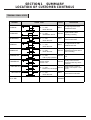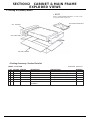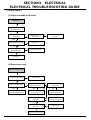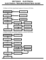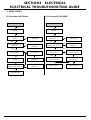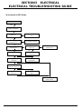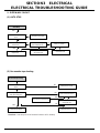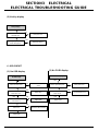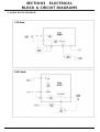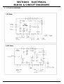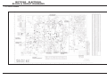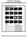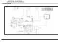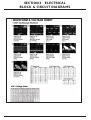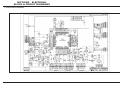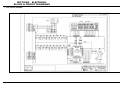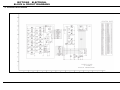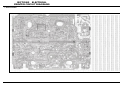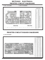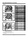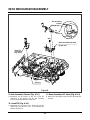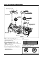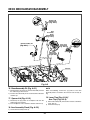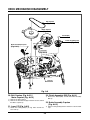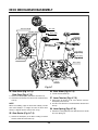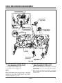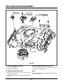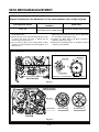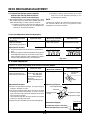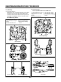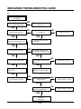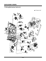
1
TIME LAPSE VCR
SERVICE MANUAL
CAUTION
BEFORE SERVICING THE UNIT, READ THE “SAFETY PRECAUTIONS”
IN THIS MANUAL.
MENU
REC
REW
F.F
REV
CUE
POWER / TIMER
MOVE
SEL
TRACKING
ALARM
UP
DOWN
KEY
LOCK
REC / PB SPEED
PAUSE / STILL
PLAY / REC CHK
STOP / EJECT
APRIL, 2006
Printed in Korea
2
TABLE OF CONTENTS
SECTION 1
SUMMARY
• SPECIFICATIONS ......................................................1-1
• LOCATION OF CUSTOMER CONTROLS .................1-2
• CRITICAL PARTS REPLACING TIME TABLE...........1-5
• CRITICAL PARTS DESCRIPTION .............................1-5
SECTION 2
CABINET & MAIN FRAME
EXPLODED VIEWS........................................................2-1
1. Cabinet and Main Frame Section ............................2-1
2. Packing & Accessory Section ..................................2-3
BLOCK & CIRCUIT DIAGRAMS....................................3-13
1. OVERALL WIRING DIAGRAM ...............................3-13
2. POWER BLOCK DIAGRAM ...................................3-15
3. POWER CIRCUIT DIAGRAM .................................3-17
4. AUDIO BLOCK DIAGRAM......................................3-19
5. Y/C BLOCK DIAGRAM ...........................................3-20
6. A/V CIRCUIT DIAGRAM.........................................3-21
7. SYSTEM BLOCK DIAGRAM ..................................3-24
8. SYSTEM CIRCUIT DIAGRAM................................3-27
9. JACK CIRCUIT DIAGRAM .....................................3-29
10. KEY-BOARD CIRCUIT DIAGRAM..........................3-31
PRINTED CIRCUIT DIAGRAMS ....................................3-33
1. MAIN P.C.BOARD ..................................................3-33
2. KEY 1 P.C.BOARD .................................................3-35
3. KEY 2 P.C.BOARD .................................................3-35
4. JACK P.C.BOARD ..................................................3-35
SECTION 3
ELECTRICAL
SECTION 4
MECHANISM
ELECTRICAL ADJUSTMENT PROCEDURES .............3-1
1. PG ADJUSTMENT..................................................3-1
ELECTRICAL TROUBLESHOOTING GUIDE ...............3-2
1. POWER(SMPS) CIRCUIT ......................................3-2
2. SERVO CIRCUIT....................................................3-4
3. Y/C CIRCUIT ..........................................................3-6
4. AUDIO CIRCUIT .....................................................3-9
5. SYSTEM/KEY CIRCUIT .........................................3-11
6. OSD CIRCUIT.........................................................3-12
NOTE) The table of contents for this section is edited
separately.
SECTION 5
REPLACEMENT PARTS LIST
• Mechanical Section.....................................................5-1
• Electrical Section ........................................................5-3
SECTION1 SUMMARY
SPECIFICATIONS
GENERAL
Head System
Power Source
Power Consumption
Back up time (clock)
Dimensions (WxHxD)
Operating Temperature
Operating Humidity
Timer
Weight
Tape Speed (NTSC)
Tape Speed (PAL)
Maximum Recording Time
Tape Width
Rewind Time
Video Signal System(PAL)
Video Signal System(NTSC)
Video Input
Video Output
Signal to Noise Ratio
Conventional audio
Input (LINE)
Output (LINE)
S/N Ratio
Frequency Range
Four head helical scan azimuth system
AC 100-240V, 50/60Hz
Approx. 15 Watts
30 days
14.2” x 3.7” x 10.7” (360 x 94 x 273 mm)
41 °F~105 °F (5 °C~40 °C)
Less than 80% RH
24-hour display type
Approx. 8.4 lb (3.8 kg)
11.12 mm/sec (6H) , 3.70 mm/sec (18H),
2.22 mm/sec (30H), 72H ~ 960H
11.695 mm/sec (6H) , 3.89 mm/sec (18H),
2.33 mm/sec (30H), 72H ~ 960H
6 hours (NT:T-120/PAL:E-180, 6H),
18 hours (NT:T-120/PAL:E-180, 18H),
30 hours (NT:T-120/PAL:E-180, 30H), 72H ~ 960H
0.5 in. (12.7 mm)
About 65 seconds (NT:T-120)(PAL:E-180)
CCIR Standard (625 lines, 50 fields)
PAL type color signal
EIA Standard (525 lines, 60 fields)
NTSC type color signal
1.0 Vp-p 75 ohms unbalanced
1.0 Vp-p 75 ohms unbalanced
More than 43 dB (6H mode)
-6.0 dBm more than 47 kohms
-6.0 dBm less than 1.5 kohms
More than 43 dB (6H mode)
200 Hz to 10kHz (6H mode)
* Designs and specifications are subject to change without notice.
* Weight and dimensions shown are approximate.
1-1
SECTION1 SUMMARY
LOCATION OF CUSTOMER CONTROLS
FRONT
1
2
3
4
5
6
7
8
9
POWER/TIMER BUTTON
MENU BUTTON
REC (RECORD) BUTTON
MOVE BUTTON
SEL (SELECT) BUTTON
DOWN BUTTON
UP BUTTON
ALARM INDICATOR
KEY LOCK INDICATOR
10 CASSETTE LOADING SLOT
11 CLEAR, KEY LOCK OFF, BUZZER OFF
12 CLOCK, COUNT, REMAIN
13 SHUTTLE RING
14 JOG RING
15 PAUSE/STILL BUTTON
16 PLAY/REC CHECK BUTTON
17 STOP/EJECT BUTTON
REAR
1 POWER CORD
2 AUDIO IN/OUT JACK
3 VIDEO IN/OUT JACK
4 RESET BUTTON
5 12-PIN TERMINAL BLOCK
1-2
SECTION1 SUMMARY
LOCATION OF CUSTOMER CONTROLS
INDICATOR PANEL
1
2
3
4
5
6
TIME LAPSE VCR TIME INDICATION
ALARM INDICATION
SERIES INDICATION
RECORD INDICATION
TIMER INDICATION
CASSETTE INDICATION
7 INDEX INDICATION
8 POWER FAILURE INDICATION
9 KEY LOCK INDICATION
10 REPEAT INDICATION
11 FUNCTION INDICATION
12 VCR FUNCTION INDICATION
VCR FUNCTION INDICATION
1-3
SECTION1 SUMMARY
LOCATION OF CUSTOMER CONTROLS
TERMINAL SIGNAL LEVELS
TERMINAL
SIGNAL LEVEL
IN/OUT
DESCRIPTION
1. ALARM IN
VIH : 4 ~ 5V
VIL : 0 ~ 0.6V
T : above 250 msec
INPUT
The input signal that makes
‘Alarm Record’ work
2. ALARM OUT
VIH : 4 ~ 5V
VIL : 0 ~ 0.6V
T : ALARM REC STATE
OUTPUT
Outputs whether ‘Alarm
Recording’ is working
3.ALARM RESET
VIH : 4 ~ 5V
VIL : 0 ~ 0.6V
T : above 250 msec
INPUT
The terminal that stops ‘Alarm
Record’ in Auto mode
5. SERIES IN
VIH : 4 ~ 5V
VIL : 0 ~ 0.6V
T : above 250 msec
INPUT
The input terminal to make
‘Series Record’ work
6. SERIES OUT
VIH : 4 ~ 5V
VIL : 0 ~ 0.6V
T : above 250 msec
Output signal appears when the
OUTPUT tape reaches to end or deck is
error in recording.
7. WARNING OUT
VIH : 4 ~ 5V
Outputs whether VCR deck is
VIL : 0 ~ 0.6V
OUTPUT
error.
T : until any-key is pressed
8. TRIGGER OUT
The signal is output which is used by
VIH : 4 ~ 5V, VIL : 0 ~ 0.6V
several cameras in
8 msec : NTSC
OUTPUT switching
general space with using camera
10 msec : PAL
multi-plexer.
10. LOW TAPE OUT
As the terminal that outputs that tape
VIH : 4 ~ 5V
less than 5 minutes in
OUTPUT remains
VIL : 0 ~ 0.6V
recording, it isn’t output in ‘1-shot
T : below 5 min, end of tape
Record’.
11. 1-SHOT REC IN
VIH : 4 ~ 5V
VIL : 0 ~ 0.6V
T : above 250 msec
INPUT
0V
COMMON
4, 9, 12. GND
-
1-4
The terminal that makes ‘1-short
Record’ work in Auto mode
SECTION1 SUMMARY
CRITICAL PARTS REPLACING TIME TABLE
No. DESCRIPTION
1
1500 3000 5000 6000 7500 9000 10000 12000 Test freatures
DRUM ASSY
Specification
RF out level
-4dB and below
2
ARM ASSY CLEANER
Wear status
Whether extraneous
matters come out
3
MOTOR CAPSTAN (D-35)
W/F(WTD)
0.4% and below
4
BELT CAPSTAN
Belt tension
Variation amount :
within 40%
5
BASE ASSY A/C
6
HEAD F/E
7
ARM ASSY IDLER
8
HOLDER ASSY PINCH
Audio and CTL out
level
The rate of erasing
(1KHz)
The capacity of ldler
for moving
Surrace solidity of
Roller
9
BAND ASSY TENSION
Back Torque
40~70 g
10
HOUSING ASSY
CST loading status
there shouldn’t be any space
betwween CST and compartment
11
CAPSTAN SOFT BRAKE
Felt wear
whether there is
touch noise
12
CLUTCHAY
Torque(Play, Rev)
40~140gcm, 100~210gcm
Reference :
Changing
Cleaning
-6dB and below
45dB min
4~12 g
60~90
Checking
Notes :
• Check the running path adjustment when you change the itens 1, 3, 5, 6 and 10.
• Check the back tension when you change Band Assy Tension.
CRITICAL PARTS DESCRIPTION
1.
Drum Ass’y
Consists of video head, rotary trans and motor. records video and audio information on
the tape, and play the tape back.(Audio information is recorded only on the Hi-Fi models)
2.
Arm Ass’y Cleaner
Cleans video head and rotation head automatically.
4.
Motor Capstan
Moves the tape with regular speed.
5.
Belt Capstan
Transfers rotative energy of capstan motor to the driving system.
6.
Brake Ass’y Capstan
Brakes rotative energy of capstan motor.
7.
Base Ass’y A/C
Consists of three head.
Audio erase head in the left upper erases audio signal in dubbing.
Audio head in the right upper records and playes the audio signal.
CTL head in the right lower records and detects CTL pulse to control tape speed.
8.
Head F/E
Is abbreviation of Full Erased Head.
erases the signal recorded on a tape clearly and absorb vibration of tape.
12. Arm Ass’y Idler
Is located between T/UP reel and supply reel.
Transfers ratative energy of capstan motor to T/UP reel or supply reel.
13. Holder Ass’y Pinch
Sticks a video tape to capstan motor and has the tape played without being
slipped from capstan motor axle.
14. Band Ass’y Tension
Has supply reel loosened properly with giving it some tensile force.
15. Arm Ass’y
Makes the cassette tape inserted be loaded and ejected precisly and safely.
16. Clutch Ass’y
Plays the tape with trasfering rotative energy of capstan motor to idler reel.
1-5
SECTION2 CABINET & MAIN FRAME
EXPLODED VIEWS
1. Cabinet and Main Frame Section
Cabinet & Main Frame Section Parts list
MODEL : TL-AT130M
S AL LOCA.NO. PART NO
A00
A42
A43
A44
A45
A46
6721R-0771U
6871R-8283A
3721R-F826D
6871R-4462A
6871R-7050B
3501R-7050B
250
260
277
278
280
281
283
284
285
286
300
320
3110R-S040F
3210R-0023A
4940R-Z075A
4940R-Z076B
3720R-F721D
524-013A
3580R-V090A
442-681A
4940R-Z086A
4940R-S017A
6410RZHV01A
3721R-D031N
323
325
330
3111R-0089B
4931R-0024D
3550R-0210A
452
457
462
353-051A
353-051E
353-136A
RUN DATE : 2004.03.12
DESCRIPTION
ASSEMBLY SECTION
DECK ASSEMBLY,VIDEO
PWB(PCB) ASSEMBLY,TOTAL
PANEL ASSEMBLY,FRONT
PWB(PCB) ASSY,TOTAL
PWB(PCB) ASSEMBLY,TOTAL
BOARD ASSEMBLY
PARTS SECTION
CASE
FRAME
KNOB
KNOB
PANEL,VIDEO
MAGNET
DOOR
SPRING
KNOB
KNOB
POWER CORD
PANEL ASSEMBLY,
DISTRIBUTOR[NOR
CASE ASSY
HOLDER ASSEMBLY
COVER
SCREW
SCREW,DRAWING
SCREW,DRAWING
SCREW,DRAWING
2-1
SPECIFICATION
DECK/MECHA D35 LG T/L (4HD(ALL
T/L VCR KEY2 JOG/SHUTTLE
CCD TIME LAPSE PANEL FRONT ASS
TL-AR30 (SERIES) - W. RS232C T/L VCR TL-AT130M MAIN
VCR TL-AT130M MAIN
LV-TL1960 2960 MOLD AIRHALL BA
VCR - MAIN
SHUTTLE(TL-AR30M)
CCD TL-AT130 MOLD
CCD LV-TL1960 S MOLD HIPS 40AF
VCR - ASSY DOOR
CCD TIME LAPSE MOLD DOOR CST
DOOR
CCD LV-TL124 MOLD
SLIDE (LV-TL24)
IT10S2(6A/250V) VOLEX IMMETRO
LV-TL1960S 2960S NEW ASSY (RSPRE-AMP (PBSB-SH)
DIGI(MONO-ENABLE)
BOTTOM(LARGE)
SPECIAL
SPECIAL (3X12)
SPECIAL(FBK) (353S353A)
REMARKS
SECTION2 CABINET & MAIN FRAME
EXPLODED VIEWS
1-1. Cabinet and Main Frame Section
Cabinet & Main Frame Section Parts list
ASSEMBLY PARTS SECTION
A42
6871RK5700K
Ass'y Front PCB
SNILN4T3526
A43
05503805
ASS'Y FRONT CAVINET
NTH960 C-TYPE
A44
6871R-4462A
Ass'y Ant. PCB
TL-AR30(SERIES)
A46
3501RK3200B
Ass'y Main PCB
CCD LV-TL1960
2-2
SECTION2 CABINET & MAIN FRAME
EXPLODED VIEWS
2. Packing & Accessory Section
✒ NOTE
Refer to “REPLACEMENT PARTSLIST” in order to look
for the part number of each part.
801 INSTRUCTION ASS’Y
803 : PACKING
804: SHEET ROLL
802: BOX CARTON
• Packing Accessory Section Parts list
MODEL : TL-AT130M
S AL LOCA.NO.
801
802
803
804
808
900
PART NO
3835RS0069N
3890R-C065K
3920R-E016A
3858R-S001A
534-008C
6711R1P041H
RUN DATE : 2004.03.12
DESCRIPTION
INSTRUCTION ASSEMBLY
BOX,MASTER
PACKING
SHEET (MECH)
BATTERY,MANGANESE
REMOTE CONTROLLER
ASSEMBLY
2-3
SPECIFICATION
REMARKS
CCD TL-AT330M-AABBDL1_ENG_POR_
TL-AT330M AABBDL . 1
Packing LV-TL24I 0.02 0 EPS 10
Packing LDPE 600M 630MM 0.5 VC
AAAM(R03) SEOTONG 1-5 V - 1PA
P9 LV-TL1960
SECTION3 ELECTRICAL
ELECTRICAL ADJUSTMENT PROCEDURES
1. PG ADJUSTMENT
MODE
SPECIFICATION
OBJECT MEASURED
OBJECT ADJUSTED
PLAYBACK IN SP
PG : 416 ± 20 sec
V.OUT JACK
VR501
1. Connect CH-1 of the oscilloscope to W357 and W362,
and adjust it to 1Vp-p as TRIGGER.
(In case of 10:1 Probe, adjust it 50m Vp-p)
2. Connect CH-2 of the oscilloscope to V.OUT JACK and
adjust it to 0.5Vp-p.
(In case of 10:1 Probe, adjust it 50 Vp-p)
3. Adjust time of the oscilloscope to 0.1 msec.
4. Adjust the range between FLLING EDGE part of video
vertical trigger signal and video vertical trigger signal
to the specification(416±20 sec) with changing VR501.
WAVEFORM
• CONNECTION CHART OF MAIN PWB
Fig 3-1. Connection chart of PG adjustment
✒ Caution
When repairing the power part just after pulling out the power code, there is hazard of electical shock caused by the
charged electricity at the peripheral circuit component(primary power) such as condenser C807(150µF). So begin
repairing after doing procedure below.
1. Set the volt meter up to resistance measurement.(In case of digital volt meter, set it up to over 20MΩ.)
2. Discharge electicity with putting the measuring terminal lines(+, 1 probe) of volt meter at the ends of condenser
C103.(You don’t have to put the polarity of the measuring terminal lines on the same polarity of the condenser.)
3-1
SECTION3 ELECTRICAL
ELECTRICAL TROUBLESHOOTING GUIDE
1. Power Circuit(SMPS)
(1) No 5.3 A
(2) No 9V
No 5.3V
Is F101 normal?
No 12V
NO
Replace F101(Use a specified
Is D109 normal?
fuse).
YES
Is BD101 normal?
NO
Is Q170 normal?
Replace BD101.
NO
Replace Q170
YES
NO
Replace R101.
Is D110 normal?
NO
Replace D110
YES
YES
Is there Vcc (about 13~19V) at
Check/Replace D109
YES
YES
Is R101 normal?
NO
NO
IC101 pin 5?
NO
Is D103 normal?
Is Q152 normal?
Replace Q152
YES
NO
Check/
Check/ Replace Q163
Replace D103
YES
Is D106 normal?
NO
Replace D106.
(3) No 24 V
YES
Is there about 2.5V at
NO
IC103 pin 1?
No 24V
Replace IC103.
YES
Is D109 normal?
NO
Replace D109.
Is D110 normal?
Check/Replace D110
YES
YES
Is L103 normal?
NO
NO
Is Q159 normal?
Is L103 normal?
YES
YES
Check the power terminal at main
Check ‘H’ signal at Q161
Base terminal
PCB short.
3-2
NO
Check/Replace Q152
SECTION3 ELECTRICAL
ELECTRICAL TROUBLESHOOTING GUIDE
(4) No 5.2 A (TO AVCP, BIAS)
(5) No 10V
No 5.2V
Is D106 normal?
No 10V
NO
Is D109 normal?
Replace D106.
YES
Is Q153 normal?
Replace D109
YES
NO
Is Q170 normal?, Is there about
Replace Q153.
13.5V at Q107 Base?
YES
YES
Is there voltage (about 0V)
NO
NO
Check/ Replace
Replace Q157.
at Q157 collector.
D155, D156, D157/\.
YES
Check/
Replace Q156
3-3
NO
Check/ Replace
Q107, ZD103
SECTION3 ELECTRICAL
ELECTRICAL TROUBLESHOOTING GUIDE
2. SERVO CIRCUIT
(1) Video is unstable in PB mode
In PB mode
Does noise level on the screen
change periodically?
YES
Does CTL pulse appear at
NO
IC501 Pin 76?
NO
Is adjusting height of CTL
Readjust the height
of CTL fead.
head accurate?
YES
NO
Replace IC501.
Does CTL pulse move on tracking?
YES
Does Video Envelope wave form
NO
appear at IC501 pin 86?
Check the Pre-Amp circuit
YES
Replace IC501.
(2) Drum motor stops
When the drum moter stop
NO
Is there 12V at PMC01 Pin8?
Check Power circuit
YES
NO
Is there 2.8V at PMC01 Pin12?
YES
NO
Does Drum PWM pulse
PMC01 Pin3?
appear at IC501 Pin34?
YES
Does DFG pulse appear at
YES
NO
Check the Ass’s between
Aren’t pattern or componets between
Check the Ass’y between
connector(PMC01) and Drum motor
IC501 Pin34 and PMC01 Pin12 short?
junction PCB and Drum motor
Does DFG pulse appear at
IC501 Pin65?
NO
Aren’t pattern or componets between
IC501 Pin34 and PMC12 Pin1 short?
YES
Does Drum PWM pulse appear
NO
at IC501 Pin34?
YES
Aren’t pattern or componets between
IC501 Pin34 and PMC01 Pin12 short?
3-4
Replace IC501
SECTION3 ELECTRICAL
ELECTRICAL TROUBLESHOOTING GUIDE
(3) Capstan motor stops
When the capstan motor stops
Is it 12VA at PMC01 Pin2?
NO
Check Power circuit
YES
NO
Is there 2.8V at PMC01 Pin9?
Does PWM signal appear at IC501 Pin 33?
YES
YES
Check the Ass’y between PMC01
NO
and Capstan motor
YES
Aren’t pattern or componets between
Does CFG signal appear at PMC01 Pin1?
IC501 Pin33 and PMC01 Pin9 short?
YES
NO
Check the Ass’y of Capstan motor
Check CFG signal appear at IC501
NO
Pin67?
Aren’t pattern or componets between IC501 Pin67 and
PMC01 Pin1 short?
YES
Does Capstan PWM signal appear
at IC501 Pin33?
NO
Replace IC501
YES
Aren’t pattern or componets between
IC501 Pin33 and PMC01 Pin1 short?
3-5
SECTION3 ELECTRICAL
ELECTRICAL TROUBLESHOOTING GUIDE
3. Y/C CIRCUIT
(1) No Video in EE Mode
No Video in EE Mode
Does the Video signal appear at the NO
Check the Video input Jack &
IC3G1 Pin9?
jack Board connection.
YES
Does the Video signal appear
NO
Check the IC3G1 Pin14
at the IC301 Pin38?
and Q3G1 emitter.
YES
Is 5V applied to the
NO
Check the 5VA Line.
IC301 Pin16, 40, 55, 58, 75, 87?
(Power Circuit)
YES
Does the Video signal appear
NO
at the IC301 Pin29?
NO
IC301 Pin 23, 24?
NO
at the IC501 Pin 47?
Check the path of the signal between
NO
the IC301 Pin29 and IC501 Pin49.
YES
Does the Video signal appear at
the Emitter terminal of the Q380?
Check the System Circuit. (Refer to
2
‘SYSTEM I C BUS Trouble Shooting’)
YES
YES
Does the Video signal appear
2
Is I C BUS signal applied to the
Check C316.(AGC)
YES
NO
Is there 9V on the plus
NO
terminal of the C381?
Replace the IC301.
YES
Check the 9V Line.
Replace the Q380.
(Power Circuit)
3-6
SECTION3 ELECTRICAL
ELECTRICAL TROUBLESHOOTING GUIDE
(2) When the Y(Luminance)signal doesn’t appear on the screen in PB Mode.
Is 5V applied to the IC301
Pin 16, 40, 55, 58, 87?
Is the I2C Bus signal applied
NO
Check the line of the 5.3VA
Line. (Power Circuit)
NO
Check the System Circuit. (Refer to
2
to the IC301 Pin 23, 24?
‘SYSTEM I C BUS Trouble Shooting’)
YES
Does the normal RF signal
NO
appear at the IC301 Pin74?
Is the V.H.S/W "H" about
NO
Check the System Circuit.
(IC501 Pin 23)
3.4V to the IC301 Pin11 ?
YES
Is V.H.S/W "H" about 3.4V at the
NO
IC301 Pin 11?
YES
Check the V.H.S/W level.
(Check R304, R305)
YES
NO
Clean the Drum.
Does the Y(Luminance) RF signal
NO
appear at the IC301 Pin 17?
Check the path of the Y(Luminance)
Replace the IC301.
YES
RF signal.(Check the Q301)
YES
Is the Y(Luminance) Video waveform
showed up at the IC301 Pin 41?
NO
Check the path of the Y(Luminance)
YES
RF signal.(Check Q302, Q303)
YES
Replace the IC301.
3-7
SECTION3 ELECTRICAL
ELECTRICAL TROUBLESHOOTING GUIDE
(3) When the C(Color) signal doesn't appear on the screen in PB Mode
NO
Is 5V applied to the IC301
Pin 16, 40, 55, 58, 87?
Is the Color Rotary signal applied to
Check the line of the 5.3VA
Line. (Power Circuit)
NO
Check the Color Rotary
the IC301 Pin 10?
Circuit. (IC501 pin 98)
YES
NO
Is Color Rotary "H" about
Check the Color Rotary level.
1.6V?
(Check the R302, R303)
YES
Does the Color signal appear at
the IC301 Pin 71?
NO
Does the X301(4.43MHz) or
NO
X302(3.58MHz) oscillate?
Replace the X301 or the X302.
YES
Does the Color signal appear
NO
YES
Check the Color Pass.
(Check the Q304)
at the IC301 Pin 61?
YES
Check the circuit of the
Replace the IC301.
NO
Replace the IC301.
IC301 Pin 35, 62.
(4) When the Video signal doesn't appear on the screen in REC Mode.
Is the EE signal normal?
Is 5V applied to the IC301
NO
Check EE Mode.
NO
Pin 16, 40, 55, 58, 87?
Check the line of the 5.3VA
Line.(Power Circuit)
YES
Does PB Mode operate
NO
Check PB Mode.
normally?
YES
Does the RF signal appear at
the IC301 Pin 12?
NO
Is the REC 'H' signal (about
NO
4V)applied to the IC301 Pin 30?
Check the System of REC 'H'
(the IC501 Pin 30 / the D301)
YES
Check REC Luminance
the IC301 Pin90?
Replace the IC301.
Pass & Color Pass.
YES
Does the REC RF signal appear at
YES
NO
Check the circuit of the
YES
IC301 Pin 90, 92, 94
YES
Check the Drum &
Drum Connector
3-8
SECTION3 ELECTRICAL
ELECTRICAL TROUBLESHOOTING GUIDE
4. AUDIO CIRCUIT
(1) No sound in EE Mode
(2) No sound in PB MODE
No sound in EE Mode.
No sound in PB Mode.
YES
YES
No sound.
No sound.
YES
YES
NO
Is 5V applied to the IC301
Pin 75?
Check the line of the 5V Line.
Is 5V applied to the
(Power Circuit)
IC301 Pin 75?
NO
Check the line of the 5V Line.
(Power Circuit)
YES
YES
Is the Audio signal applied to the
NO
IC301 Pin 76?
2
Does the CLK/Data signal(I C)
Check the path of
appear at the IC301 Pin 23, 24?
LINE/AUDIO.
YES
YES
Does the Audio signal appear
at the IC301 Pin 96?
NO
NO
Check the connecting State between
to the IC301 Pin 10?
the P3D02 Pin 6 and A/C Head.
out Jack.
(Audio Mute "H".)
at the IC301 Pin 96?
NO
YES
Check the IC501 Pin18(CLK),
NO
YES
YES
Does the Audio signal appear
appear at the IC301 Pin 23, 24?
NO
at the IC301 Pin 1?
Check the IC501 Pin 2.
2
17(Data) Line.
Does the Audio signal appear
Check the connection of the Audio
Does the CLK/Data signal(I C)
Check the IC501 Pin 18(CLK),
Is the Audio Mute "High" signal applied
YES
YES
NO
Replace the IC301
17(Data) Line.
YES
Replace the IC301
3-9
Is the Audio Mute "H" applied to
the IC301 Pin 10?
NO
YES
Check the IC501 Pin2.
SECTION3 ELECTRICAL
ELECTRICAL TROUBLESHOOTING GUIDE
(3) No sound in REC Mode.
NO sound in REC Mode.
YES
Sound is not recorded.
YES
Is Playback O.K.?
NO
Refer to "No sound in PB
Mode,".
YES
Is the Audio signal applied
NO
Check the path of Line Audio.
to the IC301 Pin 76?
YES
Does the Audio waveform appear
NO
Is the “High” signal applied to the
NO
IC301 Pin 10?
at the IC301 Pin 7?
YES
Check the CLK/Date line and
replace the IC301
YES
Is 5V applied to the FL401
Check the IC501 Pin 96
Pin 2?
YES
(Audio Mute “H”).
NO
Check the line of the 5V
Power Circuit.
Is 3.0~4.5V applied to the Emitter
of the Q481?
YES
NO
Does the Erase signal
appear at the FL401 Pin 6?
YES
NO
Replace the FL401 or the
Q405.
Is the Voltage level of the IC301
Pin6 850mVp-p?
NO
Check the Audio R/P/E
connector and Head.
3-10
SECTION3 ELECTRICAL
ELECTRICAL TROUBLESHOOTING GUIDE
5. SYSTEM/KEY CIRCUIT
(1) AUTO STOP
Auto Stop
YES
Does SW waveform appear at IC501 NO
pin23?
Check Drum motor signal
YES
Does T/up reel pulse appear
at IC501 Pin27?
YES
NO
Does T/up reel pulse appear
NO
Is there 5.3V at RS501?
at Q514 Base terminal?
YES
NO
YES
Replace T/up reel sensor of deck
Replace IC501
Check DP06, LP03
Check power circuit
(2) No cassette tape loading
No cassette tape loading
YES
NO
Is there REG. 12V at PMCQ1
Pin8?
Check power circuit L104.
YES
NO
Does 'H' signal appear at IC501
Is there 5.3V at IC501 Pin73?
Pin62 while inserting CST?
YES
Check CST SW and peripheral circuit
Check power circuit
NO
YES
NO
Check D106, L103.
Check IC501 Pin7, 8, 9, 10
Check Deck mechanism
*Caution : Auto stop can occur because Grease or Oil is dried up
3-11
SECTION3 ELECTRICAL
ELECTRICAL TROUBLESHOOTING GUIDE
(3) No Key display
No Key display
YES
Is there 5.2VA at IC501
Pin79, 80, 81?
NO
Check power circuit
YES
As pressing the byttons doeseach
NO
Replace bad switches
function work properly?
6. OSD CIRCUIT
(2) No F.OSD display.
(1) No OSD display.
No F.OSD display.
No OSD display.
YES
YES
Is there 5.3V IC501 Pin 51?
NO
Check 5.3V Line of power
Refer to “(5) No OSD picture”
NO
Does video signal appear at
Replace X502.
IC501 Pin 50?
IC501 PIns 37, 38?
YES
YES
NO
Check peripheral circuit and
replace X501
Does oscillation appear at the
IC501 Pins 40, 41?
Replace IC501
YES
NO
Does Video signal appear at the
IC501 Pin 47?
Check power Vcc 9V
YES
YES
Does oscillation appear at the
NO
circuity.
Check the signal between
IC501 Pin47 and V.out Jack.
YES
Replace IC501.
3-12
NO
Check the signal between IC301
Pin 29 and IC501 Pin 49.
SECTION3 ELECTRICAL
BLOCK & CIRCUIT DIAGRAMS
1. OVERALL WIRING DIAGRAM
3-13
3-14
SECTION3 ELECTRICAL
BLOCK & CIRCUIT DIAGRAMS
2. POWER BLOCK DIAGRAM
3-15
3-16
SECTION3 ELECTRICAL
BLOCK & CIRCUIT DIAGRAMS
3. POWER CLRCUIT DIAGRAM
3-17
3-18
SECTION3 ELECTRICAL
BLOCK & CIRCUIT DIAGRAMS
4. AUDIO BLOCK DIAGRAM
3-19
SECTION3 ELECTRICAL
BLOCK & CIRCUIT DIAGRAMS
5. Y/C BLOCK DIAGRAM
3-20
SECTION3 ELECTRICAL
BLOCK & CIRCUIT DIAGRAMS
6. A/V CIRCUIT DIAGRAM
3-21
3-22
SECTION3 ELECTRICAL
BLOCK & CIRCUIT DIAGRAMS
3-23
SECTION3 ELECTRICAL
BLOCK & CIRCUIT DIAGRAMS
7. SYSTEM BLOCK DIAGRAM
3-24
3-25
SECTION3 ELECTRICAL
BLOCK & CIRCUIT DIAGRAMS
3-26
SECTION3 ELECTRICAL
BLOCK & CIRCUIT DIAGRAMS
8. SYSTEM CLRCUIT DIAGRAM
3-27
3-28
SECTION3 ELECTRICAL
BLOCK & CIRCUIT DIAGRAMS
9. JACK CLRCUIT DIAGRAM
3-29
3-30
SECTION3 ELECTRICAL
BLOCK & CIRCUIT DIAGRAMS
10. KEY-BOARD CLRCUIT DIAGRAM
3-31
3-32
SECTION3 ELECTRICAL
PRINTED CIRCUIT DIAGRAMS
1. MAIN P.C.BOARD
3-33
3-34
SECTION3 ELECTRICAL
PRINTED CIRCUIT DIAGRAMS
2. KEY 1 P.C.BOARD
3. KEY 2 P.C.BOARD
PRINTED CIRCUIT BOARD DIAGRAMS
4. JACK P.C.BOARD
3-35
SECTION 4 MECHANISM
CONTENTS
DECK MECHANISM PARTS
LOCATIONS
• Top View......................................................4-1
• Bottom View ...............................................4-1
DECK MECHANISM
DISASSEMBLY
1. Drum Assembly .........................................4-2
2. Plate Top ...................................................4-4
3. Holder Assembly CST ...............................4-4
4. Opener Door .............................................4-4
5. Bracket Assembly L/D Motor.....................4-4
6. Gear Assembly Rack F/L ..........................4-4
7. Arm Assembly F/L .....................................4-4
8. Lever Assembly S/W .................................4-4
9. Arm Assembly Cleaner..............................4-5
10.Head F/E ...................................................4-5
11. Base Assembly A/C Head .........................4-5
12.Brake Assembly T .....................................4-6
13.Brake Assembly RS ..................................4-6
14.Arm Assembly Tension..............................4-6
15.Reel S / Reel T..........................................4-6
16.Base Assembly P4 ....................................4-7
17.Opener Lid ................................................4-7
18.Arm Assembly Pinch .................................4-7
19.Lever T/up / Arm T/up ...............................4-7
20.Belt Capstan/Motor Capstan .....................4-8
21.Lever F/R ..................................................4-8
22.Clutch Assembly D35 ................................4-8
23. Brake Assembly Capstan .........................4-8
24.Gear Drive/Gear Cam ...............................4-9
25.Gear Sector...............................................4-9
26.Plate Slider................................................4-9
27.Lever Tension ............................................4-9
28.Lever Spring..............................................4-9
29.Gear Assembly P2/
Gear Assembly P3 ..................................4-10
30.Base Assembly P2/
Base Assembly P3 ..................................4-10
31.Base Loading ..........................................4-11
32.Base Tension ...........................................4-11
33.Arm Assembly Idler .................................4-11
DECK MECHANISM ADJUSTMENT
• Tools and Fixtures for Service ...............4-12
1. Mechanism Alignment Position Check....4-13
2. Preparation for Adjustment......................4-14
3. Checking Torque .....................................4-14
4. Guide Roller Height Adjustment..............4-15
4-1. Preliminary Adjustment ....................4-15
4-2. Precise Adjustment ..........................4-15
5. Audio/Control (A/C) Head Adjustment ....4-16
5-1. Preliminary Adjustment ....................4-16
5-2. Confirmation of Tape Path between
Pinch Roller and Take-up Guide ......4-17
5-3. Precise Adjustment(Azimuth Adjustment)
.........................................................4-17
6. X-Value Adjustment .................................4-17
7. Adjustment after Replacing Drum Assembly
(Video Heads) .........................................4-18
8. Check the Tape Travel after Reassembling
Deck Mechanism.....................................4-18
8-1. Checking Audio and RF Locking Time
during Playback after CUE or REV
.........................................................4-18
8-2. Checking for Tape Curling or
Jamming ..........................................4-18
MAINTENANCE/INSPECTION
PROCEDURE
1.
2.
3.
4.
Check before starting Repairs ................4-19
Required Maintenance ............................4-20
Scheduled Maintenance..........................4-20
Supplies Required for Inspection and
Maintenance............................................4-20
5. Maintenance Procedure ..........................4-20
5-1. Cleaning...........................................4-20
5-2. Greasing ..........................................4-21
MECHANISM TROUBLESHOOTING
GUIDE
1. Deck Mechanism.....................................4-23
2. Front Loading Mechanism.......................4-26
EXPLODED VIEWS
1. Front Loading Mechanism Section .........4-28
2. Moving Mechanism Section (1)...............4-29
3. Moving Mechanism Section (2)...............4-30
DECK MECHANISM PARTS LOCATIONS
• Top View
Procedure
Starting
No.
1
2
2
3
2
4
5
2
6
3
7
4
9
5
11
10
18
1
16
31
17
19
19
12
14
15
8
13
33
20, 21
• Bottom View
20
24
30
29
29
23
30
20
25
32
27
26
28
24
22
21
20,21,23,
24,25
20,21,23,
24,25,26
2,3,14,20,
21,25,23,
24,26
25
2,3,14,25,
29
2,3,14,25,
29
2,3,14
2,3,20,21,
22
T
T
T
T
T
1 Hook, Chassis Hole
Chassis Hole
1 Hook
Chassis Embossing
Chassis Embossing
1 Screw
1 Hook
1 Hook
2 Hook
A-2
A-2
A-2
A-3
A-3
A-3
A-4
A-4
A-4
A-4
T
T
T
T
T
T
T
T
T
T
Base Assembly P4
Opener Lid
Arm Assembly Pinch
Lever T/Up / Arm T/Up
Chassis Embossing
Chassis Embossing
Shaft
1 Hook
A-5
A-5
A-5
A-5
T
T
T
T
Belt Capstan/Motor Capstan
Lever F/R
Clutch Assembly D35
Brake Assembly Capstan
Gear Drive/Gear Cam
Gear Sector
Plate Slider
3 Screw
Locking Tab
Washer
Locking Tab
Washer/Hook
1 Hook
Shaft Guide
A-6
A-6
A-6
A-6
A-7
A-7
A-7
B
B
B
B
B
B
B
27 Lever Tension
1 Hook
A-7
B
28 Lever Spring
Locking Tab
A7
B
29 Gear Assembly P2/Gear Assembly P3 Boss
30 Base Assembly P2/Base Assembly P3 Chassis Slot
A-8
A-8
B
B
31 Base Loading
1 Screw
A-9
T
32 Base Tension
33 Arm Assembly Idler
Chassis Embossing
Locking Tab
A-9
A-9
B
T
21
22
23
24
25
26
T:Top, B:Bottom
NOTE : When reassembly perform the
procedure in the reverse order.
1) When reassembling, confirm Mechanism and Mode
Switch Alignment Position (Refer to Page 4-13)
2) When disassembling, the Parts for Starting No. Should
be removed first.
4-1
Fig- Viure ew
A-1
A-2
A-2
A-2
A-2
6
7
8
9
10
11
2,3
12
2,3
13
2,3
14
2,3,12,13, 15
14
16
17
17
18
17
19
17,18
20
Drum Assembly
Plate Top
Holder Assembly CST
Opener Door
Bracket Assembly
L/D Motor
Gear Assembly Rack F/L
Arm Assembly F/L
Lever Assembly S/W
Arm Assembly Cleaner
Head F/E
Base Assembly A/C Head
Brake Assembly T
Brake Assembly RS
Arm Assembly Tension
Reel S/Reel T
Fixing Type
3 Screw
2 Hook
Chassis Hole
Chassis Hole
3 Hook
2,3,4
2,3,4,6
15
Part
DECK MECHANISM DISASSEMBLY
Stator
(S2)
(S2)
(S3)
Drum Motor
(S3)
Rotor
Drum Sub Assembly
(Fig. A-1-1)
(A)
Drum FPC
Carbon Brush
(S1)
(S1)
(S1)
H2
H1
Holder FPC
Fig. A-1
(Fig. B-1)
1. Drum Assembly (Fig. A-1-1)
1) Unplug the Drum FPC Connector.
2) Remove three Screws(S1) on bottom side and separate
the Drum assembly.
3) Unhook (H1), (H2) and separate the Holder FPC and
Cap FPC.
Cap FPC
1-1. Drum Motor
1) Remove two Screws(S2) and disassemble the Stator of
the Drum Motor.
2) Remove two Screws(S3) and separate the Rotor of the
Drum Motor from the Drum Sub assembly.
Drum FPC
Holder FPC
NOTE
When reassembling, confirm (A) portion of the Drum Sub
assembly whether the Carbon Brush is in there or not.
4-2
Figure in the opposite direction
DECK MECHANISM DISASSEMBLY
Plate Top
(Fig. A-2-1)
(C)
(B')
(B)
Holder Assembly CST
(Fig. A-2-2)
(E)
Arm Assembly F/L
(Fig. A-2-6)
Lever Assembly S/W
(Fig. A-2-7)
(H8)
(C1)
Bracket Assembly L/D Motor
Spring Lever S/W
(Fig. A-2-4)
(C')
(D)
(E')
Opener Door
(Fig. A-2-3)
(H6)
Chassis
(A)
Gear Assembly Rack F/L
(Fig. A-2-5)
Fig. A-2
4-3
(B)
DECK MECHANISM DISASSEMBLY
2. Plate Top (Fig. A-2-1)
1) Pull the (B) portion of the Plate Top back in direction of
arrow and separate the right side of it.
2) pull the (B’) portion of the Plate Top back in direction of
arrow and separate the left side of it.
(Used tools : (-) type driver, anything tool with sharp
point or flat point.)
2) Unhook three Hooks(H3, H4, H5) on bottom side of the
Chassis, lift up the Bracket Assembly L/M and disassemble the Bracket Assembly L/D Motor.
(H4)
Bracket assembly L/M
(H3)
NOTE
(1) When reassembling, push the Plate Top after alignment
the two position(C), (C’) as below Fig.
6. Gear Assembly Rack F/L (Fig. A-2-5)
(C')
1) Move the Gear Assembly Rack F/L in direction of
arrow(A) and unhook the Hook(H6) pulling back in front.
2) Separate the Gear Rack F/L in direction of arrow(B).
(C)
(B')
(H5)
(B)
NOTE
When reassembling, align the gear part of the Gear
Assembly Rack F/L with the Gear Drive as below Fig.
Gear Rack F/L
3. Holder Assembly CST (Fig.A-2-2)
1) Move the Holder Assembly CST in direction of arrow and
separate the left side of it first through the (D) position of
the Chassis.
Holder assembly CST
Chassis
Gear Drive
7. Arm Assembly F/L (Fig. A-2-6)
(D)
1) Move the Arm Assembly F/L in direction of arrow and
separate the left side of it first.
2) Disassemble the Arm Assembly F/L from each guided
hole of the Chassis.
2) Disassemble the right side of the Holder Assembly CST
from each guided hole of the Chassis.
NOTE
8. Lever Assembly S/W(Fig. A-2-7)
1) Unhook the Hook(H8) in the left side of the Chassis and
remove the Lever Assembly S/W.
When reassembling, insert the (E) part of the Holder
Assembly CST in the (E’) hole of the Chassis first and
assemble the left side of it.
Chassis
4. Opener Door (Figure. A-2-3)
1) Turn the Opener Door clockwise and remove it through
the guide hole of the Chassis.
5. Bracket Assembly L/D Motor
(Fig. A-2-4)
1) Unplug the Connector(C1).
4-4
(H8)
DECK MECHANISM DISASSEMBLY
Arm Assembly
Cleaner
(Fig. A-3-1)
(A)
(S4)
Base Assembly A/C Head
(A)
(Fig. A-3-3)
Head F/E
(Fig. A-3-2)
Chassis
Fig. A-3
9. Arm Assembly Cleaner (Fig. A-3-1)
11. Base Assembly A/C Head (Fig. A-3-3)
1) Breakaway the (A) portion as Fig. A-3-1 from the
embossing of the Chassis, turn the Arm assembly
Cleaner to clockwise direction and lift it up.
1) Remove the Screw(S4) and lift the Base Assembly A/C
Head up.
10. Head F/E (Fig. A-3-2)
1) Breakaway the (A) portion of the Head F/E from the
embossing of the Chassis, turn it to counterclockwise
direction and lift it up.
4-5
DECK MECHANISM DISASSEMBLY
Arm Assembly Tension
(Fig. A-4-3)
(H11)
Spring TB
Brake Assembly T
(Fig. A-4-1)
Spring Tension
Reel S
Reel T
(Fig. A-4-4)
(Fig. A-4-4)
Spring RS
Brake Assembly RS
(Fig. A-4-2)
(H12)
(H9)
(H10)
Base Tension
Chassis
Fig. A-4
12. Brake Assembly T (Fig. A-4-1)
NOTE
1) Unhook the Spring TB from the Hook(H9) of the Chassis.
2) Lift the Brake Assembly T up.
Difference for Springs
Spring TB
Spring RS
Color (Black)
Spring Tension
13. Brake Assembly RS (Fig. A-4-2)
1) Unhook the Spring RS from the Hook(H10) of the
Chassis.
2) Lift the Brake Assembly T up.
15. Reel S / Reel T (Fig. A-4-4)
1) Difference for Reel S / Reel T
14. Arm Assembly Tension (Fig. A-4-3)
1) Unhook the Spring Tension from the Hook(H11) of the
Arm Assembly Tension.
2) Unhook the Hook(H12) of the Base Tension and lift the
Arm Assembly Tension up.
Reel S
4-6
Reel T
DECK MECHANISM DISASSEMBLY
Opener Lid
(Fig. A-5-2)
(B)
(B)
Arm
Assembly
Pinch
(Fig. A-5-3)
(C)
Base Assembly P4
Lever T/up
(Fig. A-5-1)
(Fig. A-5-4)
(H13)
(C)
Arm T/up
(H13)
(Fig. A-5-5)
(A)
Chassis
Fig. A-5
16. Base Assembly P4 (Fig. A-5-1)
NOTE
1) Breakaway the (A) portion of the Base Assembly P4 from
the embossing of the Chassis.
2) Turn the Base Assembly P4 to counterclockwise direction
and lift it up.
When reassembling, confirm the (C) portion of the Arm
Assembly Pinch is inserted to the Chassis hole correctly as
Fig.
17. Opener Lid (Fig. A-5-2)
19. Lever T/up (Fig. A-5-4)/
Arm T/up (Fig. A-5-5)
1) Breakaway the (B) portion of the Opener Lid from the
embossing of the Chassis.
2) Turn the Opener Lid to clockwise direction and lift it up.
1) Unhook the Hook(H13) of the bottom Chassis and lift the
Lever T/up up.
2) Lift the Arm T/up up.
18. Arm Assembly Pinch (Fig. A-5-3)
1) Lift the Arm Assembly Pinch up.
4-7
DECK MECHANISM DISASSEMBLY
Belt Capstan
(Fig. A-6-1)
Motor Capstan
(Fig. A-6-2)
Washer(W1)
Clutch Assembly D35
(Fig. A-6-4)
(L1)
(L1)
Brake Assembly Capstan
(Fig. A-6-5)
Lever F/R
(Fig. A-6-3)
(L2)
Chassis
(S5)
Fig. A-6
22. Clutch Assembly D35 (Fig. A-6-4)
20. Belt Capstan (Fig. A-6-1)/
Motor Capstan (Fig. A-6-2)
1) Remove the Belt Capstan.
2) Remove the three Screws(S5) on bottom Chassis and lift
the Motor Capstan up.
21. Lever F/R (Fig. A-6-3)
1) Unlock the Locking Tab(L1) as Fig. A-6-3 and lift the
Lever F/R up.
1) Remove the Washer(W1) and lift the Clutch Assembly
D35 up.
23. Brake Assembly Capstan
(Fig. A-6-5)
1) Pull the Locking Tab(L2) back in direction of arrow and lift
it up.
4-8
DECK MECHANISM DISASSEMBLY
(H14)
Gear Cam Hole(B)
Gear Drive Hole(A)
Gear Cam
(Fig. A-7-2)
Gear Sector
Washer (W2)
(Fig. A-7-3)
Plate Slider
Gear Drive
(Fig. A-7-4)
(Fig. A-7-1)
(A)
Lever Tension
(Fig. A-7-5)
Lever spring
(L3)
(Fig. A-7-6)
Gear Drive Hole(C)
Base Loading
(H15)
(H16)
Chassis
Fig. A-7
24. Gear Drive (Fig. A-7-1)/
Gear Cam (Fig. A-7-2)
26. Plate Slider (Fig. A-7-4)
1) Just lift the Plate Slider up.
1) Remove the Washer(W2) and lift the Gear Drive up.
2) Unhook the Hook(H14) of the Gear Cam and lift the Gear
Cam up.
NOTE
When reassembling, align the Gear Drive Hole(A) and the
Gear Cam Hole(B) in a straight line after the Gear Drive
Hole(C) is aligned with the Chassis Hole as Fig.
27. Lever Tension (Fig. A-7-5)
1) Unhook the (A) portion of the Lever Tension from the
Hook(H16) of the Chassis.
2) Turn the Lever Tension to counterclockwise direction and
lift it up.
28. Lever Spring (Fig. A-7-6)
1) Unlock the Locking Tab(L3) of the bottom Chassis and lift
the Lever Spring up.
25. Gear Sector (Fig. A-7-3)
1) Unhook the Hook(H15) of the Base Loading on bottom
Chassis and lift the Gear Sector up.
4-9
DECK MECHANISM DISASSEMBLY
Gear Assembly P2 Hole
Gear Assembly P3 Hole
Gear Assembly P3
(Fig. A-8-2)
Lever Spring Boss
Gear Sector Hole(A)
Gear Assembly P2
Plate Slider Hole(B)
(Fig. A-8-1)
(B)
(A)
Chassis
Base Assembly P3
(Fig. A-8-4)
Base Assembly P2
Fig. A-8
(Fig. A-8-3)
29. Gear Assembly P2 (Fig. A-8-1)/
Gear Assembly P3 (Fig. A-8-2)
30. Base Assembly P2 (Fig. A-8-3)/
Base Assembly P3 (Fig. A-8-4)
1) Just lift the Gear Assembly P2 up.
2) Just lift the Gear Assembly P3 up.
1) Move the Base Assembly P2 in direction of arrow(A)
along the guide hole of the Chassis and disassemble it
on bottom side.
2) Move the Base Assembly P3 in direction of arrow(B)
along the guide hole of the Chassis and disassemble it
on bottom side.
NOTE
When reassembling, align the two holes of the Gear
Assembly P2 and P3 in a straight line after confirmation
whether the Gear Sector Hole(A) and the Plate Slider
Hole(B) are aligned or not as Fig.
4-10
DECK MECHANISM DISASSEMBLY
Base Tension
(S7)
Base Loading
(Fig. A-9-2)
Arm Assembly Idler
(Fig. A-9-1)
(A)
(B)
(Fig. A-9-3)
(C)
(D)
Chassis
Fig. A-9
31. Base Loading (Fig. A-9-1)
33. Arm Assembly Idler (Fig. A-9-3)
1) Remove the Screw(S7).
2) Lift the Base Loading up.
1) Make narrower the two parts, (B) and (C), as Fig. A-9-3.
2) Lift the Arm assembly Idler up.
32. Base Tension (Fig. A-9-2)
NOTE
1) Breakaway the (A) portion of the Base Tension from the
embossing of the Chassis.
2) Turn the Base Tension to counterclockwise direction and
lift it up.
When disassembling, be careful not to be caught the (D) part
by the Chassis as Fig.
4-11
DECK MECHANISM ADJUSTMENT
• Tools and Fixfures for Service
SR K
1. Cassette Torque Meter
1. SRK-VHT-303(Not SVC part)
1. Parts No: D00-D006
-V
HT
-S
2. Alignment Tape
Parts No NTSC: DTN-001
PAL:DTN-0002
3. Torque Gauge
3. 600g.Cm ATG
3. Parts No:D00-D002
5. Post Height Adjusting Driver
Parts No:DTL-0005
6. + Type Driver (ø 5)
300
250
200
150
0 50
SR
VID K
CAS EO
S
TOR ETTE
Q
MET UE
VHT ER
-303
-T
K- V HT0
SR
50
100
150
200
300
250
4. Torque Gauge Adaptor
Parts No:D09-R001
4-12
DECK MECHANISM ADJUSTMENT
1. Mechanism Alignment Position Check
Purpose:To determine if the Mechanism is in the correct position, when a Tape is ejected.
Test Equipment/ Fixture
Test Conditions (Mechanism
Condition)
• Blank tape
• Eject Mode (with Cassette ejected)
1) Turn the Power S/W on and eject the Cassette by pressing the Eject Button.
2) Remove the Top Cover and Plate Assembly Top, visually check if the Gear Cam Hole is aligned with the
Chassis Hole as below Fig. C-2.
3) IF not, rotate the Shaft of the Loading Motor to either
clockwise or counterclockwise until the alignment is as
below Fig. C-2.
Check Point
• Mechanism and Mode Switch Position
4) Remove the Screw which fixes the Deck Mechanism and
Main Frame and confirm if the Gear Cam is aligned with
the Gear Drive as below Fig. C-1(A).
5) Confirm if the Mode S/W on the Main P.C.Board is
aligned as below Fig. C-1(B).
6) Remount the Deck Mechanism on the Main P.C.Board
and check each operation.
CHECK DIAGRAM
Gear Cam
(A)
Mode S/W
(B)
Gear Drive
Gear Cam (o) and Gear Drive (o) groove alignment
BOTTOM VIEW
Fig. C-1
L/D Motor Assembly
Gear Cam
(B)
(A')
(A)
(B')
Chassis Hole
TOP VIEW
Fig. C-2
4-13
Gear Cam Hole
Gear Drive Hole
DECK MECHANISM ADJUSTMENT
cassette without tape.
Cover the holes of the End Sensors at the both sides of
the Chassis to prevent a light leak.
Then the Deck Mechanism drives to the Stop Mode.
In this case, the Deck Mechanism can accept inputs of
each mode, however the Rewind and Review operation
can not be performed for more than a few seconds
because the Take-up Reel Table is in the Stop State
and can not be detected the Reel Pulses.
2. Preparation for Adjustment (To set the
Deck Mechanism of the loading state
without inserting a cassette tape).
1)
2)
3)
4)
Unplug the power cord from the AC outlet.
Disassemble the Top Cover and Plate Assembly Top.
Plug the power cord into the AC outlet.
Turn the power S/W on and push the Lever Stopper of
the Holder Assembly CST to the back for loading the
3. Checking Torque
Purpose: To insure smooth transport of the tape during each mode of operation.
If the tape transport is abnormal, then check the torque as indicated by the chart below.
Test Conditions
(Mechanism Condition)
Test Equipment/ Fixture
• Torque Gauge(600g/cm ATG)
• Torque Gauge Adaptor
• Cassette Torque Meter
SRK-VHT-303
• Play (FF) or Review (REW) Mode • Perform each Deck Mechanism mode without
inserting a cassette tape(Refer to above No.2
Preparation for Adjustment).
• Read the measurement of the Take-up or Supply
Reels on the Cassette Torque Meter(Fig. C-3-2).
• Attach the Torque Gauge Adaptor to the Torque
Gauge and then read the value of it(Fig. C-3-1).
Mode
Item
Checking Method
Test Equipment
Measurement Reel
Measurement Values
Fast Forward Torque
Fast Forward
Cassette Torque Gauge
Rewind Torque
Rewind
Cassette Torque Gauge Supply Reel
More than 400g/cm
Play Take-Up Torque
Play
Cassette Torque Meter
Take-Up Reel
40~100g/cm
Review Torque
Review
Cassette Torque Meter
Supply Reel
120~210g/cm
Take-Up Reel
More than 400g/cm
NOTE:
NOTE:
The values are measured by using a Torque Gauge and
Torque Gauge Adaptor with the Torque Gauge affixed.
The torque reading to measure occurs when the tape
abruptly changes direction from Fast Forward to Rewind
Mode, when quick braking is applied to both Reels.
• Torque Gauge (600g.cm ATG)
• Cassette Torque Meter (SRK-VHT-303)
SR K
Torque Gauge
-V
HT
-S
300
250
200
150
SR
K
0 50
Torque Gauge
Adaptor
VID
CAS EO
S
TOR ETTE
Q
MET UE
VHT ER
-303
-T
K- V HT0
SR
50
100
150
200
300
Reel Table
Fig. C-3-1
Fig. C-3-2
4-14
250
DECK MECHANISM ADJUSTMENT
4.Guide Roller Height Adjustment
Purpose: To regulate the height of the tape so that the bottom of the tape runs along the
tape guide line on the Lower Drum.
4-1. Preliminary Adjustment
Test Equipment/ Fixture
• Post Height Adjusting Driver
Test Conditions (Mechanism Condition)
• Play or Review Mode
Adjustment Procedure
Adjustment Point
• Guide Roller Height Adjustment
screws on the Supply and Take-Up
Guide Rollers.
ADJUSTMENT DIAGRAM
1) Confirm if the tape runs along the tape guide line of the
Lower Drum.
2) If the tape runs the bottom of the guide line, turn the
Guide Roller Height Adjustment Screw to clockwise
direction.
3) If it runs the top, turn to counterclockwise direction.
4) Adjust the height of the Guide Roller to be guided to the
guide line of the Lower Drum from the starting and ending point of the Drum.
Guide Roller Height
Adjustment screw
Upper Flange
Guide Roller
Retaining Screw
Fig. C-4-1
4-2. Precise Adjustment
Test Equipment/Fixture
• Oscilloscope
• Alignment Tape
• Post Height Adjusting
Driver
Adjustment Point
Test Equipment Connection Points Test Conditions VCR(VCP) State
• Guide Roller Height
Adjustment Screws
• Play an Alignment Tape
• CH-1:PB RF Envelope
• CH-2:NTSC: SW 30Hz
PAL: SW 25Hz
• Head Switching Output
Point
• RF Envelope Output
Point
Waveform Diagrams
P2 POST
ADJUSTMENT
Adjustment Procedure
1) Play an Alignment Tape after connecting the probe of the
Oscilloscope to the RF Envelope Output Test Point and
Head Switching Output Test Point.
2) Tracking Control(in PB Mode) : Center Position(When
this adjustment is performed after the Drum Assembly
has been replaced, set the Tracking Control so that the
RF Output is Maximum).
3) Height Adjustment Screw : Flatten the RF waveform.
(Fig. C-4-2)
4) Turn(Move) the Tracking Control(in PB Mode) clockwise
and counterclockwise.(Fig. C-4-3)
5) Check that any drop of RF Output is uniform at the start
and end of the waveform.
Turn the Roller Guide Height
Adjustment Screw slightly
to flatten the waveform.
P3 POST
ADJUSTMENT
Fig. C-4-2
Tracking Control at center
Turn(Move) the Tracking
Control to both directions
Fig. C-4-3
Connection Diagram
NOTE
OSCILLOSCOPE
If the adjustment is excessive or insufficient the tape will
jam or fold.
RF ENVELOPE OUTPUT TEST POINT
HEAD SWITCHING OUTPUT TEST
POINT
4-15
DECK MECHANISM ADJUSTMENT
5. Audio/Control (A/C) Head Adjustment
Purpose: To insure that the tape passes accurately over the Audio and Control Tracks in
exact alignment of the both Record and Playback Modes.
5-1. Preliminary Adjustment (Height and Tilt Adjustment)
Perform the Preliminary Adjustment, when there is no Audio Output Signal with the Alignment Tape.
Test Equipment/ Fixture
• Blank Tape
• Screw Driver(+) Type 5mm
Test Conditions (Mechanism Condition)
Adjustment Point
• Tilt Adjustment Screw(C)
• Height Adjustment Screw(B)
• Azimuth Adjustment Screw(A)
• Play the blank tape
Adjustment Procedure/Diagrams
1) Initially adjust the Base Assembly A/C Head as shown
Fig. C-5-1 by using the Height Adjustment Screw(B).
2) Play a blank tape and observe if the tape passes accurately over the A/C Head without tape curling or folding.
3) If folding or curling is occured then adjust the Tilt
Adjustment Screw(C) while the tape is running to resemble Fig. C-5-3.
4) Reconfirm the tape path after Playback about 4~5 seconds.
NOTE
Ideal A/C head height occurs when the tape runs between
0.2~0.25mm above the bottom edge of the A/C Head core.
Tape
A/C Head
P4
10.9
Tape
0.2~0.25mm
A/C Head Base
Fig. C-5-3
Fig. C-5-1
X-Value Adjustment
Hole
Fixed Screw
Azimuth Adjustment
Screw(A)
Tilt Adjustment
Screw(C)
Height Adjustment
Screw(B)
A/C Head Assembly
Fig. C-5-2
4-16
DECK MECHANISM ADJUSTMENT
(2) If folding or curling is observed at the top of it then
slowly turn the Tilt Adjustment Screw(C) in the
counterclockwise direction.
5-2. Confirm that the tape passes smoothly
between the Take-up Guide and Pinch
Roller(using a mirror or the naked eye).
1) After completing Step 5-1.(Preliminary Adjustment), check
that the tape passes around the Take-up Guide and Pinch
Roller without folding or curling at the top or bottom.
(1) If folding or curling is observed at the bottom of the
Take-up Guide then slowly turn the Tilt Adjustment
Screw(C) in the clockwise direction.
NOTE:
Check the RF envelope after adjusting the A/C Head, if the
RF waveform differs from Fig. C-5-4, performs Precise
Adjustment to flat the RF waveform.
5-3. Precise Adjustment (Azimuth adjustment)
• Oscilloscope
• Alignment Tape(SP)
• Screw Driver(+) Type 5mm
Test Conditions
(Mechanism Condition)
Connection Point
Test Equipment/ Fixture
• Play an Alignment Tape
1KHz, 7KHz Sections
• Audio output jack
Adjustment Procedure
Adjustment Point
• Azimuth Adjustment Screw(A)
• Height Adjustment Screw(B)
1KHZ
1) Connect the probe of the oscilloscope to Audio Output
Jack.
2) Alternately adjust the Azimuth Adjustment Screw(A) and
the Tilt Adjustment Screw(C) for maximum output of the
1KHz and 7KHz segments, while maintaining the flattest
envelope differential between the two frequencies.
7KHZ
A:Maximum
B:Maximum
Fig. C-5-4
6. X-Value Adjustment
Purpose: To obtain compatibility with the other VCR(VCP) Models.
Test Equipment/ Fixture
• Oscilloscope
• Alignment Tape(SP only)
• Screw Driver(+) Type 5mm
Test Conditions
(Mechanism Condition)
Connection Point
Adjustment Point
• Play an Alignment Tape
• CH-1: PB RF Envelope
• CH-2: NTSC: SW 30Hz
PAL: SW 25Hz
• Head Switching Output
Test Point
• RF Envelope Output Test
Point
Left
Groove at the
Base A/C
Right
Adjustment Procedure
Adjustment Diagram
X-Value Adjustment Hole
1) Release the Automatic Tracking to run long enough for
tracking to complete it’s cycle.
2) Loosen the Fixed Mounting Screw and move the Base
Assembly A/C Head in the direction as shown in the diagram to find the center of the peak that allows for the maximum waveform envelope.
This method should allow the 31µm Head to be centrally
located over the 58µm tape track.
3) Tighten the Base Assembly A/C Head mounting Screw.
Fixed Screw
Azimuth Adjustment
Screw(A)
Tilt Adjustment Screw(C)
Height Adjustment Screw(B)
OSCILLOSCOPE
Connection Diagram
RF ENVELOPE OUTPUT TEST POINT
CH-1 CH-2
HEAD SWITCHING OUTPUT TEST POINT
4-17
DECK MECHANISM ADJUSTMENT
7. Adjustment after Replacing Drum Assembly (Video Heads)
Purpose: To correct for shift in the Roller Guide and X value after replacing the Drum.
Test Equipment/ Fixture
Test Conditions
(Mechanism Condition)
Connection Point
• CH-1: PB RF Envelope
• Oscilloscope
• Play the Blank Tape
• CH-2: NTSC: SW 30Hz
• Alignment Tapes
• Play an Alignment Tape
PAL: SW 25Hz
• Blank Tape
• Post Height Adjusting Driver • Head Switching Output
Test Point
• Screw Driver(+) Type 5mm
• RF Envelope Output Test Point
Checking/Adjustment Procedure
Adjustment Points
• Guide Roller Precise
Adjustment
• Switching Point
• Tracking Preset
• X-Value
Connection Diagram
OSCILLOSCOPE
Play a blank tape and check for tape curling or creasing around
the Roller Guide. If there is a problem then follow the procedure RF ENVELOPE OUTPUT TEST POINT
4. "Guide Roller Height" and 5. "Audio Control(A/C) Head
HEAD SWITCHING OUTPUT TEST
Adjustment".
CH1 CH2
POINT
Waveform
V1/V MAX E 0.7
V2/V MAX E 0.8
RF ENVELOPE OUTPUT
V1
V
V2
Fig. C-7
8. Check the Tape Travel after Reassembling Deck Assembly.
8-1. Checking Audio and RF Locking Time during playback and after CUE or REV (FF/REW)
• Oscilloscope
• Alignment Tapes(with 6H
3KHz Color Bar Signal)
• Stop Watch
Test Equipment
Connection
Connection Points
Points
Specification
Test Equipment/ Fixture
• RF Locking Time: Less than 5
sec.
• Audio Locking Time:Less than
10sec
• CH-1: PB RF Envelope
• CH-2: Audio Output
• RF Envelope Output Point
• Audio Output Jack
Test Conditions
(Mechanism Condition)
• Play an Alignment Tape
(with 6H 3kHz Color Bar
Signal)
Checking Procedure
NOTES:
Play an Alignment Tape then change the operating mode to
CUE or REV and confirm if the unit meets the above listed
specifications.
1) CUE is the forward search mode
2) REV is the backward search mode
3) Refer to the Play mede
8-2. Checking for tape curling or jamming
Test Equipment/ Fixture
• T-160 Tape
• T-120 Tape
Specification
Test Conditions
VCR(VCP)
(Mechanism
State Condition)
• Be sure there is no tape jamming or curling at • Run the CUE, REV, Play mode at the
the begining, middle or end of the tape.
beginning and the end of the tape.
Checking Procedure
1) Confirm that the tape runs smoothly around the roller
guides, Drum and A/C Head Assemblies while abruptly
changing operating modes from Play to CUE or REV.
This is to be checked at the begining, middle and end
sections of the tape.
2) Confirm that the tape passes over the A/C Head
Assembly as indicated by proper audio reproduction and
proper tape counter performance.
4-18
MAINTENANCE/INSPECTION PROCEDURE
1. Check before starting repairs
The following faults can be remedied by cleaning and oiling. Check the needed lubrication and the conditions of
cleanliness in the unit.
Check with the customer to find out how often the unit is
used, and then determine that the unit is ready for inspection and maintenance. Check the following parts.
Phenomenon
Replacement
Inspection
Color beats
Dirt on Full-Erase Head
Poor S/N, no color
F/E Head
o
Dirt on Video Head
o
Vertical or
Horizontal jitter
Dirt on Video Head
Dirt on tape transport system
o
Low volume,
Sound distorted
Dirt on Audio/Control Head
o
Dirt on Pinch Roller
o
Belt Capston
Clutch Assembly D35
torque reduced
o
Clutch
Assembly D35
Tape does not run.
Tape is slack
In Review and
Unloading (off mode),
the tape is rolled up
loosely.
Video Head
Fig. C-9-1 Top View
A/C Head
Pinch Roller
Cleaning Drum and
transport system
Fig. C-9-3
NOTE
If locations marked with o do not operate normally after
cleaning, check for wear and replace.
See the EXPLODED VIEWS at the end of this manual as
well as the above illustrations and see the Greasing (Page
4-21, 22) for the sections to be lubricated and greased.
Fig. C-9-2 Bottom View
* No. (1)~(12) Indicates the Tape Path to be traveled from Supply Reel to Take-up Reel.
(6) Base Assembly P3
(3) F/E Head
(7) A/C Head
(8) P4 Post
(5) Drum Assembly
(Video Head)
(10) Pinch Roller
(11) Take-up Guide Post
(4) Base
Assembly P2
(2) Tension Post
(9) Capstan Shaft
(1) Supply Reel
(12) Take-up Reel
Fig. C-9-3 Tape Transport System
4-19
MAINTENANCE/INSPECTION PROCEDURE
2. Required Maintenance
The recording density of a VCR(VCP) is much higher than
that of an audio tape recorder. VCR(VCP) components must
be very precise, at tolerances of 1/1000mm, to ensure compatibility with the other VCRs. If any of these components are
worn or dirty, the symptoms will be the same as if the part is
defective. To ensure a good picture, periodic inspection and
maintenance, including replacement of worn out parts and
lubrication, is necessary.
Schedules for maintenance and inspection are not fixed
because they vary greatly according to the way in which the
customer uses the VCR(VCP), and the environment in which
the VCR(VCP) is used.
But, in general home use, a good picture will be maintained
if inspection and maintenance is made every 1,000 hours.
The table below shows the relation between time used and
inspection period.
Table 1
About 1
year
About 18
months
(1)
(2)
(3)
(4)
Grease : Kanto G-311G (Blue) or equivalent
Isopropyl Alcohol or equivalent
Cleaning Patches
Grease : Kanto G-381(Yellow)
5. Maintenance Procedure
5-1) Cleaning
3. Scheduled Maintenance
When
inspection is
necessary
4. Supplies Required for Inspection and
Maintence
About 3
years
Average
hours used
per day
One hour
(1) Cleaning video head
First use a cleaning tape. If the dirt on the head is too
stubborn to remove by tape, use the cleaning patch. Coat
the cleaning patch with Isopropyl Alcohol. Touch the
cleaning patch to the head tip and gently turn the
head(rotating cylinder) right and left.
(Do not move the cleaning patch vertically. Make sure
that only the buckskin on the cleaning patch comes into
contact with the head. Otherwise, the head may be damaged.)
Thoroughly dry the head. Then run the test tape. If lsopropyl Alcohol remains on the video head, the tape may
be damaged when it comes into contact with the head
surface.
(2) Clean the tape transport system and drive system, etc, by
wiping with a cleaning patch wetted with Isopropyl
Alcohol.
NOTES:
1 It is the tape transport system which comes into contact
with the running tape. The drive system consists of those
parts which moves the tape.
2 Make sure that during cleaning you do not touch the tape
transport system with excessive force that would cause
deformation or damage to the system.
Two hours
Three hours
Drum
(Rotating Cylinder)
Cleaning Patch
Head Tip
Coat With Isopropyl Alcohol
Touch this section of cleaning
patch to the head tip and gently
turn the Drum (Rotating Cylinder)
Fig. C-9-4
4-20
MAINTENANCE/INSPECTION PROCEDURE
5-2) Greasing
(1) Greasing guidelines
Apply grease, with a cleaning patch. Do not use excessive grease. It may come into contact with the tape
transport or drive system. Wipe excessive grease and
clean with cleaning patch wetted in Isopropyl Alcohol.
(2) Periodic greasing
Grease specified locations every 5,000 hours.
1)
2)
3)
4)
5)
Loading Path Inside & Top side
Base Assembly P2,P3 stopper
Shaft
Shaft
Clutch Assembly D35 Shaft
NOTE:Greasing Points
1) Loading Path Inside & Top side
2) Base Assembly P2, P3 stopper
3) Shaft
4) L/D Motor Gear Wheel Part
6) Plate Slider Guide Sections
7) Plate Slider Guide Sections
8) Gear Assembly P2, P2 Rubbing
Sections
2
5) Arm Take-up Rubbing Sections
6)Reel S,T shaft(G381:Yellow)
7) Arm Assembly F/L Rotating
Sections
1
2
3
4
1
8
3
4
5
7
6
Slider Guide
5
Slider Guide
Chassis (Bottom)
7
7
6
Chassis (Top)
Gear Part
Gear Cam
Gear Sector
Gear Rack F/L
Gear Drive
Base Loading
Guide Rail
Chassis (Left Side)
Chassis (Right Side)
Plate Slider
4-21
MAINTENANCE/INSPECTION PROCEDURE
Lever, F/R, Base, Tension
GEAR AY, P2 & P3
Lever, F/R
Boss
Base, Tension
Clutch
(G-754. Yellow)
Arm Tension
Guide Hole
4-22
Cam
MECHANISM TROUBLESHOOTING GUIDE
1.Deck Mechanism
A.
Auto REW doesn't work.
YES
Is the output of END sensor of
supply side "H"?
“H”: more than 3.5V
“L”: less than 0.7V~1V
YES
NO
Is the Vcc. voltage of End
sensor 5V?
NO
Check the syscon power.
YES
Replace the End sensor.
Is the voltage across IR LED
between 0.8~1.5V?
NO
Replace the IR LED.
YES
Check the syscon circuit.
B.
No F/R modes.
YES
Is the present mode
F/R Mode?
NO
Is the mode SW assembled
correctly? (refer to page 4-13.)
YES
NO
Does the Capstan Motor rotate?
YES
Do the T/Up, Supply Reel
rotate?
YES
Check the syscon circuit.
Is the normal voltage supplied to
the Capstan Motor Vcc1, Vcc2?
YES
Does terminal voltage(Vctl) of
Capstan Motor supply side more
than 4V?
YES
Replace the Capstan Motor.
4-23
NO
Check the servo, power
circuits.
MECHANISM TROUBLESHOOTING GUIDE
C.
AUTO STOP.
(PLAY/CUE/REV)
Check alignment positions
(page 4-13).
In Play/Cue/Rev, Is the Pinch
Roller in contact with the
Capstan Shaft?
NO
Is the output of DFG, DPG OK?
YES
Are there T/up and Supply Reel
pulses.
Replace the Drum Motor.
NO
YES
NO
Check the Servo, Syscon.
YES
Check the Syscon, µ-COM.
Replace the Reel Sensor.
D.
Cassette doesn’t load.
Insert the cassette.
YES
Does the Lever Assembly S/W
work normally?
NO
Check Lever Assembly S/W.
YES
Is there variation for CST IN S/W
Output?
(In Tape with REC Tab
“L”→“H”→“L”)
(In Tape without REC Tab
“L”→“H”→“L”→“H”)
NO
Does the CST IN S/W work
normally?
YES
YES
NO
Check the Syscon Circuit.
Check the Syscon Circuit.
4-24
NO
Replace the CST IN S/W.
MECHANISM TROUBLESHOOTING GUIDE
E.
In PB mode Tape Presence
not sensed.
Is the Pinch Roller attached
to the Capstan Motor Shaft?
NO
Check Alignment positions
(page 4-13).
YES
NO
Does the T/Up Reel turn?
NO
Is the Belt ok?
YES
Replace the Belt.
YES
Check the Clutch and Idler
Assembly.
Does the Capstan Motor turn?
YES
Does the Drum Motor turn?
NO
YES
Is the voltage supplied to the
Capstan Motor Vcc1,Vcc2 each?
YES
Is the terminal voltage(vctl) of
Capstan Motor supplied more
than 4V?
Are there DPG, DFG pulses?
YES
NO
Check the Servo, Power.
YES
Are the T/Up and Supply Reel
Sensors ok?
Replace the Capstan Motor.
YES
NO
Check the Servo, Syscon.
Is the Vcc voltage of the Drum
Motor normal?
NO
Check the Syscon, Circuit.
YES
Is the terminal voltage(vctl) of the
Drum Motor more than 4V?
YES
Replace the
Drum Motor.
4-25
NO
Check the Syscon, Circuit.
MECHANISM TROUBLESHOOTING GUIDE
2. Front Loading Mechanism
A.
Cassette cannot be inserted.
Does the Lever Assembly
Switch work?
NO
Is the Lever Assembly Switch
Spring damaged or omitted?
YES
YES
Does the CST IN Switch work
normally?
Is the Vcc of Main P.C.Board
5V?
NO
Replace or add the Lever
Assembly Switch Spring.
NO
Replace the CST IN Switch.
YES
Check the syscon circuit.
NO
YES
Is the voltage between cassette
switch and GND on Main
P.C.Board 5V??
Check the power circuit.
NO
YES
Check the Mode switch location
and syscon circuit.
Is there a short circuit between cassette
switch and GND on main P.C.Board?
NO
YES
Remove the short circuit part or
Replace the main P.C.Board.
Replace the CST IN Switch.
B.
Cassette does not eject.
Does the L/D Motor rotate in reverse?
NO
Check the L/D Motor or Drive IC.
YES
Does the Lever Assembly Switch work?
NO
Replace the Lever Assembly Switch.
YES
NO
Does the Arm Assembly F/L work normally?
Replace the Arm Assembly F/L.
YES
NO
Replace the Opener Door.
Does the Opener Door work?
4-26
MECHANISM TROUBLESHOOTING GUIDE
C.
Cassette does not load.
Does the cassette insert?
YES
Does the Opener Lid work?
YES
NO
Does the Gear Assembly Rack F/L
work?
YES
Replace the Opener Lid.
NO
Replace the Gear Rack F/L.
Does the Opener Door work?
YES
NO
Check the opener Door assembled
correctly.
Does the Arm Assembly F/L work?
YES
NO
Does the L/D Motor work?
YES
Replace the Arm Assembly F/L.
NO
Does the Holder Assembly Cassette
move the Arm Assembly F/L?
YES
Check the power of L/D Motor.
NO
Replace the Front Loading
Mechanism Assembly.
Check the Holder Assembly Cassette
assembled correctly.
4-27
EXPLODED VIEWS
1. Front Loading Mechanism Section
103
117
A24
100A
110
105
116
115
117
106
112
107
102
A21
100B
113
100
114
032
A23
054
054A
A22
109
4-28
EXPLODED VIEWS
2. Moving Mechanism Section(1)
OPTIONAL PART
031
079
011
402
002A
017
401
022
032
003
402
002
001
012
A01
024
008
004
405
023
406
006
A03
409
007
013
016
014
405
010
015
009
019
018
025
026
027
A04
029
028
020
030
021
4-29
EXPLODED VIEWS
3. Moving Mechanism Section(2)
OPTIONAL PART
518
055
058
051
060
056
052A
052
517
A11
078
061
410
067
066
065
077
076
064
A12
032
068
069
070
4-30
SECTION 5. REPLACEMENT PARTS LIST
NOTE: Warning
Parts that are shaded are critical With respect
to risk of fire or electrical shock.
MODEL : NTH960N
NSP : Not Service Part
MECHANICAL SECTION
S AL
LOCA.NO
PART NO.
A00
A01
A04
A11
A12
A21
A22
A23
A24
6721R-0771U
6723R-D402G
4811R-0038B
4471R-0005A
4471R-0004A
4931R-0047A
4471R-0006A
4261R-0023A
4510R-0046A
001
002
002A
003
004
008
009
011
012
013
014
015
016
017
018
019
020
021
022
023
024
025
026
027
028
029
030
031
032
051
052
052A
054
054A
055
056
058
060
061
064
065
066
067
068
069
070
076
077
078
6723R-D305G
4680R-B008A
5202R00002C
4930R-0285A
5006R-0034A
6850R-HG18Z
4260R-0038A
4261R-0022A
3041R-0037A
3041R-0038A
3041R-0039A
5870R-0005A
3041R-0036A
4408R-0003A
4970R-0140A
4421R-0008A
4970R-0128A
4421R-0006A
6520D00002A
3040R-0057A
4261R-0024A
4810R-0111A
4680R-D006A
4470R-0093A
4408R-0004A
4261R-0019E
4510R-0043A
4970R-0123A
3141R-0040A
4400R-0005A
4680R-A012B
4980R-0023A
4470R-0100A
4970R-0124B
4470R-0097A
4470R-0096A
4421R-0007A
4510R-0040A
4265R-0005A
4470R-0098A
4261R-0021A
4970R-0122A
4470R-0095A
4470R-0094A
4970R-0122A
4261R-0020A
4510R-0047A
3300R-M116A
4510R-0041A
RUN DATE : 2004.05.01
DESCRIPTION
ASSEMBLY PARTS SECTION
DECK ASSEMBLY,VIDEO
DRUM(CIRC) ASSEMBLY
BRACKET ASSEMBLY
GEAR ASSY
GEAR ASSY
HOLDER ASSY
GEAR ASSY
ARM ASSY
LEVER
PARTS SECTION
DRUM(CIRC) ASSEMBLY
MOTOR(MECH)
BRUSH,CARBON
HOLDER
CAP
CABLE,FLAT
ARM
ARM ASSY
BASE ASSY
BASE ASSY
BASE ASSY
OPENER
BASE ASSEMBLY
REEL
SPRING
BRAKE ASSEMBLY
SPRING
BRAKE ASSY
HEAD(CIRC)
BASE
ARM ASSEMBLY
BRACKET
MOTOR(MECH)
GEAR
REEL
ARM ASSEMBLY
LEVER
SPRING
CHASSIS ASSEMBLY
BELT
MOTOR(MECH)
SUPPORTER
GEAR
SPRING
GEAR
GEAR
BRAKE ASSY
LEVER
CLUTCH ASSEMBLY
GEAR
ARM ASSY
SPRING
GEAR
GEAR
SPRING
ARM ASSY
LEVER
PLATE
LEVER
- 5-1 -
SPECIFICATION
DECK/MECHA D35 LG T/L (4HD(ALL
DECK/MECHA (8N4T) D35-4CH NTSC
L/D
P3
P2
CST
RACK F/L
F/L
ASSY SWITCH
DECK/MECHA SUB D35-4CH NT (8N4
DRUM VH4302-800 SANYO FOR D35K
ASSY D33 (TIP+2 SPRING) 1.4,
FPCB(4CH)
FPC
P=1.25 FFC UL2896(0.05X0.8) 7
T/UP(D35)
TENSION(D35)
P2
P3
P4
LID(D35)
A/C HEAD (ALPS)
S
COIL RS D35
RS
COIL D35 (TB)
T
D35 FE ST FE HEAD
LOADING
IDLER (H)
L/D
LOADING RF-370CA-12560 MABUCHI
DECK/MECHA WHEEL OTHER
T
DECK/MECHA PINCH
T/UP
COIL TENSION(D35)
D35
CAPSTAN
CAPSTAN MCVC-035TB LGIT FOR T/
CAPSTAN(D35)
RACK F/L
COIL D35 (RACK F/L)
DRIVE(D35)
CAM(D35)
CAPSTAN
F/R(D35)
D35 (M)
SECTOR(D35)
P3
COIL D35
P3
P2
COIL D35
P2
SPRING
SLIDER
TENSION
REMARKS
MODEL : NTH960
S AL
RUN DATE : 2004.05.01
LOCA.NO
079
100
102
103
105
106
107
109
110
112
113
114
115
116
117
116
117
PART NO.
3040R-0056A
3301R-M022A
4970R-0130A
4930R-0276A
4930R-0274A
4930R-0275A
4510R-0044A
5870R-0004A
4260R-0035A
3070R-0002A
4970R-0127A
4260R-0036A
4510R-0042A
4970R-0138A
3300R-M137A
4970R-0138A
3300R-M137A
402
405
406
409
410
452
517
518
1MPC0261418
1SZZR-0031B
1MEC0302018
1SZZR-0032B
1APF0262218
353-051A
1WZZR-0004D
1WZZR-0004A
DESCRIPTION
BASE
PLATE ASSEMBLY
SPRING
HOLDER
HOLDER
HOLDER
LEVER
OPENER
ARM
BODY
SPRING
ARM
LEVER
SPRING
PLATE
SPRING
PLATE
SCREW
SCREW MACHINE,PAN HEAD
SCREW,DRAWING
PAN HEAD MACHINE SCREW S/W +
SCREW,DRAWING
SCREW TAP TITE(B),PAN HEAD
SCREW,DRAWING
WASHER,DRAWING
WASHER,DRAWING
SPECIFICATION
TENSION(D35)
TOP
COIL D35 (STOPPER)
SIDE(L)
CST
SIDE(R)
STOPPER
DOOR
F/L(L)
F/L
COIL D35 (F/L(R))
F/L(R)
SWITCH
COIL D35 SWITCH
SPRING CST
COIL D35 SWITCH
SPRING CST
REMARKS
NSP
D 2.6 L 4.0 MSWR3/FZY
+ 1 D2.6 L5.8 SWRCH16A/FZY TAP
D 3.0 L 6.0 MSWR3/FZY
+ 1 D2.6 L5.0 SWRCH18A/FZY TAP
#NAME?
SPECIAL
STOPPER
STOPPER
Cabinet & Main Frame Section
S AL LOCA.NO.
PART NO
A00
A42
A43
A44
A45
6721R-0771U
6871RK5700K
05503807
3211RKS008B
3501RK3200B
250
260
277
278
280
281
283
284
285
286
300
320
323
325
330
3110R-S040F
3210R-0023A
4940R-Z075A
4940R-Z076B
3720R-F721D
524-013A
50502527
442-681A
4940R-Z086A
4940R-S017A
6410RZHV01A
50502166
3111R-0089B
4930R-0190B
3550R-0210A
452
457
462
353-051A
353-051E
353-136A
DESCRIPTION
ASSEMBLY SECTION
DECK ASSEMBLY,VIDEO
PWB(PCB) ASSEMBLY,C/SKD
PANEL ASSEMBLY,FRONT
FRAME ASSEMBLY
BOARD ASSEMBLY
PARTS SECTION
CASE
FRAME
KNOB
KNOB
PANEL,VIDEO
MAGNET
DOOR
SPRING
KNOB
KNOB
POWER CORD
PANEL
CASE ASSY
HOLDER ASSEMBLY
COVER
SCREW
SCREW,DRAWING
SCREW,DRAWING
SCREW,DRAWING
SPECIFICATION
REMARKS
DECK/MECHA D35 LG T/L (4HD(ALL
SNILN4T3526
NTH960 C-TYPE
VCR MAIN(S008B) + PACKING
CCD TL-AT230
LV-TL1960 2960 MOLD AIRHALL BA
VCR - MAIN
SHUTTLE(TL-AR30M)
CCD TL-AT130 MOLD
CCD LV-TL1960 S MOLD HIPS 40AF
VCR - ASSY DOOR
HRV30C
DOOR
CCD LV-TL124 MOLD
SLIDE (LV-TL24)
IT10S2(6A/250V) VOLEX IMMETRO
NTH960C
PRE-AMP (PBSB-SH)
LCD PWB(ABS XR-401))
BOTTOM(LARGE)
SPECIAL
SPECIAL (3X12)
SPECIAL(FBK) (353S353A)
Packing & Accessory Section
S AL LOCA.NO.
801
802
803
804
808
900
PART NO
3835RS0069N
3890R-C065K
3920R-E016A
3858R-S001A
534-008C
6711R1P041H
DESCRIPTION
INSTRUCTION ASSEMBLY
BOX,MASTER
PACKING
SHEET (MECH)
BATTERY,MANGANESE
REMOTE CONTROLLER ASSEMBLY
- 5-2 -
SPECIFICATION
CCD TL-AT230M-AABBDL1_ENG_POR_
TL-AT130M AABBDL . 1
Packing LV-TL24I 0.02 0 EPS 10
Packing LDPE 600M 630MM 0.5 VC
AAAM(R03) SEOTONG 1-5 V - 1PA
P9 LV-TL1960
REMARKS
MODEL : NTH960
Electrecal section
S AL LOCA.NO.
RUN DATE : 2004.05.01
PART NO
RB500
534-059AAAA
BZ501
RL301
6908RB0001A
6920R-B201A
C101
C102
C103
C105
C106
C109
C111
C112
C113
C114
C116
C117
C118
C119
C120
C121
C123
C128
C152
C153
C154
C155
C170
C172
C173
C301
C302
C303
C304
C305
C306
C307
C308
C309
C310
C311
C312
C313
C314
C315
C316
C317
C318
C319
C322
C323
C324
C325
C326
C327
C328
C329
C330
C331
624-088F
624-088F
624-082C
0CQ1031Y519
624-087A
624-085D
0CN223AK948
0CG3320U630
0CG3310U510
0CQ4732K409
0CE108BF630
624-082H
0CE2276D638
624-085D
0CE477BH630
624-082G
0CE337BJ610
0CN223AK948
0CE1064F638
0CE1064F638
0CE1064F638
0CE4754K638
0CE1044K638
0CN1040K948
0CE4764J638
0CN1040K948
0CN1030F678
0CE1054K638
0CE2274C638
0CN1040K948
0CN1030F678
0CX2700K408
0CX3300K408
0CN3310K518
0CE4754K638
0CN1810K518
0CX2200K408
0CN1010K418
0CN1020K518
0CE1063F638
0CE1063F638
0CN1030F678
0CE2254K638
0CN1040K948
0CE4764F638
0CE4764F638
0CN1040K948
0CN1050K948
0CE1063F638
0CE1063F638
0CN223AK948
0CN223AK948
0CN1030F678
0CE2274C638
DESCRIPTION
BATTERY,LITHIUM
BATTERY,LITHIUM
BUZZER
BUZZER
BUZZER
CAPACITOR
CAPACITOR,DRAWING
CAPACITOR,DRAWING
CAPACITOR,AL.ELECTROLYTIC
CAPACITOR,FIXED FILM
CAPACITOR
CAPACITOR
CAPACITOR,TUBULAR(HIGH DIELEC)
CAPACITOR,SEMI CERAMIC
CAPACITOR,FIXED CERAMIC(TEMP.C
CAPACITOR,FIXED FILM
CAPACITOR,FIXED ELECTROLYTIC
CAPACITOR
CAPACITOR,FIXED ELECTROLYTIC
CAPACITOR
CAPACITOR,AL.ELECTROLYTIC
CAPACITOR,FIXED ELECTROLYTIC
CAPACITOR,FIXED ELECTROLYTIC
CAPACITOR,TUBULAR(HIGH DIELEC)
CAPACITOR,ELECTROLYTIC
CAPACITOR,ELECTROLYTIC
CAPACITOR,ELECTROLYTIC
CAPACITOR,FIXED ELECTROLYTIC
CAPACITOR,ELECTROLYTIC
CAPACITOR,FIXED TUBULAR(HIGH D
CAPACITOR,AL.ELECTROLYTIC
CAPACITOR,FIXED TUBULAR(HIGH D
CAPACITOR TUBULA(HIGH DIELE)
CAPACITOR,ELECTROLYTIC
CAPACITOR,ELECTROLYTIC
CAPACITOR,FIXED TUBULAR(HIGH D
CAPACITOR TUBULA(HIGH DIELE)
CAPACITOR TUBULA(T.C)
CAPACITOR TUBULA(T.C)
CAPACITOR TUBULA(HIGH DIELE)
CAPACITOR,FIXED ELECTROLYTIC
CAPACITOR,FIXED TUBULAR(High d
CAPACITOR TUBULA(T.C)
CAPACITOR,TUBULAR(HIGH DIELEC)
CAPACITOR TUBULA(HIGH DIELE)
CAPACITOR,AL.ELECTROLYTIC
CAPACITOR,AL.ELECTROLYTIC
CAPACITOR TUBULA(HIGH DIELE)
CAPACITOR,FIXED ELECTROLYTIC
CAPACITOR,FIXED TUBULAR(HIGH D
CAPACITOR,ELECTROLYTIC
CAPACITOR,ELECTROLYTIC
CAPACITOR,FIXED TUBULAR(HIGH D
CAPACITOR,TUBULAR(HIGH DIELEC)
CAPACITOR,AL.ELECTROLYTIC
CAPACITOR,AL.ELECTROLYTIC
CAPACITOR,TUBULAR(HIGH DIELEC)
CAPACITOR,TUBULAR(HIGH DIELEC)
CAPACITOR TUBULA(HIGH DIELE)
CAPACITOR,ELECTROLYTIC
- 5-3 -
SPECIFICATION
LR6A-2S/ MATUSHITA - - LITHUM
PKM24SP-3801 PKM24SP-3801 MURA
UT205-5SC YUYU AC 250 V 5-0 A
PCX2 275V 0.1UF,M (PILKO)
PCX2 275V 0.1UF,M (PILKO)
100MF/400V SHL SMPS S/Y
0.01UF D 630V 10% PE NI TP5
HIGH-VOL 150P/1KV SMPS NEW-KOR
CE 47UF/50V KME (SMPS)
0.022UF 50V Z F TA26 S
3300 PF 400V M E R(NK,AD,SD)
330PF D 400V 10% B(Y5P) R
0.047UF S 50V 5% PE TP5
1000UF KME 16V M FM5 BULK
CE 1000UF/10V SHL(10*12.5)T/P
220M SMS 10V M FM5 TP(5)
CE 47UF/50V KME (SMPS)
470UF KME TYPE 25V M FM5 BULK
CE 470UF/25V SHL(10*12.5)T/P
330UF KME TYPE 35V 20% FL BULK
0.022UF 50V Z F TA26 S
10M SRA 16V M FM5 TP(5)
10M SRA 16V M FM5 TP(5)
10M SRA 16V M FM5 TP(5)
4.7UF SRA,SS 50V 20% FM5 TP 5
0.1M SRA 50V M FM5 TP(5)
0.1UF D 50V 80%,-20% F(Y5V) TA
47UF SRA,SS 35V M FM5 TP 5
0.1UF D 50V 80%,-20% F(Y5V) TA
0.01M 16V M Y TA26
1.0M SRA/SS50V M FM5 TP(5)
220M SRA 6.3V M FM5 TP(5)
0.1UF D 50V 80%,-20% F(Y5V) TA
0.01M 16V M Y TA26
27P 50V J SL TA26
33P 50V J SL TA26
330P 50V K B TA26
4.7UF SRA,SS 50V 20% FM5 TP 5
180P 50V K B TA26
22P 50V J SL TP26
100PF 50V J B TA26
1000P 50V K B TA26
10M SRE/SE 16V M FM5 TP(5)
10M SRE/SE 16V M FM5 TP(5)
0.01M 16V M Y TA26
2.2UF SRA,SS 50V 20% FM5 TP 5
0.1UF D 50V 80%,-20% F(Y5V) TA
47M SRA/SS 16V M FM5 TP(5)
47M SRA/SS 16V M FM5 TP(5)
0.1UF D 50V 80%,-20% F(Y5V) TA
1UF 50V Z F TA26 D
10M SRE/SE 16V M FM5 TP(5)
10M SRE/SE 16V M FM5 TP(5)
0.022UF 50V Z F TA26 S
0.022UF 50V Z F TA26 S
0.01M 16V M Y TA26
220M SRA 6.3V M FM5 TP(5)
REMARK
MODEL : NTH960
S AL LOCA.NO.
C332
C333
C334
C336
C337
C338
C339
C340
C341
C343
C344
C345
C346
C348
C349
C354
C355
C358
C360
C368
C369
C375
C377
C380
C381
C384
C386
C3B1
C3G1
C3G2
C3G3
C3G4
C3G5
C3G6
C3G7
C3G8
C3G9
C401
C402
C403
C405
C406
C410
C412
C413
C414
C415
C416
C417
C418
C419
C420
C421
C424
C431
C466
C480
C490
C501
C502
RUN DATE : 2004.05.01
PART NO
0CN1030F678
0CN1040K948
0CN223AK948
0CN1030F678
0CE4754K638
0CN223AK948
0CE1054K638
0CN3330K518
0CN223AK948
0CN4730K948
0CN1040K948
0CN1040K948
0CE2274C638
0CN1030F678
0CN223AK948
0CE2274C638
0CN1030F678
0CE1054K638
0CC0500K015
0CN1020K518
0CN1040K948
0CN1040K948
0CE1044K638
0CN223AK948
0CE4764F638
0CE4774C638
0CN223AK948
0CN3330K518
0CN223AK948
0CE4764F638
0CN3320F668
0CN4730K948
0CE4754K638
0CE4754K638
0CE4754K638
0CN1030F678
0CN223AK948
0CE4764F638
0CN223AK948
0CN1040K948
0CE1063F638
0CE1063F638
0CN1040K948
0CN1040K948
0CQ1032K409
0CQ1032K409
0CE2264F638
0CN2220F668
0CN1820F668
0CQ1532K409
0CQ1032K409
0CE4765K618
0CQ2232L559
0CN1040K948
0CN1030F678
0CE3354K638
0CE4754K638
0CE1054K638
0CN1040K948
0CE4764C638
DESCRIPTION
CAPACITOR TUBULA(HIGH DIELE)
CAPACITOR,FIXED TUBULAR(HIGH D
CAPACITOR,TUBULAR(HIGH DIELEC)
CAPACITOR TUBULA(HIGH DIELE)
CAPACITOR,FIXED ELECTROLYTIC
CAPACITOR,TUBULAR(HIGH DIELEC)
CAPACITOR,ELECTROLYTIC
CAPACITOR,FIXED TUBULAR(High d
CAPACITOR,TUBULAR(HIGH DIELEC)
CAPACITOR,FIXED TUBULAR(High d
CAPACITOR,FIXED TUBULAR(HIGH D
CAPACITOR,FIXED TUBULAR(HIGH D
CAPACITOR,ELECTROLYTIC
CAPACITOR TUBULA(HIGH DIELE)
CAPACITOR,TUBULAR(HIGH DIELEC)
CAPACITOR,ELECTROLYTIC
CAPACITOR TUBULA(HIGH DIELE)
CAPACITOR,ELECTROLYTIC
CAPACITOR,CERAMIC(TEMP COMP)
CAPACITOR TUBULA(HIGH DIELE)
CAPACITOR,FIXED TUBULAR(HIGH D
CAPACITOR,FIXED TUBULAR(HIGH D
CAPACITOR,ELECTROLYTIC
CAPACITOR,TUBULAR(HIGH DIELEC)
CAPACITOR,ELECTROLYTIC
CAPACITOR,FIXED ELECTROLYTIC
CAPACITOR,TUBULAR(HIGH DIELEC)
CAPACITOR,FIXED TUBULAR(High d
CAPACITOR,TUBULAR(HIGH DIELEC)
CAPACITOR,ELECTROLYTIC
CAPACITOR,TUBULAR(HIGH DIELEC)
CAPACITOR,FIXED TUBULAR(High d
CAPACITOR,FIXED ELECTROLYTIC
CAPACITOR,FIXED ELECTROLYTIC
CAPACITOR,FIXED ELECTROLYTIC
CAPACITOR TUBULA(HIGH DIELE)
CAPACITOR,TUBULAR(HIGH DIELEC)
CAPACITOR,ELECTROLYTIC
CAPACITOR,TUBULAR(HIGH DIELEC)
CAPACITOR,FIXED TUBULAR(HIGH D
CAPACITOR,AL.ELECTROLYTIC
CAPACITOR,AL.ELECTROLYTIC
CAPACITOR,FIXED TUBULAR(HIGH D
CAPACITOR,FIXED TUBULAR(HIGH D
CAPACITOR,FIXED FILM
CAPACITOR,FIXED FILM
CAPACITOR,FIXED ELECTROLYTIC
CAPACITOR,TUBULAR(HIGH DIELEC)
CAPACITOR TUBULA(HIGH DIELE)
CAPACITOR,FIXED FILM
CAPACITOR,FIXED FILM
CAPACITOR,AL.ELECTROLYTIC
CAPACITOR,FIXED FILM
CAPACITOR,FIXED TUBULAR(HIGH D
CAPACITOR TUBULA(HIGH DIELE)
CAPACITOR,FIXED ELECTROLYTIC
CAPACITOR,FIXED ELECTROLYTIC
CAPACITOR,ELECTROLYTIC
CAPACITOR,FIXED TUBULAR(HIGH D
CAPACITOR,ELECTROLYTIC
- 5-4 -
SPECIFICATION
0.01M 16V M Y TA26
0.1UF D 50V 80%,-20% F(Y5V) TA
0.022UF 50V Z F TA26 S
0.01M 16V M Y TA26
4.7UF SRA,SS 50V 20% FM5 TP 5
0.022UF 50V Z F TA26 S
1.0M SRA/SS50V M FM5 TP(5)
0.033UF 50V K B TA26
0.022UF 50V Z F TA26 S
0.047UF D 50V 80%,-20% F(Y5V)
0.1UF D 50V 80%,-20% F(Y5V) TA
0.1UF D 50V 80%,-20% F(Y5V) TA
220M SRA 6.3V M FM5 TP(5)
0.01M 16V M Y TA26
0.022UF 50V Z F TA26 S
220M SRA 6.3V M FM5 TP(5)
0.01M 16V M Y TA26
1.0M SRA/SS50V M FM5 TP(5)
5P 50V C NP0 TR
1000P 50V K B TA26
0.1UF D 50V 80%,-20% F(Y5V) TA
0.1UF D 50V 80%,-20% F(Y5V) TA
0.1M SRA 50V M FM5 TP(5)
0.022UF 50V Z F TA26 S
47M SRA/SS 16V M FM5 TP(5)
470UF SRA,SS 6.3V 20% FM5 TP 5
0.022UF 50V Z F TA26 S
0.033UF 50V K B TA26
0.022UF 50V Z F TA26 S
47M SRA/SS 16V M FM5 TP(5)
3300P 16V M
TA26
0.047UF D 50V 80%,-20% F(Y5V)
4.7UF SRA,SS 50V 20% FM5 TP 5
4.7UF SRA,SS 50V 20% FM5 TP 5
4.7UF SRA,SS 50V 20% FM5 TP 5
0.01M 16V M Y TA26
0.022UF 50V Z F TA26 S
47M SRA/SS 16V M FM5 TP(5)
0.022UF 50V Z F TA26 S
0.1UF D 50V 80%,-20% F(Y5V) TA
10M SRE/SE 16V M FM5 TP(5)
10M SRE/SE 16V M FM5 TP(5)
0.1UF D 50V 80%,-20% F(Y5V) TA
0.1UF D 50V 80%,-20% F(Y5V) TA
0.01UF S 50V 5% PE TP5
0.01UF S 50V 5% PE TP5
22UF SRA,SS 16V 20% FM5 TP 5
2200P 16V M X TA26
1800P 16V M X TA26
0.015UF S 50V 5% PE TP5
0.01UF S 50V 5% PE TP5
47UF SR,SV 50V M FL TP 5
0.022UF S 63V 10% PP NI TP5
0.1UF D 50V 80%,-20% F(Y5V) TA
0.01M 16V M Y TA26
3.3UF SRA,SS 50V 20% FM5 TP 5
4.7UF SRA,SS 50V 20% FM5 TP 5
1.0M SRA/SS50V M FM5 TP(5)
0.1UF D 50V 80%,-20% F(Y5V) TA
47M SRA 6.3V M FM5 TP(5)
REMARK
MODEL : NTH960
S AL LOCA.NO.
C503
C505
C507
C509
C510
C514
C515
C516
C517
C520
C521
C522
C525
C526
C528
C529
C530
C534
C535
C540
C541
C542
C543
C544
C545
C546
C551
C552
C554
C555
C557
C561
C567
C570
C571
C573
C574
C576
C581
C582
C583
C584
C5F1
C5F2
C6F3
C6F4
C6F5
C6F8
C5K0
C5K1
C5K2
C6R1
C601
C602
C603
C604
C605
C901
C902
C903
C904
RUN DATE : 2004.05.01
PART NO
0CE4774C638
0CE1074F638
0CN1030F678
0CN223AK948
0CN1030F678
0CC1500K415
0CC1200K415
0CE1054K636
0CE4774C638
0CN1030F678
0CN1040K948
0CN1030F678
0CN223AK948
0CE4764J638
0CN1030F678
0CN1040K948
0CE4764C638
0CE4754K638
0CE4754K638
0CE4764F638
0CE4754K638
0CN6810K518
0CN2220F668
0CQ3332K409
0CN2220F668
0CE4764H638
0CQ4732K409
0CN1030F678
0CN1040K948
0CE2264F638
0CN1040K948
0CE4764C638
0CN1020K518
0CC1200K415
0CC1500K415
0CN5610K518
0CN1020K518
0CE2264F638
0CN1030F678
0CN1030F678
0CN1040K948
0CE1054K636
0CE4766K638
0CE4766K638
0CE4764C638
0CN1030F678
0CN1030F678
0CE4766K638
0CN1030F678
0CN1030F678
0CN1030F678
0CE4764C638
0CN1030F678
0CN1030F678
0CN1030F678
0CN1030F678
0CN1030F678
0CN1020K518
0CN1020K518
0CN1020K518
0CN1020K518
DESCRIPTION
CAPACITOR,FIXED ELECTROLYTIC
CAPACITOR,ELECTROLYTIC
CAPACITOR TUBULA(HIGH DIELE)
CAPACITOR,TUBULAR(HIGH DIELEC)
CAPACITOR TUBULA(HIGH DIELE)
CAPACITOR,CERAMIC(TEMP COMP)
CAPACITOR,FIXED CERAMIC(TEMP.C
CAPACITOR,ELECTROLYTIC
CAPACITOR,FIXED ELECTROLYTIC
CAPACITOR TUBULA(HIGH DIELE)
CAPACITOR,FIXED TUBULAR(HIGH D
CAPACITOR TUBULA(HIGH DIELE)
CAPACITOR,TUBULAR(HIGH DIELEC)
CAPACITOR,AL.ELECTROLYTIC
CAPACITOR TUBULA(HIGH DIELE)
CAPACITOR,FIXED TUBULAR(HIGH D
CAPACITOR,ELECTROLYTIC
CAPACITOR,FIXED ELECTROLYTIC
CAPACITOR,FIXED ELECTROLYTIC
CAPACITOR,ELECTROLYTIC
CAPACITOR,FIXED ELECTROLYTIC
CAPACITOR TUBULA(HIGH DIELE)
CAPACITOR,TUBULAR(HIGH DIELEC)
CAPACITOR,FIXED FILM
CAPACITOR,TUBULAR(HIGH DIELEC)
CAPACITOR,FIXED ELECTROLYTIC
CAPACITOR,FIXED FILM
CAPACITOR TUBULA(HIGH DIELE)
CAPACITOR,FIXED TUBULAR(HIGH D
CAPACITOR,FIXED ELECTROLYTIC
CAPACITOR,FIXED TUBULAR(HIGH D
CAPACITOR,ELECTROLYTIC
CAPACITOR TUBULA(HIGH DIELE)
CAPACITOR,FIXED CERAMIC(TEMP.C
CAPACITOR,CERAMIC(TEMP COMP)
CAPACITOR TUBULA(HIGH DIELE)
CAPACITOR TUBULA(HIGH DIELE)
CAPACITOR,FIXED ELECTROLYTIC
CAPACITOR TUBULA(HIGH DIELE)
CAPACITOR TUBULA(HIGH DIELE)
CAPACITOR,FIXED TUBULAR(HIGH D
CAPACITOR,ELECTROLYTIC
CAPACITOR,ELECTROLYTIC
CAPACITOR,ELECTROLYTIC
CAPACITOR,ELECTROLYTIC
CAPACITOR TUBULA(HIGH DIELE)
CAPACITOR TUBULA(HIGH DIELE)
CAPACITOR,ELECTROLYTIC
CAPACITOR TUBULA(HIGH DIELE)
CAPACITOR TUBULA(HIGH DIELE)
CAPACITOR TUBULA(HIGH DIELE)
CAPACITOR,ELECTROLYTIC
CAPACITOR TUBULA(HIGH DIELE)
CAPACITOR TUBULA(HIGH DIELE)
CAPACITOR TUBULA(HIGH DIELE)
CAPACITOR TUBULA(HIGH DIELE)
CAPACITOR TUBULA(HIGH DIELE)
CAPACITOR TUBULA(HIGH DIELE)
CAPACITOR TUBULA(HIGH DIELE)
CAPACITOR TUBULA(HIGH DIELE)
CAPACITOR TUBULA(HIGH DIELE)
- 5-5 -
SPECIFICATION
470UF SRA,SS 6.3V 20% FM5 TP 5
100U SRA 16V M FM5 TP(5)
0.01M 16V M Y TA26
0.022UF 50V Z F TA26 S
0.01M 16V M Y TA26
15P 50V J NP0 TS
12PF D 50V 5% TR NP0
1.0U SRA 50V M FM5 BP TP(D)
470UF SRA,SS 6.3V 20% FM5 TP 5
0.01M 16V M Y TA26
0.1UF D 50V 80%,-20% F(Y5V) TA
0.01M 16V M Y TA26
0.022UF 50V Z F TA26 S
47UF SRA,SS 35V M FM5 TP 5
0.01M 16V M Y TA26
0.1UF D 50V 80%,-20% F(Y5V) TA
47M SRA 6.3V M FM5 TP(5)
4.7UF SRA,SS 50V 20% FM5 TP 5
4.7UF SRA,SS 50V 20% FM5 TP 5
47M SRA/SS 16V M FM5 TP(5)
4.7UF SRA,SS 50V 20% FM5 TP 5
680P 50V K B TA26
2200P 16V M X TA26
0.033UF S 50V 5% PE TP5
2200P 16V M X TA26
47M SRA 25V M FM5 TP(5)
0.047UF S 50V 5% PE TP5
0.01M 16V M Y TA26
0.1UF D 50V 80%,-20% F(Y5V) TA
22UF SRA,SS 16V 20% FM5 TP 5
0.1UF D 50V 80%,-20% F(Y5V) TA
47M SRA 6.3V M FM5 TP(5)
1000P 50V K B TA26
12PF D 50V 5% TR NP0
15P 50V J NP0 TS
560P 50V K B TA26
1000P 50V K B TA26
22UF SRA,SS 16V 20% FM5 TP 5
0.01M 16V M Y TA26
0.01M 16V M Y TA26
0.1UF D 50V 80%,-20% F(Y5V) TA
1.0U SRA 50V M FM5 BP TP(D)
47M SMS 50V M FM5 TP
47M SMS 50V M FM5 TP
47M SRA 6.3V M FM5 TP(5)
0.01M 16V M Y TA26
0.01M 16V M Y TA26
47M SMS 50V M FM5 TP
0.01M 16V M Y TA26
0.01M 16V M Y TA26
0.01M 16V M Y TA26
47M SRA 6.3V M FM5 TP(5)
0.01M 16V M Y TA26
0.01M 16V M Y TA26
0.01M 16V M Y TA26
0.01M 16V M Y TA26
0.01M 16V M Y TA26
1000P 50V K B TA26
1000P 50V K B TA26
1000P 50V K B TA26
1000P 50V K B TA26
REMARK
MODEL : NTH960
S AL LOCA.NO.
C906
C907
C908
C909
C910
C911
C917
C918
C919
C921
C922
C923
C924
RUN DATE : 2004.05.01
PART NO
0CN223AK948
0CE4764F638
0CE1054K638
0CE1054K638
0CE1054K638
0CE1054K638
0CN223AK948
0CE4754K638
0CE1064F638
0CE1074F638
0CX2700K408
0CE2264F638
0CE4774C638
FL401
L103
L104
L301
L302
L303
L304
L306
L307
L309
L380
L3G1
L401
L405
L503
L504
L505
L901
L902
L904
633-032K
633-088G
633-088G
0LR1800K035
0LA0472K018
0LA1200K018
0LR4700K035
0LR2200K035
0LR4700K035
0LR2700J025
0LR1000K035
0LR1000K035
0LR1000K035
0LR1000K035
0LR1000K035
0LA1000K018
0LR1000K035
0LA1000K018
0LA1000K018
0LR1000K035
BD101
D102
D103
D106
D107
D108
D109
D110
D154
D155
D156
D158
D159
D161
D301
D380
D401
D402
D403
D501
D510
D511
D5F6
D901
D902
0DD160000DA
0DD010009CA
0DR180209AA
0DR158220AA
0DR180209AA
0DD010009AC
0DR302000AB
0DD010009AC
0DD207000AB
0DD207000AB
0DD207000AB
0DR104009AB
0DR104009AB
0DR104009AB
0DD133009AA
0DD133009AA
0DD133009AA
0DD133009AA
0DD133009AA
0DD133009AA
0DD133009AA
0DD133009AA
0DD133009AA
0DD133009AA
0DD133009AA
DESCRIPTION
CAPACITOR,TUBULAR(HIGH DIELEC)
CAPACITOR,ELECTROLYTIC
CAPACITOR,ELECTROLYTIC
CAPACITOR,ELECTROLYTIC
CAPACITOR,ELECTROLYTIC
CAPACITOR,ELECTROLYTIC
CAPACITOR,TUBULAR(HIGH DIELEC)
CAPACITOR,FIXED ELECTROLYTIC
CAPACITOR,ELECTROLYTIC
CAPACITOR,ELECTROLYTIC
CAPACITOR TUBULA(T.C)
CAPACITOR,FIXED ELECTROLYTIC
CAPACITOR,FIXED ELECTROLYTIC
COIL
COIL,IFT
COIL,CHOKE
COIL,CHOKE
INDUCTOR RADIAL LEAD
INDUCTOR AXIAL LEAD
INDUCTOR AXIAL LEAD
INDUCTOR RADIAL LEAD
INDUCTOR RADIAL LEAD
INDUCTOR RADIAL LEAD
INDUCTOR,RADIAL LEAD
INDUCTOR RADIAL LEAD
INDUCTOR RADIAL LEAD
INDUCTOR RADIAL LEAD
INDUCTOR RADIAL LEAD
INDUCTOR RADIAL LEAD
INDUCTOR AXIAL LEAD
INDUCTOR RADIAL LEAD
INDUCTOR AXIAL LEAD
INDUCTOR AXIAL LEAD
INDUCTOR RADIAL LEAD
DIODE
DIODE,RECTIFIERS
DIODE,RECTIFIERS
DIODE,RECTIFIERS
DIODE,RECTIFIERS
DIODE,RECTIFIERS
DIODE,RECTIFIERS
DIODE,RECTIFIERS
DIODE,RECTIFIERS
DIODE,RECTIFIERS
DIODE,RECTIFIERS
DIODE,RECTIFIERS
DIODE,RECTIFIERS
DIODE,RECTIFIERS
DIODE,RECTIFIERS
DIODE,SWITCHING
DIODE,SWITCHING
DIODE,SWITCHING
DIODE,SWITCHING
DIODE,SWITCHING
DIODE,SWITCHING
DIODE,SWITCHING
DIODE,SWITCHING
DIODE,SWITCHING
DIODE,SWITCHING
DIODE,SWITCHING
- 5-6 -
SPECIFICATION
0.022UF 50V Z F TA26 S
47M SRA/SS 16V M FM5 TP(5)
1.0M SRA/SS50V M FM5 TP(5)
1.0M SRA/SS50V M FM5 TP(5)
1.0M SRA/SS50V M FM5 TP(5)
1.0M SRA/SS50V M FM5 TP(5)
0.022UF 50V Z F TA26 S
4.7UF SRA,SS 50V 20% FM5 TP 5
10M SRA 16V M FM5 TP(5)
100U SRA 16V M FM5 TP(5)
27P 50V J SL TA26
22UF SRA,SS 16V 20% FM5 TP 5
470UF SRA,SS 6.3V 20% FM5 TP 5
NON BIAC OSC,1CHIP 5V(KS-75M)
22MH TOKO 5MM TP
22MH TOKO 5MM TP
180M K 6X6 L5 TP
47M K 2.3X3.4 L5 TP
120M K 2.3X3.4 L5 TP
470M K 6X6 L5 TP
220M K 6X6 L5 TP
470M K 6X6 L5 TP
270UH 5% 4X5 TR5
100M K 6X6 L5 TP
100M K 6X6 L5 TP
100M K 6X6 L5 TP
100M K 6X6 L5 TP
100M K 6X6 L5 TP
100M K 2.3X3.4 L5 TP
100M K 6X6 L5 TP
100M K 2.3X3.4 L5 TP
100M K 2.3X3.4 L5 TP
100M K 6X6 L5 TP
S1WBA60 BK SHINDENGEN - 600V EG01C TP SANKEN - - - - - ERA18-02KFRB TP FUJI DO204AL 2
1N5822 BK RECTRON DO201AD 40V
ERA18-02KFRB TP FUJI DO204AL 2
EU01W(R-FORM) TP SANKEN
HER302 BK RECTRON DO201AD 100V
EU01W(R-FORM) TP SANKEN
2A07 2A RECT(T/S)P=12.5 F DELT
2A07 2A RECT(T/S)P=12.5 F DELT
2A07 2A RECT(T/S)P=12.5 F DELT
RL104 R. TP GULF SEMICONDUCTOR
RL104 R. TP GULF SEMICONDUCTOR
RL104 R. TP GULF SEMICONDUCTOR
1SS133 DETECT,SW TP
1SS133 DETECT,SW TP
1SS133 DETECT,SW TP
1SS133 DETECT,SW TP
1SS133 DETECT,SW TP
1SS133 DETECT,SW TP
1SS133 DETECT,SW TP
1SS133 DETECT,SW TP
1SS133 DETECT,SW TP
1SS133 DETECT,SW TP
1SS133 DETECT,SW TP
REMARK
MODEL : NTH960
S AL LOCA.NO.
D903
D904
D905
RUN DATE : 2004.05.01
PART NO
0DD133009AA
0DD133009AA
0DD133009AA
DG601
6302R-V106A
BC101
BD901
BD902
BD903
BD904
BD905
BD906
BD907
BD908
BD909
BD910
BD911
BD922
L102
W1A2
636-004C
636-004C
636-004C
636-004C
636-004C
636-004C
636-004C
636-004C
636-004C
636-004C
636-004C
636-004C
636-004C
616-145H
636-004C
F101
0FS1601B51B
ES501
ES502
FH01
FH02
LD501
4931R-0050A
4931R-0050A
586-008B
586-008B
4931R-0017A
F104
IC101
IC103
IC301
IC3G1
IC501
IC503
IC505
IC6F1
IC901
GIRH100000B
0ISK615300A
0ISS431000A
0ISA715820A
0IMA391600A
0IMCRMA024B
0ICS241600B
0IKE704200B
0IPRPPY002A
0IJR641300A
JK901
JK902
572-034R
572-034R
LD601
LD602
6301R1K001A
6301R1K001A
FR101
R101
R102
R103
R104
R107
R109
R114
R116
R117
R118
R119
R120
0RF0471Q619
614-007A
0RS1003K619
0RD0681F608
0RS5602K619
0RD1504H632
0RS0350K619
0RD1003F608
0RD3300F608
0RD2201F608
0RD1001F608
0RN3301F408
0RN2701F408
DESCRIPTION
DIODE,SWITCHING
DIODE,SWITCHING
DIODE,SWITCHING
DIGITRON
DIGITRON
FILTER
FILTER(CIRC),EMC
FILTER(CIRC),EMC
FILTER(CIRC),EMC
FILTER(CIRC),EMC
FILTER(CIRC),EMC
FILTER(CIRC),EMC
FILTER(CIRC),EMC
FILTER(CIRC),EMC
FILTER(CIRC),EMC
FILTER(CIRC),EMC
FILTER(CIRC),EMC
FILTER(CIRC),EMC
FILTER(CIRC),EMC
FILTER(CIRC),DRAWING
FILTER(CIRC),EMC
FUSE
FUSE,SLOW BLOW
HOLDER
HOLDER ASSY
HOLDER ASSY
HOLDER
HOLDER
HOLDER ASSEMBLY
IC
IC,ROHM
IC,SANKEN
IC,SAMSUNG ELECTRONICS
IC,SANYO
IC,MATSUSHITA
IC,MICRO CONTROLLER
IC,CATALYST
IC,KEC
IC,PERIPHERALS
IC,JRC
JACK
JACK,RCA
JACK,RCA
LED
LED ASSY
LED ASSY
RESISTOR
RESISTOR,DRAWING
RESISTOR
RESISTOR,FIXED METAL OXIDE FIL
RESISTOR,FIXED CARBON FILM
RESISTOR,FIXED METAL OXIDE FIL
RESISTOR,FIXED CARBON FILM
RESISTOR,FIXED METAL OXIDE FIL
RESISTOR,FIXED CARBON FILM
RESISTOR,FIXED CARBON FILM
RESISTOR,FIXED CARBON FILM
RESISTOR,FIXED CARBON FILM
RESISTOR,FIXED METAL FILM
RESISTOR,FIXED METAL FILM
- 5-7 -
SPECIFICATION
1SS133 DETECT,SW TP
1SS133 DETECT,SW TP
1SS133 DETECT,SW TP
9MT-173GNK FUTABA UNIVERSAL LV
BEAD CORE BFS3550R2FD8,R T/P
BEAD CORE BFS3550R2FD8,R T/P
BEAD CORE BFS3550R2FD8,R T/P
BEAD CORE BFS3550R2FD8,R T/P
BEAD CORE BFS3550R2FD8,R T/P
BEAD CORE BFS3550R2FD8,R T/P
BEAD CORE BFS3550R2FD8,R T/P
BEAD CORE BFS3550R2FD8,R T/P
BEAD CORE BFS3550R2FD8,R T/P
BEAD CORE BFS3550R2FD8,R T/P
BEAD CORE BFS3550R2FD8,R T/P
BEAD CORE BFS3550R2FD8,R T/P
BEAD CORE BFS3550R2FD8,R T/P
SHT LFS2020V4-04350
BEAD CORE BFS3550R2FD8,R T/P
1600MA 250 V 5.2X20 CY/GL KS /
END
END
FUSE CLIP TP SINSUNG
FUSE CLIP TP SINSUNG
MV995A NON LED
ICP-N10 T104 TP IC DETACT
STR-G6153T 5PIN FM CUT BK PWM
KA431AZ (LM431AZ)
LA71582M 100QFP BK AVCP TIMELA
AN3916 SDIP ST AGC IC
MN101D06F LE 2ND MATSUSHITA 10
CAT24WC16P 8P DIP ST 16K SERIA
KIA7042P 3P 4.2V RESET(TAPING)
PT6315 PTC 44 LQFP TRAY VFD DR
NJU6413AD 16P DIP ST RS232C DR
BJP-202-WH BAE EUN (WHITE) ST,
BJP-202-WH BAE EUN (WHITE) ST,
LTL16KEEH74 LITEON KOREA 17
LTL16KEEH74 LITEON KOREA 17
4.7 OHM 1/4 W(3.4) 5.00% TR
2.7/2W CEMENT SMPS V
100K OHM 2 W 5.00% TR
6.8 OHM 1/6 W 5.00% TA26
56K OHM 2 W 5.00% TR
1.5M OHM 1/2 W 5.00% MF10
0.35 OHM 2 W 5.00% TR
100K OHM 1/6 W 5% TA26
330 OHM 1/6 W 5% TA26
2.2K OHM 1/6 W 5% TA26
1K OHM 1/6 W 5% TA26
3.3K OHM 1/6 W 1% TA26
2.7K OHM 1/6 W 1% TA26
REMARK
MODEL : NTH960
S AL LOCA.NO.
R121
R122
R152
R156
R157
R161
R162
R166
R167
R168
R170
R171
R172
R173
R174
R175
R177
R302
R303
R304
R305
R306
R307
R308
R309
R310
R311
R312
R313
R316
R317
R318
R319
R320
R321
R322
R326
R335
R338
R340
R341
R349
R380
R381
R384
R385
R386
R387
R388
R389
R390
R391
R392
R393
R3B1
R3G1
R3G2
R3G3
R3G4
R3G5
RUN DATE : 2004.05.01
PART NO
0RD1800F608
0RD1003F608
0RD5600F608
0RD1001F608
0RD3300F608
0RD4701F608
0RD4701F608
0RD2201F608
0RD3901F608
0RD4701F608
0RD1001F608
0RD3301F608
0RD4701F608
0RD1001F608
0RD3300F608
0RD4701F608
0RD4701F608
0RD1002F608
0RD1802F608
0RD1002F608
0RD1001F608
0RD2700F608
0RD3300F608
0RD2701F608
0RD6800F608
0RD1001F608
0RD4701F608
0RD1801F608
0RD2700F608
0RD1500F608
0RD6802F608
0RD1001F608
0RD1001F608
0RD1501F608
0RD1801F608
0RD8201F608
0RD2701F608
0RD3902F608
0RD2700F608
0RD1802F608
0RD2701F608
0RD5601F608
0RD2200F608
0RD1001F608
0RD1800F608
0RD1800F608
0RD0752F608
0RD1004F608
0RD0752F608
0RD1502F608
0RD5601F608
0RD4702F608
0RD2201F608
0RD4702F608
0RD3901F608
0RD5601F608
0RD2702F608
0RD3902F608
0RD1503F608
0RD1800F608
DESCRIPTION
RESISTOR,FIXED CARBON FILM
RESISTOR,FIXED CARBON FILM
RESISTOR,FIXED CARBON FILM
RESISTOR,FIXED CARBON FILM
RESISTOR,FIXED CARBON FILM
RESISTOR,FIXED CARBON FILM
RESISTOR,FIXED CARBON FILM
RESISTOR,FIXED CARBON FILM
RESISTOR,FIXED CARBON FILM
RESISTOR,FIXED CARBON FILM
RESISTOR,FIXED CARBON FILM
RESISTOR,FIXED CARBON FILM
RESISTOR,FIXED CARBON FILM
RESISTOR,FIXED CARBON FILM
RESISTOR,FIXED CARBON FILM
RESISTOR,FIXED CARBON FILM
RESISTOR,FIXED CARBON FILM
RESISTOR,FIXED CARBON FILM
RESISTOR,FIXED CARBON FILM
RESISTOR,FIXED CARBON FILM
RESISTOR,FIXED CARBON FILM
RESISTOR,FIXED CARBON FILM
RESISTOR,FIXED CARBON FILM
RESISTOR,FIXED CARBON FILM
RESISTOR,FIXED CARBON FILM
RESISTOR,FIXED CARBON FILM
RESISTOR,FIXED CARBON FILM
RESISTOR,FIXED CARBON FILM
RESISTOR,FIXED CARBON FILM
RESISTOR,FIXED CARBON FILM
RESISTOR,FIXED CARBON FILM
RESISTOR,FIXED CARBON FILM
RESISTOR,FIXED CARBON FILM
RESISTOR,FIXED CARBON FILM
RESISTOR,FIXED CARBON FILM
RESISTOR,FIXED CARBON FILM
RESISTOR,FIXED CARBON FILM
RESISTOR,FIXED CARBON FILM
RESISTOR,FIXED CARBON FILM
RESISTOR,FIXED CARBON FILM
RESISTOR,FIXED CARBON FILM
RESISTOR,FIXED CARBON FILM
RESISTOR,FIXED CARBON FILM
RESISTOR,FIXED CARBON FILM
RESISTOR,FIXED CARBON FILM
RESISTOR,FIXED CARBON FILM
RESISTOR,FIXED CARBON FILM
RESISTOR,FIXED CARBON FILM
RESISTOR,FIXED CARBON FILM
RESISTOR,FIXED CARBON FILM
RESISTOR,FIXED CARBON FILM
RESISTOR,FIXED CARBON FILM
RESISTOR,FIXED CARBON FILM
RESISTOR,FIXED CARBON FILM
RESISTOR,FIXED CARBON FILM
RESISTOR,FIXED CARBON FILM
RESISTOR,FIXED CARBON FILM
RESISTOR,FIXED CARBON FILM
RESISTOR,FIXED CARBON FILM
RESISTOR,FIXED CARBON FILM
- 5-8 -
SPECIFICATION
180 OHM 1/6 W 5% TA26
100K OHM 1/6 W 5% TA26
560 OHM 1/6 W 5% TA26
1K OHM 1/6 W 5% TA26
330 OHM 1/6 W 5% TA26
4.7K OHM 1/6 W 5% TA26
4.7K OHM 1/6 W 5% TA26
2.2K OHM 1/6 W 5% TA26
3.9K OHM 1/6 W 5% TA26
4.7K OHM 1/6 W 5% TA26
1K OHM 1/6 W 5% TA26
3.3K OHM 1/6 W 5% TA26
4.7K OHM 1/6 W 5% TA26
1K OHM 1/6 W 5% TA26
330 OHM 1/6 W 5% TA26
4.7K OHM 1/6 W 5% TA26
4.7K OHM 1/6 W 5% TA26
10K OHM 1/6 W 5% TA26
18K OHM 1/6 W 5% TA26
10K OHM 1/6 W 5% TA26
1K OHM 1/6 W 5% TA26
270 OHM 1/6 W 5% TA26
330 OHM 1/6 W 5% TA26
2.7K OHM 1/6 W 5% TA26
680 OHM 1/6 W 5% TA26
1K OHM 1/6 W 5% TA26
4.7K OHM 1/6 W 5% TA26
1.8K OHM 1/6 W 5% TA26
270 OHM 1/6 W 5% TA26
150 OHM 1/6 W 5% TA26
68K OHM 1/6 W 5% TA26
1K OHM 1/6 W 5% TA26
1K OHM 1/6 W 5% TA26
1.5K OHM 1/6 W 5% TA26
1.8K OHM 1/6 W 5% TA26
8.2K OHM 1/6 W 5% TA26
2.7K OHM 1/6 W 5% TA26
39K OHM 1/6 W 5% TA26
270 OHM 1/6 W 5% TA26
18K OHM 1/6 W 5% TA26
2.7K OHM 1/6 W 5% TA26
5.6K OHM 1/6 W 5% TA26
220 OHM 1/6 W 5% TA26
1K OHM 1/6 W 5% TA26
180 OHM 1/6 W 5% TA26
180 OHM 1/6 W 5% TA26
75 OHM 1/6 W 5.00% TA26
1M OHM 1/6 W 5% TA26
75 OHM 1/6 W 5.00% TA26
15K OHM 1/6 W 5% TA26
5.6K OHM 1/6 W 5% TA26
47K OHM 1/6 W 5% TA26
2.2K OHM 1/6 W 5% TA26
47K OHM 1/6 W 5% TA26
3.9K OHM 1/6 W 5% TA26
5.6K OHM 1/6 W 5% TA26
27K OHM 1/6 W 5% TA26
39K OHM 1/6 W 5% TA26
150K OHM 1/6 W 5% TA26
180 OHM 1/6 W 5% TA26
REMARK
S AL LOCA.NO.
R3G6
R402
R403
R404
R406
R408
R409
R410
R411
R412
R413
R414
R415
R416
R418
R419
R420
R421
R424
R425
R430
R431
R482
R486
R488
R490
R491
R492
R493
R501
R502
R504
R505
R507
R508
R509
R510
R511
R512
R513
R515
R516
R517
R6F1
R6F2
R521
R522
R525
R526
R527
R529
R532
R534
R541
R543
R544
R546
R547
R548
R550
PART NO
0RD1800F608
0RD2204F608
0RD6801F608
0RD5600F608
0RD3301F608
0RD2201F608
0RD4701F608
0RD1002F608
0RD2202F608
0RD1801F608
0RD8201F608
0RD1202F608
0RD3303F608
0RD1800F608
0RD1802F608
0RD0472F608
0RD1001F608
0RD0221F608
0RD2700F608
0RD4702F608
0RD3901F608
0RD4701F608
0RD1001F608
0RD5600F608
0RD2202F608
0RD4702F608
0RD1202F608
0RD1501F608
0RD0102F608
0RD2200F608
0RD2200F608
0RD1001F608
0RD1001F608
0RD1201F608
0RD5600F608
0RD6800F608
0RD1503F608
0RD1001F608
0RD1001F608
0RD3901F608
0RD2700F608
0RD2200F608
0RD2200F608
0RD5600F608
0RD5600F608
0RD1002F608
0RD1001F608
0RD1002F608
0RD1002F608
0RD1000F608
0RD1002F608
0RD6802F608
0RD2201F608
0RD2201F608
0RD2701F608
0RD4701F608
0RD4701F608
0RD1002F608
0RD1003F608
0RD2200F608
DESCRIPTION
RESISTOR,FIXED CARBON FILM
RESISTOR,FIXED CARBON FILM
RESISTOR,FIXED CARBON FILM
RESISTOR,FIXED CARBON FILM
RESISTOR,FIXED CARBON FILM
RESISTOR,FIXED CARBON FILM
RESISTOR,FIXED CARBON FILM
RESISTOR,FIXED CARBON FILM
RESISTOR,FIXED CARBON FILM
RESISTOR,FIXED CARBON FILM
RESISTOR,FIXED CARBON FILM
RESISTOR,FIXED CARBON FILM
RESISTOR,FIXED CARBON FILM
RESISTOR,FIXED CARBON FILM
RESISTOR,FIXED CARBON FILM
RESISTOR,FIXED CARBON FILM
RESISTOR,FIXED CARBON FILM
RESISTOR,FIXED CARBON FILM
RESISTOR,FIXED CARBON FILM
RESISTOR,FIXED CARBON FILM
RESISTOR,FIXED CARBON FILM
RESISTOR,FIXED CARBON FILM
RESISTOR,FIXED CARBON FILM
RESISTOR,FIXED CARBON FILM
RESISTOR,FIXED CARBON FILM
RESISTOR,FIXED CARBON FILM
RESISTOR,FIXED CARBON FILM
RESISTOR,FIXED CARBON FILM
RESISTOR,FIXED CARBON FILM
RESISTOR,FIXED CARBON FILM
RESISTOR,FIXED CARBON FILM
RESISTOR,FIXED CARBON FILM
RESISTOR,FIXED CARBON FILM
RESISTOR,FIXED CARBON FILM
RESISTOR,FIXED CARBON FILM
RESISTOR,FIXED CARBON FILM
RESISTOR,FIXED CARBON FILM
RESISTOR,FIXED CARBON FILM
RESISTOR,FIXED CARBON FILM
RESISTOR,FIXED CARBON FILM
RESISTOR,FIXED CARBON FILM
RESISTOR,FIXED CARBON FILM
RESISTOR,FIXED CARBON FILM
RESISTOR,FIXED CARBON FILM
RESISTOR,FIXED CARBON FILM
RESISTOR,FIXED CARBON FILM
RESISTOR,FIXED CARBON FILM
RESISTOR,FIXED CARBON FILM
RESISTOR,FIXED CARBON FILM
RESISTOR,FIXED CARBON FILM
RESISTOR,FIXED CARBON FILM
RESISTOR,FIXED CARBON FILM
RESISTOR,FIXED CARBON FILM
RESISTOR,FIXED CARBON FILM
RESISTOR,FIXED CARBON FILM
RESISTOR,FIXED CARBON FILM
RESISTOR,FIXED CARBON FILM
RESISTOR,FIXED CARBON FILM
RESISTOR,FIXED CARBON FILM
RESISTOR,FIXED CARBON FILM
- 5-9 -
SPECIFICATION
180 OHM 1/6 W 5% TA26
2.2M OHM 1/6 W 0.05 TA26
6.8K OHM 1/6 W 5% TA26
560 OHM 1/6 W 5% TA26
3.3K OHM 1/6 W 5% TA26
2.2K OHM 1/6 W 5% TA26
4.7K OHM 1/6 W 5% TA26
10K OHM 1/6 W 5% TA26
22K OHM 1/6 W 5% TA26
1.8K OHM 1/6 W 5% TA26
8.2K OHM 1/6 W 5% TA26
12K OHM 1/6 W 5% TA26
330K OHM 1/6 W 5% TA26
180 OHM 1/6 W 5% TA26
18K OHM 1/6 W 5% TA26
47 OHM 1/6 W 5% TA26
1K OHM 1/6 W 5% TA26
2.2 OHM 1/6 W 5% TA26
270 OHM 1/6 W 5% TA26
47K OHM 1/6 W 5% TA26
3.9K OHM 1/6 W 5% TA26
4.7K OHM 1/6 W 5% TA26
1K OHM 1/6 W 5% TA26
560 OHM 1/6 W 5% TA26
22K OHM 1/6 W 5% TA26
47K OHM 1/6 W 5% TA26
12K OHM 1/6 W 5% TA26
1.5K OHM 1/6 W 5% TA26
10 OHM 1/6 W 5% TA26
220 OHM 1/6 W 5% TA26
220 OHM 1/6 W 5% TA26
1K OHM 1/6 W 5% TA26
1K OHM 1/6 W 5% TA26
1.2K OHM 1/6 W 5% TA26
560 OHM 1/6 W 5% TA26
680 OHM 1/6 W 5% TA26
150K OHM 1/6 W 5% TA26
1K OHM 1/6 W 5% TA26
1K OHM 1/6 W 5% TA26
3.9K OHM 1/6 W 5% TA26
270 OHM 1/6 W 5% TA26
220 OHM 1/6 W 5% TA26
220 OHM 1/6 W 5% TA26
560 OHM 1/6 W 5% TA26
560 OHM 1/6 W 5% TA26
10K OHM 1/6 W 5% TA26
1K OHM 1/6 W 5% TA26
10K OHM 1/6 W 5% TA26
10K OHM 1/6 W 5% TA26
100 OHM 1/6 W 5% TA26
10K OHM 1/6 W 5% TA26
68K OHM 1/6 W 5% TA26
2.2K OHM 1/6 W 5% TA26
2.2K OHM 1/6 W 5% TA26
2.7K OHM 1/6 W 5% TA26
4.7K OHM 1/6 W 5% TA26
4.7K OHM 1/6 W 5% TA26
10K OHM 1/6 W 5% TA26
100K OHM 1/6 W 5% TA26
220 OHM 1/6 W 5% TA26
REMARK
MODEL : NTH960
S AL LOCA.NO.
R553
R554
R555
R556
R557
R558
R559
R560
R563
R564
R567
R569
R570
R571
R572
R573
R574
R575
R576
R577
R578
R579
R580
R581
R582
R583
R585
R589
R590
R591
R592
R593
R595
R596
R597
R598
R5B1
R5B3
R5B4
R5C5
R5C6
R5C7
R5F0
R5F1
R5F2
R5F3
R6F4
R6F5
R6F6
R6F7
R5K0
R5K1
R5K2
R6R1
R603
R604
R605
R606
R607
R608
R609
RUN DATE : 2004.05.01
PART NO
0RD2200F608
0RD4700F608
0RD2200F608
0RD2202F608
0RD2702F608
0RD2202F608
0RD4701F608
0RD4701F608
0RD4701F608
0RD2702F608
0RD4701F608
0RD4701F608
0RD4701F608
0RD2202F608
0RD1001F608
0RD8200F608
0RD4701F608
0RD4701F608
0RD4701F608
0RD4701F608
0RD4701F608
0RD5602F608
0RD5600F608
0RD5600F608
0RD1001F608
0RD1002F608
0RD1001F608
0RD2700F608
0RD1001F608
0RD4701F608
0RD4702F608
0RD1202F608
0RD1000F608
0RD1000F608
0RD1000F608
0RD1000F608
0RD1001F608
0RD1001F608
0RD1001F608
0RD1001F608
0RD1001F608
0RD1001F608
0RD0122F608
0RD0122F608
0RD0102F608
0RD0102F608
0RD1001F608
0RD1001F608
0RD1001F608
0RD5602F608
0RD1002F608
0RD1002F608
0RD1002F608
0RD3300F608
0RD1801F608
0RD1801F608
0RD1501F608
0RD1501F608
0RD2201F608
0RD2201F608
0RD2701F608
DESCRIPTION
RESISTOR,FIXED CARBON FILM
RESISTOR,FIXED CARBON FILM
RESISTOR,FIXED CARBON FILM
RESISTOR,FIXED CARBON FILM
RESISTOR,FIXED CARBON FILM
RESISTOR,FIXED CARBON FILM
RESISTOR,FIXED CARBON FILM
RESISTOR,FIXED CARBON FILM
RESISTOR,FIXED CARBON FILM
RESISTOR,FIXED CARBON FILM
RESISTOR,FIXED CARBON FILM
RESISTOR,FIXED CARBON FILM
RESISTOR,FIXED CARBON FILM
RESISTOR,FIXED CARBON FILM
RESISTOR,FIXED CARBON FILM
RESISTOR,FIXED CARBON FILM
RESISTOR,FIXED CARBON FILM
RESISTOR,FIXED CARBON FILM
RESISTOR,FIXED CARBON FILM
RESISTOR,FIXED CARBON FILM
RESISTOR,FIXED CARBON FILM
RESISTOR,FIXED CARBON FILM
RESISTOR,FIXED CARBON FILM
RESISTOR,FIXED CARBON FILM
RESISTOR,FIXED CARBON FILM
RESISTOR,FIXED CARBON FILM
RESISTOR,FIXED CARBON FILM
RESISTOR,FIXED CARBON FILM
RESISTOR,FIXED CARBON FILM
RESISTOR,FIXED CARBON FILM
RESISTOR,FIXED CARBON FILM
RESISTOR,FIXED CARBON FILM
RESISTOR,FIXED CARBON FILM
RESISTOR,FIXED CARBON FILM
RESISTOR,FIXED CARBON FILM
RESISTOR,FIXED CARBON FILM
RESISTOR,FIXED CARBON FILM
RESISTOR,FIXED CARBON FILM
RESISTOR,FIXED CARBON FILM
RESISTOR,FIXED CARBON FILM
RESISTOR,FIXED CARBON FILM
RESISTOR,FIXED CARBON FILM
RESISTOR,FIXED CARBON FILM
RESISTOR,FIXED CARBON FILM
RESISTOR,FIXED CARBON FILM
RESISTOR,FIXED CARBON FILM
RESISTOR,FIXED CARBON FILM
RESISTOR,FIXED CARBON FILM
RESISTOR,FIXED CARBON FILM
RESISTOR,FIXED CARBON FILM
RESISTOR,FIXED CARBON FILM
RESISTOR,FIXED CARBON FILM
RESISTOR,FIXED CARBON FILM
RESISTOR,FIXED CARBON FILM
RESISTOR,FIXED CARBON FILM
RESISTOR,FIXED CARBON FILM
RESISTOR,FIXED CARBON FILM
RESISTOR,FIXED CARBON FILM
RESISTOR,FIXED CARBON FILM
RESISTOR,FIXED CARBON FILM
RESISTOR,FIXED CARBON FILM
- 5-10 -
SPECIFICATION
220 OHM 1/6 W 5% TA26
470 OHM 1/6 W 5% TA26
220 OHM 1/6 W 5% TA26
22K OHM 1/6 W 5% TA26
27K OHM 1/6 W 5% TA26
22K OHM 1/6 W 5% TA26
4.7K OHM 1/6 W 5% TA26
4.7K OHM 1/6 W 5% TA26
4.7K OHM 1/6 W 5% TA26
27K OHM 1/6 W 5% TA26
4.7K OHM 1/6 W 5% TA26
4.7K OHM 1/6 W 5% TA26
4.7K OHM 1/6 W 5% TA26
22K OHM 1/6 W 5% TA26
1K OHM 1/6 W 5% TA26
820 OHM 1/6 W 5% TA26
4.7K OHM 1/6 W 5% TA26
4.7K OHM 1/6 W 5% TA26
4.7K OHM 1/6 W 5% TA26
4.7K OHM 1/6 W 5% TA26
4.7K OHM 1/6 W 5% TA26
56K OHM 1/6 W 5% TA26
560 OHM 1/6 W 5% TA26
560 OHM 1/6 W 5% TA26
1K OHM 1/6 W 5% TA26
10K OHM 1/6 W 5% TA26
1K OHM 1/6 W 5% TA26
270 OHM 1/6 W 5% TA26
1K OHM 1/6 W 5% TA26
4.7K OHM 1/6 W 5% TA26
47K OHM 1/6 W 5% TA26
12K OHM 1/6 W 5% TA26
100 OHM 1/6 W 5% TA26
100 OHM 1/6 W 5% TA26
100 OHM 1/6 W 5% TA26
100 OHM 1/6 W 5% TA26
1K OHM 1/6 W 5% TA26
1K OHM 1/6 W 5% TA26
1K OHM 1/6 W 5% TA26
1K OHM 1/6 W 5% TA26
1K OHM 1/6 W 5% TA26
1K OHM 1/6 W 5% TA26
12 OHM 1/6 W 5.00% TA26
12 OHM 1/6 W 5.00% TA26
10 OHM 1/6 W 5% TA26
10 OHM 1/6 W 5% TA26
1K OHM 1/6 W 5% TA26
1K OHM 1/6 W 5% TA26
1K OHM 1/6 W 5% TA26
56K OHM 1/6 W 5% TA26
10K OHM 1/6 W 5% TA26
10K OHM 1/6 W 5% TA26
10K OHM 1/6 W 5% TA26
330 OHM 1/6 W 5% TA26
1.8K OHM 1/6 W 5% TA26
1.8K OHM 1/6 W 5% TA26
1.5K OHM 1/6 W 5% TA26
1.5K OHM 1/6 W 5% TA26
2.2K OHM 1/6 W 5% TA26
2.2K OHM 1/6 W 5% TA26
2.7K OHM 1/6 W 5% TA26
REMARK
MODEL : NTH960
S AL LOCA.NO.
R610
R611
R612
R613
R614
R615
R616
R617
R618
R621
R622
R623
R624
R625
R626
R627
R628
R629
R630
R634
R635
R636
R637
R638
R904
R905
R906
R907
R908
R909
R910
R911
R912
R914
R915
R916
R917
R918
R919
R920
R921
R922
R923
R924
R925
R926
R927
R928
R929
R930
R931
R932
R933
R934
R935
R936
R937
R938
R939
R940
RUN DATE : 2004.05.01
PART NO
0RD2701F608
0RD3901F608
0RD3901F608
0RD6801F608
0RD6801F608
0RD1202F608
0RD1202F608
0RD6802F608
0RD1002F608
0RD1801F608
0RD1501F608
0RD2201F608
0RD2701F608
0RD6802F608
0RD6802F608
0RD6802F608
0RD6802F608
0RD6802F608
0RD6802F608
0RD0101F608
0RD0101F608
0RD0101F608
0RD0101F608
0RD0101F608
0RD1001F608
0RD1001F608
0RD1001F608
0RD1001F608
0RD1001F608
0RD1001F608
0RD1001F608
0RD1001F608
0RD1001F608
0RD1001F608
0RD1001F608
0RD1002F608
0RD1002F608
0RD1002F608
0RD1002F608
0RD1002F608
0RD1002F608
0RD1002F608
0RD1002F608
0RD1002F608
0RD1002F608
0RD1002F608
0RD1002F608
0RD1002F608
0RD1002F608
0RD1001F608
0RD5600F608
0RD1002F608
0RD1001F608
0RD2201F608
0RD1001F608
0RD1002F608
0RD2702F608
0RD8201F608
0RD2200F608
0RD0562F608
DESCRIPTION
RESISTOR,FIXED CARBON FILM
RESISTOR,FIXED CARBON FILM
RESISTOR,FIXED CARBON FILM
RESISTOR,FIXED CARBON FILM
RESISTOR,FIXED CARBON FILM
RESISTOR,FIXED CARBON FILM
RESISTOR,FIXED CARBON FILM
RESISTOR,FIXED CARBON FILM
RESISTOR,FIXED CARBON FILM
RESISTOR,FIXED CARBON FILM
RESISTOR,FIXED CARBON FILM
RESISTOR,FIXED CARBON FILM
RESISTOR,FIXED CARBON FILM
RESISTOR,FIXED CARBON FILM
RESISTOR,FIXED CARBON FILM
RESISTOR,FIXED CARBON FILM
RESISTOR,FIXED CARBON FILM
RESISTOR,FIXED CARBON FILM
RESISTOR,FIXED CARBON FILM
RESISTOR,FIXED CARBON FILM
RESISTOR,FIXED CARBON FILM
RESISTOR,FIXED CARBON FILM
RESISTOR,FIXED CARBON FILM
RESISTOR,FIXED CARBON FILM
RESISTOR,FIXED CARBON FILM
RESISTOR,FIXED CARBON FILM
RESISTOR,FIXED CARBON FILM
RESISTOR,FIXED CARBON FILM
RESISTOR,FIXED CARBON FILM
RESISTOR,FIXED CARBON FILM
RESISTOR,FIXED CARBON FILM
RESISTOR,FIXED CARBON FILM
RESISTOR,FIXED CARBON FILM
RESISTOR,FIXED CARBON FILM
RESISTOR,FIXED CARBON FILM
RESISTOR,FIXED CARBON FILM
RESISTOR,FIXED CARBON FILM
RESISTOR,FIXED CARBON FILM
RESISTOR,FIXED CARBON FILM
RESISTOR,FIXED CARBON FILM
RESISTOR,FIXED CARBON FILM
RESISTOR,FIXED CARBON FILM
RESISTOR,FIXED CARBON FILM
RESISTOR,FIXED CARBON FILM
RESISTOR,FIXED CARBON FILM
RESISTOR,FIXED CARBON FILM
RESISTOR,FIXED CARBON FILM
RESISTOR,FIXED CARBON FILM
RESISTOR,FIXED CARBON FILM
RESISTOR,FIXED CARBON FILM
RESISTOR,FIXED CARBON FILM
RESISTOR,FIXED CARBON FILM
RESISTOR,FIXED CARBON FILM
RESISTOR,FIXED CARBON FILM
RESISTOR,FIXED CARBON FILM
RESISTOR,FIXED CARBON FILM
RESISTOR,FIXED CARBON FILM
RESISTOR,FIXED CARBON FILM
RESISTOR,FIXED CARBON FILM
RESISTOR,FIXED CARBON FILM
- 5-11 -
SPECIFICATION
2.7K OHM 1/6 W 5% TA26
3.9K OHM 1/6 W 5% TA26
3.9K OHM 1/6 W 5% TA26
6.8K OHM 1/6 W 5% TA26
6.8K OHM 1/6 W 5% TA26
12K OHM 1/6 W 5% TA26
12K OHM 1/6 W 5% TA26
68K OHM 1/6 W 5% TA26
10K OHM 1/6 W 5% TA26
1.8K OHM 1/6 W 5% TA26
1.5K OHM 1/6 W 5% TA26
2.2K OHM 1/6 W 5% TA26
2.7K OHM 1/6 W 5% TA26
68K OHM 1/6 W 5% TA26
68K OHM 1/6 W 5% TA26
68K OHM 1/6 W 5% TA26
68K OHM 1/6 W 5% TA26
68K OHM 1/6 W 5% TA26
68K OHM 1/6 W 5% TA26
1 OHM 1/6 W 5.00% TA26
1 OHM 1/6 W 5.00% TA26
1 OHM 1/6 W 5.00% TA26
1 OHM 1/6 W 5.00% TA26
1 OHM 1/6 W 5.00% TA26
1K OHM 1/6 W 5% TA26
1K OHM 1/6 W 5% TA26
1K OHM 1/6 W 5% TA26
1K OHM 1/6 W 5% TA26
1K OHM 1/6 W 5% TA26
1K OHM 1/6 W 5% TA26
1K OHM 1/6 W 5% TA26
1K OHM 1/6 W 5% TA26
1K OHM 1/6 W 5% TA26
1K OHM 1/6 W 5% TA26
1K OHM 1/6 W 5% TA26
10K OHM 1/6 W 5% TA26
10K OHM 1/6 W 5% TA26
10K OHM 1/6 W 5% TA26
10K OHM 1/6 W 5% TA26
10K OHM 1/6 W 5% TA26
10K OHM 1/6 W 5% TA26
10K OHM 1/6 W 5% TA26
10K OHM 1/6 W 5% TA26
10K OHM 1/6 W 5% TA26
10K OHM 1/6 W 5% TA26
10K OHM 1/6 W 5% TA26
10K OHM 1/6 W 5% TA26
10K OHM 1/6 W 5% TA26
10K OHM 1/6 W 5% TA26
1K OHM 1/6 W 5% TA26
560 OHM 1/6 W 5% TA26
10K OHM 1/6 W 5% TA26
1K OHM 1/6 W 5% TA26
2.2K OHM 1/6 W 5% TA26
1K OHM 1/6 W 5% TA26
10K OHM 1/6 W 5% TA26
27K OHM 1/6 W 5% TA26
8.2K OHM 1/6 W 5% TA26
220 OHM 1/6 W 5% TA26
56 OHM 1/6 W 5% TA26
REMARK
S AL LOCA.NO.
VR501
VR601
PART NO
613-032W
611-024B
RC6R1
6712R2938GA
IC102
RS501
RS502
657-063A
6500RAB003A
6500RAB003A
CS501
JS601
MS501
SL601
SW601
SW602
SW603
SW604
SW605
SW606
SW607
SW608
SW609
SW610
SW611
SW612
SW613
SW614
SW615
SW616
SW617
SW618
SW619
SW620
SW621
SW901
6600M000026
556-272A
6600JB8005B
6600Q000007
556-219B
556-219B
556-219B
556-219B
556-219B
556-219B
556-219B
556-219B
556-219B
556-219B
556-219B
556-219B
556-219B
556-219B
556-219B
556-219B
556-219B
556-219B
556-219B
556-219B
556-219B
556-219B
Q152
Q153
Q155
Q156
Q157
Q159
Q161
Q162
Q163
Q164
Q301
Q302
Q303
Q304
Q305
Q380
Q381
Q382
Q3G1
Q402
Q403
Q404
Q405
Q406
Q481
0TR320309AA
0TR127309AA
0TR127309AA
0TR120309AE
0TR120309AE
0TR127309AA
0TR319809AC
0TR120309AE
0TR127309AA
0TR120309AE
0TR319809AC
0TR319809AC
0TR126609AE
0TR319809AC
0TR319809AC
0TR126609AE
0TR319809AC
0TR126609AE
0TR126609AE
0TR126609AE
0TR319809AC
0TR319809AC
0TR320309AA
0TR319809AC
0TR126609AE
DESCRIPTION
RESISTOR,DRAWING
RESISTOR,DRAWING
REMOTE CONTROLLER RECEIVER
REMOTE CONTROLLER RECEIVER
SENSOR
SENSOR
SENSOR
SENSOR
SWITCH
SWITCH,PUSH
SWITCH
SWITCH,MODE
SWITCH,SLIDE
SWITCH,TACT
SWITCH,TACT
SWITCH,TACT
SWITCH,TACT
SWITCH,TACT
SWITCH,TACT
SWITCH,TACT
SWITCH,TACT
SWITCH,TACT
SWITCH,TACT
SWITCH,TACT
SWITCH,TACT
SWITCH,TACT
SWITCH,TACT
SWITCH,TACT
SWITCH,TACT
SWITCH,TACT
SWITCH,TACT
SWITCH,TACT
SWITCH,TACT
SWITCH,TACT
SWITCH,TACT
TRANSISTOR
TRANSISTOR,BIPOLARS
TRANSISTOR
TRANSISTOR
TRANSISTOR
TRANSISTOR
TRANSISTOR
TRANSISTOR
TRANSISTOR
TRANSISTOR
TRANSISTOR
TRANSISTOR
TRANSISTOR
TRANSISTOR
TRANSISTOR
TRANSISTOR
TRANSISTOR
TRANSISTOR
TRANSISTOR
TRANSISTOR
TRANSISTOR
TRANSISTOR
TRANSISTOR
TRANSISTOR,BIPOLARS
TRANSISTOR
TRANSISTOR
- 5-12 -
SPECIFICATION
RH063MCJ5R (220K)
RK09K113000123B
TSOP1238SP1 VISHAY(TEMIC) 37-9
LTV-817B,PHOTO COUPLER(LITEON)
SG-260 KODENSHI D33 REEL SENSO
SG-260 KODENSHI D33 REEL SENSO
MPU12970MLB0 VCR CST IN S/W MI
JRS0000-0502 SMK NON 1V 10MA V
NON 5V 1MA VERTICAL -G
CSS-2201A CHANG SHIN 30V DC 0.
THVV502GAA POSTECH DC 12 V 5THVV502GAA POSTECH DC 12 V 5THVV502GAA POSTECH DC 12 V 5THVV502GAA POSTECH DC 12 V 5THVV502GAA POSTECH DC 12 V 5THVV502GAA POSTECH DC 12 V 5THVV502GAA POSTECH DC 12 V 5THVV502GAA POSTECH DC 12 V 5THVV502GAA POSTECH DC 12 V 5THVV502GAA POSTECH DC 12 V 5THVV502GAA POSTECH DC 12 V 5THVV502GAA POSTECH DC 12 V 5THVV502GAA POSTECH DC 12 V 5THVV502GAA POSTECH DC 12 V 5THVV502GAA POSTECH DC 12 V 5THVV502GAA POSTECH DC 12 V 5THVV502GAA POSTECH DC 12 V 5THVV502GAA POSTECH DC 12 V 5THVV502GAA POSTECH DC 12 V 5THVV502GAA POSTECH DC 12 V 5THVV502GAA POSTECH DC 12 V 5THVV502GAA POSTECH DC 12 V 5KTC3203 KEC TP TO92 50V 150MA
KTA1273-TP-Y (KTA966A)KEC
KTA1273-TP-Y (KTA966A)KEC
SRC1203 TP AUK TO92 22K,22K
SRC1203 TP AUK TO92 22K,22K
KTA1273-TP-Y (KTA966A)KEC
KTC3198-TP-BL (KTC1815)KEC
SRC1203 TP AUK TO92 22K,22K
KTA1273-TP-Y (KTA966A)KEC
SRC1203 TP AUK TO92 22K,22K
KTC3198-TP-BL (KTC1815)KEC
KTC3198-TP-BL (KTC1815)KEC
KTA1266-GR,TP(KTA1015),KEC
KTC3198-TP-BL (KTC1815)KEC
KTC3198-TP-BL (KTC1815)KEC
KTA1266-GR,TP(KTA1015),KEC
KTC3198-TP-BL (KTC1815)KEC
KTA1266-GR,TP(KTA1015),KEC
KTA1266-GR,TP(KTA1015),KEC
KTA1266-GR,TP(KTA1015),KEC
KTC3198-TP-BL (KTC1815)KEC
KTC3198-TP-BL (KTC1815)KEC
KTC3203 KEC TP TO92 50V 150MA
KTC3198-TP-BL (KTC1815)KEC
KTA1266-GR,TP(KTA1015),KEC
REMARK
MODEL : NTH960
S AL LOCA.NO.
Q501
Q502
Q503
Q504
Q506
Q512
Q513
Q514
Q515
Q521
Q901
Q902
Q903
Q904
Q905
Q906
Q907
Q908
Q909
Q910
Q911
Q912
Q913
Q914
RUN DATE : 2004.05.01
PART NO
0TR319809AC
0TR319809AA
0TR127309AA
0TR126609AE
0TR126609AE
0TR120309AE
0TR103009AF
0TR120309AE
0TR120309AE
0TR320309AA
0TR120309AE
0TR120309AE
0TR120309AE
0TR120309AE
0TR120309AE
0TR120309AE
0TR120309AE
0TR120309AE
0TR120309AE
0TR120309AE
0TR320309AA
0TR534309BA
0TR198009CA
0TR198009CA
T101
642-023U
V101
656-004C
X302
X501
X502
6202R2357AE
6202R-DA01A
6202R1143DC
ZD101
ZD152
ZD502
ZD503
ZD901
ZD902
ZD903
ZD904
ZD905
ZD906
ZD907
ZD908
ZD909
ZD910
ZD911
ZD912
ZD913
ZD914
ZD915
ZD916
ZD917
ZD920
0DZ332609FA
0DZ910009BB
0DZ622609AB
0DZ622609AB
0DZ132609BB
0DZ132609BB
0DZ132609BB
0DZ132609BB
0DZ132609BB
0DZ132609BB
0DZ132609BB
0DZ132609BB
0DZ132609BB
0DZ132609BB
0DZ132609BB
0DZ132609BB
0DZ132609BB
0DZ132609BB
0DZ132609BB
0DZ132609BB
0DZ132609BB
0DZ910009BB
DESCRIPTION
TRANSISTOR
TRANSISTOR,BIPOLARS
TRANSISTOR
TRANSISTOR
TRANSISTOR
TRANSISTOR
TRANSISTOR,BIPOLARS
TRANSISTOR
TRANSISTOR
TRANSISTOR,BIPOLARS
TRANSISTOR
TRANSISTOR
TRANSISTOR
TRANSISTOR
TRANSISTOR
TRANSISTOR
TRANSISTOR
TRANSISTOR
TRANSISTOR
TRANSISTOR
TRANSISTOR,BIPOLARS
TRANSISTOR,BIPOLARS
TRANSISTOR
TRANSISTOR
TRANSFORMER
TRANSFORMER,SMPS[COIL]
VARISTOR
VARISTOR,DRAWING
X-TAL
RESONATOR,CRYSTAL
RESONATOR,CRYSTAL
RESONATOR,CRYSTAL
ZENER DIODE
DIODE,ZENER
DIODE,ZENER
DIODE,ZENER
DIODE,ZENER
DIODE,ZENER
DIODE,ZENER
DIODE,ZENER
DIODE,ZENER
DIODE,ZENER
DIODE,ZENER
DIODE,ZENER
DIODE,ZENER
DIODE,ZENER
DIODE,ZENER
DIODE,ZENER
DIODE,ZENER
DIODE,ZENER
DIODE,ZENER
DIODE,ZENER
DIODE,ZENER
DIODE,ZENER
DIODE,ZENER
- 5-13 -
SPECIFICATION
KTC3198-TP-BL (KTC1815)KEC
KTC3198(KTC1815) KEC TP TO92 5
KTA1273-TP-Y (KTA966A)KEC
KTA1266-GR,TP(KTA1015),KEC
KTA1266-GR,TP(KTA1015),KEC
SRC1203 TP AUK TO92 22K,22K
KRA103M(KRA2203) KEC TP TO92M
SRC1203 TP AUK TO92 22K,22K
SRC1203 TP AUK TO92 22K,22K
KTC3203 KEC TP TO92 50V 150MA
SRC1203 TP AUK TO92 22K,22K
SRC1203 TP AUK TO92 22K,22K
SRC1203 TP AUK TO92 22K,22K
SRC1203 TP AUK TO92 22K,22K
SRC1203 TP AUK TO92 22K,22K
SRC1203 TP AUK TO92 22K,22K
SRC1203 TP AUK TO92 22K,22K
SRC1203 TP AUK TO92 22K,22K
SRC1203 TP AUK TO92 22K,22K
SRC1203 TP AUK TO92 22K,22K
KTC3203 KEC TP TO92 50V 150MA
2SC5343-L TP AUK TO92 2SA1980G TP AUK TO92
2SA1980G TP AUK TO92
SJE-023U SJ/CS WIDE EER2828
SVC681D-10A SAMHWA 4.O CUT
HC49U SSANG TAE 3-579575MHZ 1
CFS-308 CITIZEN 32-768KHZ 20
H49U BUBANG 14-31818HZ 25PPM 1
UZ-3.3BSB 26MM TP PYUNG CHANG
MTZJ9.1C TP ROHM-K DO34 0.5W 8
UZ-6.2BSA 26MM TP PYUNG CHANG
UZ-6.2BSA 26MM TP PYUNG CHANG
UZ-13BSA 26MM TP PYUNG CHANG
UZ-13BSA 26MM TP PYUNG CHANG
UZ-13BSA 26MM TP PYUNG CHANG
UZ-13BSA 26MM TP PYUNG CHANG
UZ-13BSA 26MM TP PYUNG CHANG
UZ-13BSA 26MM TP PYUNG CHANG
UZ-13BSA 26MM TP PYUNG CHANG
UZ-13BSA 26MM TP PYUNG CHANG
UZ-13BSA 26MM TP PYUNG CHANG
UZ-13BSA 26MM TP PYUNG CHANG
UZ-13BSA 26MM TP PYUNG CHANG
UZ-13BSA 26MM TP PYUNG CHANG
UZ-13BSA 26MM TP PYUNG CHANG
UZ-13BSA 26MM TP PYUNG CHANG
UZ-13BSA 26MM TP PYUNG CHANG
UZ-13BSA 26MM TP PYUNG CHANG
UZ-13BSA 26MM TP PYUNG CHANG
MTZJ9.1C TP ROHM-K DO34 0.5W 8
REMARK